Lab Manual: VLSI DESIGN LABORATORY (AECB27) - IARE
101
INSTITUTE OF AERONAUTICAL ENGINEERING (Autonomous) Dundigal, Hyderabad - 500 043 Lab Manual: VLSI DESIGN LABORATORY (AECB27) Prepared by V R SHESHAGIRI RAO (IARE10040) S. SUSHMA (IARE10513) Electronics and Communication Engineering Institute of Aeronautical Engineering August 5, 2021
-
Upload
khangminh22 -
Category
Documents
-
view
2 -
download
0
Transcript of Lab Manual: VLSI DESIGN LABORATORY (AECB27) - IARE

INSTITUTE OF AERONAUTICAL ENGINEERING(Autonomous)
Dundigal, Hyderabad - 500 043
Lab Manual:
VLSI DESIGN LABORATORY (AECB27)
Prepared by
V R SHESHAGIRI RAO (IARE10040)
S. SUSHMA (IARE10513)
Electronics and Communication EngineeringInstitute of Aeronautical Engineering
August 5, 2021

Contents
Content iv
1 INTRODUCTION 11.1 Introduction . . . . . . . . . . . . . . . . . . . . . . . . . . . . . . . . . . . . . . . . . . 1
1.1.1 Student Responsibilities . . . . . . . . . . . . . . . . . . . . . . . . . . . . . . 11.1.2 Responsibilities of Faculty Teaching the Lab Course . . . . . . . . . . . . . 11.1.3 Laboratory In-charge Responsibilities . . . . . . . . . . . . . . . . . . . . . . 21.1.4 Course Coordinator Responsibilities . . . . . . . . . . . . . . . . . . . . . . . 2
1.2 Lab Policy and Grading . . . . . . . . . . . . . . . . . . . . . . . . . . . . . . . . . . . 21.3 Course Goals and Objectives . . . . . . . . . . . . . . . . . . . . . . . . . . . . . . . . 21.4 Use of Laboratory Instruments . . . . . . . . . . . . . . . . . . . . . . . . . . . . . . 31.5 Data Recording and Reports . . . . . . . . . . . . . . . . . . . . . . . . . . . . . . . . 3
1.5.1 The Laboratory Note book . . . . . . . . . . . . . . . . . . . . . . . . . . . . 31.5.2 The Lab Report / Work Sheet . . . . . . . . . . . . . . . . . . . . . . . . . . 4
1.6 Cover page . . . . . . . . . . . . . . . . . . . . . . . . . . . . . . . . . . . . . . . . . . . 41.7 Objective . . . . . . . . . . . . . . . . . . . . . . . . . . . . . . . . . . . . . . . . . . . 41.8 Equipment used . . . . . . . . . . . . . . . . . . . . . . . . . . . . . . . . . . . . . . . 41.9 For each partof the lab: . . . . . . . . . . . . . . . . . . . . . . . . . . . . . . . . . . 41.10 Conclusions . . . . . . . . . . . . . . . . . . . . . . . . . . . . . . . . . . . . . . . . . . 51.11 Probing further questions . . . . . . . . . . . . . . . . . . . . . . . . . . . . . . . . . . 5
2 LAB-1 ORIENTATION 62.1 Introduction . . . . . . . . . . . . . . . . . . . . . . . . . . . . . . . . . . . . . . . . . . 62.2 Objective . . . . . . . . . . . . . . . . . . . . . . . . . . . . . . . . . . . . . . . . . . . 62.3 Prelab Preparation: . . . . . . . . . . . . . . . . . . . . . . . . . . . . . . . . . . . . . 62.4 Equipment needed . . . . . . . . . . . . . . . . . . . . . . . . . . . . . . . . . . . . . . 6
2.4.1 Software Requirements: . . . . . . . . . . . . . . . . . . . . . . . . . . . . . . . 62.5 Procedure . . . . . . . . . . . . . . . . . . . . . . . . . . . . . . . . . . . . . . . . . . . 6
3 LAB-2 MOSFETS 73.1 Introduction . . . . . . . . . . . . . . . . . . . . . . . . . . . . . . . . . . . . . . . . . . 73.2 Objective . . . . . . . . . . . . . . . . . . . . . . . . . . . . . . . . . . . . . . . . . . . 73.3 Prelab Preparation: . . . . . . . . . . . . . . . . . . . . . . . . . . . . . . . . . . . . . 73.4 Software Requirements . . . . . . . . . . . . . . . . . . . . . . . . . . . . . . . . . . . 73.5 Background . . . . . . . . . . . . . . . . . . . . . . . . . . . . . . . . . . . . . . . . . . 7
3.5.1 Depletion Mode . . . . . . . . . . . . . . . . . . . . . . . . . . . . . . . . . . . 73.5.2 Enhancement Mode . . . . . . . . . . . . . . . . . . . . . . . . . . . . . . . . . 8
3.6 Procedure . . . . . . . . . . . . . . . . . . . . . . . . . . . . . . . . . . . . . . . . . . . 83.7 Result . . . . . . . . . . . . . . . . . . . . . . . . . . . . . . . . . . . . . . . . . . . . . 143.8 Further Probing Experiments . . . . . . . . . . . . . . . . . . . . . . . . . . . . . . . 15
4 LAB-3 CMOS INVERTER 164.1 Introduction . . . . . . . . . . . . . . . . . . . . . . . . . . . . . . . . . . . . . . . . . . 16
i

4.2 Objective . . . . . . . . . . . . . . . . . . . . . . . . . . . . . . . . . . . . . . . . . . . 164.2.1 Educational . . . . . . . . . . . . . . . . . . . . . . . . . . . . . . . . . . . . . . 164.2.2 Experimental . . . . . . . . . . . . . . . . . . . . . . . . . . . . . . . . . . . . . 16
4.3 Prelab Preparation: . . . . . . . . . . . . . . . . . . . . . . . . . . . . . . . . . . . . . 164.4 Equipment needed . . . . . . . . . . . . . . . . . . . . . . . . . . . . . . . . . . . . . . 164.5 Background . . . . . . . . . . . . . . . . . . . . . . . . . . . . . . . . . . . . . . . . . . 164.6 Procedure . . . . . . . . . . . . . . . . . . . . . . . . . . . . . . . . . . . . . . . . . . . 174.7 Further Probing Experiments . . . . . . . . . . . . . . . . . . . . . . . . . . . . . . . 30
5 LAB 4 – RING OSCILLATOR 315.1 Introduction . . . . . . . . . . . . . . . . . . . . . . . . . . . . . . . . . . . . . . . . . . 315.2 Objective . . . . . . . . . . . . . . . . . . . . . . . . . . . . . . . . . . . . . . . . . . . 31
5.2.1 Educational . . . . . . . . . . . . . . . . . . . . . . . . . . . . . . . . . . . . . . 315.2.2 Experimental . . . . . . . . . . . . . . . . . . . . . . . . . . . . . . . . . . . . . 31
5.3 Prelab Preparation: . . . . . . . . . . . . . . . . . . . . . . . . . . . . . . . . . . . . . 315.4 Equipment needed . . . . . . . . . . . . . . . . . . . . . . . . . . . . . . . . . . . . . . 315.5 Background . . . . . . . . . . . . . . . . . . . . . . . . . . . . . . . . . . . . . . . . . . 315.6 Procedure . . . . . . . . . . . . . . . . . . . . . . . . . . . . . . . . . . . . . . . . . . . 325.7 Output . . . . . . . . . . . . . . . . . . . . . . . . . . . . . . . . . . . . . . . . . . . . . 355.8 Further Probing Experiments . . . . . . . . . . . . . . . . . . . . . . . . . . . . . . . 36
6 LAB-5 LOGIC GATES 376.1 Introduction . . . . . . . . . . . . . . . . . . . . . . . . . . . . . . . . . . . . . . . . . . 376.2 Objective . . . . . . . . . . . . . . . . . . . . . . . . . . . . . . . . . . . . . . . . . . . 37
6.2.1 Educational . . . . . . . . . . . . . . . . . . . . . . . . . . . . . . . . . . . . . . 376.2.2 Experimental . . . . . . . . . . . . . . . . . . . . . . . . . . . . . . . . . . . . . 37
6.3 Prelab Preparation: . . . . . . . . . . . . . . . . . . . . . . . . . . . . . . . . . . . . . 376.4 Equipment needed . . . . . . . . . . . . . . . . . . . . . . . . . . . . . . . . . . . . . . 376.5 Background . . . . . . . . . . . . . . . . . . . . . . . . . . . . . . . . . . . . . . . . . . 376.6 Procedure: . . . . . . . . . . . . . . . . . . . . . . . . . . . . . . . . . . . . . . . . . . . 38
6.6.1 Symbol Creation: . . . . . . . . . . . . . . . . . . . . . . . . . . . . . . . . . . 396.6.2 Symbol Creation: . . . . . . . . . . . . . . . . . . . . . . . . . . . . . . . . . . 396.6.3 Analog Simulation with Spectre: . . . . . . . . . . . . . . . . . . . . . . . . . 40
6.7 Design of XOR GATE . . . . . . . . . . . . . . . . . . . . . . . . . . . . . . . . . . . . 416.7.1 Symbol Creation: . . . . . . . . . . . . . . . . . . . . . . . . . . . . . . . . . . 426.7.2 Building the XOR Gate Test Design: . . . . . . . . . . . . . . . . . . . . . . 43
6.8 Result: . . . . . . . . . . . . . . . . . . . . . . . . . . . . . . . . . . . . . . . . . . . . . 446.9 Further Probing Experiments . . . . . . . . . . . . . . . . . . . . . . . . . . . . . . . 44
7 LAB-6 4x1 MULTIPLEXER 457.1 Introduction . . . . . . . . . . . . . . . . . . . . . . . . . . . . . . . . . . . . . . . . . . 457.2 Objectives . . . . . . . . . . . . . . . . . . . . . . . . . . . . . . . . . . . . . . . . . . . 45
7.2.1 Educational . . . . . . . . . . . . . . . . . . . . . . . . . . . . . . . . . . . . . . 457.2.2 Experimental . . . . . . . . . . . . . . . . . . . . . . . . . . . . . . . . . . . . . 45
7.3 Prelab Preparation: . . . . . . . . . . . . . . . . . . . . . . . . . . . . . . . . . . . . . 457.3.1 Reading . . . . . . . . . . . . . . . . . . . . . . . . . . . . . . . . . . . . . . . . 45
7.4 Equipment needed . . . . . . . . . . . . . . . . . . . . . . . . . . . . . . . . . . . . . . 457.5 Back ground . . . . . . . . . . . . . . . . . . . . . . . . . . . . . . . . . . . . . . . . . . 457.6 Procedure . . . . . . . . . . . . . . . . . . . . . . . . . . . . . . . . . . . . . . . . . . . 467.7 Result . . . . . . . . . . . . . . . . . . . . . . . . . . . . . . . . . . . . . . . . . . . . . 507.8 Further Probing Experiments . . . . . . . . . . . . . . . . . . . . . . . . . . . . . . . 50
ii

8 LAB-7 Latches 518.1 Introduction . . . . . . . . . . . . . . . . . . . . . . . . . . . . . . . . . . . . . . . . . . 518.2 Objectives . . . . . . . . . . . . . . . . . . . . . . . . . . . . . . . . . . . . . . . . . . . 51
8.2.1 Educational . . . . . . . . . . . . . . . . . . . . . . . . . . . . . . . . . . . . . . 518.2.2 Experimental . . . . . . . . . . . . . . . . . . . . . . . . . . . . . . . . . . . . . 51
8.3 Prelab Preparation: . . . . . . . . . . . . . . . . . . . . . . . . . . . . . . . . . . . . . 518.4 Equipment needed . . . . . . . . . . . . . . . . . . . . . . . . . . . . . . . . . . . . . . 51
8.4.1 Hardware Requirements: . . . . . . . . . . . . . . . . . . . . . . . . . . . . . . 518.5 Background . . . . . . . . . . . . . . . . . . . . . . . . . . . . . . . . . . . . . . . . . . 518.6 PROCEDURE . . . . . . . . . . . . . . . . . . . . . . . . . . . . . . . . . . . . . . . . 528.7 output . . . . . . . . . . . . . . . . . . . . . . . . . . . . . . . . . . . . . . . . . . . . . 538.8 Further Probing Experiments . . . . . . . . . . . . . . . . . . . . . . . . . . . . . . . 53
9 LAB-8 Registers 549.1 Introduction . . . . . . . . . . . . . . . . . . . . . . . . . . . . . . . . . . . . . . . . . . 549.2 Objectives . . . . . . . . . . . . . . . . . . . . . . . . . . . . . . . . . . . . . . . . . . . 54
9.2.1 Educational . . . . . . . . . . . . . . . . . . . . . . . . . . . . . . . . . . . . . . 549.2.2 Experimental . . . . . . . . . . . . . . . . . . . . . . . . . . . . . . . . . . . . . 54
9.3 Prelab Preparation: . . . . . . . . . . . . . . . . . . . . . . . . . . . . . . . . . . . . . 549.4 Equipment needed . . . . . . . . . . . . . . . . . . . . . . . . . . . . . . . . . . . . . . 549.5 Background . . . . . . . . . . . . . . . . . . . . . . . . . . . . . . . . . . . . . . . . . . 549.6 Procedure . . . . . . . . . . . . . . . . . . . . . . . . . . . . . . . . . . . . . . . . . . . 559.7 Simualtion Result . . . . . . . . . . . . . . . . . . . . . . . . . . . . . . . . . . . . . . 559.8 Further Probing Experiments . . . . . . . . . . . . . . . . . . . . . . . . . . . . . . . 55
10 LAB-9 Differential Amplifier 5710.1 Introduction . . . . . . . . . . . . . . . . . . . . . . . . . . . . . . . . . . . . . . . . . . 5710.2 Objectives . . . . . . . . . . . . . . . . . . . . . . . . . . . . . . . . . . . . . . . . . . . 57
10.2.1 Educational . . . . . . . . . . . . . . . . . . . . . . . . . . . . . . . . . . . . . . 5710.2.2 Experimental . . . . . . . . . . . . . . . . . . . . . . . . . . . . . . . . . . . . . 57
10.3 Prelab . . . . . . . . . . . . . . . . . . . . . . . . . . . . . . . . . . . . . . . . . . . . . 5710.4 Equipment needed . . . . . . . . . . . . . . . . . . . . . . . . . . . . . . . . . . . . . . 5710.5 Back ground . . . . . . . . . . . . . . . . . . . . . . . . . . . . . . . . . . . . . . . . . . 5710.6 Procedure . . . . . . . . . . . . . . . . . . . . . . . . . . . . . . . . . . . . . . . . . . . 58
10.6.1 Creating a Schematic cellview . . . . . . . . . . . . . . . . . . . . . . . . . . . 5810.6.2 Adding Components to schematic . . . . . . . . . . . . . . . . . . . . . . . . 5910.6.3 Adding pins to Schematic . . . . . . . . . . . . . . . . . . . . . . . . . . . . . 5910.6.4 Adding Wires to a Schematic . . . . . . . . . . . . . . . . . . . . . . . . . . . 6010.6.5 Symbol Creation . . . . . . . . . . . . . . . . . . . . . . . . . . . . . . . . . . . 6010.6.6 Building the Diff-amplifier-test Design . . . . . . . . . . . . . . . . . . . . . . 6110.6.7 Building the Diff-amplifier-test Circuit . . . . . . . . . . . . . . . . . . . . . 6110.6.8 Analog Simulation with Spectre . . . . . . . . . . . . . . . . . . . . . . . . . 6210.6.9 Choosing Analyses . . . . . . . . . . . . . . . . . . . . . . . . . . . . . . . . . 6210.6.10Selecting Outputs for Plotting . . . . . . . . . . . . . . . . . . . . . . . . . . 6410.6.11Running the Simulation . . . . . . . . . . . . . . . . . . . . . . . . . . . . . . 65
10.7 Result . . . . . . . . . . . . . . . . . . . . . . . . . . . . . . . . . . . . . . . . . . . . . 6510.8 Further Probing Experiments . . . . . . . . . . . . . . . . . . . . . . . . . . . . . . . 66
11 LAB-10 NMOS AND CMOS INVERTER LAYOUT 6711.1 Introduction . . . . . . . . . . . . . . . . . . . . . . . . . . . . . . . . . . . . . . . . . . 6711.2 Objectives . . . . . . . . . . . . . . . . . . . . . . . . . . . . . . . . . . . . . . . . . . . 67
11.2.1 Educational . . . . . . . . . . . . . . . . . . . . . . . . . . . . . . . . . . . . . . 67
iii

11.2.2 Experimental . . . . . . . . . . . . . . . . . . . . . . . . . . . . . . . . . . . . . 6711.3 Prelab Preparation . . . . . . . . . . . . . . . . . . . . . . . . . . . . . . . . . . . . . . 6711.4 Equipment . . . . . . . . . . . . . . . . . . . . . . . . . . . . . . . . . . . . . . . . . . . 6711.5 Background . . . . . . . . . . . . . . . . . . . . . . . . . . . . . . . . . . . . . . . . . . 6711.6 Further Probing Experiments . . . . . . . . . . . . . . . . . . . . . . . . . . . . . . . 76
12 LAB-11 LAYOUT OF 2-INPUT NAND, NOR GATES 7712.1 Introduction . . . . . . . . . . . . . . . . . . . . . . . . . . . . . . . . . . . . . . . . . . 7712.2 Objective . . . . . . . . . . . . . . . . . . . . . . . . . . . . . . . . . . . . . . . . . . . 77
12.2.1 Educational . . . . . . . . . . . . . . . . . . . . . . . . . . . . . . . . . . . . . . 7712.2.2 Experimental . . . . . . . . . . . . . . . . . . . . . . . . . . . . . . . . . . . . . 77
12.3 Prelab Preparation: . . . . . . . . . . . . . . . . . . . . . . . . . . . . . . . . . . . . . 7712.4 Equipment needed . . . . . . . . . . . . . . . . . . . . . . . . . . . . . . . . . . . . . . 7712.5 Background . . . . . . . . . . . . . . . . . . . . . . . . . . . . . . . . . . . . . . . . . . 7712.6 Procedure . . . . . . . . . . . . . . . . . . . . . . . . . . . . . . . . . . . . . . . . . . . 7812.7 Further Probing Experiments . . . . . . . . . . . . . . . . . . . . . . . . . . . . . . . 78
13 LAB-12 COMMON SOURCE AMPLIFIER 7913.1 Introduction . . . . . . . . . . . . . . . . . . . . . . . . . . . . . . . . . . . . . . . . . . 7913.2 Objectives . . . . . . . . . . . . . . . . . . . . . . . . . . . . . . . . . . . . . . . . . . . 79
13.2.1 Educational . . . . . . . . . . . . . . . . . . . . . . . . . . . . . . . . . . . . . . 7913.2.2 Experimental . . . . . . . . . . . . . . . . . . . . . . . . . . . . . . . . . . . . . 79
13.3 Prelab Preparation . . . . . . . . . . . . . . . . . . . . . . . . . . . . . . . . . . . . . . 7913.4 Equipment . . . . . . . . . . . . . . . . . . . . . . . . . . . . . . . . . . . . . . . . . . . 7913.5 Back ground . . . . . . . . . . . . . . . . . . . . . . . . . . . . . . . . . . . . . . . . . . 7913.6 Procedure . . . . . . . . . . . . . . . . . . . . . . . . . . . . . . . . . . . . . . . . . . . 80
13.6.1 Schematic entry . . . . . . . . . . . . . . . . . . . . . . . . . . . . . . . . . . . 8013.7 Output . . . . . . . . . . . . . . . . . . . . . . . . . . . . . . . . . . . . . . . . . . . . . 8313.8 Further Probing Experiments . . . . . . . . . . . . . . . . . . . . . . . . . . . . . . . 84
14 LAB-13 COMMON DRAIN AMPLIFIER 8514.1 Introduction . . . . . . . . . . . . . . . . . . . . . . . . . . . . . . . . . . . . . . . . . . 8514.2 Objectives . . . . . . . . . . . . . . . . . . . . . . . . . . . . . . . . . . . . . . . . . . . 85
14.2.1 Educational . . . . . . . . . . . . . . . . . . . . . . . . . . . . . . . . . . . . . . 8514.2.2 Experimental . . . . . . . . . . . . . . . . . . . . . . . . . . . . . . . . . . . . . 85
14.3 Prelab Preparation . . . . . . . . . . . . . . . . . . . . . . . . . . . . . . . . . . . . . . 8514.4 Equipment . . . . . . . . . . . . . . . . . . . . . . . . . . . . . . . . . . . . . . . . . . . 8514.5 Background . . . . . . . . . . . . . . . . . . . . . . . . . . . . . . . . . . . . . . . . . . 8514.6 Procedure . . . . . . . . . . . . . . . . . . . . . . . . . . . . . . . . . . . . . . . . . . . 86
14.6.1 Schematic Entry . . . . . . . . . . . . . . . . . . . . . . . . . . . . . . . . . . . 8614.6.2 Symbol Creation . . . . . . . . . . . . . . . . . . . . . . . . . . . . . . . . . . . 8714.6.3 Building the Common Drain Amplifier Test Design . . . . . . . . . . . . . . 8714.6.4 Analog simulation with spectre . . . . . . . . . . . . . . . . . . . . . . . . . . 88
14.7 Further Probing Experiments . . . . . . . . . . . . . . . . . . . . . . . . . . . . . . . 89
A Appendix A - Safety 90
B Appendix B - CADENCE 95
C Appendix C - LAMDA BASED DESIGN RULES 96
iv

INTRODUCTION
1.1 Introduction
This Laboratory course is intended to enhance the learning experience of the student in topicsencountered in AECB27. In this lab, students are expected to gain experience in simulationand physical layout of analog and digital circuits used in VLSI applications. The VLSI Designlab consists of a number of experiments illustrating the circuit design of MoSFET amplifiers,Ring Oscillators, Latches Registers and Complex Logic Gates,. The physical layout design ofInverters and Complex Logic gates is also covered. How the student performs in the lab dependson his/her preparation, participation, and teamwork. Each team member must participate inall aspects of the lab to insure a thorough understanding of the equipment and concepts. Thestudent, lab teaching assistant, and faculty coordinator all have certain responsibilities towardsuccessful completion of the lab’s goals and objectives.
1.1.1 Student Responsibilities
The student is expected tocome prepared for each lab.Lab preparation includes understandingthe labexperiment from the lab manual and reading the related textbook material. Studentshave to write the allotted experiment for that particular week in the work sheets given and carrythem to the Lab. In case of any questions or problems with the preparation, students can contactthe Faculty Teaching the Lab course, but in a timely manner. Students have to be in formal dresscode, wear shoes and lab coat for the Laboratory Class. After the demonstration of experimentby the faculty, student has to perform the experiment individually. They have to note down theobservations in the observation Tables drawn in work sheets, do the calculations and analyzethe results. Active participation by each student in lab activities is expected. The studentis expected to ask the Faculty any questions they may have related to the experiment. Thestudent should remain alert and use commonsense while performing the lab experiment.Theyare also responsible for keeping a professional and accurate record of the labexperiments in thefiles provided.
1.1.2 Responsibilities of Faculty Teaching the Lab Course
The Faculty shall be completely familiar with each labprior to the laboratory. He/She shall pro-vide the students with details regarding the syllabus and safety review during the first week.Labexperiments should be checked in advance to make sure that everything is in working order.TheFaculty should demonstrate and explain the experiment and answer any questions posed by thestudents.Faculty have to supervise the students while they perform the lab experiments. TheFaculty is expected to evaluate the lab worksheets and grade them based on their practical skillsand understanding of the experiment by taking Viva Voce. Evaluation of work sheets has tobe done in a fair and timely manner to enable the students, for uploading them online throughtheir CMS login within the stipulated time.
1

1.1.3 Laboratory In-charge Responsibilities
The Laboratory In-charge should ensure that the laboratory is properly equipped, i.e., theFaculty teaching the lab receive any equipment/components necessary to perform the experi-ments.He/She is responsible for ensuring that all the necessary equipment for the lab is availableand in working condition. The Laboratory In-charge is responsible for resolving any problemsthat are identified by the teaching Faculty or the students.
1.1.4 Course Coordinator Responsibilities
The course coordinator is responsible fo rmaking any necessary corrections in Course Descriptionand lab manual. He/She has to ensure that it is continually updated and available to the studentsin the CMS learning Portal.
1.2 Lab Policy and Grading
The student should understand the following policy:
ATTENDANCE: Attendance is mandatory as per the academic regulations.
LAB RECORD’s: The student must:
1. Write the work sheets for the allotted experiment and keep them ready before the beginningof eachlab.
2. Keep all work in preparation of and obtained during lab.
3. Perform the experiment and record the observations in the worksheets.
4. Analyze the resultsand get the work sheets evaluated by the Faculty.
5. Upload the evaluated reports online from CMS LOGIN within the stipulated time.
Grading Policy:
The final grade of this course is awarded using the criterion detailed in the academic regula-tions. A large portion of the student’s grade is determined in the comprehensive final exam ofthe Laboratory course (SEE PRACTICALS),resulting in a requirement of understanding theconcepts and procedure of each lab experiment for successful completion of the lab course.
Pre-Requistes and Co-Requisties:
The lab course is to be taken during the same semester as AECB27, but receives a separategrade. If AECB27 is dropped, then AECB29 must be dropped as well. Students are required tohave completed both AEC002 and AEC008.
1.3 Course Goals and Objectives
The art of VLSI circuit design is dynamic with advances in process technology and innovationsin the electronic design automation (EDA) industry. The objective of this laboratory course isto demonstrate the various stages in VLSI design flow using cadence software. Hands on trainingon logic and circuit simulations of MOSFETS, ring oscillators, multiplexers, analog amplifiersetc are included. The course also covers physical layout of complex logic gates for chip design.These techniques are designed to complement the concepts introduced in AECB27. In addition,
2

the student should learn how to record experimental results effectively and present these resultsin a written report.
More explicitly, the class objectives are:
1. To gain proficiency in designing analog and digital circuits using cadence software
2. To enhance understanding of VLSI design concepts including:
� MOSFET
� CMOS inverter and NMOS inverter
� Ring oscillator
� Logic gates
� 4x1 multiplexer, latches and registers.
� Differential amplifier
� Common source amplifier and common drain amplifier
� Basic current mirror, cascode current mirror amplifiers
3. To develop communication skills through:
� Maintenance of succinct but complete laboratory notebooks as permanent, writtendescriptions of procedures, results, and analyses.
� Verbal interchanges with the laboratory instructor and other students.
� Preparation of succinct but complete laboratory reports.
4. To compare theoretical predictions with experimental results and to determine the sourceof any apparent errors.
1.4 Use of Laboratory Instruments
One of the major goals of this lab is to familiarize the student with the proper equipmentandtechniques for conducting experiments. Some understanding of the lab instruments is neces-saryto avoid personal or equipment damage.By understanding the device’s purpose and followinga fewsimple rules, costly mistakes can be avoided.
The following rules provide a guideline for instrument protection.
1.5 Data Recording and Reports
1.5.1 The Laboratory Note book
Students must record their experimental values in the provided tables in this laboratory manualand reproduce them in the lab reports. Reports are integral to recording the methodologyand results of an experiment. In engineering practice, the laboratory notebook serves as aninvaluable reference to the technique used in the lab and is essential when trying to duplicate aresult or write a report. Therefore, it is important to learn to keep accurate data. Make plotsof data and sketches when these are appropriate in the recording and analysis of observations.Note that the data collected will be an accurate and permanent record of the data obtainedduring the experiment and the analysis of the results. You will need this record when you areready to prepare a lab report.
3

1.5.2 The Lab Report / Work Sheet
Reports are the primary means of communicating your experience and conclusions to otherprofes- sionals. In this course you will use the lab report to inform your LTA about what youdid and what you have learned from the experience. Engineering results are meaningless unlessthey can be communicated to others. You will be directed by your LTA to prepare a lab reporton a few selected lab experiments during the semester. Your assignment might be different fromyour lab partner’s assignment. Your laboratory report should be filled in worksheets providedby the Institute.
� Graphs should be presented as figures. All the figures should have titles and should benumbered. Figure captions appear below the figure. Graphs should have labeled axes andclearly show the scales and units of the axes.
1.6 Cover page
Cover page must include lab name and number, your name, your lab partner’s name, and thedate the lab was performed.
1.7 Objective
Clearly state the experiment objective in your own words.
1.8 Equipment used
Indicate which equipment was used in performing the experiment.
1.9 For each partof the lab:
� Write the lab’s part number and title in bold font.
� Firstly, describe the problem that you studied in this part, give an introduction of thetheory, and explain why you did this experiment. Do not lift the text from the lab manual;use your own words.
� Secondly, describe the experimental setup and procedures. Do not follow the lab manual inlisting out individual pieces of equipment and assembly instructions. That is not relevantinformation in a lab report! Instead, describe the circuit as a whole (preferably withdiagram), and explain how it works. Your description should take the form of a narrative,and include information not present in the manual, such as descriptions of what happenedduring intermediate steps of the experiment.
� Thirdly, explain your findings. This is the most important part of your report, becausehere, you show that you understand the experiment beyond the simple level of completingit. Explain (compare expected results with those obtained). Analyse (analyze experi-mental error). Interpret (explain your results in terms of theoretical issues and relate toyour experimental objectives). This part includes tables, graphs, and sample calculations.When showing calculations, it is usual to show the general equation, and one worked ex-ample. All the results should be presented even there is any inconsistency with the theory.It should be possible to understand what is going on by just reading through the textparagraphs, without looking at the figures. Every figure/table must be referenced anddiscussed somewhere in the text.
4

� Finally, provide a summary of what was learned from this part of the laboratory ex-periment. If the results seem unexpected or unreliable, discuss them and give possibleexplanations.
1.10 Conclusions
The conclusion section should provide a take-home message summing up what has been learnedfrom the experiment:
� Briefly restate the purpose of the experiment (the question it was seeking to answer)
� Identify the main findings (answer to the research question)
� Note the main limitations that are relevant to the interpretation of the results
� Summarise what the experiment has contributed to your understanding of the problem.
1.11 Probing further questions
Questions pertaining to this lab must be answered at the end of laboratory report.
5

LAB-1 ORIENTATION
2.1 Introduction
In the first lab period, the students should become familiar with the location of equipment andcomponents in the lab, the course requirements, and the teaching instructor. Students shouldalso make sure that they have all of the co-requisites and pre-requisites for the course at thistime.
2.2 Objective
To familiarize the students with the lab facilities, equipment, standard operating procedures,lab safety, and the course requirements.
2.3 Prelab Preparation:
Read the Introduction and Appendix A, of this manual.
2.4 Equipment needed
AECB29 lab manual.
2.4.1 Software Requirements:
� Personal computer with Operating system� Cadence software
2.5 Procedure
1. During the first laboratory period, the instructor will provide the students with a generalidea of what is expected from them in this course. Each student will receive a copy ofthe syllabus, stating the instructor’s contact information. In addition, the instructor willreview the safety concepts of the course.
2. During this period, the instructor will briefly review the equipment which will be usedthroughout the semester.
6

LAB-2 MOSFETS
3.1 Introduction
The Metal Oxide Semiconductor Field Effect Transistor (MOSFET) is one type of FET tran-sistor. In these transistors, the gate terminal is electrically insulated from the current carryingchannel so that it is also called as Insulated Gate FET (IG-FET). Due to the insulation betweengate and source terminals, the input resistance of MOSFET may be very high such (usually inthe order of Mega ohms).
3.2 Objective
Plotting the (i) output characteristics (ii) Transfer characteristics of an n-channel and p-channelMOSFET with Cadence.
3.3 Prelab Preparation:
Read Appendix B and Appendix C of this manual, paying particular attention to the methodsof using cadence software. Prior to coming to lab class, complete Part 0 of the Procedure.
3.4 Software Requirements
� Personal computer� Cadence software
3.5 Background
A MOSFET can function in two ways� Depletion Mode� Enhancement Mode
3.5.1 Depletion Mode
Depletion-type MOSFETS are MOSFETs that are normally on. When you connect a depletion-type MOSFET, current flows from drain to source without any gate voltage applied. This is whyit is called a normally on device. There is current flow even without a gate voltage.When thereis no voltage across the gate terminal, the channel shows its maximum conductance. Whereaswhen the voltage across the gate terminal is either positive or negative, then the channel con-ductivity decreases.
7

Figure 3.1: Depletion mode MOSFETs
3.5.2 Enhancement Mode
The Enhancement Mode mosfet that is designed to be in ’OFF’ state when the gate voltage ap-plied is zero(i.e. Vs. =0) and will turn on when the gate voltage is pulled to drain voltage(VDD)which is positive voltage for NMOS FETs and Negative for PMOS FETs i.e When there is novoltage across the gate terminal, then the device does not conduct. When there is the maximumvoltage across the gate terminal, then the device shows enhanced conductivity.
Figure 3.2: Enhancement mode MOSFETs
3.6 Procedure
Start by creating a new schematic cell view in your existing or newly created library. Creationof new library and cell view is already covered in “First Look at Cadence” page.
Schematic creation
� Create a new schematic cell view where we shall instantiate a NMOS and apply some Vgsand Vds and plot the drain currents at different operating points.
8

� In a new schematic editor window, press “i”. This will invoke a new subwindow calledAdd an instance window.
� Here we can select what we wish to add to the schematic.
Figure 3.3:
� We can browse for an instance called N-18-MM inside the UMC-18-CMOS library, andselect the symbol view from the browser window.
Figure 3.4:
� Now the NMOS is attached to our mouse cursor and we can place the NMOS by just
9

clicking on an empty space on the schematic editor window.
� A window shown below will appear where can can change the W and L of the transistorand even rotate the transistor in all ways and direction by the Rotate, Sideways and Up-side Down keys.
� The top terminal of the NMOS is the drain, bottom one is the source (clear from thearrow), the terminal on the left is gate and on centre right is body.
Figure 3.5:
� Now we have to add dc supply sources. One Vdc source for gate to source voltage and onefor drain to source voltage.
� Again invoke add an instance menu by pressing i and browse for an instance called “vdc”inside analogLib.
� Note that analogLib can be sorted by categories by ticking the show category option atthe top of the browser window.
� Vdc can be found under analogLib ¿ Sources ¿ Independent ¿ Vdc. Draw the schematicas shown below.
� The wires can be drawn by pressing “w” then click on starting point, then click on endingpoint. NOTE that a gnd! instance has to be added to the schematic.
� Else the simulator will not be able to resolve the voltages as no reference would be specifiedthen.
� Now the value of the dc sources as to be set.
� Choose a dc source, and press “q”. This is open the query page.
� In the row DC Voltage, fill the values “vgs” and “vds” for the two voltage sources correctly.
� Note that no units are to be added. Cadence will automatically take it in voltage.
10

Figure 3.6:
� Also the W and L of the transistor can be changed at any time by selecting the transistorand pressing q. the query page “q” is generally used to set properties of all the componentsand devices invoked from the library manager.
� Once the schematic is ready, press the “Check and Save” button on top left in the schematiceditor window (tick symbol button).
� This will check for errors and save and will report if there are any errors or warnings.
� Errors cannot be ignored but warnings may be ignored if you are aware and sure that thewarning is harmless.
� Now its time to simulate.
DC Analysis
� Select Tools click on Analog Environments.
� A new window opens up. On the menu on top, select variable click on copy from cellview.
� Immediately, vgs and vds would appear on the low left side of this window.
� Double click them and assign some initial value, like vgs=0.5 V and vds=0.6 V.
� From Menu, click Analysis then select Choose. click on dc and click on save operatingpoints.
� Also select component parameter below. this will make some more options appear.
� Click on select component twice.
� This will take you to schematic, click on a voltage source for vgs, then in new popupwindow select dc voltage and then OK.
11

Figure 3.7:
� Come back to the analysis window by using ALT-TAB and give the start = 0 and stop1.8V (Since maximum supply is 1.8V for our process).
� Then press OK on analysis window.
� Coming back to the Analog Environments, select output to be plotted then click on selecton schematic.
� Now select the drain terminal of the NMOS transistor by clicking on it and then press Esc.
� The Final analysis window will look like shown below.
Figure 3.8:
12

� Come back to Analog Environment and notice that the output is added and select Simu-lation and Run or just press the Netlist and Run button on the right (third button fromdown).
� Now simulation will start and a plot window will appear as shown below
Figure 3.9:
� The X-axis is Vgs and the Y-Axis is Id. The Id Vgs curve shown above is for the specifiedvalue of vds (specified to variable vds in analog environ ment window).
Figure 3.10:
13

Parametric Analysis
� We can also plot Id Vgs characteristics for more than one value of Vds on the same graphat the same time. Such plots can be achieved by parametric analysis.
� Let us consider that we wish to plot the below given graph.
� We have Vgs on the X Axis and Id on the Y Axis. Each curve on the plot is for differentvalues of Vds. Therefore we select vgs as the sweep variable in dc analysis and vds as thevariable of parametric analysis.
� Just like earlier, from analog environment, we select vgs voltage source in componentparameter sweep in DC Analysis. Sweep it from 0 to 1.8V.
� Select the drain terminal of the transistor as the current plot.
� Then from Analog Environment window, we select Tools click on Parametric. This willopen up a new window as shown below.
Figure 3.11:
� we fill up the above window as shown.
� Note that the variable name “vds” is same as the variable name given to the dc voltagevalue of the voltage source which applies the vds of the transistor.
� To eliminate variable name errors, in this window, choose Setup click on Variable nameand then open sweep 1.
� Then select vds as the parametric sweep variable. Give in the range and the number ofsteps as shown above.
� Then click Analysis click on Start. Simulation will run, and the above shown graph for IdVs. Vgs for various vds will be plotted.
3.7 Result
Understand the basic operation and characteristics of MOS transistors.
14

3.8 Further Probing Experiments
1. To plot the (i) output characteristics (ii) Transfer characteristics of an n-channel DepletionMOSFET.
2. To plot the (i) output characteristics (ii) Transfer characteristics of an p-channel DepletionMOSFET.
15

LAB-3 CMOS INVERTER
4.1 Introduction
CMOS is also sometimes referred to as complementary-symmetry metal–oxide–semiconductor.The words ”complementary-symmetry” refer to the fact that the typical digital design style withCMOS uses complementary and symmetrical pairs of p-type and n-type metal oxide semicon-ductor field effect transistors (MOSFETs) for logic functions. Two important characteristics ofCMOS devices are high noise immunity and low static power consumption. Significant power isonly drawn while the transistors in the CMOS device are switching between on and off states.Consequently, CMOS devices do not produce as much waste heat as other forms of logic, for ex-ample transistor-transistor logic (TTL) or NMOS logic, which uses all n-channel devices withoutp-channel devices
4.2 Objective
4.2.1 Educational
�Learn the conditions for optimum performance of inverters.�Understand the working of inverters using the volt- ampere and threshold voltage characteris-tics of MOSFETS.
4.2.2 Experimental
�Learn to select the required components from analog library of Cadence software.�Determine the effect of bypass Capacitor on frequency response.�Learn to select the required gates from GPDK library of Cadence software.
4.3 Prelab Preparation:
Read Appendix B and Appendix C of this manual, paying particular attention to the methodsof using computer. Prior to coming to lab class, complete Part 0 of the Procedure.
4.4 Equipment needed
Personal computer Cadence software
4.5 Background
CMOS inverters (Complementary MOSFET Inverters) are some of the most widely used andadaptable MOSFET inverters used in chip design. They operate with very little power loss and
16

at relatively high speed. Furthermore, the CMOS inverter has good logic buffer characteris-tics, in that, its noise margins in both low and high states are large. This short description ofCMOS inverters gives a basic understanding of the how a CMOS inverter works. It will coverinput/output characteristics, MOSFET states at different input voltages, and power losses dueto electrical current. A CMOS inverter contains a PMOS and a NMOS transistor connectedat the drain and gate terminals, a supply voltage VDD at the PMOS source terminal, and aground connected at the NMOS source terminal, were VIN is connected to the gate terminalsand VOUT is connected to the drain terminals.(See diagram). It is important to notice thatthe CMOS does not contain any resistors, which makes it more power efficient that a regularresistor-MOSFET inverter. As the voltage at the input of the CMOS device varies between 0and 5 volts, the state of the NMOS and PMOS varies accordingly. If we model each transistoras a simple switch activated by VIN, the inverter’s operations can be seen very easily:
Figure 4.1: CMOS inverter
4.6 Procedure
Below steps explain the creation of new library “myDesignLib” and we will use the same through-out this course for building various cells that we going to create in the next labs. Execute Tools– Library Manager in the CIW or Virtuoso window to open Library Manager.
17

Figure 4.2: CMOS inverter cellview
� In the Library Manager, execute File - New – Library. The new library form appears..
� In the “New Library” form, type “myDesignLib” in the Name section.In the field of Direc-tory section, verify that the path to the library is set -Database-cadence-analog-labs-613and click OK.
Figure 4.3:
18

� In the next “Technology File for New library” form, select option Attach to an existingtechfile and click ok.
Figure 4.4:
� In the “Attach Design Library to Technology File” form, select gpdk180 from the cyclicfield and click OK.
Figure 4.5:
� After creating a new library you can verify it from the library manager.
� If you right click on the “myDesignLib” and select properties, you will find that gpdk180library is attached as techlib to “myDesignLib”.Creating a Schematic Cellview In this section we will learn how to open new schematicwindow in the new myDesignLib” library and build the inverter schematic as shown in thefigure at the start of this lab.
� In the CIW or Library manager, execute File – New – Cellview.
� Set up the New file form as follows:Do not edit the Library path file and the one abovemight be different from the path shown in your form.
19

Figure 4.6:
Figure 4.7:
� Click OK when done the above settings. A blank schematic window for the Inverter designappears.
� In the Inverter schematic window, click the Instance fixed menu icon to display the AddInstance form.
� Tip: You can also execute Create — Instance or press i.
� Click on the Browse button. This opens up a Library browser from which you can selectcomponents and the symbol view .You will update the Library Name, Cell Name, and theproperty values given in the table on the next page as you place each component.
� After you complete the Add Instance form, move your cursor to the schematic windowand click left to place a component.
� This is a table of components for building the Inverter schematic.
� If you place a component with the wrong parameter values, use the Edit— Properties—Objects command to change the parameters
� Use the Edit— Move command if you place components in the wrong location.
20

Library name Cell Name Properties/Comments
gpdk180 pmos For M0: Model name =pmos1, W= wp, L=180n
gpdk180 nmos For M1: Model name =nmos1, W= 2u, L=180n
� You can rotate components at the time you place them, or use the Edit— Rotate
� command after they are placed.Adding pins to Schematic
� Type the following in the Add pin form in the exact order leaving space between the pinnames.
Pin names Direction
vin Input
vout Output
� Make sure that the direction field is set to input/output/inputOutput when placing theinput/output/inout pins respectively and the Usage field is set to schematic.
� Select Cancel from the Add – pin form after placing the pins. In the schematic window,execute Window— Fit or press the f bindkey.Adding Wires to a Schematic
Figure 4.8:
� Click the Wire (narrow) icon in the schematic window.
� You can also press the w key, or execute Create — Wire (narrow).
� In the schematic window, click on a pin of one of your components as the first point foryour wiring. A diamond shape appears over the starting point of this wire.
� Follow the prompts at the bottom of the design window and click left on the destinationpoint for your wire. A wire is routed between the source and destination points.
� Complete the wiring as shown in figure and when done wiring press ESC key in theschematic window to cancel wiring.Saving the Design
� Click the Check and Save icon in the schematic editor window.
� Observe the CIW output area for any errors.Symbol Creation In this section, you will create a symbol for your inverter design soyou can place it in a test circuit for simulation. A symbol view is extremely importantstep in the design process. The symbol view must exist for the schematic to be used in ahierarchy. In addition, the symbol has attached properties (cds Param) that facilitate thesimulation and the design of the circuit.
21

� In the Inverter schematic window, execute Create — Cellview— From Cellview.
� The Cellview From Cellview form appears. With the Edit Options function active, youcan control the appearance of the symbol to generate.
� Verify that the From View Name field is set to schematic, and to View name field is setto symbol, with the Tool/Data Type set as Schematic Symbol.
Figure 4.9:
� Click OK in the Cellview From Cellview form.
� The Symbol Generation Form appears.
� Modify the Pin Specifications as follows:
Figure 4.10:
� Click OK in the Symbol Generation Options form.
22

Figure 4.11:
� A new window displays an automatically created Inverter symbol as shown here.Move the cursor over the automatically generated symbol, until the green rectangle ishighlighted, click left to select it.
� Click Delete icon in the symbol window, similarly select the red rectangle and delete that.
� Execute Create – Shape – polygon, and draw a shape similar to triangle.
� After creating the triangle press ESC key.
� Execute Create – Shape – Circle to make a circle at the end of triangle.
� You can move the pin names according to the location.
� Execute Create — Selection Box. In the Add Selection Box form, click
� Automatic.A new red selection box is automatically added.
� After creating symbol, click on the save icon in the symbol editor window to save thesymbol.
� In the symbol editor, execute File — Close to close the symbol view window.Building the Inverter-Test Design: Creating the Inverter-Test CellviewYou will create the Inverter-Test cellview that will contain an instance of the Invertercellview. In the next section, you will run simulation on this design
� In the CIW or Library Manager, execute File— New— Cellview.
� Set up the New File form as follows:
� Click OK when done. A blank schematic window for the Inverter-Test design appears.
� Using the component list and Properties/Comments in this table, build the Inverter-Testschematic
23

Figure 4.12:
Figure 4.13:
� Add the above components using Create — Instance or by pressing I.
� Click the Wire (narrow) icon and wire your schematic.Tip: You can also press the w key, or execute Create— Wire (narrow).
� Click Create — Wire Name or press L to name the input (Vin) and output (Vout) wiresas in the below schematic.
� Click on the Check and Save icon to save the design.
� The schematic should look like this.
� Leave your Inverter-Test schematic window open for the next section.
� Analog Simulation with Spectre: To set up and run simulations on the Inverter-Test design
� In this section, we will run the simulation for Inverter and plot the transient, DC charac-teristics and we will do Parametric Analysis after the initial simulation.
� Starting the Simulation Environment:Start the Simulation Environment to run a simula-tion.
24

myDesignLib Inverter Symbol
analogLib vpulse v1=0, v2=1.8,td=0tr=tf=1ns,ton=10n, T=20n
analogLib vdc, gnd vdc=1.8
� In the Inverter-Test schematic window, execute
� Launch – ADE L:The Virtuoso Analog Design Environment (ADE) simulation windowappears.Choosing a Simulator
� Set the environment to use the Spectre® tool, a high speed, highly accurate analogsimulator. Use this simulator with the Inverter-Test design, which is made-up of analogcomponents.
� In the simulation window (ADE), execute Setup— Simulator/Directory/Host.
� In the Choosing Simulator form, set the Simulator field to spectre (Not spectreS) and clickOK. Setting the Model Libraries:
� The Model Library file contains the model files that describe the nmos and pmos devicesduring simulation.
� In the simulation window (ADE), Execute Setup - Model Libraries. The Model LibrarySetup form appears. Click the browse button to add gpdk.scs if not added by default asshown in the Model Library Setup form.
� Remember to select the section type as stat in front of the gpdk.scs file. Your ModelLibrary Setup window should now looks like the below figure.
Figure 4.14:
� To view the model file, highlight the expression in the Model Library File field and ClickEdit File.
� To complete the Model Library Setup, move the cursor and click OK. The Model LibrarySetup allows you to include multiple model files. It also allows you to use the Edit buttonto view the model file.Choosing Analyses This section demonstrates how to view and select the different types
25

of analyses to completethe circuit when running the simulation. In the Simulation window(ADE), click the Choose - Analyses icon. You can also execute Analyses - Choose. TheChoosing Analysis form appears. This is a dynamic form, the bottom of the form changesbased on the selection above.
� To setup for transient analysis a. In the Analysis section select tranb. Set the stop time as 200nc. Click at the moderate or Enabled button at the bottom, and then click Apply.
Figure 4.15:
� To set up for DC Analyses: a. In the Analyses section, select dc. b. In the DC Analysessection, turn on Save DC Operating Point. c. Turn on the Component Parameter. d.Double click the Select Component, Which takes you to the schematic window. e. Selectinput signal vpulse source in the test schematic window. f. Select “DC Voltage” in theSelect Component Parameter form and click OK. g. In the analysis form type start andstop voltages as 0 to 1.8 respectively. h. Check the enable button and then click Apply.
Figure 4.16:
26

� Click OK in the Choosing Analyses Form.Setting Design Variables Set the values of any design variables in the circuit beforesimulating. Otherwise, the simulation will not run.
� In the Simulation window, click the Edit Variables icon.
� The Editing Design Variables form appears.
� Click Copy From at the bottom of the form. The design is scanned and all variables foundin the design are listed. In a few moments, the wp variable appears in the Table of Designvariables section.
� Set the value of the wp variable: With the wp variable highlighted in the Table of DesignVariables, click on the variable name wp and enter the following: Click Change and notice
value(expr) 2u
the update in the Table of Design Variables.
� Click OK or Cancel in the Editing Design Variables window. Selecting Outputs forPlotting
� Execute Outputs – To be plotted – Select on Schematic in the simulation window.
� Follow the prompt at the bottom of the schematic window, Click on output net Vout,input net Vin of the Inverter. Press ESC with the cursor in the schematic after selectingit.the simulation window
Figure 4.17:
Running the Simulation:
� Execute Simulation – Netlist and Run in the simulation window to start the Simulationor the icon, this will create the netlist as well as run the simulation.
27

Figure 4.18:
Figure 4.19:
� When simulation finishes, the Transient, DC plots automatically will be popped up alongwith log file.Saving the Simulator State We can save the simulator state, which stores informationsuch as model library file, outputs, analysis, variable etc. This information restores thesimulation environment without having to type in all of setting again.
� In the Simulation window, execute Session – Save State. The Saving State form appears.
� Set the Save as field to state1-inv and make sure all options are selected under what tosave field.
� Click OK in the saving state form. The Simulator state is saved. Loading the SimulatorState
� From the ADE window execute Session – Load State.
� In the Loading State window, set the State name to state1-inv as shown.
� Click OK in the Loading State window.Parametric Analysis
� Parametric Analysis yields information similar to that provided by the Spectre® sweepfeature, except the data is for a full range of sweeps for each parametric step. The Spectresweep feature provides sweep data at only one specified condition.
� You will run a parametric DC analysis on the wp variable, of the PMOS device of theInverter design by sweeping the value of wp.
� Run a simulation before starting the parametric tool. You will start by loading the statefrom the previous simulation run.
28

Figure 4.20:
� Run the simulation and check for errors. When the simulation ends, a single waveform inthe waveform window displays the DC Response at the Vout node.Starting the Parametric Analysis Tool
� In the Simulation window, execute Tools—Parametric Analysis. The Parametric Analysisform appears.
� In the Parametric Analysis form, execute Setup—Pick Name for Variable—Sweep 1. Aselection window appears with a list of all variables in the design that you can sweep. Thislist includes the variables that appear in the Design Variables section of the Simulationwindow.
� In the selection window, double click left on wp.The Variable Name field for Sweep 1 inthe Parametric Analysis form is set to wp.
� Change the Range Type and Step Control fields in the Parametric Analysis form. Thesenumbers vary the value of the wp of the pmos between 1um and 10um at ten evenlyspaced intervals. Execute Analysis—Start: The Parametric Analysis window displays
Figure 4.21:
the number of runs remaining in the analysis and the current value of the swept variable(s).Look in the upper right corner of the window. Once the runs are completed the waves canwindow comes up with the plots for different runs. Note: Change the wp value of pmosdevice back to 2u and save the schematic before proceeding to the next section of the lab.To do this use edits property option.
29

Figure 4.22:
4.7 Further Probing Experiments
1. Determine the output and transfer characteristics of NMOS inverter with Resistive load.
2. Determine the output and transfer characteristics of N MOS inverter with PMOS load.
30

LAB 4 – RING OSCILLATOR
5.1 Introduction
A ring oscillator is a device composed of an odd number of NOT gates in a ring, whose outputoscillates between two voltage levels, representing true and false. The NOT gates, or inverters,are attached in a chain and the output of the last inverter is fed back into the first.
5.2 Objective
5.2.1 Educational
� Design ring oscillator using inverters.� Understand the principle of operation of ring oscillators
5.2.2 Experimental
� Plot the output characteristics of ring oscillator� Learn how to form circuit symbol and then use it next level
5.3 Prelab Preparation:
Read Appendix B and Appendix C of this manual, paying particular attention to the methodsof using computer. Prior to coming to lab class, complete Part 0 of the Procedure.
5.4 Equipment needed
� Personal computer� Cadence software
5.5 Background
A device that consists of odd number of NOT gates is referred to as Ring Oscillator. The outputof these gates oscillates between two voltage levels (between 0 and 1). The immunity to externaldisturbances is provided by means of the Ring Oscillator. The output of the last Inverter is fedback to the Input. The input is same as the last output. A Ring Oscillator requires power abovethreshold Voltage to operate. At this voltage, oscillation starts spontaneously. The frequencyof oscillation and the current usage can be decreased by decreasing the applied voltage.
Ring Oscillator is one of the members of class time delay oscillators. The Ring oscillator usesodd number of Inverters so that gain can be increased greater than 1. Instead of having onedelay element, each inverter contributes delay around the ring of Inverters. Hence, the nameRing Oscillator is given.
31

5.6 Procedure
Design the Ring Oscillator schematic as shown in Figure with following parameters. Designprocedure is similar to CMOS inverter (Exp 2).
Figure 5.1: Ring oscillator
sl.no Parameters Values
1 Supply voltages 1.2v
2 Technology Cadence gpdk 180nm
3 Total width 2um
4 Threshold Value 800nm
5 Transient time 0 to 200n
6 Clock Rise Time 1.8ns
7 Clock Fall time 1.8ns
8 Clock Pulse Width 50ns
1. For this first design basic CMOS Inverter as shown below. The schematic of an CMOSInverter in which the PMOS transistor and NMOS transistor connected together to formCMOS Inverter. When low input is given, for example (0), PMOS gets ON and highoutput (1) is obtained . Similarly, when high input (1) is given, NMOS gets ON and lowoutput (0) is obtained.
32

Figure 5.2:
2. Create the symbol for the inverter.
Figure 5.3:
3. Input pin (Vin) is formed at the left side of the Inverter. Supply Voltage pin (Vdd) isgiven at the top, Ground pin is provided at the bottom. Output pin (Vout) is at the rightside of the Inverter.
33

Test setup of an Inverter:
1. Test setup of an Inverter is shown in above Figure .The supply voltage and the inputvoltage is given as 1.2 volt. The Capacitor C is held at the output for the purpose ofstoring the charges. Now form the ring oscillator using INVERTER as shown below.
Figure 5.4:
2. The Ring Oscillator shown in below Figure has three stages Inverter. In this ring oscillator,the output of the first inverter is given to the input of the second inverter and the secondinverter output is given as the input of the third inverter. The output of the third Inverteris fed back to the input of the first Inverter, since this is an oscillator. In below Figure, TheTransient response of the Ring Oscillator is shown, in which the oscillations are present dueto noise in the form of non uniform waveform. The waveform formed has the maximumpeak voltage of 1.2 V.
3. we need to configure the environment to run our first simulation. In the Analog Environ-ment window select Analyses � Choose. Select “dc” and then“Component Parameter”.Select “Select Component” and then click on the desired voltage source in the schematicto sweep. In this case we want to sweep the input voltage source which is V0 in Figure1-14. Select “dc” as the variable to sweep when the popup window opens. We wish tosweep the source from the negative supply to the positive supply, so input -1.5 into “Start”and 1.5 into “Stop”. Select OK.
34

Figure 5.5:
5.7 Output
Figure 5.6:
35

5.8 Further Probing Experiments
1. Draw the output characteristics of 5 stage ring oscillator and compare with 3 stage oscil-lator.
2. Draw the output characteristics of 7 stage ring oscillator and compare with 5 stage oscil-lator
36

LAB-5 LOGIC GATES
6.1 Introduction
The basic logic gates are the building blocks of more complex logic circuits. These logic gatesperform the basic Boolean functions, such as AND, OR, NAND, NOR, Inversion, Exclusive-OR, Exclusive-NOR. These gates can be extended to have more than two inputs. A gate canbe extended to have multiple inputs if the binary operation it represents is commutative andassociative. These basic logic gates are implemented as small-scale integrated circuits (SSICs)or as part of more complex medium scale (MSI) or very large-scale (VLSI) integrated circuits.
6.2 Objective
6.2.1 Educational
1. Design complex logic gates using NAND and NOR gates.
2. Understand the operation of complex logic gates.
6.2.2 Experimental
1. Plot the output characteristics of logic gates
2. Learn how to form circuit symbol and then use it next level
6.3 Prelab Preparation:
Read Appendix B and Appendix C of this manual, paying particular attention to the methodsof using computer. Prior to coming to lab class, complete Part 0 of the Procedure.
6.4 Equipment needed
1. Personal computer
2. Cadence software
6.5 Background
A generalized CMOS logic circuit consists of two transistor nets nMOS and pMOS. The pMOStransistor net is connected between the power supply and the logic gate output called as pull-upnetwork , Whereas the nMOS transistor net is connected between the output and ground calledas pull-down network. Depending on the applied input logic, the PUN connects the output nodeto VDD and PDN connects the output node to the ground.nMOS transistor net is connectedbetween the output and ground called as pull-down network. Depending on the applied input
37

logic, the PUN connects the output node to VDD and PDN connects the output node to theground.
Figure 6.1:
The transistor network is related to the Boolean function with a straight forwarddesign procedure:� Design the pull down network (PDN) by realizing, AND(product) terms using series-connectednMOSFETs. OR (sum) terms using parallel-connected nMOSFETS.� Design the pull-up network by realizing,AND(product) terms using parallel-connected PMOS-FETs. OR (sum) terms using series-connected PMOSFETS.� Add an inverter to the output to complement the function. Some functions are inherentlynegated, such as NAND,NOR gates do not need an inverter at the output terminal.
6.6 Procedure:
Schematic Entry Objective: To create a new cell view and build A NAND gate Use thetechniques learned in the Lab2.1 to complete the schematic of NAND gate. This is a table ofcomponents for building the NAND gate schematic.
Figure 6.2: 2 input CMOS nand
38

Library name Cell Name Properties/Comments
gpdk180 Pmos Model Name = pmos1,pmos2;
gpdk180 Nmos Model Name =nmos1,nmos2;
� Type the following in the ADD pin form in the exact order leaving space between the pinnames.
Pin names Direction
Vin1,vin2 Input
vout Output
vdd vss Input
6.6.1 Symbol Creation:
� To create a symbol for the nand gate� Use the techniques learned in the Lab2.1 to complete the symbol of NAND gate
6.6.2 Symbol Creation:
Figure 6.3:
Building the NAND Test Design: To build NANDtest circuit using your NAND gate� Using the component list and Propertiesor Comments in the table, build the nand-testschematic as shown below.
39

Library name Cellview name Properties or Comments
myDesignLib cmos-nand Symbol
analogLib Vpulse Define pulse specification asIn lab 2.1
analogLib vdd,vss,gnd vdd=1.8 ; vss= 1.8
Figure 6.4:
6.6.3 Analog Simulation with Spectre:
�To set up and run simulations on the NAND gate design.� Use the techniques learned in the Lab2.1 to complete the simulation of NAND gate, ADEwindow and waveform should look like below.
40

Figure 6.5: output of NAND gate
6.7 Design of XOR GATE
Schematic Capture
Schematic Entry� To create a new cell view and build A XOR gate.� Use the techniques learned in the Lab2.1 to complete the schematic of XOR gate. This is atable of components for building the XOR gate schematic.� Type the following in the ADD pin form in the exact order leaving space between the pinnames.�To design CMOS xor gate need 3 PMOS transistors and three NMOS transistors required.�Design the pull down network (PDN) by realizing, AND(product) terms using series-connectedNMOSFETs. OR (sum) terms using parallel-connected nMOSFETS.�Design the pull-up network by realizing,AND(product) terms using parallel-connected PMOS-FETs. OR (sum) terms using series-connected PMOSFETS.�To take the complent of input apply input to inverter.
41

Figure 6.6:
Pin names Direction
Vin1,vin2 Input
vout Output
vdd vss Input
6.7.1 Symbol Creation:
To create a symbol for the XOR gate.� Use the techniques learned in the Lab2.1 to complete the symbol of XOR gate.
Figure 6.7:
42

6.7.2 Building the XOR Gate Test Design:
To build cmos-xor-test circuit using your cmos-xor � Using the component list and Proper-ties/Comments in the table, build the cmos-xor-test schematic as shown below.
Library name Cellview name Properties/Comments
myDesignLib cmos XOR Symbol
analogLib Vpulse Define pulse specification asIn lab 2.1
analogLib vdd,vss,gnd vdd=1.8 ; vss= 1.8
Figure 6.8:
Analog Simulation with Spectre:To set up and run simulation on the XOR gate design.� Use the techniques learned in the Lab2.1 to complete the simulation of XOR gate, ADEwindow and waveform should look like below.
43

Figure 6.9: output of xor gate
6.8 Result:
Designed and verified dynamic characteristics of NAND and XOR gates.
6.9 Further Probing Experiments
1. Design 2 input NAND gate in N MOS design style
2. Design 2 input NOR gate in N MOS design style
44

LAB-6 4x1 MULTIPLEXER
7.1 Introduction
A multiplexer is a device that selects between several analog or digital input signals and forwardsthe selected input to a single output line. The selection is directed by a separate set of digitalinputs known as select lines. A multiplexer of q inputs has lnq select lines, which are used toselect which input line to send to the output.
7.2 Objectives
7.2.1 Educational
� Design complex multiplexers using transmission gates.� Understand the operation of 4 x1 and 8 X 1 multiplexers.
7.2.2 Experimental
� Plot the characteristics of a 4x1 digital multiplexer using pass transistor logic� Develop 2 X 1 multiplexers and form circuit symbol so that it can be used for higher ordermultiplexers.
7.3 Prelab Preparation:
7.3.1 Reading
�Read Appendix B and Appendix C of this manual, paying particular attention to the methodsof using computer. Prior to coming to lab class, complete Part 0 of the Procedure.
7.4 Equipment needed
� Personal computer� Cadence software
7.5 Back ground
Consider a simple design example: a 4:1 logic multiplexer with 2 control inputs. The designis to be done by creating a 2:1 multiplexer with 1 control input, and then assembling three ofthem as shown below to create the 4:1 multiplexer. A few notations have been introduced here.First, we would like to consider the four inputs to be bits of a vector D¡3:0¿. But more subtle isthe fact that we have used a symbol to represent a multiplexer in this schematic. There are notransistors. This is exactly what we want to do in Cadence. When we design the 2:1 multiplexer,
45

we will create a transistor schematic and a polygon layout as you are already familiar with, butwe will also create a ”symbol” view that looks like the symbols used above. Then, when wecreate higher levels of schematics, such as the 4:1 mux, we can instantiate the 2:1 schematics,the same as we would do in the layout.
Figure 7.1: 4x1multiplexer
7.6 Procedure
�Create transistor level schematic for 2:1 mux using transistor schematic symbols, run simula-tions to verify design.�Create layout for 2:1 mux by instantiating transistors, check DRC, LVS to verify layout.�Create symbol for 2:1 mux and 4:1 Mux.�Create transistor level schematic for 4:1 mux using 2:1 mux schematic symbols, run simulations.�Create layout for 4:1 mux by instantiating 2:1 mux layouts, check DRC, LVS.�Create symbol for 4:1 mux.�The design flow is repeated in the same manner for each cell in the hierarchy, and this proce-dure can be repeated indefinitely to create very large/complex designs.�Below is shown the schematic view for the 2:1 mux in this example.�Remember to set the I/O type of your pins to either input or output as appropriate, and to do”Check and Save” on your schematic before creating the symbol.�Note that the VDD and VSS pins are needed for the connections to the bulk terminals of theNMOS and PMOS devices.�Even though they don’t appear connected in the schematic, they are connected by referencewhen their names were used for the ”bulk node” field when instantiating the transistors.�You would also have to physically make these connections in the layout.�Note that we have used a very useful feature in the schematics editor.�Rather than explicitly wiring control signals S and SB around, we simply create wire stubs andlabel them S or SB appropriately.�Cadence knows that all nets with the same name are considered connected. Labels are createdwith keystroke ”l” and you must click directly on the wire being labeled when placing the labelsin figure7.2.
46

Figure 7.2: 2x1 multiplexer
how to position the pins in the generated symbol.� You can just hit OK for now - it will put input pins on the left and output pins on the rightby default, and you can edit the symbol later if you don’t like it.� The auto generated symbol view looks like this�We could just keep the symbol above, but we might like to make it look like a trapezoid so
Figure 7.3: 2x1mux symbol
that it is more recognizable when we use it in other layouts, and separate the power supply pinsfrom the inputs.�We can do this by deleting the green box and redrawing four lines in the shape of a trapezoid.All of these shapes are just for visual purposes - they have no meaning in terms of electricaldesign.�The only part of the symbol that is really important to the design are the red squares - theseare the pins, and they are where you will connect wires to when drawing schematics.�You can move these around, but be careful not to delete or rename them.
47

�It is always good to perform a ”Check and Save” after making edits - it will make sure thatyou have exactly the same pin names in the symbol and the schematic.�Here is the modified symbol view:
Figure 7.4: 2x1mux symbol
�Now we are ready to create the schematic for the 4:1 mux.�Start by creating a new schematic view as usual. Then chose ”instantiate”, and browse foryour 2:1 mux cell.�Click three times in your schematic to instantiate three copies of the mux.�You should have ”symbol” selected as the cellview when doing this instantiation.�You will then have something like this:�When creating layouts, you will usually perform a parallel task where you instantiate 3 copies
Figure 7.5: 4x1muxby2x
of the 2:1 mux layout into the 4:1 mux layout, but this is not shown here.
48

� Next we connect the muxes according to the original schematic drawing at the top of thispage:�Just as in the 2:1 mux, we need to name all of the pins.�Let’s consider power first. We create the typical pins called VDD and VSS, and again use thelabel tool (keystroke ”l”) to make all of the necessary power connections.�Now consider the input pins. We could just create four input pins called A, B, C, and D andconnect them to the four inputs, but this starts to become cumbersome as the number of inputsgrows.�We would like to have a single pin designation for ”Inputs 0 through 3”. This is done in Ca-dence with bus notation.�When creating your input pins, select ”input” as the I/O type, but enter D(3:0) as the pinname, and place this pin in the schematic as shown.�The schematic wire connected to pin D(3:0) actually represents four wires. This is very impor-tant to remember.�When you do the layout, there must actually be four physical wires drawn that correspond tothe four schematic wires.�Also, we only want to connect one wire to each of our 2:1 mux inputs, as they are single signalinputs.�If we just wire D(3:0) to all inputs as shown below, there is no way to know which input shouldgo to which mux.�If you perform a ”Check and Save”, you will get warnings about this.�This ambiguity is resolved by creating labels on what we want to be single wires indicatingwhich signal from D should be used.�Again, this is done with the label command (keystroke ”l”). Labeling the wires as shown belowdesignates which signal from vector D connects to which mux.�There is a shortcut for this: enter (0:3) as the label name and check the ”bus expansion on”box before placing the labels, and the next four clicks place labels 0,1,2,3.�We can do the same thing for the two control bits and name the pin S(1:0) as shown below,but this time use wire labels S(0) and S(1) to indicate both the bus name and the bit numberat the same time.�Also included is the output pin Q, and this is the complete schematic.
Figure 7.6: 4x1muxschematic
49

�Now that the 4:1 schematic is done, we can do all the normal things: export the netlist forsimulation, create the layout and run LVS to compare against this schematic, etc.� When you export the netlist, it will actually create a netlist with all 12 transistors connectedappropriately.�Also, we will need a symbol view for this 4:1 mux for when we want to use it in turn in evenhigher levels of the schematic hierarchy.�This is done the same way as for the 2:1 mux, by selecting Design-Create Cellview-FromCellview, and optionally editing the resulting symbol shapes.
Figure 7.7: 4x1 symbol
7.7 Result
Did the simulation and observed the MUX operation
7.8 Further Probing Experiments
1. Design 8X1 multiplexer using 4X1 multiplexer circuit symbol
2. Design 16X1 Multiplexer using 8X1 multiplexers
50

LAB-7 Latches
8.1 Introduction
Latch is an electronic logic circuit with two stable states i.e. it is a bistable multivibrator. Latchhas a feedback path to retain the information. Hence a latch can be a memory device. Latchcan store one bit of information as long as the device is powered on. When enable is asserted,latch immediately changes the stored information when the input is changed i.e. they are leveltriggered devices. It continuously samples the inputs when the enable signal is on.
8.2 Objectives
8.2.1 Educational
� Design positive latch using multiplexers.� Design negative latch using multiplexers.
8.2.2 Experimental
� Plot the output characteristics of positive latch.� Form circuit symbol for 2 X 1 multiplexer and then use for negative latch.
8.3 Prelab Preparation:
Read Appendix B and Appendix C of this manual, paying particular attention to the methodsof using computer. Prior to coming to lab class, complete Part 0 of the Procedure.
8.4 Equipment needed
8.4.1 Hardware Requirements:
� Personal computer� Cadence software
8.5 Background
In the proposed DETFF(Dual-Edge Triggered Flip-Flop), positive latch and negative latch areconnected in parallel as shown in Fig. These latches are designed using one transmission gateand two inverters connected back to back and the output of both the latches are connected to2:1Mux as input. Mux is designed using one PMOS and one NMOS connected in series andgates are connected together and derived by the inverted CLK. Output of Mux is connected to
51

the inverter for strengthening the output. Back to back connected inverters hold the data whentransmission gate is OFF and at the same time Mux sends the latched data to the inverter toget the correct D at the output
8.6 PROCEDURE
1.Follow the procedure that has been followed till now to make schematic and do analysis onsimulation results.
Figure 8.1: differential amplifier
52
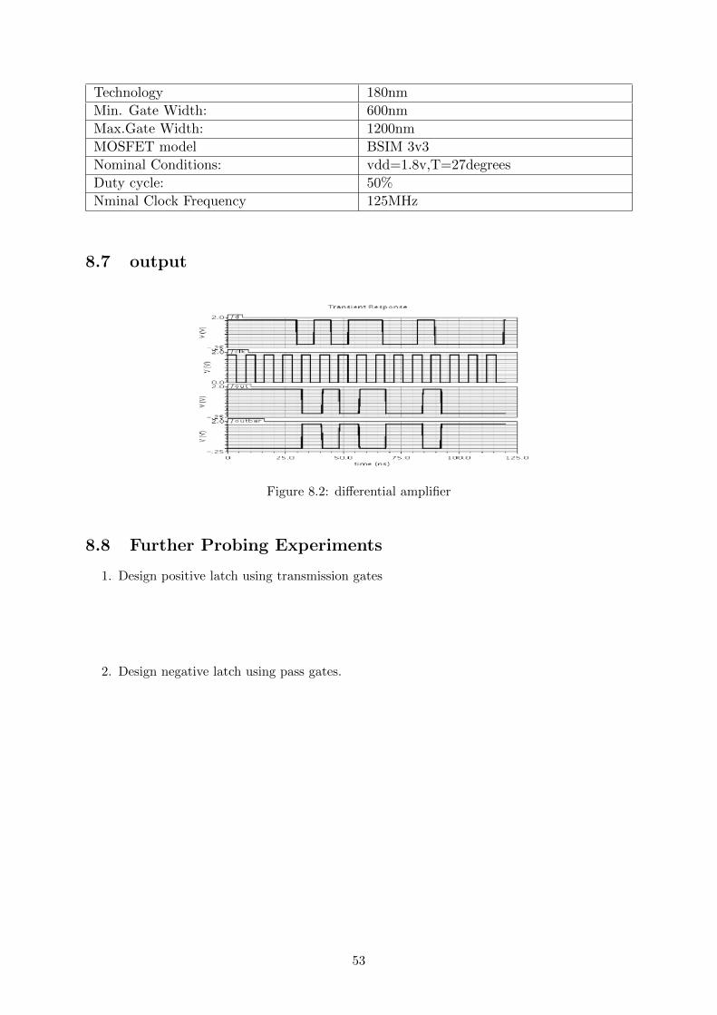
Technology 180nm
Min. Gate Width: 600nm
Max.Gate Width: 1200nm
MOSFET model BSIM 3v3
Nominal Conditions: vdd=1.8v,T=27degrees
Duty cycle: 50%
Nminal Clock Frequency 125MHz
8.7 output
Figure 8.2: differential amplifier
8.8 Further Probing Experiments
1. Design positive latch using transmission gates
2. Design negative latch using pass gates.
53

LAB-8 Registers
9.1 Introduction
The shift registers are used for temporary data storage. The shift registers are also used fordata transfer and data manipulation. The serial-in serial-out and parallel-in parallel-out shiftregisters are used to produce time delay in digital circuits. The serial-in parallel-out shift registeris used to convert serial data into parallel data.
9.2 Objectives
9.2.1 Educational
� Design registers using flip flops.� Understand the principle of operation of registers
9.2.2 Experimental
� Verify data storage using Registers.
9.3 Prelab Preparation:
Read Appendix B and Appendix C of this manual, paying particular attention to the methodsof using computer. Prior to coming to lab class, complete Part 0 of the Procedure.
9.4 Equipment needed
� Personal computer� Cadence software
9.5 Background
Master-Slave D Flip-Flop A master-slave D flip-flop is created by connecting two gated D latchesin series and inverting the enable input to one of them. It is called master-slave because thesecond (slave) latch in the series only changes in response to a change in the first (master) latch[2]. The term pulse-triggered means that data is entered on the rising edge of the clock pulse,but the output does not reflect the change until the falling edge of the clock pulse. Master-slaveflip-flops can be constructed to behave as a J-K, R-S, T or D flip-flop. The purpose of master-slave flip-flops is to protect a flip-flops output from inadvertent changes caused by glitches onthe input. Master-slave flip-flops are used in applications where glitches may be prevalent oninputs. The master-slave configuration has the advantage of being pulse-triggered, making it
54

easier to use in larger circuits, since the inputs to a flip-flop often depend on the state of itsoutput.
9.6 Procedure
Draw the Schematic and follow the steps what we did till now and do the simulation .
Figure 9.1: Schmitt trigger waveforms
9.7 Simualtion Result
Figure 9.2: simulation result
Did the simulation and observed the register operation
9.8 Further Probing Experiments
1. Design Master-Slave flip flop using some other gates?
55

2. Design negative latch using pass gates
56

LAB-9 Differential Amplifier
10.1 Introduction
A differential amplifier is a type of electronic amplifier that amplifies the difference between twoinput voltages but suppresses any voltage common to the two inputs
10.2 Objectives
10.2.1 Educational
� Design Differential amplifier using MOSFETS.� Explain the operation of Differential amplifiers.
10.2.2 Experimental
� Plot the output characteristics of Differential amplifiers.� Learn how to form circuit symbol and then use it for Non invering amplifier.
10.3 Prelab
Read Appendix B and Appendix C of this manual, paying particular attention to the methodsof using computer. Prior to coming to lab class, complete Part 0 of the Procedure.
10.4 Equipment needed
� Personal computer� Cadence software
10.5 Back ground
The differential amplifier (or subtractor) has two inputs and one output, as shown below. Thedifferential amplifier yields an output voltage which is proportional to the difference betweenthe inverting and the non-inverting input signals. By applying the superposition principle, theindividual effects of each input on the output can be determined. The cumulative effect on theoutput voltage is then the sum of the two separate inputs.
57

Figure 10.1: differential amplifier
10.6 Procedure
Figure 10.2: differential amplifier schematic
10.6.1 Creating a Schematic cellview
Open a new schematic window in the myDesignLib library and build the Differntial Amplifierdesign.1. In the CIW or Library manager, execute File – New – Cellview. Set up the Create New fileform as follows:
2. Click OK when done. A blank schematic window for the design appears.
58

Figure 10.3:
10.6.2 Adding Components to schematic
1. In the Differential Amplifier schematic window, execute Create— Instance to display the AddInstance form.2. Click on the Browse button. This opens up a Library browser from which you can selectcomponents and the Symbol view .You will update the Library Name, Cell Name, and theproperty values given in the table on the next page as you place each component.3.After you complete the Add Instance form, move your cursor to the schematic window and
Library name Cell Name Properties/Comments
gpdk180 nmos Model Name = nmos1 (NM0,NM1) ; W= 3u ; L= 1u ; BodyType : Detached
gpdk180 nmos Model Name =nmos1 (NM2,NM3) ; W= 4.5u ; L= 1u ;Body Type : Integrated
gpdk180 pmos Model Name =pmos1 (PM0,PM2); W= 15u ; L= 1u ;Body Type : Integrated
click left to place a component. This is a table of components for building the DifferentialAmplifier schematic. After entering components, click Cancel in the Add Instance form or pressEsc with your cursor in the schematic window.
10.6.3 Adding pins to Schematic
Use Create – Pin or the menu icon to place the pins on the schematic window. 1 Click the Pinfixed menu icon in the schematic window.You can also execute Create – Pin or press p. TheAdd pin form appears.2 Type the following in the Add pin form in the exact order leaving space between the pinnames.Make sure that the direction field is set to input/ouput/inputoutput when placing theinput/output/inout pins respectively and the Usage field is set to schematic.3 Select Cancel from the Add pin form after placing the pins.In the schematic window, executeView— Fit or press the f bindkey.
59

Pin Names Direction
Idc,V1,V2 Input
Vout Output
vdd, vss InputOutput
10.6.4 Adding Wires to a Schematic
Add wires to connect components and pins in the design1. Click the Wire (narrow) icon in the schematic window.You can also press the w key, orexecute Create - Wire (narrow).2. Complete the wiring as shown in figure and when done wiring press ESC key in the schematicwindow to cancel wiring.Saving the Design1. Click the Check and Save icon in the schematic editor window.2. Observe the CIW output area for any errors.
10.6.5 Symbol Creation
Objective: To create a symbol for the Differential Amplifier1 In the Differential Amplifier schematic window, execute Create — Cellview— From Cellview.2 The Cellview from Cellview form appears. With the Edit Options function active, you cancontrol the appearance of the symbol to generate.3 Verify that the From View Name field is set to schematic, and the To View Name field is setto symbol, with the Tool/Data Type set as SchematicSymbol.4 Click OK in the Cellview from Cellview form. The Symbol Generation Form appears.5 Modify the Pin Specifications as in the below symbol.6 Click OK in the Symbol Generation Options form.7 A new window displays an automatically created Differential Amplifier symbol. 8 Modifyingautomatically generated symbol so that it looks like below Differential Amplifier symbol.9 Execute Create— Selection Box. In the Add Selection Box form, click Automatic. A new redselection box is automatically added.10 After creating symbol, click on the save icon in the symbol editor window to save the symbol.In the symbol editor, execute File— Close to close the symbol view window.
60

Figure 10.4: differential amplifier symbol
Library name Cellview name Properties/Comments
myDesignLib Diff-amplifier Symbol
analogLib Vsin Define specification as AC Magnitude=1; Amplitude= 5m; Frequency= 1K
analogLib vdd, vss, gnd Vdd=2.5 ; Vss= -2.5
analogLib Idc Dc current = 30u
10.6.6 Building the Diff-amplifier-test Design
Objective: To build Differential Amplifier Test circuit using your Differential AmplifierCreating the Differential Amplifier Test Cellview.1. In the CIW or Library Manager, execute File— New— Cellview.2. Set up the Create New File form as follows:
3. Click OK when done. A blank schematic window for the Diff amplifier test design appears.
10.6.7 Building the Diff-amplifier-test Circuit
1 Using the component list and Properties/Comments in this table,build the Diff-amplifier-testschematic. Note: Remember to set the values for VDD and VSS. Otherwise your circuit willhave no power.2 Click the Wire (narrow) icon and wire your schematic.3 Tip: You can also press the w key, or execute Create— Wire (narrow).4 Click on the Check and save icon to save the design.5 The schematic should look like this.
61

Figure 10.5:
10.6.8 Analog Simulation with Spectre
Objective: To set up and run simulations on the Differential Amplifier Test design.In this section, we will run the simulation for Differential Amplifier and plot the transient, DCand AC characteristics.Starting the Simulation Environment 1. In the Diff-amplifier-test schematic window, exe-cute Launch – ADE L. 2. The Analog Design Environment simulation window appears. Choos-ing a Simulator1 In the simulation window or ADE, execute Setup— Simulator/Directory/Host. 2 In the Choos-ing Simulator form, set the Simulator field to spectre (Not spectreS) and click OK.Setting the Model Libraries1 Click Setup - Model Libraries. Note: Step 2 should be executed only if the model file notloaded by default. 2 In the Model Library Setup form, click Browse and find the gpdk180.scsfile in the ./models/spectre directory.Select stat in Section field, click Add and click OK.
10.6.9 Choosing Analyses
1. In the Simulation window, click the Choose - Analyses icon.You can also execute Analyses -Choose.The Choosing Analysis form appears. This is a dynamic form, the bottom of the form changesbased on the selection above.2. To setup for transient analysis a. In the Analysis section select tran b. Set the stop time as5m.c. Click at the moderate or Enabled button at the bottom, and then click Apply.3. To set up for DC Analyses:a. In the Analyses section, select dc.b. In the DC Analyses section, turn on Save DC Operating Point.c. Turn on the Component Parameter.d. Double click the Select Component, Which takes you to the schematic window.e. Select input signal Vsin for dc analysis.
62

Figure 10.6: differential amplifier test schematic
Figure 10.7:
f. In the analysis form, select start and stop voltages as -5 to 5 respectively.g. Check the enable button and then click Apply.4. To set up for AC Analyses form is shown in the previous page.a. In the Analyses section, select ac.b. In the AC Analyses section, turn on Frequency.c. In the Sweep Range section select start and stop frequencies as 150 to 100M d. Select Pointsper Decade as 20.e. Check the enable button and then click Apply.5. Click OK in the Choosing Analyses Form.
63

Figure 10.8:
10.6.10 Selecting Outputs for Plotting
Select the nodes to plot when simulation is finished.1. Execute Outputs – To be plotted – Select on Schematic in the simulation window.2. Follow the prompt at the bottom of the schematic window, Click on output net Vo, inputnet Vin of the Diff-amplifier. Press ESC with the cursor in the schematic after selecting node.
64

Figure 10.9:
10.6.11 Running the Simulation
1. Execute Simulation – Netlist and Run in the simulation window to start the simulation, thiswill create the netlist as well as run the simulation.2. When simulation finishes, the Transient, DC and AC plots automatically will be popped upalong with netlist.
Figure 10.10: Differential amplifier output
10.7 Result
Did the simulation and observed the Differential amplifier operation
65

10.8 Further Probing Experiments
1. Design opamp by using differential amplifier
2. Design inverting Opamp
66

LAB-10 NMOS AND CMOS INVERTER LAYOUT
11.1 Introduction
The design rules are formed to translate the circuit design concepts , (usually in stick diagramor symbolic form) into actual geometry in silicon. The design rules are the effective interfacebetween the circuit/system designer and the fabrication engineer. The design rules also helpto provide a reliable compromise between the circuit or system designer and the fabricationengineer. In general the circuit designers expect smaller layouts for improved performance anddecreased silicon area. On the other hand, the process engineer like those design rules thatresult in a controllable and reproducible process. In fact there is a need of compromise for acompetitive circuit to be produced at a reasonable cost.
11.2 Objectives
11.2.1 Educational
� Understand the lamda based and absolute design rules for optimum VLSI layouts.
11.2.2 Experimental
� Do the layout design for NMOS inverter.� Do the layout design for CMOS inverter.
11.3 Prelab Preparation
Read Appendix B and Appendix C of this manual, paying particular attention to the methodsof using computer. Prior to coming to lab class, complete Part 0 of the Procedure.
11.4 Equipment
� Personal computer
� Cadence software
11.5 Background
In this Lambda –base design rules all paths in all layers will be dimensioned in lambda units andsubsequently lambda can be allocated an appropriate value compatible with the feature size of
67

the fabrication process. These design rules are such that, if correctly obeyed, the mask layoutswill produce working circuits for a range of values allocated to lambda. For example,lambdacan be allocated a value of 1.0µm so that minimum feature size on chip will be 2 µm (2lambda).Design rules, also, specify line widths, separations, and extensions in terms of lambda.Creating Layout View of Inverter
1. From the Inverter schematic window menu execute Launch – Layout XL. A Startup Op-tion form appears.
2. Select Create New option. This gives a New Cell View Form
3. Check the Cellname (Inverter), Viewname (layout).
4. Click OK from the New Cellview form.
5. LSW and a blank layout window appear along with schematic window.
Adding Components to Layout
1. Execute Connectivity – Generate – All from Source or click the icon in the layout editorwindow, Generate Layout form appears. Click OK which imports the schematic compo-nents in to the Layout window automatically.
2. Re arrange the components with in PR-Boundary as shown in the next page.
3. To rotate a component, Select the component and execute Edit –Properties. Now selectthe degree of rotation from the property edit form.
4. To Move a component, Select the component and execute Edit -Move command. Makinginterconnection.
5. Execute Connectivity–Nets–Show or Hide selected Incomplete Nets or click .
6. Move the mouse pointer over the device and click LMB to get the connectivity information,which shows the guide lines (or flight lines) for the inter connections of the components.
7. From the layout window execute Create – Shape – Path-Create wire or Create – Shape –Rectangle (for vdd and gnd bar) and select the appropriate Layers from the LSW windowand Vias for making the inter connections.
Creating Contacts-Vias.You will use the contacts or vias to make connections between two different layers.
1. Execute Create — Via or select-command to place different Contacts, as given in formetal1– Poly Connection use Metal1-Poly contact type, for For Metal1- Psubstrate Con-nection use Metal1-Psub contact type,for For Metal1- Nwell Connection connection useMetal1-Nwell contact type. Saving the design
68

Figure 11.1: inverter layout
2. Save your design next do Physical Verification:Assura DRCRunning a DRC� Open the Inverter layout form the CIW or library manger if you have closed that. Pressshift – f in the layout window to display all the levels.� Select Assura - Run DRC from layout window. The DRC form appears. The Libraryand Cellname are taken from the current design window, but rule file may be missing.Select the Technology as gpdk180. This automatically loads the rule file.� Your DRC form should appear like this� Click OK to start DRC.� A Progress form will appears. You can click on the watch log file to see the log file.� When DRC finishes, a dialog box appears asking you if you want to view your DRCresults, and then click Yes to view the results of this run.� If there any DRC error exists in the design View Layer Window (VLW) and Error LayerWindow (ELW) appears. Also the errors highlight in the design itself.� Click View – Summary in the ELW to find the details of errors.� You can refer to rule file also for more information, correct all the DRC errors and Re –run the DRC.
69

Figure 11.2: inverter layout
� If there are no errors in the layout then a dialog box appears with No DRC errors foundwritten in it, click on close to terminate the DRC run.ASSURA LVS � In this section we will perform the LVS check that will compare theschematic netlist and the layout netlist.Running LVS � Select Assura – Run LVS from the layout window. The Assura Run LVSform appears. It will automatically load both the schematic and layout view of the cell.� Change the following in the form and click OK.
70

Figure 11.3:
3. Click use template at the bottom of the New Configuration form and select Spectre in thecyclic field and click OK. The Global Bindings lists are loaded from the template.
Figure 11.4:
4. Change the Top Cell View to schematic and remove the default entry from the LibraryList field.
5. Click OK in the New Configuration form.The hierarchy editor displays the hierarchy forthis design using table format.
71

Figure 11.5:
Figure 11.6:
6. Click the Tree View tab. The design hierarchy changes to tree format.
7. Save the current configuration.
8. Close the Hierarchy Editor window. Execute File – Close Window.
To run the Circuit without Parasites
1. From the Library Manager open Inverter-Test Config view.Open Configuration or Top cellview form appears.
2. In the form, turn on the both cyclic buttons to Yes and click OK.The Inverter-Test schematic and Inverter-Test config window appears. Notice the windowbanner of schematic also states Config: myDesignLib Inverter-Test config.
72

Figure 11.7:
Figure 11.8:
3. Execute Launch – ADE L from the schematic window.
4. Now you need to follow the same procedure for running the simulation. Executing Session–Load state, the Analog Design Environment window loads the previous state.
5. Click Netlist and Run icon to start the simulation.The simulation takes a few seconds andthen waveform window appears.
6. In the CIW, note the netlisting statistics in the Circuit inventory section. This list includesall nets, designed devices, source and loads. There are no parasitic components. Also notedown the circuit inventory section.
Measuring the Propagation Delay
1. In the waveform window execute Tools – Calculator.
2. The calculator window appears.
3. Place the cursor in the text box for Signal1, select the wave button and select the inputwaveform from the waveform window.
4. Repeat the same for Signal2, and select the output waveform.
5. Set the Threshold value 1 and Threshold value 2 to 0.9, this directs the calculator tocalculate delay at 50 percent i.e at 0.9 volts.
73

Figure 11.9:
6. Execute OK and observe the expression created in the calculator buffer. Click on Evalu-ate the buffer icon to perform the calculation, note down the value returned after execution.
7. Close the calculator window.
To run the Circuit with ParasitesIn this exercise, we will change the configuration to direct simulation of the av-extracted viewwhich contains the parasites.
1. Open the same Hierarchy Editor form, which is already set for Inverter-Test config.
2. Select the Tree View icon: this will show the design hierarchy in the tree format.
3. Click right mouse on the Inverter schematic. A pull down menu appears. Select av-extracted view from the Set Instance view menu, the View to use column now showsav-extracted view.-
Figure 11.10:
4. Click on the Recompute the hierarchy icon, the configuration is now updated from schematicto av-extracted view.
74

5. From the Analog Design Environment window click Netlist and Run to start the simulationagain.
6. When simulation completes, note the Circuit inventory conditions, this time the list showsall nets, designed devices, sources and parasitic devices as well.
7. Calculate the delay again and match with the previous one. Now you can conclude howmuch delay is introduced by these parasites, now our main aim should to minimize thedelay due to these parasites so number of iteration takes place for making an optimizelayout.
Generating Stream Data Streaming Out the Design
1. Select File – Export – Stream from the CIW menu and Virtuoso Xstream out form appearschange the following in the form.
2. Click on the Options button.
3. In the StreamOut-Options form select under Layers tab and click OK.
4. In the Virtuoso XStream Out form, click Translate button to start the stream translator.
5. The stream file Inverter.gds is stored in the specified location.
Streaming In the Design
1. Select File – Import – Stream from the CIWmenu and change the following in the form.Youneed to specify the gpdk180-oa22.tf file
Figure 11.11:
2. Click on the Options button.
3. In the StreamOut-Options form select under Layers tab and click OK.
4. In the Virtuoso XStream Out form, click Translate button to start the stream translator.
5. From the Library Manager open the Inverter cellview from the GDS-LIB library and noticethe design.
6. Close all the windows except CIW window, which is needed for the next lab.
75

11.6 Further Probing Experiments
1. Design Layout design for Ring oscillator in NMOS design style
2. Using CMOS design style do the layout design for Ring oscillator
76

LAB-11 LAYOUT OF 2-INPUT NAND, NOR GATES
12.1 Introduction
The design rules are formed to translate the circuit design concepts , (usually in stick diagramor symbolic form) into actual geometry in silicon. The design rules are the effective interfacebetween the circuit/system designer and the fabrication engineer. The design rules also help toprovide a reliable compromise between the circuit/system designer and the fabrication engineer.In general the circuit designers expect smaller layouts for improved performance and decreasedsilicon area. On the other hand, the process engineer like those design rules that result in acontrollable and reproducible process. In fact there is a need of compromise for a competitivecircuit to be produced at a reasonable cost.
12.2 Objective
12.2.1 Educational
� Understand the lamda based and absolute design rules for optimum VLSI layouts.
12.2.2 Experimental
� Do the layout design for two input NAND Gate� Do the layout design for two input NOR Gate
12.3 Prelab Preparation:
� Read Appendix B and Appendix C of this manual, paying particular attention to the methodsof using computer. Prior to coming to lab class, complete Part 0 of the Procedure.
12.4 Equipment needed
� Personal computer� Cadence software.
12.5 Background
In this Lambda –base design rules all paths in all layers will be dimensioned in lambda units andsubsequently lambda can be allocated an appropriate value compatible with the feature size ofthe fabrication process. These design rules are such that, if correctly obeyed, the mask layoutswill produce working circuits for a range of values allocated to lambda. For example, lambdacan be allocated a value of 1.0µm so that minimum feature size on chip will be 2 µm (2lambda).Design rules, also, specify line widths, separations, and extensions in terms of lambda.
77

12.6 Procedure
Use the techniques learned in the Lab2.1 to complete the layout of NAND gate. Complete theDRC, LVS check using the assura tool.
Extract RC parasites for back annotation and Re-simulation.
Figure 12.1:
12.7 Further Probing Experiments
1. Design Layout design for three input NOR Gate
2. Design Layout design for three input NAND Gate
78

LAB-12 COMMON SOURCE AMPLIFIER
13.1 Introduction
When the input signal is applied at the gate terminal and source terminal, then the outputvoltage is amplified and obtained across the resistor at the load in the drain terminal. This iscalled a common source amplifier. Here source acts as a common terminal between the input andoutput. It is also known as a voltage amplifier or a trans-conductance amplifier. It producescurrent gain and voltage gain according to the input impedance and output Impedance. Toproduce voltage gain along with high input impedances FET’s are used in these circuit.
13.2 Objectives
13.2.1 Educational
� Design common source amplifier using NMOSFETs.� Understand the operation of MOSFET amplifiers.
13.2.2 Experimental
� Plot the output characteristics common source amplifier using NMOSFETs.� Plot the transfer characteristics common source amplifier using NMOSFETs.
13.3 Prelab Preparation
Read Appendix B and Appendix C of this manual, paying particular attention to the methodsof using computer. Prior to coming to lab class, complete Part 0 of the Procedure.
13.4 Equipment
� Personal computer � Cadence software
13.5 Back ground
N-channel eMOSFET I-V Characteristics
With a fixed VDS drain-source voltage connected across the eMOSFET we can plot the valuesof drain current, ID with varying values of VGS to obtain a graph of the mosfets forward DCcharacteristics. These characteristics give the transconductance, gm of the transistor. Thistransconductance relates the output current to the input voltage representing the gain of thetransistor. The slope of the transconductance curve at any point along it is therefore given as:
79

Figure 13.1: NMOSFET I-V characteristics
gm = ID/VGS for a constant value of VDS. So for example, assume a MOS transistor passesa drain current of 2mA when VGS = 3v and a drain current of 14mA when VGS = 7v. Theratio between drain current-Id and gate to source voltage(vgs) is called the transistors static orDC transconductance which is short for “transfer conductance” and is given the unit of Siemens(S), as its amps per volt. Voltage gain of a mosfet amplifier is directly proportional to thetransconductance and to the value of the drain resistor.
13.6 Procedure
13.6.1 Schematic entry
Figure 13.2: Common source amplifier cell view
� Use the techniques learned in the inverter to complete the schematic of Common SourceAmplifier.
� This is a table of components for building the Common Source Amplifier schematic.
80

Library name Cell Name properties/comments
gpdk180 Pmos Modelname=pmos1;W=50u;L=1u;body type:integrated
gpdk180 Nmos Modelname=nmos1;W=10u;L=1u;body type:integrated
� Type the following in the ADD pin form in the exact order leaving space between thepin names. Symbol Creation Objective: To create a symbol for the Common Source
Pin Names Direction
vin vbias Input
vout Output
vdd vss Input
Amplifier
� Use the techniques learned in the inverter to complete the symbol of cs-amplifier. Buildingthe Common Source Amplifier Test Design Objective: To build cs-amplifier-testcircuit using your cs-amplifier
� Using the component list and Properties/Comments in the table, build the cs-amplifier-testschematic as shown below.
Figure 13.3: Common source amplifier symbol in cadence
81

Library name Cellview name Properties/Comments
myDesignLib csamplifier Symbol
analogLib vsin Define pulse specification asAC Magnitude= 1; DC Volt-age= 0;Offset Voltage= 0;Amplitude= 5m;Frequency=1K
analogLib vdd,vss,gnd vdd=2.5 ; vss= -2.5 vbias=-2.5
Figure 13.4: Common source amplifier symbol in cadence
Use the techniques learned in the inverter to complete the simulation of cs-amplifier, ADEwindow and waveform should look like below.
82
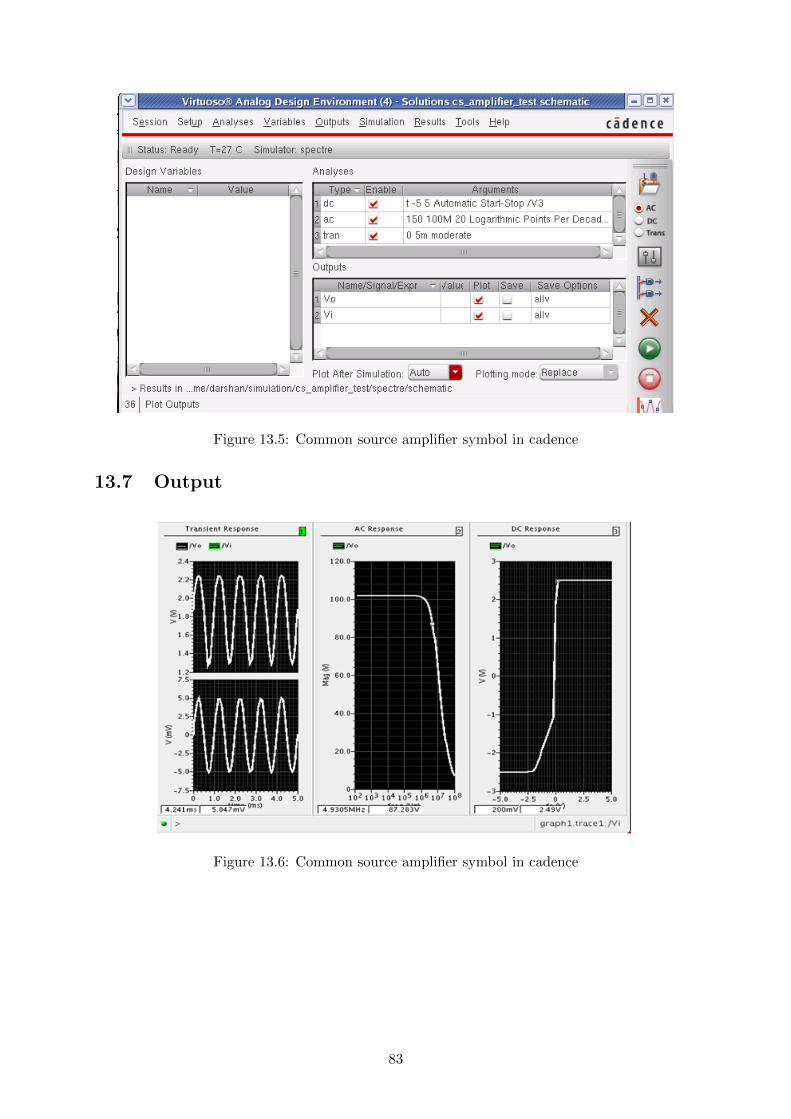
Figure 13.5: Common source amplifier symbol in cadence
13.7 Output
Figure 13.6: Common source amplifier symbol in cadence
83

13.8 Further Probing Experiments
1. Design common source amplifier using PMOSFETs enhancement type
2. Design common source amplifier using PMOSFETs depletion type
84

LAB-13 COMMON DRAIN AMPLIFIER
14.1 Introduction
In the Common Drain Amplifier configuration, the drain terminal is at AC ground. The input isapplied between the gate and drain terminals, while the output is measured between the sourceand drain terminal. Since the drain terminal is common between the input and output side, itis known as Common Drain Amplifier
14.2 Objectives
14.2.1 Educational
� Design common drain amplifier using NMOSFETs � Understand the operation of MOSFETamplifiers.
14.2.2 Experimental
� Plot the output characteristics common drain amplifier using NMOSFETs � Plot the transfercharacteristics common drain amplifier using NMOSFETs
14.3 Prelab Preparation
Read Appendix B and Appendix C of this manual, paying particular attention to the methodsof using computer. Prior to coming to lab class, complete Part 0 of the Procedure. Equipment
14.4 Equipment
� Personal computer � Cadence software
14.5 Background
Figure below shows the source follower circuit in which drain terminal of the device is common.In this circuit the drain terminal is directly connected to VDD. In CS amplifier analysis wehave seen that in order to achieve the high voltage gain the load impedance should be as highas possible. Therefore for low impedance load the buffer must be placed after the amplifier todrive the load with negligible loss of the signal level. The source follower thus worked as a bufferstage. The source follower is also called as the common drain amplifier. In this circuit, thesignal at the gate is sensed and drives the load at the source which allows the source potentialto follow the gate voltage. The small signal equivalent circuit of the source follower is shown inFigure below.
85

Figure 14.1: small signal equivalent circuit of the source follower
14.6 Procedure
14.6.1 Schematic Entry
Objective: To create a new cell view and build Common Drain Amplifier � Use the techniqueslearned in the Lab1 and Lab2 to complete the schematic of Common Drain Amplifier.
Figure 14.2: source follower schematic
86

�Type the following in the ADD pin form in the exact order leaving space between the pinnames.
14.6.2 Symbol Creation
Objective:To create a symbol for the Common Drain Amplifier �Use the techniques learned inthe Lab1 and Lab2 to complete the symbol of cd-amplifier.
Figure 14.3: source follower symbol
14.6.3 Building the Common Drain Amplifier Test Design
Objective: To build cd-amplifier-test circuit using your cd-amplifier � Using the componentlist and Properties/Comments in the table,build the cd-amplifier-test schematic as shown below.
Library name Cellview name Properties/Comments
myDesignLib cd-mplifier Symbol
analogLib vsin Define pulse specification as AC Mag-nitude= 1; DC Voltage= 0; Offset Volt-age= 0; Amplitude= 5m; Frequency=1K
analogLib vdd,vss,gnd vdd=2.5 ; vss= -2.5
87

Figure 14.4: source follower test symbol
14.6.4 Analog simulation with spectre
� Use the techniques learned in the Lab1 and Lab2 to complete the simulation of cd-amplifier,ADE window and waveform.
88

Figure 14.5: output
14.7 Further Probing Experiments
1. Design common drain amplifier using PMOSFETs enhancement type
2. Design common drain amplifier using PMOSFETs depletion type
89

Appendix A - Safety
Electricity, when improperly used, is very dangerous to people and to equipment. This is espe-cially true in an industrial environment where large amounts of power is used, and where highvoltages are present [1]; in environments where people are especially susceptible to electric shocksuch as maintenance of a high voltage system (while in operation) or in hospitals where electricalequipment is used to test or control physiological functions [2, 3]; and in an experimental orteaching laboratory where inexperienced personnel may use electrical equipment in experimentalor nonstandard configuration.Engineers play a vital role in eliminating or alleviating the danger in all three types of en-vironments mentioned above. For conditions where standard equipment is used in standardconfigurations, govern- mental agencies and insurance underwriters impose strict laws and regu-lations on the operation and use of electrical equipment including switchgear, power lines, safetydevices, etc. As a result, corporations and other organizations in turn impose strict rules andmethods of operation on their employees and contractors. Engineers who are involved in usingelectrical equipment, in supervising others who use it, and in designing such systems, have agreat responsibility to learn safety rules and practices, to observe them, and to see that a safeenvironment is maintained for those they supervise. In any working environment there is al-ways pressure to “get the job done” and take short cuts. The engineer, as one who is capableof recognizing hazardous conditions, is in a responsible position both as an engineer and as asupervisor or manager and must maintain conditions to protect personnel and avoid damage toequipment.Because of their non-standard activities, experimental laboratories are exempt from many ofthese rules and regulations. This puts more responsibility on the engineer in this environmentto know and enforce the safest working procedures.The knowledge and habit-forming experience to work safely around electrical equipment and theability to design safe electrical equipment begins with the first student laboratory experienceand con- tinues through life. This includes learning the types of electrical injuries and damage,how they can be prevented, the physiology of electrical injuries, and steps to take when accidents.
90

Physiology of Electrical Injuries
There are three main types of electrical injuries: electrical shock, electrical burns, and fallscaused by electrical shock. A fourth type, ’sunburned’ eyes from looking at electric arcs, suchas arc-welding, is very painful and may cause loss of work time but is usually of a temporarynature. Other injuries may be indirectly caused by electrical accidents, e.g., burns from explod-ing oil-immersed switch gear or transformers.Although electric shock is normally associated with high-voltage AC contact, under some circum-stances death can occur from voltages from substantially less than the nominal 120 Volts ACfound in residential systems. Electric shock is caused by an electric current passing through apart of the human body. The human body normally has a high resistance to electric currentsso that a high voltage is usually required to cause lethal currents. This resistance is almost allin the skin, but when the skin is wet its resistance is much lower. When a person is hot andsweaty or is standing in water, contact with 120 Volts or less is likely to cause a fatal shock.Electric shock is not a single phenomenon but is a disturbance of the nerves that is caused byelectric current. A current through a part of the body such as the arm or leg will cause pain andmuscle contraction. If a victim receives an electric shock from grasping a live conductor, a cur-rent of greater than 15 to 30 mA through the arm will cause muscle contractions so severe thatthe victim cannot let go. Similar currents through leg muscles may cause sudden contractionscausing the victim to jump or fall, resulting in possible injuries or death. It is also possible for aprolonged period of contact of more than a minute or so to cause chest muscles to be contracted,preventing breathing and resulting in suffocation or brain damage from lack of oxygen.The predominant cause of death by electric shock is generally attributed to ventricular fibrilla-tion, which is an uncontrolled twitching or beating of the heart that produces no pumping actionand therefore no blood circulation. Unless corrective action is taken, death follows quickly fromlack of oxygen to the brain. While the amount of current that will cause fibrillation depends onseveral variables, 0.5 to 5A through the body will normally cause the very small current throughthe heart that causes fibrillation in most people. Larger currents than this through the heartcauses contraction or clamping of the heart muscle and resulting death unless corrective actionis taken. Prolonged contact of more than a minute or so may cause chest muscles to contract,preventing breathing and resulting in suffocation or brain damage from lack of oxygen.Death by electric shock is most often attributed to ventricular fibrillation, which is an uncon-trolled twitching or beating of the heart that produces no pumping action and therefore noblood circulation. Unless corrective action is taken, death follows quickly from lack of oxygen tothe brain. While the amount of current that will cause fibrillation depends on several variables,0.5 to 5 amperes through the body will normally cause the very small current (approximately1 mA) through the heart that is sufficient to cause fibrillation in most people. Larger currentsthan this through the heart cause contraction or clamping of the heart muscle, resulting in deathunless corrective action is taken.Electric burns may be caused by electric currents flowing in or near parts of the body. Such burnsare similar to burns from ordinary heat sources, except that those caused by high-frequency cur-rents are generally deeper and take longer to heal the other burns. Electrocution will often leavesevere burns at the points where the current entered and left the body.
Source of Electric Shock
Since electric shock is caused by an electric current through a part of the body, it is preventedby not allowing the body to become part of any electric circuit. From this viewpoint, electriccircuits may be classified as either grounded or ungrounded.Electric circuits may be classified as either grounded or ungrounded. Grounded circuits are safer
91

for most conditions, since they result in known voltages at other points in the circuit and provideeasier and better protection against faulty conditions in the circuit. The disadvantage is that aperson standing on a non-insulated floor can receive a shock by touching only one conductor.Almost all electric power generation, transmission, and distribution systems are grounded to pro-tect people and equipment against fall conditions caused by windstorms, lightning, etc. Resi-dential, commercial, and industrial systems such as lighting and heating are always grounded forgreater safety. Communication, computer, and similar systems are grounded for safety reasonsand to prevent or reduce noise, crosstalk, static, etc. Many electronic equipment or instrumentsare grounded for safety and noise prevention, also. Common examples are DC power supplies,oscilloscopes, oscillators, and analog and digital multimeters.Ungrounded circuits are used in systems where isolation from other systems is necessary, wherelow voltages and low power are used, and in other instances where obtaining a ground connec-tion is difficult or impractical. In the ungrounded circuit, contact with two points in the circuitthat are at different potentials is required to produce an electrical shock. The hazard is thatwith no known ground, a hidden fault can occur, causing some unknown point to be grounded,in which case, touching a supposedly safe conductor while standing on the ground could resultin an electric shock.
Protecting People and Equipment in the Laboratory
Prevention of electric shock to individuals and damage to equipment in the laboratory can bedone by strict adherence to several common-sense rules summarized below:Protecting People
1. When hooking up a circuit, connect to the power source last, while power is off.
2. Before making changes in a circuit, turn off or disconnect the power first, if possible.
3. Never work alone where the potential of electric shock exists.
4. When changing an energized connection, use only one hand. Never touch two points inthe circuit that are at different potentials.
5. Know that the circuit and connections are correct before applying power to the circuit.
6. Avoid touching capacitors that may have a residual charge. The stored energy can causea severe shock even after a long period of time.
7. Insulate yourself from ground by standing on an insulating mat where available.
The above rules and the additional rules given below also serve to protect instruments and othercircuits from damage.Protecting Equipment
1. Set the scales of measurement instrument to the highest range before applying power.
2. Before making changes in a circuit, turn off or disconnect the power first, if possible.
3. When using an oscilloscope, do not leave a bright spot or trace on the screen for longperiods of time. Doing so can burn the image into the screen.
4. Be sure instrument grounds are connected properly. Avoid ground loops and accidentalgrounding of “hot” leads.
5. Check polarity markings and connections of instruments carefully before connecting power.
92

6. Never connect an ammeter across a voltage source, but only in series with a load.
7. Do not exceed the voltage or current ratings of circuit elements or instruments. Thisparticularly applies to wattmeters, since the current or voltage rating may be exceededwith the needle still reading on the scale.
8. Be sure any fuses and circuit breakers are of suitable value.
When connecting electrical elements to make up a network in the laboratory, it easy to losetrack of various points in the network and accidentally connect a wire to the wrong place. Oneprocedure to help avoid this problem is to connect first the main series loop of the circuit, thengo back and add the elements in parallel.Types of Equipment Damage Excessive currents and voltages can damage instruments andother circuit elements. A large over- current for a short time or a smaller over-current for alonger time will cause overheating, resulting in insulation scorching and equipment failure.Blown fuses are the most common equipment failure mode in this laboratory. The principalcauses for these failures include:� incorrectly wired circuits;� accidental shorts;� switching resistance settings while power is applied to the circuit;� changing the circuit while power is applied;� using the wrong scale on ammeter;� connecting an ammeter across a voltage source;� using a low-power resistor box (limit 1/2 amp) when high power is required;� turning on an auto-transformer at too high a setting.
All of these causes are the result of carelessness by the experimenter.
Some type of insulating material, such as paper, cloth, plastic, or ceramic, separates conduc-tors that are at different potentials in electrical devices. The voltage difference that this materialcan withstand is determined by design (type, thickness, moisture content, temperature, etc.).Exceeding the voltage rating of a device by an appreciable amount can cause arcing or corona,resulting insulation breakdown, and failure.
Some electrical devices can also be damaged mechanically by excessive currents. An exampleis the D’Arsonval meter, the indicator in most analog metering instruments. A large pulse ofover current will provide mechanical torque that can cause the needle to wrap around the pin atthe top of the scale, thereby causing permanent damage even though the current may not havebeen on long enough to cause failure due to overheating.
After Accident ActionSince accidents do happen despite all efforts to prevent them, plans for appropriate reaction
to an accident can save time and lives. Such a plan should include immediate availability of firstaid material suitable for minor injuries or for injuries that are likely because of the nature ofthe work. Knowledge of how to obtain trained assistance such as Emergency Medical Services(EMS) should be readily available for everyone.
Treating victims for electrical shock includes four basic steps that should be taken immedi-ately. Step two requires qualification in CPR and step three requires knowledge of mouth-to-mouth resuscitation. Everyone who works around voltages that can cause dangerous electricalshock should take advantage of the many opportunities available to become qualified in CPRand artificial respiration.Immediate Steps After Electric Shock
93

1. Shut off all power and remove victim from the electric circuit. If the power cannot be shutoff immediately,use an insulator of some sort, such as a wooden pole, to remove victimfrom the circuit. Attempts to pull the victim from the circuit with your hands will almostalways result in your joining the victim in the electric shock.
2. If you are qualified in CPR, check for ventricular fibrillation or cardiac arrest. If either isdetected, external cardiac massage should be started at once. Whether you are qualified inCPR or not, notify EMS and the ECE Department at once, using the telephone numberslisted below.
3. Check for respiratory failure and take appropriate action. This may have resulted fromphysical paralysis of respiratory muscles or from a head injury. Sometimes many hourspass before normal respiration returns. Artificial respiration should be continued untiltrained EMS assistance arrives.
4. Check for and treat other injuries such as fractures from a fall or burns from currententry and exit sites. Investigations are always after accidents. As an engineer you will beinvolved as a part of the investigating team or in providing information to an investigator.Information obtained and notes written immediately after the emergency will aid thisinvestigation and assist in preventing future accidents of a similar nature.
Investigations are always made after accidents. As an engineer, you will be involved as apart of the investigating team or in providing information to an investigator. Information ob-tained and notes written immediately after the emergency will aid the investigation and assistin preventing future accidents of a similar nature.Emergency NumbersFire / EMS: 911 or (864) 656-2222Student Health Center: (864) 656-2233ECE Department Office: (864) 656-5650
94

Appendix B - CADENCE
The Cadence tool kit consist of several programs for different applications such as schematicdrawing, layout, verification, and simulation. These applications can be used on various com-puter platforms. The open architecture also allows for integration of tools from other vendors orof own design. The integration of all this tools is done by a program called Design FrameworkII (DFW). The DFW-application is the cornerstone in the Cadence environment. It provides acommon user interface and a common data base to the tools used. This makes it possible toswitch between different applications without having to convert the data base.Cadence User Interface In Cadence the user interface is graphic and based on windows, forms,and menus. The main windows of DFW are: Command Interpreter Window (CIW) is control-ling the environment. Other tools can be started from here and it also serves a log windowfor many applications. Library Manager gives a view of the design libraries and the differentconstructions that exists therein. Design Window (DW) shows the current design. It is possibleto have several DW opened at the same time with different, or the same, tools. Text Window(TW) show text. It can be a log or report that was asked for, or an editor. The menus inCadence are mostly pull-downs, i.e. the menu will appear when the title are clicked with the leftbutton on the mouse. There are also pop-up menus that appear in the background of the designwindow on a middle button press. The forms are used for entering some specific informationthat is needed by the function called, the size of a transistor for instance.
95

Appendix C - LAMDA BASED DESIGN RULES
Design Rules and Layout :
The design rules are formed to translate the circuit design concepts , (usually in stick diagramor symbolic form) into actual geometry in silicon. The design rules are the effective interfacebetween the circuit/system designer and the fabrication engineer. The design rules also help toprovide a reliable compromise between the circuit/system designer and the fabrication engineer.In general the circuit designers expect smaller layouts for improved performance and decreasedsilicon area. On the other hand, the process engineer like those design rules that result in acontrollable and reproducible process. In fact there is a need of compromise for a competitivecircuit to be produced at a reasonable cost.One of the important factors associated with design rules is the achievable definition of theprocess line. For example, it is found that if a 10: 1 wafer stepper is used instead of a 1:1 projection mask aligner; the level-to-level registration will be closer. Design rules can beaffected by the maturity of the process line. For example, if the process is mature, then one canbe assured of the process line capability, allowing tighter designs with fewer constraints on thedesigner.The simple and well known design rules that are widely used in the design of multiproject chipsare ’lambda -based’ design rules developed by Mead and Conway .
Lambda-based Design Rules :
In this Lambda –base design rules all paths in all layers will be dimensioned inlambda units andsubsequently lambda can be allocated an appropriate value compatible with the feature size ofthe fabrication process. These design rules are such that, if correctly obeyed, the mask layoutswill produce working circuits for a range of values allocated to lambda. For example, lambdacan be allocated a value of 1.0µm so that minimum feature size on chip will be 2 µm (2lambda).Design rules, also, specify line widths, separations, and extensions in terms of .
96