Transistor-level estimation of worst-case delays in MOS VLSI circuits
12
384 IEEE TRANSACTIONS ON COMPUTER-AIDED DESIGN, VOL. II, NO. 3, MARCH 1992 Transistor-Level Estimation of Worst-Case Delays in MOS VLSI Circuits Michel R. Dagenais, Member, IEEE, Serge Gaiotti, Member, IEEE, Nicholas C. Rumin, Senior Member, IEEE Abstract-This paper presents three new algorithms for effi- ciently performing worst-case delay estimation in transistor groups using transistor-level delay models and timing simula- tion techniques. The first algorithm, dynamic path selection (DPS), determines the path with the longest delay in a transis- tor group. If the group consists of series-parallel transistor combinations, the time complexity is linear. The second algo- rithm, delay subnetwork enumeration (DSE), complements the DPS method by taking into account logic dependencies. The paths with the shortest delay are computed using the dynamic cut selection (DCS) algorithm. These techniques have been im- plemented in the static timing analyzer TAMIA to provide fast and accurate worst-case delay estimation for digital CMOS cir- cuits. I. INTRODUCTION NE of the important problems in the optimization and 0 verification of digital MOS circuits is determining the paths of the circuit with the longest and shortest delays. These delay paths are used extensively in timing verifi- cation [ 11, in timing optimization [2], and in optimal tran- sistor sizing [3]. Efficient solutions to this problem are all based on the use of critical path methods (PERT) [4], where the circuit is partitioned into blocks, with unidirectional input and output ports, to form a directed acyclic graph. Once the worst-case delay of each block of the circuit has been de- termined, the paths with the longest and shortest delays can be traced for the entire circuit. The two most common forms of circuit partitioning are into logic gates or transistor groups. In the case of MOS circuits the preferred partitioning is into groups since the circuit structures that are used do not always lend them- selves to a simple gate-level interpretation. Transistor groups, also called dc-connected or channel-connected components, are subcircuits in which the transistors are connected to each other by their channels to supply (Vdd or GROUND) or output nodes. A transistor group can be Manuscript received July 10, 1990; revised December 13, 1990. This work was supported by the Natural Sciences and Engineering Research Council of Canada, the Ministry of Higher Education and Science of Que- bec through its “actions structurantes” program, and the Canadian Micro- electronics Corporation. This paper was recommended by Associate Editor R. E. Bryant. M. R. Dagenais is with the Departement de genie electrique, Ecole Polytechnique, C.P. 6079, Succ. A, Montrkal, Qukbec, Canada, H3C 3A7. S. Gaiotti was with the Department of Electrical Engineering, McGill University, 3480 University Street, Montreal, Quebec, Canada, H3A 2A7. He is now with Bell-Northem Research, P.O. Box 3511, Station C, Ot- tawa, Ontario, Canada K1Y 4H7. N. C. Rumin is with the Department of Electrical Engineering, McGill University, 3480 University Street, Montreal, Quebec, Canada, H3A 2A7. IEEE Log Number 9 104229. Vdd T Pull-up t Out’ P- Out2 Pull-down t Gnd 4 Fig. 1. Transistor group: (a) group; (b) subgroups further decomposed into two-terminal subgroups, which connect supply and output nodes together. Fig. 1 shows a transistor group and its decomposition into pull-down, pull-up, and pass-transistor subgroups. A popular method for computing the propagation delay of a transistor group is to use a simple switch-level RC delay model [5]. Such models, however, have a limited accuracy owing to their poor treatment of the effects of the shape and arrival time of the input waveforms. Recent static timing analysis tools, such as CRYSTAL2 [6], SLOCOP [7], and TAMIA [8], use transistor-level delay models and relaxation solution techniques to obtain more robust and accurate delay computations. The worst-case delay estimation of a transistor group consists of the determination of the latest and earliest ris- ing and falling transitions at each output node. The latest transitions determine the maximum operating frequency of a circuit, while the earliest ones are needed to detect timing violations caused by clock skew. The latest output transition of a group is associated with a single path consisting of series-connected transistors. It is the slowest path because it conducts the smallest cur- rent, compared with all the alternative paths and, there- fore, takes the longest time to charge or discharge the out- put and intermediate node capacitances. In CRYSTAL [9], all the paths between a supply (Vdd or GROUND) and an output node are dynamically ex- tracted and are passed to a delay estimation routine. These paths, called stages, give the propagation delay of a tran- sition from the gate of the driver transistor to the gate of the target transistor, as shown in Fig. 2(a). All the other transistors in the stage are set on to allow the transition to reach the target gate. The transition on the gate of the driver is characterized by its arrival time and slew rate. 0278-0070/92$03.00 O 1992 IEEE ~~
-
Upload
independent -
Category
Documents
-
view
1 -
download
0
Transcript of Transistor-level estimation of worst-case delays in MOS VLSI circuits
384 IEEE TRANSACTIONS ON COMPUTER-AIDED DESIGN, VOL. I I , NO. 3, MARCH 1992
Transistor-Level Estimation of Worst-Case Delays in MOS VLSI Circuits
Michel R. Dagenais, Member, IEEE, Serge Gaiotti, Member, IEEE, Nicholas C. Rumin, Senior Member, IEEE
Abstract-This paper presents three new algorithms for effi- ciently performing worst-case delay estimation in transistor groups using transistor-level delay models and timing simula- tion techniques. The first algorithm, dynamic path selection (DPS), determines the path with the longest delay in a transis- tor group. If the group consists of series-parallel transistor combinations, the time complexity is linear. The second algo- rithm, delay subnetwork enumeration (DSE), complements the DPS method by taking into account logic dependencies. The paths with the shortest delay are computed using the dynamic cut selection (DCS) algorithm. These techniques have been im- plemented in the static timing analyzer TAMIA to provide fast and accurate worst-case delay estimation for digital CMOS cir- cuits.
I. INTRODUCTION NE of the important problems in the optimization and 0 verification of digital MOS circuits is determining the
paths of the circuit with the longest and shortest delays. These delay paths are used extensively in timing verifi- cation [ 11, in timing optimization [2], and in optimal tran- sistor sizing [3].
Efficient solutions to this problem are all based on the use of critical path methods (PERT) [4], where the circuit is partitioned into blocks, with unidirectional input and output ports, to form a directed acyclic graph. Once the worst-case delay of each block of the circuit has been de- termined, the paths with the longest and shortest delays can be traced for the entire circuit.
The two most common forms of circuit partitioning are into logic gates or transistor groups. In the case of MOS circuits the preferred partitioning is into groups since the circuit structures that are used do not always lend them- selves to a simple gate-level interpretation. Transistor groups, also called dc-connected or channel-connected components, are subcircuits in which the transistors are connected to each other by their channels to supply (Vdd or GROUND) or output nodes. A transistor group can be
Manuscript received July 10, 1990; revised December 13, 1990. This work was supported by the Natural Sciences and Engineering Research Council of Canada, the Ministry of Higher Education and Science of Que- bec through its “actions structurantes” program, and the Canadian Micro- electronics Corporation. This paper was recommended by Associate Editor R. E. Bryant. M. R. Dagenais is with the Departement de genie electrique, Ecole
Polytechnique, C.P. 6079, Succ. A, Montrkal, Qukbec, Canada, H3C 3A7. S. Gaiotti was with the Department of Electrical Engineering, McGill
University, 3480 University Street, Montreal, Quebec, Canada, H3A 2A7. He is now with Bell-Northem Research, P.O. Box 3511, Station C, Ot- tawa, Ontario, Canada K1Y 4H7.
N. C. Rumin is with the Department of Electrical Engineering, McGill University, 3480 University Street, Montreal, Quebec, Canada, H3A 2A7.
IEEE Log Number 9 104229.
Vdd T Pull-up t
Out’ P- Out2
Pull-down t Gnd 4
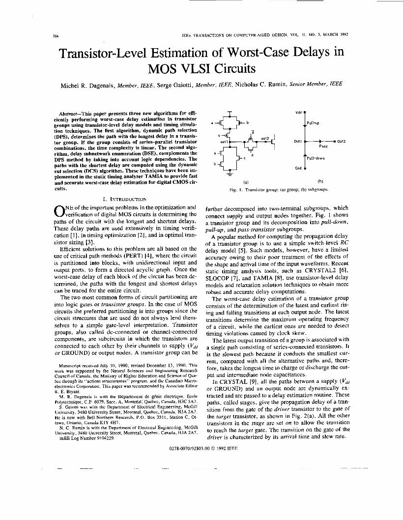
Fig. 1. Transistor group: (a) group; (b) subgroups
further decomposed into two-terminal subgroups, which connect supply and output nodes together. Fig. 1 shows a transistor group and its decomposition into pull-down, pull-up, and pass-transistor subgroups.
A popular method for computing the propagation delay of a transistor group is to use a simple switch-level RC delay model [5]. Such models, however, have a limited accuracy owing to their poor treatment of the effects of the shape and arrival time of the input waveforms. Recent static timing analysis tools, such as CRYSTAL2 [ 6 ] , SLOCOP [7], and TAMIA [8], use transistor-level delay models and relaxation solution techniques to obtain more robust and accurate delay computations.
The worst-case delay estimation of a transistor group consists of the determination of the latest and earliest ris- ing and falling transitions at each output node. The latest transitions determine the maximum operating frequency of a circuit, while the earliest ones are needed to detect timing violations caused by clock skew.
The latest output transition of a group is associated with a single path consisting of series-connected transistors. It is the slowest path because it conducts the smallest cur- rent, compared with all the alternative paths and, there- fore, takes the longest time to charge or discharge the out- put and intermediate node capacitances.
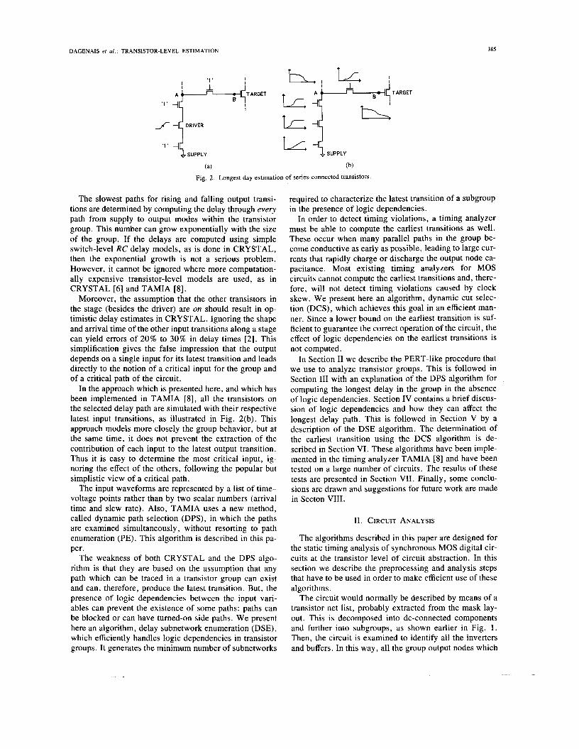
In CRYSTAL [9], all the paths between a supply (Vdd or GROUND) and an output node are dynamically ex- tracted and are passed to a delay estimation routine. These paths, called stages, give the propagation delay of a tran- sition from the gate of the driver transistor to the gate of the target transistor, as shown in Fig. 2(a). All the other transistors in the stage are set on to allow the transition to reach the target gate. The transition on the gate of the driver is characterized by its arrival time and slew rate.
0278-0070/92$03.00 O 1992 IEEE
~~
DAGENAIS er al. : TRANSISTOR-LEVEL ESTIMATION 385
I ' 1
SUPPLY ' 1 ' 4$ L L $SUPPLY
(a) (b)
Fig. 2. Longest day estimation of series-connected transistors
The slowest paths for rising and falling output transi- tions are determined by computing the delay through every path from supply to output modes within the transistor group. This number can grow exponentially with the size of the group. If the delays are computed using simple switch-level RC delay models, as is done in CRYSTAL, then the exponential growth is not a serious problem. However, it cannot be ignored where more computation- ally expensive transistor-level models are used, as in CRYSTAL [6] and TAMIA [8].
Moreover, the assumption that the other transistors in the stage (besides the driver) are on should result in op- timistic delay estimates in CRYSTAL. Ignoring the shape and arrival time of the other input transitions along a stage can yield errors of 20% to 30% in delay times [2]. This simplification gives the false impression that the output depends on a single input for its latest transition and leads directly to the notion of a critical input for the group and of a critical path of the circuit.
In the approach which is presented here, and which has been implemented in TAMIA [8], all the transistors on the selected delay path are simulated with their respective latest input transitions, as illustrated in Fig. 2(b). This approach models more closely the group behavior, but at the same time, it does not prevent the extraction of the contribution of each input to the latest output transition. Thus it is easy to determine the most critical input, ig- noring the effect of the others, following the popular but simplistic view of a critical path.
The input waveforms are represented by a list of time- voltage points rather than by two scalar numbers (amval time and slew rate). Also, TAMIA uses a new method, called dynamic path selection (DPS), in which the paths are examined simultaneously, without resorting to path enumeration (PE). This algorithm is described in this pa- per.
The weakness of both CRYSTAL and the DPS algo- rithm is that they are based on the assumption that any path which can be traced in a transistor group can exist and can, therefore, produce the latest transition. But, the presence of logic dependencies between the input vari- ables can prevent the existence of some paths: paths can be blocked or can have turned-on side paths. We present here an algorithm, delay subnetwork enumeration (DSE), which efficiently handles logic dependencies in transistor groups. It generates the minimum number of subnetworks
required to characterize the latest transition of a subgroup in the presence of logic dependencies.
In order to detect timing violations, a timing analyzer must be able to compute the earliest transitions as well. These occur when many parallel paths in the group be- come conductive as early as possible, leading to large cur- rents that rapidly charge or discharge the output node ca- pacitance. Most existing timing analyzers for MOS circuits cannot compute the earliest transitions and, there- fore, will not detect timing violations caused by clock skew. We present here an algorithm, dynamic cut selec- tion (DCS), which achieves this goal in an efficient man- ner. Since a lower bound on the earliest transition is suf- ficient to guarantee the correct operation of the circuit, the effect of logic dependencies on the earliest transitions is not computed.
In Section I1 we describe the PERT-like procedure that we use to analyze transistor groups. This is followed in Section I11 with an explanation of the DPS algorithm for computing the longest delay in the group in the absence of logic dependencies. Section IV contains a brief discus- sion of logic dependencies and how they can affect the longest delay path. This is followed in Section V by a description of the DSE algorithm. The determination of the earliest transition using the DCS algorithm is de- scribed in Section VI. These algorithms have been imple- mented in the timing analyzer TAMIA [8] and have been tested on a large number of circuits. The results of these tests are presented in Section VII. Finally, some conclu- sions are drawn and suggestions for future work are made in Secton VIII.
11. CIRCUIT ANALYSIS
The algorithms described in this paper are designed for the static timing analysis of synchronous MOS digital cir- cuits at the transistor level of circuit abstraction. In this section we describe the preprocessing and analysis steps that have to be used in order to make efficient use of these algorithms.
The circuit would normally be described by means of a transistor net list, probably extracted from the mask lay- out. This is decomposed into dc-connected components and further into subgroups, as shown earlier in Fig. 1. Then, the circuit is examined to identify all the inverters and buffers. In this way, all the group output nodes which

386 IEEE TRANSACTIONS ON COMPUTER-AIDED DESIGN, VOL. I I , NO. 3. MARCH 1992
carry the same logic signals, possibly inverted, are found. This information is then used to study the switching func- tions of the subgroups and to account for logic dependen- cies in the DSE method.
When two subgroups connected to the same output node have switching functions that intersect, they may both conduct at the same time. Therefore, one must drive sig- nals towards this node (driving subgroup), and the other one away (driven subgroup); otherwise there would be a conflict. Each subgroup has one driving end and one driven end. This property is used recursively to determine the signal flow direction in pass-transistor subgroups. The signal flow direction in the pull-up and pull-down subgroups is necessarily from the supply and ground nodes (driving end) to the output node (drive end). Thus, the signal flow direction in each subgroup, even for most groups with complex pass-transistor structures, can be found using the following procedure. Subgroups in which the signal changes direction dynamically, or pass-transis- tor subgroups connected together in cycles with complex logic dependencies, are not handled.
AssignSubgroupDirection(gr0up) { for (each output node in group){
for (each subgroup connected to the output node) { if (subgroup connected to a source){
set subgroup Direction = Driving put subgroup in DrivingList
I
for (each subgroup with direction Unknown){ if (subgroup intersects DrivingList){
set subgroup Direction = Driven I
I I for (each output node in group){
ResolveDirection(node) I
I ResolveDirection(node) {
if(node Status is Searched) return set node Status to Searched set UnknownList and DrivingListEmpty for (each subgroup connected to node){
if (subgroup Direction is Unknown) { ResolveDirection(0therEnd of subgroup)
1
I
1
if (subgroup Direction is still Unknown) { put subgroup in UnknownList
if (subgroup Direction is Driving) { put subgroup in DrivingList
I for (each subgroup in the UnknownList){
if (subgroup intersects with DrivingList){
set subgroup Direction to Driven I else {
I
set subgroup Direction to Driving put subgroup in DrivingList
1 I The subgroups are further decomposed into series-par-
allel combinations using an efficient linear-time (in the number of transistors) algorithm [8]. This considerably simplifies their analysis. When bridges are present, how- ever, they are logically replaced by an equivalent series- parallel representation. Unfortunately, the size of the equivalent representation can grow exponentially with the size of the bridge. In that case, the savings brought by the series-parallel decomposition are offset by the size of the equivalent representation. This comes as no surprise since finding the longest path in a graph can be done in linear time if no bridges are present but is NP-complete other- wise.
After this decomposition and assignment of signal flow direction, the subgroups, output nodes of the groups, and primary inputs and outputs of the circuit form a directed graph. The static timing analysis starts at the primary in- put nodes, where the worst-case transitions are readily available, since they are supplied by the user. Then, the analysis advances as a wavefront through the circuit, each subgroup being processed when all the signals at its inputs have been analyzed. This analysis is repeated for each timing interval [lo], since at most one significant transi- tion of each type (latestlearliest and rising/falling) may occur on any node in a single timing interval. The pro- cedure is summarized as follows. The edges in the pro- cedure correspond to transistors or combinations (series/ parallel) of transistors. The status of an edge (on/o$l changing) is determined by the input signals on the gates of the transistors in it.
AnalyzeCircuit(circuit) { for (each timing interval in a clock cycle){
initialize all the elements to not Ready detect and cut tight positive feedback loops for (each primary input node of the circuit){
AffectNode(primary input) I
1 I AffectNode(node) {
if (not all subgroups and nodes driving this node are ready) {
1 return
set node Ready compute the worst-case waveforms at this node
by taking the envelope of the worst-case wave- forms

DAGENAIS er a l . : TRANSISTOR-LEVEL ESTIMATION 387
111. DYNAMIC PATH SELECTION produced through each Driving subgroup of the node
for (each transistor gate connected to this node) { AffectEdge(transist0r)
1
1
for (each subgroup driven by the node){ AffectNode(0therEnd of subgroup)
1 AffectEdge(edge) {
if (edge is a series combination){ if (all sub-edges are Ready or one sub-edge is Off)
set edge Ready {
1 else return
1 if (edge is a parallel combination){
if (all sub-edges are Ready or one sub-edge is On)
1 set edge Ready
else return I else set edge Ready /* simple transistor */
determine the State of the edge /* On, Off, Chang- ing. . . *I if (edge is a subgroup){
AffectNode(DrivenEnd of subgroup) return
1 AffectEdge(SuperEdge of this edge)
I
This PERT-like procedure is normally used for directed acyclic graphs. Synchronous circuits contain both large feedback loops that cross several latches, and tight posi- tive feedback loops arising from static latches. The latter are cut during a preprocessing step, so they can be han- dled with the above procedure. The cost of doing this is a slight overestimate of the static latch's delay, since the effect of the positive feedback loop gain is lost. Since the circuit is analyzed one timing interval at a time, the large feedback loops always have at least one latch turned of, thus breaking the loop.
A relaxation-based technique, using the Seidel semi- implicit multistep method, with variable time step [ 111 is used to solve for the voltages and currents in each tran- sistor subgroup. Normally an output node will be driven by more than one subgroup. Hence, the worst-case tran- sitions at an output node are obtained by taking the en- velope of the appropriate transitions associated with every subgroup driving that node. For example, the latest rising transition is obtained by taking the Lower envelope of the subgroups' latest rising transitions.
The common approach would be to simulate each path in the subgroup and take the envelope of all the wave- forms. However, the number of paths in a subgroup can grow exponentially with its size. For a series-parallel subgroup containing n nodes and m transistors, the num- ber of paths can be up to ( m l n ) " , where m > n.
In contrast, the dynamic path selection DPS algorithm computes the latest waveform by simulating the subgroup once, resulting in a linear time complexity (in the number of transistors). At each time step the latest path is selected on the basis of currents computed during the previous step. The currents and node voltages in this path are evaluated, and the latter are used to compute the currents in the re- maining branches of the subgroup. The latest path for the next time step is chosen by comparing these currents with that in the present latest path.
The operation of the DPS method is illustrated in Fig. 3 , The subgroup contains two parallel edges in series. Ini- tially, the branch current i, is smaller than the branch cur- rent i2 and the branch current i, is smaller than the branch current i3; hence, transistors m l and m5 are set as active. Then, a few time steps later, at time t , , branch 4 starts carrying more current than branch 3 ; now, transistor m5 is dropped and transistors m3 and m4 are selected. Simi- larly, at time tZ, branch 2 carries less current than branch 1 : transistor m 1 is dropped and transistor m2 is selected instead.
Following is a pseudocode description of procedure DPS: /* procedure to compute the latest transition in a pull- down sub-group */ LatestWaveformDPS(OutputNode,DrivingSubgroup) {
set the output node and all the internal nodes in the
while (steady state not reached){ Driving and Driven subgroups to 5v
SelectLatestPath(DrivingSubgr0up) simulate the Driving and Driven subgroups for one timestep store the output node voltage in the Latest- FallingWaveform Anal y zeAlternatePath(DrivingSubgroup) select the timestep for the next step
1 1 SelectLatest Path(edge) {
if (edge is NMOS transistor) activate with Latest- Rise if (edge is PMOS transistor) activate with LatestFall if (edge is a series combination)(
for (each SubEdge in edge){ SelectLatestpath( SubEdge)
1 1 if (edge is a parallel combination) {

388 IEEE TRANSACTIONS ON COMPUTER-AIDED DESIGN, VOL. I I . NO. 3, MARCH 1992
A t time to A t time t A t time t2 TABLE I DYNAMIC PATH SELECTION ACCURACY
i,> i, i ,< i, i,< i, i, < i, i, < i, i, > i,
37.6ns 84.6ns
steps can vary slightly with the size of the subgroup. However, experimental results show that the time re-
larger than twice the time required to simulate n / k paths of k transistors. In other words, the total number of tran-
(a) (b) (C) sistors simulated is a very good indication of the time complexity.
The DPS method selects the least conductive path at
i3
4 ml m2 1 quired to simulate a subgroup with n transistors is no
Fig. 3 . Example: dynamic path selection.
SelectLatestPath(LeastConductingSubEdge of edge)
I 1 Anal yzeAlternatePath(edge) {
if (edge is a transistor) store its current and return if (edge is a series combination){
for (each SubEdge in edge){ AnalyzeAltematePath( SubEdge)
I The current of the edge is that of the SubEdge
closest to the output node 1 if (edge is a parallel combination){
Anal yzeAlternatePath(LeastConductingSubEdge of edge) set MinCurrent to the Current of the Least- Conducting SubEdge for (each SubEdge of Edge except Least- ConductingSubEdge) {
SelectLatestPath(SubEdge) simulate the late path in the SubEdge for one timestep AnalyzeAlternatePath( SubEdge) if (Current in SubEdge is smaller than Min- Current) {
set the LeastConductingSubEdge of Edge to SubEdge
1 I
The time complexity of the DPS method is that of sim- ulating the subgroup once plus some overhead to compare the currents in the parallel edges. The simulation time for one iteration of one time step is linear with the size of the subgroup. The time required to compare the currents is also linear and takes only a small fraction of the total. The number of iterations per time step and the number of time
any time step. This is more pessimistic than selecting a single path (PE), which is not necessarily always the least conductive, but does lead to the latest waveform. How- ever, experimental results indicate that, after two or three path selections, the DPS algorithm settles on the latest path. The accuracy of the DPS algorithm is illustrated in Table I for the two circuits shown in Fig. 4. As can be seen, it results in a relatively small accuracy penalty (as shown in Table I) when compared with the error of the numerical integration method used to compute the delay P I .
The DPS method shares one problem with the path enu- meration (PE) method of CRYSTAL [9]: both ignore logic dependencies between the transistors within the subgroup. This is the subject of the next section.
IV. LOGIC DEPENDENCIES Three types of logic dependencies can exist within a
subgroup. The first type, called parallel path, involves the presence of parallel transistors driven by the same signal (or its complement). For example, transmission gates form parallel paths: when a transmission gate is turning on, both transistors, n-type and p-type, will be turning on (Fig. 5(a)). Parallel paths are found frequently in net lists obtained from layout generators, where large transistors are broken into small parallel transistors to respect area constraints in fixed pitch cells. Such parallel paths may sometimes be eliminated by a simple preprocessing step which collapses the transistors. Here, they are treated by a more general mechanism which handles the larger turned-on side path category.
The second type, called blocked path, involves a path which can never be on owing to complementary logic de- pendencies (Fig. 5(b)). The third type, called turned-on side path, occurs when a path has transistors in parallel which must be on (Fig. 5(c)). The parallel paths are a special case of this third category and need not be consid- ered further.
In the pull-up subgroup of the complex gate of Fig. 6, eight paths can be traced (abc, aba, acc, aca, bbc, bba, bbc, bcu). But, once the logic dependencies are taken into
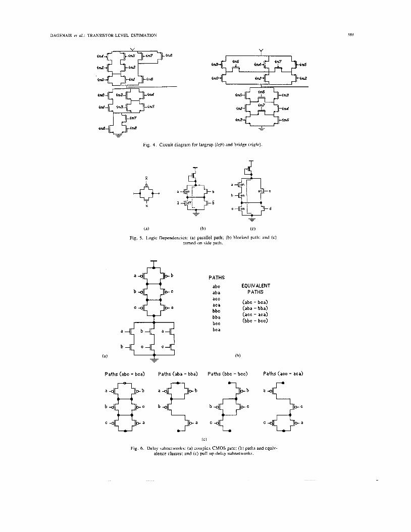
DAGENAIS et al.: TRANSISTOR-LEVEL ESTIMATION 389
I----------
Y
I I
Fig. 4 . Circuit diagram for largesp (left) and bridge (right)
& T
(a) (b) (C)
Fig. 5 . Logic Dependencies: (a) parallel path; (b) blocked path; and (c) turned-on side path.
PATHS
abc EQUIVALENT aba PATHS acc
bbc bba bcc bca
(abc - bca) (aba - bba) (acc - aca)
aca
(bbc - bcc)
Paths (bbc - bcc) Paths (acc - aca)
(C)
Fig. 6. Delay subnetworks: (a) complex CMOS gate; (b) paths and equiv- alence classes; and (c) pull-up delay subnetworks.
390 IEEE TRANSACTIONS ON COMPUTER-AIDED DESIGN. VOL. I I , NO. 3, MARCH 1992
account and duplications removed, four subnetworks re- main (Fig. 6(b)). Of these four subnetworks, only three need to be simulated to characterize the worst-case be- havior of the subgroup: the subnetwork corresponding to the paths abc or bca clearly has a faster rise time than the other subnetworks. It is “covered” by the other three
In general, the worst-case performance of a subgroup which contains logic dependencies can be characterized (a) (b) by a small number of subnetworks. The minimum set of subnetworks required to obtain the worst-case character- istics of a subgroup is called the minimum cover of the subgroup, and its subnetworks are called delay subnet- works.
$-I: c+
a b subnetworks. a. -I I-b a
Fig. 7. Series-parallel decomposition tree.
if (e is a subedge of a %node){ clear any Searched tag in the subedges of e; remove the On tag on e; propagate the deselection of e to its dependent edges; backtrack( );
V. DELAY SUBNETWORK ENUMERATION A backtracking algorithm has been designed to perform
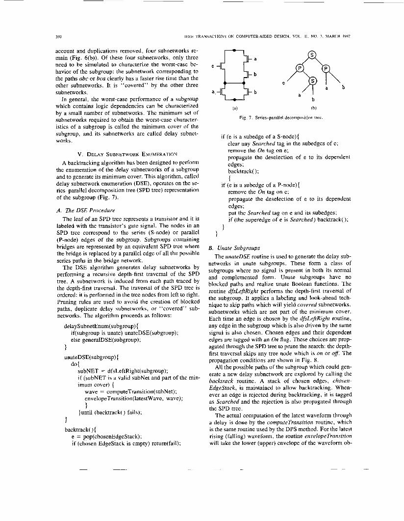
the enumeration of the delay subnetworks of a subgroup and to generate its minimum cover. This algorithm, called delay subnetwork enumeration (DSE), operates on the se- ries-parallel decomposition tree (SPD tree) representation of the subgroup (Fig. 7).
if (e is a subedge of a P-node){ remove the On tag on e; propagate the deselection of e to its dependent
A. The DSE Procedure The leaf of an SPD tree represents a transistor and it is
labeled with the transistor’s gate signal. The nodes in an SPD tree correspond to the series (S-node) or parallel (P-node) edges of the subgroup. Subgroups containing bridges are represented by an equivalent SPD tree where the bridge is replaced by a parallel edge of all the possible series paths in the bridge network.
The DSE algorithm generates delay subnetworks by performing a recursive depth-first traversal of the SPD tree. A subnetwork is induced from each path traced by the depth-first traversal. The traversal of the SPD tree is ordered: it is performed in the tree nodes from left to right. Pruning rules are used to avoid the creation of blocked paths, duplicate delay subnetworks, or “covered” sub- networks. The algorithm proceeds as follows:
edges; put the Searched tag on e and its subedges; if (the superedge of e is Searched) backtrack();
I I
B. Unate Subgroups The unateDSE routine is used to generate the delay sub-
networks in unate subgroups. These form a class of subgroups where no signal is present in both its normal and complemented form. Unate subgroups have no blocked paths and realize unate Boolean functions. The routine dfsLeftRight performs the depth-first traversal of the subgroup. It applies a labeling and look-ahead tech- nique to skip paths which will yield covered subnetworks, subnetworks which are not part of the minimum cover. Each time an edge is chosen by the dfsLefRight routine,
delaySubnetEnum(subgr0up) { any edge in the subgroup which is also driven by the same signal is also chosen. Chosen edges and their dependent edges are tagged with an On flag. These choices are prop- agated through the SPD tree to prune the search: the depth- first traversal skips any tree node which is on or o f . The propagation conditions are shown in Fig. 8.
All the possible paths of the subgroup which could gen- erate a new delay subnetwork are explored by calling the backtrack routine. A stack of chosen edges, chosen- Edgestack, is maintained to allow backtracking. When- ever an edge is rejected during backtracking, it is tagged
if(subgroup is unate) unateDSE(subgr0up); else generalDSE(subgr0up);
1 unateDSE(subgr0up) {
do{ subNET = dfsLeftRight(subgr0up); if (subNET is a imum cover) {
mbNet and part Of the
wave = computeTransition(subNet); envelopeTransition(latestWave, wave); 1 as Searched and the rejection is also propagated through I
}until (backtrack( ) fails); >
the SPD tree. The actual computation of the latest waveform through
I backtrack( ) {
a delay is done by the computeTransition routine, which is the same routine used by the DPS method. For the latest rising (falling) waveform, the routine envefopeTransition will take the lower (upper) envelope of the waveform ob-
e = pop(ch0senEdgeStack); if (chosen EdgeStack is empty) return(fai1);

DAGENAIS et al.: TRANSISTOR-LEVEL ESTIMATION 39 1
on 0 ff 0 f f on
Fig. 8. Tag propagation through SPD tree.
tained by simulating the delay subnetwork. It is interest- ing to note that the unateDSE routine does not need to store delay subnetworks or their individual latest wave- forms.
Tumed-on side paths produce delay subnetworks which contain more than one path. Subsequent calls to dfs- LeftRight will trace the other paths of the delay subnet- work, resulting in duplicate subnetworks. Duplicates can be eliminated by comparing the subnetwork with the pre- viously generated delay subnetworks. Unfortunately, this is rather inefficient since a subgroup may have an expo- nential number of delay subnetworks. For unate subgroups, a simple pruning rule is used to eliminate du- plicates: the dfsLefRight routine never chooses an edge which will add a tumed-on side path to the left of a pre- viously chosen edge.
In certain rare cases, when the subgroup contains re- dundant series edges, the delay subnetwork generated by dfsLeftRight may not be part of the minimum cover, and represents unnecessary computations. A heuristic pruning rule is used in unateDSE to reject these subnetworks: the delay subnetwork is traversed in the opposite direction by a depth-first search routine to generate the rightmost path through the subnetwork. If the rightmost path has fewer chosen leaves than the path traced by dsJLeftRight, the subnetwork is rejected. This pruning rule may fail to re- ject some subnetworks when more than two paths can be traced within the candidate subnetwork. But, in practice, for small subgroups, the redundant series edges are so rare that we can tolerate the few extra subnetworks which may be generated. It is imporant to note, however, that these rules will never falsely reject a subnetwork which could lead to a latest waveform.
C. Complemented Inputs
Unate subgroups are simple, since in the absence of transistors driven by complementary signals, for each traced path, side-path transistors can be assumed to be off. In general, it is not the case. For example, in Fig. 9, the path bc cannot exit as a valid path by itself since either a or Z has to be on. The generalDSE routine is used to gen- erate the minimum cover of delay subnetworks when the input variables xi and their complements 7 are leaves of the SPD tree. The outline of the generalDSE procedure is shown below.
generalDSE( subgroup) { initialOnOffAssignment( );
L-t' t Fig. 9. Edge assignments.
for (all the 2k assignments) /* undateDSE without simulation */ do {
subNet = dfsLeftRight(subgr0up); if (subNet is valid and is part of the minimum cover)
append(minCover, subNet) ; } until (backtrack() = = 0);
gray CodeAssignment( subgroup) ; 1
/* generate the latest waveform */ while (minCover is not empty){
subNet = pop(minCover); wave = computeTransition(subNet); envelopeTransition(latestWave, wave); 1
1 If the subgroup implements an n-variable Boolean func-
tion, let k be the number of variables which are present in their normal and complemented forms. The initialon- OffAssignment routine sets an initial assignment of on, off tags on these k variables. The tag propagation rules of Fig. 8 are used to propagate the effects of the assignments in the tree.
Then, generalDSE will try all the 2k possible assign- ments of on and off tags of these variables. Each assign- ment is propagated through the three before any path is traced by dfsLefRight. The effect of the assignment is to prune the search: the depth-first traversal will skip any tree node which is on and will avoid tracing a blocked path by skipping any node which is off. The dfsLefRight routine will effectively trace paths in an (n - k)-variable unate subgroup with some fixed on, off edges. To mini-
392 IEEE TRANSACTIONS ON COMPUTER-AIDED DESIGN. VOL. I I , NO. 3, MARCH 1992
mize the number of tag changes, the assignment of on and ofedges is changed by flipping a single variable; the as- signment of the k variables follows a Gray code encoding.
The generuZDSE algorithm often generates subnet- works which are not part of the minimum cover. To ob- tain the minimum cover, a list of subnetworks, minCover, is used to store candidate subnetworks. The subnetworks are stored in the form of compact bit vectors. The bit vec- tor representation allows the use of fast bitwise operators to perform subgraph intersections for the detection and, thus, the elimination of duplicate and covered subnet- works.
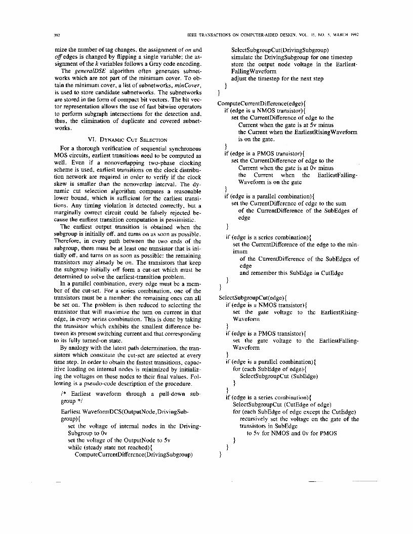
VI. DYNAMIC CUT SELECTION For a thorough verification of sequential synchronous
MOS circuits, earliest transitions need to be computed as well. Even if a nonoverlapping two-phase clocking scheme is used, earliest transitions on the clock distribu- tion network are required in order to verify if the clock skew is smaller than the nonoverlap interval. The dy- namic cut selection algorithm computes a reasonable lower bound, which is sufficient for the earliest transi- tions. Any timing violation is detected correctly, but a marginally correct circuit could be falsely rejected be- cause the earliest transition computation is pessimistic.
The earliest output transition is obtained when the subgroup is initially off, and tums on as soon as possible. Therefore, in every path between the two ends of the subgroup, there must be at least one transistor that is ini- tially off, and tums on as soon as possible: the remaining transistors may already be on. The transistors that keep the subgroup initially off form a cut-set which must be determined to solve the earliest-transition problem.
In a parallel combination, every edge must be a mem- ber of the cut-set. For a series combination, one of the transistors must be a member: the remaining ones can all be set on. The problem is then reduced to selecting the transistor that will maximize the tum on current in that edge, in every series combination. This is done by taking the transistor which exhibits the smallest difference be- tween its present switching current and that corresponding to its fully tumed-on state.
By analogy with the latest path determination, the tran- sistors which constitute the cut-set are selected at every time step. In order to obtain the fastest transitions, capac- itive loading on internal nodes is minimized by initializ- ing the voltages on these nodes to their final values. Fol- lowing is a pseudo-code description of the procedure.
/* Earliest waveform through a pull-down sub- group */
Earliest WaveformDCS(OutputNode,DrivingSub- group)
set the voltage of internal nodes in the Driving- Subgroup to Ov set the voltage of the OutputNode to 5v while (steady state not reached){
ComputeCurrentDifference(DrivingSubgroup)
SelectSubgroupCut(DrivingSubgroup) simulate the DrivingSubgroup for one timestep store the output node voltage in the Earliest- FallingWaveform adjust the timestep for the next step
I I ComputeCurrentDifference(edge) {
if (edge is a NMOS transistor){ set the CurrentDifference of edge to the
Current when the gate is at 5v minus the Current when the EarliestRisingWaveform is on the gate.
3 if (edge is a PMOS transistor){
set the CurrentDifference of edge to the Current when the gate is at Ov minus the Current when the EarliestFalling- Waveform is on the gate
if (edge is a parallel combination){ 1
set the CurrentDifference of edge to the sum of the CurrentDifference of the SubEdges of edge
3 if (edge is a series combination){
set the CurrentDifference of the edge to the min- imum
of the CurrentDifference of the SubEdges of edge and remember this SubEdge in CutEdge
I 3 SelectSubgroupCut(edge) {
if (edge is a NMOS transistor){ set the gate voltage to the EarliestRising- Waveform
3 if (edge is a PMOS transistor){
set the gate voltage to the EarliestFalling- Waveform
3 if (edge is a parallel combination){
for (each SubEdge of edge){ SelectSubgroupCut (SubEdge)
3 I if (edge is a series combination){
SelectSubgroupCut (CutEdge of edge) for (each SubEdge of edge except the CutEdge)
recursively set the voltage on the gate of the transistors in SubEdge
to 5v for NMOS and Ov for PMOS 3
1 1

DAGENAIS et al. : TRANSISTOR-LEVEL ESTIMATION 393
TABLE I1 DYNAMIC CUT SELECTION ACCURACY
subgroup of cuts size shortest delay sub-group delay
largesp pull-up 3.311s largesp pull-down 3.111s 4.611s
bridge pull-up 10 46 11. Ins 8 12.611s
i . 7 n s 8 8.3115
This method has the same interesting properties as the DPS method. Its run time is linear for series-parallel combinations, and the earliest waveform produced is slightly pessimistic (exact or earlier), except for numeri- cal inaccuracies. Also, by analogy with the DPS algo- rithm, this procedure selects the most conductive CUT at each time step, instead of using a single CUT which would be most conductive overall.
A number of subgroups were analyzed using the DCS method. The results obtained were compared with SPICE simulations, and are presented in Table 11. The error caused by the numerical integration method used with DCS often adds a delay of one or two time steps. This was insignificant with the long delays associated with the latest waveforms but affects to a certain extent the earliest waveforms. Nevertheless, the results obtained are within 7% to 30% of the results produced with SPICE.
VII. IMPLEMENTATION AND RESULTS TAMIA is a prototype static timing analyzer for the
timing and design verification of synchronous digital MOS circuits [ 101. It uses the DPS and DCS methods to obtain, respectively, the latest and earliest waveforms for each subgroup. Recently, the new DSE algorithm was included to handle subgroups which contain logic dependencies. Both the DPS and the DSE method call the same delay estimation routine to generate the waveforms for the latest transitions.
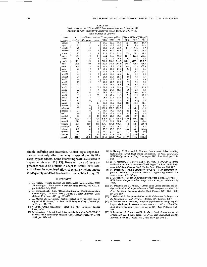
The accuracy of DCS was already discussed, in Section VI. Table I11 shows the delay and CPU time on a SUN3I 260 running UNIX for numerous circuits analyzed with the DPS, DSE, and straightforward path enumeration (PE) methods. In most cases, the delay computed with DPS is slightly pessimistic compared with PE. There are a few exceptions, caused by the numerical integration inaccu- racy. In all cases, the CPU time required by DPS is smaller than that required by PE. In some cases, such as bigm, PE is up to six times slower than DPS, but in most cases the difference is between 10 and 100%. Indeed, ex- cept for a few large subgroups, the total size of the enum- erated paths is usually not much larger than the subgroup size. Thus, although the DPS method is useful, since it is never slower than PE and is only slightly less accurate, the typical savings in CPU time are much less than the linear versus exponential complexity would suggest.
Both the DPS and PE method overestimate the delays in the presence of logic dependencies. Hence, though an accurate delay calculation routine is used, overly pessi-
mistic results are generated if logic dependencies are ig- nored. Indeed, except for small numerical integration er- rors, the worst-case values produced by DPS and PE (which are fairly close) are always larger than or equal to the values obtained by DSE. Some of the examples con- taining numerous turned-on side paths or blocked paths, such as treeadd and hhnl05, exhibit significant differ- ences between the two delay values, thus stressing the importance of taking into account logic dependencies.
As far as speed is concerned, the DSE method benefits from some of the advantages of DPS but, in some cases, suffers from an explosion in the number of blocked and turned-on paths. Thus, in most cases it is faster than PE and slightly slower than DPS, but in pathological cases like unanim/minanu8, it may require much more pro- cessing time.
Although the DSE method has a worst-case exponential time complexity, the run time overhead remains small since (i) it is only applied to subgroups containing logic dependencies, (ii) the number of delay subnetworks is less than the number of paths, and (iii) subgroup sizes are not large in optimized designs. Hence, the combination of the DPS and DSE methods in TAMIA provides a general and elegant way to handle complex CMOS gates and trans- mission gate networks.
VIII. CONCLUSIONS AND FUTURE WORK The decomposition of transistor groups into subgroups
and series-parallel combinations provides an efficient framework for analyzing complex CMOS gates, including pass-transistor logic. The DPS, DSE and DCS methods use this decomposition, and their combined implementa- tion produces a very efficient and accurate relaxation- based timing analysis program, TAMIA. These methods minimize the number of calls to the delay estimation rou- tine and correctly handle logic dependencies located with subgroups.
Future work will involve different ways to increase the accuracy of the analysis. There are at least two areas where pathological cases can easily create large errors. Presently, only some of the capacitance driven by a subgroup is modeled. This could be improved by greedy heuristics to include, or to approximate, the effects of the active capactive loads arising from (i) complementary driving subgroups at output nodes, and (ii) side paths within delay subnetworks.
The latest addition to TAMIA, the DSE method, han- dles logical dependencies within subgroups as well as
394
circuit name
admPP higm unanim4 unanim8 bridge cladd classic m a l 6 cma8 eo116 hata hhnl05 hhnl l3 hh11115 hhn22 hhn4.5 hhn46 hhn58 hhn63 lihn6i hhn69 hhnT3 hhn76 hhn99 minanu4 minanu8 largesp opti parity4 sma8 tooadd treeadd twoloops xcladd symtree xortree smal6
IEEE TRANSACTIONS ON COMPUTER-AIDED DESIGN, VOL. I I , NO. 3. MARCH 1992
# mosfet:
46 30 26 5 0 16
84F 2E
8704 21iE
168 28 32 22 26 24 26 T2 34 22 32 29 14 24 32 26 50 20 28 26
2650 248
1696 32
912 44
226 10240
TABLE 111 COMPARISON OF THE DPS A N D DSE ALGORITHMS WITH THE STANDARD PE
FOR A NUMBER OF CIRCUITS ALGORITHM, WITH RESPECT TO COMPUTED DELAY TIME AND CPU TIME,
blocked paths
4 0 4 8 0
64 0 0 0
80 0
17 3 6 5 i 2
18 3
20 10 1 3
21 0 0 0 0
16 256 24
160 0 0 0
14 1024
del. DPS 39.i ,533 3.5.6 68.1 i2.3 77.2 33.6
831.6 402.3
75.6 31.6 54.1 26.2 29.1 34..5 36.0 29.8 rj6.0 30.6 38.0 44.6 28.0 35.0 4i.9 33.5
290.3 38.1 30.8 44.2
408.2 89.5
576.1 24.1 i9.2 23.6 38.2
848.0
turned on side paths
0 21 14
2.54 0 0 5
1280 320
0 2 2 0 0 0 0 1 0 0 0 0 0 0 1 0 0 0 2 0
512 48
320 0 0
14 36
2048
simple buffering and inversion. Global logic dependen- cies can seriously affect the delay in special circuits like carry-bypass adders. Some interesting work has started to appear in this area [12] [13]. However, both of these ap- proaches would be difficult to adapt to circuit-level anal- ysis where the combined effect of many switching inputs is adequately modeled (as discussed in Section 1, Fig. 2).
REFERENCES [I] N. Jouppi,, “Timing analysis and performance improvement of MOS
VLSI designs,” IEEE Trans. Computer-Aided Design, vol. CAD-6,
[2] M. Hofmann and J. Kim, “Delay optimization of combinational static CMOS logic,” in Proc. 24th ACM/IEEE Design Automat. Conj (Miami, FL), June 1987, pp. 125-132.
[3] D. Marple and A. Gamal, “Optimal selection of transistor sizes in digital VLSI circuits,” in Proc. 1987 Stanford Con$ (Cambridge,
[4] S. Even, Graph Algorithms. Rockville, MD: Computer Science Press, 1979.
I51 J . Ousterhout, “Switch-level delay models for digital MOS VLSI,” in Proc. IEEE 21st Design Automat. Con$ (Albuquerque, NM), June 1984, pp. 542-548.
pp. 650-665, July 1987.
MA), pp. 151-172.
- time DSE 32.0 48.9 34.6 65.7 71.8 11.5 32.6
713.8 348.6 48.5 30.9 32.1 23.4 27.5 33.9 35.7 29.7 42.4 25.0 28.7 35.4 27.8 29.7 41.5 3i.2
281.i 38.1 29.3 29.5
372.8 i8 .0
,503.3 24.1 79.2 19.6 40.6
i74.3
-
r-
-
jet) P E 39..5 89.3 35.6 68.1 71.8 80.8 36.1
i44.6 364.5 7.5.4 34.2 $4.1 26.2 28.9 34.2 38.3 30.4 ,559 30.6 37.6 14.2 27.8 35.2 46.9 38.1
281.7 3T.6 33.3 43.6
110.8 89.9
581.8 26.7 78.7 25.5 46.8
-
351.6
- cpri t i DPS
16.3 4.8
4.74 11.0 22.0
227.9 4.7
2846.7 687.2 189.0
4.5 l7.R 4.0 6.2 6.8 8.9 4.0
25.7 5.9
26.7 12.9 3.2 5 . 5
22.8 4.8
11.4 3.3 4.5
33.0 818.9 57.2
414.3 5.1
245.6 8.3
12.3 3316.7
-
-
- : SUN3 DSE
14.6 8.3
7.56 125.3 21.1
227.4 6.3
3300.1 82.5.4 116.6
5.8 13.7 3.8 8.2 ij.6 i.6 4.0
15.7 5.6
18.0 11.3 3.6 1.8
16.3 7.8
146.4 3.3 5.8
19.7 889.4 61.8
443.1 5.1
246.1 8.2
42.6
-
3841.6
- ‘GO ( s )
PE 16.7 29.1 6.7
21.3 21.2
239..5 6.4
336i.i 836.3 203.9
.5.6 20.7
4.4 7.8 7.0 9.4 4.5
26.5 6.3
29.2 13.0 3.5 5.6
24.1 4.9
11.6 6.0 5.5
36.1 1029.8
70.0 507.7
6.5 247.6
8.8 44.4
__
L490.6
[6] S. Hwang, Y. Kim, and A. Newton, “An accurate delay modeling technique for switch-level timing verification,” in Proc. 23rd ACMI IEEE Design Automat. Conf. (Las Vegas, NV), June 1986, pp. 227- 233.
[7] E. V . Meersch, L. Claesen, and H. D. Man, “SLOCOP: A timing verification tool for synchronous CMOS Logic,” in Proc. 1986Euro- pean Solid-State Circuits Con$ (Delft), Sept. 1986, pp. 205-207.
[8] M. Dagenais, “Timing analysis for MOSFET’s; An integrated ap- proach,” Tech. Rep. TR-88-2R, Electrical Engineering, McGill Uni- versity, June 1987, 223 pp.
[9] J. Ousterhout, “Switch-level timing verifier for digital MOS VLSI,” IEEE Trans. Computer-Aided Design, vol. CAD-4, pp. 336-349, July 1985.
[lo] M. Dagenais and N. Rumin, “Circuit-level timing analysis and de- sign verification of high-performance MOS computer circuits,” in Proc. Int. Conf. Computer Design (Port Chester, NY), Oct. 1986,
[ll] J . White and A. Sangiovanni-Vincentelli, Relaxation Techniques for the Simulation of VLSI Circuits.
[I21 P. McGeer and R. Brayton, “Efficient algorithms for computing the longest viable path in a combinational network,” in Proc. 26th ACM/ IEEE Design Automat. Con$ (Las Vegas, NV), June 1989, pp. 561- 567.
[13] S. Perremans, L. Clasen, and H. de Man, “Static timing analysis of dynamically sensitizable paths,” in Proc. 26th ACM/IEEE Design Automat. Con$ (Las Vegas, NV), June 1989, pp. 568-573.
pp. 356-359.
Boston, MA: Kluwer, 1987.

DAGENAIS et al.: TRANSISTOR-LEVEL ESTIMATION 395
Michel R. Dagenais (S’83-M’87) received the B.Ing. degree from the Ecole Polytechnique de Montrial in 1983 and the Ph.D. degree from McGill University in 1987, both in electrical en- gineering.
Since 1987, he has been an Assistant Professor in the Department of Electrical Engineering at the Ecole Polytechnique. His research interests in- clude several aspects of CAD and VLSI with em- phasis on timing verification, object-oriented data bases, and logic synthesis.
Serge Gaiotti (S’86-M’88) received the B. Eng. degree in electrical engineering in 1986 from Concordia University, Montreal, Canada. From 1986 to 1989, he was at McGill University, Mon- treal, working towards the M.Eng. degree in elec- trical engineering.
In 1989, he joined Bell-Northem Research, Ot- tawa, where he is a member of the scientific staff. His current research interests include fast func- tional simulation, delay modeling, and timing verification of digital VLSI systems.
Nicholas C. Rumin (S’60-M’65-SM’78) re- ceived the B.Eng. degree in engineering physics, the M.Sc. degree in physics, and the Ph.D. degree in electrical engineering from McGill University, Montreal, P.Q., Canada, in 1957, 1961 and 1966, respectively.
From 1957 to 1959 he worked for Canadian Marconi on the design of transistorized commu- nication circuits. He was a research associate at the Montreal Neurological Institute from 1961 to 1963, involved in the application of radio isotopes
to the localization of intracranial lesions and to the study of blood circu- lation. From 1961 to 1964 he was also a Lecturer at McGill University. In 1965 he joined the RCA Research Laboratories in Montreal, where he was involved in the characterization of bipolar transistors and monolithic inte- grated circuits as well as in the development of photoconductive detectors. Since 1967 he has been with the Department of Electrical Engineering at McGill University, where he currently holds the rank of Professor and Chairman. In 1975 he spent nine months on sabbatical leave with the Bell Northem Research Laboratories in Ottawa, Ont., Canada, where he worked on the modeling of microwave transistors and the computer-aided design of high-speed nonlinear circuits. His current research interests are in the general area of VLSI circuits and include simulation, modeling, and IC design.
Dr. Rumin is a member of the Order of Engineers of Quebec.