
Area-efficient VLSI layouts for binary hypercubes
10
Brief Contributions________________________________________________________________________________ Area-Efficient VLSI Layouts for Binary Hypercubes Alpesh Patel, Student Member, IEEE, Anthony Kusalik, and Carl McCrosky, Member, IEEE Abstract—The hypercube is an interesting and useful topology for parallel computation. While hypercubes have been analyzed in graph theory, this analysis has done little to determine the minimum area required for realizations of the hypercube topology on two-dimensional chips. In a common VLSI layout of the hypercube, the hypercube nodes are placed in a single-row in numeric order. This paper derives an easily computed formula for the minimum number of tracks used by this configuration. For an n-node hypercube, the number of tracks required is roughly two-thirds of n. This result is also a useful upper bound on the number of tracks required under optimal ordering. In general, the number of tracks required is a function of the ordering, but finding the optimal order (optimal in the sense of requiring the minimum number of tracks over all orderings) is NP-hard. Finally, the formula is applied to more area-efficient and practical two-dimensional hypercube layouts. In general, it allows estimation of and control over implementation parameters such as area and chip aspect ratios. Index Terms—Hypercube, VLSI layout, track assignment. æ 1 INTRODUCTION THE d-dimensional binary hypercube (d-cube for short) is a powerful topology for parallel computation. The topology has been well-studied from a graph theoretic perspective [2], [3]. Parallel algorithms using the hypercube have been developed [4]. Newer applications of the d-cube include the hypercube switch [5]. Much is known about how the hypercube topology can be used, but less about how to physically realize this topology. Common VLSI layouts of the hypercube have been presented [7], but work has not focused on finding the minimum area these layouts require. This paper achieves a result from which the minimum area for a common VLSI layout of d-cubes in two-dimensional technologies can be determined. The result can also be used to explore other practical matters of d-cube layout such as chip aspect ratios and maximal bus widths. A simple physical realization of the hypercube topology is a single-row wiring layout, described in Section 2. Some important points about this layout scheme are listed below. . The nodes of the hypercube are placed in a row, with wiring tracks running parallel to the row of nodes. . The number of wiring tracks required for the layout is a function of the order in which the hypercube nodes are placed in a row. . The order that results in the least tracks required is termed optimal. Finding the optimal order requires solving the matrix permutation problem (MPP). MPP has been shown to be NP-hard [6]. . Given a particular order, the connections can be placed in a minimum number of wiring tracks using a greedy algorithm in time linear to the number of edges in the hypercube [1]. This paper derives a formula for the minimal number of wiring tracks required when the nodes are placed in numeric order. The formula is 2=3 2 d d=2 b c; where d is the dimension of the hypercube. This result is useful because: 1. It gives an upper bound on the number of tracks required with the optimal order, 2. For the numeric node-ordering, it provides a method much faster than the greedy algorithm for computing the number of wiring tracks required, and 3. It replaces a trivial upper bound on the number of tracks 2 d 1 that have been used [7] when an expression is needed to derive area requirements for this d-cube layout. The next section describes d-cube graphs, the net-gate matrix representation of the d-cube topology, the single-row wiring layout, and the augmented net-gate matrix abstraction of this wiring arrangement. Section 3 contains a proof of the formula for the number of wiring tracks required under the numeric node order. This number is the maximum column sum of the augmented net-gate matrix, so the formula is proven by consider- ing column sums of this matrix. Section 4 describes the practical application of the main result of the paper to VLSI layouts of hypercubes. The final section offers some conclusions and related ideas for future work. 2 THE HYPERCUBE AND A SIMPLE WIRING ARRANGEMENT This section defines the hypercube graph and its net-gate matrix representation. Also described is a single-row wiring layout and its augmented net-gate matrix representation. The section is con- cluded with comments on node ordering and the choice of the particular ordering used in this paper. 2.1 The Hypercube Graph and the Net-Gate Matrix The d-dimensional hypercube graph Q d has n nodes, where n is 2 d . As a convention, a unique d-bit binary identifier is assigned to each node. For a node k, the bits of its identifier are numbered k d1 k d2 ... k 0 . Nodes u and v are connected by a dimension i edge iff their identifiers differ only in the ith bit (see Fig. 1). Thus, each node has one connection for each dimension 0 to d 1. The total number of edges in the hypercube is d2 d1 . In VLSI layout terms, the nodes of an architecture to be implemented on a circuit (the hypercube in this case) are termed gates and the connections are termed nets. The net-gate matrix representation M of a topology is a binary matrix, where each row represents a net and each column represents a gate. Each row has ones in the columns for the gates connected by that net. For example, the net-gate matrix for the 2-cube (Fig. 1a) is the 4 4 matrix 160 IEEE TRANSACTIONS ON COMPUTERS, VOL. 49, NO. 2, FEBRUARY 2000 . A. Patel is with the Communications Research Laboratory, Department of Electrical and Computer Engineering, McMaster University, 1280 Main St. W., Hamilton, Ontario, L8S 4K1 Canada. E-mail: [email protected]. . A. Kusalik and C. McCrosky are with the Department of Computer Science, University of Saskatchewan, 57 Campus Drive, Saskatoon, Saskatchewan, S7N 5A9 Canada. E-mail: [email protected], [email protected]. Manuscript received 26 Aug. 1997; revised 14 Apr. 1999; accepted 29 Nov. 1999. For information on obtaining reprints of this article, please send e-mail to: [email protected], and reference IEEECS Log Number 105549. 0018-9340/00/$10.00 ß 2000 IEEE
-
Upload
independent -
Category
Documents
-
view
5 -
download
0
Transcript of Area-efficient VLSI layouts for binary hypercubes

Brief Contributions________________________________________________________________________________
Area-Efficient VLSI Layoutsfor Binary Hypercubes
Alpesh Patel, Student Member, IEEE,Anthony Kusalik, and
Carl McCrosky, Member, IEEE
AbstractÐThe hypercube is an interesting and useful topology for parallel
computation. While hypercubes have been analyzed in graph theory, this analysis
has done little to determine the minimum area required for realizations of the
hypercube topology on two-dimensional chips. In a common VLSI layout of the
hypercube, the hypercube nodes are placed in a single-row in numeric order. This
paper derives an easily computed formula for the minimum number of tracks used
by this configuration. For an n-node hypercube, the number of tracks required is
roughly two-thirds of n. This result is also a useful upper bound on the number of
tracks required under optimal ordering. In general, the number of tracks required is
a function of the ordering, but finding the optimal order (optimal in the sense of
requiring the minimum number of tracks over all orderings) is NP-hard. Finally, the
formula is applied to more area-efficient and practical two-dimensional hypercube
layouts. In general, it allows estimation of and control over implementation
parameters such as area and chip aspect ratios.
Index TermsÐHypercube, VLSI layout, track assignment.
æ
1 INTRODUCTION
THE d-dimensional binary hypercube (d-cube for short) is apowerful topology for parallel computation. The topology hasbeen well-studied from a graph theoretic perspective [2], [3].Parallel algorithms using the hypercube have been developed [4].Newer applications of the d-cube include the hypercube switch [5].Much is known about how the hypercube topology can be used,but less about how to physically realize this topology. CommonVLSI layouts of the hypercube have been presented [7], but workhas not focused on finding the minimum area these layoutsrequire. This paper achieves a result from which the minimumarea for a common VLSI layout of d-cubes in two-dimensionaltechnologies can be determined. The result can also be used toexplore other practical matters of d-cube layout such as chip aspectratios and maximal bus widths.
A simple physical realization of the hypercube topology is a
single-row wiring layout, described in Section 2. Some important
points about this layout scheme are listed below.
. The nodes of the hypercube are placed in a row, withwiring tracks running parallel to the row of nodes.
. The number of wiring tracks required for the layout is afunction of the order in which the hypercube nodes areplaced in a row.
. The order that results in the least tracks required is termedoptimal. Finding the optimal order requires solving thematrix permutation problem (MPP). MPP has been shownto be NP-hard [6].
. Given a particular order, the connections can be placed in aminimum number of wiring tracks using a greedyalgorithm in time linear to the number of edges in thehypercube [1].
This paper derives a formula for the minimal number of wiring
tracks required when the nodes are placed in numeric order. The
formula is
�2=3� � 2d� �� d=2b c;
where d is the dimension of the hypercube. This result is useful
because:
1. It gives an upper bound on the number of tracks requiredwith the optimal order,
2. For the numeric node-ordering, it provides a method muchfaster than the greedy algorithm for computing thenumber of wiring tracks required, and
3. It replaces a trivial upper bound on the number of tracks�2d ÿ 1� that have been used [7] when an expression isneeded to derive area requirements for this d-cube layout.
The next section describes d-cube graphs, the net-gate matrix
representation of the d-cube topology, the single-row wiring
layout, and the augmented net-gate matrix abstraction of this
wiring arrangement. Section 3 contains a proof of the formula for
the number of wiring tracks required under the numeric node
order. This number is the maximum column sum of the
augmented net-gate matrix, so the formula is proven by consider-
ing column sums of this matrix. Section 4 describes the practical
application of the main result of the paper to VLSI layouts of
hypercubes. The final section offers some conclusions and related
ideas for future work.
2 THE HYPERCUBE AND A SIMPLE WIRING
ARRANGEMENT
This section defines the hypercube graph and its net-gate matrix
representation. Also described is a single-row wiring layout and its
augmented net-gate matrix representation. The section is con-
cluded with comments on node ordering and the choice of the
particular ordering used in this paper.
2.1 The Hypercube Graph and the Net-Gate Matrix
The d-dimensional hypercube graph Qd has n nodes, where n is 2d.
As a convention, a unique d-bit binary identifier is assigned to each
node. For a node k, the bits of its identifier are numbered
kdÿ1kdÿ2 . . . k0. Nodes u and v are connected by a dimension i edge iff
their identifiers differ only in the ith bit (see Fig. 1). Thus, each
node has one connection for each dimension 0 to dÿ 1. The total
number of edges in the hypercube is d�2dÿ1�.In VLSI layout terms, the nodes of an architecture to be
implemented on a circuit (the hypercube in this case) are termed
gates and the connections are termed nets. The net-gate matrix
representation M of a topology is a binary matrix, where each row
represents a net and each column represents a gate. Each row has
ones in the columns for the gates connected by that net. For
example, the net-gate matrix for the 2-cube (Fig. 1a) is the 4� 4
matrix
160 IEEE TRANSACTIONS ON COMPUTERS, VOL. 49, NO. 2, FEBRUARY 2000
. A. Patel is with the Communications Research Laboratory, Department ofElectrical and Computer Engineering, McMaster University, 1280 MainSt. W., Hamilton, Ontario, L8S 4K1 Canada.E-mail: [email protected].
. A. Kusalik and C. McCrosky are with the Department of ComputerScience, University of Saskatchewan, 57 Campus Drive, Saskatoon,Saskatchewan, S7N 5A9 Canada.E-mail: [email protected], [email protected].
Manuscript received 26 Aug. 1997; revised 14 Apr. 1999; accepted 29 Nov.1999.For information on obtaining reprints of this article, please send e-mail to:[email protected], and reference IEEECS Log Number 105549.
0018-9340/00/$10.00 ß 2000 IEEE

where each column is labeled with the 2-bit identifier of thecorresponding 2-cube node and zeros are omitted for clarity. Notethat, in the net-gate matrix, the permutation of columns and ofrows is irrelevant; the matrix simply represents the connectiontopology. The net-gate matrix can be easily augmented to representlayouts of the connection topology, as will be shown in Section 2.3.
2.2 The Single-Row Hypercube Wiring Layout
To build integrated hypercubes, it is necessary to work within a fewlayers of two-dimensional integrated circuits. The single-row wiringlayout described in this section is one way to map d-dimensionalhypercubes to two dimensions. In this layout scheme, nodes(shown in Fig. 2 as bold vertical strips) are placed in a single line orrow. Nodes can be placed in any order in the line. Thus, it is usefulto identify node positions at which specific nodes can be placed. Thefollowing convention is introduced and used throughout thispaper: Decimal numbers above each strip (node) identify nodepositions, whereas binary numbers below indicate the identifier (orlabel) of the node placed at that position. The wiring tracks runparallel to the line of nodes. They are separated by dashed lines inFig. 2. Wires are indicated by gray lines and electrical contacts occurwhen a wire terminates at a strip and only there (see Fig. 3). While itis possible to allow connections to abut (i.e., two separate wires toterminate at the same node, but without overlapping), this paperonly treats the cases where connections do not abut.
Fig. 3 shows the VLSI physical design for the connection patternin Fig. 2a.
The number of tracks required for layout is dependent on theorder in which nodes are placed in the line. For instance, Fig. 2aand Fig. 2b show two possible orders for laying out the nodes 00,01, 10, and 11. (Note that the same connections between nodesmust still exist.) In Fig. 2a, three tracks are needed, while, in Fig.2b, four tracks are necessary.
The order is captured by a one-to-one function � that maps eachnode identifier to a node position. The node positions arenumbered, left to right, from 0 to nÿ 1. In Fig. 2a, ��01� � 1,while, in Fig. 2b, ��01� � 3. The sequence of node identifiers in theline, read left-to-right, is therefore:
�ÿ1�0�; �ÿ1�1�; . . . ; �ÿ1�nÿ 1�:Whether or not two nodes are connected is determined by
whether their identifiers differ in exactly one bit, but the length ofthe connection is determined by �. Fig. 2 demonstrates how the
length of connections between nodes can change with the node
order.
2.3 Augmented Net-Gate Matrix Representation
The wiring layout described above lends itself to an augmented net-
gate matrix representation. Theoretical results regarding such
representations [6] then simplify analysis of this single-row layout.In an augmented net-gate matrix, the ith column represents the
ith node position in the line of nodes. A permutation of nodes � in
the layout is represented by a corresponding permutation of
columns. As in the net-gate matrix, each row represents a
connection between nodes. A row of the net-gate matrix onlydescribes what nodes are connected by a wire. The corresponding
row of the augmented net-gate matrix, however, describes the
interval of node positions the wire will occupy physically in a
wiring track. In both types of matrices, the permutation of rows is
irrelevant.Given a net-gate matrix M and a chosen permutation � of the
gates (i.e., nodes) for the single-row layout, the augmented net-gate
matrix M� can be constructed using the following steps:
1. Order the columns of M according to the ordering givenby � and
2. For each row, set to 1 all elements from the position of theleftmost 1 to the position of the rightmost 1.
The augmented net-gate matrices for the 2-cube layouts in Fig. 2
are shown in Fig. 4. Each row indicates the continuous interval of
node positions that one connection will occupy on a wiring track.Therefore, if there is any column in which two rows both have a 1,
then those two rows represent connections that cannot share a
track.The augmented net-gate matrix representation is useful because
the number of tracks necessary and sufficient for the layout is
simply the maximum column sum of M�. It is easy to see that the
maximum column sum would give a necessary number of tracks
and MoÈhring [6] cites several results showing that this number oftracks is also sufficient.
2.4 The Numeric Node Order
Different orderings of nodes (in the hypercube layout) produce
different augmented net-gate matrices, which in turn may havedifferent maximum column sums. We shall refer to the maximum
column sum of a particular augmented net-gate matrix M� as the
number of tracks required for M under � and denote it by t��M�.Finding the permutation � that produces an M� with the lowest
possible maximum column sum is known as the matrix permutation
problem (MPP). This problem is NP-hard [6]. This lowest possible
maximum column sum is called the tracknumber of the net-gate
matrix M and denoted t�M�. Hence,
t�M� � min�
t��M�:
Much work [8] has been done on finding permutations of gates
for general layouts that result in low (though not necessarily
minimum) numbers of tracks required. In addition, several cases ofMPP that can be solved in polynomial time are listed in MoÈhring's
work [6]. Despite these results, MPP for the d-cube remains an
instance of the general NP-hard problem.Various node orderings were investigated as part of this work.
The exponential search space of node orderings was searched
exhaustively for (all) d � 4. One ordering was found to always
produce the smallest t��M�. For d > 4, only a small number of
orderings were tested. However, for all these values of d
considered and all orders tested, the same ordering again always
produced the smallest t��M�. We call this ordering the numeric node
order and denote it by num. It satisfies:
IEEE TRANSACTIONS ON COMPUTERS, VOL. 49, NO. 2, FEBRUARY 2000 161
Fig. 1. Examples of hypercubes. (a) The 2-cube. (b) The 3-cube.

num�i� � i0;where i is any node label and node position i0 is the decimal valuecorresponding to i. Fig. 2a shows the layout for the 2-cube with thisnode ordering. Given its observed properties and its common usein hypercube layout work, such as by Ranade and Johnsson [7],this paper considers only the numeric node ordering.
The track number is a property of a net-gate matrix, but, giventhe equivalence of the graph Qd to its corresponding net-gatematrix, we will refer to its track number as t�Qd�, rather thanintroducing separate notation for the net-gate matrix representingQd. Similarly, the number of tracks required for Qd under aparticular node order � we denote simply as t��Qd�. The mainresult of this paper is a formula for tnum�Qd�, which is also anupper bound on t�Qd�.
3 DERIVATION OF RESULT
This section derives a formula for the number of wiring tracksnecessary and sufficient when the nodes are placed in numericorder for the single-row wiring layout of a d-cube. This number isthe maximum column sum of the associated augmented net-gatematrix, denoted tnum�Qd�. The formula is shown to be:
tnum�Qd� � �2=3� � 2d� �� d=2b c:
The derivation proceeds by finding the maximum column sum,tnum�Qd�, of an augmented net-gate matrix of Qd constructed usingthe numeric node order. The maximum column sum of anaugmented net-gate matrix is simply the maximum number ofconnections that overlap any single node position. To find thismaximum, an expression is derived for the number of connectionsof a given dimension that overlap a given node position. Anexpression is then derived for the number of connections of two
consecutive dimensions that overlap a given node position. Byconsidering the connections two dimensions at a time, the aboveformula is proven.
3.1 Preliminaries
Lemmas needed to derive the main result are presented in thissection. Fig. 5 demonstrates their underlying intuition. Proofs ofthe lemmas are omitted where these are obvious.
As was stated earlier, an expression is developed for thenumber of dimension i connections overlapping the node positionnum�k� where node k is placed. We will refer to this integerquantity as ci;k.
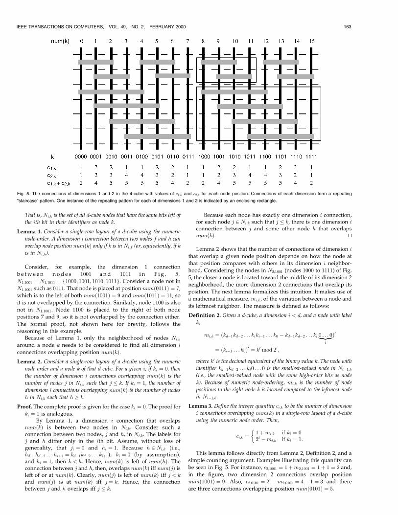
Fig. 5 shows the nodes of the 4-cube in the single-row layoutunder the numeric node order. Also shown are the dimension 1connections (in the top two wiring tracks) and dimension 2connections (in the bottom four wiring tracks). The rows under-neath the layout show the number of connections of dimensions 1and 2 overlapping each node position (c1;k and c2;k, respectively),as well as the total number of dimension 1 and dimension 2connections overlapping each node position (c1;k � c2;k).
In an augmented net-gate matrix representation of the layout,node k corresponds to the num�k�th column of the matrix and ci;kis the contribution of dimension i connections to that column'ssum.
It is clear in Fig. 5 that connections of a given dimension form arepeating pattern over ªneighborhoodsº of nodes. It is useful toformalize this notion of neighborhood and this is done in thefollowing definition.
Definition 1. Given a d-cube, a node labeled k of the d-cube, and adimension i of the d-cube, Ni;k is a subset of node labels as follows:
Ni;k � h j hdÿ1hdÿ2hi�1 � kdÿ1kdÿ2 . . . ki�1f g:
162 IEEE TRANSACTIONS ON COMPUTERS, VOL. 49, NO. 2, FEBRUARY 2000
Fig. 2. Simple wirings of the 2-cube with node positions shown. (a) Order: 00, 01, 10, 11. (b) Order: 00, 11, 10, 11.
Fig. 3. VLSI physical design for the connection pattern in Fig. 2a.
Fig. 4. Augmented net-gate matrices corresponding to the layouts in Fig. 2. (a) Matrix for Fig. 2a. (b) Matrix for Fig. 2b.
That is, Ni;k is the set of all d-cube nodes that have the same bits left of
the ith bit in their identifiers as node k.
Lemma 1. Consider a single-row layout of a d-cube using the numeric
node-order. A dimension i connection between two nodes f and h can
overlap node position num�k� only if k is in Ni;f (or, equivalently, if k
is in Ni;h).
Consider, for example, the dimension 1 connection
b e t w e e n n o d e s 1001 a n d 1011 i n F i g . 5 .
N1;1001 � N1;1011 � f1000; 1001; 1010; 1011g. Consider a node not in
N1;1001 such as 0111. That node is placed at position num�0111� � 7,
which is to the left of both num�1001� � 9 and num�1011� � 11, so
it is not overlapped by the connection. Similarly, node 1100 is also
not in N1;1001. Node 1100 is placed to the right of both node
positions 7 and 9, so it is not overlapped by the connection either.
The formal proof, not shown here for brevity, follows the
reasoning in this example.Because of Lemma 1, only the neighborhood of nodes Ni;k
around a node k needs to be considered to find all dimension i
connections overlapping position num�k�.Lemma 2. Consider a single-row layout of a d-cube using the numeric
node-order and a node k of that d-cube. For a given i, if ki � 0, then
the number of dimension i connections overlapping num�k� is the
number of nodes j in Ni;k such that j � k. If ki � 1, the number of
dimension i connections overlapping num�k� is the number of nodes
h in Ni;k such that h � k.
Proof. The complete proof is given for the case ki � 0. The proof for
ki � 1 is analogous.By Lemma 1, a dimension i connection that overlaps
num�k� is between two nodes in Ni;k. Consider such aconnection between two nodes, j and h, in Ni;k. The labels forj and h differ only in the ith bit. Assume, without loss ofgenerality, that ji � 0 and hi � 1. Because h 2 Ni;k (i.e.,hdÿ1hdÿ2 . . .hi�1 � kdÿ1kdÿ2 . . . ki�1), ki � 0 (by assumption),and hi � 1, then k < h. Hence, num�k� is left of num�h�. Theconnection between j and h, then, overlaps num�k� iff num�j� isleft of or at num�k�. Clearly, num�j� is left of num�k� iff j < kand num�j� is at num�k� iff j � k. Hence, the connectionbetween j and h overlaps iff j � k.
Because each node has exactly one dimension i connection,for each node j 2 Ni;k such that j � k, there is one dimension iconnection between j and some other node h that overlapsnum�k�. tu
Lemma 2 shows that the number of connections of dimension i
that overlap a given node position depends on how the node at
that position compares with others in its dimension i neighbor-
hood. Considering the nodes in N2;1001 (nodes 1000 to 1111) of Fig.
5, the closer a node is located toward the middle of its dimension 2
neighborhood, the more dimension 2 connections that overlap its
position. The next lemma formalizes this intuition. It makes use of
a mathematical measure, mi;k, of the variation between a node and
its leftmost neighbor. The measure is defined as follows:
Definition 2. Given a d-cube, a dimension i < d, and a node with label
k,
mi;k � �kdÿ1kdÿ2 . . . kikiÿ1 . . . k0 ÿ kdÿ1kdÿ2 . . . ki 0 . . . 0|��{z��}i
�0
� �kiÿ1 . . . k0�0 � k0 mod 2i;
where k0 is the decimal equivalent of the binary value k. The node with
identifier kdÿ1kdÿ2 . . . ki0 . . . 0 is the smallest-valued node in Niÿ1;k
(i.e., the smallest-valued node with the same high-order bits as node
k). Because of numeric node-ordering, mi;k is the number of node
positions to the right node k is located compared to the leftmost node
in Niÿ1;k.
Lemma 3. Define the integer quantity ci;k to be the number of dimension
i connections overlapping num�k� in a single-row layout of a d-cube
using the numeric node order. Then,
ci;k � 1�mi;k if ki � 02i ÿmi;k if ki � 1:
�This lemma follows directly from Lemma 2, Definition 2, and a
simple counting argument. Examples illustrating this quantity can
be seen in Fig. 5. For instance, c2;1001 � 1�m2;1001 � 1� 1 � 2 and,
in the figure, two dimension 2 connections overlap position
num�1001� � 9. Also, c2;0101 � 2i ÿm2;0101 � 4ÿ 1 � 3 and there
are three connections overlapping position num�0101� � 5.
IEEE TRANSACTIONS ON COMPUTERS, VOL. 49, NO. 2, FEBRUARY 2000 163
Fig. 5. The connections of dimensions 1 and 2 in the 4-cube with values of c1;k and c2;k for each node position. Connections of each dimension form a repeating
ªstaircaseº pattern. One instance of the repeating pattern for each of dimensions 1 and 2 is indicated by an enclosing rectangle.
Relevant patterns in the number of connections to overlap a
given node position appear when connections of two consecutive
dimensions are considered together, as is shown in the following
lemma.
Lemma 4. Given a single-row layout of a d-cube using the numeric node
order, a dimension i > 0, and a node k of that d-cube,
ci;k � ciÿ1;k � 2i � 1if �ki � 0 and kiÿ1 � 1� or�ki � 1 and kiÿ1 � 0�
ci:k � ciÿ1;k < 2i � 1if �ki � 0 and kiÿ1 � 0� or�ki � 1 and kiÿ1 � 1�:
Proof. The following relationships are useful in this proof:
mi;k � �kiÿ1kiÿ2 . . . k0�0 � �kiÿ10 . . . 0|��{z��}iÿ1
� kiÿ2 . . . k0�0
� kiÿ12iÿ1 �miÿ1;k
and
0 � mi;k � 2i ÿ 1:
The two cases yielding equality are similar to each other, asare the two cases yielding inequality. For brevity, we show theproof for one case of each.
Case 1: ki � 0 and kiÿ1 � 1
ci;k � ciÿ1;k � �1�mi;k� � �2iÿ1 ÿmiÿ1;k�� 1� 2iÿ1 �mi;k ÿmiÿ1;k
� 1� 2iÿ1 � �kiÿ12iÿ1 �miÿ1;k� ÿmiÿ1;k
� 1� 2iÿ1 � kiÿ12iÿ1 � 1� 2iÿ1 � 2iÿ1;
since kiÿ1 � 0
� 2i � 1:
Case 2: ki � 0 and kiÿ1 � 0
ci;k � ciÿ1;k � �1�mi;k� � �1�miÿ1;k�� �1� kiÿ12iÿ1 �miÿ1;k� � �1�miÿ1;k�� 1� �2iÿ1 ÿ 1� � 1� �2iÿ1 ÿ 1�;
since kiÿ1 � 1
� 2� 2iÿ1 � 2i
< 2i � 1:
tu
Lemma 4 gives the maximum number of connections of two
consecutive dimensions (i and iÿ 1) to overlap a node position.
Corollary 4.1. Whether or not a given node position is overlapped by the
maximum possible number of dimension i and dimension iÿ 1
connections is determined strictly by the ith and �iÿ 1�th bits of the
node placed at that position.
Proof. Result follows directly from Lemma 4. tu
3.2 Main Result
Theorem. The number of wiring tracks sufficient and necessary for the
single-row wiring layout of the d-cube, Qd, when the numeric node
order is used is given by:
tnum�Qd� � �2=3� � 2d� �� d=2b c:
Proof. The minimum number of wiring tracks required is the
maximum column sum of the augmented net-gate matrix. The
maximum column sum is the maximum number of connections
that overlap a particular node position. The expression for
tnum�Qd� is found by first showing that no node position can be
overlapped by a number of connections exceeding the expres-
sion. The proof is concluded by showing that a node position in
the layout exists for which the number of connections over-
lapping is given by the expression.Recalling that the number of dimension i connections
overlapping node position num�k� is given by ci;k, the totalnumber of connections overlapping node position i is simply:
Xdÿ1
i�0
ci;k: �1�
The maximum number of connections that a overlap a
particular node position (and, hence, the value tnum�Qd�) is
given by:
tnum�Qd� � maxk
Xdÿ1
i�0
ci;k
!: �2�
To take advantage of Lemma 4, connections of the d-cube are
considered, grouped into pairs. Hence, for even values of d, (2)
can be rewritten as:
tnum�Qd� � maxk
X�d=2�ÿ1
g�0
cdÿ1ÿ2g;k � cdÿ2ÿ2g;k
ÿ �" #: �3�
For odd values of d, there are bd=2c ÿ 1 pairs of dimensions and
dimension 0 remains unaccounted for after the other dÿ 1
connections are grouped into pairs. Hence, (2) for odd values of
d becomes:
tnum�Qd� � maxk
c0;k �Xbd=2cÿ1
g�0
cdÿ1ÿ2g;k � cdÿ2ÿ2g;k
ÿ �" #: �4�
From Definition 2, m0;k � 0 for all k. Thus, by Lemma 3, c0;k � 1
for all k. Using �dmod 2� to include this extra term for odd
values of d, (3) and (4) can be combined into one equation for
both odd and even values of d:
tnum�Qd� � maxk
dmod 2�Xbd=2cÿ1
g�0
cdÿ1ÿ2g;k � cdÿ2ÿ2g;k
ÿ �" #: �5�
To obtain an upper bound on tnum�Qd�, the maximum operator
is distributed through the summation in (5) to yield:
tnum�Qd� � dmod 2�Xbd=2cÿ1
g�0
maxk
cdÿ1ÿ2g;k � cdÿ2ÿ2g;k
ÿ �: �6�
From Lemma 4 it is known that ci;k � ciÿ1;k � 2i � 1, so the
upper bound reduces to:
tnum�Qd� � dmod 2�Xbd=2cÿ1
g�0
2dÿ1ÿ2g � 1ÿ �
: �7�
It remains to be shown that there is a node position in the layout
overlapped by a number of connections given by the expression
(i.e., that a particular node position achieves the upper bound
on tnum�Qd� given in (7)).Given that all possible d-bit binary numbers are used as
node labels in the d-cube, any d-bit string is a valid node label.Consider the node j labeled 1010 . . . 10. By grouping dimen-sions in pairs, the number of connections overlapping num�j� is
164 IEEE TRANSACTIONS ON COMPUTERS, VOL. 49, NO. 2, FEBRUARY 2000

Xdÿ1
i
ci;j �Xbd=2cÿ1
g�0
cdÿ1ÿ2g;j � cdÿ2ÿ2g;j
ÿ �: �8�
For all values of the summation index g in (8), it is the case that
jdÿ1ÿ2g � 1 and jdÿ2ÿ2g � 0 for this node. By Lemma 4, for all
values of the summation index g in (8) the gth term is simply
2dÿ1ÿ2g � 1. Hence, (8) becomes:
Xdÿ1
i
ci;j � dmod 2�Xbd=2cÿ1
g�0
2dÿ1ÿ2g � 1ÿ �
: �9�
Since (9) gives the number of connections overlapping a
particular node position in the layout and because no node
position is overlapped by a greater number of connections,
tnum�Qd� is equal to the expression.To obtain the simpler expression given in the statement of
the theorem, the righthand side of (9) is manipulated as follows:
dmod 2�Xbd=2cÿ1
g�0
2dÿ1ÿ2g � 1ÿ �
� dmod 2� bd=2c �Xbd=2cÿ1
g�0
2dÿ1ÿ2g
� dmod 2� bd=2c � 2d�1 � 2dmod2�1ÿ �
=3
by property of geometric series
� dmod 2� bd=2c � �2=3��2d � 2dmod2�:This is nearly identical in appearance to the expression given in
the theorem statement. To show the two expressions are
equivalent, proof by induction can be used, once for odd d
and again for even d. This is straightforward and is not shown
here. tuTable 1 gives values of tnum�Qd� for a range of small values of d.
4 PRACTICAL CONSIDERATIONS AND APPLICATIONS
Practical implementations of hypercube-based systems on VLSI
substrates and printed circuit boards (PCB) require that two issues
be addressed:
Issue 1: The wiring channels must not dominate the surface area of
the implementation.
Issue 2: Some degree of control must be had over the aspect ratio
of the resultant systems. Neither VLSI chips nor PCBs are
economical when their floor plan geometries depart too far
from a 1:1 aspect ratio.
The main result of this paper leads to single-row (one-
dimensional) implementations of hypercube-based systems. As
will be shown, this approach generalizes into two- (and three-)
dimensional implementations. The rest of this section considers the
one- and two- dimensional implementations in detail, draws
conclusions, and speculates about three-dimensional systems. The
main result derived in Section 3 gives the exact minimum number
of wiring tracks necessary under the numeric node order. This
section presents analysis on layouts that use this order, so
conclusions can be made about the minimum area required for
implementation.
IEEE TRANSACTIONS ON COMPUTERS, VOL. 49, NO. 2, FEBRUARY 2000 165
TABLE 1Sample Values of tnum�Qd� Given d
Fig. 6. One-dimensional use of the main result.
Fig. 7. Two-dimensional use of the main result.

In what follows, we consider d-dimensional hypercubes, where
each node is a square functional unit, s units on a side. The results
given below can be easily generalized to nonsquare functional
units. Each cube-edge communications path (i.e., the connections
between two functional units) consists of b parallel wires, each wire
requiring a width of w units (note that, in Fig. 3, b was 1 (for a one
bit wide bus); here, we generalize to any width of bus, b).
4.1 One-Dimensional Implementations
Fig. 6 gives a floor plan for a one-dimensional implementation of a
3-cube with nodes laid out using the numeric node order.
In this architecture, the wiring channel is VLSI real-estate
dedicated to implementing the hypercube interconnection wires
(as in Fig. 3); its width is b � w � tnum�Qd�, and its length is 2d � s.
The area of the wiring channel is the product of its width and
length: �b � w � tnum�Qd�� � �2d � s�. The wiring channel overhead ratio
(the ratio of the total system area to the area of the functional units)
is:
166 IEEE TRANSACTIONS ON COMPUTERS, VOL. 49, NO. 2, FEBRUARY 2000
TABLE 21D/2D System Comparison
TABLE 31D/2D System Comparison

�b � w � tnum�Qd� � s� � �2d � s��2d � s2� � �b � w � tnum�Qd� � s�
s
� 1� b � w � tnum�Qd�s
:
Linear use of the main result leads to undesirably high aspect
ratios. Better ways of applying the main result which improve the
aspect ratio and reduce the wiring channel overhead are presented
in the following section.
4.2 Two-Dimensional Implementations
The linear model generalizes to produce multidimensional
implementations [7]. A d-dimensional hypercube can be factored
into multiple sets of dimensions, where each dimension group is
assigned to a separate orthogonal dimension in the implementa-
tion. In the two-dimensional implementation considered here, the
d dimensions of the original cube are separated into two groups: r
of them are assigned to horizontal wiring channels and c of them
are assigned to vertical wiring channels, where d � r� c. The d-
dimensional problem can then be decomposed into 2c identical
routings of r dimensions and 2r identical routings of c dimensions,
where the two sets of replicated routings are orthogonal and their
wires cross in the resultant system. Fig. 7 illustrates this
arrangement for d � 4, r � 2, c � 2, and numeric node ordering
in both the horizontal and vertical dimensions. In the development
that follows, only cases where r � c � d=2 are considered; the
results for r 6� c are easily derived. It is assumed that the horizontal
and vertical dimensions can be conveniently brought out of the
replicated modules on the appropriate edges.In this architecture, the width of each wiring channel (whether
horizontal or vertical, r being equal to c) is b � w � tnum�Qr�, where,
in general, tnum�Qr� << tnum�Qd�. The length of each channel is
2rs� �2r ÿ 1��b � w � tnum�Qr��. The area of the entire d-dimen-
sional system is its width times its length (ignoring the notch
missing at the lower right of Fig. 7):
�2r�s� b � w � tnum�Qr���2:The wiring channel overhead ratio is:
�2r�s� b � w � tnum�Qr���2�2d � s2� � �s� b � w � tnum�Qr���2
s2:
The ratio of total system areas of the one-dimensional mapping
to the two-dimensional mapping is:
�b � w � tnum�Qd� � s� � s�s� b � w � tnum�Qr��2
:
The two-dimensional approach consumes additional area due to
the crossings of the wiring channels. However, the factoring of
the design into two dimension groups reduces the width of the
channels by a factor of tnum�Qd�=tnum�Qr� � 2d=2 because r, not d,
dimensions of connections are in each channel. This results in a
saving of wiring overhead in the two-dimensional case, which is
described below.
IEEE TRANSACTIONS ON COMPUTERS, VOL. 49, NO. 2, FEBRUARY 2000 167
TABLE 4A Large 2D System
Fig. 8. Graph of the maximum value of b (log2 scale) as a function of d for 1 and 2D mappings.

The routing overhead area per functional unit in the one-dimensional mapping is �b � w � tnum�Qd�� � s. In the two-dimen-sional mapping, the routing overhead area per functional unit isthe sum of the area of the two channel areas to the right of andbelow the unit and the channel cross-over area (ignoring theabsence of the notch for one unit):
2�b � w � tnum�Qr� � s� � �b � w � tnum�Qr��2:The ratio of routing areas (per functional unit) of the one-dimensional mapping to the two-dimensional mapping (with b �w factored out of numerator and denominator) is:
�tnum�Qd�� � s2�tnum�Qr� � s� � b � w � tnum�Qr�2
:
When the width of the channels is modest w.r.t. s, this becomes:
tnum�Qd�2 � tnum�Qr� � 2�d=2�ÿ1;
and, since tnum�Qd� � tnum�Q2r� grows much faster than2 � tnum�Qr�, the two-dimensional mapping is much superior tothe one-dimensional mapping in overhead area (and, of course, inaspect ratio). If the width of the channel is not small w.r.t. s, theratio cannot be easily simplified, but the two-dimensional mappingremains superior.
Tables 2 and 3 demonstrate the advantages of the two-dimensional physical mapping. Both tables represent systemswith 1,000�m2 functional units with 10 bit communications paths(b � 10). Table 2 has d � 4 and r � c � 2, while Table 3 has d � 6
and r � c � 3. The aspect ratio advantage of the two-dimensionalmapping is obvious; what is interesting is the advantage in overallsystem area in the two-dimensional implementations.
Table 4 demonstrates a larger system. Here, 256 1; 000�m�1; 000�m functional units are combined to produce a 2cm� 2cm
VLSI die. A one-dimensional version is not shown, as the aspectratio is extreme.
Another way to view the advantages of the two-dimensionalmapping is to consider the maximum value of b (the number ofparallel wires for interconnection) as a function of d. This function
is illustrated in Fig. 8 for both one-dimensional and two-
dimensional implementations. The values of s and w used are as
in Tables 2, 3, and 4, and a maximum wiring overhead of 100
percent is assumed (i.e., wiring area takes half of the total area).Fig. 8 shows that the maximum value for b in the 1D layout
diminishes in O�1=2d�. This is as expected given that tnum�Qd� has
O�2d� growth. The 2D layout decomposes the connections into
multiple 1D layouts of half the dimension, so the maximum value
for b in that case only diminishes in O�1=2�d=2��. This is why, as the
graph shows, the two-dimensional layout permits implementation
of higher dimension hypercubes than does the one-dimensional
layout.This section has shown that the main result of this paper maps
naturally to a two-dimensional implementation which controls
aspect ratios and reduces overall system area. Three-dimensional
mappings are also possible and useful. They can be realized by
two-sided and stacked PCBs. However, this technology is too
idiosyncratic to permit a systematic evaluation here. With current
technology, it is unlikely that more than two or three hypercube
dimensions would be mapped to the third physical dimension, but
the mapping is still useful in practice. Future VLSI technologies
may permit a limited third dimension on-chip.When functional units with nonsquare aspect ratios are to be
combined, it is desirable to control the overall system's aspect
ratio. This can be done using the two- and three-dimensional
techniques. The division of d into the physical dimensions can be
used to control the resultant aspect ratio within a power-of-two
range. Thus, the aspect ratio of the resultant system can be
controlled to lie within the range 2:1 to 1:1, which permits practical
implementations. Fig. 9 illustrates the use of this freedom to
produce a nearly square design from a functional unit with a
decidedly nonsquare aspect ratio.In another approach, d-dimensional hypercubes can be
factored into two (or more) sets of dimensions, called the i and o
dimensions, where d � i� o. The main result is used to build
linear arrays of 2i modules each, called ªinnerº modules. Each of
these inner modules has the one-dimensional structure described
in Section 4.1, but, in addition, the dimension wires for the
remaining o dimensions of each module are brought out to the
ends of the wiring channels.Next, 2o of these inner modules are combined. The dimension
wires routed out for the o outer dimensions are wired in a new
wiring channel at the top of the resultant array, thereby completing
the wiring of a d-dimensional hypercube. This arrangement is
illustrated in Fig. 10.In general, this nested arrangement is less efficient than the
two-dimensional arrangement due to the additional area con-
sumed by the passing of the o outer dimensions through the inner
wiring channels. It is more efficient to embed the o dimension
168 IEEE TRANSACTIONS ON COMPUTERS, VOL. 49, NO. 2, FEBRUARY 2000
Fig. 9. Correction of nonsquare aspect ratios.
Fig. 10. Nested layout.

channels within the structure, as is done in the two-dimensionalcase.
5 CONCLUSION
The hypercube is recognized as a powerful parallel computationtopology. For hardware implementation, it is valuable to know theminimum chip area required to realize the topology. In this work, aformula of
tnum�Qd� � �2=3� � 2d� �� d=2b c
was derived for the number of wiring tracks required for a single-row wiring layout with hypercube nodes placed in numeric order.This number can then be used to estimate the chip area required torealize the hypercube topology on a two-dimensional chip,especially for arbitrarily large hypercubes. Such information isimportant for determining at what values of d the area necessaryfor wiring a hypercube is no longer balanced by the functionalitygained by the topology.
The expression found is O�2d�, like the trivial upper bound of2d ÿ 1 [7] which it replaces. However, the new expression achievesa constant factor improvement (a one-third reduction as d getslarge) over the previous upper bound.
In a more theoretical vein, the formula gives an upper boundfor the minimum number of tracks sufficient for the layout over allpossible node orders (i.e., the track number T �Qd�). Given thatfinding the optimal order is NP-hard, and that, in experimentingwith various node orderings, no ordering was found to result in alower number of tracks than the numeric ordering, the upperbound is likely a tight bound and, certainly, a useful one.
The best practical use of the main result of this paper is in two-dimensional physical implementations in which the system aspectratio can be kept within the range 2:1 to 1:1 and the wiringoverhead is substantially reduced.
ACKNOWLEDGMENTS
The authors would like to thank Mark Keil for directing us to thework on gate matrix layout and interval graphs. The authors alsothank the reviewers for their insightful suggestions and comments.This research was made possible by funding from the CanadianNational Science and Engineering Research Council.
REFERENCES
[1] U.I. Gupta, D.T. Lee, and I.Y.-T. Leung, ªEfficient Algorithms for IntervalGraphs and Circular Arc Graphs,º Networks, vol. 12, no. 4, pp. 459-467,Winter 1982.
[2] F. Harary, J. Hayes, and H.-J. Wu, ªA Survey of the Theory of HypercubeGraphs,º Computers and Math. with Applications, vol. 15, no. 4, pp. 277-289,1988.
[3] P.C. Kainen, ªOn the Stable Crossing Number of Cubes,º Proc. Am. Math.Soc., vol. 36, no. 1, pp. 55-62, Nov. 1972.
[4] F.T. Leighton, Introduction to Parallel Algorithms and Architectures: Arrays,Trees, Hypercubes. Morgan Kaufmann, 1982.
[5] C.D. McCrosky, ªMessage Routing in Synchronous Hypercubes,º ComputerSystems Science and Eng., vol. 4, no. 1, pp. 89-96, Jan. 1989.
[6] R.H. MoÈhring, ªGraph Problems Related to Gate Matrix Layout and PLAFolding,º Computing Supplementum 7, pp. 17-51, Springer-Verlag, 1990.
[7] A.G. Ranade and S.L. Johnsson, ªThe Communication Efficiency of Meshes,Boolean Cubes and Cube Connected Cycles for Wafer Scale Integration,ºProc. 1987 Int'l Conf. Parallel Processing, pp. 479-482, 1987.
[8] O. Wing, S. Huang, and R. Wang, ªGate Matrix Layout,º IEEE Trans.Computer-Aided Design, vol. 4, no. 3, pp. 220-231, July 1985.
IEEE TRANSACTIONS ON COMPUTERS, VOL. 49, NO. 2, FEBRUARY 2000 169