Deformation-induced crystallization in amorphous Al85Ni10La5 alloy
Upload
independentCategory
view
5download
0
Ž .Thin Solid Films 383 2001 39�44
Advanced excimer laser crystallization techniques
L. Mariucci� , A. Pecora, R. Carluccio, G. Fortunato
IESS-CNR, �ia Cineto Romano 42, 00156, Rome, Italy
Abstract
Ž .In high performance polysilicon thin film transistors TFTs the uniformity of electrical characteristics remain a major problem.This situation has stimulated a growing activity aiming to control the lateral growth phenomenon. However, most of thetechniques require additional processing steps or a rather high shot density. We present a technique based on a two-pass excimerlaser crystallization process: during the first irradiation the sample is irradiated through a patterned mask, while the secondirradiation, performed without the mask, results in the homogeneous crystallization of the sample. This technique allows the
Ž .possibility of forming uniform polysilicon layers, with large �2 micron and aligned grains, with a reduced number of shots and arelatively large process energy window. The results of crystallization performed at different laser energy densities, samplethickness and laser pulse duration are analyzed. � 2001 Elsevier Science B.V. All rights reserved.
Keywords: Polycrystalline silicon; Excimer laser crystallization; Grain growth control
1. Introduction
Ž .Excimer laser crystallization ELC has become a keytechnology to fabricate high performance polysilicon
Ž . � �thin-film transistors TFTs 1�3 . Depending upon thelaser energy density, different transformations can oc-
Ž .cur. Maximum grain size �1 �m is obtained whenŽ .the so-called super lateral growth SLG mechanism is
� �triggered 4 . However, due to its peculiar mechanism,the SLG regime corresponds to a narrow processingwindow and large non-uniformities are observed in the
� �grain size distribution 4 and, consequently, in deviceperformance. This situation has stimulated a growingactivity aiming to control the SLG phenomenon, andseveral approaches have been proposed. Lateral growthof polycrystalline grains has been induced by spatial
� �modulation either of the heating 5�9 or of the heat� �losses 6,10,11 of the a-Si film. Furthermore, in the
so-called ‘sequential lateral solidification’ technique� �12 , control of the lateral growth is achieved by irradi-
� Corresponding author. Tel.: �39-6-41-522-229; fax: �39-6-41-522-220.
Ž .E-mail address: [email protected] L. Mariucci .
ating the film with shaped beamlets, inducing completemelting at a given location and promoting epitaxialgrowth from previously formed grains. By microtrans-
Žlating the sample at each pulse, very long grains �10.�m can be formed. The general idea behind the
techniques already reported for the control of lateralgrowth is to create seeds at given locations that canexpand laterally. Lateral growth can occur if the seedsare surrounded by a molten region where the probabil-ity of homogeneous nucleation events is rather low andthe lateral solidification velocity is sufficiently high, of
� �the order of 10 m�s 13 . Lateral solidification is usu-ally halted when homogeneous nucleation occurs in thesupercooled liquid. Lateral heat removal favors interfa-cial undercooling, causing an increase in the graingrowth velocity for undercooling temperatures just
� �below the crystallization temperature, T 13 . However,csevere undercooling can produce a reduction in thegrain growth velocity, in agreement with the commonly
� �accepted interface response function expression 14 ,making the lateral-growth dynamics rather complex.
At present, none of the proposed techniques to con-trol SLG appears attractive from an industrial point ofview, since most of them require additional processing
0040-6090�01�$ - see front matter � 2001 Elsevier Science B.V. All rights reserved.Ž .PII: S 0 0 4 0 - 6 0 9 0 0 0 0 1 6 2 5 - 4

( )L. Mariucci et al. � Thin Solid Films 383 2001 39�4440
Ž .Fig. 1. Schematic illustration of two-pass excimer laser crystallization process. First pass: laser irradiation through the contact mask a andŽ . Ž . Ž .lateral grain growth b . Second pass: irradiation without the mask d and propagation of the grains formed during the first pass e .
� �steps 5�7,10,11 or are characterized by rather poor� �throughput 8,9,12 . In this work we present a novel
approach to achieve a uniform distribution of laterallygrown grains with a two-pass ELC-process. The pro-posed novel technique can be rather attractive forpolysilicon TFT fabrication, being characterized by areduced number of laser-shots and wide energy densitywindow.
2. Experimental
ŽIn the first pass of the proposed process schemati-.cally represented in Fig. 1 , control of the lateral-growth
location is achieved by an opportune spatial modula-tion of the absorbed laser energy via a contact mask.Lateral growth is triggered when the irradiated regionsare fully melted and resolidification begins at the sur-rounding solid�liquid interface which is located at theboundary between masked and unmasked areas. Seed-ing at the solid�liquid interface is strongly favored,because heterogeneous nucleation has a much loweractivation energy compared to homogeneous nucle-ation. To crystallize the sample homogeneously, the
Ž .film can be reirradiated second pass without the maskŽ .Fig. 1 . Due to thermodynamic properties of amor-
� �phous and polycrystalline silicon 14 , it can be demon-strated that a useful energy window exists to induce a
Žcomplete melting of the remaining a-Si regions masked.areas during the first pass , while partially melting the
Žpolysilicon regions unmasked areas during the first.pass . In this way, the partially melted polysilicon grains
act as seeds, allowing the regrowth and expansion ofthe grains formed during the first pass. By using aone-dimensional numerical model of laser induced
phase transitions, including a first order description of� �the nucleation and growth of the grains 15 , we have
Ž .evaluated see Fig. 2 a useful energy window of ap-proximately 120 mJ�cm2 for the second pass, for a100-nm-thick film.
The proposed method was applied to crystallizeamorphous silicon films, with different thicknesses, de-posited by PECVD from silane at 350�C. After deposi-tion the samples were annealed at 500�C in nitrogenatmosphere for 12 h to reduce the hydrogen content.The samples were irradiated at different energy densi-ties by using two different XeCl excimer laser: a short-
Ž .pulse 28 ns Lambda Physik LPX205 and a long-pulseŽ . � �160 ns X-ray preionized excimer laser 16 . The laserirradiations were performed at room temperature. Themask used in the first pass, shown in Fig. 3, was
Fig. 2. Melt depth variation with energy laser density for amorphousŽ . Ž . Žsolid line and polycrystalline dashed line silicon films 100 nm
.thick, substrate at room temperature . The laser energy densitywindows, E , is 120 mJ�cm2.w
( )L. Mariucci et al. � Thin Solid Films 383 2001 39�44 41
Fig. 3. SEM micrograph of an absorbing�reflecting elementŽ .Cr�Nb�Cr of the mask used in the first pass irradiation.
fabricated on a quartz substrate and the UV-light ab-sorbing�reflecting elements consisted of a three layer
Ž . Ž . Ž .structure of Cr 20 nm �Nb 0.5 �m �Cr 40 nm ,patterned by using electron beam lithography and reac-tive ion etching.
3. Results and discussion
3.1. First pass
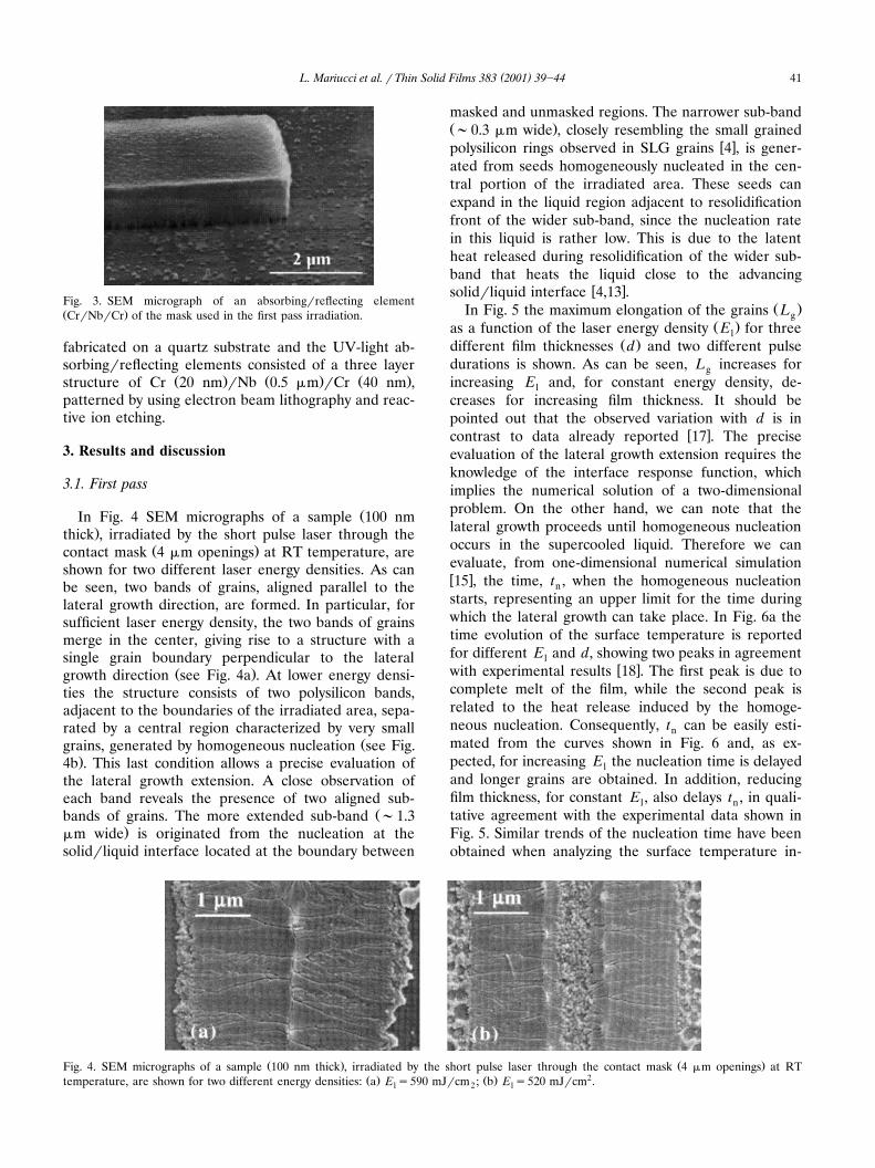
ŽIn Fig. 4 SEM micrographs of a sample 100 nm.thick , irradiated by the short pulse laser through the
Ž .contact mask 4 �m openings at RT temperature, areshown for two different laser energy densities. As canbe seen, two bands of grains, aligned parallel to thelateral growth direction, are formed. In particular, forsufficient laser energy density, the two bands of grainsmerge in the center, giving rise to a structure with asingle grain boundary perpendicular to the lateral
Ž .growth direction see Fig. 4a . At lower energy densi-ties the structure consists of two polysilicon bands,adjacent to the boundaries of the irradiated area, sepa-rated by a central region characterized by very small
Žgrains, generated by homogeneous nucleation see Fig..4b . This last condition allows a precise evaluation of
the lateral growth extension. A close observation ofeach band reveals the presence of two aligned sub-
Žbands of grains. The more extended sub-band �1.3.�m wide is originated from the nucleation at the
solid�liquid interface located at the boundary between
masked and unmasked regions. The narrower sub-bandŽ .�0.3 �m wide , closely resembling the small grained
� �polysilicon rings observed in SLG grains 4 , is gener-ated from seeds homogeneously nucleated in the cen-tral portion of the irradiated area. These seeds canexpand in the liquid region adjacent to resolidificationfront of the wider sub-band, since the nucleation ratein this liquid is rather low. This is due to the latentheat released during resolidification of the wider sub-band that heats the liquid close to the advancing
� �solid�liquid interface 4,13 .Ž .In Fig. 5 the maximum elongation of the grains Lg
Ž .as a function of the laser energy density E for threelŽ .different film thicknesses d and two different pulse
durations is shown. As can be seen, L increases forgincreasing E and, for constant energy density, de-lcreases for increasing film thickness. It should bepointed out that the observed variation with d is in
� �contrast to data already reported 17 . The preciseevaluation of the lateral growth extension requires theknowledge of the interface response function, whichimplies the numerical solution of a two-dimensionalproblem. On the other hand, we can note that thelateral growth proceeds until homogeneous nucleationoccurs in the supercooled liquid. Therefore we canevaluate, from one-dimensional numerical simulation� �15 , the time, t , when the homogeneous nucleationnstarts, representing an upper limit for the time duringwhich the lateral growth can take place. In Fig. 6a thetime evolution of the surface temperature is reportedfor different E and d, showing two peaks in agreementl
� �with experimental results 18 . The first peak is due tocomplete melt of the film, while the second peak isrelated to the heat release induced by the homoge-neous nucleation. Consequently, t can be easily esti-nmated from the curves shown in Fig. 6 and, as ex-pected, for increasing E the nucleation time is delayedland longer grains are obtained. In addition, reducingfilm thickness, for constant E , also delays t , in quali-l ntative agreement with the experimental data shown inFig. 5. Similar trends of the nucleation time have beenobtained when analyzing the surface temperature in-
Ž . Ž .Fig. 4. SEM micrographs of a sample 100 nm thick , irradiated by the short pulse laser through the contact mask 4 �m openings at RTŽ . Ž . 2temperature, are shown for two different energy densities: a E �590 mJ�cm ; b E �520 mJ�cm .l 2 l

( )L. Mariucci et al. � Thin Solid Films 383 2001 39�4442
Fig. 5. Maximum grain elongations vs. energy density for samplesŽ . Žwith different thicknesses, 100 nm closed squares , 50 open squares
. Ž .and triangles and 30 nm closed triangles , irradiated by short-pulseŽ . Ž .squares and long pulse triangles .
Ž .duced by longer pulse laser irradiation see Fig. 6b ,confirming that the dependence of grain elongationupon E and d can be simply related to the delaying oflt .n
The surface morphology of the samples was investi-gated by AFM and the results are shown in Fig. 7. Ascan be noted, the lateral growth is accompanied by asubstantial mass transport caused by the laterally ad-
� �vancing grains through the denser liquid 19 . Thisphenomenon produces the formation of two depres-sions, relative to the plane of the amorphous film, ofapproximately 10 nm and located near the boundariesbetween masked and unmasked regions, where the
lateral growth starts. On the contrary, at the center ofthe irradiated area, where the two solidification fronts
Ž .meet see Fig. 7a , a ridge up to 80 nm high is producedŽ .Fig. 7b . It can be interesting to note that this ridgedisappears after Secco-etching, as it corresponds to thecentral grain boundary observed in the SEM micro-
Ž .graphs Fig. 4a , clearly pointing out to the amorphous� �nature of the protrusion 8 . It can be also noted from
Fig. 7a the absence of protrusions at the grain boun-daries aligned parallel to the direction of the lateralgrowth, denoting no mass transport in that direction.
3.2. Second pass
In Fig. 8 SEM micrographs of a sample after thesecond pass irradiation are shown, for a line�space
Ž .mask geometry of 1.5�2.5 �m 4 �m period . As can beseen, the whole sample area has been now convertedinto polysilicon with large and aligned grains. In partic-ular, Fig. 8 shows that the grains formed during firstpass can act as seeds, allowing the regrowth in theamorphous region, which is completely melted duringthe second pass. The final structure appears formed ofbands of aligned grains nearly 2 �m long, exactly thesemi-period of the line�space mask. The maximumgrain elongation observed during the second pass is0.7�0.8 micron, that allows to fill with large oriented
Ž .grains gaps of approximately 1.5 �m Fig. 8 .Ž .AFM analysis Fig. 9a shows that the partial melt of
the polysilicon regions produced by the second pass
Fig. 6. Time evolution of the surface temperature calculated at different laser energy densities and film thicknesses for two different laser pulseŽ . Ž .durations: 28 ns a and 160 ns b . t is the time when the homogeneous nucleation startsn
Ž . Ž . ŽFig. 7. a AFM surface morphology, and b relative cross-sectional analysis of a sample irradiated through the contact mask first pass of the. 2process at E �400 mJ�cm .l

( )L. Mariucci et al. � Thin Solid Films 383 2001 39�44 43
Fig. 8. SEM micrographs of a sample after the second pass irradia-tion at E �360 mJ�cm2. The position of the mask during the firstlpass, performed at E �400 mJ�cm2 is also shown.l
irradiation allows to reduce the central ridge producedby the mass transport induced during the first pass. Onthe other hand, new roughness is generated at thegrain boundaries aligned parallel to the direction of the
Žlateral growth induced by the first pass compare Fig..7a and Fig. 9a . This can be explained considering that
during the second pass irradiation a complete melt ofthe grain boundary regions occurs, causing masstransport during regrowth of the partially melted grains.Finally, Fig. 9a shows that the regions exposed onlyduring the second pass irradiation present the typicaltopography generated by the lateral growth alreadydescribed for the first pass irradiation. In particular,the ridge marking the end of lateral growth and locatedin the central portion of the region completely meltedby the second pass irradiation is, in this case, approxi-mately 60 nm high. To reduce the roughness generatedby the second pass, using a single pulse irradiation, a
Ž .multi-shot irradiation 2�5 laser pulses in the secondpass has been performed. As evident in Fig. 9b, aconsiderable reduction of the ridge height can beachieved accompanied by a decrease of the RMSroughness of the film from 13 nm for the single pulseprocess to 9 nm for the multi-shot process.
4. Conclusions
We have presented a novel technique, based on atwo-pass ELC-process, that allows the possibility toform uniform polysilicon layers with a spatially con-trolled grain structure. In particular, by controlling thelateral growth by irradiating through a contact mask, itis possible to align the polysilicon grains along thelateral growth direction. For optimized mask geome-tries, only a single grain boundary perpendicular to thelateral growth direction and located in the centralportion of the irradiated area can be obtained. Duringthe second pass of the process, the laterally growngrains, induced by the first pass irradiation, can be usedas seeds and can be propagated in order to uniformlycrystallize the film. With an opportune designing of thecontact mask it is possible to fabricate TFTs with veryfew grain boundaries perpendicular to the current flow.The process appears quite robust in terms of energydensity windows, although the second pass energy den-sity is more critical than that used in the first pass.
Ž .Finally, multi-shot 2�5 shots second pass irradiationhas been shown to produce relatively flat surfaces,eliminating the mass-transport problems characteristicsof the lateral growth phenomenon and still keepinglimited the total number of shots per point needed.These advantages make the proposed process very at-tractive for future industrialization.
Acknowledgements
We wish to thank A. Mittiga for many useful discus-sions, P. Di Lazzaro and D. Murra for laser irradiationsperformed with X-ray preionized excimer laser HER-CULES at ENEA-Frascati laboratories. This work hasbeen partially supported by the Executive Programme‘Research and Technological Development’, funded bythe EU.
2 Ž . �Ž .Fig. 9. AFM surface morphology of samples after the second pass irradiation, at E �360 mJ�cm , performed with single a or multi-shot bl� 2five laser pulses process. The position of the mask during the first pass, performed at E �400 mJ�cm is also shown.l

( )L. Mariucci et al. � Thin Solid Films 383 2001 39�4444
References
� �1 H. Kuriyama, T. Nohda, Y. Aya, T. Kuwahara, K. Wakisaka, S.Ž .Kiyama, S. Tsuda, Jpn. J. Appl. Phys. 33 1994 5657.
� �2 T. Sameshima, A. Kohno, M. Sekiya, M. Hara, N. Sano, Appl.Ž .Phys. Lett. 64 1994 1018.
� �3 P. Lagagneux, F. Petinot, O. Huet, F. Plais, C. Reita, D. Pribat,R. Carluccio, A. Pecora, L. Mariucci, G. Fortunato, Proc.ESSDERC 96, Editions Frontiers, 1996, p. 1071.
� � Ž .4 J.S. Im, H.J. Kim, Appl. Phys. Lett. 64 1994 2303.� � Ž .5 H.J. Kim, J.S. Im, Appl. Phys. Lett. 68 1996 1513.� �6 L. Mariucci, R. Carluccio, A. Pecora, V. Foglietti, G. Fortu-
nato, P. Legagneux, D. Pribat, D. Della Sala, J. Stoemenos,Ž .Thin Solid Films 337 1999 137.
� �7 L. Mariucci, R. Carluccio, A. Pecora, G. Fortunato, F. Mas-sussi, V. Foglietti, D. Della Sala, J. Stoemenos, Polycrystallinesemiconductors V, in: J.H. Werner, H.P. Strunk, H.W. SchockŽ .Eds. , Series Solid State Phenomena, Scitech Publ, 1999, p.175.
� �8 K. Ishikawa, M. Ozawa, C. Oh, M. Matsumura, Jpn. J. Appl.Ž .Phys. 37 1998 731.
� �9 C. Oh, M. Ozawa, M. Matsumura, Jpn. J. Appl. Phys. Lett. 37Ž .1998 L492.
� �10 D.H. Choi, K. Shimizu, O. Sugiura, M. Matsumura, Jpn. J.Ž .Appl. Phys. 31 1992 4545.
� � Ž . Ž .11 P.C. van der Wilt, R. Ishihara, Phys. Status Solidi a 166 1998619.
� � Ž .12 R.S. Sposili, J.S. Im, Appl. Phys. Lett. 69 1996 2864.� � Ž .13 V.V. Gupta, H.J. Song, J.S. Im, Appl. Phys. Lett. 71 1997 99.� � Ž .14 R.F. Wood, G.A. Geist, Phis. Rev. B 34 1986 2606.� �15 A. Mittiga, L. Fornarini, R. Carluccio, Appl. Surf. Sci. 154�155
Ž .2000 112.� �16 S. Bollanti, P. Di lazzaro, F. Flora, G. Giordano, T. Hermsen,
Ž .T. Letardi, C.E. Zheng, Appl. Phys. B 50 1988 415.� �17 K. Ishikawa, M. Ozawa, M. Matsumura, Proc. of AMLCD’97
Conf., 1997, pp. 63�67.� �18 M. Hatano, S. Moon, M. Lee, K. Suzuki, C.P. Grigoropoulos, J.
Ž .Appl. Phys. 87 2000 36.� �19 D.K. Fork, G.B. Anderson, J.B. Boyce, R.I. Johnson, P. Mei,
Ž .Appl. Phys. Lett. 68 1996 .
Copyright © 2022 FDOKUMEN