
Crystallization, Properties, and Challenges of Low-Bandgap ...
18
Crystallization, Properties, and Challenges of Low-Bandgap Sn–Pb Binary Perovskites Hugh Lu Zhu and Wallace C. H. Choy* Solution-process and low-temperature perovskites have motivated a broad range of interests and intensive studies for applications in solar cells (SCs) and photodetectors (PDs). Perovskite SCs with the bandgap of 1.5 eV currently exhibit the certified efficiency over 22% comparable with those of established thin film technologies. Meanwhile, perovskite PDs achieve superb performances in the visible region compared with commercial Si PDs. Partial substitution of Sn into Pb-based perovskites can tune the absorption to near- infrared (NIR) region, which would achieve an ideal-bandgap perovskite approaching the Shockley–Queisser-efficiency limit, low-bandgap perovskite- based bottom subcells in tandem devices (1.2 eV), and NIR photodetection. Here, various crystallization methods for growing low-bandgap Sn–Pb binary perovskites are presented. Their impacts on morphology, crystallinity, preferred orientation, carrier lifetimes, Urbach energy, and stability of the resultant Sn–Pb binary perovskites are highlighted. Then, a description is given of single-junction, 2-terminal, and 4-terminal SCs using these perov- skites as absorbers, which achieve up-to-date efficiencies of 17.8%, 18.4%, and 21.2%, respectively. The current development of ultraviolet–visible–NIR PDs using these perovskites is also discussed. Furthermore, the challenges in controlling inter-grain Sn/Pb element distributions and perovskite stability, which will influence performance and stability of Sn–Pb perovskite-based devices, are presented. Finally, potential prospects are discussed for advancing low-bandgap Sn–Pb binary perovskite-based optoelectronic devices. 1. Introduction Low-temperature and solution-process perovskites have evolved a broad range of interests and intensive studies toward promising applications in photovoltaics, PDs, and light-emitting didoes due to their excellent optical and electrical properties. [1–4] In general, lead based-perovskites adopt the structure of MPbX 3 , where M generally is methylammonium (MA), formamidinium (FA), cesium (Cs), rubidium (Rb), or their mixtures, X normally is iodine (I), bromine (Br), chlorine (Cl), or their mixtures. While compositional-engineering Pb-based perov- skites present strong absorption mainly in the visible range governed by their optical bandgap of 1.55 eV, [1,5] broadening perov- skite absorption to the near-infrared (NIR) region will 1) benefit ideal-bandgap single- junction SCs approaching the Shockley– Queisser efficiency limit of 33.5%, [6] ; 2) implement low-bandgap perovskite-based bottom subcells in tandem photovoltaics; as well as; 3) realize NIR photodetection with potential applications in biometric identifi- cation and medical fluorescent imaging. [7] To employ the excellent optical and electric features of perovskites and simul- taneously widen absorption to the NIR range, various NIR sensitizers, including poly(diketopyrrolopyrrole-terthiophene) (PDPP3T), PbS quantum dots, poly{2,5- bis(2-hexyldecyl)-2,5-dihydropyrrolo[3,4-c] pyrrole-1,4-dione-3,6-di(5-thiophen-2-yl)yl- alt-N-(2-ethylhexyl)-dithieno-[3,2-b:2,3-d] pyrrole-2,6-diyl} (PDPPTDTPT), CyPF 6 and Cy1BF 4 dyes, and β-NaYF:Yb,Er upconversion nanocrystals, have been introduced to the Pb-based perovskite system and form bulk/planar heterojunc- tions for carrier extraction. [8,9] These devi- ces achieved relative low performance in the NIR range due to the weak absorption and/or inefficient carrier extraction. Mean- while, NIR sensitizers may influence the crystallization of perovskites, and increase the production complexity and costs. Substituting Pb with smaller-size halogen Sn to form MSnI 3 perovskite thin films (M ¼ MA, FA, Cs, or arbitrary mixtures of these) could lower the bandgap (1.3eV for CsSnI 3 , 1.3 eV for MASnI 3 , 1.41 eV for FASnI 3 , 1.33 eV for FA 0.75 MA 0.25 SnI 3 ). [10–13] Facile oxidation of Sn 2þ to Sn 4þ states in MSnI 3 perovskites could induce p-type self-doping, which could turn semiconducting perovskites into metal-like ones, causing reduced diffusion length and thus poor stability of these pure Sn-based perovskites and associated optoelectronic devices. [14] Interestingly, Sn-Pb binary perovskites MSn x Pb 1-x I 3 (1 > x > 0), partial incorporation of Sn into Pb-based perovskites, could achieve improved material stability. [15] Meanwhile, the bandgap tuning of Sn-Pb binary perovskites can be broadly extended from the upper value of 1.55 eV to the lower value of 1.17 eV (0.8 > x > 0.5), as shown in Figure 1. [15–18] It should be noted that the bandgap tuning does not obey the Vegard’s law between 1.55 eV of MAPbI 3 and 1.30 eV of MASnI 3 , possibly originating from the competition between the Dr. H. L. Zhu, Prof. W. C. H. Choy Department of Electrical and Electronic Engineering The University of Hong Kong Hong Kong 999077 SAR, China E-mail: [email protected] The ORCID identification number(s) for the author(s) of this article can be found under https://doi.org/10.1002/solr.201800146. DOI: 10.1002/solr.201800146 Low-Bandgap Perovskites www.solar-rrl.com REVIEW Sol. RRL 2018, 1800146 © 2018 WILEY-VCH Verlag GmbH & Co. KGaA, Weinheim 1800146 (1 of 18)
-
Upload
khangminh22 -
Category
Documents
-
view
6 -
download
0
Transcript of Crystallization, Properties, and Challenges of Low-Bandgap ...

Low-Bandgap Perovskites www.solar-rrl.com
REVIEW
Crystallization, Properties, and Challenges of Low-BandgapSn–Pb Binary Perovskites
Hugh Lu Zhu and Wallace C. H. Choy*
Solution-process and low-temperature perovskites have motivated a broadrange of interests and intensive studies for applications in solar cells (SCs)and photodetectors (PDs). Perovskite SCs with the bandgap of �1.5 eVcurrently exhibit the certified efficiency over 22% comparable with those ofestablished thin film technologies. Meanwhile, perovskite PDs achieve superbperformances in the visible region compared with commercial Si PDs. Partialsubstitution of Sn into Pb-based perovskites can tune the absorption to near-infrared (NIR) region, which would achieve an ideal-bandgap perovskiteapproaching the Shockley–Queisser-efficiency limit, low-bandgap perovskite-based bottom subcells in tandem devices (�1.2 eV), and NIR photodetection.Here, various crystallization methods for growing low-bandgap Sn–Pb binaryperovskites are presented. Their impacts on morphology, crystallinity,preferred orientation, carrier lifetimes, Urbach energy, and stability of theresultant Sn–Pb binary perovskites are highlighted. Then, a description isgiven of single-junction, 2-terminal, and 4-terminal SCs using these perov-skites as absorbers, which achieve up-to-date efficiencies of 17.8%, 18.4%,and 21.2%, respectively. The current development of ultraviolet–visible–NIRPDs using these perovskites is also discussed. Furthermore, the challengesin controlling inter-grain Sn/Pb element distributions and perovskite stability,which will influence performance and stability of Sn–Pb perovskite-baseddevices, are presented. Finally, potential prospects are discussed foradvancing low-bandgap Sn–Pb binary perovskite-based optoelectronicdevices.
1. Introduction
Low-temperature and solution-process perovskites have evolved abroad range of interests and intensive studies toward promisingapplications in photovoltaics, PDs, and light-emitting didoes dueto their excellent optical and electrical properties.[1–4] In general,lead based-perovskites adopt the structure of MPbX3, where Mgenerally is methylammonium (MA), formamidinium (FA),cesium (Cs), rubidium (Rb), or their mixtures, X normally isiodine (I), bromine (Br), chlorine (Cl), or their mixtures. While
Dr. H. L. Zhu, Prof. W. C. H. ChoyDepartment of Electrical and Electronic EngineeringThe University of Hong KongHong Kong 999077 SAR, ChinaE-mail: [email protected]
The ORCID identification number(s) for the author(s) of this articlecan be found under https://doi.org/10.1002/solr.201800146.
DOI: 10.1002/solr.201800146
Sol. RRL 2018, 1800146 © 21800146 (1 of 18)
compositional-engineering Pb-based perov-skites present strong absorption mainly inthe visible range governed by their opticalbandgap of �1.55 eV,[1,5] broadening perov-skite absorption to the near-infrared (NIR)region will 1) benefit ideal-bandgap single-junction SCs approaching the Shockley–Queisser efficiency limit of �33.5%,[6]; 2)implement low-bandgap perovskite-basedbottom subcells in tandem photovoltaics; aswell as; 3) realize NIR photodetection withpotential applications in biometric identifi-cation and medical fluorescent imaging.[7]
To employ the excellent optical andelectric features of perovskites and simul-taneously widen absorption to the NIRrange, various NIR sensitizers, includingpoly(diketopyrrolopyrrole-terthiophene)(PDPP3T), PbS quantum dots, poly{2,5-bis(2-hexyldecyl)-2,5-dihydropyrrolo[3,4-c]pyrrole-1,4-dione-3,6-di(5-thiophen-2-yl)yl-alt-N-(2-ethylhexyl)-dithieno-[3,2-b:2,3-d]pyrrole-2,6-diyl} (PDPPTDTPT), CyPF6and Cy1BF4 dyes, and β-NaYF:Yb,Erupconversion nanocrystals, have beenintroduced to the Pb-based perovskitesystem and form bulk/planar heterojunc-tions for carrier extraction.[8,9] These devi-ces achieved relative low performance inthe NIR range due to the weak absorptionand/or inefficient carrier extraction. Mean-
while, NIR sensitizers may influence the crystallization ofperovskites, and increase the production complexity and costs.
Substituting Pb with smaller-size halogen Sn to form MSnI3perovskite thin films (M¼MA, FA, Cs, or arbitrary mixtures ofthese) could lower the bandgap (1.3 eV for CsSnI3, 1.3 eV forMASnI3, 1.41 eV for FASnI3, 1.33 eV for FA0.75MA0.25SnI3).
[10–13]
Facile oxidation of Sn2þ to Sn4þ states inMSnI3 perovskites couldinduce p-type self-doping, which could turn semiconductingperovskites intometal-like ones, causing reduced diffusion lengthand thus poor stability of these pure Sn-based perovskites andassociated optoelectronic devices.[14] Interestingly, Sn-Pb binaryperovskites MSnxPb1-xI3 (1> x> 0), partial incorporation of Sninto Pb-based perovskites, could achieve improved materialstability.[15] Meanwhile, the bandgap tuning of Sn-Pb binaryperovskites can be broadly extended from the upper value of1.55 eV to the lower value of 1.17 eV (0.8> x> 0.5), as shown inFigure 1.[15–18] It shouldbenoted that the bandgap tuning doesnotobey the Vegard’s law between 1.55 eV of MAPbI3 and 1.30 eV ofMASnI3, possibly originating from the competition between the
018 WILEY-VCH Verlag GmbH & Co. KGaA, Weinheim
Hugh Lu Zhu received his B.Sc.degree from Northwest University in2009, M.Sc. degree from BeijingJiaotong University in 2012, Ph.D.degree from The University of HongKong (HKU) in 2016. Now he worksas a research associate in HKU. Hisresearch interests includecrystallization and formation of low-bandgap perovskite films, and
inorganic/organic/perovskite optoelectronic devices(including photodetectors and photovoltaics).
Wallace C. H. Choy is a full professorin the Department of Electrical andElectronic Engineering, HKU. Hisresearch interests cover organic/inorganic optoelectronic devices,plasmonic structures, metal oxides,and nanomaterial devices. He haspublished more than 170 peer-reviewed papers, several bookchapters, patents, and edited one
book. He was recognized as top 1% of most-cited scientistsin Thomson Reuter’s Essential Science Indicators from 2014to 2017. He is an elected fellow of OSA.
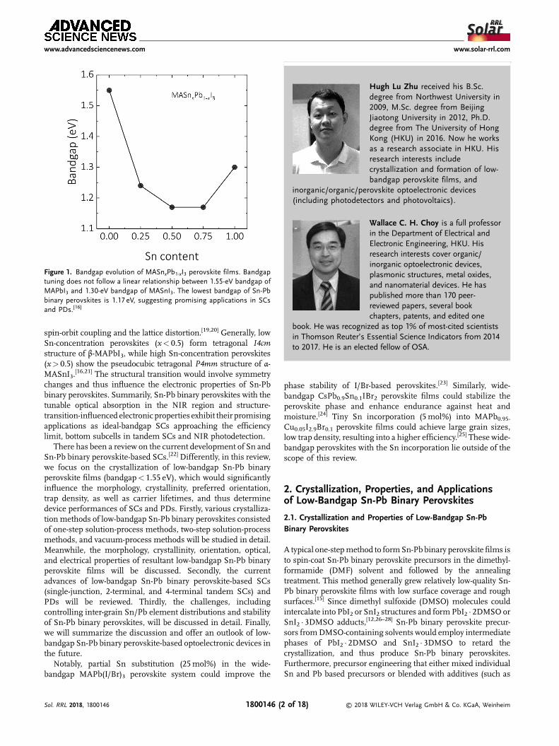
Figure 1. Bandgap evolution of MASnxPb1-xI3 perovskite films. Bandgaptuning does not follow a linear relationship between 1.55-eV bandgap ofMAPbI3 and 1.30-eV bandgap of MASnI3. The lowest bandgap of Sn-Pbbinary perovskites is 1.17 eV, suggesting promising applications in SCsand PDs.[16]
www.advancedsciencenews.com www.solar-rrl.com
spin-orbit coupling and the lattice distortion.[19,20] Generally, lowSn-concentration perovskites (x< 0.5) form tetragonal I4cmstructure of β-MAPbI3, while high Sn-concentration perovskites(x> 0.5) show the pseudocubic tetragonal P4mm structure of α-MASnI3.
[16,21] The structural transition would involve symmetrychanges and thus influence the electronic properties of Sn-Pbbinary perovskites. Summarily, Sn-Pb binary perovskites with thetunable optical absorption in the NIR region and structure-transition-influenced electronicproperties exhibit theirpromisingapplications as ideal-bandgap SCs approaching the efficiencylimit, bottom subcells in tandem SCs and NIR photodetection.
There has been a review on the current development of Sn andSn-Pb binary perovskite-based SCs.[22] Differently, in this review,we focus on the crystallization of low-bandgap Sn-Pb binaryperovskite films (bandgap< 1.55 eV), which would significantlyinfluence the morphology, crystallinity, preferred orientation,trap density, as well as carrier lifetimes, and thus determinedevice performances of SCs and PDs. Firstly, various crystalliza-tionmethods of low-bandgap Sn-Pb binary perovskites consistedof one-step solution-process methods, two-step solution-processmethods, and vacuum-process methods will be studied in detail.Meanwhile, the morphology, crystallinity, orientation, optical,and electrical properties of resultant low-bandgap Sn-Pb binaryperovskite films will be discussed. Secondly, the currentadvances of low-bandgap Sn-Pb binary perovskite-based SCs(single-junction, 2-terminal, and 4-terminal tandem SCs) andPDs will be reviewed. Thirdly, the challenges, includingcontrolling inter-grain Sn/Pb element distributions and stabilityof Sn-Pb binary perovskites, will be discussed in detail. Finally,we will summarize the discussion and offer an outlook of low-bandgap Sn-Pb binary perovskite-based optoelectronic devices inthe future.
Notably, partial Sn substitution (25mol%) in the wide-bandgap MAPb(I/Br)3 perovskite system could improve the
Sol. RRL 2018, 1800146 1800146 (2
phase stability of I/Br-based perovskites.[23] Similarly, wide-bandgap CsPb0.9Sn0.1IBr2 perovskite films could stabilize theperovskite phase and enhance endurance against heat andmoisture.[24] Tiny Sn incorporation (5mol%) into MAPb0.95-Cu0.05I2.9Br0.1 perovskite films could achieve large grain sizes,low trap density, resulting into a higher efficiency.[25] These wide-bandgap perovskites with the Sn incorporation lie outside of thescope of this review.
2. Crystallization, Properties, and Applicationsof Low-Bandgap Sn-Pb Binary Perovskites
2.1. Crystallization and Properties of Low-Bandgap Sn-PbBinary Perovskites
A typical one-stepmethod to formSn-Pbbinary perovskitefilms isto spin-coat Sn-Pb binary perovskite precursors in the dimethyl-formamide (DMF) solvent and followed by the annealingtreatment. This method generally grew relatively low-quality Sn-Pb binary perovskite films with low surface coverage and roughsurfaces.[15] Since dimethyl sulfoxide (DMSO) molecules couldintercalate into PbI2 or SnI2 structures and formPbI2 � 2DMSO orSnI2 � 3DMSO adducts,[12,26–28] Sn-Pb binary perovskite precur-sors fromDMSO-containing solvents would employ intermediatephases of PbI2 � 2DMSO and SnI2 � 3DMSO to retard thecrystallization, and thus produce Sn-Pb binary perovskites.Furthermore, precursor engineering that either mixed individualSn and Pb based precursors or blended with additives (such as
© 2018 WILEY-VCH Verlag GmbH & Co. KGaA, Weinheimof 18)

www.advancedsciencenews.com www.solar-rrl.com
chloride,Rb,andCs)wouldbeemployedto tune thecrystallization.These Sn-Pb binary perovskite precursor films generally spin-coated on poly(3,4-ethylenedioxythiophene):poly(p-styrene sulfo-nate) (PEDOT:PSS) substrates would be washed/immersed byanti-solvents, including toluene, anisole or diethyl ether, andannealed.[18,19,23,29–43] Meanwhile, Sn-Pb binary perovskite filmscan be formed by two-step solution-process methods. PbI2(SnI2)� xDMSO intermediates were firstly fabricated. MAI was spin-coated atop and experienced ionic interactions to form Sn-Pbbinary perovskites.[17,44] Additionally, the hot-casting crystalliza-tion technique as a one-step method and a vacuum-processmethod will also be discussed as below.
2.1.1. One-Step Solution-Process Methods
Precursor engineering: Chloride. Jen and co-workers directlyblended methylammonium iodide (MAI), lead chloride (PbCl2),and tin chloride (SnCl2) into anhydrous DMF solvents.[45]
Precursors were deposited on the surface of PEDOT:PSSthrough one-step spin-coating, followed by annealing at 90 �C for2 h to produce MASnxPb1-xI3(Cl) perovskite thin films. Theyfound that chloride ions not only worked as substitutionalimpurities in final iodide-based Sn-Pb binary perovskites, butalso altered the transformation pathway during annealing viaintroducing the competing chloride-based perovskite phase.Meanwhile, the presence of Sn2þ would regulate the nucleationrate and influence the growth behavior of Sn-Pb binaryperovskites. Finally, through optimizing the Sn content(x¼ 0.15), they presented rough Sn-Pb binary perovskite thinfilms with 97% surface coverage on PEDOT:PSS substrates, asshown in Figure 2A. When x> 0.5, their fabricated MASnxPb1-xI3(Cl) perovskite thin films showed low surface coverage andrough surface. The chloride incorporation that influenced thecrystallization of Sn-Pb binary perovskites and altered the opticaland electronic properties also were investigated by Diau and co-workers through mixing SnCl2 and PbI2 in varied stoichiometricratios.[46] Overall, different from the case of pure Pb-basedperovskites that chloride incorporation could improve perovskitecrystallinity and enhance performances of SCs,[47] the introduc-tion of chloride has not produced high-quality Sn-Pb binaryperovskite films and efficient SCs.
Precursor engineering: Cesium. In the early reports, Jen and co-workers found that Sn-Pb binary perovskite films exhibitedapparent pinhole and non-uniform morphology when the Sncontent exceeded 25%(i.e.,x> 0.25).[32,45] Cs-cation incorporationinto the large FA-cation based perovskite system (FAPbI3) couldtune tolerance factor and then stabilize the perovskite α-phase ofFAPbI3, as well as potentially modulate the film formation.[48]
Differently, Cs-cation incorporation intoMA-cation pure Pb-basedperovskite system (MAPbI3) has limited reports. They found thatintroduction of Cs cations could effectively control the filmformationofSn-Pbbinaryperovskitefilmsand thus lead intohigh-qualityperovskitefilms.As shown inFigure 2B–E,MAPb0.5Sn0.5I3perovskite films with the incorporation of 10mol% Cs exhibited ahomogenous and uniform morphology, ascribing to the reducedcrystallization rate inducedby the additionofCs cations. ExcessCsincorporation (�20mol%) would induce a pinhole and non-uniformmorphology,possiblyowing tophaseseparationresulting
Sol. RRL 2018, 1800146 1800146 (3
from immiscibility.[49] Appropriate Cs-cation incorporation(10–30mol%) did not change the bandgap of MAPb0.5Sn0.5I3perovskites (�1.28 eV), but slightly shrink the crystal lattice due tosmaller size of Cs cations.[31] Significantly, under an ambientenvironment with a relative humidity of 35� 5%,MAPb0.5Sn0.5I3perovskites presented a new peak indexing to MA2SnI6 (theoxidation of Sn2þ to Sn4þ), whereas no manifest peaks wereobserved for MA0.9Cs0.1Pb0.5Sn0.5I3 perovskites (Figure 2F),suggesting the enhanced stability of Sn-Pb binary perovskiteswith the incorporation of Cs cations.[31]
Precursor engineering: DMSO. Since PbI2 and SnI2 couldcoordinate with DMSO to form PbI2 � 2DMSO and SnI2 � 3DMSOadducts, respectively,[12,26] Choy and co-workers successfullyrealized controllable crystallization of Sn-poor Sn-Pb binaryperovskite films (MASn0.25Pb0.75I3) via tuning DMSO amount inraw precursors.[42] Various-content DMSOwith 0, 25, 50, and 75 vol% in theDMF:DMSO co-solvent were defined asDMSO-0, DMSO-25, DMSO-50, and DMSO-75, respectively. MASn0.25Pb0.75I3perovskite precursors were spin-coated on the surface of PEDOT:PSS, sequentially washed by toluene, finally annealed at 100 �C for10min to produce MASn0.25Pb0.75I3 perovskite films. As shown inFigure3A–D,the introductionofDMSOcouldsignificantly increasethe grain size of MASn0.25Pb0.75I3 perovskites. DMSO-25 andDMSO-50-based films exhibited large grain sizes of about 250 and200nm, respectively, while DMSO-0-based films showed smallgrain sizes of about 100nm. Excess DMSO in the raw precursor(DMSO-75) caused the small grain size.
The crystallinity and orientation of MASn0.25Pb0.75I3 perov-skite films were characterized by the XRD measurement, asshown in Figure 3E. Remarkably, in comparison with DMSO-0-based perovskites, DMSO-25, DMSO-50, and DMSO-75-basedSn-Pb perovskites showed significantly enhanced diffractionintensities of (110) plane by over 20-, 14-, and 4-folds,respectively, indicating improved perovskite crystallinity. Withthe increase of DMSO amount, intensities of MASn0.25Pb0.75I3perovskites gradually decreased. It might be resulted fromuncrystallized PbI2/SnI2 film induced by the excess DMSOmolecules and thus lowered perovskite crystallinity.[28] Thetexture coefficient was used to characterize the preferredorientation of Sn-Pb binary perovskite films. Texture coefficientsof the (110) plane relative to (112) plane of DMSO-0, DMSO-25,DMSO-50, and DMSO-75-based perovskite films were estimatedto be 0.34, 0.81, 0.88, and 0.74, respectively. The higher texturecoefficient value for DMSO-50-based Sn-Pb binary perovskitessuggested that DMSO incorporation would effectively enhancethe orientation of the main plane.
Another concern is Sn and Pb element distributions in thefinal MASn0.25Pb0.75I3 perovskite films, which was characterizedby the transmission electron microscopy (TEM) integrated withenergy-dispersive X-ray spectroscopy (EDS). It was found that Snpercentages (defined as the ratio of Sn atoms over the total atomsof Sn and Pb) in MASn0.25Pb0.75I3 perovskites were not aconstant on 100-nm scales. Interestingly, DMSO incorporationcould ameliorate inhomogeneous Sn/Pb element distributions.
Precursor engineering: FASnI3-FAPbI3 and Cesium. McGehee,Snaith and co-workers firstly introduced FA-Cs cations into Sn-Pbbinary perovskite films.[18] They employed precursor-phase anti-solvent immersion to produce highly crystalline and uniform Sn-Pb perovskite films, which combined low-vapor pressure solvents
© 2018 WILEY-VCH Verlag GmbH & Co. KGaA, Weinheimof 18)

Figure 2. A) Scanning electron microscopy (SEM) image of MASnxPb1-xI3(Cl) perovskite thin films when x¼ 0.15. B–E) SEM images of MAPb0.5Sn0.5I3,MA0.9Cs0.1Pb0.5Sn0.5I3, MA0.8Cs0.2Pb0.5Sn0.5I3, MA0.7Cs0.3Pb0.5Sn0.5I3, respectively. F) Time-resolved X-ray diffraction (XRD) spectra of MAPb0.5Sn0.5I3and MA0.9Cs0.1Pb0.5Sn0.5I3 films stored in an ambient environment with a relative humidity of 35� 5%. Figure A reproduced with permission.[45]
Copyright 2014, Wiley-VCH. Figures B–F reproduced with permission.[31] Copyright 2016, The Royal Society of Chemistry.
www.advancedsciencenews.com www.solar-rrl.com
to growprecursor complexes and an anti-solvent bath to crystallizeperovskite films with appropriate heating. Specifically, the initialprecursor solutions were prepared viamixing FASnI3 and FAPbI3precursors both from a co-solvent of DMF:DMSO (low-vapor
Figure 3. Top-view SEM images of Sn-Pb binary perovskite films producedDMSO-25, (C) DMSO-50, (D) DMSO-75, and (E) corresponding XRD patteCopyright 2017, Wiley-VCH.
Sol. RRL 2018, 1800146 1800146 (4
pressure solvents). SnF2 was added into the FASnI3 precursors toretard oxidation of the Sn2þ to Sn4þ.[10] Spin-coated transparentprecursor films were immersed in anisole (an anti-solvent bath),driedwithnitrogengasflow, and then annealed at 70 �C for20min
from different DMSO/DMF ratios-based precursors: (A) DMSO-0, (B)rns. The scale bars are 500 nm. Figures reproduced with permission.[42]
© 2018 WILEY-VCH Verlag GmbH & Co. KGaA, Weinheimof 18)
www.advancedsciencenews.com www.solar-rrl.com
to fabricate smooth, highly crystalline and uniform FASnxPb1-xI3films. The full coverage of Sn-Pb binary perovskite films onPEDOT:PSS surfaces was achieved when x¼ 0.5 and low surfacecoverage occurred at x¼ 1.0. Notably, FASn0.5Pb0.5I3 andFA0.75Cs0.25Sn0.5Pb0.5I3 binarySn-Pbperovskitefilmswereheatedat 100 �C for 4 days under nitrogen. There were no changes in theabsorption spectra, indicating excellent thermal stability ofFASn0.5Pb0.5I3 and FA0.75Cs0.25Sn0.5Pb0.5I3 perovskites.
Electrical properties of FASn0.5Pb0.5I3 films, includingcharge-carrier diffusion length, mobility, and recombinationlifetimes, were determined by the optical pump probe terahertzspectroscopy. FASn0.5Pb0.5I3 perovskite films achieved a charge-carrier mobility of 17 cm2V�1 s�1 and a charge-carrier diffusionlength of�210 nm. Importantly, substituting 25% of the FAwithCs in FASn0.5Pb0.5I3 films had little impact on morphology,bandgap, photoluminescence, charge carrier diffusion lengths,but improved efficiency of SCs.[18]
Precursor engineering: FASnI3-MAPbI3. A new precursorcomposed of a FASnI3 precursor with a MAPbI3 precursor withvarious ratios both in theDMSO:DMFco-solventwas employedbyYan and co-workers[29,41] The Sn-Pb binary perovskite precursorfilmswere produced by spin-coated the newprecursor on PEDOT:PSS surfaces. After diethyl ether was dripped, formed intermedi-ate complexeswere annealed at 100 �C for 5min to fabricate denseSn-Pb binary perovskite thin films. It was observed that this newprecursor was suited for depositing Sn-rich (x� 0.6) Sn-Pb binaryperovskite thin films. Sn-rich (x� 0.6) Sn-Pb binary perovskitesshowed relatively dense, uniform, and homogeneous thin filmscompared with Sn-poor (x� 0.4) Sn-Pb binary perovskites, asevidenced by SEM images. When x¼ 0.6, (FASnI3)0.6(MAPbI3)0.4perovskitefilms showed the lowest bandgap of�1.2 eVand carrierlifetime of 6.7 ns. Distinctively, all Sn-Pb binary perovskitesadopted the orthorhombic crystal structure, same to the crystalstructureofFASnI3,whichwasdifferent fromprevious results thatSn-Pb binary perovskites adopted the crystal structure of pure-Snbased perovskites when x> 0.5.[14,16,29]
It should be noted that the short carrier lifetime (6.7ns) of(FASnI3)0.6(MAPbI3)0.4 perovskites indicated low film crystallinity,which would impede efficiency advances of (FASnI3)0.6(MAPbI3)0.4SCs.[41] Interestingly, throughoptimizingprecursor concentrations,various-thickness (FASnI3)0.6(MAPbI3)0.4 perovskite films (400,510, 620, 1010nm) were successfully fabricated. It was found thattheaveragegrainsize increasedas the thickness increased,asshownin Figure 4A–D. Specially, 620-nm-thick perovskite film exhibitedthe smallest full-width at half-maximum values at the (110) peak,indicating the highest crystallinity. Meanwhile, 620-nm-thick filmachieved the longest carrier lifetime of �255ns (Figure 4F) andlowestUrbach energy of 18.8meV, suggestinghigh crystallinity andlow density of trap states.
Precursor engineering: FAPbI3-CsSnI3. Padture and co-workersdemonstrated a new precursor composed of homogenouslymixing stoichiometric FAPbI3 and CsSnI3 precursors bothdissolved in DMSO solvents.[19] In order to obtain an ideal-bandgap perovskite of �1.3 eV for single-junction SCs, thebandgap tuning was realized in (FAPbI3)1-x(CsSnI3)x perov-skites. Similar to early reports, the anomalous bandgap tuningwas observed, where smallest bandgap of 1.24 eV occurred atx¼ 0.4.[16,18] Authors ascribed the nonmonotonic bandgaptuning to transitions of the lattice symmetry from cubic
Sol. RRL 2018, 1800146 1800146 (5
Pm�3m (FAPbI3) to orthorhombic Pnma (CsSnI3). Finally, asshown in Figure 5A and B, an ideal bandgap perovskite atx¼ 0.3, (FAPbI3)0.7(CsSnI3)0.3, was produced and exhibited a lowUrbach energy of 30meV. Meanwhile, enhanced materialstability of (FAPbI3)0.7(CsSnI3)0.3 perovskites was experimentallyobserved, originating from the entropy of mixing and reducedoxidation of Sn2þ due to the protection of the surrounding Pb2þ
in the crystal structure at the atomic scale.[19,50] They alsoinvestigated the band structure using density function theorycalculations (DFT). Figure 5C presented the calculated totaldensity of states (DOS) and projected density of states (PDOS)and the inset was the constructed (FAPbI3)0.7(CsSnI3)0.3perovskites model. For the PDOS, the valence band maximumwas mainly contributed by I 5p, Sn 5s, and Pb 6s orbitals, whilethe conduction band minimum was resulted from I 5p, Sn 5p,and Pb 6p orbitals. The calculated bandgap of (FAP-bI3)0.7(CsSnI3)0.3 perovskites was 1.35 eV, which agreed withthe measured optical value.
Precursor engineering: Rubidium. Choy and co-workers intro-duced tiny Rb cations into Sn-rich MASn0.65Pb0.35I3 perovskiteprecursors in the DMSO:DMF co-solvent.[43] Conventionally,adding small-size Rb into large-size FA cation perovskites couldtune tolerance factor, and stabilize the perovskite phase.[2]
Distinctively, in the Sn-rich MASn0.65Pb0.35I3 perovskite system,Rb incorporation could effectivelymodify surface-energy-inducedkinetic process during the perovskite growth. According to the abinitio simulation, they found that Rb incorporation in Sn-rich Sn-Pb perovskite systems can facilitate the perovskite growth in (110)plane and suppress growth in (112) and (113) planes, indicatingcontrollable crystallization. Experimentally, compared withMASn0.65Pb0.35I3 perovskites with pinholes and roughness of16.1 nm, MA0.975Rb0.025Sn0.65Pb0.35I3 perovskite films exhibitedlarge grain size, pinhole-free, and smoothfilmswith roughness of11.2 nm, as showninFigure6AandB.AsshowninFigure6C,MA-Rb perovskite films achieved significantly enhanced diffractionintensities of (110) plane by over two times compared with MA-based perovskites, suggesting improved perovskite crystallinity.Meanwhile, it was found that intensities of (112), (113), and (224)planes of MA-Rb perovskite films were even reduced, whichindicates the strengthened preferred orientation. These findingswere consistent with the simulated results.
The influence of controllable crystallization of MA-Rb Sn-Pbperovskites on local surface potentials and charge carrierlifetimes were investigated by Kelvin probe force microscopyand time-resolved photoluminescence spectroscopy, respec-tively. In comparison with MASn0.65Pb0.35I3 perovskites,MA0.975Rb0.025Sn0.65Pb0.35I3 perovskite films showed a smallerpotential difference at the grain boundaries/grain interiorsinterface and a longer carrier lifetime, which would beneficiallycontribute to efficient optoelectronic devices.
Hot-casting crystallization: The hot-casting technique has beensuccessfully applied in crystallizing high-quality MAPbI3(Cl) and(BA)2(MA)3Pb4I13 (BA¼n-butylammonium) perovskite films.[51]
Since the solution-process hot-casting technique could influencetheperovskite crystallization, Sadhanalaandco-workers employedthis method to fabricate Sn-Pb binary perovskite films.[21]
MASnxPb1-xI3 perovskite precursors were prepared by mixingMAPbI3 precursors (PbI2:MACl with 1:1 molar stoichiometricratio in DMF) and MASnI3 precursors (SnI2:MAI with 1:1 molar
© 2018 WILEY-VCH Verlag GmbH & Co. KGaA, Weinheimof 18)
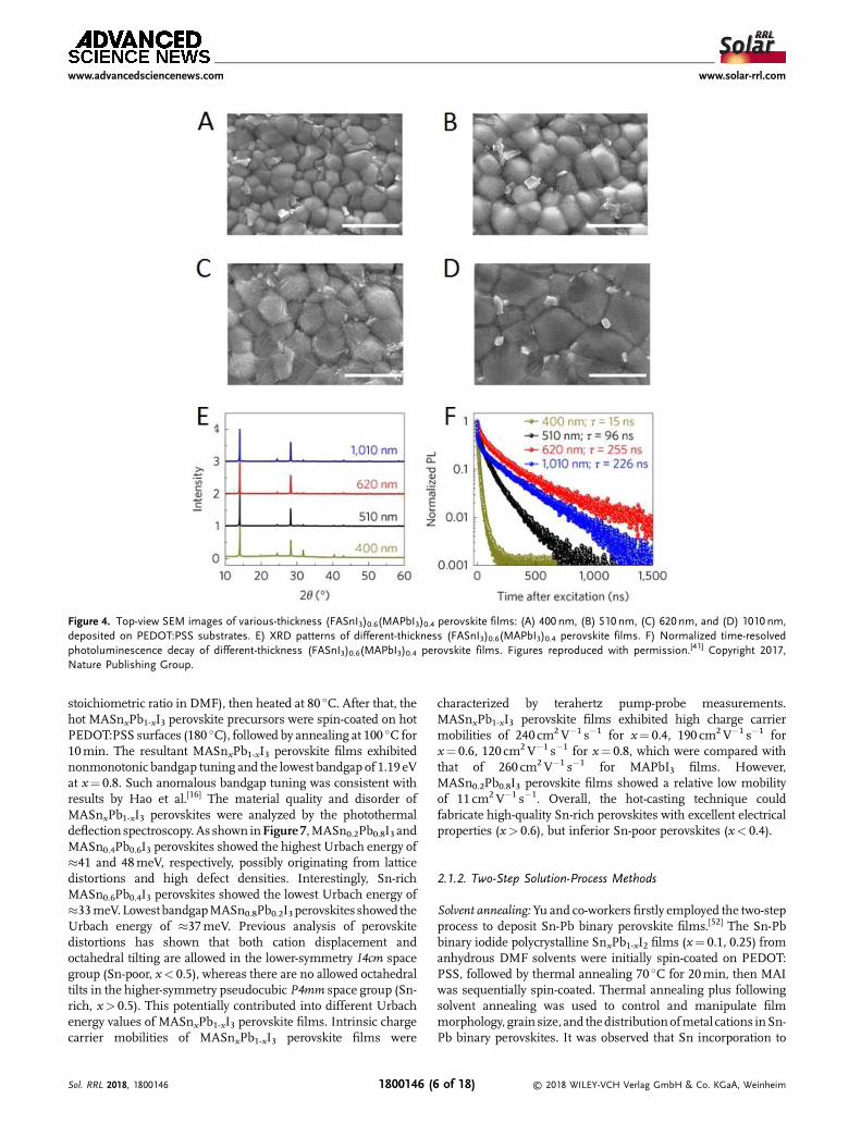
Figure 4. Top-view SEM images of various-thickness (FASnI3)0.6(MAPbI3)0.4 perovskite films: (A) 400 nm, (B) 510 nm, (C) 620 nm, and (D) 1010 nm,deposited on PEDOT:PSS substrates. E) XRD patterns of different-thickness (FASnI3)0.6(MAPbI3)0.4 perovskite films. F) Normalized time-resolvedphotoluminescence decay of different-thickness (FASnI3)0.6(MAPbI3)0.4 perovskite films. Figures reproduced with permission.[41] Copyright 2017,Nature Publishing Group.
www.advancedsciencenews.com www.solar-rrl.com
stoichiometric ratio in DMF), then heated at 80 �C. After that, thehot MASnxPb1-xI3 perovskite precursors were spin-coated on hotPEDOT:PSS surfaces (180 �C), followed by annealing at 100 �C for10min. The resultant MASnxPb1-xI3 perovskite films exhibitednonmonotonic bandgap tuning and the lowest bandgap of 1.19 eVat x¼ 0.8. Such anomalous bandgap tuning was consistent withresults by Hao et al.[16] The material quality and disorder ofMASnxPb1-xI3 perovskites were analyzed by the photothermaldeflectionspectroscopy.As shown inFigure 7,MASn0.2Pb0.8I3 andMASn0.4Pb0.6I3 perovskites showed the highest Urbach energy of�41 and 48meV, respectively, possibly originating from latticedistortions and high defect densities. Interestingly, Sn-richMASn0.6Pb0.4I3 perovskites showed the lowest Urbach energy of�33meV.LowestbandgapMASn0.8Pb0.2I3perovskites showed theUrbach energy of �37meV. Previous analysis of perovskitedistortions has shown that both cation displacement andoctahedral tilting are allowed in the lower-symmetry I4cm spacegroup (Sn-poor, x< 0.5), whereas there are no allowed octahedraltilts in the higher-symmetry pseudocubic P4mm space group (Sn-rich, x> 0.5). This potentially contributed into different Urbachenergy values of MASnxPb1-xI3 perovskite films. Intrinsic chargecarrier mobilities of MASnxPb1-xI3 perovskite films were
Sol. RRL 2018, 1800146 1800146 (6
characterized by terahertz pump-probe measurements.MASnxPb1-xI3 perovskite films exhibited high charge carriermobilities of 240 cm2V�1 s�1 for x¼ 0.4, 190 cm2V�1 s�1 forx¼ 0.6, 120 cm2V�1 s�1 for x¼ 0.8, which were compared withthat of 260 cm2V�1 s�1 for MAPbI3 films. However,MASn0.2Pb0.8I3 perovskite films showed a relative low mobilityof 11 cm2V�1 s�1. Overall, the hot-casting technique couldfabricate high-quality Sn-rich perovskites with excellent electricalproperties (x> 0.6), but inferior Sn-poor perovskites (x< 0.4).
2.1.2. Two-Step Solution-Process Methods
Solvent annealing: Yu and co-workers firstly employed the two-stepprocess to deposit Sn-Pb binary perovskite films.[52] The Sn-Pbbinary iodide polycrystalline SnxPb1-xI2 films (x¼ 0.1, 0.25) fromanhydrous DMF solvents were initially spin-coated on PEDOT:PSS, followed by thermal annealing 70 �C for 20min, then MAIwas sequentially spin-coated. Thermal annealing plus followingsolvent annealing was used to control and manipulate filmmorphology, grain size, and thedistributionofmetal cations inSn-Pb binary perovskites. It was observed that Sn incorporation to
© 2018 WILEY-VCH Verlag GmbH & Co. KGaA, Weinheimof 18)

Figure 5. A) a SEM image of (FAPbI3)0.7(CsSnI3)0.3 perovskite films. B) Tauc plot of (FAPbI3)0.7(CsSnI3)0.3 perovskite films showing a bandgap of 1.3 eV.C) DOS of (FAPbI3)0.7(CsSnI3)0.3 perovskites based on DFT calculations. Inset is the crystal model showing the (FAPbI3)0.7(CsSnI3)0.3 perovskites.Figures reproduced with permission.[19] Copyright 2017, Wiley-VCH.
www.advancedsciencenews.com www.solar-rrl.com
PbI2 showed in-plane orientation of Sn0.1Pb0.9I2 films and grainreorientation of Sn0.25Pb0.75I2 films, indicating that the amount ofSn substitution would influence grain orientation, which wouldwork as different templates to growSn-Pb binary perovskitefilms.
Figure 6. Top-view SEM images of (A) MASn0.65Pb0.35I3 and (B) MA0.975
MA0.975Rb0.025Sn0.65Pb0.35I3 (top) and MASn0.65Pb0.35I3 (bottom) perovskite fWiley-VCH.
Sol. RRL 2018, 1800146 1800146 (7
Both MASn0.1Pb0.9I3 and MASn0.25Pb0.75I3 films treated by onlythermal annealingweredensely packedwith small grains (124 and158nm, respectively) and relatively rough. When treated with thethermal plus DMSO vapor-assisted thermal annealing, both
Rb0.025Sn0.65Pb0.35I3 perovskite films, respectively. C) XRD patterns ofilms, respectively. Figures reproduced with permission.[43] Copyright 2018,
© 2018 WILEY-VCH Verlag GmbH & Co. KGaA, Weinheimof 18)
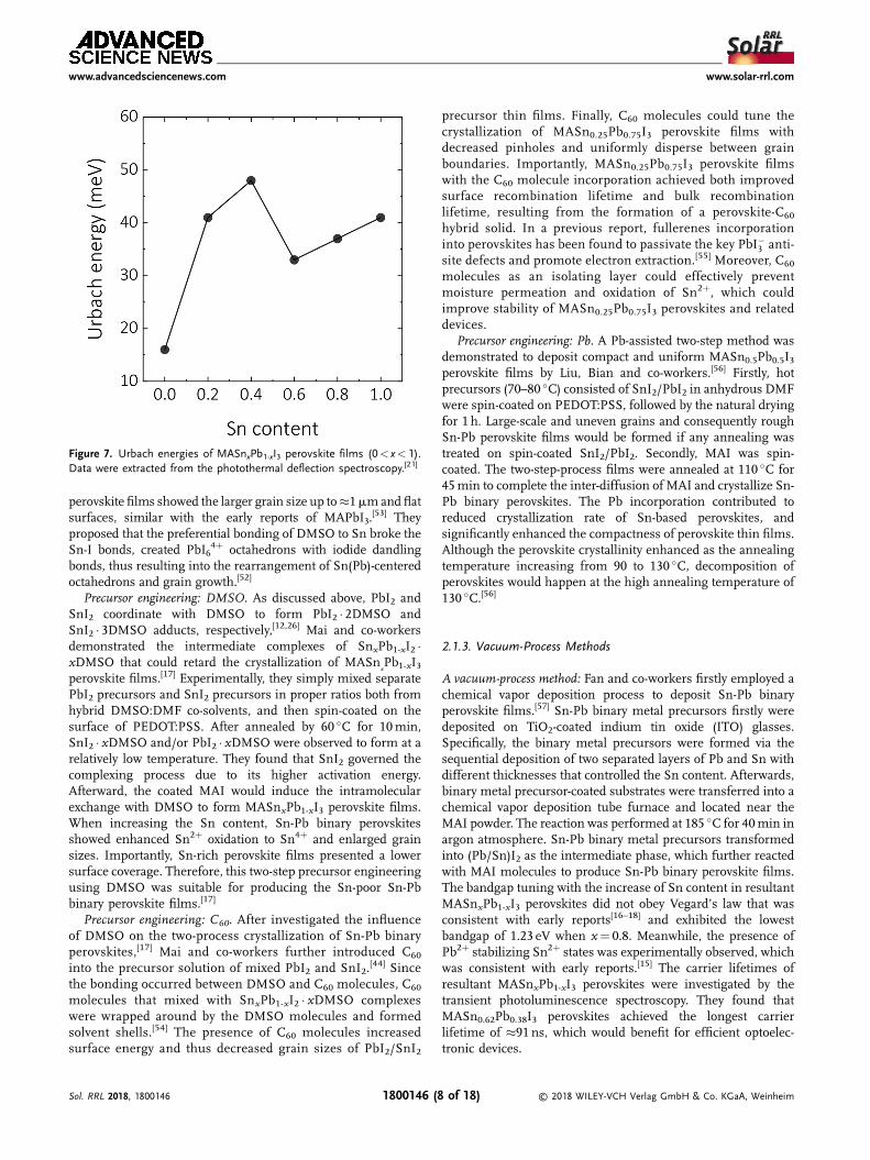
Figure 7. Urbach energies of MASnxPb1-xI3 perovskite films (0< x< 1).Data were extracted from the photothermal deflection spectroscopy.[21]
www.advancedsciencenews.com www.solar-rrl.com
perovskite films showed the larger grain size up to�1mmand flatsurfaces, similar with the early reports of MAPbI3.
[53] Theyproposed that the preferential bonding of DMSO to Sn broke theSn-I bonds, created PbI6
4þ octahedrons with iodide dandlingbonds, thus resulting into the rearrangement of Sn(Pb)-centeredoctahedrons and grain growth.[52]
Precursor engineering: DMSO. As discussed above, PbI2 andSnI2 coordinate with DMSO to form PbI2 � 2DMSO andSnI2 � 3DMSO adducts, respectively,[12,26] Mai and co-workersdemonstrated the intermediate complexes of SnxPb1-xI2 �xDMSO that could retard the crystallization of MASn
xPb1-xI3
perovskite films.[17] Experimentally, they simply mixed separatePbI2 precursors and SnI2 precursors in proper ratios both fromhybrid DMSO:DMF co-solvents, and then spin-coated on thesurface of PEDOT:PSS. After annealed by 60 �C for 10min,SnI2 � xDMSO and/or PbI2 � xDMSO were observed to form at arelatively low temperature. They found that SnI2 governed thecomplexing process due to its higher activation energy.Afterward, the coated MAI would induce the intramolecularexchange with DMSO to form MASnxPb1-xI3 perovskite films.When increasing the Sn content, Sn-Pb binary perovskitesshowed enhanced Sn2þ oxidation to Sn4þ and enlarged grainsizes. Importantly, Sn-rich perovskite films presented a lowersurface coverage. Therefore, this two-step precursor engineeringusing DMSO was suitable for producing the Sn-poor Sn-Pbbinary perovskite films.[17]
Precursor engineering: C60. After investigated the influenceof DMSO on the two-process crystallization of Sn-Pb binaryperovskites,[17] Mai and co-workers further introduced C60
into the precursor solution of mixed PbI2 and SnI2.[44] Since
the bonding occurred between DMSO and C60 molecules, C60
molecules that mixed with SnxPb1-xI2 � xDMSO complexeswere wrapped around by the DMSO molecules and formedsolvent shells.[54] The presence of C60 molecules increasedsurface energy and thus decreased grain sizes of PbI2/SnI2
Sol. RRL 2018, 1800146 1800146 (8
precursor thin films. Finally, C60 molecules could tune thecrystallization of MASn0.25Pb0.75I3 perovskite films withdecreased pinholes and uniformly disperse between grainboundaries. Importantly, MASn0.25Pb0.75I3 perovskite filmswith the C60 molecule incorporation achieved both improvedsurface recombination lifetime and bulk recombinationlifetime, resulting from the formation of a perovskite-C60
hybrid solid. In a previous report, fullerenes incorporationinto perovskites has been found to passivate the key PbI�3 anti-site defects and promote electron extraction.[55] Moreover, C60
molecules as an isolating layer could effectively preventmoisture permeation and oxidation of Sn2þ, which couldimprove stability of MASn0.25Pb0.75I3 perovskites and relateddevices.
Precursor engineering: Pb. A Pb-assisted two-step method wasdemonstrated to deposit compact and uniform MASn0.5Pb0.5I3perovskite films by Liu, Bian and co-workers.[56] Firstly, hotprecursors (70–80 �C) consisted of SnI2/PbI2 in anhydrous DMFwere spin-coated on PEDOT:PSS, followed by the natural dryingfor 1 h. Large-scale and uneven grains and consequently roughSn-Pb perovskite films would be formed if any annealing wastreated on spin-coated SnI2/PbI2. Secondly, MAI was spin-coated. The two-step-process films were annealed at 110 �C for45min to complete the inter-diffusion of MAI and crystallize Sn-Pb binary perovskites. The Pb incorporation contributed toreduced crystallization rate of Sn-based perovskites, andsignificantly enhanced the compactness of perovskite thin films.Although the perovskite crystallinity enhanced as the annealingtemperature increasing from 90 to 130 �C, decomposition ofperovskites would happen at the high annealing temperature of130 �C.[56]
2.1.3. Vacuum-Process Methods
A vacuum-process method: Fan and co-workers firstly employed achemical vapor deposition process to deposit Sn-Pb binaryperovskite films.[57] Sn-Pb binary metal precursors firstly weredeposited on TiO2-coated indium tin oxide (ITO) glasses.Specifically, the binary metal precursors were formed via thesequential deposition of two separated layers of Pb and Sn withdifferent thicknesses that controlled the Sn content. Afterwards,binary metal precursor-coated substrates were transferred into achemical vapor deposition tube furnace and located near theMAI powder. The reaction was performed at 185 �C for 40min inargon atmosphere. Sn-Pb binary metal precursors transformedinto (Pb/Sn)I2 as the intermediate phase, which further reactedwith MAI molecules to produce Sn-Pb binary perovskite films.The bandgap tuning with the increase of Sn content in resultantMASnxPb1-xI3 perovskites did not obey Vegard’s law that wasconsistent with early reports[16–18] and exhibited the lowestbandgap of 1.23 eV when x¼ 0.8. Meanwhile, the presence ofPb2þ stabilizing Sn2þ states was experimentally observed, whichwas consistent with early reports.[15] The carrier lifetimes ofresultant MASnxPb1-xI3 perovskites were investigated by thetransient photoluminescence spectroscopy. They found thatMASn0.62Pb0.38I3 perovskites achieved the longest carrierlifetime of �91 ns, which would benefit for efficient optoelec-tronic devices.
© 2018 WILEY-VCH Verlag GmbH & Co. KGaA, Weinheimof 18)
www.advancedsciencenews.com www.solar-rrl.com
2.2. Applications in Solar Cells and Photodetectors
2.2.1. Solar Cells
Sn-Pb binary perovskites with excellent optical and electricproperties have made much progress in the application of SCs.Single-junction Sn-Pb perovskite SCs have achieved a PCE of17.8%,[58] 2-terminal tandem perovskite-on-perovskite SCs havepresented a PCE of 18.4%,[36] 4-terminal all-perovskite SCs haveachieved a PCE of 21.2%.[41] The device parameters of Sn-Pbbinary perovskite SCs are summarized in Table 1. Thediscussion of perovskite photovoltaics is composed of single-junction perovskite SCs, 2-terminal tandem perovskite-on-perovskite SCs, and 4-terminal all-perovskite SCs.
Single-junction solar cells: The first Sn-Pb binary perovskite SCswere reported by Ogomi and co-workers on 2014.[15] The devicewith the structure of fluorine doped tin oxide (FTO)/compactTiO2/porous TiO2/MASnxPb1-xI3/regioregular poly(3-hexylthio-phene-2,5-diyl) (P3HT)/Ag/Au achieved the maximum effi-ciency of 4.18% and spectral response onset to 1060 nm whenthe Sn content is 50% (x¼ 0.5, 1.18 eV bandgap). The lowefficiency was ascribed to severe charge recombination atperovskite/P3HT interfaces and reduced shunt resistance. Later,Kanatzidis and co-workers demonstrated Sn-Pb binary perov-skite SCs with the structure of FTO/compact TiO2/porous TiO2/MASnxPb1-xI3/(2,2’,7,7’-tetrakis(N,N-di-p-methoxyphenyl-amine)-9,9-spirobifluorene) (spiro-MeOTAD)/Au, which showeda short-circuit current (Jsc) of 15.82mAcm�2, an open-circuitvoltage (Voc) of 728mV, a fill factor (FF) of 64.01%, correspond-ing to the maximum power conversion efficiency (PCE) of 7.37%(x¼ 0.25, 1.24 eV bandgap). The low efficiency resulted from p-type doping via Sn2þ oxidation, and back electron recombinationat TiO2/perovskite interfaces.[16]
Later, most Sn-Pb binary perovskite films were grew on theplanar surface of PEDOT:PSS and planar structures of SCs werefabricated. The first planar structure of Sn-Pb binary perovskiteSCs were reported by Jen and co-workers.[45] They introducedchlorine-containing components to tune the crystallization ofSn-Pb binary perovskite thin films and realized 97% surfacecoverage on PEDOT:PSS as discussed in Section 2.1. Planardevices with the structure of ITO/PEDOT:PSS/MASnxPb1-xI3(Cl)/phenyl-C61-butyric acid methyl ester (PC61BM)/fuller-ene surfactant (C60-bis)/Ag achieved a Jsc of 19.5mAcm�2, a Voc
of 770mV, a FF of 0.67, corresponding to a maximum PCE of10.1% when x¼ 0.15 (1.38 eV bandgap). When x> 0.5, Sn-Pbperovskite SCs did not show photovoltaic properties, possiblyoriginating from low surface coverage and Sn2þ oxidation.Afterwards, low Sn-content (x¼ 0.1 and 0.25) Sn-Pb binaryperovskites were fabricated by the two-step process and thenmanipulated by the thermal plus vapor-assisted thermalannealing to tune film morphology and grain size. Planardevices with the structure of ITO/PEDOT:PSS/MASnxPb1-xI3(x¼ 0.1, 0.25)/PC61BM:C60/bathocuproine (BCP)/Al achievedmaximum PCEs of 10.25% for MASn0.1Pb0.9I3 SCs, and 7.76%for MASn0.25Pb0.75I3 SCs.[52] The intermediate complexes ofSnxPb1-xI2 � xDMSO were demonstrated by Fan, Mai and co-workers. using two-step process to control the crystallization ofMASnxPb1-xI3 perovskite films. Optimized planar devices withthe structure of ITO/PEDOT:PSS/MASn0.25Pb0.75I3/PC61BM/
Sol. RRL 2018, 1800146 1800146 (9
BCP/Ag achieved an average PCE up to 12.25% under theforward scan and up to 12.63% under the reverse scan, andchampion SCs showed the PCE of 14.12%. In comparison topure-Pb based cells, Sn-Pb binary perovskite SCs showedinferior stability, possibly originating from the oxidation ofSn2þ.[17]
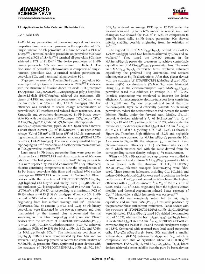
The highest PCE of MASn0.25Pb0.75I3 perovskite (x¼ 0.25,1.29 eV bandgap) based SCs has been achieved by Choy and co-workers.[42] They tuned the DMSO content in theMASn0.25Pb0.75I3 perovskite precursors to achieve controllablecrystallization of MASn0.25Pb0.75I3 perovskite films. The resul-tant MASn0.25Pb0.75I3 perovskite films exhibited enhancedcrystallinity, the preferred (110) orientation, and reducedinhomogeneous Sn/Pb distributions. After that, planar deviceswith the structure of ITO/PEDOT:PSS/MASn0.25Pb0.75I3/C60/zirconium(IV) acetylacetonate (ZrAcac)/Ag were fabricated.Using C60 as the electron-transport layer, MASn0.25Pb0.75I3perovskite based SCs exhibited an average PCE of 10.70%.Interface engineering was employed to improve the deviceefficiency. A nanocomposite electron-transport layer consistingof PC61BM and C60 was proposed and found that thisnanocomposite layer could efficiently passivate Sn-Pb binaryperovskites, reduce the series resistance and increase the carrierlifetime. Finally, under the forward scan, MASn0.25Pb0.75I3perovskite devices achieved a Jsc of 26.2mAcm�2, a Voc of800mV, a FF of 0.725, yielding a PCE of 15.2%; while under thereverse scan, the devices presented a Jsc of 26.4mAcm�2, aVoc of810mV, a FF of 0.714, yielding a PCE of 15.2%, as shown inFigure 8A. Therefore, high-efficiency of 15.2% and negligiblehysteresis were achieved for MASn0.25Pb0.75I3 perovskite SCs.As shown in Figure 8B, the integrated Jsc from the incidentphoton-to-current efficiency (IPCE) spectrum was 25.5mAcm�2, which matched well with the value derived from thecorresponding current density–voltage (J–V) measurement.
When x¼ 0.5, a Pb-assisted two-step process was studied todeposit compact and uniform MASn0.5Pb0.5I3 perovskite films.Planar devices with the structure of ITO/PEDOT:PSS/MASn0.5Pb0.5I3/electron transport layer/BCP/Ag were fabri-cated. Three common fullerenes, including C60, PC61BM, andindene-C60 bisadduct (IC60BA), were used to optimize the deviceperformance. The C60-based perovskite SCs achieved the highestefficiency with a Jsc of 26.3mAcm�2, a Voc of 750mV, a FF of0.688, and a PCE of 13.6%, originating from the highest electronmobility and thermal-evaporation-induced better coverage ofC60.
[59] Meanwhile, a slight hysteresis was observed.[56]
When MA was completely substituted by FA, highlycrystalline and uniform FASnxPb1-xI3 films were produced bythe precursor-phase anti-solvent immersion. Planar devices withthe structure of ITO/PEDOT:PSS/FASn0.5Pb0.5I3/C60/BCP/Agwere fabricated. FASn0.5Pb0.5I3 based SCs yielded the championPCE of 10.9%, whereas the best FA0.75Cs0.25Sn0.5Pb0.5I3 basedSCs exhibited a Jsc of 26.7mAcm�2, aVoc of 740mV, a FF of 0.71,corresponding to a PCE of 14.1% and the stabilized power outputis 14.8%. Compared with reported pure lead-based perovskitecells, FA0.75Cs0.25Sn0.5Pb0.5I3 based SCs exhibited a smallervoltage deficit (0.41V) between bandgap and Voc, which iscomparable with that of crystalline silicon SCs (0.38 V).[60]
Furthermore, FASn0.5Pb0.5I3 and FA0.75Cs0.25Sn0.5Pb0.5I3 baseddevices achieved a better stability than the pure Pb-based devices
© 2018 WILEY-VCH Verlag GmbH & Co. KGaA, Weinheimof 18)
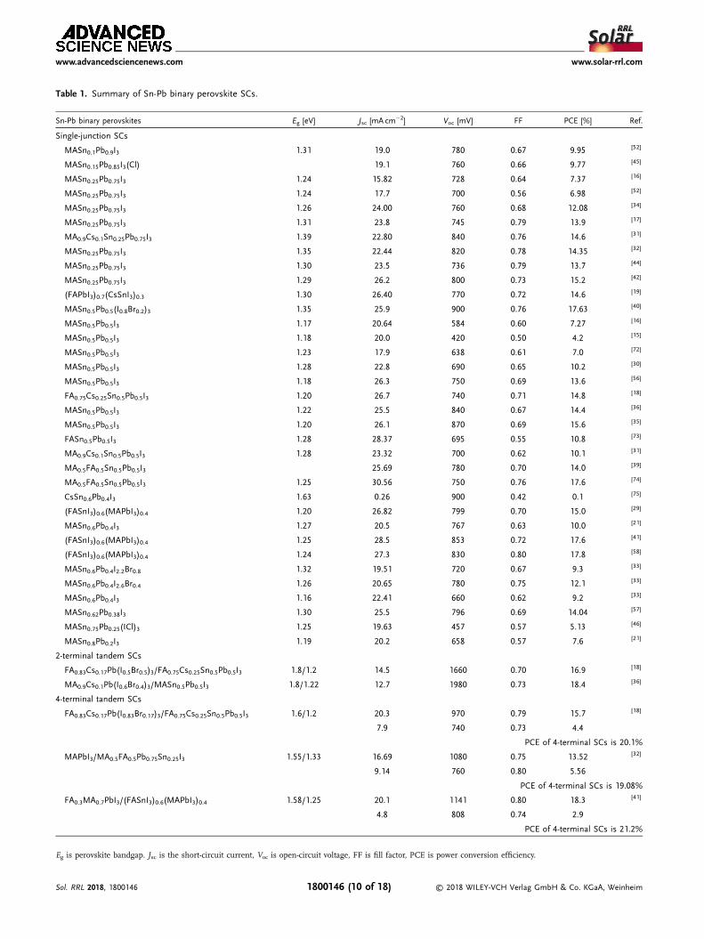
Table 1. Summary of Sn-Pb binary perovskite SCs.
Sn-Pb binary perovskites Eg [eV] Jsc [mA cm�2] Voc [mV] FF PCE [%] Ref.
Single-junction SCs
MASn0.1Pb0.9I3 1.31 19.0 780 0.67 9.95 [52]
MASn0.15Pb0.85I3(Cl) 19.1 760 0.66 9.77 [45]
MASn0.25Pb0.75I3 1.24 15.82 728 0.64 7.37 [16]
MASn0.25Pb0.75I3 1.24 17.7 700 0.56 6.98 [52]
MASn0.25Pb0.75I3 1.26 24.00 760 0.68 12.08 [34]
MASn0.25Pb0.75I3 1.31 23.8 745 0.79 13.9 [17]
MA0.9Cs0.1Sn0.25Pb0.75I3 1.39 22.80 840 0.76 14.6 [31]
MASn0.25Pb0.75I3 1.35 22.44 820 0.78 14.35 [32]
MASn0.25Pb0.75I3 1.30 23.5 736 0.79 13.7 [44]
MASn0.25Pb0.75I3 1.29 26.2 800 0.73 15.2 [42]
(FAPbI3)0.7(CsSnI3)0.3 1.30 26.40 770 0.72 14.6 [19]
MASn0.5Pb0.5(I0.8Br0.2)3 1.35 25.9 900 0.76 17.63 [40]
MASn0.5Pb0.5I3 1.17 20.64 584 0.60 7.27 [16]
MASn0.5Pb0.5I3 1.18 20.0 420 0.50 4.2 [15]
MASn0.5Pb0.5I3 1.23 17.9 638 0.61 7.0 [72]
MASn0.5Pb0.5I3 1.28 22.8 690 0.65 10.2 [30]
MASn0.5Pb0.5I3 1.18 26.3 750 0.69 13.6 [56]
FA0.75Cs0.25Sn0.5Pb0.5I3 1.20 26.7 740 0.71 14.8 [18]
MASn0.5Pb0.5I3 1.22 25.5 840 0.67 14.4 [36]
MASn0.5Pb0.5I3 1.20 26.1 870 0.69 15.6 [35]
FASn0.5Pb0.5I3 1.28 28.37 695 0.55 10.8 [73]
MA0.9Cs0.1Sn0.5Pb0.5I3 1.28 23.32 700 0.62 10.1 [31]
MA0.5FA0.5Sn0.5Pb0.5I3 25.69 780 0.70 14.0 [39]
MA0.5FA0.5Sn0.5Pb0.5I3 1.25 30.56 750 0.76 17.6 [74]
CsSn0.6Pb0.4I3 1.63 0.26 900 0.42 0.1 [75]
(FASnI3)0.6(MAPbI3)0.4 1.20 26.82 799 0.70 15.0 [29]
MASn0.6Pb0.4I3 1.27 20.5 767 0.63 10.0 [21]
(FASnI3)0.6(MAPbI3)0.4 1.25 28.5 853 0.72 17.6 [41]
(FASnI3)0.6(MAPbI3)0.4 1.24 27.3 830 0.80 17.8 [58]
MASn0.6Pb0.4I2.2Br0.8 1.32 19.51 720 0.67 9.3 [33]
MASn0.6Pb0.4I2.6Br0.4 1.26 20.65 780 0.75 12.1 [33]
MASn0.6Pb0.4I3 1.16 22.41 660 0.62 9.2 [33]
MASn0.62Pb0.38I3 1.30 25.5 796 0.69 14.04 [57]
MASn0.75Pb0.25(ICl)3 1.25 19.63 457 0.57 5.13 [46]
MASn0.8Pb0.2I3 1.19 20.2 658 0.57 7.6 [21]
2-terminal tandem SCs
FA0.83Cs0.17Pb(I0.5Br0.5)3/FA0.75Cs0.25Sn0.5Pb0.5I3 1.8/1.2 14.5 1660 0.70 16.9 [18]
MA0.9Cs0.1Pb(I0.6Br0.4)3/MASn0.5Pb0.5I3 1.8/1.22 12.7 1980 0.73 18.4 [36]
4-terminal tandem SCs
FA0.83Cs0.17Pb(I0.83Br0.17)3/FA0.75Cs0.25Sn0.5Pb0.5I3 1.6/1.2 20.3 970 0.79 15.7 [18]
7.9 740 0.73 4.4
PCE of 4-terminal SCs is 20.1%
MAPbI3/MA0.5FA0.5Pb0.75Sn0.25I3 1.55/1.33 16.69 1080 0.75 13.52 [32]
9.14 760 0.80 5.56
PCE of 4-terminal SCs is 19.08%
FA0.3MA0.7PbI3/(FASnI3)0.6(MAPbI3)0.4 1.58/1.25 20.1 1141 0.80 18.3 [41]
4.8 808 0.74 2.9
PCE of 4-terminal SCs is 21.2%
Eg is perovskite bandgap. Jsc is the short-circuit current, Voc is open-circuit voltage, FF is fill factor, PCE is power conversion efficiency.
www.advancedsciencenews.com www.solar-rrl.com
Sol. RRL 2018, 1800146 © 2018 WILEY-VCH Verlag GmbH & Co. KGaA, Weinheim1800146 (10 of 18)
www.advancedsciencenews.com www.solar-rrl.com
(FAPbI3) at maximum power point under 100mWcm�2
illumination for 50min in ambient air with a relative humidityof �50%. Importantly, low bandgap FA0.75Cs0.25Sn0.5Pb0.5I3(1.2 eV bandgap) SCs with the high efficiency were suited forbottom subcells in solution-process tandem SCs, which will bediscussed in the part of 2-terminal and 4-terminal tandem SCsbelow.
A graded heterojunction structure was introduced via theincorporation of fluoroalkyl-substituted fullerene (DF-C60) intoMASn0.5Pb0.5I3 perovskites, which contributed to beneficialsurface passivation and a reduced Urbach energy ofMASn0.5Pb0.5I3 perovskites films. Optimized devices with thestructure of ITO/PEDOT:PSS/MASn0.5Pb0.5I3(added 20mol%SnF2)/DF-C60/IC60BA/C60-bis/Ag were fabricated. SCs exhib-ited an average Jsc of 26.23mAcm�2, an average Voc of 870mV,an average FF of 0.69, yielding an average PCE of 15.18%. Thechampion device achieved a PCE up to 15.61% and a remarkablyhigh Voc of 0.89V, indicating a small voltage deficit (0.33V)between bandgap and Voc that is better than that of crystallinesilicon SCs (0.38 V). Moreover, hydrophobic nature of DF-C60 inthe graded heterojunction structure improved the devicestability.[35]
Sn-rich (FASnI3)0.6(MAPbI3)0.4 perovskites were fabricated byspin-coating the new precursor consisted of a FASnI3 precursorand a MAPbI3 precursor. Dense and uniform (FASnI3)0.6(-MAPbI3)0.4 perovskites with a thickness of about 400 nm wereapplied in SCs with the structure of ITO/PEDOT:PSS/(FASnI3)0.6(MAPbI3)0.4/C60/BCP/Ag. The champion Sn-Pbperovskite SC exhibited a forward-scan PCE of 15.00%, a
Figure 8. A) J–V curves of MASn0.25Pb0.75I3 perovskite based SCs under AM1circuit and reverse scan was recorded from open circuit to short circuit. B) IPIntegrated Jsc is 25.5mA cm�2. C) J–V curves of (FASnI3)0.6(MAPbI3)0.4 peintegrated Jsc of (FASnI3)0.6(MAPbI3)0.4 perovskite based SCs. Integrated Jsc is2017, Wiley-VCH. Figures C and D reproduced with permission.[41] Copyrig
Sol. RRL 2018, 1800146 1800146 (1
reverse-scan PCE of 15.08%, and a stabilized PCE of �14.8%.[29]
(FASnI3)0.6(MAPbI3)0.4 perovskites with the relatively thinthickness reduced the long-wavelength absorption(700–950 nm) and then achieved low external quantumefficiency (EQE) of corresponding SCs in the spectral range.However, simply increasing the thickness of Sn-Pb binaryperovskite films would induce severe photocarrier recombina-tion owing to the short carrier lifetime of 6.7 ns as discussed inSection 2.1.1 one-step solution-process methods. Throughoptimizing precursor concentrations, researchers further fabri-cated high-quality 620-nm-thick (FASnI3)0.6(MAPbI3)0.4 perov-skite films with a long carrier lifetime of 255 ns, lower Urbachenergy and higher crystallinity. Based on the same devicestructure, under the forward scan, (FASnI3)0.6(MAPbI3)0.4perovskite devices achieved a Jsc of 28.5mAcm�2, a Voc of853mV, a FF of 0.725, yielding a PCE of 17.6%; while under thereverse scan, the devices presented a Jsc of 28.7mAcm�2, aVoc of854mV, a FF of 0.714, yielding a PCE of 17.5%, as shown inFigure 8C. As shown in Figure 8D, the integrated Jsc from theEQE spectrum was 28.6mAcm�2, which further confirmed thevalue derived from the corresponding J-Vmeasurement. Overall,620-nm-thick (FASnI3)0.6(MAPbI3)0.4 perovskite SCs produced amaximumPCE of 17.6% and a certified efficiency of 17.01%witha negligible current-voltage hysteresis, which is among thehighest PCE among Sn-Pb binary perovskite single-junctionSCs.[41]
As discussed previously, through Sn-content engineering, wecould achieve Sn-Pb binary perovskites with an ideal bandgap forapproaching Shockley–Queisser-efficiency limit. Jen and co-
.5G illumination. Forward scan was measured from short circuit to openCE spectrum and integrated Jsc of MASn0.25Pb0.75I3 perovskite based SCs.rovskite based SCs under AM1.5G illumination. D) EQE spectrum and28.6mA cm�2. Figures A and B reproduced with permission.[42] Copyrightht 2017, Nature Publishing Group.
© 2018 WILEY-VCH Verlag GmbH & Co. KGaA, Weinheim1 of 18)
www.advancedsciencenews.com www.solar-rrl.com
workers conducted Sn-content engineering with MASnxPb1-xI3perovskites and found that MASn0.5Pb0.5I3 perovskites had thehighest photoluminescence intensity, indicating high materialquality among MASnxPb1-xI3 perovskites.[40] Further, afterincorporation of Br, MASn0.5Pb0.5(I0.8Br0.2)3 with an ideal1.35-eV-bandgap was fabricated. Br incorporation was beneficialfor reduced nonradiative defect states and band edge disorder.Typical devices with the structure of ITO/PEDOT:PSS/MASn0.5Pb0.5(I0.8Br0.2)3 (240-nm-thickness)/IC60BA/C60-bis/Ag achieved a Jsc of 21.51mAcm�2, a Voc of 900mV, a FF of0.76, yielding a PCE of 14.71%. Similar to results from Yan andco-workers,[41] the low EQE of thin MASn0.5Pb0.5(I0.8Br0.2)3-based SCs ranging from 700 to 900 nm limited the PCEimprovement. Optimized MASn0.5Pb0.5(I0.8Br0.2)3 SCs with 560-nm-thickness exhibited a larger Jsc of 25.67mAcm�2 and higherPCE of 17.13%, which is among highest-efficiency Sn-Pb binaryperovskite SCs. Meanwhile, devices achieved minimal hysteresisand remained 92% of its initial PCE after being stored for 30 daysunder inert conditions (H2O< 0.1 ppm, O2< 5 ppm).
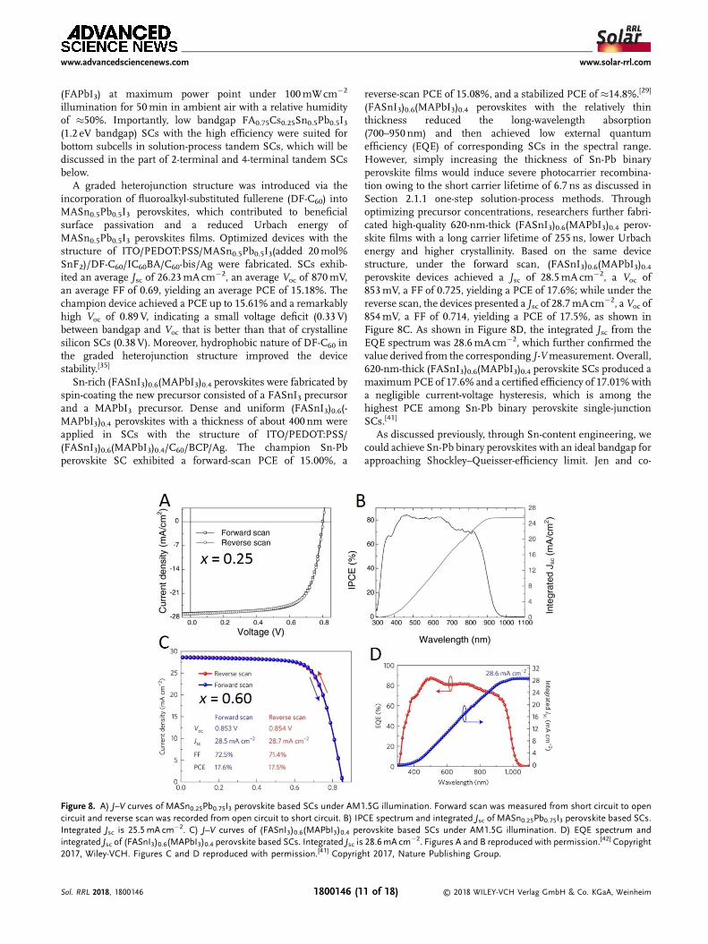
2-terminal and 4-terminal tandem SCs: The low-bandgap Sn-Pbbinary perovskites (down to 1.17 eV) enables their roles asbottom SCs in 2-terminal and 4-terminal tandem SCs thatcould theoretically achieve a PCE of 35%.[61] As shown inFigure 9, 2-terminal tandem SCs consist of monolithicallyintegrated subcells series-connected via a recombination layer.4-terminal tandem SCs mechanically stack two individualsubcells. Generally, wide bandgap semiconductors areemployed in front cells, low bandgap semiconductors areemployed in rear cells.
Using 1.2 eV bandgap FA0.75Cs0.25Sn0.5Pb0.5I3 as the rearsemiconductor, the optimized bandgaps for 2-terminal and 4-terminal architectures are �1.75–1.85 and 1.6–1.9 eV, respec-tively.[18] FA0.83Cs0.17Pb(I0.5Br0.5)3 with a 1.8 eV bandgap wasproduced as the top material and the structure of 2-terminaltandem SCs is ITO/NiO/FA0.83Cs0.17Pb(I0.5Br0.5)3/PC61BM/SnO2/zinc-tin-oxide (ZTO)/ITO/PEDOT:PSS/FA0.75Cs0.25Sn0.5Pb0.5I3/C60/BCP/Ag, as shown in Figure 10A. The recombination layerwasmade up of ZTO/ITO. 2-terminal tandemSCs exhibited a Jsc of14.5mAcm�2, aVocof1660mV,aFFof0.70, yieldinganoverallPCEof 16.9% and of 17.0% at its maximum power point (Figure 10D).The current matching between rear subcells and front subcells as
Figure 9. Schematics showing 2-terminal and 4-terminal tandem SCs. 2-terminal tandem SCs are monolithically series-integrating multicellsconnected via a recombination layer. 4-terminal tandem SCs aremechanically stacking two independent subcells. Figures reproducedwith permission.[18] Copyright 2016, American Association for theAdvancement of Science.
Sol. RRL 2018, 1800146 1800146 (1
shown in Figure 10B positively contributed to high-efficiency 2-terminal tandem SCs. Furthermore, 2-terminal tandem cellsshowed no drop of PCE at its maximum power point underillumination in nitrogen for more than 18h. Regarding 4-terminalarchitectures, FA0.83Cs0.17Pb(I0.83Br0.17)3with a 1.6 eVbandgapwasproduced as the top monolithic material and ITO was used as atransparent top contact. Top monolithic FA0.83Cs0.17Pb(I0.83Br0.17)3cells achieved a PCE of 15.8% (Figure 10C and D). RearFA0.75Cs0.25Sn0.5Pb0.5I3 cells filtered by top subcells presented aPCE of 4.5%. Therefore, 4-terminal yielded an overall stabilizedefficiency of 20.3%.
Jen and co-workers systematically investigated the limitedfactors that determined the efficiency of 2-terminal tandem SCs.Regarding bottom subcells, low-bandgap (1.22 eV)MASn0.5Pb0.5I3 perovskites with a conduction band value of3.82 eV were fabricated. The electron-transport layer C60 with thehighest electron-transport mobility among fullerenes would bethe preferentially selected. However, C60 with the lowestunoccupied molecular orbital (LUMO) value of 4.0 eV wouldcause the energy-level mismatch at MASn0.5Pb0.5I3/C60 inter-faces that non-radiatively quenches charge carriers and hindersinterfacial repopulation process, reducing the value of Voc in lowbandgap MASn0.5Pb0.5I3 perovskite SCs. Selected electron-transport layer IC60BA would provide an intimate contact,alleviating nonradiative recombination losses from intrinsic, andphotoinduced subgap defect states during charge transferprocess across IC60BA. Therefore, using IC60BA as theelectron-transport layer, low-bandgap MASn0.5Pb0.5I3 perovskiteSCs could achieve a remarkably high Voc of 0.84V, whichindicates a smaller voltage deficit (0.38 V) that is among thelowest value in reported low-bandgap Sn-Pb binary perovskiteSCs and comparable with that of crystalline silicon SCs(0.38V).[60]
Regarding top subcells, the low bandgap Sn-Pb binaryperovskites (1.22 eV) required complementary wide bandgapperovskites of 1.80–1.85 eV for photocurrent matching in 2-terminal tandem SCs. The incorporation of 10mol% Cs inMAPb(I0.6Br0.4)3 perovskites could exhibit the wide bandgapof 1.82 eV and achieve improved crystallinity. More impor-tantly, MA0.9Cs0.1Pb(I0.6Br0.4)3 perovskite SCs presented theexcellent photostability, which could remain photocurrentdensity at the maximum power point under continuousillumination for 1 h. Moreover, wide-bandgap devicesachieved a remarkably high Voc of 1.20 V, indicating a voltagedeficit of 0.42 V. The large voltage deficit originated fromnonradiative recombination of MAPb(I0.6Br0.4)3 perovskites(photoluminescence quantum yield< 0.01%) and inappropri-ate energy-level alignment at the interface of NiOx/MAPb-(I0.6Br0.4)3 (�0.35 eV barrier).
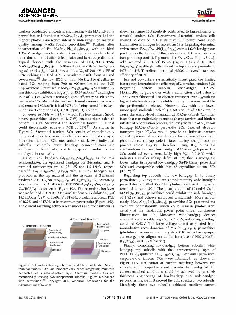
Finally, combining low-bandgap bottom subcells, wide-bandgap top subcells with the interconnecting layer ofPEDOT:PSS/sputtered ITO/C60-bis/C60, 2-terminal perovskite-on-perovskite tandem SCs were fabricated, as shown inFigure 11A. Realization of current matching between twosubcells was of importance and theoretically investigated thatcurrent-matched conditions could be achieved by preciselythickness engineering of low-bandgap and wide-bandgapperovskites. Figure 11B showed the EQE spectra of two subcells.Manifestly, these two subcells achieved excellent current
© 2018 WILEY-VCH Verlag GmbH & Co. KGaA, Weinheim2 of 18)
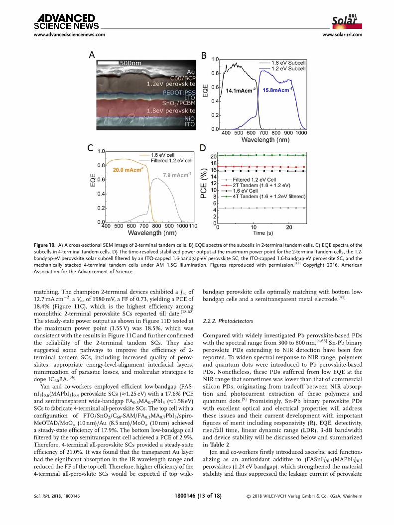
Figure 10. A) A cross-sectional SEM image of 2-terminal tandem cells. B) EQE spectra of the subcells in 2-terminal tandem cells. C) EQE spectra of thesubcells in 4-terminal tandem cells. D) The time-resolved stabilized power output at the maximum power point for the 2-terminal tandem cells, the 1.2-bandgap-eV perovskite solar subcell filtered by an ITO-capped 1.6-bandgap-eV perovskite SC, the ITO-capped 1.6-bandgap-eV perovskite SC, and themechanically stacked 4-terminal tandem cells under AM 1.5G illumination. Figures reproduced with permission.[18] Copyright 2016, AmericanAssociation for the Advancement of Science.
www.advancedsciencenews.com www.solar-rrl.com
matching. The champion 2-terminal devices exhibited a Jsc of12.7mAcm�2, a Voc of 1980mV, a FF of 0.73, yielding a PCE of18.4% (Figure 11C), which is the highest efficiency amongmonolithic 2-terminal perovskite SCs reported till date.[18,62]
The steady-state power output as shown in Figure 11D tested atthe maximum power point (1.55 V) was 18.5%, which wasconsistent with the results in Figure 11C and further confirmedthe reliability of the 2-terminal tandem SCs. They alsosuggested some pathways to improve the efficiency of 2-terminal tandem SCs, including increased quality of perov-skites, appropriate energy-level-alignment interfacial layers,minimization of parasitic losses, and molecular strategies todope IC60BA.
[36]
Yan and co-workers employed efficient low-bandgap (FAS-nI3)0.6(MAPbI3)0.4 perovskite SCs (�1.25 eV) with a 17.6% PCEand semitransparent wide-bandgap FA0.3MA0.7PbI3 (�1.58 eV)SCs to fabricate 4-terminal all-perovskite SCs. The top cell with aconfiguration of FTO/SnO2/C60-SAM/FA0.3MA0.7PbI3/spiro-MeOTAD/MoOx (10 nm)/Au (8.5 nm)/MoOx (10 nm) achieveda steady-state efficiency of 17.9%. The bottom low-bandgap cellfiltered by the top semitransparent cell achieved a PCE of 2.9%.Therefore, 4-terminal all-perovskite SCs provided a steady-stateefficiency of 21.0%. It was found that the transparent Au layerhad the significant absorption in the IR wavelength range andreduced the FF of the top cell. Therefore, higher efficiency of the4-terminal all-perovskite SCs would be expected if top wide-
Sol. RRL 2018, 1800146 1800146 (1
bandgap perovskite cells optimally matching with bottom low-bandgap cells and a semitransparent metal electrode.[41]
2.2.2. Photodetectors
Compared with widely investigated Pb perovskite-based PDswith the spectral range from 300 to 800 nm,[4,63] Sn-Pb binaryperovskite PDs extending to NIR detection have been fewreported. To widen spectral response to NIR range, polymersand quantum dots were introduced to Pb perovskite-basedPDs. Nonetheless, these PDs suffered from low EQE at theNIR range that sometimes was lower than that of commercialsilicon PDs, originating from tradeoff between NIR absorp-tion and photocurrent extraction of these polymers andquantum dots.[9] Promisingly, Sn-Pb binary perovskite PDswith excellent optical and electrical properties will addressthese issues and their current development with importantfigures of merit including responsivity (R), EQE, detectivity,rise/fall time, linear dynamic range (LDR), 3-dB bandwidthand device stability will be discussed below and summarizedin Table 2.
Jen and co-workers firstly introduced ascorbic acid function-alizing as an antioxidant additive to (FASnI3)0.5(MAPbI3)0.5perovskites (1.24 eV bandgap), which strengthened the materialstability and thus suppressed the leakage current of perovskite
© 2018 WILEY-VCH Verlag GmbH & Co. KGaA, Weinheim3 of 18)

Figure 11. A) Cross-sectional SEM image of a characteristic device. B) EQE spectra of individual subcells in 2-terminal monolithic tandem cells. C)Typical J-V characteristics of 2-terminal tandem SC along with that of the small- and large-bandgap single-junction SCs. D) Steady-state current underAM1.5 illumination at the maximum power point of tandem SCs. Figures reproduced with permission.[36] Copyright 2017, Wiley-VCH.
www.advancedsciencenews.com www.solar-rrl.com
PDs.[38] (FASnI3)0.5(MAPbI3)0.5 perovskite PDs achieved aresponsivity of over 0.2 AW�1 between 800 and 950 nm, 3-dBbandwidth of 100 kHz (transit-time-limited), LDR of 40 dB, highdetectivity of >1012 Jones. Soon later, Yan, Zhang, Zhao and co-workers employed (FASnI3)0.6(MAPbI3)0.4 (1.25 eV bandgap)perovskites obtained from mixed FASnI3 and MAPbI3 pre-cursors to fabricate UV-vis-NIR PDs. By optimizing thethickness of perovskite layer and electron-transport layer C60,they reduced noise current and simultaneously increased thevalue of EQE in the >650 nm wavelength range. Finally, PDswith EQE over 65% ranging from 350 to 900 nm, high detectivityof over 1012 Jones, rise/fall time of 6.9/9.1ms and large lineardynamic range of 83.5 dB under the negative bias of 0.2 V havebeen achieved.[37]
Very recently, Choy and co-workers incorporated rubidiumcations into theMASn-Pbperovskite systemto realize controllablecrystallization, as discussed in Section 2.1.1 One-step solution-process methods.[43] Compared with MASn0.65Pb0.35I3 perov-skites, MA0.975Rb0.025Sn0.65Pb0.35I3 perovskite films exhibitedimproved crystallinity, strengthened preferred orientation,which resulted into a smaller potential difference at the grainboundaries/grain interiors interface and a longer carrierlifetime. Consequently, as shown in Figure 12A–E, self-poweredMA0.975Rb0.025Sn0.65Pb0.35I3 perovskite-based PDs achieved im-proved responsivity of over 0.3AW�1 covering 800-950nm, lowernoise current, lower detectable signal intensity, larger LDR of110 dB, increased detectivity of >1012 Jones. Meanwhile, the PDpresented the rise/fall time of 0.04/0.47ms and 3-dB bandwidth of�1MHz (Figure 12F). Notably, large LDR and 3-dB bandwidthwere highest values among Sn-Pb binary perovskite-based PDs.The EQE value of MA0.975Rb0.025Sn0.65Pb0.35I3 perovskite-basedPDs is better than that ofmost commercial siliconPDs at the near-infrared region.
Sol. RRL 2018, 1800146 1800146 (1
3. Challenges of Sn-Pb Binary Perovskites
3.1. Controlling Inter-Grain Sn/Pb Element Distributions
Some early works exhibited homogeneous Sn/Pb elementdistributions for Sn-Pb binary perovskite films,[16,19,56] whileChoy and co-workers investigated individual grains andobserved that the molar ratio of Sn over Pb was not a constant,indicating inhomogeneous Sn/Pb element distributions be-tween separate grains.[42] In kesterite SCs, spatially inhomoge-neous Cu(In,Ga)Se2 semiconductors could induce bandgapfluctuations that would influence the photoluminescence andcharge carrier transport properties.[64] In the study of Choy andco-workers, they introduced DMSO molecules to realize thecrystallization of MASn0.25Pb0.75I3 perovskite films and thustune the level of inter-grain inhomogeneous Sn/Pb elementdistributions. They observed bandgap fluctuations and differentUrbach energies that suggested different energetic disorderlevels for MASn0.25Pb0.75I3 perovskite films. Importantly,reducing inter-grain inhomogeneous Sn/Pb element distribu-tions beneficially improved the efficiency of Sn-Pb binaryperovskite SCs. Therefore, it is of high importance to investigateinter-grain inhomogeneous Sn/Pb element distributions andfurther crystallize Sn-Pb binary perovskites to ameliorate suchdistributions.
It has been reported that the reaction between SnI2 films andMAI is much faster than for the Pb analogue.[65] MASnI3perovskite films normally exhibited pinhole, low surfacecoverage, which resulted into a poor efficiency of SCs.[66]
Hence, it is possible that competing transformation pathwayfrom Sn-Pb binary perovskite precursors into solid thin filmsbetween Sn-based and Pb-based perovskites would be existed.This potentially resulted into inter-grain inhomogeneous Sn/
© 2018 WILEY-VCH Verlag GmbH & Co. KGaA, Weinheim4 of 18)
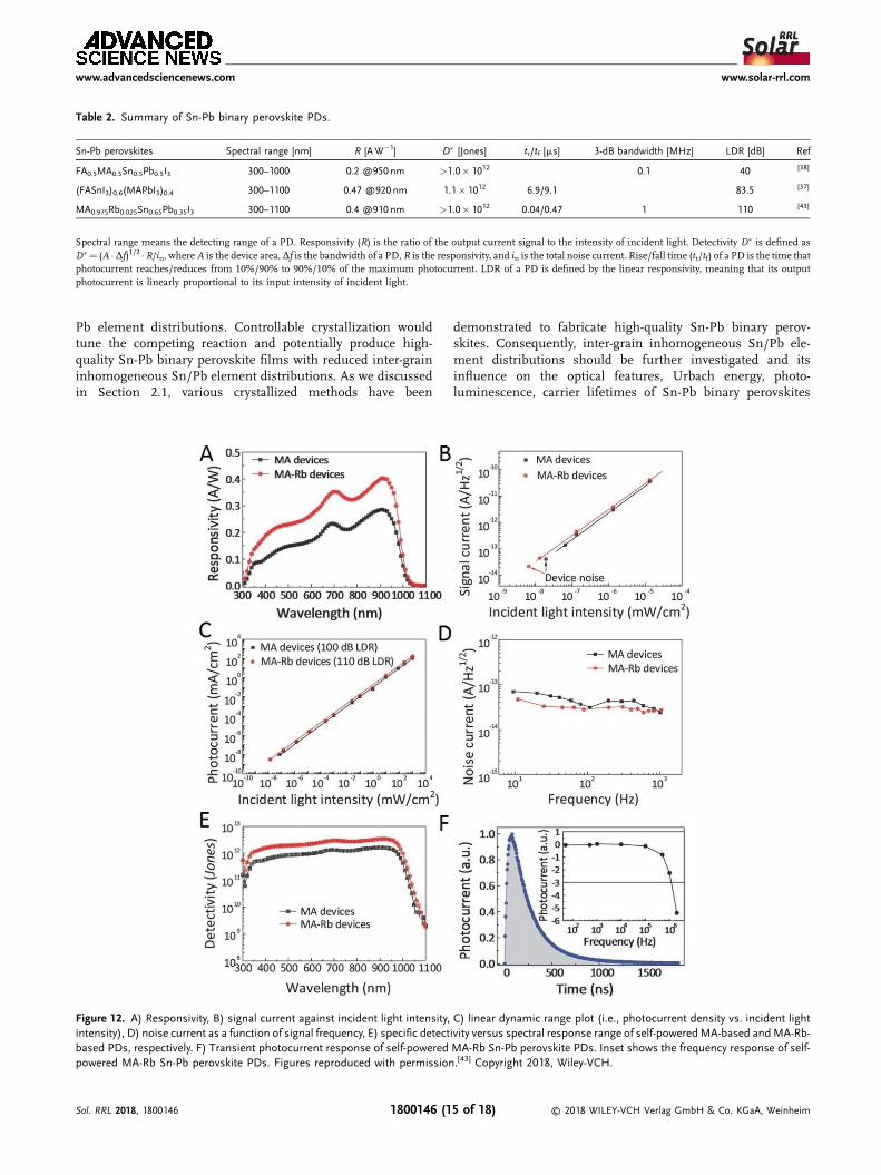
Table 2. Summary of Sn-Pb binary perovskite PDs.
Sn-Pb perovskites Spectral range [nm] R [AW�1] D [Jones] tr/tf [ms] 3-dB bandwidth [MHz] LDR [dB] Ref
FA0.5MA0.5Sn0.5Pb0.5I3 300–1000 0.2 @950 nm >1.0 1012 0.1 40 [38]
(FASnI3)0.6(MAPbI3)0.4 300–1100 0.47 @920 nm 1.1 1012 6.9/9.1 83.5 [37]
MA0.975Rb0.025Sn0.65Pb0.35I3 300–1100 0.4 @910 nm >1.0 1012 0.04/0.47 1 110 [43]
Spectral range means the detecting range of a PD. Responsivity (R) is the ratio of the output current signal to the intensity of incident light. Detectivity D is defined asD ¼ (A �Δf)1/2 �R/in, whereA is the device area,Δf is the bandwidth of a PD,R is the responsivity, and in is the total noise current. Rise/fall time (tr/tf) of a PD is the time thatphotocurrent reaches/reduces from 10%/90% to 90%/10% of the maximum photocurrent. LDR of a PD is defined by the linear responsivity, meaning that its outputphotocurrent is linearly proportional to its input intensity of incident light.
www.advancedsciencenews.com www.solar-rrl.com
Pb element distributions. Controllable crystallization wouldtune the competing reaction and potentially produce high-quality Sn-Pb binary perovskite films with reduced inter-graininhomogeneous Sn/Pb element distributions. As we discussedin Section 2.1, various crystallized methods have been
Figure 12. A) Responsivity, B) signal current against incident light intensity,intensity), D) noise current as a function of signal frequency, E) specific detectbased PDs, respectively. F) Transient photocurrent response of self-poweredpowered MA-Rb Sn-Pb perovskite PDs. Figures reproduced with permission
Sol. RRL 2018, 1800146 1800146 (1
demonstrated to fabricate high-quality Sn-Pb binary perov-skites. Consequently, inter-grain inhomogeneous Sn/Pb ele-ment distributions should be further investigated and itsinfluence on the optical features, Urbach energy, photo-luminescence, carrier lifetimes of Sn-Pb binary perovskites
C) linear dynamic range plot (i.e., photocurrent density vs. incident lightivity versus spectral response range of self-poweredMA-based andMA-Rb-MA-Rb Sn-Pb perovskite PDs. Inset shows the frequency response of self-.[43] Copyright 2018, Wiley-VCH.
© 2018 WILEY-VCH Verlag GmbH & Co. KGaA, Weinheim5 of 18)
www.advancedsciencenews.com www.solar-rrl.com
should be studied in detail. Meanwhile, different inter-gaincrystal facets induced by the crystallization of inhomogeneousSn/Pb element distributions on optical and electric propertiesof Sn-Pb binary perovskites and on performances of SCs couldbe thoroughly investigated.[67]
3.2. Stability of Sn-Pb Binary Perovskites
Early works suggested that the oxidation of Sn2þ in MASnI3perovskites to Sn4þ would cause SnI4 gas evolution and relatedSn2þ and I� vacancies that worked as recombination cen-ters.[11,66,68] Meanwhile, the fast deterioration of absorption,crystalline structure, and associated device performances wasexperimentally observed. Distinctively, several research groupsdemonstrated that Sn-Pb binary perovskites could achieve bettermaterial stability in comparison with pure Sn-based perovskitesand even pure Pb-based perovskites.[15,18,43] Encapsulated Sn-rich perovskite PDs (MA0.975Rb0.025Sn0.65Pb0.35I3) could remainthe photocurrent and dark current density over 200-daystorage.[75] There results highlight that Sn-Pb binary perovskitesmight have superb material stability.
Recently, oxidation mechanism and related reaction productsof FASn0.5Pb0.5I3 perovskites have been experimentallystuided.[69] As shown in reaction Equations (1) and (2), thepredominant degradation mechanism produced I2 instead ofSnI4 that was generated from degraded FASnI3 perovskites.
2FASnI3 þ O2 ! 2FAIþ SnO2 þ SnI4 ð1Þ
2FASn0:5Pb0:5I3 þ O2 ! 2FAIþ SnO2 þ PbI2 þ I2 ð2Þ
The degradation reaction (2) required the oxidation of both thetin and iodide species, and broke many Sn-I bonds, while thedegradation reaction (1) broke fewer Sn-I bonds. Meanwhile, theactivation energy for the reaction (2) was 731meV, which islarger than that of 537meV for the reaction (1). Therefore, SnI4formation was prevented, forcing the oxidation reaction toproceed through the less favorable pathway, requiring more Sn-Iand Pb-I bonds to break to form I2, which explained theenhanced stability of Sn-Pb binary perovskites.[69] Meanwhile,the material instability of pure Sn-based perovskite MASnI3 wasobserved,[70] which was investigated through surface- and bulk-sensitive photoelectron spectroscopy with synchrotron radiationand theoretical calculations. It was found that changes of surfacechemical states, including broken chemical bonding in Sn-I andthe depletion of MAþ cation on the surface region, result into thematerial instability of Sn-based perovskite MASnI3. Thesesuggest that enhanced stability of MA Sn-Pb binary perovskite-based devices originates from the Pb incorporation.
In addition, other factors that result into degradation,including water immersion, light-induced phase instability thatare common concerns in Pb-based perovskites, have beenscarcely discussed in low-bandgap Sn-Pb binary perovskites. Pb-based perovskite films will generally suffer from the fastdegradation when stored in the atmosphere of O2 and water,various surface treatments and hole/electron-transport-layerengineering have been demonstrated to improve the stability of
Sol. RRL 2018, 1800146 1800146 (1
related SCs.[71] Therefore, after understanding the degradationmechanism of Sn-Pb binary perovskites, effective methods,including surface treatments and interfacial engineering, couldbe proposed to study its influence on the stability, and finally leadinto increased stability of Sn-Pb binary perovskites and relatedoptoelectronic devices.
4. Conclusion and Outlook
In this article, we have reviewed crystallization, properties, andchallenges of low-bandgap Sn-Pb binary perovskite films andassociated applications in single-junction, 2-terminal, 4-terminaltandem SCs, and PDs. Different crystallization throughprecursor engineering, the hot-casting technique and vacuum-processmethod, and its impacts on themorphology, crystallinity,preferred orientation, and optical/electrical features of resultantSn-Pb binary perovskites have been detailedly studied. Chal-lenges, including controlling inter-grain Sn/Pb element dis-tributions and the stability of materials and relatedoptoelectronic devices have also been detailedly discussed.
Currently, low-bandgap Sn-Pb perovskite-based single-junc-tion, 2-terminal, and 4-terminal SCs have achieved the PCEvalues of 17.8%, 18.4%, 21.2%, respectively. These values ofefficiency are far lower than the efficiency limits, suggesting alarge gap to advance device performances. The efficiency lossmainly originates from 1) low-surface-coverage Sn-Pb binaryperovskite films; 2) traps and defects, such as Sn2þ vacancies, I�
vacancies and Sn4þ states; 3) un-passivated surfaces of Sn-Pbbinary perovskites; 4) inappropriate energy-level alignmentbetween Sn-Pb binary perovskites and hole/electron transportlayers; 5) mismatched carrier mobilities between perovskites andhole/electron transport materials. Moreover, inter-grain inho-mogeneous Sn/Pb element distributions would decrease theefficiency improvement. Consequently, the profound investiga-tion of controllable crystallization, compositional engineering,surface passivation, selection of hole/electron interfacialmaterials of Sn-Pb binary perovskites will be beneficial foradvancing the efficiency of SCs. Meanwhile, the investigationwill positively contribute to suppress noise current, raisephotocurrent and optimize response speed of PDs, althoughlow bandgap Sn-Pb perovskite-based PDs have achieved betterEQE than most commercial PDs at the NIR region. In the nearfuture, device stability and appropriate encapsulation should befurther investigated toward commercializing these solution-process and low-temperature Sn-Pb binary perovskite-baseddevices.
AcknowledgementsThis work was supported by the University Grant Council of the Universityof Hong Kong (Grant 104003113), the General Research Fund (Grants17211916 and 17204117), the Collaborative Research Fund (GrantsC7045-14E) from the Research Grants Council of Hong Kong SpecialAdministrative Region, China.
Conflict of InterestThe authors declare no conflict of interest.
© 2018 WILEY-VCH Verlag GmbH & Co. KGaA, Weinheim6 of 18)
www.advancedsciencenews.com www.solar-rrl.com
Keywordsinter-grain element distributions, low-bandgap Sn–Pb perovskites,perovskite crystallization, perovskite solar cells, perovskitephotodetectors
Received: May 24, 2018Revised: June 21, 2018
Published online:
[1] a) S. D. Stranks, H. J. Snaith, Nat. Nanotechnol. 2015, 10, 391;b) M. A. Green, A. Ho-Baillie, H. J. Snaith, Nat. Photon. 2014, 8, 506;c) N. J. Jeon, J. H. Noh, W. S. Yang, Y. C. Kim, S. Ryu, J. Seo, S. I. Seok,Nature 2015, 517, 476; d) Q. Lin, A. Armin, R. C. R. Nagiri, P. L. Burn,P. Meredith, Nat. Photon. 2015, 9, 106; e) H. Lin, L. Zhu, H. Huang,C. J. Reckmeier, C. J. Liang, A. L. Rogach, W. C. H. Choy, Nanoscale2016, 8, 19846.
[2] M. Saliba, T. Matsui, K. Domanski, J.-Y. Seo, A. Ummadisingu,S. M. Zakeeruddin, J.-P. Correa-Baena, W. R. Tress, A. Abate,A. Hagfeldt, M. Grätzel, Science 2016, 354, 206.
[3] a) M. Saliba, T. Matsui, J.-Y. Seo, K. Domanski, J.-P. Correa-Baena,M. K. Nazeeruddin, S. M. Zakeeruddin, W. Tress, A. Abate,A. Hagfeldt, M. Gratzel, Energy Environ. Sci. 2016, 9, 1989; b) H. Cho,S.-H. Jeong, M.-H. Park, Y.-H. Kim, C. Wolf, C.-L. Lee, J. H. Heo,A. Sadhanala, N. Myoung, S. Yoo, S. H. Im, R. H. Friend, T.-W. Lee,Science 2015, 350, 1222; c) N. Wang, L. Cheng, R. Ge, S. Zhang,Y. Miao, W. Zou, C. Yi, Y. Sun, Y. Cao, R. Yang, Y. Wei, Q. Guo, Y. Ke,M. Yu, Y. Jin, Y. Liu, Q. Ding, D. Di, L. Yang, G. Xing, H. Tian, C. Jin,F. Gao, R. H. Friend, J. Wang, W. Huang,Nat. Photon. 2016, 10, 699;d) Z. Xiao, R. A. Kerner, L. Zhao, N. L. Tran, K. M. Lee, T.-W. Koh,G. D. Scholes, B. P. Rand, Nat. Photon. 2017, 11, 108; e) G. Xing,N. Mathews, S. Sun, S. S. Lim, Y. M. Lam, M. Grätzel, S. Mhaisalkar,T. C. Sum, Science 2013, 342, 344; f) X. Wu, M. T. Trinh, D. Niesner,H. Zhu, Z. Norman, J. S. Owen, O. Yaffe, B. J. Kudisch, X. Y. Zhu, J.Am. Chem. Soc. 2015, 137, 2089; g) S. De Wolf, J. Holovsky,S.-J. Moon, P. Löper, B. Niesen, M. Ledinsky, F.-J. Haug, J.-H. Yum,C. Ballif, J. Phys. Chem. Lett. 2014, 5, 1035; h) A. Amat, E. Mosconi,E. Ronca, C. Quarti, P. Umari, M. K. Nazeeruddin, M. Grätzel, F. DeAngelis, Nano Lett. 2014, 14, 3608; i) S. D. Stranks, G. E. Eperon,G. Grancini, C. Menelaou, M. J. P. Alcocer, T. Leijtens, L. M. Herz,A. Petrozza, H. J. Snaith, Science 2013, 342, 341; j) A. Miyata,A. Mitioglu, P. Plochocka, O. Portugall, J. T.-W. Wang, S. D. Stranks,H. J. Snaith, R. J. Nicholas, Nat. Phys. 2015, 11, 582; k) W.-J. Yin,T. Shi, Y. Yan, Adv. Mater. 2014, 26, 4653; l) C. Wehrenfennig,G. E. Eperon, M. B. Johnston, H. J. Snaith, L. M. Herz, Adv. Mater.2014, 26, 1584; m) M. R. Filip, G. E. Eperon, H. J. Snaith, F. Giustino,Nat. Commun. 2014, 5, 5757.
[4] H. L. Zhu, J. Q. Cheng, D. Zhang, C. J. Liang, C. J. Reckmeier,H. Huang, A. L. Rogach, W. C. H. Choy, ACS Nano 2016, 10,6808.
[5] S. A. Veldhuis, P. P. Boix, N. Yantara, M. Li, T. C. Sum, N. Mathews,S. G. Mhaisalkar, Adv. Mater. 2016, 28, 6804.
[6] a) W. Shockley, H. J. Queisser, J. Appl. Phys. 1961, 32, 510;b) O. D.Miller, E. Yablonovitch, S. R. Kurtz, IEEE J. Photovolt. 2012, 2,303.
[7] a) G. Hong, A. L. Antaris, H. Dai, Nat. Biomed. Eng. 2017, 1, 0010;b) P. Reineck, B. C. Gibson, Adv. Opt. Mater. 2017, 5, 1600446.
[8] a) F.-L. Meng, J.-J. Wu, E.-F. Zhao, Y.-Z. Zheng, M.-L. Huang,L.-M. Dai, X. Tao, J.-F. Chen, Nanoscale 2017, 9, 18535; b) Q. Lin,Z. Wang, M. Young, J. B. Patel, R. L. Milot, L. Martinez Maestro,R. R. Lunt, H. J. Snaith, M. B. Johnston, L. M. Herz, Adv. Funct. Mater.2017, 27, 1702485.
Sol. RRL 2018, 1800146 1800146 (1
[9] a) S. Chen, C. Teng, M. Zhang, Y. Li, D. Xie, G. Shi, Adv. Mater. 2016,28, 5969; b) C. Liu, K. Wang, P. Du, E. Wang, X. Gong, A. J. Heeger,Nanoscale 2015, 7, 16460; c) L. Shen, Y. Lin, C. Bao, Y. Bai, Y. Deng,M. Wang, T. Li, Y. Lu, A. Gruverman, W. Li, J. Huang, Mater. Horiz.2017, 4, 242.
[10] I. Chung, B. Lee, J. He, R. P. H. Chang,M. G. Kanatzidis,Nature 2012,485, 486.
[11] F. Hao, C. C. Stoumpos, D. H. Cao, R. P. H. Chang, M. G. Kanatzidis,Nat. Photon. 2014, 8, 489.
[12] F. Hao, C. C. Stoumpos, P. Guo, N. Zhou, T. J. Marks, R. P. H. Chang,M. G. Kanatzidis, J. Am. Chem. Soc. 2015, 137, 11445.
[13] a) T. M. Koh, T. Krishnamoorthy, N. Yantara, C. Shi, W. L. Leong,P. P. Boix, A. C. Grimsdale, S. G. Mhaisalkar, N. Mathews, J. Mater.Chem. A 2015, 3, 14996; b) Z. Zhao, F. Gu, Y. Li, W. Sun, S. Ye,H. Rao, Z. Liu, Z. Bian, C. Huang, Adv. Sci. 2017, 4, 1700204.
[14] C. C. Stoumpos, C. D. Malliakas, M. G. Kanatzidis, Inorg. Chem.2013, 52, 9019.
[15] Y. Ogomi, A. Morita, S. Tsukamoto, T. Saitho, N. Fujikawa, Q. Shen,T. Toyoda, K. Yoshino, S. S. Pandey, T. Ma, S. Hayase, J. Phys. Chem.Lett. 2014, 5, 1004.
[16] F. Hao, C. C. Stoumpos, R. P. H. Chang, M. G. Kanatzidis, J. Am.Chem. Soc. 2014, 136, 8094.
[17] C. Liu, J. Fan, H. Li, C. Zhang, Y. Mai, Sci. Rep. 2016, 6, 35705.[18] G. E. Eperon, T. Leijtens, K. A. Bush, R. Prasanna, T.Green, J.T. -W.Wang,
D. P. McMeekin, G. Volonakis, R. L. Milot, R. May, A. Palmstrom,D. J. Slotcavage, R. A. Belisle, J. B. Patel, E. S. Parrott, R. J. Sutton,W.Ma,F. Moghadam, B. Conings, A. Babayigit, H.-G. Boyen, S. Bent,F. Giustino, L. M. Herz, M. B. Johnston, M. D. McGehee,H. J. Snaith, Science 2016, 354, 861.
[19] Y. Zong, N.Wang, L. Zhang, M.-G. Ju, X. C. Zeng, X. W. Sun, Y. Zhou,N. P. Padture, Angew. Chem. Int. Ed. 2017, 56, 12658.
[20] J. Im, C. C. Stoumpos, H. Jin, A. J. Freeman, M. G. Kanatzidis, J. Phys.Chem. Lett. 2015, 6, 3503.
[21] B. Zhao, M. Abdi-Jalebi, M. Tabachnyk, H. Glass, V. S. Kamboj,W. Nie, A. J. Pearson, Y. Puttisong, K. C. Gödel, H. E. Beere,D. A. Ritchie, A. D. Mohite, S. E. Dutton, R. H. Friend, A. Sadhanala,Adv. Mater. 2017, 29, 1604744.
[22] M. Konstantakou, T. Stergiopoulos, J. Mater. Chem. A 2017, 5, 11518.[23] Z. Yang, A. Rajagopal, S. B. Jo, C.-C. Chueh, S. Williams, C.-C. Huang,
J. K. Katahara, H. W. Hillhouse, A. K. Y. Jen, Nano Lett. 2016, 16,7739.
[24] J. Liang, P. Zhao, C. Wang, Y. Wang, Y. Hu, G. Zhu, L. Ma, J. Liu,Z. Jin, J. Am. Chem. Soc. 2017, 139, 14009.
[25] M. Li, Z. K. Wang, M. P. Zhuo, Y. Hu, K. H. Hu, Q. Q. Ye, M. JainSagar, Y. G. Yang, X. Y. Gao, L. S. Liao, Adv. Mater. 2018, 30,1800258.
[26] N. J. Jeon, J. H. Noh, Y. C. Kim, W. S. Yang, S. Ryu, S. I. Seok, Nat.Mater. 2014, 13, 897.
[27] W. S. Yang, J. H. Noh, N. J. Jeon, Y. C. Kim, S. Ryu, J. Seo, S. I. Seok,Science 2015, 348, 1234.
[28] Y. Wu, A. Islam, X. Yang, C. Qin, J. Liu, K. Zhang, W. Peng, L. Han,Energy Environ. Sci. 2014, 7, 2934.
[29] W. Liao, D. Zhao, Y. Yu, N. Shrestha, K. Ghimire, C. R. Grice,C. Wang, Y. Xiao, A. J. Cimaroli, R. J. Ellingson, N. J. Podraza, K. Zhu,R.-G. Xiong, Y. Yan, J. Am. Chem. Soc. 2016, 138, 12360.
[30] G. Lin, Y. Lin, H. Huang, R. Cui, X. Guo, B. Liu, J. Dong, X. Guo,B. Sun, Nano Energy 2016, 27, 638.
[31] X. Liu, Z. Yang, C.-C. Chueh, A. Rajagopal, S. T. Williams, Y. Sun,A. K. Y. Jen, J. Mater. Chem. A 2016, 4, 17939.
[32] Z. Yang, A. Rajagopal, C.-C. Chueh, S. B. Jo, B. Liu, T. Zhao,A. K. Y. Jen, Adv. Mater. 2016, 28, 8990.
[33] S. Lee, D.-W. Kang, ACS Appl. Mater. Interfaces 2017, 9, 22432.[34] L. Li, F. Zhang, Y. Hao, Q. Sun, Z. Li, H. Wang, Y. Cui, F. Zhu, J.
Mater. Chem. C 2017, 5, 2360.
© 2018 WILEY-VCH Verlag GmbH & Co. KGaA, Weinheim7 of 18)

www.advancedsciencenews.com www.solar-rrl.com
[35] A. Rajagopal, P.-W. Liang, C.-C. Chueh, Z. Yang, A. K. Y. Jen, ACSEnergy Lett. 2017, 2, 2531.
[36] A. Rajagopal, Z. Yang, S. B. Jo, I. L. Braly, P.-W. Liang,H. W. Hillhouse, A. K. Y. Jen, Adv. Mater. 2017, 29, 1702140.
[37] W. Wang, D. Zhao, F. Zhang, L. Li, M. Du, C. Wang, Y. Yu, Q. Huang,M. Zhang, L. Li, J. Miao, Z. Lou, G. Shen, Y. Fang, Y. Yan, Adv. Funct.Mater. 2017, 27, 1703953.
[38] X. Xu, C.-C. Chueh, P. Jing, Z. Yang, X. Shi, T. Zhao, L. Y. Lin,A. K. Y. Jen, Adv. Funct. Mater. 2017, 27, 1701053.
[39] X. Xu, C.-C. Chueh, Z. Yang, A. Rajagopal, J. Xu, S. B. Jo, A. K. Y. Jen,Nano Energy 2017, 34, 392.
[40] Z. Yang, A. Rajagopal, A. K. Y. Jen, Adv. Mater. 2017, 29, 1704418.[41] D. Zhao, Y. Yu, C. Wang, W. Liao, N. Shrestha, C. R. Grice,
A. J. Cimaroli, L. Guan, R. J. Ellingson, K. Zhu, X. Zhao, R.-G. Xiong,Y. Yan, Nat. Energy 2017, 2, 17018.
[42] H. L. Zhu, J. Y. Xiao, J. Mao, H. Zhang, Y. Zhao, W. C. H. Choy, Adv.Funct. Mater. 2017, 27, 1605469.
[43] H. L. Zhu, Z. Liang, Z. Huo, W. K. Ng, J. Mao, K. S. Wong, W.-J. Yin,W. C. H. Choy, Adv. Funct. Mater. 2018, 28, 1706068.
[44] C. Liu, W. Li, H. Li, C. Zhang, J. Fan, Y. Mai,Nanoscale 2017, 9, 13967.[45] F. Zuo, S. T. Williams, P.-W. Liang, C.-C. Chueh, C.-Y. Liao,
A. K. Y. Jen, Adv. Mater. 2014, 26, 6454.[46] C.-M. Tsai, H.-P. Wu, S.-T. Chang, C.-F. Huang, C.-H. Wang, S. Narra,
Y.-W. Yang, C.-L. Wang, C.-H. Hung, E.W. -G. Diau, ACS Energy Lett.2016, 1, 1086.
[47] a) F. Xie, C.-C. Chen, Y. Wu, X. Li, M. Cai, X. Liu, X. Yang, L. Han,Energy Environ. Sci. 2017, 10, 1942; b) Q. Chen, H. Zhou, Y. Fang,A. Z. Stieg, T.-B. Song, H.-H. Wang, X. Xu, Y. Liu, S. Lu, J. You, P. Sun,J. McKay, M. S. Goorsky, Y. Yang, Nat. Commun. 2015, 6, 7269.
[48] Z. Li, M. Yang, J.-S. Park, S.-H. Wei, J. J. Berry, K. Zhu, Chem. Mater.2016, 28, 284.
[49] H. Choi, J. Jeong, H.-B. Kim, S. Kim, B. Walker, G.-H. Kim, J. Y. Kim,Nano Energy 2014, 7, 80.
[50] C. Yi, J. Luo, S. Meloni, A. Boziki, N. Ashari-Astani, C. Gratzel,S. M. Zakeeruddin, U. Rothlisberger, M. Gratzel, Energy Environ. Sci.2016, 9, 656.
[51] a)W.Nie,H. Tsai, R. Asadpour, J.-C. Blancon, A. J.Neukirch,G.Gupta,J. J. Crochet, M. Chhowalla, S. Tretiak, M. A. Alam, H.-L. Wang,A. D.Mohite, Science 2015, 347, 522; b) H. Tsai, W. Nie, J.-C. Blancon,C. C. Stoumpos, R. Asadpour, B. Harutyunyan, A. J. Neukirch,R. Verduzco, J. J. Crochet, S. Tretiak, L. Pedesseau, J. Even,M. A. Alam,G. Gupta, J. Lou, P. M. Ajayan, M. J. Bedzyk, M. G. Kanatzidis,A. D. Mohite, Nature 2016, 536, 312.
[52] L. Zhu, B. Yuh, S. Schoen, X. Li, M. Aldighaithir, B. J. Richardson,A. Alamer, Q. Yu, Nanoscale 2016, 8, 7621.
[53] Z. Xiao, Q. Dong, C. Bi, Y. Shao, Y. Yuan, J. Huang, Adv. Mater. 2014,26, 6503.
[54] V. V. Chaban, C. Maciel, E. E. Fileti, J. Phys. Chem. B 2014, 118,3378.
[55] J. Xu, A. Buin, A. H. Ip, W. Li, O. Voznyy, R. Comin, M. Yuan, S. Jeon,Z. Ning, J. J. McDowell, P. Kanjanaboos, J.-P. Sun, X. Lan, L. N. Quan,D. H. Kim, I. G. Hill, P. Maksymovych, E. H. Sargent, Nat. Commun.2015, 6, 7081.
[56] Y. Li, W. Sun, W. Yan, S. Ye, H. Rao, H. Peng, Z. Zhao, Z. Bian, Z. Liu,H. Zhou, C. Huang, Adv. Energy Mater. 2016, 6, 1601353.
[57] M. M. Tavakoli, S. M. Zakeeruddin, M. Grätzel, Z. Fan, Adv. Mater.2018, 30, 1705998.
Sol. RRL 2018, 1800146 1800146 (1
[58] R. Prasanna, A. Gold-Parker, T. Leijtens, B. Conings, A. Babayigit,H.-G. Boyen, M. F. Toney, M. D. McGehee, J. Am. Chem. Soc. 2017,139, 11117.
[59] P. W. Liang, C. C. Chueh, S. T. Williams, A. K. Y. Jen, Adv. EnergyMater. 2015, 5, 1402321.
[60] M. A. Green, K. Emery, Y. Hishikawa, W. Warta, E. D. Dunlop, Prog.Photovoltaics 2015, 23, 1.
[61] M. Anaya, J. P. Correa-Baena, G. Lozano, M. Saliba, P. Anguita,B. Roose, A. Abate, U. Steiner, M. Gratzel, M. E. Calvo, A. Hagfeldt,H. Miguez, J. Mater. Chem. A 2016, 4, 11214.
[62] a) J. H. Heo, S. H. Im, Adv. Mater. 2016, 28, 5121; b) D. Forgács,L. Gil-Escrig, D. P�erez-Del-Rey, C. Momblona, J. Werner, B. Niesen,C. Ballif, M. Sessolo, H. J. Bolink, Adv. Energy Mater. 2017, 7,1602121.
[63] a) B. R. Sutherland, A. K. Johnston, A. H. Ip, J. Xu, V. Adinolfi,P. Kanjanaboos, E. H. Sargent, ACS Photon. 2015, 2, 1117; b) Y. Fang,J. Huang, Adv. Mater. 2015, 27, 2804; c) Q. Lin, A. Armin,D. M. Lyons, P. L. Burn, P. Meredith, Adv. Mater. 2015, 27, 2060;d) L. Dou, Y. Yang, J. You, Z. Hong, W.-H. Chang, G. Li, Y. Yang,Nat.Commun. 2014, 5, 5404.
[64] J. Mattheis, U. Rau, J. H. Werner, J. Appl. Phys. 2007, 101,113519.
[65] K. Liang, D. B. Mitzi, M. T. Prikas, Chem. Mater. 1998, 10, 403.[66] N. K. Noel, S. D. Stranks, A. Abate, C. Wehrenfennig, S. Guarnera, A.-
A. Haghighirad, A. Sadhanala, G. E. Eperon, S. K. Pathak,M. B. Johnston, A. Petrozza, L. M. Herz, H. J. Snaith, EnergyEnviron. Sci. 2014, 7, 3061.
[67] S. Y. Leblebici, L. Leppert, Y. Li, S. E. Reyes-Lillo, S. Wickenburg,E. Wong, J. Lee, M. Melli, D. Ziegler, D. K. Angell, D. F. Ogletree, PaulD. Ashby, F. M. Toma, J. B. Neaton, I. D. Sharp, A. Weber-Bargioni,Nat. Energy 2016, 1, 16093.
[68] Y. Sawada, M. Suzuki, Thermochim. Acta 1994, 232, 29.[69] T. Leijtens, R. Prasanna, A. Gold-Parker, M. F. Toney,
M. D. McGehee, ACS Energy Lett. 2017, 2, 2159.[70] Y. M. Lee, J. Park, B. D. Yu, S. Hong, M.-C. Jung, M. Nakamura, J.
Phys. Chem. Lett. 2018, 9, 2293.[71] a) N. Arora, M. I. Dar, A. Hinderhofer, N. Pellet, F. Schreiber,
S. M. Zakeeruddin, M. Grätzel, Science 2017, 358, 768; b) H. Tan,A. Jain, O. Voznyy, X. Lan, F. P. García de Arquer, J. Z. Fan,R. Quintero-Bermudez, M. Yuan, B. Zhang, Y. Zhao, F. Fan, P. Li,L. N. Quan, Y. Zhao, Z.-H. Lu, Z. Yang, S. Hoogland, E. H. Sargent,Science 2017, 355, 722; c) Y. C. Kim, T. Y. Yang, N. J. Jeon, J. Im,S. Jang, T. J. Shin, H. W. Shin, S. Kim, E. Lee, S. Kim, J. H. Noh,S. I. Seok, J. Seo, Energy Environ. Sci. 2017, 10, 2109; d) N. Aristidou,C. Eames, I. Sanchez-Molina, X. Bu, J. Kosco, M. S. Islam,S. A. Haque, Nat. Commun. 2017, 8, 15218.
[72] M. Lyu, M. Zhang, N. A. Cooling, Y. Jiao, Q. Wang, J.-H. Yun,B. Vaughan, G. Triani, P. Evans, X. Zhou, K. Feron, A. Du, P. Dastoor,L. Wang, Sci. Bull. 2016, 61, 1558.
[73] J. Liu, G. Wang, Z. Song, X. He, K. Luo, Q. Ye, C. Liao, J. Mei, J. Mater.Chem. A 2017, 5, 9097.
[74] G. Kapil, T. S. Ripolles, K. Hamada, Y. Ogomi, T. Bessho, T. Kinoshita,J. Chantana, K. Yoshino, Q. Shen, T. Toyoda, T. Minemoto,T. N. Murakami, H. Segawa, S. Hayase, Nano Lett. 2018, 18, 3600.
[75] F. Liu, C. Ding, Y. Zhang, T. S. Ripolles, T. Kamisaka, T. Toyoda,S. Hayase, T. Minemoto, K. Yoshino, S. Dai, M. Yanagida,H. Noguchi, Q. Shen, J. Am. Chem. Soc. 2017, 139, 16708.
© 2018 WILEY-VCH Verlag GmbH & Co. KGaA, Weinheim8 of 18)