
Wide-Bandgap Semiconductors - Typeset
109
Open access Report DOI:10.2172/886008 Wide-Bandgap Semiconductors — Source link Madhu Chinthavali Published on: 22 Nov 2005 Topics: Power module, Power semiconductor device, Silicon carbide, Semiconductor device and Buck converter Related papers: SiC-Based Power Converters System impact of silicon carbide power devices SiC Power Devices Conducted EMI Modeling and Evaluation of Si and SiC devices on Aerospace Machine Efficiency analysis of wide band-gap semiconductors for two-level and three-level power converters Share this paper: View more about this paper here: https://typeset.io/papers/wide-bandgap-semiconductors- 56btlqrb3k
-
Upload
khangminh22 -
Category
Documents
-
view
1 -
download
0
Transcript of Wide-Bandgap Semiconductors - Typeset

Open access Report DOI:10.2172/886008
Wide-Bandgap Semiconductors — Source link
Madhu Chinthavali
Published on: 22 Nov 2005
Topics: Power module, Power semiconductor device, Silicon carbide, Semiconductor device and Buck converter
Related papers:
SiC-Based Power Converters
System impact of silicon carbide power devices
SiC Power Devices
Conducted EMI Modeling and Evaluation of Si and SiC devices on Aerospace Machine
Efficiency analysis of wide band-gap semiconductors for two-level and three-level power converters
Share this paper:
View more about this paper here: https://typeset.io/papers/wide-bandgap-semiconductors-56btlqrb3k

U.S. Department of Energy
FreedomCAR and Vehicle Technologies, EE-2G
1000 Independence Avenue, S.W.
Washington, D.C. 20585-0121
FY2006
WIDE-BANDGAP SEMICONDUCTORS
Prepared by:
Oak Ridge National Laboratory
Mitch Olszewski, Program Manager
Submitted to:
Energy Efficiency and Renewable Energy
FreedomCAR and Vehicle Technologies
Vehicle Systems Team
Susan A. Rogers, Technology Development Manager
November 2005

ORNL/TM-2005/214
Engineering Science and Technology Division
WIDE-BANDGAP SEMICONDUCTORS
M. S. Chinthavali2
B. Ozpineci1
L. M. Tolbert1
A. S. Kashyap2
1Oak Ridge National Laboratory
2Oak Ridge Institute for Science and Technology
Publication Date: November 2006
Prepared by the
OAK RIDGE NATIONAL LABORATORY
Oak Ridge, Tennessee 37831
managed by
UT-BATTELLE, LLC
for the
U.S. DEPARTMENT OF ENERGY
Under contract DE-AC05-00OR22725

This report was prepared as an account of work sponsored by an agency of the
United States Government. Neither the United States Government nor any
agency thereof, nor any of their employees, makes any warranty, express or
implied, or assumes any legal liability or responsibility for the accuracy,
completeness, or usefulness of any information, apparatus, product, or process
disclosed, or represents that its use would not infringe privately owned rights.
Reference herein to any specific commercial product, process, or service by trade
name, trademark, manufacturer, or otherwise, does not necessarily constitute or
imply its endorsement, recommendation, or favoring by the United States
Government or any agency thereof. The views and opinions of authors expressed
herein do not necessarily state or reflect those of the United States Government
or any agency thereof.

ii
TABLE OF CONTENTS
Page
LIST OF FIGURES .............................................................................................................................. iv
LIST OF TABLES ................................................................................................................................ vii
1. INTRODUCTION.......................................................................................................................... 1
2. SiC DEVICES
2.1 INTRODUCTION ................................................................................................................ 2
2.2 SiC SCHOTTKY DIODES .................................................................................................. 2
2.2.1 Static Characteristics ................................................................................................. 3
2.2.2 Dynamic Characteristics ........................................................................................... 5
2.3 SiC FIELD EFFECT TRANSISTOR (FET) DEVICES ...................................................... 9
2.3.1 Static Characteristics
2.3.1.1 SiC JFET .................................................................................................... 10
2.3.1.2 SiC MOSFET ............................................................................................. 11
2.3.1.3 Gate-drive requirements ............................................................................. 14
2.3.2 Dynamic Characteristics ........................................................................................... 15
2.4 CONCLUSION S.................................................................................................................. 19
3. HYBRID Si-SiC INVERTER
3.1 OBJECTIVE......................................................................................................................... 20
3.2 WHY A HYBRID INVERTER............................................................................................ 20
3.3 TESTING AND MODELING THE 75-A DIODE .............................................................. 20
3.3.1 SiC SBD On-State Testing........................................................................................ 20
3.3.2 SiC Diode Modeling ................................................................................................. 21
3.3.3 Parameter Extraction and Model Validation Using the Characterized Data
for Diodes.................................................................................................................. 22
3.4 SCHOTTKY DIODE AT DIFFERENT TEMPERATURES .............................................. 23
3.5 SIMULATION OF Si IGBT–SiC SCHOTTKY DIODE HYBRID INVERTER ................ 25
3.6 CONFIGURATION OF THE INVERTER.......................................................................... 30
3.6.1 Normal Mode ............................................................................................................ 32
3.6.2 Debug Mode.............................................................................................................. 32
3.7 INVERTER TESTING......................................................................................................... 32
3.7.1 Isolation Impedance .................................................................................................. 33
3.7.2 R-L Load Test ........................................................................................................... 33
3.7.2.1 Test setup.................................................................................................... 33
3.7.2.2 Operation .................................................................................................... 34
3.7.2.3 Results ........................................................................................................ 35
3.7.3 Dynamometer Test .................................................................................................... 38
3.7.3.1 Test setup.................................................................................................... 38
3.7.3.2 Motoring mode ........................................................................................... 39
3.7.3.3 Regeneration mode ..................................................................................... 43
3.8 EXPLANATION FOR THE POWER LOSS DIFFERENCE BETWEEN
THE INVERTERS ............................................................................................................... 46
3.9 CONCLUSIONS .................................................................................................................. 48

iii
TABLE OF CONTENTS (cont'd)
Page
4. ALL-SiC INVERTER
4.1 INTRODUCTION ................................................................................................................ 50
4.2 JFET CHARACTERIZATION AND MODELING
4.2.1 SiC JFET Characterization........................................................................................ 50
4.2.2 SiC JFET Modeling................................................................................................... 54
4.2.3 Parameter Extraction and Model Validation of the Rockwell SiC JFET.................. 56
4.3 SIMULATION OF ALL-SiC INVERTER .......................................................................... 61
4.4 CONFIGURATION OF THE INVERTERS........................................................................ 64
4.5 INVERTER TESTING
4.5.1 Testing the Controller................................................................................................ 65
4.5.2 Resistive- and Inductive-Load Tests ......................................................................... 67
4.5.2.1 Operation .................................................................................................... 67
4.5.2.2 Results ........................................................................................................ 68
4.6 CONCLUSIONS .................................................................................................................. 74
5. DURATION TESTS
5.1 INTRODUCTION ................................................................................................................ 76
5.2 TEST SETUP .................................................................................................................... 76
5.3 OPERATION .................................................................................................................... 78
5.4 DEVICE FAILURE DISCUSSION ..................................................................................... 91
5.5 CONCLUSION S.................................................................................................................. 92
6. CONCLUSIONS ............................................................................................................................ 93
7. REFERENCES............................................................................................................................... 94
APPENDIX A. o-v CHARACTERISTICS OF SiC AND Si DIODES................................................ 96
APPENDIX B: MOVING AVERAGE FILTER EXPLANATION..................................................... 98
DISTRIBUTION................................................................................................................................... 99

iv
LIST OF FIGURES
Figure Page
2.1 Cross-section of a SBD............................................................................................................. 2
2.2 i-v characteristics of Si pn and SiC Schottky diodes at 27°C and SiC diodes
at different operating temperatures ........................................................................................... 3
2.3 i-v characteristics of S3 (600 V, 10 A) at different operating temperatures .............................. 3
2.4 Vd for Si and SiC diodes at different operating temperatures ................................................... 4
2.5 Rd for Si and SiC diodes at different operating temperatures ................................................... 5
2.6 Reverse-recovery test circuit..................................................................................................... 6
2.7 Reverse-recovery test setup ...................................................................................................... 6
2.8 Reverse-recovery waveforms showing the diode current (top) and voltage (bottom)
for the diode S3......................................................................................................................... 7
2.9 Reverse-recovery waveforms showing the diode current (top) and voltage (bottom)
for the diode S2......................................................................................................................... 7
2.10 Reverse-recovery waveforms showing the diode current (top) and voltage (bottom)
for the diode S4......................................................................................................................... 8
2.11 Reverse-recovery waveforms showing the diode current (top) and voltage (bottom)
for the diode S1......................................................................................................................... 8
2.12 Reverse-recovery waveforms showing the diode current (top) and voltage (bottom)
for the Si pn diode..................................................................................................................... 9
2.13 Turn-off energy losses with respect to forward current at different operating
temperatures.............................................................................................................................. 9
2.14 i-v characteristics of SiC JFET at different temperatures ......................................................... 10
2.15 On-resistance of SiC JFET at different temperatures................................................................ 11
2.16 Transfer characteristics of several SiC JFET samples .............................................................. 11
2.17 Forward characteristics of SiC MOSFET at room temperature................................................ 12
2.18 Forward characteristics of SiC MOSFET at different temperatures ......................................... 12
2.19 On-resistance of SiC MOSFET at different temperatures ........................................................ 13
2.20 Transfer characteristics of SiC MOSFET at different temperatures ......................................... 13
2.21 Gate threshold voltage of SiC MOSFET at different temperatures .......................................... 14
2.22 The peak-gate currents and gate-voltage waveforms
(a) SiC JFET and (b) SiC MOSFET ......................................................................................... 15
2.23 The gate and switching waveforms of the SiC JFET................................................................ 16
2.24 The gate and switching waveforms of the SiC MOSFET......................................................... 17
2.25 Energy loss plots: (a) SiC JFET, (b) SiC MOSFET.................................................................. 18
3.1 i-v characteristics of the 75-A SiC diode from Cree ................................................................. 21
3.2 Model topology of the power diode.......................................................................................... 21
3.3 Measured (solid) and simulated (dotted) on-state waveforms of SiC Schottky diode
at different temperatures ........................................................................................................... 23
3.4 Measured (solid) and simulated (dotted) reverse-recovery waveforms of the SiC
Schottky diode from Cree ......................................................................................................... 24
3.5 Simulation showing the reverse-recovery current in a SiC diode for different
values of junction capacitances................................................................................................. 25
3.6 Schematic representation of the hybrid inverter in Saber ......................................................... 26
3.7 Simulated three-phase load currents in the hybrid inverter ...................................................... 27
3.8 Simulated phase voltage (phase 1) in the hybrid inverter ......................................................... 27
3.9 Total instantaneous output power from the three phases of the hybrid inverter. ...................... 28
3.10 Comparison of peak-power output vs. efficiencies for hybrid and all-Si inverter ................... 29
3.11 Comparison of efficiencies (from simulation) of hybrid and all-Si inverter ............................ 29

v
LIST OF FIGURES
Figure Page
3.12 Inverter topology....................................................................................................................... 30
3.13 Semikron inverter unit. ............................................................................................................. 30
3.14 75-A Schottky diodes developed by Cree................................................................................. 30
3.15 Block diagram of the control system ........................................................................................ 31
3.16 A screen shot of the user interface software ............................................................................. 32
3.17 R-L load test setup. ................................................................................................................... 34
3.18 R-L load test operating waveforms........................................................................................... 35
3.19 R-L load test efficiency curves for various load conditions. .................................................... 36
3.20 Inverter dyne test setup ............................................................................................................. 38
3.21 100-hp dyne cell........................................................................................................................ 39
3.22 Dynamometer test–motoring mode operating waveforms........................................................ 40
3.23 Dynamometer test–motoring mode efficiency plots at 70ºC ................................................... 41
3.24 Dynamometer test–motoring mode data obtained from the power meter................................. 42
3.25 Dynamometer test–regeneration mode operating waveforms................................................... 44
3.26 Dynamometer test–regeneration mode efficiency plots at 70°C .............................................. 45
3.27 Comparison of static characteristics of Si pn diode and SiC Schottky diodes.......................... 47
3.28 Comparison of reverse-recovery characteristics of Si pn diode and SiC Schottky diode......... 48
3.29 Instantaneous output power during regeneration. ..................................................................... 48
4.1 Cross-section of the SiC JFET structure ................................................................................... 50
4.2 Unipolar operation of the Rockwell SiC JFET. ........................................................................ 51
4.3 Bipolar operation of the Rockwell SiC JFET. .......................................................................... 51
4.4 Test for obtaining the pinch-off voltage. .................................................................................. 52
4.5 Turn-on waveforms of the SiC JFET........................................................................................ 53
4.6 Turn-off waveforms of the SiC JFET. ...................................................................................... 53
4.7 Internal topology of the SiC JFET ............................................................................................ 54
4.8 Transfer characteristic of the Rockwell JFET........................................................................... 57
4.9 Extraction of channel modulation factor LAMBDA. ............................................................... 57
4.10 Rockwell SiC JFET measured (solid) and simulated (dotted) on-state waveforms
at 25°C for different gate voltages (Vgs ranging from 0 V to −2.5 V)....................................... 58
4.11 Extraction of channel modulation factor LAMBDA…………………………......................... 59
4.12 SiC JFET simulated (dashed) and measured (solid) turn-on waveforms at 25°C:
(a) gate voltage, (b) drain voltage, and (c) drain current……………. ..................................... 59
4.13 SiC JFET simulated (dashed) and measured (solid) turn-off waveforms at 25°C:
(a) gate voltage, (b) drain voltage, and (c) drain current .......................................................... 60
4.14 Schematic representation of the all-SiC inverter. ..................................................................... 62
4.15 On-state validation of SiC diode at 25°C—measured (solid) and simulated (dashed). ............ 62
4.16 Reverse-recovery validation of SiC diode at 25°C—measured (solid) and
simulated (dashed) ................................................................................................................... 63
4.17 Simulated output voltage in phase 1 of the all-SiC inverter with resistive load ....................... 63
4.18 All-SiC module ......................................................................................................................... 64
4.19 All-Si module............................................................................................................................ 64

vi
LIST OF FIGURES
Figure Page
4.20 Gate-drive control unit.............................................................................................................. 65
4.21 Controller output voltage with 30-V swing for SiC module..................................................... 66
4.22 Controller output voltage with 20-V swing for Si module ....................................................... 66
4.23 Test setup for R-L load test....................................................................................................... 67
4.24 Operating waveforms of SiC module for R-L load test ............................................................ 68
4.25 Efficiencies comparison plot at 30-Hz operation for R-L load test .......................................... 69
4.26 Efficiencies comparison plot at 40-Hz operation for R-L load test .......................................... 69
4.27 Efficiencies comparison plot at 40-Hz operation for resistive-load test ................................... 70
4.28 Efficiencies comparison plot at 50-Hz operation for resistive-load test ................................... 70
4.29 Efficiencies comparison plot at 50-Hz operation for resistive-load test ................................... 71
4.30 Forward characteristics of IGBT and JFET in the Si and SiC modules.................................... 71
4.31 Forward characteristics of diodes in the Si and SiC modules................................................... 72
4.32 (a) Turn-off voltage waveform of SiC JFET ............................................................................ 73
(b) Turn-on voltage waveform of SiC JFET............................................................................. 73
4.33 (a) Turn-off voltage waveform of Si IGBT .............................................................................. 74
(b) Turn-on voltage waveform of Si IGBT............................................................................... 74
5.1 Test setup for duration testing................................................................................................... 76
5.2 Four different buck converters.................................................................................................. 77
5.3 The buck-converter topology ................................................................................................... 77
5.4 Plot of temperature data for diodes without the filter ............................................................... 78
5.5 Plot of temperature data for switches without the filter............................................................ 79
5.6 Temperature profile for power switches at 250-V, 10-kHz operation. ..................................... 80
5.7 Turn-on current waveforms of Si IGBTs with SiC and Si diodes ............................................ 81
5.8 Temperature profile for 10-kHz operation: (a) Switches; (b) Diodes....................................... 82
5.9 Comparison of static charactersitics for Si IGBT and SiC JFET.............................................. 82
5.10 Temperature profile for diodes at 100-kHz operation. ............................................................. 83
5.11 Temperature profile for power switches at 100 kHz................................................................. 83
5.12 Temperature profile for diodes at 125 kHz............................................................................... 84
5.13 Temperature profile for power switches at 125 kHz................................................................. 84
5.14 Temperature profile for diodes at 150 kHz............................................................................... 85
5.15 Temperature profile for power switches at 150 kHz................................................................. 85
5.16 Temperature profile for diodes at different operating frequencies ........................................... 86
5.17 Temperature profile for power switches at different operating frequencies ............................. 86
5.18 Plot of temperature profile for diodes at 15 kHz ...................................................................... 88
5.19 Plot of temperature profile for power switches at 15 kHz ........................................................ 88
5.20 Plot of temperature profile for diodes at 20 kHz ...................................................................... 89
5.21 Plot of temperature profile for power switches at 20 kHz ........................................................ 89
5.22 Plot of temperature profile for diodes at 25 kHz. ..................................................................... 90
5.23 Plot of temperature profile for power switches at 25 kHz ........................................................ 90
5.24 Plot of temperature profile for power switches at different frequencies................................... 91
A.1 i-v characteristics of S1 (1200 V, 7.5 A) at different operating temperatures ........................... 96
A.2 i-v characteristics of S4 (300 V, 10 A) at different operating temperatures .............................. 96
A.3 i-v characteristics of S2 (600 V, 4 A) at different operating temperatures .............................. 97
A.4 i-v characteristics of Si pn diode (600 V, 10 A) at different operating temperatures .............. 97

vii
LIST OF TABLES
Table Page
3.1 SiC power diode model parameters and extraction characteristics for the Cree
75-A diode ............................................................................................................................... 26
3.2 Efficiencies of the hybrid inverter during testing and simulation............................................ 28
3.3 Efficiencies of the all-Si inverter during testing and simulation.............................................. 28
4.1 SiC power JFET model parameters and extraction characteristics for the
Rockwell 15-A JFET ............................................................................................................... 61
5.1 Specifications of the devices used in the buck converters ....................................................... 77
5.2 Temperature data of power devices at 300-V, 10-kHz operation............................................. 80

1
1. INTRODUCTION
With the increase in demand for more efficient, higher-power, and higher-temperature operation of power
converters, design engineers face the challenge of increasing the efficiency and power density of
converters [1, 2]. Development in power semiconductors is vital for achieving the design goals set by the
industry. Silicon (Si) power devices have reached their theoretical limits in terms of higher-temperature
and higher-power operation by virtue of the physical properties of the material. To overcome these
limitations, research has focused on wide-bandgap materials such as silicon carbide (SiC), gallium nitride
(GaN), and diamond because of their superior material advantages such as large bandgap, high thermal
conductivity, and high critical breakdown field strength.
Diamond is the ultimate material for power devices because of its greater than tenfold improvement in
electrical properties compared with silicon; however, it is more suited for higher-voltage (grid level)
higher-power applications based on the intrinsic properties of the material [3]. GaN and SiC power
devices have similar performance improvements over Si power devices. GaN performs only slightly
better than SiC. Both SiC and GaN have processing issues that need to be resolved before they can
seriously challenge Si power devices; however, SiC is at a more technically advanced stage than GaN.
SiC is considered to be the best transition material for future power devices before high-power diamond
device technology matures.
Since SiC power devices have lower losses than Si devices, SiC-based power converters are more
efficient. With the high-temperature operation capability of SiC, thermal management requirements are
reduced; therefore, a smaller heat sink would be sufficient. In addition, since SiC power devices can be
switched at higher frequencies, smaller passive components are required in power converters. Smaller
heat sinks and passive components result in higher-power-density power converters. With the advent of
the use of SiC devices it is imperative that models of these be made available in commercial simulators.
This enables power electronic designers to simulate their designs for various test conditions prior to
fabrication.
To build an accurate transistor-level model of a power electronic system such as an inverter, the first step
is to characterize the semiconductor devices that are present in the system. Suitable test beds need to be
built for each device to precisely test the devices and obtain relevant data that can be used for modeling.
This includes careful characterization of the parasitic elements so as to emulate the test setup as closely as
possible in simulations.
This report is arranged as follows:
Chapter 2: The testing and characterization of several diodes and power switches is presented.
Chapter 3: A 55-kW hybrid inverter (Si insulated gate bipolar transistor–SiC Schottky diodes)
device models and test results are presented. A detailed description of the various test
setups followed by the parameter extraction, modeling, and simulation study of the
inverter performance is presented.
Chapter 4: A 7.5-kW all-SiC inverter (SiC junction field effect transistors (JFET)–SiC Schottky
diodes) was built and tested. The models built in Saber were validated using the test
data and the models were used in system applications in the Saber simulator. The
simulation results and a comparison of the data from the prototype tests are discussed in
this chapter.
Chapter 5: The duration test results of devices utilized in buck converters undergoing reliability
testing are presented.

2
2. SiC DEVICES
2.1 INTRODUCTION
SiC unipolar devices such as Schottky diodes, JFETs, and metal oxide semiconductor field-effect
transistors (MOSFETs) have much higher breakdown voltages than their Si counterparts, which makes
them suitable for use in medium-voltage applications. At present, SiC Schottky diodes are the only
commercially available SiC devices. The maximum ratings of these commercial devices are 1200 V and
20 A. Some other 600-V prototype Schottky diodes with a 100-A rating are in the experimental stage and
are expected to be commercially available in the near future.
SiC Schottky diodes are being used in several applications and have been proven to increase the system
efficiency compared with Si device performance [4]. A significant reduction in the weight and size of SiC
power converters with an increase in the efficiency is projected [1, 2]. In the literature, the performance of
SiC converters has been compared with that of traditional Si converters and has been found to be superior
[5, 6].
This chapter presents the characteristics for several SiC diodes and power switches and compares their
performance. Some applications require that devices be able to handle extreme environments that include
a wide range of operating temperatures. In the following sections, the static and dynamic performances of
some commercially available SiC Schottky diodes and experimental samples of SiC JFETs and
MOSFETs tested over a wide temperature range will be presented.
2.2 SiC SCHOTTKY DIODES
The Schottky barrier diode (SBD) is a majority-carrier device that has minimal reverse-recovery charge
and therefore switches extremely fast.
It consists of a metal in direct contact with the semiconductor drift region, which happens to be the
voltage blocking layer as shown in Fig. 2.1. The semiconductor region under the metal is lightly doped,
making the contact a rectifying one instead of ohmic. The type of metal contact used to fabricate the
device determines the knee voltage of the device (the voltage at which the diode starts conducting).
SiC Schottky diodes are majority-carrier devices and are attractive for high-frequency switching because
they have lower switching losses than pn diodes. However, they have higher leakage currents, which
affect the breakdown voltage ratings of the devices [7]. SiC Schottky diode test results presented in this
report are designated as S1 (1200 V, 7.5 A), S2 (600 V, 4A), S3 (600 V, 10 A), and S4 (300 V, 10 A).
Fig. 2.1. Cross-section of a SBD.
Schottky Contact Ohmic Contact
N Drift region N+

3
2.2.1 Static Characteristics
The static characteristics of different SiC Schottky diodes at room temperature are shown in Fig. 2.2. The
threshold voltages (or the knee voltages) and the on-state resistances are different for the diodes because
of the differences in device dimensions at different voltage and current ratings. The threshold voltage also
varies with the contact metal used in the Schottky diodes because of the variation in the Fermi level for
different metal-to-semiconductor contacts [8]. The static characteristics of one of the diodes (S3, 600 V,
10 A) over a temperature range of −50°C to 175°C are shown in Fig. 2.3. The static characteristics of the
remaining diodes can be found in Appendix A.
0 0.5 1 1.5 2 2.5 3 3.50
1
2
3
4
5
6
7
8
9
10
Dio
de f
orw
ard
cu
rren
t, I
d (
A)
Diode forward voltage, Vf (V)
Increasing Temperature
-50C to 175C
Fig. 2.3. i-v characteristics of S3 (600 V, 10 A) at different operating temperatures.
0 0.5 1 1.5 2 2.50
1
2
3
4
5
6
7
8
9
10
Diode forward voltage, Vf (V)
Dio
de f
orw
ard
cu
rren
t, I
d (
A)
S1
1200V,7.5A
Si pn
600V, 10A
S4
300V,10A
S3
600V,10A
S2
600V,4A
Fig. 2.2. i-v characteristics of Si pn and SiC Schottky diodes at 27°C and SiC diodes at
different operating temperatures.
4
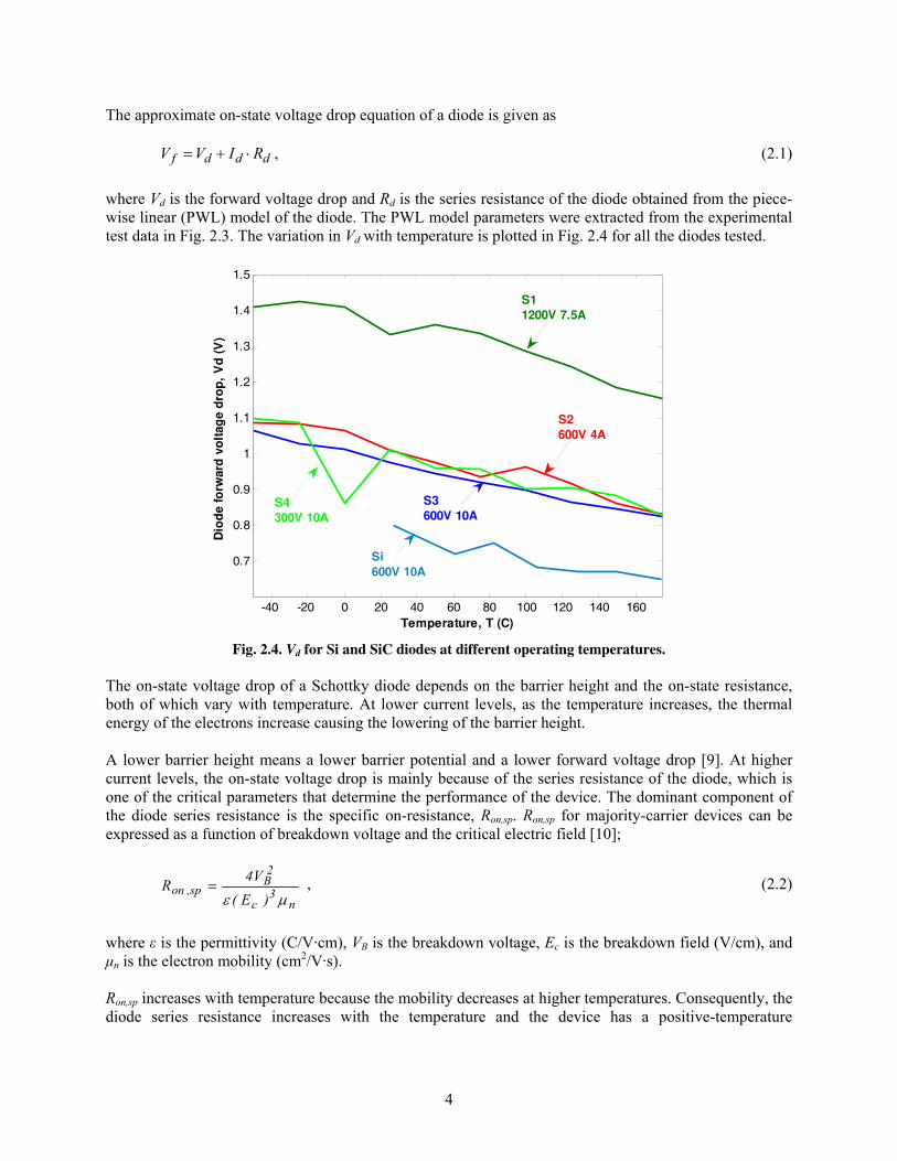
The approximate on-state voltage drop equation of a diode is given as
dddf RIVV ⋅+= , (2.1)
where Vd is the forward voltage drop and Rd is the series resistance of the diode obtained from the piece-
wise linear (PWL) model of the diode. The PWL model parameters were extracted from the experimental
test data in Fig. 2.3. The variation in Vd with temperature is plotted in Fig. 2.4 for all the diodes tested.
-40 -20 0 20 40 60 80 100 120 140 160
0.7
0.8
0.9
1
1.1
1.2
1.3
1.4
1.5
Temperature, T (C)
Dio
de f
orw
ard
vo
ltag
e d
rop
, V
d (
V)
S1
1200V 7.5A
S2
600V 4A
S3
600V 10AS4
300V 10A
Si
600V 10A
Fig. 2.4. Vd for Si and SiC diodes at different operating temperatures.
The on-state voltage drop of a Schottky diode depends on the barrier height and the on-state resistance,
both of which vary with temperature. At lower current levels, as the temperature increases, the thermal
energy of the electrons increase causing the lowering of the barrier height.
A lower barrier height means a lower barrier potential and a lower forward voltage drop [9]. At higher
current levels, the on-state voltage drop is mainly because of the series resistance of the diode, which is
one of the critical parameters that determine the performance of the device. The dominant component of
the diode series resistance is the specific on-resistance, Ron,sp. Ron,sp for majority-carrier devices can be
expressed as a function of breakdown voltage and the critical electric field [10];
n3
c
2B
sp,on)E(
V4R
με= , (2.2)
where ε is the permittivity (C/V·cm), VB is the breakdown voltage, Ec is the breakdown field (V/cm), and
μn is the electron mobility (cm2/V·s).
Ron,sp increases with temperature because the mobility decreases at higher temperatures. Consequently, the
diode series resistance increases with the temperature and the device has a positive-temperature

5
coefficient, which makes it easier to parallel the devices. The disadvantage, however, is that the diode
conduction loss also increases with temperature.
The series resistance, Rd, for the diodes is calculated from the slope of the i-v characteristics at high
currents and is plotted for different temperatures as shown in Fig. 2.5. The series resistance of each diode
is unique because of the differences in blocking voltages and in the die area. To withstand high
breakdown voltages, the blocking layer thickness must be increased and the doping concentrations must
be reduced. This results in an increased series resistance of the diode. Hence, device S1 rated at 1200 V,
7.5 A has a higher series resistance than S3 (600 V) and S4 (300 V). The resistance also varies with the
area of the device. It is evident from Fig. 2.5 that S2 and S3, with the same voltage but different current
ratings, have different series resistances.
-40 -20 0 20 40 60 80 100 120 140 1600
0.05
0.1
0.15
0.2
0.25
0.3
0.35
0.4
0.45
0.5
Temperature, T (C)
Dio
de o
n r
esis
tan
ce ,
Rd
(O
hm
s)
S2
600V 4A
S1
1200V 7.5A
S3
600V
10A
S4
300V
10A Si
600V 10A
Fig. 2.5. Rd for Si and SiC diodes at different operating temperatures.
2.2.2 Dynamic Characteristics
A buck chopper with an inductive load was built to evaluate the switching characteristics of the diodes.
The test circuit shown in Fig. 2.6 was built for the tests.
The test circuit consists of a gate-driver chip that drives the IGBT. The load includes a 24-mH inductor
and a 45.5-Ω resistor (with a maximum power dissipation rating of 1200 W) in series. The IGBT was
switched at 5 kHz with a duty cycle of 50%. The reverse-recovery tests were performed at different direct
current (dc) voltages ranging from 50 to 200 V.
The tests were performed for the following diodes: (a) S3 (600 V, 10 A), (b) S2 (600 V, 4 A), (c) S4
(300 V, 10 A), (d) S1 (1200 V, 7.5 A), and (e) a Si pn diode (600 V, 10 A) which was included for
comparison purposes. Figure 2.7 shows the reverse-recovery test setup in the lab. Some of the reverse-
recovery waveforms are shown in Figs. 2.8 and 2.9.

6
Fig. 2.6. Reverse-recovery test circuit.
Fig. 2.7. Reverse-recovery test setup.

7
Fig. 2.8. Reverse-recovery waveforms showing the diode current (top) and
voltage (bottom) for the diode S3.
Fig. 2.9. Reverse-recovery waveforms showing the diode current (top) and
voltage (bottom) for the diode S2.
The reverse-recovery waveforms for all the diodes tested are shown in Figs. 2.8, 2.10, 2.11, and 2.12. The
energy losses for various forward peak currents at different temperatures are shown for the Si diode and
Diode current – 0.5A/div
Diode voltage – 100V/div
Diode voltage – 100V/div
Diode current – 0.5A/div

8
the SiC diode S4 in Fig. 2.13. The switching loss for the Si diode increases with temperature and forward
current, while the switching loss for the SiC diode S4 is almost independent of the change in temperature
and varies slightly with increasing forward current. The reason is that the reverse-recovery current of a
diode depends on the charge stored in the drift region. Schottky diodes have no stored charge because
they are majority-carrier devices and thus have no reverse recovery. However, oscillations due to parasitic
internal pn diodes and capacitances look like reverse-recovery phenomena. The reduced reverse recovery
of Schottky diodes makes it possible to reduce the size of the snubbers. Low reverse-recovery and
snubber losses increase the efficiency of the power converters.
Fig. 2.10. Reverse-recovery waveforms showing the diode current (top) and
voltage (bottom) for the diode S4.
Fig. 2.11. Reverse-recovery waveforms showing the diode current (top) and voltage (bottom) for the diode S1.
Diode current – 0.5A/div
Diode voltage – 100V/div
Diode current – 0.5A/div
Diode voltage – 100V/div

9
Fig. 2.12. Reverse-recovery waveforms showing the diode current (top) and
voltage (bottom) for the Si pn diode.
1 1.5 2 2.5 3 3.5 4 4.5 50
0.2
0.4
0.6
0.8
1
1.2
1.4x 10
-4
T
urn
off
lo
sses,
Eo
ff (
Jo
ule
s)
Peak Forward Current, If (A)
Si
Increasing
temperature
Increasing temperature
SiC
Fig. 2.13. Turn-off energy losses with respect to forward current at different operating temperatures.
2.3 SiC FIELD-EFFECT TRANSISTOR (FET) DEVICES
FET devices are majority-carrier devices and are preferred over minority-carrier devices in power
converters. However, Si FET devices, like Si Schottky diodes, can only be used in low voltage (<300-V)
applications because of their high on-state resistance. Even the first experimental SiC FET devices have
blocking voltages of over 1000 V. It is expected that in the near future, SiC FET devices will dominate Si
minority-carrier devices in the medium-voltage (< 3000-V) applications.
Diode current – 0.5A/div
Diode voltage – 100V/div

10
2.3.1 Static Characteristics
2.3.1.1 SiC JFET
A JFET is a unipolar device and has several advantages compared with MOSFET devices. A JFET has a
low voltage drop and a higher-switching speed and is free from gate-oxide interface problems, unlike a
MOSFET [11]. A SiC JFET is typically a normally-on device and conducts even though there is no gate
voltage applied. A gate voltage must be applied for it to stop conduction. This feature dictates special
gate-drivers, increasing the complexity of the design. A normally-on device is not desirable for power
electronics since it requires additional protection circuitry to prevent a dc bus short if the gate signals fail.
A Si JFET is not classified as a power electronics device. The SiC JFET, however, can be used in high-
voltage, high-power applications, unlike a Si JFET because of its vertical structure and the intrinsic
properties of SiC.
A normally-on SiC JFET rated at 1200 V and 2 A was tested to study the high-temperature behavior of
the device. The forward characteristics of this device at different temperatures are shown in Fig. 2.14. As
seen in Figs. 2.14 and 2.15, SiC JFETs have a positive-temperature coefficient, which means that, like
SiC Schottky diodes, their conduction losses will be higher at higher temperatures. A positive-
temperature coefficient makes it easier to parallel these devices and reduce the overall on-resistance. The
on-resistance of the JFET increases from 0.36 Ω at −50°C to 1.4 Ω at 175°C, as shown in Fig. 2.16.
Fig. 2.14. i-v characteristics of SiC JFET at different temperatures.

11
Fig. 2.15. On-resistance of SiC JFET at different temperatures.
Fig. 2.16. Transfer characteristics of several SiC JFET samples.
The on-resistance is high; however, this device is a low-current-rated device and is an early prototype. It
is expected that as the technology matures, lower on-resistances will be possible.
The transfer characteristics of different SiC JFET samples are shown in Fig. 2.16. The negative gate
pinch-off voltage required to turn off the device is higher than that required for Si devices and varies from
sample to sample. This variation is attributed to the fact that these devices are experimental samples.
2.3.1.2 SiC MOSFET
A MOSFET is a unipolar device and is normally off. The forward characteristics of a 1.2-kV, 15-A SiC
MOSFET at room temperature are shown in Fig. 2.17. The gate voltage was varied from 0 to 20 V in
increments of 5 V. For Vgs = 20 V, there is a 6.7-V drain-to-source voltage drop that corresponds to a
15-A drain current. Note that it would be more reasonable to operate this device at 5 A with Vgs = 20V
because of a low voltage drop of 1.5 V. The forward characteristics of the same SiC MOSFET for a
temperature range of −50 to 175°C are shown in Fig. 2.18. Note that the device’s response to temperature

12
increase changes at 50°C. To get a better understanding of this phenomenon, the on-state resistances of
the device are calculated from the slopes of the different curves and are plotted with respect to
temperature in Fig. 2.19. It is interesting to note that this device has a negative temperature coefficient at
up to 50°C and a positive-temperature coefficient above that. MOSFETs are majority-carrier devices and
are expected to have positive-temperature coefficients. The components of the on-resistance of a
MOSFET, can be expressed as the sum of several different resistances because of the different regions in
the MOSFET structure
djfetaccchsubconton RRRRRRR +++++= , (2.3)
where Rcont is the contact resistance, Rsub the substrate resistance, Rch the channel resistance, Racc the
accumulation layer resistance, RJFET the resistance of the JFET like region, and Rd is the resistance of the
drift region [12].
Dra
in C
urr
en
t, I
d,
2A
/div
Drain to Source Voltage, Vds
, 1V/div
Vgs=20V
Vgs
=15V
Vgs
=10VVgs=5V
Fig. 2.17. Forward characteristics of SiC MOSFET at room temperature.
0 1 2 3 4 5 6 7 8 90
2
4
6
8
10
12
14
16
Dra
in c
urr
en
t, I
d (
A)
Drain to source voltage, Vds (V)
100C
125C
150C
175C
Increasing Temperature
-50C to 50C
75C
Fig. 2.18. Forward characteristics of SiC MOSFET at different temperatures.

13
-40 -20 0 20 40 60 80 100 120 140 160
0.25
0.3
0.35
0.4
0.45
0.5
Temperature, T (C)
On
-resis
tan
ce,
Ro
n (
Oh
ms)
Fig. 2.19. On-resistance of SiC MOSFET at different temperatures.
At lower temperatures, the contribution of the channel resistance to the total on-state resistance is
dominant [13]. The channel mobility increases with temperature because the interface traps are closer to
the conduction band [13, 14]; thus the channel resistance decreases with temperature. Consequently, at
low temperatures, the MOSFET on-resistance decreases. Above a certain temperature value, the channel
resistance is not dominant; and because of the other dominant on-resistance components, the MOSFET
overall on-resistance increases.
The SiC MOSFET gate-threshold voltage is measured from the transfer characteristics shown in Fig.
2.20. The gate-threshold voltage decreases with increasing temperature. Figure 2.21 shows the change in
threshold voltage from 10.7 V at −50°C to 2.8V at 175°C. This change is due to the trapped charge in the
SiO2, as well as the impurities at the SiO2 interface. These trapped charges become active at high
temperatures, which results in a Fermi level shift toward the bandgap, causing the drain current to flow at
low threshold voltages. In other words, less gate voltage is required at high temperatures for the same
drain current to flow through the device.
0 2 4 6 8 10 12 14 16 18 200
0.5
1
1.5
2
2.5
3
3.5
4
4.5
5
Dra
in C
urr
en
t, I
d(A
)
Gate voltage, Vgs (V)
Increasing
Temperature
-50C to 175C
Fig. 2.20. Transfer characteristics of SiC MOSFET at different temperatures.

14
-50 0 50 100 150 2000
2
4
6
8
10
12
Temperature, T (C)
Gate
th
resh
old
vo
ltag
e,
Vg
s (
V)
Fig. 2.21. Gate-threshold voltage of SiC MOSFET at different temperatures.
2.3.1.3 Gate-drive requirements
SiC FET switches can be operated at higher switching frequencies and higher temperatures; therefore,
they have different gate-drive requirements compared with traditional Si power switches. The switching
performance of the FET devices is determined by charging and discharging of the parasitic capacitances
across the three terminals, input capacitance, reverse-transfer capacitance, and output capacitance. These
capacitances are proportional to the area of the device [6]. Since SiC devices have smaller areas than
comparable Si devices, even for high-blocking voltages, the capacitances are reduced. This enables
devices to operate at higher switching speeds. A comparison of capacitance values for a SiC MOSFET
and for a Si power switch is reported in [15].
One of the important parameters in gate-drive designs is the capacitance between the gate and the other
terminals. Total input capacitance of the JFET, Ciss, determines the current required by the gate and the
rate at which the applied gate voltage is built across the gate and source terminals. Therefore, the gate-
drive circuit is required to have the capability of providing peak currents to charge the input capacitance
quickly. The peak-gate current is limited by the series resistance between the gate and the gate-driver
output. Higher gate-series resistance decreases the ringing effect due to the internal impedance of the
device; however, it also results in slower turn-on times.
As mentioned earlier, there are several gate-drive circuit design options for SiC JFETs using transistors
and other discrete devices [10, 16]. A commercial gate-driver chip IXDD414 was used in this project to
drive the SiC FETs under test for a more reliable and quick gate-driver design. Note that this gate-driver
chip can be used with most of the SiC JFETs whose transfer characteristics are shown in Fig. 2.16, as
well as the SiC MOSFET samples. The gate driver can be redesigned to be used as a SiC MOSFET gate
drive by replacing the series-gate resistor and reversing the output-voltage polarity. The peak-gate
currents and gate-voltage waveforms driving a SiC JFET and a SiC MOSFET are shown in Fig. 2.22. As
seen in this figure, a SiC MOSFET requires a higher current than a SiC JFET to operate at the same
switching frequency, i.e. 250 kHz in this case.

15
(a) SiC JFET
(b) SiC MOSFET
Fig. 2.22. The peak-gate currents and gate-voltage waveforms.
2.3.2 Dynamic Characteristics
The gate-drive circuit discussed in the previous section was used to determine the dynamic characteristics
of the SiC MOSFET and JFET.
SiC JFETs are normally-on devices and they can be turned off only by applying a negative voltage that is
higher than what a typical Si power device requires. Based on the transfer characteristics (Fig. 2.16), the
gate drive was designed for a voltage of −25 V, since that would be enough to turn off most of the
samples tested.
When SiC JFETs are operated at high frequencies, they need high peak-gate currents to charge and
discharge the gate capacitances faster. For example, 250-kHz switching was achieved with a series-gate
resistance of 5.4 Ω and a peak-gate current of 0.38 A.

16
The gate voltage and the switching waveforms of the JFET are shown in Fig. 2.23. The device has a turn-
off delay td,off of 40 ns, fall time tf of 80 ns, turn-on delay td,on of 20 ns, and rise time tr of 100 ns.
(a)
(b)
Fig. 2.23. The gate and switching waveforms of the SiC JFET.
The gate-drive voltage for the MOSFET was selected as 20 V, as determined from the forward
characteristics to obtain the optimum performance. The 250-kHz operation was achieved with a series-
gate resistance of 7.2 Ω and a peak-gate current of 0.6 A. The gate and switching waveforms for a SiC
MOSFET are shown in Fig. 2.24. The device has a turn-off delay td,off of 40 ns, fall time tf of 100 ns, turn-
on delay td,on of 20 ns, and rise time tr of 100 ns.
Note that both the SiC JFET and the MOSFET show fast dynamic responses, which would be required for
high-frequency switching.
The turn-on and turn-off energy losses for both the SiC MOSFET and the JFET were calculated by
integrating the instantaneous power over the turn-on (ton) and turn-off times (toff). The energy losses
calculated for the SiC MOSFET and JFET at different temperatures for a 5-kHz, 50% duty cycle, 100-V,

17
0.8-A operation are shown in Fig. 2.25. It is interesting to note that a SiC JFET needs almost no energy to
turn on because of its normally-on feature. Another observation from these figures is that the total
switching losses do not vary much with temperature.
(a)
(b)
Fig. 2.24. The gate and switching waveforms of the SiC MOSFET.

18
-40 -20 0 20 40 60 80 100 120 140 160-1
0
1
2
3
4
5
6x 10
-6
Temperature, T (C)
En
erg
y l
osses,
E (
Jo
ule
s)
Etot
Eon
Eoff
(a) SiC JFET.
-40 -20 0 20 40 60 80 100 120 140 160-1
0
1
2
3
4
5
6x 10
-6
Temperature, T (C)
En
erg
y l
osses,
E (
Jo
ule
s)
Etot
Eon
Eoff
(b) SiC MOSFET.
Fig. 2.25. Energy loss plots.

19
2.4 CONCLUSIONS
The static and dynamic performances of some SiC Schottky diodes, SiC MOSFETs, and SiC JFETs were
analyzed. It was observed that SiC Schottky diodes and JFETs have positive-temperature coefficients.
However, SiC MOSFETs display a negative temperature behavior for temperatures below 50°C and a
positive-temperature coefficient behavior above this value. This is due to the interface-trap defects in the
SiC MOSFET, which will eventually be eliminated with maturing SiC manufacturing technology. SiC
Schottky diodes showed excellent reverse-recovery characteristics compared with Si pn diodes. Even
though SiC Schottky diodes have higher on-resistances, they exhibit near-perfect switching
characteristics, making their performance superior to their Si counterparts. Thus replacing Si devices with
comparable SiC Schottky diodes will improve the performance of the power switches in a power
converter by reducing the switching stress on the switches and decreasing the overall losses.
The switching losses were almost constant for a wide temperature range for all the SiC unipolar devices
presented in this report, showing that SiC unipolar devices are well suited for high-frequency, high-
temperature, and high-power applications. Also, hard-switching circuits at higher power levels and higher
frequencies can be realized using SiC devices because of their excellent switching characteristics. With
further improvements in current ratings, SiC MOSFETs can replace Si IGBTs in medium-voltage
applications. SiC MOSFETs are preferred over SiC JFETs because of their normally-off feature.
However, gate-oxide reliability still remains an issue for SiC MOSFETs.

20
3. HYBRID Si-SiC INVERTER
3.1 OBJECTIVE
The objective is to evaluate the performance of a hybrid Si IGBT–SiC Schottky diode inverter and
compare it with the performance of a similar all-Si inverter. The main focus of this project is to study the
impact of replacing pn diodes with SiC Schottky diodes in an inverter by performing inductive load and
dynamometer tests.
3.2 WHY A HYBRID INVERTER
SiC Schottky diodes have been proven to have better performance characteristics than similar Si pn
diodes [17], especially with respect to switching characteristics as they have negligible reverse-recovery
losses. SiC devices also can operate at higher temperatures, thereby resulting in reduced heat sink weight
and volume. Improved switching performance impacts the main power switches by reducing the stress on
them and improving the system performance. SiC Schottky diodes are already commercially available at
relatively low current ratings. These diodes are being used in niche applications such as power factor
correction circuits. It is expected that the first impact of SiC devices in inverters will be as a result of SiC
Schottky diodes replacing the Si pn diodes.
Several problems must be addressed to meet the Department of Energy’s (DOE’s) FreedomCAR and
Vehicle Technologies program goals, such as reducing the size and weight of the power electronics and
cooling systems and increasing their efficiency. To evaluate the possibility of solving some of these
problems using SiC diodes, Oak Ridge National Laboratory (ORNL) collaborated with Cree and
Semikron to build a hybrid 55-kW (Si IGBT–SiC Schottky diode) inverter by replacing the Si pn diodes
in Semikron’s inverter with Cree’s SiC Schottky diodes.
3.3 TESTING AND MODELING THE 75-A DIODE
For SBDs, the two main tests that need to be performed are testing the static characteristics, consisting of
i-v curves, and turn-off testing, from which the reverse recovery of the diode can be evaluated.
3.3.1 SiC SBD On-State Testing
SBDs from Cree rated for 75 A were tested in the TEK 371B curve tracer to obtain the on-state
characteristics over a range of temperatures (−55oC to 175°C). The diode was placed in an oven
(connected through high-temperature wires) to evaluate the temperature characteristics. Since this is a
high-current device, the voltage drops across the connecting wires become significant. The resistance was
found to be 0.073 Ω, and corresponding voltage drops across the wires were subtracted from the raw data,
thereby yielding the true voltage drop across the diode.
As seen in Fig. 3.1, the built-in potential (or the knee voltage) decreases with the increase in temperature
because the increasing thermal energy of electrons in the metal overcomes the Schottky barrier height at a
lower forward voltage. It can also be seen that there is a decrease in the slope of the on-state
characteristics with a temperature increase. This is because of the reduction in mobility, or increase in on-
resistance, that is typically seen in a majority-carrier device and is a sign of a positive-temperature
coefficient.

21
Fig. 3.1. i-v characteristics of the 75-A SiC diode from Cree.
3.3.2 SiC Diode Modeling
The SiC diode model used in this project was developed at the University of Arkansas. It is a robust
model that can accurately model forward and reverse recovery accurately over temperature. Moreover,
many details pertaining to the fabrication of the diode need not be known by the user, making parameter
extraction flexible. Figure 3.2 shows the topology of the SiC power-diode model.
Fig. 3.2. Model topology of the power diode [18].
Static characterisictis - Cree Diode
0
10
20
30
40
50
60
70
80
0 1 2 3 4 5 6 7 8 9
Voltage (V)
Cu
rre
nt
(A) -50C
0C
100C
150C
175C
Increasing temperature
Knee voltage

22
The model described is a “unified” one in that it can model pn, Schottky, and merged pn–Schottky diodes.
Therefore, all the features will not be turned on for modeling the Schottky diode for this research effort.
Some of the variables seen in Fig. 3.2 do not pertain to Schottky diodes and are therefore not explained.
For modeling the static characteristics, the diode uses several equations of the form
)1e(ISi T
j
VN
V
−= ⋅ , (3.1)
where IS is the saturation current, Vj is the forward diode junction voltage, N is the emission coefficient,
and VT is the thermal voltage (kT/q). There are different regions in the diode operation, such as high- and
low-level injections and recombination, all of which are modeled with similar equations. Moving
boundary conditions are used to model the dynamic characteristics such as turn-on, turn-off, and reverse
recovery.
To incorporate temperature effects, Eq. (3.1) is altered as follows
IS(T) = IS(TNOM)·(T/TNOM)XTI·e[(T/TNOM)-1]·(EG/NT.VT) , (3.2)
where T is the user defined temperature, TNOM is room temperature, and XTI is the temperature
compensation factor.
Such normalized temperature-based factors are used in all the equations that need to scale with
temperature.
3.3.3 Parameter Extraction and Model Validation Using the Characterized Data for Diodes
The model was constructed in MAST HDL and simulated in the Saber simulator. The dc test-bench
consists of a constant dc source connected to the SiC diode model. The physical and structural parameters
of the diode are first determined at the nominal temperature. The P-N grading coefficient, M, is set to the
default value of 0.5. The parameters RS (series resistance), ISR (low-level recombination saturation
current), and NR (low-level recombination emission coefficient) can be extracted from the forward on-
state characteristics. For Schottky diodes, NR is typically set to 1. The forward series resistance, RS, can
be obtained directly from the inverse of the slope of the on-state current versus the voltage characteristic
at high to medium currents. After RS is extracted, the diode current versus internal-junction voltage (Vj =
VD - ID·RS) is calculated with the measured data. An ID versus Vj semi-log plot is then used to extract NR
and ISR as follows
2.3logID = 2.3logISR + 2.3Vj/(NR·VT) . (3.3)
The y intercept of the semi-log plot gives the value of ISR. The temperature-dependent parameters are
then extracted. The saturation current, ISR’s temperature exponent XTIR, is extracted using the low
forward current characteristic over a range of temperatures. The decrease in slope of the on-state
characteristics as temperature increases is used to extract the parameters representing the temperature
dependency of the series resistance RS. In other words, RS is extracted for each on-state curve for all
temperatures. The values of the extracted RS for each temperature are then used in Eq. (3.4) to optimize
the values of the exponential GAMMA, linear TRS1, and quadratic TRS2 temperature parameters for RS.
RS(T) = RS(TNOM)·[(T/TNOM)γ+TRS1(T-TNOM)+TRS2(T-TNOM)2]. (3.4)

23
After the parameters are extracted from the on-state characteristics, the depletion and package capacitance
are then extracted from the reverse-recovery waveforms. For Schottky diodes, the absence of stored
charge reduces the reverse recovery to just the charging of the depletion and package capacitances. After
the diode current crosses zero, the voltage is seen to rise as the depletion and package capacitances are
charged. The initial peak in the reverse recovery is due to the junction capacitance, as the depletion region
is narrow and is accounted for in the model by CJ0 and FC (forward bias-depletion capacitance
coefficient); while the further increase in the negative reverse current as the diode voltage rises is due to
the package capacitance (CP). At high voltages, the depletion region decreases, and therefore the package
capacitance dominates. Therefore, CP is extracted from the high-voltage part of the reverse-recovery
waveform. Care should be taken to ensure that the voltage waveforms from which CJ0 and CP are
extracted are aligned and have the same dv/dt.
3.4 SCHOTTKY DIODE AT DIFFERENT TEMPERATURES
The on-state validation of the model with the SiC 75-A diode from Cree is seen in Fig. 3.3. The
percentage error is approximately 0.3–0.4% in the 100°C and 150°C curves and approximately 2–3% in
the 25oC curve.
Voltage, Vd (V)
Fig. 3.3. Measured (solid) and simulated (dotted) on-state waveforms of
the SiC Schottky diode at different temperatures.
Figure 3.4 shows the reverse recovery of the SiC diode and the corresponding behavior of the model (in
dotted lines) with the extracted CJ0 parameter. The model is accurately tracking the test data.
Dio
de
curr
ent,
Id
(A
)

24
Fig. 3.4. Measured (solid) and simulated (dotted) reverse-recovery waveforms of
the SiC Schottky diode from Cree.
The junction capacitance can then be extracted from the reverse-recovery data that essentially determines
the switching speed and the peak-reverse-recovery current of the device. In Fig. 3.5, the effect of the
junction capacitance can be seen on the reverse-recovery current. It can be easily deduced that the peak-
reverse-recovery current is directly proportional to the diode-junction capacitance.
Dio
de
curr
ent,
Id
(A
)

25
Fig. 3.5. Simulation showing the reverse-recovery current in a SiC diode for
different values of junction capacitances.
3.5 SIMULATION OF Si IGBT–SiC SCHOTTKY DIODE HYBRID INVERTER
After the modeling and parameter extraction of the devices, the device models were used to construct a
three-phase voltage-source inverter in Saber. The Saber Sketch software in the suite was used. The model
closely emulated the prototype inverter from Semikron in terms of the inverter topology. The switching
frequency was set to 10 kHz. Library models were used for the comparators, voltage sources, and passive
elements. A graphical representation of the SiC Schottky diode model was created which can be
interfaced directly with other library elements instead of manually creating net lists. The modulating sine
wave had a frequency of 75 Hz, which was therefore the frequency of the output current. The IGBT that
was used for constructing the Semikron inverter was not available in the Saber library. Therefore, another
IGBT with similar ratings was used as the transistor switch instead. The load consisted of a 1.24-Ω
resistor and a 1.5-mH inductor. The input dc bus voltage was set at 325 V. The inverter topology is shown
in Fig. 3.6.

26
Fig. 3.6. Schematic representation of the hybrid inverter in Saber.
Table. 3.1. SiC power diode model parameters and extraction characteristics for the Cree 75-A diode
Parameter Parameter name Extraction characteristic Value
EG Bandgap Device-specific 1.6
VJ Built-in junction potential Device-specific 1.5
CJ0 Zero-bias junction capacitance Device-specific 20 pF
M P-N grading coefficient Device-specific 0.5
FC Forward-bias deletion capacitance coefficient Device-specific 0.5
NB Base doping concentration Device-specific 1e15
RS Forward series contact resistance High- to medium-current on-
state slope 0.013
ISR Low-level recombination saturation current Low-current on-state region 5e−16
NR Low-level recombination emission coefficient Low-current on-state region 1
XTIR ISR temperature exponent Low-current on-state vs. T 3
TNR1 Linear NR temperature coefficient Low-current on-state vs. T 0
TNR2 Quadratic NR temperature coefficient Low-current on-state vs. T 0
TRS1 Linear RS temperature coefficient High- to medium-current on-
state slope vs. T −14e−3
TRS2 Quadratic RS temperature coefficient High- to medium-current on-
state slope vs. T −16e−6
GAMMA RS temperature exponent High- to medium-current on-
state slope vs. T 2.5
An all-Si inverter with Si IGBTs and diodes was also simulated using the device parameters in Table 3.1.
The load currents and a single-phase voltage from the simulations are shown in Figs. 3.7 and 3.8,
respectively. The efficiencies of the inverter obtained during simulations are shown in Table 3.2. Table
3.3 shows the modulation index used and the resulting inverter efficiencies of the inverter. Note that the
Si IGBT–SiC Schottky diode hybrid has much better efficiencies than the all-Si inverter.

27
Fig. 3.7. Simulated three-phase load currents in the hybrid inverter.
Fig. 3.8. Simulated phase voltage (phase 1) in the hybrid inverter.
ia ib ic
Ph
ase
Vo
ltag
e (V
)

28
Table 3.2. Efficiencies of the hybrid inverter obtained from simulation
Modulation index
Peak power output
from simulation
(kW)
Efficiency (simulation)
percent
0.572671 41.65 93.54
0.700348 48.43 94.27
0.801846 54.97 95.15
0.899974 62.88 96.27
0.985006 68.92 97.36
Table 3.3. Efficiencies of the all-Si inverter obtained from simulation
Modulation index
Peak power output
from simulation
(kW)
Efficiency
(simulation) percent
0.586299 40.33 92.07
0.710617 48.17 93.48
0.821163 54.43 94.41
0.910835 61.77 95.14
1.001043 68.09 96.53
The simulation and testing was performed for all conditions with a constant dc supply of 325 V. The
instantaneous-power output from the inverter is shown in Fig. 3.9. The peak-power output can also be
gauged from the output-power plot. The hybrid inverter was found to have a peak-instantaneous-power
output ranging from 41–69 kW, depending on the amplitude modulation index. When the amplitude
modulation index was set at 0.8, the peak-power output was found to be 55 kW.
Fig. 3.9. Total instantaneous output power from the three phases of the hybrid inverter.

29
The difference in efficiencies between the simulated inverters is clearly visible in Figs. 3.10 and 3.11.
When the Si diode in the all-Si inverter was replaced with the SiC Schottky diode, a 1.5–2% increase in
the operational efficiency was observed.
Peak power output vs. Efficiency
91
92
93
94
95
96
97
98
40 45 50 55 60 65 70 75
Peak power output (kW)
Eff
icie
nc
y (
%)
Hybrid inverter
All-Si inverter
Fig. 3.10. Comparison of peak-power output vs. efficiencies for hybrid and all-Si inverter.
Fig. 3.11. Comparison of efficiencies (from simulation) of hybrid and all-Si inverter.
91
92
93
94
95
96
97
98
0.5 0.6 0.7 0.8 0.9 1
Modulation Index
Eff
icie
ncy (
%)
Hybrid Inverter All Si Inverter

30
3.6 CONFIGURATION OF THE INVERTER
The inverter module SKAI (Semikron Advanced Integration) from Semikron was developed for hybrid
electric vehicle traction drives. It is a three-phase 55-kW inverter unit (Figs. 3.12 and 3.13) built using
600-V, 600-A IGBT and 600-V, 450-A pn diode modules. Cree has developed 75-A, 600-V, 4 × 6.65m
SiC Schottky diodes as shown in Fig. 3.14. The 3–in. wafer is also shown in Fig. 3.14. The yield for the
wafer was about 46.7%, with 67 good devices from the wafer. Semikron has replaced each Si pn diode
(9 × 9mm) in its automotive integrated power module (AIPM) with two 75-A SiC Schottky diodes.
Fig. 3.12. Inverter topology.
Fig. 3.13. Semikron inverter unit.
Fig. 3.14. 75-A Schottky diodes developed by Cree.

31
The inverter is liquid-cooled with a recommended coolant-flow rate of 2.5 gal per minute (gpm). The
Semikron unit shown in Fig. 3.13 is roughly rectangular in shape, but it has irregular dimensions and
weighs approximately 17 lb (7.7 kg). The maximum length, including mounting flanges and hose
connections, is 17.6 in. (449 mm). Excluding the mounting flanges and hose connections, the unit
measures 16.1 in. (410 mm). The maximum width of the unit is 8.2 in. (210 mm) and the minimal width
is 7.2 in. (185 mm). The maximum height of the unit is about 4 in. (100 mm). The volume of the unit is
approximately 6.9 L. The unit has built-in current sensors and dc-link capacitors. It has a CAN bus
interface with a built-in digital signal processor (DSP) controller and gate drivers.
The control system implemented uses indirect field-oriented control techniques with a closed-current loop
feedback. The speed and torque controls are achieved by a space vector pulse-width modulation
(SVPWM) control scheme with current and speed as feedback parameters. A control-system block
diagram is shown in Fig. 3.15 [19]. The control firmware module was provided by Semikron with user
interface software as shown in Fig. 3.16. Different modes of operation are possible with the controller.
Fig. 3.15. Block diagram of the control system.

32
Fig. 3.16. A screen shot of the user interface software.
3.6.1 Normal Mode
The controller operates as a closed-loop system and has two control modes
• Speed mode
• Torque mode
3.6.2 Debug Mode
The controller operates as an open-loop system, and the pulse-width modulation (PWM) frequency and
the open-loop frequency can be adjusted. There are several user control parameters that can be accessed
through the software interface to set the values for different operating conditions. A fault monitoring
system provides protection to the system from faults such as over-current, bus over-voltage, over-
temperature, and desaturation.
3.7 INVERTER TESTING
There are two major tests to be performed, an R-L load test to evaluate the inverter’s power handling
capability and the dynamometer test for dynamic performance. Both the hybrid inverter and the all-Si
inverter were tested with the same procedure. As discussed in the previous section, the modes of
operation were controlled using the manufacturer-supplied user interface software. The inverter efficiency
curves were obtained using the speed mode of operation, and the power handling capability was tested

33
using the debug mode of operation. The coolant temperature of the inverter was varied (20–70oC) to
stress the wire bonds and bond joints in the inverter and to test for strength.
3.7.1 Isolation Impedance
As a safety measure, prior to the start of electrical testing, the unit was checked for a fault condition that
could have occurred as a result of shipping or handling damage. The isolation impedance between the
inverter terminals and case was measured with a multi-meter to verify proper isolation. The isolation
impedance between the terminals and case of the inverter was measured as being greater than 1 MΩ.
3.7.2 R-L Load Test
3.7.2.1 Test setup
The output leads of the inverter are connected to a three-phase star-connected variable resistor bank with
a three-phase inductor in series. The dc inputs are connected to a voltage source capable of supplying the
maximum rated operating voltage and current levels for the inverter. The test setup uses the following
equipment, as shown in Fig. 3.17.
• Yokogawa PZ4000 power analyzer for power measurement.
• Variable resistor load with a capacity of 24 kW.
• Inductor with 400-A capacity.
• Coolant pump with a temperature controller.
• A dc power supply with four-quadrant operation (not seen in the figure).
3.7.2.2 Operation
During this test, the inverter unit was operated in the debug mode instead of the normal mode. In this
mode, the open-loop frequency and the PWM frequency can be adjusted and the power capability of the
inverter can be tested.

34
Fig. 3.17. R-L load test setup.
For this test, the dc-link voltage was varied from the minimum operating voltage (200 V) to the maximum
bus voltage (450 V). The bus voltage trip fault occurs for voltages beyond 450 V. The load resistance was
set to the minimum value, and the current was controlled using the current controller. The coolant was set
at 20°C and at a flow rate of 2.5 gpm. The open-loop frequency of operation and the PWM frequency
were fixed, and the current command was varied for a particular dc-link voltage. For each value of the
current command and open-loop frequency, the dc-link voltage, dc-link current, input power, output
power, efficiency, and output-line currents and voltages were recorded. The three-phase power was
measured using the two-wattmeter method. The command current was increased in steps of 10 A without
exceeding the power rating of the inverter or the power rating of the load.
The procedure was repeated by increasing the open-loop frequency in steps of 25 Hz. The coolant
temperature was changed to 70°C, and the data were recorded for a wide range of current and open-loop
frequencies.
Coolant Temperature
Regulator
R-L LOAD

35
3.7.2.3 Results
The operating waveforms for two specific operating conditions of one phase of the hybrid inverter are
shown in Fig. 3.18. The data obtained for both the inverters were analyzed and the corresponding
efficiencies were calculated. The efficiency versus output-power plots for several operating conditions
comparing the inverters are shown in Fig. 3.19 (a) and (b). The hybrid inverter efficiencies are higher than
the all-Si inverter efficiencies for all operating conditions. The results show a reduction of up to 33.6% in
the losses when everything is kept the same and SiC Schottky diodes are used instead of Si pn diodes.
The percentage of loss reduction was calculated by comparing the power losses between the hybrid
inverter and the all-Si inverter as follows:
Percentage loss reduction = ( ) ( ) 100ddd )Si(ploss)SiC(ploss)Si(ploss ×−
Fig. 3.18. R-L load test operating waveforms.
Vdc=325V; ia,peak= 60A; fo=100Hz
Vdc=325V; ia,peak= 80A; fo=100Hz
ia
Vac
ia
Vac

36
Fig. 3.19. R-L load test efficiency curves for various load conditions.
0 2 4 6 8 10 1290
91
92
93
94
95
96
97
98
Output Power (kW)
Eff
icie
ncy (
%)
R-L Load Test - 250Vdc, 20C, 50Hz Operation
All-Si Inverter
Hybrid Inverter
Average loss reduction : 33.6 %
0 2 4 6 8 10 12 14 16 18 20 2290
91
92
93
94
95
96
97
98
Ouput Power (kW)
Eff
icie
ncy (
%)
R-L Load Test 325Vdc, 20C, 100Hz Operation
All-Si Inverter
Hybrid Inverter
Average loss reduction : 33.2 %

37
Fig. 3.19. R-L load test efficiency curves for various load conditions (cont’d).
0 2 4 6 8 10 1290
91
92
93
94
95
96
97
98
Output Power (kW)
Eff
icie
ncy (
%)
R-L Load Test - 250Vdc, 70C, 50Hz
All-Si Inverter
Hybrid Inverter
Average loss reduction : 27.54%
0 2 4 6 8 10 12 14 16 18 20 2290
91
92
93
94
95
96
97
98
Eff
icie
nc
y (
%)
Output Power (kW)
R-L Load Test - 325Vdc, 70C, 100Hz
All-Si Inverter
Hybrid Inverter
Average loss reduction : 19.4%

38
3.7.3 Dynamometer Test
3.7.3.1 Test setup
The inverter was connected to a Solectria motor and setup in a dynamometer test cell to test the dynamic
performance of the inverter in the motoring and regeneration modes. The Solectria motor is a four-pole
induction motor with a base speed of 2500 rpm, and the dynamometer has 100-hp capacity. The setup is
shown in Figs. 3.20 and 3.21. The tests were performed with the inverters supplied with 70°C coolant at a
flow rate of 2.5 gpm.
Fig. 3.20. Inverter dyne test setup.

39
Fig. 3.21. 100-hp dyne cell.
3.7.3.2 Motoring mode
The test setup connections were verified in the test cell. During this test, the inverter unit was operated in
the normal mode instead of the debug mode, and the control mode was set to speed instead of torque. In
this mode, the speed set point, the magnetizing current, the direction of rotation, and the current limit
were adjustable parameters. The dc-voltage input to the inverter was set at the nominal battery operating
voltage (325 Vdc).
The closed-loop speed controller gains were adjusted for a given magnetizing current value and current
limit to achieve stable operation of the system for a wide range of speeds. The direction of rotation was
set to forward, and the motor speed was increased from 750 rpm to the rated base speed for a specific
continuous-load torque. The data were obtained for a wide range of speed and torque values by changing
the load torque (from 100, 150, 200 Nm) using the dynamometer controller. The following information
was recorded at each speed increment: motor shaft speed (rpm and rad/second); motor torque; input
voltage and current to the inverter; and output voltages and currents from the inverter. The output voltage
and current waveforms for 40% and 80% of rated speed and several load-torque values were obtained.
The waveforms for two different loads are shown in Fig. 3.22. The efficiency plots for various speeds and
load-torque values are shown in Fig. 3.23. The average loss reduction in motoring mode was up to 10.7%.
The difference in the efficiencies of the inverters is higher at low-load torque because the diodes conduct
for relatively longer periods. The reduction in losses becomes smaller at higher-load torques as the
conduction time of the power switches increases. Note that one of the reasons the average loss reduction
is less in the motoring than in the R-L load test is that the power levels achieved are much lower in
motoring.
Figure 3.24 shows a screen shot of the test data obtained from the power meter PZ4000 for one of the
operating conditions.

40
(a) 1000 rpm and 50 Nm.
(b) 1000 rpm and 150 Nm.
Fig. 3.22. Dynamometer test–motoring mode operating waveforms.
Vac
ia
Vac
ia

41
(a) 100 Nm load torque.
(b) 150 Nm load torque.
Fig. 3.23. Dynamometer test–motoring mode efficiency plots at 70°C.
800 1000 1200 1400 1600 1800 2000 220090
91
92
93
94
95
96
97
98
Speed (rpm)
Eff
icie
ncy (
%)
Dyne Test - 100Nm Load Torque
Hybrid Inverter
All-Si Inverter
Average loss reduction : 10.7 %
800 1000 1200 1400 1600 1800 2000 220090
91
92
93
94
95
96
97
98
Speed (rpm)
Eff
icie
ncy (
%)
Dyne Test- 150Nm Load Torque
Hybrid Inverter
All-Si Inverter
Average loss reduction : 9.51%

42
(c) 200 Nm load torque.
Fig. 3.23. Dynamometer test–motoring mode efficiency plots at 70°C (cont’d).
Fig. 3.24. Dynamometer test–motoring mode data obtained from the power meter.
800 1000 1200 1400 1600 1800 2000 220090
91
92
93
94
95
96
97
98
Speed (rpm)
Eff
icie
ncy (
%)
Dyne Test - 200Nm Load Torque
Hybrid Inverter
Average loss reduction : 7.7 %
All-Si Inverter

43
3.7.3.3 Regeneration mode
During this test, the inverter unit was operated in the normal mode instead of the debug mode, and the
control mode was set to torque instead of speed. With these settings, the torque limit and the operating
current can be adjusted. The dc-voltage input to the inverter was set at the nominal battery-operating
voltage (325 V). The direction of rotation was set to be forward. The dynamometer controller was
adjusted to control the speed. The motor speed was increased from 750 rpm to the rated speed for a
specific operating current of the inverter to achieve a specific load torque. The current was varied from
zero to the values corresponding to different torque values and then decreased to zero. The procedure was
repeated to obtain the data for a wide range of speed and torque values. At each speed increment, motor-
shaft speed (rpm and rad/second), motor torque, input voltage and current to the inverter, and output
voltages and currents from the inverter were recorded. The output voltage and current waveforms for 40%
and 80% of rated speed and several load-torque values were obtained. The operating waveforms for the
regeneration mode are shown at two different speeds in Fig. 3.25. The curves comparing the efficiency of
the inverters at 70ºC coolant temperature are shown in Fig. 3.26 (a–c). The results show a reduction of up
to 12.71% in average losses, similar to the results obtained in the motoring mode.
The IGBTs used in the actual inverter and in the simulation are not the same. Therefore, a direct
comparison of the efficiencies of the simulation and the testing would not be accurate. But it is seen that
the efficiencies of the simulation and the testing do have the same trend.

44
(a) 1000 rpm and 50 Nm.
(b) 1000 rpm and 150 Nm.
Fig. 3.25. Dynamometer test–regeneration mode operating waveforms.
Vac
ia
ia
Vac

45
600 800 1000 1200 1400 1600 1800 200082
84
86
88
90
92
94
96
Speed (rpm)
Eff
icie
ncy (
%)
Regen Test - 100 Nm Load Test
Hybrid Inverter
All-Si Inverter
Average losss reduction : 11.22%
(a) 100 Nm load torque.
600 800 1000 1200 1400 1600 1800 200088
89
90
91
92
93
94
95
96
97
Speed (rpm)
Eff
icie
ncy (
%)
Regen Test - 150 Nm Load Test
Hybrid Inverter
All-Si Inverter
Average losss reduction : 12.03%
(b) 150 Nm load torque.
Fig. 3.26. Dynamometer test–regeneration mode efficiency plots at 70ºC.

46
600 800 1000 1200 1400 1600 1800 200088
89
90
91
92
93
94
95
96
97
Speed (rpm)
Eff
icie
ncy (
%)
Regen Test - 200 Nm Load Test
Hybrid Inverter
All-Si Inverter
Average losss reduction : 12.71%
(c) 200 Nm load torque.
Fig. 3.26. Dynamometer test–regeneration mode efficiency plots at 70ºC (cont’d).
3.8 EXPLANATION FOR THE POWER LOSS DIFFERENCE BETWEEN THE
INVERTERS
The results for the all-Si and the hybrid inverters for the various tests conducted have proved that the Si
IGBT–SiC Schottky diode hybrid inverter has better performance than the all-Si inverter. The effect of
replacing the Si pn diodes with the SiC Schottky diodes resulted in improved inverter efficiency.
The difference in efficiencies for the various operating conditions of the two inverters can be explained by
the static and dynamic characteristics of the diodes. A comparison of the static characteristics of the Si pn
diodes and SiC Schottky diodes obtained from one of the inverter phase legs is shown in Fig. 3.27. The
built-in forward voltage drop of the SiC and Si diodes is almost the same; however, the on-state resistance
of the Si pn diode at higher currents is much higher (slope of the static characteristics much lower) than
that of the SiC Schottky diode. Therefore, the conduction losses of the SiC diode will be less compared
with the Si pn diode at higher currents.
The SiC diode has lower reverse-recovery losses than the Si pn diode, as shown in Fig. 3.28. It should be
noted that the package for the SiC diode is not a commercial package; hence the turn-off of the SiC
Schottky diode has more oscillations because of the package capacitance. The superior reverse-recovery
characteristics of the SiC diode also results in reduced losses in the IGBT. This is because when a diode
in an inverter is turning off, the diode-reverse-recovery current passes through the other IGBT in the same
phase leg causing additional losses. The effect of this difference in diode-switching losses becomes
significant as the frequency increases; therefore, for the same operating conditions (same load current,
operating voltage, operating frequency, and coolant temperature) the losses in the hybrid inverter will be
less than in the all-Si inverter.

47
Some other observations and explanations for loss difference between the inverters in different modes are
as follows
1. The average loss reduction is much higher in the regeneration mode than the motoring mode
because the diodes conduct more in the regeneration mode, which is evident from Fig. 3.29.
2. At higher load torques in the motoring mode, the displacement factor is higher and hence the
average loss reduction is less. The reason is that at higher power factors in motoring mode, the
main switches conduct more than the diodes.
3. During the regeneration mode at higher torques, the average losses increase as the displacement
factor increases and the diodes conduct more.
0 0.2 0.4 0.6 0.8 1 1.2 1.4 1.6 1.8-50
0
50
100
150
200
250
300
Voltage (V)
Cu
rren
t (A
)
SiC Schottky diode
Si pn diode
Fig. 3.27. Comparison of static characteristics of Si pn diode and SiC Schottky diodes.

48
Fig. 3.28. Comparison of reverse-recovery characteristics of Si pn diode and SiC Schottky diode.
0 0.005 0.01 0.015 0.02 0.025 0.03 0.035 0.04 0.045 0.05-6
-5
-4
-3
-2
-1
0
1
2
3x 10
4
Time (sec)
Po
wer
(W)
Instantaneous Power During Regeneration
Fig. 3.29. Instantaneous output power during regeneration.
3.9 CONCLUSIONS
The 75-A SiC Schottky diodes used in the Si IGBT–SiC Schottky diode hybrid inverter were
characterized and the parameter extraction was conducted to build a model using Saber. The model was
used in an inverter model with Si IGBTs, and the performance of the inverter was studied with Si and SiC
SiC Schottky diode
Si pn diode
5 A/div

49
diodes. The efficiencies of the hybrid inverter were 1.5–2% higher than in the all-Si inverter, similar to
the test data.
The testing of both the hybrid and the all-Si inverters was completed successfully. The inverters were able
to operate at peak power levels with efficiencies of greater than 90%. The inverters were tested for a
maximum continuous power of 47 kW. The hybrid inverter had an average loss reduction of up to 33.6%
compared with the all-Si inverter for the R-L load test. The motoring and regeneration tests were done at
lower power levels and showed a reduction of around 10% in the average power losses. These test results
show a trend similar to the results obtained in the simulation.

50
4. ALL-SiC INVERTER
4.1 INTRODUCTION
SiC power switches have been demonstrated to have better performance compared with the equivalent Si
power switches. Simulation studies have proved that SiC devices, when compared with their Si
counterparts, have a better effect on the total system performance. SiC diodes are the only
commercialized devices available in the market. The SiC power switches are only available as some
experimental samples.
A 7.5-kW all-SiC inverter was built in collaboration with Rockwell Scientific to study the effect of
replacing the Si devices with SiC devices in the inverters. The module was built using JFETs as the main
power switches and SiC Schottky diodes. The performance of the all-SiC inverter was compared with a
similarly rated all-Si inverter.
4.2 JFET CHARACTERIZATION AND MODELING
4.2.1 SiC JFET Characterization
JFETs have reached a high level of maturity in SiC technology beyond that of other transistors, but they
still require further improvements for commercialization. Power JFETs are built with vertical topologies,
as shown in Fig. 4.1, and can support higher breakdown voltages as a result of their thick drift layer.
Fig. 4.1. Cross-section of the SiC VJFET structure.
One of the SiC JFETs from Rockwell (rated at 1200 V, 15 A) was tested for on-state and switching
characteristics to obtain data for modeling. The JFET was placed in the Tek371B curve tracer and the on-
state characteristics were measured in the unipolar and the bipolar mode.
The SiC JFETs from Rockwell are normally-on devices, meaning a negative-gate voltage is required to
turn them off. The gate voltage, Vgs, at which the JFET actually stops conducting (drain current Ids = 0 for
any value of Vds) is known as the pinch-off voltage. In the unipolar configuration, the gate is negatively
biased with respect to the source. Figure 4.2 shows the measured data of the JFETs in the unipolar region

51
of operation. In the unipolar mode, the JFET acts as a majority-carrier device and hence only the electrons
are carriers. On the other hand, in the bipolar mode of operation, the gate is positively biased with respect
to the source. In this case, both electrons and holes conduct and the total current is higher than in the
unipolar mode as a result of the increased conduction. The JFET was also tested in the bipolar mode; the
results are shown in Fig. 4.3.
Fig. 4.2. Unipolar operation of the Rockwell SiC JFET.
Fig. 4.3. Bipolar operation of the Rockwell SiC JFET.
Drain-source voltage, Vds (V)
Dra
in c
urr
ent,
Id
s (A
)
Drain-source voltage, Vds (V)
Dra
in c
urr
ent,
Id
s (A
)
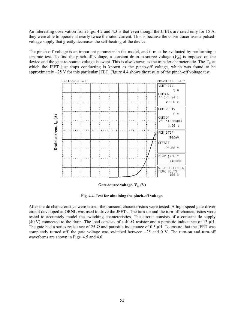
52
An interesting observation from Figs. 4.2 and 4.3 is that even though the JFETs are rated only for 15 A,
they were able to operate at nearly twice the rated current. This is because the curve tracer uses a pulsed-
voltage supply that greatly decreases the self-heating of the device.
The pinch-off voltage is an important parameter in the model, and it must be evaluated by performing a
separate test. To find the pinch-off voltage, a constant drain-to-source voltage (Vds) is imposed on the
device and the gate-to-source voltage is swept. This is also known as the transfer characteristic. The Vgs at
which the JFET just stops conducting is known as the pinch-off voltage, which was found to be
approximately –25 V for this particular JFET. Figure 4.4 shows the results of the pinch-off voltage test.
Gate-source voltage, Vgs (V)
Fig. 4.4. Test for obtaining the pinch-off voltage.
After the dc characteristics were tested, the transient characteristics were tested. A high-speed gate-driver
circuit developed at ORNL was used to drive the JFETs. The turn-on and the turn-off characteristics were
tested to accurately model the switching characteristics. The circuit consists of a constant dc supply
(40 V) connected to the drain. The load consists of a 40-Ω resistor and a parasitic inductance of 13 μH.
The gate had a series resistance of 25 Ω and parasitic inductance of 0.5 μH. To ensure that the JFET was
completely turned off, the gate voltage was switched between –25 and 0 V. The turn-on and turn-off
waveforms are shown in Figs. 4.5 and 4.6.
Dra
in c
urr
ent,
Id
s (A
)

53
Fig. 4.5. Turn-on waveforms of the SiC JFET.
Fig. 4.6. Turn-off waveforms of the SiC JFET.
Vds 10V/div
Ids 1A/div
Vgs10V/div
Vgs 10V/div
Ids 1A/div
Vds 10V/div

54
4.2.2 SiC JFET Modeling
The device physics-based analytical SiC JFET model (Fig. 4.7) used for this project was developed by the
University of Arkansas. It is a flexible model that can predict the unipolar and bipolar operation of SiC
JFETs. This circuit representation allows the modeler to visualize and qualitatively assign equations for
all the branches and elements. It should be noted that the topology does not represent a sub-circuit of any
kind.
Sp
Rmod
Ijf et
DgdDp
D
Cgd
Dgs
Rm
Rd
Cgs
G
S
Fig. 4.7. Internal topology of the SiC JFET [20].
The model can be visualized as consisting of a source-region resistance, Rmod, that is conductivity
modulated by imod for positive-gate voltages; an ideal JFET that describes the channel current, IJFET; a
bias-dependent series base or drift-region resistance, Rd; and a series-contact resistance, Rm. Dgs and Dgd
are representations of the gate-source and gate-drain pn junctions. Cgs and Cgd are the corresponding
junction capacitances. Dp and Sp, seen in the topology as shown in Fig. 4.7, are the internal nodes in the
model.
The major equations used to model the on-state characteristics are as follows
Ig + Id = Is . (4.1)
(i) Pre-turn-on: if Vgs + Vp − Vb i< = 0 ,
Ids = 0. (4.2)
(ii) Linear: if Vds<(Vgs + Vp − Vbi ) ,
( ) ( )⎪⎭
⎪⎬⎫
⎪⎩
⎪⎨⎧
⎥⎦⎤
⎢⎣⎡ −−+−−= 3VV3VVV
V
1
3
2VGI gsbidsgsbi
pdsods . (4.3)
(iii) Saturation: if Vd s≥ (Vgs + Vp − Vbi) ,

55
⎥⎥⎥
⎦
⎤
⎢⎢⎢
⎣
⎡
⎟⎟⎠
⎞⎜⎜⎝
⎛ −+
−−=
3
p
gsbi
p
gsbipods
V
VV2
V
VV31
3
VGI . (4.4)
In many cases, parameters involving device geometry and dimensions may not be available to the
modeler. Those parameters are lumped together to form an extractable parameter called Go, which is
defined as the conductance of the device with which the modeler or the circuit designer can adjust the
saturation current of the device. The metallurgical base width of the Static induction transistor (SIT) is
given by the equation:
W = Wbz − Wgd , (4.5)
where Wbz is the zero-bias value of the depletion width and Wgd is the gate-drain junction depletion width.
As only the unipolar operating mode is considered, the only carriers are electrons, and their mobility is
given by the relation
15.2
61.0
17b
n300
T
10x94.1
N1
947 −⎟⎠⎞
⎜⎝⎛
⎟⎟⎠
⎞⎜⎜⎝
⎛⎟⎟⎠
⎞⎜⎜⎝
⎛+
=μ. (4.6)
For the bipolar mode, the mobility of the holes should also be considered. It is given as
15.2
34.0
19b
p300
T
10x76.1
N1
1.1089.15
−⎟⎠⎞
⎜⎝⎛
⎟⎟⎠
⎞⎜⎜⎝
⎛⎟⎟⎠
⎞⎜⎜⎝
⎛+
+=μ . (4.7)
The bias-dependent drift-region resistance is given as
( )sgnbd
AAqN
WR
+μ= . (4.8)
The conduction charge due to background doping is
qm = τ ·Igs , (4.9)
where τ is the minority-carrier lifetime and Igs is the gate-source current.
The modulation current in the bipolar mode is

56
( )2
gd
mgspnmod
W
qVi
μμ +=
. (4.10)
The current flow in the gate-drain pn junction:
Igd = Isgd(exp(Vgd/ngd·Vt)-1) . (4.11)
The current flow in the gate-source pn junction:
Igs = Isgs(exp(Vgs/ngs·Vt) − 1) . (4.12)
While the above equations describe the operation of the model under dc conditions, a separate set of
equations must be developed for predicting the transient response. The turn-on and turn-off mechanisms
are mainly dominated by the junction capacitances between the gate-source and gate-drain areas. They are
mathematically described as follows in Eq. (4.13). The gate-source depletion width is given by the
relation
Wgs = D
bigsSiC
qN
)VV(2 +ε . (4.13)
The associated capacitance is
gs
SiCscsjgs
W
AfC
ε= . (4.14)
Similarly, the gate-drain depletion area is given by the relation
Wgd = D
bigdSiC
qN
VV )(2 +ε . (4.15)
And the capacitance of the depletion region is
gd
SiCg
gd W
AC
ε=
. (4.16)
4.2.3 Parameter Extraction and Model Validation of the Rockwell SiC JFET
The first parameter that was evaluated was the pinch-off voltage (VP) that determines the voltage at
which the JFET is completely turned off.

57
The base doping Nb was set at the default value of 2 × 10¹⁵/cm3, which is the typical doping for the drift
layer in SiC devices.
The conductance Go is found in an empirical way. Its value is set at the highest-current value divided by
2. In the unipolar mode, the highest-current value was found to be 24 A. Therefore, Go was set at 12.
The constant-series resistance RS is found from the inverse of the slope (taken at the medium- to
high-current region) from the transfer characteristic as seen in Fig. 4.8. The ideality factor NGS and
NGD for the gate-source and gate-drain pn junctions are set at the default value of 2.
The channel modulation factor LAMBDA can be extracted as seen in Fig. 4.9.
Fig. 4.8. Transfer characteristics of the Rockwell JFET.
Fig. 4.9. Extraction of channel modulation factor LAMBDA.
Pinch-off voltage
RS = 1/slope
Lambda = 1/VA
V A Vds (V)
Ids (A)Lambda = 1/VA
V A Vds (V)
Ids (A)

58
In Fig. 4.9, the green waveforms are the ones where LAMBDA is set to zero (ideal condition). But in most
transistors, the drain current never stays the same during saturation; there is a slight increase, as seen in
the on-state curves shown in black. When extrapolated, it is seen that the linear waveforms converge at a
point in the x-axis denoted as VA (or the “early” voltage in MOSFET parlance). The inverse of VA is taken
as the value of LAMBDA. The constant gate-source metallization capacitance (CGSM) can be obtained
from the switching waveforms.
The on-state validation was done only for the unipolar operation, as the JFET is mainly used in that area,
as shown in Fig. 4.10. The simulated values agree with the measured value, the fitting error being
approximately 2–3%.
Fig. 4.10. Rockwell SiC JFET measured (solid) and simulated (dotted) on-state waveforms at 25°C for
different gate voltages (Vgs ranging from 0V to −2.5V).
The transient response validation was done in Saber by building a behavioral model of the experimental
test-bench as seen in Fig. 4.11.
Drain-source voltage, Vds (V)
Dra
in c
urr
ent,
Id
s (A
)

59
Fig. 4.11. Extraction of channel modulation factor LAMBDA.
The switching characteristics seen in Figs. 4.12 and 4.13 can be explained by the capacitance effects
among the various internal model nodes. The gate-source capacitance can be described as a constant-
metallization capacitance, Cgsm, and a voltage-dependent capacitance, Cgsj, because of the gate junction
relative to the source. From the gate to drain, there exists a voltage-dependent gate-N− base junction
capacitance Cgdj. For the case of the turn-on waveforms in Fig. 4.12, the gate-voltage waveform is
represented by a two-phase capacitive response. During the initial rise of the gate voltage, the constant
Cgsm and small junction capacitance, Cgsj, are charged yielding the initial slope in Vgs
Fig. 4.12. SiC JFET simulated (dashed) and measured (solid) turn-on waveforms at 25°C:
(a) gate voltage, (b) drain voltage, and (c) drain current.
(c)
(b)
(a)

60
Fig. 4.13. SiC JFET simulated (dashed) and measured (solid) turn-off waveforms at 25°C:
(a) gate voltage, (b) drain voltage, and (c) drain current.
Once the gate-source capacitance is charged, Vgs rises according to the larger gate-drain depletion
capacitance Cgdj. The gate-drain capacitance, Cgdj, is charged until the threshold voltage Vt (Vt = Vp - Vbi) is
reached, at which point the drain current flows as Cgdj continues charging. The higher the gate resistance,
the more time it takes to charge the capacitances; therefore, the switching response gets slower. As
observed in the transient modeling results, the switching time is on the order of 0.1 µs for a 25-Ω gate
resistance. The various depletion capacitances described in the model can accurately predict the
switching characteristics of the SiC JFET. The turn-off waveforms are shown in Fig. 4.13. The turn-off
waveforms are seen to be much faster than the turn-on as the discharging of the junction and package
capacitances happens over a shorter interval of time. Table 4.1 shows the extracted parameters of the SiC
JFET.
(c)
(b)
(a)

61
Table. 4.1. SiC power JFET model parameters and extraction characteristics for the Rockwell 15-A JFET
Parameter Parameter name Extraction characteristic Value
VP Pinch-off voltage Measured −18 V
Go Conductance of the JFET Device-specific 12 S
NB Doping density Device-specific 2e15 cm−3
ISGS Gate-source junction saturation
current
High- to medium current on-
state region 1e−30 A
ISGD Gate-drain junction saturation
current
High- to medium-current on-
state region 1e−30 A
VBI Built-in junction potential Technology-specific 2.8 V
RS Metallurgical resistance Slope of high-current area in
transfer curve 0.3 Ω
LAMBDA Channel modulation parameter Extrapolation of output
characteristics 3e−4
NGS Gate-source junction emission
coefficient
High- to medium-current on-
state region
2
NGD Gate-drain junction emission
coefficient
High- to medium-current on-
state region
2
CGSM Gate-source metallization
capacitance
Device-specific 100pF
FCSJ Gate-source area factor Device-specific 0.5
MUN Electron mobility multiplier Constant for 4H-SiC 947 cm2/Vs
4.3 SIMULATION OF ALL-SiC INVERTER
The SiC JFET and diode models were used to simulate an all-SiC inverter. This is a technology
demonstrator that shows a full power electronic system in SiC being successfully simulated. The
validated models were used to construct the inverter system as seen in Fig. 4.14. The all-SiC inverter from
Rockwell was first tested to ascertain the performance and collect test data for the inverter model
validation.
A balanced three-phase 15-Ω resistive load was used to simulate the operating conditions. The switching
frequency was set at 10 kHz, and the output frequency was set to 50 Hz. The inverter was simulated for
different values of dc voltages and modulation indices. As explained before, the SiC JFETs used in the
inverter were modeled and all the parameters were extracted. The 1200-V, 15-A SiC diode in the inverter
was also modeled by the procedure explained previously. The results of the diode fitting are seen in
Figs. 4.15 and 4.16. Figure 4.17 shows the output voltage of phase 1 of the inverter. The efficiency of the
all-SiC inverter ranged from 83.2–87.8%.

62
Fig. 4.14. Schematic representation of the all-SiC inverter.
Fig. 4.15. On-state validation of SiC diode at 25°C—measured (solid) and simulated (dashed).

63
Fig. 4.16. Reverse-recovery validation of SiC diode at 25°C—measured (solid) and simulated (dashed).
Fig. 4.17. Simulated output voltage in phase 1 of the all-SiC inverter with resistive load.

64
4.4 CONFIGURATION OF THE INVERTERS
The SiCinverter module was built using 1200-V, 7.5-A JFETs and 1200-V, 15-A SiC Schottky diodes.
The main switches in each phase leg consisted of two JFETs with 7.5-A ratings in parallel. Three
modules were developed by Rockwell Scientific and delivered to ORNL.
A Si inverter module with similar ratings was selected for a performance comparison with the all-SiC
unit. Pictures of the SiC and the Si modules are shown in Figs. 4.18 and 4.19.
Fig. 4.18. All-SiC module.
Fig. 4.19. All-Si module.

65
4.5 INVERTER TESTING
4.5.1 Testing the Controller
A modified motor-drive controller shown in Fig. 4.20 was delivered by Rockwell to be used as
the inverter controller. This is an open-loop controller that features two different gate-driver
outputs, one for driving Si IGBTs (20-V swing) and another for driving SiC JFETs (30-V
swing). Figures 4.21 and 4.22 show typical 30-V and 20-V swing output voltages supplied by the
controller. The controller has a keypad to adjust the frequency of operation.
Fig. 4.20. Gate-drive control unit.

66
Fig. 4.21. Controller output voltage with 30-V swing for SiC module.
Fig. 4.22. Controller output voltage with 20-V swing for Si module.
Upper switch
Lower switch
Upper switch
Lower switch

67
4.5.2 Resistive- and Inductive-Load Tests
The test setup used the following equipment, as shown in Fig. 4.23.
• Yokogawa PZ4000 power analyzer for power measurement
• Variable resistor load with a capacity of 24 kW
• Inductor with 400-A capacity
• Coolant pump with a temperature controller
• A dc power supply
Fig. 4.23. Test setup for R-L load test.
4.5.2.1 Operation
The gate signals to the inverter modules were checked with no load on the inverter. The inverters were
connected to a three-phase R-L load. The operating current was controlled by varying the load resistance.
The dc-link voltage was varied from 0 to a maximum bus voltage of 400 V. The frequency of operation
was fixed, and the load was varied for a particular dc-link voltage. For each setting of the load and
frequency, the dc-link voltage, dc-link current, input power, output power, efficiency, output currents, and
phase voltages were recorded. The load was increased in steps without exceeding the power rating of the
inverter or exceeding the power rating of the load. The procedure was repeated, increasing the output
frequency command in steps of 10 Hz from 10–100 Hz.
Data Acquisition System
R-L Load
Controller
SiC Inverter

68
4.5.2.2 Results
The operating waveforms for the SiC inverter at different load settings are shown in Fig. 4.24. The plots
of efficiency curves for different operating conditions are shown in Figs. 4.25 and 4.26. It can be seen
from the plots that the efficiency of the Si inverter module is much higher than the SiC module.
To investigate the reasons for this difference, the inverters were tested with a resistive load only. With a
resistive load, only the JFETs and IGBTs conduct, not the diodes. The efficiency plots for different
resistive-load settings of the inverters are shown in Figs. 4.27, 4.28, and 4.29. Again, the efficiency of the
all-SiC inverter was lower.
Fig. 4.24. Operating waveforms of SiC module for R-L load test.
Vdc = 300V; ia,peak = 11A; fo = 40Hz
Vdc = 250V; ia,peak = 10A; fo = 40Hz
Vab
Vab
ia
ia

69
0 0.05 0.1 0.15 0.2 0.25 0.3 0.35 0.4 0.45
76
78
80
82
84
86
88
90
92
94
96
Output Power (kW)
Eff
icie
ncy (
%)
Efficiency vs Ouput Power at 30 Hz, 2kW load
Si
SiC
Fig. 4.25. Efficiencies comparison plot at 30-Hz operation for R-L load test.
0 0.2 0.4 0.6 0.8 1 1.2 1.4
76
78
80
82
84
86
88
90
92
94
96
98
Output Power (kW)
Eff
icie
ncy (
%)
Efficiency vs Ouput Power at 40 Hz, 4kW load
Si
SiC
Fig. 4.26. Efficiencies comparison plot at 40-Hz operation for R-L load test.

70
0 0.1 0.2 0.3 0.4 0.5 0.682
84
86
88
90
92
94
96
98
100
Ouput Power (kW)
Eff
icie
ncy (
%)
Efficiency vs Output Power at 40 Hz, 1kW load
SiC
Si
Fig. 4.27. Efficiencies comparison plot at 40-Hz operation for resistive-load test.
0 0.1 0.2 0.3 0.4 0.5 0.6 0.7 0.882
84
86
88
90
92
94
96
98
100
Ouput Power (kW)
Eff
icie
ncy (
%)
Efficiency vs Output Power at 50 Hz, 1kW load
SiC
Si
Fig. 4.28. Efficiencies comparison plot at 50-Hz operation for resistive-load test.

71
Fig. 4.29. Efficiencies comparison plot at 50-Hz operation for resistive-load test.
To get a better understanding of the reason why the all-SiC inverter efficiency was worse than that of the
all-Si inverter, a comparison of the static characteristics of the IGBT, the SiC JFET, and the diodes in the
inverter modules are shown in Fig. 4.30 and 4.31.
0 1 2 3 4 5 6 7 8
0
2
4
6
8
10
12
14
16
18
20
Forward characteristics of IGBT and JFETs
Cu
rren
t (A
)
Voltage (V)
Si IGBT at Vgs = +15V
Single JFET
at Vgs = 3V
Single JFET
at Vgs = 2.5V
Fig. 4.30. Forward characteristics of IGBT and JFET in the Si and SiC modules.
0 0.2 0.4 0.6 0.8 1 1.2 1.4 1.6 1.8 282
84
86
88
90
92
94
96
98
100
Ouput Power (kW)
Eff
icie
ncy (
%)
Efficiency vs Output Power at 50 Hz, 2kW load
SiC
Si

72
0 0.5 1 1.5 2 2.5-2
0
2
4
6
8
10
12
14
16
Forward characteristics of Si and SiC diodes in the inverter modules
Cu
rren
t (A
)
Voltage (V)
Single SiC Diode
Single Si diode in llel
with Si IGBT
Fig. 4.31. Forward characteristics of diodes in the Si and SiC modules.
The on-state voltage drop of the Si IGBT is much less than that of the SiC JFET at higher-current levels
because of the higher on-resistance of the SiC JFET. The high value of this resistance is attributed to the
fact that it is a prototype device and there are still some material and processing issues to be resolved.
Note that at lower currents, the SiC JFET has a lower on-state voltage drop. Considering that these
particular Si pn and SiC Schottky diodes have similar static characteristics, an all-SiC inverter is expected
to have higher conduction losses.
The turn-on and turn-off waveforms for the SiC JFET and Si IGBT for 4-kHz operation are shown in
Figs. 4.32 and 4.33. These waveforms show that the SiC JFETs in the all-SiC inverter are much slower
than the Si IGBTs tested; therefore, they have much higher switching losses.
The analysis of the conduction and switching losses of the devices shows that the devices in the all-SiC
inverter are not as efficient as the devices in the off-the-shelf all-Si inverter module.

73
Fig. 4.32(a). Turn-off voltage waveform of SiC JFET.
Fig. 4.32(b). Turn-on voltage waveform of SiC JFET.

74
Fig. 4.33(a). Turn-off voltage waveform of Si IGBT.
Fig. 4.33(b). Turn-on voltage waveform of Si IGBT.
4.6 CONCLUSIONS
The all-Si and all-SiC inverter modules were successfully simulated and tested with various loads. The
SiC JFET and the SiC diode used in the module were characterized and the parameters were extracted to
build their models. These models were used in the simulation of the inverter, and the efficiencies were
found to be low.

75
The efficiencies of the all-SiC inverter were at least 2–3% less in the 83–95% range. The analysis of the
conduction and switching losses of the devices showed that the devices in the all-SiC inverter are not as
efficient as the devices in the off-the-shelf all-Si inverter module.
It should be noted that the SiC JFETs used in the all-SiC inverter were experimental samples. They still
have room for improvement. The test results in this chapter should not be viewed as discouraging. The
next chapter will discuss the performance of some other, more promising SiC JFETs with respect to Si
IGBTs.

76
5. DURATION TESTS
5.1 INTRODUCTION
Reliable operation of power modules exposed to the high-temperature requirements in under the hood
conditions is an important automotive requirement. Most common failures in power modules are due to
temperature cycling over high-operating temperatures. Several SiC Schottky diodes and SiC power
switches were tested at ORNL and their performances evaluated under different operating conditions.
Even though it has been claimed that SiC devices have superior characteristics compared with Si devices,
the reliability of the material quality has always been questionable.
To test the reliability of selected SiC power devices, four different buck converters were developed with
Si IGBTs, Si pn diodes, SiC JFETs, and SiC Schottky diodes. The devices in the converters were operated
at different voltage and current levels and at different frequencies in order to subject them to thermal
stress and study their behavior. The results and analysis of the test data will be presented in the following
sections.
5.2 TEST SETUP
The test setup for the duration tests is shown in Fig. 5.1. The four buck converters were enclosed in a box
for higher ambient temperature and also as a protective feature. The four different buck converters are
shown in Fig. 5.2.
Fig. 5.1. Test setup for duration testing.

77
Fig. 5.2. Four different buck converters.
The specifications of the devices and components used in the converters are shown in Table 5.1, and the
circuit topology is shown in Fig. 5 3. The static, dynamic, and gate characteristics of the SiC devices used
in these converters were presented previously in Chapter 2.
Thermocouples were attached to the cases of these devices to monitor their thermal responses. All the
devices except the SiC JFETs were attached to a heat sink.
Table 5.1. Specifications of the devices and components used in the buck converters
SiC JFET (SiCED) 1200 V, 2 A
SiC Schottky diode (Cree) 600 V, 10 A
Si IGBT (IRF) 1200 V, 11 A
Si pn diode (Harris) 600 V, 10A
Inductor 1.2 mH
Thermocouple type T
Vdc
+
RC
L
D
S
Fig. 5.3. The buck converter topology.
SiC VJFETS
SiC Schottky Diodes
Si IGBT SiC Schottky
Diode
Si IGBT Si pn Diode
SiC VJFETSi pn Diode
SiC VJFETSiC Schottky
Diode

78
5.3 OPERATION
The buck converters were fed from a single dc supply source, and the load current was varied by
changing the input voltage. The operating current was limited to a maximum of 2 A because of the SiC
JFET current rating. They were operated continuously for 7.5 hours every day for 6 months. During this
time, their operation was closely observed and their case temperature data were recorded. The following
section will show some of these temperature profiles and will draw conclusions.
Note that the device temperature data obtained from the thermocouples also recorded noise over long
periods of operation. The thermocouples are generally very sensitive to the noise around the measuring
surface. Typical temperature profiles of switches and diodes obtained during testing are shown in
Figs. 5.4 and 5.5. Only the temperature profiles of the devices in the all-SiC converter were clean. Also,
the Si IGBT with the SiC diode is less noisy than the ones with Si diodes because the SiC diode has better
reverse-recovery characteristics than Si pn diodes. For improved visualization, a moving average filter
was used (Appendix B) to filter the noise from the signals.
0 1 2 3 4 5 6 7 820
30
40
50
60
70
80
Time (Hours)
Tem
pera
ture
(C
)
Si diode with SiC Jfet
SiC diode with Si Igbt SiC diode with SiC Jfet
Si diode with Si Igbt
Fig. 5.4. Plot of temperature data for diodes without the filter.

79
0 1 2 3 4 5 6 7 820
30
40
50
60
70
80
90
100
110
120
Time (Hours)
Tem
pera
ture
(C
)
Power Switches Temperature Plot
Si Igbt with Si diode
SiC Jfet with Si diodeSiC Jfet with SiC diode
Si Igbt with SiC diode
Fig. 5.5. Plot of temperature data for switches without the filter.
Case 1
The converters were first operated at 250 V, 50% duty cycle, and 10 kHz. All the devices, except the SiC
JFETs ,were mounted on a heat sink. The temperature profiles for the main power switches in all the buck
converters are shown in Fig. 5.6. The Si IGBTs operated at 108°C and 97°C, and the SiC JFETs were
operating at much lower temperatures–around 60°C. The SiC JFETs without heat sinks were operating at
lower temperatures compared with the Si IGBTs with the heat sinks.
To stress the devices to their maximum continuous operating conditions without exceeding the operating
temperature, the power levels were increased in the following cases.

80
0 0.5 1 1.5 2 2.5 3 3.5 420
30
40
50
60
70
80
90
100
110
Time (hrs)
Tem
pera
ture
(C
)
Temperature Profiles for Power Switches at 250 V
SiC JFET with Si diode SiC JFET with SiC diode
Si IGBT with Si diode Si IGBT with SiC diode
Fig. 5.6. Temperature profile for power switches at 250-V, 10-kHz operation.
Case 2
The dc input voltage was increased to 300 V, keeping all other parameters the same. The Si IGBT in the
all-Si converter failed at 300-V, 1.5-A; however, the other IGBT and SiC JFETs kept operating. Table 5.2
shows the temperature at which the IGBT failed with a drain-source short because the temperature was
beyond the thermal capability of the device. Note that the Si IGBT with the SiC diode did not fail. To find
the reason why one IGBT failed and not the other, the turn-on current waveforms of both IGBTs were
compared and are shown in Fig. 5.7.
Table 5.2. Temperature data of power devices at 300-V, 10-kHz operation
SiC JFET with
Si diode, C
SiC JFET with
SiC diode, C
Si IGBT with
SiC diode, C
Si IGBT with
Si diode, C
Time
(min)
40.8 38 68.6 69.7
64.8 60.8 116 125.1 5
82.6 75.6 141.1 168.9 10
79.6 70.6 115.7 263.3 15
82.7 71.1 118.5 287.2 20
85.3 72.4 121.5 298.9 25
86.1 72.9 122.3 293.1 30
As seen in Fig. 5.7, the Si IGBT has a current spike during turn-on because of the effect of the reverse-
recovery current of the diodes. Note that to stress the devices, no snubbers are used. As expected, the peak
value of the current spike is less when a SiC Schottky diode is used instead of a Si pn diode because the
peak reverse-recovery current of the SiC diode is smaller. Since the reverse recovery of the diode
adversely affects switching and consequently the switching losses of the IGBT, a Si pn diode will cause
higher losses on the IGBT than the SiC Schottky diode. This is why a Si IGBT will be hotter when used

81
with a Si pn diode as opposed to a SiC Schottky diode. This effect will be more significant at higher
switching frequencies because the switching losses are proportional to the switching frequency.
Fig. 5.7. Turn-on current waveforms of Si IGBTs with SiC and Si diodes.
Case 3
After experimenting with several test conditions, the operating voltage was fixed at 200 V for safe
operation without device failure and the duration tests were continued. The converters were operated at 10
kHz, 50% duty cycle, and 200 V. The temperature profiles were obtained for different frequencies.
The temperature profiles recorded for each device for 7.5 hours are shown in Fig. 5.8. These profiles
show that the SiC diodes were operating at higher temperatures than the Si diodes. Even though this
seems to contradict what was said about SiC Schottky diodes earlier in this report, a previous ORNL
simulation study [2] has shown that the conduction losses of SiC Schottky diodes dominate at lower
switching frequencies, and they are much higher than those of the Si pn diodes. The static characteristics
shown in Fig. 2.14 indicate that the on-state resistances of the SiC diodes are much higher than those of
the Si pn diodes, and hence they have higher conduction losses. This confirms the results of the
simulation study.
SiC JFETs, without heat sinks, operate at much lower temperatures than Si IGBTs, which indicates that
the SiC devices have lower losses than the Si IGBTs. The comparison of the static characteristics of the
SiC JFET and the Si IGBT is shown in Fig. 5.9. It is interesting to note that the Si IGBT and the SiC
JFET with the SiC diodes operate at lower temperatures than the ones with the Si pn diodes. This is again
because of the better reverse-recovery characteristics of the SiC Schottky diodes.
Si IGBT with SiC
Schottky diode
Si IGBT with
Si pn diode
0.5 A/div

82
0 1 2 3 4 5 6 7 820
30
40
50
60
70
80
90
Time (hrs)
Tem
pera
ture
(C
)
Temperature Profiles of Power Switches at 10kHz
Si IGBT with SiC diode Si IGBT with Si diode
SiC JFET with SiC diode SiC JFET with Si diode
(a) Switches.
0 1 2 3 4 5 6 7 820
25
30
35
40
45
Time (hrs)
Tem
pera
ture
(C
)
Temperature Profiles of Diodes at 10 kHz
Si diode with SiC JFET
Si diode with Si IGBTSiC diode with Si IGBT
SiC diode with SiC JFET
(b) Diodes.
Fig. 5.8. Temperature profile for 10-kHz operation.

83
0 0.5 1 1.5 2 2.5 3 3.50
0.5
1
1.5
2
2.5
3
3.5
4
Voltage (V)
Cu
rren
t (A
)
SiC JFET Si IGBT
Fig. 5.9. Comparison of static characteristics for Si IGBT and SiC JFET.
Figures 5.10–5.15 show temperature profiles of the switches and diodes for different switching
frequencies. Figures 5.16 and 5.17 show all the profiles in Figs. 5.10–5.15 plotted together. This figure
shows that the operating temperatures of the SiC diodes do not change much with an increase in
switching frequency because the switching losses of SiC Schottky diodes are significantly lower than
those of the Si pn diodes. However, the Si diodes have higher switching losses, and hence their operating
temperatures get higher as the frequency increases.
Fig. 5.10. Temperature profile for diodes at 100-kHz operation.
0 1 2 3 4 5 6 7 820
25
30
35
40
45
50
55
Time (hrs)
Tem
pera
ture
(C
)
Temperature Profile for Diodes at 100 kHz
SiC diode with SiC JFET
Si diode with SiC JFET

84
0 1 2 3 4 5 6 7 825
30
35
40
45
50
55
60
65
70
Time (hrs)
Tem
pera
ture
(C
)
Temperature Profile for Power Switches at 100 kHz
SiC JFET with SiC diode SiC JFET with Si diode
Fig. 5.11. Temperature profile for power switches at 100 kHz.
0 1 2 3 4 5 6 7 830
35
40
45
50
55
Time (hrs)
Tem
pera
ture
(C
)
Temperature Profile for Diodes at 125 kHz
SiC diode with SiC JFET
Si diode with SiC JFET
Fig. 5.12. Temperature profile for diodes at 125 kHz.

85
0 1 2 3 4 5 6 7 850
55
60
65
70
75
80
Time (hrs)
Tem
pera
ture
(C
)
Temperature Profile for Power Switches at 125 kHz
SiC JFET with SiC diode SiC JFET with Si diode
Fig. 5.13. Temperature profile for power switches at 125 kHz.
0 1 2 3 4 5 6 7 820
25
30
35
40
45
50
55
60
Time (hrs)
Tem
pera
ture
(C
)
Temperature Profile for Diodes at 150 kHz
SiC diode with SiC JFET
Si diode with SiC JFET
Fig. 5.14. Temperature profile for diodes at 150 kHz.

86
0 1 2 3 4 5 6 7 830
40
50
60
70
80
90
Time (hrs)
Tem
pera
ture
(C
)
Temperature Profile for Power Switches at 150 kHz
SiC JFET with SiC diode SiC JFET with Si diode
Fig. 5.15. Temperature profile for power switches at 150 kHz.
0 1 2 3 4 5 6 7 820
25
30
35
40
45
50
55
60
Time (hrs)
Tem
pera
ture
(C
)
Temperature Profiles of Diodes
SiC diode with SiC JFET
(100, 125, 150 kHz)Si diode with SiC JFET
(100, 125, 150 kHz)
Si SiC10 kHz operation
Fig. 5.16. Temperature profile for diodes at different operating frequencies.

87
0 1 2 3 4 5 6 7 820
30
40
50
60
70
80
90
Time (hrs)
Tem
pera
ture
(C
)
Comparison of SiC JFET with SiC diodes and SiC JFET with Si diodes
SiC JFET with
Si diode
(10, 100, 125, 150 kHz)
SiC JFET with
SiC diode
(10, 100, 125, 150 kHz)
Fig. 5.17. Temperature profile for switches at different operating frequencies.
Case 4
Since Si IGBTs are limited in their switching frequency, the buck converters with Si IGBTs were tested
separately at lower switching frequencies. The temperature profiles of the switches and diodes for 200 V,
50% duty cycle and in a frequency range of 15–25 kHz are shown in Figs. 5.18–5.23. Figure 5.24 shows
that the temperature profile of the Si IGBT with a SiC Schottky diode does not change much with
switching frequency. However, the temperature of the IGBT with a Si diode increases with switching
frequency. This also shows that the SiC diodes have less effect on the main power switch because of the
negligible reverse-recovery losses. Even though the temperatures of the Si IGBT in the all-Si converter
increase as the switching frequency increases, the Si pn diode compared with the SiC Schottky diode still
operates at a slightly lower temperature.

88
0 1 2 3 4 5 6 7 824
26
28
30
32
34
36
38
40
42
44
Time (hrs)
Te
mp
era
ture
(C
)
Temperature Profile for Diodes at 15kHz
Si diode with Si IGBT
SiC diode with Si IGBT
Fig. 5.18. Plot of temperature profile for diodes at 15 kHz.
0 1 2 3 4 5 6 7 840
45
50
55
60
65
70
75
80
85
Time (hrs)
Tem
pera
ture
(C
)
Temperature Profile for Power Switches at 15kHz
Si IGBT with SiC diode Si IGBT with Si diode
Fig. 5.19. Plot of temperature profile for power switches at 15 kHz.

89
0 1 2 3 4 5 6 7 838
39
40
41
42
43
44
Time (hrs)
Tem
pera
ture
(C
)
Temperature Profile for Diodes at 20kHz
Si diode with Si IGBT
SiC diode with Si IGBT
Fig. 5.20. Plot of temperature profile for diodes at 20 kHz.
0 1 2 3 4 5 6 7 875
80
85
90
95
100
105
Time (hrs)
Te
mp
era
ture
(C
)
Temperature Profile for Power Switches at 20kHz
Si IGBT with SiC diode
Si IGBT with Si diode
Fig. 5.21. Plot of temperature profile for power switches at 20 kHz.

90
0 1 2 3 4 5 6 7 838
39
40
41
42
43
44
45
Time (hrs)
Tem
pera
ture
(C
)
Temperature Profile for Diodes at 25kHz
Si diode with Si IGBT
SiC diode with Si IGBT
Fig. 5.22. Plot of temperature profile for diodes at 25 kHz.
0 1 2 3 4 5 6 7 875
80
85
90
95
100
105
Time (hrs)
Tem
pera
ture
(C
)
Temperature Profile for Power Switches at 25kHz
Si IGBT with SiC diode
Si IGBT with Si diode
Fig. 5.23. Plot of temperature profile for power switches at 20 kHz.

91
Fig. 5.24. Plot of temperature profile for power switches at different frequencies.
5.4 DEVICE FAILURE DISCUSSION
During the tests, several power switches failed at different operating conditions. The diodes never failed
over several months of operation.
Si IGBTs failed at certain operating conditions because the thermal limits of the devices were exceeded.
Even with heat sinks, they required cooling at higher power levels. It should be noted that only case
temperatures were measured and the junction temperatures would be much higher. Note that the devices
were operated without any snubber circuits, thus stressing the power switches even more than normal.
SiC JFETS operated at higher voltage levels than the Si IGBTs and without heat sinks. They failed only
after several days of operation
SiC JFETs operated without any failures even at higher voltage levels and without heat sinks. However,
the JFETs failed repeatedly after several days of operation. An investigation of the devices that failed
found that the gate-to-source of some devices was shorted, while some had an open drain-to-source
failure. This shows that these experimental samples need more reliability improvement.
0 1 2 3 4 5 6 7 8 40
50
60
70
80
90
100
110
Time (hrs)
Tem
pera
ture
(C
)
Comparison Plot of Temperature Profiles for Power Switches
Si IGBTs with SiC diode (15, 20, 25 kHz)
Si IGBTs with Si diode
(15, 20, 25 kHz)

92
5.5 CONCLUSIONS
The duration tests were completed successfully and the analysis of the data was presented. The SiC
diodes have shown better thermal performance than the Si devices at higher power levels and higher
frequencies. However, at lower frequencies and for the same power levels, the Si diodes had lower losses
and hence were operating at lower temperatures.
The SiC JFETs were operating at lower temperatures for all the operating conditions than the Si IGBTs,
even without heat sinks. The temperatures of the SiC JFETs operating at 150 kHz were comparable to the
temperatures of Si IGBTs operating at 10 kHz for the same power levels. This significant difference in
operating temperatures will result in reduced heat sink size and volume when SiC devices are used.
Some Si IGBTs failed during operation because of the extreme stresses they were under. Some SiC JFETs
also may have failed because these are still experimental samples and they need further improvement.

93
6. CONCLUSIONS
Several new SiC devices were acquired, tested, and characterized over a wide temperature range, and the
results were presented in Chapter 2 of this report.
The SiC Schottky diode parameters were extracted from test data and models were developed in Saber.
The SiC diode models were used in an inverter model, and the simulation studies showed that the
efficiencies of the Si IGBT, SiC diode hybrid inverter were higher than an all Si inverter. The 55-kW Si
IGBT–SiC Schottky diode hybrid inverter developed in collaboration with Cree and Semikron was tested
extensively. The inverters were tested with an inductive load and a dynamometer load. They were
operated in motoring and regeneration modes to study the effect of the SiC Schottky diodes on the
system. The efficiencies of the hybrid inverter were measured and revealed that they were higher than
those of the Si inverter. The average loss reduction in the hybrid inverter was up to 35% with an inductive
load. The inverters were tested to a maximum power of 47 kW.
The SiC JFET parameters were extracted from the test data and the models were developed in Saber. The
models were used to study the inverter performance. The results showed that the efficiencies were low
(83–94%). The all-SiC inverter module developed in collaboration with Rockwell was tested with
inductive and pure resistive loads and compared with an IGBT-based Si module. The efficiencies of the
SiC module were less compared with the Si module because of the higher on-state losses of the SiC JFET.
It should be noted that the SiC JFETs are still prototype devices, and it appears that the SiC power
switches need further improvement to make them comparable to the Si devices.
Duration tests were conducted using buck converters. Four buck converters were built with different
combinations of Si IGBTs, SiC JFETs, Si pn, and SiC Schottky diodes. The converters were operated an
average of 7.5 hours a day for several months. The experiments revealed that the SiC JFETs had better
performance in terms of operating temperatures for the same power levels with the same load. The SiC
Schottky diodes had better thermal performance at higher frequencies since they have lower reverse-
recovery losses compared with the Si diodes.
It was interesting to note that the all-SiC converter and the hybrid converter (Si IGBT–SiC diode) had less
noise in the thermal data than the Si-based converters. This indicates that there is a reduction in emitted
noise when SiC devices are used.
The diodes in the duration tests never failed even after several months of operation. The Si IGBTs failed
only for some operating conditions. However, the SiC JFETs failed repeatedly after several days of
operation. This shows that the SiC JFETs are not yet mature enough to handle long-duration operation.
It can be concluded that the SiC Schottky diodes perform better than similar Si pn diodes. The use of SiC
Schottky diodes in traction drives results in much lower losses for the same operating conditions. The
reliability of the power switches is a concern, but their performance is promising.
It is important to follow current developments in SiC power-device technology closely because the pace
of improvement has increased considerably. Better, less expensive and more reliable SiC power devices
are not far away.

94
7. REFERENCES
1. B. Ozpineci, L. M. Tolbert, S. K. Islam, and F. Z. Peng, “Testing, Characterization, and Modeling of
SiC Diodes for Transportation Applications,” pp. 1673–1678 in IEEE Power Electronics Specialists
Conference, Cairns, Australia, June 23–27, 2002.
2. L. M. Tolbert, B. Ozpineci, S. K. Islam, and F. Z. Peng, “Impact of SiC Power Electronic Devices for
Hybrid Electric Vehicles,” pp. 765–771 in SAE 2002 Transactions Journal of Passenger Cars–
Electronic and Electrical Systems, ISBN 0-7680-1291-0, 2003.
3. B. Ozpineci and L. M. Tolbert, Comparison of Wide Bandgap Semiconductors for Power Electronics
Applications, ORNL/TM-2003/257, UT-Battelle, LLC, Oak Ridge National Laboratory,
November 2003.
4. S. Hodge, “SiC Schottky Diodes in Power Factor Correction,” pp. 14–18 in Power Electronics
Technology, August 2004.
5. H. R. Chang, E. Hanna, and A. V. Radun, “Demonstration of Silicon Carbide (SiC)–Based Motor
Drive,” pp. 1116–1121 in Conference of the IEEE Industrial Electronics Society, November 2–6,
2003.
6. A. M. Abou-Alfotouh, A. V.Radun, H. R. Chang, and C. Winerhalter, “A 1 MHz Hard-Switched
Silicon Carbide DC/DC Converter,” pp. 132–138 in IEEE Applied Power Electronics Conference,
February 9–13, 2003.
7. M. Bhatnagar, P. K. McLarty, and B. J. Baliga, “Silicon Carbide High Voltage (400 V) Schottky
Barrier Diodes,” pp. 501–503 in IEEE Electron Device Letters, October 1992.
8. M. Chinthavali, B. Ozpineci, and L. M. Tolbert, “High Temperature Characterization of SiC Power
Electronic Devices,” pp. 43–47 in IEEE Workshop on Power Electronics in Transportation, October
21–22, 2004.
9. A. R. Hefner, R. Singh, J. Lai, D. W. Berning, S. Bouche, and C. Chapuy, “SiC Power Diodes
Provide Breakthrough Performance for a Wide Range of Applications,” pp. 273–280 in IEEE
Transactions on Power Electronics, March 2001.
10. M. L. Heldwein and J. W. Kolar, “A Novel SiC J-FET Gate Drive Circuit for Sparse Matrix
Converter Applications,” pp. 116–121 in IEEE Applied Power Electronics Conference, February 22–
26, 2004.
11. B. Allebrand and H. Nee, “On the Possibility to Use SiC JFETs in Power Electronic Circuits,”
European Conference on Power Electronics and Applications, Austria, 2001.
12. M. Ruff, H. Mitlehner, and R. Helbig, “SiC Devices: Physics and Numerical Simulation,” pp. 1040–
1054 in IEEE Transactions on Electron Devices, June 1994.
13. D. Peters, H. Mitlehner, R. Elpelt, R. Schorner, and D. Stephani, “State of the Art Technological
Challenges of SiC Power MOSFETs Designed for High Blocking Voltages,” European Conference
on Power Electronics and Applications, Toulouse, France, September 2–4, 2003.

95
14. S. H. Ryu, A. Agarwal, J. Richmond, J. Palmour, N. Saks, and J. Williams, “10 A, 2.4 kV Power
DIMOSFETs in 4H-SiC,” pp. 321–323 in IEEE Electron Device Letters, June 2002.
15. S. H. Ryu, S. Krishnaswami, M. Das, J. Richmond, A. Agarwal, J. Palmour, and J. Scofield, “4H-SiC
DMOSFETs for High Speed Switching Applications,” 5th European Conference on Silicon Carbide
Related Materials, August 31–September 4, 2004.
16. K. Mino, K. S. Herold, and J. W. Kolar, “A Gate Drive Circuit for Silicon Carbide JFET,” pp. 1162–
1166 in Conference of the IEEE Industrial Electronics Society, November 2–6, 2003.
17. M. Chinthavali, B. Ozpineci, and L. M. Tolbert, “Enhancing Power Electronic Devices with Wide
Bandgap Semiconductors,” Advanced Workshop on Frontiers of Electronics, Aruba, December 17–
22, 2004.
18. T. R. McNutt, “Modeling and Characterization of Silicon Carbide Power Devices,” Ph.D.
Dissertation, Department of Electrical Engineering, University of Arkansas, Fayetteville, Arkansas,
2004.
19. D. Zendzian, AIPM 42 V Software Functional Description Manual, SEMIKRON, Inc., March 2002.
20. A. S. Kashyap, “Compact Modeling of Silicon Carbide Junction Field Effect Devices,” M.S. Thesis,
Department of Electrical Engineering, University of Arkansas, Fayetteville, Arkansas, 2005.

96
APPENDIX A: i-v CHARACTERISTICS OF SiC AND Si DIODES
Fig. A.1. i-v characteristics of S1 (1200 V, 7.5 A) at different operating temperatures.
Fig. A.2. i-v characteristics of S4 (300 V, 10 A) at different operating temperatures.

97
Fig. A.3. i-v characteristics of S2 (600 V, 4 A) at different operating temperatures.
Fig. A.4. i-v characteristics of Si pn diode (600 V, 10 A) at different operating temperatures.

98
APPENDIX B: MOVING AVERAGE FILTER EXPLANATION
A moving average filter is a low-pass filter generally used to smooth the data and to remove the noise in
the sampled data. The moving average filter can be viewed as a window (an array of data points
considered at one time); moving along the data and the data points inside the window will be averaged to
find a new value. The smoothness of the data depends on the size of the window. A new array of the
averaged values of size N will be created where
N = array size/window size
The window size chosen for all the data plots is 13.
Matlab code:
clear all
b=load('275v_total_data.m');
s=b(:,9);percent input data array
M=13;percent window size
sum1=0;
for n=1:max(size(s))-M
for j=1:M
sum1=sum1+s(n+j);
end
ss(n)=sum1/M;
sum1=0;
end
f=max(size(ss))
for h =1:1:f
t(h)=b(h,1)/3600;
end
plot(t,ss,'g')
hold on

99
DISTRIBUTION
Internal
1. D. J. Adams
2. E. C. Fox
3. K. P. Gambrell
4. L. D. Marlino
5. M. Olszewski
6. M. Starke
7–8. Laboratory Records
External
9. T. Q. Duong, U.S. Department of Energy, EE-2G/Forrestal Building, 1000 Independence
Avenue, S.W., Washington, D.C. 20585.
10. R. R. Fessler, BIZTEK Consulting, Inc., 820 Roslyn Place, Evanston, Illinois 60201-1724.
11. K. Fiegenschuh, Ford Motor Company, Scientific Research Laboratory, 2101 Village Road, MD-
2247, Dearborn, Michigan 48121.
12. V. Garg, Ford Motor Company, 15050 Commerce Drive, North, Dearborn, Michigan 48120-
1261.
13. E. Jih, Ford Motor Company, Scientific Research Laboratory, 2101 Village Road, MD-1170, Rm.
2331, Dearborn, Michigan 48121.
14. W. C. Johnson, University of Tennessee-Knoxville, ECE Department, 414 Ferris Hall, 1508
Middle Drive, Knoxville, Tennessee 37996.
15. A. Lee, Daimler Chrysler, CIMS 484-08-06, 800 Chrysler Drive, Auburn Hills, Michigan 48326-
2757.
16. F. Liang, Ford Motor Company, Scientific Research Laboratory, 2101 Village Road, MD1170,
Rm. 2331/SRL, Dearborn, Michigan 48121.
17. M. W. Lloyd, Energetics, Inc., 7164 Columbia Gateway Drive, Columbia, Maryland 21046.
18. M. Mehall, Ford Motor Company, Scientific Research Laboratory, 2101 Village Road, MD-2247,
Rm. 3317, Dearborn, Michigan 48124-2053.
19. N. Olds, USCAR, [email protected].
20. J. Rogers, Chemical and Environmental Sciences Laboratory, GM R&D Center, 30500 Mound
Road, Warren, Michigan 48090-9055.
21. S. A. Rogers, U.S. Department of Energy, EE-2G/Forrestal Building, 1000 Independence
Avenue, S.W., Washington, D.C. 20585.
22. G. S. Smith, General Motors Advanced Technology Center, 3050 Lomita Boulevard, Torrance,
California 90505.
23. E. J. Wall, U.S. Department of Energy, EE-2G/Forrestal Building, 1000 Independence Avenue,
S.W., Washington, D.C. 20585.
24. B. Welchko, General Motors Advanced Technology Center, 3050 Lomita Boulevard, Torrance,
California 90505.
25. P. G. Yoshida, U.S. Department of Energy, EE-2G/Forrestal Building, 1000 Independence Avenue,
S.W., Washington, D.C. 20585.