Command and Control Experimentation using Distributed Simulation
Upload
independentCategory
view
3download
0
Combinatorial design of semiconductor chemistry for bandgapengineering: ‘‘virtual’’ combinatorial experimentation
Changwon Suh, Krishna Rajan*
Department of Materials Science and Engineering, Combinatorial Materials Science and Materials Informatics Laboratory,Rensselaer Polytechnic Institute, Troy, NY, USA
Abstract
The objective of this paper is to show how one may design combinatorial libraries a priori by integrating data miningtechniques with physically robust multivariate data. It is shown that large datasets can be developed from relatively smallamounts of experimental and theoretically based information. This involves a process of strategically selecting appropriatephysical based parameters that can be analyzed in a multivariate manner. In this paper we identify for the first time the bandgapand lattice parameters of nearly 200 stoichiometries of new and yet to be synthesized compound chalcopyrite semiconductors.The robustness of this ‘‘virtual’’ combinatorial experimentation approach is demonstrated by comparison to band gappredictions from theoretical studies on a range of compositions for a selected quaternary compound semiconductor.# 2003 Elsevier B.V. All rights reserved.
JEL classification: 71.55.Cn; 71.55.Eq; 71.55.Gs
Keywords: Semiconductor compounds; Crystallographic databases; Crystal stoichiometry
1. Introduction
The field of ‘‘bandgap engineering’’ is in fact one ofthe earliest examples of combinatorial design of mate-rials. The recognition that by matching lattice para-meters of different covalently bonded semiconductors,one can engineer the bandgap of epitaxial heterostruc-tures has been one of the success stories in integratingfundamental physics into device engineering. How-ever, the strategy of what materials one may work withis limited to relatively few and the ‘‘discovery’’ of newmaterials with more complex chemistries is still a slow
process. Clearly high throughput experimentationtechniques offer some exciting possibilities for devel-oping such new materials. In this paper we wish tooutline the use of a statistically based strategy com-bined with the appropriate understanding of key phy-sical parameters to show how we can develop acomputational screening tool prior to conducting com-binatorial experiments. We propose the idea of ‘‘vir-tual’’ combinatorial libraries, which lay a map ofsuggested chemical combinations, likely to give thedesired properties one is seeking. Using chalcopyritesemiconductors as a testbed, we show how such alibrary can be built. The formalisms of the mathema-tical foundations are described in Appendix A butsuffice it to say that a judicious use of multivariatestatistics tools serves as the means to manipulate andprocess the incoming data.
Applied Surface Science 223 (2004) 148–158
* Corresponding author.E-mail address: [email protected] (K. Rajan).URL: http://www.rpi.edu/!rajank/materialsdiscovery.
0169-4332/$ – see front matter # 2003 Elsevier B.V. All rights reserved.doi:10.1016/S0169-4332(03)00918-8

2. Building the input for the combinatoriallibrary
The strategy of the work was as follows. We firstidentify a set of descriptors or parameters associatedwith our ‘‘raw’’ materials (i.e. elements). Thesedescriptors need not be related themselves exceptfor the fact that they each describe some physicalcharacteristic that may be relevant to our desiredproperty (e.g. bandgap). The choice of which andhow many descriptors is in itself a subject of anotherpaper, suffice it to say, we chose descriptors describingelectronic and crystal structure level parameters. Wefocused on the combination of elements of I–III–VIcompounds and II–IV–V compounds (see Table 1).Hence Table 1 outlines our ‘‘combinatorial chemicalspace’’ that forms the foundation of this study. Foreach of these selected elements, we chose five descrip-tors: valency, atomic number, melting point, electro-negativity and pseudopotential radii (Table 2). Thedatabase was expanded to compounds from elementsby first identifying in the reported literature, experi-mental/theoretical information on bandgaps of knownI–III–VI and II–IV–V. The chemistries of these com-pounds helped define a strategy for deriving a new setof values for the same descriptors used for the ele-ments. The parameterization of these descriptors forcompounds was based using a relatively simple strat-egy originally proposed by Villars et al. whichinvolved a linear weighting model [7]. The formula-tions are given below:
For the binary system such as AxBy with x " y andx# y $ 1, the atomic parameters become:
% Average valence electron number, Nv $ x&Nv'A #y&Nv'B.
% Average atomic number, Zavg $ xZA # yZB.% Average melting point, MPavg $ xMPA # yMPB.
% Weighted electronegativity differences, D!X $2x&XA ( XB'.
% Weighted differences of Zunger’s pseudopotentialradii sums, D!R $ 2xf&rAs # rAp ' ( &rBs # rBp 'g.
For ternary compounds as if AxByCz if x " y " zand x# y# z $ 1, then:
% Average valence electron number, Nv $ x&Nv'A #y&Nv'B # z&Nv'C.
% Average atomic number, Zavg $ xZA # yZB # zZC.% Average melting point, MPavg $ xMPA # yMPB#
zMPC.% Weighted electronegativity differences, D!X $
2x&XA ( XB' # 2x&XA ( XC' # 2y&XB ( XC'.% Weighted differences of Zunger’s pseudopoten-
tial radii sums, D!R $ 2xf&rAs # rAp '( &rBs # rBp 'g#2xf&rAs # rAp ' ( &rCs # rCp 'g# 2yf&rBs # rBp '(&rCs #rCp 'g.
Table 1Combinatorial array of elements used in building our virtual arrayof I–III–VI and II–IV–V compounds
I II III IV V VI
Cu Zn B C N OAg Cd Al Si P SAu Hg Ga Ge As Se
In Sn Sb TeTl Pb Bi Po
Table 2Descriptors for elements in virtual combinatorial library
Element EN AN MP PR V
Be 1.45 4 1562 1.08 2Mg 1.31 12 922 2.03 2Cu 1.08 29 1358 2.04 11Ag 1.07 47 1235 2.375 11Au 1.19 79 1338 2.66 11Zn 1.44 30 692.7 1.88 12Cd 1.4 48 594.3 2.215 12Hg 1.49 80 234.3 2.41 12B 1.9 5 2365 0.795 3Al 1.64 13 933.5 1.675 3Ga 1.7 31 302.9 1.695 3In 1.63 49 429.8 2.05 3Tl 1.69 81 577 2.235 3C 2.37 6 3800 0.64 4Si 1.98 14 1687 1.42 4Ge 1.99 32 1211 1.56 4Sn 1.88 50 505.1 1.88 4Pb 1.92 82 600.7 2.09 4N 2.85 7 63.15 0.54 5P 2.32 15 317.3 1.24 5As 2.27 33 1089 1.415 5Sb 2.14 51 903.9 1.765 5Bi 2.14 83 544.6 1.997 5O 3.32 8 54.36 0.465 6S 2.65 16 388.4 1.1 6Se 2.54 34 494 1.285 6Te 2.38 52 722.7 1.67 6Po 2.4 84 527 1.9 6
EN: electronegativity; AN: atomic number; MP: melting point; PR:pseudopotential radii; V: valency.
C. Suh, K. Rajan / Applied Surface Science 223 (2004) 148–158 149

Collectively this new database forms our known or‘‘training set’’ onto which we can apply our dataanalysis tools.
3. Results and analysis
For this study we applied a technique known aspartial least squares (PLS) to serve as a predictivetool based on our training data. PLS is a multivariatepredictive technique with distinct advantages overthe classical multiple regression and principal com-ponent regression approaches. The use of partialleast squares techniques is well established in manyfields such as psychology, chemometrics, processcontrol, biology and economics. The advantages ofPLS over multiple linear regression include its hand-ling of collinearity, missing variables, robustnesswith respect to coefficients. In PLS, the collineardata matrix is transformed into a latent structuralmatrix with orthogonal vectors. It can fit data withfewer components than other modeling approaches.PLS has the desirable property in that the precision
of the model parameters improves with the increas-ing number of relevant variables and observations.The mathematical formulations underlying the PLScalculations are described in Appendix A, but thecomputational procedure involves eigenvalue calcu-lations of the data matrix which permit one toidentify the maximum covariance between disparatedatasets. Before we can apply the technique to a setof unknown compounds, it was first tested on ourtraining data. Figs. 1 and 2 demonstrate the robust-ness of the analysis using the training dataset(Table 3).
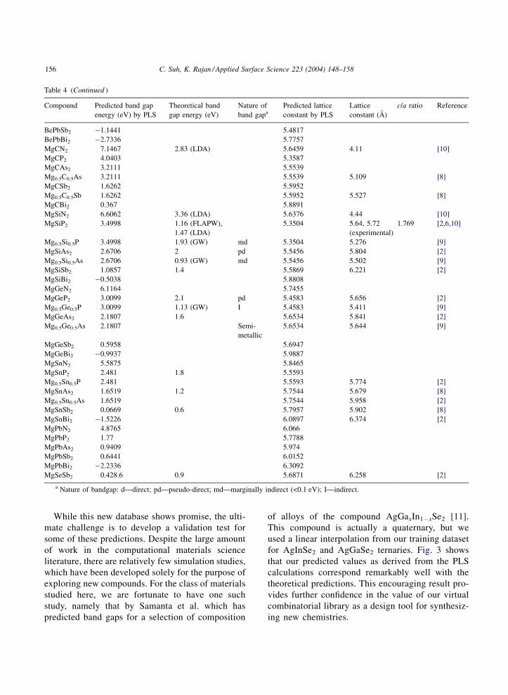
Based on these results, we embarked on completingour analysis of property prediction for over 200 com-pounds based on our initial combinatorial input ofelements outlined in Table 1. The results are given inTable 4. It should be noted that the deviation from PLSderived results from the first principles LDA calcula-tions simply reflects the differences that exist betweenexperimental and theoretical studies. Our data mininganalysis relied heavily on the experimental data andhence the difference, however the data trends matchwell.
Fig. 1. 4LV PLS results for I–III–VI chalcopyrite compounds.
150 C. Suh, K. Rajan / Applied Surface Science 223 (2004) 148–158

Fig. 2. 3LV PLS results for II–IV–V chalcopyrite compounds.
Fig. 3. Comparison of theoretically derived calculations with PLS derived results.
C. Suh, K. Rajan / Applied Surface Science 223 (2004) 148–158 151

Table 3Chalcopyrite compounds data table (training set)
Type Compound Experimental mini-mal bandgap energy (eV)
Theoretical bandgap energy (eV)
Nature ofband gapa
Lattice constant(A)
c/a ratio Reference
I–III–V12 CuAlS2 3.49 3.4 d 5.31, 5.34, 5.333 1.96, 1.958 [1–3]I–III–V12 CuAlSe2 2.67 2.7 d 5.606 1.954 [1–3]I–III–V12 CuAlTe2 2.06 5.964 1.975 [1,2]I–III–V12 CuGaS2 2.43 0.92 (LDA) 5.347–5.356 1.959 [1,2,4]I–III–V12 CuGaSe2 1.68 0.20 (LDA) 5.59–5.614 1.966 [1,2,4]I–III–V12 CuGaTe2 1.0–1.24 0.43 (LDA) 5.994 1.987 [1,2,4]I–III–V12 CuInS2 1.53 0.01 (LDA) 5.517–5.523 2.016 [1,2,4]I–III–V12 CuInSe2 1.04 0.01 (LDA) 5.773–5.784 2.008 [1,2,4]I–III–V12 CuInTe2 1.06 0.18 (LDA) 6.167 2 [1,2,4]I–III–V12 AgAlS2 3.13 5.695, 5.720 1.802, 1.772 [1,2]I–III–V12 AgAlSe2 2.55 5.956, 5.986 1.805, 1.793 [1,2]I–III–V12 AgAlTe2 2.27 6.296 1.878 [1,2]I–III–V12 AgGaS2 2.64 1.02 (LDA) 5.743–5.757 1.786–1.789 [1,2,4]I–III–V12 AgGaSe2 1.8 0.17 (LDA) 5.973, 5.985 1.823, 1.793 [1,2,4]I–III–V12 AgGaTe2 1.32 0.17 (LDA) 6.283 1.897 [1,2,4]I–III–V12 AgInS2 1.87 0.35 (LDA) 5.816, 5.872 1.92–1.91 [1,2,4]I–III–V12 AgInSe2 1.24 0.10 (LDA) 6.090–6.109 1.916–1.919 [1,2,4]I–III–V12 AgInTe2 0.95 0.21 (LDA) 6.406 1.962 [1,2,4]II–IV–V2 ZnSiP2 2.07 1.22 (LDA) pd 5.399 1.933 [1,2,4]II–IV–V2 ZnSiAs2 1.74 0.91 (LDA) pd, d (th) 5.61 1.94 [1,5,6]II–IV–V2 ZnGaP2 2.05 1.16 (LDA) pd, I (th) 5.465 1.965 [1,5,6]II–IV–V2 ZnGaAs2 1.15 0.13 (LDA) d 5.672 1.966 [1,2,5]II–IV–V2 CdSiP2 2.2–2.45 1.16 (FLAPW),
1.19 (LDA)pd 5.678 1.836 [1,5,6]
II–IV–V2 CdSiAs2 1.55 0.42 (LDA) d 5.885 1.849 [1,2,5]II–IV–V2 CdGaP2 1.72 0.75 (LDA) d 5.74 1.878 [1,2,5]II–IV–V2 CdGaAs2 0.57 (() 0.44 (LDA) d 5.942–5.945 1.888 [1,2,5]II–IV–V2 CdSnP2 1.17 0.03 (FLAPW) 5.9 1.951 [1,6]II–IV–V2 CdSnAs2 0.26 (() 0.72 (FLAPW) 6.094 1.956 [1,6]
a Nature of bandgap: d—direct; pd—pseudo-direct; th—theoretical; I—indirect.
Table 4Virtual chalcopyrite compounds data table (test set)
Compound Predicted band gapenergy (eV) by PLS
Theoretical bandgap energy (eV)
Nature ofband gapa
Predicted latticeconstant by PLS
Latticeconstant (A)
c/a ratio Reference
CuBO2 (0.0807 4.5981CuBS2 4.1354 5.511CuBSe2 3.5699 5.8313CuBTe2 3.0768 6.1312CuBPo2 0.0308 6.2737CuAlO2 (1.0101 4.4194CuAlPo2 (0.8986 6.095CuGaO2 (1.8999 4.4333CaGaPo2 (1.7884 6.1089CuInO2 (2.4383 4.5688CuInPo2 (2.3269 6.2445CuTlO2 (3.4319 4.7973
152 C. Suh, K. Rajan / Applied Surface Science 223 (2004) 148–158

Table 4 (Continued )
Compound Predicted band gapenergy (eV) by PLS
Theoretical bandgap energy (eV)
Nature ofband gapa
Predicted latticeconstant by PLS
Latticeconstant (A)
c/a ratio Reference
CuTlS2 0.7842 5.7102 5.58 2.001 [2]CuTlSe2 0.2187 6.0305 5.832 1.995 [2]CuTlTe2 (0.2744 0.9 6.3305 6.299 [2]CuTlPo2 (3.3205 6.4729AgBO2 (0.0058 4.9227AgBS2 4.2103 5.8356AgBSe2 3.6448 6.1559AgBTe2 3.1517 6.4558AgBPo2 0.1056 6.5983AgAlO2 (0.9352 4.744AgAlPo2 (0.8237 6.4196AgGaO2 (1.825 4.7579AgGaPo2 (1.7135 6.4335AgInO2 (2.3634 4.8934AgInPo2 (2.252 6.5691AgTlO2 (3.357 5.1219AgTlS2 0.8591 1.1 6.0348 5.882 [2]AgTlSe2 0.2936 0.71 6.3551AgTlTe2 (0.1995 0.6 6.6551 6.529 [2]AgTlPo2 (3.2456 6.7975AuBO2 0.7492 5.5635AuBS2 4.9653 6.4764AuBSe2 4.3998 6.7967AuBTe2 3.9067 7.0967AuBPo2 0.8606 7.2391AuAlO2 (0.1802 5.3848AuAlS2 4.0359 6.2977AuAlSe2 3.4704 6.618AuAlTe2 2.9773 6.918AuAlPo2 (0.0688 7.0604AuGaO2 (1.07 5.3987AuGaS2 3.1461 6.3116AuGaSe2 2.5806 6.6319AuGaTe2 2.0876 6.9319AuGaPo2 (0.9585 7.0743AuInO2 (1.6084 5.5343AuInS2 2.6077 6.4472AuInSe2 2.0422 6.7675AuInTe2 1.5491 7.0675AuInPo2 (1.497 7.2099AuTiO2 (2.602 5.7627AuTiS2 1.6141 6.6756AuTiSe2 1.0486 6.9959AuTlTe2 0.5555 7.2959AuTlPo2 (2.4906 7.4383ZnCN2 6.006 5.6714ZnCP2 2.8996 5.3842ZnCAs2 2.0704 5.5793Zn0.5C0.5As 2.0704 5.5793 5.044 [8]Zn0.5C0.5Sb 0.4855 Metallic 5.6206 5.384 [8]ZnCBi2 (1.104 5.9146ZnSiN2 5.4655 5.6631
C. Suh, K. Rajan / Applied Surface Science 223 (2004) 148–158 153

Table 4 (Continued )
Compound Predicted band gapenergy (eV) by PLS
Theoretical bandgap energy (eV)
Nature ofband gapa
Predicted latticeconstant by PLS
Latticeconstant (A)
c/a ratio Reference
Zn0.5Si0.5P 2.3591 1.56 (GW) d 5.3759 5.262 [9]Zn0.5Si0.5As 1.5299 0.68 (GW) md 5.571 5.483 [8]ZnStSb2 (0.055 0.9 5.6125 6.077 [2]Zn0.5Si0.5Sb (0.055 5.6123 5.962 [8]ZnSiBi2 (1.6445 5.9063ZnGeN2 4.9757 5.7709Zn0.5Ge0.5P 1.8692 1.15 (GW) I 5.4837 5.382 [9]Zn0.5Ge0.5As 1.04 0.23 (GW) md 5.6789 5.597 [9]ZnGeSb2 (0.5449 0.5 5.7202 6.111 [2]ZnGeBi2 (2.1344 6.0141ZnSnN2 4.4468 5.8719ZnSnP2 1.3403 5.5847 5.651 2 [1,2]Zn0.5Sn0.5P 1.3404 1.70 (GW) I 5.5847 5.688 [9]ZnSnAs2 0.5112 5.7799 5.851 2 [1,2]Zn0.5Sn0.5As 0.5112 0.79 (GW) md 5.7799 5.87 [9]ZnSnSb2 (1.0738 5.8212 6.275 2 [1]ZnSnBi2 (2.6633 6.1151ZnPbN2 3.7358 6.0915ZnPbP2 0.6293 5.8043ZnPbAs2 (0.1998 5.9994ZnPbSb2 (1.7848 6.0407ZnPbBi2 (3.3743 6.3347CdCN2 5.8097 5.9651CdCP2 2.7032 5.6779Cd0.5C0.5P 2.7032 5.6779 4.973 [8]CdCAs2 1.8741 5.8731Cd0.5C0.5As 1.8741 5.8731 5.201 [8]CdCSb2 0.2891 5.9143Cd0.5C0.5Sb 0.2891 5.9143 5.62 [8]CdCBi2 (1.3004 6.2083CdSiN2 5.2692 5.9568Cd0.5Si0.5P 2.1627 1.22 (GW) 5.6696 5.378 [9]Cd0.5Si0.5As 1.336 5.8648 5.61 [8]CdSiSb2 (0.2514 0.8 5.9061 6.344 [2]CdSiBi2 (1.18409 6.2CdGeN2 4.7793 6.0646Cd0.5Ge0.5P 1.6729 0.33 (GW) d 5.7774 5.523 [9]Cd0.5Ge0.5As 0.8437 Metallic 5.9726 5.755 [8]CdGeSb2 (0.7412 0.2 6.0139 6.383 [2]CdGeBi2 (2.3308 6.3078CdSnN2 4.2504 6.1657Cd0.5Sn0.5P 1.144 5.8785 5.797 [8]CdSnSb2 (1.2701 (0.80 (FLAPW) 6.1149 6.479 [6]CdSnBi2 (2.8596 6.4089CdPbN2 3.5394 6.3852CdPbP2 0.433 6.098CdPbAs2 (0.3962 6.2931CdPbSb2 (1.9811 6.3344CdPbBi2 (3.5706 6.6284HgCN2 4.5586 6.2613HgCP2 1.4522 5.9741HgCAs2 0.623 6.1693
154 C. Suh, K. Rajan / Applied Surface Science 223 (2004) 148–158

Table 4 (Continued )
Compound Predicted band gapenergy (eV) by PLS
Theoretical bandgap energy (eV)
Nature ofband gapa
Predicted latticeconstant by PLS
Latticeconstant (A)
c/a ratio Reference
HgCSb2 (0.9619 6.2106HgCBi2 (2.5514 6.5045HgSiN2 4.0181 6.2531HgSiP2 0.9117 1.6 5.9659 5.74 [2]HgSiAs2 0.0825 0.7 6.161 5.926 [2]HgSiSb2 (1.5024 6.2023HgSiBi2 (3.0919 6.4963HgGeN2 3.5283 6.3609HgGeP2 0.4218 1.2 6.0737 5.78 [2]HgGeAs2 (0.4074 0.2 6.2688 5.966 [2]HgGeSb2 (1.9923 6.3101HgGeBi2 (3.5818 6.6041HgSnN2 2.9994 6.4619HgSnP2 (0.1071 0.8 6.1747 5.909 [2]HgSnAs2 (0.9362 6.3699HgSnSb2 (2.5212 6.4112HgSnBi2 (4.1107 6.7051HgPbN2 2.2884 6.6814HgPbP2 (0.8181 6.3942HgPbAs2 (1.6472 6.5894HgPbSb2 (3.2322 6.6307HgPbBi2 (4.8217 6.9246BeCN2 6.6467 8.2, 4.22 (LDA) pd 5.1124 3.847, 3.71 [2,10]BeCP2 3.5403 4.8252BeCAs2 2.7111 5.0204BeCSb2 1.1262 5.0617Be0.5C0.5Sb 1.1262 5.0617 5.207 [8]BeCBi2 (0.4633 5.3556BeSiN2 6.1062 3.60 (LDA) 5.1041 4.1 [10]Be0.5Si0.5P 2.9998 1.68 (GW) I 4.8169 5.086 [9]Be0.5Si0.5As 2.1706 1.19 (GW) I 5.0121 5.305 [9]BeSiSb2 0.5857 5.0534Be0.5Si0.5Sb 0.5857 5.0534 5.608 [8]BeSiBi2 (1.0038 5.3473BeGeN2 5.6164 5.212Be0.5Ge0.5P 2.5099 1.16 (GW) I 4.9248 5.17 [9]BeGeAs2 1.6808 5.1199Be0.5Ge0.5As 1.6808 0.53 (GW) 5.1199 5.397 [9]BeGeSb2 0.0958 5.1612Be0.5Ge0.5Sb 0.0958 5.1612 5.723 [8]BeGeBi2 (1.4937 5.4551BeSnN2 5.0875 5.313BeSnP2 1.981 5.0258Be0.5Sn0.5P 1.981 0.98 (GW) I 5.0258 5.465 [9]BeSnAs2 1.1519 5.2209Be0.5Sn0.5As 1.1519 0.45 (GW) I 5.2209 5.664 [9]BeSnSb2 (0.4331 5.2622Be0.5Sn0.5Sb (0.4331 5.2622 5.902 [8]BeSnBi2 (2.0226 5.5562BePbN2 4.3765 5.5325BePbP2 1.27 5.2453BePbAs2 0.4409 5.4405
C. Suh, K. Rajan / Applied Surface Science 223 (2004) 148–158 155
While this new database shows promise, the ulti-mate challenge is to develop a validation test forsome of these predictions. Despite the large amountof work in the computational materials scienceliterature, there are relatively few simulation studies,which have been developed solely for the purpose ofexploring new compounds. For the class of materialsstudied here, we are fortunate to have one suchstudy, namely that by Samanta et al. which haspredicted band gaps for a selection of composition
of alloys of the compound AgGaxIn1(xSe2 [11].This compound is actually a quaternary, but weused a linear interpolation from our training datasetfor AgInSe2 and AgGaSe2 ternaries. Fig. 3 showsthat our predicted values as derived from the PLScalculations correspond remarkably well with thetheoretical predictions. This encouraging result pro-vides further confidence in the value of our virtualcombinatorial library as a design tool for synthesiz-ing new chemistries.
Table 4 (Continued )
Compound Predicted band gapenergy (eV) by PLS
Theoretical bandgap energy (eV)
Nature ofband gapa
Predicted latticeconstant by PLS
Latticeconstant (A)
c/a ratio Reference
BePbSb2 (1.1441 5.4817BePbBi2 (2.7336 5.7757MgCN2 7.1467 2.83 (LDA) 5.6459 4.11 [10]MgCP2 4.0403 5.3587MgCAs2 3.2111 5.5539Mg0.5C0.5As 3.2111 5.5539 5.109 [8]MgCSb2 1.6262 5.5952Mg0.5C0.5Sb 1.6262 5.5952 5.527 [8]MgCBi2 0.367 5.8891MgSiN2 6.6062 3.36 (LDA) 5.6376 4.44 [10]MgSiP2 3.4998 1.16 (FLAPW),
1.47 (LDA)5.3504 5.64, 5.72
(experimental)1.769 [2,6,10]
Mg0.5Si0.5P 3.4998 1.93 (GW) md 5.3504 5.276 [9]MgSiAs2 2.6706 2 pd 5.5456 5.804 [2]Mg0.5Si0.5As 2.6706 0.93 (GW) md 5.5456 5.502 [9]MgSiSb2 1.0857 1.4 5.5869 6.221 [2]MgSiBi2 (0.5038 5.8808MgGeN2 6.1164 5.7455MgGeP2 3.0099 2.1 pd 5.4583 5.656 [2]Mg0.5Ge0.5P 3.0099 1.13 (GW) I 5.4583 5.411 [9]MgGeAs2 2.1807 1.6 5.6534 5.841 [2]Mg0.5Ge0.5As 2.1807 Semi-
metallic5.6534 5.644 [9]
MgGeSb2 0.5958 5.6947MgGeBi2 (0.9937 5.9887MgSnN2 5.5875 5.8465MgSnP2 2.481 1.8 5.5593Mg0.5Sn0.5P 2.481 5.5593 5.774 [2]MgSnAs2 1.6519 1.2 5.7544 5.679 [8]Mg0.5Sn0.5As 1.6519 5.7544 5.958 [2]MgSnSb2 0.0669 0.6 5.7957 5.902 [8]MgSnBi2 (1.5226 6.0897 6.374 [2]MgPbN2 4.8765 6.066MgPbP2 1.77 5.7788MgPbAs2 0.9409 5.974MgPbSb2 0.6441 6.0152MgPbBi2 (2.2336 6.3092MgSeSb2 0.428.6 0.9 5.6871 6.258 [2]
a Nature of bandgap: d—direct; pd—pseudo-direct; md—marginally indirect (<0.1 eV); I—indirect.
156 C. Suh, K. Rajan / Applied Surface Science 223 (2004) 148–158

4. Conclusions
This paper has demonstrated an a priori approach todevelop combinatorial libraries, which can serve as aneffective screening tool to guide combinatorial experi-mentation. The application to designing and tailoringchemistries of compound semiconductors is just one
example of the use of this approach to materials designin general. By integrating this approach to largerdatasets, even more robust and reliable predictionsof materials behavior can be made. Hence virtualcombinatorial libraries can also serve as a way todevelop more targeted experimental strategies formaterials design and development.
Appendix A. Procedures of PLS for bandgap energy
C. Suh, K. Rajan / Applied Surface Science 223 (2004) 148–158 157

Acknowledgements
The authors gratefully acknowledge support fromthe National Science Foundation International Mate-rials Institute Program for the Combinatorial Sciencesand Material Informatics Collaboratory: CoSMIC-IMI; grant # DMR 0231291.
References
[1] A. Zunger, Appl. Phys. Lett. 50 (3) (1987) 164.[2] J.E. Jaffe, A. Zunget, Phys. Rev. B 29 (4) (1984) 1882.[3] O. Madelung (Ed.), Semiconductors other than group IV
elements and III–V compounds, Data in Science andTechnology, Springer, Berlin, 1992.
[4] S.N. Rashkeev, W.R.L. Lambrecht, Phys. Rev. B 63 (2001)165–212.
[5] S.N. Rashkeev, S. Limpijumnong, W.R.L. Lambrecht, Phys.Rev. B 59 (4) (1999) 2737.
[6] A. Continenza, S. Massidda, A.J. Freeman, Phys. Rev. B 46(16) (1992) 10070.
[7] P. Villars, et al., J. Less-common Met. 132 (1987) 289.[8] T. Wang, N. Moll, K. Cho, J.D. Joannopoulos, Phys. Rev.
Lett. 82 (16) (1999) 3304.[9] T. Wang, N. Moll, K. Cho, J.D. Joannopoulos, Phys. Rev. B
63 (2000) 035306.[10] A.G. Petulthov, W.R.L. Lambrecht, B. Segall, Phys. Rev. B 49
(7) (1994) 4549.[11] L.K. Samanta, D.K. Ghosh, G.C. Bhar, Phys. Rev. B 33 (6)
(1986) 4145.
Appendix A. (Continued )
158 C. Suh, K. Rajan / Applied Surface Science 223 (2004) 148–158
Copyright © 2022 FDOKUMEN