PROCESS FOR MAKING THIN FILMS BY PULSED EXCIMER ...
12
(19) Europaisches Patentamt European Patent Office Office europeen des brevets (12) peen des brevets EP 0 664 927 B1 EUROPEAN PATENT SPECIFICATION (45) Date of publication and mention of the grant of the patent: 16.07.1997 Bulletin 1997/29 (21) Application number: 93923279.9 (22) Date of filing: 13.10.1993 (51) Intel e H01L 39/24 (86) International application number: PCT/US93/09544 (87) International publication number: WO 94/09518 (28.04.1994 Gazette 1994/10) (54) PROCESS FOR MAKING THIN FILMS BY PULSED EXCIMER LASER EVAPORATION VERFAHREN ZUM HERSTELLEN VON DUNNSCHICHTEN DURCH GEPULSTE EXCIMERLASER-VERDAMPFUNG PROCEDE DE PRODUCTION DE FILMS MINCES PAR EVAPORATION AU LASER EXCIMER PULSE (84) Designated Contracting States: AT BE CH DE DK ES FR GB GR IE IT LI NL PT SE (30) Priority: 19.10.1992 US 963156 (43) Date of publication of application: 02.08.1995 Bulletin 1995/31 (73) Proprietor: E.I. DU PONT DE NEMOURS AND COMPANY Wilmington Delaware 19898 (US) (72) Inventors: • KEATING, Kenneth, Bernard Wilmington, DE 19803 (US) • THE, Stephens, Sintsun Newark, DE 19711 (US) DO Is- CM O) CO CO o a. LU (74) Representative: Jones, Alan John et al CARPMAELS & RANSFORD 43 Bloomsbury Square London, WC1A2RA (GB) (56) References cited: EP-A- 0 526 326 • APPLIED PHYSICS LETTERS, vol. 55, no. 2, 10 July 1989, New York US, pp. 197-199; M. BALOOCH et al.: 'Y-Ba-CU-O superconducting films produced by long-pulse laser vaporization' • RESEARCH DISCLOSURE, vol. 320, no. 94, December 1990, Havant GB; 'Reduction of particulates in laser ablated high Tc thin films by laser induced plume heating' Note: Within nine months from the publication of the mention of the grant of the European patent, any person may give notice to the European Patent Office of opposition to the European patent granted. Notice of opposition shall be filed in a written reasoned statement. It shall not be deemed to have been filed until the opposition fee has been paid. (Art. 99(1) European Patent Convention). Printed byJouve, 75001 PARIS(FR)
-
Upload
khangminh22 -
Category
Documents
-
view
1 -
download
0
Transcript of PROCESS FOR MAKING THIN FILMS BY PULSED EXCIMER ...
(19)
Europaisches Patentamt
European Patent Office
Office europeen des brevets
(12)
peen des brevets E P 0 6 6 4 9 2 7 B 1
EUROPEAN PATENT S P E C I F I C A T I O N
(45) Date of publication and mention of the grant of the patent: 16.07.1997 Bulletin 1997/29
(21) Application number: 93923279.9
(22) Date of filing: 13.10.1993
(51) Intel e H01L 3 9 / 2 4
(86) International application number: PCT/US93/09544
(87) International publication number: WO 94/09518 (28.04.1994 Gazette 1994/10)
(54) PROCESS FOR MAKING THIN FILMS BY PULSED EXCIMER LASER EVAPORATION
VERFAHREN ZUM HERSTELLEN VON DUNNSCHICHTEN DURCH GEPULSTE EXCIMERLASER-VERDAMPFUNG
PROCEDE DE PRODUCTION DE FILMS MINCES PAR EVAPORATION AU LASER EXCIMER PULSE
(84) Designated Contracting States: AT BE CH DE DK ES FR GB GR IE IT LI NL PT SE
(30) Priority: 19.10.1992 US 963156
(43) Date of publication of application: 02.08.1995 Bulletin 1995/31
(73) Proprietor: E.I. DU PONT DE NEMOURS AND COMPANY Wilmington Delaware 19898 (US)
(72) Inventors: • KEATING, Kenneth, Bernard
Wilmington, DE 19803 (US) • THE, Stephens, Sintsun
Newark, DE 19711 (US)
DO Is- CM O)
CO CO o a . LU
(74) Representative: Jones, Alan John et al CARPMAELS & RANSFORD 43 Bloomsbury Square London, WC1A2RA (GB)
(56) References cited: EP-A- 0 526 326
• APPLIED PHYSICS LETTERS, vol. 55, no. 2, 10 July 1989, New York US, pp. 197-199; M. BALOOCH et al.: 'Y-Ba-CU-O superconducting films produced by long-pulse laser vaporization'
• RESEARCH DISCLOSURE, vol. 320, no. 94, December 1990, Havant GB; 'Reduction of particulates in laser ablated high Tc thin films by laser induced plume heating'
Note: Within nine months from the publication of the mention of the grant of the European patent, any person may give notice to the European Patent Office of opposition to the European patent granted. Notice of opposition shall be filed in a written reasoned statement. It shall not be deemed to have been filed until the opposition fee has been paid. (Art. 99(1) European Patent Convention).
Printed by Jouve, 75001 PARIS (FR)

1 EP 0 664 927 B1 2
Description
FIELD OF THE INVENTION
This invention relates to manufacture of thin films which can be used as such, or patterned for use as cir- cuit elements.
BACKGROUND OF THE INVENTION
Recent advances in the superconducting transition temperature of various oxide materials has provided the opportunity for applications in radio frequency, micro- wave and other electronic technologies. Considerable progress has been made in a number of fabrication tech- nologies related to forming these oxide superconduc- tors into various electronic devices.
The technique of laser evaporation for deposition of thin films has been applied to a large class of materials ranging from polymers to semiconductors and dielec- trics. For most present electronic device applications such as radio frequency and microwave technology, thin films are proving to be the form of superconducting ox- ide most useful. As a result, much of the work relating to the use of high temperature superconductors in mi- croelectronic applications has focused on the growth of high quality thin films. Such films can serve as ground planes or can be patterned into a microwave circuit. High quality superconducting films can have significant- ly lower values of surface resistance than copper or gold films. This low surface resistance is important for mak- ing high-performance thin film microwave circuits such as filters, resonators and delay lines.
While various methods are available for producing superconducting thin films, one of the better methods is pulsed laser deposition, described first by D. Dijkkamp atal., Appl. Phys. Lett., 51 , 61 9-621 (1987). This method provides thin films of superconducting material having correct stoichiometry and high superconductivity transi- tion temperature, Tc. In addition to the high deposition rate provided by this method and relatively simple ap- paratus required, the film can be grown at low substrate temperatures, as discussed in Koren et al., Appl. Phys. Lett., 56, 2144-2146 (1990). A major drawback of this technique is that the deposited film contains a large number of particles, commonly referred to as particu- lates, typically on the order of 0.5 urn to 2 urn in width and are commonly present in a density of 110-140 par- ticulates per 1000 urn2. The presence of these particu- lates limits the use of the film in most applications where microscopic patterns must be printed thereon, e.g., mi- crowave circuits. Koren et al. has speculated that these undesirable particulates may result from loosely con- nected target flakes, splashing of molten material, or deep target subsurface heating that leads to an explo- sion of bubbles and condensation in the high density plume that results from the laser ablation of the target.
Balooch etal., Appl. Phys. Lett. 55(2), pp. 197-199,
10 July 1989 disclose deposition of superconducting thin films from YBa2Cu307 targets using a long-pulse (ms) Nd-glass laser with 50 J/pulse energy. Scanning electron microscopy revealed spherical inclusions of
5 about 3 urn in diameter in the film. Several techniques have been devised to reduce
the size and/or number of particulates in these films. One described by Koren et al. involves the use of a sec- ond laser beam perpendicular to the first to reduce the
10 size of the particulates. Another involves using a target that is moved at a velocity comparable to the fragments in order to eject the particulates, Research Disclosure, 32397, March 1991, page 209.
While these methods have met with some success, is they involve more expensive and complex apparatus
than conventional laser ablation and do not produce suf- ficiently particulate-free films for demanding applica- tions. The present invention provides a method for pro- ducing films wherein the amount of particulates is re-
20 duced by orders of magnitude rendering such films of superior utility as circuit elements.
SUMMARY OF THE INVENTION
25 The present invention as claimed provides for a process for producing thin films of superconducting ma- terial by bombarding a heated target with radiation from a pulsed high energy UV laser to form a plume of target material and depositing said plume on a substrate. In
30 particular, the present invention as claimed provides an improved process for the deposition of superconducting thin film onto a substrate by pulsed laser ablation where- in the improvement comprises heating an ablation target to at least 500°C below its melting point prior to and dur-
35 ing ablation. The present invention as claimed further comprises a superconducting thin film having a maxi- mum of 10 particulates per 1000 urn2 deposited on a substrate.
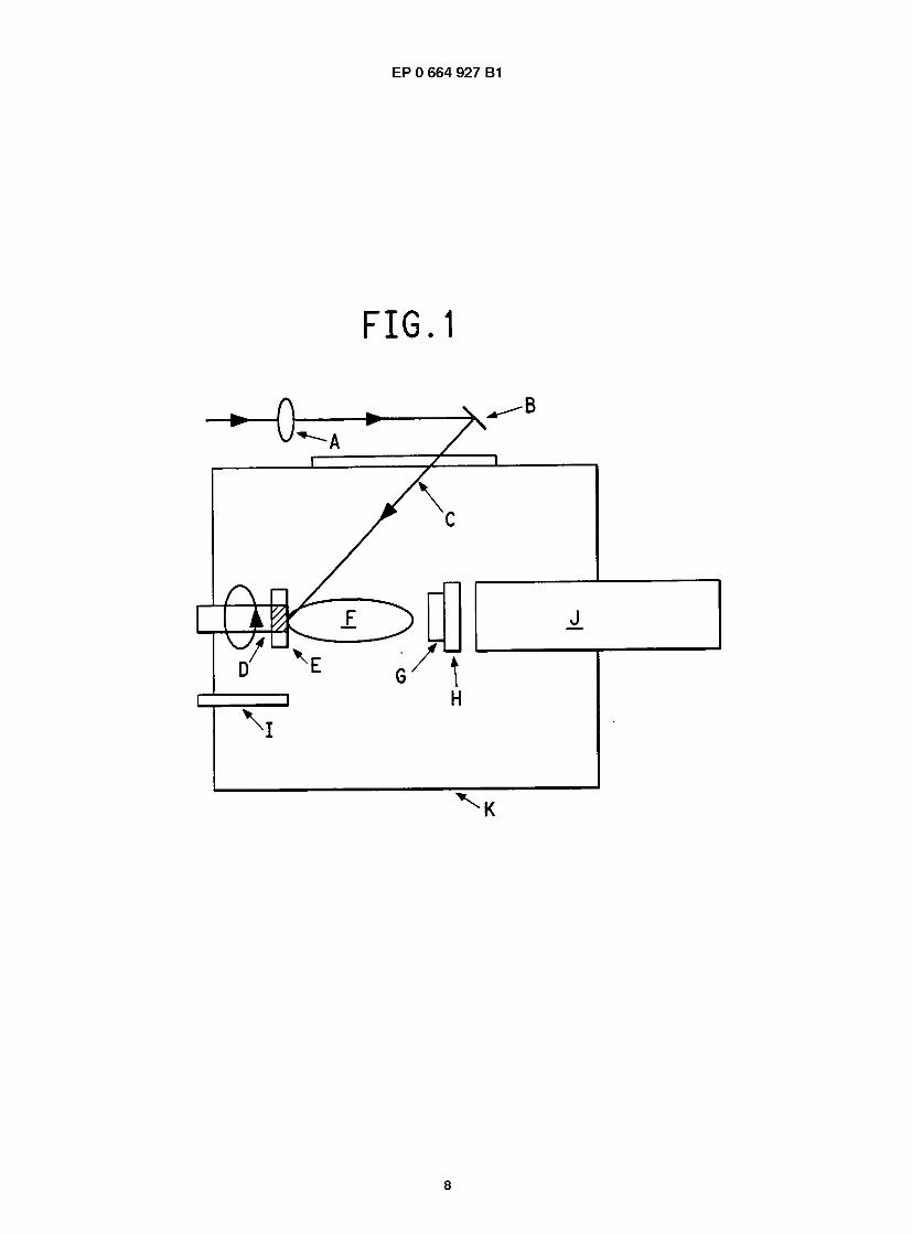
Figure 1 shows a schematic diagram of a pulsed laser deposition apparatus useful in the practice of the present invention.
45 Figures 2 and 4 each show a scanning electron mi- crograph of a thin film prepared in accordance with this invention.
Figures 3 and 5 each show a scanning electron mi- crograph of a thin film prepared in accordance with con-
so ventional pulsed laser ablation.
DETAILED DESCRIPTION OF THE INVENTION
The target materials suitable for use in the practice 55 of the present invention include metal oxides. Target
materials particularly suitable are copper oxides, pref- erably superconducting copper oxides. Thus the pre- ferred thin films prepared by the process of the present
40 BRIEF DESCRIPTION OF THE FIGURES
45
50
2
3 EP 0 664 927 B1 4
invention are also superconducting copper oxides. A su- perconducting material is a material whose resistance decreases to zero at or below a critical temperature and/ or becomes perfectly diamagnetic and excludes a mag- netic field, this effect being known as the Meissner ef- fect.
Suitable copper oxide superconductors include several types of compounds such as:
(1) rare earth superconductors of the R-,-R2-Cu-0, R-|-R2-R3-Cu-0, R-Ba-Cu-O, R1-R2-Ba-Cu-0, R- Ca-Cu-O, or R-,-R2-Ca-Cu-0 types wherein R, R-,, and R2 are each independently a rare earth element such as Y, La, Nd, Sm, Eu, Gd, Dy, Ho, Er, Tm, Yb, or Lu; (2) bismuth superconductors of the Bi-R-Cu-O, Bi- R1 -R2-Cu-0 or Bi-R1-R2-R3-Cu-0 types wherein R, R-,, R2, and R3 are each independently Ca, Sr, Y, Pb, or Sb. (3) thallium superconductors of the Tl-R-Cu-O or Tl- R-|-R2-Cu-0 types wherein R, R-,, and R2 are each independently Ca, Ba, Sr, or Pb. (4) lead superconductors of the Pb-R-|-R2-Cu-0 or Pb-R-|-R2-R3-Cu-0 types wherein R-,, R2, and R3 are each independently Sr, Ca, Sb, Ln, Nd, Ba, or Bi.
Preferred for use in the present invention are super- conducting compounds of the following types:
(1) rare earth superconductors of the 1-2-3 com- pound type such as RD2Cu307.x wherein R is a rare earth such as Y, La, Nd, Sm, Eu, Gd, Dy, Ho, Er, Tm, Yb, or Lu; D is Ba or Sr; and x is 0 to 1 . Specific examples include YBa2Cu307.x, wherein x is 0 to 0.3. (2) superconducting compounds of the formulae (AO)xD2Can.1Cun02n+2 or ( A O ^ C a ^ C u . O ^ a wherein A is at least one of Bi, Tl, or Pb; D is Ba or Sr; x is 1 to 2; and n is an integer from 1 to 5. Typically for A is Tl, x is 1 or 2 and for A is Bi, x is 2. Specific examples include TIBa2CaCu207, TIBa2Ca2Cu309, TIBa2Ca3Cu4012, TI2Ba2CaCu2Os, or TI2Ba2Ca2 Cu3O10. (3) Superconducting compounds of the formula TlePbaCabSrcCudOx wherein a is 0.1 to 1.5, b is 1 to 4, c is 1 to 3, d is 1 to 5, e is 0.3 to 1, x is (a+b+c+d+e+y) and y is 0.5 to 3. (4) Superconducting compounds of the formula TI2Ba2Cu06+x wherein x is 0 to 0.5. (5) Superconducting compounds of the formula Bi2Sr3.xYxCu208+y wherein x is 0.05 to 0.45 and y is 0 to 1 .
Especially preferred materials are superconducting ceramics having a high Tc, such as target materials as described in (3) above prepared as described in U.S. Patent 4,894,361 of Subramanian, and those having an
atomic ratio of Y:Ba:Cu of a:b:c wherein a is 0.5 to 1 .5, b is 1 .5 to 2.5, and c is 2.5 to 3.5 prepared in accordance with the procedure described in Bordia, R. K. etal., MRS Symposia Proceedings, Vol. 99, pp. 245-248 (1988). An
5 example of a preferred thin film resulting from this ma- terial is YBa2Cu307.x wherein x is 0 to 0.3. Other pre- ferred thin films are those of TlePbaCabSrcCudOx where- in a is 0. 1 to 1 .5, b is 1 to 4, c is 1 to 3, d is 1 to 5, e is 0.3 to 1 , x is (a+b+c+d+e+y), and y is 0.5 to 3.
10 It is preferred that the target be as dense as possible consistent with the density possible by the method of preparation. A minimum density target of at least about 60% of its crystal specific gravity is preferred, with a more preferred density target of at least about 80% of
is its crystal specific gravity. Density targets of about 90% or higher are conventionally achievable from known synthetic techniques. The most convenient form of the target is that of a ceramic pellet. The ceramic pellet used for the ablation target can commonly be prepared by
20 mixing oxides of Y, Ba and Cu in the atomic ratio of Y: Ba:Cu of 1:2:3. The resulting mixture is calcined at 600°C to 900°C for 1 to 12 hours, ground, and retired under the conditions just described. The resulting ma- terial is reground, and pressed into a target disk of about
25 1 cm diameter and 3 mm thick. This disk is sintered at 700°C to 900°C for 1 to 3 hours in an oxygen atmos- phere.
In accordance with this invention the target is heat- ed prior to and during exposure to the laser radiation.
30 The target is preferably heated to at least about 500°C below its melting point, more preferably to about 300°C below its melting point, and most preferably to 200°C below its melting point. In the case of YBa2Cu307, melt- ing point about 1100°C, it is preferred that the target be
35 heated to at least about 600°C, and more preferably to at least about 800°C.
Figure 1 shows a schematic diagram of a pulsed laser deposition apparatus. In Figure 1 an excimer laser beam is passed through an aperture, then a lens A and
40 reflected from a scanning mirror B through a fused silica window C to target E heated by heater D. The impinge- ment of the laser beam on target E results in immediate ablation of material from the target in the form of a plas- ma plume F which is deposited upon substrate G pre-
45 heated by substrate heater H. J denotes a differentially pumped mass spectrometer and I a dosing value. The entire apparatus is enclosed in a vacuum chamber de- noted as K.
The target disk is placed in the vacuum chamber so approximately 3 cm from the substrate upon which the
film is to be deposited. The laser beam of an excimer laser, for example a Lambda-Physik EMG-201 or a Questek model 2260 248 nm wavelength excimer, then is focused onto the target disk with a pulse energy den-
55 sity (fluence) of at least 1 Joule/cm2. The impingement of the laser beam on the disk results in immediate melt- ing and expulsion of material from the target that is de- posited on the substrate forming a thin film at the rate
25
30
35
40
45
50
3

5 EP 0 664 927 B1 6
of approximately .03 nm/pulse. The target is maintained at an elevated temperature within less than about 500°C of its melting point, preferably less than about 300°C of its melting point, most preferably less than about 200°C of its melting point. If the target contains oxygen, the ablation is conducted in an 02 atmosphere of 1 .3-26 Pa (10-200 mtorr).
The present invention further comprises a super- conducting thin film prepared according to the above- described process of the present invention. The proper- ties of the oxide films formed by laser ablation can be varied by changing the substrate temperature. Deposi- tion onto the substrate at ambient temperature results in an amorphous film of the desired stoichiometry, while deposition onto a substrate heated to very high temper- atures (> 700°C) yields films which are a mixture of the crystalline phases of the oxides. Deposition preferably is done above 450°C to achieve a film which will main- tain a good contiguous morphology during the subse- quent heating of the film over the range of 820°C to 950°C. The ablated material is deposited to provide a film having a thickness of 0. 1 urn to 2 urn, preferably 0. 1 urn to 0.2 urn A typical film of 0.2 urn thickness will pos- sess less than 10 particulates per 1000 urn2 when the target is heated in accordance with this invention.
Substrates useful in the present invention are com- patible with formation of the superconductor. Preferred substrates are MgO, LaAI03, SrTi03 and yttria-stabi- lized zirconia (YSZ).
The superconducting film produced by this inven- tion can be fabricated into devices such as resonators, delay lines, filters and other passive devices. The su- perconducting film also can be combined with semicon- ductor materials to produce active devices. Devices can be designed into microstrip, stripline and coplanar ar- rangements. Depending upon use, the superconducting film can be used directly in a circuit device, or alterna- tively, can be patterned.
Patterning the superconducting film is performed by depositing a photohardenable polymer onto the oxide film. The thickness of the photohardenable polymer film is from 1 urn to 20 urn The deposited, photohardenable polymer is exposed imagewise to radiation capable of hardening the polymer. If the photohardenable polymer is a negative resist type, the exposed (hardened) poly- mer constitutes the desired pattern of the oxide super- conductor. Subsequent to exposure to radiation, the photohardenable polymer is contacted with a solvent to selectively remove those portions of the polymer film that have not been hardened by radiation to expose the oxide film where oxide superconductor is not wanted. The exposed oxide film is removed with a chemical etch- ant.
If the photohardenable polymer is a positive resist type, the unexposed polymer forms the desired pattern of the oxide superconductor film. The exposed polymer is contacted with a solvent to selectively remove those portions of the polymer film that are hardened by radia-
tion to expose the oxide film in those regions where ox- ide superconductor is not wanted. The exposed oxide film is removed with a chemical etchant.
High quality, high resolution (5 urn wide lines) in the 5 patterned film can be obtained by using positive resist
photohardenable polymers. Examples of these poly- mers include AZ521 4-E, a propylene glycol monomethyl ether acetate cresol novolak resin from American Hoec- sht Corporation, Rte. 202-206 N., Post Office Box 2500,
10 Somerville, NJ 08876. Another positive resist useful is KTI 820 from KTI Chemicals Incorporated, 1170 Sonora Court, Sunnyvale, CA 94086. Both of these positive re- sist polymers are developed in basic solutions. A suita- ble basic solution includes one part of sodium hydroxide
is in 80 parts H20, and one part of potassium hydroxide in 80 parts of H20. The resist is developed for 1 minute in a first bath of the basic solution, for 2 minutes in a sec- ond bath of the basic solution, and rinsed in water.
Reactive ion beam etching, as is well known, also 20 can be used to pattern the superconducting films to ob-
tain very fine line widths and excellent feature definition. The invention will now be described in detail by ref-
erence to the following examples.
25 EXAMPLE 1
A high density superconducting YBa2Cu307 pellet was mounted on a modified automobile cigarette lighter heating coil. The target temperature was controlled by
30 adjusting the voltage supplied to the lighter heating coil through a commercially available voltage regulator. In order to produce a target temperature of about 800°C, the voltage was set at 8 volts AC. The substrate onto which the film of superconducting ceramic oxide was de-
35 posited was a 500 urn thick, c-axis oriented single crys- tal of LaAI03 heated to 700°C during the deposition. The target and substrate were placed about 3 cm apart as illustrated in Figure 1. The target was heated to about 800°C. The ablation was conducted at three different
40 spots on the target each with an ablation area of 1400 urn x 1 400 urn using a 248 nm laser beam from a Model 2260 Questek KrF excimer laser. The pulse energy was 295 mJ/pulse at 10 Hz, giving a fluence at the target of 1 .2 J/cm2. The first target area was ablated for 10 min-
45 utes (or 6000 pulses). The second target area was also ablated for 10 minutes and the last target area for 1 minute. Three separate ablation locations were selected to increase the ablation efficiency and also to allow later scanning electron micrograph (SEM) studies. To main-
50 tain a constant temperature of the target, the voltage to the target heater was periodically adjusted. A total of 12000 pulses were deposited. The oxygen pressure in the chamber was held at 13 Pa (100 mtorr). and, after deposition, the substrate with the film deposited thereon
55 was annealed in 101x103Pa(760torr)oxygenat400°C for 30 minutes, followed by slow cooling to room tem- perature. The SEM analysis of the film showed that the film was very smooth with a minimal number of particu-
4

7 EP 0 664 927 B1 8
lates, approximately 6 particulates/1 000 urn2 (Figure 2). SEM analysis of the target showed that the target had melted and that cone and melted type morphology was observed. The cone shape, however, was very irregular and thin, compared to the previously observed cones on a room temperature target. It was apparent that the cones and droplets at the target had partially melted. Rutherford Backscattering analysis (RBS) of the film showed a composition with the following Y, Ba, and Cu atomic ratios: 0.95 + -0.05, 2.00 + -0.14, and 3.05 + -0.13. (Theoretical ratios: 1.00, 2.00, 3.00.)
COMPARATIVE EXAMPLE A
The procedure of Example 1 was followed except that the target was not heated prior to or during the dep- osition. Scanning electron micrographs of the resulting film are shown in Figure 3. The analysis of the film showed approximately 1 00-1 40 particulates/ 1 000 urn2. Comparison of Figures 2 and 3 clearly show the de- crease in both the size and number of particulates when the target material is heated prior to and during the dep- osition process.
EXAMPLE 2
A target high density pellet of superconducting ce- ramic oxide, YBa2Cu307 (5.7 g/cc, 90% theoretical den- sity), was mounted onto a modified automobile cigarette lighter heating coil. The target temperature was control- led by adjusting the voltage supplied to the lighter heat- ing coil using a commercially available voltage regulator. The target was heated to 600°C and maintained at that temperature during the film deposition. The substrate onto which the film of superconducting ceramic oxide was deposited, specifically a 500 urn thick, c-axis ori- ented single crystal of LaAI03, was heated to 700°C dur- ing the deposition. The target and substrate were placed about 3 cm apart in a commercially available pulsed la- ser deposition chamber using a KrF laser beam at a wavelength of 248 nm. During the deposition, the laser fluence was maintained at 2.5 Joules/cm2 using a Questek Powerlok at 470 mJ/pulse. A total of 12000 pulses (4 sites of 3000 pulses per site) at 1 0 pulses per second was deposited. The size of the laser ablation was 1 200 urn by 1 200 urn imaged from an aperture near the laser source. The ablation was conducted in an at- mosphere of pure oxygen at a pressure of 13 Pa (100 mtorr). After the deposition, the substrate with the film deposited thereon was annealed in 101 x 103 Pa (760 torr) oxygen at 400°C for 30 minutes, followed by slow cooling to room temperature. RBS analysis of the film showed an atomic composition of Y, B, Cu to be the fol- lowing: 0.92 + .08, 2. 00 + . 10, 3.08 ± .11.
Scanning electron micrographs of the resulting film are shown in Figure 4.
COMPARATIVE EXAMPLE B
The procedure of Example 2 was followed except that the target was not heated prior to or during the dep-
5 osition. Scanning electron micrographs of the resulting film
are shown in Figure 5. Comparison of Figures 4 and 5 clearly shows the decrease in both the size and number of particulates when the target material is heated prior
10 to and during the deposition process.
Claims
is 1. A process for the deposition of a copper oxide su- perconducting thin film onto a substrate by pulsed excimer laser ablation characterized by heating a metal oxide ablation target to at least 500°C below its melting point prior to and during ablation.
20 2. The process of Claim 1 wherein the target material
and the superconducting thin film each comprise a copper oxide.
25 3. The process of Claim 2 wherein the target material has an atomic ratio of Y:Ba:Cu of a:b:c where a is 0. 5 to 1 .5, b is 1 .5 to 2.5, and c is 2.5 to 3.5.
4. The process of Claim 1 wherein the superconduct- 30 ing thin film comprises YBa2Cu307.x wherein x is 0
to 0.3.
5. The process of Claim 1 wherein the superconduct- ing thin film is TlePbaCabSrcCudOx wherein a is 0.1
35 to 1 .5, b is 1 to 4, c is 1 to 3, d is 1 to 5, e is 0.3 to 1 , x is (a+b+c+d+e+y) and y is 0.5 to 3.
6. The process of Claim 2 wherein the target material is TlePbaCabSrcCudOx wherein a is 0.1 to 1.5, b is
40 1 to 4, c is 1 to 3, d is 1 to 5, e is 0.3 to 1, x is (a+b+c+d+e+y), and y is 0.5 to 3.
7. The process of Claim 1 wherein the target material has a density target of at least 60% of its crystal
45 specific gravity.
8. The process of Claim 1 performed at a maximum pressure of about 26 Pa.
so 9. The process of Claim 1 wherein the substrate com- prises MgO, LaAI03, SrTi03, oryttria-stabilized zir- con ia.
10. A superconducting thin film comprising 55 YBa2Cu307.x wherein x is 0 to 0.3 or TlePbaCabSrc.
CudOx wherein a is 0.1 to 1 .5, b is 1 to 4, c it 1 to 3, d is 1 to 5, e is 0.3 to 1 , x is (a+b+c+d+e+y) and y is 0.5 to 3, the film containing no more than 10 par-
20
5

9 EP 0 664 927 B1 10
ticulates per 1000 urn2, wherein the particulates have a width of 0.5 urn to 2 urn, said film being de- posited on a substrate.
11. The film of Claim 10 having a thickness of from 0.1 urn to 0.2 urn.
Patentanspriiche
1. Verfahren zur Abscheidung eines supraleitenden Kupferoxid-Dunnfilmsauf einem Substratdurch ge- pulste Excimer-Laser-Ablation, dadurch gekenn- zeichnet, dal3 ein Target fur die Metalloxid-Ablation vor und wahrend der Ablation auf wenigstens 500 °C unterhalb seines Schmelzpunkts erwarmt wird.
2. Verfahren nach Anspruch 1, wobei das Targetma- terial und der supraleitende Dunnfilm jeweils ein Kupferoxid umfassen.
3. Verfahren nach Anspruch 2, wobei das Targetma- terial ein Atomverhaltnis von Y:Ba:Cu von a:b:c auf- weist, wobei a 0,5 bis 1 ,5 ist, b 1 ,5 bis 2,5 ist und c 2,5 bis 3,5 ist.
4. Verfahren nach Anspruch 1 , wobei der supraleiten- de Dunnfilm YBa2Cu307.x umfaBt, wobei xO bis 0,3 ist.
5. Verfahren nach Anspruch 1 , wobei der supraleiten- de Dunnfilm TlePbaCabSrcCudOx ist, wobei a 0, 1 bis 1 ,5 ist, b 1 bis 4 ist, c 1 bis 3 ist, d 1 bis 5 ist, e 0,3 bis 1 ist, x (a+b+c+d+e+y) ist und y 0,5 bis 3 ist.
6. Verfahren nach Anspruch 2, wobei das Targetma- terial TlePbaCabSrcCudOx ist, wobei a 0,1 bis 1,5 ist, b 1 bis 4 ist, c 1 bis 3 ist, d 1 bis 5 ist , e 0,3 bis 1 ist, x (a+b+c+d+e+y) ist und y 0,5 bis 3 ist.
7. Verfahren nach Anspruch 1, wobei das Targetma- terial ein Dichtetarget von wenigstens 60 % seines spezifischen Kristallgewichts aufweist.
8. Verfahren nach Anspruch 1 , durchgefuhrt bei einem Hochstdruck von etwa 26 Pa.
9. Verfahren nach Anspruch 1, wobei das Substrat MgO, LaAI03, SrTi03 oder durch Yttriumoxid stabi- lisiertes Zirkoniumoxid umfaBt.
10. Supraleitender Dunnfilm, umfassend YBa2Cu307.x, wobei x 0 bis 0,3 ist, oder TlePbaCabSrcCudOx, wo- bei a 0,1 bis 1,5 ist, b 1 bis 4 ist, c 1 bis 3 ist, d 1 bis 5 ist, e 0,3 bis 1 ist, x (a+b+c+d+e+y) ist und y 0,5 bis 3 ist, wobei der Film nicht mehr als 10 Ma- kroteilchen auf 1 000 urn2 enthalt, wobei die Makro- teilchen eine Breite von 0,5 urn bis 2 urn aufweisen,
wobei der Film auf einem Substrat abgeschieden ist.
11. Film nach Anspruch 10 mit einer Dicke von 0,1 bis 5 0,2 urn
Revendications
10 1. Un procede pour le depot d'un film mince d'oxyde de cuivre supraconducteur sur un substrat par abla- tion par laser a excimere pulse, caracterise par le chauffage d'une cible d'ablation en oxyde metalli- que a une temperature non inferieure de plus de
is 500 °C a son point de fusion avant et pendant I'abla- tion.
2. Le procede de la revendication 1 dans lequel la ma- tiere cible et le film mince supraconducteur com-
20 prennent chacun un oxyde de cuivre.
3. Le procede de la revendication 2 dans lequel la ma- tiere cible a un rapport atomique de Y:Ba:Cu de a: b:c ou a est 0,5 a 1 ,5, b est 1 ,5 a 2,5 et c est 2,5 a
25 3,5.
4. Le procede de la revendication 1 dans lequel le film mince supraconducteurcomprend YBa2Cu307_xou x est 0 a 0,3.
30 5. Le procede de la revendication 1 dans lequel le film
mince supraconducteur est en TlePbaCabSrcCudOx ou a est 0,1 a 1 ,5, b est 1 a 4, c est 1 a 3, d est 1 a 5, e est 0,3 a 1 , x est (a+b+c+d+e+y) et y est 0,5 a 3.
35 6. Le procede de la revendication 2 dans lequel la ma-
tiere cible est en TlePbaCabSrcCudOx ou a est 0,1 a 1 ,5, b est 1 a 4, c est 1 a 3, d est 1 a 5, e est 0,3 a 1 , x est (a+b+c+d+e+y) et y est 0,5 a 3.
40 7. Le procede de la revendication 1 dans lequel la ma-
tiere cible a une densite de cible d'au moins 60 % de sa masse volumique a I'etat cristallin.
45 8. Le procede de la revendication 1 mis en oeuvre a une pression maximum d'environ 26 pascals.
9. Le procede de la revendication 1 dans lequel le substrat comprend du MgO, LaAI03, SrTi03 ou de
so la zircone stabilisee par de I'oxyde d'yttrium.
10. Un film mince supraconducteur comprenant du YBa2Cu307.x ou x est 0 a 0,3 ou du TlePbaCabSrc. CudOx ou a est 0,1 a 1 ,5, b est 1 a 4, c est 1 a 3, d
55 est 1 a 5, e est 0,3 a 1 , x est (a+b+c+d+e+y) et y est 0,5 a 3, le film ne comportant pas plus de 10 defauts particulaires par 1000 urn2, les defauts par- ticulates consideres ayant une largeur de 0,5 urn
35
6

11 EP 0 664 927 B1 12
a 2 urn, ledit film etant depose sur un substrat.
11. Le film de la revendication 10 ayant une epaisseur de 0,1 urn a 0,2 urn
5
10
15
20
25
30
35
40
45
50
55
7
EP 0 664 927 B1
F I G . 1
8

EP 0 664 927 B1
F I G . 2
9

EP 0 664 927 B1
F I G . 3
10

EP 0 664 927 B1
F I G . 4
11

EP 0 664 927 B1
12