Ma'had Ittihad al-Islam wa al-Ta'lim al-Qaim 'ala Da'amah al-Mujtama'
IEEE TRANSACTIONS ON ELECTRON DEVICES, VOL. 54, NO. 9, SEPTEMBER 2007 2327
Simulation of Ultrasubmicrometer-GateIn0.52Al0.48As/In0.75Ga0.25As/In0.52Al0.48As/InP
Pseudomorphic HEMTs Using a Full-BandMonte Carlo Simulator
Jason S. Ayubi-Moak, Student Member, IEEE, David K. Ferry, Life Fellow, IEEE,Stephen M. Goodnick, Fellow, IEEE, Richard Akis, and Marco Saraniti, Member, IEEE
Abstract—Pseudomorphic delta-doped ultrasubmicrometer-gate high-electron mobility transistors have been modeled using afull-band cellular Monte Carlo simulator. Reasonable agreementbetween experimental and numerical results is obtained for a70-nm gate length. We discuss the scaling of this device to shortergate lengths and the role played by various dimensions in thestructure. Devices with 20-nm gate lengths should produce fT sabove 1.5 THz without difficulty. This paper demonstrates thepower of particle-based simulation tools in capturing the relevantphysics responsible for device operation and key to performanceoptimization.
Index Terms—Millimeter-wave transistors, Monte Carlomethods, pseudomorphic high-electron mobility transistors(p-HEMTs).
I. INTRODUCTION
THE HIGH-ELECTRON mobility transistor (HEMT) [1],[2] has become a favorite device for high-frequency and
low-noise applications [3]. HEMTs have been made froma great variety of materials, and the efficacy of molecular-beam epitaxy has allowed strained layers to be incorporated inpseudomorphic HEMTs (p-HEMTs) [4]. Recently, the use ofIn-rich InGaAs in InP-based p-HEMTs has led to remarkablesubmillimeter-wave amplifiers above 200 GHz [5]. Devicesused in these amplifiers had 70-nm gate lengths and 75%indium in the quantum well channel, and individual devicesgave more than 1500-mS/mm transconductance [6]. Naturally,it becomes of interest to see if further scaling of these devicescan provide even higher frequency performance and to ascertainthe limits of this technology. While it is beyond our abilitiesto completely answer this question through simulation, in this
Manuscript received January 3, 2007; revised May 16, 2007. This work wassupported in part by the DARPA SWIFT project through the Army ResearchLaboratory under cooperative agreement W911NF-06-2-0012. The review ofthis paper was arranged by Editor A. Asenov.
The authors are with the Department of Electrical Engineering and Center forSolid State Electronics Research, Ira A. Fulton School of Engineering, ArizonaState University, Tempe, AZ 85287 USA (e-mail: [email protected];[email protected]).
Color versions of one or more of the figures in this paper are available onlineat http://ieeexplore.ieee.org.
Digital Object Identifier 10.1109/TED.2007.902902
paper, we discuss a detailed full-band cellular Monte Carlo(CMC) simulation of these devices and their scaling. We willexamine a range of gate lengths for scaled devices based uponthis In-rich p-HEMT technology.
To study the device performance, we will make use ofa full-band CMC simulation tool that has been developedby our group. Ensemble Monte Carlo techniques have beenused to study HEMTs for more than two decades [7], [8],including the role of quantization in the channel [9]–[12]. Full-band treatment of the transport by coupling a pseudopotentialband structure to the Monte Carlo simulation is even older[13], [14], but the most well-known implementation remainsDAMOCLES from IBM [15], [16]. Our own pseudopotential-based full-band simulator is a CMC [17], and it has beenapplied to MESFETs [18], HEMTs [19], [20], and quantumwell MOSFETs [21]. Here, we adapt this code to the structureof the multiple heterojunction that is used in the In0.52Al0.48As/In0.75Ga0.25As/In0.52Al0.48As/InP devices mentioned above[6]. We present results on gate lengths from 20 to 70 nm,with other dimensions scaled accordingly. We also discuss theimportance of internal series resistance whether from contactresistance or from a long source–drain spacing.
In the next section, we discuss the device structure that isused in the simulation, details of the pseudopotential code, thephonon model, and the gridding issues for the Poisson solution.The following section will provide the results and a discussionof these. Finally, we draw some conclusions about the scalingof this type of device and discuss some of the limitations thatmay arise from approximations made in our work.
II. FULL-BAND MONTE CARLO SIMULATION APPROACH
The full-band simulator used in this paper is based upona hybrid transport approach discussed previously [22]. Thissimulator combines a traditional ensemble Monte Carlo method(for low carrier energies) with a CMC approach (at high carrierenergies). In our simulator, the solution of Poisson’s equation iscomputed using a fast multigrid technique [23], which solvesthe full set of electrostatic field equations resulting from acenter-difference discretization of the 3-D Poisson equationover a set of grids with varying coarseness. These grids actin concert to simultaneously reduce the different low- and
0018-9383/$25.00 © 2007 IEEE
2328 IEEE TRANSACTIONS ON ELECTRON DEVICES, VOL. 54, NO. 9, SEPTEMBER 2007
high-frequency components of the error resulting in faster andmore robust convergence [24].
A. Pseudopotential Code
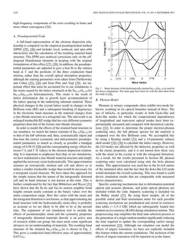
A full-band representation of the electron dispersion rela-tionship is computed via the empirical pseudopotential method(EPM) [25], [26] and includes local, nonlocal, and spin-orbitinteractions into the calculation of the resulting material bandstructure. This EPM uses nonlocal corrections only on the off-diagonal Hamiltonian elements in keeping with the originalformulations of this effect [27], [28]. In addition, the pseudopo-tential parameters are adjusted to give a best fit to the valenceband at Γ and the positions of the three conduction bandminima, rather than the overall optical absorption properties,although the starting parameters were taken from Chelikowskyand Cohen [25], [26] and from Pötz and Vogl [29]. An im-portant effect that must be accounted for in our simulations isthe strain caused by the lattice mismatch at the In0.52Al0.48As/In0.75Ga0.25As heterojunctions. This strain is the result oflattice deformation due to growth layer accommodation ofthe lattice spacing in the underlying substrate material. Thesephysical changes in the crystal lattice result in changes in theBrillioun zone (BZ) and a subsequent breaking of degeneracyin the electronic band structure as the material changes froma zinc-blende structure to a tetragonal one. The end result is anenlarged irreducible BZ wedge that has very different symmetryproperties than that of the former zinc-blende structure.
In order to model the effects of the strained band structure inour simulator, we match the lattice constant of In0.75Ga0.25Asto that of the InP substrate and, then, systematically adjust andfine-tune the correct symmetric and antisymmetric pseudopo-tential parameters to match as closely as possible a bandgapenergy of 0.58 eV [30] and the corresponding energy offsets be-tween Γ-L and Γ-X valleys in the electron dispersion relation-ship. It is important to emphasize here that, in our simulations,we have maintained a zinc-blende material structure and simplyapplied the necessary strain hydrostatically. This approximationassumes an isotropically strained unit cell and allows us toutilize a smaller irreducible wedge than would be necessary fora tetragonal crystal structure. We have taken this approach forthe simple reason that the nature of the tetragonally distortedcell and its band structure is not known at this time. This isfurther complicated by the fact that Mikkelsen and Boyce [31]have shown that the In-As and Ga-As nearest neighbor bondlengths remain nearly constant at the binary values over theentire composition range. How this varies with the strain andthe tetragonal distortion is not known, so that approximating theband structure with the hydrostatically strain alloy is probablyas accurate as we are likely to be able to be at the presenttime. The expansion of our simulation tool to include theeffects of pseudomorphic strain and the symmetry propertiesof tetragonally distorted materials directly is an active areaof research within our group, but must await some significantadvances in our understanding of materials. The resulting bandstructure of the strained In0.75Ga0.25As is shown in Fig. 1.This gives a conduction band effective mass of approximately0.037m0.
Fig. 1. Band structure of the hydrostatically strained In0.75Ga0.25As used inthe device simulations. The main gaps have been set with the data taken fromthe study in [30].
B. Phonon Model
Phonons in ternary compounds often exhibit two-mode be-havior, resulting in six optical branches instead of three. Theuse of InGaAs, in particular, results in both GaAs-like andInAs-like modes for which the compositional dependenciesof longitudinal and transverse optical modes have been ex-perimentally measured and compared with theoretical calcula-tions [32]. In order to determine the proper electron-phononscattering rates, the full phonon spectra for the material iscomputed over the first Brillouin zone. We accomplish thisby using a Keating model [33] and a 14-parameter valenceshell model [34]–[36] to calculate the lattice energy. However,the LO modes are affected by the dielectric properties as wellas the elastic properties, and it is not known how these varywith the strain in the crystal or with the tetragonal distortion.As a result, for the results presented in Section III, phononscattering rates were calculated using only the InAs phononmodes. This approximation was used due to the In-rich natureof the simulated alloy and the fact that the InAs-like LO modewould dominate the overall scattering. This was found to yielddevice simulation results that are comparable with measureddevice characteristics.
Specific scattering mechanisms due to deformation potentialoptical and acoustic phonons, and polar optical phonons areincluded within the code. Impurity scattering is included viathe Ridley model [37]. By using these models, all of thepossible initial and final momentum states for each possiblescattering mechanism are pretabulated and stored in extensivedata tables (∼1.5–2 GB) which are subsequently loaded intorandom access memory (RAM) during simulation runtime. Thispreprocessing step simplifies the final state selection process tothe generation of a single random number significantly reducingthe time required to update the corresponding carrier energyand momentum [22]. Although our simulator can model theeffects of impact ionization, we have not explicitly includedthis feature within the current simulations. The inclusion of theeffects of impact ionization will be reported on in the future.
AYUBI-MOAK et al.: SIMULATION OF In0.52Al0.48As/In0.75Ga0.25As/In0.52Al0.48As/InP p-HEMTs 2329
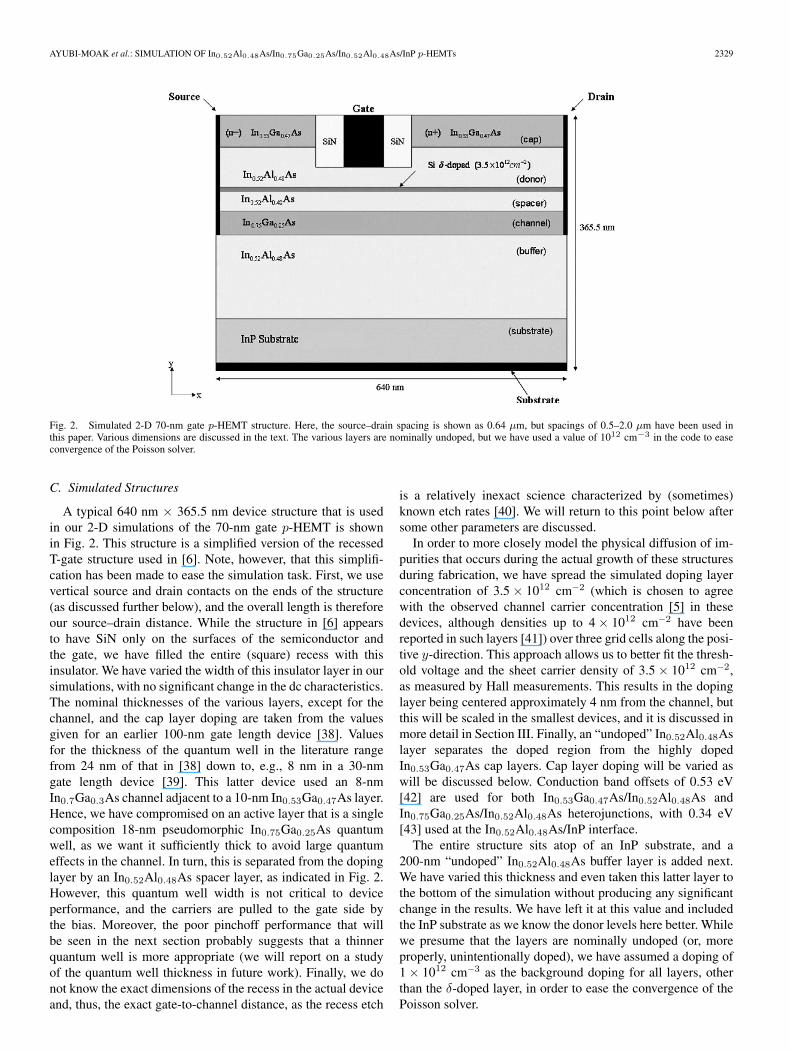
Fig. 2. Simulated 2-D 70-nm gate p-HEMT structure. Here, the source–drain spacing is shown as 0.64 µm, but spacings of 0.5–2.0 µm have been used inthis paper. Various dimensions are discussed in the text. The various layers are nominally undoped, but we have used a value of 1012 cm−3 in the code to easeconvergence of the Poisson solver.
C. Simulated Structures
A typical 640 nm × 365.5 nm device structure that is usedin our 2-D simulations of the 70-nm gate p-HEMT is shownin Fig. 2. This structure is a simplified version of the recessedT-gate structure used in [6]. Note, however, that this simplifi-cation has been made to ease the simulation task. First, we usevertical source and drain contacts on the ends of the structure(as discussed further below), and the overall length is thereforeour source–drain distance. While the structure in [6] appearsto have SiN only on the surfaces of the semiconductor andthe gate, we have filled the entire (square) recess with thisinsulator. We have varied the width of this insulator layer in oursimulations, with no significant change in the dc characteristics.The nominal thicknesses of the various layers, except for thechannel, and the cap layer doping are taken from the valuesgiven for an earlier 100-nm gate length device [38]. Valuesfor the thickness of the quantum well in the literature rangefrom 24 nm of that in [38] down to, e.g., 8 nm in a 30-nmgate length device [39]. This latter device used an 8-nmIn0.7Ga0.3As channel adjacent to a 10-nm In0.53Ga0.47As layer.Hence, we have compromised on an active layer that is a singlecomposition 18-nm pseudomorphic In0.75Ga0.25As quantumwell, as we want it sufficiently thick to avoid large quantumeffects in the channel. In turn, this is separated from the dopinglayer by an In0.52Al0.48As spacer layer, as indicated in Fig. 2.However, this quantum well width is not critical to deviceperformance, and the carriers are pulled to the gate side bythe bias. Moreover, the poor pinchoff performance that willbe seen in the next section probably suggests that a thinnerquantum well is more appropriate (we will report on a studyof the quantum well thickness in future work). Finally, we donot know the exact dimensions of the recess in the actual deviceand, thus, the exact gate-to-channel distance, as the recess etch
is a relatively inexact science characterized by (sometimes)known etch rates [40]. We will return to this point below aftersome other parameters are discussed.
In order to more closely model the physical diffusion of im-purities that occurs during the actual growth of these structuresduring fabrication, we have spread the simulated doping layerconcentration of 3.5 × 1012 cm−2 (which is chosen to agreewith the observed channel carrier concentration [5] in thesedevices, although densities up to 4 × 1012 cm−2 have beenreported in such layers [41]) over three grid cells along the posi-tive y-direction. This approach allows us to better fit the thresh-old voltage and the sheet carrier density of 3.5 × 1012 cm−2,as measured by Hall measurements. This results in the dopinglayer being centered approximately 4 nm from the channel, butthis will be scaled in the smallest devices, and it is discussed inmore detail in Section III. Finally, an “undoped” In0.52Al0.48Aslayer separates the doped region from the highly dopedIn0.53Ga0.47As cap layers. Cap layer doping will be varied aswill be discussed below. Conduction band offsets of 0.53 eV[42] are used for both In0.53Ga0.47As/In0.52Al0.48As andIn0.75Ga0.25As/In0.52Al0.48As heterojunctions, with 0.34 eV[43] used at the In0.52Al0.48As/InP interface.
The entire structure sits atop of an InP substrate, and a200-nm “undoped” In0.52Al0.48As buffer layer is added next.We have varied this thickness and even taken this latter layer tothe bottom of the simulation without producing any significantchange in the results. We have left it at this value and includedthe InP substrate as we know the donor levels here better. Whilewe presume that the layers are nominally undoped (or, moreproperly, unintentionally doped), we have assumed a doping of1 × 1012 cm−3 as the background doping for all layers, otherthan the δ-doped layer, in order to ease the convergence of thePoisson solver.
2330 IEEE TRANSACTIONS ON ELECTRON DEVICES, VOL. 54, NO. 9, SEPTEMBER 2007
Now, with the above parameters, we can estimate the gate-to-channel distance from standard HEMT theory [44]. From thedata in [5], we estimate that perhaps 10% of the charge is leftin the channel at VG = 0. This provides the necessary data todo the electrostatics, which suggests that the gate-to-channelseparation should be somewhere between 11.4 nm, for a trulyδ-doped device, and 12.8 nm for a doping distribution smoothedover 3 nm. However, these values are for long channel devices,and this separation needs to be reduced to control fringing fieldsin short-gate FETs [45], an effect known to be important insub-100-nm FETs [46]. Hence, we have taken a nominal valueof 10 nm for the 70-nm gate length device, and this is scaleddownward as the gate length is reduced. As will be seen, withthis value, the results in Section III agree reasonably well withthe reported device [6].
A 320 × 95 cell grid mesh with uniform grid spacings (∆x =2 nm) and nonuniform ∆y spacings, between 0.5 and 14 nm, isutilized with finer gridding (∆y = 1 nm) used across the activechannel region, the highly doped delta-doping layer and caplayers, and coarser gridding utilized in the buffer and substratelayers.
We have performed a systematic set of scaling simulationsfor several 2-D recessed gate p-HEMT structures with gatelengths of 70, 35, and 20 nm. The actual source–drain spac-ing (the width of the device in Fig. 2) is varied for thesedevices, as will be discussed in Section III. This variationof the source–drain ranges from 0.3 to 2.0 µm for differentgate length device simulations. In addition, we have performedsmall-signal RF simulations to study the frequency response ofthese ultrafast devices.
D. Contacts
Another important factor that can have significant effects onthe device performance is series resistance. The intrinsic seriesresistance can arise from just the gate–source region of thedevice, but it can also arise from the contact resistances. Hence,device characteristics are related to the manner in which devicecontacts are handled. In our simulations, both the source anddrain contacts are treated as ohmic contacts, while the gateelectrode is treated as an absorbing Schottky contact with abarrier height of 0.8 eV. By “ohmic” contact, we mean thefollowing: In our simulator, the “effect” that a metallic contacthas on the semiconductor material directly adjacent to it iswhat is actually being simulated during runtime. Two primaryboundary conditions are established on these “contact cells”within the simulation domain. The first is a fixed potential or en-forced Dirichelet boundary condition necessary for the solutionof Poisson’s equation. The second condition is that of chargeneutrality, which is a boundary condition on the Boltzmanntransport equation (solved stochastically by the CMC portionof the code). Charge neutrality is assured by assigning a dopingconcentration to each simulated contact cell during the initial-ization phase of the simulation. A fixed number of simulatedparticles is then maintained in each contact cell throughout thetotal simulation time, and carriers are subsequently injectedand/or ejected following each periodic update of the electro-static potential ensuring charge neutrality within these regions,
as discussed in [47]. The simulated doping within the “contactcells” creates a potential drop near the ohmic contacts, whichemulates an effective source resistance. This effect will beshown in the results in Section III. Thus, by varying the dopingconcentration within the contact cells, we can easily study theeffect of an internal contact resistance in our model. The role ofcontact doping on the device performance will be illustrated inmore detail in Section III.
The back contact of the substrate is treated as a constantpotential surface, with a local potential relative to the Fermienergy (which is the reference level for all potentials in thesimulation) that is set by the doping of the substrate. Therationale for this lies in submillimeter wave device packaging.Normally, these devices are mounted on a metalized carrier.In addition, the source itself is well grounded to assure goodsignal grounds. As a result of this, we use a vertical sourcecontact (on the left in Fig. 2) and similarly with the draincontact. However, the metal carrier also provides excellentscreening of the substrate so that there is no charge buildup inthe substrate. Hence, we find it acceptable to treat the substrateas the equipotential surface described here.
E. Cap Layer Oscillations
In real devices, highly doped cap layers ensure that thesource and drain electrodes form good ohmic contacts withthe device. However, the inclusion of highly doped cap layersin simulated device structures means that finer gridding isneeded in these regions of the device to accurately resolve theelectrostatic potential and resulting forces felt by carriers duringthe simulation. In our structures, we have utilized verticalsource and drain contacts, as mentioned, to ensure injection ofcarriers directly into the active channel region. Given that weare already enforcing ohmic contact behavior on both sourceand drain contacts, there is no need to simulate the highly dopedcap regions other than to include their contribution into the totalsource–drain resistance of the device. Furthermore, the use oflower doping in the cap regions means that a larger percentageof the total number of simulated carriers can contribute totransport in the active channel region. Indeed, we have studiedthe results as the cap layer doping is varied and determined thatthe doping, once above about 1018 cm−3, does not affect ourdevice results.
However, failure to maintain the grid spacing significantlybelow the Debye length in regions of high-doping concentrationoften requires short time steps if unphysical density oscillationsare to be avoided. Such oscillations can significantly affect thesimulated device characteristics and performance. The onsetof density oscillations is often assumed to be minimized byensuring that the Poisson solver update time step is much lessthan the inverse of the plasma frequency ωp. This is satisfactoryif one is dealing with a collisionless plasma [48]. However,that is certainly not the case in our device simulations wherescattering from optical phonons and ionized impurities playsan important role in carrier transport. The onset of densityoscillations (referred to as the “plasma catastrophe”) in highlydoped cap regions has been discussed in [15] and can beavoided as long as the electrostatic potential is updated using
AYUBI-MOAK et al.: SIMULATION OF In0.52Al0.48As/In0.75Ga0.25As/In0.52Al0.48As/InP p-HEMTs 2331
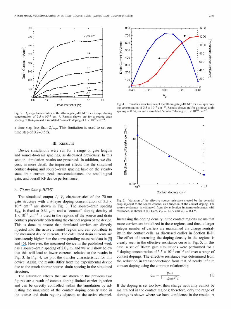
Fig. 3. Id–Vd characteristics of the 70-nm gate p-HEMT for a δ-layer dopingconcentration of 3.5 × 1012 cm−2. Results shown are for a source–drainspacing of 0.64 µm and a simulated “contact” doping of 1 × 1018 cm−3.
a time step less than 2/ωp. This limitation is used to set ourtime step of 0.2–0.5 fs.
III. RESULTS
Device simulations were run for a range of gate lengthsand source-to-drain spacings, as discussed previously. In thissection, simulation results are presented. In addition, we dis-cuss, in more detail, the important effects that the simulatedcontact doping and source–drain spacing have on the steady-state drain current, peak transconductance, the small-signalgain, and overall RF device performance.
A. 70-nm Gate p-HEMT
The simulated output Id–Vd characteristics of the 70-nmgate structure with a δ-layer doping concentration of 3.5 ×1012 cm−2 are shown in Fig. 3. The source–drain spacingLSD is fixed at 0.64 µm, and a “contact” doping density of1 × 1018 cm−3 is used in the regions of the source and draincontacts physically penetrating the channel region of the device.This is done to ensure that simulated carriers are directlyinjected into the active channel region and can contribute tothe measured device currents. The calculated drain currents areconsistently higher than the corresponding measured data in [5]and [6]. However, the measured device in the published workhas a source–drain spacing of 2.0 µm, and we will show belowthat this will lead to lower currents, relative to the results inFig. 3. In Fig. 4, we plot the transfer characteristics for thisdevice. Again, the results differ from the experimental devicedue to the much shorter source–drain spacing in the simulatedstructure.
The saturation effects that are shown in the previous twofigures are a result of contact doping-limited carrier injectionand can be directly controlled within the simulation by ad-justing the magnitude of the contact doping density used inthe source and drain regions adjacent to the active channel.
Fig. 4. Transfer characteristics of the 70-nm gate p-HEMT for a δ-layer dop-ing concentration of 3.5 × 1012 cm−2. Results shown are for a source–drainspacing of 0.64 µm and a simulated “contact” doping of 1 × 1018 cm−3.
Fig. 5. Variation of the effective source resistance created by the potentialdrop adjacent to the source contact, as a function of the contact doping. Thesource resistance is estimated from the reduction in transconductance withresistance, as shown in (1). Here, VD = 1.0 V and VG = 0.4 V.
Increasing the doping density in the contact regions means thatmore carriers are initialized in these regions, and thus, a largerinteger number of carriers are maintained via charge neutral-ity in the contact cells, as discussed earlier in Section II-D.The effect of increasing the doping density in the regions isclearly seen in the effective resistance curve in Fig. 5. In thiscase, a set of 70-nm gate simulations were performed for aδ-doping concentration of 3.5 × 1012 cm−2 and over a range ofcontact dopings. The effective resistance was determined fromthe reduction in transconductance from that of nearly infinitecontact doping using the common relationship
gm =gm0
1 + gm0RC. (1)
If the doping is set too low, then charge neutrality cannot bemaintained in the contact regions; therefore, only the range ofdopings is shown where we have confidence in the results. A
2332 IEEE TRANSACTIONS ON ELECTRON DEVICES, VOL. 54, NO. 9, SEPTEMBER 2007
Fig. 6. Calculated output current of the 70-nm gate p-HEMT for a δ-layerdoping concentration of 3.5 × 1012 cm−2 and various source–drain spac-ings. Results are shown for source–drain spacings from 0.64 to 2.0 µm anda simulated “contact” doping of 3 × 1018 cm−3. Here, VD = 1.0 V andVG = 0.4 V.
Fig. 7. Peak transconductance of the 70-nm gate length device for varioussource–drain spacings for VD = 1.0 V. Results are shown for source–drainspacings from 0.64 to 2.0 µm and a simulated “contact” doping of 43 ×1018 cm−3.
similar result was obtained by actually measuring the potentialdrops at the contacts that were found from the Poisson solver.While the quantitative results differed, the trends were quitesimilar. Clearly, the contacts are a crucial point in the simulationand must be carefully addressed.
In a similar manner, the semiconductor material between thesource and the gate also provides a series resistance withinthe device. We have also studied this effect, particularly asour devices are much shorter than the experimental ones. Inthis case, a set of 70-nm gate simulations was performed fora channel concentration of 3.5 × 1012 cm−2 and over a rangeof source–drain spacings from 0.64 to 2.0 µm. In each of thesesimulations, the contact doping was fixed at 3 × 1018 cm−3.In Figs. 6 and 7, we plot the drain current at VD = 1.0 V andVG = 0.4 V and the peak transconductance at VD = 1.0 V.The peak transconductance has increased from 1500 to almost1900 mS/mm as the channel length is shortened, indicatingfaster overall device response. An increase in the source–drainspacing reveals a decrease in the overall drive current and lower
Fig. 8. Variation of the average velocity and the average energy of the carriersin the quantum well channel for the 70-nm device. Here, the energy remainshigh due to the long return time of carriers from the satellite valley.
peak transconductance as LSD is increased. This effect is bestunderstood by relating the additional distance carriers, whichmust travel across the active channel region, to an increase inthe effective internal source-to-drain series resistance of thedevice. Thus, as LSD is increased, this resistance increases andresults in lower drive currents and reduced switching speeds.A similar scaling of the source–gate length, in particular, hasrecently been investigated [49] in terms of its effect on RFdevice performance specifically due to the role it plays inhelping to optimize output current and peak transconductancein AlGaN/GaN HEMTs, with similar conclusions.
Of interest is also the velocity and energy in the channelof the device. In Fig. 8, we plot the average velocity in thequantum well channel and the average energy of the carriersin the channel for VD = 1.0 V and VG = 0.4 V. Here, we notethat, while the velocity drops quickly once the carriers haveleft the gate region, the average energy stays quite high. Thisis because the return time from the satellite valleys is very longin InAs and, presumably, also in strained In0.75Ga0.25As [50].This is significant as it will reduce the tendency for any impactionization to occur, as the effective bandgap for carriers in the Lvalleys is more than 1 eV, e.g., almost twice that in the Γ valley.
B. 35-nm Gate p-HEMT
The structure of the 35-nm p-HEMT is the same as the70 nm, as shown in Fig. 2; with some exceptions, the mostobvious of which is the shorter gate length. In addition, the pas-sivation SiN layers are scaled downward, and the distance fromthe gate metal to the channel is reduced to 8 nm (from the earlier10 nm), which is achieved by reducing the thickness of themolecular beam epitaxy (MBE) layer between the gate and theposition of the doping layer. The latter is done to implementfurther control of the fringing fields. The output Id–Vd char-acteristics for a 35-nm gate structure with a δ-layer dopingconcentration of 3.5 × 1012 cm−2 are given in Fig. 9 andreveal that drain currents are considerably larger than those
AYUBI-MOAK et al.: SIMULATION OF In0.52Al0.48As/In0.75Ga0.25As/In0.52Al0.48As/InP p-HEMTs 2333
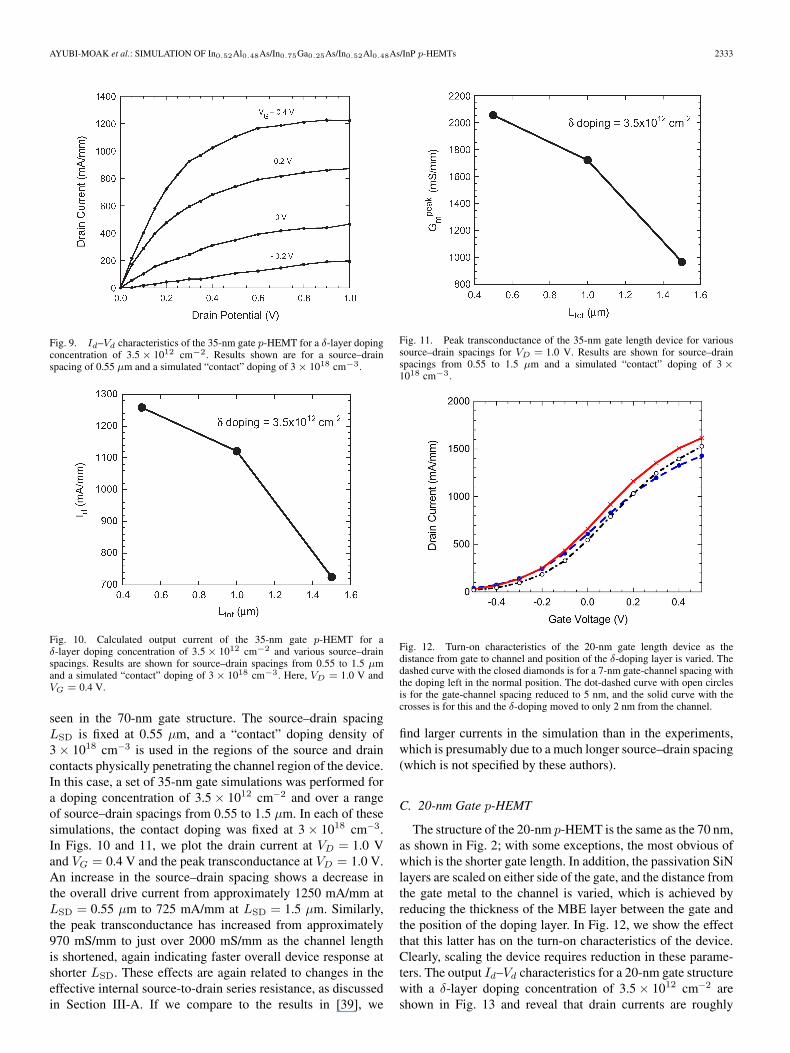
Fig. 9. Id–Vd characteristics of the 35-nm gate p-HEMT for a δ-layer dopingconcentration of 3.5 × 1012 cm−2. Results shown are for a source–drainspacing of 0.55 µm and a simulated “contact” doping of 3 × 1018 cm−3.
Fig. 10. Calculated output current of the 35-nm gate p-HEMT for aδ-layer doping concentration of 3.5 × 1012 cm−2 and various source–drainspacings. Results are shown for source–drain spacings from 0.55 to 1.5 µmand a simulated “contact” doping of 3 × 1018 cm−3. Here, VD = 1.0 V andVG = 0.4 V.
seen in the 70-nm gate structure. The source–drain spacingLSD is fixed at 0.55 µm, and a “contact” doping density of3 × 1018 cm−3 is used in the regions of the source and draincontacts physically penetrating the channel region of the device.In this case, a set of 35-nm gate simulations was performed fora doping concentration of 3.5 × 1012 cm−2 and over a rangeof source–drain spacings from 0.55 to 1.5 µm. In each of thesesimulations, the contact doping was fixed at 3 × 1018 cm−3.In Figs. 10 and 11, we plot the drain current at VD = 1.0 Vand VG = 0.4 V and the peak transconductance at VD = 1.0 V.An increase in the source–drain spacing shows a decrease inthe overall drive current from approximately 1250 mA/mm atLSD = 0.55 µm to 725 mA/mm at LSD = 1.5 µm. Similarly,the peak transconductance has increased from approximately970 mS/mm to just over 2000 mS/mm as the channel lengthis shortened, again indicating faster overall device response atshorter LSD. These effects are again related to changes in theeffective internal source-to-drain series resistance, as discussedin Section III-A. If we compare to the results in [39], we
Fig. 11. Peak transconductance of the 35-nm gate length device for varioussource–drain spacings for VD = 1.0 V. Results are shown for source–drainspacings from 0.55 to 1.5 µm and a simulated “contact” doping of 3 ×1018 cm−3.
Fig. 12. Turn-on characteristics of the 20-nm gate length device as thedistance from gate to channel and position of the δ-doping layer is varied. Thedashed curve with the closed diamonds is for a 7-nm gate-channel spacing withthe doping left in the normal position. The dot-dashed curve with open circlesis for the gate-channel spacing reduced to 5 nm, and the solid curve with thecrosses is for this and the δ-doping moved to only 2 nm from the channel.
find larger currents in the simulation than in the experiments,which is presumably due to a much longer source–drain spacing(which is not specified by these authors).
C. 20-nm Gate p-HEMT
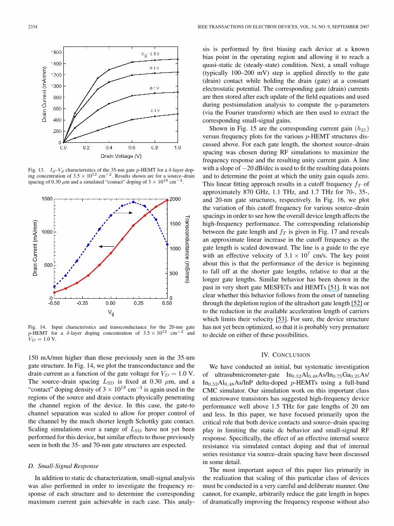
The structure of the 20-nm p-HEMT is the same as the 70 nm,as shown in Fig. 2; with some exceptions, the most obvious ofwhich is the shorter gate length. In addition, the passivation SiNlayers are scaled on either side of the gate, and the distance fromthe gate metal to the channel is varied, which is achieved byreducing the thickness of the MBE layer between the gate andthe position of the doping layer. In Fig. 12, we show the effectthat this latter has on the turn-on characteristics of the device.Clearly, scaling the device requires reduction in these parame-ters. The output Id–Vd characteristics for a 20-nm gate structurewith a δ-layer doping concentration of 3.5 × 1012 cm−2 areshown in Fig. 13 and reveal that drain currents are roughly
2334 IEEE TRANSACTIONS ON ELECTRON DEVICES, VOL. 54, NO. 9, SEPTEMBER 2007
Fig. 13. Id–Vd characteristics of the 35-nm gate p-HEMT for a δ-layer dop-ing concentration of 3.5 × 1012 cm−2. Results shown are for a source–drainspacing of 0.30 µm and a simulated “contact” doping of 3 × 1018 cm−3.
Fig. 14. Input characteristics and transconductance for the 20-nm gatep-HEMT for a δ-layer doping concentration of 3.5 × 1012 cm−2 andVD = 1.0 V.
150 mA/mm higher than those previously seen in the 35-nmgate structure. In Fig. 14, we plot the transconductance and thedrain current as a function of the gate voltage for VD = 1.0 V.The source–drain spacing LSD is fixed at 0.30 µm, and a“contact” doping density of 3 × 1018 cm−3 is again used in theregions of the source and drain contacts physically penetratingthe channel region of the device. In this case, the gate-tochannel separation was scaled to allow for proper control ofthe channel by the much shorter length Schottky gate contact.Scaling simulations over a range of LSD have not yet beenperformed for this device, but similar effects to those previouslyseen in both the 35- and 70-nm gate structures are expected.
D. Small-Signal Response
In addition to static dc characterization, small-signal analysiswas also performed in order to investigate the frequency re-sponse of each structure and to determine the correspondingmaximum current gain achievable in each case. This analy-
sis is performed by first biasing each device at a knownbias point in the operating region and allowing it to reach aquasi-static dc (steady-state) condition. Next, a small voltage(typically 100–200 mV) step is applied directly to the gate(drain) contact while holding the drain (gate) at a constantelectrostatic potential. The corresponding gate (drain) currentsare then stored after each update of the field equations and usedduring postsimulation analysis to compute the y-parameters(via the Fourier transform) which are then used to extract thecorresponding small-signal gains.
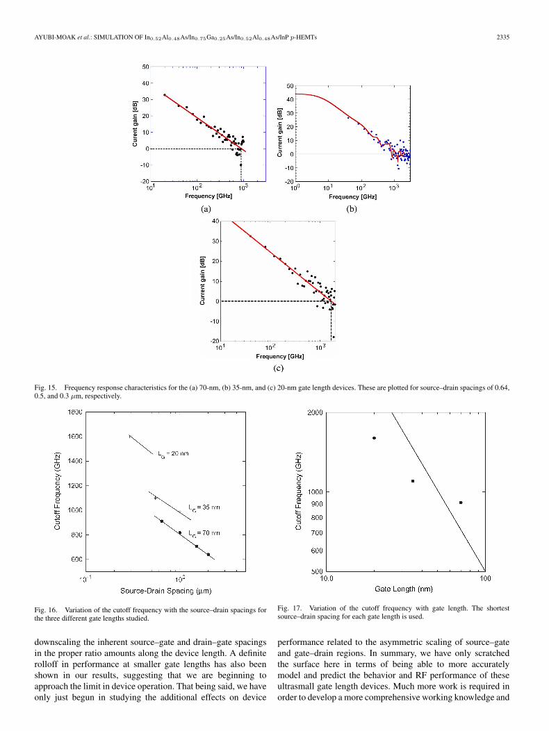
Shown in Fig. 15 are the corresponding current gain (h21)versus frequency plots for the various p-HEMT structures dis-cussed above. For each gate length, the shortest source–drainspacing was chosen during RF simulations to maximize thefrequency response and the resulting unity current gain. A linewith a slope of −20 dB/dec is used to fit the resulting data pointsand to determine the point at which the unity gain equals zero.This linear fitting approach results in a cutoff frequency fT ofapproximately 870 GHz, 1.1 THz, and 1.7 THz for 70-, 35-,and 20-nm gate structures, respectively. In Fig. 16, we plotthe variation of this cutoff frequency for various source–drainspacings in order to see how the overall device length affects thehigh-frequency performance. The corresponding relationshipbetween the gate length and fT is given in Fig. 17 and revealsan approximate linear increase in the cutoff frequency as thegate length is scaled downward. The line is a guide to the eyewith an effective velocity of 3.1 × 107 cm/s. The key pointabout this is that the performance of the device is beginningto fall off at the shorter gate lengths, relative to that at thelonger gate lengths. Similar behavior has been shown in thepast in very short gate MESFETs and HEMTs [51]. It was notclear whether this behavior follows from the onset of tunnelingthrough the depletion region of the ultrashort gate length [52] orto the reduction in the available acceleration length of carrierswhich limits their velocity [53]. For sure, the device structurehas not yet been optimized, so that it is probably very prematureto decide on either of these possibilities.
IV. CONCLUSION
We have conducted an initial, but systematic investigationof ultrasubmicrometer-gate In0.52Al0.48As/In0.75Ga0.25As/In0.52Al0.48As/InP delta-doped p-HEMTs using a full-bandCMC simulator. Our simulation work on this important classof microwave transistors has suggested high-frequency deviceperformance well above 1.5 THz for gate lengths of 20 nmand less. In this paper, we have focused primarily upon thecritical role that both device contacts and source–drain spacingplay in limiting the static dc behavior and small-signal RFresponse. Specifically, the effect of an effective internal sourceresistance via simulated contact doping and that of internalseries resistance via source–drain spacing have been discussedin some detail.
The most important aspect of this paper lies primarily inthe realization that scaling of this particular class of devicesmust be conducted in a very careful and deliberate manner. Onecannot, for example, arbitrarily reduce the gate length in hopesof dramatically improving the frequency response without also
AYUBI-MOAK et al.: SIMULATION OF In0.52Al0.48As/In0.75Ga0.25As/In0.52Al0.48As/InP p-HEMTs 2335
Fig. 15. Frequency response characteristics for the (a) 70-nm, (b) 35-nm, and (c) 20-nm gate length devices. These are plotted for source–drain spacings of 0.64,0.5, and 0.3 µm, respectively.
Fig. 16. Variation of the cutoff frequency with the source–drain spacings forthe three different gate lengths studied.
downscaling the inherent source–gate and drain–gate spacingsin the proper ratio amounts along the device length. A definiterolloff in performance at smaller gate lengths has also beenshown in our results, suggesting that we are beginning toapproach the limit in device operation. That being said, we haveonly just begun in studying the additional effects on device
Fig. 17. Variation of the cutoff frequency with gate length. The shortestsource–drain spacing for each gate length is used.
performance related to the asymmetric scaling of source–gateand gate–drain regions. In summary, we have only scratchedthe surface here in terms of being able to more accuratelymodel and predict the behavior and RF performance of theseultrasmall gate length devices. Much more work is required inorder to develop a more comprehensive working knowledge and
2336 IEEE TRANSACTIONS ON ELECTRON DEVICES, VOL. 54, NO. 9, SEPTEMBER 2007
understanding of these important effects and their interactionand interdependencies with those discussed herein.
Finally, some remarks should be made about the compu-tational effort required for this class of codes. Clearly, theadvantage of the CMC lies in the precalculation of scatteringrates between different momentum states (as opposed to energystates). This provides a definite speedup in the simulation, but atthe expense of an enormous need for available dynamic RAM.Our processors typically have 3–6 GB each of available RAM,which is necessary to store the very large scattering tables.Nevertheless, the Poisson solver is the real-time consumer, asit is in most simulations. Hence, the computational time willdepend upon the number of grid points, and this primarilydepends upon the source–drain spacing. Typical times for thework described here can range from the order of 3–5 h forthe smallest 20-nm gate device to 12–15 h for the largest(2-µm source–drain spacing) 70-nm gate device per bias point.Of course, this also depends upon the time for which the sim-ulation is run, and the results here were nominally determinedwith 5–10 ps to allow for all transients to decay. Runs werealso carried out for 50 ps in a few cases to assure that wewere not missing key temporal elements, particularly in thehigh-frequency response. Again, the actual time is dependentupon the total number of particles in the simulation. Here,the nominal number was 50 000, although more were used onoccasion.
REFERENCES
[1] T. Mimura, S. Hiyamizu, T. Fujii, and K. Nanbu, “A new field-effecttransistor with selectively doped GaAs/n-AlxGa1-xAs heterojunctons,”Jpn. J. Appl. Phys., vol. 19, no. 5, pp. L225–L227, May 1980.
[2] Modulation-Doped Field Effect Transistors: Principles, Design and Tech-nology, H. Daembkes, Ed. New York: IEEE Press, 1991. and referencescontained therein.
[3] F. Schwierz and J. J. Liou, Modern Microwave Transistors: Theory,Design and Performance. Hoboken, NJ: Wiley, 2003.
[4] Pseudomorphic HEMT Technology and Applications, R. L. Ross,S. P. Svensson, and P. Lugli, Eds. Dordrecht, The Netherlands: Kluwer,1996. and references contained therein.
[5] D. Dawson, L. Samoska, A. K. Fung, K. Lee, R. Lai, R. Grundbacher,P.-H. Liu, and R. Raja, “Beyond G-band: A 235 GHz InP MMIC ampli-fier,” IEEE Microw. Wireless Compon. Lett., vol. 15, no. 12, pp. 874–876,Dec. 2005.
[6] R. Grundbacher, R. Raja, R. Lai, Y. C. Chou, M. Nishimoto, T. Gaier,D. Dawson, P. H. Liu, M. Barski, and A. Oki, “A 150–215 GHz InP HEMTlow noise amplifier with 12 db gain,” in Proc. Int. Conf. InP RelatedCompounds, 2005, pp. 613–616.
[7] T. Wang and K. Hess, “Calculation of the electron velocity distribution inhigh electron mobility transistor using an ensemble Monte Carlo method,”J. Appl. Phys., vol. 57, no. 12, pp. 5336–5339, Jun. 1985.
[8] M. Tomizawa, A. Yoshii, and K. Yokoyama, “Modeling for an AlGaAs/GaAs heterostructure device using Monte Carlo simulation,” IEEE Elec-tron Device Lett., vol. EDL-6, no. 7, pp. 332–334, Jul. 1985.
[9] P. Price, “Low-temperature, two-dimensional mobility of a GaAs hetero-layer,” Surf. Sci., vol. 143, no. 1, pp. 145–156, 1984.
[10] W. Walukiewicz, H. E. Ruda, J. Lagowski, and H. C. Gatos, “Electronmobility in modulation doped heterostructures,” Phys. Rev. B, Condens.Matter, vol. 30, no. 8, pp. 4571–4582, Oct. 1984.
[11] K. Yokoyama and K. Hess, “Monte Carlo study of electronic transport inAl1−xGaxAs/GaAs single-well heterostructures,” Phys. Rev. B, Condens.Matter, vol. 33, no. 8, pp. 5595–5606, 1986.
[12] U. Ravaioli and D. K. Ferry, “MODFET ensemble Monte Carlo modelincluding the quasi-two-dimensional electron gas,” IEEE Trans. ElectronDevices, vol. ED-33, no. 5, pp. 677–680, May 1986.
[13] H. Shichijo and K. Hess, “Band-structure-dependent transport and impactionization in GaAs,” Phys. Rev. B, Condens. Matter, vol. 23, no. 8,pp. 4197–4207, Apr. 1981.
[14] H. Shichijo, K. Hess, and G. E. Stillman, “Simulation of high-field trans-port in GaAs using a Monte Carlo method and pseudopotential bandstructures,” Appl. Phys. Lett., vol. 38, no. 2, pp. 89–91, Jan. 1981.
[15] M. V. Fischetti and S. E. Laux, “Monte Carlo analysis of electrontransport in small semiconductor devices including band-structure andspace-charge effects,” Phys. Rev. B, Condens. Matter, vol. 38, no. 14,pp. 9721–9745, Nov. 1988.
[16] S. E. Laux and M. V. Fischetti, “Monte-Carlo simulation of submicrome-ter Si n-MOSFETs at 77 and 300 K,” IEEE Electron Device Lett., vol. 9,no. 9, pp. 467–469, Sep. 1988.
[17] K. Kometer, G. Zandler, and P. Vogl, “Lattice-gas cellular-automatonmethod for semiclassical transport in semiconductors,” Phys. Rev. B,Condens. Matter, vol. 46, no. 3, pp. 1382–1394, Jul. 1992.
[18] S. J. Wigger and S. M. Goodnick, “Full-band CA/Monte Carlo modelingof ultrasmall FETs,” Superlatt. Microstruct., vol. 27, no. 5, pp. 417–420,May 2000.
[19] S. Yamakawa, S. Goodnick, S. Aboud, and M. Saraniti, “Quantum cor-rected full-band cellular Monte Carlo simulation of AlGaN/GaN HEMT,”J. Comput. Electron., vol. 3, no. 3/4, pp. 299–303, Oct. 2004.
[20] S. Yamakawa, J. Branlard, M. Saraniti, and S. M. Goodnick, “High fieldtransport in GaN and AlGaN/GaN heterojunction field effect transistors,”in Proc. Nonequilibrium Carrier Dynamics Semicond.—Springer Proc.Phys., M. Saraniti and U. Ravaioli, Eds., 2005, pp. 133–138.
[21] J. Branlard, N. Faralli, T. Dutta-Roy, S. M. Goodnick, D. K. Ferry,S. Aboud, and M. Saraniti, “Cellular Monte Carlo modeling ofAlxIn1−xSb/InSb quantum well transistors,” in Proc. NonequilibriumCarrier Dynamics Semicond.—Springer Proc. Phys., M. Saraniti andU. Ravaioli, Eds., 2005, pp. 359–364.
[22] M. Saraniti and S. M. Goodnick, “Hybrid fullband cellular automaton/Monte Carlo approach for fast simulation of charge transport insemiconductors,” IEEE Trans. Electron Devices, vol. 47, no. 10,pp. 1909–1916, Oct. 2000.
[23] W. Hackbush, Multigrid Methods and Applications. Berlin, Germany:Spinger-Verlag, 1985.
[24] S. J. Wigger, M. Saraniti, and S. M. Goodnick, “Three-dimensional multi-grid Poisson solver for modeling semiconductor devices,” in Proc. 2ndInt. Conf. MSM, San Juan, PR, Apr. 1999, pp. 380–383.
[25] J. R. Chelikowsky and M. L. Cohen, “Nonlocal pseudopotential cal-culations for the electronics structure of eleven diamond and zinc-blende semiconductors,” Phys. Rev. B, Condens. Matter, vol. 14, no. 2,pp. 556–582, Jul. 1976.
[26] J. R. Chelikowsky and M. L. Cohen, “Erratum: Nonlocal pseudopotentialcalculations for the electronics structure of eleven diamond and zinc-blende semiconductors,” Phys. Rev. B, Condens. Matter, vol. 30, no. 8,p. 4828, Oct. 1984.
[27] M. J. G. Lee and L. M. Falicov, “The de Haas-van Alphen effect andthe fermi surface of potassium,” Proc. R. Soc. Lond. A, Math. Phys. Sci.,vol. 304, no. 1478, pp. 319–334, Apr. 1968.
[28] K. C. Pandey and J. C. Phillips, “Nonlocal pseudopotentials for Ge andGaAs,” Phys. Rev. B, Condens. Matter, vol. 9, no. 4, pp. 1552–1559,Feb. 1974.
[29] W. Pötz and P. Vogl, “Theory of optical-phonon deformation potentialsin tetrahedral semiconductors,” Phys. Rev. B, Condens. Matter, vol. 24,no. 4, pp. 2025–2037, Aug. 1981.
[30] C. Kopf, H. Kosina, and S. Selberherr, “Physical models for strainedand relaxed GaInAs alloys: Band structure and low-field transport,” SolidState Electron., vol. 41, no. 8, pp. 1139–1152, Aug. 1997.
[31] J. C. Mikkelsen and J. B. Joyce, “Atomic-scale structure of ran-dom solid solutions: Extended X-ray-absorption fine-structure studyof Ga1−xInxAs,” Phys. Rev. Lett., vol. 49, no. 19, pp. 1412–1415,Nov. 1983.
[32] J. Groenen, R. Carles, G. Landa, C. Guerret-Piecourt, C. Fontaine, andM. Gendry, “Optical-phonon behavior in Ga1−xInxAs: The role of mi-croscopic strains and ionic plasmon coupling,” Phys. Rev. B, Condens.Matter, vol. 58, no. 16, pp. 10 452–10 462, Oct. 1998.
[33] P. N. Keating, “Effect of invariance requirements on the elastic strainenergy of crystals with application to the diamond structure,” Phys. Rev.,vol. 145, no. 2, pp. 637–645, May 1966.
[34] K. Kunc and O. H. Nielsen, “Lattice dynamics of zincblende structureII. Shell model,” Comput. Phys. Commun., vol. 17, no. 4, pp. 413–422,Jul./Aug. 1979.
[35] D. L. Price, J. M. Rowe, and R. M. Nicklow, “Lattice dynamics of greyTin and Indium antimonide,” Phys. Rev. B, Condens. Matter, vol. 3, no. 4,pp. 1268–1279, Feb. 1971.
[36] P. H. Borcherds and K. Kunc, “The lattice dynamics of indium pnic-tides,” J. Phys. C, Solid State Phys., vol. 11, no. 20, pp. 4145–4155,Oct. 1978.
AYUBI-MOAK et al.: SIMULATION OF In0.52Al0.48As/In0.75Ga0.25As/In0.52Al0.48As/InP p-HEMTs 2337
[37] B. K. Ridley, “Reconciliation of the Conwell-Weisskopf and Brooks-Herring formulae for charged-impurity scattering in semiconductors:Third-body interference,” J. Phys. C, Solid State Phys., vol. 10, no. 10,p. 1589, May 1977.
[38] H. Wang, G. I. Ng, R. Lai, Y. Hwang, D. C. W. Lo, R. Dia,A. Freudenthal, and T. Block, “Fully passivated W-band InAlAs/InGaAs/InP monolithic low noise amplifiers,” Proc. Inst. Electr. Eng.—Microw.Antennas Propag., vol. 143, no. 5, pp. 361–366, Oct. 1996.
[39] D.-H. Kim, S.-J. Yeon, J.-H. Lee, and K.-S. Seo, “30 nm triple-gate In0.7GaAs HEMTs fabricated by damage-free SiO2/SiNx sidewallprocess and BCB planarization,” Jpn. J. Appl. Phys., vol. 43, no. 4B,pp. 1905–1909, 2004.
[40] S. Arulkumaran, T. Egawa, L. Selveraj, and H. Ishikawa, “On the effectsof gate recess etching in current collapse of different cap layers grownAlGaN/GaN high-electron- mobility transistors,” Jpn. J. Appl. Phys.,vol. 45, no. 8, pp. L220–L223, 2006.
[41] T. P. Chin, Y. C. Chen, M. Barsky, M. Wojtowicz, R. Grundbacher,R. Lai, D. C. Streit, and T. R. Block, “High performance InP high electronmobility transistors by valved phosphorus cracker,” J. Vac. Sci. Tech-nol. B, Microelectron Process. Phenom., vol. 18, no. 3, pp. 1642–1644,May 2000.
[42] M. V. Fishetti and J. M. Higman, “Theory and calculation of the defor-mation potential electron-phonon scattering rates in semiconductors,” inMonte Carlo Device Simulation: Full Band and Beyond, K. Hess, Ed.Norwell, MA: Kluwer, 1991.
[43] M. S. Hybertsen, “Band offset transistivity at the InGaAs/InAlAs/InP(001) heterointerfaces,” Appl. Phys. Lett., vol. 58, no. 16, pp. 1759–1761, Apr. 1991.
[44] D. K. Ferry and R. O. Grondin, Physics of Submicron Devices.New York: Plenum, 1991. Sec. 3.6.
[45] J. R. Hauser, “Characteristics of junction field-effect transistors withsmall channel length-to-width ratios,” Solid State Electron., vol. 10,pp. 577–587, 1967.
[46] G. Bernstein and D. K. Ferry, “Velocity overshoot in ultra-short-gate-length GaAs MESFETs,” IEEE Trans. Electron Devices, vol. 35, no. 7,pp. 887–892, Jul. 1988.
[47] C. Jacoboni and P. Lugli, The Monte Carlo Method for SemiconductorDevice Simulation. Berlin, Germany: Springer-Verlag, 1989.
[48] R. W. Hockey and J. W. Eastwood, Computer Simulation Using Particles.Bristol, U.K.: Inst. Phys. Publishing, 1988.
[49] S. Russo and A. Di Carlo, “Influence of the source-gate distance onthe AlGaN/GaN HEMT performance,” IEEE Trans. Electron Devices,vol. 54, no. 5, pp. 1071–1075, May 2007.
[50] E. D. Grann, K. T. Tsen, and D. K. Ferry, “Non-equilibrium phonondynamics and electron distribution functions in InP and InAs,” Phys. Rev.B, Condens. Matter, vol. 53, no. 15, pp. 9847–9851, Apr. 1996.
[51] J. H. Han, J. M. Ryan, A. M. Kriman, and D. K. Ferry, “Ultrasubmi-cron microwave GaAs MESFETs and HEMTs,” Proc. SPIE, vol. 1288,pp. 193–199, 1990.
[52] J. M. Ryan, J. M. Han, A. M. Kriman, and D. K. Ferry, “Scalingof transconductance in ultra-submicron GaAs MESFETs and HEMTs,”Proc. SPIE, vol. 1288, pp. 39–44, 1990.
[53] J. M. Ryan, J. H. Han, A. M. Kriman, and D. K. Ferry, “Overshootsaturation in ultra-submicron FETs due to minimum acceleration lengths,”Solid State Electron., vol. 32, no. 12, pp. 1609–1613, Dec. 1989.
Jason S. Ayubi-Moak (S’01) received the B.S.E.E.degree from the University of Southern California,Los Angeles, in 1993 and the M.S.E.E. degree fromArizona State University, Tempe, in 2005, wherehe is currently working toward the Ph.D. degree inelectrical engineering.
He is a former U.S. Naval Nuclear Power Officerwith active duty service aboard Los Angeles classfast-attack nuclear submarines from 1993 to 1998.His present research interests include particle-basedmodeling of high-frequency devices, computational
electromagnetics, and global modeling of high-frequency devices.Mr. Ayubi-Moak is a member of the IEEE Electron Devices Society and Phi
Kappa Phi and has twice been awarded the Achievement Rewards for CollegeScientists Scholarship.
David K. Ferry (S’61–M’62–SM’72–F’87–LF’06)received the B.S.E.E and M.S.E.E. degrees fromTexas Tech University, Lubbock, in 1962 and 1963,respectively, and the Ph.D. degree from the Univer-sity of Texas at Austin, in 1966.
He then spent a National Science Foundation Post-doctoral Fellowship in Vienna, Austria. He served asa member of the faculty of Texas Tech Universityfrom 1967 to 1973 and then joined the Office ofNaval Research, Washington, DC. From 1977 to1983, he was with Colorado State University, Fort
Collins. He was the Director of the Center for Solid State Electronics Researchfrom 1983 to 1989, the Chair of Electrical Engineering from 1989 to 1992, theAssociate Dean for Research from 1993 to 1995 with Arizona State University(ASU), Tempe. Since 1998, he has been one of the first Regents’ Professorin the Department of Electrical Engineering and the Center for Solid StateElectronics Research, Ira A. Fulton School of Engineering, Arizona StateUniversity, Tempe. He has published more than 600 articles, books, bookchapters, and conference proceedings. His work addresses transport physics andthe model of quantum effects in submicron semiconductor devices and electronbeam lithography for ultrasubmicron quantum functional devices.
Dr. Ferry received the IEEE Cledo Brunetti Award for advances in nanoelec-tronics. He is a Fellow of the American Physical Society.
Stephen M. Goodnick (M’88–SM’91–F’04) re-ceived the B.S. degree in engineering science fromTrinity University, San Antonio, TX, in 1977, andthe M.S. and Ph.D. degrees in electrical engineeringfrom the Colorado State University, Fort Collins, in1979 and 1983, respectively.
He was an Alexander von Humboldt Fellowwith the Technical University of Munich, Munich,Germany, and the University of Modena, Modena,Italy, in 1985 and 1986, respectively. From 1986 to1997, he was a Faculty Member in the Department
of Electrical and Computer Engineering, Oregon State University, Corvalis,Oregon. From 1996 to 2005, he was a Chair and Professor of ElectricalEngineering with Arizona State University, Tempe. He served as the DeputyDean and the Director of Nanoelectronics of the Ira A. Fulton School ofEngineering during 2005–2006. In 2006, he was appointed as Associate VicePresident for Research at Arizona State University, Tempe. He has coauthoredover 165 journal articles, books, and book chapters related to transport insemiconductor devices and nanostructures.
Dr. Goodnick was the President of the Electrical Computer EngineeringDepartment Heads Association from 2003 to 2004 and was the Program Chairfor the Fourth IEEE Conference on Nanotechnology in Munich in August 2004.
2338 IEEE TRANSACTIONS ON ELECTRON DEVICES, VOL. 54, NO. 9, SEPTEMBER 2007
Richard Akis received the bachelor’s degree inphysics from Lakehead University, Thunder Bay,ON, Canada, in 1986, where he received theScience Gold Medal, and the Ph.D. degree in physicsfrom McMaster University, Hamilton, ON, Canada,in 1991, specializing in superconductivity.
For his postdoctoral work, he began studyingnanoscale semiconductor devices, initially at SimonFraser University, Burnaby, BC, Canada, where hewas an National Sciences and Engineering ResearchCouncil of Canada Postdoctoral Fellow and subse-
quently at Concordia University, Montreal, QC, Canada, where he was aResearch Associate. He joined the Electrical Engineering Department, ArizonaState University, Tempe, in 1995, as a Faculty Research Associate. Since 2001,he has been an Associate Research Professor at Arizona State University. Hehas coauthored over 180 articles, the greatest proportion of which is related totransport in semiconductor devices and nanostructures.
Marco Saraniti (M’98) received the Ph.D. degreefrom the Technical University of Munich, Germany,in 1996.
From 1996 to 1998, he was a Faculty Research As-sociate with the Electrical Engineering Department,Arizona State University. He joined the Electricaland Computer Engineering Department, Illinois In-stitute of Technology, Chicago, in 1998, where hewas awarded the tenure in 2004. He is currentlya Professor with the Department of Electrical En-gineering, Arizona State University, Tempe. He is
the author or coauthor of more than 80 publications, four book chapters,and four technical reports. His current research activity focuses mainly oncomputational electronics applied to the simulation of semiconductor devicesand biological structures. His recent scientific work covers the following fields:the development of Monte Carlo and cellular automaton techniques for 2-Dand 3-D simulation of semiconductor devices, simulation and engineering ofsemiconductor devices, and the development of numerical methods for themodeling and simulation of membrane proteins.
Copyright © 2022 FDOKUMEN