Fabrication and nonlinear characterization of GaN HEMTs on SiC and sapphire for high-power...
11
Fabrication and Nonlinear Characterization of GaN HEMTs on SiC and Sapphire for High-Power Applications V. Camarchia, 1 S. Donati Guerrieri, 1 M. Pirola, 1 V. Teppati, 1 A. Ferrero, 1 G. Ghione, 1 M. Peroni, 2 P. Romanini, 2 C. Lanzieri, 2 S. Lavanga, 2 A. Serino, 3 E. Limiti, 3 L. Mariucci 4 1 Dipartimento di Elettronica, Politecnico di Torino, Corso Duca degli Abruzzi, 24, 10129 Torino, Italy 2 Active Components and GaAs Foundry, Radar Technologies & Operations Italy Division, SELEX Sistemi Integrati S.p.A., Via Tiburtina km 12,400, 00131 Rome, Italy 3 Dipartimento di Ingegneria Elettronica, Universita ` degli Studi di Roma “Tor Vergata,” Via del Politecnico 1, 00133 Rome, Italy 4 Institute for Photonics and Nanotechnologies, National Research Council (CNR-IFN), Via Cineto Romano 42, 00156 Rome, Italy Received 14 March 2005; accepted 20 August 2005 ABSTRACT: In this work, we present the characterization results for several HEMT GaN- based devices developed by SELEX Sistemi Integrati. Due to the wide band-gap properties of this material, these devices are very well-suited for high-power applications, and must be characterized under strongly nonlinear and high-power conditions. An extensive power characterization of devices fabricated on GaN grown either on SiC or sapphire substrates is carried out, including pulsed I-V, power sweeps, and load-pull measurements in different bias conditions from class A to class B. An active load-pull bench optimized for high-voltage and high-power measurements allows the load-pull characterization to be extended to the whole Smith chart and the optimum loads to be localized, even for devices with almost reactive optimum terminations. The characterization procedure is performed on HEMT devices fabricated with different technologies and different layouts, in order to improve and refine the fabrication methodology and verify the scaling rules and the effects of defects and thermal degradation. SELEX SI devices show a growing maturity, with performances comparable to state-of-the-art technology. © 2005 Wiley Periodicals, Inc. Int J RF and Microwave CAE 16: 70 – 80, 2006. Keywords: high power; GaN HEMT; nonlinear characterization; load-pull; pulsed measurements I. INTRODUCTION High electron-mobility transistors (HEMTs) in GaN technology are quickly becoming mature enough for industrial fabrication of high-power, high-frequency devices for microwave applications [1–3]. Attractive intrinsic material properties include highly saturated electron drift velocity, wide band-gap energy, radia- tion hardness capability, and breakdown electric-field strengths several times larger than in either silicon or GaAs [4 – 6]. In particular, the AlGaN/GaN modula- tion-doped heterostructure has some attractive char- acteristics. First and foremost, it is the only hetero- structure system in wide-bandgap semiconductors that exploits the capabilities of wide-bandgap materials, Correspondence to: M. Pirola; email: [email protected]. DOI 10.1002/mmce.20132 Published online 14 November 2005 in Wiley InterScience (www.interscience.wiley.com). © 2005 Wiley Periodicals, Inc. 70
-
Upload
independent -
Category
Documents
-
view
6 -
download
0
Transcript of Fabrication and nonlinear characterization of GaN HEMTs on SiC and sapphire for high-power...
Fabrication and Nonlinear Characterization of GaNHEMTs on SiC and Sapphire for High-PowerApplications
V. Camarchia,1 S. Donati Guerrieri,1 M. Pirola,1 V. Teppati,1 A. Ferrero,1 G. Ghione,1
M. Peroni,2 P. Romanini,2 C. Lanzieri,2 S. Lavanga,2 A. Serino,3 E. Limiti,3 L. Mariucci4
1 Dipartimento di Elettronica, Politecnico di Torino, Corso Duca degli Abruzzi, 24, 10129 Torino, Italy2 Active Components and GaAs Foundry, Radar Technologies & Operations Italy Division, SELEXSistemi Integrati S.p.A., Via Tiburtina km 12,400, 00131 Rome, Italy3 Dipartimento di Ingegneria Elettronica, Universita degli Studi di Roma “Tor Vergata,” Via delPolitecnico 1, 00133 Rome, Italy4 Institute for Photonics and Nanotechnologies, National Research Council (CNR-IFN), Via CinetoRomano 42, 00156 Rome, Italy
Received 14 March 2005; accepted 20 August 2005
ABSTRACT: In this work, we present the characterization results for several HEMT GaN-based devices developed by SELEX Sistemi Integrati. Due to the wide band-gap properties ofthis material, these devices are very well-suited for high-power applications, and must becharacterized under strongly nonlinear and high-power conditions. An extensive powercharacterization of devices fabricated on GaN grown either on SiC or sapphire substrates iscarried out, including pulsed I-V, power sweeps, and load-pull measurements in different biasconditions from class A to class B. An active load-pull bench optimized for high-voltage andhigh-power measurements allows the load-pull characterization to be extended to the wholeSmith chart and the optimum loads to be localized, even for devices with almost reactiveoptimum terminations. The characterization procedure is performed on HEMT devicesfabricated with different technologies and different layouts, in order to improve and refine thefabrication methodology and verify the scaling rules and the effects of defects and thermaldegradation. SELEX SI devices show a growing maturity, with performances comparable tostate-of-the-art technology. © 2005 Wiley Periodicals, Inc. Int J RF and Microwave CAE 16: 70–80,2006.
Keywords: high power; GaN HEMT; nonlinear characterization; load-pull; pulsed measurements
I. INTRODUCTION
High electron-mobility transistors (HEMTs) in GaNtechnology are quickly becoming mature enough forindustrial fabrication of high-power, high-frequency
devices for microwave applications [1–3]. Attractiveintrinsic material properties include highly saturatedelectron drift velocity, wide band-gap energy, radia-tion hardness capability, and breakdown electric-fieldstrengths several times larger than in either silicon orGaAs [4–6]. In particular, the AlGaN/GaN modula-tion-doped heterostructure has some attractive char-acteristics. First and foremost, it is the only hetero-structure system in wide-bandgap semiconductors thatexploits the capabilities of wide-bandgap materials,
Correspondence to: M. Pirola; email: [email protected] 10.1002/mmce.20132Published online 14 November 2005 in Wiley InterScience
(www.interscience.wiley.com).
© 2005 Wiley Periodicals, Inc.
70
and makes GaN and its associated compounds well-suited for high-power high-frequency applications.Another appealing attribute of the AlGaN/GaN het-erostucture is the possibility to obtain very high chan-nel-charge density. GaN is a strongly polar material,with a spontaneous polarization that leads to sheet-charge accumulation on the end faces of the crystal [7,8]. AlGaN also has a spontaneous polarization, simi-lar to GaN, but of different magnitude (a function ofthe aluminum content of the ternary). As a result,when a heterostucture is formed, a discontinuity of thespontaneous polarization vector proportional to thepolarization difference appears at the AlGaN/GaNheterointerface. Furthermore, the strain resulting fromgrowing lattice-mismatched AlGaN on GaN induces apiezoelectric charge, which supplies additional elec-trons to the HEMT channel. This total channel chargecan be roughly four to five times higher than inAlGaAs/GaAs HEMTs. Higher channel charge in-creases the device current-handling capability. To-gether with the higher breakdown voltage, theAlGaN/GaN HEMT structure is well-suited for high-power applications.
In this article, we show some recent advances andpromising results of the GaN technology developedby SELEX-SI. An extensive characterization cam-paign has been carried out on GaN HEMTs, includingpulsed I-V, power sweep, and load-pull measurementson devices fabricated with different technologies andlayouts, and exploiting both SiC and sapphire sub-strates. Improved measurement setups have been im-plemented in order to carry out GaN HEMT charac-terization at the required high DC-bias and powerlevels. The results show that devices grown on SiC,and with contact lithography (CL) have at the presentmoment better performances than those fabricatedwith electron-beam lithography (EBL). Devices fab-ricated on sapphire substrates have also been charac-terized and the results show that, when biased inhigh-efficiency classes, they can be viable candidatesfor medium-power applications, despite the higherthermal resistivity of sapphire as compared to that ofSiC. Although the technology is constantly improv-ing, the characterization shows that the SELEX-SItechnology already exhibits a good maturity, withperformances comparable to the state of the art [9].
This article is organized as follows. Section IIdescribes the fabrication technology of HEMT de-vices. In sections III and IV, a brief description ofboth the pulsed and improved load-pull measurementsetups are presented. Sections V and VI present theresults of the pulsed measurements and load-pull mea-surements, respectively, with particular emphasis onthe comparison of the various technological pro-
cesses. Finally, section VII is dedicated to the con-clusions.
II. FABRICATION TECHNOLOGY
In this article, we examine devices fabricated bySELEX-SI with three different technologies, in orderto assess the benefits and limitations given by thevarious technological parameters. Two of the consid-ered technologies are based on SiC substrates andexploit two different lithography processes, while thethird is based on sapphire substrates.
Concerning SiC-based devices, they have beenfabricated using undoped Al1-xGaxN/GaN hetero-structure grown on SiC provided by Qinetiq Ltd.After ohmic contact formation with Ti/Al/Ni/Au met-allization and rapid thermal annealing at 875°C for60 s in formingas atmosphere, the wafer surface hasbeen passivated with plasma-enhanced CVD siliconnitride (PECVD SiN), and subsequently active areaisolation has been obtained by fluorine-ion implanta-tion. Then, Ni/Au metallization has been used for thegate, deposited after opening a window below the gatelithography mask in the SiN layer by CF4 reactive-ionetching (RIE), and subsequent lift-off definition. Onthe same wafer, both contact lithography (CL) andelectron-beam lithography (EBL) have been em-ployed for gate definition, the latter done at CNR-IFNby using Leica EBMF equipment.
The electrodes geometry of devices realized usingCL has gate length (LG) and source-to-drain spacing(LSD) of 1 and 5 �m, respectively, while devices withLSD � 3 �m are written using EBL due to the lowertolerances viable with this lithographic approach, andfor these latter devices a gate length of 0.5 �m isachieved.
Gate definition via CL has been obtained afteroptimizing the lithographic process, the RIE condi-tions, and gate metallization processes to reduce thecarriers’ trapping effects consequent to process re-lated surface damage, while an analogous optimiza-tion has not been carried out in EBL devices duringthe time when wafer fabrication was being completed.To our knowledge, the different maturity stages forCL and the EBL gate fabrication are only responsiblefor the different behavior on I-V dispersion of tran-sistor characteristics obtained by using the two differ-ent technologies, as described below.
The same fabrication process described above hasbeen employed to fabricate sapphire substratedevices, by further improving the gate definition pro-cess so as to minimize the drain-current-collapse phe-nomena.
Power GaN HEMT Nonlinear Characterization 71
The typical gate-drain breakdown voltage achievedfrom the fabricated devices is VDGB � 80 and 100 Vfor SiC and sapphire substrates, respectively.
Devices with different gate periphery have beendrawn on both SiC and sapphire substrate wafers andmeasured, in order to assess scaling rules for both theDC and power characteristics. This allows estimatingthe effect of both defects and thermal degradation onthe device performances. In the characterization cam-paign, devices with growing gate periphery, startingfrom 50 �m up to 1 mm, have been measured. For thesake of brevity, only the most significant measureddata will be reported in this article. For SiC substratetechnology, two EBL-drawn devices with gate periph-eries of 50 and 200 �m, (with two interdigitated gatefingers of 25 and 100 �m, respectively) will be pre-sented, while for the CL lithography two devices with2 � 100 �m and 1 mm (10 � 100 �m) periphery havebeen chosen. Due to the lower gate length, EBLdevices have been characterized at a higher frequencythan CL devices. Finally, for the sapphire-based tech-nology, two devices with 25 � 2 �m and 1-mm gateperiphery have been considered.
III. PULSED I-V MEASUREMENTSET-UP
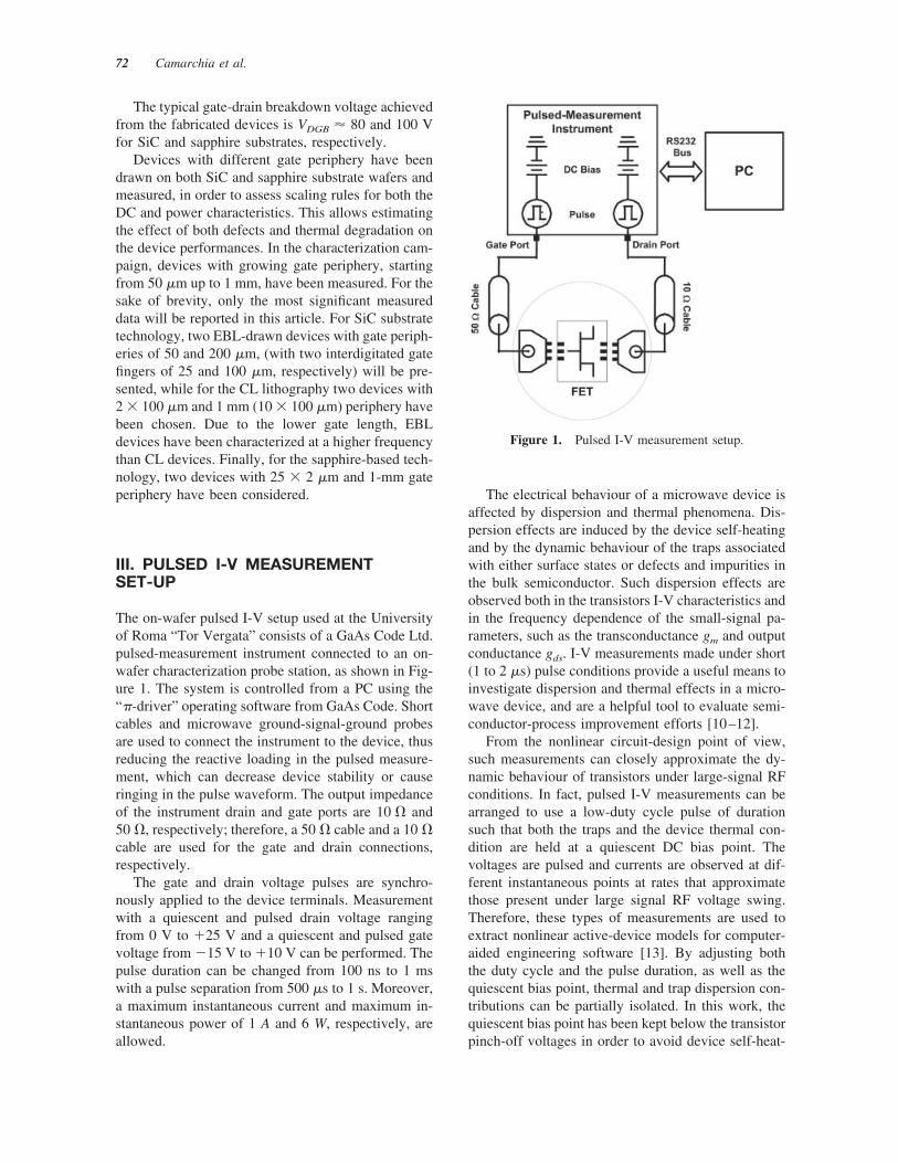
The on-wafer pulsed I-V setup used at the Universityof Roma “Tor Vergata” consists of a GaAs Code Ltd.pulsed-measurement instrument connected to an on-wafer characterization probe station, as shown in Fig-ure 1. The system is controlled from a PC using the“�-driver” operating software from GaAs Code. Shortcables and microwave ground-signal-ground probesare used to connect the instrument to the device, thusreducing the reactive loading in the pulsed measure-ment, which can decrease device stability or causeringing in the pulse waveform. The output impedanceof the instrument drain and gate ports are 10 � and50 �, respectively; therefore, a 50 � cable and a 10 �cable are used for the gate and drain connections,respectively.
The gate and drain voltage pulses are synchro-nously applied to the device terminals. Measurementwith a quiescent and pulsed drain voltage rangingfrom 0 V to �25 V and a quiescent and pulsed gatevoltage from �15 V to �10 V can be performed. Thepulse duration can be changed from 100 ns to 1 mswith a pulse separation from 500 �s to 1 s. Moreover,a maximum instantaneous current and maximum in-stantaneous power of 1 A and 6 W, respectively, areallowed.
The electrical behaviour of a microwave device isaffected by dispersion and thermal phenomena. Dis-persion effects are induced by the device self-heatingand by the dynamic behaviour of the traps associatedwith either surface states or defects and impurities inthe bulk semiconductor. Such dispersion effects areobserved both in the transistors I-V characteristics andin the frequency dependence of the small-signal pa-rameters, such as the transconductance gm and outputconductance gds. I-V measurements made under short(1 to 2 �s) pulse conditions provide a useful means toinvestigate dispersion and thermal effects in a micro-wave device, and are a helpful tool to evaluate semi-conductor-process improvement efforts [10–12].
From the nonlinear circuit-design point of view,such measurements can closely approximate the dy-namic behaviour of transistors under large-signal RFconditions. In fact, pulsed I-V measurements can bearranged to use a low-duty cycle pulse of durationsuch that both the traps and the device thermal con-dition are held at a quiescent DC bias point. Thevoltages are pulsed and currents are observed at dif-ferent instantaneous points at rates that approximatethose present under large signal RF voltage swing.Therefore, these types of measurements are used toextract nonlinear active-device models for computer-aided engineering software [13]. By adjusting boththe duty cycle and the pulse duration, as well as thequiescent bias point, thermal and trap dispersion con-tributions can be partially isolated. In this work, thequiescent bias point has been kept below the transistorpinch-off voltages in order to avoid device self-heat-
Figure 1. Pulsed I-V measurement setup.
72 Camarchia et al.

ing and hence observe the voltage dependency of trapeffects only.
IV. LOAD-PULL TEST-SET
Single or two-tone load-pull characterization is themost straightforward way to extract the maximumpower that can be achieved in a given device and,together with pulsed I-V measurements, is therefore avaluable technique for directly evaluating the effect oftechnology improvements on the device power per-formances. Challenges in the load-pull characteriza-tion arise in the particular case of GaN devices andrequire dedicated measurement setups. In particular,devices with small gate periphery are often used as atechnological benchmark to determine, for a giventechnology, the maximum power capabilities byavoiding thermal effects; these devices pose charac-terization problems, since the power optimum loadtermination is highly reflective due to the high biasvoltages associated with a relatively small drain cur-rent, and to the small reactive part involved. In thissituation, a passive system may not be able to imposethe needed load value at the on-wafer reference plane,while an active system can. In this work, the activeload-pull bench from Politecnico di Torino [14], asshown in Figure 2, has been exploited. This bench isa real-time test set and operates in the 0.5–18-GHzband. As shown in Figure 2, the incident and reflectedpower waves at input and output ports (ports 1 and 2)are measured (samplers 1 and 2) using a vector net-work analyzer (VNA). After the VNA calibration atthe on-wafer reference planes and power calibrationwith a power meter [15–17], the system measures:
● scattering parameters;
● input and output reflection coefficients (funda-mental and harmonics);
● source reflection coefficient (fundamental andharmonics);
● Pin, Pout, gain, and power-added efficiency(PAE).
For high-power and high-reflectivity GaN devices,the active load-pull setup has been further improvedwith new ad hoc features: high-power bias tees, low-loss directional couplers [18], and fast current shutterso as to protect probe damaging in case of devicefailure.
A set of devices with different layouts and fabri-cation processes has been measured, both at Politec-nico di Torino and University of Roma “Tor Ver-gata.” The results are shown in the following sections.
V. PULSED I-V MEASUREMENTS
Figures 3, 4, and 5 show pulsed I-V measurementsnormalized to a total gate periphery of 1 mm for thethree device processes: EBL and CL on SiC sub-strates, and CL on sapphire substrate, respectively. Inparticular, small devices (with 100 and 200 �m oftotal gate peripheries) were measured for the CL andEBL processes on SiC, while a large device (with 1mm of total gate periphery) has been measured toinvestigate the CL process on sapphire.
As is evident from the measurements shown inFigures 3 and 4, when compared with the ones ofFigure 5, the relative measurement uncertainty ishigher for smaller periphery devices. This is due totwo concurring effects: first of all, the absolute instru-ment uncertainty is amplified when the measured dataare normalized to a 1-mm gate width; secondly the
Figure 2. A simplified scheme of the Politecnico di Torino real-time active load-pull system.More details on test-set and calibration can be found in [14].
Power GaN HEMT Nonlinear Characterization 73
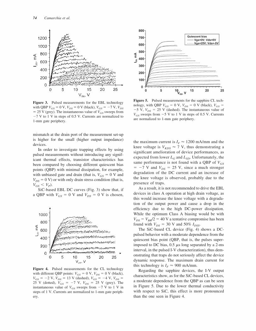
mismatch at the drain port of the measurement set-upis higher for the small (higher output impedance)devices.
In order to investigate trapping effects by usingpulsed measurements without introducing any signif-icant thermal effects, transistor characteristics hasbeen compared by choosing different quiescent biaspoints (QBP) with minimal dissipation, for example,with unbiased gate and drain (that is, VGS � 0 V andVDS � 0 V) or with only drain stress condition (that is,VGS � VP).
SiC-based EBL DC curves (Fig. 3) show that, ifa QBP with VGS � 0 V and VDS � 0 V is chosen,
the maximum current is IF � 1200 mA/mm and theknee voltage is VKDS � 7 V, thus demonstrating asignificant amelioration of device performances, asexpected from lower LG and LSD. Unfortunately, thesame performance is not found with a QBP of VGS
� �7 V and VDS � 25 V, since a much strongerdegradation of the DC current and an increase ofthe knee voltage is observed, probably due to thepresence of traps.
As a result, it is not recommended to drive the EBLdevices in class A operation at high drain voltage, asthis would increase the knee voltage with a degrada-tion of the output power and cause a drop in theefficiency due to the high DC-power dissipation.While the optimum Class A biasing would be withVDS � VBR/2 � 40 V a tentative compromise has beenfound with VDS � 30 V and 50% IDSS.
The SiC-based CL device (Fig. 4) shows a DC-pulsed behavior with a moderate dependence from thequiescent bias point (QBP, that is, the pulses super-imposed to DC bias, 0.5 �s long separated by a 2-msinterval, in the pulsed I-V characterization), thus dem-onstrating that traps do not seriously affect the devicedynamic response. The maximum drain current forthis technology is IF � 900 mA/mm.
Regarding the sapphire devices, the I-V outputcharacteristics show, as for the SiC-based CL devices,a moderate dependence from the QBP as can be seenin Figure 5. Due to the lower thermal conductivitywith respect to SiC, this effect is more pronouncedthan the one seen in Figure 4.
Figure 3. Pulsed measurements for the EBL technologywith QBP VGS � 0 V, VDS � 0 V (black), VGS � �7 V, VDS
� 25 V (grey). The instantaneous value of VGS sweeps from�7 V to 1 V in steps of 0.5 V. Currents are normalized to1-mm gate periphery.
Figure 4. Pulsed measurements for the CL technologywith different QBP points: VGS � 0 V, VDS � 0 V (black),VGS � �2 V, VDS � 13 V (dashed), VGS � �4 V, VDS �25 V (dotted), VGS � �7 V, VDS � 25 V (grey). Theinstantaneous value of VGS sweeps from �7 V to 1 V insteps of 1 V. Currents are normalized to 1-mm gate periph-ery.
Figure 5. Pulsed measurements for the sapphire CL tech-nology, with QBP VGS � 0 V, VDS � 0 V (black), VGS ��5 V, VDS � 25 V (dashed). The instantaneous value ofVGS sweeps from �5 V to 1 V in steps of 0.5 V. Currentsare normalized to 1-mm gate periphery.
74 Camarchia et al.

VI. LOAD-PULL MEASUREMENTS
In order to verify the RF performances of the threetechnologies under test, a complete nonlinear character-ization of various devices with different gate peripherieshas been carried out. CL devices both on SiC, andsapphire have been characterized at 2 GHz, while EBLdevices on SiC can operate at higher frequencies withoutany significant gain degradation and, therefore havebeen measured at 8 GHz. In fact, from the S-parametermeasurements (omitted here for brevity), the cut-offfrequency fT was found to be around 6 GHz for CLdevices and 18 GHz for EBL devices.
Starting with the EBL technology on SiC, at 8 GHzand bias conditions of VDS � 30 V and IDS � 50%IDSS, Figure 6 shows the output stability circles fortwo devices with gate peripheries of 50 and 200 �m,respectively, and the load map. Observe that thewhole map is made on an area of the Smith chart thathas very high reflection coefficients and is very closeto the instability region, hence making this measure-ment difficult to be performed. The optimum loads formaximum power obtained in the two cases, �L �
(0.85, 9°) and �L � (0.79, 19°) respectively, are alsorepresented. The most critical point for high powerdevices is the power scaling with gate periphery.While DC current scales approximately in the correctway (IDS � 20 mA and IDS � 72 mA, respectively, forthe two devices), this is not fully true for the Y-parameters. Note that in this work the effect of theparasitics has not been de-embedded from row mea-surements, and the loss of scalability properties mustbe partially due to this fact. Nevertheless, the rawmeasurements already allow a first evaluation of max-imum output-power scaling rules in these emergingtechnologies. Table I shows that the scaling factor isclose to four for Im{Y11} ( CGS) and Im{Y21}, but isclose to two for Im{Y22}, the same factor that is roughlyobserved in the imaginary part of the optimum load forpower. The real part of the optimum load does not scaleas would be expected for true class A operation, alsosuggesting that the maximum output power will notscale. Figure 7 shows the measured Pin-Pout, gain, andPAE for the same EBL devices. The maximum output-power density Pout at 5-dB gain compression is 5 W/mmfor the small periphery EBL device (2 � 25 �m), whilea larger periphery one (2 � 100 �m) exhibits 4 W/mm.As expected, partly due to the behavior of the optimumload YL,opt, Pout does not scale exactly.
Turning to the CL devices on SiC substrates, weshow the results for a 2 � 100 �m and 1-mm devicefor the same bias conditions of VDS � 30 V and IDS �50% IDSS. In this case, the optimal loads are �L �(0.7, 0°) for 2 � 100 �m and � L � (0.4, 17°) for a1-mm periphery device. Figure 8 shows the scalingproperties of the two SiC CL devices with optimumloads. The two devices do not respect the scaling ofthe DC current; in fact, the IDSS values are 560 and140 mA for the 1-mm and the 2 � 100 �m devices,respectively. This imperfect scaling can be due eitherto the higher power dissipated in the large peripherydevice, which leads to a higher device temperature, orto layout differences. In class A, the ratio of the IDSS
values in the two devices should lead to an expectedmaximum output-power difference of 6 dB, that is,slightly more than the measured 5 dB shown in Figure8. Concerning the output power at 5-dB gain com-pression, the small periphery device (2 � 100 �m) is
Figure 6. Output stability circles at 8 GHz and optimumloads for the EBL on SiC 2 � 25 and 2 � 100 �m devices.
TABLE I. Device Scaling Table
Y-Parameter ( � 103) 2 � 25 �m Device 2 � 100 �m Device Scaling Factor K (Re/Im)
Y11 0.21 � j � 2.64 1.58 � j � 9.18 7.6/3.5Y21 7.13 � j � 2.34 26.21 � j � 9.37 3.7/3.9Y22 0.27 � j � 2.03 1.10 � j � 3.6 4.1/1.8YL,opt 1.63 � j � 1.51 2.29 � j � 3.4 1.4/2.2
Power GaN HEMT Nonlinear Characterization 75

capable of 5.7 W/mm, while the 1-mm one shows 3.2W/mm. From these results, we can state that the CLtechnology is still performing slightly better than theEBL one (see the comparison of the two 200-�mdevices), although the latter offers significantly betterperformances once the trap effects have been reduced.The measurements offer highlights on the possibleimprovements of device technology, especially con-cerning imperfect scaling with gate periphery.
As is evident from Figure 8, the efficiency in class Ais low, especially for the large-periphery devices. Thisposes limitations, especially if we now turn to examinethe sapphire-based CL technology. In fact, it must benoted that the sapphire thermal conductivity is muchlower than the SiC conductivity [19]; therefore making itdesirable to bias these devices in a higher-efficiencymode than in class A in order to decrease the powerdissipation. Class B has been chosen as the best testcondition. Figure 9 shows the load-pull characterizationat 2 GHz on a small periphery device (2 � 25 �m) inclass B. The optimum load is �L � (0.86, 3°). For a1-mm periphery device in class B, the load-pull mea-sures show an optimum load �L � (0.43, 23°). Finally,Figure 10 shows the scaling behavior of the two sapphiredevices at 2 GHz and optimum loads. The output powerat the 1-dB compression point rises from 21.5 dBm for
the 2 � 25 �m device to 33 dBm for the 1-mm device,with an increase of 11.5 dB instead of 13, as foreseen bythe simple periphery-scaling rule. At the 5-dB compres-sion point, the 1-mm device exhibits an output power of2.8 W/mm.
In order to draw some conclusions on the compar-ison of the two CL devices (on SiC and sapphire),note that, although the maximum output power isroughly the same for 1-mm devices based on the twotechnologies, the sapphire devices are fabricated us-ing a more advanced technological process. The sameimprovements are also expected in the most recentSiC based devices (currently under test), which arefabricated using the same improved technology.While the new SiC devices will be suitable for high-power and highly linear applications, the low-costsapphire devices already exhibit interesting proper-ties: despite the poor thermal behavior, they can beviable candidates for medium-power applications,once they are operated in a high-efficiency class.
VII. CONCLUSION
This work has presented a complete characterizationof GaN HEMTs fabricated by SELEX-SI with differ-
Figure 7. Power sweep, gain, and PAE at 8 GHz for 2 � 25 and 2 � 100 �m EBL devices, VDS
� 30 V and IDS � 50% IDSS under output-power optimum loading conditions.
76 Camarchia et al.

ent fabrication steps on both SiC and sapphire sub-strates. The SELEX-SI processes already exhibitstate-of-the-art performances, although the nonlinear
measurements show that amelioration of the devicefabrication technology can lead to even further in-creased power capabilities. Although EBL technologyallows high-frequency operation and higher staticmaximum drain current IF (due to the lower drain-to-source spacing), the higher drain-current collapsephenomena, consequent to the lower maturity gate-
Figure 8. Power sweep, gain, and PAE at 2 GHz for 2 � 100 �m and 1 mm CL devices, VDS �30 V and IDS � 50% IDSS under output-power optimum loading conditions.
Figure 9. Load-pull map at 2 GHz and optimum load forthe 2 � 25 �m CL device on sapphire.
Figure 10. Power sweep, and gain at 2 GHz for 2 � 25�m and 1-mm CL devices on sapphire in class B underoutput-power optimum loading conditions.
Power GaN HEMT Nonlinear Characterization 77
definition process, cause lower RF output-power per-formances than the corresponding CL technology onthe same substrate. Pulsed I-V measurements allow toidentify defects that play a major role in the deviceoperation at high voltages. Power measurements on1-mm devices fabricated using CL lithography SiCsubstrate show 3.2 W/mm, with a significant reduc-tion due to thermal heating with respect to the small-periphery devices, which can reach 5.7 W/mm. Withconstant improvement in the CL lithography process,the sapphire-based devices show interesting features:despite the poor thermal behavior of the substrate, the1-mm device exhibits an output power of 2.8 W/mm(small 2 � 25 �m devices from the same substrateexhibits 4.6 W/mm for similar conditions), whichalready enables these low-cost devices to be exploitedfor medium-power applications. Significant advancesare also anticipated for the application of the sameimproved CL process on sapphire to EBL SiC-baseddevices, which are currently under test.
AKNOWLEDGMENTS
This work was partially supported by the Italian Minister ofUniversity and Research through the PRIN 2003 project,“GaN power HEMTs for wideband systems up to 30 GHz.”The research reported here was performed in the context ofthe network TARGET, “Top Amplifier Research Groups ina European Team,” and supported by the Information So-ciety Technologies Program of the EU under contract IST-1-507893-NOE (www.target-net.org).
REFERENCES
1. S.N. Mohammad, A.A. Salvador, and H. Morkoc,Emerging gallium nitride based devices, Proc IEEE 83(1995), 1306–1355.
2. J.-Y. Duboz, GaN as seen by industry, Phys Stat Sol (a)176 (1999), 5–14.
3. R. Quay, A. Tessmann, R. Kiefer, R. Weber, F. vanRaay, M. Kuri, M. Riessle, H. Massler, S. Muller, M.Schlechtweg, and G. Weimann, AlGaN/GaN HEMTson SiC: towards power operation at V-band, IEEE IntElectron Devices Mtg (IEDM’03), Washington, DC,2003, pp. 23.2.1–23.2.4.
4. S.C. Jain, M. Willander, J. Narayan, and R. Van Over-straeten, III-Nitrides: Growth, characterization, andproperties, J Appl Phys 87 (2000), 965–1006.
5. Y.-N. Xu and W.Y. Ching, Electronic, optical, andstructural properties of some wurtzite crystals, PhysRev B 48 (1993), 4335–4351.
6. B.E. Foutz, S.K. O’Leary, M.S. Shur, and L.F. East-man, Transient electron transport in wurtzite GaN, InN,and AlN, J Appl Phys 85 (1999), 7727–7734.
7. H. Morkoc, Growth of GaN/AlGaN modulation dopedand quantum well structures, and the associated polar-ization effects, Int Conf Silicon Carbide and RelatedMater (ICSCRM’99), Research Triangle Park, NC,1999.
8. O. Ambacher, J. Smart, J.R. Shealy, N.G. Weimann, K.Chu, M. Murphy, W.J. Schaff, L.F. Eastman, R. Dim-itrov, L. Wittmer, M. Stutzmann, W. Rieger, and J.Hilsenbeck, Two-dimensional electron gases inducedby spontaneous and piezoelectric polarization chargesin N- and Ga-face AlGaN/GaN heterostructures, J ApplPhys 85 (1999), 3222–3233.
9. I.P. Smorchkova, M. Wojtowicz, R. Sandhu, R. Tsai,M. Barsky, C. Namba, P.-S. Liu, R. Dia, M. Truong, D.Ko, J. Wang, H. Wang, and A. Khan, AlGaN/GaNHEMTs: Operation in the K-band and above, IEEETrans Microwave Theory Tech MTT-51 (2003), 665–668.
10. J. Vidalou, F. Grossier, M. Camiade, and J. Obregon,On-wafer large-signal pulsed measurements, IEEEMTT Symp Dig-2 (1989), 831–834.
11. A. Platzker, A. Palevsky, S. Nash, W. Struble, and Y.Tajima, Characterization of GaAs devices by a versatilepulsed I-V measurements system, IEEE MTT SympDig-3 (1990), 1137–1140.
12. P. Ladbrooke and J. Bridge, The importance of thecurrent-voltage characteristics of FETs, HEMTs, andbipolar transistors in contemporary design, MicrowaveJ 45 (2002).
13. M. Paggi, P. Williams, and J. Borrego, Nonlinear GaAsMESFET modeling using pulsed gate measurements,IEEE Trans Microwave Theory Tech 36 (1988), 1593–1597.
14. P. Colantonio, F. Giannini, E. Limiti, and V. Teppati,An approach to harmonic load- and source-pull mea-surements for high-efficiency PA design, IEEE TransMicrowave Theory Tech MTT-52 (2004), 191–198.
15. I. Hecht, Improved error-correction technique for large-signal load-pull measurements, IEEE Trans MicrowaveTheory Tech MTT-35 (1987), 1060–1062.
16. R. Tucker and P. Bradley, Computer-aided error correc-tion of large-signal load pull measurements, IEEE TransMicrowave Theory Tech MTT-32 (1984), 296–300.
17. A. Ferrero and U. Pisani, An improved calibration tech-nique for on-wafer large-signal transistor characterization,IEEE Trans Instrum Meas IM-47 (1993), 360–364.
18. V. Teppati, M. Goano, and A. Ferrero, Conformal-mapping design tools for coaxial couplers with complexcross section, IEEE Trans Microwave Theory TechMTT-50 (2002), 2239–2245.
19. V.M. Asnin, F.H. Pollak, J.Ramer, M.Schurman, and I.Ferguson, High spatial resolution thermal conductivityof lateral epitaxial overgrown GaN-sapphire (0001) us-ing a scanning lateral microscope, Appl Phys Lett 75(1999), 1240–1242.
78 Camarchia et al.
BIOGRAPHIES
Vittorio Camarchia was born in Turin, It-aly, in 1972. He received his Laurea degreein electronics engineering and his Ph.D. de-gree in electronics engineering from the Po-litecnico di Torino, Turin, Italy, in 2000 and2003, respectively. From August to Decem-ber 2001 and September to December 2002,he was a Visiting Researcher with the ECEDepartment, Boston University, Boston,
MA. In February 2003, he joined the Dipartimento di Elettronica ofthe Politecnico di Torino. His research is focused on RF devicemodeling and characterization.
Simona Donati Guerrieri was born in 1969in Milano, Italy. She received her degree intheoretical physics in 1993 from the Univer-sity of Milano and her Ph.D. degree in elec-tron devices from University of Trento in1999. In 1998 and 2000, she was with theULSI Technology Research Department ofBell Laboratories in Murray Hill, NJ, as aconsultant, working on physics-based noise
modelling of electron devices. She is presently working as a Re-searcher in the Electonics Department of Politecnico of Torino,where she joined the Microwave Electronics Group. Her researchinterests include the modelling and simulation of microwave solid-state devices, including physics-based nonlinear noise analysis, andthe RF and microwave integrated circuit design. She has been anIEEE Member since 1997.
Marco Pirola was born in Velezzo Lomel-lina, Italy, in 1963. He received his Laureadegree in electronic engineering and hisPh.D. degree from Politecnico di Torino, It-aly, in 1987 and 1992, respectively. In 1992and 1994, he was a Visiting Researcher withthe Hewlett Packard Microwave TechnologyDivision, Santa Rosa, CA. Since 1992, hehas been with the Electronic Department of
Politecnico di Torino, first as Researcher and, since 2000, as As-sociate Professor, where his research concerns the simulation, mod-eling, and measurements of microwave devices and systems.
Valeria Teppati was born in Torino, Italy,on October 20, 1974. She received her de-gree in electronics engineering from Politec-nico di Torino, Torino, Italy in 1999 and herPh.D in electronic instrumentation in 2003.Since then, she has been a Research andTeaching Assistant at Politecnico di Torino.Her research interests and activities includemicrowave devices design, linear and non-
linear measurements design, calibration, and uncertainty.
Andrea Ferrero was born in Novara, Italy,on November 7, 1962. He received elec-tronic engineering and Ph.D. degrees in elec-tronics from the Politecnico in 1987 and1992, respectively. In 1988, he joined Aeri-talia as a Microwave Consultant. During1991, he joined the Microwave TechnologyDivision, Hewlett Packard, Santa Rosa, CA,as a Summer Student. In 1995, he was with
the Electrical Engineering Department of the Ecole Polytechniquede Montreal, Montreal, P.Q., Canada, as a Guest Researcher. In1998, he became an Associate Professor in electronic measure-ments at the Politecnico di Torino, where his main research activ-ities are in the area of microwave measurements techniques, cali-bration, and modeling.
Giovanni Ghione was born in 1956 in Ales-sandria, Italy. He was graduated cum laudein electronic engineering from Politecnico diTorino in 1981. In 1983, he became a Re-search Assistant with Politecnico di Torinoand from 1987 to 1990, he was an AssociateProfessor with Politecnico di Milano. In1990, he joined the University of Catania asFull Professor of Electronics, and since 1991
he has covered the same position again at Politecnico di Torino, IIFaculty of Engineering. Since 1981, he has been engaged in Italianand European research projects (ESPRIT 255, COSMIC, andMANPOWER) in the field of active and passive microwave CAD.His present research interests concern the physics-based simulationof active microwave and optoelectronic devices, with particularattention to noise modelling, thermal modelling, and active-deviceoptimization. His research interests also include several topics incomputational electromagnetics, including coplanar componentanalysis. He has published more than 150 papers and book chaptersin the above fields. He is member of the Editorial Board of the IEEEMTT Transactions, a Senior Member of the IEEE, and member ofthe AEI (Associazione Elettrotecnica Italiana).
Power GaN HEMT Nonlinear Characterization 79
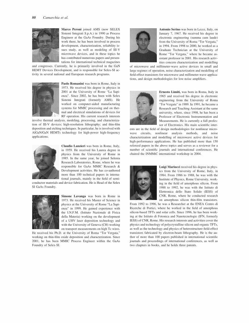
Marco Peroni joined AMS (now SELEXSistemi Integrati S.p.A.) in 1990 as ProcessEngineer at the GaAs Foundry. During hiswork there, he has been involved in processdevelopment, characterization, reliability is-sues study, as well as modeling of III-Vmicrowave devices, and in these topics hehas contributed numerous papers and presen-tations for international technical magazines
and congresses. Currently, he is primarily involved in the GaNHEMT Devices Development, and is responsible for Selex-SI ac-tivity in several national and European research programs.
Paolo Romanini was born in Rome, Italy in1973. He received his degree in physics in2001 at the University of Rome “La Sapi-enza”. Since 2002, he has been with SelexSistemi Integrati (formerly AMS). Heworked on computer-aided manufacturingsystems for MMIC processing and on ther-mal and electrical simulations of devices forRF operation. His current research interests
involve thermal analysis, modeling, processing, and characteriza-tion of III-V devices; high-resolution lithography; and thin-filmdeposition and etching techniques. In particular, he is involved withAlGaN/GaN HEMTs technology for high-power high-frequencyapplications.
Claudio Lanzieri was born in Rome, Italy,in 1959. He received his Laurea degree inphysics from the University of Rome in1985. In the same year, he joined SeleniaResearch Laboratories, Rome, where he wasresponsible for GaAs MMIC Research &Development activities. He has co-authoredmore than 100 technical papers in interna-tional journals, mainly in the field of semi-
conductor materials and device fabrication. He is Head of the SelexSI GaAs Foundry.
Simone Lavanga was born in Rome in1973. He received his Master of Science inphysics at the University of Rome “La Sapi-enza” in 1999. He gained experience withthe I.N.F.M. (Istituto Nazionale di Fisicadella Materia) working on the developmentof a UHV laser deposition technology andwith the University of Geneva (CH) workingon transport measurements on high Tc wires.
He received his Ph.D. at the University of Roma “Tor Vergata,”working on thin-film oxide deposition and characterization. Since2001, he has been MMIC Process Engineer within the GaAsFoundry of Selex-SI.
Antonio Serino was born in Lecce, Italy, onJanuary 7, 1967. He received his degree inelectronic engineering (summa cum laude)from the University of Roma “Tor Vergata,”in 1994. From 1998 to 2000, he worked as aGraduate Technician at the University ofRome “Tor Vergata,” where he became as-sistant professor in 2001. His research activ-ities concern characterization and modelling
of microwave and millimeter-wave active devices in small andlarge regimes of operation, noise characterization and modelling offield-effect transistors for microwave and millimeter-wave applica-tions, and design methodologies for low-noise amplifiers.
Ernesto Limiti, was born in Roma, Italy in1965 and received his degree in electronicengineering from the University of Roma“Tor Vergata” in 1989. In 1991, he became aResearch and Teaching Assistant at the sameuniversity, where, since 1998, he has been aProfessor of Electronic Instrumentation andMeasurements. He is currently a full profes-sor of Electronics. His main scientific inter-
ests are in the field of design methodologies for nonlinear micro-wave circuits, nonlinear analysis methods, and noisecharacterization and modelling of microwave active devices forhigh-performance applications. He has published more than 150refereed papers in the above topics and serves as a reviewer for anumber of scientific journals and international conferences. Hechaired the INMMiC international workshop in 2004.
Luigi Mariucci received his degree in phys-ics from the University of Rome, Italy, in1984. From 1986 to 1988, he was with theInstitute of Physics, Rome University, work-ing in the field of amorphous silicon. From1988 to 1992, he was with the Istituto diElettronica dello Stato Solido (IESS) ofCNR, Rome, where he conducted researchon amorphous silicon thin-film transistors.
From 1992 to 1996, he was a Researcher at the ENEA Centro diRicerche di Portici, where he worked in the field of amorphoussilicon-based TFTs and solar cells. Since 1996, he has been work-ing at the Istituto di Fotonica and Nanotecnologie (IFN, formerlyIESS) of CNR, Rome. His research interests and activities cover thephysics and technology of polycrystalline silicon and organic TFTs,as well as the technology and physics of heterostructure field-effecttransistors fabricated by electron-beam lithography. He is the au-thor of more than 100 papers published in international scientificjournals and proceedings of international conferences, as well astwo chapters in books, and he holds three patents.
80 Camarchia et al.