John H. Lau - Fan-Out Wafer-Level Packaging
319
John H. Lau Fan-Out Wafer-Level Packaging
-
Upload
khangminh22 -
Category
Documents
-
view
0 -
download
0
Transcript of John H. Lau - Fan-Out Wafer-Level Packaging

John H. Lau
Fan-Out Wafer-Level Packaging

Fan-Out Wafer-Level Packaging

John H. Lau
Fan-Out Wafer-LevelPackaging
123

John H. LauASM Pacific TechnologyHong Kong, New TerritoriesHong Kong
ISBN 978-981-10-8883-4 ISBN 978-981-10-8884-1 (eBook)https://doi.org/10.1007/978-981-10-8884-1
Library of Congress Control Number: 2018935844
© Springer Nature Singapore Pte Ltd. 2018This work is subject to copyright. All rights are reserved by the Publisher, whether the whole or partof the material is concerned, specifically the rights of translation, reprinting, reuse of illustrations,recitation, broadcasting, reproduction on microfilms or in any other physical way, and transmissionor information storage and retrieval, electronic adaptation, computer software, or by similar or dissimilarmethodology now known or hereafter developed.The use of general descriptive names, registered names, trademarks, service marks, etc. in thispublication does not imply, even in the absence of a specific statement, that such names are exempt fromthe relevant protective laws and regulations and therefore free for general use.The publisher, the authors and the editors are safe to assume that the advice and information in thisbook are believed to be true and accurate at the date of publication. Neither the publisher nor theauthors or the editors give a warranty, express or implied, with respect to the material contained herein orfor any errors or omissions that may have been made. The publisher remains neutral with regard tojurisdictional claims in published maps and institutional affiliations.
Printed on acid-free paper
This Springer imprint is published by the registered company Springer Nature Singapore Pte Ltd.part of Springer NatureThe registered company address is: 152 Beach Road, #21-01/04 Gateway East, Singapore 189721,Singapore

Preface
The first fan-out wafer-level packaging (FOWLP) U.S. patent was filed by Infineonon October 31, 2001, and the first technical papers were also published (2006) byInfineon and their industry partners: Nagase, Nitto Denko, and Yamada. At thattime, they called it embedded wafer-level ball (eWLB) grid array. Since 2009Infineon and since 2011 Intel and STATS ChipPAC have been in volume pro-duction of packaging semiconductor devices with the FOWLP technology.Unfortunately, because of the small sizes and low performance of the packageddevices, the FOWLP did not get too much tractions. Until September 2016, afterTSMC used their InFO (integrated fan-out) technology to package the Appleapplication processor (A10), then the whole semiconductor packaging communityis excited about the FOWLP technology. This is because the chip size of A10 is> 125 mm2 and A10 is a very high-performance SoC (system-on-chip).
The advantages of FOWLP over the popular PBGA (plastic ball grid array)packages with solder-bumped flip chip are (1) lower cost, (2) lower profile,(3) eliminating the substrate, (4) eliminating the wafer bumping, (5) eliminating theflip chip reflow, (6) eliminating the flux cleaning, (7) eliminating the underfill,(8) better electrical performance, (9) better thermal performance, and (10) easier togo for system-in-package (SiP) and 3D IC packaging. The advantages of FOWLPover the popular WLCSP (wafer-level chip scale package) are (1) the use of knowngood die (KGD), (2) better wafer-level yield, (3) using the best of silicon,(4) multi-chip, (5) embedded integrated passive devices, (6) more than one RDL,(7) higher pin counts, (8) better thermal performance, (9) easier to go for SiP and3D IC packaging, and (10) higher PCB-level reliability.
Unfortunately, for most of the practicing engineers and managers, as well asscientists and researchers, temporary bonding and debonding of carriers, reconsti-tuted wafer or panel, pick and place, EMC (epoxy molding compound), com-pression molding, PMC (post mold cure), copper revealing, organic RDLs(redistribution layers), inorganic RDLs, hybrid RDLs, warpage, chip-first and dieface-up, chip-first and die face-down, and chip-last or RDL-first are not wellunderstood. Thus, there is an urgent need, both in industry and research institute, tocreate a comprehensive book on the current state of knowledge of these key
v

enabling technologies. This book is written so that readers can quickly learn thebasics of problem-solving methods and understand the trade-offs inherent inmaking system-level decisions.
There are 11 chapters in this book, namely (1) Patent Issues of Fan-outWafer-Level Packaging, (2) Flip Chip Technology versus FOWLP, (3) Fan-InWafer-Level Packaging versus FOWLP, (4) EmbeddedChip Packaging, (5) FOWLP:Chip-First and Die Face-Down, (6) FOWLP: Chip-First and Die Face-Up,(7) FOWLP: Chip-Last or RDL-First, (8) FOWLP: PoP (package-on-package),(9) Fan-Out Panel-Level Packaging (FOPLP), (10) 3D Integration, and (11) 3DIC Heterogeneous Integration by FOWLP.
Chapter 1 briefly discusses the patent issues of FOWLP and FOPLP. The patentsimpacting the semiconductor packaging will also be mentioned.
Chapter 2 presents the wafer-level flip chip technology. Emphasis is placed onwafer bumping, various substrate technologies, flip chip assembly, underfill, andreliability. Cu–Cu direct hybrid bonding is also briefly mentioned. Finally, the flipchip technology versus FOWLP is presented.
Chapter 3 details the fan-in wafer-level packaging. Emphasis is placed onWLCSP, PCB assembly of WLCSP, and solder joint reliability of WLCSP.TSMC’s UFI (UBM-free integration) WLCSP will also be briefly mentioned.Finally, WLCSP versus FOWLP will be presented.
Chapter 4 presents the embedded chip packaging. Emphasis is placed on chipsembedded in laminated/polyimide substrate, Si wafer, and glass panel.
Chapter 5 discusses the chip-first and die face-down FOWLP. Emphasis isplaced on the demonstration of the feasibility of a SiP (system-in-package), whichconsists of four chips and four capacitors. The test chips, test package, temporarycarrier, thermal release tape, EMC, compression molding, RDLs, solder ballmounting, and dicing will be presented.
Chapter 6 provides the chip-first and die face-up FOWLP. Emphasis is placed onthe demonstration of the feasibility of a large package with three RDLs for a verylarger chip. The test chip, test package, temporary glass carrier, Cu revealing,RDLs, debonding, and dicing will be discussed. The packages are then assembledon PCB and then go through thermal-cycling test and drop test.
Chapter 7 presents the chip-last (or RDL-first) FOWLP. Emphasis is placed onthe reasons for chip-last FOWLP. Various methods in making the organic RDLs,inorganic RDLs, and hybrid RDLs will be examined.
Chapter 8 discusses the PoP with FOWLP. Emphasis is placed on the applicationof the FOWLP method to house the application processors for smartphones in thebottom package. STATS ChipPac’s and TSMC’s PoP with FOWLP technologywill be presented.
Chapter 9 provides the fan-out panel-level packaging (FOPLP). Emphasis isplaced on various methods in using PCB technology and LDI (laser direct imaging)to make the fan-out packages. The panel versus wafer and the issues of FOPLP willbe discussed.
vi Preface

Chapter 10 presents the most recent developments in 3D integrations. Emphasisis placed on 3D IC packaging, 3D IC integration, and 3D silicon integration. Whoshould be making the TSV (through silicon via) will also be discussed.
Chapter 11 discusses the heterogeneous integration by FOWLP. Emphasis isplaced on heterogeneous integration on organic substrates, silicon substrates, andRDL substrates. The 3D IC heterogeneous integration by FOWLP is also provided.
For whom is this book intended? Undoubtedly, it will be of great interest to threegroups of specialists: (1) those who are active or intend to become active in researchand development of the key enabling technologies of FOWLP and FOPLP such astemporary bonding and debonding of carriers, reconstituted wafer or panel, EMC,compression molding, PMC, copper revealing, RDLs fabricated by polymer andcopper plating/etching, PECVD (plasma enhanced chemical vapor deposition) andcopper damascene and CMP (chemical mechanical polishing), and PCB and LDI,warpage, chip-first and die face-up, chip-first and die face-down, and chip-last orRDL-first; (2) those who have encountered practical FOWLP and FOPLP problemsand wish to understand and learn more methods for solving such problems; and(3) those who have to choose a reliable, creative, high performance, high density,low power consumption, and cost-effective FOWLP and FOPLP technique for theirproducts. This book can also be used as a text for college and graduate students whohave the potential to become our future leaders, scientists, and engineers in theelectronics and optoelectronics industry.
I hope that this book will serve as a valuable reference source for all those facedwith the challenging problems created by the ever-increasing interest in FOWLPand FOPLP. I also hope that it will aid in stimulating further research and devel-opment on key enabling technologies and more sound applications to FOWLP andFOPLP products. The organizations that learn how to design and manufacturetemporary bonding and debonding carrier, molding, and RDLs in their semicon-ductor packaging systems have the potential to make major advances in the elec-tronics and optoelectronics industry, and to gain great benefits in performance,functionality, density, power, bandwidth, quality, size, and weight. It is my hopethat the information presented in this book may assist in removing roadblocks,avoiding unnecessary false starts, and accelerating design, materials, process, andmanufacturing development of key enabling technologies of FOWLP and FOPLP.
Palo Alto, CA, USA John H. Lau
Preface vii

Acknowledgements
Development and preparation of Fan-Out Wafer-Level Packaging was facilitated bythe efforts of a number of dedicated people. I would like to thank them all, withspecial mention of Ms. Parvathidevi Krishnan and Mr. Vinoth Selvamani, SpringerNature Scientific Publishing Services (P) Ltd., for their unswerving support andadvocacy. My special thanks go to Ms. Jasmine Dou, Springer Beijing, who mademy dream of this book come true by effectively sponsoring the project and solvingmany problems that arose during the book’s preparation. It has been a great plea-sure and fruitful experience to work with all of them in transferring my messymanuscripts into a very attractive printed book.
The material in this book clearly has been derived from many sources, includingindividuals, companies, and organizations, and I have attempted to acknowledge bycitations in the appropriate parts of the book the assistance that I have been given. Itwould be quite impossible for me to express my thanks to everyone concerned fortheir cooperation in producing this book, but I would like to extend due gratitude.Also, I would like to thank several professional societies and publishers for per-mitting me to reproduce some of their illustrations and information in this book,including the American Society of Mechanical Engineers (ASME) conferenceproceedings (e.g., International Intersociety Electronic Packaging Conference) andtransactions (e.g., Journal of Electronic Packaging), the Institute of Electrical andElectronic Engineers (IEEE) conference proceedings (e.g., Electronic Componentsand Technology Conference and Electronics Packaging and TechnologyConference) and transactions (e.g., Components, Packaging, and ManufacturingTechnologies), the International Microelectronics and Packaging Society (IMAPS)conference proceedings (e.g., International Symposium on Microelectronics), andtransactions (e.g., International Journal of Microcircuits & Electronic Packaging),and Chip Scale Review.
I would like to thank my former employers, Industrial Technology ResearchInstitute (ITRI), the Hong Kong University of Science and Technology (HKUST),the Institute of Microelectronics (IME), Agilent, and HP, for providing me withexcellent working environments that have nurtured me as a human being, fulfilled
ix

my need for job satisfaction, and enhanced my professional reputation. Also,I would like to thank Dr. Don Rice (HP), Dr. Steve Erasmus (Agilent),Prof. Dim-Lee Kwong (IME), Prof. Ricky Lee (HKUST), and Dr. Ian Yi-Jen Chanof ITRI for their kindness and friendship while I was at their organizations.Furthermore, I would like to thank Mr. Lee Wai Kwong (CEO of ASM) andMr. Wong Yam Mo (CTO of ASM) for their trust, respect, and support of my workat ASM Pacific Technology Ltd. in Hong Kong. Finally, I would like to thank thefollowing colleagues for their stimulating discussions and significant contributionsto this book: P. Tzeng, C. Lee, C. Zhan, M. Li, J. Cline, K. Saito, Y. Hsin,P. Chang, Y. Chang, J. Chen, S. Chen, C. Wu, H. Chang, C. Chien, C. Lin, T. Ku,R. Lo, M. Kao, Ming Li, Dewen Tian, Nelson Fan, Eric Kuah, Wu Kai, Margie Li,J. Hao, Yiu Ming Cheung, Zhang Li, Kim Hwee Tan, Rozalia Beica, ThomasTaylor, Cheng-Ta Ko, Henry Yang, Yu-Hua Chen, Sze Pei Lim, Ning Cheng Lee,Jiang Ran, Cao Xi, Koh Sau Wee, Qing Xiang Yong, Yang Lei, Anthony Chan,T. J. Tseng, C. M. Lai, Ken Cheung, Marc Lin, Casper Tsai, Y. M. Chan, LeslieChang, Eric Ng, T. W. Lam, J. W. Dong, and Jiang Leon. Definitely, I would like tothank my eminent colleagues (the enumeration of whom would not be practicalhere) at ASM, ITRI, HKUST, IME, Agilent, EPS, HP, and throughout the elec-tronics industry for their useful help, strong support, and stimulating discussions.Working and socializing with them has been a privilege and an adventure. I learneda lot about life and advanced semiconductor packaging and fan-out wafer/panel-level packaging technologies from them.
Lastly, I would like to thank my daughter Judy and my wife Teresa for theirlove, consideration, and patience by allowing me to work peacefully on this book.Their simple belief that I am making a contribution to the electronics industry was astrong motivation for me. Thinking that Judy got married to a supportive husband(Bill) and two adorable kids (Allison and James), and has been doing very well in asemiconductor company, Teresa and I are in good health, I want to thank God forHis generous blessings.
Palo Alto, CA, USA John H. Lau
x Acknowledgements

Contents
1 Patent Issues of Fan-Out Wafer-Level Packaging . . . . . . . . . . . . . . 11.1 Introduction . . . . . . . . . . . . . . . . . . . . . . . . . . . . . . . . . . . . . 11.2 Functions of Semiconductor Packaging . . . . . . . . . . . . . . . . . 11.3 Level of Semiconductor Packaging . . . . . . . . . . . . . . . . . . . . 21.4 Patents Impacting the Semiconductor Packaging . . . . . . . . . . . 2
1.4.1 Leadframe . . . . . . . . . . . . . . . . . . . . . . . . . . . . . . . 31.4.2 Organic Substrate with Solder Balls . . . . . . . . . . . . . 41.4.3 Fan-In Wafer-Level Packaging . . . . . . . . . . . . . . . . 51.4.4 Fan-Out Wafer-Level Packaging . . . . . . . . . . . . . . . 7
1.5 Major Claims of Infineon’s Patent . . . . . . . . . . . . . . . . . . . . . 101.6 TSMC InFO-WLP. . . . . . . . . . . . . . . . . . . . . . . . . . . . . . . . . 121.7 Fraunhofer IZM FOPLP . . . . . . . . . . . . . . . . . . . . . . . . . . . . 151.8 Ball/Bump Pitch/Size of PBGA, fcPBGA, WLCSP,
and FOWLP . . . . . . . . . . . . . . . . . . . . . . . . . . . . . . . . . . . . . 151.9 Summary and Recommendations . . . . . . . . . . . . . . . . . . . . . . 17References . . . . . . . . . . . . . . . . . . . . . . . . . . . . . . . . . . . . . . . . . . . . 18
2 Flip Chip Technology Versus FOWLP . . . . . . . . . . . . . . . . . . . . . . 212.1 Introduction . . . . . . . . . . . . . . . . . . . . . . . . . . . . . . . . . . . . . 212.2 Wafer Bumping . . . . . . . . . . . . . . . . . . . . . . . . . . . . . . . . . . 24
2.2.1 C4 Bumps . . . . . . . . . . . . . . . . . . . . . . . . . . . . . . . 242.2.2 C2 (Cu Pillar with Solder Cap) Bumps . . . . . . . . . . 25
2.3 Flip Chip Package Substrates . . . . . . . . . . . . . . . . . . . . . . . . . 272.3.1 Surface Laminar Circuit (SLC) Technology . . . . . . . 272.3.2 Integrated Thin-Film High-Density Organic
Package (i-THOP) . . . . . . . . . . . . . . . . . . . . . . . . . 282.3.3 Coreless Substrate . . . . . . . . . . . . . . . . . . . . . . . . . . 302.3.4 Bump-on-Lead (BOL) . . . . . . . . . . . . . . . . . . . . . . . 312.3.5 Embedded Trace Substrate (ETS) . . . . . . . . . . . . . . 32
xi

2.4 Flip Chip Assembly . . . . . . . . . . . . . . . . . . . . . . . . . . . . . . . 342.4.1 Cu-to-Cu TCB Direct Bonding . . . . . . . . . . . . . . . . 342.4.2 C4 Solder Mass Reflow . . . . . . . . . . . . . . . . . . . . . 352.4.3 C2 Solder Mass Reflow . . . . . . . . . . . . . . . . . . . . . 362.4.4 C2 TCB . . . . . . . . . . . . . . . . . . . . . . . . . . . . . . . . . 36
2.5 Underfill/Reliability . . . . . . . . . . . . . . . . . . . . . . . . . . . . . . . . 372.6 Post-assembly Underfill . . . . . . . . . . . . . . . . . . . . . . . . . . . . . 38
2.6.1 Capillary Underfill (CUF) . . . . . . . . . . . . . . . . . . . . 382.6.2 Molded Underfill (MUF) . . . . . . . . . . . . . . . . . . . . . 382.6.3 Printed Underfill . . . . . . . . . . . . . . . . . . . . . . . . . . . 39
2.7 Preassembly Underfill . . . . . . . . . . . . . . . . . . . . . . . . . . . . . . 522.8 Cu–Cu Direct Hybrid Bonding . . . . . . . . . . . . . . . . . . . . . . . 562.9 Flip Chip Technology Versus FOWLP . . . . . . . . . . . . . . . . . . 572.10 Summary and Recommendations . . . . . . . . . . . . . . . . . . . . . . 58References . . . . . . . . . . . . . . . . . . . . . . . . . . . . . . . . . . . . . . . . . . . . 60
3 Fan-in Wafer-Level Packaging Versus FOWLP . . . . . . . . . . . . . . . 693.1 Introduction . . . . . . . . . . . . . . . . . . . . . . . . . . . . . . . . . . . . . 693.2 Fan-in Wafer-Level Packaging (WLP) . . . . . . . . . . . . . . . . . . 703.3 Wafer-Level Chip Scale Packages (WLCSPs) . . . . . . . . . . . . . 703.4 WLCSP Test Vehicle . . . . . . . . . . . . . . . . . . . . . . . . . . . . . . 71
3.4.1 The Chip . . . . . . . . . . . . . . . . . . . . . . . . . . . . . . . . 713.4.2 The WLCSP . . . . . . . . . . . . . . . . . . . . . . . . . . . . . . 713.4.3 WLCSP Key Process Steps . . . . . . . . . . . . . . . . . . . 72
3.5 PCB Assembly of the WLCSP. . . . . . . . . . . . . . . . . . . . . . . . 733.6 Thermal Cycling Test of WLCSP-PCB Assembly . . . . . . . . . . 76
3.6.1 Thermal Cycling Condition . . . . . . . . . . . . . . . . . . . 763.6.2 Crack Length Distribution of All Solder Joints . . . . . 763.6.3 Crack Propagation of the Corner Solder Joint . . . . . . 773.6.4 Fatigue Crack Growth Rate . . . . . . . . . . . . . . . . . . . 78
3.7 Fracture Characteristics of the Corner Solder Joint—SolderMaterial and Properties . . . . . . . . . . . . . . . . . . . . . . . . . . . . . 81
3.8 Fracture Characteristics of the Corner SolderJoint—Geometry . . . . . . . . . . . . . . . . . . . . . . . . . . . . . . . . . . 83
3.9 Fracture Characteristics of the Corner Solder Joint—ElasticThermal Fatigue Life Prediction Model (DK) . . . . . . . . . . . . . 843.9.1 Boundary Value Problem . . . . . . . . . . . . . . . . . . . . 843.9.2 Thermal Fatigue Life Prediction Model . . . . . . . . . . 863.9.3 Summary and Recommendations . . . . . . . . . . . . . . . 88
3.10 Fracture Characteristics of the Corner Solder Joint—PlasticThermal Fatigue Life Prediction Model (DJ) . . . . . . . . . . . . . . 893.10.1 Boundary Condition and Results . . . . . . . . . . . . . . . 903.10.2 Thermal Fatigue Life Prediction Model . . . . . . . . . . 903.10.3 Summary and Recommendations . . . . . . . . . . . . . . . 94
xii Contents
3.11 Fracture Characteristics of the Corner Solder Joint—CreepThermal Fatigue Life Prediction Model (DW) . . . . . . . . . . . . . 953.11.1 Assumptions . . . . . . . . . . . . . . . . . . . . . . . . . . . . . . 953.11.2 Boundary Conditions . . . . . . . . . . . . . . . . . . . . . . . 953.11.3 Deformed Shape, Stress, and Strain . . . . . . . . . . . . . 963.11.4 Strain Energy Density Around the Crack Tip . . . . . . 973.11.5 A New and Simple Thermal Fatigue Life Prediction
Model . . . . . . . . . . . . . . . . . . . . . . . . . . . . . . . . . . 1023.11.6 Summary and Recommendation . . . . . . . . . . . . . . . . 104
3.12 Hitachi’s WLCSP . . . . . . . . . . . . . . . . . . . . . . . . . . . . . . . . . 1053.12.1 Hitachi’s WLCSP with Stress Relaxation Layer . . . . 1053.12.2 Key Process Steps for Hitachi’s WLCSP . . . . . . . . . 1063.12.3 Reliability of Hitachi’s WLCSP . . . . . . . . . . . . . . . . 107
3.13 TSMC’s UFI WLCSP . . . . . . . . . . . . . . . . . . . . . . . . . . . . . . 1083.13.1 TSMC’s WLCSP with Protection Layer . . . . . . . . . . 1083.13.2 Key Process Steps for TSMC’s WLCSP . . . . . . . . . 1083.13.3 Reliability of TSMC’s WLCSP . . . . . . . . . . . . . . . . 108
3.14 Summary and Recommendations . . . . . . . . . . . . . . . . . . . . . . 109References . . . . . . . . . . . . . . . . . . . . . . . . . . . . . . . . . . . . . . . . . . . . 111
4 Embedded Chip Packaging . . . . . . . . . . . . . . . . . . . . . . . . . . . . . . . 1154.1 Introduction . . . . . . . . . . . . . . . . . . . . . . . . . . . . . . . . . . . . . 1154.2 Chips Embedded in Laminated/Polyimide Panel Format . . . . . 115
4.2.1 Advantages and Disadvantages . . . . . . . . . . . . . . . . 1154.2.2 Various Chip Embedding Processes . . . . . . . . . . . . . 1164.2.3 Embedded Chip in Rigid Laminated Substrates . . . . 1164.2.4 3D Embedded Chip in Flexible Polyimide
Substrates . . . . . . . . . . . . . . . . . . . . . . . . . . . . . . . . 1184.2.5 3D Embedded Stacking Chips in Flexible
Polyimide Substrates . . . . . . . . . . . . . . . . . . . . . . . . 1184.3 Chips Embedded in Si Wafer . . . . . . . . . . . . . . . . . . . . . . . . . 119
4.3.1 Key Process Steps . . . . . . . . . . . . . . . . . . . . . . . . . 1194.3.2 Reliability of Chips Embedded in Si Wafer . . . . . . . 119
4.4 Chips Embedded in Glass Panel . . . . . . . . . . . . . . . . . . . . . . . 1204.4.1 Key Process Steps . . . . . . . . . . . . . . . . . . . . . . . . . 1224.4.2 Reliability of Chips Embedded in Glass Panel . . . . . 123
4.5 Summary and Recommendations . . . . . . . . . . . . . . . . . . . . . . 123References . . . . . . . . . . . . . . . . . . . . . . . . . . . . . . . . . . . . . . . . . . . . 124
5 FOWLP: Chip-First and Die Face-Down . . . . . . . . . . . . . . . . . . . . 1275.1 Introduction . . . . . . . . . . . . . . . . . . . . . . . . . . . . . . . . . . . . . 1275.2 Chip-First and Face-Down . . . . . . . . . . . . . . . . . . . . . . . . . . . 1295.3 Test Chips . . . . . . . . . . . . . . . . . . . . . . . . . . . . . . . . . . . . . . 1305.4 Test Package . . . . . . . . . . . . . . . . . . . . . . . . . . . . . . . . . . . . . 131
Contents xiii

5.5 The Temporary Carrier . . . . . . . . . . . . . . . . . . . . . . . . . . . . . 1325.6 The 2-Side Thermal Release Tape and Pick and Place . . . . . . . 1345.7 EMC and Dispensing . . . . . . . . . . . . . . . . . . . . . . . . . . . . . . 1355.8 Compression Molding and PMC . . . . . . . . . . . . . . . . . . . . . . 1365.9 RDL . . . . . . . . . . . . . . . . . . . . . . . . . . . . . . . . . . . . . . . . . . . 137
5.9.1 Debonding the Metal Carrier . . . . . . . . . . . . . . . . . . 1375.9.2 Temporary Bonding of Another Glass Carrier . . . . . 138
5.10 Solder Ball Mounting . . . . . . . . . . . . . . . . . . . . . . . . . . . . . . 1405.11 Final Debonding . . . . . . . . . . . . . . . . . . . . . . . . . . . . . . . . . . 1405.12 Summary and Recommendations . . . . . . . . . . . . . . . . . . . . . . 141References . . . . . . . . . . . . . . . . . . . . . . . . . . . . . . . . . . . . . . . . . . . . 142
6 FOWLP: Chip-First and Die Face-Up . . . . . . . . . . . . . . . . . . . . . . 1456.1 Introduction . . . . . . . . . . . . . . . . . . . . . . . . . . . . . . . . . . . . . 1456.2 Fan-Out of Chip Circuitries in Semiconductor Packaging . . . . 145
6.2.1 Advantages of FOWLP over PBGA . . . . . . . . . . . . . 1466.2.2 Advantages of FOWLP over WLCSP . . . . . . . . . . . 146
6.3 FOWLP with Chip-First and Die Face-Up . . . . . . . . . . . . . . . 1466.4 Test Chip . . . . . . . . . . . . . . . . . . . . . . . . . . . . . . . . . . . . . . . 1476.5 Test Package . . . . . . . . . . . . . . . . . . . . . . . . . . . . . . . . . . . . . 1486.6 Chip-First (Die Face-Up) FOWLP Assembly Process . . . . . . . 1506.7 Assembly on the Test Chip Wafer . . . . . . . . . . . . . . . . . . . . . 1506.8 Assembly on the Reconstituted Wafer . . . . . . . . . . . . . . . . . . 151
6.8.1 Glass Carrier Wafer and LTHC Layer . . . . . . . . . . . 1516.8.2 Pick and Place . . . . . . . . . . . . . . . . . . . . . . . . . . . . 1546.8.3 EMC Dispensing . . . . . . . . . . . . . . . . . . . . . . . . . . 1556.8.4 Compression Molding, PMC, and Die Shift . . . . . . . 1576.8.5 Warpages . . . . . . . . . . . . . . . . . . . . . . . . . . . . . . . . 1596.8.6 Cu Revealing . . . . . . . . . . . . . . . . . . . . . . . . . . . . . 1646.8.7 RDLs . . . . . . . . . . . . . . . . . . . . . . . . . . . . . . . . . . . 1656.8.8 Solder Ball Mounting . . . . . . . . . . . . . . . . . . . . . . . 1676.8.9 Debonding . . . . . . . . . . . . . . . . . . . . . . . . . . . . . . . 168
6.9 PCB Assembly of FOWLP . . . . . . . . . . . . . . . . . . . . . . . . . . 1696.9.1 PCB . . . . . . . . . . . . . . . . . . . . . . . . . . . . . . . . . . . . 1696.9.2 Stencil and Printing . . . . . . . . . . . . . . . . . . . . . . . . 1706.9.3 Pick and Place and Reflow . . . . . . . . . . . . . . . . . . . 172
6.10 Thermal Performance of FOWLP . . . . . . . . . . . . . . . . . . . . . . 1736.10.1 Structure . . . . . . . . . . . . . . . . . . . . . . . . . . . . . . . . 1736.10.2 Material Properties . . . . . . . . . . . . . . . . . . . . . . . . . 1736.10.3 Boundary Conditions . . . . . . . . . . . . . . . . . . . . . . . 1746.10.4 Finite-Element Modeling and Analysis . . . . . . . . . . . 1746.10.5 Analysis Results . . . . . . . . . . . . . . . . . . . . . . . . . . . 175
6.11 Reliability Assessments—Thermal Cycling Test . . . . . . . . . . . 1786.11.1 Test Setup . . . . . . . . . . . . . . . . . . . . . . . . . . . . . . . 1786.11.2 Test Results . . . . . . . . . . . . . . . . . . . . . . . . . . . . . . 180
xiv Contents

6.12 Reliability Assessments—Drop Test . . . . . . . . . . . . . . . . . . . . 1806.12.1 Test Setup . . . . . . . . . . . . . . . . . . . . . . . . . . . . . . . 1806.12.2 Test Results . . . . . . . . . . . . . . . . . . . . . . . . . . . . . . 182
6.13 Simulation on Thermal Cycling . . . . . . . . . . . . . . . . . . . . . . . 1836.14 Simulation on Shock (Drop) . . . . . . . . . . . . . . . . . . . . . . . . . 1876.15 Summary and Recommendations . . . . . . . . . . . . . . . . . . . . . . 192References . . . . . . . . . . . . . . . . . . . . . . . . . . . . . . . . . . . . . . . . . . . . 192
7 FOWLP: Chip-Last or RDL-First . . . . . . . . . . . . . . . . . . . . . . . . . . 1957.1 Introduction . . . . . . . . . . . . . . . . . . . . . . . . . . . . . . . . . . . . . 1957.2 Reasons for Chip-Last or RDL-First FOWLP . . . . . . . . . . . . . 1967.3 Methods for Chip-Last or RDL-First FOWLP . . . . . . . . . . . . . 1967.4 Chip-Last (RDL-First) by PECVD and Cu
Damascene + CMP . . . . . . . . . . . . . . . . . . . . . . . . . . . . . . . . 1967.4.1 Key Process Flow . . . . . . . . . . . . . . . . . . . . . . . . . . 1967.4.2 RDLs by PECVD and Cu Damascene + CMP . . . . . 1987.4.3 UBM/Cu Contact Pad/Solder Ball . . . . . . . . . . . . . . 199
7.5 Chip-Last (RDL-First) by Polymer and CuPlating + Etching . . . . . . . . . . . . . . . . . . . . . . . . . . . . . . . . . 2007.5.1 Key Process Steps . . . . . . . . . . . . . . . . . . . . . . . . . 2007.5.2 RDLs by Polymer and Cu Plating + Etching . . . . . . 201
7.6 Chip-Last (RDL-First) by Hybrid RDLs . . . . . . . . . . . . . . . . . 2017.6.1 Key Process Steps . . . . . . . . . . . . . . . . . . . . . . . . . 2017.6.2 Examples of Hybrid RDLs . . . . . . . . . . . . . . . . . . . 202
7.7 Summary and Recommendations . . . . . . . . . . . . . . . . . . . . . . 203References . . . . . . . . . . . . . . . . . . . . . . . . . . . . . . . . . . . . . . . . . . . . 205
8 FOWLP: PoP . . . . . . . . . . . . . . . . . . . . . . . . . . . . . . . . . . . . . . . . . 2078.1 Introduction . . . . . . . . . . . . . . . . . . . . . . . . . . . . . . . . . . . . . 2078.2 STATS ChipPAC’s PoP for AP Chipset with eWLB . . . . . . . 207
8.2.1 The Structure . . . . . . . . . . . . . . . . . . . . . . . . . . . . . 2088.2.2 Structural Warpages . . . . . . . . . . . . . . . . . . . . . . . . 2088.2.3 Component-Level Reliability Assessments . . . . . . . . 2108.2.4 Board-Level Reliability Assessments . . . . . . . . . . . . 210
8.3 TSMC’ PoP for AP Chipset with FOWLP . . . . . . . . . . . . . . . 2118.3.1 TSMC’ InFO . . . . . . . . . . . . . . . . . . . . . . . . . . . . . 2118.3.2 TSMC’ InFO-PoP for AP Chipset . . . . . . . . . . . . . . 211
8.4 Summary and Recommendations . . . . . . . . . . . . . . . . . . . . . . 215References . . . . . . . . . . . . . . . . . . . . . . . . . . . . . . . . . . . . . . . . . . . . 216
9 Fan-Out Panel-Level Packaging (FOPLP) . . . . . . . . . . . . . . . . . . . . 2179.1 Introduction . . . . . . . . . . . . . . . . . . . . . . . . . . . . . . . . . . . . . 2179.2 J-Devices’ WFOP™ . . . . . . . . . . . . . . . . . . . . . . . . . . . . . . . 217
9.2.1 Structure of J-Devices’ WFOP™ . . . . . . . . . . . . . . . 2189.2.2 Key Process Steps of J-Devices’ WFOP™ . . . . . . . . 218
Contents xv

9.3 Fraunhofer’s FOPLP . . . . . . . . . . . . . . . . . . . . . . . . . . . . . . . 2199.3.1 Fraunhofer’s FOPLP Integration Line . . . . . . . . . . . 2199.3.2 Fraunhofer’s RDLs Key Process Steps . . . . . . . . . . . 220
9.4 SPIL’s P-FO . . . . . . . . . . . . . . . . . . . . . . . . . . . . . . . . . . . . . 2229.4.1 Structure of SPIL’s P-FO . . . . . . . . . . . . . . . . . . . . 2239.4.2 Key Process Steps of SPIL’s P-FO . . . . . . . . . . . . . 223
9.5 Panel Versus Wafer . . . . . . . . . . . . . . . . . . . . . . . . . . . . . . . . 2249.5.1 Issues of FOPLP . . . . . . . . . . . . . . . . . . . . . . . . . . . 2249.5.2 Reconstituted Wafers for High-End Applications . . . 2279.5.3 Reconstituted Wafers for Middle-End
Applications . . . . . . . . . . . . . . . . . . . . . . . . . . . . . . 2279.5.4 Reconstituted Panels for Low-End Applications . . . . 227
9.6 Summary and Recommendations . . . . . . . . . . . . . . . . . . . . . . 227References . . . . . . . . . . . . . . . . . . . . . . . . . . . . . . . . . . . . . . . . . . . . 229
10 3D Integration . . . . . . . . . . . . . . . . . . . . . . . . . . . . . . . . . . . . . . . . . 23110.1 Introduction . . . . . . . . . . . . . . . . . . . . . . . . . . . . . . . . . . . . . 23110.2 Overview and Outlooks of 3D IC Packaging . . . . . . . . . . . . . 233
10.2.1 Chip Stacking by Wire Bonding . . . . . . . . . . . . . . . 23410.2.2 PoP . . . . . . . . . . . . . . . . . . . . . . . . . . . . . . . . . . . . 23410.2.3 Chip-to-Chip Interconnects . . . . . . . . . . . . . . . . . . . 23710.2.4 Outlook of 3D IC Packaging . . . . . . . . . . . . . . . . . . 238
10.3 Overview, Challenges, and Outlook of 3D Si Integration . . . . . 23810.3.1 Issues of 3D Si Integration . . . . . . . . . . . . . . . . . . . 23810.3.2 Cu-to-Cu Bonding and Oxide-to-Oxide Bonding . . . 23910.3.3 R&D in 3D Si Integration . . . . . . . . . . . . . . . . . . . . 24010.3.4 Outlooks of 3D Si Integration . . . . . . . . . . . . . . . . . 24110.3.5 Hybrid Bonding . . . . . . . . . . . . . . . . . . . . . . . . . . . 241
10.4 Overview, Challenges, and Outlook of 3D IC Integration . . . . 24210.4.1 Memory Stacking with TSVs . . . . . . . . . . . . . . . . . 24310.4.2 Wide I/O DRAM and Wide I/O 2 . . . . . . . . . . . . . . 24310.4.3 High-Bandwidth Memory (HBM) . . . . . . . . . . . . . . 24410.4.4 AMD’s Graphic Processor Unit with HBM . . . . . . . 24510.4.5 Nvidia’s Graphic Processor Unit with HBM2 . . . . . . 24610.4.6 Intel’s CPU with Micron’s HMC . . . . . . . . . . . . . . . 24710.4.7 Passive Interposer (2.5D IC Integration) . . . . . . . . . . 24810.4.8 Fabrication of TSVs . . . . . . . . . . . . . . . . . . . . . . . . 24910.4.9 Fabrication of RDLs . . . . . . . . . . . . . . . . . . . . . . . . 25010.4.10 Backside Processing and Assembly . . . . . . . . . . . . . 25110.4.11 Cu Revealing . . . . . . . . . . . . . . . . . . . . . . . . . . . . . 25210.4.12 Outlook of 2.5D/3D IC Integration . . . . . . . . . . . . . 254
10.5 Supply Chains Before the TSV Era . . . . . . . . . . . . . . . . . . . . 25510.5.1 Front-End-of-Line (FEOL) . . . . . . . . . . . . . . . . . . . 25510.5.2 BEOL . . . . . . . . . . . . . . . . . . . . . . . . . . . . . . . . . . 25510.5.3 OSATs . . . . . . . . . . . . . . . . . . . . . . . . . . . . . . . . . . 255
xvi Contents

10.6 Supply Chains for the TSV Era—Who Makes the TSV? . . . . . 25610.6.1 TSVs Fabricated by the via-First Process . . . . . . . . . 25610.6.2 TSVs Fabricated by the via-Middle Process . . . . . . . 25610.6.3 TSVs Fabricated by the via-Last
(from the Front-Side) Process . . . . . . . . . . . . . . . . . 25610.6.4 TSVs Fabricated by the via-Last
(from the Backside) Process . . . . . . . . . . . . . . . . . . 25610.6.5 How About the Passive TSV Interposers? . . . . . . . . 25710.6.6 Who Wants to Fabricate the TSV for Passive
Interposers? . . . . . . . . . . . . . . . . . . . . . . . . . . . . . . 25710.7 Supply Chains for the TSV Era—Who Does the MEOL? . . . . 25710.8 Outlook of HVM Supply Chains for TSVs and MEOL . . . . . . 25810.9 Summary and Recommendations . . . . . . . . . . . . . . . . . . . . . . 258References . . . . . . . . . . . . . . . . . . . . . . . . . . . . . . . . . . . . . . . . . . . . 259
11 3D IC Heterogeneous Integration by FOWLP . . . . . . . . . . . . . . . . 26911.1 Introduction . . . . . . . . . . . . . . . . . . . . . . . . . . . . . . . . . . . . . 26911.2 Multichip Module (MCM) . . . . . . . . . . . . . . . . . . . . . . . . . . . 269
11.2.1 MCM-C . . . . . . . . . . . . . . . . . . . . . . . . . . . . . . . . . 26911.2.2 MCM-D . . . . . . . . . . . . . . . . . . . . . . . . . . . . . . . . . 27011.2.3 MCM-L . . . . . . . . . . . . . . . . . . . . . . . . . . . . . . . . . 270
11.3 System-in-Package (SiP) . . . . . . . . . . . . . . . . . . . . . . . . . . . . 27011.3.1 Intention of SiP . . . . . . . . . . . . . . . . . . . . . . . . . . . 27011.3.2 Actual Applications of SiP . . . . . . . . . . . . . . . . . . . 27011.3.3 Potential Applications of SiP . . . . . . . . . . . . . . . . . . 271
11.4 System-on-Chip (SoC) . . . . . . . . . . . . . . . . . . . . . . . . . . . . . . 27111.4.1 Apple Application Processor (A10) . . . . . . . . . . . . . 27111.4.2 Apple Application Processor (A11) . . . . . . . . . . . . . 271
11.5 Heterogeneous Integration . . . . . . . . . . . . . . . . . . . . . . . . . . . 27211.5.1 Heterogeneous Integration Versus SoC. . . . . . . . . . . 27211.5.2 Advantages of Heterogeneous Integration . . . . . . . . . 274
11.6 Heterogeneous Integration on Organic Substrates . . . . . . . . . . 27411.6.1 Amkor’s SiP for Automobiles . . . . . . . . . . . . . . . . . 27411.6.2 Apple Watch II (SiP) Assembled by ASE . . . . . . . . 27411.6.3 Cisco’s ASIC and HBM on Organic Substrate . . . . . 27511.6.4 Intel’s CPU and Micron’s HMC on Organic
Substrate . . . . . . . . . . . . . . . . . . . . . . . . . . . . . . . . 27611.7 Heterogeneous Integration on Silicon Substrates (SoW) . . . . . . 277
11.7.1 Leti’s SoW . . . . . . . . . . . . . . . . . . . . . . . . . . . . . . . 27711.7.2 Xilinx/TSMC’s CoWoS . . . . . . . . . . . . . . . . . . . . . 27811.7.3 Analog Devices’ MEMS on ASIC Wafer . . . . . . . . . 27811.7.4 AMD’s GPU and Hynix’s HBM
on TSV-Interposer . . . . . . . . . . . . . . . . . . . . . . . . . 280
Contents xvii

11.7.5 Nvidia’s GPU and Samsung’s HBM2on TSV-Interposer . . . . . . . . . . . . . . . . . . . . . . . . . 281
11.7.6 UCLA’s SoW . . . . . . . . . . . . . . . . . . . . . . . . . . . . . 28211.8 Heterogeneous Integration on RDLs . . . . . . . . . . . . . . . . . . . . 282
11.8.1 Xilinx/SPIL’s TSV-Less SLIT . . . . . . . . . . . . . . . . . 28211.8.2 Amkor’s TSV-Less SLIM . . . . . . . . . . . . . . . . . . . . 28511.8.3 Intel’s TSV-Less EMIB (RDL) for FPGA
and HBM . . . . . . . . . . . . . . . . . . . . . . . . . . . . . . . . 28611.8.4 EMIB (RDL) for Intel’s CPU and AMD’s GPU . . . . 28711.8.5 STATS ChipPAC’s FOFC-eWLB . . . . . . . . . . . . . . 28811.8.6 ASE’s FOCoS . . . . . . . . . . . . . . . . . . . . . . . . . . . . 28911.8.7 MediaTek’s RDLs by FOWLP . . . . . . . . . . . . . . . . 290
11.9 3D IC Heterogeneous Integration by FOWLP . . . . . . . . . . . . . 29011.9.1 Application Processor with FOWLP. . . . . . . . . . . . . 29111.9.2 Application Processor by 3D IC Heterogeneous
Integration with FOWLP . . . . . . . . . . . . . . . . . . . . . 29311.10 3D IC High-Performance Heterogeneous Integration
by FOWLP . . . . . . . . . . . . . . . . . . . . . . . . . . . . . . . . . . . . . . 29811.10.1 High-Performance 3D IC Heterogeneous
Integration System . . . . . . . . . . . . . . . . . . . . . . . . . 29811.10.2 Manufacturing Process . . . . . . . . . . . . . . . . . . . . . . 29811.10.3 Advantages of the New Manufacturing Process . . . . 300
11.11 Summary and Recommendations . . . . . . . . . . . . . . . . . . . . . . 300References . . . . . . . . . . . . . . . . . . . . . . . . . . . . . . . . . . . . . . . . . . . . 301
xviii Contents

About the Author
John H. Lau, Ph.D., P.E. has been a Senior Technical Advisor at ASM PacificTechnology in Hong Kong since July 2014. Prior to that, he was a fellow of theIndustrial Technology Research Institute in Taiwan for 4½ years; a VisitingProfessor at Hong Kong University of Science and Technology for 1 year; theDirector of the Microsystems, Modules, and Components Laboratory at the Instituteof Microelectronics in Singapore for 2 years; and a Senior Scientist/MTS atHewlett-Packard Laboratory/Agilent in California for more than 25 years.
His professional competences are design, analysis, materials, process, manu-facturing, qualification, reliability, testing, and thermal management of electronic,optoelectronic, LED, CIS, and MEMS components and systems, with emphases onsolder mechanics and manufacturing, RoHS-compliant products, SMT, flip chip,fan-in and fan-out WLP, SiP, heterogeneous integration, and TSV and otherenabling technologies for 3D IC integration.
With more than 39 years of R&D and manufacturing experience, he hasauthored or coauthored more than 460 peer-reviewed technical publications,invented more than 30 issued or pending US patents, and given more than 290lectures/workshops/keynotes worldwide. He has authored or coauthored 20 text-books on 3D IC integration and packaging, TSV for 3D integration, advancedMEMS packaging, reliability of 2D and 3D IC interconnects, flip chip, WLP,MCM, area-array packages, WLCSP, high-density PCB, SMT, DCA, TAB,lead-free materials, soldering, manufacturing, and solder joint reliability.
He earned a Ph.D. degree in theoretical and applied mechanics from theUniversity of Illinois at Urbana–Champaign, an M.A.Sc. degree in structuralengineering from the University of British Columbia, a second M.S. degree inengineering mechanics from the University of Wisconsin at Madison, and a thirdM.S. degree in management science from Fairleigh Dickinson University. He alsohas a B.E. degree in civil engineering from National Taiwan University.
He has received many awards from the American Society of MechanicalEngineers (ASME), the Institute of Electrical and Electronics Engineers (IEEE), theSociety of Manufacturing Engineers (SME) and other societies, including for thebest IEEE/ECTC proceedings paper (1989), outstanding IEEE/EPTC paper (2009),
xix

best ASME transactions paper (Journal of Electronic Packaging, 2000), and bestIEEE transactions paper (CPMT, 2010), and the ASME/EEP Outstanding TechnicalAchievement Award (1998), IEEE/CPMT Manufacturing Award (1994),IEEE/CPMT Outstanding Contribution Award (2000), IEEE/CPMT OutstandingSustained Technical Contribution Award (2010), SME Total Excellence inElectronics Manufacturing Award (2001), Pan Wen Yuan Distinguished ResearchAward (2011), IEEE Meritorious Achievement in Continuing Education Award(2000), IEEE Components, Packaging, and Manufacturing Technology FieldAward (2013), and ASME Worcester Reed Warner Medal (2015). He is an electedASME fellow, IEEE fellow, and IMAPS fellow, and has been heavily involved inmany of ASME’s, IEEE’s, and IMAPS’ technical activities.
xx About the Author

Chapter 1Patent Issues of Fan-Out Wafer-LevelPackaging
1.1 Introduction
In the industry, research institute, and university, there are many engineers,researchers, students, and professors working on fan-out wafer-level packaging. Inorder to avoid the granted patents in this area, they are trying various methods suchas die-up, die-down, die-first, die-last, RDL (redistribution layer)-first, RDL-last,mold-first, mold-last, round temporary carrier, and rectangular temporary carrier. Inthis chapter, the patent issues of fan-out wafer/panel-level packaging will beinvestigated. Emphasis will be placed on the claims of the granted patents and therange of things which might be covered under the patents. Depending on the RDLline width/spacing, the material, process, equipment, and application of fan-outwafer/panel-level packaging are examined and some recommendations are made.The patents which impacting the semiconductor packaging the most, so far, will bebriefly mentioned first.
1.2 Functions of Semiconductor Packaging
Figure 1.1 shows the inside of a typical electronic product. It consists of printedcircuit boards (PCBs) with some semiconductor integrated circuit (IC) chip com-ponents. IC chip is not an isolated island. It must communicate with other IC chipsin a circuit through an input/output (I/O) system of interconnects. Furthermore, theIC chip and its embedded circuitry are delicate, requiring the package to both carryand protect it. Consequently, the major functions of the semiconductor packagingare, for example [1]: (1) to provide a path for the electrical current that powers thecircuits on the IC chip; (2) to distribute the signals onto and off the IC chip; (3) toremove the heat generated by the circuits on the IC chip; and (4) to support andprotect the IC chip from hostile environments.
© Springer Nature Singapore Pte Ltd. 2018J. H. Lau, Fan-Out Wafer-Level Packaging,https://doi.org/10.1007/978-981-10-8884-1_1
1

1.3 Level of Semiconductor Packaging
Semiconductor packaging is an art (engineering) based on the science of estab-lishing interconnections ranging from [1] zero-level packages (i.e., chip-levelconnections, wire bonding, solder bump flip chip, and tape automated bonding),first-level packages (e.g., leadframe, substrate, molding, and single/multichipmodule), and second-level packages, i.e., board-level interconnect or PCB.Figure 1.1 schematically shows the cross section of a simple semiconductorpackaging. It can be seen that Chip A is solder bumped flip chip on an organicsubstrate with solder balls. The circuitry of Chip A is fanned out through thesubstrate with vias, solder joints, and then to the PCB. By going through the Cutrace on the PCB, the circuitry is moving up the solder joint, leadframe, wire bond,and reaching to Chip B. This is how an electronic product works.
1.4 Patents Impacting the Semiconductor Packaging
There are many significant patents such as the solder bumped flip chip andthrough-silicon vias that impact semiconductor packaging. However, based on theauthor’s opinion, the leadframe, organic substrate with area-array solder balls,
Printed Circuit Board
IC Chip BPackage
Substrate
Solder Joint
Lead-frameSolder Joint
Au/Cu wireUnderfill
Solder BumpMolding Compound
IC Chip A
Cu Trace
Via
One of the packaging functions is to
distribute the signals onto and off the IC
chip.
Fig. 1.1 Inside an electronic product and schematic of the cross section of a typical PCB
2 1 Patent Issues of Fan-Out Wafer-Level Packaging

fan-in wafer-level packaging, and fan-out wafer-level packaging (schematicallyshown Fig. 1.2) are the most important so far [2].
1.4.1 Leadframe
On July 17, 1967, Kauffman of The Jade Corporation [3] proposed the use of aleadframe (see items #14, 16 in Fig. 1.3) having terminal ends (item #18) to fan-outthe circuitry from a chip (item #20) as shown in Fig. 1.3, to a PCB. Today, justabout all electronic products use leadframes such as the gull-wing lead (e.g., plasticquad flat pack (PQFP)), J-lead (e.g., plastic leaded chip carrier (PLCC)), and/or dualinline package (DIP) to fan-out the circuitry from a chip to a PCB (Fig. 1.4). Thepitch of gull-wing leadframe for PQFP is usually 0.4 or 0.5 mm, J-lead leadframefor PLCC is 1.27 mm, and through-hole leadframe for DIP is 2.54 mm. In the pastalmost 50 years, the leadframe patent has had the most impact on semiconductorpackaging.
Printed Circuit Board
(a) PQFP (b) PBGA
(d) Fan-out WLP(c) Fan-in WLP (WLCSP)
Printed Circuit Board
Fig. 1.2 Schematically showing the patents impacting the semiconductor packaging.a Leadframe. b Substrate and area-array solder balls. c Fan-in WLP. d Fan-out WLP
1.4 Patents Impacting the Semiconductor Packaging 3

1.4.2 Organic Substrate with Solder Balls
On March 2, 1992, Paul Lin, Mike McShane, and Howard Wilson of Motorolaproposed [4] the use of an organic carrier or substrate (item #12 in Fig. 1.5) witharea-array solder balls (item #26) (instead of leadframes) to fan-out the circuitry(items #22, 30, 33) from a chip (item #18) (Fig. 1.5) to a PCB, which is called aplastic ball grid array (PBGA) package. Also referring to Fig. 1.5, item #22 is awire bond and item #32 is a via in the substrate connecting the upper wiring layer(item #30) to the bottom wiring layer (item #33). It should be pointed out that in1989, Motorola and Citizen Watch announced the over molded pad array carrier(OMPAC) package [1, 5], which is the first PBGA.
Amkor (1993) led the OSATs (outsourced semiconductor assembly and testproviders) to license this packaging technology from Motorola—and the BGA erabegan. Since then, hundreds of patents such as solder bumped flip chip on organicsubstrate as shown in Fig. 1.6 have been granted in the related area. However, theyare incremental patents and Motorola’s [4] is the fundamental patent.
The advantages of PBGA packages with organic substrate and area-array solderballs over the gull-wing leadframe PQFP and J-lead PLCC packages are (1) lesspackage area for the same package pin count and thus less PCB real estate,(2) higher pin counts, (3) lower profile, (4) better in handling (no-bend leads),
Fig. 1.3 Leadframe patentproposed by Jade Corporation
4 1 Patent Issues of Fan-Out Wafer-Level Packaging

(5) better coplanarity, (6) better assembly yield because the forgiving ofself-aligning characteristic of the surface tension of molten solder ball duringreflow, (7) better in rework, (8) smaller inductance because of the short runsbetween the chip and the solder balls on the bottom of the substrate, (9) smallerreflections and noise levels, respectively, by matching the trace length with theoutput impedance, and (10) better heat dissipation with copper power and groundplanes.
Today, PBGA packages have been used for housing just about any (low-end tohigh-end) semiconductor ICs (from 4 to 625 mm2) with area-array solder ballsranging from 10 to 1000 s and their pitch ranges from 1.27, 1, 0.8, 0.65, 0.5, to0.4 mm. The sizes of the PBGA packages range from 10 mm � 10 mm, to as largeas 55 mm � 55 mm. The organic substrate with solder ball patent ranks second interms of impact on semiconductor packaging, so far.
1.4.3 Fan-In Wafer-Level Packaging
On July 13, 1998, Peter Elenius and Harry Hollack of flip chip technologies pro-posed [6] the use of redistribution layer (RDL) (item #30 in Fig. 1.7) to fan-in thecircuitry from the original peripheral bond pads (items #18, 20) of a chip (item #10)
Silicon Chip Au/Cu Wires
Gull-wing Lead PCB
J- Lead
Lead-Frame PLCC
SOIC
DIP
PQFP
Fig. 1.4 Through-hole lead (DIP), gull-wing lead (PQFP), and J-lead (PLCC)
1.4 Patents Impacting the Semiconductor Packaging 5

on a wafer (item #14) and of solder balls (item #28) (Fig. 1.7) to connect to a PCBwithout underfill. The RDL (item #30) is connecting the electrical contact (item#32) on the peripheral bond pad (items #18, 20) to the solder bump pad (item #26).Large solder balls (item #28) can be fabricated within the chip (item #10) on thewafer (item #14). Leadframe, substrate, and underfill are eliminated as shown inFig. 1.8.
It should be pointed out that the concept of fan-in wafer-level packaging(WLP) was first proposed by flip chip technologies [6, 7, and 8]. However, theknowledge in this area has been mentioned/demonstrated by many others such asMitsubishi [9, 10], Marcoux [11], Sandia [12], ShellCase [13], Fraunhofer IZM [14,15], DiStefano [16], and EPIC [17]. The packages made by the fan-in WLP arecalled wafer-level chip scale package (WLCSP) and one of the most famous isUltraCSP [18] developed and patented by flip chip technologies [6]. In 2001, againAmkor led the OSATs and foundries to license the UltraCSP, and the WLP erabegan.
In the past 16 years, WLCSP has been used mainly for low pin counts (� 200)with redistributed pad pitch ranges from 0.5, 0.4, 0.35, and 0.3 mm, small die size(� 6 mm � 6 mm), low-cost, low-end, low-profile, and high-volume applications.Semiconductor ICs such as the electrostatic discharge/electromagnetic interferenceprotection, radio frequency (RF) filtering, power management, power amplifiers,
Fig. 1.5 Organic substratewith area-array solder ballspatent proposed by Motorola
6 1 Patent Issues of Fan-Out Wafer-Level Packaging

surface acoustic wave/bulk acoustic wave filters, DC/DC converters, light-emittingdiodes, battery and display driver, audio/video codes and amplifiers, logic gates,electrically erasable programmable read-only memory (EEPROM), microcon-trollers, Bluetooth + frequency modulation (FM) + Wi-Fi combos, global posi-tioning system (GPS), baseband, and radio frequency transceivers have beenpackaged with various WLCSPs for various electronic products such as cellphones,smartphones and tablets, and wearables. For internet of things (IoTs) [19], theCMOS image sensors and MEMS sensors will also be packaged with WLCSPs.
The advantages of WLCSPs over PBGA packages are (1) lower cost, (2) loverprofile, (3) small form factor, (4) simpler structure, (5) lighter, (6) less assemblysteps, (7) better electrical performance, and (8) eliminate the substrate, underfill,and one level of wafer bumping. The fan-in WLP patent is the third most impactfulone in semiconductor packaging, so far.
1.4.4 Fan-Out Wafer-Level Packaging
On October 31, 2001, Harry Hedler, Thorsten Meyer, and Barbara Vasquez ofInfineon proposed [20] the use of RDLs (items #34a–f in Fig. 1.9) to fan-out the
Device Wafer
Singulation
Device Wafer
Wafer Bumping and Singulation
Chip Chip
Solder Ball
Substrate Substrate
Wirebonds Die attach
Over MoldUnderfill Solder
Bumps
Solder Ball
Wire Bonding Technology(PBGA)
Flip Chip Technology(fcPBGA)
PBGA or fcPBGA
Fig. 1.6 PBGA and fcPBGA
1.4 Patents Impacting the Semiconductor Packaging 7

circuitry from the metal pad (item #22) of the chip (item #16a) on a wafer andsolder ball (items 40a–f) to the metal pads (items #52b–g) on a PCB (item #50)without underfill (Fig. 1.9). Some of the RDLs (items #34a, 34f) having a portionthat extends beyond (fan-out) the edges (item #36a) of the chip (item #16a). Item#26a is the encapsulant (molding compound). Items #14a–b are the dielectric layer.
It should be pointed out that the concept of fan-out WLP was first proposed byInfineon [20]. Even though some of the knowledge of this technology has beenpatented by General Electric [21, 22] and EPIC [23], however, Infineon’s patent[20] specifically pointed out the use of RDLs to fan-out the circuitry from the metalpad of the chip on a wafer and solder ball to the metal pads on a PCB (Fig. 1.10).Infineon also specifically pointed out that some of the RDLs have a portion thatextends beyond (fan-out) the edges of the chip. These are the major claimed in [20],which were not claimed by GE and EPIC.
Infineon first commercialized the fan-out WLP for their wireless baseband SoC(system-on-chip) with multiple integrated functions (GPS, FM radio …) for LG’scellphone in 2009. The same SoC has also been used in Nokia’s handsets since2010. Since then, LG (wireless baseband), Samsung (baseband modem), and Nokia(baseband modem and RF transceiver) have used Infineon’s fan-out WLP in theircellphones and smartphones. Infineon’s fan-out WLP technology was licensed byASE, STATSChipPAC, STMicroelectronics, and NANIUM (now Amkor).
Fig. 1.7 Fan-in WLP patentproposed by flip chiptechnologies
8 1 Patent Issues of Fan-Out Wafer-Level Packaging

In 2011, Intel acquired Infineon’s wireless operation, which includes the fan-outWLP patents. Intel used the fan-out WLP technology to package their RF IC(5 mm � 5 mm � 0.67 mm) with 139 solder balls on 0.4 mm pitch.
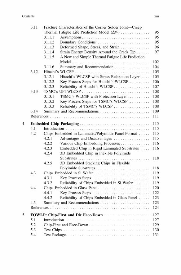
The advantages of fan-out WLP over fcPBGA packages with solder bumped flipchip are (Fig. 1.11) (1) lower cost, (2) lower profile, (3) eliminating the substrate,(4) eliminating the wafer bumping, (5) eliminating the flip chip reflow, (6) elimi-nating the flux cleaning, (7) eliminating the underfill, (8) better electrical perfor-mance, (9) better thermal performance, and (10) easier to go for system-in-package(SiP) and 3D IC packaging [24].
The advantages of fan-out WLP over fan-in WLP are (Fig. 1.12) (1) the use ofknown good die (KGD), (2) better wafer-level yield, (3) using the best of silicon,(4) single or multichip, (5) embedded integrated passive devices, (6) more layer ofRDLs, (7) higher pin counts, (8) better thermal performance, (9) easier to go for SiPand 3D IC packaging, and (10) higher PCB level reliability.
Fan-out WLP can do the same things fan-in WLP can, such as for low-cost,low-end, low-profile, low pin count, small form factor, and high-volume applica-tions. In addition, fan-out WLP can do most of the things PBGA can, such as formiddle-end to high-end microprocessor, ASIC, and memory applications. Evenfan-out WLP is not in very high-volume manufacturing yet, however, because of
TiCu
Ni
PIAl Pad(Original Pad)
PI
Passivation
Cu-RDL
Cu Pad (Stud)Ni
TiCu
Solder Bump
Solder Bump
Cu Stud
1
2
3
4
5
6
7
8
9
10
11
12
13
14
15
16
17
18
19
20
21
22
23
24
25
26
27
28
29
30
31
32
33
34
35
36
37
38
39
40 48
47
46
45
44
43
42
41
Al Pad(Original Pad)
Cu-RDL
Device Wafer with Chips
Cu-Pad
Chip
Fig. 1.8 WLCSP made by fan-in WLP technology
1.4 Patents Impacting the Semiconductor Packaging 9

the important advantages over the fan-in WLP and PBGA; it has the potential forsubstantial growth. Thus, this author considers fan-out WLP as the four mostimpactful for semiconductor packaging in the near future.
1.5 Major Claims of Infineon’s Patent
The major claims of Infineon’s patent [20] are the use of RDLs to fan-out thecircuitry from the metal pad of the chip and solder ball to the metal pads on a PCB,Figs. 1.9 and 1.10. The company [20] also claimed that some of the RDLs have aportion that extends beyond the edges of the chip. As a matter of fact, Infineon [20]did not claim anything such as die-first or last, die-up or down, RDL-first or last,mold-first or last, and reconfigured wafer or panel at all. It is a “structure” patent.
Fig. 1.9 Fan-out WLP patentproposed by Infineon
10 1 Patent Issues of Fan-Out Wafer-Level Packaging
KGDKGDEMC
RDLsPad
PadDielectric
Solder ball
KGDKGD
Solder ballEMC
Solder ball
PCB
Fig. 1.10 Fan-out WLP—multiple chips
Chip
OrganicSubstrate Underfill
Solder BumpsSolder Balls
Molded Compound
(1) lower cost(2) lower profile(3) eliminating the substrate(4) eliminating the wafer bumping(5) eliminating the flip chip reflow(6) eliminating the flux cleaning(7) eliminating the underfill(8) better electrical performance(9) better thermal performance(10) easier to go for system-in-package (SiP) and 3D IC packaging
ChipEMC
Fig. 1.11 Advantages of fan-out WLP over fcPBGA
1.5 Major Claims of Infineon’s Patent 11

1.6 TSMC InFO-WLP
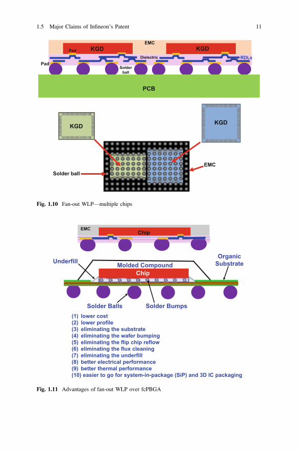
One of the most famous fan-out WLPs is TSMC’ integrated fan-out wafer-levelpackaging (InFO-WLP). Figure 1.13 schematically shows a typical process of theInFO-WLP technology [25–28]. It starts off by KGD testing of a device wafer.Then, under bump metallization (UBM) is performed by sputtering (e.g., Ti/Cu)with physical vapor deposition (PVD), and the Cu contact pad (or post) accom-plished using electroplating. These steps are followed by spin coating a polymer[e.g., polyimide (PI), benzocyclobutene (BCB), or polybenzobisoxazole (PBO)] ontop of the whole device wafer and laminating a die-attach film (DAF) on the bottomof the whole device wafer. Then, singulating the device wafer into individual dies,Fig. 1.13a. The individual KGD is placed (face-up) on a temporary round carrier(wafer) with a light-to-heat conversation (LTHC) layer as shown in Fig. 1.13b, andthen EMC (epoxy molding compound) dispensing, compression molding, andpost-mold curing of EMC are done on the whole temporary wafer with KGDs toform the molded reconstituted wafer (Fig. 1.13c). It is followed by backgrinding theEMC of the reconstituted wafer to expose the Cu contact pad (Fig. 1.13d), buildingup the RDLs (Fig. 1.13e) with conventional processes [29], and mounting thesolder ball, Fig. 1.13e. Finally, remove the temporary wafer (Fig. 1.13f) and sin-gulate the reconfigured wafer into individual units, and then we have the fan-outpackage by InFO-WLP technology. Comparing the cross section of Fig. 1.13f with
(1) the use of known good die (KGD)(2) better wafer-level yield(3) using the best of silicon(4) multichip(5) embedded integrated passive devices(6) more than one RDL(7) higher pin counts (or die shrink)(8) better thermal performance(9) easier to go for SiP and 3D IC packaging(10) higher PCB level reliability.
ChipEMC
Chip
Fig. 1.12 Advantages of fan-out WLP over fan-in WLP
12 1 Patent Issues of Fan-Out Wafer-Level Packaging

KGDUBMCu contact pad
Pad Pad
Polymer UBM
SiO2
Si Chip
Passivation
(a)
Si SiO2
PassivationPad
UBM
Pad
Temporary round Carrier
Die attach film
Polymer
Chip
(b)
Cu contact pad Cu contact pad
Cu contact padCu contact pad
LTHC
Si SiO2
PassivationPad
UBM
Pad
Temporary round Carrier
Die attach film
Polymer
Chip
(c)
EMC Cu contact pad Cu contact pad
Fig. 1.13 Integrated fan-out (InFO)-WLP patent proposed by TSMC. a UBM and Cu contact padon the Al-pad and polymer over the whole wafer. b Laminate a DAF on the backside of the devicewafer and attach to a glass carrier with LTHC layer. c Compression mold and PMC. d Backgrindthe EMC to expose the Cu contact pad. e Build the RDLs and solder balls. f Debond the glasscarrier by a laser, then dicing
1.6 TSMC InFO-WLP 13
that of Figs. 1.9 and 1.10, it can be seen that they are similar, i.e., the RDLs fan-outthe circuitry beyond the chip edge.
TSMC have been working on a new package-on-package (PoP) called InFO-PoPfor the application processor (AP) chipset (mobile DRAM + AP SoC). Just likeTSMC’ CoWoS (chip-on-wafer on substrate) technology, they called this PoW(package-on-wafer) technology [30–32]. PoW means the mobile DRAM package isstacked on the AP InFO reconfigured wafer, and the connection between thememory package and the AP InFO package is by through-InFO-via (TIV).
TSMC put the PoP of AP with FOWLP technology into high-volume manu-facturing on September 15, 2016. This is very significant, since this means thatFOWLP is not just only for packaging baseband, power management IC, RF (radiofrequency) switch/transceiver, RF radar, audio codec, microcontroller unit, con-nectivity ICs, etc., it can also be used for packaging high-performance and large(>120 mm2) SoC (system-on-chip) such as APs. More information on TSMC’sPoP will be presented in Chap. 8.
Over Mold
Si SiO2
PassivationPad
UBM
Pad
Temporary round Carrier
Die attach film
Polymer
Chip
EMC
(d)Cu contact pad Cu contact pad
Si
SiO2
PassivationPad
UBM
Pad
PolymerPolymer
Chip
Solder Ball
Solder Ball
RDLRDL
UBMUBM
Polymer/DielectricPolymer/Passivation
Die attach film
Temporary round Carrier
EMC
Si
(e)
SiO2 Passivation Pad
UBM Cu contact pad
Pad
PolymerPolymer
Chip
Solder Ball
Solder Ball
RDL RDL
UBM UBM
Polymer/DielectricPolymer/Passivation
Die attach film
EMC Si
(f)
Cu contact pad
Cu contact padCu contact pad
Fig. 1.13 (continued)
14 1 Patent Issues of Fan-Out Wafer-Level Packaging
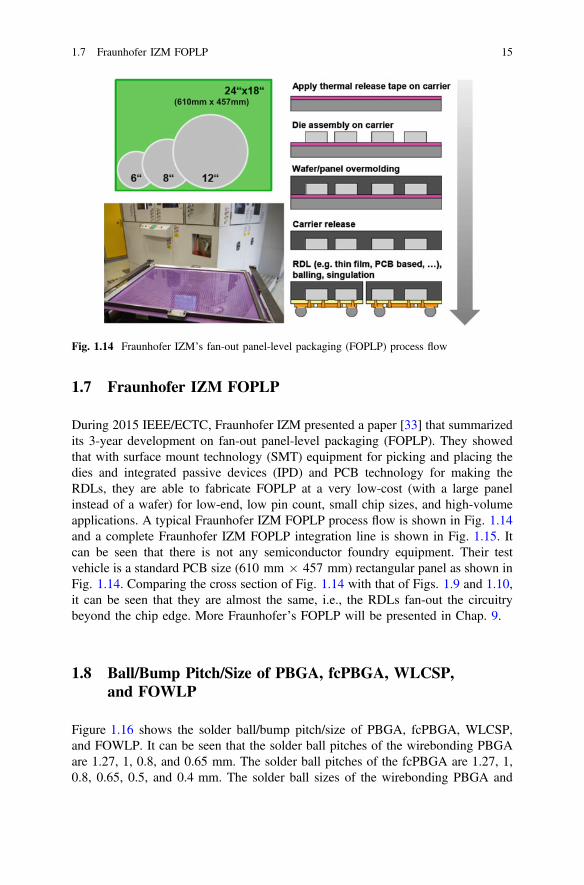
1.7 Fraunhofer IZM FOPLP
During 2015 IEEE/ECTC, Fraunhofer IZM presented a paper [33] that summarizedits 3-year development on fan-out panel-level packaging (FOPLP). They showedthat with surface mount technology (SMT) equipment for picking and placing thedies and integrated passive devices (IPD) and PCB technology for making theRDLs, they are able to fabricate FOPLP at a very low-cost (with a large panelinstead of a wafer) for low-end, low pin count, small chip sizes, and high-volumeapplications. A typical Fraunhofer IZM FOPLP process flow is shown in Fig. 1.14and a complete Fraunhofer IZM FOPLP integration line is shown in Fig. 1.15. Itcan be seen that there is not any semiconductor foundry equipment. Their testvehicle is a standard PCB size (610 mm � 457 mm) rectangular panel as shown inFig. 1.14. Comparing the cross section of Fig. 1.14 with that of Figs. 1.9 and 1.10,it can be seen that they are almost the same, i.e., the RDLs fan-out the circuitrybeyond the chip edge. More Fraunhofer’s FOPLP will be presented in Chap. 9.
1.8 Ball/Bump Pitch/Size of PBGA, fcPBGA, WLCSP,and FOWLP
Figure 1.16 shows the solder ball/bump pitch/size of PBGA, fcPBGA, WLCSP,and FOWLP. It can be seen that the solder ball pitches of the wirebonding PBGAare 1.27, 1, 0.8, and 0.65 mm. The solder ball pitches of the fcPBGA are 1.27, 1,0.8, 0.65, 0.5, and 0.4 mm. The solder ball sizes of the wirebonding PBGA and
(610mm x 457mm)
Fig. 1.14 Fraunhofer IZM’s fan-out panel-level packaging (FOPLP) process flow
1.7 Fraunhofer IZM FOPLP 15
fcPBGA vary. The solder bump pitch of WLCSP is 0.5, 0.4, 0.35, and 0.3 mm andthe solder bump size of WLCSP is 0.15 mm for 0.3 mm pitch. The solder ball pitchand size for FOWLP do not have a standard yet. However, it is recommended thatthe solder ball pitches of FOWLP are 0.5, 0.4, 0.35, and 0.3 mm. The solder ballsizes of FOWLP are 0.17 mm for 0.3 mm pitch, 0.225 mm for 0.35 mm pitch,0.25 mm for 0.4 mm pitch, and 0.3 mm for 0.5 mm pitch.
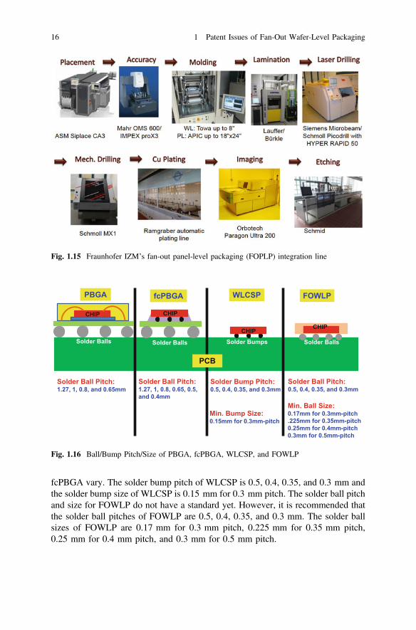
Fig. 1.15 Fraunhofer IZM’s fan-out panel-level packaging (FOPLP) integration line
Solder Ball Pitch: 1.27, 1, 0.8, and 0.65mm
Solder Bump Pitch: 0.5, 0.4, 0.35, and 0.3mm
Solder Ball Pitch: 0.5, 0.4, 0.35, and 0.3mm
Min. Bump Size: 0.15mm for 0.3mm-pitch
Min. Ball Size: 0.17mm for 0.3mm-pitch .225mm for 0.35mm-pitch 0.25mm for 0.4mm-pitch 0.3mm for 0.5mm-pitch
WLCSP
Solder Bumps
FOWLP
CHIP
Solder Balls
PBGA
Solder Balls
CHIP
fcPBGA
CHIP
Solder Balls
Solder Ball Pitch: 1.27, 1, 0.8, 0.65, 0.5, and 0.4mm
CHIP
PCB
Fig. 1.16 Ball/Bump Pitch/Size of PBGA, fcPBGA, WLCSP, and FOWLP
16 1 Patent Issues of Fan-Out Wafer-Level Packaging

1.9 Summary and Recommendations
The patent issues of embedded fan-out wafer-level packaging have been investi-gated. Some important results and recommendations are as follows:
– As of today, the patents impacting the semiconductor packaging industry themost are (1) leadframe [3], (2) organic substrate with area-array solder balls [4],(3) fan-in WLP [6], and (4) fan-out WLP [20].
– Fan-out WLP can do the same things fan-in WLP can such as for low-cost,low-end, low-profile, low pin count, small form factor, and high-volumeapplications.
– Fan-out WLP can do most of the things PBGA can such as for middle-end tohigh-end microprocessor, ASIC, and memory applications. However, some ofthe things PBGA can do but fan-out WLP cannot are (1) large die size(� 12 mm � 12 mm) and (2) large fan-out package size (� 25 mm � 25mm). These are due to the thermal expansion mismatch and warpage limitationsof the fan-out WLP.
– Infineon’s patent [20] is a “structure” patent. The major claims are the use ofRDLs to fan-out the circuitry from the metal pad of the chip and solder ball tothe metal pads on a PCB; some of the RDLs have a portion that extends beyondthe edges of the chip.
– If the cross section of an individual fan-out package (no matter if it is made fromdie-first or last, die-up or down, RDL-first or last, mold-first or last, andreconstituted wafer or panel) looks like the one in Figs. 1.9 and 1.10 (RDLsfan-out the circuitry beyond the chip edge), then it is subjected to Infineon’spatent [20].
– Instead of trying to avoid Infineon’s fan-out WLP patent [20], the focus shouldbe on the development of new and innovative applications such as TSMC’low-profile and low-cost InFO-PoP and Fraunhofer IZM’s low-cost andhigh-volume FOPLP with SMT and PCB/LDI technology.
– The geometry, material, process, equipment, and application of fan-out wafer/panel-level packaging are recommended as follows (Fig. 1.17).
• For high-end applications (e.g., high-end APs), the reconstituted carrier is awafer, and the RDL line width/spacing and thickness are, respectively, � 5and 2 lm right now. But very soon the RDLs are going down to � 2 and1 lm, and the lithography process is accomplished using a stepper. They arefabricated by the Cu damascene method. The dielectric layer (SiO2) is*1 lm thick and fabricated by the plasma-enhanced chemical vapordeposition (PECVD) method. A high-precision pick-and-place (P&P) bonderis needed for die placement.
• For middle-end applications (e.g., low-end APs, ASIC and memory), thereconstituted carrier is a wafer, and the RDL line width/spacing and thick-ness are, respectively, 5–10 and 3 lm, and the lithography is accomplishedusing a mask aligner or stepper for better yield. They are fabricated by the
1.9 Summary and Recommendations 17

electrochemical deposition method. The dielectric layer comprises polymers(e.g., PI, PBO, or BCB) and is 4–8 lm thick. An ordinary P&P bondershould be able to perform the die placement.
• For low-end applications (e.g., Wi-Fi/Bluetooth, FMmodule, RF transceivers,PMIC, baseband, and the power management unit), the reconstituted carriercan be a panel, and the RDL line width/spacing and thickness are, respectively,10–20 and 5 lm. They can be fabricated using PCB/LDI technology.A resin-coated copper (RCC) sheet or Ajinomoto build-up film (ABF) islaminated on the reconstituted panel. Microvias are drilled through the RCC orABF layer to the die pads and electrically connected by Cu plating. RDLformation is done by laser direct imaging (LDI) in combination with a dry filmresist and copper etching. The dielectric layer (resin or film) ranges from 5 to30 lm. In general, an SMT P&P is adequate for die and IPD placement.
• There is a small overlapping area between the high-end and middle-end, andthe middle-end and low-end.
References
1. Lau, J.H., C. Wong, J. Price, and W. Nakayama. 1998. Electronic Packaging. New York:McGraw-Hill Book Company.
2. Lau, J.H. 2015. Patent Issues of Fan-Out Wafer/Panel-Level Packaging. Chip Scale Review19: 42–46.
> 10µm
< 2 - 5µm
5 - 10µm
Reconstituted carrier width/spacing Appl.
Middle-end
High-end
Low-end
thick.
≤ 2µm
≥ 3µm
≥ 5µmLaser direct
imaging
Stepper
Mask aligner/ Stepper
_Cu damascene/CMP_Semi. Equip._High-Precision P&P
_ECD/Etching_Packaging Equip._Ordinary P&P
_PCB Cu plating _PCB Equip._SMT P&P
Litho. Proc./Equip. DielectricMat.(Thick.)
SiO2 (1µm)
Polymers (4 - 8µm)
Resin (15 - 30µm)
ABF (5 - 10µm)
Conductor Layer (Cu)
KGDKGDEMC
RDLsPad
Pad
Solder mask, polymer, or SiO2
Dielectric
Solder ball
Fig. 1.17 Geometry, material, process, and equipment for fan-out wafer/panel WLP
18 1 Patent Issues of Fan-Out Wafer-Level Packaging

3. Kauffman, J. 1969. Method of Packaging Integrated Circuits. US Patent 3,436,810, Filed onJuly 17, 1967, Patented on April 8, 1969.
4. Lin, P., M. McShane, and P. Wilson. 1993. Semiconductor Device Having a Pad ArrayCarrier Package. US Patent 5,216,278, Filed on March 2, 1992, Patented on June 1, 1993.
5. Freyman, B., and R. Pennisi. 1991. Overmolded Plastic Pad Array Carriers (OMPAC): A LowCost, High Interconnect Density IC Packaging Solution for Consumer and IndustrialElectronics. In Proceedings of IEEE/ECTC, May 1991, 176–182.
6. Elenius, P., and H. Hollack. 2001. Method for Forming Chip-Scale Package. US Patent6,287,893, Filed on July 13, 1998, Patented on September 11, 2001.
7. Elenius, P. 1997. FC2SP-(Flip Chip-Chip Size Package). In Proceedings of NEPCON West,February 1997, 1524–1527.
8. Elenius, P. 1998. Flip-Chip Bumping for IC Packaging Contractors. In Proceedings ofNEPCON West, February 1998, 1403–1407.
9. Yasunaga, M., S. Baba, M. Matsuo, H. Matsushima, S. Nakao, and T. Tachikawa. 1994.Chip-Scale Package: A Lightly Dressed LSI Chip. In Proceedings of IEEE/CPMTInternational Electronics Manufacturing Technology Symposium, 169–176.
10. Baba, S., Y. Tomita, M. Matsuo, H. Matsushima, N. Ueda, and O. Nakagawa. 1996. Shellcase—A True Miniature Integrated Circuit Package. In Proceedings of IEEE/ECTC, May 1996,1251–1257.
11. Marcoux, P. 1994. A Minimal Packaging Solution for Known Good Die and Direct ChipAttachment. In Proceedings of Surface Mount International Conference, August 1994, 19–26.
12. Chanchani, R., K. Treece, and P. Dressendorfer. 1995. A New Mini Ball Grid Array(m-BGA) Multichip Module Technology. In Proceedings of NEPCON West, February 1995,938–945.
13. Badihi, A., and E. Por. 1995. Shellcase—A True Miniature Integrated Circuit Package. InProceedings of International FC, BGA, Advanced Packaging Symposium, February 1995,244–252.
14. Topper, M., J. Simon, and H. Reichl. 1996. Redistribution Technology for Chip-ScalePackage Using Photosensitive BCB. Future Fab International, 363–368.
15. Auersperg, J., D. Vogel, J. Simon, A. Schubert, and B. Michel. 1997. Reliability Evaluationof Chip-Scale Packages by FEA and MicroDAC. In Proceedings of Symposium on Designand Reliability of Solder and Solder Interconnections, 439–445.
16. DiStefano, T. 1997. Wafer-Level Fabrication of IC Packages. Chip Scale Review, 20–27.17. Kohl, J., C. Eichellerger, S. Phillips, and M. Rickley. 1997. Low-Cost Chipscale Packaging
and Interconnect Technology. In Proceedings of the CSP Symposium, 37–43.18. Lau, J.H., and S.W.R. Lee. 1999. Chip Scale Package. New York: McGraw-Hill Book
Company.19. Lau, J.H. 2015. Semiconductors and Packaging for Internet of Things. Chip Scale Review,
25–30.20. Hedler, H., T. Meyer, and B. Vasquez. 2004. Transfer Wafer-Level Packaging. US Patent
6,727,576, Filed on October 31, 2001, Patented on April 27, 2004.21. Eichelberger, C., and R. Wojnarowski. 1991. High-Density Interconnect With High
Volumetric Efficiency. US Patent 5,019,946, Filed on September 27, 1988, Patented onMay 28, 1991.
22. Fillion, R., R. Wojnarowski, M. Gdula, H. Cole, E. Wildi, and W. Daum. 1994. Method forFabricating an Integrated Circuit Module. US Patent 5,353,498, Filed on July 9, 1993,Patented on October 11, 1994.
23. Eichelberger, C. 1998. Single-Chip Modules, Repairable Multi-Chip Modules, and Methodsof Fabrication Thereof. US Patent 5,841,193, Filed on May 20, 1996, Patented on November24, 1998.
24. Lau, J.H. 2015. 3D IC Integration and Packaging. New York: McGraw-Hill Book Company.25. Lin, J., J. Hung, N. Liu, Y. Mao, W. Shih, and T. Tung. 2015. Packaged Semiconductor
Device With a Molding Compound and a Method of Forming the Same. US Patent 9,000,584,Filed on December 28, 2011, Patented on April 7, 2015.
References 19

26. Lau, J.H., N. Fan, and M. Li. 2016. Design, Material, Process, and Equipment of EmbeddedFan-Out Wafer/Panel-Level Packaging. Chip Scale Review 20: 38–44.
27. Lau, J.H., et al. 2017. Warpage and Thermal Characterization of Fan-Out Wafer-LevelPackaging. IEEE Transactions on CPMT 7 (10): 1729–1738.
28. Lau, J.H., et al. 2017. Fan-Out Wafer-Level Packaging (FOWLP) of Large Chip withMultiple Redistribution Layers (RDLs). IMAPS Transactions Journal of Microelectronicsand Electronic Packaging 14 (4): 123–131.
29. Lau, J. H., P. Tzeng, C. Lee, C. Zhan, M. Li, J. Cline, K. Saito, et al. 2014. RedistributionLayers (RDLs) for 2.5D/3D IC Integration. IMAPS Transactions, Journal of MicroelectronicPackaging 11 (1): 16–24 (First Quarter 2014).
30. Yu, D. 2014. Wafer-Level System Integration (WLSI) Technologies for 2D and 3DSystem-In-Package. In SEMIEUROPE 2014.
31. Tseng, C., C. Liu, C. Wu, and D. Yu. 2016. InFO (Wafer Level Integrated Fan-Out)Technology. In IEEE/ECTC Proceedings, 1–6.
32. Hsieh, C., C. Wu, and D. Yu. 2016. Analysis and Comparison of Thermal Performance ofAdvanced Packaging Technologies for State-of-the-Art Mobile Applications. In IEEE/ECTCProceedings, 1430–1438.
33. Braun, T., S. Raatz, S. Voges, R. Kahle, V. Bader, J. Bauer, K.-F. Becker, T. Thomas, R.Aschenbrenner, and K. D. Lang. 2015. Large Area Compression Molding for Fan-out PanelLevel Packing. In Proceedings of IEEE/ECTC, May 2015, 1077–1083.
20 1 Patent Issues of Fan-Out Wafer-Level Packaging

Chapter 2Flip Chip Technology Versus FOWLP
2.1 Introduction
In this chapter, a flip chip is defined [1–4] as a chip attached to the pads of asubstrate or another chip with various interconnect materials (e.g., Sn–Pb, Cu, Au,Ag, Ni, In, and isotropic or anisotropic conductive adhesives) and methods [e.g.,mass reflow and thermocompression bonding (TCB)], as long as the chip surface(active area or I/O side) is facing the substrate or another chip as shown in Fig. 2.1.
The flip chip technology was introduced by IBM in the early 1960s for theirsolid logic technology, which became the logical foundation of the IBM System/360 computer line [5]. Figure 2.2a shows the first IBM flip chip with three terminaltransistors, which are Ni/Au-plated Cu balls embedded in an Sn–Pb solder bump onthe three I/O pads of transistor. A Cr–Cu–Au adhesion/seed layer is depositedbetween the Al–Si contact pads on the Si chip and the solder bump. Figure 2.2bshows the first IBM flip chip assembly (three chips) on a ceramic substrate.
As the I/Os increase, the Cu ball is replaced by solder bump. The so-called C4(controlled collapse chip connection) technology [6] utilizes high-lead solderbumps deposited on wettable metal terminals on the chip and a matching footprintof solder wettable terminals on the substrate. The solder-bumped flip chip is alignedto the substrate, and all solder joints are made simultaneously by reflowing thesolder.
Today, the applications of flip chip technology have been extended to [7–12]chip-to-chip, face-to-face, and face-to-back. Figure 2.3 shows Amkor’s Double-POSSUM package [12]. It can be seen that the package is actually defined by twolevels of nesting die. The three daughter dies are flip chip attached to the largermother die which is then attached to the largest grandma die. The grandma die isthen flip chip attached to the package substrate. The bumps between the daughterdies and the mother dies are microbumps (Cu pillar with solder cap). C4 bumps areused between the mother die and grandma die, and between the grandma die andpackage substrate.
© Springer Nature Singapore Pte Ltd. 2018J. H. Lau, Fan-Out Wafer-Level Packaging,https://doi.org/10.1007/978-981-10-8884-1_2
21
Flip chip technologies have been used extensively for the processors of main-frame computers, servers, personal computers, notebooks, smartphones, tablets,games, etc., the application-specific integrated circuits (ASICs) of networking,telecommunications, etc., and the memories of data storage devices, etc. Most of theflip chip assemblies are mass reflowed.
Recently, because of the requirements of higher functionalities of the chips andshrinking the chips’ area, the number of pin-outs of the processors, ASICs, andmemories increases and their pitch (or the spacing between the pin-out pads)decreases. Also, because of the trends of smaller form factors for mobile (e.g.,smartphones and tablets) and portable (e.g., notebooks) products, the thickness ofthe chips and package substrates must be as thin as possible. Higher pin counts,tighter pitches, thinner chips, and thinner package substrates lead to the necessity ofthe TCB method for flip chip assemblies. In this study, besides mass reflow, variousTCB techniques are mentioned.
Recent advances in high-density and low-cost package substrates have promotedmore flip chip applications. In this study, the organic build-up substrate, organicbuild-up substrate with thin-film layers, coreless substrate, bump-on-lead (BOL),and embedded trace substrate (ETS) will be discussed.
In order to enhance the solder joint reliability of flip chip assemblies, underfill isa must, especially for organic package substrate. In this study, the preassemblyunderfill such as the no-flow underfill (NUF), nonconductive paste (NCP), andnonconductive film (NCF) will be discussed. Also, the post-assembly underfill such
Ceramic, Silicon, or Organic Substrate
Silicon Flip Chip Solder Joint
TCE of Ceramic = 5-6x10⁻⁶/oC; TCE of Organic = 15-18x10-6/oC TCE of Silicon = 2.5x10⁻⁶/oC
Underfill
ChipSolder or Cu-Pillar bumps on the active surface of the Chip
Metal PadSubstrate or Chip
(a)
(b)
Fig. 2.1 a Definition of flip chip assembly. b Flip chip assembly on various substrates
22 2 Flip Chip Technology Versus FOWLP

as the capillary underfill (CUF) and molded underfill (MUF) will be examined.Since wafer bumping is the mother of flip chip technology, it will be brieflymentioned first.
Flip chip technology is facing stiff competition from fan-out wafer-level pack-aging (FOWLP) [13, 14], which will be discussed in Chaps. 4, 5, 6, 7, 8, 9, 10, and 11.Fan-in wafer-level packaging (WLCSP) [15–17] will be discussed in Chap. 3.
Cu Ball with Ni and Au plated
Sn-Pb SolderCr-Cu-Au
Terminal PadAl-Si
Flip Chip
Flip Chip
Flip Chip
Ceramic Substrate
(a)
(b)
Fig. 2.2 a IBM’s first flip chip component with three-terminal transistors. b IBM’s first flip chipassembly (3 chips) on a ceramic substrate
2.1 Introduction 23

2.2 Wafer Bumping
There are many ways to perform the wafer bumping (at least 12 are shown in [2]),and the most common method is by electrochemical deposition (ECD) or electro-plating [18]. Stencil printing method [19–25] is also used for wafer bumping but itwill not be presented herein.
2.2.1 C4 Bumps
Usually, the pad size is equal to 100 lm and the target bump height is equal to 100lm. After redefining the passivation opening (usually, it is not required), either Tior TiW (0.1–0.2 lm) are sputtered over the entire surface of the wafer first, fol-lowed by 0.3–0.8 lm of Cu. Ti–Cu and TiW–Cu are called under bump metallurgy(UBM). In order to obtain 100 lm bump height, a 40 lm layer of resist is thenoverlaid on the Ti–Cu or TiW–Cu and a solder bump mask is used to define(ultraviolet exposure) the bump pattern as shown in steps #1–4 in Fig. 2.4. Theopening in the resist is 7–10 lm wider than the pad opening in the passivation layer.A 5 lm layer of Cu is then plated over the UBM, followed by electroplating thesolder. This is done by applying a static or pulsed current through the plating bathwith the wafer as the cathode. In order to plate enough solder to achieve the target(100 lm), the solder is plated over the resist coating by about 15 lm to form amushroom shape. The resist is then stripped off and the Ti–Cu or TiW–Cu isremoved with a hydrogen peroxide or plasma etching. The wafer is then reflowed
Mother Die Daughter Die Grandma Die
Package Substrate
PCB
Cu Pillar Micro-Bumps with SnAg Solder Caps (C2 Bumps)
Daughter DieDaughter Die
C4 BumpsSolder Ball
Fig. 2.3 3D IC packaging (Amkor’s multiple chip-to-chip interconnects)
24 2 Flip Chip Technology Versus FOWLP

with flux, which creates smooth truncated spherical solder C4 bumps, Figs. 2.4 and2.5, due to surface tension as shown in steps #5–8 on the right-hand side of Fig. 2.4[18].
2.2.2 C2 (Cu Pillar with Solder Cap) Bumps
Because of higher pin count and tighter pitch (smaller spacing between pads), thereis a possibility of shorting the adjacent solder C4 bumps. Wire interconnects [26]and Cu pillar with solder cap [27, 28] can be a solution. The fabrication process isbasically the same as that of the C4 bumps except electroplating the Cu instead ofsolder as shown in step #5 of Fig. 2.6. It is followed by electroplating the solder capand then reflowing the solder with flux (Fig. 2.7a shows the Cu pillar with solder
Si
Solder
Passivation
TiCu
Pad
Cu
Passivationpad
Cu
(1) Redef. Passivation
(2) Sputter Ti/Cu (4) Patterning
(3) Spin Resist
MaskTi
UV
SolderCu
(5) ECD Cu, Solder
(6) Strip Resist
(7) Etch Cu/Ti
(8) Flux, Reflow
Solder
Si
Fig. 2.4 Wafer bumping by ECD or electroplating method for C4 bumps
Si
100μm
Cu Pad/UBM
Fig. 2.5 SEM image of C4bumps
2.2 Wafer Bumping 25

Cu
Solder
SiPassivation
TiCu
Pad
Passivationpad
Cu
(1) Redef. Passivation
(2) Sputter Ti/Cu (4) Patterning
(3) Spin Resist
MaskTi
UV
CuSolder
(5) ECD Cu, Solder
(6) Strip Resist
(7) Etch Cu/Ti
(8) Flux, Reflow
Solder
Cu
Si
Fig. 2.6 Wafer bumping by ECD or electroplating method for C2 bumps
Cu Pad/UBMSi
(b)
(a)
Cu Pillar
SnAg
Fig. 2.7 a SEM image of C2bumps with solder cap.b SEM image of C2 bumpswithout solder cap
26 2 Flip Chip Technology Versus FOWLP

cap and Fig. 2.7b shows the very tall Cu pillar without solder cap). Because thesolder volume is very small compared with the C4 bump, the surface tension is notenough to perform the self-alignment of the Cu pillar with the solder cap bump andtherefore, it is sometimes called a C2 (chip connection) bump. Besides being able tohandle finer pitch, C2 bumps also provide better thermal and electrical perfor-mances than C4 bumps. This is because the thermal conductivity (W/m K) andelectrical resistivity (µΩm) of Cu (400 and 0.0172) are superior to those (55–60 and0.12–0.14) of solder as shown in Table 2.1.
2.3 Flip Chip Package Substrates
In the past few years, tremendous efforts have been devoted to enhance/advance thecapabilities of the conventional low-cost build-up organic package substrates byincreasing the number of build-up layers, fabricating thin-film layers on top of thebuild-up layer, shrinking the dimensions of the metal line width and spacing,reducing the pad size and pitch, eliminating the core, making the BOL, and lam-inating the ETS. For silicon substrates, first come with the TSV interposer and thefuture trend is for TSV-less interposer, which will be discussed in Chap. 10.Ceramic substrate [29–34] will not be discussed in this book.
2.3.1 Surface Laminar Circuit (SLC) Technology
Almost 25 years ago, IBM in Japan at Yasu invented the SLC technology, Fig. 2.8[35–38], which formed the basis of today’s very popular low-cost organic packagesubstrates with build-up layers vertically connected through microvias [39–59] tosupport flip chips. There are two parts of the SLC technology: one is the coresubstrate and the other is the SLC for the signal wiring. The core substrate is madeby the ordinary glass epoxy panel. However, the SLC layers are sequentially builtup with the dielectric layers made of photo-sensitive epoxy and the conductor planeof copper plating (semi-additive technique). In general, a package substrate withtwelve layers [e.g., two core layers and ten build-up layers (5-2-5)] and 10 µm linewidth and spacing are more than adequate to support most of the chips.
Table 2.1 C4 bumps versus C2 bumps
Structure Majormaterial
Thermal conductivity(W/m K)
Electricalresistivity (µΩm)
Padpitch
Self-alignment
C2bump
Cu 400 0.0172 Smaller Smaller
C4bump
Solder 55–60 0.12–0.14 Larger Larger
2.2 Wafer Bumping 27

2.3.2 Integrated Thin-Film High-Density OrganicPackage (i-THOP)
In 2013, Shinko proposed to make thin-film layers on top of the build-up layer of apackage substrate. Figure 2.9 shows Shinko’s i-THOP substrate [60, 61] forhigh-performance applications. It is a 4 + (2-2-3) test vehicle, which means there isa two-layer metalcore, three build-up metal layers at the bottom (PCB) side, twobuild-up metal layers on the top (chip) side, and the first number “4” represents thatthere are four thin-film Cu wiring layers (RDLs) on the surface of the top build-uplayer. The thickness, line width, and spacing of the thin-film Cu RDLs can be assmall as 2 µm. The thin-film Cu RDLs are vertically connected through a 10 µmvia, as shown in Fig. 2.9. The surface Cu pad pitch is 40 lm, and the Cu paddiameter is 25 µm with a height of 10–12 µm. The i-THOP substrate passed thewarpage and reliability tests and there was no via delamination observed [60].
In 2014, Shinko demonstrated that [61] ultrafine pitch flip chips can be suc-cessfully assembled on the i-THOP substrate. Figure 2.10 schematically shows thetwo chips’ lateral communications by the 2 µm line width/spacing RDLs of the twothin-film layers, which are built on top of the 1-2-2 build-up organic substrate,
Surface Laminar Circuit (SLC)
Substrate Core
Plate Through Hole (PTH)Solder Mask Microvia
Photosensitive Material
Power Line
1st Build-up Layer
3rd Build-up Layer2nd Build-up Layer
PTH
SLC
Substrate Core
PCB
Build-up package substrate
Chip ChipUnderfill Solder Bump
Solder Ball
Fig. 2.8 IBM’s SLC for flip chip organic build-up package substrate
28 2 Flip Chip Technology Versus FOWLP

10μm stack via
50μm build-up via
40μm pad pitch
2μm line width/spacing
100μm PTH
10μm stack via11.8μm thick pad25μm (dia.) Cu pad2μm line width1.9μm spacing2μm thick Cu
Build-up layers
Thin-Film layers
Core
Fig. 2.9 Shinko’s i-THOP; a flip chip package substrate with thin film layers on top of thebuild-up layer
Chip Chip
Chip-to-chip lateral interconnection through 2μm width traces
Thin Film (2 layers + FC Pad)
Conventional Build-up
Substrate (1-2-2)
40μm-pitch Pads
Chip1
Chip2
2μm line width/spacing (C2C lateral connection)
Chip1 Chip2
Chip1 Chip2
Fig. 2.10 Shinko’s i-THOP test vehicle. Two thin-film layers are built on top of the 1-2-2package substrate
2.3 Flip Chip Package Substrates 29
i.e., 2 + (1-2-2). Figure 2.11 shows the 40 µm pitch microbumps (Cu pillar +Ni + SnAg) of the test chips and the 40 µm pitch flip chip bonding pads (25 µmdiameter). Typical images of the cross section of the flip chip assembly withoptimized conditions are shown in Fig. 2.11. It can be seen that good solder jointsare confirmed in all areas of the assembly [61].
2.3.3 Coreless Substrate
Coreless substrate was first proposed by Fujitsu [62] in 2006. Figure 2.12 shows thecomparison between the conventional organic package substrate with build-uplayers and the organic coreless package substrate. It can be seen that the biggestdifference is that there is not a core in the coreless package substrate and all thelayers of the coreless package substrate are the build-up layers [62–84].
The advantages of the coreless package substrate are [62–84]: (a) because ofeliminating the core, the cost of the coreless substrate is lower; (b) by eliminatingthe core, higher wiring ability can be achieved; (c) better electrical performancebecause of good high-speed transmission characteristic; and (d) definitely smallerform factor. On the other hand, the disadvantages are [62–84]: (a) because ofeliminating the core, the warpage of the coreless substrate is larger; (b) easier tohave laminate chipping; (c) poor solder joint yield because of less substrate rigidity;
SEM image of test chip with μbumps
Passivation
Min. 40μm-pitchCu-pillar + Ni + SnAg
Daisy Chain
Schematic image of the test chip
40μm pitch flip chip bonding pads (25μm-diameter)
Fig. 2.11 C2 Microbumps at 40 µm pitch. 40 µm pitch flip chip bonding pads (25 µm diameter)on the i-THOP substrate. Good solder joints from optimized condition
30 2 Flip Chip Technology Versus FOWLP

and (d) new manufacturing infrastructure is necessary. In 2010, Sony manufacturedthe first coreless package substrate for the cell processor of their PlayStation 3 [74].
Even though coreless substrates have many advantages, they are not popularbecause of the warpage control issue. One of the key factors affecting the warpageis the coefficient of thermal expansion mismatch of substrate materials. Thus, aproper control of this factor will help reduce the warpage issue of coreless sub-strates. Another factor affecting the warpage is the package assembly. Thus, aproper package assembly warpage correction control (with vacuum and pressure)will help improve the warpage problem of coreless substrate.
2.3.4 Bump-on-Lead (BOL)
BOL was first proposed by STATS ChipPAC [85–89] and was used by Qualcomm[90] and others [90–93]. A conventional bump-on-capture pad (BOC) or simplybump-on-pad (BOP) flip chip organic substrate layout is shown in Fig. 2.13a. It canbe seen that the flip chip pads are on a 210-µm area-array pitch in a solder mask(SR) defined configuration with one signal escape between bump pads resulting inan effective escape pitch of 105 µm. The BOL methodology is shown in Fig. 2.13b;here, the landing pad on the substrate is merely the trace (lead) itself, or a slightlywidened version of the trace which results in freeing up of enough routing space toallow routing an additional trace between bumps thereby resulting in an effectiveescape pitch of 7 µm without changing the design rules (trace width and space) ofthe substrate. The improved BOL structure is shown in Fig. 2.13c. It can be seen
Build-up Layers
Build-up Layers
ChipUnderfillBump
Filled Micro ViaCore
UnderfillBump
Chip
Coreless Build-up Layers
Core
Coreless
Build-up Package Substrate with Core
Coreless Build-up Package Substrate Filled
Micro Via
Fig. 2.12 (Top) Flip chip on conventional build-up package substrate. (Bottom) Flip chip oncoreless substrate
2.3 Flip Chip Package Substrates 31

that the bump pads are without any solder resist confinement, i.e., open SR [90].The test vehicles, Cu column on BOL, used in Ref. [90] are shown in Fig. 2.13dand e. It can be seen that one trace between the 180 µm bump pitch and up to twotraces with the 20 µm bump pitch can be comfortably routed.
Typical cross sections of the perpendicular-to-BOL and longitudinal-to-BOL areshown in the upper portion of Fig. 2.14. A 3D slide finite element model showingthe BOL, BOC (or BOP), and solder joint is shown in the middle of Fig. 2.14. Thecreep strain contours of the BOL solder joint are shown in the lower portion ofFig. 2.14 [93] and are too small to create solder joint reliability problem under mostconditions.
2.3.5 Embedded Trace Substrate (ETS)
ETS is one of the coreless substrates with fine line width/spacing embedding the topmetal trace pattern into prepreg layer [94–98]. The process flow of ETS is shown inFig. 2.15a. It starts from a carrier board with a removable Cu foil. It is followed by
33 84
180
45
30
84
45
200
3030
13
μmμm
μm
μm μm
(a)
(e)(d)
(c)(b)Improved BOL Structure
Bumps without solder resist confinement
Two-trace escaping
Improved BOL with Cu-Pillar FC (180μm-pitch) Improved BOL with Cu-Pillar FC (200μm-pitch)
Cu CuCu Cu
CHIP CHIP
Fig. 2.13 Bump-on-lead (BOL). a Conventional BOP. b New BOL. c Improved BOL.d Improved BOL with Cu pillar FC (180 lm pitch). e Improved BOL with Cu pillar FC(200 lm pitch)
32 2 Flip Chip Technology Versus FOWLP

Cu-PillarCu-Pillar
LeadLead
SolderSolder
CHIPCHIP
Perpendicular to BOL Longitudinal to BOL
Creep strain contour in the BOL solder joint
Fig. 2.14 Images of the perpendicular-to-BOL and longitudinal-to-BOL. Finite element modelsand creep strain contours in the BOL solder joint
CHIP
CuSolder
Embedded Trace
Cu
SolderBall
Coreless ETS
Underfill
CHIP
Cu-PillarSolder
Solder Ball
Prepreg
Solder Mask
Embedded Traces
Dry filmCu foilCarrier board
Cu plating
Remove DF
PP lamination
De-carrier
Micro-etching
SR pre-treatment
SR & OSP
(a) (b)
Fig. 2.15 a Process flow for fabricating the ETS. b Flip chip with C2 bumps on ETS assembly
2.3 Flip Chip Package Substrates 33

using a typical electrolytic copper plating method to form the first layer of copperpattern. Then, laminate a prepreg on the copper pattern. It is followed by laser viadrilling, electroless copper coating, dry film laminating, exposing and developing,second-layer copper pattern plating, stripping, and micro-etching. Once all thecopper pattern layers have been completed, the carrier board will be removed. Sincethe Cu foil is connected to the first copper pattern, micro-etching is necessary beforeSR coating. After the SR opening process, it is completed by metal finishestreatment, e.g., organic solderability preservatives (OSPs). Figure 2.15b shows across section of a Cu pillar flip chip on ETS assembly by SPIL [97]. Most linewidth/spacing of ETS in use today is 15/15 µm. However, 13/13 µm line width/spacing is in production by Simmtech [98].
2.4 Flip Chip Assembly
Basically, there are two groups of flip chip assemblies: one is with an intermediatelayer between the bonding pads/traces, and the other is not, i.e., nothing! Flip chipassembly with intermediate layers such as solder for mass reflow and Cu pillar withsolder cap by TCB is called as indirect bonding, which is the focus of this chapter.Cu-to-Cu diffusion bonding, which does not have anything between the bondingpads/traces on the chip/wafer, is therefore called as direct bonding.
2.4.1 Cu-to-Cu TCB Direct Bonding
Cu-to-Cu diffusion bonding can go down to ultrafine pitch and pad size (the spacingbetween pads is 5 µm or less). In order to reduce the tendency to form native oxidesthat strongly affect the bonding quality and reliability, Cu-to-Cu is a TCB andusually operates at high temperature and pressure and long process time [99–101],which are not good for throughput and the device reliability. On the other hand,Cu-to-Cu bonding at room temperature [102–108] leads to the highest throughputand the least amount of device reliability concerns, as well as very low costs.However, the drawbacks of room temperature bonding are the stringent require-ments on (a) pad/trace/wafer planarization, (b) surface treatment to ensure smoothhydrophilic surfaces for high-quality bonding, and (c) the class of cleanroom (veryhigh required). Cu-to-Cu TCB is mainly for wafer-to-wafer (W2W) assemblyprocess and is not in high-volume manufacturing yet, and thus, it is discussed at theend of this chapter.
34 2 Flip Chip Technology Versus FOWLP

2.4.2 C4 Solder Mass Reflow
Solder mass reflow has been used for flip chip assembly for almost 50 years. Mostof the solder C4 bumps are mass reflowed on either silicon, ceramic, or organicsubstrates. The assembly process is very simple, Fig. 2.16a: (i) use a lookup andlookdown camera to identify the location of the bumps on the chip and the pads onthe substrate; (ii) apply flux on either the C4 bumps, or the substrate, or both; and(iii) pick and place the C4-bumped chips on the substrate, then mass reflow withtemperature H. Because of the surface tension of the C4 solder bumps duringreflow, the process is very robust (self-alignment). Figure 2.17 shows the crosssection of iPhone 6 Plus (September 2015). It can be seen that the A9 applicationprocessor is housed in a PoP format and the solder-bumped flip chip is massreflowed on a 2-2-2 organic package substrate. In general, the spacing between thebumps on the solder mass reflow of C4-bumped chips can be as small as 50 lm.
H H H H H HH H H H
H H H H
(c) TCB with High-Force of C2 Bumps (NCP)
(d) TCB with High-Force of C2 Bumps (NCF)
H H H H H HH H H H
(a) Mass Reflow of C4 or C2 Bumps (CUF)
H H H H H HH H H H
(b) TCB with Low-Force of C2 Bumps (CUF)
f f f
F F F
F F F
Fig. 2.16 Flip chip assembly with indirect bonding. a Mass reflow of chips with C4 or C2 bumpswith CUF. b TCB with low force of chips with C2 bumps with CUF. c TCB with high force ofchips with C2 bumps with NCP. d TCB with high force of chips with C2 bumps with NCF
2.4 Flip Chip Assembly 35

2.4.3 C2 Solder Mass Reflow
In the past few years, solder mass reflow of C2 (Cu pillar with solder cap)-bumpedchips on either silicon, ceramic, or organic package substrates has been tried forhigh pin count and fine-pitch flip chip assemblies. The assembly process,Fig. 2.16a, is exactly the same as that of the C4 bumps, but the self-alignmentcharacteristic is nowhere near the same, and thus, it is seldom being used. Ingeneral, the spacing between the pillars on the solder mass reflow of C2-bumpedchips can be as small as 25 lm.
2.4.4 C2 TCB
In the past few years, TCB of chips with an intermediate layer such as C2 (Cu pillarwith solder cap) bumps on silicon, ceramic, or organic package substrates, has beenattracting attention for high-density and ultrafine pitch flip chip assemblies.Basically, there are two methods, one is with low bonding force and the other iswith a high bonding force.
LPDDR4 2-chipcross-stack wirebond
3-Layer Coreless substrate
A9
2-2-2 build-up substrate (380μm thick and 75μm hole)
150μm pitch
staggeredC4 bumps
0.4mm pitch
solder balls
90μm .35mm pitch
PCB
2GB LPDDR4
A9 application processorfabricated by 14/16nm Fin-FET process technology
Coreless Package Substrate for LPDDR4
2-2-2 Package Substrate for A9 processor
A9
Fig. 2.17 PoP in Apple’s smartphone. The C4 solder-bumped flip chip is mass reflowed on a2-2-2 package substrate
36 2 Flip Chip Technology Versus FOWLP

2.4.4.1 C2 TCB with Low Bonding Force
For the one with low bonding force, the assembly process is simple, Fig. 2.16b:(i) first, use the lookup and lookdown camera to locate the position of the C2 bumpson the chip and their corresponding pads on the substrate; (ii) apply flux on thesolder cap or on the substrate or both; and (iii) pick and place the chip on thesubstrate and then apply temperature (H) to melt the solder and a low force (f) tohold the chip at a certain distance from the substrate. The above procedure is doneone chip at a time and therefore, the throughput is low in comparison with the C2solder mass reflow process. Figure 2.18 shows a typical cross section of a flip chipassembly with TCB with low force on C2 bumps [109]. In general, the spacingbetween the pillars on the C2 chip by TCB with a low bonding force can be as smallas 8 lm.
2.4.4.2 C2 TCB with High Bonding Force
For TCB with a high bonding force on the C2 chip, the assembly process must becombined with the NCP or NCF underfill, which will be discussed in Sect. 2.5.
2.5 Underfill/Reliability
The reliability of flip chip solder joints is enhanced by the application of underfill[110–124], especially on organic substrate. Most underfills consist oflow-expansion fillers such as fused silica (SiO2) and a liquid prepolymer such asthermosetting resin (adhesive) that can be cured to a solid composite.
Chip
Chip
Cu-Pillar
Solder
Substrate Cu Pad
Substrate
Fig. 2.18 Cross section of a C2 flip chip assembled on an organic package substrate by a TCBwith low force (CUF)
2.4 Flip Chip Assembly 37

In 1987, Hitachi showed that with underfill, the thermal fatigue life of the flipchip solder joints on ceramic substrate increased [125]. In 1992, IBM at Yasuproposed the use of the low-cost organic substrate instead of the high-cost ceramicsubstrate for flip chip assemblies [35–38]. They showed that with underfill, thelarge thermal expansion mismatch between the silicon chip (2.5 � 10−6/°C) and theorganic substrate (15–18 � 10−6/°C) is reduced substantially and the solder jointsare reliable for most applications. This opened up the doors for today’s very popularsolder-bumped flip chip on low-cost organic substrate packages used, e.g., in theprocessors of personal computers, notebooks, smartphones, tablets, etc.
Basically, there are two different procedures to apply the underfill, namelypreassembly underfill and post-assembly underfill.
2.6 Post-assembly Underfill
For post-assembly underfill, the application of underfill is after the flip chipassembly, i.e., the flip chip is already on the substrate and the solder joints arealready mass reflowed (either with C2 or C4 bumps) or low-force TCB with C2bumps.
2.6.1 Capillary Underfill (CUF)
For post-assembly underfill, there are basically two methods, namely CUF [126–129] and MUF [130–134]. CUF is the first method that went into volume pro-duction [126–129]. For CUF, the underfill is dispensed by a needle or jet w/ovacuum assisted on one (or two) sides of the flip chip on substrate assembly.Because of capillary action, this underfill completely fills the space between thechips, solder joints, and substrates. The chip and the substrate are then firmlybonded by curing the underfill. CUF is performed one chip assembly at a time, andthus, throughput is an issue.
2.6.2 Molded Underfill (MUF)
Molded underfill was first proposed by Cookson Electronics [130] in 2000 and laterby, e.g., Dexter [131], Intel [128], Amkor [132], STATS ChipPAC [133], andLETI/STMicroelectronics [134]. For MUF, the modified EMC is transferredmolding the chip and filling the gap between the chip, solder joints, and the sub-strate of the flip chip assembly. The encapsulant of the chip and the underfill areformed at the same time, which will increase the throughputs. However, thechallenges of MUF are (a) the flow of MUF between the chip and the substrate is
38 2 Flip Chip Technology Versus FOWLP

usually assisted by vacuum; (b) the size of the silica filler of the EMC must be verysmall for flowability; (c) the cost of EMC for MUF is much higher than that forpackage molding; (d) package warpage is an issue due to the thermal expansionmismatch between the EMC, chip, and substrate; (e) the molding temperature islimited by the melting point of the solder joints; and (f) the standoff height and pitchof the solder joints cannot be too small.
2.6.3 Printed Underfill
In order to increase the throughput of CUF and avoid the drawbacks of MUF, amethod of post-assembly underfill has been proposed by Lucent Technologies[135], where a stencil is used to print the underfill material for flip chips on packagesubstrate assembly as shown in Fig. 2.19. It can be seen that (1) the stencil design iswith a wide opening which is at least the size of the chip [135]; (2) the stencilthickness is not above the height of the flip chip assembly [135] (Fig. 2.19); and
StencilStencil
openingStencil
opening
Chip Stencil
Underfill
Aperture
Stencil opening
Substrate
Printed underfillChip Chip
Aperture
Printed underfill
Substrate
(a)
(c)
(b)
Stencil opening
Stencil StencilChip
Aperture
Aperture
Fig. 2.19 aLucent Technologies’ stencil printing of underfill.bStencil openings. cPrinted underfill
2.6 Post-Assembly Underfill 39

(3) the substrates must have an aperture [135] to let the underfill to flow out. Thedrawbacks of [135] are (1) lots of underfills are wasted due to the very largeopening of the stencil and the flow out of underfill from the aperture of the sub-strate; (2) there is a very good chance to damage the chip due the very large openingof the stencil (to expose the entire backside of the chip) and the stencil thickness isnot taller than the backside of the chip (thus all the squeegee pressure is applied tothe backside of the chip) during printing; and (3) an aperture in the substrate is notpractical because it is not only affecting the routing but also increasing cost and thesize of the substrate.
In the present investigation [136], a new stencil will be designed for printing theunderfill for flip chips on organic-panel and Si-wafer assemblies. The effects of theviscosity, thermal enhancement, and multiple prints of underfills will be examined.The cured assemblies will be characterized by the C-SAM, X-ray, shear test,cross-sectioning, and SEM methods.
2.6.3.1 A New Stencil Design
A new stencil designed for printing underfill for flip chips on organic-panel andSi-wafer assemblies is proposed in the present investigation and shown in Figs. 2.20,2.21, and 2.22. It can be seen that (1) a very small rectangular opening of the stencil isdesigned for each chip and it is located on one edge of the chip; (2) the stencil is with adry film underneathwithmany rectangular openings (one for each chip) and the size isa little larger than the chip size; (3) there is a gap between the stencil and the backsideof the chips; and (4) there is a fixture to apply heat to the stencil and underfill to lowerthe underfill’s viscosity as shown in Fig. 2.20. The size of the stencil opening and thethickness of the stencil and dry film determine the underfill volume which should beapproximately equal to the space between the chip, solder joints, and the substrate plusthe filet on the four sides of the chip.
During printing (Fig. 2.20b), the underfill will fill the opening of the stencil andfall into the space between one edge of the chip and the dry film. After printing(usually, it only takes a few seconds), remove the assembly (Fig. 2.20c) from thestencil printer and place it on a hot plate (*120 °C) for the underfill to flowbetween the chip, solder joints, and the substrate by capillary action (Fig. 2.20d).Finally, cure the underfill.
Comparing the present stencil design with that of Luncet Technologies, theadvantages are (1) for a given chip size, solder joint size, and standoff height, theopening and thickness of the stencil and dry film can be estimated and there will notbe any waste of the underfill material; (2) because of the dry film underneath thestencil and the gap between the stencil and the backside of the chip, the chance ofdamaging the chip is very slim; (3) with the aid of heat, the underfill is easier to beprinted and the printed underfill on one edge of the chip is more uniform, and theresidue of underfill on the stencil is reduced; and (4) the throughput is higher thanthat of Lucent Technologies.
40 2 Flip Chip Technology Versus FOWLP

2.6.3.2 Test Chip
In order to demonstrate the feasibility of the new stencil design for post-assemblyunderfill, test vehicles are built. The test chip for both organic-panel and Si-waferassemblies is the same and shown in Fig. 2.23. It can be seen that the chipdimensions are 5 mm � 5 mm � 150 µm and there are 31 � 31 (961) Cupillar + SnAg solder cap bumps, which are on 160 µm pitch. The diameter of theCu pillar is 40 µm and its height is 25 µm, while the SnAg solder cap is 17 µm asshown in Fig. 2.23.
Fig. 2.20 a Before printing. b During printing. c After printing. d After capillary action. Hot air(optional)
2.6 Post-Assembly Underfill 41

2.6.3.3 Test Substrates
In this study, the test substrates for theflip chip assemblies are organic panel and Siwaferand shown, respectively, in Figs. 2.24 and 2.25. It can be seen that, for the organic-panelsubstrate (Fig. 2.24), the dimensions are 240 mm � 63 mm � 0.32 mm. There are36 units and the dimensions for each unit are 15.4 mm � 15.4 mm � 0.32 mm. Thereare pads and traces on each chip site. The diameter of the OSP (organic solderabilitypreservative)Cupad is 80 µmand is on a 320 µmpitch.The trace (leads)width is 25 µmand will be bump-on-lead (BOL).
Figure 2.25 shows the 200 mm Si-wafer substrate. The dimensions of the chipsite are 5 mm � 5 mm � 760 µm. There are 961 Cu pads and are on 160 µm pitchon each chip site. The pad diameter is 60 µm. Because the street (kerf) widthbetween the chip sites on the wafer is too narrow (<160 µm) to place the underfill,every other chip site will be used.
Chip
Underfill Printing
Direction
Underfill
Organic Package
Substrate Panel
(Top-view)
Stencil(Top-view)
Stencil Opening
Organic Package Substrate
Panel(Top-view)
Chip
Package Substrate
Chip
StencilStencil Opening(5.5mmx0.8mm)
Underfill
Dry-Film
Stencil
Stencilopening
Stencil (3D Bottom-view)Dry-Film (blue color)
12mm
15.4mm
Stencil opening
Dry Film Dry FilmDry Film
Stencil openingStencil (X-section view)
(a)
(b)
(c)
100μm250μm
Fig. 2.21 Printing underfill for flip chips on organic substrate. a Top view. b X-sectional view.c 3-D view
42 2 Flip Chip Technology Versus FOWLP

Package Substrate
Chip
StencilStencil Opening(5.5mmx0.8mm)
Underfill
Stencil (3D Bottom-view)
Dry-film
Dry-film (Blue color)
Stencil
Stencil opening
Stencil Opening
Stencil (Top-view)
Si-Interposer Wafer (Top-view)Chip
Underfill Printing
Direction
Underfill
Stencil opening
Dry Film Dry FilmDry Film
Stencil openingStencil (X-section view)
32.4
mm
8mm 10.2mm
(a)
(b)
(c)
100μm250μm
Fig. 2.22 Stencil printing of underfill for flip chips on Si substrate. a Top view. b X-section view.c 3-D view
160μm
40μm
25μm17μm
CuSnAg
Fig. 2.23 Test chip with Cu pillar + SnAg solder cap
2.6 Post-Assembly Underfill 43

2.6.3.4 Flip Chip Assemblies
The flip chips (Fig. 2.23) are dipped into flux, placed on the organic-panel orSi-wafer substrates, and then massed reflowed. The flux residues are cleaned byjetting water at 60 °C. The X-ray image of the flip chip assembly on organic-panelsubstrate is shown in Fig. 2.26a. It can be seen that there are two kinds of solderjoints: one is BOP (bump-on-pad) and the other is BOL (bump-on-lead). The pitchof BOP is 320 µm and that of BOL is 160 µm. The X-ray image of the flip chipassembly on Si-wafer substrate is shown in Fig. 2.26b. It can be seen that the 40-µm-diameter Cu pillar on the chip is soldered on the 60-µm-diameter Cu pad on thesubstrate. They are on a 160 µm pitch.
320μm
TraceTr
ace
80μm
Thic
knes
s =
0.32
mm
240m
m
63mm
25μm
15.4
mm
15.4mm
Fig. 2.24 Organic-panel substrate. The diameter of the OSP Cu pads is 80 lm on a 320 lm pitch.The trace width is 25 lm for BOL
44 2 Flip Chip Technology Versus FOWLP

Si
160μmCu-Pad60μm
Cu-Pad60μm
5mm
5mm
760μ
m
Fig. 2.25 Si-wafer substrate. The diameter of the Cu pad is 60 lm on a 160 lm pitch
Trac
e
BOL
BOP
Fiducialbump
Trace
(a) Pad-diameter on organic (b) Cu-Pillar-diameter on Chip = 40μm; Cu-
Fiducialbump
320μm
160μm
substrate = 80μm
Cu-pillar-diameter on Chip = 40μm
160μm
Pad diameter on Si-substrate = 60μm
Fig. 2.26 X-ray images. a Flip chip assembly on organic substrate that includes BOLs and BOPs.b Flip chip assembly on Si substrate
2.6 Post-Assembly Underfill 45

2.6.3.5 Stencil Designs
The stencil designs for the test vehicles are shown in Fig. 2.21 for flip chips onorganic-panel substrate and Fig. 2.22 for flip chips on Si-wafer substrate. For bothcases, the stencil thickness is 100 µm and the opening is 5.5 mm � 0.8 mm. Thedry film thickness underneath the stencil is 250 µm. For the case with organic-panelsubstrate, the dry film opening underneath the stencil is 11 mm � 12 mm(Fig. 2.21). For the case of Si-wafer substrate, the dry film opening underneath thestencil is 8 mm � 32.4 mm as shown in Fig. 2.22. The dry film (photoresist) islaminated on the stencil with a heater roller (*125 °C). The opening of the dry filmis by UV (ultraviolet) exposure machine and chemical solution.
2.6.3.6 Test Matrix
The test matrix, baking of assemblies, printing process, underfill capillary action,and curing will be briefly mentioned. Three different underfill materials are con-sidered in this study. Their viscosities are Material #1 = 34 Pa.s (RT), Material#2 = 68 Pa.s (RT), and Material #3 = 15000 Pa.s (RT) and are shown in Fig. 2.27.For underfill Materials #3, since the viscosity is so high that the squeegee of stencilhardly moves (even with 60 °C thermal enhancement), it will not be considered forthe rest of the studies.
Material #2Material #1
Material #3
Visc
osity
(Pa.
s)
Visc
osity
(Pa.
s)
Visc
osity
(Pa.
s)
Fig. 2.27 Viscosity versus temperature for underfill materials #1–#3
46 2 Flip Chip Technology Versus FOWLP

The test matrix is shown in Table 2.2. It can be seen that (1) there are twodifferent substrates (organic panel and Si wafer); (2) for each substrate, there aretwo difference underfill materials (#1 and #2); (3) for each underfill, there are twodifferent print numbers (1 time and 10 times); and (4) for each time, there are twodifferent temperature environments (RT and 45 °C).
2.6.3.7 Baking Substrates
The underfill process begins by baking the organic- and Si-substrate flip chipassemblies. The baking conditions are at 120 °C for 60 min (on a hot plate). Thisstep is critical for voidless underfill. Otherwise, the entrapped moisture in theassemblies will create voids in the underfill as shown in the C-SAM image,Fig. 2.28.
Table 2.2 Test matrix for stencil printing of underfills for flip chip assemblies
Parameters Test structures
Chip on organic panel Chip on Si wafer
Underfills (Pa.s)(Viscosity at25 °C)
34Material #1
68Material #2
34Material #1
68Material #2
Multiple print(times)
1 10 1 10 1 10 1 10
Thermalenhanced(°C)
25No
45 25No
45 25No
45 25No
45 25No
45 25No
45 25No
45 25No
45
Underfill(dark area)
Void (white area)
Fig. 2.28 Voids in underfillsample without baking of theassembly
2.6 Post-Assembly Underfill 47

2.6.3.8 Printing Process
After baking, the flip chip assemblies are loaded in a stencil printer (DEK). Theunderfill is placed on the stencil. The printing speed is between 150 and 290 mm/s,the printing force is 8 kg, and the snap-off height is zero. The printing patterns arequite uniform as shown in Figs. 2.29L for organic substrate and Fig. 2.29R for Sisubstrate.
2.6.3.9 Capillary Action and Curing
The printed underfill flip chip assemblies are placed on a hot plate with 120 °C. Theunderfill will flow underneath the chip and fill the space between the chip, solderjoints, and substrate by capillary action. After the underfill come out from the otheredges of the chip, then cure the underfill.
2.6.3.10 Effects of Underfill Viscosity, Thermal Enhancement,and Multiple Prints
The experimental samples are characterized by C-Mode SAM, X-ray, cross section,shear test, and SEM methods. The experimental results are shown in Table 2.3. Itcan be seen that there is not significant effect on multiple prints. For both underfills#1 and #2 (with and without thermal enhancement), there are only three chips thathave voids and all the others are voidless. Figure 2.30 shows a flip chip assemblythat has voids, which are due to the flux residues from the cleaning process. TypicalC-Mode SAM images are shown in Fig. 2.31. Figure 2.31 (Top) shows flip chipson Si-substrate assembly with underfill Material #1, while Fig. 2.31 (Bottom)
Chip
Chip
Chip
Chip
Underfill
Si Substrate
Chip
Chip
Chip ChipChip
Chip Chip
ChipChip
Organic-Substrate
Underfill
Fig. 2.29 Stencil printing of underfill on organic-panel substrate (left) and Si-wafer substrate(right)
48 2 Flip Chip Technology Versus FOWLP

shows flip chips on organic substrate with Material #2. There is not any void inthese assemblies.
The effect of thermal enhancement for stencil printing underfill is shown inFig. 2.32. It can be seen that, for both underfill Materials #1 and #2: (1) there isvery little underfill residue after stencil printing underfill at 45 °C, and (2) there arelots underfill residue after stencil printing underfill at RT (no thermal enhancement).
Fig. 2.30 C-mode SAM image of underfill flip chip assembly with voids
R5 R6 R7 R8
R9 R10 R11 R12
Fig. 2.31 Typical C-mode SAM. Top: flip chip on Si-substrate assemblies with underfill material#1. Bottom: flip chip on organic substrate with underfill material #2
2.6 Post-Assembly Underfill 49

2.6.3.11 Cross Sections
Figure 2.33 shows a typical cross section of the stencil-printed underfill for flip chipon organic-panel assemblies. It can be seen that (1) the underfill filets on the edgesof the chip are clearly shown; (2) the underfill between the chip, solder joints, andsubstrate has no void and is properly processed; and (3) the solder joints on Cu pad(BOP) and lead (BOL) of the organic substrate look very good.
Figure 2.34 shows a typical cross section of stencil-printed underfill for flip chipon Si-wafer assemblies. It can be seen that (1) the underfill filets on the edges of thechip are clearly shown; (2) the underfill between the chip, solder joints, and sub-strate has no void and is properly processed; and (3) the solder joints with 40-µm-diameter Cu pillar of the chip on 60-µm-diameter Cu pad of the Si substratelook good.
Little underfillresidue after printing
Lots underfill residue after printing
Fig. 2.32 Left: stencil printing underfill at 45 °C. Right: stencil printing underfill at RT
ChipUnderfill
Organic Substrate
UnderfillUnderfill
UnderfillUnderfill
CuCu Cu Cu
Chip ChipChipChip
Cu-Pad Cu-PadSnAg SnAgSnAgSnAg Trace Trace
Underfill
Underfill
Fig. 2.33 Typical cross section of stencil-printed underfill for flip chip on organic-panel assembly
50 2 Flip Chip Technology Versus FOWLP

2.6.3.12 Underfill Filler Density
Figure 2.35 shows a flip chip assembly with voidless underfill. It is observed thateven there is no void; however, there are darker spots. For example, it is slightlydarker between solder joints 7 and 8 than between solder joints 8 and 9 on the crosssection shown in the top portion of Fig. 2.35. The SEM images show that the silicafillers between solder joints 7 and 8 are denser than those between solder joints 8and 9.
2.6.3.13 Shearing Test
The stencil-printed underfill flip chip assemblies are subjected to shearing test. Thetip of the shear blade is placed at 30 µm from the substrate surface (near to thebottom of the flip chip). The maximum shear force of the tester is set at 60 kg.Some of the test results are shown in Table 2.3 and Fig. 2.36. It can be seen thatmany samples passed 60 kg and have no failure. For the failed samples, the failuremode is chip fracture (cracking) and there is not any underfill failure. For some ofthe flip chip on Si-substrate assemblies, not only the chip fracture but also crackingof the Si substrate as shown in Fig. 2.36. This shows the toughness of the underfill(Fig. 2.36; Table 2.3).
Chip
Si-Substrate
UnderfillUnderfill
Underfill
Underfill
CuPad SnAg
Chip
Chip
Si-Substrate
Si-Substrate
UnderfillSolder Joint
CuPadSnAg
Fig. 2.34 Typical cross section of the stencil-printed underfill for flip chip on Si-wafer assembly
2.6 Post-Assembly Underfill 51
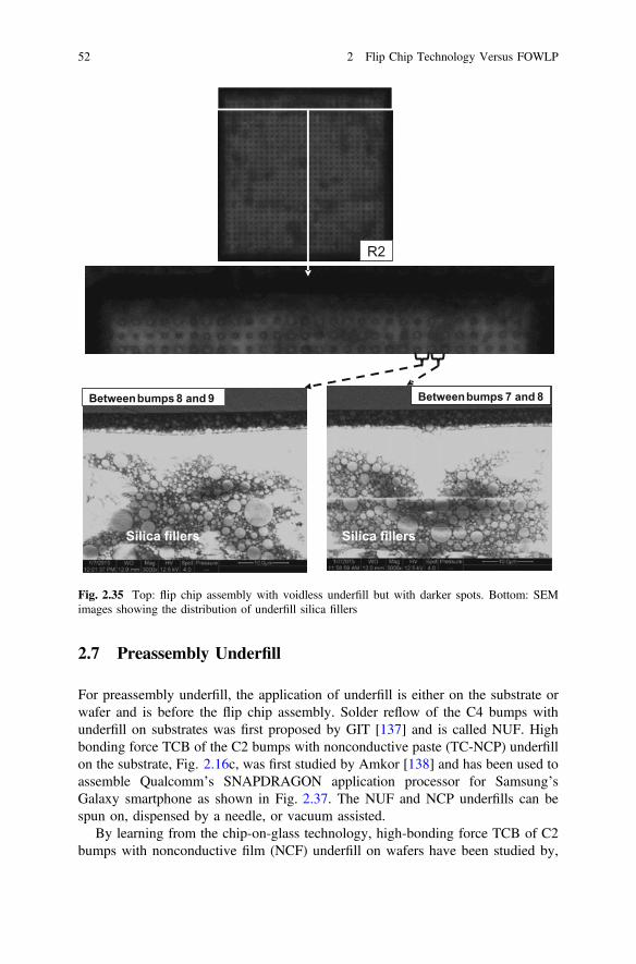
2.7 Preassembly Underfill
For preassembly underfill, the application of underfill is either on the substrate orwafer and is before the flip chip assembly. Solder reflow of the C4 bumps withunderfill on substrates was first proposed by GIT [137] and is called NUF. Highbonding force TCB of the C2 bumps with nonconductive paste (TC-NCP) underfillon the substrate, Fig. 2.16c, was first studied by Amkor [138] and has been used toassemble Qualcomm’s SNAPDRAGON application processor for Samsung’sGalaxy smartphone as shown in Fig. 2.37. The NUF and NCP underfills can bespun on, dispensed by a needle, or vacuum assisted.
By learning from the chip-on-glass technology, high-bonding force TCB of C2bumps with nonconductive film (NCF) underfill on wafers have been studied by,
Betweenbumps 7 and 8Between bumps 8 and 9
R2
Silica fillersSilica fillers
Fig. 2.35 Top: flip chip assembly with voidless underfill but with darker spots. Bottom: SEMimages showing the distribution of underfill silica fillers
52 2 Flip Chip Technology Versus FOWLP

e.g., Sanyo [139], Hitachi [140, 141], Tohoku [142, 143], DOW [144], Hynix[145], KAIST/Samsung [146, 147], Amkor/Qualcomm [148], and Toray [149–151]for 2.5D/3D IC integration [7–10]. Figure 2.38 shows the lamination of NCF on theCu pillar with a solder cap-bumped wafer.
Chip
Chip crack
Shear direction
Organic-substrate
Chip crack
Shear direction
Si-substrate
Chip
Shear direction
Si-substrate
Chip
Chip crack
Si-substrate crack
Fig. 2.36 Shearing tests and failure modes
Table 2.3 Experimental results
Runs Temperature(°C)
Multipleprints
Voids(Y/N)
Die shearforce (kg)
Remark
UnderfillMaterial#1
Chip toorganicsubstrate
R1 25 1 N (0/5) >60
R2 25 10 N (0/5) >60
R3 45 1 Y (2/4) >60
R4 45 10 N (0/4) 53 Die crack
Chip to Sisubstrate
R5 25 1 N (0/4) 57 Die crack
R6 25 10 N (0/4) 45 Die crack
R7 45 1 N (0/4) 43 Die/subcrack
R8 45 10 N (0/4) >60
UnderfillMaterial#2
Chip toorganicsubstrate
R9 25 1 N (0/4) >60
R10 25 10 N (0/5) >60
R11 45 1 N (0/4) 39 Die crack
R12 45 10 N (0/4) >60
Chip to Sisubstrate
R13 25 1 Y (1/3) >60
R14 25 10 N (0/4) 26 Die crack
R15 45 1 N (0/3) 41 Die/subcrack
R16 45 10 N (0/4) 45 Die crack
2.7 Preassembly Underfill 53
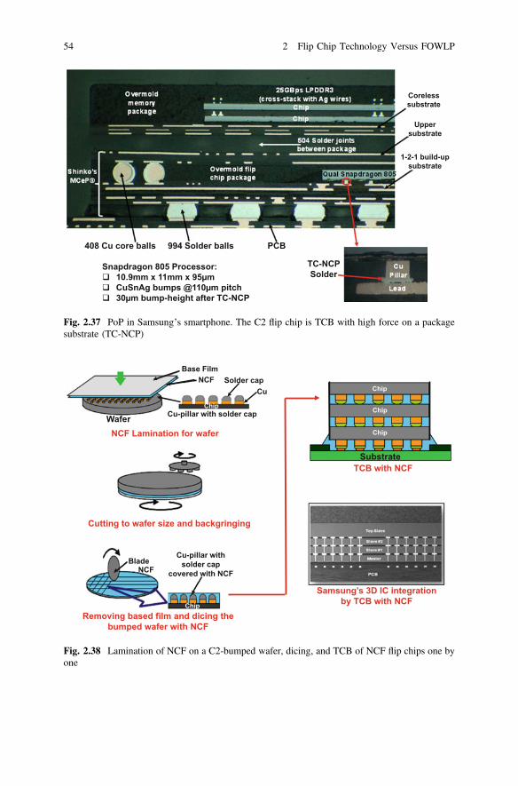
Coreless substrate
Upper substrate
1-2-1 build-up substrate
408 Cu core balls 994 Solder balls PCB
TC-NCP Solder
Snapdragon 805 Processor:10.9mm x 11mm x 95µmCuSnAg bumps @110µm pitch30µm bump-height after TC-NCP
Fig. 2.37 PoP in Samsung’s smartphone. The C2 flip chip is TCB with high force on a packagesubstrate (TC-NCP)
Cutting to wafer size and backgringing
Cu-pillar with solder cap
covered with NCFNCFBlade
Removing based film and dicing the bumped wafer with NCF
Chip
Base FilmNCF
NCF Lamination for waferWafer
ChipCu-pillar with solder capChip
CuSolder cap
Chip
Chip
Chip
Substrate TCB with NCF
Samsung’s 3D IC integration by TCB with NCF
Fig. 2.38 Lamination of NCF on a C2-bumped wafer, dicing, and TCB of NCF flip chips one byone
54 2 Flip Chip Technology Versus FOWLP
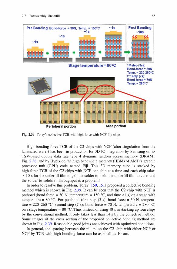
High bonding force TCB of the C2 chips with NCF (after singulation from thelaminated wafer) has been in production for 3D IC integration by Samsung on itsTSV-based double data rate type 4 dynamic random access memory (DRAM),Fig. 2.38, and by Hynix on the high bandwidth memory (HBM) of AMD’s graphicprocessor unit (GPU) code named Fiji. This 3D memory cube is stacked byhigh-force TCB of the C2 chips with NCF one chip at a time and each chip takes*10 s for the underfill film to gel, the solder to melt, the underfill film to cure, andthe solder to solidify. Throughput is a problem!
In order to resolve this problem, Toray [150, 151] proposed a collective bondingmethod which is shown in Fig. 2.39. It can be seen that the C2 chip with NCF isprebond (bond force = 30 N, temperature = 150 °C, and time <1 s) on a stage withtemperature = 80 °C. For postbond (first step (3 s): bond force = 50 N, tempera-ture = 220–260 °C, second step (7 s): bond force = 70 N, temperature = 280 °C)on a stage temperature = 80 °C. Thus, instead of using 40 s in stacking up four chipsby the conventional method, it only takes less than 14 s by the collective method.Some images of the cross section of the proposed collective bonding method areshown in Fig. 2.39. Reasonable good joints are achieved with optimized conditions.
In general, the spacing between the pillars on the C2 chip with either NCP orNCF by TCB with high bonding force can be as small as 10 µm.
Fig. 2.39 Toray’s collective TCB with high force with NCF flip chips
2.7 Preassembly Underfill 55

2.8 Cu–Cu Direct Hybrid Bonding
Sony is the first to use Cu–Cu direct hybrid bonding (which bonds the metal padsand dielectric layer on both sides of the wafers at the same time) in high-volumemanufacturing (HVM). Sony produced the IMX260 backside illuminated CMOSimage sensor (BI-CIS) for the Samsung Galaxy S7, which shipped in 2016.Electrical test results [152] showed that their robust Cu–Cu direct hybrid bondingachieved remarkable connectivity and reliability. The performance of the imagesensor was also super. A cross section of the IMX260 BI-CIS is shown in Fig. 2.40.It can be seen that, unlike in [153] for Sony’s ISX014 stacked camera sensor, theTSVs are gone and the interconnects between the BI-CIS chip and the processorchip are achieved by Cu–Cu direct bonding. The signals are coming from thepackage substrate with wire bonds to the edges of the processor chip.
The assembly process of Cu–Cu direct hybrid bonding starts off with surfacecleaning, metal oxide removal, and activation of SiO2 or SiN (by wet cleaning andplasma activation) of wafers for the development of high bonding strength. Then,use optical alignment to place the wafers in contact at room temperature and in atypical cleanroom atmosphere. The first thermal annealing (100–150 °C) isdesigned to strengthen the bond between the SiO2 and SiN surfaces of the wafers
Wirebonds
Wirebonds
Processor Chip
Processor Chip
Processor Chip
BI-CIS Chip
Cu-Cu
BI-CIS Chip
BI-CIS Chip
Microlens
SiO2-SiO2
Fig. 2.40 Images of Sony’s CIS by Cu–Cu hybrid bonding
56 2 Flip Chip Technology Versus FOWLP

while minimizing the stress in the interface due to the thermal expansion mismatchamong the Si, Cu, and SiO2 or SiN. Then, apply higher temperature and pressure(300 °C, 25 kN, 10–3 Torr, N2 atm) for 30 min to introduce the Cu diffusion at theinterface and grain growth across the bond interface. The postbond annealing is300 °C under N2 atm for 60 min. This process leads to the seamless bonds(Fig. 2.40) formed for both Cu and SiO2 or SiN at the same time.
2.9 Flip Chip Technology Versus FOWLP
Flip chip technology is facing stiff competition. Some of its market share will betaken away by the fan-out wafer/panel-level packaging (FOW/PLP or simplyFOWLP) technology [13, 14, 154]. Figure 2.41 shows the schematic and SEM(scanning electron microscope) images of the cross section of the PoP which housesthe application processor (AP) and mobile dynamic random access memory(DRAM) of a production smartphone. This PoP is fabricated with the InFO (inte-grated fan-out) WLP technology [154]. It can be seen from the bottom package thatthe wafer bumping, fluxing, flip chip assembly, cleaning, underfill dispensing andcuring, and build-up package substrate (of the AP shown in Fig. 2.17) have beeneliminated and are replaced by the EMC and RDLs (for the AP as shown inFig. 2.41). This results in a lower cost, higher performance, and lower profile
3-Layer Coreless Package Substrate
Solder Ball
Wirebond
A10 AP TIVSolder Ball
RDLs
EMC
Over MoldMemoryMemory
Underfill
15.5mm x 14.4mm
PoP sizes: 15.5mm x 14.4mm x 825µm
Fig. 2.41 Images of iPhone 7/7 + PoP A10 chipset FOWLP
2.8 Cu–Cu Direct Hybrid Bonding 57

package. This is very significant, since the smartphone company (Apple) and thecomponent company (TSMC) developing these packages are the “sheep leaders”.Once they use it, then many others will follow. Also, this means that FOWLP is notjust only for packaging baseband, RF (radio frequency) switch/transceiver, PMIC(power management integrated circuit), audio codec, MCU (micro-control unit), RFradar, connectivity ICs, etc., it can also be used for packaging high-performanceand large (>120 mm2) SoC such as APs.
2.10 Summary and Recommendations
Wafer bumping, package substrate, assembly, and underfill for flip chip technologyhave been investigated in this study. Some important results and recommendationsare as follows:
• Flip chip technology came from a long way: from the three-bump flip chip to10,000-bump flip chip, and could be 50,000-bump flip chip by the year of 2020.Also, by that time, the flip chip pitch could be as small as 30 µm as shown inFig. 2.42 [155, 156].
• Flip chip technology is facing stiff competition and some of its market share willbe taken away by the FOWLP technology.
• C2 bumps have better thermal and electrical performance and can go down tofiner pitch (smaller spacing between pads) than C4 bumps. However, moreresearch and development works should be done on relative performancecharacteristics, such as electromigration life, thermal fatigue life, signal speed,chip junction temperature, etc.
1970 1980 1990 2000 2010 2020Year
Num
ber o
f bum
ps (1
04)
6
5
4
3
2
1
0
Number of bumpsPitch
Pitc
h (1
02) (
µm)
6
5
4
3
2
1
0
Fig. 2.42 Trend in flip chip bump and pitch
58 2 Flip Chip Technology Versus FOWLP

• The self-alignment characteristic (one of the most unique features of flip chiptechnology) of the C2 bumps is nowhere near the C4 bumps. Thus, mass reflowis usually applied to C4-bumped chips.
• C2-bumped chips are usually assembled by TCB with high force, while lowforce is sometimes used.
• The advantages of TCB are for higher pin count, finer pitch, thinner chips,higher density, thinner package substrates, and controlling warpage and die tilt.One of the drawbacks of TCB is throughput (compared with mass reflow).
• A package substrate with ten build-up layer (5-2-5) and 10 µm line width andspacing is more than adequate to support most of the flip chips.
• More research and development works should be done on innovative andlow-cost ETS and coreless substrates for portable, mobile, wearable, and IoTsapplications. More research and development works should be done to effec-tively use the BOL technique to increase routing density, and thus, lower thecost and reduce the size of organic package substrate.
• For Cu-to-Cu direct diffusion bonding, the spacing between pads is 5 µm orless.
• For mass reflow of C4-bumped chips with either CUF or MUF, the spacingbetween bumps is as low as 50 µm.
• For mass reflow of C2-bumped chips with either CUF or MUF, the spacingbetween Cu pillars is as low as 25 µm.
• For TCB with low force of C2-bumped chips with either CUF or MUF, thespacing between Cu pillars is as low as 8 µm.
• For TCB with high force of C2-bumped chips with either NCP or NCFunderfills, the spacing between Cu pillars is as low as 10 µm.
• For the post-assembly underfill approach, the CUF or MUF is usually applied toflip chip assemblies with mass reflow and TCB with low bonding forcemethods.
• For the preassembly underfill approach, the NUF, NCP, or NCF is usuallyapplied before flip chip assemblies; NUF is with mass reflow and NCP or NCFis with high-force TCB. In general, the NUF and NCP are applied on thesubstrate and the NCF is laminated onto the C2-bumped wafer and then dicedinto individual chips.
• Toray’s collectiveTCBwith high-forcemethod can be a potential high-throughputprocess for stacking C2 chips with laminated NCF.
• Now that Sony has been in HVM with its BI-CIS with Cu–Cu hybrid bonding,in order to increase the throughput further for 3D IC integration, more researchand development should be done on DRAM wafer stacking with Cu–Cu hybridbonding.
2.10 Summary and Recommendations 59
References
1. Lau, J.H. (ed.). 1996. Flip Chip Technologies. New York: McGraw-Hill.2. Lau, J.H. 2000. Low Cost Flip Chip Technologies. New York: McGraw-Hill.3. Lau, J.H., C. Wong, J. Prince, and W. Nakayama. 1998. Electronic Packaging. New York:
McGraw-Hill.4. Lau, J.H., N. Lee, C. Wong, and R. Lee. 2003. Electronic Manufacturing. New York:
McGraw-Hill.5. Davis, E., W. Harding, R. Schwartz, and J. Corning. 1964. Solid Logic Technology:
Versatile, High Performance Microelectronics. IBM Journal of Research and Development 8(2): 102–114.
6. Totta, P., and R. Sopher. 1969. SLT Device Metallurgy and Its Monolithic Extension. IBMJournal of Research and Development 13 (3): 226–238.
7. Lau, J.H. 2016. 3D IC Integration and Packaging. New York: McGraw-Hill.8. Lau, J.H. 2013. Through-Silicon Vias for 3D Integration. New York: McGraw-Hill.9. Lau, J.H. 2011. Reliability of RoHS-Compliant 2D and 3D IC Interconnects. New York:
McGraw-Hill.10. Lau, J.H., C. Lee, C. Premachandran, and A. Yu. 2010. Advanced MEMS Packaging. New
York: McGraw-Hill.11. Lim, S., V. Rao, W. Hnin, W. Ching, V. Kripesh, C. Lee, J.H. Lau, J. Milla, and A. Fenner.
2010. Process Development and Reliability of Microbumps. IEEE Transactions on CPMT33 (4): 747–753.
12. Sutanto, J. 2012. POSSUMTM Die Design as a Low Cost 3D Packaging Alternative. 3DPackag 25, 16–18.
13. Lau, J.H. 2015. Patent Issues of Fan-Out Wafer/Panel-Level Packaging. Chip Scale Review19 (6): 42–46.
14. Lau, J.H., N. Fan, and M. Li. 2016. Design, Material, Process, and Equipment of EmbeddedFan-Out Wafer/Panel-Level Packaging. Chip Scale Review 20 (3): 38–44.
15. Lau, J.H., T. Chung, R. Lee, C. Chang, and C. Chen. 1999. A Novel and ReliableWafer-Level Chip Scale Package (WLCSP). In Chip Scale International Conference, SanJose, CA, September 14–15, 1999, H1–8.
16. Elenius, P., and H. Yang. 1998. The Ultra CSP Wafer-Scale Package. In High DensityInterconnect Conference and Expo, Tempe, AZ, September 15–16, 1998, 36–40.
17. Lau, J.H., and S.W.R. Lee. 1999. Chip Scale Package. New York: McGraw-Hill.18. Lau, J.H., and Y. Pao. 1997. Solder Joint Reliability of BGA, CSP, and Flip Chip
Assemblies. New York: McGraw-Hill.19. Lau, J.H., and C. Chang. 2000. Taguchi Design of Experiment for Wafer Bumping by
Stencil Printing. IEEE Transactions on Electronics Packaging Manufacturing 21 (3):219–225.
20. Elenius, P. 1998. Flip Chip Bumping for IC Packaging Contractors. In NEPCON WestConference, Anaheim, CA, March 3–5, 1998, 1403–1407.
21. Elenius, P., J. Leal, J. Ney, D. Stepniak, and S. Yeh. 1999. Recent Advances in Flip ChipWafer Bumping Using Solder Paste Technology. In IEEE 49th Electronic Components andTechnology Conference, San Diego, CA, June 1–4, 1999, 260–265.
22. Li, L., S. Wiegele, P. Thompson, and R. Lee. 1998. Stencil Printing Process Developmentfor Low Cost Flip Chip Interconnect. In IEEE 48th Electronic Components and TechnologyConference, Seattle, WA, May 25–28, 1998, 421–426.
23. Wiegele, S., P. Thompson, R. Lee, and E. Ramsland. 1998. Reliability and ProcessCharacterization of Electroless Nickel-Gold/Solder Flip Chip Interconnect Technology. In48th Electronic Components and Technology Conference, Seattle, WA, May 25–28, 1998,861–866.
60 2 Flip Chip Technology Versus FOWLP

24. Kloeser, J., K. Heinricht, E. Jung, L. Lauter, A. Ostmann, R. Aschenbrenner, and H. Reichl.1998. Low Cost Bumping by Stencil Printing: Process Qualification for 200 mm Pitch. InInternational Symposium on Microelectronics, San Diego, CA, November 1–4, 1998,288–297.
25. Cho, M., S. Kang, Y. Kwon, D. Jang, and N. Kim. 1999. Flip-Chip Bonding on PCB WithElectroless Ni-Au and Stencil Printing Solder Bump. In SMTA International Conference,San Jose, CA, September 12–16, 1999, 159–164.
26. Love, D., L. Moresco, W. Chou, D. Horine, C. Wong, and S. Eilin. 1994. Wire InterconnectStructures for Connecting an Integrated Circuit to a Substrate. U.S. Patent No. 5,334,804,filed November 17, 1992 and issued August 2, 1994.
27. Tung, F. 2003. Pillar Connections for Semiconductor Chips and Method of Manufacture.U.S. Patent No. 6,578,754, filed April 27, 2000 and issued June 17, 2003.
28. Tung, F. 2004. Pillar Connections for Semiconductor Chips and Method of Manufacture.U.S. Patent No. 6,681,982, filed June 12, 2002 and issued January 27, 2004.
29. Cappo, F., J. Milliken, and J. Mosley. 1991. Highly Manufacturable Multi-Layered CeramicSurface Mounted Package. In 11th IEEE/CHMT International Electronic ManufacturingTechnology Symposium, San Francisco, CA, September 16–18, 1991, 424–428.
30. Banks, D., T. Burnette, R. Gerke, E. Mammo, and S. Mattay. 1994. Reliability Comparisonof Two Metallurgies for Ceramic Ball Grid Array. In International Conference andExhibition on Multichip Modules, Denver, CO, April 13–15, 1994, 529–534.
31. Sigliano, R., and K. Gaughan. 1992. Ceramic Material Options for MCM’s. In 1stInternational Conference on Multichip Modules, Denver, CO, April 1–3, 1992, 291–299.
32. Sigliano, R. 1995. Ceramic Substrates for Ball Grid Array Packages. In Ball Grid ArrayTechnology, ed. J. H. Lau, 65–92. New York: McGraw-Hill.
33. Lau, J.H., and W. Dauksher. 2005. Reliability of an 1657CCGA (Ceramic Column GridArray) Package With 96.5Sn3.9Ag0.6Cu Lead-Free Solder Paste on PCBs (Printed CircuitBoards). ASME Journal of Electronic Packaging 127 (2): 96–105.
34. Lau, J.H., T. Castello, D. Shangguan, W. Dauksher, J. Smetana, R. Horsley, D. Love, I.Menis, and B. Sullivan. 2007. Failure Analysis of Lead-Free Solder Joints of an 1657CCGA(Ceramic Column Grid Array) Package. IMAPS Transactions on Journal ofMicroelectronics and Electronic Packaging 4 (3): 189–213.
35. Tsukada, Y., S. Tsuchida, and Y. Mashimoto. 1992. Surface Laminar Circuit Packaging. In42nd IEEE Electronic and Components Technology Conference, San Diego, CA, May 18–20, 1992, 22–27.
36. Tsukada, Y., and S. Tsuchida. 1992. Surface Laminar Circuit, a Low Cost High DensityPrinted Circuit Board. In Surface Mount International Conference, San Jose, CA, August27–29, 1992, 537–542.
37. Tsukada, Y. 1994. Solder Bumped Flip Chip Attach on SLC Board and Multichip Module.In Chip on Board Technologies for Multichip Modules, ed. J. H. Lau, 410–443. New York:Van Nostrand Reinhold.
38. Tsukada, Y., Y. Maeda, and K. Yamanaka. 1993. A Novel Solution for MCM-L UtilizingSurface Laminar Circuit and Flip Chip Attach Technology. In Proceedings of 2ndInternational Conference on Multichip Modules, April 1993, 252–259.
39. Lau, J.H., and S.W.R. Lee. 2001. Microvias for Low Cost, High Density Interconnects.New York: McGraw-Hill.
40. Gonzalez, C., R. Wessel, and S. Padlewski. 1999. Epoxy-Based Aqueous Processable PhotoDielectric Dry Film and Conductive ViaPlug for PCB Build-Up and IC Packaging. IEEETransactions on Advanced Packaging 22 (3): 385–390.
41. Burgess, L., and P. Madden. 1998. Blind Vias in SMD Pads. Printed Circuit Fabrication21 (1): 28–29.
42. Castro, A. 1997. Chip Carrier Package Constructions Made Easier with Dry Film PhotoDielectric. In Proceedings from IPC Works, October 1997, S01-5-1.
References 61

43. Nargi-Toth, K., and P. Gandhi. 1998. Manufacturing Methodologies for High DensityInterconnect Structures (HDIS). In CSI Technical Symposium, September 1998, 63–70.
44. Noddin, D., E. Swenson, and Y. Sun. 1998. Solid State UV-LASER Technology for theManufacture of High Performance Organic Modules. In IEEE/ECTC Proceedings, May1998, 822–827.
45. Cable, A. 1997. Improvements in High Speed Microvia Formation Using Solid State Nd:YAG UV Lasers. In IPC EXPO, March 1997, S-2.
46. Tessier, T., and J. Aday. 1995. Casting Light on Recent Advancements in Laser BasedMCM-L Processing. In Proceedings of International Conference on Multichip Modules,April 1995, 6–13.
47. Illyefalvi-Vitez, Z., and J. Pinkola. 1997. Application of Laser Engraving for the Fabricationof Fine Resolution Printed Wiring Laminates for MCM-Ls. In IEEE/ECTC Proceedings,May 1997, 502–510.
48. Enomoto, R., M. Asai, and N. Hirose. 1998. High Density MLB using Additive andBuild-up Process. In Proceddings of the International Symposium on Microelectronics,November 1998, 399–404.
49. Kobayashi, K., N. Katagiri, and S. Koyama. 1999. Development of a Build Up Package withHigh Density of Circuits for High Pin Count Flip Chip Application. In IPC EXPO, March1999, S01–4.
50. Burgess, L., and F. Pauri. 1999. Optimizing BGA to PCB Interconnections UsingMulti-Depth Laser Drilled Blind Vias-in-Pad. Circuit World 25 (2): 31–34.
51. Petefish, W., D. Noddin, and D. Hanson. 1998. High Density Organic Flip Chip PackageSubstrate Technology. In IEEE/ECTC Proceedings, May 1998, 1089–1097.
52. Li, L. 2004. Embedded Passives in Organic Substrate for RF Module and AssemblyCharacterization. In Proceedings of the 6th IEEE CPMT Conference on High DensityMicrosystem Design and Packaging and Component Failure Analysis, June 2004, 74–82.
53. Srinivasan, K., P. Muthana, R. Mandrekar, E. Engin, J. Choi, and M. Swaminathan. 2006.Enhancement of Signal Integrity and Power Integrity with Embedded Capacitors inHigh-Speed Packages. In Proceedings of the 7th International Symposium on QualityElectronic Design, March 2006, 286–291.
54. Pham, N., M. Cases, D. de Araujo, B. Mutnury, E. Matoglu, B. Herrman, and P. Patel. 2006.Embedded Capacitor in Power Distribution Design of High-End Server Packages. In IEEE/ECTC Proceedings, May 2006, 1677–1682.
55. Tanaka, H., T. Kariya, H. Nagata, K. Yoshikawa, K. Shimizu, H. Noauchi, and S. Kato.2008. Embedded High-k Thin Film Capacitor in Organic Package. In IEEE/EPTCProceedings, December 2008, 988–993.
56. Akahoshi, T., D. Mizutani, K. Fukui, S. Yamawaki, H. Fujisaki, M. Watanabe, and M.Koide. 2017. Development of CPU Package Embedded with Multilayer Thin Film Capacitorfor Stabilization of Power Supply. In IEEE/ECTC Proceedings, May 2017, 179–184.
57. Lau, J.H., C. Chang, C. Chen, C. Ouyang, and R. Lee. 1999. Via-In-Pad (VIP) Substrates forSolder Bumped Flip Chip Applications. In Proceedings of the SMTA InternationalConference, September 1999, 128–136.
58. Lau, J.H., and C. Chang. 2000. An Overview of Microvia Technologies. Circuit World26 (2): 22–32.
59. Schmidt, W. 1999. High Performance Microvia PWB and MCM Applications. In IPCEXPO, S17-5-1–S17-5-8.
60. Shimizu, N., W. Kaneda, H. Arisaka, N. Koizumi, S. Sunohara, A. Rokugawa, and T.Koyama. 2013. Development of Organic Multi Chip Package for High PerformanceApplication. In IMAPS International Symposium on Microelectronics, Orlando, FL,September 30–October 3, 2013, 414–419.
61. Oi, K., S. Otake, N. Shimizu, S. Watanabe, Y. Kunimoto, T. Kurihara, T. Koyama, M.Tanaka, L. Aryasomayajula, and Z. Kutlu. 2014. Development of New 2.5D Package WithNovel Integrated Organic Interposer Substrate With Ultra-Fine Wiring and High Density
62 2 Flip Chip Technology Versus FOWLP

Bumps. In IEEE 64th Electronic and Components Technology Conference, Orlando, FL,May 27–30, 2014, 348–353.
62. Koide, M., K. Fukuzono, H. Yoshimura, T. Sato, K. Abe, and H. Fujisaki. 2006.High-Performance Flip-Chip BGA Technology Based on Thin-Core and Coreless PackageSubstrate. In IEEE 56th Electronic and Components Technology Conference, San Diego,CA, May 30–June 2, 2006, 1869–1873.
63. Sung, R., K. Chiang, Y. Wang, and C. Hsiao. 2007. Comparative Analysis of ElectricalPerformance on Coreless and Standard Flip-Chip Substrate. In IEEE 57th Electronic andComponents Technology Conference, Reno, NV, May 29–June 1, 2007, 1921–1924.
64. Lin, E., D. Chang, D. Jiang, Y. Wang, and C. Hsiao. 2007. Advantage and Challenge ofCoreless Flip-Chip BGA. In International Microsystems, Packaging, Assembly and CircuitsTechnology, Taipei, Taiwan, October 1–3, 2007, 346–349.
65. Chang, D., Y. Wang, and C. Hsiao. 2007. High Performance Coreless Flip-Chip BGAPackaging Technology. In IEEE 57th Electronic and Components Technology Conference,Reno, NV, May 29–June 1, 2007, 1765–1768.
66. Savic, J., P. Aria, J. Priest, N. Dugbartey, R. Pomerleau, B. Shanker, M. Nagar, J. Lim, S.Teng, L. Li, and J. Xue. 2009. Electrical Performance Assessment of Advanced SubstrateTechnologies for High Speed Networking Applications. In IEEE 59th Electronic andComponents Technology Conference, San Diego, CA, May 26–29, 2009, 1193–1199.
67. Kurashina, M., D. Mizutani, M. Koide, and N. Itoh. 2009. Precision Improvement Study ofThermal Warpage Prediction Technology for LSI Packages. In IEEE 59th Electronic andComponents Technology Conference, San Diego, CA, May 26–29, 2009, 529–534.
68. Wang, J., Y. Ding, L. Liao, P. Yang, Y. Lai, and A. Tseng. Coreless Substrate for HighPerformance Flip Chip Packaging,” IEEE 11th International Conference on ElectronicPackaging Technology.
69. Kimura, M. 2011. Shinko Officially Announces Volume Production of Coreless Substrate.Nikkei Electronics.
70. Fujimoto, D., K. Yamada, N. Ogawa, H. Murai, H. Fukai, Y. Kaneato, and M. Kato. 2011.New Fine Line Fabrication Technology on Glass-Cloth Prepreg Without Insulating Films forKG Substrate. In IEEE 61st Electronic and Components Technology Conference, LakeBuena Vista, FL, May 31–June 3, 2011, 387–391.
71. Kim, G., S. Lee, J. Yu, G. Jung, H. Yoo, and C. Lee. 2011. Advanced Coreless Flip-ChipBGA Package With High Dielectric Constant Thin Film Embedded Decoupling Capacitor.In IEEE 61st Electronic and Components Technology Conference, Lake Buena Vista, FL,May 31–June 3, 2011, 595–600.
72. Nickerson, R., R. Olmedo, R. Mortensen, C. Chee, S. Goyal, A. Low, and C. Gealer. 2012.Application of Coreless Substrate to Package on Package Architectures. In IEEE 62ndElectronic and Components Technology Conference, San Diego, CA, May 29–June 1, 2012,1368–1371.
73. Kim, G., J. Yu, C. Park, S. Hong, J. Kim, G. Rinne, and C. Lee. 2012. Evaluation andVerification of Enhanced Electrical Performance of Advanced Coreless Flip-Chip BGAPackage With Warpage Measurement Data. In IEEE 62nd Electronic and ComponentsTechnology Conference, San Diego, CA, May 29–June 1, 2012, 897–903.
74. Nishitani, Y. 2012. Coreless Packaging Technology for High-Performance Application. InIEEE/ECT/CMPT Seminar on Advanced Coreless Package Substrate and MaterialTechnologies, Electronic Components and Technology Conference, San Diego, CA, May29–June 1, 2012.
75. Kurashina, M., D. Mizutani, M. Koide, M. Watanabe, K. Fukuzono, and H. Suzuki. 2012.Low Warpage Coreless Substrate for Large-Size LSI Packages. In IEEE 62nd Electronic andComponents Technology Conference, San Diego, CA, May 29–June 1, 2012, 1378–1383.
76. Kurashina, M., D. Mizutani, M. Koide, M. Watanabe, K. Fukuzono, N. Itoh, and H. Suzuki.2012. Low Warpage Coreless Substrate for IC Packages. Transaction of the Japan Instituteof Electronics Packaging 5 (1): 55–62.
References 63

77. Manusharow, M., S. Muthukumar, E. Zheng, A. Sadiq, and C. Lee. 2012. Coreless SubstrateTechnology Investigation for Ultra-Thin CPU BGA Packaging. In IEEE 62nd Electronicand Components Technology Conference, San Diego, CA, May 29–June 1, 2012, 892–896.
78. Kim, J., S. Lee, J. Lee, S. Jung, and C. Ryu. 2012. Warpage Issues and AssemblyChallenges Using Coreless Package Substrate. In IPC APEX Expo, San Diego, CA,February 28–March 1, 2012.
79. Sakuma, K., E. Blackshear, K. Tunga, C. Lian, S. Li, M. Interrante, O. Mantilla, and J. Nah.2013. Flip Chip Assembly Method Employing Differential Heating/Cooling for Large DiesWith Coreless Substrates. In IEEE 63rd Electronic and Components TechnologyConference, Las Vegas, NV, May 28–31, 2013, 667–673.
80. Hahm, Y., M. Li, J. Yan, Y. Tretiakov, H. Lan, S. Chen, and S. Wong. 2016. Analysis andMeasurement of Power Integrity and Jitter Impacts on Thin-Core and Coreless Packages. InIEEE 66th Electronic Components and Technology Conference, Las Vegas, NV, May 31–June 3, 2016, 387–392.
81. Baloglu, B., W. Lin, K. Stratton, M. Jimarez, and D. Brady. 2013. Warpage Characterizationand Improvements for IC Packages With Coreless Substrate. In 46th InternationalSymposium on Microelectronics, Orlando, FL, September 30–October 3, 2013, 260–284.
82. Sun, Y., X. He, Z. Yu, and L. Wan. 2013. Development of Ultra-Thin Low WarpageCoreless Substrate. In IEEE 63rd Electronic and Components Technology Conference, LasVegas, NV, May 28–31, 2013, 1846–1849.
83. Lin, W., B. Baloglu, and K. Stratton. 2014. Coreless Substrate With Asymmetric Design toImprove Package Warpage. In IEEE 64th Electronic and Components TechnologyConference, Orlando, FL, May 27–30, 2014, 1401–1406.
84. Liu, W., G. Xiaa, T. Liang, T. Li, X. Wang, J. Xie, S. Chen, and D. Yu. 2015. Developmentof High Yield, Reliable Fine Pitch Flip Chip Interconnects With Copper Pillar Bumps andThin Coreless Substrate. In IEEE 65th Electronic and Components Technology Conference,San Diego, CA, May 26–29, 2015, 1713–1717.
85. Pendse, R., K. Kim, O. Kim, and K. Lee. 2006. Bond-On-Lead: A Novel Flip ChipInterconnection Technology for Fine Effective Pitch and High I/O Density. In IEEE 56thElectronic and Components Technology Conference, San Diego, CA, May 30–June 2, 2006,16–23.
86. Pendse, R. 2008. Bump-On-Lead Flip Chip Interconnection. U.S. Patent No. 7,368,817,filed Nov. 10, 2004 and issued May 6, 2008.
87. Ouyang, E., M. Chae, S. Chow, R. Emigh, M. Joshi, R. Martin, and R. Pendse. 2010.Improvement of ELK Reliability in Flip Chip Packages Using Bond-On-Lead (BOL)Interconnect Structure. In IMAPS 43rd International Symposium on Microelectronics,Raleigh, NC, October 31–November 4, 2010, 197–203.
88. Pendse, R. 2011. Bump-On-Lead Flip Chip Interconnection. U.S. Patent No. 7,901,983,filed May 26, 2009 and issued March 8, 2011.
89. Pendse, R., C. Cho, M. Joshi, K. Kim, P. Kim, S. Kim, S. Kim, H. Lee, K. Lee, R. Martin,A. Murphy, V. Pandey, and C. Palar. 2010. Low CostmFlip Chip (LCFC): An InnovativeApproach for Breakthrough Reduction in Flip Chip Package Cost. In IEEE 60th ElectronicComponents and Technology Conference, Las Vegas, NV, June 1–4, 2010.
90. Movva, S., S. Bezuk, O. Bchir, M. Shah, M. Joshi, R. Pendse, E. Ouyang, Y. Kim, S. Park,H. Lee, S. Kim, H. Bae, G. Na, and K. Lee. 2011. CuBOL (Cu-Column on BOL)Technology: A Low Cost Flip Chip Solution Scalable to High I/O Density, Fine Bump Pitchand Advanced Si-Nodes. In IEEE 61st Electronic and Components Technology Conference,Lake Buena Vista, FL, May 31–June 3, 2011, 601–607.
91. Lan, A., C. Hsiao, J.H. Lau, E. So, and B. Ma. 2012. Cu Pillar Exposed-Die Molded FCCSPfor Mobile Devices. In IEEE 62nd Electronic and Components Technology Conference, SanDiego, CA, May 29–June 1, 2012, 886–891.
92. Kuo, F., J. Lee, F. Chien, R. Lee, C. Mao, and J.H. Lau. 2014. Electromigration Performanceof Cu Pillar Bump for Flip Chip Packaging With Bump on Trace by Using Thermal
64 2 Flip Chip Technology Versus FOWLP

Compression Bonding. In IEEE 64th Electronic and Components Technology Conference,Orlando, FL, May 27–30, 2014, 56–61.
93. Li, M., D. Tian, Y. Cheung, L. Yang, and J.H. Lau. 2015. A High Throughput and ReliableThermal Compression Bonding Process for Advanced Interconnections. In IEEE 65thElectronic Components and Technology Conference, San Diego, CA, May 26–29, 2015,603–608.
94. Liu, F., C. Nair, V. Sundaram, and R. Tummala. 2015. Advances in Embedded Traces for1.5 lm RDL on 2.5D Glass Interposers. In IEEE 65th Electronic and ComponentsTechnology Conference, San Diego, CA, May 26–29, 2015, 1736–1741.
95. Chen, C., M. Lin, G. Liao, Y. Ding, and W. Cheng. 2015. Balanced Embedded TraceSubstrate Design for Warpage Control. In IEEE 65th Electronic and ComponentsTechnology Conference, San Diego, CA, May 26–29, 2015, 193–199.
96. Zhang, L., and G. Joseph. 2015. Low Cost High Performance Bare Die PoP With EmbeddedTrace Coreless Technology and ‘Coreless Cored’ Build UpSubstrate Manufacture Process.In IEEE 65th Electronic Components and Technology Conference, San Diego, CA, May26–29, 2015, 882–887.
97. Lu, M. 2014. Challenges and Opportunities in Advanced IC Packaging. Chip Scale Review18 (2): 5–8.
98. Lee, K., S. Cha, and P. Shim. 2016. Form Factor and Cost Driven Advanced PackageSubstrates for Mobile and IoT Applications. In China Semiconductor TechnologyInternational Conference, Shanghai, China, March 13–14, 2016.
99. Chen, K., S. Lee, P. Andry, C. Tsang, A. Topop, Y. Lin, Y.J. Lu, A. Young, M. Ieong, andW. Haensch. 2006. Structure, Design, and Process Control for Cu Bonded Interconnects in3D Integrated Circuits. In IEEE International Electron Devices Meeting, San Francisco, CA,December 11–13, 2006, 367–370.
100. Liu, F., R. Yu, A. Young, J. Doyle, X. Wang, L. Shi, K. Chen, X. Li, D. Dipaola, D. Brown,C. Ryan, J. Hagan, K. Wong, M. Lu, X. Gu, N. Klymko, E. Perfecto, A. Merryman, K.Kelly, S. Purushothaman, S. Koester, R. Wisnieff, and W. Haensch. 2008. A 300-mmWafer-Level Three-Dimensional Integration Scheme Using Tungsten Through-Silicon Viaand Hybrid Cu-Adhesive Bonding. In IEEE International Electron Devices Meeting, SanFrancisco, CA, December 15–17, 2008.
101. Yu, R., F. Liu, R. Polastre, K. Chen, X. Liu, L. Shi, E. Perfecto, N. Klymko, M. Chace, T.Shaw, D. Dimilia, E. Kinser, A. Young, S. Purushothaman, S. Koester, and W. Haensch.2009. Reliability of a 300-mm-Compatible 3DI Technology Based on Hybrid Cu-AdhesiveWafer Bonding. In Symposium on VLSI Technology, Honolulu, HI, June 16–18, 2009, 170–171.
102. Shigetou, A., T. Itoh, K. Sawada, and T. Suga. 2008. Bumpless Interconnect of 6-lm PitchCu Electrodes at Room Temperature. In Electronic Components and TechnologyConference, Lake Buena Vista, FL, May 27–30, 2008, 1405–1409.
103. Tsukamoto, K., E. Higurashi, and T. Suga. 2010. Evaluation of Surface Microroughness forSurface Activated Bonding. In IEEE CPMT Symposium Japan, Tokyo, Japan, August 24–26, 2010, 1–4.
104. Kondou, R., C. Wang, and T. Suga. 2010. Room-Temperature Si-Si and Si-SiN WaferBonding. In IEEE CPMT Symposium Japan, Tokyo, Japan, August 24–26, 2010, 161–164.
105. Shigetou, A., T. Itoh, M. Matsuo, N. Hayasaka, K. Okumura, and T. Suga. 2006. BumplessInterconnect Through Ultrafine Cu Electrodes by Means of Surface-Activated Bonding(SAB) Method. IEEE Transactions on Advanced Packaging 29 (2): 218–226.
106. Wang, C., and T. Suga. 2009. A Novel Moir_e Fringe Assisted Method for NanoprecisionAlignment in Wafer Bonding. In IEEE 59th Electronic Components and TechnologyConference, San Diego, CA, May 26–29, 2009, 872–878.
107. Wang, C., and T. Suga. 2009. Moir_e Method for Nanoprecision Wafer-To-WaferAlignment: Theory, Simulation, and Application. In IEEE International Conference onElectronic Packaging Technology and High-Density Packaging, Beijing, China, August 10–13, 2009, 219–224.
References 65

108. Higurashi, E., D. Chino, T. Suga, and R. Sawada. 2009. Au-Au Surface-Activated Bondingand Its Application to Optical Microsensors With 3-D Structure. IEEE Journal of SelectedTopics in Quantum Electronics 15 (5): 1500–1505.
109. Eitan, A., and K. Jing. 2015. Thermo-Compression Bonding for Fine-Pitch Copper-PillarFlip Chip Interconnect—Tool Features as Enablers of Unique Technology. In IEEE 65thElectronic Components and Technology Conference, San Diego, CA, May 26–29, 2015,460–464.
110. Lau, J.H., and C. Chang. 2002. Characteristics and Reliability of Fast-Flow, Snap-Cure, andReworkable Underfills for Solder Bumped Flip Chip on Low-Cost Substrates. IEEETransactions on Electronics Packaging Manufacturing 25 (3): 231–230.
111. Lau, J.H., and R. Lee. 2000. Fracture Mechanics Analysis of Low Cost Solder Bumped FlipChip Assemblies With Imperfect Underfills. ASME Journal of Electronic Packaging 222 (4):306–310.
112. Lau, J.H., R. Lee, and C. Chang. 2000. Effects of Underfill Material Properties on theReliability of Solder Bumped Flip Chip on Board With Imperfect Underfill Encapsulants.IEEE Transactions on CPMT 23 (2): 323–333.
113. Lau, J.H., and S.W. Lee. 2000. Effects of Underfill Delamination and Chip Size on theReliability of Solder Bumped Flip Chip on Board. IMAPS Transactions on InternationalJournal of Microcircuits and Electronic Packaging 23 (1): 33–39.
114. Lau, J.H., C. Chang, and C. Chen. 1999. Characteristics and Reliability of No-FlowUnderfills for Solder Bumped Flip Chip Assemblies. IMAPS Transactions on InternationalJournal of Microcircuits and Electronic Packaging 22 (4): 370–381.
115. Lau, J.H., and C. Chang. 1999. How to Select Underfill Materials for Solder Bumped FlipChips on Low Cost Substrates? IMAPS Transactions on International Journal ofMicroelectronics and Electronic Packaging 22 (1): 20–28.
116. Lau, J.H., and C. Chang. 1999. Characterization of Underfill Materials for Functional SolderBumped Flip Chips on Board Applications. IEEE Transactions on CPMT, Part A 22 (1):111–119.
117. Lau, J.H., C. Chang, and C. Ouyang. 1998. SMT Compatible No-Flow Underfill for SolderBumped Flip Chip on Low-Cost Substrates. Journal of Electronics Manufacturing 8 (3–4):151–164.
118. Lau, J.H., C. Chang, and R. Chen. 1997. Effects of Underfill Encapsulant on the Mechanicaland Electrical Performance of a Functional Flip Chip Device. Journal of ElectronicsManufacturing 7 (4): 269–277.
119. Lau, J.H., and B. Wun. 1995. Characterization and Evaluation of the Underfill Encapsulantsfor Flip Chip Assembly. Soldering and Surface Mount Technology 21 (1): 25–27.
120. Lau, J.H., E. Schneider, and T. Baker. 1996. Shock and Vibration of Solder Bumped FlipChip on Organic Coated Copper Boards. ASME Journal of Electronic Packaging 118 (2):101–104.
121. Lau, J.H. 1998. Flip Chip on PCBs With Anisotropic Conductive Film. AdvancedPackaging, 44–48.
122. Lau, J.H., C. Chang, and R. Lee. 2000. Failure Analysis of Solder Bumped Flip Chip onLow-Cost Substrates. IEEE Transactions on Electronics Packaging Manufacturing 23 (1):19–27.
123. Lau, J.H., R. Lee, S. Pan, and C. Chang. 2002. Nonlinear Time-Dependent Analysis ofMicro Via-In-Pad Substrates for Solder Bumped Flip Chip Applications. ASME Journal ofElectronics Packaging 124 (3): 205–211.
124. Lau, J.H., Q. Zhang, M. Li, K. Yeung, Y. Cheung, N. Fan, Y. Wong, M. Zahn, and M. Koh.2015. Stencil Printing of Underfill for Flip Chips on Organic-Panel and Si-WaferAssemblies. In IEEE 65th Electronic Components and Technology Conference, SanDiego, CA, May 26–29, 2015, 168–174.
125. Nakano, F., T. Soga, and S. Amagi. 1987. Resin-Insertion Effect on Thermal CycleResistivity of Flip-Chip Mounted LSI Devices. In International Symposium onMicroelectronics, Minneapolis, MN, September 28–30, 1987, 536–541.
66 2 Flip Chip Technology Versus FOWLP

126. Lau, J.H., T. Krulevitch, W. Schar, M. Heydinger, S. Erasmus, and J. Gleason. 1993.Experimental and Analytical Studies of Encapsulated Flip Chip Solder Bumps on SurfaceLaminar Circuit Boards. Circuit World 19 (3): 18–24.
127. Wun, B., and J.H. Lau. 1995. Characterization and Evaluation of the Underfill Encapsulantsfor Flip Chip Assembly. Circuit World 21 (3): 25–32.
128. Lai, Y.M., C.K. Chee, E. Then, C.H. Ng, and M.F. Low. 2007. Capillary Underfill and MoldEncapsulation Method and Apparatus. U.S. Patent No. 7,262,077, filed September 30, 2003and issued August 28, 2007.
129. Cremaldi, J., M. Gaynes, P. Brofman, N. Pesika, and E. Lewandowski. 2014. Time,Temperature, and Mechanical Fatigue Dependence on Underfill Adhesion. In IEEE 64thElectronic Components and Technology Conference, Orlando, FL, May 27–30, 2014, 255–262.
130. Gilleo, K., B. Cotterman, and I.A. Chen. 2000. Molded Underfill for Flip Chip in Package.In Proceedings of High Density Interconnects, 2000, 28–31.
131. Rector, L.P., S. Gong, T.R. Miles, and K. Gaffney. 2000. Transfer Molding Encapsulation ofFlip Chip Array Packages. International Journal of Microcircuits and Electronic Packaging23 (4): 401–406.
132. Lee, J.Y., K.S. Oh, C.H. Hwang, C.H. Lee, and R.D.S. Amand. 2009. Molded UnderfillDevelopment for FlipStack CSP. In IEEE 59th Electronic Components and TechnologyConference, San Diego, CA, May 26–29, 2009, 954–959.
133. Joshi, M., R. Pendse, V. Pandey, T.K. Lee, I.S. Yoon, J.S. Yun, Y.C. Kim, and H.R. Lee.2010. Molded Underfill (MUF) Technology for Flip Chip Packages in Mobile Applications.In IEEE 60th Electronic Components and Technology Conference, Las Vegas, NV, June 1–4, 2010, 1250–1257.
134. Ferrandon, C., A. Jouve, S. Joblot, Y. Lamy, A. Schreiner, P.Montmeat, M. Pellat,M. Argoud,F. Fournel, G. Simon, and S. Cheramy. 2013. Innovative Wafer-Level Encapsulation andUnderfill Material for Silicon Interposer Application. In IEEE 63rd Electronic Componentsand Technology Conference, Las Vegas, NV, May 28–31, 2013, 761–767.
135. Degani, Y., and L.A. Greenberg. 2002. Integrated circuit bonding method. European Patent0 805 486 B1, February 6, 2002.
136. Lau, J.H., Q. Zhang, M. Li, K. Yeung, Y. Cheung, N. Fan, Y. Wong, M. Zahn, and M. Koh.2015. Stencil Printing of Underfill for Flip Chips on Organic-Panel and Si-Wafer Substrates.IEEE Transactions on CPMT 5 (7): 1027–1035.
137. Wong, C.P., D. Baldwin, M.B. Vincent, B. Fennell, L.J. Wang, and S.H. Shi. 1998.Characterization of a No-Flow Underfill Encapsulant During the Solder Reflow Process. InIEEE 48th Electronic Components and Technology Conference, Seattle, WA, May 25–28,1998, 1253–1259.
138. Lee, M., M. Yoo, J. Cho, S. Lee, J. Kim, C. Lee, D. Kang, C. Zwenger, and R. Lanzone.2009. Study of Interconnection Process for Fine Pitch Flip Chip. In IEEE 48th ElectronicComponents and Technology Conference, Seattle, WA, May 25–28, 2009, 720–723.
139. Okayama, Y., M. Nakasato, K. Saitou, Y. Yanase, H. Kobayashi, T. Yamamoto, R. Usui,and Y. Inoue. 2010. Fine Pitch Connection and Thermal Stress Analysis of a Novel WaferLevel Packaging Technology Using Laminating Process. In IEEE 60th ElectronicComponents and Technology Conference, Las Vegas, NV, June 1–4, 2010, 287–292.
140. Honda, K., T. Enomoto, A. Nagai, and N. Takano. 2010. NCF for Wafer Lamination Processin Higher Density Electronic Packages. In IEEE 60th Electronic Components andTechnology Conference, Las Vegas, NV, June 1–4, 2010, 1853–1860.
141. Honda, K., A. Nagai, M. Satou, S. Hagiwara, S. Tuchida, and H. Abe. 2012. NCF forPre-Applied Process in Higher Density Electronic Package Including 3D-Package. In IEEE62nd Electronic Components and Technology Conference, San Diego, CA, May 29–June 1,2012, 385–392.
142. Fukushima, T., Y. Ohara, J. Bea, M. Murugesan, K.-W. Lee, T. Tanaka, and M. Koyanagi.2012. Non-Conductive Film and Compression Molding Technology for Self-Assembly-
References 67

Based 3D Integration. In IEEE 62nd Electronic Components and Technology Conference,San Diego, CA, May 29–June 1, 2012, 385–392.
143. Ito, Y., M. Murugesan, H. Kino, T. Fukushima, K. Lee, K. Choki, T. Tanaka, and M.Koyanagi. 2015. Development of Highly-Reliable Microbump Bonding Technology UsingSelf-Assembly of NCF-Covered KGDs and Multi-Layer 3D Stacking Challenges. In IEEE65th Electronic Components and Technology Conference, San Diego, CA, May 26–29,2015, 336–341.
144. Choubey, A., E. Anzures, D. Fleming, A. Dhoble, L. Herong, R. Barr, J. Calvert, and J. Oh.2014. Non-Conductive Film (NCF) Underfill for Flip Chip Assembly and High Reliability.In International Wafer Level Packaging Conference, San Jose, CA, November 11–13, 2014.
145. Lee, D., K. Kim, K. Kim, H. Kim, J. Kim, Y. Park, J. Kim, D. Kim, H. Park, J. Shin, J. Cho,K. Kwon, M. Kim, J. Lee, K. Park, B. Chung, and S. Hong. 2014. A 1.2 V 8 Gb 8-Channel128 GB/s High-Bandwidth Memory (HBM) Stacked DRAM With Effective Microbump I/OTest Methods Using 29 nm Process and TSV. In IEEE International Solid-State CircuitsConference Digest of Technical Papers, San Francisco, CA, February 9–13, 2014, 433–435.
146. Shin, J., Y. Kim, H. Lee, U. Kang, S. Seo, and K. Paik. 2015. Effects of Thermo-Compression Bonding Parameters on Joint Formation of Micro-Bumps in Non-ConductiveFilm (NCF). In IEEE 65th Electronic Components and Technology Conference, San Diego,CA, May 26–29, 2015, 910–915.
147. Lee, H., Y. Choi, J. Shin, and K. Paik. 2015. Wafer Level Packages (WLPs) Using B-StageNon-Conductive Films (NCFs) for Highly Reliable 3D-TSV Micro-Bump Interconnection.In IEEE 65th Electronic Components and Technology Conference, San Diego, CA, May 26–29, 2015, 331–335.
148. Hiner, D., D. Kim, S. Ahn, K. Kim, H. Kim, M. Lee, D. Kang, M. Kelly, R. Huemoeller, R.Radojcic, and S. Gu. 2015. Multi-Die Chip on Wafer Thermo-Compression Bonding UsingNon-Conductive Film. In IEEE 65th Electronic Components and Technology Conference,San Diego, CA, May 26–29, 2015, 17–21.
149. Nonaka, T., Y. Kobayashi, N. Asahi, S. Niizeki, and K. Fujimaru. 2014. High ThroughputThermal Compression NCF Bonding. In IEEE 64th Electronic Components and TechnologyConference, Orlando, FL, May 27–30, 2014, 913–918.
150. Matsumura, K., M. Tomikawa, Y. Sakabe, and Y. Shiba. 2015. New Non Conductive Filmfor High Productivity Process. In IEEE CPMT Symposium Japan, Kyoto, Japan, November9–11, 2015, 19–20.
151. Asahi, N., Y. Miyamoto, M. Nimura, Y. Mizutani, and Y. Arai. 2015. High ProductivityThermal Compression Bonding for 3D-IC. In IEEE International 3D Systems IntegrationConference, Sendai, Japan, August 31–September 2, 2015, TS7.3.1–TS7.3.5.
152. Kagawa, Y., N. Fujii, K. Aoyagi, Y. Kobayashi, S. Nishi, N. Todaka, et al. 2016. NovelStacked CMOS Image Sensor With Advanced Cu2Cu Hybrid Bonding. In IEEE/IEDMProceedings, December 2016, 8.4.1–4.
153. Sukegawa, S., T. Umebayashi, T. Nakajima, H. Kawanobe, K. Koseki, I. Hirota, et al. 2013.A 1/4-inch 8Mpixel back-illuminated stacked CMOS image sensor. In Proceedings of IEEE/ISSCC, San Francisco, CA, February 2013, 484–484.
154. Tseng, C., C. Liu, C. Wu, and D. Yu. 2016. InFO (Wafer Level Integrated Fan-Out)Technology. In IEEE/ECTC Proceedings, May 2016, 1–6.
155. Lau, J.H. 2016. Recent Advances and New Trends in Flip Chip Technology. ASMETransactions, Journal of Electronic Packaging 138(3):1–23.
156. Lau, J.H. 2017. Status and Outlooks of Flip Chip Technology. In IPC EXPO Proceedings,February 2017, 1–20.
68 2 Flip Chip Technology Versus FOWLP

Chapter 3Fan-in Wafer-Level Packaging VersusFOWLP
3.1 Introduction
Fan-in wafer-level packaging (WLP) technology [1–19] will be discussed in thischapter. A wafer-level chip scale package (WLCSP) will be designed and fabri-cated, and then assembled on a printed circuit board (PCB). Emphasis is placed onthe key process steps in making the redistribution layer (RDL) of the WLCSP andits PCB solder joint reliability.
Unlike most of the solder joint reliability studies which are to generate enoughtest data to fit into a life distribution [20–28], one of the objectives of the presentstudy is to determine the crack initiation and crack propagation in solder joints ofthe WLCSP on PCB assemblies. How does a crack grow (propagate) in WLCSPsolder joints during thermal cycling? This is a frequently asked question, and theanswer could be useful in designing the reliability of WLCSP solder joints. In thisstudy, the crack length of a WLCSP solder joint is measured as a function of thenumber of thermal cycles, i.e., to determine experimentally the fatigue crack growthrate of WLCSP solder joints.
Empirical equations for predicting the thermal fatigue life of WLCSP solderjoints are proposed that use the crack tip fracture characteristics, such as thoseshown in Sect. 3.10 (the solder is assumed to be an elastic material) for the stressintensity factors KI (opening mode) and KII (shearing mode), those shown inSect. 3.10 (the solder is assumed to be an elasto-plastic material) for the J-integrals,and those shown in Sect. 3.10 (the solder is assumed to be a creep material) for theaverage creep strain energy density.
Because of die shirking, putting more functions on a die, and the popularity ofsystem-in-package (SiP), fan-in WLP is facing stiff competition from fan-outwafer-level packaging (FOWLP) [29–53], which will be discussed in Chaps. 4, 5, 6,7, 8, 9, and 11.
© Springer Nature Singapore Pte Ltd. 2018J. H. Lau, Fan-Out Wafer-Level Packaging,https://doi.org/10.1007/978-981-10-8884-1_3
69

3.2 Fan-in Wafer-Level Packaging (WLP)
Fan-in WLP has been used extensively in mobile, portable, and consumer productsin the past 18 years. Specially, it is used for housing the semiconductor devices withlow pin counts (� 200), small die size (� 6 mm � 6 mm), low-cost, low-end,low-profile, and high-volume applications.
3.3 Wafer-Level Chip Scale Packages (WLCSPs)
The packages made from the fan-in wafer-level packaging technology are calledwafer-level chip scale packages (WLCSPs) [1–19]. The unique feature of mostWLCSPs is the use of a metal (usually Cu) RDL to redistribute the fine-pitchperipheral-arrayed pads on the chips of a wafer to much larger pitch area-arrayedpads with much taller solder bumps as shown in Figs. 3.1 and 3.2. Thus, withWLCSPs, the demand on the PCB is relaxed and the underfill may not be neces-sary. From the system houses’ point of view, WLCSPs are just like another“solder-bumped flip chip” surface-mount component, except for the following:(a) the solder bumps of WLCSP are much taller and bigger; (b) the PCB assemblyof WLCSP is more robust; and (c) they are so happy that they do not have tostruggle with the underfill encapsulant.
Device Wafer with Chips
1
2
3
4
5
6
7
8
9
10
11
12
13
14
15
16
17
18
19
20
21
22
23
24
25
26
27
28
29
30
31
32
33
34
35
36
37
38
39
40 48
47
46
45
44
43
42
41
Al Pad(Original Pad)
Cu-RDL
Cu-Pad
Chip
Fig. 3.1 Wafer-level chip scale package (WLCSP)
70 3 Fan-in Wafer-Level Packaging Versus FOWLP

3.4 WLCSP Test Vehicle
A WLCSP test vehicle is designed and fabricated, and then assembled on PCB todemonstrate its feasibility and reliability [2].
3.4.1 The Chip
Figure 3.1 shows the silicon chip on a wafer under consideration. This chip is6.5 mm � 6.5 mm � 0.5 mm and has 48 pads (with 0.2 mm pitch) on twoopposite sides.
3.4.2 The WLCSP
By adding an additional metal layer on top of the wafer, the fine-pitchperipheral-arrayed pads on the chip can be redistributed to a much larger pitchand area array pads in the interior of the chip. In this case, after wafer-levelredistribution, the new pads (0.33 mm in diameter) are in area-arrayed format with0.75 mm pitch.
TiCu
Ni
PI Al Pad
(Original Pad)
PI
Passivation
Cu-RDL
Cu Pad (Stud)
NiTi
Cu
Solder Bump
Fig. 3.2 RDL of WLCSP
3.4 WLCSP Test Vehicle 71

The WLCSP consists of a copper conductor layer (RDL) and two low-costpolyimide dielectric layers. Figure 3.2 shows the details of redistribution. It can beseen that the solder bump is supported by a copper core, which is connected to theredistributed Cu–Ni pad through the Cu–Ti under-bump metallurgy (UBM). Theredistributed metal layer is made of Cu–Ni.
3.4.3 WLCSP Key Process Steps
The key process steps of the WLCSP (Figs. 3.1 and 3.2) are briefly discussed asfollows. First of all, the wafers are ultrasonic cleaned.
• Step 1: Spin the polymers such as polyimide (PI), benzocyclobutene (BCB), orpolybenzo-bisoxazole (PBO) on the wafer and cure for 1 h. This will form a 4–7-lm-thick layer.
• Step 2: Apply photoresist and mask and then use photolithography techniques(align and expose) to open vias on top of the PI, BCB, or PBO.
• Step 3: Etch the PI, BCB, or PBO.• Step 4: Strip off the photoresist.• Step 5: Sputter Ti and Cu over the entire wafer.• Step 6: Apply photoresist and mask and then use photolithography techniques to
open the redistribution traces locations.• Step 7: Electroplate Cu in photoresist openings.• Step 8: Electroplate Ni.• Step 9: Strip off the photoresist.• Step 10: Etch off the Ti/Cu.• Step 11: Same as Step 1 (for UBM).• Step 12: Apply photoresist and mask and then use photolithography techniques
to open vias on the photoresist for the desired bump pads and cover theredistribution traces.
• Step 13: Etch the PI, BCB, or PBO.• Step 14: Strip off the photoresist.• Step 15: Sputter Ti and Cu over the entire wafer.• Step 16: Apply photoresist and mask and then use photolithography techniques
to open the vias on the bump pads to expose the areas with UBM.• Step 17: Electroplate the Cu core.• Step 18: Electroplate solder.• Step 19: Strip off the photoresist.• Step 20: Etch off the Ti/Cu.• Step 21: Apply flux and Reflow the 63Sn37Pb solder.
A typical cross section of the WLCSP bump is shown in Fig. 3.2. The solderbump height and Cu core height of the WLCSP are measured and the results areshown in Fig. 3.3. It can be seen that the Cu core height and the solder bump height
72 3 Fan-in Wafer-Level Packaging Versus FOWLP
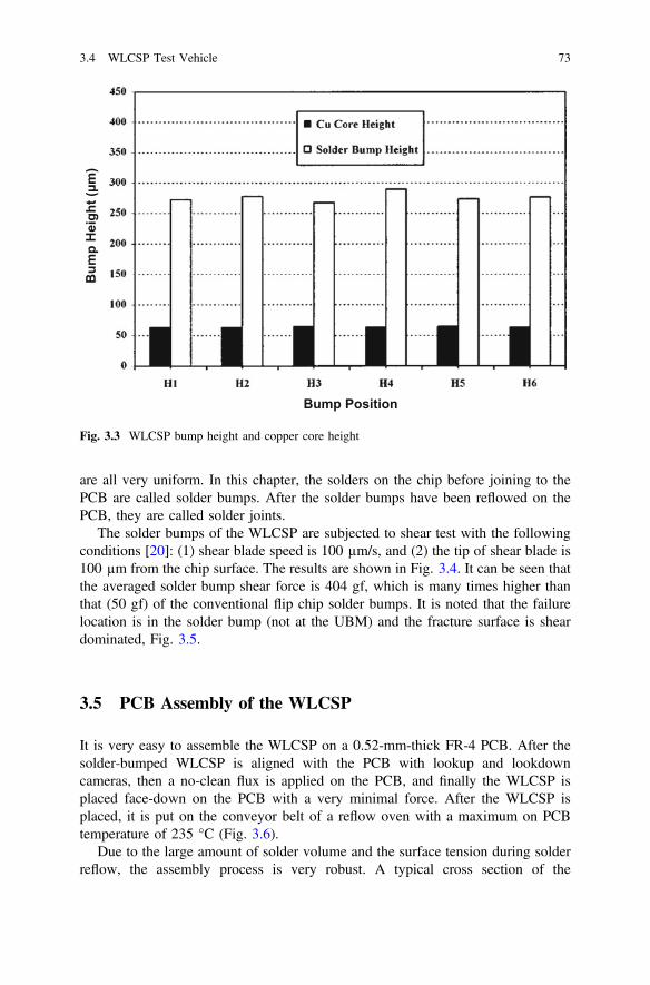
are all very uniform. In this chapter, the solders on the chip before joining to thePCB are called solder bumps. After the solder bumps have been reflowed on thePCB, they are called solder joints.
The solder bumps of the WLCSP are subjected to shear test with the followingconditions [20]: (1) shear blade speed is 100 µm/s, and (2) the tip of shear blade is100 µm from the chip surface. The results are shown in Fig. 3.4. It can be seen thatthe averaged solder bump shear force is 404 gf, which is many times higher thanthat (50 gf) of the conventional flip chip solder bumps. It is noted that the failurelocation is in the solder bump (not at the UBM) and the fracture surface is sheardominated, Fig. 3.5.
3.5 PCB Assembly of the WLCSP
It is very easy to assemble the WLCSP on a 0.52-mm-thick FR-4 PCB. After thesolder-bumped WLCSP is aligned with the PCB with lookup and lookdowncameras, then a no-clean flux is applied on the PCB, and finally the WLCSP isplaced face-down on the PCB with a very minimal force. After the WLCSP isplaced, it is put on the conveyor belt of a reflow oven with a maximum on PCBtemperature of 235 °C (Fig. 3.6).
Due to the large amount of solder volume and the surface tension during solderreflow, the assembly process is very robust. A typical cross section of the
Bump Position
Bum
p H
eigh
t (µm
)
Fig. 3.3 WLCSP bump height and copper core height
3.4 WLCSP Test Vehicle 73

Bump Number
Shea
r For
ce (g
f)
Fig. 3.4 Shear strength of WLCSP solder bumps
Solder
SolderSolder
Solder
Redistributed Trace
Fig. 3.5 Shear fracture surfaces of WLCSP solder bumps
74 3 Fan-in Wafer-Level Packaging Versus FOWLP
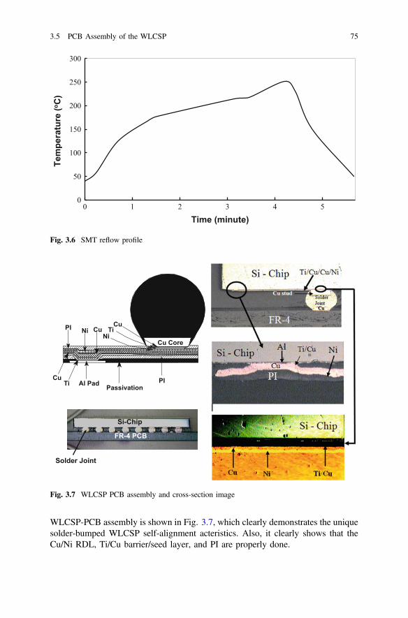
WLCSP-PCB assembly is shown in Fig. 3.7, which clearly demonstrates the uniquesolder-bumped WLCSP self-alignment acteristics. Also, it clearly shows that theCu/Ni RDL, Ti/Cu barrier/seed layer, and PI are properly done.
0
50
100
150
200
250
300
0 1 2 3 4 5
Time (minute)
Tem
pera
ture
(oC
)
Fig. 3.6 SMT reflow profile
Si-Chip
FR-4 PCB
Solder Joint
TiCu
Ni
PIAl Pad
PI
Passivation
Cu
Cu CoreNi
TiCu
Fig. 3.7 WLCSP PCB assembly and cross-section image
3.5 PCB Assembly of the WLCSP 75
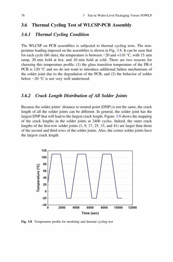
3.6 Thermal Cycling Test of WLCSP-PCB Assembly
3.6.1 Thermal Cycling Condition
The WLCSP on PCB assemblies is subjected to thermal cycling tests. The tem-perature loading imposed on the assemblies is shown in Fig. 3.8. It can be seen thatfor each cycle (60 min), the temperature is between −20 and +110 °C, with 15 minramp, 20 min hold at hot, and 10 min hold at cold. There are two reasons forchoosing this temperature profile: (1) the glass transition temperature of the FR-4PCB is 120 °C and we do not want to introduce additional failure mechanisms ofthe solder joint due to the degradation of the PCB; and (2) the behavior of solderbelow −20 °C is not very well understood.
3.6.2 Crack Length Distribution of All Solder Joints
Because the solder joints’ distance to neutral point (DNP) is not the same, the cracklength of all the solder joints can be different. In general, the solder joint has thelargest DNP that will lead to the largest crack length. Figure 3.9 shows the mappingof the crack lengths in the solder joints at 2400 cycles. Indeed, the outer cracklengths of the first-row solder joints (1, 9, 17, 25, 33, and 41) are larger than thoseof the second and third rows of the solder joints. Also, the corner solder joints havethe largest crack length.
-40
-20
0
20
40
60
80
100
120
0 2000 4000 6000 8000 10000 12000
Tem
pera
ture
(o C)
Time (sec)
Fig. 3.8 Temperature profile for modeling and thermal cycling test
76 3 Fan-in Wafer-Level Packaging Versus FOWLP

3.6.3 Crack Propagation of the Corner Solder Joint
It should be pointed out that unlike most of the solder joint reliability studies whichare to generate enough test data to fit into a life distribution [20–28], one of theobjectives of the present study is to determine the crack initiation and crackpropagation in solder joints of the WLCSP on PCB assemblies.
The initiation and propagation of cracks in any structures have always been avery complicated phenomenon. The initial crack length and crack growth length arealso difficult to define. In this study, at 100, 200, 500, 800, 1000, 1200, 1500, 2000,and 2400 cycles, three of the WLCSP-PCB assemblies are taken out from thethermal cycling chamber for inspection. Cracks of the cross-sectioned samples areinspected under high-power microscope. Important results are summarized as fol-lows [2, 14–18]:
(1) No obvious cracks in the solder joints up to 800 cycles (Fig. 3.10a and b). Itshould be pointed out that because of the small amount of sample size (3) andthe power of the microscope, there could be some very small tiny cracksinitiated much earlier.
(2) Between 800 and 1000 cycles, there are cracks on both sides of the cornersolder joint. The inner crack length (toward the center of the chip) = 25 lm andthe outer crack length = 40 lm, Fig. 3.10b. The outer crack initiated first asshown in Fig. 3.11b.
(3) Between 1000 and 1200 cycles, the inner crack length propagates to 37 lmwhile the outer crack length grows to 48 lm, Figs. 3.10c and 3.11c.
0
20
40
60
80
100
120
140
160
180
200
0 1 2 3 4 5 6 7
First row
Second row
Third row
Fourth row
1
9
2
3 124
1725
4
33
42
1810
2634
11 35 36 4 44282719 20
Column Number
Cra
ck L
engt
h (µ
m)
1
2
3
4
5
6
7
8
9
10
11
12
13
14
15
16
17
18
19
20
21
22
23
24
25
26
27
28
29
30
31
32
33
34
35
36
37
38
39
40 48
47
46
45
44
43
42
41
Fig. 3.9 Crack length distribution in solder joints of WLCSP assembly
3.6 Thermal Cycling Test of WLCSP-PCB Assembly 77

(4) Between 1200 and 1500 cycles, the inner crack length = 70 lm and the outercrack length = 100 lm, Fig. 3.10d.
(5) Between 1500 and 2000 cycles, the inner crack length grows to 100 lm and theouter crack length grows to 140 lm, Fig. 3.10e.
(6) Between 2000 and 2400 cycles, the cracks separate the corner solder joint,Figs. 3.10f and 3.11d.
(7) In the corner solder joint, the cracks initiated and grew near the copper pad ofthe PCB.
3.6.4 Fatigue Crack Growth Rate
Figure 3.12 shows the inner and outer crack lengths of the corner solder joint as afunction of the thermal cycling numbers. They can be curve-fitted, as shown inFig. 3.13, into the following forms:
(a)
(f)
(e)
(d)
(c)
(b) Si
PCBOuter Crack
Inner Crack
Direction to chip center
Fig. 3.10 Cross sections of the corner solder joint at different thermal cycles. a 800 cycles (noobvious cracks). b 1000 cycles with 40 lm crack (outer crack). c 1200 cycles with 48 lm crack(outer crack). d 1500 cycles with 100 lm crack (outer crack). e 2000 cycles with cracks from twoedges. f 2400 cycles with crack passing through solder joint
78 3 Fan-in Wafer-Level Packaging Versus FOWLP

Fig. 3.11 Schematic of the corner solder joint at different stages. a No obvious crack whentemperature cycles are less than 800. b Crack initiates from the outer edge. c Crack begins from theinner edge. d Cracks grow through the whole solder joint
0
50
100
150
200
0 500 1000 1500 2000 2500
Outer Crack
Inner Crack
N (Cycle)
Cra
ck L
engt
h (µ
m)
Si
PCBOuter Crack
Inner Crack
Direction to chip center
Fig. 3.12 Test results: crack length versus cycle numbers
3.6 Thermal Cycling Test of WLCSP-PCB Assembly 79

log ðaÞ ¼ C1 log ðNÞþC2 ð3:1Þ
or
a ¼ 10C2NC1 ð3:2Þ
and
N ¼ 10�C2=C1a1=C1 ð3:3Þ
Differentiating Eq. (3.2) with respect to N yields
dadN
¼ C110C2NðC1�1Þ ð3:4Þ
Substituting Eq. (3.3) into Eq. (3.4) gives
dadN
¼ C110C2=C1aðC1�1Þ=C1 ; ð3:5Þ
where a is the crack length, N is the number of cycles, and C1 and C2 are given inTable 3.1. Thus, for the corner solder joint, the length of outer and inner cracks canbe determined by Eq. (3.2) for a given number of thermal cycles. Also, the fatiguecrack growth rate (da/dN) of the corner solder joint can be obtained from Eq. (3.5).
log(a) = 1.8019log(N) - 3.8061
log(a) = 1.8605log(N) - 4.1427
1.2
1.6
2
2.4
2.8 3 3.2 3.4 3.6
Outer Crack
Inner Crack
Log(N)
Log(
a)
Fig. 3.13 Curve-fitting of crack length versus cycle numbers
80 3 Fan-in Wafer-Level Packaging Versus FOWLP

3.7 Fracture Characteristics of the Corner SolderJoint—Solder Material and Properties
The solder joint is made of 63Sn–37Pb solder and has a Poisson’s ratio of 0.4, and acoefficient of thermal expansion (CTE) of 21 � 10−6/°C. The Young’s modulus(Fig. 3.14) and the stress–strain relations (Fig. 3.15) of the solder are temperaturedependent. The Young’s modulus, Poisson’s ratio, and CTE for copper (Cu) are,respectively, 76 GPa, 0.34, and 17 � 10−6/°C. The CTE of FR-4 PCB is18.5 � 10−6/°C and that of Si WLCSP is 2.5 � 10−6/°C. The material propertiesused in the computational modeling are shown in Table 3.2.
The Garofalo-Arrhenius steady-state creep is generally expressed as
dcdt
¼ CGh
� �sin h x
sG
� �h inexp
�Qkh
� �
Table 3.1 Curve-fitting constants: C1, C2, C3, C4
Curve-fitted Location C1 C2 C3 C4
Crack length versus cycles Inner crack 1.86 −4.14 – –
Outer crack 1.80 −3.81 – –
Stress intensity factor versus crack length Inner crack – – 0.587 0.485
Outer crack – – 0.610 0.520
22
24
26
28
30
32
34
0 10 20 30 40 50 60 70 80 90 100 110
Youn
g's
Mod
ulus
(GPa
)
Temperature (oC)
Fig. 3.14 Temperature-dependent young’s modulus of solder
3.7 Fracture Characteristics of the Corner Solder … 81

where
c is the shear creep strain,dc/dt is the shear creep strain rate,t is the time,C is a material constant,G is the temperature-dependent shear modulus,h is the absolute temperature (K),x defines the stress level at which the power law stress dependence breaks
down, s is the shear stress,
0
10
20
30
40
50
60
70
0 0.002 0.004 0.006 0.008 0.01 0.012
Stre
ss (M
Pa)
Strain (%)
0oC
20oC
40oC
60oC
80oC
100oC
Fig. 3.15 Nonlinear temperature-dependent stress–strain relations of solder
Table 3.2 Material properties for modeling
Materialproperties
Young’s modulus(GPa)
Poisson’sratio
Thermal expansion coefficient(10−6/°C)
FR-4 PCB 22 0.28 18.5
63Sn–37Pb Temp. Dep. 0.4 21
Polyimide 8.3 0.33 3
SiliconWLCSP
131 0.3 2.8
Solder mask 6.9 0.35 19
Ni 20.5 0.3 12.3
Cu 76 0.35 17
82 3 Fan-in Wafer-Level Packaging Versus FOWLP

n is the stress exponent,Q is the activation energy for a specific diffusion mechanism, andk is the Boltzmann’s constant (8.617 � 10−5 eV/°K).
The Garofalo-Arrhenius creep equation can be rearranged by lumping certaincoefficients and expressed as:
dedt
¼ C1 sin h C2rð Þ½ �C3exp �C4
T
� �
where C1, C2, C3, and C4 are (not those Cs shown in Table 3.1) determined by creeptest (curves) at various sets of constant stress and temperature. It should be notedthat the last equation is exactly the same as the input form of the implicit creepmodel (TBOPT = 8) in ANSYS. In the equation, r is the effective normal stress,and de/dt is the effective normal creep strain rate. The unit for r is MPa. For thepresent study, the creep constitutive equation for the 63Sn–37Pb is given byLau [21]
dedt
¼ 926 508� Tð ÞT
sin h3:3r
37:78� 106 � 74414T
� �exp
�6360T
� �
The unit of r is Pa and of T is °K.
3.8 Fracture Characteristics of the Corner SolderJoint—Geometry
Even though the initiation and propagation of the outer crack and the inner crack(toward to the chip center) of the corner solder joint are not exactly the same,however, for the sake of modeling simplicity, they are assumed to be equal.Figure 3.16 shows the corner solder joint for fracture mechanics finite elementmodeling. It can be seen that the solder joint is 0.24 mm tall and the diameters ofthe bottom and top surfaces are 0.28 and 0.3 mm, respectively.
Because of the WLCSP on PCB assembly’s global thermal expansion mismatch(3.2259 � 130 � [18.5 − 2.5] � 10−6 = 0.0067 mm) between the Si WLCSP andthe FR-4 PCB, and the thermal expansion of the corner solder joint, the solder jointis subjected to a complex state of stress and strain during thermal cycling condition.These stresses and strains produce the driving force for solder joint failure. Sincemost of the thermal fatigue life of ductile materials such as solder is spent inpropagating the crack (i.e., fatigue crack growth), the stresses and strains (stressintensity factors, J-integral, or creep strain energy density) around the crack tip ofdifferent crack lengths in the solder joint are of utmost interest.
3.7 Fracture Characteristics of the Corner Solder … 83

3.9 Fracture Characteristics of the Corner Solder Joint—Elastic Thermal Fatigue Life Prediction Model (DK)
3.9.1 Boundary Value Problem
In this study [14], the solder (63Sn–37Pb) is assumed to be an elastic material andfive different crack lengths are considered. These cracks are located symmetrically10 lm above the copper pad on the PCB. The eight-node plain strain element isused in this study and the units are in Newton and mm. At the crack tip, themid-side nodes are placed at the quarter points to capture the singularity in thestresses. Since most of the thermal fatigue life of ductile materials such as solder isspent in propagating the crack (i.e., fatigue crack growth), the stresses and strains
Fig. 3.16 Corner solder joint for modeling
84 3 Fan-in Wafer-Level Packaging Versus FOWLP

(stress intensity factor) around the crack tip of different crack lengths in the solderjoint are of utmost interest.
The boundary conditions imposed on the corner solder joint are shown inFig. 3.16, where the bottom surface is fixed, the top surface (nodes) of the solderjoint is subjected to a 0.0067 mm displacement, and the whole solder joint issubjected to a temperature change of 130 °C. The top surface is also restrained fromrotation by specifying nodal couplings of vertical displacement to those nodes sothat the vertical displacements are the same.
With the prescribed loadings, the left crack in Fig. 3.16 is expected to pop openand the right crack should remain close. Instead of using contact elements, nodalcouplings are conveniently used to simulate the closing and sliding of the rightcrack surfaces. In ANSYS (a commercial finite element code), the nodes on theright crack surfaces are nodal-coupled in the vertical direction at the coincidentnodes, while free to slide in the horizontal direction. By using nodal couplings,there is no penetration of the crack surfaces when the crack is closed.
Figure 3.17a–e show the deformed (with finite element meshes) andun-deformed shapes of the corner solder joint with different crack lengths: 0.028,0.056, 0.084, 0.112, and 0.133 mm. The typical von Mises stress contours aroundthe crack tips (with a crack length = 0.112 mm) are shown in Fig. 3.18. It can beseen that, due to stress concentration (Fig. 3.18), the stresses at the crack tip arevery large. The stress intensity factors DKI (opening mode I) and DKII (shearingmode II) at the inner and outer crack tips for different crack lengths of the cornersolder joint are shown in Fig. 3.19. It can be seen that the fracture characteristics atthe crack tips are dominated by shearing mode of fracture (due to the thermalexpansion mismatch between the Si WLCSP and FR-4 PCB) especially at largercrack lengths.
Fig. 3.17 Deformed shape of the corner solder joint. a Crack length = 0.028 mm. b Cracklength = 0.056 mm. c Crack length = 0.084 mm. d Crack length = 0.112 mm. e Cracklength = 0.133 mm
3.9 Fracture Characteristics of the Corner Solder … 85

3.9.2 Thermal Fatigue Life Prediction Model
Define the effective stress intensity factor range DKeff as
DKeff ¼ffiffiffiffiffiffiffiffiffiffiffiffiffiffiffiffiffiffiffiffiffiffiffiDK2
I þDK2II
qð3:6Þ
The curves in Fig. 3.19 can be curve-fitted, as shown in Fig. 3.20 [only themiddle three points are used since the crack initiation (near to the first point) is notvery well defined and the solder joint fracture (near the fifth point) is not stable],into the following forms:
log ðDKeffÞ ¼ C3 log ðaÞþC4 ð3:7Þ
or
a ¼ 10�C4=C3DK1=C3eff ð3:8Þ
Fig. 3.18 Mises stress contour at the tip of outer (left) and inner (right) cracks (cracklength = 0.112 mm)
86 3 Fan-in Wafer-Level Packaging Versus FOWLP

0
40
80
120
0.1 0.2 0.3 0.4 0.5
Outer Crack-
Inner Crack-
Inner Crack-
Outer Crack-
ΔKII
ΔKII
ΔKI
ΔKI
Normalized Crack Length (a/280µm)
Stre
ss In
tens
ity F
acto
r, M
Pa(m
m)1/
2
Fig. 3.19 Stress intensity factors range at the crack tip of different crack length in the cornersolder joint
log(ΔKeff) = 0.6104log(a) + 0.5196
log(ΔKeff) = 0.5868log(a) + 0.4851
1.5
1.6
1.7
1.8
1.6 1.8 2 2.2
Outer Crack
Inner Crack
ΔKeff=[ΔKI2+ΔKII
2]1/2
Log(a)
Log(
Kef
f)
Fig. 3.20 Curve-fitting of the effective stress intensity factors range at the crack tip of differentcrack length in the corner solder joint
3.9 Fracture Characteristics of the Corner Solder … 87

The constants C3 and C4 are given in Table 3.1. Substituting Eq. (3.8) intoEq. (3.5) yields
dadN
¼ C110ðC2C3�C1C4 þC4Þ=C1C3DKðC1�1Þ=C1C3eff ð3:9Þ
Thus, for the inner crack (Table 3.1), C1 = 1.8606; C2 = −4.1427; C3 = 0.5868;C4 = 0.4851, and Eq. (3.9) becomes
dadN
¼ 0:0046DK0:79eff ð3:10Þ
For the outer crack (Table 3.1), C1 = 1.8019; C2 = −3.8061; C3 = 0.6104;C4 = 0.5196, and Eq. (3.9) becomes
dadN
¼ 0:0058DK0:73eff ð3:11Þ
By averaging the coefficients of Eqs. (3.10) and (3.11), the thermal fatigue lifeprediction equation (in the form of Paris law) for flip chip solder joints can beexpressed as
dadN
¼ 0:0052DK0:76eff ð3:12Þ
Thus, for a given solder-bumped WLCSP assembly, once the effective stressintensity factor range DKeff in terms of the crack length (a) is determined for a giventemperature-cycling condition by computational modeling, the number of cycle tofailure (N) can be estimated by Eq. (3.12).
3.9.3 Summary and Recommendations
Stress intensity factors at the crack tip of different crack lengths of the corner solderjoint have been determined by fracture mechanics with the finite element method.Some important results are summarized as follows:
• In the present study, corner solder joint cracks initiate at two different locations,one near the chip center (inner crack) and the other on the opposite side (outercrack) of the solder joint. These cracks are right above the copper pad of thePCB.
• The outer crack of the corner solder joint initiates first and grows slightly largerthan the inner crack at higher thermal cycles.
• In the present study, the outer and inner cracks of the corner solder joint meetbetween 2000 and 2400 cycles. This indicates that the present WLCSP on PCB
88 3 Fan-in Wafer-Level Packaging Versus FOWLP

solder joints is reliable for use in most of the operating conditions even withoutunderfill encapsulant.
• For the WLCSP on PCB under consideration, the crack length of the cornersolder joint as a function of the number of thermal cycles has been measured anddetermined as shown in Eq. (3.2). Also, the thermal fatigue crack growth rate ofthe corner solder joint is given by Eq. (3.4) in terms of the number of thermalcycles or Eq. (3.5) in terms of the crack length.
• For the WLCSP on PCB under consideration, the effective stress intensity factorrange at the crack tip as a function of the crack length of the corner solder jointhas been determined and is given by Eq. (3.8). Also, the thermal fatigue crackgrowth rate in terms of the effective stress intensity factor range of the cornersolder joint is given by Eq. (3.9).
• A new thermal fatigue life prediction model for flip chip solder joints is pro-posed as shown in Eq. (3.12).
3.10 Fracture Characteristics of the Corner SolderJoint—Plastic Thermal Fatigue Life PredictionModel (DJ)
In this study [19], the solder (63Sn–37Pb) is assumed to be an elasto-plasticmaterial and the Young’s modulus (Fig. 3.13) and the stress–strain relations(Fig. 3.14) of the solder are temperature dependent. Since most of the thermalfatigue life of ductile materials such as solder is spent in propagating the crack (i.e.,fatigue crack growth), the stresses and strains (J-integrals) around the crack tip ofdifferent crack lengths in the solder joint are of utmost interest.
In its simplest form, the J-integral is defined as a path-independent line integralthat measures the strength of the singular stresses and strains near a crack tip(Fig. 3.21). The following equation shows an expression for J in its two-dimensional form. It assumes that the crack lies in the global Cartesian X–Y plane,with X parallel to the crack.
J ¼ZC
Wdy�ZC
tx@ux@x
þ ty@uy@x
� �ds; ð3:13Þ
where
C any path surrounding the crack tipW strain energy densitytx traction along x axis = rxnx + rxynyty traction along y axis = ryny + rxynxr stress componentn unit outward normal to path
3.9 Fracture Characteristics of the Corner Solder … 89

u displacements distance along the path
In this study, five different crack lengths are considered. These cracks are locatedsymmetrically 10 lm above the copper pad on the PCB. The eight-node plain strainelement is used in this study and the units are in Newton and mm. At the crack tip,the mid-side nodes are placed at the quarter points to capture the singularity in thestresses.
3.10.1 Boundary Condition and Results
The boundary conditions imposed on the corner solder joint are exactly the same asthose in Sect. 3.9 (Fig. 3.16). Figure 3.22a–e show the deformed (with finite ele-ment meshes) and un-deformed shapes of the corner solder joint with different cracklengths: 0.056, 0.084, 0.112, 0.1225, and 0.133 mm. The typical von Mises stresscontours around the crack tips (with a crack length = 0.112 mm) are shown inFig. 3.23. It can be seen that, due to stress concentration, the stresses at the crack tipare very large. The J-integrals at the inner and outer crack tips for different cracklengths of the corner solder joint are shown in Fig. 3.24.
3.10.2 Thermal Fatigue Life Prediction Model
The curves in Fig. 3.24 can be curve-fitted, as shown in Fig. 3.25 [only four pointsare used since the solder joint fracture (near the fifth point) is not stable], into thefollowing forms:
G
1
G 1 G 2
G 3
n
Fig. 3.21 J-integral contour path surrounding a crack tip
90 3 Fan-in Wafer-Level Packaging Versus FOWLP

log ðDJÞ ¼ C3 logðaÞþC4 ð3:14Þ
or
a ¼ 10�C4=C3DJ1=C3 ð3:15Þ
The constants C3 and C4 are given in Table 3.3. Substituting Eq. (3.15) intoEq. (3.5) yields
dadN
¼ C110ðC2C3�C1C4 þC4Þ=C1C3DJðC1�1Þ=C1C3 ð3:16Þ
Thus, for the inner crack (Table 3.3), C1 = 1.8606; C2 = −4.1427; C3 = 1.655;C4 = −4.108, and Eq. (3.16) becomes
dadN
¼ 0:155DJ0:279 ð3:17Þ
X
Y
Z
(a)
X
Y
Z
(e)
X
Y
Z
(d)
X
Y
Z
(c)
X
Y
Z
(b)
Fig. 3.22 Deformed shape of the corner solder joint. a Crack length = 0.056 mm, DJ_inner crack= 0.0704 MPa-mm, DJ_outer crack = 0.0791 MPa-mm. b Crack length = 0.084 mm, DJ_innercrack = 0.0918 MPa-mm, DJ_outer crack = 0.126 MPa-mm. c Crack length = 0.112 mm,DJ_inner crack = 0.175 MPa-mm, DJ_outer crack = 0.183 MPa-mm. d Crack length =0.1225 mm, DJ_inner crack = 0.284 MPa-mm, DJ_outer crack = 0.313 MPa-mm. e Crack length= 0.133 mm, DJ_inner crack = 1.163 MPa-mm, DJ_outer crack = 1.133 MPa-mm
3.10 Fracture Characteristics of the Corner Solder … 91

ANSYS 5.6.1 JUN 27 200020:38:56 NODAL SOLUTIONSTEP=1 SUB =10 TIME=1 SEQV (AVG) PowerGraphicsEFACET=1AVRES=MatDMX =.006825 SMN =6.309 SMX =685.142
1
CDECDEDECDECCBBBBBBBCDECDECDEBCDECBBBBBDECDECDEDEDBCCBB
CBBCCBBBCDEDEDECDEDCCB
BCBBBBBCCB
AAAB AABB
DDDDDDDD DEFGDD CDC CC
DDD CC CDDDDDDDDD
DDDDDDDDDEFG DDCDCCCCCC
AAA CDCDCDBCDBBBBBDCDCDCDCBBCBCBBBBBCDDDCDBCCCBBBBBBBCBBCDBCDCDCDBBCBBBBBBBB
AA
DDDDDD
CDED
CCCCCCCCCCDEFGHCCCCCCCCCCD
ECCCCCCCCCDEFGHICCCDEFGHI
BBB BBBBB
B
AA
AA A A AA
A
AA AA
A AAA
AA
AA
AAAA AA
A AAA
AA
AAAAAA
AA AA AAA
AAA
A
AAA
AA
AAAAAA
AAAAAA
AA
AAAA
AA A
A
AA
AAAA
MN
MX
2
D
A
A
A
C DC DCD
B
CDB
BBBB
DCDCDC
D C
BB
C
B
C
BB
BBB
CD DDC
D
BCCC
B
B
BBBB
B
C
B
BCD
BCD
CDC D
BBCB
BBBBBBB
D
D
D
B B B
B
3
CDECDE DE CDE
CC
BB BBB BB
CDE CDECDE
BCDE C
B
BB
BB
D ECDE
CDEDED
BCC
B
B
C
BB
CC
BBB
CDEDE
DECDED
CCB
B
C
B
BBBB
C C
B
AA
A
BBB
DD
D
D DD
D
D
DD
D
B BB
X
Y
Z A =44.022 B =119.448 C =194.874 D =270.299 E =345.725 F =421.151 G =496.577 H =572.003 I =647.429 A =44.022 B =119.448 C =194.874 D =270.299 E =345.725 F =421.151 G =496.577 H =572.003 I =647.429 a/280=0.4
Fig. 3.23 Mises stress contour at the tip of outer (left) and inner (right) cracks (cracklength = 0.112 mm)
0.0
0.2
0.4
0.6
0.8
1.0
1.2
1.4
0.2 0.3 0.4 0.5
Inner
Outer
Normalized Crack Length (a/280µm)
J-In
tegr
al (M
Pa-m
m)
Fig. 3.24 J-Integral range of different crack length in the corner solder joint
92 3 Fan-in Wafer-Level Packaging Versus FOWLP
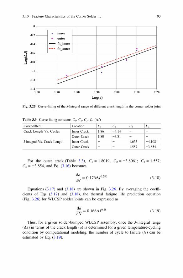
For the outer crack (Table 3.3), C1 = 1.8019; C2 = −3.8061; C3 = 1.557;C4 = −3.854, and Eq. (3.16) becomes
dadN
¼ 0:176DJ0:286 ð3:18Þ
Equations (3.17) and (3.18) are shown in Fig. 3.26. By averaging the coeffi-cients of Eqs. (3.17) and (3.18), the thermal fatigue life prediction equation(Fig. 3.26) for WLCSP solder joints can be expressed as
dadN
¼ 0:166DJ0:28 ð3:19Þ
Thus, for a given solder-bumped WLCSP assembly, once the J-integral range(DJ) in terms of the crack length (a) is determined for a given temperature-cyclingcondition by computational modeling, the number of cycle to failure (N) can beestimated by Eq. (3.19).
-1.4
-1.2
-1
-0.8
-0.6
-0.4
-0.2
0
1.60 1.70 1.80 1.90 2.00 2.10 2.20
innerouterfit_innerfit_outer
Log(a)
Log(
J)
Fig. 3.25 Curve-fitting of the J-Integral range of different crack length in the corner solder joint
Table 3.3 Curve-fitting constants C1, C2, C3, C4 (DJ)
Curve-fitted Location C1 C2 C3 C4
Crack Length Vs. Cycles Inner Crack 1.86 −4.14 − −
Outer Crack 1.80 −3.81 − −
J-integral Vs. Crack Length Inner Crack − − 1.655 −4.108
Outer Crack − − 1.557 −3.854
3.10 Fracture Characteristics of the Corner Solder … 93

3.10.3 Summary and Recommendations
• A simple empirical equation for predicting the thermal fatigue life ofsolder-bumped flip chip on low-cost PCB has been presented. It is derived bycombining the measured thermal fatigue crack growth rate of the corner solderjoint and the simulated nonlinear fracture characteristics (J-integral) at the cracktip of the corner solder joint with various crack lengths.
• The use of the proposed equation is very simple. For any given 63Sn–37Pbsolder-bumped flip chip on FR-4 epoxy PCB assembly, once the J-integralrange in terms of the crack length is determined for a given temperature-cyclingcondition by computational modeling, then the number of cycle to failure of thesolder joint can be estimated by the integration of the proposed equation.
• In order to verify the accuracy of the proposed equation, more experimentalwork is necessary. This can be done by testing WLCSPs with different chip sizesand various solder joint geometry.
0
0.02
0.04
0.06
0.08
0.1
0.12
0.14
0 0.05 0.1 0.15 0.2 0.25 0.3 0.35 0.4
innerouterAverage
J (MPa-mm)
da/d
N (µ
m/C
ycle
)
Fig. 3.26 Fatigue crack growth rate curves
94 3 Fan-in Wafer-Level Packaging Versus FOWLP

3.11 Fracture Characteristics of the Corner SolderJoint—Creep Thermal Fatigue Life PredictionModel (DW)
3.11.1 Assumptions
In this study [18], the solder (63Sn–37Pb) is assumed to be a creep material(Fig. 3.15). Again, Fig. 3.16 (the corner solder joint) is used for modeling. Due tothe global/local thermal expansion mismatch between the Si, FR-4, and solder, themismatch stresses and strains (such as the creep strain energy density around thecrack tip of different crack lengths) produce the driving force for solder joint failure.
In this study, three different crack lengths are considered. These cracks arelocated symmetrically 10 mm above the copper pad on the PCB. The eight-nodeplain strain element is used in this study. At the crack tip, the mid-side nodes of thetriangular elements, as shown in Fig. 3.27, are placed at the quarter points tocapture the singularity in the stresses. Contact elements are used to simulate theclosing and sliding of the crack surfaces.
3.11.2 Boundary Conditions
The whole solder joint is subjected to a temperature profile, T (°C), as shown inFig. 3.28. The bottom surface is fixed, the top surface (nodes) of the solder joint issubjected to a global thermal expansion mismatch displacement, D = 3.22593 � T
Fig. 3.27 Elements around acrack tip for averaged strainenergy density calculation
3.11 Fracture Characteristics of the Corner Solder … 95

(°C) � [18.5 − 2.5] � 10−6 mm, as shown in Figs. 3.28 and 3.16. The top surfaceis also restrained from rotation by specifying nodal couplings of vertical dis-placement to those nodes so that the vertical displacements are the same.
3.11.3 Deformed Shape, Stress, and Strain
Figure 3.29a–c shows the deformed (with finite element meshes) and un-deformedshapes of the corner solder joint with different crack lengths: 0.056, 0.084, and0.112 mm. The typical von Mises stress contours around the crack tips (with acrack length = 0.112 mm) are shown in Fig. 3.30. It can be seen that due to stressconcentration the stresses at the crack tip are very large.
Figures 3.31, 3.32, and 3.33 show the shear creep strain history, shear stresshistory, and shear stress and shear creep strain hysteresis loops at the middle betweenthe crack tips (Fig. 3.29a with crack length = 0.112 mm) of the corner solder jointfor three full thermal cycles. It can be seen that the responses are converged. Theshear creep strain range is about 0.33 and the shear stress range is about 90 MPa.
Figures 3.34, 3.35, and 3.36 show the shear creep strain history, shear stresshistory, and shear stress and shear creep strain hysteresis loops at a point near thecrack tip (with crack length = 0.112 mm) of the corner solder joint for three fullthermal cycles. Again, the responses are converged. However, as expected, theshear creep strain range is very large (about 0.72) and the shear stress range is alsovery large (about 115 MPa).
Time (sec)
Dis
plac
emen
t (m
m)
Tem
pera
ture
(oC
)
Fig. 3.28 Temperature and displacement boundary conditions
96 3 Fan-in Wafer-Level Packaging Versus FOWLP

3.11.4 Strain Energy Density Around the Crack Tip
Theoretically speaking, because of singularity, the strain energy density at the cracktip is infinitive. Practically, however, the average strain energy density per thermalcycle around the crack tip is used to determine the thermal fatigue life of solderjoints. In this study, the strain energy density around a crack tip is obtained byaveraging across the elements in an area of 0.02 mm by 0.02 mm in thetwo-dimensional model as shown in Fig. 3.27. (For the case of conventionalsolder-bumped flip chip on board assembly, the radius of the copper pad is about 3–4 mils and the solder joint height is about 1–2 mils for eutectic solder and 3–4 milsfor high-temperature solder, then the area for averaging the strain energy densityshould be 0.008 mm by 0.008 mm.)
There are about 100 elements in the 0.02 � 0.02 mm area2. The crack tip ismodeled with two rows of elements. The elements in the first row are triangularelements with the mid-side nodes skewed to 1/4 points, as suggested by ANSYS for
Fig. 3.29 Deformed shape of the corner solder joint. a Crack length = 0.056 mm, T = 20 °C.b Crack length = 0.084 mm, T = 20 °C. c Crack length = 0.112 mm, T = 20 °C
3.11 Fracture Characteristics of the Corner Solder … 97

the effect of crack tip singularity. The radius of the first row is 0.0037 mm, i.e.,about 20% of the length of one side (0.02 mm) of the square area as shown inFig. 3.27 (For the case of conventional flip chip on board assembly, the radius isabout 0.0016 mm.). There are 16 uniform angular divisions around the cracktip. The quadrilateral elements on the second row have a radial length being half ofthat of the first row. Regular meshed are generated for the remaining area used inthe strain energy density calculation.
The average strain energy density of the elements in this area at any time instantduring the viscoplastic process is normalized by the volume of the elements.
Wt ¼X
Welement � Velement
� �=X
Velement; ð3:20Þ
where Wt is the average creep strain energy density at time point t, Welement is thecreep strain energy density in each element and is directly extracted from ANSYSin its postprocessing, and Velement is the volume of each element. For atwo-dimensional problem, however, ANSYS gives volume of each element in its
Fig. 3.30 Mises stress contour at the tip of outer (left) and inner (right) cracks (cracklength = 0.112 mm)
98 3 Fan-in Wafer-Level Packaging Versus FOWLP
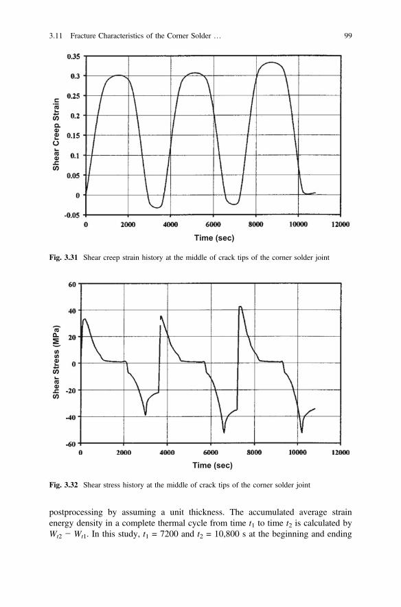
postprocessing by assuming a unit thickness. The accumulated average strainenergy density in a complete thermal cycle from time t1 to time t2 is calculated byWt2 − Wt1. In this study, t1 = 7200 and t2 = 10,800 s at the beginning and ending
Time (sec)
Shea
r Cre
ep S
trai
n
Fig. 3.31 Shear creep strain history at the middle of crack tips of the corner solder joint
Time (sec)
Shea
r Str
ess
(MPa
)
Fig. 3.32 Shear stress history at the middle of crack tips of the corner solder joint
3.11 Fracture Characteristics of the Corner Solder … 99

of the third cycle, respectively, are used. The accumulated average strain energydensity range in the third thermal cycle around the inner and outer crack tips fordifferent crack lengths of the corner solder joint is shown in Fig. 3.37. It can be seen
Shear Creep Strain
Shea
r Str
ess
(MPa
)
Fig. 3.33 Hysteresis loops at the middle of crack tips of the corner solder joint
Shea
r Cre
ep S
trai
n
Time (sec)
Fig. 3.34 Shear creep strain history near one of the crack tips of the corner solder joint
100 3 Fan-in Wafer-Level Packaging Versus FOWLP
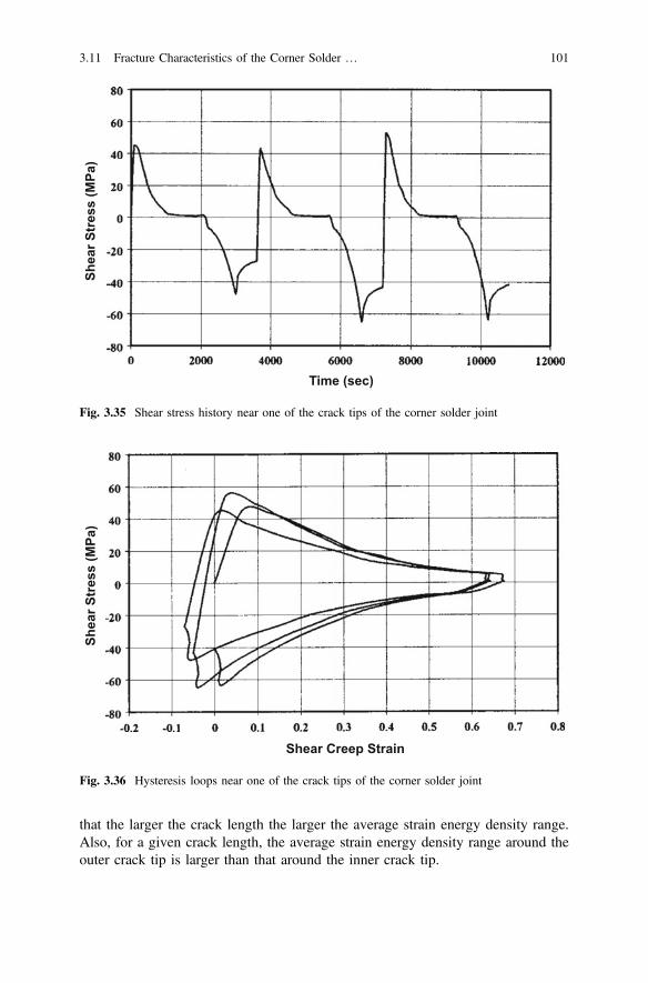
that the larger the crack length the larger the average strain energy density range.Also, for a given crack length, the average strain energy density range around theouter crack tip is larger than that around the inner crack tip.
Time (sec)
Shea
r Str
ess
(MPa
)
Fig. 3.35 Shear stress history near one of the crack tips of the corner solder joint
Shea
r Str
ess
(MPa
)
Shear Creep Strain
Fig. 3.36 Hysteresis loops near one of the crack tips of the corner solder joint
3.11 Fracture Characteristics of the Corner Solder … 101
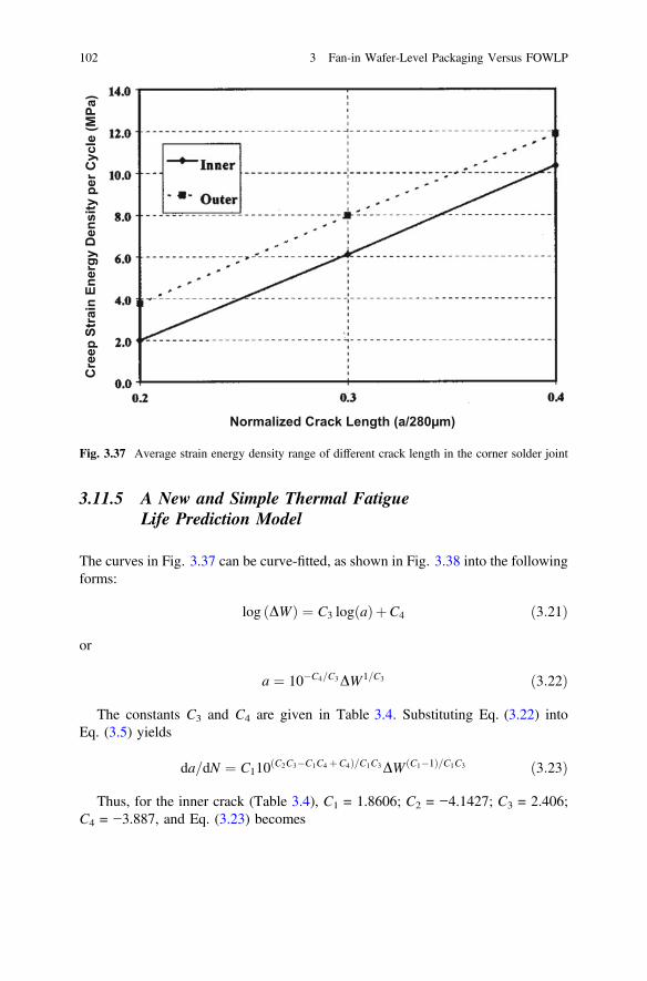
3.11.5 A New and Simple Thermal FatigueLife Prediction Model
The curves in Fig. 3.37 can be curve-fitted, as shown in Fig. 3.38 into the followingforms:
log ðDWÞ ¼ C3 log að ÞþC4 ð3:21Þ
or
a ¼ 10�C4=C3DW1=C3 ð3:22Þ
The constants C3 and C4 are given in Table 3.4. Substituting Eq. (3.22) intoEq. (3.5) yields
da=dN ¼ C110ðC2C3�C1C4 þC4Þ=C1C3DW ðC1�1Þ=C1C3 ð3:23Þ
Thus, for the inner crack (Table 3.4), C1 = 1.8606; C2 = −4.1427; C3 = 2.406;C4 = −3.887, and Eq. (3.23) becomes
Cre
ep S
trai
n En
ergy
Den
sity
per
Cyc
le (M
Pa)
Normalized Crack Length (a/280µm)
Fig. 3.37 Average strain energy density range of different crack length in the corner solder joint
102 3 Fan-in Wafer-Level Packaging Versus FOWLP

da=dN ¼ 0:062DW0:192 ð3:24Þ
For the outer crack (Table 3.4), C1 = 1.8019; C2 = −3.8061; C3 = 1.677;C4 = −2.347, and Eq. (3.23) becomes
da=dN ¼ 0:058DW0:265 ð3:25Þ
Equations (3.24) and (3.25) are shown in Fig. 3.39. By averaging the coeffi-cients of Eqs. (3.24) and (3.25), the thermal fatigue life prediction equation(Fig. 3.39) for WLCSP solder joints can be expressed as
Cre
ep S
trai
n En
ergy
Den
sity
per
Cyc
le (M
Pa)
Log(a)
Fig. 3.38 Curve-fitting of the average strain energy density range of different crack lengths in thecorner solder joint
Table 3.4 Curve-fitting constants C1, C2, C3, C4 (DW)
Curve-fitted Location C1 C2 C3 C4
Crack Length Vs. Cycles Inner Crack 1.86 −4.14 − −
Outer Crack 1.80 −3.81 − −
Strain energy Vs. Crack Length Inner Crack − − 2.406 −3.887
Outer Crack − − 1.677 −2.347
3.11 Fracture Characteristics of the Corner Solder … 103

da=dN ¼ 0:06DW0:25 ð3:26Þ
Thus, for a given solder-bumped flip chip assembly, once the average strainenergy range (DW) in terms of the crack length (a) is determined for a giventemperature-cycling condition by computational modeling, the number of cycle tofailure (N) can be estimated by Eq. (3.26).
3.11.6 Summary and Recommendation
• A new and simple empirical equation for predicting the thermal fatigue life ofsolder-bumped flip chip on low-cost PCB has been presented. It is derived bycombining the measured thermal fatigue crack growth rate of the corner solderjoint and the simulated nonlinear fracture characteristics * average strainenergy density per cycle around the crack tip of the corner solder joint withvarious crack lengths.
• The use of the proposed equation is very simple. For any given WLSCP PCBassembly and solder-bumped flip chip on PCB assembly, once the average strainenergy density range per thermal cycle in terms of the crack length is determinedfor a given temperature-cycling condition by computational modeling, then the
da/d
N (µ
m/C
ycle
)
Creep Strain Energy Density per Cycle (MPa)
Fig. 3.39 Fatigue crack growth rate curves of the corner solder joint
104 3 Fan-in Wafer-Level Packaging Versus FOWLP

number of cycle to failure of the corner solder joint can be estimated by theintegration of the proposed equation *8!
• The element sizes and shapes and the area around the crack tip for calculatingthe average strain energy density are recommended for the WLCSP-PCBassembly. For the conventional solder-bumped flip chip on PCB assemblies,these parameters for determining the average strain energy density are alsorecommended.
3.12 Hitachi’s WLCSP
Figure 3.40a shows a Hitachi’s wafer with memory chips. The original pads on thememory chips are very fine-pitch and distributed along the centerline of the chip asshown in Fig. 3.40b.
3.12.1 Hitachi’s WLCSP with Stress Relaxation Layer
A metal RDL is used to redistribute the fine-pitch original pads along the centerlineof the chips on a wafer to much larger pitch area-arrayed pads all over the areawithin the chips as shown in Fig. 3.40b. In order to apply to larger chips (e.g.,10 mm � 10 mm) without underfill, Hitachi introduced [54] a stress relaxationlayer between the Si chip and the solder bumps as shown in Fig. 3.41.
(a) (b)
Fig. 3.40 a Hitachi’s memory chips on an 8-in. wafer. b Hitachi’s WLCSP with original padsalong the centerline and redistributed pads area array within the chip area
3.11 Fracture Characteristics of the Corner Solder … 105

3.12.2 Key Process Steps for Hitachi’s WLCSP
The key process steps of Hitachi’s WLCSP (Table 3.5) with a stress relaxationlayer are shown in Fig. 3.42. First, the wafer is spin-coated with a photosensitivepolyimide (P–PI), and the chip pads and dicing streets are opened up by pho-tolithography. Then, a stress relaxation layer is formed by printing liquid resin onthe wafer through a stencil mask with no opening on the pads and dicing streets.The resin will flow through the open edges and form smooth slopes.
To add a layer of metal on the wafer, Hitachi sputters the seed metals (Cr andCu) on the whole wafer, spin-costs a photoresist layer, and opens up the shapes ofinterconnections and new pads (in area array format) by photolithography. Then,the interconnections and pads are formed by electroplating the Cu and Ni. Thephotoresist and seed metals are removed by etching.
Now, the wafer is spin-coating with the P–PI again and the new chip pads anddicing streets are opened up by photolithography. This time, the P–PI acts like asolder mask. After fluxing, the SnAgCu solder bumps are placed on the new landpads on the wafer through a stencil mask with a solder ball mounter. Finally, thewafer is reflowed, cleaned, and diced.
Fig. 3.41 Cross section of Hitachi’s WLCSP mounted on a PCB
Table 3.5 Hitachi’s WLCSPtest vehicle
Chip Size 10 mm � 10mm
Thickness 0.725 mm
Pad layout Number of bumps 54 (9 � 6)
Bump pitch 1.0 mm � 0.8 mm
DNP 4.7 mm
Solder Material SnAgCu
Ball diameter 400 µm
PCB Material FR-4
Thickness 1.27 mm
106 3 Fan-in Wafer-Level Packaging Versus FOWLP

3.12.3 Reliability of Hitachi’s WLCSP
Figure 3.43 shows the life distribution of the temperature-cycling test(−55 $ 125 °C) of the Hitachi’s (10 mm � 10 mm) WLCSP (without an
Fig. 3.42 Key process steps of Hitachi’s WLCSP with a stress relaxation layer
Fig. 3.43 Temperature-cycling test of Hitachi’s WLCSP with a stress relaxation layer
3.12 Hitachi’s WLCSP 107
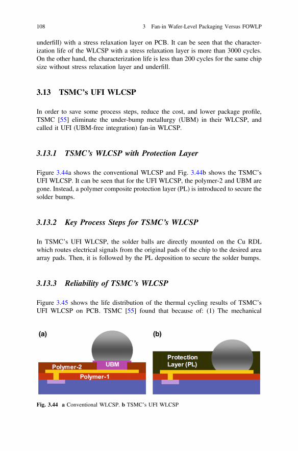
underfill) with a stress relaxation layer on PCB. It can be seen that the character-ization life of the WLCSP with a stress relaxation layer is more than 3000 cycles.On the other hand, the characterization life is less than 200 cycles for the same chipsize without stress relaxation layer and underfill.
3.13 TSMC’s UFI WLCSP
In order to save some process steps, reduce the cost, and lower package profile,TSMC [55] eliminate the under-bump metallurgy (UBM) in their WLCSP, andcalled it UFI (UBM-free integration) fan-in WLCSP.
3.13.1 TSMC’s WLCSP with Protection Layer
Figure 3.44a shows the conventional WLCSP and Fig. 3.44b shows the TSMC’sUFI WLCSP. It can be seen that for the UFI WLCSP, the polymer-2 and UBM aregone. Instead, a polymer composite protection layer (PL) is introduced to secure thesolder bumps.
3.13.2 Key Process Steps for TSMC’s WLCSP
In TSMC’s UFI WLCSP, the solder balls are directly mounted on the Cu RDLwhich routes electrical signals from the original pads of the chip to the desired areaarray pads. Then, it is followed by the PL deposition to secure the solder bumps.
3.13.3 Reliability of TSMC’s WLCSP
Figure 3.45 shows the life distribution of the thermal cycling results of TSMC’sUFI WLCSP on PCB. TSMC [55] found that because of: (1) The mechanical
Fig. 3.44 a Conventional WLCSP. b TSMC’s UFI WLCSP
108 3 Fan-in Wafer-Level Packaging Versus FOWLP

support of the PL, (2) The controlling of the maximum strain location, and (3) Thematerial optimization, the UFI WLCSP solder joint is reliable (the characteristic lifeis more than 800 cycles and the thermal cycling takes place between the temper-atures of −40 and +125 °C, at one cycle per hour) even for a chip size up to10.3 mm � 10.3 mm without underfill.
3.14 Summary and Recommendations
WLCSP is facing stiff competition from FOWLP. Because of (1) the die shrinkingto reduce the device wafer cost, and (2) the more functionality to build into a chip(and thus increase pin outs) to increase efficiency, there is not enough space of thechip to fan-in all the pads. This is compound with the desire/demand to go forsystem-in-package (SiP) to increase performance and reduce cost, some of the
Protection Layer
Solder MaskPCB Cu-Pad
NSMD Chip CornerChipPad
RDL
Solder Ball
WLCSP: 5.2x5.2mm2
WLCSP: 10.3x10.3mm2
UFI: 5.2x5.2mm2
UFI: 7.2x7.2mm2
UFI: 10.3x10.3mm2
Failure Cycle (cycles)
Cum
ulat
ive
Failu
re (%
)
Protection Layer
UBM-FreeSolder Joint
Fig. 3.45 TSMC’s UFI WLCSP with polymer composite protection layer
3.13 TSMC’s UFI WLCSP 109

Die shrinkingMore functionality (more pin outs)SiP (system-in-package)
WaferCHIP
Not enough spacing for fanning-in the pads due to die shrinking
and more functionality
Die shrink
SiP
CHIP BCHIP A
Fig. 3.46 WLCSP versus FOWLP
Modem (2.8 x 2.8mm) Apps Processor (3x3mm)
2 RDLs: 20µm L/S
230 solder balls @0.4mm pitch
Package Size: 7.4 x 7.4 x 0.71mm
430µ
m
115µm
Over Mold
PCB
Fig. 3.47 HTC desire 606W (SPREADTRUM SC8502)
110 3 Fan-in Wafer-Level Packaging Versus FOWLP

market shares are and will be taken away from the FOWLP as shown in Fig. 3.46.Figure 3.47 shows a SiP from a smartphone, HTC Desire 606 W (SPREADTRUMSC8502), which is made by FOWLP technology. The SiP size is 7.4 mm � 7.4mm � 0.71 mm, which consists of a 2.8 mm � 2.8 mm modem and a 3 mm �3 mm application processor. There are 2 RDLs.
References
1. Lau, J.H., and S.W.R. Lee. 1999. Chip Scale Package. New York: McGraw-Hill BookCompany.
2. Lau, J.H., T. Chung, R. Lee, C. Chang, and C. Chen. 1999. A Novel and ReliableWafer-Level Chip Scale Package (WLCSP). In Proceedings of the Chip Scale InternationalConference, SEMI, September 1999, H1–8.
3. Elenius, P. 1998. Flip Chip Bumping for IC Packaging Contractors. In Proceedings ofNEPCON West, Anaheim, CA, February 1998, 1403–1407.
4. Wu, M., S. Chung, and D. Yu. 2016. UFI (UBM-free integration) Fan-in WLCSP TechnologyEnables Large Die Fine-Pitch Packages. In IEEE/ECTC Proceedings, May 2016, 1154–1159.
5. Yasunaga, M., S. Baba, M. Matsuo, H. Matsushima, S. Nakao, and T. Tachikawa. 1994. ChipScale Package: A Lightly Dressed LSI Chip. In Proceedings of IEEE/CPMT InternationalElectronics Manufacturing Technology Symposium, La Jolla, CA, 1994, 169–176.
6. Marcoux, P. 1994. A Minimal Packaging Solution for Known Good Die And Direct ChipAttachment. In Proceedings of Surface Mount International Conference, San Jose, CA,August 1994, 19–26.
7. Chanchani, R., K. Treece, and P. Dressendorfer. 1995. A New Mini Ball Grid Array(m-BGA) Multichip Module Technology. In Proceedings of NEPCON West, February 1995,938–945.
8. Badihi, A., and E. Por. 1995. Shellcase—A True Miniature Integrated Circuit Package. InProceedings of International FC, BGA, Advanced Packaging Symposium, San Jose, CA,February 1995, pp. 244–252.
9. Baba, S., Y. Tomita, M. Matsuo, H. Matsushima, N. Ueda, and O. Nakagawa. 1996. MoldedChip Scale Package for High Pin Count. In Proceedings of IEEE/ECTC, Orlando, FL, May1996, 1251–1257.
10. Topper, M., J. Simon, and H. Reichl. 1996. Redistribution Technology For Chip ScalePackage Using Photosensitive BCB. Future Fab International, 363–368.
11. Auersperg, J.,D.Vogel, J. Simon,A.Schubert, andB.Michel. 1997.ReliabilityEvaluationofChipScalePackagesbyFEAandmicroDAC. InProceedings of SymposiumonDesignandReliability ofSolder and Solder Interconnections, TMS Annual Meeting, Orlando, FL, 1997, 439–445.
12. DiStefano, T. 1997. Wafer-Level Fabrication of IC Packages. Chip Scale Review, 20–27.13. Kohl, J.E., C.W. Eichellerger, S.K. Phillips, and M.E. Rickley. 1997. Low Cost Chip Scale
Packaging and Interconnect Technology. In Proceedings of the CSP Symposium, San Jose,CA, 1997, 37–43.
14. Lau, J.H., C. Chang, and S.W.R. Lee. 2000. Solder Joint Creak Propagation Analysisof Wafer-Level Chip Scale Packages on Printed Circuit Board Assemblies. In IEEE/ECTCProceedings, 1360–1368.
15. Lau, J.H., S.W.R. Lee, and C. Chang. 2000. Solder Joint Reliability of Wafer Level ChipScale Packages (WLCSP): A Time-Temperature-Dependent Creep Analysis. ASMETransactions Journal of Electronic Packaging 122 (4): 311–316.
16. Lau, J.H., S.W.R. Lee, and C. Chang. 2001. Solder Joint Crack Propagation Analysis ofWafer-Level Chip Scale Package on Printed Circuit Board Assemblies. IEEE Transactions onCPMT, 285–292.
3.14 Summary and Recommendations 111
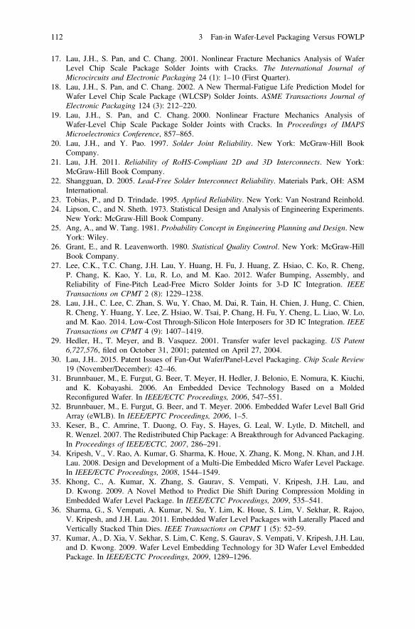
17. Lau, J.H., S. Pan, and C. Chang. 2001. Nonlinear Fracture Mechanics Analysis of WaferLevel Chip Scale Package Solder Joints with Cracks. The International Journal ofMicrocircuits and Electronic Packaging 24 (1): 1–10 (First Quarter).
18. Lau, J.H., S. Pan, and C. Chang. 2002. A New Thermal-Fatigue Life Prediction Model forWafer Level Chip Scale Package (WLCSP) Solder Joints. ASME Transactions Journal ofElectronic Packaging 124 (3): 212–220.
19. Lau, J.H., S. Pan, and C. Chang. 2000. Nonlinear Fracture Mechanics Analysis ofWafer-Level Chip Scale Package Solder Joints with Cracks. In Proceedings of IMAPSMicroelectronics Conference, 857–865.
20. Lau, J.H., and Y. Pao. 1997. Solder Joint Reliability. New York: McGraw-Hill BookCompany.
21. Lau, J.H. 2011. Reliability of RoHS-Compliant 2D and 3D Interconnects. New York:McGraw-Hill Book Company.
22. Shangguan, D. 2005. Lead-Free Solder Interconnect Reliability. Materials Park, OH: ASMInternational.
23. Tobias, P., and D. Trindade. 1995. Applied Reliability. New York: Van Nostrand Reinhold.24. Lipson, C., and N. Sheth. 1973. Statistical Design and Analysis of Engineering Experiments.
New York: McGraw-Hill Book Company.25. Ang, A., and W. Tang. 1981. Probability Concept in Engineering Planning and Design. New
York: Wiley.26. Grant, E., and R. Leavenworth. 1980. Statistical Quality Control. New York: McGraw-Hill
Book Company.27. Lee, C.K., T.C. Chang, J.H. Lau, Y. Huang, H. Fu, J. Huang, Z. Hsiao, C. Ko, R. Cheng,
P. Chang, K. Kao, Y. Lu, R. Lo, and M. Kao. 2012. Wafer Bumping, Assembly, andReliability of Fine-Pitch Lead-Free Micro Solder Joints for 3-D IC Integration. IEEETransactions on CPMT 2 (8): 1229–1238.
28. Lau, J.H., C. Lee, C. Zhan, S. Wu, Y. Chao, M. Dai, R. Tain, H. Chien, J. Hung, C. Chien,R. Cheng, Y. Huang, Y. Lee, Z. Hsiao, W. Tsai, P. Chang, H. Fu, Y. Cheng, L. Liao, W. Lo,and M. Kao. 2014. Low-Cost Through-Silicon Hole Interposers for 3D IC Integration. IEEETransactions on CPMT 4 (9): 1407–1419.
29. Hedler, H., T. Meyer, and B. Vasquez. 2001. Transfer wafer level packaging. US Patent6,727,576, filed on October 31, 2001; patented on April 27, 2004.
30. Lau, J.H.. 2015. Patent Issues of Fan-Out Wafer/Panel-Level Packaging. Chip Scale Review19 (November/December): 42–46.
31. Brunnbauer, M., E. Furgut, G. Beer, T. Meyer, H. Hedler, J. Belonio, E. Nomura, K. Kiuchi,and K. Kobayashi. 2006. An Embedded Device Technology Based on a MoldedReconfigured Wafer. In IEEE/ECTC Proceedings, 2006, 547–551.
32. Brunnbauer, M., E. Furgut, G. Beer, and T. Meyer. 2006. Embedded Wafer Level Ball GridArray (eWLB). In IEEE/EPTC Proceedings, 2006, 1–5.
33. Keser, B., C. Amrine, T. Duong, O. Fay, S. Hayes, G. Leal, W. Lytle, D. Mitchell, andR. Wenzel. 2007. The Redistributed Chip Package: A Breakthrough for Advanced Packaging.In Proceedings of IEEE/ECTC, 2007, 286–291.
34. Kripesh, V., V. Rao, A. Kumar, G. Sharma, K. Houe, X. Zhang, K. Mong, N. Khan, and J.H.Lau. 2008. Design and Development of a Multi-Die Embedded Micro Wafer Level Package.In IEEE/ECTC Proceedings, 2008, 1544–1549.
35. Khong, C., A. Kumar, X. Zhang, S. Gaurav, S. Vempati, V. Kripesh, J.H. Lau, andD. Kwong. 2009. A Novel Method to Predict Die Shift During Compression Molding inEmbedded Wafer Level Package. In IEEE/ECTC Proceedings, 2009, 535–541.
36. Sharma, G., S. Vempati, A. Kumar, N. Su, Y. Lim, K. Houe, S. Lim, V. Sekhar, R. Rajoo,V. Kripesh, and J.H. Lau. 2011. Embedded Wafer Level Packages with Laterally Placed andVertically Stacked Thin Dies. IEEE Transactions on CPMT 1 (5): 52–59.
37. Kumar, A., D. Xia, V. Sekhar, S. Lim, C. Keng, S. Gaurav, S. Vempati, V. Kripesh, J.H. Lau,and D. Kwong. 2009. Wafer Level Embedding Technology for 3D Wafer Level EmbeddedPackage. In IEEE/ECTC Proceedings, 2009, 1289–1296.
112 3 Fan-in Wafer-Level Packaging Versus FOWLP

38. Lim, Y., S. Vempati, N. Su, X. Xiao, J. Zhou, A. Kumar, P. Thaw, S. Gaurav, T. Lim, S. Liu,V. Kripesh, and J.H. Lau. 2010. Demonstration of High Quality and Low Loss MillimeterWave Passives on Embedded Wafer Level Packaging Platform (EMWLP). IEEETransactions on Advanced Packaging 33: 1061–1071.
39. Lau, J.H., N. Fan, and M. Li. 2016. Design, Material, Process, and Equipment of EmbeddedFan-Out Wafer/Panel-Level Packaging. Chip Scale Review 20 (May/June): 38–44.
40. Kurita, Y., T. Kimura, K. Shibuya, H. Kobayashi, F. Kawashiro, N. Motohashi, andM. Kawano. 2010. Fan-Out Wafer-Level Packaging with Highly Flexible Design Capabilities.In IEEE/ESTC Proceedings, 2010, 1–6.
41. Motohashi, N., T. Kimura, K. Mineo, Y. Yamada, T. Nishiyama, K. Shibuya, H. Kobayashi,Y. Kurita, and M. Kawano. 2011. System in Wafer-Level Package Technology withRDL-First Process. In IEEE/ECTC Proceedings, 2011, 59–64.
42. Yoon, S., J. Caparas, Y. Lin, and P. Marimuthu. 2012. Advanced Low Profile PoP Solutionwith Embedded Wafer Level PoP (eWLB-PoP) Technology. In IEEE/ECTC Proceedings,2012, 1250–1254.
43. Tseng, C., C. Liu, C. Wu, and D. Yu. 2016. InFO (Wafer Level Integrated Fan-Out)Technology. In IEEE/ECTC Proceedings, 2016, 1–6.
44. Hsieh, C., C. Wu, and D. Yu. 2016. Analysis and Comparison of Thermal Performance ofAdvanced Packaging Technologies for State-of-the-Art Mobile Applications. In IEEE/ECTCProceedings, 2016, 1430–1438.
45. Yoon, S., P. Tang, R. Emigh, Y. Lin, P. Marimuthu, and R. Pendse. 2013. Fanout FlipchipeWLB (Embedded Wafer Level Ball Grid Array) Technology as 2.5D Packaging Solutions.In IEEE/ECTC Proceedings, 2013, 1855–1860.
46. Lin, Y., W. Lai, C. Kao, J. Lou, P. Yang, C. Wang, and C. Hseih. 2016. Wafer WarpageExperiments and Simulation for Fan-out Chip on Substrate. In IEEE/ECTC Proceedings,2016, 13–18.
47. Chen, N., T. Hsieh, J. Jinn, P. Chang, F. Huang, J. Xiao, A. Chou, and B. Lin. 2016. A NovelSystem in Package with Fan-out WLP for high speed SERDES application. In IEEE/ECTCProceedings, 2016, 1495–1501.
48. Chang, H., D. Chang, K. Liu, H. Hsu, R. Tai, H. Hunag, Y. Lai, C. Lu, C. Lin, and S. Chu.2014. Development and 601 Characterization of New Generation Panel Fan-Out(PFO) Packaging Technology. In IEEE/ECTC Proceedings, 2014, 947–951.
49. Liu, H., Y. Liu, J. Ji, J. Liao, A. Chen, Y. Chen, N. Kao, and Y. Lai. 2014. WarpageCharacterization of Panel Fab-out (P-FO) Package. In IEEE/ECTC Proceedings, 2014,1750–1754.
50. Braun, T., S. Raatz, S. Voges, R. Kahle, V. Bader, J. Bauer, K. Becker, T. Thomas,R. Aschenbrenner, and K. Lang. 2015. Large Area Compression Molding for Fan-out PanelLevel Packing. In IEEE/ECTC Proceedings, 2015, 1077–1083.
51. Che, F., D. Ho, M. Ding, X. Zhang. 2015. Modeling and Design Solutions to OvercomeWarpage Challenge for Fanout Wafer Level Packaging (FO-WLP) Technology. In IEEE/EPTC Proceedings, 2015, 2–4.
52. Che, F., D. Ho, M. Ding, D. MinWoopp. 2016. Study on Process Induced Wafer LevelWarpage of Fan-Out Wafer Level Packaging. In IEEE/ECTC Proceedings, 2016, 1879–1885.
53. Lau, J.H., M. Li, D. Tian, N. Fan, E. Kuah, K. Wu, M. Li, J. Hao, K. Cheung, L. Zhang,K. Tan, R. Beica, T. Taylor, C. Ko, H. Yang, Y. Chen, S. Lim, N. Lee, J. Ran, C. Xi, K. Wee,and Q. Yong. 2017. Warpage and Thermal Characterization of Fan-Out Wafer-LevelPackaging. IEEE Transactions on CPMT, 1729–1738.
54. Kazama, A., T. Satoh, Y. Yamaguchi, I. Anjoh, and A. Nishimura. 2001. Development ofLow-cost and Highly Reliable Wafer Process Package. In IEEE/ECTC Proceedings, May2001, 40–46.
55. Wu, M., C. Liu, and D. Yu. 2016. UFI (UBM-Free Integration) Fan-In WLCSP TechnologyEnables Large Die Fine Pitch Packages. In IEEE/ECTC Proceedings, May 2016, 1154–1159.
References 113

Chapter 4Embedded Chip Packaging
4.1 Introduction
There are many kinds of embedded chip packaging. For example, chips areembedded in epoxy molding compound (EMC) [1–17], chips are embedded in rigidlaminated substrates [18], chips are embedded in flexible polyimide substrates [19,20], chips are embedded in silicon substrates [21, 22], and chips are embedded inglass substrates [23, 24]. Usually, chips embedded in rigid and flexible laminated/polyimide substrates are in a panel format. In this chapter, except the chipsembedded in EMC (which are the focus and will be discussed all over in this book),all the others are briefly mentioned.
4.2 Chips Embedded in Laminated/PolyimidePanel Format
4.2.1 Advantages and Disadvantages
Figure 4.1 schematically shows the embedded passive component and chip. It canbe seen from Fig. 4.1a that the passive component is connected to an inner layer byeither solder or adhesive first, and then embedded. On the other hand, the chip ismounted on an inner layer/foil first, embedded, and then connected by drilling andCu plating as shown in Fig. 4.1b. The advantages of embedding passive compo-nents and chips are: (a) low profile, (b) low cost with a large panel, (c) betterelectrical performance with low inductances, and (d) easy to extend to 3D chipstacking. The disadvantages are: (a) cannot rework, (b) infrastructure, and (c) sup-ply chain.
© Springer Nature Singapore Pte Ltd. 2018J. H. Lau, Fan-Out Wafer-Level Packaging,https://doi.org/10.1007/978-981-10-8884-1_4
115
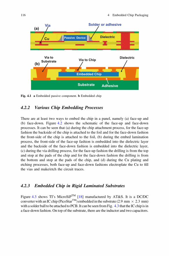
4.2.2 Various Chip Embedding Processes
There are at least two ways to embed the chip in a panel, namely (a) face-up and(b) face-down. Figure 4.2 shows the schematic of the face-up and face-downprocesses. It can be seen that (a) during the chip attachment process, for the face-upfashion the backside of the chip is attached to the foil and for the face-down fashionthe front-side of the chip is attached to the foil, (b) during the embed laminationprocess, the front-side of the face-up fashion is embedded into the dielectric layerand the backside of the face-down fashion is embedded into the dielectric layer,(c) during the via drilling process, for the face-up fashion the drilling is from the topand stop at the pads of the chip and for the face-down fashion the drilling is fromthe bottom and stop at the pads of the chip, and (d) during the Cu plating andetching processes, both face-up and face-down fashions electroplate the Cu to fillthe vias and make/etch the circuit traces.
4.2.3 Embedded Chip in Rigid Laminated Substrates
Figure 4.3 shows TI’s MicroSiPTM [18] manufactured by AT&S. It is a DC/DCconverterwith an IC chip (PicoStarTM) embedded in the substrate (2.9 mm � 2.3 mm)with a solder ball to be attached toPCB. It can be seen fromFig. 4.3 that the IC chip is ina face-down fashion. On top of the substrate, there are the inductor and two capacitors.
Embedded Chip
Adhesive
Via to ChipVia to
Substrate
Substrate
Dielectric
Passive Device Dielectric
Solder or adhesive
Cu
Via(a)
(b)
Fig. 4.1 a Embedded passive component. b Embedded chip
116 4 Embedded Chip Packaging

Face-Up Face-Down
Electrical and thermal backside contact
Better fine pitch capability
Chip attach
Embedded by lamination
Via drilling
Cu plating and etching
Fig. 4.2 Fabrication processes for the embedded chip in face-up and face-down fashions
DC/DC convertor IC chip embedded in the substrate
Embedded chip
X-ray image after solder
and SMD component
removal
Capacitor CapacitorInductor
Substrate IC ChipSolder Ball
PicoStarTM
Fig. 4.3 TI’s embedded chip in a rigid substrate of a DC/DC converter
4.2 Chips Embedded in Laminated/Polyimide Panel Format 117

4.2.4 3D Embedded Chip in Flexible Polyimide Substrates
Figure 4.4 shows schematically the multichip SiP with an embedded chip. It canbe seen from the left-hand side of Fig. 4.4 that for the conventional system-in-package (SiP) there are 5 chips (U1 through U5) side-by-side on the substrate(3.5 mm � 3.5 mm). On the left-hand side of Fig. 4.4, it shows that the U1 chip isembedded into the flexible substrate (2.5 mm � 2.5 mm) by Fujikura’s WABE(wafer and board level embedded package) technology [19]. The other 4 chips (U2through U5) are on top of the substrate surface. The package size has been reducedby 50%. The cross section in Fig. 4.4 shows the embedded chip (ASIC or U1) andone sensor chip (the other 3 chips are not in the photo image).
4.2.5 3D Embedded Stacking Chips in FlexiblePolyimide Substrates
Figure 4.5 shows the cross-section photo image of a multilayer board embeddingtwo chips in stacked configuration [20] fabricated by the WABE technology. Theminimum thickness of these chips is 85 µm and they are interconnected through theCu traces and vias. There are nine layers of the board and its total thickness is0.55 mm.
Conventional Packaging WABE Packaging
U3
U1 is embedded
Fig. 4.4 Fujikura’s embedded chip in a flexible substrate of a 3D SiP
118 4 Embedded Chip Packaging

4.3 Chips Embedded in Si Wafer
In 2013, Maxim is the first to present the concept of mold-free silicon wafer-basedfan-out technology, i.e., chips embedded in Si wafer [21, 22].
4.3.1 Key Process Steps
Figure 4.6a shows the schematic of Maxim’s chips embedded in Si wafer [21, 22]with rectangular-shaped cavities (left-hand side) and trapezoidal-shaped cavities(right-hand side). These cavities are formed on a low-cost silicon wafer using thepotassium hydroxide (KOH) wet-etch process. The chips are picked and placedface-up in the cavities filled with epoxy resin as shown in Fig. 4.6b. Then, it isfollowed by fabricating the dielectric layers and conductor layers (RDLs) andmounting the solder balls as shown in Fig. 4.6c. Figure 4.7 shows the scanningelectron microscope (SEM) image of a cross section of the chip embedded in Siwafer. It can be seen that the chip is embedded in the Si substrate and its circuitriesare fanned-out through the RDLs to solder balls.
4.3.2 Reliability of Chips Embedded in Si Wafer
Figure 4.8 shows the schematic of a test package (6 mm � 6mm) with 16 � 16solder balls on a 0.4 mm pitch. It is assembled on a PCB and subjected to a thermalcycling test (−40 °C $ +125 °C, one cycle per hour, 15-min dwell, and 15-minramp) according to the JEDEC standard JESD22-A104 [23]. The test results(Weibull distribution [24]) are shown in Fig. 4.9 and it can be seen that it passes645 cycles.
Chip 1
Chip 2
ViasCu tracesDielectric
Fig. 4.5 Fujikura’s embedded two chips in the stacked configuration
4.3 Chips Embedded in Si Wafer 119

4.4 Chips Embedded in Glass Panel
In 2017, George Institute of Technology (GIT) is the first to present and demon-strate the concept of mold-free glass panel-based fan-out technology, i.e., chipsembedded in glass panel [25, 26].
CHIP CHIP CHIP CHIP
CHIP CHIP CHIP CHIP
Si Wafer Si Wafer
Si Wafer
Si Wafer Si Wafer
Si Wafer
RDLs
Solder Ball Solder Ball
RDLs
Cavity Cavity
Epoxy Resin Epoxy Resin
Epoxy Resin Epoxy Resin
(a)
(b)
(c)
Fig. 4.6 Maxim’s chips embedded in silicon wafer. a Cavities formation by KOH. b P&P chips(face-up) in cavities. c RDLs fabrication and solder balls mounting
Si
Solder Ball
CHIP
Passivation
RDLs
Epoxy Resin
Fig. 4.7 Cross-section SEMimage of Maxim’s chipsembedded in silicon wafer
120 4 Embedded Chip Packaging
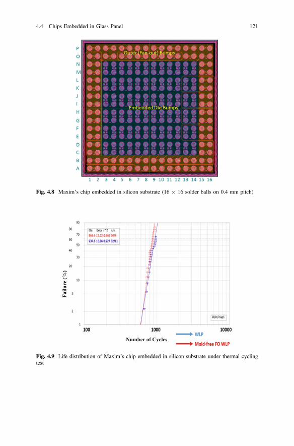
Fig. 4.8 Maxim’s chip embedded in silicon substrate (16 � 16 solder balls on 0.4 mm pitch)
Failu
re (%
)
Number of Cycles
Fig. 4.9 Life distribution of Maxim’s chip embedded in silicon substrate under thermal cyclingtest
4.4 Chips Embedded in Glass Panel 121
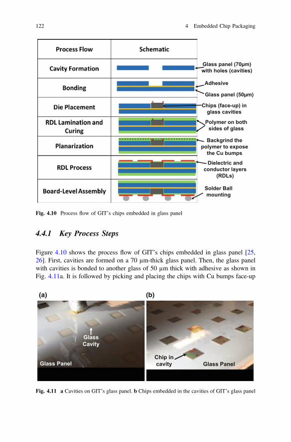
4.4.1 Key Process Steps
Figure 4.10 shows the process flow of GIT’s chips embedded in glass panel [25,26]. First, cavities are formed on a 70 µm-thick glass panel. Then, the glass panelwith cavities is bonded to another glass of 50 µm thick with adhesive as shown inFig. 4.11a. It is followed by picking and placing the chips with Cu bumps face-up
Glass panel (70µm) with holes (cavities)
Glass panel (50µm)
Adhesive
Chips (face-up) in glass cavities
Polymer on both sides of glass
Backgrind the polymer to expose
the Cu bumps
Dielectric and conductor layers
(RDLs)
Solder Ball mounting
Fig. 4.10 Process flow of GIT’s chips embedded in glass panel
Glass PanelChip in cavity
Glass Cavity
Glass Panel
(a) (b)
Fig. 4.11 a Cavities on GIT’s glass panel. b Chips embedded in the cavities of GIT’s glass panel
122 4 Embedded Chip Packaging
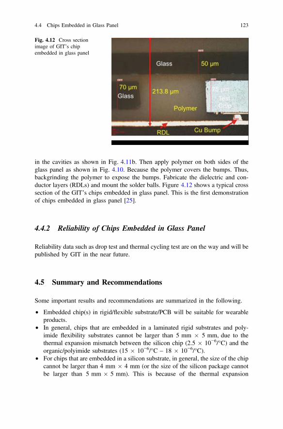
in the cavities as shown in Fig. 4.11b. Then apply polymer on both sides of theglass panel as shown in Fig. 4.10. Because the polymer covers the bumps. Thus,backgrinding the polymer to expose the bumps. Fabricate the dielectric and con-ductor layers (RDLs) and mount the solder balls. Figure 4.12 shows a typical crosssection of the GIT’s chips embedded in glass panel. This is the first demonstrationof chips embedded in glass panel [25].
4.4.2 Reliability of Chips Embedded in Glass Panel
Reliability data such as drop test and thermal cycling test are on the way and will bepublished by GIT in the near future.
4.5 Summary and Recommendations
Some important results and recommendations are summarized in the following.
• Embedded chip(s) in rigid/flexible substrate/PCB will be suitable for wearableproducts.
• In general, chips that are embedded in a laminated rigid substrates and poly-imide flexibility substrates cannot be larger than 5 mm � 5 mm, due to thethermal expansion mismatch between the silicon chip (2.5 � 10−6/°C) and theorganic/polyimide substrates (15 � 10−6/°C – 18 � 10−6/°C).
• For chips that are embedded in a silicon substrate, in general, the size of the chipcannot be larger than 4 mm � 4 mm (or the size of the silicon package cannotbe larger than 5 mm � 5 mm). This is because of the thermal expansion
Fig. 4.12 Cross sectionimage of GIT’s chipembedded in glass panel
4.4 Chips Embedded in Glass Panel 123

mismatch between the silicon (package) substrate (not the chip) and the PCB(18 � 10−6/°C).
• George Institute of Technology (GIT) just demonstrated that they are able tofabricate the chips embedded in glass substrate (panel). However, making thecavities on glass and fabricating the fine line width/spacing RDLs on glass needto be mature. Also, the PCB solder joint reliability under drop and thermalcycling conditions need to be demonstrated.
References
1. Brunnbauer, M., E. Fürgut, G. Beer, T. Meyer, H. Hedler, J. Belonio, E. Nomura, K. Kiuchi,and K. Kobayashi. 2006. An Embedded Device Technology Based on a MoldedReconfigured Wafer. In Proceedings of IEEE/ECTC, May 2006, 547–551.
2. Brunnbauer, M., E. Furgut, G. Beer, and T. Meyer. 2006. Embedded Wafer Level Ball GridArray (eWLB). In Proceedings of IEEE/EPTC, Singapore, December 2006, 1–5.
3. Meyer, T., G. Ofner, S. Bradl, M. Brunnbauer, and R. Hagen. 2008. Embedded Wafer LevelBall Grid Array (eWLB). In Proceedings of IEEE/EPTC, Singapore, December 2008, 994–998.
4. Brunnbauer, M., T. Meyer, G. Ofner, K. Mueller, and R. Hagen. 2008. Embedded WaferLevel Ball Grid Array (eWLB). In Proceedings of IEEE/IEMTS, 2008, 1–6.
5. Pressel, K., G. Beer, T. Meyer, M. Wojnowski, M. Fink, G. Ofner, and B. Römer. 2010.Embedded Wafer Level Ball Grid Array (eWLB) Technology for System Integration. InProceedings of Japan IEEE/CPMT Symposium, 2010, 1–4.
6. Yoon, S., J. Caparas, Y. Lin, and P. Marimuthu. 2012. Advanced Low Profile PoP Solutionwith Embedded Wafer Level PoP (eWLB-PoP) Technology. In Proceedings of IEEE/ECTC,May 2012, 1250–1254.
7. Jin, Y., J. Teysseyrex, X. Baraton, S. Yoon, Y. Lin, P. Marimuthu. 2011. Development ofNext General eWLB (Embedded Wafer Level BGA) Technology. In Proceedings of IWLPC,San Jose, CA, November 2011, 7.1–7.7.
8. Yoon, S., P. Tang, R. Emigh, Y. Lin, P. C. Marimuthu, and R. Pendse. 2013. Fanout FlipchipeWLB (embedded Wafer Level Ball Grid Array) Technology as 2.5D Packaging Solutions. InProceedings of IEEE/ECTC, Las Vegas, NV, May 2013, 1855–1860.
9. Keser, B., C. Amrine, T. Duong, O. Fay, S. Hayes, G. Leal, W. Lytle, D. Mitchell, and R.Wenzel. 2007. The Redistributed Chip Package: A Breakthrough for Advanced Packaging. InProceedings of IEEE/ECTC, May 2007, 286–291.
10. Hayes, S., N. Chhabra, T. Duong, Z. Gong, D. Mitchell, and J. Wright. 2011.System-in-Package Opportunities with the Redistributed Chip Package (RCP). InProceedings of IWLPC, November 2011, 10.1–10.7.
11. Sharma, G., V. Rao, A. Kumar, Y. Lim, K. Houe, S. Lim, V. Sekhar, R. Rajoo, V. Kripesh,and J.H. Lau. 2011. Design and Development of Multi-Die Laterally Placed and VerticallyStacked Embedded Micro-Wafer-Level Packages. IEEE Transactions on CPMT 1 (5): 52–59.
12. Sharma, G., S. Vempati, A. Kumar, N. Su, Y. Lim, K. Houe, S. Lim, V. Sekhar, R. Rajoo, V.Kripesh, and J. H. Lau. 2009. Embedded Wafer Level Packages with Laterally Placed andVertically Stacked Thin Dies. In IEEE/ECTC Proceedings, San Diego, CA, May 2009, 1537–1543.
13. Lim, Y., X. Xiao, R. Vempati, S. Nandar, K. Aditya, S. Gaurav, T. Lim, V. Kripesh, J. Shi, J.H. Lau, and S. Liu. 2010. High Quality and Low Loss Millimeter Wave PassivesDemonstrated to 77-GHz for SiP Technologies Using Embedded Wafer-Level PackagingPlatform (EMWLP). IEEE Transactions on Advanced Packaging 33: 1061–1071.
124 4 Embedded Chip Packaging

14. Lim, Y., S. Vempati, N. Su, X. Xiao, J. Zhou, A. Kumar, P. Thaw, S. Gaurav, T. Lim, S. Liu,V. Kripesh, and J. H. Lau. 2009. Demonstration of High Quality and Low Loss MillimeterWave Passives on Embedded Wafer Level Packaging Platform (EMWLP). In IEEE/ECTCProceedings, San Diego, CA, May 2009, 508–515.
15. Kripesh, V., V. Rao, A. Kumar, G. Sharma, K. Houe, X. Zhang, K. Mong, N. Khan, andJ. H. Lau. 2008. Design and Development of a Multi-Die Embedded Micro Wafer LevelPackage. In IEEE Proceedings of IEEE/ECTC, Orlando, FL, May 2008, 1544–1549.
16. Khong, C., A. Kumar, X. Zhang, S. Gaurav, S. Vempati, V. Kripesh, J. H. Lau, and D.Kwong. 2009. A Novel Method to Predict Die Shift During Compression Molding inEmbedded Wafer Level Package. In IEEE/ECTC Proceedings, San Diego, CA, May 2009,535–541.
17. Kumar, A., D. Xia, V. Sekhar, S. Lim, C. Keng, S. Gaurav, S. Vempati, V. Kripesh, J. H. Lau,and D. Kwong. 2009. Wafer Level Embedding Technology for 3D Wafer Level EmbeddedPackage. In IEEE/ECTC Proceedings, San Diego, CA, May 2009, 1289–1296.
18. Texas Instruments. 2011. Design SUMMARY for MicroSiP™-Enabled TPS8267xSiP. Dallas,TX, First Quarter.
19. Itoi, K., M. Okamoto, Y. Sano, N. Ueta, S. Okude, O. Nakao, T. Tessier, S. Sivaswamy, andG. Stout. 2011. Laminate Based Fan-Out Embedded Die Packaging Using PolyimideMultilayer Wiring Boards. In Proceedings of IWLPC, San Jose, CA, November 2011, 7.8–7.14.
20. Munakata, K., N. Ueta, M. Okamoto, K. Onodera, K. Itoi, S. Okude, O. Nakao, J. Aday, andT. Tessier. 2013. Polyimede PCB Embedded with Two Dies in Stacked Configuration. InProceedings of IWLPC, San Jose, CA, November 2013, 5.1–5.6.
21. Kelkar, A., V. Sridharan, K. Tran, K. Ikeuchi, A. Srivastava, V. Khandekar, and R. Agrawal.2016. Novel Mold-free Fan-out Wafer Level Package using Silicon Wafer. In IMAPSproceedings on International Symposium on Microelectronics, October 2016, 410–414.
22. Tran, K., A. Samoilov, P. Parvarndeh, and A. Kelkar. 2013. Fan-Out and HeterogeneousPackaging of Electronic Components. US2014/0252655 A1, filed on June 28, 2013.
23. JEDEC Standard. JESD22-A104, Temperature Cycling, 2005.24. Lau, J.H. 2011. Reliability of RoHS Compliant 2D and 3D Interconnects. New York:
McGraw-Hill Book Company.25. Shi, T., C. Buch,V. Smet, Y. Sato, L. Parthier, F. Wei, C. Lee, V. Sundaram, and R.
Tummala. 2017. First Demonstration of Panel Glass Fan-out (GFO) Packages for High I/ODensity and High Frequency Multi-Chip Integration. In IEEE/ECTC Proceedings, May 2017,41–46.
26. Buch, C., D. Struk, K. Wolter, P. Hesketh, V. Sundaram, and R. Tummala. 2017. Design andDemonstration of Highly Miniaturized, Low Cost Panel Level Glass Package for MEMSSensors. In IEEE/ECTC Proceedings, May 2017, 1088–1097.
References 125

Chapter 5FOWLP: Chip-First and Die Face-Down
5.1 Introduction
The first fan-out wafer-level packaging (FOWLP) U.S. patent was filed by Infineonon October 31, 2001 [1, 2], and the first technical papers were also published (atECTC2006 and EPTC2006) by Infineon and their industry partners: Nagase, NittoDenko, and Yamada [3, 4]. At that time, they called it embedded wafer-level ball(eWLB) grid array. This technology eliminates wire bonding or wafer bumping andlead frame or package substrate, and potentially leads to a lower cost, better per-formance, and lower profile package. Alternatively, this technology requires atemporary (reconstituted) carrier for the known good die (KGD), epoxy moldingcompound (EMC), compression molding, and the fabrication of the redistributionlayers (RDLs). During ECTC2007, Freescale (now NXP) presented a similartechnology and called it redistributed chip package [5]. IME extended the FOWLPtechnology to multi-die and stacked multi-die in 3D format and presented atECTC2008 [6]. During ECTC2009, IME presented four papers on: (1) a novelmethod to predict die shift during compression molding [7]; (2) laterally placed andvertically stacked thin dies [8]; (3) the reliability of 3D FOWLP [9]; and (4) thedemonstration of high quality and low-loss millimeter-wave passives on FOWLP[10]. In [1, 3–10], they used chip-first and die face-down [11] fan-out wafer-levelprocessing, which will be the focus of this chapter.
During ESTC2010 and ECTC2011, NEC (now Renesas) presented a couple ofpapers on system-in-wafer-level package (SiWLP) [12], and “RDL-first” FOWLP[13]. Their technology requires besides the fabrication of the RDLs, wafer bump-ing, fluxing, flip chip assembly, cleaning, and underfills dispensing and curing, andthus is very high cost. Their potential applications are for very high-density and
© Springer Nature Singapore Pte Ltd. 2018J. H. Lau, Fan-Out Wafer-Level Packaging,https://doi.org/10.1007/978-981-10-8884-1_5
127

high-performance products such as supercomputers, high-end servers, telecom-munications, and networking systems. Their technology is chip-last or RDL-first[11] FOWLP processing, which will be discussed in Chap. 7.
At ECTC2012, STATS ChipPAC proposed a package-on-package (PoP) for theapplication processor (AP) chipset with the FOWLP technology [14]. DuringECTC2016, TSMC presented two papers on FOWLP: one is their integrated fan-out(InFO) wafer-level packaging for housing the most advanced AP for mobileapplications [15], and the other is to compare the thermal and electrical performancebetween their InFO technology and the conventional flip chip on buildup packagesubstrate technology [16]. During September 2016, TSMC put the PoP of AP withFOWLP technology into high-volume manufacturing. This is very significant sincethis means that FOWLP is not just only for packaging baseband, power managementIC, radio frequency (RF) switch/transceiver, RF radar, audio codec, microcontrollerunit, connectivity ICs, etc., it can also be used for packaging high-performance andlarge (>120 mm2) system-on-chip (SoC) such as APs. TSMC used chip-first and dieface-up [2, 11] FOWLP processing, which will be discussed in Chap. 6. Theapplications of FOWLP on PoP will be discussed in Chap. 8.
Recently, through-silicon via (TSV)-less interposer [17] to support flip chips is avery hot topic in semiconductor packaging. At ECTC2013, STATS ChipPACproposed [18] using the fan-out flip chip-eWLB to make the RDLs for the chips toperform mostly lateral communications. During ECTC2016, ASE [19] andMediaTek [20] used a similar technology to fabricate the RDLs and showed that theTSV interposer, wafer bumping, fluxing, chip-to-wafer bonding, cleaning, andunderfill dispensing and curing are eliminated. FOWLP for heterogeneous inte-gration without TSV-interposers will be discussed in Chap. 11.
All pervious mentioned fan-out papers are using the round 200- or 300-mmwafers as the reconstituted carriers for supporting the KGDs and making the molds,RDLs, etc. (This is because of the existing equipment for fabricating the devicewafers.) In order to increase the throughput, fan-out panel-level packaging (FOPLP)has been proposed. For example, starting from EPTC2011, J-Devices have beenpresenting their FOPLP (320 mm � 320 mm) called WFOPTM (Wide StripFan-Out Package) [21–23]. Starting from ECTC2013, Fraunhofer has been pre-senting its evaluation results on compression molding of a large-area (610 mm� 457 mm) FOPLP [24–26]. At ECTC2014, SPIL published two papers onFOPLP called P-FO, one is to develop and characterize a 370 mm � 470 mmP-FO [27] and the other is to measure their warpage [28]. One of the bottlenecks forFOPLP is the availability of panel equipment such as the spin coating, physicalvapor deposition (PVD), electrochemical deposition, etching, backgrinding, anddicing for making the RDLs, molds, etc., due to the lack of the standard of panelsizes. Thus, the potential FOPLP users are unanimously calling for the panel-sizeindustry standards. FOPLP will be discussed in Chap. 9.
128 5 FOWLP: Chip-First and Die Face-Down
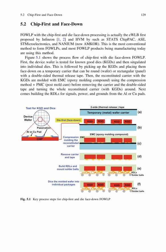
5.2 Chip-First and Face-Down
FOWLP with the chip-first and die face-down processing is actually the eWLB firstproposed by Infineon [1, 2] and HVM by such as STATS ChipPAC, ASE,STMicroelectronics, and NANIUM (now AMKOR). This is the most conventionalmethod to form FOWLPs, and most FOWLP products being manufacturing todayare using this method.
Figure 5.1 shows the process flow of chip-first with die face-down FOWLP.First, the device wafer is tested for known good dies (KGDs) and then singulatedinto individual dies. This is followed by picking up the KGDs and placing themface-down on a temporary carrier that can be round (wafer) or rectangular (panel)with a double-sided thermal release tape. Then, the reconstituted carrier with theKGDs are molded with EMC (epoxy molding compound) using the compressionmethod + PMC (post mold cure) before removing the carrier and the double-sidedtape and turning the whole reconstituted carrier (with KGDs) around. Nextcomes building the RDLs for signals, power, and grounds from the Al or Cu pads.
Temporary (metal) wafer carrier
2-side (thermal release ) tape
Remove carrier and tape
Dice the molded wafer into individual packages
Die-first (face-down)
Compression molding the
reconstituted carrier
Test for KGD and Dice
Passivation
Device Wafer
Al or Cu Pad
CHIP
Build RDLs and mount solder balls
RDLs Solder balls
KGD KGD KGD KGD
KGD KGD KGD KGD
(a)
(f)
(e)
(d)
EMC (epoxy molding compound)EMC
(c)
(b)
RDLs Solder balls
Fig. 5.1 Key process steps for chip-first and die face-down FOWLP
5.2 Chip-First and Face-Down 129
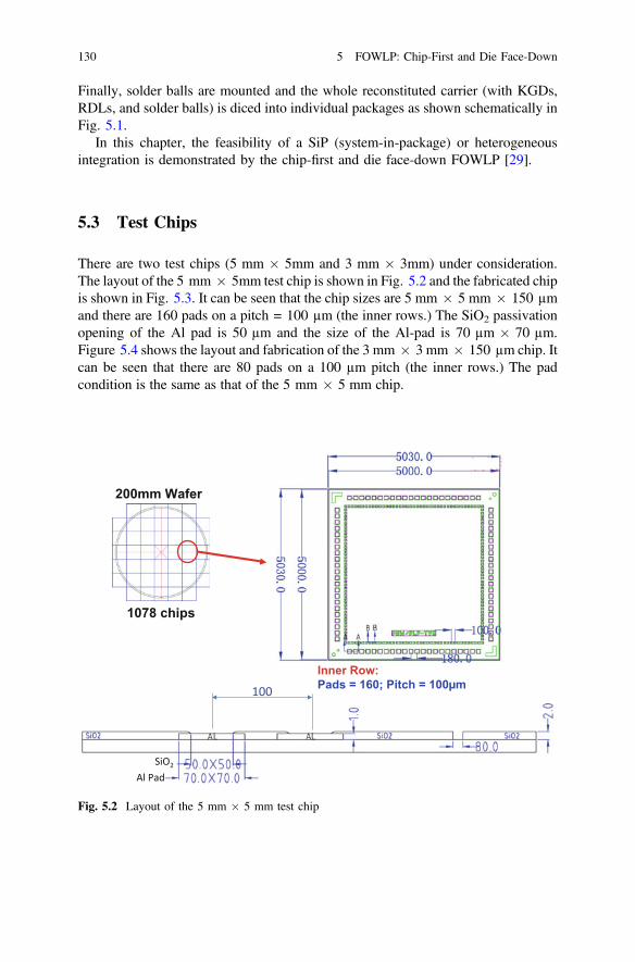
Finally, solder balls are mounted and the whole reconstituted carrier (with KGDs,RDLs, and solder balls) is diced into individual packages as shown schematically inFig. 5.1.
In this chapter, the feasibility of a SiP (system-in-package) or heterogeneousintegration is demonstrated by the chip-first and die face-down FOWLP [29].
5.3 Test Chips
There are two test chips (5 mm � 5mm and 3 mm � 3mm) under consideration.The layout of the 5 mm � 5mm test chip is shown in Fig. 5.2 and the fabricated chipis shown in Fig. 5.3. It can be seen that the chip sizes are 5 mm � 5 mm � 150 µmand there are 160 pads on a pitch = 100 µm (the inner rows.) The SiO2 passivationopening of the Al pad is 50 µm and the size of the Al-pad is 70 µm � 70 µm.Figure 5.4 shows the layout and fabrication of the 3 mm � 3 mm � 150 µm chip. Itcan be seen that there are 80 pads on a 100 µm pitch (the inner rows.) The padcondition is the same as that of the 5 mm � 5 mm chip.
1078 chips
200mm Wafer
Inner Row: Pads = 160; Pitch = 100µm100
SiO2
Al Pad
Fig. 5.2 Layout of the 5 mm � 5 mm test chip
130 5 FOWLP: Chip-First and Die Face-Down

5.4 Test Package
Figures 5.5 and 5.6 schematically show the test package under consideration. It canbe seen that the reconstituted carrier is a 300 mm wafer, Fig. 5.5, and there are 629test packages with a pitch = 10.04 mm. The layout of the test package is shown inFigs. 5.5 and 5.6. The dimensions of the test package are: 10 mm � 10 mm andthere are 4 chips within the package, one 5 mm � 5 mm chip, and three 3 mm � 3mm chips. The spacing (gap) between the large chip and the smaller chips is100 µm. The dimensions of a typical pad on the test package are shown in Fig. 5.6.Also, there are 4 capacitors (0402).
Figure 5.7 schematically shows the cross-sectional view of the test package. Itcan be seen that there are 2 RDLs and the thickness of RDL1 is 3 µm and RDL2 is7.5 µm. The line width and spacing of RDL1 and RDL2 are 10 µm/10 µm and 15lm/15 lm, respectively. The dielectric layer thickness of DL1 and DL2 is 5 µmand of DL3 is 10 µm. The via (VC1), through the first dielectric layer (DL1),connecting the Cu contact pad of the test chip to the first RDL (RDL1) is 20–30 µmin diameter. The pad diameter on the RDL1 is 55 µm, which is connected to RDL2
Chip5mmx5mm
Pad
Fig. 5.3 Image of the 5 mm � 5 mm test chip
5.4 Test Package 131

through the via (V12) with a diameter of 35–45 µm. Finally, 220 µm Cu pads areformed on RDL2 for the solder ball mounting. The opening of the passivation(DL3) is 180 µm. The solder ball size is 200 µm and ball pitch is 0.4 mm.
5.5 The Temporary Carrier
The temporary (round or rectangular) carrier as shown in Fig. 5.1a can be madefrom silicon, glass, or metal and is reusable. Their thickness and material propertiesare shown in Table 5.1. Since the thermal expansion of coefficient (TEC) of EMC isabout 10 � 10−6/°C, thus the stainless steel metal carrier (10.6 � 10−6/°C) ischosen for production. Another reason is that metal is not easy to be broken when it
> 3080 chips
200mm Wafer
Inner Row: Pads = 80; Pitch = 100µmChip3mmx3mm
Pad
Fig. 5.4 Layout and images of the 3 mm � 3 mm test chip
132 5 FOWLP: Chip-First and Die Face-Down

R1-1 R1-1R1-2
R1-2
R1-3
R1-4
R1-4
R1-7
C1
R1-3
R1-6
C1
C2
C2 R1-9
R1-7
R1-9
R1-6
R1-10
R1-8
R1-10
R1-5
R1-8
R1-11
R1-11
R1-5 R2-1R2-2R2-3
R2-1
R2-2
R2-3
R2-4
R2-4R2-6R2-5
R2-6
R2-5 S-2
S-2
S-3
S-3
S-4
S-4
S-5
S-5
S-1
S-1
Chip: 5mmx5mm Chip: 3mmx3mm
Chip: 3mmx3mm Chip: 3mmx3mm
Capacitor
300mm
Fig. 5.5 Layout of the reconstituted wafer and test package
Line width/spacing of:1st RDL are 10/10µm 2nd RDL are 15/15µm 0402 (Unit = mm)
e = 0.28+0.10/-0.05 ; L = 1.0±0.05W = 0.5±0.05; T = 0.135±0.015
10mm
10m
m
0.95mm
0.95
mm
5mm
5mm
3mm
3mm
100µm
100µ
m
CHIP1
3mm
3mm
CHIP2
3mm
3mm
CHIP4
EMC
CHIP3
0402100µm
CeramicsCu
PlatingNiL
e T
Capacitor
5mmx5mm 3x3
3x3 3x3
Fig. 5.6 Layout and dimensions of the test package and capacitor
5.5 The Temporary Carrier 133
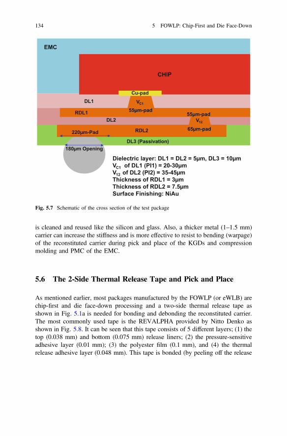
is cleaned and reused like the silicon and glass. Also, a thicker metal (1–1.5 mm)carrier can increase the stiffness and is more effective to resist to bending (warpage)of the reconstituted carrier during pick and place of the KGDs and compressionmolding and PMC of the EMC.
5.6 The 2-Side Thermal Release Tape and Pick and Place
As mentioned earlier, most packages manufactured by the FOWLP (or eWLB) arechip-first and die face-down processing and a two-side thermal release tape asshown in Fig. 5.1a is needed for bonding and debonding the reconstituted carrier.The most commonly used tape is the REVALPHA provided by Nitto Denko asshown in Fig. 5.8. It can be seen that this tape consists of 5 different layers; (1) thetop (0.038 mm) and bottom (0.075 mm) release liners; (2) the pressure-sensitiveadhesive layer (0.01 mm); (3) the polyester film (0.1 mm), and (4) the thermalrelease adhesive layer (0.048 mm). This tape is bonded (by peeling off the release
CHIP
EMC
Cu-pad
RDL1
VC1
55µm-pad
DL1
RDL2
180µm Opening
220µm-Pad 65µm-padV12 DL2
DL3 (Passivation)
55µm-pad
Dielectric layer: DL1 = DL2 = 5µm, DL3 = 10µmVC1 of DL1 (PI1) = 20-30µmV12 of DL2 (PI2) = 35-45µmThickness of RDL1 = 3µmThickness of RDL2 = 7.5µmSurface Finishing: NiAu
Fig. 5.7 Schematic of the cross section of the test package
134 5 FOWLP: Chip-First and Die Face-Down

liner) to the metal carrier at room temperature. Then, peel off the other release linerand pick and place the KGDs (face-down) on top of the thermal release adhesive asshown in Fig. 5.1b. The debonding temperature of the carrier is 170 °C.
5.7 EMC and Dispensing
The molding of FOWLP is by the compression method with EMC. For chip-firstand die face-down FOWLP, the curing temperature of the EMC must be lower thanthe release temperature of the double-sided tape. There are at least two forms ofEMC, namely liquid and solid. The advantages of liquid EMC are better handling,good flowability, less voids, better fill, and less flow marks. The advantages of solidEMC are less cure shrinkage, better stand-off, and less die drift. For chip-firstFOWLP, high filler content (� 85%) EMC will shorten the time in mold, lower themold shrinkage, and reduce the mold warpage.
Uniform filler distribution and filler size of the EMC will reduce flow marks/filland enhance flowability. For example, the filler content (wt.%), maximum fillersize, compression mold condition, post mold cure, Tg, and bending stiffness ofEMC by Sumitomo (solid) are 90, 55 lm, 7 m/125 °C, 1 h/150 °C, 170 °C, and30GPa, respectively, and by Nagase (liquid), 85, 25 lm, 10 m/125 °C, 1 h/150 °C,150 °C, and 19GPa, respectively. In this chapter Nagase’s liquid EMC R4507 willbe used and the material properties are shown in Table 5.2.
Table 5.1 Carrier material and thickness
Carrier material andthickness
Thermal expansioncoefficient (10−6/°C)
Young’s modulus(GPa)
Poisson’sratio
Silicon (0.76 mm) 2.6 168 0.28
Glass-1 (0.76 mm) 3.2 73.6 0.3
Glass-2 (1 mm) 7.6 69.3 0.3
Stainless Steel 420(1.5 mm)
10.5 200 0.3
Release liner (0.038mm)
Thermal-release adhesive (0.048mm)
Polyester film (0.1mm)
Pressure-sensitive adhesive (0.01mm)
Release liner (0.075mm)
Fig. 5.8 Nitto Denko’s REVALPHA tape
5.6 The 2-Side Thermal Release Tape and Pick and Place 135

Figure 5.9a shows the dispensing of the liquid EMC in a circular pattern on thereconstituted carrier with KGDs. It can be shown in Sect. 6.8.3 that with the circularpattern, there will be less and shorter flow marks.
5.8 Compression Molding and PMC
Due to the large size of the reconstituted wafer or panel, the conventional transfermolding method won’t work and the compression molding method is used.After EMC dispensing, it is followed by the compression molding as shown inFig. 5.1c and Fig. 5.9b. The KOZ (keep-out-zone) method is used and the mold capdiameter is 295 mm (2.5 mm clearance from the 300 mm glass carrier wafer edge).The metal carrier with dies attached is fixed onto the top mold chase by vacuum asshown in Fig. 5.9b. The dispensed EMC on a releasing film is placed on the bottomplunger. After a few experiments, the optimal compression molding parameters are:temperature = 125 °C, pressure = 45 kg/cm2, time = 10 min, and removing trapair before compression molding. It is followed by post mold cure (PMC) with atemperature = 150 °C, time � 60 min, and a dead weight = 15 kg for a betterwarpage control. Then, it is followed by debonding the metal carrier and peeling offthe tape as shown in Fig. 5.1d.
Figure 5.10 shows a typical reconstituted wafer with the chips embedded by theEMC by using compression method and PMC. It can be seen from Fig. 5.10d thatthose 4 chips are properly fabricated. The total thickness of the reconstituted wafer
Table 5.2 Nagase liquidepoxy molding compound
Item R4507
Filler content (%) 85
Filler to cut (µm) 25
Filler average size (µm) 8
Specific gravity 1.96
Viscosity (Pa.s) 250
Flexural Modulus (GPa) 19
Tg (DMA) (°C) 150
CTE1 (ppm/K) 10
CTE2 (ppm/K) 41
∙ High flowability as suitable for large surface areas and thin filmmolds
∙ Liquid at room temperature and able to be dispensed, and dustfree as suitable for clean room environments
∙ Capable of low temperature form molding (125 °C)∙ Delivers low reflection in large surface area molds with lowstress design
∙ High reliability∙ High purity∙ Low a line
136 5 FOWLP: Chip-First and Die Face-Down

is about 250 µm with 100 µm-thick EMC above the backside of the chips with150 µm thick.
Inspections for molding voids are carried out by C-mode scanning acousticmicroscopy (C-SAM). In order to balance the resolution and signal penetrationdepth, a transducer of 75 MHz is selected for the voids observation. After a coupleof parametric studies, there is not any void in the optimal wafers.
5.9 RDL
5.9.1 Debonding the Metal Carrier
In most eWLBs or chip-first and die face-down FOWLP, the total thickness of thereconstituted wafer is � 450 µm. Thus, right after debonding the carrier and peelingoff the tape, it is followed by building the RDLs and mounting the solder balls.
Remove trap air before
compression moldingDie
(a)
(b)
Keep-out-zone (KOZ) method
EMC
EMC dispensing
(circular pattern)
Fig. 5.9 a EMC dispensing. b Compression molding
5.8 Compression Molding and PMC 137

However, in this study, since we would like to save the EMC materials and have avery low-profile package, the total thickness of our reconstituted wafer is only250 µm. Thus, the reconstituted wafer is too fragile to fabricate the RDLs andmount the solder balls.
5.9.2 Temporary Bonding of Another Glass Carrier
One of the solutions is to attach the reconstituted wafer on another temporary glasswafer with a coated LTHC (light-to-heat conversion) layer (before removing themetal carrier) as shown in Fig. 5.11a. It is followed by making the RDLs as shown inFig. 5.11c with the method report in [29, 30]. Figure 5.12 shows the line width andspacing of the first RDL. It can be seen that the line width is slightly (10.44 µm)larger than the designed value and the spacing is slightly (9.5 µm) smaller than thedesigned value. This could be due to the etching of the Ti seed layer.
5mmx5mm 3x3
3x3 3x3
(a)
(d) (c)
(b)
5mmx5mm
3mmx3mm
3mmx3mm
3mmx3mm
Fig. 5.10 Molded reconstituted wafer. a Layout of the SiP. b Molded reconstituted wafer.c Closed-up of the molded reconstituted wafer. d Closed-up of the SiP without capacitors
138 5 FOWLP: Chip-First and Die Face-Down

RDLs
KGD KGD KGD KGD
Glass carrier
Build RDLs and mount solder balls
RDLs Solder balls
Glass carrier
RDLs Solder balls
Remove the metal carrier and peel off the tape
(b)
Dice the molded wafer into individual packages
(e)
(c)
De-bond the glass carrier by laser
(d)
Attach a glass carrier with a LTHC layer to the backside of the EMC reconstituted wafer
(a)
EMC
LTHC
KGD KGD KGD KGD EMC
Glass carrier
Metal carrier
Tape
Fig. 5.11 Key process for fabricating the RDLs and solder balls
Fig. 5.12 Line width andspacing of RDL1
5.9 RDL 139

5.10 Solder Ball Mounting
There are two different stencils for the solder ball mounting, one is for stencilprinting the flux and the other is for stencil mounting the solder balls. The solder(Sn3 wt.%Ag0.5 wt.%Cu) balls (200 µm diameter) used are from Indium and areon 0.4 mm pitch. The peak temperature for solder reflow is 245 °C.
5.11 Final Debonding
The de-bonding of the glass carrier as shown in Fig. 5.11d is by scanning a laser(355 nm DPSS Nd: YAG UV laser source is used) from the glass carrier side. Thelaser spot size is 240 µm, the scanning speed is 500 mm/s and the scanning pitch is100 µm. When the LTHC layer “sees” the laser light, it converts into powders andthe glass carrier is easily removed. It is followed by chemical cleaning. Figure 5.13shows the reconstituted wafer without any carrier and a closed-up on one of thepackage. It can be seen that there are 4 chips and 4 capacitors in a package and theyare properly fabricated. The reconstituted wafer is diced, as shown in Fig. 5.11e, intoindividual packages as shown in Fig. 5.14. It can be seen from the x-ray image thatthe chips and the capacitors are properly fabricated. Also, the vias (Vc1 and V12),RDLs (RDL1 and RDL2) and solder balls are properly done.
5mmx5mm
3mmx3mm
3mmx3mm
100µm Gap
3mmx3mm
10mmx10mm SiP
Capacitor
Fig. 5.13 Final debonded reconstituted wafer and closed-up of an individual package
140 5 FOWLP: Chip-First and Die Face-Down

5.12 Summary and Recommendations
FOWLP with chip-first and die face-down has been presented in this chapter. Someimportant results and recommendations are summarized as follows.
• The feasibility of a heterogeneous integration of 4 chips and 4 capacitors hasbeen demonstrated.
• There is not visible C-SAM void in the optimal reconstituted molded wafer.• In order to have a low-profile and less EMC (low-cost) package, the thickness of
the reconstituted molded wafer without the temporary carrier is about 250 µm.• The price we have to pay is to attach the reconstituted molded wafer to another
glass wafer with a LTHC layer, then perform the RDL and solder ball fabri-cation. After that, debond the glass wafer by laser. In this case, including thesolder ball, the total thickness of the final package is <450 µm.
Chip
RDL1 RDL2
VC1
3mmx3mm
5mmx5mm 3mmx3mm
3mmx3mm
100µm Gap Capacitor
10mmx10mm SiP
Chip
Solder Ball
RDL1 RDL2 VC1V12
EMC
UBM-less pad
Fig. 5.14 X-ray image, RDLs, and solder balls of an individual package
5.12 Summary and Recommendations 141

References
1. Hedler, H., T. Meyer, and B. Vasquez. 2001. Transfer Wafer Level Packaging. U.S. Patent 6727 576 B2, April 27, 2001.
2. Lau, J.H. 2015. Patent Issues of Fan-Out Wafer/Panel-Level Packaging. Chip Scale Review19: 42–46.
3. Brunnbauer, M., E. Furgut, G. Beer, T. Meyer, H. Hedler, J. Belonio, E. Nomura, K. Kiuchi,and K. Kobayashi. 2006. An Embedded Device Technology Based on a MoldedReconfigured Wafer. In IEEE/ECTC Proceedings, May 2006, 547–551.
4. Brunnbauer, M., E. Furgut, G. Beer, and T. Meyer. 2006. Embedded Wafer Level Ball GridArray (eWLB). In IEEE/EPTC Proceedings, December 2006, 1–5.
5. Keser, B., C. Amrine, T. Duong, O. Fay, S. Hayes, G. Leal, W. Lytle, D. Mitchell, andR. Wenzel. 2007. The Redistributed Chip Package: A Breakthrough for Advanced Packaging.In Proceedings of IEEE/ECTC, 2007, 286–291.
6. Kripesh, V., V. Rao, A. Kumar, G. Sharma, K. Houe, X. Zhang, K. Mong, N. Khan, andJ. H. Lau. 2008. Design and Development of a Multi-Die Embedded Micro Wafer LevelPackage. In IEEE/ECTC Proceedings, 2008, 1544–1549.
7. Khong, C., A. Kumar, X. Zhang, S. Gaurav, S. Vempati, V. Kripesh, J.H. Lau, andD. Kwong. 2009. A Novel Method to Predict Die Shift During Compression Molding inEmbedded Wafer Level Package. In IEEE/ECTC Proceedings, 2009, 535–541.
8. Sharma, G., S. Vempati, A. Kumar, N. Su, Y. Lim, K. Houe, S. Lim, V. Sekhar, R. Rajoo,V. Kripesh, and J.H. Lau. 2009. Embedded Wafer Level Packages with Laterally Placed andVertically Stacked Thin Dies. In IEEE/ECTC Proceedings, 2009, 1537–1543. Also, IEEETransactions on CPMT 1 (5): 52–59 (May 2011).
9. Kumar, A., D. Xia, V. Sekhar, S. Lim, C. Keng, S. Gaurav, S. Vempati, V. Kripesh, J.H. Lau,and D. Kwong. 2009. Wafer Level Embedding Technology for 3D Wafer Level EmbeddedPackage. In IEEE/ECTC Proceedings, 2009, 1289–1296.
10. Lim, Y., S. Vempati, N. Su, X. Xiao, J. Zhou, A. Kumar, P. Thaw, S. Gaurav, T. Lim, S. Liu,V. Kripesh, and J. H. Lau. Demonstration of High Quality and Low Loss Millimeter WavePassives on Embedded Wafer Level Packaging Platform (EMWLP). In IEEE/ECTCProceedings, 2009, 508–515. Also, IEEE Transactions on Advanced Packaging 33: 1061–1071 (2010).
11. Lau, J.H., N. Fan, and M. Li. 2016. Design, Material, Process, and Equipment of EmbeddedFan-Out Wafer/Panel-Level Packaging. Chip Scale Review 20 (May/June):38–44.
12. Kurita, Y., T. Kimura, K. Shibuya, H. Kobayashi, F. Kawashiro, N. Motohashi, andM. Kawano. 2010. Fan-Out Wafer-Level Packaging with Highly Flexible Design Capabilities.In IEEE/ESTC Proceedings, 2010, 1–6.
13. Motohashi, N., T. Kimura, K. Mineo, Y. Yamada, T. Nishiyama, K. Shibuya, H. Kobayashi,Y. Kurita, and M. Kawano. 2011. System in Wafer-Level Package Technology withRDL-First Process. In IEEE/ECTC Proceedings, 2011, 59–64.
14. Yoon, S., J. Caparas, Y. Lin, and P. Marimuthu. 2012. Advanced Low Profile PoP Solutionwith Embedded Wafer Level PoP (eWLB-PoP) Technology. In IEEE/ECTC Proceedings,2012, 1250–1254.
15. Tseng, C., C. Liu, C. Wu, and D. Yu. 2016. InFO (Wafer Level Integrated Fan-Out)Technology. In IEEE/ECTC Proceedings, 2016, 1–6.
16. Hsieh, C., C. Wu, and D. Yu. 2016. Analysis and Comparison of Thermal Performance ofAdvanced Packaging Technologies for State-of-the-Art Mobile Applications. In IEEE/ECTCProceedings, 2016, 1430–1438.
17. Lau, J.H. 2016. TSV-less Interposers. Chip Scale Review 20 (September/October):28–35.18. Yoon, S., P. Tang, R. Emigh, Y. Lin, P. Marimuthu, and R. Pendse. 2013. Fanout Flipchip
eWLB (Embedded Wafer Level Ball Grid Array) Technology as 2.5D Packaging Solutions.In IEEE/ECTC Proceedings, 2013, 1855–1860.
142 5 FOWLP: Chip-First and Die Face-Down
19. Lin, Y., W. Lai, C. Kao, J. Lou, P. Yang, C. Wang, and C. Hseih. 2016. Wafer WarpageExperiments and Simulation for Fan-out Chip on Substrate. In IEEE/ECTC Proceedings,2016, 13–18.
20. Chen, N., T. Hsieh, J. Jinn, P. Chang, F. Huang, J. Xiao, A. Chou, and B. Lin. 2016. A NovelSystem in Package with Fan-Out WLP for High Speed SERDES Application. In IEEE/ECTCProceedings, 2016, 1495–1501.
21. Hayashi, N., T. Takahashi, N. Shintani, T. Kondo, H. Marutani, Y. Takehara, K. Higaki,O. Yamagata, Y. Yamaji, Y. Katsumata, and Y. Hiruta. 2011. A Novel Wafer Level Fan-outPackage (WFOPTM) Applicable to 50 µm Pad Pitch Interconnects. In IEEE/EPTCProceeding, December 2011, 730–733.
22. Hayashi, N., H. Machida, N. Shintani, N. Masuda, K. Hashimoto, A. Furuno, K. Yoshimitsu,Y. Kikuchi, M. Ooida, A. Katsumata, and Y. Hiruta. 2014. A New Embedded StructurePackage for Next Generation, WFOPTM (Wide Strip Fan-Out Package). In Pan PacificSymposium Conference Proceedings, February 2014, 1–7.
23. Hayashi, N., M. Nakashima, H. Demachi, S. Nakamura, T. Chikai, Y. Imaizumi, Y. Ikemoto,F. Taniguchi, M. Ooida, and A. Yoshida. 2017. Advanced Embedded Packaging for PowerDevices. In IEEE/ECTC Proceedings, 2017, 696–703.
24. Braun, T., K.-F. Becker, S. Voges, T. Thomas, R. Kahle, J. Bauer, R. Aschenbrenner, and K.-D. Lang. 2013. From Wafer Level to Panel Level Mold Embedding. In IEEE/ECTCProceedings, 2013, 1235–1242.
25. Braun, T., K.-F. Becker, S. Voges, J. Bauer, R. Kahle, V. Bader, T. Thomas,R. Aschenbrenner, and K.-D. Lang. 2014. 24 � 18 Fan-Out Panel Level Packing. In IEEE/ECTC Proceedings, 2014, 940–946.
26. Braun, T., S. Raatz, S. Voges, R. Kahle, V. Bader, J. Bauer, K. Becker, T. Thomas,R. Aschenbrenner, and K. Lang. 2015. Large Area Compression Molding for Fan-Out PanelLevel Packing. In IEEE/ECTC Proceedings, 2015, 1077–1083.
27. Chang, H., D. Chang, K. Liu, H. Hsu, R. Tai, H. Hunag, Y. Lai, C. Lu, C. Lin, and S. Chu.2014. Development and Characterization of New Generation Panel Fan-Out (PFO) PackagingTechnology. In IEEE/ECTC Proceedings, 2014, 947–951.
28. Liu, H., Y. Liu, J. Ji, J. Liao, A. Chen, Y. Chen, N. Kao, and Y. Lai. 2014. WarpageCharacterization of Panel Fab-out (P-FO) Package. In IEEE/ECTC Proceedings, 2014,1750–1754.
29. Lau, J.H., M. Li, M. Li, T. Chen, I. Xu, X. Qing, et al. 2018. Fan-Out Wafer-Level Packagingfor Heterogeneous Integration. In IEEE/ECTC Proceedings, May 2018.
30. Lau, J.H., M. Li, N. Fan, E. Kuah, Z. Li, K. Tan, T. Chen, et al. 2017. Fan-Out Wafer-LevelPackaging (FOWLP) of Large Chip with Multiple Redistribution-Layers (RDLs). IMAPSTransactions on Journal of Microelectronics and Electronic Packaging, 123–131.
References 143

Chapter 6FOWLP: Chip-First and Die Face-Up
6.1 Introduction
The design, materials, process, fabrication, and reliability of fan-out wafer-levelpackaging (FOWLP) with chip-first and die face-up method are presented in thischapter. Emphasis is placed on the issues and their solutions (such as reconstitutedcarrier, die-attach film placement, pitch compensation, die shift, epoxy moldingcompound dispensing, compression molding, warpage, and Cu revealing) duringthe fabrication of a very large test chip (10 mm � 10 mm � 150 µm) and testpackage (13.47 mm � 13.47 mm), and three redistribution layers (RDLs) with thesmallest line width/spacing = 5 µm/5 µm. The FOWLP test package on a six-layerprinted circuit board (PCB) is subjected to thermal cycling and drop tests.Recommendations of process integration and guidelines on FOWLP with chip-firstand die face-up are provided.
6.2 Fan-Out of Chip Circuitries in SemiconductorPackaging
One of the major functions of semiconductor packaging is to fan-out the circuitriesfrom the chip and talk to circuitries from another chip [1]. On July 17, 1967,Kauffman of The Jade Corporation [2] proposed the use of a lead frame to fan-outthe circuitries from a chip. Today, just about all electronic products use lead framessuch as the gull-wing lead [e.g., plastic quad flat pack (PQFP)], J-lead [e.g., plasticleaded chip carrier (PLCC)], and/or dual in-line package (DIP) to fan-out the cir-cuitries from a chip to a PCB.
On March 2, 1992, Paul Lin, Mike McShane, and Howard Wilson of Motorolaproposed [3] the use of an organic carrier or substrate with area-array solder balls(instead of lead frames) to fan-out the circuitries from a chip to a PCB, which is
© Springer Nature Singapore Pte Ltd. 2018J. H. Lau, Fan-Out Wafer-Level Packaging,https://doi.org/10.1007/978-981-10-8884-1_6
145

called a plastic ball grid array (PBGA) package. Amkor (1993) led the OSATs(outsourced semiconductor assembly and test providers) to license this packagingtechnology from Motorola—and the BGA era began.
On July 13, 1998, Peter Elenius and Harry Hollack of Flip Chip Technologiesproposed [4] the use of RDLs to fan-in the circuitries from the original peripheralbond pads of a chip on a wafer and of solder balls to connect to a PCB withoutunderfill. The packages made by the fan-in wafer-level packaging (WLP) are calledwafer-level chip scale package (WLCSP) and one of the most famous is UltraCSPdeveloped and patented by Flip Chip Technologies [5]. In 2001, again Amkor ledthe OSATs and foundries to license the UltraCSP, and the WLP era began.
On October 31, 2001, Harry Hedler, Thorsten Meyer, and Barbara Vasquez ofInfineon proposed [6] the use of RDLs to fan-out the circuitries from the metal padof the chip on a wafer and solder ball to the metal pads on a PCB without underfill.(At that time, they called it embedded wafer-level ball (eWLB) grid array [7, 8].Today, we called it FOWLP.) Some of the RDLs having a portion that extendsbeyond (fan-out) the edges of the chip.
6.2.1 Advantages of FOWLP over PBGA
The advantages of FOWLP over PBGA packages with solder bumped flip chip are[9]: (1) lower cost, (2) lower package profile, (3) eliminating the substrate,(4) eliminating the wafer bumping, (5) eliminating the flip chip reflow, (6) elimi-nating the flux cleaning, (7) eliminating the underfill, (8) better electrical perfor-mance, (9) better thermal performance, and (10) easier to go for system-in-package(SiP) and 3D IC packaging [10, 11].
6.2.2 Advantages of FOWLP over WLCSP
The advantages of FOWLP over fan-in WLP or WLCSP are [9]: (1) the use ofknown good die (KGD), (2) better wafer-level yield, (3) using the best of silicon,(4) single or multichip, (5) embedded integrated passive devices, (6) more layer ofRDLs, (7) higher pin counts, (8) better thermal performance, (9) easier to go for SiPand 3D IC packaging, and (10) higher PCB-level reliability.
6.3 FOWLP with Chip-First and Die Face-Up
As mentioned before, basically there are two methods to form (build) the FOWLP[12]. One is chip-first and the other is chip-last [13, 14]. For the chip-first method,there are two options: face-down (die-down) [15–22] and face-up (die-up) [23–30].
146 6 FOWLP: Chip-First and Die Face-Up

FOWLP with chip-first and die face-down has been presented in Chap. 5. In thischapter, we will present the FOWLP with chip-first and die face-up. The test chip,test package, assembly process on the device (test) wafer, assembly process on thereconstituted wafer, EMC (epoxy molding compound) dispensing, compressionmolding and PMC (post mold cure), warpage, Cu reveal, RDLs, debonding, solderball mounting, PCB assembly, thermal cycling test, and drop test will be presentedand discussed [31].
6.4 Test Chip
Figure 6.1 shows the test chip under consideration. The layout of the test chip isshown in Fig. 6.1a and the fabricated chip is shown in Fig. 6.1b–d. It can be seenthat the chip sizes are 10 mm � 10 mm � 150 µm and there are 1988 pads with aminimum pitch = 150 µm staggered. The polyimide (PI) opening of the Al pad is40 µm in diameter and is 5 µm-thick. (Later on, because of the Cu smear underbackgrinding of the epoxy molding compound (EMC) to expose the Cu contact
(d)
(c)
(b) (a) 10mmx10mm
10m
mx1
0mm
Fig. 6.1 Test chip. a 10 mm � 10 mm test chip layout. b The fabricated test chip. c A close-uplook of the test chip. d Cross-section image of the test chip
6.3 FOWLP with Chip-First and Die Face-Up 147

pad, the thickness of the PI has been increased to slightly taller than the Cu contactpad.) The SiO2 passivation opening of the Al pad is 50 µm � 50 µm and the sizeof the Al pad is 70 µm � 70 µm. The Cu contact pad is 60 µm in diameter and is25 µm tall from the Al pad.
6.5 Test Package
Figure 6.2 schematically shows the test package under consideration. It can be seenthat the reconstituted wafer is a 300 mm glass wafer, Fig. 6.2a, and there are 325test packages with a pitch = 13.46 mm. The layout of the test package is shown inFig. 6.2b. The dimensions of the test package are: 13.42 mm � 13.42 mm asshown in Fig. 6.2c. Thus, a package/chip area ratio = 1.8 and the test package is1.71 mm all around larger than the test chip. The dimensions of a typical pad on thetest package are shown in Fig. 6.2d.
Figure 6.3 schematically shows the cross-sectional view of the test package. Itcan be seen that there are 3 RDLs and the thickness of RDL1, RDL2, and RDL3 is3 µm. The line width and spacing of RDL1, RDL2, and RDL3 are, respectively,5 µm/5 µm, 10 µm/10 µm, and 15 µm/15 µm. The dielectric layer thickness of
13.42mm
13.4
2mm
Test Chip
10m
m
10mmEMC
1.71
mm
1.71mm
Si Al-Pad
Ti/CuCu
SiO2
Contact pad (60µm)
(5µm)25µm
150µm
13.42mm
13.4
2mm
13.42mm
(a)
(d)
(c)
(b)
Fig. 6.2 Test package. a Schematic of the test packages on a 300 mm reconstituted wafer.b Layout of the test package. c Schematic of the test package (13.42 mm � 13.42 mm) for the testchip. d A schematic of the cross section of a pad on the test chip
148 6 FOWLP: Chip-First and Die Face-Up

DL1, DL2, DL3, and DL4 is 5 µm. The via (VC1), through the first dielectric layer(DL1), connecting the Cu contact pad of the test chip to the first RDL (RDL1) is20 µm in diameter. The pad diameter on the RDL1 is 55 µm, which is connected toRDL2 through the via (V12) with a diameter of 35 µm. Similarly, the pad diameteron the RDL2 is 65 µm, which is connected to RDL3 through V23 with a diameter of45 µm. Finally, 220 µm pads are formed on the bottom side of RDL3 and a V3P
with a diameter of 160 µm is formed through the passivation (DL4), a UBM (underbump metallurgy) and a 180-diameter Cu contact pad is formed for the solder ballmounting. Figure 6.4 shows the other case with UBM-less/Cu pad for a solder ball.In this case, 220 µm Cu pads are formed on RDL3 for the solder ball mounting.The thickness of RDL3 is 7.5 µm. The thickness of the passivation (DL4) is 10 µmand the passivation opening is 180 µm. For both cases, the solder ball size is200 µm and ball pitch is 0.4 mm.
Figure 6.5 shows the partial daisy-chain design of the RDLs of the test package.Basically, there are three objectives of the layout of the daisy-chain of the RDLs:(1) to capture the delamination of the daisy-chain trace; (2) to capture the failure ofthe daisy-chain trace through the vias, and (3) to identify the failure of the solderjoint (after they are assembled on the PCB), during drop and thermal cycling tests.
Solder ball(200µm)
CHIP
Dielectric Layer - 1 (DL1)
RDL1
DL2
RDL2
DL3
RDL3
EMC
Contact PadVC1
V12
V23
V3P
180µm Contact Pad
TiCu
TiCu
DL4 (Passivation)
Dielectric layer thickness:DL1 = DL2 = DL3 = DL4 = 5µm
55µm-pad
65µm-pad
220µm-pad65µm-pad
65µm-pad
55µm-pad
VC1 of DL1 (PI1) = 20µm
Thickness of RDL1 = 3µm
V12 of DL2 (PI2) = 35µm
Thickness of RDL2 = 3µm
V23 of DL3 (PI3) = 45µm
V3P of DL4 (PI4) = 160µm
Thickness of RDL3 = 3µm
Cu Contact Pad = 160µm
Fig. 6.3 Schematic of the cross section of the test package with conventional solder ballattachment
6.5 Test Package 149

6.6 Chip-First (Die Face-Up) FOWLP Assembly Process
Figure 6.6 shows schematically the FOWLP with chip-first and die face-upassembly process. Basically, works must be done on the device (test chip) wafer(Fig. 6.6a, b) and the reconstituted (temporary carrier) wafer (Fig. 6.6c–h).
6.7 Assembly on the Test Chip Wafer
First, the test chip wafer must be modified by sputtering a Ti/Cu as a bottom layerof under bump metallurgy (UBM) with a physical vapor deposition (PVD) on theAl (or Cu) pad, and a Cu contact pad (for building the RDLs later) is electroplatedon the UBM, as shown in Fig. 6.6a. This step is followed by spin coating a polymeron top of the test chip wafer and laminating (at *70 °C) with a (*20 µm)die-attach film (DAF) provided by Hitachi (Fig. 6.7 and Table 6.1) at the bottom ofthe test chip wafer as shown in Fig. 6.6b. The test chip wafer is then diced intoindividual chips.
VC1 of DL1 (PI1) = 20µm
Thickness of RDL1 = 3µm
V12 of DL2 (PI2) = 35µm
Thickness of RDL2 = 3µm
V23 of DL3 (PI3) = 45µm
Via of DL4 (PI4) = 180µm
Thickness of RDL3 = 7.5µm
CHIP
Dielectric Layer - 1 (DL1)
RDL1
DL2
RDL2 DL3
RDL3
EMC
Contact PadVC1
V12
V23
TiCu
DL4 (Passivation)
Solder ball(200µm)
65µm-pad
RDL3 220µm-pad
55µm-pad 55µm-pad
65µm-pad
65µm-pad
Dielectric layer thickness:DL1 = 5µmDL2 = 5µmDL3 = 5µmDL4 = 10µm
Passivation opening = 180µm
Fig. 6.4 Schematic of the cross section of the test package with UBM-less Cu pad solder ballattachment
150 6 FOWLP: Chip-First and Die Face-Up

6.8 Assembly on the Reconstituted Wafer
Figures 6.6c through 6.6h show the FOWLP with chip-first and die face-up processsteps on the reconstituted wafer and they will be briefly mentioned below.
6.8.1 Glass Carrier Wafer and LTHC Layer
A light-to-heat conversion (LTHC) layer (about 1 µm) provided by 3M (Table 6.2)is spin coated onto the temporary glass carrier wafer as shown in Figs. 6.6c and6.8a. In this study, three different glasses with thermal coefficient of expansion(TCE) = 3.26 � 10−6/°C, 7.6 � 10−6/°C, and 8.1 � 10−6/°C are considered. Thethickness of the one with 3.26 � 10−6/°C is 780 µm and with 7.6 � 10−6/°C and8.1 � 10−6/°C is 1 mm.
Fig. 6.5 Daisy-chain design of the RDLs of the test package
6.8 Assembly on the Reconstituted Wafer 151

Temporary glass wafer carrier
KGD KGDKGD
Build RDLs on contact pads and
mount solder balls
Solder ballsRDLs
Remove carrier by a laser and then dice the molded wafer into
individual packages
Die face-up
RDLsSolder balls
KGD KGD KGD
Compression molding the
reconstituted carrier and post
mold cure
EMC
Backgrind the EMC to
expose the Cu contact-pad
Test for KGD
Device Wafer
CHIP
Passivation
UBM
Al or Cu Pad
Cu contact-pad
UBM Contact pad
CHIP
Polymer
Sputter UBM and electroplate contact pad
Polymer on top, die-attach film on bottom of wafer, and
dice the wafer
DAF
Coated with a LTHC sacrificial layer
LTHC
(a)
(b)
(c)
(d)
(f)
(e)
(g)
(h)
Fig. 6.6 FOWLP with chip-first and die face-up process. a Sputter UBM and ECD of Cu contactpad. b Polymer on top, die-attach film on bottom of wafer, and dice the wafer. c Spin coat a LTHClayer on top of the temporary glass wafer carrier. d Pick and place the die face-up on the LTHClayer carrier. e Compression mold the reconstituted wafer and post mold cure. f Backgrinding theEMC to expose the Cu contact pad. g Build RDLs on contact pads and mount solder balls.h Remove the carrier and dice the reconstituted wafer into individual packages
Wafer backside lamination: 60 - 70oCCuring: 125oC for one hour
Fig. 6.7 Die-attach film(DAF) provided by Hitachi
152 6 FOWLP: Chip-First and Die Face-Up

Table 6.1 Material properties of the DAF
Item Unit FH-9011 Testmethod
Adhesive thickness lm 10, 20,25, 40
–
DC tapeproperties
Exposure doze mJ/cm2 150–400 –
Adhesive strengthbetween DCT andDBF
BeforeUV
N/25 mm 1.4 –
AfterUV
N/25 mm <0.1 –
Wafer laminating temp. °C 60–80 –
Die bondingcondition
Temp. °C 100–160 –
Load MPa 0.05–2.0 –
Elastic modulus (35 °C) MPa 200 DMA
Tg °C 180 TMA
Die shear strength (260 °C) N/chip >100 5 � 5 mmchip
Wafer backside lamination: 60–70 °CCuring: 125 °C for one hour
Table 6.2 Characteristics of the LTHC material
Productdescription
3M™ Light-To-Heat Conversion Release Coating (LTHC) ink is asolvent-based coating applied using a spin coating method. This coatingforms the light-to-heat conversion layer on a glass substrate for 3M™Wafer Support System
Features andbenefits
Enables stress-free, room temperature debonding of adhesive
Typicalproperties note
The following technical information and data should be consideredrepresentative or typical only and should not be used for specificationpurposes
Base resin Acrylic
Color Black thixotropic liquid
Specific gravity 1.00
Solid 11%
Solvent • Methoxy-2-propyl acetate• Butoxy ethanol
Flash point 45 °C
Generalinformation
Standard container is 20 L Stainless steel drum (UN: 1A1/X/250)
Storage Store this product under normal conditions of 5–35 °C in originalcontainer for maximum storage life
Shelf life Six months after the date of shipping from 3M
Method of usage • Product must be stirred/mixed at 600–700 RPM for 12 h before usage• Product must be stirred continuously while in use
6.8 Assembly on the Reconstituted Wafer 153

6.8.2 Pick and Place
The individual test chips are picked and placed face-up on the LTHC carrier asshown in Figs. 6.6d and 6.8a. In order to cure the DAF, a bonder with temperatureand pressure such as the multipurpose high-accuracy NUCLEUS is used. The DAFprocess is carried out at 120 °C (both bond-head and bond-stage) with the bondforce of 2 kg for 2 s. Thus, the reconstituted wafer will expand during chips pickand place. The X and Y pitch offset (the measured pitch subtract from the designedpitch) of chips are plotting against the column and row and shown in Fig. 6.9. It canbe seen that the chip placement offsets can be as large as ±100 µm. However,during patterning/photolithography of the RDLs, it is operated at room temperature.Thus, pitch compensation due to the DAF heating is needed and can be calculatedby the following equation:
PA ¼ PR þ aLDT
where PA is die-attach pitch, PR is the designed RDL pitch, aL is the linear thermalcoefficient of expansion of the glass carrier, DT is the temperature differencebetween DAF curing temperature and RDL patterning/photolithography tempera-ture. The X and Y pitch offset of chips after pitch compensation are shown in
Place the KGD face-up on the LTHC layer glass carrier
Temporary glass wafer carrierLTHC
KGD KGDKGDDAF
Reconstituted glass wafer carrier
Carrier coated with a LTHC (~1µm) layer
KGD
Reconstituted Wafer
Glass carrier coated with a LTHC layer
Reconstituted Wafer
Compression molding the EMC (Epoxy Molding Compound) on the
reconstituted wafer.125oC for 10 minutes; Pressure = 45kg/cm2
DAF
EMC
Reconstituted glass carrier
KGDKGD KGD
LTHC layer
Cu contact-pad
(a) (b)
Fig. 6.8 a Spin coat a LTHC layer on the carrier and pick and please the chip face-up on thecarrier. b Compression molding the EMC
154 6 FOWLP: Chip-First and Die Face-Up

Fig. 6.10. It can be seen that the placement offset is reduced from ±100 µm(without pitch compensation) to ±4.0 µm (with pitch compensation), and this is agood performance that can meet the process specifications.
6.8.3 EMC Dispensing
The EMC is a liquid-like material (Nagase R4507) and its material properties areshown in Table 6.3. It can be seen that the filler content is 85%. The average size of
Offset in X-direction (without pitch compensation)
Offset in Y-direction (without pitch compensation)
Column number
Row number
Offs
et (µ
m)
Offs
et (µ
m)
Fig. 6.9 Position offset data: X- and Y-direction (without pitch compensation)
6.8 Assembly on the Reconstituted Wafer 155

Offset in X-direction (with pitch compensation)
Offset in Y-direction (with pitch compensation)
Column number
Row number
Offs
et (µ
m)
Offs
et (µ
m)
Fig. 6.10 Position offset data: X- and Y-direction (with pitch compensation)
Table 6.3 Materialproperties of the EMC
Item R4507
Filler content (%) 85
Filler to cut (µm) 25
Filler average size (µm) 8
Specific gravity 1.96
Viscosity (Pa s) 250
Flexural modulus (GPa) 19
Tg (DMA) (°C) 150
CTE1 (ppm/K) 10
CTE2 (ppm/K) 41
156 6 FOWLP: Chip-First and Die Face-Up
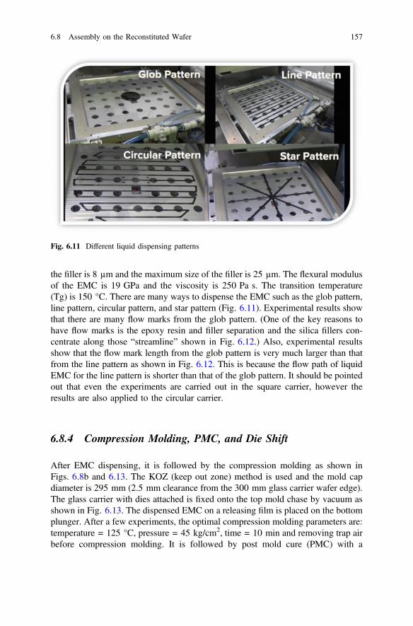
the filler is 8 µm and the maximum size of the filler is 25 µm. The flexural modulusof the EMC is 19 GPa and the viscosity is 250 Pa s. The transition temperature(Tg) is 150 °C. There are many ways to dispense the EMC such as the glob pattern,line pattern, circular pattern, and star pattern (Fig. 6.11). Experimental results showthat there are many flow marks from the glob pattern. (One of the key reasons tohave flow marks is the epoxy resin and filler separation and the silica fillers con-centrate along those “streamline” shown in Fig. 6.12.) Also, experimental resultsshow that the flow mark length from the glob pattern is very much larger than thatfrom the line pattern as shown in Fig. 6.12. This is because the flow path of liquidEMC for the line pattern is shorter than that of the glob pattern. It should be pointedout that even the experiments are carried out in the square carrier, however theresults are also applied to the circular carrier.
6.8.4 Compression Molding, PMC, and Die Shift
After EMC dispensing, it is followed by the compression molding as shown inFigs. 6.8b and 6.13. The KOZ (keep out zone) method is used and the mold capdiameter is 295 mm (2.5 mm clearance from the 300 mm glass carrier wafer edge).The glass carrier with dies attached is fixed onto the top mold chase by vacuum asshown in Fig. 6.13. The dispensed EMC on a releasing film is placed on the bottomplunger. After a few experiments, the optimal compression molding parameters are:temperature = 125 °C, pressure = 45 kg/cm2, time = 10 min and removing trap airbefore compression molding. It is followed by post mold cure (PMC) with a
Fig. 6.11 Different liquid dispensing patterns
6.8 Assembly on the Reconstituted Wafer 157

Fig. 6.12 Glob versus rectangular dispensing pattern. Flow mark point of measurement
Reconstituted Wafer
Remove trap air before
compression molding
DAF
EMC
Reconstituted glass carrier
KGDKGD KGD
LTHC layer
Cu contact-pad
KGD
EMC (Epoxy Molding Compound)
Compression molding the EMC on the reconstituted wafer:125oC for 10 minutes; Pressure = 45kg/cm2
SAM observation of the molding voids
Post mold cure of EMC:150oC for ≥ one hour
Voidless after trap air removal
Fig. 6.13 Compression molding of EMC and PMC
158 6 FOWLP: Chip-First and Die Face-Up

temperature = 150 °C, time � 60 min, and a dead weight = 15 kg for a betterwarpage control. The compression molding is performed by the high-coplanarityaccuracy machine ORCAS.
Inspections for molding voids are carried out by C-mode scanning acousticmicroscopy (C-SAM). In order to balance the resolution and signal penetrationdepth, a transducer of 75 MHz is selected for the voids observation. Before com-pression molding parameter optimization, around 10 voids are detected (especiallylocated at the die edge) in each of the molded wafers as shown in Fig. 6.13. Afteroptimization, the voids are eliminated.
Figure 6.14a shows the top side of the molded test packages on the glassreconstituted wafer with the LTHC layer. In order to see the test chips, some of thereconstituted carrier wafers are without the LTHC layer such as the one shown inFig. 6.14b. In this case, we can determine the die shift due to compression moldingby measuring the position of each chip before and after molding. Figure 6.15 showsthe statistical plots of the X-position die shift and Y-position die shift caused by thecompression molding. It can be seen that because of the DAF (which solidlyholding the chip to the carrier), the die shift (can be controlled within ±4 µm) is toosmall to be an issue on making the RDLs.
6.8.5 Warpages
The total thickness variations (TTV) of a few typical molded reconstituted wafersafter PMC are shown in Table 6.4. This is a measurement of 8 points around theperipheral and one point at the center of the reconstituted wafer. It can be seen from
Fig. 6.14 a Top view of a molded reconstituted wafer. b Bottom view of a molded reconstitutedwafer without the LTHC-layer so we can see the test chips
6.8 Assembly on the Reconstituted Wafer 159

Table 6.4 that the TTV is about 10 µm. The warpages of several reconstitutedwafers after PMC are measured by the shadow Moire method. The results areshown in the table of Fig. 6.16. It can be seen that the maximum average warpagefor the glass CTE = 3.25 � 10−6/°C is 4.003 mm, CTE = 7.6 � 10−6/°C is0.38 mm, and CTE = 8.1 � 10−6/°C is 0.25 mm. It is noted that the CTE of theEMC is 10 � 10−6/°C (Table 6.3). Thus, as expected, the smaller the CTE mis-match between the glass carrier and the EMC the smaller the warpage.
Finite element simulation results for the glass with CTE = 3.25 � 10−6/°C andthe glass with CTE = 7.6 � 10−6/°C are reported, respectively, in Fig. 6.16a, b.The measurement results for these two cases are also reported in Fig. 6.16a, b. Itcan be seen that the measurement and simulation results compare very well. Detaildescriptions of the finite element simulation are shown in the following paragraphs.
A. Material Properties
Table 6.5 shows the material properties of the key elements of a FOWLP. Thecoefficient of thermal expansion (CTE) of Si carrier, Glass-1 carrier, and Glass-2
Because of the Die-attach film (DAF), the die-shift is very small!
Fig. 6.15 Compression molding-induced die shift distribution data. (L) X-direction. (R) Y-direction
Table 6.4 TTV of typicalmolded reconstituted wafers
Position Wafer-1 Wafer-2 Wafer-3
1 1301 1301 1299
2 1307 1307 1300
3 1308 1308 1303
4 1305 1310 1305
5 1310 1312 1309
6 1307 1312 1307
7 1305 1312 1310
8 1306 1302 1307
9 1309 1310 1306
Range 9 µm 11 µm 11 µm
160 6 FOWLP: Chip-First and Die Face-Up

carrier are, respectively, 2.6 � 10−6/°C, 3.25 � 10−6/°C, and 7.6 � 10−6/°C. TheYoung’s modulus (GPa) of DAF is temperature dependent: 2.3 (0 °C), 0.02 (50 °C),0.006 (100 °C), and 0.005 (200 °C).
B. Finite-Element Model
A bowl shape of the molded wafer is assumed. Due to double symmetries of themolded (reconfigured) wafer shown in Fig. 6.17, only quarter of the wafer is
CTE = 3.25x10⁻⁶/oC
CTE = 7.6x10⁻⁶/oC
Glass CTEx10-6/oC
Average Warpage (mm)
3.25 4.003mm
7.6 0.380mm
8.1 0.250mm
(a)
(b)
Fig. 6.16 Measured warpage and simulation contours of the molded wafer (after PMC) witha carrier CTE = 3.25 � 10−6/°C, and b carrier CTE = 7.6 � 10−6/°C
Table 6.5 Material properties of the package structure for warpage analysis
Materials Thermal expansion coefficient (10−6/°C) Young’s modulus(GPa)
Poisson’sratio
Silicon 2.6 168 0.28
EMC 10 19 0.25
DAF 120 2.3 (0 °C)0.02 (50 °C)0.006 (100 °C)0.005 (200 °C)
0.4
Glass-1 3.2 73.6 0.3
Glass-2 7.6 69.3 0.3
Glass-1 (0.76 mm thick)Glass-2 (1 mm thick)
6.8 Assembly on the Reconstituted Wafer 161

modeled (Fig. 6.17a). Figure 6.17b shows the finite element meshes for the Si chip,EMC, DAF, and carrier. Since the LTHC layer is so thin, it is not included in themodel. The finite element code (ABAQUS V6.12) with element type: 3D stress and290,000–340,000 elements (depends on different cases) is used for the simulations.
C. Boundary Conditions
The displacement/rotation boundary conditions along the x-axis are that there is nodisplacement in the y-direction (U2 = 0), and there is no rotation about the x-axis(UR1 = 0) and the z-axis (UR3 = 0). The boundary conditions along the y-axis arethat there is no displacement in the x-direction (U1 = 0), and there is no rotationabout the y-axis (UR2 = 0) and the z-axis (UR3 = 0). At the center, the boundaryconditions are that there are not any displacement and rotation (U1 = U2 =U3 = UR1 = UR2 = UR3 = 0). The temperature boundary condition is for thereconstituted wafer to cool down from 125 °C (stress-free temperature) to roomtemperature. That is right after PMC of the EMC. Another boundary condition is forthe backgrinding of the EMC of the reconstituted wafer to expose the Cu contactpad for making the RDLs. This will be executed by using the “birth and death”technique that the element to be grinded will be deactivated during the simulation.
(a) (b) Finite element meshBoundary condition
U1=U2=U3=UR1=UR2=UR3=0
Fig. 6.17 a Boundary conditions. b Finite element meshes for the warpage analyses of quartermodel of the molded reconstituted wafer
162 6 FOWLP: Chip-First and Die Face-Up

However, the backgrinding process parameters such as pressure, speed, fine, orcoarse grinding are not modeled.
D. Comparison between the Simulation and Experimental Results
In order to compare the simulation and experimental results, the DAF and itstemperature-dependent material properties are included in the modeling.Figure 6.16b shows the comparison between the simulation and experimentalresults for the case of chip dimensions = 10 mm � 10 mm � 150 lm, package/chip area ratio = 1.8, die EMC cap = 100 lm, and glass carrier thickness = 1 mmwith CTE = 7.6 � 10−6/°C. A volume shrinkage of the EMC = 0.27% is assumed.It can be seen that the maximum warpage of the double symmetry model is equal to0.232 mm, which compares reasonably well (17% off) from the maximum exper-imental result (0.28 mm). It should be pointed out that due to the die uniformity, diepick and place accuracy, EMC filler distribution, EMC dispensing uniformity,compression condition, and die shift, the warpage after PMC is not exactly a bowlshape. Also, these factors cannot (or are very difficult to) be modeled by finiteelement method, especially for small warpage.
Actually, some of the experimental results (in the cases for very large warpage)show that the warpage is not in a bowl shape but a cylindrical shape. In order tocompare the simulation result to these experimental results, half of the structure ismodeled as shown in Fig. 6.18. The warpage contour distribution of the measure-ment result shown in the left-hand side of Fig. 6.16a is for the case of chipdimensions = 10 � 10 � 0.15 mm3, package/chip area ratio = 1.8, die EMCcap = 100 lm, and glass carrier thickness = 0.78 mmwith CTE = 3.26 � 10−6/°C.The warpage contour distribution of the simulation result shown in the right-handside of Fig. 6.16a compares very well (1%) with the experimental result shown onthe left-hand side.
E. Effect of Carrier Wafer Material and Thickness on FOWLP Warpage
Based on the above simulation and experimental result, it shows that a reasonablethicker glass with higher CTE (closer to that of EMC) carrier wafer will lead to a lowerwarpage of the FOWLP. For the case of chip dimensions = 10 mm � 10 mm� 150 lm, the chip EMC cap = 100 lm, and the package/chip area ratio = 1.8,the maximum warpage is 0.28 mm if the reconstituted carrier wafer is 1 mm thickglass with CTE = 7.6 � 10−6/°C. On the other hand, the maximumwarpage is largerthan 3.7 mm if the reconstituted carrier wafer is 0.78 mm thick with CTE= 3.25 � 10−6/°C, which is equivalent to a Si carrier and a thin glass with low-CTEcarrier. This is because, unlike the CTE of Si (2.6 � 10−6/°C), the CTE of glass iscloser to the CTE of EMC (10 � 10−6/°C). Also, a thicker glass compensates thelower Young’s modulus of the glass (69.3 GPa) than the Si (168 GPa). Furthermore,a thicker glass has less chance to be broken during handling and manufacturing.Thus, for chip-first and die face-up FOWLPs, a glass carrier wafer with CTE= 7.6 � 10−6/°C and a thickness = 1 mm is recommended.
6.8 Assembly on the Reconstituted Wafer 163

6.8.6 Cu Revealing
For FOWLP with chip-first and die face-up process, in order to make the RDLs andthen mount the solder balls, the molded EMC above the Cu contact pad must beremoved (Cu revealing) as shown in Fig. 6.6f. In this study, DISCO’s backgrindingmachine is used to remove the EMC. During backgrinding, some of the areas haveCu smearing as shown in Fig. 6.19. Because of the Cu smearing, the stepper won’twork and the RDLs cannot be fabricated.
Another test chip is fabricated, this time the polymer is much taller (30 µm vs.5 µm the first time is shown in Fig. 6.2) and covered the Cu contact pad as shownin Fig. 6.20. After pick and place, EMC dispensing, compression molding, PMC,and backgrinding, the resulting surface of the reconstituted structure is shown inFig. 6.20. It can be seen that because of the polymer, there is not any Cu smearingand the Cu contact pad is ready for the fabrication of the RDLs.
Measurement Results
Max. Warpage = 3.711mm
Simulation Results
Max. Warpage = 3.768mm
Fig. 6.18 Comparison between the warpage experimental result and simulation result (glasscarrier thickness = 0.7 mm and CTE = 3.2 � 10 − 6/°C)
164 6 FOWLP: Chip-First and Die Face-Up

6.8.7 RDLs
The key process steps of fabricating the RDLs of the FOWLP (Fig. 6.3, withconventional UBM/Cu pad) are briefly discussed as follows (Fig. 6.21). First of all,the wafers are ultrasonically cleaned.
• Step 1: Spin coat the photosensitive polyimide (PI) on the reconstituted wafer.Apply a stepper (every 4 test packages as a unit) and then use photolithography
EMC
Cu Smear
Cu Contact-pad
SiAl-Pad
CuSiO2
(5μm)
EMC
Fig. 6.19 Cu smear during backgrinding of the EMC to expose the Cu contact pad
Cu contact-pad
PolymerPolymer
PolymerPolymer
Cu contact-pad
Cu contact-padCu contact-pad
EMC
Fig. 6.20 (L) Test chip with the tall polymer (*30 µm) to cover the Cu contact pad and chipsurface. (R) After backgrinding the EMC to expose the Cu contact pads (Cu revealing)
6.8 Assembly on the Reconstituted Wafer 165
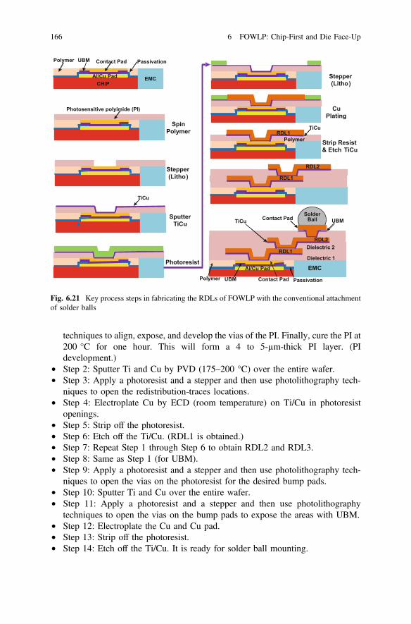
techniques to align, expose, and develop the vias of the PI. Finally, cure the PI at200 °C for one hour. This will form a 4 to 5-µm-thick PI layer. (PIdevelopment.)
• Step 2: Sputter Ti and Cu by PVD (175–200 °C) over the entire wafer.• Step 3: Apply a photoresist and a stepper and then use photolithography tech-
niques to open the redistribution-traces locations.• Step 4: Electroplate Cu by ECD (room temperature) on Ti/Cu in photoresist
openings.• Step 5: Strip off the photoresist.• Step 6: Etch off the Ti/Cu. (RDL1 is obtained.)• Step 7: Repeat Step 1 through Step 6 to obtain RDL2 and RDL3.• Step 8: Same as Step 1 (for UBM).• Step 9: Apply a photoresist and a stepper and then use photolithography tech-
niques to open the vias on the photoresist for the desired bump pads.• Step 10: Sputter Ti and Cu over the entire wafer.• Step 11: Apply a photoresist and a stepper and then use photolithography
techniques to open the vias on the bump pads to expose the areas with UBM.• Step 12: Electroplate the Cu and Cu pad.• Step 13: Strip off the photoresist.• Step 14: Etch off the Ti/Cu. It is ready for solder ball mounting.
CHIPEMCAl/Cu Pad
PassivationUBM Contact PadPolymer
Stepper (Litho)
Cu Plating
Strip Resist & Etch TiCu
RDL1Polymer
RDL2
RDL1
TiCu
Contact Pad UBM
Passivation
EMCCHIP
Cu Pad
Polymer UBM
RDL1
RDL2
Contact Pad
TiCu
Dielectric1
Dielectric2
Photosensitive polyimide (PI)
Spin Polymer
Stepper (Litho)
Sputter TiCu
Photoresist
TiCu
RDL2
RDL1
Solder Ball
Al/Cu Pad EMCDielectric 1
Dielectric 2
Fig. 6.21 Key process steps in fabricating the RDLs of FOWLP with the conventional attachmentof solder balls
166 6 FOWLP: Chip-First and Die Face-Up

The process steps in fabricating the RDLs for Fig. 6.4 with UBM-less Cu padare the same (from Step 1 through Step 7) as those for Fig. 6.3 with conventionalUBM/Cu pad, except Step 8 (same as Step 1) is for PI development as shown inFig. 6.22. It is ready for solder ball mounting. Step 9 through Step 14 are notneeded. From here on, only the case of UBM-less Cu pad for solder ball will beconsidered.
The thickness of DL1, DL2, and DL3 is 5 µm and that of DL4 is 10 µm. Thethickness of RDL1 and RDL2 is 3 µm and that of RDL3 is 7.5 µm. (The thickerRDL3 is for the UBM-less thicker Cu pads to “resist” the Cu consumption from thesolder ball reflow and during operation.)
The RDLs are shown in Figs. 6.23, 6.24 and 6.25. Overall, it can be seen that allthe RDLs are properly done. However, a closer look at the RDL1, based on the topview as well as cross-sectional measurements, the actual fabricated line width/spacing are (on average) 4.68 µm/5.30 µm. This means the line width is smallerthan it should be while the line spacing is larger than the design values (5 µm/5 µm). These errors could be due to (a) the small feature size of line width/spacing,(b) the photoresist opening, and (c) the seed layer (Ti) etching. For RDL2 andRDL3, they are very close to the designed values.
6.8.8 Solder Ball Mounting
There are two different stencils for the solder ball mounting, one is for stencilprinting the flux and the other is for stencil mounting the solder balls. The solder(Sn3 wt%Ag0.5 wt%Cu) balls (200 µm diameter) used are from indium and are on
Passivation
EMCCHIP
Cu Pad
Polymer UBM
RDL1
RDL2
Contact Pad
TiCu
Dielectric1
Dielectric2
Solder Ball
Fig. 6.22 Key process steps in fabricating the RDLs of FOWLP with UBM-less Cu pad for solderballs
6.8 Assembly on the Reconstituted Wafer 167

0.4 mm pitch. The peak temperature for solder reflow is 245 °C. Figure 6.26ashows the reflowed reconstituted wafer, Fig. 6.26b shows the individual package,and Fig. 6.26c shows the close-up view of solder balls on the package.
6.8.9 Debonding
The debonding of the glass carrier is by scanning a laser (355 nm DPSS Nd:YAG UV laser source is used) from the glass carrier side. The laser spot size is240 µm, the scanning speed is 500 mm/s and the scanning pitch is 100 µm. Whenthe LTHC layer “sees” the laser light, it converts into powders and the glass carrieris easily removed. It is followed by chemical cleaning. The DAF is remained on thebackside of the chip as shown in Fig. 6.27. The bottom side of the FOWLP isshown in Fig. 6.28. A cross section of the FOWLP is shown in Fig. 6.29 for theUBM-less case (Fig. 6.4).
EMC
(b)(a)
(c)
Fig. 6.23 a Before Cu revealing. b After Cu revealing and 2 RDLs. c Cross-section SEM imagesof RDL1 and RDL2
168 6 FOWLP: Chip-First and Die Face-Up

6.9 PCB Assembly of FOWLP
The design of the PCB and stencil will be briefly mentioned. The stencil solderpaste printing, pick and place, and solder reflow will also be presented. The x-rayimages and the cross-section images of the PCB assembly are provided.
6.9.1 PCB
The PCB for the fan-out wafer-level package is made of FR-4 and is shown inFig. 6.30. It can be seen that there are 4 package sites on the board. The dimensionsof the PCB are 103 mm � 52 mm � 0.65 mm and there are 6 layers. There are908 pads (with a pitch = 0.4 mm) for each package. The pad with a diameter= 0.2 mm is non-solder mask defined and its surface finish is OSP (organic sol-derability preservative). The solder mask opening diameter is 0.28 mm.
RDL1 RDL1RDL1RDL1
(a)
(b)
Fig. 6.24 a RDL1 (5 µm/5 µm line width/spacing). b SEM image of RDL1
6.9 PCB Assembly of FOWLP 169

6.9.2 Stencil and Printing
The stencil is made of stainless steel with a grain size of 2 µm and is 0.08 mmthick. The opening is fabricated by laser and electrical/chemical polishing. Theopening is increased from a 0.2286 mm diameter circle to a 0.2413 mm2 square(a paste volume increased by 41.8%). The SPI (solder paste inspection) data isshown in Fig. 6.31. It can be seen that slight more pastes are printed near the centralarea (Area 1). The solder paste printing is by the DEK Horizon 9.
Fig. 6.25 RDL2 (10 µm/10 µm line width/spacing)
170 6 FOWLP: Chip-First and Die Face-Up

Reconstituted wafer with packages (backside)
(a)
(c) (b)
Individual package Solder balls on package
Fig. 6.26 a Image of the fabricated reconstituted wafer. b Individual FOWLP package.c Close-up view of the solder balls
Die-attach film
EMC
Fig. 6.27 Reconstitutedwafer after laser debonding
6.9 PCB Assembly of FOWLP 171

6.9.3 Pick and Place and Reflow
The pick and place is by the SiPlace x4s. The 10 temperature zones BYU Pyramnitrogen 150N is used for the reflow of the solder paste. The temperature profile isshown in Fig. 6.32. It can be seen that the maximum temperature is 245 °C and thetime above 217 °C is 85 s (it meets the JSTD-020 standard). The PCB assembliesare shown in Figs. 6.33 and 6.34. Figure 6.33 shows the assembled PCB with 4packages and the x-ray image of one of the packages. It can be seen that thepackage is properly assembled. Figure 6.34 shows the cross section of one of thepackages and the solder joint height measurement. It can be seen that the solderjoint are properly made (no bridging and head-in-pillow) and the variation of solderjoints height is from 120 to 145 µm.
Package(13.42mm x 13.42mm)
Chip (10mm x 10mm)
Solder balls on package
Pads on package for TIV
Chip corner
RDLs
Pads on chip
Fig. 6.28 Individual package for the 10 mm � 10 mm chip
172 6 FOWLP: Chip-First and Die Face-Up

6.10 Thermal Performance of FOWLP
6.10.1 Structure
Figure 6.35a shows the top view and Fig. 6.35b shows the cross-sectional view ofthe FOWLP structure for thermal analyses [27]. It can be seen that the chip size is10 mm � 10 mm with various thicknesses (10, 25, 50, 100, 150, 200, 250, and300 lm). The molded package size is 13.42 mm � 13.42 mm, i.e., the package/chip area ratio = 1.8. There are a 100 lm EMC covering the top of the chip and40 lm-thick RDLs to fan-out the circuitry from the bottom of the chip. Thepackage is with 1024 (0.25 mm diameter) solder balls on a 0.4 mm pitch, which arereflowed on a PCB. The dimensions of the PCB are 25 mm � 25 mm � 0.8 mm.
6.10.2 Material Properties
Table 6.6 shows the thermal conductivity (W/m K) in cross-plane direction (kz) andin-plane direction (kxy) of the structural elements in Fig. 6.35. For Si, EMC, Cu,and solder, their kz and kxy are equal due to their homogeneous properties. For theRDL and PCB, they are assumed laminated materials in which there are several
Solder ball
RDL3 V23RDL2
CHIP
Contact-Pad
RDL1
VC1
V12
UBM-less Pad
Fig. 6.29 Cross-section image of the assembled fan-out wafer-level package with three RDLs
6.10 Thermal Performance of FOWLP 173

high conductive (Cu) layers inside the lamination, so their effective kxy is obviouslyhigher than their effective kz, as shown in Table 6.6.
6.10.3 Boundary Conditions
The ambient temperature is assumed to be 25 °C. The boundary condition on thetop side and bottom side of the PCB and the top side of the chip is with a convectiveheat-transfer coefficient, h = 10 W/m2 K, which is to imitate a natural convectioncondition. The heat dissipation of the chip is 5 W.
6.10.4 Finite-Element Modeling and Analysis
Figure 6.36 shows the finite element model for thermal analysis. It can be seen thatdue to double symmetries of the chip/package/PCB, only quarter of the structure ismodeled. For simplicity and the object of the present study, only steady-stateheat-transfer analyses are performed.
103
52
46.5
93
40
98
Units: mm
OSP PCB for package
Pad
Thickness: 0.65mmMaterial: FR-4 Size: 103mm x 52mmLayer: 6Pad finish: OSP
0.28 0.2
0.20.28
Solder mask opening
Fig. 6.30 PCB for package assembly and reliability tests
174 6 FOWLP: Chip-First and Die Face-Up

6.10.5 Analysis Results
The junction-to-ambient thermal resistance (Rja) of the 10 mm � 10 mm chip withvarious thicknesses is shown in Fig. 6.37. It can be seen that the thinner the chip thehigher the Rja (i.e., the lower the thermal performance). This is because of theinferior thermal spreading capability of thinner chips. The thermal performancedegrades rapidly as the chip thickness goes below 100 lm, as shown in Fig. 6.37.
Area 1 Area 2
Fig. 6.31 Solder paste SPI
Tem
pera
ture
(oC
)
Time (s)
Maximum temperature = 245oC; Time above 217oC = 85s
Fig. 6.32 Temperature profile for solder reflow with nitrogen
6.10 Thermal Performance of FOWLP 175

PCB
Fan-out package
Chip
Solder ballsSolder balls
Chip Underfill Void EMC
PCB
Solder Joint(a)
(b) (d)(c)
Fig. 6.33 X-ray images for the PCB-assembled package
Sold
er jo
int h
eigh
t (µm
)
Package diagonal posi ons
Chip
Solder jointsVIP PCB
3RDLs
Chip
3RDLs
VIP PCB
Solder joints
Fig. 6.34 Cross sections of PCB-assembled package
176 6 FOWLP: Chip-First and Die Face-Up

Figure 6.38 shows a typical temperature contour distribution of a FOWLP (chipsizes are 10 mm � 10 mm � 150 lm, and package sizes are 13.42 mm � 13.42mm � 290 lm). It can be seen that (1) the maximum temperature is 101.5 °C;(2) the minimum temperature is 89.9 °C; and (3) the Rja is 15.3 °C/W.
25mmx25mmx0.8mm
32x32 solder balls (0.25mm-diameter)
at 0.4mm pitch
Chip thickness (µm):10, 25, 50, 100, 150, 200, 250, 300
10-layer PCB
13.42mm
13.4
2mm Chip
(5W)
100µm
40µm3RDLs
10mm
10m
mChip
EMC
(a)
(b)
Ta
Tj
Fig. 6.35 Structure of the FOWLP assembly for thermal analyses. a Top view. b Cross-sectionalview
Table 6.6 Materialproperties of the packagestructure for thermal analysis
Material Thermal conductivity (W/m/K)
Si 148
EMC 0.25
Cu 400
Solder 40
RDL Kxy = 25.2 Kz = 0.29
PCB Kxy = 27.4 Kz = 0.35
6.10 Thermal Performance of FOWLP 177

6.11 Reliability Assessments—Thermal Cycling Test
6.11.1 Test Setup
Fifteen boards (each with 4 packages) are used for the temperature cycling tests[32]. The sample size is 60 packages. Thermal cycling is performed in a Votsch7027-15 environmental chamber. This unit is capable of achieving chamber tem-perature as high as 190 °C and as low as −70 °C. Heating and cooling are achievedby forced convection, and the maximum ramp rate is 15 °C per minute. All of theboards are placed vertically in the chamber as shown in Fig. 6.39. The temperatureinput to the chamber (measured in the air of the chamber) is shown in Fig. 6.39. Itcan be seen that the temperature cycling is from room temperature to 85 °C and staythere for 15 min, then ramp down to −40 °C and stay there for 15 min, then rampup to 85 °C and stay there for 15 min, and so for. The ramp up and ramp downtimes are 15 min each. The acquisition system is an Agilent 30970A data logger.
Fig. 6.36 Quarter finiteelement model for thermalanalyses
178 6 FOWLP: Chip-First and Die Face-Up

Rja (Junction-to-ambient thermal resistance)
Chip Thickness (µm)
Rja
(oC
/W)
Fig. 6.37 Junction-to-ambient thermal resistance versus various chip thickness
Chip thickness = 150µm; Power = 5WMax, temperature = 101.5oC Min. temperature = 89.9oC
Fig. 6.38 Typicaltemperature contourdistribution of a FOWLPassembly
6.11 Reliability Assessments—Thermal Cycling Test 179

6.11.2 Test Results
The thermal cycling test results of the FOWLP solder joint (without underfill)reliability are shown in Fig. 6.40. The thermal cycling test stops at 1100 cycles andthere are 14 failures (including one early failed at 58 cycles). It can be seen that thecharacteristic life (63.2% failed) of the Weibull plot is 2382 cycles which is morethan adequate for the expecting life (usually is less than 3 years) of mobile productsuch as the smartphones and tablets.
6.12 Reliability Assessments—Drop Test
6.12.1 Test Setup
The test setup is according to JEDEC Standard JESD22-B111 as shown inFig. 6.41. After more than 20 tries, the right height of the drop table is obtainedwhich yields the drop spectrum with 1500 G/ms as shown in Fig. 6.42 [32].
Fig. 6.39 Thermal cycling test setup and temperature profile
180 6 FOWLP: Chip-First and Die Face-Up

100.00 3000.001000.001.00
5.00
10.00
50.00
80.00
Solder Joint Reliability (without underfill)
Cycles-to-failure
Perc
ent f
aile
d
Characteristic life = 2382 cycles
Fig. 6.40 Weibull plot of the package solder joint under thermal cycling test
Guide Rods
Base Plate
Drop Table
Strike Surface
Rigid Base
Drop Table
Base Plate
StandoffsPCB Assembly
Accelerometer
Drop Test Setup
Fig. 6.41 Drop test setup
6.12 Reliability Assessments—Drop Test 181

6.12.2 Test Results
The drop condition is 1000 drops. There are 24 samples. The ones without underfillfailed very early and the failure mode is the broken of the first RDL near the solderjoint as shown in Fig. 6.43.
Another 24 PCB assemblies (samples) are underfilled. The material properties ofthe underfill are: the filler content = 25%, the maximum filler size = 5 µm, theaverage filler size = 1–2 µm, the curing time and curing temperature = 8 min @135 °C or 5 min @ 150 °C. The Young’s modulus, Poisson’s ratio, and CTE are,respectively, 4–5 GPa, 0.35, and 50–52 � 10−6/°C. The drop condition is also1000 drops. The results are shown in Fig. 6.44. It can be seen that the characteristiclife of the Weibull plot of the solder joint under drop test is 1187 drops and all 24samples passed 500 drops without failure. The failure modes after 550 drips areshown in Fig. 6.45. It can be seen that the RDLs are broken. In this case, the EMCalso has cracks. However, the solder joint is not failed.
0 0.1 0.2 0.3 0.4 0.5 0.6 0.7 0.8 0.9 1.0 1.1 1.2 1.3 1.4 1.5 1.6 1.7 1.8 TIME (ms)
1500
1400
1300120011001000
900800
700600500
400300200100
0
-200- 100
1500G/ms
ACCE
LERA
TIO
N (g
)
Fig. 6.42 Drop test spectrum
182 6 FOWLP: Chip-First and Die Face-Up

6.13 Simulation on Thermal Cycling
(A) The Structure and Boundary ConditionsThe PCB assembly of the fan-out wafer-level package shown in Figs. 6.33 and 6.34is modeled as a three-dimensional strip that captures the construction along adiagonal path from the assembly’s geometry center to a corner (Fig. 6.46). Due tothe symmetry about the vertical midplane of a full strip, the model is actually ahalf-strip with the appropriate in-plane restraints placed on one symmetry plane.Coupled in-plane translations are applied to the other symmetry plane to produce astate of generalized plane strain. Using exclusively hexahedral solid elements, themodel can capture the precise shape of the packages’ solder joint and potential DNP(distance to neutral point) effects while retaining significant computational effi-ciency over full octant models.
Fig. 6.43 Failure modes (broken) of the RDL1 near the solder joint
6.13 Simulation on Thermal Cycling 183

Despite the overall economy of elements in the strip model, selective meshrefinement is used to concentrate highly refined elements in the solder joints wherefailure is anticipated. In the present PCB assembly, failure would be predicted in thesolder joints with the greatest DNP (the package corner) and near the chip cornersas shown in Fig. 6.46. Thus, highly refined meshes are applied to these two solderjoints. The other solder joints are coarsely meshed. The C3D8R element ofABAQUS is used for the model.
(B) Material Properties for Thermal CyclingThe material properties of the PCB assembly shown in Figs. 6.33 and 6.34 areshown in Table 6.7. All the material properties are assumed to be constant exceptfor those of solder. The Sn3 wt% Ag0.5 wt%Cu is assumed to follow the gener-alized Garofalo creep equation:
dedt
¼ 500000 sin h5 r� 10�8� �exp
�5807TðKÞ
� �
where e is the strain, r is the stress in Pa, and K is the Kelvin.
300 150010001.00
5.00
10.00
50.00
70.00
Number of Drops
Perc
ent F
aile
d
Characteristic Life = 1187 DropsRDL Drop Reliability Fig. 6.44 Weibull plot of the
package RDL/solder jointunder drop test
184 6 FOWLP: Chip-First and Die Face-Up

RDL2
RDL3
RDL2
RDL3 Broken
ChipPackage
EMC
EMC
Solder Joint
PCB
PCB VIP
EMC Crack
RDL1
Fig. 6.45 PCB assembly for failure analysis (after 550 drops). Failure modes showing RDLsbroken and EMC cracking
Fig. 6.46 The 3D strip model for thermal analysis
6.13 Simulation on Thermal Cycling 185

(C) Temperature Boundary ConditionThe temperature profile shown in Fig. 6.39 is to be imposed on the PCB assembly.Five temperature cycles are executed.
(D) Thermal Cycling Simulation ResultsFigure 6.47 shows the shear stress and creep shear strain hysteresis loops at thesolder joint under the chip corner. It can be seen that after three cycles, the creepresponses converged (become stabilized). The maximum Mises stress occurs at thesolder joints near the chip corner and the package corner as shown in Fig. 6.48. Thelocation is at the interface between the bottom of the package and the bulk solder.The maximum Mises stress occurs at –40 °C during the thermal cycling conditionshown in Fig. 6.39. The deformed shape of the strip model at –40 °C is shown inFig. 6.49.
The accumulated creep strain versus time is shown in Fig. 6.50. It can be seenthat the creep strain per cycle is equal to 0.0084, which is too small to create solderjoint reliability problem, especially for mobile products such as smartphones, whoselife is less than 3 years.
Table 6.7 Material properties for thermal cycling modeling
CTE (ppm/°C) Young’s Modulus (GPa) Poison’s ratio
Copper 16.3 121 0.34
PCB a1 = 18, a2 = 18, a3 = 70 E1 = 22, E2 = 22, E3 = 10 0.28
Silicon 2.8 131 0.278
Solder 21.3 + 0.017T 49 – 0.07T 0.3
Polyimide 35 3.3 0.3
EMC 10(<150 °C) 19 0.25
Shea
r str
ess
(MPa
)ain
Creep shear strain
Fig. 6.47 Shear stress and creep shear strain hysteresis loops
186 6 FOWLP: Chip-First and Die Face-Up

6.14 Simulation on Shock (Drop)
(A) Structure and Boundary ConditionsThe finite element model for drop test is shown in Fig. 6.51. It can be seen thatone-fourth of the PCB assembly is modeled. For simplicity, there is only onepackage at the center of the PCB and the package is subjected to the accelerationshown in Fig. 6.42.
During impact, the most likely failure location is near the corner solder joints ofthe package and the most likely failure mode is the broken Cu wire in the RDLs andbroken Cu trace in the PCB. Thus, finer meshes are applied to the Cu wire of RDLsand Cu trace of PCB near the corner solder joints of the package as shown inFig. 6.52.
(B) Material Properties for DropThe material properties for drop analysis are shown in Table 6.8. Since the focus ofthis analysis is not on the solder joint, all the materials are assumed to be constant.Since the ABAQUS explicit solver is applied for the simulation. Thus, the dampingeffect is included through the bulk viscosity method in ABAQUS explicit solver.The bulk viscosity introduces damping associated with the volumetric straining. Thedamping coefficients b1 and b2 applied in the analysis are respectively, 0.02 and 0.
Fig. 6.48 Maximum accumulated creep strain
6.14 Simulation on Shock (Drop) 187

Time (min)
Acc
umul
ated
Cre
ep S
trai
n
Creep Strain per cycle = 0.0084
Fig. 6.50 Accumulated creep strain versus time
Bending shape of the slice model @-40˚C (scale factor:10)Max. Mises equivalent stress occurred at die corner solder joint @-40˚C.
Unit: Pa
Die corner solder joint
Package corner solder joint
Max. Mises stress
Fig. 6.49 (Top) Maximum Mises stress at chip corner and package corner solder joints at −40 °C.(Bottom) The deformed shape of the quarter structure at −40 °C
188 6 FOWLP: Chip-First and Die Face-Up

(C) Drop Simulation ResultsThe applied acceleration is shown in Figs. 6.42 and 6.51. The time step for thecalculation is 1 � 10–8 s. The time histories of strain in the x–direction, e11(Fig. 6.51) and maximum principal strain acting at the RDL of the package cornerare shown in Fig. 6.53. Basically, they behave the same, i.e., the strain is dominatedin the x–direction. The maximum deflection of the PCB assembly occurs near the0.0023 s (Fig. 6.53) and is shown in Fig. 6.52(b). The maximum principal strain =0.0045 occurs also at that time. The deflection and strains are decreasing with timedue to the damping of the structure as shown in Fig. 6.53.
The maximum Mises stress occurs at the same location (at the Cu wiring of RDLnear the package corner) as the maximum principal strain as shown in Fig. 6.54 andis equals to 7.724 � 108 Pa, which occurs at 0.0023 s. Thus, any failure shouldoccur at this location. This demonstrates the failure mode that the RDL is brokenafter > 550 drops during the drop test.
x
y z
PCB
EMC
Die
PI
EMC Die
Schematic for model
RDLSolder
PCBCu traceUnderfill
Fig. 6.51 Quarter model for drop analysis and boundary conditions
6.14 Simulation on Shock (Drop) 189

Package cornerSolder joint
Die corner solder joint
Finer meshed critical joints
RDL
Solder
Cu trace on PCB
Cu trace on
package
(a)
(b)
Fig. 6.52 a Mesh at corner solder joint, RDL on package, and Cu trace on PCB. b Deformedshape of the quarter of PCB assembly
Table 6.8 Material properties for drop modeling
Density (Kg/m3) Young’s Modulus (GPa) Poison’s ratio
Copper 8954 121 0.34
PCB 1800 E1 = 22, E2 = 22, E3 = 10 0.28
Silicon 2330 131 0.278
Solder 7400 49 0.30
Underfill 1560 4.5 0.3
Polyimide 1420 3.3 0.3
EMC 1960 19 0.25
190 6 FOWLP: Chip-First and Die Face-Up

Fig. 6.54 Maximum Mises stress occurs at the RDL of the package
Time (s)
Acc
eler
atio
n (G
)
Mic
rost
rain
Max. principal strain
Fig. 6.53 The applied acceleration. The time-history maximum principal strain and e11 at theRDL of the package
6.14 Simulation on Shock (Drop) 191

6.15 Summary and Recommendations
The design, materials, process, fabrication, and reliability of FOWLP with chip-firstand die face-up method have been investigated in this chapter. The lessons learnedfrom the problems and solutions have also been provided. Some important resultsand recommendations are summarized in the following.
• A test package, 13.42 mm � 13.42 mm, (with a package/chip ratio = 1.8 and achip-top EMC cap = 100 lm) has been designed and fabricated. This testpackage has three RDLs; the line width/spacing of the first RDL is 5 lm/5 lm,of the second RDL is 10 lm/10 lm, and of the third RDL is 15 lm/15 lm.
• DAF helps! There is not any die shift issue for chip-first with die face-upFOWLP.
• The price must pay is to do the P&P pitch compensation due to the thermalexpansion mismatch between the silicon chip and the glass carrier wafer duringthe heating of the DAF (both bond-head and the bond-stage tempera-ture = 120 °C with the bond force of 2.0 kg for 2 s).
• For liquid EMC dispensing, in order to reduce the area and length of flow marks,the line pattern is recommended.
• Remove trap air before compression molding is a must and the optimal con-ditions are: temperature = 125 °C, time = 2 min, and pressure = 45 kg/cm2.The PMC is at 150 °C for � 1 h, and a dead weight = 15 kg for a betterwarpage control.
• For the present study, in order to have theminimumwarpage (� 0.3 mm), the glassthickness is 1 mm and the glass thermal expansion coefficient is 8 � 10−6/°C.
• During Cu revealing (backgrinding of the EMC to expose the Cu contact pads),there are Cu smears for the short (5 µm) polyimide and there is not any Cusmear for the tall (*30 µm) polyimide.
• Reliability thermal cycling test of a sample size of 60 package assemblies showsthat the characteristic life is more than 2380 cycles, which is adequate for mostapplications of mobile products such as smartphones and tablets.
• Reliability drop test of a sample size of 24 package assemblies with underfillshows that all the samples passed 500 drops and the characteristic life is morethan 1187 drops, which is adequate for most applications of mobile productssuch as smartphones and tablets.
References
1. Lau, J.H., C. Wong, J. Price, and W. Nakayama. 1998. Electronic Packaging. New York:McGraw-Hill Book Company.
2. Kauffman, J.E. 1969. Method of Packaging Integrated Circuits. US Patent 3,436,810, Filed onJuly 17, 1967, Patented on April 8, 1969.
192 6 FOWLP: Chip-First and Die Face-Up

3. Lin, P.T., M.B. McShane, and H.P. Wilson. 1993. Semiconductor Device Having a Pad ArrayCarrier Package. US Patent 5,216,278, Filed on March 2, 1992, Patented on June 1, 1993.
4. Elenius, P., and H. Hollack. 2001. Method for Forming Chip Scale Package. US Patent6,287,893, Filed on July 13, 1998, Patented on September 11, 2001.
5. Lau, J.H., and R.S.-W. Lee. 1999. Chip Scale Package. New York: McGraw-Hill BookCompany.
6. Hedler, H., T. Meyer, and B. Vasquez. 2004. Transfer Wafer Level Packaging. US Patent6,727,576, Filed on October 31, 2001, Patented on April 27, 2004.
7. Brunnbauer, M., et al. 2006. An Embedded Device Technology Based on a MoldedReconfigured Wafer. In Proceedings of IEEE/ECTC, May 2006, 547–551.
8. Meyer, T., G. Ofner, S. Bradl, M. Brunnbauer, and R. Hagen. 2006. Embedded Wafer LevelBall Grid Array (eWLB). In Proceedings of IEEE/EPTC, December 2006, W.1–5.
9. Lau, J.H. 2016. Patent Issues of Embedded Fan-Out Wafer/Panel Level Packaging. InProceedings of IEEE/Semiconductor Technology International Conference,March 2016, 1–7.
10. Lau, J.H. 2013. Through-Silicon Via (TSV) for 3D Integration. New York: McGraw-HillBook Company.
11. Lau, J.H. 2016. 3D IC Integration and Packaging. New York: McGraw-Hill Book Company.12. Lau, J.H., N. Fan, and M. Li. 2016. Design, Material, Process, and Equipment of Embedded
Fan-Out Wafer/Panel-Level Packaging. Chip Scale Review 20: 38–44.13. Kurita, Y., T. Kimura, K. Shibuya, H. Kobayashi, F. Kawashiro, N. Motohashi, and
M. Kawano. 2010. Fan-Out Wafer-Level Packaging with Highly Flexible Design Capabilities.In IEEE/ESTC Proceedings, 2010, 1–6.
14. Motohashi, N., T. Kimura, K. Mineo, Y. Yamada, T. Nishiyama, K. Shibuya, H. Kobayashi,Y. Kurita, and M. Kawano. 2011. System in Wafer-Level Package Technology withRDL-First Process. In IEEE/ECTC Proceedings, 2011, 59–64.
15. Brunnbauer, M., E. Furgut, G. Beer, T. Meyer, H. Hedler, J. Belonio, E. Nomura, K. Kiuchi,and K. Kobayashi. 2006. An Embedded Device Technology Based on a MoldedReconfigured Wafer. In IEEE/ECTC Proceedings, 2006, 547–551.
16. Brunnbauer, M., E. Furgut, G. Beer, and T. Meyer. 2006. Embedded Wafer Level Ball GridArray (eWLB). In IEEE/EPTC Proceedings, 2006, 1–5.
17. Keser, B., C. Amrine, T. Duong, O. Fay, S. Hayes, G. Leal, W. Lytle, D. Mitchell, andR. Wenzel. 2007. The Redistributed Chip Package: A Breakthrough for Advanced Packaging.In Proceedings of IEEE/ECTC, 2007, 286–291.
18. Yoon, S., J. Caparas, Y. Lin, and P. Marimuthu. 2012. Advanced Low Profile PoP Solutionwith Embedded Wafer Level PoP (eWLB-PoP) Technology. In IEEE/ECTC Proceedings,2012, 1250–1254.
19. Yoon, S., P. Tang, R. Emigh, Y. Lin, P. Marimuthu, and R. Pendse. 2013. Fanout FlipchipeWLB (Embedded Wafer Level Ball Grid Array) Technology as 2.5D Packaging Solutions.In IEEE/ECTC Proceedings, 2013, 1855–1860.
20. Braun, T., K.-F. Becker, S. Voges, J. Bauer, R. Kahle, V. Bader, T. Thomas,R. Aschenbrenner, and K.-D. Lang. 2014. 24”�18” Fan-out Panel Level Packing. InIEEE/ECTC Proceedings, 2014, 940–946.
21. Sharma, G., S. Vempati, A. Kumar, N. Su, Y. Lim, K. Houe, S. Lim, V. Sekhar, R. Rajoo,V. Kripesh, and J.H. Lau. 2011. Embedded Wafer Level Packages with Laterally Placed andVertically Stacked Thin Dies. In IEEE/ECTC Proceedings, 2009, 1537–1543. Also, IEEETransactions on CPMT 1 (5): 52–59.
22. Lim, Y., S. Vempati, N. Su, X. Xiao, J. Zhou, A. Kumar, P. Thaw, S. Gaurav, T. Lim, S. Liu,V. Kripesh, and J.H. Lau. 2010. Demonstration of High Quality and Low Loss Millimeter WavePassives on Embedded Wafer Level Packaging Platform (EMWLP). In IEEE/ECTCProceedings, 2009, 508–515. Also, IEEE Transactions on Advanced Packaging 33: 1061–1071.
23. Yu, D. 2014. Wafer-Level-System-Integration (WLSI) Technologies for 2D and 3DSystem-in-Package. In SEMIEUROPE 2014.
References 193

24. Lin, J.C., J.P. Hung, N.W. Liu, Y.C. Mao, W.T. Shih, and T.H. Tung. 2015. PackagedSemiconductor Device with a Molding Compound and a Method of Forming the Same. USPatent 9,000,584, Filed on December 28, 2011, Patented on April 7, 2015.
25. Tseng, C., C. Liu, C. Wu, D. Yu. 2016. InFO (Wafer Level Integrated Fan-Out) Technology.In IEEE/ECTC Proceedings, 2016, 1–6.
26. Hsieh, C., C. Wu, and D. Yu. 2016. Analysis and Comparison of Thermal Performance ofAdvanced Packaging Technologies for State-of-the-Art Mobile Applications. In IEEE/ECTCProceedings, 2016, 1430–1438.
27. Lau, J.H., M. Li, D. Tian, N. Fan, E. Kuah, K. Wu, M. Li, J. Hao, Y. Cheung, Z. Li, K. Tan,R. Beica, T. Taylor, C.T. Lo, H. Yang, Y. Chen, S. Lim, N.C. Lee, J. Ran, X. Cao, S. Koh,and Q. Young. 2017. Warpage and Thermal Characterization of Fan-Out Wafer-LevelPackaging. In IEEE/ECTC Proceedings, 2017, 595–602. Also, IEEE Transactions on CPMT7 (10): 1729–1938 (October 2017).
28. Lau, J.H., M. Li, N. Fan, E. Kuah, Z. Li, K. Tan, T. Chen, et al. 2017. Fan-Out Wafer-LevelPackaging (FOWLP) of Large Chip with Multiple Redistribution-Layers (RDLs). In IMAPSProceedings, October 2017, 576–583. Also, IMAPS Transactions. Journal ofMicroelectronics and Electronic Packaging 123–131 (October 2017).
29. M. Li, Q. Li, J.H. Lau, N. Fan, E. Kuah, K. Wu, et al. 2017. Characterizations of Fan-OutWafer-Level Packaging. In IMAPS Proceedings, October 2017, 557–562.
30. Hua, X., H. Xu, Z. Li Zhang, D. Chen, K. Tan, J.H. Lau, et al. 2017. Development ofChip-First and Die-Up Fan-Out Wafer-Level Packaging. In IEEE/EPTC Proceedings,December 2017, S23_1-6.
31. Lau, J.H., M. Li, M. Li, I. Xu, T. Chen, Z. Li, K. Tan, et al. 2018. Design, Materials, Process,Fabrication, and Reliability of Fan-Out Wafer-Level Packaging. To be published in IEEETransactions on CPMT.
32. Lau, J.H., M. Li, Y. Lei, M. Li, X. Qing, C. Zhong, et al. 2018. Reliability of Fan-OutWafer-Level Packaging (FOWLP) with Large Chips and Multiple Re-Distributed Layers(RDLs). In IEEE/ECTC Proceedings, May 2018.
194 6 FOWLP: Chip-First and Die Face-Up

Chapter 7FOWLP: Chip-Last or RDL-First
7.1 Introduction
Since 2006, NEC Electronics Corporation (now Renesas Electronics Corporation)has been developing a novel SMAFTI (SMArt chip connection with feedthroughinterposer) packaging technology for inter-chip wideband data transfer [1, 2], 3Dstacked memory integrated on logic devices [3–7], system in wafer-level package(SiWLP) [8], and “RDL-first” fan-out wafer-level packaging [9]. The feedthroughinterposer (FTI) used in SMAFTI is a film with ultrafine line width and spacingRDLs. The dielectric of the FTI is usually SiO2 or a polymer, and the conductorwiring of the RDLs (redistribution-layers) is Cu. The FTI not only supports theRDLs underneath within the chip but it also provides support beyond the edges ofthe chip. Area array solder balls are mounted at the bottom side of the FTI, whichare to be connected to the PCB. EMC is used to embed the chip and support theRDLs and solder balls [10].
In 2015, Amkor announced a very similar RDL-first technology called SWIFT™(silicon wafer integrated fan-out technology) [11]. In 2016, IME presented the largemultichip RDL-first FOWLP (fan-out wafer-level packaging) on printed circuitboard (PCB) [12, 13]. In 2016, SPIL demonstrated the first hybrid integration of thefine line plasma-enhanced chemical vapor deposition (PECVD) RDL and the RDLwith polymeric dielectrics [14]. In 2017, Amkor announced a very similar hybridRDLs for their SLIM™ (Silicon-Less Integrated Module) [15, 16]. In this chapter,the RDL-first or chip-last FOWLP process and the hybrid RDLs will be discussed.The reasons for chip-last or RDL-first will be briefly mentioned first.
© Springer Nature Singapore Pte Ltd. 2018J. H. Lau, Fan-Out Wafer-Level Packaging,https://doi.org/10.1007/978-981-10-8884-1_7
195

7.2 Reasons for Chip-Last or RDL-First FOWLP
According to [8, 9], one of the challenges of chip-first FOWLP (Chaps. 5 and 6)and the key reasons for them to introduce the chip-last or RDL-first FOWLP is theproduction yield during the RDL process is low because the KGDs are alreadyembedded. This is true only if the chip-last (RDL-first) FTI is fully functionallytested before the chip-to-wafer bonding. Otherwise, the KGDs still have to bethrown away for the case of an FTI with bad RDLs after a system test. Also, itshould be noted that fully functionally tests of RDLs on an FTI are not only verycostly but very difficult, if not possible [10].
7.3 Methods for Chip-Last or RDL-First FOWLP
There are at least three methods for making the chip-last (RDL-first) FOWLP. Oneis by using PECVD to make the SiO2 dielectric layer and Cu damascene + CMP(chemical mechanical polishing) to make the conductor layer of all the RDLs, e.g.,[10]. One is by using the polymer to make the dielectric layer and Cu plat-ing + etching to make the conductor layer for all the RDLs, e.g., [12, 13]. The thirdone is by using PECVD and Cu damascene + CMP to make the first fine line widthand spacing RDL and then using the polymer to make the dielectric layer and Cuplating + etching to make the conductor layer for the rest of not so fine line widthand spacing RDLs [14–16]. The last one is also called hybrid RDLs [14]. All thesethree methods will be discussed in the followings.
7.4 Chip-Last (RDL-First) by PECVD and CuDamascene + CMP
7.4.1 Key Process Flow
Figure 7.1 shows the process flow of the chip-last with face-down or “RDL-first”FOWLP. This is very different from the chip-first FOWLP discussed in Chaps. 5and 6. First of all, this only works on a wafer carrier. Also, RDL-first FOWLPrequires (1) building up the RDLs on a bare silicon wafer (the FTI); (2) performingthe wafer bumping; (3) performing the fluxing, chip-to-wafer bonding, and clean-ing; and (4) performing the underfill dispensing and curing. As to wafer bumping,chip-to-wafer bonding and underfilling, please see Chap. 2 and [17]. Each of thesetasks is a major undertaking and requires additional materials, process, equipment,manufacturing floor space, and personal effort. Therefore, compared to chip-firstFOWLP, chip-last (RDL-first) FOWLP incurs very high cost and has a higher
196 7 FOWLP: Chip-Last or RDL-First

probability of greater yield losses. It can only be afforded by very high-density andperformance applications such as high-end servers and computers.
The very first step in RDL-first is to build the RDLs on a bare silicon wafer,which will be detailed later. On the device wafer, the first step is to perform waferbumping as shown in Sect. 2.2. The next step is to test for KGDs and then dice thewafer into individual KGDs as shown in the left-hand side Fig. 7.1. Next, theKGDs are picked up, flux is applied, and then the KGDs are placed face-down onthe contact pad (which is on top of the RDLs) of the full-thickness silicon waferprior to performing chip-to-wafer bonding. That step is followed by cleaning theflux residue and then dispensing the underfill and curing. Next comes molding thewhole reconstituted wafer carrier using the compression method with EMC (epoxymolding compound). Then, backgrinding is done to remove the silicon carrier.(Another way is to backgrind the EMC to expose the backside of the KGDs, whichare attached to a metal-reinforced wafer, and then backgrinding is done to removethe silicon carrier as shown in Fig. 7.1). Finally, the solder balls are mounted on thebottom RDL and the reconstituted wafer is diced into individual packages.
Build RDLs on a bare Si-wafer
RDLs
Device Wafer
After wafer bumping, test for KGDs and dice the wafer
CHIPPassivation
UBM
Al or Cu Pad
Contact pad
Cu-pillar plating
Cu-Pillar
Solder-cap plating
Solder cap
Cu-Pillar
Contact pad
Contact pad
CHIP
Mount solder ball and dice molded wafer
Fluxing, Chip-to-wafer bonding, and cleaning
Underfill dispensing and curing
Backgrind EMC to expose the backside of the KGDs and attach to a reinforced wafer, then
backgrind the Si-wafer
Underfill
Molding the reconfigured wafer
EMC
RDLSolder ball
Solder joint
Cu-pillarUnderfill
EMC
KGDKGD
SolderKGD KGD
Cu
Metal reinforced wafer
Heat spreader
Si-wafer
Fig. 7.1 Chip-last (RDL-first) FOWLP key process steps
7.4 Chip-Last (RDL-First) by PECVD and Cu Damascene + CMP 197

7.4.2 RDLs by PECVD and Cu Damascene + CMP
Figure 7.2 shows the process flow of fabricating very fine line width/spacing(<5 lm) RDLs for chip-last (RDL-first) FOWLP. First, use PECVD to form a thinlayer of SiO2 (or SiN) on a full-thickness bare silicon wafer and then use a spincoater to laminate the photoresist. These steps are followed by using a stepper toopen up the resist and a reactive ion etch (RIE) to remove the SiO2. Then, a stepperis used to open the resist wider and RIE to etch more of the SiO2. Next, strip off theresist, sputter the TiCu, and electrochemical deposition (ECD) the Cu on the wholewafer. These steps are followed by chemical mechanical polishing (CMP) toremove the overburden Cu and the TiCu, and then we have the first RDL1 and V01(the via connecting the Si and RDL1) as shown in Fig. 7.2. This is called the dualCu damascene method [18, 19]. Repeat all the processes to get the second RDL2,the third RDL3, and so forth. V12 is the via connecting RDL1 and RDL2.Figure 7.3 shows an example of fabricated RDLs by the dual Cu damascene method[18, 19]. It can be seen that there are three RDLs and on top of RDL3, there are aUBM and a Cu contact pad; the contact pad is to be connected to the microbump forchip-to-wafer bonding.
Si wafer
SiO2 by PECVD
SiO2
Spin coat Photoresist
Stepper, Litho.
RIE of SiO2
Stepper, Litho.
RIE of SiO2
Strip resist, sputter Ti/Cu, and Cu damascene
CMP the overburden Cu and Ti/Cu, get RDL1
RDL1
RDL2
RDL1V01
V12
Si wafer
DL1
DL2DL12
DL01
Repeat the processes to get RDL2
TiCu
V01
Fig. 7.2 Key process steps of RDLs by PECVD and dual Cu damascene + CMP method
198 7 FOWLP: Chip-Last or RDL-First

7.4.3 UBM/Cu Contact Pad/Solder Ball
After fluxing, chip-to-wafer bonding, cleaning, underfill dispensing and curing, andmolding, it is time to remove the silicon bare wafer and attach the solder balls.Figure 7.4 shows the process flow. The steps are as follows: (1) backgrind thesilicon wafer to a few microns from the via (V01), (2) then use CMP on the siliconwafer, and then (3) TiCu and passivation to expose the Cu of V01. These steps arefollowed by (4) PECVD to form a SiO2 layer and then (5) spin coating a pho-toresist. Then, (6) use a stepper to open the resist and an RIE to remove the SiO2,and then (7) strip off the resist. It is followed by sputtering the Ti/Cu and elec-troplating the Cu. Then, (8) CMP the overburden Cu and TiCu and obtain the UBMand Cu contact pad. Finally, (9) mount the solder balls on the Cu contact pads asshown in Fig. 7.4.
V01RDL1
RDL2RDL3
V12
V23
Contact PadUBM
Si wafer
Fig. 7.3 SEM image of RDLs by PECVD and dual Cu damascene + CMP method
7.4 Chip-Last (RDL-First) by PECVD and Cu Damascene + CMP 199

7.5 Chip-Last (RDL-First) by Polymer and CuPlating + Etching
7.5.1 Key Process Steps
Figure 7.5 shows the key process steps for chip-last (RDL-first) by polymer and Cuplating + etching. It can be seen that wafer bumping of the Cu pillar and solder capis a must (the left-hand side of Fig. 7.5). The RDLs are built on a glass carriercoated with a sacrificial layer (Sect. 7.5.2). It is followed by fluxing, chip-to-waferbonding, cleaning, and underfill dispensing and curing. Then, mold the reconsti-tuted wafer with EMC by compression method. It is following by laser debondingto remove glass carrier and solder ball mounting as shown in the right-hand side ofFig. 7.5.
Stepper, Litho.
RIE of SiO2
Backgrind and then CMP the Si wafer, TiCu, and passivation
SiO2 by PECVD
Spin coat photoresist
V01 RDL1
RDL2V12
RDL2RDL1
V01V12
Si wafer Strip resist
Sputter Ti/Cu
ECD Cu
Solder ball
CMP Cu and TiCu
Solder ball mounting
Cu-Contact padUBM
Passivation
RDL2V12
V01 RDL1
Fig. 7.4 Silicon wafer removal and solder ball mounting
200 7 FOWLP: Chip-Last or RDL-First
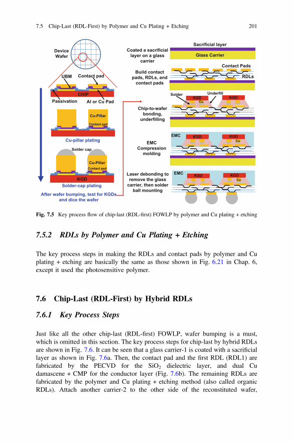
7.5.2 RDLs by Polymer and Cu Plating + Etching
The key process steps in making the RDLs and contact pads by polymer and Cuplating + etching are basically the same as those shown in Fig. 6.21 in Chap. 6,except it used the photosensitive polymer.
7.6 Chip-Last (RDL-First) by Hybrid RDLs
7.6.1 Key Process Steps
Just like all the other chip-last (RDL-first) FOWLP, wafer bumping is a must,which is omitted in this section. The key process steps for chip-last by hybrid RDLsare shown in Fig. 7.6. It can be seen that a glass carrier-1 is coated with a sacrificiallayer as shown in Fig. 7.6a. Then, the contact pad and the first RDL (RDL1) arefabricated by the PECVD for the SiO2 dielectric layer, and dual Cudamascene + CMP for the conductor layer (Fig. 7.6b). The remaining RDLs arefabricated by the polymer and Cu plating + etching method (also called organicRDLs). Attach another carrier-2 to the other side of the reconstituted wafer,
Chip-to-wafer bonding,
underfilling
Laser debonding to remove the glass
carrier, then solder ball mounting
Glass Carrier
Sacrificial layer
Contact Pads
RDLs
KGD KGDCu
KGD KGDCu
KGD KGDCu
EMC Compression
molding
Build contact pads, RDLs, and
contact pads
Coated a sacrificial layer on a glass
carrier
Device Wafer
After wafer bumping, test for KGDs and dice the wafer
CHIPPassivation
UBM
Al or Cu Pad
Contact pad
Cu-pillar plating
Cu-Pillar
Solder-cap plating
Solder cap
Cu-Pillar
Contact pad
Contact pad
KGD
EMC
UnderfillSolder
EMC
Fig. 7.5 Key process flow of chip-last (RDL-first) FOWLP by polymer and Cu plating + etching
7.5 Chip-Last (RDL-First) by Polymer and Cu Plating + Etching 201

Fig. 7.6c. It is followed by laser debonding of the carrier-1 as shown in Fig. 7.6d.It is followed by fluxing, chip-to-wafer bonding, cleaning, underfill dispensing, andcuring as shown in Fig. 7.6e. Then, mold the reconstituted wafer with EMC bycompression method, Fig. 7.6f. It is following by debonding the carrier-2 andsolder ball mounting as shown in Fig. 7.6g.
7.6.2 Examples of Hybrid RDLs
Figure 7.7 shows the drawing and SEM (scanning electron microscope) images of achip-last (RDL-first) FOWLP with hybrid RDLs fabricated by SPIL [14]. It can beseen that the line width and spacing of the first RDL (M1) are 2 µm, of the secondRDL2 (M2) are 5 µm, and of the third RDL3 (M3) are 10 µm. The dielectricmaterial for RDL1 is SiO2, and for RDL2 and RDL3 is PBO (polybenzoxazole).Instead of the capillary underfill and EMC, they used the MUF (molded underfill).
Figures 7.8 and 7.9 show the images of a RDL-first (chip-last) FOWLP withhybrid RDLs fabricated by Amkor [15, 16] for their SLIM™. It can be seen that thesize of the package is 15 mm � 15 mm. The line width and spacing of the firstRDL1 are 0.5 µm, of the second RDL2 are 5 µm, and of the third RDL3 are 10 µm.The dielectric material for RDL1 is SiN or SiO2, and for RDL2 and RDL3 is a
Glass Carrier - 1
Sacrificial layer
(b) Build contact pads, first RDL (RDL1) with PECVD/ Cu-damascene/CMP, and the
rest RDLs with polymer/Cu-plating
(a) Coated a sacrificial layer on a glass carrier
(c) Attach carrier-2
Carrier - 2
Glass Carrier - 1
Glass Carrier - 1
Carrier - 2 (d) Laser debond of carrier - 1
RDL1RDLs
RDL1
(e) Chip-to-wafer bonding, underfilling
(f) EMC compression molding
KGD KGDCu
Carrier - 2
KGD KGDCu
EMC
KGD KGDCu
EMC
RDL1
Carrier - 2
RDLsRDL1
(g) De-bonding of carrier - 2 and solder ball mounting
Solder ball
Fig. 7.6 Key process flow of chip-last (RDL-first) FOWLP with hybrid RDLs
202 7 FOWLP: Chip-Last or RDL-First

polymer. The chip-to-wafer bonding is mass reflowed even the pitch of themicrobumps is only 30 µm. The capillary underfill is dispensed and cured andEMC is compression molded.
7.7 Summary and Recommendations
Different methods in making the FOWLP with chip-last (RDL-first) have beenpresented. Also, three different processes in fabricating the RDLs have been pro-vided. Some important results and recommendations are as follows:
• The first method of making the FOWLP with RDL-first is by using PECVD tomake the SiO2 (or SiN) dielectric layer and Cu damascene + CMP to make theconductor layer of all the RDLs, which are called the inorganic RDLs.
Fig. 7.7 SPIL’s chip-last FOWLP with hybrid RDLs
7.6 Chip-Last (RDL-First) by Hybrid RDLs 203

Chip on Wafer bonding with mass reflow
An image of solder joint shape
Gap filled with Capillary Underfill
30µm-pitch pillars(a) (b)
Fig. 7.8 Amkor’s chip-last FOWLP with hybrid RDLs
CoW Mass Reflow (RDL1: 0.5µm L/S)
Cross-section Image of the Final Package
ChipEMC
CapillaryUnderfill
Cu Pillar
Solder Joint
RDL2
RDL1RDL2: 5µm L/S
RDL3: 10µm L/S
Solder Ball
Solder Ball
RDL1
RDL3
Fig. 7.9 Amkor’s chip-last FOWLP with very fine line width and spacing (0.5 µm) hybrid RDLs
204 7 FOWLP: Chip-Last or RDL-First

• The second method in making the FOWLP with RDL-first is by using thepolymer to make the dielectric layer and Cu plating + etching to make theconductor layer for all the RDLs, which are called organic RDLs. A simplerprocess can be achieved by the photosensitive polymer as shown in Sect. 6.8.7.
• The third method in making the FOWLP with RDL-first is by using PECVD andCu damascene + CMP to make the first fine line width and spacing RDL andthen using the polymer to make the dielectric layer and Cu plating + etching tomake the conductor layers for the rest of not so fine line width and spacingRDLs. This is the so-called hybrid RDLs method.
• Because of wafer bumping, fluxing, chip-to-wafer bonding, cleaning, underfilldispensing and curing, etc., compared to chip-first FOWLP, chip-last(RDL-first) FOWLP incurs very high cost and has a higher probability ofgreater yield losses. It can only be afforded by very high-density and perfor-mance applications such as high-end servers and computers.
• On the other hand, for high-density and performance applications, why insist onthe FOWLP technology because there are many packaging alternatives.
References
1. Kurita, Y., K. Soejima, K. Kikuchi, M. Takahashi, M. Tago, M. Koike, et al. 2006. A Novel“SMAFTI” Package for Inter-Chip Wide-Band Data Transfer. In IEEE/ECTC Proceedings,2006, 289–297.
2. Kawano, M., S. Uchiyama, Y. Egawa, N. Takahashi, Y. Kurita, K. Soejima, et al. 2006. A 3DPackaging Technology for 4 Gbit Stacked DRAM with 3 Gbps Data Transfer. In IEEE/IEMTProceedings, 2006, 581–584.
3. Kurita, Y., S. Matsui, N. Takahashi, K. Soejima, M. Komuro, M. Itou, et al. 2007. A 3DStacked Memory Integrated on a Logic Device Using SMAFTI Technology. In IEEE/ECTCProceedings, 2007, 821–829.
4. Kawano, M., N. Takahashi, Y. Kurita, K. Soejima, M. Komuro, and S. Matsui. 2008. A 3-DPackaging Technology for Stacked DRAM with 3 Gb/s Data Transfer. IEEE Transactions onElectron Devices 55 (7): 1614–1620.
5. Motohashi, N., Y. Kurita, K. Soejima, Y. Tsuchiya, and M. Kawano. 2009. SMAFTI Packagewith Planarized Multilayer Interconnects. In IEEE/ECTC Proceedings, 2009, 599–606.
6. Kurita, M., S. Matsui, N. Takahashi, K. Soejima, M. Komuro, M. Itou, et al. 2009. VerticalIntegration of Stacked DRAM and High-Speed Logic Device Using SMAFTI Technology.IEEE Transactions on Advanced Packaging, 2009, 657–665.
7. Kurita, Y., N. Motohashi, S. Matsui, K. Soejima, S. Amakawa, K. Masu, et al. 2009. SMAFTIPackaging Technology for New Interconnect Hierarchy. In Proceedings of IITC, 2009, 220–222.
8. Kurita, Y., T. Kimura, K. Shibuya, H. Kobayashi, F. Kawashiro, N. Motohashi, et al. 2010.Fan-Out Wafer Level Packaging with Highly Flexible Design Capabilities. In IEEE/ECTCProceedings, 2010, 1–6.
9. Motohashi, N., T. Kimura, K. Mineo, Y. Yamada, T. Nishiyama, K. Shibuya, et al. 2011.System in a Wafer Level Package Technology with RDL-First Process. In IEEE/ECTCProceedings, 2011, 59–64.
10. Lau, J.H., N. Fan, and M. Li. 2016. Design, Material, Process, and Equipment of EmbeddedFan-Out Wafer/Panel-Level Packaging. Chip Scale Review 20: 38–44.
7.7 Summary and Recommendations 205

11. Huemoeller, R., and C. Zwenger. 2015. Silicon Wafer Integrated Fan-Out Technology. ChipScale Review 34–37.
12. Che, F.X., D. Ho, M. Ding, and D. MinWoo. 2016. Study on Process Induced Wafer LevelWarpage of Fan-Out Wafer Level Packaging. In IEEE/ECTC Proceedings, 2016, 1879–1885.
13. Rao, V., C. Chong, D. Ho, D. Zhi, C. Choong, S. Lim, D. Ismael, and Y. Liang. 2016.Development of High Density Fan Out Wafer Level Package (HD FOWLP) with Multi-layerFine Pitch RDL for Mobile Applications. In IEEE/ECTC Proceedings, 2016, 1522–1529.
14. Ma, M., S. Chen, P.I. Wu, A. Huang, C.H. Lu, A. Chen, C. Liu, and S. Peng. 2016. TheDevelopment and the Integration of the 5 lm to 1 lm Half Pitches Wafer Level CuRedistribution Layers. In IEEE/ECTC Proceedings, 2016, 1509–1614.
15. Kim, Y., J. Bae, M. Chang, A. Jo, J. Kim, S. Park, D. Hiner, M. Kelly, and W. Do. 2017.SLIM™, High Density Wafer Level Fan-out Package Development with Submicron RDL. InIEEE/ECTC Proceedings, 2017, 18–13.
16. Hiner, D., M. Kolbehdari, M. Kelly, Y. Kim, W. Do, J. Bae, M. Chang, and A. Jo. 2017.SLIM™ Advanced Fan-out Packaging for High Performance Multi-die Solutions. In IEEE/ECTC Proceedings, 2017, 575–580.
17. Lau, J.H. 2016. Recent Advances and New Trends in Flip Chip Technology. ASMETransactions, Journal of Electronic Packaging 138 (3): 1–23.
18. Lau, J.H., P. Tzeng, C. Lee, C. Zhan, M. Li, J. Cline, K. Saito, Y. Hsin, P. Chang, Y. Chang,J. Chen, S. Chen, C. Wu, H. Chang, C. Chien, C. Lin, T. Ku, R. Lo, and M. Kao. 2013.Redistribution Layers (RDLs) for 2.5D/3D IC Integration. In Proceedings of IMAPSInternational Symposium on Microelectronics, October 2013, 434–441.
19. Lau, J.H., P. Tzeng, C. Lee, C. Zhan, M. Li, J. Cline, K. Saito, Y. Hsin, P. Chang, Y. Chang,J. Chen, S. Chen, C. Wu, H. Chang, C. Chien, C. Lin, T. Ku, R. Lo, and M. Kao. 2014.Redistribution Layers (RDLs) for 2.5D/3D IC Integration. IMAPS Transactions, Journal ofMicroelectronic Packaging 11 (1): 16–24.
206 7 FOWLP: Chip-Last or RDL-First

Chapter 8FOWLP: PoP
8.1 Introduction
Package-on-package (PoP) has been used for housing the application processor(AP) chipset for a few years as shown in Fig. 2.17. Usually, the top package is used tohouse the mobile memory and the bottom package is used to house the AP. STATSChipPAC proposed a PoP for the AP chipset with the FOWLP technology [1, 2].During ECTC2016, TSMC presented two papers on FOWLP: one is their integratedfan-out (InFO) wafer-level packaging [3–8] for housing the most advanced AP formobile applications [9], and the other is to compare the thermal and electrical per-formance between their InFO technology and the conventional flip chip on builduppackage substrate technology [10]. In September 2016, TSMC put the PoP of APchipset with FOWLP technology into high-volume manufacturing (HVM).
This is very significant since this means that FOWLP is not just only forpackaging baseband, power management IC, radio frequency (RF) switch/transceiver, RF radar, audio codec, microcontroller unit, connectivity ICs, etc. asshown in Chap. 5, but it can also be used for packaging high-performance and large(>120 mm2) system-on-chip (SoC) such as APs. TSMC used chip-first anddie face-up [3–15] FOWLP processing as shown in Chap. 6. In this chapter, PoPfor AP chipset with FOWLP technology by STATS ChipPAC and TSMC will bepresented and discussed.
8.2 STATS ChipPAC’s PoP for AP Chipset with eWLB
The first concept of using FOWLP to house the AP chipset in a PoP format wasproposed by STATS ChipPAC in 2010 [1]. In 2012, they demonstrated the feasi-bility of the concept [2].
© Springer Nature Singapore Pte Ltd. 2018J. H. Lau, Fan-Out Wafer-Level Packaging,https://doi.org/10.1007/978-981-10-8884-1_8
207

8.2.1 The Structure
Figures 8.1, 8.2, and 8.3 show, respectively, the schematic of and the SEM(scanning electron microscope) images of the cross sections of the PoP for the APchipset by FOWLP technology developed by STATS ChipPAC. It consists of abottom package which is a fan-out embedded wafer-level ball grid array package(eWLB) or FOWLP and a top package which is a memory package. It can be seenthat (a) the eWLP contains the logic, baseband, or application processor; (b) theeWLB is only 450 µm thick; (c) the top package is 520 µm thick and is housing thememory chips with wire bonding; and (d) the interconnection is from the PCB,solder balls, redistribution layers (RDLs), to processor, and solder balls, memorysubstrate, to the memory chips. The interconnections between the top package andthe bottom package are through the solder, which is filled into the via hole of theEMC ablated by laser as shown in Figs. 8.2 and 8.3. This package is a potentialcandidate for mobile and wearable products.
8.2.2 Structural Warpages
Two package sizes are considered, namely 12 mm � 12 mm and 14 mm � 14mm. The warpage results are shown in Fig. 8.4. It can be seen that (1) in general,
AP
AP
450µm520µm
450µm
190µm25µm250µm
PCB
RDLs
Fig. 8.1 STATS ChipPAC’s PoP with FOWLP for the application processor chipset
208 8 FOWLP: PoP

the larger the package size the larger the warpage, (2) the largest warpage of the196 mm2 package is ±50 µm, and (3) the largest warpage of the 144 mm2 is±40 µm. These values are within the allowable (±100 µm).
0.9mmMemory PKG
PCB
AP EMC
Laser ablated via hole filled with solder
Solder Ball
Fig. 8.2 SEM images of STATS ChipPAC’s PoP with FOWLP for the application processorchipset and through mold via filled with solder
Solder Ball
Laser ablated via hole filled with solder
Memory
Solder Ball
Laser ablated via hole filled with solder
EMC
EMC
Fig. 8.3 SEM images of STATS ChipPAC’s PoP with through mold via filled with solder
8.2 STATS ChipPAC’s PoP for AP Chipset with eWLB 209

8.2.3 Component-Level Reliability Assessments
Two package sizes are considered, namely 10 mm � 10 mm and 14 mm � 14mm. Both packages go through component-level reliability assessments. The testsand conditions are (1) MSL1 + 3X Reflows (JESD20-A120): 85 °C/85%RH @168 h, (2) Unbiased HAST (w/MSL1) (JESD22-A118): 130 °C/85%RH @ 168 h,(3) Temperature Cycling (TC-B, w/MSL1) (JESD22-A104): −55 to 125 °C; 2cycles/h @ 1000 cycles, and (4) High-Temperature Storage (HTS w/o PC) (JESD22-A103): 150 °C @ 1000 h. Both packages passed all the tests [2].
8.2.4 Board-Level Reliability Assessments
Two package sizes are considered, namely 10 mm � 10 mm and 14 mm � 14mm. Both packages go through board-level drop reliability assessments.The JEDEC Standard JESD22-B111 is adopted for the drop test. The first failure ofthe 10 mm � 10 mm package is 161 drops and that of the 14 mm � 14 mmpackage is 98 drops. These are more than adequate for most drop reliability.
The 10 mm � 10 mm package goes through the board-level thermal cycling test(JEDEC Standard JESD, −40 to 125 °C on an 8-layer board). The 10 mm � 10mm package passed 1000 cycles without failure.
War
page
(µm
)
Temperature ( C)o
Fig. 8.4 Individual package warpage versus temperature
210 8 FOWLP: PoP

8.3 TSMC’ PoP for AP Chipset with FOWLP
During September 2016, TSMC HVM the AP (A10) with their InFO-PoP tech-nology. In September 2017, again TSMC HVM the AP (A11) with their InFO-PoPtechnology. A10 and A11 are SoC (system-on-chip) designed by Apple, please readChap. 11 for more information.
8.3.1 TSMC’ InFO
One of the most famous FOWLPs is TSMC’ integrated fan-out WLP (InFO-WLP).Figure 8.5 shows a typical cross section of the InFO-WLP [16]. It starts off by KGDtesting of a device wafer. Then, under bump metallization (UBM) is performed bysputtering (e.g., Ti/Cu) with physical vapor deposition (PVD), and the Cu contactpad (or post) accomplished using electroplating. These steps are followed by spincoating a polymer [e.g., polyimide (PI), benzocyclobutene (BCB), or polybenzo-bisoxazole (PBO)] on the top of the whole wafer and laminating a die-attach film onthe bottom of the whole wafer, and then singulating the device wafer into individualdies (Fig. 8.5a). The individual KGD is placed (face-up) on a temporary roundglass carrier with a LTHC (light to heat conversion) layer as shown in Fig. 8.5b,and then compression molding is done on the whole temporary carrier with KGDsto form the molded reconstituted wafer (Fig. 8.5c). It is followed by backgrindingthe EMC of the reconstituted wafer to expose the Cu contact pad (Fig. 8.5d),building up the RDLs, and mounting the solder ball (Fig. 8.5e). Finally, remove thetemporary carrier by a laser and singulate the reconstituted wafer into individualunits, and then we have the fan-out package (Fig. 8.5f) by InFO-WLP.
8.3.2 TSMC’ InFO-PoP for AP Chipset
TSMC have been working on a new package-on-package (PoP) called InFO-PoPfor the application processor (AP) chipset (mobile DRAM + AP SoC). Just likeTSMC’ CoWoS (chip-on-wafer on substrate) technology (please see Chap. 10),they called this PoW (package-on-wafer) technology [6]. PoW means the mobileDRAM package is stacked on the AP InFO reconstituted wafer and the connectionbetween the memory package and the AP InFO package is by through InFO via(TIV). If this happens, then the wafer bumping, flip chip assembly, flux cleaning,underfill, and package substrate are eliminated, and it results into a lower profileand cost PoP.
During September 2016, TSMC put the AP chipset with their InFO-PoP tech-nology into HVM—the very first in the world. Figures 8.6 and 8.7 show theschematic and the SEM images of the cross sections of the PoP for the AP (A10)
8.3 TSMC’ PoP for AP Chipset with FOWLP 211
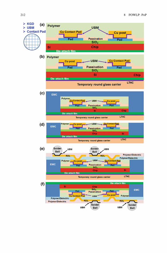
212 8 FOWLP: PoP

chipset by InFO-WLP technology manufactured by TSMC. It can be seen that(1) the dimensions of the A10 are 11.6 mm � 10.8 mm � 150 µm, (2) thepackage dimensions are 15.5 mm � 14.4 mm � 825 µm, (3) the package/chipratio = 1.8, (4) there are 3 RDLs, (4) the TIV (through InFo via) is electroplatedwith Cu, (5) the mobile DRAMs are wirebonded on a three-layer coreless packagesubstrate, (6) the DRAMs and the wires are over molded, (7) there are 386 solderballs (at 0.3 mm pitch) between the top package and the bottom package, (8) thereis underfill between the top and bottom packages, (9) there are *1300 solder balls(at 200 lm diameter and 0.4 mm pitch) at the bottom package, and (10) there isunderfill between the PoP and the PCB (printed circuit board).
Figure 8.8 shows the schematic and SEM images of the PoP for the AP (A11)chipset by InFO-WLP technology HVM by TSMC during September 2017.Basically, the PoP for both APs (A10 and A11) is very similar. However, becauseTSMC used 10 nm process technology to fabricate the A11 (instead of the 16 nmprocess technology for the A10), the chip dimensions are much smaller (10 mm� 8.7 mm � 150 µm), *30% chip area reduction from A10. Since the dimen-sions of the new package do not change much (13.9 mm � 14.8 mm), only *8%
JFig. 8.5 a Test for KGD. Electroplate Cu contact pads and then spin coat a polymer on top of thewafer. Laminate a DAF at the bottom of the wafer. b Singulate the wafer into individual KGD andplace it face-up on a LTHC-coated glass reconstituted wafer. c Compression molding an EMC.d Backgrind the EMC to explore the Cu contact pads. e Build up the RDLs and mount the solderballs. f De bond the glass carrier by a laser and singulate the reconstituted wafer
Wiri
ng
bond
ing
Wiri
ng
bond
ing
Wiri
ngbo
ndin
g W
iring
bo
ndin
g
Wiring bonding
LPDDR4 Chips Layout in the upper (PoP) Package
Memory
Memory Memory
Memory
Wiring bonding
3-Layer Coreless Package Substrate
Solder Ball
Wirebond
A10 AP TIV
Solder Ball
RDLs
EMC
Over MoldMemoryMemory
Underfill
15.5mm x 14.4mm x 825µm
A10 chip size: 11.6mm x 10.8mm x165µm
PackageChip = ~ 1.8 15.5x14.4
11.6x10.8
Fig. 8.6 PoP for Apple’s iPhone 7 AP chipset
8.3 TSMC’ PoP for AP Chipset with FOWLP 213

3-Layer Coreless Package Substrate
Solder Ball
Wirebond
A10 AP TIV
Solder Ball
3RDLs
EMC
MoldingMemoryMemory
Underfill
15.5mm x 14.4mm x 825µm11.6mm x 10.8mm
x 165µm
SoC
PoP
Fig. 8.7 PoP for Apple’s iPhone 7 showing the FOWLP for the AP chipset
3-Layer Coreless Package Substrate
Solder Ball
Wirebond
A11 AP TIV
Solder Ball
4RDLs
EMC
MoldingMemoryMemory
Underfill
10mmx8.7mmx165µm
A11 (SoC)PoP
13.9mmx14.8mmx790mm
A11 AP (150µm)
A11
Memory (140µm)Wirebond
Molding (140µm)
Coreless Substrate (90µm)Solder Ball
TIV
PCBSolder Ball
Underfill
Underfill4RDLs Capacitor
4RDLs(50µm)
EMC
Modified from Prismark/Binghamton University
Fig. 8.8 PoP for Apple’s iPhone 8 showing the FOWLP for the AP chipset
214 8 FOWLP: PoP

package area reduction from the old one, thus the package/chip ratio of A11increases from 1.8 to 2.3. Also, the number of RDLs increases from 3 to 4. The linewidth and spacing of those 4 RDL are 10 µm.
8.4 Summary and Recommendations
PoP for AP chipset with FOWLP technology by STATS ChipPAC and TSMC havebeen presented and discussed. Some important results and recommendations aresummarized as follows.
• The first concept on using FOWLP to house the AP chipset in a PoP format wasproposed and demonstrated by STATS ChipPAC. They showed that the pack-age warpage is within the allowable limit. Also, they showed that the package isqualified with most JEDEC component standards and the solder joints arereliable under the board-level drop and thermal cycling tests.
• The first HVM of PoP for AP chipset with FOWLP is by TSMC’ InFO-PoPtechnology. They showed that [9, 10] the InFO-PoP is better than the conven-tional PoP (Fig. 2.17) in (a) package profile, (b) electrical performance, and(c) thermal performance.
• Recently, Samsung announced their packaging technology for their AP chipset.They proposed that (Fig. 8.9) the application processor (logic) and the mobileDRAM are placed side-by-side and communicated by RDLs (they called it RDLinterposer, or Si-less interposer)—a heterogeneous integration. For moreinformation about heterogeneous integration by FOWLP on AP chipset, pleaseread Chap. 11.
Fig. 8.9 Samsung’s next generation packaging technology for housing the AP chipset
8.3 TSMC’ PoP for AP Chipset with FOWLP 215

References
1. Eslampour, H., S. Lee, S. Park, T. Lee, I. Yoon, and Y. Kim. 2010. Comparison of AdvancedPoP Package Configurations. In IEEE/ECTC Proceedings, 2010, 1946–1950.
2. Yoon, S., J. Caparas, Y. Lin, and P. Marimuthu. 2012. Advanced Low Profile PoP Solutionwith Embedded Wafer Level PoP (eWLB-PoP) Technology. In Proceedings of IEEE/ECTC,2012, 1250–1254.
3. Lin, J.C., J.P. Hung, N.W. Liu, Y.C. Mao, W.T. Shih, and T.H. Tung. 2015. PackagedSemiconductor Device with a Molding Compound and a Method of Forming the Same. USPatent 9,000,584, Filed on December 28, 2011, Patented on April 7, 2015.
4. Liu, C., S. Chen, F. Kuo, H. Chen, E. Yeh, C. Hsieh, L. Huang, M. Chiu, J. Yeh, T. Lin, T.Yeh, S. Hou, J. Hung, J. Lin, C. Jou, C. Wang, S. Jeng, and D. Yu. 2012. High-PerformanceIntegrated Fan-Out Wafer Level Packaging (InFO-WLP): Technology and SystemIntegration. In IEEE/IEDM Proceedings, 2012, 14.1.1–14.1.4.
5. Tsai, C., J. Hsieh, M. Liu, E. Yeh, H. Chen, C. Hsiao, C. Chen, C. Liu, M. Lii, C. Wang, andD. Yu. 2013. Array Antenna Integrated Fan-out Wafer Level Packaging (InFO-WLP) forMillimeter Wave System Applications. In IEEE/IEDM Proceedings, 2013, 25.1.1–25.1.4.
6. Chen, S.M., L.H. Huang, J.H. Yeh, Y.J. Lin, F.W. Kuo, H.N. Chen, M.Y. Chiu, C.C. Liu,J. Yeh, T.J. Yeh, S.Y. Hou, J.P. Hung, J.C. Lin, C.P. Jou, S.P. Jeng, and D. Yu. 2013.High-Performance Inductors for Integrated Fan-Out Wafer Level Packaging (InFO-WLP). InSymposium on VLSI Technology Digest of Technical Papers, 2013, T46–T47.
7. Yu, D. 2014. Wafer-Level System Integration (WLSI) Technologies for 2D and 3DSystem-in-Package. In SEMIEUROPE, 2014.
8. Yu, D. 2015. New Integration Technology Platform: Integrated Fan-OutWafer-Level-Packaging for Mobile Applications. In Symposium on VLSI TechnologyDigest of Technical Papers, 2015, T46–T47.
9. Tseng, C., C. Liu, C. Wu, and D. Yu. 2016. InFO (Wafer Level Integrated Fan-Out)Technology. In IEEE/ECTC Proceedings, 2016, 1–6.
10. Hsieh, C., C. Wu, and D. Yu. 2016. Analysis and Comparison of Thermal Performance ofAdvanced Packaging Technologies for State-of-the-Art Mobile Applications. In IEEE/ECTCProceedings, 2016, 1430–1438.
11. Lau, J.H., N. Fan, M. Li. 2016. Design, Material, Process, and Equipment of EmbeddedFan-Out Wafer/Panel-Level Packaging. Chip Scale Review 20: 38–44.
12. Lau, J.H., M. Li, D. Tian, N. Fan, E. Kuah, K. Wu, et al. 2017. Warpage and ThermalCharacterization of Fan-Out Wafer-Level Packaging. In IEEE/ECTC Proceedings, 2017,595–602. Also, IEEE Transactions on CPMT 7 (10), 1729–1938 (October 2017).
13. Lau, J.H., M. Li, N. Fan, E. Kuah, Z. Li, K. Tan, T. Chen, et al. 2017. Fan-Out Wafer-LevelPackaging (FOWLP) of Large Chip With Multiple Redistribution-Layers (RDLs). In IMAPSProceedings, October 2017, 576–583. Also, IMAPS Transactions, Journal ofMicroelectronics and Electronic Packaging 14 (4), 123–131 (October 2017).
14. Li, M., Q. Li, J.H. Lau, N. Fan, E. Kuah, K. Wu, et al. 2017. Characterizations of Fan-OutWafer-Level Packaging. In IMAPS Proceedings, October 2017, 557–562.
15. Hua, X., H. Xu, Z. Li Zhang, D. Chen, K. Tan, J.H. Lau, et al. 2017. Development ofChip-First and Die-Up Fan-Out Wafer-Level Packaging. In IEEE/EPTC Proceedings,December 2017, S23_1-6.
16. Lau, J.H. 2015. Patent Issues of Fan-Out Wafer/Panel-Level Packaging. Chip Scale Review19: 42–46.
216 8 FOWLP: PoP

Chapter 9Fan-Out Panel-Level Packaging(FOPLP)
9.1 Introduction
All previously mentioned fan-out technologies are using the round 200 or 300 mmwafers as the temporary carriers for making the molds, RDLs, etc. (This is becauseof the existing equipment for fabricating the device wafers.) In order to increase thethroughput, fan-out panel-level packaging (FOPLP) has been proposed. Forexamples, starting from EPTC2011, J-Devices have been presenting their FOPLP(320 mm � 320 mm) called WFOP™ (Wide Strip Fan-Out Package) [1–3].Starting from ECTC2013, Fraunhofer has been presenting their evaluation resultson compression molding of a large area (610 mm � 457 mm) FOPLP [4–6]. AtECTC2014, SPIL published two papers on FOPLP called P-FO: one is to developand characterize a 370 mm � 470 mm P-FO [7] and the other is to measure theirwarpage [8]. One of the bottlenecks for FOPLP is the availability of panel equip-ment such as the spin coating, physical vapor deposition, electrochemical deposi-tion, etching, backgrinding, dicing, etc. for making the RDLs, molds, etc. due to thelack of the standard of panel sizes. Thus, the potential FOPLP users are unani-mously calling for the panel-size industry standards.
9.2 J-Devices’ WFOP™
J-Devices is the first company to use panel for making the fan-out packages. Thestructure and key process steps of J-Devices’ WFOP™ will be briefly mentioned inthis section.
© Springer Nature Singapore Pte Ltd. 2018J. H. Lau, Fan-Out Wafer-Level Packaging,https://doi.org/10.1007/978-981-10-8884-1_9
217
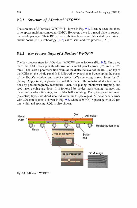
9.2.1 Structure of J-Devices’ WFOP™
The structure of J-Devices’ WFOP™ is shown in Fig. 9.1. It can be seen that thereis no epoxy molding compound (EMC). However, there is a metal plate to supportthe whole package. Their RDLs (redistribution layers) are fabricated by a printedcircuit board (PCB) technology [1–3] called semi-additive process (SAP).
9.2.2 Key Process Steps of J-Devices’ WFOP™
The key process steps for J-Devices’ WFOP™ are as follows (Fig. 9.2). First, theyplace the KGD face-up with adhesive on a metal panel carrier (320 mm � 320mm). Then, coat a photosensitive resin (as the dielectric layer of the RDL) on top ofthe KGDs on the whole panel. It is followed by exposing and developing the opensof the KGD’s window and direct current (DC) sputtering a seed layer for Cuplating. Apply (coat) a photoresist and then pattern the redistributed interconnec-tions by photolithography techniques. Then, Cu plating, photoresist stripping, andseed layer etching are done. It is followed by solder mask coating, contact padpatterning, surface finishing, and solder ball mounting. Then, the panel and resin(dielectric) layers are diced into individual units (packages). A metal panel carrierwith 320 mm square is shown in Fig. 9.3, where a WFOP™ package with 20 µmline width and spacing RDL is also shown.
Fig. 9.1 J-Devices’ WFOP™
218 9 Fan-Out Panel-Level Packaging (FOPLP)

9.3 Fraunhofer’s FOPLP
Fraunhofer IZM summarized its 3-year development on fan-out panel-level pack-aging (FOPLP) in [4–6]. They showed that with surface mount technology(SMT) equipment for picking and placing the dies and passive devices and PCBtechnology + LDI (laser direct imaging) for making the RDLs, they are able tofabricate FOPLP at a very low cost (with a large panel instead of a wafer) for lowend, low pin count, small chip sizes, and high-volume applications. Their testvehicle is a standard PCB size (610 mm � 457 mm) rectangular panel which is 3.8times (in area) of the 300 mm wafer, as shown in Fig. 9.4.
9.3.1 Fraunhofer’s FOPLP Integration Line
A complete Fraunhofer FOPLP integration line is shown in Fig. 9.5. It can be seenthat there is not any semiconductor foundry equipment. They use the ASM SiPlaceCA3 for pick and place the chips, Towa for compression molding the EMC,Lauffer/Burkle for lamination, Siemens Microbeam/Schmoll Picodrill for laser
Metal carrierKGD Adhesive
Resin
Seed layer
KGD placement (face-up)
Resin costing (dielectric)
Seed layer deposition
Photoresist and Lito.
Cu plating
Strip off photoresist
Etch off seed layer
Solder mask coating
Solder mask
Cu
Solder ball mounting
Solder ball
Metal carrierKGD
Dielectric layer
Solder mask
Photoresist
Fig. 9.2 Key process steps of J-Devices’ WFOP™
9.3 Fraunhofer’s FOPLP 219

drilling, Schmoll for mechanical drilling, Ramgraber for Cu plating, Octotech forLDI, and Schmid for etching.
9.3.2 Fraunhofer’s RDLs Key Process Steps
Fraunhofer’s FOPLP key process steps are shown in Fig. 9.6, which are verysimilar to those shown in Chap. 5. Their RDLs key process steps are shown in
Fig. 9.3 J-Devices’ panel and individual package
220 9 Fan-Out Panel-Level Packaging (FOPLP)

(610mm x 457mm)Area > 3.8 X 12”-wafer
12” wafer carrier
24”x18” carrier
4
Fig. 9.4 Fraunhofer’s FOPLP
Fig. 9.5 Fraunhofer’s FOPLP integration line
9.3 Fraunhofer’s FOPLP 221

Fig. 9.7. First, laminate a resin-coated copper (RCC) on the reconstituted panel.Then, use a mechanical or laser drill to make holes into the RCC. It is followed byPCB Cu plating to fill the holes and connect to the Al or Cu pads. Laminate a dryfilm photoresist and use an LDI to remove the resist. Perform the Cu etching andstrip off the resist. We then have the first RDL1 and can repeat all the processes toget the other RDLs. The final RDL can be used as a contact pad. Next, we laminate,photolithograph, and cure the solder mask (in either a solder mask defined or anon-solder mask defined formats) before mounting the solder balls. For this pro-cess, no material and equipment are needed from the semiconductor arena except aPCB shop. Figure 9.8a shows the 610 mm � 457 mm panel and Fig. 9.8b showsthe X-ray image of the 8 mm � 8 mm package which is housing two chips withdimensions of 2 mm � 3 mm.
9.4 SPIL’s P-FO
Based on a PCB technology, thin-film transistor liquid-crystal display (TFT-LCD)2.5G (generation) technology (panel dimensions = 370 mm � 470 mm), andbackend technology, SPIL developed their P-FO technology [7, 8].
Fig. 9.6 Key process steps ofFraunhofer’s FOPLP
222 9 Fan-Out Panel-Level Packaging (FOPLP)

9.4.1 Structure of SPIL’s P-FO
The structure of SPIL’s P-FO is shown in Fig. 9.9a. It can be seen that the chip isembedded in a dry film and it is not in an EMC. Currently, there is only one layer ofRDL.
9.4.2 Key Process Steps of SPIL’s P-FO
The key process steps in making the SPIL’s P-FO package are as follows. First,apply an adhesive on top of a glass panel (370 mm � 470 mm) carrier 1 as shownin Figs. 9.9b and 9.10a. Then, pick and place the KGDs face-down on the glasscarrier 1, Fig. 9.10b, by using a PCB technology to laminate a dry film on top of thewhole panel as shown Fig. 9.10c. It is followed by debonding the glass carrier 1and attaching another carrier 2 on the other side of the reconstituted panel. Then,use the TFT-LCD 2.5G processing technology to fabricate the RDL on top of the Alor Cu contact pads and dry film as shown in Fig. 9.10e. It is followed by solder ballmounting as shown in Fig. 9.10f and dicing of the reconstituted panel as shown inFig. 9.10g. A test package (9 mm � 9 mm) embedded a chip (6 mm � 6 mm) hasbeen demonstrated and is shown in Fig. 9.9a.
KGD
Passivation
EMC
CuResin
Photoresist
Laser direct imaging
Cu etching
Strip photoresist
Lamination of a RCC on the reconfigured panel
Drilling
Cu plating to fill the hole and connect to the pad
Photoresist
RDL1
KGD EMC
Resin
Resin
Cu
CuRDL1
RDL2
Al or Cu Pad
KGD EMC
Passivation
ResinCuRDL1
ResinCuRDL2
ResinCu
Repeat all the processes to get RDL2
Contact padSolder mask Solder ball
Repeat all the processes to get Cu contact pads, spin coat solder mask, and mount solder balls
Al Pad + Cu or Ni bump
Fig. 9.7 Key process steps in making the RDLs of Fraunhofer’s FOPLP
9.4 SPIL’s P-FO 223

9.5 Panel Versus Wafer
Simple mathematic shows that, compared to FOWLP, FOPLP will increasethroughput and potentially lower the cost. However, there are many issues ofFOPLP and they should be noted and resolved.
9.5.1 Issues of FOPLP
Some of the typical issues of FOPLP are shown as follows.
• Most OSATs and Foundries already have the necessary equipment forFOWLP. For FOPLP, new capital will have to be expended on newly developedequipment.
• Inspection of wafers is a well-known process. FOPLP inspection must bedeveloped.
610mm x 457mm
Chip
Chip
8mm x 8mm
(a)
(b)
Fig. 9.8 Fraunhofer’sFOPLP panel and individualpackage
224 9 Fan-Out Panel-Level Packaging (FOPLP)

• The yield of FOWLP is higher than that of FOPLP. (Assuming the size of panelis larger than that of wafer.)
• The cost advantages of panel over wafer need to be carefully determined. (Yes,the throughput is higher, but the pick-and-place time is longer, the EMC dis-pensing time is longer, and the yield is lower.)
• A fully loaded high-yield wafer line might be cheaper than a partially loadedlow-yield panel line.
• The panel equipment takes longer to clean than wafer equipment.• Unlike FOWLP, the FOPLP is for small to medium chip size and line width and
spacing RDLs.• There are only a few companies in the world capable of doing panel. You must
have a materials background, equipment automation support, and IP. You alsoneed to manage the dimensional stability and yield of the panel in a large format.
• Lack of panel standard for FOPLP, thus the equipment suppliers cannot makethe equipment.
• If, indeed, the panel processing is developed and is high yield for fine line widthand spacing, there is a chance to produce a major oversupply of capacity.
470mm (49 columns)
370m
m (3
8 ro
ws)
(a)
(b)
Fig. 9.9 SPIL’s P-FO panel and individual package
9.5 Panel Versus Wafer 225

The choice between panel and wafer will depend on applications. Figure 9.11shows the applications, geometry, material, process, and equipment for fan-outwafer/panel WLP.
Glass Carrier 1
KGD
Adhesive
Dry film
RDL
Solder balls
KGD
Dry film
RDL
Fig. 9.10 Key process steps in making SPIL’s P-FO
≥ 10µm
< 2 - 5µm
5 - 10µm
Reconstituted carrier width/spacing Appl.
Middle-end
High-end
Low-end
thick.
≤ 2µm
≥ 3µm
≥ 5µmLaser direct
imaging
Stepper
Mask aligner or Stepper
_Cu damascene _Semi. Equip._High-Precision P&P
_Cu plating _Packaging Equip._Ordinary P&P
_PCB Cu plating _PCB Equip._SMT P&P
Litho. Proc./Equip. DielectricMat.(Thick.)
SiO2 (1µm)
Polymers (4 - 8µm)
Resin (15 - 30µm)
ABF(~10µm)
Conductor Layer (Cu)
KGDKGDEMC
RDLsPad
Pad
Solder mask or passivation
Dielectric
Solder ball
Fig. 9.11 Wafer versus panel (line width and spacing of RDLs)
226 9 Fan-Out Panel-Level Packaging (FOPLP)

9.5.2 Reconstituted Wafers for High-End Applications
The RDL line width/spacing and thickness are, respectively, � 5 and 2 lm rightnow. But very soon they are going down to � 2 and 1 lm, and the lithographyprocess is accomplished using a stepper. The Cu conductor lines of the RDLs arefabricated by the Cu damascene + CMP (chemical mechanical polishing) method.The dielectric layer (SiO2 or SiN) is 1 lm thick and fabricated by theplasma-enhanced chemical vapor deposition (PECVD) method. A high-precisionpick-and-place (P&P) bonder is needed for die placement.
9.5.3 Reconstituted Wafers for Middle-End Applications
The RDL line width/spacing and thickness are, respectively, 5–10 and 3 lm, andthe lithography is accomplished using a mask aligner or stepper to increase theyield. The conductor lines of the RDLs are fabricated by the electrochemicaldeposition Cu + etching method. The dielectric layer comprises polymers such asthe PI (polyimide), BCB (benzocyclobutene), or PBO (polybenzobisoxazole), andis 4–8 lm thick. An ordinary pick-and-place bonder should be able to perform thedie placement.
9.5.4 Reconstituted Panels for Low-End Applications
The RDL line width/spacing and thickness are, respectively, 10–20 and � 5 lm.They are fabricated using PCB technology. First of all, the Al pad is coated with aCu or Ni bump. A RCC sheet is laminated on the reconstituted panel. Microvias aredrilled through the RCC layer to the die pads and electrically connected by Cuplating. RDL formation is done by LDI (laser direct imaging) in combination with adry film resist and copper etching. The dielectric layer (resin) ranges from 15 to30 lm. An SMT pick and place is adequate for die placement.
There is a small overlapping area between the high end and middle end, and themiddle end and low end.
9.6 Summary and Recommendations
Fan-out panel-level packaging has been briefly presented and discussed in thischapter. Some important results and recommendations are summarized as follows.
• J-Devices’ WFOP™ does not use an EMC and the package is supported by ametal plate. The RDLs are fabricated by a PCB technology called SAP. The linewidth and spacing of the RDL are 20 µm. The panel dimensions are320 mm � 320 mm.
9.5 Panel Versus Wafer 227

• Fraunhofer’s FOPLP is very similar to the eWLB (Chap. 5), except they useSMT to perform the pick and place of the chips and PCB + LDI to make theRDLs. Their panel dimensions are 610 mm � 457 mm.
• SPIL’s P-FO does not use an EMC. Instead, they laminate a dry film on top ofthe whole panel by PCB technology. The RDL on top of the Al or Cu contactpads and dry film is fabricated by the TFT-LCD 2.5G processing technology.The panel dimensions are 370 mm � 470 mm.
• The dielectric and conductor layers of the RDLs fabricated by the Fraunhofer’sECC method are too thick. Another method [9] which can reduce their thicknessis shown in Fig. 9.12. It can be seen that instead of the ECC, laminate an ABF(Ajinomoto build-up film) on the panel. It is followed by laser drilling through theABF and electroless Cu deposition of the seed layer. Then, laminate a dry filmphotoresist and use the LDI to pattern (dry film development) the interconnecttraces. It is followed by PCB Cu plating. Then, strip off the photoresist and etchoff the seed layer and get RDL1. Repeat all the processes to get the other RDLs.The final RDL can be used as a contact pad. Next, we laminate, photolithograph,and cure the solder mask (in either a solder mask defined or a non-solder maskdefined formats) before mounting the solder balls. In this case, the dielectric layerthickness can be as little as 10 µm and the conductor layer thickness can be aslittle as 5 µm. Figure 9.13 shows the panel (340 mm � 340 mm) and thepackages with 4 chips, and the cross section of the PCB assembly of a packagemade by the presented method, where RDL1 and RDL2 are shown.
KGD
Passivation
EMC
PCB Cu plating
Dry film strip and Cu seed
etching
Laser drilling
Electroless Cu seed
layer
Laser direct imaging (LDI) and dry film development
Repeat all the
processes to get RDL2
Solder ball mount
ABFLamination of a Ajinomoto
Build-up Film (ABF)
PhotoresistDry film
lamination
Spin coat solder mask and surface
finish
Cu
RDL1
RDL2
RDL1
RDL1
RDL2
Surface finishSolder mask
KGD EMC
Al or Cu Pad Passivation
Cu
Cu
ABF
ABF
Solder mask
Solder ball
Surface finish
Al Pad + Cu or Ni bump
Fig. 9.12 A new method in making RDLs with PCB technology
228 9 Fan-Out Panel-Level Packaging (FOPLP)

References
1. Hayashi, N., T. Takahashi, N. Shintani, T. Kondo, H. Marutani, Y. Takehara, K. Higaki,O. Yamagata, Y. Yamaji, Y., Katsumata, and Y. Hiruta. 2011. A Novel Wafer Level Fan-outPackage (WFOP™) Applicable to 50 µm Pad Pitch Interconnects. In IEEE/EPTC Proceeding,December 2011, 730–733.
2. Hayashi, N., H. Machida, N. Shintani, N. Masuda, K. Hashimoto, A. Furuno, K. Yoshimitsu,Y. Kikuchi, M. Ooida, A. Katsumata, and Y. Hiruta. 2014. A New Embedded StructurePackage for Next Generation, WFOP™ (Wide Strip Fan-Out Package). In Pan PacificSymposium Conference Proceedings, February 2014, 1–7.
3. Hayashi, N., M. Nakashima, H. Demachi, S. Nakamura, T. Chikai, Y. Imaizumi, Y. Ikemoto,F. Taniguchi, M. Ooida, and A. Yoshida. 2017. Advanced Embedded Packaging for PowerDevices. In IEEE/ECTC Proceedings, 2017, 696–703.
4. Braun, T., K.-F. Becker, S. Voges, T. Thomas, R. Kahle, J. Bauer, R. Aschenbrenner, and K.-D. Lang. 2013. From Wafer Level to Panel Level Mold Embedding. In IEEE/ECTCProceedings, 2013, 1235–1242.
5. Braun, T., K.-F. Becker, S. Voges, J. Bauer, R. Kahle, V. Bader, T. Thomas,R. Aschenbrenner, and K.-D. Lang. 2014. 24”�18” Fan-out Panel Level Packing. In IEEE/ECTC Proceedings, 2014, 940–946.
6. Braun, T., S. Raatz, S. Voges, R. Kahle, V. Bader, J. Bauer, K. Becker, T. Thomas,R. Aschenbrenner, and K. Lang. 2015. Large Area Compression Molding for Fan-out PanelLevel Packing. In IEEE/ECTC Proceedings, 2015, 1077–1083.
Chip: 3mm x 3mm
Chip: 3mm x 3mm
Chip: 3mm x 3mm
Chip: 5mm x 5mm Gap: 100µm
Solder Ball
340mmx340mm
Fig. 9.13 Cross section of the PCB assembly of the test package with RDL1 and RDL2
References 229

7. Chang, H., D. Chang, K. Liu, H. Hsu, R. Tai, H. Hunag, Y. Lai, C. Lu, C. Lin, and S. Chu.2014. Development and Characterization of New Generation Panel Fan-Out (PFO) PackagingTechnology. In IEEE/ECTC Proceedings, 2014, 947–951.
8. Liu, H., Y. Liu, J. Ji, J. Liao, A. Chen, Y. Chen, N. Kao, and Y. Lai. 2014. WarpageCharacterization of Panel Fab-out (P-FO) Package. In IEEE/ECTC Proceedings, 2014,1750–1754.
9. Ko, C.T., Henry Yang, John H. Lau, Ming Li, Margie Li, Curry Lin, et al., 2018. Chip-FirstFan-Out Panel-Level Packaging for Heterogeneous Integration. In ECTC Proceedings, May2018.
230 9 Fan-Out Panel-Level Packaging (FOPLP)
Chapter 103D Integration
10.1 Introduction
The Electronics Industry has been the largest industry since 1996 and may wellreach 2 trillion dollars by the end of 2018 [1–3]. The most important invention ofthe Electronics Industry is arguably the transistor (1947), which earned JohnBardeen, Walter Brattain, and Shockley the 1956 Nobel Prize in Physics. Theinvention of the IC (integrated circuit) by Kilby in 1958 (which earned him the2000 Nobel Prize in Physics), and 6 months later by Noyce (who did not share theNobel Prize with Kilby because he passed away in 1990) excited the generations ofIC integrations. The proposal of doubling the number of transistors on an IC chip(for minimum costs and innovations) every 24 months by Moore in 1965 (alsocalled Moore’s law) [4] has been the most powerful driver for the development ofthe microelectronics industry in the past 50+ years. This law emphasizes lithog-raphy scaling and integration (on a 2D surface) of all functions on a single chip,perhaps through system-on-chip (SoC). On the other hand, the integration of allthese functions can be achieved through 3D integrations such as 3D IC packaging[1], 3D IC integration [1–3, 5–89] and 3D Si integration [1–3, 69–125] as shown inFig. 10.1 [1–3]. They are different, and in general, the through-silicon via(TSV) separates the 3D IC packaging from 3D Si integration and 3D IC integration,because the latter two use TSVs (through-silicon vias), but 3D IC packaging doesnot.
TSV was invented almost 60 years ago [1, 126] by the 1956 Nobel Laureate inPhysics, Shockley. (Yes, the same Shockley who coinvented the transistor, which isgenerally considered the greatest invention in Semiconductor industry.) He filed thepatent “Semiconductive wafer and method of making the same” on October 23,1958, and was granted the U.S. Patent (3,044,909) on July 17, 1962. One of the keyclaims is shown in Fig. 10.2, which gets the semiconductor world so excited today.Basically, the “deep pits” (which are called TSVs today) on the wafer allow thesignals from its top side to its bottom side and vice versa.
© Springer Nature Singapore Pte Ltd. 2018J. H. Lau, Fan-Out Wafer-Level Packaging,https://doi.org/10.1007/978-981-10-8884-1_10
231

TSV is the heart of 3D Si integration and 3D IC Integration [1, 127]. It providesthe opportunity for the shortest chip-to-chip interconnects and the smallest pad sizeand pitch of interconnects. Compared with other interconnection technologies, such
Technology
Mat
urity
Basic/Applied
R&D
Applied R&D
Mass Production
Commercia-lization
Die Stacking with wire
bonds
Package on
Package(PoP)
Stacking
C2C, C2W Stacking
W2WStacking
Volume production for mobile products.
Active applied R&D is undertaken. In the phase of industrialization.
Samples are shipping. Small volume production
Still in upstream research. Challenges such as known-
good-die, yield & device architecture, and electronic design automation are key
issues.
3D IC Packaging 3D IC Integration 3D Si IntegrationDon’t use TSV Use TSV
Full swing production for memories.
Fig. 10.1 3D integration technologies versus maturity
Deep Pits (TSVs)
Fig. 10.2 TSV invented byShockley (US Patent#3,044,909)
232 10 3D Integration

as wire bonding, the advantages of TSV include: (a) better electrical performance,(b) lower power consumption, (c) wider data width and thus bandwidth, (d) higherdensity, (e) smaller form factor, and (f) lighter weight, [1–3, 5–125].
TSV is a disruptive technology. As with all disruptive technologies, the ques-tions to ask are: “What is it displacing?” and “What is the cost?” Unfortunately,TSV is trying to replace the wire bonding technology, which is a most mature,high-yield, and low-cost technology [128]. However, just like solder-bumped flipchip technology [129, 130], because of their unique advantages, TSVs will be hereto stay and for a very long time for wide bandwidth, high-performance andhigh-density applications.
TSV has been in volume production for microelectromechanical systems[131, 132] and complementary metal-oxide semiconductor (CMOS) image sensor[133, 134]. However, they are out of the scope of this study, which is focused onmemory, logic, processor, and SoC. 3D (IC and Si) integration is a very old idea[69, 70] which consists of two or more layers of active electronic components thatare integrated vertically through TSV (it used to be called vertical interconnection)into a single circuit. It was triggered by the advance of the silicon-on-insulator(SOI) technology first reported by Gat and his colleagues more than 35 years ago[135], when semiconductor people thought Moore’s law could be hitting the wallby the 1990s. Of course, the fact showed otherwise.
3D IC integration is to stack up the thin chips with TSVs and microbumps.While 3D Si integration is to stack up the thin wafers/chips with TSVs alone, i.e.,bumpless. The advantages of 3D Si integration over 3D IC integration are: (1) betterelectrical performance, (2) less power consumption, (3) lower profile, (4) lessweight, and (5) higher throughput.
The most powerful proponent on 3D IC/Si integration is the 1965 Nobel Physicslaureate, Richard Feynman. More than 30 years ago, during his lecture, ComputingMachines in the Future in 1985, he said “Another direction of improvement (ofcomputing power) is to make physical machines three dimensional instead of all ona surface of a chip. That can be done in stages instead of all at once—you can haveseveral layers and then add many more layers as time goes on.” In this chapter, theoverview, challenge, and outlook of 3D IC integration, and 3D Si integration willbe presented and discussed [64]. 3D IC packaging will be briefly mentioned first.
10.2 Overview and Outlooks of 3D IC Packaging
Figure 10.1 shows that chip stacking by wire bonding and package-on-package(PoP) are now mature for high-volume manufacturing (HVM). Chip-to-chipinterconnects and 3D embedded fan-out wafer-level packaging are getting tractions.
10.1 Introduction 233

10.2.1 Chip Stacking by Wire Bonding
The first paper on stacking of memory chips in 3D by die-attach material and Auwire bonding was published by nCHIP [136] more than 20 years ago. Since then,memory chip (especially the NAND Flash) stacking by Au wire bonding has beenin high volume production for, e.g., the smartphones, tablets, and solid state drivesas shown in Figs. 10.3 and 10.4. Because of the surge in Au prices and research anddevelopment progress in Cu wire bonding technology, many companies have beenlooking for low-cost solutions, and the shift from Au to Cu wire bonding as shownin Fig. 10.5 is genuinely picking up. In 2017, the world uses of Cu wires excess theAu wires.
10.2.2 PoP
PoP comes from many different forms. Figure 10.6 shows a wire bond package ontop of a flip chip package. It can be seen that the top package consists of two chipscross stacked and wire bonded on a package substrate and then over molded. Thebottom package consists of a solder-bumped flip chip on another package substratewith underfill. All these package substrates are with solder balls. Again, PoP is inhigh-volume production for, e.g., the smartphones and tablets [6].
Figure 10.7 shows the cross-section scanning electron microscope (SEM)images of a 3D fan-out embedded wafer-level package [137] developed by STATSChipPAC. It consists of a bottom package which is an embedded fan-out
Top-side Bottom-side
Fig. 10.3 Samsung’s 48-layer V-NAND 3D flash memory in a solid state drives (SSD)
234 10 3D Integration

wafer-level ball grid array package (eWLB) and a top package which is a memorypackage. It can be seen that: (a) the eWLP contains the logic, baseband, or appli-cation processor, (b) the eWLB is only 450 µm thick, (c) the top package is 520 µmthick and is housing the memory chips with wire bonding, and (d) the intercon-nection is from the PCB, solder balls, redistribution layers (RDLs), to processor,and solder balls, RDL, to the memory chips. This package is a potential candidate
Samsung 48L V-NAND
WirebondsSamsung 48L V-NAND die (40µm-thick)
Each package is housing 16 of the 48 layer V-NAND 3D flash memory chips
with wire bonding technology
The stack of chips is on a coreless organic package substrate with area array solder balls to be attached on PCB
Coreless substrateSolder ball
Fig. 10.4 16 stacked Samsung 48L V-NAND dies
Top Chip
Bottom Chip
Substrate
Fig. 10.5 3D stacked ofchips with Cu wire bonding
10.2 Overview and Outlooks of 3D IC Packaging 235

LPDDR4 2-chipcross-stack
3-Layer Coreless substrate
A9
2-2-2 build-up substrate (380µm thick and 75µm hole)
150µm pitch
staggeredC4 bumps
0.4mm pitch
solder balls
90µm .35mm pitch
PCB
LPDDR4
A9 application processorfabricated by 14/16nm Fin-FET process technology
Coreless Package Substrate for LPDDR4
2-2-2 Package Substrate for A9 processor
A9
Wirebonds
Wirebonds
Solder balls
Fig. 10.6 Apple’s A9 is solder-bumped flip chip packaged in a PoP
450µm
450µm
520µm
Bottom eWLB
Top Package
Si ChipRDL
0.9mm
Bottom eWLB
Top Memory Package
PCB Solder ballsPCB
Fig. 10.7 3D IC packaging (STATSChipPAC’s package-on-package.) Memory package on topand eWLB package for the application processor at the bottom
236 10 3D Integration

for mobile and wearable products. On September 15, 2016, TSMC used their InFO(integrated fan-out) wafer-level packaging to package the application processor(A10) for the iPhone 7 and iPhone 7+ as shown in Fig. 10.8.
10.2.3 Chip-to-Chip Interconnects
Figure 10.9 shows the schematic of a 3D chip-to-chip interconnect [138] developedby IME. It consists of the mother chip which is face-to-face connected to a daughterchip. The backside of the mother chip can be attached to a heat spreader (and a heatsink if necessary). The whole module is attached (through the flip chip mother die)to a rigid or flexible substrate. It is a very cost-effective 3D IC package withoutusing the TSVs. In 2012, SONY’s PlayStation (CXD53135GG) attachedSamsung’s 1 GB wide input/output (I/O) synchronous dynamic random accessmemory face-to-face to the processor and then wire bonded to the next levelinterconnects. The packages shown in Fig. 10.9 are not in manufacturing yet;however, they are the potential candidates for medium-range performanceapplications.
3-Layer Coreless Package Substrate
Solder Ball
Wirebond
A10 AP TIV
Solder Ball
3RDLs
EMC
MoldingMemoryMemory
Underfill
15.5mm x 14.4mm
15.5mm x 14.4mm x 825µm11.6mm x 10.8mm
x 165µm
SoC
PoP
PoP for the Mobile DRAMs and Application Processor of iPhone 7/7+
Underfill 386 balls at 0.3mm pitch
Fig. 10.8 Cross section images of iPhone 7/7+ A10-chipset packaging
10.2 Overview and Outlooks of 3D IC Packaging 237

10.2.4 Outlook of 3D IC Packaging
The outlook of 3D IC packaging is great! Stacked dies with wire bonding and PoPare in HVM for commercial products such as wearables, smartphones, and tablets.Chip-to-chip interconnects are getting tractions and into manufacturing soon. 3Dfan-out embedded wafer-level package is already in production. All these 3D ICpackaging technologies have been keeping 3D IC/Si integration technologies awayfrom HVM.
10.3 Overview, Challenges, and Outlook of 3D SiIntegration
10.3.1 Issues of 3D Si Integration
Basically, wafer to wafer (W2W) is the only way to perform the bonding operationfor 3D Si integration and yield is a critical issue (e.g., some bad chips are forced tobond on the good chips). In addition, the absence of (or an infinitesimal) gap
Daughter Die
Mother Die
Rigid or Flex Substrate
Heat spreader/sink (optional)
Solder Bump
Microbump
Daughter Die
Mother Die
NiAuCu + AuSn
Fig. 10.9 Chip-to-chip (Face-to-face) 3D IC packaging
238 10 3D Integration

between wafers and thermal management could be a big problem. Furthermore, therequirements of the bonding conditions, such as the surface cleanness, surfaceflatness, and the class of clean room for 3D Si integration are very high.
10.3.2 Cu-to-Cu Bonding and Oxide-to-Oxide Bonding
There are at least two different W2W bonding methods for 3D Si integration,namely, Cu-to-Cu bonding and oxide-to-oxide bonding, as shown in Figs. 10.10and 10.11, respectively. In general, for Cu-to-Cu bonding, the TSVs have to befabricated before bonding. On the other hand, for oxide-to-oxide bonding, the TSVsare fabricated after bonding.
Figure 10.10a shows a high-quality bonding interface by IBM and RPI [90–92].Before bonding, the Cu interconnects (pads) are fabricated with the standardback-end-of-line (BEOL) damascene process, followed by the oxide chemicalmechanical polishing (CMP) process (oxide touch-up) to recess the oxide level to40 nm lower than the Cu surface. The bonding temperature is ramped up to 400 °C.Figure 10.10b shows a cross section of the interface between the bumplessCu-to-Cu electrodes (pads) given by the NIMS/AIST/Toshiba/University of Tokyo[93–99].
Figure 10.11a shows a cross section of MIT’s oxide-to-oxide bonding structureof three-layer 3D (ring oscillator) bonded at 275 °C [100–106]. It can be seen that:(1) the layers are bonded and interconnected with W-plugs, (2) the conventionalinter-level connections are in the bottom two layers, and (3) the 3D vias arelocated in the isolation (field) region between transistors. Figure 10.11b shows
Fig. 10.10 3D Si integration: a IBM/RPI’s Cu-to-Cu bonding. b NIMS/AIST/Toshiba/University of Tokyo’s Cu-to-Cu bonding
10.3 Overview, Challenges, and Outlook of 3D Si Integration 239

Leti/Freescale/STMicroelectronics’ dielectric-to-dielectric bonding structure of twodevice layers bonded at 400 °C [107–109]. It can be seen that: (a) first, a metal levelis formed on a 200 mm bulk wafer and SOI wafer; next, these wafers are bondedface-to-face, and then the bulk silicon of the SOI wafer is removed down to theburied oxide layer, (b) the 1.5 µm interstrata vias (ISVs) are formed, which makecontact from upper strata to lower strata, (c) a metal layer is formed at the top of theback side of the SOI wafer, and (d) this ISV makes contact with both the top andbottom metal layers.
10.3.3 R&D in 3D Si Integration
In order to use the 3D Si integration technology to HVM products, many researchand development efforts have to be performed. Besides thermal management, viasformation, thin-wafer handling, more research and development efforts should alsobe placed on areas such as: cost reduction, design and process parameter opti-mization, bonding environment, W2W bonding alignment, wafer distortion, waferbow (warpage), inspection and testing, contact performance, contact integrity,contact reliability, and manufacturing yield issues. In addition, packaging the 3D Si
Fig. 10.11 3D Si integration: a MIT’s oxide-to-oxide bonding. b Leti/Freescale/STMicroelectronics’ oxide-to-oxide bonding
240 10 3D Integration

integration module systematically and reliably to the next level of interconnect poseanother great challenge.
Besides technology issues just mentioned, the electronic design automation(EDA) which is the soul of 3D Si integration [127] is far from ready. Urgently, theindustry needs to build standard and infrastructure and form an ecosystem for 3D Siintegration. Then, the EDA can write the design, simulation, analysis and verifi-cation, manufacturing preparation, and test software with the following guidelines:(1) design automation from high-level description to layout generation/optimization, (2) verification of all dedicated and tuned to 3D integration, (3) ad-dressing the third dimension not like a packaging bumping, (4) addressing the truethird dimension, with partitioning, floor planning, automatic placing, and routing,(5) full extraction with the third dimension, full 3D design rule checks, 3D layoutversus schematic with all tiers together in a same database, and (6) the 3D inte-grations have then to be seen as a whole system distributed in several tiers, and notjust a stack of predefined chips.
10.3.4 Outlooks of 3D Si Integration
In the next 10 years, the industry will be hard-pressed for HVM with the 3D Siintegration technology, except for very niche applications. However, it should benoted and emphasized that 3D Si integration is the right way to go and competewith Moore’s law. The industry should strive to make this happen!
10.3.5 Hybrid Bonding
It is worthwhile to mention that there is another kind of W2W bonding, namelyhybrid bonding which bonds the metal pads and dielectric layer on both sides of thewafers at the same time. SONY is the first to use Cu–Cu direct hybrid bonding inHVM [139]. SONY produced the IMX260 backside illuminated CMOS imagesensor (BI-CIS) for the Samsung Galaxy S7, which shipped in 2016. Electrical testresults showed that their robust Cu–Cu direct hybrid bonding achieved remarkableconnectivity and reliability. The performance of the image sensor was also super.A cross section of the IMX260 BI-CIS is shown in Fig. 10.12. It can be seen that,unlike in [140] for SONY’s ISX014 stacked camera sensor, the TSVs are elimi-nated and the interconnects between the BI-CIS chip and the processor chip areachieved by Cu–Cu direct bonding. The signals are coming from the packagesubstrate with wire bonds to the edges of the processor chip.
The assembly process of Cu–Cu direct hybrid bonding starts off with surfacecleaning, metal-oxide removal, and activation of SiO2 or SiN (by wet cleaning andplasma activation) of wafers for the development of high bonding strength. Then,use optical alignment to place the wafers in contact at room temperature and in a
10.3 Overview, Challenges, and Outlook of 3D Si Integration 241

typical clean room atmosphere. The first thermal annealing (100–150 °C) isdesigned to strengthen the bond between the SiO2 or SiN surfaces of the waferswhile minimizing the stress in the interface due to the thermal expansion mismatchamong the Si, Cu, and SiO2 or SiN. Then, apply higher temperature and pressure(300 °C, 25 kN, 10-3 Torr, N2 atm) for 30 min to introduce the Cu diffusion at theinterface and grain growth across the bond interface. The post-bond annealing is300 °C under N2 atm for 60 min. This process leads to the seamless bonds(Fig. 10.12) formed for both Cu and SiO2 or SiN at the same time.
10.4 Overview, Challenges, and Outlookof 3D IC Integration
Unlike 3D Si integration, 3D IC Integration stacks up thin IC chips in the thirddimension with TSVs and microbumps (<25 µm) [1] to achieve performance, lowpower consumption, wide bandwidth, and small form factor. The ones which are inand going into low volume production are: memory stacking with TSVs, wide I/ODRAM, wide I/O DRAM 2, high-bandwidth memory (HBM), hybrid memory cube(HMC), and 2.5D IC integration (passive interposer).
Wirebonds
Wirebonds
Processor Chip
Processor Chip
Processor Chip
BI-CIS Chip
Cu-Cu
BI-CIS Chip
BI-CIS Chip
Microlens
SiO2-SiO2
Fig. 10.12 Sony’s Cu–Cu hybrid bonding
242 10 3D Integration

10.4.1 Memory Stacking with TSVs
Samsung mass-produced (August 2014) the industry’s first TSV-based 64 GBdouble data rate type 4 (DDR4) DRAM stack module (Fig. 10.13). Each stack has 4DRAMs, each DRAM die has 78 TSVs, and the 64 GB DDR4 DRAM stacks areon a printed circuit board (PCB). The module performs twice as fast as a modulethat uses wire bonding packaging technology, while consuming approximately halfthe power. The module is for environmentally friendly server applications. OnNovember 26, 2015, Samsung started to produce the 128 GB registered dual inlinememory module (RDIMM).
10.4.2 Wide I/O DRAM and Wide I/O 2
JEDEC standard (JESD229) [141], Wide I/O Single Data Rate (Wide I/O SDR), waspublished in Dec. 2011 and JEDEC standard (JESD229-2) [141], Wide I/O 2 (WideI/O2), was published in August 2014. They are meant for a stack of DRAMs withTSVs on a logic controller with TSVs. The microbumps are divided into fourquadrants with signal assignments mirrored both horizontally and vertically as shownin Fig. 10.14, where the bump pitch (40 µm) of the area array is also shown. Thedimensions of each quadrant are 2880 µm � 200 µm. There will be a space betweenquadrants in the x-direction (1000 µm) and in the y-direction (120 µm) [141].
TSVs Microbumps
DRAMs
This is not a wide I/O device, nor does it contain a base logic die.
It is just for memory capacityand low power consumption.
On November 26, 2015, Samsung start to produce the 128GB RDIMM
(dual inline memory module)
78 TSVs for each DRAM!
Server Farm
Fig. 10.13 Samsungs’ DRAM stacking with TSVs
10.4 Overview, Challenges, and Outlook of 3D IC Integration 243

10.4.3 High-Bandwidth Memory (HBM)
JEDEC standard (JESD235) [142], high-bandwidth memory (HBM) DRAM, waspublished in December 2013. It is meant for the graphics applications supportingbandwidth from 128 to 256 GB/s. A TSV/RDL interposer is used to support/connect mainly the lateral communication (HBM interface) between theHBM DRAM memory cube with TSVs and the SoC such as graphic processor unitor CPU without TSVs. The optional base chip is used for buffering and signalrerouting of the HBM DRAM cube (Fig. 10.15).
40μm
40μm
2880μm
200μm 120μm
1000μm
Fig. 10.14 Schematic of JEDEX’s Wide I/O 2
Underfill is needed between the interposer and the organic substrate. Also, underfill is needed between the interposer and the GPU/CPU and the HBM cube
GPU/CPU/SoC
Organic Package Substrate
PCB PCB
TSV/RDL Interposer
HBM Interface
HBM DRAM
Optional Base Chip
TSV
Microbump
Fig. 10.15 Schematic of JEDEX’s High-Bandwidth Memory (HBM)
244 10 3D Integration

10.4.4 AMD’s Graphic Processor Unit with HBM
Figure 10.16 shows AMD’s Radeon R9 Fury X graphic processor unit (GPU)shipped in the second-half of 2015. The GPU is built on TSMC’s 28 nm processtechnology and is supported by four high-bandwidth memory (HBM) cubes man-ufactured by Hynix. Each HBM consists of four DRAMs with C2 bumps and alogic base with TSVs straight through them. Each DRAM chip has >1000 TSVs.The GPU and HBM cubes are on top of a TSV interposer (28 mm � 35 mm),which is fabricated by UMC with a 64 nm process technology. The final assemblyof the TSV interposer (with C4 bumps) on a 4-2-4 organic package substrate(fabricated by Ibiden) is by ASE.
PTH
C44-2-4 Build-up
substrate
TSV-Interposer
GPU
HBM HBM
HBM HBM
TSV-Interposer
1st DRAM
4th DRAM3rd DRAM2nd DRAM
Fig. 10.16 AMD’s GPUwith Hynix’s HBM andUMC’s TSV interposer
10.4 Overview, Challenges, and Outlook of 3D IC Integration 245

10.4.5 Nvidia’s Graphic Processor Unit with HBM2
Figure 10.17 shows Nvidia’s Pascal 100 GPU, which shipped in the second-half of2016. The GPU is built on TSMC’s 16 nm process technology and is supported byfour HBM2 (16 GB) fabricated by Samsung. Each HBM2 consists of four DRAMswith C2 bumps and a base logic die with TSVs straight through them. Each DRAMchip has >1000 TSVs. The GPU and HBM2s are on top of a TSV interposer(1200 mm2), which is fabricated by TSMC with a 64 nm process technology.The TSV interposer is attached to a 5-2-5 organic package substrate with C4bumps.
Both Samsung and Hynix use the high bonding force TCB of the C2 bumpedDRAMs with NCF as shown in Fig. 2.16d to fabricate the 3D IC integration stack.This 3D memory cube is stacked one chip at a time and each chip takes *10 s forthe underfill film to gel, the solder to melt and solidify, and the film to cure.
TSV Interposer(TSMCís CoWoS)
HBM2 HBM2
HBM2HBM2
GPU
HBM2 GPU
Build-up Package Substrate
Base logic dieµbump
C4 bump
4DRAMs
Solder Ball
HBM2 by Samsung
Fig. 10.17 Nvidia’s GPU with Samsung’s HBM2 and TSMC’s TSV interposer
246 10 3D Integration

10.4.6 Intel’s CPU with Micron’s HMC
Figure 10.18 shows Intel’s Knights Landing CPU with Micron’s HMC (hybridmemory cube) [143], which have been shipping to Intel’s favorite customers sincethe second-half of 2016. It can be seen that the 72-core processor is supported by 8multichannel DRAMs (MCDRAM) based on Micron’s HMC technology.Each HMC consists of 4 DRAMs and a logic controller (with TSVs), and eachDRAM has >2000 TSVs with C2 bumps. The DRAM+ logic controller stack isattached to an organic package substrate. Micron reports that having such HMC inthe CPU package is expected to deliver 5X the sustained memory bandwidth versusGDDR5 (graphics double data rate type 5) with one-third the energy per bit in halfthe footprint. Micron’s current HMC assembly process is different from that ofSamsung and Hynix. Instead of using high-force TCB-NCF (Fig. 2.16d), Micronuses low-force TCB with CUF (Fig. 2.16b). Again, just like Samsung and Hynix,Micron has to do it one DRAM at a time.
Stacked DRAMs
Fig. 10.18 Intel’s knights landing processor unit with Micron’s HMC
10.4 Overview, Challenges, and Outlook of 3D IC Integration 247

10.4.7 Passive Interposer (2.5D IC Integration)
A 2.5D IC integration is a TSV/RDL interposer system which consists of a piece ofdeviceless silicon with TSVs, RDLs, and IC chips without TSVs. This piece ofdeviceless TSV silicon (also called a passive TSV interposer) is used to support thehigh-performance, high-density, fine-pitch chips and has RDLs (mainly) for lateralcommunication between the chips as shown schematically in Fig. 10.19.Figure 10.20 shows a sample designed and fabricated by Altera/TSMC [41, 42]. Itcan be seen that even with more than 12 buildup layers (6-2-6) on the packagesubstrate, it is still not enough to support the four-sliced 28 nm FPGA (field-programmable gate array) chips. In addition, a passive TSV interposer with 200,000+ microbumps on 45 µm pitch and four RDLs (three Cu damascene layers and onealuminum layer) at a minimum of 0.4 µm pitch is needed. This type of structure(Figs. 10.19 and 10.20) is called by TSMC as chip on (interposer) wafer on(package) substrate (CoWoS) and has been in small production for Xilinx since theearly of 2013.
Chip 1 Chip 2
UnderfillSolder
Cu Pillar
TSV
UBM
Si Interposer
RDLs(Redistribution
layers)
RDLs for lateral communication
of chips
Solder Bumps
Underfill
Solder Balls Not-to-scale
UBM
Package Substrate Build-up Layers
Fig. 10.19 TSV/RDL passive interposer supporting chips on package substrate
248 10 3D Integration

10.4.8 Fabrication of TSVs
The fabrication process of TSVs for interposer is shown in Fig. 10.21. The processstarts with a SiNx/SiOx insulation layer by either thermal oxidation or PECVD(plasma enhanced chemical vapor deposition) as shown in Fig. 10.21. After pho-toresist and TSV lithography, the TSV is etched into the Si substrate by Bosch-typedeep reactive ion etch (DRIE) [45] to form a high aspect ratio (10.5) via structure.The etched TSV structure is then processed with a SiOx liner by sub-atmospherechemical vapor deposition, a Ta barrier layer and a Cu seed layer by physical vapordeposition (PVD) [17]. Cu electroplating is used to fill the TSV structure. The finalblind TSV has a top opening of approximately 10 µm in diameter and a depth ofabout 105 µm, which gives an aspect ratio of 10.5. In such a high aspect ratio viastructure, a bottom-up plating mechanism is applied to ensure a seamless TSV witha reasonably low Cu thickness in the field.
The SEM cross-sectional images are shown in Fig. 10.22. It can be seen that thediameter of the TSV is slightly decreased at the bottom, which is expected from theetching process. The Cu thickness at the field is <5 µm. The post-plating anneal isat 400 °C for 30 min. To complete the TSV process, excess Cu in the field isremoved by CMP [13].
Package Substrate
TSV
RDLs
Interposer
Build-up Layers
Cu Pillar
Solder
ChipInterposer
C4 Bumps
Solder Balls
The package substrate is at least (6-2-6)
4 RDLs: 0.4μm-pitch line width and spacingEach FPGA has >50,000 μbumps on 45μm pitchInterposer is supporting >200,000 μbumps
TSV
Microbump
Fig. 10.20 Altera/TSMC’s chips on wafer on substrate (CoWoS)
10.4 Overview, Challenges, and Outlook of 3D IC Integration 249

10.4.9 Fabrication of RDLs
There are at least two ways to fabricate RDLs [1–3, 5]. The first method is by usingpolymers, such as polyimide (PI) PWDC 1000 (Dow Corning), benzocyclobutenecyclotene (BCB) 4024-40 (Dow Chemical), polybenzo-bisoxazole (PBO) HD-8930(HD Micro Systems), and the fluorinated aromatic AL-X 2010 (Asahi GlassCorporation) to make the dielectric layer and electroplating (such as Cu) to makethe metal layers. This method has been used by the outsourced semiconductorassembly and test providers (OSATs) to fabricate RDLs for wafer-level (fan-in)chip scale package [130], embedded wafer-level (fan-out) ball grid array package[144–148], and (fan-out) redistribution chip package [149, 150]. The secondmethod is the Cu damascene method, which is primarily modified from the con-ventional semiconductor BEOL to make the Cu metal RDLs such as those shown inFig. 10.23. In general, much thinner structures (both dielectric layers and CuRDLs), finer pitches, smaller line widths, and spacing can be obtained with the dualCu damascene method, which will be briefly stated in the following.
If starting with the wafer from Fig. 10.21, the fabrication process of RDLs with adual Cu damascene technique is primarily based on the semiconductor BEOLprocess. The details are shown in Fig. 2.23 and listed in the following [5]: (1) SiO2
layer by PECVD, (2) apply photoresist and mask, then use photolithographytechniques (align and expose) to open vias on the SiO2, (3) RIE of SiO2, (4) strip offportion of the photoresist, (5) repeat step 3, (6) strip off the photoresist, (7) sputter
Si substrate
SiO2 by thermal oxidation or PECVD
Photoresist
Mask, Litho/Patterning
SiO2 etch
DRIE
Strip resist
PECVD or SACVD SiO2, PVD barrier layer (Ti or Ta) and seed layer (Cu)
Cu Plating. Then anneal at 400oC for 30m
CMP the overburden Cu, Cu seed layer, and barrier layer
SiO2
Photoresist
TSV
SiO2Ti/Cu or Ta/Cu
Cu
Cu TSVSiO2
Ti/Cu or Ta/Cu
Fig. 10.21 TSV fabrication process flow
250 10 3D Integration

Ti and Cu and electroplate Cu over the entire wafer, (8) CMP the Cu and Ti/Cu andRDL1 is completed, and (9) repeat steps 1–8 to complete RDL2 and any additionallayers. SEM images of the RDL cross sections fabricated by the Cu damascenetechnique are shown in Fig. 10.24. The minimum RDL line width is 3 µm. Thethickness of RDL1 and RDL2 is 2.6 µm and of RDL3 is 1.3 µm. The dielectricthickness between RDLs is 1 µm.
10.4.10 Backside Processing and Assembly
The process flow of backside and assembly [5] is shown in Fig. 10.25. It can beseen that after the fabrication of TSV, RDLs, passivation, and UBM (under bumpmetallurgy), the topside of the interposer wafer is temporarily bonded to a carrier byadhesive. The next step is backgrinding the interposer wafer, Si etching,low-temperature passivation, and Cu revealing. Next, backside RDL (optional),UBM, and C4 (controlled collapse chip connection) wafer bumping are carried out.After that, the next step is to temporary bond another carrier wafer to the backside
8.67μm
10.1μm 0.44μm
0.40μm
0.83μm
TSV
100μ
m
Fig. 10.22 SEM images of TSV cross sections
10.4 Overview, Challenges, and Outlook of 3D IC Integration 251

(with solder bumps) and debond the first carrier wafer. This step is followed bychip-on-wafer bonding and underfilling. After the whole (chip on) interposer waferis completed, the next step is to debond the second carrier wafer and transfer thethin interposer wafer with attached chips to a dicing tape and ring for singulation.The individual TSV/RDL interposer with chips is attached to the package substrateby natural reflow and then underfilled.
10.4.11 Cu Revealing
Figure 10.26 shows more details on Cu revealing. Right after the temporarybonding of the support carrier, backgrind the wafer to a few microns to the tip ofTSVs, Si dry etching (by RIE) to a few microns below the tip of TSVs, andlow-temperature passivating the SiN/SiO2 are performed. Then, CMP for SiN/SiO2
buffing and barrier and Cu seed layers polishing are carried out. Cu revealing iscompleted and shown in Fig. 10.27 [5]. These processes also apply to device TSVwafers.
SiO2
Si
TSV (Cu) Ta/Cu
or Ti/Cu
SiO2
SiO2 by PECVD
SiO2
TSV
TSVPhotoresist
TSVMask, litho
TSVRIE of SiO2
TSV
Mask. litho
Sputter Ti/Cu and plate Cu
CMP Cu and Ti/CuTSV
RDL1
V01
V01
TSV V01RDL1
RDL2
V12DL2
DL1DL01DL12
TSV
TSV
TSV
RIE of SiO2
Strip resist
Fig. 10.23 Process flow for fabricating RDLs by dual Cu damascene
252 10 3D Integration

RDL1RDL2
RDL3
TSV
TSV
RDL1
RDL2
RDL3
UBM
V01
V12
V23
TUTO
V01
V12
V23
Fig. 10.24 SEM images of cross sections of RDLs fabricated by the Cu damascene method [5]
Carrier #1
BackgrindingTemporary
Bonding Carrier #1
Silicon Etching Pass., and Cu
Revealing C4 Wafer BumpingTemporary
Bonding Carrier #2
UBM
Assemble the TSV module on package substrate, then test. Underfill
RDL/Pass.
Si SubstrateTSV
Passivation UBM
Carrier #1 Carrier #1 Carrier #1 Carrier #1
Carrier #2
Carrier #1
Chip-on-Wafer. Underfill
Carrier #2 Carrier #2 De-bonding
Carrier #2 and dicingDe-bonding
Carrier #1
Package Substrate
Not-to-scale
Chip
TSV Interposer
Interposer
Chip ChipRDLs
Chip
Wafer Micro bumping &
dicing
Interposer
Adhesive
Fig. 10.25 Conventional process flow for chip on interposer wafer on package substrate [8]
10.4 Overview, Challenges, and Outlook of 3D IC Integration 253

10.4.12 Outlook of 2.5D/3D IC Integration
TSVs straight through the same memory chips, e.g., DRAMs to enlarge thememory capacity, increase the bandwidth, lower the power consumption, lower thelatency (enhance the electrical performance), and reduce the form factor is the rightthing to do and will be the major application of 3D IC integration [151]. Thememory stacking, HMC, HBM, and HBM2 are examples, which are targeted for
TSV SiO2
Ta/Cu
Si
RDLs and UBM
TSV
Adhesive
Support Carrier
Si
TSV
Adhesive
Support Carrier
Si
TSV
Adhesive
Support Carrier
passivation
Si
TSV
Adhesive
Support Carrier
Si
TSV
Adhesive
Support Carrier
Si
Complete frontsideRDLs & UBM
Temporary bonded to a carrier by adhesive. Backgrindingto a few microns to the TSV
Si dry etch (RIE) to a few microns below the TSV
Low temperature SiN/SiO2
CMP for SiN/SiO2buffing, and barrier and Cu seed layers polishing
SiN/SiO2
Sputter Ti/Cu
TSV
Adhesive
Support Carrier
Si
CuSolder
Photo-resist, Mask, litho, Cu plating, solder plating
TSV
Adhesive
Support Carrier
Si
Cu
Strip resist and etch Ti/Cu
Not-to-Scale
Solder
Ti/Cu
passivationTi/Cu
RDLs and UBM
SiN/SiO2
Ta/CuSiN/SiO2 SiO2
Fig. 10.26 Backside Cu reveal and UBM/solder plating process flow
CuTSV
Cu TSV
SiSi SiSi
SiO2SiO2
Fig. 10.27 TSV Cu revealing. (Left) Before dry etch of Si. (Right) After Si dry etching,low-temperature SiN/SiO2, and removal (CMP) of the isolation, barrier, and seed layer
254 10 3D Integration

such as high-performance computing, cloud computing, in-memory database,graphic, networking, energy, wireless communications, transportation, security, andhigh-end servers.
TSV/RDL interposer (2.5D IC integration) is in small volume manufacturing byXilinx/TSMC for the sliced FPGAs, which cannot be supported by the packagesubstrate even with 12 buildup layers. Thus, interposer is for very high perfor-mance, high-density, high-I/O, and fine-pitch applications such as big data, cloud,augmented reality, substitutional reality, mixed reality, and artificial intelligence,networking, communications, high-end servers, etc.
10.5 Supply Chains Before the TSV Era
Before the TSV era, the technology supply chains are very well defined andunderstood. Descriptions of the various entities comprising the supply chain beforethe TSV era are presented below.
10.5.1 Front-End-of-Line (FEOL)
This is the first portion of IC fabrication where the individual devices such astransistors or resistors are patterned. This process is from a bare wafer to (but notincluding) the deposition of metal layers. FEOL is usually performed in semicon-ductor fabrication plants (fabs).
10.5.2 BEOL
This is the fabrication in which active devices are interconnected with wiring on thewafer. This process starts from the first layer of metal to bonding pads with pas-sivation. It also includes insulators and metal contacts which are calledmiddle-of-the-line (MOL). The term “MOL” is seldom used and embedded in theBEOL. Again, BEOL is usually performed in the fabs.
10.5.3 OSATs
Outsourced semiconductor assembly and test providers (OSATs) is also calledpackaging, assembly and test. The process starts when the passivated wafer isreceived from the fab and then goes through circuit probing, bumping, thinning,dicing, wiring bonding, flip chip, fan-in or fan-out RDLs, molding, ball mounting,final testing, and etc.
10.4 Overview, Challenges, and Outlook of 3D IC Integration 255

10.6 Supply Chains for the TSV Era—Who Makesthe TSV?
The following steps in the TSV fabrication process impact the various considera-tions that must be addressed:
10.6.1 TSVs Fabricated by the via-First Process
The TSVs are fabricated before the FEOL. This can only be done by the fab.However, even in the fab, this seldom happens because the devices (e.g., transis-tors) are much more important than the TSVs.
10.6.2 TSVs Fabricated by the via-Middle Process
The TSVs are fabricated right after the FEOL (e.g., transistors) and MOL (e.g.,metal contacts), and before the BEOL (e.g., metal layers). In this case, the MOL isno longer embedded in the BEOL because the TSV fabrication process is betweenthem. Owing to logistics and equipment compatibilities, usually the TSV by thevia-middle process is done by the fab.
10.6.3 TSVs Fabricated by the via-Last(from the Front-Side) Process
The TSVs are fabricated (from the front-side of the wafer) after the FEOL, MOL,and BEOL. As of today, there is not a single creditable paper published with thisprocess.
10.6.4 TSVs Fabricated by the via-Last(from the Backside) Process
The TSVs are fabricated (from the backside of the wafer) after the FEOL, MOL,and BEOL process flows. The CMOS image sensor is an example. Strictlyspeaking, CMOS image sensors are not examples of 3D IC integration. For CMOSdevice sample wafers, the only creditable publication is given by LETI [152].However, because of technical issues, such as hitting the various embeddedalignment targets in the x-, y-, and z-directions (to enable the alignment between the
256 10 3D Integration

metal layers on the topside of the wafer and the positioning of TSVs formed fromthe backside), TSVs fabricated by the via-last (from the backside) process should beavoided until these issues are resolved. Based on the above discussions, it seemsthat for active device wafers being used for 3D IC integration applications, TSVsare better fabricated using the via-middle process. Also, the TSVs should be fab-ricated by the fabs, where all the equipment and expertise already exist and the costto fabricate the TSVs is less than 5% of the cost in fabricating the (� 32 nm) devicewafers!
10.6.5 How About the Passive TSV Interposers?
When the industry defined the TSV processes for 3D IC integration, there were nopassive TSV interposers yet. Also, since there is no active device in the passiveinterposers, thus they do not fit into any of the preceding!
10.6.6 Who Wants to Fabricate the TSV for PassiveInterposers?
Both the fab and OSATs want to do it! It depends on the layout, design, andfabrication capabilities, especially the line width and spacing of the RDLs and thediameter of the TSVs. Usually, for a few microns of line width and spacing of theRDL and � 5 µm of TSV diameter it can be done by the OSATs. Otherwise, itshould be done by the fabs. Today, there is not a single OSATs in HVM of TSVsfor passive interposers.
10.7 Supply Chains for the TSV Era—Who Doesthe MEOL?
For the thicknesses of memory chip stacking and DRAMs in HMC and HBM, andinterposers under consideration, all the TSVs fabricated are blind vias. The blindTSV wafer is followed by temporary bonding, backgrinding, TSV revealing, thinwafer handling, debonding, cleaning, solder bumping, etc., which, taken together,are called MEOL (middle end of line). Except for the vertically integrated com-panies (e.g., TSMC and Samsung), it is better for the MEOL process flow to beperformed by the OSATs.
10.6 Supply Chains for the TSV Era—Who Makes the TSV? 257
10.8 Outlook of HVM Supply Chains for TSVsand MEOL
For device wafers, the TSVs should be fabricated by the via-middle process andmanufactured by the fabs. For deviceless wafers, it depends on the line width/spacing of the RDLs and the diameter of the TSVs, but it should also be done by thefabs. As to the MEOL, for both device and deviceless wafers, it should be done bythe OSATs.
10.9 Summary and Recommendations
The overview, challenge, and outlook of 3D IC packaging, 3D IC integration, and3D Si integration have been presented and discussed. The fabrication processes ofTSVs and RDLs have also been mentioned. Furthermore, the supply chains ofTSVs and 3D IC integration at HVM have been examined. Some important resultsand recommendations are summarized as follows:
• The driving forces for consumer products such as smartphones, tablets, andwearables are cost, cost, and cost. The cost-effective 3D IC packaging such asthe stacked dies by wire bonding, PoP, chip-to-chip interconnect, and 3Dembedded fan-out wafer-level packaging (FOWLP) are just the right tech-nologies for these products.
• The driving forces for high-performance computing, cloud computing, net-working, wireless communications, high-end servers are performance and reli-ability. The considerable high-cost 2.5D/3D IC integrations such as memorychip stacking with TSVs, HMC, HBM, and passive interposer are the righttechnologies for these products.
• For device wafers, the TSVs should be fabricated by the via-middle process andmanufactured by the fabs. For interposer wafers, if the diameter of the TSVs is� 5 µm and the line width/spacing of the RDLs is � 3 lm, then it can bemanufactured by the fabs and OSATs; otherwise, it should be done by the fabs.However, since most interposers are for very high performance, high-density,and fine-pitch applications, thus the TSV diameters and RDLs line width andspacing are most likely falling into the fabs’ territory.
• As to the MEOL, assembly, and test of both the device and deviceless TSVwafers they should be performed by the OSATs except the vertical integratedcompanies such as TSMC and Samsung. There are many important tasks inMEOL, assembly, and test, thus the OSATs should strive to make themselvesready for a robust and high-yield manufacturing process.
258 10 3D Integration

References
1. Lau, J.H. 2013. Through-Silicon Vias for 3D Integration. New York: McGraw-Hill.2. Lau, J.H. 2011. Reliability of RoHS Compliant 2D & 3D IC Interconnects. New York:
McGraw-Hill.3. Lau, J.H., C.K. Lee, C.S. Premachandran, and A. Yu. 2010. Advanced MEMS Packaging.
New York: McGraw-Hill.4. Moore, G. 1965. Cramming More Components Onto Integrated Circuits. Electronics 38 (8):
114–117.5. Lau, J.H., P. Tzeng, C. Lee, C. Zhan, M. Li, J. Cline, K. Saito, Y. Hsin, P. Chang, Y. Chang,
J. Chen, S. Chen, C. Wu, H. Chang, C. Chien, C. Lin, T. Ku, R. Lo, and M. Kao. 2014.Redistribution Layers (RDLs) for 2.5D/3D IC Integration. IMAPS Journal ofMicroelectronics and Electronic Packaging 11 (1): 16–24.
6. Lau, J.H. 2014. The Future of Interposer for Semiconductor IC Packaging. Chip ScaleReview 18 (1): 32–36.
7. Hsieh, M.C., S.T. Wu, C.J. Wu, and J.H. Lau. 2014. Energy Release Rate Estimation forThrough Silicon Vias in 3-D IC Integration. IEEE Transactions on Components, Packagingand Manufacturing Technology 4 (1): 57–65.
8. Lau, J.H. 2013. Supply Chains for High-Volume Manufacturing of 3D IC Integration. ChipScale Review 17 (1): 33–39.
9. Khan, N., H. Li, S. Tan, S. Ho, V. Kripesh, D. Pinjala, J.H. Lau, and T. Chuan. 2013. 3-DPackaging with Through-Silicon Via (TSV) for Electrical and Fluidic Interconnections.IEEE Transactions on Components, Packaging and Manufacturing Technology 3 (2): 221–228.
10. Lau, J.H., and G.Y. Tang. 2012. Effects of TSVs (Through-Silicon Vias) on ThermalPerformances of 3D IC Integration System-In-Package (SiP). Journal of MicroelectronicsReliability 52 (11): 2660–2669.
11. Lau, J.H. 2012. Recent Advances and New Trends in Nanotechnology and 3D Integrationfor Semiconductor Industry. ECS Transactions 44 (1): 805–825.
12. Chien, H.C., J.H. Lau, Y. Chao, R. Tain, M. Dai, S.T. Wu, W. Lo, and M.J. Kao. 2012.Thermal Performance of 3D IC Integration with Through-Silicon Via (TSV). IMAPS Journalof Microelectronics and Electronic Packaging 9 (2): 97–103.
13. Chen, J.C., J.H. Lau, P.J. Tzeng, S. Chen, C. Wu, C. Chen, H. Yu, Y. Hsu, S. Shen, S. Liao,C. Ho, C. Lin, T.K. Ku, and M.J. Kao. 2012. Effects of Slurry in Cu Chemical MechanicalPolishing (CMP) of TSVs for 3-D IC Integration. IEEE Transactions on Components,Packaging and Manufacturing Technology 2 (6): 956–963.
14. Lee, C.K., T.C. Chang, J.H. Lau, Y. Huang, H. Fu, J. Huang, Z. Hsiao, C. Ko, R. Cheng,P. Chang, K. Kao, Y. Lu, R. Lo, and M. Kao. 2012. Wafer Bumping, Assembly, andReliability of Fine-Pitch Lead-Free Micro Solder Joints for 3-D IC Integration. IEEETransactions on Components, Packaging and Manufacturing Technology 2 (8): 1229–1238.
15. Sekhar, V.N., L. Shen, A. Kumar, T.C. Chai, X. Zhang, C.S. Premchandran, V. Kripesh, S.Yoon, and J.H. Lau. 2012. Study on the Effect of Wafer Back Grinding Process onNanomechanical Behavior of Multilayered Low-K Stack. IEEE Transactions onComponents, Packaging and Manufacturing Technology 2 (1): 3–12.
16. Zhang, X., R. Rajoo, C.S. Selvanayagam, A. Kumar, V. Rao, N. Khan, V. Kripesh, J.H. Lau,D. Kwong, V. Sundaram, and R.R. Tummala. 2012. Application of Piezoresistive StressSensor in Wafer Bumping and Drop Impact Test of Embedded Ultra-thin Device. IEEETransactions on Components, Packaging and Manufacturing Technology 2 (16): 935–943.
17. Wu, C., S. Chen, P. Tzeng, J.H. Lau, Y. Hsu, J. Chen, Y. Hsin, C. Chen, S. Shen, C. Lin, T.Ku, and M. Kao. 2012. Oxide Liner, Barrier and Seed Layers, and Cu-Plating of BlindThrough Silicon Vias (TSVs) on 300 mm Wafers for 3D IC Integration. IMAPS Journal ofMicroelectronics and Electronic Packaging 9 (1): 31–36.
References 259

18. Lau, J.H., M.S. Zhang, and S.W.R. Lee. 2011. Embedded 3D Hybrid IC IntegrationSystem-in-Package (SiP) for Opto-Electronic Interconnects in Organic Substrates. ASMEJournal of Electronic Packaging 133 (3): 1–7.
19. Chai, T.C., X. Zhang, J.H. Lau, C.S. Selvanayagam, D. Pinjala, Y. Hoe, Y. Ong, V. Rao, E.Wai, H. Li, E. Liao, N. Ranganathan, V. Kripesh, S. Liu, J. Sun, M. Ravi, C. Vath III, and Y.Tsutsumi. 2011. Development of Large Die Fine-Pitch Cu/Low-k FCBGA Package withThrough Silicon Via (TSV) Interposer. IEEE Transactions on Components, Packaging andManufacturing Technology 1 (5): 660–672.
20. Lau, J.H. 2011. TSV Interposers: The Most Cost-Effective Integrator for 3D IC Integration.Chip Scale Review 15 (5): 23–27.
21. Kumar, A., X. Zhang, Q. Zhang, M. Jong, G. Huang, V. Lee, V. Kripesh, C. Lee, J.H. Lau,D. Kwong, V. Sundaram, R.R. Tummula, and G. Meyer-Berg. 2011. Residual StressAnalysis in Thin Device Wafer Using Piezoresistive Stress Sensor. IEEE Transactions onComponents, Packaging and Manufacturing Technology 1 (6): 841–851.
22. Yu, A., J.H. Lau, S. Ho, A. Kumar, W. Hnin, W. Lee, M. Jong, V. Sekhar, V. Kripesh, D.Pinjala, S. Chen, C. Chan, C. Chao, C. Chiu, C. Huang, and C. Chen. 2011. Fabrication ofHigh Aspect Ratio TSV and Assembly with Fine-Pitch Low-Cost Solder Microbump for SiInterposer Technology with High-Density Interconnects. IEEE Transactions onComponents, Packaging and Manufacturing Technology 1 (9): 1336–1344.
23. Ong, Y.Y., S. Ho, V. Sekhar, X. Ong, J. Ong, X. Zhang, V. Kripesh, S. Yoon, J.H. Lau, Y.Lim, D. Yeo, K. Chan, Y. Zhang, J. Tan, and D. Sohn. 2011. Underfill Selection,Characterization, and Reliability Study for Fine-Pitch, Large Die Cu/Low-k Flip ChipPackage. IEEE Transactions on Components, Packaging and Manufacturing Technology1 (3): 279–290.
24. Lau, J.H. 2011. Overview and Outlook of TSV and 3D Integrations. Journal ofMicroelectronics International 28 (2): 8–22.
25. Lau, J.H., C.-J. Zhan, P.-J. Tzeng, C.-K. Lee, M.-J. Dai, H.-C. Chien, Y.-L. Chao, W. Li, S.-T. Wu, J.-F. Hung, R.-M. Tain, C.-H. Lin, Y.-C. Hsin, C.-C. Chen, S.-C. Chen, C.-Y. Wu,J.-C. Chen, C.-H. Chien, C.-W. Chiang, H. Chang, W.-L. Tsai, R.-S. Cheng, S.-Y. Huang,Y.-M. Lin, T.-C. Chang, C.-D. Ko, T.-H. Chen, S.-S. Sheu, S.-H. Wu, Y.-H. Chen, W.-C.Lo, T.-K. Ku, M.-J. Kao, and D.-Q. Hu. 2011. Feasibility Study of a 3D IC IntegrationSystem-in-Packaging (SiP) from a 300 mm Multi-Project Wafer (MPW). IMAPS Journal ofMicroelectronics and Electronic Packaging 8 (4): 171–178.
26. Sheu, S., Z. Lin, J. Hung, J.H. Lau, P. Chen, S. Wu, K. Su, C. Lin, S. Lai, T. Ku, W. Lo, andM. Kao. 2011. An Electrical Testing Method for Blind Through Silicon Vias (TSVs) for 3DIC Integration. IMAPS Journal of Microelectronics and Electronic Packaging 8 (4): 140–145.
27. Lau, J.H. 2010. Critical Issues of 3D IC Integrations. IMAPS Journal of Microelectronicsand Electronic Packaging 7 (1): 35–43.
28. Lau, J.H., Y.S. Chan, and R.S.W. Lee. 2010. 3D IC Integration with TSV Interposers forHigh-Performance Applications. Chip Scale Review 14 (5): 26–29.
29. Lau, J.H. 2010. Design and Process of 3D MEMS Packaging. IMAPS Journal ofMicroelectronics and Electronic Packaging 7 (1): 10–15.
30. Lau, J.H., R. Lee, M. Yuen, and P. Chan. 2010. 3D LED and IC Wafer Level Packaging.Journal of Microelectronics International 27 (2): 98–105.
31. Lau, J.H. 2010. State-of-the-Art and Trends in 3D Integration. Chip Scale Review 14 (2):22–28.
32. Tang, G.Y., S. Tan, N. Khan, D. Pinjala, J.H. Lau, A. Yu, V. Kripesh, and K. Toh. 2010.Integrated Liquid Cooling Systems for 3-D Stacked TSV Modules. IEEE Transactions onComponents, Packaging and Manufacturing Technology 33 (1): 184–195.
33. Khan, N., V. Rao, S. Lim, H. We, V. Lee, X. Zhang, E. Liao, R. Nagarajan, T.C. Chai, V.Kripesh, and J.H. Lau. 2010. Development of 3-D Silicon Module with TSV for System inPackaging. IEEE Transactions on Components, Packaging and Manufacturing Technology33 (1): 3–9.
260 10 3D Integration

34. Lau, J.H., and G. Tang. 2009. Thermal Management of 3D IC Integration with TSV(Through Silicon Via). In IEEE 59th Electronic Components and Technology Conference,635–640. San Diego, CA, 26–29 May 2009.
35. Yu, A., N. Khan, G. Archit, D. Pinjala, K. Toh, V. Kripesh, S. Yoon, and J.H. Lau. 2009.Fabrication of Silicon Carriers with TSV Electrical Interconnections and Embedded ThermalSolutions for High Power 3-D Packages. IEEE Transactions on Components, Packaging andManufacturing Technology 32 (3): 566–571.
36. Selvanayagam, C., J.H. Lau, X. Zhang, S. Seah, K. Vaidyanathan, and T.C. Chai. 2008.Nonlinear Thermal Stress/Strain Analyses of Copper Filled TSV (Through Silicon Via) andTheir Flip-Chip Microbumps. In IEEE 58th Electronic Components and TechnologyConference, 1073–1081. Lake Buena Vista, FL, 27–30 May 2008.
37. Zhang, X., A. Kumar, Q.X. Zhang, Y.Y. Ong, S.W. Ho, C.H. Khong, V. Kripesh, J.H. Lau,D.-L. Kwong, V. Sundaram, R.R. Tummula, and G. Meyer-Berg. 2009. Application ofPiezoresistive Stress Sensors in Ultra Thin Device Handling and Characterization. Journal ofSensors and Actuators A 156 (1): 2–7.
38. Lau, J.H., C.-K. Lee, C.-J. Zhan, S.-T. Wu, Y.-L. Chao, M.-J. Dai, R.-M. Tain, H.-C. Chien,J.-F. Hung, C.-H. Chien, R.-S. Cheng, Y.-W. Huang, Y.-M. Cheng, L.-L. Liao, W.-C. Lo,and M.-J. Kao. 2014. Through-Silicon Hole Interposers for 3-D IC Integration. IEEETransactions on Components, Packaging and Manufacturing Technology 4 (9): 1407–1419.
39. Lau, J.H., R.S.W. Lee, M. Yuen, J. Wu, C. Lo, H. Fan, and H. Chen. 2013. ApparatusHaving Thermal-Enhanced and Cost-Effective 3D IC Integration Structure with ThroughSilicon Via Interposer. U.S. Patent No. 8,604,603.
40. Tummula, R., and M. Swaminathan. 2008. System-On-Package: Miniaturization of theEntire System. New York: McGraw-Hill.
41. Xie, J., H. Shi, Y. Li, Z. Li, A. Rahman, K. Chandrasekar, D. Ratakonda, M. Deo, K.Chanda, V. Hool, M. Lee, N. Vodrahalli, D. Ibbotson, and T. Verma. 2012. Enabling the2.5D Integration. In Proceedings of IMAPS International Symposium on Microelectronics,254–267. San Diego, CA, 9–13 Sept 2012.
42. Li, Z., H. Shi, J. Xie, and A. Rahman. 2012. Development of an Optimized Power DeliverySystem for 3D IC Integration with TSV Silicon Interposer. In IEEE 62nd ElectronicComponents and Technology Conference, 678–682. San Diego, CA, May 29–June 1 2012.
43. Kwon, W., M. Kim, J. Chang, S. Ramalingam, L. Madden, G. Tsai, S. Tseng, J. Lai, T. Lu,and S. Chin. 2013. Enabling a Manufacturable 3D Technologies and Ecosystem Using28 nm FPGA with Stack Silicon Interconnect Technology. In IMAPS 46th InternationalSymposium on Microelectronics, 217–222. Orlando, FL, Sept 30–Oct 3 2013.
44. Juergen, M., W.K. Zoschke, A. Klumpp, R. Wieland, M. Klein, L. Nebrich, A. Heinig, I.Limansyah, W. Weber, O. Ehrmann, and H. Reichl. 2009. 3D Integration of Image SensorSiP Using TSV Silicon Interposer. In IEEE 11th Electronics Packaging TechnologyConference, 795–800. Singapore, 9–11 Dec 2009.
45. Hsin, Y.C., C. Chen, J.H. Lau, P. Tzeng, S. Shen, Y. Hsu, S. Chen, C. Wn, J. Chen, T. Ku,and M. Kao. 2011. Effects of Etch Rate on Scallop of Through-Silicon Vias (TSVs) in200 mm and 300 mm Wafers. In IEEE 61st Electronic Components and TechnologyConference, 1130–1135. Orlando, FL, May 31–June 3 2011.
46. Garrou, P., C. Bower, and P. Ramm. 2009. 3D Integration: Technology and Applications.New York: Wiley.
47. Ramm, P., M. Wolf, A. Klumpp, R. Wieland, B. Wunderle, B. Michel, and H. Reichl. 2008.Through Silicon Via Technology—Processes and Reliability for Wafer-Level 3D SystemIntegration. In IEEE 58th Electronic Components and Technology Conference, 847–852.Orlando, FL, 27–30 May 2008.
48. Andry, P.S., C.K. Tsang, B.C. Webb, E.J. Sprogis, S.L. Wright, B. Bang, and D.G. Manzer.2008. Fabrication and Characterization of Robust Through-Silicon Vias for Silicon-CarrierApplications. IBM Journal of Research and Development 52 (6): 571–581.
49. Knickerbocker, J.U., P.S. Andry, B. Dang, R.R. Horton, C.S. Patel, R.J. Polastre, K.Sakuma, E.S. Sprogis, C.K. Tsang, B.C. Webb, and S.L.Wright. 2008. 3-D Silicon
References 261

Integration. In IEEE 58th Electronic Components and Technology Conference, 538–543.Lake Buena Vista, FL, 27–30 May 2008.
50. Shorey, A., S. Pollard, A. Streltsov, G. Piech, and R.Wagner. 2012. Development ofSubstrates for Through Glass Vias (TGV) for 3DS-IC Integration. In IEEE 62nd ElectronicComponents and Technology Conference, 289–291, San Diego, CA, May 29–June 1 2012.
51. Sundaram, V., Q. Chen, G. Kumar, F. Liu, R. Tummala, and Y. Suzuki. 2012. Low-Cost andLow-Loss 3D Silicon Interposer for High Bandwidth Logic-to-Memory InterconnectionsWithout TSV in the Logic IC. In IEEE 62nd Electronic Components and TechnologyConference, 292–297. San Diego, CA, May 29–June 1 2012.
52. Lee, H.S., Y.-S. Choi, E. Song, K. Choi, T. Cho, and S. Kang. 2007. Power DeliveryNetwork Design for 3D SIP Integrated Over Silicon Interposer Platform. In IEEE 57thElectronic Components and Technology Conference, 1193–1198. Reno, NV, May 29–June1 2007.
53. Messemaeker, J., O. Pedreira, B. Vandevelde, H. Philipsen, I. Wolf, E. Beyne, and K. Croes.2013. Impact of Post-Plating Anneal and Through-Silicon Via Dimensions on Cu Pumping.In IEEE 63rd Electronic Components and Technology Conference, 586–591. Las Vegas,NV, 28–31 May 2013.
54. Morikawa, Y., T. Murayama, Y. Nakamuta, T. Sakuishi, A. Suzuki, and K. Suu. 2013. TotalCost Effective Scallop Free Si Etching for 2.5D & 3D TSV Fabrication Technologies in300 mm Wafer. In IEEE 63rd Electronic Components and Technology Conference, 605–607. Las Vegas, NV, 28–31 May 2013.
55. Shi, X., P. Sun, Y. Tsui, P. Law, S. Yau, C. Leung, Y. Liu, C. Chung, S. Ma, M. Miao, andY. Jin. 2010. Development of CMOS-Process-Compatible Interconnect Technology for3D-Stacking of NAND Flash Memory Chips. In IEEE 60th Electronic Components andTechnology Conference, 74–78. Las Vegas, NV, 1–4 June 2010.
56. Kikuchi, K., C. Ueda, K. Takemura, O. Shimada, T. Gomyo, Y. Takeuchi, T. Ookubo, K.Baba, M. Aoyagi, T. Sudo, and K. Otsuka. 2010. Low-Impedance Evaluation of PowerDistribution Network for Decoupling Capacitor Embedded Interposers of 3-D Integrated LSISystem. In IEEE 60th Electronic Components and Technology Conference, 1455–1460. LasVegas, NV, 1–4 June 2010.
57. Sridharan, V., S. Min, V. Sundaram, V. Sukumaran, S. Hwang, H. Chan, F. Liu, C. Nopper,and R. Tummala. 2010. Design and Fabrication of Bandpass Filters in Glass Interposer withThrough-Package-Vias (TPV). In IEEE 60th Electronic Components and TechnologyConference, 530–535. Las Vegas, NV, 1–4 June 2010.
58. Lau, J.H. 2016. Recent Advances and New Trends in Flip Chip Technology. ASMETransactions, Journal of Electronic Packaging 138 (3): 1–23.
59. Sakuma, K., K. Sueoka, S. Kohara, K. Matsumoto, H. Noma, T. Aoki, Y. Oyama, H.Nishiwaki, P.S. Andry, C.K. Tsang, J. Knickerbocker, and Y. Orii. 2010. IMC Bonding for3D Interconnection. In IEEE 60th Electronic Components and Technology Conference,864–871. Las Vegas, NV, 1–4 June 2010.
60. Doany, F., B. Lee, C. Schow, C. Tsang, C. Baks, Y. Kwark, R. John, J. Knickerbocker, andJ. Kash. 2010. Terabit/s-Class 24-Channel Bidirectional Optical Transceiver Module Basedon TSV Si Carrier for Board-Level Interconnects. In IEEE 60th Electronic Components andTechnology Conference, 58–65. Las Vegas, NV, 1–4 June 2010.
61. Khan, N., D. Wee, O. Chiew, C. Sharmani, L. Lim, H. Li, and S. Vasarala. 2010. ThreeChips Stacking with Low Volume Solder Using Single Re-Flow Process. In IEEE 60thElectronic Components and Technology Conference, 884–888. Las Vegas, NV, 1–4 June2010.
62. Trigg, A., L. Yu, X. Zhang, C. Chong, C. Kuo, N. Khan, and D. Yu. 2010. Design andFabrication of a Reliability Test Chip for 3D-TSV. In IEEE 60th Electronic Components andTechnology Conference, 79–83. Las Vegas, NV, 1–4 June 2010.
63. Agarwal, R., W. Zhang, P. Limaye, R. Labie, B. Dimcic, A. Phommahaxay, and P. Soussan.2010. Cu/Sn Microbumps Interconnect for 3D TSV Chip Stacking. In IEEE 60th ElectronicComponents and Technology Conference, 858–863. Las Vegas, NV, 1–4 June 2010.
262 10 3D Integration

64. Lau, J.H. 2014. Overview and Outlook of 3D IC Packaging, 3D IC Integration, and 3D SiIntegration. ASME Transactions, Journal of Electronic Packaging 136 (4): 1–15.
65. Liu, H., K. Wang, K. Aasmundtveit, and N. Hoivik. (2010). Intermetallic Cu3Sn asOxidation Barrier for Fluxless Cu-Sn Bonding. In IEEE 60th Electronic Components andTechnology Conference, 853–857. Las Vegas, NV, 1–4 June 2010.
66. Kang, I., G. Jung, B. Jeon, J. Yoo, and S. Jeong. 2010. Wafer Level Embedded System inPackage (WL-eSiP) for Mobile Applications. In IEEE 60th Electronic Components andTechnology Conference, 309–315. Las Vegas, NV, 1–4 June 2010.
67. Dorsey, P. 2010. Xilinx Stacked Silicon Interconnect Technology DeliversBreakthrough FPGA Capacity, Bandwidth, and Power Efficiency. San Jose, CA: XilinxInc. White Paper Virtex-7 FPGAs, WP380 (v1).
68. Lau, J.H., C. Lee, C. Zhan, S. Wu, Y. Chao, M. Dai, R. Tain, H. Chien, C. Chien, R. Cheng,Y. Huang, Y. Lee, Z. Hsiao, W. Tsai, P. Chang, H. Fu, Y. Cheng, L. Liao, W. Lo, and M.Kao. 2014. Low-Cost TSH (Through-Silicon Hole) Interposers for 3D IC Integration. InIEEE 64th Electronic Components and Technology Conference, 290–296. Orlando, FL,27–30 May 2014.
69. Akasaka, Y. 1986. Three-Dimensional IC Trends. Proceedings of the IEEE 74 (12):1703–1714.
70. Akasaka, Y., and T. Nishimura. 1986. Concept and Basic Technologies for 3-D IC Structure.In IEEE International Electron Devices Meetings, 488–491. Los Angeles, CA, 7–10 Dec1986.
71. Dang, B., P. Andry, C. Tsang, J. Maria, R. Polastre, R. Trzcinski, A. Prabhakar, andJ. Knickerbocker. 2010. CMOS Compatible Thin Wafer Processing Using TemporaryMechanical Wafer, Adhesive and Laser Release of Thin Chips/Wafers for 3D Integration. InIEEE 60th Electronic Components and Technology Conference, 1393–1398. Las Vegas,NV, 1–4 June 2010.
72. Bieck, F., S. Spiller, F. Molina, M. Töpper, C. Lopper, I. Kuna, T. Seng, and T. Tabuchi.2010. Carrierless Design for Handling and Processing of Ultrathin Wafers. In IEEE 60thElectronic Components and Technology Conference, 316–322. Las Vegas, NV, 1–4 June2010.
73. Itabashi, T., and M. Zussman. 2010. High Temperature Resistant Bonding SolutionsEnabling Thin Wafer Processing (Characterization of Polyimide Base Temporary BondingAdhesive for Thinned Wafer Handling). In IEEE 60th Electronic Components andTechnology Conference, 1877–1880. Las Vegas, NV, 1–4 June 2010.
74. Zoschke, K., M. Wegner, M. Wilke, N. Jürgensen, C. Lopper, I. Kuna, V. Glaw, J. Röder, O.Wünsch, M.J. Wolf, O. Ehrmann, and H. Reichl. 2010. Evaluation of Thin Wafer ProcessingUsing a Temporary Wafer Handling System as Key Technology for 3D System Integration.In IEEE 60th Electronic Components and Technology Conference, 1385–1392. Las Vegas,NV, 1–4 June 2010.
75. Charbonnier, J., R. Hida, D. Henry, S. Cheramy, P. Chausse, M. Neyret, O. Hajji, G.Garnier, C. Brunet-Manquat, P. Haumesser, L. Vandroux, R. Anciant, N. Sillon, A. Farcy,M. Rousseau, J. Cuzzocrea, G. Druais, and E. Saugier. 2010. Development andCharacterisation of a 3D Technology Including TSV and Cu Pillars for High FrequencyApplications. In IEEE 60th Electronic Components and Technology Conference, 1077–1082. Las Vegas, NV, 1–4 June 2010.
76. Sun, Y., X. Li, J. Gandhi, S. Luo, and T. Jiang. (2010). Adhesion Improvement for PolymerDielectric to Electrolytic-Plated Copper. In IEEE 60th Electronic Components andTechnology Conference, 1106–1111. Las Vegas, NV, 1–4 June 2010.
77. Kawano, M., N. Takahashi, M. Komuro, and S. Matsui. 2010. Low-Cost TSV Process UsingElectroless Ni Plating for 3D Stacked DRAM. In IEEE 60th Electronic Components andTechnology Conference, 1094–1099. Las Vegas, NV, 1–4 June 2010.
References 263

78. Malta, D., C. Gregory, D. Temple, T. Knutson, C. Wang, T. Richardson, Y. Zhang, and R.Rhoades. 2010. Integrated Process for Defect-Free Copper Plating and Chemical-Mechanical Polishing of Through-Silicon Vias for 3D Interconnects. In IEEE 60thElectronic Components and Technology Conference, 1769–1775. Las Vegas, NV, 1–4 June2010.
79. Campbell, D.V. 2010. Yield Modeling of 3D Integrated Wafer Scale Assemblies. In IEEEProceedings of ECTC, 60th Electronic Components and Technology Conference, 1935–1938. Las Vegas, NV, 1–4 June 2010.
80. Archard, D., K. Giles, A. Price, S. Burgess, and K. Buchanan. 2010. Low TemperaturePECVD of Dielectric Films for TSV Applications. In IEEE 60th Electronic Components andTechnology Conference, 764–768. Las Vegas, NV, 1–4 June 2010.
81. Shigetou, A., and T. Suga. 2010. Modified Diffusion Bonding for Both Cu and SiO2 at 150 °C in Ambient Air. In IEEE 60th Electronic Components and Technology Conference, 872–877. Las Vegas, NV, 1–4 June 2010.
82. Amagai, M., and Y. Suzuki. 2010. TSV Stress Testing and Modeling. In IEEE 60thElectronic Components and Technology Conference, 1273–1280. Las Vegas, NV, 1–4 June2010.
83. Lu, K., S. Ryu, Q. Zhao, X. Zhang, J. Im, R. Huang, and P. Ho. 2010. Thermal StressInduced Delamination of Through Silicon Vias in 3-D Interconnects. In IEEE 60thElectronic Components and Technology Conference, 40–45. Las Vegas, NV, 1–4 June2010.
84. Miyazaki, C., H. Shimamoto, T. Uematsu, Y. Abe, K. Kitaichi, T. Morifuji, and S.Yasunaga. 2010. Development of High Accuracy Wafer Thinning and Pickup Technologyfor Thin Wafer (Die). In IEEE CPMT Symposium, 139–142. Tokyo, Japan, 24–26 Aug2010.
85. Cho, J., K. Yoon, J. Pak, J. Kim, J. Lee, H. Lee, K. Park, and J. Kim. 2010. Guard RingEffect for Through Silicon Via (TSV) Noise Coupling Reduction. In IEEE CPMTSymposium, 151–154. Tokyo, Japan, 24–26 Aug 2010.
86. Nonake, T., K. Fujimaru, A. Shimada, N. Asahi, Y. Tatsuta, H. Niwa, and Y. Tachibana.2010. Wafer and/or Chip Bonding Adhesives for 3D Package. In IEEE CPMT Symposium,169–172. Tokyo, Japan, 24–26 Aug 2010.
87. Gupta, A., S. Kannan, B. Kim, F. Mohammed, and B. Ahn. 2010. Development of NovelCarbon Nanotube TSV Technology. In IEEE 60th Electronic Components and TechnologyConference, 1699–1702. Las Vegas, NV, 1–4 June 2010.
88. Kannan, S., A. Gupta, B. Kim, F. Mohammed, and B. Ahn. 2010. Analysis of CarbonNanotube Based Through Silicon Vias. 2010. In IEEE 60th Electronic Components andTechnology Conference, 51–57. Las Vegas, NV, 1–4 June 2010.
89. Lau, J.H. 2010. TSV Manufacturing Yield and Hidden Costs for 3D IC Integration. In IEEE60th Electronic Components and Technology Conference, 1031–1041. Las Vegas, NV, 1–4June 2010.
90. Chen, K., S. Lee, P. Andry, C. Tsang, A. Topop, Y. Lin, Y.J. Lu, A. Young, M. Ieong, andW. Haensch. 2006. Structure, Design and Process Control for Cu Bonded Interconnects in3D Integrated Circuits. In IEEE International Electron Devices Meeting, 367–370. SanFrancisco, CA, 11–13 Dec 2006.
91. Liu, F., R. Yu, A. Young, J. Doyle, X. Wang, L. Shi, K. Chen, X. Li, D. Dipaola, D. Brown,C. Ryan, J. Hagan, K. Wong, M. Lu, X. Gu, N. Klymko, E. Perfecto, A. Merryman, K.Kelly, S. Purushothaman, S. Koester, R. Wisnieff, and W. Haensch. 2008. A 300-mmWafer-Level Three-Dimensional Integration Scheme Using Tungsten Through-Silicon Viaand Hybrid Cu-Adhesive Bonding. In IEEE International Electron Devices Meeting, SanFrancisco, CA, 15–17 Dec 2008.
92. Yu, R., F. Liu, R. Polastre, K. Chen, X. Liu, L. Shi, E. Perfecto, N. Klymko, M. Chace, T.Shaw, D. Dimilia, E. Kinser, A. Young, S. Purushothaman, S. Koester, andW.Haensch. 2009.Reliability of a 300-mm-Compatible 3DI Technology Based on Hybrid Cu-Adhesive WaferBonding. In Symposium on VLSI Technology, 170–171. Honolulu, HI, 16–18 June 2009.
264 10 3D Integration

93. Shigetou, A., T. Itoh, K. Sawada, and T. Suga. 2008. Bumpless Interconnect of 6-lm PitchCu Electrodes at Room Temperature. In IEEE 58th Electronic Components and TechnologyConference, 1405–1409. Lake Buena Vista, FL, 27–30 May 2008.
94. Tsukamoto, K., E. Higurashi, and T. Suga. 2010. Evaluation of Surface Microroughness forSurface Activated Bonding. In Proceedings of IEEE CPMT Symposium Japan, 147–150.Tokyo, Japan, 24–26 Aug 2010.
95. Kondou, R., C. Wang, and T. Suga. 2010. Room-Temperature Si-Si and Si-SiN WaferBonding. In IEEE CPMT Symposium, 161–164. Tokyo, Japan, 24–26 Aug 2010.
96. Shigetou, A., T. Itoh, M. Matsuo, N. Hayasaka, K. Okumura, and T. Suga. 2006. BumplessInterconnect Through Ultrafine Cu Electrodes by Means of Surface-Activated Bonding(SAB) Method. IEEE Transactions on Advanced Packaging 29 (2): 218–226.
97. Wang, C., and T. Suga. 2009. A Novel Moire Fringe Assisted Method for NanoprecisionAlignment in Wafer Bonding. In IEEE 59th Electronic Components and TechnologyConference, 872–878. San Diego, CA, 25–29 May 2009.
98. Wang, C., and T. Suga. 2009. Moire Method for Nanoprecision Wafer-to-Wafer Alignment:Theory, Simulation and Application. In IEEE International Conference on ElectronicPackaging Technology and High-Density Packaging, 219–224. Beijing, China, 10–13 Aug2009.
99. Higurashi, E., D. Chino, T. Suga, and R. Sawada. 2009. Au-Au Surface-Activated Bondingand Its Application to Optical Microsensors with 3-D Structure. IEEE Journal of SelectedTopics in Quantum Electronics 15 (5): 1500–1505.
100. Burns, J., B. Aull, C. Keast, C. Chen, C. Chen, C. Keast, J. Knecht, V. Suntharalingam, K.Warner, P. Wyatt, and D. Yost. 2006. A Wafer-Scale 3-D Circuit Integration Technology.IEEE Transactions on Electron Devices 53 (10): 2507–2516.
101. Chen, C., K. Warner, D. Yost, J. Knecht, V. Suntharalingam, C. Chen, J. Burns, and C.Keast. 2007. Scaling Three-Dimensional SOI Integrated-Circuit Technology. In IEEEInternational SOI Conference, 87–88. Indian Wells, CA, 1–4 Oct 2007.
102. Chen, C., C. Chen, D. Yost, J. Knecht, P. Wyatt, J. Burns, K. Warner, P. Gouker, P. Healey,B. Wheeler, and C. Keast. 2008. Three-Dimensional Integration of Silicon-on-Insulator RFAmplifier. Electronics Letters 44 (12): 746–747.
103. Chen, C., C. Chen, D. Yost, J. Knecht, P. Wyatt, J. Burns, K. Warner, P. Gouker, P. Healey,B. Wheeler, and C. Keast. 2009. Wafer-Scale 3D Integration of Silicon-on-Insulator RFAmplifiers. In IEEE Topical Meeting on Silicon Monolithic Integrated Circuits in RFSystems, San Diego, CA, 19–21 Jan 2009.
104. Chen, C., C. Chen, P. Wyatt, P. Gouker, J. Burns, J. Knecht, D. Yost, P. Healey, and C.Keast. 2008. Effects of Through-BOX Vias on SOI MOSFETs. In IEEE InternationalSymposium on VLSI Technology, Systems and Applications, 95–96. Hsinchu, Taiwan, 21–23Apr 2008.
105. Chen, C., C. Chen, J. Burns, D. Yost, K. Warner, J. Knecht, D. Shibles, and C. Keast. 2007.Thermal Effects of Three-Dimensional Integrated Circuit Stacks. In IEEE International SOIConference, 91–92. Indian Wells, CA, 1–4 Oct 2007.
106. Aull, B., J. Burns, C. Chen, B. Felton, H. Hanson, C. Keast, J. Knecht, A. Loomis, M. Renzi,A. Soares, V. Suntharalingam, K. Warner, D. Wolfson, D. Yost, and D. Young. 2006. LaserRadar Imager Based on 3D Integration of Geiger-Mode Avalanche Photodiodes withTwo SOI Timing Circuit Layers. IEEE International Solid-State Circuits Conference, 1179–1188. San Francisco, CA, 6–9 Feb 2006.
107. Chatterjee, R., M. Fayolle, P. Leduc, S. Pozder, B. Jones, E. Acosta, B. Charlet, T. Enot, M.Heitzmann, M. Zussy, A. Roman, O. Louveau, S. Maitreqean, D. Louis, N. Kernevez, N.Sillon, G. Passemard, V. Pol, V. Mathew, S. Garcia, T. Sparks, and Z. Huang. 2007.Three-Dimensional Chip Stacking Using a Wafer-to-Wafer Integration. In IEEEInternational Interconnect Technology Conference, 81–83. Burlingame, CA, 4–6 June 2007.
References 265

108. Ledus, P., F. Crecy, M. Fayolle, M. Fayolle, B. Charlet, T. Enot, M. Zussy, B. Jones,J. Barbe, N. Kernevez, N. Sillon, S. Maitreqean, D. Louis, and G. Passemard. 2007.Challenges for 3D IC Integration: Bonding Quality and Thermal Management. In IEEEInternational Interconnect Technology Conference, 210–212. Burlingame, CA, 4–6 June2007.
109. Poupon, G., N. Sillon, D. Henry, C. Gillot, A. Mathewson, L. Cioccio, B. Charlet, P. Leduc,M. Vinet, and P. Batude. 2009. System on Wafer: A New Silicon Concept inSip. Proceedings of the IEEE 97 (1): 60–69.
110. Fujimoto, K., N. Maeda, H. Kitada, Y. Kim, A. Kawai, K. Arai, T. Nakamura, K. Suzuki,and T. Ohba. 2010. Development of Multi-Stack Process on Wafer-on-Wafer (WoW). InIEEE CPMT Symposium, 157–160. Tokyo, Japan, 24–26 Aug 2010.
111. Lee, C., A. Yu, L. Yan, H. Wang, J. Han, Q. Zhang, and J.H. Lau. 2009. Characterization ofIntermediate In/Ag Layers of Low Temperature Fluxless Solder Based Wafer Bonding forMEMS Packaging. Journal of Sensors and Actuators A 154 (1): 85–91.
112. Yu, D.Q., C. Lee, L. Yan, M. Thew, and J.H. Lau. 2009. Characterization and ReliabilityStudy of Low Temperature Hermetic Wafer Level Bonding Using In/Sn Interlayer and Cu/Ni/Au Metallization. Journal of Alloys and Compounds 485 (1–2): 444–450.
113. Yu, D.Q., C. Lee, L.L. Yan, W.K. Choi, A. Yu, and J.H. Lau. 2009. The Role of Ni BufferLayer on High Yield Low Temperature Hermetic Wafer Bonding Using In/Sn/CuMetallization. Applied Physics Letters 94 (3): 034105.
114. Reed, J., M. Lueck, C. Gregory, A. Huffman, J. Lannon Jr., and D. Temple. 2010.High-Density Interconnect at 10 lm Pitch with Mechanically Keyed Cu/Sn-Cu and Cu-CuBonding for 3-D Integration. In IEEE 60th Electronic Components and TechnologyConference, 846–852. Las Vegas, NV, 1–4 June 2010.
115. Okoro, C., R. Agarwal, P. Limaye, B. Vandevelde, D. Vandepitte, and E. Beyne. 2010.Insertion Bonding: A Novel Cu-Cu Bonding Approach for 3D Integration. In IEEE 60thElectronic Components and Technology Conference, 1370–1375. Las Vegas, NV, 1–4 June2010.
116. Huyghebaert, C., J. Olmen, O. Chukwudi, J. Coenen, A. Jourdain, M. Cauwenberghe, R.Agarwahl, R.A. Phommahaxay, M. Stucchi, and P. Soussan, Enabling 10 lm Pitch HybridCu-Cu IC Stacking with Through Silicon Vias. In IEEE 60th Electronic Components andTechnology Conference, 1083–1087. Las Vegas, NV, 1–4 June 2010.
117. Di Cioccio, L., P. Gueguen, E. Grouiller, L. Vandroux, V. Delaye, M. Rivoire, J. Lugand,and L. Clavelier. 2010. Vertical Metal Interconnect Thanks to Tungsten Direct Bonding. InIEEE 60th Electronic Components and Technology Conference, 1359–1363. Las Vegas,NV, 1–4 June 2010.
118. Gueguen, P., L. Di Cioccio, P. Morfouli, M. Zussy, J.Dechamp, L. Bally, and L. Clavelier.2010. Copper Direct Bonding: An Innovative 3D Interconnect. In IEEE 60th ElectronicComponents and Technology Conference, 878–883. Las Vegas, NV, 1–4 June 2010.
119. Taibi, R., L. Di Cioccio, C. Chappaz, L. Chapelon, P. Gueguen, J. Dechamp, R. Fortunier,and L. Clavelier. 2010. Full Characterization of Cu/Cu Direct Bonding for 3D Integration. InIEEE 60th Electronic Components and Technology Conference, 219–225. Las Vegas, NV,1–4 June 2010.
120. Lim, D., J. Wei, C. Ng, and C. Tan. 2010. Low Temperature Bump-less Cu-Cu BondingEnhancement with Self Assembled Monolayer (SAM) Passivation for 3-D Integration. InIEEE 60th Electronic Components and Technology Conference, 1364–1369. Las Vegas,NV, 1–4 June 2010.
121. Yu, D.Q., Y. Li, C. Lee, W. Choi, S. Thew, C. Foo, and J.H. Lau. 2009. Wafer-LevelHermetic Bonding Using Sn/In and Cu/Ti/Au Metallization. IEEE Transactions onComponents, Packaging and Manufacturing Technology 32 (4): 926–934.
122. Campbell, D. 2010. Process Characterization Vehicles for 3D Integration. In IEEE 60thElectronic Components and Technology Conference, 1112–1116. Las Vegas, NV, 1–4 June2010.
266 10 3D Integration

123. Made, R., C. Gan, L. Yan, A. Yu, S. Yoon, J.H. Lau, and C. Lee. 2009. Study of LowTemperature Thermocompression Bonding in Ag-In Solder for Packaging Applications.Journal of Electronic Materials 38 (2): 365–371.
124. Pang, X., T.T. Chua, H.Y. Li, E.B. Liao, W.S. Lee, and F.X. Che. 2010. Characterizationand Management of Wafer Stress for Various Pattern Densities in 3D IntegrationTechnology. In IEEE 60th Electronic Components and Technology Conference, 1866–1869. Las Vegas, NV, 1–4 June 2010.
125. Yan, L.L., C.K. Lee, D.Q. Yu, A. Yu, W. Choi, J.H. Lau, and S. Yoon. 2009. A HermeticSeal Using Composite Thin Solder In/Sn as Intermediate Layer and Its InterdiffusionReaction with Cu. Journal of Electronic Materials 38 (2): 200–207.
126. Lau, J.H. 2010. Who Invented the TSV (TSV) and When? Posted at 3D InCites on 24 Apr2010. http://www.semineedle.com/posting/31171.
127. Lau, J.H. 2010. Heart and Soul of 3D IC Integration. Posted at 3D InCites on 29 June 2010.http://www.semineedle.com/posting/34277.
128. Harman, G. 2010. Wire Bonding in Microelectronics. New York: McGraw-Hill.129. Lau, J.H. 1996. Flip Chip Technology. New York: McGraw-Hill.130. Lau, J.H. 2000. Low Cost Flip Chip Technologies. New York: McGraw-Hill.131. Pang, W., R. Ruby, R. Parker, P.W. Fisher, M.A. Unkrich, and J.D. Larson III. 2008.
A Temperature-Stable Film Bulk Acoustic Wave Oscillator. IEEE Electron Device Letters29 (4): 315–318.
132. Small, M., R. Ruby, S. Ortiz, R. Parker, F. Zhang, J. Shi, and B. Otis. 2011. Wafer-ScalePackaging for FBAR-Based Oscillators. In Joint Conference of the IEEE InternationalFrequency Control and the European Frequency and Time Forum, San Francisco, CA, 2–5May 2011.
133. Wakabayashi, H., H.K. Yamaguchi, M. Okano, S. Kuramochi, O. Kumagai, S. Sakane, M.Ito, M. Hatano, M. Kikuchi, Y. Yamagata, T. Shikanai, K. Koseki, K. Mabuchi, Y.Maruyama, K. Akiyama, E. Miyata, T. Honda, and M. Ohashi. 2010. A 1/2.3-Inch 10.3 MPixel 50 Frame/s Back-Illuminated CMOS Image Sensor. In IEEE International Solid-StateCircuits Conference Digest of Technical Papers, 411–412. San Francisco, CA, 7–11 Feb2010.
134. Sukegawa, S., T. Umebayashi, T. Nakajima, H. Kawanobe, K. Koseki, I. Hirota, T. Haruta,M. Kasai, K. Fukumoto, T. Wakano, K. Inoue, H. Takahashi, T. Nagano, Y. Nitta, T.Hirayama, and N. Fukushima. 2013. A 1/4-Inch 8 M Pixel Back-Illuminated Stacked CMOSImage Sensor. In IEEE International Solid-State Circuits Conference Digest of TechnicalPapers, 484. San Francisco, CA, 17–21 Feb 2013.
135. Gat, A., L. Gerzberg, J. Gibbons, T. Mages, J. Peng, and J. Hong. 1978. CW Laser ofPolyerystalline Silicon: Crystalline Structure and Electrical Properties. Applied PhysicsLetters 33 (8): 775–778.
136. Tuckerman, D.B., L.O. Bauer, N.E. Brathwaite, J. Demmin, K. Flatow, R. Hsu, P. Kim, C.M. Lin, K. Lin, S. Nguyen, and V. Thipphavong. 1994. Laminated Memory: A NewThree-Dimensional Packaging Technology for MCMs. In IEEE Multi-Chip ModuleConference, 58–63. Santa Cruz, CA, 15–17 Mar 1994.
137. Yoon, S., J. Caparas, Y. Lin, and P. Marimuthu. 2012. Advanced Low Profile PoP Solutionwith Embedded Wafer Level PoP (eWLB-PoP) Technology. In IEEE 62nd ElectronicComponents and Technology Conference, 1250–1254. San Diego, CA, May 29–June 12012.
138. Lim, S., V. Rao, W. Hnin, W. Ching, V. Kripesh, C. Lee, J.H. Lau, J. Milla, and A. Fenner.2008. Process Development and Reliability of Microbumps. In IEEE Electronic PackagingTechnology Conference, 367–372. Singapore, 9–12 Dec 2008.
139. Kagawa, Y., N. Fujii, K. Aoyagi, Y. Kobayashi, S. Nishi, and N. Todaka, NovelStacked CMOS Image Sensor with Advanced Cu2Cu Hybrid Bonding. In IEEE/IEDMProceedings, Dec 2016, 8.4.1-4.
References 267

140. Sukegawa, S., T. Umebayashi, T. Nakajima, H. Kawanobe, K. Koseki, and I. Hirota. 2013.A 1/4-inch 8 Mpixel Back-Illuminated Stacked CMOS Image Sensor. In Proceedings ofIEEE/ISSCC, 484. San Francisco, CA, Feb 2013.
141. JEDEC. 2011. Standard No. JESD229, Wide I/O Single Data Rate (Wide I/O SDR) andStandard No. JESD229-2, Wide I/O 2 (Wide I/O2). In JEDEC, Arlington, VA.
142. JEDEC. 2013. Standard No. JESD235, High Bandwidth Memory (HBM) DRAM. InJEDEC, Arlington, VA.
143. Graham, S. 2013. Development of Hybrid Memory Cube. 3D IC Panel Discussion. InIMAPS 46th International Symposium on Microelectronics, Orlando, FL, Sept 30–Oct 32013.
144. Brunnbauer, M., E. Feurgut, G. Beer, T. Meyer, H. Hedler, J. Belonio, E. Nomura, K.Kiuchi, and K. Kobayashi. 2006. An Embedded Device Technology Based on a MoldedReconfigured Wafer. In IEEE 56th Electronic Components and Technology Conference,547–551. San Diego, CA, May 30–June 2 2006.
145. Brunnbauer, M., E. Furgut, G. Beer, and T. Meyer. 2006. Embedded Wafer Level Ball GridArray (eWLB). In IEEE 8th Electronics Packaging Technology Conference, Singapore, 6–8Dec 2006.
146. Meyer, T., G. Ofner, S. Bradl, M. Brunnbauer, and R. Hagen. 2008. Embedded Wafer LevelBall Grid Array (eWLB). In IEEE 10th Electronics Packaging Technology Conference,994–998. Singapore, 9–12 Dec 2008.
147. Brunnbauer, M., T. Meyer, G. Ofner, K. Mueller, and R. Hagen. 2008. Embedded WaferLevel Ball Grid Array (eWLB). In 33rd IEEE/CPMT International ElectronicManufacturing Technology Symposium, Penang, Malaysia, 4–6 Nov 2008.
148. Pressel, K., G. Beer, T. Meyer, M. Wojnowski, M. Fink, G. Ofner, and B. Römer. 2010.Embedded Wafer Level Ball Grid Array (eWLB) Technology for System Integration. InIEEE CPMT Symposium, Tokyo, Japan, 24–26 Aug 2010.
149. Keser, B., C. Amrine, T. Duong, O. Fay, S. Hayes, G. Leal, W. Lytle, D. Mitchell, and R.Wenzel. 2007. The Redistributed Chip Package: A Breakthrough for Advanced Packaging.In IEEE 57th Electronic Components and Technology Conference, 286–291. Reno, NV,May 29–June 1 2007.
150. Hayes, S., N. Chhabra, T. Duong, Z. Gong, D. Mitchell, and J. Wright. 2011.System-in-Package Opportunities with the Redistributed Chip Package (RCP). In 8thAnnual International Wafer-Level Packaging Conference, 10.1–10.7. Santa Clara, CA, 3–6Oct 2011.
151. Lau, J.H. 2016. 3D IC Integration and Packaging. New York: McGraw-Hill BookCompany.
152. Chaabouni, H., M. Rousseau, P. Ldeus, A. Farcy, R. El Farhane, A. Thuaire, G. Haury, A.Valentian, G. Billot, M. Assous, F. de Crecy, J. Cluzel, A. Toffoli, D. Bounchu, L. Cadix, T.Lacrevaz, P. Ancey, N. Sillon, and B. Flechet. 2010. Investigation on TSV Impact on 65 nmCMOS Devices and Circuits. In IEEE International Electron Devices Meeting, 35.1.1–35.1.4. San Francisco, CA, 6–8 Dec 2010.
268 10 3D Integration

Chapter 113D IC Heterogeneous Integration byFOWLP
11.1 Introduction
Two 3D IC heterogeneous integrations by Fan-Out Wafer-Level Packaging (FOWLP)technology are presented in this chapter. The emphasis of the first such method ison the design, and of the other method, the emphasis is on the manufacturing process.The heterogeneous integration versus SoC (system-on-chip) will be briefly discussed.Some examples on the TSV (Through-Silicon Via)-less heterogeneous integrationby FOWLP will also be presented. Since MCM (multichip module) is the frontierof heterogeneous integration and thus it will be briefly mentioned first.
11.2 Multichip Module (MCM)
MCM integrates different chips and discrete components side-by-side on a commonsubstrate such as ceramic, silicon, or organic to form a system or subsystem forhigh-end networking, telecommunication, servers, and computer applications.Basically, there are three different kinds of MCM, namely, MCM-C, MCM-D, andMCM-L.
11.2.1 MCM-C
MCM-C are multichip modules that use thick film technology such as fireablemetals to form the conductive patterns, and are constructed entirely from ceramic orglass-ceramic materials, or possibly, other materials having a dielectric constantabove five. In short, an MCM-C is constructed on ceramic (C) or glass-ceramicsubstrates [1].
© Springer Nature Singapore Pte Ltd. 2018J. H. Lau, Fan-Out Wafer-Level Packaging,https://doi.org/10.1007/978-981-10-8884-1_11
269
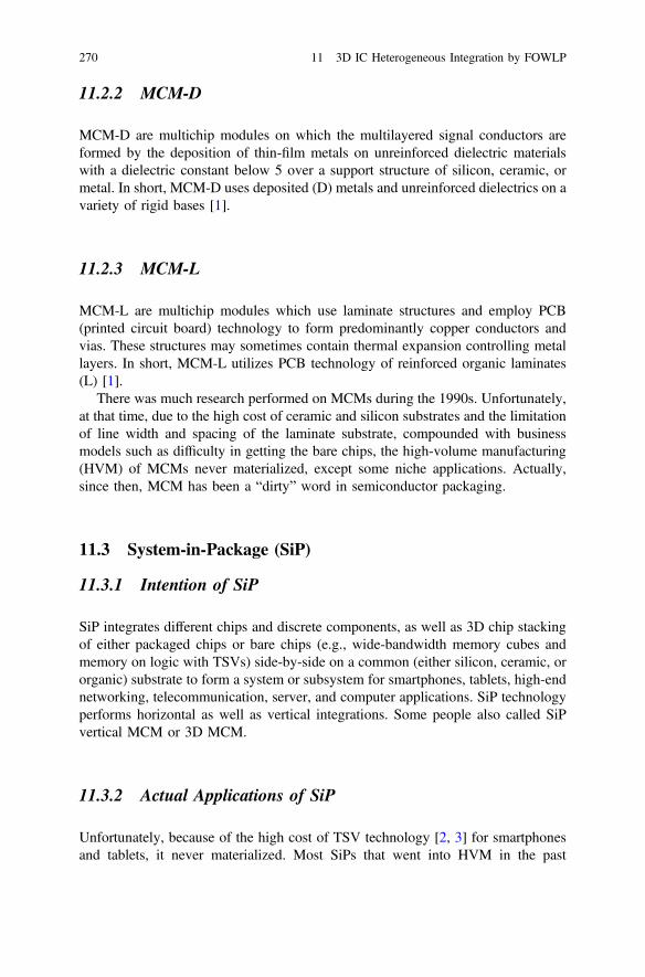
11.2.2 MCM-D
MCM-D are multichip modules on which the multilayered signal conductors areformed by the deposition of thin-film metals on unreinforced dielectric materialswith a dielectric constant below 5 over a support structure of silicon, ceramic, ormetal. In short, MCM-D uses deposited (D) metals and unreinforced dielectrics on avariety of rigid bases [1].
11.2.3 MCM-L
MCM-L are multichip modules which use laminate structures and employ PCB(printed circuit board) technology to form predominantly copper conductors andvias. These structures may sometimes contain thermal expansion controlling metallayers. In short, MCM-L utilizes PCB technology of reinforced organic laminates(L) [1].
There was much research performed on MCMs during the 1990s. Unfortunately,at that time, due to the high cost of ceramic and silicon substrates and the limitationof line width and spacing of the laminate substrate, compounded with businessmodels such as difficulty in getting the bare chips, the high-volume manufacturing(HVM) of MCMs never materialized, except some niche applications. Actually,since then, MCM has been a “dirty” word in semiconductor packaging.
11.3 System-in-Package (SiP)
11.3.1 Intention of SiP
SiP integrates different chips and discrete components, as well as 3D chip stackingof either packaged chips or bare chips (e.g., wide-bandwidth memory cubes andmemory on logic with TSVs) side-by-side on a common (either silicon, ceramic, ororganic) substrate to form a system or subsystem for smartphones, tablets, high-endnetworking, telecommunication, server, and computer applications. SiP technologyperforms horizontal as well as vertical integrations. Some people also called SiPvertical MCM or 3D MCM.
11.3.2 Actual Applications of SiP
Unfortunately, because of the high cost of TSV technology [2, 3] for smartphonesand tablets, it never materialized. Most SiPs that went into HVM in the past
270 11 3D IC Heterogeneous Integration by FOWLP

10 years are actually MCM-L for low-end applications such as smartphones,tablets, smart watches, medical, wearable electronics, gaming systems, consumerproducts, and internet of things (IoT)-related products [4] such as smart homes,smart energy, and smart industrial automation. Most actual applications of SiPs byOSATs (outsourced semiconductor assembly and test providers) integrate two ormore dissimilar chips and some discrete components on a common laminatedsubstrate.
11.3.3 Potential Applications of SiP
The applications of SiP for the high-price, high-margin, and high-end products are,e.g., dual-lens camera modules. However, right now this SiP cannot be all done bythe OSATs, but also involves optical design, testing, lenses, micromotors, flexiblesubstrate, and system integration capabilities which still need to be strengthened.
11.4 System-on-Chip (SoC)
Moore’s law [5] has been driving the system-on-chip (SoC) platform. Especially inthe past 10 years, SoCs have been very popular for smartphones, tablets, and thelike. SoCs integrate different-function ICs into a single chip for a system or sub-system. Two typical SoC examples are shown in the followings.
11.4.1 Apple Application Processor (A10)
The application processor (AP) A10 is designed by Apple and manufactured byTSMC using its 16 nm process technology. It consists of a 6-core graphics pro-cessor unit (GPU), two dual-core central processing unit (CPUs), 2 blocks of staticrandom access memories (SRAMs), etc. The chip area (11.6 mm � 10.8 mm) is125 mm2, Fig. 11.1a.
11.4.2 Apple Application Processor (A11)
The application processor A11 is also designed by Apple and manufactured usingTSMC’s 10 nm process technology. The A11 consists of more functions, includinga tri-core Apple-designed GPU, neural engine for face ID, etc. However, the chiparea (89.23 mm2) is about 30% smaller than that of the A10 because of Moore’slaw, i.e., the feature size is from 16 nm down to 10 nm, Fig. 11.1b.
11.3 System-in-Package (SiP) 271

11.5 Heterogeneous Integration
Some of the early researches in heterogeneous integration have been provided byGeorgia Institute of Technology [6–8], where they reported a differential Si CMOS(complementary metal–oxide semiconductor) receiver IC (operating at 1 Gbps)integrated with a large-area thin-film InGaAs/InP I-MSM (metal–semiconductor–metal) photodetector (Fig. 11.2). Today, most heterogeneous integrations focus onhigher density, finer pitch, and more complex system.
11.5.1 Heterogeneous Integration Versus SoC
Why is the heterogeneous integration of such great interest? One of the key reasonsis because the end of Moore’s law is fast approaching and it is more and moredifficult and costly to reduce the feature size (to do the scaling) to make SoCs.
Heterogeneous integration contrasts with SoCs as follows. The heterogeneousintegration uses packaging technology to integrate dissimilar chips (either side-by-side or stack) with different functions from different foundries, wafer sizes, andfeature sizes (as shown in Fig. 11.3) into a system or subsystem on different (e.g.,organic, silicon, or RDL) substrates, rather than integrating most of the functionsinto a single chip and going for a finer feature size. Heterogeneous integration andSiP are similar, except that heterogeneous integration is for finer pitch and higherdensity applications.
A10 A11
(a) (b)
Fig. 11.1 SoC platforms for the A10 and A11 APs
272 11 3D IC Heterogeneous Integration by FOWLP
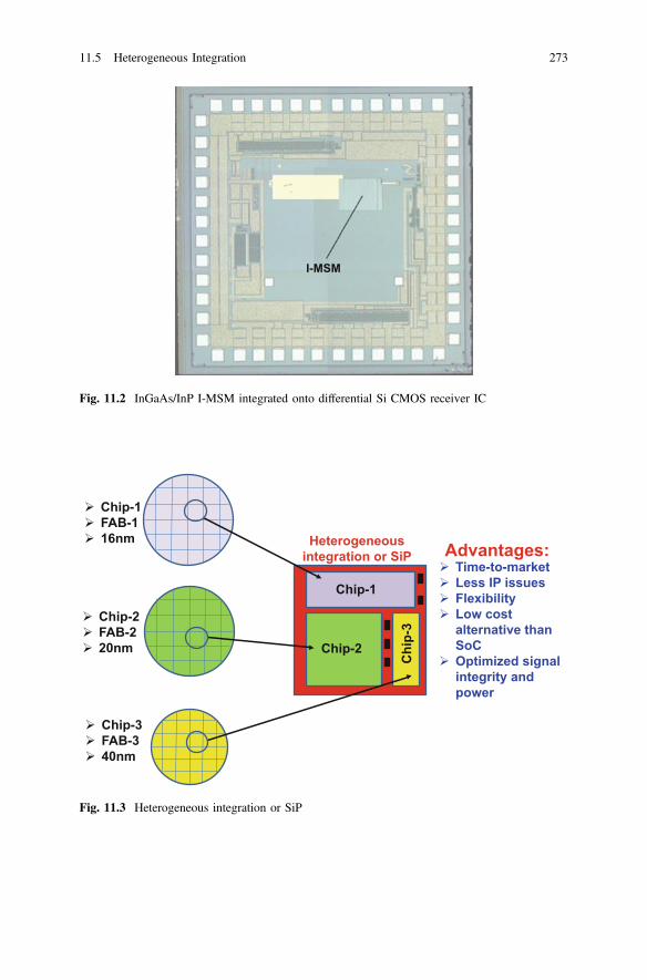
I-MSM
Fig. 11.2 InGaAs/InP I-MSM integrated onto differential Si CMOS receiver IC
Chip-1 FAB-1 16nm
Chip-3 FAB-3 40nm
Chip-2 FAB-2 20nm
Chip-1
Chi
p-3
Chip-2
Time-to-marketLess IP issuesFlexibilityLow cost alternative than SoCOptimized signal integrity and power
Heterogeneous integration or SiP Advantages:
Fig. 11.3 Heterogeneous integration or SiP
11.5 Heterogeneous Integration 273

11.5.2 Advantages of Heterogeneous Integration
For the next few years, we will see more of a higher level of heterogeneousintegration, whether it is for time-to-market, performance, form factor, powerconsumption, signal integrity, or cost. Heterogeneous integration is going to takesome of the market shares away from SoCs on high-end applications such ashigh-end smartphones, tablets, wearables, networkings, telecommunications, andcomputing devices. How should these dissimilar chips talk to each other, however?The answer is redistribution layers (RDLs) [9]! How should those RDLs be made?One key method is by FOWLP technology.
11.6 Heterogeneous Integration on Organic Substrates
Today, the most common applications of heterogeneous integration are on organicsubstrates, or the so-called SiP. The assembly methods are usually SMT (surface mounttechnology) including flip chips with mass reflow as shown in Fig. 2.16a and wirebonding chips on board. In general, this is for low-end to middle-end applications.
11.6.1 Amkor’s SiP for Automobiles
Amkor’s SiP for automobiles focuses on autonomous driving, infotainment, andADAS (advanced drive assist systems), and computer in a car. Figure 11.4a, bshows a couple of examples of Amkor’s SiP for automobiles. It can be seen fromFig. 11.4a that the 42.5 mm � 42.5 mm infotainment organic substrate is sup-porting the processor and DDR (double data rate) memories. While fromFig. 11.4b, the 55 mm � 72 mm organic substrate is supporting the networkswitch, ASIC (application-specific integrated circuit), and memories.
11.6.2 Apple Watch II (SiP) Assembled by ASE
Through USI (Universal Scientific Industrial), ASE is a sole backend provider forApple’s custom-designed S2 SiP modules (Fig. 11.5) for use in the Apple Watch II.It can be seen from Fig. 11.5 that there are 42 chips and are on an organic substrate.Some of these chips are discrete passive components such as capacitors andresistors, ASIC, processors, controller, converter, DRAM (dynamic random accessmemory), NAND, Wi-Fi, NFC (near-field communication), GPS (global position-ing system), sensors, etc.
274 11 3D IC Heterogeneous Integration by FOWLP
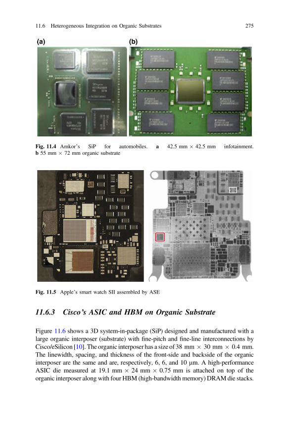
11.6.3 Cisco’s ASIC and HBM on Organic Substrate
Figure 11.6 shows a 3D system-in-package (SiP) designed and manufactured with alarge organic interposer (substrate) with fine-pitch and fine-line interconnections byCisco/eSilicon [10]. The organic interposer has a size of 38 mm � 30 mm � 0.4 mm.The linewidth, spacing, and thickness of the front-side and backside of the organicinterposer are the same and are, respectively, 6, 6, and 10 lm. A high-performanceASIC die measured at 19.1 mm � 24 mm � 0.75 mm is attached on top of theorganic interposer along with four HBM (high-bandwidth memory) DRAMdie stacks.
Fig. 11.4 Amkor’s SiP for automobiles. a 42.5 mm � 42.5 mm infotainment.b 55 mm � 72 mm organic substrate
Fig. 11.5 Apple’s smart watch SII assembled by ASE
11.6 Heterogeneous Integration on Organic Substrates 275

The 3D HBM die stack with a size of 5.5 mm � 7.7 mm � 0.48 mm includes onebase buffer die and four DRAM core dice, which are interconnected with TSVs andfine-pitch micro-pillars with solder caps. This is for the high-end application.
11.6.4 Intel’s CPU and Micron’s HMC on OrganicSubstrate
Figure 11.7 shows Intel’s Knights Landing CPU with Micron’s HMC (hybridmemory cube), which have been shipping to Intel’s favorite customers since thesecond-half of 2016. It can be seen that the 72-core processor is supported by 8multichannel DRAMs (MCDRAM) based on Micron’s HMC technology.Each HMC consists of 4 DRAMs and a logic controller (with TSVs), and eachDRAM has >2000 TSVs with C2 bumps (Fig. 2.6). The CPU and the DRAM+ logic controller stack are attached to an organic package substrate.Micron’s currentHMC assembly process is by using a low-force TCB (thermocompression bonding)with CUF (capillary underfill) as shown in Fig. 2.16b. This is for the high-endapplication.
ASIC/FPGA
HB
MH
BM
Organic Substrate
Fig. 11.6 Cisco’s networking system with organic interposer
276 11 3D IC Heterogeneous Integration by FOWLP

11.7 Heterogeneous Integration on Silicon Substrates(SoW)
In general, heterogeneous integrations on silicon substrates are for multichips onsilicon wafer or system-on-wafer (SoW). The assembly methods are usually flipchips-on-wafers (CoW) with TSVs (through-silicon vias) with mass reflow(Fig. 2.16a) or with thermocompression bonding (Fig. 2.16b, c) for very fine pitches.In general, this is for high-end applications.
11.7.1 Leti’s SoW
One of the early applications of SoW is given by Leti [11, 12] as shown inFig. 11.8. It can be seen that a system of chips such as ASIC and memories, PMIC(power management IC) and MEMS (microelectromechanical systems) are on asilicon wafer with TSVs. After dicing, the individual unit becomes a system orsubsystem and can be attached on an organic substrate or stand alone.
Stacked DRAMs
Fig. 11.7 Intel’s Knights Landing and micron’s HMC on an organic substrate
11.7 Heterogeneous Integration on Silicon Substrates (SoW) 277

11.7.2 Xilinx/TSMC’s CoWoS
In the past few years, because of the very high-density, high I/Os, and ultrafinepitch requirements such as the sliced field-programmable gate array (FPGA), even a12 build-up layers (6-2-6) organic package substrate is not enough to support thechips and a TSV-interposer is needed [13–22]. For example, Fig. 11.9 shows theXilinx/TSMC’s sliced FPBG chip-on-wafer-on-substrate (CoWoS) [15–17]. It canbe seen that the TSV (10 µm diameter) interposer (100 µm deep) has four topRDLs: three Cu damascene layers and one aluminum layer. The 10,000+ of lateralinterconnections between the sliced FPGA chips are connected mainly by the0.4 µm pitch (minimum) RDLs of the interposer. The minimum thickness of theRDLs and passivation is <1 µm. Each FPGA has more than 50,000 microbumps(200,000+ microbumps on the interposer) at 45 µm pitch as shown in Fig. 11.9.
11.7.3 Analog Devices’ MEMS on ASIC Wafer
Figure 11.10 shows Analog Devices’MEMS on ASIC wafer. It can be seen that theMEMS chip is bonded on the ASIC wafer with TSVs. After dicing the wafer intoindividual units, then they can be attached to the PCB (printed circuit board) withsolder bumps (balls).
TSV
Fig. 11.8 Leti’s SoW
278 11 3D IC Heterogeneous Integration by FOWLP

4RDLs TSV
Package Substrate
Build-up Layers
Si Interposer
Interposer
PTH
Chip Chip
Cu PillarSolder
C4 Bumps
Solder Balls
Si
Devices (Cannot see)
Metal Layers
Metal Contacts
Micro Bump
The package substrate is at least (5-2-5)
RDLs: 0.4μm-pitch line width and spacingEach FPGA has >50,000 μbumps on 45μm pitchInterposer is supporting >200,000 μbumps
Core
Fig. 11.9 Xilinx/TSMC’s CoWoS
Fig. 11.10 Analog devices’ MEMS on ASIC wafer
11.7 Heterogeneous Integration on Silicon Substrates (SoW) 279

11.7.4 AMD’s GPU and Hynix’s HBM on TSV-Interposer
Figure 11.11 shows AMD’s Radeon R9 Fury X graphic processor unit(GPU) shipped in the second-half of 2015. The GPU is built on TSMC’s 28 nmprocess technology and is supported by four HBM cubes manufactured by Hynix.Each HBM consists of four DRAMs with C2 bumps and a logic base with TSVsstraight through them. Each DRAM chip has >1000 TSVs. The GPU and HBMcubes are on top of a TSV interposer (28 mm � 35 mm), which is fabricated by
PTH
C44-2-4 Build-up
substrate
TSV-Interposer
GPU
HBM HBM
HBM HBM
TSV-Interposer
1st DRAM
4th DRAM3rd DRAM2nd DRAM
Fig. 11.11 IMD’s GPU and Hynix’s HBM on Si interposer
280 11 3D IC Heterogeneous Integration by FOWLP

UMC with a 64 nm process technology. The final assembly of the TSV interposer(with C4 bumps as shown in Fig. 2.4) on a 4-2-4 organic package substrate (fab-ricated by Ibiden) is by ASE.
11.7.5 Nvidia’s GPU and Samsung’s HBM2on TSV-Interposer
Figure 11.12 shows Nvidia’s Pascal 100 GPU, which was shipped in thesecond-half of 2016. The GPU is built on TSMC’s 16 nm process technology and issupported by four HBM2 (16 GB) fabricated by Samsung. Each HBM2 consists offour DRAMs with C2 bumps and a base logic die with TSVs straight through them.Each DRAM chip has >1000 TSVs. The GPU and HBM2s are on top of a TSVinterposer (1200 mm2), which is fabricated by TSMC with a 64 nm process tech-nology. The TSV interposer is attached to a 5-2-5 organic package substrate withC4 bumps.
TSV Interposer(TSMC’s CoWoS)
HBM2 HBM2
HBM2HBM2
GPU
HBM2 GPU
Build-up Package Substrate
Base logic dieµbump
C4 bump
4DRAMs
Solder Ball
HBM2 by Samsung
Fig. 11.12 Nvidia’s GPU and Samsung’s HBM2 on Si interposer
11.7 Heterogeneous Integration on Silicon Substrates (SoW) 281

11.7.6 UCLA’s SoW
Figure 11.13 shows the complete fabricated Si-IF (silicon interconnect fabric) byUCLA [23]. It can be seen that the test Si-IF has 4 dielets of size (4 mm � 4 mm)with an interconnect pitch of 10 lm and with a total of 640,000 connections. TheSi-IF is fabricated using conventional Si-based BEOL (back end of line) processingwith up to four levels of conventional Cu damascene interconnects with wire pit-ches in the range of 1–10 lm and is terminated with Cu pillars of 2–5 lm heightand diameter also using a damascene process. Au-capped Cu–Cu thermocom-pression direct bonding has been used.
11.8 Heterogeneous Integration on RDLs
Recently, in order to lower the package profile, enhance the performance, and lowerthe cost, the heterogeneous integration on RDLs have been very popular, especiallywith the FOWLP technology. In general, this is for middle-end to high-endapplications.
11.8.1 Xilinx/SPIL’s TSV-Less SLIT
In the past few years, through-silicon via (TSV)-less interposer [24] to support flipchips is a very hot topic in semiconductor packaging. In 2014, Xilinx/SPIL
Fig. 11.13 UCLA’s SoW
282 11 3D IC Heterogeneous Integration by FOWLP

proposed a TSV-less interposer for sliced FPGA chips called silicon-less inter-connect technology (SLIT) [25]. The upper right-hand corner of Fig. 11.14 showsthe new packaging structure along with the old one, which is shown in the left-handcorner. It can be seen that the TSVs and most of the interposer are eliminated andonly the four RDLs needed for performance, mainly, the lateral communication ofthe sliced FPGA chips, remain.
The SLIT process flow is shown in Fig. 11.15. It starts off by fabricating theRDLs—examples on a bare silicon wafer can be seen in [9] (Fig. 11.15a). Thatprocess is followed by chip-to-wafer bonding (i.e., bonding the FPGA chip to thesilicon wafer with RDLs; Fig. 11.15b), and underfilling/curing (Fig. 11.15c). Theseprocesses are followed by overmolding the whole wafer with an epoxy moldcompound (EMC) (Fig. 11.15d). It is followed by backgrinding the over mold toexpose the backside of the chips and attaching an optional reinforcement wafer onthe backside of the chips (Fig. 11.15d). Then, backgrind the silicon wafer(Fig. 11.15e). Next come passivation, photoresist, mask, patterning, etching,sputtering TiCu, photoresist, mask, and patterning (Fig. 11.15f). Finally,Cu-contact pad plating (Fig. 11.15g), photoresist stripping, TiCu etching, andcontrolled-collapse chip connection (C4) wafer bumping are done (Fig. 11.15h).The final assembly of the heterogeneous integration package on the substrate andthen on PCB is shown in Fig. 11.16.
4RDLs
TSV
Interposer
CuPillar
Solder
Si Chip
Devices (Cannot see)
Metal Layers
Metal Contacts
Micro Bump
C4
Xilinx/TSMC’s CoWoS
C4
C4
Si Chip
Cu PillarSolder
4RDLs
Xilinx/SPIL’s SLIT
Package Substrate
Solder Ball
TSV and most interposer are eliminated! Only RDLs are remained.
Lower cost Better performance Lower profile
No entire TSV fabrication module No thin wafer handling technology No novel backside TSV revealing process No multiple inspection & metrology steps for TSV fabrication & backside TSV revealing steps.
Microbump
65nm RDLs
C4/Contact via
Fig. 11.14 Xilinx/SPIL’s SLIT
11.8 Heterogeneous Integration on RDLs 283

(a) RDLs and contact pad build-up on a Si-wafer
Si-wafer
RDL
Pad
Passivation
(b) Chip to wafer bonding
Si-wafer
CHIP
Cu-PillarSolderSolder
(c) Underfilling
Si-wafer
CHIP
(d) Over molding the whole wafer
Si-wafer
CHIPMolding
Compound
CHIPMolding Compound
(e) Reinforced wafer and Backgrind the Si-wafer
Reinforcement Wafer (Heat Spreader)
CHIP
(g) Cu plating
CHIP
(f) Passivation, photoresist, mask, litho, etch, sputter Ti/Cu, photoresist, mask, litho
CHIP
Passivation
(h) Strip photoresist, etch Ti/Cu, C4 bumping
C4 Cu Contact padTi/Cu UBM
Reinforcement (Heat Spreader)
Molding Compound
Underfill Cu-PillarSolderPad
RDLRDL
Fig. 11.15 Process flow for implementing SLIT technology
284 11 3D IC Heterogeneous Integration by FOWLP

Depending on the linewidth/spacing of the RDLs’ conductive wiring, the fab-rication method of the RDLs can be accomplished either by using a polymer for thedielectric layer and Cu plating of the conductive wiring (line width/spacing� 5 lm), or by using plasma-enhanced chemical vapor deposition (PECVD) tomake the SiO2 dielectric layer and Cu damascene plus chemical mechanical pol-ishing (CMP) to make the conductive wiring (linewidth/spacing <5 lm). In 2016,SPIL/Xilinx published a similar paper [26] with more characterization resultsincluding warpage data and called it non-TSV interposer (NTI).
11.8.2 Amkor’s TSV-Less SLIM
In 2015, Amkor announced a very similar technology to SLIT and is called siliconinterposer-less integrated module (SLIM) [27].
CHIP
Passivation
C4
Package Substrate
PCB
Underfill
Molding Compound
Cu-PillarSolderSolder
Solder Ball
Reinforcement (Heat Spreader)
Contact padUBM
RDLRDL
Pad
Fig. 11.16 Final assembly of the Xilinx/SPIL’s SLIT
11.8 Heterogeneous Integration on RDLs 285

11.8.3 Intel’s TSV-Less EMIB (RDL) for FPGA and HBM
Intel proposed an embedded multi-die interconnect bridge (EMIB) [28] RDLs toreplace the TSV interposer [29]. The lateral communication between the chips willbe taken care of by the silicon embedded bridge and the power/ground and somesignals will go through the organic package substrate as shown in Fig. 11.17. Thereare two major tasks in fabricating the organic package substrate with EMIB. One isto make the EMIB, and the other is to make the substrate with EMIB. To make theEMIB, one must first build the RDLs (including the contact pads) on a Si wafer.The way to make the RDLs depends on the line width/spacing of the conductivewiring of the RDLs. Finally, attach the non-RDL side of the Si wafer to a die-attachfilm, and then singulate the Si wafer.
To make the substrate with an EMIB, first place the singulated EMIB with thedie-attached film on top of the Cu foil in the cavity of the substrate, Fig. 11.18a. Itis followed by laminating a resin film on the whole organic package substrate.Then, drilling (on epoxy resin) and Cu plating to fill the holes (vias) to makeconnections to the contact pads of the EMIB. Continue Cu plating to make lateralconnections of the substrate as shown in Fig. 11.18b. Then, it is followed bylaminating another resin film on the whole substrate and drilling (on resin) and Cu
Cu-foil
CHIP
Microbumps
Contact PadsRDLs
EMIB
Resin Film
Drilling and Cu Plating
EMIB
EMIB
EMIBCHIP CHIP
CHIPCHIP
Organic Package Substrate
PCB
Fig. 11.17 Intel’s TSV-less interposer—EMIB
286 11 3D IC Heterogeneous Integration by FOWLP

plating to fill the holes and make contact pads, Fig. 11.18c. (Smaller pads on a finerpitch are for microbumps, while larger pads on a gross pitch are for ordinarybumps). The organic package substrate with an EMIB is ready for bonding of thechips as shown in Fig. 11.18d.
On November 9, 2015, Altera/Intel announced the industry’s first heterogeneousintegration devices that integrate stacked HBM from SK Hynix with high-performance Stratix® 10 FPGAs and SoCs as shown in Fig. 11.19. It can be seenthat the TSV interposer is gone and replaced by Intel’s EMIB.
It is interesting to note that in order to use the EMIB, the chips will have differentkinds/sizes of bumps as shown in Fig. 11.19, i.e., C4 bumps and microbumps (Cupillar + solder cap). Wafer bumping and flip chip assembly could be challenging.
11.8.4 EMIB (RDL) for Intel’s CPU and AMD’s GPU
On November 6, 2017, Intel has formally revealed it has been working on a newseries of processors that combine its high-performance �86 cores CPUs with AMDGPUs (Radeon Graphics), as shown in Fig. 11.20, into the same processor package(heterogeneous integration) using Intel’s own EMIB multi-die technology. If thatwasn’t enough, Intel also announced that it is bundling the design with the latesthigh-bandwidth memory, HBM, as shown schematically in Fig. 11.21.
(a) (b)
(c) (d)
Fig. 11.18 Assembly process of Intel’s EMIB
11.8 Heterogeneous Integration on RDLs 287

11.8.5 STATS ChipPAC’s FOFC-eWLB
At ECTC2013, STATS chipPAC proposed [30, 31] using the fan-out flip chip(FOFC)-eWLB to make the RDLs for the chips to perform mostly lateral com-munications as shown in Fig. 11.22. It can be seen that the TSV interposer, waferbumping, fluxing, chip-to-wafer bonding, cleaning, and underfill dispensing andcuring are eliminated.
Intel/CPU(Kaby Lake)
AM
D/G
PU(R
adeo
n)
Fig. 11.20 Intel’s CPU andAMD’s GPU on EMIB
C4 bumps
PCB
Solder Ball
Package Substrate EMIBEMIB
FPGAHBM HBMRDL RDL
Microbumps C4 bumps Microbumps
Via
FPGA
Fig. 11.19 Intel’s FPGA and HBM on EMIB
288 11 3D IC Heterogeneous Integration by FOWLP

11.8.6 ASE’s FOCoS
In 2016, ASE [32] proposed using the fan-out wafer-level packaging (FOWLP)technology (chip-first and die-down on a temporary wafer carrier and then over-molded by the compression method) to make the RDLs for the chips to performmostly lateral communications as shown in Fig. 11.23; the technology is called
C4 bumps
PCB
Solder Ball Package Substrate
EMIB EMIB
HBM HBMRDL RDL
Microbumps C4 bumps Microbumps
Via
CPU GPUEMIB
HBM HBM
HBM
HBM HBM
HBM
EMIB
EMIB EMIB
EMIB EMIB
EMIB EMIB
AMD/GPU (Radeon)
Intel/CPU (Kaby Lake)
Fig. 11.21 Schematic of Intel’s CPU, AMD’s GPU, and Hynix’s HBM on EMIB
Logic
Logic Analog
Organic Substrate
AnalogTSV interposer
Organic Substrate
C4 bumpUnderfill
µbump
C4 bumpRDLs
EMC
Fig. 11.22 STATSChipPac’sTSV-less FOFC-eWLB
11.8 Heterogeneous Integration on RDLs 289

fan-out wafer-level chip-on-substrate (FOCoS). The TSV interposer, wafer bump-ing of the chips, fluxing, chip-to-wafer bonding, and cleaning, and underfill dis-pensing and curing are eliminated. The bottom RDL is connected to the packagesubstrate using under bump metallurgy (UBM) and the C4 bump as shown inFig. 11.23.
11.8.7 MediaTek’s RDLs by FOWLP
In 2016, MediaTek [33] proposed similar TSV-less interposer RDLs fabricated withFOWLP technology as shown in Figs. 11.24 and 11.25. Instead of the C4 bump,they used a microbump (Cu pillar + solder cap) to connect the bottom RDL to the6-2-6 package substrate.
11.9 3D IC Heterogeneous Integration by FOWLP
A low-profile and low-cost 3D IC heterogeneous integration of the applicationprocessor chipset by FOWLP is presented in this section. The emphasis is placed onthe design of the package.
Die1
Die2
Die2
Die1TSV-interposer + RDLs
Microbumps + Underfill
Package Substrate
Solder Balls C4 bumps Solder Balls
Package Substrate
C4 bumps
RDLs
EMC EMC
C4 bump
UBM
RDLsRDLs RDLs
CoWoS ASE’s FOCoS
Fig. 11.23 ASE’s FOCoS
290 11 3D IC Heterogeneous Integration by FOWLP

11.9.1 Application Processor with FOWLP
The A10 and A11 application processors are packaged using TSMC’s InFO (in-tegrated fan-out) wafer-level packaging method [34–44]. The mobile dynamicrandom access memories (DRAMs) are wire bonded on a 3-layer core-less packagesubstrate and the substrate is area-array solder balled on top of the applicationprocessor package—a package-on-package (PoP) format as shown schematically inFig. 11.26. The interconnections between the application processor and the mobileDRAMs are mainly through the RDLs, through-InFO vias (TIVs), solder balls, andcore-less substrate.
EMC
RDL3
RDL2
DL4
DL3
DL2
DL1 RDL1
Cu
Package Substrate
Solder cap
Pad
Si Die
Package substrate
RDL3DL4
UBM
Cu-pillar
Solder resist opening
Solder cap
Cu pad
µbump
Fig. 11.24 Schematic of MediaTek’s RDLs by FOWLP
11.9 3D IC Heterogeneous Integration by FOWLP 291

(a)
(b)
Microbump
Fig. 11.25 SEM images of MediaTek’s RDLs by FOWLP
3-Layer Coreless Package Substrate Wirebond
Application ProcessorTIV
Solder Ball
RDLs
EMC
Over Mold
Underfill
PCB
Mobile DRAMsMobile DRAMs
Solder Ball
Fig. 11.26 PoP for packaging the application processor and mobile memory
292 11 3D IC Heterogeneous Integration by FOWLP

11.9.2 Application Processor by 3D IC HeterogeneousIntegration with FOWLP
A new 3D IC heterogeneous integration by FOWLP, as shown in Fig. 11.27, isproposed in this chapter. It consists of the SoC, chips, and the mobile DRAMs.Their interconnections are mainly through the RDLs, which can be fabricated bythe FOWLP method. Depending on the number of layers of the RDLs, usually thetotal thickness of a 3-layer RDL is about 40 µm. The DRAMs (� 50 µm thick) arecross-stacked with wire bonds and then encapsulated. The diameter of the solderball is usually 200 µm.
Figure 11.28 shows a special case of Fig. 11.27 (when there is no other chip andthe SoC is the application processor). Comparing the new design (Fig. 11.28) withthat of Fig. 11.26 (the 3D IC heterogeneous integration vs. the PoP), it is obviousthat: (1) the new design leads to a lower package profile; (2) the new design has lessinterconnects; (3) the new design is more reliable because of less interconnects;(4) the new design has better electrical performance; and (5) the new design leads tolower cost.
The manufacturing process of the proposed 3D IC heterogeneous integration isvery simple. First, the device wafer has to be modified by sputtering an under bumpmetallurgy (UBM) and electroplating a Cu contact pad (for building the RDLs later),as shown in Fig. 11.29. This step is followed by spin coating a polymer on top of thedevice wafer and laminating a die-attach film (DAF) at the bottom of the devicewafer. Meanwhile, a light-to-heat conversion (LTHC) layer is spin coated onto thetemporary glass carrier wafer. Then the individual known-good die (KGD) (chip)from the device wafer is placed face-up on the LTHC carrier. This step is followedby epoxy molding compound (EMC) dispensing, compression molding, and finally,post mold cure (PMC). These steps are followed by backgrinding the EMC andpolymer to expose the Cu contact pad for making the RDLs and for mounting thesolder balls, as shown in Fig. 11.29. This is the conventional FOWLP method topackage the application processor [34–44], as shown in Chap. 6.
PCB
EMC
RDLsSolder
Ball
SoCCHIP
Wirebonded DRAMs Encapsulant
Fig. 11.27 3D IC heterogeneous integration by FOWLP
11.9 3D IC Heterogeneous Integration by FOWLP 293
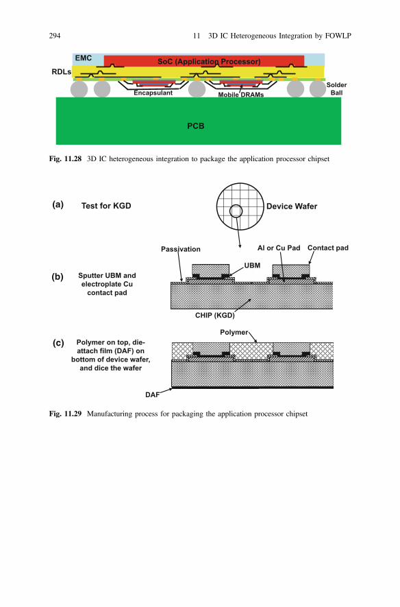
SoC (Application Processor)
PCB
EMC
RDLsSolder
BallMobile DRAMsEncapsulant
Fig. 11.28 3D IC heterogeneous integration to package the application processor chipset
Test for KGD Device Wafer
Sputter UBM and electroplate Cu
contact pad
CHIP (KGD)
UBM
Contact padPassivation Al or Cu Pad
Polymer on top, die-attach film (DAF) on
bottom of device wafer, and dice the wafer
DAF
Polymer
(a)
(b)
(c)
Fig. 11.29 Manufacturing process for packaging the application processor chipset
294 11 3D IC Heterogeneous Integration by FOWLP

There are two methods to attach the mobile DRAMs to the bottom of theapplication processor fan-out wafer-level package. The first method comprises thefollowing steps: (1) removing the glass carrier by a laser (Fig. 11.30a); (2) dicingthe reconstituted wafer into strips with individual packages (Fig. 11.30b); (3) wirebonding the memory chips to the bottom side of the individual package(Fig. 11.30c, d); (4) and then glob topping the wires and memory chips with anencapsulant (Fig. 11.30c, d).
The second method to attach the mobile DRAMs to the bottom of the applicationprocessor fan-out wafer-level package comprises the following steps: (1) wirebonding the memory chips to the bottom side of every package on the reconstitutedwafer; (2) glob topping the wires and memory chips with an encapsulant; and(3) then dicing the reconstituted wafer into individual packages (Fig. 11.31).
Figure 11.32 is a special case of Fig. 11.27. This is when it is difficult and costlyto reduce the feature size to make the SoC. Therefore, some of the functions (forexample, the GPU) are not integrated into the SoC and the GPU chip is placedside-by-side with the SoC.
Build RDLs on contact pads and then mount solder
balls
Place KGD (chip) face-up
Compression mold the EMC on the
reconfigured carrier
Backgrind the EMC and polymer to
expose the contact pad
Coated with a light-to-heat conversion (LTHC)
release layer
DAF
Contact pad
EMC
KGD KGDKGD
KGD KGDKGD
KGD KGDKGD
Solder ballsRDLs
KGD KGDKGD
PolymerTemporary glass wafer carrier
LTHC
(d)
(e)
(f)
(g)
(h)
Fig. 11.29 (continued)
11.9 3D IC Heterogeneous Integration by FOWLP 295
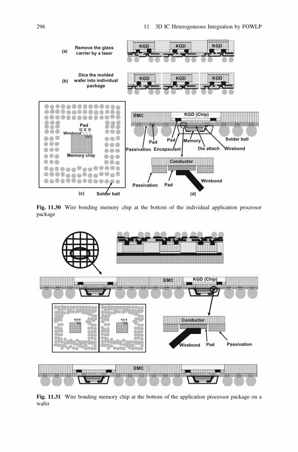
PadWirebond
Memory chip
Solder ball
Solder ball
KGD (Chip)
Die attach Wirebond Pad
EMC
Pad Memory
Passivation PadWirebond
Conductor
Remove the glass carrier by a laser
Passivation
(d) (c)
Encapsulant
KGD KGD KGD
KGD KGD KGD Dice the molded
wafer into individual package
(a)
(b)
Fig. 11.30 Wire bonding memory chip at the bottom of the individual application processorpackage
Passivation PadWirebond
Conductor
KGD (Chip) EMC
EMC
Fig. 11.31 Wire bonding memory chip at the bottom of the application processor package on awafer
296 11 3D IC Heterogeneous Integration by FOWLP

In [21], we asked the question: “What if there is no PoP for the applicationprocessor chipset?” We proposed to place the application processor and the mobileDRAMs side-by-side on a build-up package substrate. The memory chips can beeither cross-stacked or individually placed by wire bonding. Also, the memorychips can be placed individually by solder-bumped flip chips. The memory chipscan even be stacked and have TSVs. In this study, because we used the FOWLPmethod to construe the RDLs for the interconnections between the SoC and mobileDRAMs as shown in Fig. 11.33, the build-up package substrate was eliminated.
PCB
EMC
RDLsSolder
Ball
Application Processor MemoryMemory
Application Processor
(SoC)
MobileDRAM
Mob
ile D
RA
M
MobileDRAM
Mob
ile D
RA
M
Application Processor
(SoC)
Stac
k M
obile
D
RA
M
Fig. 11.33 2D/3D IC heterogeneous integration to package the application processor chipset
SoC (CPU, SRAM, …)
PCB
EMC
RDLsSolder
BallMobile DRAMsEncapsulant
GPU
Fig. 11.32 3D IC heterogeneous integration to package the application processor chipset
11.9 3D IC Heterogeneous Integration by FOWLP 297

11.10 3D IC High-Performance HeterogeneousIntegration by FOWLP
A high-performance 3D IC heterogeneous integration of CPU, GPU, FPGA, ASIC,HBM, etc., is presented in this section. The emphasis is placed on the manufac-turing process.
11.10.1 High-Performance 3D IC HeterogeneousIntegration System
Figure 11.34 schematically shows a 3D IC high-performance heterogeneous inte-gration by FOWLP technology. It can be seen that it consists of a GPU, a FPGA(field-programmable grid array), CPU, or a high-performance application-specificintegrated circuit (ASIC), and is surrounded by high-bandwidth memory(HBM) cubes. Each HBM cube consists of four DRAMs and a logic base withthrough-silicon vias (TSVs) [2, 3] straight through them. Each DRAM chip has>500 TSVs. The interconnections between the GPU/FPGA/CPU/ASIC and HBMsare through the RDLs. The major heat path of this structure is from the backside ofthe GPU/FPGA/CPU/ASIC to the heat spreader. A heat sink can be added on top ofthe heat spreader if it is necessary.
11.10.2 Manufacturing Process
In this case, the emphasis is placed on the manufacturing method (process) of thisstructure. This method comprises these steps: (1) testing for KGD of device wafers;(2) sputtering UBM; (3) electroplating the Cu contact pad; (4) spin coating apolymer on top of the device wafers; and (5) painting a thermal interface material(TIM) on the bottom (backside) of the device wafers (Fig. 11.35). The last step isdifferent from the conventional method (the first case) which is laminating a DAFon the bottom of the device wafers.
After the steps outlined above are completed, the following are done: (1) theindividual KGDs are picked and placed face-up on a metal such as copper, alu-minum, steel, and an alloy 42 (with thermal expansion coefficient = 8 to10 � 10−6/°C) carrier about 1 mm thick; (2) molding the EMC on the reconstitutedwafer is accomplished by using the compression method and then post mold curing(PMC) of the EMC; (3) backgrinding the EMC and polymer to expose the Cucontact pad; (4) building up the RDLs; and (5) mounting the solder balls. Then, thereconstituted wafer is diced into individual packages (Fig. 11.35). (Note: thisprocess is different from the conventional method, which used a glass carrier andwas coated with an LTHC release layer).
298 11 3D IC Heterogeneous Integration by FOWLP

HBM HBMGPU/FPGA
PCB
EMCRDLs
Solder Ball
Heat Spreader Thermal Interface Material
GPU/FPGA/CPU/ASIC
HBM
HBM
HBM
HBM
Fig. 11.34 3D IC high-performance heterogeneous integration by FOWLP
Test for KGD Device Wafer
Sputter UBM and electroplate Cu
contact pad
CHIP (KGD)
UBM
Contact pad Passivation Al or Cu Pad
Polymer on top and thermal interface
material (TIM) on bottom of the device wafer, and
dice the wafer
TIM
Polymer
(a)
(b)
(c)
Fig. 11.35 Manufacturing method for 3D IC high-performance heterogeneous integration
11.10 3D IC High-Performance Heterogeneous Integration by FOWLP 299

11.10.3 Advantages of the New Manufacturing Process
It should be emphasized that unlike the conventional method, there is no debondingof the carrier. The metal carrier becomes the heat spreader of the individualhigh-performance heterogeneous integration package. This new method of manu-facturing high-performance chips and memory cubes in a heterogeneous integrationscheme with the FOWLP technology results in fewer assembly steps, lower cost,faster time-to-market, and higher assembly yield. Also, because of the metal carrier,the warpage is reduced during all the process steps. Furthermore, because of themetal carrier, the individual package size can be larger.
11.11 Summary and Recommendations
Two 3D IC heterogeneous integrations by FOWLP technology have been pre-sented. The first 3D IC heterogeneous integration is emphasized on the design andthe other 3D IC high-performance heterogeneous integration is on the manufac-turing method. Some important results and recommendations are as follows:
Build RDLs on contact pads and then mount
solder balls
Compression mold the EMC on the
reconfigured carrier
Backgrind the EMC and polymer to
expose the contact pad
EMC
KGD KGD KGD
KGD KGD KGD
Solder balls RDLs
KGD KGD KGD
Polymer
Place KGD (chip) face-upon on a metal wafer
carrier
TIM
Contact pad
KGD KGD KGD
Metal wafer carrier
Solder balls RDLs
KGD KGD KGD
Dice the reconstituted wafer with the metal carrier
into individual package. The metal carrier becomes
the heat spreader
Metal wafer carrier
TIM
Heat Spreader
(d)
(e)
(f)
(g)
(h)
Fig. 11.35 (continued)
300 11 3D IC Heterogeneous Integration by FOWLP

• A 3D IC heterogeneous integration of the application processor chipset has beenproposed. The interconnections between the application processor and mobileDRAMs are through the RDLs, which are fabricated using the FOWLP method.The manufacturing processes for making the 3D IC heterogeneous integrationhave also been presented.
• When it is difficult and costly to reduce the feature size to make the SoC, oneway is not to integrate some of the functions (for example, the GPU) into theSoC and instead place the GPU chip side-by-side with the SoC.
• The simplest heterogeneous integration of the application processor chipset is toplace the application processor and the mobile DRAMs side-by-side on RDLs.One consideration is that the package size could be too large to be reliable. Oneof the alternatives is to stack up the mobile DRAMs by wire bonding (for lowercost) or TSV (for wider bandwidth.)
• A 3D IC high-performance heterogeneous integration of GPU/FPGA/CPU/ASIC and HBM/HBM2 by FOWLP technology has been proposed. Emphasis isplaced on a simple and effective manufacturing method to fabricate the struc-ture. Unlike the conventional method, there is no debonding of the temporarymetal carrier. The metal carrier becomes the heat spreader of the individualhigh-performance heterogeneous integration package.
• The advantages of heterogeneous integration are time-to-market, performance,form factor, power consumption, signal integrity, and cost.
• In order to lower the package profile and enhance the electrical and thermalperformance of the application processor chipset for mobile applications such assmartphones and tablets, the current PoP format should be eliminated.
• The recent advances of heterogeneous integrations on organic substrates, siliconwafers, and RDLs have been briefly mentioned.
References
1. Lau, J.H. 1994. A Brief Interlocution to Wire Bonding, Tape Automated Bonding, and FlipChip on Board for Multichip Module Applications. In Chip on Board Technologies forMultichip Modules, ed. J.H. Lau, 1–100. New York: Van Nostrand Reinhold.
2. Lau, J.H. 2013. Through-Silicon Via (TSV) for 3D Integration. New York: McGraw-Hill.3. Lau, J.H. 2016. 3D IC Integration and Packaging. New York: McGraw-Hill.4. Lau, J.H. 2015. Semiconductor and Packaging for Internet of Things. Chip Scale Review 19:
25–30.5. Moore, G. 1965. Cramming More Components Onto Integrated Circuits. Electronics 38 (8).6. Jokerst, N.M. 1997. Hybrid Integrated Optoelectronics: Thin Film Devices Bonded to Host
Substrates. International Journal of High Speed Electronics and Systems 8 (2): 325–356.7. Vrazel, M., J. Chang, I. Song, K. Chung, M. Brooke, N. Jokerst, A. Brown, and D. Wills.
2001. Highly Alignment Tolerant InGaAs Inverted MSM Photodetector HeterogeneouslyIntegrated on a Differential Si CMOS Receiver Operating at 1 Gbps. In Proceedings of IEEE/ECTC, May 2001, 1–6.
8. Jokerst, N.M., M.A. Brooke, S. Cho, S. Wilkinson, M. Vrazel, S. Fike, J. Tabler, Y. Joo,S. Seo, D. Wills, and A. Brown. 2003. The Heterogeneous Integration of Optical
11.11 Summary and Recommendations 301

Interconnections Into Integrated Microsystems. IEEE Journal of Selected Topics in QuantumElectronics 9 (2): 350–360.
9. Lau, J.H., P. Tzeng, C. Lee, C. Zhan, M. Li, J. Cline, et al. 2014. Redistribution Layers(RDLs) for 2.5D/3D IC Integration. In IMAPS Proceedings, October 2013, 434–441. Also,IMAPS Transactions, Journal of Microelectronic Packaging 11 (1): 16–24.
10. Li, L., P. Chia, P. Ton, M. Nagar, S. Patil, J. Xie, et al., 3D SiP with Organic Interposer ofASIC and Memory Integration. In IEEE/ECTC Proceedings, 2016, 1445–1450.
11. Souriau, J., O. Lignier, M. Charrier, and G. Poupon. 2005. Wafer Level Processing of 3DSystem in Package for RF and Data Applications. In IEEE/ECTC Proceedings, 356–361.
12. Henry, D., D. Belhachemi, J.-C. Souriau, C. Brunet-Manquat, C. Puget, G. Ponthenier,J. Vallejo, C. Lecouvey, and N. Sillon. 2006. Low Electrical Resistance Silicon ThroughVias: Technology and Characterization. In IEEE/ECTC Proceedings, 2006, 1360–1366.
13. Selvanayagam, C., J.H. Lau, X. Zhang, S. Seah, K. Vaidyanathan, and T.C. Chai. 2009.Nonlinear Thermal Stress/Strain Analyses of Copper Filled TSV (Through Silicon Via) andTheir Flip-Chip Microbumps. In Proceedings of IEEE/ECTC, May 2008, 1073–1081. Also,IEEE Transactions on Advanced Packaging 32 (4), 720–728 (November 2009).
14. Chai, T.C., X. Zhang, J.H. Lau, C.S. Selvanayagam, D. Pinjala, Y. Hoe, Y. Ong, V. Rao,E. Wai, H. Li, E. Liao, N. Ranganathan, V. Kripesh, S. Liu, J. Sun, M. Ravi, C. Vath III, andY. Tsutsumi. 2011. Development of Large Die Fine-Pitch Cu/low-k FCBGA Package withThrough Silicon Via (TSV) Interposer. IEEE Transactions on CPMT 1 (5): 660–672.
15. Banijamali, B., S. Ramalingam, H. Liu, and M. Kim. 2012. Outstanding and InnovativeReliability Study of 3D TSV Interposer and Fine Pitch Solder Micro-bumps. In Proceedingsof IEEE/ECTC, May 2012, 309–314.
16. Chaware, R., K. Nagarajan, and S. Ramalingam. 2012. Assembly and Reliability Challengesin 3D Integration of 28 nm FPGA Die on a Large High Density 65 nm Passive Interposer. InIEEE/ECTC Proceedings, 2012, 279–283.
17. Banijamali, B., C. Chiu, C. Hsieh, T. Lin, C. Hu, S. Hou, S. Ramalingam, S. Jeng,L. Madden, and D. Yu. 2013. Reliability Evaluation of a CoWoS-Enabled 3D IC Package. InProceedings of IEEE/ECTC, May 2013, 35–40.
18. Yu, A., J.H. Lau, S. Ho, A. Kumar, W. Hnin, W. Lee, M. Jong, V. Sekhar, V. Kripesh,D. Pinjala, S. Chen, C. Chan, C. Chao, C. Chiu, C. Huang, and C. Chen. 2011. Fabrication ofHigh Aspect Ratio TSV and Assembly With Fine-Pitch Low-Cost Solder Microbump for SiInterposer Technology With High-Density Interconnects. IEEE Transactions on CPMT 1 (9):1336–1344.
19. Lau, J.H. 2011. Overview and Outlook of TSV and 3D Integrations. MicroelectronicsInternational 28 (2): 8–22.
20. Lau, J.H., and G.Y. Tang. 2012. Effects of TSVs (Through-Silicon Vias) on ThermalPerformances of 3D IC Integration System-In-Package (SiP). Microelectronics Reliability52 (11): 2660–2669.
21. Lau, J.H. 2014. The Future of Interposer for Semiconductor IC Packaging. Chip Scale Review18 (1): 32–36.
22. Lau, J.H., S. Lee, M. Yuen, J. Wu, J. Lo, H. Fan, and H. Chen. 2013. Apparatus HavingThermal-Enhanced and Cost-Effective 3D IC Integration Structure With Through Silicon ViaInterposer. U.S. Patent No. 8,604,603, Filed February 29, 2010 and Issued December 10,2013.
23. Bajwa, A., S. Jangam, S. Pal, N. Marathe, T. Bai, T. Fukushima, M. Goorsky, and S.S. Iyer.2017. Heterogeneous Integration at Fine Pitch (� 10 lm) Using Thermal CompressionBonding. In IEEE/ECTC Proceedings, 2017, 1276–1284.
24. Lau, J.H. 2016. TSV-Less Interposers. Chip Scale Review 20: 28–35.25. Kwon, W., S. Ramalingam, X. Wu, L. Madden, C. Huang, H. Chang, et al. 2014.
Cost-Effective and High-Performance 28 nm FPGA with New Disruptive Silicon-LessInterconnect Technology (SLIT). In Proceedings of International Symposium onMicroelectronics, 599–605.
302 11 3D IC Heterogeneous Integration by FOWLP

26. Liang, F., H. Chang, W. Tseng, J. Lai, S. Cheng, M. Ma, et al. 2016. Development ofNon-TSV Interposer (NTI) for High Electrical Performance Package. In IEEE/ECTCProceedings, 2016, 31–36.
27. Hiner, D., M. Kelly, R. Huemoeller, and R. Reed. 2015. Silicon Interposer-Less IntegratedModule—SLIM. In International Conference and Exhibition on Device Packaging, 2015.
28. Chiu, C., Z. Qian, M. Manusharow. 2014. Bridge Interconnect with Air Gap in PackageAssembly. US Patent No. 8,872,349.
29. Mahajan, R., R. Sankman, N. Patel, D. Kim, K. Aygun, Z. Qian, et al. 2016. EmbeddedMulti-die Interconnect Bridge (EMIB)—A High-Density, High-Bandwidth PackagingInterconnect. In IEEE Proceedings of Electronic Components and Technology Conference,2016, 557–565.
30. Pendse, R.D. 2011. Semiconductor Device and Method of Forming Extended SemiconductorDevice with Fan-Out Interconnect Structure to Reduce Complexity of Substruate. PatentPublication No. US2013/0161833A1, Filed on December 23, 2011.
31. Yoon, S.W., P. Tang, R. Emigh, Y. Lin, P.C. Marimuthu, and R. Pendse. 2013. FanoutFlipchip eWLB (embedded Wafer Level Ball Grid Array) Technology as 2.5D PackagingSolutions. In Proceedings of IEEE/ECTC, 2013, 1855–1860.
32. Lin, Y., W. Lai, C. Kao, J. Lou, P. Yang, C. Wang, et al. 2016. Wafer Warpage Experimentsand Simulation for Fan-Out Chip-On-Substrate. In IEEE Proceedings of ElectronicComponents and Technology Conference, 2016, 13–18.
33. Chen, N., T. Hsieh, J. Jinn, P. Chang, F. Huang, J. Xiao, et al. 2016. A Novel System-In-Package with Fan-Out WLP for High-Speed SERDES Application. In IEEE Proceedingsof Electronic Components and Technology Conference, 2016, 1495–1501.
34. Lau, J.H. 2015. Patent Issues of Fan-Out Wafer/Panel-Level Packaging. Chip Scale Review19: 42–46.
35. Lau, J.H., N. Fan, M. Li. 2016. Design, Material, Process, and Equipment of EmbeddedFan-Out Wafer/Panel-Level Packaging. Chip Scale Review 20: 38–44.
36. Tseng, C., C. Liu, C. Wu, D. Yu. 2016. InFO (Wafer-Level Integrated Fan-Out) Technology.In IEEE/ECTC Proceedings, June 2016, 1–6.
37. Hsieh, C., C. Wu, D. Yu. 2016. Analysis and Comparison of Thermal Performance ofAdvanced Packaging Technologies for State-of-the-Art Mobile Applications. In IEEE/ECTCProceedings, June 2016, 1430–1438.
38. Lau, J.H., M. Li, D. Tian, N. Fan, E. Kuah, K. Wu, et al. 2017. Warpage and ThermalCharacterization of Fan-Out Wafer-Level Packaging. In IEEE/ECTC Proceedings, 2017,595–602. Also, IEEE Transactions on CPMT 7 (10), 1729–1938 (October 2017).
39. Lau, J.H., M. Li, N. Fan, E. Kuah, Z. Li, K. Tan, T. Chen, et al. 2017. Fan-Out Wafer-LevelPackaging (FOWLP) of Large Chip with Multiple Redistribution-Layers (RDLs). In IMAPSProceedings,October 2017, 576–583. Also, IMAPS Transactions, Journal of Microelectronicsand Electronic Packaging 14 (4), 123–131 (October 2017).
40. Li, M., Q. Li, J.H. Lau, N. Fan, E. Kuah, K. Wu, et al. 2017. Characterizations of Fan-OutWafer-Level Packaging. In IMAPS Proceedings, October 2017, 557–562.
41. Lau, J.H. 2018. 3D IC Heterogeneous Integration by FOWLP. Chip Scale Review 22: 16–21.42. Lau, J.H. 2018. FOWLP for 3D IC Heterogeneous Integration. In IEEE/CSTIC Proceedings,
VII. 1–6.43. Kuah, E., W. Chan, J. Hao, N. Fan, M. Li, J.H. Lau, et al. 2017. Dispensing Challenges of
Large Format Packaging and Some of Its Possible Solutions. In IEEE/EPTC Proceedings,December 2017, S27_1-6.
44. Hua, X., H. Xu, Z. Li Zhang, D. Chen, K. Tan, J.H. Lau, et al. 2017. Development ofChip-First and Die-Up Fan-Out Wafer-Level Packaging. In IEEE/EPTC Proceedings,December 2017, S23_1-6.
References 303