
82 Silicon Wafer Manufacture V6
40
HND Unit 73 QCF Level 5 Topic 1.1 Designing & Manufacturing Integrated Circuits Part 1 Silicon Wafers Nick Brackenbury Silicon Wafer Manufacture V6 [email protected] 1
Transcript of 82 Silicon Wafer Manufacture V6

HND Unit 73
QCF Level 5
Topic 1.1
Designing & Manufacturing
Integrated Circuits
Part 1
Silicon Wafers
Nick Brackenbury Silicon Wafer Manufacture V6 [email protected] 1

Designing & Manufacturing
of Integrated Circuits
Part 1 - Silicon Wafers Manufacture
Part 2 – Mask Design & Fabricating the IC
Part 3 – Packaging IC into Protective Case
Nick Brackenbury Silicon Wafer Manufacture V6 [email protected] 2

This sub-topic covers the
types of wafers used in
IC manufacture and the
series of manufacturing
processes used in making
and repairing these
wafers
Sub-Topic 1.1 Aim
Silicon wafers (after IC fab) 2”, 4”,
6” and 8” standard sizes
Nick Brackenbury Silicon Wafer Manufacture V6 [email protected] 3

Properties of Silicon:
Chemical element, atomic number 14 in periodic table
Classic semiconductor – its resistance is half way between (metal)
conductors and (dielectric) insulators
Name of silicon derived from Latin (silex meaning pebbles, silicis
meaning flint)
It occurs as silicon dioxide being sand, quartz or silicate, which contain
other impurities as well
Very low cost starting material and very stable element
‘Competitors’ such as Gallium Arsenide and Germanium can operate
faster in circuits but are less stable in manufacturing and heat sensitive
when finally running in circuits
On silicon crystal, oxide layers can be produced very easily
Silicon dioxide is an insulator of the very highest quality, and can be
fabricated very precisely on the substrate (wafer base for IC)
Having a semiconductor base with an easily added insulation material
helps in the IC manufacturing process
Silicon Wafer Fabrication
Bohr model of silicon
– has 14 electrons, 14
protons and 14
neutrons.
Outer shell has three
electrons called a
valence III (three)
Nick Brackenbury Silicon Wafer Manufacture V6 [email protected] 4

The silicon crystal structure is ultra stable
and strong
But ….
Only when the silicon is extremely pure, by
avoiding ‘fault lines’ in the crystal lattice.
To produce silicon crystal in the form that we
need it for semiconductor manufacture is an
expensive process.
It has to be purified from ordinary beach
sand then crystallised into a large ingot with
a very organised symmetrical crystal
structure.
Silicon Crystal Structure
Nick Brackenbury Silicon Wafer Manufacture V6 [email protected] 5

Companies that manufacture Integrated Circuit chips
The chips could be 2mm square up to 1cm square
A chip is a complete circuit comprising 10’s to 10’s of thousands to 10’s of millions of transistors
Circuits can be ‘analogue’ such as Operational Amplifiers (Op Amps), oscillators, control IC’s
Circuits can be ‘digital’ such as logic functions for use within control systems or computer systems
Circuits can be ‘mixed signal’ used to convert audio / visual to / from digital streams in ‘phones and HDTV’s
100’s to 1000’s of identical chips can be fabricated at a time using a wafer as substrate
Who wants Silicon Wafers?
Nick Brackenbury Silicon Wafer Manufacture V6 [email protected] 6

USA still use Imperial UoM, whilst Europe and most of the rest of the
world use Metric UoM. Sales and product information can be in
imperial or jargon terms. It is wise to use metric for calculations:
1,000mm = 100 cm = 1m
Conversion between Imperial and Metric, with jargon, is:
mil = thousandths of an inch = 0.001 inch
mil is a USA term thou is a UK term
1” = 2.54cm = 25.4mm 1mm = 39.37 mil or thou
1 micron = 10-6m = 1 micro-meter = 0.000001m
1,000 microns = 1mm 1 micron = 10-3mm
1 mil = 0.0254 mm = 24.5μm = 25.4 x 10⁻⁶m
IC technology is becoming more and more micro-miniaturised so
measurement is now using the atomic physics UoM:
1 Ångstrom = 10-10 m = 0.1 nm = 1 billionth of a meter
Units of Measurement
Nick Brackenbury Silicon Wafer Manufacture V6 [email protected] 7

Wafers have always been made in a range of standard sizes
Wafers are normally manufactured as perfectly circular discs
The manufacturing measurements are now always in metric
However, the jargon is to refer to a disc by its nearest inch size
1” to 5” were/are produced in inches
150mm to 450mm are produced in mm
Standard Wafer Sizes
Imperial Metric Imperial
Actual Size
2” 50mm 2”
3” 75mm 3”
4” 100mm 4”
5” 150mm 5”
Imperial Metric
Actual Size
Imperial
Actual Size
6” 150mm 5.9”
8” 200mm 7.9”
12” 300mm 11.8”
18” 450mm 17.7”
Nick Brackenbury Silicon Wafer Manufacture V6 [email protected] 8

6” silicon wafer after die
fabrication, with 128 VLSI
digital IC die, next step
cutting using diamond
saw.
Note the flat edge along
the bottom, this was the
standard locating method
up to and including 6” die.
It was found to be
wasteful so the flat edge
was replaced with a small
‘v’ cut.
6” Silicon Wafer
Nick Brackenbury Silicon Wafer Manufacture V6 [email protected] 9

12” silicon wafer after die fabrication,
with over 900 HDTV AV-Digital IC die,
next step is cutting using diamond saw
12” Silicon Wafer
Moving up from a
6” wafer to a 12”
wafer increased
the number of IC’s
being produced
per ‘IC fabrication
run’ from 128 to
over 900, an
increase of 7
times. At about
0.8mm square, the
die are about the
same size
Nick Brackenbury Silicon Wafer Manufacture V6 [email protected] 10

• Wafer fabrication steps are operations such as an etch step or a
lithography step, the process of making an IC on the wafer. There can
be many 100’s, even 1,000’s, of steps for a high density complex IC.
• Each step can be performed on more dies’ per wafer as roughly the
square of the increase in wafer diameter
Whilst:
• The cost of the unit fabrication step goes up more slowly than the
square of the wafer diameter
• This is the cost basis for shifting to larger and larger wafers
• Up-grading from 200mm wafers to 300mm wafers began in earnest in
Year 2000, and reduced the cost / die by between 30% to 40%
• This process has taken over a decade with large capital expenditure
• Problems that had to be overcome with 300mm included vibrational
effects, gravitational bending (sag), and achieving acceptable flatness
Economics of Using Bigger Wafers
Nick Brackenbury Silicon Wafer Manufacture V6 [email protected] 11

• There was much opposition within the industry to standardising on 300mm
wafers, with the progress made only 20% of all IC’s being manufactured on
300mm wafers by 2005
• Development cost issues, technical uncertainties, vast capital investment
needs plus global economic uncertainties
• The development of 450mm wafers has become a major challenge
• Tremendous pressure from the big IC manufacturers in order for them to be
able to supply burgeoning mobile phone and HDTV manufacturers
• Intel ($45b pa), Samsung ($28b pa) and TSMC (Taiwan) are investing nearly
$10b in a Dutch tool maker company ASML to ensure the 450mm wafer
project gets off the ground and succeeds (taking 25% of the equity)
• This drive is, in part, to keep up with ‘Moore’s Law’, and in part to clobber AMD
and ARM progress competing with Intel CPU’s
• Prototype shipping of 450mm is expected in 2017 and volume production in
2018, which makes a product cycle (300 to 450) about 18 years in the
semiconductor industry
Moving to 450mm Wafers
Nick Brackenbury Silicon Wafer Manufacture V6 [email protected] 12

The original, and still the most popular material for wafers is silicon
It is expensive to make but is the most durable product during the IC die fabrication process. At 10000C to 12000C using a range of very active chemicals, the silicon base is the most reliable and stable.
However, silicon is hard to cut, so the process of producing the die from the wafer is difficult. The most common method is to use automated diamond studded rotating discs.
An alternative method is to use automated laser cutting which is much more controllable and flexible. Unfortunately the laser does not ‘cut’ the silicon until over 10000C which jeopardises the die reliability.
The silicon wafers are extremely hard and brittle, similar to granite tops in the kitchen. Under tensile pressure the disc will not bend, but eventually it will break.
Silicon as Wafer Material
Nick Brackenbury Silicon Wafer Manufacture V6 [email protected] 13

Other wafer materials include:
• Germanium
• Gallium arsenide
• Indium phosphide
• Graphite
• Silicon carbide
• Diamond coated
• Stainless steel
There are a variety of reasons why other materials are more suitable, we will look at this later.
Other Wafer Materials
Nick Brackenbury Silicon Wafer Manufacture V6 [email protected] 14

The die made from cutting up a wafer will finally have to be packaged into a
case with pins, leads or wires protruding. On the right are some typical IC
formats. The package chosen will depend on the IC heat output, the number of
pins, the maximum frequency of operation and the most convenient method of
mounting onto a mainboard, preferably using automated means. We examine
these issues in the next sub-topic on IC packaging.
Die to packaged IC
Nick Brackenbury Silicon Wafer Manufacture V6 [email protected] 15

This is the topside of the HDTV mainboard with the high density IC (by NXP) mounted in the top left area of the board.
The TV Receiver itself is the silver rectangle in the bottom right of the board.
Final Product – IC on Mainboard
Nick Brackenbury Silicon Wafer Manufacture V6 [email protected] 16

Thin wafers are lower cost because they use
less material, however, they are more fragile.
• 0.5mm and 1mm for 2” up to 5”
• 0.65mm 1.0mm for 6”
• 0.8mm, 1.0mm and 1.5mm for 8”
• 0.8mm, 1.2mm and 1.5mm for 12”
Bigger wafers are thicker, which then means the
final IC die is thicker as well.
Wafer Thickness
Nick Brackenbury Silicon Wafer Manufacture V6 [email protected] 17

There are a range of final finish grades which relate to the flatness of the overall surface.
• Fine polish (F) – run of the mill logic and analogue LSI
• Optical grade (O) – more complex IC’s using VLSI
• Nano grade (N) – very high density, over 1 million transistors per die
Typically there is about a 15% increase in cost to go from one grade up to the next better grade
Top Side Finish Grade
Nick Brackenbury Silicon Wafer Manufacture V6 [email protected] 18

These factors all have specific manufacturing reasons why a customer needs to be selective:
• Standard or better chemical purity (better than one part in a billion)
• Processing temperature during IC fabrication from as low as 8000C (high cost) up to 11600C (low cost)
• Improved finish on Side B, where Side A is regarded as the principle side for IC fabrication
• n or p type doping, or left as plain silicon
Other Specification Factors (1)
Nick Brackenbury Silicon Wafer Manufacture V6 [email protected] 19

These factors all have specific IC Use reasons why a customer needs to be selective:
• Electrical resistivity –
fast low power need high resistance
high power low frequency will have lower resistance
• Dielectric constant – this affects frequency range of IC operation
• Dielectric loss factor – as above
• Index of refraction – stability with temp change
• Dielectric strength – how high the voltage is that the IC can be operated at
Other Specification Factors (2)
Nick Brackenbury Silicon Wafer Manufacture V6 [email protected] 20

• Obtaining the sand
• Preparing the molten silicon bath
• Making the ingot
• Preparing the wafers
• Lapping and etching processes
• Thickness sorting and flatness checking
• Polishing process
• Final dimensional and electrical properties
qualification
Steps in Wafer Manufacturing Process
Nick Brackenbury Silicon Wafer Manufacture V6 [email protected] 21

• Silicon is 27% of this planet Earths material
• One abundant form is as sand, which is silicon
dioxide (SiO2), called silica, and used in glass
• Note oxygen is 48% of the earths material (the most
abundant element)
• Any old sand will not be acceptable, it has far too
many impurities (dirt) and would be excessively
expensive to refine
• Certain sand beaches on the coastline of Australia
are used for most of the sand used in silicon wafers
Obtaining the Sand
Nick Brackenbury Silicon Wafer Manufacture V6 [email protected] 22

Commercial quantities of silicon are obtained by the reaction of silicon dioxide and carbon in an electric furnace using carbon electrodes. The carbon reduces the silicon dioxide to silicon. Silicon produced in this way is about 98% pure.
Very high purity silicon for semiconductors is obtained using the Siemens process; the silicon is reacted to produce trichlorosilane. This is first purified by distillation, then reacted with purified hydrogen on high purity silicon rods at 1150 oC to yield high purity, polycrystalline silicon with hydrochloric acid by-product. Remaining impurities in the silicon are about 1 part per billion or less.
Preparing the Molten Silicon Bath
Nick Brackenbury Silicon Wafer Manufacture V6 [email protected] 23

• The silicon crystal making process is
started by dipping a ‘seed crystal’
into the purified crystal bath.
• The seed crystal is attached to the
end of a strong pulling rod, since
the silicon boule can be up to 2
metres in length and diameters of
300 mm, soon to be up to 450 mm
and weighing up to 200 kgms.
Preparing the Molten Silicon Bath
Nick Brackenbury Silicon Wafer Manufacture V6 [email protected] 24

Many IC manufacturers prefer to start their IC ‘building’ on an ‘n type’ or a ‘p type’ semi-conductor substrate by pre-doping the molten silicon.
Doping with traces of boron will create n-type silicon and doping with traces of phosphorous will create p-type silicon.
The electrical conductivity of the semiconductor boule can be altered to a specifically desired level according to the amount of doping added.
Optional n and p Type Doping
Nick Brackenbury Silicon Wafer Manufacture V6 [email protected] 25

Jan Czochralski was a Polish professor carrying out
research into forming quality crystals with materials such as
gold, silver and silicon. He developed the silicon process in
1916. Nearly one hundred years later this process is still the
most popular method of producing silicon ingots which are
then sliced into wafers.
The process is started with sand being placed into a large
quartz crucible and heated to about 1,2000C.
The Czochralski Process
Nick Brackenbury Silicon Wafer Manufacture V6 [email protected] 26
The crucible is heated using electric powered heating elements to
enable tight control on temperature and maintain a very clean
environment.
The whole process is carried out in a sealed room with the air
replaced by an inert noble gas such as argon.
The quartz material of the crucible has its inside walls partially and
slowly dissolved into the molten silicon. This has the effect of
‘trapping’ metal impurities out of the main melt.
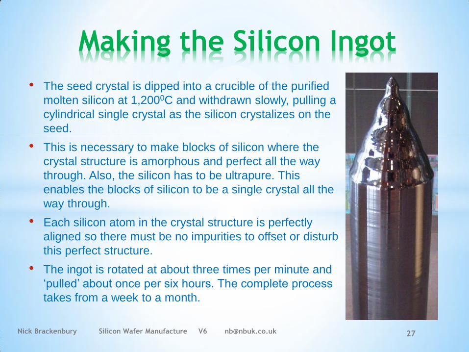
• The seed crystal is dipped into a crucible of the purified
molten silicon at 1,2000C and withdrawn slowly, pulling a
cylindrical single crystal as the silicon crystalizes on the
seed.
• This is necessary to make blocks of silicon where the
crystal structure is amorphous and perfect all the way
through. Also, the silicon has to be ultrapure. This
enables the blocks of silicon to be a single crystal all the
way through.
• Each silicon atom in the crystal structure is perfectly
aligned so there must be no impurities to offset or disturb
this perfect structure.
• The ingot is rotated at about three times per minute and
‘pulled’ about once per six hours. The complete process
takes from a week to a month.
Making the Silicon Ingot
Nick Brackenbury Silicon Wafer Manufacture V6 [email protected] 27

This is a fully
automated
crystal growth
furnace to
produce ingots
for photovoltaic
cells in solar
panels.
Crystal Growth Furnace
Nick Brackenbury Silicon Wafer Manufacture V6 [email protected] 28

An ingot being twisted
and pulled out of a
1,2000C furnace of
molten silicon in a
graphite crucible.
Making the Silicon Ingot
Nick Brackenbury Silicon Wafer Manufacture V6 [email protected] 29
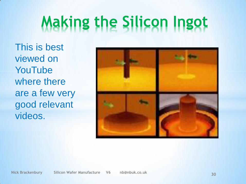
This is best
viewed on
YouTube
where there
are a few very
good relevant
videos.
Making the Silicon Ingot
Nick Brackenbury Silicon Wafer Manufacture V6 [email protected] 30

Growth of Epitaxial Silicon
At this stage we have a large solid
silicon cylindrical ingot, from a meter to
2m long
The diameter of the ingot is determined
by the silicon bath temperature and the
rate at which it is withdrawn
The outside surface is rough and
uneven
The ingot is ground to a uniform external
surface and diameter
A notch or flat is marked to identify the
subsequent wafer size
Nick Brackenbury Silicon Wafer Manufacture V6 [email protected] 31
The photograph to above shows
a number of completed ingots
with various diameters

Cutting Wafers from Ingot
The silicon ingot is now sliced into very thin wafers using a diamond
saw. The ingot is laid inside a sealed machine. The sawing
parameters can be set on an operator control panel using a PLC.
Nick Brackenbury Silicon Wafer Manufacture V6 [email protected] 32

Edge Grinding
• Subsequent wafer breakage can be
reduced by up to 400% by grinding
the edge to make it even and smooth.
• An extra step on prime wafers is to
polish the edges as well, making
subsequent cleaning more effective.
Nick Brackenbury Silicon Wafer Manufacture V6 [email protected] 33

Lapping Processes
• The sawing process leaves surface silicon
which has been cracked or otherwise damaged
by the slicing process which leaves saw marks.
• Lapping removes this cutting damage and
relieves stress accumulated in the thin wafer
from the slicing process.
• Wafers are then etched in a chemically active
reagent to remove any crystal damage
remaining from the previous step.
Nick Brackenbury Silicon Wafer Manufacture V6 [email protected] 34

Etching & Cleaning Processes
• The microscopic cracks and surface
damage left by lapping are removed.
• The wafers are scrubbed with sodium
hydroxide or acetic with nitric acid.
• The wafers are then cleaned with
deionised water rinsing.
Nick Brackenbury Silicon Wafer Manufacture V6 [email protected] 35

Polishing Process
Nick Brackenbury Silicon Wafer Manufacture V6 [email protected] 36
• Polishing requires a number of
steps using progressively finer
slurry, the polishing compound.
• Polishing is mainly just carried out
on the ‘frontside’ but may also be
required on the underside as well.

Final Cleaning
Nick Brackenbury Silicon Wafer Manufacture V6 [email protected] 37
This step is to remove trace metals, residues and
particles on the wafers.
The method was developed by RCA in the 1970’s.
The first clean, called SC1, uses:
Ammonium hydroxide clean
Hydrofluoric acid clean
DI water rinse
The second clean, called SC2, comprises:
Hydrochloric acid
Hydrogen peroxide
DI water rinse
Finally, a front-side and underside scrub to remove the
smallest particles.
Final Dimensional & Electrical
Properties Qualification
Nick Brackenbury Silicon Wafer Manufacture V6 [email protected] 38
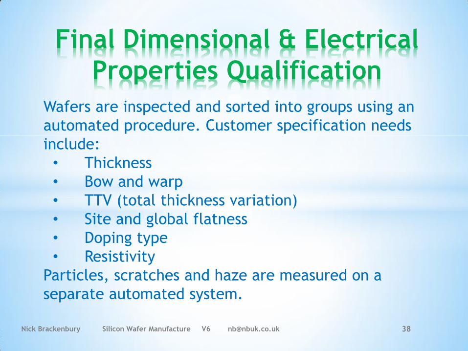
Wafers are inspected and sorted into groups using an
automated procedure. Customer specification needs
include:
• Thickness
• Bow and warp
• TTV (total thickness variation)
• Site and global flatness
• Doping type
• Resistivity
Particles, scratches and haze are measured on a
separate automated system.

• Coring, or resizing, recovers otherwise wasted
wafers that failed the flatness test immediately
after being cut off the main block
• Patterned or blank wafers can be cut to any
geometry or size within the original wafer shape
• The process is a water jet-guided laser technique
invented in Switzerland known as Synova Microjet
• Wafer types include silicon, germanium, gallium
arsenide, indium phosphide, graphite, silicon
carbide, diamond coated wafers and stainless
steel wafers
• The example on the right shows a 200mm wafer
being cut to produce two 100mm wafers
• All standard wafers can be cored – 2”, 3”, 4”, 6”, 8”
and 12”
Wafer Coring
Nick Brackenbury Silicon Wafer Manufacture V6 [email protected] 39
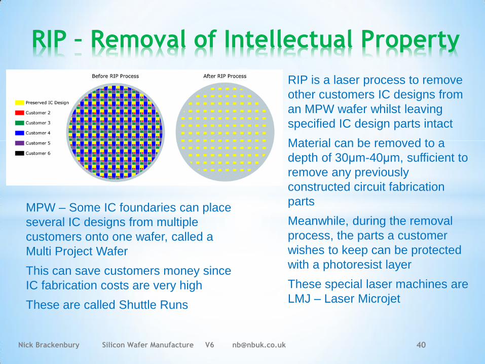
RIP is a laser process to remove
other customers IC designs from
an MPW wafer whilst leaving
specified IC design parts intact
Material can be removed to a
depth of 30μm-40μm, sufficient to
remove any previously
constructed circuit fabrication
parts
Meanwhile, during the removal
process, the parts a customer
wishes to keep can be protected
with a photoresist layer
These special laser machines are
LMJ – Laser Microjet
RIP – Removal of Intellectual Property
MPW – Some IC foundaries can place
several IC designs from multiple
customers onto one wafer, called a
Multi Project Wafer
This can save customers money since
IC fabrication costs are very high
These are called Shuttle Runs
Nick Brackenbury Silicon Wafer Manufacture V6 [email protected] 40