MEMS and MICROSYSTEMS DESIGN AND MANUFACTURE
57
MEMS and MICROSYSTEMS DESIGN AND MANUFACTURE Tai-Ran Hsu, ASME Fellow, Professor Microsystems Design and Packaging Laboratory Department of Mechanical and Aerospace Engineering San Jose State University San Jose, California, USA E-mail: [email protected] HEMANTH KUMAR G, ASSISTANT PROFESSOR , DEAPRTMENT OF BME, ACS COLLEGE OF ENGINEERING
-
Upload
khangminh22 -
Category
Documents
-
view
1 -
download
0
Transcript of MEMS and MICROSYSTEMS DESIGN AND MANUFACTURE
MEMS and MICROSYSTEMS
DESIGN AND MANUFACTURETai-Ran Hsu, ASME Fellow, Professor
Microsystems Design and Packaging Laboratory
Department of Mechanical andAerospace Engineering
San Jose State University
San Jose, California, USAE-mail: [email protected]
HEMANTH KUMAR G, ASSISTANT PROFESSOR , DEAPRTMENT OF BME, ACS COLLEGE OF ENGINEERING
Chapter 1
Overview of MEMS and Microsystems
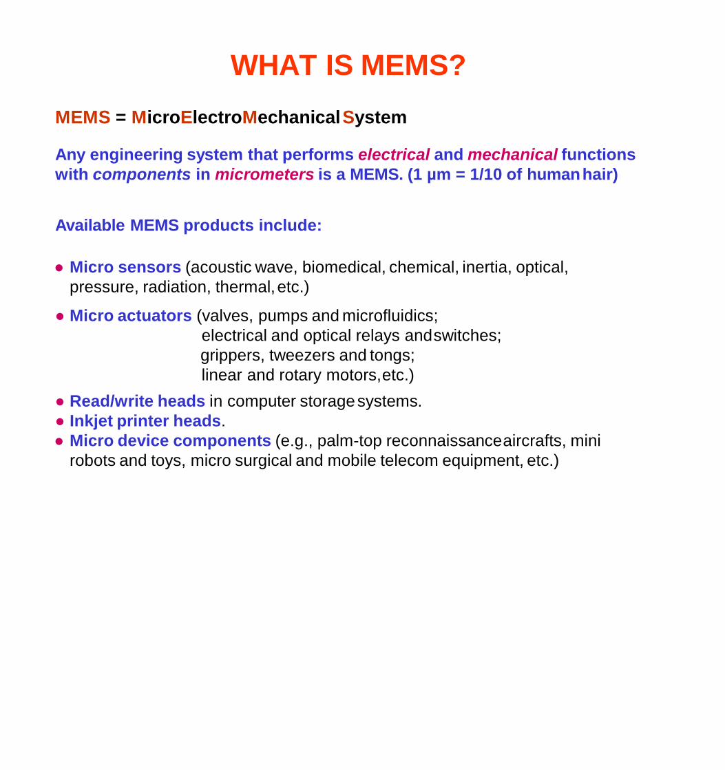
WHAT IS MEMS?
MEMS = MicroElectroMechanicalSystem
Any engineering system that performs electrical and mechanical functions
with components in micrometers is a MEMS. (1 µm = 1/10 of humanhair)
Available MEMS products include:
● Micro sensors (acoustic wave, biomedical, chemical, inertia, optical,
pressure, radiation, thermal,etc.)
● Micro actuators (valves, pumps and microfluidics;
electrical and optical relays andswitches;
grippers, tweezers and tongs;
linear and rotary motors,etc.)
● Read/write heads in computer storagesystems.
● Inkjet printer heads.
● Micro device components (e.g., palm-top reconnaissanceaircrafts, mini
robots and toys, micro surgical and mobile telecom equipment, etc.)
HOW SMALL ARE MEMS DEVICES?
in plain English please!
They can be of the size of a rice grain, or smaller!
Two examples:
- Inertia sensors for air bag deployment
systems in automobiles
- Microcars
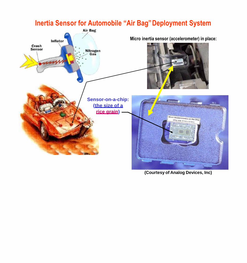
Inertia Sensor for Automobile “Air Bag”Deployment System
Micro inertia sensor (accelerometer) in place:
(Courtesy of Analog Devices, Inc)
Sensor-on-a-chip:
(the size of a
rice grain)
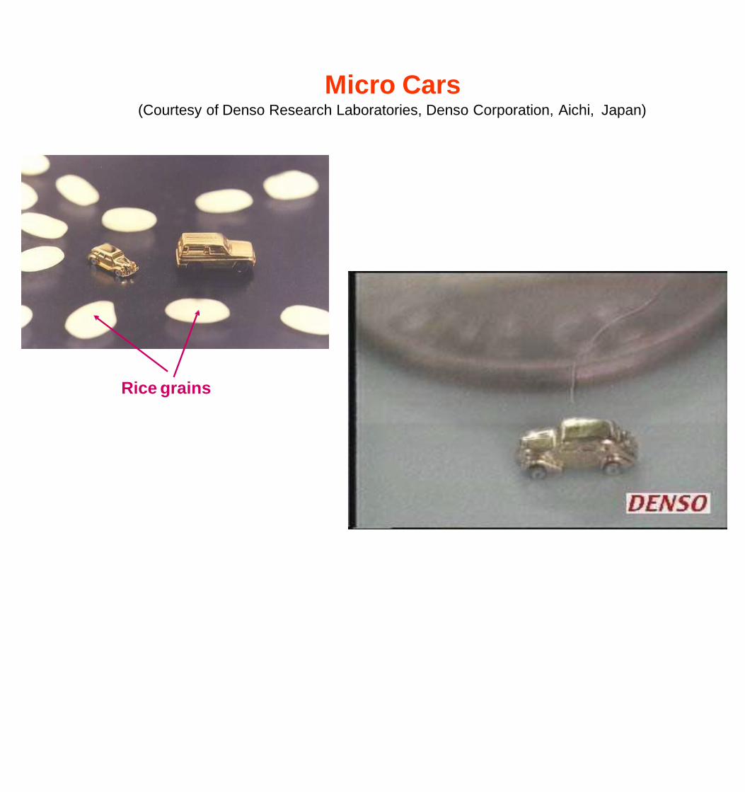
Micro Cars(Courtesy of Denso Research Laboratories, Denso Corporation, Aichi, Japan)
Rice grains
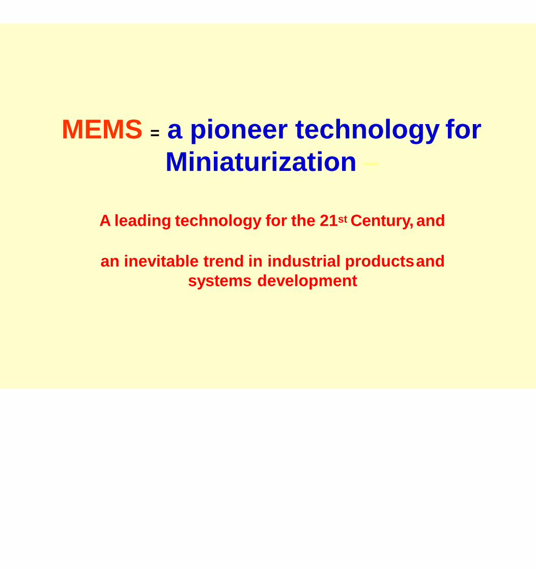
MEMS = a pioneer technology for
Miniaturization –
A leading technology for the 21st Century, and
an inevitable trend in industrial productsand
systems development
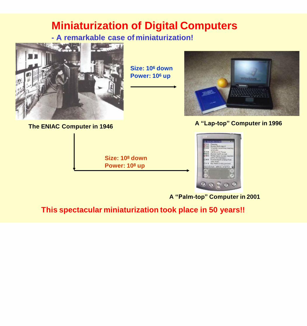
Miniaturization of Digital Computers- A remarkable case of miniaturization!
The ENIAC Computer in 1946A “Lap-top” Computer in 1996
Size: 106 down
Power: 106 up
Size: 108 down
Power: 108 up
A “Palm-top” Computer in 2001
This spectacular miniaturization took place in 50 years!!
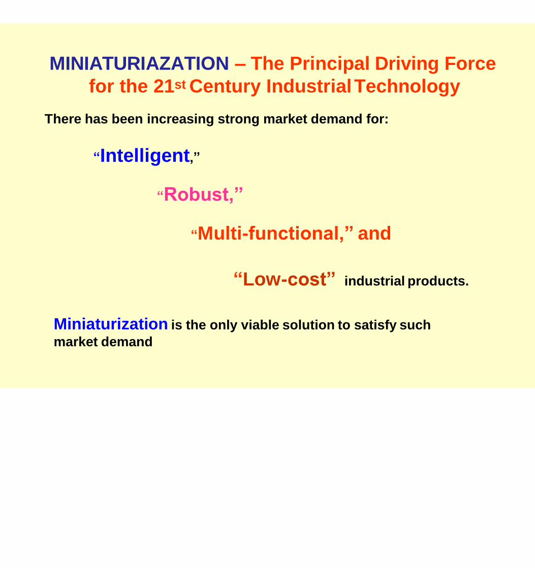
MINIATURIAZATION – The Principal Driving Force
for the 21st Century IndustrialTechnology
There has been increasing strong market demand for:
“Intelligent,”
“Robust,”
“Multi-functional,” and
“Low-cost” industrial products.
Miniaturization is the only viable solution to satisfy such
market demand
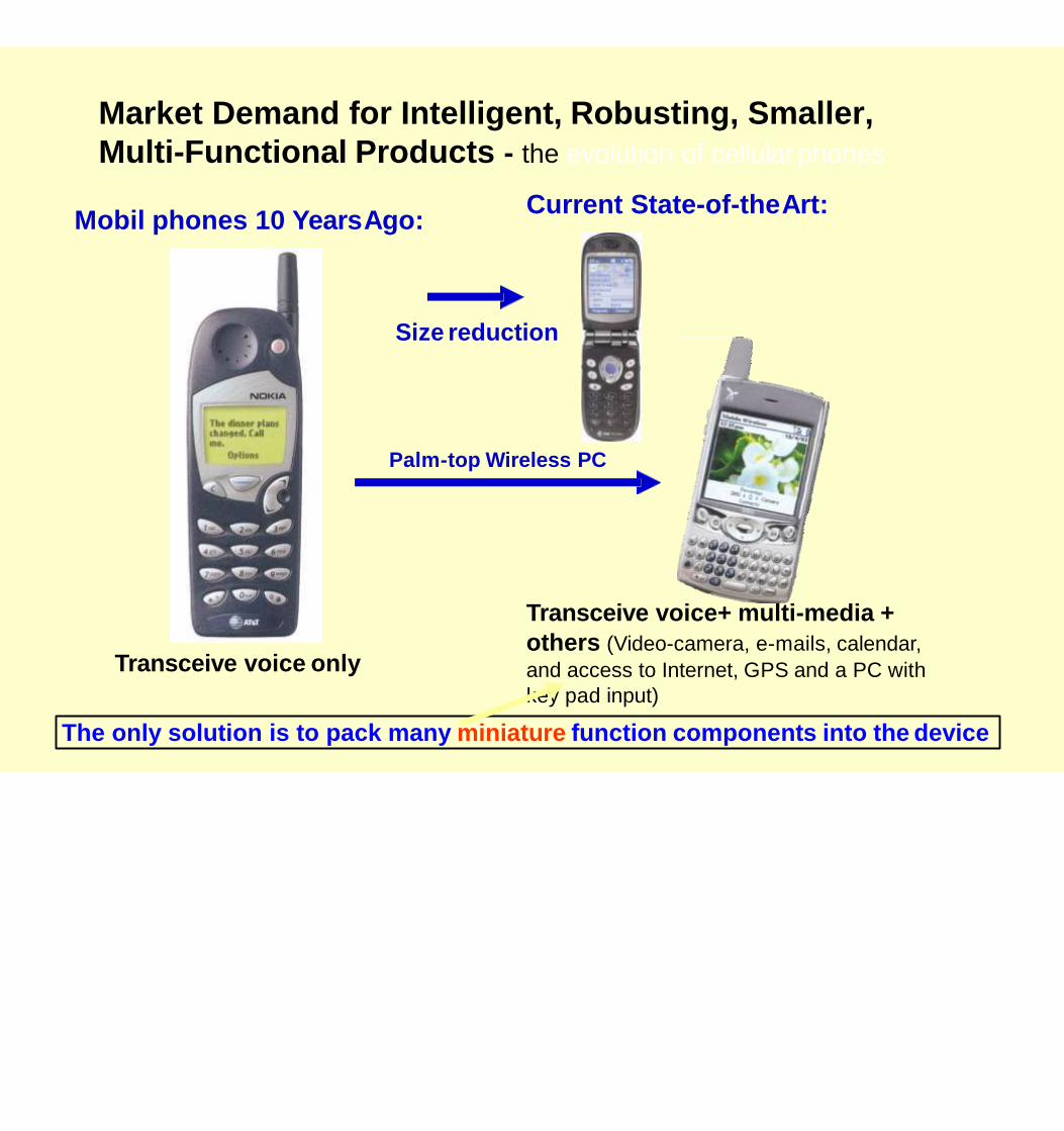
Market Demand for Intelligent, Robusting, Smaller,
Multi-Functional Products - the evolution of cellularphones
Mobil phones 10 YearsAgo:Current State-of-theArt:
Transceive voice only
Transceive voice+ multi-media +
others (Video-camera, e-mails, calendar,
and access to Internet, GPS and a PC with
key pad input)
Size reduction
Palm-top Wireless PC
The only solution is to pack many miniature function components into the device
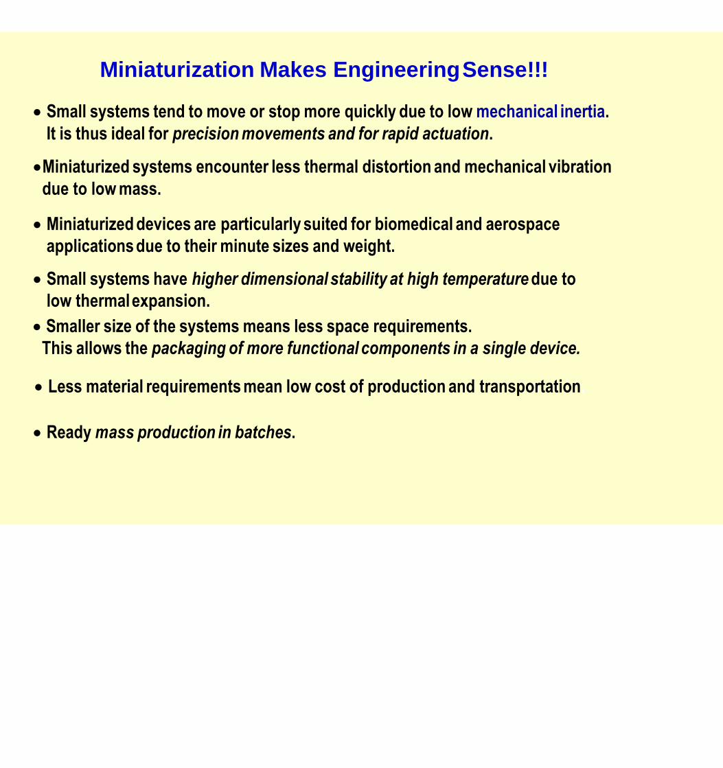
Miniaturization Makes EngineeringSense!!!
Small systems tend to move or stop more quickly due to low mechanical inertia.
It is thus ideal for precisionmovements and for rapid actuation.
Miniaturized systems encounter less thermal distortion and mechanical vibration
due to low mass.
Miniaturized devices are particularly suited for biomedical and aerospace
applications due to their minute sizes and weight.
Small systems have higher dimensional stability at high temperaturedue to
low thermalexpansion.
Smaller size of the systems means less space requirements.
This allows the packaging of more functional components in a single device.
Less material requirements mean low cost of production and transportation.
Readymass production in batches.
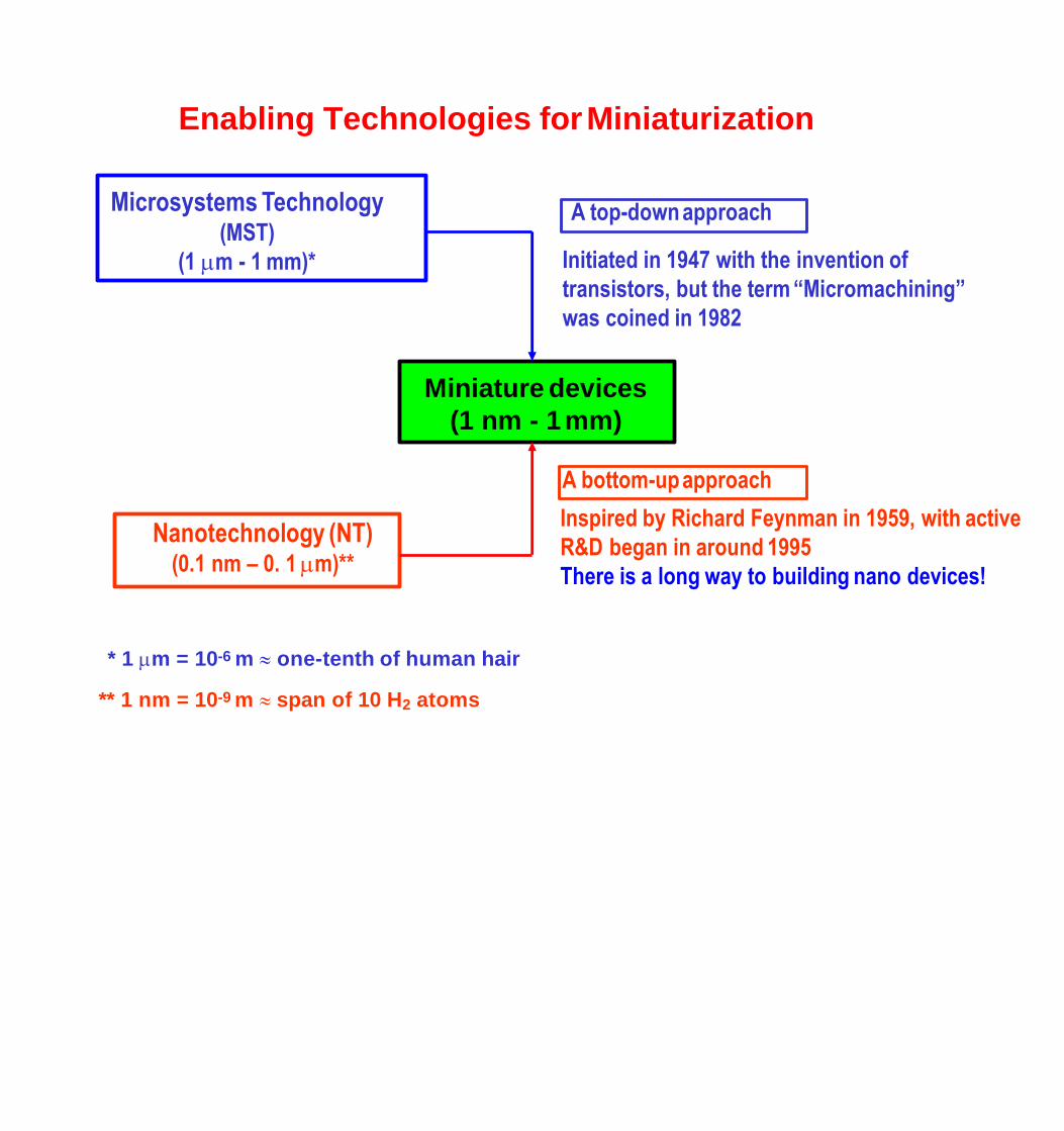
Enabling Technologies forMiniaturization
Miniature devices
(1 nm - 1 mm)
Microsystems Technology(MST)
(1 m - 1 mm)* Initiated in 1947 with the invention of
transistors, but the term “Micromachining”
was coined in 1982
* 1 m = 10-6 m one-tenth of human hair
** 1 nm = 10-9 m span of 10 H2 atoms
Nanotechnology (NT)(0.1 nm – 0. 1 m)**
Inspired by Richard Feynman in 1959, with active
R&D began in around 1995
There is a long way to building nano devices!
A top-down approach
A bottom-upapproach

The Lucrative Revenue Prospects for
Miniaturized Industrial Products
Microsystems technology:$43 billion - $132 billion* by Year 2005
( *High revenue projection is based on different definitions
used for MST products)
Source: NEXUS http://www.smalltimes.com/document_display.cfm?document_id=3424
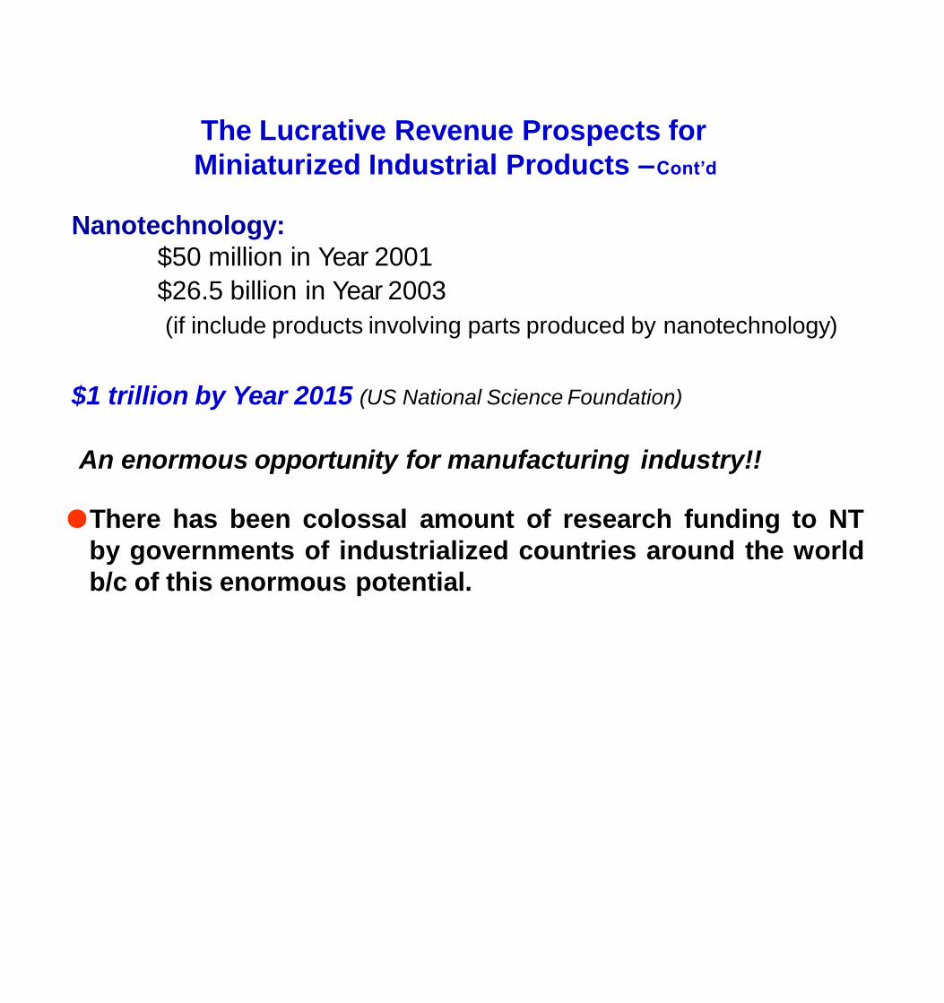
Nanotechnology:
$50 million in Year 2001
$26.5 billion in Year 2003
(if include products involving parts produced by nanotechnology)
$1 trillion by Year 2015 (US National Science Foundation)
An enormous opportunity for manufacturing industry!!
●There has been colossal amount of research funding to NT
by governments of industrialized countries around the world
b/c of this enormous potential.
The Lucrative Revenue Prospects for
Miniaturized Industrial Products –Cont’d

MEMS Products
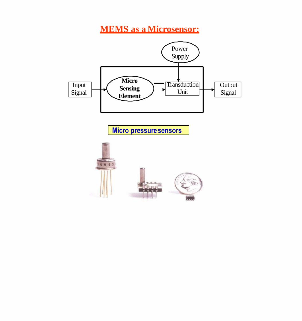
Micro
Sensing
Element
Input
Signal
TransductionUnit
Output
Signal
Power
Supply
MEMS as a Microsensor:
Micro pressuresensors
Micro
Actuating
Element
Output
Action
Transduction
Unit
Power
Supply
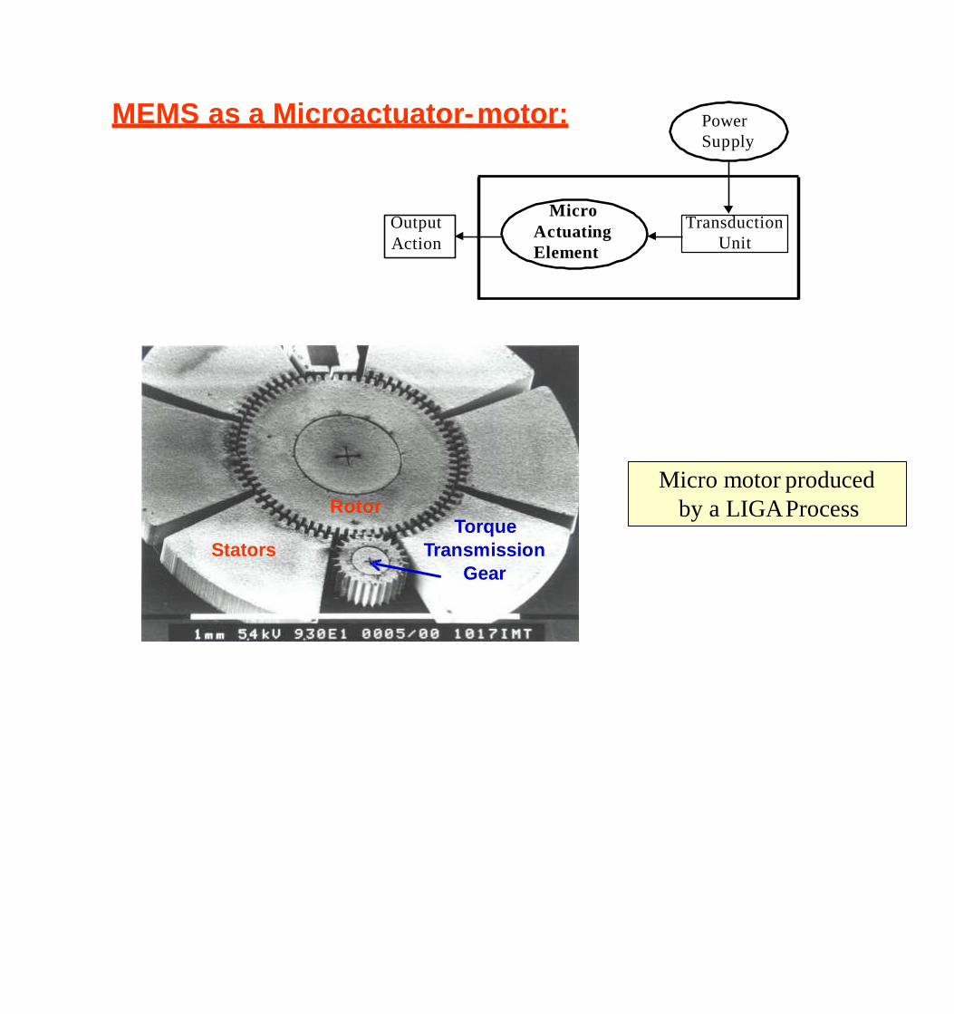
MEMS as a Microactuator-motor:
Micro motor produced
by a LIGAProcess
Stators
RotorTorque
Transmission
Gear

Components of Microsystems
Sensor
Signal
Transduction &
Processing
Unit
Actuator
Power
Supply
Microsystem

Typical Microsystems Products
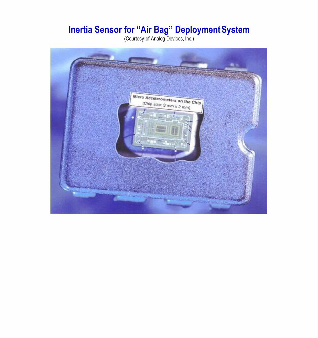
Inertia Sensor for “Air Bag” DeploymentSystem(Courtesy of Analog Devices, Inc.)
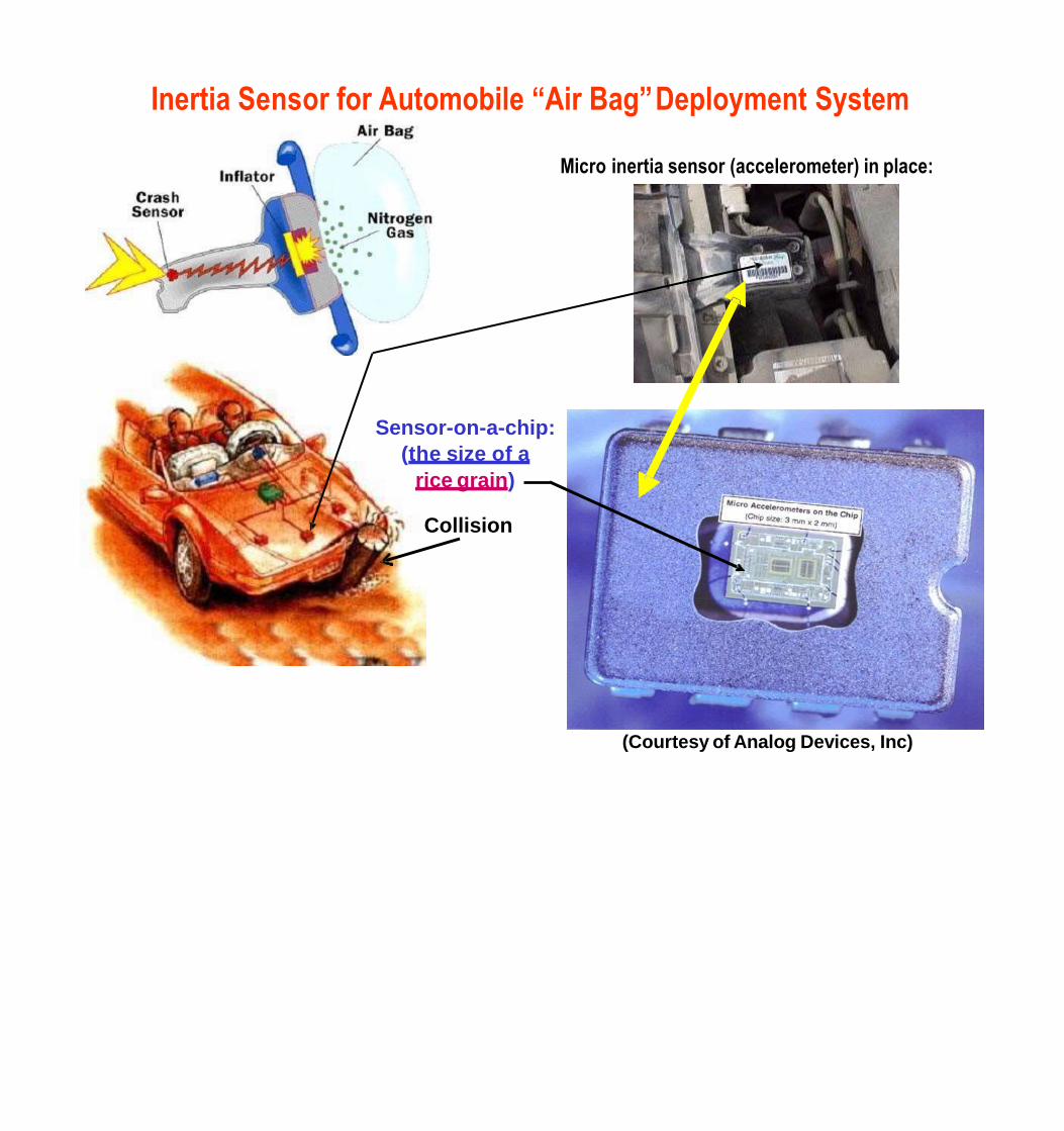
Inertia Sensor for Automobile “Air Bag”Deployment System
Micro inertia sensor (accelerometer) in place:
(Courtesy of Analog Devices, Inc)
Sensor-on-a-chip:
(the size of a
rice grain)
Collision
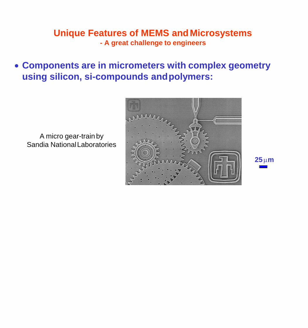
Unique Features of MEMS and Microsystems- A great challenge to engineers
Components are in micrometers with complex geometry
using silicon, si-compounds andpolymers:
25 m
A micro gear-train by
Sandia NationalLaboratories
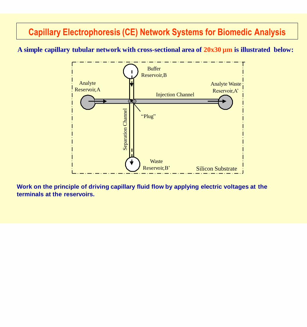
Capillary Electrophoresis (CE) Network Systems for Biomedic Analysis
Analyte
Reservoir,AAnalyte Waste
Reservoir,A’
A simple capillary tubular network with cross-sectional area of 20x30 µm is illustrated below:
Buffer
Reservoir,B
Waste
Reservoir,B’
Injection Channel
Sep
arat
ion
Chan
nel
Silicon Substrate
“Plug”
Work on the principle of driving capillary fluid flow by applying electric voltages at the
terminals at the reservoirs.
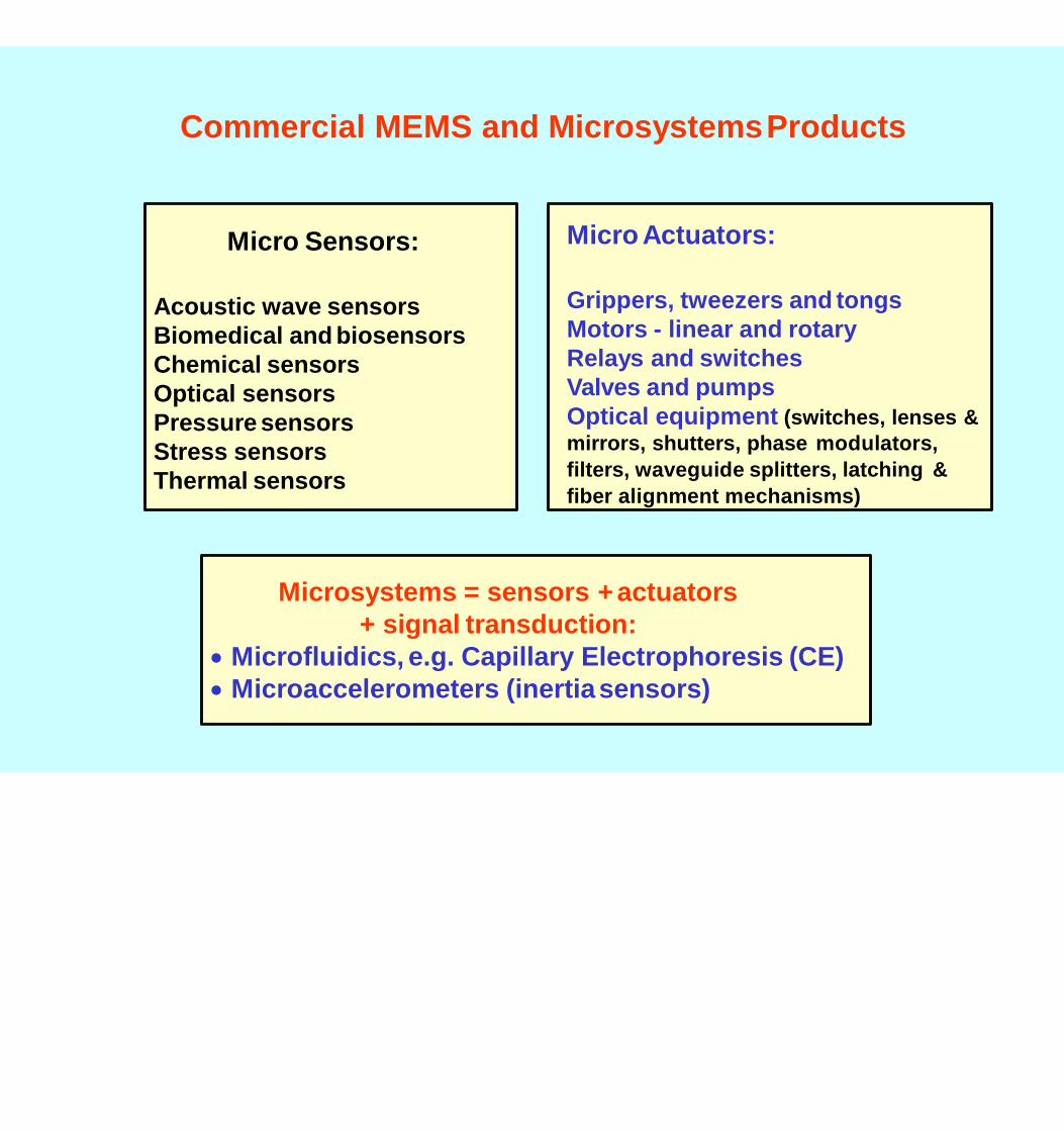
Commercial MEMS and MicrosystemsProducts
Micro Sensors:
Acoustic wave sensors
Biomedical and biosensors
Chemical sensors
Optical sensors
Pressure sensors
Stress sensors
Thermal sensors
Micro Actuators:
Grippers, tweezers and tongs
Motors - linear and rotary
Relays and switches
Valves and pumps
Optical equipment (switches, lenses &
mirrors, shutters, phase modulators,
filters, waveguide splitters, latching &
fiber alignment mechanisms)
Microsystems = sensors +actuators
+ signal transduction:
Microfluidics, e.g. Capillary Electrophoresis (CE)
Microaccelerometers (inertiasensors)
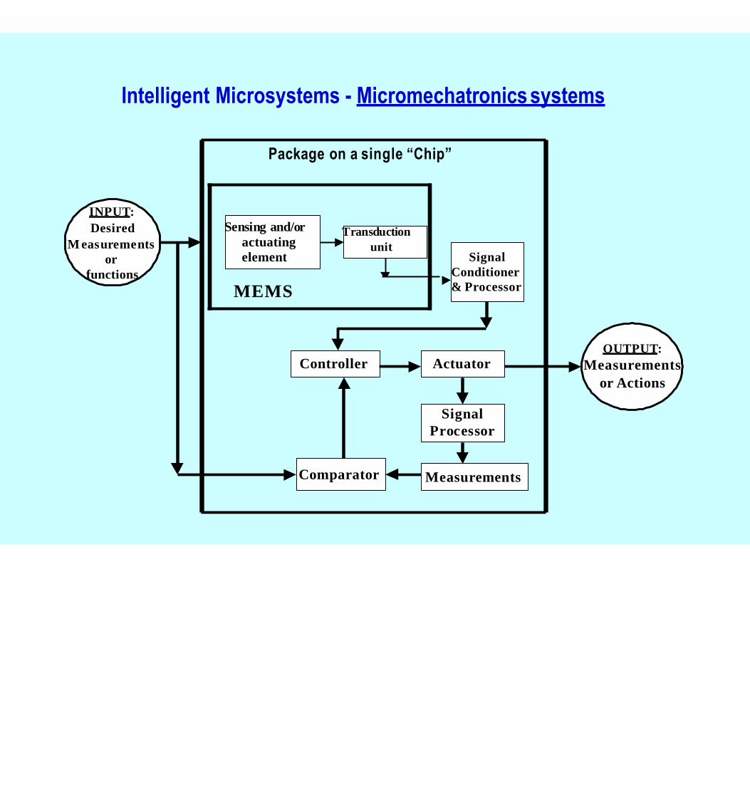
INPUT:
Desired
M easurements
or
functions
Signal
Conditioner
& Processor
Controller Actuator
Signal
Processor
MeasurementsComparator
OUTPUT:
Measurements
or Actions
Package on a single “Chip”
Sensing and/or Transduction actuating unit element
MEMS
Intelligent Microsystems - Micromechatronics systems

Evolution of Microfabrication
●There is no machine tool with today’s technology can produce any device or MEMS
component of the size in the micrometer scale (or in mmsizes).
●The complex geometry of these minute MEMS components can only be produced
by various physical-chemical processes – the microfabrication techniques originally
developed for producing integrated circuit (IC) components.
Significant technological development towards miniaturization was
initiated with the invention of transistors by three Nobel Laureates, W.
Schockley, J. Bardeen and W.H. Brattain of Bell Laboratories in 1947.
This crucial invention led to the development of the concept of
integrated circuits (IC) in 1955, and the production of the first IC three
years later by Jack Kilby of TexasInstruments.
ICs have made possible for miniaturization of many devices and
engineering systems in the last 50 years.
The invention of transistors is thus regarded as the beginning of
the 3rd Industrial Revolution in human civilization.
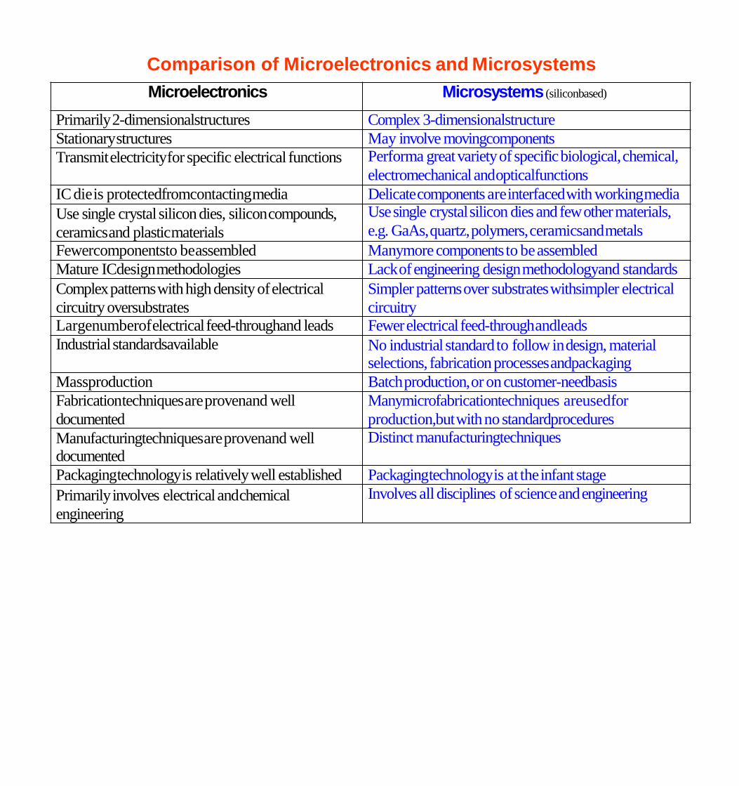
Comparison of Microelectronics and Microsystems
Microelectronics Microsystems (siliconbased)
Primarily2-dimensionalstructures Complex 3-dimensionalstructure
Stationarystructures May involve movingcomponents
Transmitelectricityfor specific electrical functions Performa greatvarietyof specificbiological,chemical,
electromechanical andopticalfunctions
ICdieis protectedfromcontactingmedia Delicatecomponents areinterfacedwith workingmedia
Use single crystal silicon dies, siliconcompounds,
ceramicsand plasticmaterials
Usesingle crystalsilicon dies andfewothermaterials,
e.g. GaAs,quartz,polymers,ceramicsandmetals
Fewercomponentsto beassembled Manymorecomponents to beassembled
Mature ICdesignmethodologies Lackofengineering designmethodologyand standards
Complexpatternswithhighdensityofelectrical
circuitry oversubstrates
Simpler patternsover substrateswithsimpler electrical
circuitryLargenumberofelectricalfeed-throughand leads Fewerelectrical feed-throughandleads
Industrialstandardsavailable No industrial standardto follow indesign, materialselections, fabrication processesandpackaging
Massproduction Batchproduction,or oncustomer-needbasis
Fabricationtechniquesareprovenand well
documented
Manymicrofabricationtechniques areusedfor
production,butwithno standardprocedures
Manufacturingtechniquesareprovenand welldocumented
Distinct manufacturingtechniques
Packagingtechnologyis relativelywell established Packagingtechnologyis at theinfant stage
Primarily involves electrical andchemical
engineering
Involves all disciplines of scienceandengineering
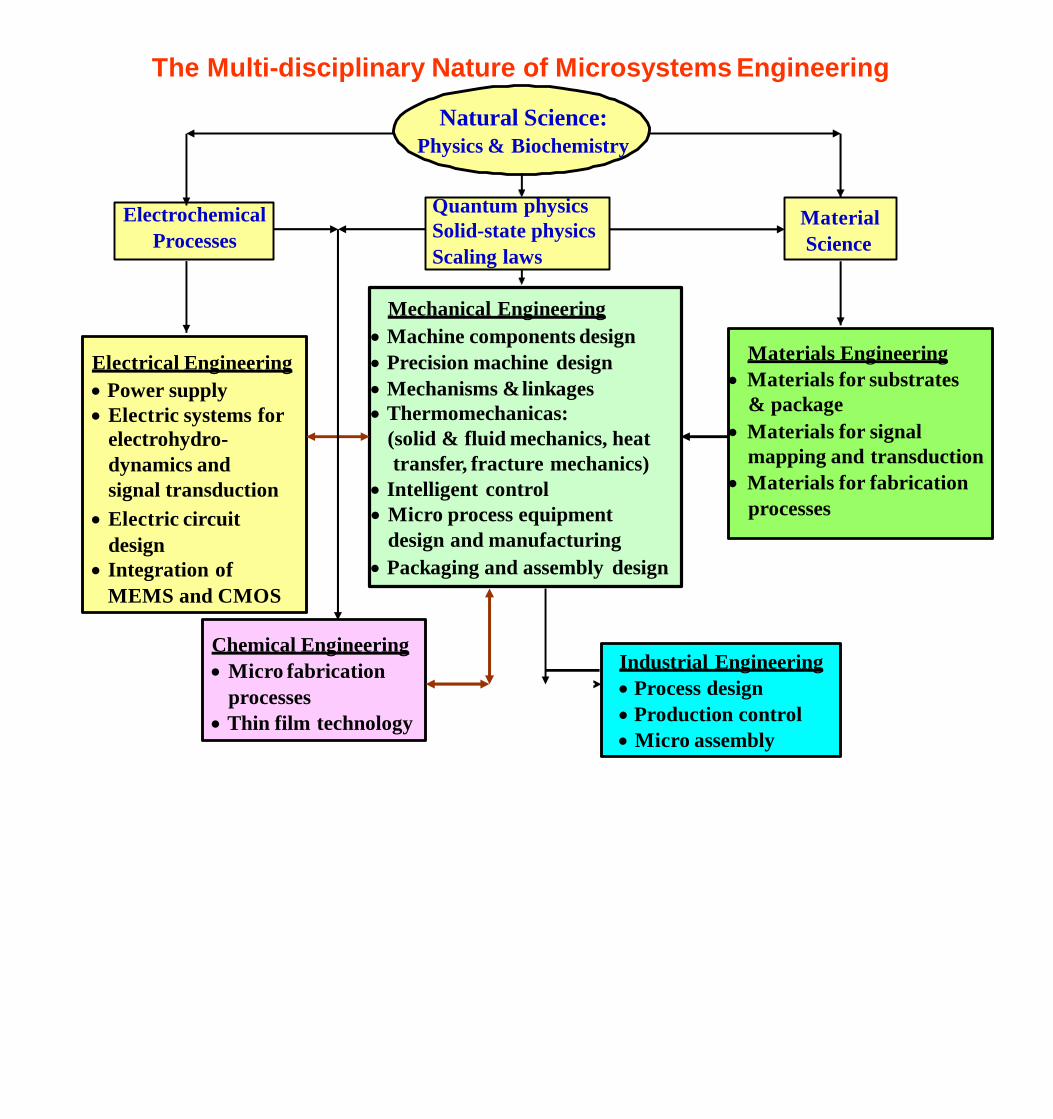
Natural Science:
Physics & Biochemistry
Mechanical Engineering
Machine components design
Precision machine design
Mechanisms &linkages
Thermomechanicas:
(solid & fluid mechanics, heat
transfer, fracture mechanics)
Intelligent control
Micro process equipment
design and manufacturing
Packaging and assembly design
Quantum physics
Solid-state physics
Scaling laws
Electrical Engineering
Power supply
Electric systems for
electrohydro-
dynamics and
signal transduction
Electric circuit
design
Integration of
MEMS and CMOS
Materials Engineering
Materials for substrates
& package
Materials for signal
mapping and transduction
Materials for fabrication
processes
Chemical Engineering
Micro fabrication
processes
Thin film technology
Industrial Engineering
Process design
Production control
Micro assembly
Electrochemical
ProcessesMaterial
Science
The Multi-disciplinary Nature of Microsystems Engineering
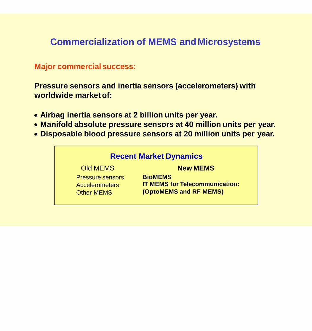
Commercialization of MEMS andMicrosystems
Major commercial success:
Pressure sensors and inertia sensors (accelerometers) with
worldwide market of:
Airbag inertia sensors at 2 billion units per year.
Manifold absolute pressure sensors at 40 million units per year.
Disposable blood pressure sensors at 20 million units per year.
Recent Market Dynamics
New MEMSOld MEMS
Pressure sensors
Accelerometers
Other MEMS
BioMEMSIT MEMS for Telecommunication:
(OptoMEMS and RF MEMS)
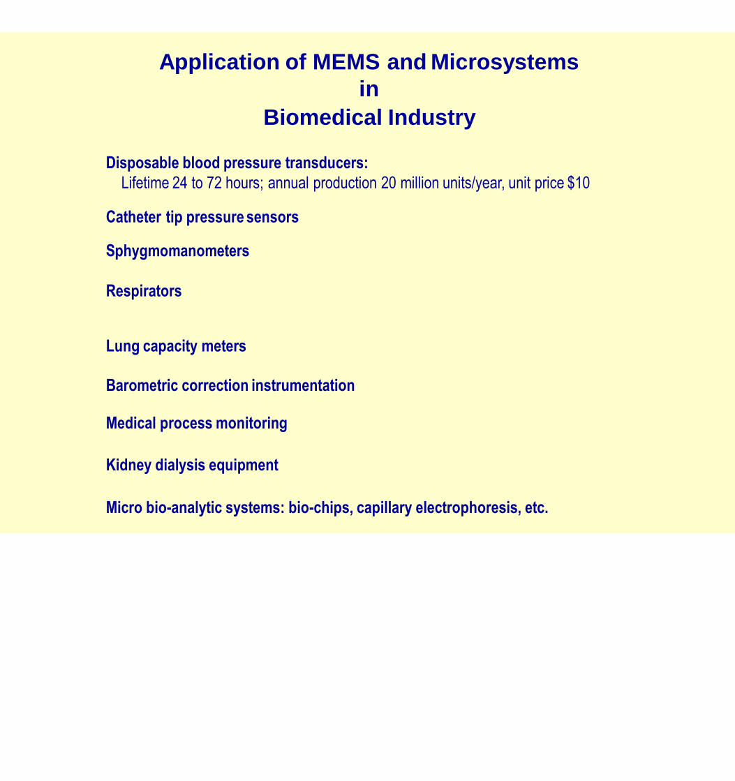
Application of MEMS and Microsystems
in
Biomedical Industry
Disposable blood pressure transducers:
Lifetime 24 to 72 hours; annual production 20 million units/year, unit price $10
Catheter tip pressure sensors
Sphygmomanometers
Respirators
Lung capacity meters
Barometric correction instrumentation
Medical process monitoring
Kidney dialysis equipment
Micro bio-analytic systems: bio-chips, capillary electrophoresis, etc.
Scanned by CamScanner
Scanned by CamScanner
Scanned by CamScanner
Scanned by CamScanner
Scanned by CamScanner
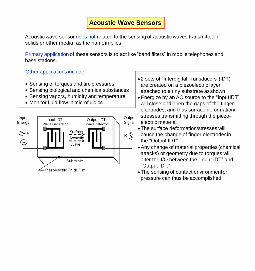
Acoustic Wave Sensors
Acoustic wave sensor does not related to the sensing of acoustic waves transmitted in
solids or other media, as the nameimplies.
Primary application of these sensors is to act like “band filters” in mobile telephones and
base stations.
Other applications include:
Sensing of torques and tire pressures
Sensing biological and chemicalsubstances
Sensing vapors, humidity and temperature
Monitor fluid flow in microfluidics
2 sets of “Interdigital Transducers”(IDT)
are created on a piezoelectric layer
attached to a tiny substrate asshown
Energize by an AC source to the “InputIDT”
will close and open the gaps of the finger
electrodes, and thus surface deformation/
stresses transmitting through the piezo-
electric material
The surface deformation/stresses will
cause the change of finger electrodesin
the “Output IDT”
Any change of material properties (chemical
attacks) or geometry due to torques will
alter the I/O between the “Input IDT” and
“Output IDT.”
The sensing of contact environmentor
pressure can thus be accomplished
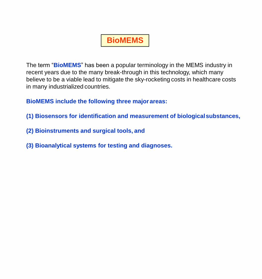
BioMEMS
The term “BioMEMS” has been a popular terminology in the MEMS industry in
recent years due to the many break-through in this technology, which many
believe to be a viable lead to mitigate the sky-rocketing costs in healthcare costs
in many industrialized countries.
BioMEMS include the following three majorareas:
(1) Biosensors for identification and measurement of biologicalsubstances,
(2) Bioinstruments and surgical tools, and
(3) Bioanalytical systems for testing and diagnoses.
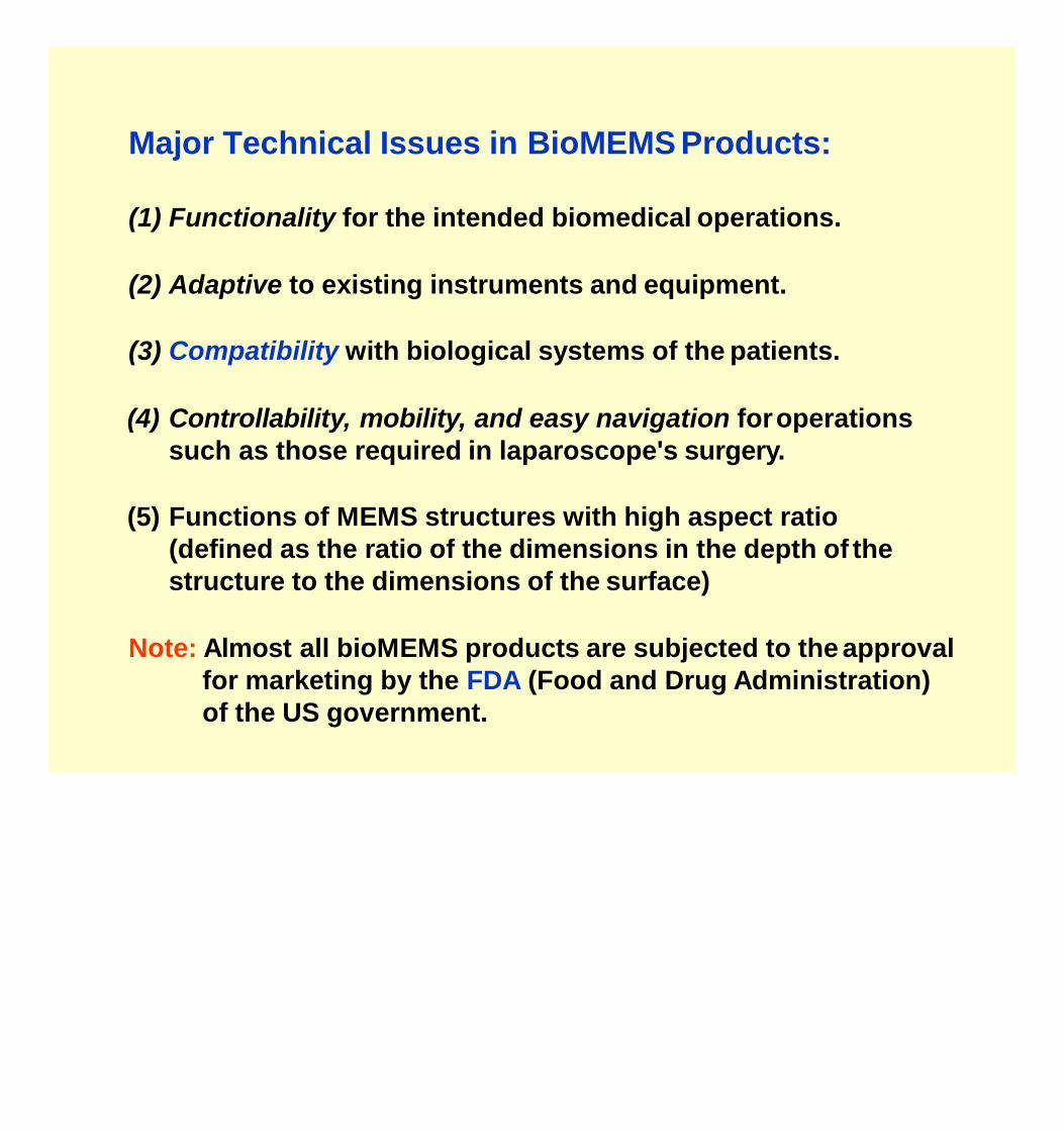
Major Technical Issues in BioMEMS Products:
(1) Functionality for the intended biomedical operations.
(2) Adaptive to existing instruments and equipment.
(3) Compatibility with biological systems of the patients.
(4) Controllability, mobility, and easy navigation foroperations
such as those required in laparoscope's surgery.
(5) Functions of MEMS structures with high aspect ratio
(defined as the ratio of the dimensions in the depth of the
structure to the dimensions of the surface)
Note: Almost all bioMEMS products are subjected to the approval
for marketing by the FDA (Food and Drug Administration)
of the US government.
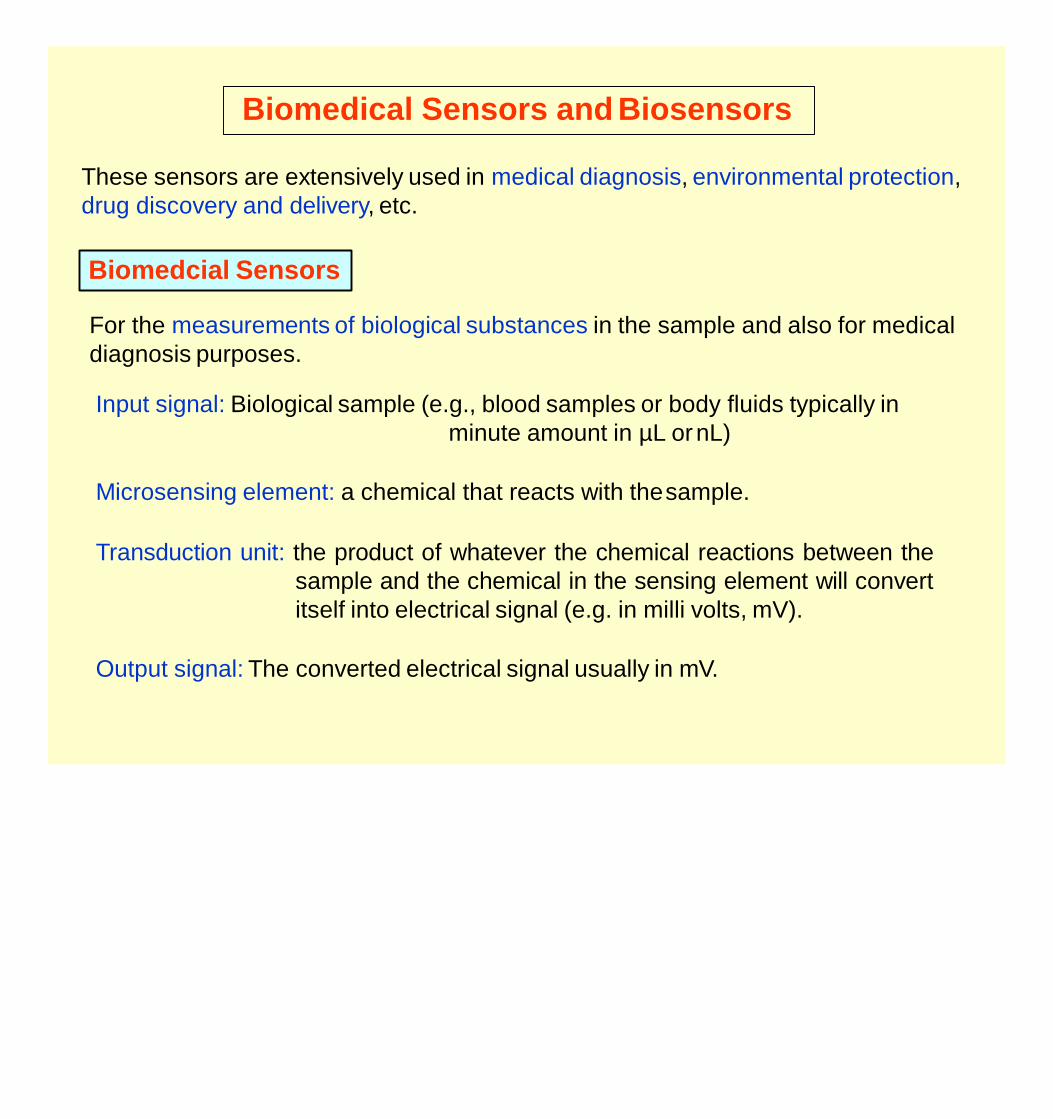
Biomedical Sensors and Biosensors
These sensors are extensively used in medical diagnosis, environmental protection,
drug discovery and delivery, etc.
Biomedcial Sensors
For the measurements of biological substances in the sample and also for medical
diagnosis purposes.
Input signal: Biological sample (e.g., blood samples or body fluids typically in
minute amount in µL ornL)
Microsensing element: a chemical that reacts with thesample.
Transduction unit: the product of whatever the chemical reactions between the
sample and the chemical in the sensing element will convert
itself into electrical signal (e.g. in milli volts, mV).
Output signal: The converted electrical signal usually in mV.
Ag/AgCl Reference electrode
Example of a biomedical sensor:
A sensor for measuring the glucose concentration of a patient.
Pt electrodeBloodsample
H+ H+H+
Polyvinyl alcohol solution
H+ H+V
i
Working principle:
●The glucose in patient’s blood sample reacts with the O2 in thepolyvinyl
alcohol solution and producesH2O2.
●The H2 in H2O2 migrates toward Pt film in a electrolysis process, and builds
up layers at that electrode.
●The difference of potential between the two electrodes due to thebuild-up
of H2 in the Pt electrode relates to the amount of glucose in the blood
sample.
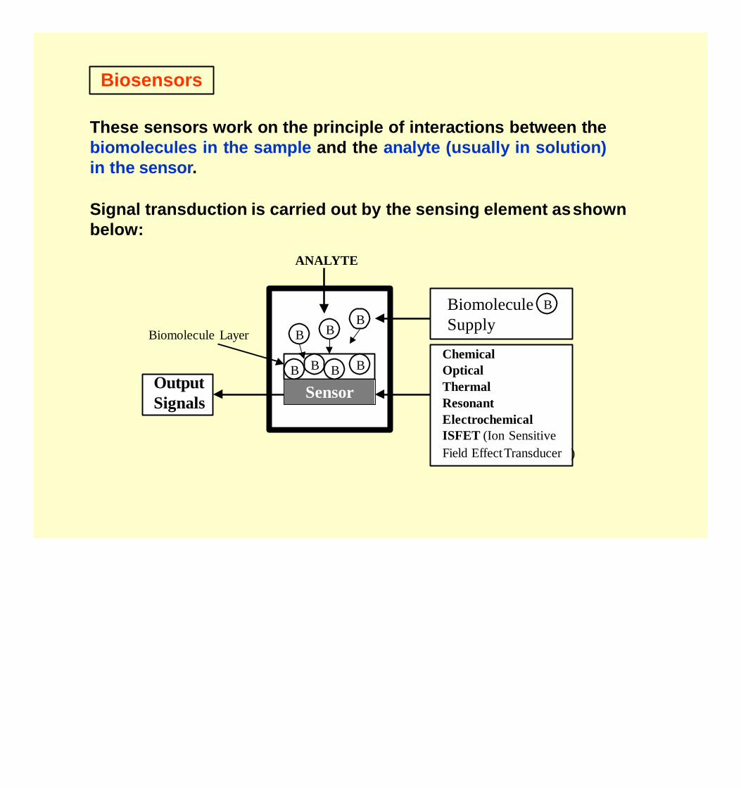
Biosensors
B BB B
These sensors work on the principle of interactions between the
biomolecules in the sample and the analyte (usually in solution)
in the sensor.
Signal transduction is carried out by the sensing element asshown
below:
ANALYTE
B
BB
Sensor
Chemical
Optical
Thermal
Resonant
Electrochemical
ISFET (Ion Sensitive
Field EffectTransducer )
Output
Signals
Biomolecule B
SupplyBiomolecule Layer
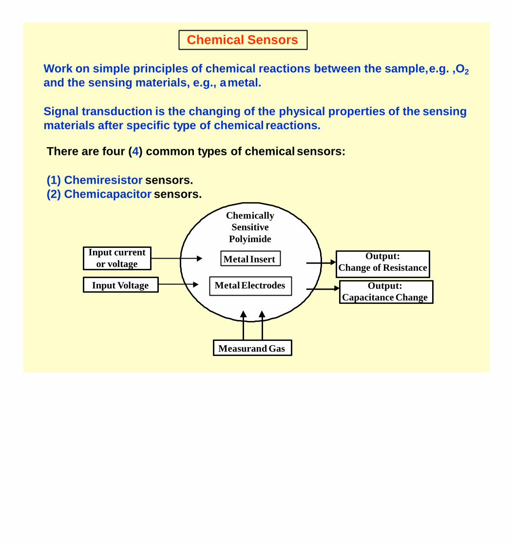
Chemical Sensors
Work on simple principles of chemical reactions between the sample,e.g. ,O2
and the sensing materials, e.g., ametal.
Signal transduction is the changing of the physical properties of the sensing
materials after specific type of chemical reactions.
There are four (4) common types of chemical sensors:
(1) Chemiresistor sensors.
(2) Chemicapacitor sensors.
Chemically
Sensitive
Polyimide
Metal Insert
Metal Electrodes
Input current
or voltageOutput:
Change of Resistance
Input Voltage Output:
Capacitance Change
Measurand Gas
Chemical Sensors-Cont’d
(3) Chemimechanical sensors:
Work on certain materials (e.g. polymers) that change shapes when they
are exposed to chemicals. Measuring the change of the shape of the
sensing materials determines the presence of the chemical.
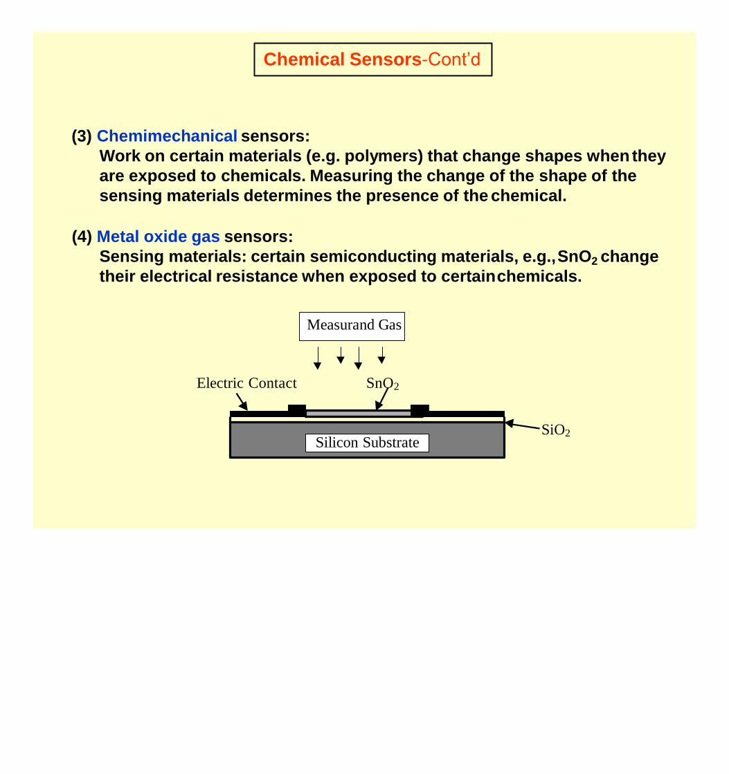
(4) Metal oxide gas sensors:
Sensing materials: certain semiconducting materials, e.g.,SnO2 change
their electrical resistance when exposed to certainchemicals.
SnO2
SiO2
Electric Contact
Silicon Substrate
Measurand Gas

Chemical Sensors-Cont’d
Semiconducting Metals Catalyst Additives Gas to be Detected
BaTiO3/CuO La2O3, CaCO3 CO2
SnO2 Pt + Sb CO
SnO2 Pt Alcohols
SnO2 Sb2O3 H2, O2, H2S
SnO2 CuO H2S
ZnO V, Mo Halogenated hydrocarbons
WO3 Pt NH3
Fe2O3 Ti-doped + Au CO
Ga2O3 Au CO
MoO3 None NO2, CO
In2O3 None O3
Available metal oxide gas sensors:
Optical Sensors
● These sensors are used to detect the intensity of lights.
●It works on the principle of energy conversion between the photons in
the incident light beams and the electrons in the sensingmaterials.
●The following four (4) types of optical sensors are available:Photon Energy
Semiconductor B
Semiconductor AR
Photon Energy
R
(a) Photovoltaicjunction (b) Photoconductive device
Vout
_
+
R
Photon Energy
p-Material
n-Material
Bias
Voltage
Reverse
Bias
Voltage
Junction
p n
Photon Energy
Leads
(c)Photodiodes
Semiconductor Ais more transparent
to photon energy in
incident light
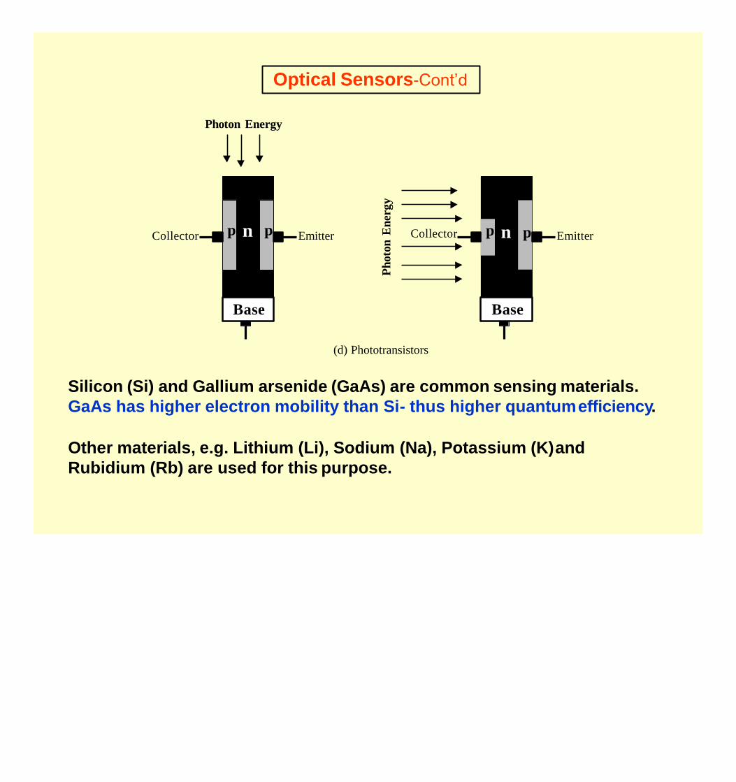
Optical Sensors-Cont’d
p n p
Base
Photon Energy
np p
Base
Collector Emitter Collector Emitter
Ph
oto
nE
ner
gy
(d) Phototransistors
Silicon (Si) and Gallium arsenide (GaAs) are common sensing materials.
GaAs has higher electron mobility than Si- thus higher quantumefficiency.
Other materials, e.g. Lithium (Li), Sodium (Na), Potassium (K)and
Rubidium (Rb) are used for this purpose.
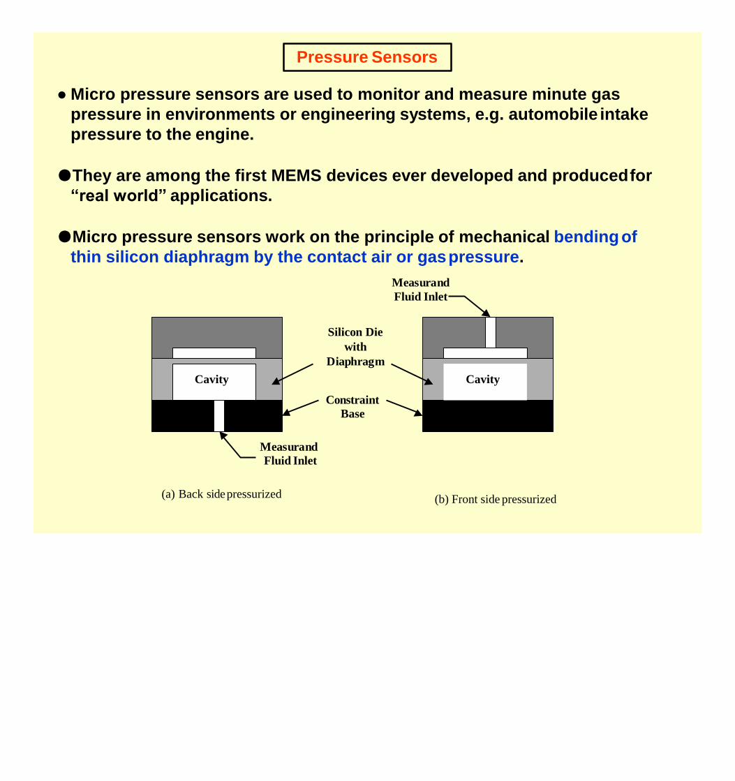
Pressure Sensors
Cavity Cavity
Constraint
Base
Measurand
Fluid Inlet
● Micro pressure sensors are used to monitor and measure minute gas
pressure in environments or engineering systems, e.g. automobile intake
pressure to the engine.
●They are among the first MEMS devices ever developed and producedfor
“real world” applications.
●Micro pressure sensors work on the principle of mechanical bendingof
thin silicon diaphragm by the contact air or gaspressure.
Measurand
Fluid Inlet
Silicon Die
with
Diaphragm
(a) Back sidepressurized (b) Front side pressurized
Pressure Sensors-Cont’d
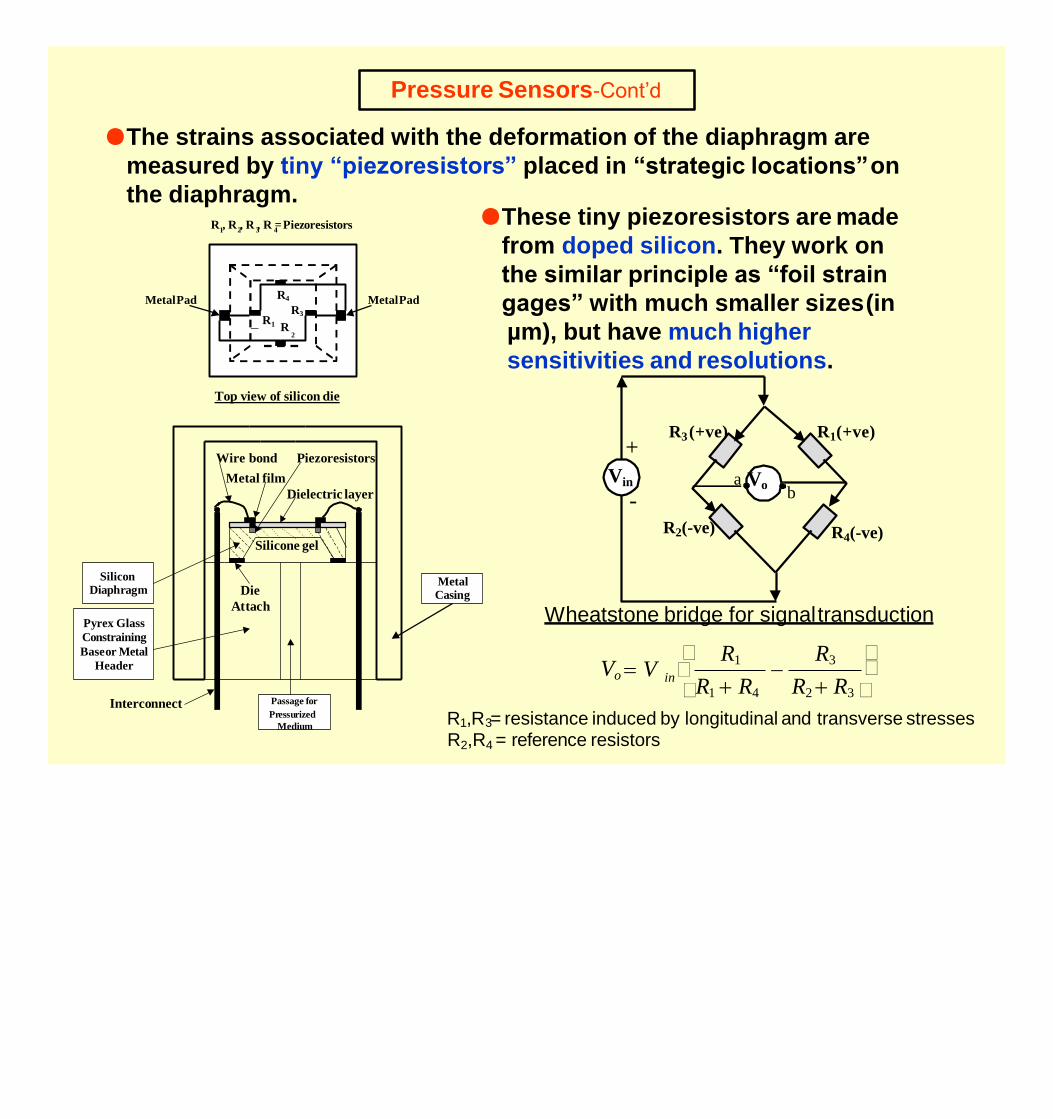
●The strains associated with the deformation of the diaphragm are
measured by tiny “piezoresistors” placed in “strategic locations”on
the diaphragm.
Silicon Diaphragm
Pyrex Glass
Constraining
Baseor Metal
Header
Metal Casing
Passage for
Pressurized
Medium
Silicone gel
Wire bond Piezoresistors
Metal film
Dielectric layer
Die
Attach
Interconnect
R3
R4
R1 R2
MetalPad MetalPad
1 2 3 4R , R , R , R =Piezoresistors
Top view of silicon die
Vin
R1(+ve)R3(+ve)
R4(-ve)
+
-a Vo
R2(-ve)
b
Wheatstone bridge for signaltransduction
●These tiny piezoresistors are made
from doped silicon. They work on
the similar principle as “foil strain
gages” with much smaller sizes(in
µm), but have much higher
sensitivities and resolutions.
R1 R4 R2 R3
R1 R3
inVo V
R1,R3= resistance induced by longitudinal and transverse stresses R2,R4 = reference resistors
Pressure Sensors-Cont’d
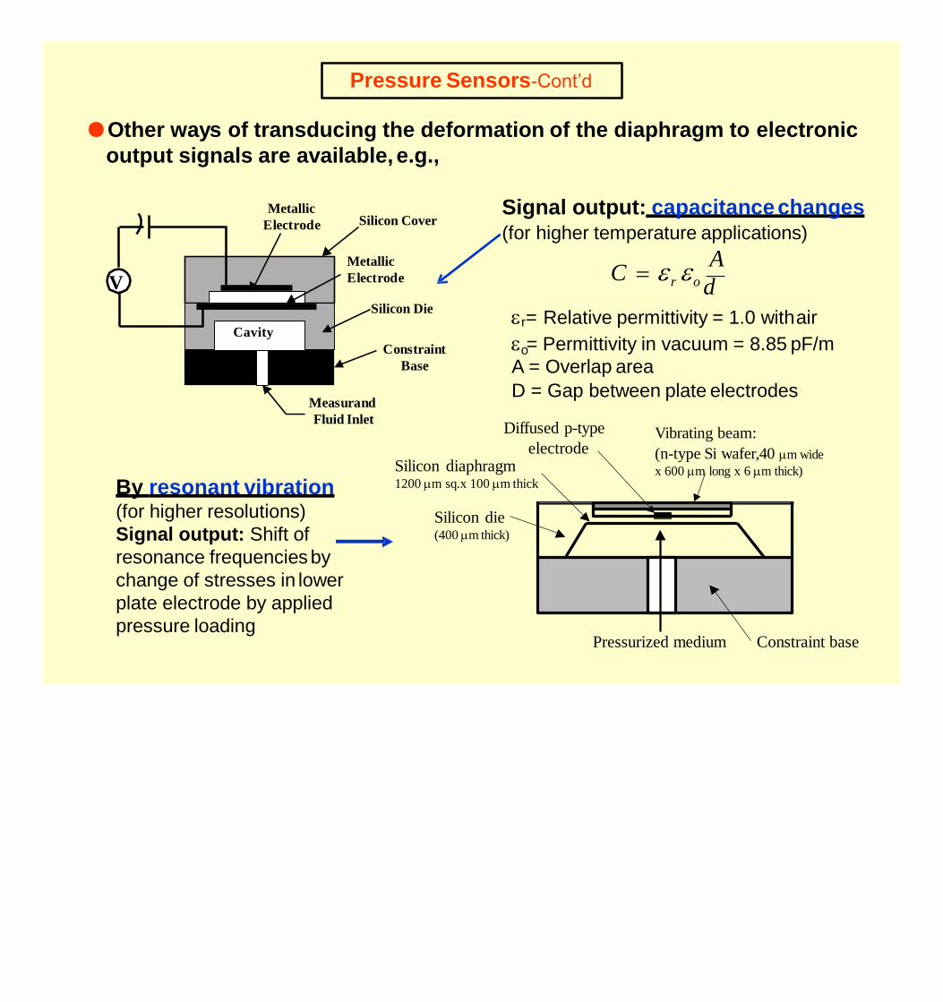
●Other ways of transducing the deformation of the diaphragm to electronic
output signals are available, e.g.,
Cavity
Constraint
Base
Measurand
Fluid Inlet
V
Metallic
Electrode
Metallic
Electrode
Silicon Die
Silicon Cover
Vibrating beam:
(n-type Si wafer,40 m wide
x 600 m long x 6 m thick)
Silicon die(400 m thick)
Constraint basePressurized medium
Diffused p-type
electrodeSilicon diaphragm1200 m sq.x 100 m thickBy resonant vibration
(for higher resolutions)
Signal output: Shift of
resonance frequenciesby
change of stresses in lower
plate electrode by applied
pressure loading
Signal output: capacitancechanges(for higher temperature applications)
Ar o d
C
r= Relative permittivity = 1.0 withair
o = Permittivity in vacuum = 8.85 pF/m
A = Overlap area
D = Gap between plate electrodes
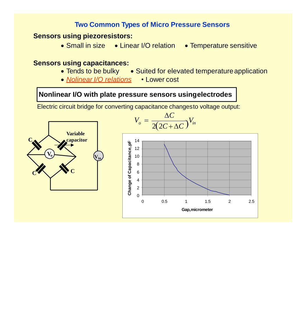
Two Common Types of Micro Pressure Sensors
Sensors using piezoresistors:
Small in size Linear I/O relation Temperature sensitive
Sensors using capacitances: Tends to be bulky Suited for elevated temperatureapplication
Nolinear I/O relations • Lower cost
Nonlinear I/O with plate pressure sensors usingelectrodes
Electric circuit bridge for converting capacitance changesto voltage output:
Vo Vin
C C
CVariable
capacitor
ino VC
V 22C C
14
12
10
8
6
4
2
0
0 0.5 2 2.51 1.5
Gap,micrometer
Ch
an
ge
of
Ca
pa
cit
an
ce
,pF
●Major problems in pressure sensors are in the
system packaging and protection of the
diaphragm from the contacting pressurized
media, which are often corrosive, erosive,and at high temperatures.
Pressure Sensors-Cont’d
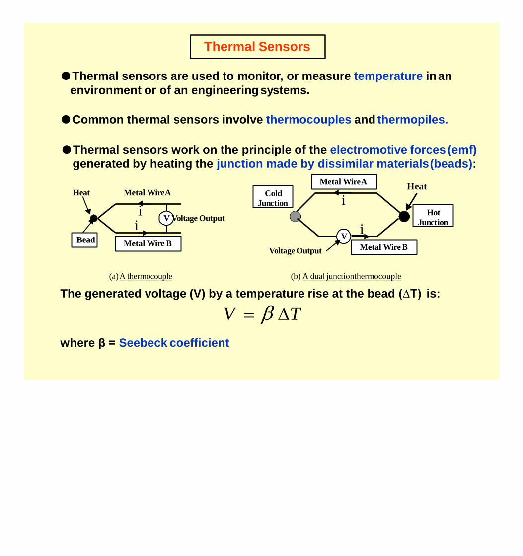
Thermal Sensors
●Thermal sensors are used to monitor, or measure temperature inan
environment or of an engineering systems.
●Common thermal sensors involve thermocouples and thermopiles.
●Thermal sensors work on the principle of the electromotive forces (emf)
generated by heating the junction made by dissimilar materials(beads):
Bead
Heat Metal WireA
Metal Wire B
V Voltage Output
V
Voltage Output
Metal WireA
Metal Wire B
Cold
JunctionHot
Junction
Heat
i
i
i i
(a)A thermocouple (b) A dual junctionthermocouple
The generated voltage (V) by a temperature rise at the bead (∆T) is:
V T
where β = Seebeck coefficient
Thermal Sensors-Cont’d
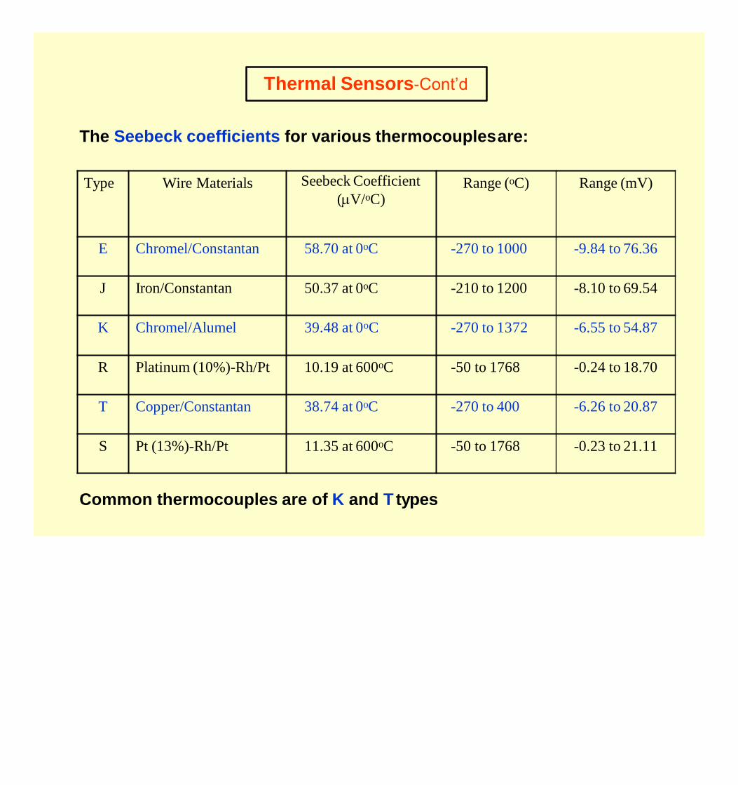
The Seebeck coefficients for various thermocouplesare:
Type Wire Materials Seebeck Coefficient
(V/oC)Range (oC) Range (mV)
E Chromel/Constantan 58.70 at 0oC -270 to 1000 -9.84 to 76.36
J Iron/Constantan 50.37 at 0oC -210 to 1200 -8.10 to 69.54
K Chromel/Alumel 39.48 at 0oC -270 to 1372 -6.55 to 54.87
R Platinum (10%)-Rh/Pt 10.19 at 600oC -50 to 1768 -0.24 to 18.70
T Copper/Constantan 38.74 at 0oC -270 to 400 -6.26 to 20.87
S Pt (13%)-Rh/Pt 11.35 at 600oC -50 to 1768 -0.23 to 21.11
Common thermocouples are of K and T types
Thermal Sensors-Cont’d
HotJ
un
ctio
n
Reg
ion
,Th
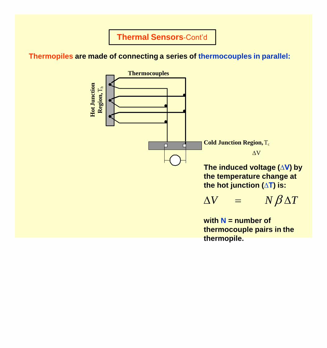
Thermopiles are made of connecting a series of thermocouples in parallel:
Thermocouples
Cold Junction Region, Tc
V
The induced voltage (∆V) by
the temperature change at
the hot junction (∆T) is:
V N T
with N = number of
thermocouple pairs in the
thermopile.
Thermal Sensors-Cont’d
Hot
Junction
Region3.6
mm
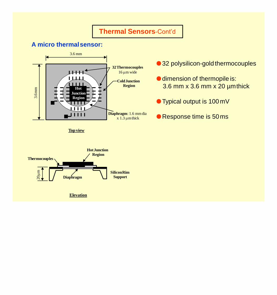
A micro thermalsensor:
3.6 mm
Diaphragm: 1.6 mm dia x 1.3 mthick
32Thermocouples
16 m wide
ColdJunction
Region
20
m
HotJunction
RegionThermocouples
Diaphragm
SiliconRim
Support
Top view
Elevation
●32 polysilicon-gold thermocouples
●dimension of thermopile is:
3.6 mm x 3.6 mm x 20 µmthick
●Typical output is 100 mV
●Response time is 50ms