Highly Sensitive Capacitive Sensor Based on Injection Locked ...
Upload
independentCategory
view
0download
0
3482 IEEE TRANSACTIONS ON MICROWAVE THEORY AND TECHNIQUES, VOL. 53, NO. 11, NOVEMBER 2005
Reliability Modeling of Capacitive RF MEMSSamuel Mellé, Student Member, IEEE, David De Conto, David Dubuc, Member, IEEE, Katia Grenier, Member, IEEE,
Olivier Vendier, Jean-Luc Muraro, Jean-Louis Cazaux, Senior Member, IEEE, and Robert Plana, Member, IEEE
Abstract—The kinetic of dielectric charging in capacitive RF mi-croelectromechanical systems (RF MEMS) is investigated using anoriginal method of stress and monitoring. This effect is investi-gated through a new parameter: the shift rate of the actuation volt-ages. We demonstrate that this lifetime parameter has to be con-sidered as a function of the applied voltage normalized by the con-tact quality between the bridge and the dielectric. We also demon-strate that this phenomenon is related to Frenkel–Poole conduc-tion, which takes place into the dielectric. We finally propose amodel that describes the dielectric charging kinetic in capacitiveRF MEMS. This model is used to extract a figure-of-merit of ca-pacitive switches lifetime.
Index Terms—Dielectric charging, figure-of-merit (FOM),Frenkel–Poole conduction, reliability, RF microelectromechanicalsystems (RF MEMS).
I. INTRODUCTION
I T IS now understood that RF microelectromechanical sys-tems (RF MEMS) devices exhibit very attractive capabilities
for wireless communications associated to space, mobile, andautomotive applications. They could replace solid-state com-ponents thanks to their attractive microwave performances [1]and even create new functions thanks to their electromechanicalbehavior. Today, however, these devices are still classified as apromising and emergent technology; one issue that limits theirindustrial use deals with the reliability properties that are stillunsolved and under discussion. We know that the main causeof failure of electrostatically actuated structures is related to di-electric charging. This physical effect creates a shift of the ac-tuation voltages [2], [3], which leads to the failure of the switchthrough two different mechanisms: the stiction of the bridge(when the pull-up voltage approaches 0 V) and the screeningof the bridge (when the pull-down voltage overdrives the actu-ation voltage) [4]. In order to improve the lifetime of capacitiveRF MEMS, it is, therefore, mandatory to identify and model thecharging mechanisms occurring in the dielectric.
In Section II, we describe the measurement test setup and theproposed methodology to evaluate the dielectric charging. Sec-
Manuscript received April 23, 2005; revised June 30, 2005. This work wassupported in part by the Centre National d’Etudes Spatieles, by Alcatel Space,and by the Advanced Microelectromechanical Systems for RF and Millimeter-wave Communications Network of Excellence.
S. Mellé, D. Dubuc, K. Grenier, and R. Plana are with the Laboratoired’Analyse et d’Architectures des Systèmes, Centre National de la RechercheScientifique, 31077 Toulouse, France (e-mail: [email protected]).
D. De Conto was with the Laboratoire d’Analyse et d’Architectures desSystèmes, Centre National de la Recherche Scientifique, 31077 Toulouse,France. He is now with Alcatel Alenia Space Toulouse, 37700 Toulouse,France.
O. Vendier, J.-L. Muraro, and J.-L. Cazaux are with Alcatel Space, 31100Toulouse, France.
Digital Object Identifier 10.1109/TMTT.2005.857109
Fig. 1. RF MEMS reliability test set.
tions III and IV discuss the experimental data and address thekey figures that determine the degradation kinetic of switch per-formances. Sections V and VI propose an extended model ofdielectric charging, which has recently been presented in [5].We finally present measurements of dielectric physical proper-ties and propose a figure-of-merit (FOM) of dielectrics used incapacitive RF MEMS.
II. EXPERIMENTAL
A. Test Set Description
To investigate the reliability of capacitive RF MEMS, we havedeveloped a specific test setup, which is detailed in Fig. 1. Themain feature of this test setup deals with the fact that we monitorthe microwave characteristics of the device-under-test.
This test setup is organized into three parts. The first onedrives the switch actuation thanks to an arbitrary waveform gen-erator and a voltage amplifier. Various signals can be synthe-sized with peak-to-peak voltages ranging from 100 to 100 V,and frequencies ranging from 1 Hz to 16 MHz with a variableduty cycle. The second part of the test setup is dedicated to themicrowave performances measurement of the switches and thento its reliability behavior investigation. This is made through avector network analyzer used either in -parameter measure-ment modes or in continuous wave (CW) power source modes.In this last mode, a 10-dB coupler, an RF power detector, and adigital oscilloscope allow monitoring of the bridge state and theswitching times. The test setup is controlled by a PC through a
0018-9480/$20.00 © 2005 IEEE
MELLE et al.: RELIABILITY MODELING OF CAPACITIVE RF MEMS 3483
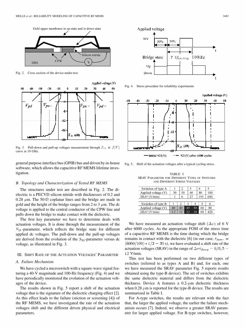
Fig. 2. Cross section of the device-under-test.
Fig. 3. Pull-down and pull-up voltages measurement through S = f(V )curve at 10 GHz.
general purpose interface bus (GPIB) bus and driven by in-housesoftware, which allows the capacitive RF MEMS lifetime inves-tigation.
B. Topology and Characterization of Tested RF MEMS
The structures under test are described in Fig. 2. The di-electric is a PECVD silicon nitride with thicknesses of 0.2 and0.28 m. The 50- coplanar lines and the bridge are made ingold and the height of the bridge ranges from 2 to 3 m. The dcvoltage is applied to the central conductor of the CPW line andpulls down the bridge to make contact with the dielectric.
The first key parameter we have to determine deals withactuation voltages. It is done through the measurement of the
-parameter, which reflects the bridge state for differentapplied dc voltages. The pull-down and the pull-up voltagesare derived from the evolution of the -parameter versus dcvoltage, as illustrated in Fig. 3.
III. SHIFT RATE OF THE ACTUATION VOLTAGES’ PARAMETER
A. Failure Mechanism
We have cycled a microswitch with a square-wave signal fea-turing a 40-V magnitude and 100-Hz frequency (Fig. 4) and wehave periodically monitored the evolution of the actuation volt-ages of the device.
The results shown in Fig. 5 report a shift of the actuationvoltage that is the signature of the dielectric charging effect [2].As this effect leads to the failure (stiction or screening [4]) ofthe RF MEMS, we have investigated the rate of the actuationvoltages shift and the different driven physical and electricalparameters.
Fig. 4. Stress procedure for reliability experiments
Fig. 5. Shift of the actuation voltages after a typical cycling stress.
TABLE ISRAV PARAMETER FOR DIFFERENT TYPES OF SWITCHES
AND DIFFERENT STRESS VOLTAGES
We have measured an actuation voltage shift of 6 Vafter 6000 cycles. As the appropriate FOM of the stress timeof a capacitive RF MEMS is the time during which the bridgeremains in contact with the dielectric [6] (in our case,
s), we have evaluated a shift rate of theactuation voltages (SRAV) in the range of
V/min.This test has been performed on two different types of
switches (referred to as types A and B) and, for each, onewe have measured the SRAV parameter Fig. 5 reports resultsobtained using the type-B device). The set of switches exhibitsthe same dielectric material and differs from the dielectricthickness. Device A features a 0.2- m dielectric thicknesswhen 0.28 m is reported for the type-B device. The results aresummarized in Table I.
For A-type switches, the results are relevant with the factthat, the larger the applied voltage, the earlier the failure mech-anism occurs [7]. Indeed, we observe a greater SRAV param-eter for larger applied voltage. For B-type switches, however,

3484 IEEE TRANSACTIONS ON MICROWAVE THEORY AND TECHNIQUES, VOL. 53, NO. 11, NOVEMBER 2005
Fig. 6. Effective field through the dielectric.
we have observed a different behavior. Indeed, for switches 1and 2, we observe two different shift rates (3.2 and 12 V/min)for the same applied voltage (40 V). Moreover, we observe that,for switches 3 and 4, the larger SRAV corresponds to the lowerapplied voltage.
These results indicate that the evolution of the SRAV param-eter versus the stress voltage does not reflect reality and thatother factors may be involved. We now have to determine a suit-able electrical stress parameter to predict the lifetime of the de-vice-under-test.
B. Effective Electrical Stress Intensity
The roughness of the central line can be critical for themicrowave performances, but it also has an influence on thefield intensity through the dielectric. The dielectric will notbe stressed with the same field intensity everywhere underthe bridge, as it depends on the air gap between the metallicmembrane and the dielectric, as shown in Fig. 6.
From the Maxwell–Gauss equation, we deduce that the elec-tric field into the dielectric can be expressed as follows:
(1)
The dielectric is then stressed by an effective field whoseintensity corresponds to the mean value of the electric fieldthrough the insulator
(2)
As the measured capacitance is equal to
(3)We prove that
(4)
where the ratio corresponds to the expected (theoret-ical) capacitance in the on state divided by the measuredone . Table II summarizes the ratio for all thetested switches.
We can observe a significant dispersion in the ratiofor the same type of switches. We have then
considered and plotted all of the SRAV parameter versus theeffective applied field in Fig. 7.
The proposed normalized parameter defines a new definitionof the stress intensity through the dielectric. This stress is pro-
TABLE IIC =C PARAMETER FOR DIFFERENT TYPES OF SWITCHES
Fig. 7. Influence of the effective field on the SRAV parameter.
portional to the contact quality: the better the contact betweenthe bridge and the dielectric, the stronger the electrical stress,the higher the SRAV parameter. The results illustrated in Fig. 7are now relevant as device B2, which exhibits a better contactthan device B1, has a greater drift rate of its actuation voltagesfor a greater applied stress. That means that by normalizing theapplied field by the contact quality, we introduce the real stressintensity through the dielectric.
The interesting benefit of this parameter deals with the factthat we can compare devices that have been designed and pro-cessed differently. Indeed, thanks to this normalization, the re-sults are then relevant for a given type of switch, but we canobserve a difference of the SRAV for the same applied stressbetween switches of types A and B. To understand this lifetimedifference, we have to model the dielectric charging kinetic tohave access to the physical parameters of the dielectric.
IV. FAILURE PHENOMENON INVESTIGATION
Before modeling the failure phenomenon, we have to identifyits physical causes. As the failure phenomenon for capacitive RFMEMS is related to the charges trapping within the dielectric,we have investigated the conduction mechanism which sets upwithin the dielectric thanks to current measurements.
A. Dielectric Conduction Mechanism
It has been already referred to that many types of conduc-tion mechanisms can take place in dielectrics depending on theelectric-field magnitude [8]. At high electric fields and for lowthicknesses, Frenkel–Poole conduction (5) is considered as thegreatest contributor to the total current density
(5)
MELLE et al.: RELIABILITY MODELING OF CAPACITIVE RF MEMS 3485
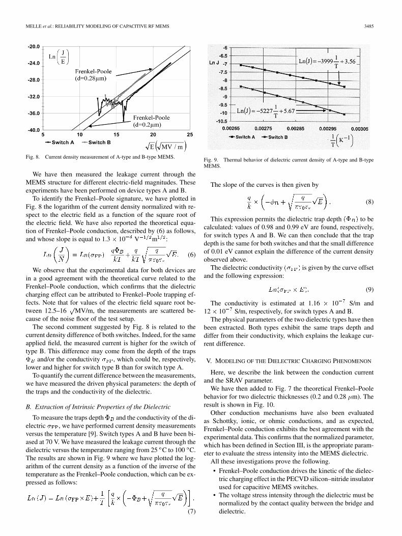
Fig. 8. Current density measurement of A-type and B-type MEMS.
We have then measured the leakage current through theMEMS structure for different electric-field magnitudes. Theseexperiments have been performed on device types A and B.
To identify the Frenkel–Poole signature, we have plotted inFig. 8 the logarithm of the current density normalized with re-spect to the electric field as a function of the square root ofthe electric field. We have also reported the theoretical equa-tion of Frenkel–Poole conduction, described by (6) as follows,and whose slope is equal to 1.3 10 V m :
(6)
We observe that the experimental data for both devices arein a good agreement with the theoretical curve related to theFrenkel–Poole conduction, which confirms that the dielectriccharging effect can be attributed to Frenkel–Poole trapping ef-fects. Note that for values of the electric field square root be-tween 12.5–16 MV/m, the measurements are scattered be-cause of the noise floor of the test setup.
The second comment suggested by Fig. 8 is related to thecurrent density difference of both switches. Indeed, for the sameapplied field, the measured current is higher for the switch oftype B. This difference may come from the depth of the traps
and/or the conductivity , which could be, respectively,lower and higher for switch type B than for switch type A.
To quantify the current difference between the measurements,we have measured the driven physical parameters: the depth ofthe traps and the conductivity of the dielectric.
B. Extraction of Intrinsic Properties of the Dielectric
To measure the traps depth and the conductivity of the di-electric , we have performed current density measurementsversus the temperature [9]. Switch types A and B have been bi-ased at 70 V. We have measured the leakage current through thedielectric versus the temperature ranging from 25 C to 100 C.The results are shown in Fig. 9 where we have plotted the log-arithm of the current density as a function of the inverse of thetemperature as the Frenkel–Poole conduction, which can be ex-pressed as follows:
(7)
Fig. 9. Thermal behavior of dielectric current density of A-type and B-typeMEMS.
The slope of the curves is then given by
(8)
This expression permits the dielectric trap depth to becalculated: values of 0.98 and 0.99 eV are found, respectively,for switch types A and B. We can then conclude that the trapdepth is the same for both switches and that the small differenceof 0.01 eV cannot explain the difference of the current densityobserved above.
The dielectric conductivity is given by the curve offsetand the following expression:
(9)
The conductivity is estimated at 1.16 10 S/m and12 10 S/m, respectively, for switch types A and B.
The physical parameters of the two dielectric types have thenbeen extracted. Both types exhibit the same traps depth anddiffer from their conductivity, which explains the leakage cur-rent difference.
V. MODELING OF THE DIELECTRIC CHARGING PHENOMENON
Here, we describe the link between the conduction currentand the SRAV parameter.
We have then added to Fig. 7 the theoretical Frenkel–Poolebehavior for two dielectric thicknesses (0.2 and 0.28 m). Theresult is shown in Fig. 10.
Other conduction mechanisms have also been evaluatedas Schottky, ionic, or ohmic conductions, and as expected,Frenkel–Poole conduction exhibits the best agreement with theexperimental data. This confirms that the normalized parameter,which has been defined in Section III, is the appropriate param-eter to evaluate the stress intensity into the MEMS dielectric.
All these investigations prove the following.
• Frenkel–Poole conduction drives the kinetic of the dielec-tric charging effect in the PECVD silicon–nitride insulatorused for capacitive MEMS switches.
• The voltage stress intensity through the dielectric must benormalized by the contact quality between the bridge anddielectric.

3486 IEEE TRANSACTIONS ON MICROWAVE THEORY AND TECHNIQUES, VOL. 53, NO. 11, NOVEMBER 2005
Fig. 10. Comparison between the theoretical curve for Frenkel–Pooleconduction and the SRAV measurement.
To model the dielectric charging phenomenon, we have firstcalculated the shift of the actuation voltages from the followingequation demonstrated in [10]:
(10)
Considering a uniform charge distribution through the dielec-tric, we can calculate a shift of the actuation voltages
(11)
where represents the trapped charges, is the thicknessof the dielectric, and is the surface of the dielectric.
We can consider that the accumulation of charges within thedielectric is due to the current density flowing and deduce that
(12)
where is a proportionality factor, which depends on the phys-ical and dimensional properties of the dielectric. This parametercorresponds to the ability of the dielectric to trap charges.
We propose the following model, which describes the be-havior of the SRAV:
(13)
This model takes all the physical and electrical parametersinto account: the dielectric properties and thickness, the appliedvoltage, the contact quality, and the temperature, and allows pre-dicting the lifetime of the RF MEMS device.
VI. EXTRACTION OF THE FOM OF CAPACITIVE RF MEMS
The above model separates the SRAV into the following twoparts.
Fig. 11. FOM for the dielectric of switches of type A and switches of type B.
• The first one is called the stress intensity factor (SIF)through the dielectric as it relates the consequence of theelectrical stress on the SRAV parameter
(14)
• The second one only depends on the dielectric properties( is the conductivity of the dielectric and is thedepth of the traps) and then gives its FOM regarding theMEMS reliability
(15)
We can extract the FOM plotting (16) as follows in a graph,as shown in Fig. 11:
(16)
We then deduce from Fig. 11, a FOM offor switches of type A and
for switches of type B. The FOM then defines the ability ofthe dielectric to accumulate charges under an electrical effec-tive stress. The greater the FOM, the shorter the lifetime. Wecan then use this FOM to compare the reliability of differentswitches realized with different technologies independently ofthe electrical stress or the contact quality.
From the values of the traps depth, the conductivity, and theFOM, we can calculate the factor for both types of switches
As a result, the A-type MEMS has a greater FOM than theB-type ones, whereas the corresponding conductivity is lower(one decade). This is due to a higher (two decades) parameter,which translates to a greater FOM. This indicates that the A-type
MELLE et al.: RELIABILITY MODELING OF CAPACITIVE RF MEMS 3487
MEMS has a greater ability to trap charges than the B-type oneand then features a poor reliability.
VII. CONCLUSION
This paper investigates the dielectric charging kinetic of ca-pacitive RF MEMS. This effect has been demonstrated as themajor issue for the reliability investigation of RF MEMS as itdrives their lifetime. As the dielectric charging can be analyzedthrough the shift of the actuation voltages of the device, thekinetic of the dielectric charging has been investigated by theSRAV parameter. In order to overcome the technological dis-persion, we have shown that the investigation of this SRAV pa-rameter has to be considered with respect to an effective elec-trical field, which takes the quality factor of the device into ac-count. From the measurements, we have shown that the dielec-tric charging phenomenon origin is related to the Frenkel–Pooleconduction through the dielectric. Finally, we propose a modelthat describes the kinetic of the dielectric charging effect. Thegreat interest of the proposed methodology is to provide the suit-able parameters (SIF and dielectric FOM), which drive the re-liability of RF MEMS in order to compare and optimize theirlifetime.
This paper has then proven that reliability of RF MEMS has tobe studied regarding appropriate parameters and that some indi-cators (as a number of cycles or the applied voltage) do not givesuitable information about the real lifetime of microswitches.
REFERENCES
[1] G. M. Rebeiz and J. B. Muldavin, “RF MEMS switches and switch cir-cuits,” IEEE Micro, pp. 59–71, Dec. 2001.
[2] R. Reid, “Dielectric charging effects on capacitive MEMS actuators,”presented at the IEEE MTT-S Int. Microwave Symp., Seattle, WA, Jun.2002.
[3] X. Yuan, S. Cherepko, J. Hwang, C. L. Goldsmith, C. Nordquist, and C.Dyck, “Initial observation and analysis of dielectric-charging effects onRF MEMS capacitive switches,” in IEEE MTT-S Int. Microwave Symp.Dig., Fort Worth, TX, Jun. 2004, pp. 1943–1946.
[4] S. Mellé, F. Flourens, D. Dubuc, K. Grenier, P. Pons, J. L. Muraro,Y. Segui, and R. Plana, “Investigation of dielectric degradation of mi-crowave capacitive microswitches,” in IEEE MEMS 2004, Maastricht,The Netherlands, Jan. 2004, pp. 141–144.
[5] S. Mellé, D. De Conto, L. Mazenq, D. Dubuc, K. Grenier, L. Bary, O.Vendier, J. L. Muraro, J. L. Cazaux, and R. Plana, “Modeling of thedielectric charging kinetic for capacitive RF MEMS,” presented at theIEEE MTT-S Int. Microwave Symp., Long Beach, CA, Jun. 2005.
[6] W. M. Van Spengen, R. Puers, R. Mertens, and I. DeWolf, “Experimentalcharacterization of stiction due to charging in RF MEMS,” in Int. IEEEElectron Devices Meeting, San Francisco, CA, pp. 901–904.
[7] C. Goldsmith, J. Ehmke, A. Malczewski, B. Pillans, S. Eshelman, Z.Yao, L. Brank, and M. Eberly, “Lifetime characterization of capacitiveRF MEMS switches,” in IEEE MTT-S Int. Microwave Symp. Dig., vol.1, Phoenix, AZ, May 2001, pp. 227–230.
[8] S. M. Sze, “MIS diode and charge-coupled device,” in Physics of Semi-conductor Devices. New York: Wiley, 1981, ch. 7, pp. 362–430.
[9] S. Habermehl and R. T. Apodaca, “Correlation of charge transport tointrinsic strain in silicon oxynitride and Si-rich silicon nitride thin films,”Appl. Phys. Lett., vol. 84, no. 2, pp. 215–217, Jan. 2004.
[10] X. Rottenberg, B. Nauwelaers, W. De Raedt, and H. A. C. Tilmans,“Novel 2 D+ model for the impact of the dielectric charge distribu-tion on the electrostatic actuation of RF MEMS devices,” in Proc. 34thEur. Microwave Conf., Amsterdam, The Netherlands, Oct. 2004, pp.B11–B14.
Samuel Mellé (S’05) was born in 1979. He receivedthe M.Sc. degree in electrical engineering from theUniversity Paul Sabatier of Toulouse, Toulouse,France in 2002, and is currently working toward thePh.D. degree at the Laboratoire d’Analyze et d’Ar-chitectures des Systèmes (LAAS), Centre Nationalde la Recherche Scientifique (CNRS), Toulouse,France.
His main field of interest is in the study of the relia-bility of capacitive RF MEMS and particularly the di-electric charging effects. His research deals with the
understanding of the dielectric charging phenomenon in order to improve thereliability of RF MEMS.
David De Conto was born in 1975. He received aTwo-Year Diploma (with a specialization in physicalmeasurement) from the Technology Institute, Univer-sity Paul Sabatier of Toulouse, Toulouse, France in1997, and the Engineer Diploma from the from theNational Conservatory of Arts and Crafts, Toulouse,France, in 2005.
He was involved with dielectrics characterizationwith the Laboratoire d’Analyze et d’Architecturesdes Systèmes (LAAS), Centre National de laRecherche Scientifique (CNRS). His research aimed
to identify leakage current mechanisms and to determine physical propertiesof dielectrics. He is currently a Materials and Processes Quality Engineer withAlcatel Alenia Space Toulouse, Toulouse, France.
David Dubuc (M’03) received the Ph.D. degreefrom the University of Toulouse, Toulouse, France,in 2001.
He is currently an Associate Professor with theUniversity of Toulouse, where he is involved in re-search on millimeter-wave microsystem integrationwith the Laboratoire d’Analyze et d’Architecturesdes Systèmes (LAAS), Centre National de laRecherche Scientifique (CNRS). During his doctoralresearch he was involved with the design of AsGaand SiGe circuits. He is currently involved with the
integration of RF-MEMS-based tunable passive circuits, three-dimensional(3-D) ultra-compact passives function, and silicon–germanium circuits intomillimeter-wave smart microsystems. He has authored or coauthored over 80papers in refereed journals and conferences. Since 2001, he has advised fourdoctoral students.
Katia Grenier (M’03) received the M.S. and Ph.D.degrees in electrical engineering from the UniversityPaul Sabatier of Toulouse, Toulouse, France, in 1997and 2000, respectively. Her doctoral dissertation con-cerned the elaboration of MEMS circuits on silicon.
Following a post-doctoral position with the RFMEMS Department, Agere Systems (Bell Lab-oratories), she joined the Laboratoire d’Analyzeet d’Architectures des Systèmes (LAAS), CentreNational de la Recherche Scientifique (CNRS),Toulouse, France, in 2002. Her research interests are
currently focused on the technological development of smart microsystems formicrowave and millimeter-wave applications, which includes the improvementof various MEMS devices (optimized in term of reliability, power, etc.), as wellas their integration with integrated circuits (such as SiGe BiCMOS technolo-gies) in order to realize wireless reconfigurable communication systems.

3488 IEEE TRANSACTIONS ON MICROWAVE THEORY AND TECHNIQUES, VOL. 53, NO. 11, NOVEMBER 2005
Olivier Vendier received the Engineering degree inapplied physics and the Post-Graduate degree in mi-croelectronics from the Institut National des SciencesAppliquées, Toulouse, France, in 1993, and the Ph.D.degree in electrical engineering from the Georgia In-stitute of Technology, Atlanta.
From 1993 to 1997, he was a Research and De-velopment Engineer with the College of ElectricalEngineering, Georgia Institute of Technology. As amember of the Packaging Research Center, Atlanta,GA, he was involved with several projects associated
with high-density packaging for microwave applications. Beginning in Summer1997, he was part of the technical staff of the Technology Department, AlcatelSpace, Toulouse, France, where he was involved in various advanced-pack-aging-based projects. He is currently with the Microwave Product Line Depart-ment (advanced Microwave Study Group), Alcatel Space, where he heads RFMEMS activities for a new generation of microwave products for space satel-lites. He is currently Project Leader for the IST 5 MEMS-Based IntegratedPhased Array Antennas (MIPA) Project and for several European Space Foun-dation (ESA)-funded projects in the area of RF MEMS devices. He has authoredor coauthored over 40 technical papers in various journal and conferences. Hehold four patents.
Jean-Luc Muraro received the Ph.D. degree fromthe Université Paul Sabatier of Toulouse, Toulouse,France, in 1997. His doctoral research concerned thereliability of solid-state power amplifiers.
Since 1997, he has been a Reliability Expert formonolithic microwave integrated circuits (MMICs)with Alcatel Space, Toulouse, France. He is in chargeof the Space Qualification Programme for MMICsand currently researches reliability aspects of newtechnologies including, among others, SiC, GaNpower amplifiers, MEMS devices, and nonhermetic
packaging for space applications.
Jean-Louis Cazaux (SM’97) was born in 1960. Hereceived the Ph.D. degree in physics and electronicsfrom the University Paul Sabatier of Toulouse,Toulouse, France, in 1985.
He then joined The University of Michigan at AnnArbor as a Post-Doctoral Research Fellow, wherehe was involved in the field of advanced transistorsand circuits for microwave electronics. In 1988, hejoined Alcatel Space, Toulouse, France, as MMICDesigner. Since 1996, he has been the Head of theMicrowave Advanced Studies within the Microwave
Department. He has authored or coauthored over 170 technical papers injournals or conferences. He holds five technical patents. He acts as reviewerand expert for the European Commission (IST) and the French Network forResearch in Telecommunication (RNRT).
Dr. Cazaux was a member of the Board of Directors of the European Mi-crowave Association (1999/2002). He is a member of the Technical Committeeof the GaAs Symposium and of the French Journées Nationales Microondes(JNM). He is the chairman of the 2005 European Microwave Conference, Paris,France. He is Distinguished Member of the Alcatel Technical Academy since2001.
Robert Plana (M’03) was born in Toulouse, France,in March 1964. He received the Ph.D. degree fromthe Laboratoire d’Analyze et d’Architectures desSystèmes (LAAS), Centre National de la RechercheScientifique (CNRS), University Paul Sabatier ofToulouse, Toulouse, France, in 1993. His doctoraldissertation concerned the noise modeling and char-acterization of advanced microwave devices (highelectron-mobility transistors (HEMTs), pseudomor-phic high electron-mobility transistors (PHEMTs),and HBTs) that includes reliability.
In 1993, as an Associate Professor with the LAAS, CNRS, he created a newresearch area concerning the investigation of millimeter-wave capabilities of sil-icon-based technologies. More precisely, he has focused on the microwave andmillimeter-wave properties of SiGe devices and their capabilities for low-noisecircuits. In 1995, he began a new project concerning the improvement of pas-sives on silicon through the use of MEMS technologies. In 1999, he became in-volved with SiGe Semiconductor, Ottawa, ON, Canada, where he was involvedwith low-power and low-noise integrated circuits for RF applications. In 2000,he became a Professor with the University Paul Sabatier of Toulouse, Toulouse,France, where he created a research team with the LAAS, CNRS, in the field ofmicrosystems and nanosystems for RF and millimeter-wave communications.The team’s main interests are on the technology, design, modeling, test, char-acterization, and reliability of RF MEMS for low-noise and high-power mil-limeter-wave applications and the development of the MEMS integrated-circuitconcept for smart microsystems. He has built a network of excellence in Europein this field regrouping 25 research groups. He is currently Director of the Infor-mation and Communication Department, CNRS. He has authored or coauthoredpapers appearing in over 200 international journals and conferences.
Dr. Plana was the recipient of a 1999 special award presented by the CNRSfor his research on silicon-based technologies for millimeter-wave communica-tions.
Copyright © 2022 FDOKUMEN