Single chip interdigitated electrode capacitive chemical sensor arrays
7
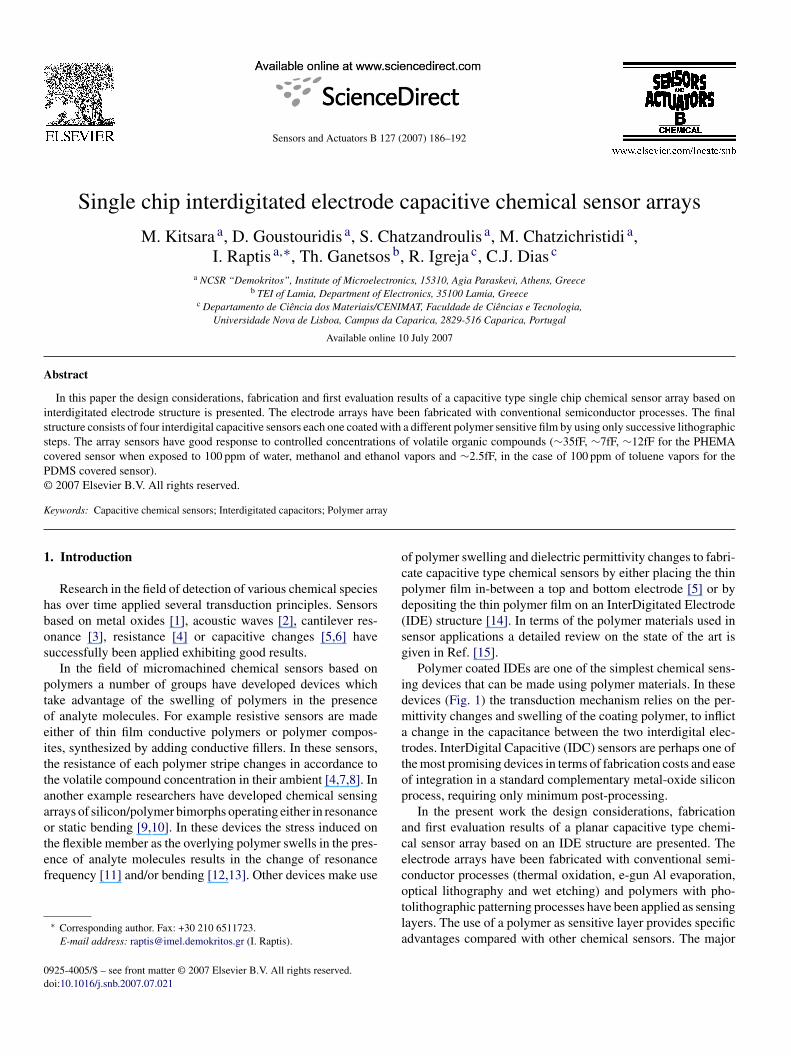
Sensors and Actuators B 127 (2007) 186–192 Single chip interdigitated electrode capacitive chemical sensor arrays M. Kitsara a , D. Goustouridis a , S. Chatzandroulis a , M. Chatzichristidi a , I. Raptis a,∗ , Th. Ganetsos b , R. Igreja c , C.J. Dias c a NCSR “Demokritos”, Institute of Microelectronics, 15310, Agia Paraskevi, Athens, Greece b TEI of Lamia, Department of Electronics, 35100 Lamia, Greece c Departamento de Ciˆ encia dos Materiais/CENIMAT, Faculdade de Ciˆ encias e Tecnologia, Universidade Nova de Lisboa, Campus da Caparica, 2829-516 Caparica, Portugal Available online 10 July 2007 Abstract In this paper the design considerations, fabrication and first evaluation results of a capacitive type single chip chemical sensor array based on interdigitated electrode structure is presented. The electrode arrays have been fabricated with conventional semiconductor processes. The final structure consists of four interdigital capacitive sensors each one coated with a different polymer sensitive film by using only successive lithographic steps. The array sensors have good response to controlled concentrations of volatile organic compounds (∼35fF, ∼7fF, ∼12fF for the PHEMA covered sensor when exposed to 100ppm of water, methanol and ethanol vapors and ∼2.5fF, in the case of 100ppm of toluene vapors for the PDMS covered sensor). © 2007 Elsevier B.V. All rights reserved. Keywords: Capacitive chemical sensors; Interdigitated capacitors; Polymer array 1. Introduction Research in the field of detection of various chemical species has over time applied several transduction principles. Sensors based on metal oxides [1], acoustic waves [2], cantilever res- onance [3], resistance [4] or capacitive changes [5,6] have successfully been applied exhibiting good results. In the field of micromachined chemical sensors based on polymers a number of groups have developed devices which take advantage of the swelling of polymers in the presence of analyte molecules. For example resistive sensors are made either of thin film conductive polymers or polymer compos- ites, synthesized by adding conductive fillers. In these sensors, the resistance of each polymer stripe changes in accordance to the volatile compound concentration in their ambient [4,7,8]. In another example researchers have developed chemical sensing arrays of silicon/polymer bimorphs operating either in resonance or static bending [9,10]. In these devices the stress induced on the flexible member as the overlying polymer swells in the pres- ence of analyte molecules results in the change of resonance frequency [11] and/or bending [12,13]. Other devices make use ∗ Corresponding author. Fax: +30 210 6511723. E-mail address: [email protected] (I. Raptis). of polymer swelling and dielectric permittivity changes to fabri- cate capacitive type chemical sensors by either placing the thin polymer film in-between a top and bottom electrode [5] or by depositing the thin polymer film on an InterDigitated Electrode (IDE) structure [14]. In terms of the polymer materials used in sensor applications a detailed review on the state of the art is given in Ref. [15]. Polymer coated IDEs are one of the simplest chemical sens- ing devices that can be made using polymer materials. In these devices (Fig. 1) the transduction mechanism relies on the per- mittivity changes and swelling of the coating polymer, to inflict a change in the capacitance between the two interdigital elec- trodes. InterDigital Capacitive (IDC) sensors are perhaps one of the most promising devices in terms of fabrication costs and ease of integration in a standard complementary metal-oxide silicon process, requiring only minimum post-processing. In the present work the design considerations, fabrication and first evaluation results of a planar capacitive type chemi- cal sensor array based on an IDE structure are presented. The electrode arrays have been fabricated with conventional semi- conductor processes (thermal oxidation, e-gun Al evaporation, optical lithography and wet etching) and polymers with pho- tolithographic patterning processes have been applied as sensing layers. The use of a polymer as sensitive layer provides specific advantages compared with other chemical sensors. The major 0925-4005/$ – see front matter © 2007 Elsevier B.V. All rights reserved. doi:10.1016/j.snb.2007.07.021
Transcript of Single chip interdigitated electrode capacitive chemical sensor arrays
A
isscP©
K
1
hbos
ptoeittaaotef
0d
Sensors and Actuators B 127 (2007) 186–192
Single chip interdigitated electrode capacitive chemical sensor arrays
M. Kitsara a, D. Goustouridis a, S. Chatzandroulis a, M. Chatzichristidi a,I. Raptis a,∗, Th. Ganetsos b, R. Igreja c, C.J. Dias c
a NCSR “Demokritos”, Institute of Microelectronics, 15310, Agia Paraskevi, Athens, Greeceb TEI of Lamia, Department of Electronics, 35100 Lamia, Greece
c Departamento de Ciencia dos Materiais/CENIMAT, Faculdade de Ciencias e Tecnologia,Universidade Nova de Lisboa, Campus da Caparica, 2829-516 Caparica, Portugal
Available online 10 July 2007
bstract
In this paper the design considerations, fabrication and first evaluation results of a capacitive type single chip chemical sensor array based onnterdigitated electrode structure is presented. The electrode arrays have been fabricated with conventional semiconductor processes. The final
tructure consists of four interdigital capacitive sensors each one coated with a different polymer sensitive film by using only successive lithographicteps. The array sensors have good response to controlled concentrations of volatile organic compounds (∼35fF, ∼7fF, ∼12fF for the PHEMAovered sensor when exposed to 100 ppm of water, methanol and ethanol vapors and ∼2.5fF, in the case of 100 ppm of toluene vapors for theDMS covered sensor).2007 Elsevier B.V. All rights reserved.ay
ocpd(sg
idmattop
a
eywords: Capacitive chemical sensors; Interdigitated capacitors; Polymer arr
. Introduction
Research in the field of detection of various chemical speciesas over time applied several transduction principles. Sensorsased on metal oxides [1], acoustic waves [2], cantilever res-nance [3], resistance [4] or capacitive changes [5,6] haveuccessfully been applied exhibiting good results.
In the field of micromachined chemical sensors based onolymers a number of groups have developed devices whichake advantage of the swelling of polymers in the presencef analyte molecules. For example resistive sensors are madeither of thin film conductive polymers or polymer compos-tes, synthesized by adding conductive fillers. In these sensors,he resistance of each polymer stripe changes in accordance tohe volatile compound concentration in their ambient [4,7,8]. Innother example researchers have developed chemical sensingrrays of silicon/polymer bimorphs operating either in resonancer static bending [9,10]. In these devices the stress induced on
he flexible member as the overlying polymer swells in the pres-nce of analyte molecules results in the change of resonancerequency [11] and/or bending [12,13]. Other devices make use∗ Corresponding author. Fax: +30 210 6511723.E-mail address: [email protected] (I. Raptis).
cecotla
925-4005/$ – see front matter © 2007 Elsevier B.V. All rights reserved.oi:10.1016/j.snb.2007.07.021
f polymer swelling and dielectric permittivity changes to fabri-ate capacitive type chemical sensors by either placing the thinolymer film in-between a top and bottom electrode [5] or byepositing the thin polymer film on an InterDigitated ElectrodeIDE) structure [14]. In terms of the polymer materials used inensor applications a detailed review on the state of the art isiven in Ref. [15].
Polymer coated IDEs are one of the simplest chemical sens-ng devices that can be made using polymer materials. In theseevices (Fig. 1) the transduction mechanism relies on the per-ittivity changes and swelling of the coating polymer, to inflictchange in the capacitance between the two interdigital elec-
rodes. InterDigital Capacitive (IDC) sensors are perhaps one ofhe most promising devices in terms of fabrication costs and easef integration in a standard complementary metal-oxide siliconrocess, requiring only minimum post-processing.
In the present work the design considerations, fabricationnd first evaluation results of a planar capacitive type chemi-al sensor array based on an IDE structure are presented. Thelectrode arrays have been fabricated with conventional semi-onductor processes (thermal oxidation, e-gun Al evaporation,
ptical lithography and wet etching) and polymers with pho-olithographic patterning processes have been applied as sensingayers. The use of a polymer as sensitive layer provides specificdvantages compared with other chemical sensors. The major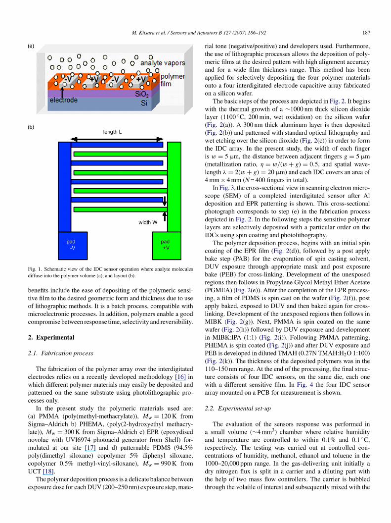
M. Kitsara et al. / Sensors and Actu
Fd
btomc
2
2
ewpc
(SlnmpcU
e
rtmaaoo
wl((wti(l4
sdpdlI
cbDbr(ialMwiPP(1twa
2
aarc
ig. 1. Schematic view of the IDC sensor operation where analyte moleculesiffuse into the polymer volume (a), and layout (b).
enefits include the ease of depositing of the polymeric sensi-ive film to the desired geometric form and thickness due to usef lithographic methods. It is a batch process, compatible withicroelectronic processes. In addition, polymers enable a good
ompromise between response time, selectivity and reversibility.
. Experimental
.1. Fabrication process
The fabrication of the polymer array over the interdigitatedlectrodes relies on a recently developed methodology [16] inhich different polymer materials may easily be deposited andatterned on the same substrate using photolithographic pro-esses only.
In the present study the polymeric materials used are:a) PMMA (poly(methyl-methacrylate)), Mw = 120 K fromigma–Aldrich b) PHEMA, (poly(2-hydroxyethyl methacry-
ate)), Mw = 300 K from Sigma–Aldrich c) EPR (epoxydisedovolac with UVI6974 photoacid generator from Shell) for-ulated at our site [17] and d) patternable PDMS (94.5%
oly(dimethyl siloxane) copolymer 5% diphenyl siloxane,
opolymer 0.5% methyl-vinyl-siloxane), Mw = 990 K fromCT [18].The polymer deposition process is a delicate balance betweenxposure dose for each DUV (200–250 nm) exposure step, mate-
1dtt
ators B 127 (2007) 186–192 187
ial tone (negative/positive) and developers used. Furthermore,he use of lithographic processes allows the deposition of poly-
eric films at the desired pattern with high alignment accuracynd for a wide film thickness range. This method has beenpplied for selectively depositing the four polymer materialsnto a four interdigitated electrode capacitive array fabricatedn a silicon wafer.
The basic steps of the process are depicted in Fig. 2. It beginsith the thermal growth of a ∼1000 nm thick silicon dioxide
ayer (1100 ◦C, 200 min, wet oxidation) on the silicon waferFig. 2(a)). A 300 nm thick aluminum layer is then depositedFig. 2(b)) and patterned with standard optical lithography andet etching over the silicon dioxide (Fig. 2(c)) in order to form
he IDC array. In the present study, the width of each fingers w = 5 �m, the distance between adjacent fingers g = 5 �mmetallization ratio, η = w/(w + g) = 0.5, and spatial wave-ength λ = 2(w + g) = 20 �m) and each IDC covers an area ofmm × 4 mm (N = 400 fingers in total).
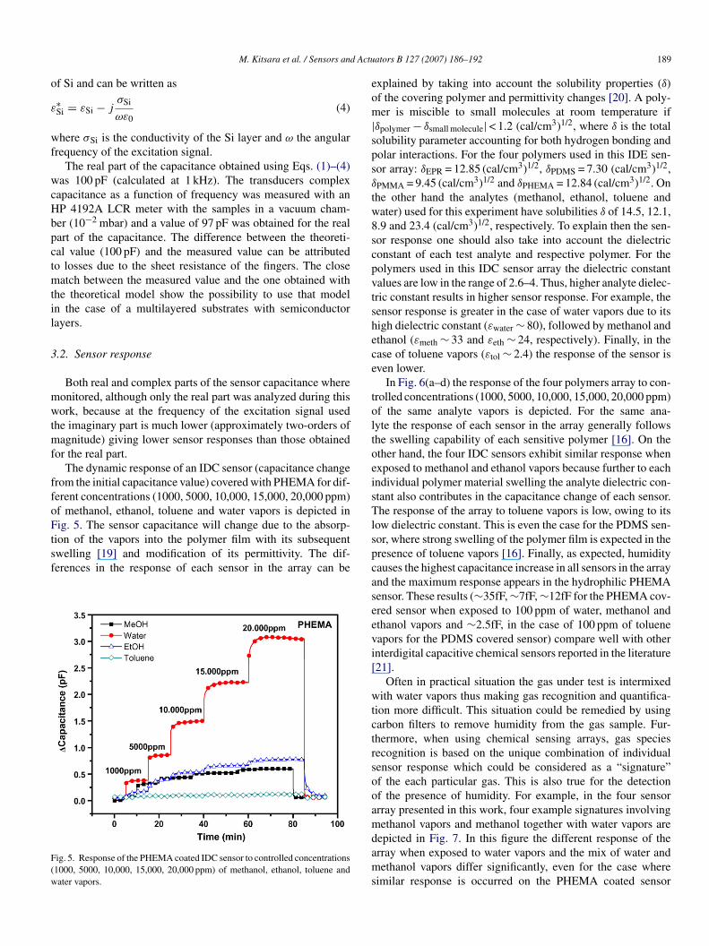
In Fig. 3, the cross-sectional view in scanning electron micro-cope (SEM) of a completed interdigitated sensor after Aleposition and EPR patterning is shown. This cross-sectionalhotograph corresponds to step (e) in the fabrication processepicted in Fig. 2. In the following steps the sensitive polymerayers are selectively deposited with a particular order on theDCs using spin coating and photolithography.
The polymer deposition process, begins with an initial spinoating of the EPR film (Fig. 2(d)), followed by a post applyake step (PAB) for the evaporation of spin casting solvent,UV exposure through appropriate mask and post exposureake (PEB) for cross-linking. Development of the unexposedegions then follows in Propylene Glycol Methyl Ether AcetatePGMEA) (Fig. 2(e)). After the completion of the EPR process-ng, a film of PDMS is spin cast on the wafer (Fig. 2(f)), postpply baked, exposed to DUV and then baked again for cross-inking. Development of the unexposed regions then follows in
IBK (Fig. 2(g)). Next, PMMA is spin coated on the sameafer (Fig. 2(h)) followed by DUV exposure and development
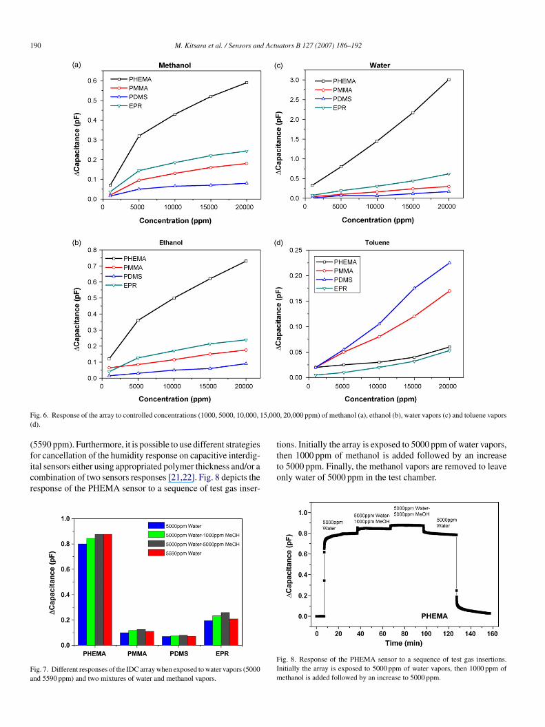
n MIBK:IPA (1:1) (Fig. 2(i)). Following PMMA patterning,HEMA is spin coated (Fig. 2(j)) and after DUV exposure andEB is developed in diluted TMAH (0.27N TMAH:H2O 1:100)Fig. 2(k)). The thickness of the deposited polymers was in the10–150 nm range. At the end of the processing, the final struc-ure consists of four IDC sensors, on the same die, each oneith a different sensitive film. In Fig. 4 the four IDC sensor
rray mounted on a PCB for measurement is shown.
.2. Experimental set-up
The evaluation of the sensors response was performed insmall volume (∼4 mm3) chamber where relative humidity
nd temperature are controlled to within 0.1% and 0.1 ◦C,espectively. The testing was carried out at controlled con-entrations of humidity, methanol, ethanol and toluene in the
000–20,000 ppm range. In the gas-delivering unit initially ary nitrogen flux is split in a carrier and a diluting part withhe help of two mass flow controllers. The carrier is bubbledhrough the volatile of interest and subsequently mixed with the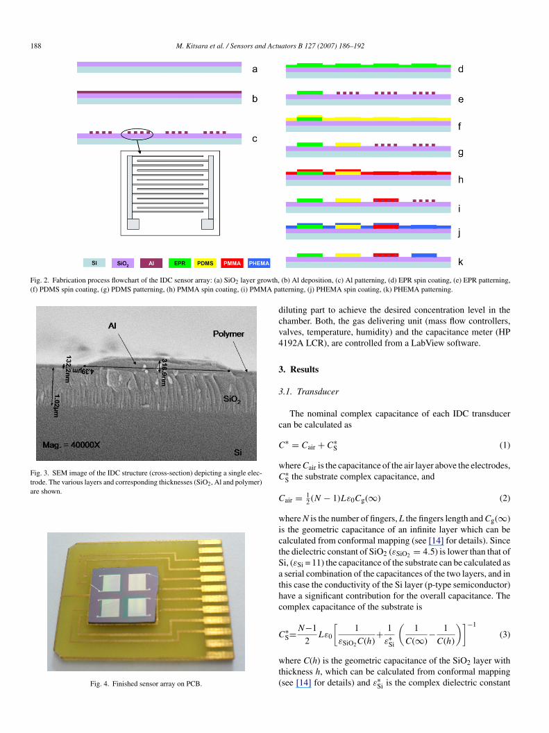
188 M. Kitsara et al. / Sensors and Actuators B 127 (2007) 186–192
Fig. 2. Fabrication process flowchart of the IDC sensor array: (a) SiO2 layer growth,(f) PDMS spin coating, (g) PDMS patterning, (h) PMMA spin coating, (i) PMMA pa
Fig. 3. SEM image of the IDC structure (cross-section) depicting a single elec-trode. The various layers and corresponding thicknesses (SiO2, Al and polymer)are shown.
Fig. 4. Finished sensor array on PCB.
dcv4
3
3
c
C
wC
C
wictSathc
C
wt(
(b) Al deposition, (c) Al patterning, (d) EPR spin coating, (e) EPR patterning,tterning, (j) PHEMA spin coating, (k) PHEMA patterning.
iluting part to achieve the desired concentration level in thehamber. Both, the gas delivering unit (mass flow controllers,alves, temperature, humidity) and the capacitance meter (HP192A LCR), are controlled from a LabView software.
. Results
.1. Transducer
The nominal complex capacitance of each IDC transduceran be calculated as
∗ = Cair + C∗S (1)
here Cair is the capacitance of the air layer above the electrodes,∗S the substrate complex capacitance, and
air = 12 (N − 1)Lε0Cg(∞) (2)
here N is the number of fingers, L the fingers length and Cg(∞)s the geometric capacitance of an infinite layer which can bealculated from conformal mapping (see [14] for details). Sincehe dielectric constant of SiO2 (εSiO2 = 4.5) is lower than that ofi, (εSi = 11) the capacitance of the substrate can be calculated asserial combination of the capacitances of the two layers, and in
his case the conductivity of the Si layer (p-type semiconductor)ave a significant contribution for the overall capacitance. Theomplex capacitance of the substrate is
∗S=N−1
2Lε0
[1
ε C(h)+ 1
ε∗
(1
C(∞)− 1
C(h)
)]−1
(3)
SiO2 Sihere C(h) is the geometric capacitance of the SiO2 layer withhickness h, which can be calculated from conformal mappingsee [14] for details) and ε∗
Si is the complex dielectric constant
Actu
o
ε
wf
wcHbpctmtil
3
mwtmf
ffoFtsf
F(w
eom|spsδ
tw8scpvtshece
toltoeisT
M. Kitsara et al. / Sensors and
f Si and can be written as
∗Si = εSi − j
σSi
ωε0(4)
here σSi is the conductivity of the Si layer and ω the angularrequency of the excitation signal.
The real part of the capacitance obtained using Eqs. (1)–(4)as 100 pF (calculated at 1 kHz). The transducers complex
apacitance as a function of frequency was measured with anP 4192A LCR meter with the samples in a vacuum cham-er (10−2 mbar) and a value of 97 pF was obtained for the realart of the capacitance. The difference between the theoreti-al value (100 pF) and the measured value can be attributedo losses due to the sheet resistance of the fingers. The close
atch between the measured value and the one obtained withhe theoretical model show the possibility to use that modeln the case of a multilayered substrates with semiconductorayers.
.2. Sensor response
Both real and complex parts of the sensor capacitance whereonitored, although only the real part was analyzed during thisork, because at the frequency of the excitation signal used
he imaginary part is much lower (approximately two-orders ofagnitude) giving lower sensor responses than those obtained
or the real part.The dynamic response of an IDC sensor (capacitance change
rom the initial capacitance value) covered with PHEMA for dif-erent concentrations (1000, 5000, 10,000, 15,000, 20,000 ppm)f methanol, ethanol, toluene and water vapors is depicted in
ig. 5. The sensor capacitance will change due to the absorp-ion of the vapors into the polymer film with its subsequentwelling [19] and modification of its permittivity. The dif-erences in the response of each sensor in the array can be
ig. 5. Response of the PHEMA coated IDC sensor to controlled concentrations1000, 5000, 10,000, 15,000, 20,000 ppm) of methanol, ethanol, toluene andater vapors.
lspcaseevi[
wtctrsooamdams
ators B 127 (2007) 186–192 189
xplained by taking into account the solubility properties (δ)f the covering polymer and permittivity changes [20]. A poly-er is miscible to small molecules at room temperature if
δpolymer − δsmall molecule| < 1.2 (cal/cm3)1/2, where δ is the totalolubility parameter accounting for both hydrogen bonding andolar interactions. For the four polymers used in this IDE sen-or array: δEPR = 12.85 (cal/cm3)1/2, δPDMS = 7.30 (cal/cm3)1/2,PMMA = 9.45 (cal/cm3)1/2 and δPHEMA = 12.84 (cal/cm3)1/2. Onhe other hand the analytes (methanol, ethanol, toluene andater) used for this experiment have solubilities δ of 14.5, 12.1,.9 and 23.4 (cal/cm3)1/2, respectively. To explain then the sen-or response one should also take into account the dielectriconstant of each test analyte and respective polymer. For theolymers used in this IDC sensor array the dielectric constantalues are low in the range of 2.6–4. Thus, higher analyte dielec-ric constant results in higher sensor response. For example, theensor response is greater in the case of water vapors due to itsigh dielectric constant (εwater ∼ 80), followed by methanol andthanol (εmeth ∼ 33 and εeth ∼ 24, respectively). Finally, in thease of toluene vapors (εtol ∼ 2.4) the response of the sensor isven lower.
In Fig. 6(a–d) the response of the four polymers array to con-rolled concentrations (1000, 5000, 10,000, 15,000, 20,000 ppm)f the same analyte vapors is depicted. For the same ana-yte the response of each sensor in the array generally followshe swelling capability of each sensitive polymer [16]. On thether hand, the four IDC sensors exhibit similar response whenxposed to methanol and ethanol vapors because further to eachndividual polymer material swelling the analyte dielectric con-tant also contributes in the capacitance change of each sensor.he response of the array to toluene vapors is low, owing to its
ow dielectric constant. This is even the case for the PDMS sen-or, where strong swelling of the polymer film is expected in theresence of toluene vapors [16]. Finally, as expected, humidityauses the highest capacitance increase in all sensors in the arraynd the maximum response appears in the hydrophilic PHEMAensor. These results (∼35fF, ∼7fF, ∼12fF for the PHEMA cov-red sensor when exposed to 100 ppm of water, methanol andthanol vapors and ∼2.5fF, in the case of 100 ppm of tolueneapors for the PDMS covered sensor) compare well with othernterdigital capacitive chemical sensors reported in the literature21].
Often in practical situation the gas under test is intermixedith water vapors thus making gas recognition and quantifica-
ion more difficult. This situation could be remedied by usingarbon filters to remove humidity from the gas sample. Fur-hermore, when using chemical sensing arrays, gas speciesecognition is based on the unique combination of individualensor response which could be considered as a “signature”f the each particular gas. This is also true for the detectionf the presence of humidity. For example, in the four sensorrray presented in this work, four example signatures involvingethanol vapors and methanol together with water vapors are
epicted in Fig. 7. In this figure the different response of therray when exposed to water vapors and the mix of water andethanol vapors differ significantly, even for the case where
imilar response is occurred on the PHEMA coated sensor
190 M. Kitsara et al. / Sensors and Actuators B 127 (2007) 186–192
F 5,000(
(ficr
Fa
tions. Initially the array is exposed to 5000 ppm of water vapors,then 1000 ppm of methanol is added followed by an increase
ig. 6. Response of the array to controlled concentrations (1000, 5000, 10,000, 1d).
5590 ppm). Furthermore, it is possible to use different strategiesor cancellation of the humidity response on capacitive interdig-
tal sensors either using appropriated polymer thickness and/or aombination of two sensors responses [21,22]. Fig. 8 depicts theesponse of the PHEMA sensor to a sequence of test gas inser-ig. 7. Different responses of the IDC array when exposed to water vapors (5000nd 5590 ppm) and two mixtures of water and methanol vapors.
to
FIm
, 20,000 ppm) of methanol (a), ethanol (b), water vapors (c) and toluene vapors
o 5000 ppm. Finally, the methanol vapors are removed to leavenly water of 5000 ppm in the test chamber.
ig. 8. Response of the PHEMA sensor to a sequence of test gas insertions.nitially the array is exposed to 5000 ppm of water vapors, then 1000 ppm ofethanol is added followed by an increase to 5000 ppm.
Actu
4
empmpsi
tMo
A
ITtfi
R
[
[
[
[
[
[
[
[
[
[
[
[
[
B
MaSicsbtc
DtPPtNi
SBPrs“t
Moii
M. Kitsara et al. / Sensors and
. Conclusions
A single chip chemical sensor array based on interdigitatedlectrodes and lithographically defined photosensitive poly-eric films has successfully been fabricated. The technique
resented in this work enables the deposition of sensitive poly-er films with a very well controlled thickness, which is a crucial
arameter for this type of sensors [21]. Furthermore, the wholeensor was implemented on Si wafers thus allowing for futurentegration with CMOS signal conditioning circuits.
Future work will focus on the analytical modeling ofhe sensors responses when exposed to different analytes.
iniaturization of the sensor array size is currently under devel-pment.
cknowledgments
This research work was partially supported by EPEAEKI/YPEPTH/ARXIMIDHS II-EEOT-YPOERGO 4 program.he authors wish to thank P. Argitis (IMEL, NCSR’ Demokri-
os’) for helpful discussions on the processing of polymericlms.
eferences
[1] N. Najafi, K.D. Wise, J.W. Schwank, W. Johannes, Micromachinedultra-thin-film gas detector, Electron. Devices, IEEE Trans. 41 (1994)1770–1777.
[2] J.W. Grate, Acoustic wave microsensor arrays for vapor sensing, Chem.Rev. 100 (2000) 2627–2648.
[3] P.G. Datskos, S. Rajic, M.J. Sepaniak, N. Lavrik, C.A. Tipple, L.R. Senesac,I. Datskou, Chemical detection based on adsorption-induced and photoin-duced stresses in microelectromechanical systems devices, J. Vac. Sci.Technol. B 19 (2001) 1173–1179.
[4] L. Quercia, F. Loffredo, B. Alfano, V. La Ferrara, G. Di Francia, Fabrica-tion and characterization of carbon nanoparticles for polymer based vaporsensors, Sens. Actuators, B: Chem. 100 (2004) 22–28.
[5] S.V. Patel, T.E. Mlsna, B. Fruhberger, E. Klaassen, S. Cemalovic, D.R.Baselt, Chemicapacitive microsensors for volatile organic compound detec-tion, Sens. Actuators, B: Chem. 96 (2003) 541–553.
[6] S. Chatzandroulis, A. Tserepi, D. Goustouridis, P. Normand, D. Tsoukalas,Fabrication of single crystal Si cantilevers using a dry release processand application in a capacitive-type humidity sensor, Microelectron. Eng.61–62 (2002) 955–961.
[7] D.M. Wilson, S.D. Garrod, Optimization of gas-sensitive polymer arraysusing combinations of heterogeneous and homogeneous subarrays, IEEESens. J. 2 (2002) 169–178.
[8] K.J. Albert, N.S. Lewis, C.L. Schauer, G.A. Sotzing, S.E. Stitzel, T.P. Vaid,D.R. Walt, Cross-reactive chemical sensor arrays, Chem. Rev. 100 (2000)2595–2626.
[9] M. Sepaniak, P. Datskos, N. Lavrik, C. Tipple, Microcantilever transducers:a new approach in sensor technology, Anal. Chem. 74 (2002) 568A–575A.
10] M. Maute, S. Raible, F.E. Prins, D.P. Kern, H. Ulmer, U. Weimar, W.Gopel, Detection of volatile organic compounds (VOCs) with polymer-coated cantilevers, Sens. Actuators, B: Chem. 58 (1999) 505–511.
11] B.H. Kim, F.E. Prins, D.P. Kem, S. Raible, U. Weimar, Multicomponentanalysis and prediction with a cantilever array based gas sensor, Sens.
Actuators, B: Chem. 78 (2001) 12–18.12] K. Baller, H.P. Lang, J. Fritz, Ch. Gerber, J.K. Gimzewski, U. Drechsler,H. Rothuizen, M. Despont, P. Vettiger, F.M. Battiston, J.P. Ramseyer, P.Fornaro, E. Meyer, H.-J. GuK ntherodt, A cantilever array-based artificialnose, Ultramicroscopy 82 (2000) 1–9.
oTtnp
ators B 127 (2007) 186–192 191
13] S. Chatzandroulis, E. Tegou, D. Goustouridis, S. Polymenakos, D.Tsoukalas’, Capacitive-type chemical sensors using thin silicon/polymerbimorph membranes, Sens. Actuators, B: Chem. 103 (2004) 392–396.
14] R. Igreja, C.J. Dias, Analytical evaluation of the interdigital electrodescapacitance for a multi-layered structure, Sens. Actuators A 112 (2004)291–301.
15] B. Adhikari, S. Majumdar, Polymers in sensor applications, Prog. Polym.Sci. 29 (2004) 699–766.
16] M. Kitsara, D. Goustouridis, S. Chatzandroulis, K. Beltsios, I. Raptis, Alithographic polymer process sequence for chemical sensing arrays, Micro-electron. Eng. 83 (2006) 1192–1196.
17] P. Argitis, I. Raptis, C.J. Aidinis, N. Glezos, M. Baciocchi, J. Everett, M.Hatzakis, Advanced epoxy novolac resist for fast high-resolution electron-beam lithography, J. Vac. Sci. Technol. B 13 (1995) 3030–3034.
18] A. Tserepi, E. Gogolides, K. Tsougeni, V. Constantoudis, E.S. Valamontes,Tailoring the surface topography and wetting properties of oxygen-plasmatreated polydimethylsiloxane, J. Appl. Phys. 98 (11) (2005) 1–6.
19] D. Goustouridis, K. Manoli, S. Chatzandroulis, M. Sanopoulou, I. Rap-tis, Characterization of polymer layers for silicon micromachined bilayerchemical sensors using white light interferometry, Sens. Actuators B111–112 (2005) 549–554.
20] J.W. Grate, M.H. Abraham, Solubility interactions and the selection ofsorbent coating materials for chemical sensors and sensor arrays, Sens.Actuators B 3 (1991) 85–111.
21] R. Igreja, C.J. Dias, Dielectric response of interdigital chemocapacitors:the role of the sensitive layer thickness, Sens. Actuators B 115 (2006)69–78.
22] A.M. Kummer, A. Hierlemann, H. Baltes, Tuning sensitivity and selectivityof complementary metal oxide semiconductor-based capacitive chemicalmicrosensors, Anal. Chem. 76 (2004) 2470–2477.
iographies
aria Kitsara was born in Ioannina, Greece in 1982. She graduated in Materi-ls Science and Engineering Department from University of Ioannina in 2004.he received the MSc degree in Polymer Science from the Department of Chem-
stry of National University of Athens and concluded her thesis in the field ofharacterization of polymeric materials and their applications in chemical sen-ors, at the Institute of Microelectronics, NCSR “Demokritos”, in 2006. She haseen studying for the PhD degree since 2006. Her current research is focused onhe fabrication of optical sensors and their applications in chemical/biologicalharacterizations.
imitris Goustouridis was born in 1969. He received the BS in 1992 fromhe department of Physics of the University of Patras. In 2002, he received thehD degree in microelectronics from the Faculty of Applied Mathematics andhysics of National Technical University of Athens for his work on capacitive
ype pressure sensors. He is currently with the Institute of Microelectronics atCSR “Demokritos”. His interests include silicon sensors and pressure sensors
n particular, and silicon micromachining.
tavros Chatzandroulis was born in Athens Greece in 1967. He received theachelor degree and the MSc in Electronic Automation from the Department ofhysics at the University of Athens in 1990 and 1993, respectively. In 1999, heeceived the PhD degree from the same Department for his work on integratedilicon sensors. He is currently with the Institute of Microelectronics at NCSRDemokritos”. His interests include silicon sensors, silicon micromachiningechnology, and sensor electronic interfaces.
argarita Chatzichristidi received her BS degree in Physics from Universityf Ioannina in 1997, her MSc in Polymer Science and Technology from UMISTn 1999 and her PhD in the field of lithography from the University of Athensn 2004. From 2005, she is working as a Post-Doctoral fellow in the University
f Patras. Since 2001 she is working in parallel as laboratory assistant at theechnical University of Piraeus. Her current research activities are focused onhe development and characterization of lithographic materials, patterning tech-ologies and devices in the micro/nano scale. She is author and co-author of 9ublications in international referred journals.
1 d Actu
IofaEarapchm
RPo
Mimidr
Cfoo
92 M. Kitsara et al. / Sensors an
oannis Raptis received his BS degree in Physics in 1989 and his PhD in the fieldf e-beam lithography in 1996 all from National University of Athens. His workor the PhD thesis was carried out at IMEL-NCSR ‘Demokritos’ (Greece) andt IESS-CNR (Italy). From 1997 until 2003 he was working as lecturer at thelectronic Engineering Department, TEI of Athens and as research associatet the NCSR “Demokritos”. From 2003 he works at NCSR “Demokritos” asesearcher and from 2007 as senior researcher. His current research activitiesre focused on the development and characterization of lithographic materials,atterning technologies and devices in the micro/nano scale. He is author ando-author of more than 60 publications in international referred journals andolder of two patents. He acts as a reviewer for several journals in the field of
icro/nano fabrication.ui Igreja was born in Lisbon, Portugal in 1966. He graduated in Engineeringhysics from Universidade Nova de Lisboa in 1992 and joined the Departmentf Physics of the same University in 1993 as assistant professor. He obtained the
cdraf
ators B 127 (2007) 186–192
Sc degree in Instrumentation, Industrial Mainteinence and Quality in 1998n Universidade Nova de Lisboa. He received the PhD degree in the field of
icroelectronics and optoelectronics from the Universidade Nova de Lisboan 2006. Since then he has been an auxiliary professor at Universidade Novae Lisboa and is currently working in the Materials Science Department. Hisesearch interests are in solid state physics, dielectrics and sensors.
.J. Dias was born in Angola in 1959. He graduated in Engineering Physicsrom Universidade Nova de Lisboa in 1982 and joined the Department of Physicsf the same University in 1985. He received the PhD degree from the Universityf North Wales (Bangor) in 1994 working on ferroelectric polymer–ceramic
omposites. Since then he has been an auxiliary professor at Universidade Novae Lisboa and is currently working in the Materials Science Department. Hisesearch interests include characterization of dielectrics and their use in variouspplications such as sensors and actuators, acoustics and polymer ionic materialsor energy applications.