High-Resolution Mode-Locked Laser Rangefinder With Harmonic Downconversion
Upload
khangminh22Category
view
3download
0
HAL Id: hal-02939709https://hal.archives-ouvertes.fr/hal-02939709
Submitted on 18 Dec 2020
HAL is a multi-disciplinary open accessarchive for the deposit and dissemination of sci-entific research documents, whether they are pub-lished or not. The documents may come fromteaching and research institutions in France orabroad, or from public or private research centers.
L’archive ouverte pluridisciplinaire HAL, estdestinée au dépôt et à la diffusion de documentsscientifiques de niveau recherche, publiés ou non,émanant des établissements d’enseignement et derecherche français ou étrangers, des laboratoirespublics ou privés.
Highly Sensitive Capacitive Sensor Based on InjectionLocked Oscillators with ppm Sensing Resolution
Meissa Babay, Clement Hallepee, Claire Dalmay, Bruno Barelaud, Emre CanDurmaz, Canan Baristiran-Kaynak, Mehmet Kaynak, David Cordeau, Arnaud
Pothier
To cite this version:Meissa Babay, Clement Hallepee, Claire Dalmay, Bruno Barelaud, Emre Can Durmaz, et al.. HighlySensitive Capacitive Sensor Based on Injection Locked Oscillators with ppm Sensing Resolution. IMS2020 IEEE MTT-S International Microwave Symposium, Aug 2020, Los Angeles, United States. �hal-02939709�

Paper presented during the IMS 2020 conference: Los Angeles 2-4th August 2020
Highly Sensitive Capacitive Sensor Based on Injection Locked
Oscillators with ppm Sensing Resolution
Meissa Babay#1, Clement Hallepee#, Claire Dalmay#, Bruno Barelaud#, Emre Can Durmaz*,
Canan Baristiran Kaynak*, Mehmet Kaynak*, David Cordeau$2, Arnaud Pothier#3 # XLIM- CNRS- University of Limoges, France $XLIM - CNRS- University of Poitiers, France
* IHP – Leibniz-Institut für innovative Mikroelektronik, Frankfurt (Oder), Germany [email protected], [email protected], [email protected]
Abstract—This paper presents the design and the
implementation of an ultra-sensitive capacitive sensor based on an
injection-locked oscillator architecture able to achieve ppm
sensing resolution. The proposed RF IC chip, implemented on a
BiCMOS SiGe 0.25 μm technology, is able to detect capacitance
changes in the range of few attoF, induced by dielectric
disturbance occurring on on-chip integrated sensing capacitors.
Indeed, this paper demonstrates that, once locked on a 4.693 GHz
and -50 dBm injection signal, the proposed sensing system can
efficiently detect differences of free running frequencies as low as
10 kHz between two oscillators. Considering a differential
measurement approach with two injection locked oscillators (one
used as a sensor, the other as a reference), a 3 attoF difference
between both LC tank sensing capacitors might be detectable. This
results, in the present case, in a 5 ppm sensing sensitivity.
Keywords—RF sensors, injection locked oscillator, BiCMOS,
dielectric characterization
I. INTRODUCTION
Dielectric capacitive sensors currently find widespread use
in various domains such as medical diagnostics, food safety
control [1], air pollution [2] or toxic gas detection [3], thanks to
the high level of sensitivity that such sensors can reach [4-6].
Research activities are multiplying to develop sensors with
small size, low cost and low energy consumption. Recent works
have shown the potential of Integrated Circuits (ICs) and
CMOS technology for the miniaturization and the integration
of RF characterization devices. In addition, several works have
demonstrated how the sensitivity of such devices can be
significantly enhanced by the use of oscillator-based sensors. In
this study, the proposed sensing method consists in measuring
a capacitance change due to a dielectric disturbance on the
sensor, which leads to an output frequency change of the
oscillator-based device. This sensing approach can be applied
in different types of analysis depending on the targeted
application (moisture control, gas detection, bio-detection….)
and on the sensitive material used. For example, in the
biomedical domain, capacitive bio-sensing systems are well-
known to have great potential applications for single cell
analysis based on label-free and non-destructive detection [7].
Besides, it is also possible to monitor basic environmental
parameters such as the relative humidity [8] with such dielectric
capacitive sensors. In addition, the development of emerging
IoT gas sensing systems presents a great interest as it allows for
precise monitoring of different types of environment.
Capabilities of measuring the concentration of greenhouse gas
such as alcohol vapor, aldehydes, organic acids, and aromatic
hydrocarbons, find various applications like air quality control
with environmental issues: in the context of the fight against
global warming, such highly sensitive sensors can be strategic
[9].
In this context, this paper presents a new differential
architecture of an ultra-sensitive dielectric capacitive sensor
based on injection-locked oscillators (ILOs) integrated on a
BiCMOS SiGe 0.25 μm process. The proposed architecture has
the potential to reach a very high level of sensitivity which
makes it to be used as a versatile tool. The paper is organized
as follows. Section II describes the proposed sensing system
and reminds the principle of an ILO. Section III presents the
circuit design and the experimental results. Finally, a
conclusion is given in section IV.
II. SENSOR ARCHITECTURE
A. Proposed sensing system
Fig. 1. Sensing system schematic diagram.
The objective of the proposed work is to implement, on a
silicon chip, an ultrasensitive capacitive sensor architecture
reaching a sensitivity in the order of the ppm. Generally, fully
integrated oscillators suffer from one major constraint that may
limit the performances of the sensing system: they can be very
sensitive to environmental perturbations (temperature, noise,
electromagnetic interferences…) which can cause a significant
timing jitter at the output of the oscillator. For the targeted
objective in this work, strong stability and very low phase noise

Paper presented during the IMS 2020 conference: Los Angeles 2-4th August 2020
of the oscillator is compulsory required in order to efficiently
detect any frequency shifts induced by the event to monitor,
even more in the case of very low sensing capacitance changes
(ppm resolution is targeted). To overcome this issue and
achieve high sensitivity sensing, the implementation of an
injection locked oscillator can be a relevant approach to limit
the phase noise near the carrier and reach a strong frequency
stability.
In these conditions, the proposed system aims to detect any
minor dielectric disturbances in the vicinity of the detection
capacitor by measuring the induced phase difference between
two identical LC oscillators output signals locked on the same
injection signal (Fig.1); considering that only one (Detector)
will be exposed, whereas the other (Reference) will not be
affected by the dielectric perturbation. Hence, when a
disturbance occurs and only affects the detection capacitor, it
induces a small sensing capacitance change and so the free-
running frequency of the corresponding oscillator (Detector) is
brought to vary in similar proportions with respect to the one of
the reference. Under injection, this frequency difference will
lead to a phase shift between the output signals of the two
oscillators. As illustrated in Fig. 1, this differential
measurement approach should ensure better sensing accuracy
by self-correcting unwanted frequency deviations potentially
induced by environmental perturbations. Under these
conditions, the two oscillators free-running frequencies should
vary in the same amount depending on the environment but
only the variations that rely on the phenomenon to monitor will
be characterized.
Fig. 2 describes the fundamental blocks of the proposed
Injection-locked detection system. At the input, the single-
ended injected signal is converted into a differential signal
using an external off-chip RF balun. This differential signal is
subsequently applied to an injection circuit associated to the LC
oscillator. The differential output signal from the sensor is then
buffered. Furthermore, a differential amplifier is implemented
at the output of the oscillator followed by a buffer stage in order
to combine the differential output into a single 50 Ω-matched
output.
Fig. 2. Detection oscillator schematic implementation.
B. Injection locking theory
The injection-locking phenomena was first introduced by
Adler [10] for weak injection level, and after that by Razavi
[11] for high injection level. The principle of the injection-
locking is based on the fact that a master oscillator, modeled as
a spectrally pure source, imposes, under certain conditions, its
frequency and its phase noise close to the carrier on a slave
oscillator. In these conditions, a phase shift between the output
signals of the two oscillators is generated. This phase difference
can be controlled by tuning the free-running frequency of the
slave oscillator [10, 11]. Actually, the behavior of an injection-
locked oscillator can be modelled using the Adler’s equation
for a weak injection level (1):
ωdet 𝐹𝑅 − ωinj =ωdet 𝐹𝑅
2Q.
Ainj
Aosc
. sin(фdet − фinj) (1)
Where ωinj, фinj and Ainj are respectively the pulsation, the phase
and the amplitude of the injected signal, ωdet 𝐹𝑅 the free
running pulsation and фdet and Aosc the phase and the amplitude
of the output signal of the injection-locked slave oscillator. For
our purpose, capacitance variations are expected to be in the
order of few hundreds to few tens of attofarads. In order to
properly detect such minor capacitive variations, it is necessary
to work on low injection mode (Ainj<<Aosc) to ensure a
generated phase shift that might linearly vary between [-30°, +30°].
III. CIRCUIT DESIGN AND MEASUREMENT RESULTS
A. Circuit Design
As mentioned before, the proposed circuit is composed of
one pair of differential injection-locked oscillators (Detection
& Reference). Fig.3 shows the schematic of the detection
injection-locked oscillator. The differential LC oscillator is
based on a NMOS cross-coupled architecture used here to
provide the negative resistance to compensate the losses
associated with the resonator. The implemented resonator is
made of a differential inductor (Ldiff), a high Q Metal insulator
Metal capacitor (CMIM) and a sensing capacitor (CSens), all
associated in parallel. The injected signal in the differential
branches is applied through the gates of 𝑀3,4 NMOS transistors.
Output signals from 𝑀1,2 drains (Vout- & Vout+) are then buffered
and transferred to the differential amplifier to allow sensor
oscillation measurements with a high-speed oscilloscope.
Fig. 3. Differential injection-locked oscillator schematic
B. Implementation and Experimental Results

Paper presented during the IMS 2020 conference: Los Angeles 2-4th August 2020
The proposed circuit was implemented in the SG25H4
SiGe:C BiCMOS 0.25 μm technology of IHP. A chip
photograph with a close view on the detection oscillator is
shown in Fig.4. The chip area is 1035*1800 µm² including all
the pads. Finally, to allow easier measurements, the chip is
mounted on a PCB (Fig.5).
Fig. 4. Photograph of the detection system.
Fig.5 shows the measurement setup used for evaluating the
device performances. This measurement bench is composed of
an external low phase noise RF source (Rohde & Schwarz
SMF100A) connected to an RF balun (Focus Microwaves
BUN-750-IN). Differential outputs of this balun are mounted
with circulators to limit the effects of potential signal
reflections from the PCB and thus to avoid couplings between
both injection locked oscillators. At the PCB outputs, both ILO
output signals are directed to a coupler that allows
simultaneously monitoring the sensing and reference signals on
a spectrum analyzer (Rohde & Schwarz FSV) and on an high-
speed oscilloscope (Lecroy SDA 816 Zi-A 16 GHz 40 GS/s).
Furthermore, batteries are used as supply voltages to avoid
external parasitic signals.
Fig. 5. Measurement setup.
In these conditions, the measurement results show that the
circuit operates at a free running frequency 𝑓𝑑𝑒𝑡 𝐹𝑅= 4.693 GHz,
when no injection signal is applied. In this case, Fig. 6 (a)
shows the output spectrum of either the reference or the sensing
oscillator (without any disturbances) on 50 Ω load. Fig.6(b)
shows the output spectrum of the same oscillator locked by
injection on 50 Ω load when the injected frequency 𝑓𝑖𝑛𝑗 is the
same as the free running frequency 𝑓𝑑𝑒𝑡 𝐹𝑅. As shown in
Fig. 6 (b), the phase noise near the carrier is significantly
reduced compared to the case when no injection is applied. In
these conditions, the proposed circuit can be more appropriated
to efficiently measure sub femtofarads capacitance variations
and to detect very small dielectric disturbances on the sensing
capacitor.
Fig. 6. Output spectrum of the oscillator in respectively (a) free-running mode
and (b) locked by injection.
Fig. 7 shows the plot of the measured phase shift between
the output signal of the detection oscillator with a free running
frequency 𝑓𝑑𝑒𝑡 𝐹𝑅 and the master signal set to a frequency 𝑓𝑖𝑛𝑗 .
As shown on this figure, when 𝑓𝑖𝑛𝑗=𝑓det 𝐹𝑅 , the resulting phase
shift фdet - фinj is null. Now thanks to external bias, the
capacitance brought back by 𝑀1,2 transistors in parallel with
CSens can be slightly tuned. It allows to artificially change 𝑓det 𝐹𝑅
thus resulting in a phase shift variation whose value can be
tailored by adjusting the amplitude of the injected signal (1).
Hence, with the proposed circuit design and by reducing the
injection level in the order of -50 dBm, the measurement
results, depicted in Fig.7, show the system capability to
accurately monitor a low frequency variation ranging from -100
kHz to +100 kHz around 4.693 GHz. Indeed, in such injection
conditions, it still leads to a phase shift ranging between -30°
and +30°. Therefore, considering a minimum 3° detectable
phase difference, one can see that the minimal achievable
measurement resolution is close to 10 kHz frequency shift for a
single ILO sensor.
Fig. 7. Single ILO measured phase shift versus the free running frequency
variation related to the injection signal one.
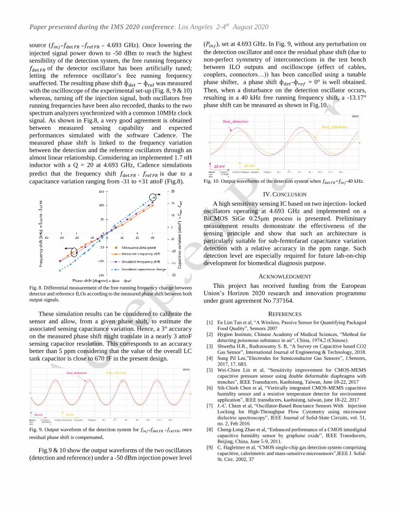
Now considering a differential measurement between the
detector and the reference ILOs, Fig. 8 shows the resulting
phase shift measured between the output signals of both
injection-locked oscillators with the same injection external RF
Paper presented during the IMS 2020 conference: Los Angeles 2-4th August 2020
source (𝑓𝑖𝑛𝑗=𝑓det 𝐹𝑅 =𝑓ref 𝐹𝑅 = 4.693 GHz). Once lowering the
injected signal power down to -50 dBm to reach the highest
sensibility of the detection system, the free running frequency
𝑓det 𝐹𝑅 of the detector oscillator has been artificially tuned;
letting the reference oscillator’s free running frequency
unaffected. The resulting phase shift фdet − фref was measured
with the oscilloscope of the experimental set-up (Fig. 8, 9 & 10)
whereas, turning off the injection signal, both oscillators free
running frequencies have been also recorded, thanks to the two
spectrum analyzers synchronized with a common 10MHz clock
signal. As shown in Fig.8, a very good agreement is obtained
between measured sensing capability and expected
performances simulated with the software Cadence. The
measured phase shift is linked to the frequency variation
between the detection and the reference oscillators through an
almost linear relationship. Considering an implemented 1.7 nH
inductor with a Q = 20 at 4.693 GHz, Cadence simulations
predict that the frequency shift 𝑓det 𝐹𝑅 - 𝑓ref 𝐹𝑅 is due to a
capacitance variation ranging from -31 to +31 attoF (Fig.8).
Fig. 8. Differential measurement of the free running frequency change between
detector and reference ILOs according to the measured phase shift between both
output signals.
These simulation results can be considered to calibrate the
sensor and allow, from a given phase shift, to estimate the
associated sensing capacitance variation. Hence, a 3° accuracy
on the measured phase shift might translate in a nearly 3 attoF
sensing capacitor resolution. This corresponds to an accuracy
better than 5 ppm considering that the value of the overall LC
tank capacitor is close to 670 fF in the present design.
Fig. 9. Output waveform of the detection system for 𝑓𝑖𝑛𝑗=𝑓det 𝐹𝑅 =𝑓ref 𝐹𝑅, once
residual phase shift is compensated.
Fig.9 & 10 show the output waveforms of the two oscillators
(detection and reference) under a -50 dBm injection power level
(𝑃𝑖𝑛𝑗), set at 4.693 GHz. In Fig. 9, without any perturbation on
the detection oscillator and once the residual phase shift (due to
non-perfect symmetry of interconnections in the test bench
between ILO outputs and oscilloscope (effect of cables,
couplers, connectors…)) has been cancelled using a tunable
phase shifter, a phase shift ф𝑑𝑒𝑡-ф𝑟𝑒𝑓 = 0° is well obtained.
Then, when a disturbance on the detection oscillator occurs,
resulting in a 40 kHz free running frequency shift, a -13.17°
phase shift can be measured as shown in Fig.10.
Fig. 10. Output waveforms of the detection system when 𝑓det 𝐹𝑅=𝑓𝑖𝑛𝑗-40 kHz.
IV. CONCLUSION
A high sensitivity sensing IC based on two injection- locked
oscillators operating at 4.693 GHz and implemented on a
BiCMOS SiGe 0.25μm process is presented. Preliminary
measurement results demonstrate the effectiveness of the
sensing principle and show that such an architecture is
particularly suitable for sub-femtofarad capacitance variation
detection with a relative accuracy in the ppm range. Such
detection level are especially required for future lab-on-chip
development for biomedical diagnosis purpose.
ACKNOWLEDGMENT
This project has received funding from the European
Union’s Horizon 2020 research and innovation programme
under grant agreement No 737164.
REFERENCES
[1] Ee Lim Tan et al, “A Wireless, Passive Sensor for Quantifying Packaged
Food Quality”, Sensors 2007 [2] Hygien Institute, Chinese Academy of Medical Sciences, “Method for
detecting poisonous substance in air”, China, 1974,2 (Chinese).
[3] Shwetha H.R., Rudraswamy S. B, “A Survey on Capacitive based CO2 Gas Sensor”, International Journal of Engineering & Technology, 2018.
[4] Sung Pil Lee,”Electrodes for Semiconductor Gas Sensors”, J.Sensors,
2017, 17, 683. [5] Wei-Chien Lin et al, “Sensitivity improvement for CMOS-MEMS
capacitive pressure sensor using double deformable diaphragms with
trenches”, IEEE Transducers, Kaohsiung, Taiwan, June 18-22, 2017
[6] Sih-Chieh Chen et al, “Vertically integrated CMOS-MEMS capacitive
humidity sensor and a resistive temperature detector for environment
application”, IEEE transducers, kaohsiung, taiwan, june 18-22, 2017 [7] J.-C. Chien et al, “Oscillator-Based Reactance Sensors With Injection
Locking for High-Throughput Flow Cytometry using microwave
dielectric spectroscopy”, IEEE Journal of Solid-State Circuits, vol. 51, no. 2, Feb 2016
[8] Cheng-Long Zhao et al, “Enhanced performance of a CMOS interdigital
capacitive humidity sensor by graphene oxide”, IEEE Transducers, Beijing, China, June 5-9, 2011.
[9] C. Hagleitner et al, “CMOS single-chip gas detection system comprising
capacitive, calorimetric and mass-sensitive microsensors”,IEEE J. Solid-St. Circ. 2002, 37

Paper presented during the IMS 2020 conference: Los Angeles 2-4th August 2020
[10] R. Adler et al, “A study of locking phenomena in oscillators” , Proc. IRE,
vol. 34, pp. 351–357, Jun. 1946
[11] B. Razavi et al, “A study of injection locking and pulling in oscillators,” IEEE J. Solid-State Circuits, vol. 39, no. 9, pp. 1415–1424, Sep. 2004.
Copyright © 2022 FDOKUMEN