RF MEMS sequentially reconfigurable sierpinski antenna on a flexible organic substrate with novel...
8
JOURNAL OF MICROELECTROMECHANICAL SYSTEMS, VOL. 16, NO. 5, OCTOBER 2007 1185 RF MEMS Sequentially Reconfigurable Sierpinski Antenna on a Flexible Organic Substrate With Novel DC-Biasing Technique Nickolas Kingsley, Member, IEEE, Dimitrios E. Anagnostou, Member, IEEE, Manos Tentzeris, Senior Member, IEEE, and John Papapolymerou, Senior Member, IEEE Abstract—Devices and systems that use RF microelectro- mechanical systems (RF MEMS) switching elements typically use one switch topology. The switch is designed to meet all of the performance criteria. However, this can be limiting for highly dy- namic applications that require a great deal of reconfigurability. In this paper, three sets of RF MEMS switches with different actua- tion voltages are used to sequentially activate and deactivate parts of a multiband Sierpinski fractal antenna. The implementation of such a concept allows for direct actuation of the electrostatic MEMS switches through the RF signal feed, therefore eliminating the need for individual switch dc bias lines. This reconfigurable antenna was fabricated on liquid crystal polymer substrate and operates at several different frequencies between 2.4 and 18 GHz while maintaining its radiation characteristics. It is the first in- tegrated RF MEMS reconfigurable antenna on a flexible organic polymer substrate for multiband antenna applications. Simulation and measurement results are presented in this paper to validate the proposed concept. [2007-0013] Index Terms—Liquid crystal polymer (LCP), multiband, reconfigurable antenna, RF microelectromechanical systems (RF MEMS), Sierpinski fractal antenna. I. I NTRODUCTION T HE RF microelectromechanical systems (RF MEMS) switches are quickly becoming a popular switching ele- ment among microwave designers. Their low loss, small size, excellent isolation, and low distortion make them attractive for a wide range of applications. They have already been integrated into filters [1], [2], antennas [3]–[5], phase shifters [6], and many other RF devices. Designers typically optimize the MEMS geometry to meet a given specification. Switches can be made wide and short or narrow and long to meet a specific size requirement. The materials can be tailored to meet a desired actuation voltage. Manuscript received January 22, 2007; revised April 27, 2007. This work was supported by the National Science Foundation (NSF) under Grant ECS0500860. Subject Editor S. Lucyszyn. N. Kingsley was with the School of Electrical and Computer Engineering, Georgia Institute of Technology, Atlanta, GA 30308 USA. He is now with the Modeling and Design Group, Auriga Measurement Systems, Lowell, MA 01854 USA (e-mail: [email protected]). D. E. Anagnostou is with the Electrical and Computer Engineering De- partment, South Dakota School of Mines and Technology, Rapid City, SD 57701 USA. M. Tentzeris and J. Papapolymerou are with the School of Electrical and Computer Engineering, Georgia Institute of Technology, Atlanta, GA 30308 USA. Color versions of one or more of the figures in this paper are available online at http://ieeexplore.ieee.org. Digital Object Identifier 10.1109/JMEMS.2007.902462 The height of the membrane can be tuned to give a certain level of isolation when in the “OFF” position. The inductive and capacitive regions can be designed to work best at a given frequency. For each application, and in all existing literature, there is typically one switch membrane geometry, and it is used exclusively throughout the system. However, using only one switch membrane geometry can be limiting if the device needs maximum reconfigurability. It could be beneficial to utilize multiple switch membrane geometries to add an additional level of reconfigurability. For example, to provide the lowest possible loss from the switching element, several different switches could be used in parallel which are tuned for different operating frequencies. As the frequency is changed, the switch that works best at that frequency is used. Since MEMS switches offer excellent “OFF”-state isolation (usually better than 30 dB), the presence of the additional switches would have a negligible effect on the device. This same technique could be used to select switches of different impedances, switching speed, isolation, capacitance, etc. A sys- tem could also select between ohmic and capacitive switches to operate from dc to very high frequencies. This technique is ideal for applications that need maximum reconfigurability and can tolerate the slight size increase from the additional switches. To demonstrate the effectiveness of using multiple switch geometries in a working system, this paper presents a three- iteration coplanar waveguide (CPW)-fed Sierpinski gasket monopole antenna that is reconfigured by turning on various RF MEMS switches. Different areas of the antenna geometry are sequentially activated and deactivated by changing the dc voltage present at the RF feed. This method eliminates the need for dc bias lines at each MEMS switch, which will improve the radiation characteristics of the antenna. In the past decade, fractal or prefractal shapes have been introduced in antenna and array designs. Several of these de- signs have been extensively studied, including Koch [7]–[9], Hilbert, Peano, Minkowski, and Sierpinski [10], [11] geomet- rical shapes or array arrangements [10], demonstrating both compactness and multiband behavior. A comprehensive review [12] describes in detail, among others, the multiband function of the Sierpinski gasket monopole and dipole antennas. In the majority of the published literature, integration has been accomplished on rigid and nonflexible semiconducting or organic polymer substrates such as silicon and FR-4. The idea of integrating RF MEMS switches into a multiband self-similar antenna was first implemented in [3], where the entire system, 1057-7157/$25.00 © 2007 IEEE
Transcript of RF MEMS sequentially reconfigurable sierpinski antenna on a flexible organic substrate with novel...

JOURNAL OF MICROELECTROMECHANICAL SYSTEMS, VOL. 16, NO. 5, OCTOBER 2007 1185
RF MEMS Sequentially Reconfigurable SierpinskiAntenna on a Flexible Organic Substrate
With Novel DC-Biasing TechniqueNickolas Kingsley, Member, IEEE, Dimitrios E. Anagnostou, Member, IEEE,
Manos Tentzeris, Senior Member, IEEE, and John Papapolymerou, Senior Member, IEEE
Abstract—Devices and systems that use RF microelectro-mechanical systems (RF MEMS) switching elements typically useone switch topology. The switch is designed to meet all of theperformance criteria. However, this can be limiting for highly dy-namic applications that require a great deal of reconfigurability. Inthis paper, three sets of RF MEMS switches with different actua-tion voltages are used to sequentially activate and deactivate partsof a multiband Sierpinski fractal antenna. The implementationof such a concept allows for direct actuation of the electrostaticMEMS switches through the RF signal feed, therefore eliminatingthe need for individual switch dc bias lines. This reconfigurableantenna was fabricated on liquid crystal polymer substrate andoperates at several different frequencies between 2.4 and 18 GHzwhile maintaining its radiation characteristics. It is the first in-tegrated RF MEMS reconfigurable antenna on a flexible organicpolymer substrate for multiband antenna applications. Simulationand measurement results are presented in this paper to validatethe proposed concept. [2007-0013]
Index Terms—Liquid crystal polymer (LCP), multiband,reconfigurable antenna, RF microelectromechanical systems(RF MEMS), Sierpinski fractal antenna.
I. INTRODUCTION
THE RF microelectromechanical systems (RF MEMS)switches are quickly becoming a popular switching ele-
ment among microwave designers. Their low loss, small size,excellent isolation, and low distortion make them attractive fora wide range of applications. They have already been integratedinto filters [1], [2], antennas [3]–[5], phase shifters [6], andmany other RF devices.
Designers typically optimize the MEMS geometry to meeta given specification. Switches can be made wide and shortor narrow and long to meet a specific size requirement. Thematerials can be tailored to meet a desired actuation voltage.
Manuscript received January 22, 2007; revised April 27, 2007. This workwas supported by the National Science Foundation (NSF) under GrantECS0500860. Subject Editor S. Lucyszyn.
N. Kingsley was with the School of Electrical and Computer Engineering,Georgia Institute of Technology, Atlanta, GA 30308 USA. He is now withthe Modeling and Design Group, Auriga Measurement Systems, Lowell, MA01854 USA (e-mail: [email protected]).
D. E. Anagnostou is with the Electrical and Computer Engineering De-partment, South Dakota School of Mines and Technology, Rapid City,SD 57701 USA.
M. Tentzeris and J. Papapolymerou are with the School of Electricaland Computer Engineering, Georgia Institute of Technology, Atlanta, GA30308 USA.
Color versions of one or more of the figures in this paper are available onlineat http://ieeexplore.ieee.org.
Digital Object Identifier 10.1109/JMEMS.2007.902462
The height of the membrane can be tuned to give a certainlevel of isolation when in the “OFF” position. The inductiveand capacitive regions can be designed to work best at a givenfrequency. For each application, and in all existing literature,there is typically one switch membrane geometry, and it is usedexclusively throughout the system.
However, using only one switch membrane geometry can belimiting if the device needs maximum reconfigurability. It couldbe beneficial to utilize multiple switch membrane geometriesto add an additional level of reconfigurability. For example, toprovide the lowest possible loss from the switching element,several different switches could be used in parallel which aretuned for different operating frequencies. As the frequency ischanged, the switch that works best at that frequency is used.Since MEMS switches offer excellent “OFF”-state isolation(usually better than 30 dB), the presence of the additionalswitches would have a negligible effect on the device. Thissame technique could be used to select switches of differentimpedances, switching speed, isolation, capacitance, etc. A sys-tem could also select between ohmic and capacitive switches tooperate from dc to very high frequencies. This technique is idealfor applications that need maximum reconfigurability and cantolerate the slight size increase from the additional switches.
To demonstrate the effectiveness of using multiple switchgeometries in a working system, this paper presents a three-iteration coplanar waveguide (CPW)-fed Sierpinski gasketmonopole antenna that is reconfigured by turning on variousRF MEMS switches. Different areas of the antenna geometryare sequentially activated and deactivated by changing the dcvoltage present at the RF feed. This method eliminates the needfor dc bias lines at each MEMS switch, which will improve theradiation characteristics of the antenna.
In the past decade, fractal or prefractal shapes have beenintroduced in antenna and array designs. Several of these de-signs have been extensively studied, including Koch [7]–[9],Hilbert, Peano, Minkowski, and Sierpinski [10], [11] geomet-rical shapes or array arrangements [10], demonstrating bothcompactness and multiband behavior. A comprehensive review[12] describes in detail, among others, the multiband functionof the Sierpinski gasket monopole and dipole antennas.
In the majority of the published literature, integration hasbeen accomplished on rigid and nonflexible semiconducting ororganic polymer substrates such as silicon and FR-4. The ideaof integrating RF MEMS switches into a multiband self-similarantenna was first implemented in [3], where the entire system,
1057-7157/$25.00 © 2007 IEEE
1186 JOURNAL OF MICROELECTROMECHANICAL SYSTEMS, VOL. 16, NO. 5, OCTOBER 2007
Fig. 1. Illustration of a MEMS reconfigurable Sierpinski antenna. The center-line of the CPW feed provides the RF input and dc voltage for MEMS switchactuation. Switches S1 and S1’ actuate at a low voltage, switches S2 and S2’actuate at a medium voltage, and switches S3 and S3’ actuate at a high voltage.
Fig. 2. Four different reconfigurable antenna states: State 1 has no voltageapplied, state 2 has a low voltage applied, state 3 has a medium voltage applied,and state 4 has a high voltage applied. The activated (radiating) part of theantenna is darkened.
including the RF MEMS, the planar self-similar antenna, andthe CPW–coplanar strip transition, was fabricated on silicon. Inthis paper, the integration is achieved on a very thin and flexibleliquid crystal polymer (LCP) substrate.
Since all of the switches share a common dc feed, this tech-nique provides reconfigurability without the need for additionalbias lines. This is advantageous since dc bias lines take upspace, add loss, and reduce the bandwidth of a device. Thistechnology is particularly useful for antennas where bias linescan have a pronounced effect on radiation patterns. In thispaper, simulation and measurement results are presented withgood agreement.
II. IMPLEMENTATION OF RECONFIGURABILITY
The implementation of a sequentially activated antenna isshown in Fig. 1. All of the MEMS switches used are single-supported (cantilever type) and ohmic. Regardless of the ap-plied voltage, the triangular element that is closest to the RF/dcinput is always active (Fig. 2, state 1). When no dc voltage isapplied, the antenna radiates at its highest frequency.
When a low dc voltage is applied to the signal line, thefirst set of MEMS switches (S1 and S1’) actuate, and thisactivates the second level of triangular elements (Fig. 2,state 2). The antenna now radiates at a lower frequency. Sinceall of the switches are ohmic, the low voltage is also presentat the membrane of the next set of switches (S2 and S2’).However, these switches are designed to actuate at a highervoltage so they are unaffected by the voltage present.
When a higher dc voltage is applied, the first set of MEMSswitches (S1 and S1’) remains in the “ON” position while thesecond set of switches (S2 and S2’) actuates (Fig. 2, state 3).
This activates the next iteration, consisting of six additionalradiating elements. Again, this higher voltage is present at thenext set of switch membranes (S3 and S3’), but the electrostaticforce created is not sufficient for actuation.
Finally, when the voltage is increased to its highest value, thefirst two sets of switches (S1 and S1’ and S2 and S2’) remainin the “ON” position while the remaining set of the switches(S3 and S3’) actuates (Fig. 2, state 4). In a way, the voltagecascades from one state to the next like a sequence of overflow-ing buckets. This technique could not be used if the switcheswere capacitive since they do not pass dc voltage. The fourdifferent states are illustrated in Fig. 2, where all of the activatedregions for different voltages are dark in color.
This biasing technique allows for direct actuation of theelectrostatic MEMS switches through the RF feed structure.Since only the RF feed is dc grounded, the switches actuate withthe use of a floating ground. That is, the signal pin of the CPWfeed is connected to the dc cathode, and the ground pins arecorrected to the anode of a bias tee. The electrostatic chargesthat are created during switch actuation can dissipate throughthe substrate and be removed by the dc-grounded RF feedwhen in the “OFF” state. This method has been successfullydocumented in [6].
The reduction or elimination of bias lines is highly advanta-geous because they can significantly distort the radiation pat-terns and they can introduce additional unwanted resonances.
III. RF MEMS SWITCH DESIGN PROCEDURE
To change the actuation voltage of a MEMS switch, there arefour parameters that can be changed.
1) Membrane material: Switch membranes are almost al-ways made of metal. This is due to their pliable nature.Stiffer metals (that is, those with a high Young’s ModulusE) will have a higher actuation voltage than those with alower Young’s Modulus.
2) Bridge thickness: The thicker the bridge, the stiffer themembrane. This gives a higher actuation voltage.
3) Bridge height: The higher the bridge, the larger the gapbetween the metal layers. This decreases the electrostaticforce and increases the actuation voltage.
4) Membrane geometry: Springs can be designed into theshape of the membrane to lower the actuation voltage.
Of these parameters, only the fourth one does not require anyfabrication changes. Making changes to a fabrication processcan be a costly endeavor and may add additional variables.For example, it can be more challenging to precisely controlthe membrane height or thickness. For these reasons, we choseto alter the membrane geometry. By carefully controlling thespring constant (κ) of the switch membrane, the actuationvoltage can be tailored to a desired value.
A. RF MEMS Switch Design and Simulation Results
An accurate method for determining the actuation voltage fora given switch geometry was published in [13]. In this method,a switch is simulated using the static structural mechanicsmodule from FEMLAB 3.0 [14]. FEMLAB, by Comsol, is

KINGSLEY et al.: RF MEMS SEQUENTIALLY RECONFIGURABLE SIERPINSKI ANTENNA ON A SUBSTRATE 1187
Fig. 3. Procedure for determining the optimal force needed to deflect theswitch membrane. If the force is too high, the deflection is more than themembrane height. If the force is too low, the deflection does not reachthe substrate. The optimal force is determined when the deflection matchesthe membrane height. The ground symbols denote the location of the floatingground.
Fig. 4. Varieties of switch geometries are shown. The stationary posts areshown in black. The dotted areas show the electrostatic regions. The switchesare listed from lowest actuation voltage (lowest spring constant) to the highestactuation voltage (highest spring constant). All dimensions are labeled.
a multiphysics simulator that uses the finite-element method.Any mechanical simulator that can perform a force–deflectionanalysis can use this method. Once the geometry and materialspecifications have been loaded into the software, a force canbe applied to the beam over the electrostatic area, and thedeflection can be determined. The force is changed until thedeflection matches the desired bridge height. This procedure isdemonstrated in Fig. 3.
The actuation voltage V can then be calculated using
V =
√2g2F
ε(1)
where g is the gap (membrane height), F is the force perarea, and ε is the free-space permittivity. In [13], the measuredvoltage was within 5 V of the expected voltage.
For the mechanical simulations, it was assumed that analuminum bridge with a thickness of 1.5 µm was used thatwas suspended 5.0 µm above the substrate. Aluminum has aYoung’s Modulus (E) of 70 GPa, a Poisson’s Ratio (ν) of0.33, and a density (ρ) of 2700 kg/m3. Single-supported (can-tilever) ohmic switches were chosen although this techniquecould be used with other topologies. The switch geometriesshown in Fig. 4 were loaded into FEMLAB with the mechan-ical and material properties stated before. These geometrieswere chosen because they have a wide variety of spring con-stants. They were also tuned to give a convenient ratio to theSwitch 1 actuation voltage. That is, Switch 2 has an activationvoltage that is 1.5 times higher than that of Switch 1, and
TABLE ISIMULATED PULL-DOWN FORCE AND THE CALCULATED
PULL-DOWN VOLTAGE FROM (1)
Fig. 5. Simulated deflections for the switch geometries from Fig. 4 are shown.The darkest areas represent the location of the posts where there is no deflection.
Switch 3 has an activation voltage that is two times higher thanthat of Switch 1, etc.
The simulated force that resulted in a 5-µm deflection foreach of the geometries is given in Table I. The deflection isshown in Fig. 5. These values were entered into (1) to calculatethe pull-down voltage. These values are also given in Table I.
Careful considerations were made to ensure complete andsymmetric actuation of the switch membranes. All the voltagespresented in this paper are for the full pull-down state of theswitch membrane. This was verified visually by increasingthe pull-down voltage until the “ON”-state resistance and RFinsertion loss values converged. Ohmic switches that are par-tially actuated will have a higher “ON”-state resistance and RFinsertion loss than a fully actuated switch.
B. RF MEMS Switch Measurement Results
The switches shown in Figs. 4 and 5 were fabricated onLCP substrate. However, this technique would work for mostsubstrates. The fabricated switches are shown in Fig. 6. They allhave a measured resistance of 1.7 Ω in the “ON” position anda measured capacitance of approximately 35 fF in the “OFF”position. This low capacitance provides excellent isolation inthe “OFF” position.
The minimum voltage was measured by starting at 0 V andincreasing by 2 V every second. This increment was chosenbecause it is important to actuate the switch before substan-tial dielectric charging occurs. When the switch actuated, S-parameter measurements were taken. These results are shownin Figs. 7 and 8. The measured pull-down voltages agreed wellwith the expected values. These results are given in Table II.
IV. ANTENNA DESIGN PROCEDURE
To date, Sierpinski gasket antennas have been fabricatedon many different rigid substrates with low permittivity (such

1188 JOURNAL OF MICROELECTROMECHANICAL SYSTEMS, VOL. 16, NO. 5, OCTOBER 2007
Fig. 6. Fabricated MEMS switches modeled after the designs shown inFigs. 4 and 5.
Fig. 7. S-parameter measurement results when the switch membrane is in theup position (not actuated).
Fig. 8. S-parameter measurement results when the switch membrane is in thedown position (actuated).
TABLE IICOMPARISON OF CALCULATED AND MEASURED PULL-DOWN VOLTAGES.
ALL MEASURED VOLTAGES ARE WITHIN 2 V OF THE ACTUAL
MINIMUM VALUE DUE TO THE 2-V/s INCREMENT
Fig. 9. Photograph of the fabricated Sierpinski antenna with MEMS switchesshown. The design parameters are labeled on the plot.
as CuClad) and high permittivity (such as silicon). LCP waschosen as the substrate for its numerous advantages. LCP is athin (100 µm) flexible low-loss (tan δ ≈ 0.004) low-moisture-absorbing material with low permittivity (εr ≈ 3) [15]. Sincethe material is a polymer, there are additional packaging andcost advantages. All of these characteristics make it an idealsubstrate for antennas, particularly at high frequencies.
With respect to the geometry, the antenna elements havea 60 flare angle and maintain the resonant structure’s self-similarity with a log-periodicity of δ = 2. The antenna is fedthrough a 6-mm-long CPW transmission line with a 50-µmgap, a 1.3-mm signal conductor width, and a 1.5-µm-thickaluminum layer. Switch geometries 1–3 from Figs. 4–6 wereused to implement switches S1, S2, and S3, respectively. Apicture of the fabricated antenna is shown in Fig. 9. The overallsize of the antenna, including the feed, is 20 × 25 mm.
The CPW feed was chosen to facilitate the measurementsetup. This reconfigurable antenna operates at four differentprinciple frequencies. For each of these frequencies, the an-tenna maintains its multiband performance.
The antenna was simulated using IE3D,1 a method-of-moments electromagnetic solver. The simulated return loss isshown in Fig. 10. The switches were modeled in two ways.First, they were simplified to a 200 × 400-µm gap in the “OFF”position and by a metal pad of the same size in the “ON”position. Those results were compared to a simulation thatincluded the MEMS geometry in the “OFF” and “ON” positions.The difference in the results between the two simulations wasminor, which indicates that the isolation provided by the MEMSwas adequate.
It was verified that the antenna has a different first reso-nant frequency for each of the four states. Since the antennais self-similar with a log-periodicity of two, each time theantenna transitions to the next state, the frequency shouldbe halved. That is, the resonant frequency of state 2 shouldbe half that of state 1. The simulated E-plane copolarization(zy-plane, ϕ = 90) patterns for the four states are shown inFig. 11. These patterns are as expected for a monopole antenna.The simulated radiation pattern for the H-plane copolarization
1IE3D is a trademark of Zeland Software.

KINGSLEY et al.: RF MEMS SEQUENTIALLY RECONFIGURABLE SIERPINSKI ANTENNA ON A SUBSTRATE 1189
Fig. 10. Simulated return loss for all four states of the designed reconfigurableantenna.
Fig. 11. Simulated radiation pattern for the E-total copolarization (zy-plane,ϕ = 90) plane for all four states of the designed reconfigurable antenna at thefirst resonant frequency. It is clear that the MEMS have a minimal effect on theantenna patterns, as it maintains its broadside characteristics.
(xz-plane, ϕ = 0) is not presented for brevity since it showsan omnidirectional pattern in that plane.
V. MEMS SWITCH INTEGRATION
The placement of the RF MEMS switches was illustrated inFig. 1 and shown in Fig. 9. In order to bias the ohmic switchesfor electrostatic actuation, the MEMS need to have an appliedvoltage. A metal pad beneath the switch should be present toattract the charged metal. The metal pad must be placed under athin dielectric material (such as silicon nitride) to prevent direct
metal bridge to metal pad contact. Otherwise, no charge willdevelop, and the switch will not actuate.
Traditionally, the actuation voltage is applied via a dc biasline. However, in order to prevent RF leakage into the dcpath, careful attention needs to be given to the dc bias linesthemselves. This can be implemented in different ways.
1) By using a quarter-wavelength transmission line con-nected to a quarter-wavelength open-circuit radial stub.Alternatively, a half-wavelength transmission line with-out a radial stub can be used with a reduced bandwidth.Each MEMS switch would require a different dc bias lineand, for this antenna, that would require six lengthy metallines being added. This would have a pronounced effecton the antenna performance. Therefore, this solution isnot advisable.
2) High-resistance lines have been investigated to provide awider bandwidth alternative [16]. Aluminum-doped zincoxide is one example, which is used for biasing in [3].Thin films of this kind are generally deposited usingcombustion chemical vapor deposition, which uses veryhigh temperatures. This is not a problem for materialslike silicon, but it is much higher than the melting pointof the organic substrate (≈315 C) used in this paper. Atthe moment, very high-resistivity materials that can bedeposited at low temperature are not widely available butare under investigation [17].
The proposed alternative to these approaches is to eliminatethe need for individual switch dc bias lines. Instead, the biasingis handled through the antenna structure itself. Here, the dcvoltage and the RF signal are both applied to the antennathrough the same signal conductor of the CPW feed line. Theantenna reconfigurability is made possible by using MEMSswitches of varying actuation voltages.
Like all RF MEMS devices, self-actuation of the switchescan be an issue for the antenna. If the RF signal ever becomeslarge enough to actuate the switches, then the antenna willremain in state 4. This will occur because these switcheshave an actuation time of approximately 40 µs. This is almost100 000 times slower than the period of the wavelength at2.4 GHz (the lowest operating frequency of the antenna). Ef-fectively, all of the switches will remain in the “ON” position(state 4). This antenna should only be used at normal RF MEMSswitch power levels (micro- to milliwatt range).
VI. ANTENNA AND MEMS FABRICATION
Fabrication and MEMS integration was performed in sixgeneral steps. First, the LCP material was polished using analumina slurry until the surface roughness was approximately10 nm. This roughness is comparable to that of a polishedsilicon wafer. Therefore, the original polymer roughness hasno effect on the switch or the antenna performance. Second,the bottom seed layer was electron-beam deposited. Third,a silicon nitride layer was deposited using plasma-enhancedchemical vapor deposition, patterned, and etched using areactive ion etch. Fourth, a sacrificial photoresist layer waspatterned to define the switch height. Fifth, a 1.5-µm-thick
1190 JOURNAL OF MICROELECTROMECHANICAL SYSTEMS, VOL. 16, NO. 5, OCTOBER 2007
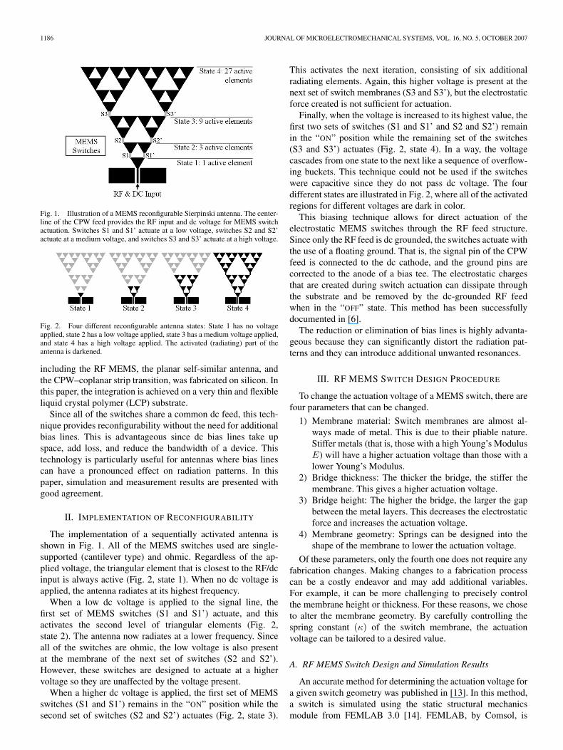
Fig. 12. Measured return loss for all four states of the designed reconfigurableantenna.
Ti–Al layer was electron-beam deposited and etched to definethe switch membranes. Lastly, the switches were released bysoaking in photoresist stripper and dried using CO2 at the supercritical point.
VII. RECONFIGURABLE SIERPINSKI ANTENNA
TESTING AND RESULTS
The antenna reconfigurability was tested by varying the volt-age and witnessing the antenna transition between the differentstates. The antenna was able to transition from the first to thelast state and back again without a change in the performance.This procedure was repeated many times without problems.This demonstrates that the floating ground is sufficient.
The return-loss measurements were taken with an Agilent8510C vector network analyzer using 850-µm pitch GSG RFprobes. Pattern measurements were taken using an Agilent 8530vector network analyzer with the antenna inside an anechoicchamber. End-launch gold SMA connectors were hand solderedonto the antenna for pattern measurements. These connectorshave a maximum operating frequency of 18 GHz, which coin-cides with the highest principle frequency of the antenna whenno voltage is applied.
The return-loss-measurement results are shown in Fig. 12.The resonant frequencies roughly halve as the antenna increasesin size. These measurement results are summarized in Table IIIand agree well with the simulated values shown in Fig. 10. Asa proof of concept, the focus was given to the first resonancesonly, and thus, higher order modes were not studied in greatdetail. Higher order modes of the Sierpinski gasket antennashave been studied in [11] and [12]. However, all of the firstresonance frequencies were correctly simulated. Almost all ofthe higher order resonances were measured within 5% of thesimulated values.
The state 4 measurement results exhibit the most variancefrom the simulated values because of the size of the antenna.This accounts for the second (9.0 GHz) and third (16.4 GHz)
TABLE IIITABULATED ANTENNA SIMULATION (AND MEASUREMENT) RESULTS FOR
ALL FOUR STATES. THE ACTUATION VOLTAGE AND FIRST THREE
RESONANCES (IN GIGAHERTZ) ARE GIVEN. THE MAXIMUM
PERCENT ERROR BETWEEN SIMULATED AND
MEASURED VALUES IS NOTED
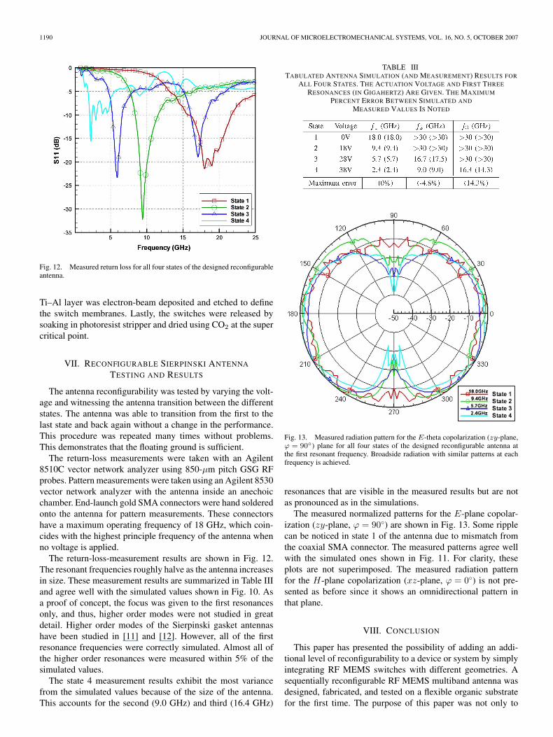
Fig. 13. Measured radiation pattern for the E-theta copolarization (zy-plane,ϕ = 90) plane for all four states of the designed reconfigurable antenna atthe first resonant frequency. Broadside radiation with similar patterns at eachfrequency is achieved.
resonances that are visible in the measured results but are notas pronounced as in the simulations.
The measured normalized patterns for the E-plane copolar-ization (zy-plane, ϕ = 90) are shown in Fig. 13. Some ripplecan be noticed in state 1 of the antenna due to mismatch fromthe coaxial SMA connector. The measured patterns agree wellwith the simulated ones shown in Fig. 11. For clarity, theseplots are not superimposed. The measured radiation patternfor the H-plane copolarization (xz-plane, ϕ = 0) is not pre-sented as before since it shows an omnidirectional pattern inthat plane.
VIII. CONCLUSION
This paper has presented the possibility of adding an addi-tional level of reconfigurability to a device or system by simplyintegrating RF MEMS switches with different geometries. Asequentially reconfigurable RF MEMS multiband antenna wasdesigned, fabricated, and tested on a flexible organic substratefor the first time. The purpose of this paper was not only to

KINGSLEY et al.: RF MEMS SEQUENTIALLY RECONFIGURABLE SIERPINSKI ANTENNA ON A SUBSTRATE 1191
illustrate a method of biasing MEMS reconfigurable antennaswithout the need for dc bias lines but also to illustrate howthe antenna performance can be enhanced by increasing thenumber of resonant frequencies. The final device does not haveany additional lines to bias the switches, while the antennaexhibited four principle resonant frequencies with good radia-tion characteristics. By using MEMS switches, the losses arekept to a minimum. Three different switch geometries wereintegrated into a Sierpinski antenna with different actuationvoltages. The simulated and measured responses agree well.This technology can be applied to many other devices, includ-ing tuners, tunable filters, other antenna geometries, or signalsplitters.
REFERENCES
[1] C. D. Nordquist et al., “An X-band to Ku-band RF MEMS switchedcoplanar strip filter,” IEEE Microw. Wireless Compon. Lett., vol. 14, no. 9,pp. 425–427, Sep. 2004.
[2] R. Lempkowski, K. Lian, M. Eliacin, and P. Kulkarni, “A PWB-based MEMS switched filter bank using lumped element embeddedpassives,” in Proc. 31st Annu. Conf. IEEE Ind. Electron. Soc., Nov. 2005,pp. 2331–2334.
[3] D. E. Anagnostou et al., “Design, fabrication, and measurements ofan RF-MEMS-based self-similar reconfigurable antenna,” IEEE Trans.Antennas Propag., vol. 54, no. 2, pt. 1, pp. 422–432, Feb. 2006.
[4] B. Cetiner, J. Qian, H. Chang, M. Bachman, G. Li, and F. DeFlaviis,“Monolithic integration of RF MEMS switches with a diversity antennaon PCB substrate,” IEEE Trans. Microw. Theory Tech., vol. 51, no. 1,pp. 332–334, Jan. 2003.
[5] R. Jackson and R. Ramadoss, “A MEMS-based electrostatically tunablecircular microstrip patch antenna,” J. Micromech. Microeng., vol. 17,no. 1, pp. 1–8, Jan. 2007.
[6] N. Kingsley and J. Papapolymerou, “Organic ‘wafer-scale’ packagedminiature four-bit RF MEMS phase shifter,” IEEE Trans. Microw. TheoryTech., vol. 54, no. 3, pp. 1229–1236, Mar. 2006.
[7] C. P. Baliarda, J. Romeu, and A. Cardama, “The Koch monopole:A small fractal antenna,” IEEE Trans. Antennas Propag., vol. 48, no. 11,pp. 1773–1781, Nov. 2000.
[8] S. R. Best, “On the resonant properties of the Koch fractal and other bentwire monopole antennas,” IEEE Antennas Wireless Propag. Lett., vol. 1,no. 1, pp. 74–76, 2002.
[9] N. Cohen and R. Hohlfeld, “Fractal loops and the small loop approxima-tion,” Commun. Q., pp. 77–81, Winter 1996.
[10] D. Werner and S. Ganguly, “An overview of fractal antenna engineer-ing research,” IEEE Antennas Propag. Mag., vol. 45, no. 1, pp. 38–57,Feb. 2003.
[11] C. Puente Baliarda, J. Romeu, R. Pous, and A. Cardama, “On the behav-ior of the Sierpinski multiband fractal antenna,” IEEE Trans. AntennasPropag., vol. 46, no. 4, pp. 517–524, Apr. 1998.
[12] J. Anguera, C. Puente, C. Borja, and J. Soler, “Fractal-shaped antennas: Areview,” in Wiley Encyclopedia of RF and Microwave Engineering, vol. 2,K. Chang, Ed. New York: Wiley, 2005, pp. 1620–1635.
[13] N. Kingsley, G. Wang, and J. Papapolymerou, “Comparative study ofanalytical and simulated doubly-supported RF MEMS switches for me-chanical and electrical performance,” Appl. Comput. Electromagn. Soc.J., vol. 21, no. 1, pp. 9–15, Mar. 2006.
[14] Comsol Inc., FEMLAB Multiphysics Modeling, Nov. 2004. [Online].Available: http://www.comsol.com/products/femlab
[15] D. Thompson, O. Tantot, H. Jallageas, G. Ponchak, M. Tentzeris, andJ. Papapolymerou, “Characterization of liquid crystal polymer (LCP) ma-terial and transmission lines on LCP substrates from 30 to 110 GHz,”IEEE Trans. Microw. Theory Tech., vol. 52, no. 4, pp. 1343–1352,Apr. 2004.
[16] G. Du, Y. Zhang, Y. Ma, X. Yang, B. Zhao, and B. Liu, “ZnO thin filmsgrown by plasma-assisted metal-organic vapor phase epitaxy,” in Proc.6th Chin. Symp. Optoelectronics, Sep. 2003, pp. 292–296.
[17] S. Horst, S. Bhattacharya, S. Johnson, E. Tentzeris, and J. Papapolymerou,“Modeling and characterization of thin film broadband resistors on LCPfor RF applications,” in Proc. 56th Electron. Compon. Technol. Conf.,Jun. 2006, pp. 1751–1755.
Nickolas Kingsley (S’02–M’07) received the B.S.,M.S., and Ph.D. degrees in electrical engineeringfrom the Georgia Institute of Technology (GeorgiaTech), Atlanta, in 2002, 2004, and 2007, respectively.
During his thesis work, he investigated methodsfor packaging RF microelectromechanical systemsswitches in flexible organic packages and testedthe methods for reliability. In June 2007, he joinedthe Auriga Measurement Systems team in Lowell,MA, as a Principal Engineer. He will be developinghigh-performance amplifier systems. His research
interests have focused on developing miniature multilayer system-on-packageRF front ends using liquid crystal polymer substrate. He has published onebook chapter and over a dozen publications and has submitted four inventiondisclosures.
Dr. Kingsley was a member of the Georgia Electronic Design Center underthe direction of Prof. J. Papapolymerou until May 2007. He is a member ofthe IEEE Antennas and Propagation Society, IEEE Microwave Theory andTechniques Society, and the Order of the Engineer. While at Georgia Tech, hewon numerous awards. He is the recipient of the 2002 President’s Undergradu-ate Research Award. He won three poster competitions at university, college,and school levels. He received the Trainer of the Year distinction from theMicroelectronics Research Center clean room in 2005 and 2006. As a coopstudent with Compaq Computer Corporation, he won the 2001 Armada Awardfor excellence. He will serve as a Technical Program Committee member forthe 2008 International Microwave Symposium Conference in Atlanta, GA.
Dimitrios E. Anagnostou (S’98–M’05) was born inAthens, Greece, in November 1975. He received theDiploma degree (M.Sc. equivalent) in electrical andcomputer engineering from Democritus Universityof Thrace, Xanthi, Greece, in 2000, and the M.Sc.and Ph.D. degrees in electrical engineering from theUniversity of New Mexico, Albuquerque, in 2002and 2005, respectively.
From August 2005 to December 2006, he was aPostdoctoral Fellow with the School of Electrical andComputer Engineering, Georgia Institute of Technol-
ogy, Atlanta. Since 2007, he has been with the faculty of Electrical and Com-puter Engineering Department, South Dakota School of Mines and Technology,Rapid City, as an Assistant Professor. His current research interests includethe development, characterization, and integration of reconfigurable low-costflexible antennas and RF front ends using direct write deposition processes,miniaturized antenna designs, microwave packaging, RF microelectromechan-ical systems, and neural networks. He has authored or coauthored more than25 papers in published peer-reviewed journals and international conferenceproceedings.
Dr. Anagnostou has been awarded with three research and travel grantsfrom 2003 to 2005 and has filed two invention disclosures on recon-figurable and ultrawideband antennas. He is serving as a Reviewer forthe IEEE TRANSACTIONS ON ANTENNAS AND PROPAGATION, the IEEETRANSACTIONS ON MICROWAVE THEORY AND TECHNIQUES, and otherinternational publications. In 2006 and 2007, he was invited to act as a SessionChair for the IEEE International Symposia on Antennas and Propagation. He isa member of Eta Kappa Nu and the Technical Chamber of Greece.

1192 JOURNAL OF MICROELECTROMECHANICAL SYSTEMS, VOL. 16, NO. 5, OCTOBER 2007
Manos Tentzeris (SM’07) received the Diploma de-gree in electrical and computer engineering (magnacum laude) from the National Technical Universityof Athens, Athens, Greece, and the M.S. and Ph.D.degrees in electrical engineering and computer sci-ence from the University of Michigan, Ann Arbor.
He was a Visiting Professor with the TechnicalUniversity of Munich, Germany, for the summer of2002, where he introduced a course in the area ofhigh-frequency packaging. He is the Georgia Elec-tronic Design Center Associate Director for RF iden-
tifications (RFIDs)/sensors research, and he has been the Georgia Tech NationalScience Foundation (NSF) Packaging Research Center Associate Director forRF research and the RF Alliance Leader from 2003 to 2006. He is also theLeader of the RFID Research Group of the Georgia Electronic Design Center ofthe State of Georgia. He is currently an Associate Professor with the School ofElectrical and Computer Engineering, Georgia Institute of Technology, Atlanta.He has helped develop academic programs in highly integrated/multilayerpackaging for RF and wireless applications using ceramic and organic flexiblematerials, paper-based RFIDs and sensors, microwave microelectromechan-ical systems, system-on-package-integrated (ultrawideband, multiband, con-formal) antennas, and adaptive numerical electromagnetics (finite-differencetime-domain, MultiResolution Algorithms). He is the Head of the ATHENAResearch Group of 20 researchers. He has published more than 250 papersin refereed journals and conference proceedings, two books, and ten bookchapters. He has given more than 50 invited talks in the area of high-frequencypackaging to various universities and companies in Europe, Asia, and America.
Dr. Tentzeris was the recipient of the 2007 IEEE Antennas and Prop-agation Society (APS) Symposium Best Student Paper Award, the 2007IEEE Instrumentation and Measurement Society (IMS) Symposium Third-Place Best Student Paper Award, the 2006 IEEE MICROWAVE THEORY
AND TECHNIQUES (MTT) Outstanding Young Engineer Award, the 2006Asian-Pacific Microwave Conference Award, the 2004 IEEE TRANSACTIONS
ON ADVANCED PACKAGING Commendable Paper Award, the 2003 NASAGodfrey “Art” Anzic Collaborative Distinguished Publication Award, the 2003IBC International Educator of the Year Award, the 2003 IEEE Compo-nents, Packaging, and Manufacturing Technology Society (CPMT) OutstandingYoung Engineer Award, the 2002 International Conference on Microwaveand Millimeter-Wave Technology Best Paper Award, Beijing, China, the 2002Georgia Tech-ECE Outstanding Junior Faculty Award, the 2001 ACES Con-ference Best Paper Award, the 2000 NSF CAREER Award, and the 1997Best Paper Award of the International Hybrid Microelectronics and PackagingSociety. He was also the 1999 Technical Program Cochair of the 54th ARFTGConference, Atlanta, GA, and the Chair of the 2005 IEEE ComputationalElectromagnetics in Time Domain Workshop, and he is the Vice Chair of theRF Technical Committee (TC16) of the IEEE CPMT Society. He has organizedvarious sessions and workshops on RF/wireless packaging and integration,RFIDs, numerical techniques/wavelets for the IEEE Electronics Componentsand Technology Conference, IMS, Vehicular Technology Conference, and APSSymposia in all of which he is a member of the Technical Program Committeein the area of “Components and RF.” He will be the Transaction ProcessingPerformance Council Chair for the IEEE IMS 2008 Symposium. He is anAssociate Editor of the IEEE TRANSACTIONS ON ADVANCED PACKAGING.He is a member of Union Radio-Scientifique Internationale–Commission D, amember of MTT-15 committee, an Associate Member of EuMA, and a memberof the Technical Chamber of Greece.
John Papapolymerou (SM’04) received theB.S.E.E. degree from the National TechnicalUniversity of Athens, Athens, Greece, in 1993, andthe M.S.E.E. and Ph.D. degrees from the Universityof Michigan, Ann Arbor, in 1994 and 1999,respectively.
From 1999 to 2001, he was a Faculty Memberwith the Department of Electrical and Computer En-gineering, University of Arizona, Tucson, and duringthe summers of 2000 and 2003, he was a VisitingProfessor at the University of Limoges, France. From
2001 to 2005, he was an Assistant Professor with the School of Electricaland Computer Engineering, Georgia Institute of Technology, Atlanta, wherehe is currently an Associate Professor. His research interests include the imple-mentation of micromachining techniques and microelectromechanical systemsdevices in microwave, millimeter-wave and terahertz circuits, and the devel-opment of both passive and active planar circuits on semiconductor (Si/SiGe,GaAs), and organic substrates (liquid crystal polymer, low-temperature cofiredceramic) for system-on-a-chip/system-on-a-package RF front ends. He hasauthored or coauthored over 150 publications in peer-reviewed journals andconference proceedings.
Dr. Papapolymerou received the 2004 Army Research Office Young Investi-gator Award, the 2002 National Science Foundation CAREER Award, the bestpaper award at the Third IEEE International Conference on Microwave andMillimeter-Wave Techmology (ICMMT2002), Beijing, China, and the 1997Outstanding Graduate Student Instructional Assistant Award presented by theAmerican Society for Engineering Education, University of Michigan Chapter.In 2004, he was the Chair of the IEEE Microwave Theory and TechniquesSociety/AP Atlanta Chapter. He currently serves as the Vice Chair for Com-mission D of the U.S. National Committee of the Union Radio-ScientifiqueInternationale and as an Associate Editor for the IEEE TRANSACTIONS ON
ANTENNAS AND PROPAGATION and IEEE MICROWAVE AND WIRELESS
COMPONENT LETTERS.