Simulation and microfabrication of MEMS vacuum electronic ...
132
University of South-Eastern Norway Faculty of Technology, Natural Sciences and Maritime Studies — Doctoral dissertation no. 49 2019 Laxma Reddy Billa Simulation and microfabrication of MEMS vacuum electronic devices for terahertz technology
-
Upload
khangminh22 -
Category
Documents
-
view
1 -
download
0
Transcript of Simulation and microfabrication of MEMS vacuum electronic ...
Sim
ulation
and
microfab
rication of M
EM
S vacu
um
electronic d
evices for terahertz tech
nolog
y - Laxma R
ed
dy B
illa
University of South-Eastern NorwayFaculty of Technology, Natural Sciences and Maritime Studies
—Doctoral dissertation no. 49
2019
Laxma Reddy Billa
Simulation and microfabrication of MEMS vacuum electronic devices for terahertz technology
Laxma Reddy Billa
A PhD dissertation in Applied Micro- and Nanosystems
Simulation and microfabrication of MEMS vacuum electronic devices for terahertz technology
© Laxma Reddy Billa 2019
Faculty of Technology, Natural Sciences and Maritime Studies University of South-Eastern Norway Horten, 2019
Doctoral dissertations at the University of South-Eastern Norway no. 49
ISSN: 2535-5244(print)ISSN: 2535-5252 (online)
ISBN: 978-82-7860-398-7 (print)ISBN: 978-82-7860-399-4 (online)
This publication is licensed with a Creative Com-mons license. You may copy and redistribute the material in any medium or format. You must give appropriate credit, provide a link to the license, and indicate if changes were made. Complete
license terms at https://creativecommons.org/licenses/by-nc-sa/4.0/deed.en
Print: University of South-Eastern Norway

Billa: Simulations and microfabrication of MEMS vacuum electronic devices for terahertz technology
___
I
Dedicated to my beloved parents, brother, sister, brother-in-law and sister-in-law for
their love, trust and motivations

Billa: Simulations and microfabrication of MEMS vacuum electronic devices for terahertz technology
___
III
Preface
This thesis is submitted in partial fulfilment of the requirements for the degree of
Philosophise Doctor from Department of Microsystems Technology at University of
South-Eastern Norway.
This doctoral work has been conducted at the Department of Microsystems Technology
(IMST), Faculty of Technology and Maritime Science, University of South-Eastern
Norway, Horten, Norway, under the supervision of Professor Xuyuan Chen and Professor
Muhmmud Nadeem Akram.
Financial support was provided by the Ministry of Education, Norway. The Research
Council of Norway is acknowledged for the support to the Norwegian Micro- and Nano-
fabrication facility, NorFab (245963/F50) and the Norwegian Ph.D. Network on
Nanotechnology for Microsystems, Nano-Network (221860/F40).

Billa: Simulations and microfabrication of MEMS vacuum electronic devices for terahertz technology
___
V
Acknowledgements
First of all, I would like to express my appreciation and sincere gratitude to my
supervisors, Professor Xuyuan Chen and Professor Nadeem Akram for guidance and
support throughout my PhD research. Their advice and encouragement have been
valuable for the success of my PhD work.
I would like to thank my colleagues at USN for a meaningful contribution to my PhD
work. Thanks also to lab engineers: Zekija Ramic, Muhmmad Tayib, Antuan, Rangnar
Dahl Johanseen, Thomas Martisen for their support in the laboratory.
The Norwegian research council is thankfully acknowledged for the financial support for
this PhD work. The Norwegian PhD Network on Nanotechnology for the Microsystems
is also deeply acknowledged for grating travel support to international conferences and
the laboratory fee.
I would like to thank the department of Microsystem technology for giving me the
opportunities for performing this work, the thank to Kristin Skjold Granerød and Aina
Enstad for their support with administration work.
Finally, I would like to thank my family and friends for their support, understanding and
encouragement during these years.

Billa: Simulations and microfabrication of MEMS vacuum electronic devices for terahertz technology
___
VII
Abstract
Keywords: Terahertz, Millimetre-wave, Vacuum electron technology, Slow-wave
structure, Traveling wave tube, Microfabrication
Numerous applications explore the scarcely used terahertz (THz) band in the
electromagnetic spectrum. However, widespread utilization of the THz band is
technically challenging, due to the lack of power sources. The power level of the
signal generators drastically drops as the frequency approaches the THz frequencies.
Moreover, at this frequency range, the attenuation level of electromagnetic waves
in the earth atmosphere increases. In vacuum electronics family, traveling wave tube
(TWT) has gained particular interest for millimetre-wave and THz signal amplification
for high-power and wideband applications. The characteristics of the TWT are
mainly represented by the performance of a slow-wave structure (SWS). The SWS in
TWT is used to facilitate the input THz signal which gets amplified by the process of
the beam-wave interaction. Therefore, an efficient and reliable SWS is an essential
aspect of a powerful TWT design.
This thesis proposes a novel SWS, which consists of metal corrugations in the H-
plane and E-plane of the rectangular waveguide operated in the fundamental mode.
The concept of H-plane and E-plane load shows potential benefits to the THz TWTs,
such as excellent linear characteristics, an increased interaction impedance, ultra-
wide bandwidth, and high-power output. Furthermore, the geometry of the SWS
made the fabrication easier by using the available microfabrication techniques. The
thesis involves all elements of development from device design, simulations,
through material growth and interactive device fabrication to extensive
characterization, along with the prototype cold-testing of the scaled-up device.
The proposed SWS is investigated for TWT working at 400 GHz central frequency.
The design and simulation of TWT involve three stages, which are high frequency
electromagnetic study of a unit cell of the SWS using Eigenmode simulations,
scattering parameters or S-parameters analysis of coupler design with the SWS using
Billa: Simulations and microfabrication of MEMS vacuum electronic devices for terahertz technology
___
VIII
time-domain transient simulations, and beam-wave interaction study using particle-
in-cell (PiC). The PiC simulations found that this tube can produce an excess of 25
dB small-signal gain with 60 GHz 3-dB bandwidth at 400 GHz central frequency. The
LIGA technique was employed to fabricate the 400-GHz E-plane and H-plane loaded
SWS. In particular, the KMPR negative tone photoresist was used in the fabrication
process. The KMPR mold produced the nearly perfect features of the mask designs,
tolerance within the ±2.5 µm of the lateral features and maximum deviation of 20 in
the vertical profiles. The experiments for surface roughness study revealed that the
interior sidewall roughness of the LIGA-fabricated metal parts was achieved about
20 nm. A diffusion bonding method was employed to attach the two LIGA-fabricated
copper parts of the SWS, producing a bonding strength of 25 MPa at 400 0C bonding
temperature and with a void-free bonding interface.
A scale-up model of the H-plane and E-plane SWS together with input and output
couplers at W-band (85-110 GHz) was designed, manufactured using CNC milling,
and verified the electromagnetic characteristics experimentally. The test results of
S-parameters agreed with the simulations, S11<-15 dB over a frequency range of 85
GHz - 98 GHz. PiC simulations were also performed to the 93.5-mm length SWS,
demonstrating a gain about 24 dB over 89 GHz – 101 GHz. To mitigate the diocotron
instability in the sheet-beam transmission, a modified geometry of the sheet beam
was employed and analysed through PiC simulations. The robust design and high
performance from the H-plane and E-plane loaded SWS suggests that this is a
promising candidate for high-power and wideband TWT development in the
millimetre and THz frequency ranges.
Billa: Simulations and microfabrication of MEMS vacuum electronic devices for terahertz technology
___
IX
List of papers
The thesis includes the following articles
1. H-plane and E-plane loaded rectangular slow-wave structure for terahertz TWTamplifier, Laxma Reddy Billa, Muhammad Nadeem Akram and Xuyuan Chen,IEEE Transactions on Electron Devices, Vol. 63, 2016.
2. Improved design and microfabrication of H-plane and E-plane loadedrectangular slow-wave structure for THz amplifier Laxma Reddy Billa, XianbaoShi, Muhammad Nadeem Akram and Xuyuan Chen, IEEE Transactions onElectron Devices, Vol. 64, 2017
3. UV-LIGA microfabricated THz slow-wave structures for vacuum electronicsdevices using KMPR photoresist, Laxma Reddy Billa, Muhammad NadeemAkram and Xuyuan Chen, IOP Journal of Micromechanics and Microengineering.(manuscript submitted).
4. H- and E-plane loaded slow-wave structure slow-wave structure for W-bandTWT, Laxma Reddy Billa, Muhammad Nadeem Akram, Claudio Paoloni, andXuyuan Chen, IEEE Transactions on Electron Devices. (manuscript accepted)
The following articles are conference proceedings
1. Novel rectangular slow-wave circuit for terahertz traveling wave tubes, LaxmaReddy Billa, Muhammad Nadeem Akram and Xuyuan Chen, 8th UK, Europe, ChinaMillimeter Waves and THz Technology Workshop (UCMMT), in the UK, 2015.
2. Modified corrugated rectangular slow-wave structure for terahertz travelingwave tube amplifier, Laxma Reddy Billa, Xianbao Shi, Muhammad NadeemAkram and Xuyuan Chen, IEEE International Vacuum Electronics Conference(IVEC), in USA, 2016.
3. E-plane bending input/output coupler in staggered double vane TWT amplifier,Xianbao Shi, Laxma Reddy Billa, Muhammad Nadeem Akram and Xuyuan Chen,IEEE International Vacuum Electronics Conference (IVEC), in USA, 2016.
4. COMSOL Multiphysics modeling and simulation of traveling wave tubeamplifier, Laxma Reddy Billa, Muhammad Nadeem Akram and Xuyuan Chen, 8th
UK, Europe, China Millimeter Waves and THz Technology Workshop (UCMMT),in China, 2016.
5. MEMS fabrication of H-plane and E-plane loaded 400 GHz TWT amplifier,Laxma Reddy Billa, Xianbao Shi, Muhammad Nadeem Akram and Xuyuan Chen,IEEE International Vacuum Electronics Conference (IVEC) , in the UK, 2017.
6. Cold-test analysis of H-plane and E-plane loaded rectangular slow-wavestructure, Laxma Reddy Billa, Muhammad Nadeem Akram and Xuyuan Chen, 8th
UK, Europe, China Millimeter Waves and THz technology Workshop (UCMMT),in the UK, 2017.
Papers omitted from the online publication due to publisher's restrictions

Billa: Simulations and microfabrication of MEMS vacuum electronic devices for terahertz technology
___
XI
Papers summary
1. H-plane and E-plane loaded rectangular slow-wave structure for TWT amplifier In this paper, a novel miniaturized rectangular slow-wave structure (SWS) is proposed
for sub-millimetre or THz vacuum electron traveling wave tube (TWT) amplifier. The SWS
is composed of both H-plane and E-plane corrugations in the rectangular waveguide.
The advantage of this SWS was investigated using three-dimensional (3D) simulators.
The SWS permits design flexibility to achieve wider bandwidth, high output power, and
easy fabrication by utilizing the available microfabrication techniques. The preliminary
particle-in-cell (PiC) simulations have shown promising TWT amplifier performance such
as 80 GHz instantaneous bandwidth, the maximum gain of 19.5 dB at 400 GHz for a
defined moderate beam voltage of 17 kV and 20 mA beam current. The large-signal
simulations have predicted a saturated output power of 19.3 W for 400 GHz CW
excitation.
Author contribution:
Literature review, device proposal, investigation of the proposed device, simulations,
analysis of the results and manuscript preparation.
2. Improved design and microfabrication of H-plane and E-plane loaded rectangular slow-wave structure for THz TWT
This paper explains the design optimization of the H-plane and E-plane loaded SWS for
400-GHz TWT. An improved coupler was devised in order to enable the same LIGA
process used for fabricating the SWS as well as for utilizing the full intrinsic bandwidth
of the SWS. The coupler showed excellent impedance wave matching characteristics and
a low reflection coefficient, S11 < -15 dB over a frequency range of 360 GHz –460 GHz.
By implementing the phase velocity tapering technique, an increase of 60% in the
saturated output power across the 80 GHz instantaneous bandwidth was achieved. The
study of fabrication tolerance of the individual geometrical parameters on the device
performance was studied in detail. The feasibility of KMPR UV-LIGA technique was
verified through preliminary fabrication runs.
Billa: Simulations and microfabrication of MEMS vacuum electronic devices for terahertz technology
___
XII
Author contribution:
Literature review, design and simulations, analysis of the results, device fabrication and
characterization, and manuscript preparation.
3. UV-LIGA microfabricated THz slow-wave structure for vacuum electronics devices using KMPR photoresist
A negative tone photoresist KMPR was used as mold material in the device fabrication
using UV-LIGA technique, for easing the removal of mold. A customized UV-LIGA process
was proposed, whose critical process parameters were optimized to achieve a high
structural quality. An optical microscope and scanning electron microscope (SEM)
analysis showed that the dimensional accuracy of copper metal structures is less than 2
µm and sidewall verticality is 900±10. From the surface roughness study, it was revealed
that a sidewall surface roughness of copper metal structure of about 20 nm was
achieved, which met the desired electromagnetic propagation property (skin-depth) in
the THz devices. Homogenous and excellent bonding mechanism between the copper-
copper interface of the SWS parts was achieved, with the bonding strength of about 12
MPa at 400 °C bonding temperature.
Author contribution:
Literature review, process flow design, process parameter optimization, device
characterization and analysis and manuscript preparation.
4. H- and E-plane loaded Slow-wave structure for W-band TWT
For fast verification of the design concept of the proposed SWS for the THz TWTs, a
scale-up model was designed at W-band. The scaled device was manufactured using
advanced CNC milling. The test results of S-parameters agreed with the simulations,
S11<-15 dB over a frequency range of 91 GHz – 98 GHz and showed a very good
electromagnetic propagation characteristics. The PiC simulations demonstrated the W-
band TWT using the H-plane and E-plane loaded SWS, predicting a gain of 24 dB over 91
GHz – 98 GHz, for given 85-periods length SWS. The prototype device showed that the

Billa: Simulations and microfabrication of MEMS vacuum electronic devices for terahertz technology
___
XIII
proposed SWS, H-plane and E-plane loaded SWS, a viable alternative for high-power and
wideband millimetre-wave and THz TWT development.
Author contribution:
Literature review, design and simulations, device S-parameters measurements, analysis
of the results and manuscript preparation.

Billa: Simulations and microfabrication of MEMS vacuum electronic devices for terahertz technology
___
XV
Table of contents
Dedication .......................................................................................................................... I
Preface ............................................................................................................................. III
Acknowledgements ...........................................................................................................V
Abstract ...........................................................................................................................VII
List of papers .................................................................................................................... IX
Papers summary .............................................................................................................. XII
Table of contents ........................................................................................................... XV
1 Introduction ................................................................................................................... 1
1.1 Motivation ...................................................................................................... 1
1.2 THz traveling wave tube ................................................................................. 5
1.3 State of the art THz SWSs .............................................................................. 7
1.3.1 Planar Helix SWS ............................................................................................ 9
1.3.2 Folded waveguide SWS ................................................................................ 11
1.3.3 Derived folded waveguide SWS ................................................................... 12
1.3.4 Sheet-beam corrugated SWS . ..................................................................... 16
1.3.5 Circular-beam corrugated SWS .................................................................... 17
1.3.6 Meander-line SWS ....................................................................................... 18
1.4 Microfabrication techniques for THz SWS ................................................... 19
1.4.1 LIGA .............................................................................................................. 20
1.4.2 DRIE .............................................................................................................. 22
1.4.3 Electrical discharge machining ..................................................................... 24
1.4.4 CNC milling ................................................................................................... 25
1.4.5 3-D printing .................................................................................................. 26
1.5 Scope of the thesis ....................................................................................... 27
2 Design and simulation of H-plane and E-plane loaded SWS for 400-GHzTWT ........... 29
2.1 Analytical theory of SWS .............................................................................. 29
2.1.1 Electronic equation ...................................................................................... 29
2.1.2 Circuit equation ............................................................................................ 31
2.1.3 Determinantal equation .............................................................................. 34
Billa: Simulations and microfabrication of MEMS vacuum electronic devices for terahertz technology
___
XVI
2.1.4 Gain equation ............................................................................................... 35
2.2 H-plane and E-plane loaded SWS ................................................................ 35
2.3 Electromagnetic analysis.............................................................................. 37
2.3.1 Eigenmode simulations ................................................................................ 37
2.3.2 Coupler design ............................................................................................. 43
2.4 Particle-in-cell simulations .......................................................................... 46
2.4.1 Uniform profile configuration ...................................................................... 48
2.4.2 Phase velocity tapering ............................................................................... 49
3 LIGA microfabricted H-plane and E-plane loaded SWS ............................................... 53
3.1 Process description ..................................................................................... 53
3.2 Fabrication conditions ................................................................................. 56
3.2.1 KMPR process .............................................................................................. 56
3.2.1.1 Metallization ............................................................................................... 57
3.2.1.2 KMPR deposition ......................................................................................... 58
3.2.1.3 Soft-bake ..................................................................................................... 60
3.2.1.4 UV-exposure................................................................................................. 61
3.2.2 Electroplating and KMPR removal ............................................................. 64
3.2.3 Surface study .............................................................................................. 67
3.2.4 Diffusion bonding ........................................................................................ 70
4 CNC-milled H-plane and E-plane loaded SWS and test results .................................... 73
4.1 W-band SWS design .................................................................................... 73
4.2 CNC milling and cold-test measurements.................................................... 77
4.3 W-band TWT Partcle-in-cell simulations ..................................................... 83
5 Conclusion and Future work ........................................................................................ 89
References....................................................................................................................... 91
Journal paper 1 ...................................................................................................................
Journal paper 2 ...................................................................................................................
Journal paper 3 ...................................................................................................................
Journal paper 4 ...................................................................................................................


Billa: Simulations and microfabrication of MEMS vacuum electronic devices for terahertz technology
___
1
Chapter 1
Introduction
1.1 Motivation
In recent years the study and research on signal sources in the terahertz (THz) region of
the electromagnetic spectrum have surged [1, 2]. The THz region is roughly defined in
the electromagnetic spectrum ranging from 100 GHz to 10 THz, which is between the
technological domains of electronics and photonics [2]. In terms of the wavelength, it
corresponds to the range of 3 mm - 0.03 mm. The interest is due to the unique
properties of the THz radiation that led to a wide range of applications in military and
commercial systems. Those properties are listed below:
• Penetration— THz signals penetrate non-metallic and non-polarizing materials
such as semiconductors, textiles and plastics. This helps to reveal hidden objects
inside these materials [3, 4].
• High-resolution imaging— imaging systems operating THz regions can provide
better spatial resolutions and image qualities than the imaging systems at
microwave regions [4, 5].
• Spectroscopy— plenty of materials exhibit their spectral characteristics in the
THz domain, among them being semiconductors, ferroelectrics, dielectrics, high-
temperature superconductors, gases and liquids [6, 7].
• Non-ionization— THz radiation is nonionizing in contract to the ionizing radiation
by X-ray, and it can penetrate through skin, hair, teeth or dried biological
samples. Hence, biological tissues and genetics can be monitored by THz signal
in medical imaging application for detection of infected tissues [8, 9]. However,
the deep penetration of THz radiation inside the body due to the water content
in any cell is very poor.
Billa: Simulations and microfabrication of MEMS vacuum electronic devices for terahertz technology
___
2
• Less scattering—due to the longer wavelength of the THz signals compared to
visible light, the THz signals allows the visualization of objects in granular
materials.
• Intensity— THz signals are much easier to focus and collimate than radio waves.
During the 1980s and 1990s, sensing and imaging were the leading applications in the
field of spectroscopy [10] and radio astronomy [11] as they utilized the THz signals. Since
then, revolutionary advancements in the THz device development that pave the way for
attractive applications extended from fundamental science to real-world applications in
different sectors, such as semiconductor, medical, manufacturing, defence, wireless
communications, agriculture and many other industries. For most applications, this
usually involves the transmission and detection of signals in free space in either a short
range or a medium range. However, the attenuation of the electromagnetic waves in
the earth atmosphere and scattering from atmospheric particulates are serious
obstacles that prevent extensive usage of the THz spectrum [12]. Figure 1.1 shows that
the specific transmission windows in which the spectrum exhibits with minimum
attenuation, are roughly located at 140 GHz, 300 GHz, 350 GHz, 410 GHz, 670 GHz, and
850 GHz. The atmospheric attenuation varies under different weather conditions. The
level of attenuation raises as the frequency moves from the low-frequency band to the
higher end of the spectrum. The high degree of attenuation, as approaching the higher
frequency bands, imposes a challenge in exploring THz band for applications that need
propagation over a longer distance.
Currently, the THz sources which are commercially available are, either developed by
using solid-state technology or photonics technology. The family of III-V semiconductor
materials (for example, GaN, InP and GaAs) which are used to develop powerful
monolithic integrated circuit (MMIC) power amplifiers for generating RF signals in the
lower end of the THz spectrum [13]. The wide-bandgap

Billa: Simulations and microfabrication of MEMS vacuum electronic devices for terahertz technology
___
3
Figure 1.1: Atmospheric attenuation of electromagnetic waves in the THz spectrum
[12].
semiconductors materials offer a high breakdown voltage and low mean carrier velocity.
InP HBT and GaN HEMT can produce approximately 1 W saturated output power at 100-
GHz [14]. Gunn diodes using GaN and GaAs are proved high power signal sources in the
microwave band, which works on the principle of negative differential resistance [15,
16]. This can generate a few hundreds of mW around 100 GHz. However, if the number
of power modules is increased and connected in cascaded to enhance the output power
levels of the solid-state power amplifier, the device performance deteriorates with the
thermal management.
Nevertheless, the operating frequency beyond 300-GHz, solid-state signal sources suffer
from short transit-time, resistance-capacitance effect, and the presence of spurious
signals from harmonic frequencies which arise from multiplied sources. These
drawbacks limit the available power capability well below the milliwatt-level and only
offer a very narrow bandwidth [17].
Quantum cascade lasers (QCL), comprises of a series of thin layers of GaAs/AlGaAs
heterostructures and, can also be used for generating THz radiation. Although the
Billa: Simulations and microfabrication of MEMS vacuum electronic devices for terahertz technology
___
4
advancement shown in this field, is still required to operate at cryogenic temperatures
(for example,199.5 K), which is a serious drawback of this technology [18].
An encouraging technique is nonlinear photo-mixing in which the different wavelength
of lasers is mixed and down-converted to the wavelength of THz radiation. The main
disadvantages of the photo-mixing technique, for frequencies below 1 THz, are low
output power, very low conversion efficiency and a bulky optical system [19]. This is due
to a lack of reliability, compactness, and high cost, the category of THz signal sources
available until now, which have deprived the full-fledged utilization of THz region for
innovative application areas.
The most promising and established technology for high power electromagnetic signal
generators is vacuum electronic tubes [20]. Historically, these devices were developed
in the microwave band, mainly for space and military applications. For high power
applications, the vacuum electronic tubes have been found to have an excellent thermal
management system and a high-power handling capability over solid-state technology.
Therefore, a good approach is to realize the compact THz signal generators or amplifiers
by promoting the operation frequency of existing vacuum electron devices in the
microwave to THz frequencies [21, 22]. Thereby the vacuum electronics-based THz
sources can offer a much higher power and broader bandwidth than other counterparts.
In vacuum electronics technology, the parts of the tube must be scaled with the
wavelength of the operating frequency. Therefore, according to the physical scaling law,
the critical features of the vacuum tube’s parts must be in the range of hundreds of
millimetres to tens of microns in the THz frequency range. The miniaturised parts
demand stringent dimensional accuracy and a very tight alignment for assembly.
Furthermore, the Ohmic loss, due to the surface currents in the SWS, increases rapidly
as the frequency approaches THz frequency band [23, 24]. This is due to RF currents
passing through on the surface of skin-depth, proportional to 1 ⁄ √(𝑓𝑟𝑒𝑞𝑢𝑒𝑛𝑐𝑦^2 ).
Hence the surface quality of the SWS should be within a fraction of skin-depth, for
example, the skip depth at 220 GHz is 120nm. Conventional milling techniques are the
main obstacle to realizing THz tube parts. To deal with these issues, the application of
Billa: Simulations and microfabrication of MEMS vacuum electronic devices for terahertz technology
___
5
microfabrication techniques shows the possible solutions for manufacturing the
miniaturized THz tube parts. In recent years research advancement in THz vacuum
devices have encouraged the scientific community to develop robust and affordable THz
systems [1].
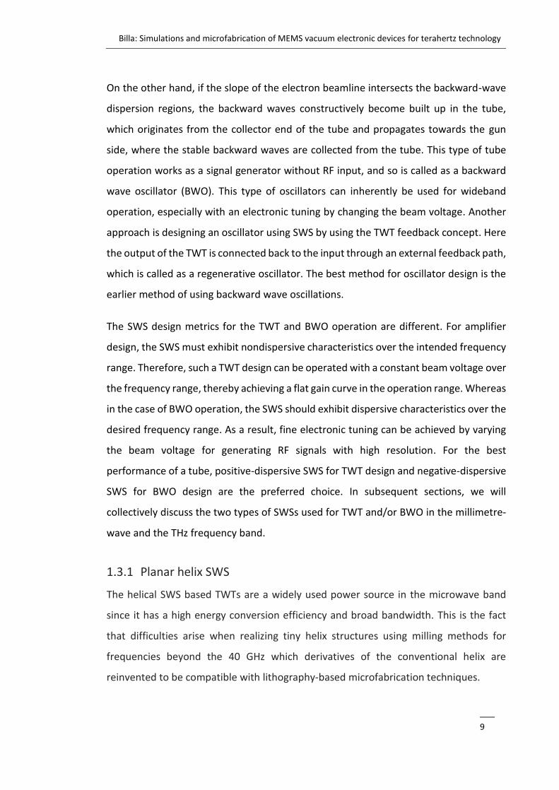
1.2 THz traveling wave tube
In vacuum electronics technology, the traveling wave tube (TWT) is widely used as a
microwave power amplifier in radar, satellite communication, spacecraft transmitter
and electronic warfare systems. This device has a unique combination of features such
as high power, high gain and broad bandwidth, together with being relatively small in
size, compared with other vacuum electron device types. Therefore, it meets the
requirement of most applications that are commercialized. Rapid research progress in
improving device performance has been made since the invention of the helix TWT by
N.E.Lindenblad and Rudolf Kompfner in the1940’s [25, 26]. A detailed analysis with the
improved performance the first-ever TWT was made by J. R. Pierce and L.M. Field in
1947 [27, 28]. In subsequent years the advances in the research were credited to
innovations in device design, and the enhancement of underlying theories and
modelling methods to understand the device principle.
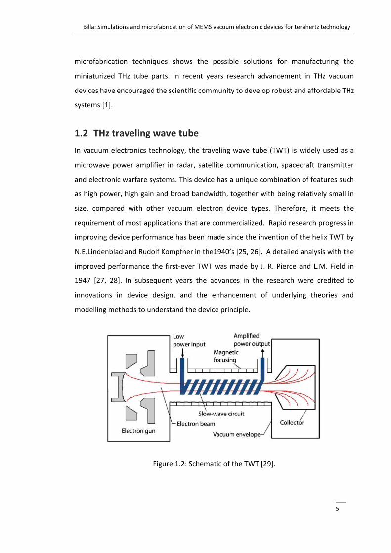
Figure 1.2: Schematic of the TWT [29].
Billa: Simulations and microfabrication of MEMS vacuum electronic devices for terahertz technology
___
6
TWT can be defined as a vacuum envelope, inside which an electron beam interacts with
an electromagnetic wave. This interaction means that the electron beam transfers part
of its kinetic energy to the electromagnetic wave, thereby amplifying the wave.
Therefore, to facilitate the interaction process in the vacuum envelope, TWT required
several parts, such as an electron gun, a guiding structure, a magnetic focusing system,
a collector and vacuum windows, as shown in figure 1.2.
A condition for the energy transfer in the tube is that the velocity of the electron beam
must be approximately equal to the phase velocity of the electromagnetic wave.
However, the electron velocity in a vacuum is less than the speed of light in free space.
The guiding structure does the job of slowing down the axial phase velocity of
electromagnetic waves so that they are approximately equal to the velocity of electrons.
Hence, the guiding structure is also called a slow-wave circuit or slow-wave structure
(SWS). The characteristics of the TWT is mainly represented by the performance of the
SWS that has to be facilitated for maximum energy conversion rate. The various SWSs
of their millimetre-wave and THz version are given in details in the subsequent section.
The electron gun produces electron particles into the SWS, which is commonly consisted
of a cathode, focusing electrodes and anode. The cathode, where the electrons particles
emerge, is extremely difficult to machine due to miniaturization. The focus electrodes,
the control electrodes, and the anode help to create the desired electron beam contour
that is emanated from the cathode surface area and directed to the SWS [30, 31].
Moreover, the assembling of gun parts presents a challenging task in the process of gun
making due to the stringent tolerances required between them. It is a fact that the
operating temperature and robustness of cathode surface directly affect the lifetime
and reliability of the product. Dispenser cathodes [32], nanocomposite dispenser
cathodes [33], and scandate dispenser cathodes [34] have been proven effective for the
millimetre-wave and THz TWTs. It was reported that a 750 A/cm2 current density of
sheet beam with corresponding to cathode loading of 56 A/cm2 using Scandate cathode
is achievable [35].
Billa: Simulations and microfabrication of MEMS vacuum electronic devices for terahertz technology
___
7
The beam focusing system provides an axial magnetic field to compensate the repulsive
radial space charge forces in the electron beam, thereby maintaining the electron beam
transmission in its axis during the interaction process. Unlike the traditional bulky
solenoid magnetic system, period permanent magnetic (PPM) configuration can
drastically reduce the size of the beam focusing system, which results in lowering the
entire tube size and weight [36-38]. Further, it can provide an excess of 6000 Gauss
magnitude of a uniform magnetic field, for the collimation of both beam geometries like
sheet beam and circle beam, for the entire length of beam transmission, for millimetre-
wave and THz TWTs [31, 39].
At the tail end of the SWS, the collector is placed to collect the all spent electron beam.
A multistage depressed configuration of collector design, like three-stage and five-stage,
is used to recover the spent electron beam power to enhance the intrinsic efficiency of
the tube by up to order of magnitude [40, 41]. The higher the number of depressed
voltage levels used the better the management of thermal cooling, and the more
recovery of the beam energy is possible, also avoiding secondary emissions [42].
Vacuum windows which are, usually the type of component used in either of pillbox
windows [42] or diamond windows [43], are transparent to electromagnetic waves as
an interface between the high-vacuum region and ambient environment for the RF
signal feeding into the tube and drawing from the tube. All subparts of the TWT should
be assembled precisely within micron range accuracy and to be vacuum-sealed, to make
a full working device.
1.3 State of the art THz SWSs
As mentioned in the previous section the SWS does the job of slowing down the
propagating electromagnetic waves to match with the velocity of the electron beam,
therefore there are two possible approaches in the design of SWS to perform their job.
First approach is to delay the axial electric field components of the input
electromagnetic waves in the guiding structure in which transverse fields propagate
with their initial velocity. Helix structures are known to support this kind of wave
propagation. The second approach is to create a load periodically to the electromagnetic
Billa: Simulations and microfabrication of MEMS vacuum electronic devices for terahertz technology
___
8
waves in the cavity waveguide which establishes slow electromagnetic waves. Examples
that come under the second approach are corrugated waveguides and dielectric loaded
waveguides. Any SWS design discussed in this section follows either of the above two
approaches.
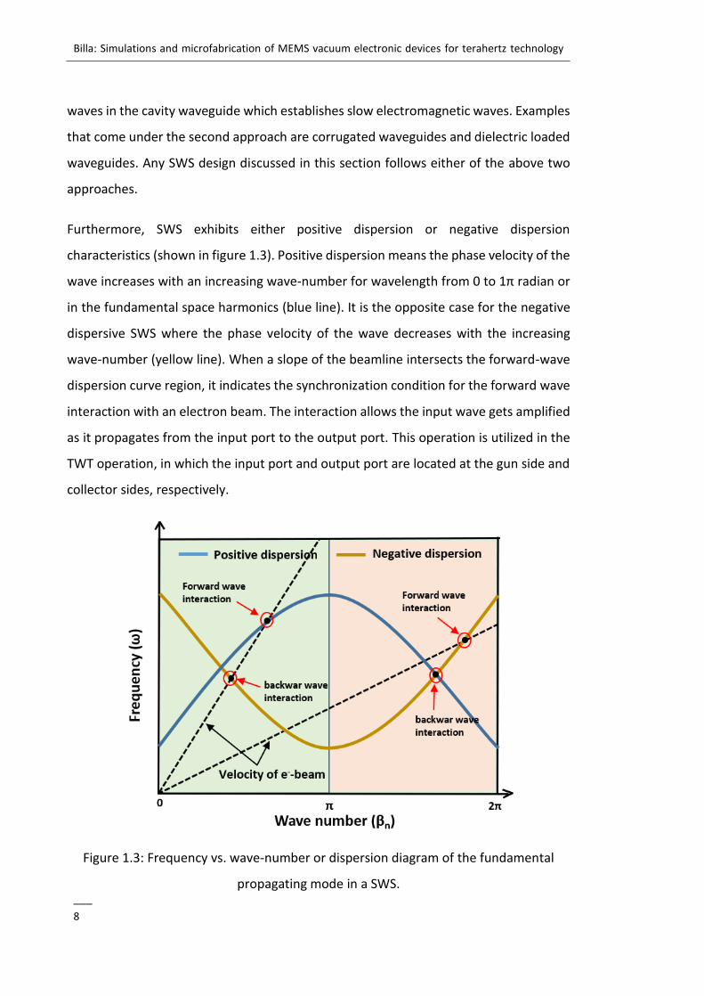
Furthermore, SWS exhibits either positive dispersion or negative dispersion
characteristics (shown in figure 1.3). Positive dispersion means the phase velocity of the
wave increases with an increasing wave-number for wavelength from 0 to 1π radian or
in the fundamental space harmonics (blue line). It is the opposite case for the negative
dispersive SWS where the phase velocity of the wave decreases with the increasing
wave-number (yellow line). When a slope of the beamline intersects the forward-wave
dispersion curve region, it indicates the synchronization condition for the forward wave
interaction with an electron beam. The interaction allows the input wave gets amplified
as it propagates from the input port to the output port. This operation is utilized in the
TWT operation, in which the input port and output port are located at the gun side and
collector sides, respectively.
Figure 1.3: Frequency vs. wave-number or dispersion diagram of the fundamental
propagating mode in a SWS.
Billa: Simulations and microfabrication of MEMS vacuum electronic devices for terahertz technology
___
9
On the other hand, if the slope of the electron beamline intersects the backward-wave
dispersion regions, the backward waves constructively become built up in the tube,
which originates from the collector end of the tube and propagates towards the gun
side, where the stable backward waves are collected from the tube. This type of tube
operation works as a signal generator without RF input, and so is called as a backward
wave oscillator (BWO). This type of oscillators can inherently be used for wideband
operation, especially with an electronic tuning by changing the beam voltage. Another
approach is designing an oscillator using SWS by using the TWT feedback concept. Here
the output of the TWT is connected back to the input through an external feedback path,
which is called as a regenerative oscillator. The best method for oscillator design is the
earlier method of using backward wave oscillations.
The SWS design metrics for the TWT and BWO operation are different. For amplifier
design, the SWS must exhibit nondispersive characteristics over the intended frequency
range. Therefore, such a TWT design can be operated with a constant beam voltage over
the frequency range, thereby achieving a flat gain curve in the operation range. Whereas
in the case of BWO operation, the SWS should exhibit dispersive characteristics over the
desired frequency range. As a result, fine electronic tuning can be achieved by varying
the beam voltage for generating RF signals with high resolution. For the best
performance of a tube, positive-dispersive SWS for TWT design and negative-dispersive
SWS for BWO design are the preferred choice. In subsequent sections, we will
collectively discuss the two types of SWSs used for TWT and/or BWO in the millimetre-
wave and the THz frequency band.
1.3.1 Planar helix SWS
The helical SWS based TWTs are a widely used power source in the microwave band
since it has a high energy conversion efficiency and broad bandwidth. This is the fact
that difficulties arise when realizing tiny helix structures using milling methods for
frequencies beyond the 40 GHz which derivatives of the conventional helix are
reinvented to be compatible with lithography-based microfabrication techniques.
Billa: Simulations and microfabrication of MEMS vacuum electronic devices for terahertz technology
___
10
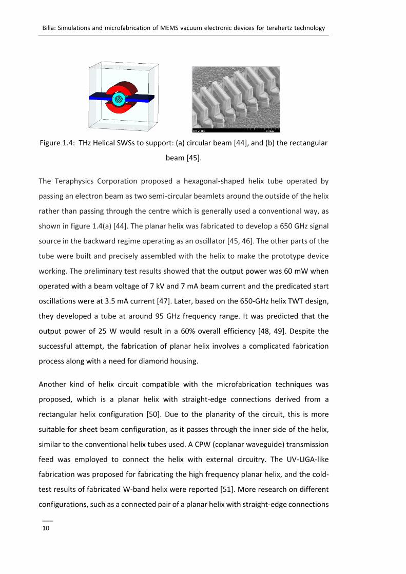
Figure 1.4: THz Helical SWSs to support: (a) circular beam [44], and (b) the rectangular
beam [45].
The Teraphysics Corporation proposed a hexagonal-shaped helix tube operated by
passing an electron beam as two semi-circular beamlets around the outside of the helix
rather than passing through the centre which is generally used a conventional way, as
shown in figure 1.4(a) [44]. The planar helix was fabricated to develop a 650 GHz signal
source in the backward regime operating as an oscillator [45, 46]. The other parts of the
tube were built and precisely assembled with the helix to make the prototype device
working. The preliminary test results showed that the output power was 60 mW when
operated with a beam voltage of 7 kV and 7 mA beam current and the predicated start
oscillations were at 3.5 mA current [47]. Later, based on the 650-GHz helix TWT design,
they developed a tube at around 95 GHz frequency range. It was predicted that the
output power of 25 W would result in a 60% overall efficiency [48, 49]. Despite the
successful attempt, the fabrication of planar helix involves a complicated fabrication
process along with a need for diamond housing.
Another kind of helix circuit compatible with the microfabrication techniques was
proposed, which is a planar helix with straight-edge connections derived from a
rectangular helix configuration [50]. Due to the planarity of the circuit, this is more
suitable for sheet beam configuration, as it passes through the inner side of the helix,
similar to the conventional helix tubes used. A CPW (coplanar waveguide) transmission
feed was employed to connect the helix with external circuitry. The UV-LIGA-like
fabrication was proposed for fabricating the high frequency planar helix, and the cold-
test results of fabricated W-band helix were reported [51]. More research on different
configurations, such as a connected pair of a planar helix with straight-edge connections
Billa: Simulations and microfabrication of MEMS vacuum electronic devices for terahertz technology
___
11
[52], and a vane loaded planar helix with straight-edge connections [53], has been
conducted for improving the planar helix design. The advantage of such a planar helix is
that it can retain the broadband width nature of the conventional helix tube. However,
it suffers from poor thermal dissipation, and it is rated as having low power levels.
1.3.2 Folded waveguide SWS
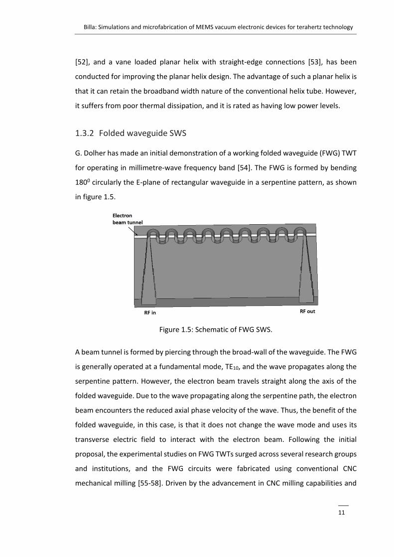
G. Dolher has made an initial demonstration of a working folded waveguide (FWG) TWT
for operating in millimetre-wave frequency band [54]. The FWG is formed by bending
1800 circularly the E-plane of rectangular waveguide in a serpentine pattern, as shown
in figure 1.5.
Figure 1.5: Schematic of FWG SWS.
A beam tunnel is formed by piercing through the broad-wall of the waveguide. The FWG
is generally operated at a fundamental mode, TE10, and the wave propagates along the
serpentine pattern. However, the electron beam travels straight along the axis of the
folded waveguide. Due to the wave propagating along the serpentine path, the electron
beam encounters the reduced axial phase velocity of the wave. Thus, the benefit of the
folded waveguide, in this case, is that it does not change the wave mode and uses its
transverse electric field to interact with the electron beam. Following the initial
proposal, the experimental studies on FWG TWTs surged across several research groups
and institutions, and the FWG circuits were fabricated using conventional CNC
mechanical milling [55-58]. Driven by the advancement in CNC milling capabilities and
Billa: Simulations and microfabrication of MEMS vacuum electronic devices for terahertz technology
___
12
electron discharge method (EDM), the fabrication of FWG circuits was done for
submillimeter-wave frequency operation, such as 95-GHz (W-band) and 140-GHz (D-
band) [59-63]. Besides, 220-GHz FWG TWTs were designed and fabricated using
photolithography techniques [64-66].
A configuration of a multi-beamlets gun and single collector with each beamlet passes
through an individual FWG circuit, was designed to enhance the output power of the
TWT [67]. An integrated coupler was designed for this TWT to split the input drive signal
equally for each of the FWG circuits and recombined the amplified signals at the output
into a single output signal. In this way, at the same time, the individual beam thermal
loading reduces with the number of beamlets used. 233-GHz [68] and 320-GHz [69]
FWG TWTs were manufactured using high precision nano-CNC milling. To develop the
0.67-THz signal source, Northrop Grumman utilized the FWG in the regenerative
principle to operate as an oscillator [70]. The 0.67-THz-FWG circuit was fabricated using
DRIE (deep reactive ion etching) technique, and the test results showed 21.5 dB gain and
15 GHz operational bandwidth [71]. Northrop Grumman also developed 0.85-THz TWT
amplifier based FWG, which is based on the previously developed 0.67-THz regenerate
TWT [72]. This tube can produce an output power of 39.4 mW at 0.85 GHz, with an
instantaneous bandwidth of 11 GHz [73].
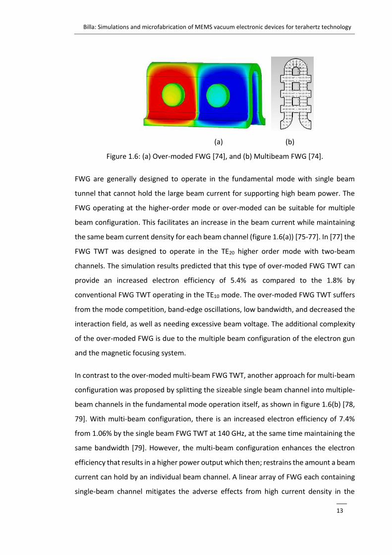
1.3.3 Derived folded waveguide SWS
FWG-SWSs are inherently narrow-band structures whose bandwidth is limited to a
maximum of 30%. Moreover, the efficiency of electron interaction is also low due to the
low value of interaction impedance in conventional FWG-SWS. Thus, there is a need to
explore the possibility of enhancing both the bandwidth and interaction impedance in
the structure.
Billa: Simulations and microfabrication of MEMS vacuum electronic devices for terahertz technology
___
13
(a) (b)
Figure 1.6: (a) Over-moded FWG [74], and (b) Multibeam FWG [74].
FWG are generally designed to operate in the fundamental mode with single beam
tunnel that cannot hold the large beam current for supporting high beam power. The
FWG operating at the higher-order mode or over-moded can be suitable for multiple
beam configuration. This facilitates an increase in the beam current while maintaining
the same beam current density for each beam channel (figure 1.6(a)) [75-77]. In [77] the
FWG TWT was designed to operate in the TE20 higher order mode with two-beam
channels. The simulation results predicted that this type of over-moded FWG TWT can
provide an increased electron efficiency of 5.4% as compared to the 1.8% by
conventional FWG TWT operating in the TE10 mode. The over-moded FWG TWT suffers
from the mode competition, band-edge oscillations, low bandwidth, and decreased the
interaction field, as well as needing excessive beam voltage. The additional complexity
of the over-moded FWG is due to the multiple beam configuration of the electron gun
and the magnetic focusing system.
In contrast to the over-moded multi-beam FWG TWT, another approach for multi-beam
configuration was proposed by splitting the sizeable single beam channel into multiple-
beam channels in the fundamental mode operation itself, as shown in figure 1.6(b) [78,
79]. With multi-beam configuration, there is an increased electron efficiency of 7.4%
from 1.06% by the single beam FWG TWT at 140 GHz, at the same time maintaining the
same bandwidth [79]. However, the multi-beam configuration enhances the electron
efficiency that results in a higher power output which then; restrains the amount a beam
current can hold by an individual beam channel. A linear array of FWG each containing
single-beam channel mitigates the adverse effects from high current density in the
Billa: Simulations and microfabrication of MEMS vacuum electronic devices for terahertz technology
___
14
single-beam-single-FWG TWTs [67]. Because the multiple FWG approach lowers the
beam current required in the individual FWG circuit, this results in a lower beam tunnel
fill factor and thus a lower total thermal load compared to a single-beam device.
Furthermore, it collects the power from each FWG at the output section, thus there is
overall more output power in the device.
(a) (b)
(c) (d)
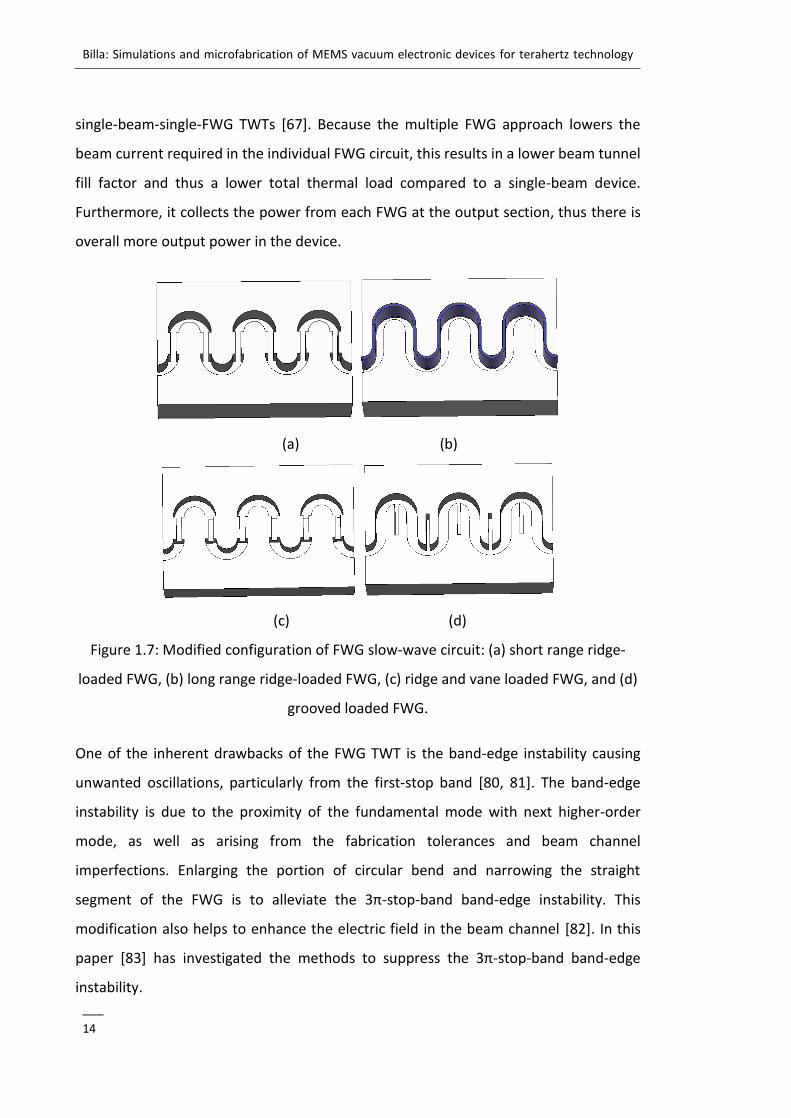
Figure 1.7: Modified configuration of FWG slow-wave circuit: (a) short range ridge-
loaded FWG, (b) long range ridge-loaded FWG, (c) ridge and vane loaded FWG, and (d)
grooved loaded FWG.
One of the inherent drawbacks of the FWG TWT is the band-edge instability causing
unwanted oscillations, particularly from the first-stop band [80, 81]. The band-edge
instability is due to the proximity of the fundamental mode with next higher-order
mode, as well as arising from the fabrication tolerances and beam channel
imperfections. Enlarging the portion of circular bend and narrowing the straight
segment of the FWG is to alleviate the 3π-stop-band band-edge instability. This
modification also helps to enhance the electric field in the beam channel [82]. In this
paper [83] has investigated the methods to suppress the 3π-stop-band band-edge
instability.
Billa: Simulations and microfabrication of MEMS vacuum electronic devices for terahertz technology
___
15
A ridge-loaded FWG TWT [84] was proposed to enhance the beam-wave interaction,
where the ridge load is applied to the straight segment, shown in figure 1.7(a) [84]. The
concept was developed for the W-band TWT that can produce an output power excess
of 25 W for the frequency from 93.1 GHz to 94.8 GHz with a gain of over a 23 dB [85].
To enhance the bandwidth of the FWG TWT, a similar kind of the ridge-loaded FWG was
proposed, where the ridge is inserted in one of the broad walls of the FWG over an entire
length as shown in figure 1.7(b) [86]. The behaviour of the ridge-loaded FWG was
studied using different analytical methods, such as the equivalent circuit analysis,
parametric analysis, and a quasi-TEM analysis, for dispersion and interaction impedance
characteristics. Moreover, the analytical studies were verified against results from 3-D
electromagnetic simulations and cold-test experimental data.
A more complex geometry of FGW, which includes ridges along the horizontal and
vertical sides of the straight segment of the FWG, was proposed (figure 1.7(c)) [87]. The
simulation results predicted the increased interaction impedance compared to the
conventional FWG. The more complexity in the geometry, the more challenges to the
fabrication phase. The fabrication could be done either using a milling method or a
photolithography process.
When the width of the ridge increases the effective length of beam-wave interaction in
the beam channel decreases. To avoid this type of loading, incorporation of a groove
between two straight segments helps to increase the interaction impedance and to
improve the linearity of the dispersion curve, but at the cost of reducing the bandwidth
[88, 89].
The concept of the frequency multiplier was implemented in the TWT, by dividing the
SWS into three sections: fundamental section, drift section and harmonic section [90,
91]. A source frequency is excited into the fundamental section to modulate the injected
electron beam. The modulated beam passes through the drift tube further into the
harmonic section, where the beam is tuned to the desired harmonic frequency of the
input signal frequency, according to the harmonic section designed. The harmonic
frequency is then amplified through the beam-wave interaction process in the harmonic
Billa: Simulations and microfabrication of MEMS vacuum electronic devices for terahertz technology
___
16
section before it is collected at the output port. In contrast to the circular beam FWG
TWT, FWG was utilized to support the sheet beam with a rectangular beam tunnel [92-
94].
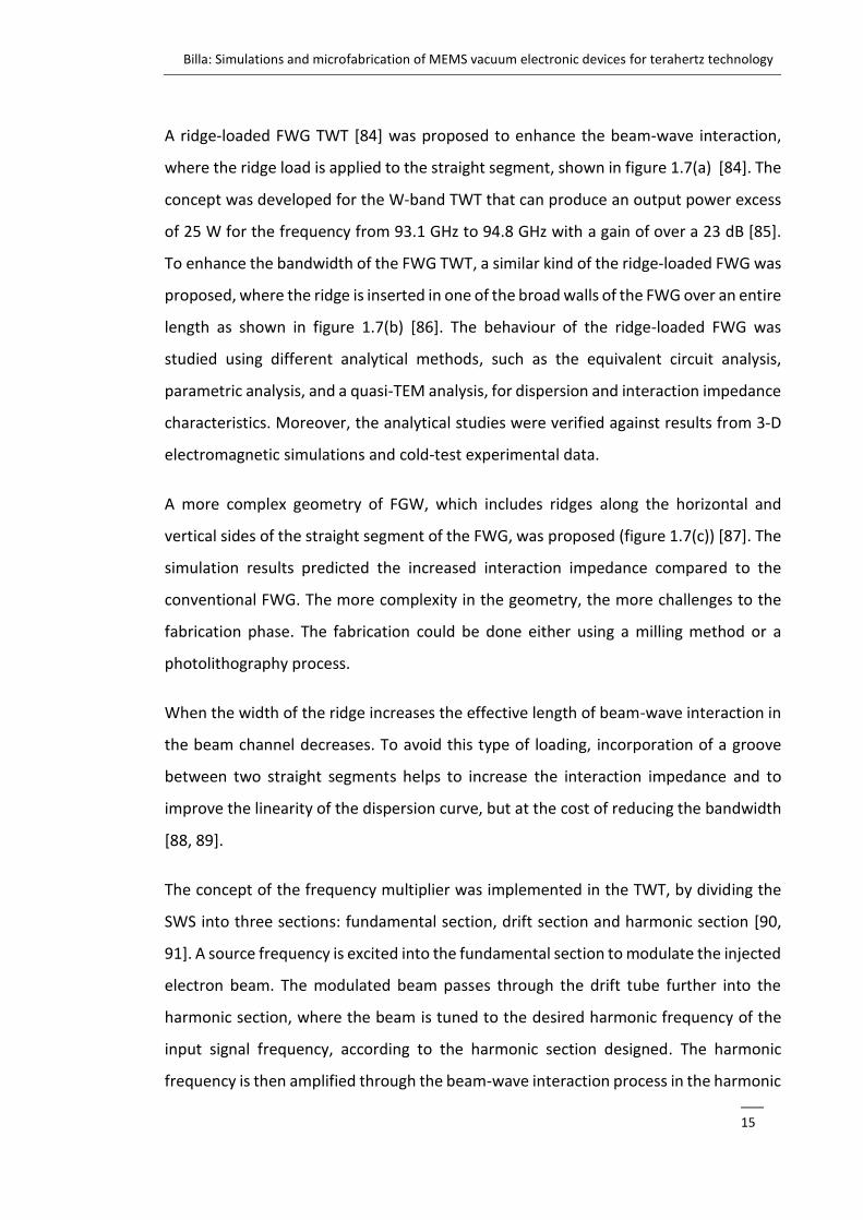
1.3.4 Sheet-beam corrugated SWS
A SWS, composed of periodically loaded metal corrugations or vanes transverse to the
broader side in a rectangular waveguide along the axial direction, is more viable to
fabricate operating from the microwave frequencies up to THz frequency bands. It also
offers mechanical robustness and a high thermal dissipation capability. This type of
SWSs is suitable for sheet-beam tube types.
(a) (b)
Figure 1.8: Sheet-beam corrugated SWS: (a) single corrugation SWS [95] , and (b)
double-staggered corrugated SWS [96].
A simple design of a metal corrugation transverse to the broader side of the
rectangular waveguide was conceived as a SWS for TWTs and BWOs (shown in figure
1.8(a)) [95]. An electron beam sends over the corrugation for the beam-wave
interaction process. The SWS was used to design a 220-GHz TWT amplifier with an
estimated growth of 33 dB/cm at 211.3 GHz [96]. The LIGA technique was applied to
fabricate the SWS and validates the electromagnetic characteristics using S-
parameters measurements. [97]. By reducing the width of corrugations, the SWS can
provide more interaction fields available for energy transfer [98, 99]. A 1-THz BWO was
designed using the narrow-corrugated SWS [99, 100].
Young-Min Shin proposed a SWS which is composed of a pair of half-period staggered
corrugations in a rectangular waveguide, for THz TWTs, as shown in figure 1.8(b) [101].
Billa: Simulations and microfabrication of MEMS vacuum electronic devices for terahertz technology
___
17
It offers strong axial electric fields in the beam channel which is the region between
the two opposite rows of corrugations. The SWS was applied to design a 220-GHz sheet
beam TWT [102, 103]. Various microfabrication techniques, like LIGA, DRIE and nano-
CNC milling, were used to explore the feasibility of fabricating the SWS [104]. The test
results of the prototype device demonstrated an output power of 107 W with 6 GHz
3-dB bandwidth centred at 200 GHz [105]. Later, the SWS was considered at various
frequency bands for the TWT [106, 107] and BWO [108]. A modified version of
staggered double corrugated SWS was proposed, with a sinusoidal geometry [109]. A
large signal code for staggered double vane SWS was developed [110]. With the help
of this code, the analysis can be done quickly in comparison with the commercial three-
dimensional (3D) software tools.
1.3.5 Circular-beam corrugated SWS
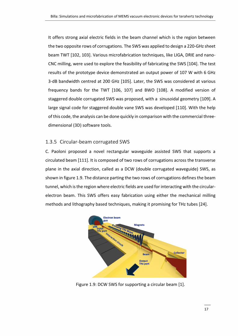
C. Paoloni proposed a novel rectangular waveguide assisted SWS that supports a
circulated beam [111]. It is composed of two rows of corrugations across the transverse
plane in the axial direction, called as a DCW (double corrugated waveguide) SWS, as
shown in figure 1.9. The distance parting the two rows of corrugations defines the beam
tunnel, which is the region where electric fields are used for interacting with the circular-
electron beam. This SWS offers easy fabrication using either the mechanical milling
methods and lithography based techniques, making it promising for THz tubes [24].
Figure 1.9: DCW SWS for supporting a circular beam [1].
Billa: Simulations and microfabrication of MEMS vacuum electronic devices for terahertz technology
___
18
Initially, DCW SWS was used to operate in the backward region for THz BWOs. A 1-THz
backward wave the amplifier (BWA) using the DCW SWS was designed [112] and
fabricated using the PMMA DXRL (deep X-ray lithography) process. The DCW SWS was
also used to operate in a forward wave regime for 0.22-THz TWT [113]. Later it was
adopted to design a Ka-Band TWT [114], 71-76-GHz TWT [115], and 0.346-TH BWO [74].
1.3.6 Meander-line SWS
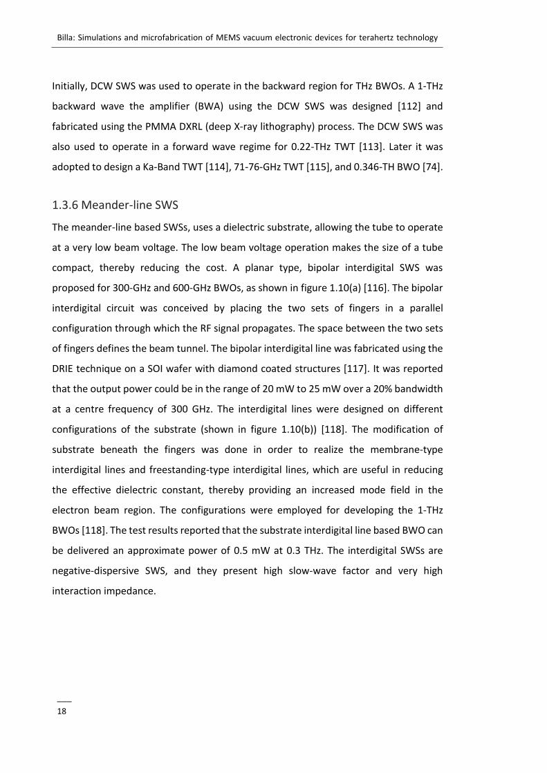
The meander-line based SWSs, uses a dielectric substrate, allowing the tube to operate
at a very low beam voltage. The low beam voltage operation makes the size of a tube
compact, thereby reducing the cost. A planar type, bipolar interdigital SWS was
proposed for 300-GHz and 600-GHz BWOs, as shown in figure 1.10(a) [116]. The bipolar
interdigital circuit was conceived by placing the two sets of fingers in a parallel
configuration through which the RF signal propagates. The space between the two sets
of fingers defines the beam tunnel. The bipolar interdigital line was fabricated using the
DRIE technique on a SOI wafer with diamond coated structures [117]. It was reported
that the output power could be in the range of 20 mW to 25 mW over a 20% bandwidth
at a centre frequency of 300 GHz. The interdigital lines were designed on different
configurations of the substrate (shown in figure 1.10(b)) [118]. The modification of
substrate beneath the fingers was done in order to realize the membrane-type
interdigital lines and freestanding-type interdigital lines, which are useful in reducing
the effective dielectric constant, thereby providing an increased mode field in the
electron beam region. The configurations were employed for developing the 1-THz
BWOs [118]. The test results reported that the substrate interdigital line based BWO can
be delivered an approximate power of 0.5 mW at 0.3 THz. The interdigital SWSs are
negative-dispersive SWS, and they present high slow-wave factor and very high
interaction impedance.
Billa: Simulations and microfabrication of MEMS vacuum electronic devices for terahertz technology
___
19
(a) (b) (c)
Figure 1.10: Planar SWSs: (a) bipolar interdigital SWS [116], (b) free interdigital line
SWS [118], and (c) microstrip meander line SWS [119].
Another meander line-type planar SWS was proposed for TWTs and BWOs, shown in
figure 1.10(c). Similar to interdigital SWSs, it also operates at a low beam voltage at the
same time making it easy to fabricate [119]. Various versions of the meander line SWSs
were reported in the literature, such as V-shaped meander line [120, 121], a symmetric
double V-shaped meander line [122], a ring-shaped strip line [123], and sheath structure
[124]. The advantages of these type of planar structures are that they do not require
growing the thick metal structures using photolithography processes [125]. The
meander line structures usually needed tens of micron or less metal pattern on the
dielectric substrate, which can be done by easy photolithographic process steps [126].
Few of these SWSs were tested using verifying of s-parameters experimentally [119,
126, 127]. This type of SWSs provides a narrow bandwidth.
1.4 Microfabrication techniques for THz SWS
When the operating frequency pushes towards the THz, the dimensions of the SWS
shrink to hundreds of microns or even less, and fabrication tolerances at these
frequency ranges are very demanding. It is impractical to produce such micron level
features using traditional machining techniques. In recent years, research has been
focused on attempting the fabrication of those micro-sized SWSs for THz TWTs and
BWOs using various microfabrication techniques. These microfabrication methods are
also useful for manufacturing the other parts of the THz tubes. This section discusses
the possible micromachining techniques for fabricating THz SWSs.
Billa: Simulations and microfabrication of MEMS vacuum electronic devices for terahertz technology
___
20
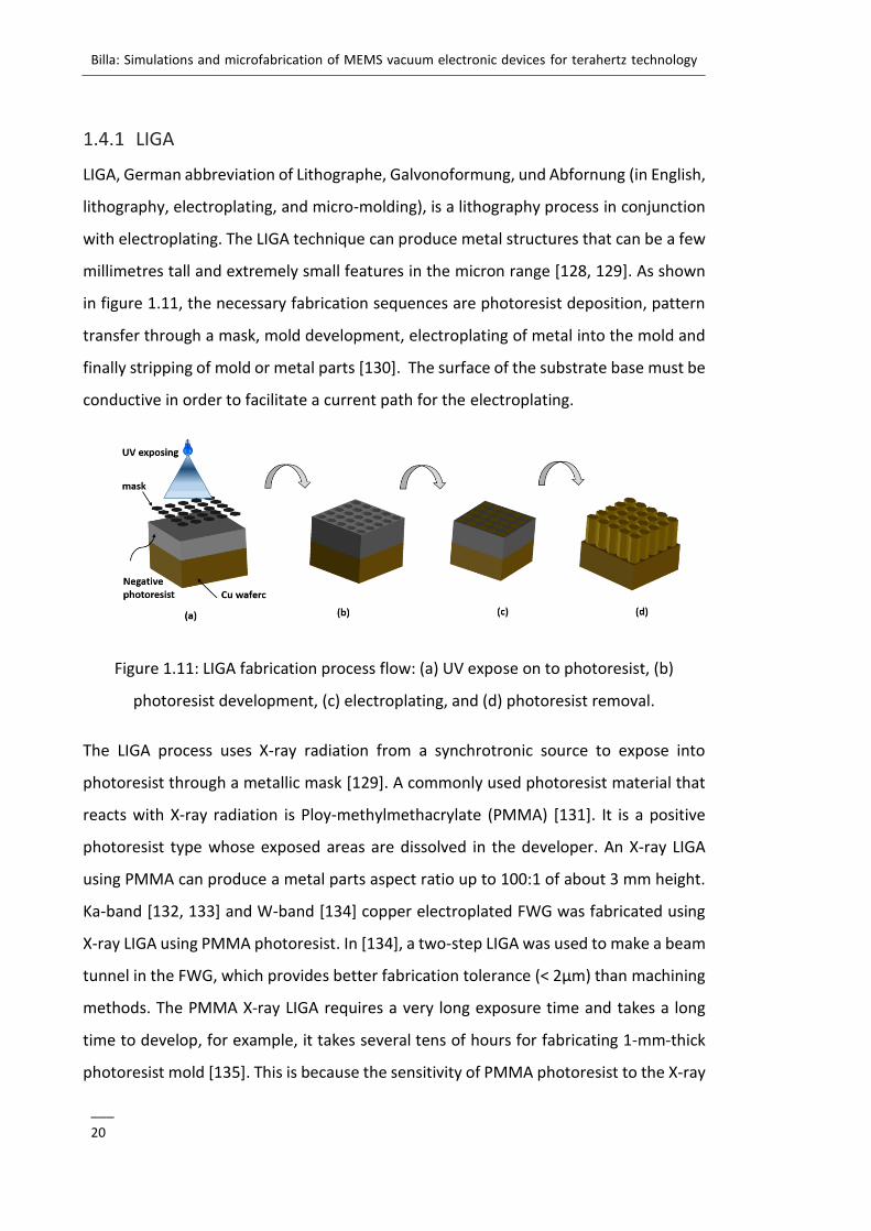
1.4.1 LIGA
LIGA, German abbreviation of Lithographe, Galvonoformung, und Abfornung (in English,
lithography, electroplating, and micro-molding), is a lithography process in conjunction
with electroplating. The LIGA technique can produce metal structures that can be a few
millimetres tall and extremely small features in the micron range [128, 129]. As shown
in figure 1.11, the necessary fabrication sequences are photoresist deposition, pattern
transfer through a mask, mold development, electroplating of metal into the mold and
finally stripping of mold or metal parts [130]. The surface of the substrate base must be
conductive in order to facilitate a current path for the electroplating.
Figure 1.11: LIGA fabrication process flow: (a) UV expose on to photoresist, (b)
photoresist development, (c) electroplating, and (d) photoresist removal.
The LIGA process uses X-ray radiation from a synchrotronic source to expose into
photoresist through a metallic mask [129]. A commonly used photoresist material that
reacts with X-ray radiation is Ploy-methylmethacrylate (PMMA) [131]. It is a positive
photoresist type whose exposed areas are dissolved in the developer. An X-ray LIGA
using PMMA can produce a metal parts aspect ratio up to 100:1 of about 3 mm height.
Ka-band [132, 133] and W-band [134] copper electroplated FWG was fabricated using
X-ray LIGA using PMMA photoresist. In [134], a two-step LIGA was used to make a beam
tunnel in the FWG, which provides better fabrication tolerance (< 2µm) than machining
methods. The PMMA X-ray LIGA requires a very long exposure time and takes a long
time to develop, for example, it takes several tens of hours for fabricating 1-mm-thick
photoresist mold [135]. This is because the sensitivity of PMMA photoresist to the X-ray
Billa: Simulations and microfabrication of MEMS vacuum electronic devices for terahertz technology
___
21
radiation is very weak. Besides, X-ray LIGA needs an expensive gold mask. It was proven
that this process produces an undercut in the PMMA mold due to backscattering from
the substrate. SU-8 photoresist was developed as an alternative to the PMMA for LIGA
applications. The SU-8 is a negative photoresist, so the exposed areas remain after
etching. The benefits of using the SU-8 compared to the PMMA are that the photo
absorption to x-ray radiation is 200 times more, better tolerance control, and it does
not require an expensive gold-mask [135].
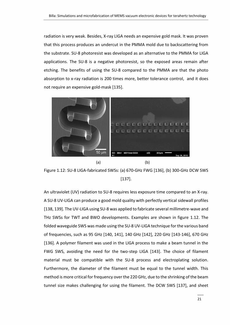
(a) (b)
Figure 1.12: SU-8 LIGA-fabricated SWSs: (a) 670-GHz FWG [136], (b) 300-GHz DCW SWS
[137].
An ultraviolet (UV) radiation to SU-8 requires less exposure time compared to an X-ray.
A SU-8 UV-LIGA can produce a good mold quality with perfectly vertical sidewall profiles
[138, 139]. The UV-LIGA using SU-8 was applied to fabricate several millimetre-wave and
THz SWSs for TWT and BWO developments. Examples are shown in figure 1.12. The
folded waveguide SWS was made using the SU-8 UV-LIGA technique for the various band
of frequencies, such as 95 GHz [140, 141], 140 GHz [142], 220 GHz [143-146], 670 GHz
[136]. A polymer filament was used in the LIGA process to make a beam tunnel in the
FWG SWS, avoiding the need for the two-step LIGA [143]. The choice of filament
material must be compatible with the SU-8 process and electroplating solution.
Furthermore, the diameter of the filament must be equal to the tunnel width. This
method is more critical for frequency over the 220 GHz, due to the shrinking of the beam
tunnel size makes challenging for using the filament. The DCW SWS [137], and sheet
Billa: Simulations and microfabrication of MEMS vacuum electronic devices for terahertz technology
___
22
beam based SWS [97, 147] were fabricated using the SU-8 UV-LIGA technique with
single-step LIGA. These SWSs do not require additional fabrication steps to make the
beam tunnel. It is a fact that the etching of cross-linked SU-8 poses difficulties [148].
Several approaches have been explored to find the best solution for stripping the cross-
linked SU-8 [97]. A KMPR photoresist is a promising choice of mold material for UV-LIGA
application, which is similar to SU-8.
The KMPR UV-LIGA process was employed to fabricate the 340-GHz FWG SWS [149] and
the 220-GHz staggered double vane SWS [150]. It revealed that compared to SU-8, the
KMPR photoresist is much easier to lift-off after the electroplating step. The sidewall
surface roughness of LIGA-fabricated SWSs is mainly dependant on the quality of the
photoresist mold and the electroplating process conditions. The photoresist molds can
produce very smooth surfaces, < 20 nm. However, the process conditions must be
optimized for there are any changes in the design, which is not favourable. The LIGA
technique is limited to producing 2D geometries. But, the modified versions of LIGA
techniques could fabricate 3D geometries.
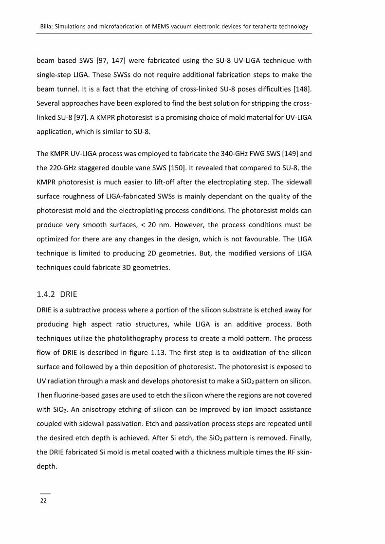
1.4.2 DRIE
DRIE is a subtractive process where a portion of the silicon substrate is etched away for
producing high aspect ratio structures, while LIGA is an additive process. Both
techniques utilize the photolithography process to create a mold pattern. The process
flow of DRIE is described in figure 1.13. The first step is to oxidization of the silicon
surface and followed by a thin deposition of photoresist. The photoresist is exposed to
UV radiation through a mask and develops photoresist to make a SiO2 pattern on silicon.
Then fluorine-based gases are used to etch the silicon where the regions are not covered
with SiO2. An anisotropy etching of silicon can be improved by ion impact assistance
coupled with sidewall passivation. Etch and passivation process steps are repeated until
the desired etch depth is achieved. After Si etch, the SiO2 pattern is removed. Finally,
the DRIE fabricated Si mold is metal coated with a thickness multiple times the RF skin-
depth.
Billa: Simulations and microfabrication of MEMS vacuum electronic devices for terahertz technology
___
23
Figure 1.13: DRIE fabrication process flow: (a) UV expose on to photoresist, (b)
photoresist development, (c) Si electing using DRIE, and (d) photoresist removal and
metal coating.
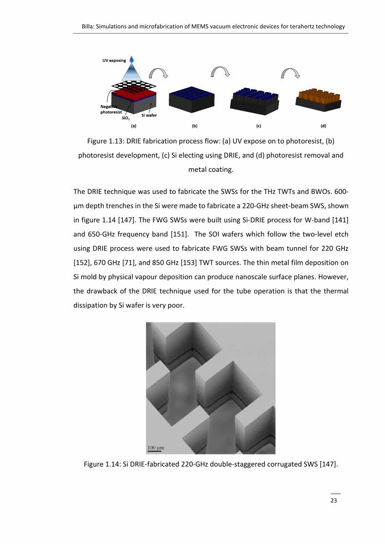
The DRIE technique was used to fabricate the SWSs for the THz TWTs and BWOs. 600-
µm depth trenches in the Si were made to fabricate a 220-GHz sheet-beam SWS, shown
in figure 1.14 [147]. The FWG SWSs were built using Si-DRIE process for W-band [141]
and 650-GHz frequency band [151]. The SOI wafers which follow the two-level etch
using DRIE process were used to fabricate FWG SWSs with beam tunnel for 220 GHz
[152], 670 GHz [71], and 850 GHz [153] TWT sources. The thin metal film deposition on
Si mold by physical vapour deposition can produce nanoscale surface planes. However,
the drawback of the DRIE technique used for the tube operation is that the thermal
dissipation by Si wafer is very poor.
Figure 1.14: Si DRIE-fabricated 220-GHz double-staggered corrugated SWS [147].
Billa: Simulations and microfabrication of MEMS vacuum electronic devices for terahertz technology
___
24
1.4.3 Electrical discharge machining
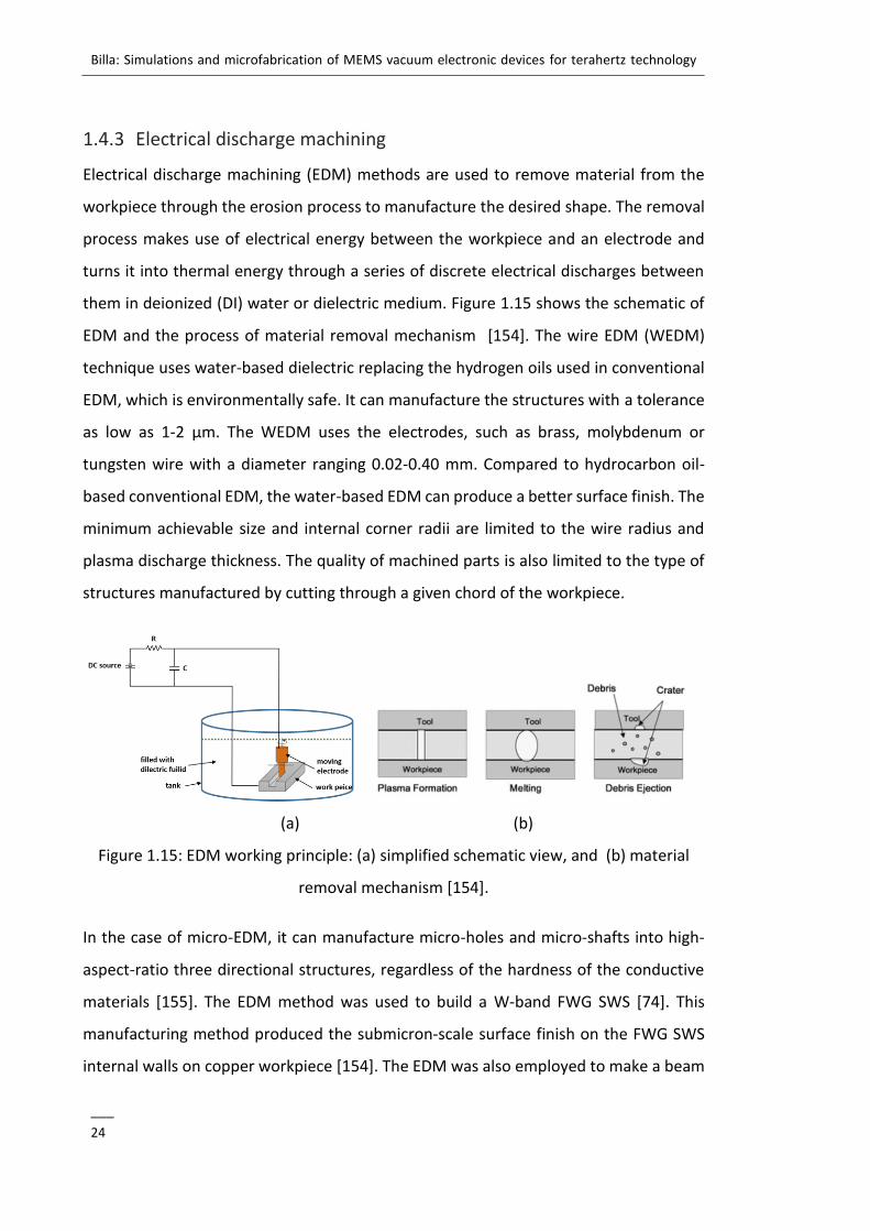
Electrical discharge machining (EDM) methods are used to remove material from the
workpiece through the erosion process to manufacture the desired shape. The removal
process makes use of electrical energy between the workpiece and an electrode and
turns it into thermal energy through a series of discrete electrical discharges between
them in deionized (DI) water or dielectric medium. Figure 1.15 shows the schematic of
EDM and the process of material removal mechanism [154]. The wire EDM (WEDM)
technique uses water-based dielectric replacing the hydrogen oils used in conventional
EDM, which is environmentally safe. It can manufacture the structures with a tolerance
as low as 1-2 µm. The WEDM uses the electrodes, such as brass, molybdenum or
tungsten wire with a diameter ranging 0.02-0.40 mm. Compared to hydrocarbon oil-
based conventional EDM, the water-based EDM can produce a better surface finish. The
minimum achievable size and internal corner radii are limited to the wire radius and
plasma discharge thickness. The quality of machined parts is also limited to the type of
structures manufactured by cutting through a given chord of the workpiece.
(a) (b)
Figure 1.15: EDM working principle: (a) simplified schematic view, and (b) material
removal mechanism [154].
In the case of micro-EDM, it can manufacture micro-holes and micro-shafts into high-
aspect-ratio three directional structures, regardless of the hardness of the conductive
materials [155]. The EDM method was used to build a W-band FWG SWS [74]. This
manufacturing method produced the submicron-scale surface finish on the FWG SWS
internal walls on copper workpiece [154]. The EDM was also employed to make a beam
Billa: Simulations and microfabrication of MEMS vacuum electronic devices for terahertz technology
___
25
tunnel on the LIGA–fabricated FWG SWS [64]. The achievable resolution and surface
finish by the EDM methods are not suitable for the SWS operating beyond W-band [156].
1.4.4 CNC milling
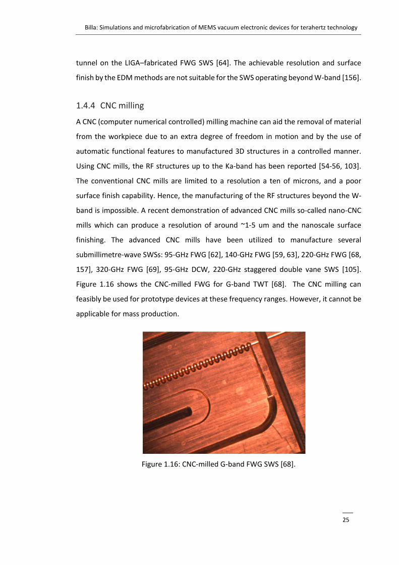
A CNC (computer numerical controlled) milling machine can aid the removal of material
from the workpiece due to an extra degree of freedom in motion and by the use of
automatic functional features to manufactured 3D structures in a controlled manner.
Using CNC mills, the RF structures up to the Ka-band has been reported [54-56, 103].
The conventional CNC mills are limited to a resolution a ten of microns, and a poor
surface finish capability. Hence, the manufacturing of the RF structures beyond the W-
band is impossible. A recent demonstration of advanced CNC mills so-called nano-CNC
mills which can produce a resolution of around ~1-5 um and the nanoscale surface
finishing. The advanced CNC mills have been utilized to manufacture several
submillimetre-wave SWSs: 95-GHz FWG [62], 140-GHz FWG [59, 63], 220-GHz FWG [68,
157], 320-GHz FWG [69], 95-GHz DCW, 220-GHz staggered double vane SWS [105].
Figure 1.16 shows the CNC-milled FWG for G-band TWT [68]. The CNC milling can
feasibly be used for prototype devices at these frequency ranges. However, it cannot be
applicable for mass production.
Figure 1.16: CNC-milled G-band FWG SWS [68].
Billa: Simulations and microfabrication of MEMS vacuum electronic devices for terahertz technology
___
26
1.4.5 3-D printing
3-D printing, also known as additive manufacturing, has found widespread applications
in the rapid prototype and production of geometrically complex components. The
interest of additive manufacturing has been explored for passive and active RF
components [158]. Recently an exploration of the additive manufacturing for SWSs has
been begun [159, 160]. A 95-GHz FWG SWS was fabricated using 3D-printing technology
[161].
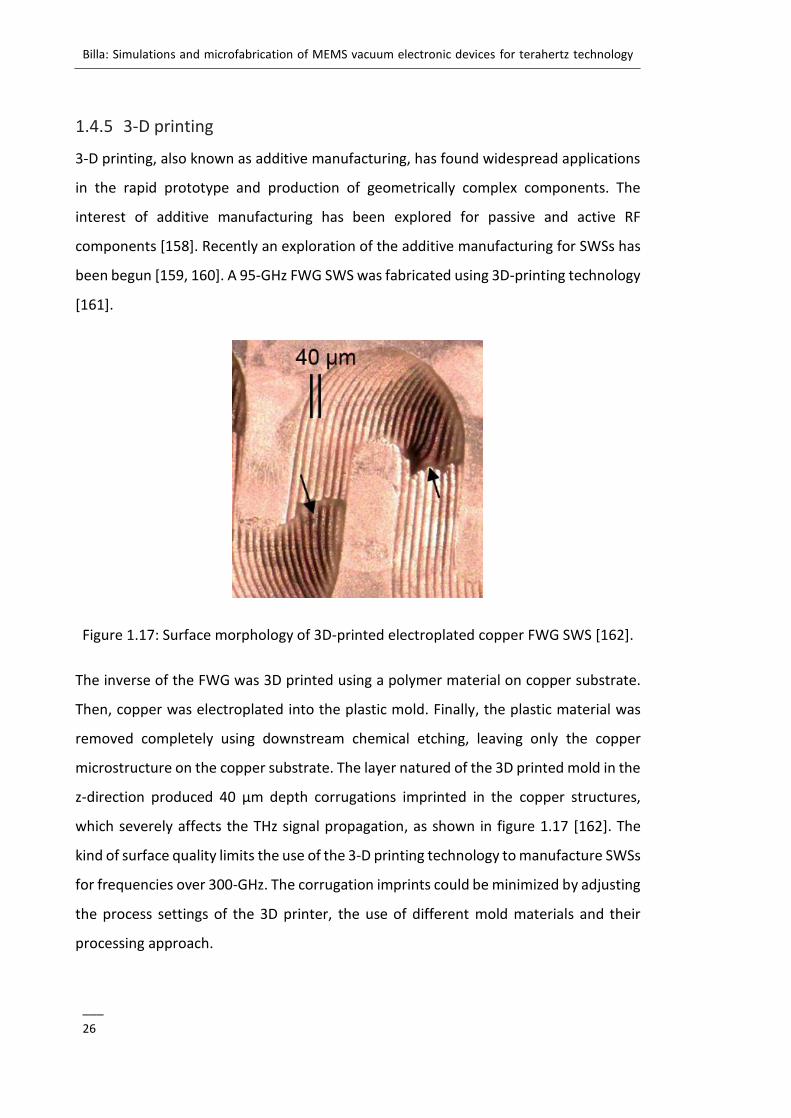
Figure 1.17: Surface morphology of 3D-printed electroplated copper FWG SWS [162].
The inverse of the FWG was 3D printed using a polymer material on copper substrate.
Then, copper was electroplated into the plastic mold. Finally, the plastic material was
removed completely using downstream chemical etching, leaving only the copper
microstructure on the copper substrate. The layer natured of the 3D printed mold in the
z-direction produced 40 µm depth corrugations imprinted in the copper structures,
which severely affects the THz signal propagation, as shown in figure 1.17 [162]. The
kind of surface quality limits the use of the 3-D printing technology to manufacture SWSs
for frequencies over 300-GHz. The corrugation imprints could be minimized by adjusting
the process settings of the 3D printer, the use of different mold materials and their
processing approach.
Billa: Simulations and microfabrication of MEMS vacuum electronic devices for terahertz technology
___
27
1.5 Scope of the thesis
This thesis proposes a new design of a slow-wave structure, called H-plane and E-plane
loaded SWS, for developing a THz TWTs. Such a new design assists in easy fabrication by
using available microfabrication techniques, and it can also provide a high gain-
bandwidth product. Chapter-1 consists of an explanation of the basic principle of TWT
and literature on the THz SWSs and their possible microfabrication methods. The
proposed H-plane and E-plane loaded SWS design is analysed and simulated for 400-
GHz TWT which reported in chapter-2. The simulations are divided into three steps:
Eigenmode simulations, transient simulations, and PiC simulations. Eigenmode
simulations are used to extract the electromagnetic characteristics of the SWS, which
will be utilised for next stage simulations. By using time-domain transient solver, a
coupler design for the new SWS is devised, which can be fabricated as an integral part
of the SWS by applying the same fabrication method employed for the SWS. The TWT
performance based on the H-plane and E-plane loaded SWS, such as gain, 3-dB
bandwidth and power, is predicted using PiC simulations. Chapter-3 presents the
experimental studies on the KMPR-based LIGA technique for the H-plane and H-plane
loaded SWS fabrication. It includes the optimization of the KMPR lithography process
parameters, electroplating and diffusion bonding of the LIGA-fabricated parts. A
quantitative structural study of the fabricated samples was conducted, for examining
fabrication tolerances and their process conditions. A study of surface morphology of
the electroplated copper structures was studied. The quality of bonding strength
between the LIGA fabricated copper structures was analysed at different experimental
conditions, by scanning electron microscope (SEM) inspection and shear test methods.
Chapter-4 emphasis the test results of the H-plane and E-plane loaded SWS at W-band.
The W-band SWS was manufactured using the CNC milling. This chapter also reported
the simulations results of the SWS at W-band. At the end of the thesis, journal papers
are attached, which give an insight into the research findings from the Ph.D. work.

Billa: Simulations and microfabrication of MEMS vacuum electronic devices for terahertz technology
___
29
Chapter 2
2 Design and simulation of H-plane and E-plane loaded
SWS for 400-GHz TWT
The discovery of a new type of SWS is the way to improve the performance levels of the tube,
which is the first and most important performance decider of the TWT. Therefore, a variant and
a robust design that is H-plane and E-plane loaded SWS has been proposed for the THz TWTs.
This chapter focuses on investigating the performance of 400-GHz TWT amplifier using proposed
SWS by utilizing the analytical method and numerical simulations. Pierce linear theory is used
for an approximate estimation of small-signal gain. The computer simulations are first used to
investigate the electromagnetic characteristics of the SWS, and then performed the beam-wave
interaction simulations. A coupler for proposed SWS is devised for efficient use of intrinsic
bandwidth of the SWS without losing RF power during wave transition. Finally, this chapter
discusses the phase velocity technique employed to extend the performance level of the tube.
2.1 Analytical theory of SWS
The classic small-signal theory of interaction of an electron beam with a traveling-wave
is presented, which was developed by J.R. Pierce. To discuss any TWT design, the
parameters he derived are considered as standard metrics, and this will also be applied
for designing this TWT. Pierce’s theory is built up by finding an electronic equation and
the current equation. The electronic equation referred to the AC current is caused by an
axial electric field, whereas the circuit equation referred to the field in the circuit due to
an AC current in the beam. The circuit equation and electronics equation can be
combined to form the determinantal equation whose solutions are for all possible
propagation modes.
2.1.1 Electronics equation
First, we will derive the equation of AC current of the beam from the axial electric field.
Due to the electric field force, it is assumed that there are small variations in the velocity,
current, and density of the electron beam:
Billa: Simulations and microfabrication of MEMS vacuum electronic devices for terahertz technology
___
30
,0 vvv += (2.1)
,0 iIi +−= (2.2)
,0 +−= (2.3)
The indication of a subscript of zero and the bar above the variable are for the initial
quantities and the quantities that small perturbation proportional to ( ) ,ztje −
respectively. First, we introduce the current density, which is defined as a product of the
electron density and velocity of the electrons, and the current density is substituted by
electron current over the beam cross-section, A:
i
J vA
= = (2.4)
Then we substitute equations (2.1), (2.2) and (2.3) into equation (2.4) and expand out
the terms replacing 0=v which reduce the equation to a second-order equation:
( )Avvi o 0 −= (2.5)
It is worth considering the continuity equation .Jt
= −
, and the derivatives that
can be reduced after the substitution of the perturbation of quantities with ( ) ztje − ,
𝑖̅ =𝐴𝜔�̅�
𝛽 (2.6)
Combining equation (2.5) and continuity equation, forms the perturbed current and
velocity equations,
AvA
ivi
−= 0
0
(2.7)
( )0
0
vA
iv
−
−= (2.8)

Billa: Simulations and microfabrication of MEMS vacuum electronic devices for terahertz technology
___
31
In the presence of the electric field, 𝐸𝑧 = 𝐸1𝑒𝑗(𝜔𝑡−𝛽𝑧) , the electrons accelerate as
zEm
e
dt
dv −= (2.9)
Partial derivatives of equation (2.9),
t
z
z
v
t
v
dt
dv
+
= (2.10)
With 0vt
z=
, the partial derivatives can be evaluated with the perturbed quantities,
�̅�(𝑗𝜔 − 𝑗𝛽𝑣0) =𝑒
𝑚𝐸𝑧 (2.11)
Finally combining equations (2.8) and (2.11) and considering the𝛽𝑒 = 𝜔𝑣0⁄ , vAI 00 = ,
and emvV 20
2
= , establishes a relationship between current and electric field.
2
0
0
)(2
−=
e
ze
V
EIji (2.12)
Where I0 and V0 are the current and voltage operation conditions of the electron gun.
Including the space charge field effect, iAe
mjE
q
sc
0
2
= , pq R = , the equation (2.12)
becomes
2
0
2
2
0
0
)(2v
wV
EIji
q
e
ze
+−
=
(2.13)
2.1.2 Circuit equation
The SWS is modelled as a distributed transmission line in Pierce’s theory, in which it is
assumed that the same slow-wave behaviour in the transmission line model as well.
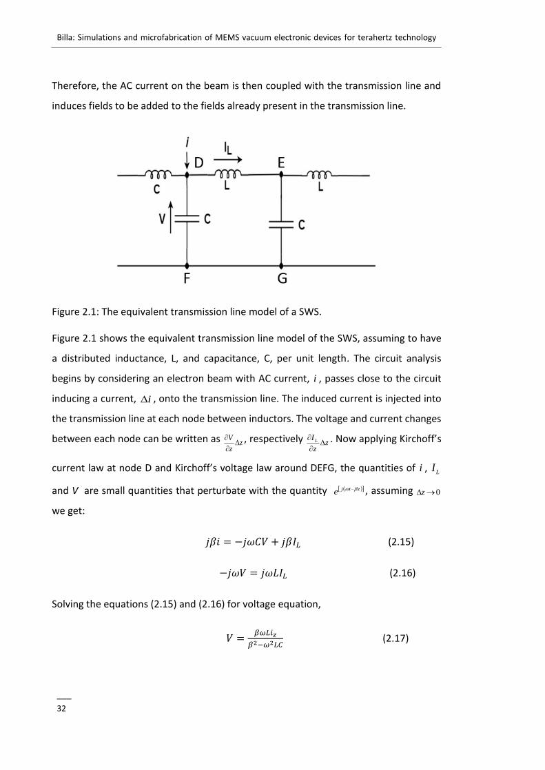
Billa: Simulations and microfabrication of MEMS vacuum electronic devices for terahertz technology
___
32
Therefore, the AC current on the beam is then coupled with the transmission line and
induces fields to be added to the fields already present in the transmission line.
Figure 2.1: The equivalent transmission line model of a SWS.
Figure 2.1 shows the equivalent transmission line model of the SWS, assuming to have
a distributed inductance, L, and capacitance, C, per unit length. The circuit analysis
begins by considering an electron beam with AC current, i , passes close to the circuit
inducing a current, i , onto the transmission line. The induced current is injected into
the transmission line at each node between inductors. The voltage and current changes
between each node can be written as zz
V
, respectively zz
I L
. Now applying Kirchoff’s
current law at node D and Kirchoff’s voltage law around DEFG, the quantities of i , LI
and V are small quantities that perturbate with the quantity ( ) ztje − , assuming 0→z
we get:
𝑗𝛽𝑖 = −𝑗𝜔𝐶𝑉 + 𝑗𝛽𝐼𝐿 (2.15)
−𝑗𝜔𝑉 = 𝑗𝜔𝐿𝐼𝐿 (2.16)
Solving the equations (2.15) and (2.16) for voltage equation,
𝑉 =𝛽𝜔𝐿𝑖𝑧
𝛽2−𝜔2𝐿𝐶 (2.17)
Billa: Simulations and microfabrication of MEMS vacuum electronic devices for terahertz technology
___
33
Now we assume as before that the electrons pass close to the transmission line, then
the change in voltage between nodes of the transmission line will be an electric field on
the electron beam.
2
2 2.
( )z
dV LE V j i
z LC
= − = − =
− (2.18)
Phase velocity and the interaction impedance of the circuit are defined with circuit
constants, L and C:
𝑣𝑝 = (1
𝐿𝐶)1 2⁄
and
2/1
=
C
LK (2.19)
By rewriting the electric field equation (2.18) we get the following form:
2
2 2
cz
c
KE j i
=
− (2.20)
For microwave the circuit impedance is related to power travelling on the circuit by
P
VZ
2
2
= (2.21)
And from (2.18):
cVE = (2.22)
We get the following for the interaction impedance:
P
EK
c
n
2
2
2= (2.23)
Where subscription n refers to space harmonic of the electric field, the fields that would
be by the electron beam. According to the Floquet’s theorem
dzezyxEP
yxEz
P
nj
L
n
)2
(
0
),,(1
),(
= and P
nn
20 += (2.24)
Billa: Simulations and microfabrication of MEMS vacuum electronic devices for terahertz technology
___
34
Where p is the total length of integration. Coupling impedance is only based on axial
electric fields travelling with the electron beam. En is found by taking the spatial Fourier
transformation. For these calculations, it is assumed that βn is the axial velocity of the
circuits and first space harmonic. Calculating the value of En in 3D electromagnetic
simulations is not straight forward. En shows the integration of the total electric field in
the z-direction multiplied by a phase, where both terms will have real and imaginary
parts. The simulation software does not allow one to integrate non-real numbers;
therefore, the following formulas are used in a post solver run to find the square
magnitude of En :
𝐸𝑛(𝑥, 𝑦) =1
𝑃∫ 𝑅𝑒(𝐸(𝑥, 𝑦, 𝑧)
𝐿
0𝑒𝑗(
2𝜋𝑛
𝑃)𝑧)𝑑𝑧 + 𝑗
1
𝑃∫ 𝐼𝑚(𝐸(𝑥, 𝑦, 𝑧)
𝐿
0𝑒𝑗(
2𝜋𝑛
𝑃)𝑧)𝑑𝑧 (2.25)
| 𝐸𝑛(𝑥, 𝑦)|2 = (1
𝑃∫ 𝑅𝑒(𝐸(𝑥, 𝑦, 𝑧)
𝐿
0𝑒𝑗(
2𝜋𝑛
𝑃)𝑧)𝑑𝑧)
2
− (1
𝑃∫ 𝐼𝑚(𝐸(𝑥, 𝑦, 𝑧)
𝐿
0𝑒𝑗(
2𝜋𝑛
𝑃)𝑧)𝑑𝑧)
2
(2.26)
2.1.3 Determinantal equation
The two equations from the electronics and circuits methods of analysis, (12) and (20),
can be combined to arrive at the dispersion relation, without space-charge.
( ) ( )
12 3
22
2
2=
−−C
c
e
e
e
(2.27)
The pierce parameter, C, has been introduced, which establishes an easy relationship
between the beam parameter, 0I and V0 and the circuit coupling impedance, K.
0
0
4V
KIC = (2.28)
With space charge,
( )( )
12 3
22
2
2
0
22
=−
+−
C
v
c
e
q
e
e
(2.29)
Billa: Simulations and microfabrication of MEMS vacuum electronic devices for terahertz technology
___
35
2.1.4 Gain equation
The determinantal equation (2.29), a fourth-order polynomial equation for β, is used to
determine the gain in the circuit. The determinantal equation will have four solutions,
corresponding to four modes of the circuit. The solution of the determinantal equation
is considered under synchronous operation, such that ec = . The two modes travel
slower than the speed of the light: one has an exponential growing nature and another
a decaying exponential. The remaining two modes travel with the speed of light: one
forward wave and another backward wave. By solving the boundary and initial
condition, Pierce shows the gain, G, in a TWT which is a result of the slow forward
growing wave,
2
22
3
103
1log10
=
NC
eG
[dB] (2.30)
where, ( )eN
2= is the number of longitudinal wavelengths in the circuit and C is the
Pierce parameter. The fraction amplitude scaling of 31 results from the fact that only
one-third of the wave couples into the slow forward growing wave. The other 32 is lost
to the decaying slow-wave and forward fast-wave.
2.2 H-plane and E-plane loaded SWS
Having discussed in the chapter-1, the reported SWSs have been found to have drawbacks
either due to manufacturing difficulties or the lack of high-performance levels. The pros and
cons of those SWSs are described in section (1.3) and section (1.4). The imaging and
spectroscopy applications demand reasonable power from 0.1 W to tens of watts in the THz
frequencies, particularly in the 400-GHz band.
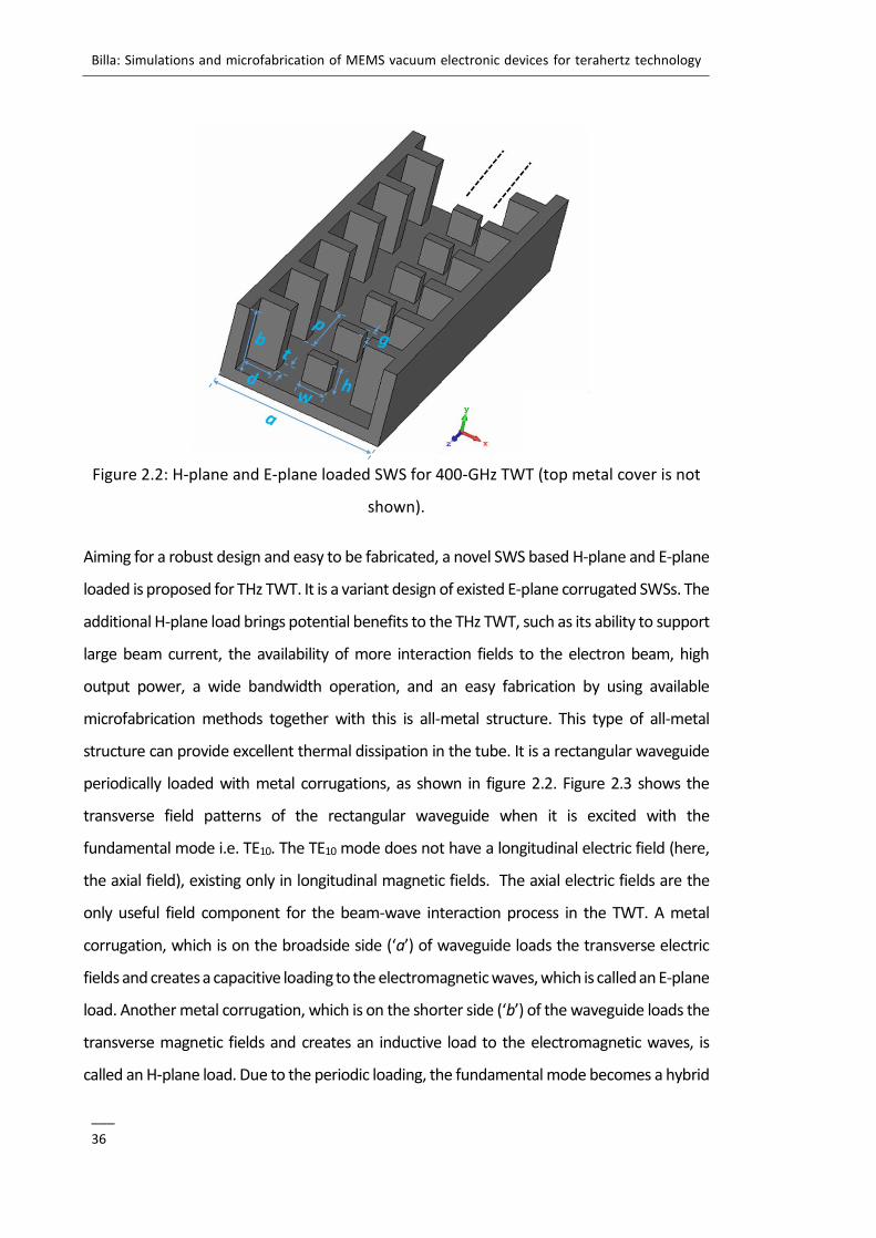
Billa: Simulations and microfabrication of MEMS vacuum electronic devices for terahertz technology
___
36
Figure 2.2: H-plane and E-plane loaded SWS for 400-GHz TWT (top metal cover is not
shown).
Aiming for a robust design and easy to be fabricated, a novel SWS based H-plane and E-plane
loaded is proposed for THz TWT. It is a variant design of existed E-plane corrugated SWSs. The
additional H-plane load brings potential benefits to the THz TWT, such as its ability to support
large beam current, the availability of more interaction fields to the electron beam, high
output power, a wide bandwidth operation, and an easy fabrication by using available
microfabrication methods together with this is all-metal structure. This type of all-metal
structure can provide excellent thermal dissipation in the tube. It is a rectangular waveguide
periodically loaded with metal corrugations, as shown in figure 2.2. Figure 2.3 shows the
transverse field patterns of the rectangular waveguide when it is excited with the
fundamental mode i.e. TE10. The TE10 mode does not have a longitudinal electric field (here,
the axial field), existing only in longitudinal magnetic fields. The axial electric fields are the
only useful field component for the beam-wave interaction process in the TWT. A metal
corrugation, which is on the broadside side (‘a’) of waveguide loads the transverse electric
fields and creates a capacitive loading to the electromagnetic waves, which is called an E-plane
load. Another metal corrugation, which is on the shorter side (‘b’) of the waveguide loads the
transverse magnetic fields and creates an inductive load to the electromagnetic waves, is
called an H-plane load. Due to the periodic loading, the fundamental mode becomes a hybrid
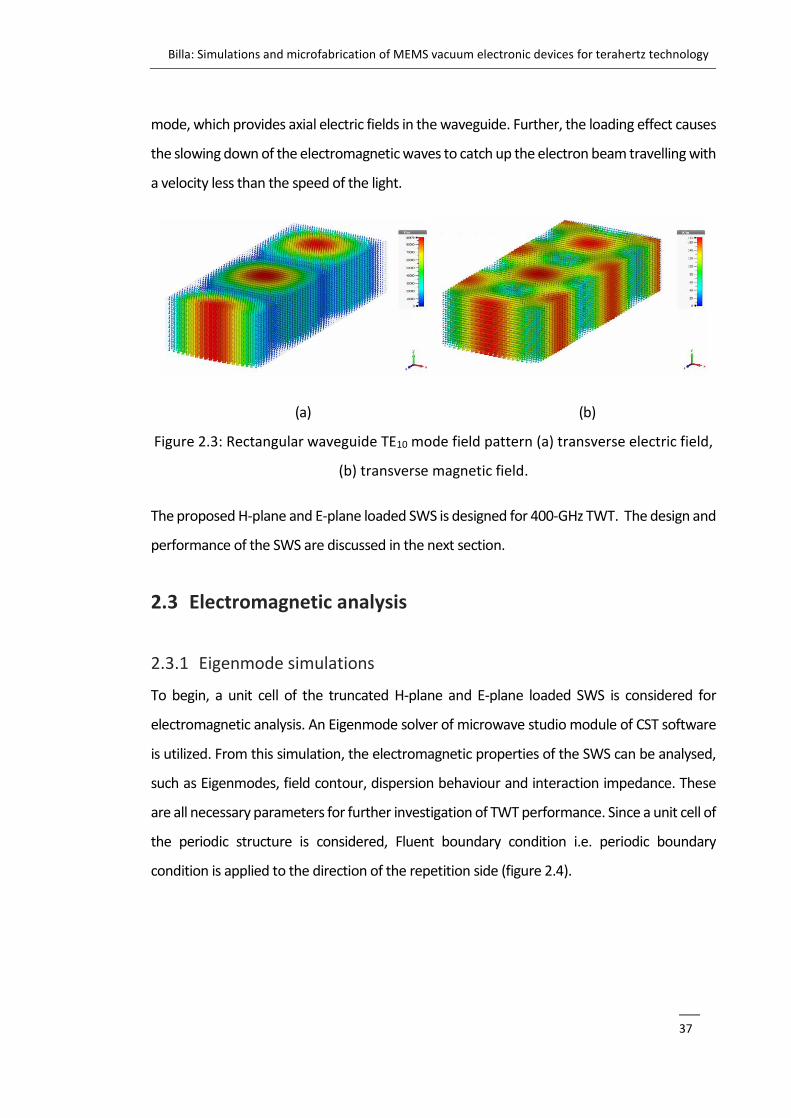
Billa: Simulations and microfabrication of MEMS vacuum electronic devices for terahertz technology
___
37
mode, which provides axial electric fields in the waveguide. Further, the loading effect causes
the slowing down of the electromagnetic waves to catch up the electron beam travelling with
a velocity less than the speed of the light.
(a) (b)
Figure 2.3: Rectangular waveguide TE10 mode field pattern (a) transverse electric field,
(b) transverse magnetic field.
The proposed H-plane and E-plane loaded SWS is designed for 400-GHz TWT. The design and
performance of the SWS are discussed in the next section.
2.3 Electromagnetic analysis
2.3.1 Eigenmode simulations
To begin, a unit cell of the truncated H-plane and E-plane loaded SWS is considered for
electromagnetic analysis. An Eigenmode solver of microwave studio module of CST software
is utilized. From this simulation, the electromagnetic properties of the SWS can be analysed,
such as Eigenmodes, field contour, dispersion behaviour and interaction impedance. These
are all necessary parameters for further investigation of TWT performance. Since a unit cell of
the periodic structure is considered, Fluent boundary condition i.e. periodic boundary
condition is applied to the direction of the repetition side (figure 2.4).
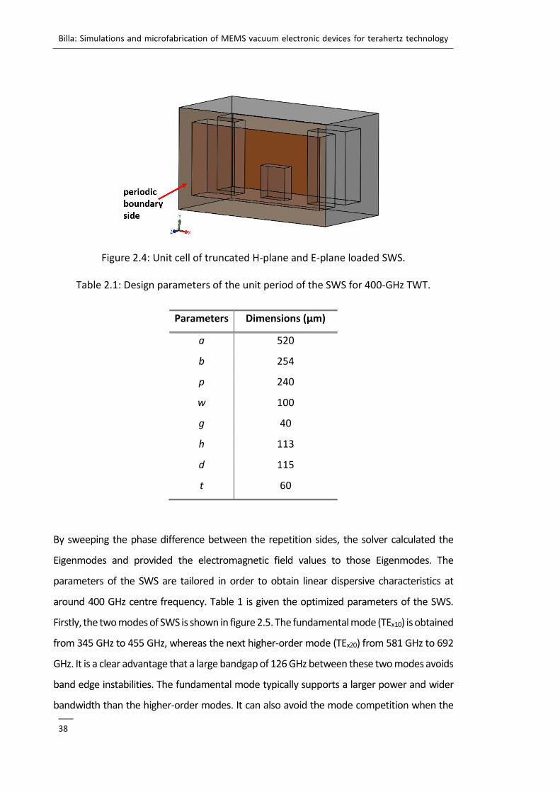
Billa: Simulations and microfabrication of MEMS vacuum electronic devices for terahertz technology
___
38
Figure 2.4: Unit cell of truncated H-plane and E-plane loaded SWS.
Table 2.1: Design parameters of the unit period of the SWS for 400-GHz TWT.
Parameters Dimensions (µm)
a 520
b 254
p 240
w 100
g 40
h 113
d 115
t 60
By sweeping the phase difference between the repetition sides, the solver calculated the
Eigenmodes and provided the electromagnetic field values to those Eigenmodes. The
parameters of the SWS are tailored in order to obtain linear dispersive characteristics at
around 400 GHz centre frequency. Table 1 is given the optimized parameters of the SWS.
Firstly, the two modes of SWS is shown in figure 2.5. The fundamental mode (TEx10) is obtained
from 345 GHz to 455 GHz, whereas the next higher-order mode (TEx20) from 581 GHz to 692
GHz. It is a clear advantage that a large bandgap of 126 GHz between these two modes avoids
band edge instabilities. The fundamental mode typically supports a larger power and wider
bandwidth than the higher-order modes. It can also avoid the mode competition when the
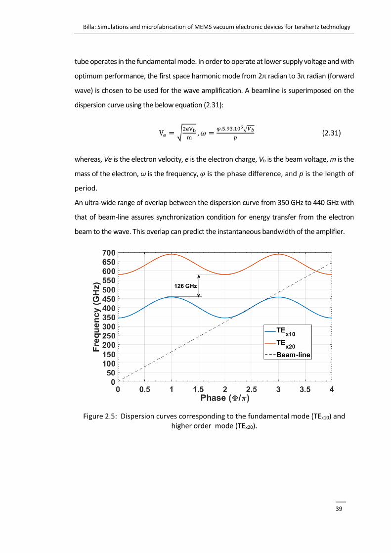
Billa: Simulations and microfabrication of MEMS vacuum electronic devices for terahertz technology
___
39
tube operates in the fundamental mode. In order to operate at lower supply voltage and with
optimum performance, the first space harmonic mode from 2π radian to 3π radian (forward
wave) is chosen to be used for the wave amplification. A beamline is superimposed on the
dispersion curve using the below equation (2.31):
Ve = √2eVb
m, 𝜔 =
𝜑.5.93.105√𝑉𝑏
𝑝 (2.31)
whereas, Ve is the electron velocity, e is the electron charge, Vb is the beam voltage, m is the
mass of the electron, ω is the frequency, 𝜑 is the phase difference, and p is the length of
period.
An ultra-wide range of overlap between the dispersion curve from 350 GHz to 440 GHz with
that of beam-line assures synchronization condition for energy transfer from the electron
beam to the wave. This overlap can predict the instantaneous bandwidth of the amplifier.
Figure 2.5: Dispersion curves corresponding to the fundamental mode (TEx10) and higher order mode (TEx20).
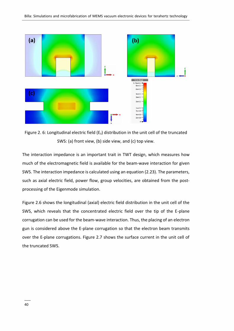
Billa: Simulations and microfabrication of MEMS vacuum electronic devices for terahertz technology
___
40
Figure 2. 6: Longitudinal electric field (Ez) distribution in the unit cell of the truncated
SWS: (a) front view, (b) side view, and (c) top view.
The interaction impedance is an important trait in TWT design, which measures how
much of the electromagnetic field is available for the beam-wave interaction for given
SWS. The interaction impedance is calculated using an equation (2.23). The parameters,
such as axial electric field, power flow, group velocities, are obtained from the post-
processing of the Eigenmode simulation.
Figure 2.6 shows the longitudinal (axial) electric field distribution in the unit cell of the
SWS, which reveals that the concentrated electric field over the tip of the E-plane
corrugation can be used for the beam-wave interaction. Thus, the placing of an electron
gun is considered above the E-plane corrugation so that the electron beam transmits
over the E-plane corrugations. Figure 2.7 shows the surface current in the unit cell of
the truncated SWS.
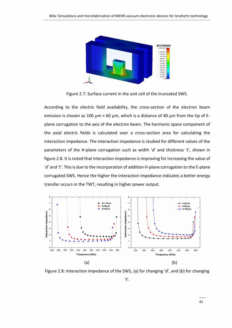
Billa: Simulations and microfabrication of MEMS vacuum electronic devices for terahertz technology
___
41
Figure 2.7: Surface current in the unit cell of the truncated SWS.
According to the electric field availability, the cross-section of the electron beam
emission is chosen as 100 µm × 60 µm, which is a distance of 40 µm from the tip of E-
plane corrugation to the axis of the electron beam. The harmonic space component of
the axial electric fields is calculated over a cross-section area for calculating the
interaction impedance. The interaction impedance is studied for different values of the
parameters of the H-plane corrugation such as width ‘d’ and thickness ‘t’, shown in
figure 2.8. It is noted that interaction impedance is improving for increasing the value of
‘d’ and ‘t’. This is due to the incorporation of addition H-plane corrugation to the E-plane
corrugated SWS. Hence the higher the interaction impedance indicates a better energy
transfer occurs in the TWT, resulting in higher power output.
(a) (b)
Figure 2.8: Interaction impedance of the SWS, (a) for changing ‘d’, and (b) for changing
‘t’.
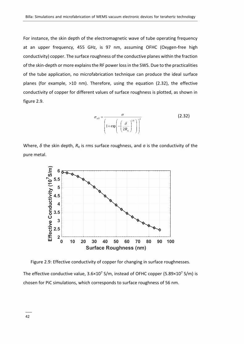
Billa: Simulations and microfabrication of MEMS vacuum electronic devices for terahertz technology
___
42
For instance, the skin depth of the electromagnetic wave of tube operating frequency
at an upper frequency, 455 GHz, is 97 nm, assuming OFHC (Oxygen-free high
conductivity) copper. The surface roughness of the conductive planes within the fraction
of the skin-depth or more explains the RF power loss in the SWS. Due to the practicalities
of the tube application, no microfabrication technique can produce the ideal surface
planes (for example, >10 nm). Therefore, using the equation (2.32), the effective
conductivity of copper for different values of surface roughness is plotted, as shown in
figure 2.9.
2
6.1eff
2
exp1
−+
=
qR
(2.32)
Where, δ the skin depth, Rq is rms surface roughness, and σ is the conductivity of the
pure metal.
Figure 2.9: Effective conductivity of copper for changing in surface roughnesses.
The effective conductive value, 3.6×10⁷ S/m, instead of OFHC copper (5.89×10⁷ S/m) is
chosen for PiC simulations, which corresponds to surface roughness of 56 nm.
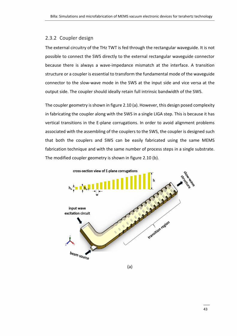
Billa: Simulations and microfabrication of MEMS vacuum electronic devices for terahertz technology
___
43
2.3.2 Coupler design
The external circuitry of the THz TWT is fed through the rectangular waveguide. It is not
possible to connect the SWS directly to the external rectangular waveguide connector
because there is always a wave-impedance mismatch at the interface. A transition
structure or a coupler is essential to transform the fundamental mode of the waveguide
connector to the slow-wave mode in the SWS at the input side and vice versa at the
output side. The coupler should ideally retain full intrinsic bandwidth of the SWS.
The coupler geometry is shown in figure 2.10 (a). However, this design posed complexity
in fabricating the coupler along with the SWS in a single LIGA step. This is because it has
vertical transitions in the E-plane corrugations. In order to avoid alignment problems
associated with the assembling of the couplers to the SWS, the coupler is designed such
that both the couplers and SWS can be easily fabricated using the same MEMS
fabrication technique and with the same number of process steps in a single substrate.
The modified coupler geometry is shown in figure 2.10 (b).
(a)
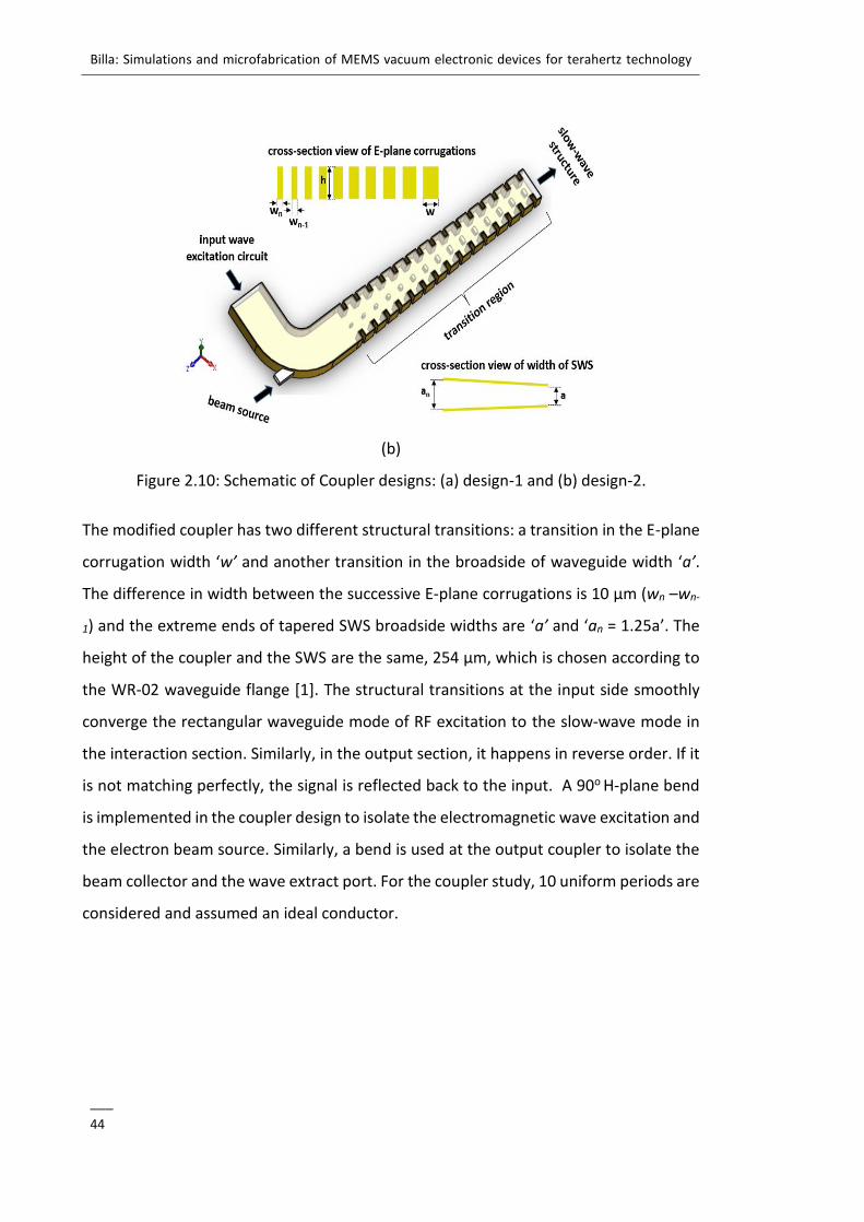
Billa: Simulations and microfabrication of MEMS vacuum electronic devices for terahertz technology
___
44
(b)
Figure 2.10: Schematic of Coupler designs: (a) design-1 and (b) design-2.
The modified coupler has two different structural transitions: a transition in the E-plane
corrugation width ‘w’ and another transition in the broadside of waveguide width ‘a’.
The difference in width between the successive E-plane corrugations is 10 µm (wn –wn-
1) and the extreme ends of tapered SWS broadside widths are ‘a’ and ‘an = 1.25a’. The
height of the coupler and the SWS are the same, 254 µm, which is chosen according to
the WR-02 waveguide flange [1]. The structural transitions at the input side smoothly
converge the rectangular waveguide mode of RF excitation to the slow-wave mode in
the interaction section. Similarly, in the output section, it happens in reverse order. If it
is not matching perfectly, the signal is reflected back to the input. A 90o H-plane bend
is implemented in the coupler design to isolate the electromagnetic wave excitation and
the electron beam source. Similarly, a bend is used at the output coupler to isolate the
beam collector and the wave extract port. For the coupler study, 10 uniform periods are
considered and assumed an ideal conductor.
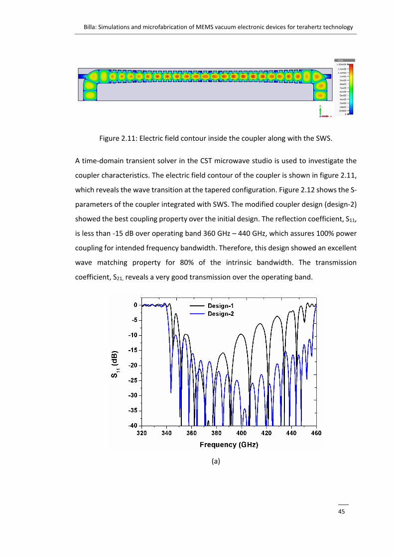
Billa: Simulations and microfabrication of MEMS vacuum electronic devices for terahertz technology
___
45
Figure 2.11: Electric field contour inside the coupler along with the SWS.
A time-domain transient solver in the CST microwave studio is used to investigate the
coupler characteristics. The electric field contour of the coupler is shown in figure 2.11,
which reveals the wave transition at the tapered configuration. Figure 2.12 shows the S-
parameters of the coupler integrated with SWS. The modified coupler design (design-2)
showed the best coupling property over the initial design. The reflection coefficient, S11,
is less than -15 dB over operating band 360 GHz – 440 GHz, which assures 100% power
coupling for intended frequency bandwidth. Therefore, this design showed an excellent
wave matching property for 80% of the intrinsic bandwidth. The transmission
coefficient, S21, reveals a very good transmission over the operating band.
(a)
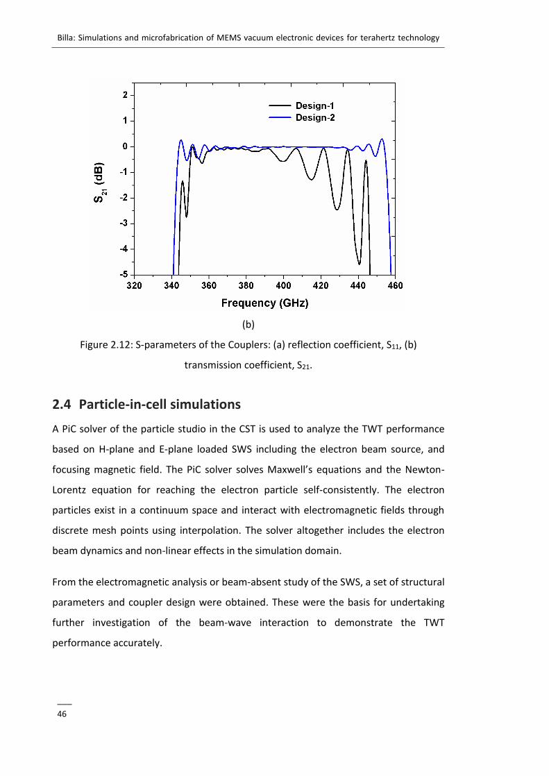
Billa: Simulations and microfabrication of MEMS vacuum electronic devices for terahertz technology
___
46
(b)
Figure 2.12: S-parameters of the Couplers: (a) reflection coefficient, S11, (b)
transmission coefficient, S21.
2.4 Particle-in-cell simulations
A PiC solver of the particle studio in the CST is used to analyze the TWT performance
based on H-plane and E-plane loaded SWS including the electron beam source, and
focusing magnetic field. The PiC solver solves Maxwell’s equations and the Newton-
Lorentz equation for reaching the electron particle self-consistently. The electron
particles exist in a continuum space and interact with electromagnetic fields through
discrete mesh points using interpolation. The solver altogether includes the electron
beam dynamics and non-linear effects in the simulation domain.
From the electromagnetic analysis or beam-absent study of the SWS, a set of structural
parameters and coupler design were obtained. These were the basis for undertaking
further investigation of the beam-wave interaction to demonstrate the TWT
performance accurately.
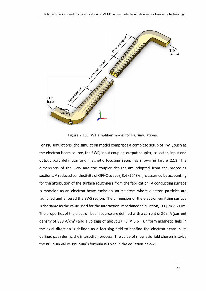
Billa: Simulations and microfabrication of MEMS vacuum electronic devices for terahertz technology
___
47
Figure 2.13: TWT amplifier model for PiC simulations.
For PiC simulations, the simulation model comprises a complete setup of TWT, such as
the electron beam source, the SWS, input coupler, output coupler, collector, input and
output port definition and magnetic focusing setup, as shown in figure 2.13. The
dimensions of the SWS and the coupler designs are adopted from the preceding
sections. A reduced conductivity of OFHC copper, 3.6×10⁷ S/m, is assumed by accounting
for the attribution of the surface roughness from the fabrication. A conducting surface
is modeled as an electron beam emission source from where electron particles are
launched and entered the SWS region. The dimension of the electron-emitting surface
is the same as the value used for the interaction impedance calculation, 100µm × 60µm.
The properties of the electron beam source are defined with a current of 20 mA (current
density of 333 A/cm2) and a voltage of about 17 kV. A 0.6 T uniform magnetic field in
the axial direction is defined as a focusing field to confine the electron beam in its
defined path during the interaction process. The value of magnetic field chosen is twice
the Brillouin value. Brillouin’s formula is given in the equation below:
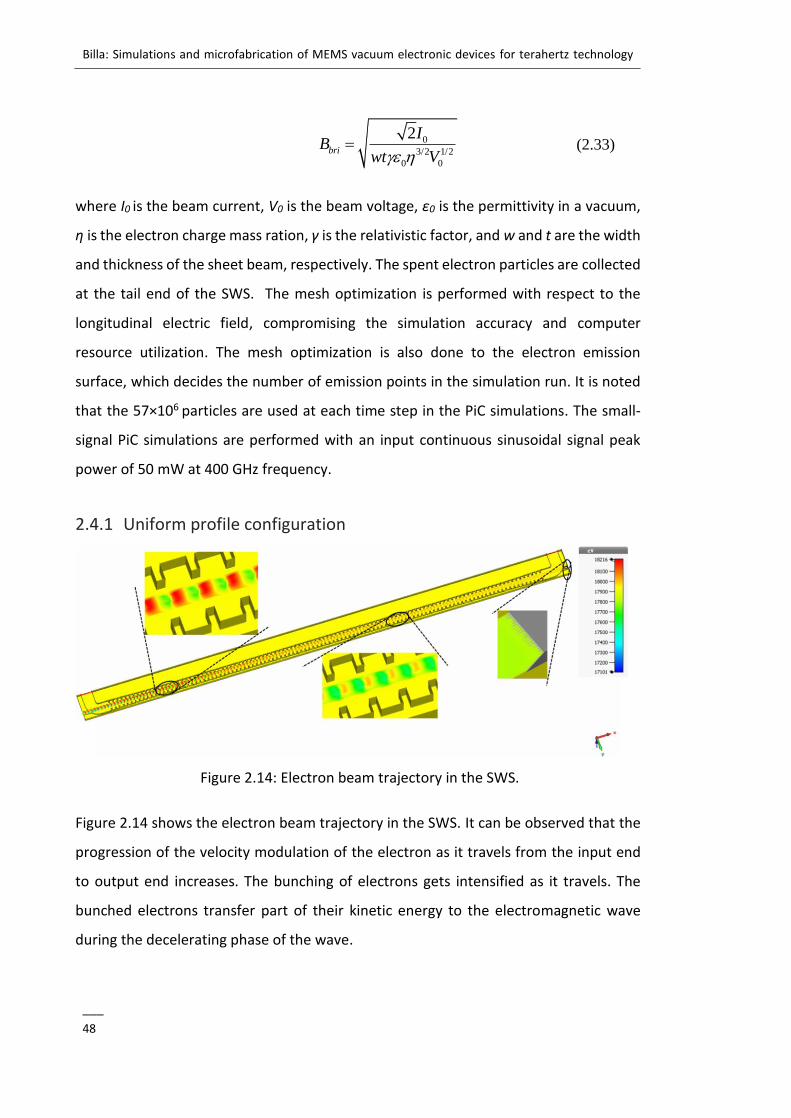
Billa: Simulations and microfabrication of MEMS vacuum electronic devices for terahertz technology
___
48
0
3/2 1/2
0 0
2bri
IB
wt V = (2.33)
where I0 is the beam current, V0 is the beam voltage, ε0 is the permittivity in a vacuum,
η is the electron charge mass ration, γ is the relativistic factor, and w and t are the width
and thickness of the sheet beam, respectively. The spent electron particles are collected
at the tail end of the SWS. The mesh optimization is performed with respect to the
longitudinal electric field, compromising the simulation accuracy and computer
resource utilization. The mesh optimization is also done to the electron emission
surface, which decides the number of emission points in the simulation run. It is noted
that the 57×106 particles are used at each time step in the PiC simulations. The small-
signal PiC simulations are performed with an input continuous sinusoidal signal peak
power of 50 mW at 400 GHz frequency.
2.4.1 Uniform profile configuration
Figure 2.14: Electron beam trajectory in the SWS.
Figure 2.14 shows the electron beam trajectory in the SWS. It can be observed that the
progression of the velocity modulation of the electron as it travels from the input end
to output end increases. The bunching of electrons gets intensified as it travels. The
bunched electrons transfer part of their kinetic energy to the electromagnetic wave
during the decelerating phase of the wave.
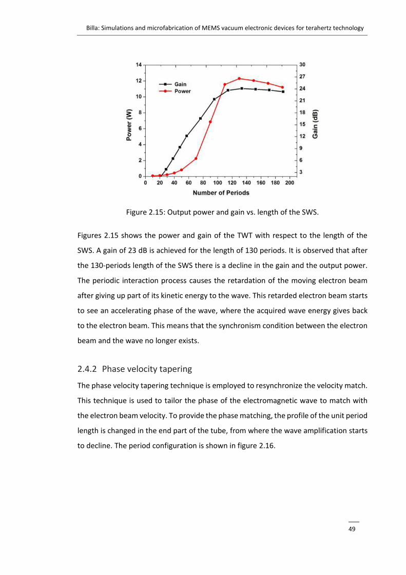
Billa: Simulations and microfabrication of MEMS vacuum electronic devices for terahertz technology
___
49
Figure 2.15: Output power and gain vs. length of the SWS.
Figures 2.15 shows the power and gain of the TWT with respect to the length of the
SWS. A gain of 23 dB is achieved for the length of 130 periods. It is observed that after
the 130-periods length of the SWS there is a decline in the gain and the output power.
The periodic interaction process causes the retardation of the moving electron beam
after giving up part of its kinetic energy to the wave. This retarded electron beam starts
to see an accelerating phase of the wave, where the acquired wave energy gives back
to the electron beam. This means that the synchronism condition between the electron
beam and the wave no longer exists.
2.4.2 Phase velocity tapering
The phase velocity tapering technique is employed to resynchronize the velocity match.
This technique is used to tailor the phase of the electromagnetic wave to match with
the electron beam velocity. To provide the phase matching, the profile of the unit period
length is changed in the end part of the tube, from where the wave amplification starts
to decline. The period configuration is shown in figure 2.16.
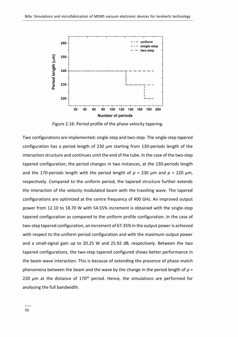
Billa: Simulations and microfabrication of MEMS vacuum electronic devices for terahertz technology
___
50
Figure 2.16: Period profile of the phase velocity tapering.
Two configurations are implemented: single-step and two-step. The single-step tapered
configuration has a period length of 230 μm starting from 130-periods length of the
interaction structure and continues until the end of the tube. In the case of the two-step
tapered configuration, the period changes in two instances, at the 130-periods length
and the 170-periods length with the period length of p = 230 μm and p = 220 μm,
respectively. Compared to the uniform period, the tapered structure further extends
the interaction of the velocity modulated beam with the traveling wave. The tapered
configurations are optimized at the centre frequency of 400 GHz. An improved output
power from 12.10 to 18.70 W with 54.55% increment is obtained with the single-step
tapered configuration as compared to the uniform profile configuration. In the case of
two-step tapered configuration, an increment of 67.35% in the output power is achieved
with respect to the uniform period configuration and with the maximum output power
and a small-signal gain up to 20.25 W and 25.92 dB, respectively. Between the two
tapered configurations, the two-step tapered configured shows better performance in
the beam wave interaction. This is because of extending the presence of phase-match
phenomena between the beam and the wave by the change in the period length of p =
220 μm at the distance of 170th period. Hence, the simulations are performed for
analysing the full bandwidth.
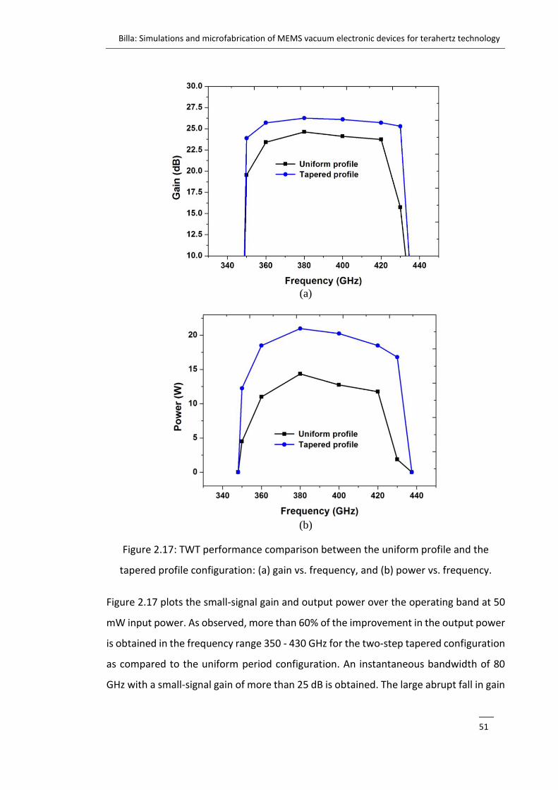
Billa: Simulations and microfabrication of MEMS vacuum electronic devices for terahertz technology
___
51
(a)
(b)
Figure 2.17: TWT performance comparison between the uniform profile and the
tapered profile configuration: (a) gain vs. frequency, and (b) power vs. frequency.
Figure 2.17 plots the small-signal gain and output power over the operating band at 50
mW input power. As observed, more than 60% of the improvement in the output power
is obtained in the frequency range 350 - 430 GHz for the two-step tapered configuration
as compared to the uniform period configuration. An instantaneous bandwidth of 80
GHz with a small-signal gain of more than 25 dB is obtained. The large abrupt fall in gain

Billa: Simulations and microfabrication of MEMS vacuum electronic devices for terahertz technology
___
52
and power of the TWT at the lower and the higher frequencies is due to the mismatch
between the velocity of the beam and the phase velocity of the wave.
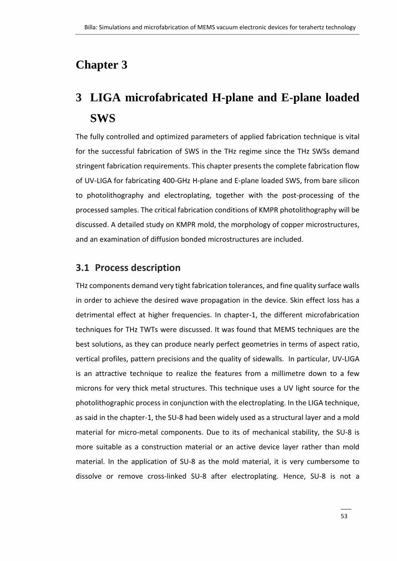
Billa: Simulations and microfabrication of MEMS vacuum electronic devices for terahertz technology
___
53
Chapter 3
3 LIGA microfabricated H-plane and E-plane loaded
SWS
The fully controlled and optimized parameters of applied fabrication technique is vital
for the successful fabrication of SWS in the THz regime since the THz SWSs demand
stringent fabrication requirements. This chapter presents the complete fabrication flow
of UV-LIGA for fabricating 400-GHz H-plane and E-plane loaded SWS, from bare silicon
to photolithography and electroplating, together with the post-processing of the
processed samples. The critical fabrication conditions of KMPR photolithography will be
discussed. A detailed study on KMPR mold, the morphology of copper microstructures,
and an examination of diffusion bonded microstructures are included.
3.1 Process description
THz components demand very tight fabrication tolerances, and fine quality surface walls
in order to achieve the desired wave propagation in the device. Skin effect loss has a
detrimental effect at higher frequencies. In chapter-1, the different microfabrication
techniques for THz TWTs were discussed. It was found that MEMS techniques are the
best solutions, as they can produce nearly perfect geometries in terms of aspect ratio,
vertical profiles, pattern precisions and the quality of sidewalls. In particular, UV-LIGA
is an attractive technique to realize the features from a millimetre down to a few
microns for very thick metal structures. This technique uses a UV light source for the
photolithographic process in conjunction with the electroplating. In the LIGA technique,
as said in the chapter-1, the SU-8 had been widely used as a structural layer and a mold
material for micro-metal components. Due to its of mechanical stability, the SU-8 is
more suitable as a construction material or an active device layer rather than mold
material. In the application of SU-8 as the mold material, it is very cumbersome to
dissolve or remove cross-linked SU-8 after electroplating. Hence, SU-8 is not a
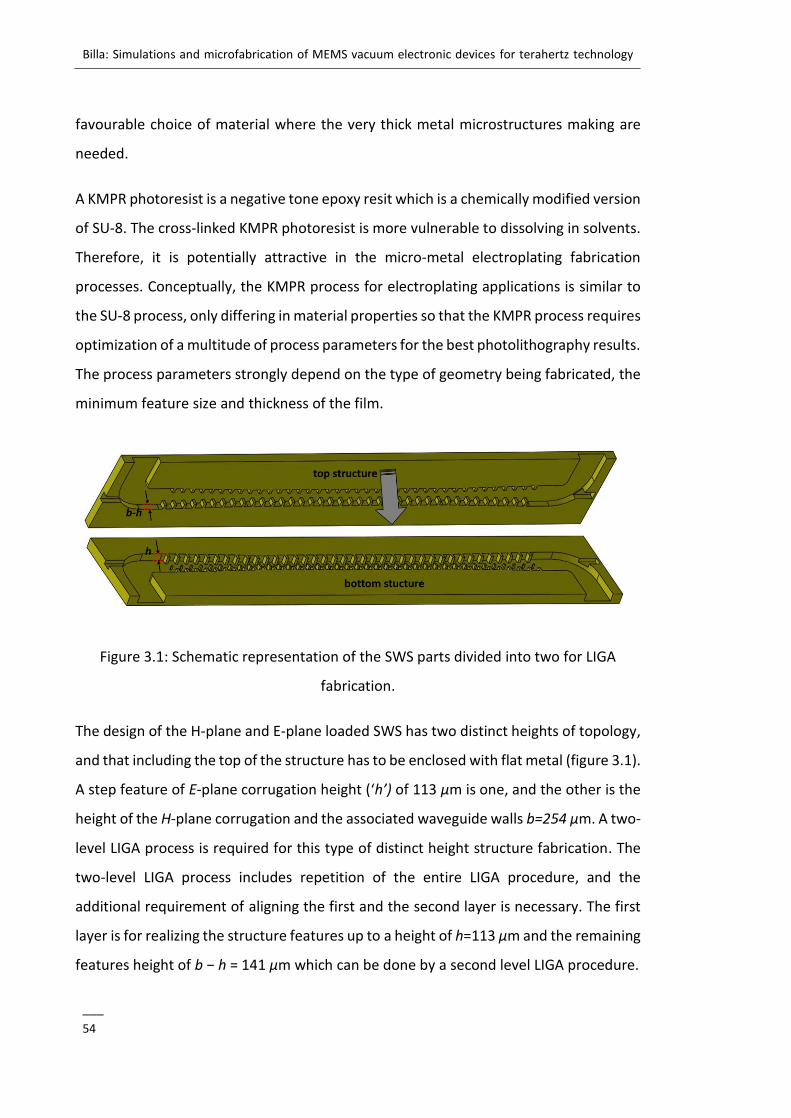
Billa: Simulations and microfabrication of MEMS vacuum electronic devices for terahertz technology
___
54
favourable choice of material where the very thick metal microstructures making are
needed.
A KMPR photoresist is a negative tone epoxy resit which is a chemically modified version
of SU-8. The cross-linked KMPR photoresist is more vulnerable to dissolving in solvents.
Therefore, it is potentially attractive in the micro-metal electroplating fabrication
processes. Conceptually, the KMPR process for electroplating applications is similar to
the SU-8 process, only differing in material properties so that the KMPR process requires
optimization of a multitude of process parameters for the best photolithography results.
The process parameters strongly depend on the type of geometry being fabricated, the
minimum feature size and thickness of the film.
Figure 3.1: Schematic representation of the SWS parts divided into two for LIGA
fabrication.
The design of the H-plane and E-plane loaded SWS has two distinct heights of topology,
and that including the top of the structure has to be enclosed with flat metal (figure 3.1).
A step feature of E-plane corrugation height (‘h’) of 113 μm is one, and the other is the
height of the H-plane corrugation and the associated waveguide walls b=254 μm. A two-
level LIGA process is required for this type of distinct height structure fabrication. The
two-level LIGA process includes repetition of the entire LIGA procedure, and the
additional requirement of aligning the first and the second layer is necessary. The first
layer is for realizing the structure features up to a height of h=113 μm and the remaining
features height of b − h = 141 μm which can be done by a second level LIGA procedure.
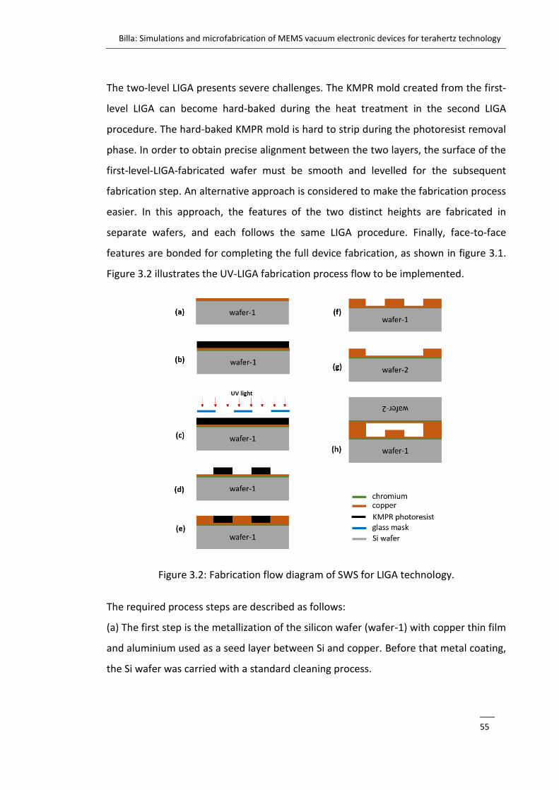
Billa: Simulations and microfabrication of MEMS vacuum electronic devices for terahertz technology
___
55
The two-level LIGA presents severe challenges. The KMPR mold created from the first-
level LIGA can become hard-baked during the heat treatment in the second LIGA
procedure. The hard-baked KMPR mold is hard to strip during the photoresist removal
phase. In order to obtain precise alignment between the two layers, the surface of the
first-level-LIGA-fabricated wafer must be smooth and levelled for the subsequent
fabrication step. An alternative approach is considered to make the fabrication process
easier. In this approach, the features of the two distinct heights are fabricated in
separate wafers, and each follows the same LIGA procedure. Finally, face-to-face
features are bonded for completing the full device fabrication, as shown in figure 3.1.
Figure 3.2 illustrates the UV-LIGA fabrication process flow to be implemented.
Figure 3.2: Fabrication flow diagram of SWS for LIGA technology.
The required process steps are described as follows:
(a) The first step is the metallization of the silicon wafer (wafer-1) with copper thin film
and aluminium used as a seed layer between Si and copper. Before that metal coating,
the Si wafer was carried with a standard cleaning process.
Billa: Simulations and microfabrication of MEMS vacuum electronic devices for terahertz technology
___
56
(b) KMPR photoresist is applied onto the wafer and spun with appropriate speed. The
spin speed is determined by the type of photoresist series used, and the desired
thickness of the film. The Si wafer with deposited photoresist is then subjected to a soft
bake on a levelled hot plate to drive off the solvent.
(c) The KMPR photoresist is then exposed under UV light through a glass mask that
defines a 2-D pattern of the SWS. By projecting UV light, the pattern is transferred from
the mask to the photoresist.
(d) A post-exposure bake process, typically for the negative photoresist, is performed to
produce cross-linking reactions. These cross-linked regions will be insoluble in the
developer. Development is then employed to remove unwanted KMPR.
(e) The electroplating experiment is conducted to deposit metal around the open region
of the mold and up to the height of the mold. The processed wafer was diced, and the
individual dices were lapped and polished to the desired thickness.
(f) Then the KMPR is etched from the electroplated samples to obtain the bottom metal
structure of the SWS.
(g) The steps from (a) to (f) are repeated on another Si wafer (wafer-2) with a different
photomask, which has 2D patterns of the top structure of the SWS.
(h) Diffusion bonding is employed to attach the top and bottom structures of the SWS
to realize the full device.
3.2 Fabrication conditions
The process parameters of KMPR lithography are quite different from the protocols
suggested by the manufacturer. The parameters are totally dependent on the geometry
of the structure, cleanroom conditions and equipment used. In this section, detailed
process conditions are discussed.
3.2.1 KMPR process
Particle-free wafer surfaces is an essential requisite for successful fabrication.
Therefore, before the KMPR process begins, wafer pre-treatment must be carried out.
Wafers were first cleaned with solvents to rid of the organic residues and later treated
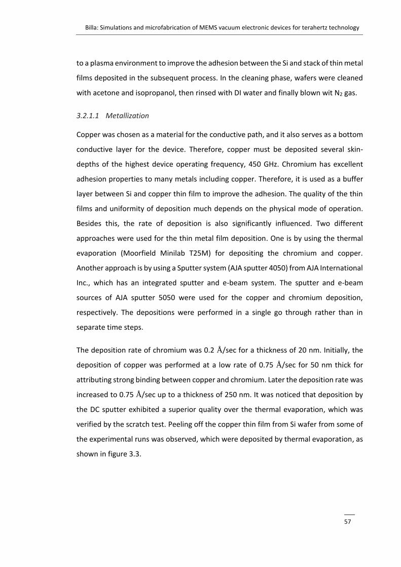
Billa: Simulations and microfabrication of MEMS vacuum electronic devices for terahertz technology
___
57
to a plasma environment to improve the adhesion between the Si and stack of thin metal
films deposited in the subsequent process. In the cleaning phase, wafers were cleaned
with acetone and isopropanol, then rinsed with DI water and finally blown wit N2 gas.
3.2.1.1 Metallization
Copper was chosen as a material for the conductive path, and it also serves as a bottom
conductive layer for the device. Therefore, copper must be deposited several skin-
depths of the highest device operating frequency, 450 GHz. Chromium has excellent
adhesion properties to many metals including copper. Therefore, it is used as a buffer
layer between Si and copper thin film to improve the adhesion. The quality of the thin
films and uniformity of deposition much depends on the physical mode of operation.
Besides this, the rate of deposition is also significantly influenced. Two different
approaches were used for the thin metal film deposition. One is by using the thermal
evaporation (Moorfield Minilab T25M) for depositing the chromium and copper.
Another approach is by using a Sputter system (AJA sputter 4050) from AJA International
Inc., which has an integrated sputter and e-beam system. The sputter and e-beam
sources of AJA sputter 5050 were used for the copper and chromium deposition,
respectively. The depositions were performed in a single go through rather than in
separate time steps.
The deposition rate of chromium was 0.2 Å/sec for a thickness of 20 nm. Initially, the
deposition of copper was performed at a low rate of 0.75 Å/sec for 50 nm thick for
attributing strong binding between copper and chromium. Later the deposition rate was
increased to 0.75 Å/sec up to a thickness of 250 nm. It was noticed that deposition by
the DC sputter exhibited a superior quality over the thermal evaporation, which was
verified by the scratch test. Peeling off the copper thin film from Si wafer from some of
the experimental runs was observed, which were deposited by thermal evaporation, as
shown in figure 3.3.
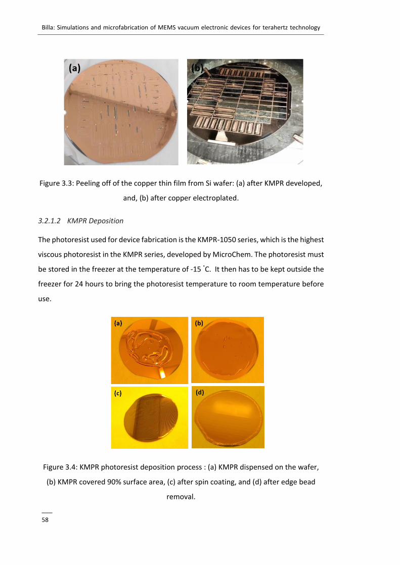
Billa: Simulations and microfabrication of MEMS vacuum electronic devices for terahertz technology
___
58
Figure 3.3: Peeling off of the copper thin film from Si wafer: (a) after KMPR developed,
and, (b) after copper electroplated.
3.2.1.2 KMPR Deposition
The photoresist used for device fabrication is the KMPR-1050 series, which is the highest
viscous photoresist in the KMPR series, developed by MicroChem. The photoresist must
be stored in the freezer at the temperature of -15 °C. It then has to be kept outside the
freezer for 24 hours to bring the photoresist temperature to room temperature before
use.
Figure 3.4: KMPR photoresist deposition process : (a) KMPR dispensed on the wafer,
(b) KMPR covered 90% surface area, (c) after spin coating, and (d) after edge bead
removal.
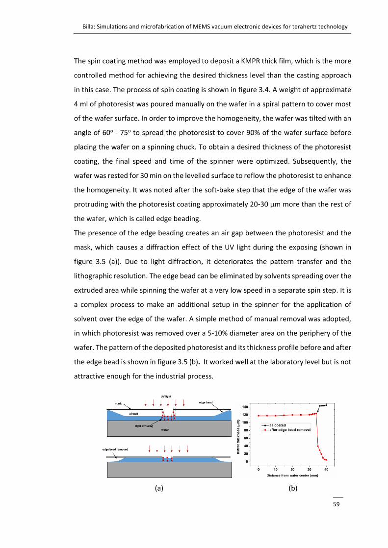
Billa: Simulations and microfabrication of MEMS vacuum electronic devices for terahertz technology
___
59
The spin coating method was employed to deposit a KMPR thick film, which is the more
controlled method for achieving the desired thickness level than the casting approach
in this case. The process of spin coating is shown in figure 3.4. A weight of approximate
4 ml of photoresist was poured manually on the wafer in a spiral pattern to cover most
of the wafer surface. In order to improve the homogeneity, the wafer was tilted with an
angle of 60o - 75o to spread the photoresist to cover 90% of the wafer surface before
placing the wafer on a spinning chuck. To obtain a desired thickness of the photoresist
coating, the final speed and time of the spinner were optimized. Subsequently, the
wafer was rested for 30 min on the levelled surface to reflow the photoresist to enhance
the homogeneity. It was noted after the soft-bake step that the edge of the wafer was
protruding with the photoresist coating approximately 20-30 µm more than the rest of
the wafer, which is called edge beading.
The presence of the edge beading creates an air gap between the photoresist and the
mask, which causes a diffraction effect of the UV light during the exposing (shown in
figure 3.5 (a)). Due to light diffraction, it deteriorates the pattern transfer and the
lithographic resolution. The edge bead can be eliminated by solvents spreading over the
extruded area while spinning the wafer at a very low speed in a separate spin step. It is
a complex process to make an additional setup in the spinner for the application of
solvent over the edge of the wafer. A simple method of manual removal was adopted,
in which photoresist was removed over a 5-10% diameter area on the periphery of the
wafer. The pattern of the deposited photoresist and its thickness profile before and after
the edge bead is shown in figure 3.5 (b). It worked well at the laboratory level but is not
attractive enough for the industrial process.
(a) (b)
Billa: Simulations and microfabrication of MEMS vacuum electronic devices for terahertz technology
___
60
Figure 3.5: KMPR film thickness study with edge bead and with EBR: (a) Light diffusion
effect, and (b) edge bead effect from spin coating for 120µm thick KMPR film.
A single spin deposition was used for the bottom structure of the SWS, to obtain a 120
µm thick film. For the top structure of the SWS, a double spin deposition was used to
obtain a 150 µm thick film, which is a stack of 30 µm and 120 µm film thicknesses. The
spin parameters are summarized in Table 3.2.
Table 3.2: Spin parameters for the bottom and top structures of the SWS.
Deposition method Final spin parameters Structure
Speed (rpm) Time (sec)
Single deposition 1100 30 bottom structure
Double deposition 3600 30 top structure
1100 30
3.2.1.3 Soft-bake
As the coated photoresist film is wet, it must be baked to evaporate the solvent content.
The right amount of solvent content is required to avoid adhesion to the contact mask
during the UV exposure and to enhance the photolithography performance by reducing
the diffusion of the photo-initiator. A two-level procedure of baking was adapted unlike
the one temperature level recommended by the manufacturer. In the first step, the
photoresist is baked at 65 °C for a short duration to reflow the photoresist for improving
the homogeneity. The second step baking was done at 95 °C for a more extended period
to evaporate the solvents. Following this, the wafer was allowed to cool down for 30
min until it reached room temperature, which helps the photoresist be dried and the
diffusion of heat in the photoresist. The peeling of the photoresist mold was observed
during the development step when the wafer was baked longer than the sufficient time
due to the contest of solvents being too low, as shown in figure 3.3(a). On the other
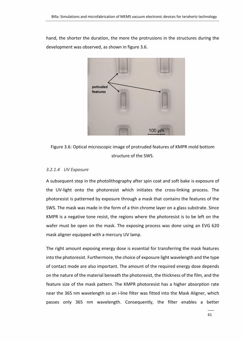
Billa: Simulations and microfabrication of MEMS vacuum electronic devices for terahertz technology
___
61
hand, the shorter the duration, the more the protrusions in the structures during the
development was observed, as shown in figure 3.6.
Figure 3.6: Optical microscopic image of protruded features of KMPR mold bottom
structure of the SWS.
3.2.1.4 UV Exposure
A subsequent step in the photolithography after spin coat and soft bake is exposure of
the UV-light onto the photoresist which initiates the cross-linking process. The
photoresist is patterned by exposure through a mask that contains the features of the
SWS. The mask was made in the form of a thin chrome layer on a glass substrate. Since
KMPR is a negative tone resist, the regions where the photoresist is to be left on the
wafer must be open on the mask. The exposing process was done using an EVG 620
mask aligner equipped with a mercury UV lamp.
The right amount exposing energy dose is essential for transferring the mask features
into the photoresist. Furthermore, the choice of exposure light wavelength and the type
of contact mode are also important. The amount of the required energy dose depends
on the nature of the material beneath the photoresist, the thickness of the film, and the
feature size of the mask pattern. The KMPR photoresist has a higher absorption rate
near the 365 nm wavelength so an i-line filter was fitted into the Mask Aligner, which
passes only 365 nm wavelength. Consequently, the filter enables a better
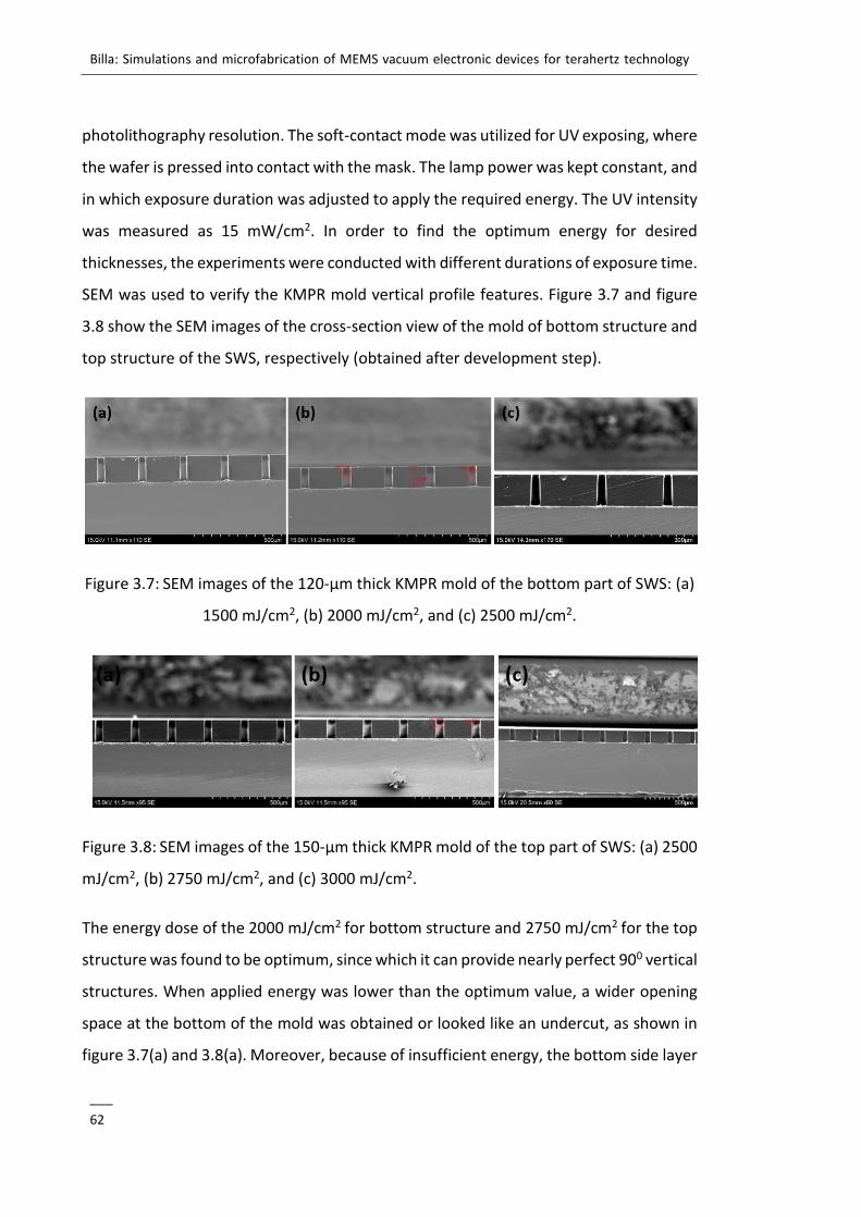
Billa: Simulations and microfabrication of MEMS vacuum electronic devices for terahertz technology
___
62
photolithography resolution. The soft-contact mode was utilized for UV exposing, where
the wafer is pressed into contact with the mask. The lamp power was kept constant, and
in which exposure duration was adjusted to apply the required energy. The UV intensity
was measured as 15 mW/cm2. In order to find the optimum energy for desired
thicknesses, the experiments were conducted with different durations of exposure time.
SEM was used to verify the KMPR mold vertical profile features. Figure 3.7 and figure
3.8 show the SEM images of the cross-section view of the mold of bottom structure and
top structure of the SWS, respectively (obtained after development step).
Figure 3.7: SEM images of the 120-µm thick KMPR mold of the bottom part of SWS: (a)
1500 mJ/cm2, (b) 2000 mJ/cm2, and (c) 2500 mJ/cm2.
Figure 3.8: SEM images of the 150-µm thick KMPR mold of the top part of SWS: (a) 2500
mJ/cm2, (b) 2750 mJ/cm2, and (c) 3000 mJ/cm2.
The energy dose of the 2000 mJ/cm2 for bottom structure and 2750 mJ/cm2 for the top
structure was found to be optimum, since which it can provide nearly perfect 900 vertical
structures. When applied energy was lower than the optimum value, a wider opening
space at the bottom of the mold was obtained or looked like an undercut, as shown in
figure 3.7(a) and 3.8(a). Moreover, because of insufficient energy, the bottom side layer
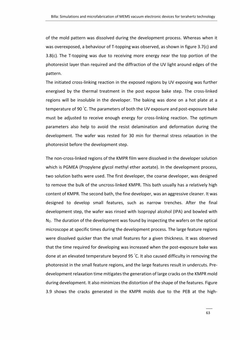
Billa: Simulations and microfabrication of MEMS vacuum electronic devices for terahertz technology
___
63
of the mold pattern was dissolved during the development process. Whereas when it
was overexposed, a behaviour of T-topping was observed, as shown in figure 3.7(c) and
3.8(c). The T-topping was due to receiving more energy near the top portion of the
photoresist layer than required and the diffraction of the UV light around edges of the
pattern.
The initiated cross-linking reaction in the exposed regions by UV exposing was further
energised by the thermal treatment in the post expose bake step. The cross-linked
regions will be insoluble in the developer. The baking was done on a hot plate at a
temperature of 90 °C. The parameters of both the UV exposure and post-exposure bake
must be adjusted to receive enough energy for cross-linking reaction. The optimum
parameters also help to avoid the resist delamination and deformation during the
development. The wafer was rested for 30 min for thermal stress relaxation in the
photoresist before the development step.
The non-cross-linked regions of the KMPR film were dissolved in the developer solution
which is PGMEA (Propylene glycol methyl ether acetate). In the development process,
two solution baths were used. The first developer, the coarse developer, was designed
to remove the bulk of the uncross-linked KMPR. This bath usually has a relatively high
content of KMPR. The second bath, the fine developer, was an aggressive cleaner. It was
designed to develop small features, such as narrow trenches. After the final
development step, the wafer was rinsed with Isopropyl alcohol (IPA) and bowled with
N2. The duration of the development was found by inspecting the wafers on the optical
microscope at specific times during the development process. The large feature regions
were dissolved quicker than the small features for a given thickness. It was observed
that the time required for developing was increased when the post-exposure bake was
done at an elevated temperature beyond 95 °C. It also caused difficulty in removing the
photoresist in the small feature regions, and the large features result in undercuts. Pre-
development relaxation time mitigates the generation of large cracks on the KMPR mold
during development. It also minimizes the distortion of the shape of the features. Figure
3.9 shows the cracks generated in the KMPR molds due to the PEB at the high-
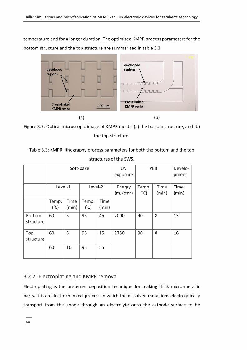
Billa: Simulations and microfabrication of MEMS vacuum electronic devices for terahertz technology
___
64
temperature and for a longer duration. The optimized KMPR process parameters for the
bottom structure and the top structure are summarized in table 3.3.
(a) (b)
Figure 3.9: Optical microscopic image of KMPR molds: (a) the bottom structure, and (b)
the top structure.
Table 3.3: KMPR lithography process parameters for both the bottom and the top
structures of the SWS.
Soft-bake UV exposure
PEB Develo- pment
Level-1 Level-2 Energy (mJ/cm2)
Temp. (°C)
Time (min)
Time (min)
Temp. (°C)
Time (min)
Temp. (°C)
Time (min)
Bottom structure
60 5 95 45 2000 90 8 13
Top structure
60 5 95 15 2750 90 8 16
60 10 95 55
3.2.2 Electroplating and KMPR removal
Electroplating is the preferred deposition technique for making thick micro-metallic
parts. It is an electrochemical process in which the dissolved metal ions electrolytically
transport from the anode through an electrolyte onto the cathode surface to be
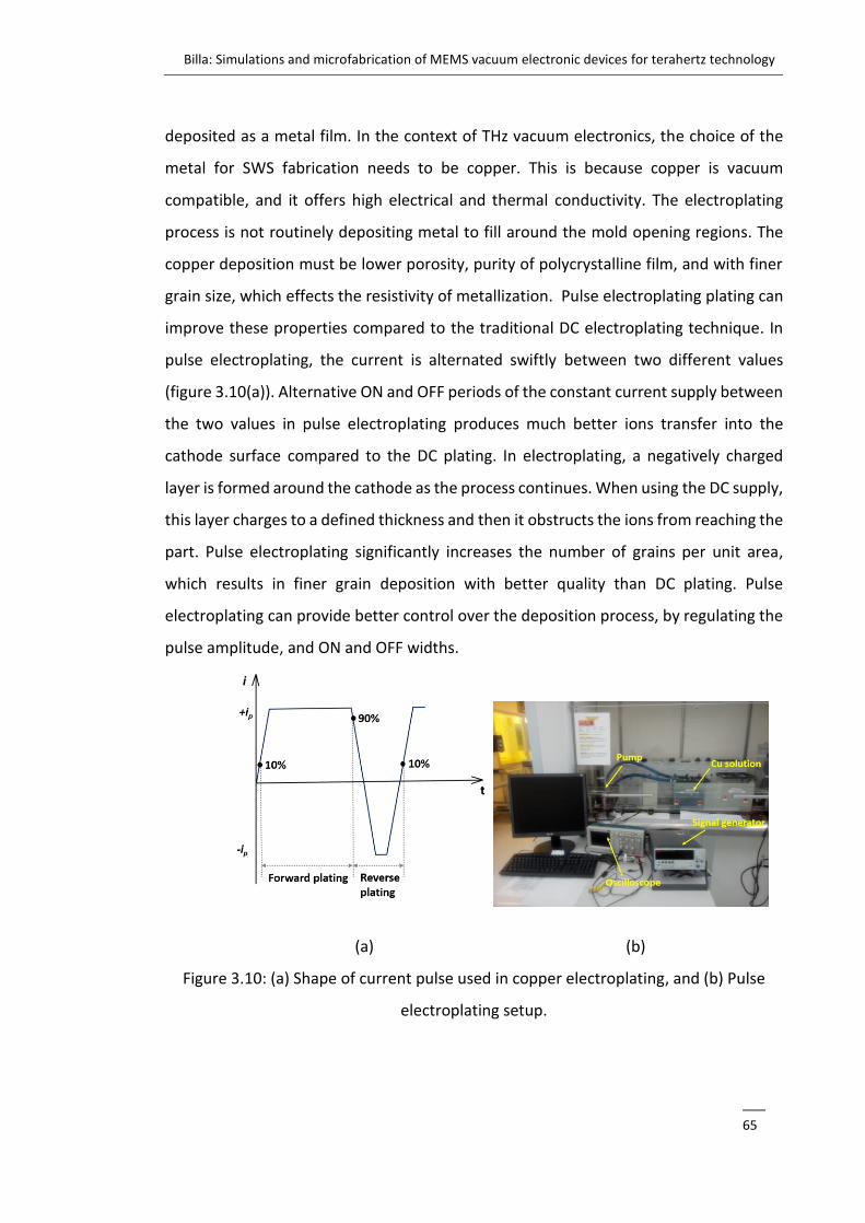
Billa: Simulations and microfabrication of MEMS vacuum electronic devices for terahertz technology
___
65
deposited as a metal film. In the context of THz vacuum electronics, the choice of the
metal for SWS fabrication needs to be copper. This is because copper is vacuum
compatible, and it offers high electrical and thermal conductivity. The electroplating
process is not routinely depositing metal to fill around the mold opening regions. The
copper deposition must be lower porosity, purity of polycrystalline film, and with finer
grain size, which effects the resistivity of metallization. Pulse electroplating plating can
improve these properties compared to the traditional DC electroplating technique. In
pulse electroplating, the current is alternated swiftly between two different values
(figure 3.10(a)). Alternative ON and OFF periods of the constant current supply between
the two values in pulse electroplating produces much better ions transfer into the
cathode surface compared to the DC plating. In electroplating, a negatively charged
layer is formed around the cathode as the process continues. When using the DC supply,
this layer charges to a defined thickness and then it obstructs the ions from reaching the
part. Pulse electroplating significantly increases the number of grains per unit area,
which results in finer grain deposition with better quality than DC plating. Pulse
electroplating can provide better control over the deposition process, by regulating the
pulse amplitude, and ON and OFF widths.
(a) (b)
Figure 3.10: (a) Shape of current pulse used in copper electroplating, and (b) Pulse
electroplating setup.
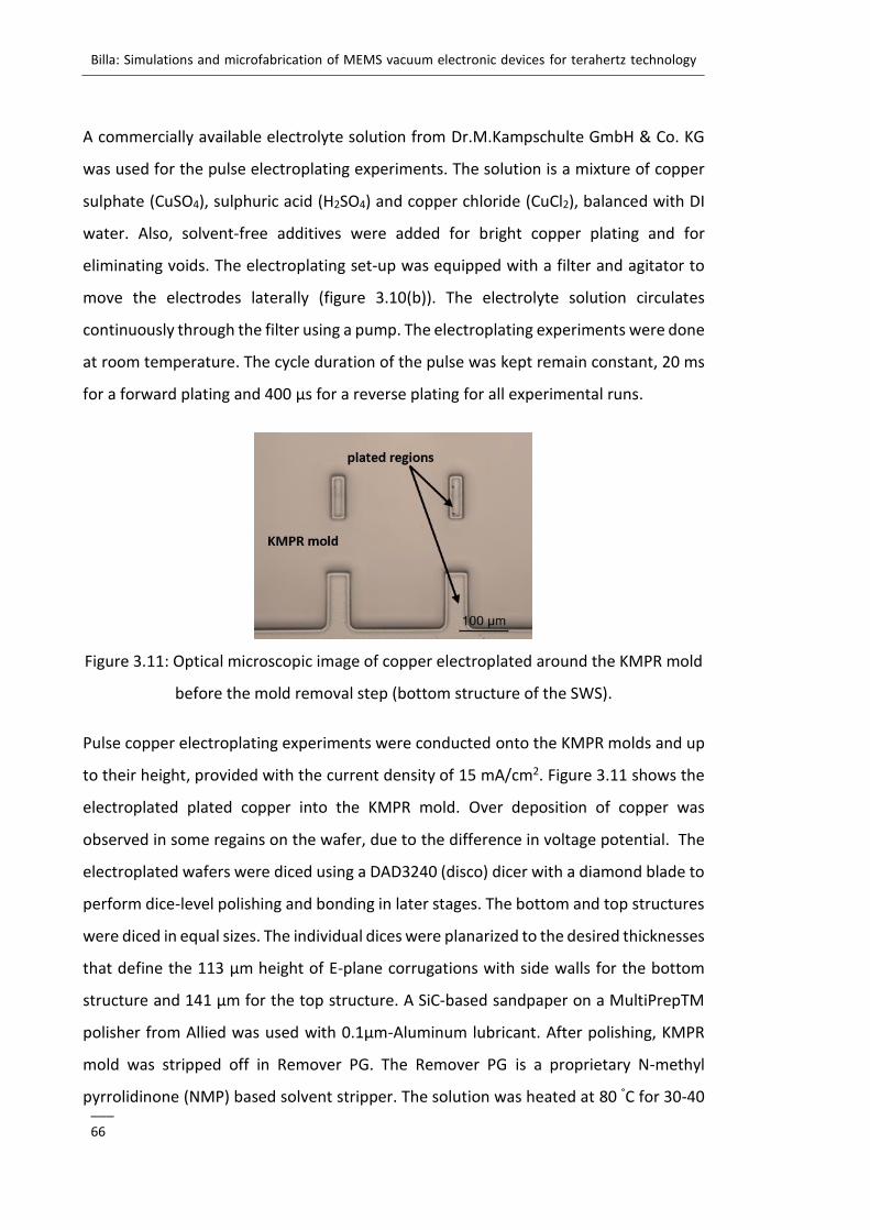
Billa: Simulations and microfabrication of MEMS vacuum electronic devices for terahertz technology
___
66
A commercially available electrolyte solution from Dr.M.Kampschulte GmbH & Co. KG
was used for the pulse electroplating experiments. The solution is a mixture of copper
sulphate (CuSO4), sulphuric acid (H2SO4) and copper chloride (CuCl2), balanced with DI
water. Also, solvent-free additives were added for bright copper plating and for
eliminating voids. The electroplating set-up was equipped with a filter and agitator to
move the electrodes laterally (figure 3.10(b)). The electrolyte solution circulates
continuously through the filter using a pump. The electroplating experiments were done
at room temperature. The cycle duration of the pulse was kept remain constant, 20 ms
for a forward plating and 400 µs for a reverse plating for all experimental runs.
Figure 3.11: Optical microscopic image of copper electroplated around the KMPR mold
before the mold removal step (bottom structure of the SWS).
Pulse copper electroplating experiments were conducted onto the KMPR molds and up
to their height, provided with the current density of 15 mA/cm2. Figure 3.11 shows the
electroplated plated copper into the KMPR mold. Over deposition of copper was
observed in some regains on the wafer, due to the difference in voltage potential. The
electroplated wafers were diced using a DAD3240 (disco) dicer with a diamond blade to
perform dice-level polishing and bonding in later stages. The bottom and top structures
were diced in equal sizes. The individual dices were planarized to the desired thicknesses
that define the 113 µm height of E-plane corrugations with side walls for the bottom
structure and 141 µm for the top structure. A SiC-based sandpaper on a MultiPrepTM
polisher from Allied was used with 0.1µm-Aluminum lubricant. After polishing, KMPR
mold was stripped off in Remover PG. The Remover PG is a proprietary N-methyl
pyrrolidinone (NMP) based solvent stripper. The solution was heated at 80 °C for 30-40
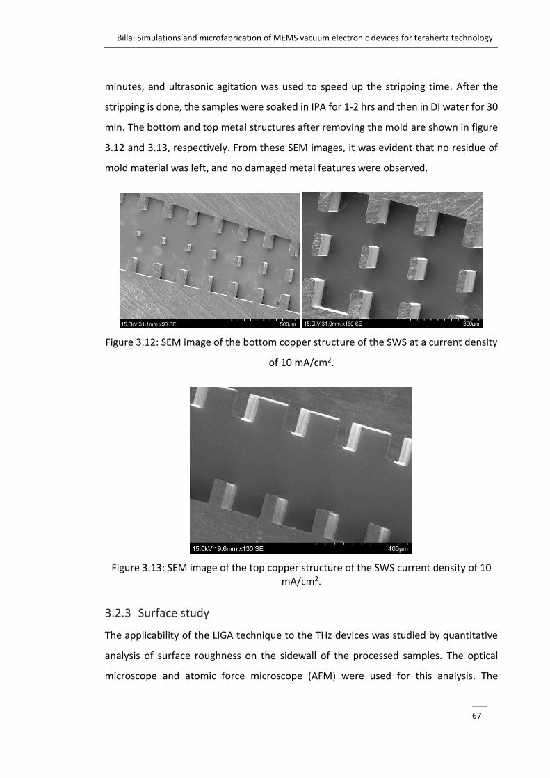
Billa: Simulations and microfabrication of MEMS vacuum electronic devices for terahertz technology
___
67
minutes, and ultrasonic agitation was used to speed up the stripping time. After the
stripping is done, the samples were soaked in IPA for 1-2 hrs and then in DI water for 30
min. The bottom and top metal structures after removing the mold are shown in figure
3.12 and 3.13, respectively. From these SEM images, it was evident that no residue of
mold material was left, and no damaged metal features were observed.
Figure 3.12: SEM image of the bottom copper structure of the SWS at a current density
of 10 mA/cm2.
Figure 3.13: SEM image of the top copper structure of the SWS current density of 10 mA/cm2.
3.2.3 Surface study
The applicability of the LIGA technique to the THz devices was studied by quantitative
analysis of surface roughness on the sidewall of the processed samples. The optical
microscope and atomic force microscope (AFM) were used for this analysis. The
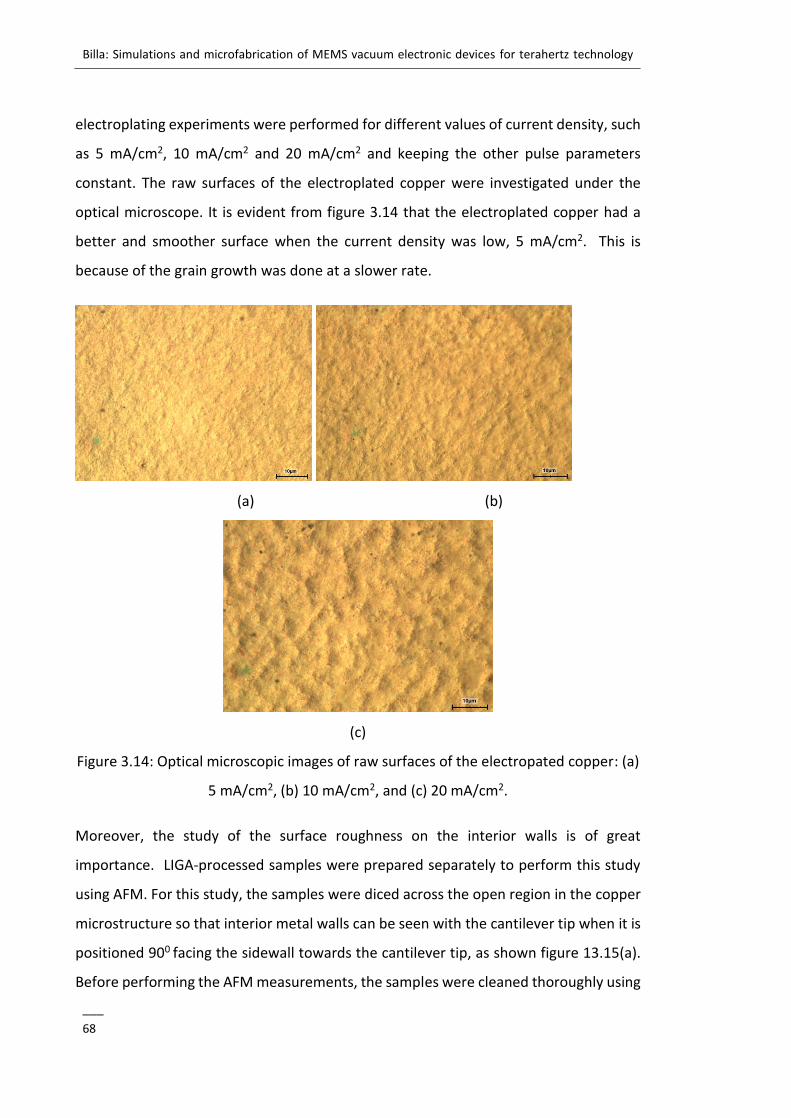
Billa: Simulations and microfabrication of MEMS vacuum electronic devices for terahertz technology
___
68
electroplating experiments were performed for different values of current density, such
as 5 mA/cm2, 10 mA/cm2 and 20 mA/cm2 and keeping the other pulse parameters
constant. The raw surfaces of the electroplated copper were investigated under the
optical microscope. It is evident from figure 3.14 that the electroplated copper had a
better and smoother surface when the current density was low, 5 mA/cm2. This is
because of the grain growth was done at a slower rate.
(a) (b)
(c)
Figure 3.14: Optical microscopic images of raw surfaces of the electropated copper: (a)
5 mA/cm2, (b) 10 mA/cm2, and (c) 20 mA/cm2.
Moreover, the study of the surface roughness on the interior walls is of great
importance. LIGA-processed samples were prepared separately to perform this study
using AFM. For this study, the samples were diced across the open region in the copper
microstructure so that interior metal walls can be seen with the cantilever tip when it is
positioned 900 facing the sidewall towards the cantilever tip, as shown figure 13.15(a).
Before performing the AFM measurements, the samples were cleaned thoroughly using
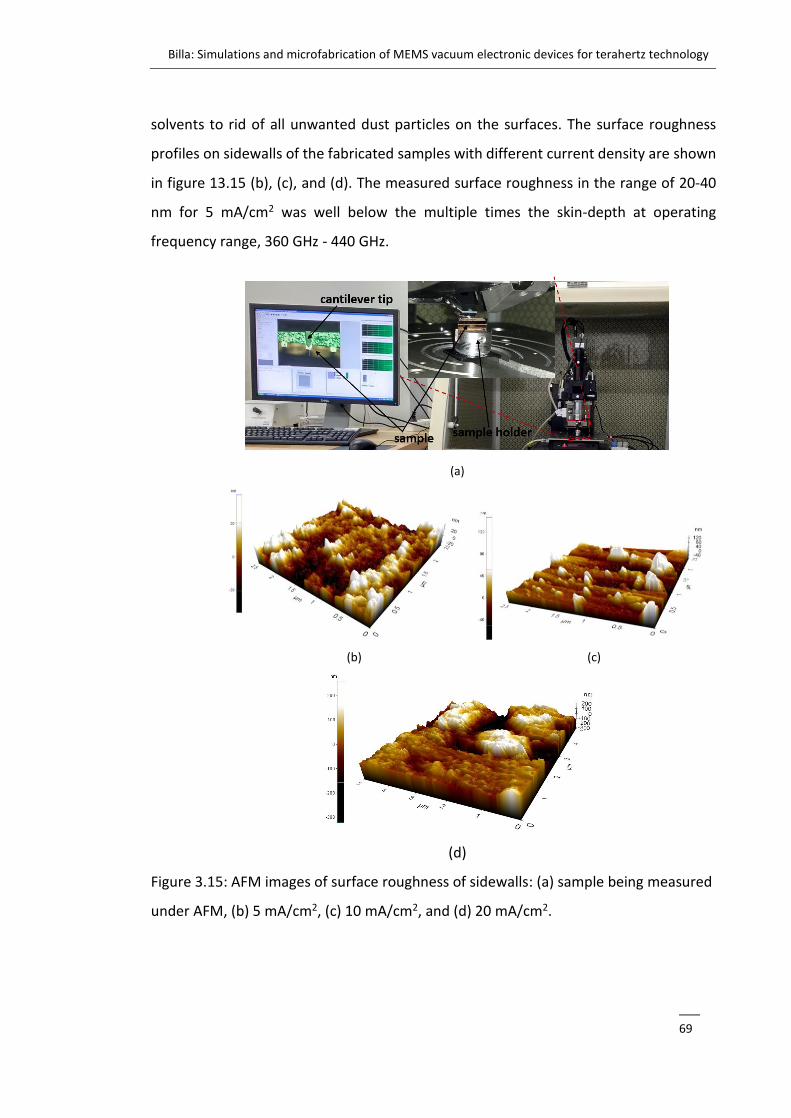
Billa: Simulations and microfabrication of MEMS vacuum electronic devices for terahertz technology
___
69
solvents to rid of all unwanted dust particles on the surfaces. The surface roughness
profiles on sidewalls of the fabricated samples with different current density are shown
in figure 13.15 (b), (c), and (d). The measured surface roughness in the range of 20-40
nm for 5 mA/cm2 was well below the multiple times the skin-depth at operating
frequency range, 360 GHz - 440 GHz.
(a)
(b) (c)
(d)
Figure 3.15: AFM images of surface roughness of sidewalls: (a) sample being measured
under AFM, (b) 5 mA/cm2, (c) 10 mA/cm2, and (d) 20 mA/cm2.
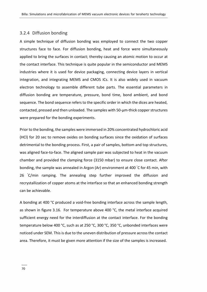
Billa: Simulations and microfabrication of MEMS vacuum electronic devices for terahertz technology
___
70
3.2.4 Diffusion bonding
A simple technique of diffusion bonding was employed to connect the two copper
structures face to face. For diffusion bonding, heat and force were simultaneously
applied to bring the surfaces in contact; thereby causing an atomic motion to occur at
the contact interface. This technique is quite popular in the semiconductor and MEMS
industries where it is used for device packaging, connecting device layers in vertical
integration, and integrating MEMS and CMOS ICs. It is also widely used in vacuum
electron technology to assemble different tube parts. The essential parameters in
diffusion bonding are temperature, pressure, bond time, bond ambient, and bond
sequence. The bond sequence refers to the specific order in which the dices are heated,
contacted, pressed and then unloaded. The samples with 50-µm-thick copper structures
were prepared for the bonding experiments.
Prior to the bonding, the samples were immersed in 20% concentrated hydrochloric acid
(HCl) for 20 sec to remove oxides on bonding surfaces since the oxidation of surfaces
detrimental to the bonding process. First, a pair of samples, bottom and top structures,
was aligned face-to-face. The aligned sample pair was subjected to heat in the vacuum
chamber and provided the clamping force (3150 mbar) to ensure close contact. After
bonding, the sample was annealed in Argon (Ar) environment at 400 °C for 45 min, with
26 °C/min ramping. The annealing step further improved the diffusion and
recrystallization of copper atoms at the interface so that an enhanced bonding strength
can be achievable.
A bonding at 400 °C produced a void-free bonding interface across the sample length,
as shown in figure 3.16. For temperature above 400 °C, the metal interface acquired
sufficient energy need for the interdiffusion at the contact interface. For the bonding
temperature below 400 °C, such as at 250 °C, 300 °C, 350 °C, unbonded interfaces were
noticed under SEM. This is due to the uneven distribution of pressure across the contact
area. Therefore, it must be given more attention if the size of the samples is increased.
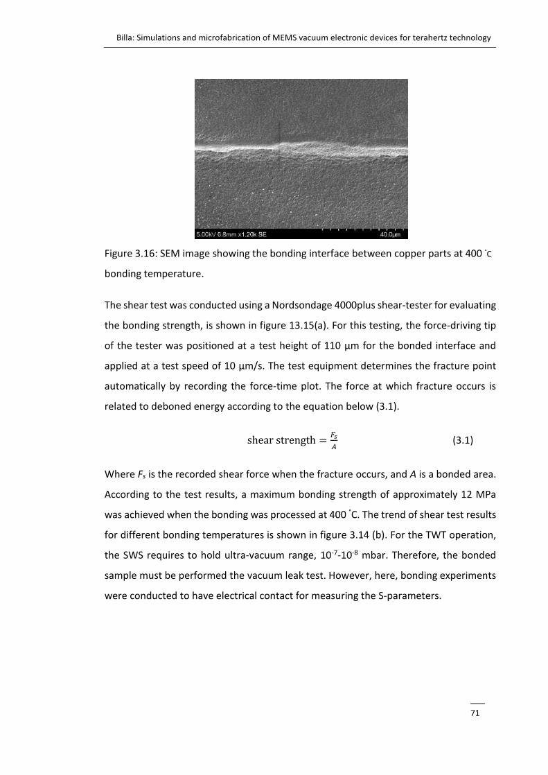
Billa: Simulations and microfabrication of MEMS vacuum electronic devices for terahertz technology
___
71
Figure 3.16: SEM image showing the bonding interface between copper parts at 400 °C
bonding temperature.
The shear test was conducted using a Nordsondage 4000plus shear-tester for evaluating
the bonding strength, is shown in figure 13.15(a). For this testing, the force-driving tip
of the tester was positioned at a test height of 110 µm for the bonded interface and
applied at a test speed of 10 µm/s. The test equipment determines the fracture point
automatically by recording the force-time plot. The force at which fracture occurs is
related to deboned energy according to the equation below (3.1).
shear strength =𝐹𝑠
𝐴 (3.1)
Where Fs is the recorded shear force when the fracture occurs, and A is a bonded area.
According to the test results, a maximum bonding strength of approximately 12 MPa
was achieved when the bonding was processed at 400 °C. The trend of shear test results
for different bonding temperatures is shown in figure 3.14 (b). For the TWT operation,
the SWS requires to hold ultra-vacuum range, 10-7-10-8 mbar. Therefore, the bonded
sample must be performed the vacuum leak test. However, here, bonding experiments
were conducted to have electrical contact for measuring the S-parameters.
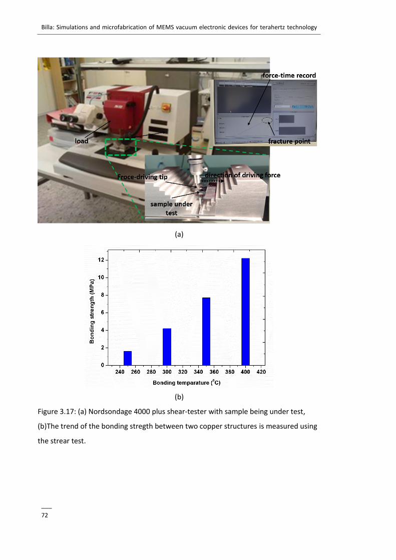
Billa: Simulations and microfabrication of MEMS vacuum electronic devices for terahertz technology
___
72
(a)
(b)
Figure 3.17: (a) Nordsondage 4000 plus shear-tester with sample being under test,
(b)The trend of the bonding stregth between two copper structures is measured using
the strear test.
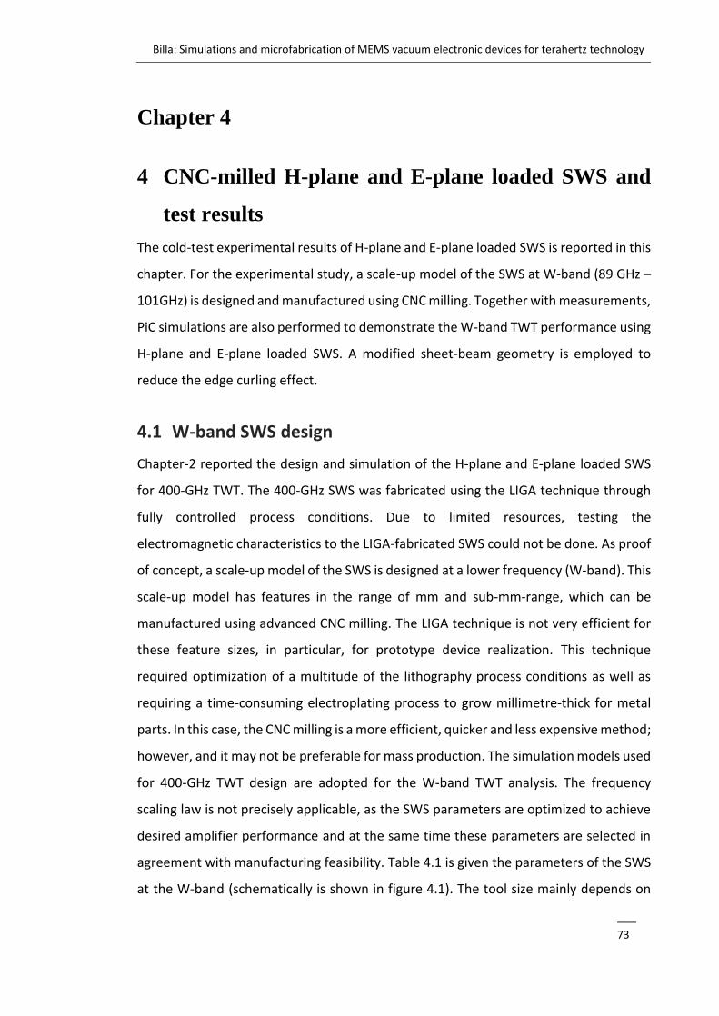
Billa: Simulations and microfabrication of MEMS vacuum electronic devices for terahertz technology
___
73
Chapter 4
4 CNC-milled H-plane and E-plane loaded SWS and
test results
The cold-test experimental results of H-plane and E-plane loaded SWS is reported in this
chapter. For the experimental study, a scale-up model of the SWS at W-band (89 GHz –
101GHz) is designed and manufactured using CNC milling. Together with measurements,
PiC simulations are also performed to demonstrate the W-band TWT performance using
H-plane and E-plane loaded SWS. A modified sheet-beam geometry is employed to
reduce the edge curling effect.
4.1 W-band SWS design
Chapter-2 reported the design and simulation of the H-plane and E-plane loaded SWS
for 400-GHz TWT. The 400-GHz SWS was fabricated using the LIGA technique through
fully controlled process conditions. Due to limited resources, testing the
electromagnetic characteristics to the LIGA-fabricated SWS could not be done. As proof
of concept, a scale-up model of the SWS is designed at a lower frequency (W-band). This
scale-up model has features in the range of mm and sub-mm-range, which can be
manufactured using advanced CNC milling. The LIGA technique is not very efficient for
these feature sizes, in particular, for prototype device realization. This technique
required optimization of a multitude of the lithography process conditions as well as
requiring a time-consuming electroplating process to grow millimetre-thick for metal
parts. In this case, the CNC milling is a more efficient, quicker and less expensive method;
however, and it may not be preferable for mass production. The simulation models used
for 400-GHz TWT design are adopted for the W-band TWT analysis. The frequency
scaling law is not precisely applicable, as the SWS parameters are optimized to achieve
desired amplifier performance and at the same time these parameters are selected in
agreement with manufacturing feasibility. Table 4.1 is given the parameters of the SWS
at the W-band (schematically is shown in figure 4.1). The tool size mainly depends on
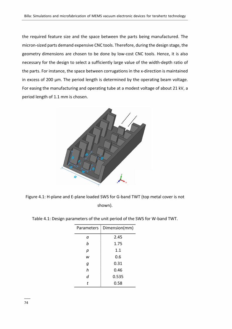
Billa: Simulations and microfabrication of MEMS vacuum electronic devices for terahertz technology
___
74
the required feature size and the space between the parts being manufactured. The
micron-sized parts demand expensive CNC tools. Therefore, during the design stage, the
geometry dimensions are chosen to be done by low-cost CNC tools. Hence, it is also
necessary for the design to select a sufficiently large value of the width-depth ratio of
the parts. For instance, the space between corrugations in the x-direction is maintained
in excess of 200 µm. The period length is determined by the operating beam voltage.
For easing the manufacturing and operating tube at a modest voltage of about 21 kV, a
period length of 1.1 mm is chosen.
Figure 4.1: H-plane and E-plane loaded SWS for G-band TWT (top metal cover is not
shown).
Table 4.1: Design parameters of the unit period of the SWS for W-band TWT.
Parameters Dimension(mm)
a 2.45
b 1.75
p 1.1
w 0.6
g 0.31
h 0.46
d 0.535
t 0.58
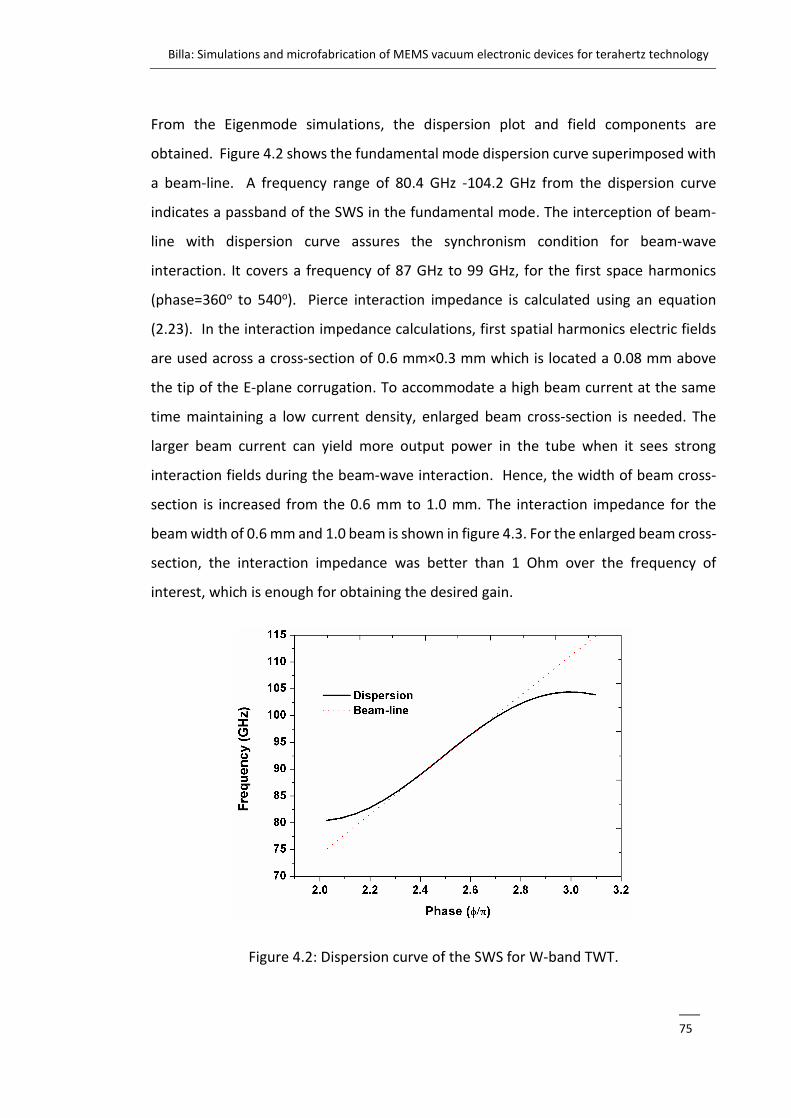
Billa: Simulations and microfabrication of MEMS vacuum electronic devices for terahertz technology
___
75
From the Eigenmode simulations, the dispersion plot and field components are
obtained. Figure 4.2 shows the fundamental mode dispersion curve superimposed with
a beam-line. A frequency range of 80.4 GHz -104.2 GHz from the dispersion curve
indicates a passband of the SWS in the fundamental mode. The interception of beam-
line with dispersion curve assures the synchronism condition for beam-wave
interaction. It covers a frequency of 87 GHz to 99 GHz, for the first space harmonics
(phase=360o to 540o). Pierce interaction impedance is calculated using an equation
(2.23). In the interaction impedance calculations, first spatial harmonics electric fields
are used across a cross-section of 0.6 mm×0.3 mm which is located a 0.08 mm above
the tip of the E-plane corrugation. To accommodate a high beam current at the same
time maintaining a low current density, enlarged beam cross-section is needed. The
larger beam current can yield more output power in the tube when it sees strong
interaction fields during the beam-wave interaction. Hence, the width of beam cross-
section is increased from the 0.6 mm to 1.0 mm. The interaction impedance for the
beam width of 0.6 mm and 1.0 beam is shown in figure 4.3. For the enlarged beam cross-
section, the interaction impedance was better than 1 Ohm over the frequency of
interest, which is enough for obtaining the desired gain.
Figure 4.2: Dispersion curve of the SWS for W-band TWT.
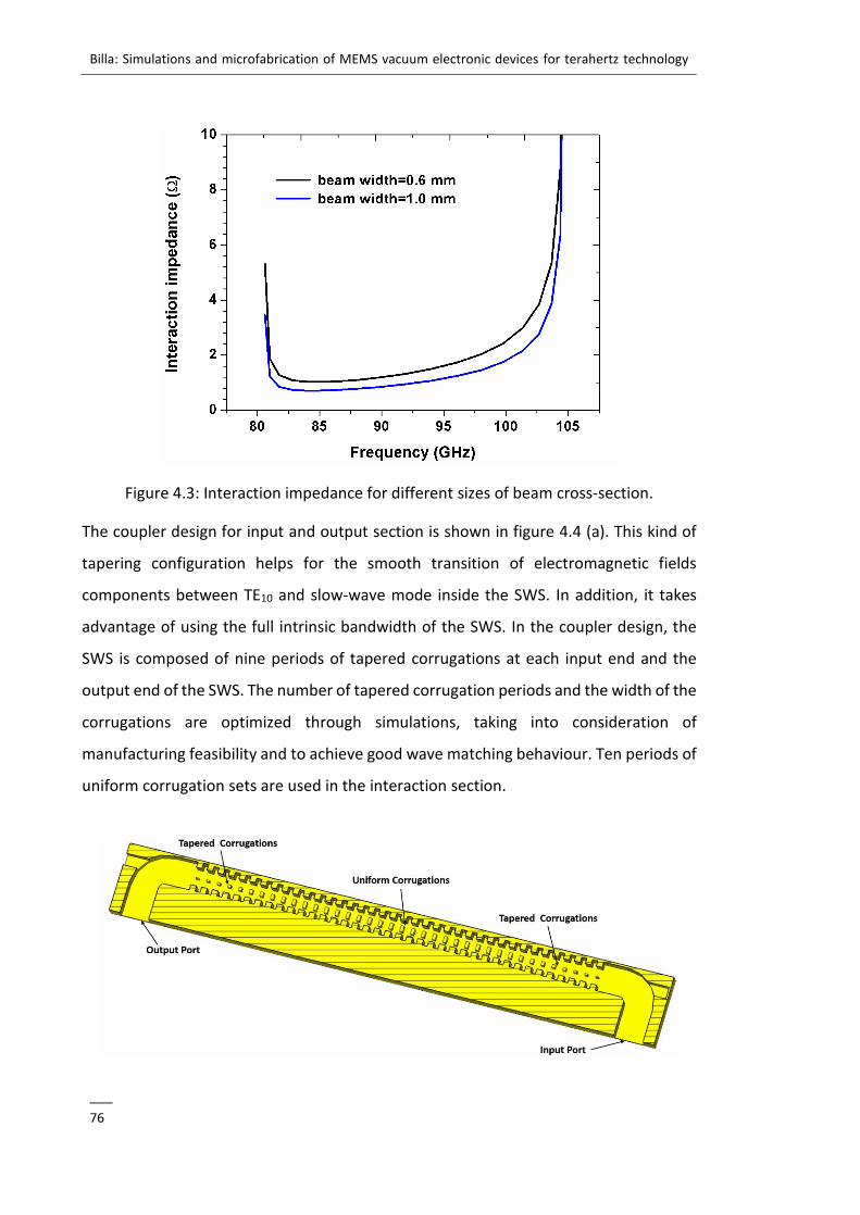
Billa: Simulations and microfabrication of MEMS vacuum electronic devices for terahertz technology
___
76
Figure 4.3: Interaction impedance for different sizes of beam cross-section.
The coupler design for input and output section is shown in figure 4.4 (a). This kind of
tapering configuration helps for the smooth transition of electromagnetic fields
components between TE10 and slow-wave mode inside the SWS. In addition, it takes
advantage of using the full intrinsic bandwidth of the SWS. In the coupler design, the
SWS is composed of nine periods of tapered corrugations at each input end and the
output end of the SWS. The number of tapered corrugation periods and the width of the
corrugations are optimized through simulations, taking into consideration of
manufacturing feasibility and to achieve good wave matching behaviour. Ten periods of
uniform corrugation sets are used in the interaction section.
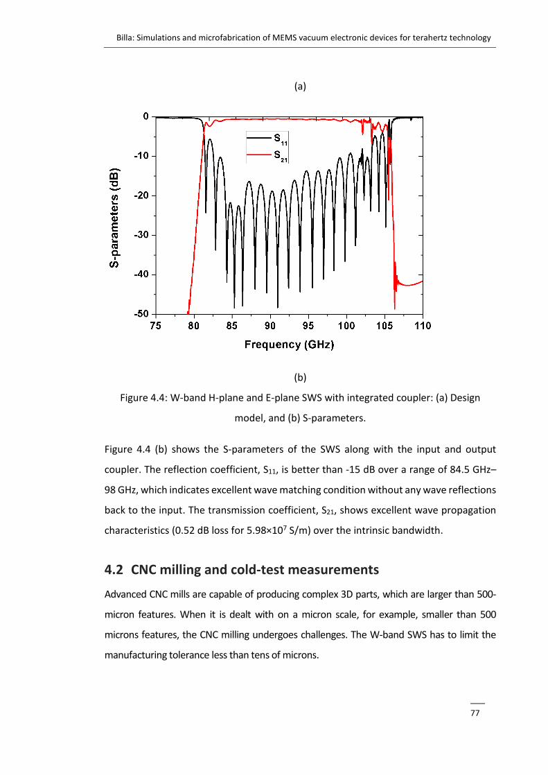
Billa: Simulations and microfabrication of MEMS vacuum electronic devices for terahertz technology
___
77
(a)
(b)
Figure 4.4: W-band H-plane and E-plane SWS with integrated coupler: (a) Design
model, and (b) S-parameters.
Figure 4.4 (b) shows the S-parameters of the SWS along with the input and output
coupler. The reflection coefficient, S11, is better than -15 dB over a range of 84.5 GHz–
98 GHz, which indicates excellent wave matching condition without any wave reflections
back to the input. The transmission coefficient, S21, shows excellent wave propagation
characteristics (0.52 dB loss for 5.98×10⁷ S/m) over the intrinsic bandwidth.
4.2 CNC milling and cold-test measurements
Advanced CNC mills are capable of producing complex 3D parts, which are larger than 500-
micron features. When it is dealt with on a micron scale, for example, smaller than 500
microns features, the CNC milling undergoes challenges. The W-band SWS has to limit the
manufacturing tolerance less than tens of microns.
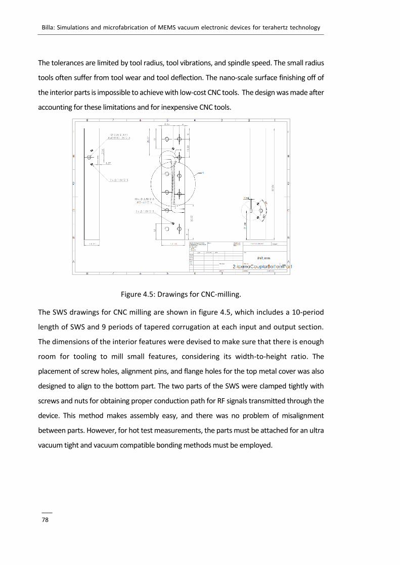
Billa: Simulations and microfabrication of MEMS vacuum electronic devices for terahertz technology
___
78
The tolerances are limited by tool radius, tool vibrations, and spindle speed. The small radius
tools often suffer from tool wear and tool deflection. The nano-scale surface finishing off of
the interior parts is impossible to achieve with low-cost CNC tools. The design was made after
accounting for these limitations and for inexpensive CNC tools.
Figure 4.5: Drawings for CNC-milling.
The SWS drawings for CNC milling are shown in figure 4.5, which includes a 10-period
length of SWS and 9 periods of tapered corrugation at each input and output section.
The dimensions of the interior features were devised to make sure that there is enough
room for tooling to mill small features, considering its width-to-height ratio. The
placement of screw holes, alignment pins, and flange holes for the top metal cover was also
designed to align to the bottom part. The two parts of the SWS were clamped tightly with
screws and nuts for obtaining proper conduction path for RF signals transmitted through the
device. This method makes assembly easy, and there was no problem of misalignment
between parts. However, for hot test measurements, the parts must be attached for an ultra
vacuum tight and vacuum compatible bonding methods must be employed.
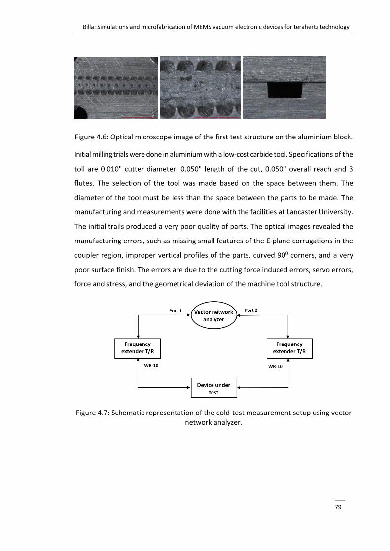
Billa: Simulations and microfabrication of MEMS vacuum electronic devices for terahertz technology
___
79
Figure 4.6: Optical microscope image of the first test structure on the aluminium block.
Initial milling trials were done in aluminium with a low-cost carbide tool. Specifications of the
toll are 0.010" cutter diameter, 0.050" length of the cut, 0.050" overall reach and 3
flutes. The selection of the tool was made based on the space between them. The
diameter of the tool must be less than the space between the parts to be made. The
manufacturing and measurements were done with the facilities at Lancaster University.
The initial trails produced a very poor quality of parts. The optical images revealed the
manufacturing errors, such as missing small features of the E-plane corrugations in the
coupler region, improper vertical profiles of the parts, curved 900 corners, and a very
poor surface finish. The errors are due to the cutting force induced errors, servo errors,
force and stress, and the geometrical deviation of the machine tool structure.
Figure 4.7: Schematic representation of the cold-test measurement setup using vector network analyzer.
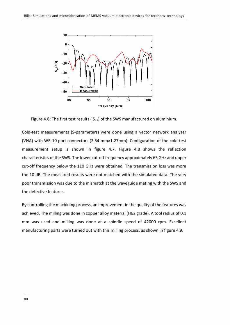
Billa: Simulations and microfabrication of MEMS vacuum electronic devices for terahertz technology
___
80
Figure 4.8: The first test results ( S11) of the SWS manufactured on aluminium.
Cold-test measurements (S-parameters) were done using a vector network analyser
(VNA) with WR-10 port connectors (2.54 mm×1.27mm). Configuration of the cold-test
measurement setup is shown in figure 4.7. Figure 4.8 shows the reflection
characteristics of the SWS. The lower cut-off frequency approximately 65 GHz and upper
cut-off frequency below the 110 GHz were obtained. The transmission loss was more
the 10 dB. The measured results were not matched with the simulated data. The very
poor transmission was due to the mismatch at the waveguide mating with the SWS and
the defective features.
By controlling the machining process, an improvement in the quality of the features was
achieved. The milling was done in copper alloy material (H62 grade). A tool radius of 0.1
mm was used and milling was done at a spindle speed of 42000 rpm. Excellent
manufacturing parts were turned out with this milling process, as shown in figure 4.9.
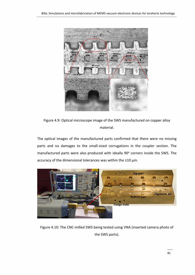
Billa: Simulations and microfabrication of MEMS vacuum electronic devices for terahertz technology
___
81
Figure 4.9: Optical microscope image of the SWS manufactured on copper alloy
material.
The optical images of the manufactured parts confirmed that there were no missing
parts and no damages to the small-sized corrugations in the coupler section. The
manufactured parts were also produced with ideally 90o corners inside the SWS. The
accuracy of the dimensional tolerances was within the ±10 µm.
Figure 4.10: The CNC-milled SWS being tested using VNA (inserted camera photo of
the SWS parts).
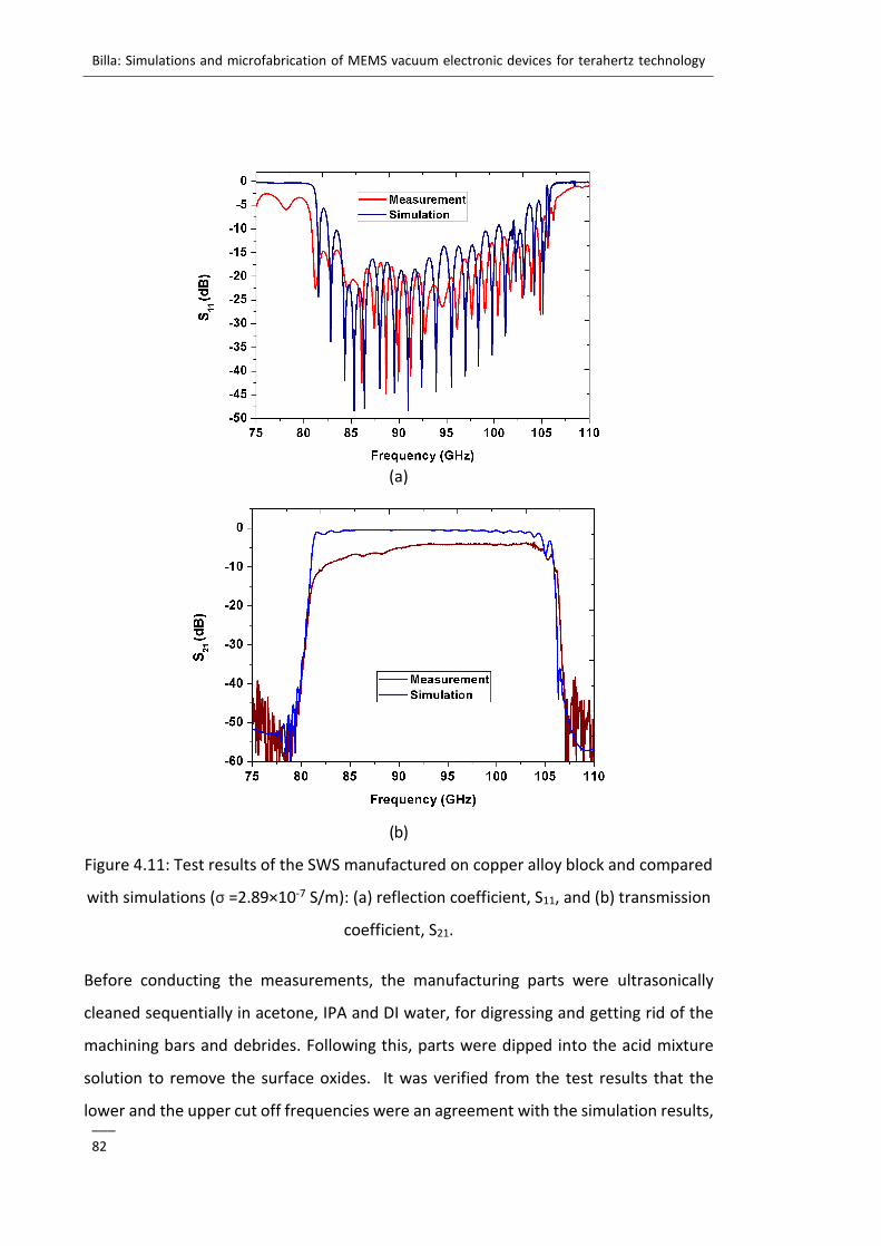
Billa: Simulations and microfabrication of MEMS vacuum electronic devices for terahertz technology
___
82
(a)
(b)
Figure 4.11: Test results of the SWS manufactured on copper alloy block and compared
with simulations (σ =2.89×10⁻⁷ S/m): (a) reflection coefficient, S11, and (b) transmission
coefficient, S21.
Before conducting the measurements, the manufacturing parts were ultrasonically
cleaned sequentially in acetone, IPA and DI water, for digressing and getting rid of the
machining bars and debrides. Following this, parts were dipped into the acid mixture
solution to remove the surface oxides. It was verified from the test results that the
lower and the upper cut off frequencies were an agreement with the simulation results,
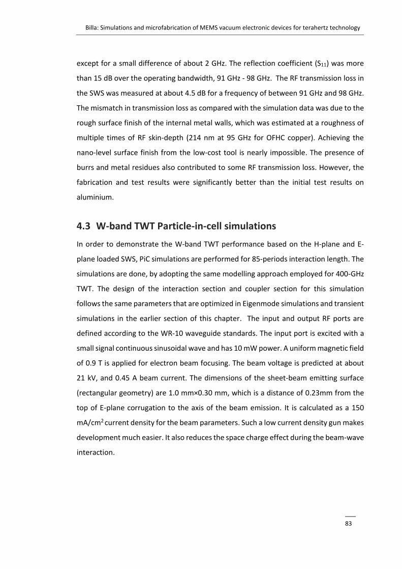
Billa: Simulations and microfabrication of MEMS vacuum electronic devices for terahertz technology
___
83
except for a small difference of about 2 GHz. The reflection coefficient (S11) was more
than 15 dB over the operating bandwidth, 91 GHz - 98 GHz. The RF transmission loss in
the SWS was measured at about 4.5 dB for a frequency of between 91 GHz and 98 GHz.
The mismatch in transmission loss as compared with the simulation data was due to the
rough surface finish of the internal metal walls, which was estimated at a roughness of
multiple times of RF skin-depth (214 nm at 95 GHz for OFHC copper). Achieving the
nano-level surface finish from the low-cost tool is nearly impossible. The presence of
burrs and metal residues also contributed to some RF transmission loss. However, the
fabrication and test results were significantly better than the initial test results on
aluminium.
4.3 W-band TWT Particle-in-cell simulations
In order to demonstrate the W-band TWT performance based on the H-plane and E-
plane loaded SWS, PiC simulations are performed for 85-periods interaction length. The
simulations are done, by adopting the same modelling approach employed for 400-GHz
TWT. The design of the interaction section and coupler section for this simulation
follows the same parameters that are optimized in Eigenmode simulations and transient
simulations in the earlier section of this chapter. The input and output RF ports are
defined according to the WR-10 waveguide standards. The input port is excited with a
small signal continuous sinusoidal wave and has 10 mW power. A uniform magnetic field
of 0.9 T is applied for electron beam focusing. The beam voltage is predicted at about
21 kV, and 0.45 A beam current. The dimensions of the sheet-beam emitting surface
(rectangular geometry) are 1.0 mm×0.30 mm, which is a distance of 0.23mm from the
top of E-plane corrugation to the axis of the beam emission. It is calculated as a 150
mA/cm2 current density for the beam parameters. Such a low current density gun makes
development much easier. It also reduces the space charge effect during the beam-wave
interaction.
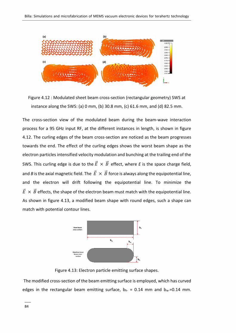
Billa: Simulations and microfabrication of MEMS vacuum electronic devices for terahertz technology
___
84
Figure 4.12 : Modulated sheet beam cross-section (rectangular geometry) SWS at
instance along the SWS: (a) 0 mm, (b) 30.8 mm, (c) 61.6 mm, and (d) 82.5 mm.
The cross-section view of the modulated beam during the beam-wave interaction
process for a 95 GHz input RF, at the different instances in length, is shown in figure
4.12. The curling edges of the beam cross-section are noticed as the beam progresses
towards the end. The effect of the curling edges shows the worst beam shape as the
electron particles intensified velocity modulation and bunching at the trailing end of the
SWS. This curling edge is due to the �⃗� × �⃗� effect, where E is the space charge field,
and B is the axial magnetic field. The �⃗� × �⃗� force is always along the equipotential line,
and the electron will drift following the equipotential line. To minimize the
�⃗� × �⃗� effects, the shape of the electron beam must match with the equipotential line.
As shown in figure 4.13, a modified beam shape with round edges, such a shape can
match with potential contour lines.
Figure 4.13: Electron particle emitting surface shapes.
The modified cross-section of the beam emitting surface is employed, which has curved
edges in the rectangular beam emitting surface, bh- = 0.14 mm and bw-=0.14 mm.
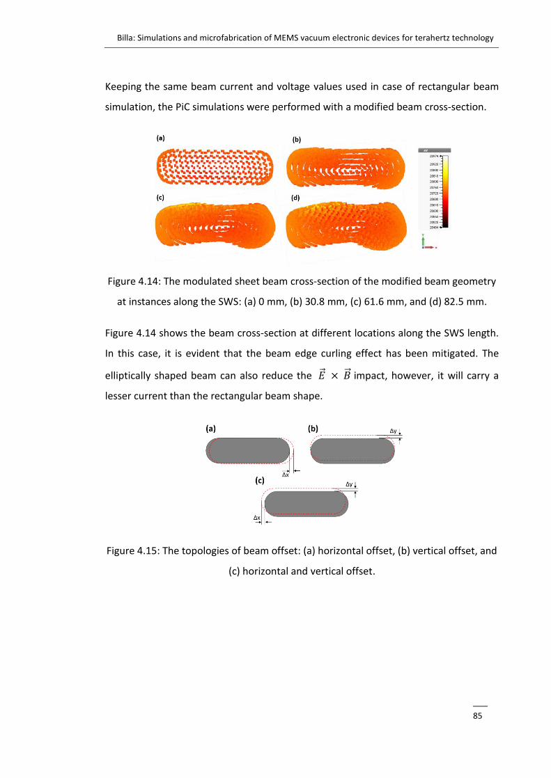
Billa: Simulations and microfabrication of MEMS vacuum electronic devices for terahertz technology
___
85
Keeping the same beam current and voltage values used in case of rectangular beam
simulation, the PiC simulations were performed with a modified beam cross-section.
Figure 4.14: The modulated sheet beam cross-section of the modified beam geometry
at instances along the SWS: (a) 0 mm, (b) 30.8 mm, (c) 61.6 mm, and (d) 82.5 mm.
Figure 4.14 shows the beam cross-section at different locations along the SWS length.
In this case, it is evident that the beam edge curling effect has been mitigated. The
elliptically shaped beam can also reduce the �⃗� × �⃗� impact, however, it will carry a
lesser current than the rectangular beam shape.
Figure 4.15: The topologies of beam offset: (a) horizontal offset, (b) vertical offset, and
(c) horizontal and vertical offset.
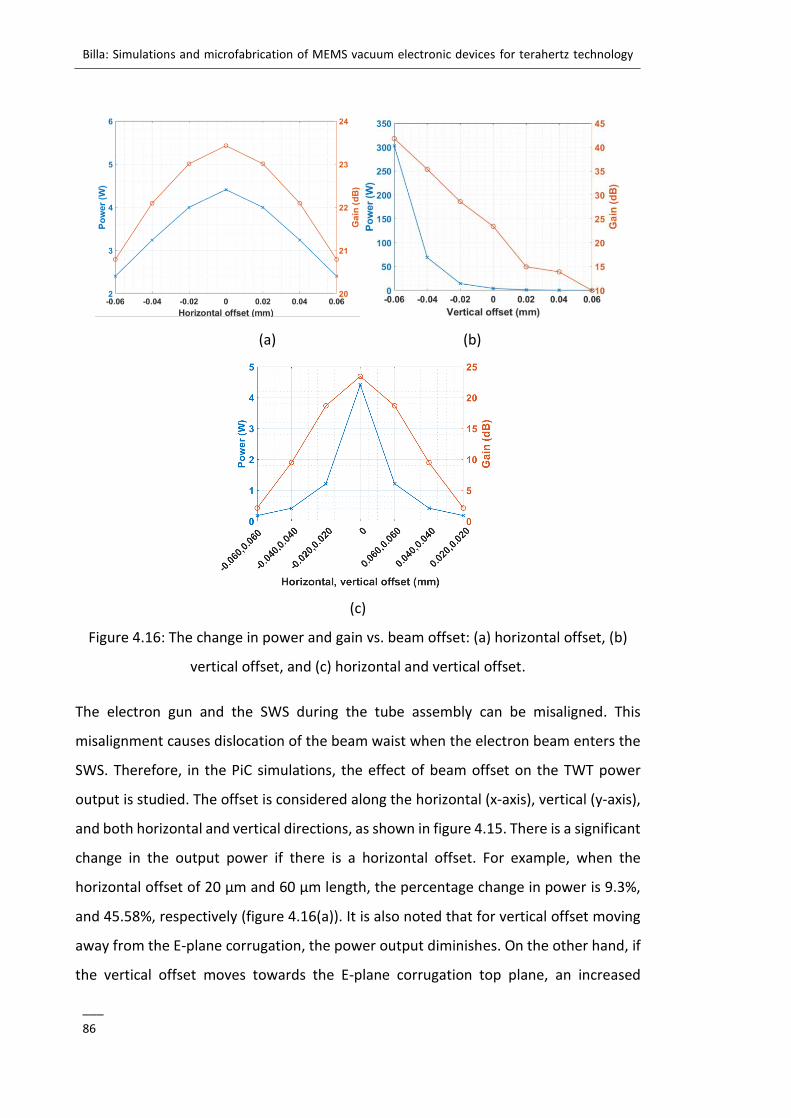
Billa: Simulations and microfabrication of MEMS vacuum electronic devices for terahertz technology
___
86
(a) (b)
(c)
Figure 4.16: The change in power and gain vs. beam offset: (a) horizontal offset, (b)
vertical offset, and (c) horizontal and vertical offset.
The electron gun and the SWS during the tube assembly can be misaligned. This
misalignment causes dislocation of the beam waist when the electron beam enters the
SWS. Therefore, in the PiC simulations, the effect of beam offset on the TWT power
output is studied. The offset is considered along the horizontal (x-axis), vertical (y-axis),
and both horizontal and vertical directions, as shown in figure 4.15. There is a significant
change in the output power if there is a horizontal offset. For example, when the
horizontal offset of 20 µm and 60 µm length, the percentage change in power is 9.3%,
and 45.58%, respectively (figure 4.16(a)). It is also noted that for vertical offset moving
away from the E-plane corrugation, the power output diminishes. On the other hand, if
the vertical offset moves towards the E-plane corrugation top plane, an increased
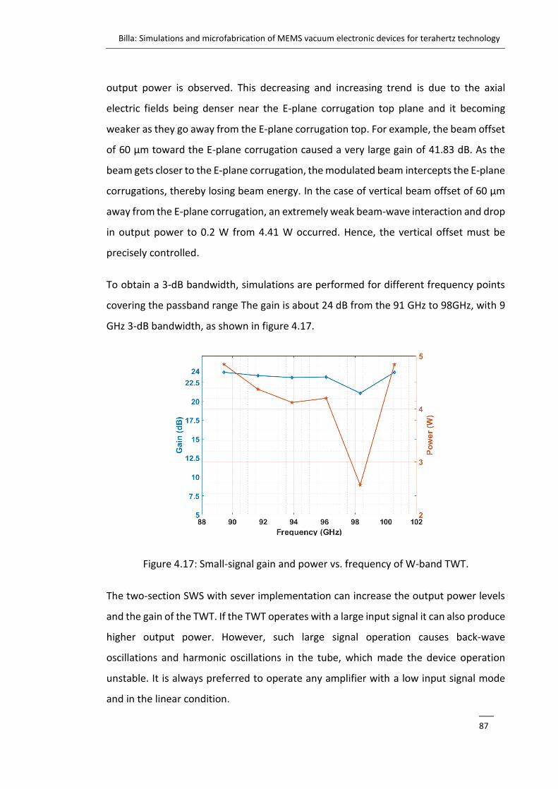
Billa: Simulations and microfabrication of MEMS vacuum electronic devices for terahertz technology
___
87
output power is observed. This decreasing and increasing trend is due to the axial
electric fields being denser near the E-plane corrugation top plane and it becoming
weaker as they go away from the E-plane corrugation top. For example, the beam offset
of 60 µm toward the E-plane corrugation caused a very large gain of 41.83 dB. As the
beam gets closer to the E-plane corrugation, the modulated beam intercepts the E-plane
corrugations, thereby losing beam energy. In the case of vertical beam offset of 60 µm
away from the E-plane corrugation, an extremely weak beam-wave interaction and drop
in output power to 0.2 W from 4.41 W occurred. Hence, the vertical offset must be
precisely controlled.
To obtain a 3-dB bandwidth, simulations are performed for different frequency points
covering the passband range The gain is about 24 dB from the 91 GHz to 98GHz, with 9
GHz 3-dB bandwidth, as shown in figure 4.17.
Figure 4.17: Small-signal gain and power vs. frequency of W-band TWT.
The two-section SWS with sever implementation can increase the output power levels
and the gain of the TWT. If the TWT operates with a large input signal it can also produce
higher output power. However, such large signal operation causes back-wave
oscillations and harmonic oscillations in the tube, which made the device operation
unstable. It is always preferred to operate any amplifier with a low input signal mode
and in the linear condition.

Billa: Simulations and microfabrication of MEMS vacuum electronic devices for terahertz technology
___
88
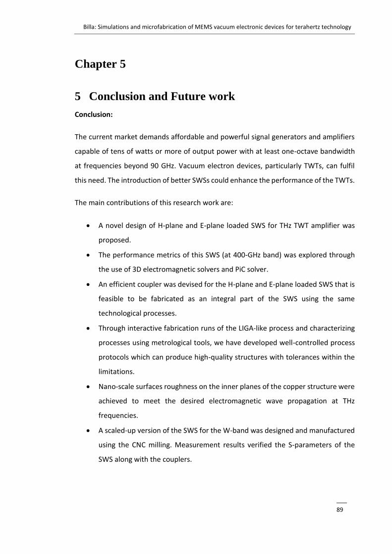
Billa: Simulations and microfabrication of MEMS vacuum electronic devices for terahertz technology
___
89
Chapter 5
5 Conclusion and Future work
Conclusion:
The current market demands affordable and powerful signal generators and amplifiers
capable of tens of watts or more of output power with at least one-octave bandwidth
at frequencies beyond 90 GHz. Vacuum electron devices, particularly TWTs, can fulfil
this need. The introduction of better SWSs could enhance the performance of the TWTs.
The main contributions of this research work are:
• A novel design of H-plane and E-plane loaded SWS for THz TWT amplifier was
proposed.
• The performance metrics of this SWS (at 400-GHz band) was explored through
the use of 3D electromagnetic solvers and PiC solver.
• An efficient coupler was devised for the H-plane and E-plane loaded SWS that is
feasible to be fabricated as an integral part of the SWS using the same
technological processes.
• Through interactive fabrication runs of the LIGA-like process and characterizing
processes using metrological tools, we have developed well-controlled process
protocols which can produce high-quality structures with tolerances within the
limitations.
• Nano-scale surfaces roughness on the inner planes of the copper structure were
achieved to meet the desired electromagnetic wave propagation at THz
frequencies.
• A scaled-up version of the SWS for the W-band was designed and manufactured
using the CNC milling. Measurement results verified the S-parameters of the
SWS along with the couplers.
Billa: Simulations and microfabrication of MEMS vacuum electronic devices for terahertz technology
___
90
Future work:
In this thesis, the simulation and cold-test experimental results of the H-plane and E-
plane loaded SWS for THz TWT amplifier have demonstrated the effectiveness of this
SWS for sheet-beam technology in the high frequency of operation, which facilitates
easy fabrication by the available microfabrication techniques. However, there are other
parts of the TWT which must be designed, and some potential challenges that need to
be addressed.
• The simulation considered the use of 17 kV, 20 mA electron gun, producing 100
µm × 60 µm rectangular beam. Such an electron gun manufacturing and/or
procurement might be difficult. Because the electron gun with such parameters
requires a sophisticated cathode, and assembly of the gun must follow very tight
tolerances (accurate positioning of the cathode, focusing electrode, and anode)
in order to meet the design requirements.
• Manufacturing of the magnetic focusing system using PPM configuration with
0.6 T integrated with the SWS pose challenges at the THz frequencies. A little
drift in the magnetic field and pole piece placement causes significant change in
the net magnetic field value that leads to the deterioration of the electron beam
transmission and the possibility of intercepting the SWS.
• For improved efficiency of the tube, the multi-depressed collector is needed with
an efficient cooling system. It is important to study the thermal analysis of the
collector as well as the entire tube.
• There are several factors that need to be considered for building a complete
tube; techniques required for attaching sub-parts, ultra-high vacuum pumping,
vacuum windows and high voltage supply circuitry design.
Billa: Simulations and microfabrication of MEMS vacuum electronic devices for terahertz technology
___
91
References
[1] S. Dhillon et al., "The 2017 terahertz science and technology roadmap," Journal
of Physics D: Applied Physics, vol. 50, no. 4, p. 043001, 2017.
[2] M. Tonouchi, "Cutting-edge terahertz technology," Nature photonics, vol. 1, no.
2, p. 97, 2007.
[3] D. Dragoman and M. Dragoman, "Terahertz fields and applications," Progress in
Quantum Electronics, vol. 28, no. 1, pp. 1-66, 2004.
[4] W. L. Chan, J. Deibel, and D. M. Mittleman, "Imaging with terahertz radiation,"
Reports on progress in physics, vol. 70, no. 8, p. 1325, 2007.
[5] H. B. Wallace, "Analysis of RF imaging applications at frequencies over 100 GHz,"
Applied optics, vol. 49, no. 19, pp. E38-E47, 2010.
[6] J. F. Federici, "Review of moisture and liquid detection and mapping using
terahertz imaging," Journal of Infrared, Millimeter, and Terahertz Waves, vol. 33,
no. 2, pp. 97-126, 2012.
[7] B. Ferguson and X.-C. Zhang, "Materials for terahertz science and technology,"
Nature materials, vol. 1, no. 1, p. 26, 2002.
[8] P. H. Siegel, "Terahertz technology in biology and medicine," IEEE transactions
on microwave theory and techniques, vol. 52, no. 10, pp. 2438-2447, 2004.
[9] A. G. Davies, A. D. Burnett, W. Fan, E. H. Linfield, and J. E. Cunningham,
"Terahertz spectroscopy of explosives and drugs," Materials today, vol. 11, no.
3, pp. 18-26, 2008.
[10] B. B. Hu and M. C. Nuss, "Imaging with terahertz waves," Optics Letters, vol. 20,
no. 16, pp. 1716-1718, 1995.
[11] A. A. Penzias and C. A. Burrus, "Millimeter-Wavelength Radio-Astronomy
Techniques," Annual Review of Astronomy and Astrophysics, vol. 11, no. 1, pp.
51-72, 1973.
[12] R. Appleby and H. B. Wallace, "Standoff Detection of Weapons and Contraband
in the 100 GHz to 1 THz Region," IEEE Transactions on Antennas and Propagation,
vol. 55, no. 11, pp. 2944-2956, 2007.
Billa: Simulations and microfabrication of MEMS vacuum electronic devices for terahertz technology
___
92
[13] R. J. Trew, "High-frequency solid-state electronic devices," IEEE Transactions on
Electron Devices, vol. 52, no. 5, pp. 638-649, 2005.
[14] K. W. Brown, D. M. Gritters, and H. Kazemi, "W-and G-band solid state power
combining," in Compound Semiconductor Integrated Circuit Symposium (CSICS),
2015 IEEE, 2015, pp. 1-4: IEEE.
[15] S. Francis and R. van Zyl, "Evaluating the microwave performance of a two
domain GaN Gunn diode for THz applications," Terahertz Sci. Technol, vol. 8, no.
1, pp. 1941-7411, 2015.
[16] A. S. Hajo, O. Yilmazoglu, F. Kiippers, and A. Dadgar, "Reliability Improvement of
High-Power THz GaN Gunn Sources for Active Imaging Systems," in 2018 43rd
International Conference on Infrared, Millimeter, and Terahertz Waves (IRMMW-
THz), 2018, pp. 1-2: IEEE.
[17] Z. Griffith, M. Urteaga, P. Rowell, and R. Pierson, "A 6–10 mW power amplifier
at 290–307.5 GHz in 250 nm InP HBT," IEEE Microwave and Wireless Components
Letters, vol. 25, no. 9, pp. 597-599, 2015.
[18] M. S. Vitiello, G. Scalari, B. Williams, and P. De Natale, "Quantum cascade lasers:
20 years of challenges," Optics express, vol. 23, no. 4, pp. 5167-5182, 2015.
[19] J. Hebling, K. Yeh, M. C. Hoffmann, and K. A. Nelson, "High-Power THz
Generation, THz Nonlinear Optics, and THz Nonlinear Spectroscopy," IEEE
Journal of Selected Topics in Quantum Electronics, vol. 14, no. 2, pp. 345-353,
2008.
[20] R. Abrams, B. Levush, A. Mondelli, and R. Parker, "Vacuum electronics for the
21st century," IEEE Microwave magazine, vol. 2, no. 3, pp. 61-72, 2001.
[21] R. K. Parker, R. H. Abrams, B. G. Danly, and B. Levush, "Vacuum electronics," IEEE
transactions on microwave theory and techniques, vol. 50, no. 3, pp. 835-845,
2002.
[22] S. H. Gold and G. S. Nusinovich, "Review of high-power microwave source
research," Review of Scientific instruments, vol. 68, no. 11, pp. 3945-3974, 1997.
Billa: Simulations and microfabrication of MEMS vacuum electronic devices for terahertz technology
___
93
[23] J. H. Booske, "Plasma physics and related challenges of millimeter-wave-to-
terahertz and high power microwave generation," Physics of plasmas, vol. 15,
no. 5, p. 055502, 2008.
[24] C. Paoloni et al., "Design and fabrication of a 1 THz backward wave amplifier,"
Terahertz Science and Technology, vol. 4, pp. 149-163, 2011.
[25] N. E. Lindenblad, "High voltage generator," ed: Google Patents, 1942.
[26] R. Kompfner, "The traveling-wave tube as amplifier at microwaves," Proceedings
of the IRE, vol. 35, no. 2, pp. 124-127, 1947.
[27] J. Pierce and L. M. Field, "Traveling-wave tubes," Proceedings of the IRE, vol. 35,
no. 2, pp. 108-111, 1947.
[28] J. Pierce, "Theory of the beam-type traveling-wave tube," Proceedings of the IRE,
vol. 35, no. 2, pp. 111-123, 1947.
[29] J. H. Booske et al., "Vacuum electronic high power terahertz sources," IEEE
Transactions on Terahertz Science and Technology, vol. 1, no. 1, pp. 54-75, 2011.
[30] Y. Zheng, D. Gamzina, and N. C. Luhmann, "0.2-THz Dual Mode Sheet Beam
Traveling Wave Tube," IEEE Transactions on Electron Devices, vol. 64, no. 4, pp.
1767-1773, 2017.
[31] H. Liang et al., "Integrated Planar Three-Beam Electron Optics System for 220-
GHz Folded Waveguide TWT," IEEE Transactions on Electron Devices, vol. 65, no.
1, pp. 270-276, 2018.
[32] J.-x. Bao and B.-f. Wan, "The tungsten powder study of the dispenser cathode,"
Applied Surface Science, vol. 252, no. 16, pp. 5873-5876, 2006.
[33] J. Zhao et al., "High current density and long-life nanocomposite scandate
dispenser cathode fabrication," IEEE Transactions on Electron Devices, vol. 58,
no. 4, pp. 1221-1228, 2011.
[34] N. Li, N. Luhmann Jr, D. Gamzina, G. Soekland, M. Banducci, and M. Gonzalez,
"Study on the compositions of emission active materials and the emission
properties of dispenser cathodes made from Scandia-doped powders,"
Advanced Powder Technology, vol. 27, no. 5, pp. 1933-1940, 2016.
Billa: Simulations and microfabrication of MEMS vacuum electronic devices for terahertz technology
___
94
[35] J. E. Atkinson et al., "8.3: A high aspect ratio, high current density sheet beam
electron gun," in 2010 IEEE International Vacuum Electronics Conference (IVEC),
2010, pp. 97-98.
[36] Y. Zheng, D. Gamzina, B. Popovic, and N. C. Luhmann, "Electron Beam Transport
System for 263-GHz Sheet Beam TWT," IEEE Transactions on Electron Devices,
vol. 63, no. 11, pp. 4466-4472, 2016.
[37] K. T. Nguyen, J. A. Pasour, T. M. Antonsen, P. B. Larsen, J. J. Petillo, and B. Levush,
"Intense sheet electron beam transport in a uniform solenoidal magnetic field,"
IEEE Transactions on Electron Devices, vol. 56, no. 5, pp. 744-752, 2009.
[38] J. H. Booske and M. A. Basten, "Demonstration via simulation of stable
confinement of sheet electron beams using periodic magnetic focusing," IEEE
transactions on plasma science, vol. 27, no. 1, pp. 134-135, 1999.
[39] X. Shi et al., "Theoretical and experimental research on a novel small tunable
PCM system in staggered double vane TWT," IEEE Transactions on electron
devices, vol. 62, no. 12, pp. 4258-4264, 2015.
[40] S. Coco, F. Emma, A. Laudani, S. Pulvirenti, and M. Sergi, "COCA: a novel 3-D FE
simulator for the design of TWT's multistage collectors," IEEE Transactions on
Electron Devices, vol. 48, no. 1, pp. 24-31, 2001.
[41] A. M. Latha and S. Ghosh, "An Asymmetric Highly Efficient Multistage Depressed
Collector for Space TWTs," IEEE Transactions on Electron Devices, vol. 63, no. 5,
pp. 2139-2144, 2016.
[42] P. R. R. Rao, S. Datta, V. Deshmukh, and L. Kumar, "Simulation of collectors for
TWT including the effects of SEE using PIERCE," in Vacuum Electronics Conference
(IVEC), 2011 IEEE International, 2011, pp. 509-510: IEEE.
[43] D. M. Springmann et al., "Potential use of UNCD membranes as broadband
vacuum windows at W-band frequencies," in Vacuum Electronics Conference,
2008. IVEC 2008. IEEE International, 2008, pp. 316-317: IEEE.
[44] C. L. Kory and J. A. Dayton, "Design of 650 GHz helical BWO using CST studio
suite," in Vacuum Electronics Conference, 2008. IVEC 2008. IEEE International,
2008, pp. 392-393: IEEE.
Billa: Simulations and microfabrication of MEMS vacuum electronic devices for terahertz technology
___
95
[45] J. A. Dayton, C. L. Kory, G. T. Mearini, D. Malta, M. Lueck, and K. Gilchrist,
"Applying microfabrication to helical vacuum electron devices for THz
applications," in Vacuum Electronics Conference, 2009. IVEC'09. IEEE
International, 2009, pp. 41-44: IEEE.
[46] J. A. Dayton, C. L. Kory, G. T. Mearini, D. Malta, M. Lueck, and C. A. Bower, "A 650
GHz helical BWO," in Vacuum Electronics Conference, 2008. IVEC 2008. IEEE
International, 2008, pp. 396-397: IEEE.
[47] J. A. Dayton, C. L. Kory, G. T. Mearini, D. Malta, M. Lueck, and B. Vancil,
"Fabrication and testing of the 0.650 THz helical BWO," in Vacuum Electronics
Conference (IVEC), 2012 IEEE Thirteenth International, 2012, pp. 33-34: IEEE.
[48] C. L. Kory et al., "95 GHz helical TWT design," in Vacuum Electronics Conference,
2009. IVEC'09. IEEE International, 2009, pp. 125-126: IEEE.
[49] J. A. Dayton, C. L. Kory, and G. T. Mearini, "Microfabricated mm-wave TWT
platform for wireless Backhaul," in Vacuum Electronics Conference (IVEC), 2015
IEEE International, 2015, pp. 1-2: IEEE.
[50] C. Chua, S. Aditya, J. M. Tsai, M. Tang, and Z. Shen, "Microfabricated planar
helical slow-wave structures based on straight-edge connections for THz vacuum
electron devices," Int. J. Terahertz Sci. Technol., vol. 4, no. 4, pp. 208-229, 2011.
[51] C. Chua et al., "Microfabrication and characterization of W-band planar helix
slow-wave structure with straight-edge connections," IEEE Transactions on
Electron Devices, vol. 58, no. 11, pp. 4098-4105, 2011.
[52] C. Zhao, S. Aditya, and C. Chua, "Connected pair of planar helices with straight-
edge connections for application in TWTs," IEEE Transactions on Electron
Devices, vol. 61, no. 6, pp. 1692-1698, 2014.
[53] K. Swaminathan, C. Zhao, C. Chua, and S. Aditya, "Vane-loaded planar helix slow-
wave structure for application in broadband traveling-wave tubes," IEEE
Transactions on Electron Devices, vol. 62, no. 3, pp. 1017-1023, 2015.
[54] G. Dohler, D. Gagne, D. Gallagher, and R. Moats, "Serpentine waveguide TWT,"
in 1987 International Electron Devices Meeting, 1987, pp. 485-488.
Billa: Simulations and microfabrication of MEMS vacuum electronic devices for terahertz technology
___
96
[55] D. B. Lyon and A. J. Theiss, "Litton folded-waveguide high-power millimeter-wave
TWTs," in Proceedings of 1994 IEEE International Electron Devices Meeting, 1994,
pp. 918-920.
[56] H.-J. Ha et al., "Experimental Investigation of Ku-Band Folded Waveguide TWT,"
International Journal of Infrared and Millimeter Waves, vol. 20, no. 12, pp. 2099-
2106, 1999.
[57] J. H. Booske et al., "Accurate parametric modeling of folded waveguide circuits
for millimeter-wave traveling wave tubes," IEEE Transactions on Electron
Devices, vol. 52, no. 5, pp. 685-694, 2005.
[58] H. Gong et al., "A 1-kW 32–34-GHz folded waveguide traveling wave tube," IEEE
Transactions on Plasma Science, vol. 42, no. 1, pp. 8-12, 2014.
[59] J. Cai, J. Feng, Y. Hu, X. Wu, Y. Du, and J. Liu, "10 GHz bandwidth 100 watt W-
band folded waveguide pulsed TWTs," IEEE Microwave and Wireless
Components Letters, vol. 24, no. 9, pp. 620-621, 2014.
[60] J. Feng et al., "Development of W-band folded waveguide pulsed TWTs," IEEE
Transactions on Electron Devices, vol. 61, no. 6, pp. 1721-1725, 2014.
[61] Y. Hu et al., "Design and experimental study of a widebandwidth W-band folded
waveguide continuous-wave TWT," IEEE Transactions on Plasma Science, vol. 42,
no. 10, pp. 3380-3386, 2014.
[62] X. Zhang et al., "Design and Experimental Study of 250-W W-band Pulsed TWT
With 8-GHz Bandwidth," IEEE Transactions on Electron Devices, vol. 64, no. 12,
pp. 5151-5156, 2017.
[63] L. Wenqiang et al., "Development of D-band continuous-wave folded waveguide
traveling-wave tube," in 2015 IEEE International Vacuum Electronics Conference
(IVEC), 2015, pp. 1-3.
[64] P. Pan et al., "Development of G band folded waveguide TWTs," in Vacuum
Electronics Conference (IVEC), 2016 IEEE International, 2016, pp. 1-2: IEEE.
[65] C. D. Joye et al., "Demonstration of a high power, wideband 220-GHz traveling
wave amplifier fabricated by UV-LIGA," IEEE Transactions on Electron Devices,
vol. 61, no. 6, pp. 1672-1678, 2014.
Billa: Simulations and microfabrication of MEMS vacuum electronic devices for terahertz technology
___
97
[66] K. E. Kreischer, J. C. Tucek, M. A. Basten, and D. A. Gallagher, "220 GHz power
amplifier testing at Northrop Grumman," in 2013 IEEE 14th International
Vacuum Electronics Conference (IVEC), 2013, pp. 1-2.
[67] M. Basten et al., "A multiple electron beam array for a 220 GHz amplifier," in
2009 IEEE International Vacuum Electronics Conference, 2009, pp. 110-111.
[68] M. A. Basten, J. C. Tucek, D. A. Gallagher, and K. E. Kreischer, "233 GHz high
Power amplifier development at Northrop Grumman," in 2016 IEEE International
Vacuum Electronics Conference (IVEC), 2016, pp. 1-2.
[69] P. Hu et al., "Development of a 0.32-THz Folded Waveguide Traveling Wave
Tube," IEEE Transactions on Electron Devices, 2018.
[70] J. Tucek, K. Kreischer, D. Gallagher, R. Vogel, and R. Mihailovich, "Development
and Operation of a 650 GHz Folded Waveguide Source," in 2007 IEEE
International Vacuum Electronics Conference, 2007, pp. 1-2.
[71] J. C. Tucek et al., "A 100 mW, 0.670 THz power module," in IVEC 2012, 2012, pp.
31-32.
[72] M. A. Basten, J. C. Tucek, D. A. Gallagher, K. E. Kreischer, and R. Mihailovich, "A
0.85 THz vacuum-based power amplifier," in IVEC 2012, 2012, pp. 39-40.
[73] J. C. Tucek, M. A. Basten, D. A. Gallagher, and K. E. Kreischer, "0.850 THz vacuum
electronic power amplifier," in IEEE International Vacuum Electronics
Conference, 2014, pp. 153-154.
[74] G. Dohler, D. Gagne, D. Gallagher, and R. Moats, "Serpentine waveguide TWT,"
in 1987 International Electron Devices Meeting, 1987, vol. 33, pp. 485-488.
[75] C. L. Kory, M. E. Read, R. L. Ives, J. H. Booske, and P. Borchard, "Design of
Overmoded Interaction Circuit for 1-kW 95-GHz TWT," IEEE Transactions on
Electron Devices, vol. 56, no. 5, pp. 713-720, 2009.
[76] E. J. Kowalski, M. A. Shapiro, and R. J. Temkin, "An Overmoded W-Band Coupled-
Cavity TWT," IEEE Transactions on Electron Devices, vol. 62, no. 5, pp. 1609-1616,
2015.
Billa: Simulations and microfabrication of MEMS vacuum electronic devices for terahertz technology
___
98
[77] Y. Gong et al., "A 140-GHz Two-Beam Overmoded Folded-Waveguide Traveling-
Wave Tube," IEEE Transactions on Plasma Science, vol. 39, no. 3, pp. 847-851,
2011.
[78] S. Yan, W. Su, Y. Wang, and A. Xu, "Design and Theoretical Analysis of Multibeam
Folded Waveguide Traveling-Wave Tube for Subterahertz Radiation," IEEE
Transactions on Plasma Science, vol. 43, no. 1, pp. 414-421, 2015.
[79] S.-m. Yan, W. Su, and G.-l. Zhang, "Design and fabrication of a sub-millimeter
multi-beam folded waveguide structure," Optoelectronics Letters, vol. 13, no. 1,
pp. 33-37, 2017.
[80] K. T. Nguyen et al., "Design Methodology and Experimental Verification of
Serpentine/Folded-Waveguide TWTs," IEEE Transactions on Electron Devices,
vol. 61, no. 6, pp. 1679-1686, 2014.
[81] D. Chernin et al., "TWT stability for frequencies near a band edge," in 2013 IEEE
14th International Vacuum Electronics Conference (IVEC), 2013, pp. 1-2: IEEE.
[82] J. Cai, J. Feng, and X. Wu, "Folded Waveguide Slow Wave Structure With
Modified Circular Bends," IEEE Transactions on Electron Devices, vol. 61, no. 10,
pp. 3534-3538, 2014.
[83] S. Liu, J. Cai, J. Feng, and X. Wu, "Characteristics Study of 3pi Stopbands of Folded
Waveguide Slow-Wave Structures in V-band Traveling-Wave Tubes," IEEE
Transactions on Electron Devices, vol. 63, no. 3, pp. 1294-1298, 2016.
[84] J. He, Y. Wei, Y. Gong, W. Wang, and G. S. Park, "Investigation on a W Band Ridge-
Loaded Folded Waveguide TWT," IEEE Transactions on Plasma Science, vol. 39,
no. 8, pp. 1660-1664, 2011.
[85] Y. Wei et al., "Novel W-Band Ridge-Loaded Folded Waveguide Traveling Wave
Tube," IEEE Electron Device Letters, vol. 35, no. 10, pp. 1058-1060, 2014.
[86] M. Sumathy, K. J. Vinoy, and S. K. Datta, "Analysis of Ridge-Loaded Folded-
Waveguide Slow-Wave Structures for Broadband Traveling-Wave Tubes," IEEE
Transactions on Electron Devices, vol. 57, no. 6, pp. 1440-1446, 2010.
Billa: Simulations and microfabrication of MEMS vacuum electronic devices for terahertz technology
___
99
[87] Y. Hou et al., "A Novel Ridge-Vane-Loaded Folded-Waveguide Slow-Wave
Structure for 0.22-THz Traveling-Wave Tube," IEEE Transactions on Electron
Devices, vol. 60, no. 3, pp. 1228-1235, 2013.
[88] M. Liao, Y. Wei, Y. Gong, J. He, W. Wang, and G. S. Park, "A Rectangular Groove-
Loaded Folded Waveguide for Millimeter-Wave Traveling-Wave Tubes," IEEE
Transactions on Plasma Science, vol. 38, no. 7, pp. 1574-1578, 2010.
[89] J. He and Y. Wei, "Study of the Slow-Wave Properties of a Rectangular Groove-
Loaded Folded Waveguide for Millimeter Traveling-Wave Tubes," IEEE
Transactions on Plasma Science, vol. 42, no. 1, pp. 55-61, 2014.
[90] H. Gong, G. Travish, J. Xu, Y. Wei, J. Feng, and Y. Gong, "High-Power Tunable
Terahertz Radiation by High-Order Harmonic Generation," IEEE Transactions on
Electron Devices, vol. 60, no. 1, pp. 482-486, 2013.
[91] D. J. Bates and E. L. Ginzton, "A Traveling-Wave Frequency Multiplier,"
Proceedings of the IRE, vol. 45, no. 7, pp. 938-944, 1957.
[92] Y. Tian et al., "A Novel Slow-Wave Structure Folded Rectangular Groove
Waveguide for Millimeter-Wave TWT," IEEE Transactions on Electron Devices,
vol. 59, no. 2, pp. 510-515, 2012.
[93] Y. Tian, L. Yue, Q. Zhou, Y. Wei, Y. Wei, and Y. Gong, "Investigation on Sheet Beam
Folded V-Shape Groove Waveguide for Millimeter-Wave TWT," IEEE
Transactions on Plasma Science, vol. 44, no. 8, pp. 1363-1368, 2016.
[94] Y. Tian et al., "Investigation of Ridge-Loaded Folded Rectangular Groove
Waveguide Slow-Wave Structure for High-Power Terahertz TWT," IEEE
Transactions on Electron Devices, vol. 65, no. 6, pp. 2170-2176, 2018.
[95] M. Mineo and C. Paoloni, "Corrugated rectangular waveguide tunable backward
wave oscillator for terahertz applications," IEEE Transactions on Electron Devices,
vol. 57, no. 6, pp. 1481-1484, 2010.
[96] C. D. Joye, J. P. Calame, M. Garven, D. Park, R. Bass, and B. Levush, "UV-LIGA and
DRIE grating microfabrication and testing for sheet beam amplifiers at 220 GHz,"
in Infrared Millimeter and Terahertz Waves (IRMMW-THz), 2010 35th
International Conference on, 2010, pp. 1-2: IEEE.
Billa: Simulations and microfabrication of MEMS vacuum electronic devices for terahertz technology
___
100
[97] D. J. Colin, P. C. Jeffrey, G. Morag, and L. Baruch, "UV-LIGA microfabrication of
220 GHz sheet beam amplifier gratings with SU-8 photoresists," Journal of
Micromechanics and Microengineering, vol. 20, no. 12, p. 125016, 2010.
[98] M. Mineo and C. Paoloni, "Narrow corrugation rectangular waveguide for
terahertz TWTs," Electronics Letters, vol. 46, no. 13, pp. 927-928, 2010.
[99] M. Mineo, A. Di Carlo, and C. Paoloni, "Analytical design method for corrugated
rectangular waveguide SWS THz vacuum tubes," Journal of Electromagnetic
Waves and Applications, vol. 24, no. 17-18, pp. 2479-2494, 2010.
[100] M. Mineo and C. Paoloni, "Comparison of THz backward wave oscillators based
on corrugated waveguides," Progress In Electromagnetics Research, vol. 30, pp.
163-171, 2012.
[101] Y. M. Shin, L. R. Barnett, and N. C. Luhmann, "Phase-Shifted Traveling-Wave-
Tube Circuit for Ultrawideband High-Power Submillimeter-Wave Generation,"
IEEE Transactions on Electron Devices, vol. 56, no. 5, pp. 706-712, 2009.
[102] Y.-M. Shin, A. Baig, L. R. Barnett, W.-C. Tsai, and N. C. Luhmann, "System design
analysis of a 0.22-THz sheet-beam traveling-wave tube amplifier," IEEE
Transactions on Electron Devices, vol. 59, no. 1, pp. 234-240, 2012.
[103] Y.-M. Shin, L. R. Barnett, and N. C. Luhmann Jr, "Strongly confined plasmonic
wave propagation through an ultrawideband staggered double grating
waveguide," Applied Physics Letters, vol. 93, no. 22, p. 221504, 2008.
[104] A. Baig et al., "Design fabrication and RF testing of near-THz sheet beam TWTA,"
IEEE Trans. Terahertz Sci. Technol., vol. 4, no. 4, pp. 181-207, 2011.
[105] A. Baig et al., "Performance of a Nano-CNC Machined 220-GHz Traveling Wave
Tube Amplifier," IEEE Transactions on Electron Devices, vol. 64, no. 5, pp. 2390-
2397, 2017.
[106] C. Ruan et al., "W -Band Multiple Beam Staggered Double-Vane Traveling Wave
Tube With Broad Band and High Output Power," IEEE Transactions on Plasma
Science, vol. 43, no. 7, pp. 2132-2139, 2015.
Billa: Simulations and microfabrication of MEMS vacuum electronic devices for terahertz technology
___
101
[107] X. Shi et al., "Study on wideband sheet beam traveling wave tube based on
staggered double vane slow wave structure," IEEE Transactions on Plasma
Science, vol. 42, no. 12, pp. 3996-4003, 2014.
[108] Q.-L. Liu, Z.-C. Wang, P.-K. Liu, C.-H. Du, H.-Q. Li, and A.-Y. Xu, "A THz backward-
wave oscillator based on a double-grating rectangular waveguide," IEEE
Transactions on Electron Devices, vol. 60, no. 4, pp. 1463-1468, 2013.
[109] X. Xu et al., "Sine waveguide for 0.22-THz traveling-wave tube," IEEE Electron
Device Letters, vol. 32, no. 8, pp. 1152-1154, 2011.
[110] W. Xie, Z.-C. Wang, J. Luo, and D. Zhao, "A 3-D Large signal model for sheet beam
traveling wave tubes," IEEE Transactions on Electron Devices, vol. 62, no. 3, pp.
1010-1016, 2015.
[111] M. Mineo and C. Paoloni, "Double-corrugated rectangular waveguide slow-wave
structure for terahertz vacuum devices," IEEE Transactions on Electron Devices,
vol. 57, no. 11, pp. 3169-3175, 2010.
[112] J. F. David, A. J. Durand, M. Mineo, and C. Paoloni, "Design of a terahertz cascade
backward wave amplifier," IEEE Transactions on Electron Devices, vol. 61, no. 6,
pp. 1715-1720, 2014.
[113] C. Paoloni and M. Mineo, "Double corrugated waveguide for G-band traveling
wave tubes," IEEE Transactions on Electron Devices, vol. 61, no. 12, pp. 4259-
4263, 2014.
[114] C. Paoloni, M. Mineo, M. Henry, and P. G. Huggard, "Double corrugated
waveguide for ka-band traveling wave tube," IEEE Transactions on Electron
Devices, vol. 62, no. 11, pp. 3851-3856, 2015.
[115] X. Li, X. Huang, S. Mathisen, R. Letizia, and C. Paoloni, "Design of 71–76 GHz
Double-Corrugated Waveguide Traveling-Wave Tube for Satellite Downlink,"
IEEE Transactions on Electron Devices, vol. 65, no. 6, pp. 2195-2200, 2018.
[116] J. A. Dayton et al., "Assembly and preliminary testing of the prototype 650 GHz
BWO," in Vacuum Electronics Conference, 2008. IVEC 2008. IEEE International,
2008, pp. 394-395: IEEE.
Billa: Simulations and microfabrication of MEMS vacuum electronic devices for terahertz technology
___
102
[117] J. Dayton, G. Mearini, C. Kory, and C. Bower, "Fabrication of diamond-based 300
and 650 GHz BWOs," in Vacuum Electronics Conference, 2007. IVEC'07. IEEE
International, 2007, pp. 1-2: IEEE.
[118] G. A. O. Vela, M. S. Miller, and R. W. Grow, "9.1: Terahertz backward-wave
oscillator slow-wave circuits," in Vacuum Electronics Conference (IVEC), 2010
IEEE International, 2010, pp. 179-180: IEEE.
[119] W.-S. Chang and C.-Y. Chang, "A high slow-wave factor microstrip structure with
simple design formulas and its application to microwave circuit design," IEEE
Trans. Microw. Theory Tech., vol. 60, no. 11, pp. 3376-3383, 2012.
[120] F. Shen et al., "A novel V-shaped microstrip meander-line slow-wave structure
for W-band MMPM," IEEE Transactions on Plasma Science, vol. 40, no. 2, pp. 463-
469, 2012.
[121] F. Shen et al., "140-GHz V-shaped microstrip meander-line traveling wave tube,"
Journal of Electromagnetic Waves and Applications, vol. 26, no. 1, pp. 89-98,
2012.
[122] F. Shen et al., "Symmetric double V-shaped microstrip meander-line slow-wave
structure for W-band traveling-wave tube," IEEE Transactions on Electron
Devices, vol. 59, no. 5, p. 1551, 2012.
[123] G. Ulisse and V. Krozer, " W-band Traveling Wave Tube Amplifier Based on Planar
Slow Wave Structure," IEEE Electron Device Letters, vol. 38, no. 1, pp. 126-129,
2017.
[124] L. B. Nguyen, T. M. Antonsen, and G. S. Nusinovich, "Planar slow-wave structure
with parasitic mode control," IEEE Transactions on Electron Devices, vol. 61, no.
6, pp. 1655-1660, 2014.
[125] R. L. Ives, "Microfabrication of high-frequency vacuum electron devices," IEEE
Transactions on plasma science, vol. 32, no. 3, pp. 1277-1291, 2004.
[126] S. Sengele, H. Jiang, J. H. Booske, C. L. Kory, D. W. Van der Weide, and R. L. Ives,
"Microfabrication and characterization of a selectively metallized W-band
meander-line TWT circuit," IEEE Transactions on Electron Devices, vol. 56, no. 5,
pp. 730-737, 2009.
Billa: Simulations and microfabrication of MEMS vacuum electronic devices for terahertz technology
___
103
[127] N. M. Ryskin et al., "Planar Microstrip Slow-Wave Structure for Low-Voltage V-
Band Traveling-Wave Tube With a Sheet Electron Beam," IEEE Electron Device
Letters, vol. 39, no. 5, pp. 757-760, 2018.
[128] E. Becker, W. Ehrfeld, P. Hagmann, A. Maner, and D. Münchmeyer, "Fabrication
of microstructures with high aspect ratios and great structural heights by
synchrotron radiation lithography, galvanoforming, and plastic moulding (LIGA
process)," Microelectronic engineering, vol. 4, no. 1, pp. 35-56, 1986.
[129] D. Tolfree, "Microfabrication using synchrotron radiation," Reports on Progress
in Physics, vol. 61, no. 4, p. 313, 1998.
[130] A. Rogner, J. Eicher, D. Munchmeyer, R.-P. Peters, and J. Mohr, "The LIGA
technique-what are the new opportunities," Journal of Micromechanics and
Microengineering, vol. 2, no. 3, p. 133, 1992.
[131] C. K. Malek and V. Saile, "Applications of LIGA technology to precision
manufacturing of high-aspect-ratio micro-components and -systems: a review,"
Microelectronics Journal, vol. 35, no. 2, pp. 131-143, 2004.
[132] H. Seong-Tae et al., "Investigations on a microfabricated FWTWT oscillator," IEEE
Transactions on Electron Devices, vol. 52, no. 5, pp. 702-708, 2005.
[133] H. Seong-Tae et al., "Experimental investigations on miniaturized high-frequency
vacuum electron devices," IEEE Transactions on Plasma Science, vol. 33, no. 2,
pp. 679-684, 2005.
[134] Y.-M. Shin et al., "Microfabrication of millimeter wave vacuum electron devices
by two-step deep-etch x-ray lithography," Applied Physics Letters, vol. 88, no. 9,
p. 091916, 2006.
[135] L. Jian et al., "SU-8-based deep x-ray lithography/LIGA," in Micromachining and
Microfabrication, 2003, vol. 4979, p. 8: SPIE.
[136] O. V. Makarova, R. Divan, J. Tucek, K. Kreischer, and C.-M. Tang, "Fabrication of
solid copper two-level waveguide circuits for a THz radar system by UV
lithography," in 2016 IEEE International Vacuum Electronics Conference (IVEC),
2016, pp. 1-2: IEEE.
Billa: Simulations and microfabrication of MEMS vacuum electronic devices for terahertz technology
___
104
[137] A. Malekabadi and C. Paoloni, "UV-LIGA microfabrication process for sub-
terahertz waveguides utilizing multiple layered SU-8 photoresist," Journal of
Micromechanics and Microengineering, vol. 26, no. 9, p. 095010, 2016.
[138] H. Lorenz, M. Despont, N. Fahrni, J. Brugger, P. Vettiger, and P. Renaud, "High-
aspect-ratio, ultrathick, negative-tone near-UV photoresist and its applications
for MEMS," vol. 64, no. 1, pp. 33-39-33-39, 1998.
[139] H. Lorenz, M. Laudon, and P. Renaud, "Mechanical characterization of a new
high-aspect-ratio near UV-photoresist," Microelectronic Engineering, vol. 41-42,
pp. 371-374, 1998.
[140] J. Feng, D. Ren, H. Li, Y. Tang, and J. Xing, "Study of high frequency folded
waveguide BWO with MEMS technology," Terahertz Science and Technology, vol.
4, no. 4, pp. 164-180, 2011.
[141] J. Cai et al., "Development of W-band folded waveguide pulsed TWT," in 2013
IEEE 14th International Vacuum Electronics Conference (IVEC), 2013, pp. 1-2:
IEEE.
[142] X. Fuqiang, D. Guifu, Z. Xiaolin, and C. Ping, "Design, fabrication and
measurement of a novel 140 GHz folded waveguide based on SU-8 UV-LIGA
technology," Journal of Micromechanics and Microengineering, vol. 25, no. 8, p.
085010, 2015.
[143] D. J. Colin, P. C. Jeffrey, T. N. Khanh, and G. Morag, "Microfabrication of fine
electron beam tunnels using UV-LIGA and embedded polymer monofilaments
for vacuum electron devices," Journal of Micromechanics and Microengineering,
vol. 22, no. 1, p. 015010, 2012.
[144] P. Pan et al., "Development of G band folded waveguide TWTs," in 2016 IEEE
International Vacuum Electronics Conference (IVEC), 2016, pp. 1-2: IEEE.
[145] C. D. Joye et al., "Demonstration of a High Power, Wideband 220-GHz Traveling
Wave Amplifier Fabricated by UV-LIGA," IEEE Transactions on Electron Devices,
vol. 61, no. 6, pp. 1672-1678, 2014.
[146] J. Tucek et al., "220 GHz folded waveguide circuits for high power amplifiers," in
2009 IEEE International Vacuum Electronics Conference, 2009, pp. 108-109: IEEE.
Billa: Simulations and microfabrication of MEMS vacuum electronic devices for terahertz technology
___
105
[147] Y.-M. Shin, L. R. Barnett, D. Gamzina, N. C. Luhmann Jr, M. Field, and R. Borwick,
"Terahertz vacuum electronic circuits fabricated by UV lithographic molding and
deep reactive ion etching," Applied Physics Letters, vol. 95, no. 18, p. 181505,
2009.
[148] C.-H. Ho, K.-P. Chin, C.-R. Yang, H.-M. Wu, and S.-L. Chen, "Ultrathick SU-8 mold
formation and removal, and its application to the fabrication of LIGA-like
micromotors with embedded roots," Sensors and Actuators A: Physical, vol. 102,
no. 1, pp. 130-138, 2002/12/01/ 2002.
[149] H. Li, Y. Li, and J. Feng, "Fabrication of 340-GHz Folded Waveguides Using KMPR
Photoresist," IEEE Electron Device Letters, vol. 34, no. 3, pp. 462-464, 2013.
[150] Y. Shin, D. Gamzina, L. R. Barnett, F. Yaghmaie, A. Baig, and N. C. Luhmann, "UV
Lithography and Molding Fabrication of Ultrathick Micrometallic Structures
Using a KMPR Photoresist," Journal of Microelectromechanical Systems, vol. 19,
no. 3, pp. 683-689, 2010.
[151] K. E. Kreischer, J. C. Tucek, D. A. Gallagher, and R. E. Mihailovich, "Operation of a
compact, 0.65 THz source," in 2008 33rd International Conference on Infrared,
Millimeter and Terahertz Waves, 2008, pp. 1-2: IEEE.
[152] J. C. Tucek, M. A. Basten, D. A. Gallagher, and K. E. Kreischer, "220 GHz power
amplifier development at Northrop Grumman," in IVEC 2012, 2012, pp. 553-554:
IEEE.
[153] J. C. Tucek, M. A. Basten, D. A. Gallagher, and K. E. Kreischer, "Testing of a 0.850
THz vacuum electronic power amplifier," in 2013 IEEE 14th International Vacuum
Electronics Conference (IVEC), 2013, pp. 1-2: IEEE.
[154] D. K. Chung, K. H. Lee, J. Jeong, and C. N. Chu, "Machining characteristics on
electrochemical finish combined with micro EDM using deionized water,"
International Journal of Precision Engineering and Manufacturing, journal article
vol. 15, no. 9, pp. 1785-1791, 2014.
[155] H. S. Lim, Y. S. Wong, M. Rahman, and M. K. Edwin Lee, "A study on the machining
of high-aspect ratio micro-structures using micro-EDM," Journal of Materials
Processing Technology, vol. 140, no. 1, pp. 318-325, 2003.
Billa: Simulations and microfabrication of MEMS vacuum electronic devices for terahertz technology
___
106
[156] D. Gamzina et al., "Nanoscale Surface Roughness Effects on THz Vacuum Electron
Device Performance," IEEE Transactions on Nanotechnology, vol. 15, no. 1, pp.
85-93, 2016.
[157] Q. Zhou et al., "Development of a 0.22THz folded waveguide travelling wave
tube," in 2015 IEEE International Vacuum Electronics Conference (IVEC), 2015,
pp. 1-2: IEEE.
[158] T. Horn et al., "Additively manufactured WR-10 copper waveguide," in 2018 IEEE
International Vacuum Electronics Conference (IVEC), 2018, pp. 409-410: IEEE.
[159] R.-J. Hwu, D. K. Kress, S. V. Judd, and L. P. Sadwick, "3D printing additive
manufacturing of W-band vacuum tube parts," in Vacuum Electronics Conference
(IVEC), 2016 IEEE International, 2016, pp. 1-2: IEEE.
[160] D. Gamzina et al., "Additive vacuum electronics: Electron beam melting of
copper," in Vacuum Electronics Conference (IVEC), 2017 Eighteenth
International, 2017, pp. 1-2: IEEE.
[161] A. M. Cook, C. D. Joye, J. P. Calame, and D. K. Abe, "3D-printed mold
electroforming for microfabrication of W-band TWT circuits," in Vacuum
Electronics Conference (IVEC), 2017 Eighteenth International, 2017, pp. 1-2: IEEE.
[162] A. M. Cook, C. D. Joye, J. P. Calame, and D. K. Abe, "3D-printed mold
electroforming for microfabrication of W-band TWT circuits," in 2017 Eighteenth
International Vacuum Electronics Conference (IVEC), 2017, pp. 1-2: IEEE.
Journal paper 1
H-plane and E-plane loaded rectangular slow-wave structure for terahertz TWT
amplifier
Laxma Reddy Billa, Muhammad Nadeem Akram, and Xuyuan Chen
IEEE Transaction on electron devices, volume 63, number 4, page 1722-1727
Papers omitted from the online publication due to publisher's restrictions

Journal paper 2
Improved design and microfabrication of H-plane and E-plane loaded rectangular
slow-wave structure for THz TWT amplifier
Laxma Reddy Billa, Xianbao Shi, Muhammad Nadeem Akram, and Xuyuan Chen
IEEE Transaction on electron devices, Volume 64, number 4, page 1722-1727
Papers omitted from the online publication due to publisher's restrictions

Journal paper 3
UV-LIGA microfabricated terahertz slow-wave structures for vacuum electronics
devices using KMPR photoresist
Laxma Reddy Billa, Muhammad Nadeem Akram, and Xuyuan Chen
IOP Journal of Micromechanics and Microengineering (manuscript submitted)
Papers omitted from the online publication due to publisher's restrictions

Journal paper 4
H- and E-plane loaded slow-wave structure for W-band TWT
Laxma Reddy Billa, Muhammad Nadeem Akram, Claudio Paoloni, and Xuyuan Chen
IEEE Transaction on electron devices (manuscript submitted)
Papers omitted from the online publication due to publisher's restrictions
Doctoral dissertation no. 492019
—Simulation and microfabrication of MEMS vacuum electro-
nic devices for terahertz technology Dissertation for the degree of PhD
—Laxma Reddy Billa
—ISBN: 978-82-7860-398-7 (print)
ISBN: 978-82-7860-399-4 (online)
usn.no