Vacuum Ultraviolet Radiation Physics
648
The 13 th International Conference on Vacuum Ultraviolet Radiation Physics July 23-27, 2001 Stazione Marittima Trieste, Italy CNR INFM
-
Upload
khangminh22 -
Category
Documents
-
view
0 -
download
0
Transcript of Vacuum Ultraviolet Radiation Physics

The 13th
International Conferenceon
Vacuum UltravioletRadiation Physics
July 23-27, 2001
Stazione MarittimaTrieste, Italy
CNR INFM

Organized by
“ELETTRA” Sincrotrone Trieste S.c.p.A.
Conference Chair Massimo Altarelli (Sincrotrone Trieste, Italy)
Organizing Chair Giovanni Comelli (University of Trieste, INFM)
International Advisory Board Chair Ingolf Lindau (MAX-lab, Lund University, Sweden)
Program Advisory Committee Chair Maya Kiskinova (Sincrotrone Trieste, Italy)
Giorgio Margaritondo (EPFL Lausanne, Switzerland)
Conference Administrator Francesco Antonangeli (Sincrotrone Trieste, Italy)
( email: [email protected] Web site: http://vuv13.elettra.trieste.it )
2

Committees
Conference Chair Massimo Altarelli (Sincrotrone Trieste, Italy)
Organizing Chair Giovanni Comelli (Trieste University, INFM, Italy)
International Advisory Board Chair Ingolf Lindau (MAX-lab, Lund University, Sweden)
Program Advisory Committee Chair Maya Kiskinova (Sincrotrone Trieste, Italy)
Giorgio Margaritondo (EPFL Lausanne, Switzerland)
Organizing Committee A. Accettulli (ST)
F. Antonangeli (ST – Treasurer) M. Bassanese (ST)
M. Bertolo (ST) G. D’Eliso (ST) R. Gioppo (ST)
M. Matteucci (ST) L. Pierandrei (ST)
K. C. Prince (ST - Editor) R. Pugliese (ST) E. Radosic (ST) R. Skabar (ST) M. Stolfa (ST) I. Weffort (ST)
International Advisory Board S. V. Bobashev (Russia)
C. T. Chen (Taiwan) K. Codling (UK)
M. L. Cohen (USA) W. Eberhardt (Germany)
D. L. Ederer (USA) E. Gluskin (USA) V. Ivanov (Russia)
P. D. Johnson (USA) C. J. Latimer (UK)
3

B. R. Lewis (Australia) I. Nenner (France)
S. J. Oh (South Korea) P. Perfetti (Italy) K. Seki (Japan)
B. Sonntag (Germany) S. Suga (Japan)
E. T. Verkhovtseva (Ukraine) A. Yagishita (Japan)
Z. Xinyi (China)
Program Advisory Committee U. Becker (Germany) G. Bratina (Slovenia)
J. C. Campuzano (USA) C. S. Fadley (USA)
A. Jablonski (Poland) J. Kirz (USA)
A. Kotani (Japan) Y. P. Lee (Taiwan)
N. Mårtensson (Sweden) E. G. Michel (Spain) M. Oshima (Japan) Y. Petroff (France)
M. N. Piancastelli (Italy) R. Rosei (Italy) G. Rossi (Italy)
M. Scheffler (Germany) P. Soukiassian (France)
V. G. Stankevitch (Russia) J. Stöhr (USA)
A. Taleb-Ibrahimi (France) E. Umbach (Germany)
P. Weightman (UK) C. N. Whang (South Korea)
D. P. Woodruff (UK)
Proceedings Editors K. C. Prince (ST)
G. Comelli (Trieste University, INFM) M. Kiskinova (ST)
4

CONTENTS
MAP OF “CENTRO CONGRESSI STAZIONE MARITTIMA” 7
PROGRAM 9
INVITED TALKS Inv001
CONTRIBUTED POSTERS: MONDAY, JULY 23
Atomic and Molecular Research
Mo001
Mo003
CONTRIBUTED POSTERS: TUESDAY, JULY 24
Material Research
Instrumentation and New Techniques
Coherence Techniques and Novel Sources
Tu001
Tu003
Tu087
Tu141
CONTRIBUTED POSTERS: WEDNESDAY, JULY 25
Interfaces
Dynamic Processes
Magnetism and Photon Polarization Techniques
Inelastic Scattering
Low Dimensional and Correlated Systems
We001
We003
We059
We077
We121
We131
CONTRIBUTED POSTERS: THURSDAY, JULY 26
Related Theory
High Resolution Spectroscopy
Electronic Structure
Th001
Th003
Th033
Th045
AUTHOR INDEX I001

Tu002Tu002Tu0026

Stazione Marittima Floor Plan
First Floor
Second Floor
Registration
Main Hall Gallery
Main Hall
Bar
Oceania
Saturnia Vulcania 2
LegendaFirst FloorMain Hall Registration, Scientific Secretariat, Industrial ExhibitionSaturnia Plenary SessionsSaturnia/Oceania Parallel SessionsVulcania 2 Poster Sessions
Second FloorMain Hall Gallery Terminal Room
77

Tu002Tu002Tu00288

PROGRAM
MONDAY, July 23
9:00 – 9:45 OPENING SESSION (SATURNIA)
Chair: G. Margaritondo (EPFL, Lausanne)
9:00 – 9:45 Welcome and Introduction
9:45 – 10:30 PLENARY SESSION (SATURNIA)
Chair: G. Margaritondo (EPFL, Lausanne)
9:45 – 10:30 O. Björneholm (Uppsala University): Resonant core level studies of molecules and clusters: electronic structure and femtosecond dynamics.
10:30 – 11:00 COFFEE BREAK
11:00 – 12:30 POSTER SESSION 1 (VULCANIA 2) ATOMIC AND MOLECULAR RESEARCH
12:30 – 2:30 LUNCH
2:30 – 4:30 PARALLEL SESSIONS
SATURNIA
ATOMIC AND MOLECULAR RESEARCH
OCEANIA
HIGH RESOLUTION SPECTROSCOPY
Chair: M. N. Piancastelli (University Tor Vergata, Rome) Chair: T. Greber (University of Zürich)
2:30 – 3:00 U. Hergenhahn (Fritz-Haber-Institut der Max-Planck-Gesellschaft, Berlin): Continuum structures in molecular photoionization.
2:30 – 3:00 J. N. Andersen (University of Lund): Simple metals - Simple core levels ?
3:00 – 3:30 K. Ueda (Tohoku University, Sendai): Nuclear motion, symmetry breaking and dissociation dynamics of core-excited polyatomic molecules.
3:00 – 3:30 S. Suga (Osaka University): Recent development in soft X-ray spectroscopy of correlated materials: high resolution absorption and bulk sensitive photoemission.
3:30 – 4:00 B. R. Lewis (The Australian National University, Canberra): Comparative very-high-resolution VUV spectroscopy: laser spectroscopy of O2.
3:30 – 4:00 P. Perfetti (CNR–ISM, Rome): Observation of low dimensional behaviour of electronic structures in one-dimensional In-rows of clean InAs(001)4x2-c(8x2) surface.
4:00 – 4:30 L. Avaldi (CNR–IMAI, Rome): Spectroscopy and dynamics in the photoionization of neon.
4:30 – 5:00 COFFEE BREAK
199

5:00 – 6:30 PARALLEL SESSIONS
SATURNIA
INELASTIC SCATTERING
OCEANIA
ADVANCED MATERIAL RESEARCH
Chair: H. Aksela (University of Oulu) Chair: A. Franciosi (TASC-INFM, Trieste)
5:00 – 5:30 J. E. Rubensson (Uppsala University): Fluorescence from doubly excited states of helium.
5:00 – 5:30 L. J. Terminello (LLNL – University of California, Livermore): Nanocluster properties characterized using soft X-ray spectroscopies.
5:30 – 6:00 M. Krisch (ESRF, Grenoble): X-ray Raman scattering from low Z materials.
5:30 – 6:00 P. Aebi (University of Fribourg): Angle-scanned photoemission on switchable mirrors.
6:00 – 6:30 C. S. Fadley (University of California at Davis): Core-level spectroscopy, diffraction and holography: recent developments and future prospect.
6:00 – 6:30 E. Di Fabrizio (TASC-INFM, Trieste): Novel zone plate doublet for differential interference contrast microscopy fabricated by means of electron beam lithography.
21010

PROGRAM
TUESDAY, July 24
9:00 – 10:30 PARALLEL SESSIONS
SATURNIA
INTERFACES
OCEANIA
COHERENCE TECHNIQUES & NOVEL SOURCES I
Chair: A. Taleb-Ibrahimi (LURE, Orsay) Chair: R. P. Walker (Sincrotrone Trieste)
9:00 – 9:30 G. Le Lay (CRMC2-CNRS, Marseille): Dynamical effects at the order-disorder reversible phase transitions of Sn and Pb on the Ge and Si(111) surfaces.
9:00 – 9:30 J. Feldhaus (HASYLAB at DESY, Hamburg): Single pass free electron lasers for short wavelengths: from proof-of-principle experiments to a user facility.
9:30 – 10:00 F. P. Netzer (Karl-Franzens-Universität Graz): High-resolution core level spectroscopy of “inverse catalyst” surfaces: Probing the metal-oxide interface.
9:30 – 10:00 I. Lindau (Lund University and Stanford University): Scientific opportunities with the proposed LCLS at Stanford.
10:00 – 10:30 R. Imbihl (University of Hannover): Electrocatalysis at Pt/YSZ Interfaces.
10:00 – 10:30 E. Gluskin (Argonne National Laboratory): SASE FEL – toward VUV and X-ray.
10:30 – 11:00 COFFEE BREAK
11:00 – 12:30 POSTER SESSION 2 (VULCANIA 2) MATERIAL RESEARCH
12:30 – 2:30 LUNCH
2:30 – 4:30 PARALLEL SESSIONS
SATURNIA
COHERENCE TECHNIQUES & NOVEL SOURCES II
OCEANIA
BIOLOGICAL APPLICATIONS AND SOFT MATTER
Chair: V. G. Stankevitch (RRC Kurchatov Institute, Moscow)
Chair: C. A. Larabell (University of California at San Francisco)
2:30 – 3:00 M. Murnane (University of Colorado, Boulder): Control of atoms and molecules using shaped pulses.
2:30 – 3:00 S. P. Cramer (University of California at Davis and LBNL, Berkeley): X-ray spectroscopy of metals in enzymes – soft or hard ?
3:00 – 3:30 G. N. Kulipanov (Budker Institute of Nuclear Physics, Novosibirsk): Diffraction limited fourth generation VUV and X-ray source based on an accelerator-recuperator.
3:00 – 3:30 G. Schneider (LBNL, Berkeley): Computed tomography of cryogenic cells.
3:30 – 4:00 M. Marsi (Sincrotrone Trieste): UV/VUV Free Electron Lasers and applications in material science.
3:30 – 4:00 C. Jacobsen (SUNY Stony Brook): Spectromicroscopy of biological and environmental systems at Stony Brook.
4:00 – 4:30 A. P. Hitchcock (McMaster University, Hamilton) Soft X-ray microscopy of soft matter - Hard information from two softs.
4:30 – 5:00 COFFEE BREAK
5:00 – 6:30 POSTER SESSION 3 (VULCANIA 2) INSTRUMENTATION AND NEW TECHNIQUES COHERENCE TECHNIQUES AND NOVEL SOURCES
31111

PROGRAM
WEDNESDAY, July 25
9:00 – 10:30 PLENARY SESSION (SATURNIA)
Chair: R. L. Stockbauer (Louisiana State University, Baton Rouge)
9:00 – 9:45 C. A. Larabell (University of California at San Francisco): Imaging cells using soft X-ray microscopy.
9:45 – 10:30 R. Wiesendanger (University of Hamburg): Spin-resolved spectro-microscopy at the atomic level.
10:30 – 11:00 COFFEE BREAK
11:00 – 12:30 POSTER SESSION 4 (VULCANIA 2)
INTERFACES DYNAMIC PROCESSES
12:30 – 1:30 MEETING OF THE INTERNATIONAL ADVISORY COMMITTEE
12:30 – 2:30 LUNCH
2:30 – 4:00 PARALLEL SESSIONS
SATURNIA
MICROSCOPY AND SPECTROMICROSCOPY
OCEANIA
MAGNETIC SYSTEMS & PHOTON POLARIZATION TECHNIQUES I
Chair: C. Jacobsen (SUNY Stony Brook) Chair: C. Carbone (CNR-ISM, Trieste)
2:30 – 3:00 J. Susini (ESRF, Grenoble): Recent achievements in multi-keV X-ray microscopy.
2:30 – 3:00 F. U. Hillebrecht (Max-Planck-Institut für Mikrostrukturphysik, Halle): Surface antiferromagnetic order of transition metal oxides studied by photoemission microscopy.
3:00 – 3:30 R. Klauser (SRRC, Hsinchu): Zone-plate-based scanning photoemission microscopy at SRRC: performance and applications.
3:00 – 3:30 G. Schütz (University of Würzburg): Magnetic X-ray absorption and scattering.
3:30 – 4:00 T. Schmidt (University of Würzburg): Nanospectroscopy using aberration correction: the SMART project.
3:30 – 4:00 M. Sacchi (LURE, Orsay): Magnetic coupling in thin layers and superlattices investigated by resonant scattering of polarized soft x-rays.
4:00 – 4:30 COFFEE BREAK
4:30 – 6:00 POSTER SESSION 5 (VULCANIA 2) MAGNETISM AND PHOTON POLARIZATION TECHNIQUES INELASTIC SCATTERING LOW DIMENSIONAL AND CORRELATED SYSTEMS
41212

PROGRAM
THURSDAY, July 26
9:00 – 10:30 PARALLEL SESSIONS
SATURNIA
MAGNETIC SYSTEMS & PHOTON POLARIZATION TECHNIQUES II
OCEANIA
DYNAMICS AT SURFACES
Chair: D. Chandesris (LURE, Orsay) Chair: F. P. Netzer (Karl-Franzens-Universität Graz)
9:00 – 9:30 F. Nolting (Paul Scherrer Institut, Villigen and SSRL, Stanford and LBNL, Berkeley): Exploring the ferromagnetic-antiferromagnetic interface using PEEM.
9:00 – 9:30 S. Günther (University of Hannover): Transport of K on Rh(110) during the catalytic reaction H2 + O2.
9:30 – 10:00 Z. Q. Qiu (University of California at Berkeley): Quantum well states and interlayer coupling in magnetic nanostructures.
9:30 – 10:00 P. Feulner (Technical University of Munich): Core excitation induced bond breaking of chemisorbed molecules probed by emission of ions, neutrals and electrons.
10:00 – 10:30 J. García Ruiz (CSIC – University of Saragoza): Lack of atomic charge localization in transition metal mixed valence oxides.
10:00 – 10:30 G. Paolucci (Sincrotrone Trieste): Surface kinetics by fast core-level photoemission.
10:30 – 11:00 COFFEE BREAK
11:00 – 12:30 POSTER SESSION 6 (VULCANIA 2) RELATED THEORY HIGH RESOLUTION SPECTROSCOPY ELECTRONIC STRUCTURE
12:30 – 2:30 LUNCH
2:30 – 4:00 PARALLEL SESSIONS
SATURNIA
RELATED THEORY
OCEANIA
LOW DIMENSIONAL AND CORRELATED SYSTEMS I
Chair: M. A. Van Hove (LBNL, Berkeley and University of California at Davis)
Chair: S. Suga (Osaka University)
2:30 – 3:00 M. V. Ganduglia-Pirovano (Fritz-Haber-Institut der Max-Planck-Gesellschaft, Berlin): Theoretical predictions of oxygen induced surface core-level shifts: a probe of the local overlayer structure.
2:30 – 3:00 X. J. Zhou (Stanford University): Charge ordering and electronic structure of (La2-x-ySrxNdy)CuO4 stripe phase and (La2-xSrx)CuO4 high-Tc superconductors.
3:00 – 3:30 S. Baroni (SISSA and INFM, Trieste): The interaction of ethylene with perfect and defective Ag(001) surfaces.
3:00 – 3:30 P. D. Johnson (Brookhaven National Laboratory): Photoemission studies of self-energy effects in high Tc superconductors and other materials.
3:30 – 4:00 H. Ebert (University of Munich): Theoretical description of the magneto-optical properties of arbitrary layered systems.
3:30 – 4:00 M. C. Asensio (LURE, Orsay and ICMM-CSIC, Madrid): Fermi surface topology and angle-resolved photoemission results of Bi2212 single crystals.
51313

4:00 – 4:30 COFFEE BREAK
4:30 – 5:30 PARALLEL SESSIONS
SATURNIA
LOW DIMENSIONAL AND CORRELATED SYSTEMS II
OCEANIA
ELECTRONIC STRUCTURE
Chair: P. D. Johnson (Brookhaven National Laboratory) Chair: W. Wurth (University of Hamburg)
4:30 – 5:00 D. J. Huang (SRRC, Hsinchu): Correlation effects on the electronic structure of half-metallic transition metal oxide thin films.
4:30 – 5:00 T. Greber (University of Zürich): K-resolved one and two photon photoemission around the Fermi level.
5:00 – 5:30 A. Damascelli (Stanford University): Fermi surface of Sr2RuO4 by ARPES: a longstanding controversy.
5:00 – 5:30 K. Horn (Fritz-Haber-Institut der Max-Planck-Gesellschaft, Berlin): Valence band structure of quasicrystals studied by photoemission: dispersing states and quasi-Brillouin zones.
5:30 – 6:30 BEST POSTERS PRESENTATION (SATURNIA)
61414

PROGRAM
FRIDAY, July 27
9:00 – 11:15 PLENARY SESSION (SATURNIA)
Chair: I. Lindau (Lund University and Stanford University)
9:00 – 9:45 E. Bauer (Arizona State University, Tempe and Sincrotrone Trieste): Spectromicroscopy with the SPELEEM.
9:45 – 10:30 M. A. Van Hove (LBNL, Berkeley and University of California at Davis): Advances in the theory of photoelectron diffraction and holography.
10:30 – 11:15 T. Takahashi (Tohoku University, Sendai) Progress of high-resolution photoemission spectroscopy in strongly correlated electron systems.
11:15 – 11:45 COFFEE BREAK
11:45 – 12:30 CLOSING SESSION (SATURNIA)
Chair: VUV-XIV Chair (to be announced).
11:45 – 12:30 Concluding remarks and announcement of VUV-XIV.
71515

Tu002Tu002Tu00216

INVITED TALKS
Inv001Inv001Inv001

Inv002Inv002Inv002

RESONANT CORE LEVEL STUDIES OF MOLECULES AND CLUSTERS:ELECTRONIC STRUCTURE AND FEMTOSECOND DYNAMICS
Olle Björneholm
Dept. of Physics, Uppsala University, Box 530, S-751 21 Uppsala, Sweden
Core levels have some properties which make them highly interesting for the study of
atomic matter: they are atomic-like and localized even in multi-atom systems such as moleculesand solids, and core holes are very short lived. The first aspect means that core level spectroscopycan give information about not only which atoms are present in the sample, but also the numberand type of different sites which these occupy, and how the local electronic structure depends onthe type of site. The second aspect, the short life time of core holes, enables studies of thepossible dynamic development occurring during the core hole life time, i.e. a few femtosecondsor even shorter. In this talk I will give some examples of how both these properties incombination with synchrotron radiation of well defined energy and polarization can be used tostudy molecules and clusters:
When molecules are core-excited to a repulsive state, dissociation may occur on the same
time scale as the Auger decay, i.e. a few femtoseconds. The velocity of the core-excited fragmentcauses shifts in the measured kinetic energy of the Auger electrons, a phenomenon known as theAuger Doppler effect [1,2]. I will discuss what can be learnt about the dynamics of thefemtosecond dissociation from the experimentally observed Doppler splitting, using simplemodels.
Clusters consist of a small number of atoms or molecules, bridging the gap between the isolatedatom and the infinite solid. A large and size-dependent fraction of the atoms in a cluster is locatedat the surface, which results in size-dependent physical and chemical properties. Connected tothis are changes in the electronic and geometric structures. I will present new resonant Auger andphotoemission measurements of free clusters, which demonstrate some possibilities offered by
site-selective core excitation in these systems.
References
[1] F. Gel'mukhanov, H. Ågren, and P. Salek, Phys. Rev. A57, 2511 (1998)[2] O. Björneholm, M. Bässler, A. Ausmees, I. Hjelte, R. Feifel, H. Wang, C. Miron, M. N.
Piancastelli, S. Svensson, S. L. Sorensen, F. Gel'mukhanov and H. Ågren, Phys. Rev. Lett.84 2826 (2000)
Monday, July 23, 9:45 a.m.Monday, July 23, 9:45Monday, July 23, 9:45
- Inv001 -
Monday, July 23, 9:45
- Inv003 -Inv003Inv001Inv003

CONTINUUM STRUCTURES IN MOLECULARPHOTOIONIZATION
Uwe Hergenhahn 1,2
1 Fritz-Haber-Institut der Max-Planck-Gesellschaft, Faradayweg 4-6, 14195 Berlin, Germany2 Max-Planck-Institut für Plasmaphysik, 85748 Garching, Germany
I will present two examples of our work on molecular core level photoionization, which bothshow the influence of the molecular symmetry on the photoionization continuum.
In the N 1s photoionization of nitrogen, we have resolved the splitting between the singlycharged N2
+ (1s−1) states of g and u molecular symmetry. By following the ratio of the twosymmetry components with photon energy we were able to demonstrate that the continuumwavefunction in the N 1s shape resonance region of N2 is dominated by a σu
* symmetrycontribution.
Chiral molecules exist in two different conformations called enantiomers, which are mirrorimages of each other. A lot of biomolecules are chiral, with a natural preference for one or the otherenantiomer. From symmetry considerations, in dipole photoionization of chiral molecules with cir-cularly polarized light a forward/backward asymmetry of the angularly resolved intensity is pos-sible even if the molecules are not oriented. We have observed this asymmetry in the C 1s pho-toionization of the C=O carbon in camphor. Asymmetry values of up to 0.05 are observed, whichchange sign when the enantiomer of opposite handedness is probed. Since the strength of the effectis photon energy dependent, and since similar effects have been found in the valencephotoionization of bromocamphor and camphor at similar kinetic energies [1], we suggest that thisis an interference effect imposed by the surroundings on the continuum wavefunction.
295 300 305 355 360−0.10
−0.05
0.00
0.05
0.10
S-camphor
R-camphor
Asy
mm
etry
=
(Ι(σ
+ )−Ι
(σ− )
)/(Ι(σ
+ )+Ι
(σ− )
)
photon energy (eV)
Figure 1: Asymmetry of the carbonyl C 1s photoelectron intensity ofboth camphor enantiomers, measured in a forward scattering geometryunder an angle of 54.7° with respect to the beam propagation direction.
References
[1] N. Böwering, T. Lischke, B. Schmidtke, N. Müller, T. Khalil, and U. Heinzmann, Phys.Rev. Lett. 86, 1187 (2001); and U. Heinzmann, private communication.
Monday, July 23, 14:30Monday, July 23, 9:45
- Inv004 -
Monday, July 23, 14:30
- Inv004 -Inv004Inv001Inv004

NUCLEAR MOTION, SYMMETRY BREAKING, AND DISSOCIATIONDYNAMICS OF CORE-EXCITED POLYATOMIC MOLECULES
Kiyoshi Ueda
Institute of Multidisciplinary Research for Advanced Materials, Tohoku University, Sendai 980-8577, Japan
Lifetimes of the core-excited states in light, small molecules are ~10 fs and thus nuclearmotions in the molecular core-excited states proceed before the Auger decay. Asymmetricnuclear motions in the core-excited states cause structural changes and often play a key role indynamics of ionic fragmentation after the Auger decay. In the present paper, I will report currentstatus of our research program on nuclear dynamics in the core-excited polyatomic molecules.
Carbon dioxide (CO2) is a linear molecule in the ground state. When the C 1s core electronis excited to the lowest unoccupied molecular orbital 2πu, the doubly degenerate 1s-1 2πu statessplit into Renner-Teller pair states. The lower-energy state (A1 in C2v) has a bent stable geometrywhile the other (B1 in C2v) has a linear stable geometry. By means of the triple-ion coincidencemomentum imaging technique we could probe these different geometries of the Renner-Tellerpair states and determine the ratios of the excitation cross sections to the A1 and B1 states. Usingthe ratios thus obtained, we could reconstruct symmetry-resolved absorption spectra for the A1
and B1 excitations from the angle-resolved energetic ion yield spectra recorded at very highresolution (E/∆E > 12,000). Progressions of symmetric stretching vibrations are observed forboth excitations, whereas contributions from the unresolved bending vibrations are significantonly in the A1 excitation spectrum.
The O 1s excitation in oxygen-contained molecules, such as CO2 and H2O, often exhibitsbroad peak structures that consist of overlap of the vibrational components which are notresolved owing to the lifetime width (~150 meV) broader than the vibrational spacing. We haveinvestigated nuclear motions in the O 1s excited states in CO2 and H2O using resonant Augerspectroscopy. The measurements were carried out under the sub-natural-width conditions wherethe overall linewidths were much smaller than the lifetime linewidths of the core-excited states.It turned out that both stretching and bending vibrations are caused in the O 1s-1 2πu state in CO2
as well as in the O 1s-12b2 state in H2O.
The F 1s excitation of highly-symmetric molecules CF4 and SiF4 exhibits anisotropicfragmentation. Symmetry breaking induced by asymmetric vibrations in the core-excited statesand its effect in the following anisotropic fragmentation will be discussed.
The experiments reported here were carried out on beamline 27SU at SPring-8 in Japanwith the approval of the SPring-8 program advisory committee, in collaboration with manycolleagues whom I cannot list up all here. I thank to my colleagues for fruitful collaborationsand staff at SPring-8 for invaluable help.
Monday, July 23, 15:00Monday, July 23, 15:00
- Inv005 -Inv005Inv001Inv005

Comparative very-high-resolution VUV spectroscopy: laser
spectroscopy of O2
B. R. Lewis, S. T. Gibson, K. G. H. Baldwin, and K. WaringResearch School of Physical Sciences and Engineering, The Australian National University, Canberra,
ACT 0200, Australia
Despite their importance in the photochemistry of the terrestrial atmosphere [1], and
many experimental studies, previous knowledge of the Schumann-Runge (SR) bands of O2,
B3
u X
3g(17502050 A) has been limited by poor experimental resolution. In
addition, our understanding of the SR spectrum is incomplete, many rovibrational
transitions in the perturbed region of the spectrum [B(v > 15)] remaining unassigned.
We present new very-high-resolution measurements of the O2 photoabsorption cross
section in the SR bands. Tunable, narrow-bandwidth background VUV radiation for the
measurements ( 106 resolving power) was generated by the two-photon-resonant
dierence-frequency four-wave mixing in Xe of excimer-pumped dye-laser radiation [2].
With the aid of these measurements, new rovibrational analyses of the heavily-perturbed
spectral region have led to new insight into the molecular structure of O2.
These VUV laser-spectroscopic (VUVLS) measurements are shown to compare
favourably with results from two other very-high-resolution experimental techniques [3],
namely laser-induced uorescence spectroscopy (LIFS), and Fourier-transform spectroscopy
(FTS), the latter performed using a synchrotron source.
[1] M. Nicolet, J. Geophys. Res. 89, 2573 (1984).
[2] R. Hilbig and R. Wallenstein, IEEE J. Quantum Electron. QE-19, 194 (1983).
[3] P. M. Dooley, B. R. Lewis, S. T. Gibson, K. G. H. Baldwin, P. C. Cosby, J. L. Price, R.
A. Copeland, T. G. Slanger, A. P. Thorne, J. E. Murray, and K. Yoshino, J. Chem.
Phys. 109, 3856 (1998).
Monday, July 23, 15:30Monday, July 23, 15:30
- Inv006 -Inv006Inv001Inv006

Spectroscopy and dynamics in the photoionization of neon
Lorenzo AvaldiCNR-IMAI, Area della Ricerca di Roma, CP10 00016 Monterotondo Scalo, Italy
and
The research team of the Gas Phase Photoemission Beam-Line at ElettraConsiglio Nazionale delle Ricerche (CNR), Istituto Nazionale di Fisica della Materia (INFM) and
Sincrotrone Trieste
A series of experiments devoted to the study of the dynamics and spectroscopy ofphotoexcitation and photoionization of the neon atom has been performed at the Gas PhasePhotoemission beam-line of Elettra (Trieste) by the research team of the beam line and incollaboration with external users.
These experiments, which extend over a broad energy range from the region of the Ne 2sexcitations/ionisation (»40 eV) [1] up to and above the Ne 1s ionisation threshold (> 900 eV) [2,3]have addressed fundamental topics in atomic physics :i) the competition between radiative/non radiative decay of the Ne 2s-1nl excited states [1];ii) the interference phenomena observed in resonant photo-double ionisation due to coherence
and correlation effects[4,5];iii) the possibility to achieve a “complete” experiment in the study of the cascade Auger decay
of inner shell excited states[6];iv) the spectroscopy and decay of inner shell doubly excited states[3].
On the other hand, the same experiments have allowed to exploit the resolving power, thebroad energy range and the flux of the beam-line and the high efficiency of the multicoincidenceend-station[7].
References[1] P. Lablanquie et al. Phys. Rev. Lett. 84 (2000) 431[2] M. Coreno et al. Phys. Rev. A59 (1999) 2494[3] K.C. Prince et al. to be published[4] S. Rioual et al. Phys. Rev. A61 (2000) 044702[5] S. Rioual et al. Phys. Rev. Lett. 86 (2001) 1470[6] G. Turri et al. to be published in J. Electron Spectrosc. Relat. Phenom. (2001)[7] R.R. Blyth et al. J. Electron Spectrosc. Relat. Phenom. 101-103 (1999) 959
Monday, July 23, 16:00Monday, July 23, 16:00
- Inv007 -Inv007Inv001Inv007

SIMPLE METALS ⇔⇔⇔⇔ SIMPLE CORE LEVELS ?
Jesper N Andersen
Dept. of Synchrotron Radiation Research, University of Lund, Box 118, S-221 00 Lund, Sweden.
Core level photoemission from simple metals is treated with the intention of firstlydemonstrating what effects may be experimentally observed given the high resolution of todayand secondly discussing our current understanding of the observed effects.
A number of examples of core level binding energy shifts are given. These include shifts ofthe surface and the near surface layers in Al and Be as well as shifts induced by alloying Al withother metals. It is demonstrated that such shifts may be calculated with very high precision byDensity Functional Theory (DFT). The importance of such accurate calculations of bindingenergies for following e.g. the fine details of alloy formation is stressed. It is also demonstratedthat inclusion of more subtle effects is necessary in order to give a full description of all theexperimentally observed binding energy shifts.
The second part of the talk will concentrate on the core level lineshapes. Effects caused byexcitations of vibrations in the core levelphotoemission process are illustrated by anumber of examples. It is demonstrated thatthese effects may result in the occurrence ofstrong resolvable structure also in the case ofbulk emission from a metal. E.g. for the caseof Be, strong phonon replicas are produced inthe 1s photoemission spectra [1] by thiseffect, as demonstrated in Figure 1. A muchweaker coupling to phonons is found for 2pphotoemission from Al, however, structure inthe core level spectra is still produced. Thenecessity of a full understanding of theseeffects for the analysis of core levellineshapes of metals is stressed. Finally, theexperimentally determined core hole lifetimesfor Be and Al are shown to be in excellentagreement with the calculations by Almbladhand Morales [2] if the core hole inducedrelaxation of the valence orbitals is included.
References
[1] J. N. Andersen, T. Balasubramanian, C.-O. Almbladh, L. I. Johansson, and R. Nyholm,to be published
[2] C.-O. Almblad and A. L. Morales, Phys. Rev. B 39 3489 (1989).
Binding Energy (eV)
110.5111.0111.5112.0112.5
S4
Be 1shν= 132 eV
S1S2S3B
Figure 1: Be 1s core level spectra from Be(0001)measured with resolutions of ~70 meV (upper curve) and~20 meV (lower curve).
Monday, July 23, 14:30
Inv008Inv001Inv008

RECENT DEVELOPMENT IN SOFT X-RAY SPECTROSCOPY OF CORRELATED MATERIALS:
HIGH RESOLUTION ABSORPTION AND BULK SENSITIVE PHOTOEMISSION
Shigemasa SUGA
Department of Material Physics, Graduate School of Engineering Science, Osaka University, Toyonaka, Osaka 560-8531, Japan
Extremely high quality soft X-ray is supplied with high photon flux(>1011 photons/s) , high
energy resolution(hν/Δhν>104), high circular polarization(>98%) and low(<10-2) higher
order light at the twin-helical undulator beam line BL25SU of SPring-8.1) A varied line spacing
plane grating monochromator(VLSPGM) equipped with gratings of 600 and 1000/mm central
groove density can cover the region from 0.22 to 2 keV by use of the fundamental radiation from
the undulator. The total resolution of photoemission is better than 100 meV near 1 keV.
It is demonstrated that the mean free path of photoelectrons in correlated materials is much
deviated from the so-called universal curve at low kinetic energies below few tens eV. Bulk
sensitive photoemission spectra measured above a few hundreds eV are much different from the
surface sensitive spectra measured slightly above or below 100 eV. The difference between the
bulk and surface sensitive spectra in various Ce, Sm, Yb, as well as transition metal compounds
are demonstrated.2,3,4) The applicability of bulk sensitive angle resolved photoemission
spectroscopy to correlated materials and its limitation will also be discussed.
References
[1] Y.Saitoh et al., Rev.Sci.Instrum.71,3254(2000).
[2] A.Sekiyama, T.Iwasaki, K.Matsuda, Y.Saitoh, Y.Onuki and S.Suga, Nature 403,396(2000).
[3] S.Suga et al, unpublished.
[4] A.Sekiyama et al., unpublished.
Monday, July 23, 15:00
Monday, July 23, 15:00
Inv009Inv001Inv009

Observation of low dimensional behaviour of electronic structures in one-dimensional In-rows of clean InAs(001)4x2-c(8x2) surface.
P. Perfetti1, P. De Padova1, C. Quaresima 1, R. Brochier 2, C. Richter 2, V. Ilakovac2, O.
Heckmann2, L. Chevalier2, K. Hricovini 2,3
1 CNR-ISM; via Fosso del Cavaliere, 100, 00133 Roma, Italy 2 LMPS, Université de Cergy-Pontoise, Neuville/Oise, 95031 Cergy-Pontoise, France
3 LURE, Bat. 209 D,. 91 898 Orsay, France
The breakdown of the independent-electron approximation is a fingerprint of a new class of materials: layered high-Tc superconductors and one- two- dimensional (1D, 2D) systems, where the quantum confinement constricts the electrons to deviate from quasiparticle behaviour. In strongly correlated fermions, in addition to the interactions between the electrons, which are very strong in 3D metals, we have also correlations between the electrons in 1D and 2D systems. In these systems, the dimension of the electron gas plays an important role in order to explain the behaviour of electronic structures and the Fermi surface. Photoemission spectra of 1D, 2D systems, actually constitute one of the most interesting issues of solid-state physics.
We report the investigation of clean In-terminated InAs(001)(4x2)-c(8x2) surface by high-resolution valence band (VB) spectroscopy. The measurements were performed in ultra high vacuum conditions (base pressure 8x10- 11 mbar) using the synchrotron radiation on the VUV beamline of ELETTRA (Trieste). Very-ordered clean In-terminated InAs(001) 4x2-c(8x2) surface was recently examined by LEED, STM, High-resolution core-levels, and VB Angular resolved photoemission spectroscopies (ARUPS) [1]. Thanks to a rigorous conservation law of the photoelectron’s momentum parallel to the surface during the emission, ARUPS is a particularly powerful probe of 2D and 1D electronic structures.
First of all, the determination of 1D and 2D, as well as the emission at the Fermi level requires the best possible samples and highest energy resolution. As demonstrated in ref. [2], by LEED and STM analysis, a good quality of untwinned In-rich InAs(001) 4x2-c8x2 reconstruced surface where the long-order range, indispensable to study low-dimensional electronic structures, is obtained after Ion Bombardment Annealing (IBA) procedure. The brightness and sharpness of the LEED pattern spots, and the low background intensity indicate that the surface is highly ordered and smooth with a very large coherence length, while the filled-state (U=-1.2 V, I=0.6 nA) STM images collected at high resolution over an area of 100Å x100Å, show very uniform and bright rows (In rows) along the [011] direction, of impressive coherence and narrow inter-row distance.
k-dispersion ARUPS measurements of parallel and perpendicular to the chain orientations, exploiting the polarisation plane of the Electric field of synchrotron radiation, were collected on highly ordered In-rich InAs(001) surface.
1D and 2D sharp electronic structures, probably, related to one-dimension nature of the In-rows, and to geometrical characteristic of the stripes allocated on the InAs substrate, have been discovered as a function of the surface reconstruction. Strong light polarisation and photon energies dependence on these electronic structures were observed. References [1] P. De Padova et al. work in preparation. [2] P.De Padova et al. Surface Sience in press.
Monday, July 23, 15:30
Inv010Inv001Inv010

FLUORESCENCE FROM DOUBLY EXCITED STATES OF HELIUM
Jan-Erik Rubensson
Department of Physics, Uppsala Univ ersity, Box 530, SE-751 21 Uppsala
Fluorescence yield measurements demonstrate that the radiative decay channel dominates
over autoionization for most of the doubly excited states of helium below the N=2 threshold [1].In the immediate vicinity of the threshold, pronounced relativistic effects are found: the data canbe understood only if LS-coupling is abandoned. Using JK-coupling, the predictions of R-matrixmultichannel quantum defect theory (MQDT) are in excellent agreement with the experimentalresults [2].
Pronounced static Stark effects are seen in the fluorescence yield spectrum already at fieldstrengths of a few V/cm. An electric field dependence is seen not only for the higher Rydbergstates, but through the whole spectrum below the N=2 threshold. Especially, we find aredistribution of intensity between the radiative and autoionization decay channels when singletand triplet states are Stark shifted to anti-crossings, where the symmetry mixing is anomalouslyhigh. These data are discussed in terms of new R-matrix MQDT results [3].
Further opportunities to study electron correlation in this prototype two-electron system aresuggested by these findings. We will briefly discuss what may be learned from analyzing theinfluence of external electric and magnetic fields in general. The relatively long lifetime of thesestates, set by the radiative decay channel, makes pump-probe experiments feasible. We will alsodiscuss the potential of examining the angular distribution, and consider high-resolutionspectroscopic studies of the fluorescence from selectively excited states.
References
[1] J-E. Rubensson, C. Såthe, S. Cramm, B. Kessler, S. Stranges, R. Richter, M. Coreno, andM. Alagia, Phys. Rev. Lett. 83, 947 (1999).
[2] T. W. Gorczyca, J.-E. Rubensson, Conny Såthe, M. Ström, M. Agå ker, D. Ding, S.Stranges, R. Richter, and M. Alagia, Phys. Rev. Lett. 85, 1202 (2000).
[3] T. Gorczyca and F. Robicheaux, private commuication.
Monday, July 23, 17:00
Inv011Inv001Inv011

X-ray Raman scattering from low Z materials
M. Krisch1, J.P. Rueff2, F. Sette1 and A. Shukla1
1 European Synchrotron Radiation Facility, BP 220, F-38043 Grenoble, France2 Laboratoire de Chimie Physique; 11, rue P. et M. Curie; F-75231 Paris Cedex, France
X-ray Raman scattering (XRS) from core electrons of low Z materials is analogous to softx-ray absorption spectroscopy (XAS), as long as the momentum transfer Q is small comparedwith the radial extent of the wave function of the core electron, involved in the inelasticscattering process. While in XAS the incident photon energy has to be tuned to the absorptionedge energy under consideration, in XRS this role is taken by the energy transfer, thus leaving acertain freedom in the choice of the incident photon energy. Consequently, XRS allows toperform soft x-ray absorption studies in the hard x-ray regime, with the advantage to probe bulkproperties and study systems which are not compatible with an ultra-high vacuum environment,necessary in the soft x-ray regime. Moreover, by varying the momentum transfer Q, the electricdipole selection rule, defining the final state symmetry which can be reached in an absorptionprocess, is relaxed and, for example, electric monopolar transitions become possible.
The present status, the limitations and future perspectives of the technique shall beillustrated by presenting several experiments, performed on the inelastic x-ray scatteringbeamlines at the ESRF. 1) A momentum transfer dependent study of the lithium K-edge inlithium metal, recorded with an energy resolution of 80 meV at 10 keV, which allowed to extractthe threshold exponents α0 and α1 of the Mahan-Nozières-De Dominicis many body theory [1].2) A study around and above the oxygen 1s absorption edge in liquid water and ice I. Significantdifferences in the near-edge part of the edge could be revealed and the partial radial distributionfunction of oxygen in liquid water could be extracted [2]. 3) A study of the near-edge region ofthe carbon 1s edge in pure, 1D- and 2D polymerized C60 molecules which showed significantchanges due to the breaking of the C double bonds and the 2+2 cycloaddition process [3].
References
[1] M.H. Krisch, F. Sette, C. Masciovecchio, and R. Verbeni; Phys. Rev. Lett. 78, 2843(1997).
[2] T. Bowron, M.H. Krisch, A.C. Barnes, J.L. Finney, A. Kaprolat, and M. Lorenzen; Phys.Rev. B R9223, (2000).
[3] J.P. Rueff, M. Krisch, F. Bartolomé, J.-L. Hodeau, Y. Joly, A. Kaprolat, M. Lorenzen, A.Shukla, and F. Sette; in preparation.
Monday, July 23, 17:30
Inv012Inv001Inv012

Core-Level Spectroscopy, Diffraction, and Holography: Recent Developments and Future Prospect
Charles S. Fadley 1
1 Department of Physics, University of California Davis, Davis, CA 95616 and
Materials Sciences Division, Lawrence Berkeley National Laboratory, Berkeley, CA 94720
Several emerging aspects of vuv/soft x-ray photoelectron spectroscopy, diffraction, and holography and related x-ray emission and scattering experiments making use of third-generation synchrotron radiation will be discussed:
· photoemission or x-ray emission excited by x-ray standing waves from synthetic multilayer substrates, which permits probing species at surfaces and at buried interfaces;
· measurements with electron spin resolution and/or variable light polarization for studying magnetic systems;
· multi-atom resonant photoemission, which holds promise of directly determining near-neighbor atomic identities and other bonding and magnetic properties in nanostructures or molecules [1];
· new approaches to photoelectron and x-ray fluorescence holography providing improved resolution and/or element sensitivity;
· extension of photoemission measurements into the multi-torr pressure regime [2]. Work supported by the U.S. Department of Energy, Office of Science, Office of Basic
Energy Sciences, Materials Sciences Division, under Contract No. DE-AC03-76SF00098.
References
[1] A.W. Kay, F.J. Garcia de Abajo, S.H. Yang, E. Arenholz, B.S. Mun, M.A. Van Hove, Z. Hussain, and C.S. Fadley, Physical Review B 63, 5119 (2001), and Proceedings of the Eighth International Conference on Electronic Spectroscopy and Structure, J. Electron Spectrosc. 114, 1179 (2001), available at http://www.elsevier.nl/gej-ng/29/30/33/show/Products/SID/frame.htt.
[2] H. Bluhm, D.F. Ogletree, C.S. Fadley, Z. Hussain, and M.B. Salmeron, paper to be presented at VUV13, and to be published elsewhere.
Monday, July 23, 18:00
Inv013Inv001Inv013

Nanocluster Properties Characterized using Soft X-ray Spectroscopies
L. J. Terminello(1), T. VanBuuren(1), N. Franco(1), J. E. Klepeis(1), C. Bostedt(1),T. A. Callcott(3), D. E. Ederer(4)
(1)Lawrence Livermore National Laboratory, University of California, Livermore, CA(2)Lawrence Berkeley National Laboratory, University of California, Berkeley, CA
(3)Department of Physics, University of Tennesse, Knoxville, Tennesse(4)Department of Physics, Tulane University, New Orleans, Louisiana
The scientific world is embracing all types of nanoscience and technology through therapidly advancing work seen in the scientific community. Central to this work is the control ofproperties for novel nanostructured materials, and how to incorporate them into useful devices.At LLNL, we have used third generation synchrotron radiation from the Advanced Light Source,Berkeley to perform X-ray Absorption Spectroscopy (XAS), Photoelectron Spectroscopy (PES),and Soft X-ray Fluorescence (SXF) experiments on a variety of nanostructured materials inorder to better understand the properties of these novel compounds. The reduced dimensionalmaterials characterized include diamond, Si,(1) and Ge nanoclusters ranging is size from 1 _ 12nM. In each case we have exploited the element selectivity of the soft x-ray methods to probethe electronic structure, bonding, and morphology of these materials as a function of particlesize. In particular, we use soft x-ray probes to determine band-shift and surface effects in ournanocluster samples. For many of these material systems, knowledge of band gap widening withquantum confinement, band alignment, and surface effects is critical to rational design andutilization of these novel materials in diverse applications.
This work was supported by the Division of Materials Sciences, Office of Basic EnergyScience, and performed under the auspices of the U. S. DOE by LLNL under contract No. W-7405-ENG-48, and at the ALS, LBNL under Contract No. DE-AC03-76SF00098. N.Franco issupported by the Spanish Education and Culture Office under contract PF-98-33501134. C.Bostedt is supported by the German Academic Exchange Service DAAD.
Figure 1: AFM image of Si nanoclusters on graphitesurface
Figure 2: Band gap opening for 1 nM Si clusters asmeasured by Soft X-Ray spectroscopies
1. T. W. H. van Buuren, L. Dinh, L. L. Chase, L. J. Terminello, Phys. Rev. Lett. 80, 3803(1998). K. S. Hamad, et al, Phys. Rev. Lett. 8 3, 3474 (1999), and in press.
92 94 96 98 100 102 104 106 108
Inte
nsit
y (A
rb.
Uni
ts)
Photon Energy (eV)
Si Nanocluster ~1 nm diameter
Monday, July 23, 17:00
Inv014Inv001Inv014

ANGLE-SCANNED PHOTOEMISSION ON SWITCHABLE MIRRORS
P. Aebi, J. Hayoz, C. Koitzsch, M. Bovet, D. Popovic, D. Naumovic, L. Schlapbach
Institut de Physique, Université de Fribourg, Pérolles, CH-1700 Fribourg, Switzerland
Yttrium can be loaded with hydrogen causing dramatic structural and electronic changesto the host lattice. In particular, shiny, metallic dihydride films become transparent semicon-ductors in the trihydride phase. [1] We report on the in situ preparation and characterisation (Fig.1) of clean, single-crystalline YHx films (0≤x≤ 2.9). [2] Angle-scanned ultraviolet and soft x-rayphotoemission data will be presented. Direct Y dihydride growth, i.e., Y evaporation under H2
partial pressure on W(110), is the most convenient starting point for the preparation of cleansingle-crystalline Y hydride films with H concentrations from the “clean metal” (x~0) up to thelower boundary of the pure trihydride phase (x~2.9). Upon annealing Y dihydride films thedesired x can be adjusted within the α-phase or the (α+β) two-phase regime. On the other hand,the Y dihydride can be transformed into the trihydride with an ultra-high vacuum compatiblehydrogenation cell within a few minutes. Direct Y dihydride growth on W(110) results in twoequally populated fcc(111) domains rotated by 180° with respect to each other. Pure Y and thetrihydride form an hcp(0001) oriented lattice. A detailed analysis of forward focusing maxima(Fig. 1) allows for in situ H concentration estimation. Ultraviolet photoemission data reveal agap at normal emission upon the phase transformation from Y dihydride to Y trihydride.
10-5 mbar H2700 K
2 h
1000 mbarRT
2 min.
350 K10 min.
1100 K2 min.
XW
U V
Y 3d5/2
1098.0 eV
a) b)
Y 3d5/21097.6 eV
[2110]hcp
intensity
[101]fcc
XW
U V
c)
Y 3d5/2
1096.1 eV
Y deposition at 700 K(7*10-11 mbar) without H2
Y deposition at 500 Kp(H2) = 5*10-6 mbar
[2110]hcp
Figure 1: Photoelectron diffraction experiments on differently prepared thin YHx films. The characteristicdifferences in the images allow to distinguish between the fcc and the hcp phase, to juge lattice expansion and toestimate the concentration x.
References
[1] J.N. Huiberts, R. Griessen, J.H. Rector, R.J. Wijngaarden, J.P. Dekker, D.G. de Groot, N.J.Koemann, Nature 380, 231 (1996).
[2] J. Hayoz, Th. Pillo, M. Bovet, A. Züttel, St. Guthrie, G. Pastore, L. Schlapbach, P. Aebi.Vac. Sci. Tech. A 18 (5), 2417 (2000); J. Hayoz, S. Sarbach, Th. Pillo, E. Boschung, D.Naumovic, P. Aebi, and L. Schlapbach, Phys. Rev. B 58, R4270 (1998).
Monday, July 23, 17:30
Inv015Inv001Inv015

Novel Zone Plate Doublet for Differential Interference Contrast Microscopy Fabricated by means of Electron Beam Lithography
Enzo Di Fabrizio(1), Stefano Cabrini(2), Filippo Romanato(1), Burkhard Kaulich(3),
Thomas Wilhein(4), Jean Susini(5)
1 TASC-INFM at ELETTRA – Sincrotrone Trieste, S.S.14, km 163.5 in Area S.P., I-34017 Basovizza-TS, Italy 2 Istituto di Elettronica dello Stato Solido, Via Cineto Romano 42, 00158 Rome, Italy
3 ESCA microscopy, ELETTRA - Sincrotrone Trieste, S.S.14, km 163.5 in Area S.P., I-34017 Basovizza-TS, Italy 4 Rheinahrcampus Remagen, University of Applied Physics, Suedallee 2, D-53424 Remagen, Germany
5 ID21 X-ray microscopy beamline, ESRF, BP 220, F-34073 Grenoble Cedex, France
Electron beam lithography was used to fabricate for the first time a novel X-ray optical element to perform X-ray imaging in differential interferential contrast (DIC) with sub-mm optical resolution. With a proper fabrication process it was possible to generate a doublet of zone plates, on both faces of a 2 mm thick silicon nitrate membrane which were displaced by 100 nm within their optical resolution. The use of ZP doublets for visible light interferometry 1 , metrology and optical sensing dates back to a few decades ago. The principle of using ZP doublets for interferometry with multi-keV X-rays was described only recently 2 . We demonstrate similar to differential imaging in visible light microscopy a drastically increase in image contrast for low absorbing specimen using both a full-field imaging x-ray microscope and a scanning X-ray microscope at a photon energy of 4 keV. This contribution demonstrates the feasibility of X-ray DIC generated by a doublet of two zone plates fabricated by electron beam lithography. The ZPs are, transversely to the optical axis, displaced of 100 nm, that is, within their optical resolution that is about 200 nm. This means that also the Airy disks of their focal spots are displaced within the optical resolution. Thus, the wavefront division by the ZP doublet can be used for differential imaging with X-rays intrisically taking advantage of the high optical resolution reachable with ZPs. The fabrication process consists of several exposures/deposition of the alignment system and the double side fabricated (doublet) zone plates. The good reproducibility of the fabrication indicates the possibility of fabricating zone plate doublet with resolution around 50 nm. Our efforts are already pointed to that direction. The doublet was optically tested at the microscope ID21 at European sinchrotron radiation facility (ESRF) in Grenoble. We can anticipate the following advantages of using a ZP doublet for X-ray DIC imaging: (1) The alignment of the ZP doublet is comparable uncomplicated and similar to that of a single ZP. (2) This DIC technique is usable for both complementary X-ray imaging techniques, i. e. the full-field imaging and the scanning type. (3) The image acquisition does not require data processing and images are on-line visible. 4) The doublet can be fabricate for a wide energy range: from soft to hard X-rays. References [1] R. F. Stevens, “Zone plate interferometer”, J. Mod. Opt. 35, 75-79 (1988). [2] T. Wilhein, B. Kaulich, and J. Susini, “Common path zone plate interferometry at 4 keV
photon energy,” submitted to Opt. Comm.
Monday, July 23, 18:00
Inv016Inv001Inv016

Dynamical effects at the order-disorder reversible phase transitions of Sn and Pb on the Ge and Si(111) surfaces
G. Le Lay
CRMC2-CNRS, Campus de Luminy, Case 913, F-13288 Marseille Cedex 9, France
Tin and lead adsorbed at one third of a monolayer coverage on the (111) surfaces of
germanium and silicon display a reversible two-dimensional phase transition from a metallic √3x√3 reconstruction at room temperature, to a 3x3 one at low temperatures which presents either a metallic or a semiconducting character.
The nature of this transition, which is very unusual in the general context of the initial
formation of metal/semiconductor interfaces, has been strongly debated and has remained a puzzle until recently. All kinds of surface science experiments, especially variable temperature Scanning Tunneling Microscopy and state-of-the-art Synchrotron Radiation investigations, as well as the most advanced ab-initio theoretical calculations and molecular dynamics simulations have been used by several teams to explore the atomic and electronic structures of each phase and to elucidate the origin of their mutual transformations.
Different driving mechanisms have been proposed as potential candidates at the origin
of these reversible, low temperature, phase transitions, namely, genuine surface charge density waves, bond density waves, Peierls-like transitions, dynamical fluctuations in the adatom vertical positions and the softening of a surface phonon. The role played by intrinsic defects and the effect of phase mixture have been also emphasized.
These various mechanisms will be reviewed and discussed in the light of novel
structural results obtained by synchrotron radiation surface x-ray diffraction for both phases that demonstrate the dynamical origin of the √3x√3 phase and the order-disorder nature of the phase transition [1].
[1] J. Avila et al., submitted
Tuesday, July 24, 9:00
Inv017Inv001Inv017

High-resolution core level spectroscopy of „inverse catalyst“ surfaces:Probing the metal-oxide interface
S. Surnev, M. Sock, S. Eck, M.G. Ramsey, F.P. Netzer
Institut für Experimentalphysik, Karl-Franzens-Universität Graz, A-8010 GRAZ, Austria
Metal single crystal surfaces decorated with nanometer size oxide island structures provideinteresting model systems to study the physical and chemical properties of the metal-oxideinterface. In view of their complementary nature with respect to real supported catalystsystems, namely metal particles on an oxide support, these systems may be regarded as„inverse or inverted catalysts“. Here we discuss the physico-chemical properties of two„inverse catalyst“ model systems: vanadium oxides on a Pd(111) surface and cerium oxides onRh(111), prepared in-situ by reactive evaporation of the respective metals. The oxidation statesand stoichiometries of the oxide layers have been established by X-ray photoelectronspectroscopy (XPS) and near-edge X-ray absorption fine structure spectroscopy (NEXAFS),whereas the structure and morphology of the oxide particles have been characterised byscanning tunneling microscopy (STM). Figure 1(a) shows a topographic STM image of atypical vanadium oxide/Pd(111) inverse catalyst surface. The surface at 0.25 monolayer (ML)oxide coverage displays island structures of a well-ordered (2x2) oxide phase, which has beenidentified as a particular interface-stabilised V2O3 layer [1]. Its V 2p core level signature isshifted by ~1 eV with respect to bulk-type V2O3 due to the proximity of the Pd interface (Fig.1b). The growth of V-oxides on Pd(111) is distinguished by a complex, coverage-dependentstructural pattern with varying oxide stoichiometries. In contrast, Ce-oxides on Rh(111) growas a mixture of Ce3+/Ce4+ oxides at low coverages (<1 ML) and form CeO2 in thicker layers.
The chemical reactivity of the „inverse catalyst“ surfaces hasbeen gauged by studying the adsorption of probe moleculessuch as CO and ethylene. In the search for catalytically activesites at the metal-oxide phase boundary high-resolution XPSof adsorbate and metal surface core levels has been used todetermine possible differences of adsorption sites of moleculeson the oxide-decorated surfaces as compared to the cleanmetal surfaces. A change of the site distribution of adsorbedCO [2,3] on V-oxide/Pd(111) surfaces and different C2H4
species will be discussed.
Fig.1: (a) STM image of 0.25 ML V-oxide island structures on Pd(111);(b) XPS spectrum of (a)
[1] S. Surnev, L. Vitali, M.G. Ramsey, F.P. Netzer, G.Kresse, J. Hafner, Phys. Rev. B61(2000)13945
[2] F.P. Leisenberger, S. Surnev, G. Koller, M.G. Ramsey,F.P. Netzer, Surface Sci. 444(2000)211
[3] M. Sock, S. Surnev, M.G. Ramsey, F.P. Netzer, Topicsin Catal. 14(2001)15
(a)
520 518 516 514 512 510
X P SV 2p3 /2
h = 6 0 0 eVν5 14 .5 eV
5 15 .4
B ind ing E ne rgy (eV )(b)
Tuesday, July 24, 9:30
Inv018Inv001Inv018

Electrocatalysis at Pt/YSZ Interfaces
R. Imbihl 1, S. Günther1, H. Marbach1, J. Janek2, B. Luerßen2, and M. Kiskinova3
1 Institut für Physikalische Chemie und Elektrochemie, Universität Hannover,Callinstr. 3 - 3a, D-30167 Hannover, Germany
2 Physikalisch-Chemisches Institut, Justus-Liebig-Universität Gießen,Heinrich-Buff-Ring 58, D-35392 Gießen, Germany
3 Sincrotrone Trieste, Area Science Park-Basovizza, I-34012 Trieste, Italy
Large electrocatalytic effects have been observed with porous Pt electrodes deposited onsolid electrolytes. To investigate the mechanistic basis of this so-called NEMCA effect (= Non-Faradaic Electrochemical Modification of Catalytic Activity) we constructed planar modelsystems for use in UHV. Scanning photoelectron microscopy (SPEM) has been employed tostudy the processes at the interface between the oxygen ion conducting solid electrolyte YSZ(= yttrium stabilized zirconia) and a microstructured 500 Å thick Pt film on top of the YSZ whenelectrical potentials are applied. An electrochemically induced oxygen spillover onto the Ptsurface has been observed upon electrochemical pumping with a positive potential applied to thePt film. With negative potentials the spreading of a reduction front is seen which reduces thesurface zirconia to metallic Zr. It is shown that spectromicroscopy is crucial for identifying thesurface changes in such complex systems.
Tuesday, July 24, 10:00
Inv019Inv001Inv019

SINGLE PASS FREE ELECTRON LASERS FOR SHORT WAVELENGTHS:FROM PROOF-OF-PRINCIPLE EXPERIMENTS TO A USER FACILITY
J. Feldhaus
HASYLAB at DESY, Notkestrasse 85, 22603 Hamburg, Germany
Proof-of-principles experiments demonstrating high gain of single-pass free electron lasers(FELs) at wavelengths of 12 µm [1], 530 nm [2], and around 100 nm [3] have recently beenreported by research teams at Los Alamos National Laboratory, Argonne National Laboratory,and Deutsches Elektronensynchrotron DESY, respectively. These novel devices are based on theconcept of self-amplified spontaneous emission (SASE) proposed in the early 1980s, allowingvery large gain up to saturation in a single pass through a long periodic magnetic structure. Sinceno optical components are required, it is believed that SASE can be used to produce intense, sub-picosecond laser pulses for a very wide, continuous range of wavelengths down to approximately0.1 nm.
The results at DESY and the other laboratories are in agreement with theory and indicatethat SASE FELs will soon become available for experiments in the VUV and soft X-ray region.The FEL at the TESLA Test Facility at DESY is currently in a test and development phase. Inparallel extensive work has started on an energy upgrade of the accelerator and the FEL as wellas on instrumentation for the experimental area in order to provide radiation pulses up to 200 eVphoton energy for user experiments in the next development stage. This contribution will presentthe current status of the FEL project at DESY and the program towards a VUV/soft X-ray userfacility.
References
[1] M.J. Hogan et al., Phys. Rev. Lett. 81, 4867 (1998).[2] S.V. Milton et al., Phys. Rev. Lett. 85, 988 (2000).[3] J. Andruszkow et al., Phys. Rev. Lett. 85, 3825 (2000).
Tuesday, July 24, 9:00
Inv020Inv001Inv020

SCIENTIFIC OPPORTUNITIES WITH THE PROPOSED LCLS AT STANFORD
Ingolf Lindau
Stanford Synchrotron Radiation Laboratory,Stanford University, P.O.Box 4349,MS69,Stanford, California 94305, USA, and
Department of Synchrotron Radiation Research, Lund University, Box 118, S-22100 Lund, Sweden
Efforts are now under way to develop radiation sources that combine the unique characteristics of lasers (e.g.high peak brilliance,full coherence,femtosecond time-structure) and synchrotron radiation (e.g. high average brilliance, full tunability and variable polarization into the hard x-ray regime). The motivation is the novel scientific opportunities as will be demonstrated in this talk by the scientific case made for the proposed Linac Coherent Light Source (LCLS) at Stanford. The source is base on the SASE (self-amplified spontaneous emission) concept for the spectral region1.5-0.15 nm.The unprecedented characteristics of this source will open up a number of new research areas. The time-structure will make it possible to study structural dynamics in the femtosecond scale,i.e. when chemical bonds are formed or broken.With the high intensity of the x-ray femtosecond pulse the structure of non-crystalline materials,including biomolecular fragments and nanostructures,can be determined and (ultimately) single biomolecules can be imaged. The LCLS radiation can be used to create and probe warm dense matter, of importance in laser plasma production, inertial fusion and astrophysics. Within atomic and molecular physics it will be possible to study multiple core-hole formation and non-linear x-ray interactions. The length/time-scales can be extended to study a broad range of phenomena in condensed and soft matter physics, e.g. nanoscale dynamics related to structural relaxation in polymers, structural phase transitions and domain switching in magnetic materials. The talk will also address future research opportunities when the LCLS characteristics have been further refined.
Tuesday, July 24, 9:30
Inv021Inv001Inv021

SASE FEL – toward VUV and X-ray
E. Gluskin
Advanced Photon Source, Argonne National Laboratory
Recent remarkable advances in the electron source, linac and undulator technologies laythe groundwork for a new type of radiation source – the SASE FEL. This source exceeds bymany orders of magnitude all existing sources in the tunability range, inverse pulse length, andpeak brilliance. Its unique properties will open opportunities for novel experiments in manyscientific areas.
Several SASE FELs are operational now and several others, on a much larger scale, areplanned. Results of first experiments with a SASE FEL show good agreement with the theory ofthese sources that has been developed over the last two decades. Also, the recent success inreaching saturation mode [1] makes it possible to move toward the very first use of the SASEFEL for application purposes.
In this paper the status of SASE FEL projects and recent experimental results will bepresented. Also near-future applications experiments will be discussed.
[1] S.V. Milton, E. Gluskin, et.al. “Measured Gain and Saturation of a SASE FEL,”submitted to Science, February, 2001
Tuesday, July 24, 10:00
Inv022Inv001Inv022

CONTROL OF ATOMS AND MOLECULES USING SHAPED PULSES
R. Bartels1, T. Weinacht1, S. Backus1, L. Misoguti1, I. Christov 2, H. Rabitz3, P. Bucksbaum4, M.Murnane1, H. Kapteyn1
1 JILA, University of Colorado, Boulder, CO 803042 Department of Physics, Sofia University, Bulgaria
3 Department of Chemistry, Princeton University3 Department of Physics, University of Michigan
During the past decade, there has been a revolution in the field of ultrafast science. Visiblelight pulses of only a few optical cycles in duration can now be generated from a simple laser,and their shape in time can be manipulated using new optical waveform generators.[1] Usingadaptive feedback control algorithms, we can "teach" a laser to generate an optimally-shaped
waveform to enhance a quantum process. This allows us for example to control the response ofan atom to light by shaping the wavefunction of the radiating electron. Feedback control ofquantum systems can selectively channel laser energy into a specific x-ray wavelength,[2,3] or
selectively excite or supress particular vibrations in molecules.
Figure 1: Optimization of a single harmonic peak in argon. Enhancements between 16 and 33are observed for optimally shaped laser pulses, depending on the gas pressure, pulsewidth, etc.
References
[1] P E. Zeek et al., Opt. Lett. 25, 587 (2000).[2] R. Bartels et al., Nature 406, 164-166, 2000.[3] R. Bartels et al., Invited paper to be published in Chemical Physics (2001).
Tuesday, July 24, 14:30
Inv023Inv001Inv023
DIFFRACTION LIMITED FOURTH GENERATION VUV and X-RAY SOURCE BASED on a ACCELERATOR – RECUPERATOR
G. Kulipanov
Budker Institute of Nuclear Physics, Novosibirsk, Russia
Important tasks for the future generation of the VUV and X-ray sources is providing:
· full spatial coherence;
· as high as possible temporal coherence (Dl/l < 10-4 without additional monochromatization);
· ultra short pulses of radiation (less 100 fs).
The new approach for the fourth generation synchrotron radiation (SR) source, based on
using accelerator-recuperator, was proposed recently. The installation consists of the
radiofrequency (RF) one-pass or multipass accelerator and long undulators. After passing
through the undulators the electron beam is decelerated in the same RF accelerating structure.
The main motivation of using accelerator-recuperator was to combine the advantages of
storage ring (high reactive power in beam up to 1 – 10 Gw, low radiation hazard) and linac
(normalized emittance and energy spread can be conserved). The time of the acceleration in an
accelerator-recuperator is small in comparison with the radiation damping time in a storage ring
(factor 100 – 10 000) due to diffusion processes (quantum fluctuation of the SR in bending
magnets, intra beam scattering) can not “spoil” emittance and energy spread.
In this talk diffraction limited VUV – SXR and X-ray SR source based on accelerator-
recuperator with low emittance (ex ~ 10-11 mrad) and energy spread (s E/E ~ 10-4) on energy 3 ¸ 6
GeV with brightness 3×10²³ ph/s/mm2/mrad2/ 0.1 % Bw is presented.
The very rough cost estimations indicate, that scale of the cost is the same as for the
existing third generation facilities.
Tuesday, July 24, 15:00
Inv024Inv001Inv024

UV/VUV FREE ELECTRON LASER OSCILLATORSAND APPLICATIONS IN MATERIALS SCIENCE
M. Marsi1, M.E. Couprie2, D. Garzella2, A, Gatto3, L. Giannessi4, S. Günster5, N. Kaiser3,A.Locatelli1, L. Nahon2, D. Nutarelli2, M.W. Poole6, E. Renault2, D. Ristau5,A. Taleb-Ibrahimi7, M. Trovò1 and R.P.Walker1
1 Sincrotrone Trieste, Area Science Park, 34012 Trieste - Italy2 CEA/DSM/DRECAM/SPAM and LURE, Cen-Saclay 91191, Gif sur Yvette - France3 Fraunhofer Institut für Angewandte Optik und Feinmechanik, Schillerstrasse 1, 07745 Jena - Germany4 ENEA, Via E. Fermi 45, 00044 Frascati - Italy5 Laser Zentrum Hannover, Hollerithallee 8, 30419 Hannover - Germany6 CLRC Daresbury Laboratory, Warrington WA4 4AD – United Kingdom7 CNRS/LURE, Bât. 209 D, Université de Paris-Sud, B.P. 34, 91898 Orsay Cedex - France
The operation of storage ring Free Electron Lasers (FELs) in the UV/VUV regionhas recently experienced a significant progress, thus offering unprecedented researchopportunities to the scientific community.
In particular, when used in combination with synchrotron radiation for pump-probe experiments, UV FELs represent an ideal light source to probe the excited states ofmatter. This kind of two colour spectroscopy has been pioneered on the SuperACOstorage ring at LURE (Orsay), in a series of experiments on silicon interfaces.Furthermore, as demonstrated by the European FEL project at Elettra, the possibility ofoperating at short wavelengths with extended tunability and high power makes FELs veryinteresting light sources also per se.
An overview will be given of these kinds of experiments, together with adescription of the light sources and of their main distinctive features.
Tuesday, July 24, 15:30
Inv025Inv001Inv025

X-RAY SPECTROSCOPY OF METALS IN ENZYMES –SOFT OR HARD?
Uwe Bergmann1, Stephan Friedrich1, Tobias Funk2, Pieter Glatzel1, Weiwei Gu1,Ping-chang Liu1, Daulat Patil1, Hongxin Wang1, Stephen P. Cramer1,2
1 Department of Applied Science, UC Davis, CA 956562 Lawrence Berkeley National Lab, Berkeley, CA 94022
About one third of enzymes contain metal centers [1]. X-ray spectroscopy is a
powerful tool for studying the molecular, electronic, and magnetic structure of these sites.Although metals in proteins are dilute, with third generation synchrotron sources, there issufficient photon flux to ‘see’ the metal centers in EXAFS, L-edge, XMCD, fluorescence,and RIXS experiments. We have examined the Ni-Fe site in hydrogenase [2] and theoxygen-evolving Mn complex of photosystem II [3]. We will present L-edge, XMCD,and RIXS data addressing the metal electronic structure under different conditions.
Metalloproteins are frequently radiation and vacuum sensitive, and maintainingsample integrity is critical for bioinorganic x-ray spectroscopy. Our attempts to improvedetection efficiency with larger solid angle crystal analyzers, higher resolution
superconducting detectors, lower sample temperatures, and higher magnetic fields will bepresented. In this vein, we will try to quantitatively compare the relative merits of soft(L-edge) and hard x-ray (RIXS) experiments for elucidation of electronic structure.
8331
8332
8333
8334
8335
846848850852854856858860
0
1
2
3
4
5
6
7
x 104
Figure 1: 2p3/23d9 final state structure for MnF2 obtained by RIXS spectroscopy.
References
[1.] Holm, R. H.; Kennepohl, P.; Solomon, E. I. Chem. Rev., 1996, 96, 2239-2314.[2.] Wang, H.; , Cramer, S. P. J. Am. Chem. Soc., 2000, 122, 10544-10552.[3.] Bergmann, , Cramer, S. P. J. Phys. Chem. B, 1998, 102, 8350-8352.
Tuesday, July 24, 14:30
Inv026Inv001Inv026

Computed tomography of cryogenic cells
G. Schneider1, C. Knöchel2, S. Vogt2, D. Weiß3, M. LeGros4, and C. Larabell4,5
1 Center for X-ray Optics, Lawrence Berkeley National Laboratory, 1 Cyclotron Rd MS 2-400, Berkeley, CA 94720 2 Institut für Röntgenphysik, Universtität Göttingen, Geiststraße 11, D-37073 Göttingen, Germany
3 Max-Planck-Institute for Biochemistry, Dept. of Molecular Structural Biology, Am Klopferspitz 18a, D-82152 Martinsried, Germany
4 Life Sciences, Lawrence Berkeley National Laboratory, 1 Cyclotron Rd MS 2-400, Berkeley, CA 94720 5 Department of Anatomy, University of California, San Francisco, CA 95143, USA
By employing the natural absorption contrast of organic matter in water at 0.5 keV photon energy, X-ray microcopy has resolved 30 nm structures in animal cells. To protect the cells from radiation damage caused by x-rays, imaging of the samples was performed at cryogenic temperatures, which makes it possible to take multiple images of a single cell [1]. Due to the small numerical aperture of zone plates, x-ray objectives have a depth of focus on the order of several microns. By treating the X-ray microscopic images as projections of the sample absorption, computed tomography (CT) can be performed, as was previously shown using a scanning X-ray microscope [2]. Since frozen-hydrated cells are resistant to radiation damage, this approach has also been used to reconstruct frozen-hydrated algae using a full-field X-ray microscope [3]. We show here that this approach can also be used to obtain 3-D information about the location of proteins in cells.
To localize proteins in cells, immunolabeling with strongly X-ray absorbing nanoparticles was performed [4,5]. In this report, we describe the new tomography apparatus developed for the X-ray microscope XM-1 in Berkeley. Using this approach, we have combined immunolabeling techniques with tomographic imaging of frozen cells to detect protein distributions in all three dimensions inside of cells. As a first example, the distribution of the nuclear protein, male specific lethal 1 (MSL-1) in the Drosophila melanogaster cell was studied. Fig. 1 shows one selected X-ray micrograph projection and three slices after the reconstruction, demonstrating that the combination of CT and immunolabeling reveals protein distributions inside of whole cells.
Figure 1: Panel (a) shows the first of the 48 X-ray microscope images of immunogold labeled Drosophila lanogaster cells constituting the tilt series, panels (b) - (d) show parallel 30 nm thick slices of the reconstructed al linear absorption coefficient.
References [1] G. Schneider, Ultramicroscopy 75 (1998) 85 - 104 [2] W. S. Haddad et al., Science 266 (1994) 1213 - 1215 [3] D. Weiß et al., Ultramicroscopy 84 (2000) 185 - 197 [4] S. Vogt et al., Journal of Structural Biology 132 (2000) 123 – 132 [5] W. Meyer-Ilse et al., Journal of Microscopy 201 (2000) 1 - 10
Tuesday, July 24, 15:00
Inv027Inv001Inv027

SPECTROMICROSCOPY OF BIOLOGICAL AND ENVIRONMENTAL SYSTEMS AT STONY BROOK
T. Beetz1, M. Feser1, C. Jacobsen1, J. Kirz1, A. Osanna1, D. Sayre1, T. Schaefer1, D. Shapiro1, A. Stein1, D. Tennant2, S. Wirick1
1. Dept. Physics & Astronomy, SUNY Stony Brook, USA 2. Agere Systems, USA
Scanning transmission x-ray microscopes can be used to investigate micrometer thick, hydrated specimens with spectroscopic sensitivity. At Stony Brook and Agere, we have developed zone plates with high spatial resolution and good working distance for these experiments. These zone plates are used in a new room temperature microscope [1] as well as in a cryo microscope [2] for studies of radiation-sensitive specimens.
One mode of spectromicroscopy involves the collection of image sequences over a variety
of photon energies, allowing spectral investigations of ~50 nm regions [3]. The resulting data sets can also be analyzed using multivariate statistical analysis methods to uncover the relationship between different components of a specimen [4]. Use of these methods for studies of biological and environmental science specimens will be described.
We also briefly discuss 3D imaging methods. One approach is to use conventional
tomographic methods; efforts in our group have centered on the imaging of samples cultured on flat substrates [5]. We also describe methods to go beyond the depth of focus limit of conventional tomography by using diffraction tomography, and methods to go beyond the resolution limit of lenses by using diffraction [6]. References [1] M. Feser, T. Beetz, M. Carlucci-Dayton, and C. Jacobsen, “Instrumentation advances and
detector development with the Stony Brook scanning transmission x-ray microscope,” in X-ray Microscopy: Proceedings of the Sixth International Conference, vol. 507, W. Meyer-Ilse, A. Warwick, and D. T. Attwood, Eds. Melville, NY: American Institute of Physics, 2000, pp. 367-372.
[2] J. Maser, A. Osanna, Y. Wang, C. Jacobsen, J. Kirz, S. Spector, B. Winn, and D. Tennant, “Soft x-ray microscopy with a cryo STXM: I. Instrumentation, imaging, and spectroscopy,” Journal of Microscopy, vol. 197, pp. 68-79, 2000.
[3] C. Jacobsen, G. Flynn, S. Wirick, and C. Zimba, “Soft x-ray spectroscopy from image sequences with sub-100 nm spatial resolution,” Journal of Microscopy, vol. 197, pp. 173-184, 2000.
[4] A. Osanna and C. Jacobsen, “Principal component analysis for soft x-ray spectromicroscopy,” in X-ray Microscopy: Proceedings of the Sixth International Conference, vol. 507, W. Meyer-Ilse, T. Warwick, and D. T. Attwood, Eds. Melville, NY: American Institute of Physics, 2000, pp. 350-357.
[5] Y. Wang, C. Jacobsen, J. Maser, and A. Osanna, “Soft x-ray microscopy with a cryo STXM: II. Tomography,” Journal of Microscopy, vol. 197, pp. 80-93, 2000.
[6] J. Miao, P. Charalambous, J. Kirz, and D. Sayre, “An extension of the methods of x-ray crystallography to allow imaging of micron-size non-crystalline specimens,” Nature, vol. 400, pp. 342-344, 1999.
Tuesday, July 24, 15:30
Inv028Inv001Inv028

SOFT X-RAY MICROSCOPY OF SOFT MATTER - HARD INFORMATION FROM TWO SOFTS
A.P. Hitchcock, C. Morin, T. Tyliszczak, I.N Koprinarov and H. Ikeura-Sekiguchi
Brockhouse Institute for Materials Research, McMaster University, Hamilton, ON, L8S 4M1, CANADA
Scanning transmission x-ray microscopy (STXM) and photoelectron emission
microscopy (PEEM) provide quantitative chemical analyses at sub-100 nm spatial resolution. Contrast from near edge X-ray absorption (NEXAFS) features provides sensitive differentiation of species which have similar elemental composition but are chemically distinct [1]. The experimental techniques will be presented and the capabilities illustrated by examples from a number of recent studies: phase segregation in polyurethanes ([2] - see Fig. 1) and polymer blends [3], nano-structured polyurea capsules, water filtration membranes, and protein adsorption on polymers relating to biomaterial optimization. The presentation will emphasize the capability of adapting soft X-ray spectromicroscopy to a wide variety of samples, from wet systems, to submonolayer surface analysis, to in situ material transformations. I will describe the status of recent instrumental improvements including: improved accuracy via interferometric control of scan stages, 3 dimensional imaging, and development of new dedicated beamlines for X-ray microscopy at the Advanced Light Source and at the Canadian Light Source.
Figure 1: Quantitative component maps (nm*g/cm3) derived from fits of the indicated reference spectra to a C 1s STXM image sequence of a polyurethane containing filler-particles [2].
The Advanced Light Source is supported by DoE under contract DE-AC03-76SF00098. Research is supported by NSERC (Canada) and the Canada Research Chair program. [1] A.P. Hitchcock, J. Synchrotron Radiation (2001) in press [2] A.P. Hitchcock, et al. Ultramicroscopy (2001) in press. [3] C. Morin et al. J. Electron Spectroscopy (2001) submitted.
Tuesday, July 24, 16:00
Inv029Inv001Inv029

Imaging Cells Using Soft X-ray Microscopy
C.A. Larabell1,2, G. Schneider3, G. Denbeaux3, D. Yager2, and M.A. LeGros4
1Deptartment of Anatomy, University of California at San Francisco; and 2Life Sciences Division, 3Center for X-ray Optics, Materials Sciences Division, 4Genome Division,
Lawrence Berkeley National Laboratory, 1 Cyclotron Rd., Berkeley, CA 94720
Understanding complex living systems requires a thorough comprehension of the function of individual cells within the organism. And to understand those cells, we must understand the functional units comprising them – the proteins and nucleic acids. Although extensive information about proteins can be obtained through the use of molecular biology, biochemistry, and crystallography, determining their function within cells requires sophisticated imaging techniques. Light microscope analyses of fluorescently tagged markers yield critical information about the location and behavior of proteins, as well as many details of protein-protein interactions, at the level of resolution of the light microscope (150-200 nm). Although better resolution can be obtained using electron microscopes, this approach requires elaborate, labor-intensive, cell processing procedures that potentially introduce artifacts. X-ray microscopy is an emerging biological imaging technique for the examination of intact, hydrated cells as well as the structural distribution of proteins in those cells. The resolution is 5-8 times better than that achieved by light microscopy and the information obtained from the image contrast is highly quantitative in nature. The ultrastructure of whole hydrated cells can be determined in rapidly frozen cells that have not been exposed to chemical fixatives, stains or contrast enhancement agents, as shown in Figure 1. In addition, the location of proteins can be determined at better than 50-nm resolution using immunocytochemistry techniques. Ultimately, the use of X-ray cryo-tomography facilitates three-dimensional reconstructions of cells as well as the precise localization of proteins in those cells. We are now in a position to conduct studies of specific proteins in living cells using light microscopy followed by determination of the ultrastructural localization of those proteins in the same cells using soft X-ray cryo-tomographic imaging techniques. Using these techniques, we are combining the power of protein-specific live cell fluorescent light microscopy with the unique high spatial resolution, whole cell imaging methods of X-ray microscopy for high-throughput analyses of protein function in cells.
Figure 1. Cryo X-ray micrograph of whole, hydrated fibroblast (NIH-3T3) cell that was rapidly frozen using a blast of liquid nitrogen-cooled helium gas then examined in the soft x-ray microscope at the Advanced Light Source at Lawrence Berkeley National Laboratory. No chemical fixatives or contrast enhancement agents were used. The image was obtained using a photon energy of 517 eV (l = 2.4 nm). X-ray magnification of 2400 x, 0.034 NA, 20 nm pixel size.
Wednesday, July 25, 9:00
Inv030Inv001Inv030

SPIN-RESOLVED SPECTRO-MICROSCOPY AT THE ATOMIC LEVEL
R. Wiesendanger
Microstructure Advanced Research Center, University of Hamburg, Jungiusstraße 11, D-20355 Hamburg, Germany
Spin-split electronic states at surfaces of ferro- and antiferro-magnetic materials werestudied by spin-resolved scanning tunneling spectroscopy combining extremely high spatial andenergy resolution [1-3]. By using ferromagnetically or antiferromagnetically coated probe tipsthe spatial distribution of a particular spin component could be mapped, thereby allowing thedirect real-space observation of magnetic domains and domain walls with subnanometer spatialresolution [4-6]. For antiferromagnetic samples, the different orientation of magnetic momentscould even be made visible at the atomic level [7].
References
[1] M. Bode, M. Getzlaff, and R. Wiesendanger, Phys. Rev. Lett. 81, 4256 (1998)[2] M. Bode, M. Getzlaff, A. Kubetzka, R. Pascal, O. Pietzsch, and R. Wiesendanger, Phys.
Rev. Lett. 83, 3017 (1999)[3] 0.OHLEHU0%RGH55DYOLüDQG5:LHVHQGDQJHU3K\V5HY/HWW85, 4606 (2000)[4] O. Pietzsch, A. Kubetzka, M. Bode, and R. Wiesendanger, Phys. Rev. Lett. 84, 5212
(2000)[5] M. Bode, O. Pietzsch, A. Kubetzka, S. Heinze, and R. Wiesendanger, Phys. Rev. Lett. (in
press)[6] O. Pietzsch, A. Kubetzka, M. Bode, and R. Wiesendanger (submitted to Science)[7] S. Heinze, M. Bode, O. Pietzsch, A. Kubetzka, X. Nie, S. Blügel, and R. Wiesendanger,
Science 288, 1805 (2000)
Friday, July 27, 9:45
Inv055Inv001Inv031

Recent achievements in multi-keV X-ray microscopy
J. Susini, M. Salomé, B. Fayard, B. Kaulich and R. Ortega
European Synchrotron Radiation Facility, BP220, F-38043 Grenoble Cedex, France
X-ray microscopy techniques are emerging as powerful and complementary tools for
sub-micron investigations. Soft X-ray microscopy traditionally offers the possibility to form direct images of thick hydrated biological material in near-native environment, at a spatial resolution well beyond that achievable with visible light microscopy. Natural contrast is available in the soft X-ray region, in the so-called “water-window”, due to the presence of absorption edges of the major constituents (C, N, O). Recent advances in manufacturing techniques have enlarged the accessible energy range of micro-focussing optics and offer new applications in a broad range of disciplines. For example, X-ray microscopy in the 1-10keV energy range is better suited to map trace elements in fluorescence yield, for 3D tomographic imaging and micro-diffraction.
This presentation will be biased towards sub-micron microscopy developed on the
ID21 beamline at the ESRF. The main technical developments, involving new focussing lenses or novel phase contrast geometry, will be presented. Strengths and weaknesses of X-ray microscopy and spectro-microscopy techniques will be discussed and illustrated by examples in Biology, Materials Sciences and Geology.
Wednesday, July 25, 14:30
Inv032Inv001Inv032

Zone-plate-based Scanning Photoemission Microscopy at SRRC: Performance and Applications
Ruth Klauser1, I.-H. Hong1, T.-H. Lee1, G.-C. Yin1, D.-H. Wei1, K.-L. Tsang1, T. J. Chuang2
1 Synchrotron Radiation Research Center, Hsinchu 300, Taiwan 2 Center for Condensed Matter, National Taiwan University, Taipei 106, Taiwan
Adapting classical spectroscopic methods to the new challenge of studying nanomaterials,
imaging techniques are the trendsetter in recent years. Among them is scanning photoemission microscopy (SPEM), where the sample surface is raster-scanned by a focused soft x-ray beam, collecting photoelectrons at each point with an electron energy analyzer. We developed such a station at SRRC in Taiwan [1,2], which is now fully in operation. The spatial resolution is close to the ultimate resolution of the zone plate of about 0.15 µm. A set of 16 photoelectron images at different kinetic energies can be simultaneously acquired in one single scan, which typically takes several minutes. Photonenergies between 250 eV and 800 eV can be fully utilized with easy alignment procedure for zone plate and OSA. Both, sample and zone plate can be transferred in-situ to attached chambers. The microanalysis capability of the SPEM station is demonstrated in Fig. 1, showing images of an area from a field effect transistor. In collaboration with different user groups, various experiments have been performed. We will present results on SiOx patterns on Si3N4 substrate, carbon nanotubes, structured self-assembled monolayers and others. Strength and weakness of this microscope will be discussed. Fig 1: Si2p SPEM image of a section between drain, gate and source of a FETransistor, illustrating the capability of spatial resolution and chemical state selection using the 16-channels of the analyzer for different kinetic energies. Enhanced intensities show areas of SiO2, poly-Si and TiSi2, respectively. References [1] C.-H. Ko, R. Klauser, D.-H. Wei, H.-H. Chan and T. J. Chuang, J. Synchrotron Rad. 5 (1998) 299. [2] I.-H. Hong, T.-H. Lee, G.-C. Yin, D.-H. Wei, J.-M. Juang, T.-E. Dann, R. Klauser, T.
J. Chuang, C. T. Chen, K.-L. Tsang, Nucl. Instr. Meth. A in press.
3 0 µ m × 3 0 µ m
1 2 .8 µ m × 1 2 µ m
1 .5 µ m
c h a n n e l 8 , S i-o x id e c h a n n e l 1 1 , p o ly -S i
c h a n n e l 1 3 , s i l ic id e
Wednesday, July 25, 15:00
Inv033Inv001Inv033

Nanospectroscopy using aberration correction: the SMART project
Th. Schmidt
Experimental Physik II, Universität Würzburg, Germany
The ongoing miniaturization in technological devices and the progress in surface science demands instrumental methods for characterization on a length scale of only a few atomic distances. Up to now, the state-of-the-art instruments for that purpose are scanning tunneling (STM) and atomic force microscopes (AFM) which can investigate the surface, the film morphology, and the geometric structure even on an atomic scale. However, the disadvantages of scanning probe microscopes are (a) the relatively slow data acquisition due to serial detection and especially (b) the fact that they do not allow a sufficient spectroscopic, electronic, and chemical analysis.
Alternative techniques are the PEEM (photo electron emission microscope) or - even better
- the LEEM (low energy electron microscope) combined with an imaging analyzer and a tunable high brilliance synchrotron radiation source. Besides the fast imaging (a few 10 ms time scale due to parallel detection) which allows the in situ and real time study of processes like growth, surface reaction, annealing, phase transitions, etc. these spectromicroscopes enable a comprehen-sive spectroscopic, electronic, and chemical analysis on a length scale corresponding to their lateral resolution. This lateral resolution has been pushed in the last decades, but is limited to 5 nm in LEEM and to about 10 to 20 nm in spectroscopic PEEM by the unavoidable spherical and chromatic aberrations.
The SMART project will overcome this limit by introducing an electrostatic mirror
together with a highly symmetric magnetic beam splitter in an optimized optical design. This corrector compensates for the spherical and chromatic aberrations as recently demonstrated and will improve the lateral resolution by a factor of 10 and, at the same time, will increase the transmission by two to three orders of magnitude. When completed this instrument with a theoretical lateral resolution of 0.3 nm at an energy resolution of 100 meV is surely going to open new possibilities in surface science and investigations of nanoscaled technological devices.
The SMART project, involving 5 different research institutions in Germany, is funded by
BMBF under contract 05 SL8 WW1 8.
Wednesday, July 25, 15:30
Inv034Inv001Inv034

Surface antiferromagnetic order of transition metal oxides studied by photoemission microscopy
F.U. Hillebrecht1
1Max-Planck-Institut für Mikrostrukturphysik, Weinberg 2, 06120 Halle, Germany.
Antiferromagnetic oxides play an important role for exchange biasing of coupled magnetic multilayers. We present studies of AF oxide surfaces and magnetic films deposited on such surfaces by spatially resolved soft x-ray photoabsorption. Spatial resolution is achieved by measuring the total electron yield, which is a measure for the absorption, in an emission electron microscope. Contrast between antiferromagnetic domains occurs because of linear magnetic dichroism in the core level absorption edges. For cleaved NiO surfaces we find a bulklike termination of the magnetic structure at the surface [1,2]. The domain pattern shows stripes running along (100) directions in the surface, with typical widths on the scale of 10 µm. The width of antiferromagnetic walls between so-called T domains is found to be about 100 to 200 nm, depedning on the type of wall [3]. A new type of S-like domain wall is observed within T domains, which can be described as a 180° rotation of the AF vector. Such walls are not fully compensated. For sputtered surfaces, the same domain pattern is observed as for cleaved ones, however, the magnetic structure is partially relaxed. For CoO films of more than 8 monolayers thickness, the films show antiferromagnetic order at room temperature. This shows a significant enhancement of the CoO Néel temperature. The domain pattern of ferromagnetic Co films deposited on NiO is governed by the underlying AF domain pattern, and shows collinear exchange coupling with the substrate.
References:
[1] F.U. Hillebrecht, H. Ohldag, N. Weber et al., Phys. Rev. Lett. 86, 3419-3422 (2001). [2] H. Ohldag, N. Weber, C. Bethke, U. Mick, F.U. Hillebrecht, M. Weiss and J. Bahrdt,
Synchr. Rad. News 13, no. 6, p. 25 (Nov./Dec. 2000). [3] N.B. Weber, F.U. Hillebrecht et al., submitted. [4] H. Ohldag, A. Scholl, F. Nolting, S. Anders, F.U. Hillebrecht, and J. Stöhr, Phys. Rev.
Lett. 86, 2878 (2001).
Wednesday, July 25, 14:30
Inv035Inv001Inv035

Magnetic X-Ray Absorption and Scattering
G. Schütz, E. Göring, P. Fischer, J. Geissler, T. Einmüller
Univeristät Würzburg
The inner-shell absorption coefficient of circularly polarized x-rays depends in general on the projection of the local magnetic moment of the absorbing atom onto the photon propagation direction. A comparison of the dichroic effects ( or XMCD = X-Ray Circular Magnetic Dichroism ) for two spin-split initial states provides in addition an unique possibility to get insights into spin and orbital contributions separately by applying sum rules. Especially for the L 2,,3 -absorption in (3,4,5)d transition elements and the M 4,5 -absorption in Rare Earths the magnetic contribution to the absorption can reach values of more than 20%. This results in a sensitivity to the average moments of less than 0.005 Bohr magnetons, a possibility to study magnetism of highly dilute systems and submonolayers with a coverage of only a few percent.
The dichroic absorption effects are closely related to the magnetic scattering amplitude via
Cramers-Kronig relations. Thus a variety of methods, which use the strong magnetic part in resonant scattering, could be developed in the last years.
Nearly every spectroscopic, crystallographic and imaging technique, which can or has to
use x-rays in the energy ranges, where the large dichroic effects occur, can be in principle be extended to its “magnetic counterpart” providing special and lateral resolution of magnetic structures.
In this contribution the physical origin of XMCD is outlined briefly in a simple picture and
the physical origin of the sum rules and their limits are discussed. To demonstrate to complementarity of soft and hard x-ray studies in the magnetic absorption an scattering mode we present recent results on Pt-Co bi- and multilayers, which give unique insights into the modified Co and induced Pt magnetization profile, the role of the orbital momentum and the influence of the interface roughness on the magnetism of these systems.
We report on new developments in the field of magnetic imaging with circularly polarized
x-rays as the magnetic transmission and photoemission microscopes. Recent results on modern magneto-optic storage media and artifical nanostructures are shown, where the magnetic domain pattern and their development in external magnetic fields have been quantitatively displayed in an element-specific manner with a lateral resolution of better than 30 nm.
Wednesday, July 25, 15:00
Inv036Inv001Inv036

Magnetic coupling in thin layers and superlattices investigated by resonantscattering of polarized soft x-rays
Maurizio Sacchi 1 and Coryn Hague 1,2
1 L.U.R.E., Centre Universitaire Paris-Sud, B.P. 34, 91898 Orsay (France)2 Laboratoire de Chimie Physique-Matière et Rayonnement, Université Pierre et Marie Curie, 75005 Paris (France)
Magnetism of surfaces and thin layers is a field of research that has taken full advantageof the possibilities offered by the polarized light delivered by new synchrotron radiation sources.The term x-ray magnetic dichroism was introduced by analogy with magneto-optical effects inthe visible region. Magnetic scattering of x-rays was first demonstrated by de Bergevin andBrunel using a conventional x-ray source working on NiO. The availability, in the late eighties,of tunable wide band sources in this field has made resonant x-ray magnetic scattering (XRMS)experiments possible. Here one selects photon energies that correspond to the onset of coreelectron excitations. The first experiments were performed over the 4 - 10 keV energy range, inorder to match Bragg diffraction conditions for typical lattice spacings. Soon after, the presenceof large magnetic effects at core resonances located in the soft x-ray range (50-2000 eV) wasdemonstrated, especially in 3d transition metals and rare-earths. In particular, magneto-opticseffects are stronger when the photon energy is tuned across an absorption edge that directlyinvolves the magnetic orbitals. Experiments in the soft x-ray region are particularly suited tostudying 3p or 2p → 3d resonances in transition metals and 4d or 3d → 4f resonances in rare-earths, as large magnetic signals are thus combined with the element selectivity of coreexcitations. Soft x-ray experiments have since been performed not only in the specularreflectivity mode but also under the angular conditions of Bragg diffraction from orderedmultilayers of appropriate chemical modulation period.
Soft x-ray resonant magnetic scattering is characterized by some specific properties thatmake it an indispensable tool among the techniques that use spectroscopy to investigatemagnetism. XRMS is naturally sensitive to structural properties. Relying on core resonantprocesses, it is also a spectroscopic tool, therefore element selective and sensitive to electronicproperties. Using polarized x-rays, the scattered intensity contains information on the samplemagnetic ordering, just as in any other dichroism technique. The interplay between incoming andoutgoing photon polarization gives more flexibility in the choice of experimental geometries:both ferro- and antiferro-magnetic ordering, for instance, can be studied using either circularly orlinearly polarized radiation. Finally, the photon-in / photon-out character of the XRMS process isvery useful when working in presence of strong and/or time dependent fields.
Examples will be given of recent applications of resonant scattering of polarized x-rays tothe study of the magnetic properties of thin layers and superlattices, including quantitativedetermination of element specific magnetic moments.
Wednesday, July 25, 15:30
Inv037Inv001Inv037

EXPLORING THE FERROMAGNETIC – ANTIFERROMAGNETICINTERFACE USING PEEM
F. Nolting1,2,3, Andreas Scholl3, H. Ohldag2,3, J. Lüning2, S. Anders4, and J. Stöhr2
1 Paul Scherrer Institut, Swiss Light Source, 5232 Villigen PSI, Switzerland2 Stanford Synchrotron Radiation Laboratory, P.O. Box 20450, Stanford, CA 94309, USA
3 Advanced Light Source, 1 Cyclotron Road, Lawrence Berkeley National Laboratory, Berkeley, CA 94720, USA4 IBM Research Division, Almaden Research Center, 650 Harry Road, San Jose, CA 95120, USA
The investigation of magnetic multilayers is an active research area which is driven by theinteresting physics as well as by their application in the magnetic storage industry. The magneticproperties of these multilayers are often influenced by the arrangement of the spins near theinterfaces. One example is the so-called exchange bias effect, which is the alignment of aferromagnet (FM) by coupling it to an antiferromagnet (AFM). This effect is routinely used inthe manufacturing of advanced magnetic recording heads and will be used in tomorrow’snonvolatile magnetic memory devices. Though the phenomenon of exchange bias wasdiscovered in 1956 the origin of this technological important effect is still poorly understood. Inparticular information about the microscopic arrangement of the magnetic structure at theFM/AFM interface is missing which is largely due to the lack of techniques capable ofdetermining the magnetic structure of thin antiferromagnetic films. Here we present resultsobtained with photoelectron emission microscopy (PEEM), showing for the first time the domainpattern on both sides of a FM/AFM interface [1,2]. In particular the systems LaFeO3/Co andNiO/Co [3] were investigated using the photoelectron emission microscope at the AdvancedLight Source in Berkeley (the so-called PEEM2 [4]).
References[1] A. Scholl, et al., Science 287, 1014 (2000).[2] F. Nolting, et al., Nature 405, 767 (2000).[3] H. Ohldag, et al. accepted for Phys. Rev. Let (2001).[4] S. Anders, et al., Rev. Sci. Instrum. 70, 3973 (1999).
Thursday, July 26, 9:00
Inv038Inv001Inv038

Quantum well states and interlayer coupling in magnetic nanostructures
Z. Q. Qiu Department of Physics, University of California at Berkeley, Berkeley, CA 94720
It is well recognized that the existence of spin-polarized quantum well states (QWS) in magnetic multilayers plays an important role in understanding the phenomena of oscillatory magnetic coupling and giant magnetoresistance. Photoemission provides the most direct observation of QWS in k-space. The unique capabilities now available at the Advanced Light Source (ALS) at Berkeley make it possible to image QW states on the atomic scale. Scanning photoemission experiments are performed across wedged samples using a small photon spot size (50-100µm) with high brightness (>1012 photons/sec at a resolving power of 104). Recent photoemission results from ALS on the Cu/Co(100) QW system are presented using single- and double-wedge samples. Firstly, using a Ni monolayer to probe the Cu QWS at different positions, it is shown that the QWS in metallic thin films can be described by the envelope function of the Bloch wave. Secondly, quantum interference between two QWS is discussed, as are its implications with respect to the magnetic coupling. Finally, by measuring the magnetic coupling by means of the magnetic linear dichroism, the relationship is demonstrated between the oscillatory magnetic coupling and the oscillations of the density of states at the Fermi level.
Thursday, July 26, 9:30
Inv039Inv001Inv039

LACK OF ATOMIC CHARGE LOCALIZATION IN TRANSITIONMETAL MIXED VALENCE OXIDES.
J. García1, G. Subías2, J. Blasco1, M.C. Sánchez1 and M. G. Proietti1
1 Instituto de Ciencia de Materiales de Aragón, CSIC-Universidad de Zaragoza, 50009 Zaragoza, Spain2 ESRF, B.P. 220, 38043 Grenoble Cedex, France
The knowledge of the electronic state of the metal atom in mixed valence oxides is a pointof fundamental interest in order to understand their different and unusual macroscopic properties.Generally, transition metal oxides has been described in terms of the ionic model which impliesa transfer of d electrons to the neighboring oxygen atoms where the remaining electrons are fixedto the transition metal d-orbitals. It has been suggested that spatial atomic charge localizationgives rise to the charge ordered phases. An archetypical example of this description is theVerwey phase in magnetite. Recently some phases in mixed valence manganites have beenexplained as charge ordering states. We will show here, that X-ray absorption spectroscopy andresonant scattering experiments demonstrate the lack of atomic charge localization, either spatialor temporal in these two important systems.
Magnetite was studied by means of resonant X-ray scattering at the iron K-edge. Theevolution of the intensity of the (002) and (006) forbidden reflections as a function of theincoming x-ray beam energy, the azimuthal angle and the polarization dependence of thescattering process was studied. The experimental results were correctly explained in terms of theanisotropic character of the octahedral iron atomic scattering factor. These reflections werestudied above and below the Verwey transition temperature. Identical behavior was observed athigh and low temperatures showing the same kind of anisotropy in the two phases. Accordingly,this experiment demonstrates the lack of charge fluctuation between octahedral atoms in the hightemperature phase and the absence of real charge ordering in the insulating phase[1,2].
Mixed valence manganites were studied by high resolution X-ray absorption spectroscopyrecording the intensity at the maximum of the Mn Kβ emission line. Our analysis showed that theelectronic state in intermediate compounds could not be considered as a mixture of Mn3+ andMn4+ pure states[3]. We have also reanalyzed the recent published X-ray resonant scatteringexperiments on the so-called charge ordered manganites showing that although theseexperiments demonstrated the existence of two different kinds of Mn atoms, they can not beidentified as Mn3+ and Mn4+ ions. Moreover, the resonant scattering experiments can be wellexplained by the anisotropy of the anomalous scattering factor due to small distortions of thelocal geometrical structure[4].
References
[1] J. García et al, Phys. Rev. Lett. 85, 578 (2000).[2] J. García et al, Phys. Rev. B 63, 054110 (2001).[3] J. García, M. C. Sánchez, G. Subías and J. Blasco, J. Phys. Condens. Matt., in press.[4] J. García, M. C. Sánchez, G. Subías, J. Blasco and M. G. Proietti, J- Phys. Condens. Matt.,
in press.
Thursday, July 26, 10:00
Inv040Inv001Inv040

TRANSPORT OF K ON RH(110) DURING THE CATALYTIC REACTION OF H2 + O2
M. Hinz1, H. Marbach1, B. Lürßen1, R. Imbihl1, L. Gregoratti2, M. Kiskinova2, S. Günther1
1 Institut für Physikalische Chemie und Elektrochemie, Universität Hannover,
Callinstr. 3-3a, D-30167 Hannover, Germany 2 Sincrotrone Trieste, Area Science Park-Basovizza, I-34012 Trieste, Italy
We report on the lateral transport of potassium deposited on a Rh(110) single crystal surface during the catalytic H2 + O2 reaction. It is known that under certain conditions of the catalytic H2 + O2 reaction the Rh surface switches between oxidized and reduced state. The transition takes place via a sharp front travelling over the surface. These so called chemical wave-fronts were followed on a Rh(110) surface modified by preadsorbing a submonolayer coverage of potassium. It is shown that the chemical waves initiate transportation of potassium with the fronts while the potassium atoms themselves effect the chemical waves. This process is leading to a type of selforganization that produces a lateral inhomogeneous surface on a macroscopic length scale (several hundred µm up to 1 mm). The working principle of this new type of catalytic behavior could be understood with the help of the experimental data obtained at the ESCAMICROSCOPE at ELETTRA [1].
Microstructuring of the Rh surface by evaporating Pt patches of ~100 µm diameter leads to a modified behavior of the system. During the H2 + O2 reaction potassium atoms move inside the Pt-patches producing a stationary pattern. The formation and the chemical status of these patterns could again be characterized making use of the capabilities of the ESCAMICROSCOPE.
References: [1] H. Marbach, S. Günther, M. Hinz, B. Lürßen, L. Gregoratti, M. Kiskinova, R. Imbihl,
Selforganization of alkali metal on a catalytic metal surface, Phys. Rev. Lett., submitted.
Thursday, July 26, 9:00
Inv041Inv001Inv041

CORE EXCITATION INDUCED BOND BREAKING OF CHEMISORBEDMOLECULES PROBED BY EMISSION OF IONS, NEUTRALS AND
ELECTRONS
P. Feulner1, R. Romberg1, R. Weimar1, M. Ecker1, A. Föhlisch2, D. Menzel1
1 Physik-Department E20, Technische Universität München, 85747 Garching, Germany2 II. Institut für Experimentalphysik, Universität Hamburg, Luruper Chaussee 149, 22761 Hamburg, Germany
Photodesorption and photofragmentation of adsorbed molecules by core electron excitationhas attracted constant interest since the advent of tunable soft X-ray sources. Reasons are i) thatthe allocation of the primary excitation to a distinct atom allows us to start the reaction at a defi-nite site, at least for heteronuclear molecules; ii) that by their electronic decay primary core ex-citations serve as a source for strongly antibonding and well localized valence states which cancause bond breaking even if substrate or co-adsorbate induced electronic quenching is fast; andiii) that the distinct lifetime of the core hole can be used as an internal clock for investigations ofthe dynamics of the photochemical process. Furthermore, the decay electrons are ideal probes formonitoring the electronic evolution. As a result, studies of core induced bond breaking of iso-lated molecules are commonly based on data of emitted electrons and photoions created uponcore decay. For chemisorbates particularly on metal surfaces, however, substrate-adsorbatecharge transfer is very fast and neutral products are important as well.
We have developed sensitive devices for the detection of these neutral reaction products[1], and for the measurement of kinetic energy distributions of ions and neutrals emitted fromsurfaces [2]. Utilizing photodesorption and photofragmentation data from CO and N 2 chemi-sorbed on Ru, Ni and Cu surfaces, we demonstrate that ions and neutrals are complementaryprobes for different parts of the K shell excitation region. Ions are mainly emitted for primarymulti electron states, whereas neutrals dominate for one electron excitations. Kinetic energy datahelp to disentangle the different contributions. Special emphasis is laid on atom selective bondbreaking by p-resonant excitation [3] and its modification by surface effects, on possible contri-butions of ultrafast dissociation during the lifetime of the core hole, and on interatomic excitationtransfer monitored by stimulated desorption of ions.
We acknowledge financial support by the Deutsche Forschungsgemeinschaft (SFB 338),and help during the experiments by the staffs of BESSY and HASYLAB.
References:
[1] S. Frigo et al., PRL 80 (1998) 2813; R. Romberg et al., Surf. Sci. 451 (2000) 116.[2] R. Weimar et al., Surf. Sci. 451 (2000) 124.[3] R. Romberg et al., PRL 84 (2000) 374.
Thursday, July 26, 9:30
Inv042Inv001Inv042

SURFACE KINETICS BY FAST CORE-LEVEL PHOTOEMISSION
Giorgio Paolucci
Sincrotrone Trieste S.C.p.A.Strada State 14, Km 163.5, in Area Science Park
34012 Basovizza-Trieste (Italy)
The study of surface reactions is one of the oldest applications of core level photoemission[1]. The field has greatly benefitted in recent years by the combination of third generationsynchrotron radiation beamlines with state of the art detection systems which has greatly reducedthe data acquisition times and improved the energy resolution. Core photoemission spectra withan energy resoltion resolution better than 200 meV from carbon, nitrogen and oxygen 1 s levelsof chemisorbed species can now be measured in less than a second, thus enabling to study thekinetics of surface reactions. We will present real time XPS studies performed at the SuperESCAbeamline at ELETTRA of the interaction of simple molecules with single crystal surfaces. Giventhe high resolution, complementary information on the evolution of surface species is obtainedby measuring the time dependence of the surface shifted components of the substrate corespectrum. It will be shown that by following the surface concentration of each species in itsadsorption states as a function of time it is possible to highlight the interplay between theadsorption rate and changes occuring at the surface during adsorption and desorption.
References
[1] See, for example, E. Umbach, J.C. Fuggle, D. Menzel, J. Electron Spectrosc. 10,15 (1977)
Thursday, July 26, 10:00
Inv043Inv001Inv043

THEORETICAL PREDICTIONS OF OXYGEN INDUCED SURFACECORE-LEVEL SHIFTS: A PROBE OF THE LOCAL OVERLAYER
STRUCTURE
M. Veronica Ganduglia-Pirovano, Karsten Reuter and Matthias Scheffler
Fritz-Haber Institut der Max-Planck Gesellschaft , Faradayweg 4-6, 14195 Berlin, Germany
The knowledge of the geometrical structure of atoms and molecules adsorbed on metalsurfaces is a very important step towards understanding the gas-surface interactions that are thebasis of heterogeneous catalysis. It is well known that X-ray photoelectron spectroscopy (XPS)is a useful experimental technique, complementary to others such as low-energy electrondiffraction (LEED) for the determination of the adsorption geometry. The core levels ofchemisorbed atoms are very sensitive to the adsorption site and additionally the core-levelbinding energies of the substrate atoms are influenced by the adatoms. Nevertheless, thisexperimental information is by no means direct; actually, it is the synergy between experimentand theoretical calculations of the initial- and final-state contributions to the core-level shifts thatallows for the validity of structural and electronic models and provides insight into the nature ofbonding and screening at surfaces and the physics that underlies surface structure.
As an example of a trend and its interpretation, the oxygen adsorption on Rh(111) andRu(0001) surfaces is studied using density-functional theory calculations of the initial- andfinal-state contributions to the shift in the Rh 3d and Ru 3d surface core-levels as a function ofoxygen coverage, (0 1.0 monolayer). Shifts in the core-level binding energies of surfaceatoms induced by adsorption have often been attributed solely to charge transfer betweenadsorbate and substrate atoms. Adsorption of oxygen shifts the Rh 3d and Ru 3d surface core-levels to higher binding energies with the magnitude of the shift depending almost linearly on thenumber of directly coordinated O atoms. This correlation is robust with respect to differencesbetween initial- and transition-state theory calculations of the surface core-level shifts. A relationis established between the detailed geometry of the O adlayers and the changes observed in theRh 3d [1] and Ru 3d [2] XPS spectra. Surprisingly, a simple model, which attributes the Oinduced shifts not only to charge transfer but also to an increase effective coordination of surfaceatoms provides a sound basis for the interpretation of the origin of the shifts while improvingour understanding of the O-metal interaction.
References
[1] M.V. Ganduglia-Pirovano, M. Scheffler, A. Baraldi, S. Lizzit, G. Comelli, G. Paolucci,and R. Rosei, Phys. Rev. B (submitted).
[2] S. Lizzit, A. Baraldi, A. Groso, K. Reuter, M.V. Ganduglia-Pirovano, C. Stampfl, and M.Scheffler, Phys. Rev. B (submitted).
Thursday, July 26, 14:30
Inv044Inv001Inv044
The interaction of ethylene with perfect and defective Ag(001) surfaces.
Stefano Baroni, A, Kokalj, A. Dal Corso, and S. de Gironcoli
SISSA and INFM, via Beirut 2-4 Trieste, Italy
Ethylene epoxidation, catalyzed by silver, is one of the most important selective oxidation processes based on heterogeneous catalysis on a metal surface.
We present a theoretical investigation of ethylene adsorption on Ag(001), based on state-
of-the-art density-functional calculations. The process was simulated at coverage 1/4 and considering several possible adsorption sites in a (2x2) surface unit cell of perfect Ag(001). After full structural optimization the largest binding energy was found to be only 90 meV, corresponding to the top site. By contrast, we predict the binding energy to be twice and three times as large when the molecule is adsorbed on a monatomic step and on adatom defects, respectively. Monatomic steps are modeled by an Ag(310)-(2x1) surface, while adatom defects are simulated by an Ag adatom in the four-fold hollow site of a (2x2) surface unit cell. Adsorption of ethylene on oxygen pre-adsorbed Ag(001) surface is currently under investigation.
Thursday, July 26, 15:00
Inv045Inv001Inv045

Theoretical description of the magneto−optical properties of arbitrary layeredsystems
H. Ebert1, A.Perlov1, T. Huhne1
1 Institut für Physikalische Chemie, Universität München, Butenandtstr. 5−13, D−81377 München, Germany
The calculation of the optical properties of ordered solids can nowadays be done in a more orless routine way. Even the magneto−optical effects caused by the interplay of magnetism andspin−orbit coupling can be investigated in a quantitative way by using modern methods of bandstructure calculation. However the interpretation of the corresponding magneto−optical spectrais by no means straightforward. In addition there are still several important classes of materialsthat are not accessible to ab initio type investigations.
To allow for a detailed analysis of the magneto−optical properties of periodic magnetic multilayer systems the concept of the layer resolved optical conductivity σIJ(ω) applied by means of aconventional band structure method is introduced. It will be shown for several transition metalmulti layer systems that the layer projected optical conductivity σI(ω) of an atomic layer isinfluenced by only very few neighboring layers. This property can be exploited within theBaukasten principle that aims to predict the magneto−optical properties of a complex layersystem from the properties calculated for a closely related but simpler one.
In addition a more general scheme will be introduced that allows to define the frequency−dependent optical conductivity tensor for arbitrary layered systems in a layer−resolved way. Thisopens in particular the way to deal with the magneto−optical properties of magnetic surfacelayer systems and to calculate the corresponding magneto−optical Kerr spectra. The formalism,based on a fully relativistic description of response theory in arbitrary order, will be described insome detail. For an implementation the very flexible spin polarized relativistic Korringa−Kohn−Rostoker (SPR−KKR) method of band structure calculation has been used. Correspondingresults for the surface layer systems Au(001)/Fe/au and Cu(110)/Co will be presented anddiscussed.
Thursday, July 26, 15:30
Inv046Inv001Inv046

Charge Ordering and Electronic Structure of (La2-x-ySrxNdy)CuO4 StripePhase and (La2-xSrx)CuO4 High-Tc Superconductors
X. J. ZHOU1, T. YOSHIDA2, P. BOGDANOV1, S. A. KELLAR1, E. D. LU3, A. LANZARA1,3,L. WAN3, M. NAKAMURA2, T. NODA4, T. Kakeshita4, H. EISAKI4, S. UCHIDA4,
A. FUJIMORI2, Z. HUSSAIN3 AND Z.-X. SHEN1
1 Department of Physics, Applied Physics and Stanford SynchrotronRadiation Laboratory, Stanford University, Stanford, CA 94305
2 Department of Physics, The University of Tokyo, Bunkyo-ku, Tokyo113, Japan3 Advanced Light Source, Lawrence Berkeley National Lab, Berkeley, CA 94720
4 Department of Superconductivity, The University of Tokyo, Bunkyo-ku, Tokyo 133, Japan
We have carried out extensive high resolution angle-resolved photoemissionmeasurements on (La1.4-xNd0.6Srx)CuO4 (Nd-LSCO) (x=0.10, 0.12, and 0.15) [1,2], a modelsystem with static stripes, and (La2-xSrx)CuO4 (LSCO) (x=0.0~0.30) [2,3], a system that spansthe whole range from Mott insulator (x~0.0) to spin glass (0.03<x<0.05) to high temperaturesuperconductors (0.05<x<0.30). The LSCO system also contains possible diagonal stripes in thespin glass region and dynamic vertical stripes in its superconducting region.
We have observed that the stripe phase (both static and dynamic) exhibits dual nature inits electronic structure. On the one hand, it shows one-dimensional feature with the frequencyintegrated spectral weight confined inside 1D straight segments in the momentum space; the lowenergy excitation is confined near (p, 0) and (0,p) anti-nodal regions. On the other hand, it showsspectral weight near the (p/2,p/2) nodal region and an associated Fermi surface, indicating acharge motion perpendicular to stripes. The observation of this dual nature in the electronicstructure of the stripe phase indicates an order-disorder competition in the system.
By studying (La2-xSrx)CuO4 system over its whole doping range (x=0.0~0.30), significantnew insight can be obtained on how a Mott insulator is doped into a high temperaturesuperconductor and how the electronic structure evolves from the underdoped, to the optimallydoped to the overdoped in the superconducting range. We have also identified an energy scale inthe quasiparticle dispersion of LSCO over its entire doping range and its implications to hightemperature superconductivity will be discussed.
References
[1] X. J. Zhou, P. Bogdanov, S. A. Kellar, T. Noda, H. Eisaki, S. Uchida, Z. Hussain, and Z.-X. Shen, Science 286 (1999) 268.
[2] X. J. Zhou, T. Yoshida, S. A. Kellar, P. V. Bogdanov, E. D. Lu, A. Lanzara, M. Nakamura,T. Noda, T. Kakeshita, H. Eisaki, S. Uchida, A. Fujimori, Z. Hussain, Z.-X. Shen, cond-mat/0009002 (2000), submitted to PRL.
[3] T. Yoshida, X. J. Zhou, M. Nakamura, S. A. Kellar, P. V. Bogdanov, E. D. Lu, A. Lanzara,Z. Hussain, A. Ino, T. Mizokawa, A. Fujimori, H. Eisaki, C. Kim, Z.-X. Shen, T.Kakeshita, S. Uchida, cond-mat/0011172 (2000), submitted to PRL.
Thursday, July 26, 14:30
Inv047Inv001Inv047

Photoemission Studies of Self-Energy Effects in High TcSuperconductors and other Materials
P.D. Johnson
Physics Department, Brookhaven National Laboratory
Recent instrumentation developments in photoemission are providing newinsights into the physics of complex materials. With increased energy and momentumresolution, it has become possible to examine in detail different contributions to the self-energy or inverse lifetime of the photohole created in the photoexcitation process. Thisinformation may be extracted either from momentum distribution curves, thephotoemitted intensity as a function of momentum at constant binding energy, or fromthe more traditional energy distribution curves, the intensity as a function of bindingenergy at constant angle or momentum. In studies of metallic systems, such as Mo, it ispossible to isolate and identify the different contributions to the quasi-particle lifetimeincluding electron-electron, electron-phonon and electron-impurity scattering.[1] Instudies of 2H-TaSe2 a new dwcay channel reflecting the presence of the CDW gap isidentified.[2] In contrast to these systems, studies of the high Tc superconductor,Bi2Sr2CaCu2O8+• , show that the material behaves like a non-Fermi liquid rather a Fermiliquid.[3] Further, detailed studies of the latter material reveal that interactions withmagnetic excitations in the system lead to renormalization effects at the superconductingtransistion.[4]
This work has been carried out in different collaborations with Tonica Valla,Alexei Fedorov, Barry Wells, Zikri Yusof, Jinue Xue, Kevin Smith, Qiang Li, Genda Gu,N. Koshizuka, and Frank DiSalvo. The work at BNL is supported by the Department ofEnergy under contract number DE-AC02-98CH10886
References
[1] T. Valla, A.V. Fedorov, P.D. Johnson, and S.L. Hulbert, Phys. Rev. Lett. 83, 2085(1999).
[2] T. Valla, A.V. Fedorov, P.D. Johnson, J. Xue, K.E. Smith, F.J. DiSalvo, Phys.Rev. Lett 85, 4759 (2000).
[3] T. Valla, A.V. Fedorov, P.D. Johnson, B.O. Wells, S.L. Hulbert, Q. Li, G.D. Gu,and N. Koshizuka, Science 285, 2110 (1999)
[4] P.D. Johnson, T. Valla, A. Fedorov, Z. Yusof, B.O. Wells, Q. Li, A.R.Moodenbaugh, G.D. Gu, N. Koshizuka, C. Kendziora, Sha Jian, D.G. Hinks,cond-mat/0102260 (2001)
Thursday, July 26, 15:00
Inv048Inv001Inv048

FERMI SURFACE TOPOLOGY AND ANGLE-RESOLVED PHOTOEMISSION RESULTS OF Bi2212 SYNGLE CRYSTALS
M.C. Asensio
LURE, Centre Universitaire Paris Sud, Bât 209D . 91898 Orsay, France &
Instituto de Ciencia de Materiales, CSIC, 28049 Madrid, Spain.
Angle-resolved photoemission (ARPES) has been a useful tool to study single particle properties of high-Tc superconducting materials [1]. There are two main approaches of ARPES that are used to study the Fermi surface features of the high-Tc superconductors. The traditional method is based on the measurement of energy distribution curves (EDC) in all high-symmetry directions of the Brillouin zone (BZ) in order to determine the reciprocal space localization of the Fermi level crossing of the quasi-particle bands. The second approach is based on measuring the photointensity within a narrow energy window at the Fermi level (Ef) defined by the spectrometer and photon source resolution to get the distribution of spectral weight near the Fermi level in the k space. This second approach has the advantage that it provides a global view of the topology of the Fermi surface throughout the whole BZ. However, the photointensity images are influenced by strong matrix elements which depend on the angle between the polarization vector of the photon beam and the wave vectors of the initial and final state involved in the photoemission process [2].
In this communication, we report on recent photoemission data of the normal state of
Bi2212 compounds (Tc = 91 K) recorded using high-resolution synchrotron radiation ARPES at LURE. As a function of the incident photon energy, we have performed complete scans of the BZ in two different polarization geometry detections. Particular attention has been paid to the current controversy on whether or not the Fermi surface is electron- or hole-like in the vicinity of the M(π ,0) high symmetry point. By mapping the spectral weight in the momentum space, we have found substantial additional information concerning the symmetry of those initial states that define the Fermi surface contours. The completeness of our results provides a clear identification of the key features associated to the Fermi surface of the Bi-based high Tc superconductors. References [1] Z.-X. Shen, W.E. Spicer, D.M. King, D.S. Desseau, and B.O. Wells, Science 267, 343
(1995); Z.-X. Shen and D.S. Desseau, Phys. Rep. 253, 1(1995) and references therein. [2] A. Bansil and M. Lindroos, Phys. Rev. Lett., 83, 5154(1999).
Thursday, July 26, 15:30
Inv049Inv001Inv049

!"##$%& (' )+*,&-./ 012,3456 798:;<3&=?> :A@BC:6ADFE G
HJILKNMIPO%QSRSTU/O%QVXWZY\[X]^_` ^_Yacbedgf b`Pf _YaihAjXhkb^[X]<lihXYg`mhA^ n oprq s\tXugvwxrygq z ys
|X~eckLNe~\"N/0~e|X\\e/N~eNN|r~\e\|Xeg\~eNe/NSN\L|L|~e/\%eN e¡F\¢£\eN¤XNZ\¢¥/¤X¦¥g¤N0§¨<©ª\¢N«X¬e\¢N¢NN ¦N¡/0§§X®e¯°0§&± ² ³ ´ µg¶·°¸¹kº » ¼½e¾¿9À¿\¿eÁ½eÂNÂNÃX½\Äe¿\ÅÆÇÄe¼ ½eÂN¿eÁ/ÂÈNÉÁ ½eÁÅÀ¿Z¿eÁ Ä\ÉÁcÊkÈNÅ/¿gÃX¿\Å9½0ʪÈLÆËÉýeÁ/ÂËÉ¿eÁ/ÂÈN½\Ì"ƽeÂ1¿eÃXÈN½\ÌʪÍÉÎà ÊXËÈLÁ/ÂNÃXÉÁÈNÄ0ÊÏÐ ¼¿0Êk¿ÂNÑÉÒÊkÓÊX¿eÆÊ.¼½e¾¿?À¿\¿eÁÒÄ\ÉÁcÊkÈNÅ/¿eÃX¿\Å ½ ÔÔXÕÖL×ÒÖL×eØ+Ù\ÚeÛÖNÜ×ÝÔkÜÞ/ßXÚ\Ù Ô àÞÙ?ÛÜÛNáÙ\ÖLßÕÜÔÔkÖLâãNÙ?áä\ãNåXæçÙeÛä\ãNãNÖNÚ(âÙeáäeèÖNÜß é
ê1ë?ìNíîïìð\ñLòcó/ôõCö÷Xõ0ïkõeë/ìïXìNøù/îNõ0ï$úë?ìNíõõ\ñNõ\ûeìN÷Xúëî£ûïXìN÷øûeìNø/÷rõªú/ü"õeöîLìðeýîNð\ñ þ÷rÿ ðeëù õ ÿ ìNíîLëüîNñï øcïkîLëSð\ùðeëû\õ\ù !"# $ %"& (') *+,(-*. /01+32#4576. 8:9<;=-10>*. /01+32#09+.,(-?5 4*4,5 4, [email protected]* 9+., E FG0IHJ,49+KK+1LKM/01 N OPQ RS OTUWV:XZY\[^]`_aNcb QSdS eUGOTfTOSa<gJhiQeOTfTje#TkS lmdQeneoePdRSa7PSRDRLeo_dOSa7el?lDeIPd?TkSapdQeneoeIPdRSaOPqTdRDjPdjRe#TkS lrebOd_s(O_o YkRLt u _aN v<e w t xyz|~Dc= #fB`y(< yz|DcL|(y^|| ¡¢£ ¤B¢¥¦§¥¨#¢§©ª«¬^®r®r¯W§©ª°`®r®r¯²±G¨I§#¢£ ¦¨±¨© ¥?¢n¢³´µ¶¥³§¥`¥³¨7¢£ ¦·D§I¸¨´·k¥³¨#¢¨·D¹º±¢¨»³¹¤¹¥?¢¼½¾À¿½ÁÂLÁ¿¼¾ÂÃļÿſIÆ:ÇCÈÇ É¾¿ÊËBļÂDÌ(¿¼ÃÊË<Í^Î@½Ê¼Ê ¾ÏGÃÄfÄÃÊËÐÏG¾Á#ÄÌ Â¾ÏG¾Ë ¼?ÄÒÑ ¾ÏGÊËBļÂÁ¼:¾Ó¼½Á¼G¼½¾ÄÔÃË(ÕÔÊ ÖÁÂÃ3×#Á¼ÃÊËGÊ Øi¼½¾¼ÊÔGÊ Ø`¼½¾ÙÁÖ¾Ë(¿¾ÚÁËÑ)ÃÄkËʼm¿ÊÏ)ÔÖ¾¼:¾Ö3ÛGÄÔÃË(ÕÔÊ ÖÁÂÃ3×#¾ÑÜcü½7ÏGÃËÊÂüÛÕÝÞßàáâáãäåæàBÝç#ÝÞ åLáè ßãäáèéêë`ì^í²äîáæåLáäßãçâ`ãIçâãïâçäßæàBÝñðBòiîácÞ îæäæ áóGßÝfÝßæàåá#Ýïâä?Ýôcßââiéáçããæï à äáèõDæåößàäáåDóÝ÷æ õöÝäåæà(øáâáãäåæà(ù?ãæCåDåáâçäßæàúáIõ:õáãä?ÝöäîçäûÝáärçàï Þ Þ(áåöâßóGßärõDæåkäîápÝÞßàüý þÿ#ÿýpý ý#ÿýÿÿ@ÿý
!#"$&%('*)+,.-0/"1,+234,%2"5#)768/#85685%9,:<;"+/%2"5>=?8.,4;@+8=A85%7;*"$B8/2%,C#2,.1 DE+GF H %I25J$21=K;L +"MN5>"5 OP2QF H RTSVUUWN;@:<;%+,%84;X;I"MY;%+"5 L "+:2%,.1Z,52;"%+"/-0250%I8AF\[/0I"184;^]`_&5a,.662%2"5<b"@+B;/25#)+84;"1c8.6d/"1,V+234,%2"5#)768/85685%(FeS.;f,:<;"+/%2"5g+84;@1%7;B"$ DE+GF H %I250$21=K;h/+"c268?,62+8.i%N;/8.i%Q+";i."/2ij8c268V5i.80;I"Mk25 L %I#8j8c"1@%2"5l"$B%I8j8.1Q8.i%+"5#)7i."++G8.1,%2"5m8.$7$8ni%h"5J%I88.18.i%+"52iX;%+@#i%@+8*25A%I8fc2i.252%-A"$o%I8kp8V+=?2q18c8.17]OqI8r;/25#)/"1,V+234,%2"5A=?8.,4;@+8=?85%7;,.1;";I"Ms%I,%0%I8ti."56@i%2"5u8.18ni%+"5<;m58n,+J%I8 p`8+=?2018c#8.1g2;v,.1=?";% $&@11-u;/25w/"1,+2348.6bi."5<;2;%85%#Mk2%I*%I8xI,.1$y)=?8%,.112ix/+"/#8+%284;o"$ DE+F H ,4;z/+G8.62i%8.6f:-f:#,56r;%+@i%@+8hi.,.1i@1Q,%2"5<;
G|B~ .T Th 4#Vn . <VGVV* Vn*¡ ¢ £4¤P£4¤#¥^¦§V¨ © ª¬« ®<«.®<¯T°.±4²Z« ³« ´µ ¶.·¸¶V¹hºP»4¼»º#½V¾¶¿ ÀÁnÂ.ÃÄ^Å7Æ^Ç Å7ÆTÂÈÉÊVË É^ÇË ÆÌÂBÈÍyÎÍÉÌÅ7ÃÄkÏÍÂVÇÍyÅ ÐPÑGÒVÓ ÔPÒTÕ Ö× ØÙ ÚZÙ ÛÜÝÞßkàáEâ ãZâ4ä`åæåçà èé êoë ìíZîxï ð#ñnò óTôyõöGò ÷ øúùûBü`õ7ùTñnò ñTý4ôñTþÿ !#"$&%'! ')(* + ,-. /(0, 13254 6798:4 ; <0=.>:4 ?@2A754 B CDEF<G<>IH5D J#K LNM&K OFPQRTSUVWYX ZNWYX[\R] ^I_`ab a cFa+dYef3g.hidj&b `a klnmoYprqFsFdj&b q t b _:b prqnmvu5qb wYq_ x
Thursday, July 26, 16:30
Inv050Inv001Inv050

Fermi surface of Sr2RuO4 by ARPES: a longstanding controversy
A. Damascelli1, K.M. Shen1, D.H. Lu1, N.P. Armitage1, F. Ronning1, D.L. Feng1, C. Kim1,Z.-X. Shen1, I.I. Mazin2, D.J. Singh2, T. Kimura3, Y. Tokura3, Z.Q. Mao4, Y. Maeno4
1 Stanford Synchrotron Radiation Laboratory, Stanford University, California, CA 94305, USA2 Naval Research Laboratory, Code 6391, Washington, DC 20375, USA
3 Department of Applied Physics, Tokyo University, Tokyo 113-8656, Japan4 Department of Physics, Kyoto University, Kyoto 606-8502, Japan
The electronic structure of Sr2RuO4 is investigated by high-resolution angle-resolvedphotoemission spectroscopy (ARPES). We address the controversial issue of the Fermisurface (FS) topology, showing that a 22 × surface reconstruction (as confirmed byLEED) and, in particular, the detection of surface bands are responsible for previousconflicting interpretations. By cleaving the samples at different temperatures and varying theincident photon energy, we could separate the bulk from the surface electronic structure,concluding that the bulk FS as determined by ARPES is consistent with LDA and de Haas-van Alphen results. In addition, ARPES provides direct information on the exact shape of theFS and confirms, in particular, the nested topology of two of the three different sheets of theFS [1]. Furthermore, by comparing the surface electronic structure with band structurecalculations for a reconstructed and/or ferromagnetic surface, we could test the hypothesis ofsurface ferromagnetism in Sr2RuO4, which may have significant ramifications fordetermining the mechanism of superconductivity in the bulk. This way, we could concludethat the ARPES data are most readily explained by the 22 × surface reconstruction, withno evidence for surface ferromagnetism [2].
Figure 1: ARPES spectra and corresponding intensity plot along Γ-M-Γ (a), and M-X (b). Fermi surfacemapping obtained by integrating the ARPES spectra over a 5 meV window at EF (c). Low-energy electrondiffraction pattern showing the fractional reflection due to the 22 × surface reconstruction (d).
References
[1] A. Damascelli et al., Phys. Rev. Lett. 85, 5194 (2000).
[2] K.M. Shen et al., submitted to Phys. Rev. B (2001).
200 100 0200 100 0Binding Energy (meV)Binding Energy (meV)
200 100 0 200 100 0
SB
γ
γ
β
β
(a) (b) (c)
T= 10 K hν=28 eV
Γ
M
ΓM
Xα
Sr2RuO4 cleaved at 180 K
Γ M
XM
(d)
T= 10 K E=550 eV
Thursday, July 26, 17:00
Inv051Inv001Inv051

K-RESOLVED ONE AND TWO PHOTON PHOTOEMISSION AROUNDTHE FERMI LEVEL.
T. Greber1, W. Auwärter2, H.J. Neff1, M. Muntwiler1, F. Baumberger1, M. Hoesch1,M. Hengsberger1, G. Grad2, P. Blaha2 and J. Osterwalder1
1 Physics Institute of the University of Zürich, Switzerland2 Institute of Physical and Theoretical Chemistry TU Vienna, Austria
Angle scanned photoemission experiments of occupied and ‘unoccupied’ states arepresented. Ni(111) and the interface of hexagonal boron nitride on Ni(111) [1] serve as modelsystems for an itinerant ferromagnet that is truncated with vacuum or a single layer insulator.
He I one photon photoemission reaches thermally excited electrons up to 5 kBTabove the Fermi level and large kparalell (<2Å-1) values. This gives insight into a magneticallyactive region with unoccupied minority d-bands [2]. The exchange splitting of the sp-bands and
the d-bands is accurately determined. The spin polarization of the individual bands is inferredfrom band structure calculations. It is seen how the exchange splitting and the energies of thebands are affected upon the h-BN/Ni interface formation. h-BN acts as an atomic grating andinduces umklapp processes.
Two photon photoemission (2PPE) (3.01<hν<3.14 eV) accesses the occupied andunoccupied electronic states around the L-neck in the Fermi surface of nickel. Occupied surfacestates and on h-BN/Ni(111) an image potential state, are identified. The polarization dependenceof 2PPE is discussed in view of the identification of the spin polarization of these states.
References
[1] W. Auwärter, T.J. Kreutz, T. Greber and J. Osterwalder, Surf. Sci. 429 (1999) 229.[2] T. Greber, T.J. Kreutz and J. Osterwalder, Phys. Rev. Lett. 79 (1997) 4465.
0.4
0.2
0.0
-0.2
Ele
ctro
n B
indi
ng E
nerg
y E
F-E
kin
(eV
)
50403020100Polar Angle Theta (deg)
Figure 1: He I excited electron bands of a magnetically activeregion in Ni. The data are normalized with a Fermi function.Clearly, exchange split d-bands (parabolas) andsp-bands (steep lines) are observed.
Thursday, July 26, 16:30
Inv052Inv001Inv052

Valence band structure of quasicrystals studied by photoemission:dispersing states and quasi-Brillouin zones
Eli Rotenberg1,Wolfgang Theis2, Katharina Franke2, Karsten Horn3,Peter Gille4
1 Advanced Light Source, Lawrence Berkeley Lab, Berkeley, California, USA2Fachbereich Physik der Freien Universität Berlin, Germany
3 Fritz-Haber-Institut der Max-Planck-Gesellschaft, Berlin, Germany4 Institut für Kristallographie u. Angewandte Mineralogie, Ludwig-Maximilians-Universität München, Germany,
Quasicrystals possess perfect long-range structural order in spite of the fact that theirrotational symmetries are incompatible with long-range periodicity [1]. The question whetherthe unusual physical properties of quasicrystals, such as a low electrical conductivity andelectronic contribution to the specific heat, are a consequence of these exotic structuralproperties is largely unresolved, since an interpretation of valence electron state nature, interms of either extended (as in periodic crystals) or localized states (as in amorphous mate-rials), is still missing [2]. To address this question, we have measured the momentum (k-)dependent distribution of the electronic states in d-AlNiCo using high-resolution, k-resolvedphotoemission measurements at the Advanced Light Source in Berkeley. The photoemissiondata show that the valence electrons feel the symmetry of the quasicrystalline structure, sinceangular intensity maps provide clear evidence for a tenfold or twofold (AlNiCo) rotationallysymmetric emission pattern. The structure of decagonal AlNiCo is interesting since itcombines periodic order, along the tenfold axis, with quasiperiodic order in the planes normalto the tenfold axis. Valence band spectra show peaks that disperse continuously with wavevector, in the periodic as well as quasiperiodic directions [3]. The effective mass of some ofthese states approaches m*=1, indicating a high degree of delocalization. Constant energysurfaces in momentum (k)-space show that the s-p bands have spherical energy surfaces,emanating from the locations of strong in-plane diffraction spots, supporting a picture inwhich the strongest Fourier components of the atomic potential define a quasi-Brillouin zone.We also find d-derived states of both localized and delocalized character which cross theFermi level, and thus form a well-defined Fermi surface. Considering that the responsefunction of the electrons derives from the detailed topology of the Fermi surface, these resultshave a bearing on many of the electronic properties of decagonal AlNiCo in particular andquasicrystals in general.
References
[1] D.P.DiVincenzo and P.J.Steinhardt, "Quasicrystals - the State of the Art", WorldScientific Singapore 1991[2] C.Janot , "Quasicrystals - a Primer", Oxford Science Publications, Oxford 1994[3] E.Rotenberg, W. Theis, K.Horn, and P.Gille, Nature 406, 602 (2000).
Thursday, July 26, 17:00
Inv053Inv001Inv053

Spectromicroscopy with the SPELEEM
A. Locatelli1, S. Heun1, M. Marsi1, and E. Bauer1,2
1Sincrotrone Trieste, Strada Statale 14, km 163,5, Basovizza, Trieste, Italy2Department of Physics and Astronomy, Arizona State University, Tempe, AZ 85287-1504, USA
The combination of spectroscopic photo emission with low energy electronmicroscopy (SPELEEM) in one instrument allows a comprehensive characterizationof surfaces and thin films and processes occurring on and in them. The talk describesbriefly the principles of the combination, the first commercial instrument in which itis implemented and initial results obtained with it at the new nanospectroscopybeamline at ELETTRA. This initial work is concerned mainly with ultrathin Co filmson W(110) and their interaction with Au and Cr films, with emphasis on the magneticdomain structure Two aspects will be discussed: i) the influence of energy filtering ofthe secondary electrons on the resolution in x-ray magnetic circular dichroismphotoemission electron microscopy (XMCDPEEM) and ii) the relative merits ofenergy-filtered XMCDPEEM compared to spin-polarized low energy electronmicroscopy (SPLEEM) such as fast image acquisition in SPLEEM and chemicalspecifity in XMCDPEEM. Depending upon the progress of the work results on Croverlayers on Co and on the influence of Pb as surfactant will also be presented.
Friday, July 27, 9:00
Inv054Inv001Inv054

ADVANCES IN THE THEORY OF PHOTOELECTRON DIFFRACTION AND HOLOGRAPHY
M.A. Van Hove1,2 and C.S. Fadley1,2
1 Lawrence Berkeley National Laboratory, Berkeley, CA 94720, USA
2 University of California at Davis, Davis, CA 95616, USA
The theory of photoelectron diffraction and holography has developed in various directions in recent years, in order to interpret a wider range of experiments, particularly those enabled by new synchrotron radiation facilities. These include measurements that depend on photon polarization and electron spin, as well as low-final-energy data that are sensitive to the electronic structure of a surface, and different kinds of resonance. Thereby, the technique is moving toward the detailed interpretation of magnetic and bonding effects, among other applications.
The extension to low final energies will be illustrated with the modeling of recent
photoemission experiments from fixed-in-space CO molecules, in and out of resonance [1]. Non-muffin-tin corrections and the effect of the electron hole will be discussed. This example serves as a severe test case before application of our new methods to surfaces.
A very efficient scheme for the convergent calculation of multiple scattering in large
atomic clusters will also be presented: the new code, called EDAC, includes spin- and polarization dependence [2]. It can be run interactively in limited form on the web at http://electron.lbl.gov/~edac/ and will be downloadable in the near future.
Regarding photoelectron holography, an improved approach has been developed, called
differential holography, which reduces the negative effect of the forward scattering peaks [3]. It thus cleans up artifacts in the resulting image, a much needed improvement.
Finally, the recently created Synchrotron Radiation Research Theory Network (SRRTNet) will be described: it serves to bring together theorists and experimentalists involved in synchrotron-based and related research. See http://www.cse.clrc.ac.uk/Activity/SRRTnet. References [1] R. Diez Muiño, D. Rolles, F.J. García de Abajo, F. Starrost, W. Schattke, C.S Fadley and
M.A. Van Hove, J. El. Spectrosc. Rel. Phen., in press; D. Rolles, R. Diez Muiño, F.J. García de Abajo, C.S Fadley and M.A. Van Hove, J. El. Spectrosc. Rel. Phen., in press.
[2] F.J. García de Abajo, C.S. Fadley and M.A. Van Hove, in "Theory and Computation for Synchrotron Radiation Spectroscopy", Eds. M. Benfatto, C.R. Natoli, E. Pace, AIP Conference Proceedings 514, 123-9 (2000); F.J. García de Abajo, M.A. Van Hove and C.S Fadley, subm. to Phys. Rev. B; F.J. García de Abajo, B.S. Mun, N. Mannella, S.-H. Yang, E. Soares, M.A. Van Hove, S. Hüfner, Z. Hussain and C.S Fadley, to be publ. J. El. Spectrosc. Rel. Phen., in press.
[3] S.Omori, Y. Nihei, E. Rotenberg, J.D. Denlinger, S.D. Kevan, B.P. Tonner, M.A. Van Hove and C.S. Fadley, subm. to Phys. Rev. Lett..
Wednesday, July 25, 9:45
Inv031Inv001Inv055

Progress of High-Resolution Photoemission Spectroscopy inStrongly Correlated Electron Systems
T. TakahashiDepartment of Physics, Tohoku University, Sendai 980-8578, Japan
Recent remarkable progress in the energy and momentum resolutions in photoemissionspectroscopy (PES) opens an opportunity to challenge the long-standing fundamental problems instrongly correlated electron systems, where the detailed electronic structure very close to the Fermilevel plays an essential role in characterizing the material and phenomena. The energy andmomentum resolutions have been progressively improved in these ten years, reaching 1 meV and0.01Å-1, respectively. This means that we are able to investigate the electronic structure of crystalby slicing the Brillouin zone into 106 pieces with an accuracy of 1 meV. High-resolution ARPESis now routinely used to map out the state-of-art band dispersions and the Fermi surface with agreat accuracy. A “dressed” electron, quasiparticle, near EF has been directly observed by high-resolution ARPES.
In this talk, I review the history, present status, and future of high-resolution PES with a stresson the importance in the strongly correlated electron systems such as high-temperaturesuperconductors and heavy f-electron materials.
Friday, July 27, 10:30
Inv056Inv001Inv056

CONTRIBUTED POSTERS MONDAY, JULY 23
Mo001Mo001Mo001Mo001Mo001

Mo002Mo002Mo002Mo002Mo002

ATOMIC
AND MOLECULAR RESEARCH
Mo003

Mo004Mo002Mo004Mo004Mo004

SPECTRAL PROPERTIES OF CONFINED ATOMS
J P Connerade1, V K Dolmatov2, A P Lakshmi3, S T Manson4
1 The Blackett Laboratory, Imperial College, London SW7 2BW, UK 2 Starodubtsev Physical-Technical Institute, Tashkent 700084, Uzbekistan
3 The School of Physics, University of Hederabad, Hederabad 500046, India 4 Department of Physics and Astronomy, Georgia State University, Atlanta, 30303, GA, USA
The energy spectra of ground-state, ionized and excited multielectron atoms and ions of the 3d and 4d periods of the Periodic Table centered in impenetrable spherical confinement are detailed using Hartree-Fock configuration average calculations. It is shown that, owing to modifications in 3d and 4d orbital collapse, the filling of shells for the transition sequence becomes more regular than for free atoms with increasing confinement pressure, that s-d competition ultimately disappears, and that, for d-excited states, the crossing between inner-shell excited states and the double-ionization threshold are altered. In general, the Periodic Table for confined atoms differs from that for free atoms.
The properties of hydrogen confined endohedrally at the geometrical center of a spherical,
attractive short-range potential shell are explored. The evolution of the energy spectrum, as a function of the depth of the shell, is found to exhibit avoided crossings and unusual degeneracies. In addition, a new level ordering, principally by the number of nodes in the radial wavefunction, develops. The results apply generally to endohedrally confined atoms.
With the use of the above model, the origin and nature of confinement resonances in
photoionization spectra of endohedrally confined atoms is established. Also found is that near-threshold resonances demonstrate significant sensitivity to the size and thickness of the shell and develop modulations in their intensities as a function of the confinement parameters.
A novel effect - the effect of selective orbital compression in endohedrally confined atoms
is demonstrated. It turns out that even an attractive shell can exert positive pressure on an atomic orbital, making its size even smaller than the radius of the confinement itself.
It is shown that confinement can produce a significant redistribution of oscillator strengths
in endohedral multielectron atoms, making the dominant transitions no longer superior but inferior in strength, and also making electron correlations in such atoms act in the opposite way to free atoms. This is exemplified by calculated results for endohedral Ca.
It is found that non-dipole effects in low energy photoionization of atoms surrounded by a
repulsive semi-transparent potential can be increased by many orders of magnitude due to virtual levels occuring in the spectra of photoelectrons as a result of confinement. The strengths and widths of such resonances in non-dipole channels can be controlled by altering the characteristics of the confining potential, and under certain circumstances can be so large that treating quadrupole transitions as a perturbation breaks down, even for photon energies as low as tens of eV.
This work was financed by the Royal Society, INTAS, CRDF, NATO and NSF.
Mo005Mo001Mo005Mo005Mo005

CORE-CORE AND CORE-AUGER ELECTRON CORRELATIONS INDOUBLE AUGER PROCESSES IN NE
A.G.Kochur1, B.Kanngießer, P.Zimmermann2, V.L.Sukhorukov1
1 Rostov State University of Transport Communication. Rostov-na-Donu 344038 Russia2 Institute of Atomic and Analytical Physics, Berlin Technical University, Hardenberg str.36, 10623 Berlin
Using the photoelectron-photoion coincidence technique with energy dispersed electronswe measured the yields of the photoions upon the decay of the Ne1s-1 state [1]. The yield of theNe3+ ions which is roughly the probability of double Auger processes (DAP) was found to be5.97±0.16%. Our configuration-interaction calculation of only the correlations of core electrons(core-core) gave the total DAP probability of 3%. Earlier many body perturbation theorycalculation [2] gave 4%.
In ref. [3] the contribution to DAP in Ne due to the correlations of core and Augerelectrons (core-Auger), i.e. inelastic scattering of the Auger electron by core electrons, iscalculated with inclusion of only radial correlations, i.e. those where core and Auger electronsare excited into the states with the same orbital quantum numbers. The calculation [3] gave about2% probability of DAP for each final state of the KLL transitions.
In this work we calculate the contribution to DAP from correlations of core and Augerelectrons with inclusion of both radial and angular correlations (the excitations to all possiblechannels with l up to 3 are considered). Calculated DAP probabilities are presented in Table 1.Total calculated DAP probability is close to the experiment. Therefore, core–core and core–Auger electron correlations are the principal mechanisms of double Auger processes in Ne
Table 1. Probabilities (in %) of double Auger processes in Ne
Type of correlationFinal statecore–core [1] core–Auger
1s22s02p6εs 8.16 3.941s22s12p5εp 4.87 2.451s22s22p4εs,d 1.12 2.05Weighted total probability of the K-LLL DAP 5.37
References
[1] B. Kanngiesser, M.Jainz, S.Bruenken et al. Phys. Rev. A. 62 (2000) 014702[2] M.Ya. Amusia, I.S. Lee and V.A. KLilin, Phys. Rev.A. 45(1994) 4576.[3] V.F. Demekhin, N.V. Demekhina. Studied in Russia (electronic journal) 91(2000) 1258-
1270, http://zhurnal.ape.relarn.ru/articles/2000/091.pdf
Mo006Mo001Mo006Mo006Mo006

A VAPOUR PHASE STUDY OF PHOTOIONISATION OF TIN
M. Huttula, H. Aksela, M. Jurvansuu, E. Kukk, and S. Aksela
Department of Physical Sciences, P.O.Box 3000, FIN-90014 University of Oulu, Finland
The photoelectron study of electronic structure of metals as free atoms has beenactively studied since the introduction of synchrotron radiation. Recently, the researchin this field has became more active as the light sources and also experiments havedeveloped allowing more accurate studies.
We have studied the photoionisation of the 5p, 5s and 4d orbitals in vapourphase atomic Sn, which have not been reported earlier, as far as we know. Themeasurements were carried out using synchrotron light at the beamline I411 of thethird generation light source MAX II in Lund, Sweden. The vapour was generatedusing home-made resistively heated oven and the photoelectrons were detected with ahigh resolution Scienta SES-100 electron spectrometer. Figure 1 presents a Sn 4dphotoelectron spectrum measured with photon energy of 60.6 eV.
Figure 1: Photoelectron spectrum of Sn 4d orbital ( Ephoton = 60.6 eV)
Sn is an open shell atom with the electronic configuration of [Kr]4d105s25p2.Consequently, several close-lying neutral states are populated at the high temperature( T ~= 1400K ) of our experiment, giving rise to multiple sets of peaks in thephotoelectron spectra. The intensity distribution in photoelectron spectra of Sn hasbeen predicted by relativistic Dirac Fock calculations applied to the thermallydistributed initial states. The results have been found to be in good agreement with theexperimental data.
2500
2000
1500
1000
500
0
Int.
[co
unts
]
3534333231Binding energy [eV]
Mo007Mo001Mo007Mo007Mo007

ELECTRONIC AND ENERGY TRANSFER IN H2O@Rg CLUSTERS(Rg=He, Ne, Ar)
A.V.Kanaev1#, L.Museur2, T.Laarman3, T.Möller3
1LIMHP CNRS, Université Paris-Nord, avenue J.B.Clément, 93430 Vill etaneuse, France2LPL CNRS, Université Paris-Nord, avenue J.B.Clément, 93430 Vill etaneuse, France
3HASYLAB at DESY, Notkestrasse 85, 22603 Hamburg, Germany
We have studied the electron and energy transfer in large RgN-clusters doped with H2O moleculeunder photoexcitation in the 9-30 eV range (140-40 nm). The mean cluster size is varied fromN=400 (argon) to 5⋅103 (neon) and ≥104 (helium). The reaction channel has been characterizedby fluorescence of neutral OH* and H* and ionic H2O
+* fragments. The measurements have beenperformed at the CLULU experimental station at HASYLAB. Rg-clusters have been prepared ina continuous free-jet expansion of a pure rare gas through an orifice-type nozzle of 40 µmdiameter or through a conical-shaped nozzle (D=200 µm, °= 42θ ). The nozzle is mounted on aliquid He cryostat and it can be cooled down until temperatures below 10K. RgN@H2O-clustershave been prepared by a crossbeam technique. Tunable SR (∆λ=0.05 nm) is focused on thedoped cluster. UV-visible fluorescence spectra are collected with a liquid nitrogen cooled CCDcamera installed after a monochromator (f=275 mm, 150 or 1500 l/mm gratings). Thebackground pressure is kept below 10-3 mbar during experiments by continuous pumping of theinteraction volume.
As it is well known, a free water molecule predissociates under the VUV excitation above 9.137eV yielding the OH(A-X) fragment emission. At higher excitation energy the fluorescence bandsbelonging to neutrals OH
**, H
* and ionized H2O
+* excited products appear. We have observed an
eff icient energy transfer from Rg-matrix to the doped H2O molecule. A strong difference in thereaction yield has been observed when going from free water molecule to that one embedded indifferent rare-gas clusters. The preddissociation channel is found to be unaffected by the heliumcluster environment. On the other hand, the ionization exit channel (H2O
+*) seems to be
suppressed inside both helium and neon clusters in favor of the fragmentation into neutralexcited products. Additionally, the neon cluster strongly affects the neutral reaction channel. At17.7 eV excitation instead of strong Balmer series H
*(β,γ,δ,ε), which is characteristic of a free
water molecule and of H2O@HeN clusters, only the intense OH(A-X) emission has beenobserved. The same result has been observed in experiments with H2O@ArN clusters. It has beenfound that higher energy excitation induces higher vibrational excitation of the OH
*(A)
fragment; the rotational temperature in the same time is lower. Our calculations show thatOH
*(A) is rotationally thermalyzed inside Ne-clusters with the temperature as low as 10K. A
bimodal J-distribution of the OH*(A) fragment has been found in Ar-clusters. This effect is
attributed to a different geometric position of the H2O molecule in/on the Rg-cluster. Thisdifference is apparently related to the Rg-Rg and Rg-H2O pair potentials. In contrast to the caseof He or Ne clusters, water molecule does not entry the Ar-cluster and takes the surface site.
The financial support of the project II-98-026EC by the EU program is kindly acknowledged.
# E-mail : [email protected]
Mo008Mo001Mo008Mo008Mo008

CAGE EFFECT IN PHOTODISSOCIATION OF H2O MOLECULE INAr-CLUSTERS
A.V.Kanaev1#, L.Museur2, T.Laarman3, T.Möller3
1LIMHP CNRS, Université Paris-Nord, avenue J.B.Clément, 93430 Vill etaneuse, France2LPL CNRS, Université Paris-Nord, avenue J.B.Clément, 93430 Vill etaneuse, France
3HASYLAB at DESY, Notkestrasse 85, 22603 Hamburg, Germany
We study a caging of an electronically excited fragment OH*(A) after VUV excitation of rare-gasclusters (Rg=He,Ne,Ar) doped with H2O molecule. The measurements have been performed atthe CLULU experimental station at HASYLAB. Our results indicate that by using the standardcrossbeam technique we are unable to achieve the bulk site doping of the Ar-cluster by a watermolecule. This is apparently related to the difference in Ar-Ar and Ar-H2O interaction potentials.In order to overcome this limitation we have employed a three-crossbeam technique. The conicalnozzle (D=200 µm, °= 42θ ) was a source of large host clusters made of light atoms (Ne in ourcase). The first crossbeam dopes the NeN-clusters (N~5000) with water molecules, which take thesites in the interior of the cluster; the second crossbeam dopes the H2O@NeN cluster by Ar-atoms.
Since the temperature of Ne-clusters is very low (~10K, the temperature of Ar-clusters is ~35K),Ar-atoms freeze around H2O molecule inside the Ne-cluster and the low temperature prohibitsthe structural rearrangement in the embedded H2O@Arm cluster. Because of its small size and alow concentration of the doped H2O@Arm@NeN clusters, we used to excite them in the firstexcitonic band of the large host Ne-cluster at ~70 nm. Additional experiments performed withthe Ar@NeN and H2O@ArN clusters show that an eff icient energy transfer exists between theexcited host cluster matrix and the doped center in each case. These experiments give evidencethat after Ne-cluster matrix excitation the energy can be eff iciently transferred onto the watermolecule surrounded by Ar-atoms in the composed multishell cluster.
We have measured the OH(A-X) fluorescence spectra as a function of the Ar-crossbeamintensity, which has been done by a variation of the stagnation pressure (PAr). The size of the Ar-cluster formed around a water molecule is proportional to PAr. We have observed a strongdecrease of the OH*(A) emission intensity at the argon crossbeam pressure above 20 mbar. Asecond decrease of the intensity seems to exist at the pressure higher than 70 mbar. Except forthese points the fluorescence band intensity exhibits only a small variation. We attribute thisfeature to the cage effect of Ar-atoms on the H2O photodissociation fragments: being caged, OH*
and H have high probabilit y to be quenched through the H2O(X) potential. We believe that at thecrossbeam pressure of 20 mbar the first shell of Ar-atoms (m1=12) is almost formed around thewater molecule. The subsequent decrease of the emission intensity above 70 mbar may indicatethe formation of the second atomic shell (m2=54) of the Arm cluster. These studies can be helpfulin understanding of the solid structure formation in small rare gas clusters.
The financial support of the project II-98-026EC by the EU program is kindly acknowledged.
# E-mail : [email protected]
Mo009Mo001Mo009Mo009Mo009

Measurements of double photoionization (γ,2e) in atomic Sr
J.B. West1, K.J. Ross2, H.J. Beyer3, A. De Fanis2,5 and H. Hamdy4
1 Daresbury Laboratory, Daresbury, UK2 Southampton University, Southampton, UK
3 Stirling University, Stirling, UK4 Cairo University, Beni-Suef, Egypt
5 present address: IMRAM, Tohoku University, Sendai, Japan
We present measurements of the differential cross section for double photoionization(DPI) of Sr vapour, collected at the Daresbury Synchrotron Radiation Source. Electrons fromthe 5s2 shell are analyzed in energies by electrostatic hemispherical analyzers and detected incoincidence; the radiation energy is tuned at an energy resonant with the 4p→4d excitation(25.25 eV).
Measurements are reported for equal (4.26 eV) and unequal (6.76 and 1.76 eV) energies ofthe two electrons; both electrons are observed in the plane perpendicular to the photon beam.One electron is detected either parallel (θ1=0) or perpendicular (θ1=90) to the E field of thepartly linearly polarized radiation.
In figure 1 the coincidence pattern for equal electron energy is displayed as a function ofthe relative angle of emission. It is clear that the present data show evidence for antiparallelemission of the two electrons. This is against the selection rules imposed by the dipoleapproximation and 1S0
e symmetries of the initial and doubly charged final states, that predict anode for antiparallel emission of the two electrons. We tentatively explain this anomalous resulteither by the presence of two unresolved maxima close to and either side of θ12= 180°, or by a 3Pcomponent in the 4p →4d resonance.
90 120 150 180 210 240 2700
θ1=90
o
Relative Angle θ12
0
θ1=0ohν=25.25 eV (Sr 4p 4d)
E1=E2=4.26 eV
Figure 1: Coincidence pattern of electrons emitted with thesame kinetic energy in the plane perpendicular to the photonbeam. One electron is emitted either parallel (θ1=0) orperpendicular (θ1=90) to the polarization of the radiation.
Mo010Mo001Mo010Mo010Mo010

PHOTON YIELD FROM SOLID KRYPTON AND XENON AT THE EDGEOF EXCITON ABSORPTION
A.N. Ogurtsov1,2, E.V. Savchenko1, E. Gminder3, S. Vielhauer3, G.Zimmerer3
1 Verkin Institute for Low Temperature Physics & Engineering of the National Academy of Sciences of Ukraine,Lenin Avenue 47, Kharkov 61164, Ukraine
2 Kharkov State Academy of Railway Transport, Majdan Feuerbacha 7, Kharkov 61050, Ukraine3 II. Institut für Experimental Physik der Universität Hamburg, Luruper Chaussee 149, Hamburg 22761, Germany
Spatial and temporal fluctuation of the lattice potential caused by phonons anddeformability of the lattice induce the broadening and existence of low-energy tail of theexcitonic absorption spectra and dressing of excitons by phonons, which leads to self-trapping ofexcitons [1]. Relaxation of electronic excitation in rare gas solids results in formation of varietyof trapped centers [2]. Recently the effect of molecular trapped centers associated with latticeimperfections on the shape of excitation spectra of excitons has been reported [3]. In the presentstudy the time-resolved fluorescence excitation spectroscopy in the VUV has been used to studythe effects of crystal lattice perturbations on relaxation of excitons in solid Kr and Xe. Theexperiments were performed at the SUPERLUMI experimental station at HASYLAB, DESY,Hamburg. The excitation spectra of solid Xe and Kr were measured in the energy range of n=1exciton absorption. Figure 1 shows the decay curve of free-exciton luminescence and selectedexcitation spectra of solid Xe, which were measured in three time windows ∆t with delay δtrelative to excitation synchrotron pulse: 1) window W1 (∆t=1.5 ns, δt=0 ns); 2) window W2(∆t=2 ns, δt=1 ns); and 3) window W3 (∆t=32 ns, δt=5 ns). The effects of interaction of freeexcitons with neutral and charged intrinsic trapped centers are discussed.
Figure 1: Decay curve of free-exciton luminescence (excitation with hν=8.86 eV) and excitation spectrameasured at photon energies (1) 8.05 eV, (2) 8.36 eV, (3) 8.67 eV within time windows W1, W2, W3indicated above the decay curve by rectangles.
References
[1] M. Ueta, H. Kanzaki, K. Kobayashi, Y. Toyozawa, and E. Hanamura, Excitonic Processesin Solids, Springer-Verlag Ser. in Solid-State Sciences vol.60, Berlin 1986.
[2] A.N. Ogurtsov, E.V. Savchenko, M. Kirm, B. Steeg, G. Zimmerer, J. Electron Spectrosc.Relat. Phenom. 101-103, 479 (1999).
[3] A.N. Ogurtsov, E.V. Savchenko, J. Low Temp. Phys. (2001) in press.
7,5 8,0 8,5 9,010-3
10-2
10-1
100
321
W1
7,5 8,0 8,5 9,00,00
0,02
0,04
0,06
Photon energy of excitation, eV
321
W2
7,5 8,0 8,5 9,00,000
0,005
0,010
321
W3
0 10 20 30100
102
104
Inte
nsity
, a.u
.
Time, ns
W3W2W1
Mo011Mo001Mo011Mo011Mo011

First observation of resonant Auger decay of Xe 3d-16p to Xe+4d-2nl
A. De Fanis1, K. Okada2, Y. Shimizu3, M. Okamoto4, K. Kubozuka5,N. Saito6, I. Koyano5, and K Ueda1
1 IMRAM, Tohoku University, Aoba-ku, Sendai 980-8577, Japan2 Department of Chemistry, Hiroshima University, Higashi-Hiroshima 739-8526, Japan
3 Institute for Molecular Science, Okazaki 444-8585, Japan4 Department of Physics, Sophia University, Tokyo 102-8554, Japan
5 Department of Material Science, Himeji Institute of Technology, Kamigori, Hyogo 678-1297, Japan6 Electrotechnical Laboratory, Tsukuba 305-8568, Japan
The resonant Auger (RA) process, where a system with an inner-shell electron promoted toan unoccupied orbital decays by electron emission, has received considerable attention duringthe last decade [1]. Recent improvements on optical resolution of soft X-ray monochromatorsinstalled in the undulator beamlines of synchrotron radiation facilities made it possible toobserve RA emission spectra (RAES) with overall widths narrower than the core-hole lifetimewidths.
We have recorded, for the first time, angle-resolved RAES arising from the transitions Xe3d5/2
-16p3/2 → Xe+ 4d-26p3/2 and 4d-27p3/2 in the kinetic energy region of 520-530 eV. Theexperiments were carried out on beamline 27SU at SPring-8 using an ultrahigh-resolutionhemispherical electron spectrometer (Gammadata-Scienta SES2002). The overall widths wereless than 100 meV, far narrower than the core-hole lifetime width of 500 meV. At this resolutionthe splitting due to the coupling between the Rydberg electron (6p3/2 or 7p3/2) and the doubly-charged ionic core (4d-2) were partly resolved.
The energies of RAES are ~ 4.7 eV lower than those of the corresponding normal Augeremission spectra. With the help of the spectator model [2], where the wave function of theexcited electron is assumed not to change during the de-excitation process, the asymmetryparameters β and branching ratios for each transition in RAES can be related to those for thecorresponding normal Auger transitions. The corresponding M5N4,5N4,5 normal Auger transitionshave been studied both experimentally [3] and theoretically [4]. Comparing the asymmetryparameters β and branching ratios measured for the RA lines with those predicted from thenormal Auger data, we could assign most of the observed RA lines.
This experiment was carried out with the approval of the SPring-8 program advisorycommittee and supported in part by Grants-in-Aids for Scientific Research from the JapanSociety for the Promotion of Science and by the Matsuo Foundation. We are grateful to the staffof SPring-8 for their help.
References
[1] G.B. Armen, H Aksela, T. Åberg and S. Aksela, J. Phys. B 33, R49 (2000).[2] U. Hergenhahn, B Lohmann, N.M. Kabachnik and U. Becker, J. Phys. B 26, L117 (1993).[3] J. Karvonen et al.; Phys. Rev. A 59, 315 (1999).[4] J. Tulkki, N.M. Kabachnik and H. Aksela; Phys. Rev. A 48, 1277 (1993).
Mo012Mo001Mo012Mo012Mo012

HIGH-RESOLUTION C 1s and F 1s RESONANT AUGER EMISSIONIN THE TETRAFLUOROMETHAN MOLECULE
A. De Fanis1, N. Saito2, K. Okada3, M. Okamoto4, K. Hoshino4, M. Kitajima4,K. Kubozuka5, M. Machida5, I. Koyano5 and K. Ueda1
1 IMRAM, Tohoku University, Sendai 980-8577, Japan2 Electrotechnical Laboratory, Tsukuba 305-8568, Japan
3 Department of Chemistry, Hiroshima University, Higashi-Hiroshima 739-8526, Japan4 Department of Physics, Sophia University, Tokyo 102-8544, Japan
5 Department of Material Science, Himeji Institute of Technology, Kamigori, Hyogo 678-1297, Japan
We recorded angle-resolved resonant photoemission spectra of CF4 in the excitationregions of C 1s and F 1s to the lowest antibonding molecular orbitals σ*. The measurementshave been carried out on beamline 27SU at SPring-8, using a high-resolution electron energyanalyser (Gammadata SCIENTA SES2002). In figure 1, the valence photoemission spectrum ofCF4 recorded at the photon energy resonant with the C 1s −> σ* excitation is compared with thenon-resonant spectrum; both collected in the direction parallel to the polarisation vector. Theoverall energy resolution was <50 meV. The tail of the C 2T2 band towards high binding energyin the resonant spectrum is evidence of enhanced nuclear motions in the core-excited states; nosuch enhancements are observed for the D 2A1 bands. Vibrational structure is not resolved in thehigh binding energy part of the C 2T2 band, due to overlap of non-totally symmetric vibrationalmodes with the totally symmetric breathing mode; the non-totally symmetric vibrations arehighly excited through vibronic couplings in the core-excited states. This effect is present alsofor F 1s excitation but is less dramatic, reflecting that the nuclear motion is less significant in theF 1s-1σ* state, due to shorter lifetime, than in the C 1s-1σ* state.
2 5 2 4 2 3 2 20
1
2
3
4
5
Inte
ns
ity (
arb
itra
ry u
nits
)
C2T 2
D2A
1 C F4 photoem iss ion
B ind ing en erg y (e V)
hν =298.21 eV (C 1s t2σ *)
hν = 295.10 eV (non resonant)
Figure 1: Photoemission spectrum of CF4 recorded at photonenergy resonant with the C 1s→t2σ∗ excitation, compared with anon-resonant spectrum.
Mo013Mo001Mo013Mo013Mo013

NEAR-THRESHOLD HIGH-RESOLUTION O 1s PHOTOELECTRONSPECTROSCOPY OF CO2
A. De Fanis1, K Ueda1, M. Kitajima2, M. Okamoto2, M. Hoshino2, H. Tanaka2, K. Okada3,N. Saito4, I. Koyano5, A. Pavlychev6, and D. Yu. Ladonin6
1 IMRAM, Tohoku University, Sendai 980-8577, Japan2 Department of Physics, Sophia University, Tokyo 102-8554, Japan
3 Department of Chemistry, Hiroshima University, Higashi-Hiroshima 739-8526, Japan4 Electrotechnical Laboratory, Tsukuba 305-8568, Japan
5 Department of Material Science, Himeji Institute of Technology, Kamigori, Hyogo 678-1297, Japan6 Institute of Physics, St. Petersburg State University, 198904, St. Petersburg, Russia
The O 1s ionization spectra of CO2 are dominated by the 5σg* and 4σu* shape resonances,centered at ~2 and ~20 eV above the O 1s ionization threshold [1]. If one adopts one-particledescription, valence electrons can be regarded as independent spectators in the excitation of theO 1s electron to the 5σg* and 4σu* molecular orbitals. Double excitations and changes in nuclearmotion, however, often accompany the inner-shell excitations and open questions to the validityof the one-particle description [2]. In the present study we focus on O 1s photoemission at the5σg* shape resonance just above the threshold.
Coupling between the slow photoelectron and the nuclear motion is an intriguingtheoretical problem because in molecular species, in addition to the post-collision interaction [3](PCI) among photoelectrons, Auger electrons and ions, the coupling between the photoelectronand vibrations in the residual singly charged ion are also present. The calculations are based onthe quasi-atomic and optical potential concepts [2] that allow us to predict essential contributionof the quasi-elastic component to the photoelectron band, such as population of high vibrationalcomponents and non-Franck-Condon distribution of the vibrational branching ratios, as well asasymmetry parameters β of these vibrational components.
Experimentally, we collected for the first time angle-resolved O 1s photoelectron spectraof CO2 in the region of the 5σg* shape resonance. Experiments were carried out on beamline27SU at SPring-8 using a high-resolution electron spectrometer (Gammadata-Scienta SES2002).The present high-resolution (∆E ~ 140 meV) allows us to resolve the vibrational structure, whichis dominated by the progression of the antisymmetric stretching mode (313 meV separation), thatbecomes allowed due to symmetry breaking [1]. Vibrational branching ratios and asymmetryparameters β are extracted from the present data by fitting the spectra with PCI-distortedlineshape [3]. The present results show significant non-Franck-Condon behaviour of thebranching ratios and essential changes in asymmetry parameters β across the 5σg* shaperesonance. Semi-quantitative agreement between the measurements and calculations are found.
References
[1] K. Maier et al., Phys. Rev. A 58, 3654 (1998).[2] A. A. Pavlychev, J. Phys. B 32, 2077 (1999).[3] M. Yu. Kuchiev and S.A. Sheinarman, Sov. Phys. JETP 63, 986 (1986).
Mo014Mo001Mo014Mo014Mo014

90 120 150 180
Inte
nsity
(ar
b. u
nits
)
N-O angle (degree)
O1s-13p*
O1s-13ss
Figure 1. The distributions for the angle between the momenta of the terminal N+ and the O+ ions for the triple fragmentation through the O1s
3p*
resonance (solid circles) and the O1s
3ss* resonance (open circles).
DEFORMATION OF O1s EXCITED N2O STUDIED BY MOMENTUM MEASUREMENTS OF FRAGMENT IONS
N. Saito1, K. Kubozuka2, M. Machida2, H. Chiba3, A. De Fanis3, Y. Muramatsu3, K. Okada4,
M. Lavollée5, M. Hattass6, A. Czasch6, H. Schmidt-Böcking6, K. Ueda3 and I. Koyano2
1 National Institute of Advanced Industrial Science and Technology, Tsukuba 305-8568, Japan
2 Department of Material Science, Himeji Institute of Technology, Kamigori, Hyogo 678-1297, Japan 3 IMRAM, Tohoku University, Sendai 980-8577, Japan
4 Department of Chemistry, Hiroshima University, Higashi-Hiroshima 739-8526, Japan 5 LURE, Bat. 209d, Centre Universitaire Paris-Sud, F-91898, Orsay Cedex, France
6 Institut für Kernphysik, Universität Frankfurt, D-60486 Frankfurt, Germany
The equivalent-core model predicts that N2O in the O1s-13p* state is bent. The equilibrium bond angle of N2O in the O1s-13p* state is calculated to be 111.7 degrees. The angular distributions of fragment ions from N2O in the O1s-13p* state also suggest that the molecule is bent [1,2]. We measured the momenta of three fragment ions (N+, N+, and O+) from N2O3+ following O1s
3p* photoexcitation in N2O, in order to clarify how the molecule deforms
at the p* resonance. The experiments were performed on the c-branch of BL27SU at SPring-8. The momenta of three fragment ions were measured in coincidence using a time-of-flight mass spectrometer fitted with a position sensitive detector and a supersonic jet of N2O. Figure 1 shows the distributions for the angle between the momenta of the terminal N+ and the O+ ions for the triple fragmentation (Nt-O angle) through the O1s
3p* resonance (solid circles) and the
O1s
3ss* resonance (open circles). Ions are collected for emission over 4p steradian. Because only the simultaneous three-body break-up contains information about the geometry of the parent ions, in the off-line analysis we selected only these events, rejecting those where the fragmentation proceeds via sequential steps. The Nt-O angle distribution at the O1s-13ss* state is peaked at about 165 degrees. This angle corresponds to the angle due to the ground-state zero-point vibration. The Nt-O angle distribution through the O1s
3p* excitation
shows a broad peak centered at about 162 degrees, with a long tail towards lower angles. The comparison between the two angle distributions clearly shows that the molecule is more bent at the O1s-13p* state than at the O1s-13ss* state.
References [1] J.D.Bozek, N.Saito and I.H.Suzuki, J.
Chem. Phys. 98, 4652 (1993). [2] J.Adachi, N.Kosugi, E.Shigemasa and
A.Yagishita, J. Chem. Phys. 102, 7369 (1995).
Mo015Mo001Mo015Mo015Mo015

THE PHOTOABSORPTION CROSS SECTION OF Kr IN THE SUB keV ENERGY REGION
Norio Saito and Isao H. Suzuki
Electrotechnical Laboratory, AIST, Umezono, Tsukuba Ibaraki 305-8568, Japan
It is important to obtain reliable data on photoabsorption cross sections of rare gas atoms in detail for clarification of fundamental interaction between photon and material. However, there are limited number of data reported about those cross sections in the soft X-ray region [1-3]. We report here the precise photoabsorption cross section for Kr in the soft X-ray region using a multi-electrode ion chamber [4]. The spectral purity of monochromatized synchrotron radiation was improved through the low energy operation of the storage ring (TERAS) and through inserting a thin metal foil into the incident photon beam. The ion chamber includes 4 electrodes for collecting photoions. The length of the two electrodes mounted near the entrance window is 100mm and that of the other two is 500 mm. The measurement using the electrodes with different lengths enables us to remove the contribution of the stray light and higher orders in the photoion-currents, as follows. The photoion-current (i) of the electrode from the 1st order light is given by the following equation.
i = enI exp(-dpσ) (1 - exp(-Lpσ) ). (1)
In this equation, I, e, n, d, L, p, and σ denotes the incident photon intensity, the elementary charge, the number of electrons totally produced from a photon in the chamber, the length of insensitive region in front of the electrode, the electrode length, the gas density, and photoabsorption cross section, respectively. The photocurrents from the stray and higher orders are also given by Eq.(1) with different I, n, and σ. The photoabsorption cross section is obtained by fitting Eq.(1) to the photocurrents of the 4 electrodes measured with several gas densities, which include contributions from the first order light, stray and higher orders. Figure 1 shows the photoabsorption cross section of Kr in the region of 80 eV to 1200 eV, together with literature data [1,3]. Although the present results are close to the reported values, there are seen some discrepancies between the previous data and the present ones.
References [1] B.L.Henke et al, Atom. Data Nucl.
Data Tables, 54, 181 (1993). [2] G.V.Marr & J.B.West, Atom. Data
Nucl. Data Tables, 18, 497 (1976). [3] J.B.West & J. Morton, Atom. Data
Nucl. Data Tables, 22, 103 (1978). [4] N.Satio and I.H.Suzuki, J. Electron
Spectrosc. Relat. Phenom. 101-103, 33 (1999)
100 10000.1
1
10 3p 3s3d
present Henke [1] West [3]P
hoto
abso
rptio
n (M
b)
Photon Energy (eV)
Figure 1 Photoabsorption cross section of Kr.
Mo016Mo001Mo016Mo016Mo016

).()( ppn δγ +=
W-VALUES OF RARE GAS ATOMS IN THE SUB -keV X-RAY REGION
Isao H. Suzuki and Norio Saito
Electrotechnical Laboratory, AIST, Umezono, Tsukuba, Ibaraki 305-8568 Japan
The W-value is defined as average energy required to produce an electron-ion pair in a gas system by ionizing radiation. This value is a fundamental constant regarding interaction between the radiation and an atom and/or a molecule. Above several keV, the W-value is insensitive to quality and energy of the radiation. On the other hand, this value for low-energy radiation varies around the inner-shell ionization threshold of the atom [1]. In the present study, photon W-values for rare gas atoms have been obtained in an absolute scale in the region of 90-1000 eV using a multiple electrode ion chamber. Synchrotron radiation from the TERAS electron storage ring was dispersed using a Grasshopper monochromator. Thin filters and low energy operation of the ring were used for improving spectral purity [2]. Monochromatic soft X-rays entered the ion chamber, and then ions produced in the chamber were collected with electrodes, and these photoion currents were measured as a function of the gas density. The photon W-value, Wp, is given with
In this equation, N denotes the number of electrons totally produced in the sufficiently voluminous gas system and Ep is the photon energy. The number of electrons, n, totally produced under a gas density of p, is the summation of the initial ionization and the secondary ionization effects in the chamber.
In eq.(2), γ denotes the number of electrons ejected from the atom absorbing a photon, and δ is the number of electrons secondarily produced through the collision between ambient atoms and emitted electrons. Photon W-values have been determined from ion currents at sufficiently low and high gas densities in the ion chamber. Figure 1 shows photon W-values of Kr in the soft X-rays region (solid circles). The photon W-value shows a peak just below the Kr 3d ionization threshold, increases steeply just above this threshold and becomes nearly constant in higher energies. The open squares indicate data of the W-value for electrons. The solid curve denotes the result derived from a model here proposed, which takes into account atomic shell effects in the initial photo-ionization step. [1] N.Saito and I.H.Suzuki, Chem.
Phys. 108, 327(1986). [2] N.Saito and I.H.Suzuki, J.
Electron Spectrosc. Relat. Phenom., 101-103 , 33 (1999).
(2)
(1) NEW pp =
100 1000
25
30
35
3s3p3d
W-v
alue
Photon Energy (eV)
Fig.1: Photon W-value of Kr.
Mo017Mo001Mo017Mo017Mo017

FINE-STRUCTURE SELECTIVITY OF NEUTRAL DISSOCIATIONOBSERVED IN O2
H. Liebel, R. Müller-Albrecht, S. Lauer, F. Vollweiler, A. Ehresmann, H. Schmoranzer
Fachbereich Physik, Universität Kaiserslautern, D-67653 Kaiserslautern, Germany
The knowledge about the decay mechanisms of superexcited states - states whose internalenergy exceeds the lowest ionization energy - is presently far away from being complete [1].Superexcited states have several possible decay paths such as formation of electrons andmolecular ions through autoionization and of neutral atoms through dissociation where theirinternal energy is distributed among the arising fragments. If a neutral fragment emerges fromthe dissociation process in an excited state which can decay further by fluorescence, photon-induced fluorescence spectroscopy (PIFS, see, e.g., [2]) - measuring the exciting-photon energydependence of the fluorescence spectrum - can be applied.
Synchrotron radiation from BESSY I, Berlin, was monochromatized by a 3m-normal-incidence monochromator (3m-NIM-2) equipped with a 2400 lines/mm grating and focused intoa liquid nitrogen cooled target gas cell. The target cell contained molecular oxygen at a pressureof 40 µbar. For detecting the atomic fragment fluorescence a VUV-photomultiplier with a CsIcoated photocathode and a MgF2 entrance window was used. The exciting-photon fluxtransmitted through the gas cell was monitored and enabled to determine the absorption crosssection simultaneously with the fluorescence spectrum of the dissociation fragment as a functionof the exciting-photon energy. For slit widths of 20 µm a bandwidth of the exciting radiation of0.9 meV was achieved. The exciting-photon energy was varied from 14.6 eV to 16.3 eV in stepsof typically 0.2 meV.
The absolute O2 absorption cross section and the absolute emission cross section for
OI (4So)3s 3So1 →2p4 3PJ were investigated using PIFS in the vicinity of the threshold for neutral
dissociation leading to the OI (4So)3s 3So1 state with a very narrow bandwidth (0.9 meV) of the
exciting radiation. Both cross sections are found to be structured by the vibrational progressions
of the O2 Rydberg states I, I' and I" which converge to the a 4Πu state of O+2. In the present
investigation the fine-structure components of the vibrational progressions of the I, I‘ and I‘‘states were resolved for the first time in a fluorescence excitation spectrum. A certain degree ofselectivity in the population of fine-structure components was observed in the fluorescenceexcitation spectra.
References
[1] Y. Hatano, Phys. Rep. 313, 109 (1999).
[2] H. Liebel, S. Lauer, F. Vollweiler, R. Müller-Albrecht, A. Ehresmann, H. Schmoranzer,G. Mentzel, K.-H. Schartner, O. Wilhelmi,Phys. Lett. A 267, 357 (2000) and further references therein.
Mo018Mo001Mo018Mo018Mo018

AUGER ELECTRON SPECTRA OF Kr2p HOLESUSING MONOCHROMATIC SOFT X-RAYS
K. Kamimori1, I.H. Suzuki2, K. Okada1, J. Sasaki1, S. Nagaoka3, Y. Shimizu3,H. Yoshida1, A. Hiraya1, H. Ohashi4, Y. Tamenori4, and T. Ibuki5
1 Hiroshima Univ., 2 Electrotechnical Lab., AIST, Tsukuba, Japan,
3 Inst. Molecular Sci., 4 JASRI, 5 Kyoto Univ. Education
Radiationless transitions are of great interest because of the dominant mode for de-excitationof atomic inner-shell vacancies and of the main factor for determining hole-state lifetimes [1-3].Rates and energies of Auger and Coster-Krönig transitions provide stringent tests of theoreticalmodels on electronic coupling, correlation and relativistic effects. Auger electron spectra fromKr2p hole states were studied using techniques of electron beam excitation and of ion beamexcitation [1-2], and then they were compared with results calculated by several theoreticalmethods. Since experimental data were obtained at a moderate resolution, however, there hasbeen obtained no clear conclusion on branching ratios for the multiplet final states populateddensely. In the present study normal Auger spectra of 2p holes have been measured usingmonochromatized synchrotron radiation and a high resolution electron spectrometer.
Measurements were performed in the c branch of the undulator beamline 27SU at SPring-8.Ion yield spectra were measured in the region of the ionization thresholds of Kr2p electrons forconfirming the energy of the incident photon beam. Electrons emitted from the sample gas wereobserved at the direction parallel to the photonpolarization with the hemispherical electron energyanalyzer (SES 2002). Auger spectra of L2M45M45
and L3M45M45 are shown at the upper part and thelower in Fig. 1, respectively. Thin dotted curvesdenote peaks calculated for individual final statesusing Gaussian and Lorentzian shapes forinstruments and lifetime widths. Thick curves arethe summation of all thin curves. It is seen that thepresent result has been obtained with the resolutionhigher than the reported data [1-2]. Energies for thespectral peaks here obtained agree with the previousresults at most final states. However relativeintensities for several peaks are appreciably differentfrom the reported ones.
[1] J.C. Levin et al., Phys. Rev. A 33, 968(1986).[2] H. Aksela et al., Phys. Rev. A 22, 1116(1980).[3] S. Nagaoka et al., J. Phys. B 33, L605(2000).
Fig.1: Photoexcited Auger electron spectra of Kr.
a)L2M45M45, b)L3M45M45
1445 1450 1455 1460 1465 1470 14752
4
6
8
hν = 1720.5 eV
1S0
1G43P0,1+1D2
3P2
3F2
3F3
3F4
b ) L3M45M45
Rela
tive
Inte
nsit
y (
arb.
uni
ts )
Kinetic Energy ( eV )
1500 1505 1510 1515 1520 1525
3
4
5 hν = 1779.7 eV
1S0
1G43P0,1+1D2
3P2 3F2 3F3 3F4
a ) L2M45M45
Mo019Mo001Mo019Mo019Mo019

EXPERIMENTAL STUDIES AND AB INITIO CALCULATIONS ONCHARACTERISTICS OF THE C STATE OF SF2 RADICAL
Xiaoguo Zhou, Zhenyu Sheng, Shuqin Yu
Department of Chemical Physics, University of Science and Technology of China, Hefei, 230026, P.R.Chinaand
Abdus Salam International Centre for Theoretical Physics, 34014 Trieste, Italy
SF2 radicals were generated by a pulsed dc discharge in the mixture gas beam of SF2 and Ar.The (2+1) resonance-enhanced multiphoton ionization (REMPI) excitation spectroscopy of SF2
radical was obtained between 325 and 365 nm. The SF+ ion signals were also observed in thesame wavelength range. These results are shown in Fig.1.The excitation spectrum of SF2 can beassigned a two-photon resonant transition from the ground state to 1
1BB (4s) Rydberg state andC state.
3 3 0 3 3 5 3 4 0 3 4 5 3 5 0 3 5 5 3 6 0 3 6 5
( b )
m/z
=7
0 S
ign
al
m/z
=5
1 S
ign
al
3 3 0 3 3 5 3 4 0 3 4 5 3 5 0 3 5 5 3 6 0 3 6 5
( a )
4 s ( 1 05 )
4 s ( 1 02 )4 s ( 1 0
3 )4 s ( 1 0
4 )4 s ( 1
0
1 )
C ( 1 02 ) C ( 1 0
1 ) C ( 0 00 )
L a s e r W a v e l e n g t h ( n m )
Fig. 1 Composite (2+1) REMPI excitation spectrum between 330 and 365 nm,which were carried by a) SF2
+ (m/z 70) and b) SF+ (m/z 51)
Ab initio calculations were carried out using GAUSSIAN98 programs. The optimizedgeometries, harmonic vibrational frequencies, excited energies and the PESs of the ground stateand several excite states of SF2 calculated at CIS/Aug-cc-PVTZ. It is reasonable to assign thesecond 1
1B state as the 11BB (4s) Rydberg state, and the 1
1 A state as the C state in experiment. Italso shows that the 1
1BB states of SF2 radical are a bonding state and the 11AC state is a valence
state with predissociative characteristics, which are in agreement with experiment,.As shown in Fig.1, SF2
+ and SF+ signals can be observed in the same wavelength. The traceof SF+ began at 350 nm, close to the band origin of the C state. According to our experimentsand calculations, we think that the m/z 51 signal originates from the REMPDI processes. That is,the 1
1AC state derives from the ground state by two-photon resonant excitation, then dissociatesto the neutral SF radical, which can ionize after absorbing one laser photon:
21
22
21
22 3581 bbaaL SF2 ( 1
1AX ) ¾®¾ hv2 11
11
22
21
22 43581 bbbaaL SF2 ( 1
1AC ) SF ¾®¾hv SF+ .
References
[1] R. D. Johnson III, J. W. Hudgens, J. Phys. Chem. 94 (1990) 3273[2] Q. X. Li, J. N. Shu, Q. Zhang, S. Q. Yu, et. al. J. Phys. Chem. 102 (1998) 7233[3] X. Zhou, Q. Li, Q. Zhang, S. Yu, et. al. J. of Electron Spectro. Relat. Pheono. 108 (2000) 135
Mo020Mo001Mo020Mo020Mo020

FRAGMENT-ION DESORPTION FROM SULFUR-CONTAINING AMINO ACIDS BY LOCALIZED CORE-LEVEL EXCITATION
Yuji Baba, Tetsuhiro Sekiguchi and Iwao Shimoyama
Synchrotron Radiation Research Center, Japan Atomic Energy Research Institute
Tokai-mura, Naka-gun, Ibaraki-ken, 319-1195, Japan
Irradiation of VUV or X-ray on solid surface induces decomposition and desorption triggered by the core-level excitation. Due to the localized nature of core levels, many examples for site-specific and element-specific reactions have been reported. Generally, such specific reaction is clearly observed in thin films of adsorbed molecules. In condensed phase or bulk materials, the specificity is weakened due to the secondary electrons which induce non-specific reaction. Here we present clear examples where the localized core-level excitation in bulk biological molecules induces desorption of specific fragment ions.
The molecules investigated are sulfur-containing amino acids, such as cystine, cysteine and methionine. The fragmentation pattern in these molecules by the core-level excitation is of great importance in elucidating the effect of radiation on living things [1]. The samples were pressed into pellets, and irradiated in ultra-high vacuum by synchrotron beam around the sulfur K-edge. The desorbed ions were detected in-situ by a quadrupole mass spectrometer. For comparison, the desorption of fragment-ions by valence excitation was measured using low-energy electron gun. The photoelectron and Auger electron spectra were also measured by a hemispherical electron energy analyzer.
For valence excitations, various fragment ions containing carbon, nitrogen and oxygen were desorbed, but the core-to-valence resonant excitations at the sulfur K-edge induced only S+ ion desorption. Figure 1 shows the photon-energy dependencies of the total electron yield TEY and S+ ion yield for cystine which has a disulfide bond. When we compare the jump ratio (Ion/Ioff) defined as the peak intensity ratio between off-resonance and on-resonance energies, the Ion/Ioff ratio for the TEY curve is 1.5, but the value for the S+ yield curve exceeds 20. The results clearly show that the S+ desorption is caused not by the secondary electrons but the direct core-to-valence resonance localized at the sulfur atom. As to the photon-energy dependencies, the TEY curve exhibits the double structure of the S 1s * resonance peak, corresponding to the excitations into the * state localized at the S-S bond (peak A) and that localized at the S-C bond (peak B) [2]. While the S+ yield curve has single structure around the peak A. The results also suggest that the direct core-to-valence resonant excitation localized at the S-S bond has high efficiency for the S+ desorption. The mechanism of desorption is discussed on the basis of the photoelectron and Auger electron spectra. References [1] A. Yokoya, K. Kobayashi, N. Usami and S. Ishizaka, J. Rad. Res. 32, 215 (1991). [2] Y. Baba, K. Yoshii and T.A. Sasaki, J. Chem. Phys. 105, 8858 (1996).
%[UVKPG
+QP
+QHH
$5U 5%
#5U 55
6';
5
+PVGPUKV[CTDWPKVU
2JQVQPGPGTI[G8
Figure 1: Photon-energy dependencies of the TEY and S+ yield around S K-edge for cystine.
Mo021Mo001Mo021Mo021Mo021

MOLECULAR SIZE EFFECT ON THE SITE SPECIFICFRAGMENTATION OF THE N AND O K-SHELL EXCITED
CH3CO(CH2)nCN (n=0, 1, 3) MOLECULES
T. Ibuki 1, K. Okada 2, S. Tanimoto 2, T. Gejo 3, and K. Saito 2
1 Kyoto University of Education, Kyoto 612-8522, Japan
2 Hiroshima University, Higashi-Hiroshima 739-8526, Japan3 Institute for Molecular Science, Okazaki 444-8585, Japan
Site specific photofragmentation following the innermost 1s electron has been investigated inexpectation of a possibility that a chemical bond fission will be localized around the atomic siteof excitation of a molecule [1]. We anticipate that the site specific photofragmentation maydepend on the molecular size. In the present work we employed a series of CH3CO(CH2)nCN (n= 0,1,3) molecules since they have the CO and CN groups.
The experiments were performed on thebeamline BL8B1 at the UVSOR of IMS. Areflectron-type TOF mass spectrometer wasinstalled in the main chamber that wasrotatable from –20 to 110 degrees with respectto the linearly polarized electric vector ofsynchrotron radiation. In this work it was fixedat the magic angle. Figure 1 shows the TOFmass spectra of CH3COCN andCH3CO(CH2)3CN excited at the π*CN ← N(1s)and π*CO ← O(1s) resonance transitions. Wesee that the site dependent fragmentation issmall or negligible in the small CH3COCN andCH3COCH2CN (not shown) molecules. Thesite specific photofragmentation was clearlyobserved in the long-chained CH3CO(CH2)3CNmolecule: At the terminal N(1s) excitationmany small fragment ions were produced andat the O(1s) excitation the main product wasCH3CO+ fragment. The observed site specificfragmentation seems to be related to the shapeof the valence orbital of bonding electrons.
Reference
0
400
800
12000
200
400
0
400
800
1200
0 10 20 30 40 50 60 70 80
0
400
800
1200
COCN+
CH3COCNππππ*CN 399.5 eV
Rel
ativ
e In
tens
ities
Mass Number (m/e)
CN+
CH3COCNππππ*CO 531.5 eV
CH3CO+
CH3CO(CH2)3CNππππ*CN 401.9 eV
CH3+
CH3CO(CH2)3CNππππ*CO 531.5 eV
Figure 1. Reflectron-type TOF mass spectra ofCH3COCN and CH3CO(CH2)3CN moleculesexcited at the O and N K-shells.
[1] W. Eberhardt et al., Phys. Rev. Lett. 50 (1983) 1038.
Mo022Mo001Mo022Mo022Mo022

RESONANT AUGER SPECTRA OF Kr NEAR THE L3 THRESHOLD
T. Ibuki 1, K. Kamimori 2, K. Okada 2, J. Sasaki 2, A. Hiraya 2, H. Yoshida 2, S. Nagaoka 3,Y. Shimizu 3, H. Ohashi 4, Y. Tamenori 4, N. Saito 5, and I. H. Suzuki 5
1 Kyoto University of Education, Kyoto 612-8522, Japan
2 Hiroshima University, Higashi-Hiroshima 739-8526, Japan
3 Institute for Molecular Science, Okazaki 444-8585, Japan
4 JASRI/SPring-8, Mikazuki 679-5198, Japan
5 Electrotechnical Lab., Tsukuba 305-8568, Japan
The 2p electron of krypton can be excited into the vacant 5s orbital [1]. The resonant Augerelectron spectrum following photoexcitation to the 5s level was first observed by use of acylindrical-mirror-type electron analyzer [2]. However, assignment of the final states is open forquestion, because a low resolution was employed. In the present work we measured the Auger
electron spectra in the energy region crossing the Kr(2p) → 5s resonance excitation by using ahigh resolution analyzer (SES 2002). Measurements were performed on the undulator beamlineBL27SU of SPring-8.
Figure 1 shows the Auger spectrum of
L3-M45M455s transition at hν = 1677.3 eV.The final states were assigned from Ref. 3.The dots are the experimental data, the thincurves denote the peaks for individual finalstates, and the thick one is the sum of thethin curves. The Auger peaks shiftedlinearly with the photon energies as areexpected. The intensity of 1G4 peak increa-sed with photon energy and that of the3P0,1+
1D2 peak was maximum at the Kr(2p)
→ 5s resonance excitation.
References
1460 1465 1470 14752000
3000
4000
5000
6000
7000
8000
3F2,3,43P2
3P0,1+1D2
1G4
3p3/2
Rel
ativ
e In
tens
ity
Kinetic Energy (eV)
[1] F. Wuilleumier, J. Phys. (Paris) 32 (C4) 88 (1971).[2] S. Nagaoka et al., J. Phys. B At. Mol. Opt. Phys. 33 L605 (2000).[3] U. Kleiman et al., J. Phys. B At. Mol. Opt. Phys. 32 4781 (1999).
Figure 1. Resonant Auger spectrum ofL3M45M455s of Kr.
Mo023Mo001Mo023Mo023Mo023

ANGLE-, ENERGY-, AND MASS-RESOLVED PHOTOFRAGMENTATION OF THE C AND N K-SHELL EXCITED CF3CN MOLECULE
K. Okada1, S. Tanimoto1, T. Ibuki2, K. Saito1, and T. Gejo3
1 Department of Chemistry, Hiroshima University, Higashi-Hiroshima 739-8526, Japan
2 Kyoto University of Education, Kyoto 612-8522, Japan 3 Institute for Molecular Science, Okazaki 444-8585, Japan
Inner-shell photoexcitation dynamics of trifluoroacetonitrile (CF3CN) is of great interest
because the C–C≡N skeleton is linear in the ground state. In addition, fluorine is the most electronegative atom and induces the largest chemical shift around it in a molecule. Thus, we can selectively excite the K-shell electron of either carbon atom besides the N(1s) of CF3CN.
Measurements of the angle-resolved time-of-flight (TOF) mass spectra were done on the beamline BL8B1 at UVSOR facility. First, photoabsorption spectra were observed at room temperature in the C and N K-shell regions. The TOF mass spectra were then measured at the several prominent resonance peaks observed. The spectra were acquired at 0° and 90° angles with respect to the linearly polarized electric vector of the incident photon. Figure 1 shows the enlarged TOF mass spectra recorded at the π* ← CN(1s) resonance excitation of CF3CN. It is noteworthy that the peaks of CN+ and CF3
+ observed at the 90° angle distinctly split into triplets. The profiles of CN+, CF+, and CF3
+ peaks were reproduced by the fitting method developed by Saito and Suzuki [1] to obtain the angular distributions of the energetic photofragment ions. The CN+ and CF3
+ ions are produced by typical Π–Σ transition, which means that the symmetry basically holds also for the relatively large CF3CN molecule. The anisotropy parameters for CN+ were found to be +0.10, -0.57, and -0.85 for kinetic energies 0.01–0.41, 0.67–3.61, and 4.33–6.86 eV, respectively. More distinct results were obtained for the N(1s) excitation.
26 28 30 32 68 70
0
10
20
30
40
π* CN(1s)
0o
CF3CN
Mass number (m/e)
05
10152025
CF+
CN+ CF3
+90o
Rel
ativ
e in
tens
ities
Figure 1: Experimental and simulated angle-resolved TOF mass spectra recorded at the π* ← CN(1s) resonance excitation of CF3CN. The solid curves are the simulated profiles for the kinetic energy components of 0.01–6.86, 0.01–6.86, and 0.01–3.17 eV for CN+, CF+, and CF3
+ ions, respectively. Reference [1] N. Saito and I. H. Suzuki, Int. J. Mass Spectrom. Ion Processes 82, 61 (1988).
Mo024Mo001Mo024Mo024Mo024

SYMMETRY BREAKING OF SiF4 MOLECULE BY F 1s EXCITATION
K. Okada1, Y. Tamenori2, I. Koyano3, and K. Ueda4
1 Department of Chemistry, Hiroshima University, Higashi-Hiroshima 739-8526, Japan 2 SPring-8/Japan Synchrotron Radiation Research Institute, Mikazuki, Hyogo 679-5198, Japan
3 Department of Material Science, Himeji Institute of Technology, Kamigori, Hyogo 678-1297, Japan 4 Institute of Multidisciplinary Research for Advanced Materials, Tohoku University, Sendai 980-8577, Japan
The lifetime of the core-excited state of a molecule consisting of light atoms (C, N, O, and F) is > 10–15 s and thus nuclear motion in the molecular core-excited state can proceed before the Auger decay. The angular distribution measurement of the fragment ions provides us with information not only on symmetries of the core-excited states but also symmetry breaking due to asymmetric nuclear motion in the core-excited states. In the present study we have investigated the angular distribution of the fragment ions ejected after F 1s excitation of the SiF4 molecule to probe the symmetry breaking by the F 1s excitation.
The experiments were performed on the soft X-ray photochemistry beamline BL27SU at
SPring-8. Using a pair of energetic ion detectors of retarding-potential type mounted in the direction parallel (0°) and perpendicular (90°) to the polarization vector, we measured yield curves of energetic ions (F+ with KE ≥ 6.4 eV) of SiF4 in the F 1s excitation region. We also measured the total ion yield (TIY) curve simultaneously.
Figure 1 shows the total and
energetic ion yield spectra of SiF4 in the F 1s excitation region. The peak at 689.2 eV is clearly separated from other structures in the present spectra, while it appeared as a shoulder structure in ref. [1]. We can clearly see anisotropic angular distributions of the F+ energetic fragment ions, suggesting the symmetry breaking in the F 1s core-excited state. This result can be interpreted as the localization of the valence holes produced by Auger decay of the F 1s core-hole state, as in the case of SF6 [2] and CF4 [3]. References [1] A. S. Vinogradov and T. M. Zimkina,
Opt. Spectrosc. 31, 288 (1971). [2] K. Ueda et al., Phys. Rev. Lett. 79, 3371
(1997). [3] Y. Muramatsu et al., J. Phys. B: At.
Mol. Opt. Phys. 32, L213 (1999).
690 695 700 705
0
1(b)
β
Photon energy (eV)
0
10
20
30
40
50
(a)SiF
4 F1s
Inte
nsity
(ar
b. u
nits
) TIY
I(0o)
I(90o)
Figure 1: The yield spectra and the anisotropy parameterβ of photofragment ions of SiF4 in the F 1s excitationregion.
Mo025Mo001Mo025Mo025Mo025

PHOTODOUBLE IONIZATION OF D2 AND He WITH ASYMMETRIC
KINEMATIC CONDITIONS
S. A. Collins1, A. Huetz
2, T. J. Reddish
1, D. P. Seccombe
1, and K. Soejima
3
1 Physics Department, Newcastle University, Newcastle-upon-Tyne, NE1 7RU, UK.2 Laboratoire de Spectroscopie Atomique et Ionique, Université Paris-Sud,
Bat. 350, 91405, Orsay Cedex, France
3 Graduate School of Science and Technology, Niigata University, Niigata-shi 950-21, Japan.
Following on from the first molecular (γ, 2e) ‘triple’ differential cross section (TDCS)
measurements for D2 [1], with equal energies for the two ejected electrons (E1 = E2), we present
mutual angular distributions for E1 ≠ E2. These photodouble ionization (PDI) studies were
performed at the Super-ACO synchrotron source (Orsay, France) using a dual-toroidal electron-
electron coincidence spectrometer [2] and full details are available in [3]. Measurements taken
using helium under near-identical conditions are also presented for comparison. Both targets
were excited to 25 eV above their PDI thresholds (79.00 and 51.17 eV for He and D2,
respectively) using linearly polarized light (S1 = 0.9 ± 0.05, S3 = 0). Mutual angular distributions
were recorded between electrons with energies of 5 and 20 eV. The results for θ1 = 0º and 90ºare shown in Figure 1, where θ is measured relative to the electric field direction.
The helium TDCSs are in excellent agreement with recent ‘hyperspherical R-matrix with
semiclassical outgoing waves’ (HRM-SOW) calculations [4]. The D2 results have similar
features to those of He, yet there are some significant differences. Of most interest is the
suppression of the back-to-back maximum for θ1 = 0º (Figure 1b) which could be evidence of
interference effects arising from the two center nature of the target.
He D2
θθθθ1 = 0o(a) (b) θθθθ
1 = 90o(c) (d)
He D2
Figure 1. (γ, 2e) triple differential cross sections for He (a,c) and D2 (b,d) on an arbitrary scale. The reference
electron has an energy (E1) of 5 eV and E2 is 20 eV; in all case the data points are plotted in 5° intervals. The scatter
is generally greatest at θ2 ~ 270° due to a minimum in the argon coincidence spectrum used for normalization.
[1] T. J. Reddish et al., Phys. Rev. Lett. 79 2438 (1997).
[2] T. J. Reddish et al., Rev Sci Instrum 68 2685 (1997).
[3] S. A. Collins et al., Phys. Rev. Lett. Submitted (2001).
[4] L. Malegat, P. Selles, and A. K. Kazansky, Phys Rev Lett. 85 4450 (2000).
Mo026Mo001Mo026Mo026Mo026

80 70 60 50 400
1000
2000
3000
4000
5000
3s-1
3p-1
Cou
nts
binding energy [eV]
PHOTOIONIZATION OF ATOMIC TITANIUM
K. Godehusen1, T. Richter1, S. Brünken1, B. Kanngießer1, K. Tiedtke1, P. Zimmermann1, M. Martins2
1 Institut für Atomare und Analytische Physik, Technische Universität Berlin,Hardenbergstr. 36, D-10623 Berlin, Germany
2 Institut für Experimentalphysik, Freie Universität Berlin,Arnimallee 14, D-14195 Berlin ,Germany
The 3p multiplet structure of the photoelectron spectra for the 3d metal atoms is domi-nated by the Coulombic 3p-3d interaction due to the large overlap of the 3p hole state and the(collapsed) 3d wave functions of the valence electrons. Previous experiments on heavier 3dmetal atoms [1,2] have shown that the subsequent Auger decay has a distinct influence on thelinewidth of the different components giving rise to a near suppression of the so-called low-spincomponents.
The 3p-1 photoelectron spectra of the free Titanium atoms has been recorded using a highresolution Scienta electron analyzer and the synchrotron radiation from the high-brilliance lightsource Bessy II. For the understanding of the 3p ionization of Ti not only the term-dependentlinewidth of the different multiplet states, but also shake-up satellites and the influence of thenearby 3s ionization must be considered.
Figure 1: Photoelectron spectrum of atomic Titanium, hν= 110 eV.
References
[1] A. von der Borne, R.L. Johnson, B. Sonntag, M. Talkenberg, A. Verweyen, Ph. Wernet, J.Schulz, K. Tiedtke, Ch. Gerth, B. Obst, P. Zimmermann, J.E. Hansen, Phys. Rev. A 62,052703 (2000)
[2] K. Tiedtke, Ch. Gerth, B. Kanngießer, B. Obst, P. Zimmermann, Phys. Rev. A 60, 3008(1999)
Mo027Mo001Mo027Mo027Mo027

0.0
0.2
0.4
0.6
0.8
1.0
1.2
21.0 21.5 22.0 22.5 23.0 23.5 24.0 24.520
25
30
35
v=1
v=0
4
3
3
544
656548765
3
3
ndσg
nsσg
Pho
toab
sorp
tion
cros
s se
ctio
n [M
b]
Pho
toem
issi
on
cros
s se
ctio
n [M
b]
Exciting-photon energy [eV]
6nsσg
ndσg
CBA
Figure 1: Measured photoemission and photoabsorption
cross sections of O2.
NEUTRAL DISSOCIATION OF MOLECULAR OXYGEN BY VUVRADIATION
H. Liebel1, A. Ehresmann1, H. Schmoranzer1,B.M. Lagutin2, Ph. V. Demekhin2, V.L. Sukhorukov2
1 Fachbereich Physik, Universität Kaiserslautern, D-67653 Kaiserslautern, Germany
2 Rostov State University of Transport Communications, 344038, Rostov-on-Don, Russia
The neutral dissociation of molecular oxygen excited by synchrotron radiation was studiedexperimentally and theoretically. The experimental setup was as described previously [1].
The energy of the exciting photons was varied in the interval 20.8-24.8 eV which
corresponds to excitation of the guu nσσ )c(2 41 −− Σ Rydberg states. The absolute value of the
photoemission cross section for atomic fragmentfluorescence in the detection range from 97 nmto 131 nm was measured for the first time. Themeasured cross section is shown in figure 1 incomparison with the photoabsorption crosssection from [2].
To understand why some featuresobserved in the photoabsorption cross section,e.g., the peaks A, B and C, are suppressed in thephotoemission cross section, the Auger rates for
the guu nσσ )c(2 41 −− Σ Rydberg states were
calculated as well as the dissociation lifetimesτdv. The τdv values were computed using the
potential curves from [3].
The calculations showed that the τdv for the first vibrational level v=0 is equal to3.4⋅10-12
s and significantly larger than the Auger lifetime (3.3⋅10-15, 1.6⋅10-14, 3.3⋅10-14 s for the
first three Rydberg members, respectively). As a consequence, the levels corresponding to v=0decay by emitting an Auger electron rather than by dissociation and are invisible inphotoemission. The dissociation lifetime of the v=1 level is equal to 6.3⋅10-14
s and thus smallenough to explain the features observed in the photoemission cross section.
References
[1] Liebel H., Lauer S., Vollweiler F., Müller-Albrecht R., Ehresmann A., Schmoranzer H.,Mentzel G., Schartner K.-H., Wilhelmi O., Phys. Lett. A 267, 357 (2000)
[2] Holland D.M.P., Show D.A., McSweeney S.M., MacDonald M.A., Hopkirk A.,Hayes M.A., Chem. Phys. 173, 315 (1993)
[3] Beebe N.H.F., Thulstrup E.W., Andersen A., J. Chem. Phys. 64, 2080 (1976)
Mo028Mo001Mo028Mo028Mo028

24.8 25.00
10
20
30
40
Present work
Our previous calculations (1997)
24.8 25.0 25.20
10
20
30
Kr
Flemming et al (1991)Experiment
4p-P
I Cro
ss s
ectio
n [M
b]
Exciting-photon energy [eV]
COMPETITION OF SINGLE- AND DOUBLE-EXCITATION PROCESSESIN THE THRESHOLD PHOTOIONIZATION OF FREE ATOMS.
I.D. Petrov1, B.M. Lagutin1, Ph.V. Demekhin1, V.L. Sukhorukov1, K.-H.Schartner2, H. Liebel3,A. Ehresmann3, H. Schmoranzer3
1 Rostov State University of Transport Communications, 344038, Rostov-on-Don, Russia
2 I. Physikalisches Institut, Justus-Liebig-Universität, D-35392 Giessen, Germany
3 Fachbereich Physik, Universität Kaiserslautern, D-67653 Kaiserslautern, Germany
High-resolution study of the photoionization (PI) of outer shells of noble-gas atoms is thesubject of a long-standing interest starting from the work [1]. The reason lies in a variety ofresonant pathways of the PI which manifest themselves as prominent autoionization profilesappearing on the smooth background of the non-resonant PI cross section (CS).
During the last years considerable progress has been achieved inthe study of the 3s-np isolated resonances in the 3p-PI of Ar and Ar-like ions (see, e.g., [2,3]). In the excitation energy region above the 3s-threshold the resonance structure is more complex [3-5]. It is caused bythe 3p6-3p4nln’l’ double-electron excitations.In the case of Kr the mixing of the singly and doubly excited resonancestates leads to a complex structure of the 4p-PI already in the region of4s-np resonances. The measured 4p-PI CS in the region of the first4s-5p excitation [6] is presented in the lower part of figure 1 forcomparison. The first theoretical interpretation of the resonant structurewas given in our previous work [5] and is presented as a dashed line inthe upper part of the figure. However, due to the considered limitationsof the computational model the agreement between the calculated andmeasured shapes of the resonances was still incomplete.
In the present work extended calculations were performed. Thenew results are presented in the upper part of figure 1 as a solid line. The good agreement obtainedshows that the following effects play an important role and should be incorporated in calculations:− the interactions between resonances via the decay continua;− the interaction between different continua, which was accounted for by using the K-matrix
technique;− the core polarization by the doubly-excited electrons.
References
[1] Madden R.P., Ederer D.L., and Codling K. Phys.Rev. 177, 136 (1969)
[2] van Kampen P., O’Sullivan G., Ivanov V.K., Ipatov A.N., Costello J.T., Kennedy E.T.Phys.Rev.Lett. 78, 3082 (1997)
[3] Lagutin B.M., Demekhin Ph.V., Petrov I.D., Sukhorukov V.L., Lauer S., Liebel H.,Vollweiler F., Schmoranzer H., Wilhelmi O, Mentzel G., Schartner K.-H.J.Phys.B:At.Mol.Opt.Phys. 32, 1795 (1999)
[4] van der Haart H., Greene C.H. Phys.Rev.A 58, 2097 (1998)
[5] Schmoranzer H., Lauer S., Vollweiler F., Ehresmann A., Sukhorukov V.L., Lagutin B.M.,Petrov I.D., Demekhin Ph.V., Schartner K.-H., Magel B., Mentzel G.J.Phys.B:At.Mol.Opt.Phys. 30,.4463 (1997)
[6] Flemming M.G., Wu J.-Z., Caldwell C.D., Krause M.O. Phys.Rev.A, 44, 1733 (1991)
Figure 1: Comparison ofcalculated and measured Kr4p-PI CS.
Mo029Mo001Mo029Mo029Mo029

Dissociative single and double photoionization of CF4 and ionic fragmentation of
CF4+ and CF4
2+ in the range from 23 to 120 eV
Toshio Masuoka, Atsuo Okaji, and Ataru Kobayashi
Department of Applied Physics, Faculty of Engineering, Osaka City University,
Sugimoto 3-3-138, Sumiyoshi-ku, Osaka 558-8585, Japan
We have studied dissociative single and double photoionization processes with time-of-flightmass spectrometry and the photoion-photoion-coincidence (PIPICO) method by use of synchrotronradiation in the photon energy range of 23-120 eV. The TOF mass spectra and the PIPICO spectrawere measured at an angle of ~55° with respect to the polarization vector where the second-orderLegendre polynomial is close to zero. Under these conditions, the effects of anisotropic angulardistributions of fragment ions are minimized [1]. To obtain accurate ion branching ratios, the radiofrequency (rf) signal of the storage ring was used as the start signal of a time-to-amplitude converter.
The present study focuses on the determination of the ratio of double to single photoionization(σ2+/σ+) and the partial cross sections for single (σ+) and double (σ2+) photoionization as a function ofphoton energy. Second, the ion branching ratios and the partial cross sections for the individual ionsrespectively produced from the parent CF4
+ and CF42+ ions are separately determined. Third, the
dissociation ratio of the parent CF42+ ions into two ionic fragments is determined.
The ion branching ratios and the absolute partial cross sections for the production of singlycharged CF3
+, CF2+, CF+, F+, and C+ ions, as well as doubly charged CF3
2+ and CF22+ ions have been
previously reported [2]. The ratio of double to single photoionization was obtained first, increasingmonotonically with photon energy. The threshold of double ionization 37.5±0.5 eV is in goodagreement with the value 37.6±0.6 eV reported by Codling et al. [3]. Above 100 eV, the ratio exceeds0.3. Since the total photoabsorption cross section of CF4 in this photon energy range has been reported[4], the σ2+/σ+ ratio is converted to the absolute cross sections for single and double photoionization.
Ion branching ratios for the individual ions respectively produced from the parent CF4+ and CF4
2+
ions are determined separately, thus enabling more detailed study of the dissociation processes of theCF4
+ and CF42+ ions. For the ion branching ratios of CF4
+ , the major ions produced are CF3+ and their
ratio still increases at higher photon energies. The ratio for C+ also increases with photon energy up toabout 85 eV. As for the fragmentation of CF4
2+, two body dissociation F++CF3+ takes place first.
Depending on the number of neutral fluorine atoms in the dissociation, the different channels(F++CF2
++F, F++CF++2F, and F++C++3F) appear one after another.
References[1] T. Masuoka, I. Koyano, and N. Saito, J. Chem. Phys. 97, 2392 (1992).[2] T. Masuoka and A. Kobayashi, J. Chem. Phys. 113, 1559 (2000).[3] K. Codling, L. J. Frasinski, P. A. Hatherly, M. Stankiewicz, and F. P. Larkins, J. Phys. B 24, 951(1991).[4] J. W. Au, G. R. Burton, and C. E. Brion, Chem. Phys. 221, 151 (1997).
Mo030Mo001Mo030Mo030Mo030

Fragmentation of doubly charged CF42+ ion
Toshio Masuoka, Atsuo Okaji, and Ataru Kobayashi
Department of Applied Physics, Faculty of Engineering, Osaka City University,
Sugimoto 3-3-138, Sumiyoshi-ku, Osaka 558-8585, Japan
The doubly charged CF42+ ion has received much attention recently by the advent of
synchrotron radiation. Recently Hall et al. [1] reported the threshold for double ionization to be37.5±0.5 eV using threshold photoelectron(s) coincidence (TPEsCO) spectroscopy.Experimental information on the CF4
2+ dication has also been obtained via Auger spectroscopy,double-charge-transfer (DCT) spectroscopy, PIPICO, and PEPIPICO experiments. Among theseexperiments, Codling et al. [2] determined the thresholds for the ion-pair formation of CF4
2+ intoF++CF3
+ (37.6 eV), F++CF2+ (42.4 eV), F++CF+ (47.5 eV), and C++F+ (62.0 eV) and tentatively
correlated these thresholds with specific two-hole states of CF4 calculated by Lurkins and Tulea[3].
In the present study, we have studied dissociative double photoionization processes withthe photoion-photoion-coincidence (PIPICO) method by use of synchrotron radiation. ThePIPICO spectra were measured at an angle of ~55° with respect to the polarization vector tominimize any effects of anisotropic angular distributions of fragment ions [4]. Al optical filterwas used to eliminate higher order radiation. The PIPICO branching ratios obtained for thesemany-body fragmentation channels increase at different photon energies, indicating theexistence of fragmentation pathways at these different photon energies. In order to correlatethese fragmentation pathways more clearly to the electronic states of CF4
2+, the PIPICObranching ratios for these fragmentation channels were differentiated with respect to the photonenergy.
Larkins and Tulea [3] have calculated the energy of the 107 two-hole states associatedwith the seven outermost orbitals. The electron configuration of the ground electronic state ofCF4 is (1a1
21t26)(2a1
2)(3a122t2
6)(4a123t2
61e44t261t1
6): 1A1. The important bonding orbitals are 4t2,4a1, 2t2, and 3a1 [2]. In the attempt to correlate initial states of the CF4
2+ ion with the abovethresholds for fragmentation, Codling et al. [2] used various simplifying assumptions: the firstone is that no fragmentation occurs where both orbitals are non-bonding or antibonding (1t1, 1e,3t2), and they shifted the calculation of Larkins and Tulea by 4.8 eV. We follow their treatment.The results show that the three-body fragmentation occurs in a relatively narrow energy rangefrom the threshold to about 49 eV, where 14 two-hole states, 1t1, 4t2(2); 3t2, 4t2(7); 1e, 4t2 (2);4a1, 1t1 (2); and 4a1, 4t2 (1) lies. The value in the parentheses represents the number of the statesin this range. That is, only the outer-valence electrons are involved. The four-bodyfragmentation takes place in a rather wide energy range from the threshold to about 73 eV,where both inner-valence and outer-valence electrons are involved.
References[1] R. I. Hall, L. Avaldi, A. G. McConkey, M. A. MacDonald, and G. C. King, Chem. Phys. 187,125 (1994).[2] K. Codling, L. J. Frasinski, P. A. Hatherly, M. Stankiewicz, and F. P. Larkins, J. Phys. B 24,951 (1991).[3] F. P. Larkins and L. C. Tulea, J. Phys. (Paris), Colloq. C9(12) 48, 725 (1987).[4] T. Masuoka, I. Koyano, and N. Saito, J. Chem. Phys. 97, 2392 (1992).
Mo031Mo001Mo031Mo031Mo031

Molecular and dissociative single and double photoionization of CS2
Toshio Masuoka, Atsuo Okaji, and Ataru Kobayashi
Department of Applied Physics, Faculty of Engineering, Osaka City University,
Sugimoto 3-3-138, Sumiyoshi-ku, Osaka 558-8585, Japan
Molecular and dissociative single and double photoionization processes of carbon disulfide havebeen studied with time-of-flight (TOF) mass spectrometry in the 20-120 eV range by the use ofsynchrotron radiation. The experimental details can be found elsewhere [1]. The observed ions areCS2
+, S2+, CS+, S+, C+, and CS2
2+. The ion branching ratios for these ions increase at various photonenergies, indicating the presence of dissociation pathways at these photon energies. In order tocorrelate these dissociation pathways more clearly to the electronic states of CS2
+ and CS22+, the ion
branching ratios for these ions were differentiated with respect to the photon energy. These differentialspectra are similar by nature to those measured by threshold photoelectron-photoion coincidencespectroscopy (TPEPICO) except for a low spectral resolution of the present spectra.
The first peak in the photoion spectrum (dBR/dE) for CS+ indicates that the C state of CS2+
dissociates into CS+ (and also into S+) in agreement with previous observation. The satellite bands dueto configuration interaction have been observed in the 19.1-35 eV range by Carnovale et al. [2]. Thefirst peak covers the lower part of the satellite bands, meaning that the lower part of the satellite bandsdissociates into CS+. The threshold for formation of the metastable CS2
2+ ions lies at 27.05±0.02 eVmeasured by TPEsCO spectroscopy [3]. The second peak locates in the double ionization region,probably indicating that the CS+ ions are formed by the charge separation CS++S+ of the dication. It isinteresting to note that the CS+ ions are formed only in a restricted energy range from about 31 toabout 42 eV.
The results of the differential spectrum for the CS22+ ions show that the dication is formed only in
a narrow energy range from 27.05 to about 35 eV with a peak at about 29 eV. Hochlaf et al. havereported the potential energy curves along the SC-S coordinate for 14 electronic states of CS2
2+ usingcomplete active space self-consistent field (CASSCF) approach and have shown that all low-lyingelectronic states of CS2
2+ are separated by large barriers from their dissociation asymptotes [4]. Theyhave further mentioned that all electronic states up to about 32-33 eV have bound parts on theirpotential curves and are stable with respect to the dissociation. The present observation is essentiallyin agreement with their calculation.
References[1] T. Masuoka and A. Kobayashi, J. Chem. Phys. 113, 1559 (2000).[2] F. Carnovale, M. G. White, and C. E. Brion, J. Electron Spectrosc. Relat. Phenom. 24, 63 (1981).[3] M. Hochlaf, R. I. Hall, F. Penent, J. H. D. Eland, and P. Lablanquie, Chem. Phys. 234, 249 (1998).[4] M. Hochlaf, G. Chambaud, and P. Rosmus, J. Chem. Phys. 108, 4047 (1998).
Mo032Mo001Mo032Mo032Mo032

An angular correlation function for double photoionization of an atom us-ing the density and efficiency matrix approach
Chiranjib Sur† and Dipankar Chattarji
Department of Physics, Visva Bharati, Santiniketan, West Bengal, INDIA, 731235†email : [email protected]
We consider the double photoionization process in a rare gas atom as a two-step process,namely (i) photoionization in an inner shell followed by (ii) the emission of an Auger electronfrom an outer shell. Our treatment makes use of the density matrix approach along with the effi-ciency matrix which takes care of limitations of the detecting equipment. No reference is madeto perturbation theory. Results are obtained for the Xenon atom undergoing photoionization inthe 4D5/2 shell and a subsequentN5 − O23O23
1S0 Auger transition. Comparison is made withexperimental results given by Kammerling and Schmidt [1] for unpolarized light.
References :
1. B. Kammerling and V. Schmidt, J.Phys.B,26(1993), p1141
Mo033Mo001Mo033Mo033Mo033

CASCADE PROCESSES AFTER 3p-SHELL THRESHOLD PHOTOIONIZATION OF Kr
T. Matsui1, I. Higurashi1, E. Murakami2, T. Aoto3, T. Onuma3, Y. Itoh3, Y. Morioka3, H. Yoshii4,
A. Yagishita4 and T. Hayaishi1
1 Institute of Applied Physics, University of Tsukuba, Tsukuba, Ibaraki 305-8573, Japan 2 Department of Physics, Chiba Institute of Technology, Narashino, Chiba 275-0023, Japan
3 Institute of Physics, University of Tsukuba, Tsukuba, Ibaraki 305-8571, Japan 4 Photon Factory, Institute of Materials Structure Science, Tsukuba, Ibaraki 305-0801, Japan
Inner-shell photoionization of atoms induces sequential vacancy transfer, such as cascades of Auger and Coster-Kronig decays. Multiply charged ions are consequently produced according to steps of the cascades. The branching ratio for channels of the decays can be estimated from yields of the multiply charged ions. In threshold ionization, particularly the branching ratio can be well decided by small disturbances from ionization of other shells.
Multiply charged ions were measured in coincidence with threshold electrons near the 3p-shell ionization limits of Kr. Figure 1 shows yield spectra of total ions, threshold electrons and the multiply charged ions (Kr2+, Kr3+, Kr4+ and Kr5+). Peaks at 216 and 223 eV in the yield spectra of the multiply charged ions are due to threshold ionization, in which post-collision interaction effects appear; the profile is asymmetric and broadened [1, 2, 3].
References [1] T. Hayaishi, E. Murakami, Y. Morioka, E. Shigemasa, A. Yagishita and F. Koike, Journal
of Physics B, 27, L115 (1994). [2] T. Hayaishi, E. Murakami, Y. Lu, E. Shigemasa, A. Yagishita, F. Koike and Y. Morioka,
Physical Review A, 54, 4064 (1996). [3] T. Hayaishi, Y. Fujita, M. Izumisawa, T. Tanaka, E. Murakami, E. Shigemasa, A.
Yagishita and Y. Morioka, Journal of Physics B, 33, 37 (2000).
Figure 1: Yields spectra of total ions, threshold electrons and multiply charged ions incoincidence with threshold electrons near the Kr 3p-shell ionization limits.
0
20M
40M
60M
3 p 1/23 p 3/2
CO
UN
TS /
408
sec
Total ion
205 210 215 220 225 230 2350
50k
100k
Threshold electron
0
1000
2000
K r 2+
205 210 215 220 225 230 2350
5000
10000
15000K r
3+
0
2000
4000 K r 4+
205 210 215 220 225 230 2350
500
1000
1500 K r 5+
P H O T O N E N E R G Y (eV)
Mo034Mo001Mo034Mo034Mo034

STUDY ON THE AUGER ELECTRON CASCADES INDUCED BYPHOTO-EXCITATION OF Kr 3dj→→→→5p AND Xe 4dj→→→→6p(j=3/2, 5/2)
M. Okamoto1, M. Kitajima1, M. Hoshino1, H. Tanaka1, Y. Shimizu2, H. Chiba2, T. Hayaishi3,S. Fritzsche4, F. Koike5, N. M. Kabachnik6, and K. Ueda2
1 Department of Physics, Sophia University, Tokyo 102-8554, Japan2 Research Institute for Scientific Measurements, Tohoku University, Sendai 980-8577, Japan
3 Institute of Applied Physics, Tsukuba University, Tsukuba 305-8577, Japan4 Fachbereich Physik, University of Kassel, D-34109 Kassel, Germany
5 School of Medicine, Kitasato University, Sagamihara 228-8555, Japan6 Faculty of Physics, Bielefeld University, 33615 Bielefeld, Germany
We report the comparison between the experimental results of high-resolution angulardistribution measurements and the results of multi-configuration Dirac-Fock (MCDF)calculations for the first-step and the second-step Auger transitions following the photoexcitationin Kr 3dj
-15p and Xe 4dj-16p (j=3/2, 5/2) resonances. The experiment was carried out on the 24-m
spherical grating monochromator installed in the soft X-ray undulator beamline 16B at thePhoton Factory in Japan using home-made angle-resolved electron spectroscopy apparatus.
The measured electron spectra of the first-step Auger transitions following the Kr 3dj→5pexcitation are shown in Figure 1 (j=5/2) and Figure 2 (j=3/2). Arabic numbers given in the figurecorrespond to the line numbers given by Mursu et al.[1]. We have obtained values of the angularanisotropy parameter β for the groups of strong lines indicated by roman numbers in Figures 1and 2. The spectra showed not only the "diagram" lines of the spectator Auger decay but alsomany of the correlation satellite lines and shake-up satellite lines of the diagram lines. Fairlygood agreement between the experimental and the theoretical results for j=5/2 excitation havebeen obtained. Similar results for Xe will also be presented.
25 30 35 40 450
2
4
6
8
0 deg 90 deg
4s1 4
p5 (1 P)6
p
4s0 4
p6 (1 S)6
p 4s0 4
p6 (1 S)5
p
4s2 4
p3 4d
(1 P)5
p
4s1 4
p5 (3 P)6
p
VII
VI V
IV
III
II
4s1 4
p5 (1 P)5
p
147
136,137 62-64
42
20 1718
13-15
2
4
4s1 4
p5 (3 P)5
p
10
6-8
I
Inte
nsi
ty (
arb
. u
nits
)
Kinetic energy (eV)
25 30 35 40 450
2
4
6
8
135-137
100,10164
60,61
16
147
42,43
12-15
2
V'VII
VI
V
IV
III
II
I
4s0 4
p6 (1 S)6
p
4s0 4
p6 (1 S)5
p
4s2 4
p3 4d(
1 P)6
p
4s2 4
p3 4d
5p
4s1 4
p5 (1 P)6
p
4s1 4
p5 (3 P)6
p
4s1 4
p5 (1 P)5
p
4s1 4
p5 (3 P)5
p
0 deg 90 deg
Inte
nsi
ty (
arb
. u
nits
)
Kinetic energy (eV)
Figure 1: The first step Auger electron spectrumfollowing the Kr 3d5/2
-15p excitation.Figure 2: The first step Auger electron spectrumfollowing the Kr 3d3/2
-15p excitation.
References
[1] J. Mursu, J. Jauhiainen, H. Aksela, and S. Aksela, J. Phys. B 31, 1973 (1998).
Mo035Mo001Mo035Mo035Mo035

POST-COLLISION INTERACTION EFFECTS FOLLOWING 4p-SHELL IONIZATION OF Xe
T. Hayaishi1, T. Matsui1, I. Higurashi1, E. Murakami2, H. Yoshii3, A. Yagishita3 , T. Aoto4, T.
Onuma4, Y. Itoh4 and Y. Morioka4
1 Institute of Applied Physics, University of Tsukuba, Tsukuba, Ibaraki 305-8573, Japan 2 Department of Physics, Chiba Institute of Technology, Narashino, Chiba 275-0023, Japan
3 Photon Factory, Institute of Materials Structure Science, Tsukuba, Ibaraki 305-0801, Japan 4 Institute of Physics, University of Tsukuba, Tsukuba, Ibaraki 305-8571, Japan
Multi-step post-collision interaction (PCI) often occurs in Auger cascades following inner-shell threshold ionization [1, 2, 3]. In the cascades, an initially ejected threshold photoelectron is overtaken sequentially by faster Auger electrons ejected in every step of the cascades. Sudden changes of the Coulomb field due to the overtaking cause the multi-step PCI effect. As a result, the PCI energy distribution for the photoelectron obtains a characteristic profile; the profile is asymmetric and broadened, and its maximum is shifted in energy. Measurements of multiply charged ions in coincidence with threshold electrons enable one to acquire PCI effects divided into the cascades, because multiply charged ions are produced from the cascades following the threshold ionization.
Figure 1 shows yield spectra of Xe3+ and Xe4+ ions in coincidence with threshold electrons near the 4p-shell ionization limit of Xe. A peak above the ionization limit exhibits the PCI profile.
Figure 1: Yields spectra of Xe3+ and Xe4+ ions in coincidence with threshold electrons near the Xe 4p-shell ionization limit. Arrows indicate the 4p-shell threshold ionization limit.
References [1] T. Hayaishi, E. Murakami, Y. Morioka, E. Shigemasa, A. Yagishita and F. Koike, Journal
of Physics B, 27, L115 (1994). [2] T. Hayaishi, E. Murakami, Y. Lu, E. Shigemasa, A. Yagishita, F. Koike and Y. Morioka,
Physical Review A, 54, 4064 (1996). [3] T. Hayaishi, Y. Fujita, M. Izumisawa, T. Tanaka, E. Murakami, E. Shigemasa, A.
Yagishita and Y. Morioka, Journal of Physics B, 33, 37 (2000).
138 140 142 144 146 148 1504000
8000
12000
16000
CO
UN
TS /
230
sec
X e3+ - eth
138 140 142 144 146 148 1500
2000
4000
6000
X e4+ - eth
PHOTON ENERGY (eV)
Mo036Mo001Mo036Mo036Mo036

RESONANT AUGER SPECTRA OF GAS PHASE KCl
V. Pennanen, T. Matila, E. Kukk, M. Huttula, H. Aksela and S. Aksela
Department of Physical Sciences, P. O. Box 3000, FIN-90570 University of Oulu
Normal and resonant Auger spectra of gas phase KCl at the K 2p edge have beenmeasured using synchrotron radiation. The measurements were carried out at beamline I411at MAX-II laboratory in Lund, Sweden. The beamline is equipped with a Zeiss SX-700 planegrating monochromator. The electron spectra were measured using a Scienta SES-100analyzer at the magic angle of 54.7°. KCl crystals were evaporated in a resistively heated
oven at the temperature of about 600°C under the base pressure of 1.5-3.3 x 10⁻⁷mbar.
Measurements were made as follows: first a total ion yield spectrum at the K 2p edgewas measured using a Wiley-McLaren type time-of-flight spectrometer (Figure 1). Thespectrum has four distinct maxima that are most likely due to excitations from the K 2p to msand nd (m=4, n=3) Rydberg orbitals [1,2]. Figure 2 displays the Auger electron spectrameasured at the two strong resonances (hν=296.75 and 299.5 eV). Drastic differences seenin the Auger intensity distribution cannot be due to the 2p spin-orbit splitting only, but mustbe assigned to molecular effects instead. The spectra resemble the results from solid KCl [3],where the orientation of crystal-field-split collapsed 3d orbital was thought to play a crucialrole. Similar symmetry considerations could apply in the molecular case.
Figure 1: Total ion yield of gas phase KCl. Figure 2: Auger electron spectra of the KCl molecule.
References
[1] M. Meyer et al., Phys. Rev. A 49 (1994) 3685.[2] A. Kikas et al., J. Electron Spectrosc. Relat. Phen. 68 (1994) 287.[3] M. Elango et al., Phys. Rev. B 47, 11736 (1993).
296 297 298 299 300 301
B
A
Inte
nsit
y [a
rb. u
nit
]
Photon Energy [eV]
10 15 20 25 30 35 40 45 50 55 60 65
B
A
Inte
nsit
y [a
rb. u
nit]
Binding Energy [eV]
Mo037Mo001Mo037Mo037Mo037

DIRECT PROBE OF THE BENT AND LINEAR GEOMETRIES FOR THE CORE-EXCITED RENNER-TELLER PAIR STATES IN CO2
BY TRIPLE-ION-COINCIDENCE MOMENTUM IMAGING
Y. Muramatsu1, K. Ueda1, H. Chiba1, N. Saito2, M. Lavollée3, A. Czasch4, T. Weber4, O. Jagutzki4, H. Schmidt-Böecking4, R. Moshammer5, K. Kubozuka6 and I. Koyano6
1 IMRAM,Tohoku University, Sendai 980-8577, Japan
2 AIST, Tsukuba 305-8568, Japan 3 LURE, Bat. 209d, Centre Universitaire Paris-Sud, F-91898, Orsay Cedex, France
4 Frankfurt University, D-60486 Frankfurt, Germany 5 Freiburg University, D-79104 Freiburg, Germany
6 Himeji Institute of Technology, Kamigori 678-1297, Japan
The core-excited Π state of a linear molecule CO2 splits into Renner-Teller pair states A1 and B1 (in C2v symmetry) due to vibronic coupling with bending motion. In the present study, we directly measure that A1 and B1 states are bent and linear, respectively. The experiment was carried out on the beamline 27SU at SPring-8 in Japan. We employed the triple-ion-coincidence momentum imaging technique, which is based on the time-of-flight method combined with a position-sensitive detector, to extract complete information on the linear momenta of the three ions C+, O+ and O+ produced from the CO2
3+ parent ion. Figure1 shows Newton diagrams for the three-body break-up of CO2
3+ after the C 1s → 2πu excitation. In these diagrams the amplitude of the linear momentum of the first O+ is normalized to unity and its direction is set to negative x, the linear momenta of C+ and the second O+ are plotted in the positive and negative y directions, respectively. We selected the excitation to the A1 state selecting the events that eject the C+ ion in the direction parallel to the E vector and the excitation to the B1 state selecting the events that eject the two O+ ions within the plane perpendicular to the E vector. Diagrams (a) and (b) correspond to the selections for the B1 and A1 states, respectively. The diagram (a) coincides with those recorded at any other excitation energies, illustrating that the B1 state is linear: the molecule looks slightly bent in diagram (a), due to zero-point bending motion. In the diagram (b), however, one can recognize a long tail of each island. This tail reflects how much the molecule is bent when it breaks up and thus is direct evidence that the A1 state is bent.
Figure 1: Newton diagrams for the three-body break-up CO2
3+ → C+ + O+ + O+ for the C 1s → 2πu excitation by 290.7 eV photons, (a) to the B1 state and (b) to A1.
Mo038Mo001Mo038Mo038Mo038

Electron Beam Ion Trap Spectroscopy of Highly
Ionized Tungsten
Roger Hutton1 , C. Beidermann2, R. Radtke 2 and Yaming Zou3.
1Dept. of Physics, Lunds Universitet, Lund, Sweden. 2Max-Planck-Institute for Plasma Physics, Berlin, Germany.
3Applied Physics Department, Shanghai Jiaotong University, China.
.In a 1980 Physical Review Letter by Curtis and Ellis [1] an interesting simplification of the lowest excited levels of 61 electron ions was discussed. 61 electron ions belong to the Pm I iso-electronic sequence and the ground configuration of Pm I is [Xe]4f56s2, which is far from simple. However for higher members of the sequence the 4f orbitals undergo a so-called collapse and the ground state becomes [Pd]4f 145s. The 1st excited levels are then the 4f145p 2P levels and an alkalai-like doublet is expected in the spectra. A number of experiments have been attempted to observes this doublet for highly ionized members of the Pm I sequence, for example beam -foil observations of Au. However, in the beam-foil spectra a multitude of lines were observed and only tentative identifications of the Pm-like lines could be given, see [2]. It was suggested in [1] that these doublet lines should be strong in the spectra of plasmas containing such elements. As Tungsten is of current interest in Tokamak fusion plasmas there is an interest in identifying these two, expected strong, lines for Pm-like W (W13+). The fact that these lines do not appear as strong features in the beam-foil spectra should not be taken is a discouraging way. The population mechanisms for excited states in the beam-foil interaction are not expected to be the same as those in a Tokamak plasma. It is evident however that the excitation mechanisms in an Electron Beam Ion Trap (EBIT) are more similar to those in a Tokamak plasma, disregarding the active diagnostic lines for now. Hence we made a search for the Pm-like doublet in the spectra of W using the Berlin EBIT. This led to rather clean spectra compared to the beam-foil case, as we may expect from the cleaner excitation conditions. References. [1] L.J. Curtis and D.G. Ellis, Phys. Rev. Letts. 45 , 2099 (1980). [2] E. Träbert and P.H. Heckmann, Z. Phys. D1, 381 (1986).
Mo039Mo001Mo039Mo039Mo039

TWO-PHOTON EXCITATION/IONIZATION OF 1S-SHELLOF HIGHLY CHARGED IONS
S.A.Novikov and A.N.Hopersky
Chair of Mathematics, Rostov State University of Transport Communication,Narodnogo Opolcheniya Square 2, Rostov-on-Don, 344038 , Russia
E-mail: [email protected]
The cross section of two-photon absorption by neutral many-electron atoms’ inner shells arecalculated. The case of Cl atom [1] and case of Ne atom [2] are considered. The aim of this work is to calculate the cross section of two-photon absorption by an innershell of highly charged positive ions with inclusion of the relaxation effects and the effect ofvacancy stabilization. A simple system with 1S0 ground state term is chosen as the subject of thestudy, namely, +6Ne and +8Ne ions. The calculations are fulfilled both for linear and circularpolarization of the laser beam. The calculation results of cross section absolute values and shape of the considered process(excitation/ionization of 1s-shell of +6Ne , +8Ne ions and neon neutral atom by two linearlypolarized photons) accounting both the effect of relaxation of the atomic residue in the field ofthe creating vacancies and the effect of 1s-vacancy stabilization are presented in Figure. Dottedline – for the 0Ne atom [2]; solid line – for the +6Ne ion; short dashed line – for the +8Ne ion. The strong dependence of absolute values and shape of the cross section on the ion charge ispredicted.
References:
[1] J.Abdallah Jr.,L.A.Collins,G.Csanak,A.G.Petschek,G.T.Schappert, Z. Phys. D34, 233 (1995).
[2] S.A.Novikov, A.N.Hopersky, J. Phys. B: At. Mol. Opt. Phys. 33 , 2287 (2000).
10 100 100010-17
10-7
103
1013
Ne8+
Ne6+
Ne0
σ1s(2),10-52 cm4sec linearly polarized photons
Photon energy, eV
Mo040Mo001Mo040Mo040Mo040

!"!# $!%&'()'# *
!+ ,!!+ ++-! -+ ! !! .+!+ - !!+ .+ -++ .+ / +- + !! ! + !,! +- !+. . ! 0 !+. /.+.!+-! +0 !-+ !+ !. ! +0 !+,..+ ++ .+ !+.+ !+ !+-+.+ !+ 1,! ! ! . +- +0 +!!..+!++-+.+
2 + ,. !..+. !!!+0!+!!.+!++ 3!+ +-1 ! .+!+- ! ! 1! +! 4556 47819:56 ;<=+!++ 3!+ +! -! -+!+ +- ,! .+!+- ! !1+!! 1.+.551!+ 2!1+-1-!.!+!!+.!+ +-!..+!+.+!- !+ +-!551.+!+ <+0!.,.!.+!++ 3!+ +!+ +-,!!++, 4#4<>66 ! !0 <9 5 <85 ;9=#4<>6 ! ..+!+- !+-+3+ 4#?6..+!+!79%( @!-+ !!!.+!++ 3!+ + +! + ! -! 4 4A<<):566 + ! +- # ! !+ ! ! . ! + ! 4> 4A<&'8 56 4A<))%566 @ ! + + +0!>1+ ! 0!+BC1-+ ! !+ !+
!++ 3 ! !! !-+ ! 0+ + ! .+!+ +-!+. ! + + +, 4#6 + +, 4##6+ .+, 4##6 !+ 4D#6 ;?= . ! 0!++ 3!+ + 3!+ !+ -+ ! ! !!+ +- !E ! !! +- . .+!+- !2+! !+ .+!++ 3!+ +!+ +0 !+ !+ E ! +- +.! .+!+.+;<=
@ ! <?<'49(((6
;9= 2 :9%9?49(((6
;?= 2!!49((<6
0.4
0.2
0
Inte
nsity
[ar
b. u
nits
]
18171615141312
Energy [eV]
(2P
o) 3 4 5
ns' 4 5 76ns''
3 5nd''
nd'3 4 56
(2D
o)
4
+!++ +-# -+#4>6 !551 / !+ !+ !++ 3 !! !.! + ! !
Mo041Mo001Mo041Mo041Mo041
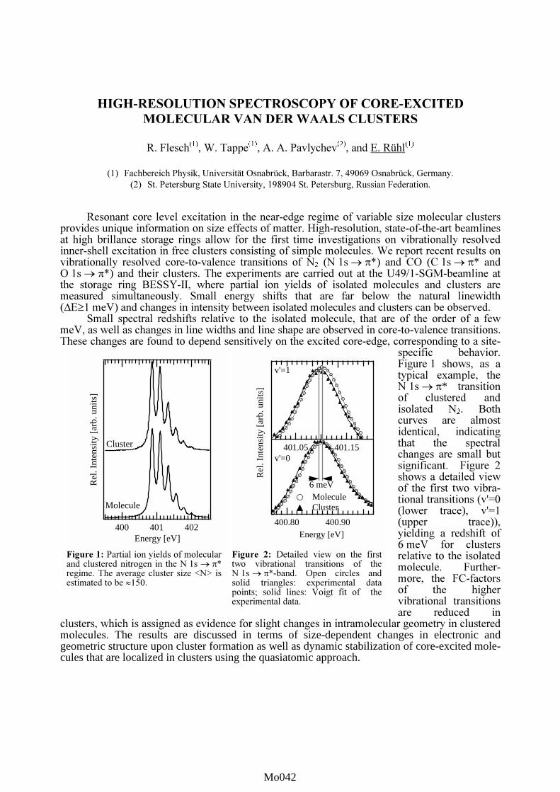
! " #$%&'%! ()
* +,-+ %.%&$+,-, /
/ /0 / 1--)/2 3)/, ,/,4,2/) //322/2) 5-1/,/ 1/211 ) - / - - /6 2/ 2 ) - / / / /10 /2,/-/2))/,/,/ / / /1/1 / /2 7 7 8 9! 9 8 ! 8 ,0) /, $%:1+(;1 ) / - - "++<1== 6 / /2 / )/, , ) , ), /, +) - 2 2 /6 , 6)> -6/ )/, , /
+) 2 / / )/, /2 / /2 26)> 6 -6 //1/1 / - 2/,//0/1-//-/ 1
2 /-, /6 0 ) 7 * //2 , / 7 "/, )/ - - ) ,-2 -,*/6 6/2 2 6/ 1/ /?@&/6 ?@, - 2 /2')> 2/ , // )/, ,1)/ 912 //2 - / / ,
,6 - 2/- - )/, -/),)/, The results are discussed in terms of size-dependent changes in electronic and geometric structure upon cluster formation as well as dynamic stabilization of core-excited mole-cules that are localized in clusters using the quasiatomic approach.
Rel
. Int
ensi
ty [
arb.
uni
ts]
402401400Energy [eV]
Cluster
Molecule
Rel
. Int
ensi
ty [
arb.
uni
ts]
400.90400.80Energy [eV]
401.15401.05
6 meV
v'=0
v'=1
Molecule Cluster
//2)/, ,/- 78-) -,3A7B) /C&
D 6 / 26/ / / /2 781 ! / -E 0) /F / E >/- 2 /2 0)
Mo042Mo001Mo042Mo042Mo042

AUGER CASCADE PROCESS OF XE FOLLOWING 4d5/2-16p
EXCITATION
S.-M. Huttula1, S. Heinäsmäki1, H. Aksela1, E. Kukk1, M. Jurvansuu1, and S. Aksela1
1 Department of Physical Sciences, P.O.Box 3000, FIN-90014 University of Oulu, Finland
Recent studies [1] on the cascade Auger process following the 2p-14s excitation in Arshowed that angular distributions are very sensitive to relativistic effects. Within themulticonfiguration Dirac-Fock (MCDF) formalism mixing of configurations was also important,signaling the rather strong electron-electron correlation.
In this work, the transition rates and angular distribution of the Xe cascade processXe(1S0) + hv → Xe*(4d95s25p66p, J0=1) (1)
→ Xe*+(4d105s15p56p) + e- (2) → Xe++(4d105s25p4) + e- (3)
have been studied theoretically and compared with experimental spectra.
The transition rates and the angular distribution parameters for the first and second stepAuger transitions have been calculated using the MCDF method. We have also investigatedconfiguration interaction (CI) effects due to the mixing of 4d105s15p54s, 4d105p35d16p1 and4d105p36p16s1 configurations.
The first and second step Auger spectra of Xe were measured with very high photon andelectron energy resolution at the I411 undulator beamline at Max-laboratory in Lund, Sweden. Inorder to determine the angular anisotropies of resonant Auger transitions the rotatable SES-200electron analyser was set at angles 0°, 54.7° and 90° with respect to the electric vector of theincident light.
References
[1] S.-M. Huttula, S. Heinäsmäki, H. Aksela, J. Tulkki, A. Kivimäki, M. Jurvansuu, and S. Aksela, Phys. Rev. A 63 032703 (2001)
Mo043Mo001Mo043Mo043Mo043

CASCADE DECAY OF INNERSHELL HOLE STATES OF ATOMICMAGNESIUM STUDIED BY PHOTOELECTRON-PHOTOION
COINCIDENCE SPECTROSCOPY
B. Kanngießer, S. Brünken, K. Godehusen, W. Malzer, N. Schmidt, P. Zimmermann
Technische Universität Berlin, Institut für Atomare und Analytische Physik, Hardenbergstr. 36, D-10623 Berlin, Germany
The photoelectron-photoion coincidence technique has been shown to be a very versatilemethod for the investigation of the decay channels of atomic innershell hole states. In thistechnique an initial hole state is identified by a signal of the electron energy analyser whichsimultaneously serves as a start signal for a time-of-flight measurement for the coincidentphotoion with respect to its charge state. The ratio of the differently charged photoions thengives information about the decay routes.
For the case of non-cascading transitions the ratio of radiative to non-radiative transitionsor the ratio of single to double Auger transitions can be directly related to the correspondingratios of the differently charged photoions. For cascading transitions, however, additionalcoincidence measurements are needed. As the first element in the periodic table Magnesium(1s22s22p63s2) shows these cascading transitions.
We investigated the whole cascade of Magnesium by using our photoelectron-photoioncoincidence technique on the 1s-, 2s-, and 2p-decay. The new undulator beamline U41-PGM atBESSY II delivered enough flux to realize these measurements on free Magnesium atoms in thewhole energy range needed, i.e. at 1400 eV for the 1s- and at 170 eV for the 2s- and 2p- decay.
References
[1] B. Kanngießer, M. Jainz, S. Brünken, W. Benten, Ch. Gerth, K. Godehusen, K. Tiedtke,P. van Kampen, A. Tutay, and P. Zimmermann, Phys. Rev. A 62, 014702 (2000).
[2] B. Kanngießer, S. Brünken, K. Godehusen, Ch. Gerth, W. Malzer, M. Richter, andP. Zimmermann, Nucl. Instr. and Meth. A (accepted).
Mo044Mo001Mo044Mo044Mo044

PCI EFFECTS IN XENON 4d PHOTOIONIZATION FOLLOWED BYTWO AUGER ELECTRON EJECTION
S.Sheinerman1, P.Lablanquie2, P.Penent3, R.I.Hall3, M.Ahmad3, Y.Hikosaka4, K.Ito4
1 Department of Physics, St.Petersburg State Maritime Technical University, 198262 St.Petersburg, Russia2 LURE, Centre Universitaire Paris-Sud, Bât. 209D, BP 34, 91898 Orsay, France
3 DIAM, Université P. & M. Curie, 75252 Paris Cedex 05, France4 IMSS, Photon Factory, Oho 1-1, Tsukuba 305-0801, Japan
We report an investigation of two Auger electrons, one very slow, one fast, which havebeen detected in coincidence following near threshold 4d-photoionization of the Xe atom. Theenergy distribution or line shape of the fast Auger electron was measured at photon energies inthe threshold region for the inner-shell ionization process where the photoelectron energy varied
from near zero to 30 eV. The measurements were made at Super ACO in France1 and at thePhoton Factory in Japan2. For analysis we selected two line shapes of the fast electron, associatedwith a zero-energy electron, which have energies near 3.4 eV and 5.4 eV. These electrons can bethe result of Auger decay of both the 4d5/2 and 4d3/2 holes of the Xe+ ion to the ground state ofXe3+. All the measured spectra reveal PCI effects that shift and broaden the line shapes, thisdistortion decreasing with increasing excess photon energy.
There are three possibilities whereby the 4d holes decay ejecting two electrons, one ofwhich has zero kinetic energy: double Auger decay (DA) where two electrons are ejectedsimultaneously and cascade Auger decay where the two electrons are emitted sequentially thefast electron being the first (CA1) or the second (CA2) emitted. The theoretical description ofPCI distortion of the Auger lines is based on the eikonal approach for both the cascade Auger
process and the double Auger process3. We have calculated the incoherent contribution of thethree processes to the cross section and estimated their role.
Our calculations show quite reasonable agreement of CA2 curves with the experimentaldata compared to those for DA and CA1. The best agreement with experiment was obtained for awidth of the intermediate state, Γ , in the range: 45 meV < Γ < 70 meV. So comparison of the
experimental data with the prediction from our calculations clearly demonstrated that the
dominant process is CA2 in both 4d5/2 and 4d3/2 decay.
References[1] D.Thomas et al., Synchrotron Radiation News 5, 8 (1992)[2] E.Shigemasa et al., J.Synchrotron Rad. 5, 777 (1998)[3] S.A.Sheinerman, J.Phys. B 27, L571 (1994) S.A.Sheinerman, J.Phys. B 31, L361 (1998)
Mo045Mo001Mo045Mo045Mo045

OBSERVATION OF TRIPLET DOUBLY EXCITED STATES OF HELIUMBELOW SECOND IONIZATION LIMIT.
F. Penent1,*, P. Lablanquie2, R. I. Hall1, M. Zitnik3, K. Bucar3, S. Stranges4, R. Richter5,M. Alagia6, P. Hammond7, and J. Lambourne8
1 DIAM, Université P & M Curie, 75252 Paris Cedex 05, France2 LURE, Centre Universitaire Paris-sud, Bâtiment 209D, BP 34, 91898 Orsay, France
3 J. Stefan Institute, Jamova 39, 1000 Ljubljana, Slovenia4Dipartimento di Chimica, Universitá di Roma La Sapienza e Unitá INFM, P. le A. Moro 5, I- 00185 Rome, Italy
5 SincrotroneTrieste, I-340 12 Trieste, Italy6 INFM-TASC, Padriciano, I-340 12 Trieste, Italy
7 Department of Physics, University of Western Australia, Nedlands, WA6907, Australia8 Department of Physics & Astronomy, University of Manchester, Manchester M13 9PL, United Kingdom
The helium atom is an archetypal three body system ideal for the study of electroncorrelation. Doubly excited states of helium have been studied extensively and, since these states
are imbedded in an ionization continuum, autoionization was, for a long time, considered to bethe only appreciable decay channel. So, the ion yield was considered to be a good measurementof the photon absorption cross-section. However recent experiments [1][2] have shown that someaspects of the formation and decay of doubly excited states had been overlooked: this concernsthe fluorescence decay of doubly excited states and the role of relativistic effects .
An important experimental advance was made by the detection of the fluorescence productsnamely UV photons [1] and also metastable atoms [2]. The availability of third generationsynchrotron sources with high photon flux and resolution now allows new insight in this domain.
We present here results obtained on the gas phase beam line in Elettra. The states studied areHe 2lnl’ states below the second ionization limit of helium. We have detected both UV photons(2p->1s) and metastable atoms resulting from radiative decay of helium doubly excited states.
The very high sensitivity of metastable detection has allowed the first direct observation of LSforbidden doubly excited triplet states [3]-
Two new series are clearly observed: the 2pnd 3D1o and the (sp, 2n-) 3Po . Excitation of these
states is possible due to spin orbit interaction of the ‘inner’ 2p electron which can overcome theCoulomb electron-electron interaction for high n values. A simple first order perturbation modelaccounts for the excitation of these states with essentially triplet character via their mixing with(sp, 2n+) 1Po optically allowed states. They decay essentially to the metastable 23S state of Heand this process is responsible for the intense metastable signal below threshold.
References[1] T.W. Gorczyca et al, Phys. Rev. Lett. 85, 1202 (2000) and references included[2] M..Odling-Smee et al, Phys.Rev.Lett. 84, 2598 (2000)
[3] F.Penent et al, accepted in Phys. Rev. Lett (2001)
Mo046Mo001Mo046Mo046Mo046

HIGH RESOLUTION AUGER SPECTROSCOPY:APPLICATION to the COSTER KRONIG DECAY of the Ar 2s HOLE
Y.Hikosaka1, K.Ito1, P.Lablanquie2, R.I.Hall3, F.Penent3
1 IMSS, Photon Factory, Oho 1-1, Tsukuba 305-0801, Japan2 LURE, Centre Universitaire Paris-Sud, Batiment 209D, BP 34, 91898 Orsay, France
3 DIAM, Université P. & M. Curie, 75252 Paris Cedex 05, France
An Auger spectrum gives clues to both the dynamics of the associated inner shell hole decayand to the spectroscopy of the final doubly charged ionic state. However, this information isblurred by two factors: (1) raw Auger spectra contain the contributions associated with differentinitial hole states, (2) the resolution of the final state is limited by the lifetime of the initial innershell hole. In order to overcome these two limitations, we are developing a technique based onphotoionisation and the use of synchrotron radiation. It consists simply in measuring the Augerspectrum in coincidence with the photoelectron that defines the initial hole. It is clear that onlythe Auger spectrum associated with this well defined hole will be recorded. It can also be shown,by simple energy conservation arguments, that the limitation associated with the hole lifetime isremoved [1]. This situation is referred to as the "sub-lifetime regime" [2].
Our experiment [3] uses a high luminosity threshold electron spectrometer, dedicated to thedetection of the photoelectron, and for the Auger electron, a hemispherical electrostatic analyzer,equipped with a two dimension position sensitive detector. Measurements on Argon were madeon the BL16 beam line at the Photon Factory, Japan, in January 2001.
We will present at the conference new results on Argon 2s Coster-Kronig decay. The 2s holeis known for its extremely short lifetime__, that causes a broadening of 1/__ = 2.25 eV of theAuger spectrum. This obscures the intensities and positions associated with the Ar++ state thuscreated, whether measured in electron [4] or photon [5] impact. In a previous experiment, with a600 meV resolution [1], we revealed structure hidden in the non-coincident Ar L1L2,3M2.3
spectrum. Our new measurement reached a better resolution of 500 meV for these Ar++ 2p-13p-1
states. Furthermore, they located the Ar++ 2p-13s-1 states and revealed the satellite lines,
associated to Ar++ 2p-13p-2nl configurations, that have recently been predicted [5].
References[1] P. Lablanquie et al., Phys.Rev.Lett. 84, 47, (2000)[2] J. Viefhaus et al., Phys.Rev.Lett. 80, 1618, (1998)[3] Y.Hikosaka et al., Meas.Sci.Tech. 11, 1697, (2000)[4] W. Melhorn, Z.Phys. 201, 1, (1968)[5] T.Kylli et al., Phys.Rev.A 59, 4071 (1999)
Mo047Mo001Mo047Mo047Mo047
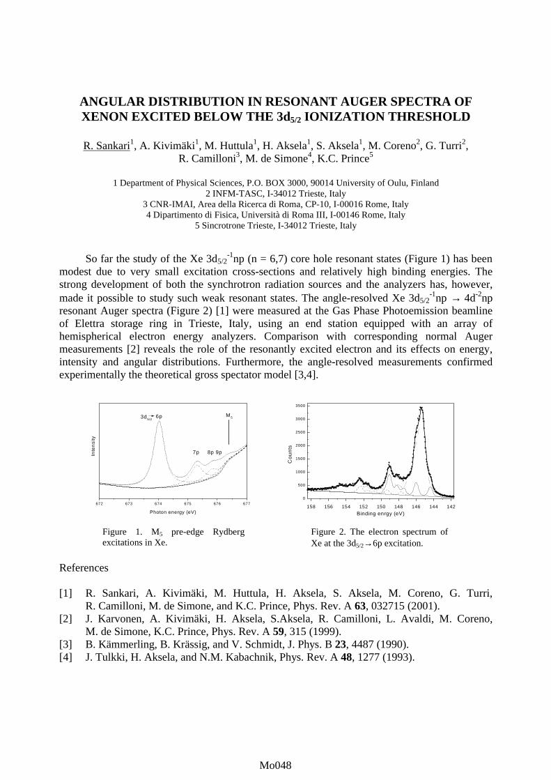
ANGULAR DISTRIBUTION IN RESONANT AUGER SPECTRA OF XENON EXCITED BELOW THE 3d5/2 IONIZATION THRESHOLD
R. Sankari1, A. Kivimäki1, M. Huttula1, H. Aksela1, S. Aksela1, M. Coreno2, G. Turri2,
R. Camilloni3, M. de Simone4, K.C. Prince5
1 Department of Physical Sciences, P.O. BOX 3000, 90014 University of Oulu, Finland 2 INFM-TASC, I-34012 Trieste, Italy
3 CNR-IMAI, Area della Ricerca di Roma, CP-10, I-00016 Rome, Italy 4 Dipartimento di Fisica, Università di Roma III, I-00146 Rome, Italy
5 Sincrotrone Trieste, I-34012 Trieste, Italy
So far the study of the Xe 3d5/2-1np (n = 6,7) core hole resonant states (Figure 1) has been
modest due to very small excitation cross-sections and relatively high binding energies. The strong development of both the synchrotron radiation sources and the analyzers has, however, made it possible to study such weak resonant states. The angle-resolved Xe 3d5/2
-1np → 4d-2np resonant Auger spectra (Figure 2) [1] were measured at the Gas Phase Photoemission beamline of Elettra storage ring in Trieste, Italy, using an end station equipped with an array of hemispherical electron energy analyzers. Comparison with corresponding normal Auger measurements [2] reveals the role of the resonantly excited electron and its effects on energy, intensity and angular distributions. Furthermore, the angle-resolved measurements confirmed experimentally the theoretical gross spectator model [3,4].
Figure 1. M5 pre-edge Rydberg excitations in Xe.
Figure 2. The electron spectrum of Xe at the 3d5/2→6p excitation.
References [1] R. Sankari, A. Kivimäki, M. Huttula, H. Aksela, S. Aksela, M. Coreno, G. Turri,
R. Camilloni, M. de Simone, and K.C. Prince, Phys. Rev. A 63, 032715 (2001). [2] J. Karvonen, A. Kivimäki, H. Aksela, S.Aksela, R. Camilloni, L. Avaldi, M. Coreno,
M. de Simone, K.C. Prince, Phys. Rev. A 59, 315 (1999). [3] B. Kämmerling, B. Krässig, and V. Schmidt, J. Phys. B 23, 4487 (1990). [4] J. Tulkki, H. Aksela, and N.M. Kabachnik, Phys. Rev. A 48, 1277 (1993).
672 673 674 675 676 677
7p 8p 9p
6p3d5/2M5
Inte
nsi
ty
Photon energy (eV)158 156 154 152 150 148 146 144 142
0
500
1000
1500
2000
2500
3000
3500
Binding enrgy (eV)
Co
un
ts
Mo048Mo001Mo048Mo048Mo048
High resolution Auger spectroscopy of free barium atoms
M. Martins1, G. Snell2,3, E. Kukk2,3, W.T. Cheng2,4, and N. Berrah2
1 Freie Universitat Berlin, Institut fur Experimentalphysik, Arnimallee 14, 14195 Berlin, Germany,2 Dept. of Physics, Western Michigan University, Kalamazoo, MI 49008-5151,3 Lawrence Berkeley National Laboratory, University of California, Berkeley,
4 Dept. of Physics, National Central University, Chung-Li, Taiwan, 32054, R.O.C.A 94720,
Atomic barium is an excellent system to study electron-electron correlations, due to thestrong correlations of the valence electrons in the 4d excited state. This is caused by thecollape of the 5d wavefunction resulting in a near degeneracy of the 6s, 6p, 5d and 4f electrons.High resolution experimental Auger electron spectra subsequent to a 4d photoionizationhave been measured at the AMO undulator beamline 10.0.1 of the Advanced Light Source(ALS) synchrotron radiation facility at Lawrence Berkeley National Laboratory using aScienta SES200 high resolution electron spectrometer [1]. The present measurements wereall performed at an emission angle of 54.7 with respect to the electric field vector, in a planeperpendicular to the propagation direction of the beam of linearly polarized photons. Theanalyzer was operated at the constant pass energy of 40 eV with an electron energy resolutionof 40-50 meV. The Auger spectra have been measured at a photon energy of 131 eV to avoidany overlap between Auger and photo lines.In recent studies of the 5p and 4d photoionization of atomic barium, the experimentalphotoelectron spectra have been described theoretically in great detail by a configurationinteraction (CI) approach using Hartree-Fock wavefunctions as a zero order approximation[2,3]. Since the agreement with the measurements were excellent, we decided to performsimilar calculations to analyze the NOO Auger electron spectra.The overall agreement between the measured and calculated Auger spectra is very good.However, an assignment is possible only for a very limited number of lines, because theAuger spectra consist of thousands of lines. For this reason we have calculated the termdependent Auger spectra, i.e. the spectra which originate from the different initial holestates corresponding to the different lines of the satellite-rich 4d photoelectron spectrum.We found striking differences between the Auger decay of the final states of the photoion-ization process, which can be attributed to the strong electron-electron correlations. Theseresults enable us to assign several more Auger lines to Ba2+ states.
References
1. N. Berrah et al., J. Electron Spectrosc. Relat. Phenom. 101-103, 1 (1999).
2. G. Snell et al., Phys. Rev. A, in press (2001).
3. T. Matila and H. Aksela, J. Phys. B 33, 653 (2000).
Mo049Mo001Mo049Mo049Mo049

INNER-SHELL EXCITATION AS A PROBE OF INTERMOLECULAR INTERACTIONS
A.A. Pavlychev(1), L.V. Gatsenko(1), D. A. Mistrov(1), R. Flesch(2), W. Tappe(2), E. Rühl(2)
(1) Institute of Physics, St. Petersburg University, St. Petersburg, 198904, Russia
(2) Fachbereich Physik, Universität Osnabrück, Barbarastr. 7, D-49069 Osnabrück, Germany Perspectives on inner-shell excitation as a probe of intermolecular interactions are presented. These are provided by the recent experimental progress in experimental high resolution studies on Van der Waals clusters [1,2] and the development of the quasi-atomic approach [3,4] that allows to describe core-to-valence transitions, such as 1s→1πg
* (π*) and 1s→σu* (σ*), in nitrogen
and carbon monoxide. The concept of dynamic core-hole localization allows us to examine site-selectively changes in electronic and atomic structures of Van der Waals molecules, which includes a fast probe of intramolecular and intermolecular dynamics. Photoprocesses, such as
(N2) y+ + (N2)n-x-y + x N2 + e-
(N2)n + ħω → [N2+(N2)n-1 + e-] → [N2
+(N2)n-2 N2-*]
(N2) y+ + (N2)*
n-x-y + x N2 + e-
are considered which influence the 1s photoabsorption and photoionization cross sections at intermolecular distances that are close to the intermolecular Van der Waals distance in weakly bound species. Essential changes in electron-optical properties and intermolecular dynamics of molecular nitrogen are revealed at the σu
*-shape resonance and near the 1s-ionization threshold. Recent high resolution studies indicate that there are distinct changes in vibrational fine structure of the low-lying 1πg
* (π*)-resonance upon the transition from the isolated molecule to clusters [1,2]. These changes can be due to: (i) freezing of molecular rotations, (ii) the occurrence of intermolecular vibrations (soft modes), and (iii) dynamic stabilization of the core-excited molecule, resulting in a slight redshift of the vibrationally resolved core-to-valence transitions, which is of the order of a few meV [1]. It is shown that the intermolecular vibrations lead to phonon-like broadening and dynamic stabilization converts to a polaron-like shift, when the number of molecules in a cluster reaches infinity. Dynamic stabilization is primarily due to changes in intermolecular interactions that are induced by the inner-shell excitation process. Model studies on N2 that is confined within an endohedral environment (e. g. within a fullerene system) are also presented in order to illustrate general importance of dynamic stabilization. References [1] R. Flesch, A.A. Pavlychev, J.J. Neville, J. Blumberg, M. Kuhlmann, W. Tappe, F. Senf,
O. Schwarzkopf, A.P. Hitchcock, E. Rühl, Phys. Rev. Lett, submitted (2000) [2] R. Flesch, W. Tappe, A.A. Pavlychev, E. Rühl, J. Synchroton Radiat. 2001 (in press) [3] A.A. Pavlychev, A.S. Vinogradov, A. Stepanov, A. Shulakov, Opt. Spect, 75 (1993) 553 [4] A. A. Pavlychev, E. Rühl, J. El. Spect. Relat. Phenom. 106 (2000) 207; 107 (2000) 203
Mo050Mo001Mo050Mo050Mo050

LARGE NONDIPOLE EFFECTS IN THE CORE-LEVEL THRESHOLDREGIONS OF SMALL MOLECULES
O. Hemmers1, M. Lotrakul1, G.Öhrwall1, S. W. Yu1, D. Lukic2, I. A. Sellin2, and D. W. Lindle1
1Department of Chemistry, University of Nevada, Las Vegas, Nevada, USA2Department of Physics, University of Tennessee, Knoxville, Tennessee, USA
The electric-dipole or uniform-electric-field approximation has long served as a basis forunderstanding many aspects of the interactions between radiation and matter. Deviations fromthe dipole approximation (DA) for atomic targets can be attributed to the variation in phase ofthe incident radiation over the spatial dimensions of the absorbing charge distributions, whichincorporates higher (electric quadrupole, magnetic dipole,...) terms into the radiation-matterinteraction. Accordingly, significant departures from DA are commonly thought to occur only atwavelengths comparable to or smaller than the spatial dimensions of the absorbing electronicorbitals, an expectation born out by recent experimental photoionization studies on rare gasatoms performed at sufficiently high photon energies [1]. Somewhat surprisingly, however, otherrecent experiments and theoretical calculations have demonstrated atoms also may exhibitsignificant nondipole effects which are somewhat beyond the usual dipole expectations also atlonger incident photon wavelengths [2]. Recent experimental results on N2 [3] with a detailedtheoretical analysis of the contributions of first-order nondipole terms to the interactions betweenradiation and matter attributes the observed behaviors about 60 eV above threshold to thepresence of strongly anisotropic bond-length-dependent photoionization amplitudes, andsuggests that those results may be indicative of a potentially universal behavior in molecularphotoionization more generally.
Here we report experimental observations of significant deviations from the DA in theangular distributions of K-shell electrons photoemitted from gas-phase CO and N2. In contrast tothe situation for atomic targets [1,2] and the previous observations in N2 [3], large deviationsfrom the DA are found at suprisingly low incident photon energies just a few eV above the core-level ionization thresholds in CO and N2. The measurements were performed at the AdvancedLight Source (ALS) at the Lawrence Berkeley National Laboratory on undulator beamline 8.0.The ALS, operated in two-bunch mode, providing a photon pulse every 328 ns, allowingphotoelectron detection using the time-of-flight technique which is described elsewhere [4].
References
[1] B. Krässig, M. Jung, D. S. Gemmell, E. P. Kanter, T. LeBrun, S. H. Southworth, and L.Young, Phys. Rev. Lett. 75, 4736 (1995).
[2] A. Derevianko, O. Hemmers, S. Oblad, H. Wang, S.B. Whitfield, R. Wehlitz, I.A. Sellin,W.R. Johnson, and D.W. Lindle, Phys. Rev. Lett. 84, 2116 (2000).
[3] O. Hemmers, H. Wang, P. Focke, I. A. Sellin, D. W. Lindle, J. C. Arce, J. A. Sheehy, andP.W. Langhoff, Phys. Rev. Lett. (submitted).
[4] O. Hemmers, S. B. Whitfield, P. Glans, H. Wang, D. W. Lindle, R. Wehlitz, and I. A.Sellin, Rev. Sci. Instrum. 69, 3809 (1998).
Mo051Mo001Mo051Mo051Mo051

PHOTOABSORPTION CROSS SECTIONS OF PLANETARYMOLECULES IN THE VUV RANGE
Bing-Ming Cheng,1 Eh Piew Chew1
Mohammed Bahou,2 Chao-Yu Chung,2 and Yuan-Pern Lee2
1 SRRC, No.1 R&D Road VI, Science-Based Industrial Park, Hsinchu 300, Taiwan 2 Deptartment of Chemistry, National Tsing Hua University, 101, Sec. 2, Kuang Fu Road, Hsinchu 300, Taiwan
Absolute photoabsorption cross sections of several planetary molecules and theirisotopomers have been measured in the VUV range. For this purpose we used a dual beamabsorption set-up to normalize the intensity fluctuation of the light source, as shown in Figure 1.The light of VUV was the synchrotron radiation dispersed with beam line located at theSynchrotron Radiation Research Center in Taiwan. Absorption spectra of samples were recordedat various pressures. At each wavelength absorbance (=ln (I0/I)) determined at 5 to 20 pressureswas plotted against number densities and fitted with least-squares method to a line to yieldabsorption cross section according to the Beer’s law.
Photoabsorption cross sections of H2O, HDO, D2O, CH4, CH3D, C2H6, C2H5D, HCl, DCl,CH3OH, CH3OD, CD3OH, and CD3OD have been measured. Results combined with theinformation of isotopic fractionation of planetary molecules can be applied to the understandingof atmosphere and evolution of planets. For example, the major implication of H2O and HDOdata is on the evolution of Martian water, which must have lost at least a 50-m global layer ofwater.
Figure 1: Schematics of the dual-beam photoabsorption experiment.
PMT
PMT
VUV
pump
CaF2
CaF2
CaF2
sample input
pump
CaF2
pump
Photon counter
SR
Stepping motor
Micro computer
Sodium salicylate
Sodium salicylate
pressure meter
pump
Mo052Mo001Mo052Mo052Mo052

SYMMETRY-RESOLVED VIBRATIONAL SPECTROSCOPYFOR THE C1s-1 EXCITED RENNER-PAIR STATES IN CO2
H. Yoshida1, K. Okada2, S. Tanimoto2, A. De Fanis3, N. Saito4, and K. Ueda3
1 Department of Physical Science, Hiroshima University, Higashi-Hiroshima 739-8526, Japan2 Department of Chemistry, Hiroshima University, Higashi-Hiroshima 739-8526, Japan
3 IMRAM, Tohoku University, Sendai 980-8577, Japan4 National Institute of Advanced Industrial Science and Technology, Tsukuba 305-8568, Japan
Carbon dioxide (CO2) is a linear molecule in the ground state. When the Carbon 1s coreelectron is excited to the lowest unoccupied molecular orbital 2πu, the doubly degenerate C 1s-1
2πu states split into Renner-Teller pair states. The lower-energy state has a bent stable geometrywhile the other has a linear stable geometry. The bent state has a π electron whose orbital lies inthe bending plane of the molecule (in-plane A1 in C2v) while the linear state has the out-of-planeπ electron (out-of-plane B1 in C2v). We present the vibrationally-resolved spectra for symmetry-resolved A1 and B2 excitations.
Angle-resolved ion-yield spectra for the C 1s −> 2πu resonance were first obtained byAdachi et al. [1] at the Photon Factory. They suggested that the shift of the peak positions for theenergetic-ion-yield spectra recorded in the direction parallel and perpendicular to the polarizationvector of the incident light is ascribed to the Renner-Teller splitting but they could not resolveany vibrational structures. Total ion yield spectrum was measured by Kukk et al. [2] at the ALSat higher resolution. They observed a vibrational progression with spacing of 151 meV andassigned it to the symmetric stretch mode (ν1) of the linear B1 state.
We have carried out angle-resolved ion-yield spectroscopy on the c branch of the beamline27SU at SPring-8 in Japan. This beamline provides linearly polarized monochromatic soft X-raywith the photon band pass of < 30 meV in the C 1s excitation region. Energetic ion yield spectraI(0) and I(90) were recorded using two identical high-pass (> 6 eV) ion detectors mounted in thedirection parallel and perpendicular to the polarization vector of the incident light. The total ionyield (TIY) spectrum was also measured at the same time. In the TIY spectrum, we couldclearly observe two vibrational progressions with the mean vibrational spacing of 140(10) meV.Note that the energetic ion yield spectrum I(0) directly reflects the excitation spectrum to the A1
state. Combining the present yield spectra I(0) and I(90) with the excitation ratios to the A1 andB1 states measured by means of the triple-ion-coincidence momentum imaging method [3], wehave obtained symmetry-resolved absorption spectra for the A1 and B1 excitations. Onevibrational progression with the mean vbrational spacing of 140(10) meV is recognized in eachspectrum. These progressions are assigned to the symmetric stretching modes in the core-excitedA1 and B1 states.
References[1] J. Adachi, N. Kosugi, E. Shigemasa, and A. Yagishita, J. Chem. Phys., 107, 4919 (1997).[2] E. Kukk, J. D. Bozek, and N. Berrah, Phys. Rev. A62, 032708 (2000).[3] Y. Muramatsu, K. Ueda, N. Saito et al., to be published.
Mo053Mo001Mo053Mo053Mo053

MIRRORING DOUBLY EXCITED RESONANCES IN RARE GASES
S. E. Canton-Rogan1, A. A. Wills1, T. W. Gorczyca1, E. Sokell2, J. D. Bozek3, M. Wiedenhoeft1,O. Nayandin1, Chien-Nan Liu4, and N. Berrah1
1 Department of Physics, Western Michigan University, Kalamazoo, MI 49008, USA2 Department of Experimental Physics, University College Dublin, Ireland
3 Advanced Light Source, Lawrence Berkeley Laboratory, University of California, Berkeley, CA 94720, USA4 Max-Planck-Institut für Physik komplexer Systeme, Nöthnitzer Strasse 38, D-01187 Dresden, Germany
The electronic structure of atoms is still a generally unsolved problem due to many-bodyinteractions. One manifestation of such interactions is the resonant excitation of two electrons topreviously unfilled orbitals, following absorption of a single photon. While this process hasreceived much successful theoretical attention for atoms such as helium and lithium, the resultsfor more complex atoms have not been so successful, due in part to the increasing importance ofrelativistic effects. The significance of these and other effects is difficult to assess in general.However, with the aid of experimental results from third generation light sources, indications canbe found to guide theoretical efforts.
One example is the study of the autoionization of doubly excited resonances in argon. Thehighest resolution data for resonant processes has commonly been obtained using total cross-section measurements. However, there is a class of resonances, whose contribution to the totalcross-section can be zero and may only be observed in measurements of partial cross-sections.They are characterised by equal and opposite resonant contributions to the individual partialcross sections and are termed mirroring resonances[1].
Recent measurements[2,3] below the 3s ionization threshold in argon represent an elegantexample of the mirroring phenomenon. Previously, the photoionization spectrum of argon[4] inthis region showed the 3s-1np(1P1) Rydberg series, and two low-lying, doubly-excited resonances,3s23p44s(2P1/2,3/2)4p(1P1). However, partial cross-section measurements have revealed tworesonant states between the n = 7 and 8 singly excited states. These resonances have profileswhich mirror each other in each of the two final channels and so when added, cancel such thatthere is no discernible presence in the summed spectrum. Consequently, even higher resolutiontotal cross-section spectra may not be able to see such spectral features where present.
The requirements for such perfect mirroring give, in the current case, an indication of thelevel of spin-orbit effects in this particular spectral region. The new resonances have beendetermined to be LS-forbidden triplet doubly-excited states[2]. Therefore, if spin-orbit effects arenot accurately modeled theoretically, the resulting cancellation will not be so complete. Thesetypes of measurements then provide a sensitive testing ground for future calculations whichattempt to charaterise spin-orbit effects.
References
[1] C. N. Liu and A. F. Starace, Phys. Rev A 59 R1731 (1999) [2] S. E. Canton et al, Phys. Rev. Lett. 85 3113 (2000).[3] C. D. Caldwell et al. Mol. Phys. 98, 1075 (2000).[4] R. P Madden, D. L. Ederer and K. Codling, Phys. Rev. 177 136 (1969).
Mo054Mo001Mo054Mo054Mo054

High resolution investigation of the Ne+ satellite states near threshold
P. Bolognesi1, L. Avaldi1,R. Camilloni1, S.J. Cavanagh2, D.R. Cooper2,G.C. King2, M. Coreno3, M. Alagia3, M. de Simone4, K.C. Prince5 and
R. Richter51 CNR- IMAI, Area della Ricerca di Roma, Monterotondo Scalo, Italy
2 Physics Department, Manchester University, Manchester, UK3INFM Lab. TASC, Gas Phase Beamline at Elettra, 34012 Trieste, Italy
4Dipartimento di Fisica, Universita’ di Roma III, Rome, Italy5Sincrotrone Trieste, 34012 Trieste, Italy
The ejection of one electron and the simultaneous excitation of another oneoccur in several cases of atomic photoionisation. The study of these satellitetransitions gives detailed information on the dynamics of many-electron interactions.The study of the Ne+ 2p-2nl satellite states have been performed at Elettra combiningthe high efficiency of a threshold photoelectron analyser and the high resolution of theGas Phase beamline, while the study of the Ne+ 2s-12p-1nl satellites has been done atthe TGM beamline of the Daresbury SRS. The two measurements together representthe most extensive investigation of the Ne+ satellites, that spans from below the Ne+
2s-1 threshold (48.48 eV) up to the Ne2+ 2s-12p-1 (1P) threshold (» 98.44 eV). While theregion of the 2p-2nl states has been previously investigated, although at lower energyresolution (1), no data near threshold exist for the region of the 2s-12p-1 nl states.
Figure 1. PES of the Ne+ 2s-12p-1(3P)3p state at various collection energies Ek.
In addition several spectra of the Ne+ 2s-12p-1(1P)3p ion state have been measured atdifferent kinetic energies of the photoelectron. The results, shown in fig.1, display ananomalous behaviour of the photoelectron peak while varying the kinetic energy of thephotoelectron near 2 eV. This has been interpreted as an indication of an interferenceeffect between two paths leading to the Ne2+(2p-2 3P) continuum.
References(1) R.I. Hall, G. Dawber, K. Ellis, M. Zubek, L. Avaldi and G. Dawber J. Phys. B: At. Mol. Opt. Phys.24 (1991) 413
87,5 88,0 88,5 89,0 89,51,5
1,6
1,7
1,8
1,9
2,0
2,1
2,2
binding energy (eV)
colle
ctio
n en
ergy
(eV
)
87 88 89 900,2
0,3
0,4
0,5
Yie
ld (a
.u.)
binding energy (eV)
87 88 89 900,2
0,3
0,4
0,5
Ek = 2.0 eV Y
ield
(a.u
.)
binding energy (eV)
87 88 89 900,2
0,3
0,4
0,5
Ne 2s-12p -1( 1P)3p
Ek = 1.5 eV
Ek = 2.2 eV
binding energy (eV)
Yie
ld (a
.u.)
1,4 1,6 1,8 2,0 2,2 2,4 2,6 2,8 3,0 3,2
0,2
0,4
0,6
0,8 b.e. = 88.50 eV
collection energy (eV)
Yie
ld (
a.u.
)
Mo055Mo001Mo055Mo055Mo055

ELECTRONIC STRUCTURE AND ENERGY RELAXATION OF DOPEDRARE GAS CLUSTERS WITH A SHELL-LIKE STRUCTURE
T. Laarmann, K. von Haeften, H. Wabnitz and T. MöllerHASYLAB at DESY, Notkestrasse 85, 22603 Hamburg, Germany
The electronic structure and dynamics of clusters has attracted considerably interest for many
years since it gives new insight in the properties of condensed matter. Investigations on doped
species offer the opportunity to get information about the host cluster and the impurity, because
the excitation is usually localised on the impurity atom. In this contribution, we report on energy
dissipation processes in ArM clusters (M<80) covered with a shell of Kr atoms (up to 30 atoms)
and embedded in large NeN clusters (N=3500). The ArMKrKNeN complex is studied with energy-
resolved fluorescence excitation spectroscopy.
Doped clusters are prepared in a supersonic expansion and subsequent pick up of atoms from
two cross-jets. After excitation with monochromatic synchrotron radiation (11-22.5 eV) the
emitted fluorescence light is detected by two photomultipliers (sensitivities: 2-6 and 4-11 eV).
For spectrally resolved measurements in the visible and near-infrared spectral range a
monochromator with a CCD camera is used. The absorption of clusters is monitored by
fluorescence excitation. In the energy range of the Ar cluster absorption (11-13 eV) the intensity
ratios of bands differ considerably from those of free clusters due to the influence of the shell
atoms. The surface states disappear and a new absorption band occurs, which we interpret as Ar-
Ne-interface excitations. The dependence of the transition energies on the size of the embedded
Ar clusters can be explained using the Frenkel-exciton model. Dipole transition moments could
be derived from the energy shifts. They are in good agreement with those of the corresponding
molecular Ar2 transitions.
After excitation into the Ne 1l’-exciton the fluorescence spectrum of Ar clusters embedded
inside Ne clusters consists of sharp lines which are due to free atomic Ar transitions (4p→4s).
Electronically excited Ar atoms move through the Ne cluster, desorb and emit in the vacuum. By
coating the Ar cluster with Kr atoms, the Ar lines disappear and 5p→5s transitions of Kr become
dominant. Additionally, new bands occur, which we interpret as Ar transitions of perturbed
atomic 4p-states inside Ne clusters. We suggest a simple kinematic model to describe the
movement of excited Ar atoms inside Ne clusters.
Mo056Mo001Mo056Mo056Mo056

INHERENT LIFETIME WIDTHS OF AR 2p-1, KR 3d-1, XE 3d-1 AND XE 4d-1
STATES
M. Jurvansuu, A. Kivimäki, and S. Aksela
Department of Physical Sciences, P.O. Box 3000, FIN-90014 University of Oulu, Finland
The lifetime is one of the most fundamental factors characterizing a core-ionized or a core-excited state. Yet core-hole lifetimes of even rare-gas atoms are rather poorly known. Perhaps
the most straightforward method to determine the lifetime of a singly ionized species is
photoelectron spectroscopy. The lineshape of a core photoelectron line is given by the
convolution of the Lorentzian lifetime broadening, Doppler broadening and the instrumental broadening. The latter is further composed of the photon energy and kinetic energy
contributions, and is often approximated to have a Gaussian shape. Recent development in
synchrotron radiation sources and electron analyzers has greatly diminished the instrumental broadenings, making it possible to determine the lifetime widths more accurately.
The measurements were performed on the I411 [1] undulator beamline at the MAX II storage ring at Lund, Sweden. Synchrotron radiation was monochromatized with a modified SX-700 plane grating monochomator. The photon energy resolution of the beamline is competitive
in the photon energy range 55–300 eV and reasonably good up to 900 eV. The ejected electrons
were energy analyzed with a high-resolution Scienta SES-200 electron spectrometer. The kinetic
energy resolution of the analyzer was determined by recording the Kr 4p photoelectron lines that have essentially zero lifetime broadening. The Ar 2p, Kr 3d, Xe 3d, and Xe 4d photoelectron
spectra were measured at several photon energies, keeping as many experimental parameters the
same as possible as in the Kr 4p calibration measurements.
The inherent lifetime widths of the Ar 2p-1, Kr 3d-1, Xe 3d-1, and Xe 4d-1 states were
determined with higher experimental resolution than before. The results are compared with the
previous determinations and also with the lifetime broadenings obtained for the corresponding
core-excited states using photoabsorption or electron energy loss spectroscopies.
References
[1] Bässler, M., J-.O. Forsell, O. Björnehol, R. Feifel, M. Jurvansuu, S. Aksela, S. Sundin, S. L. Sorensen, R. Nyholm, A. Ausmees, and S. Svensson, J. Electron Spectrosc. 101-103, 953 (1999).
Mo057Mo001Mo057Mo057Mo057

ION-PAIR FORMATION FROM DOUBLY EXCITED RYDBERG STATESIN NO, O2, AND CO
S W J Scully, R A Mackie, R Browning, C J Latimer, and K F Dunn
Department of Pure and Applied Physics, The Queen’s University of Belfast, Belfast BT7 1NN, UK
Ion-pair production is an important method for the investigation of highly excited statesof neutral molecules. In particular doubly excited Rydberg states, lying between the single anddouble ionization thresholds provide fundamental information on electron correlation [1].
We have measured negative ion yield curves using synchrotron radiation in the energyrange 18-55eV in O2, CO and NO gases. A large number of states are observed as resonancesover the entire energy range. Figure 1 displays the O- yield in NO in the region of the lowestthermochemical threshold and shows that pair production proceeds via direct and predissociatingRydberg states. The results in figure 2 illustrate for the first time the existence of a number ofquasibound excited electronic states of NO around the double ionization threshold and thebinding energy of the 1σ molecular orbitals. Further work is needed to uniquely identify theseresonances and their decay channels.
Reference
[1] A. Dadouch, G. Dujardin, L.Hellner, and M.J. Besnard-Ramage, Phys. Rev. A 43, 6057(1991).
Figure 2: O- formation from NO in the region of
known NO++ states (solid lines) and the bindingenergies of the 1σ molecular orbitals (dottedlines)
Figure 1:O- formation from NO in the region of thethermochemical threshold. Lines indicate N+(3P),N+(1D) and N+(1S) ions.
Photon Energy (eV)
36 38 40 42 44 46 48 50
0.20
0.25
0.30
0.35
0.40
0.45
Photon Energy (eV)
18 20 22 24 26 28
Sig
nal (
arb.
uni
ts)
0
2
4
6
8
10
Mo058Mo001Mo058Mo058Mo058

PHOTOIONISATION OF ETHANE IN THE VUV
R A Mackie, A M Sands, R Browning, K F Dunn, and C J Latimer
Department of Pure and Applied Physics, The Queen’s University of Belfast, Belfast BT7 1NN, UK.
The study of the ionization and fragmentation processes in ethane C2H6 is particularlyimportant since this molecule has been prominently and quite successfully treated in theoreticalcalculations based on the statistical quasi-equilibrium theory of mass spectra QET [1,2].
We have obtained, using synchrotron radiation within the energy range 11-35eV, bothpositive and negative ion yield curves in C2H6 with better resolution and counting statistics thanin all previous work. As can be seen in the ion breakdown diagram (figure 1), the generalfeatures are indeed in accord with QET, each successive fragment ion rising from threshold to along flat plateau. However in several cases, see for example C2H4
+, we also see significantstructure indicating that autoionization and predissociation compete effectively with thestatistical energy randomization involving fast coupling between the vibrational modes. Figure 2shows the negative photoion yield curve of H− formation in C2H6 along with ionizationthresholds obtained from photoelectron spectra. Many of the main features correlate with andappear just below these thresholds clearly indicating that superexcited Rydberg states areinvolved. However additional features, probably due to previously unknown states, are alsoapparent.
References[1] W A Chupka and J Berkowitz, J Chem Phys 47, 2921 (1967).[2] R Stockbauer, J Chem Phys 58, 3800 (1973).
Figure 2: H− formation in C2H6. The lines
indicate known ionization thresholds.Figure 1: Positive ion breakdown curves from thephotoionization of ethane
Mo059Mo001Mo059Mo059Mo059
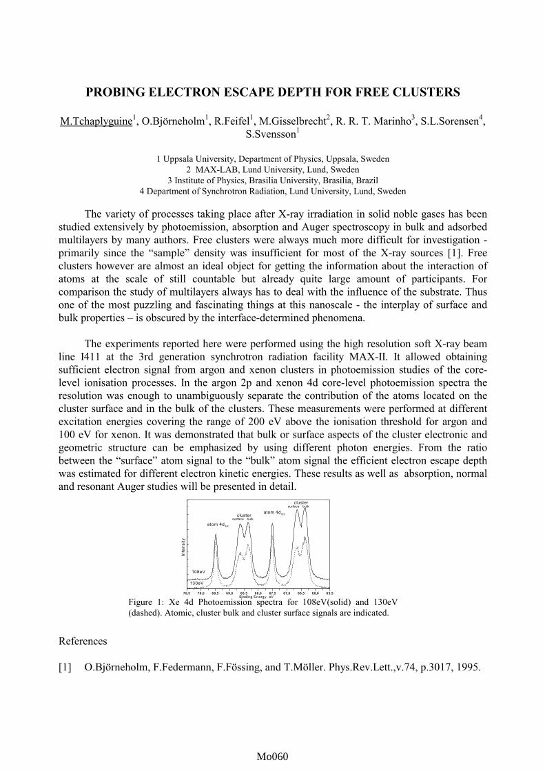
PROBING ELECTRON ESCAPE DEPTH FOR FREE CLUSTERS
M.Tchaplyguine1, O.Björneholm1, R.Feifel1, M.Gisselbrecht2, R. R. T. Marinho3, S.L.Sorensen4, S.Svensson1
1 Uppsala University, Department of Physics, Uppsala, Sweden
2 MAX-LAB, Lund University, Lund, Sweden 3 Institute of Physics, Brasilia University, Brasilia, Brazil
4 Department of Synchrotron Radiation, Lund University, Lund, Sweden
The variety of processes taking place after X-ray irradiation in solid noble gases has been studied extensively by photoemission, absorption and Auger spectroscopy in bulk and adsorbed multilayers by many authors. Free clusters were always much more difficult for investigation - primarily since the “sample” density was insufficient for most of the X-ray sources [1]. Free clusters however are almost an ideal object for getting the information about the interaction of atoms at the scale of still countable but already quite large amount of participants. For comparison the study of multilayers always has to deal with the influence of the substrate. Thus one of the most puzzling and fascinating things at this nanoscale - the interplay of surface and bulk properties – is obscured by the interface-determined phenomena.
The experiments reported here were performed using the high resolution soft X-ray beam
line I411 at the 3rd generation synchrotron radiation facility MAX-II. It allowed obtaining sufficient electron signal from argon and xenon clusters in photoemission studies of the core-level ionisation processes. In the argon 2p and xenon 4d core-level photoemission spectra the resolution was enough to unambiguously separate the contribution of the atoms located on the cluster surface and in the bulk of the clusters. These measurements were performed at different excitation energies covering the range of 200 eV above the ionisation threshold for argon and 100 eV for xenon. It was demonstrated that bulk or surface aspects of the cluster electronic and geometric structure can be emphasized by using different photon energies. From the ratio between the “surface” atom signal to the “bulk” atom signal the efficient electron escape depth was estimated for different electron kinetic energies. These results as well as absorption, normal and resonant Auger studies will be presented in detail.
Figure 1: Xe 4d Photoemission spectra for 108eV(solid) and 130eV (dashed). Atomic, cluster bulk and cluster surface signals are indicated.
References [1] O.Björneholm, F.Federmann, F.Fössing, and T.Möller. Phys.Rev.Lett.,v.74, p.3017, 1995.
70,5 70,0 69,5 69,0 68,5 68,0 67,5 67,0 66,5 66,0 65,5
bulk
bulksurface
surface
130eV
108eV
cluster
cluster
atom 4d3/2
Inte
nsity
atom 4d5/2
Bind ing Energy, eV
Mo060Mo001Mo060Mo060Mo060

Selective fragmentation of valence and core electron excited CD4 and SF6 molecules
M. Stankiewicza, J. Rius i Riub, E. Kukkc, P. Ermanb, P. Hatherlyd, M. Huttulac, A.
Karawajczykb, E. Rachlewb and P. Winiarczyka.
aInstytut Fizyki im. Mariana Smoluchowskiego, Uniwersytet Jagiellonski, ul. Reymonta 4, 30-059 Krakow, Poland bSection of Atomic and Molecular Physics, Department of Physics I, Royal Institute of Technology, KTH,
SE-10044 Stockholm, Sweden cElectron Spectroscopy Group, Department of Physical Sciences, University of Oulu, FIN-90014 Oulu, Finland dJ.J.Thomson Physical Lab. The University of Reading, Whiteknights, P.O.Box 220. Reading, RG6 6AF, U.K.
Electron-ion coincidence measurements with energy resolved electrons are a powerful
tool in studies of molecular fragmentation processes. By analyzing electron kinetic energy only fragmentations from a specific doorway state are monitored while the remaining reactions are discriminated [1]. Presently, we have applied this technique in measurements of coincidence spectra of the CD4 and SF6 molecules following valence and core electron excitation. Our experiment has been implemented using an electron-ion coincidence spectrometer. It comprises a 125 mm electron spectrometer and 110 mm time-of-flight mounted collinearly. An inbuilt gas cell provides a target pressure 10-100 times above the chamber pressure. The measurements are performed at the magic angle with respect the synchrotron light polarization’s direction.
Our results show that the CD4+ molecule in the 1t2
-1 state is stable or fragments into CD3+
+ D only. None of these reactions occur from the 2a1-1 state for which the D+, CD+ and CD2
+ fragments were observed only. CI computations reveal that the CD4
+ fragments into CD3+ + D in
a process in which the initially excited 2B1 state of the C2v geometry undergoes the transition to the state in the C3v geometry which instantaneously fragments to CD3
+ + D. Dissociations from the 2a1
-1 state are governed by the 2 2A1 states in C2v and C3v geometries. Molecular fragmentation is also studied following core excitations of the C 1s electrons in CD4. Autoionization of the excited state to the 1t2
-1 state significantly alters the CD4+/CD3
+ fragment ratio, which is the first demonstration of a correlation between nuclear motion and molecular dissociation in the CD4 molecule. In addition, strong spectator Auger transitions that create double-hole ionic states result in a drastically different fragmentation pattern. Molecular fragments D+, C+, CD+ and CD2
+ are detected in coincidence with the Auger electrons, indicating a more complete breakdown of the molecule. Our results of the coincidence measurements on SF6 show that the SF6
+ molecule in the 1t1g-1 state is unstable and fully dissociates into the SF5+
+ F channel. Also the SF6+ ions in the 4t1u
-1 state are unstable and fragments to SF3+ + 3F in full
agreement with predictions of Hitchcock et al [2]. Also the mass spectra acquired in coincidence with the 5t1u, 3eg, 1t2u, 1t2g, and 5a1g electrons reveal strong selectivity in dissociation from these states. This selectivity reflects the bonding properties of the potential surfaces involved in the studied processes. References [1] K. Ueda, M. Simon, C. Miron, N. Leclercq, R. Guillemin, P. Morin, S. Tanaka Phys.
Rev. Lett. 83, 3800 (1999). [2] A. P. Hitchcock, M. J. van der Wiel J. Phys.B 12, 2153 (1979).
Mo061Mo001Mo061Mo061Mo061

”Novel decay processes in core-excited diatomic molecules”
R. Feifela, M. N. Piancastellia,b, P. Salekc , R. F. Finka, M. Bässlera, O. Björneholma, F. Burmeistera, S. L. Sorensend, C. Mirona, H. Wanga, K. Wiesnera, I. Hjeltea, A. Naves de
Britoe, F. Kh. Gel’mukhanovc,f, H. Ågrenc, L. Karlssona and S. Svenssona
aDepartment of Physics, Uppsala University, Uppsala, Sweden bDepartment of Chemical Sciences and Technologies, University “Tor Vergata”, Rome, Italy
cTheoretical Chemistry, Royal Institute of Technology, Stockholm, Sweden dDepartment of Synchrotron Radiation Research, Institute of Physics, Lund University, Lund, Sweden
eInstitute of Physics, University of Brasilia, Brasilia DF, Brazil fInstitute of Automation and Electrometry, Novosibrisk, Russia
With the availability of third-generation synchrotron light sources in the soft X-ray regime in combination with high-resolution photoelectron spectrometers, the investigation of very weak processes, often hitherto not possible at all to study, has become feasible. The first example is the N1s → π* resonant Auger decay to the B final state in N2
+ [Pia00] which demonstrates that a classification of decaying core-hole processes into ”spectators” (2h-1e final state) and ”participators” (1h final state) is too rough in some cases. Other examples are the observation of ”atomic holes” in ultrafast dissociation of core-excited molecules, as recently shown for the decay of the 2p → 6σ* core-excited state to the 4σ-1 final state in HCl [Fei00], and the spin selectivity in the vibrational progression of the X-participator decay following the same resonant excitation which revealed a novel type of propensity mechanism [Fin01]. Furthermore, the resonant Auger decay following C1s → π* excitation in CO was reinvestigated at high resolution, demonstrating that one can investigate the decay properties of higher vibrational levels than only v´ = 0, 1, 2, even if these higher vibrational states are not ”visible” in a total ion or total electron yield absorption spectrum [Fei01].
The experimental spectra have been recorded at the undulator beam line I411 [Bäss00], MAX-II, Lund, Sweden, equipped with a modified Zeiss SX 700 monochromator and with a high resolution Scienta SES 200 electron spectrometer. High photon flux combined with state-of-the-art electron energy resolution allowed us to investigate these remarkable decay processes in detail for the first time. References: [Pia00] M. N. Piancastelli et al., J. Phys. B: At. Mol. Opt. Phys. 33, 1819, 2000 [Fei00] R. Feifel et al., Phys. Rev. Lett. 85 (15), 3133, 2000 [Fin01] R. F. Fink et al., submitted to Phys. Rev. Lett. [Fei01] R. Feifel et al., in manuscript [Bäss00] M. Bässler et al., Nucl. Instr. Methods (accepted 2000) and references therein
Mo062Mo001Mo062Mo062Mo062

Observation of quantum oscillations in the C
70
photoemissionpartial cross sections up to 200 eV
B. Langer
1,2
, A. Wills
2
, G. Prümper
2
, R. Hentges
2
, and U. Becker
2
1
Max-Born-Institut, Max-Born-Str.2A, 12489 Berlin, Germany
2
Fritz-Haber-Institut der MPG, Faradayweg 4-6, 14195 Berlin, Germany
Fullerenes, in particular C
60
and C
70
, are a very specific form of matter causing unexpectedbehavior even in such matured fields as photoelectron emission. In recent years it has been shownthat the partial photoemission cross sections of the two outermost valence shells of C
60
showstrong oscillations [1-3] due to the potential in which the corresponding electrons are bound. Thefrequency of the oscillation is related to the avarage radius of the fullerene molecule, which is forthe case of C
60
the bucky ball radius. In the case of C
70
which has a more egg like shape the averageradius of the rotating molecule should cause the oscillating behavior. Former measurements of C
70
[4] were not performed at sufficiently close energy intervals in order to prove this assumption.Therefore, a new photoemission experiment of C
70
was performed at the beamline BW III of HA-SYLAB and the new MBI-Beamline at BESSY II.
Figure 1 shows ratio of the cross sections of theoutermost C
70
photolines between 40 and 190 eV, Thesolid line is the result of a fit of the data by an exponen-tially decaying sine function. The result of this fit givesthe mean radius R of the rotating C
70
molecule. The val-ue is in good agreement with what one would expectfrom averaging over all three axis of the ellipsoidellyshaped fullerene. This corrobotates the simple quantumoscillation model used to explain the partial cross sec-tion oscillation in fullerenes. The next step of a more so-phisticated model would be to look for quantum beats inthe oscillations as a signature of the thickness of the real shell like potential in which the electrons arebound [5,6]. Our data are still not taken in fine enough steps as well as limited to too low photon en-ergies in order to draw a conclusion in this direction. This new measurement, however, is a very solidverification of the basic oscillation predicted by the quantum oscillation model for the case of C
70
.
References
[1]. P. Benning, D. Poirier, N. Troullier, J. Martins, J. Weaver, R. Haufler, L. Chibante, andR. Smalley, Phys. Rev. B
44
, 1962 (1991).[2]. T. Liebsch, O. Plotzke, F. Heiser, U. Hergenhahn, O. Hemmers, R. Wehlitz, J. Viefhaus,
B. Langer, S. B. Whitfield, and U. Becker, Phys. Rev. A
52
, 457 (1995) .[3]. T. Liebsch, R. Hentges, A. Rüdel, J. Viefhaus, U. Becker, and R. Schlögl, Chem. Phys. Lett.
279
, 197 (1997).[4]. [4] A. Rüdel, A. Hempelmann, U. Hergenhahn, G. Prümper, J. Viefhaus, T. Liebsch, and
U. Becker, HASYLAB at DESY Annual report p. 231 (1996).[5]. Y. B. Xu, M. Q. Tan, and U. Becker, Phys. Rev. Lett.
76
, 3538 (1996) .[6]. O. Frank and J. Rost, Chem. Phys. Lett.
271
, 367 (1997).
R-1HO
MO
HO
MO
HO
MO
HO
MO
-1-1
Figure 1: Oscillation in the ratio of the crosssections of the outermost C70 photolines.
Mo063Mo001Mo063Mo063Mo063

Figure 1: Circular dichroism in the angulardistribution (CDAD) of photoelectronsemitted by free NO molecules.
-60
-40
-20
0
20
40
60
-180-150-120 -90 -60 -30 0 30 60 90 120 150 180
theta(ez)
CIRCULAR DICHROISM IN THE VALENCE-PHOTOIONIZATION OFFREE NO MOLECULES
O. Gessner1, B. Zimmermann1, A. Hempelmann1, P.-M. Guyon2, U. Becker1
1 Fritz-Haber-Institut der Max-Planck-Gesellschaft, Faradayweg 4-6, D-14195 Berlin, GERMANY
2 Laboratoire des Collisions Atomiques et Moléculaires, Bât. 351, Université Paris Sud, 91405 Orsay, FRANCE
We have measured NO 4σ inner valence photoelectron angular distributions in themolecular frame. Using circularly polarized light of two different helicities we were able toderive the circular dichroism in the angular distribution (CDAD) of the photoelectrons [1]. The
CDAD describes the difference between theangular distributions for the two different lighthelicities. While the angular distributions haveto be described by a rather big number of matrixelements and phase shifts, the CDAD is afunction of only a few terms containinginformation on the relative phase shift betweenthe outgoing σ and π continuum waves and thepartial wave composition. We observed aremarkable f-wave contribution in the outgoingphotoelectron wave which can be explained bythe influence of the shape resonance beingobserved previously in the relevant photonenergy region [2,3].
The CDAD has previously beenmeasured for molecules adsorbed on surfaces[4]. To our knowledge this is the first time that ithas been observed on free fixed-in-spacemolecules. The target molecules were notstatically oriented before the photoionizationtook place, rather the molecular orientation wasderived at the instant of photoionization bymeasuring the vector correlation between thephotoelectrons and the molecular ionicfragments.
References
[1] N. A. Cherepkov, Chem. Phys. Lett. 87, 344 (1982).[2] T. Gustafsson and H.J. Levinson, Chem. Phys. Letters 78 (1981) 28
[3] H.-P. Steinrück, C. Schneider, P.A. Heimann, T. Pache, E. Umbach and D. Menzel,
Surface Sci. 208 (1989) 136
[4] C. Westphal, J. Bansmann, M. Getzlaff, and G. Schönhense, Phys. Rev. Lett. 63, 151
(1989).
Mo064Mo001Mo064Mo064Mo064

C2+
C+ O+
CO22+
C2+
CO+
Figure 1: Auger electron-ion coincidence spectra forC 1s ionised CO2 (photon energy = 430 eV)
AUGER ELECTRON - ION COINCIDENCE SPECTROSCOPY OF COREIONISED CARBON DIOXIDE
B.O. Fisher1, P.A. Hatherly1, D. Collins1, M. Stankiewicz2, M.D. Roper3
1 J.J. Thomson Physical Laboratory, University of Reading, Whiteknights, Reading RG6 6AF , United Kingdom.2 Institute of Physics, Jagiellonian University, ul Reymonta 4, 30 059 Kraków, Poland3 CLRC Daresbury Laboratory, Daresbury, Warrington WA4 4AD, United Kingdom.
The Auger electron - ion double coincidence technique was pioneered by Eberhardt et al[1] and extended to a triple coincidence technique correlating Auger electrons with ion pairs byHanson et al [2] and Alkemper et al [3]. We will present recent data exploiting both the doubleand triple Auger electron coincidence techniques with carbon dioxide exploring ion percentageyields and fragmentation dynamics.
As an example, Figure 1 shows the variation of the fragmentation pattern of C 1s ionisedCO2 molecules as a function of Auger electron energy. It is firstly noticeable that the degree offragmentation decreases with increased Auger energy, as observed by Alkemper et al [3] in thecase of S 2p ionised CS2. Such a result may be understood by noting that a high energy Auger
electron will leave the final doubly chargedmolecule in a low lying state, and vice-versafor low energy Auger electrons.
Other data will be presented for the C 1sand O 1s edges and the C 1s→π* resonance andthe results compared with an earlier study onnear threshold phenomena in core excited CO2
[4]. In particular further details offragmentation dynamics will be discussed inthe light of triple coincidence experimentsrevealing ion pair correlations.
This work was carried out on beamline5U.1 of the SRS, Daresbury Laboratory, UnitedKingdom and has been supported by theEngineering and Physical Science ResearchCouncil.
References
[1] Eberhardt W, Plummer E W, Lyo I-W, Carr R and Ford W K. 1987 Phys. Rev. Letts. 58207
[2] Hanson D M, Ma C I, Lee K, Lapiano-Smith D and Kim D Y. 1990 J. Chem. Phys. 939200
[3] Alkemper U and von Busch F. 1998 J. Electron Spect. and Relat. Phenom. 93 115[4] Hatherly P A, Codling K, Stankiewicz M and Roper M. 1995 J. Phys. B At. Mol. Opt.
Phys. 28 3249
Mo065Mo001Mo065Mo065Mo065

Interchannel interaction vs. relativistic effects:the Xe 5p photoionization case
B. Zimmermann
1
, G. Snell
2
, B. Schmidtke
2
, J. Viefhaus
1
, N. A. Cherepkov
1,3
, B. Langer
4
,M. Drescher
2
, N. Müller
2
, U. Heinzmann
2
, and U. Becker
1
1
Fritz-Haber-Institut der Max-Planck-Gesellschaft, Faradayweg 4-6, D-14195 Berlin, Germany
2
Fakultät für Physik, Universität Bielefeld, Universitätsstraße 25, D-33615 Bielefeld, Germany
3
State University of Aerospace Instrumentation, 190000 St. Petersburg, Russia
4
Max-Born-Institut, Rudower Chaussee 6, D-12489 Berlin, Germany
Xenon 5p subshell photoionization has been studied in the vicinity of the Xe 4d shape reso-nance by angle and spin resolved photoelectron spectroscopy. Both kinds of spin polarization,transferred and dynamical, were determined between 40 eV and 150 eV. Dipole matrix elementsand relative phase shifts derived from these experimental data are compared with calculations withregard to the strength of interchannel and relativistic interactions. The comparison shows stronginfluence of interchannel interactions on the transition matrix elements, particularly on the phaseshift in the vicinity of the 4d shape resonance, but gives little evidence for relativistic interactionsof comparable strength This shows the persistence of LS coupling for continuum electrons in thepresence of a shape resonance for a heavy atom like xenon.
References
[1]. G. Snell, B. Langer, M. Drescher, N. Müller, B. Zimmermann, U. Hergenhahn, J. Viefhaus,U. Heinzmann, and U. Becker, Phys. Rev. Lett.
82
, 2480 (1999).
[2]. U. Heinzmann, J. Phys. B
13
, 4353, 4367 (1980).
[3]. C. Heckenkamp, F. Schäfers, G. Schönhense, and U. Heinzmann, Z. Phys. D
2
, 257 (1986).
[4]. K. N. Huang, W. R. Johnson, and K. T. Cheng, At. Dat. Nucl. Dat.
26
, 33 (1981).
[5]. M. Ya. Amusia and L. V. Chernysheva,
Computation of Atomic Processes - A Handbook forthe ATOM Programs
(Institute of Physics Publishing, Bristol, Philadelphia, 1997).
Figure 1: a) Transferred and b) dynamical spin polarization (see Ref [1]) of the Xe 5p photoionization linesshown as function of the incident photon energy.!Ref[2,3], (5p1/2: ^, 5p3/2: *) - present measurements;dashed lines: relativistic RRPA Ref.[4]; solid and dotted lines: our nonrelativistic RPAE and HF calcula-tions, respectively, using the code from Ref[5]).
Xe+
Mo066Mo001Mo066Mo066Mo066

Absolute photoionization cross section measurements on atomic ions
J B West1, T Andersen2, H Kjeldsen2, F Folkmann2, R Brooks2,3 and H Knudsen2
1 Daresbury Laboratory, Warrington WA4 4AD, UK2 Institute of Physics and Astronomy, University of Aarhus, DK-8000 Aarhus C, Denmark
3 Permanent address: Guelph-Waterloo Physics Institute, University of Guelph, Ontario, Canada N1G 2W1
A merged ion-photon beam experiment is now in operation at the ASTRID storage ring inDenmark, installed on the undulator beamline and providing high intensity well collimated radiationover the photon energy range 25 — 180 eV. By measurement of the overlap between ion andphoton beams, and calibration of ion and photon detectors, cross sections with a precision of–10% have been measured for a range of ions of astrophysical interest. For the lighter ions, eg C+,the results have been compared with calculations from the IRON [1] and OPACITY projects [2].
We present here our measurements on the ions of Mg and Al, which we have used both torevise spectral assignments made earlier in the literature and also to compare with RPAE [3] andour own MCHF calculations. The ability to provide values of the oscillator strength has provedvery useful in making these assignments, as well as making direct comparisons along theisoelectronic sequence Na, Mg+ and Al++. The identification of the numbered resonances shown inthe figure below will be presented in detail on the poster presentation.
Figure 1: The absolute photoionization cross sections of Mg+ (lower) and Al++ (upper). Thenumbers refer to the corresponding 2p —ns, nd transitions.
References[1] The Opacity Project, Vol 1 (Institute of Physics, Bristol, UK) 1995[2] S N Nahar and A K Pradhan, Phys. Rev. A 49 181 (1994)[3] V K Ivanov, J B West, G F Gribakin and A A Gribakina, Z. Phys. D 29 109 (1994)
Mo067Mo001Mo067Mo067Mo067

EFFECTS OF LIGHT POLARIZATIONS ON 2σ g PHOTOELECTRON ANGULAR DISTRIBUTIONS FROM ORIENTED N2 MOLECULES
A. Yagishita1,2, S. Motoki2, J. Adachi1,2, K. Ito1, K. Ishii3, K. Soejima4,
S. K. Semenov5, N. A. Cherepkov5
1 Photon Factory, Institute of Materials Structure Science, KEK, Tsukuba-shi, Ibaraki 305-0801 Japan 2 Graduate School of Science, The University of Tokyo, Bunkyo-ku, Tokyo 113-0033 Japan
3 Department of Physics, Tokyo Metropolitan University, Hachioji-shi, Tokyo 192-0397 Japan 4 Graduate School of Science and Technology, Niigata University, Niigata-shi, Niigata 950-2181 Japan
5 State University of Aerospace Instrumentation, 190000 St. Petersburg, Russia
To perform complete experiments of molecular photoionization, we have measured the angular distributions of 2sg photoelectrons from oriented N2 molecules using three different polarization states of incoming photons with 58.2eV, i.e., linear, left-elliptical and right-elliptical polarization.
Experimental results on the photoelectron angular distributions are shown in Figure 1. The
molecular axis is aligned to the vertical line, and the polarization ellipse is indicated in the figure. These photoelectron angular distribution patterns can be expressed by the dipole matrix elements, phases, and Stokes parameters describing the polarization state of incoming light. Because we have determined the Stokes parameters before or after the measurements of the photoelectron angular distributions from fixed- in-space N2 molecules, the unknown parameters are the dipole matrix elements and phases. Taking p s, p p , f s, and f p partial waves into account, we have analyzed our photoelectron angular distribution patterns. Fitting curves are shown in the figure. To determine the unique solution of the matrix elements and phases, we have examined the solutions obtained for three different data sets; each data set gives more than two solutions. In this procedure, we have succeeded in picking up the unique solution, i.e., the common solution for the different data sets. The dipole matrix elements and phases determined uniquely by the complete experiments will be compared with the results by RPA calculations.
(a) (b) (c)
Figure 1: 2sg photoelectron angular distributions from fix-in-space N2 ; (a) linear polarization, S1=0.97 (b) left-elliptical polarization, S1=0.42 (b) and S3=-0.91 (c) right-elliptical polarization S1=0.50 and S3=0.87
Mo068Mo001Mo068Mo068Mo068

NONDIPOLE EFFECTS IN CORE-ELECTRON PHOTOEMISSIONANGULAR DISTRIBUTIONS OF SMALL MOLECULES
G. Öhrwall 1, O. Hemmers1, S. W. Yu1,2, M. Lotrakul1, D. Lukic3, I. A. Selli n3, and D. W. Lindle1
1 Department of Chemistry, University of Nevada, Las Vegas, NV 89154-4003, USA2 Center for X-Ray Optics, Ernest Orlando Lawrence Berkeley National Laboratory,
University of California, Berkeley, California 94720, USA3 Department of Physics and Astronomy, University of Tennessee, Knoxvill e, TN 37996-1200, USA
Much of our understanding of the photoionization of matter is based on the electric-dipoleapproximation. It is generally known this approximation breaks down for photon energies abovea few keV, as has been experimentally found [1], but it has been assumed the nondipolecontributions to the photoionization matrix elements can be neglected for wavelengths in the softx-ray and ultraviolet regions of the electromagnetic spectrum. However, recent experiments andtheoretical developments have shown that significant nondipole effects occur for atomic [2] andmolecular [3] photoemission at much larger wavelengths than expected. In the soft-x-ray regime,the first-order effects are predicted to be the major deviations for photoionization. First-orderdeviations from the dipole approximation for photoemission only affect the angular distributionof photoelectrons, not the cross section, and manifest themselves in a forward/backwardasymmetry relative to the photon direction.
Here, we report observations of significant deviations from the dipole approximation forthe angular distribution of core-shell photoemission of CO2, CF4 and SF6. For all three molecules,strong effects are found in the near-edge region. Particularly SF6 has a complex behavior, withrapid changes in the nondipole deviations over the t2g and eg continuum resonances above the SL2,3 edges. The measurements were performed at the Advanced Light Source synchrotronradiation facilit y at the Lawrence Berkeley National Laboratory. Four time-of-f lightspectrometers, positioned both in and out of the plane perpendicular to the photon beam to makethe nondipole-effect measurements possible, were used to record the photoelectron spectra [4].
References
[1] B. Krässig, M. Jung, D. S. Gemmell , E. P. Kanter, T. LeBrun, S. H. Southworth, and L.Young, Phys. Rev. Lett. 75, 4736 (1995).
[2] A. Derevianko, O. Hemmers, S. Oblad, H. Wang, S. B. Whitfield, R. Wehlitz, I. A. Selli n,W. R. Johnson, and D. W. Lindle, Phys. Rev. Lett. 84, 2116 (2000).
[3] O. Hemmers, H. Wang, P. Focke, I. A. Selli n, W. R. Johnson, D. W. Lindle, J. C. Arce, J.A. Sheehy, and P. W. Langhoff , Phys. Rev. Lett. (submitted).
[4] O. Hemmers, S. B. Whitfield, P. Glans, H. Wang, D. W. Lindle, R. Wehlitz, and I. A.Selli n, Rev. Sci. Instrum. 69, 3809 (1998).
Mo069Mo001Mo069Mo069Mo069

Ni 2p Photoabsorption and Resonant Photoelectron Spectroscopy of
Molecular High-spin Ni complex, Ni(N,N’-dimethylethylenediamine)2Cl2)
Hiroshi Oji, Yasutaka Takata, Takaki Hatsui, and Nobuhiro Kosugi
Institute for Molecular Science, Myodaiji, Okazaki 444-8585, JAPAN
We found that some planar molecular Ni complexes with a 3d8 low-spin ground state showdifferent resonant behaviors from Ni metal and Ni oxide [1]. The kinetic energy of Ni 3p satellitepeaks decrease as the photon energy increases, indicating the one electron, or excitonic, featureof the excited states in these systems. In the present study, we have measured soft X-ray Ni 2pabsorption and resonant Ni 3s and 3p photoelectron spectra of a molecular Ni complex with a 3d8
high-spin, Ni(N,N'-dimethylethylenediamine)2Cl2 (Ni(DED)2Cl2) to clarify the effect of the spinstate on the core-excited states of the system.
Measurements of X-ray absorption andphotoelectron spectra were performed atBL1A soft X-ray beamline of the UVSORfacility in the Institute for Molecular Science.Figure 1 shows the kinetic energy for the Ni3p and 3s primary ion states and the satellitepeaks observed in the resonant photoelectronspectra as a function of the photon energy.This shows nearly linear relationship betweenthe kinetic energy of these satellite peaks andthe photon energy with the slope (DKE/Dhν)of +1. This dependence of satellite bands onthe photon energy is different from that of thelow-spin complexes where the slope becomesnegative (e.g. DKE/Dhν= 0.55±0.05 forK2[Ni(CN)4] [1]), but is similar to that of NiOwith important electron correlation andmultiplet interaction. This indicates that theexcited states in this high-spin Ni complexcannot be described within the one-electronpicture. A series of our studies on the Nicomplexes with various electronic statesreveals that the resonant behavior ofphotoelectron spectra reflects the electronconfiguration of core-excited metal atomwhich depends on the chemical bonding statebetween the metal and the ligand molecules.
Fig. 1. Photon energy dependence of the kinetic energyfor Ni 3p, 3s primary and satellite photoelectron peaks.
Reference[1] Y. Takata, T. Hatsui, and N. Kosugi, J.Electron Spectrosc. Relat. Phenom. 88, 235(1998)
Mo070Mo001Mo070Mo070Mo070

PHOTOABSORPTION CROSS SECTIONS OF MOLECULAR CHLORINE
Youngmin Chung1 and Yang-Soo Chung2
1 Pohang Accelerator Laboratory, San31, Hyoja-dong, Pohang, 790-784, Korea 2 Department of Physice, Chungnam University, Yooseong-ku, Taejon, 305-764, Korea
The absolute total photoabsorption cross sections of molecular chlorine has been measured from ionization threshold to 30 eV using double electrode ion chamber and synchrotron radiation. The photoabsorption cross section shows three broad peaks at around 97, 92.5 and 85 nm superimposed to a continuous background. Also, small increase of photoabsorption cross sections were found at around 74, 60 and 53 nm. In general, the agreement between the present data and Samson’ s[1] one is excellent with maximum deviation of about 5% up to 83 nm. The earlier measurement by W.J. van der Meer et al.[2] was about 30% higher than the present one at 58.4 nm. It seems neither length nor velocity approximation in the Hartree-Fock calculation[3] provides satisfactory results for the photoionization of molecular chlorine. It is interesting that velocity approximations fits better in the lower energy side and length approximations in the higher energy side.
0.0
20.0
40.0
60.0
80.0
100.0
120.0
40 45 50 55 60 65 70 75 80 85 90 95 100 105 110 115
Wavelength (nm)
Abs
orpt
ion
Cro
ss S
ectio
n (M
b)
Figure 1. The total photoabsorption cross sections of molecular chlorine: Filled circle, present data. Open circle, the total photoabsorption cross sections measured by Samson et al.[1].
References [1] J.A.R. Samson and G.C. Angel, J. Chem. Phys. 86, 1814 (1987). [2] W.J. van der Meer, R.J. Butselaar and C.A. de Lange, Aust. J. Phys. 39, 779 (1986). [3] M. Braunstein and V. McKoy, J. Chem. Phys. 92, 4887 (1990).
Mo071Mo001Mo071Mo071Mo071

ABSORPTION CROSS SECTIONS OF O3 IN VUV
S. J. Tu1 and J. B. Nee1,2 1Department of Physics and 2Department of Chemistry
National Central University Chung-Li, Taiwan 32054
ROC
The absorption cross sections of O3 in the 105-200 nm wavelength region were measured. Ozone was prepared by the silent discharge of oxygen and trapped in silica gel. Absorption cross sections were measured by flowing the purified ozone through the experimental system. Minor oxygen absorption bands were subtracted to derive the ozone spectrum.
The absorption spectrum of ozone in the VUV wavelengths consists of several regions.
Between 155 and 200 nm, a low absorption spectrum was found. A region strong bands consists of several excited states was found at 105-140 nm. Two progressions of vibrational states were found between 113 and 105 nm. The structures in 105-108 nm, which are previously unknown, are similar to the other one in 108-113 nm. Our cross sections in l> 110 nm are comparable to the previous measurements [1-2].
105 110 115 120 125 130 135 1400
5
10
15
20
25
30
Cro
ss s
ectio
n (M
b)
Wavelength(nm)
References [1] N. J. Mason, J. M. Gingell, J. A. Davies, H. Zhao, I. C. Walker and M. R. F. Siggel,
J. Phys. B:At. Mol. Opt. Phys. 29 (1996) 3075. [2] Y. Tanaka, E. C. Y. Inn and K. Watanabe, J. Chem. Phys. 21 (1953) 1651.
Mo072Mo001Mo072Mo072Mo072

SPIN-RESOLVED ELECTRON SPECTROSCOPYOF THE OCS MOLECULE
G. Snell1, B. Langer 2, M. Martins3, E. Kukk4, and N. Berrah1
1 Western Michigan University, Department of Physics, Kalamazoo, MI 49008, USA2 Fritz-Haber-Institut der Max-Planck-Gesellschaft, 14195 Berlin, Germany
3 Freie Universität Berlin, Institut für Experimentalphysik, 14195 Berlin, Germany4 Dept. of Physics, Oulu University, 90570 Oulu, Finland
Spin-resolved electron spectroscopy of atoms and molecules can yield valuableinformation about the dynamics of the photoionization and Auger decay processes as well asabout the electronic structure of the samples. Quantum mechanically this information isexpressed in terms of the wavefunctions for the initial and final states and the dipole andCoulomb transition matrix elements. A complete set of matrix elements, amplitudes and phaseshifts, enables the prediction of all observable parameters of the emission process, such as theangular distribution and spin polarization of the electrons. For this reason, big advancementswere made in complete photoionization experiments of atoms in recent years [1].
In contrast, there have been only very few studies of inner-shell photoionization ofmolecules beyond intensities and angular distributions [2]. A molecular ‘complete experiment’ ismuch more difficult than the determination of matrix elements for atoms, because of the largenumber of possible outgoing partial waves. Additionally, the molecular environment caninfluence the core orbitals of the atoms in the molecule. This can lead to the splitting of energylevels due to vibrations, lower than spherical symmetry of the system, etc.
Recently, Kukk et al. [3] investigated the sulphur 2p photoionization of OCS molecules byhigh-resolution, angle-resolved electron spectroscopy. They found that the angular distributionparameter β of the two molecular-field-split components of the sulphur 2p3/2 line differssignificantly at a broad range of photon energies above the 2p threshold. Since the origin of thisdifference cannot be traced solely by angle-resolved spectroscopy, we measured the spinpolarization of the S 2p lines. We used circularly and linearly polarized light of 185-220 eVphoton energy from the new elliptical polarization undulator (EPU) beamline of the AdvancedLight Source storage ring to carry out this experiment. The spin polarization componentmeasured with linearly polarized light is almost zero for all lines of the spectra. In contrast, in themeasurements with circularly polarized radiation the 2p1/2 line is almost completely polarizedand the molecular field split components of the 2p3/2 line show clearly different degree ofelectron polarization.
References
[1] G. Snell, B. Langer, M. Drescher, N. Müller, U. Hergenhahn, J. Viefhaus, U. Heinzmann,and U. Becker, Phys. Rev. Lett. 82, 2480 (1999).
[2] E. Shigemasa, J. Adachi, K. Soejima, N. Watanabe, A. Yagishita, and N. A. Cherepkov,Phys. Rev. Lett. 80, 1622 (1998).
[3] E. Kukk, J. D. Bozek, J. A. Sheehy, P. W. Langhoff, and N. Berrah, J. Phys. B, At. Mol.Opt. Phys. 33, L51 (2000).
Mo073Mo001Mo073Mo073Mo073

ANGULAR DISTRIBUTION OF 1S PHOTOELECTRONS FROM FIXED-IN-SPACE OCS MOLECULES
S Motoki1, J Adachi1, 2, Y Takahashi3, K Ito2 and A Yagishita1, 2
1 Graduate School of Science, The University of Tokyo, Bunkyo-ku, Tokyo 113-0033, Japan
2 Photon Factory, Institute of Materials Structure Science, Tsukuba-shi, Ibaraki-ken 305-0801, Japan 3 Research Institute of Electrical Communication, Tohoku University, Aoba-ku, Sendai 980-8577, Japan
To understand the mechanism of the shape resonance, we have measured the angular distributions of photoelectrons from C and O K-shells of the fixed- in-space CO molecules and determined dipole matrix elements and phase shift differences describing the photoionization process (i.e. perfect experiment) [1], [2]. However this kind of experiments has been done only for the diatomic molecules. There still has been a great distance to clarify the origin of shape resonance for polyatomic molecules. As a prototype of polyatomic molecules, we have selected OCS molecules and measured S-, C- and O-1s photoelectron angular distribution from them.
Figure 1 shows the angular distributions of 1s photoelectrons from fixed- in-space OCS
molecules on the top of the shape resonances above the S, C and O K-edge. The angular distribution patterns for S, C and O K-shell are very different each other, as can be seen from the figure. It implies that the shape resonances in the S, C and O K-shell ionization continua are caused by different mechanisms, reflecting the different molecular potentials. As these angular distribution patterns are expressed by the dipole matrix elements and phase shift differences, we can determine them analyzing the experimental data. At the conference, we will present dipole matrix elements and phase shift differences, which are obtained by the same procedure of Ref. [2], and try to make the origin of the three shape resonances clear.
hn=2494eV hn=310eV hn=550.2eV e=15.3eV ( S-1s ) e=14.5eV ( C-1s ) e=10.3eV ( O-1s ) (a) (b) (c)
Figure 1: Polar plots of photoelectrons angular distributions (full circles) for the S (a), C (b) and O K-shell (c) of OCS. The electric vector of linearly polarized light is parallel to the molecular axis. Photoelectron kinetic energies (e) are shown in the figure.
References [1] S. Motoki et.al., J. Phys. B 33 (2000), 4193. [2] N. A. Cherepkov et.al., J. Phys. B 33 (2000), 4213.
S C O E
Mo074Mo001Mo074Mo074Mo074

Inner shell Photoabsorption in the chlorine iso-electronic sequence
M. Martins1, A.S. Schlachter2, A.M. Covington3, A. Aguilar3, I. Alvarez4, C. Cisneros4,M.F. Garaibeh3, G. Hinojosa3, M.M. Sant’Anna5, R. A. Phaneuf3, and B. McLaughlin6
1Freie Universitat Berlin, Institut fur Experimentalphysik, Germany2 Advanced Light Source, Lawrence Berkeley National Laboratory, Berkeley, California 94720, USA
3Department of Physics, University of Nevada-Reno, Reno NV 89557, USA4Centro de Ciencias Fisicas, UNAM, Apartado Postal 6-96, Cuernavaca 62131, Mexico
5Departamento de Fisica, Pontificia Universidade Catolica, Rio de Janeiro, Brazil6Queens University Belfast, N. Ireland
Photoionization is one of the fundamental processes in the interaction of photons and matter.Unfortunately detailed studies of the inner-shell photoionization exist only for a limitednumber of free atoms and ions. However, especially for ions these data is of great interest,due to their importance in astrophysics, as space is filled primarily with ionized matter. Wepresent a study on the resonant 2p photoabsorption process of atomic chlorine, single ionizedargon, doubly ionized potassium and triple ionized calcium. First experimental data on freeclorine atoms have been presented by Caldwell et al. [1]. A first theoretical study of thephotoionization process for chlorine has been presented in [2]. For single ionized argon firstexperiments have been performed using an ion source installed at beamline 10.0.1.2 at theAdvanced Light Source (ALS). Experimental data for higher ionized atoms are not availableup to now.The electronic structure in the chlorine sequence is comparable to argon, but with an unfilled3p shell, so an absorption similar to the Ar 2p case, with relatively broad resonances (Γ ≈100 meV) and a pronounced Rydberg structure is expected. However, the absorption ofthe open shell atom and ions is different. Here a large number of narrow resonances withlinewidths around 10 meV are observed in the experiment. Above the first 2p threshold astrong broadening is observed due to a spin flip decay, which is not observed in the case ofargon.To analyze the photoabsorption process, we are using a theoretical approach based on theHartree-Fock (HF) method and the extended Fano formalism. For the case of chlorine noclear Rydberg structure is visible in the spectrum, due to the strong mixing of the states.Nevertheless a good description of the experimental data is achieved. For Ar+ also a gooddescription of the experimental data is found. Here the Rydberg structure is much more pro-nounced compared to chlorine, but the states are still mixed. This mixing has nearly vanishedfor K2+ and Ca3+ and an unpertubed Rydberg series of narrow resonances (∆E ≈ 10 meV)is observed.
References
1. C. Caldwell et al., Phys. Rev. A 59, R926 (1999).
2. M. Martins, J. Phys. B, in print (2001).
Mo075Mo001Mo075Mo075Mo075

High-resolution symmetry-resolved ion yield spectra of N2 : double excitations near the K-shell threshold
E. Shigemasa, T. Gejo, H. Oji, M. Nagasono, T. Hatsui, and N. Kosugi
Institute for Molecular Science, Myodaiji, Okazaki 444-8585, Japan
Recent work [1, 2] has revealed resonances below and just at the 1s threshold of N2, which
do not originate from singly excited states. These resonances were assigned to core hole double excitations. Although the double excitations in the continuum are easily observed in the normal absorption spectrum of N2, the other doubly excited states may lie in the same photon energy region. It is highly desirable to decompose degenerate features in the absorption spectrum and to determine their excitation energy, intensity, line width, and symmetry.
The experiments were performed on the newly constructed beamline BL4B at the UVSOR,
IMS. The fragment-ion yield spectra of N2 were measured with two identical ion detectors having retarding grids, which were set at 0° and 90° relative to the electric vector of the light, by scanning the photon energy. The monochromator bandwidth was set to about 80 meV for a high-resolution mode.
The symmetry-resolved ion yield spectra of N2 measured with a resolving power of about
5000 are shown in Figure 1. The I90 spectrum reveals previously unresolved double excitations just above the K-shell ionization threshold and even on the σ* shape resonance position. The I0 spectrum also exhibits double excitations around 415 eV. Their excitation energies and nature will be discussed with the help of theoretical calculations for the potential energy curves of the doubly excited states.
Figure 1: High-resolution symmetry-resolved ion yield spectra of N2 in
the K-shell ionization region. References [1] M. Neeb, A. Kivimäki, B. Kempgens, H.M. Köppe, A.M. Bradshaw, Phys. Rev. Lett. 76,
2250 (1996). [2] M. Neeb, A. Kivimäki, B. Kempgens, H.M. Köppe, K. Maier, A.M. Bradshaw, and N.
Kosugi, Chem. Phys. Lett. 320, 217 (2000).
Mo076Mo001Mo076Mo076Mo076

Fragmentation of state-selected SF5CF3+ probed by threshold-photoelectron
photoion coincidence (TPEPICO) spectroscopy :the bond dissociation energy of SF5--CF3, and its atmospheric implications
R. Y. L. Chim1, R. A. Kennedy1, R. P. Tuckett1, W. Zhou1, G. K. Jarvis2, D. J. Collins3 and P. A.Hatherly3.
1 School of Chemistry, University of Birmingham, Edgbaston, Birmingham, UK. B15 2TT2 School of Physics and Astronomy, University of Birmingham, Edgbaston, Birmingham, UK. B15 2TT
3 Department of Physics, University of Reading, Whiteknights, Reading, UK RG6 2AF
A recent paper (Science 2000, 289, 611) has suggested that a new anthropogenic greenhouse gas,
SF5CF3, recently detected in the Antarctic, has the highest radiative forcing per molecule of any
gas in the earth’s atmosphere. Using tunable vacuum-UV radiation from a synchrotron in the
range 12-26 eV, we have measured the threshold photoelectron – photoion coincidence
(TPEPICO) spectrum of this molecule. The ground state of SF5CF3+ is repulsive in the Franck-
Condon region, the parent ion is not observed, and the onset of ionisation can only give an upper
limit to the energy of the first dissociative ionisation pathway of SF5CF3 (to CF3+ + SF5 + e-).
Using a variation of TPEPICO spectroscopy at high time-of-flight resolution to determine the
kinetic energy (KE) released into the two fragments over a range of energies, however, we have
extrapolated the data to zero KE to obtain a value for the first dissociative ionisation energy
(DIE) for SF5CF3 of 12.9 ± 0.4 eV. A similar experiment for CF4 (to CF3+ + F + e-) and SF6 (to
SF5+ + F + e-) yields values for their DIEs of 14.45 ± 0.20 and 13.6 ± 0.1 eV, respectively. We
have therefore determined new values for the adiabatic ionisation energy of the CF3 (8.8 ± 0.2
eV) and SF5 (9.6 ± 0.2 eV) free radicals, for the enthalpy of formation at 0 K of SF5CF3 (-1753
± 46 kJ mol-1), and for the dissociation energy of the SF5-CF3 bond at 0 K (392 ± 48 kJ mol-1 or
4.1 ± 0.5 eV). The implications of the bond strength for the lifetime of SF5CF3 in the earth’s
atmosphere are discussed. In addition, over the complete energy range of 12-26 eV, coincidence
ion yields of SF5CF3 have been determined. CF3+ and SF3
+ are the most intense fragment ions,
with SF5+, SF4
+ and CF2+ observed very weakly. At threshold, SF3
+, SF4+ and CF2
+ can only
form in their lowest-energy dissociation channel, i.e. with CF4+F, CF4 and SF6, respectively.
Thus these fragment ions can only form following migration of a fluorine atom across the S-C
bond. The translational KE release into CF3+ + SF5 are also measured at photon energies
between 14 and 19 eV, and the results discussed in terms of different dissociation mechanisms of
the ground and excited states of SF5CF3+.
Mo077Mo001Mo077Mo077Mo077

POTASSIUM 2p PHOTOELECTRON SPECTRA OF GAS PHASE KCl
V. Pennanen, T. Matila, E. Kukk, M. Huttula, H. Aksela and S. Aksela
Department of Physical Sciences, P. O. Box 3000, FIN-90014 University of Oulu, Finland
The K 2p photoelectron spectra have been measured from molecular KCl sample, usingsynchrotron radiation at beamline I411 at MAX-II laboratory in Lund (Sweden), equippedwith a modified Zeiss SX-700 plane grating monochromator. The spectra were recorded witha Scienta SES-100 analyzer at the “magic” emission angle of 54.7° and the sample wasevaporated in a resistively heated oven at the temperature of about 600°C.
Figure 1 shows the K 2p photoelectron lines excited at 346 eV photon energy under thetotal instrumental broadening of about 630 meV. The main 2p1/2 and 2p3/2 spin-orbit splitcomponents are accompanied by an expanse of satellite transitions at the high binding energyside of the main structure. In order to clarify the origin and assignment of the observedtransitions, multiple open-shell average-of-configurations Dirac-Hartree-Fock calculationcombined with a small general active space configuration interaction (GASCI) calculationwas carried out. The calculations have been performed using fully relativistic Dirac [1]program package. The resulting theoretical spectrum, convoluted with a 0.9 eV Gaussian andshifted by –0.85 eV, is also shown in Figure 1.
Figure 1. K 2p photoelectron spectrum of molecular KCl.
REFERENCES
[1] Dirac, a relativistic ab initio electronic structure program, Release 3.1 (1998), written by T. Saue,T. Enevoldsen, T. Helgaker, H. J. Aa. Jensen, J. K. Laerdahl, K.Ruud, J. Thyssen, and L. Vissche(http://dirac.chem.sdu.dk).
4000
3000
2000
1000
Cou
nts
315310305300Binding energy (eV)
experiment theory
Mo078Mo001Mo078Mo078Mo078

FLUORESCENCE AND QUENCHING STUDIES FOR THE EXCITED STATES OF NO IN 160-220 NM REGION
C. Y.Juan1, J. C. Yang1, J. B. Nee1, C.Y. Tseng2, and C. T. Kuo2
1 National central University, Chung-Li, Taiwan 320 2 National Sun Yat-Sen University, Kaohsiung, Taiwan 804
Production of the fluorescence from the excited states A2S+ (v’=0-7), B2P (v’=5 -8), B’ 2D(v’=0-2), C2P(v’=0), and D2S+ (v’=0) of NO in 160 -220 nm wavelength region were investigated by using the VUV synchrotron radiation at SRRC as the excitation light source. The fluorescence in the VUV to infrared wavelengths was measured by using a combination of filters and photomultiplier tubes. Quenching rates were measured for gases He, Ar, N2, O2, CO2, and CF4. Some bands above the dissociation level was observe to emit at the increased buffer gases pressure conditions. These included bands of B(v’=9), C(v’=1) among others. Collision related processes were employed to explain these data.
Mo079Mo001Mo079Mo079Mo079

AUGER-FINAL-STATE-DEPENDENT DISSOCIATION PROCESSES OF CORE-EXCITED ACETONITRILE
Y. Senba1, H. Yoshida1, K. Kato1, Y. Mishima1, M. Morita1, T. Gejo2, K. Mase3, and A. Hiraya1
1 Department of Physical Science, Hiroshima University, Japan
2 UVSOR, Institute for Molecular Science, Japan 3 Photon Factory, Institute of Materials Structure Science, Japan
Photochemical reactions of complex organic molecules induced by core excitation have
been studied extensively in recent years [1]. Since core-excited organic molecules dissociate via various Auger-decay processes, dissociation processes are expected to depend on Auger-final state. A coincidence measurement of energy-analyzed Auger-electrons and fragment ions is, thus, a powerful tool to investigate such dissociation processes. Acetonitrile is a quasi-linear polyatomic molecule which has two different bonds of a C−C and a C≡N. We reported angle-resolved time-of-flight mass spectra of acetonitrile following N1s→π* excitation, previously [2]. In the present study, we have measured Auger electron-photoion(-photoion) coincidence (AEPI(PI)CO) spectra of acetonitrile-d3 (CD3CN) for N1s→π* excitation to investigate the Auger-final states dependence of dissociation processes.
Measurements were carried out at the soft X-ray beamline BL8B1 of UVSOR using a cylindrical mirror type electron energy analyzer and a time-of-flight mass spectrometer. Electrons and ions were extracted by an electrostatic field of 40 V/cm.
Doubly-charged fragment CD2CN2+ is observed in AEPICO spectra. It would be produced by autoionization from resonant-Auger-final states with single charge and D atom elimination. When the energy of resonant-Auger-final state is higher than the threshold of double ionization, initial momenta of fragment ions become larger because of coulomb repulsion between two fragment ions. To elucidate dissociation mechanism of doubly-charged ions, we have measured AEPIPICO spectra. A part of the AEPIPICO 2-D maps for the final-state-energy of 50 eV are shown in Fig.1. Coincidence peaks with a slope of –1 are observed not only for (D+/C2D2N+), (N+/C2D3
+) and (CD3+/CN+) but also for
(CD2+/DCN+) which produced with
rearrangement. These ion pairs are produced by two-body dissociation. On the other hand, the slopes of (C+/CD3
+) and (D+/CD2N+) peaks are about –2 and –0.7, respectively. These values are in good agreement with the calculated values for the sequential three-body dissociation processes as following. CD3CN2+→ CD3
+ + CN+ → CD3+ + C+ + N
CD3CN2+→ D+ + C2D2N+ → D+ + C + CD2N+
[1] A.P. Hitchcock and J.J. Neville, Photoionization Dynamics from Inner shell Mass Spectrometry; Chemical Applications of Synchrotron Radiation, T.K. Sham ed. (World Scientific 2000)
[2] Y. Senba, H. Yoshida, T. Ogata, D. Sakata, A. Hiraya, and K. Tanaka, J. Electron Spectrosc. Relat. Phenom., 101-103, 131 (1999)
3 4 5 612
13
14
15
16
C2D+ / CN+
C2D2+ / CDN+
CD2N+
D2+
D+
C2N+
CDCN+
CD2CN+
TOF of 1st ion / µsec
TO
F o
f 2nd
ion
/ µs
ec
8 9 10 11 128
9
10
11
12
13
14
C2D2+ / CDN+
C2D3+ / CD2N
+
C2D+ / CN+
CD3+
CD2+
CD+ / N+
C+
Figure 1: AEPIPICO 2-D maps of acetonitrile (CD3CN)
Mo080Mo001Mo080Mo080Mo080

Detailed Analysis of the 2p−1 → 3pπ−2 Normal Auger Spectra in HCl and DCl
R. Püttner1, V. Pennanen2, T. Matila2, A. Kivimäki2, M. Jurvansuu2, S. Alitalo2, E. Nõmmiste2,3, H. Aksela2, and S. Aksela2
1 Freie Universität Berlin, Institut für Experimentalphysik, Arnimallee 14, 14195 Berlin, Germany
2 Department of Physical Sciences, University of Oulu, P. O. Box 3000, FIN-90014 University of Oulu, Finland 3 Institute of Physics, University of Tartu, Riia 142, EE-51014 Tartu, Estonia
Molecular normal-Auger spectra due to the decay of core-hole states to quasistable two-hole final states exhibit a rich vibrational fine structure. For core-hole states with angular momenta l > 0 (i.e. p and d holes) the spectra can be influenced by spin-orbit and ligand-field splitting. These splittings as well as vibrational splittings of the core-hole state lead to lifetime interference contributions and result in highly complicated spectra.
Recently, we performed a detailed analysis of the 3d-1 ® 4pp-2 normal-Auger spectra of HBr and DBr, where spin-orbit and ligand-field splitting as well as vibrational lifetime interference were properly taken into account for the first time, leading to a much deeper insight into the potential-energy surfaces of the states involved.
In the present study, we carried out a similar evaluation of the 2p-1 ® 3pp-2 normal-Auger spectra of HCl and DCl. For that purpose high-resolution Auger spectra of both HCl and DCl were measured at three photon energies using the undulator beamline I411 at MAX II storage ring in Lund, Sweden. The Auger spectra were fitted simultaneously with the 2p photoelectron spectra taken at the same photon energy; this allows to take the electronic lifetime interference into account semi-empirically. The equilibrium distances and vibrational energies of the final states 3S-, 1D, and 1S+ are derived and compared with calculations, revealing good agreement. From the fits we also derived the intensity ratios of the different 2p-1 ® 3pp-2 normal-Auger transitions and the energetic splitting between the states 3S-, 1D, and 1S+.
In addition we observed some spectral features in the Auger spectra that vary with the excitation energy. These spectral features are explained with the Auger decay of 2p-13ps-1s*, 2p-13pp-1s*, 2p-13ps-1Ryd states that are resonantly excited at different photon energies.
Mo081Mo001Mo081Mo081Mo081

ANGULAR CORRELATION BETWEEN ELECTRONS EMITTED INDIRECT DOUBLE AUGER PROCESS
B. Rouvellou1, S. Rioual1, P. Bolognesi3, K. Soejima2, P. Selles2, S.A. Sheinerman4 and A. Huetz2
1 L.C.E.A., Université de Bretagne Occidentale, 6 av. le Gorgeu, 29285 Brest Cedex, France2 L.S.A.I., Université Paris Sud, Bat. 350, 91405 Orsay Cedex, France
3 CNR-IMAI, Area della Ricerca di Roma, CP 10, 00016 Monterotondo scalo, Italy4 Department of Physics, St Petersburg Agricultural University, 189620 St Petersburg/Pushkin, Russia
Double photoionization may occur via a direct (D) or an indirect (I) process. The latter (I)is characterized by the formation of an excited state of the singly charged ion that may decay intothe double continuum via Auger electron emission. The emission of the photoelectron and theAuger electron can be treated within a two-step model, made up by two uncorrelated successiveprocesses. Except particular cases [1], the two-step model correctly describes the measurements.The direct transition (D) related to the dipole operator would not be possible without correlationin the initial and final state. It has been shown that electron-electron repulsion and the symmetryof the final state explain the main features of the angular spectra [2,3].
We here present results obtained in an experiment in which relaxation is now responsiblefor a simultaneous emission of two electrons. We have chosen the relaxation of a 3d 5/2 or 3/2 holeof Kr+ leading to Kr+++ ion. This double Auger processes can occur via direct or indirectprocesses:
h+ Kr Kr+ (3d5/2, 3/2) + ep Kr+++(4p3) 4S,2D,2P + ep + eA1 + eA2 (DDA)
hKr Kr+ (3d5/2, 3/2) + ep Kr++* + ep + eA1 Kr+++(4p3) 4S,2D,2P + ep + eA1 + eA2 (DAS)
Angular correlations between the two Auger electrons A1 and A2 were studied bymeasuring both electrons in coincidence for a photon energy of 120 eV using synchrotronfacilities of LURE. We tried to isolate the direct double Auger (DDA) from the sequential one(DAS). In a DDA process, one can assume that coulomb repulsion and symmetry effectsdetermine the correlation like for (D), except that relaxation is, here, involved. For the selectedfinal states, the symmetries of the Auger electron pair do not allow anti-parallel emission. Likefor the direct double photoionization (D) of helium an angular node was expected in the back-to-back emission [2], but we did not clearly observed it. Contamination by others processes, likedirect triple ionization, which in our case does not seem to be negligible, may explain thisbehavior. Theoretical calculations and interpretations are in progress.
References
[1] Selles et al., 1998, J. Phys B 31, L353[2] Lablanquie et al., 1995 Phys Rev. Letts 74, 2192[3] Mazeau et al., 1998, J. Phys B., 30, L293
Mo082Mo001Mo082Mo082Mo082
BEHAVIOUR OF LINEWIDTHS IN RESONANT AUGER
AND CASCADE AUGER PROCESSES
S. Heinasmaki, S.M. Huttula, H. Aksela and E. Kukk
Department of Physical Sciences, P.O.Box 3000, FIN90014 University of Oulu, Finland
Resonant Auger spectra are well known to exhibit the linewidthnarrowing eect. Tuning
the photon band width the resulting resonant Auger spectra can in principle be made to
exhibit widths from zero (convoluted with the detector eÆciency) up to the natural lifetime
width. When the remaining ion permits a further Auger decay the secondstep widths are in
most cases determined by the natural width of the rststep nal state. This happens when
the resonant Auger electron has suÆciently large energy so that the secondstep decay is
decoupled from the resonant Auger emission [1].
In cases where the rststep and secondstep spectra are at the same energy region
it may be diÆcult to identify the peaks corresponding to the resonant Auger transitions
from the secondstep ones. One example of such a case is the cascade process following the
4d! 6p excitation in Xe. The resonant Auger electrons corresponding to the [Xe]5s15p56p1
ionic states overlap energetically with the secondstep Auger electrons corresponding to the
[Xe]5p4 states. It is thus an interesting possibility to use the photon band widths to tune the
width of the rststep peaks, while the secondstep peaks are left untouched. This opens up
the possibility to extract detailed information about the cascade process, which is known to
be extremely sensitive to relativistic and correlation eects [2]. We present simulated and
experimental spectra illustrating the process.
[1] S.M. Huttula, S. Heinasmaki, H. Aksela, M. Jurvansuu and S. Aksela, submitted to
J. Phys. B: At. Mol. Opt. Phys.
[2] S.M. Huttula, S. Heinasmaki, H. Aksela, J. Tulkki, A. Kivimaki, M. Jurvansuu and
S. Aksela, Phys. Rev. A 63 032703 (2001)
Mo083Mo001Mo083Mo083Mo083
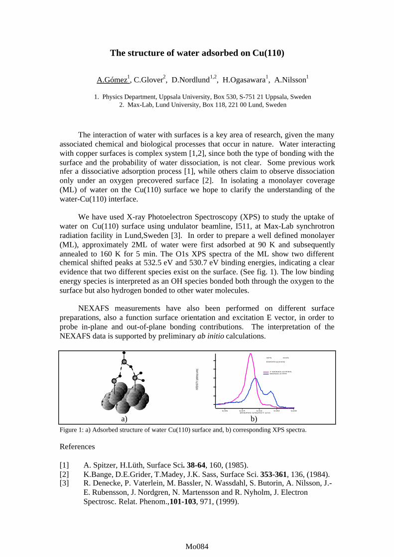
The structure of water adsorbed on Cu(110)
A.Gómez1, C.Glover2, D.Nordlund1,2, H.Ogasawara1, A.Nilsson1
1. Physics Department, Uppsala University, Box 530, S-751 21 Uppsala, Sweden
2. Max-Lab, Lund University, Box 118, 221 00 Lund, Sweden
The interaction of water with surfaces is a key area of research, given the manyassociated chemical and biological processes that occur in nature. Water interactingwith copper surfaces is complex system [1,2], since both the type of bonding with thesurface and the probability of water dissociation, is not clear. Some previous worknfer a dissociative adsorption process [1], while others claim to observe dissociationonly under an oxygen precovered surface [2]. In isolating a monolayer coverage(ML) of water on the Cu(110) surface we hope to clarify the understanding of thewater-Cu(110) interface.
We have used X-ray Photoelectron Spectroscopy (XPS) to study the uptake ofwater on Cu(110) surface using undulator beamline, I511, at Max-Lab synchrotronradiation facility in Lund,Sweden [3]. In order to prepare a well defined monolayer(ML), approximately 2ML of water were first adsorbed at 90 K and subsequentlyannealed to 160 K for 5 min. The O1s XPS spectra of the ML show two differentchemical shifted peaks at 532.5 eV and 530.7 eV binding energies, indicating a clearevidence that two different species exist on the surface. (See fig. 1). The low bindingenergy species is interpreted as an OH species bonded both through the oxygen to thesurface but also hydrogen bonded to other water molecules.
NEXAFS measurements have also been performed on different surfacepreparations, also a function surface orientation and excitation E vector, in order toprobe in-plane and out-of-plane bonding contributions. The interpretation of theNEXAFS data is supported by preliminary ab initio calculations.
INTE
NSITY
(arbi
trary
units
)
536 534 532 530 528BINDING ENERGY (eV)
XPS O1S D2O/Cu(110)
2 MONOLAYERS MONOLAYER
a) b)Figure 1: a) Adsorbed structure of water Cu(110) surface and, b) corresponding XPS spectra.
References
[1] A. Spitzer, H.Lüth, Surface Sci. 38-64, 160, (1985).[2] K.Bange, D.E.Grider, T.Madey, J.K. Sass, Surface Sci. 353-361, 136, (1984).[3] R. Denecke, P. Vaterlein, M. Bassler, N. Wassdahl, S. Butorin, A. Nilsson, J.-
E. Rubensson, J. Nordgren, N. Martensson and R. Nyholm, J. ElectronSpectrosc. Relat. Phenom.,101-103, 971, (1999).
Mo084Mo001Mo084Mo084Mo084
INTERFERENCE EFFECTS IN ANGLE RESOLVED AUGER-PHOTOELECTRON COINCIDENCE EXPERIMENTS
S. Rioual1, B. Rouvellou1, L. Avaldi2, R. Camilloni2, P. Bolognesi2, G. Battera2, G. Turri3 and G.
Stefani4
1 LCEA, Université de Brest, UFR Sciences et Techniques; 6 av. V. Le Gorgeu, 29285 Brest Cedex, France2 CNR-IMAI, Area della Ricerca di Roma, CP 10, 00016 Monterotondo scalo, Italy
3 INFM TASC, Padriciano 99, 34102 Trieste Italy and Dipartimento di Fisica, Politecnico di Milano, Milan, Italy4 Unita’ INFM and Dipartimento di Fisica, Universita’ di Roma Tre, via della Vasca Navale 84, 00146 Rome, Italy
The study of coherence is one among the most debated topics in quantum mechanics.Observations of such effects can be performed in atomic physics when the interaction betweenan atom and a photon or an electron proceeds through many undistinguishable channels leadingto the same final state. Then, the experimental challenge is to achieve in both the exciting sourceand the analyzers a resolving power comparable with the width of the involved intermediateatomic states. Such a resolution is mandatory to observe the interference effects typical ofcoherence.
Double photoionization of rare gases offers unique opportunities to investigate suchinterference effects. This process may, indeed, proceed either directly with the simultaneousemission of two photoelectrons, or indirectly with the sequential emission of a photoelectron andan Auger electron. As we will show in this poster, the latter process, characterized by theformation of an intermediate excited state of the singly charged ion that decays by Auger decayinto the double continuum, is of particular relevance to the investigation of interference effects.In particular, two different cases have been investigated experimentally with themulticoincidence apparatus located at the Gas Phase beamline of the Elettra storage ring. In thefirst case, the photon energy has been tuned in order to obtain a photoelectron kinetic energyclose to the Auger electron one [1,2] . In the second one , we have studied a process in which thesame doubly charged final state can be reached via different paths which involve the populationof two different intermediate states [3]. This latter case is analogous to the Young’s classicaltwo-slit experiments.
References
[1] L. Vegh and J.H. Macek, Phys. Rev. A 50, 4031 (1994).[2] S. Rioual, B. Rouvellou, L. Avaldi, G. Battera, R. Camilloni, G. Stefani, et G. Turri, Phys.
Rev. Lett. 86 1470 (2001).[3] J.A. de Gouw, J. van Eck, A.Q. Wollrabe, J. van der Weg, and H.G.M. Heideman, Phys.
Rev. A 50, 4013 (1994).
Mo085Mo001Mo085Mo085Mo085

High resolution resonant 2p–3d photoelectron and photoion spectroscopy ofatomic Scandium
B. Obst1∗, T. Richter1, M. Martins2, P. Zimmermann1
1 Technische Universitat Berlin, Institut fur Atomare und Analytische Physik,
Hardenbergstraße 36, D-10623 Berlin
2 Freie Universitat Berlin, Institut fur Experimentalphysik,
Arminallee 14, D-14195 Berlin
The study of the resonant np–md photoionization especially of the transition metalelements and its neighbors in the periodic table has attracted very much interest for the lastdecades. The 3p–3d-excitation has been studied in great detail [1, and references therein].In recent years the focus has switched to the study of the 2p–md excitation. Studies of theelement Calcium (Ca) have shown that the resonant photoionization is very sensitive to theelectron-electron-correlations of the outer electrons [2,3]. This contribution presents data onthe neighboring element Scandium.
The experiments present were carried out at the BESSY II beamline U49-1/SGM inJanuary 2000. Scandium (Sc) is evaporated in a Molybdenum crucible heated by elec-tron bombardment. the resulting atomic beam is collimated and crossed with the linearlypolarized undulator radiation. The photoions can be detected with a time of flight massspectrometer. Alternatively the kinetic energy of photoelectrons emitted under the magicangle with respect to the main axis of the polarization ellipse of the synchrotron radiationcan be analyzed in a hemispherical electron analyzer (SCIENTA SES200).
The experimental data are compared to theoretical calculations using a Hartree-Fockapproach. The calculations treats the resonant photoionization as a two-step process calcu-lating the excitation and the decay separate. The photoion yield spectrum as well as thephotoelectron spectra show an excellent agreement with the calculated ones. The detailedanalysis reveals that almost all oscillator strength is concentrated in the 2p–3d transition.Only one structure in the photoion spectrum can be assigned to Sc∗ 2p3d4s24d states. Thephotoelectron spectra are dominated by lines assigned to highly excited states of the Sc II. Itcan be shown that the decay is dominated by a spectator process which leaves the originallyexcited electron unaffected.
References
[1] B. Sonntag and P. Zimmermann Rep. Prog. Phys., 911–987 (1992)[2] B. Obst, W. Benten, A. von dem Borne, J. Costello, L. Dardis, Ch. Gerth, P. Glatzel, A.
Gray, J. E. Hansen, O. Meighan, E. Kennedy, C. McGuiness, B. Sonntag, A. Verweyen,Ph. Wernet, and P. Zimmermann J. Electron Spectrosc. Relat. Phenom. 101-103, 39-42(1999)
[3] M. Meyer, E. von Raven, B. Sonntag, and J.E. Hansen Phys. Rev. A 49, 3685-3703(1994)
∗present address: Max-Planck-Institut fur Plasmaphysik, c/o Fritz-Haber-Institut, Faradayweg 4-6,D-14195 Berlin
Mo086Mo001Mo086Mo086Mo086

High Resolution Resonant Auger Raman Spectra of HBr
Y.F. Hu1,2, R. Püttner3,4, G.M. Bancroft1, A. Kivimäki3, M. Jurvansuu3, S. Aksela3
1 Department of Chemistry, University of Western Ontario, London Ontario Canada N6A 5B72 Synchrotron Radiation Center, University of Wisconsin-Madison, Stoughton WI USA 53589
3 University of Oulu, Department of Physical Sciences, PL 3000, 90401 Oulu, Finland4. Freie Universität Berlin, Institute für Experimentalphysik, Arnimallee 14, D-14195 Berlin, Germany
Resonant Auger Raman spectra of atoms and molecules have been studied extensively dueto the advances in the synchrotron light sources and high resolution electron energy analyzers[1,2]. The major advantage of the “resonant Auger” process over the normal Auger process isthat the lifetime of the core excited state does not contribute to the experimental linewidth. Thebroadening and the complication due to the ligand-field effect commonly observed in d and fcore level spectra can be eliminated in the resonant Auger spectra [3].
High resolution resonant Auger spectra of HBr are presented at the Br 3d to 5s, 5p, 6p and7p resonances. The resonant Auger spectra subsequent to the 3d®5s and 3d®5p excitations canbe described by the splitting of the 4pp -2 two-hole final states derived from normal Augerspectrum of HBr [4] and a coupling of the Rydberg electron to the final states, with littlevibrational fine structure. However, the spectra due to the 3d®6p and 3d®7p excitationsexhibit complex features. Surprisingly, these features can be described with a combination ofthe splitting of the 4pp -2 configuration into the final states 3S-, 1D, and 1S+ and the vibrationalprofile obtained from the 3d-1®4pp -2 normal Auger process [4]. We conclude that theequilibrium distance of the 4pp -2 5s, 5p final states is close to that of the ground state and the 3dcore-hole state, while the equilibrium distance of the 4pp -2 np (when n³6) Rydberg states is closeto that of the 4pp -2 two-hole states, i.e., the lower Rydberg states have a bonding character andthe higher Rydberg states a non-bonding character.
References
[1] S. Svensson, A. Ausmees, Appl. Phys. A, 65, 107, 1997.[2] M.N. Picncastelli, J. Electron Spect. Relat. Phenom., 108, 1, 2000.[3] Z.F. Liu, G.M. Bancroft, K.H. Tan, M. Schachter, Phys. Rev. Lett., 72, 62, 1994.[4] R. Püttner, Y.F. Hu, G.M. Bancroft, H. Aksela, E. Nõmmiste, J. Karvonen, A. Kivimäki, S.
Aksela, Phys. Rev. A, 59, 4438, 1999.
Mo087Mo001Mo087Mo087Mo087

Alignment of Ar+ ions produced after resonant Auger decayof Ar* 2p5 3d resonances
M. Meyer(a,b), R. Flesch(c), A. Marquette(a,b), E. Rühl(c), and A. Grum-Grzhimailo(a,d)
(a) LU.R.E, Centre Universitaire Paris-Sud, Bâtiment 209D, F-91898 Orsay cedex, France(b) CEA/DRECAM/SPAM, CEN Saclay, F-91105 Gif-sur-Yvette, France
(c) Fachbereich Physik, Universität Osnabrück, Barbarastr. 7, D-49069 Osnabrück, Germany(d) Institute of Nuclear Physics, Moscow State University, Moscow 119899, Russia
The relaxation of the Ar* 2p5 (2P3/2, 2P1/2) 3d resonances is governed by the resonant Auger
decay leading predominantly to singly charged ions with electron configurations Ar+ 3p4 3d, 4d
and 5d [1, 2]. In the present work dispersed fluorescence spectroscopy has been used to study the
subsequent radiative decay of these excited ions. Similar to experiments on 4d excited Xe [3],
the degree of linear polarization of the fluorescence was determined allowing to deduce the
alignment of Ar+ ions produced after the resonant Auger decay. The experiments have been
performed at the U49/1-SGM beamline of BESSY II using monochromatized synchrotron
radiation with high degree of linear polarization. UV-visible fluorescence was investigated in the
wavelength regime 320nm≤λ(fluo)≤530nm with a spectral resolution of about ∆λ(fluo)=0.5nm.
A part of the fluorescence spectra is displayed in Figure 1 showing the variation of line
intensities for different relative orientations between the polarization vectors of the fluorescence
and the synchrotron radiation. The spectra are recorded after excitation of the Ar* 2p5 (2P3/2) 3d
resonance at hν(SR) = 246.9 eV and show mainly transitions of the type Ar+ 3p4 4d --> 3p4 4p
and 3p4 4p --> 3p4 4s. The negligibly small differences for lines arising from initial states with
total angular momentum J = 1/2 demonstrate qualitatively the consistency of our results. A
detailed analysis of the data, taking into account also contributions from possible radiative
cascades, is under progress and will be presented at the conference.
inte
nsity
(arb
.uni
ts)
495490485480475470465
fluorescence wavelength (nm)
Ar* 2p5 (2P
3/2) 3d
parallel
perpendicular
difference
1/2-1/25/2-5/2
1/2-1/2 3/2-3/23/2-5/2
3/2-1/2
5/2-5/2 7/2-5/25/2-3/2
3/2-3/2
Figure 1: Part of two dispersed fluorescence spectra
recorded after resonant Ar* 2p5 (2P3/2)3d excitation for
parallel and perpendicular orientation between the
polarization vector of the fluorescence and the
synchrotron radiation. The differences between the
intensities of the individual lines are given as a histogram
on top of the figure.
[1] M. Meyer, E. v. Raven, B. Sonntag, and J.E. Hansen, Phys. Rev. A 43, 177 (1991)
[2] J. Mursu, H. Aksela, O.P. Sairanen, A. Kivimäki et al., J. Phys. B29, 4387 (1996)
[3] M.Meyer, A.Marquette, A.Grum-Grzhimailo, U.Kleimann, B.Lohmann, Phys.Rev.A, subm.
Mo088Mo001Mo088Mo088Mo088

Coupling between the vibrational modes of core-excited and valence ionizedstates in CO2 and N2O
M . M e y e r ( 1 , 2 ) , M. M a r q u e t t e ( 1 , 2 ) , S . A l o i s e ( 1 , 2 ) , P. van Kampen( 3 ) ,
S. Al-Moussalami( 4 ) , C. McGinley( 4 ) , Th. Möller( 4 ) , R. Flesch( 5 ) , and E. Rühl( 5 )
( 1 ) L . U . R . E . , B â t i m e n t 2 0 9 D , U n i v e r s i t é P a r i s - S u d , F - 9 1 4 0 5 O r s a y C é d e x a n d
( 2 ) C E A / D R E C A M / S P A M , C E N S a c l a y , F - 9 11 9 1 G i f - s u r -Y v e t t e C é d e x
(3) Dublin City University, Glasnevin 9, Dublin, Ireland
(4) HASYLAB / DESY, Notkestr. 85, 22603 Hamburg, Germany
(5) Fachbereich Physik, Universität Osnabrück, Barbarastr. 7, D-49069 Osnabrück, Germany
Fluorescence spectroscopy in the wavelength region 200nm ≤ λ(fluo) ≤ 1000nm has been
used to probe the vibrational structure of CO2+ and N2O
+ outer valence states, which are
produced after electronic relaxation of core-excited resonances. The experiments have been
performed using monochromatized synchrotron radiation from the high-resolution beamlines
U49-1-SGM (BESSY II) and BW3 (HASYLAB). The small bandwidth of the exciting photons
allows to select different members of the strongly overlapping vibrational states of 1s-π*
resonances, which are not completely resolved due to lifetime broadening. The spectral analysis
of the fluorescence has been performed with a high-resolution spectrograph (Jobin-Yvon HR460,
aperture f / 5.3) providing a maximum spectral resolution of ∆λFL = 0.03nm.
Similar to earlier studies on vibrational resolved fluorescence of N2+ after 1s-π* excitation
[1], in the present work the coupling between the vibrational modes of core-excited and valence-
ionized states of CO2 and N2O has been investigated. The high spectral resolution enables us to
resolve the very close lying vibrational states of the tri-atomic molecules [2]. In the case of N2O,
the radiative relaxation N2O+ A 2Σ (n'1,n'2,n'3) --> X 2Π (n1,n2,n3) formed upon N-1s and O-1s
excitation has been observed showing a strong enhancement of the bending modes of the N2O+ A
2Σ state upon excitation at the low energy side of the 1s-π* resonances. For CO2, the complex
structure of the C2O+ A 2Π (n'1,n'2,n'3) --> X 2Π (n1,n2,n3) displays also pronounced variations of
the relative intensities of the lines, when the photon energy of the exciting synchrotron radiation
is tuned across the C 1s-π* resonance. For both molecules the importance of bending modes,
excited due to the Renner-Teller effect, has been emphasized upon 1s-π* excitation [3, 4]. The
analysis of fluorescence spectra allows to obtain detailed complementary information on the
symmetry of the excited inner-shell resonances and its influence on the valence shell ionization.
[1] A. Marquette, M. Meyer, F. Sirotti, R. F. Fink, J. Phys. B 32, L325 (1999)
[2] M. Meyer, A. Marquette, M. Gisselbrecht, J. Electr. Spectr. 101-103, 81 (1999)
[3] J. Adachi et al., J. Chem. Phys. 102, 7369 (1995) and J. Chem. Phys. 107, 4919 (1997)
[4] P. Morin et al., Phys. Rev. A61, 050701R (2000)
Mo089Mo001Mo089Mo089Mo089

STATE- AND SITE- SELECTIVE DISSOCIATION PROCESSES OF CORE-EXCITED METHANOL
T. Tokushima, Y. Mishima, M. Morita, M. Yamashita, H. Yoshida, and A. Hiraya
Hiroshima university, Higashi-hiroshima 739-8526, Japan
Pronounced state-selective H2
+ formation from H2O molecule following the O 1s to the 2b2 resonant excitation has been reported by Piancastelli et al.[1] They also observed H3
+ formation from core-excited methanol (CH3OH) [2], though state selectivity in H3
+ formation was not concluded. Also reaction pathway, whether H3 formed by elimination from methyl group or by head and tail (H3C and OH) reaction, was still not clear. To elucidate details of the dissociation mechanism of the core-excited methanol molecule, especially for the H3
+ formation, high-resolution ion-yield spectra of photofragment ions by using photoelectron-photoion coincidence (PEPICO) and ion-pair correlation spectra by using photolectron-photoion-photoion coincidence (PEPIPICO) were measured for CH3OH and CD3OH. PEPIPICO and PEPICO measurements were carried out at the BL8B1 beamline of UVSOR and the BL27SU of SPring-8, respectively.
As only D3+ is observed for core-excited CD3OH, the reaction pathway to form H3
+ (D3+)
is concluded as the molecular elimination from the methyl group. This result was further supported by the existence of the D3
+/COH+ ion-correlation peak in the PEPIPICO spectra. Figure 1 shows the high-resolution partial ion-yield spectra of D3
+, COH+, CD3+, OH+ and
total ion-yield spectra of CD3OH in the C 1s (3sa’, 3pa”) region. Partial ion-yields of D3
+ and COH+, formed by C-D bond scissions, are lower at the 3sa’ resonance than those at the 3pa” resonance. On the contrary, CD3
+ and OH+ formed by the C-O bond scission are stronger at the 3sa’. Another interesting state- and site- selectivity for O-H bond scission was found in the O 1s region. In the O 1s excitation, suppression of OH+ and COH+ while enhancement of O+ and DCO+ relative to the total ion-yield are observed at the 3sa’. This excited state selectivity for the O-H bond scission is not observed in the C 1s excitation at all. Therefore, the O-H bond scission is not only state-selective but also the site- (excited atom-) selective reaction. References [1] M.N. Piancastelli, A. Hempelmann, F. Heiser, O. Gessner, A. Rüdel, and U. Becker, Phys.
Rev. A 59 (1999) 300 [2] A Hempelmann, M N Piancastelli, F Heiser, O Gessner, A Rüdel and U Becker, J. Phys. B:
At. Mol. Opt. Phys. 32 (1999) 2677
287.5 288.0 288.5 289.0 289.5 290.00
1
23pa"
3sa'
COH+
D3
+
Rel
ativ
e in
tens
ity
Photon energy / eV
TIY
0
1
2 3pa"
3sa'
OH+
CD3
+
TIY
Figure 1. H3+, COH+, CD3
+, OH+ and total ion-yield spectra of CD3OH in the C 1s (3sa’, 3pa”) region.
Mo090Mo001Mo090Mo090Mo090

460 480 500 5200
20
40
60
80
100
120
140460 480 500 520
0
1
2
3
AE
PIC
O In
tens
ity /
arb.
uni
ts
Kinetic Energy /eV (Exp.)
AEPICO yield
Auger electron
Bond dissociation factor
Calculated Intensity /arb. units
Kinetic Energy /eV (Calc.)
Auger transition probability
FIG. 1. Calculated and Experimental Spectra of core excited H2O. Symbols: broken line; Auger transition probability, thick line; bond dissociation factor for OH, dotted line; normal Auger spectrum, and square; AEPICO yield spectrum for H+ ion.
Study of Auger Decay Process and Subsequent Ion Desorption Reaction of Some Simple Molecules Using Molecular Orbital Theory
Shin-ichi Wada1, Erika O. Sako1, Yuki Kanameda1, Masaki Mitani2,
Osamu Takahashi2, Ko Saito2, Suehiro Iwata2, Tetsuji Sekitani1 and Kenichiro Tanaka1
1Department of Physical Science, Hiroshima University, Higashi-Hiroshima 739-8526, Japan 2Department of Chemistry, Hiroshima University, Higashi-Hiroshima 739-8526, Japan
Recent progress in synchrotron radiation
techniques in a soft x-ray region has developed various newly experimental approaches. Especially the Auger electron - photoion coincidence (AEPICO) spectroscopy is one of powerful technique to investigate the Auger stimulated ion desorption (ASID) mechanism of core excited molecules, as it clarifies the Auger decay process (i.e. Auger final state) and the ion desorption mechanism related to the Auger process [1,2]. In this study, in order to elucidate the experimental results of AEPICO spectroscopy in detail, the Auger transition probabilities and dissociation factors for bonds were calculated using molecular orbital (MO) theory.
Because of the difficulty in exact calculation of the Auger transition probability and the applicability for various molecules, the calculation was based on the single configuration state function (CSF) and limited configuration interaction (CI) methods. The probability was estimated by the overlap between core and valence MOs using electron densities of valence MOs on the excited atom [3]. The bond dissociation factor was calculated as the product of the change of electron densities on the bond and the Auger transition probability in order to elucidate the result of the AEPICO experiment.
Figure 1 shows the calculated Auger transition probability and bond dissociation factor for H2O molecule with the experimental normal Auger and AEPICO yield spectra as an example. The calculated probability well-reproduces the Auger electron spectrum. The correspondence between the bond dissociation factor and AEPICO yield spectrum indicates that the H+ ion desorbs efficiently from the Auger final states where two holes are produced in the bonding MOs. The suitability of this calculation including spectator Auger transition is also confirmed for H2O, NH3 and CH3CN molecules and the ASID mechanisms are discussed for each molecule. [1] K. Mase, S. Tanaka, S. Nagaoka and T. Urisu, Surf. Sci. 451 (2000) 143. [2] E. Ikenaga, K. Isari, K. Kudara, Y. Yasui, S. A. Sardar, S. Wada, T. Sekitani, K. Tanaka, K.
Mase and S. Tanaka J. Chem. Phys. 114 (2001) 2751.; E. Ikenaga, K. Kudara, K. Kusaba, K. Isari, S. A. Sardar, S. Wada, K. Mase, T. Sekitani and K. Tanaka J. Electron Spectrosc. Relat. Phenom. in press.
[3] E. O. Sako, Y. Kanameda, E. Ikenaga, M. Mitani, O. Takahashi, K. Saito, S. Iwata, S. Wada, T. Sekitani and K. Tanaka J. Electron Spectrosc. Relat. Phenom. in press.
Mo091Mo001Mo091Mo091Mo091

K-SHELL PHOTOIONIZATION OF O2 AND N2 STUDIED BY
FIXED-MOLECULES PHOTOELECTRON ANGULAR DISTRIBUTIONS
J. Adachi1,2, K. Ito1, K. Soejima3, E. Shigemasa4, S. Motoki2, and A. Yagishita1,2
1) Photon Factory, Institute of Materials Structure Science, Tsukuba 305-0801, Japan 2) Graduate School of Science, Univ. of Tokyo, Bunkyo-ku 113-0033, Japan
3) Graduate School of Science and Technology, Niigata Univ., Niigata 950-2181, Japan 4) UVSOR, Institute for Molecular Science, Okazaki 444-0805, Japan
In order to understand the 1s photoionization dynamics of molecules, the angle-resolved photoelectron-photoion coincidence (ARPEPICO) technique [1] has been applied to the 1s photoionization of O2, in which there is no shape resonance enhancement in contrast to the 1s photoionization of N2. The previous measurement of the angular distribution patterns (ADP) of 1s photoelectron of N2 reveal that the 1ssg ® fsu channel has a primary role in the s* shape resonance [1,2]. On the other hand, there is no prominent feature above the O1s ionized threshold for O2, so few attention to O1s photoionization dynamics of O2 have been paid. The residual O2
+ following the 1s photoionization has two multiplet states, the doublet and quartet states. In the present measurement, these states are not resolved. The ADP obtained with ARPEPICO is fitted with the Legendre polynomial (PK) expansion to determine the relative values for those coefficients AK. Assuming that the higher l (l ³ 4) partial wave are neglected, the square of the dipole matrix element for the 1s ® fsu, |Dfs|2, is proportional to the coefficient A6. Roughly speaking, the value of |Dfs|2 very gently decreases as the incident photon energy becomes higher. However, the ADPs of the 1s photoelectrons remarkably change as a function of the incident photon energy. These results mean that the ADP is strongly affected by the phase shift and the relative intensities of the lower l (l £ 2) component to the |Dfs|. References 1. E. Shigemasa, J. Adachi, M. Oura, and A. Yagishita, Phys. Rev. Lett. 74, 359 (1995). 2. N. A. Cherepkov, S. K. Semenov, Y. Hikosaka, K. Ito, S. Motoki, and A. Yagishita, Phys. Rev. Lett. 84, 250 (2000).
Figure Partial cross sections for the K-shell excitation and ionization of O2. Open circles show the photoion yield observed in 0° direction respect to the electric vector of the incident light. Triangles and filled circles show the partial cross section for the 1s ® efsu transition and essg + epsu + edsu
transitions. The inserted figures show the ADPs for O1s photoelectrons measured at hn = 546.7, 555.7, and 568.7 eV.
OO OO
OO OO
535 540 545 550 555 560 565 570535 540 545 550 555 560 565 570
|Dfs|2
|Dss|2 + |Dps|2 + |Dds|2
O K-shellO2
Par
tial
Cro
ss S
ecti
ons
(arb
. uni
ts)
Photon Energy (eV)
OO OO
Mo092Mo001Mo092Mo092Mo092

Non Franck-Condon effects in the photoionization of N2 to the N2+ A 2ΠΠΠΠu state
and of O2 to the O2+ X 2ΠΠΠΠg state in the 19-34 eV photon energy region
J. Rius i Riua, M. Stankiewiczb, L. Vesethc, P. Ermana, A. Karawajczyka and P. Winiarczykb
aSection of Atomic and Molecular Physics, Department of Physics, Royal Institute of Technology, KTH,
SE-10044 Stockholm, Sweden bInstytut Fizyki im. Mariana Smoluchowskiego, Uniwersytet Jagiellonski, ul. Reymonta 4, 30-059 Krakow, Poland
cDepartment of Physics, University of Oslo, N-0316 Oslo, Norway
Photoionization to the N2+ A 2Πu state and to the O2
+ X 2Πg state is studied using photoelectron spectroscopy.
In the case of the N2 molecule, the experimental vibrational branching ratios obtained for the first time in the 20-34 eV region for the v = 0-3 levels, show strong non Franck-Condon effects around 22 eV. Using ab initio many body perturbation theory, branching ratios for ionization to the A 2Πu state are calculated. This study indicates that the Franck-Condon breakdown in the photoionization of the N2 1πu electron is due to autoionization from Rydberg and valence states of N2. In Figure 1, top panel, the solid circle-lines (--) indicate the R(D) and R(C) Rydberg series autoionizing to the A 2Πu state of the N2
+ molecule. In the bottom panel, the solid squares () represent Non Rydberg Doubly Excited Resonances (NRDERs) of 1Σ+
u symmetry predicted in this region and the solid circles () represent NRDERs of 1Πu symmetry.
In the case of the O2 molecule, the experimental vibrational branching ratios for v = 0-3 levels, which are obtained in the 19-31 eV region show strong non Franck-Condon effects. Using ab initio many body perturbation theory branching ratios, vibrationally resolved partial cross sections and total cross section for ionization to the X 2Πg state are calculated. Molecular states that autoionize to the O2
+ X 2Πg state continuum are discussed. Photoionization of the O2 πg electron is not fully explained by channel coupling effects and autoionization from known Rydberg series and valence states.
0,5
0,6
0,7
0,8
0,9
1,0
1,1
0 2 43 5 7
5 8
5 10R(D)
n = 5
n = 4v' =
v' =
ξ A s
tate
(a.u
.)
n = 4
n = 5R(C)v' =
v' =
B
ranc
hing
Rat
io
21 22 23 24 25 26 27 28 29 30 31 32 3310-4
10-3
10-2
10-11 ΠΠΠΠ
u
1 ΣΣΣΣ +u
Excitation Energy (eV)
Figure 1. Top panel. Computed ( ― ) and experimental (-o-) branching ratio for v = 2 over v = 0 of the A 2Πu state of the N2
+ in the studied region. Lower panel. Computed autoionization strengths to the A state for the predicted NRDERs.
Mo093Mo001Mo093Mo093Mo093

High-resolution inner-shell studies of free radicals and transient species.
M. Alagia1, R. Richter2, and S. Stranges3
1 TASC-INFM, Area Science Park, 34012 Basovizza, Trieste, Italy.2Sincrotrone Trieste, Area Science Park, 34012 Basovizza, Trieste, Italy.3Department of Chemistry, University of Rome La Sapienza and INFM Unit, P.le A. Moro 5, 00185 Rome, Italy.
Third generation SR undulator beam lines allow low density and highly reactive species tobe studied in the gas phase using high photon energy resolution. Core-excited states in the OHand OD free radicals and the CS transient molecule have been investigated for the first time. Inthe case of the lowest O 1s excited state (2S+) of OH and OD, vibronic components have beenclearly observed in the total-ion-yield spectra using time-of-flight mass spectrometry. Relativetransition probabilities, excitation energies, and core-hole lifetimes have been measuredaccurately for the vibronic components of this state. Excited states at higher energies have beenalso observed. The free radicals have been produced in situ by the fast atom-molecule reactionH (D) + NO 2 ® OH (OD) + NO using a microwave technique to generate the H atom. In thecase of CS, C 1s and S 2p excited states have been observed. Some of them display a resolvedvibrational progression. As for the S 2p excited states, the extent of the vibrational progression,and therefore the change in molecular geometry, varies largely depending on the specificresonant state. Spin-orbit and molecular field splitting effects in S 2p excitation processes areobserved for the first time in a diatomic molecule. The CS transient species has been producedin situ using the CS2 precursor and the same microwave technique.
Core-excited states of transient and radical species are often observed as “intermediatefragments” in studies of ultra-fast dissociation processes of core-excited molecules. Ourexperiments provide, for the first time, a direct information on the inner-shell spectroscopy ofthose fragments.
Mo094Mo001Mo094Mo094Mo094

STATISTICAL PROPERTIES OF INTER-SERIES MIXING IN
HELIUM: FROM INTEGRABILITY TO CHAOS
R. Puttner1, B. Gremaud2, D. Delande2, M. Domke1, M. Martins1,
A. S. Schlachter3, and G. Kaindl1
1Institut fur Experimentalphysik, Freie Universitat Berlin,
Arnimallee 14, D-14195 Berlin-Dahlem, Germany2Laboratoire Kastler-Brossel T12 E1, Universite Pierre et Marie Curie,
4 Place Jussieu, 75005 Paris, France3Lawrence Berkeley National Laboratory, 1 Cyclotron Road, Berkeley, CA 94720, USA
Due to the non-integrability of the classical three-body problem, no exact quantum num-
bers can be found to describe the helium atom. Nevertheless, for not too high excitation
energies, the approximate classication scheme N;Kn (with N (n) being the quantum num-
ber of the inner (outer) electron and K the angular correlation quantum number) can be
used to describe the 1Po doubly excited states in helium. However, in the semiclassical limit,
i.e. close to the double-ionization threshold, the in uence of the underlying classical phase
space is expected to become more and more important for the quantum mechanical solution.
We present high-resolution photoabsorption spectra below the N=9 ionization threshold
measured at beamline 9.0.1 at the Advanced Light Source in Berkeley/California, and cal-
culated photoionzation cross sections in the same energy region using the complex-rotation
method. Based on the excellent agreement between experiment and theory, we performed a
statistical analysis of the nearest neighbor spacing (NNS) using the theoretical results.
The NNS distribution was determined by two dierent procedures: (i) globally by consid-
ering all resonances regardless of the series to which they belong; (ii) individually for each
series associated with a given value of N K, i.e. constant number of bending quanta with
respect to a collinear eZe conguration. In the rst case the NNS distribution reveals a Pois-
son distribution that is typical for a regular system, while in the second case a development
of the NNS distribution towards a Wigner distribution which is typical for chaotic systems
was found. This corresponds to the loss of the radial quantum number N , whereas N K
remains approximately a good quantum number, and it is directly related to the instability
of the eZe orbits along the radial direction and their stability with respect to bending.
In addition, 1 dimensional (1D) stretched helium was studied theoretically below the N=9,
13, and 17 ionization threshold revealing that the NNS distribution develops clearly towards
a Wigner distribution with increasing N . This study provides an estimate for the observation
of a fully chaotic regime in 3D helium (for N 17).
In conclusion, we show clear evidence of chaotic eects in both the 3D and 1D helium
spectra on the basis of statistical analysis, emphasizing the role played by mixing between
dierent Rydberg series.
The work in Berlin was supported by the Deutsche Forschungsgemeinschaft, project DO
561/1-3, and the Bundesministerium fur Bildung und Forschung, project 05-SR8KE1-1.
Mo095Mo001Mo095Mo095Mo095

Ultra-fast dissociation processes in poly-atomic molecules.
I. Hjeltea, M. N. Piancastellia,b, R. F. Fink a, c, O. Björneholma, M. Bässlera, R. Feifela, K.Wiesner a, S. L. Sorensene and S. Svenssona
aDept. of Physics, Uppsala University, S- 751 21 Uppsala, SwedenbDept. of Chemical Sciences and Technologies, University “Tor Vergata”, 00133 Rome, Italycalso at: Dept. of Theoretical Chemistry, Chemical Centre, Box 124, S-22100 Lund, Sweden
eDept. of Synchrotron Radiation Research, Inst. of Physics, Lund University, Box 118, S-221 00 Lund, Sweden
Core-excitation processes can be induced in a molecule if radiation of a suitable wavelength isused to promote one electron from a core level to an empty molecular or Rydberg orbital.Core-excited species are unstable and decay processes follow rapidly; the most long-livedcore holes have a lifetime in the order of 10 fs. Core excitations lead frequently to dissociativeor predissociative states. In some cases, the nuclear dynamics is so rapid that dissociationtakes place on the same time scale as Auger electron emission. Ultra-fast dissociation is aterm used to describe dissociation taking place on a time scale comparable to that of theAuger decay placing it in the low femtosecond regime. This time scale corresponds to theshortest molecular dissociation times i.e. to the fastest existing chemical reactions. It haspreviously been shown to occur in a number of molecules such as HBr [1], HCl [2], H2S [3],O2 [4] and N2 [5]. Since the beginning of the nineties, there has been a long-standingdiscussion on the possible occurrence of ultra-fast dissociation of core-excited water into O*Hand H (* indicates core excitation) [6] which has been indicated in ion yield spectroscopy [7,8]. However, for ammonia no conclusive evidence of this phenomenon has been presentedpreviously.
We present direct evidence for ultra-fast dissociation of molecular water [9] and ammonia inconnection to photo-excitation of the O1s→4a1 and N1s→4a1 resonance's respectively. Thecore-excited molecules are shown to dissociate into a core-excited fragment and a neutralfragment on a time scale comparable to the core hole lifetime, i.e. a few femtoseconds. Thisconclusion is based on a resonant Auger study and qualitative arguments concerning thedispersive behavior of the fragment versus the molecular lines while tuning the frequency ofthe exciting light around the resonance as well as ab initio calculations in the case of water.
Figure 1. The Auger decay spectra of molecular water and ammonia after core excitation.
[1] P. Morin, I. Nenner, Phys. Rev. Lett. 56 (1986) 1913.[2] H. Aksela, et. al., Phys. Rev. A41 (1990) 6000.[3] A. Naves de Brito,et. al. , J. Mol. Structure (Theochem) 394 (1997) 135.[4] S. J. Schaphorst, et. al., Chem. Phys. Lett. 213 (1993) 315.[5] M. Neeb, et. al., Phys. Rev. Lett. 76 (1996) 2250.[6] D. Coulman, et. al., J. Chem. Phys. 93 (1990) 58.[7] M.N. Piancastelli, et. al., Phys. Rev. A 59 (1999) 300.[8] A. Naves de Brito, et. al., Chem. Phys. Lett. 309 (1999) 377.[9] I. Hjelte, et. al., Chem. Phys. Lett. 334 (2001) 151.
390388386384382380378
3a11e
NH3N1s → 4a1
Fragment peaks
520518516514512510508
H2OO1s → 4a1
1b13a11b2
Mo096Mo001Mo096Mo096Mo096

Photoexcitation Processes of Methanol Isotopmers in VUV Region
Bing-Ming Cheng,1 Mohammed Bahou,2 Yuan-Pern Lee,2 and L. C. Lee3
1 SRRC, No. 1, R&D Road VI, Hsinchu Science- Based Industrial Park, Hsinchu 300, Taiwan
2 Department of Chemistry, National Tsing Hua University, No. 101, Sec. 2, Kuang Fu Road, Hsinchu 300, Taiwan
3 Department of Electrical and Computer Engineering, San Diego State University, San Diego, California 92182
The photoabsorption cross sections of CH3OH, CH3OD, CD3OH, and CD3OD are measuredin the 110-220 nm region using the synchrotron radiation light source in Taiwan. In the 160-220nm region, the absorption maximum and band shape of CH3OH are same as CD3OH, and thoseof CH3OD are same as CD3OD; but the absorption maximum of CH3OD is blue-shifted fromCH3OH. This result shows that the excitation is clearly related to the O-H bond. On the otherhand, in the 140-160 nm region the absorption spectrum of CH3OH is similar to CH3OD, and thatof CD3OH is similar to CD3OD; but the band origin of CD3OH is blue-shifted from CH3OH. Thisresult shows that the excitation in this region is related to the C-O bond. Based on the absorptioncross sections combined with theoretical calculations, the quasi-diatomic potential curves for theC-O and O-H bonds of methanol are derived.
The absorption in the 160-220 nm is a smooth continuous band that results a repulsivecurve for the O-H bond. This curve is produced from perturbation between the 3s Rydberg stateand the valence state that dissociates into CH3O + H products. A vibrational progression with anirregular spacing appears in the 150-160 nm region. The irregularity is caused by perturbationbetween the 3p Rydberg state and the valence state that dissociates into CH3 + OH products. Avibrational progression with a regular spacing appears in the 140-150 nm region. The upper stateof this band is assigned to the 3p' Rydberg state of which the energy is higher than the repulsivevalence state. The regular spacing indicates that this 3p' state is a bound state, and its potentialcurve is not perturbed by a valence state.
The deuteration technique is a powerful tool to study photoexcitation processes ofmolecules in the infrared region. The current results demonstrate that this technique can also beextended to study the photoexcitation processes in the VUV region.
Mo097Mo001Mo097Mo097Mo097
The vacuum-UV photofragmentation of a range of hydrofluorocarbon (HFC) cations, CxHyFz
+, studied using coincidence techniques
W.D. Zhou, D.P. Seccombe, R.Y.L. Chim and R. P. Tuckett
School of Chemistry, University of Birmingham, Edgbaston, Birmingham B15 2TT, UK
HFCs are being increasingly used as substitutes for the banned chlorofluorocarbons in a range of domestic and industrial applications. The lifetime of these species in the atmosphere can be very long (ca. years) due to their slow reaction with the important tropospheric free radicals such as OH and O (1D). The removal of these species from the atmosphere can therefore be governed by processes occurring in the mesosphere. We are investigating these possible uni- and bi-molecular processes in the laboratory. The bi-molecular processes include reactions of HFCs with small positive ions and with electrons. The principal uni-molecular process is vacuum-UV photodissociation, especially with wavelengths in the range 50-150 nm, and this poster presents a progress report on our work.
Using vacuum ultraviolet radiation from the Daresbury synchrotron source, we have used threshold photoelectron-photoion coincidence (TPEPICO) spectroscopy to study the decay dynamics of the valence electronic states of the parent cation of several HFCs (CHF3, CF3-CHF2, CF3-CH2F, CHF2-CHF2, CF3-CH3) in the energy range 10 to 25 eV. This project represents a follow-on to a successful study of both saturated and unsaturated perfluorocarbon cations by the TPEPICO technique [1]. Electrons and ions are detected by threshold electron analysis and time-of-flight mass spectrometry respectively, allowing breakdown diagrams showing the formation probability of fragment ions as a function of the internal energy of the parent ion to be obtained. Higher resolution, fixed-energy TPEPICO spectra were also performed on many of the heavier fragment ions, and the translational kinetic energy released in fragmentation determined [2]. By comparing the integrated threshold photoelectron signal with the total ion yield as a function of photon energy, the importance of autoionisation in these molecules can be gauged.
For many of these saturated HFCs, the parent ions are not observed, indicating that the ground states of the ions are repulsive in the Franck-Condon region. Both from the analysis of the breakdown diagrams and the high kinetic energy releases, we conclude that non-statistical effects are occurring for states of these cations below ca. 18 eV. This suggests that decay from these states takes place rapidly before internal conversion to the ground state of the parent cation can occur. The substituted ethanes therefore seem to be mimicing the behaviour of C2F6
+ (CF3-CF3+) where non-statistical effects are well
known [1], and not that of C2H6+ where statistical dissociation is observed [3]. F--anion migration
across the C-C bond must occur to explain the observation of some of the daughter ions. References [1] G.K. Jarvis, K.J. Boyle, C.A. Mayhew and R.P. Tuckett, J. Phys. Chem. A., (1998) 102, 3219 and 3230 [2] G.K. Jarvis, D.P. Seccombe and R.P. Tuckett, Chem. Phys. Letts., (1999) 315, 287 [3] F. Guthe and K.M. Weitzel, Ber. Buns. Ges. Phys. Chem., (1997) 101, 484
Mo098Mo001Mo098Mo098Mo098

Resonant Auger Raman spectroscopy at the Kr 3p edge
K.C. Prince1, M. Coreno2 and M. de Simone3,
Sincrotrone Trieste, Strada Statale 14, km. 163.5, in Area Science Park,I-34012 Basovizza (Trieste) Italy,
INFM- TASC, Laboratorio ELETTRA, I-34012 Trieste, Italy,Università di Roma III ed Unità INFM, Via della Vasca Navale 84, I-00146 Rome, Italy.
The x-ray absorption spectra of the sharp core levels of noble gases, Ne 1s, Ar 2p, Kr 3d, etc,have been extensively studied and are well understood [1, 2,] but less attention has been given to theirbroader, more difficult core levels [3, 4]. At the Kr 3p edge, the Rydberg sates are about 1.4 eV wide,overlap one another and are superimposed on a strong 3d continuum [4]. Thus the peaks are difficult toidentify and controversy exists about their assignment [5].
The 3p-1nl (n>4, l=0; n>3, l=2) Rydberg states decay rapidly via Coster-Kronig (CK) processesto 3d-14p-1nl, 3d-14s-1nl and related shake states, and via super Coster-Kronig processes. We haveidentified the CK states, fig. 1, and they lie close to the 3d satellite states 3d-14p-1np. On the first main3p-1nl resonance, there is a strong increase in emission below and above the 3d satellites. The peakshave widths determined by the resolution of the photons and the energy analysers, about 200 meV,fulfilling Resonant Auger Raman conditions. The new peaks disperse with photon energy as expected.
Constant Initial State spectra were measured by setting the analysers to energies correspondingto each group of peaks, fig. 2. The CIS spectra are shown in fig. 2, and clear differences in the resonantbehaviour are seen. Peaks A, B and C show similar resonant behaviour on the absorption peak that hasbeen attributed to the 3p-15s, both for 3p3/2 and 3p1/2 at 209.8 and 218 eV photon energy respectively. Incontrast the E and F multiplets show completely different resonances, and are assigned to ionic statesderived from different intermediate excited states.
We have successfully applied the Resonant Auger Raman technique and CIS to the problem ofthe absorption spectrum of Kr at the 3p edge.
[1] M. Coreno, et al, Phys. Rev. A 59 (1999) 2494.[2] O.P. Sairanen et al, Phys. Rev. A 54 (1992) 2834.[3] T. Kylli et al, Phys. Rev. A. 59 (1999) 4071.[4] I.T. Steinberger et al, Phys. Rev. B 60 (1999) 3995.[5] M. Ohno, Phys. Rev. A 51 (1995) 1042.
Fig. 1. Photoemission spectra below resonance(lower curves), and on resonance below the Kr 3pthreshold.
Fig. 2. CIS spectra, Kr 3p threshold.
800
600
400
200
0
Counts
969492908886Kinetic energy (eV)
1009896949290
hv=209.8 eV
hv=205.0 eV
AB
C
D
E
F
30x103
20
10
0Inte
nsity
(co
unts
)
220215210205Photon energy (eV)
C C
E (offset)
F (offset)
Mo099Mo001Mo099Mo099Mo099

1
High resolution photoabsorption studies at the C and O K edges
K.C. Prince1, M. de Simone2, R. Richter1, M. Coreno3 and M. Alagia3,1Sincrotrone Trieste, Strada Statale 14, km 163.5, Area Science Park,
I-34012 Basovizza (Trieste), Italy.2Università di Roma III ed Unità INFM, Via della Vasca Navale 84, I-00146 Rome, Italy,
3INFM- TASC, Laboratorio ELETTRA, I-34012 Trieste, Italy,
We report the carbon and oxygen K edge x-ray absorption spectra of fourtetrahedral molecules CX4 (X = H, Cl, F) and a series of oxygenated organicmolecules (CH2O, HCOOH, CH3CH2O, CH3COCH3, CH3OH and CH3OCH3),with the cross-section detemined in absolute units.
The antibonding valence peaks of the halides do not show any vibrationalstructure [1-3] but sharp Rydberg states are observed above these states at the C 1sedge. We identify a possible Fermi resonance in the Rydberg states of core excitedCF4, and we report the CCl4 Rydberg states for the first time. The C 1s intrinsicline widths were compared to theoretical predictions of ion state line widths andreasonable values are found for CH4 and CCl4 but not for CF4. The discrepancy isassigned to valence band - Rydberg mixing, which is especially strong in CF4,and/or to multi-centre Auger processes [4].
At the carbon K edge of the oxygenated species, most gases showvibrational structure; the spectrum of CH2O is in good agreement with that of [5],whereas few high resolution spectra of the other gases have been reported. At theoxygen edge, only CH2O shows vibrational structure. This is important as itindicates that for the very similar molecules CH3COCH3 and CH3CH2O, thestructure is not absent due to lifetime broadening, but is obscured by manyoverlapping vibrational bands. This implies that the excited states of all aldehdydesand ketones are most likely bound. On the othe hand the situation is unclear for thesaturated molecules CH3OH and CH3OCH3.
Fig. 1. Oxygen K edge spectrum of
formaldehyde. The first 5 vibrational states
(CO stretch) are marked .
References.1. K. Ueda et al, Chem. Phys. Lett. 236 (1995) 311.2. W. Zhang, T. Ibuki and C.E. Brion, Chem. Phys. 160 (1992) 435.3. B.S. Itchkawitz et al, Rev. Sci. Instrum. 66 (1995) 1531.4. T. X. Carroll, et al, Phys. Rev. A 61 (2000) 42503.5. G. Remmers et al, Phys. Rev. A 46 (1992) 3935.
80x103
60
40
20
0Inte
nsity
(ar
b. u
nits
)
532.0531.0
Photon energy (eV)
0
1
23 4
Mo100Mo001Mo100Mo100Mo100

MEASUREMENTS OF THE ABSOLUTE PHOTOIONIZATION CROSSSECTION OF THE DOUBLY-CHARGED O2+ ION
J.-P. Champeaux,1,2 J.-M. Bizau,2 C. Blancard,1 D. Cubaynes, 2 A. Compant La Fontaine,1
C. Couillaud,1 R. Marmoret,1 D. Hitz,3 M. Delaunay,3 S. Nahar,4 and F. J. Wuilleumier1
1Centre d’Etudes de Bruyères-le-Châtel, BP12, 91680 Bruyères-le-Châtel, France2Université Paris-Sud, LSAI, UMR 8624 CNRS, B. 350, 91405 Orsay3DRF, SI2A, CEA-Grenoble, rue des Martyrs, 38054 Grenoble, France
4S. Nahar, The Ohio State University, Columbus, Ohio 43210 , USA
Photoionization of O2+ ion over the energy range 50-70 eV has been investigated experi-mentally using the end-station for studies of photon-ion interactions at the Super ACO synchro-tron radiation source in Orsay. The experiments were performed at the SU6 undulator beamline,which provides monochromatic photon beams in the energy range 30-160 eV. The photon beamwas merged with a collimated 500 nA-beam of O2+ ions produced in an ECR ion source. The spa-tial overlap of the beams was determined by three sets of translating-wire beam-profile monitors.After an interaction path of 20 cm, the parent O2+ beam and the O3+ product ions were demergedand counted separately. In the interaction region, the O2+ ions are mainly in the 2s22p2 3P0,1,2ground state, but some of them are also in the 2s22p2, 1S or 1D, and 2s2p3 5S metastable states.Photo-ion yield measurements were carried out at a resolving power of 225. Previous R-Matrix[1] and new MCDF calculations were used to interpret the data.
In Fig. 1, we show the variation of the photoionization cross section as a function of photonenergy between 47 eV and 65 eV. Continuum and resonant structures are seen in the measuredcross section. The onset of the cross section at the 2p ionization threshold of the 3P ground stateis clearly seen at 54.90 eV. The lines are produced mainly by autoionization of 2s2p2np(n ≥ 2)2S+1LJ excited states of O2+ ion into the continua of the 2s22p O3+ ion. The results of both R-matrix and MCDF calculations agree satisfactorily with experiment and allow to identify the lines.Lines 1 and 2, below the 3P0,1,2 thresholds, are due to 2p-excitation of O2+ ions in the 2s2p3 5S
and 2s22p2 1S metastable states, respectively.Above the 3P thresholds, several lines (line 3 at58.27 eV as the first one) originate from excita-tion of O2+ ions in the 3P0,1,2 ground state. Otherlines are due to similar excitations of O2+ ionseither in the 1D (line 4 at 58.90 eV) or 1S (line 5at 61.07 eV) metastable states. We determinedalso the absolute value of the cross section forphotoionization into the continuum. Expe-rimental and theoretical values of energies andcross sections will be presented and discussed atthe conference.
1. S. Nahar, Phys. Rev. A 58, 3677 (1998).
Fig. 1 - Measured photoionization cross section of O2+
between 47 and 65 eV photon energy. The cross sectionscale is in arbitrary units.
Mo101Mo001Mo101Mo101Mo101

HIGH-RESOLUTION STUDIES OF CORRELATION SATELLITES INPHOTOIONIZATION OF SODIUM ATOMS IN THE 2p-SUBSHELL
D. Cubaynes,1 S. Diehl,2 J.-M. Bizau,1 F. J. Wuilleumier,1 J. D. Bozek,3 B. Rude,3 S. Canton,4
and N. Berrah4
1LSAI, UMR CNRS 8624, Université Paris-Sud, B. 350, Orsay 91405, France2Laboratoire DIAM, UMR CNRS, Université Paris VI, place Jussieu, 75231 Paris, France
3Lawrence Berkeley Laboratory, ALS, University of California, Berkeley, CA 94720, USA4Western Michigan University, Department of Physics, Kalamazoo, MI 43309, USA
In earlier studies of photoionization of sodium using electron spectroscopy, [1, 2] the manycomponents of the various groups of satellites could not be resolved because the spectral and elec-tron spectrometer resolutions were not good enough. In the work presented here, we have used thehigh-resolution Scienta electron spectrometer with an ultimate spectral resolution of 25 meV, andthe photon beam available at the 10.0 1 beamline of the Advanced Light Source in Berkeley bet-ween 50 and 110 eV photon energy. The total instrumental resolution, including contributionsfrom both excitation and detection channels as well as the Doppler effect, was at best 35 meVFWHM. With such a high-resolution, we were able to study the dynamics of 2p-photoionizationtransitions to correlation satellite states created without transfer of angular momentum: ∆l = 0(electronic configuration 2p54s, shake-up transitions) and with transfer of angular momentum: ∆l = 1 (electronic configuration 2p53p) and ∆l = 2 (electronic configuration 2p53d).
In the photoelectron spectrum following photoionization in the 2p-subshell, three groups oflines are clearly indentified: the main lines due to single ionization of a 2p-electron, ∆l = 0, (2p53sfinal ionic states), the satellites produced with ∆l = 1 (states with 2p53p electronic configuration),and the high-energy satellites produced with ∆l = 0 (states with electronic configuration 2p54s),and ∆l = 2 (states with electronic configuration 2p53d). Resolving the satellites within the latergroup requires as high a resolution as possible. In Figure 1, we show this later group of satellitesmeasured at 54 eV and 90 eV photon energy. One clearly sees three components: peak numbered1 corresponds to a mixture of satellites states with both 2p54s and 2p53d electronic configurations,peak 2 is mainly due to 2p54s satellite states, and peak 3 is assigned to only 2p53d satellite states.Peaks 2 and 3 are good references to detect any difference in the energy dependence of the rela-tive intensity of the ∆l = 0 and ∆l = 2 satellites, respectively. At 54 eV, the three componentshave roughly the same intensity, at 90 eV, the relative intensity of peak 3 has clearly decreased,revealing a significant energy dependence of the 2p53d state intensity. The 2p53p correlation satel-lites were all resolved. Detailed results will be presented at the conference and compared to exis-ting photoionization calculations.
[1]. S. Krummacher et al., J. Phys. B 15, 4363 (1982).[2]. D. Cubaynes et al., Phys. Rev. A 57, 4432 (1998).
Fig. 1 - Electron spectra showing theintensity of the correlation satellites pro-duced with ∆l = 0 (peak 2, mainly 2p54sfinal ionic states) and with ∆l = 2 (peak3, 2p53d final ionic states) at 54 eV (leftpanel) and 90 eV (right panel) photonenergy, respectively.
Mo102Mo001Mo102Mo102Mo102

Beat structure in the doubly excited Rydberg states converging
to the N=2 threshold of helium
R. Follath, G. Reichardt, O. Schwarzkopf and W. Gudat
BESSY, Albert-Einstein-Strae 15, 12489 Berlin, Germany
Doubly excited helium is the prototype system for studying autoionisation phenoma, i.e. the
eect of electron correlation. The presence of only two electrons makes it readily accessible
for ab initio calculations of the parameters describing the autoionisation resonances.
In the present work we investigated the helium Rydberg series converging to the N=2 au-
toionisation threshold (IP2) by means of total photoionisation yield measurements. Three
Rydberg series are converging to this ionisation threshold, namely the principle (2; 0n) and
the secondary series (2; 1n) and (2;1n). With a resolving power of 90 000 a hitherto unre-
solved beat structure in the series was observed at very high excitation levels.
Figure 1 gives an enlarged view of the region just below the N=2 ionization threshold. The
amplitudes of the autoionisation proles decrease continuously up to a minimum value at
n = 26 as already observed in experiments with lower energy resolution [1]. But with the
highest currently available energy resolution, an increase of the amplitudes above this prole
with a maximum value at the (2; 029) line is observed. For n > 29, the amplitude is again
decreasing. The beat can be explained by a mixing of two series converging to dierent ion-
isation thresholds and having an energy spacing corresponding to the energy split between
the 2p1=2 and 2p3=2 level of singly ionised helium. This indicates that the electron interac-
tion at high excitation levels can be described within the jj-coupling scheme of two electrons.
65,37 65,38 65,39 65,40 65,41
0,95
1,00
1,05
1,10 IP250
2,026
2,0n
3022n=21 23 24 25 26
phot
oion
izat
ion
yiel
d [a
rb.
units
]
energy [eV]
Figure 1: Near thresh-
old region of the N=2
Rydberg series. Between
the proles (2; 026) and
(2; 034) a beat structure is
observed. The arrow in-
dicates the 26th prole of
the (2; 0n) series, where
the minimum in the am-
plitudes occurs. IP2 de-
notes the ionization limit.
[1] K. Schulz, G. Kaindl, J. D. Bozek, P. A. Heimann and A. S. Schlachter, J. Electr. Spectr.
Rel. Phenom. 79, 253 (1996).
Mo103Mo001Mo103Mo103Mo103

NUCLEAR MOTION EFFECTS OBSERVED IN PHOTOELECTRONSPECTRA OF HCL AND DCL MOLECULES
F. Burmeister1, L. M. Andersson2, H. O. Karlsson2, S. L. Sorensen3, O.
Björneholm1, A.Naves de Brito4, R. F. Fink1, R. Feifel1, I. Hjelte1, K.
Wiesner1, A. Giertz1, M. Bässler1, C. Miron1, H. Wang1, M. N.
Piancastelli5, L. Karlsson1, S. Svensson1 and O. Goscinski2
1 Dept of Physics, Box 530, S-75121 Uppsala, SWEDEN
2 Dept. of Quantum Chemistry, BoxBox 518, S-751 20 Uppsala SWEDEN
3 Dept. of Synchrotron Radiation Research, Institute of Physics, Box 118, S-221 00 Lund, Sweden
4 Laboratorio Nacional de Luz Sincrotron, Box 6992, CEP 13083 Campinas SP, BRAZIL
5 Dept. Of Chemical Sciences and Technologies, University "Tor Vergata", Rome, Italy
The HCl inner-valence photoelectron band at 26 eV binding energy has been recorded with
a photon energy of 64 eV at high resolution. Discrete peaks arising from at least two separate
vibrational progressions are superimposed on the broad continuum. Fano profiles are visible in
one of the progressions. This indicates interference between superimposed electronic states. In
the isotopic DCl molecular spectrum the discrete lines are much less pronounced. The difference
between HCl and DCl is due to dissociation dynamics[1], where non-adiabatic, non-avoided
crossing behavior is more pronounced for the lighter HCl molecule. A theoretical treatment of
the systems, with simulated spectra based upon the potential curves [2] is also presented.
References
[1] H. Eyring, J. E. Walter, and G. E. Kimball, Quantum Chemistry, 326-330 (Wiley, New
York, 1944).
[2] M. Hiyama, S. Iwata, Chem. Phys. Lett, 210, 187 (1993).
Mo104Mo001Mo104Mo104Mo104

Tot
al Io
n Y
ield
Photon Energy / eV
285 286
CH3
N
Figure 1. C 1s÷B* total ion yield spectra ofpyridine (top), toluene (middle) and benzene(bottom).
Core excitation and ionic fragmentation of aromatic molecules
John J. Neville
Department of Chemistry, University of New Brunswick, Box 45222, Fredericton, NB E3B 6E2, Canada
C 1s ÷ B* resonant excitation of benzene yields a core-excited state in which the core hole islocalised on a single carbon atom and the aromaticity is lost [1]. This symmetry lowering isaccompanied by a rehybridisation of the bonding orbitals of the excited carbon atom, loss ofplanarity and the excitation of both symmetric and asymmetric vibrational modes. In the case ofaromatic molecules of lower symmetry, such as pyridine and toluene, resonant core-excitation canin principal be performed selectively at each of the chemically inequivalent carbon centres, givensufficiently large chemical shifts in the C 1s energy levels between inequivalent sites and asufficiently narrow photon bandwidth. The resulting core-excited states might be expected to havediffering vibrational structure depending upon the location of the core-excited atom with respect tothat of the heteroatom or the substitution site. In all cases, the core-excited state is short lived;electronic relaxation typically results in multiple ionisation and molecular fragmentation.
Results will be presented of studies of the coreex c i t a t ion spec t roscopy and subsequentphotofragmentation of a number of aromatic molecules,performed with high resolution using synchrotronradiation and ion time-of-flight mass spectrometry. Inparticular, the vibrational structure of the C 1s ÷ B*
transitions of benzene, toluene and pyridine, shown inFigure 1, will be discussed and contrasted. The ionicfragmentation processes occurring in these moleculesfollowing selective core excitation will be examined asa function both of core-hole position and of vibrationalexcitation.
Reference
[1] Y. Ma, F. Sette, G. Meigs, S. Modesti and C. T.Chen, Phys. Rev. Lett. 63 (1989) 2044--2047.
Mo105Mo001Mo105Mo105Mo105

NUCLEAR MOTION EFFECTS AS OBSERVED IN THE RESONANT AUGER DECAY TO THE X2Π ELECTRONIC GROUND STATE OF N2O
+
C. Miron1-3, M. Simon1,2, P. Morin1,2, S. Nanbu4, N. Kosugi4, S. L. Sorensen5, A. Naves de
Brito6, M. N. Piancastelli7, O. Björneholm3, R. Feifel3, M. Bässler3 and S. Svensson3
1 LURE, Bât. 209d, BP. 34, Université Paris-Sud, 91898 ORSAY Cedex, France
2 Laboratoire “Francis Perrin” and CEA/DRECAM/SPAM, Bât. 522, CE Saclay, 91191 Gif/Yvette Cedex, France 3 Department of Physics, Uppsala University, Box 530, S-751 21 Uppsala, Sweden
4 Institute for Molecular Science, Myodaiji, JP 444-8585 Okazaki, Japan 5 Department of Synchrotron Radiation Research, University of Lund, Box 118, S-221 00 Lund, Sweden
6 Laboratorio Nacional de Luz Sincrotron, BR 13083-970 Campinas, Brazil 7 Department of Chemical Sciences and Technologies, University “Tor Vergata”, 00133 Rome, Italy
High-resolution Auger spectroscopy applied under resonant Auger Raman (RAR) conditions is shown to be a powerful tool for characterizing complex potential energy surfaces in core-excited systems. Using the example of Nt1s-1 ® p* resonant Auger transition in nitrous oxide we emphasize the interplay between the nuclear motion and the electronic decay. We show how the choice of the excitation energy allows selection of core-excited species of different geometries [1,2]. The nuclear dynamics of these species are mapped by measuring the resonant Auger decay spectra. In addition to the changes in vibrational structure observed for the resonant Auger decay spectra, a strong influence of the nuclear motion on the electronic decay is revealed inducing the so-called “dynamical Auger emission”. The experiments have been carried-out at the undulator beamline I411 at the Swedish synchrotron radiation facility Max-Lab in Lund. The experimental results are supported by ab-initio quantum chemical calculations restricted to a linear geometry of the core excited state (Figure 1).
Inte
nsity
[Arb
. uni
ts]
16.015.014.013.0Binding Energy [eV]
NNO - RAS (X2P)
Figure 1: Comparison between ab-initio calculations (bars and continuous line) and the experimental resonant Auger decay spectrum (empty circles) of the X2P electronic state of N2O measured on the top of the p* resonance: hn =401.3 eV.
References [1] J. Adachi, N. Kosugi, E. Shigemasa and A. Yagishita, J. Chem. Phys. 102, 7369 (1995). [2] J. Adachi, N. Kosugi, E. Shigemasa and A. Yagishita, J. Chem. Phys. 107, 4919 (1997).
Mo106Mo001Mo106Mo106Mo106

Hot-electron dynamics in mass-selected transition metal clusters probed byfemtosecond pump-probe photoelectron spectroscopy
N. Pontius, G. Lüttgens, P.S. Bechthold, M. Neeb, and W. EberhardtInstitut für Festkörperforschung, Forschungszentrum Jülich GmbH, 52425 Jülich, Germany
Clusters in the gas phase are confined systems ideally suited to follow the internal energydissipation from a non-thermally excited state into the thermal equilibrium. Of emerging interestis the dynamics of excited electrons in a non-equilibrium state, which is created when an electron
is photoexcited by an ultrashort light pulse. Here we show by time-resolved photoelectronspectroscopy that electron relaxation processes are efficient energy dissipation channels not onlyin bulk metals but also in extremely small transition metal clusters [1]. An analysis of the time-resolved two-photon photoemission spectra of optically excited small Ni, Pd,, Pt- and metal-carbonyl clusters reveal effective electron relaxation times of less than 100 fs for electronsexcited below the vacuum threshold (hνpump=1.5 eV). A comparative series of pump-probe
spectra of different Pd-clusters demonstrates that the relaxation times vary with the cluster size.This is attributed to the partial density of states of small clusters as deduced from the resonanttwo-photon photoemission spectra of Pd3-7. In comparison to simple metal clusters, e.g. Agn, andNan, the bulk-like inelastic scattering processes in open d-shell transition metal clusters areattributed to the larger electronic level density caused by both the small d-bandwidth at the Fermilevel and the larger number of valence electrons. Furthermore, statistical evaporation of CO-ligands has been observed as alternative energy relaxation channel in metal-carbonyl clusters.While Pt2(CO)5
- reveals thermal desorption of a single CO ligand reaching up to the nanosecondregime, Au2(CO)- desorbs the CO-ligand within some hundreds of femtoseconds. The reason forthe high desorption rate in Au2(CO)- is attributed to the much smaller CO-desorption barrier andthe smaller number of vibrational degrees of freedom..
References
[1] N. Pontius, P.S. Bechthold, M. Neeb, W. Eberhardt, Phys. Rev. Lett. 84, 1132 (2000).
Mo107Mo001Mo107Mo107Mo107

The electronic structure of supported endohedrally doped fullerenes
R. Klingeler, I. Wirth, G. Kann, S. Eisebitt, P. S. Bechthold, M. Neeb, and W. Eberhardt
Institut für Festkörperforschung, Forschungszentrum Jülich GmbH, 52425 Jülich, Germany
We have investigated the electronic structure of endohedrally doped fullerenes which havebeen deposited onto a substrate from a mass-selected ion beam [1]. The valence orbitals ofendohedrally doped C60 can be explained by those of pristine C60, taking a charge transfer and aJahn-Teller effect into account. The band gap depends on the kind of encapsulated atom, asshown by scanning tunneling spectroscopy. Semiconductor-like and metal-like densities of stateshave been observed for Ce@C60 and La@C60, respectively. The core level region exhibits a shiftto higher binding energies with respect to the bulk due to metal-to-cage charge transferprocesses, as demonstrated by X-ray photoelectron spectroscopy in the case of Ce 3d in Ce@C60.
References
[1] R. Klingeler, P.S. Bechthold, M. Neeb, W. Eberhardt, J. Chem. Phys. 113, 1420 (2000); M.Neeb, R. Klingeler, P.S. Bechthold, G. Kann, I. Wirth, S. Eisebitt, W. Eberhardt, Appl.Phys. A 72, 289 (2001)
Mo108Mo001Mo108Mo108Mo108

EVIDENCES OF LOCALIZATION EFFECT AFTER S 1s EXCITATION AND AUGER DECAY IN THE SO2 AND CS2 MOLECULES
E. S. Cardoso1,2, F. Burmeister3, O. Björneholm3, and A. Naves de Brito2,4
1 Campinas State University-UNICAMP/IFGW - Campinas-SP - Brazil 2 Laboratório Nacional de Luz Síncrotron-Box 6192 CEP 13083-970-Campinas-SP-Brazil
3 Uppsala University - Department of Physics - Uppsala - Sweden 4 Brasília University - Institute of Physics -Brasília-DF - Brazil
We present the measured electron-multi-ion coincidence spectra after photoexcitation of the SO2 and CS2 molecules around the S1s edge. A procedure for complete determination of all set of ions formed is described. The dissociation channels and its behavior with the photon energy of these molecules are presented in comparison with the Total Ion Yield (TIY). We observed a charge distribution preferentially of asymmetric form with higher charge in the excitation atom for SO2 molecule, see Fig.1. In CS2, similar asymmetric distribution was observed. Furthermore, above S 1s first resonance, the channel with an even charge distribution between the two oxygen in SO2 in the most abundant. In CS2 it is not, in it, one of the Sulfur atoms is core ionized. Auger cascade after the 1s core hole creation leading to 2p double hole states need to be taken in to account to explain the observed memory effects. The time scale of the nuclear motion and decay is taken into account to explain the competition between intra-atomic cascade Auger leading to asymmetric charge distribution and Coulomb explosion giving rise to symmetric charge distribution in CS2. Recombination forming an O2 ion was found for SO2
TIY
35
30
25
20
15
2475247024652420.80 2520.80
2.5
0.0
S+C
+S
2+
S+C
2+S
+
CS2+
S2+
Charge 4
CS2
photon energy (ev)
rel.
abu
nd
ance
(%
)
40
30
20
10
0
248024762472 2523.332423.33
0.50.0
O+S
++O
+
O++
S+O
+
S+++
O 2+
& S+ O 2
+++
rel.
abu
nd
ance
(%
)
photon energy (eV)
Charge 4
SO2
TIY
Figure 1: Relative abundance of selected dissociation channels with total ionic charge 4. The total ion yield (TIY) is also shown.
Reference [1] E. S. Cardoso, F. Burmeister, O. Björneholm, and A. Naves de Brito, Submitted for
publication in J. Chem. Phys. (2001
Mo109Mo001Mo109Mo109Mo109

EVIDENCE AGAINST ATOMIC-LIKE RESONANT AUGER DECAY IN N2 DOUBLY- EXCITED CORE STATES BY HIGH-RESOLUTION
EXPERIMENTS
A. Naves de Britoa,1, I. Hjelteb, K. Wiesnerb, R. Feifelb, M. Bässlerb, S. L. Sorensenc, O.
Björneholmb, M.N. Piancastellid, L. Karlssonb and S. Svenssonb
a Laboratório Nacional de Luz Síncrotron (LNLS), Box 6192 CEP: 13083-970, Campinas-Brazil, BRAZIL b Dept. of Physics, Uppsala University, Box 530, S-751 21 Uppsala, SWEDEN
cDept of Synchrotron Radiation Research, Univ. of Lund, Box 118, S-221 00 Lund, SWEDEN d Dept. of Chemical Sciences and Technologies, University "Tor Vergata", I-00133, Rome, ITALY
Resonant Auger spectra following the decay of doubly-excited core states in N2 in the range 409-411 eV have previously been assigned to “atomic” lines indicating ultrafast dissociation. Using high-resolution synchrotron radiation electron spectroscopy from the MAX II facility in Sweden we have remeasured the resonant Auger spectrum of N2 in the vicinity of the N 1s threshold. Contrary to earlier studies, we find vibrational progressions that can be associated to the final C 2Su
+ and 2 2Pg states in N2+ . We conclude that the decay is entirely
leading to molecular final states.
References [1] A. Naves de Brito , I. Hjelte, K. Wiesner, R. Feifel, M. Bässler, S. L. Sorensen, O.
Björneholm, M.N. Piancastelli, L. Karlsson and S. Svensson, Submitted for publication in Phys. Rev. Lett. (2001)
1 [email protected]; on leave from Inst. of Physics, Brasilia University, Brasilia Brazil
Mo110Mo001Mo110Mo110Mo110

Dissociative photoionization of ethylene molecules and clusters
in a supersonic molecular beam
D. Ascenzi1, D. Bassi1, M. Coreno2, M. de Simone3, P. Franceschi1, P. Tosi1
1 INFM and Dipartimento di Fisica, Università degli Studi di Trento I-3850 Povo, Italy2 INFM - Laboratorio Nazionale TASC, I-34012 Trieste, Italy
3INFM and Dipartimento di Fisica, Università di Roma Tre, Roma, Italy
The photoionization and photodissociation cross-sections of ethylene monomers and
clusters have been measured in the 20-70 eV photon energy range at the Gas Phase
Photoemission Beamline, ELETTRA. Our experimental apparatus is a supersonic beam source
coupled to a quadrupole mass spectrometer, that we have specifically developed for the Gas
Phase Photoemission Beamline for photoionization studies on atomic and molecular clusters.
In the case of the ethylene monomer the measurement of the branching ratios for the
different dissociation channels has allowed us to extend previous synchrotron radiation studies
[1], whereas the data on ethylene clusters complete and extend previous investigations carried
out using a H2 lamp and TOF mass spectroscopy [2]. The main fragmentation channels
characterizing our spectra correspond to C2nH4n+ and C2n-1H4n-3
+ ions, the latter obtained from the
cluster ion by loss of a neutral CH3 fragment.
Further data on possible correlation between patterns of photofragmentation of the cluster
ions and the cross-section for reaction of the ethylene ion with its neutral parent will also be
presented.
References
[1] D.M.P. Holland, D.A. Shaw, M.A. Hayes, L.G. Shpinkova, E.E. Rennie, L. Karlsson, P.Balzers and B. Wannberg, Chem. Phys. 219, 91 (1997).
[2] J.A. Booze, T.N. Feinberg, J. W. Keister and T. Baer, J. Chem. Phys. 100, 4294 (1994).
Mo111Mo001Mo111Mo111Mo111

THIOPHENE PHOTOELECTRON SPECTRA IN THE GAS PHASE
M. Bäßler1*, A. Giertz1, K. J. Børve2, L. J. Sæthre2, and S. Svensson1
1 Department of Physics, Uppsala University, Box 530, SE-751 21 Uppsala, Sweden2 Department of Chemistry, University of Bergen, Allégaten 41, NO-5007 Bergen, Norway
* Present address: Carl-Zeiss Oberkochen, TechnologieZentrum Messtechnik, Carl-Zeiss-Strasse, DE-73447
Oberkochen
The C 1s and S 2p photoelectron spectra of thiophene were investigated with a total
instrumental resolution of around 60 meV and 30 meV, respectively. The experiments were
performed at the third generation synchrotron radiation facility MAX II in Sweden, at BL I411. The
spectra were also theoretically modelled with the Frank-Condon factors calculated using molecular
geometries, vibrational frequencies and normal modes for neutral and excited states obtained
analogously as described in reference [1].
In the C 1s XP spectrum, two chemically shifted carbon lines (split by 300 meV) are observed,
each with a vibrational progression. The S 2p XPS is more complicated due to the molecular-field
splitting (MFS) of the S 2p3/2 line. Analysis of the spectra results in a value of 99 meV for the MFS,
i.e. of the same size as the main vibrational spacing. The MFS has also been calculated using
second-order Møller-Plesset perturbation theory and large atomic basis sets. The computed splitting,
93 meV, confirms the value obtained from fitting the experimental spectrum.
References
[1] Karlsen Tor, Børve Knut J., J. Chem. Phys. 112, 7979 (2000)
Mo112Mo001Mo112Mo112Mo112

PHOTOIONIZATION OF ATOMIC SCANDIUM
Zikri Altun* and Steven T. Manson$
*Department of Physics, Marmara University, Istanbul, TURKEY $Department of Physics and Astronomy, Georgia State University, Atlanta, Georgia
30303, USA We are in the process of recalculating the partial cross sections corresponding to the photoionization of 3p, 3d and 4s electrons of the scandium atom in the [Ne]3s23p63d4s2 ground state using our MCHF-enhanced MBPT methodology. In our previous calculations1 we did not explicitly include photoionization with excitation channels; two-electron transitions that leave the Sc+ ion in a [Ne]3s23p63d2 state. The threshold energies of these photoionization with excitation channels are nearly degenerate with the 3d and 4s single photoionization thresholds. The calculated threshold energies for the 4s and 3d single photoionization channels are listed in Table I and for the photoionization with excitation channels in Table II.
Table I: Threshold energies for single-electron excitation channels
Ionic Core [Ar]3d4s(1D) [Ar]3d4s(3D) [Ar]3d4s(1S) Energy (au) 0.2443245 0.2244494 0.26785456
Table II: Threshold energies for two-electron excitation channels
Ionic Core [Ar]3d2(1S) [Ar]3d2(1D) [Ar]3d2(1G) [Ar]3d2(3P) [Ar]3d2(3F) Energy (au) 0.3717778 0.2993129 0.2985242 0.2863842 0.2713485
We expected markedly different behaviour from our previous calculation,1 particularly for the 3d partial cross section around its threshold, and our preliminary results indicate that this is so. This region is now dominated by the two-electron resonances corresponding to the 3p63d2(1S,1D,1G,3F)np(nf)(2P,2D,2F) autoionizing doubly excited configurations. We are in the processes of calculating the region where the autoionization of the 3p53d24s2(2P,2D,2F) singly excited resonance configurations play a dominant role. We have obtained partial results for channels with 2F final coupling, and the results indicate an increase in the widths of these resonances because the various 3d24s2 excitations now have other channels to decay into that were omitted in the previous calculation. This work was supported by NASA and NSF. Computing grant from Auburn University is gratefully acknowledged. 1Z. Altun and S. T. Manson, Phys. Rev. A 59, 3576 (1999).
Mo113Mo001Mo113Mo113Mo113

Vacuum−UV Absorption Spectrum of Laser Produced Rubidium and StrontiumPlasmas
A. Neogi1 , E. T. Kennedy1, J−P. Mosnier1, P. van Kampen1, C. McGuinness1,2 , G. O’Sullivan2 and J.T. Costello1
1National Centre for Plasma Science and Technology, School of Physical Sciences, DCU, Glasnevin, Dublin 9, Ireland2Department of Physics, University College Dublin, Dublin 4, Ireland
The Dual Laser Plasma (DLP) photoabsorption technique has been used to measure the timeand space resolved VUV photoabsorption spectra of laser produced rubidium and strontiumplasmas. In this technique a high power laser is focussed onto the material under investigation (hererubidium and strontium) and an absorbing plasma is formed. After an adjustable time delay asecond laser pulse if fired onto a high atomic number target (which is tungsten here) which givesrise to a VUV continuum emitting plasma source used to back−light the absorbing plasma [1].
Data on inner shell transitions are relevant not only for research in atomic structure anddynamics but also for applications in astrophysical, fusion, analytical and materials research. Thepresent work on inner−shell transitions in ions of the Kr isoelectronic sequence follows earlier workon the Ar sequence [2]. We are specifically interested here in excitation of the 3d and 4s subshellsof Rb+ and Sr2+. The 3d−photoabsorption spectra of the Sr isonuclear sequence has already beenstudied [3] while the corresponding data on the Rb II spectrum are new. We compare theseparticular data with Hartree−Fock calculations. We will also present the 4s−photoabsorption spectrawhich can be compared with recent many−body calculations.
References
[1] E T Kennedy, J T Costello, J−P Mosnier, A A Caffola, M Collins, L Kiernan, U Köble, MH Sayyad & M Shaw, Opt. Eng 33, 3964 (1994)
[2] P. van Kampen, G. O’Sullivan, V.K. Ivanov, A.N. Ipatov, J.T. Costello and G. O’Sullivan,Phys. Rev. Lett. 78 3082 (1997).
[3] C. McGuinness, G. O’Sullivan, P. K. Carroll, D. Audley and M. W. D. Mansfield,Phys.Rev.A 51, 2053 (1995)
Mo114Mo001Mo114Mo114Mo114

K-Shell Photodetachment of Li- : Experiment and theory
N. Berrah1, J. D. Bozek2, A. A. Wills1, G. Turri1,2, H. –L. Zhou3, S. T. Manson3, G.Akerman2, B. Rude2, N. D. Gibson4, C. W. Walter4, L. VoKy5, A. Hibbert6 and
S. Fergusson1
1Western Michigan University, Physics Department, Kalamazoo, MI 490082 Lawrence Berkeley National Laboratory, Advanced Light Source, Berkeley CA 947203 Department of Physics and Astronomy, Georgia State University, Atlanta, GA 30309
4Department of Physics and Astronomy, Denison University, Granville OH 430235 DAMAP, UMR 8588 du CNRS, Observatoire de Paris 92195, Meudon Cedex, France
6 Queen’s University of Belfast, Belfast, BT7 1NN, United Kingdom
An experimental K-shell photodetachment/photoionization study of Li- giving rise to doublyphotoionized Li+ ions has been carried out at the Advanced Light Source, using a collinearphoton-ion beam apparatus. The experiment reveals dramatic structure, differing substantiallyboth qualitatively and quantitatively from the corresponding processes in neutral atoms andpositive ions, as predicted by our enhanced R-matrix calculation. Theexperimental/theoretical comparison shows good agreement over some of the photon energyrange, and also reveals some puzzling discrepancies.
Mo115Mo001Mo115Mo115Mo115

SYNCHROTRON RADIATION PHOTOEMISSION STUDY OF SOLIDPHASE TRANSITION METAL COORDINATION COMPOUNDS
Corrado Crotti1, Erica Farnetti2, Teresa Celestino2, Maddalena Pedio3
1 CNR – IMAI, Sez. di Trieste - S.S.14, Km163.5, 34012 Basovizza (Trieste) - ITALY2 Dip. Scienze Chimiche, Univ. di Trieste - V. Giorgieri 1, 34127 Trieste - ITALY
3 CNR – ISM, Sez. di Trieste - S.S.14, Km163.5, 34012 Basovizza (Trieste) - ITALY
Core-levels photoemission spectroscopy has been intensively used to investigate TransitionMetal Coordination Compounds (TMCC) [1]. Also in this field, in the last 15 years SynchrotronRadiation has allowed much more resolved spectra than traditional X-Rays sources. However itsapplication has been limited to gas phase TMCC samples [2], due to the insulating nature of thiskind of molecules, which causes dramatic broadening and shifting of the peaks in solid phasesamples. Unfortunately, only a very small number of TMCC can be evaporated without thermaldecomposition, thus preventing such application to important fields like bioinorganic chemistryand homogeneous catalysis. High resolution XPS of solid phase TMCC would provide apowerful tool to correlate chemical behaviuor with bonding abilities and electron densities.
In order to fully exploit the advantages of such technique, we have searched for an optimalsample preparation, suitable to minimize the differential charging effects. The results obtainedwith the model compound W(CO)4(dppe) (dppe=1,2-bis(diphenylphosphino)ethane) show thatthe best method is by spin-coating a solution of the compound on a conducting support. Then wehave compared the spectra obtained by that way with those acquired on samplesprepared by more traditional techniquesor by evaporating the compound invacuum on a clean Gold foil. Figure 1shows the spectra taken at VUV beam-line at Elettra: spectra from traditionaltechniques (brushing or dipping) areabsolutely unacceptable, whereas byoptimizing the solvent and the spin-coating parameters the core-levelspeaks become narrow enough(FWHM~0.65 eV) to be comparablewith the peaks obtained by sampleevaporation (FWHM~0.42 eV) andwith no significant difference in thechemical shift.
10x103
8
6
4
2
Inte
nsity (
a.u
.)
170165160155Kinetic Energy (eV)
brushing dipping spin coating in CH3COCH3 spin coating in CHCl3 spin coating in CH2Cl2 evaporation (P.E.=5 eV)
hν= 201.31 eVP.E.=10 eV
Figure 1: W 4f XPS spectra of W(CO)4(dppe).
References
[1] C.D.Cook, K.Siegbahn et al., J.Amer.Chem.Soc., 1971, 93, 1904; L.Wang, P.G.Gassman etal., Organometallics, 1996, 15, 4240 and references cited therein.
[2] J.Wu, G.M.Bancroft et al., Inorg.Chem., 1999, 38, 4688 and references cited therein.
Mo116Mo116

CONTRIBUTED POSTERS TUESDAY, JULY 24
Tu001Tu001

Tu002Tu002Tu002Tu002

MATERIAL RESEARCH
Tu003Tu003Tu003

Tu004Tu004Tu004Tu004
Cross-sectional photoemission microscopy of semiconductor heterostructures
F.Barbo1, M.Bertolo1, A.Bianco1, G.Cautero1, R.Cimino3, S.Fontana1, A.Franciosi2, T.K.Johal1,2,S.La Rosa1, D.Orani2, M.Piccin2, R.C.Purandare1, S.Rubini2, N.Svetchnikov1
1 Sincrotrone Trieste, S.S.14 Km 163.5 – in Area Science Park, I-34012 Basovizza – Trieste, Italy2 Laboratorio Nazionale TASC-INFM, Area Science Park, I-34012 Trieste, Italy
3 INFN – Laboratori Nazionali di Frascati, P.O. Box 13 00044 Frascati, Italy
Photoemission spectroscopy has been traditionally used to monitor chemical, structural andelectronic changes upon interface formation [1]. Measurements are usually performed atdifferent growth stages and the junction parameters are inferred from the coverage-dependenceof the core emission. With the emergence of spectromicroscopy, a natural application ofphotoemission to the study of semiconductor interfaces is to directly determine theheterojunction parameters by measuring the device in cross section.
Initial test systems examined were GaAs p-n doping superlattices with different periodsproduced by molecular beam epitaxy (MBE). After growth, wafers were mechanically thinned-down to below 100 µm, pre-notched and transferred in vacuum to the photoemissionspectrometer. In-situ cleaving was used to expose 110 cross-sections of the buried interfaces.Several efforts were devoted to obtaining flat bands conditions on both the p- and the n-side ofthe junction. Such conditions were inferred from an analysis of the Ga 3d core lineshape withenergy and spatial resolution better than 0.15 eV and 0.5 µm, respectively, having reduced to anegligible spectral contribution the diffuse background typical of any Schwarzschild microscope.
The methods developed were then applied to Al/n-GaAs(001) Schottky junctions, alsofabricated by MBE. Spatially-resolved studies of the core-level emission in cross-section wereused to probe the semiconductor depletion layer near the metallurgical junction. Our data showthat a systematic study of this system as a function of doping type and level can provide uniqueinformation of the static surface dielectric constant, which is relevant to many aspects of surfacephysics, including core-hole relaxation and electron/surface interactions [2].
References
[1] A.Franciosi and C.G.Van de Walle, Surf.Sci.Rep. 25, 1 (1996); L.J.Brillson, Surf.Sci.Rep2, 123 (1982).
[2] L.Reining and R.Del Sole, Phys.Rev.B 38, 12768 (1988); L.Reining and R.Del Sole,Phys.Rev.B 41, 12918 (1991).
Tu005Tu005Tu005Tu005

SPECTROSCOPIC CHARACTERIZATION OF ELECTRON AND X-RAYINDUCED DAMAGE IN SELF-ASSEMBLED MONOLAYERS
M. Zharnikov1, S. Frey1, K.Heister1, L.S.O. Johansson2, M. Grunze1
1 Angewandte Physikalische Chemie, Universität Heidelberg, 69120 Heidelberg, Germany2 Department of Physics, Karlstad University, 65188 Karlstad, Sweden
An important practical issue in the research of thin organic films and in particular self-assembled monolayers (SAMs) is their response to irradiation by X-rays, UV-light, electrons orions. On the one hand, irradiation-induced SAM modification can be used as a lithographicapproach to pattern surfaces. On the other hand, a possible non-intentional irradiation-induceddamage can occur during standard spectroscopic characterization of SAMs. Considering theseaspects we have investigated the low-energy electron and X-ray induced damage in differentaliphatic and aromatic thiol-derived SAMs on noble metal substrates by X-ray photoelectronspectroscopy (XPS), high resolution XPS, and angle resolved near edge X-ray absorption finestructure spectroscopy. It was found that both electron and X-ray irradiation causes the loss ofthe orientational and conformational order, partial dehydrogenation leading to the cross-linkingand, in particular, to C=C double bond formation, desorption of the film fragments, reduction ofthe thiolate species, and the appearance of new sulfur species (see Figs. 1 and 2 for SAMsformed from CH3(CH2)11SH (C12) on Au). The chemical identity of this species have beenidentified. A possibility to modify the sensitivity of SAMs toward electron and X-ray irradiationand to control the balance between the irradiation induced cross-linking and desorption processesis analyzed in detail and practical recipes for SAM-based lithography are derived. It isdemonstrated that this balance can be shifted both toward the quasi-polymerization of a SAM oran enhanced desorption of the molecular fragments by a proper design of the SAM constituents.This work has been supported by the German Bundesministerium für Bildung und Forschungthrough grants No. 05 SF8VHA 1 and 05 SL8VHA 2 and by DAAD (313/S-PPP-pz).
Figure 1. The C 1s and S 2p HRXPS spectra of thepristine and strongly irradiated C12/Au. Thedecomposition of the spectra into the components relatedto the pristine and irradiation-induced species is shown.
Figure 2. C1s NEXAFS spectra of pristine (bottomcurves) and irradiated C12/Au as well as therespective differences of the spectra recorded at X-ray incident angles of 90° and 20°.
Tu006Tu006Tu006Tu006

XPS AND NEXAFS SPECTROSCOPY STUDY OF THIOAROMATICSELF-ASSEMBLED MONOLAYERS ON NOBLE METAL SUBSTRATES
M. Zharnikov1, S. Frey1, K. Heister1, A. Terfort2, B. Zeysing2, M. Grunze1
1 Angewandte Physikalische Chemie, Universität Heidelberg, 69120 Heidelberg, Germany2 Anorganische und Angewandte Chemie, Universität Hamburg, 20146 Hamburg, Germany
Self-assembled monolayers (SAMs) formed from thiophenol (TP), 1,1'-biphenyl-4-thiol(BPT), 1,1';4',1''-terphenyl-4-thiol (TPT), and anthracene-2-thiol (AnT) on polycrystalline Auand Ag (Fig. 1) were characterized by X-ray photoelectron spectroscopy and angle resolved nearedge X-ray absorption fine structure spectroscopy. The measurements were performed at theGerman synchrotron radiation facility BESSY I in Berlin. With the exception of the poorlydefined thiophenol film on Au, all thioaromatic molecules were found to form highly-orientedand densely packed SAMs on both substrates. The molecular orientation and orientational orderof the adsorbed thioaromatic molecules depends on the number of aromatic rings, the substrate,and the rigidity of the aromatic system. The molecules, which in average are slightly inclinedwith respect to the surface normal, show a less tilted orientation with increasing length of thearomatic chain, and as observed for aliphatic SAMs, they exhibit smaller tilt angles on Ag thanon Au. However, the difference in the tilt angles for aromatic SAMs on Au and Ag is smallerthan that observed in the aliphatic films. A comparison of the monolayers formed from p-terphenylthiol and anthracenethiol films suggests that a higher molecular rigidity has only aslight effect on the final molecular orientation within the respective SAMs. Based both on thefindings of this study and on the comparison of the thioaliphatic and thioaromatic films, wesuppose that in the case of the latter systems the structure determining balance between the headgroup/substrate interactions and the intermolecular forces is shifted toward intermolecular forces.This work has been supported by the German Bundesministerium für Bildung und Forschungthrough grant No. 05 SF8VHA 1 and by the Fonds der Chemischen Industrie.
Figure 1. Schematic drawing of the thioaromatic molecules in an artificial upright adsorption geometry includingthe respective numbers of carbon atoms and the length of the aromatic chains (in closed brackets).
Tu007Tu007Tu007Tu007

Cu contaminants removal using UV/O and remote hydrogen plasma3
Jae Bum Kim and Chongmu LeeDepartment of Materials Science and Engineering, Inha University, Inchon 402-75, South Korea
Removal of Cu contaminants from Si wafer surface was carried out using remote
hydrogen plasma (RHP) and UV/O cleaning techniques. The concentration of Cu 3
impurities on the wafer surface was monitored by TXRF (total reflection x-ray
fluorescence) and XPS (x-ray photoelectron spectroscopy). Our results show that
metal impurities including Cu can be effectively removed by hydrogen plasma and
UV/O cleaning techniques, only if it is performed under optimum process conditions.3
A two step cleaning process composed of remote hydrogen plasma cleaning, first and
UV/O cleaning, next has been found to be more effective than a single process of UV/O3 3
or remote hydrogen plasma cleaning and a two step cleaning process composed of
UV/O cleaning, first and remote hydrogen plasma cleaning, next. The removal 3
mechanism of Cu impurities in the two step cleaning seems to be as follows:* First, Si atoms react with atomic oxygen to form SiO during UV/O cleaning. Next, 3
metallic impurities including Cu are lifted off when SiO* is evaporated during remote
plasma cleaning. The optimum process parameters for the remote hydrogen plasma
cleaning are the rf power of 20W and the exposure time of 5 min. The optimum exposure
time of the UV/O cleaning for Cu impurity removal is 1 min. Cleaning efficiency is3
degraded with increasing the process parameters above the optimum values for both
UV/O and remote hydrogen plasma cleaning techniques.3 Body text
Tu008Tu008Tu008Tu008

6FKRRO RI 3K\VLFV $VWURQRP\ 5D\PRQG DQG %HYHUO\ 6DFNHU )DFXOW\ RI
([DFW 6FLHQFHV 7HO$YLY 8QLYHUVLW\ 7HO$YLY ,VUDHO
3HUPDQHQW DGGUHVV 8QLYHUVLW\ RI *D]LDQWHS 'HSW RI (QJLQHHULQJ 3K\VLFV
*D]LDQWHS 7XUNH\
!" #
! $#
%%&'&& "( )(* )(+!,# -.*
" . $ . " - " $
! !" .
$ " /.-)0 /,)0
/1,,)0# ,#
, ), $ " 2 #
# 3 ,) $ 4 $"
! ,) 4 # 4 !
# ! 4$, " 5
2 5 " , # $
$"$42" $ ,)
$"$"!!"1$
,)!# !
6%7(8#8- 1"-9:/%;<=0:<'2:<:
6'7) 5+3 "# >5) 5
+ -( '9;2'?%/%;;@0:<%2:<=
697 - 3+
1"8%?/%;;<09?929?=
Tu009Tu009Tu009Tu009

650 0C
RT
Inte
nsity
(arb
. uni
t)
Kinetic Energy (eV)
650 0C
RT
Inte
nsity
(arb
. uni
t)
Kinetic Energy (eV)
Fig.1. XPS scans near Si 2p for different annealing temperatures. Left: 20mA/cm2, 250s. Right: 5mA/cm2, 1000s.
Study of P-type Photoluminescent Porous Silicon upon Annealing in Vacuum
H. J. Shin1, M. K. Lee1, C. K. Whang1, K. J. Kim1, T. H. Kang1, B. Kim1, G. B. Kim2, C. K. Hong2, K. W. Lee3, and Y. Y. Kim3
1PLS, Pohang Accelerator Lab., POSTECH, Pohang, Korea
2Phys. Dept., POSTECH, Pohang, Korea 3Kongju University, Kongju, Chungnam, Korea
Photoluminescent porous silicon, fabricated by chemically anodizing boron-doped [100] Si
wafer in 10% HF-ethanol solution, was annealed up to 650 0C in vacuum. After annealing, PL disappeared. We investigated the skeleton size using AFM before and after annealing, and chemical information of the PS surface in-situ using X-ray photoemission spectroscopy at the 2B1 SGM beamline at the Pohang Light Source. AFM data showed fine skeleton size of 5-10 nm before annealing, which is close to the size the quantum confinement model predicts the PL. After annealing, the fine skeleton structure became smoothened and the overall skeleton size increased to about 50-100 nm.
Fig. 1 shows photoemission spectra obtained with 130 eV photon energy of two different PS with the same thickness (same PL intensity and shape before annealing) but showing different suboxide states. The suboxide states, +3, +2, +1, were reported to be related with strong PL in PS layers [1]. As the annealing temperature increased, the suboxide state intensity increased. At 650 0C, where PL disappeared, the observed oxidation state is still in the range where the strong PL observed, indicating that the oxidation state change in this experimental condition is not a direct cause of the PL failure. The main cause of the PL disappearance in our study is attributed to the skeleton size increase. Reference Sendova-Vassileva, etal., J. Lumines. 80, 179 (1999).
Tu010Tu010Tu010Tu010

O K X-Ray Absorption Spectra of Condensed Aromatic Compounds Having Various Oxygen Functional Groups
Y. Muramatsu1, E. M. Gullikson2, and R. C. C. Perera2
1Japan Atomic Energy Research Institute, Sayo, Hyogo 679-5148, Japan 2Center for X-Ray Optics, Lawrence Berkeley National Laboratory, Berkeley, California 94720, USA
Microporous carbon has been widely used for adsorbents and catalysts in many industrial fields. Its adsorption properties were thought likely to depend on the chemical states of the graphitic surface in the micropores. In order to analyze the oxidation states of the graphitic surface in microporous carbon, we measured O K x-ray absorption spectra of microporous carbon [1, 2] and condensed aromatic compounds having various oxygen functional groups such as -OH, -R-OH, -COOH, -C=O, -CH=O, and -C-O-C-. Total-electron-yield (TEY) x-ray absorption spectra of these compounds were measured in BL-6.3.2 at the Advanced Light Source, and fluorescence yield (FY) x-ray absorption spectrum of microporous carbon was in BL-8.0.1. Figure 1 shows the x-ray absorption spectra of the condensed aromatic compounds and microporous carbon in the O K regions. From the comparison in spectral features of microporous carbon with the condensed aromatic compounds, it can be suggested that -C=O or -COOH are the most probable chemical bonding states of oxygen in microporous carbon. Theoretical analysis of these x-ray absorption spectra is in progress to determine the chemical bonding states of oxygen on the graphitic surface in microporous carbon. References [1] Y. Muramatsu et al., Carbon (in press) [2] Y. Muramatsu et al., J. Electron Spectrosc. Relat. Phenom. (in press).
OH
OHHO
OHOH
OHOH
HO
HO
OH OH
CH2OH
COOH
OO
O OO
O OO
OO
O
OO
O
CHO
COOH
COOHCOOH
COOH
COOH
O
O
O
O
O
COOHOH
OHCOOH
O
O OH
OH
O
O
O
OHO
microporouscarbon
520 540 560530 550 520 540 560530 550 520 540 560530 550
Photon energy / eV
X-r
ay in
tens
ity (a
rb. U
nits
)
OH
OHHO
OHOH
OHOH
HO
HO
OH OH
CH2OH
COOH
OO
O OO
O OO
OO
O
OO
O
CHO
COOH
COOHCOOH
COOH
COOH
O
O
O
O
O
COOHOH
OHCOOH
O
O OH
OH
O
O
O
OHO
microporouscarbon
520 540 560530 550520 540 560530 550 520 540 560530 550520 540 560530 550 520 540 560530 550520 540 560530 550
Photon energy / eV
X-r
ay in
tens
ity (a
rb. U
nits
)
Figure 1. TEY x-ray absorption spectra of condensed aromatic compounds having various oxygen functional groups and microporous carbon. FY x-ray absorption spectrum of microporous carbon is shown by dotted line. Molecular structures of the condensed aromatic compounds are superimposed on the corresponding x-ray absorption spectra.
Tu011Tu011Tu011Tu011

Deoxidization of a SiO2 Layer by Irradiating Incoherent Vacuum Ultraviolet Excimer Emission
Takeshi Ohtsubo, Shoichi Kubodera, and Wataru Sasaki
Department of Electrical and Electronic Engineering and Photon Science Center, Miyazaki University, Gakuen Kibanadai Nishi 1-1, Miyazaki, 889-2192 Japan
Photochemical deoxidization of an oxidized layer on a silicon wafer has been demonstrated by use of an incoherent vacuum ultraviolet (VUV) light source.
Typical removal process of an oxidized layer on a silicon wafer utilizes chemicals such as hydrofluoric acid. Such a treatment would certainly influence the environment and residual chemicals may play a negative role in the semiconductor processing. We have been developing VUV light sources by use of rare gas excimers [1]. Rare gas excimer sources excited by a silent discharge make the highest emission power with wide varieties of emission geometry. We have chosen Ar2* emission centered at 126 nm (9.8 eV), according to our previous silicon precipitation results using a high power Ar2* excimer laser [2]. This deoxidizing process, however, has been realized with low power incoherent Ar2* emission, resulting in pure photochemical process with absolutely no surface modification.
A silicon wafer with a SiO2 layer was placed inside a vacuum chamber at pressure of 3 x 10⁻⁵ Torr. The thickness of the layer was controlled at 100 nm. The Ar2* emission from a silent discharge pumped excimer lamp was irradiated onto the sample at an intensity of 0.3 mW/cm2. An MgF2 lens was used to increase the emission intensity. This lens also separated the vacuum chamber from the discharge lamp. The surface morphology was inspected by use of an AFM and the layer was monitored by ellipsometry. The atomic concentration of the surface was measured by use of XPS.
A ratio of atomic concentration of Si and SiO2 as a function of irradiated time (i.e. number of deposited quanta) was measured. In XPS measurement, a peak at 103 eV was observed, which was caused by Si(2p) of SiO2. Another peak at 99 eV originated from the atomic Si(2p). No other peaks appeared during the measurement. A ratio of these two peak intensities (I(99 eV)/I(103 eV)), i.e. the concentration of atomic Si in a layer, increased linearly with the irradiation time. AFM images of the sample showed no difference before and after the irradiation. The layer thickness was not changed, but the index of refraction decreased in 10-2 after the irradiation. Other measurement revealed that the precipitated atomic silicon concentration decreased exponentially with the sample depth. The characteristic depth was estimated to be 3 nm, which seems to be one order of magnitude smaller than the penetration depth of the 126-nm radiation into SiO2. This photochemical deoxidization of SiO2 layer would be connected with photochemical SiO2 layer production process [3]. References [1] S. Kubodera, M. Kitahara, J. Kawanaka, W. Sasaki, and K. Kurosawa, Appl. Phys. Lett.
69, 452 (1996). [2] K. Kurosawa, P. R. Herman, E. Z. Kurmaev, S. N. Shamin, V. R. Galakhov, Y. Takigawa,
A. Yokotani, A. Kameyama, and W. Sasaki, Appl. Surf. Sci. 126, 83 (1998). [3] A. Yokotani, N. Takezoe, K. Kurosawa, W. Sasaki, T. Igarashi, and H. Matsuno, Appl.
Phys. Lett. 69, 1399 (1996).
Tu012Tu012Tu012Tu012

/80,1(6&(1&(3523(57,(62)*G%$6('&203/(;)/825,'(&5<67$/6'23(':,7+(U$1'7P$63520,6,1*0$7(5,$/6
)25989(;&,7('3+263+256
10.KDLGXNRY0.LUP6./DP'/R910DNKRY196XHWLQ*=LPPHUHU
.XUQDNRY,QVWLWXWHRI*HQHUDODQG,QRUJDQLF&KHPLVWU\0RVFRZ5XVVLD,,,QVWLWXWIU([SHULPHQWDOSK\VLNGHU8QLYHUVLWlW+DPEXUJ+DPEXUJ*HUPDQ\
3K\VLFV'HSDUWPHQW&KLQHVH8QLYHUVLW\RI+RQJ.RQJ6KDWLQ17+RQJ.RQJ6$5&KLQD/HEHGHY3K\VLFDO,QVWLWXWH0RVFRZ5XVVLD
1XFOHDU3K\VLFV,QVWLWXWH0RVFRZ6WDWH8QLYHUVLW\0RVFRZ5XVVLD
7KHYDFXXPXOWUDYLROHW989VSHFWURVFRS\RIUDUHHDUWK5(LRQVGRSHGLQWRZLGHEDQGJDS FU\VWDO KRVWV KDV EHHQ DWWUDFWLQJ PXFK DWWHQWLRQ IRU WKH SDVW IHZ \HDUV EHFDXVH RI DQLQGXVWULDOGHPDQGIRUHIILFLHQW989H[FLWHGSKRVSKRUVIRUPHUFXU\IUHHIOXRUHVFHQW ODPSVDQGSODVPDGLVSOD\SDQHOVZKHUHWKH989UDGLDWLRQIURPQREOHJDVGLVFKDUJHLVXVHGIRUH[FLWDWLRQRISKRVSKRUV>@,QWKHSUHVHQWZRUNVSHFWURVFRSLFSURSHUWLHVRI&V*G)DQG/L.*G)FU\VWDOVGRSHG ZLWK (U RU 7P ZHUH VWXGLHG IURP WKH YLHZSRLQW RI WKHLU SRVVLEOH DSSOLFDWLRQ DVPDWHULDOVIRU989H[FLWHGSKRVSKRUVEDVHGRQWKHSULQFLSOHRIVRFDOOHGGRZQFRQYHUVLRQ>@7KHPHDVXUHPHQWV ZHUH SHUIRUPHG XQGHU H[FLWDWLRQ E\ ERWK V\QFKURWURQ UDGLDWLRQ DQG 989UDGLDWLRQIURPDSXOVHGPROHFXODU)ODVHU
,WKDVEHHQIRXQGWKDW989OXPLQHVFHQFHGXHWRG±I WUDQVLWLRQVIURP(UDQG7P
GRSHGLQERWK&V*G)DQG/L.*G)LVH[WUHPHO\ZHDN2QWKHRWKHUKDQGWKHHPLVVLRQVSHFWUDRIERWK(UDQG7PGRSHGFU\VWDOVFRQWDLQLQWHQVHOLQHVLQWKH89YLVLEOHVSHFWUDOUDQJHZKLFKFRUUHVSRQGWRI±IWUDQVLWLRQVLQWKHGRSLQJLRQVDQGWKH*GLRQ7KLVPHDQVWKDWWKH989HQHUJ\DEVRUEHGE\I±GWUDQVLWLRQVLQWKHUHOHYDQW5(LRQLVQHDUO\FRPSOHWHO\FRQYHUWHGLQWRWKH 89YLVLEOH HPLVVLRQ 6XFK D FRQYHUVLRQ RI 989 HQHUJ\ WR 89YLVLEOH OLJKW LH GRZQFRQYHUVLRQ LV GXH WR WKH HQHUJ\ WUDQVIHU IURP WKH G VWDWH RI WKH(U RU WKH7P LRQ WR WKHQHLJKERXULQJ *G LRQ DV D UHVXOW RI FURVVUHOD[DWLRQ JLYLQJ ULVH WR WKH HPLVVLRQ RI WZR89YLVLEOHSKRWRQVLQVWHDGRIRQH989TXDQWXP>@
%RWK &V*G) DQG /L.*G) FU\VWDOV GRSHG ZLWK (U RU 7P VHHP WR EH SURPLVLQJ
PDWHULDOV IRU HIILFLHQW 989H[FLWHG SKRVSKRUV WKH OXPLQHVFHQW SURSHUWLHV RI ZKLFK FRXOG EHEHWWHUWKDQWKRVHRIWKH/L*G)FU\VWDOVVWXGLHGLQ>@7KHVWURQJDEVRUSWLRQEHORZQPDVDUHVXOWRIIGWUDQVLWLRQVLQWKH(URUWKH7PLRQPDWFKHVZHOOWRWKHHPLVVLRQVSHFWUXPRIWKH[HQRQPRQRPHUOLQHRUWKHNU\SWRQH[FLPHUGLVFKDUJHFRQWLQXXPZLWKPD[LPXPDWQP%HVLGHV HLWKHU WKH (U *G RU WKH 7P *G FRPELQDWLRQ RIIHUV HIILFLHQW QRQUDGLDWLYHHQHUJ\ WUDQVIHU YLD FURVVUHOD[DWLRQ IURP WKH G OHYHO RI (U RU 7P WR *G ZLWK QHDUO\FRPSOHWHFRQYHUVLRQRIDEVRUEHG989UDGLDWLRQLQWRWKH89YLVLEOHHPLVVLRQ
5HIHUHQFHV
>@ *%ODVVH%&*UDEPDLHU/XPLQHVFHQW0DWHULDOV6SULQJHU9HUODJ%HUOLQ>@ 57:HJK(9'YDQ/RHI$0HLMHULQN-/XPLQ
Tu013Tu013Tu013Tu013

Electronic Structure and Reactivity of TM-doped La1-xSrxCoO3 (TM=Ni,Fe) Catalysts
S C Grice, W R Flavell, A G Thomas, S Warren, P G Marr, D E Jewitt, N Khan, P MDunwoody,
Dpeartment of Physics, UMIST, PO Box 88, Manchester M60 1QD, UK
S A JonesSynetix, PO Box 1, Belasis Avenue, Billingham, Cleveland, TS23 1LB, UK
The catalytic properties of LaCoO3 in aqueous oxidation are explored as a function ofdoping with both Sr substitution for La and with Fe and Ni substitution for Co. SR VUVphotoemission is used to explore the surface reactivity of the ceramic catalysts inaqueous solution, using H2O as a probe molecule. These measurements arecomplemented by EXAFS and XANES measurements designed to probe the local defectstructure, XPS measurements of surface composition, and GC measurements of catalyticactivity in the aqueous epoxidation of crotyl alcohol. We relate the observed catalyticactivity to the defect structure of the doped materials. In Ni-doped materials, oxygenvacancies appear to be the predominant defect, whereas in Fe-doped samples, electronholes are stabilised on Fe, leading to very different behaviour in oxidation, and differingsurface reactivity. The reactivity of theses perovskites is compared with that of relatedlayered perovskites [1,2], and the possible mechanism for the epoxidation reaction isdiscussed.
[1] J Hollingworth, W R Flavell, A G Thomas, S C Grice, C E J Mitchell, P MDunwoody, S Warren, S J Squire, P G D Marr, S W Downes and F E Hancock, JElectron Spectrosc Relat Phenom, 101-103, 765, (1999).
[2] J F Howlett, W R Flavell, A G Thomas, J Hollingworth, S Warren, Z Hashim, MMian, S Squire, H R Aghabozorg, Md M Sarker, P L Wincott, D Teehan, SDownes, D S-L Law and F E Hancock, Faraday Discuss, 105, 337, (1996).
Tu014Tu014Tu014Tu014

!"#
$%%&
$' #!( " )* %%%$+
! "# $ % & &
' % $ (&
& % ) !* +,#,+, % $ -
'&% &'+,#,+,
%%&+,#,+, !*./$
* % !* & .01 *
-$0$2.34253 -
6
*$27.$8200$82098
:
$)) 377277% &))$
))%(387# $$*;)
&))%(3<8
= $)%
.$0, ) ) 097
' ) ,> ) >$ 1 1 8 *
%( 037 1 1 8 %( <8$
%( 200$83<8<8%
%% *$097
,> > *$ *
.01 ) )
?177$
!
! !"#$#%
, (- # ./0(#
12&3%4
, ( # ./0(#
1256%4
λ
λλλλ
Tu015Tu015Tu015Tu015

!"#
$%&' ((## !#)
!"
#$ % % $ & ' ("
)*!!!+$$ *,-.+&-
/ % % *01+
*2,1+ & 3 $ $
$ % % &
& %
$ &
*!44+ $
$$*23+ $ *,331+
(! *56+ 2 , *2,+ 7 8"&
1
(#!,331$&
9
!" :6; - <((==7*!==7+&
(" 5&,&' 6&3& 2$&9%&>?!??@*!==?+&
7" &9 & A&& &,9%&&;&BB!@>!*!==>+&
8" :&&2$&&74!8?*!==@+&
Tu016Tu016Tu016Tu016

The optimal formation condition of chromium oxide thin film on stainless-steel surface
Sangwoon Moon1, Boklae Cho1, Sukmin Chung1, Kijeong Kim2, Taihee Kang2,
Chongdo Park2, Bongsoo Kim2
1 Department of Physics, Pohang University of Science and Technology, Pohang, Kyungbuk, 790-784, South Korea
2 PLS, Pohang Accelerator Laboratory, Pohang University of Scince and Technology, Pohang, Kyungbuk, 790-784,
South Korea
We investigated the various oxidation conditions of stainless-steel surfaces using
synchrotron radiation photoemission spectroscopy. Stainless-steel samples are oxidized at 450 ~
550× in various oxygen partial pressures. Increasing the annealing temperature from 450× to
550×, the trivalent chromium concentration in the surface increased and iron oxides decreased.
The PES spectra from stainless-steels oxidized at 550× show that there exists the critical
oxygen partial pressure, p'c ~ 5Ý10-7 Torr. Below this critical pressure, the oxide formed mainly
consists of chromium oxide, while the oxide formed mainly consists of iron oxide above the
critical pressure. The oxidation behavior is in good agreement with the Ellingham diagram(a
free-energy/temperature diagram).
Tu017Tu017Tu017Tu017
X-ray absorption spectroscopy studies of CeAl2 thin films
C. L. Dong1 , C. L. Chen1 , C. L. Chang1 , Y. Y. Chen2, J. F. Lee3 , L. Y. Jang3
1 D e p a r t m e n t o f P h y s i c s , T a m k a n g U n i v e r s i t y , T a m s u i 2 5 1 , T a i w a n , R . O . C .
2 I n s t i t u t e o f P h y s i c s , A c a d e m i a S i n i c a, Ta ipe i 107 , Ta iwan , R .O .C .
3 S y n c h r o t r o n R a d i a t i o n R e s e a r c h C e n t e r , H s i n c h u 3 0 0 , T a i w a n , R . O . C .
We report results of x-ray absorption on near edge structure (XANES) on Ce L 3-edge, M 4 ,5 -edge and Al K-edge for thin films of CeAl2 with thickness from 400 Å to 1200 Å. The intensityof near edge features at the Ce L3 -edge decreased and the line width increased as the filmbecomes thicker. On the other hand, we observed the intensity at M 4 ,5 -edge increases with thefilm thickness. The differences among these spectral are attributed to surface effects. Thevalency of Ce in these films, as suggested by the spectral results, is mainly trivalent. In a moredetailed analysis, we observed the Ce4 + feature (4f 0 configuration) increased in comparison withthe thicker ones. We have also performed the temperature dependent study on bulk CeAl2 at CeL 3-edge spectrum from 35K to 300K. The small variations in the spectral shape between differenttemperatures indicate that a small amount of Ce4 + appear in low temperature.
Tu018Tu018Tu018Tu018

Polarized XANES Studies in Zn-Doped GaN Thin Films
K. V. R. Rao1, J.W. Chiou1, K. Asokan1, J. C. Jan1, W. F. Pong1 and G.C. Chi2
1 Department of Physics, Tamkang University, Tamsui 251, Taiwan2 Department of Physics, National Central University, Chungli 340, Taiwan.
The significant anisotropic nature of the nitrogen conduction bands in GaN are due to Gad electrons energy coupling with N 2s states. X-ray absorption near edge structure(XANES) K-edge of Ga and N provides the information on the conduction band structure,we report the polarized X-ray absorption measurements on as-grown, n and p types ofGaN performed at Synchrotron Radiation Research Center, Taiwan. A strong polarizationdependence of the absorption spectra was observed in all the samples as grown, n-typeand p-type. The shape and energy of the characteristic spectral features differconsiderably in N K- and Ga K-edges spectra strongly with respect to polarization angle.The significant features points to microstructural modification with localized distortion.Our analysis of polarized XANES and quantitative estimation of dislocations/defects inGaN pointed mainly that defects/dislocations are confined in major way to Ga site withlittle distribution on N Sites. The other significant aspect of polarized XANES results isthat as polarization angle varying, the number of defects/dislocations is changing pointingthat most of the defects are distributed along the direction of substrate basal plane. In thispresentation, we shall make an attempt to relate the polarization dependence, the natureof defects/dislocations distribution, anisotropy of the conduction band and themodification of electronic structure with filled Zn 3d shell.
Tu019Tu019Tu019Tu019

1
The electronic and atomic structures of the exchange-biased NiFe-FeMn bilayers
W. F. Pong,1 J. M. Lee,1 J. C. Jan,1 J. W. Chiou,1 F. Z. Chien,1 P. K. Tseng,1 M.-H. Tsai2
Y. K. Chang,3 Y. Y. Chen,3 J. F. Lee,4 Z. H. Mai,5 and W. Y. Lai5
1 Department of Physics, Tamkang University, Tamsui 251, Taiwan2 Department of Physics, National Sun Yat-Sen University, Kaohsiung 805, Taiwan
3 Institute of Physics, Academia Sinica, Taipe 107, Taiwan4 Synchrotron Radiation Research Center, Hsinchu 300, Taiwan
5 Institute of Physics, Chinese Academy of Science, Beijing 100083, China
We measured the Ni, Fe, and Mn L2,3-edge x-ray absorption near edge structure (XANES)and K-edge extended x-ray absorption fine structure (EXAFS) of the ferromagnetic (FM) NiFeand antiferromagnetic (AFM) FeMn bilayers prepared with various annealing temperatures. Thebranching ratios of white-line intensities in the Ni, Fe, and Mn L3-edges XANES spectra of thesebilayers depend strongly on the annealing temperature. This dependency indicates that theannealing temperature significantly influences the Ni, Fe, and Mn 3d local electronic structuresand alters the magnetic properties of the exchange-biased FM NiFe-AFM FeMn bilayers. On theother hand, the similarity in the Ni, Fe, and Mn K-edge EXAFS Fourier transform spectrasuggests that the Ni, Fe, and Mn atoms essentially have similar local atomic structure in the FMNiFe/AFM FeMn bilayers independent of the annealing temperature.
Tu020Tu020Tu020Tu020

&21752/2)(;&,721,&$1'(/(&7521+2/(352&(66(6,1:,'(*$3&5<67$/6%<0($162)(/$67,&81,$;,$/675(66
$/XVKFKLN0.LUP&K/XVKFKLN,0DUWLQVRQ(9DVLO¶FKHQNR
,QVWLWXWHRI3K\VLFV8QLYHUVLW\RI7DUWX5LLD7DUWX(VWRQLD,,,QVWLWXWHRI([SHULPHQWDO3K\VLFV+DPEXUJ8QLYHUVLW\/XUXSHU&KDXVVHH'+DPEXUJ*HUPDQ\
'HSDUWPHQWRI3K\VLFV/XQG8QLYHUVLW\%R[6(/XQG6ZHGHQ
,Q UHFHQW \HDUV V\QFKURWURQ UDGLDWLRQ 65 RI H9 KDV EHHQ ZLGHO\ XVHG IRU WKHLQYHVWLJDWLRQ RI WKH RSWLFDO HIIHFWV FRQQHFWHG ZLWK WKH PXOWLSOLFDWLRQ RI HOHFWURQLF H[FLWDWLRQV0((VLHWKHFUHDWLRQRIVHFRQGDU\H[FLWRQVRUHOHFWURQKROHHKSDLUVE\KRWSKRWRHOHFWURQVLQOXPLQHVFHQWZLGHJDSFU\VWDOV:*&V ,Q:*&VDQHODVWLFXQLD[LDOVWUHVV(86KDVEHHQDSSOLHGIRUWKHVHSDUDWLRQDQGWKRURXJKVWXG\RIWKHHOHPHQWDU\VWDJHVRI0((V>@,QLWLDOO\WKHPHWKRGRI(86ZDVHODERUDWHGIRUWKHLQYHVWLJDWLRQRILPSXULW\OXPLQHVFHQFHFHQWUHVLQ:*&V>@ DQG ODWHU XVHG IRU WKH VWXG\ RI OXPLQHVFHQFH H[FLWDWLRQ SURFHVVHV QHDU WKH HGJH RI WKHIXQGDPHQWDODEVRUSWLRQLQDONDOLLRGLGHV>@:HKDYHFRQWLQXHGLQYHVWLJDWLRQVRIWKHLQIOXHQFHRI(86RQWKHH[FLWDWLRQSURFHVVHVRIYDULRXVLPSXULW\DQGLQWULQVLFHPLVVLRQVLQ5E,.,.%UDQG1D&O FU\VWDOV XVLQJ WKH 65 IDFLOLWLHV RI WKH +$6</$% DW '(6< +DPEXUJ DQG0$;/DERUDWRU\/XQG7KHHPLVVLRQDQGH[FLWDWLRQVSHFWUD IRU WLPHLQWHJUDWHGVLJQDODVZHOODVIRUWKHHPLVVLRQGHWHFWHGZLWKLQD WLPHZLQGRZKDYHEHHQPHDVXUHGERWK IRUDQXQVWUHVVHGDQGDVWUHVVHGaNJPPVDPSOHXVLQJ65RIWRH9
/XPLQHVFHQFHVSHFWUDIRUDWLPHLQWHJUDWHGIDVWaQVDQGDVORZaQVFRPSRQHQWKDYHEHHQPHDVXUHGIRUVWUHVVHGDQGXQVWUHVVHGVDPSOHVRI5E,H[FLWHGE\SKRWRQVRIYDULRXVHQHUJLHV LQ WKH UHJLRQ RI IXQGDPHQWDO DEVRUSWLRQ WR H9 DW . 7KH WLPHUHVROYHGH[FLWDWLRQ VSHFWUD RI H9 67( HPLVVLRQ H9 67( HPLVVLRQ DQG H9HPLVVLRQV KDYH EHHQ PHDVXUHG IRU VWUHVVHG DQG XQVWUHVVHG 5E, VDPSOHV DW . DV ZHOO 7KHEHKDYLRXURIWKHLQWHQVLW\UDWLRVSHFWUDIRU DQG FRPSRQHQWVRIWKHVHOIWUDSSHGH[FLWRQ67(HPLVVLRQ , , DQG IRU WKH LPSXULW\ HPLVVLRQ DQG 67( HPLVVLRQ ,LPS, RU ,LPS, LV TXLWHGLIIHUHQW LQ WKH VSHFWUDO UHJLRQ RI H9 ZKHUH 65 IRUPV VHFRQGDU\ DQLRQ H[FLWRQV RUVHFRQGDU\HKSDLUV,WLVVKRZQWKDWWKHDSSOLHG(86FDXVHVDORZHULQJRIWKHDFWLYDWLRQEDUULHUEHWZHHQWKHHQHUJHWLFVWDWHVRIIUHHH[FLWRQVDQG67(V$WWKHVDPHWLPHWKHLQIOXHQFHRI(86RQSULPDU\DQGVHFRQGDU\HKSDLUVIRUPHGE\65LVPRUHFRPSOLFDWHG,QSDUWLFXODUWKH(86SUHYHQWVWKHUHOD[DWLRQRIKRWKROHVWRWKHWRSRIDYDOHQFHEDQGLPSHGHVWKHLUVHOIWUDSSLQJDQGZHDNHQV WKH UHFRPELQDWLRQ HPLVVLRQ 7KH PLFURPHFKDQLVPV RI (86 LQIOXHQFH RQ WKH VHOIWUDSSLQJRI VHFRQGDU\ DQLRQ H[FLWRQV DQG VHFRQGDU\ YDOHQFHKROHV DVZHOO DVRQ WKHGHFD\RIFDWLRQH[FLWRQVLQ5E,ZLOOEHGLVFXVVHG
5HIHUHQFHV
>@ 0.LUP$ /XVKFKLN &K /XVKFKLN (9DVLOFKHQNR LQ 7KH (OHFWURFKHPLFDO 6RFLHW\3URFHHGLQJV6HULHV3HQQLQJWRQ1-39SS
>@ $$.DSO\DQVNLL2SW6SHFWURVF8665>@ 9%DELQ$%HNHVKHY$(ODQJRHWDO-3K\V&RQGHQV0DWWHU
Tu021Tu021Tu021Tu021

Selective Cleavage of Functional Groups in the Substituted Organic Monolayers by Synchrotron Soft X-ray
Tai-Hee Kang1, Young-Hye La2, Ki-jeong Kim1, Chan-Cuk. Hwang1,
Hyun Ju Kim2, Joon Won Park2 , Chong-Yun Park3 and Bongsoo Kim1
1 Beamline Research Division, Pohang Accelerator Laboratory, POSTECH, Pohang, 790-784, Korea 2 Department of Chemistry, Division of Molecular and Life Science, POSTECH, Pohang, 790-784, Korea
3. Department of Physics and BK21, Sung Kyun Kwan University, Suwon 440-746, Korea Aminosilylated surface was treated with nitro- and halide-substituted aromatic aldehydes, and the resulting molecular layers were examined with synchrotron X-ray photoelectron spectroscopy at 2B1 SGM and 4B1 microscopy beamline in Pohang Accelerator Laboratory. It is observed that nitro and halide group of the film diminished upon the irradiation, but the other bands were constant in terms of the intensity and the shape (Figure 1). This observation indicates that the functional groups of the organic monolayers are cleaved selectively by soft X-ray. The cleavage rate is measured as a function of photon energy and normalized with the photon flux. The cleavage is first-order to the concentration of the functional group. Its rate constant is sensitive to the molecular structure of the organic monolayers and the kind of substituents on aromatic ring.
Figure 1. XPS spectra of the 4-bromobenzaldimine monolayer. (a) Br(3d); (b) C(1s); (c) N(1s); (d) O(1s) bands. Each spectrum was obtained after exposure to X-ray for 0 min (d), 10 min(e), 20 min(o), 30 min(n), 40 min (i), and 50 min (ð). Inset: A kinetic plot as a function of the irradiation time.
74 72 70 68
(a) Br(3d)
290 288 286 284 282 280
(b) C(1s)
404 402 400 398 396 394
(c) N(1s)
B inding Energy (eV)
534 532 530 528 526 524 522
(d) O(1s)
0 10 20 30 40 50
Time (min)
ln (
Are
a)
Tu022Tu022Tu022Tu022

PEEM AND SXES CHARACTERIZATION ON SURFACE AND INTERFACE OF TRANSITION METALS/SiC SYSTEM
J. Labis, A. Ohi, T. Kamezawa, H. Kida, Y. Morikawa, T. Fujiki,
M. Hirai, M. Kusaka, and M. Iwami
Graduate School of Natural Science and Technology, Okayama University 3-1-1 Tsushima-Naka, Okayama 700-8530, Japan
Possessing extremely remarkable properties such as wide energy bandgap, high breakdown
electric field, high thermal conductivity, and high- saturated-drift velocity, silicon carbide (SiC) is expected to be the material for high-power/high frequency, high-temperature, and radiation-resistant electronics devices. Among other polytypes, 3C-SiC, 4H-SiC, and 6H-SiC have been the objects of intense research especially on surface and interfacial reactions in nanostructures level in transition metal(film)/SiC(substrate) systems. The reactions in these systems have been classified either as Mode 1 (formation of silicides and graphite) or Mode 2 (formation of silicides and carbide) [1] with Ni/SiC and Ti/SiC as systems having Mode 1 and Mode 2 types, respectively.
With the introduction of ultra-high-vacuum technology in emission microscopy,
photoemission electron microscopy (PEEM) became a high-resolution surface-sensitive technique for the study of surface structures. The image in the PEEM system is based on the lateral photoemission intensity distribution from a solid sample surface [2].
In this study, we have conducted a PEEM imaging on the formations of transition metals-
nanostructures (Ti, Ni) on SiC surfaces. The contrast mechanisms of PEEM such as topographical, elemental, chemical, magnetic, and orientation contrasts allowed us a real-time view on the islanding and agglomeration of metals and its dynamics. We have observed during in-situ annealing the formation of island metal structures with diameter of ~2-3 microns as well as contrast in the surrounding of each island which is due to different work functions of surface reactants such as metal silicides and carbides/graphites. The PEEM system uses either Hg arc lamp or synchrotron radiation and is attached to BL-5 of Hiroshima Synchrotron Radiation Facility (HiSor), Hiroshima, Japan.
We have also complimented the PEEM images with SEM images and EDX profile of the
surface structures. The valence band density of states (VD-DOS) of the reacted layer in the interface of
metal/SiC systems was studied by soft x-ray emission spectroscopy (SXES) utilizing either soft x-rays from synchrotron radiation source in Photon Factory, KEK, Japan or high-energy electron beam from an e-gun in a Shimadzu-type 0789 SXES device. The changes in the VD-DOS were due to the formations of combinations of silicides and carbide/graphite in the reacted interfacial region. References [1] J. S. Park, K. Landry, J. H. Perepesko, Mat. Sci. and Engg. A259 (1999) 279-286. [2] G. Schonhense, J. Phys., Condens. Matter. 11 (1999) 9517-9547.
Tu023Tu023Tu023Tu023

Photo-induced phase transition of spin-crossover complex studied
with the combination of SR and laser
Kazutoshi Takahashi1, Yo-ichiro Doi2, Kazutoshi Fukui3, Takeshi Tayagaki4, Koichiro Tanaka4,
and Masao Kamada1
1 UVSOR Facility, Institute for Molecular Science, Okazaki 444-8585, Japan
2 Faculty of Engineering, Fukui University, Fukui 910-8507, Japan
3 Department of VUV Photo-Science, Institute for Molecular Science, Okazaki 444-8585, Japan
4 Department of Physics, Kyoto University, Kyoto 606-8205, Japan
Combinational use of synchrotron radiation and laser is attractive and promising, since it is
powerful to investigate the various photo-induced phenomena. Recently, some transition metal
complex are attracting much interest, since they show drastic magnetic and chromic changes by the
excitation with visible laser light. Up to now, these photo-induced phase transitions have been
investigated mainly by optical and magnetic methods, but to our knowledge, there is no systematic
work which highlights the electronic structure in the wide energy range. We have carried out a
photoemission study on an organometal spin-crossover complex [Fe(2-pic)3]Cl2 · EtOH, using a
photoelectron micro-spectrometer system with the combination of synchrotron radiation and laser.
Experimental system has been constructed at BL6A2 of UVSOR facility. The photoelectron
micro-spectrometer (FISIONS Instruments, ESCALAB 220i-XL) was installed at a focusing point
from a PGM monochromator. The laser light was introduced through a quartz view-port of a main
sample chamber. The crystalline sample was cooled with a liquid helium cryostat. The
valence-band and core-level photoemission spectra were taken for high-spin (high temperature),
low-spin (low temperature), and photo-induced phases. The Fe 3d and N 1s spectra showed
remarkable changes due to the photo-induced phase transition, indicating that the electron charge
was transferred from nitrogen to iron atoms on the phase transition. It was also found that
valence-band structure of the photo-induced phase is very different from that of the high-spin
phase caused by the thermally-induced phase transition. From these results, we discuss the
photo-induced phase transition of spin-crossover complex.
Tu024Tu024Tu024Tu024

Photoelectron spectroscopic study on core-exciton decay in Auger-free luminescence material BaF2
Masao Kamada1 and Minoru Itoh2
1 UVSOR Facility, Institute for Molecular Science, Okazaki 444-8585, Japan
2 Faculty of Engineering, Shinshu University, Nagano 380-8553, Japan
In recent decades, new luminescence, so-called Auger-free luminescence, was discovered
by core-level excitations in the wide-band gap materials, where the band-gap energy (Eg) is
larger than the energy difference (Evc) between a valence band and an outer-most core level.
The luminescence is attributed to the optical transition from the valence band to the core level.
There is no Auger process when the condition Eg > Evc is satisfied, and therefore the Auger-free
luminescence is so strong that it is useful for fast scintillation in the vacuum ultraviolet and soft
x-ray regions. The Auger-free luminescence appears only with the excitation of core levels, but
it is known that there is no exciton peak in the excitation spectrum. The present work has been
conducted in order to understand why the core-exciton peak is missing in the excitation spectrum
of Auger-free luminescence in BaF2. The photoelectron and luminescence spectra were
obtained on the same thin evaporated film under the same experimental conditions. It was found
that the valence-band photoelectron intensity is enhanced with the excitation photon energy
corresponding to the formation of the Ba-5p core-excitons, indicating the non-radiative decay of
the core excitons. The probability of the non-radiative decay due to the direct-recombination
process of an excited-electron and a hole which form the Ba-5p core-exciton can be estimated
using the three-step model from the resonant enhancement of the photoelectrons. The
probability is about 25%, indicating that other non-radiative decay processes of the core exciton
exist in this material. It is also proposed that the core excitons in BaF2 have the lattice
relaxation of about 0.9 eV. The present result is in good agreement with that obtained in
another Auger-free luminescence material CsCl.
Tu025Tu025Tu025Tu025

Photoemission- spectromicroscopy of a-C and C1-xNx hard disk coatings
Ch. Ziethen1, F. Wegelin1, R. Ohr1, M. Neuhäuser2, H. Hilgers2, G. Schönhense1
1 Johannes Gutenberg Universität, Institut für Physik, D-55099 Mainz2 IBM Speichersysteme Deutschland GmbH, Werk Mainz
The protective coating of magnetic hard disks is an important application in the field of thin filmtechnology. Thin films made of amorphous carbon (a-C) and C1-xNx are used, where x denotesthe fraction of nitrogen. These overcoats serve not only for mechanical wear protection but alsofor an increased corrosion resistance of the underlying magnetic film. One importantcontribution to increase the data storage capability is the thinning of the carbon coating to around2 nm, which results in a decrease of the magnetic spacing and thus the storage density. XANESspectromicroscopy using a Photoemission Electron Microscope (FOCUS IS-PEEM) gives aninsight into the bonding conditions and serves as a tool both for laterally resolved and chemicallysensitive examination of these ultra- thin functional films. Especially for thin C1-xNx films thereis a discussion concerning the interpretation of XANES (and XPS) spectra with regard tomicroscopic bonding, because there exist sp, sp² and sp³ bonding environments for the C and Natoms [1]. The arrangement of the atoms, the corresponding electronic structure and the featuresrecorded in XANES spectra depends on the substrate temperature and nitrogen flux used for thepreparation of the films. So, PEEM can be successfully applied for the laterally resolvedinvestigation of the nucleation phase, the growth, the finished film and the head/ disk interactionduring head crashes. The a-C and C1-xNx thin films were deposited on silicon wafers and on harddiscs using magnetron based and new cathodic arc reactors, both under experimental andproduction line conditions (UNAXIS M12 at IBM). The film thickness were around ≤5 nm,determined by ellipsometry. We present Micro- XANES spectra of a-C and C1-xNx samples,prepared with different plasma reactors. The averaged intensity of predefined sample areas wasrecorded using a CCD- Camera (LaVision), triggered by the monochromator at the synchrotronsource BESSY II (Berlin). Between hν= 283 eV and hν= 290 eV, the spectra reveal four clearlyseparated peaks. The first one at hν= 284.5 eV can be attributed to sp² bonded carbon atoms. Thelateral distribution of these atoms is mapped. So, the most important information of thesespectroscopic PEEM images is that the homogeneity of the local bonding conditions can bechecked [2]. At hν= 289 eV C-H* bonds contribute to the spectrum. In addition, the distributionof the sp² atoms seems to be structured on a micrometer scale. By doping the a-C films withnitrogen, the local arrangement of the atoms changes. The results show the complex chemistry ofthe samples and the variation of the bonding structure at the surface of the carbon thin films. Dueto the fact that XANES features are determined by the initial and final states, we compare theresults with XPS and Raman studies.
References[1] J.M. Ripalda, E. Román, N. Díaz, L. Galán, I. Montero, G. Comelli, A. Baraldi, S.
Lizzit, A. Goldoni, G. Paolucci, Phys. Rev. B 60 (1999) R3705[2] Ch. Ziethen O. Schmidt, G.K.L. Marx, G. Schönhense R. Frömter, J. Gilles, J.
Kirschner, C.M. Schneider, O. Gröning, J. Electron. Spectr. Relat. Phenom. 107(2000) 261
Tu026Tu026Tu026Tu026

PHOTOEMISSION STUDY OF NOVEL HALF-METAL; ZINC BLENDE CrAs
M. Mizuguchi1,2, K. Ono1, H. Akinaga2, T. Manago3, H. W. Yeom4, Y. D. Chung4, J. Okabayashi5, M. Shirai6, and M. Oshima1
1 Graduate School of Engineering, The University of Tokyo, Tokyo 113-8656, Japan2 JRCAT: NAIR, Ibaraki 305-8562, Japan3 JRCAT: ATP, Ibaraki 305-0046, Japan
4 Atomic Scale Surface Science Research Center and Department of Physics, Yonsei University, Seoul 120-749, Korea
5 Graduate School of Science, The University of Tokyo, Tokyo 113-0033, Japan6 Graduate School of Engineering Science, Osaka University, Osaka 560-8531, Japan
Half-metallic ferromagnets such as CrO2 and Heusler alloys have attracted a great deal of
attention due to its application to spin-dependent devices[1]. We have predicted that zinc
blende(zb) type CrAs, which normally exists as the MnP type, shows a half-metallic band
structure by ab initio calculations, and succeeded in fabrication of zb-CrAs[2]. Here, we show
photoemission study of zb-CrAs.
The photoemission experiments were performed
at BL-1C of the Photon Factory, and BL-8A1 of the
Pohang Light Source. The angle-resolved
photoemission, 3p-3d resonant photoemission, Cr 2p
photoemission, and Cr 2p X-ray absorption were
obtained. Zb-CrAs were grown on clean GaAs (001)
surfaces in an MBE chamber linked with a high-
resolution photoemission end station. Figure 1 shows
the valence band spectra of thin films measured with
different photon energies. Distinct Fermi edges were
observed for all the photon energies, which suggests
the metallic characteristics. A flat band which
corresponds to Cr 3d was also observed around 1 eV
which agrees well with band calculations. The
change in the electronic structure depending on the
crystallographic structure of CrAs will be presented
in detail.References
[1] N. Brener, J. M. Tyler, J. Callaway, D. Bagayoko and G. L. Zhao, Phys. Rev. B 61, 16582(2000).
[2] H. Akinaga, T. Manago and M. Shirai, Jpn. J. Appl. Phys. 39, L1118 (2000).
-10 -5 045
47
49
51
53
55
60
70
Energy Relative to EF
hν(eV)
Figure 1: Valence band spectra of a zinc-blende type CrAs thin film measured withdifferent photon energies.
Inte
nsity
(ar
b. u
nits
)
Tu027Tu027Tu027Tu027

Photodegradation of poly(tetrafluoroethylene) and poly(vinylidene fluoride)thin films by inner shell excitation
Koji K.Okudaira1,2, H.Yamane1, K. Ito1, M. Imamura3, S. Hasegawa4 and N. Ueno1,2
1 Graduate School of Science and Technology, Chiba University, 1-33 yayoi-cho, Inage-ku, Chiba 263-8522, Japan2 Department of Materials Technology, Faculty of Engineering, Chiba University, 1-33 yayoi-cho, Inage-ku, Chiba
263-8522, Japan3 1DWLRQDO ,QVWLWXWH RI 0DWHULDOV DQG &KHPLFDO 5HVHDUFK 7XNXED ,EDUDNL -DSDQ
4 ,QVWLWXWH IRU 0ROHFXODU 6FLHQFH 2ND]DNL -DSDQ
Photodegradation by inner shell excitation for poly(tetrafluoroethylene) (PTFE, -(CF2)n-) andpoly(vinylidene fluoride) (PVDF, -(CH2-CF2)n-) thin films was investigated by partial ion yield(PIY) and near-edge x-ray absorption fine structure (NEXAFS) spectroscopies.
Thin films of PTFE and PVDF with thickness of 250Å were prepared by vacuum evaporationon Cu plates. PTFE films were rubbed at room temperature. Experiments were performed at thebeamline BL13C at the Photon Factory of the High Energy Accelerator Research Organization. PIYspectra were measured using a time-of-fight (TOF) mass spectrometer. NEXAFS spectra wereobtained by the total electron yield method. At the measurements of PIY and NEXAFS spectra, theincidence angle of photon was about 55° (magic angle) from the surface normal.
Figure 1 shows ion TOF spectra of PTFE and PVDF thin films obtained at hν=723eV. For thePTFE thin film, peaks corresponding to F+, CF+ and CF3+ were observed, while for the PVDF thinfilm, H+ and F+ peaks were mainly observed. These indicate that for PTFE the polymer chain (C-Cbonds) as well as C-F bonds are broken by irradiation of photons above fluorine K-edge, while forPVDF the bond scission occurs mainly at the C-F and C-H bonds.
Figure 2 shows NEXAFS and PIY spectra of F+, CF+ and CF3+ for PTFE thin film nearfluorine K-edge. It is noted that the intensity of F+ ion increases strongly at hν=689eVcorresponding to the transition of F1sÈσ*(C-F), although the intensities of CF+ and CF3+ ions donot. It indicates that the bond scission of PTFE by inner shell excitation depends on the electronicconfiguration of the excited states.
At the conference, PIY spectra for PTFE will be shown and compared with those of PVDF.
Figure 1 Ion TOF mass spectra of PTFE (a) andPVDF (b) obtained at hν=723eV.
Figure 2 NEXAFS and PIY spectra of F+, CF+ andCF3+ for PTFE thin film near fluorine K-edge.Intensities of PIY spectra are normalized athν=715eV.
Inte
nsity
(nor
mal
ized
) 37)( 1(;$)6
σ&)
Photon energy (eV)
)
&)
&)
D 37)(
Time-of-flight (ns)
Inte
nsity
(arb
uni
ts)
E 39')
&) &)
)
+
)
Tu028Tu028Tu028Tu028

Mn 3p-3d Resonant Inverse-Photoemission Spectroscopy of NiAs-type MnTe
H. Sato1, Y. Kani1, Y. Ueda1, F. Nagasaki1, S. Senba2, H. Namatame2 and M. Taniguchi1,2
1 Graduate School of Science, Hiroshima University, Kagamiyama 1-3-1, Higashi-Hiroshima 739-8526, Japan
2 Hiroshima Synchrotron Radiation Center, Hiroshima University, Kagamiyama 2-313,
Higashi-Hiroshima 739-8526, Japan
Recently, a number of Ce 3d-4f and Ce 4d-4f resonant inverse-photoemission spectroscopy(RIPES) for Ce compounds has been carried out [1] and the RIPES is demonstrated to be a power-ful technique to investigate the unoccupied Ce 4f states. On the other hand, the RIPES for the 3dtransition-metal (TM) compounds in the TM 2p-3d or 3p-3d excitation region has not been re-ported so much. In this study, we have measured the Mn 3p-3d RIPES spectra of antiferromagneticsemiconductor NiAs-type MnTe. The RIPES experiments were carried out using the low-energyelectron gun with a BaO cathode, and a dispersive photon detector with a non-periodic sphericalgrating and a multi-channel plate [2]. Total energy resolution was ~0.5 eV with a kinetic energy ofincidence electrons (Ek) of 50 eV. The polycrystalline sample used in the present experiments wasgrown by quenching an equal amount of Mn and Te from 1000˚C to room temperature. Cleansurfaces were obtained by scraping with a diamond file every two hours and all measurements wereperformed at room temperature.
Figure 1 shows a series of the Mn 3p-3d RIPES spectra of NiAs-type MnTe. Energy is re-ferred to the valence-band maximum, which is determined from the photoemission spectrum mea-sured at an excitation photon energy of 21.2 eV for the samesample surface. With the increase of Ek from 40 eV, theintensity of a peak at 2.9 eV becomes minimum at Ek=46.5eV and reaches maximum at Ek=50 eV. This is due to aninterference effect between two processes; 1) 3d5+e →3d6+hν and 2) 3p63d5+e → 3p53d7 → 3p63d6+hν, wherehν stands for the emitted photons. The resonance enhance-ment indicates that the peak at 2.9 eV is due to the d6 finalstates, which supports the previous assignment of the IPESspectrum of NiAs-type MnTe obtained by monitoring theemitted photons centered at 9.4 eV [3]. In the RIPES spec-trum at Ek=46.5 eV, the broad structure indicated by an ar-row in the figure is observed around 12 eV, which is notshown in the previous IPES spectrum. In comparison withthe theoretical analysis [3], this structure is assigned to bed7L final states, where L represents a ligand hole. The broadstructures a and b originate from the Mn 3d-3p and Te 5p-4d fluorescence emissions, respectively.
[1] K. Kanai et al., Phys. Rev. B 60, 5244 (1999).[2] H. Sato et al., J. Syn. Rad. 5, 772 (1998).[3] H. Sato et al., Solid State Commun. 92, 921 (1994).
b
b
a b
0 5 10 15 20
40
46.5
50
55
60a b
d7L
Energy (eV)
MnTeEk(eV)
Inte
nsity (
arb
. u
nits)
Figure 1: Mn 3p-3d RIPES spectra of
NiAs-type MnTe.
Tu029Tu029Tu029Tu029

ELECTRONIC PROPERTIES OF TIN DIOXIDE SEMICONDUCTORNANOPARTICLES STUDIED BY PHOTOELECTRON SPECTROSCOPY
C. McGinley1, M. Pflughoefft2, H. Borchert2, S. Al Moussalami1, M.Riedler1,A.R.B. de Castro3, M. Haase2, H. Weller2 and T. Möller1
1 HASYLAB/DESY, Notkestrasse 85, D-22603 Hamburg, Germany2 Institut für Physikalische Chemie, Universität Hamburg, D-22761 Hamburg, Germany
3 Laboratorio National de Luz Sincrotron, Campinas 13081-90, Brazil
Thin layers of n-type SnO2 nanoparticles, 60 Å in diameter, were studied using
Photoelectron Spectroscopy with Synchrotron Radiation. The effect of Sb doping on the
size of the bulk band gap was measured and results are compared to those found for bulk
material [1]. Dopant induced changes in the band gap are discussed in terms of many body
interactions. Particles were highly doped with Sb (16.7 atomic percent) and the dopant
atom distribution was found using the depth sensitivity of Photoemission with Synchrotron
Radiation. There is a high density of conduction band electrons giving rise to plasmon
satellite peaks in the core level photoemission spectra. These peaks are more intense for
spectra recorded at the higher photon energies showing that the conduction band electrons
are confined to the central region of the nanoparticles.
References
[1] R. G. Egdell, J. Rebane, T. J. Walker and D. S. L. Law, Phys. Rev. B 59, 1792 (1999)
Tu030Tu030Tu030Tu030

Total Electron Yield of Multilayers ¾ Extension of Pepper ’s Method ¾
Takeo EJIMA
Institute of Multidisciplinary Research for Advanced Materials, Tohoku University, 2-1-1 Katahira, Aoba-ku, Sendai, 980-8577 JAPAN
Formula of total electron yield (TEY) of single layers derived by S. V. Pepper [1] (single-layer model) is extended to that of multilayers (multilayer model). The total electron emissionprocess is divided into three steps. The first step is photo-absorption and photoemissionprocesses, of which probabil ities are assumed to be proportional to the divergence of the time-averaged Poynting vector depending on optical constants. The second one is travelling,scattering, and electron multiplication processes of the photoelectrons in the mediumcharacterized by the escape depth. The third one is the passing process of the photoelectronsacross the interfaces and the surface of the multilayer. The TEY formula of the multilayermodel was obtained by combining the formula of TEY for single layers [1] and that ofreflection and transmission for multilayers [2]. Schematic diagram of the multilayer is shown inFig. 1. The j-th layer of a thickness dj has the optical constant, Nj=nj+ikj, and the escape depth,L j. The passing probabil ity across the interface between the j-th and the j+1-th layers is definedas cj. In the figure, the angle of incidence of θ, the amplitude reflectance of the j-th layer as forthe vacuum, rj, and the amplitude reflectance of the j layers, Rj, are given.
The obtained formula is applied to theanalysis of TEY spectra around the Si-L edgeof LiF/Si/LiF multilayers measured fordifferent angles of incidence from 0° to 75°,which were not explained sufficiently by thesingle-layer model [3]. In the calculations,escape depths of Si and LiF are adopted as8Å [4] and 70Å [5], respectively. When theratio of the passing probabil ity from the Silayer to LiF layer and that from the LiF layerto Si layer was 0.1, the calculations explainedwell the spectral shapes of the TEY spectra.This difference between the two passingprobabil ities may be related to the differenceof the energy positions of the lowestconduction-band bottoms between LiF and Si.The details wil l be discussed in the session.
References
0
1
2
j-1
j
j+1
m-1
m
y
x
z
Rj+1
Rj
Rj-1 1
d1
d2
dj-1
dj
dj+1
dm-1
dm
N1
N2
Nj-1
Nj
Nj+1
Nm-1
Nm
rj
e-
cm-1
cm
tj
Nm+1 m+1
N0
Figure 1: Schematic diagram of multilayer.[1] S. V. Pepper, J. Opt. Soc. Am., 60 (1969) 805.[2] M. Yamamoto and T. Namioka, Appl. Opt., 31 (1992) 1622.[3] T. Ejima, K. Ouchi, and M. Watanabe, Jpn. J. Appl. Phys., Suppl. 38-1 (1999) 222.[4] M. Kasrai, et al., Appl. Surf. Sci., 99 (1996) 303.[5] W. Gudat and C. Kunz, Proc. of 4th Int. Conf. on Vacuum Ultraviolet Radiation Physics, Hamburg, 1974
(Pergamon Vieweg, 1975), p.392.
Tu031Tu031Tu031Tu031

ANGLE-RESOLVED PHOTOELECTRON SPECTROSCOPY AT HIGHPHOTON ENERGIES
K. Rossnagel1, L. Kipp1, and M. Skibowski1
1 Institut für Experimentelle und Angewandte Physik, Universität Kiel, D-24098 Germany
Tuneable light sources have emerged as an essential tool for investigating the electronicstructure of solids and their surfaces. Employing angle-resolved photoelectron spectroscopy(ARPES) with synchrotron radiation in the ultraviolet regime large portions of k space areaccessible, an achievement almost impossible with other spectroscopic techniques. For example,the recently developed photoemission mapping technique [1], in which one records two-dimensional photoelectron angular distributions patterns from a large piece of solid angle,directly provides constant-energy cuts through the band structure E(k||) at k⊥ values determinedby the photon energy selected.
Going far beyond the ultraviolet regime, modern storage rings routinely supplysynchrotron radiation in the 6 – 1500 eV range. Hence, it has become possible to bridge theentire gap between lower VUV (hν < 41 eV) and X-ray (hν > 1254 eV) energies available fromlaboratory sources. So far, however, only a few valence band photoemission studies have beendone in the interesting transition region from sharply structured direct-transition features atultraviolet energies to density-of-states-like spectra at X-ray energies. Importantly, the availablehigh-intensity continuum of synchrotron radiation provides a means of probing both the bulk andthe surface electronic states in solid materials, a technique that is based on the increase of thephotoelectron inelastic mean free path at higher photon energies [2].
Here we present ARPES measurements on the layered model compound 1T-TiTe2 atphoton energies in the 10 - 400 eV range. We study matrix element effects in higher Brillouinzones, determine the photon energy limit up to which ARPES spectra can be understood in termsof the direct-transition model, and we investigate if there are any significant differences in theband dispersions at low (hν < 30 eV) and higher (hν ≥ 200 eV) photon energies, which mightindicate a possible surface effect in a layered material as suggested by Ref. [3]. Allmeasurements were carried out at the beamlines W3.2 and BW3 at the HamburgerSynchrotronstrahlungslabor using our recently developed spectrometer ASPHERE [4].
References
[1] A. Santoni, L. J. Terminello, F. J. Himpsel, and T. Takahashi, Appl. Phys. A: Solids Surf.52, 229 (1991).
[2] A. Sekiyama, T. Iwasaki, K. Matsuda, Y. Saitoh, Y. Onuki, and S. Suga, Nature (London), 403, 396 (2000).[3] C. M. Fang, R. A. de Groot, and C. Haas, Phys. Rev. B 56, 2453 (1996).[4] This work was supported by the BMBF, Project Nos. 05 SB8 FKB and 05 SE8 FKA.
Tu032Tu032Tu032Tu032

ABLATION OF POLYMETHYLMETHACRYLATE BY A SINGLEPULSE OF SOFT X-RAYS EMITTED FROM Z-PINCH
AND LASER-PRODUCED PLASMAS
L. Juha1, J. Krása1, A. Präg1, A. Cejnarová1, T. Mocek1, B. Rus1,J. Kravárik2, P. Kubeš2, Yu L. Bakshaev3, P. I. Blinov3, A. S. Chernenko3, E. M. Gordeev3,
S. A. Dan’ko3, V. D. Korolev3, A.Yu. Shashkov3, V. I. Tumanov3, A. V. Chesnokov4,M. I. Ivanov4, A. Bernardinello5, F. P. Boody6
1 Institute of Physics, Czech Academy of Sciences, Na Slovance 2, 182 21 Prague 8, Czech Republic2Institute of Physics, Faculty of Electrical Engineering, Czech Technical University, Technická 2,
166 27 Prague 6, Czech Republic3Russian Research Center ”Kurchatov Institute”, 123182 Moscow, Russia
4Institute of Applied Physics and High Technologies, Raspletina 4/1, 123060 Moscow, Russia5Dipartimento di Fisica "G. Occhialini" and INFM, Università degli Studi di Milano Bicocca, Via Emanueli 15,
20126 Milano, Italy6Ion Light Technologies GmbH, Lessingstrasse 2c, 93077 Bad Abbach, Germany
The efficiency of ablation of polymethylmethacrylate (PMMA) by single pulses of soft X-ray radiationemitted from a Z-pinch and from laser-produced plasma was investigated. The Z-pinch was driven by the S-300pulsed-power machine (Kurchatov Institute, Moscow; for more details see [1]). Sample irradiation by the Z-pinchresults in comparatively softer radiation (maximum of emitted photons have energy about 120eV), higher total XUVpulse energy (~kJ), longer pulse duration (~40ns), and leads to ablation of a 350 nm thick layer of PMMA. Theplasma formed by focusing the near-infrared beam from the Asterix IV high-power iodine laser system (CzechAcademy of Sciences, Prague; for details see [2]) on the surface of a tantalum slab target in a vacuum interactionchamber was of higher temperature. Comparatively, the radiation pulse emitted by the laser-produced plasmacontains much less energy (<100J), most of its radiation is significantly harder (~keV), the pulse duration is muchshorter (<400ps), and only several nanometers of PMMA are ablated. Small bubbles were seen at the surface of thePMMA irradiated by the laser-driven X-ray source. Radiation-induced coloration of the material below the ablatedlayer was observed in both cases. The role of nonthermal processes in soft X-ray ablation will be discussed.Although polymer ablation by intense soft X-rays was first reported almost twenty years ago [3], the experimentswere only performed with polymers which are extremely sensitive to ionizing radiation: Poly(butene-1 sulfone) [3]and teflon (PTFE) [4,5]. To the best of our knowledge, this is the first report of efficient pulsed soft X-ray ablationof an organic polymer which does not exhibit ultrahigh radiation sensitivity. The shortest wavelength previouslyused for ablation of PMMA was 125 nm (photon energy ~10eV) [6]. We expect that soft X-ray ablation can be usedfor fast and efficient nanostructuring.
References
[1] Yu. L. Bakshaev, P. I. Blinov, A. S. Chernenko, S. A. Dan’ko, Yu. G. Kalinin, V. D. Korolev, V. I.Tumanov, A. Yu. Shashkov, A. V. Chesnokov, M. I. Ivanov: Rev. Sci. Instrum. 72,1210-1213(2001).
[2] B. Rus, K. Rohlena, J. Skála, B. Králiková, K. Jungwirth, J. Ullschmied, K.J. Witte and H. Baumhacker:Laser Particle Beams 17,179-194(1999).
[3] B. Yaakobi, H. Kim, J. M. Soures, H. W. Deckman and J. Dunsmuir: Appl. Phys. Lett. 43,686-688(1983).
[4] A. T. Anderson, M. T. Tobin and P. F. Peterson: Fusion Technol. 26,804-808(1994).
[5] H. Deno, S. Sugiyama, Y. Kakudate, M. Yoshida and S. Fujiwara: Appl. Surf. Sci. 96-8,563-568(1996).
[6] D. Riedel and M. C. Castex: Appl. Phys. A69,375-380(1999).
Tu033Tu033Tu033Tu033

THERMALLY ASSISTED EMISSION OF ELECTRONS AND VUV PHOTONS FROM IRRADIATED RARE GAS SOLIDS
E.V. Savchenko1, O.N. Grigorashchenko1, A.N. Ogurtsov1 V.V. Rudenkov1, G.B.Gumenchuk2,
M. Lorenz3, A.M. Smith-Gicklhorn3, and V.E. Bondybey3
1 Verkin Institute for Low Temperature Physics & Engineering NASU, 61164 Kharkov, Ukraine 2 Institute of Radioastronomy NASU, 61002 Kharkov, Ukraine
3 Institut für Physikalische und Theoretische Chemie der TU München, 85747 Garching, Germany
Interaction of ionizing radiation with insulators turns them into metastable solids containing localized charge carriers, guest atoms, radicals and defects of structure. Energy absorbed during the irradiation and stored by these centers can be triggered by heating of samples resulting in a complex series of reactions followed by energy conversion and transfer processes. Understanding thermally assisted physical and chemical processes in irradiated solids is of considerable interest both from the point of view of fundamental solid state physics, and a number of important applications in dosimetry, photochemistry, material and surface sciences. Thermally stimulated luminescence (TSL) is a valuable tool for studying recombination and relaxation paths in metastable solids as well as for trap-level analysis [1]. However, an interpretation of TSL data is complicated by the fact that it can stem both from charge carrier recombination and from thermally driven chemical reactions of neutral fragments [2].
Here we present the results obtained combining the techniques of spectrally resolved TSL
and thermally stimulated exoelectron emission (TSEE) applied to rare gas solids (RGS). These model insulators are the widest band gap solids and most of the optical spectroscopy of recombination processes must be done in the VUV range. The samples of pure and doped Ne, Ar, Kr and Xe solids were grown by pulsed deposition on a cooled substrate under a 200 eV electron beam or irradiated after deposition. Total and spectrally resolved yields of photons were studied upon controlled heating of preirradiated samples. Charge recombination reactions were examined both for intrinsic (self-trapped holes) and extrinsic positively charged centers. In addition we measured optical absorption of the samples subjected to stepwise annealing. The yield of TSEE was measured as a function of temperature in an external electric field of 20V/cm. Comparison of the yields of electrons and photons in VUV and visible ranges made it possible for the first time (i) to discriminate between reactions of neutral species and charge carriers, (ii) to find their interconnection, (iii) to identify the charge of mobile charge carriers and (iv) to differentiate between bulk and surface traps. The fading effect was studied and conditions of charge center stability were found. New information on the charge trap levels in the bulk and on the surface was obtained. TSEE and the recombination of positively charged centers (intrinsic and extrinsic) with electrons, induced by chemical reactions were found in doped RGS.
References [1] Luminescence of Solids, ed. By D.R. Vij, Plenum Press, New York (1998). [2] V.E. Bondybey, M. Räsänen, A. Lammers, Annu. Rep. Prog. Chem., C 95 (1999) 331.
Tu034Tu034Tu034Tu034

X-ray absorption evidence for the back-donation in iron cyanide complexes.
A.S. Vinogradov a, A.B. Preobrajenski a,b, S.A. Krasnikov a,b, A. Knop-Gericke c, P. Bressler d, T. Chassé b, R. Szargan b, R. Schlögl c
a Institute of Physics, St. Petersburg State University,198904 St. Petersburg, Russia; bW.- Ostwald-Institut für Physikalische und Theoretische Chemie, Universität Leipzig, Linnéstr. 2, D-04103 Leipzig, Germany; cFritz-Haber-Institut der Max-Planck-Gesellschaft, Faradayweg 4-6, D-14195 Berlin, Germany; dBESSY GmbH, Albert-Einstein-Str. 15, D-12489 Berlin, Germany.
The nature of the electronic structure and chemical bonding in iron compounds is of fundamental and technological interest. The 3dπ-2π(π*) charge transfer (π-back-donation) between the 3d atom and ligands (CN-, CO, NO, etc.) with low-lying unfilled antibonding 2π(π*) molecular orbitals (MOs) is a characteristic feature of chemical bonding in these and similar compounds. Our recent X-ray absorption study of hexacyano complexes of 3d atoms has shown that this feature can be successfully probed by the ligand N 1s absorption [1]. In this work we present high-resolution Fe 2p absorption spectra of various Fe(II) and Fe(III) compounds with the metal atom coordinated octahedrally (or nearly octahedrally) to ligands (F, O, S, CN) expecting changes in the absorption spectra due to differences in the formal valence state and in the
character of the chemical bond. The X-ray absorption measurements on iron compounds FeF2, FeS, FeO, FeCO3, K4Fe(CN)6, FeF3, Fe2O3, K3Fe(CN)6, Na2Fe(CN)5NO were performed at the VLS-PGM beamline at BESSY II in the total electron yield detection mode. The spectra are aligned energetically using the absorption peaks of a reference compound recorded simultaneously. While the graduate low-energy shift of the absorption edge in the series FeF2 – FeS – FeO – FeCO3 can be explained by the growing 4s screening of the initial and final states, the large high-energy shift of the Fe 2p3/2 absorption (~ 3 eV for the center of gravity) in going from the more ionic FeCO3 to the covalent [Fe(CN)6]4- complex (Fig. 1) is quite surprising, because this most covalent Fe(II) compound of the investigated series should give a low-energy shift of the absorption spectrum. This fact may indicate a decrease of screening of the absorption transition because of a decreased number of the 3d electrons localized on the Fe(II) atom in the complex due to the mixing of the highest occupied Fe 2t2g
with the 2π-orbitals of ligands (π-back-donation). The shape of the spectrum (Fig. 1, bottom) also cannot be understood without taking of such molecular effects into account. That is why the Fe 2p spectra of both K4Fe(CN)6 and K3Fe(CN)6 can be hardly explained within the atomic multiplet approach for the transition metal compounds [2].
[1] A.S. Vinogradov, A.B. Preobrajenski, A. Knop-Gericke et al., J. Electron Spectr. Rel. Phenom. 114-116 (2001) 813.
[2] Ch. Cartier dit Moulin, F. Villain et al., J. Am. Chem. Soc. 122 (2000) 6653.
Tu035Tu035Tu035Tu035

ELECTRONIC STRUCTURES OF CARBON MATERIALSCONTAINING MULTIWALL CARBON NANOTUBESSTUDIED BY PHOTOELECTRON SPECTROSCOPY
K. Umishita1, Y. Ochiai2, K. Iwasaki3,4, S. Hino3,4
1 Research Center for Materials Science, Nagoya University, Nagoya 464-8602, Japan2 Department of Materials, Chiba University, Chiba 263-8522, Japan
3 Graduate School of Science and Technology, Chiba University, Chiba 263-8522, Japan4 Faculty of Engineering, Chiba University, Chiba 263-8522, Japan
Multiwall carbon nanotubes (MWNTs) are prepared byarc dc discharge method using graphite electrodes in heliumatmosphere, and produced abundantly inside a deposit on acathode. Electronic structures of one MWNT, which maydepend on its structures such as multiplicity, chirality and soon, are researched with scanning tunneling microscopy(STS), while photoelectron spectroscopic experiments forelectronic structures of MWNT-aggregates are carried [1,2].Here ultraviolet and x-ray photoelectron spectra (UPS andXPS) of carbon materials before/after separating from theelectrode, containing MWNTs with high concentration, havebeen measured and compared with other carbon allotropes.
The deposit appears like a hard crater at the center ofthe cathode. Following specimens are measured: (a) thedeposit on the cathode, (b) powder material (obtained fromthe deposit) purified in ethanol, and (c) residue afterseparating the powder from the deposit. Specimens of (d)graphite and (e) C60 have been prepared for comparison.Each specimen is mounted on a gold substrate, especiallypowder (c) and (e) are applied in the same way [3].
UPS (Figure 1) of (b) MWNTs has several peaks andresembles that of (d) graphite, indicating that the differencebetween (a) and (b) is induced by the condition ofarrangement and the direction of each MWNT. Details willbe discussed with the results of XPS (Figure 2).
References[1] P. Chen, X. Wu, X. Sun, J. Lin, W. Ji, K. L. Tan, Phys.
Rev. Lett. 82, 2548 (1999).[2] H. Ago, T. Kugler, F. Cacialli, W. R. Salaneck, M. S. P.
Shaffer, A. H. Windle, R. H. Friend, J. Phys. Chem. B1999, 103, 8116.
[3] S. Hino, K. Umishita, K. Iwasaki, K. Tanaka, T. Sato,T. Yamabe, K. Yoshizawa, K. Okahara, J. Phys. Chem.A 101, 4346 (1997).
10 8 6 4 2 0
(e)
(d)
(e) C60
(c) deposit without MWNT
(a) deposit
(b) powder MWNT
(d) graphite
(b)
(c)
D'C'
B'A'
E'
DC
B
A (a)
=EF
He Ι (hν = 21.2 eV)
Phot
oele
ctro
n In
tens
ity /
arb.
uni
ts
Binding Energy / eV
Figure 1. UPS of depositsand powder MWNTs.
295 290 285 280
Mg Kα
284.9 eV
=1.3 eVFWHM
(e) C60
284.6 eV
284.8 eV
FWHM=1.55 eV
= 1.7 eVFWHM
(b) powder MWNT
(a) deposit
C 1s(hν = 1253.6 eV)
Phot
oele
ctro
n In
tens
ity /
arb.
uni
ts
Binding Energy / eV
Figure 2. C 1s XPS of depositsand powder MWNTs.
Tu036Tu036Tu036Tu036

High resolution photoemission study of nitrogen chemical bonding in ultrathin Si oxynitride on Si(100)
J. W. Kim1, H. W. Yeom1, Y. D. Chung1, K. Jeong1, C. N. Hwang1,
J. H. Oh2, K. Ono2, M. Oshima2, M. K. Lee3, and H. J. Shin3
1 IPAP and ASSRC, Yonsei University, Seoul 120-749, Korea 2 Department of Applied Chemistry, University of Tokyo, Tokyo 113-0086, Japan
3 Pohang Accelerator Laboratory, Pohang Institute of Technology, Pohang 790-784, Korea
In current ULSI technology, oxynitride (SiOxNy) film is widely used as a specific dielectric material. The oxynitride gate dielectrics act as a boron diffusion barrier and reduce the damage from hot-carrier electron. This advantage is achieved by the crucial role of incorporated nitrogen at SiO2/Si interface. However, the chemical and depth structure of nitrogen incorporated in the oxynitride film is unclear.
The chemical bonding structure of nitrogen within thin oxynitride films on Si(100) was investigated by high resolution photoemission spectroscopy for systematic comparison of NO and N2O-nitrided species. Two N 1s peaks are resolved with separation energy of ~0.63 eV, which correspond to N atoms at interface and in SiO2. The lowest binding component has the similar chemical environment as that in Si3N4. The higher binding components have electronegative O atoms as second nearest neighbors and is shifted more by core-hole screening effect. The different behavior of N2O-treated film with NO-treated one is explained using the second-nearest-neighbor effect induced by lower nitrogen concentration in N2O-treated oxynitride.
Figure 1: N 1s core level spectra and fitting results of NO-SiON film made by RTP at hυ = 500 eV. As the emission angle varies from surface normal, the intensity ratio of each component (N1 and N2) changes.
Figure 2: N 1s core level spectra and fitting results of N2O-SiON film made by RTP at hυ = 500 eV with the same experimental geometry as in figure 1. To enhance the core level intensity, we etched the sample for 8min. in 0.1%-HF solution.
0o
30o
60o
NO-SiON/Si(100)h = 500 eVN 1s
N1
N3
N2
398 397 396 395399400401Binding Energy (eV)
Inte
nsity
(arb
.uni
t)
emission angle
401 400 399 398 397 396 395
0o
30o
60o
N2O-SiON/Si(100)h = 500 eVN 1s
Binding Energy (eV)
Inte
nsity
(arb
.uni
t)
N1’N2’ emission angle
Tu037Tu037Tu037Tu037

DOMAIN IMAGING OF SMALL MAGNETIC DOTS ARRAY BYPHOTOELECTRON EMISSION MICROSCOPE
Hideyuki Kiwata1, Takayuki Kihara1, Kanta Ono1, Masaharu Oshima1, Atsushi Yokoo2,Ayumi Harasawa3, Taichi Okuda3 and Toyohiko Kinoshita3
1 Graduate School of Engineering, University of Tokyo, Tokyo 113-8656, Japan2 NTT Basic Research Laboratories, 3-1 Morinosato-Wakamiya, Atsugi 243-0198, Japan
3 Institute for Solid State Physics, University of Tokyo, Kashiwa 277-8581, Japan
It is now well known that the combination method of MCD (magnetic circular dichroism)effect and photoelectron emission microscope (PEEM) enable us to make magnetic domainimaging [1]. We report here the results of magnetic domain imaging of small dots array. Avariety of sizes, shapes of the Ni dots were produced onto a Si wafer covered with a gold film.These patterns were made by electron beam lithography combined with a chemical lift-offmethod. The thickness of the Ni dots is 40nm. The PEEM equipment (Staib inc. PM350) isattached to the home made spherical chamber. The experiments were performed at the bendingmagnet beamline BL11A and the helical undulator beamline BL28A at the Photon Factory.Circularly polarized light of the photon energy around the Ni L edge region is used at the BL11Aby using the upper part light of the electron orbit. Circularly polarized light around the Ni Medge region is provided at the BL28A.
Figure shows an image obtained for hexagonal Ni dots arrays, in which the MCD effectaround the Ni L edge is used. The sizes (diameters) of dots are 10µm, 5µm and 2µm,respectively. Magnetic domain is clearly observed. There seems to be no interaction betweeneach dots. As the size of dots becomes smaller than 5µm, probably due to the effect of edgeforce of domain, the magnetization direction of the each domain is aligned to the edge of eachdot, whereas the direction of magnetization for larger dots (10µm) is almost random.
The observed domain images can be simulated based on the Landau-Lifshitz-Gilbertequation [2]. The domain observationfor other types of the magnetic dotsarray such as squares, circles, andtriangles will also be reported. Theresults will be discussed by comparingwith the simulation and the results ofthe observation by magnetic forcemicroscope (MFM).
References
[1] J. Stöhr, et al., Science 259,658(1993): C.M.Schneider, et al.,Appl. Phys. Lett. 63, 2432 (1993) .
[2] L.D.Landau and E. Lifshitz, Phys.Z. Sowjetunion 8, 153 (1935).
Figure : Magnetic domain images of Ni hexagonal dots. The sizes ofdots are 10µm, 5µm and 2µm, respectively.
Tu038Tu038Tu038Tu038

!""
# $ $ """%"
#&'() $ )* +$,$, -./ $
!! !! " # $ "
%##! & # ! # !!# '
() "!! !! !!# !#
& &'*+,)-! !!
##
$ & &&# ## && !
! !# & #& # & #
& ./0/./ #&#& # # ,
!" !!" 1
2344 #/./'52246272 ) &
! # " #! &8 9:5 # ;<= "
>& 0? &! = # '99
)
14# = # #./ '96< ) !
#&8#;=9 " ## 3
& #!&8# @"%
# !
93 4 & ;=9 !# #
&8# 955 # " "8 # '45 29< ) " "8 #
& # ! &
'9:5 ;<= )# #24< 95<
# # # !!#&! , &
## !%!& #95< 4 &
## !" #;5<
;, # 9:5 # ;<= = # ;<
& %!" % 4 ;5<! #
;=9 9< =< " & 4
;5<
!! % # #
! , &! "!!
& " &
001 '2 3140 , 567 4$%8988:;<8
'= * 4= #$1 !-<988.;-
'= * 4= #$1 !<!988.;!.-
: 42 >/0 /=?/?$$ 4= * 2? /@
A--9 """;%!
!
! !"#"$
Tu039Tu039Tu039Tu039

HIGH-RESOLUTION SURFACE CORE-LEVELS OFInAs ON GaAs(001) SUBSTRATES
K. Ono1, K. Nakamura1, T. Mano1, M. Mizuguchi1, S. Nakazono1, H. Kiwata1, K. Horiba1,T. Kihara1, J. Okabayashi2, A. Kakizaki3, M. Oshima1
1 Graduate School of Engineering, University of Tokyo, Tokyo 113-8656, Japan2 Department of Physics, University of Tokyo, Tokyo 113-0033, Japan
3 Institute for materials Structure Science, KEK, Tsukuba 305-0801, Japan
Low-dimensional semiconductor heterostructures are one of the main research topics inelectronics as well as solid-state physics. Semiconductor heterostructure and/or nanostructuresare widely used in the field of opto-electronic devices and high-speed devices. Among them,InAs/GaAs is one of the most typical highly lattice-mismatched heterostructures in whichStranski-Krastanow growth mode is observed that leads to the formation of self-assembledquantum dots (QDs). To control the growth and a bandgap of self-assembled QDs, theinformation on the atomic structure and chemical composition of the 2D wetting layer as well asthe intermixing effect is essential.
In this contribution, we have performed synchrotron radiation high-resolutionphotoemission for molecular beam epitaxy (MBE)-grown InAs/GaAs(001) and determined thesurface structure and surface chemical composition of InGaAs wetting layers. The experimentswere performed at the newly built MBE-in situ photoemission beamline BL-1C of the PhotonFactory. The photoemission spectra of As 3d, In 4d and Ga 3d core-levels with 0˚ and 60˚emission angles were shown in Fig.1. From the surface core-level shift (SCLS) analysis, we haveobserved that In atom has 2 components, Ga atom has 1 surface and 1 bulk components, and Asatom has 3 surface and 1 bulk components. The above results are explained by our proposedsurface structure model (Fig. 1), which considers the surface region up to the 4th layer. We havealso quantitatively estimated the chemical composition of the top layer from the spectrum weightof each component and revealed the intermixing effect.
[110]
[110]
73 74 75 76 77 78
60˚100eVGa 3d & In 4d
0˚
Ga 3d
In 4d
Kinetic Energy (eV)
51 52 53 54 55 56 57 58
0˚
100eVAs 3d 60˚
Kinetic Energy (eV)
Figure 1: In, Ga, and As 3d photoemission spectra for the 1 monolayerInAs on GaAs(001) substrate with 0˚ and 60˚ emission angles.
Tu040Tu040Tu040Tu040

X-RAY PHOTOELECTRON DIFFRACTION STUDY ON EPITAXIALGROWTH OF SULFIDE FILMS AND SELF-ASSEMBLED DOTS
A.B. Preobrajenski1, A. Chassé2, T.Chassé1,3
1 Wilhelm-Ostwald-Institut für Physikalische und Theoretische Chemie, Universität Leipzig, Leipzig, Germany2 Fachbereich Physik, Martin-Luther Universität Halle-Wittenberg, Halle, Germany
3 Institut für Oberflächenmodifizierung, Leipzig, Germany
The growth of II-VI films on III-V semiconductor substrates has attracted much attentionfor several years. Both epitaxial film growth and strain-induced island formation have beenobserved depending on the combination of materials. We have investigated the interfaceformation and growth of the CdS and PbS compound semiconductors on well lattice-matchedInP(110) and (001) surfaces. While the originally wurtzite-type CdS adopts the zincblendestructure of the substrate during initial film growth, the PbS keeps its rocksalt structureindependent on the substrate face. We have investigated the growth and lattice matching of PbSusing XPD experiments in the angle-scanned mode and multiple scattering cluster calculationsaccompanying LEED, ARUPS, and AFM studies on this interface.
The epitaxial relations of substrate and film were derived by comparison of angulardistribution curves (ADC) of core levels. In agreement with LEED and ARUPS data we find thatat substrate temperatures up to 200°C PbS films grow with the (001) face parallel to the substrate(001) or (110) surfaces. This results in a well lattice matched, commensurate film on InP(001),while the PbS films on (110) substrates are partially incommensurable. However, ADC recordedin both the commensurate and incommensurate orientations on InP(110) were in accordance witheach other and comparable directions on PbS/InP(001) and PbS single crystals, indicating thatthe incommensurable matching does not significantly affect the film structure. The ADC couldbe explained well by single scattering cluster calculations based on the bulk PbS structure.Volcano-type modifications of the forward scattering peak features of the S2p peaks could beclearly traced back to complex interference patterns including Pb scatterers off the sulfur forwardscattering direction by the simulations. In agreement with theoretical prediction, volcano-typepeak shapes are not observed for ultrathin PbS films (<1nm), indicating a possible application ofthis feature as fingerprint for evaluation of the effective film thickness.
A more complex growth pattern of PbS was observed on InP(110) at temperatures of 250-300°C, indicated by a rigid shift of the ADC in polar angle. A tilt in the growth direction by 20°was revealed from these XPD and confirmed by both LEED and AFM. This could be interpretedby achievement of a completely commensurate matching to the substrate at these growthconditions, leading to appearance self- assembled PbS islands of rather narrow size distributionas determined from AFM [1].
References
[1] A.B. Preobrajenski, K. Barucki, T. Chassé, Phys. Rev. Lett. 85 (2000) 20, 4337-40
Tu041Tu041Tu041Tu041

XMCD on paramagnetic V-compounds and metalloproteins
T. Funk1, S. Friedrich1, D. Rehder3, S. P. Cramer1,2
1Lawrence Berkeley National Lab, Cyclotron Road 1, Berkeley, CA 94720 USA2Department of Applied Science, UC Davis, One Shields Avenue, Davis, CA 95616 USA
3Department of Chemistry, University of Hamburg, Germany
X-ray magnetic circular dichroism (XMCD) spectroscopy provides a unique opportunity tostudy spin and oxidation states of concentrated and dilute transition metals in organic andinorganic complexes. Advantages of the technique include element selectivity and highsensitivity. The XMCD signal is given by the difference in absorption between right and leftcircular polarized X-rays [1]. Applying the sum rules to the measured spectra allows determiningthe spin and the orbital angular momentum of the metal centers. Sample current measurementshave been performed on the concentrated model compounds. Similarly, the XMCD effect wasmeasured on proteins. In this case the absorption spectra have been measured via fluorescence[2] utilizing a commercial 30-element Ge detector. With our current setup located at theelliptically polarized undulator beamline of the ALS we can study systems with a metalconcentration of 500 ppm and below [3]. This gives us the ability to address widely discussedquestions of oxidation and spin states of transition metals in active sites of certain proteins.
XMCD probes the population of the magnetically split levels. Since in paramagneticsystems this population is given by Boltzmann statistics, XMCD requires high fields and lowtemperatures. Our endstation hosts a 6 Tesla superconducting magnet cooled with liquid helium.The sample holder is located in the bore of the magnet and is attached to a separate pumped 4Hecryostat with a base temperature of 1.5 K.
We have studied a wide range of air sensitive sulfur ligated vanadium complexes. Thisapproach gives a chance to study the influence of different ligands, oxidation and spin states. It isespecially interesting since these complexes serve as models for biological systems likemetalloproteins. The active sites of these proteins also have been studied with this technique. Inthis paper we will give an overview of the results achieved so far.
References
[1] S. Cramer et al., ACS symposium series 692, 154 (1997)[2] J. Jaclevic et al., Solid State Communication 23, 679(1977)[3] T. Funk et al., ALS compendium 2000
Tu042Tu042Tu042Tu042

ELECTRONIC STRUCTURES OF SYSTEMS FORMED FROM C AND FSTUDIED BY UPS, VUV OPTICAL SPECTROSCOPY, AND NEXAFS:
POLY(HEXAFLUORO-1,3-BUTADIENE) [C(CF3)=C(CF3)]n,FLUORINATED GRAPHITES(CF, C2F AND C6F),
PERFLUOROALKANES n-CnF2n+2, POLY(TETRAFLUOROETHYLENE)(CF2)n, AND FLUORINATED FULLERENES (C60Fx AND C70Fx)
K. Seki,1 R. Mitsumoto,2 E. Ito,3 T. Araki,2 Y. Sakurai,2 D. Yoshimura,2 H. Ishii,2 Y. Ouchi,2
T. Miyamae,4 T. Narita,5 S. Nishimura,6 Y. Takata,4 T. Yokoyama,7 T. Ohta,7 S. Suganuma,8
F.Okino,8 and H. Touhara8
1 Research Center for Materials Science, Nagoya Univ., Chikusa-ku, Nagoya 464-8602, Japan
2 Department of Chemistry, Graduate School of Science, Nagoya Univ. , Chikusa-ku, Nagoya 464-8602, Japan3 Venture Business Laboratory, Nagoya Univ, Chikusa-ku, Nagoya 464-8602, Japan
4 Institute for Molecular Science, Myodaiji, Okazaki 444-8585, Japan5 Department of Applied Chemistry, Saitama Institute of Technology, Okabe, Saitama 369-0293, Japan
6 Hitachi Research Laboratory, Hitachi Ltd., Kuji-cho, Hitachi, Ibaraki 319-1292, Japan7 Department of Chemistry, Graduate School of Science, The Univ. of Tokyo, Bunkyo-ku, Tokyo 113-0033, Japan
8 Department of Materials Chemistry, Faculty of Textile Sci. & Tech., Shinshu Univ. , Ueda 386-8567, Japan
Various types of compounds can be formed from C and F. In this work [1], the electronicstructure of 4 such groups were systematically studied, based on the new and reported data ofUV photoelectron (UPS), vacuum-UV (VUV) optical, and near-edge X-ray absorption finestructure (NEXAFS) spectroscopies. New data were measured for (1) UPS, VUV reflection, andNEXAFS (C- & F-K) spectra of poly(hexafluoro-1,3-butadiene), whose actual structure is[C(CF3)=C(CF3)]n [2], and (2) NEXAFS (C- & F-K) spectra of fluorinated graphites CF, C2F,and C6F. These data were analyzed together with the data for n-CnF2n +2 + poly(tetrafluoro-ethylene) (CF2)n [3-7] and fluorinated fullerenes C60Fx and C70F [8]x. The UPS data and MOcalculations indicated upper valence electronic states consisting of (1) C2p +F2p sigma-delocalized states, (2) the F2p lone pair orbitals at the middle of these levels, and (3) localizd pistates in unsaturated compounds. The details can be explained in terms of the degree ofdelocalization, inductive effects of F and CF3, and steric hindrance. The energies of the lowestelectronic excitations obtained by optical spectra could also be analyzed with these factors. Theionization threshold of PHFBD (10.3 eV) is the largest among unsaturated systems, due toelectron localization in the twisted chain and the inductive effect of CF3 groups. CF and C2Fgave well polarized NEXAFS spectra, which could be analyzed in comparison with the spectraof n-C24F50 etc. The NEXAFS of C6F showed that the F atoms are neither in molecular form norcovalently bonded to C atoms, in consistency with the reported ionic or semi-ionic nature. [1] K. Seki et al., Mol Cryst. Liq. Cryst., in press.[2] S. Nishimura et al, Macromolecules 25, 1648 (1992).[3] K. Seki, H. Tanaka, T. Ohta,, A. Imamura, and Y. Aoki, Phys. Scr. 41, 167 (1990).[4] T. Ohta, K. Seki, T. Yokoyama, I. Morisada, and K. Edamatsu, Phys. Scr. 41, 150 (1990).[5] K. Nagayama, R. Mitsumoto, T. Araki, Y. Ouchi & K. Seki, Physica B208/209, 419 (1995).[6] K. Nagayama et al., J. Electron Spectrosc. Relat. Phenom 78, 407 (1996).[7] T. Miyamae et al., J. Chem. Phys. 112, 3333 (2000).[8] R. Mitsumoto et al., J. Phys. Chem. A 102, 552 (1998).
Tu043Tu043Tu043Tu043

HIGH-RESOLUTION PHOTOEMISSION STUDIES ON InAs(001)-c(4x4)SURFACE RECONSTRUCTIONS
H. Kiwata1, K. Ono1, T. Mano1, K. Nakamura1, M. Mizuguchi1, S. Nakazono1,K. Horiba1, T. Kihara1, J. Okabayashi2, M. Oshima1
1 Graduate School of Engineering,, University of Tokyo , Tokyo 113-8656, Japan2 Department of Physics, University of Tokyo, Tokyo 113-0033, Japan
The III-V compound semiconductors are widely used for high-speed and opto-electronicdevices. The morphology of surfaces and interfaces can significantly affect the performance ofsemiconductor devices. To control the physical properties of future quantum nano-devices,atomic scale accurate control of surfaces and interfaces is indispensable. In this contribution, wefocus on the surface structure and chemical bonding of an InAs (001)-c(4x4) surface, which isobserved under the most As-rich condition in the molecular beam epitaxy (MBE)-growth [1].
An n+-InAs(001) substrate was used. After removing a surface oxide, a 1000Å buffer layerwas grown. The surface structures were monitored by RHEED during the growth. The MBE-growth and photoemission experiments were performed at the newly built MBE + in situphotoemission beamline BL-1C of the Photon Factory [2]. The photon energy was set at 100 eV.The photoemission spectra of As 3d (shown in Fig. 1) and In 4d with 0˚ and 60˚ emission angleswere measured. The surface structures were checked by LEED before and after eachmeasurement. We have observed surface core-level shifts (SCLSs) from chemically inequivalentsurface sites, while we have observed three surface components and one bulk component in theAs 3d spectra. Whereas we have observed only one component in the In 4d spectra. Based onthese SCLS results, we have successfully determine the surface structures and chemical bondingsfor the InAs(001) surface.
51 52 53 54 55 56 57 58 51 52 53 54 55 56 57 58
Kinetic Energy (eV)
Inte
nsity
(arb
. uni
ts)
Inte
nsity
(arb
. uni
ts)
Kinetic Energy (eV)
As 3d As 3de= 0 e= 60
h =100 eVh =100 eV
(a) (b)
Figure 1:As 3d core-level spectra taken at (a) 0˚ and (b) 60˚.
References
[1] C. Ratsch, W. Barvosa-Carter, F. Grosse, and J. H. G. Owen, Phys.Rev. B62, 7719(2000).[2] K. Ono el al., Nucl. Inst. Meth. A, in press.
Tu044Tu044Tu044Tu044

HIGH SPATIAL RESOLUTION SOFT X-RAY PHOTOEMISSION STUDYOF WO3 THIN FILMS.
L. Lozzi1, M. Passacantando1, S. Santucci1, S. La Rosa2, N. Yu. Svetchnikov2
1 INFM and Department of Physics, University of L’Aquila, L’Aquila, Italy2 Sincrotrone Trieste S.p.A., Trieste, Italy
Tungsten trioxide (WO3) is a wide gap n-type semiconductor and it is the subject of anintense both theoretical and experimental studies because of its interesting applications, such asgas sensors towards different gases, like NO2 and H2S, and as electrochromic film. Many ofthese possible applications are mainly due to the oxygen vacancies. For example, in the sensingmechanism, the gas species are adsorbed on the surface changing the concentration of the freeelectrons on the surface. These electrons are present on the surface because of the oxygenvacancies. The variation of this concentration modifies the electrical conductivity of the film.Similarly, the presence of substoichiometric WO3-x compounds, determines the optical propertiesof these films. An important parameter in the preparation of WO3 thin films is the thermaltreatment following the sample growth. For example it has been shown that the gas sensitivityand response time are strongly influenced by the annealing procedure, because of the phasetransitions induced by the annealing. In this work the WO3 surface chemical composition hasbeen studied by means of high spatial resolution soft X-ray photoemission spectroscopy at theElettra Synchrotron Radiation Center, Trieste, using the Spectromicroscopy beamline. We havestudied the surface properties of both as deposited samples and samples after annealing in air athigh temperatures. Valence band and W 4f core levels have been analysed on different samplespositions and high spatial resolution maps have been acquired. The valence band spectra haveshown W 5d density of state at the Fermi level, indicating the presence of metallic tungsten onthe surface. This has been confirmed by the W 4f signal, which present both metallic andoxidized phases. The high resolution maps, obtained following both valence and core states, haveclearly evidenced the presence non stoichiometric areas and of some metallic islands.
Tu045Tu045Tu045Tu045

STRUCTURE OF AMORPHOUS SILICON INVESTIGATED BY EXAFS
C.J. Glover1,2, G.J. Foran3, J.R. Hester3, M.C. Ridgway2
1 MAXLab, Lund University, Lund, Sweden.2 Research School of Physical Sciences and Engineering, Australian National University, Canberra, Australia.
3 Australian Nuclear Science and Technology Organisation, Menai, Australia.
The local structure of amorphous Si (a-Si) has been investigated at the Si-K edge withextended X-ray absorption fine structure spectroscopy (EXAFS). Crystalline Si wafers were selfimplanted with a multi-energy Si implantation sequence, performed at -196 oC, to render anapproximately constant level of energy deposited in vacancy production in the near surfaceregion. For low ion doses, the residual disorder was characterised with RutherfordBackscattering Spectrometry (RBS), and the critical dose for amorphisation was determined.EXAFS measurements were performed at beamline 11C of the Photon Factory, Japan. Theincident photon flux to the sample was measured from the photocurrent of a Gold mesh, and theSi absorption signal by total electron yield (TEY) by simultaneous electron detection and sampledrain current. EXAFS measurements as a function of ion-dose were performed to characterise:a. the crystalline-to-amorphous transformation and b. any structural dependence within theamorphous phase; with ion doses exceeding that of the amorphous threshold by approximatelytwo orders of magnitude. Data analysis by convention methods was hampered by the presenceof the Si KL double electron excitation at ~ 124 eV past the Si K-edge [1]. Thus the backgroundwas modelled to include an additional step to account for this jump in absorption.
The EXAFS-determined structural parameters compared favourably to previous EXAFSinvestigations of a-Si [1]. Comparisons are also made to recent X-ray diffraction measurementsof a-Si [2] and also the ion-dose dependent structure of another Group IV semiconductor: a-Ge[3].
[1] A. Filipponi, F. Evangelisti, M. Benfatto, S. Mobilio, and C. R. Natoli, Phys. Rev. B. 40,9636 (1989), and references therein.
[2] K. Laaziri, S. Kycia, S. Roorda, M. Chicoine, J. L. Robertson, J. Wang, and S. C. Moss,Phys. Rev. Lett. 82, 3460 (1999).
[3] M. C. Ridgway, C. J. Glover, K. M. Yu, G. J. Foran, C. Clerc, J. L. Hansen, and A.Nylandsted-Larsen, Phys. Rev. B 61, 12586 (2000).
Tu046Tu046Tu046Tu046

X-RAY ABSORPTION NEAR EDGE STRUCTURE AND PHOTOEMISSIONINVESTIGATIONS OF NITRIDED AIII-BV SEMICONDUCTOR SURFACES
J.-D. Hecht1, F. Frost1, A.B. Preobrajenski2, T.Chassé1,2
1 Institut für Oberflächenmodifizierung, Leipzig, Germany2 Wilhelm-Ostwald-Institut für Physikalische und Theoretische Chemie, Universität Leipzig, Germany
The nitridation of AIII-BV semiconductors surfaces has attracted much attention becauseof the importance of nitride growth on established substrates and of semiconductor surface passi-vation [1,2]. In this work we have investigated the surface nitridation by a bombardment withlow-energy N2
+ ions at room temperature using X-ray absorption and photoemission.
GaAs, InAs and InSb(100) wafers were nitrided in situ using 300-1000 eV N2+ ions.
XANES measurements were performed at the nitrogen (and oxygen) K-edge in total electronyield (TEY) mode in order to probe the chemical bonding of the implanted nitrogen species.Core level photoemission spectra were recorded using conventional excitation sources. Evidentsimilarity of the principal features of XANES taken at α-GaN and the N2
+ ion-bombarded GaAsindicates the formation of a nitrided surface layer on the N2
+ bombarded GaAs, mostly consistingof GaN as confirmed by core level photoemission. In striking contrast to the typical brodening ofall the other spectral features from nitrided GaAs compared to GaN, a rather sharp peak appearsat 401.0 eV. Extending our X-ray absorption studies also to In-based III-V compounds we haveobserved similar indications for surface nitridation on InAs and InSb, too. But in contrast to theN2
+ bombarded GaAs and GaN surfaces the XANES shown in Fig. 1 are now strongly domi-nated by an intense and sharp peak near the onset of absorption. The identical position of thesharp spectral features at 401.0 eV for the nitrided GaAs, InAs, and InSb suggests a commonorigin. We assign this characteristic feature to a π*-resonance related to interstitial nitrogen [3].The good agreement with the 1s-π* transition energy of molecular nitrogen let us suggest thatthe peak is due to N2 molecules. Extended photoemission studies permit us to propose a modelthat describes the surface nitridation steps.
Fig. 1:TEY spectra of theN K edge energy regionrecorded on InAs and InSbfollowing N2
+ ion beambombardment
[1] M. Katsikini, E. C. Paloura, J. Bollmann, E. Holub-Krappe, and W. T. Masselink, J. Electron Spectrosc. Relat. Phenom. 101-103, 689 (1999).[2] M. Lübbe, P. R. Bressler, W. Braun, T. U. Kampen, and D. R. T. Zahn, J. Appl. Phys. 86, 209 (1999).[3] J-D. Hecht, F. Frost, T. Chassé, D. Hirsch, H. Neumann, A. Schindler, F. Bigl, Appl. Surf. Sci, 2000, accepted, and Appl. Phys. Lett., 2001, submitted
390 400 410 420 430 440
(a)
(b)
Photon energy [eV]
TEY
[arb
.u.]
IP2
IP1
N K-edge
InAs: N2
+ (500 eV)
InSb: N2
+ (500 eV)
Tu047Tu047Tu047Tu047

Crystallinity dependence of the high resolution near edge X-ray absorptionfine structure spectra of polyethylene
Achim Schöll 1, Rainer Fink 1, Eberhard Umbach 1
Stephen G. Urquhart 2, Harald W. Ade 3, Gary Mitchell 4
1 Physikalisches Institut, Universität Würzburg, Am Hubland, 97074 Würzburg, Germany2 Department of Physics, University of Saskatchewan, Saskatoon SK, S7N 5C9, Canada
3 Department of Physics, North Carolina State University, Raleigh, NC 27695, USA4 DOW Chemical USA, Midland, Michigan, 48667, USA
The mechanical and electronic properties of polymers strongly depend on the intermolecularinteraction. Using high-resolution near-edge X-ray absorption fine structure (NEXAFS)(recorded by scanning transmission x-ray microspectroscopy at NSLS Brookhaven) the influenceof different branch lengths and branching ratios has been investigated for polyethylene in detail.Systematic changes in the C 1s NEXAFS spectra and the results of annealing experimentsprovide unambiguous evidence for different fractions of crystalline and amorphous phases. Ab-initio calculations [1] reflect the relatively strong influence of matrix effects on the electronicstructure and reproduce the behaviour of the distinct C-H σ*/Rydberg resonances observedbetween 287 and 289 eV. An explanation for the experimental observations is given on the basisof the different nearest neighbour distributions in the crystalline and amorphous phases.
References
[1] N. Kosugi, Chem. Phys. Lett. 74 (1980) 490-493
Fig. 1: C-K NEXAFS spectra of polyethylene with different butenecomonomer content (left) and of a polyethylene sample with lowcomonomer content after annealing (right). The given values represent thecurrent through the sample holder reflecting the “annealing temperature”.
Tu048Tu048Tu048Tu048

ELECTRONIC STRUCTURE AND METAL-INSULATOR TRANSITION OF LaNiO3-δ
M. Abbate1, G. Zampieri2, F. Prado2, A. Caneiro2, J.M. Gonzalez-Calbet3, M. Vallet-Regi4
1 Departamento de Física, UFPR, C.P. 19091, 81531-990 Curitiba PR, Brasil 2 Centro Atómico Bariloche, CNEA, 8400 Bariloche, Rio Negro, Argentina
3 Facultad de Química, Universidad Complutense, 28040 Madrid, Spain 4 Facultad de Farmacia, Universidad Complutense, 28040 Madrid, Spain
The purpose of this work is to study the electronic structure of LaNiO3-δ as a function of the oxygen concentration. This compound presents a metal-insulator transition for a critical oxygen concentration of around 2.75 (δ = 0.25). The main experimental technique used in this study was O 1s X-ray Absorption Spectroscopy (XAS). The experimental results were analyzed using a cluster model solved by the configuration interaction method. The analysis of the results shows that the metal-insulator transition is related to the concentration of charge carriers in LaNiO3-δ. Furthermore, both the results and the calculation suggest that these charge carriers contain considerable oxygen character.
Stoichiometric LaNiO3 is metallic, but a metal-insulator transition can be induced by controlling the oxygen concentration. In particular, LaNiO3.00 is metallic (∂σ/∂T < 0) and exhibits Pauli paramagnetism, whereas LaNiO2.50 is insulating (∂σ/∂T > 0) and antiferromagnetic (TN = 320 K) [1]. The intermediate LaNiO2.75 presents a subtle metal-insulator transition around TC = 75 K, as well as spin localization and magnetic frustration [1]. The Ni ions in LaNiO3.00 are all occupying octahedral sites, whereas in LaNiO2.50 they equally occupy octahedral and square planar sites [1]. Finally, the Ni ions in the intermediate LaNiO2.75 occupy both octahedral (66 %) and square planar sites (33 %) [1].
The O 1s XAS spectrum of LaNiO3.00 presents a sharp peak at threshold which corresponds to 3d 8L → c3d 8 transitions [2]. The analysis of this peak suggests that the charge carriers in LaNiO3.00 contain considerable oxygen character. This peak disappears almost completely in the spectrum of LaNiO2.50 (a small intensity still remains due to a slight oxygen excess in LaNiO2.50). This shows that the metal-insulator transition is related to the disappearance of the charge carriers and the ensuing band gap opening. The spectrum of LaNiO2.75 presents an intermediate situation with the peak at threshold split by crystal field effects. The metal-insulator transition in this compound is attributed to potential disorder between the octahedral and square planar sites. References: [1] R.D. Sanchez, M.T. Causa, A. Caneiro, A. Butera, M. Vallet-Regi, M.J. Sayagues, J.M.
Gonzalez-Calbet, F. Garcia-Sanz and J. Rivas, Phys. Rev. B 54, 16574 (1996). [2] M. Medarde, A. Fontaine, J.L. Garcia-Muñoz, J. Rodriguez-Carvajal, M. de Santis, M.
Sacchi, G. Rossi and P. Lacorre, Phys. Rev. B 46, 14975 (1992).
Tu049Tu049Tu049Tu049

ELECTRONIC STRUCTURE OF MGS, MNS, FES, AND CAS: SOFT X-RAY ABSORPTION STUDY
A.V. Soldatov1, I.E. Stekhin1,A.N. Kravtsova1, M.I.Luchkina1, S.P. Farrell2 and M.E. Fleet2
1 Faculty of Physics, Rostov State University, 344090, Rostov-on-Don, Russia.
2.Dept. of Earth Sciences, University of Western Ontario, London, Ontario , Canada N6A 5B7
The sulfur s-, p - and d- unoccupied states are investigated using S L 2,3- edge XANES and S K-edge XANES in MgS, MnS, FeS, CaS. The spectra were collected at the Canadian Synchrotron Radiation Facility (Aladdin storage ring; University of Wisconsin at Madison, Wisconsin) using a double crystal monochromator beamline in both total electron yield (surface sensitive) and fluorescence yield (bulk sensitive).
Theoretical analysis of experimental data has been done on the basis of full multiple scattering theory. This approach made it possible to study the origin of XANES peculiarities, including the role of the atoms, around sulfur atom and the influence of the symmetry of metal surrounds. The results show that a cluster of 3 shells (radius about 4.5 Å) could describe the features of the whole sulfides solids.
A special kind of hybridization has been found. It has been shown that as a result of the interaction between sulfur p states and metal d states, sulfur p states are "squeezed out" of the energy region of the metal d electronic states.
Tu050Tu050Tu050Tu050

Soft-x-ray spectroscopic study of solvent-ligand exchange in Fe3+
water solutions
Jinghua Guo, Andreas Augustsson, Sergei Butorin, and Joseph NordgrenDepartment of Physics, Uppsala Univversity, Box 530, 751 21 Uppsala, Sweden
Metal-ion transport in both aqueous- and polymer-solvent media involves continualsolvent-ligand exchange. Metal-ion coordination chemistry is therefore fundamental tothese phenomena where a dramatic exchange of ligands occurs. The application of softx-ray absorption (SXAS) and emission spectroscopy (SXES) to study wet systemshas been hampered by the experimental difficulties of handling the wet samples underhigh-vacuum conditions. Experimental solutions to these problems have beendeveloped and recently such experiments: soft x-ray absorption and emissionspectroscopic studies of liquid water and solutions have been carried out at BL7.0 atAdvanced Light Source. The ligand field interactions and charge transfer effects havebeen observed in water, FeCl3, and K3[Fe(CN)6] solutions.
Tu051Tu051Tu051Tu051
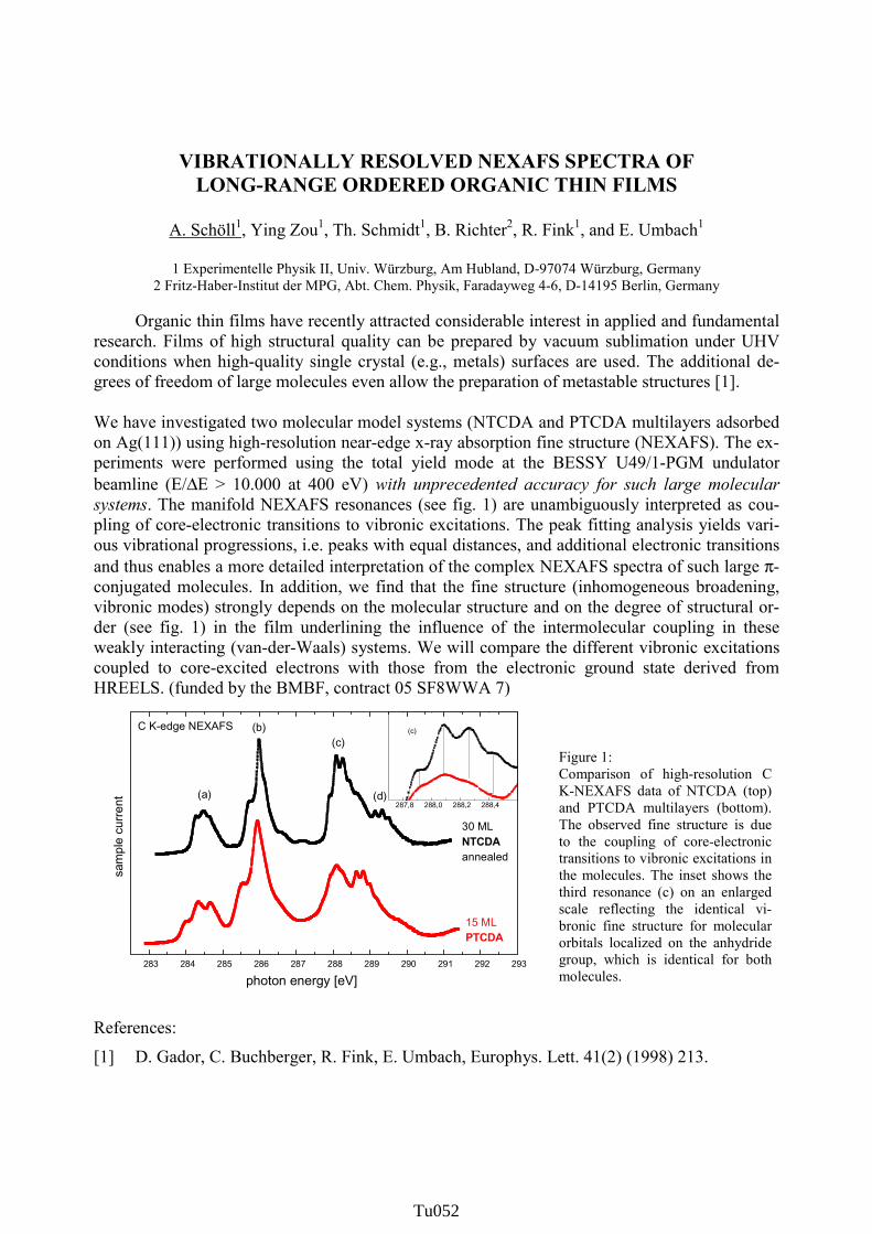
VIBRATIONALLY RESOLVED NEXAFS SPECTRA OFLONG-RANGE ORDERED ORGANIC THIN FILMS
A. Schöll1, Ying Zou1, Th. Schmidt1, B. Richter2, R. Fink1, and E. Umbach1
1 Experimentelle Physik II, Univ. Würzburg, Am Hubland, D-97074 Würzburg, Germany2 Fritz-Haber-Institut der MPG, Abt. Chem. Physik, Faradayweg 4-6, D-14195 Berlin, Germany
Organic thin films have recently attracted considerable interest in applied and fundamentalresearch. Films of high structural quality can be prepared by vacuum sublimation under UHVconditions when high-quality single crystal (e.g., metals) surfaces are used. The additional de-grees of freedom of large molecules even allow the preparation of metastable structures [1].
We have investigated two molecular model systems (NTCDA and PTCDA multilayers adsorbedon Ag(111)) using high-resolution near-edge x-ray absorption fine structure (NEXAFS). The ex-periments were performed using the total yield mode at the BESSY U49/1-PGM undulatorbeamline (E/∆E > 10.000 at 400 eV) with unprecedented accuracy for such large molecularsystems. The manifold NEXAFS resonances (see fig. 1) are unambiguously interpreted as cou-pling of core-electronic transitions to vibronic excitations. The peak fitting analysis yields vari-ous vibrational progressions, i.e. peaks with equal distances, and additional electronic transitionsand thus enables a more detailed interpretation of the complex NEXAFS spectra of such large π-conjugated molecules. In addition, we find that the fine structure (inhomogeneous broadening,vibronic modes) strongly depends on the molecular structure and on the degree of structural or-der (see fig. 1) in the film underlining the influence of the intermolecular coupling in theseweakly interacting (van-der-Waals) systems. We will compare the different vibronic excitationscoupled to core-excited electrons with those from the electronic ground state derived fromHREELS. (funded by the BMBF, contract 05 SF8WWA 7)
287,8 288,0 288,2 288,4
(c)
283 284 285 286 287 288 289 290 291 292 293
(d)
(c)(b)
(a)
15 MLPTCDA
C K-edge NEXAFS
sam
ple
curre
nt
30 MLNTCDAannealed
photon energy [eV]
Figure 1:Comparison of high-resolution CK-NEXAFS data of NTCDA (top)and PTCDA multilayers (bottom).The observed fine structure is dueto the coupling of core-electronictransitions to vibronic excitations inthe molecules. The inset shows thethird resonance (c) on an enlargedscale reflecting the identical vi-bronic fine structure for molecularorbitals localized on the anhydridegroup, which is identical for bothmolecules.
References:
[1] D. Gador, C. Buchberger, R. Fink, E. Umbach, Europhys. Lett. 41(2) (1998) 213.
Tu052Tu052Tu052Tu052

Photoemission and Photoabsorption Investigation of the ElectronicStructure of Ytterbium Doped Strontium Fluoroapatite
A. J. Nelson, T. van Buuren, K. I. Schaffers, and Lou Terminello
Lawrence Livermore National Laboratory, Livermore, CA 94550 USA
X-ray photoemission and x-ray photoabsorption were used to study the surfaceversus bulk composition and the electronic structure of ytterbium doped strontium
fluoroapatite (Yb:S-FAP). High resolution photoemission measurements on the valenceband electronic structure and Sr 3d, P 2p and 2s, Yb 4d and 4p, F 1s and O 1s core lineswere used to evaluate the surface and near surface chemistry of this fluoroapatite.
Enhancement of the photoemission signal from the partially filled Yb 4f orbitals in thevalence band was accomplished by resonant excitation of the 4d–4f transition since thereis an overlap between the 4f orbitals and the O and F p states in the valence band.
Element specific density of unoccupied electronic states in Yb:S-FAP were probed by x-ray absorption spectroscopy (XAS) at the Yb 4d (N4,5-edge), Sr 3d (M4,5-edge), P 2p (L2,3-edge), F 1s and O 1s (K-edges) absorption edges. These results provide the first
measurements of the electronic structure and surface chemistry of this material.
Tu053Tu053Tu053Tu053

STRUCTURAL AND ELECTRONIC PROPERTIES OF COPPER ANDCOBALT µµ -CRYSTALLITES IN A CONDUCTING POLYMER.
M.C.M. Alves1, N. Watanabe 1,2, and J.Morais3
1 Laboratório Nacional de Luz Síncrotron, Campinas - Brazil2 UNICAMP, Instituto de Química, Campinas - Brazil3 UFRGS, Instituto de Física – Porto Alegre - Brazil
Conducting polymer films may be used as host matrices for metal clusters and aggregates.Promising applications of such metal doped polymers may be envisaged in different areas ascatalysis [1], environmental science [2] and magnetism.
In this work the electrochemical growth of copper and cobalt in polypyrrole (C4H3N)nfilms was followed by in-situ X-ray absorption spectroscopy (XAS) [3] at the LNLS XAS beamline (Cu and Co K edge). Thin polymeric films were grown and the copper insertion was carriedout at selected potentials chosen from the electrochemical response of the system. XANES andEXAFS results showed that the initial stages of the copper and the cobalt insertion in polypyrroletook place in an ionic form, like Cu+n(OSO3
-)n, with posterior reduction to a metallic form (Fig.1). In addition, absorption measurements at the O and N K edges were performed in the LNLSSGM beam line for the same set of samples. These measurements allowed us to confirm theformation of an ionic form in the beginning of the process and to understand the final stability ofthe metal clusters inside the polymer matrix. A correlation between structural and chemicalenvironment of the metal clusters will be discussed. (Support from LNLS, FAPESP, CNPq aregratefully acknowledged.)
Figure 1: XANES spectra obtained at the Cu and Co K edges .
References
[1] K.M. Kost, D.E. Bartak, M. Kazee, and T. Kuwana, Anal. Chem. 60, 2379 (1988)..[2] M. Hepel and L. Dentrone, Electroanalysis 8 (11), 996 (1996).[3] M. C. M. Alves, N. Watanabe, A. Y. Ramos and H. C. N. Tolentino. J. Synchrotron
Radiation (accepted 2000).
Tu054Tu054Tu054Tu054

SURFACE AND INTERFACE INVESTIGATION IN NANOMETRICDIELECTRIC FILMS ON Si AND ON SiC
E. B. O. da Rosa1, C. Krug1, C. Radtke1, R. Pezzi1, L. Miotti1,R. Brandão1, F. C. Stedile2, T. D. M. Salgado2, J. Morais1, and I. J. R. Baumvol 1
1 Instituto de Física, Universidade Federal do Rio Grande do Sul, Porto Alegre, Brazil2 Instituto de Química, Universidade Federal do Rio Grande do Sul, Porto Alegre, Brazil
The search for an alternative to SiO 2 as the gate dielectric material to be used in advancedSi-based MOS devices constitutes a new and very lively research area [1]. Many materials havebeen suggested, as Al2O3, Ta2O5, TiO2, and many double (e.g. zirconium silicate) and triple (e.g.barium strontium titanate - BST) oxides. A major requirement is stability — specially at theinterface with Si — upon thermal annealing, which is inherent to processing steps following gatedielectric deposition. We studied atomic transport and chemical stability in Al2O3, ZrSiO4,ZrAlxOy, and Gd2O3 films less than 10 nm-thick on crystalline Si substrates, submitted tothermal annealing in vacuum or in O2. The use of isotopically enriched oxygen (18O2) allowed todistinguish oxygen eventually incorporated during annealing from that originally existing in thefilms.
Single-crystalline SiC is a wide-bandgap semiconductor in current use to fabricate devicescapable of operating at higher temperatures and higher frequencies than Si-based devices.Increased resistance to radiation is also observed. As observed for Si, thermal oxidation of SiC inO2 leads to the formation of an amorphous SiO 2 film. The electrical characteristics of theinterface between SiO2 and SiC are degraded by the formation of an intermediate layer of siliconoxicarbide of variable composition at the initial stages of oxidation. We studied the formation ofthis oxycarbide layer, starting with a clean SiC surface and performing in-situ layer-by-layerthermal oxidation and analysis.
In this work, we will report on recent investigations of the thermal stability of insulatingfilms for advanced Si-based microelectronic devices and of the initial stages of oxidation of SiC.Surface compositions were determined by low-energy ion scattering. Elemental concentrationprofiles were accessed at sub-nanometric depth resolution using narrow nuclear resonanceprofiling. Near-surface, bulk, and near-interface chemical environments of various elements wasdetermined by means of angle-resolved x-ray photoelectron spectroscopy. Atomic transport andcompound formation were modeled based on diffusion-reaction equations.
Research partially supported by CNPq, FINEP, and FAPERGS, Brazil.
References
[1] C. Krug, E.B.O. da Rosa, R.M.C. de Almeida, J. Morais, I. J. R. Baumvol, T.D.M.Salgado, and F.C. Stedile, Phys. Rev Lett. 85, 4120 (2000).
Tu055Tu055Tu055Tu055

Burst Reaction of Thin Films Excited by High-Flux Soft-X-Rays
T. Kanashima1,2, H. Ohashi2, E. Ishiguro3, M. Okuyama1 and M. Okamoto1
1 Department of Physical Science, Graduate School of Engineering Science, Osaka University2 Experimental Facilities Division, JASRI / SPring-83 College of Education, University of the Ryukyus
Recently, high-flux soft X-rays from undulator can be available at the third generation facili-ties such as SPring-8. However, the changes or reactions of thin films owing to the effects of such strong light are not well known. The evaporation of thin films by irradiation with soft X-rays from bending magnet has been reported[1], but this rate is slow. So, heat or etching gases were used to assist the evaporation, drastic reaction have not been observed. In this report, we have observed a burst reaction when high-flux soft X-rays from the undulator of BL27 beamline [2,3,4] is directly irradiated with thin films such as amorphous-Si. Amorphous-Si:H (a-Si:H) and micro-crystal-Si:H (µc-Si:H) were irradiated with soft X-rays. These samples were prepared by LP-CVD (low-pressure chemical vapor deposition) on the glass substrates at around 200oC. Film thickness varies from 400 nm to 8200 nm. The high-flux soft X-ray irradiation was carried out under the following conditions. The samples were held in vacuum chamber and did not heated. The chamber is directly connected the SR-ring without any windows and filters. Fundamental emitted light energy is 1.1 keV and total photon number is 1015 photons/sec (calculated value). Typical irradiation time is 30 minutes, and the storage ring current is 90-100 mA. A mask is placed in front of the sample to characterize the difference be-tween irradiated and unirradiated areas. In the case of a-Si:H film of 8200 nm thickness on silica-glass, vigorous reaction is seen owing to soft X-ray irradiation. The film is crashed and its broken fragments fly off only for a several seconds. After the irradiation, the film was completely removed from substrate. On the other hand, such behavior does not observed in µc-Si:H and 400 nm a-Si:H. The evaporation was seen in the irradiated area, the mask pattern is transcribed to the surface on the samples. This unique reaction is strongly may depend on crystallinity and film thickness of the thin films, and never seen in the case of low density soft X-ray irradiation. The other remarkable irradiation changes of the thin films with high-flux soft X-rays will be discussed.
References
[1] H. Akazawa, Phys. Rev. B. 52, 12386 (1995)[2] I. Koyano, M. Okuyama, E. Ishiguro, A. Hiraya, H. Ohashi, T. Kanashima, K. Ueda, I. H. Suzuki and T. Ibuki, J. Synchrotron Rad. 5, 545 (1998)[3] T. Tanaka, H. Kitamura, Nucl. Instr. and Meth. in Phys. Res. A 364, 368 (1995)[4] H. Ohashi, E. Ishiguro, Y. Tamenori, H. Kishimoto, M. Tanaka, M. Irie, T. Tanaka and T. Ishikawa, POS1-094, Proc. of 7th Int. Conf. on SRI (2000)
Tu056Tu056Tu056Tu056

Electronic Structure of MoS2 clusters using X-ray Absorption and EmissionSpectroscopes
T. Van Buuren1, J.P. Wilcoxon2, C. Bostedt1, N. Franco1, J.E.Klepeis1, T.D. Callcott3,D.L.Ederer4, L. Terminello1
1 Lawrence Livermore National Laboratory2 Sandia National Laboratory
3 Physics Department University of Tennessee4 Physics Department Tulane University
Molybdenum disulfide (MoS2) nanoclusters have demonstrated to be effectivephotocatalysts for the detoxification of chemical waste. In such an application the clusterwould absorb light creating electron-hole pairs and thus catalyze specific chemicalreactions. For these applications the cluster must have a band gap that is matched to thevisible spectrum and the valence and conduction band edges must be compatible with theredox potentials for the reactions involved. To tailor these properties for a specificapplication we measure the valence and conduction band edges of well-defined MoS2clusters using x-ray absorption and emission spectroscopes. MoS2 clusters from 1-10nmin diameter were formed using the inverse micelle synthetic process at room temperaturein inert oil. The cluster size and distribution could be precisely controlled using a high-pressure liquid chromatography system. By measuring the S 2p absorption were are ableto measure the change in the conduction band edge of the MoS2 clusters as a function ofparticle size. We found that the conduction band edge was blue shifted with decreasingclusters size with shifts up to 1.2 eV measured for clusters 2nm in diameter. These resultsagree with earlier predictions of the conduction band shifts as a function of particle size.The valence band density of states was determined by measuring the soft x-ray emissionfrom the S 2p core hole. A shift in the valence band edge together with a dramaticchange in the density of states was observed with decreasing cluster size. For 2nmclusters a valence band shift of approximately 1.0 eV was measured. This does not agreewith effective mass calculations, which predict little or no shift in the valence band edge.We compare these results to recent optical measurements.
This work was supported by the Division of Materials Sciences, Office of BasicEnergy Science, and performed under the auspices of the U. S. DOE by LLNL undercontract No. W-7405-ENG-48, and at the ALS, LBNL under Contract No. DE-AC03-76SF00098. N.Franco is supported by the Spanish Education and Culture Office undercontract PF-98-33501134. C. Bostedt is supported by the German Academic ExchangeService DAAD.
Tu057Tu057Tu057Tu057

Intramolecular energy-band dispersion in oriented thin filmof n-CF3(CF2)22CF3 observed by angle-resolved UV photoemission
and its theoretical simulation
D. Yoshimura1, H. Ishii2, T. Miyamae3, S. Hasegawa4, K.K. Okudaira5, N. Ueno5, and K. Seki1
1 Research Center for Materials Science, Nagoya University, Furo-cho, Chikusa-ku, Nagoya 464-8602, Japan2 Department of Chemistry, Faculty of Science, Nagoya University, Furo-cho, Chikusa-ku, Nagoya 464-8602, Japan
3 National Institute of Materials and Chemical Research, 1-1 Higashi, Tsukuba 305-8565, Japan4 Institute for Molecular Science, Myodaiji-cho, Okazaki 444-8585, Japan
5 Depertment of Materials Technology, Faculty of Engineering, Chiba University, Yayoi-cho, Inage-kuChiba 263-8522, Japan
Poly(tetrafluoroethylene) (PTFE) (CF2)n is one of the most fundamental polymers, whichis the perfluorinated analogue of polyethylene (CH2)n with a simple repeating CF2 unit. PTFEhas been widely used due to its excellent properties, such as chemical stability, good electricalinsulation and so on. Many of the interesting chemical and physical properties of PTFE arerelated to its valence electronic structures, and its elucidation is important from the viewpointsof both basic science and practical applications. For such a one-dimensional polymer, we canalso expect the formation of intramolecular energy-bands, and the energy-band structures ofPTFE have been studied theoretically.[1] Unfortunately, however, there were no experimentalresults to be compared with such calculated energy-band structure.
In the present work, we report on angle-resolved UV photoemission studies of orientedthin films of perfluorotetracosane (n-CF3(CF2)22CF3; PFT),[2] which is one of the oligomer ofPTFE, prepared by in-situ vacuum evaporation. The use of oligomers is based on the theoreticaland experimental findings that oligomers more than ten repeating units have very similarelectronic structures with infinite polymers. The incident photonenergy dependence of the normal-emission spectra of the PFT thinfilm at 22 ≤ hν ≤ 60 eV is shown in Fig. 1. The emission intensitiesof these spectra are normalized by the photon flux of the incidentphoton energy. The main features show continuous and significantchanges in both peak positions and intensities. We attribute thepeak shifts to the intramolecular energy-band dispersion. We alsoperformed the theoretical simulation of the spectra by usingindependent-atomic-center (IAC) approximation combined with abinitio MO calculations, which have been successfully applied to theanalysis of the photoelectron angular distribution for orientedorganic films and the energy-band dispersion of solid surface.[3]
References[1] K.Seki, H.Tanaka, T.Ohta, Y.Aoki, A.Imamura, H.Fujimoto, H.Yamamoto, and H.Inokuchi, Phys. Scripta 41, 167 (1990).[2] T. Miyamae, S. Hasegawa, D. Yoshimura, H. Ishii, N. Ueno and K. Seki, J. Chem. Phys., 112, 3333 (2000).[3] D.Yoshimura, H.Ishii, Y.Ouchi, E.Ito, T.Miyamae, S.Hasegawa, Fig. 1 hν-depencence of ARUPS K.K.Okudaira, N.Ueno, and K.Seki, Phys. Rev B60, 9046 (1999). spectra for oriented PFT film.
Tu058Tu058Tu058Tu058

XAFS AND PHOTOELECTRON DIFFRACTION STUDIES OF ALKANETHIOL SELF-ASSEMBLED MONOLAYER FILMS ON NOBLE
METALS
Hiroshi Kondoh, Masaoki Iwasaki, Kenta Amemiya, Toshihiko Yokoyama and Toshiaki Ohta
Department of Chemistry, Graduate School of Science, The University of Tokyo, 7-3-1 Hongo, Bunkyo-ku, Tokyo 113-0033, Japan
Self-assembled monolayers (SAMs) such as alkanethiols on noble metal surfaces have been investigated due to their unique properties and technological availability. How SAM films form chemical bonding with noble metal surfaces is of fundamental importance. The structure of the SAM films depend strongly on the kind of substrate metal, the face of the surface and the surface coverage. A number of structural studies have been conducted on SAM films on Au, Ag and Cu crystal surfaces as a function of coverage by use of IRAS, LEED, STM, LEAD, GIXD and C-K NEXAFS. S-K XAFS is a very suitable method for the study of chemical bonding of a thiolate and the metal substrate since it provides information of the local structure around the thiolate S atom.
Recently, we have studied the structures of several alkanethiol SAM films prepared by vacuum vapor deposition on Cu(100) and Ag(100) with C-K NEXAFS, S-K NEXAFS and EXAFS measurements. All the experiments have been carried out at the Photon Factory. In both cases, S atom is located at the fourfold hollow site without reconstruction. These results are compared with previous results on thiolates on Ag(111)[1] and Cu(111)[2]. On the other hand, the structures of alkanethiols on Au(111) cannot be studied by S-K XAFS experiment due to large background from the gold substrate. Instead, we found that S 2p photoelectron diffraction (PED) experiments are very promising to determine the adsorbed structures on gold. Polar and azimuthal dependences of the S 2p peak intensity relative to C 1s were obtained for methyl thiolate on Au(111). S2p energy scanning PED spectra were also obtained for the same system. The analyzed results will be discussed by comparing with other experimental and theoretical studies on the structures of thiolates on Au(111).
References [1] P.N.Floriano et al, Chem.Phys.Letters 321, 175(2000) [2] A.Imanishi et al, Surf. Sci. 407, 282 (1998)
Tu059Tu059Tu059Tu059

TEST MEASUREMENTS ON THE SOFT-X-RAY EMISSION AT THE Fe L-EDGE OF MYOGLOBIN SOLUTION
Y. Harada1, K. Kobayashi1, M. Oura1, M.Watanabe1, T. Takeuchi2 and S. Shin1,3
1 RIKEN/Spring-8, 1-1-1 Kouto, Mikazuki-cho, Sayo-gun, Hyogo 679-5148, Japan
2 Faculty of Science, Science University of Tokyo, Kagurazaka, Shinjuku, Tokyo 162-8601, Japan 3 Institute for Solid State Physics, University of Tokyo, Kashiwanoha, Kashiwa, Chiba 277-8581, Japan
Iron-Porphyrin complexes are known as the basis of heme proteins. The electronic
structure of the center irons in the complexes may be responsible for the basic biological function of them. Soft-x-ray emission spectroscopy(SXES) is one of the most applicable methods to know the electronic states of center irons because it follows dipole transition and projects Fe3d valence states as partial density of states by Fe2p core excitation. Moreover, polarization dependence of the soft-x-ray Raman scattering(PSXRS) at resonant core excitation is a noble tool to find non-degenerate states[1,2], so that it is even feasible to detect spin configurations by PSXRS at Fe2p resonant excitation. What is more interesting is the bulk sensitivity of SXES, which may allow us to do experiments on liquids as a physiological solution. Myoglobin is appropriate for the test measurements of solution because it has an equivalent heme site.
The experiments were perfonrmed at KEK-PF(Photon Factory, JAPAN) BL2C and BL19B. First, we tried SXES of a powdered Myoglobin that we could easily treat in ultra-high vacuum. SXES intensity of the Myoglobin powder was about 5% of that of Iron-Porphyrin powder even for only about 0.4% of the density ratio of iron ions as shown in the figure. Next, SXES of a frozen solution(8mmol/l) was measured with a liquid cell that holds a liquid in high vacuum below 1x10⁻⁷Torr. A 150nm thick polyimide window was used where the transparency throughout the photon-in and the photon-out process was about 20%. Again the SXES intensity of the solution is almost the same as that of the powder even for only about 0.4% of the density ratio of iron ions. This means protein chains composed of light elements are quite transparent to the soft-x-ray above Fe2p resonance, which results in the quite effective emission from buried iron ions.
We have also experienced SXES of Myoglobin solutions of various spin and valency states, which will be discussed in the conference. References [1] Y. Harada, T. Kinugasa, R. Eguchi, M. Matsubara, A. Kotani, M.Watanabe, A.Yagishita
and S. Shin, Phys. Rev. B, 61 12854(2000) [2] M. Matsubara, T. Uozumi, A. Kotani, Y. Harada and S. Shin, J. Phys. Soc. Jpn., 69
1558(2000)
Inte
nsity
(arb
.uni
ts)
725720715710705700695690
Emission energy (eV)
Fe2p SXES
Met-Myoglobin solution
Met-Myoglobin powder
Iron-Porphyrin powder
x 20
Figure : Fe2p SXES of heme samples. The intensity of the solution is calibrated by the window attenuation.
Tu060Tu060Tu060Tu060

MORPHOLOGY AND CHEMISTRY OF S-TREATED GaAs(001)SURFACES
S. Heun1, M. Rudolf2, M. Lazzarino2, G. Biasiol2, B. Bonanni2, L. Gregoratti1, A. Barinov1, B.Kaulich1, and L. Sorba2,3
1 Sincrotrone Trieste, Basovizza, 34012 Trieste, Italy2 Laboratorio TASC-INFM, Basovizza, 34012 Trieste, Italy
3 Universita' di Modena e Reggio Emilia, Via Campi 213/A, 41100 Modena, Italy
Most as-grown III-V semiconductor surfaces possess a very high surface state density,which leads to Fermi-level pinning near-midgap. Many studies addressed the problem of GaAssurface states since the pioneering work of C.J. Sandroff who passivated the GaAs surface bydipping it in a solution of (NH4)2S [1]. Optical and topographic inhomogeneities on passivatedsurfaces were demostrated by scanning near-field optical microscopy [2], scanning tunnelingmicroscopy [3], and atomic force microscopy [4]. However, no spatially-resolved information ispresently available on the chemistry of the S-treated GaAs surface. We addressed this importantissue by scanning photoemission microscopy (SPEM) on S-treated GaAs. The measurementswere performed at the ESCA microscopy beamline at ELETTRA. The S-treatment consisted of apreliminary removal of the native oxide with a 1 min dip in a 1% HF:H2O solution, followed bya 30 s water rinse. Then the samples were soaked for a 5 min period in a (NH4)2S solution,enriched by adding 8% by volume of S powder, at a temperature of 65-70°C. The treatment wasstopped in two different ways. Sample A was removed from the solution and directly blown drywith N2. Sample B instead was rinsed by flowing DI water in the same beaker for 10 min, thusavoiding drying of the surface before rinsing, and finally blown dry with N2.
SPEM images of sample A show lateral inhomogeneities at the Ga 3d, As 3d, S 2p, and O1s core levels. Two distinct regions with higher and lower intensity are observed, and a contrastinversion is observed between the image obtained at the O 1s core level and the images from theGa 3d, As 3d, and S 2p core levels. On the other hand, SPEM images from sample B show thatthis sample is laterally homogeneous on the 100-nm scale. The nature of the inhomogeneities onsample A was identified by laterally resolved photoelectron spectroscopy. The spectra from theGa 3d, As 3d, and S 2p core levels show that the intensity variation observed in thecorresponding SPEM images is caused by an inhomogeneous attenuation of the signal from theS/GaAs interface. In comparison, the spectra from sample B indicate the loss of S from thesample surface during the water rinse. An analysis of the spectra from the O 1s core level, takenfrom samples A and B, shows that this peak is composed of two components. One is identified ascorresponding to Ga-O and As-O bonds, while the other is assigned to S-O bonds. The relativecontribution of the S-O component differs strongly from sample to sample, and in the case ofsample A even from region to region on the sample surface. On sample B, it is much reduced ascompared to sample A. Finally, on sample A a lateral variation in the intensity of this componentis observed which can be explained by a monolayer-variation of the local O coverage.
[1] C.J. Sandroff et al., Appl. Phys. Lett. 51, 33 (1988).[2] J. Liu and T. F. Kuech, Appl. Phys. Lett. 69, 662 (1996).[3] J. S. Ha, S. J. Park, S. B. Kim, and E. H. Lee, J. Vac. Sci. Technol. A 13, 646 (1995).[4] Z. H. Lu, M. J. Graham, X. H. Feng, and B. X. Yang, Appl Phys Lett 62, 2932 (1993).
Tu061Tu061Tu061Tu061

Analysis of phase composition of surface oxidesusing X-ray photoelectron spectral line shapes
Nikolai V. Alov
Department of Analytical Chemistry,Lomonosov Moscow State University,
119899 Moscow, [email protected]
X-ray photoelectron spectroscopy (XPS) is a powerful method of surface phasecomposition analysis on the basis of spectral line deconvolution. Nowadays XPS is widely usedfor the investigation of surface phase composition of high-technology materials and phasetransitions on the modified solid surfaces after the physical and chemical treatment.
In this work the influence of low-energy oxygen ion bombardment on the phasecomposition of surface layers of metals (Mo, W, Nb, Ta) was investigated by XPS. The in situexperiments including surface cleaning by argon ion bombardment, surface oxidation by low-energy (E=1-5 keV) oxygen ion bombardment, analysis of phase composition by XPS werecarried out in an UHV chamber (p=10-10 mbar) of a Leybold LHS-10 electron spectrometer. TheXP-spectra were measured in the constant transmission energy mode of hemispherical energyanalyzer (50 eV) with use of Mg Ka-radiation (1253.6 eV) as a primary excitation. Theinstrumental resolution - 0.9 eV (Au 4f7/2 spectral line). The accuracy of measurement of bindingenergies of core level electrons - 0.1 eV. The spectral line deconvolution was fulfilled using aLeybold software product.
Analysis of X-ray photoelectron spectral line shapes of Mo 3d-, W 4f-, Nb 3d- and Ta 4f-core level shown that the oxides are formed in metal surface layers during the low-energyoxygen ion bombardment at room temperature. The oxides with composition MO2, MOx, MO3
(M=Mo, W) and MO, MO2, M2O5 (M=Nb, Ta) were revealed. The oxidation degree of surfacelayers is a complex function of energy and fluence of oxygen ions and chemical reactivity ofmetal.
In Rabalais approximation the absolute values of fundamental parameters of low-energyoxygen ion interaction with metal surfaces (reaction and sputtering cross-sections) werecalculated. The mechanisms of phase transformations in surface layers of irradiated metals arediscussed.
Tu062Tu062Tu062Tu062

THE EFFECT OF LiF LAYER ON AL/LiF/ALQ3 INTREFACES STUDIED WITH ELECTRON SPECTROSCOPIES
T.Yokoyama1, D.Yoshimura2, E.Ito3, H.Oji4, H.Ishii1, Y.Ouchi1, K.Seki2
1 Graduate School of Science, Nagoya University, Chikusaku, Nagoya 464-8602, Japan
2 Research Center for Materials Science, Nagoya University, Chikusaku, Nagoya 464-8602, Japan 3 Institute of Physical and Chemical Research, Wako 351-0198, Japan 4 Institute for Molecular Science, Myodaiji, Okazaki 444-8585, Japan
Organic electroluminescent(EL) devices have been extensively studied for possible application to flat panel display. The device structure is sandwiched organic layers between two metal electrodes, and the study of the organic/organic and metal/organic interfaces are important for understanding and improving the performance of organic EL devices. The enhancement of device efficiency at the insertion of LiF layer between tris(8-hydroxyquinolino) aluminum (Alq3) and Al electrode was reported[1], and, interface energy level alignment was found to be changed by inserting the LiF layer[2]. For clarifying more details of this phenomenon, we have investigated Al/LiF/Alq3 interface using X-ray photoelectron spectroscopy (XPS), ultraviolet photoelectron spectroscopy (UPS), and metastable atom electron spectroscopy (MAES). Figure1 shows the observed UP spectra of Alq3(0.5nm) film on Al substrate with inserted LiF layer of increasing thickness. When LiF layer is absent, an extra state(X) appears above the HOMO(A) of Alq3, and the increase in LiF thickness leads to the decrease of the peak intensity of X. Thus this peak results from the interaction between Al and Alq3. Figure2 depicts observed energy offset of the interfaces. The vacuum level shift occurs at the interfaces. The electron injection barrier, obtained as the difference of LUMO of Alq3 and Fermi level of Al substrate, is decreased with increasing LiF thickness. We can suppose two possible origin of device efficiency
enhancement. Thus, i.e. (1) suppressed of Alq3/Al interaction and (2) reduction of the electron injection barrier.
References [1] L.S.Hung, C.W.Tang, and M.G.Mason, Appl.Phys Lett (1997) 152. [2] T.Mori,H.Fujiwara,S.Toikito,and T.Taga, Appl.Phys.Lett (1998) 276
Figure1 The UP spectra of Alq3(0.5nm)/LiF/Al interfaces. LiF layer thickness (θLiF) is shown for each spectrum.
Figure2 The energy diagram of Alq3/Al, Alq3/LiF(0.5nm)/Al, and Alq3/LiF(2.0nm)/Al interfaces. (Φm:work function of metal, Evac: vacuum level, EF: Fermi level, εv
F:difference between EF and HOMO of organic layer, ∆:vacuum level shift, Ith: ionization potential )
Tu063Tu063Tu063Tu063

STRUCTURAL CHANGES IN ANNEALED,HYDROGEN IMPLANTED MONOCRYSTALLINE SILICON
P. Dubcek1, B. Pivac2, O. Milat3, S. Bernstorff1, R.Tonini4, F. Corni4 and G. Ottaviani4
1 Sincrotrone Trieste, SS 14 km 163,5, 34012 Basovizza (TS), Italy2 Ruder Boskovic Institute, Bijenicka 54, 10000 Zagreb, Croatia
3 Institute for Physics, Bijenicka 46, 10000 Zagreb, Croatia4 University of Modena, Physics Department, Via Campi 213a, 41100 Modena, Italy
The grazing incidence small angle X-ray scattering (SAXS) technique was used toinvestigate monocrystalline silicon samples, prepared from Czochralski grown monocrystallinesilicon, implanted with H2+ (beam current density 1mA/cm2) impinging on the sample at anenergy of 31 keV, and annealed isochronally at different temperatures in the range from 100oCto 900oC.
Although the H depth distribution was expected to be smooth initially, nanosized features,like agglomerates of defects, have been detected (minor correlation peak, indicated by arrow, at0.265nm-1 for implanted, but unannealed sample in Figure 1.). After annealing this features aredestroyed due to the relaxing of the defect structure, controlled by hydrogen captured inintersticials, as well as in produced vacancies. Above 300 oC a well defined film with highlycorrelated borders is formed on the edge of the layer rich in defects (presumably due to themigration of vacancies and hydrogen), whose thickness is slowly decreasing from 17 to 12 nmwith increasing annealing temperature. This is attributed to vacancies and bubblesagglomeration, and the size decreases due to hydrogen abandoning the vacancies in the region.With increasing annealing temperature, defects as well as hydrogen are migrating towards thesurface, as it is indicated by the increase of the surface roughness. We will present a model forthe film structure changes obtained by data evaluation using distorted wave Born approximation.
102
103
104
105
106
107
108
I(a.u.)
0.350.300.250.200.15
S(nm-1)
as implanted
100
200 300 350
400
500
600 650
700
800
900
Figure 1: GISAXS intensities for H implanted silicon vs. scatteringangle, for diverse annealing temperatures (in centigrades, as indicated)
Tu064Tu064Tu064Tu064

SiC(100) ORDERED FILMS GROWTH BY C60DECOMPOSITION ON Si(100) SURFACES
M. Pedio1, A. Pesci1, P. Moras 1, L. Ferrari1, M. Capozi1, S. N. Jha2, R.Verucchi3, L. Aversa3
1 ISM-CNR Sede Distaccata di Trieste, Basovizza (Trieste) Italy2 Sincrotrone Trieste and Spectroscopy Division, BARC, Mumbai-400 085, India
3 CeFSA-CNR Povo,(Trento)
Fullerene (C60) was deposited on Si(100) 2x1 double domain reconstructedsubstrate. The interface has been treated with annealing procedure in order to inducecovalent Si-C bond formation and to obtain carbidization. In this way 3C-SiC(100) canbe obtained. The different stages of growth have been checked by in situ low energyelectron diffraction (LEED), Auger and Inverse Photoemission techniques. We foundthat differences in the morphology and electronic properties can be detected dependingon the growth procedure. In particular a SiC(100) 2x1 ordered sample have beenobtained with a thickness of about 2000 Å. Ex situ we verified surface order by meansof LEED technique, observing the recovering of the 2x1 double domain reconstruction.
We characterized electronic properties collecting valence band and core levelphotoemission spectra employing synchrotron radiation source. ARUPS measurementsshowed evident electronic surface states in valence band similar to those revealed on 3C-SiC(100) (2x1) surfaces grown by different techniques.
Tu065Tu065Tu065Tu065

LOCAL GEOMETRY AND ELECTRONIC STRUCTURE OF BOROSILICATE GLASSES: X-RAY ABSORPTION FINE STRUCTURE
ANALYSIS
A V Soldatov1, M.I. Mazuritsky1, V.L. Lyashenko1, M.Kasrai2and G. M. Bancroft2
1 Faculty of Physics, Rostov State University, 344090, Rostov-on-Don, Russia
2. Dept. of Chemistry, University of Western Ontario, London, Ontario , Canada
The Si L2,3, and B K- edge XANES spectra of two types of borosilicate glasses (“white” and “black”) have been measured at the Canadian Synchrotron Radiation Facility (Aladdin storage ring; University of Wisconsin-Madison). These glasses correspond to two stages of micro-channel plate manufacturing. The TEY (surface sensitive) and FY (bulk sensitive) detection modes were used to study the distribution of Si and B atoms in the glasses. Theoretical analysis of XANES data has been done on the basis of “ab initio” full multiple-scattering theory. An agreement between theory and experiment has been obtained. The distribution of the unoccupied projected silicon s and d electronic states and boron p electronic states has been established. The interactions between these states in the bottom part of the conduction band of borosilicate glasses have been studied.
100 110 120 130 1400
5
10
15
20
25
30
Si L2,3 edge XANES
black glass (tey)
quartz
white glass (fy)
Inte
nsity
(rel.u
nits
)
Energy(eV)
Figure 1: Si L2,3 edge XANES spectra in two types of borosilicate glasses compared with the spectrum of quartz..
Tu066Tu066Tu066Tu066

SOFT X-RAY PHOTOEMISSION STUDY OF Ni, Pd AND Pt
Takayuki Muro1, Yuji Saitoh2, Akira Sekiyama3, Shin Imada3, and Shigemasa Suga3
1 Japan Synchrotron Radiation Research Institute (JASRI),SPring-8, Mikazuki-cho, Sayo-gun, Hyogo 679-5198, Japan
2 Department of Synchrotron Radiation Research, Japan Atomic Energy Research Institute (JAERI),SPring-8, Mikazuki-cho, Sayo-gun Hyogo 679-5148, Japan
3 Department of Material Physics, Graduate School of Engineering Science,Osaka University, Toyonaka, Osaka 560-8531, Japan
We report valence band photoemission spectra of Ni, Pd, and Pt metals measured with softx-ray synchrotron radiation. Pd is interesting for its nearly ferromagnetic behavior. For example,spin alignment in Pd thin films is realized by a contact with ferromagnetic Ni [1]. In comparisonwith ferromagnetic Ni, Pd metal has the same crystal structure and comparable number ofvalence electrons. According to Kanamori’s theory [2], the achievement of the ferromagnetismin Ni is related to the shape of the density of states (DOS) in the valence band, namely, theproperly wide valence band DOS with a narrow and high DOS peak at the Fermi level (EF). It isexpected that Pd metal also has such a feature of the valence band DOS because of its nearlyferromagnetic behavior.
The measurements were performed at the soft x-ray undulator beamline BL25SU atSPring-8. The grazing incidence monochromator of BL25SU with varied-line-spacing planegratings covers a photon energy (hν) range from 220 to 2000 eV [3]. The photoemission spectrawere taken with a GAMMADATA-SCIENTA SES-200 analyzer. The sample temperatures wereset at 100 K. The polycrystalline samples were cleaned by repeated filing under the ultra highvacuum (∼ 4 × 10⁻⁸ Pa).
Figure 1 shows the valence bandphotoemission spectra of Ni, Pd and Pt metalstaken at hν = 955eV with a total energyresolution of about 270meV. The valenceband width becomes wider on going from Nito Pt. A narrow peak close to EF is recognizedin the Pd spectrum indicating a high DOS atEF. It is considered that this narrow peak ofDOS is responsible for the nearlyferromagnetic nature of Pd metal.
References
[1] U. Gradmann and R. Bergholz, Phys.Rev. Lett. 52, 771 (1984).
[2] J. Kanamori, Prog. Theor. Phys. 30, 275(1963).
[3] Y. Saitoh et al., Rev. Sci. Instrum. 71,3254 (2000). Fig. 1: Valence band photoemission spectra of
Ni, Pd and Pt taken at hν = 955eV.
10 5 0
Binding energy (eV)
Inte
nsity
(arb
. uni
ts)
Pt
Pd
Ni
Tu067Tu067Tu067Tu067

Effects of Air-Exposure and Cs-Deposition on the Electronic Structure ofMulti-Walled Carbon Nanotubes
S. Suzuki1, Y. Watanabe1, K. G. Nath1, T. Ogino1, S. Heun2, W. Zhu3, C. Bower4 and O. Zhou4, 5
1 NTT Basic Research Laboratories, Atsugi, Kanagawa 243-0198 Japan2 Sincrotrone Trieste, Bassovizza, 34012 Trieste, Italy
3 Bell Laboratories, Lucent Technologies, Murray Hill, New Jersey 07974 USA4 Department of Physics and Astronomy, University of North Carolina, Chapel Hill, NC 27599 USA
5 Curriculum in Applied and Materials Science, University of North Carolina, Chapel Hill, NC 27599 USA
The field emission (FE) current from carbon nanotubes has been found to be significantlyenhanced by adsorbates [1] and by Cs deposition [2]. We studied the electronic structural changeof multi-walled carbon nanotubes (MWNTs) induced by air-exposure and by Cs-depositionusing photoemission spectroscopy.
Figure 1 shows the secondary electron threshold spectra of as-received (before an anneal)and annealed aligned MWNT samples. This figure shows the work function of as-receivedsample which is covered by adsorbates is slightly larger than that of the annealed sample. Thevalence band measurement revealed that the work function increase was mainly due to a surfacedipole moment induced by the adsorbates rather than to a Fermi level shift. Whereas, Csdeposition on the clean sample caused a Fermi level shift and a large enhancement of the densityof states at the Fermi level, indicative of an intercalation reaction. Furthermore, in strong contrastto the air-exposure, Cs deposition drastically decreased the work function of the MWNTs. Theseresults reveal that the FE current enhancements caused by adsorbates and Cs deposition arebased on essentially different mechanisms.
Figure 1: Secondary electron threshold spectra of the as-received and annealed aligned MWNTs.References[1] K. A. Dean, B. R. Chalamala, Appl. Phys. Lett. 76, 375 (2000).[2] A. Wadhawan, R. E. Stallcup II and J. M. Perez, Appl. Phys. Lett. 78, 108 (2001).
70x103
60
50
40
30
20
10
0
Inte
nsity
(arb
. uni
ts)
17.2 17.0 16.8 16.6 16.4
Nominal Binding Energy (eV)
before anneal after anneal
hν=21.2 eV
Tu068Tu068Tu068Tu068

SOFT X-RAY ABSORPTION SPECTROSCOPY OF SINGLENANOCRYSTALS
F. Nolting1,2,3, J. Rockenberger4,5, J. Lüning3, Jiangtao Hu4,5, and A. Paul Alivisatos4,5
1 Paul Scherrer Institut, Swiss Light Source, 5232 Villigen PSI, Switzerland2 Advanced Light Source, Ernest Orlando Lawrence Berkeley National Laboratory, Berkeley, CA 94720, USA
3 Stanford Synchrotron Radiation Laboratory, Stanford, CA 94309, USA4 Universtiy of California at Berkeley, Department of Chemistry, Berkeley, CA 94720, USA
5 Lawerence Berkeley National Laboratory, Materials Science Division, Berkeley, CA 94720, USA
The development of the electronic structure of nanocrystals and the investigation of sizedependent scaling laws is an active research area of academic and technological relevance [1,2].In general, experiments are performed on ensembles of nanocrystals which, even in the bestsamples, still exhibit a distribution with respect to particle size and shape, crystallinity and defectstructure etc. In consequence, scaling laws derived from such experiments represent an ensembleaverage with an inherent uncertainty with respect to intrinsic properties of individualnanocrystals. To overcome these limitations, single particle experiments have been developedand performed in recent years [3-5]. For instance, in optical fluorescence spectroscopy ofensembles of semiconductor nanocrystals one observes typically rather broad fluorescence lines(FWHM ~0.1-0.2 eV at 10 K). However, experiments on individual nanocrystals yield not onlyextremely sharp emission lines (FWHM ~200 µeV at 10 K ) but also allow the observation ofeffects like spectral diffusion and blinking of single nanocrystals which is inherently not possiblewith ensemble techniques [3].
While the size dependence of the optical excitation gap can be investigated with opticalspectroscopy, detailed information about the electronic structure can be obtained by X-rayabsorption spectroscopy (XAS) [6]. In addition, insight into the chemical composition, structuralproperties, and even the magnetic properties of nanostructures can be obtained. Here we reportthe first experiments to explore the feasibility of spectromicroscopy to record the X-rayabsorption spectra of a single nanocrystal using photoelectron emission microscopy (PEEM).The experiment was carried out with the PEEM2 instrument of the Advanced Light Source atbeamline 7.3.1.1 [7].
References[1] A.P. Alivisatos, Abstr. Pap. Am. Chem. Soc. 216(3), U337 (1998).[2] "National Nanotechnology Initiative: Leading to the Next Industrial Revolution," National
Science and Technology Council, 2000.[3] S. Empedocles and M. Bawendi, Acc. Chem. Res. 32, 389 (1999).[4] D.L. Klein, R. Roth, A.L. Lim, A.P. Alivisatos, and P.L. McEuen, Nature 389(6652), 699
(1997).[5] H.J. Dai, E.W. Wong, and C.M. Lieber, Science 272(5261), 523 (1996).[6] J. Lüning, J. Rockenberger, S. Eisebitt, J.E. Rubensson, A. Karl, A. Kornowski, H. Weller,
and W. Eberhardt, Solid State Comm. 112(1), 5 (1999).[7] S. Anders, et al., Rev. Sci. Instrum. 70, 3973 (1999).
Tu069Tu069Tu069Tu069

Soft X-ray absorption spectra of lithium phthalocyanine radical T. Okajima 1, H. Fujimoto 2, M. Sumimoto 2, T. Araki 3, E. Ito 4, H. Ishii 5, Y. Ouchi 5 K. Seki 5,6
1 Japan Synchrotron Radiation Research Institute, Kouto, Mikazuki-cho, Sayo-gun, Hyogo 679-5198, Japan 2 Department of Chemistry, Kumamoto University, Kurokami, Kumamoto 860-8555, Japan 3 Department of Chemistry, Saitama University, ohkubo, Urawa, Saitama 338-8570, Japan 4 Frontier Research Program, RIKEN, Hirosawa, Wako, Saitama 351-0198, Japan 5 Department of Chemistry, Nagoya University, Furo-cho, Chikusa-ku, Nagoya 464-8602, Japan 6 Research Center for Materials Science, Nagoya University, Furo-cho, Chikusa-ku, Nagoya 464-8602, Japan
Lithium phthalocyanine (LiPc) is a stable neutral radical and one of the few intrinsic molecular semiconductors with energy gap of nearly 0.2 eV and conductivity of 2x10⁻³ S/cm at room temperature [1]. These semiconducting properties imply many potential applications for molecular electronic devices such as light emitting diodes, laser diodes, solar cells, sensors, etc. To realize these electronic devices and improve the device properties, it is very important to understand the electronic structure of LiPc in detail. The valence band structure of LiPc was studied using ultraviolet photoelectron spectroscopy, which showed that LiPc had similar electronic structure with that of H2Pc and ZnPc except for the weak intensity of the highest occupied molecular orbital (HOMO) peak [2]. This weak intensity corresponds to the single-electron occupation of the HOMO, in contrast to the double occupation in other Pcs. In this study, the unoccupied electronic structure of LiPc was studied by near edge X-ray absorption fine structure (NEXAFS) spectroscopy. The carbon (C) and nitrogen (N) K-edge NEXAFS spectra were measured in the total electron yield mode at BL-11A of Photon Factory. Figure shows the C K-edge NEXAFS spectra at low photon energy region of (a) LiPc and some phthalocyanine compounds ((b) CuPc, (c) ZnPc, and (d) H2Pc) at an X-ray incidence angle of θ ~ 55° (magic angle). The spectra except for LiPc have similar features. The slight difference between the spectra of H2Pc and Cu- and Zn-Pc can be ascribed to the different symmetries of these molecule (H2Pc : D2h, CuPc and ZnPc : D4h). The spectrum of LiPc is different from these spectra. In particular, a peak around 283.5 eV indicated by an arrow in figure appears only in the spectrum of LiPc. On the other hand, the general appearance of the spectra of these Pcs in N K-edge region is similar in spite of the difference in the central element. Molecular orbital calculations show that the singly occupied HOMO of LiPc mainly consists of the atomic orbitals of carbons rather than those of nitrogens. These results indicate that the peak around 283.5 eV observed in LiPc is attributed to the excitation to the HOMO. Based on these results, the unoccupied electronic structure of LiPc radical will be discussed. This work has been performed under the approval of Photon Factory Advisory Committee (99G180 and 2000G282). References [1] P. Turek, et al., J. Am. Chem. Soc., 109 (1987) 5119. [2] T. Kimura, et al., Chem. Phys., 253 (2000) 125.
285 290
(d)
(c)
(b)
(a)
hν
55º
H2Pc
ZnPc
CuPc
LiPc
Inte
nsity
/ ar
b. u
nits
Photon energy / eVFigure : C K-edge NEXAFS spectra of LiPc, CuPc, ZnPc, and H2Pc.
Tu070Tu070Tu070Tu070

- 1 -
VUV Photoelectron Dynamics in Pure Cesium Halides andImpurity(Tl and Na) doped CsI; Absolute Photoemission Total Yield,
Auger Free Luminescence, and STE Luminescence.2Arisato Ejiri and Shinzou Kubota,1
Meiji University, School of Science and Technology,Higasi-Sanda,Tama,Kawasaki 214, Japan.1
Rikkyo University, Department of Physics, Faculty of Science, Tosimaku, Tokyo 171, Japan.2
In last decade, large band gap and shallow innershell substances have been attractedinterest in their VUV photoelectron dynamics for the usefulness to photoelectric devicesand scintillator[1-3]. Absolute photoemissin total yield (APTY) spectra in cesium halidesof CsCl, CsBr, and CsI, as well as in Tl-doped and Na-doped cesium iodide, were studiedat several temperatures from 400K to 80K in VUV region (5 30eV). SOR-RING(Tokyo~University) BL-1 site was used for the total yield measurements. The measurments ofthe APTY were explained in detail elsewhere[1]. Luminescence measurements wereperformed at UV-SOR (Okazaki-IMS) BL-8 site and also at the SOR-RING BL-1 site atroom temperature and several low temperatures down to 20K.
+APTY spectra are appeared to exceed unity in the photon energy region exciting Cs5p core electron in all of these halides. This phenomenon was explained in terms of
+Auger enhancement due to the Auger effect associated with the decay process of the Cs5p core hole[2,3]. Decrease of APTY at the core excited photon energy region fordecreasing temperature was attributed to increase of Auger free luminescence (AFL) inCsCl and CsBr. As the results of detail analysis, a strong complementary relationbetween APTY and AFL was revealed[1], and the temperature dependence of energylevel diagram of CsBr including the valence band and the Cs 5p core level was proposed+
[1]. In pure CsI, APTY indicate as large as 1.5 or more at the high temperature asshown in Figure 1 and the APTY due to valence primary coincides very well with theresults of DiStefano et al[4] in intensity at the photon energy of 12 eV. Decrease ofAPTY in these cesium iodides for decreasing temperature can be commonly explained intermes of complementary relation with STE luminescence.
ig. 1. Absolute photoemission total yield Fig. 2. Excitation spectra of STE luminescenceFand its temperature dependence in CsI. (400nm) at 90K and room temperature in CsI.
[1] A.Ejiri and K.Arakaki; Solid State Commun. 110 (1999) 573.[2] A.Ejiri, S.Kubota, A.Hatano and K.Yahagi; J. Phys. Soc. Jpn. 64 (1995) 1484.[3] A.Ejiri, S.Kubota, A.Hatano and K.Arakaki; J.Ele.Spec.Rel.Phen 79 (1996) 151.[4] T.H.DiStefano and W.E.Spicer; Phys. Rev. B15 (1973) 1544.
項目1
Tu071Tu071Tu071Tu071

Electronic Structure of Transition Metal Oxochlorides
Monica de Simone1, Piero Decleva2, Marcello Coreno3, Kevin C. Prince4, GiovannaFronzoni2, Pietro Franceschi5, Claudio Furlani1
1 Dip. di Fisica, Università di Roma Tre ed Unità INFM, Roma, Italy2 Dip. di Chimica, Università di Trieste, Trieste, Italy
3 Lab. Nazionali TASC-INFM, Trieste, Italy4 Sincrotrone Trieste scpa, Trieste, Italy
5 INFM e Dip. di Fisica, Università degli Studi di Trento, Povo, Italy
Transition metal compounds (TMC) have been extensively investigated by SRspectroscopy (photoemission and absorption) in the solid state due to the fundamentalimportance of these materials in catalysis, sensors and a range of other applications. On the otherhand SR spectroscopy of free molecule TMC's in the gas phase is a barely touched subject. Thisis certainly due to additional experimental difficulties in dealing with not stable, often notvolatile and rather aggressive compounds, which are however routinely manipulated inchemistry laboratories.
Here we present some results of a XAS study on TiCl4, VOCl3 and CrO2Cl2.spectra atchlorine, titanium, vanadium and cromium L-edges and oxygen K-edge [1].
Moreover their electronic structure of the first two compounds has been analysed by PESthrough a complete mapping of all the electronic states accessible with photons in the energyrange 20÷1000 eV [2].
The absorption measurements were carried out on the undulator-based Gas PhasePhotoemission beamline at Elettra [3], Trieste.
References[1] A. T. Wen and A. P. Hitchcock, Can. J. Chem. 71 (1992) 100.[2] B. Wallbank, J. S. H. Q. Perera, D. C. Frost and C. A. McDowell, J. Chem. Phys. 69 (1978) 5405; B. E.
Bursten, J. C. Green, N. Kaltsoyannis, M. A. MacDonald, K. H. Sze and J. S. Tse, Inorg. Chem. 33(1994) 5086; W. von Nissen Inorg. Chem. 26 (1987) 567.
[3] R. R. Blyth, R. Delaunay, M. Zitnik, J. Krempasky, R. Krempaska, J. Slezak, K.C. Prince, R. Richter andM. Vondracek, R. Camilloni, L. Avaldi, M. Coreno, G. Stefani, C. Furlani, M. de Simone, S. Stranges,M.-Y. Adam, J. Electron Spectrosc. Related Phenomena, 101-103 (1999) 959-964.
Tu072Tu072Tu072Tu072

GISAXS STUDY OF CADMIUM SULFIDE QUANTUM DOTS
P. Dubcek1, U.V. Desnica2, I.D. Desnica-Frankovic 2, K. Salomon2, S. Bernstorff1, C.W. White3,E. Sonder3 and R.A. Zuhr3
1Sincrotrone Trieste, SS 14 km 163,5, 34012 Basovizza (TS), Italy2 Ruder Boskovic Institute, Bijenicka 54, 10000 Zagreb, Croatia
2 Oak Ridge National Laboratory, P.O. Box 2008, Oak Ridge TN 37831, USA
The traditional method of preparing quantum dots in optical semiconductor devices isadding semiconductor components into glass melt. During the solidification process however,one has not sufficient control over the growth proces, which results in non-ideal sampleproperties (defects, semiconductor surface states, dopant size fluctuations). Most of thesedrawbacks are overcome in a newly proposed technique of ion implantation into solid substrates.
In order to investigate the structure of films prepared by this new method, the grazingincidence small angle X-ray scattering (GISAXS) technique was applied on the films of CdSnanocrystals synthesized in SiO2 by implanting separately constituent Cd and S atoms with adose of 1017/cm2 each and subsequently annealed at 700OC. Due to the high concentration ofnanocrystalline CdS, the scattered intensity is not following the distorted wave Bornapproximation. The inherent Gaussian variation of implanted ions concentration with depthresults in a similar profile of nanocrystals sizes. Changing the grazing incidence angle controlsthe depth of X-ray penetration, and detects this size distribution to be varying from 15 to 35 nm.When the surface roughness contribution is deconvoluted numerically, inplane correlationcontribution to scattering is obtained (see Figure 1.). We will show that numerical analysis ofthis contribution can be a powerful tool to determine the depth variation of the nanocrystals sizesand their inplane size distribution. The results are to be used for further improvements ofsemiconductor quantum dots preparation.
4
68
103
2
4
68
104
2
4
I(a.u.)
0.30.20.10.0-0.1-0.22θ−2θspec(nm
-1)
0.14
0.23
0.12
0.30 0.27
0.25
0.21 0.19
0.17
Figure 1: Inplane correlation part of GISAXS from ion (Cd and S)impanted glass vs. offset from specular angle, for diverse grazingincidence angles (in nm-1, as indicated)
Tu073Tu073Tu073Tu073

VUV Optical Investigations of Carbon-Deuterium Films Produced inTokamak-10 Plasma.
Amarantov S.V.1, Dudin P.V.1, Kolbasov1, A.M.Lebedev1, B.N., Romanov1 P.V.,Ivanov2 S.N.
1 – RRC Kurchatov Institute, Russia, Moscow
2 - Moscow State University, Physical Faculty, Russia
The Tokamak-10 instrument for the thermonuclear investigations has thegraphite entities working in immediate proximity to the hot plasma. Under the impactof plasma on these entities the carbon is deposited on the cold walls of Tokamakalong with elements of plasma, i.e. deuterium. The deuterieum-carbon (D/C) ration indeveloped carbon films could reach the value of 0.8 [1],[2]. Note that the fullerenes,nanotubes etc are usually produced in the related conditions.
The investigations of the C-D films are technologically stimulated by thethermonuclear synthesis problem. Particularly, the investigation is directed towardsthe increase of plasma confinement quality, because the process eliminates thedeuterium from plasma to the C-D films.
We have studied the C-D films using the optical methods. The luminescencespectra were measured using nitrogen (3.68 eV) and synchrotron (3.5-12 eV)excitation. The possible explanations of the observed features and their connectionwith deuterium confinement in films are discussed.
1. Jacob W., Thin Solid Films, 1998, vol. 326, p.1
2. B.N.Kolbasov, A.B.Kukushkin, V.A.Rantsev-Kartinov, P.V.Romanov,Phusics Letters A, 269(2000), pp. 363-367.
Tu074Tu074Tu074Tu074

Investigation of scintillators for medical and high energy physics applications using VUV and XUV synchrotron radiation
V. Mikhailin, A. Belsky, I. Kamenskikh, V. Kolobanov, I. Shpinkov, A. Vasil’ev
Synchrotron radiation laboratory, Moscow State University, 119899 Moscow, Russia
A large variety of gamma and X-ray photon detectors is based on scintillators. Scintillation of a crystal is the result of several consecutive processes:
• Absorption • Inelastic electron-electron scattering and Auger decay processes (hot relaxation stage) • Emission of phonons (cooling) • Capture of charge carriers by radiative and non-radiative centres (trapping) • Photon emission. Hot relaxation stage results in the creation of secondary electronic excitations of
intermediate energies, similar to those created after the absorption of VUV-XUV photons. Thus synchrotron radiation in this energy range provides a unique tool for their direct “imaging” and investigation.
As an example the role of synchrotron radiation in the study of lead tungstate, a new heavy
scintillator for high energy physics, is discussed. The results on other scintillators based on rare earth elements are provided as well.
Tu075Tu075Tu075Tu075

Reflectivity and luminescence excitation of barium fluoro-halides doped with Eu in the fundamental absorption region.
I.Shpinkov1, I.Kamenskikh1, V.Kolobanov1, V. Mikhailin1, E.Radzhabov2, G.Zimmerer3
1 Synchrotron Radiation Laboratory, Physics Faculty, Moscow State University, 119899 Moscow, Russia 2 Vinogradov Institute of Geochemistry, Siberian Branch of Russian Academy of Sciences, Irkutsk, Russia
3 II Institut fur Experimentalphysik der Universitat Hamburg, D-22761 Hamburg, Germany
Barium fluorobromide doped with Eu is a well known phosphor for X-Ray storage screens. Its luminescence properties were extensively studied by several experimental groups, however most of the measurements have been performed either on powder or thin film samples. Here we present the results of the study of single crystals of BaFBr:Eu and BaFCl:Eu grown by Shteber technique in Vinogradov Institute of Geochemistry, Irkutsk. Reflectivity and luminescence excitation and emission spectra were measured using synchrotron radiation of DORIS storage ring (HASYLAB, Hamburg) at the stations SUPERLUMI (excitation energy range 4 – 30 eV) and BW3 (energy range 50 – 600 eV) special attention was paid to the region of core levels as well as to temperature dependence of self-trapped exciton luminescence.
Tu076Tu076Tu076Tu076

Depth resolved soft X-ray emission spectroscopy of Si-based materials
A.S.Shulakov1, A.V.Zimina1, S.Eisebitt2, W.Eberhardt2
1 Institut of Physics, Saint-Petersburg State University, Ulianovskaya str. 1, 198904, Saint-Petersburg, Russia
2 IFF, Forschungszentrum Jülich, D-52425, Juelich, Germany
It is well recognized by now that the variation of the primary electron beam energy (E0) is anexcellent method for the non-destructive depth-resolved study of the electronic structure andspatial distribution of atoms in the surface region of solids by means of the characteristic softX-ray emission (SXE). The main goal of the work presented here were:
1) To obtain an estimate for the sensitivity of the SXE for the top surface atomic layer(surface sensitivity) and its dependence on E0 and the experimental geometry.
2) To apply this method to the investigation of materials with non-uniform depthdistribution;
3) To modify the electron scattering and X-ray excitation model to describe non-isotropicsolids and to verify it.
As samples Si-based materials have been used. For the study of surface sensitivity we haveused Si(100) wafers covered with natural SiO2 films of 1.5 and 0.6 nm thickness. It was foundthat the contribution of the characteristic Si L2,3 emission from the surface (SiO2) to the totalsignal (Si + SiO2) even from 0.6 nm SiO2 / c-Si sample is more than 50% for primary beamenergies E0 exceeding the Si 2p ionization threshold up to 150 eV. The experimental data arein a good agreement with the theoretical calculation. Due to the isotropic character of the lowenergy electron scattering in the surface region a grazing incidence of the primary electronsdoes not increase surface sensitivity considerably. One can conclude in general that for anySXE spectra a relatively wide E0 range up to more than hundred eV above threshold may beused for measurements with high surface sensitivity.
As a system with a non-uniform depth distribution Si(100) implanted with Al ions beforeand after heat treatment has been investigated. The analysis of the Al L2,3 band shape clearlydemonstrates that only a short heat treatment at 1000K for 100 sec initiates a fast Al impurityredistribution. The metallic-like chemical bonding structure in the ”as-implanted” sample whereAl atoms form metallic conglomerates or clusters in a highly damaged Si matrix, changes to asemiconductor-like structure. Here the chemical bonding of the Al-Si type dominates andimpurities are mainly in substitutional, interstitial or point defect positions. The dependence ofthe SXE intensity on E0 allows to resolve the Al impurity depth profiles before and afterannealing in the depth range up to 50 nm. These profiles were reconstructed by means ofdeveloped modified theory, they prove that during heat treatment Al moves not only inside thematrix but also form prominent concentration peak at surface.
This work clearly demonstrates that SXE with variable energy electron excitation can bevery fruitful for the investigations of surfaces, ultrathin films and materials with a non-uniformdepth distribution.
This work was supported by RFBR grant 01-03-32771, Russia
Tu077Tu077Tu077Tu077

Polarization properties of synchrotron radiation in the study of anisotropic insulating crystals
I.A. Kamenskikh(1), V.N. Kolobanov(1), V.V. Mikhailin(1), I.N. Shpinkov(1), D.A. Spassky(1),
G. Zimmerer(2), L.I. Potkin(3) and B.I. Zadneprovsky(3)
(1)Synchrotron Radiation Laboratory, Physics Faculty, Moscow State University, 119899 Moscow, Russia (2) II Institut fur Experimentalphysik der Universitat Hamburg, D-22761 Hamburg, Germany
(3)All-Russian Research Institute for Synthesis of Materials (VNIISIMS), Alexandrov, Vladimir region, Russia
Application of lead tungstate as a scintillator for high energy physics stimulated extensive studies of its optical properties. However, a substantial controversy in the reflectivity and luminescence excitation spectra measured by different groups, especially in the low energy part of the fundamental absorption region, was observed. Our studies revealed that to a large extend these ambiguities can be accounted for by anisotropic properties of lead tungstate, which is a representative of a group of crystals with scheelite structure, characterised by a substantial anisotropy. New developments in crystal growth techniques in VNIISIMS allowed to grow large size, good optical quality crystals of several compounds of this class, namely CaWO4, BaWO4, BaMoO4, PbMoO4 and PbWO4. Notwithstanding similar crystal structure, these compounds have substantially different luminescent properties. Thus, CaWO4 is a well-known X-ray phosphor, while PbWO4, due to its nanosecond luminescence at room temperature, is used as a scintillator. Samples oriented along different crystallographic axes were studied using linearly polarised synchrotron radiation in the range 4 – 30 eV at temperatures 7 to 300 K at the SUPERLUMI station of HASYLAB, DESY. Luminescence emission and excitation spectra as well as reflectivity and luminescence decay kinetics were measured and the results are presented. Orientation of the crystals affected luminescence excitation and reflectivity spectra up to ~ 20 eV, though the most prominent differences were observed, as expected, at the fundamental absorption threshold. Features of the reflectivity and excitation spectra attributed to cation core excitons are analysed. The contribution of electronic states of cations to the formation of the bottom of the conduction band and the top of the valence band for the series of the crystals studied is discussed. Its relation with the dominant mechanisms of the energy transfer to the emission centres and the formation of these centres is demonstrated. These investigations were also extended to other types of anisotropic crystals: berlinite (AlPO4, a highly transparent crystal up to ~ 8 eV, suitable as a material for optical windows, radiation hard) and calcite (CaCO3, a birefringent material used for manufacturing prisms) of improved optical quality. Recent advances in DFT of complex oxides allows to compare experimental results with calculations when available.
Tu078Tu078Tu078Tu078
OPTICAL PROPERTIES OF HEAT TREATED GLASSY CARBON
L.Soukup, L.Jastrabik, L.Pajasova, D.Chvostova
Institute of Physics, Academy of Sciences of Czech Republic, Na Slovance 2, 182 21 Praha 8, Czech Republic
Glassy Carbon is one of the important synthetic materials with a wide range of industrial applications. Like some other products of pyrolysis of organic compounds, glassy carbon is considered to be resistant to three-dimensional ordering of bulk graphite [1].
In this paper the optical properties of turbostratic glassy carbon samples subjected to a heat treatment from 1000 to 3000 °C are reported. From the Raman spectra measurements it was concluded, that the ordering and perfection of graphitic regions in this material increases with increasing of the heat treating temperature [2].
The optical constants and dielectric functions are evaluated by Kramers-Kronig analysis, combining the method of the spectroscopic ellipsometry (1.5 to 5 eV) and theVUV reflectivity (4 to 14 eV). The reflectivity vs angle-of-incidence method [3] is also used for testing.
The results are discussed in analogy with graphite in terms of single-electron transitions and π-electron plasma oscillations. Spectra are compared with those, reported by Williams and Arakawa [4]. A systematic shift of σ-electron transitions to lower energies with increasing heat treating temperature is observed. It indicates only fine changes of ordered regions, but not a bulk graphitization. These results are supported by the density and microhardness measurements. References [1] D.G.Mc Culloch, S.Prawer,A.Hoffman Phys. Rev. B, Vol.50, No.9 (1994) 5905 [2] L.Soukup, I.Gregora ,L.Jastrabik and A.Konakova Materials Science and Engineering, B11(1992) 355-357 [3] L.Pajasova, D.Chvostova, L.Jastrabik, J.Polach J. of Non-Crystalline Solids 182 (1995) 286-292 [4] M.W.Williams, E.T.Arakawa J.Appl.Phys. Vol.43, No.8,August 1972.
Tu079Tu079Tu079Tu079

X-Ray Photoelectron Spectroscopy and Ultra Soft X-Ray Spectroscopy of theMultilayer X-Ray Mirrors
T.M.IVANOVA[a],V.A.TEREKHOV[b] A.V.SHCHUKAREV[c],A.V.VINOGRADOV[d][a] Kurnakov Institute of General and Inorganic Chemistry, Russian Academy of
Sciences, 117907, Moscow, Russia[b] Voronezh State University, 394693, Voronezh, Russia
[c] Mekhanobor-Analyt, 199026, St-Petersbyrg, Russia[d] Lebedev Physical Institute, Russian Academy of Sciences,Moscow, Russia
The multilayer Si-Mo and Mo-Si with different layer thickness obtained by magnetronsputtering were investigated by x-ray photoelectron spectroscopy (XPS) and ultra soft x-rayspectroscopy (USXS). The chemical composition,in-depth profiling,and stoichiometry of themultilayer structure were determined by using of these methods. Identification of chemicalcompounds were carried out by using of photoelectron lines Si2s,Si2p,Mo3d5/2,O1s,N1s andratio of atomic concentrations (XPS method). Emission band SiL2,3,which reflects thedistribution of valence 3s-electrons in silicon,was obtained by USXS method. Using this spectraldata,the formation of chemical compounds of Si with different elements (C,O,N,Mo) werestudied. The presence and concentration of Mo were determined by measurement of MoMξ-line.The data of USXS analysis were treated by programme of phase analysis using x-ray emissionbands. The samples produced without preliminary cleaning of Ar in magnetron installationshowed the presence of silicon oxynitride through all the analysed depth.There were nomolybdenum silicide (MoSi2) and amorphous silicon (a-Si). Preliminary cleaning of Ar leads tothe a-Si layers pure enough, with MoSi2 at the Mo interfaces.
We are grateful to the Russian Foundation of Basic Research for the financial support.
Tu080Tu080Tu080Tu080

Intermetallic Alloys surface studied by spectromicroscopy
R.G. Agostino, G. Liberti, A. Santaniello, M. Bertolo, S. La Rosa
INFM UDR Cosenza - Progetto Sud Metal Hydrides for Energy Storage, Rende - Cosenza Sincrotrone Trieste, Basovizza – Trieste
We focussed our attention on the surface chemical and electronic features of a metal
hydride alloy, Zr0.33V0.25Ni0.42. The use of these alloys as active materials in rechargeable
battery electrodes depends on the properties of the surface (both elemental composition and
spatial distribution of elements). Freshly produced metal hydride electrodes consist of alloy
grains with a high surface oxidation. The results obtained at the Spectromicroscopy beamline,
show a non-uniform oxide distribution on the surface resulting in three different surface
composition separated by clear borders. Moreover, the oxidation process seems to be related to
the segregation of Ni. Removing the few surface layers by Ar sputtering, we studied the pristine
material in the same surface region. The spectroscopic features changed remarkably revealing
the 'substrate' elemental distribution. Finally, comparing the spectroscopic maps of the same
region we can point out an interesting correlation between substrate and surface oxidation and
segregation processes.
Tu081Tu081Tu081Tu081

Time-resolved luminescence spectroscopy of some Hf compounds in the VUV range
L.N. Dmitruk1, I.A. Kamenskikh2, M. Kirm3, E.E. Lomonova1, V.V. Mikhailin2, D.A. Spasski2,
I.N. Shpinkov2, G. Zimmerer3
General Physics Institute, Vavilov str., 38, 117947 Moscow, Russia Physics Department, Moscow State University, 119899 Moscow, Russia
II. Institute for Experimental Physics, University of Hamburg, Luruper Chausse 149, 22761 Hamburg, Germany
The search for new inorganic scintillators often concentrates on dense, high atomic number materials. Their obvious advantage is a short attenuation length, hence smaller volumes of the crystals are required and the price is reduced; it can affect also such characteristics of scintillator-based detectors as resolution (in positron emission tomography, for example). Hf compounds are quite attractive in this respect, however none of them is acknowledged as a scintillator. Here we present the results of the study of optical and luminescence properties of some Hf-compounds: single crystals of solid solutions HfO2-Yb2O3 with different ratios of the components and fluoro- hafnate glasses of the system HfF4-BaF2-RF3-AlF3-NaF-InF3, where R=La, Ce. Attractive feature of the former material is a high concentration of Yb (up to 40 %), which makes it suitable for the neutrino detection based on recently discovered reaction [1] when the capture of νe is accompanied by a prompt emission of an electron followed by a delayed by 50 ns emission of a γ-quantum or of another electron. At present there are no industrial scintillators available with large Yb concentration, however research is underway. In [2] ytterbium containing aluminium garnets were shown to posses a set of attractive properties. Solid solutions of hafnium and ytterbium oxides for such application were studied the first time and encouraging results are presented. Fast (characterised by 20-30 nanoseconds decay time) emission peaking at ~ 290 nm was observed. It was investigated in a wide region of excitation from 4 to 600 eV and in the temperature range 6 to 300 K at the SUPERLUMI and BW3 stations of HASYLAB, DESY, Germany. The origin of this luminescence, the possibilities to increase its yield and to eliminate slow luminescence component are discussed.
Glasses are a cheaper alternative of single crystal scintillators. However, low yield and
insufficient radiation hardness prevent from their wide applications. Here the results of the study of the effect of synthesis conditions on the luminescence properties and radiation hardness of cerium-containing fluoro-hafnate glasses are presented. References [1] R.S. Raghavan, Phys. Rev. Lett., 78 (1997) 3618. [2] N. Guerassimova, N. Garnier, C. Dujardin, A.G. Petrosyan, C. Pedrini, Chem. Phys. Lett.
(in press).
Tu082Tu082Tu082Tu082

X-RAY EMISSION SPECTROSCOPY OF A LIQUID-SOLID INTERFACE:WATER AND THE CU(IN,GA)(S,SE)2 SURFACE
C. Heske1, U. Groh1, O. Fuchs1, E. Umbach1, Th. Schedel-Niedrig2, Ch.-H. Fischer2, M.Ch. Lux-Steiner2, S. Zweigart3, F. Karg4, J.D. Denlinger5, B. Rude5, C. Andrus6, and F. Powell6
1 Experimentelle Physik II, Universität Würzburg, Am Hubland, 97074 Würzburg, Germany2 Hahn-Meitner-Institut, Berlin, Germany
3 Siemens AG, Munich, Germany4 Siemens Solar, Munich, Germany
5 Advanced Light Source, Lawrence Berkeley National Lab, Berkeley, CA, U.S.A.6 Luxel Corp., Friday Harbor, WA, U.S.A.
We present a spectroscopic investigation of the interface between liquid water andCu(In,Ga)(S,Se)2 (CIGSSe) thin film solar cell absorbers using soft X-ray emission spectroscopy(XES). The photon-in-photon-out nature of XES, combined with the high photon flux of third-generation synchrotron sources, allows to investigate the electronic and chemical structure ofburied interfaces and "under-water" surfaces with atomic and chemical sensitivity as well as highspectral resolution. In the present approach, we have used a thin (1 µm) polyimide vacuumwindow and a custom-designed stainless steel frame to create a 1.3 µm-thick water layer underambient conditions. The complete sample assembly is transferred into a UHV chamber, andexperiments are performed in a 45°-in-45°-out geometry with a conventional XES spectrometerin the SXF endstation at ALS beamline 8.0.
CIGSSe-based solar cells represent one of the most promising classes of materials for thinfilm solar cells, with record efficiencies of 18.8 % on a laboratory scale [1] and around 15 % formodules [2]. There are two areas of interest for which investigations of liquid/CIGSSe interfacesare of particular importance. First, a commercial success will heavily rely on a detailedunderstanding of the influence of humidity on the solar cell performance. Hence insight into thechemical reactions to be expected during the life of a solar cell is very important. Secondly, amore detailed understanding of the interfaces involved in CIGSSe solar cells is widely regardedas a prerequisite for further optimization. Currently, the common preparation procedure is to coatthe CIGSSe film with a thin CdS buffer layer in a chemical bath deposition process. XES andFY-XAS promise to be uniquely suited methods to study such an interface formation in-situ,provided that the general problems of investigating a liquid-solid interface can be solved.
In our presentation we will demonstrate that such experiments can be readily performed,and that chemical reactions at the liquid/solid interface can even be locally stimulated by theexciting X-ray beam as well as monitored in XES spectra. In particular, we will show that theCIGSSe "surface" is oxidized by H2O via a sulfate formation. At the same time, sodiumimpurities – which are generally beneficial for the solar cell performance - are attracted to theCIGSSe surface, allowing insight into the complicated mechanism of oxygen-sodium correlationin these materials. The results will be discussed in view of the applicability to study theelectronic structure of liquid/solid interfaces and liquid solutions in general.
[1] M.A. Contreras et al., Progr. Photov. Res. Appl. 7, 311 (1999).[2] V. Probst et al., Proc. E-MRS Conference, Strasbourg, June 2000.
Tu083Tu083Tu083Tu083

EMPLOYMENT OF XPS METHOD FOR STUDYING THE CARBON CLUSTER SYSTEMS OBTAINED BY THE METHOD OF LOW-ENERGY
SYNTHESIS
L.G.Makarova1, I.N.Shabanova1, A.P.Kuznetsov2, O.A.Nikolaeva2, V.I.Kodolov2
1 Udmurt State University, 2 Udmurt Scientific Center, Ural Branch of RAS, Russia, Izhevsk
The method of X-ray photoelectron spectroscopy (XPS) is well applied for study of systems in amorphous and liquid states, alloys, powders. It’s undestructive method and has a good resolution of 0,1eV. The investigations were carried out on X-ray photoelectron magnetic spectrometer with AlKα-radiation. The studying systems are nonconducting samples. It is known that the positive electric charge, accumulated on the sample during the process of radiation owing to electrons emission, can shift the atomic levels by some electron-volts. To avoid the influence of these effects on XPS data obtaining the aluminum grid was applicated. The absence of the charging was controlled by C1s, O1s lines. The spectra shift was not observed.
In this paper the carbon cluster systems containing different transition metals of the third
period (Mn, Co, Ni), nano- and mezoscopy sizes were investigated. These cluster systems were obtained by the method of low-energy synthesis of aromatic hydrocarbons in active media. Anthracene was mixed with the powders of metal chlorides (Mn, Co, Ni) in a molar ratio (anthracene : metal chloride). The dependence of graphite-like bonds forming from the ratio of initial substances (the anthracene and metal chlorides) was investigated.
Due to the obtained results it’s discovered that:
1. The contents increase of metal chloride (transitional metal of third period) to definite composition in each type of the sample in mixture leads to quantity increase of graphite-like bonds.
2. Depending on the degree of d-electron shell filling of transitional metals saturation occurs at different metal chlorides contents. The less d-shell of metal filling, the more metal chlorides is necessary in the mixture for nanostructures forming.
The obtained results are confirmed by data of electron microscopy.
Tu084Tu084Tu084Tu084

Cu3Au(001) surface relaxation probed by Surface Core Level Shift X-Ray Photoelectron Diffraction
F.Bruno1,D.Cvetko1, L.Floreano1, A.Morgante1, A.Verdini1,M.Canepa2, R.Moroni2, P.Luches3
1 Laboratorio TASC-INFM, Area Science Park, S.S. 14, Km 163.5, I-34012 Basovizza, Trieste, Italy
2 INFM and Dipartimento di Fisica, University of Genova, via Dodecanneso 33, I-16146 Genova, Italy 3 INFM and Dipartimento di Fisica, University of Modena, via Campi 231/a, I-41100 Modena, Italy
The Cu3Au compound has attracted much interest for its order-disorder phase transition at 665 K, moreover its (001) surface is being used as a template for the growth of thin Fe films with strained fcc and bcc structure, i.e. different magnetic properties from the Fe bulk ones. However only a few theoretical[1] and experimental[2] studies have been devoted to the determination of the clean Cu3Au(001) surface structure, with only a rough agreement on a buckling of the topmost Au (up) and Cu (down) atoms. High resolution photoemission spectra of the Au 4f core level allow to resolve the surface component from the bulk one. The surface core level shift measured at the ALOISA beamline at ELETTRA (540 ± 10 meV) is in good agreement with the theoretical calculations[3] (630 meV) and refines previous experimental determinations[4]. Polar scans along the main symmetry axis have been also taken for both the bulk and surface component to investigate the structural relaxation of the outermost layer. References [1] W.E.Wallace and G.J.Ackland, Surf. Sci. Letters 275 (1992) L685-L690; R.J.Kobistek,
G.Bozzolo, J.Ferrante, H.Schlosser, Surf. Sci. 307-309 (1994) 390-395. [2] Z.Q.Whang, T.S.Li, C.K.C.Lok, J.Quinn, F.Jona and P.M.Marcus, Solid State Commun.
62 (1987) 181. [3] R.G.Jordan and G.Y.Guo, Solid State Commun. 105 (1998) 125. [4] S.B.DiCenzo, P.H.Citrin, E.H.Hartford, Jr., and G.K.Wertheim, PRB 34, 1343 (1986).
Tu085Tu085Tu085Tu085

Tu002Tu002Tu002Tu086

INSTRUMENTATION
AND NEW TECHNIQUES
Tu086Tu086Tu087

Tu087Tu087Tu087Tu088

MULTILAYER BRAGG-FRESNEL MONOCHROMATOR FOR FOCUSING SOFT X-RAYS
Masaki Koike and Isao H. Suzuki
National Institute of Advanced Industrial Science and Technology
1-1-1 Umezono, Tsukuba, Ibaraki, 305-8568 Japan
A monochromator system which uses a pair of multilayer mirrors has been designed and developed for synchrotron radiation soft X-rays in the energy range of 0.4 - 4 keV. In order to intensify the X-rays in the horizontal direction, a linear Fresnel pattern which produces a phase shift of p/4 is deposited on the first multilayer mirror. The multilayer mirrors were manufactured by the helicon plasma sputtering system[1,2] and the Fresnel pattern was generated by an E-beam lithography. The dimension of the mirror is 2 inch in diameter and the incident angle to the mirror can be adjusted between 3.6 - 45 degrees. Because the focal length of the Bragg-Fresnel lens is inversely proportional to the wavelength of X-ray, the movement of the first mirror is designed so as to minimize the difference in the focal points.
Figure 1: Schematic view of the multilayer monochromator. Fresnel pattern is deposited on the surface of the first multilayer mirror.
References [1] M. Koike, M. Chiwaki, I. H. Suzuki and N. Kobayashi, Rev. Sci. Instrum. 66(1995)2141. [2] M. Koike, I. H. Suzuki and S. Komiya, Proc.SPIE 3449(1998)129.
Tu088Tu088Tu088Tu089

SU5 : A VARIABLE POLARIZATION FACILITY IN THE VUV
L. Nahon1,2 and C. Alcaraz1
1Lure, Bâtiment 209D, Université Paris -Sud, BP 34, 91898 Orsay Cedex, France 2CEA/DRECAM/SPAM, Bâtiment 522, CE de Saclay, 91191 Gif Sur Yvette Cedex, France
Besides its primary scientific case dealing with high resolution spectroscopy [1], the VUV SU5 beamline of
Super- ACO is also devoted to the study of anisotropic systems such as laser-aligned species, molecules adsorbed on surfaces, chiral molecules or magnetic systems, via linear and circular dichroism experiments, requiring the use of "exotic polarizations", i.e. rotating linear and circular polarizations.
In order to achieve such a scientific program, we have conceived and built the first 10 period electromagnetic Onuki -type crossed undulator [2], called OPHELIE [3]. With the help of a VUV polarimeter based on 4 reflections on mirrors, we have been able to measure, for the first time in the VUV range, a complete set of polarization ellipses as produced by OPHELIE, including of course the linear (in any directions) and circular cases, by playing with the 3 undulator's main parameters Kx, K y and ? [4].
Nevertheless, because of some mechanical defects, it was not possible to get reliable quantitative informations on the polarization rates. This led us to built, with great care on both the optical and the mechanical aspects, a new VUV polarimeter based on two elements achieving 3 reflections on prisms, according to an idea originally proposed by Koide [5]. Such a device is located in situ, i.e. just upstream of the sample, so that at any time it is possible, by inserting the prisms into the beam, to check the polarization state of the light impinging onto the sample.
We initiated a polarization analysis campaign consisting in measuring the polarization ellipses in different undulator configurations. In the linear cases, starting with the trivial Kx = 0 or Ky = 0 configurations, we found a linear polarization rate above 98 % in the vertical mode (standard) and above 90 % in the horizontal mode. In the circular case, it is less straightforward, since one has to determined the correct polarization ellipse at the undulator level providing, after modifications by the optics of the beamline, the corresponding left or right -handed polarization. The results, so far between 6 and 10 eV, are very encouraging since we obtained circular polarization rates (S3) above 93 %. At the time of the conference, a complete polarization analysis over the whole VUV range should be available.
See also : http://www.lure.u-psud.fr/Experiences/SACO/SU5/intro_SU5_eng.htm References [1] L. Nahon, C. Alcaraz, J-L. Marlats, B. Lagarde, F. Polack, R. Thissen, D. Lepère and K. Ito, Rev. Sci.
Instrum. 72 (2001) 1320. [2] H. Onuki, Nucl. Instrum. Meth. A 246 (1986) 94. [3] L. Nahon, M. Corlier, P. Peaupardin, F. Marteau, O. Marcouillé, P. Brunelle, C. Alcaraz and P. Thiry, Nucl.
Instrum. Meth. A 396 (1997) 237. [4] C. Alcaraz, R. Thissen, M. Compin, A. Jolly, M. Drecher and L. Nahon, Proc. SPIE 3773, (1999) 250. [5] T. Koide, T. Shidara, M. Yuri, N. Kandaka and H. Fukutani, Appl. Phys. Lett . 58 (1991) 2592.
Tu089Tu089Tu089Tu090

Optical components for polarization analysis at the vanadium L3 edge and the carbon K edge
H. Grimmer1, O. Zaharko1, M. Horisberger1, H.-Ch. Mertins2 and F. Schäfers2
1Paul Scherrer Institut, Laboratory for Neutron Scattering, CH-5232 Villigen PSI, Switzerland
2BESSY, Albert-Einstein-Strasse 15, D-12489 Berlin, Germany
A complete polarization analysis of soft x-ray radiation with primary standards can be performed using a phase retarder in transmission and an analyser in reflection [1]. Such components were realized as multilayers of Mo/Si for 97 eV [2], Cr/C for 265 eV [3] and Cr/Sc for 399 and 573 eV [1]. For practical application the phase retardation of the transmission multi-layer should exceed 5 degrees and the linear reflectance ratio Rs/Rp of the reflection analyser should be as high as possible. Both features crucially depend on the selected material combi-nation of the multilayer and on the smoothness of the interfaces, i.e. the quality of production.
At PSI, we have succeeded to produce V/Ni multilayers by sputter deposition, which give a phase retardation ∆ = 5.7° at 512 eV and a reflectance ratio Rs/Rp > 1000 for E in the range 507-512 eV (see Figure 1), thus extending the possibility of complete polarization analysis to the vanadium L3 edge. These measurements were carried out at the BESSY undulator beamline UE56/1-PGM using the BESSY polarimeter [1].
500 505 510 5150
200
400
600
800
1000
1200
RS /
RP
ReflectionMultilayer100(V/Ni)
Photon Energy E [eV]
RS / R
P
0.0
0.5
1.0
1.5
2.0
2.5
| Θ -
45o |
| Θ - 45o|
Figure 1: The reflectance ratio Rs/Rp at the first Bragg peak is strongly correlated with the deviation of the
Bragg angle Θ from the Brewster angle, which is close to 45°. The energy dependence of Θ reflects the strong fluctuations of the refractive index at the L3 edge of vanadium.
At the same time, also improved Cr/C multilayers were produced at PSI. The measure-ments at BESSY gave Rs /Rp = 1400 at 278 eV. The characterization of the phase retarder will be completed in the beginning of March 2001. First estimates can be made from the ratio ts/tp of its transmissions for linearly s- and p-polarised radiation, which lets us expect a phase shift much larger than 5 degrees.
References
[1] F. Schäfers et al., Appl. Optics 38 (1999) 4074. [2] J.B. Kortright et al., Appl. Phys. Lett. 60 (1992) 2963. [3] S. Di Fonzo et al., Appl. Optics 33 (1994) 2624.
Tu090Tu090Tu090Tu091

Electron and photon stimulated desorption of CO2 condensed ontopolycrystalline copper
M. L. M. Rocco1, F. C. Pontes1, D. E. Weibel2,#
1 Instituto de Química, Universidade Federal do Rio de Janeiro, Cidade Universitária, Ilha do Fundão, 21949-900,Rio de Janeiro, RJ, Brazil
2 Facultad de Ciencias Químicas, Universidad Nacional de Córdoba, Ciudad Universitaria, 5000, Córdoba,Argentina
# Present Address: Department of Chemistry, UMIST, P.O.Box 88, Manchester M60 1QD, UK.
An experimental set-up has been developed with the aim of studying the ionic desorptionof solids and surfaces induced by fast electrons and photons. It consists mainly of a vacuumchamber (base pressure: 5.0 x 10⁻⁹ Torr) containing a cryostat for sample cooling, an electrongun, a helium resonance lamp, a time-of-flight spectrometer and a quadrupole mass spectrometerfor residual gas monitoring. In this system, a pulsed electron beam or monochromatic photonsare focused on the target and as a result different fragments (ionic and neutral species) desorbedfrom the surface. The positive ions are analyzed through their mass/charge ratio using the time-of-flight (TOF) technique and recorded by a time to digital converter with a maximum resolutionof 2.5 ns/channel. In the TOF normal operation with the electron beam, the stop signal is givenby the positive ions while the start signal by the pulsed electron gun. In the case of photons, thestart signal was obtained by pulsing the positive potential applied to the sample. This procedurewould for instance enable the use of synchrotron radiation sources without the need for singlebunch operation.
This work shows the preliminary results for CO2 condensed onto polycrystalline copperobtained with both techniques. The results showed the presence of C+, O+, CO+ and CO2
+ asmain ionic fragments, after electron bombardment as well as UV photons. The CO2
+ ion showedhowever a different behavior with electron irradiation time as compared to the others fragments.In the case of photon irradiation the CO2
+ peak intensity was much higher than the other ions.The mass calibration of the spectra was achieved through introduction of argon gas to thechamber [1].The authors would like to thank FAPERJ, CNPq and LNLS for financial support.
References
[1] M. L. M. Rocco, G. G. B. de Souza and D. E. Weibel, Rev. Sci. Instrum. (accepted forpublication).
Tu091Tu091Tu091Tu092
A new and simple mass calibration procedure for time-of-flight studies ofstimulated desorption of ions from solid samples
M. L. M. Rocco1, D. E. Weibel2,#, G. G. B. de Souza1
1 Instituto de Química, Universidade Federal do Rio de Janeiro, Cidade Universitária, Ilha do Fundão, 21949-900,Rio de Janeiro, RJ, Brazil
2 Facultad de Ciencias Químicas, Universidad Nacional de Córdoba, Ciudad Universitaria, 5000, Córdoba,Argentina
# Present Address: Department of Chemistry, UMIST, P.O.Box 88, Manchester M60 1QD, UK.
A technique that provides a simple mass scale calibration for a linear time-of-flight(TOF) measurement of ionic desorption from solid samples is presented. This procedure hasbeen used in the calibration of the mass scale in experiments of electron stimulated desorption ofions from solid surfaces [1] and can be easily adapted for photon stimulated desorptionexperiments. The technique, which will be here exemplified with the use of electrons, is basedon the admission of a small amount of a gaseous compound into the high vacuum chamber. Ionsgenerated after electron excitation act like internal standards within the plume of desorbing ionsdue to the focussing capacities of the TOF-spectrometer. In the present case, a sample of eitherAr or He gas, was admitted inside the ultra-high vacuum (UHV) chamber, raising the pressurefrom 5.0 x 10⁻⁹ to 0.1-5.0 x 10⁻⁶ Torr. The gas was then irradiated under the same experimentalconditions as the solid samples. Peaks related to the desorbed ions as well as to the atomic gasescould consequently be observed in the same mass spectra, thus allowing for an accurate massscale calibration. The solid samples were excited using a pulsed electron beam (0.18 µs, 3 kHz).The output signal of the ion detector was used to provide a stop signal to a time-to-digitalconverter, TDC. Start signals to the TDC were provided by the rising electron gun pulse. TheTOF spectrometer employed in the present work has been developed in our laboratory and hasbeen described in detail elsewhere [2]. Basically, it consists of an efficient electrostatic ionextraction system, a drift tube (25 cm) and a pair of microchannel plate (MCP) detectors,disposed in a chevron mode. After extraction, positive ions travel through three metallic grids(each of which with a nominal transmission of 90%), before reaching the MCP. The presentcalibration procedure is especially suitable in the low mass range (< 200 amu).The authors would like to thank CNPq and FAPERJ for financial support.
References
[1] M. L. M. Rocco, G. G. B. de Souza and D. E. Weibel, Rev. Sci. Instrum. (accepted forpublication).
[2] J. B. Maciel, E. Morikawa and G. G. B. de Souza, Synchrotron Radiation Instrumentation1997, National Conference. American Institute of Physics (AIP) Conference Proceedings.
Tu092Tu092Tu092Tu093

ELECTRON OPTICS WITH CYLINDRICAL DEFLECTOR FOR SPIN-RESOLVED INVERSE PHOTOEMISSION SPECTROSCOPY
S. Qiao1, A. Kimura2, A.Morihara2, S.Hasui2, E. Kotani2, H. Takayama2,
K. Shimada1, H. Namatame1, M. Taniguchi 1,2
1 Hiroshima Synchrotron Radiation Center, Hiroshima University, Kagamiyama 2-313, Higashi-Hiroshima, Hiroshima 739-8526, Japan
2 Graduate School of Science, Hiroshima University, Kagamiyama 1-3-1, Higashi-Hiroshima, Hiroshima 739-8526, Japan
In Hiroshima University, the set up for both spin-resolved photoemission and inverse photoemission spectrometers is in progress. For spin-resolved inverse photoemission spectrometer, the most important components are the 90-degree deflector and lens optics with a high transmission for spin-polarized electrons from GaAs photocathode to the sample.
Spherical deflector has been used by many groups in the design of spin-polarized electron
gun [1, 2, 3]. Since the electronic field between two cylindrical electrodes is in inverse proportion to the radius of electron orbit, which is as same as the relation for centripetal force, therefore in principle, cylindrical electrodes are more suitable for electron deflection. Besides, the fabrication of cylindrical one is simpler than that for spherical one. For these reasons, the cylindrical deflector is adopted in our system. The structure of electron optics is shown in Figure 1. The design consideration and performance test of our electron optics will be reported.
Figure 1: The photograph of the electron optics of our spin-polarized electron gun.
References [1] U. Kolac, M. Donath, K. Ertl. H. Liebl, and V. Dose, Rev. Sci. Instrum. 59, 1933(1988). [2] F. Ciccacci, E. Vescovo, G. Chiaia, S. De Rossi, and M. Tosca, Rev. Sci. Instrum. 63,
3333(1992) [3] Fredrik Schedin, Ranald Warburton, and Geoff Thornton, Rev. Sci. Instrum. 69,
2297(1998).
Tu093Tu093Tu093Tu094

Space solar patrol apparatus for the photometric measurements at photon-energy range from 8 eV to 8 keV.
S.V. Avakyan, E.P. Andreev, I.M. Afanas'ev, N.B. Leonov, M.L. Lebedinskaya, A.V.
Savushkin, A.E. Serova, E.V. Kuvaldin, N.A. Voronin
"S.I. Vavilov State Optical Institute", St. Petersburg, Russia, Fax: 7 (812) 328-3720, E-mail: [email protected]
In the Vavilov State Optical Institute the special apparatus and also the methodology have been developed which enable to measure absolute fluxes from the full disk of Sun in VUV, EUV and soft X-ray spectral ranges (0.14-157 nm) [1, 2]. The apparatus have been tested in the laboratory vacuum chambers of the SOI and ESTEC [3-5]. The apparatus allows the absolute spectral measurements to be carried out due to the simultaneous operation of the radiometer and spectrometers. The radiometer is equipped with à special disk on which are fitted several filters (foils, thin films and crystalls). This enables to carry out measurements at the spectral range from 0.14 nm to 157 nm. The EUV grating spectrometer with normal incidence provides five spectral channels with channels width of 35 nm each for measurements in the spectral range under 155 nm. The spectral range from 1.8 nm to 60 nm can be covered by soft X-ray grazing grating spectrometer. All instruments are equipped with the same detectors namely with the open secondary electron multipliers (SEM) with photocathodes made of BeO which was developed at the Vavilov State Optical Institute. This photocathode has à good sensitivity in the spectral range under 150 nm and its sensitivity falls practically down to zero at the wavelengths grater than 160 nm. SEM has à great amplification (up to 108) and stable to atmospheric influence. The stability of SEM could be control with radiation of isotope 55Fe (0.2 nm). There are plans to use this complex for mutual calibration of various synchrotron sources. The work is financial supported by the International Science and Technology Center, Moscow (projects #385, 385B and 1523).
References
[1] S.V. Avakyan, A.I. Yefremov, “Strategy for the patrol of the solar soft X-ray and extreme
ultraviolet flux”. X-ray and Extreme Ultraviolet Optics, Proc. SPIE, v. 2515, pp. 301-309, 1995.
[2] S.V. Avakyan, “Radiometric measurements for the purposes of the permanent space patrol of the solar EUV and soft X-ray radiation”, Multilayer and Grazing Incidence X-Ray Optics, Proc. SPIE, v. 2805, pp. 244-252, 1996.
[3] S. Avakyan, M. Van Esbeek, A. Milintchouk, at al., "Ground test of X-Ray monitor device for flights on boards of satellites", Proc. 8-th International Symposium on "Materials in Space Environment", 5-th International Conference on "Protection of materials and structures from the LEO space environment", France, Arcachon, June 2000, pp. 17-23.
[4] S.V. Avakyan, E.P. Andreev, E.V. Kuvaldin, at al., "The laboratory testing of the space patrol apparatus for the solar ionizing radiation", Sensors, Systems and Next Generation Satellites III, Proc. SPIE, v. 3870, pp. 451-461, 1999.
[5] S.V. Avakyan, E.P. Andreev, I.M. Afanas'ev, at al., "Laboratory calibration of the EUV-spectrometer for Space Solar Patrol Mission", Sensors, Systems and Next Generation Satellites IV, Proc. SPIE, 4169-47, 2000.
Tu094Tu094Tu094Tu095

RESOLUTION OF EMISSION ELECTRON MICROSCOPY IN THEPRESENCE OF MAGNETIC FIELDS AT THE OBJECT SURFACE
S. A. Nepijko1, Ch. Ziethen1, G. Schönhense1, U. Muschiol2, C. M. Schneider2
1 Institut für Physik, Johannes Gutenberg-Universität Mainz, Staudingerweg 7, 55099 Mainz, Germany
2 Institut für Festkörper- und Werkstofforschung Dresden, Helmholtzstr. 20, 01069 Dresden, Germany
The well-known Brüche-Recknagel formula for the resolving power of an emission
electron microscope (EEM) was derived under the assumption of ideal conditions: a flat object
surface and a uniform electric field accelerating the electrons [1,2]. However, it is obvious that in
realistic samples various violations of these conditions will be present and may thus deteriorate
the resolving power [3]. It can be a corrugation as well as the presence of local electric or
magnetic fields at the object surface. In the present work, the sensitivity of an emission electron
microscope for the situation of an object surface with local magnetic fields is calculated. In this
case, the deterioration of the sensitivity depends on the local field magnitude not only at the
given point of the object surface, but also in the neighboring regions. The estimations performed
show that due to this long-range influence of magnetic microfields at a real ferromagnetic
surface, the lateral resolution in an EEM can be several times worse than in the field-free case.
The theoretical results are supported by an experimental study performed on ferromagnetic
Fe80Ni20 (permalloy) microstructures. In these experiments magnetic domain patterns were
imaged by means of EEM, exploiting magnetic circular dichroism (XMCD) at the Fe L2,3
absorption edges as a magnetic contrast mechanism.
References
[1] A. Recknagel, Z. Phys. 117 (1941) 689.
[2] E. Brüche, Kolloid Z. 100 (1942) 192.[3] S. A. Nepijko, N. N. Sedov, G. Schönhense, M. Escher, Xinhe Bao, and Weixin Huang,
Ann. Phys. 9 (2000) 441.
Tu095Tu095Tu095Tu096

Accurate figure error correction of multilayer mirrors for Cu K radiation
Eva Majkova1 and Masaki Yamamoto2
1Institute of Physics Slovak Academy of Sciences, 842 28 Bratislava, Slovak Republic 2Center for Soft-X-ray Microscopy, RISM, Tohoku University, 2-1-1 Katahira, Sendai 980-8577, Japan
Synthetic multilayer structures have now been used for comprising imaging mirrors at
wide ranges of radiation from EUV to X-ray including Cu K radiation[1]. For these imaging, the mirror shape must be finished within a figure error of the wavelength, which is extremely difficult to achieve. To find a possible solution, we extended theoretical study of figure error correction by multilayer milling[2] to the Hard X-ray mirrors working at grazing incidence.
At the wavelength of 0.154nm, material combinations of Cu and/or Ni with Al, Be, C, Mg and Si, were selected for high reflectivity. For each combination, the optimum ML structure was calculated at a grazing angle of 3°by layer-by-layer designing[3] up to 800-1000 periods, where the reflectance increase was in saturation. Then the milling was applied with keeping the reference at the original surface before the milling. Figure 1 shows an example for a Cu/Al ML with an additional 30 nm top Cu layer. Milling within the Cu top layer results in a phase correction rate of -2.2 deg/nm with slight reflectivity increase due to decrease of the Cu layer absorption. For the milling more than 30 nm into the ML, the phase correction rate is -1.9 deg/nm with negligible reflectivity variation. The oscillations in the curves are due to interference. Such calculations will be summarized with brief discussion of practical applicability of this approach.
0 10 20 30 40 50-100
-80
-60
-40
-20
0
dCu
=0.58 nm, dAl
=0.90 nmtop Cu layer 30 nm
ph
ase
shif
t [d
eg]
milling thickness [nm]
0,99
1,00
1,01
1,02
1,03
1,04
1,05
1,06
rel
. re
flec
tivi
ty
Figure 1: Phase shift and relative reflectivity as a function of milling thickness of Cu/Al multilayer with a 30 nm top layer of Cu. The addition of the Cu top layer decreased the reflectivity from 73.1 % to 69.6%. Phase shift of 20º by 10nm milling at the surface of a ML mirror corresponds to accurate 0.1nm figure correction at the substrate."
References [1] M. Schuster and H. Goebel, J. Phys. D 28 (1995) A270-A275 [2] M. Yamamoto, accepted for publication in Nucl. Instr. Methods [3] M. Yamamoto, T. Namioka, Appl. Opt. 31 (1992) 1622.
Tu096Tu096Tu096Tu097

Activity at the Spectromicroscopy End Station at the PLS 8A1 Undulator Beamline
M. K. Lee1, G. B. Kim2, C. K. Hong2, and H. J. Shin1
1PLS, Pohang Accelerator Lab., POSTECH, Pohang, Korea
2Phys. Dept., POSTECH, Pohang, Korea
A scanning photoemission microscope (SPEM) at the Pohang Light Source has a spatial resolution of 0.4-0.5 µm with a focused flux of ~108 photons/s. The SPEM has been applied to a sensor chip passivated with an insulating layer and to Cu patterns embedded in Si substrate, in order to obtain elemental or chemical distribution on the devices. As an example Fig.1 shows SPEM images of the Cu patterns in Si substrate obtained at the C 1s, Si 2p, Cu 3d peaks and at continuum of the photoelectron spectra, indicating that Cu patterns are more contaminated with carbon.
Coherence property of the beamline has been investigated using a coherent X-ray application (CXRA) setup. Fig. 2 shows Young’s interference patterns from a double-pinhole at different photon energies. Lateral coherence length and coherence factor as a function of photon energy has been investigated. Interference patterns from other samples and proposed application of the CXRA setup will be presented.
Near edge X-ray absorption spectroscopy (NEXAFS) in total electron yield mode with spectral resolving power of about 3,000 has been applied to investigate electronic structures of the transition metal composites such as battery materials, magnetic materials, and oxide materials. Recent results of the NEXAFS setup will be presented.
Cu 3d C 1s Si 2p Continuum
60 µmFig.1. SPEM images of Cu patterns embedded in Si substrate
100 eV 200 eV
Fig. 2. Young’s interference patterns from double-pinhole at different photon energies.
100 200 300 400 5000
500
1000
1500
2000
at 100eV
Inte
nsity
(Arb
i. un
its)
Distance (µm)
µ
Tu097Tu097Tu097Tu098

INELASTIC ULTRA VIOLET SCATTERING (IUVS) BEAMLINE
Claudio Masciovecchio1
1Sincrotrone Trieste, s. s. 14 Km 163.5 in Area Science Park,34012 Basovizza – Trieste, Italy
The goal of the IUVS project at Elettra is the construction and operation of a high energyresolution spectrometer to study collective atomic dynamics in dense systems, especiallydisordered systems, in a time-space domain not accessible so far. This is of fundamentalimportance for the understanding of the elementary interactions in the investigated system, aswell as for the connection between long and short wavelength dynamics, that correspondrespectively to those behaviors referred to as hydrodynamic and kinetic.
The uniqueness of this instrument consists in reducing the momentum transfer gap (see Fig.1) in the study of propagating collective excitations (sound modes). Indeed, using Brill ouinLight Scattering (BLS) one can study excitations up to 0.07 nm-1, while Inelastic X-rayScattering (IXS) is routinely used down to 0.8 nm-1. Inelastic Neutron Scattering (INS) hasstrong kinematic constraints which make diff icult investigations of acoustic-like excitationswith a speed of sound larger than 1.5 Km/s. The present instrument will operate up to 0.3 nm-1,reducing the unexplored momentum gap from 0.07 – 0.8 nm-1 to 0.3 – 0.8 nm-1.
Figure 1: Kinematic regions accessible from the existent (DMDP2000, FP, IN5, BL21, BL30) and in construction(HIRESUV, BRISP, IUVS) instruments. The lines corresponding to 500 m/s and 7000 m/s represent thelower and upper limit of speed of sound measured in disordered systems.
It is worth noting that this facili ty would be one of its kinds in the world, and it will t ake fulladvantage of the tunabilit y of the radiation source, and of the high brilli ance of a thirdgeneration synchrotron source.
10-3 10-2 10-1 100 101 10210-4
10-3
10-2
10-1
100
101
102
IUV
S
B R IS P
ES
RF
-BL
21
(1
99
5)
IN S
IX S
IN5
(1
98
1)
FP
(S
an
der
cock
) (
19
90
)D
MD
P2
00
0
(19
85
)
ES
RF
-BL
30
(1
99
8)
H IR E SU V500 m
/s
7000 m/s
B L S
E
(m
eV)
Q ( nm-1
)
Tu098Tu098Tu098Tu099

DIFFERENTIAL INTERFERENCE CONTRAST FOR X-RAYS
Burkhard Kaulich1, Thomas Wilhein2, Enzo Di Fabrizio3, and Jean Susini4
1 Sincotrone Trieste, Strada Statale 14, km 163.5 in Area Science Park, I-34012 Basovizza-Trieste, Italy2 RheinAhrCampus Remagen, University for Applied Sciences, Suedallee 2, D-53434 Remagen-Koblenz, Germany
3 TASC/INFM, Strada Statale 14, km 163.5 in Area Science Park, I-34012 Basovizza-Trieste, Italy4 ESRF, ID21 X-ray microscopy beamline, BP 220 - 6, rue Jules Horowitz, F-38043 Grenoble, France
X-ray microscopy suffers often from a lack of sufficient absorption to provide suitedcontrast, especially when low-Z matter is imaged or high photon energies are used. Differentapproaches were performed to use the orders of magnitudes higher real, phase shifting part of therefractive index in the recent past [1, 2, 3]. The purpose of this work is to demonstrate thefeasibility of differential interference contrast (DIC) for X-ray microscopy using zone plates.Use of zone plates takes advantage of (i) presently highest possible spatial resolution in X-rayfocusing combined with (ii) the generation of smallest shear wave front division by displacingtwo zone plates transversely to the optical axis and generating two focal spots in close distance.Recently achieved advances in lithography and nano-structuring allow displacing two zoneplates within their optical resolution, thus also the Airy disks of the focal spots are displacedwithin the spatial resolution and the X-ray imaging is of differential type. The contrast increaseby applying DIC was demonstrated with nearly pure phase shifting test structures and biologicalsamples at 4 keV. This technique is not limited to any photon energy and its versatility allowsapplying DIC in full-field imaging and scanning X-ray microscopy [4, 5].
References
[1] G. Schmahl et.al, Phase contrast studies of biological specimens with the X-raymicroscope at BESSY, Rev. Sci. Instrum. 66, 1282 (1995)
[2] W.J. Eaton et.al, Configured detector system for STXM imaging, in W. Meyer-Ilse et.al(eds.), AIP Proc. 507, 452 (2000)
[3] F. Polack et.al, Applications of wave front division interferometers in soft x-rays, Rev. Sci.Instrum. 66, 2180 (1995)
[4] T. Wilhein et.al, Differential interference contrast for sub-micronx-ray imaging using zoneplate doublets, accepted to be published in Appl. Phys. Lett. (02/04/01)
[5] B. Kaulich et.al, Differential interference contrast x-ray microscopy, submitted to J. Opt.Soc. A
10 µm
Fig. 1: X-ray images taken witha full-field imaging microscope(ESRF, ID21) at 4 keV. Leftimage was acquired inabsorption contrast, the rightimage shows the tremendousincrease in contrast when DICis applied
Tu099Tu099Tu099Tu100

DESIGN OF A FLAT FIELD SPECTROMETER FOR SOFT X-RAY EMISSION SPECTROSCOPY
T. Tokushima1,3, Y. Harada1, M. Watanabe1, Y.Takata1, E. Ishiguro2, A. Hiraya3 and S. Shin1
1 RIKEN/SPring-8, 1-1-1 Kouto, Mikazuki-cho, Sayo-gun, Hyogo 679-5148, Japan
2 University of the Ryukyus, 1 Senbaru, Nishihara, Okinawa 903-0213, Japan 3 Hiroshima University, 1-3-1 Kagamiyama, Higashi-Hiroshima, Hiroshima 739-8526, Japan
Soft X-ray emission spectroscopy (SXES) is a powerful tool for studies of electronic structure of various matter including liquid and wet samples. We have designed a new spectrometer aiming to do experiments on adsorbate, liquid, and biological samples. As the soft X-ray emission intensity from adsorbate and liquid samples is low and biological samples are easily damaged by irradiation of soft X-ray, a spectrometer with high detection efficiency is required.
Spectrometers for SXES are usually Rowland mount type equipped with a constant line spacing spherical grating, which forms a circular focal curve. In that case, a detector must be mounted at grazing incidence to fit the focal curve. On the other hand, the focal curve of a spherical VLS (Varied Line Spacing) grating is nearly straight (flat field) and the incidence angle to the detector surface can be enlarged. Owing to these characteristics, flat field spectrometers using a spherical VLS grating can achieve a wide energy range and high detection efficiency[1,2].
The spectrometer (see Figure 1) consists of two VLS spherical gratings and a CCD (Charge Coupled Device) detector. A CCD detector was chosen to get further detection efficiency instead of MCP (Micro Channel Plate). There is no entrance slit, because the vertical size of the soft X-ray beam at the focus point is less than 30 µm at SPring-8 BL27SU. In order to find optimal line spacing function making nearly straight focal curve and larger incidence angle to the detector [3], a simulation program was developed. Optical performance was tested with a ray-tracing program.
The spectrometer covers 250-900 eV by two gratings, a 1500 lines/mm grating for the low-energy region (250-450 eV), and a 2400 lines/mm grating for the high-energy region (400-900 eV). Estimated energy resolution of this spectrometer is about 1000 (E/∆E) for beam size of 10µm. References [1] J. Nordgren et al., J. Electron Spectroscopy and Related Phenomena, 110-111, 1-13 (2000). [2] H. Sato et al., J. Synchrotron Radiation, 5, 772-773 (1998). [3] L. Poletto, and G. Tondello, Applied Optics, 39, 4000-4006 (2000).
Figure 1: A schematic diagram of the flat field spectrometer.
250 mm
660 mm
CCD
sample position
Grating
Tu100Tu100Tu100Tu101

Characterization of mirror coatings for X-ray Free Electron Lasers
B. Steeg1, J. Feldhaus1, S. Jacobi2, and C. Michaelsen2
1HASYLAB at DESY, Notkestrasse 85, 22603 Hamburg, Germany2GKSS Research Center, Max-Planck-Strasse, 21502 Geesthacht, Germany
Worldwide, there are strong activities to develop free electron lasers with unprecedentedpeak and average power for the VUV and X-ray region up to 104 eV photon energy. The VUVFEL at the TESLA Test Facility at DESY has recently demonstrated gain between 7 and 15 eVphoton energy and will provide photons up to 200 eV in the next development stage. For thesenew sources, mirrors of very high radiation stability are required.
DESY and GKSS have therefore started a joint program to produce and characterize op-tical coatings optimized for FEL applications in the VUV and X-ray spectral region. In orderto minimize radiation damage and thermal deformation, coatings with lowest possible absorptionand highest possible reflectivity have been selected. Ideal candidates are low-Z elements and com-pounds below their K absorption edges, such as Be, B, C, and B4C, and Si below the 2p threshold at 100 eV. The best choice for the mirror substrates is Si because it has superior thermal propertiesand can be machined and polished to very high standards.
Plane, well polished Si mirrors were coated with C and B4C at GKSS using magnetron sput-tering [1]. The coatings with thicknesses of 35 nm were prepared under different sputteringconditions. The optical characterization of the mirrors was done at HASYLAB/DESY using thereflectometer beamline G1. The reflectivity measurements were carried out at energies below theC-K edge, at grazing incidence angles between 0Æ and 5Æ. Energy dependent reflectivity spectraof different selected C coatings will be presented. The C-K edge is clearly visible, and reflectivityis typically 95 - 93 % in the energy range of 40 - 230 eV. In addition to this the Ar-L2;3 edge isquite pronounced in the spectrum of one sample and the reflectivity is reduced. Obviously a sig-nificant amount of Ar has been incorporated in this sample deposited under non-optimal sputteringconditions.
For fixed photon energies between 40 eV and 300 eV reflectivities were measured as a func-tion of incidence angles (0Æ - 50Æ). The optical constants, surface roughnesses, and layer thick-nesses were determined for all samples by fitting these curves using modified Fresnel coefficients[2]. The optical constants determined for each energy agree very well with those of amorphouscarbon given by Henke et al. [3]. Surface roughness before and after coating was also measureddirectly using atomic force microscopy.
The project also includes studies on chemical and physical stability under extreme radiationand thermal conditions. First annealing experiments, which have been carried out between RT and1200ÆC, using Cu-K radiation, will also be presented.
References
[1] C. Michaelsenet al., Adv. X-ray Anal. 42 (2000).[2] D.L. Windt, Computers in Physics, 12, 360 (1998).[3] L. Henkeet al., Atomic Data and Nuclear Data Tables, 54(2) (1993).
Tu101Tu101Tu101Tu102
IMAGING OF DICHROISM IN PHOTOEMISSION ELECTRONMICROSCOPY AT NON-MAGNETIC MATERIALS USING
CIRCULARLY POLARIZED LIGHT
A. Oelsner, Ch. Ziethen, G. H. Fecher, G. Schönhense
Johannes Gutenberg – Universität, Institut für Physik, 55099 Mainz,Germany
A new approach for investigations of circular dichroism in the angular distribution ofphotoelectrons (CDAD) is presented. The image contrast using a photoemission line of a certainmaterial is combined with imaging of the angular distribution pattern using a photoemissionelectron microscope (PEEM). CDAD can be used to investigate pure scattering information bymeans of the same instrument in microscopically selected regions on a surface. This so-calledCDAD-holography method [1] delivers structural information about the local environment of theemitter atoms in an indirect but simple and reliable way.
There are two exciting aspects to use this novel approach. The first concerns the angleresolved XPS-imaging, the second an indirect mapping of the local environment of atoms bymeans of CDAD-holography. In a conventional photoelectron diffraction or photoelectronholography experiment, it is necessary to move the sample and/or the detector, e.g. a rotatableelectron analyser is used to map a full angular pattern.
In the present approach, we map the diffraction plane for a certain kinetic energy ofelectrons in the backfocal plane. Direct photoemission from the W-4f core levels was observed atthe fixed photon energy hν = 148eV and at different polarisations. A high-pass energy filter hasbeen used in combination with PEEM based on a retarding field analyzer (RFA) [2]implemented at the end of the imaging column. In addition, a transfer lens was implementedwhich allows to image the backfocal plane of the objective lens.In the experiment, we measuredtwo diffraction patterns of the W-4f emission line using light of opposite helicity. We adjustedthe contrast aperture slightly in an off-centre position in order to obtain the maximum difference.The agreement of calculations with the experimental result is satisfactory. This constitutes a veryencouraging starting point for the further use of the CDAD-holography together with the PEEMproviding mesoscopic and atomic as well as chemical resolution in micro-selected areas on solidsurfaces. From previos measurements at the same system, we have proven an inversion of themeasured CDAD-hologram that clearly shows the positions of the neighboring atoms in the layer1.937Å above the plane of the emitting atoms. The accuracy of the measurement is better than0.2Å. It should be stressed that this was already possible with a measured set of CDAD-datataken at only one photon energy.
(This project was funded by the German government via BMBF – 05 SC8 UMA0)
References[1] A. Oelsner and G.H. Fecher, J.Elec.Spec.Rel.Phen., 101-103, (1999) 455-461[2] M. Merkel, M. Escher, J. Settemeyer, D. Funnemann, A. Oelsner, Ch. Ziethen, O.
Schmidt, M. Klais, G. Schönhense; Surface Science, in print
Tu102Tu102Tu102Tu103

A TIME OF FLIGHT DETECTOR FOR VISUALIZATION OFPHOTOEMISSION IMAGES AND MOMENTUM DISTRIBUTIONS
M. Schicketanz1, A. Oelsner1, J. Morais2 ,V. Mergel3, H. Schmidt-Böcking3 and G. Schönhense1
1 Institut für Physik, Johannes Gutenberg-Universität, 55099 Mainz, Germany2 Universidade Federal do Rio Grande do Sul, Instituto de Fisica, Porto Alegre, Brazil
3 Institut für Kernphysik, Johann Wolfgang von Goethe-Universität, 60486 Frankfurt, Germany
We present new methods for space-, momentum- and time- selective imaging by means ofa TOF (time of flight) technique. Two new instruments employ a time- and space-resolvingdelayline detector (see ref. [1]) in combination with different electrostatic lens systems. For useas a spatial imaging instrument, the electrostatic lens is a modified photoemission electronmicroscope (PEEM). In the case of the momentum-imaging device, a parabolic electrostatic fieldand a drift tube is used.
Photoemission electron microscopy offers access to many aspects in surface chemistry,physics and thin film magnetism on a mesoscopic length scale. The fast parallel imageacquisition with wide zoom range establishes a growing interest in this method. The additionalopportunity to add a spectroscopic filter makes it valuable for chemical microanalysis orspectromicroscopy. The conventional solution is an imaging dispersive energy filter beingintegrated into the electron-optical column (for example see [2]). In this work we present a newand very simple approach to this technique. It is based on the photoelectrons’ time-of-flight bymaking use of the pulsed time structure of synchrotron radiation. The new spectroscopic PEEM-detector has the technical advantage of retaining a linear column. We will show that it works as adetector with very low noise and high efficiency. It will be compared to conventional methodslike the combination of a fluorescence screen together with a CCD-camera.
The TOF-spectrometer for complete momentum analysis is used to raise the efficiency ofenergy and angular resolved experiments. The main difference to conventional photoemissionexperiments, using a rotatable spectrometer, is the simultaneous detection of all emittedphotoelectrons regardless of energy and emission angle. The angular distribution becomesdirectly visible, without mechanical movement. In future it will serve to study dynamics atsurfaces by angular resolved photoemission in a fast way. The present time resolution is 500 pswith the potential of 100 ps in an advanced design.
First results obtained with the single-bunch mode at BESSY I are presented.(This project was funded by the German government via BMBF - 05 SL8 UM10)
References
[1] R. Mooshammer, M.Unverzagt, W.Schmitt, J.Ullrich, H.Schmidt-Böcking, Nucl. Instr.Meth. B 108 (1996) 425
[2] H. Ade (ed.), “Spectromicroscopy” J. Electron Spectrosc. Relat. Phenom. 84 (1997)nos. 1-3
Tu103Tu103Tu103Tu104

A UHV APPRATUS FOR SOFT X-RAY SPECTROSCOPIC STUDIES OFSURFACES UNDER TOTAL REFLECTION CONDITION
Yasutaka Takata1, Takashi Tokushima1,2, Atsunari Hiraya2, and Shik Shin1
1 RIKEN/SPring-8, 1-1-1 Kouto, Mikazuki-cho, Sayo-gun, Hyogo 679-5148, Japan
2 Hiroshima University, 1-3-1 Kagamiyama, Higashi-Hiroshima, Hiroshima 739-8526, Japan
We have constructed a new UHV apparatus for soft x-ray spectroscopic studies of surface
systems such as molecular adsorbates on metal or semiconductor crystals and
metal/semiconductor interfaces. A high performance electron energy analyzer, SES2002
(SCIENTA), is equipped for resonant photoemission spectroscopy with high energy resolution.
An originally designed flat field spectrometer with a CCD (Charge Coupled Device) detector is
under construction for resonant soft X-ray emission spectroscopy and will achieve the energy
resolution of 1000 (E/DE) with high detection efficiency [1].
For these soft X-ray spectroscopies, polarization dependent measurements are very
essential in order to resolve the symmetry both of core-excited (intermediate) and final electronic
states. To do such experiments, a measurement chamber equipped with an electron energy
analyzer and a spectrometer is usually rotated around the incident beam axis, making the
apparatus complicated. On the other hand, at the beamline BL27SU [2] of SPring-8, where our
new apparatus is placed, can supply horizontally and vertically polarized soft X-rays so that the
electron analyzer and the soft X-ray spectrometer can be fixed on the vertical and horizontal
direction, respectively, in the plane vertical to the incident beam. This arrangement enabled us
to measure the resonant photoemission and soft X-ray emission spectra simultaneously for the
same irradiated area on the sample surface. This is valuable to do the experiments efficiently and
also to check the surface condition.
One of the characteristics of the apparatus is soft X-ray spectroscopic measurements under
the total reflection condition without loss of the incident beam owing to the small spot size
shaped by a post-focusing mirror system. Furthermore, glazing emission of soft X-rays and
photoelectrons can be detected. These experimental geometry should strongly enhance the
surface sensitivity and enabled us to investigate electronic states of not only surface adsorbates
but also a very thin surface layer such as metal/semiconductor.
References
[1] T. Tokushima et al., ibid.
[2] H. Ohashi et al., Nucl. Instr. and Meth.. in press.
Tu104Tu104Tu104Tu105

FEASIBILITY STUDIES OF THE 3-DIMENSIONAL DETECTOR FOR THE SOFT X-RAY EMISSION SPECTROSCOPY
M. Oura1, K. Kobayashi1, M. Watanabe1, Y. Harada1, T. Suzuki2, S. Shin1,3 and O. Jagutzki4
1RIKEN/SPring-8, 1-1-1 Kouto, Mikazuki-cho, Sayo-gun, Hyogo 679-5148, Japan 2JASRI/SPring-8, 1-1-1 Kouto, Mikazuki-cho, Sayo-gun, Hyogo 679-5198, Japan
3Institute for Solid State Physics, University of Tokyo, Kashiwanoha, Kashiwa-shi, Chiba 277-8581, Japan 4Institute for Nuclear Physics, University of Frankfurt, August-Euler-Str.6, 60486 Frankfurt, Germany
Soft x-ray emission spectroscopy (SXES) is a powerful tool to study the electronic structure
of matter and the relaxation process of the core-excited states with a localized core-hole [1,2]. The SXES also allows us to separate the angular momentum components of the valence states because of a clear selection rule due to the dipole nature of the x-ray transitions. Furthermore, since the mean free path of the soft x rays is much longer than that of the electron, the SXES provides us bulk sensitivity giving rise to an opportunity to study the electronic structure of bulk of the materials as well as the buried structure such as multi-quantum well.
Recently, we have adopted a time-resolving two-dimensional position sensitive detector [3], i.e. 3-dimensional detector, to the SXES in order to study the relaxation dynamics of the core-hole states and to pioneer new applications in spectroscopic studies. In this paper, we briefly describe the recent feasibility studies in which SR-bunch gated SXES, coincidence measurements as well as the SXES with simultaneous irradiation of SR and laser were carried out. Figure 1 shows the typical example of the SR-bunch gated SXES showing the improvement in the S/N ratio. Details will be discussed at the conference.
References [1] T. A. Callcott et al., Rev. Sci. Instrum. 57, 2680 (1986). [2] J. Nordgren et al., Rev. Sci. Instrum. 60, 1690 (1989). [3] Fast position- and time-sensitive MCP-detectors manufactured by RoentDek, Handels
GmbH, Im Vogelshaag 8, D- 65779 Kelkheim, Germany
Figure 1: SXE spectra emitted from 2p-excited Zn of ZnSe target. Open circles show SR-bunch gated SXE spectrum and closed circles represent ungated spectrum. In the spectrum, characteristic diagram lines of Zn and some satellite lines emitted in the multielectron processes are clearly resolved.
Tu105Tu105Tu105Tu106

Microscopic Ultraviolet Photoelectron Spectrometer using He-I and He-II Resonance Lines
Yuzi KONDO, Takeo EJIMA, Hirofumi TAKATSUKA and Makoto WATANABE
Institute of Multidisciplinary Research for Advanced Materials, Tohoku University,
2-1-1 Katahira, Aoba-ku, Sendai, 980-8577 JAPAN
Microscopic ultraviolet photoelectron spectrometers (micro-UPS) have been required to investigate the electronic structures of condensed matters of small size and those consisting of grains in laboratories. With excitations by He-I and He-II resonance lines the partial density of states of valence bands with different symmetries can be obtained, but the micro-UPS developed so far utilizes only the He-I resonance line, because its normal incident ellipsoidal mirror was coated with the platinum monolayer, so that it could not reflect efficiently the He-II resonance line [1]. Recently, two-color reflection multilayers were developed, which reflect efficiently both the He-I and He-II resonance lines [2]. In this study, a micro-UPS is developed using a Schwarzschild objective coated with two-color multilayer, a He lamp and an electron energy analyzer [3] as shown in Fig.1. The spot size by the use of a pinhole of 300 mm-diameter is 4 mm, which was measured using the visible light from a Xe lamp. In the present micro-UPS, a pinhole of 2 mm-diameter is used to gain the sufficient photon intensity, so that the spot size is 25 mm. In Fig. 2 the valence band spectrum of a NiWO4 single crystal (2´0.5´0.5 mm3) measured by the present micro-UPS is presented, which has not been obtained because the crystal of sufficient size cannot be fabricated. The valence band of NiWO4 is found to consist of O 2p and Ni 3d orbitals.
References [1] G. Meister and A. Goldmann, J. Electron Spectrosc. Rel. Phenom., 84 (1997) 1. [2] T. Ejima, Y. Kondo, and M. Watanabe, Jpn. J. Appl. Phys., 40 (2001) 376. [3] Y. Fujii, E. Ishiguro, and T. Kitada, Jpn. J. Appl. Phys. 29 (1990) 2176.
He Lamp(He-I, He-II)
Electron Energy Analyzer(CREA Type)
SchwarzschildObjective
Sample
Two-colorMultilayer
Figure 1: Schematic of microscopic ultraviolet photoelectron spectrometer.
-14 -12 -10 -8 -6 -4 -2 0 2
NiWO4
He-I (21.2eV)
He-II (40.8eV)
Inte
nsity
(arb
. uni
ts)
Binding Energy (eV)
Figure 2: Valence band spectrum of NiWO4 obtained by the micro-UPS. The sample size is 2´0.5´0.5 mm3.
Tu106Tu106Tu106Tu107

HIGH-RESOLUTION LOW-TEMPERATURE PHOTOEMISSIONSPECTROSCOPY AT HiSOR LINEAR UNDULATOR BEAMLINE
Kenya Shimada1, Masashi Arita1, Yukiharu Takeda2, Hiroyuki Fujino2, Kenichi Kobayashi1,Takamasa Narimura2, Hirofumi Namatame1, Masaki Taniguchi1, 2
1 Hiroshima Synchrotron Radiation Center, Hiroshima University
2 Graduate school of Science, Hiroshima University
We report a high-resolution low-temperature photoemission spectroscopy (HRPES)measurement system installed on the linear undulator beamline (BL-1) of a compact 700 MeVelectron-storage ring (HiSOR) at Hiroshima University [1-3]. A spherical gratingmonochromator on the beamline covers the photon energy range of hn = 26 - 300 eV. Accordingto the gas phase experiments, the maximum photon energy resolving power (E/DE) of themonochromator is estimated to be >16,000 at hn ~ 48 eV (DE ~ 3 meV) with the photon flux>1010 photons/sec/200mA [4]. We have connected a high-resolution electron energy analyzer(GAMMADATA-SCIENTA, ESCA200) to the beamline. To estimate the energy resolution, wemeasured the Fermi edge of evaporated Au cooled at 8 K. If we set the entrance and exit slitopenings at 50 mm and 100 mm, respectively, the total energy resolution was 25 meV at hn ~ 47eV in good agreement with the expected value. Now the beamline is ready for HRPESexperiments. We will examine the electronic states of strongly correlated electron systems withintense undulator radiation, collaborating with groups for development of new materials.
References
[1] M. Taniguchi and J. Ghijsen, J. Synchrotron Rad. 5 (1998) 1176.[2] K. Yoshida, T. Takayama and T. Hori, J. Synchrotron Rad. 5 (1998) 345.[3] A. Hiraya et al. J. Synchrotron Rad. 5 (1998) 445.[4] K. Shimada et al. Nucl. Instrum. Meth. A (2001) in press.
Tu107Tu107Tu107Tu108

The VUV Spectrometer for the Investigation of Optical Properties of Solid State.
K.A.Menshikov1, P.V.Dudin1, A.M.Lebedev1, V.G.Stankevitch1.
1 - RRC Kurchatov Institute, Russia, Moscow
The optical spectrometer for the VUV region is presented. This instrument was recentlycommissioned to work with the synchrotron radiation of Siberea-1 storage ring at KurchatovSynchrotron Radiation Source.
The spectrometer was designed for the work in the wide energy region with highefficiency, so the original "coupled" optical scheme was proposed to satisfy this criterion. Theoriginality consists in the use of two different optical schemes for the VUV and soft X-rayregion. Namely the Seya-Namioka normal incidence scheme is used for the region 4-40 eV(30-300 nm), while the grazing incidence scheme works in the region 30-200 eV.
The station is devoted to the optical investigations in the VUV and is accomplished withthe UHV sample chamber, UHV chamber for sample preparation, fast entry lock, windowstransparent in visible region, helium cryostat, equipment for the luminescence and absorptionmeasurements. The installation of VUV reflectometer is supposed in the future.
SR beam was passed trough the monochromator in the February, 2001. The first testmeasurements with sodium salicilate luminophore were performed to compare theoretical andexperimental brightness in the region 4-40 eV.
Figure 1. Overview of the spectrometer.
Tu108Tu108Tu108Tu109

HIGH-RESOLUTION LOW-TEMPERATURE PHOTOEMISSIONSPECTROSCOPY AT HiSOR HELICAL UNDULATOR BEAMLINE
Masashi Arita1, Kenya Shimada1, Hirofumi Namatame1, Masaki Taniguchi1, 2
1 Hiroshima Synchrotron Radiation Center, Hiroshima University2 Graduate school of Science, Hiroshima University
We report a high-resolution low-temperature photoemission spectroscopy (HRPES)measurement system installed on the helical undulator beamline (BL-9) of a compact 700 MeVelectron-storage ring (HiSOR) at Hiroshima University [1-3]. 3m Off-plane Eagle normalincidence monochromator on the beamline covers the photon energy range of hν = 4 - 40 eV. Themaximum photon flux with 100 µm slit at the BL-9 end station was 1.4 x 10¹² photons/sec for the1200 lines/mm grating at hν = 30 eV for the 200 mA storage current. According to the gas phaseexperiments, the photon energy resolving power (E/∆E) of the monochromator is estimated to be12000 - 30000 at hν = 6 - 30 eV (∆E ~ 2.3 meV at hν ~ 30 eV)[4]. We have connected ahigh-resolution electron energy analyzer (GAMMADATA-SCIENTA, SES2002) to the beamline.To estimate the energy resolution, we measured the Fermi edge of evaporated Au cooled at 6.4 K.If we set the entrance and exit slit openings at 20 µm and 20 µm, respectively, the total energyresolution was 7.5 meV at hν ~ 23 eV. Now the beamline is ready for HRPES experiments (Figure1). We will examine the electronic states of strongly correlated electron systems with intenseundulator radiation, collaborating with groups for development of new materials.
References
[1] M. Taniguchi and J. Ghijsen, J. Synchrotron Rad. 5 (1998) 1176.[2] K. Yoshida, T. Takayama and T. Hori, J. Synchrotron Rad. 5 (1998) 345.[3] A. Hiraya et al. J. Synchrotron Rad. 5 (1998) 445.[4] T. Matsui et al. Nucl. Instrum. Meth. A (2001) in press.
Figure 1: Photoemission spectrum of Au Fermi edge at BL-9.The total energy resolution was estimated to be 7.5 meV.
Inte
nsity
(ar
b. u
nits
)
20 10 EF= 0 -10 -20
Binding Energy (meV)
hν = 22.6 eV
Au Fermi edge
Exp. (6.4K) Fermi fun.(6.4K)
Resolution 7.5meV
BL-9entrance & exit Slit
= 20 µm
Tu109Tu109Tu109Tu110

TWO-PHOTON PHOTOELECTRON EMISSION MICROSCOPY OFMAGNETIC COPT NANOSTRUCTURES
F. Kronast1, H.A. Dürr1, W. Eberhardt1, S. Landis2
1 Institut für Festkörperforschung, Forschungszentrum Jülich, 52425 Jülich, Germany2 CEA/Grenoble, Service de Physique des Matériaux et Microstructures,
17, rue des Martyrs 38054 Grenoble Cedex 9
The increasing miniaturization in non-volatile data-storage devices demands substantialshortening of read-write cycles. In order to study the underlying physical phenomena andfundamental limits it is necessary to probe the spin-dynamics in nanostructures on a fsec time-scale. We present a novel approach where this can be achieved together with the required nmspatial resolution. The method is based on the combination of fsec pump-probe laser-techniquesand photoelectron emission microscopy. Magnetic sensitivity is obtained by analyzing the spin-polarization of the emitted photoelectrons. The spatial and angular distribution of photoelectronsexcited by multiphoton absorption events was investigated for magnetic CoPt nanostructuresgrown on a lithographically patterned Si substrate. We show that for magnetic dots of 200 nm x200 nm size there is a pronounced dependence of the emission characteristics on the lightpolarization. The results are interpreted in terms of plasmon-assisted multiphoton photoemissionin nanoparticles. Investigations of the fsec electron and spin dynamics in the nanoparticlesdemonstrate that significant changes in the sample magnetization occur already during theduration of the laser pulses.
Tu110Tu110Tu110Tu111

A novel apparatus for laser excited time resolved photoemission spectroscopy
1 INFM, Gruppo Progettazione Strumenti UdR Roma TRE Via della Vasca Navale 84 - I 00146 Roma.2 INFM and Dip. di Fisica, Università Roma TRE - I 00146 Roma.
3 INFM and Dip. di Matematica e Fisica, Università Cattolica - I 25121 Brescia4 INFM and Dip. di Elettronica, Università di Pavia - I 27100 Pavia
5 Sincrotrone Trieste S.C.p.A - I 34012 Basovizza, Trieste6 INFM and Università di Treste - I 34000 Trieste
In recent years a new area has been opened to photoemission spectroscopy thanks to thedevelopments of sub picosecond laser source in the UV regime. This is the investigation of electrondynamics by time resolved photoemission measurements [1].
We will present here a novel apparatus devoted to pump and probe and non linearphotoemission experiments composed by a Ti:Sappire laser source, a UHV experimental chamberand a Time of Flight electron energy analyser. The laser source is characterised by a pulse durationof 150 fs at a wavelength of 790 nm (1.57 eV) and operates at a repetition rate of 1 kHz. Theexperimental chamber is equipped by standard tools for surface analysis and it has been realisedcompletely on m-metal steel to reduce the internal magnetic field down to 10 mG. The sample,mounted on a 5 degrees manipulator, can be heated to1000 K and cooled to150 K.
A new Time of Flight (TOF) electron energy analyser has been developed for thisapparatus. The key part of the TOF spectrometer are the drift region and the acquisition system.The drift tube is a cylindrical weak lens that allows two different angular resolution modes selectedby chancing electrodes polarisation. In the High angular resolution mode (Da=±2.70) the energyrange from 0.1 eV up to 5 eV can be analysed with an energy resolution better than 30 meV. In theLow angular resolution mode (Da=±5.60) the luminosity is increased at the expenses of the energyrange and energy resolution. The spectrometer characteristics, in the second operational mode, havebeen optimised by electrons trajectories simulations and we have estimated an energy resolution of60 meV for 4 eV electrons. The acquisition system consist of an home made MCP detectorassembly characterised by a rise time below 800 ps and a Multiscaler Card (Fast 7886) directlymounted on the PC bus which perform the time measurement with an intrinsic resolution of 500ps.
l n
References
[1] R. Haight Electron dynamics at surfaces Surface Science Reports 21 (1995) 275-325
Tu111Tu111Tu111Tu112

THE XMOSS OPTICAL AND PHOTOEMISSION SPECTROSCOPYPROJECT AT ELETTRA
P. Finetti1, G. Gazzadi2, A. Giglia1, L. Pasquali3, G. Naletto4, M.G. Pelizzo4, G. Tondello4, S.Nannarone3
1 Laboratorio TASC-INFM, Area di Ricerca-Basovizza, Edificio MM, S.S. 14 Km163,5, 34012 Trieste, Italy.2 INFM -UdR Modena, Italy.
3 INFM -UdR Modena and Dipartimento di Fisica Università di Modena, Italy.4 INFM -UdR Padova and Dipartimento di Elettronica ed Informatica Università di Padova, Italy.
We present a new near UV/soft X-ray facility currently under installation at Elettra. The X-ray magneto optics and surface science (XMOSS) project, which includes light transportationand monochromatisation plus spectroscopy and preparation end stations, exploits the potentialoffered by the interaction of a polarised photon beam with matter. The aim is to study theinterplay between the electronic (magnetic included) and structural properties of systems withreduced dimensionality, such as free surfaces, adsorbates, metal-metal and metal semiconductorinterfaces and multilayers.
The optical performance of the facility takes advantage of the flexibility offered bybending magnet radiation, such as smooth photon flux over a wide range and polarisationselection. The end station equipment includes detectors of energy and k-resolved photoemittedelectrons and of absorbed and reflected photons. With this combination of excitation source anddetectors it is possible to perform angle resolved photoemission on a wide range of kinetic andphoton energies and optical absorption and reflection spectroscopy.
To take full advantage of the vectorial properties of the light-matter interaction, the endstation is designed to grant maximum flexibility in the experimental geometry. In particular thechamber allows to vary the angle between the impinging photon and the momentum vector of thescattered/emitted particle (photon or electron) and between these and any other vector relevant tothe experiment such as surface normal, magnetisation, direct or reciprocal vectors.
The optical lay-out of XMOSS [1] includes five elements: a parabolic mirror (to defocusthe divergent beam at the source into a parallel beam), a plane mirror-plane gratingmonochromator stage, a second parabolic mirror (to refocus the beam on the monochromatorexit slit) and finally an elliptical mirror (to refocus the beam at the experiment). The use ofparallel light enhances the performances of the beamline by suppressing the effect of aberrationsdue to the angular distribution of the photon beam. The theoretical performance of the beamlineis as follows: range- 4 to 1400 eV, flux- in the range 1011 to 1012 photons/sec, resolution3000/5000, spot size- 100x20 µm. Polarisation selection (photon helicity selection) is achievedby means of apertures that allow the collection of in plane (linear) or out of plane (right or leftcircularly polarised) light emission.
The end station is supported by a preparation chamber intended for UHV preparation ofsurfaces, interfaces and multilayers and in situ characterisation.
References
[1] G. Naletto, M.G. Pelizzo, G. Tondello, S. Nannarone, A. Giglia, SPIE Proc. 4145 (2000).
Tu112Tu112Tu112Tu113

CLEANING OF OPTICAL ELEMENTS USED IN BEAMLINE BY SYNCHROTRON RADIATION EXCITED ETCHING
H. Ohashi1, T. Kanashima1,2, Y. Tamenori1, M. Okuyama2, E. Ishiguro3
1 Experimental Facilities Division, JASRI/SPring-8
2 Department of Physical Science, Graduate School of Engineering Science, Osaka University 3 College of Education, University of the Ryukyus
Hydrocarbons are gradually deposited on the surface of optical elements (mirrors and
gratings), which used in a beamline even if the chamber is kept in an ultrahigh vacuum. It cases a decrease of reflectivity around carbon K absorption edge at 284eV[1]. Because the loss of photon flux is one of the most serious problems, some techniques have been developed in several synchrotron radiation facilities. Cleaning by ozone asher [2] or by oxygen-discharge [3-4] were applied to mirrors or gratings used in vacuum ultra violet (VUV) region. Some excited sources such as UV light, dc- or rf-discharges were used in order to produce oxygen atoms or ions efficiently.
On the other hand some materials containing carbon such as diamond and silicon carbide were etched by irradiating “white” synchrotron radiation (SR) at room temperature and at the low-pressure atmosphere [5-6]. SR excited etching provides us with unique features owing to many advantages (1) cleanliness, (2) soft process without accelerated ions, (3) lowering of the process temperatures, and (4) materials selectivity. These features are useful to cleaning of optical elements.
In this report SR excited etching was applied to cleaning of VUV optical components. The test pieces of silicon were used in beamlines of SPring-8 during a few years. Interference fringes were observed as footprints of SR beam on the samples. The cleaning by SR excited etching was tried in BL27SU [7] at SPring-8. A light source is an undulator, which produces linearly polarized soft X-rays between 0.1 and 5keV. When the samples at low-pressure atmosphere of oxygen were irradiated by the 1st photon energy of 1.1keV, the removal of contamination was measured by surface stylus meter. Other conditions and results will be discussed.
References [1] K. Boller, R. P. Haelbich, H. Ogrefe, W. Jark and C. Kunz, Nucl. Instrum. Methods 208,
(1983) 273. [2] T. Harada, S. Yamaguchi, M. Itou, S. Mitani, H. Maezawa, A. Mikuni, W. Okamoto and H.
Yamaoka, Applied Optics 30, (1991)1165. [3] T. Koide, T. Shidara, K. Tanaka, A. Yagishita and S. Sato, Rev. Sci. Inst. 60, 2034(1989). [4] B. R. Muller, J. Feldhaus, F. Schafers and F. Eggenstein, Rev. Sci. Inst. 63, 1428(1992). [5] H. Ohashi, E. Ishiguro, T. Sasano and K. Shobatake, Appl. Phys. Lett. 68, 3713(1996). [6] E. Ishiguro, H. Ohashi, T. Sasano and K. Shobatake, J. Electron Spectroscopy and related
phenomena 80, 77(1996). [7] H. Ohashi, E. Ishiguro, Y. Tamenori, H. Kishimoto, M. Tanaka, M. Irie, T. Tanaka and T.
Ishikawa, POS1-094, Proceedings of 7th International Conference on SRI (2000).
Tu113Tu113Tu113Tu114

MULTILAYER THICKNESS CONTROL OF ION BEAM SPUTTERINGON A SPHERICAL MIRROR SUBSTRATE
Tadashi Hatano, Shogo Kubota and Masaki Yamamoto
Research Center for Soft X-ray Microscopy, IMRAM, Tohoku University
2-1-1 Katahira, Aobaku, Sendai 980-8577, Japan
We are developing an ion beam sputtering apparatus with a programmable shutter tofabricate multilayers with the thickness distribution controlled. In our system a deposition shuttermoves at a programmed speed in front of a rotating substrate as shown in Fig. 1.
Rx0
60°
v(x)
rotating substrateshutter
-R 2R
closed positionopen position
Figure 1: Schematic illustration of a deposition shutter.
The deposition rate on a curved substrate has a different spatial distribution from that on aplane substrate due to the variation of the slope and the sputtering distance. Figure 2 shows theMo/Si multilayer period distribution of 100 mm in diameter fabricated on a plane substrate and aspherical substrate of a radius of curvature of 300 mm without shutter control. We applied thesystem to control the thickness distribution uniform on the spherical substrate, successfully. Therequired shutter speed function and full exposure time are shown in Fig. 3.
5
5.5
6
6.5
7
7.5
0 10 20 30 40 50
plane
spherical
PE
RIO
D (n
m)
RADIAL DISTANCE (mm)
0
10
20
30
40
-50 0 50 100
SP
EE
D (
mm
/sec
)
POSITION (mm)
Mo
Si
TMo = 75.5 sec
TSi = 63.3 sec
Figure 2: Period distribution of Mo/Si multilayers
on plane and spherical (r = 300 mm) substrates.
Figure 3: Shutter speed program designed for a Mo/Si
multilayer of uniform thickness on a spherical substrate.
Tu114Tu114Tu114Tu115

THE CIRCULAR POLARIZATION BEAMLINE AT ELETTRA: RECENT
PROGRESS
Tommaso Prosperi 1, Stefano Turchini 1, R.P. Walker 2, Nicola Zema 3 and
Stefano Zennaro 1
1 Istituto di Chimica dei Materiali del CNR, Area della Ricerca di Roma, Monterotondo, Italy.2 Sincrotrone Trieste, Area Science Park, Basovizza, Trieste, Italy.3 Istituto di Struttura della Materia del CNR, Area della Ricerca di Tor Vergata, Roma, Italy
In this paper we report the present stage of the commissioning of the Circular Polarization
beamline at ELETTRA synchrotron radiation facility. The beamline uses the circularly
polarized radiation produced by an Elliptical Electromagnetic Wiggler/Undulator. Photon
energies between 5 eV and 1200 eV are provided by means of two spherical grating
monochromators, one operating at normal incidence (NIM) for the low energy range (5-30 eV)
and the second working at grazing incidence in Padmore configuration. The best available
resolving power at grazing incidence depends on photon energy and ranges from 3900 to
10000. The photon flux, at the sample position, varies from 2.0*107(phot/s/0.1%bw/mA) to
1.0*1010(phot/s/0.1%bw/mA), while the degree of circular polarization has values from 1 to
0.65 according to the selected photon energy and the mode of operation of the insertion device.
The NIM performances will be discussed in more details in terms of resolution and photon flux
and several absorption spectra of He and Ne will be reported.
The polarization characteristics of the beamline make it particularly suitable for the dichroic
spectroscopies such as Magnetic Circular Dichroism (MDC) and Natural Circular Dichroism
(NDC) which need to make comparison between absorption spectra taken with right- and left-
handed radiation. The MDC and NDC signals are often very small and located at the onset of
the inner absorption edges. For these reasons special attention has been devoted to the
reproducibility and stability of the photon beam in the right- and left-handed polarization, to the
normalization of the signal to the incident intensitiy and to the signal to noise ratio. In order to
improve these features we developped a low frequency modulation of the polarization of the
source which allows to measure almost sinchronously the signals from the sample in each one
of the two polarization condition. Experimental results obtained at L2,3 edges of transition
metals (600-900 eV) and at Carbon K-edge on organic molecules will be presented.
Tu115Tu115Tu115Tu116

A SOFT X-RAY UNDULATOR BEAMLINE AT THE ADVANCED LIGHTSOURCE WITH CIRCULAR AND VARIABLE LINEAR POLARIZATION
FOR THE SPECTROSCOPY AND MICROSCOPY OF MAGNETICMATERIALS
Anthony T. Young , Elke Arenholz, Jun Feng, Howard Padmore, Steve Marks, Ross Schlueter,Egon Hoyer, Nicholas Kelez, and Christoph Steier
Advanced Light Source, Lawrence Berkeley National Laboratory, Berkeley, California 94720 USA
The use of polarized x-rays to study the chemical and physical properties of materials hasbecome an experimental technique of great utility. In particular, linearly and circularly polarizedradiation has been used to study the magnetic properties of ferro- and antiferro-magneticmaterials. The Advanced Light Source at Lawrence Berkeley Laboratory has completed a newbeamline, Beamline 4.0.2, which has been optimized for performing high resolutionspectroscopy using circularly and linearly polarized x-rays. This new beamline has as its photonsource an elliptically polarizing undulator (EPU). This insertion device directly produces highflux, high brightness beams of x-rays of variable polarization, from linear horizontal to circularto linear vertical. A novel feature of this undulator is the ability to generate linearly polarized x-rays at arbitrary polarization angles. The output from the EPU is directed to a beamline with twobranches. The first branchline is optimized to produce high spectral resolution x-rays from 50eV to beyond 1600 eV. The second branchline is equipped with a photoemission electronmicroscope for the full field imaging of magnetic materials.
This paper will present the operating characteristics and key performance parameters ofthe new beamline, including measurements using the variable linear polarization. Recentexperimental results illustrating the utility of circularly and linearly polarized x-rays to studies ofadvanced materials will also be presented, including examples of the spectroscopy of transitionmetal and rare earth compunds and alloys.
This work has been support by the Director, Office of Science, Offices of Basic Energy Sciencesand Biological and Environmental Research, of the U.S. Department of Energy under ContractNo. DE-AC03-76SF00098.
Tu116Tu116Tu116Tu117

The beam position monitor for the XMOSS beamline at ELETTRA
A. Giglia1, R. Capelli2, P. Finetti1, A. Galimberti3, R. Presacco3, S. Nannarone4
1 Istituto Nazionale di Fisica della Materia, Lab.TASC2 Istituto Nazionale Di Fisica della Materia, UdR Roma2
3 Sincrotrone Trieste SCpA4 Istituto Nazionale Di Fisica della Materia, UdR Modena and Universita’ di Modena
Aim of this contribution is to present the design and performance of the beam positionmonitor (BPM) installed as first element of the XMOSS (X-ray magneto optics and surfacescience) beamline.
The XMOSS beamline, currently under installation at the ELETTRA in Trieste, collects4x2 mρ horizontal x mρ vertical of the radiation emitted from a bending magnet (the criticalenergy of a bending magnet at ELETTRA is about 3200 eV at 2 GeV storage ring energy). Thebeamline optics is based on parabolic mirrors and on the Naletto-Tondello monochromator [1].The absence of an entrance slit and the presence of a parabolic mirror as firs optical elementrequire an accurate monitoring of the relative orientation between the beam direction and theoptical axis of the first mirror. To this end a BPM based on four photo-emitting Mo plates wasconstructed and installed upstream the first parabolic mirror at a distance of 11150 mm from thebending magnet source. Each plate has a horizontal x vertical size of 11 mm x 10 mm. The fourground-isolated Mo plates are mounted onto a water cooled copper frame and are arranged intwo sets of vertically adjacent plates. Each set is placed at the horizontal edges of the beamintercepted by the first mirror. The vertical distance between the centers of the two plates withineach set is of 13 mm. This assembly can be moved in the x-y plane orthogonal to the beamdirection. Both movements are accomplished by step motors and are computer controlled. Homemade high stability and low noise floatable transimpedance amplifiers were used to detect thedrain current. A small negative bias (≈ 25 V) was applied to the input to reject spurious negativecurrents. The measured photoemission yield of each Mo plates was of the order of 1 µA perELETTRA mA. A simulation of the photoemission yield due to the white beam of ELETTRAwas carried out. The comparison with the experimental results shows that the dominatingcontribution comes from photons with an energy falling in the 500 – 1000 eV range, inagreement with the absorption coefficient of molybdenum. The beam position monitoring isachieved through two different and complementary modes. In the first mode, through a verticalscan of a single plate across the beam. In this case the absolute position of the beam in thelaboratory frame of the is achieved. An overall accuracy not worse than 0.1 mm was obtained inthis mode. In the second mode the drain currents from two vertically adjacent plates aresimultaneously and continuously recorded. The unbalance signal allows to get the upward ordownward displacement of the beam with an accuracy not worse than 10-3 mm. Time responsewill be also discussed. Comparison with the performance and response of the BPMs operating atELETTRA will be made.
References
[1] G. Naletto, M.G. Pelizzo, G. Tondello, S. Nannarone, A. Giglia, SPIE Proc. 4145 (2000).
Tu117Tu117Tu117Tu118

SPACE-RESOLVING VUV AND SOFT X-RAY SPECTROSCOPY IN THE TANDEM MIRROR GAMMA 10 PLASMA
M. Yoshikawa1, Y. Okamoto1, E. Kawamori1, Y. Watanabe1, C. Watabe1, T. Furukawa1, Y.
Kubota1, K. Sedo1, N. Yamaguchi2, T. Cho1 and K. Yatsu1,
1 Plasma Research Center, University of Tsukuba, 1-1-1 Tennodai, Tsukuba, Ibaraki 305-8577, Japan 2 Toyota Technological Institute, Tenpaku, Nagoya, Aichi 468-8511, Japan
Vacuum ultraviolet (VUV) and soft X-ray (SX) spectroscopic measurements are important means to diagnose radiation power loss, impurity ion densities, impurity transport and Zeff in magnetically confined plasmas such as fusion plasmas. Recently, we have constructed space- and time-resolving flat-field VUV (150-1050 Å) and SX (20-350 Å) spectrographs by using aberration-corrected concave gratings with varied spacing grooves which give us a wide simultaneous spectral coverage on a micro channel plate intensified detector. Absolute calibration experiments have been conducted at the beamline 11C and 12A at the Photon Factory in High Energy Accelerator Research Organization. Absolute sensitivities of the VUV and SX spectrographs have been taken for two (S and P) polarization geometries (Fig. 1). Thus, we can measure absolute intensities of emission spectra from impurity ions together with their radial distributions in plasmas. Carbon and oxygen ions are main impurity ions observed in the tandem mirror GAMMA 10 plasma. The total emissivities of various ions including line spectra and continuum spectrum in the wavelength range from VUV to SX was integrated over plasma cross section and axial length, then over plasma volume. The total radiation power obtained from the above procedure was determined to be less than 6 kW in the plasma operation with 70 kW input power. The radiation power loss during the period of the plug potential formation by ECRH at the plug cells was higher than that in the period without plug potentials. Density profiles of impurity ions were reduced by using absolute emissivities of impurity lines and a collisional-radiative model. The radial profiles of impurity ion densities in the central cell also increased at the core of the plasma during the formation of plug potential. This could be explained from the effect of the axial confinement of the plasma during ECRH phase. Moreover, we obtained the value of Zeff. It is less than 1.01 in the GAMMA 10 central cell.
S-polarized light conditionP-polarized light condition
Wavelength [ Å ]
Sen
sitiv
ity
[ co
unt
ph
oto
n-1]
10 -8
10 -7
10 -6
10 -5
10 -4
200 400 600 800 100010-7
10-6
10-5
Wavelength [ Å ]
Sen
sitiv
ity
[ co
unt
ph
oto
n-1]
50 100 150 200 250
(a ) (b )
S-polarized light conditionP-polarized light condition
Figure 1: Absolute sensitivity of VUV (a) and SX (b) spectrographs under S and P polarized light conditions.
Tu118Tu118Tu118Tu119

DEVELOPMENT OF SUPERCONDUCTING TUNNEL JUNCTIONSFOR EUV DETECTORS
Y. Takizawa 1, T. Ikeda 2,T. Oku1, C. Otani1, K. Kawai1, H. Sato1, H. M. Shimizu1, H. Miyasaka2,
H. Watanabe1
1 Division of Image Information, RIKEN, 2-1 Hirosawa, Wako-shi, Saitama 351-0198, Japan.
2 Atomic Physics Laboratory, RIKEN, 2-1 Hirosawa, Wako-shi, Saitama 351-0198, Japan.
Superconducting tunnel junctions (STJs) have the potential for good photon detectors
which can have energy resolution and a high photon counting rate. The basic physical principle
underlying the STJs is that an absorbed photon produces quasiparticles that are then recorded as
a charge pulse. STJs have good performance for soft X-ray and extreme ultraviolet (EUV) [1],
because materials of STJs have high absorptance below 1 keV. We are developing an energy-
dispersive detector for EUV radiation using STJs with Al trapping layers[2]. We have evaluated
the performance of the detector for EUV photons using the Synchrotron Facility at KEK-PF in
Tsukuba,Japan. We have achieved the energy resolution of FWHM=18 eV (including the
external noise of 17 eV) for 55 eV EUV photons with a 100 x 100 um^2 STJ. In this presentation,
we will present and discuss the details of the junction design, our experiments and the results.
Figure 1: We have achieved the energy resolution of
FWHM=18 eV for 55 eV EUV photons with a 100 x
100 um^2 STJ.
References
[1] Y. Takizawa, et al. :"Development of superconducting tunnel junctions for ultra soft X-ray
detectors", IEEE Trans. Appl. Super.(2001).
[2] H. Sato, et al.:”Improved Fabrication Method for Nb/Al/AlOx/Al/Nb Superconducting
Tunnel Junctions as an X-ray Detector”, Jpn. J. Appl Phys. 39, 5090, (2000)
Tu119Tu119Tu119Tu120

Interaction of a pulsed aluminum vapor plasma with the low density polyethylene wall
Rahmani bouabdallah1 and Ishii shozo2
1- Institute of Electronics, University of Sciences and Technology
of Oran (U.S.T.O), B.P.1505 Mnaouer, Oran, ALGERIA Email:[email protected]
2- Department of Electrical and Electronic Engineering
Tokyo Institute of Technology (T.I.T) 2-12-1 O-Okayama, Meguro-ku, Tokyo, JAPAN
An experimental method is proposed to investigate the radiation emitted from the boundary layer which is formed near the insulator wall. It consists of a fast pulsed exploding aluminum wire set near the Low-Density PolyEthylene (LDPE) flat wall. The observed visible light detected by a high speed camera in streak mode shows the effect of the wall on the expansion of the aluminum vapor plasma. Two phases have been observed in the intensity shape of the carbon atoms line showing an enhancement during the collisionless interaction regime. The photoablation of the LDPE surface was occurred during the plateau as observed in the temporal behavior of the intensity of the carbon atom line, which agree with the observed peak value in the Ultra Violet (UV) radiation emission.
Tu120Tu120Tu120Tu121
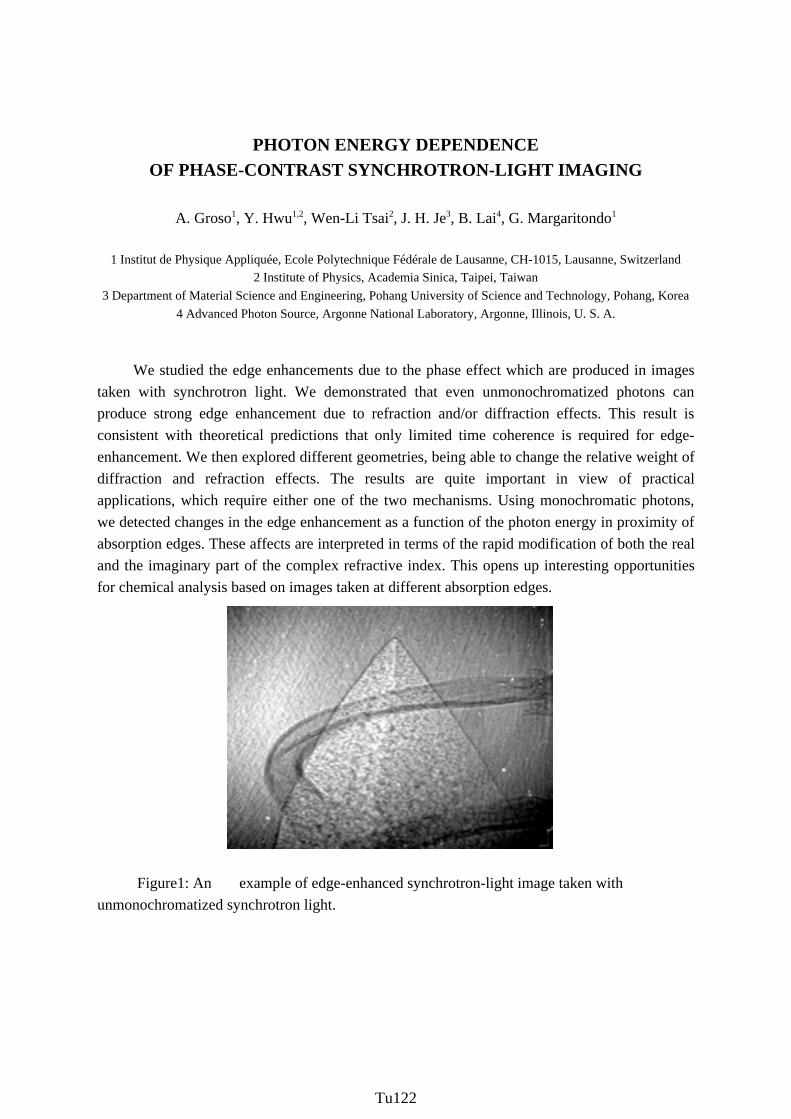
PHOTON ENERGY DEPENDENCEOF PHASE-CONTRAST SYNCHROTRON-LIGHT IMAGING
A. Groso1, Y. Hwu1,2, Wen-Li Tsai2, J. H. Je3, B. Lai4, G. Margaritondo1
1 Institut de Physique Appliquée, Ecole Polytechnique Fédérale de Lausanne, CH-1015, Lausanne, Switzerland
2 Institute of Physics, Academia Sinica, Taipei, Taiwan
3 Department of Material Science and Engineering, Pohang University of Science and Technology, Pohang, Korea
4 Advanced Photon Source, Argonne National Laboratory, Argonne, Illinois, U. S. A.
We studied the edge enhancements due to the phase effect which are produced in images
taken with synchrotron light. We demonstrated that even unmonochromatized photons can
produce strong edge enhancement due to refraction and/or diffraction effects. This result is
consistent with theoretical predictions that only limited time coherence is required for edge-
enhancement. We then explored different geometries, being able to change the relative weight of
diffraction and refraction effects. The results are quite important in view of practical
applications, which require either one of the two mechanisms. Using monochromatic photons,
we detected changes in the edge enhancement as a function of the photon energy in proximity of
absorption edges. These affects are interpreted in terms of the rapid modification of both the real
and the imaginary part of the complex refractive index. This opens up interesting opportunities
for chemical analysis based on images taken at different absorption edges.
Figure1: An example of edge-enhanced synchrotron-light image taken with
unmonochromatized synchrotron light.
Tu121Tu121Tu121Tu122

FEASIBILITY OF MICROSCOPY WITH LOW ENERGY X-RAYSBY USE OF THIN-FILM WAVEGUIDES
W. Jark1, S. Di Fonzo
1, S. Lagomarsino
2, A. Cedola
2,
N. V. Kovalenko3, V. A. Chernov
3
1Sincrotrone Trieste, S.S. 14 km 163.5, I-34012 Basovizza (TS), Italy2IESS-CNR, Via Cineto Romano 42, I-00156 Roma, Italy
3BINP, 11 Lavrentiev Prospect, Novosibirsk, 630090, Russian Federation
Thin film X-ray waveguides were introduced very recently as a novel andunconventional means for the production of microbeams in the hard x-ray regime [1,2]. Theypermit to obtain reliably x-ray beams with one dimension as small as 10 nm [3]. Indeedapplications in some new microscope schemes, where spatial resolutions of the order of 100 nmhave been achieved, were already successfully tested [4,5]. By the use of waveguides, thisresolution is an intrinsic limit of the experimental set-up and is not depending on the sourceparameters. A single object can provide an intensity gain compared to the incident intensity overa rather large photon energy range limited, however, to the x-ray regime. For the operation atlower x-ray energies the most promising material is Be with favorable absorption characteristics.Actually a waveguide with a Be guiding layer of 74 nm thickness provided until now the highestintensity gain at 13 keV photon energy [6]. The measured value in excess of 100 is very
competitive with the gain possible with other microscope objectives. The observed performanceis about 30% of the expectation for ideal waveguides. On this basis and with a starting value ofgain 40 for the same waveguide for 8 keV photon energy the feasibility of thin-film waveguidesfor lower x-ray energies will be discussed.
References
[1] S. Lagomarsino et al., J. Appl. Phys. 79, 4471 (1996)[2] Y. P. Feng et al., Appl. Phys. Lett. 67, 3647 (1995)[3] F. Pfeiffer et al., Phys. Rev. B62, 16939 (2000)
[4] S. Lagomarsino et al., Appl. Phys. Lett. 71, 2557 (1997)[5] S. Di Fonzo et al, Nature 403, 638 (2000)[6] W. Jark et al., Appl. Phys. Lett. 78, 1192 (2001)
Tu122Tu122Tu122Tu123

'HVLJQ DQG IDEULFDWLRQ RI PXOWLOD\HU PLUURUV IRU +H,, UDGLDWLRQ
<RVKLIXPL +RWWD DQG 0DVDNL <DPDPRWR
&HQWHU IRU 6RIW;UD\ 0LFURVFRS\ 5,60 7RKRNX 8QLYHUVLW\ .DWDKLUD 6HQGDL -DSDQ
,Q WKLV ZRUN RXU SURFHVV RI PXOWLOD\HU PLUURU GHYHORSPHQW ZLOO EH GHVFULEHG E\ WDNLQJ WKH
ZDYHOHQJWK RI QP +H,, UDGLDWLRQ DV DQ H[DPSOH 7KH SURFHVV VWDUWV E\ RSWLFDO VHOHFWLRQ RI
PDWHULDOV LQ UHIHUULQJ WR WKHLU )UHVQHO DPSOLWXGH UHIOHFWDQFHV DV VKRZQ LQ )LJ %DVHG RQ RSWLFDO
FULWHULD>@ 0J $O 6L &U DQG & ZHUH VHOHFWHG DV VPDOO DEVRUSWLRQ PDWHULDOV WR EH SDLUHG )LJXUH
VKRZV WKHRUHWLFDO EHVW UHIOHFWDQFH DV WKH IXQFWLRQ RI WKH QXPEHU RI OD\HUV HDFK ZLWK WKH EHVW
WKLFNQHVV VWUXFWXUH REWDLQHG E\ OD\HUE\OD\HU GHVLJQLQJ 7KH FXUYHV DERYH WKH UHIOHFWDQFH OHYHO
RI DUH ZLWK 0J DV DQ HOHPHQW ,Q UHIHUULQJ WR SUHYLRXV ZRUNV 0R6L>@ DQG 6F>@ ZHUH DOVR
DGGHG LQ WKH VHOHFWLRQ SURFHVV
0XOWLOD\HUV RI $O $X & 6F SDLUHG ZLWK 0J &6L $O& DQG 0R6L ZHUH WKHQ IDEULFDWHG
E\ LRQEHDP VSXWWHULQJ %HVW FDQGLGDWHV ZLOO EH GLVFXVVHG ZLWK ;5' GDWD DQG UHIOHFWDQFH VSHFWUD
PHDVXUHG DURXQG QP LQFOXGLQJ D OD\HU 0J6F VKRZLQJ UHIOHFWDQFH RI
5HIHUHQFHV
>@ 0 <DPDPRWR 7 1DPLRND $SSO 2SW
>@ 8 +HLQ]PDQQ ([W $EVWU QG 86-DSDQ :RUNVKRS RQ 6RIW ;UD\ 2SWLFV 7HFKQLFDO
&KDOOHQJHV <DPDQDNDNR
>@ <X $ 8VSHQVNLL 6 9 $QWRQRY 9 <X )HGRWRY DQG $ 9 9LQRJUDGRY 3URF 63,(
)LJ )UHVQHO DPSOLWXGH UHIOHFWDQFH RI PDWHULDO DW D
ZDYHOHQJWK RI QP IRU VHOHFWLRQ RI WKH SDLU IRU
KLJK UHIOHFWDQFH PXOWLOD\HU PLUURU
)LJ 7KHRUHWLFDO UHIOHFWDQFH YV QXPEHU RI OD\HUV
FDOFXODWHG E\ OD\HUE\OD\HU PHWKRG VKRZLQJ WKH LGHDO
SRVVLEOH JDLQ RI HDFK PXOWLOD\HU FRPELQDWLRQ
Tu123Tu123Tu123Tu124
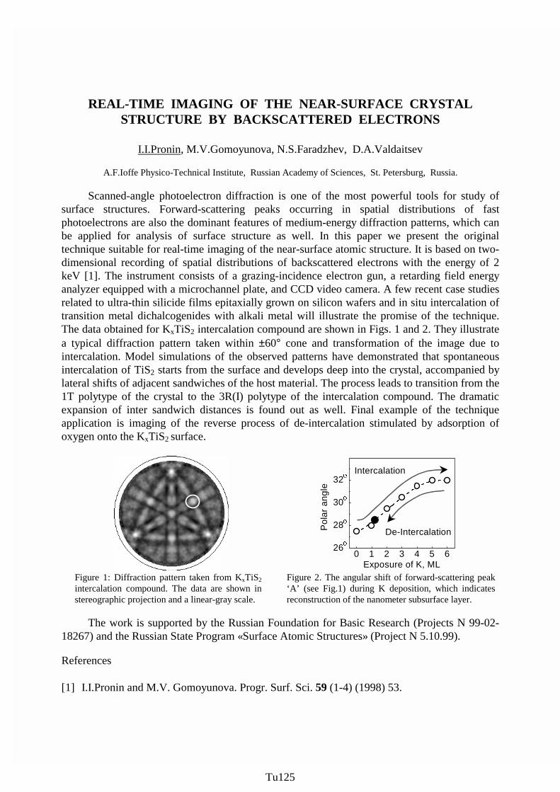
REAL-TIME IMAGING OF THE NEAR-SURFACE CRYSTAL STRUCTURE BY BACKSCATTERED ELECTRONS
I.I.Pronin, M.V.Gomoyunova, N.S.Faradzhev, D.A.Valdaitsev
A.F.Ioffe Physico-Technical Institute, Russian Academy of Sciences, St. Petersburg, Russia.
Scanned-angle photoelectron diffraction is one of the most powerful tools for study of surface structures. Forward-scattering peaks occurring in spatial distributions of fast photoelectrons are also the dominant features of medium-energy diffraction patterns, which can be applied for analysis of surface structure as well. In this paper we present the original technique suitable for real-time imaging of the near-surface atomic structure. It is based on two-dimensional recording of spatial distributions of backscattered electrons with the energy of 2 keV [1]. The instrument consists of a grazing-incidence electron gun, a retarding field energy analyzer equipped with a microchannel plate, and CCD video camera. A few recent case studies related to ultra-thin silicide films epitaxially grown on silicon wafers and in situ intercalation of transition metal dichalcogenides with alkali metal will illustrate the promise of the technique. The data obtained for KxTiS2 intercalation compound are shown in Figs. 1 and 2. They illustrate a typical diffraction pattern taken within ±60° cone and transformation of the image due to intercalation. Model simulations of the observed patterns have demonstrated that spontaneous intercalation of TiS2 starts from the surface and develops deep into the crystal, accompanied by lateral shifts of adjacent sandwiches of the host material. The process leads to transition from the 1T polytype of the crystal to the 3R(I) polytype of the intercalation compound. The dramatic expansion of inter sandwich distances is found out as well. Final example of the technique application is imaging of the reverse process of de-intercalation stimulated by adsorption of oxygen onto the KxTiS2 surface.
0 1 2 3 4 5 6
26
28
30
32
De-Intercalation
Intercalation
R
R
R
R
Pol
ar a
ngle
Exposure of K, ML Figure 1: Diffraction pattern taken from KxTiS2
intercalation compound. The data are shown in stereographic projection and a linear-gray scale.
Figure 2. The angular shift of forward-scattering peak ‘A’ (see Fig.1) during K deposition, which indicates reconstruction of the nanometer subsurface layer.
The work is supported by the Russian Foundation for Basic Research (Projects N 99-02-
18267) and the Russian State Program «Surface Atomic Structures» (Project N 5.10.99).
References [1] I.I.Pronin and M.V. Gomoyunova. Progr. Surf. Sci. 59 (1-4) (1998) 53.
Tu124Tu124Tu124Tu125

MULTILAYER OPTICS FOR THE EXTREME ULTRA-VIOLET,SOFT X-RAY AND X-RAY SPECTRAL DOMAINS
Troy W. Barbee, Jr.1 Lawrence Livermore National Laboratory, Livermore CA 94550, USA
Extreme ultraviolet (EUV), soft x-ray (SXR) and x-ray (XR) multilayer optics are successfullyapplied in spectrally resolving experiments. Thus, EUV, SXR and higher photon energy x-ray(XR) multilayers, multilayer optics and multilayer optic systems have demonstrated the ability toenable new science and technologies. Multilayers are nano-engineered synthetic thin filmlayered materials of sufficient quality to be applied as reflecting/diffracting dispersion elementsand optics in such instrumentation. Their importance to space science observations is that theyenable instrumentation to be designed for previously inaccessible spectral ranges important tothe understanding of the physics of both solar and astrophysical phenomena. Hence, new
understanding of these phenomena is gained from the new data gained by use of multilayeroptical systems. The figure on the left presents the measured reflectivity [1] for a witnessmultilayer fabricated at the same time as the multilayer applied in the TRACE [2] EUVtelescope used to obtain the image of the Solar Corona at 19.5 nm ( FeXII) on the right. In thispaper the emphasis will be on multilayer structures and optics, their current capabilities andexpected advances in performance. Both normal incidence and grazing incidence multilayeroptic structures will be considered. Needed advances in multilayer technology are outlined andefforts in this area described. The paper will be concluded with an assessment of currentcapabilities and the potential for new optic structures and enhanced performance. [1] T. W. Barbee, Jr. and M. Wall, “Interface Reaction Characterization and Interfacial Effectsin Multilayers”, SPIE, Vol. 3113, 204-213 (1997)[2] Transition Region and Coronal Explorer (TRACE) : http://vestige.lmsal.com/TRACE/This work was performed under the auspices of the U.S. Department of Energy by the Lawrence LivermoreNational Laboratory under Contract No.W-7405-ENG-48.
0.0
0.1
0.2
0.3
0.4
0.5
170 180 190 200 210 220
NIST (Tario)AMP-LLNL (Montcalm)
Calculation
Ref
lect
ivit
y
Wavelength (Å)
Tu125Tu125Tu125Tu126

Design of a Complete Photoemission Experiment
M. Hoesch1,2, M. Muntwiler1,2, M. Hengsberger1, T. Greber1, J. Osterwalder1
1) Physik-Institut, Universität Zürich, CH-8057 Zürich, Switzerland2) SLS Project, Paul Scherrer Institut CH-5232 Villigen PSI, Switzerland
A new photoelectron spectrometer is being set-up featuring a full three-dimensional spinpolarimeter, which makes it complete in the sense that all properties of the photoelectrons in theframe of reference of the sample crystal lattice can be measured. The spectrometer is devoted tospin-resolved Fermi surface mapping using angle resolved ultraviolet photoelectronspectroscopy. Studies on thin film and surface magnetism require full information on in planeand out of plane spin components. The rotation of the sample for different emission anglesmakes it necessary to record all three components of the spin-polarization to retrieve the truespin polarization in the sample.
VUV photoelectrons are energy and angle selected by a hemispherical analyzer (EA125from Omicron Vakuumphysik GmbH). The photoelectron beam is switched at ~1 Hz betweentwo orthogonally mounted Mott detectors, which span the 3D polarization space, because in anelectrostatic transport, the spin orientation is preserved from the sample to the detector. A two-axis sample goniometer covers the full range of emission angles above the sample surface. Aftersuccessful commissioning at Zürich university, the instrument can be operated at the new SwissLight Source (PSI, Villigen, Switzerland) and/or at ELETTRA (Trieste, Italy).
Figure 1) Left: Schematic view of COPHEE, the complete photoemission experiment.Electrons photoemitted from a sample by UV radiation are energy- and angle-selected by anelectrostatic analyzer and detected in two orthogonal Mott polarimeters. Right: Details of thebeam transport system that takes the electrons from the analyzer into the two Mott detectors(ray tracing and graphics made using SIMION [2], Mott assembly rotated 90º with respect tothe analyzer for graphical clarity).
[1] V.N. Petrov, M. Landolt, M.S. Galaktionov, B.V. Yushenkov, Rev. Sci. Instr. 68, 4385 (1997).[2] "SIMION 3D Version 6.0" by David A. Dahl 43rd ASMS Conference on Mass Spectrometry and Allied
Topics, May 21-26 1995, Atlanta, Georgia, pg 717, http://www.srv.net/~klack/simion.html
Tu126Tu126Tu126Tu127

Wide bandgap EUV and VUV detectors for solar observations
J-F Hochedez1, et al
1 Royal Observatory of Belgium, Circular Avenue 3., B-1180 Brussels, Belgium
The BOLD (Blind to the Optical Light Detectors) [1, 2] is an international investigationdedicated to the development of novel imaging detectors for the X-UV to Near UV wavelengthranges. It relies on the diamond and nitrides materials that have lately undergone key advances.Several detector designs are being evaluated. The potential applications in science and industryare numerous, but the current initiative is carried out towards future Solar Physics missions suchas the planned Solar Orbiter of ESA [3] to be launched around 2010. These developments occurin the particularly propitious context of a mission, which will operate close to the Sun, where theexpected properties of the new sensors -visible blindness and radiation hardness- are highlybeneficial. We report on the latest progresses achieved in the course of this objective.
References
[1] http://bold.oma.be
[2] Hochedez, Bergonzo, Castex, Dhez, Hainaut, Sacchi, Alvarez, Boyer, Deneuville, Gibart,Guizard, Kleider, Lemaire, Mer, Monroy, Munoz, Muret, Omnes, Pau, Ralchenko,Tromson, Verwichte, Vial, Diamond UV detectors for future solar physics missions, 2001,Diamond and Related Materials, Vol 10/3-7, pp 669-676
[3] Marsch, E.; et al.; SOLAR ORBITER (High-resolution mission to the Sun and innerHeliosphere), Assessment Study Report, 2000, ESA-SCI(2000)6
Tu127Tu127Tu127Tu128

A NEW XUV BEAMLINE ON A MULTIPOLE WIGGLER IN THE SRS
M. Bowler1, J. B. West1, F. M. Quinn1, D. Holland1, B. Fell1, P. Hatherly2, I. Humphrey3, W.Flavell3
1 CLRC-Daresbury Laboratory, Warrington, UK, WA4 4AD2 Physics Dept., Reading University, Reading, UK
3 Physics Dept., UMIST, Manchester, UK
An XUV beamline has been constructed on the SRS synchrotron radiation sourceexploiting the output from a 2T Multi-pole Wiggler (MPW). The beamline is based on an SGMdesign and produces photons in the energy range 40 eV to 350 eV. By taking a 7.5 mrad fan, ahigh flux can be delivered of between 1 x 10¹³ and 1 x 10¹⁴ photons/sec/300mA ring current witha resolving power of around 1000. A Kirkpatrick-Baez mirror pair focuses the light onto theentrance slit of the monochromator. Using 10 micron entrance and exit slits, a resolving power ofup to 10,000 can be achieved, with a flux of 0.5 – 2 x 10¹¹ photons/sec/300mA.
The calculated and measured performance will be presented, with emphasis on thechallenges associated with utilising the XUV output of a high field MPW source.
Tu128Tu128Tu128Tu129

Development of a conical energy analyzer for angle-resolved photoelectron spectroscopy
Kota IWASAKI and Koichiro MITSUKE
Institute for Molecular Science, Myodaiji, Okazaki 444-8585, Japan
A new angle-resolved electron energy analyzer incorporating a position sensitive detector
(PSD) has been constructed to measure the angular distribution of photoelectron from rare gas
atoms excited by linearly polarized synchrotron radiation. This analyzer has the advantages of
high angular resolution and wide angular acceptance simultaneously. These characteristics are
required to measure complicated angular distributions of photoelectrons caused by the atomic
alignment with relatively short accumulation time of signals.
The conical analyzer consists of a set of an inner and outer conical electrode, cylindrical
lenses, a gas cell and a PSD unit as shown in Figure 1. Photoelectrons emitted in the gas cell
are accelerated between the cell and an extractor electrode, then focused on an entrance slit by
the cylindrical lenses. The electron trajectories between
the inner and the outer conical electrodes are similar to
those expected for a conventional parallel-plate analyzer
[1]. Energy selected electrons exiting out of the conical
deflector electrodes are detected with the PSD of an
effective diameter 40mm mounted behind the analyzer.
The azimuth angular resolution is determined from the
diameter of the sample volume (f1mm) and the position
sensitivity of PSD, and we expect the angular resolution
of 1.5 degree.
The apparatus has been tested by carrying out gas
phase ultraviolet photoelectron spectroscopy with a
helium discharge lamp. Since the light produced in the
discharge lamp is unpolarized and the photoelectron
distribution is expected to be isotropic, we made a
calibration cone electrode on which the entrance slit is a
series of circular holes as test objects. Details of apparatus
and a performance test will be presented at the
conference. Fig.1. Schematic of the conical analyzer.
[1] D. Brewer, W. Newell and A. Smith, J. Phys. E, 13, 114 (1980)
Tu129Tu129Tu129Tu130

THE SURFACE AND INTERFACE: SPECTROSCOPY BEAMLINE ATSWISS LIGHT SOURCE
L. Patthey, M. Shi, J. Krempasky, T. Schmidt, U. Flechsig, C. Quitmann, R. Betemps, M.
Botkine, R. Abela, F. van der Veen
Swiss Light Source, Paul Scherrer Institut, CH-5232 Villigen
We report here on the Surface and Interface: Spectroscopy (SIS) beamline which is under
construction at the Swiss Light Source. This beamline is dedicated for electronic and
atomic structure study on surface and interface using high resolution photoemission, angle-
resolved ultra-violet photoelectron spectroscopy (ARUPS), photoelectron diffraction,
Fermi surface mapping, X-ray absorption spectroscopy and X-ray emission spectroscopy.
The energy range of this beamline is 10 to 800 eV with an overall resolving power E/DE>10000. The beamline will used twin electromagnetic undulators providing variable
photon polarization (linear and circular) at high switching rate (approx. 1msec). In order to
provide high resolving power and harmonic rejection also at low photon energies we used
quasi-periodic scheme for the two undulators and an opical scheme combining normal
(NIM) and grasing (PGM) incidance monochromators.The end station is equipped with a
high resolution hemispherical photoelectron spectrometer with an energy resolution of
1.5meV and an angular resolved < 0.2 deg. A high precision manipulator equipped with a
1K Helium flow cryostat is used for the low temperature measurment. The normal
operation of the beamline is schedule for 2002.
Tu130Tu130Tu130Tu131

MULTILAYER POLARIZERS FOR USE OFHe-I AND He-II RESONANCE LINES
Tadashi HATANO, Yuzi KONDO, Katsuhiko SAITO, Takeo EJIMA, Makoto WATANABE
and Masahiko TAKAHASHI
Institute of Multidisciplinary Research for Advanced Materials, Tohoku University,
2-1-1 Katahira, Aoba-ku, Sendai 980-8577, Japan
The multilayer polarizers for the use of He resonance lines have been developed. Mg/Si
and Mg/SiC multilayers were designed with the parameters listed in Table 1 and fabricated by
magnetron sputtering for the He-I (584 Å) and He-II (304 Å) resonance lines, respectively.
Table 1: Design parameters of multilayer polarizers for He-I and He-II resonance lines.
Wavelength Material(Thickness)Number of
Periods
Angle of
Incidences-Reflectance Polarizance
He-I Polarizer 584 Å Mg(235 Å)/Si(287 Å) 10 31.5° 45% 0.93
He-II Polarizer 304 Å Mg(131.8 Å)/SiC(79.5 Å) 20 40° 44% 0.99
The performance was checked at BL5B of UVSOR Facility. The multilayer was mounted
at the center of a goniometer. The Stokes parameters, S0 and S1 of the incident and reflected
lights were measured by a rotating analyzer unit mounted with the same multilayer, which gives
the complete information about the s-reflectance and the polarizance. The experimental results
for the He-II resonance line are shown in Fig.1. The measured s-reflectance and polarizance at
the angle of incidence of 40° were
41% and 0.98, respectively. The
measured polarizance of the He-I
polarizer was 0.96.
Both polarizers will be used
to measure the degree of
polarization of the He resonance
lines passing through a grating
monochromator for the angular
distribution measurements of
photoelectrons from isolated
molecules.
0
0.2
0.4
0.6
0.8
1
0 15 30 45 60 75 90
Rs
P
0
0.2
0.4
0.6
0.8
1
s-R
EF
LEC
TA
NC
E
ANGLE OF INCIDENCE (deg)
Mg/SiC multilayerλ = 304
PO
LAR
IZA
NC
E
Figure 1: s-reflectance and polarizance of Mg/SiC multilayer for He-
II resonance line. Open and closed circles are experimental results
and solid and dotted curves, designed ones.
Tu131Tu131Tu131Tu132

Ultrasoft X-Ray Spectra of Magnesium Diboride
I.I. Lyakhovskaya
Institute of Physics of St. Petersburg University, 198904 St. Petersburg, Russia
At ultrasoft X-ray spectrometer with high resolution the following spectra of MgB2 were
studied: emission K-spectrum of boron, quantum yield spectrum in the range of K-edge of
absorption of boron and emission L2,3-band of Mg . These spectra are compared with the
corresponding spectra of pure boron and metal magnesium.
Tu132Tu132Tu132Tu133

EUV Transmission Interferometer for Direct
Index of Refraction Measurements
Chang Chang1,2, Erik Anderson1, Patrick Naulleau1, Eric Gullikson1,Kenneth Goldberg1, David Attwood1,2
1Center for X-Ray Optics,Lawrence Berkeley National Laboratory, Berkeley, CA 94720
2Department of Electrical Engineering & Computer Science,University of California, Berkeley, CA 94720
Abstract
We have directly measured the real and imaginary part of the indexof refraction of Aluminum in the vicinity of its L-edge. The experi-ment is done with an amplitude-division, transmission interferometerdesigned and used at extreme ultraviolet (EUV) wavelengths extendingfrom 19.1 nm to 8.9 nm (65 eV to 140 eV). The real (dispersive) partof the optical constant is directly determined by the amount of phaseshift of the interferogram. The imaginery (absorptive) part is deter-mined by changes in fringe visibility. This experiments are performedusing undulator radiation at Beamline 12 of the Advanced Light Source(ALS)[1]. Fine structure within the Aluminum L-edge, i.e. L2 and L3,is resolved in both real and imaginery parts. Other materials are inthe process of being studied.
References
[1] D.T. Attwood, Soft X-Rays and Extreme Ultraviolet Radia-tion:Principles and Applications., (Cambridge University Press,Cambridge UK, 1999), chapter 2.
Tu133Tu134
TOROIDAL ENERGY- AND ANGLE-RESOLVED ELECTRON SPECTROMETER
M.R.F. King1, F.M. Quinn1, G. Fraser2, G. Thornton3
1 Daresbury Laboratory, Daresbury, Warrington, U.K.
2 Department of Physics and Astronomy, University of Leicester, Leicester, U.K. 3 Department of Chemistry, University of Manchester, Manchester, U.K.
The Toroidal Energy- and Angle-Resolved Electron Spectrometer (TEARES) is a state-of-the-art high-resolution electron detector that is being designed, built and developed at Daresbury Laboratory. One of the aims of the project is to provide a toroidal electron analyser based system with simultaneous readout of energy and angle. Experiments which would benefit from such a system include photoelectron diffraction from solid surfaces, magnetic dichroism from solid surfaces, atomic and molecular physics experiments, 'spin-polarised' studies of surfaces, and electron spectroscopy based experiments where the cross-section is low.
A toroidal energy analyser allows both the energy and angle of ejection of an electron to be measured simultaneously. In the TEARES system, electrons that are ejected within ±1° of the plane perpendicular to the main axis of the spectrometer will be transported and focussed by a double-focussing cylindrical slit lens onto the entrance of a toroidal electrostatic analyser. The entrance lens is designed to transport and focus an interaction region of approximately 1mm3 to the entrance of the analyser. The toroidal deflector analyser is comprised of an inner and an outer toroidal sector. Electrons are deflected by the electric field between the two toroids in such a way that only those electrons having energies near the pass energy of the analyser will arrive at the exit cone of the analyser. The toroidal analyser disperses and focuses the electrons according to their energy in the radial dimension whilst preserving their initial angular direction. The single-focussing conical slit exit lens transports, demagnifies, and focuses the electrons from the exit of the analyser onto the detector.
The TEARES toroidal analyser is defined by a spherical radius of 125 mm, a cylindrical radius of 120 mm and a sector angle of 142°; these dimensions have been chosen to insure optimum focussing properties. The working distance is defined by a 40 mm radius. The resolution of the toroidal analyser is determined by the spherical radius, and slit heights of the entrance lens window and pupil; a resolution of 4 meV should be possible using 1 mm entrance slits together with a pass energy of 0.5 eV. The TEARES system is designed to operate over the kinetic energy range of <0.5 £ KE £ 1000 eV. The energy spread that is passed to the detector is ±10% of the pass energy and the useful angular range is 230°.
Further details of the TEARES system and progress to date will be given.
Tu134Tu134Tu134Tu135
THE DEVELOPMENT OF A FAST IMAGING ELECTRON DETECTOR BASED ON THE CODADON CONCEPT
G. Fraser1, M.R.F. King2, F.M. Quinn2, G. Thornton3
1 Department of Physics and Astronomy, University of Leicester, Leicester, U.K.
2 Daresbury Laboratory, Daresbury, Warrington, U.K. 3 Department of Chemistry, University of Manchester, Manchester, U.K.
A fast imaging electron detector is being developed at Leicester University as part of the Toroidal Energy- and Angle-Resolved Electron Spectrometer (TEARES) project. TEARES is a state-of-the-art high-resolution electron spectrometer that is being developed at Daresbury Laboratory. The analysed solid angle of the TEARES system is about 600 times greater than in a conventional hemispherical analyser of similar radius and entrance slit sizes. It has been estimated that the TEARES system on a third generation synchrotron source with a 'typical' solid sample utilising the full potential of the analyser, would pass countrates in excess of 1 GHz (>1x10⁹)! However, at the present time, commercial imaging electron detectors are capable of achieving countrates up to only 1MHz (1x10⁶). There is a large discrepancy between the commercially available imaging detectors and the optimum requirements for the TEARES system. Therefore, one of the aims of the TEARES project is to start the development of a fast 2D readout system for electron analyser systems that is capable of high dynamic range and matched to TEARES. This part of the project is driven by the great need for faster electron detectors.
The system being developed is an extension of the 1-dimensional CODACON encoder [1]
developed for UV astronomy. In the 1-dimensional case, N conductor pairs encode 2N resolution elements, so that an eight-element CODACON would provide 256 azimuthal bins. The encoder directly generates a binary address for each event from the minimum number of signal channels. In our adaptation, we are using two coupled 1-dimensional encoder tracks to obtain the required 2-dimensional data; five electrode pairs are used to obtain the energy and seven electrode pairs are used to determine the initial ejection angle of the electron. This will generate a 12-bit binary word that uniquely identifies the position (energy and angle) of the electron. It is important to note that all the electronics are outside the vacuum and no pulse shaping is required. The first version of this detector will comprise commercially available electronic components and low resistance microchannel plates with an aim of achieving a modest 2 MHz counting rate. Higher versions of the detector are envisioned whereby the advantages of this system may be fully realised. The main advantages include (1) the deliberate utilisation of all-conducting electrodes so the anode can be directly bonded to the microchannel plate, which makes possible the utilisation of ultra-low resistance conductively cooled microchannel plates, and (2) designing faster electronic components to match the speed of the detector system. It is important to note that such a detector can be easily modified to suit any output geometry by re-designing the position of the tracks on the anode. References [1] W. E. McClintock, C. A. Barth, R. D. Steele, G. M. Lawrence, J. G. Timothy, Applied
Optics 21 (1982) 3071.
Tu135Tu135Tu135Tu136

Fabrication of VUV blazed grating for synchrotron radiation
Xiangdong Xu, Yilin Hong, Shaojun Fu, Liusi Sheng, Yunwu Zhang
(National Synchrotron Radiation Laboratory, University of Science and Technology of China, Hefei, Anhui, 230026, P.R.China)
A spherical holographic ion-etched blazed grating of 1200l/mm with blazed angle 4.5° has successfully fabricated for a Seya-Namioka monochromator at the photochemistry experiment station of National Synchrotron Radiation Laboratory, as Fig.1.
The reason of grating line defects forming was analyzed. To eliminate these defects, the photoresist-ashing process [1] was applied to holographic-ion beam etching technique. We present the results of surface measurements made on the bare grating substrate using an scanning probe microscope (DI3100). The efficiency of the grating after coating aluminum was measured using synchrotron radiation source. The experimental result shows that holographic- ion beam etching in combination with photoresist-ashing technique is useful and effective for achieving large and good quality grating.
Figure 1: SPM image of a 1200l/mm blazed grating
Reference
[1] J.Chung, M.C.Jeng, J.E.Moon et al. Deep-submicrometer MOS device fabrication using a
photoresist-ashing technique. IEEE. Electr.Dev.Lett. 1988,9(4):186-188
Tu136Tu136Tu136Tu137

Laser Plasma Sourced VUV Photoabsorption Imaging System
J. S. Hirsch1 , E. T. Kennedy1, A. Neogi1, P. Nicolosi2, L. Poletto2 and J.T. Costello1
1NCPST, School of Physical Sciences, Dublin City University, Glasnevin,Dublin 9, Ireland2Department of Electronics and Informatics, University of Padua, Padova, Italy
We have recently completed the design phase of a system intended to produce a wavelengthtuned and collimated Vacuum−UV beam (30 − 100 nm). The system is based on a 1m normalincidence vacuum monochromator with corrected (toroidal) optics on both the entrance and exitarms. The light source is a laser produced rare earth plasma, well known to be a virtually ’ line free’continuum emitter [1]. The primary function of this system will be the measurement of timeresolved ’ images’ or spatial distributions of Vacuum−UV photoabsorption in expanding laserplasma plumes.
We have already shown the potential of the photoabsorption technique in a proof ofprinciple experiment which utilised a diverging beam interrogated by a back−thinned CCD array[2]. In particular we were able to (i) track and extract column density distributions in the expandingplasma plume and (ii) measure the plume front velocity which compared well with a simple modelbased on adiabatic plume expansion. The time resolution depends on the laser plasma continuumduration which can be as low as 100 psec [3]. Our new system design is significantly improvedover that used in [2] in a number of ways:
1. The collimated beam simplifies the interpretation of the photoabsorption images and theextraction of physical information2. The spectral resolution is improved to 0.05 nm compared to 1 nm in [2]3. Both high VUV flux (20 nsec) and short pulse (150 psec) rare earth light sources areavailable offering the time resolutions indicated in brackets4. The spatial resolution is better than 100 microns
We will present the results of ray tracing calculations for various options, e.g., collimatedbeam and projection imaging of the sample plasma. We will also present first measurements fromthe commissioning phase of the project: e.g., (i) detected flux per CCD pixel, (ii) beam footprint,(iii) beam collimation, (iv) spectral resolution, (v) spatial resolution and (vi) time resolution.
References
[1] Carroll P K, O’Sullivan G and Kennedy E T, Opt.Lett 2, 72 (1978)[2] Hirsch J S, van Kampen P, Meighan O, Mosnier J−P, Costello J T, Lewis CL S,
MacPhee A, Hirst G, Westhall J and Shaikh W, J.Appl.Phys 88, 4953 (2000)
[3] Meighan O, Dardis L, McGuinness C, Moloney C, Costello J T, MacPhee A,O’Rourke RLewis C, Danson C, Shaikh W and Turcu I , J.Phys.B:At.Mol. Opt. Phys. 33 1159 (2000)
Tu137Tu137Tu137Tu138

SOFT X-RAY REFLECTIVITY AND THERMAL STABILITY OFCoCr/C MULTILAYER X-RAY MIRRORS
H. Takenaka1, K. Nagai1, H. Ito1, T. Sakuma2, K. Namikawa2
Y. Muramatsu3, E. Gullikson4, R. C. C. Perera4
1 NTT Advanced Technology Co., 162 Shirakata, Tokai, Ibaraki, 319-1193, Japan2 Tokyo Gakugei University, Koganei, Tokyo, 184-8501, Japan
3 Japan Atomic Energy Research Institue, Sayo-gun, Hyogo 679-5148, Japan4 Lawrence Berkeley National Laboratory, Berkeley, CA 94720, USA
The development of highly-reflective multilayer mirrors for use in the 6 nm region isdesired for x-ray photoemission spectroscopy for inner-shell excitation using a Schwarzchildobjective. For this applications, reflectivity is the most critical parameters determining theperformance of multilayer mirrors, because the reflectivities of multilayers in the 6-nmregion are generally very low.
We have designed CoCr/C multilayer mirrors with a comparatively high reflectivity ataround normal incidence and have fabricated them by magnetron sputtering. We evaluatedthe structures and reflectivity of these multilayers using a soft x-ray reflectometer.
Figure 1 shows the measured reflectivities of the fabricated CoCr/C multilayer. Themeasured peak reflectivity is about 16 % at a wavelength of around 6 nm and an incidentangle of 88 degree. This peak reflectivity is sufficient for our Shwartzshild x-ray optics.Figure 2 shows this reflectivity and reported multilayer reflectivities. The reflectivities arealmost constant by annealing at 300C in an Ar atmosphere for 4 hours.
This study was performed through Special Coordination Funds of the Science andTechnology Agency of the Japanese Government.
Mo/BRu etc. /B4CW/B4CCo/CCr/CNiCr etc./C
W/CW/Sc
Ru/C
B K-edge
C K-edge
0
5
10
15
20
3.0 4.0 5.0 6.0 7.0 8.0
25
CoCr/C
0
5
10
15
20
25
30
4 4.5 5 5.5 6 6.5 7
Ref
lect
ivity
(%)
Wavelength (nm)
88 deg70 deg
60 deg 53 deg
50 deg47 deg
45.8 deg
45.4 deg
CoCr / CD = 2.9 nmN = 150θ= 45-88deg
Ref
lect
ivity
(%)
Wavelength (nm)
Figure 1. Measured reflectivities of thefabricated CoCr/C multilayer.
Figure 2. Reported reflectivites at incident anglesmore than 80 degrees[1] and CoCr/C’s reflectivityat 88 degree.
References[1] E. Gullikson, http://www-cxro.lbl.gov/optical_constants/
Tu138Tu138Tu138Tu139

3UHOLPLQDU\UHVXOWVRQWKHUHDOL]DWLRQRIPXOWLOD\HU(89UHIOHFWLYH
FRDWLQJV
Valentino Rigato1, Alessandro Patelli2, Gianluigi Maggioni1, Piergiorgio Nicolosi2, Maria-Guglielmina Pelizzo2, Luca Poletto2, Paolo Mazzoldi3 and Giuseppe Tondello2
1 INFN , Laboratori Nazionali di Legnaro, Strada Romea 4 - 35020 Legnaro (Pd), Italy2 Dipartimento di Elettronica e Informatica, Università di Padova and INFM, Unità di Padova, via Gradenigo 6A,
Padova, Italy3 Dipartimento di Fisica, Università di Padova and INFM, Unità di Padova, via Marzolo 8, Padova, Italy
Recently a new program for the development of coatings with enhanced EUV normal incidencereflectivity has started at the University of Padova. Here we would like to present somepreliminary results obtained in the deposition of multilayer coatings. Since the properties andperformance of the EUV mirrors are mainly affected by the surface roughness of each layer andby thickness uniformity initial effort has been devoted to the characterization of the growth ofvery thin (down to about 3 nm) layers. Mo and Si have been chosen since they are widely usedfor EUV reflective coatings. The adopted deposition technique has been radio frequencymagnetron sputtering. The layers have been deposited on quartz and silicon substrates atdifferent temperatures. The impurity concentration and the dependence of the deposition rate onthe growth temperature have been studied using Rutherford Backscattering. The characterisationof the surface morphology has been performed by SEM and AFM. This study has been carriedout in order to optimize the deposition parameters in view of the final multi-layer deposition.The final Multilayer coatings have been characterized by X-ray diffraction and TEM and theEUV reflectivity has been measured by a dedicated apparatus.The results of multilayer depositions optimized for 13-14 nm and for the 20-30 nm range will bepresented.
Tu139Tu139Tu139Tu140

COHERENCE TECHNIQUES
AND NOVEL SOURCES
Tu140Tu141

Tu141Tu141Tu142

TEMPERATURE DEPENDENCE OF LASER INDUCED HOTLUMINESCENCE OF SELF-TRAPPED EXCITONS IN SOLID XENON
R.Kink1, M.Selg1, M.Kink1, J.Maksimov1, I.Martinson2
1 Institute of Physics of the University of Tartu, Riia 142, Tartu 51014, Estonia2 University of Lund, Sölvegatan 14, Lund S22363, Sweden
Self-trapped excitons (STE) in rare gas crystals (RGC) represent excimer-like (R2
*)vibrational excitations, whose lower level spacings considerably exceed the highest phononenergies. Vibrational relaxation of such STE can be adequately described in terms of the recentnonperturbative quantum theory of multiphonon anharmonic decay of strong local modes [1].
Useful information on the specific features of vibrational relaxation of STE in RGC can beinferred from their hot luminescence (HL) spectra. We present detailed experimental data andrelevant theoretical analysis of the HL in Xe crystal. HL appears to be very sensitive to thecrystal’s quality and temperature, as well as to the kind of excitation used (see Figure 1). Two-photon KrF excimer laser excitation (10.0 eV), especially at low temperatures, produces morestructured HL spectra compared with those induced by ArF (12.4 eV) laser excitation. At highertemperatures (T ∼ 100 K) HL gradually disappears independent of the method of excitation.Although different in position and width, HL spectra of solid Xe always show up a deep hollownear 8 eV, already reported earlier [2, 3]. According to the general theory [1], this minimumarises from the abruptly increased relaxation rate in the characteristic “critical” range ofvibrational levels (ncr ≈ 23) of Xe2
*.
References
[1] V.Hizhnyakov, Europhysics Letters 45, 508 (1999).[2] V.Hizhnyakov, M.Selg, R.Kink, M.Kink, J.Maksimov, Physica B 263-264, 683 (1999).[3] V.Hizhnyakov, M.Kink, R.Kink, J.Maksimov, A.Lõhmus, M.Selg, Physica B 284-288,
1129 (2000).
Figure 1: Hot luminescence spectra of solid Xe under different two-photon excimer laser excitation at varioustemperatures. The overall luminescence spectrum is shown in the major part of the left-side graph.
Photon energy (eV)7.9 8.0 8.1 8.2 8.3
Inte
nsity
(ar
b. u
nits
)
0
100
200
300
400
500
600
T = 10 K
T = 50 K
T = 60 K
T = 80 K
T = 100 K
KrF excitation
Photon energy (eV)7.0 7.5 8.0
Inte
nsity
(ar
b. u
nits
)
0
200
400
600
800
1000
1200
7.7 7.8 7.9 8.0 8.1 8.2 8.30
1
2
3
4ArF excitation
∆E = 20 meV
∆E = 10 meVT = 50 K
Tu142Tu142Tu143

Inte
nsity
(arb
.uni
ts)
120 140 160 180
NeAr
He
0
1
2
3
Wavelength (nm)
Vacuum Ultraviolet Spectroscopic System for Solid State Materials
Masanori Kaku, Takahiro Yamaura, Shoichi Kubodera, and Wataru Sasaki
Department of Electrical and Electronic Engineering and Photon Science Center, Miyazaki University, Gakuen Kibanadai Nishi 1-1, Miyazaki, 889-2192 Japan
Vacuum ultraviolet (VUV) continua emitting from a laser-produced plasma have been utilized for the spectroscopy of a solid state laser material. An absorption spectrum of 0.1% Nd:LaF3 has been measured by use of the continuum emission. The minimum absorption coefficient of 1.4 cm-1 was evaluated at 174 nm.
Our VUV spectroscopic system consists of three parts; a plasma-initiating laser, a rare gas chamber where a plasma is produced and a sample is installed, and a VUV detection system. A Q-switched Nd:YAG laser was focused inside a pressurized rare gas chamber to produce a plasma. Typical emission spectra of three rare gases (He, Ne, Ar) are shown in Figure 1. At a laser intensity of 1011 W/cm2, continuum emission dominates over line emissions for heavy rare gases. The emission intensity also becomes larger for heavier rare gases. Although the higher intensity has been observed for Kr, Xe [1], the resonant absorption of relevant atoms limits the wavelength range in the VUV. Note that the short wavelength range is limited by the cutoff of a MgF2 window, which is used to separate the pressurized chamber and a sample. The long wavelength limit reflects on the sensitivity of a micro-channel plate. The wavelength-integrated emission power of the Ar continuum was measured to be 8.4 kW, which was large enough to obtain absorption spectra of solid state materials.
Figure 2 shows the absorption spectrum of 0.1%Nd:LaF3 crystal by use of the Ar emission. Nd:LaF3 has been known as a possible new VUV laser crystal around 172 nm [2]. Two samples with different lengths (0.9 and 5 mm) produced the same results. Our absorption spectrum has been a revised result of rather old spectroscopic data [3]. This VUV spectroscopic system is applicable to the evaluation of defects and a lifetime of VUV CaF2 optics produced for F2 laser optical lithography, with a help of FT-IR spectrograph. References [1] P. Laporte, N. Damany, and H. Damany, Opt. Lett. 12, 987 (1987). [2] M. A. Dubinskii, A. C. Cefalas, E. Sarantopoulou, S. M. Spyrou, C. A. Nikolaides, R.
Yu. Abdulsabirov, S. L. Korableva, and V. V. Semashko, J. Opt. Soc. Am B 9, 1148 (1992).
[3] Wm. S. Heaps, L. R. Elias, and W. M. Yen, Phys. Rev. B 13, 1976 (1976).
170160150 180Wavelength (nm)
200190Abso
rptio
n C
oeffi
cien
t (cm
-1)
0
20
60
40
Fig. 1 Emission spectra of three rare gases.
Fig. 2 Measured absorption spectrum of a 0.1% Nd:LaF3 crystal.
Tu143Tu143Tu144

98963(&7526&23<2)&5<67$//,1((0,77(56%$6('21G±I75$16,7,216,15$5(($57+,216
10.KDLGXNRY1<X.LULNRYD0.LUP-&.UXSD6./DP'/R910DNKRY(1HJRGLQ*=LPPHUHU
.XUQDNRY,QVWLWXWHRI*HQHUDODQG,QRUJDQLF&KHPLVWU\0RVFRZ5XVVLD/HEHGHY3K\VLFDO,QVWLWXWH0RVFRZ5XVVLD
,,,QVWLWXWIU([SHULPHQWDOSK\VLNGHU8QLYHUVLWlW+DPEXUJ+DPEXUJ*HUPDQ\,QVWLWXWGH3K\VLTXH1XFOHDLUH2UVD\&HGH[)UDQFH
3K\VLFV'HSDUWPHQW&KLQHVH8QLYHUVLW\RI+RQJ.RQJ6KDWLQ17+RQJ.RQJ6$5&KLQD
7KHLQWHUFRQILJXUDWLRQG±IWUDQVLWLRQVLQUDUHHDUWK5(LRQV1G(U7PGRSHGLQWRZLGHEDQGJDSFU\VWDOVFDQPDNHSRVVLEOHODVHUDFWLRQLQWKH989>@+RZHYHUXSWRGDWHWKH989ODVHUHPLVVLRQIURPG±IWUDQVLWLRQVQPKDVEHHQREWDLQHGRQO\LQ1GGRSHG/D)>@1HLWKHUGLIIHUHQWFU\VWDOKRVWVQRURWKHU5(LRQVKDYHEHHQWHVWHGIRUODVHUDFWLRQLQWKH9892QWKHRWKHUKDQGFRPSOH[IOXRULGHVSURYLGHDYDULHW\RIFU\VWDOKRVWVZLWK WKHGHVLUHGV\PPHWU\DQGFRRUGLQDWLRQQXPEHUDVZHOOZLWKWKHGLIIHUHQWQXPEHURIFU\VWDOORJUDSKLFVLWHVIRUGRSLQJZLWK5(LRQV,QWKHSUHVHQWSDSHUWKHDSSURSULDWHVSHFWURVFRSLFSURSHUWLHVRIVHYHUDOFRPSOH[IOXRULGHFU\VWDOV.<).<)./L<)&V<)GRSHGZLWK3U
1G(URU7P
KDYHEHHQVWXGLHGDQGDQDO\]HGIURPWKHYLHZSRLQWRIWKHLUSRVVLEOHDSSOLFDWLRQVDVDFWLYHPHGLDIRU89 DQG989 VROLG VWDWH ODVHUV 7KHPHDVXUHPHQWV RI WLPHUHVROYHG H[FLWDWLRQ DQG989HPLVVLRQ VSHFWUD DV ZHOO DV OXPLQHVFHQFH GHFD\ FXUYHV ZHUH SHUIRUPHG XQGHU H[FLWDWLRQ E\V\QFKURWURQUDGLDWLRQIURPWKH'25,6VWRUDJHULQJDWWKH683(5/80,VWDWLRQRI+$6</$%DW'(6<7KHHPLVVLRQVSHFWUDZHUHDOVRVWXGLHGXQGHUSXOVHGPROHFXODU)ODVHUH[FLWDWLRQ7KHPHDVXUHPHQWVRIDEVRUSWLRQVSHFWUDLQWKH989ZHUHFDUULHGRXWZLWKDGHXWHULXPODPS
,W KDV EHHQ IRXQG WKDW LQPRVW RI WKH FU\VWDOV WKH LQWHQVLW\ RI WKH VSLQDOORZHG G ± IOXPLQHVFHQFHRI(URU7PLVH[WUHPHO\ZHDNLHLQWKHVHFU\VWDOVWKHUHH[LVWVYHU\HIILFLHQWQRQUDGLDWLYH UHOD[DWLRQ IURP KLJKHU O\LQJ G VWDWHV WR WKH ORZHVW G OHYHO UHVSRQVLEOH IRU WKHVSLQIRUELGGHQ OXPLQHVFHQFH ,Q IDFW WKH HQHUJ\ OHYHOGLDJUDPRIG±I WUDQVLWLRQV IRU WKHVHWZR LRQV LQ VRPH IOXRULGH FU\VWDOV UHSUHVHQWV D W\SLFDO IRXUOHYHO ODVHU VFKHPH >@ 7KLVSHFXOLDULW\UHVXOWV LQD ODUJHU6WRNHVVKLIWRIG±I OXPLQHVFHQFH IURPWKHHGJHRI WKHVWURQJVSLQDOORZHG I ± G DEVRUSWLRQ IRU (U DQG 7P WKDQ IRU 1G ZKLFK FDXVHV VPDOOHU UHDEVRUSWLRQRIHPLWWHG989UDGLDWLRQLQWKHFU\VWDOVGRSHGZLWK(URU7P%HVLGHVUHODWLYHO\ZLGHHPLVVLRQEDQGVGXHWRG±IWUDQVLWLRQVLQWKHVHLRQVRIIHUDSRVVLELOLW\IRUWXQDEOH989ODVHUGHVLJQ2QHFDQH[SHFWWKDWRSWLFDOSXPSLQJIRUH[DPSOHE\WKHQREOHJDVGLVFKDUJHLQWKHZLGHVSHFWUDOUDQJHRIVWURQJI±GDEVRUSWLRQZLOOEHYHU\HIILFLHQW
5HIHUHQFHV
>@ .+<DQJ-$'H/XFD$SSO3K\V/HWW>@ 5::D\QDQW$SSO3K\V%>@ 10.KDLGXNRY0.LUP6./DP'/R910DNKRY*=LPPHUHU2SW&RPPXQ
Tu144Tu144Tu145

$&203$5$7,9(678'<2)7(03(5$785(%52$'(1,1*)25&5266/80,1(6&(1&($1'6(/)75$33('(;&,721(0,66,21
910DNKRY0.LUP(1HJRGLQ*=LPPHUHU
/HEHGHY3K\VLFDO,QVWLWXWH/HQLQVN\3URVSHFW0RVFRZ5XVVLD,,,QVWLWXWIU([SHULPHQWDOSK\VLNGHU8QLYHUVLWlW+DPEXUJ/XUXSHU&KDXVVHH'+DPEXUJ*HUPDQ\
7KH HOHFWURQLF VWUXFWXUH DQG ODWWLFH JHRPHWU\ RI HPLWWLQJ FHQWHUV IRU GLIIHUHQW HPLVVLRQEDQGVLQWKHVSHFWUDRIERWKNLQGLQWULQVLFOXPLQHVFHQFHLQLRQLFFU\VWDOVQDPHO\WKHVHOIWUDSSHGH[FLWRQ 67( OXPLQHVFHQFH DQG WKH FURVVOXPLQHVFHQFH &/ DUH VWLOO XQGHU GLVFXVVLRQ 7KHVWXGLHV RI EDQGZLGWK DV D IXQFWLRQ RI WHPSHUDWXUH SURYLGH VRPH LQGLFDWLRQV RQ WKH QDWXUH RIODWWLFH UHOD[DWLRQ DURXQG WKH HPLVVLRQ FHQWHU 7KH DQDO\VLV RI WKH WHPSHUDWXUH EHKDYLRU RI WKHEDQGZLGWKVIRUERWK&/DQG67(HPLVVLRQVSHFWUDLVEDVHGRQWKHPRGHORISKRQRQEURDGHQLQJIRU WKH ORFDO RSWLFDO FHQWHU LQ WKH DSSUR[LPDWLRQ RI VWURQJ HOHFWURQODWWLFH FRXSOLQJ :7 :>FRWK wN%7@ZKHUH:7DQG:DUHWKHVSHFWUDOZLGWKVRIWKHHPLVVLRQEDQGDWWHPSHUDWXUHV7DQG7 UHVSHFWLYHO\wLVSKRQRQIUHTXHQF\N%LV%ROW]PDQQFRQVWDQW>@
,Q WKH SUHVHQWZRUN WKH WHPSHUDWXUH GHSHQGHQFLHV RI WKH EDQGZLGWKV IRU 67( HPLVVLRQVSHFWUD LQ VHYHUDO DONDOL KDOLGH FU\VWDOV ZLWK KLJK WHPSHUDWXUH RI WKHUPDO TXHQFKLQJ IRU 67(HPLVVLRQ1D%U.,5E,&V,ZHUHVWXGLHGDQGFRPSDUHGZLWKDW\SLFDOWHPSHUDWXUHEHKDYLRURI&/ VSHFWUD 7KH PHDVXUHPHQWV ZHUH FDUULHG RXW DW WKH 683(5/80, VWDWLRQ RI +$6</$%XQGHU WKH H[FLWDWLRQ E\ 989 V\QFKURWURQ UDGLDWLRQ IURP WKH '25,6 VWRUDJH ULQJ DW '(6<+DPEXUJ7KHWHFKQLTXHRIWLPHUHVROYHGVSHFWURVFRS\ZDVXVHGIRUWKHVHOHFWLRQRIIDVW&5VLQJOHW67(DQGVORZWULSOHW67(FRPSRQHQWVRIOXPLQHVFHQFH
7KHREWDLQHGUHVXOWVGHPRQVWUDWHWKDWIRUWKHW\SH,,67(ZHDNRIIFHQWHUFRQILJXUDWLRQWKHFRXSOLQJZLWK³VRIW´SKRQRQPRGHVFRUUHVSRQGLQJPRVWSUREDEO\WRWKHWUDQVODWLRQPRWLRQRI;
-PROHFXODU LRQ ; LV D KDORJHQ DWRP LV UHVSRQVLEOH IRU WKH WKHUPDO EURDGHQLQJ RI WKHHPLVVLRQEDQG)RUWKH67(W\SH,RQFHQWHUFRQILJXUDWLRQDQGIRUWKH&/EDQGVZKLFKVKRZFRPSDUDWLYHO\VWURQJWKHUPDOEURDGHQLQJWKHWHPSHUDWXUHGHSHQGHQFHRIWKHEDQGZLGWKLVZHOOGHVFULEHG E\ FRXSOLQJ ZLWK SKRQRQV WKH IUHTXHQFLHV RI ZKLFK DUH FORVH WR FKDUDFWHULVWLFIUHTXHQFLHVRI WKHKRVW ODWWLFHYLEUDWLRQV7KLV IHDWXUH LQGLFDWHV WKDW WKH ODWWLFH VWUXFWXUHRI WKHHPLWWLQJVWDWHIRU&/KDVWKHRQFHQWHUFKDUDFWHU+RZHYHUIRUWKH&/EDQGVZLWKZHDNWKHUPDOEURDGHQLQJWKHPRGHORIWKHORFDORSWLFDOFHQWHULVQRWSURYLGLQJDUHDVRQDEOHH[SODQDWLRQRIWKHREVHUYHGWHPSHUDWXUHEHKDYLRURIWKHEDQGZLGWKV
5HIHUHQFHV
>@ .6 6RQJ 57 :LOOLDPV 6HOI7UDSSHG ([FLWRQV 6SULQJHU9HUODJ %HUOLQ +HLGHOEHUJ
>@ 910DNKRY0$7HUHNKLQ,+0XQUR&0\WKHQ'$6KDZ-/XPLQ
>@ 910DNKRY,.XXVPDQQ-%HFNHU05XQQH*=LPPHUHU-(OHFWURQ6SHFWURVFRS\DQG5HODWHG3KHQRPHQD
Tu145Tu145Tu146

AN INTENSE XUV SOURCE AT A WAVELENGTH OF 13.5 NM FROMAN ABLATIVE CAPILLARY DISCHARGE
Z. Andreic1, S. S. Ellwi2, S. Pleslic3, H.-J. Kunze2
1 Division of Materials Research, Rudjer Boskovic Institute, Bijenicka 54, pp 180, 10002 Zagreb, Croatia,E-mail: [email protected]
2 Institute of Experimental Physics V, Ruhr-University, 44780 Bochum, Germany3 Department of Applied Physics, Faculty of Electrical Engineering and Computing, University of Zagreb, Unska 3,
10000 Zagreb, Croatia
Strong emissions of an XUV source at a wavelength of 13.5 nm are presented in this study.In particular this wavelength has attracted the attention of many scientists working in the field bybeing a good candidate for the development of EUV lithography. One of the main reasons forthis interest is due to the speedy development of multilayer mirrors such as the Mo/Si which hasa reflectivity of 69.5 % at a wavelength of 13.5 nm [1]. This source was generated by using anablative capillary discharge where the capillary was made of PVC (polyvinyl chloride). Aremarkable burst of radiation at the above mentioned wavelength was recorded. Figure 1 showstime resolved spectra of a capillary made of POM (polyacetal) in comparison to the one madeof PVC. This figure shows clearly that the intensity of the radiation is higher by a factor of 10,in the spectral region of interest, when the capillary is made of PVC in comparison to that ofPOM. These spectra were recorded using a flat field spectrograph (grating 1200 line/mm)combined with a MCP whose phosphorous was imaged onto a CCD camera.
8 10 12 14 16 18 20 22 240
2000
4000
6000
8000
10000
Wavelength (nm)
Inte
nsity
(a.
u.)
PVC
POM
Figure 1: Time resolved spectra for PVC and POM capillaries at 70 nsfrom the beginning of the discharge.
[1] Louis E. et . al . SPIE, pp 3997-44 (2000).
Tu146Tu146Tu147

Study of the cathode sheath of high pressure discharge for XeCl excimerlasers
M. A. Salhi, A. Belasri
Laboratoire de Physique des Plasmas, Matériaux Conducteurs et leurs ApplicationsU.S.T.O Faculté des Sciences. Département de Physique U.S.T.O El M’NAOUR B.P. 1505 Oran (ALGERIA)
abstract
The purpose of this work is to study the evolution of the cathode sheath of high pressure
discharge for excimer lasers. In this region of discharge which is a transient between the
plasma and the cathode, the electron field can reach high values until 106 v/cm. These
elevated values are largely responsible of the development of the instabilities in plasma. We
study also other phenomenons which have an influence on the stability of plasma; the
secondary emission coefficient, the photoemission current at the cathode, the nonuniformity
of the preionisation density and the transition avalanche-streamer.
We present here a simplified analytical description of the cathode sheath formation. A one-
dimensional longitudinal model for the study of the cathode sheath has been developed. This
model is based on continuity and momentum-transfer equation for electron and ions coupled
with Poisson’s equation. We use the numerical model MUSCL (monotone Upstream-Centred
Schemes For Conservation Laws).
Keys: cathode sheath, instabilities in plasma, excimer lasers, numerical modelling.
Tu147Tu147Tu148

PICOSECOND TIME-RESOLVED SPECTROSCOPY OF SOLIDSWITH VUV HIGH ORDER HARMONICS SOURCE
P. Martin and A.N. Belsky
Centre Lasers Intenses et Applications, Université de Bordeaux I-CNRS, 33405 Talence, France
A High Order Harmonics VUV laser source and its applications in investigation ofelectronic relaxation in solids are discussed. Femtosecond duration and high intensity Ti-sapphire laser pulses lead to direct generation in a gas of high order harmonics with a spectrumextended up to VUV-X region. The duration of the harmonic pulse is the same (or shorter) asthat of the primary laser pulse. The main advantages for spectroscopic study with high orderharmonics radiation are: quasi continuous spectrum in the VUV region (up to 500 eV), ultra-short pulse duration (20 fs – 1 ps), high pulse intensity (up to 1010 photons/pulse/harmonic),relatively high frequency of pulses ( 1 kHz) and table-top size. These properties offer newpossibilities compared to the synchrotron radiation sources and pulsed X-ray tubes for the studyof dynamics of the excited region created by VUV-X photon in solids. Spectroscopy with HighOrder Harmonics VUV source requires development of temporary non-perturbed beam-lineoptics and ultrafast detectors.
We describe the design of the VUV beam line composed of the high order harmonicsgeneration chamber, VUV monochromator and experimental chamber. A 800 nm light beamfrom a 20 fs and 20 mJ laser chain operating at a repetition rate of 1 kHz [1] is used forharmonics generation in an hollow-core fiber containing a rare gas. The beam line wasdeveloped to study the high order harmonics properties and to perform time-resolvedexperiments in the picosecond range. We present the results on HH spectra studies and theresults of the first time-resolved measurements of solid state fluorescence in the picosecondrange.
References
[1] V. Bagnoud, F. Salin, Appl. Phys. B 70 (2000) S165.
Tu148Tu148Tu149

Measurement of the second order coherenceof synchrotron radiation in VUV region
Hidetsugu Shiozawa1, Kenji Obu1, Chol Lee1, Yasuhiro Takayama1, Tsuneaki Miyahara1,LenZhong Tai2, Kazumichi Namikawa2, Masami Ando3, Shigeru Yamamoto3,
Junji Urakawa4, Hitoshi Hayano4
1 Dep. of Phys., Tokyo Metropolitan Univ., 1-1 Minamiosawa, Hachioji, Tokyo 192-0397 JAPAN2 Dep. of Phys., Tokyo Gakugei Univ., 4-1-1 Nukuikitamachi, Koganei, Tokyo 184-8501 JAPAN
3 KEK-PF, 1-1 Oho, Tsukuba, Ibaraki 305-0801 JAPAN 4 KEK-ATF, 1-1 Oho, Tsukuba, Ibaraki 305-0801 JAPAN
The statistical nature of light is closely related to the mechanism by witch light isgenerated. We can estimate the statistical nature of light by measuring the second ordercoherence. This experimental method is useful for the diagnosis of present synchrotronradiation sources and Free-Electron Lasers. It also provides a technique for measuring theinstantaneous elecron-beam emittance, while the averaged emittance was obtained bymeasuring the first order coherence. In this study, we measured the second order coherence of synchrotron radiation(undulator radiation) in VUV region. The experiment was performed at the beamline BL-16Bof the Photon Factory, KEK. Figure 1 shows the second order coherence (arbitrary units) as afunction of the width of the fraunhofer slit. The second order coherence tends to increase withdecreasing slit width. This result indicates the synchrotron radiation has a chaotic nature. Wealso estimated the electron-beam emittance by measuring the second order coherence and thebeam size independently. The estimated emittance is lower than the designed value, whichimplies that the instantaneous emittance is actually smaller than the averaged one.
Figure 1: Bunching effect of the second order coherence of synchrontron radiation.
References[1] Y. Takayama et al., J. Synchrotron Rad. 5 (1998) 456-458.[2] R. Z. Tai et al., Phys. Rev. A 60 (1999) 3262-3266.
0 10 20 30 40 50 60 70
Width of Fraunhofer Slit (µm)
Tu149Tu149Tu150

STUDY OF COMPACT X-RAY LASER PUMPED BYPULSE-TRAIN LASER
Naohiro YAMAGUCHI1, Chiemi FUJIKAWA1, Tamio HARA1
1 Toyota Technological Institute, Hisakata, Tempaku, Nagoya 468-8511, JAPAN
Tabletop x-ray lasers that are operated at shorter wavelengths less than 20 nm, are
promising tools for many noble applications such as x-ray photoelectron spectroscopy, x-ray
microscopy, x-ray holography and so on. Introducing a resonant cavity for the x-ray laser could
improve the effective gain-length product of the system, which would contribute to reduce the
required pumping energy, and could produce highly coherent x-rays.
We observed the amplification of Li-like Al soft x-ray transitions in recombining Al
plasmas produced by a pulse-train YAG laser with an input energy of only 1.5-2 J/cm [1].
Furthermore we performed cavity experiments using multilayer mirrors for the Al XI 3d-4f
transition line (15.47 nm). A clear enhancement of the lasing x-ray from the x-ray laser cavity
was confirmed for the first time [2]. The cavity output has been characterized to have a beam
divergence of about 3 mrad with an absolute intensity of approximately 108 photons/shot.
Recently we have performed an advanced experiment with the double-target configuration
to improve x-ray laser output substantially. X-ray intensity of the 15.47 nm transition line has
been enhanced. Half-cavity experiments in the double-target configuration were also performed,
the enhancement of x-ray was also observed. The results in the half-cavity experiment were
consistent with a simple estimation, where the two plasmas having positive gain-length products
contribute to amplify x-rays passing through each plasma.
To measure the spatial coherence of our x-ray laser, an arrangement for dispersing
coherent diagnostic has been constructed. It is consisted of several Young’s double-slits, a
transmission grating and an x-ray CCD camera. Preliminary results will be presented.
References
[1] N. Yamaguchi, T. Hara, C. Fujikawa, and Y. Hisada, Jpn. J. Appl. Phys. 36 (1997)
L1297.[2] N. Yamaguchi, T. Hara, T. Ohchi, C. Fujikawa, and T. Sata, Jpn. J. Appl. Phys. 38
(1999) 5114.
Tu150Tu150Tu151

Near field imaging of transient collisional excitation x-ray laser
Momoko Tanaka1, Tetsuya Kawachi1, Masataka Kado1,Noboru Hasegawa1, Kouta Sukegawa1,
Peixiang Lu1, Hisataka Takenaka2, Keisuke Nagashima1, and Yoshiaki Kato1
1 Advanced Photon Research Center, Japan Atomic Energy Research Institute
8-1-1-2, Umemidai, Kizucho, Sourakugun, Kyoto, 619-0215, Japan
2 Optical Device Division, NTT Advanced Technology Corporation
3-9-11, Midoricho, Musashinoshi, Tokyo, 180-8585, Japan
Since the first demonstration of x-ray lasers has been done, compact and applicable x-ray
laser systems were intensively studied. Saturated amplification of x-ray laser with low
pumping energy have been achieved by transient collisional excitation technique in Ne- and Ni-
like series. X-ray laser with wavelength around 13nm is very useful for laser processing, since
it is suitable for multilayer optics. In order to use x-ray lasers for various applications, it is
indispensable to characterize the x-ray lasers in terms of the spatial gain profile, output energy,
and the far field pattern.
We have been successful to generate x-ray lasers such as the Ne-like Ti (λ=32.6nm), Ni-
like Ag (λ=13.9nm) [1], and Ni-like Sn (λ= 11.9nm) in transient collisional excitation scheme
which is generated by use of a picosecond CPA hybrid laser system with pre-pulse technique.
Measuring the spatial gain profile of the x-ray laser, a near field imaging system with
magnification 10 was used. The near field imaging system was constructed with a concave
mirror, two turning mirrors, and a soft x-ray CCD camera. The mirrors were coated with
molybdenum/silicon multilayers for 13.9nm x-ray by NTT Advanced Technology.
The gain region was crescent shape and the size was 50µm. Inside the gain region
localization of high gain area was also observed. We will report the near field imaging of the
Ni-like Ag laser with several pumping pulse variations.
Reference
[1] T. Kawachi, M. Kado, M. Tanaka, N. Hasegawa, K. Nagashima, K. Sukegawa, P. Lu, K.
Takahashi, S. Namba, M. Koike, A. Nagashima, and Y. Kato, to be submitted
Tu151Tu151Tu152

THE BRIGHT SIDE OF THE FEL AT DESY: PHOTON BEAMCHARACTERIZATION OF THE ULTRA-INTENSE VUV RADIATION
K. Tiedtke, Ch. Gerth, T. Lokajczyk, B. Steeg, R. Treusch, J. Feldhaus
HASYLAB at DESY, Notkestrasse 85, 22603 Hamburg, Germany
A single-pass free electron laser (FEL) based on the principle of self-amplified spontaneous emis-sion (SASE) is currently under test at the TESLA Test Facility (TTF) at DESY [1-3]. In a secondstep, after completion of the test experiments in the VUV, the accelerator energy will be increasedto 1 GeV to produce uniquely intense and extremly short-pulse radiation tunable down to 6 nmwavelength.
Up to now lasing has been achieved for wavelengths between 80 nm and 180 nm, while thehighest SASE gain was observed about 100 nm. In comparison to spontaneous undulator radiationthe photon density on axis has been increased by a factor of 200, and the angular distributionhas been narrowed by more than a factor of three. Figure 1 shows a footprint of the FEL beam at102 nm on a Ce:Yag crystal.
Figure 1: Footprint of the FEL beam at102 nm on a Ce:Yag crystal.
This paper presents recent results and summarizes the techniques used for the determinationof the photon beam intensity, its angular and spectral distribution, and its statistical properties [4].
References
[1] T. Aberg et al., A VUV FEL at the TESLA Test Facility at DESY, Conceptual Design Report,DESY Print TESLA-FEL 95-03 (1995).
[2] J. Roßbach, Nucl. Instrum. and Methods A 375, 269 (1996).[3] J. Feldhaus and B. Sonntag, Synchrotron Radiation News 11, 14 (1998).[4] R. Treusch, T. Lokajczyk, W. Xu, U. Jastrow, U. Hahn, L. Bittner, and J. Feldhaus,
Nucl. Instrum. and Methods A 445, 456 (2000).
Tu152Tu152Tu153

Single and two photon one electron removal Fermi edge spectra measured bya 150 fs coherent pulses on the Ag (110)
G. Ferrini1, M. Peloi1, A. Bottari2, G. P. Banfi2,G. Paolicelli3, A. Ruocco3, G. Stefani3, F. Parmigiani1
1 Istituto Nazionale per la Fisica della Materia andDipartimento di Matematica e Fisica, Università Cattolica, I-25121 Brescia
2 Istituto Nazionale per la Fisica della Materia andDipartimento di Elettronica, Università di Pavia, I-27100 Pavia
3 Istituto Nazionale per la Fisica della Materia andDipartimento di Fisica, Università Roma III, I- 00146 Roma
The dynamical aspects of electron-phonon interaction play a crucial role in manyproperties of metals and has been studied both by indirect methods, like transient reflectiontechniques (Ref.1), and direct methods, i.e. pump and probe photoemission (Ref.2). In this workthe single and two photon Fermi edge photoemission spectra of the Ag (110) surface arepresented and discussed. Thanks to the very low noise (less than 10-2 electrons/s) of the time offlight spectrometer used to measure the photoelectron kinetic energy, we are able to observe ingreat details the non-equilibrium effects induced by a second order (two photons) photoemissionprocess with respect to the direct photoemission obtained by a 6.28 eV-150 fs laser pulse.Particular emphasis is given to the non equilibrium heating of the electron gas and theconsequent Fermi edge smearing effect.
In addition, the experimental set to produce the third (264nm-4.69 eV) and fourth (198nm-6.28eV) harmonics of an amplified Ti:Sapphire coherent source and the electron time of flightspectrometer is presented (Fig. 1).
Fig. 1 - Experimental set up: harmonic generation and time of flight apparatus. In the graph some typical spectrataken with different harmonics of the laser pulses.
References[1] R. H. M. Groeneveld, R. Sprik, A. Lagendijk, Phys. Rev. B 45, 5079 (1992).[2] W. S. Fann, R. Storz, H. W. K. Tom, and J. Bokor, Phys. Rev. Lett. 68, 2834 (1992) and
Phys. Rev. B 46, 13592 (1992).
30
sample
790 nm
ToF
HG
LASER
L790, 400, 266, 200 nm
790 nm
400 nm
266 n
m
200 n
m
1
0Inte
nsity
(A
rb. U
nits
)
2.52.01.51.00.50.0Kinetic Energy (eV)
EF
400 nm
200 nm
266 nm
Tu153Tu153Tu154

Generation of short laser pulses at 130 nm-9.4 eV
G. P. Banfi1, G. Ferrini2, D. Finarelli1, M. Peloi2, F. Parmigiani2
1 Istituto Nazionale per la Fisica della Materia andDipartimento di Elettronica, Università di Pavia, I-27100 Pavia
2 Istituto Nazionale per la Fisica della Materia andDipartimento di Matematica e Fisica, Università Cattolica, I-25121 Brescia
A new scheme for the generation of ultrashort pulses at a photon energy of 9.4 eV isdiscussed. We propose a simple arrangement, shown in Fig. 1. It is based on the third harmonicgeneration in a MgF2 crystal induced by the second harmonic of the fundamental pulses from anamplified Ti:Sapphire laser system. Even with a pump energy of few tens of µJ, the number ofVUV photons (Fig. 2) is suitable to use the device in spectroscopic time resolved studies. Wealso present a possible experimental arrangement for pump and probe angle resolvedphotoemission spectroscopy.
Fig. 1 - Layout (schematic) of the experimental set-up: VA variable attenuator; EM energy monitor; FL focusinglens; S1 and S2 apertures; W1 Magnesium fluoride crystal wedge where harmonics are generated; W2 dispersingmagnesium fluoride wedge; PM solar blind photomultiplier; B glass plate, ξ is the polarization axis. Typical pumppulse parameters: time width: 150 fs, energy: 20 µJ, wavelength: 400 nm.
Fig 2 - Number of VUV photon generated per pulse versus the energy of the pump pulse.
Tu154Tu154Tu155

Time-resolved x-ray absorption of laser-excited materials
P.A. Heimanna, A.M. Lindenbergb, S. Johnsonb, I. Kangb, R.W. Falconeb, T. Missallac,R.W. Leec, R.W. Schoenleind, T.E. Glovera, A.A. Zholentse, M.S. Zolotoreve
and H.A. PadmoreaaAdvanced Light Source, Lawrence Berkeley National Laboratory, Berkeley, CA 94720, USA
bPhysics Department, University of California at Berkeley, Berkeley, CA 94720, USAcLawrence Livermore National Laboratory, Livermore, CA 94551, USAdMaterials Sciences Division, Lawrence Berkeley National Laboratory,
Berkeley, CA 94720, USAeCenter for Beam Physics, Accelerator and Fusion Research Division, Lawrence Berkeley National Laboratory,
Berkeley, CA 94720
Laser sources currently produce ultrashort pulses at infrared, visible, and ultravioletwavelengths, which can be used to study the dynamics of valence electrons in atoms, molecules,and solids. Alternatively, to probe structural and electronic properties, near-edge and extendedx-ray absoption (XANES and XAFS) are powerful techniques. A femtosecond laser induces aphase transition or chemical reaction in a material. Time-resolved detectors and a fs x-ray sourceare used to obtain the x-ray absorption spectrum.
A fs x-ray pulse can be generated through the interaction of a fs laser pulse co-propagating with an electron bunch in a wiggler [1]. The fs laser pulse produces an energymodulation in the electrons. The accelerated electrons are then spatially separated from the restof the electron bunch in a dispersive section (bend magnet). Finally, by imaging the radiationfrom the displaced electrons, it is possible to separate out the fs x-ray pulse. Pulses ofsynchrotron radiation with 300 fs duration have been measured.
Time-resolved x-ray absorption enables one to probe the electronic structure of materials athigh temperature and near-solid densities. X-rays from the Advanced Light Source synchrotronare focused onto a thin foil sample, dispersed by a flat-field spectrometer and detected by astreak camera. The sample is heated at constant density by a fs laser pulse. X-ray absorptionspectra of high temperature silicon at the L edge have been obtained with 8 x-ray pulses.
1. R.W. Schoenlein, S. Chattopadhyay, H.H.W. Chong, T.E. Glover, P.A. Heimann, C.V.Shank, A.A. Zholents and M.S. Zolotorev, Science 287, 2237 (2000).
Tu155Tu155Tu156

Investigation of gas- jet debris-free laser plasma source of soft X-rayradiation in 11-14nm spectral interval.
V.V. Askov, D.S. Ivanov, G.K. Tumakaev, Z.A. Stepanova, Yu.A.Kurakin,A.A. Schmidt, S.V. Bobashev
All of the authors are from Ioffe Physico-Technical Institute, St.-Petersburg, Russia
One of the key problems of the soft X-ray nanolithography is a development ofdebris-free laser plasma source. Debris generated by condensed matter targets causeunacceptable damage of the optic system. Development of the laser plasma sourcewith a cluster gas jet exploited as a target can provide a solution of this problem [1,2].Therefore, investigation of gas jet expanding into low pressure chamber is animportant part of the gas jet target development.
Gas jet parameters, which determine intensity of cluster formation, are studiedboth by experimental and numerical methods.
A new experimental setup was built in order to carry out series of experimentsthat could provide necessary data concerning intricate structure of the cluster gas jets.
Numerical simulation was also performed to estimate parameters of jet and toanalyze effects of nozzle shape, pressure ratio and gas characteristics. Effects ofnucleation and the micro-droplet formation in the expending supersonic gas jet werealso taken into an account. At the first stage of the investigations, the trialcomputations for confirmation of the simulating nozzle flow algorithm wereaccomplished under the various conditions [3] The developed approach hasdemonstrated good efficiency, flexibility and accuracy. It enables us to considershocked flows which are characterized by the complex structure and interphasetransfer processes. The jet structure and parameters (density, velocity and temperaturefields) were determined as well as a fraction of the condensed matter and micro-droplet parameters. Experimental investigation of the soft X-ray radiation from thelaser plasma source based on the supersonic gas jet target using absolutely calibrateddetector is planning to be carried out.
[1]. O.F. Hagena, W. Obert, Chem. Phys., vol 56, 1794 (1972)
[2]. G.D. Kubiak, L.J. Bernarder, K.D. Krenz, D.J. O’Connell*, R. Gutowski,A.M.M. Todd, OSA Proc. On Extreme Ultraviolet Lithography, 25, 66 (1996)
[3]. S.V. Bobashev, T.G. Kharlapenko, Yu.A.Kurakin, A.A. Schmidt, Z.A.Stepanova, G.K. Tumakaev, Surface, N01, 101 (2000)
Tu156Tu156Tu157

Radiance of Laboratory Plasma Source for Extreme UltravioletLithography.
S.V.Bobashev.
Ioffe Physical-Technical Institute Russian Academy of Sciences, St Petersburg, Russia.
One of the fast developing area of intensive impulse plasma sources application isthe industrial approach to nanolithography using radiation in the wavelength rangearound 13 nm ( photon energy~100 eV), i.e. so-called Extreme UltravioletLithography (EUVL). The sources applicable for nanolithography have to meet manystringent requirements, but one its characteristic of great importance is absoluteradiance (photons/sr..s.nm.cm2 ). The procedure of absolute radiance calculation hasbeen analyzed and standard approach [1] for estimation of emission characteristic fordifferent kind of impulse plasma sources in spectral interval of interest is proposed.Contrastive studies and calculations of absolute radiance of source designs used andproposed for EUVL technique are presented and compared with synchrotron radiationand high harmonic generation facilities.
[1] S.V.Bobashev , Contrib. Plasma Phys.40 (2000), 1-2,77-80.
Tu157Tu157Tu158

A table-top soft X-ray source based on 5-10 MeV LINACs
W. Knulst1, O.J. Luiten1, M.J. van der Wiel1 and J. Verhoeven2
1 Eindhoven University of Technology, Department of Applied Physics, P.O. Box 513, 5600 MB Eindhoven, TheNetherlands
2 FOM Institute for Atomic and Molecular Physics, Kruislaan 407, 1098 SJ Amsterdam, The Netherlands
Relativistic electrons emit Cherenkov radiation when they are sent through a foil. This effect iswell known in the visible wavelength region, but it can also be put to use in the VUV and soft X-ray region to generate narrow-band radiation [1]. Generally, in those wavelength regions therefractive index is smaller than unity, but shows resonant behavior around inner-shell absorptionedges. Due to this effect the refractive index of some materials exceeds unity in narrowwavelength regions and may fulfill the Cherenkov condition (e.g. Al, Si, C, Ti, V). Radiation isthen emitted in a narrow wavelength band and with a high directionality (Cherenkov cone).Moreover, moderate electron energies, i.e. 10 MeV up to 25 MeV, which can be obtained fromtable-top accelerators, are sufficient to produce the maximum output power from a single foil.The combination of such small accelerators and the Cherenkov radiation characteristics enable ahigh brightness, laboratory sized source in the VUV and soft X-ray region. Applications can befound in a variety of fields, such as X-ray microscopy, X-ray fluorescence analysis of low Zelement contamination and EUV lithography.
Just recently we established the generation of silicon L-edge Cherenkov radiation by 5MeV electrons [2]. In the detector set-up we used a Si/Mo multilayer mirror as wavelengthdispersive element. By changing the angle of incidence we could perform a small wavelengthscan through the Cherenkov 'line'. The radiation from the multilayer mirror was projected on aphotodiode specially prepared for 100 eV by a zirconium bandpass filter.
References
[1] W. Knulst, O.J. Luiten, M.J. van der Wiel and J. Verhoeven, Proc. EPAC 2000, 2609[2] W. Knulst, O.J. Luiten, M.J. van der Wiel and J. Verhoeven, "Observation of narrow band
100 eV soft X-ray Cherenkov radiation generated by 5 MeV electrons", to be published
e-
e-
silicon foil
bendingmagnet bandpass
filter
photodiode
multilayermirror
beamdump
output
Cherenkovlight
10o
accelerator
Figure 1: Experimental setup of silicon L-edge (100 eV) Cherenkovradiation measurement.
Tu158Tu158Tu159

VUV spectroscopy of new fluoride system NaF-(R,Y)F3
V.V. Apollonov1, A.A. Blistanov2, S.P. Chernov3, D.N. Karimov1, T.V. Ouvarova1
1 General Physics Institute, Vavilov Street 38, 119991 Moscow, Russia
2 Moscow Institute of Steel and Alloys, Leninsky Prospect 4, 117936 Moscow, Russia
3 Moscow State University, Physics Department, 119899 Moscow, Russia
Lasers operating in the vacuum ultraviolet (VUV) spectral region are of great importance
for different applications such as selective photochemistry, biology, isotope separation, laser
induced thermonuclear fusion, photolithography, etc. The interconfiguration 5d 4f transitions in
rare earth (TR3+) ions (Nd3+, Er3+, Tm3+) doped into wide band-gap crystals provide possibilities
for laser action in the VUV [1,2].
The transparency of matrix crystals Na0.4R0.6F2.2 based on R= Y, Lu in VUV has been meas-
ured. Limits of transmittance were located at 127,2 and 132,5 nm, respectively. Such a remark-
able property as dopeability by all triply ionized rare earth ions in a wide range of concentrations
makes these matrixes extremely promising for the creation of new emitting media for VUV
region.
Emission, absorption and excitation spectra of new complex fluoride system
Na0.4(Y1-xRx)0.6F2.2 (x = 0.05 1) have been studied in the VUV spectral range. It has been shown
that these crystals have intense VUV luminescence due to the interconfiguration 5d 4f transi-
tions beginning from 165 nm.
This makes the studied new fluoride system a promising active media for the production of
VUV solid state laser with optical pumping. Due to rather large bandwidth of TR3+ 5d 4f lumi-
nescence in this system there is a possibility for the construction of tunable VUV laser [3].
This work was supported by the Grant INTAS 99-01350.
References
[1] K.H.Yang, J.A.DeLuca, Appl. Phys. Lett. 29 (1976) 499.
[2] R.W.Waynant, Appl. Phys. B28 (1982) 205.
[3] V.N.Makhov, T.V.Ouvarova, G.Zimmerer et al. Opt. Mater. (2001) (to be published)
Tu159Tu159Tu160

POWERFUL SOURCE OF BROADBAND VUV-RADIATION BASED ON MULTI-CHANNEL SLIDING DISCHARGE
V.I.Tcheremiskine1,2, M.L.Sentis1, L.D.Mikheev2
1 Laboratoire Lasers, Plasmas et Procédés Photoniques (LP3), FRE 2165 CNRS – Université Aix-Marseille II ,
Campus de Luminy, Case 917, 13288 Marseille Cedex 9, France 2 Photochemical Processes Laboratory, P.N.Lebedev Physical Institute, Leninsky prospekt 53, Moscow, 117924,
Russia
The development of powerful sources of broadband UV-VUV radiation is important for various scientific and industrial applications, such as laser optical pumping, ionization of gases, treatment, disinfection and decontamination of various objects, and others. From this view point, optical sources based on a multi-channel sliding discharge exhibit many perspective features. Being compared with diffuse sliding discharge (“plasma-sheet”), which possesses a large radiating area and a low electrical circuit inductance, the initiation in parallel of multiple narrow plasma channels allows obtaining enhanced VUV-radiation characteristics. To obtain high values of electric power deposition into the discharge plasma, we designed a fast electrical circuit which did not incorporate any separate high-voltage switching device [1]. The discharge gap breakdown was initiated by conductive plasma channel of barrier discharge, which was formed by short high-voltage pulse applied to the trigger electrode. On this basis a large-area optical source was designed, which consisted of 47 parallel discharge channels of 20 cm long positioned 1.2 cm apart. Electrical circuit of the source realizes remarkably fast power deposition into the discharge plasma: up to 4 kJ during 1.5 µs. The discharges were initiated in the Ar/N2 mixture under pressure of 1 bar. Total photon flux produced by the source within the 120-200 nm spectral range reaches the value of 1026 photons/s. The latter value is estimated on the basis of absolute measurements of VUV radiation from single-channel discharge, which were carried out by method of spectrally-selective dynamic actinometry [2]. Absolute values were deduced from the analysis of the photodissociation dynamics of a small amount (<1017 cm-3) of XeF2 molecules added to the gas mixture, as well as the registered evolutions of plasma boundary radius and VUV radiation power and spectrum. The dynamics of XeF2 dissociation wave produced under discharge VUV radiation was monitored by blue-green fluorescence of excited XeF(C) molecules formed in the wave front. We examined the VUV-radiation from 20-cm-long single-channel discharge along Teflon substrate. The discharge of a storage capacitor of 0.22 µF charged up to 40 kV produced electric current pulse of 14 kA in maximum and FWHM of 0.9 µs, which exhibited a good impedance matching with the load. The photon flux intensity emitted by plasma surface within the 120-200 nm spectral range reached the value of (6.2±1.0)×1023 photons/cm2s (corresponds to the equivalent black-body temperature of 25±1 kK). References
[1] V.I.Tcheremiskine, M.L.Sentis, L.D.Mikheev, et al., “Proceedings of the XXIII Interna- tional Conference on the Phenomena in Ionized Gases” (Toulouse, 1997), Vol. IV, 52.
[2] V.S.Zuev and L.D.Mikheev, Photochemical Lasers, Vol. II of Laser Science and Technology Series, Harwood Academic Publishers, 1991.
Tu160Tu160Tu161
SPECIFIC FEATURES OF SOFT X-RAY BREMSSTRAHLUNG ONSCATTERING OF INTERMEDIATE ENERGY ELECTRONS BY
ARGON ATOMS
Gnatchenko E.V., Tkachenko A.A., Verkhovtseva E.T.Verkin Institute for Low Temperature Physics and Engineering , National Academy of Sciences of Ukraine,
47, Lenin Ave., 61103 Kharkov, Ukraine, E-mail: [email protected]
It is accepted that the bremsstrahlung (BS) cross-section at the atom scattering of anonrelativistic electron decreases with increasing energy of the electron [1]. But when recordingthe differential spectra of BS in the ultra-soft X-ray region (USX) on scattering of intermediateenergy electrons by Ar atoms, an increase in the BS intensity with rising the electron energy hasbeen observed. This fact has given impetus to a thorough investigations of intensity (I) of the BSdifferential spectrum in the USX region versus energy of electrons (E) scattered by Ar atoms. Itis the results of the investigations that are the objective of the report.
The experiments were carried out at single collisions on a setup consisting of an X-raytube with an argon supersonic jet (used as an anticathode) and an X-ray spectrometer RSM-500[2]. The dependences I(E) were measured at wavelengths of 6.5 to 10 nm (where the polarizationBS contribution is insignificant) with an electron energy varying from 0.3 to 2 keV. The electronbeam current was 10 mA for all electron energies. The Ar atom concentration was 2.3x1016 cm-3
at the electron-jet intersection. The angle between the directions of motion of the incidentelectrons and the photons analyzed was 970. The solid angle of BS sampling was 1.7x10⁻³
steradian.
For each of the wavelengths studied it is found that the BS intensity increases as I(E)~E1/2 with increasing the electron energy from 0.3 to 0.7 keV and then it decreases as I(E) ~1/E1/2
with rising the electron energy from 0.8 to 2 keV. Note that the decrease in the intensity, I(E)~1/E1/2, does not agree with that calculated in the Born approximation [1]. Based on the analysisof the experimental data in terms of the Jouch-Rorlich low-energy theorem [1, 3], we believe thatthe increase in the BS intensity with the electron energy is responsible for by the increase of theopened channels of atom excitation and ionization that accompany the braking effect, i.e. by thecontributions of inelastic BS processes. The decrease in the BS intensity with increasing energyfrom 0.8 to 2 keV is due to the decrease in the contributions of the “inelastic” BS.
Thus, the USX bremsstrahlung in the region with intermediate energy electrons scatteredby Ar atoms cannot be described in the Born approximation. In parallel with the elastic BSprocesses, the contributions of the inelastic BS processes should be taken into account.
References[1] A.I.Ahiezer, V.B.Berestetski. Kvantovaya Elektrodinamika, Nauka, Moskva (1969).[2] E.T.Verkhovtseva et.al. Zhurnal Eksperimentalnoi i Teoreticheskoi Fiziki,98,797 (1990).[3] B.A.Zon. Zhurnal Eksperimentalnoi i Teoreticheskoi Fiziki, 107, 1176 (1995).
Tu161Tu161Tu162

Atomic ionization experiments in absolute terms
M. Richter1, G. Ulm,1 Chr. Gerth3, K. Tiedtke3, J. Feldhaus3, A.A. Sorokin2, L.A. Shmaenok2, S.V. Bobashev2
1 Physikalisch-Technische Bundesanstalt, Berlin, Germany
2 Ioffe Physico-Technical Institute RAS, St.Petersburg, Russia 3 DESY,Hamburg,Germany
Synchrotron radiation was used as a basic element for the development of a method and an apparatus that provides the accurate measurement of ratios of absolute total cross sections for photoionization and electron-impact ionization in rare gas atoms. The method is based on the comparison of ion yields resulting from ionization of rare gases by electrons and photons. The ratios of total cross-sections for electron-impact ionization and photoionization in Ne, Ar, Kr, and Xe were measured with relative uncertainties as low as 1 to 2 % in the energy range from 140 eV to 4000 eV for electrons and from 16 eV to 1500 eV for photons. It enabled us to deduce total electron-impact ionization and photoionization cross sections of rare gases with relative uncertainties below 3 % [1,2]. An upgraded version of the experiment is scheduled for absolute flux monitoring on the VUV-FEL at DESY. References [1] A.A.Sorokin et al., Phys. Rev. A 58, 2900 (1998) [2] A.A.Sorokin et al., Phys. Rev. A 61, 022723 (2000)
Tu162Tu162Tu163

A Fourth Generation Light Source Facility for the UK
E. A. Seddon1, F. M. Quinn1, J. B. West1
1 CLRC Daresbury Laboratory, Warrington, UK
Free electron lasers are the latest generation of accelerator-based advanced light source,providing a unique combination of tuneability, coherence, polarisation, time-structured pulsesand high laser power. The proposed facility, 4GLS, will consist of a low energy storage ring withinsertion devices and a cavity-based VUV-FEL, together with a stand alone linac-based infraredfree electron laser (IR-FEL). These sources range from the far infrared to the extreme ultravioletand they offer ultra-high intensity within a facility layout which will encourage flexible andinnovative use.
This work will describe the facility currently proposed and will discuss the predictedperformance and opportunities for exploitation.
Tu163Tu163Tu164

CONTRIBUTED POSTERS WEDNESDAY, JULY 25
We001

We002We002We002We002We002

INTERFACES
We003We003We003We003

We004We004We004We004We004

C70 adsorbed on Cu(111): interaction and molecular orientation
A. Goldoni 1, C. Cepek 2, R. Larciprete 1,3, L. Sangaletti 4, S. Pagliara 4, L. Floreano 2,A. Verdini 2, A. Morgante 2,5, Y. Luo 6,and M. Nyberg 6
1 Sincrotrone Trieste, s.s. 14 Km 163,5 in Area Science Park, 34012 Trieste, Italy3 ENEA-Divisione di Fisica Applicata, Via E. Fermi 45, 00044 Frascati (RM), Italy2 Laboratorio TASC-INFM, s.s. 14 Km 163,5 in Area Science Park, 34012 Trieste, Italy4 Dipartimento di Matematica e Fisica, Universita' Cattolica del Sacro Cuore, Via dei Musei 41,25121 Brescia, Italy5 Dipartimento di Fisica, Universita' di Trieste, Via Valerio 2, 34127 Trieste, Italy6 Department of Physics, University of Stockholm, P.O. Box 6730, S-11385 Stockholm, Sweden
ABSTRACTAlthough there have been a huge number of studies about the interaction of C60 with
metal surfaces, so far such a kind of investigations are not available for the parentmolecule C70. By exploiting the unique capability of the ALOISA beamline to change theangle between the linear polarization vector of the photons and the sample surface,without changing any other geometrical parameter, we have investigated the interactionof C70 with the Cu(111) surface using x-ray photoemission spectroscopy (XPS) and near-edge x-ray absorption fine structure spectroscopy (NEXAFS).
The data point to a net charge transfer from the Cu substrate to the C70 moleculesdirectly bonded to the Cu atoms, providing a metallic character for a single layer of C70
(monolayer) adsorbed on this surface. The charge state and metallicity of the C70
monolayer have been further tailored by adding Na atoms, showing that is possible to fillcontinuously the LUMO derived states with electrons. This behavior is at variance withthe behavior observed in bulk C70 compounds, where no stable metallic phases form byNa intercalation. Finally, we observe a strong light polarization dependence of theNEXAFS spectra. The comparison between the experimental data and density-functionalcalculations of the expected contribution to the NEXAFS spectrum of the fiveinequivalent carbon atoms in the C70 cage, suggests the molecules mainly oriented withthe C5V axis almost perpendicular to the Cu surface.
0.35
0.30
0.25
0.20
0.15
0.10
0.05
0.00
292290288286284282
Photon Energy (eV)
XAS C70 /Cu(111) Monolayer
P // P _I_
294292290288286284282
Photon Energy (eV)
Along the C5V axis Perpendicular to the C5V axis
Figure: Experimental (left) and calculated (right) NEXAFS spectra of C70.
We007We007We006We005We005

BURIED INTERFACES OF HEAT-LOADED Mo/Si MULTILAYERS STUDIED BY SOFT-X-RAY EMISSION SPECTROSCOPY
Noboru Miyata, Takashi Imazono, Sadayuki Ishikawa, Akira Arai
Mihiro Yanagihara and Makoto Watanabe
Research Institute for Scientific Measurements, Tohoku University, 2-1-1 Katahira, Aoba-ku, Sendai 980-8577, Japan
Soft-x-ray emission (SXE) spectroscopy is a useful tool to study chemical bonding of buried interfaces. Using this method, we have shown that Mo3Si is formed at the interfaces of as-deposited Mo/Si multilayer (ML) coatings [1]. A Mo/Si ML coating is very useful for its high reflectance at normal incidence for soft x-rays. By using it, novel optical systems, such as soft-x-ray lithography and microscopes, have been developed. For the use as a first mirror in SR beamlines or cavities for soft-x-ray lasers the thermal stability is a serious problem, because the ML structure is broken by the heat load of the intense light. It is important to study this mechanism for the development of thermally stable ML coatings. In this study we measured Si L2,3 SXE spectra for annealed Mo/Si ML coatings.
Mo/Si ML samples were made by a magnetron sputtering system. Annealing was performed under various temperatures and times. Before and after annealing we measured x-ray diffraction and soft-x-ray reflectivity for the samples. SXE spectra were measured at beamline BL-12A of the Photon Factory, KEK. We also measured SXE spectra of some bulk compounds as reference data.
The Si L2,3 SXE spectra of some samples are shown in Fig. 1. The spectrum of the not-annealed sample resembles that of amorphous Si (a-Si) because most part of the Si layers is amorphous. The spectrum of the 400 °C – 5 hours annealed sample is different from that of the not-annealed one. The spectrum of the 10 hours one is more different. Comparison with that of MoSi2 suggests that this change is caused by formation of MoSi2 at the interfaces on annealing.
From the spectra, we are going to estimate the thickness of the MoSi2 interlayers and compare it with the results of the x-ray diffraction and reflectivity measurements. Reference [1] N. Miyata, et al., Jpn. J. Appl. Phys. 38 (1999) 6476.
Figure 1: Si L2,3 SXE spectra of MoSi2, 400°&KRXUV annealed ML coating, 400 °C-5 hours annealed, not-annealed and a-Si.
6L /6;(6 0R6L
& +
,QWHQVLW\ & +
QRWDQQHDOHG
3KRWRQ (QHUJ\ H9
D6L
We008We008We007We006We006

Si L2,3 EMISSION SPECTRA FROM THE INTERFACES IN ANTIFERROMAGNETICALLY COUPLED Fe/Si MULTILAYERS
Takashi Imazono, Noboru Miyata, Osamu Kitakami, and Mihiro Yanagihara
Research Institute for Scientific Measurements, Tohoku University
2-1-1 Katahira, Aoba-ku, Sendai 980-8577, Japan
Fe/Si multilayers are known to exhibit remarkable magnetic coupling between the Fe layers. The origin of the interlayer coupling has been widely investigated, but the proposed models are quite controversial. The most possible reason is that severe interdiffusion occurs at Fe/Si interfaces during sample preparation. Kitakami et al. [1] studied the interlayer coupling for a series of Fe/Fe1-xSix (0.4< x <1.0) multilayers, and suggested the quantum interference model from the results that the antiferromagnetic coupling appeared above x = 0.5 with the nonmagnetic and highly resistive spacer layer, while the layer was ferromagnetic below x = 0.5. Moreover, the coupling strength was enhanced dramatically with increasing x for 0.5< x <1. The soft-x-ray emission (SXE) spectroscopy is a useful tool to investigate the chemical bonds of buried interfaces. Carlisle et al. [2] concluded from SXE spectra and near-edge absorption data that the spacer layer is metallic in antiferromagnetically coupled Fe/Si multilayers.
A series of Fe(30Å)/Si(t) multilayers were prepared using a dc magnetron sputter system under an Ar pressure of 1.6 mTorr. The temperature dependence of the resistivity perpendicular to plane measured for the multilayers showed that the Si layer was unambiguously an insulating layer. The antiferromagnetic coupling was observed for samples of 10Å< t <15Å. Figure 1 shows the Si L2,3 SXE spectra measured for the multilayer samples and amorphous Si using electron beam excitation. They were fairly consistent with those obtained using SR. The spectral feature of the t = 40 Å sample is quite similar to that of amorphous Si. The peak at 90 eV and the shoulder at 98 eV become steeper with decreasing t, and the feature finally resembles that of Fe3Si. Thus the interface in the antiferromagnetically coupled sample (t=15Å) consists of metallic silicide, which cannot contribute to the interlayer coupling. Considering the resistivity property we speculate that the interlayer coupling originates from a very thin nonmagnetic and insulating layer sandwiched by the metallic silicide. References [1] Y. Endo, O. Kitakami, and Y. Shimada, Phys. Rev. B59, 4279 (1999). [2] J.A. Carlisle, A. Chaiken, et al., Phys. Rev. B53, R8824 (1996).
8 0 85 9 0 9 5 100 10 5
Si L2,3
a -S i
t= 40 Å
t= 20 Å
t= 15 Å
t= 10 Å
No
rmal
ize
d I
nte
nsi
ty (
a. u
.)
P h oton En ergy (eV)
Figure 1: Si L2,3 SXE spectra measured for the Fe(30Å)/Si(t) multilayers and amorphous Si.
We009We009We008We007We007

Defect-induced lateral heterogeneity at metal/n-GaN interfaces and its
effect on the Schottly barrier heights
A. Barinov, L. Casalis, L. Gregoratti, B. Kaulich, M. Kiskinova
Sincrotrone Trieste, Area Science Park, 34012 Trieste, Italy
Employing synchrotron radiation photoelectron specromicroscopy, which provides chemicaland electronic information from sub-µm surface areas, has enabled us to identify compositionheterogeneity developed at the metal/n-GaN interfaces and investigate its effect on the localSchottky barrier heights and surface conductivity. In all three cases, Au/GaN, Ti/GaN and Ni/GaN,the reaction-induced heterogeneity at the interfaces was related to the presence of defect areas in theGaN epilayers grown on different substrates. The most peculiar finding is that this inhomogeneitydoes not lead to the expected variations in the Schottky barrier heights. Detailed characterization ofthe interfaces was made in order to understand the effect of the interface morphology on theelectronic properties of these interfaces.
Figure 1 shows an example the Ga 3d and Ni 3p maps from a ‘defect’ GaN region taken afterNi deposition and following annealing to 300 C for 120 sec. Spectroscopic examination wasnecessary to specify the origin of the observed contrast. The most peculiar finding is the presence ofC in some microspots within the dark areas and the higher reactivity exhibited by the defect regions.
FIG. 1 Ni 3p and Ga 3d maps taken at 25 C (a) and after annealing to 300 C (b). (c) C 1s map and entirespectrum measured in the C spots (bottom) and in the non-defect region (top). (d) Ga 3d chemical maps illustrating thehigher reactivity of the defect areas, right – image of reacted component, left – image of component from GaN.
We010We010We009We008We008
Surface Core Level Shifts of Clean and Oxygen Covered Ru(0001)
S. Lizzit1, A. Baraldi1, A. Groso1, K. Reuter2, M.V. Ganduglia-Pirovano2, C. Stampfl2,M Scheffler2, M. Stichler3, C. Keller3, W. Wurth3, and D. Menzel3
1Sincrotrone Trieste S.C.p.A., S.S. 14 Km 163.5, 34012 Trieste, Italy2Fritz-Haber-Institut der MPG, Faradayweg 4-6, D-14191 Berlin, Germany
3Physik-Department E20, Techn. Universität München,D-85748 Garching, Germany
Surface core level shifts (SCLS) measured at high resolution, as is now available atthird generation synchrotron sources, can contribute valuable information on thecharge rearrangements induced by the surface situation for clean surfaces, and by thepresence of adsorbates. Even if measured with high resolution, the disentanglement ofthe observed shifts into contributions of initial state (charge redistribution in theground state, including bonding) and of final state (charge redistribution in the core-ionized state, in particular screening changes) effects is difficult. Such aninterpretation is possible if equally accurate and reliable calculations are available.We have performed High Resolution XPS experiments of the Ru(0001) surface, eitherclean or covered with well-defined amounts of oxygen. For the clean surface wedetected two distinct components in the Ru3d5/2 core level spectra, for which adefinite assignment was made using the High Resolution Angle-Scan PhotoelectronDiffraction approach. The first principles all electron density functional slabcalculations (LAPW code WIEN97, PBE-GGA) are in very good agreement with ourexperimental results. For the (2x2), (2x1), (2x2)3O and (1x1) oxygen structures wefound Ru 3d5/2 core level peaks which are shifted up to 1 eV. Again, very goodagrement with the corresponding calculations results. Since the latter permit theseparation of initial and final state effects, our coupled results give valuableinformations for the understanding of bonding and screening at the surface otherwisenot accessible in the measurement of the core level energies of the adsorbate.
We011We011We010We009We009

CHEMISORPTION AND SURFACE REACTIONS OF NH3 ON Si(001)2××××1STUDIED BY HIGH RESOLUTION PHOTOEMISSION SPECTROSCOPY
R. Larciprete1,2, A. Baraldi1, Goldoni1, S. Lizzit1 and G. Paolucci1
1 Sincrotrone Trieste, S. S. 14, Km.163,5, 34012 Basovizza (TS)2 ENEA, Div. Fisica Applicata, via E. Fermi 45, 00044 Frascati (RM), Italy
Reactions of ammonia on the Si(001) surface have a considerable importance since NH3
is an excellent nitration agent and is the most frequently used nitrogen source for silicon nitrideand silicon oxynitride CVD growth. In spite of the numerous investigations performed on theNH3/Si(001) system, a clear understanding of the bonding configurations assumed by N atomson the silicon surface, especially in the intermediate stages between the initial chemisorptionand the high temperature silicon nitride growth, has not yet been achieved. Concerningphotoemission, differently from the NH3 adsorption on the Si(111) surface, which has beenrecently studied with high energy resolution1, only studies performed at moderate energyresolution have been reported up to now in the case of the NH3/Si(001) interface and aunequivocal correspondence between the N bonding environment and the N 1s and Si2p corelevel shifts has not been obtained.
In this study the low temperature (150 K) adsorption of ammonia on Si(001)2x1 and thethermal reactions occurring up to 850 °C were studied by high resolution core level and valenceband photoemission spectroscopy at the SuperESCA beamline of ELETTRA. Si2p and N1score level components were correlated to the dissociative chemisorption and molecularphysisorption occurring at low temperature, whereas at higher temperature monitored thetransition from the initial NH2 adspecies to N triply coordinated to Si. Results were comparedwith spectra taken on silicon nitride grown by dosing NH3 on the surface held at 850 °C.
[1] N. Bjorkqvist et al, Phys. Rev. B 57 (1998) 2327
We012We012We011We010We010

LAYER DEPENDENT PHOTOEMISSION IN ULTRATHIN Ar LAYERSON Pt(111)
R. Larciprete1,2, A. Goldoni1, A. Grošo1 S. Lizzit1 and G. Paolucci1
1 Sincrotrone Trieste, S. S. 14, Km.163,5, 34012 Basovizza (TS)2 ENEA, Div. Fisica Applicata, via E. Fermi 45, 00044 Frascati (RM), Italy
Solid films of rare gases on metals are known to show layer dependent photoemissionspectra. Recently in the case of Xe adsorbed on Pt (100)1, Ag(111)2, Cu(100)2,3 and Ru(0001)3
the thickness dependent changes have been interpreted as a quantization of the electron statesperpendicular to the surface depending on the number of adsorbed layers.
Argon physisorbs on the Pt(111) surface forming ordered structures several monolayersthick. In this study we dosed with Ar the Pt(111) surface at 40 K and measured the evolution ofthe Ar2p, Ar3s and Ar3p spectra during gas adsorption using fast photoemission at the Superescabeamline of Elettra. The Ar 3p spectra measured at increasing Ar coverage and the Ar 3sisointensity plot up to an Ar dose of 4 Langmuirs are shown in Fig.1. Peaks corresponding todifferent layers are shifted in binding energy and decrease in intensity after the adsorption of anadditional layer on top of the structure. Analysis of the layer resolved shifts within a potentialwell model for the quantization of the electron states is in progress.
Picture(s)
Figure 1: Caption (10-point Times, single spacing, preferably leftaligned and right-justified.
Fig.1 (left) Ar 3p spectra and (right) isointensity contour plot of the Ar 3s spectrataken during Ar adsorption on Pt(111) at 40 K using photon energy at 96 eV.
References
[1] T. Schmitz-Hubsch et al. Phys. Rev Lett. 74 (1995) 2595[2] M. Grune et al, J. Electr. Spect. Rel. Phenom. 98-99 (1999) 121
[3] R. Paniago et al. Surf. Sci. 325 (1995) 336
10 9 8
Binding energy (eV)
Ar 3p
Inte
nsity
(ar
b. u
nits
)
1 L
2 L
3 L
4
3
2
1
0
Ar
dose
(L)
22.8 22.4 22.0 21.6Binding energy (eV)
Ar 3s
We013We013We012We011We011

Spin reorientation transition induced by adsorption of H2 and CO on Ni/Cu(001) observed by x-ray magnetic circular dichroism
Daiju Matsumura, Toshihiko Yokoyama, Kenta Amemiya, Yoshiki Yonamoto
and Toshiaki Ohta
Department of Chemistry, Graduate School of Science, The University of Tokyo, 7-3-1 Hongo, Bunkyo-ku, Tokyo 113-0033, Japan
It is well known that magnetic metal thin films show unique properties such as perpendicular magnetic anisotropy (PMA). PMA has widely been investigated for technological and scientific researches. Recently, it was found that absorption of H2 and CO on Ni thin films grown on Cu(001) causes a change of magnetization easy axis from in-plane to perpendicular [1]. In this work, we have measured Ni L-edge x-ray magnetic circular dichroism (XMCD) of Ni/Cu(100) before and after the spin reorientation transition induced by H2 or CO adsorption.
All the spectra were taken at bending-magnet Beamline 7A of the Photon Factory. Ni films were grown by evaporation from resistively heating of wires, and thickness was controlled by in-situ monitoring reflection high-energy electron diffraction oscillation. We have prepared several films of 6-12 ML around which the transition from in-plane to perpendicular magnetization occurrs. Subsequently, the film was dosed with H2 at 200 K and with CO was 300K. The samples were magnetized by pulsed magnetic field and the remanent magnetization was investigated.
The Ni L-edge XMCD spectra were analyzed by using the sum rule for obtaining the spin and orbital magnetic moments (Ms and Ml) separately. We have observed the spin reorientation transition from in-plane to perpendicular in the range of 7-9 ML after H2 and CO adsorption. The critical thickness of clean Ni/Cu(100) is about 9 ML and that of H2 or CO covered ones is about 7 ML. This means that H2 or CO adsorption stabilizes PMA.
The ratio of the orbital-to-spin magnetic moment, Ml/Ms, before and after adsorption of H2 is shown in Fig. 1. For the clean Ni films, the orbital magnetic moment is gradually enhanced as the film thickness decreases. Or rather, in the in-plane magnetized films with thickness less than 9 ML, the Ml/Ms ratio is enhanced compared to the PMA ones beyond 9 ML. After H2 adsorption, all the films investigated here show PMA, and the Ml/Ms values are almost constant as a function of Ni thickness, as shown in Fig. 1. It is concluded that H2 adsorption suppresses the orbital magnetic moment of Ni, this leading to the spin orientation transition from in-plane to perpendicular. The results of CO adsorption will also be presented at the Conference. References [1] S. van Dijken, et al., J. Magn. Magn. Mater. 210 (2000) 316
Fig. 1 The ratio of orbital and spin magneticmoments of the Ni thin films before and afterH2 adsorption..
We014We014We013We012We012

The Effect of Multiple Scattering on the Circular Dichroism in AngularResolved Photoemission from Molecular Adsorbates
G.H.Fecher, A.Oelsner, and G.Schönhense
Johannes Gutenberg – Universität, Institut für Physik, 55099 Mainz, Germany
We report on the dichroism in angular resolved photoemission excited by circularly polarizedlight. The difference in the differential cross section determined for opposite helicity of the photons isusually termed CDAD (circular dichroism in the angular distribution). The CDAD was observed foremission from the N 1s core-level of NO molecules being adsorbed in a p(2x2) superstructure onPt(111). The CDAD was measured in a plane perpendicular to the plane of photon incidence. Itvanishes in normal emission, independent of the photon incidence. The azimuth of the sample wasrotated so that different mirror planes coincide with the plane of observation. Differences in the CDADare observed mainly at large polar angles.
The CDAD from K shells is expected to vanish identically if atomic models are recalled.Therefore, the CDAD was theoretically investigated using a three step cluster photoemission model. Itwas previously shown that the main aspects of the CDAD are already described by a single scatteringformalism [1]. This single scattering model is extended to include multiple scattering. For the free NOmolecule we present a model that includes an infinite number of scattering events. This model is used toexplain how the CDAD changes if the number of scattering events is successively raised. Further it isused to explain basic effects of the molecular orientation. The Pt(111)-p(2x2)NO structure is modeledby a cluster of variable size to study the effect of multiple scattering on the CDAD from the completeadsorbate system. It is shown that the multiple scattering does not introduce new features in the angulardependence of the CDAD, it merely changes the absolute values. We conclude that the CDAD is muchless sensitive to multiple scattering than the differential cross-section itself.
The calculations are compared to the measurements in order to determine the adsorption site andgeometry. It is shown that already the single scattering approach confirms the on-top adsorption sitewith the N-end of the molecule bound to the Pt substrate. We will show how the CDAD measurementsmay be extended to allow a direct determination of the height of the molecule above the substrate.Finally a comparison to the CDAD measured from the C-1s and O-1s shells of CO adsorbed onPd(111) will be given [2].
(This work is funded by the German government via BMBF - 05 SC8UMA0)
References[1] G.H.Fecher; Europhys.Lett. 29 (1995) 605[2] J.Bansmann, Ch.Ostertag, G.Schönhense, F.Fegel, C.Westphal, M.Getzlaff, F.Schäfers,
H.Peterson; Phys.Rev. B 46 (1992) 13496
We015We015We014We013We013

TEMPERATURE AND DEFECT DENSITY DEPENDENCE OF THE1/3 ML Sn/Si(111) SURFACE
L. Ottaviano1, G. Profeta1, C. Nacci1, S. Santucci1, L. Petaccia2, A. Pesci3, M. Pedio3
1 Unità INFM and Dipartimento di Fisica, Università degli Studi de L'Aquila, via Vetoio 10,I-67010 Coppito - L'Aquila, Italy
2 Laboratorio Nazionale TASC-INFM, Basovizza S.S.14 Km 163.5, I-34012 Trieste, Italy3 ISM-CNR, Sede distaccata di Trieste, Basovizza S.S.14 Km 163.5, I-34012 Trieste, Italy
The α phase (1/3 of a monolayer (ML)) of Sn on Si(111) has been investigated as afunction of temperature (40-300 K) and as a function of surface defect density (1-54 % ofsubstitutional Si ad-atoms) by means of high resolution (40 meV) synchrotron radiation corelevel photoemission.
Although the LEED pattern shows a (√3×√3)R30° periodicity and no sign of (3×3)reconstruction has been reported, we observed that Sn 4d core level spectra of the almost defect-free surface present two well-defined components shifted by 0.46 eV. The intensity ratiobetween these components is close to the expected ratio for a (3×3) periodicity (i.e. 2). Thesefindings are substantially temperature independent (40-300 K) and suggest the presence of twonon-equivalent T4 adsorption sites.
Increasing the surface defect density by annealing at different temperatures [1], theevolution of the Sn 4d line shape again indicates that only two components are present. There isno energy shift between these two components and the corresponding ones in the almost defect-free surface. The only main effect we observed is the progressive intensity reduction of the majorcomponent. In contrast with the suggestion of Uhrberg et al. [2], no spectral feature can beclearly associated to the Sn atoms around the Si defects. The onset of a (3×3) background in the100 K LEED pattern has been observed only for a Si ad-atom concentration close to 25 %.
The XPS data will be also compared with corresponding STM images and an overallinterpretation scheme will be given.
References
[1] L. Ottaviano, M. Crivellari, L. Lozzi, and S. Santucci, Surf. Sci. 445, L41 (2000).
[2] R. I. G. Uhrberg, H. M. Zhang, T. Balasubramanian, S. T. Jemander, N. Lin, and G. V.Hansson, Phys. Rev. B 62, 8082 (2000).
We016We016We015We014We014

PHOTOEMISSION STUDY ON THE SURFACE RECONSTRUCTIONS OFPb ON Si(100)
K. Nakamura1, H. W. Yeom2, S. Nakazono1, K. Ono1 and M. Oshima1
1Department of Applied Chemistry, The University of Tokyo, Hongo, Tokyo 113-8656, Japan2Atomic-scale Surface Science Research Center and Institute of Physics and Applied Physics, Yonsei University,
Seoul 120-749, Korea Surface reconstructions induced by Pb adsorption on a Si(100) surface have been studied byhigh-resolution photoelectron spectroscopy using synchrotron radiation at a newly-built VUVbeam line BL-1C at Photon Factory. The single-atom-wide chains of Pb adsorbates wereidentified in the Pb coverage range less than 0.5 monolayers (ML) at room temperature [1]. ThePb chains are proposed to consist of parallel buckled dimers by the scanning tunnelingmicroscope study [1] and ab initio total-energy calculations [2] in contrast to the group-IIIadsorbate systems. There are also complex phases, c(4x8) and 2x1, beyond 0.5 ML. However, nodetailed structural analyses were carried out to confirm these structures. Figure 1 shows the Pb 5d spectra for the 2x2 and 2x1 phases taken at hν = 50 eV with theresults of corresponding curve fitting. The Pb 5d spectrum for the 2x2-Pb surface is decomposedinto two components, indicating that the Pb chains consist of buckled dimers. On the other hand,The Pb 5d spectrum for the 2x1-Pb surface is found to consist of one dominant component,suggesting that the buckled dimers are not the major adsorbate configuration in the 2x1 unit cell.Moreover, the Pb 5d spectrum for the 2x1-Pb exhibits a long tail on the low kinetic energy side.This existence of the high asymmetric tail indicates a metallic nature of the surface, which isconsistent with the previous study by angle-resolved photoelectron spectroscopy [3]. The Pb 5dand Si 2p core-level analyses of the Pb/Si(100) with different coverage are also discussedsystematically.
2x1-Pb
Inte
nsity
(ar
b. u
nits
)
Kinetic Energy (eV)21 22 23 24 25 26 27 28
Inte
nsity
(ar
b. u
nits
) 2x2-PbPb 5dhν=50eV
Kinetic Energy (eV)21 22 23 24 25 26 27 28
Figure 1: Pb 5d core-level spectra from both the 2x2-Pb and 2x1-Pb surfaces taken with photonenergy (hν) of 50 eV in normal emission (θe=0˚) with the results of curve-fitting analyses.
References[1] H. Itoh et al., J. Vac. Sci. Technol. B 12, 2086 (1994).[2] M. E. Gonzolez-Mendez et al., Phys. Rev. B 58, 16172 (1998).[3] K. Tono et al., Phys. Rev. B 61, 15866 (2000).
We017We017We016We015We015

Overlayer Metallization of Na/Si(100) Surface
C. C. Hwang, T. –H. Kang, K. J. Kim, and B. Kim
Beamline Research Division, Pohang Accelerator Laboratory (PAL), Pohang University of Science and Technology,Pohang, Kyungbuk 790-784, Korea
Alkali metal (AM)/Si surface has received much attention as a model system of metal-semiconductor interface [1]. AM is known to reduce the work-function and act as a catalyst for the oxidation of silicon. There have been a number of studies concerning the bonding between AM and Si, AM coverage, and the surface metallization, etc. It has been widely believed that the adsorption of K (or Cs) on Si(100) surface gives rise to an overlayer metallization but the Na/Si(100) surface is semiconducting at room temperature [2]. To the contrary, some experimental results suggest that Na overlayer is also metallic. In this work, we provide an evidence for the overalyer metallization of Na/Si(100) surface.
The experiment was performed in an ultra-high vacuum chamber equipped with low energy electron diffraction and synchrotron radiation photoemission spectroscopy at the beam line 2B1 of PAL in Korea. We measured the change of work-function and core level (Si 2p, Na 2p) spectra with increasing Na deposition time. The work-function change decreased (to about 3.2 eV) linearly up to the saturation coverage. It should be noted that a structure appears and then grows up as the coverage increases. Its kinetic energy is independent of the incident photon energy and the structure is also found in Na thin films. These results suggest that the structure is a LVV Auger peak from metallic Na overlayer.
1 5 2 0 2 5 3 0
8 min
4 min
O min
Kinet ic Energy (eV)
Figure 1: LVV Auger spectra taken from Na/Si(100) surface at several Na deposition time.
References [1] P. Soukiassian and H. I. Starnberg, Physiccs and Chemistry of Alkali Metal Adsorption, eds.
H. P. Bonze, A. M. Bradshaw, and G. Ertl (Elsevier, Amsterdam, 1989) p. 449. [2] L. S. O. Johansson and B. Reihl, Phys. Rev. B47, 1401 (1993).
We018We018We017We016We016

Electronic Structure of Ag Thin Films on Ge(001) Surface
K. Nakatsuji1, M. Yamada1, S. Ohno1, Y. Naitoh1, 2, T. Iimori1, T. Okuda1, A. Harasawa1, T. Kinoshita1 and F. Komori1, 2
1 Institute for Solid State Physics, University of Tokyo, Kashiwa, Chiba 277-8581, Japan
2 CREST, Japan Science and Technology Corporation, Kawaguchi, Saitama 332-0012, Japan
Ag deposited Ge(001) surface is known to show superconducting (SC) behaviors below ~8K. It is localized at surface since Ag and Ge are not superconductors. Recent scanning tunneling spectroscopy work showed non-linear I-V character, which supports SC, but the surface structure contributing to SC is still unclear [1]. So far, we have studied the initial growth of Ag by using scanning tunneling microscopy (STM) at room temperature (RT) and found two characteristic surface structures [2]. On the substrate at 90K, two dimensional (2D) monoatomic height Ag islands grow along the dimer-row. It is possible to saturate the substrate only with 2D islands at Ag thickness of ~2Å. Another is three dimensional (3D) islands which grow at RT. In the present work, we have studied valence band spectra and surface core-level shift (SCLS) to reveal the electronic structure of these two kinds of islands.
The experiments were performed at beamline 18A at KEK-PF. A clean Ge(001)-(2×1)
surface was obtained by the repetition of Ar+ ion sputtering and annealing at ~970K. Ag was deposited at substrate temperature of 90K and RT. The average thickness of Ag was 1 – 2.1Å. SCLS and valence band spectra were measured at RT for each sample. Figure 1 shows Ge 3d spectra. A shoulder at lower binding energy on clean surface (A in Fig.1 (a)) is suppressed in the case of low-temperature Ag deposition (Fig.1 (b)). This suggests a strong interaction between Ag and the substrate. In the valence band spectrum (Fig.2 (b)), all the surface states on the clean surface (S1 –S4 in Fig.2 (a)) are suppressed and some new features (indicated by arrows) appear. Increment of the density of states just below Fermi level and atomic Ag 4d peak are also found. In the case of RT deposition (Fig.2 (c)), surface states on the clean surface still remain. Ag 4d has wide band-width and show bulk-like character. The shoulder in Ge 3d spectrum also remains (Fig.1 (c)) and suggests the growth of 3D islands which have not saturate the substrate. These findings are consistent with the STM observation. References [1] K. Hattori et al., Surf. Sci. 357-358, 361 (1996). [2] F. Komori et al., Surf. Sci. 438, 123 (1999).
Inte
nsity
(arb
. un
its)
31 30 29 28 27
Binding Energy (eV)
Ge 3d
(a) Clean
(b) 2.1 90K
(c) 2.1 RT
hν = 70eVθe = 60
A
Figure 1: Ge 3d spectra for (a) clean surface, (b) 2.1Å deposited at 90K, (c) 2.1Å deposited at RT.
Inte
nsity
(ar
b. u
nits
)
8 7 6 5 4 3 2 1 0
Binding Energy (eV)
(a)
(b)
(c)
hν = 17eVθe = 40
S1S2
S3
S4
Ag 4d
Figure 2: ARPES spectra for (a) clean surface, (b) 2.1Å deposited at 90K, (c) 2.1Å deposited at RT.
We019We019We018We017We017

THEORY AND X-RAY ABSORPTION SPECTROSCOPY OF THE SIGMA-SHAPE RESONANCE OF LINEAR HYDROCARBONS.
K. Baberschke1, D. Arvanitis2, H. Wende1, N. Haack1, G. Ceballos1, A.L. Ankudinov3, J.J. Rehr3
1 Institut für Experimentalphysik, Freie Universität Berlin, Arnimallee 14, D-14195 Berlin-Dahlem, Germany
2 Department of Physics, Uppsala University, Box 530, S-75121 Uppsala, Sweden 3 Department of Physics, University of Washington, Seattle, WA 98185-1560, USA
One of the very useful successes of the X-ray absorption spectroscopy is the study of molecular excitations close to the absorption edge. This may be the transition of 1s-1 to unoccupied bound states (e.g. LUMO) or to quasibound states in the continuum. Full use of the linear polarized synchrotron radiation can be made if the molecules are aligned, i.e. oriented on a surface and not random as in the gas phase.
We present new results for NEXAFS (XANES) of the σ* shape resonance for the linear hydrocarbon molecules ethane (C2H6), ethylene (C2H4) and acetylene (C2H2), adsorbed on a Cu(100) surface. These molecules play an important part in the discussion concerning the so-called σ* shape resonance, as they can be considered a paradigm for systems with a single, double and triple bond, resulting in a systematic variation of the C-C bond length dC-C. This new analysis is combined with first principle calculations of the total absorption cross section. The theory is based on a relativistic Green´s function formalism, using an ab initio self-consistent field (SCF) real space multiple scattering (RSMS) approach for a defined cluster of about 100 atoms. The SCF potentials are essential for an accurate determination of the Fermi level. For the purpose of an improved calculation of NEXAFS spectra, a full multiple scattering (FMS) approach is implemented into the code. FEFF8 calculates the excitation of a photoelectron of the cluster for a fully relaxed core hole.
For a critical comparison between theory and experiment it is important to calculate and measure the total cross section µ(E,Θ,T), that is to say to follow the angular dependence for an E1 transition and to take into consideration the thermal damping of the resonance. Moreover it is insufficient to discuss only the energy position of the resonance, more important is to calculate and measure the asymmetric resonance profile, which is a principle feature when scattering into the continuum.
Both, theory and experiment, are in excellent agreement [1,2]. Other work addressing the same question will be discussed as well. The present work will serve to bring the X-ray absorption spectroscopy on a level of a more quantitative analysis and principle understanding, getting away from finger print assignments.
This work was supported by BMBF grant# 05 SF8 KEA 2
References [1] N. Haack et al. PRL 84, 614 (2000) [2] D. Arvanitis et al. JESRP 113, 57 (2000)
We020We020We019We018We018

ELECTRONIC STRUCTURE OF THE Si(001)5x3.2-Au SURFACE
Iwao Matsuda1), Taichi Okuda2), Toshiaki Ohta1) and Han Woong Yeom3) 1)Department of Chemistry, School of Science, The University of Tokyo, Tokyo 113-0033, Japan
2)SRL-ISSP, The University of Tokyo, Kashiwa 277-8581, Japan 3) Atomic-scale Surface Science Research Center and Institute of Physics and Advanced Physics, Yonsei Univeristy,
Seoul 120-749, Korea
Au adsorption on Si surfaces has been one of the prototype systems for understanding fundamental physical properties of metal/semiconductor interfaces. Although intensive studies have focussed on Au/Si(111) surfaces, recently there have been growing interests in Au/Si(001) surfaces. In the initial stage of Au adsorption on the Si(001) surface, several long-ranged ordered phases such as 5x3.2 are formed. However, up to now, there is no electronic structure study on Au/Si(001) surfaces. In this research, electronic structure of the Si(001)5x3.2-Au surface was investigated by angle-resolved photoelectron spectroscopy using synchrotron radiation. The experiment was performed on the beam line 7B at Photon Factory in Japan.
From detail measurements, the dispersions and symmetries of surface states were determined
for the highly symmetric axes of surface Brillouin zones (SBZs). The surface state dispersions of Si(001)5x3.2-Au are shown in figure. The surface is metallic with a shallow metallic state (m1) dispersing anisotropically. The dispersion of m1 is, however, found not to coincide with the periodicity of the SBZ along [110] direction. In the figure, the presence and dispersions of three other surface state bands, S1, S2 and S'2, are also identified within the band gap. These results are discussed by comparing with those of the recent structure studies of this surface.
Figure: Gray-scale EB(binding energy)-k//(wave vector) diagram for the Si(001)5x3.2-Au along [110] (hu = 21.9
eV) and [_
110] ((hu =17.0 eV) directions. The dispersions for the surface states are depicted as white dashed curves. The white solid curve is the edge of bulk band projection into 1x1 SBZ.
We021We021We020We019We019

Interatomic Phenomena in Resonant Photoemission from Adsorbate Layerson Ni(111)
R. Denecke1, M. Roth2, C. Whelan1, M. Weinelt2
1 Physikalische Chemie II, Universität Erlangen-Nürnberg, Egerlandstr. 3, 91058 Erlangen2 Lehrstuhl für Festkörperphysik, Universität Erlangen-Nürnberg, Staudtstr. 7, A3, 91058 Erlangen
In this contribution we address the effect of interatomic multi-atom resonant photo-emission (MARPE) in adsorbate layers. MARPE has recently caused a lot of interest, first whenit was observed [1], and second when problems with detector non-linearities questioned theeffect as being induced by the experimental equipment [2,3]. In principle, MARPE should beobserved when the photon energy is tuned to a core-level absorption edge of an atom Aneighboring the atom B from which the photoelectron is detected [1].
We have studied this phenomenon for adsorbates on Ni(111) with varying bond strengthsto the surface. Starting from CO, i.e., fairly strong chemisorption, we investigated physisorbedsystems like Ar, N2, N2 on Ar, and CO multilayers. Using the detector at the SUPERESCAbeamline at ELETTRA (Trieste) with its confirmed strict linearity in counting efficiency, allowsus to unambiguously measure even small effects. For all systems studied we obtain a very si-milar behavior. Measurements performed at normal incidence of the synchrotron light show areduction of the respective core level intensities (C 1s, O 1s in CO, Ar 2p, N 1s) by about 10%when tuning the photon energy across the Ni L3 edge at about 855 eV. Going to grazing lightincidence (10°) we find a decrease of the signals by about 25%, again independent of the system.In terms of resonant photoemission, the profile can be described by a q-value close to q=0, asexpected for direct photoemission being the dominant channel.
Since even the decoupled system of N2 on Ar on Ni(111) showed the same magnitude ofthe effect as the truly chemisorbed CO/Ni(111), the observed intensity variation cannot dependon the overlap of wave functions. Also, the distance between the two atoms involved does notplay a significant role either. The trend in the observed variation of the effect with lightincidence angle would support the explanation of MARPE in terms of x-ray optics, taking thechange in the absorption coefficients at strong absorption edges into account [2]. That way, theresults would also be independent of adsorbate and only depend on the substrate used. However,from a previous account of this theoretical description [2] one would conclude, that at normalincidence the observed effect should be much smaller than observed here, which calls for furthertheoretical work.
This work was supported by EU ARI program (HPRI-CT-1999-00033).
References:[1] A. Kay, E. Arenholz, S. Mun, J. G. de Abajo, C.S. Fadley, R. Denecke, Z. Hussain and M.A.
Van Hove, Science 281 (1998) 679.[2] A.W. Kay, F.J. Garcia de Abajo, S.H. Yang, E. Arenholz, B.S. Mun, N. Manella, Z.
Hussain, M.A. Van Hove, C.S. Fadley, Phys. Rev. B (in print).[3] D. Nordlund, M. G. Garnier, N. Witkowski, R. Denecke, A. Nilsson, M. Nagasono, N.
Martensson , A. Föhlisch, Phys. Rev. B (in print).
We022We022We021We020We020

Quantum Size Effect on Pb/Ge(100) systemL. Ferrari, M. Pedio, M. Capozi, A. Pesci, *P. Moras and P. Perfetti
Istituto di Struttura della Materia CNR sede Trieste, I-34012 Basovizza
*Universita' di Trieste
When electronic states are confined in the z-direction of a thin film they become discretized, a
continuos band splits up into discrete points in the slab and their number increases by increasing
the film thickness [1,2]; the quantization is due to the confinement of the wavefunction inside the
slab. The quality of the interface between the metal film and the substrate material plays a crucial
role in the observation of the effect.
From the structural point of view we found that the deposition of lead on the c(4x2)Ge(100)
double domain surface, for film thickness above 3 ML at 100 K, leads to a layer by layer Pb film
growth, with a double domain (111) structure as shown by LEED, in agreement with Helium
Atom Scattering (HAS) experiments [3]. Early stages of Pb growth lead to an intermediate phase
that should correspond to intermixing of Pb and Ge. This phase shows a complex LEED,
different by the pseudomorphic (4x1) superstructure already detected in the literature [4] and is
probably the evolution from the (100) to the hexagonal symmetry.
We performed angle-resolved photoemission measurements, at the VUV beam line of
ELETTRA, to study the quantum size effect on thin films of Pb deposited on Ge(100) c(4x2)
surface at low temperatures (100K). Quantum Size States (QWS) are unambiguously pointed out
as a series of peaks in Valence Band (VB) below EF for film thickness ranging between 3 and 20
ML. We measured the VB spectra as a function of the film thickness, and of the emission angle
(in ARUPS spectra) in order to detect the dispersion of the QWS. The number of the QWS
increases with the number of layers and their energy position moves towards the upper band
edge as a function of the film thickness "d". As a consequence the intensity at Fermi level
changes periodically as a function of "d", reaching a maximum at some particular values.
[1] F.J. Himpsel, Phys. Rev. B 44, 5966. J.E.Ortega, F.J. Himpsel, Phys.
Rev. Lett. 69, 844 (1992)
[2] F.Patthey and W.D. Schneider Phys. Rev. 50, 17560 (1994).
[3] A. Crottini, D. Cvetko, L. Floreano, R. Gotter, A. Morgante, F.
Tommasini, Phys. Rev. Lett. 79, 1527, (1997).
We023We023We022We021We021

Changes induced in the surface electronic structure of Be(0001) after Siadsorption.
L.I. Johansson1, T. Balasubramanian2 and C. Virojanadara1
1 Department of Physics and Meas. Technology, Linköping University, S-58183 Linköping, Sweden2. Max-laboratory, Lund University, S-22100 Lund, Sweden
Effects induced on the surface electronic properties of Be(0001) upon Si adsorption havebeen investigated. One motivation was that epitaxial Be(0001) films grown on Si(111) substratesshowed significantly different electronic properties [1] compared to the (0001) surface of bulksingle crystals [2,3]. Segregation of Si to the surface was suspected to be the reason for thesedifferences. Therefore a core level and valence band study of Be(0001) single crystal surfaceafter deposition of Si overlayers at room temperature and after subsequent heating was made.After deposition a 1x1 LEED pattern with weak √3x√3 R30o spots [4] was observed. Afterheating to about 450 Co the √3 spots were no longer visible.
The four surface shifted Be 1s levels on the clean Be(0001) surface [2] showed afterdeposition pronounced differences in relative strengths and after heating both the number ofresolved surface components and the shifts were found to be smaller. Thus a small amount of Siin the surface region was found to have a dramatic effect on the surface shifted Be 1s core levels.The Si 2p level was after deposition quite broad and showed presence of more than onecomponent. After heating the Si 2p spectrum contained essentially only one component.
The prominent surface state [3] at the Γ point on the clean Be(0001) surface was found tobroaden and weaken considerably after Si deposition. After heating it was found to shiftdownward in energy by about 1.2 eV. The dispersion of this surface state was mapped over theSurface Brillouin Zone and showed fairly great similarities with the dispersion reported forBe(0001) with H [5] or Li [6] adsorbed on top.
These results will be presented and discussed.
References[1] T. Balasubramanian et al, to be published.[2] L.I. Johansson, P.-A. Glans and T. Balasubramanian, Phys. Rev. B 58 (1998) 3621.[3] R.A. Bartynski et al, Phys. Rev. B 32 (1985) 1921.[4] J.A. Ruffner et al, Appl. Phys. Lett. 64 (1994) 31.[5] K.B. Ray et al, Surf. Sci. 285 (1993) 66.[6] G.M. Watson et al, Phys. Rev. Lett. 65 (1990) 468.
We024We024We023We022We022

SPIN-RESOLVED PHOTOELECTRON SPECTROSCOPY OF ULTRATHIN FE FILMS ON GAAS(001)
Naoshi Takahashi1, T. Zhang2, M. Spangenberg2, T.-H. Shen3, S. Cornelius4, M. Rendall4,
E. A. Seddon4, D. Greig2, and J. A. D. Matthew5
1 Department of Physics, Kagawa University, 1-1 Saiwaichyo, Takamatsu 760-8522, Japan 2 Department of Physics, University of Leeds, Leeds LS2 9JT, UK
3 Joule Physics Laboratory, Institute for Materials Research, University of Salford, G. Manchester M5 4WT, UK 4 CLRC Daresbury Laboratory, Warrington, WA4 4AD, UK
5 Department of Physics, University of York, Heslington, York YO1 5DD, UK
Thin epitaxial Fe films were grown on singular and vicinal GaAs(001) substrates, and their magnetic and electronic structure were investigated by a synchrotron based spin-resolved and spin-integrated photoelectron spectroscopy with different Fe thickness[1]. There were two types of substrates; one was a Si-doped n-type GaAs(001) surfaces with doping concentration of 2×10-18cm-3(hereafter, singular substrate), and the other was orientated by 3o towards (111)A direction (hereafter, vicinal substrate). Figure 1 shows typical spin polarization of the secondary electron peak with the growth of Fe coverage for the singular substrate sample and the vicinal one. In the case of singular substrates, there was a dependence of their initial surface reconstruction, which is associated with complex domain structure [2], while no such the dependence was observed in the case of vicinal substrates. The result from the vicinal sample suggests that the geometrical influence of the initial surface stoichiometry of the substrate. In this paper, further latest results of the rotation of the spin polarization and change of core level peaks are also reported.
0 10 20 30 40 50 60 70 80
0
10
20
30
40
50
60
Fe Coverage (Å)
Vicinal Substrate
Spi
n P
olar
izat
ion
(%)
Singular Substrate
Figure 1: Spin polarization of secondary electrons as a function of Fe coverage. Black square for the vicinal substrate, and open circle for the singular substrate.
References [1] T. Zhang, M. Spangenberg, D. Greig et al., Appl. Phys. Lett., Vol. 78, No. 7, 961(2001). [2] M. Spangenberg, T. Zhang, N. Takahashi, T.-H. Shen, D. Greig et al., to be submitted.
We025We025We024We023We023

INTERFACIAL REACTION AT NI(FILM)/4H-SIC(SUBSTRATE) SYSTEM STUDIED USING SOFT X-RAY EMISSION SPECTROSCOPY
A. Ohi1, J. Labis1, T. Fujiki1, Y. Morikawa1, M. Hirai1, M. Kusaka1, and M. Iwami1
1 Research Laboratory for Surface Science, Faculty of Science, Okayama University Address: 3-1-1 Tsushima-Naka, Okayama 700-8530, Japan
Phone: 81-86-251-7897 e-mail: [email protected]
Silicon carbide (SiC) is a suitable semiconductor for electronic devices operating at high temperatures and at high power. Knowledge of how metal/SiC interfaces are affected by elevated temperatures is required since the performance of the devices strongly depends on the electronic properties of metal/semiconductor contacts. Also metal silicides are of interest for contact materials for SiC device fabrication. Currently much of the mechanism of contact formation, especially the thermally induced chemical behavior at the interface region, is not adequately understood.
Soft x-ray emission spectroscopy (SXES) is a non-destructive, less surface sensitive method that provides information on valence features of the materials under investigation. Thus we can obtain the chemical information from buried interface region. Synchrotron radiation as an excitation source for SXES takes advantages such as high intensity, element selective excitation, and more non-destructive character compared with excitation by high-energy electron irradiation. The objective of this study is to analyze the interfacial reaction of thermally treated metal(Ni)/semiconductor(SiC) system qualitatively, using synchrotron radiation excited SXES.
Samples were prepared as follows: a Ni films with thickness of 30nm was deposited on a clean surface of n-type 4H-SiC (Cree Research Inc.) and annealed in N2 + H2 for 30min. The samples were characterized using SXES. SXES measurements were carried out at BL19B at Photon Factroy, KEK, Japan.
Certain interfacial reaction was found to be induced by thermal annealing, and Ni Silicide formation was identified by the Si L2,3 emission band spectra. The existence of carbon species in the reacted region was indicated by the C K emission band spectra, and the chemical bondings of these C atoms differ from that of C in bulk SiC.
We026We026We025We024We024

!!"#!$ % &
'!()*+ !,"#!! (%-
! "
# #
$ %
&%'
()%*+), "
-- ./0-/
1 23/1) #
&4 2563' &4 26/'
&43./'4.6/
% ".6/
07/13./ 07/18
# # .6/
27/ .//
#
!"# $%%& '% "(()*++,-
!+# ./' 000122 $$ 22+)3 4"(()*5(6
!,# 787 "((5*96)
We027We027We026We025We025

XPS and XAES study of carbon states on the surface of Pt(111)
A.I. Boronin, E.M. Pazhetnov, S.V. Koscheev Boreskov Institute of Catalysis SB RAS, Novosibirsk 630090, Russia
During the last decade chemistry of carbon had a good progress. The understanding of nature of carbon depositions on the platinum surfaces is very important for catalysis of hydrocarbon refining. The adsorbed layers of carbon on the surface of Pt(111) have been studied with aid of the photoemission methods (XPS and XAES). Carbon deposition was performed in situ in electron spectrometer VG ESCALAB by decomposition of simple hydrocarbons: methane or ethylene. Since dehydrogenation of hydrocarbons on Pt(111) occurs below 700 K, the catalytically obtained adsorbed layers studied in the temperature range 900 –1400 K do not contain hydrogen or hydrocarbon species. Photoemission spectra of carbon adsorbed layer obtained at T < 1100 K characterize graphite– like structures. At temperatures being higher than 1100 K the structure of carbon adsorbed layer depends on carbonizing agent. In Figure 1 C1s and C-KLL spectra of two adsorbed layers obtained with usage of methane or ethylene at T = 1370 K are presented. When methane is used for carbon deposition the electron emission characteristics (Eb(C1s), shake-up satellite structure, C-KLL shape) are practically the same as for graphite (curves 1). Otherwise, when ethylene is used, the spectroscopic characteristics are noticeably different (curves 2). The precise comparison with electron spectra obtained for carbon materials of different structure (HOPG, diamond, nanotubes, fullerenes) shows strong coincidence with spectra for fullerenes [1]. So, the formation of fullerite type adsorbed layer of carbon deposited from ethylene is proposed.
2 4 0 2 6 0 2 8 0 3 0 0
K i n e t i c E n e r g y ( E V )
C - K L L
2 8 0 2 8 4 2 8 8 2 9 2
1 ( C H4
)
2 ( C2
H4
)
B i n d i n g E n e r g y ( E V )
C - 1 s
Figure 1. C1s and C-KLL spectra obtained for adsorbed layers of carbon deposited
from methane and ethylene. References [1]. J. Zhu, T. Yi, L. Cao. // Appl. Surf. Sci. 137 (1999) 83-90.
We028We028We027We026We026

Dynamics of a thin Pd overlayer on a polycrystalline Ni surface
A.W.Potts1, G.R.Morrison1, L. Gregoratti2, A. Barinov2, B. Kaulich2 and M Kiskinova2
1 King’s College London, Dept. of Physics, Strand, London WC2R 2LS, UK2 Sincrotrone Trieste, in Area Science Park, SS14-Km163.5, 34012 Basovizza-Trieste, Italy
In recent years, there has been considerable interest in the study of thin metal filmsdeposited on metallic surfaces [1]. Polycrystalline substrates are interesting because they arecloser to the materials used by industry than oriented monocrystals; indeed features such as grainboundaries strongly influence the behaviour of thin overlayers [2]. Photoemission microscopywith sub-micron spatial resolution is one of the most powerful techniques suitable for the studyof these processes. The Scanning Photoemission Microscope (SPEM) installed at theESCAmicroscopy beamline on the Elettra synchrotron light facility allows the acquisition ofchemical maps using the core levels of a great number of metals, with a spatial resolution of90 nm. The same instrument can also record photoemission spectra (with ~350 meV energyresolution) of the core levels and the valence bands from small areas of interest identified bymeans of the images.
In this work we present the results obtained after depositing and annealing a thin film of Pd(1ML) on a polycrystalline Ni sample. To simplify the data analysis we also identified the planeorientation of the crystals measured using the microLEED option of the SPE-LEEM microscopeunder commissioning at the NANOspectroscopy beamline at Elettra. The images and spectracollected show a heterogeneous chemical behaviour of the Pd film on the different crystals, ascan be seen from the figure 1. Closer inspection of the grain boundaries suggests that the Pdtends to migrate away from them.
64 microns
LEEM SPEM
Figure 1: the left picture shows a LEEM image of a small portion of the Ni polycrystalline sample; a fewgrain boundaries that delimit different grains are clearly visible. The right image is a photoemission pictureof the same area acquired using the Pd 3d core level signal. This image was taken after room temperaturedeposition of a thin (1 ML) Pd overlayer, and subsequent annealing at 720 K for 40 minutes.
References
[1] J. A. Venables et al. Rep. Prog. Phys. 47 (1984) 399.[2] A.W.Potts et al. Chem. Phys. Lett. 290 (4-6) (1998) 304.
We029We029We028We027We027

Electronic properties of CaF2 on Si(001)
L. Pasquali1, S. D’Addato1, S.M. Suturin2, N.S. Sokolov2 and S. Nannarone1
1INFM, Unità di Modena e Dipartimento di Fisica, Università di Modena e Reggio EmiliaVia Campi 213/a, 41100 Modena
2Ioffe Physico-Techincal Institute, 194021, St.Petersburg, Russia
Due to the small lattice mismatch between the two materials (6% at room temperature), CaF2 filmsof good crystal quality can be grown by MBE epitaxy on Si surfaces. CaF2 is an insulator with agood optical transmission in the range of infrared and visible radiation. Epitaxial films of CaF2 onSi, grown at elevated temperatures in UHV conditions, can be considered as promising candidatesfor substituting SiO2 in MOS technology and in the fabrication of epitaxial multilayer structures[1], with possible applications in MISFETs and CCDs. Furthermore, films of CaF2 on Si, if properlydoped with rare earths and annealed at suitable high temperature, permit to realize solid state lightemitters in the infrared and visible light ranges [2]. Under suitable growth conditions, CaF2
nanostructures of different shape and size can be obtained on Si(001). Recently, CaF2 grown on aSi(001) vicinal surface in a wide temperature range has permitted to realize nanostructures ofdifferent shape and dimensions (nanodots and nanowires) [3]. On the other hand, the interactionbetween a polar insulator with ionic bonding and a semiconductor with covalent bonding risesinteresting questions about the interface bonding.Angle resolved photoemission is used to get insights into the orientation of the CaF2 molecules atthe interface, on the chemical bond between the molecule and the substrate, and on the dependenceof the electronic properties on nanostructures size when CaF2 is grown on Si(001).
[1] T. Suemasu, M. Watanabe, J. Suzuki, Y. Kohono, M. Asada, N. Suzuki, Japan. J. Appl. Phys.33 (1994) 57.
[2] T. Chatterjee, P.J. McCann, X. M. Fang, M. B. Johnson, J. Vac. Sci. Technol. B 16 (1998)1463.
[3] N.S. Sokolov, S.M. Suturin, Appl. Surf. Sci., in press.
We030We030We029We028We028

CORE LEVEL SHIFTS OF ORGANIC MOLECULES ADSORBED ON Si(100)-(2x1): A COMPARISON.
W. Widdra1, A. Fink1, W. Wurth1, C. Keller1, M. Stichler1, A. Achleitner1, G. Comelli2, S. Lizzit3, A. Baraldi,3 and D. Menzel1
1 Physik-Department E20, Technische Universität München, 85747 Garching, Germany
2 TASC-INFM Lab., 34012 Basovizza, and Dipartimento di Fisica, Universita' di Trieste, 34127, Trieste, Italy 3 ELETTRA, Sincrotrone Trieste, 34012 Trieste, Italy
Although many aspects of the adsorption of small hydrocarbon molecules on Si(100) have been quite extensively investigated, there is a lack of detailed information on the core level binding energies which can supply information on adsorbate-induced charge redistribution in the ground state and screening changes. We have therefore investigated different adsorbate systems under otherwise identical conditions: Adsorbate C 1s and substrate Si 2p core level binding energies for adsorption layers of six unsaturated hydrocarbons (C2H2, C2H4, C3H4, C4H6, C6D6 (C6H6), and 1,2-C2H2Cl2) on a vicinal single-domain Si(100)-(2x1) surface have been determined by high resolution X-ray photoemission spec-troscopy using synchrotron radiation. Results for the clean and the (2x1)-H covered surface have been obtained for comparison. Remarkable differences in the Si 2p and C 1s surface core level shifts for the various adsorbates are found, which range from 327 to -169 meV and from 1220 to -260 meV, respectively [1]. Both initial and final state effects are necessary to explain the strong but unsystematic variations of the observed shifts. Additionally, from a comparison of the C 1s intensities the absolute saturation coverages are determined.
References [1] A. Fink, W. Widdra, W. Wurth, C. Keller, M. Stichler, A. Achleitner, G. Comelli,
S. Lizzit, A. Baraldi and D. Menzel, Phys. Rev. B, 2001 (in press).
Figure 1: Surface core level shifts for different hydrocarbon adsorbates on Si(100)-(2x1). The Si 2p3/2 core level bulk value is set to zero.
We031We031We030We029We029

TWO TYPES OF SULFUR-INDUCED (2××××1) SUPERSTRUCTURES ON INP(001)
A.B. Preobrajenski1, R.K. Gebhardt1, I. Uhlig1,2, T. Chassé1,2
1 Wilhelm-Ostwald-Institut für Physikalische und Theoretische Chemie, Universität Leipzig, Germany
2 Institut für Oberflächenmodifizierung, Leipzig, Germany Despite the ten-years story of intensive investigations, the atomic arrangement at the sulfurized InP(001)-(2×1)S surface is still far from clear understanding. In attempt to provide new information on this controversial issue we propose in this work a new method of surface sulfurization based on in-situ deposition of small amounts PbS onto the InP(001)-(2×4) surface followed by mild annealing to get rid of metallic lead and lead sulfide. It is shown that different steps of annealing of the surface prepared in this way
can result in the formation of two different types of sulfur-induced (2×1) superstructures depending on the annealing temperature. The most probable structural models for both S(2×1)-A and S(2×1)-B superstructures are shown in Fig. 1. They are constructed on the basis of our XPS, LEED and ARUPS investigations. The S(2×1)-A reconstruction has been observed in the wide annealing temperature range of 200-400°C with the surface being free from any traces of Pb or PbS at 350-400°C. The proposed model of the corresponding surface structure implies formation of (2×1) surface unit cells with 1 ML of sulfur
incorporated into the second layer on phosphorus sites and with a P-S dimer per cell along [110] (Fig. 1). The S(2×1)-B reconstruction appears in a narrow temperature range of 420-445°C and is assumed to possess the same atomic structure as the (2×1)-reconstruction typically observed on (NH4)2S-treated InP(001) above 360°C [1]. Further heating results in formation of regularly arranged surface domains of the S(2×1)-B phase and areas free of sulfur. Above 490-500°C no sulfur can be detected by XPS any more. Some number of In-vacancies in the third surface layer are probably necessary to conform the proposed models at least for S(2×1)-A to the electron counting rule. A detailed description of both sulfur-induced (2×1) superstructures observed upon PbS-sulfurization of InP(001) will be presented elsewhere [2].
1. R. K. Gebhardt, A. B. Preobrajenski and T. Chassé, Phys. Rev. B 61, 9997 (2000).
2. A. B. Preobrajenski, R. K. Gebhardt, I. Uhlig and T. Chassé, subm. to Surf. Sci.
We032We032We031We030We030

SHIFT OF Fe L3M45M45 AUGER SPECTRA WITH PHOTON ENERGYACROSS Fe L2 EDGE IN ULTRATHIN Fe FILMS ON CU(100)
S. D’Addato1 , P. Luches1, R. Gotter2, A. Morgante2, D. Cvetko2, L. Floreano2, A. Newton3, D.Martin3, P. Weightmann3
1 INFM and Dip. di Fisica, Università di Modena, Italy2 Laboratorio TASC, Trieste, Italy
3 Surface Science Research Centre, University of Liverpool, UK
X-ray excited L3-M45M45 Auger spectra of Ni, Cu and Zn show prominent satellites atlow kinetic energies [1-3], which have been attributed to L3M45-M45M45M45 Auger transitions inthe presence of a 3d spectator hole. The L3M45 doubly ionized initial states can be created byseveral mechanisms, in particular by L1-L23M45 and L2-L3M45 Coster-Kronig (CK) transitionsand by L3M45 shake up and shake off processes. Previous synchrotron radiation studies showedthat in pure Fe the intensity of the L3M45- M45M45M45 Auger vacancy satellite transition isnegligibly small, because of a high degree of delocalization of the 3d spectator hole prior to thedecay of the L3 core hole [4,5]. In FeAl alloys, instead, this transition has a significant intensity,since in this case the 3d spectator hole is more localized [5].
We investigated the presence of satellites in the L3-M45M45 Auger spectra of ultrathin (1-2 ML) Fe films grown on Cu(100) by scanning the photon energy through the Fe L2 absorptionedge and by Auger-photoelectron coincidence spectroscopy (APECS) experiments performed atALOISA beamline, ELETTRA synchrotron radiation source. The aim of the experiments is toinvestigate a possible modification of the correlation effects consequent to reduced atomiccoordination in the Fe films with respect to bulk Fe. The kinetic energy of the centroid of the FeL3-M45M45 feature has been found to disperse with photon energy, in a range covering Fe L2
absorption white line. The CK preceded contribution to the L3-M45M45 Auger transition has beenseparated by detecting the L3-M45M45 spectrum in coincidence with Fe 2p1/2. The feasibility of anAPECS experiment on ultrathin films has been shown for the first time. We could observe thespectral lines resulting from coincidence between L23-M45M45 and 2p1/2 and 2p3/2 photoionizationevents, respectively. The statistics of the data did not allow to observe a marked differencebetween the two cases, apart from the L2-M45M45 contribution in coincidence with the ionizationof the 2p1/2 core level.
References
[1] P. Weightman and P. Andrews, J. Phys. C 12 (1979) 943.[2] H.W. Haak, G.A. Sawatzky and T.D. Thomas, Phys. Rev. Lett. 41 (1978) 1825.[3] D. D. Sarma, C. Carbone, P. Sen, R. Cimino and W. Gudat, Phys. Rev. Lett. 63 (1989)
656.[4] D.D. Sarma, S.R. Barman, R. Cimino, C. Carbone, P. Sen, A. Roy, A. Chianiani and W.
Gudat Phys. Rev. B48 (1993) 6822.[5] P. Unsworth, et al., Jour. El. Spectrosc. Rel. Phen. 72 (1995) 205
We033We033We032We031We031

Structural transition in epitaxial Fe/Ni(111) films: from pseudomorphic fcc toNW-oriented bcc(110) phase
G.C. Gazzadi*, F. Bruno# , L. Pasquali* and S. Nannarone*
* INFM and Dipartimento di Fisica, Università di Modena e Reggio Emilia, via Campi 213/a 41100 Modena ITALY.# Lab. TASC-INFM, Edificio MM in Area Science Park, S.S. 14 - Km 163,5 34012 Basovizza (Ts) ITALY
Fe films epitaxially grown on fcc substrates represent a very attractive topic due to the stronginterplay between structural and magnetic properties in Fe metastable fcc (γ) phase at roomtemperature (RT) [1,2]. In this contribution we present a detailed structural study of Fe epitaxialfilms grown on Ni(111) at RT, performed by angle-scanned Photoelectron Diffraction (PD) withmultiple scattering calculations' data modelling. Both back- and forward-scattering energy regimeshave been employed in order to enhance structural sensitivity at lower and higher film thickness,respectively. We found that Fe atoms in the first layer occupy fcc hollow sites, and stack withpseudomorphic fcc structure up to 2 ML (see fig.1). Concerning the growth mode, evidence of goodwetting and sharp Fe/Ni interface formation was observed. From 3 to 6 ML transition to bcc(110)phase develops. Quantitative R-factor analysis revealed that bcc(110) phase has Nishiyama-Wassermann (NW) in-plane orientation (<001>bcc directions parallel to < 011 >fcc ones), with threenon-equipopulated domains. The vertical interlayer distance between bcc(110) planes is d=2.11 Å(+3.9% expansion) at 6 ML and relaxes to d=2.05 Å (+1%) at 18 ML. In the same coverage rangethe angle between surface unit cell vectors changes from 68° to 69°, corresponding to -1.7 % and-1.0% contraction of cell area, respectively. Preliminary results from Surface X-Ray Diffractiondata will be also presented to support the observed fcc(111)-bcc(110) NW structural transition.
Fig. 1: Left: Stereographic projection of Fe2p intensity measured from 1.5 ML Fe/Ni(111) film in backscatteringenergy regime (EK=120 eV). Right: multiple scattering calculation for a 2 ML film with Fe atoms at theinterface occupying fcc hollow sites.
References
[1] V.L. Moruzzi, P.M. Marcus and J. Kübler, Phys. Rev. B 39 (1989) 6957.[2] W. L. O’Brien and B. P. Tonner, Phys. Rev. B 52, (1995)15332 and references therein.
We034We034We033We032We032
The Successive Metal - Insulator – Metal Transitions on the Si(111)7×7 Surface with K Overlayers
G.V. Benemanskaya, V.S. VikhninA.F. Ioffe Physicotechnical Institute of Russian Academy of Sciences, St.Petersburg, 194021, Russia
A study of electronic band structure has been carried out for K adsorption on themetallic-like Si(111)7×7 surface in submonolayer coverage region. A new photoemissiontechnique has been employed for probing surface band structure near both the Fermi level andvalence band maximum (VBM) and for measuring the ionization energy and work function as afunction of coverage. The technique of threshold photoemission spectroscopy is based on theseparation of surface and bulk photoemission and on the near-threshold enhancement inphotoemission from surface states by the quasi-resonant p-polarized light excitation [1-2].
Qualitative changes have been observed in the character of the electronic surface structuredepending on K coverage. At low coverage Θ < 0.15ML, one K-induced surface band below theVBM indicating the energy gap is revealed. Therefore, the suppression of metallic-like propertiesof the Si(111)7x7 surface due to K adsorption is observed in accordance with [3,4]. The metal-insulator transition is provided by disappearance of S1 surface state associated with Si “adatom”dangling bonds. No interaction between adsorbed atoms and Si “rest-atom” dangling bonds wasfound. Increasing K coverage leads to significant movement of the K-band towards the Fermilevel. Before the saturation, the edge of K-band is found to be 0.45 eV above the VBM. TheK/Si(111)7×7 interface is found to be semiconducting up to saturation coverage Θ ~ 0.5 ML.Near saturation, K adsorption leads to drastic change in the surface band structure. The K-induced band crosses the Fermi level. Such surface band structure is identified as being metallic-like. The metallization is accompanied by the Fermi level pinning. Therefore, two surfacetransitions such as metal-to-insulator and insulator-to-metal are revealed.
A model taking into account local interactions between 6 K atoms and 12 Si “adatom”dangling bonds is developed for 2D system. The important role in such interaction can be causedmetal cluster formation in the 7x7 unit cell through specific “Negative-U” effect. At increasingcoverage the results indicate metallization via adsorbed layer, which can be related to Motttransition.
This work was supported by the project No 2.14.99 of Russian National Programme“Surface atomic structures” and by the project No 01-02 of Russian Foundation for BasicResearch.
[1] A.Liebsch, G.V.Benemanskaya, M.N.Lapushkin Surf. Sci. 302(1994)303.[2] G.V.Benemanskaya, D.V.Daineka, G.E.Frank-Kamenetskaya Surf. Rev. Lett. 5(1998)91.[3] H.H.Weitering, J.Chen, N.J.DiNardo, E.W.Plummer Phys. Rev. B48(1993)8119.[4] G.V.Benemanskaya, D.V.Daineka, G.E.Frank-Kamenetskaya J. Phys.: Cond. Matter 11 (1999) 6679.
We035We035We034We033We033

AMMONIA ADSORPTION ON A PRISMIC ZNO SURFACE
K. Ozawa1, T. Noda1, K. Edamoto1, K. Takahashi2, M. Kamada2
1 Department of Chemistry and Materials Science, Tokyo Institute of Technology, Ookayama, Meguro, Tokyo 152-0033, Japan
2 Institute for Molecular Science, Okazaki, Aichi 444-8585, Japan
Ammonia adsorbed oxide surfaces are one of a fundamental chemisorption system and have been studied extensively over the years. Several authors have been investigated chemisorbed ammonia on ZnO [1-3]. As a Lewis base, ammonia adsorbs on surface Lewis acidic sites, i.e. the Zn atoms, through its lone pair [1]. The IR spectroscopic study for ammonia on ZnO powder has shown a absorption band due to the surface hydroxyl group [2], which is formed through decomposition of adsorbed ammonia. Moreover, ammonia on the Zn-terminated ZnO(0001) surface is also deprotonated upon adsorption [3]. In the present study, we have investigated ammonia adsorption on a prismic ZnO surface, whose surface is composed of equal numbers of O adnd Zn atoms, by photoemission spectroscopy (PES) and X-ray absorption spectroscopy (XAS) utilizing synchrotron radiation. The experiment was carried out at beamline 2B1 at UVSOR, Institute for Molecular Science, where the light was monochromatized by a grasshopper monochromator. Ammonia was dosed onto the surface which was kept at 100 K.
As ammonia adsorbs on the prismic ZnO surface, the PES measurements show that the N 1s peak with the tail to the lower binding energy side is developed at the very initial stages of adsorption. The low binding energy tail is ascribed to the decomposed species of ammonia. However, with increasing amount of adsorbed species, the N 1s peak becomes symmetric, and the low binding energy tail is no more observed. This indicates that a majority of adsorbed species is undecomposed ammonia, which is similar to the adsorption behavior of ammonia on the Zn-terminated ZnO(0001) surface [3].
In the XAS measurements, a submonolayer ammonia-covered surface exhibits three resonance peaks at 400, 405 and 425 eV in the N 1s absorption edge. The 405-eV peak is associated with hybridized states between the N np orbitals and the Zn 4sp orbitals. The 425-eV peak is close to the resonance observed for gaseous ammonia [4], and is assigned to the shape resonance. The threshold resonance peak at 400 eV lies very close to the N 1s vacuum level and should be due to the excitation from the N 1s core level to the low lying unoccupied molecular orbitals of 4a1 and 2e. It is found that the intensity ratio of these three peaks varies as a function of the electric vector of the light, suggesting a tilted adsorption geometry of ammonia on the surface.
References [1] M. Casarin et al., Chem. Phys. Lett. 300 (1999) 403. [2] A.A. Tsyganenko et al, J. Mol. Struct. 29 (1975) 299. [3] J. Lin et al., Inorg. Chem. 31 (1992) 686. [4] F. Sette et al., J. Chem Phys. 81 (1984) 4906.
We036We036We035We034We034

HIGH-RESOLUTION SURFACE CORE LEVEL SHIFTS AT THECu/Ru(0001) INTERFACE
T.H. Andersen1, L. Bech1, J. Onsgaard2, Z. Li3, S.V. Hoffmann3
1Department of Physics, University of Southern Denmark, Odense University2 Institute of Physics, Aalborg university, Denmark
3 ISA, University of Aarhus, Denmark
Copper adsorption on Ru(0001) has been studied by means of high-resolutionphotoemission surface core level shifts. The Ru 3d5/2 core level spectra were measured at theScienta beam line at ASTRID. Experiments were carried out with copper coverages varyingfrom the submonolayer range up to two monolayers of copper.
The clean Ru 3d5/2 spectra were found to consist of two components with a binding energy(BE) shift of 400 meV. The component with the lowest BE represents the first layer of rutheniumatoms. Adsorption of copper gives rise to core level shifts of the Ru 3d5/2 peaks. The BE of theRu 3d5/2 surface component increases linearly as the Cu coverage increases from 0 ML to 0.7ML, with a total BE shift of 85 meV. Core level BE shifts are also observed for the Ru 3d5/2 highBE component with a 60 meV decrease as the Cu coverage increases from 0 ML to 0.2 ML. Asthe Cu coverage increases from 0.2 ML to 1 ML the BE increases linearly to the valuecharacteristic of the clean Ru 3d5/2 spectrum. This is attributed to the effect that this componenthas contributions from both the Ru 3d bulk core level and the Ru 3d copper interface core level.The latter relatively increases in intensity as the coverage is increased from 0 ML to 0.2 MLwhere after the relative intensity decreases again, as the coverage is further increased.
Cu 2p3/2 spectra were obtained with a Mg X-ray source. The BE of the Cu 2p3/2 electrons isfound to be constant at Cu coverages below 1 ML while the BE increases with Cu coveragesabove 1 ML in agreement with the observations of Rodriguez et al. [1]. In the present study wefurther determined a strictly linear increase of the Cu 2p3/2 BE with increasing Cu coverage in the1 ML to 2 ML interval.
Reference
[1] J.A. Rodriguez, R.A. Campbell, D.W. Goodman, J. Phys. Chem. 95 (1991) 2477
We037We037We036We035We035

Thin manganese films on Si(111): chemical reactionsand interface electronic structure
A.Kumar, M.Tallarida, U.Starke, and K.HornFritz-Haber-Institut der Max-Planck-Gesellschaft, Berlin, Germany
Thin films of magnetic materials, and their interfaces with semiconductor substrates, areinteresting study subjects in view of the recent progress in combining semiconductor techno-logy with magnetic layers [1], for example in nonvolatile magnetic data storage devices andother applications. Here we report on a core and valence level photoemission study of theinteraction of manganese with Si(111). Manganese layers have received little attention so far,and the formation of thin films and reacted layers such as silicides, as expected in analogywith other 3d transition metals, has not been investigated in photoemission. Data wererecorded at the UE56/2 beamlines at the BESSY II facility; clean Si(111) samples wereprepared by flashing of fresh wafers, and manganese layers were deposited from a water-cooled MBE cell at deposition ratesof about 1 Å per minute, up tocoverages of 15 monolayersthickness. The high resolution andflux up to high photon energiespermitted the recording of Mn 2pspectra (binding energy about 640eV) even for the thinnest layers,along with the Si 2p and valencelevel spectra.
In the deposition of Mn ontoSi(111), we identify several phasesas evident from the Si 2p spectra inFigure 1. Deposition of Mn at roomtemperature leads to an attenuation ofthe silicon signal as expected. This isfollowed, upon annealing at tempera-tures of about 300 º C, by the forma-tion, for thin films, of a (1 x 1) phasein LEED, characterized by a broad doublet; thicker films leads to the formation of a (Ö3 x Ö3)R 30º phase which has also been seen in STM studies [2]. The Si 2p signal of the cleansurface is very similar to that of the reacted layers, in particular the (Ö3 x Ö3) R 30º phase,where even the S2 surface core level seems to be present as a shoulder. This absence ofchemically shifted components may indicate that chemical shifts are small; on the other hand,RHEED studies [3] have suggested the formation of a layer of clean, i.e. unreacted Si on topof the reacted layer, as was previously found in nickel silicide [4]. Such a reaction path is alsosuggested from the weakness of the Mn 2p signal; however, the valence level signature of thereacted phases, with their sharp cutoff at the Fermi level, indicate the formation of a metallicsilicide, possibly with a clean silicon top layer. These results will be compared with other 3dtransition metal interaction with silicon, and interpreted in terms of known reaction modelsfor metal/silicon interaction.
References1. see, for example, J.B.Kortright et al., J. Magn.Magn. Mater. 207, 7 (1999), and references
therein.2. M.M.R.Evans, J.C.Glueckstein, J.Nogami, Phys.Rev. B 53, 4000(1996).3. G.Ctistis, J.J.Paggel, and P.Fumagalli, to be published.4. V.Hinkel,L.Sorba, H.Haak, K.Horn und W.Braun, Appl.Phys.Lett.50,1257(1987).
Figure 1: Si 2p and valence band spectra from a series of manga-nese depositions on Si(111), demonstrating the reaction betweenthe metal and the silicon substrate. The signature of the valenceband serves to identify the interface phase as metallic.
We038We038We037We036We036

XAFS study of self-organized uniform Ge quantum dots on Si(001)
S.B.Erenburga, N.V.Bauska, A.V.Nenashevb, N.P.Stepinab, A.I.Nikiforovb, A.I.YakimovbaInstitute of Inorganic Chemistry SB RAS, Novosibirsk 630090, Russia, e-mail: [email protected]
bInstitute of Semiconductors Physics SB RAS, Novosibirsk 630090, Russia
GeK XAFS measurements have been performed using the total electron yield and fluorescenceyield detection modes for pseudomorphous Ge films deposited on Si(001) substrate viamolecular beam epitaxy. The samples have been produced by thrice repeating of the growingprocedure of Ge films at 300° C separated by deposition of blocking Si layers at 500° C. Two-dimensional pseudomorphous Ge films have grown up to the critical thickness of fourmonolayers. As a result of the following deposition pyramid-like Ge islands have been grownin Stranski-Krastanov mode. The islands revealing quantum dots (QD) properties [1] are self-organized during the growth in uniform Ge nanostructures with lateral sizes ~ 15nm and height~ 1.5nm. The effective thickness was changed from four up to ten monolayers for films underthe study.
The local microstructure parameters (interatomic distances, Ge coordination numbers) arelinked to nanostructure morphology and adequate models are suggested and discussed. It wasestablished that pseudomorphous 4-monolayer Ge films contain 50% of Si atoms on theaverage. Pyramid-like, pure Ge islands formed in the Stranski-Krastanov growth arecharacterized by the interatomic Ge-Ge distances of 2.41Å (by 0.04 Å less than in bulk Ge)and the Ge-Si distances of 2.37Å. The values of interatomic distances obtained within thelimits of experimental error (±0.01Å) coincide with interatomic bond lengths calculated byvalence force field (VFF) method and allowed to understand previous capacitancespectroscopy results. It was revealed that the pure Ge nanoclusters are covered by a 1-2 -monolayer film with admixture on the average of a 50% Si atom impurity from blocking Silayers.
Financial support from the Russian State Scientific and Engineering Program on Physics ofSurface Atomic Structures (grant 1-14-99) is greatly appreciated.
[1] A.I.Yakimov, C.J.Adkins, R.Boucher, A.V.Dvurechenskii, A.I.Nikiforov, O.P.Pchelyakov, G.Biskupskii, Phys. Rev. B 59, 12598, 1999
We039We039We038We037We037

HIGH-RESOLUTION PHOTOEMISSION AND NEXAFS STUDIES OFMETAL-ORGANIC INTERFACES
Ying Zou1, A. Schöll1, Th. Schmidt1, B. Richter2, R. Fink1, and E. Umbach1
1 Experimentelle Physik II, Univ. Würzburg, Am Hubland, D-97074 Würzburg, Germany2 Fritz-Haber-Institut der MPG, Abt. Chem. Physik, Faradayweg 4-6, D-14195 Berlin, Germany
The interface between an inorganic substrate and the organic thin films plays a key role in theimprovement of organic-based devices since it not only determines the structure and morphologyof the organic film and hence its properties but it also strongly influences the electric and opticalprocesses that occur at this interface (e.g., charge injection, quenching of optical transitions) [1].Our present study is concerned with a detailed understanding of such interfaces for thePTCDA/Ag model system. Using the high-brilliance undulator radiation at the BESSY-II U49/1-PGM beamline we could drastically improve the spectroscopic details obtained so far.
The comparison of the photoemission and x-ray absorption data recorded for PTCDAmono- and multilayers yields new information on the electronic properties of organic thin filmsand on the molecule-substrate interactions at the metal-organic interface. From high-resolutionNEXAFS spectra several new observations can be made: (a) The spectra contain a wealth offine-structure which is partly due to hitherto unknown electronic transitions and partly to vibra-tional coupling. (b) The monolayer data show drastic changes compared to the multilayer spec-trum which can only be explained by a covalent coupling between Ag and PTCDA. (c) Thecomparison between the monolayer data taken at 70° and those taken at 0° proves that the mole-cules are completely coplanar to the surface. (d) The suppression of the first resonance in themonolayer spectra (compared to the multilayer spectrum) is clearly due to the chemical bondingthat involves particularly the former LUMO and is accompanied by the appearance of a newstructure just below the Fermi edge as seen in photoemission. Since the Fermi level apparentlycuts through this bonding orbital one can consider this adsorbate as metallic. (e) The monolayerstructures are much broader and display a different fine structure since the bonding to the sub-strate considerably increases the lifetime broadening of the involved levels which is observedhere for such systems for the first time. Similar results have been obtained in photoemission.
Compared to previous XPS experiments of PTCDA multilayers, the now available finestructure clearly reflects several distinct shake-up satellites. The monolayer data look completelydifferent. The shift of the main peak is understandable as arising from bonding to and screeningby the substrate. Less clear is the splitting of the main peak which probably arises from astronger involvement of some of the aromatic carbon atoms in the bonding, but this needs furtherconsideration. Also unclear at present is the appearance of three instead of two smaller peaks athigher BE. Further evaluation and perhaps calculations will clarify the situation. (supported byBMBF, project 05 SF8 WWA 7)
References:
[1] L. Chkoda, C. Heske, M. Sokolowski, and E. Umbach:“Improved band alignment for hole injection by aninterfacial layer in organic light emitting devices”, Appl. Phys. Lett. 77, 1093 (2000).
We040We040We039We038We038

Mg-adsorbed on Si(100)2x1 surfaces
Eun-sang Cho1, Cheol-hwan Lee1, Chan-cuk Hwang2, Jae-chul Moon1, Jin-ho Oh3, kanta Ono3, Masaharu Oshima3, Ki-seok An4, Chong-Yun Park1
1 Department of Physics and Institute of Basic Science, Sung Kyun Kwan University, Suwon 440-746,
Korea 2 Beamline Research Division, Pohang Accelerator Laboratory, POSTECH, Pohang 790-784, Korea
3 Department of Applied Chemistry, Graduate school of Engineering, University of Tokyo, 7-3-1 Hongo, Bunkyo-ku, Tokyo 113-8656, Japan
4 Thin Film Materials Laboratory, Korea Research Institute of Chemical Technology, Yusung P.O. Box 107, Taejon 305-600, Korea
The atomic structure of the Mg/Si(100)-2x2 and –2x3 surfaces has been
investigated by using high-resolution photoelectron spectroscopy. The surface were measured at normal emission angle at several photon energies as shown in Fig.1(a) and (b). These spectra were fitted using spin-orbit splitting Viogt function. As seen from the fitting result in Fig.1(c) and (d), the two spectra measured from both surfaces at photon energy of 130eV were reproduced with bulk, two surface components and one second layer component, respectively. The Mg 2p core level spectra showed to be consisted of single component. It seems that these fitting results support a structural model suggested by P. Hunchison et.al[1] from STM study.
Figure1. A set of Si 2p core-level spectra taken from the (a) Mg/Si(100)-2x2 and (b)-2x3 surface obtained at various photon energies. (c) and (d) shows the fitting results for the Si 2p core -level spectra taken at photon energy of 130eV at normal emission. Reference [1] P.Hunchison, M.M.R. Evans, J.Norgami, Surf.Sci, 411 (1998) 99-110
2.0 1.5 1.0 0.5 0.0 -0.5 -1.0 -1.5
150eV
140eV
130eV
120eV
115eV
110eV
Mg/Si(100)-2x2
qe=0
o
In
te
ns
it
y
(a
bt
.
un
it
)
Relative binding energy (eV)
2.0 1.5 1.0 0.5 0.0 -0.5 -1.0 -1.5
150eV
140eV
130eV
120eV
115eV
110eV
Mg/Si(100)-2x3
qe=0o
In
te
ns
it
y
(a
rb
.
un
it
)
Relative binding energy (eV)
(a) (b)
(c) (d)
2.0 1.5 1.0 0.5 0.0 -0.5 -1.0 -1.5
0.0
0.2
0.4
0.6
0.8
1.0 raw fit background Bulk S1 S2 2nd layer
Mg/Si(100)-2x2
130eV
qe= 0
o
Inte
nsi
ty
Relative binding energy (eV)2.0 1.5 1.0 0.5 0.0 -0.5 -1.0 -1.5
0.0
0.2
0.4
0.6
0.8
1.0 raw fit background Bulk S1 S2 2nd layer
Mg/Si(100)-2x3130eV
qe=0o
Inte
nsity
Relative binding energy (eV)
We041We041We040We039We039

An adsorption study of Geranyl Acetone on Si(111)7x7 by Valence BandPhotoemission and Scanning Tunneling Microscopy
M. Carbone1, G. Comtet2, G. Dujardin2,3 L.Hellner2,3A. Mayne2
1 Dept. of Chemical Sciences and Technologies, University "Tor Vergata", Rome, Italy2 Laboratoire de Photophysique Moléculaire, Bât 209D, Centre Universitaire Paris Sud,Orsay, France3 LURE, Bât 209D, Centre Universitaire Paris Sud, Orsay, France
The connection of organic molecules on semiconductor surfaces is a key problem in a number of
advanced technologies such as molecular nanotechniques, nano-sensors and biochips. The first
step of such a study implies the adsorption of a polyfunctional molecule, which might have, at
the occurrence, one functional group for the surface adsorption, and the other one(s) for further
reactions. We present here a test study of adsorption of a polyfunctional molecule, the geranyl-
acetone (C13H22O, ), which is characterized by two double bonds and a ketone,
all of three rich enough in electrons to interact with Si(111)7x7. We performed this study by
temperature and coverage dependent valence band synchrotron radiation photoemission and
Scanning Tunneling Microscopy (STM). The use of these combined techniques allows us to
infer that the molecule does not fragment in any part, as it is for instance the case for acetone on
the same surface1. Furthermore, the carbonyl group is more reactive than the double bonds with
respect to the surface, and as a function of coverage we observe an interaction between adsorbate
molecules, a sign that the molecule-molecule interaction is stronger than the carbonyl-surface
interaction. The molecules are observed to adsorb preferentially on Si rest atoms, although the Si
adatoms are modified by the molecular adsorption through a charge transfer from the adatoms to
the rest atoms.
Reference 1 J.L. Armstrong, J.M. White, M. Langell,, J. Vacuum Sci. & Technol. A, 15(3) (1997) 1146
O
We042We042We041We040We040

A Photon-Stimulated Desorption Approach to Benzene/ Si(111)7x7 Low-Temperature Transitions
M. Carbone1, M.N. Piancastelli1, M.P. Casaletto2, R. Zanoni2, M.J. Besnad-Ramage3 G.
Comtet3, G. Dujardin3,4, L.Hellner3,4
1 Dept. of Chemical Sciences and Technologies, University "Tor Vergata", Rome, Italy2 Dept. of Chemistry, University "La Sapienza", Rome, Italy3 Laboratoire de Photophysique Moléculaire, Bât 209D, Centre Universitaire Paris Sud,Orsay, France4 LURE, Bât 209D, Centre Universitaire Paris Sud, Orsay, France
Benzene adsorption on Si(111)7x7 has been under debate due to its peculiar temperature-dependent adsorption states, being physisorbed at temperatures as low as 40 K and turning to achemisorbed state when the temperature increases above 100 K[1]. We found out that those twoadsorption states also show a very different behaviour with respect to the photodesorptionprocess, being the chemisorption state hardly affected by a selective energy irradiation, while theD+ photodesorption yield is much higher for the physisorbed benzene. We decided, then, to usethe photodesorption process as an indication of the benzene state transition. In particular, weperformed two types of experiments, one following the D+ yield at a given temperature as afunction of exposure and the other one at a given exposure as a function of temperature.The first type of experiment is fundamental to determine which exposure range corresponds to aphysisorbed state and above which limit we approach the multilayer regime. We fund that the D+
yield curve clearly changes slope for an exposure higher than 0.15 L, that we considered theexposure limit to get a physisorbed state. On the basis of this founding we performed a few setsof experiments at different benzene exposures as a function of temperature. In particular weinvestigated the D+ yield at 0.1 L and 0.6 L. Both curves show a yield decrease, though fordifferent temperatures. The physisorbed state shows a change of slope starting at 110 K and themultilayer at 150K. We attribute those two chages of slopes to a transition to a chemisorptionstate in the first case and to the multilayer desorption in the second one. In order to make surethat the processes are really of a different nature, we compared the D+ yield to the C1s yield inthe same temperature ranges, since a transition to a chemisorption state would not affect the C1syield. We observe a C1s yield decrease in the same energy ranges as for the D+ yield for themultilayer and a constant C1s yield as a function of temperature when exposing the siliconsurface to 0.1 L. Therefore, we can conclude that we observe a benzene physisorption tochemisorption transition in the temperature range 110-140 K, and a multilayer desorption in therange 150-170 K. We can also assume that the first layer on the silicon surface undergoes atransition from a physisorbed to a chemisotrbed state, in the case of multilayer as well, though itis masked by the presence of the layers on top, which eventually desorb for higher temperatures.
Reference[1] M. Carbone, M.N. Piancastelli, M.P. Casaletto, R. Zanoni, G. Comtet, G. Dujardin,L.Hellner, Phys. Rev. B, 61 (2000) 8531.
We043We043We042We041We041

PHOTOELECTRON DIFFRACTION STUDY OF THE Cs ORDEREDLAYERS ON GaAs(110)
M. Pedio 1, L. Ferrari1, N. Mahne1,3, A. Pesci1, P. Moras3, G.C. Gazzadi2, and S. Nannarone2
1 ISM-CNR sede distaccata Trieste, S.S. 14, Km 163.5 Basovizza I-34012 Trieste2 Dipartimento di Fisica, Universita’ di Modena, V. Campi 122, I-xxxxx Modena INFM…
3 Dipartimento di Fisica, Universita’ di Trieste,
The intrinsic simple nature of alkali metals, together with the absence of surface states in thegap of the III-V surfaces (GaP excluded), candidates their interaction with III-V semiconductorsurfaces to be considered as model systems to extract general information on low dimensionalsystems and related nanostructures. STM[1] and LEED studies[2] found on Cs/GaAs(110) systemthat the initial formation of Cs zigzag chains is followed, with increasing the coverage, by a two-dimensional overlayer consisting in a c(4x4) superstructure. The electronic structure ofCs/GaAs(110) has been studied extensively by all the spectroscopic techniques available butfundamental aspects, like charge transfer and onset of metallicity, are still under debate. Somecalculations[3,4] indicate that the Cs-substrate interaction is dominated by Cs-As bond, other byCs-Ga bond. A Hubbard model has been also proposed to explain the non-metallic behaviour of the1ML Cs/GaAs. The lack of structural determination for the system is the major problem for theunderstanding of this system. Photoelectron Diffraction is particularly suitable because it allows thedirect determination of multiple adsorption sites using the chemical shift resolved in high resolutioncore level photoemission measurements. We performed Photoelectron Diffraction measurements atlow kinetic energies[5] on Cs/GaAs(110), at different stages of the interface formation at the corelevel Cs 4d, As 3d and of Ga 3d in order to shed light on structural details in the two orderedsystems (chains and c(4x4)). We found that the PhD modulations of the cation substrate core levelpresent strong changes induced by the Cs deposition, more pronounced at the symmetry directions,while the anion PhD signal is much less perturbed with respect to the clean signal. This findingshould confirm the preferential adsorption on the cation site. The analysis of the structural modelwill be discussed.
References[1] L.J. Whitman, J.A. Stroscio, R.A. Dragoset, R. J. Celotta Phys. Rev. Lett. 66, 1338
(1991).[2] M. Pedio, J.J. Paggel, N. Pangher, R. Cimino, Proc. of ICFSI IV, p 207 (1994); M. Pedio,
A.Pesci, R. Cimino in preparation.[3] F. Bechstedt M. Scheffler Surf. Sci. Rep. 18, 145 (1993) and reference therein.[4] K.M. Song and A. K. Ray Phys. Rev. B50, 14255 (1994) and reference therein.[5] E. L. Bullock, R. Gunnella, L. Patthey, T. Abukawa, S. Komo, C. R. Natoli, L.S.O.
Johansson, Phys. Rev. Lett. 74, 2756 (1995); L. Ferrari, N. Barrett, R. Gunnella, M.Pedio, Surf. Sci. xx,xxxx (2001); H. Ascolani, J. Avila, N. Franco, M. C. Asensio, Phys.Rev. Lett. 78, 2604 (1997).
We044We044We043We042We042

Intra-atomic versus interatomic process in resonant Auger spectra at the TiL2,3 edges in rutile
J. Danger1,2,3, H. Magnan2, D. Chandesris1, P. Le Fèvre1, S. Bourgeois4, J. Jupille5, A. Verdini6, R.Gotter6 and A. Morgante6,7
1 Laboratoire pour l’Utilisation du Rayonnement Electromagnétique, CNRS-CEA-MRT, BP 34, 91898 Orsay, France2 Service de Physique et de Chimie des Surfaces et des Interfaces, CEA, 91191 Gif sur Yvette, France
3 Institut de Physique et de Chimie des Matériaux et des Surfaces, CNRS-Université Louis Pasteur, 67037Strasbourg, France
4 Laboratoire de Recherches sur la Réactivité des Solides, BP 47870, 21078 Dijon, France5 Laboratoire CNRS/Saint-Gobain “Surface du Verre et Interfaces”, BP 135, 93303 Aubervilliers, France6 Laboratorio Nazionale TASC-Istituto Nazionale di Fisica della Materia, Basovizza 34012 Trieste, Italy
7 Dipartimento di Fisica, Universita' degli studi, Trieste, Italy.
The chemical nature and environment of an element often manifest themselves through theoccurrence of specific electronic transitions. In ionocovalent compounds, the severely depletedvalence population of the cations favors a possible interatomic core hole Auger decay.Furthermore, it has been evidenced recently that core level electrons of neighboring atoms can bedirect actors in the resonant photoemission process of the excited atom which can haveapplications as a probe of the hybridization with the external orbitals of neighboring atoms [1].In transition metal oxides, the occurrence of interatomic transitions in Auger decays involvingvalence electron has suggested to make use of them to determine the surface stoichiometry. InTiO2, the stoichiometry has been shown to be directly related to the ratio of the two componentsof the Ti L23M23V Auger transition [2]. Due to its appearance when the metal is oxidized and itsincrease in intensity upon increasing the oxidation state of the metal, the low kinetic energycomponent is assigned to a so-called “interatomic LMV(O)” decay, while the other component isassociated to an “intra-atomic LMV(Ti)” process (V(Ti) and V(O) refer to Ti and Ocontributions to the oxide valence band).
In this work, the two components of the Ti L2,3M2,3V Auger transition recorded on astoichiometric rutile crystal are identified as L2M2,3V and L3M2,3V contributions. This assignmentis evidenced by concordant data relative to resonances of the LMV decay at the Ti L2,3 thresholdsand to Auger emission recorded in coincidence with the 2p1/2 and 2p3/2 photoemission at a photonenergy far above the Ti L2,3 edges. The L3M2,3V transition is shown to follow either the directphotoexcitation of a 2p3/2 electron or the fast Coster-Kronig decay of a 2p1/2 photohole. Althoughspecific LMV contributions related to valence orbitals are identified, the long-suggested dualdescription of the L2,3M2,3V Auger line as intra-atomic and interatomic transitions is discarded.
References
[1] M. Garnier et al., MAX Lab report and submitted to Phys. Rev. B; A. Kay et al., Science281, 679 (1998).
[2] C.N.R. Rao, D.D.Sarma, Phys. Rev. B 25, 2927 (1982).
We045We045We044We043We043

Role of the gold self-surfactant effect on the growth mode and the morphology of Fe/Au(001) magnetic thin films.
R. Belkhou1, M. Marsi2, R. Flaminni1, L. Gregoratti2, A. Taleb-Ibrahimi1, A. Barinov2 and M.
Kiskinova2. 1 - LURE Bat 209d, Centre Universitaire Paris-Sud, 91405 Orsay Cedex, France.
2 – ELETTRA, Area Science Park, I-34012 Basovizza TS - Italy.
During the last decade, a great amount of attention has been given to understanding the role played by atomic process in the growth of thin films. The simple and fundamental theories of epitaxial growth have been modified and extended to include new phenomena: preferential nucleation, anisotropy surface diffusion, segregation, place exchange at the interface...The former phenomenon can results in the formation during the growth of a surface alloy or a deposited layer encapsulated by a layer of substrate atoms. The presence of such floating layer is of particular interest since it can play a self-surfactant role and lead to significant modification of the epitaxy[1] and then of the magnetic properties in magnetic thin films. The Fe/Au(001) system is a good candidate to investigate the role of atomic process in the growth mode and the correlation between structure of thin films and magnetism. It is well know that the gold plays the role of self-surfactant during the growth of Fe/Au(001) thin films[2], leading to a segregated Au layer and a buried epitaxial Fe bcc films. In spite of an important number of studies [3,4,5], little is known on how this action occurs and the way in which the self-surfactant role of the gold substrate makes the system grow epitaxially. We report a combined high-resolution photoemission and spectromicroscopy study of the self-surfactant effect in the growth of Fe/Au(100). Core level photoemission measurements have confirmed the formation of AuFe surface alloy in the Fe submonolayer range. For higher coverage up to 15ML, a significant signal from the Au4f has been measured, confirming the presence of a gold floating layer. The analysis of the Au4f line shapes allows us to conclude to the presence of at least two different kinds of environment for gold atoms in the floating layer. This can correspond to a mixing of different domains for gold: pure layer (adatom or embedded), a surface alloy or islands (2D or 3D phases). Spectromicroscopy measurements have shown clearly and then confirm the chemical non-homogeneity of the growth of Fe/Au. For low coverage, the growth proceeds by the segregation of small gold islands (<500nm). For higher coverage, the size of the islands increases while their density decreases. From these results, we can conclude that the gold atoms segregate via an exchange mechanism leading to the formation of a AuFe surface alloy. This mechanism has been already shown for low coverage. However, the reduced mobility of gold atoms at room temperature, does not allow a complete segregation and limits then the self-surfactant effect. 1 J. Camarero, L. Spendeler, G. Schmidt, K. Heinz, J.J. de Miguel, R. Miranda, Phys. Rev. Lett. 73
(1994) 2448. 2 S.D. Bader, E.R. Moog, J. Appl. Phys. 61 (1987) 3729. 3 Q. Jiang, Y.L. He, G.C. Wang, Surf. Sci. 295 (1993) 197. 4 O.S. Hernan, A.L. Vazquez de Parga, J.M. Gallego, R. Miranda, Surf. Sci. 415 (1998) 106. 5 S.A. Kellar et al Phys. Rev. B 57 (1998) 1890.
We046We046We045We044We044

Lateral effects in the Cu/GaSxSe1-x interfaces formation
A.Reginelli1, M.Zacchigna2 ,M.Bertolo3, S. La Rosa3 ,H.Berger1 and G.Margaritondo1
1 Institut de Physique Appliquée, Ecole Polytechnique Fédérale de Lausanne, Lausanne CH 1015, Switzerland2 Laboratorio TASC – INFM, Bach Beamline,S.S. 14, km. 163.5,in Area Science Park, 34012 Trieste, Italy
3 Sincrotrone Trieste, S.S.14-Km 163.5, in Area Science Park, 34012 Trieste, Italy
The Cu/ GaSxSe1-x interfaces are investigated by the mean of a synchrotron-based
scanning photoelectron spectromicroscope (SPEM) of the Schwarzschild optics type. In
particular we present the results for the case x=0 and x= 0.4. As compared to conventional X-ray
photoemission spectroscopy (XPS), with spectromicroscopy we can provide spatially resolved
chemical information. All the data presented here have been acquired at the Spectromicroscopy
beamline in ELETTRA.
Using the combined study of images recorded with the energy tuned at different values
and core level spectra taken along the interfaces, we analyzed the differences between the
interfaces, dues to changed surface reactivity of the two substrates. By taking microimages in all
the systems tuned on the Ga 3d and on the Se 3d core levels we can find out the presence of an
intermediate zone in proximity of the Cu overlayer edge where reacted chemical species are
visible for a well defined coverage. In addition to the two components that correspond to bulk
and surface atoms, the detailed analysis of Ga 3d photoemission spectra reveals the presence of a
metallic and reacted Ga components with different energetic positions. The reaction takes place
in the first stages of the interfaces formation and the lateral resolution of the technique allows to
monitor its spatial distribution.
We047We047We046We045We045

X-ray photoelectron and absorption spectra of
fragments from NH3/Cu(110) induced by soft x-ray irradiation
M. Nagasono1,2,3, D. Nordlund 1,2, N. Kosugi3, and A. Nilsson2
1 Max-lab, Lund University, P.O. Box 118, SE-221 00 Lund, Sweden
2 Department of Physics, Uppsala University, P.O. Box 530, SE-571 21 Uppsala, Sweden
3 Institute for Molecular Science, Okazaki 444-8585, Japan
We have studied fragments from NH3 molecules adsorbed on Cu(110) induced by soft x-ray
irradiation using x-ray photoelectron spectroscopy (XPS) and x-ray absorption spectroscopy (XAS)
in combination with theoretical calculations. The soft x-ray induced dissociation of NH3 adsorbed
on Cu(110) leads to desorption of H+ ions and H0 neutral atoms leaving the NHX fragments on the
surface [1,2]. Characterization of the NHX is significant for understanding the dominant dissocia-
tion process by soft x-ray irradiation.
The experiments were carried out on the surface end-station at undulator beam line I511 at
MAX-lab. The analyzer chamber at the end-station is equipped with a spherical electron spectrom-
eter (SCIENTA SES-200) for XPS and a partial electron yield detector for XAS. The Cu(110)
crystal was cleaned by cycles of Argon ion sputtering and an-
nealing to 800 K. NH3 was adsorbed at 90 K and annealed to
140 K for 10 min to obtain only the chemisorbed NH3.
Figure 1 shows the N 1s photoelectron spectrum before
and after soft x-ray irradiation. There are two peaks: the higher-
energy peak is assigned to the chemisorbed NH3 in both spec-
tra and the lower-energy peak arising from the irradiation is
assigned to NHX fragments. In the photoabsorption spectrum
at the N K edge, the fine structure of the NHX was also ob-
served. We will present the assignment and the electronic struc-
ture of the NHX based on the theoretical calculations.
[1] M. Nagasono, K. Mase, S. Tanaka, T. Urisu, Surface Sci. 377-379, 380 (1997).
[2] R. Romberg, S.P. Frigo, A. Ogurtsov, P. Feulner, D. Menzel, Surface Sci. 451, 116 (2000).
Figure 1. N 1s photoelectron spectra
of NH2 on Cu(110) before irradiation
(dotted line) and after (solid line).
Inte
nsity
(ar
b. u
nits
)
404 402 400 398 396 394
Binding Energy (eV)
NHX
NH3
We048We048We047We046We046

Modification of the surface states induced by Ga deposition on InAs(001)
Yoshio Watanabe and Fumihiko Maeda
NTT Basic Research Laboratories
With growing technological use of group III-V compound semiconductor heterostructuresin advanced applications, an understanding of the physical properties of these systems isimportant. In this work we have used in-situ ultraviolet and synchrotron radiation photoelectronspectroscopy to investigate the electronic structure of Ga deposited on InAs(001) surfaces. Thesurface states induced by Ga deposition on the InAs(001) 2x4 reconstructed surface, seen inFig.1, are detected near the valence band edge, and are similar to surface states of the InAs(001)4x2 reconstructed surface. In contrast, upon Ga deposition on the InAs(001) 4x2 reconstructedsurface, no prominent surface state appears near the valence band edge. The results obtainedfrom analyses of the core-level spectra and reflection high-energy electron diffraction indicatethat the presence of Ga deposition-induced surface states are related to the group-III (In or Ga)atom-stabilized surface reconstruction.
Figure 1: Valence band spectra of Ga deposited on InAs(001) 2x4 and4x2 reconstructed surfaces and a clean InAs(001) 4x2 surface.
We049We049We048We047We047

Band discontinuity of heterojunction GaAs/AlAsstudied by Syncrotron Radiation in situ photoemission spectroscopy
Jun Okabayashi, 1Kanta Ono, 1Takaaki Mano, 1Masaki Mizuguchi,1Koji Horiba,1Shinsuke Nakazono, 1Takayuki Kihara, 1Kenya Nakamura, 1Toshiyuki Kiwata,
Atsushi Fujimori, 1Masaharu Oshima
Dept. of Physics, University of Tokyo, Bunkyo-ku, Tokyo 113-0033, Japan1Dept. of Applied Chemistry, University of Tokyo, Bunkyo-ku, Tokyo 113-8656, Japan
A photoemission system combined with molecular beam epitaxy (MBE), called ‘in situ
photoemission’, enables the new research field of nanostructures [1]. III-V semiconductor
heterojunctions, especially GaAs/AlAs, with small lattice-constant mismatch have high
potential for device applications using energy-band discontinuity. In order to investigate the
valence-band discontinuity, we perfomed in situ photoemission spectroscopy (PES) at BL-1C,
Photon Factory, KEK, Japan.
The GaAs layer thickness dependence of GaAs/AlAs shows a continuous peak shift of the
valence-band maximum as shown in Fig. 1. The peaks in each of the GaAs and AlAs spectra
has about 0.4 eV binding energy difference [2] and the spectrum of GaAs with 8 ML (~2 nm)
thickness shows almost the same feature as bulk GaAs, which means that 8 ML GaAs is
enough for probing only the GaAs layer in the GaAs/AlAs heterostructure. For thickness less
than 8 ML, PES spectra behave as Al1-xGaxAs with respect to the concentration x dependence.
Thus we conclude that GaAs/AlAs system behaves as Al1-xGaxAs in thin limit, which is the
same behavior as GaAs and AlAs digital growth.
References
[1] K. Ono et al, Nucl. Inst. Meth.
A, in press.
[2] K. Hirakawa et al, Appl. Phys.
Lett., 57, 2555 (1990).
Figure 1. GaAs layer thickness
dependence in the valence-band
region.
-8 -6 -4 -2 0
AlAs
GaAs
1ML
2ML
5ML
8ML
hν=130 eV
Binding Energy (eV)
Inte
nsity
(ar
b. u
nits
)
We050We050We049We048We048

Quantum-well states in ultrathin Ag(111) films deposited onto H-passivatedSi(111)-(1x1) surfaces.
A. Arranz1,2, J.F. Sánchez-Royo1,3, J. Avila1,4, V. Pérez-Dieste1,4, P. Dumas1 and M.C. Asensio1,4
1 LURE, Centre Universitaire Paris-Sud, Bât. 209 D, B.P. 34, 91898 Orsay Cedex, France2 Dpt. Física Aplicada, Fac. de Ciencias, C-XII, Univ. Autónoma de Madrid, Cantoblanco, 28049 Madrid, Spain
3 Dpt. Física Aplicada, ICMUV, Univ. de Valencia, c/Dr. Moliner 50, 46100 Burjassot, Valencia, Spain4 Instituto de Ciencia de Materiales de Madrid, CSIC, Cantoblanco, Cantoblanco, 28049 Madrid, Spain
During the last years, the study of low-dimensional structures has attracted considerableinterest because of spatial confinement of electrons in thin films results in discrete quantum-wellstates (QWS). This phenomenon has been found in semiconductors, in two-dimensional metaloverlayers, and recently, in quasi-zero-dimensional metallic quantum dots. In semiconductorlayer systems, these effects are well known, and it has been already used in electronic devices.However, the observation of quantization effects in metallic layers, has been restricted to a fewsystems. In this respect, thin films of Ag metals have attracted strong interest due to the nearlyfree-electron characteristics of the sp-like bands over large regions of the Brillouin zone. Ag spQWS have been widely observed in thin Ag films deposited over several metallic substrates[1].However, observation of confinement effects on silver films deposited over semiconductorsubstrates has been restricted to a few systems[2]. Weak peaks associated to QWS have beenobserved by Wachs et al[2] in the photoemission spectra of 0-17 monolayers (ML) Ag filmsdeposited on Si(111)-(7x7). The weakness of the QWS observed by these authors could beassociated to the formation of non-uniform thickness Ag films, suggesting that an improvementof Ag deposition conditions and silicon substrate preparation, could play a key role for theobservation of well-defined QWS in thin Ag films deposited on silicon substrates.
By this reason, in this work thin silver films have been deposited in ultra-high-vacuum atroom temperature onto H-passivated Si(111)-(1x1) substrates, and subsequently annealed at300ºC to enhance the film uniformity. By such a procedure, Ag grows in a quasi-layer-by-layermode, forming islands much thinner than those on the non-passivated substrate[3]. In such away, an abrupt non-reactive Ag/Si interface is formed, and high-quality thin Ag films of 6-13MLhave been obtained.
The quality of the silver films has been probed by angle-resolved photoemissionspectroscopy. Well-defined Ag sp QWS have been observed at discrete energies between0.5−2eV bellow the Fermi level. The energy dispersion of the QWS as a function of the parallelwave vector has been measured along the ΓK and ΓM symmetry directions, showing a parabolicbehavior with in-plane effective mass of 0.38-0.46. Varying the photon energy, no dispersion hasbeen found as a function of the perpendicular wave vector. On the other hand, the binding energydependence of the QWS as a function of Ag film thickness has been analyzed in the workframeof the phase accumulation model[4]. A good agreement between experimental data and theabove mentioned model is obtained for the Ag/H/Si(111)-(1x1) system.
References[1] T.C. Chiang, Surf. Sci. Rep. 39, 181 (2000)[2] A.L. Wachs, A.P. Shapiro, T.C. Hsieh and T.C. Chiang, Phys. Rev. B 33, 1460 (1986)[3] K. Sumitomo, T. Kobayashi, F. Shoji, K. Oura and I. Katayama, Phys. Rev. Lett. 63, 1193 (1991)[4] N.V. Smith, N.B. Brookes, Y. Chang and P.D. Johnson, Phys. Rev. B 49, 332 (1994)
We051We051We050We049We049
ANTONIO ARRANZ
ANTONIO ARRANZ

Ferromagnetic properties of low temperature early stage deposition of Fe/Si(111)-7x7 interface
R.Flammini, F. Sirotti, P.Torelli, R. Belkhou, A.Taleb-Ibrahimi
L.U.R.E. Centre Universitaire Paris-Sud, 91898 Orsay, France
Magnetic thin films have shown recently phenomenology that cannot be observed in bulk materials. Growth conditions and substrate morphology characteristics can lead to surprising magnetic behaviours. It is well known that the substrate has substantial influence on the structure, growth mode and magnetic properties of ultrathin overlayers1; in particular one of the problems in the growth of the magnetic structures on semiconductors substrates is the intermixing of the overlayer and substrate elements. Growing magnetic overlayers at low temperature, and hence retarding the diffusion (of the overlayer) and/or the segregation (of the substrate), might provide a possible solution to this problem. The debate still passionate many researchers and also recently the Fe/Si(100) and Fe/Si(111) interfaces have been investigated with different techniques to study the nature of the iron silicides 5 related with their magnetic properties 2-4. Here, we report a low temperature epitaxial growth of Fe films on Si(111)-7x7, in the thickness range of 1.5ML, by means of photoelectron spectroscopy, X-ray magnetic circular absorption and photoemission core-levels spectroscopy. Our measurements show a magnetic interface formation in spite of the low density of iron on silicon. References [1] G.A. Prinz, Science 250(1990)1092 [2] R. Kläsges et al., PRB 56(1997)10801 [3] M. Cougo dos Santos et al. PRB 61(2000)1311 [4] P. Bertoncini et al., Surf. Sci. 454(2000)755 [5] H. J. Kim et al., PRB 59(1999)4650
We052We052We051We050We050

Silicide islands at the Au/Si(111)-H interface: the role of H passivation
R.Flammini#, R. Belkhou#, A. Taleb-Ibrahimi#,
L. Gregoratti@, A. Barinov@, M.Marsi@ and M. Kiskinova@
# L.U.R.E. Centre Universitaire Paris-Sud, 91898 Orsay, France
@ Sincrotrone Trieste, Area Science Park Basovizza, 34012 Trieste, Italy
The high degree of order and passivation of the H/Si(111)-7x7 system, prepared byatomic hydrogen exposure, makes it an ideal prototype for understanding chemisorptionphenomena 1. Nonetheless metal-silicon interfaces are of crucial importance for the Si-basedtechnology, in particular the gold–silicon interface has been extensively investigated by severaldifferent techniques and models to improve Schottky barriers and Ohmic contacts fabrication 2-4.The aim of this paper is to elucidate the reaction at the Au/Si(111)-H interface as a function ofthe annealing temperature: the sample is cleaned by chemical etching, protected by chemicalgrowth of a thin oxide film (which is desorbed in-situ) and exposed to atomic hydrogen. Afterdeposition of gold we have concentrated our attention on Si2p and Au4f core levels as a functionof the temperature up to 800°C by means of PES and Scanning Photoemission Microscopy. Ourresults show the presence of silicide islands that have been analysed from the point of view ofchemical and electronic properties.
References
[1] K. Oura et al., Surf. Sci. Rep. 32(1999)1
[2] C. Grupp et al., PRB 57(1998)6258
[3] J.J. Yeh et al., PRL 70(1993)3768
[4] Shin’ichi Kitamura et al., Surf. Sci. 157(2000)222
[5] D. Grozea et al., Surf. Sci. 461(2000)23
We053We053We052We051We051

ADSORPTION BEHAVIOUR OF THIOPHENE ON NOBLE METAL SURFACES
Akira Nambu, Hiroshi Kondoh, Toshihiko Yokoyama, and Toshiaki Ohta
Department of Chemistry, Graduate School of Science, The University of Tokyo,
7-3-1 Hongo, Bunkyo-ku, Tokyo 113-0033, Japan
The interaction of thiophene with metal surfaces is of interest from the viewpoint of fundamental understanding of hydrodesulfurization process in the petrochemical industry. In this work we have studied the structures of thiophene adsorbate on noble metal surfaces (Au, Ag and Cu) with several coverages, from sub-monolayer to multilayer, by mainly C K-edge and S K-edge near edge x-ray absorption fine structure (NEXAFS).
All NEXAFS experiments were carried out at soft x-ray beamline 7A and 11B of Photon Factory (KEK-PF, Tsukuba, Japan). The measurements were performed in ultrahigh vacuum (UHV) chambers connected to the beamlines. Metal substrates were cleaned by the cycles of Ar+ sputtering and annealing. After cleaning, the substrates were exposed to gaseous thiophene at low temperatures.
In the sub-monolayer region, the incident angle dependence of a peak assigned to 1s→π*1
peak of C K-NEXAFS spectra indicated that thiophene adsorbs with a flat- lying configuration on all the metal surfaces.
Figure 1 shows S K-edge NEXAFS spectra of a multilayer of thiophene adsorbed on Au(111) with different x-ray incident angles. There is the incident-angle dependence of spectrum, which means that thiophene molecules in the multilayer on Au(111) were adsorbed with a standing configuration. Figure 2 shows S K-edge NEXAFS of a thiophene multilayer on Cu(100). There is little polarization dependence of spectra. We could conclude that the absence of polarized dependence indicates the orientation of thiophene multilayer on Cu(100) is random. The result for Ag(111) is the same as that of Cu(100).
The significant difference in molecular orientation of multilayer between Au(111) and other metal surfaces(Ag and Cu) might be attributed to the difference in the structure of the first-layer in multilayer. In the case of Cu(111) and Ag(111), there has been some studies reporting about so-called compressed monolayer of thiophene, where the monolayer adopts a standing configuration, however there is no report on Au(111). Now we are investigating the structure of adsorbed thiophene in the saturated monolayer on each metal surface, and the detailed results will be presented in the Conference.
Figure 1: S K -NEXAFS of Thiophene Multilayer on Au(111);The incident-angle dependence shows a standing configuration of molecules.
Figure 2: S K -NEXAFS of Thiophene Multilayer on Cu(100); No incident-angle dependence is observed.
2465 2470 2475 2480 2485 2490
Inte
nsity
(a.
u.)
2473eV
Photon Energy (eV)
90o
55o
15o
2465 2470 2475 2480 2485 2490
90 o
55 o
15o
2473.6eV(s*S - C )
2473.4eV(p*4b 1)
Inte
nsit
y(a.
u.)
Photon Energy (eV)
We054We054We053We052We052

A BEAMLINE FOR PHOTOELECTRON-MICROSCOPY AT THE SWISSLIGHT SOURCE (SLS)
C. Quitmann, U. Flechsig, F. Nolting, L. Patthey, T. Schmidt, G. Ingold,M. Janousch, R. Abela, F. van der Veen
Paul Scherrer Institut, Swiss Light Source, CH-5232 Villigen-PSI, SWITZERLAND
We describe the "Surface/Interface: Microscopy" (SIM) beamline currently underconstruction at the Paul Scherrer Institute. This beamline will use a commercial photoemissionelectron microscope to study the electronic and magnetic structure of a variety of materials. Itsphoton energy range will be 94 to 2000eV. It uses elliptical undulators allowing full control ofthe light polarization (linear 0-360°, circular right- or left-handed).
In order to allow for time resolved measurements (~1ms resolution) we developed a newscheme allowing to switch the photon helicity optically without interference with the storagering. We use two identical elliptical undulators located behind each other in the same straightsection. They can produce light with opposite helicities. These two sources are separated byintroducing a small static parallel offset in the electron orbit. Switching between the two oppositehelicities takes place at the horizontal focus behind the monochromator. The X-rays are broughtto overlap by moving the sample slightly out of focus.
The optical components and the microscope are currently being installed and first testresults will be reported. The commercial microscope (25 nm resolution) is adapted to thesynchrotron by various upgrades. These include sample cooling (Tmin~110K), a separate samplepreparation chamber, a control system combining microscope and beamline operation and acomputer controlled alignment system. The beamline will be available for user operation in2002.
We055We055We054We053We053

THE TRANSITION FROM AMORPHOUS SILICON OXIDETO CRYSTALLINE SILICON
STUDIED BY PHOTOELECTRON DIFFRACTION
C. Westphal1,2, S. Dreiner2, M. Schürmann2, and H. Zacharias2
1 Universität Dortmund, Experimentelle Physik I, Otto-Hahn-Str. 4, D-44221 Dortmund, Germany2 Westfälische Wilhelms-Universität Münster, Physikalisches Institut, Wilhelm-Klemm-Str. 10, D-48149 Münster,
Germany
Thermally grown SiO2 was prepared on Si(111) surfaces and was studied by angle-scannedhigh resolution photoelectron diffraction. The photoemission spectra were recorded a for photonenergy of 155 eV at the U49/1-SGM beamline at BESSYII using an hemispherical electronanalyzer with an angular acceptance angle of 4°. The electron energy resolution was about 50meV, the photon energy resolution was set to 80 meV. The photoemission spectra were recordedover 180° azimuth range and 84 ° polar angle range, each with a constant increment of 2° overthe full range. With the energy resolution used, it is possible to resolve four additional andchemically shifted components (Si1+, Si2+, Si3+, and Si4+) with the Si bulk signal in a Si 2pphotoelectron spectrum. We present data showing the first full 2π photoelectron diffraction dataof all oxidation states at the surface.
As an example, Figure 1 displays the experimental diffraction pattern recorded for a cleanSi(111) surface and the pattern of the Si1+ chemically shifted state. The two different patternsreflect the individual local environment for atoms in different oxidation states. We compare theexperimental with simulated diffraction patterns obtained for various assumed interfacestructures. The results within an R-factor analysis indicate horizontally compressed silicon oxideat the interface with a bond length of SiO2. Also, while the R-factor analysis was performed foreach suboxide separately, structure parameters obtained for common atom bonds of all thesuboxides are in good agreement to each other.
Figure 1: Photoelectron diffraction patterns of silicon surfaces: (a) bulk signal, clean surface(b) Si1+ chemically shifted state below amorphous silicon oxide
(a) (b)
We056We056We055We054We054

Photoelectron diffraction study of Si 2p surface-core-level-shift component ofSi(001)1x2-Sb
M. Shimomura, T. Abukawa, K. Yoshimura, J.H. Oh*, H.W. Yeom** and S. KonoRISM, Tohoku University, Sendai 980-8577, Japan
*Dept. of Appl. Chem., Univ. of Tokyo, Tokyo 113-8656, Japan**ASSRC & Inst. of Phys. & Appl. Phys., Yonsei University, Seoul 120-749, Korea
The structural model of Si(001)2x1-Sb surface has been well established in which Sb dimersoccupy a bridge site of Si(001)[1]. However, the origin of a major Si 2p surface-core-level-shift (SCLS) component is not yet certain as appeared in recent experiment[2] and theory[3].In this report, the SCLS resolved Si 2p photoelectron diffraction (PED) is used to clarify theorigin of the SCLS component. The experiment was carried out on the undulater beamline, BL-13C at KEK-PF, Japan. Ahome-build PED chamber that equipped a VG-CLAM4 analyzer and a motor controlled samplemanipulator was connected to the beamline. A single-domain (SD) Si(001)2x1 substrate wasmade by a DC heating at ~1520 K of an well-oriented Si wafer. Sb was deposited onto the SD2x1 surface at room temperature. A subsequent annealing at ~830 K for 1 min resulted in thechange in LEED pattern from 2x1 to 1x2. Si 2p photoelectron spectra were measured for the1x2 sample at a surface-sensitive photon energy of 136 eV. The origin-unknown dominantSCLS component was found in the Si 2p spectra at a binding energy, 0.6 eV smaller than thebulk component. SCLS Si 2p PED patterns were obtained from the sets of azimuthal-angle-scanned Si 2p spectra. The simulation of the PED patterns were made using MSCD program[4] for the assignmentsof Padova et al.[2] and Cho et al. [3] In the former assignment, the SCLS component isascribed to the first layer Si together with some second layer Si. In the later, it is ascribed tosome of the second layer Si atoms. The simulation for the former assignment showed closesimilarity to the experiment while it was not the case for the later. This suggests that the SCLScomponent mainly originates from the first layer Si atoms.
References[1] M. Richter et al., Phys. Rev. Lett. 65(1990)3417.[2] P. De Padova et al., Phys. Rev. Lett. 81(1998)2320.[3] Jun-Hyung Cho et al., Phys. Rev. Lett. 82(1999)4564.[4] Y. Chen et al., Phys. Rev. B58(1998)13121.
We057We057We056We055We055

Photoelectron diffraction study of ethylene adsorption on Si(001)
M. Shimomura, M. Munakata, T. Abukawa, K. Sato, T. Kawawa and S. Kono
RISM, Tohoku University, Sendai 980-8577, Japan
Ethylene adsorption on Si(001) surface is a model system of pai-bonded hydrocarbon adsorptionon Si(001) and there were a pioneering work by Yoshinobu et al.[1] and a structural study byTerborg et al.[2] In this work, C 1s photoelectron diffraction (PED) patterns were measuredand compared with results of simulation with different coverage of ethylene molecules adsorbedon Si dimers. The experiment was carried out on the undulater beamline, BL-13C at KEK-PF, Japan. Ahome-build PED chamber that equipped a VG-CLAM4 analyzer and a motor controlled samplemanipulator was connected to the beamline. A single-domain (SD) Si(001)2x1 substrate wasmade by a DC heating at ~1520 K of an well-oriented Si wafer. 10 L ethylene exposure wasmade onto the RT Si(001)2x1 substrate. The photon energy used for the PED measurementwas 386 eV. The simulation of the PED patterns was made using MSCD program[3] withmodel clusters of adsorbed ethylene and 6 Si layers including dimers. Simulational patterns for a full-coverage model cluster in which ethylene molecule adsorbsevery dimer-site on SD Si(001)2x1 showed unsatisfactory agreement with experiment even forthe previously optimized geometry[2]. Simulational patterns for the full-coverage modelcluster in which a distortion of adsorbate complex[4] is included showed no improvement.Simulational patterns for a model cluster in which an isolated ethylene molecule is present on adimer-site agree better with experiment. Further detailed simulation with different degrees ofethylene coverage showed that ethylene molecules are present on every other dimer-sites alongthe dimer-row. These results are consistent with recent coverage-dependent high-resolutionphotoemission study[5] and STM study[6].
References[1] J. Yoshimobu et al., J. Chem. Phys. 87(1987)7332.[2] R. Terborg et al., Phys. Rev. B61(2000)16697.[3] Y. Chen et al., Phys. Rev. B58(1998)13121[4] U. Birkenheuer et al. J. Chem. Phys. 108(1998)9868.[5] M.P. Casaletto et al., Phys. Rev. B62(2000)17128.[6] M. Ikeda, private communication.
We058We058We057We056We056

Valence-band resonant photoemission of Cr2O3
A. Santaniello 1,2, G. Chiarello 2,3, V. Formoso 2,3, A. Cupolillo 2,3, L. Papagno 2,3, E. Colavita 2,3, R.Gotter 4, A. Verdini 4, A. Morgante 4,5,
1Sincrotrone Trieste S.C.p.A., Basovizza, I-34012 Trieste,
2Dipartimento di Fisica, Universita’ della Calabria, I-87036 Rende,
3INFM Cosenza, I-87036 Rende
4TASC-INFM , Basovizza, I-34012 Trieste,
5Dipartimento di Fisica, Universita’ di Trieste, I-34012 Trieste.
Resonant photoemission measurements evidence the interference effects occurring between thedirect photoemission channel and the Auger-like de-excitation channel opened up by the photonexcitation of a core level. Intensity modulations of the photoemission cross-section are measured as aconsequence. Similar modulations were also reported for the satellite features of the mainphotoemission line of transition metals[1,2]. In this case, however, the direct and the recombiningchannels share the singly ionised two-hole final state. The intensity of the resonant photoemissionsignal also reflects the availability of the empty states involved in the hole decay process.
This study presents valence-band resonant photoemission data on Cr2O3 at the metal L3absorption edge. The density of states near the Fermi level is modified with respect to the metal caseby the oxygen. We observed a high interference effect on the Cr 3d main line, in partial agreementwith previous results on Cr metal[2]. However, the binding energy position of the Cr 3d line increasesdiscontinuosly in correspondence of the absorption from 2p core states to the empty states of theligand field atomic multiplet[3].
References
[1] M. Weinelt, A. Nilsson, M. Magnuson, T. Wiell, N. Wassdahl, O. Karis, A. Foehlisch, andN. Martensson, J. Stoehr and M. Samant,Phys.Rev.Lett. 78 (1997) 967.
[2] S. Huefner, S.-H. Yang, B.S. Mun, C.S. Fadley, J. Schaefer, E. Rotenberg, S.D. Kevan,Phys. Rev. B61 (2000) 12582.
[3] C. Theil, J. van Elp, F. Folkmann,Phys. Rev. B59 (1999) 7931.
We059We059We058We057We057

ANGLE-SCANNED PHOTOELECTRON DIFFRACTION: FROM CLEAN SURFACES TO COMPLEX ADSORPTION SYSTEMS
F. Bondino1,2, G. Comelli1,2, A. Baraldi1,2, S. Lizzit3, F. Esch1, A. Locatelli3, A. Goldoni3, R.
Larciprete4, G. Paolucci3 and R. Rosei1,2
1 Laboratorio TASC-INFM, I-34012 Basovizza-Trieste, Italy. 2 Dipartimento di Fisica, Università di Trieste, I–34127 Trieste, Italy.
3 Sincrotrone Trieste S.C.p.A., I-34012 Basovizza-Trieste, Italy. 4 ENEA, Div Fis Applicata, I-00044 Frascati, RM, Italy.
Recent selected applications of low-energy, angle-scanned photoelectron diffraction (PED) for surface structural determination are described, with the aim of highlighting the advantages of the angle-scanning approach.
In the first experiment, we used surface-core-level shift PED for the determination of the
clean Rh(110) surface layer relaxation. The bulk and surface components of the Rh 3d5/2 core level were measured as a function of the azimuthal angle in a high resolution photoemission experiment. Both components display strong modulations with a periodicity reflecting the symmetry of the crystal. The experimental PED data have been analyzed by comparison with multiple-scattering cluster calculated curves. A preliminary evaluation yields relaxation values in good accord with previous LEED-IV determinations.
In the second experiment, a system lacking of long-range order is examined, namely the
saturation layer formed by nitrogen monoxide on Rh(100) at 123 K. We show that this phase is locally well-ordered, yielding N 1s PED curves identical to the well ordered p(4v2x2)–NO phase produced by heating the system to 390 K, proving that the two phases have the same local geometry. By multiple scattering cluster calculations the adsorption geometry model and structural parameters have been determined.
The last example is a recent chemical shift PED study of the c(4x2) phase of carbon
monoxide on Pt(111). This is a complex system where CO molecules adsorb at different adsorption sites, showing a 0.7 eV chemical shift in the C 1s binding energy. We exploit the capabilities of this technique to yield quantitative information on the local structure around inequivalent atoms of the same species coadsorbed on the surface, by measuring and simulating the angular dependence of both chemically shifted C 1s core levels.
We060We060We059We058We058

DYNAMIC PROCESSES
We059

We062We060

RESONANT CORE-LEVEL PROCESSES IN ADSORBATES:POLARIZATION AND ANGULAR DEPENDENCES
A. Föhlisch1, W. Wurth1, S. Lizzit2, R. Larciprete2, R. Romberg3, K. Kostov3, P. Jakob3, R.Weimar3, M. Ecker3, P. Feulner3, and D. Menzel3
1 II. Institut für Experimentalphysik, Universität Hamburg, Luruper Chaussee 149, D 22761 Hamburg, Germany2 Sincrotrone Trieste, S.S. 14, km 163,5 in Area Science Park, 34012 Basovizza – Trieste, Italy
3 Physik Department E 20, Technische Universität München, D-85747 Garching, Germany
Auger resonant Raman scattering has been shown to be a powerful tool to study dynamicprocesses at surfaces on a fs-timescale [1] as well as the electronic structure and electroncorrelation of bulk materials [2]. Especially in the latter case exploiting the angular andpolarization dependence of Auger resonant Raman scattering and the interfering directphotoemission channel have been found to be very important [2]. In this contribution we presentangular and polarization dependent results of Auger resonant Raman scattering for adsorbates onmetal surfaces. As an example, the distinct angular dependence is shown for Ar/Cu(111) in Fig.1, with strong variations for different final states. Consequences for the application of Augerresonant Raman scattering data to determine ultrafast electron relaxation processes will bediscussed.
Ar/Cu(111)
216214212210208216214212210208
kinetic Energy (eV)kinetic Energy (eV)
e-
E
Auger
Geometry
e-Photoemission
GeometryE
Resonance
-0.1 eV
-0.3 eV
-0.2 eV
Resonance
0.1 eV
0.3 eV
0.2 eV
hv (eV)
2,4P
2D
3P
1D
1S
2,4P
2D
3P1
D
1S
Figure 1: Angular dependence of Auger resonant Raman scattering onAr/Cu(111). Strong angular variations are observed, i.e. for the 3P and 2Dfinal states.
Furthermore, we investigated the coupling of core-hole states across different atomic centers. Forthese processes weak polarization dependence has been found. This research was supported bythe Deutsche Forschungsgemeinschaft under contract SFB 338.R e f e r e n c e s[1] W. Wurth, and D. Menzel, Chem. Physics, 2 5 1, 141 (1999).[2] M. Weinelt, A. Nilsson, M. Magnuson, T. Wiell, N. Wassdahl, O. Karis, A. Föhlisch, and
N. Martensson, Phys. Rev. Lett., 7 8, 967 (1997).
We063We061

A COMBINED STUDY OF PHOTOEMISSION AND LASERFOR Si(111) SURFACE
Yuichi HARUYAMA1, Taichi OKUDA2, Ayumi HARASAWA2, Toyohiko KINOSHITA2,Shin-ichiro TANAKA3, Hideo MAKINO4, Katsuo WADA4, and Shinji MATSUI1
1 LASTI, Himeji Institute of Technology, 3-1-2 Kouto, Kamigori, Ako 678-1205, Japan2 SRL, ISSP, University of Tokyo, Kashiwa 277-8581, Japan
3 Faculty of Science, Nagoya University, Furo-cho, Chikusa-ku, Nagoya 464-8602, Japan4 Silicon Technology LTD, 897-20 Kyowa, Mochizuki, Kitasaku-gun, Nagano 384-2204, Japan
Recently, the research on the surface photovoltage (SPV) has been performed at super-ACO in France using the FEL light [1]. In the study, it was observed that the band bending isdecreased when the synchronized FEL light and SR are irradiated for Si(111) 2x1 and GaAs-Agsurface. At UVSOR, SPV for GaAs surface was also observed using synchronized laser lightand SR [2]. In these cases, SPV is caused to the direction decreasing the band bending betweensurface and bulk. The mechanism of SPV is explained by a model that the carrier induced bylaser light irradiation transfers to the surface. However, it is not clear whether SPV is associatedwith the surface state. Moreover, it is not clear whether the same scenario is applied in the caseof the metallic surface or in the case of the semiconducting surface. In order to investigate therelationship between SPV and the surface state, between SPV and the carrier concentration, wehave performed the combined study of the photoemission and laser light irradiation.
Photoemission experiments were carried out at UVSOR (Okazaki) and at PF (Tsukuba).Typical energy resolution under Si 2p core-level photoemission measurements was ~100 meV athν = 130 eV. The clean surface was obtained by annealing the sample at ~1200°C irradiating theCW laser light (Nd YAG laser: hν = 1.165 eV). The temperature of the sample was measuredwith an optical pyrometer.
It was observed that the Si 2p core-level photoemission spectra for the n-type (p-type)clean 7x7 Si(111) surface shift to higher (lower) binding energy side under the laser lightirradiation. The shift direction for the n- and p-type surface was opposite. It is considered thatthe observed shift is caused by SPV. With increasing the carrier concentration, SPV is increased(decreased) for n-type (p-type) Si(111) surface. The shift is associated with the band bendingbecause the band bending is increased with the carrier concentration. However, for the highercarrier concentration, the shift was not observed in our measurements. For the √3x√3 Si (111)-Bi surface, it is known that the surface state near the Fermi level disappears and the band gap isopen. Under the laser light irradiation, the photoemission spectrum for the √3x√3 Si (111)-Bisurface shifts to higher binding energy side by ~0.2 eV. The shift is identical to that for the clean7x7 Si(111) surface. This means that SPV is not associated with the surface state in this system.The conclusion was also supported by the fact that the Si 2p surface-sensitive photoemissionspectra with higher energy resolution shift without changing the spectral shape. In the conference,we discuss the laser induced effect and the temperature dependence for Si(111) surface.
References[1] M. Marusi et al, Appl. Phys. Lett. 70 (1997) 895.[2] M. Kamada et al, J. Jpn. Soc. for Synchrotron Radiation Research 12 (1999) 48.
We064We062

Tracking molecular reactions and fragmentation by fast photoemission:SiC via thermally induced decomposition of fullerenes on Si(111)
A. Goldoni 1, R. Larciprete 1,2, C. Cepek 3, C. Masciovecchio 1, R. Hudej 3,4, M. Sancrotti 3, andG. Paolucci 1
1 Sincrotrone Trieste, s.s. 14 Km 163,5 in Area Science Park, 34012 Trieste, Italy2 ENEA-Divisione di Fisica Applicata, Via E. Fermi 45, 00044 Frascati (RM), Italy3 Lab. TASC-INFM, s.s. 14 Km 163,5 in Area Science Park, 34012 Trieste, Italy4 Nova Gorica Polytechnic, Vipavska 13, SI-5001 Nova Gorica, SLOVENIA
ABSTRACT
By exploiting the capabilities of the SuperESCA beamline (i.e. high photon flux andfast acquisition rate) at the ELETTRA Synchrotron in Trieste, we followed in real timethe thermal reaction of fullerene molecules with the Si(111) surface by means ofphotoemission spectroscopy. The formation of SiC via fullerenes fragmentation on Sisurfaces is used as a key example of the potentiality of fast photoemission, associatedwith a fine temperature control, in determining the nature of thermally induced chemicalreactions. By monitoring every 10 sec the evolution of the C 1s core level photoemissionspectrum, as a function of temperature and as a function of time at fixed temperature, wewere able to show that there are two mechanisms, one kinetically limited and oneactivated at T ~ 1000 K, responsible for the interaction and the fragmentation of C60 onSi(111) and the consequent SiC formation. A model describing this reaction, inagreement with the experimental observation, has been proposed.
286 285 284 283 282 281 280
Binding Energy (eV)
1ML of C60/Si(111)
800 K900 K 1000 K1050 K1070 K
Tem
pera
ture
(K)
800
1000
286 284 282 280
SiC
Figure: Some representative C 1s photoemission spectra as a function of temperature. A complete set ofspectra, showing the evolution of the C 1s core level from 800 K up to 1100 K, is reported in the inset(intensity plot).
We065We063

INNER-SHELL EXCITATION AND FRAGMENT-IONDESORPTION PROCESSES DEPENDING ON
POLARIZATION ANGLES
Tetsuhiro Sekiguchi1, Hiromi Ikeura-Sekiguchi2, Iwao Shimoyama1,Guohua Wu3, Yoshinori Kitajima4, and Yuji Baba1
1Japan Atomic Energy Research Institute, Tokai, Naka, Ibaraki, 319-1195, Japan2Electrotechnical Laboratory, Umezono, Tsukuba, Ibaraki 305-8568, Japan3National Synchrotron Radiation Laboratory, University of Science and Technology of
China, Hefei-230029, Anhui, P. R. China4Institute of Materials Structure Science, Oho, Tsukuba, Ibaraki, 305-0801, Japan
It has been known that various kinds of fragment-ions desorb from solid surfaces whenthe solids are irradiated by VUV light or soft X-rays. This phenomenon is called DesorptionInduced by Electronic Transition (DIET). In general, almost all bulk-derived ions areneutralized by electrons of bulk matters and can not desorb as ions. Thus, the desorptionprocess of ions should be very sensitive to how the top-most surfaces are, namely, molecularorientation at the surface or the direction of bonds to be broken by electronic excitation. So far,however, this issue has not been fully investigated.
In this study we used linearly polarized synchrotron radiation (SR) as an excitationsource, which allows us to selectively activate molecules with desired direction of the molecularaxis according to the dipole selection rule in photoabsorption process. To measure thedesorption yield spectra as a function of angles of impinging SR beam we have newly designedand constructed the time-of-flight mass-spectrometer (TOF-MS) that can rotate in the UHVchamber. H+ and F+ ions were detected as dominant ions from condensed fluorobenzene(C6H5F) around the C and F K-edges. The excitation-energy dependence of the fragment-masspatterns and desorption yields has been measured with various polarization angles. We haveobserved the following features: (i) the relative H+ yields greatly increase at the C K-edge whileenhanced F+ yields are observed in the F K-edge, indicating that fragments are produced fromthe vicinity of (or the same as) primarily core-excited site; (ii) F+ yields are enhanced in alowest-energy resonance (F 1s→σ*(C-F)) at the F K-edge when the incidence angles (θ) are
small (as shown in Fig. 1), while H+ yields increase in a π* resonance at the C K-edge when θare large. These findings mean that the fragment ions are preferentially produced from C-F orC-H bonds standing on the surface. The mechanism of the fragmentation and desorptionprocesses will also be discussed on the basis of the translational energy distribution ofdesorbing particles.
Fig. 1 (c) F+ desorption yields and (d) photoabsorption spectra (TEY) at the F K-edge for the incidence angle of(1)10° and (2) 90°. Also shown are the (a) slow and (b) fast components of F+ yields. The spectra werenormalized at the position pointed by an arrow.
We066We064

High-pressure XPS: a new tool for environmental science and catalysis
D.F. Ogletree, F.G. Requejo1, C.S. Fadley2, Z. Hussain3, and M. SalmeronMaterials Sciences Division, Lawrence Berkeley National Laboratory, Berkeley, CA 94720
1also at Department of Physics, University of La Plata, 1900 La Plata, Argentina.2also at Department of Physics, University of California, Davis, CA 95616.
3Lawrence Berkeley National Laboatory, Advanced Light Source, Berkeley, CA 94720
H. Bluhm, A. Knop-Gericke, M. Hävecker, and R. SchlöglFritz-Haber-Institut der Max-Planck-Gesellschaft, Abt. Anorganische Chemie, Faradayweg 4-6, D-14195 Berlin
Most processes on surfaces in the environment, in the atmosphere, in biological systems
or in catalytic reactors take place in gaseous environments. Photoelectron spectroscopy has
been an extremely powerful tool in surface science for decades. Traditional electron
spectroscopies are exquisitely sensitive to surface structure and composition but generally
must operate in high vacuum due to the short mean free path of electrons in a gas phase
(about 1 mm at 1 torr for 100 eV electrons).
To overcome these limitations, we have developed a new high-pressure electron
spectrometer. Monochromatized soft x-ray photons from a synchrotron source pass through a
thin silicon nitride window and strike the sample surface in a gas atmosphere with a pressure
of up to 5 torr. Emitted photoelectrons are transmitted through a 1 mm diameter aperture
approximately 1 mm above the sample surface. This aperture is the entrance to a differentially
pumped electrostatic lens system (the unique feature of our instrument), which refocuses the
electrons into the object plane of a standard electron energy analyzer situated downstream, in
the high vacuum region.
We will present two examples for the application of this novel instrument to problems
in environmental science and catalysis. Using a combination of electron-yield NEXAFS and
XPS we have investigated the influence of hydrocarbon contamination on the premelting of
the ice surface at temperatures close to the triple point. Our experiments show that
hydrocarbon contaminants increase the degree of premelting. We have also investigated the
catalytic reaction of methanol and oxygen over a copper catalyst. The correlation of XPS
spectra of the copper surface and mass spectrometer data (that show the efficiency of the
catalytic reaction) allow us to draw conclusions about the electronic state of the catalyst under
different reaction conditions.
We067We065

DEVELOPMENT OF AN ‘ENERGY DISPERSIVE SURFACE XAFS’ IN THE SOFT X-RAY REGION
Kenta Amemiya, Hiroshi Kondoh, Masaoki Iwasaki, Akira Nambu, Toshihiko Yokoyama
and Toshiaki Ohta
Graduate School of Science, The University of Tokyo, Bunkyo-ku, Tokyo 113-0033, Japan
A novel technique ‘energy dispersive surface XAFS (x-ray absorption fine structure)’ has been successfully developed by using a new soft x-ray beamline constructed at the bending mag-net in the Photon Factory. Soft x rays in the energy range of 100-1500 eV are available with three varied-line-spacing plane gratings. The schematic diagram for the measurements is illus-trated in Figure 1. In the en-ergy dispersive mode, hori-zontally dispersed x rays illuminate the sample, and Auger electrons emitted from each position of the sample surface are collected at once by a position sensitive electron analyzer (SCIENTA SES-2002). Accordingly, the Auger electron yield XAFS spectrum can be obtained with one shot.
Figure 2 shows an application of the new tech-
nique to the surface reaction of methanol on Ni(111). By using a 300-l/mm grating, x rays dispersed in the energy range of ~20 eV were obtained at once with ~1011 photons/s/eV around the O K edge. The en-ergy dispersive XAFS was measured in situ during heating the substrate with the accumulation time of 10 s for each spectrum. At 210 K, two peaks deriv-ing from the methoxy (CH3O) species were observed at ~534 and ~544 eV. The lower energy peak shifted to ~534.5 eV and the higher energy one disappeared around 280 K. These changes can be attributed to the formation of carbon monoxide. No peaks were found above 420 K, indicating desorption of the ad-sorbate. Further performance and applications of the technique will be reported.
Figure 1: Schematic diagram for the energy dispersive surface XAFS. The horizontal position at the sample surface corresponds to the photon energy.
Figure 2: In situ O K-edge energy dispersivesurface XAFS of methanol adsorbed onNi(111) taken with increasing temperatures.
530 535 540 545 5500.8
1.0
1.2
1.4
1.6
1.8
2.0
2.2
2.4
2.6
2.8
225 K
241 K
420 K
350 K365 K383 K
439 K
401 K
344 K
311 K
330 K
294 K
277 K
259 K
215 K210 K
Aug
er E
lect
ron
Yie
ld (
arb.
uni
ts)
Photon Energy (eV)
We068We066

AN ANALYSIS OF ELECTRON-HOLE RECOMBINATION IN SOLIDKRYPTON USING TIME-RESOLVED SPECTROSCOPY
V. Kisand1,2, M. Kirm2, S. Vielhauer2, G. Zimmerer2
1Institute of Physics, Univerity of Tartu, Riia 142, 51014 Tartu, Estonia
2 II. Institut für Experimentalphysik, Universität Hamburg, Luruper Chaussee 149, D-22 761 Hamburg, Germany
Kr crystals exhibit simultaneously a strong broad-band self-trapped exciton (STE)luminescence as well as considerable narrow-band luminescence of free excitons (FE) in VUVregion. For the first time, the FE luminescence decay curves are systematically investigatedusing photoexcitation in the energy region above band gap energy. Such measurements arepossible due to the intense FE emission achieved in high-quality samples using Kr gas withhighest available purity. The experiments are performed at the SUPERLUMI station ofHASYLAB at DESY.
If the exciting photon energy is smaller than the band gap energy of solid Kr (Eg=11.59eV), a direct optical creation of excitons occurs. After their creation, excitons relax 'promptly' (insub-ns region) to the lowest FE state and then emit the FE emission or become self-trapped. Ifphoton energy exceeds the forbidden gap energy Eg, creating electron-hole pairs, then the FEdecay curve exhibits along with the 'prompt' component also a 'slow' component with anadditional maximum delayed some nanoseconds. It means that the 'slow' component is caused byFE creation through electron-hole recombination. More precisely, the 'slow' component is aconvolution of the temporal evolution of electron-hole recombination into an excitonic state andthe decay of the free excitons.
A detailed model for the dynamics of electron-hole recombination into the FE state hasbeen developed. In this model, kinetic energy of the charge carriers is described using effectiveelectron and hole temperature. The model includes (i) carrier thermalization via scattering onacoustic phonons and (ii) electron-hole recombination cross-section, both described by thedeformation potential theory. Due to the very simple crystal structure, only acoustic phononsexist in rare gas solids. Hence, the phonon-assisted relaxation processes are much slower than insystems with optical phonons and take place in nanosecond scale.
Both thermalization rate and recombination cross-section depend strongly on values for theelectron effective mass me and the deformation potential Ed. In earlier calculations for solid Xe[1], the values for me and Ed were based on theoretical considerations. But in the present work,these values are derived from the experimental value of the low-field electron mobility. Thispermits to reduce the number of fitting parameters of the model. The ‘slow’ component of FEdecay curves can be reproduced with model calculations. Experimental and theoretical resultswill be compared in this report.
References
[1] I. Reimand, E. Gminder, M. Kirm, V. Kisand, B. Steeg, D. Varding, and G. Zimmerer,phys. stat. sol. (b) 214 (1999) 81-90.
We069We067

Picosecond Core-Level Dynamics in Laser-Perturbed SiliconT.E. Glover1, G.D. Ackermann1, A. Belkacem2, P.A. Heimann1, Z. Hussain1 , H.A. Padmore1, C.
Ray2, R.W. Schoenlein3, W.F. Steele1
1Advanced Light Source Division,2Chemical Sciences Division,3Materials Sciences DivisionLawrence Berkeley National Laboratory
1 Cyclotron Road, MS 2-345Berkeley, California 94720, USA
Phase transitions driven by intense laser pulses are of fundamental interest (e.g. the natureof the solid-liquid phase transition) as well as applied interest (e.g. materials processingapplications). We report, to our knowledge, the first direct measurement of core-level dynamicsin a molten semiconductor. Experiments are performed at the Advanced Light Source (ALS,beamline 7.3.1.2) using ~400 eV synchrotron light and 800 nm (1KHz, ~200 fs) laser light. Ahemispherical analyzer records x-ray photoelectron spectra (XPS) in the vicinity of the Si 2pphotoemission peak as a function of x-ray/laser relative arrival time at a Si <111> sample. TheALS is operated in ‘cam-shaft’ mode whereby a single electron bucket is isolated from theremaining bunches in the storage ring; electronic gating is used to collect photoelectronsproduced by ALS pulses temporally overlapped (or nearly overlapped) with laser pulses.
Figure 1. Silicon 2p photoelectron spectra obtained with (solid markers) and without (open markers)laser excitation. The inset shows electron counts near 100 eV as a function of xray/laser time delay.
Upon laser excitation (Fig. 1) the Si 2p peak shifts to lower binding energy by ~ 1 eV as a resultof a laser driven solid-liquid phase transition. The peak shift recovers rapidly (<100 ps) due torapid cooling. Previous x-ray measurements of liquid silicon focused on x-ray absorption and aredominated by modifications of the valence states. Photoelectron spectroscopy permits directobservation of the core-level dynamics; important to understanding the molten semiconductor.
electron energy (eV)
time delay (ps)
1.0
0.8
0.6
0.4
0.2
0.0
106104102100
1.0
0.8
0.6
0.4
0.2
2001000electron counts
We070We068
A temperature programmed X-ray photoelectron spectroscopy study of the decomposition reactions of unsaturated hydrocarbons on Ni(100)
Caroline M. Whelan, Ralf Neubauer, Reinhard Denecke and Hans-Peter Steinrueck
Physikalische Chemie II, Universität Erlangen-Nürnberg, Egerlandstr. 3, D-91058 Erlangen.
The surface chemistry of hydrocarbons on transition metals has received much attention
reflecting the importance of such systems in elucidating the mechanisms of heterogeneous catalysis, e.g., alkyl fragments (CHx where x = 0-3) are proposed as key intermediates in the methanation of CO and H2, Fischer-Tropsch synthesis, and other alkane conversion processes. In particular, the adsorption and reaction of small unsaturated hydrocarbons on the low index surfaces of Ni has been the focus of much research activity in an effort to develop an understanding of the selectivity for C-C and C-H bond cleavage/formation and hydrogen exchange. We present a temperature programmed X-ray photoelectron spectroscopy (TP-XPS) study of the adsorption and dissociation of acetylene, ethylene and propene on Ni(100) performed at BL I511 at MAX-lab. The use of third generation synchrotron sources makes it possible to measure high resolution photoemission spectra within a few seconds approaching the ideal of real-time analysis [1]. The evolution of the C 1s core level spectra at a resolution of 120 meV has been monitored in-situ as a function of sample temperature from 95 to 500 K. Analysis of the observed changes in photoemission lineshape and peak binding energy positions and correlation with TPD, HREELS and UPS data from the literature have allowed us to distinguish the surface intermediates formed during the decomposition reactions [2-5]. The resultant temperature-dependent intensity curves provide additional insight into dehydrogenation mechanisms involved in such systems. This work was supported by EU TMR program (ERB FMGE CT98 0124), BMBF (05 SF8 WEA7) and a DAAD exchange program 313/S-PPP. [1] A. Baraldi, G. Comelli, S. Lizit, D. Cocco, G. Paulucci and R. Rosei, Surf. Sci. 367
(1996) L67. [2] X.-Y. Zhu, M.E. Castro, S. Akhter and J.M. White, Surf. Sci. 207 (1988) 1. [3] X.-Y. Zhu, M.E. Castro, S. Akhter, J.M. White and J.E. Houston, J. Vac. Sci. Technol.
A7 (1989) 1991. [4] F. Zaera and R.B. Hall, Surf. Sci. 180 (1987) 1; J. Phys. Chem. 91 (1987) 4318. [5] R. Kleyna, D. Borgmann and G. Welder, Surf. Sci. 402-404 (1998) 131.
We071We069

In-situ core-level photoelectron spectroscopy of adsorbates on surfacesinvolving a molecular beam – general setup and first experiments
R. Denecke, M. Kinne, C. Whelan, H.-P. Steinrück
Physikalische Chemie II, Universität Erlangen-Nürnberg, Egerlandstr. 3, 91058 Erlangen, Germany
Traditionally, spectroscopic surface science experiments dealing with adsorption anddesorption are performed ex-situ, that is, after the adsorption or reaction process has taken place.The main reason for this is that the speed of these reactions is usually too fast for themeasurements to follow in-situ. With the operation of third-generation synchrotron facilities thislimitation could be overcome for photoemission experiments. In the past, a series of studies havebeen performed using what is called fast-XPS or temperature-programmed XPS (TP-XPS) (see,for example [1,2]). The next step forward is to include molecular beam techniques to controland vary the kinetic properties of the incident molecules, such as translational energy (e.g. forCO between 0.03 and 2.0 eV) or rotational motion, and to locally increase the pressure on thesurface. In order to explore this idea we have designed and built a new apparatus, whichcombines high-resolution photoelectron spectroscopy with a three-stage supersonic molecularbeam source. The transportable setup has been optimized for use at BESSY II, but also allowsexperiments and preparations in the laboratory using a monochromated x-ray source. In thiscontribution we want to introduce the general layout and its properties, and discuss some firstexperiments using synchrotron radiation.
For the beginning we have chosen the system CO/Pt(111) for which there exists a largenumber of publications, including some in-situ studies using a molecular beam [3]. CO is knownto adsorb in two different adsorption sites (ontop and bridge), leading to core-level shifts notonly in the C and O 1s levels, but also in the Pt 4f levels. During the CO uptake one can see thatthe on-top site is occupied first, with the bridge site occupation starting with some delay, inagreement with [3]. With the new setup we are able to measure core level spectra with goodresolution (180 meV for C 1s, 120 meV for Pt 4f) with an acquisition time of 3 seconds perspectrum. That allows the observation of differences in site occupation between fast and slowadsorption experiments, depending on pressure and sample temperature. We also investigated theCO oxidation reaction on Pt(111) by predosing the surface with a c(2x2) oxygen layer. Again theinfluence of beam pressure and sample temperature on the reaction are investigated. Localpressures up to 10-5 mbar are achieved on the sample surface, while maintaining UHV conditionsin the analysis chamber. Using the tunability of the molecular beam energy we also studiedactivated adsorption processes, like methane on Pt(111). Interesting questions here are theadsorbed species as function of translational and rotational energy of the impinging molecules.
Work has been supported by BMBF (Project 05 SF8 WEA 7) and DFG (STE 620/4-1).
[1] A. Baraldi, G. Comelli, S. Lizzit, D. Cocco, G. Paolucci, R. Rosei, Surf. Sci. Lett. 367(1996) L67.
[2] F. Esch, A. Baraldi, G. Comelli, S. Lizzit, M. Kiskinova, P.D. Cobden, B.E. Nieuwenhuys,J. Chem. Phys. 110 (1999) 7969.
[3] A. Cudok, H. Froitzheim, M. Schulze, Phys. Rev. B 47 (1993) 13682
We072We070

WATER ICE AND ITS INTERACTION WITH AMMONIA : A PSD-NEXAFS STUDY.
C. Laffon1, Ph. Parent1, C. Mangeney2, F. Bournel2 and M. Tronc2.
1LURE, Centre universitaire de Paris-Sud, bât. 209d, BP 34, 91898 Orsay Cedex, France. 2LCPMR, 11 rue Pierre-et-Marie-Curie, 75231 Paris cedex 05, France.
The physics and chemistry of ice and the heterogeneous reactions occurring at its surface is of interest in a wide range of disciplines, as solid state physics, biology, environmental chemistry, etc. In most of these reactions, both surface adsorption and bulk diffusion play a key role. They are known to be strongly influenced by the temperature and the morphology of the ice’s bulk and surface and by the nature of the interacting molecule [1], but are still not well understood.
We have studied the temperature dependence of the O K-edge X-ray absorption spectra of the bulk of ice (by use of conventional NEXAFS) and of the surface of ice (by use of Photo Stimulated Desorption-NEXAFS), starting from the amorphous microporous ice (38 K) to crystalline hexagonal ice Ih (160 K). From the variation of the σ*(O-O) energy with the temperature in both the NEXAFS and PSD-NEXAFS signals, we have shown that :
- the surface of ice Ih owns a crystal structure, which differs from that of the bulk. - the density of the ice surface is lower than in the bulk, and decreases as temperature
increases. - the bulk density (at a nanoscale) is constant in the whole temperature range, except
between 38 K and 55 K where a steep densification of the bulk of ice is observed. Other changes are also observed in the PSD-NEXAFS signal, related to the evolution of the
surface OH dangling bond concentration and to the collapse of the micropores with temperature [2].
We have also studied at different temperatures the interaction of NH3 with ice - ammonia being a model of hydrophilic molecule -, in order to follow the adsorption modes, the bulk diffusion and the modifications induced at the ice surface by the interaction. We have shown that :
- NH3 adsorbs at the dangling OH site in the monohydrate form NH4OH. - NH4OH quickly diffuses as it is in the bulk of ice, likely via a molecular transport
mechanism [3]. Bulk diffusion is slowed when the temperature decreases, but does not change in nature.
- the ice surface reconstructs as the NH4OH diffusion proceeds ; the number of dangling OH re-increases, so that the ice surface becomes again reactive for further reactions with NH3.
Thus, we conclude that the strong reactivity of the ice surface towards NH3, together with a molecular transport mechanism allowing a rapid dilution of the pollutant followed by the re-activation of the ice surface, make the water ice highly efficient for trapping and scavenging ammonia.
[1] V. Sadtchenko, K. Knutsen, C. F. Giese, W. Ronald Gentry, J. Phys. Chem. B 104 (2000)
2511 ; N. Uras, J. Paul Devlin, J. Phys. Chem. A 104 (2000) 5770 ; V. Sadtchenko, C. F. Giese, W.Ronald Gentry, J. Phys. Chem. B, 104 (2000) 9421.
[2] E. Vichnevetski, A. D. Bass, L. Sanche, J. Chem. Phys. 113 (2000) 3874 ; D. Coulman, A. Pushman, U. Höefer, H. P. Steinrück, W. Wurth, P. Feulner, D. Menzel, J. Chem. Phys. 93 (1990) 58.
[3] F. E. Livingston, G. C. Whipple, S. M. George, J. Phys. Chem. B, 101 (1997) 6127.
We073We071

The combination of a supersonic molecular beam with high-resolution corelevel photoemission at the SuperESCA beamline: real-time surface
segregation study in a Pt-Rh alloy.
A. Baraldi1,2, D. Giacomello1, L. Rumiz3, M. Moretuzzo1, G. Comelli1,2, R. Rosei1,2, S. Lizzit3, M.Kiskinova3, G. Paolucci3, B.E. Nieuwenhuys4, F. Buatier de Mongeot5, U. Valbusa5.
1 Dipartimento di Fisica, Università di Trieste, via Valerio 2, I-34127 Trieste 2 Laboratorio T.A.S.C.-I.N.F.M., S.S. 14, km 163.5, I-34012 Basovizza (Trieste), Italy
3 Sincrotrone Trieste, S.S. 14, km 163.5, I-34012 Basovizza (Trieste), Italy4 Leiden Institute of Chemistry, Leiden Univeristy, The Netherlands
5 INFM Unità di Genova and Dipartimento di Fisica, Via Dodecaneso 33, I-16146 Genova, Italy
The process of surface segregation in a Pt50Rh50(100) single crystal alloy has been studiedby combining a novel supersonic molecular beam with the real-time core level photoemission atthe SuperESCA beamline of ELETTRA. The evolution of the surface and bulk components inthe Pt4f7/2 and Rh3d5/2 core levels is followed with time-resolution down to 100ms/spectrum,while oxygen is dosed on the surface with a well defined temporal modulation. Detailedinformation about the relation between oxygen surface coverage (O1s signal), Rh-O bondconfiguration and variation of the vertical Pt population in a oxiding and reducing ambient isobtained, shedding light on the structural and chemical properties of the Pt-Rh alloy. Timeconstant of the bulk-to-surface diffusion process and enthalpy of surface segregation have alsobeen derived.
We074We072

Femtosecond electron dynamics of image potential states on bulk and thinfilm Ni surfaces
J. Sievers1, S. Link1, H.-S. Rhie1, H. A. Dürr1, W. Eberhardt1, N. V. Smith1,2
1Forschungszentrum Jülich GmbH, IFF, D-52425 Jülich, Germany2Advanced Light Source, Lawrence Berkeley National Laboratory, Berkely, California 94720, USA
Electrons in front of a metal surface can be trapped by their own image charge inside themetal. If there exists a band gap on the crystal side, which prevents the electrons from relaxinginto the bulk, they form a series of Rydberg-like bound states localized in front of the crystalsurface, with energies En ∝ –1 / n2 converging towards the vacuum level[1].
Lifetimes of image potential states (IPS) on noble metal surfaces are relatively wellunderstood. But little is known about their behaviour on transition metal surfaces. Weinvestigated lifetimes and binding energies of IPSs in front of Ni surfaces using time-resolvedtwo-photon photoemission. With this technique, lifetimes of normally unoccupied electronicstates can be measured with an accuracy of a fraction of the laser pulse duration. For the Ni(100)bulk surface we obtain a lifetime of 13±3 fs of the n=1 IPS. This is much shorter than thelifetimes observed on Cu(100) and Ag(100)[2], as will be discussed below. For thin epitaxiallygrown Ni films on Cu(100) we obtain drastically reduced lifetimes as compared to bulk Ni.
We show that the lifetimes for noble as well as transition metal surfaces can be understoodqualitatively by a simple model, which takes into account two parameters: First, the degree towhich the wavefunctions extend into the crystal, determining the spatial overlap with bulkstates. Second, the density of final bulk states into which the electrons can decay. The decay intothese final states takes place by the creation of electron-hole pairs. One would expect from themodel that this Auger decay is enhanced by partially unoccupied d-bands for transition metalsurfaces, giving rise to a reduced lifetime for Ni, Pt and Pd as compared to noble metals[3,4,5].
[1] P. M. Echenique, J. B. Pendry, J. Phys. C 11 (1978), 2065[2] I. L. Shumay, U. Höfer, Ch. Reuß, U. Thomann, W. Wallauer[3] S. Link, J. Sievers, H. A. Dürr, W. Eberhardt, J. Electron Spectroscopy 114[4] R. W. Schoenlein, J. G. Fujimoto, G. L. Eesley, T. W. Capehart, Phys. Rev. B 43 (1991),
4688[5] M. Wolf, E. Knoesel, T. Hertel, Phys. Rev. B 54 (1996) R5295
We075We073

Charge transfer on a few fs-timescale in model solar cells
J. Schnadt1, P. A. Brühwiler1, J. N. O'Shea1, L. Patthey2, S. Södergren1, M. Odelius3, R. Ahuja1,O. Karis1, H. Hillesheimer1, J. Krempasky2, P. Persson1, M. Bässler4, S. Lunell1, H. Siegbahn1, N.
Mårtensson1
1 Department of Physics, Uppsala University, Box 530, 751 21 Uppsala, Sweden
2 Swiss Light Source, Paul-Scherrer-Institut, 5232 Villigen-PSI, Switzerland
3 Department of Physical Chemistry, Uppsala University, Box 532, 751 21 Uppsala, Sweden4 MAX-Lab, University of Lund, Box 518, 221 00 Lund, Sweden
The monomer and the dimer of isonicotinic acid, cf. Figure 1, are active in the bonding ofvarious dyes to the semiconducting substrate (nanoporous TiO2) in dye-sensitised solar cells [1].
We employed resonant photoemission (RPES) on multilayers and monolayers of these moleculeson rutile TiO2(110) to characterise the extent of electron delocalisation upon N 1s excitation. Theresulting CIS (Constant Initial State) curves for the bi-isonicotinic case in comparison to the X-ray Absorption Spectra (XAS) are shown in figures 2 and 3. Intensities in the CIS spectraindicate charge localisation on a timescale comparable to the core-hole lifetime (approx. 5 fs incase of an N 1s core-hole). One can derive charge transfer times on a few fs timescale bycomparing the CIS to the XAS intensities.
In the multilayer case the degree of localisation is high for excitation to both π-
resonances, while for the monolayer we find a strong dependence on the excited state. Thelowermost resonance lies within the bandgap, which suppresses any charge transfer on the giventimescale, while for the two higher π-resonances the transfer is faster than 2.5 fs.
OHO
N
OHO
N
OHO
N
Isonicotinic acid Bi-isonicotinic acid
XAS CIS
Inte
nsity
404403402401400399398397Photon energy (eV)
x 4
x 4
Multilayer
Inte
nsity
403402401400399398397
Photon energy (eV)
XAS CIS
x 4
x 4
Monolayer
Figure 1: The isonicotinic acid monomer and dimer Figure 2: XAS and CIS Figure 3: XAS and CISfor a multilayer of bi-iso- for a monolayer of bi-iso-nicotinic acid nicotinic acid/TiO2(110)
References[1] see, for example, A. Hagfeldt and M. Grätzel, Acc. Chem. Res. 33, 269 (2000).
We076We074

SYNCHROTRON-RADIATION PHOTOEMISSION AND INFRARED SPECTROSCOPY STUDY OF ADSORPTION AND DECOMPOSITION OF
DICHLOROSILANE ON Si(100)(2X1)
Nozomu Kamakura, Masanori Shinohara, Hayato Watanabe, Takayuki Kuwano, Akio Seyama, Yasuo Kimura, and Michio Niwano
Research Institute of Electrical Communication, Tohoku University, Sendai 980-77, Japan
Dichlorosilane (SiH2Cl2) is one of the most widely used molecular precursors for silicon epitaxial growth and silicon-germanium heteroepitaxy. Dichlorosilane is very competitive with silane for silicon chemical vapor deposition (CVD). The sticking probability of SiH2Cl2 on silicon surfaces is greater than that of silane. Dichlorosilane can also produce higher quality silicon epitaxial layers at lower reaction temperatures than silane. Therefore, there has been much interest in dichlorosilane as a molecular precursor for atomic layer epitaxy (ALE).
We have used synchrotron-radiation photoemission (SR-PES) and infrared absorption
spectroscopy (IRAS) to investigate in-situ the adsorption and thermal decomposition of SiH2Cl2 on Si(100)(2x1). Si 2p core-level photoemission spectra and IRAS spectra in the Si-H stretching vibration region of the surface exposed to SiH2Cl2 at room temperature have been measured to examine how SiH2Cl2 dissociatively adsorbs on the surface. Si2p core-level photoemission spectra show that peaks due to monochloride (SiCl) and surface hydride species (SiHx) were monitored. IRAS spectra revealed that at initial stages of SiH2Cl2 adsorption, the monohydride (Si-H) and the Cl-substituted hydride (-SiHCl) species are present on the SiH2Cl2-adsorbed surface. With further exposure to SiH2Cl2, a peak due to Si dihydride species appeared. These findings indicate that at low SiH2Cl2 exposure, SiH2Cl2 dissociatively adsorbs onto the Si(100)(2x1) surface to generate Si monohydride, Si monochloride, and the Cl-substituted species -SiHCl. We suggest that -SiHCl sticks onto the bridge site between two adjacent dimers. With increase of SiH2Cl2 exposure, SiH2Cl2 adsorbs onto a single dimer to produce a Si chloride -SiCl and a Cl-substituted dihydride –SiH2Cl.
The surface was annealed following saturation exposure to SiH2Cl2 to examine how the
surface species as mentioned above are decomposed. As the surface temperature was raised from room temperature to approximately 400 oC the dihydride absorption peak (-SiH2Cl) vanished completely, whereas the Si2p peak due to monochloride remained. This spectral change indicates that during thermal annealing -SiH2Cl species is thermally decomposed to generate surface Si-H and Si-Cl bonds. We furthermore observed that with increasing the surface temperature, the absorption peak due to the monohydride shifts to higher wave numbers. Comparing infrared data with the density functional cluster calculation, we suggest that the peak shift is due to the formation of surface adatom dimer =HSi-SiCl=.
The present results show that comparison of SR-PES and IRAS data provides us with
valuable information about the atomic bonding configuration of chemical species on semiconductor surfaces.
We077We075

DIRECT LIFETIME MEASUREMENTS OF 1snp STATES IN HELIUM
K. Bucar∗, M. Zitnik∗, F. Penent†, P. Lablanquie‡, R. I. Hall†
∗ Jozef Stefan Institute, Jamova 39, SI-1290, Slovenia† DIAM, Universite P. & M. Curie, 75252 Paris Cedex 05, France
‡ LURE, Centre Universitaire Paris-Sud, Batiment 209D, BP 34, 91898, Orsay, France
The lifetimes of 1snp 1P1 excited states in heliumhave been measured on beamline SA72 using a two-bunch mode operation of the SuperACO storage ringin Orsay, France. Every 120 ns the helium target wasprobed by short photon pulse, tuned to the excitationenergy of 1snp states. These states can decay only bya fluorescence cascade, ending either in helium groundstate or in the singlet metastable state:
1s2 + γp
1s2 + γ0 → 1snp→ (γ1, γ2, γ3...) (1)
1s2s + γq
The metastable atoms and UV photons γp emittedfrom the target were detected by a large area MCPstack, having two properly biased grids in front to re-ject the entrance of charged particles1. The axis ofMCP detector was aligned with polarization directionof the incoming light beam and placed with the sur-face perpendicularly to the gas inlet in order to inter-cept the metastable atoms (Fig. 1). Time coincidenceswere recorded between the START pulse signaling thearrival of the probing pulse and STOP pulse comingfrom the MCP detector. The coincidence spectra wererecorded for 1snp states up to n = 11. All the seriesdisplay a sharp, exponentially decaying peak, pertain-ing to the prompt γp photons and flat background dueto detection of metastables (Fig. 2).
Figure 1. Experimental setup: He gas (A) en-ters through the needle (B) into the vacuumchamber. The photon beam (C) interacts withgas in the region D. The resulting photons andmetastables are detected with MCP (E).
The time scale and to the lesser extent, the branch-ing ratio of decay into the two available final states(1) depend on the quantum number n of the excitedstate. Indeed, the experimental decay time is seen toincrease very fast with n, coming close to the timewindow of the experiment for n = 11. As our MCHFcalculations show, the most probable are the directtransitions into the final states, p, q = 1, in agreementwith previously tabulated data2. The branching ratioof the metastable to the ground state population isthen approximately given by the ratio of direct transi-tion rates, being about 0.1% for 1s2p state and 3% forhigher 1snp states. At n=8 there is already about 2%of decays entering more complicated, the indirect pathtoward the final states, p, q > 1. To properly deter-mine the branching ratio we have numerically solvedthe coupled system of differential equations, governingtime dependent population of all the levels involved inthe cascade. Using MCHF approach we have calcu-lated abinitio the lifetimes of 1snp states. The resultsof calculations are combined together and compared toparameters, extracted directly from the experimentalspectra.
10
8
6
4
2
0
x103
860840820800780760740720
Figure 2. Coincidence spectrum of 1s5p state.
References
1. F. Penent et al. accepted for publication inPhy. Rev. Lett.
2. C. E. Theodosiou, At. Data and Nucl. Data Tables,36, 97 (1987)
E-mail: [email protected]
We078We076

MAGNETISM AND
PHOTON POLARIZATION TECHNIQUES
We079We001We1-79We079We077

We080We002We1-80We080We078
Morphology and magnetic properties of thin films of Rh on Highly Oriented Pyrolitic Graphite
A. Goldoni, A. Baraldi, G. Comelli 1 ,2, F. Esch 1, R. Larciprete 3, S. Lizzit and
G. Paolucci
Sincrotrone Trieste S.C.p.A ., s.s. 14 Km 163.5 in Area Science Park, 34012 Trieste, Italy 1 Laboratorio TASC- INFM, s.s. 14 Km 163.5 in Area Science Park, 34012 Trieste, Italy
2 Dipartimento di Fisica Universit‹ di Trieste, Via Valerio 2, 34127 Trieste, Italy 3 ENEA, Divisione di Fisica Applicata, Via E. Fermi 45, 00044 Frascati (RM), Italy
The structure and magnetic properties of ultra-thin Rh layers deposited on highly oriented
pyrolitic graphite (HOPG) have been investigated by means of core-level photoemission and
scanning tunneling microscopy. The Rh growth on HOPG follows the Volmer-Weber mode at
300 K for any coverage, while Rh may form a commensurate p(1x1) ordered structure when deposited
at 150 K for a coverage up to one monolayer. For sub-monolayers or monolayer Rh films on
HOPG the linear magnetic dichroism in the angle distribution of photoelectrons shows no
evidence of in-plane long range magnetic ordering.
Besides, when thick Rh islands were grown we observed the presence of a surface component in
the Rh 3d5/2 core level photoemission spectra and the appearance of a net magnetic moment in
the surface atoms, like in the case of the Rh(100) surface. This suggests that the magnetic
properties of Rh atoms are not only related to the reduced dimension of the system, but also to
the interaction (orbital hybridization) with the surrounding atoms.
We081We003We1-81We081We079

Precursor non-magnetic states of PrFe4P12 and CePd3 detected by coreexcitation MCD
Tsuneaki Miyahara , Hiroyoshi Ishii, Kenji Obu, Motoki Shinoda, YasuhiroTakayama, Takayuki Muro1, T.D.Matsuda, Hitoshi Sugawara, and Hideyuki Sato
Department of Physics, Tokyo Metropolitan University, Minamiohsawa 1-1, Hachioji-shi, Tokyo 192-0397 JAPAN1SPring-8, Kouto 1-1-1, Mikazuki-cho, Sayo-gun. Hyogo 679-5198, JAPAN
MCD signals can be detected even for states without magnetic order, because the MCD signals canbe induced by the external magnetic field. An example on a Kondo-like semiconductor was reportedin ref.[1]. Therefore it is interesting to measure MCD signals for magnetic materials at temperatureshigher than Tc or for Kondo-like materials. In general magnetic properties without magnetic order are well visualized when the inverse of themagnetic susceptibility is plotted against temperatures. In this study we have assumed that themagnitude of MCD signal is proportional to atom-selective magnetic susceptibility. It is one of theadvantages of core excitation MCD that atom-selective information on magnetic states is obtained forcompounds or alloys. We have measured the MCD signals on PrFe4P12 and CePd3 in the rare earth 3d-4f excitationregion at several temperatures and then estimated the magnitudes of the obtained MCD signals. Theinverse of the magnitude of MCD is plotted against the measured temperature. Figure 1 shows the results on PrFe4P12 with arbitrary units of the vertical axis. The curve iscompletely different from the behavior of the inverse of the susceptibility that is almost constant inthis temperature range. This is an example to suggest that the atom-selective precursor state isdifferent from the ordinary averaged magnetic susceptibility. Figure 2 shows the results on CePd3, which is a Kondo-like material with TK around 150 K.Though the susceptibility of this material is almost constant, the present material shows a remarkablechange dependent on the temperatures. This again suggests difference between the atom-selectiveMCD magnitude and the ordinary averaged magnetic susceptibility. The above two results clearly indicate that the local atomic state is magnetized by the external field.Of course this magnetization is under both thermal and quantum mechanical fluctuations. Thesefluctuations contribute the precursor state without magnetic order
Inve
rse
of M
CD
Mag
nitu
des
(arb
. un
its)
Temperature(K)0 50 100 150
0
100
PrFe4P
1 2
Figure 1
Inve
rse
of M
CD
Mag
nitu
des
(Arb
. un
its)
0
100
0 50 100 150Temperature(K)
CePd3
Figure 2
Reference[1] T.Miyahara, H.Ishii, S.Imada, Y.Saitoh, Rang-J.Jung, H.Kimura, S.Suga,H.Sugawara and H.Sato,J.J.Appl.Phys.Suppl.38-1(1999)396
We082We004We1-82We082We080

MAGNETIC CIRCULAR DICHROISM OF 4D-4F RESONANT X-RAY EMISSION FOR GADOLINIUM
Yasuhiro Takayama1, Motoki Shinoda1, Kenji Obu1, Chol Lee1, Hidetsugu Shiozawa1,
Hiroyoshi Ishii1, Tsuneaki Miyahara1, Jun Okamoto2
1 Department of Physics, Tokyo Metropolitan University, 1-1,Minami-Ohsawa,Hachioji-shiTokyo, 192-0397, Japan 2 Department of Physics, University of Tokyo, 7-3-1, Hongo, Bunkyo-ku, Tokyo, 116-8654, Japan
Magnetic circular dichroism (MCD) of x-ray emission spectroscopy (XES) for rare earths in 4d-4f excitation region is very attractive, since it is expected to show a variety of spectra due to the strong Coulomb interaction between 4d hole and 4f electrons. We have measured XES-MCD for a Gadolinium bulk sample at the undulator beamline BL-28A of the Photon Factory, KEK. The sample was cooled to liquid nitrogen temperature during measurements and 1.2 T magnetic fields in the opposite direction were alternately applied. Figure 1 shows total photoelectron yield (TEY) and TEY-MCD spectra, which are very consistent with the XAS result taken by S. Muto et al [1]. For excitation energies shown in the TEY spectra, we have measured the XES and XES-MCD spectra and clear Ramman scatterings appeared at energy losses of -22 and -4 eV. The ground state of Gd3+ is 4d105p64f7 (8S) configuration and the final states of these Ramman scatterings are 4d105p54f8 (8D) and 4d105p64f7 (6D, 6P, 6G) configurations, respectively [2]. The former Ramman scattering extremely enhanced for 8D resonant excitation (B) and the XES-MCD was much larger than the TPY-MCD. The magnitude of the magnetic moment evaluated with the TPY and XES spectra are 0.2 mB and 0.8 mB, respectively. This indicates the great difference of the magnetic states at the surface and in the bulk.
-30 -25 -20 -15 -10 -5 0
Energy Loss Spectra (plus)
Energy Loss (eV)
CD
EF * 1.5
H * 2.5
G * 2.5
B * 0.5A
-5
0
5
10
15
20
135 140 145 150 155 160
TEY spectraT E Y
mcd x 10
Photon Energy (eV)
BCD
EF
G
H
A
-30 -25 -20 -15 -10 -5 0
Energy Loss Spectra (MCD)
Energy Loss (eV)
CD
EF * 1.5
H * 2.5
G * 2.5
B * 0.5
A
Figure 1: TEY and XES spectra for Gadolinium bulk sample. Energy loss in the figures of XES is defined as (emission energy – excitation energy). [1] S. Muto, S. Y. Park, S. Imada, K. Yamaguchi, Y. Kagoshima, T. Miyahara, J. Phys. Soc.
Jpn. 63 (1994) 1179. [2] J. -J. Gallet, J. -M. Mariot, C .F. Hague, F. Sirotti, M. Nakazawa, H. Ogasawara and A.
Kotani, Phys. Rev. B 54 (1996) R14238.
We083We005We1-83We083We081

Magnetic Circular Dichroism in the Total Ion Yieldof Atomic Iron and Chromium
G. Prümper, O. Geßner, J. Viefhaus, B. Langer, B. Zimmermann,U. Becker and H. Kleinpoppen
1
1 Fritz-Haber-Institut der Max-Planck-Gesellschaft, D-14195 Berlin, Germany2 University of Stirling, Atomic Physics Unit Stirling FK9 4LA, Scotland
References
[1] B. T. Thole et al. Phys. Rev. Lett. 68, 1943 (1992)
1 1 1 1
1 2
We performed an experiment on polarized iron and chromium atoms in the gas phase. For iron we observed a remarkably large polarization dependence of the total ion yield of Fe-vapor far away from any absorption edge. Similar measurenents have been performed on chromium below the 2p threshold. They do not show this behaviour. In solid state studies the MCD shows a large effect only at the 2p- and 4f-absorption edges of the 3d-transition metals and rare-earth compounds, respectively. In the non-resonant region several eV away from absorption edges MCD vanishes in absorption measurements of thin iron films i.e. the absorption of left- and right handed radiation differs by less than 0.1% [1]. Additionally our data shows an increase of the MCD-asymmetry with photon energy. This effect can not be understood in an independent particle model: At higher photon energies a stronger contribution from the 3p shell must cause an attenuation of the MCD effect. An explanation for this observation needs more sophisticated theoretical calculations
Figure 1: Results for the MCD asymmetry for radiation with positive (solid circles) and negative (open circles) helicity. The dotted line is a fit to the data points below 220 eV to illustrate the trend to higher values of the asymmetry at higher photon energies.
We084We006We1-84We084We082

HIGH ENERGY-RESOLUTION MAGNETIC CIRCULAR DICHROISMMEASUREMENT OF FERRITE FAMILY
Akane Agui1, Tomohiro Matsushita2, Masaichiro Mizumaki2, Yuji Saitoh1, Akitaka Yoshigoe1,Takeshi Nakatani1, 2, and Makoto Nakazawa2
1 Synchrotron Radiation Research Center, Japan Atomic Energy Research Institute (JAERI), SPring-8,Mikazuki-cho, Sayo-gun, Hyogo 679-5148, Japan
2 Japan Synchrotron Radiation Research Institute (JASRI), SPring-8,
Mikazuki-cho, Sayo-gun, Hyogo 679-5198, Japan
Magnetic circular dichroism (MCD) in the soft x-ray absorption spectroscopy has beenused as a powerful technique to investigate the electronic state of magnetic materials. The magne-tism of ferrite family denoted with MFe2O4 (M : a transition metal element), has been studiedintensively [1]. In this study, we measured Fe 2p MCD and XAS spectra of MFe2O4 to study the 3delectronic states with spin states.
The measurements were performed at the newly constructed soft x-ray beamline, BL23SU,at SPring-8. The light source is an APPLE-2 (Sasaki) type variably-polarizing undulator. The peri-odic phase shift up to 0.1 Hz of the magnet rows of the undulator provides a switching of the hilisityof circularly polarizing soft x-ray synchrotron radiation. The MCD measurement system, which issynchronized the monochromator control with the phase shift, has shown good signal-and-noiseratio with the high energy-resolution [2]. MFe2O4 pow-der sample was pasted on a sample holder using a carbontape. During the measurements, a permanent magnet ap-plied 0.4 Tesla magnetic field at room temperature.
The Fe L3 MCD spectra of MnFe2O4 and NiFe2O4are plotted in Fig. 1. The high-energy resolution spectrashow the fine structures due to final state multiplets af-fected by crystal field. The local symmetry of Fe inNiFe2O4 is tetrahedral and octahedral, while that inMnFe2O4 is only octahedral. The origin of the positivepeak of NiFe2O4 MCD at 706 eV is attributed to thetetrahedral 3d5 state. The spectra will be analyzed with amultiplet atomic model calculation.
References
[1] S. Imada et al. J. Elec. Spec.& Related Phenomena, 88-91 (1998) 195.[2] A. Agui et al., Rev. Sci. Inst., to be published.
Figure 1: Fe L3 MCD spectra of NiFe2O4 and
MnFe2O4 at magnetic field 0.4 T and R. T.
-0.1
0.0
0.1
MC
D
715710705700
Photon Energy (eV)
-0.1
0.1
MC
D
NiFe2O4
MnFe2O4
Fe L3 edgeR. T.0.4 T
We085We007We1-85We085We083

THE XAS AND MCD STUDIES IN CrFe2O4
Masaichiro Mizumaki1, Akane Agui2, Makoto Nakazawa1, Tomohiro Matsushita1, Yuji Saitoh2 ,
Akio Kotani3
1 Japan Syncrotron Radiation Research Institute, SPring-8,
Mikazuki-cho, Sayo-gun, Hyogo 679-5198, Japan
2 Japan Atomic Energy Research Institute, SPring-8,
Mikazuki-cho, Sayo-gun, Hyogo 679-5148, Japan
3 Institute for Solid State Physics, University of Tokyo
Kashiwanoha 5-1-5, Kashiwa, Chiba 277-8581, Japan
Magnetic Circular Dichroism (MCD) in the core-level absorption spectroscopy (XAS) hasbecome quite a powerful tool for the investigation of the electronic state of ferro- and ferri mag-netic materials. CrFe2O4 is one of the spinel systems of FeCr2O4- Fe3O4. In CrFe2O4, Cr ions sitoctahedral site, while Fe ions sit both tetrahedral and octahedral site. CrFe2O4 has been studiedextensively about the magnetic and electronic properties.
We have performed XAS and MCD at the soft X-ray beamline BL23SU of SPring-8. XAS
Figure. 1: The experimentally observed XAS and MCDfor Cr 2p XAS. I+ (solid line) represents the XAS formagnetization parallel to the photon-spin and I- (brokenline) represents that for anti-prallel.
were measured with the total electron yieldmethod. MCD was obtained by switching theright-handed and left-handed circularly polarizedX-rays at each photon energy. MCD measure-ments were carried out at T = 300 K with a mag-netic field of H = 0.4 Tesla.
In Fig. 1, Cr 2p XAS and MCD spectraare shown . The overall line shape of the XAS isquite similar between CrFe2O4 and Cr2O3
[2].
The XAS and MCD of CrFe2O4 shows multipletstructures clearly.
The origin of structures seen in the 2p XASspectra is the combination of the electron-elec-tron interaction in the Cr atom, the crystal fieldapplied to the Cr ion by O2- and the hybridizationbetween the Cr3+ 3d orbital and O2- 2p orbital.Because of the small spin-orbit splitting of the Cr2p1/2 and Cr 2p3/2 states the Cr L2,3-edges are notseparated clearly, so that the spin sum rules couldnot be applicable. We, however, could estimatethe contribution of the orbial moment by meansof the orbital sum rules. Our results indicated
that the orbital moment was very small.
References[1] M. Robbins, G. K. Wertheim, R. C. Sherwood, and D. N. E. Buchanan: J. Phys. Chem. Solids
32 (1971) 717[2] K. Attenkofer and G. Schutz: Journal de Physique IV (1997) C2-459
570 575 580 585 590 595
-0.02
0.00
0.16
0.20
0.24
0.28
H = 0.4 TeslaT = 300 K
MCD
MC
D
CrFe2O
4Cr-2p XAS
XA
S
Energy / eV
I+
I-
We086We008We1-86We086We084

THE MCD STUDIES IN 2P AND 3D XAS OF LASRCOO3
Masaichiro Mizumaki1, Kenji Yoshii2, Makoto Nakazawa1, Yuji Saitoh2
1 Japan Syncrotron Radiation Research Institute, SPring-8,
Mikazuki-cho, Sayo-gun, Hyogo 679-5148, Japan
2 Japan Atomic Energy Research Institute, SPring-8,
Mikazuki-cho, Sayo-gun, Hyogo 679-5148, Japan
Magnetic Circular Dichroism (MCD) in the core-level absorption spectroscopy (XAS) hasbecome quite a powerful tool in the investigation of the electronic state of ferro- and ferri magneticmaterials. The family of Perovskite compounds La1-xSrxCoO3 has been extensively studied fortheir properties related to semiconductor-metal transition as a function of doping concentration.For the compositions of x>0.1, La1-xSrxCoO3 shows itinerant ferromagnetism.[1]
MCD of Co 2p in La1-xSrxCoO3 ( x = 0.3, 0.4, 0.5 ) was measured at the soft X-ray beamlineBL25SU of SPring-8. XAS was obtained by measuring the total photoelectron of the sample.MCD was evaluated by alternating the magnetic field with respect to the spin of the circularly
Figure 1: Co 2p MCD spectra of La1-xSrxCoO3 (x=0.3,
0.4 and 0.5)at magnetic field 1.4 T and T=50 K .
polarized soft X-ray.
Fig. 1 shows Co 2p MCD spectra of La1-
xSrxCoO3 ( x = 0.3, 0.4, 0.5 ). MCD spectra of
La1-xSrxCoO3 were shown multiplet structures andthese spectra were quite similar. The origin ofstructures seen in the 2p XAS spectra is the com-bination of the electron-electron interaction in theCo atom, the crystal field applied to the Co ionby O2- and the hybridization between the Co3+ 3dorbital and O2- 2p orbital. We define the inte-grated intensities of the 2p -> 3d absorption inthe L3 and L2 region for the RCP (LCP) beam byI+(L3) and I+(L2) [I-(L3) and I-(L2)], respectively.In our result, RMCD=[I-(L3) – I+(L3) ] / [ I-(L2) –I+(L2)] became bigger as Sr compositions in-creased. This fact means that the orbital momentis bigger as a function of Sr concentration.
For the analysis of the 3d electronic state,the XAS and MCD spectra will be compared withtheoretical calculation of the spectra using theligand field multiplet model.
References
[1] M. Itoh, I. Natori, S. Kubota, and K. Motoya: J. Phys. Soc. Jpn. 63 (1994) 1486
770 780 790 800 810-0.15
-0.10
-0.05
0.00x = 0.3
x = 0.5
x = 0.4
La1-x
SrxCoO
3Co 2p MCD
MC
D /
arb.
uni
ts
Energy / eV
We087We009We1-87We087We085

Re-investigation of electronic structure and ferromagnetismof non-reconstructed Cr(001) 1x1 surface
N. Nakajima 1, W. Suraban 2, T. Saitoh 1 and A. Kakizaki 1
1 Institute of Materials Structure Science, High Energy Accelerator Research Organization, Ibaraki 305-0801,Japan
National Synchrotron Research Center, Nakhon Ratchasima 30000, Thailand
Cr(001) surface is of great interest because of the possible existence offerromagnetism despite of its antiferromagnetic behaviour in bulk, and intensive studies havebeen carried out with various electron spectroscopies with and without electron spin analysis,so far [1-3]. The results suggest that the long range ferromagnetic order of Cr(001) surface isstrongly influenced by oxygen incorporation, lattice distortion, existence of defects in thesurface, etc., the origins of which are not fully understood.
We have measured spin- and angle-resolved photoemission spectra of non-reconstructed Cr(001) 1x1 surface andinvestigated the electronic structure and itsdependence upon oxygen and carbonincorporation. The valence band structureobtained by angle-resolved photoemissionspectra (Figure 1) shows a good agreementwith previous experimental and theoreticalinvestigations including surface electronicstates [1, 4]. In spin-resolved photoemissionexperiments, we have observed that theferromagnetic order of the Cr(001) surface isstrongly influenced not only by a smalloxygen concentration but also by carbon.Carbon atoms of a few atomic percent oftotal volume probed by Auger spectroscopysubstantially reduce the ferromagnetic orderof Cr(001) surface.
Figure 1. Experimentally obtained valence bandstructure of Cr(001) along ∆ and Σ direction in Brillouinzone. Solid curves represent the results of theoreticalband calculation.
References
[1] F. Meier et al., Phys. Rev. Lett. 48, 645 (1982).[2] L. E. Klebanoff et al., Phys. Rev. 31, 6379 (1985).[3] M. Kleiber et al., Phys. Rev. Lett. 85, 4606 (2000).[4] H. L. Skriver, J. Phys. F: Metal Phys. 11, 97 (1981).
We088We010We1-88We088We086

Electronic structure and re-orientation of perpendicular magneticanisotropy of Co/Au(111) and Co/Pd(111)
M. Sawada 1, K. Hayashi 1 and A. Kakizaki 2
1Institute for Solid State Physics, University of Tokyo, Chiba 277-8581, Japan2 Institute of Materials Structure Science, High Energy Accelerator Research Organization, Ibaraki 305-0801,
Japan
Epitaxially grown magnetic thin films in a monolayer regime have attracted manyinterests because they embody magnetic properties with low dimensionality such asperpendicular magnetic anisotropy (PMA), enhanced magnetic moments at surfaces andinterfaces, etc. [1]. Since the magnetism of thin films depend on details of geometricstructures, many studies have been performed using various experimental techniques whichare accessible to their structural and magnetic properties. In case of Co thin films, themagnetization direction of Co depends on the film thickness and changes from perpendicularto parallel to the surface at a certain thickness [2]. So far, only a few experimental works weredevoted to directly observe the electronic structures of Co films, and the connection betweenthe structural and electronic and hence magnetic properties of Co films is not fullyunderstood.
We have measured spin- and angle-resolved photoemission spectra of Co thin filmsepitaxially grown on Au(111) and Pd(111) substrates and investigated their electronic andmagnetic properties. In the Co/Au(111) system [3], we have observed strong mixing betweenAu 5d and Co 3d states at the interface resulting a considerable spin polarization of Au 5dstates and the increase of Co 3d orbital parallel to the surface, which causes the PMA of theCo film. The electronic structure of the Co film in low coverage region is different from thatof bulk hcp Co and it becomes closer to those of the bulk as the film thickness increases. Themagnetization direction changes from perpendicular to parallel to the surface at about 6 ML.The origin of the reorientation is qualitatively explained by the increasing contribution of Co3d orbitals perpendicular to the surface due to the relaxation of the atomic distance of Coperpendicular to the surface. In the Co/Pd(111) system [4], the reorientation of themagnetization direction of the Co film occurs at about 4 ML. The origin of the reorientation isqualitatively explained as due to the increasing contribution of the upper L3 band withincrease of the film thickness as in the case of Co/Au(111) system. The stronger hybridizationbetween Co 3d and Pd 4d states causes lager binding energies of the L3 states than in theCo/Au(111).
References
[1] Ultrathin Magnetic Structures, eds. B. Heinrich and J. A. C. Bland, (Springer-Verlag,Berlin, 1994).
[2] T. Duden and E. Bauer, Surf. Rev. Lett. 5, 1213 (1998).[3] M. Sawada, K. Hayashi and A. Kakizaki, Phys. Rev. B 63 (2001).[4] M. Sawada, K. Hayashi and A. Kakizaki, to be published.
We089We011We1-89We089We087

Polarisation Dependence of Soft X-Ray Resonant Magnetic Scatteringat the 2p Edge of Fe
H.-Ch. Mertins1, A. Gaupp1, D. Abramsohn1, L. Enge1, F. Schäfers1,O. Zaharko2, H. Grimmer2, P.M. Oppeneer3
1) BESSY, Albert-Einstein-Str. 15, D-12489 Berlin, 2) Lab. f. Neutron Scattering, PSI & ETHZ, CH-5232 Villigen,3) Institute of Solid State and Materials Research, P.O. Box 270016, D-01171 Dresden
We report on resonant magnetic scattering experiments of circularly, elliptically and linearlypolarised soft X-rays in L- and T-MOKE geometry at the Fe-2p absorption edge of an ex-situgrown ferromagnetic Fe/C multilayer. We focus on the polarisation dependence of the asymme-try parameters AL, AT , which are the normalised differences of the reflected intensities uponreversal of the magnetic field. The asymmetry is investigated in detail as a function of photonenergy, angle of incidence, azimuthal angle and magnetic field strength. The measurements wereperformed with the BESSY polarimeter /1/ exploiting the tunability of the polarisation state ofsynchrotron radiation from the BESSY-II undulator beamline UE56/2 PGM /2/.
The longitudinal magneto-optical Kerr effect (L-MOKE) is observed predominantly withcircularly polarised light and magnetic moments lying in the sample surface parallel / anti-parallel to the light direction. The asymmetry AL is found to be directly proportional to thedegree of circular polarisation for all investigated energies and angles of incidence. The T-MOKE is observed predominantly with linearly polarised light with polarisation vector in theplane of incidence (p-geometry) and magnetic moment perpendicular to the scattering plane. Forthe asymmetry we find AT ≈ a + bPL where a and b are constants and PL is the degree of linearpolarisation. This shows that magnetic information can be obtained in T-MOKE even with unpo-larised light. In both L- and T-MOKE the asymmetry dependence obeys the theoreticalpredictions based on the reflection matrix and on the Stokes formalism.
Based on these experimental data set a method was developed for a selfcalibrating determinationof both, the polarisation state of light and of the magneto-optical constants of the sample in use.
/1/ F. Schäfers et al. Appl. Opt. 38, 4074 (1999) /2/ M. Weiss et al., Proc. Nat. Conf. Synch. Rad. Instrum. (SRI 99), Stanford, USA, Ed. P. Pianetta, J. Arthur, S. Brennan, AIP, New York, CP521, p.134 (2000)
We090We012We1-90We090We088

DICHROISM EXPERIMENTS IN THE 3P PHOTOELECTRONSPECTRUM OF FREE LASERPOLARIZED FE ATOMS
R. Müller1, J. Schulz2, Ph. Wernet2, M. Dickow1, M. Martins3, B. Sonntag2, P. Zimmermann1
1 Institut für Atomare und Analytische Physik, Technische Univ. Berlin, Hardenbergstr. 36, 10623 Berlin, Germany2 II. Institut für Experimentalphysik, Universität Hamburg, Luruper Chaussee 149, 22761 Hamburg, Germany
3 Institut für Experimentalphysik, Freie Universität Berlin, Arnimallee 14, 14195 Berlin, Germany
Dichroism experiments are widely used in solid-state physics to investigate magneticproperties. For the most important ferromagnetic element, Fe, no data were available for freeatoms yet. We present experimental results on dichroism in the 3p-photoelectron spectra ofeither oriented or aligned atoms. The ionisation was done by means of synchrotron light from theundulator beam line BW3 at HASYLAB.
The necessary ground state polarisation of the iron atoms was achieved by laser opticalpumping around 372nm. This near-UV light was generated by a combination of a narrowband,single-mode cw laser and a subsequent frequency doubling in an external ring cavity [1].
The figure shows the results of the magneticorientation dichroism. The atomic orientation wasgenerated by optical pumping with either left or righthanded circularly polarized laser light.
Further experimental results as well as adetailed comparison with the standard theoreticalapproach for photoelectron angular distribution frompolarised atoms [2] will be presented including theinfluence of higher order atomic multipole moments.
We welcome and encourage everyone to stop byat our booth to talk about this research field anddiscuss future experimental or theoretical ideas.
References
[1] M. Brieger, H. Büsener, A. Hese, F. von Moers, and A. Renn, Opt. Comm. 38, 423 (1981)[2] S. Baier, A. N. Grum-Grizhimailo, and N. Kabachnik, J. Phys. B 27, 3363 (1994)
0
5
10
15
20
25
Inte
nsi
ty [
103 c
ou
nts
]
60 62 64 66 68 70-4
-2
0
2
Diff
ere
nce
[1
03 c
ou
nts
]
Bindi ng En ergy [eV]
Figure 1: Orientation dichroism of the high spincomponents 6F and 6D of the Fe 3p spectrum.
We091We013We1-91We091We089

High-resolution angle-resolved photoemission spectroscopy on US
T. Ito, H. Kumigashira, S. Souma, T. Takahashi, and A. Ochiai
Department of Physics, Tohoku University, Sendai 980-8578, Japan
US has been intensively studied by experiment and theory since it shows the anomalousphysical properties such as the para-ferro magnetic phase transition (TC = 180 K) which isregarded to originate in the U 5f electrons. [1] To study the electronic structure near the Fermilevel (EF) and temperature dependence of the U 5f states, we have performed high-resolutionangle-resolved photoemission spectroscopy (ARPES) on US. As a result, we have observed thehighly-dispersive bands at the high-binding energy of 4 - 7 eV as well as several bands whichapproach EF around G(X) and W point. From the comparison with the band structure calculation[2, 3], the former bands are ascribable to the occupied S 3p bands and the latter to the U 6dbands. We found that the overall dispersive feature in the experiment is qualitatively wellreproduced by the calculation. In the vicinity of EF, we found an anomalously sharp non-dispersive peak just below EF with a broad shoulder structure at higher-binding-energy side. Weassign these peaks as the U 5f states from the photon-energy dependent PES and the comparisonwith the calculation. Upon increasing temperature across TC, the midpoint of leading edge ofARPES spectrum suddenly shifts toward EF. Our results suggest that the magnetic-phasetransition of US is described with the itinerant-ferromagnetism model.
References
[1] H. Rudigier, H. R. Ott, and O. Vogt, Phys. Rev. B 32 (1985) 4584.[2] T. Shishidou and T. Oguchi, Phys. Rev. B 62 (2000) 11747.[3] J. Trygg, J. M. Wills, M.S.S. Brooks, B. Johansson and O. Eriksson, Phys. Rev. B 52
(1995) 2496.
We092We014We1-92We092We090

Co L emission spectra of LaCoO3 at low temperatures
Y. Taguchi, K. Mimura, T. Uozumi, K. Ichikawa, Y. Okabayashi, D. Sakiyama, H. Mizohata,S. Kawamata, K. Okuda, and O. Aita
Graduate School of Engineering, Osaka Prefecture University, Gakuen-cho 1-1, Sakai, Osaka 599-8531, Japan
A nonmagnetic to paramagnetic transition takes place in LaCoO3 with increasing temperature.The magnetic susceptibility exhibits a broad peak at around 100 K. In the present study, the spin-state transition in LaCoO3 is studied by the use of x-ray emission spectroscopy. Figure 1 shows theemission spectra of LaCoO3 taken at the excitation photon energy of 782 eV corresponding to theCo L3 absorption peak. The emitted photons have been detected in the so-called depolarizedconfiguration [1]. The main peak shifts toward higher energy by 1.5 eV upon heating from 35 to110 K, whereas x-ray absorption and photoemission spectra do not show distinct change [2, 3]. Theobserved peak shift results from decreasing population of Co in the low-spin state by heating.According to the selection rule of resonant x-ray emission for the depolarized configuration [1], ifthe Co3+ ion is totally symmetric, that is, in the low-spin state with filled t2g band, the elastic andantibonding inelastic scatterings are forbidden contrary to other high- or intermediate-spin states.Figure 2 shows Co L3 emission spectra calculated within a full-multiplet CoO6 cluster model. It isassumed that the high-spin state is thermally excited, and the population is estimated by the magneticsusceptibility data [3]. The calculated spectra also exhibit the energy shift of the main peak similarto the experimental spectra. Even if the intermediate-spin state is thermally excited in place of thehigh-spin state, it is expected that the calculated spectra show similar peak shift.
References[1] M. Matsubara et al., J. Phys. Soc. Jpn. 69, 1558 (2000).[2] M. Abbate et al., Phys. Rev. B 47, 16124 (1993).[3] T. Saitoh et al., Phys. Rev. B 55, 4257 (1997).
Figure 1: Co L3 x-ray emission spectra of LaCoO3taken at different temperatures. The excitation photonenergy is 782 eV. The emitted photons are detected inthe depolarized configuration.
Figure 2: Co L3 x-ray emission spectra of LaCoO3calculated with the cluster model. The low- to high-spin state transition is assumed.
Photon Energy (eV)
LaCoO3 Co L3 XESexperiment
LaCoO3 Co L3 XEScalculation
Inte
nsi
ty (
arb
. un
its)
Inte
nsi
ty (
arb
. un
its)
770 775 780 785765
Relative Photon Energy (eV)-10 -5 0 5-15
110 K
85 K60 K
35 K
110 K
85 K
60 K
35 K
We093We015We1-93We093We091

Magnetic Microspectroscopy by a Combination of XMCD and PEEM
S. Imada1, S. Suga1, W. Kuch2, J. Kirschner2
1 Division of Materials Physics, Graduate School of Engineering Science, Osaka University2 Max-Planck-Institut für Mikrostrukturphysik
The Study of magnetic nanostructures has been attracting considerable attention as one ofthe most important fields in nanotechnology, as a result of the rapid advance of informationtechnology. It has become necessary not only to observe magnetic domains and their response toapplied magnetic fields but also to evaluate magnetic properties on a microscopic scale.
Element-selective imaging of magnetic domain structures has been enabled by combiningX-ray magnetic circular dichroism (XMCD) for core-level absorption with microscopy methodssuch as photoelectron emission microscope (PEEM) or soft X-ray microscopy. In thispresentation, we will demonstrate the powerfulness of XMCD microscopy by utilizing fully thespectroscopic aspect of XMCD. The resolution of spin and orbital magnetic moments based onthe sum-rule of XMCD will be proved to be efficient in applying the method to studies ofproperties such as magnetic anisotropy and oscillatory exchange coupling. Experiments wereperformed by setting a photoelectron emission microscope at the twin-helical undulator beamlinefor soft X-ray spectroscopy BL25SU of SPring-8 in Japan[1-3].
Magnetism of fcc-Fe thin films show a wide variety of phenomena. We studied themagnetic coupling across Fe film in epitaxial crossed wedge 0-6 ML Ni/0-14 ML Fe/6 MLCo/Cu(001). PEEM image was taken at 121 energies in the 2p XAS region for both photonspins. By analyzing the spectrum of each pixel by XMCD-sum-rule, Fe spin and orbitalmagnetic moment distribution was obtained. In the region without Ni overlayer, three thicknessranges were observed with respect to the Fe 3d spin moment: 0-3.5 ML (~2.5 mB, phase I), 3.5-11(~0.7 mB, phase II), and >11 ML Fe (~2.0 mB, phase III). In phase II, where Fe is expected to beferromagnetic only at the interface and non-ferromagnetic in the bulk, it was found that the Nioverlayer and the Co substrate couple antiferromagnetically through the Fe layer in the Fethickness range of ~3.5-7.5 ML. The mechanism for the antiferromagnetic coupling is expectedto be the oscillatory exchange coupling through non-ferromagnetic interlayer.
Next, we focused on the spin reorientation transition in Co/Ni bilayer in order to discussthe mechanism in terms of the magnetic anisotropy energy. Here, we have prepared a double-wedged 0-4 ML Co/0-14 ML Ni/ Cu(001) sample. The distribution of the Fe spin momentindicated that a spin-reorientation occurs as functions of both Ni and Co thicknesses.Furthermore, the orbital magnetic moment was shown to be larger in the out-of-plane region.This is consistent with the perpendicular anisotropy of the Ni film alone.
[1] S. Imada, et al., Jpn. J. Appl. Phys. 39, L585 (2000).[2] W. Kuch, J. Gilles, S. S. Kang, S. Imada, S. Suga, J. Kirschner, Phys. Rev. B 62, 3824
(2000).[3] W. Kuch, J. Gilles, S. S. Kang, F. Offi, S. Imada, S. Suga, J. Kirschner, J. Electron
Spectrosc. Relat. Phenom., 109, 249 (2000).
We094We016We1-94We094We092

O AND N K-EDGE X-RAY MAGNETIC CIRCULAR DICHROISM OF CO AND NO ADSORBED ON MAGNETIC THIN FILMS
Toshihiko Yokoyama, Kenta Amemiya, Yoshiki Yonamoto, Daiju Matsumura and
Toshiaki Ohta
Department of Chemistry, Graduate School of Science, The University of Tokyo, 7-3-1 Hongo, Bunkyo-ku, Tokyo 113-0033, Japan
Adsorption of molecules is known to influence strongly the magnetic properties of thin films: suppression and enhancement of magnetization, rotation of magnetic easy axis and so forth. In order to understand the effects of adsorption, it is essentially important to investigate the magnetization not only of magnetic substrates but also of adsorbed atoms and molecules. The x-ray magnetic circular dichroism (XMCD) technique is potentially useful to measure weak signals from adsorbates because of its element-specific character. We have measured O and N K-edge XMCD of CO and NO adsorbed on ultrathin Ni and Co films on Cu(001).
All the experiments were carried out at bending-magnet Beamline 11A (Pc=0.60−0.75 depending on the beam time) in Photon Factory. Evaporated Ni and Co films were grown on clean Cu(001) at room temperature by monitoring the oscillations of reflection high energy electron diffraction. The films were exposed to saturated amounts of CO and NO at 200 K. We have examined the systems of CO/Co(//) [1], CO/Co/Ni(⊥ ), CO/6ML-Ni(//) [2], CO/10ML-Ni(⊥ ) [2], CO/thick-Ni(//) [2], NO/Co(//) and NO/Co/Ni(⊥ ), where // and ⊥ denotes the in-plane and perpendicular magnetization, respectively. O and N K-edge XMCD spectra were taken by means of the partial electron yield mode and by reversing the magnetization directions.
We have observed systematical features of the O K-edge XMCD of CO adsorbed Ni and Co films. There exist two resonances in O K-edge absorption spectra of CO, which are ascribed to π* and σ*. All the XMCD spectra exhibit meaningful signals at the π* resonance while do not at the σ* one. This implies significant hybridization between CO 2π* and metal 3d bands. The XMCD signals at the π* resonance provide negative signs for perpendicularly magnetized films of 10 ML Ni and 3ML-Co/Ni (“negative” means µ↑↑ (π*)−µ↑↓ (π*)<0), while the signs are positive for all the in-plane magnetized films. When we apply the K-edge sum rule to the observed findings, we can remark that the perpendicular magnetization induces the O orbital moment parallel to the substrate magnetization while the in-plane magnetization leads to the antiparallel O orbital moment. The N and O K-edge XMCD spectra of NO on the Co(//) and Co(⊥ ) films show similarities and dissimilarities to the CO case. The XMCD signs were found to be negative for all the spectra, implying that the orbital moments induced at the N and O atoms are always parallel to the Co magnetization, irrespective of the magnetization directions.
Possible qualitative interpretations for the observed K-edge XMCD features will be presented within the framework of the local chemical bonding picture. References
[1] K. Amemiya, T. Yokoyama, Y. Yonamoto et al., Jpn. J. Appl. Phys. 39 (2000) L63. [2] T. Yokoyama, K. Amemiya, M. Miyachi et al., Phys. Rev. B62 (2000) 14191.
We095We017We1-95We095We093

Bandstructure and Correlation Effects in Gd
M. C. Malagoli 1, K. Maiti1, E. Magnano2, A. Dallmeyer1 and C. Carbone1*
1 Institut für Festkörperforschung, Forschungszentrum Jülich, D-52425, Jülich, Germany2 Laboratorio Nazionale TASC, Istituto Nazionale per la Fisica della Materia, Padriciano 99, I-34012 Trieste,
Italy
* present address: Istituto di Struttura della Materia, Consiglio Nazionale delle Ricerche, Area Science Park ,Basovizza Trieste
Gd is a prototypical Heisenberg ferromagnet with large magnetic moments due to thehighly localized 4f subshell. While the 4f-electrons maintain an atomic character in the solidstate, the (5d6s)-valence electrons form the metallic bonding and mediate the indirect exchangeinteraction (RKKY-type) among the 4f moments. Despite the importance of the (5d6s)-valencestates, their band structure is yet not well understood.
The width of the (5d6s)-bands derived from photoemission experiments [1] issignificantly smaller (by more than a factor 2 for the ∆2 states) than that predicted by the state-of-the-art calculations [2]. This discrepancy has been attributed to band narrowing due tostrong correlation effects. Notably, such band narrowing in Gd appears to be much larger thanin the strongly correlated 3d transition metals [3], in contrast with the comparatively delocalizedcharacter of the (5d6s)-states, an unusual fact that has until now no explanation.
We investigated by spin and angle resolved photoemission the Gd band structure in orderto address the apparent inconsistency between the theoretical and experimental description. Spinresolved spectra reveal an evolution of the spectral line shape as a function of the photon energythat can not be visualized in the spin-integrated measurements. The weak dispersion and theunusual broadening of the spin-integrated (5d6s)-features is found to be due to superposition ofstrongly dispersive and non-dispersive components in each of the two spin-resolvedphotoemission channels. The presence of non-dispersive components is explained by strongmomentum broadening [4], due to the extremely short photoelectron lifetime in Gd.Consideration of the photoelectron lifetime convoluted to the LSDA bandstructure [5] resultsaccount well for the observed spectral evolution. This study thus resolves the long standingcontroversy between theory and experiment on the electronic band structure of rare earths andsignificantly reassess the role of correlation effects in these systems.
References
[1] B. Kim, A. B. Andrews, and J. L. Erskine, Phys. Rev. Lett. 68, 1931 (1992)
[2] W. Μ. Temmerman and P. A. Sterne, J. Phys. Cond. Matt. 2, 5529 (1990) W. Nolting, T. Dambeck, G. Borstel, Z. Phys. B 94, 409 (1994) Η. Yamagami, J. Phys. Soc. Jpn. 67, 3176 (1998)
[3] A. Santoni, and F.J. Himpsel, (1991), , Phys. Rev. B 43, 1305 (1991)
[4] N.V. Smith, P. Thiry and Y. Petroff, Phys.Rev.B 47, 15476 (1993)
[5] P. Kurz and S. Bluegel, to be published
We096We018We1-96We096We094

Dichroism in Angular Resolved Photoemission from Paramagnetic Materials: Pt(111)
G.H.Fecher 1, J.Braun 2, A.Oelsner 1, Ch.Ostertag 1, G.Schönhense 1
1 Johannes Gutenberg – Universität, Institut für Physik, 55099 Mainz, Germany2 Physikalisches Institut, Westfälische Wilhelms - Universität Münster, 48149 Münster, Germany
We report on the dichroic photoemission from paramagnetic platinum excited by linearly andcircularly polarized light. We measured the difference in the angle-resolved photoemission intensitiesfrom the Pt(111) valence band and 4f core level excited by photons of opposite polarization. Thesedifferences are usually termed as dichroism in the angular distribution of photoelectrons.
For the case of VUV photoemission, we will show the dependence of the dichroism on details ofthe electronic band structure. The measurements are compared with relativistic single stepphotoemission calculations. In particular, the influences of hybridization on the observed circulardichroism will be discussed.
For the case of soft X-ray excitation the influence of the dichroism on other photoemissionquantities like the spin-orbit branching ratio will be discussed. We will present first results from a fullrelativistic single step core-level photoemission model. This model will be compared to three stepcluster calculations most oftenly used to describe diffraction effects in core level photoemission fromsolids and surfaces.
One usually distinguishes between LDAD and CDAD depending on the type of polarization ofthe applied photons (linear or circular). The otical properties of a particular material play an importantrole for VUV photoemission. It is shown how the metal optics influences all kinds of dichroism in VUVphotoemission by comparing the excitation with linearly and circularly polarized photons. We show thatit will be generally impossible to measure a pure dichroism of one or the other type.
(This work is funded by the German government via BMBF - 05 SC8UMA0)
We097We019We1-97We097We095

AN EXPERIMENTAL PROOF OF THE BACK-SCATTERING MODELFOR DICHROIC EFFECTS IN VUV-PHOTOEMISSION
A. Oelsner1, J. Morais2, M. Schicketanz1, G. H. Fecher1, G. Schönhense1
1Johannes Gutenberg – Universität, Institut für Physik, 55099 Mainz,Germany2Universidade Federal do Rio Grande do Sul, Instituto de Fisica, Porto Alegre, Brazil
We investigated the energy dependence of the circular dichroism in the angular distributionof photoelectrons (CDAD) from the shallow Cs-5p core-levels. Cesium was prepared in ahexagonal ordered monolayer on tungsten.
The results are mainly influenced by scattering of the photoelectrons within the adlayer.We are able to describe the observed behavior by means of a known model that treats only theback-scattering of photoelectrons at the potential step between the adlayer and the substrate [1].It leads to a simple method determining the height of the monolayer above the substrate.
In this approach, the back-scattering model is matched with the measured energydependence of the CDAD. This procedure yields results already for a single off-normal angle ofthe photoelectron detection. We determined the distance between cesium and tungsten to be2.2±0.1Å (see Fig.1). It should be mentioned that this corresponds to the effective distancebetween the center of the adsorbed layer and the potential step between the layer and thesubstrate. Finally, the fitted result was proven to meet the complete angular dependence of theCDAD at different photon energies.
(This project was funded by the German government via BMBF – 05 SC8 UMA0)
Figure 1: Experiment and theory for the energy dependence of theCDAD using different distances between adsorbate and substrate.
References[1] P. Budau, M. Büchner, G. Raseev, Surf. Sci. 292 (1993) 67
5 10 15 20 25 30 35-60
-40
-20
0
20
40
60
80
Cs-5p1/2
, W(110)-hex-Cs
z0 = 1Å
z0 = 3Å
Exp. z
0 = 2.2Å
CD
AD
-Asy
mm
etry
[%]
Kinetic Energy of Photoelectrons [eV]
We098We020We1-98We098We096

MAGNETIC COUPLING OF ALKALI AND RARE-GAS FILMSADSORBED ON A FERROMAGNETIC SURFACE
M. Schicketanz1, A. Oelsner1, J. Morais2, G.H. Fecher1 and G. Schönhense1
1 Institut für Physik, Johannes Gutenberg-Universität, 55099 Mainz, Germany2 Universidade Federal do Rio Grande do Sul, Instituto de Fisica, Porto Alegre, Brazil
We report on the observation of magnetic circular dichroism in the angular distribution(MCDAD) from alkali and rare-gas films adsorbed on a thin remanently magnetised Co layer.The measurements give evidence for an induced magnetic moment of the adsorbate from theferromagnetic substrate. We observed for Co(0001) – Cs 5p – semi core level an antisysmmetricMCDAD near normal emission (NE) as shown in Fig. 1. The reversed magnetisation leads to amirror image like distribution. The second system under investigation, physisorbed Co(0001) – Xe 5p, does not give such an obvious asymmetric result, but shows significant differences in theMCDAD signal for both directions of magnetisation. A magnetic coupling between Xe and Co isproved by comparison to spin resolved photoemission data from Ref. [1].
The measurements were obtained using the 6.5 m normal incidence monochromator NIMat Bessy I. The results will be compared to calculations using a spin dependent three stepphotoemission model [2].
Figure 1: Angular distribution of the near NE-MCD for magnetisationparallel and antiparallel to the projection of the photon propagation onthe surface. The photon energy was 22 eV with α = 45°.
(This project was funded by the German government via BMBF - 05 SC8 UMA0)
References
[1] M. Getzlaff, N.A. Cherepkov and G. Schönhense, Phys. Rev. B 52, 5 (1995) 3421[2] N.A. Cherepkov and G.H. Fecher, Phys. Rev. B 61, 4 (2000) 2561
-15° -10° -5° 0° 5° 10° 15°
-15 %
-10 %
-5 %
0 %
5 %
10 %
15 %
Mo(110) - Co(0001) - Cs(p2x2) 5p3/2
asym
met
ry
polar angle
Mp+
Mp-
We099We021We1-99We099We097

SPIN ARRANGEMENT OF THE Mn / Fe(001) SYSTEM INVESTIGATEDBY THE SPIN POLARIZED PHOTOELECTRON DIFFRACTION
Taichi OKUDA1, Ayumi HARASAWA1, Toyohiko KINOSHITA1, Kentaro NAKAYAMA2,Takashi FUJIKAWA2, and Angelika CHASSÉ3
1 Institute for Solid State Physics, The University of Tokyo, 5-1-5 Kashiwanoha, Kashiwa 277-8581, Japan2 Graduate School for Science, Chiba University, Yayoi-cho 1-33, Inage, Chiba 263-8522
3 Department of Physics, Martin-Luther-University Halle-Wittenberg, D-06099 Halle, Germany
Recently magnetic properties of ultra thin films on magnetic substrates, particularly theMn/Fe(001) system have been widely investigated both experimentally and theoretically[1]. Inspite of such efforts the magnetic coupling between Mn and Fe interface or between Mn itself inthis system, however, is the controversial problem. In order to help understanding of thisproblem, we applied the spin-polarized photoelectron diffraction method to Mn(1ML)/Fe(001)thin epitaxial film which was grown on the Ag(001) substrate.All the experiments have been done at the undulator beamline BL-19A of Photon Factory
(KEK, Tsukuba). Fe(001) thin film(∼ 12ML) was grown at room temperature(R.T.) on the Ag(001) single crystal substrate which is cleaned by usual procedure. The cleanliness of theAg(001) substrate and the epitaxial growth of Fe film were checked by the low energy electrondiffraction and Auger electron spectroscopy. 1ML or less Mn was deposited on to the Fe(001)thin film and the sample was magnetized along [010] direction. Linearly polarized light of hν =127 eV was injected to the sample along surface normal direction and the emitted photoelectronsare detected along the [010] direction by the polar angle scan with the electron analyzer equippedwith small Mott-type spin detector[2]. Figure shows the spin and angle resolvedphotoemission spectra (upper part) and thepolarization (lower part) at θ = 22.5˚. In thisangle, the sign of the polarization is the samebetween Mn and Fe 3p core levels. Comparingthe angular dependence of the polarization ofeach component with that of calculated forseveral models (p(1×1) ferro(F), p(1×1) antiferro (AF), c(2×2), p(2×2)(F), and p(2×2)(AF);see ref.[1]), our experimental angulardependence of the polarization is in qualitativelyagreement with the calculation for the modelhaving c(2×2) spin-arrangement of Mn atoms.
References[1] For example, O. Elmouhssine et al., Phys. Rev. B 55, R7410 (1997) and references therein.[2] S. Qiao et al., Rev. Sci. Instrum. 68 (1997) 4390.
Figure. Spin polarized spectra (upper part) and
the polarization (lower part) at θ = 22.5˚
measured at hν = 127 eV.
Inte
nsity
(ar
b. u
nits
)
767472706866Binding energy (eV)
80
70
60
50
40
30
20
10
0
-10
Polarizaton (%)
hν = 127 eV θ = 22.5 o
Majority MinorityPolarization
Fe 3pMn 3p
We100We022We1-100We100We098

In situ photoemission spectroscopy of localized Mn 3d states
in (Ga,Mn)As and nanoscale MnAs dots
Jun Okabayashi, 1Kanta Ono, 1Masaki Mizuguchi, 1Motohisa Yamada, 1Takaaki Mano,1Koji Horiba, 1Kenya Nakamura, Atsushi Fujimori, 1Masaharu Oshima, and 2Hiro Akinaga
Dept. of Physics, University of Tokyo, Bunkyo-ku, Tokyo 113-0033, Japan1Dept. of Applied Chemistry, University of Tokyo, Bunkyo-ku, Tokyo 113-8656, Japan
2Joint Research Center for Atom Technology (JRCAT), 1-1-4 Higashi, Tsukuba, Ibaragi 305-8562, Japan
We discuss the electronic structure of the Mn 3d states in the ferromagnetic diluted magnetic
semiconductor (DMS) (Ga,Mn)As and nanoscale MnAs dots (10nm size) using an in situ photoemission
system with molecular beam epitaxy (MBE) at BL-1C, Photon Factory, KEK, Japan. Both (Ga,Mn)As
and nanoscale MnAs dots have a high potential for new device applications using giant magnetoresistatce
[1]. Correlation between the Mn 3d electronic structure and the local environment of the Mn atoms gives
us a key to reveal the microscopic mechanism of Òcarrier-induced ferromagnetismÓ in (Ga,Mn)As and the
size effect in the MnAs dots.
The "Mn 3d partial density of states (PDOS) were deduced using the 3p 3d resonant photoemission
technique. As shown in Fig. 1, the Mn 3d PDOS is deduced by the subtruction between the 50 eV and 48
eV spectra. The PDOS in in situ prepared (Ga,Mn)As is similar to the previous reported spectra [2]. The
nanoscale MnAs dots also shows spectra similar to (Ga,Mn)As, which is quite different from metallic
MnAs film spectra as shown in right pannel of Fig. 1. The results indicate that the local environment of
Mn strongly affects the localized and delocalized character of the Mn 3d states.
[1] H. Ohno, Science, 281, 951 (1999).
[2] J. Okabayashi et al, Phys. Rev. B, 59, R2486 (1999).
Figure 1. Valence-band spectra of (Ga,Mn)As (left), MnAs dots (middle), and MnAs film (right).
-12 -8 -4 0
46
48
49
50
51
53
Inte
nist
y (a
rb. u
nits
)
Energy Relative to E F (eV)
difference 50-48 eV
(Ga,Mn)As
-12 -8 -4 0
MnAs dots
Energy Relative to E F (eV)
Inte
nist
y (a
rb. u
nits
)
46
48
49
50
52
55
difference 50-48 eV
-12 -8 -4 0
46
484950
51
53
55
MnAs film
Energy Relative toE F
Inte
nist
y (a
rb. u
nits
)
We101We023We1-101We101We099

MAGNETIC CIRCULAR DICHROISM OF CORE ABSORPTIONIN Fe-Pt AND Fe-Pd ALLOYS
Takayuki Muro1, Yuji Saitoh2, Takeshi Kanomata3, Shin Imada4, and Shigemasa Suga4
1 Japan Synchrotron Radiation Research Institute (JASRI),SPring-8, Mikazuki-cho, Sayo-gun, Hyogo 679-5198, Japan
2 Department of Synchrotron Radiation Research, Japan Atomic Energy Research Institute (JAERI),SPring-8, Mikazuki-cho, Sayo-gun Hyogo 679-5148, Japan
3 Department of Applied Physics, Tohoku Gakuin University, Tagajo, Miyagi 985-8537, Japan4 Department of Material Physics, Graduate School of Engineering Science,
Osaka University, Toyonaka, Osaka 560-8531, Japan
A magnetic circular dichroism (MCD) study of Fe 2p core level x-ray absorption (XAS)has been performed for FePt, Fe3Pt, FePd and FePd3 ordered alloys. The FePt ordered alloy hashigh uniaxial anisotropy related to the tetragonal CuAu I-type structure and then thin films ofFePt are attracting much interest as high-density recording media with perpendicularmagnetization. FePd also has CuAu I-type structure, but its uniaxial anisotropy constant issmaller than that of FePt [1]. Therefore it is interesting to compare the contributions of orbitalmagnetic moment (mo) between FePt and FePd because the spin-orbit coupling could be a reasonfor magnetic anisotropy.
The experiment has been done at the second experimental station of the soft x-raybeamline BL25SU at SPring-8. The light source of BL25SU is the Twin Helical Undulator [2],which provides high brilliant SR with high degree of circular polarization (>99 %). The grazingincidence monochromator employs varied-line-spacing plane gratings and covers an energyrange from 220 to 2000 eV [3]. The samples were scraped with a diamond file in the UHVchamber just before the measurements. The total electron yield method was employed for theXAS measurement. The XAS intensities were measured at each photon energy for bothmagnetization directions (1.4 T) in the Faraday geometry. The difference of XAS provides theMCD.
From the results of experiment, the ratios of A/B, where A (B) represents the integral valueof the MCD in the 2p3/2 (2p1/2) region, have been estimated to be -1.1, -1.1 and -1.2 for Fe metal,Fe3Pt and FePt, respectively. In the case of Fe-Pd alloys, the estimated A/B ratios are -1.1 and-1.2 for FePd and FePd3. This result means that the contribution of mo to the total magneticmoment at the Fe site of FePt is larger than that of FePd and comparable with that of FePd3 [4,5].
References
[1] T. Klemmer et al., Scr. Metall. Mater. 33, 1793 (1995).[2] Y. Saitoh et al., J. Synchrotron Rad. 5, 542 (1998).[3] Y. Saitoh et al., Rev. Sci. Instrum. 71, 3254 (2000).[4] B. T. Thole et al., Phys. Rev. Lett. 68, 1943 (1992).[5] P. Carra et al., Phys. Rev. Lett. 70, 694 (1993).
We102We024We1-102We102We100

[2] J. Garcia et al. Phys. Rev. Lett. 85, 578 (2000); Phys. Rev. B 63, 54110 (2001).
ν
ν
ν
ν=35eV
ν=30eV
ν=25eV
ν
We103We025We1-103We103We101

Transverse Magneto-optical Kerr-effect in the soft X-ray regimeat ultrathin metals films and islands on W(110)
V. Senz, A. Kleibert, and J. BansmannFachbereich Physik, Universität Rostock, Universitätsplatz 3, D-18051 Rostock; Germany
Tunable linearly and circularly soft X-ray radiation opens the possibility for powerful methodsin investigating magnetic thin films, islands, and nanoparticles on surfaces, e.g., magneticdichroism in angle resolved photoemission (MDAD), X-ray magnetic circular dichroism inphotoemission (XMCD) and in-situ Magneto-optics at core levels.
Here, we will focus on new results from recent measurements using the transverseMagneto-optical Kerr-effect (T-MOKE) at in-situ prepared iron and cobalt films and islands onW(110). The measurements have been carried out at the U49 undulator beamline at BESSY IIusing linearly polarized radiation. For recording hysteresis curves we have used an externalelectromagnet (B<0.5T). Close to the Fe and Co 2p core levels the reflectivity and the Kerrrotation is strongly enhanced by resonant forward scattering, cf. Fig. 1. We could observe hugeintensities in the specular reflection although the reflectivity is usually small in the soft X-rayregime. Moreover, we have detected intensity differences up to 50% e.g., at iron films with lessthan 5ML. The experimental data will be compared to calculations from Oppeneer andcoworkers.
Fig. 1: T-MOKE spectra of bcc(110) Fe films taken with p-linearly polarized radiation at the Fe 2p levels foropposite magnetization directions. The solid line (with full circles, lower part) denotes the intensity difference.
When annealing epitaxially grown Fe(110) films on W(110) above 500°C a well orientedFe island structure can be created. We have analyzed the rotation of the easy magnetization axisof such self-organized islands with respect to flat bcc(110) iron films, where the surfaceanisotropy determines the remanent magnetization along W[ 011 ]. Our experimental dataclearly show a remanent magnetization parallel to W[001] depending on the Fe coverage beforeannealing and on the temperature during annealing. Moreover, we have investigated themagnetic properties of cobalt films on a clean W(110) single crystal and two adsorbate-inducedreconstructions which lead to different growth processes of the cobalt overlayer.
695 700 705 710 715 720 725 730 735-8,0x10⁻¹¹
-6,0x10⁻¹¹
-4,0x10⁻¹¹
-2,0x10⁻¹¹
0,0
2,0x10⁻¹¹
4,0x10⁻¹¹
6,0x10⁻¹¹
8,0x10⁻¹¹
1,0x10⁻¹⁰
1,2x10⁻¹⁰
1,4x10⁻¹⁰
M+
M-
photon energy (eV)
refle
ctiv
ity
We104We026We1-104We104We102

RESONANT MAGNETIC SCATTERING IN GMR MULTILAYERS
Carlo Spezzani 1, Piero Torelli 1, Alessandro Mirone 1, Maurizio Sacchi 1, Renaud Delaunay 2,Coryn Hague 1,2, Fahrad Salmassi 3, James Underwood 3, Eric Gullikson 3
1 L.U.R.E., Centre Universitaire Paris-Sud, B.P. 34, 91898 Orsay (France)2 Laboratoire de Chimie-Physique, Université Pierre et Marie Curie, 75005 Paris (France)
3 Center for X-Ray Optics, Lawrence Berkeley Laboratory, Berkeley (U.S.A.)
The origin of giant magneto-resistance (GMR) in metallic multilayers is frequently related tocoupling between adjacent magnetic layers and to spin dependent scattering in the electrontransport process.By simultaneous measurements of sample resistance and of x-ray resonant magnetic scattering(XRMS), we tried to establish a direct correlation between GMR and antiferromagnetic (AF)order.The sample was a (Co11Å /Cu21Å)20 multilayer sputter-deposited on Si(111). The experiment wasperformed on beamline 6.3.2 (soft x-ray metrology) of the storage ring ALS (Berkeley).Field dependent scattered intensity has been measured in a geometrical configurationcorresponding to the Bragg peak coming from the AF coupling (order ½ ), at a photon energyclose to Co L3 absorption edge (hν = 776.5 eV). At the same time, the resistance of the samplewas measured in a two wire mode. The applied field was varied over loops of increasingamplitude, always starting from as-prepared samples. This last condition is of particularimportance, since we observed strong and irreversible changes upon magnetic cycling thesample.The comparison between scattered intensity and resistance values as function of H clearly showsa direct relation between antiferromagnetic order and magneto resistance.
We105We027We1-105We105We103

Two-band magneto-optical elements for soft x-ray polarizationanalysis at the Fe, Co 2p and Gd 3d edge
E. Meltchakov, W. Jark, S. Di FonzoSINCROTRONE TRIESTE, S.S. 14km 163.5 in AREA SCIENCE PARK, 34012 Basovizza (TS), Italy
H.-Ch. Mertins, M. Scheer, F. SchäfersBESSY GmbH, Albert-Einstein-Str. 15, D-12489 Berlin, Germany
The magneto-optical effects resonantly enhanced in the vicinity of an absorption edgecan be utilized for a quantitative determination of the polarization state of synchrotron radiation(SR) at the 2p edges of the transition metals (TM) [1] and the 3d edges of the rare-earth elements(RE) in the energy range from 700eV to 1500eV.
Gd/Fe and Gd/Co multilayer structures with d-spacing in the order of 1nm were preparedby alternating deposition of Fe (or Co) and Gd using the triode sputtering system at SincrotroneTrieste. The techniques of magnetic circular dichroism (MCD) and x-ray resonant magneticscattering (XRMS) have been used to investigate the magneto-optical properties of the Gd/TMmultilayers in the regions of the 3d edge of Gd and the 2p edge of TM at room temperature. TheMCD effect was measured as a function of the degree of circular polarization in order tocalibrate the magneto-optical response from the multilayers with regard to the polarization stateof incident light.
A significant dichroic signal from magnetically saturated samples was observed inspecular reflection measured at grazing incidence in the geometry of longitudinal magneto-optical Kerr effect (L-MOKE). The MCD signal is derived from the reflectivity curves as anasymmetry ratio A = (R+ - R-)/(R+ + R-), where R+ and R- are the intensities of the reflected lightdetected by reversing the in-plane magnetization of the sample.
The variation of the degree of circular polarization results in corresponding modulationof both spectral and angular dependent MCD asymmetry ratio [2]. The analysis of experimentaldata obtained at both Gd 3d and TM 2p edges shows that the degree of circular polarization doesnot modify the shape of the MCD spectra and the magnitude of the MCD asymmetry signal isproportional to Pcirc .
These measurements confirm the possibility to use the multilayert structures Gd/TM aftercalibration as two-band magneto-optical elements for polarimetry purposes in the energy regionsclose to the 3d edge of Gd and the 2p edge of TM.
References1. F. Schäfers et al., Appl. Optics 38, 4074 (1999)2. E. Meltchakov et al., Proc. of SRI-2000, Berlin (in press)
Project supported by EU #ERBFMGECT980105
We106We028We1-106We106We104

MAGNETISM OF 1D COBALT ATOMIC WIRES
P. Gambardella1, A. Dallmeyer2, K. Maiti2, M.C. Malagoli2, W. Eberhardt2, K. Kern1,3, C. Carbone2
1Institut de Physique Expérimentale, EPF-Lausanne, CH-1015 Lausanne, Switzerland
2 Institut für Festkörperforschung, Forschungszentrum Jülich, D-52425 Jülich, Germany 3 Max-Planck-Institut für Festkörperforschung, Heisenbergstr. 1, D-70569 Stuttgart, Germany
We present the first investigation of the magnetic properties of 1D structures in the
monatomic limit. Periodic arrays of uniformly-spaced Co monatomic wires have been obtained by controlled step decoration of the vicinal Pt(997) surface [1-3], as shown in Fig. 1. X-ray magnetic dichroism (XMCD) measurements show that the Co wires are superparamagnetic with a blocking temperature of about 15 K. Magnetic ordering in 1D structures is thus demonstrated despite contrasting theoretical predictions [4,5].
Figure 1: STM image of monatomic Co wires on Pt(997). The inset shows the wire periodic structure.
Figure 2: XMCD spectra at the LII, LIII Co edges for monatomic wires and one monolayer on Pt(997).
The XMCD spectra of monatomic wires and one monolayer Co on Pt(997) reported in Fig. 2 reveal strong differences in the electronic structure of such systems due to their reduced dimensions. The high values of the orbital to spin magnetic moment ratio and of the magnetic anisotropy energy reduce considerably as the system becomes 2D. References [1] P. Gambardella, M. Blanc, L. Bürgi, K. Kuhnke, and K. Kern, Surf. Sci. 449, 93 (2000). [2] P. Gambardella, M. Blanc, H. Brune, K. Kuhnke, and K. Kern, Phys. Rev. B 61, 2254
(2000). [3] A. Dallmeyer, C. Carbone, W. Eberhardt, C. Pampuch, O. Rader, W. Gudat, P.
Gambardella, and K. Kern, Phys. Rev. B 61, R5133-6 (2000). [4] J.M. Ziman, Principle of the Theory of Solids, 2nd Ed., Cambridge Univ. Press (1995). [5] M. Weinert and A.J. Freeman, J. Magn. Magn. Mat. 38, 23 (1983).
We107We029We1-107We107We105

EFFECT OF OXYGEN ON COBALT FILMS ON PALLADIUM (111)
Wookje Kim1, T.-U Nahm2, S.-J. Oh1
1 Department of Physics, Seoul National University, Seoul 15-742, Korea2 Department of Physics, Hanyang University, Seoul 133-791, Korea
Physical properties of Co films on nonmagnetic metallic substrates such as Pd and Pt havebeen studied very extensively because they show perpendicular magnetic anisotropy [1]. But forpractical application situations, gas such as oxygen may adsorbe at the surface, which can affectthe electronic structure and magnetic properties. We have studied the changes of electronic andmagnetic properties of Co films on Pd(111) single crystal substrate after oxygen exposure andannealing using X-ray photoemission spectroscopy (XPS) and surface magneto-optical Kerreffect (SMOKE), in situ. When Co is exposed to ~ 300 L oxygen, Co reacts with oxygen andmakes the form of CoO. This is consistent with previous results for bulk Co [2]. CoO is knownto be antiferromagnetic, and as expected, the oxidized films show no ferromagnetism. When theoxidized film is annealed at temperatures above 700 K, the oxygen is decomposed from CoO andmetallic Co reappears. Hence in annealed film, ferromagnetism reappears and again prefersperpendicular easy axis. The oxygen decomposition occurs more rapidly at higher temperatureand thinner films. Alloying near the interface may occur for thicker films. We demonstrate thechanges of magnetic properties (Figure 1(a)) and Co 2p XPS spectra (Figure 1(b)).
(a) (b)
Figure 1: (a) SMOKE intensities of 5.6 ML Co film (b) XPS spectra of Co 2p andoxygen Auger of 6.1 ML Co film after oxygen exposure and subsequentannealing.
References
[1] J. A. C. Bland, B. Heinrich, Ultrathin Magnetic Structures I (Springer-Velag, 1994)[2] F. Grellner, B. Klingenberg, D. Borgmann, and G. Wedler, J. Electron Spectrosc. Relat.
Phenom. 71, 107 (1995)
O2 ~300 L
magnetic field (Oe)
SM
OK
E In
tens
ity (
arb.
uni
t)
Co 5.6 ML
-200 0 200
longitudinal polar
anneal 700 K
-200 0 200
820 800 780 760 740 720
Co 2p XPS and O(Auger)
O (Auger)Co 2p
anneal 800K
anneal 750K
anneal 700K
O2 300L
Inte
nsity
(ar
b. u
nit)
Binding Energy (eV)
Co 6.1ML
We108We030We1-108We108We106

Induced magnetic profile from a Fe/V superlattice probedby soft X-ray resonant magnetic scattering
M. Magnuson and C. F. Hague
Université Pierre et Marie Curie (Paris VI), Laboratoire de Chimie Physique - Matière etRayonnement, 11 rue P. et M. Curie, F-75231 Paris Cedex 05, France.
The element selectivity and bulk sensitivity of X-ray magnetic scattering(XRMS) has been used to investigate the induced magnetism of the 3d electronicstates of vanadium across the individual atomic layers in a Fe/V multilayer.Reflectivity measurements were performed using the precision reflectometer atbeamline 6.3.2 at the Advanced Light Source (ALS) in Berkeley, USA [1]. This isa bending magnet beamline dedicated to EUV and soft X-ray reflectometry andscattering. The measurements were made as a function of photon energy around theFe and V L23 thresholds at different scattering angles from the multilayer [2]. Thestructural parameters were obtained by a refinement to the reflectivity spectra andX-ray diffraction data [3]. This makes it possible to determine the compositionprofile of the Fe and V sublayers as well as the interfacial surface roughness. Theinduced magnetic moments of the individual atomic V layers are obtained by scalingthe magnetic moments of each monolayer to best fit the total extracted spectralasymmetry ratios obtained from the two directions of the applied magnetic field.The description of the induced magnetic polarization in vanadium is found toheavily rely on the simulated average interface roughness within the multilayerperiod [4]. The distribution of the Fe 3d magnetic moments is found to be almostuniform across the Fe layers. As expected the V 3d polarization is strongest at theinterfaces with Fe and a quantitative assessment is made.
References
[1] J. H. Underwood, E. M. Gullikson, M. Koike, P. J. Batson, P. E. Denham,K. D. Frank, R. E. Tackaberry and W. F. Steele;Rev. Sci. Instrum. 67 3343 (1996).
[2] M. Sacchi, C. F. Hague, L. Pasquali, A. Mirone, J.-M. Mariot, P. Isberg,E. M. Gullikson and J. H. Underwood; Phys. Rev. Lett. 81 1521 (1998).
[3] E. E. Fullerton, I. K. Schuller, H. Vanderstraeten and Y. Bruynseraede;Phys. Rev. B 45, 9292 (1992).
[4] L. Sève, N. Jaouen, J. M. Tonnerre, D. Raoux, F. Bartolomé, M. Arend,W. Felsch, A. Rogalev, J. Goulon, C. Gautier and J. F. Bérar;Phys. Rev. B 60 9662 (1999).
We109We031We1-109We109We107
EPITAXY OF ULTRATHIN NiO AND CoO ULTRATHIN FILMSSTUDIED BY PED AND GIXRD
P. Luches1, S. Altieri1, C. Giovanardi1, T. Moia1, S. Valeri1, F. Bruno2, A. Santaniello2, R.Gotter2, T. Hibma3
1 INFM and Dip. di Fisica, Università di Modena, Italy2 Laboratorio TASC, Trieste, Italy
3 Materials Science Center, University of Groningen, The Netherlands
Ultrathin transition metal oxide films grown on metals can show peculiar electronic,magnetic and structural properties, very different from those of their bulk phases [1]. In factMadelung potential can be lower at the surface and hybridization of electronic states at theinterface can come into play. For these reasons these systems have been an outstanding subjectof investigation in the field of highly correlated materials, in the field of catalysis and inmicroelectronics technology in recent years.
We performed synchrotron radiation based structural studies of NiO/Ag(001) andCoO/Fe(001) systems at ALOISA beamline, at ELETTRA synchrotron radiation source. Thesubstrates were chosen to ensure a good lattice matching to reduce the number of dislocation anddefects. The characterization included grazing incidence X-ray diffraction measurements for in-plane structure determination, combined with photoelectron diffraction giving the vertical latticeparameter of the films. In the case of the NiO/Ag(001) system specular X-ray reflectivity dataallowed an accurate thickness determination and gave information on the roughness of theinterface and of the film itself. NiO films in the 5-50 ML thickness range were grown in situ.The films showed a rock-salt structure, in registry with the substrate and no significant strain wasfound in this thickness range. CoO films were also grown in situ in the 2-10 ML thickness range.They were found to have a rocksalt structure rotated by 45 degrees with respect to the Fesubstrate unit cell. In this case in the thinner films a significant strain was found, graduallyreleasing as the thickness increases.
References
[1] S. Altieri, L. H. Tjeng, F.C. Voogt, T. Hibma and G.A. Sawatzky, Phys. Rev. B 59 (1999)R2517.
We110We032We1-110We110We108

Direct Determination of an Antiferromagnetic Surface Spin Structure by(Soft) X-Ray Magnetic Linear Dichroism
J. Lüning1, F. Nolting1,2, A. Scholl2, J.W. Seo4, J. Fompeyrine4, H. Siegwart4,E.E. Fullerton3, M.F. Toney3, J.-P. Locquet4, and J. Stöhr1,3
1 Stanford Synchrotron Radiation Laboratory, Stanford University, Stanford CA 943092 Advanced Light Source, LBNL, Berkeley, CA 94720
3 IBM Research Division, Almaden Research Center, 650 Harry Road, San Jose, CA 951204 IBM Research Division, Zürich Research Laboratory, 8803 Rüschlikon, Switzerland
Magnetic multilayer structures exhibit fascinating scientific effects and have importantapplications in the high-tech industry. An important class of magnetic multilayers containsantiferromagnetic thin films, which are used to pin the magnetization direction of an adjacentferromagnetic layer, thereby defining a unique magnetization direction. This pinning effect,which is referred to as ‘exchange bias’, has been discovered more than 45 years ago andalthough it is of great technological importance, the origin of the exchange bias effect is despiteactive research still unknown. One of the obstacles preventing a better understanding of its originis the lack of sensitivity of conventional techniques to address the surface and interface magneticproperties of thin antiferromagnetic films. On the other hand, it is clear that the surface/interfacestructure should play the key role in the exchange bias effect. Lacking experimental informationmost common exchange bias models have assumed a bulk like spin structure at the interface, i.e.,the possibility that the magnetic structure of the thin film surface might differ from the knownantiferromagnetic bulk structure is generally ignored.
We have studied the antiferromagnetic structure in the surface region of structurally well-characterized antiferromagnetic LaFeO3 films. These some ten nm thin films were grown onSrTiO3 (110) and SrTiO3 (100) substrates. Plan-view electron-diffraction and conventional TEMhave been used to resolve the crystallography. The magnetic spin structure has been investigatedvia the x-ray magnetic linear dichroism (XLMD) effect. This gives rise to a polarizationdependence of the absorption coefficient on the orientation of the antiferromagnetic axis relativeto the electric field vector of linearly polarized x-rays. From the experimentally observedpolarization dependence one can directly conclude that the magnetic structure in the surfaceregion of the thin films differs significantly from the magnetic structure of LaFeO3 bulk. Inparticular, for LaFeO3 on SrTiO3 (110) we find that the antiferromagnetic axis is rotated from thein-plane bulk direction into an orthogonal direction pointing out of the film surface. Aftercorrecting the data for the non-linear polarization component and for experimental saturationeffects, we can quantitatively derive the direction of the antiferromagnetic axis. For bothsubstrate orientations we find the rotated antiferromagnetic axis to lie in an SrTiO3 (111) plane.
We111We033We1-111We111We109

FARADAY AND MAGNETIC-KERR ROTATION MEASUREMENTS ON Co FILMS AROUND M2,3 EDGES
Katsuhiko SAITO, Mitsuaki IGETA, Takeo EJIMA,
Tadashi HATANO and Makoto WATANABE
Institute of Multidisciplinary Research for Advanced Materials, Tohoku University 2-1-1 Katahira, Aoba-ku, Sendai 980-8577, Japan
In the extreme ultraviolet (EUV) region, magneto-optical effects have been investigated mainly by MCD measurements with the circularly polarized light. On the other hand, magnetic rotation measurements with the linearly polarized light are also promising if adequate polarizers can be developed. Therefore, we developed multilayer polarizers, so that we have carried out Faraday rotation measurements in the 50-70 eV region [1] and recently we began magnetic Kerr rotation measurements.
In this study, Faraday and Kerr rotation measurements were performed on Co films around M2,3 edges at UVSOR Facility, at room temperature (RT) using Al/YB6 multilayer polarizers in a magnetic field of 0.82 T generated by a permanent magnetic circuit. The longitudinal Kerr rotation measurement was performed using the s-polarization configuration. The results of the Kerr rotation measurement for an angle of incidence 65º are plotted by closed circles in Fig. 1. In the figure, the Kerr rotation spectra calculated from (i) the present Faraday rotation spectrum (0.82 T, RT) and (ii) the MCD spectrum (1.2 T, 140 K) obtained by the total photoelectron yield method [2], using equations derived by Zak et al. [3], are also shown by dashed and solid lines, respectively. The maximum Kerr rotation angle of the present result is larger than the calculated one from (i). The main reason for the difference may be due to the difference of the magnetization between the longitudinal Kerr (saturated) and Faraday (unsaturated) configurations under applied magnetic field of 0.82 T. It is consistent with the fact that the present result is almost the same as the calculated one from (ii) in which magnetization may be saturated (1.2 T). References [1] T. Hatano, W. Hu, K. Saito, M. Watanabe, J. Electr. Spectr. Rel. Phenom. 101 (1999) 287. [2] T. Hatano, S. Y. Park, T. Hanyu and T. Miyahara, J. Electr. Spectr. Rel. Phenom.
78 (1996) 217. [3] J. Zak, E. R. Moog, C. Liu and S. D. Bader, Phys. Rev. B 43 (1991) 6423.
53 54 55 56 57 58 59 60 61 62 63 64 65-1.0
-0.5
0.0
0.5
1.0
1.5
2.0
2.5
3.0
3.5
Co 100nm/Si wafer
Lo
ngi
tud
ina
l Ke
rr R
ota
tion
An
gle
(de
g)
Photon Energy(eV)
(θ = 65º, s-pol.)Exp. (0.82T,RT) Cal. from Faraday
rotation (0.82T,RT) Cal. from MCD
(1.2T,140K)
Figure 1: Longitudinal Kerr rotation angle spectra on Co 100nm/Si wafer around Co M2,3 edges.
We112We034We1-112We112We110

MEASURING THE ORBITAL MOMENT OF THE ANTIFERROMAGNETCoO WITH SPIN-RESOLVED PHOTOEMISSION
G. Ghiringhelli1,2, N. B. Brookes2, L.H. Tjeng3, A. Tanaka4, O. Tjernberg5,2, T. Mizokawa6,3,J. L. de Boer7
1 INFM, Dipartimento di Fisica, Politecnico di Milano, piazza Leonardo da Vinci 32, 20133 Milano, Italy2 ESRF – European Synchrotron Radiation Facility, BP 220, 38043 Grenoble, France
3 Solid State Physics Lab., MSC, University of Groningen, Nijenborgh 4, 9747 AG Groningen, the Netherlands4 Dept. of Quantum Matter, ADSM, Hiroshima Univ.,1-3-1Kagamiyama, Higashi-Hiroshima 739-8526, Japan
5 Department of Physics, KTH, S-10044 Stockholm, Sweden6 Department of Complexity Science and Engineering, University of Tokyo, Tokyo 113-0033, Japan
7 Chemical~Physics~Lab., MSC, Univ. Of Groningen, Nijenborgh 4, 9747 AG Groningen, the Netherlands
The measurement of the separate spin and orbital contributions to the magnetic momentsof transition metal materials is experimentally and theoretically challenging. Besides the sumrules for magnetic soft x-ray absorption dichroism (for ferromagnetic materials) and magnetic x-ray scattering (for magnetically ordered antiferromagnetic systems like NiO [1]), we haveexplored the feasibility of another spectroscopic technique potentially applicable toantiferromagnets and ferromagnets. Spin-resolved photoemission using circularly polarised softx-rays can provide quantitative information on the magnetic moments both in ordered anddisordered systems.
By measuring the spin-resolved spectra of the valence states, and by integrating over thewhole valence states we can determine the total difference between photoelectrons whose spin isparallel or antiparallel to the photon angular momentum. We call P the ratio between thisintegrated difference and the integrated valence band photoemission intensity. We takeadvantage of the sum rule derived by van der Laan and Thole [2], which relates P to theexpectation value of a spin-orbit operator of the system in the initial state.
We have tested the technique for CoO at beam line ID12B of the ESRF. CoO is anantiferromagnetic insulator with an intriguing magnetic structure. The sample was a singlecrystal kept at T=390K, above TNéel. The ratio of the integrals of the curves measured withparallel and with antiparallel orientations of the photon angular momentum and photoelectronspin converges (going from the Fermi level EF towards higher binding energies) to the quantityP= 0.045±0.005. Applying the sum rule appropriate for the isotropic cases we can thus get arough estimate of <Lz>/<Sz> » 0.84 at 390K, directly from the measurements.
In order to extract further numbers, as far as local properties are concerned, we haveperformed model calculations using a CoO6 cluster in Oh symmetry [3], which reproduces theexperimental value at T=390K. By combining the calculation results with the known totalmagnetic moment of 3.81mB (at 0K) we can easily derive <Lz>= 1.31h and <Sz>=1.25h.
References[1] V. Fernandez et al., Phys. Rev. B 57, 7870 (1998).[2] G. van der Laan and B. T. Thole, Phys. Rev. B 48, 210 (1993).[3] A. Tanaka and T. Jo, J. Phys. Soc. Jpn. 63, 2788 (1994).
We113We035We1-113We113We111

Quadrupolar transitions evidenced by resonant Auger spectroscopy
J. Danger1,2,3, P. Le Fèvre1, H. Magnan2, D. Chandesris1, S. Bourgeois4, J. Jupille5, T. Eickhoff 6,and W. Drube 6
1 Laboratoire pour l’Utilisation du Rayonnement Electromagnétique, CNRS-CEA-MRT, BP 34, 91898 Orsay, France2 Service de Physique et de Chimie des Surfaces et des Interfaces, CEA, 91191 Gif sur Yvette, France
3 Institut de Physique et de Chimie des Matériaux et des Surfaces, CNRS-Université Louis Pasteur, 67037Strasbourg, France
4 Laboratoire de Recherches sur la Réactivité des Solides, BP 47870, 21078 Dijon, France5 Laboratoire CNRS/Saint-Gobain “Surface du Verre et Interfaces”, BP 135, 93303 Aubervilliers, France
6 Hamburger Synchrotronstrahlungslabor at Deutsches Elektronen Synchrotron, Notkestraße 85, 22 603 Hambourg,Germany
The hamiltonian describing the interaction between a photon and matter can be written tosecond order as a sum of electric dipolar and quadrupolar terms [1]. If most of the simpleabsorption experiments can be interpreted within the electric dipolar approximation, theintroduction of quadrupolar transitions is necessary for the interpretation of magnetic effects inabsorption measurements. For instance, the magnetism of selected orbitals can be probed by X-ray Magnetic Circular Dichroism; for experiments at the L2,3 edges of rare earths, quadrupolartransitions from the 2p levels towards the 4f orbitals (which generally carry most of the magneticmoment in rare earths compounds) give a signal of the same order of magnitude as the one dueto the dipolar 2p→5d transitions [2]. In Resonant X-ray Magnetic Scattering, the signal due toquadrupolar transitions is predominant at the L3-edge of rare earths (2p→4f) [3] or at the K-edgeof transition metals (1s→3d) [4]. For a better understanding of the experimental data obtainedfrom these techniques, it is of key importance to be able to bring to the fore the occurrence ofquadrupolar transitions in absorption spectra, as well as to quantify their intensities.
From absorption spectra, quadrupolar transitions can only be studied by angular-dependentmeasurements [5]. Resonant spectroscopies offer a new opportunity to get more insight intoexcited states of atom by studying lineshapes and intensities of decay processes. We show thatresonant Auger spectra carry a clear signature of an additional electron promoted in localizedempty states via a quadrupolar transition. In our measurements on TiO2, we were able todetermine the relative weight of quadrupolar transitions at the Ti K-edge, as well as thesymetries of the orbitals reached by the photoexcited electron.
References
[1] C. Brouder, J. Phys.: Condens. Matter 2, 701 (1990).[2] F. Baudelet, Ch. Giorgetti, S. Pizzini, Ch. Brouder, E. Dartyge, A. Fontaine, J. P. Kappler
and G. Krill, J. Electron Spectrosc. Relat. Phenom. 62, 153 (1993); H. Matsuyama, K.Fukui, K. Okada, I. Harada and A. Kotani, J. Electron Spectrosc. Relat. Phenom. 92, 31(1998).
[3] K. Dumesnil, C. Dufour, A. Stunault and Ph. Mangin, J. Phys.: Condens. Matter 12, 3091(2000).
[4] W. Neubeck, C. Vettier, K.-B Lee and F. De Bergevin, Phys. Rev. B 60, R9912 (1999).[5] G. Dräger, R. Frahm, G. Materlik and O. Brümmer, Phys. Stat. Sol. (b) 146, 287 (1988).
We114We036We1-114We114We112

MAGNETIC PROPERTIES OF NANOMETRIC MAGNETITE LAYERS :
A Resonant Magnetic Scattering Study
Susana Gota1, Martine Gautier-Soyer1 , Alessandro Mirone2, Maurizio Sacchi 2, and Coryn F.
Hague2,3
1 CEA/Saclay - DSM/DRECAM/SPCSI - Service de Physique et Chimie des Surfaces et Interfaces- 91191 Gif-sur-
Yvette Cedex - France. [email protected]
2 Laboratoire pour l'Utilisation du Rayonnement Electromagnétique, Centre Universitaire Paris-Sud, BP 34, 91898
Orsay, France3 Laboratoire de Chimie, Physique-Matière et Rayonnement, Univ. P. et M. Curie F-75231 Paris Cedex 05, France
Large magnetoresistance effects in tunnel junctions are expected when using half-metallic ferromagnets as the electrodes of the junction. Half-metallic ferromagnets are metallicfor one spin direction and insulating for the other. This means that the Fermi level is fullypolarised. This property is highly dependent on the magnetic ordering in the material.
Fe3O4 is theoretically predicted to be a half-metal ferromagnet, and it is in principle veryattractive for applications in magneto-electronics for its high Curie temperature (TC= 850 K).However, there are several reports of the anomalous magnetic behavior of Fe3O4 in the thin layerform [1,2]. In this framework, we investigated the local magnetic properties of Fe3O4(111)layers with thicknesses from 0.5 to 25 nm, by means of resonant scattering of polarized soft x-rays (ALS synchrotron facility, Berkeley). Reflectivity spectra recorded at the Fe 2p resonanceare analysed within the framework of ligand field atomic multiplet calculations.
The magnetic properties of Fe3O4 are explained by a collinear antiferromagnetic orderingof spins in the tetrahedral (A) and octahedral (B) sites, which are in the high spin configuration.The Fe3+ ions with 5µB are located in the A sites as well as on half of the B sites. The remaininghalf of the B sites is occupied by the Fe2+ ions with 4µB of magnetic moment. Thus the totalmoment of Fe3O4 is 4µB per formula unit. The half-metallic character is due to the presence ofsolely minority spin electrons from the Fe2+-B ions above the Fermi level.
In high energy spectroscopy, we can analyse separately the properties of the threedifferent iron sites (Fe3+-A, Fe3+-B and Fe2+-B) present in Fe3O4, because their contributions areshifted by crystal field effects. For thicknesses larger than ∼ 8 nm, the layers exhibit the magneticproperties of bulk Fe3O4 described before. In contrast, the 0.5 nm-thick layer present specificmagnetic properties. The main difference with respect to standard Fe3O4 is the fact that the Fe2+
ions are in the low spin configuration. The consequence is that the Fe2+ ions become non-magnetic and that the half metallic character vanishes. This result can be linked to the presenceof a magnetically "dead" layer evoked by several authors to explain the anomalous magneticbehavior of Fe3O4 thin films [2]. We also find that the local exchange field between the Fe3+ atthe A and B sites is significantly reduced in comparison to bulk.
[1] Margulies et al. Phys. Rev. Lett. (1997), 5162.
[2] Van der Haiden et al. Phys. Rev. B. 55 (1996), 11569.
We115We037We1-115We115We113

X-Ray Magnetic Circular Dichroism Study of Size Selected Iron Clusters
J. T. Lau, A. Föhlisch, M. Reif, R. Nietubyc, and W. Wurth
II. Institut für Experimentalphysik, Universität Hamburg,Luruper Chaussee 149, D-22761 Hamburg
Soft X-ray magnetic circular dichroism (XMCD) is a valuable tool to investigatemagnetic properties because of its element specificity and the possibility to determine spinand orbit magnetic moments separately /1/. At third generation synchrotron sources, thistechnique can even be used to study highly diluted systems such as sub-monolayer coveragesof clusters on a substrate. These supported nanoclusters have recently received considerableinterest for their potential future application in high-density information storage media or asnovel catalysts.
Magnetic properties of size selected transition metal clusters have so far been studied inStern-Gerlach type experiments on free cluster beams, where magnetic moments have beenobserved which are considerably larger than the respective bulk values /2/. For potentialapplications, however, these clusters have to be supported on substrate materials, which maysubstantially alter their properties.
In recent experiments at BESSY II (Berlin) and ELETTRA (Trieste), we have usedXMCD at the Fe L2,3 edges to study the magnetic behaviour of small, deposited Fen clusters
(n=2-9). Small Fen clustersgenerated by a sputter sourcewere size selected in amagnetic dipole field anddeposited under "soft-landing"conditions onto ultrathin Nifilms (» 20 layers) grown insitu on Cu(100) andremanently magnetisedperpendicular to the surface/3/ by using a small coil.Experimental details aboutthe cluster source and thedeposition process can befound in two recent papers ondeposited Crn clusters /4/.
All X-ray absorption spectra were taken in normal incidence geometry at a temperatureof 20 K. The resulting XMCD spectra of the magnetised Fen clusters show large asymmetriesat the L2,3 edges. All Fen clusters are ferromagnetically coupled to the Ni/Cu(100) underlayer.As an example, an Fe8 XMCD spectrum is shown in Fig. 1. Careful analysis of the dataallows us to determine the ratio of orbital to spin magnetic moments for the different clusters.These results can be compared to related experiments on ultrathin films and multilayersystems as well as to theoretical predictions, from which an increased orbital magneticmoment is expected in systems with reduced dimensionality.
References:/1/ see e.g. J. Stöhr J. Magn. Magn. Mater. 200, 470 (1999) and references therein./2/ I.M.L. Billas, A. Chatelain, W.A. de Heer, Science 265, 1682 (1994)./3/ H.A. Dürr et al., Science 277, 213 (1997)./4/ J.T.Lau, et al., Chem.Phys.Lett. 317, 269 (2000); and Surf.Sci. 467,L834 (2000).
Diff
eren
ce s
pect
rum
[ar
b.un
its]
740730720710700Photon energy [eV]
Fig .1: Dichroism for Fe8-clusters on Ni/Cu(100)
We116We038We1-116We116We114

Magnetic Circular Dichroism in the Soft X-Ray Absorption Spectra of Co-Based Heusler Alloys
A. Yamasaki1, S. Imada1, T. Kanomata2, S. Ishida3, and S. Suga1
1 Department of Material Physics, Graduate School of Engineering Science, Osaka University,
Toyonaka, Osaka 560-8531, Japan
2 Department of Applied Physics, Faculty of Engineering, Tohoku Gakuin University,
Tagajo, Miyagi 980-8511, Japan
3 Department of Physics, Faculty of Science, Kagoshima University,
Kagoshima 890-0065, Japan
In ferromagnetic Heusler alloys, many experimental studies have been carried out in order
to discuss the magnetic moments. The Mn-based Heusler alloys X2MnZ have the magnetic
structure with moments of approximately 4 µB on the Mn atom, which is predominant in the total
magnetic moment. On the other hand, Co atoms mainly carry magnetic moments in Co-based
Heusler alloys except for Co2MnSn. The Co2YZ are of particular interest because the local
magnetic moment carried by the Co atom is known to have values between 0.3 to 1.0 µB. [1]
According to the theoretical descriptions, the orbital angular momentum component on the Co
atom is not quenched and contributes to the magnetic moment.[2] In order to investigate the
orbital angular momentum on the Co atom, we have carried out measurements of magnetic
circular dichroism (MCD) in the soft x-ray absorption (XAS) spectra of the Co 2p to 3d core
excitation for Co2TiSn, Co2ZrSn, and Co2NbSn at BL25SU beamline of SPring-8 in Japan.
The Co 2p to 3d XAS spectra show clear MCD in these three alloys at 50 or 100 K which
is much lower than their Curie temperature. We have estimated the absolute values of the spin
and orbital angular momentum components in the magnetic moment on the Co atom by using the
magneto-optical sum rules with use of the reported total magnetic moments obtained by
magnetization measurements in the high magnetic field. The estimated ⟨Lz⟩ is not varied by the
substitution of Ti with Zr and Nb. The ⟨Sz⟩ depends also on these Y atoms, that is, on the
occupation number of the Co eg minority spin bands near the Fermi. These features are consistent
with the theoretical descriptions based on the band picture.[2]
References
[1] K. R. A. Ziebeck and P. J. Webster, J. Phys. Chem. Solids, 35 (1974) 1.
[2] S. Ishida, S. Akazawa, Y. Kubo, and J. Ishida, J. Phys. F: Met. Phys., 12 (1982) 1111.
We117We039We1-117We117We115

Electronic structure of bcc Mn
O. Rader1, C. Pampuch1, W. Gudat1, A. Dallmeyer2, and C. Carbone2
1BESSY, Albert-Einstein-Str. 15, D-12489 Berlin, Germany2Institut für Festkörperforschung, Forschungszentrum Jülich, D-52425 Jülich, Germany
Understanding magnetism has been an important driving force for studying the electronicstructure of the magnetic transition metals in the past decades. Using angle-resolvedphotoemission and inverse photoemission, almost complete band structures have experimentallybeen obtained for Cr, Fe, Co, and Ni. For Mn metal, on the other hand, no experimental bandstructure data is available.
We have recently noticed that deposition of, e. g., 4 monolayers (ML) Mn leads onepitaxial Fe(110) films on W(110) to a clear p(1×1) LEED pattern [1]. On pure W(110), STMhas recently shown epitaxial growth of bcc Mn up to a local thickness of 3 ML [2]. To exploreepitaxy further, we have tried to stabilize thick, bulklike films of Mn on W(110). By roomtemperature deposition and post-annealing we obtain sharp p(1×1) LEED patterns for Mn filmsbetween 15 and 30 ML, i. e., thick enough to serve as samples for photoemission studies of theMn bulk electronic structure.
We have studied these films by angle-resolved photoemission. The electron wave vectorhas been varied parallel and perpendicular to the surface plane. Normal emission spectra havebeen taken from 6 eV to 300 eV photon energy. Each spectrum is dominated by a broadintensive peak at –2.7 eV and a peak near the Fermi energy. The peak at –2.7 eV does notdisperse while the peak at the Fermi energy shows a finite dispersion with angle and photonenergy and changes its intensity. Oxygen adsoprtion has been used to assign the peak at –2.7 eVto Mn bulk-derived emission. We interpret our results along similar lines as our previous datataken on fcc Mn grown on Cu3Au(100) [3]. In particular, the dispersionless structure at –2.7 eVreflects the strongly correlated electronic structure of bcc Mn.
References
[1] O. Rader, C. Pampuch, W. Gudat, A. Dallmeyer, C. Carbone, W. Eberhardt, Europhys.Lett. 46, 231 (1999).
[2] M. Bode, M. Hennefarth, D. Haude, M. Getzlaff, R. Wiesendanger, Surf. Sci. 432, 8(1999).
[3] A. Dallmeyer, S. Biermann, C. Carbone, W. Eberhardt, C. Pampuch, O. Rader, M. I.Katsnelson, A. I. Lichtenstein, to be published.
We118We040We1-118We118We116

Angle Resolved Photoemission Spectroscopy and Magnetic Circular Dichroism in Fe-Intercalated TiS2
A. Yamasaki1, S. Imada1, A. Sekiyama1, T. Matsushita2, T. Muro2, Y. Saitoh3, H. Negishi4,
M. Sasaki4, and S. Suga1
1 Department of Material Physics, Graduate School of Engineering Science, Osaka University,
Toyonaka, Osaka 560-8531, Japan
2 Japan Synchrotron Radiation Research Institute, SPring-8, Hyogo 679-5148, Japan
3 Japan Atomic Energy Research Institute, SPring-8, Hyogo 679-5148, Japan
4 Graduate School of Advanced Sciences of Matter, Hiroshima University,
Higashi-Hiroshima 739-8526, Japan
The 3d transition metal intercalation compounds MxTiS2 have actively been studied to
understand their variety of physical properties. Fe-intercalated TiS2 have shown various
interesting magnetic behaviors and revealed an itinerant electron magnetism associated with the
intercalated Fe 3d electrons.[1] It has been known for x=1/3 that the Fe eg orbitals make covalent
bonds with the 3p orbitals of the surrounding S atoms and the Fe t2g orbitals hybridize
appreciably with the t2g orbitals of the nearest neighbor Ti atoms.[2] We have carried out
measurements of angle resolved photoemission spectroscopy and magnetic circular dichroism
(MCD) in the soft x-ray absorption spectra (XAS) for Fe-intercalated TiS2.
The energy dispersion of the photoemission structures of Fe1/3TiS2 is measured by means
of the angle resolved photoemission spectroscopy in the soft x-ray region (~ 460 eV) as well as
in the vacuum ultraviolet region. The resonance photoemission technique is employed for the Ti
and Fe 2p core excitations. We have found a clear Fermi cut of the spectra and interpreted the
origin of the structure lying in the vicinity of the Fermi level. As for the Fe 2p to 3d XAS, clear
MCD are seen for x=0.10, 1/4, and 1/3. The Ti 2p to 3d XAS spectra also show MCD, revealing
that a magnetic moment is induced on the Ti atom through the hybridization with the Fe t 2g
states.
References
[1] H.Negishi, M.Koyano, M.Inoue, T.Sakakibara, T.Goto, J.Magn. Magn. Mater. 74 (1988)
27.
[2] N.Suzuki, T.Yamasaki, K.Motizuki, J. Magn. Magn. Mater. 70 (1987) 64.
We119We041We1-119We119We117

COHERENT RESONANT SOFT X-RAY SCATTERING FROMMAGNETIC DOMAIN PATTERNS
S. Eisebitt1,2, M. Lörgen1, J. Lüning2, R. Scherer1, A. Rahmim3, S. Tixier3, T. Tiedje3, J. Stöhr2,
W. Eberhardt1, E.E. Fullerton4
1 Institut für Festkörperforschung, Forschungszentrum Jülich, D-52425 Jülich, Germany
2 Stanford Synchrotron Radiation Laboratory, SLAC, Stanford University, Stanford CA 94025, USA
3 Department of Physics and Astronomy, University of British Columbia, Vancouver V6T 1Z4, Canada
4 IBM Almaden Research Center, 650 Harry Road, San Jose, CA 95120, USA
The spatial arrangement and the dynamics of domain patterns in both antiferromagnets and
ferromagnets can be studied by coherent resonant soft x-ray scattering. Interference in coherent
scattering gives rise to characteristic speckle patterns, which can be used to (a) track the
dynamics of the system by following the intensity fluctuations at a given point in reciprocal
space as a function of time and (b) reconstruct the spatial arrangement of the scattering objects,
using iterative phase retrieval algorithms. Exploiting XMCD and XMLD, we present
experimental results on coherent magnetic scattering from ferromagnetic and antiferromagnetic
domain patterns in transmission and reflection geometries. The experiments were performed at
the ALS (BL 8) and BESSY II (UE56/1 SGM). The coherence of the spatially filtered x-ray
beam is analyzed by diffraction from pinholes and the soft x-ray analog of Young's double slit
experiment. First results from domain pattern reconstructions will be presented.Figure 1: Coherent resonant
scattering of synchrotron
radiation from a Co/Pt
multilayer sample, containing
worm domains magnetized
perpendicular to the multilayer
film. The scattering was
performed in transmission
geometry employing circularly
polarized radiation with an
energy corresponding to the Co
L3 absorption edge. A 5 µm
diameter pinhole in front of the
sample was utilized as a
transverse coherence filter.
We120We042We1-120We120We118

IN-PLANE MAGNETIC ANISOTROPY IN FE-NI NANOSTRUCTURES
S. Cherifi1,2, C. Boeglin1 , P. Ohresser3, S. Stanescu1, J.-P. Deville1
1 Institut de Physique et Chimie des Matériaux de Strasbourg UMR 750423, rue du Loess - BP20 CR, F- 67037 Strasbourg, France
2 ELETTRA, Synchrotron Trieste, 34012 Basovizza - Trieste, Italy3 LURE, UMR 130, Université de Paris-Sud, 91405 Orsay, France
The correlation between magnetic anisotropies and the microscopic structure ofnanostructures and ultrathin films is of growing interest. Compared to bulk materials, these low-dimensionality structures show various effects in magnetism due to reduced symmetry andcluster size effects. Although the reduced symmetry introduced by monoatomic steps on thesurface leads to an anisotropy (since the different crystallographic directions are not anymoreequivalent), the azimuthal dependence of the in-plane anisotropy has been generally neglected upto now. In this work we focus on the effect of the substrate steps on the growth of ferromagneticnanostructures and on the related magnetic in-plane anisotropy measured by angle dependent X-ray magnetic circular dichroism (XMCD).
Magnetic and structural proprieties of Fe-Ni nanostructures grown on Cu(111) steppedsurfaces are investigated in order to correlate the in-plane step-induced magnetic anisotropydeduced from X-ray induced magnetic circular dichroism (XMCD) to the structure andmorphology of the films obtained by scanning tunneling microscopy (STM) and surfaceextended X-ray absorption spectroscopy (SEXAFS).We observed a strong in-plane anisotropy in morphology (cf. figure1), structure and magnetism(cf. figure 2). We demonstrate the importance of the step induced in-plane anisotropy bymeasuring the orbital magnetic moment dependence as a function of the in-plane azimuth angle.In the submonolayer regime an in-plane magnetic anisotropy is observed related to the stepdecoration growth mode. In the thickness range 2 - 4 equivalent monolayers, 2D coalescenceinduces anisotropic in-plane strain and leads to a strong in-plane magnetic anisotropy of themagnetic orbital moment (ML). The microscopic origin of this strong in-plane variation of MLhas been attributed to magnetocrystalline effects.
0 1 2 3 4 5-0.1
0.0
0.1
0.2 Ribbons
2D coalescence
1D wires
In-plane anisotropy Out-of-plane anisotropy
Orb
ital m
omen
t ani
sotro
py∆
ML (m
B / a
tom
e)
Thickness (ML)
-1
0
1
2
3
M
AE
(m
eV/a
tom
)
Figure 1: 80 x 80 nm 2 STM topography imageshowing Fe65Ni35 wires grown on stepped Cu(111)
Figure 2: Evolution with thickness of the magneticanisotropy energy (MAE) comparing the out-of-plane and thelargest in-plane magnetic anisotropy.
We121We043We1-121We121We119

MAGNETIC CIRCULAR DICHROISM IN HEUSLER ALLOYS
M.V. Yablonskikh 1, 2 , V.I. Grebennikov2, Yu.M. Yarmoshenko2, E.Z. Kurmaev2
S.M. Butorin1, L.-C. Duda1, and J. Nordgren1 S Plogmann3 and M. Neumann3
1 Uppsala University, Department of Physics, Sweden
2 Institute of Metal Physics, Ekaterinburg, Russia 3 Osnabruck University, Department of Physics, Germany
Heusler alloys are of great interest since their discovery in 1903 [1] because they are ternary intermetallic compounds with magnetic properties that can be altered by changing the degree or type of chemical order. Spin-polarized calculations showed that the electronic structure of Heusler alloys has a metallic character for majority spin-electrons [2].
The Mn 2p x-ray photoemission spectra shows the magnetic splitting of Mn 2p3/2 core level, that reflects the high 2p-3d exchange interaction [3]. Mn L3, L2 x-ray emission spectra, following the excitation with circularly polarized -x-rays, were carried out on beam-line ID12B, ESRF (Fig.1). The magnetic dichroism was detected in emisson and absorption spectra of NiMnSb and Co2MnSb.
It was shown, that the differences at Mn L3 and Mn L2 magnetic spectra are linked with non-symmetry character of Mn 3d3/2, 3d5/2 states in valence band. The sharp re-emission peak B at Mn L3 x-ray spectrum
corresponds to maximum of empty minority spin DOS Mn states [4], that is supposed to be a specific feature of Half-metallic ferromagnets [2]. References [1] F. Heusler, Verh. Dtsch. Phys. Ges. 5 (1903) 219 [2] R.A. de Groot, F.M. Mueller, et.al, Phys. Rev. Lett. 50 (1983) 2024 [3] S. Plogmann, T. Schlatholter, J. Braun, M. Neumann, Yu. M. Yarmoshenko, M. V.
Yablonskikh, E. I. Shreder, E. Z. Kurmaev A. Wrona, A. S´lebarski. Phys Rev B 60 (1999) 6428
[4] M.V. Yablonskikh, Yu.M. Yarmoshenko, V.I. Grebennikov, et.al. Phys Rev B 2351XXX
2001
Figure 1: Mn L2,3 x-ray emission spectra.
630 640 650 660 670
Inte
nsity(arb.u
nits.)
Emission energy (eV)
L3
L2E
f(L
2)E
f(L
3)
A'
B'
hν=680 eV
(d)
(c)
hν=652 eV
(b)
hν=644 eV
L2
L3
Mn L3,2
XES
AB
C
A
B
hν=640.5 eV
(a)
Co2MnSb
Mn L3XES
We044We1-122We122We120

INELASTIC SCATTERING
We123We121

We124We122

Contact: Kozhakhmetov, Serik K. – 1, Ibragimov str., 480082, Almaty, Republic ofKazakstan, Phone +7 3272 546524; fax +7 3272 546517; e-mail: [email protected]
STRUCTURAL STUDY OF THE SURFACE SOLID LAYERSBY ANOMALOUS SCATTERING OF SOFT X-RAYS TECHNIQUES
S.K. KozhakhmetovInstitute of Nuclear Physics, National Nuclear Center
1, Ibragimov str., 480082, Almaty, Republic of Kazakstan,
To investigate the electronic and atomic structure of surface solid layers various structuralmethods have been used [1, 2]. In common to these methods, the measurements of anomalousscattering of soft X-rays (=10÷300Å) provide an access to the structure of surface solid layers[3]. In this work the results of extended experimental soft X-ray scattering investigation of thesurface solid layers structure is presented.
On the basis of carried study physical regularity of genesis of the scattering indicatrix wasestablished and one relationship with electronic and atomic structure of surface layers wasfounded. Two model system, such as implanted by phosphor ions crystalline silicon and SiO2
surface films with different thickness, grown on crystal silicon substrate, have been investigated.For soft X-ray region, experimentally X-ray anomalous scattering effect (Yoneda effect)
has been detected.The typical indicartixes of scattering in soft
X-ray region on figure are showed. Theirparameters (angular displacement and relativeintensity) could make it possible to extractadditional structural information about solidsurface region.
On the basis study of the number of solid-state objects, used in various technologies (X-rayoptics, microelectronics etc.,), the possibility ofundestroyed surface structural analysis withnano- and subnano-scale resolution was showed.
Unfortunately we could not obtained thegood results for many interesting objects, becausein our experiments usual x-ray tube is used.Hence it appears clear the intensity of incidentradiation was limited. Beyond doubt using thesynchrotron radiation can be avoid above-mentioned problem.
Fig. The indicatrixes of scattering for Si-SiO2
PRGHOV\VWHPDW Å for SiO2 surface films withdifferent thickness (1 - 20, 2 - 85, 3 – 140, 4 – 190,5 – 630Å): Z – 0=4Û b – 0=8Û c – 0=10Û
References[1]. Whitehouse D.J. //J. Phys. E, 8, 955(1997)[2]. Tsui Kouchi, Hirocawa Kichikosuke //Surface and Interface Anal. 24, 286(1996)[3]. Kozhakhmetov S.K.// J. Exp. and Theor. Phys. 90, 823 (2000) [Zh. Eksp. Teor. Fiz. 117, 947 (2000)].
We125We123

SPIN-FLIP TRANSITIONS in Gd STUDIED byRESONANT INELASTIC SCATTERING of POLARIZED X-RAYS
J.-M. Mariot1, L. Journel1, R. Delaunay1, C. F. Hague1,2, M. Sacchi2, A. Mirone2,S. Turchini3 and T. Prosperi 3
1 Laboratoire de Chimie Physique – Matière et Rayonnement (UMR 7614),Université Pierre et Marie Curie, 11 rue P. et M. Curie, 75231 Paris Cedex 05, France
2 LURE, Université Paris-Sud, BP 34, F–91898 Orsay Cedex, France3 CNR-ICMAT, Area della Ricerca di Roma, CP 10, I–00016 Monterotondo Stazione, Italy
A spin flip in the final state of a 4d ^ 4f ^ 4d resonant inelastic x-ray scattering (RIXS)experiment was first observed by Gallet et al. [1], using a second generation synchrotronradiation source. It concerned Gd which has a 8S7/2 ground state (half-filled 4f shell). Laterexperiments performed under very high resolution conditions at the Advanced Light Sourcedemonstrated that a spin-flip could even be resolved into fine structure [2].
Magnetic circular dichroism experiments and multiplet calculations have demonstrated thatpolarization effects are present in 4d ^ 4f x-ray absorption spectra performed on magnetizedsamples [3]. Preliminary calculations performed by A. Mirone (unpublished results) havepredicted large variations in the intensity of the multiplets as a function of polarization in the(4d104f n ) ^ (4d94f n+1 ) ^ (4d104f n)* RIXS transitions, where * denotes an excited state.
We report here on RIXS measurements performed in the quasi-elastic energy range after4d ^ 4f excitation of a magnetized Gd layer. Experiments were performed at Elettra on theCircular Polarization 4.2R beamline. The low energy excitations in the final state, thatcorrespond to low energy losses relative to the elastic peak in the RIXS spectrum, are resolvedinto three contributions. The intensity of these features shows a marked dependence on theenergy of the incident photons, a maximum in intensity being observed in the vicinity of the4d104f7 ^ 4d94f8 (6D) excitation. There is also a marked helicity dependence of these features, themaximum of this dependence being obtained when the incident photon energy is set 0.5 eVabove the 4d104f7 ^ 4d94f8 (6D) excitation.
References
[1] J.-J. Gallet, J.-M. Mariot, C. F. Hague, F. Sirotti, M. Nakazawa, H. Ogazawara, A. Kotani,Phys. Rev. B 54, 14238 (1996).
[2] A. Moewes, T. Eskilden, D. L. Ederer, J. Wang, J. McGuire, T. A. Callcott, Phys. Rev. B57, 8059 (1998).
[3] K. Starke, E. Navas, E. Arenholz, Z. Hu, L. Baumgarten, G. van der Laan, C. T. Chen, G.Kaindl, Phys. Rev. B 55, 2672 (1997).
vuvABS1284
We126We124

Ce 2p3d RESONANT INELASTIC X-RAY SCATTERINGas a PROBE of HYBRIDIZATION EFFECTS
in CERIUM COMPOUNDS
J.-M. Mariot1, J.-J. Gallet1, L. Journel1, C. F. Hague1,2, A. Rogalev3, G. Krill2,J.-P. Kappler4 and G. Schmerber4
1 Laboratoire de Chimie Physique – Matière et Rayonnement (UMR 7614),Université P. et M. Curie, 11 rue P. et M. Curie, F–75231 Paris Cedex 05, France
2 LURE, Université Paris-Sud, BP 34, F–91898 Orsay Cedex, France3 ESRF, 6 rue Jules Horowitz, BP 220, F–38043 Grenoble Cedex, France
4 IPCMS, 23 rue du Loess, F–67037 Strasbourg, France
The fundamental difficulty in describing the electronic structure of mixed-valent Cecompounds lies in the description of localized and itinerant electrons within the sameframework. The problem is further aggravated in high energy spectroscopies in the presence of acore-hole excitation introducing further complex exchange interactions.
We report here on Ce 2p3d resonant inelastic x-ray scattering (RIXS), i.e., a process wherea Ce 2p electron is resonantly excited into empty states in the vicinity of the Fermi edge and theenergy distribution of the scattered photons resulting from decay to a final 3d core-hole state isrecorded.
Information on the hybridization between the 4f and the valence states (v) is obtained. Inparticular these experiments provide information concerning the 4f 2-related component of the L3absorption spectra not normally available via the first order process.
We will compare the weight of the RIXS features arising from the various 2p–14fnvexcitations involved in the intermediate states of the process through a series of compounds. Thetrends on the degree of 4f–v hybridization across the series will be discussed.
We127We125

WHAT CAN BE LEARNED FROM THE ANGULAR DEPENDENCE INX-RAY RESONANT RAMAN SCATTERING
A. Tagliaferri 1, L. Braicovich2, G. Ghiringhelli2, K. Giarda2, M. Marcon2, G. van der Laan3,N.B. Brookes1
1 ESRF – European Synchrotron Radiation Facility, BP 220, 38043 Grenoble, France2 INFM, Dipartimento di Fisica, Politecnico di Milano, piazza Leonardo da Vinci 32, 20133 Milano, Italy
3 Daresbury Laboratory, Warrington WA4 4AD, United Kingdom
Despite the little experimental investigation ever devoted to it, the angular dependence inx-ray resonant Raman scattering (RRS) has the potentiality of giving information hardlyaccessible to other spectroscopies. It can be shown that the RRS spectra can be expressed as thelinear combination of fundamental spectra, weighted over functions having specific angulardependence, so that each term carries specific information. In particular, if the geometricalarrangement of the experiment is properly chosen, this approach gives direct access toinformation on the symmetry of the emitting site. We show that this general approach can beconveniently implemented by directly measuring the RRS spectra as integrated along hnout overthe whole emission peak. In this way we obtain what we call the integrated RRS spectra, whichare functions of hnin and of the scattering angles. This integration does not wash out thesignificant angular dependence and gives a substantial signal to be tracked over all directions inspace. We describe, for the first time at this conference, the new apparatus built for this kind ofspectroscopy. We present measurements on Co-metal, Co in the CoFe2O4 ferrite and Ni-metal,using circularly polarised light incident perpendicularly to the sample magnetisation direction. Inparticular, we give the spectral distribution of the RRS dichroism and of the sum signalIdichr=[I+(hnin)-I-(hnin)] and Isum=[I+(hnin)+I-(hnin)] where the indices refer to the oppositehelicities of the incident x-rays. In this geometry any anisotropy of the Isum signal at constantdeflection around the incident beam is related to the charge and magnetic quadrupolar momentsof the ground state. It is important to notice that the angular anisotropy in this case cannot bealtered or generated by the self-absorption/saturation effects, always very dangerous in the softx-ray scattering experiments. We find that Ni is fully adapted to the crystal symmetry i.e. that ithas no quadrupoles. This is not the case of Co-metal showing a tiny anisotropy and of Co ferriteshowing clearly that the Co ion is not fully adapted to the local symmetry and has non-zerocharge and magnetic quadrupolar moments. The quantitative analysis is currently in progress.The perspectives offered by this new approach are discussed.
Fig. 1. Integrated RRS spectra of Co in the L2,3 region inthe Co ferrite. The sum and the difference (“Dicr”) of the spectrataken with the opposite photon polarisations are shown. In thesemeasurements the incidence is perpendicular to themagnetisation direction, and the detection of the integrated RRSsignal is at the magic backscattering angle (acos(1/Ö3)). Thecircular dichroism in absorption is obviously zero while a strongRRS dichroism is measured. This RRS dichroism exists only atthe L3 edge while it is zero at L2, as predicted by the theory.
7 8 0 7 9 0 8 0 0
We128We126

POLARIZATION-DEPENDENCE STUDY OF RESONANT SOFT X-RAY EMISSION SPECTRA ON CeRh3
M. Watanabe1, Y. Harada1, Y. Ishii2, Y. Ishiwata2, R. Eguchi2, T. Takeuchi2, and S. Shin1,2
1 RIKEN/Spring-8, 1-1-1, Kouto, Mikazukki-cho, Sayo-gun, Hyogo 679-5148, Japan
2 Institute for Solid State Physics, University of Tokyo, Kashiwanoha, Kashiwa, Chiba 277-8581, Japan
4f electrons of Ce compounds play an important role to determine electronic properties of the substances due to hybridization between 4f states and valence bands. CeRh3 is one of strongly hybridized Ce compounds. The electronic structure of CeRh3 has been investigated using many spectroscopic methods and theoretical efforts. In this presentation, we will present a result of polarization dependence of resonant soft x-ray emission spectroscopy (RXES) of CeRh3.
The RXES is a powerful tool to inspect the hybridization of the electronic structures. Butorin et. al. reported results of RXES on some Ce compounds. In the study of CeO2, the hybridization appears in the spectra as inelastic scattering peaks[1]. On the other hand, Harada et. al. tried to detect the polarization dependence of the RXES spectra on TiO2[2]. They found that some spectral peaks appear or disappear depending on the linear polarization of incident photons. It indicates polarization dependence of the spectra gives information about symmetry concerning the electronic states.
Figure shows the polarization dependence of the RXES spectra on CeRh3. The incident photon energies are set at the satellite peaks of Ce-M4,5 absorption spectrum. In both of the spectra, apparent difference due to the polarization dependence exists. The sharp and highest-energy peaks are the elastic scattering peaks. In the depolarized configuration, there is neither elastic scattering peak nor 4.5-eV inelastic peak. The fact says that the 4.5-eV peak is originated from same symmetry as the ground state. In addition, the width of the 4.5-eV peak tells us that the peak is composed by the states with electron-hole pairs near the Fermi level.
In the presentation, the polarization dependence of the resonantly excited XES spectra will be shown.
References [1] S. M. Butorin, D.C. Mancini, J.-H. Guo, N. Wassdahl, J. Nordgren, M. Nakazawa, S.
Tanaka, T. Uozumi, A. Kotani, Y. Ma, K.E. Myano, B.A. Karlin, D.K.Shuh, Phys. Rev. Lett. 77, 574 (1996)
[2] Y. Harada, T. Kinugasa, R. Eguchi, M. Matsubara, A. Kotani, M. Watanabe, A. Yagishita, and S. Shin, Phys. Rev. B61, 12854(2000)
Inte
nsity
(arb
. uni
ts)
920900880860
Photon Energy (eV)
4.5 eV
4.5 eV
CeRh3 3d-4f RXEST = 40 K
M4+7
M5+7
depolarized polarized
Figure : Polarization dependence of the RXES spectra on CeRh3 with excitation photon energy at satellite peaks of Ce-M4,5 absorption spectrum.
We129We127

Soft x-ray magnetic diffraction with coherent beams: towards magneticspeckle spectroscopy
J.F. Peters1, M.A. de Vries1, J.Miguel1, O.Toulemonde1, E. Brück1, J.B. Goedkoop1, S.S. Dhesi2,N.B. Brookes2
1 Van der Waals-Zeeman Institute, Valckenierstraat 65, 1018 XE Amsterdam The Netherlands2 ESRF BP220, 38043 Grenoble, France
Traditionally, x-ray diffraction was a matter of hard x-rays. Currently, this situation ischanging by the growing awareness that the spectroscopic information contained in soft x-rayedges can be exploited in anomalous scattering experiments to obtain electronic or magneticinformation on nanometer length scales.
Thus, it has recently become possible to study the magnetic domain structures in thinfilms and surfaces using polarization dependent soft x-ray magnetic scattering. A unique featureof this technique compared to microscopic techniques is the possibility to obtain 3-dimensionalinformation. In reflection geometry this is achieved by varying the angle of incidence [1]. Anumber of systems can also be studied in transmission [2].
This will be illustrated for weak-stripe domain structures in amorphous GdFe thin films.We will show results of magnetic field dependent measurements in transmission and reflectiongeometries and with the field applied both parallel and normal to the film plane. These dataallow us to follow the changes in the 3-dimensional magnetic structure of the stripe domainsystem up to saturation with a resolution of 30 nm.
The next step in this development is the exploitation of the coherence available at thirdgeneration sources. In this presentation we will demonstrate the possibility to obtain sufficientcoherent flux to obtain magnetic x-ray speckle patterns from static magnetic domain structures inthin films. It will be shown that the speckle pattern yields the correlation function of themagnetization on length scales ranging from ~10 nm to ~50 µm. Possible applications of specklespectroscopy for the study of magnetic fluctuations will be discussed.
References
[1] H.A. Dürr, E. Dudzik, S.S. Dhesi, J.B. Goedkoop, G. van der Laan, M. Belakhovsky, C.Mocuta, A. Marty and Y. Samson, Chiral magnetic Domain Structures in Ultrathin FePdFilms, Science 284, 2166-2168 (1999)
[2] J.F. Peters, M.A. de Vries, J. Miguel, O. Toulemonde and J.B. Goedkoop, Magnetic Speckleswith Soft X-rays, ESRF Newsletter 34, 15-16 (2000)
We130We128

RESONANT INELASTIC SOFT-X-RAY SCATTERING OF MgB2 BY INCIDENT PHOTON ENERGY DETUNING BELOW B 1s THRESHOLD
S.M.Butorin1, J.-H. Guo1, D.K. Shuh2, and J. Nordgren1
1 Department of Physics, Uppsala University, Box 530, S-751 21 Uppsala, Sweden
2 Chemical Sciences Division, Lawrence Berkeley National Laboratory, Berkeley, California 94720, USA
Resonant inelastic soft-x-ray scattering spectra of MgB2 were measured at a number of
incident photon energies near the B 1s threshold. When the excitation energy is tuned to the first
resonance in the B 1s absorption edge, corresponding to unoccupied B 2p states close to the
Fermi level, the B Ka fluorescence spectrum shows a distinct inelastic scattering structure at a
about 0.5 eV below the elastic peak. This structure is also observed in spectra for a range of
incident photon energies from 0.85 eV below to 0.3 eV above the B 1s threshold. Since detuning
the excitation energy below the threshold has been proven to suppress effects of electron-phonon
interaction and vibrational coupling, the observed inelastic structure is thought to originate from
other type of coupling such as electron-electron interaction.
We131We129

PROBING Mn3+ SUBLATTICE IN Ca-DOPED LaMnO3 BY RESONANT INELASTIC SOFT-X-RAY SCATTERING
S.M. Butorin1, C. Såthe1, F. Saalem1, X.-M. Zhu2, J. Nordgren1
1 Department of Physics, Uppsala University, Box 530, S-751 21 Uppsala, Sweden
2 Department of Experimental Physics, University of Umeå, S-901 87 Umeå, Sweden
Resonant inelastic soft x-ray scattering data of La1-xCaxMnO3, obtained at different
excitation energies throughout the Mn 2p edge, are compared with spectra calculated for the
Mn3+ system in the D4h crystal field within framework of an single-impurity Anderson model. In
the calculation, 3d4 and 3d5L (L stands for a hole in the O 2p band) configurations were taken
into account for the ground and final states of the spectroscopic process and 2p53d5 and 2p53d6L
configurations for the intermediate state. Good agreement between experiment and theory
indicates that in this case the technique probes the sublattice of La1-xCaxMnO3 which is based on
Mn3+ ions. The existance of local magnetic order and orbital d3x2-r2/d3y2-r2 ordering manifest
themselves in the domination of Dm =±1 radiative transitions over Dm=0 transitions for applied
experimental geometry.
We132We130

LOW DIMENSIONAL AND
CORRELATED SYSTEMS
We132We131We131

We133We132We132

THREE-DIMENSIONAL AND INTRINSIC PHOTOEMISSION EFFECTSIN QUASI-TWO-DIMENSIONAL MATERIALS
V.N. Strocov1,2,5, R. Claessen1, H.I. Starnberg2, P.-O. Nilsson2, P. Blaha3, M. Rohlfing4,J.-M. Themlin5, A. Charrier5, N. Barrett6, M.-C. Asensio6
1 Universität Augsburg, D-86135 Augsburg, Germany2 Chalmers University of Technology, SE-41296 Göteborg, Sweden
3 Institute für Physikalische und Theoretische Chemie, Technische Universität Wien, A-1060 Wien, Austria4 Institut für Theoretische Physik II, Universität Münster, D-48149 Münster, Germany
5 Groupe de Physique des Etats Condensés CNRS, Université de la Méditerraneé, 13288 Marseille Cedex 9, France6 LURE, Bât 209D, Université Paris-Sud, BP 34, 91898 Orsay Cedex, France
Remnant interlayer interaction in the quasi-2D layered materials leads to 3D effects in theirelectronic structure determined by layer-perpendicular electron dispersionE(k⊥). Its investigationby photoemission (PE) spectroscopy encounters two problems: (1) The final bands, required forevaluation of the valence bandE(k⊥), strongly deviate from free-electron-like dispersion; (2) Theintrinsic accuracy – the shifts of PE spectral peaks from the true quasiparticle bands (peaks of thevalence band spectral function) caused basically by the final state damping – is comparable withthe valence bandk⊥-dispersion range. This requires determination of the final state dispersionsand damping, which can be achieved by Very-Low-Energy Electron Diffraction (VLEED).
We report on systematic determinationof the 3D effects for typical layered materials– VSe2, TiS2 and graphite. VLEED showsessentially 3D dispersion of the unoccupiedstates, but the weak interlayer interactionresults in strong non-free-electron effects,including wide band gaps and multibandcomposition. For graphite the band gaps areparticularly wide, resulting in strong electrondamping. Above ~20 eV the dampingsharply rises due to the plasmon excitation.Knowledge of the final states dispersion anddamping has allowed us to optimize the PEexperiment in the intrinsic accuracy and mapconsistently the valence bandk⊥-dispersions(Fig.1). For graphite the intrinsic shifts,particularly large, were deconvoluted usingmodel PE calculations.
References
[1] V.N. Strocovet al. Phys. Rev. Lett.79, 467 (1997); J. Phys. Cond. Matter10, 5749 (1998)[2] V.N. Strocov, inElectron spectroscopies applied to low-dimensional materials(Kluwer,
Netherlands, 2000)
Γ k⊥ A
-6
-4
-2
V d3
zSe p4 *
zSe p4
Se px,y4
free-electron final bands
Fig.1. PE valence band of VSe2: consistent determinationof the k⊥-dispersions is achieved if only the non-free-electron and self-energy effects in the final bands foundby VLEED are taken into account; for the final statesabove ~20 eV the experimental points (gray) are shifteddue to increase of thek⊥-broadening.
We134We133We133

Unified theory on angle-resolved photoemission and light absorption spectraof strongly correlated electron systems
Norikazu Tomita and Keiichiro Nasu
Institute of Materials Structure Science, Oho 1-1, Tsukuba, Ibaraki, 305-0801, Japan
Very recently, the angle-resolved photoemission spectrum(ARPES) of [Ni(chxn)2Br]Br2(chxn=cyclohexanediamine), which is a typical one-dimensional(1-D) Mott insulator, hasbeen experimentally observed[1]. The experiment has strongly suggested that the density ofstates of the [Ni(chxn)2Br]Br2 has quite a small gap, despite a large optical gap observed in thelight absorption spectrum (LAS) [2]. In this talk, we show that the ARPES and LAS of the[Ni(chxn)2Br]Br2 are consistently explained within the framework of the 1-D extendedHubbard model. Lehmann spectra of the one-body and light absorption-type two-body Greenfunctions are calculated by a quantum Monte Carlo method of a path-integral form. As shownin Fig.1, our theoretical results reproduce well the experimentally observed ARPES and LAS.The direct comparison of the experimental and theoretical results confirms the small one-bodygap, which is double the ARPES gap, and large optical gap. The apparent difference betweentwo gaps indicates the breakdown of a mean-filed description of the strongly correlatedelectron system, where the optical gap is equal to the one-body gap. We suggest that thedifference is caused by the dynamical Zeeman field induced by the large quantum fluctuations.
Fig.1 Observed ARPES and LAS of Ni-Br complex ((a) and (c)), and theoretical results ((b) and (d)).
References
[1] S.Fujimori, et al., Private communication.[2] H.Okamoto, et al., Phy.Rev.B54(1996)8438.
(a) (b) (c) (d)He II(hν=40.8eV)
Binding Energy (eV)1.5 1.0 0.5 EF 1.5 1.0 0.5 0.0
Binding Energy (eV) Energy(eV)1 2 3 4 1 2 3 40 0
Energy(eV)
kb/π=
00.130.260.330.46
00.1250.250.330.5k/π=
We135We134We134

NON-LOCAL SCREENING EFFECTS ON RU 3D XPS IN SR2RUO4
Kozo Okada
Department of Physics, Okayama University, Okayama 700-8530, JAPAN
Sr2RuO4 and its family have recently attracted much attention on their superconductivity and magnetism. Core-level photoemission is one of the most powerful tools to obtain the fundamental information on the Ru 4d - O 2p valence (conduction) states. Very recently, Sekiyama has reported that the Ru 3d XPS in Sr2RuO4 is quite anomalous, compared with that in CeRu2Si2 for instance [1]. According to his results, the Ru 3d XPS in Sr2RuO4 consist of a weak leading peak and an intense broad satellite structure, while there is no satellite in CeRu2Si2. Sekiyama has suggested the possibility of non-local screening, in analogy to the Cu 2p XPS in low-dimensional cuprates [2]. The present study discuss the role of the non-local screening effects in Sr2RuO4 on basis of the exact diagonalization calculations for multi-site cluster model such as, Ru3O10 and Ru5O16.
Figure 1 is the calculated Ru 3d XPS in Ru5O16, where the Coulomb interaction strength between Ru 4d electrons (U) and that between Ru 4d and 3d electrons (Q) are varied as adjustable parameters. In this calculation, the spin-orbit splitting of Ru 3d core level is not taken into account. When U and Q are increased, several satellite peaks appears at the higher binding energy side of the leading peak. For (U, Q)=(4eV, 5eV), the total intensity of the satellites is larger than that of the leading peak. The charge distribution analysis for the XPS final states shows that the electrons on the Ru sites neighboring the core-hole site participate in the core-hole screening process quite actively, which means the importance of non-local screening. I expect that, in the limit of infinite-size cluster, those satellite lines form a continuum which corresponds to the satellite observed in the experiment.
References [1] A. Sekiyama, Abstracts of the Meeting of the Phys. Soc. Jpn. (55th Annual Meeting, Niigata,
September, 2000) Pt.4 , p.632, 24pXC-3. [2] K. Okada and A. Kotani, Phys. Rev. B 52, 4794(1995).
Figure 1: Ru 3d XPS calculated as functions of U and Q.
We136We135We135

PEIERLS FLUCTUATIONS IN THE ELECTRON SYSTEM OF AQUASI-ONE-DIMENSIONAL SOLID
J. Schäfer1,2, E. Rotenberg2, S. D. Kevan3, P. Blaha4, R. Claessen1, and R. E. Thorne5
1 Institut für Physik, Universität Augsburg, 86135 Augsburg, Germany2 Advanced Light Source, Lawrence Berkeley National Laboratory, Berkeley, CA 94720, USA
3 Department of Physics, University of Oregon, Eugene, OR 94703, USA4 Institut für Physikal. u. Theoret. Chemie, Technische Universität Wien, 1060 Wien, Austria5 Laboratory of Atomic and Solid State Physics, Cornell University, Ithaca, NY 14853, USA
Using NbSe3 as a quasi one-dimensional model system, the symmetriesof the electron system were explored withangle-resolved synchrotron photoemission.Particular focus is given to precursorfluctuations [1] of the Peierls-distorted stateabove the actual transition temperature. Thecharacter of the electron bands is found to belargely one-dimensional, with deviations in asecond dimension. The Fermi level crossingswhich are a prerequisite for the two chargedensity wave (CDW) transitions areidentified. These first photoemission data onthe NbSe3 band structure are complementedby density functional calculations of theFermi surface, which deliver accurate nestingconditions for both nesting vectors q1 and q2.
One of the two nesting vectors, q1, is inline with the chain direction, and confirmedexperimentally with high accuracy. However,in the data taken at room temperature – wellabove the phase transition temperature T1 =145 K – we do not observe a metalliccrossing of the relevant band, but instead seea backfolding of the electron dispersion (seefigure). The phenomenon is a high-temperature analogy of the effect reported bythe authors for a spin density wave [2]. It
implies that a supercell zone characteristic ofthe Peierls state is still imposed onto theelectron system. To our knowledge, this isthe first such direct observation of apersistent CDW symmmetry-breaking in theelectron system far above the criticaltemperature. From the Fermi velocity of thenested band we estimate a coherence lengthwhich indicates that our observation at T =2.1×T1 is at the upper temperature limitwhere a sufficiently defined bandstructurecan be seen.
References:
[1] A. H. Moudden, J. D. Axe, et al., Phys. Rev. Lett. 65, 223 (1992).[2] J. Schäfer, E. Rotenberg, et al., Phys. Rev. Lett. 83, 2069 (1999).
Figure: Electron bands in NbSe3 near EF satisfyingthe nesting condition for q1. In the fluctuation regimeat 300 K, the bands are still backfolded and obey thesymmetry of the Peierls state.
q1
ΓΓΓΓ
Back-folding
0.0
0.2
0.4
0.6
1.0
0.8
EF
B.E.(eV)
-0.4 -0.2 0.0 0.2
k|| (Å-1) along chains
We137We136We136

Ce 4f states in CePd2Si2 and CeNi2Si2 investigated byresonant photoemission spectroscopy
K. Mimura1, Y. Okabayashi1, H. Mizohata1, D. Sakiyama1, O. Sakai2,D. Huo3, J. Sakurai3, Y. Taguchi1, K. Ichikawa1, and O. Aita1
1 Department of Mathematical Sciences, Osaka Prefecture University, Gakuen-cho 1-1, Sakai 599-8531, Japan
2 Department of Physics, Tokyo Metropolitan University, Hachioji, Tokyo 192-0397, Japan
3 Department of Physics, Toyama University, Toyama 930-8555, Japan
CePd2Si2 and CeNi2Si2 crystallize in the ThCr2Si2-type structure. CePd2Si2 is known as anantiferromagnetic Kondo compound with the Néel temperature and the Kondo temperature (TK)nearly equal to 10 K. CeNi2Si2 is known to be an intermediate valence (IV) compound with highTK (500-600 K). Such phenomena are derived from a hybridization of the Ce 4f states with theconduction-band states. In this study, we investigate the Ce 4f states in CePd2Si2 and CeNi2Si2from the valence-band spectra measured by means of high-resolution Ce 4d-4 f resonantphotoemission spectroscopy (RPES).
Ce 4d-4f RPES spectra were measured at BL-11D of KEK-PF. The sample temperature was set at
Figure 1: Ce 4f spectra of CePd2Si2 and CeNi2Si2.The Ce 4f spectra are evaluated by subtractingthe off-resonance spectra taken at h = 114 eVfrom the on-resonance spectra at h = 122 eV.
12 K. The sample surface was cleaned in situ by scrapingwith a diamond file. The overall energy resolution wasestimated to be 65 meV at h = 122 eV.
Figure 1 shows the Ce 4f spectra of CePd2Si2and CeNi2Si2. The Ce 4f spectra for both materialsexhibit the peak structures at 0.03, 0.28 and ~2.3 eV,which are ascribed to the f 15/2 (a tail of the Kondo peak),f 1
7/2 (its spin orbit partner) and f 0 final states,respectively. The intensity of the f 15/2 final state forCeNi2Si2 is stronger than that for CePd2Si2. Thisindicate that the intensity of Kondo resonance scalesTK on bulk components, although the Ce 4d-4f RPESmeasurements provide surface-sensitive information.
Both Ce 4f spectra are well fitted by the spectralcalculations based on a single impurity Anderson modelwith considering the bulk and surface components. Theparameters evaluated by the analyses for bulkcomponents are clarified that CePd2Si2 is the nearlytrivalent Kondo compound and CeNi2Si2 the IVcompound. For CeNi2Si2, the hybridization of the Ce4f states with the Ni 3d states in the next-nearest-neighboring Ni atoms around Ce also plays animportant role in showing the behavior as the IVcompound.
Inte
nsit
y (a
rb. u
nits
)
8 6 4 2 0
Binding Energy (eV)
Ce 4f spectraT=12 K
CeNi2Si2CePd2Si2
We138We137We137

High-resolution angle-resolved photoemission study of ηηηη-Mo4O11
H. Fujisawa1, H. Kumigashira1, T. Takahashi1, R. Kurita2 and M. Koyano2
1 Department of Physics, Tohoku University, Sendai 980-8578, Japan
2 School of Materials Science, Japan Advanced Institute of Science and Technology, Ishikawa 923-1292, Japan
We have performed angle-resolved photoemission spectroscopy (ARPES) of η-Mo4O11,
a quasi-two-dimensional (2D) conductor which shows charge-density-wave (CDW) transition at
109K and 35K. We found several dispersive bands across the Fermi level (EF) which are
assigned to the Mo 4d bands from the band structure calculation. Although the observed width of
Mo 4d bands is two or three times as large as the band structure calculation, we found the
experimental Fermi surface (FS) shows a good agreement with the band structure calculation
showing a nesting property consistent with the CDW wave vectors obtained in the X-ray
diffraction experiment. The present ARPES results indicate that the CDW instability in
η-Mo4O11 is driven by “ the hidden 1D FS nesting” due to the quasi-1D chains in the crystal
structure.
We139We138We138

USXES, XPS and OPTICAL PHEMONENA IN SiLOW-DIMENSIONAL STRUCTURES
DEPENDENT ON MORPHOLOGY AND SILICONOXIDE COMPOSITION ON Si SURFACE
T.V.Torchynska1, M.Morales Rodriguez1, F.G.Bacarril-Espinoza 1,L.I.Khomenkova2, N.E.Korsunskaya2, L.V.Scherbina2,
E.P.Domashevskaya3, V.A. Terekhov3, S.Yu. Turischev.3.
1ESFM-National Polytechnic Institute, Mexico D.F., 07738, Mexico.2Inst. of Semiconductor Physics Academy of Sciences of Ukraine, Kiev,252028.3Solid State Physics Depart.,Voronezh State Univers. Voronezh, 394693, Russia
Silicon nanocrystal systems attract scientific attention due toSi based optoelectronic devices perspective.X-ray photoelectronicspectroscopy (XPS), ultra soft X-ray emission spectroscopy(USXES), Atomic Force Microscopy (AFM), Raman scatteringand photoluminescence (PL) methods have been used for theinvestigation PL mechanism in silicon nanocrystal structures, likeporous silicon (PSi), and Si nanoparticles in silicon oxide.
We have found that PL spectra of bright red luminescence inPSi can be decomposed on two Gaussian shape elementary PLb a n d s : A ( h õm= 1 . 7 0 - 1 .8 5 e V ) a n d B ( h õm=1.9-2.05 eV). Therelative intensities of these bands change with the variation of PSipreparation conditions and the temperature of measurement.
The very bright A band dominates in PL spectra of PSisamples with maximal roughness of top PSi surface and,consequently, the largest Si/SiOx interface area. XPS results werereceived on different depth of PSi layer during it layer by layer Arion etching. XPS and USXES investigations have shown theessential quantity of silicon suboxide at Si/SiOx interface. So, ithas been found a direct correlation between suboxideconcentration, the value of Si/SiOx interface area and Aelementary PL band intensity.
With increase of etching current or etching duration PSiroughness decreases. Simultaneously A band intensity decreasesand B band start dominates. XPS and USXES studies have shownthe Si/SiOx interface is created by silicon dioxide in this case.
The mechanisms of the both luminescence bands in PSi havebeen analyzed from the point of view of defect related emissioncenters at Si/SiOx interface, created by silicon suboxide anddioxide. The comparative investigation of the PL peculiarities ofSi nanoparticles in silicon oxide films has been used forconfirmation of the proposed luminescence models.
We140We139We139

ELECTRONIC STRUCTURE OF Sr2-xLaxFeMoO6
T. Saitoh1, H. Nakajima2, O. Morimoto2, A. Kakizaki1,Sh. Xu3, Y. Moritomo4, N. Hamada5, and Y. Aiura6
1 Photon Factory, Institute of Materials Structure Science, Tsukuba, Ibaraki 305-0801, Japan2 Dept. of Materials Structure Science, Graduate Univ. for Advanced Studies, Tsukuba, Ibaraki 305-0801, Japan
3 Department of Crystalline Materials Science, Nagoya University, Nagoya 464-8603, Japan4 Center for Integrated Research in Science and Engineering, Nagoya University, Nagoya 464-8601, Japan
5 Department of Physics, Science University of Tokyo, Chiba 278-8510, Japan6 Electrotechnical Laboratory, Tsukuba, Ibaraki 305-8568, Japan
A double perovskite Sr2FeMoO6 is ametal ferrimagnet below TC = 420 K [1].Recently, Kobayashi et al. have found a fairlylarge magnetoresistance (MR) effect of thissystem at the room temperature [2]. Band-structure calculations predicted a (nearly) half-metallic nature of the system like the colossalmagnetoresistive (CMR) manganites [2,3]. Toelucidate the electronic structure of this system,we have performed photoemission experimentson Sr2-xLaxFeMoO6 (x=0.0 and 0.2). Themeasurements were done at the beamline 11Dof the Photon Factory, using a Scienta SES-200 electron analyzer. Fresh clean surface wasobtained by fracturing single crystallinesamples in situ.
Figure 1 shows near-EF photoemissionspectra of Sr2-xLaxFeMoO6 at 20K. Twofeatures at ~0.2 eV (Feature A) and ~1.3 eV(Feature B) can be observed near the Fermilevel (EF). Compared with the band-structurecalculations [2,3], A and B have beeninterpreted to be the Fe-Mo t2g down-spin bandand the Fe eg up-spin band, respectively. UponLa substitution, Feature A moves away from EF
by ~54 meV, reflecting electron doping. Inaddition, however, the intensity of A and Bincreases, which indicates that the carrier-doping effects are not the rigid-band type.
,QWH
QVLW\D
UEXQLWV
%LQGLQJ (QHUJ\ H9
$
%
H9
H9
H9
H9
H9
H9
H9
)H0R WJGRZQ
)H HJXS
[
[
6U[/D
[)H0R2
7 .
Figure 1: Near-EF spectra of Sr2-xLaxFeMoO6 at 20K.
References
[1] F. Galasso et al., J. Chem. Phys. 44, 1672 (1966).[2] K.-I. Kobayashi et al., Nature 395, 677 (1998).[3] Y. Moritomo et al., Phys. Rev. B 62, 14224 (2000).
We141We140We140

Electronic Structure of La1-XCeXMnO3 by X-Ray Absorption Spectroscopy
K. Asokan1,2, K. V. R. Rao1, J. C. Jan1, W. F. Pong1, Ravi Kumar2 Shahid Husain3
1 Department of Physics, Tamkang University, Tamsui 251, Taiwan2 Nuclear Science Centre, Aruna Asaf Ali Marg, New Delhi 110 067, India
3 Department of Physics, Aligarh Muslim University, Aligarh, India
We report x-ray absorption near edge structure (XANES) spectra of Ce M5,4-, Mn L3,2-,and O K-edges of Ce doped La1-xCexMnO3 (x = 0.2, 0.3 and 0.5) and understand their changeelectronic structure in terms of near-neighbor environment. No pre-edge features are observed inO K-edge spectra, which are generally present in hole-doped CMR materials implying theelectron-doped nature in valence band. Intensity enhancement of all the peaks indicates that Ce5d and/or Ce 4f states hybridization with O 2p states. Ce is doped into this compound intetravalent state and not in mixed state. This study also indicates that Ce is incorporated into thelattice at La site of this material resulting in modification of Mn-O network. These changes areclearly visible in the Mn L3,2 and O K-edges spectra. The ratio of Mn4+ and Mn3+ is changing withCe doping and hence has direct influence on the states at the Fermi level.
We142We141We141
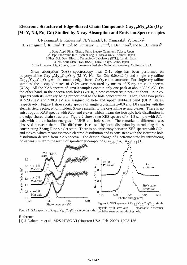
Electronic Structure of Edge-Shared Chain Compounds Ca2+xM2-xCu5O10 (M=Y, Nd, Eu, Gd) Studied by X-ray Absorption and Emission Spectroscopies
J. Nakamura1, E. Kabasawa1, N. Yamada1, H. Yamazaki1, Y. Tezuka2, H. Yamaguchi3, K. Oka3, T. Ito3, M. Fujisawa4, S. Shin4, J. Denlinger5, and R.C.C. Perera5
1 Dept. Appl. Phys. Chem., Univ. Electro-Commun., Tokyo, Japan2 Dept. Electronic Info. System Eng., Hirosaki Univ., Aomori, Japan
3 Phys. Sci. Dev., Electric Technology Labolatory (ETL), Ibaraki, Japan4 Inst. Solid State Phys. (ISSP), Univ. Tokyo, Chiba, Japan
5 The Advanced Light Sorce, Ernest Lowrence Berkeley National Laboratory, California, USA
X-ray absorption (XAS) spectroscopy near O-1s edge has been performed on polycrystalline Ca2+xM2-xCu5O10 (M=Y, Nd, Eu, Gd; 0.0≤x≤2.0) and single crystalline Ca2+xY2-xCu5O10 which contains edge-shared CuO2 chain structure. For single crystalline samples, the occupied states of O-2p were measured by means of X-ray emission spectra (XES). All the XAS spectra of x=0.0 samples contain only one peak at about 530.9 eV. On the other hand, in the spectra with holes (x>0.0) a new characteristic peak at about 529.2 eV appears with its intensity being proportional to the hole concentration. Then, these two peaks at 529.2 eV and 530.9 eV are assigned to hole and upper Hubbard band (UHB) states, respectively. Figure 1 shows XAS spectra of single crystalline x=0.0 and 1.8 samples with the electric field vector, P, of incident X-rays parallel to the crystalline a- and c-axes. There is no anisotropy in XAS spectra with P//a- and c-axes, which means the isotropic hole distribution in the edge-shared chain structure. Figure 2 shows two XES spectra of x=1.8 sample with P//a-axis with the excitation energies of UHB and hole states. The remarkable difference was observed between them. The difference is caused by local distortion by introducing holes constructing Zhang-Rice singlet state. There is no anisotropy between XES spectra with P//a- and c-axes, which means isotropic electron distribution and is consistent with the isotropic hole distribution derived from XAS spectra. The drastic change of electronic state by introducing holes was similar to the result of spin-ladder compounds, Sr14-xCaxCu24O41.[1]
0.0
0.5
1.0
1.5
2.0
2.5
3.0
525 530 535 540
UHBholestate
x=0.0P//a-axis
Photon energy (eV)
x=1.8P//a-axis
x=1.8P//c-axis
515 520 525 530 5350.0
0.1
0.2
0.3x=1.8P//a-axis UHB
excitation
Hole state excitation
Photon energy (eV)
Figure 1: XAS spectra of Ca2+xY2-xCu5O10 single crystals.
Figure 2: XES spectra of Ca3.8Y0.2Cu5O10 single
crystals with P//a-axis. Remarkable difference could be seen by introducing hole.
Reference[1] J. Nakamura et al., M2S-HTSC-VI (Houston USA, Feb. 2000), 1PO3-136.
We143We142We142
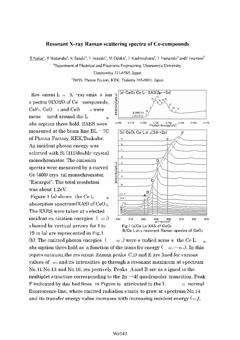
!
"
#
!! "# $ %% &'( )))
!"
! #
$ %%&' "
( )
! *** ! !
" &
+
, -.. !
/)0" & ! !
*"12"
) *
( "
& ' !
3 )
+! *
*4 )"*
" & )
! ) " 5
' 6 3 +
+! ) ) 3
7"**7"*8 7"*9 +! " $' ( )
!! ) 1 - :! " $'
! ) !
! ! ) 7"*-
) +! ) ) "
We144We143We143

PHOTOEMISSION STUDY OF QUASI-ONE-DIMENSIONAL HALOGEN-BRIDGED COMPOUND [Ni(chxn)2Br]Br2
Shin-ichi Fujimori1, Akihiro Ino1, Testuo Okane1, Atushi Fujimori1,2, Kozo Okada3, Toshio Manabe4, Masahiro Yamashita4, Hideo Kishida5 and Hiroshi Okamoto5
1Synchrotron Radiation Research Center, Japan Atomic Energy Research Institute,
SPring-8, Mikazuki, Hyogo 679-5148, Japan 2Department of Physics, Graduate School of Science, University of Tokyo, Hongo 7-3-1, Tokyo 113-0033, Japan
3Department of Physics, Faculty of Science, Okayama University, Tsushima-naka, Okayama 700-8530, Japan 4Department of Chemistry, Graduate School of Science, Tokyo Metropolitan University, Tokyo 192-0397, Japan
5Department of Advanced Material Science, Graduate School of Frontier Science, University of Tokyo, Tokyo 113-8656, Japan
The one-dimensional (1D) halogen (X) bridged transition-metal (M) compounds (MX-chain
compounds) have been attracting much attention as a good target material to investigate the properties of the 1D electronic state under the influence of strong electron-lattice interactions and electron-electron correlations. In these compounds, the electronic structure of 1D chain is composed of half- filled dz2 orbitals of the metals and the filled pz orbitals of halogens, and is considered to be a purely one-dimensional. In particular, the complex with X=Br and M=Ni,
[Ni(chxn)2Br]Br2 (chxn=1R, 2R-cyclohexanediamine) is known to show no lattice distortions related to Peierls or Spin-Pierls transition even at low temperatures. The magnetic susceptibility c is described by Boner-Fisher formula with S=1/2 and J=3600K, and this material can be regarded as the 1D Heisenberg chain. In the present study, the electronic structure of this compound is studied by angle-resolved photoelectron spectroscopy. Figure shows the spectra, taken with parallel to the chain axis. The expected two dispersions, originated with spin-charge separations as have been observed in other 1D electron system, are not clearly observed in this compound. Instead, only one “band” having about 0.5eV energy dispersion, is found in the half of the Brillouin zone. These results are compared with other 1D electron system, like SrCuO2[1] or Sr2CuO3[2]. In addition, d-p chain model calculations are employed to understand these differences.
References [1] C. Kim, A. Y. Matsuura, Z.-X. Shen, N. Motoyama, H. Eisaki, S. Uchida, T. Tohyama,
and S. Maekawa, Phys. Rev. Lett. 77, 4054 (1996); C. Kim, Z.-X. Shen, N. Motoyama, H. Eisaki, S. Uchida, T. Tohyama, and S. Maekawa, Phys. Rev. B 56, 15589 (1997).
[2] H. Fujisawa, T. Yokoya, T. Takahashi, S. Miyasaka, M. Kibune, and H. Takagi, Phys. Rev. B 59, 7358 (1999).
Photo
em
issi
on In
tensi
ty (
arb
. units
)
1.5 1.0 0.5 0.0Binding Energy (eV)
????
??
0
1.0
0.5
kb/π
[Ni(chxn)2Br]Br2
He II (hν=40.8eV)
We145We144We144
PHOTOEMISSION STUDY OF ONE-DIMENSIONAL GOLD CHAINS ONSTEPPED SILICON SURFACES
O. Gallus, M. Giovannini, Th. Pillo, P. Segovia and Y. Baer
Institut de Physique, Université de Neuchâtel, Switzerland
It is well known that low dimensional structures present different physical behaviorscompared to 3D materials. A striking example is the breakdown of the Fermi-liquid descriptionin one-dimensional metals, which are described by the Luttinger liquid formalism, wherequasiparticles are replaced by distinct collective excitations involving spin and charge, calledspinons and holons, respectively.
In a previous study, a double peak in photoemission spectra has been observed on theAu/Si-(5x1) surface [1]. This double peak has been interpreted as spin-charge separation in aLuttinger Liquid. This is now a matter of debate, since new studies seem to demonstrate that theband splitting does not vanish at the Fermi level, in contradiction with the spinon-holoninterpretation of this spectral feature [2].
In an attempt to clarify the real nature of the studied system, we present newphotoemission measurements of Au/Si-(5x1). We compare them to the former studies [1, 2], andto measurements of a new system, the Au/Si-(3x1) surface, which, to our knowledge, has notbeen measured yet.
References
[1] P. Segovia, D. Purdie, M. Hengsberger and Y. Baer Nature 402, 504 (1999)[2] K. N. Altmann, A. Kiraiosian, J.-L. Lin, D. Y. Petrovykh and F. J. Himpsel, preprint
We146We145We145

INDIUM CHAINS ON SI(111): A PEIERLS TRANSITION ?
Th. Pillo, O. Gallus, M. Giovannini,P. Segovia, Y. Baer
Physics Institute, University of Neuchâtel, CH-2000 Neuchâtel, Switzerland
Self-assembled one-dimensional (1D) chains received much attraction both in thedevelopment of nano-scale devices, and also in testing the theories describing their electronicstructure, which differs significantly from that of conventional 3D Fermi liquid systems. 1DLuttinger liquid-type chains, however, may become unstable due to fluctuations at finitetemperature and, hence, become susceptible to metal-insulator transitions such as, e.g., thePeierls textbook example for quasi-1D chains.
Recently, quasi-1D Indium chains on vicinal Si(111) have been found to exhibit a metal-insulator transition upon cooling [1], but the temperature and character of this transition was notinvestigated in great detail. Although the geometric structure of Indium chains on vicinal Si(111)seems to be explained now [2], the detailed electronic band structure near the Fermi surface (FS)as a function of temperature, and consequently the nature of the transition remain quite unclear.
The existence of three surface state bands induced by the (4x1) reconstruction has beenestablished [3]. What concerns the nature of the transition, a simple FS nesting picture for onlyone of those Indium induced surface state bands has been proposed, based on FS mappingexperiments with moderate resolution[1].
We examined in detail the geometric and electronic structure of thin Indium chains onSi(111) surfaces by means of low energy electron diffraction (LEED) and ultrahigh-resolutionphotoemission (ARPES) as a function of temperature. Our data reveal a transition around 115 Kfrom a high temperature (4x1)- to a low temperature (8x2)-phase being reversible with a smallhysteresis of the order of 10 K. ARPES spectra exhibit clearly important concomitant changes inthe electronic band structure near the Fermi surfaces and at the border of the surface Brillouinzones [4]. We derive the dispersive behavior of the bands involved in the transition in detail anddemonstrate that at least two surface state bands show the opening of a pseudo energy gap on theFermi surface leaving small but finite spectral weight in the low-temperature state. We concludethat this transition is probably driven by a similar but more complex mechanism than in aconventional Peierls transition. Furthermore, we evidence a strong influence of matrix elementeffects, as we observe considerable spectral weight of the same bands in different Brillouinzones.
References:
[1] H.W. Yeom et al., Phys. Rev. Lett. 82, 4898 (1999).[2] O. Bunk et al., Phys. Rev. B 59, 12228 (1999); C. Kumpf et al., Phys. Rev. Lett. 85, 4916
(2000).[3] T. Abukawa et al., Surf. Sci. 325, 33 (1985).[4] O. Gallus et al., Eur. Phys. J. B, to appear.
We147We146We146

PHOTOEMISSION ON TWO-DIMENSIONAL ELECTRON SYSTEMS
M. Getzlaff 1, M. Morgenstern1, J. Klijn1, Ch. Meyer1, A. Wachowiak1, J. Wiebe1, L. Plucinski2,R.L. Johnson2, R. Adelung3, K. Roßnagel3, L. Kipp3, M. Skibowski3 and R. Wiesendanger1
1 Institute of Applied Physics, University of Hamburg, Jungiusstr. 11, D-20355 Hamburg2 II. Institute for Experimental Physics, University of Hamburg, Luruper Chaussee 149, D-22761 Hamburg
3 Institute for Experimental and Applied Physics, University of Kiel, Leibnizstr. 19, D-24098 Kiel
Photoelectron spectroscopy in the VUV region is a powerful tool to investigate low-dimensional electron systems. Here we report on the electronic behavior of the two-dimensionalelectron gas (2DEG) on an InAs(110) surface being induced by adsorption of Nb and Fe in thesubmonolayer regime. This is of great importance for the understanding of different aspects inthe field of, e.g., spin electronics and the quantum Hall effect. Additionally, the 2DEG can beused for fundamental investigations in the photoemission process due to its relatively largeintrinsic life time and its spatial confinement. The n-InAs(110) crystals were cleaved in-situ(ND=1×1016cm-3). A calibrated electron beam evaporator enables the adsorption of metals in thesubmonolayer regime with a high accuracy. This investigation was carried out at two differentbeamlines at HASYLAB/DESY (Hamburg). The former one allows an overall energy resolutionof 50meV and an angular resolution of about 1°, the latter one of 10meV and 0.3°, resp.
Figure 1 exemplarily shows the determination of the coverage dependent surface bandbending and the increasing intensity of the corresponding 2DEG peak. In this experiment Nb wasevaporated at room temperature. Obviously, the growing intensity with increasing coverage isdirectly correlated with the increasing electron density of the 2DEG. Figure 1c demonstrates adispersion effect showing the angular dependence of the 2DEG peak. The peak maximumslightly shifts to higher energies with increasing detection angle.
We acknowledge financial support by the DFG, the Graduiertenkolleg Felder undlokalisierte Atome - Atome und lokalisierte Felder and the BMBF proj.: 05 SE8 FKA.
Figure 1: (a) Energetic shift of the valence band peak on the InAsspectrum as a function of the Nb coverage. The corresponding excitationenergy (hν), kinetic energy of the photoelectrons (Ekin) and the estimatedescape depth (λ) are given. The solid line marks the resulting surfaceband bending. (b) The 2DEG peak measured at hν = 13eV and differentNb coverages. The expected subband energies are marked as lines. (c)Angular dependence of the 2DEG peak at hν = 13eV for 8% Nb cover-age. In the x-y-plane the expected dispersion of both subbands are given.
-0,2 0,0 0,2
EF
2. subband1. subband
19 % 9 % 4 % 2 % 1 % 0.5 % 0.1 % 0 %
inte
nsity
[a.u
.]
binding energy -EF [eV]0,0 0,2 0,4 0,6 0,8 1,0 1,2
0
100
200
300
400
500 x work function
hν Ekin
λ 21 eV 16 eV 0.5 nm 13 eV 4.5 eV 5 nm 18 eV 13 eV 1 nm 18 eV 9 eV 2 nm 13 eV 7 eV 3 nm
ener
gy s
hift
[meV
]
Nb coverage [ML]
CBM
surface dipole
-10
12
3-0,3 -0,2 -0,1 0 0,1
Inte
nsity
[ arb
. uni
ts]
angle
[°]
binding energy -EF [eV]
a cb
We148We147We147

SOFT X-RAY ABSORPTION SPECTROSCOPY (Mn-L2,3, O-K) IN MIXED VALENCE MANGANITES.
Gloria Subías1,2, J. García2, M. Concepción Sánchez2, J. Blasco2and M. Grazia Proietti2
1 European Synchrotron Radiation Facility (ESRF),
6 rue Jules Horowitz, B.P. 220, F-38043 Grenoble Cedex, France. 2 Instituto de Ciencia de Materiales de Aragón, CSIC-Univ. de Zaragoza,
Pl. San Francisco s/n, 50009 Zaragoza, Spain.
In mixed valence materials, like RE1-xAxMnO3 (RE being a trivalent rare-earth cation and A a divalent cation), the extra charges induced by partial substitution of the rare-earth site are expected to go to states of mixed transition-metal 3d-oxygen 2p character, within the framework of the Zaanen-Sawatzky-Allen model [1]. The purpose of this work was to check the validity of this model in a wide range of doped manganites by means of X-ray absorption spectroscopy at both, Mn-L2,3 and O-K edges.
XANES spectra of REMnO3, RE1-xCaxMnO3 (RE=La, Tb) and RE0.5A0.5MnO3 (RE-A=
LaCa, TbCa, PrCa, PrSr) were measured at the beamline ID12B at ESRF, by recording the total electron yield. Experiments were carried out as a function of temperature up to room temperature. The Mn 2p spectra shift towards higher energies with increasing the formal valence of the sample, as it occurs for the Mn K-edge XANES spectra [2]. Moreover, the spectral shape change slightly with both, the doping rate and the different rare-earth cations. However, the O 1s spectra are much more sensitive to the variations in the rare-earth atoms. The spectra at the O K-edge show a prepeak at the Fermi energy corresponded to empty states in the O-2p band. This prepeak shifts to lower energies and increases the intensity with the divalent metal content. A double structure is observed for this prepeak in REMnO3 samples. Similarly to the Mn K-edge results [2], neither the O-K edge nor the Mn-L2,3 edge XANES spectra of the intermediate compounds cannot be reproduced by a weighted linear combination of the REMnO3 and CaMnO3 ones.
Finally, a comparison between the O K-edge and the Mn K-edge spectra indicates that the
first excited states in these systems are mainly of 2p oxygen character, strongly hybridized with the Mn 3d states, so the conduction electrons move in the oxygen 2p band. Therefore, new models based on many-body interaction effects are needed for well understanding these results. References [1] J. Zaanen, G. A. Sawatzky andJ. W. Allen, Phys. Rev. Lett. 55, 418 (1985). [2] G. Subías, J. García, M. G. Proetti and J. Blasco, Phys. Rev. B 56, 8183 (1997).
We149We148We148

Temperature-Dependent High-Resolution Photoemission Spectroscopy of
YbMCu4 (M=In, Cd, Mg)
H. Sato1, Y. Nishikawa1, F. Nagasaki1, H. Fujino1, Y. Takeda1, M. Arita2, K. Shimada2,
H. Namatame2, A. Kimura1, M. Taniguchi1,2, K. Hiraoka3 and K. Kojima4
1 Graduate School of Science, Hiroshima University, Kagamiyama 1-3-1, Higashi-Hiroshima 739-8526, Japan
2 Hiroshima Synchrotron Radiation Center, Hiroshima University, Kagamiyama 2-313,
Higashi-Hiroshima 739-8526, Japan
3 Faculty of Engineering, Ehime University, Bunkyo-cho 3, Matsuyama 790-8577, Japan
4 Faculty of Integrated Arts and Sciences, Hiroshima University, Kagamiyama 1-7-1, Higashi-Hiroshima 739-8521, Japan
We have investigated the electronic structure near the Fermi level (EF) of YbMCu4 (M=In,Cd, Mg) from 10 K to room temperature (RT) by means of the high-resolution (~5 meV) photo-emission spectroscopy (UPS) with an excitation photon energy hν=21.22 eV. The Yb 4d x-rayphotoemission (XPS) experiments with an Al Kα line were also carried out in order to investigatethe valence of the Yb atom. Among three compounds, YbInCu4 exhibits a first order valence tran-sition at Tν=42 K where the Yb changes from a nearly trivalent at high temperature to a mixedvalent state (z~2.8) at low temperature [1].
For YbInCu4 and YbCdCu4, the prominent peak due to the Yb2+ 4f7/2 states are clearly ob-served near EF at 10 K in the UPS spectra. The energy positions of the Yb2+ 4f7/2 peaks of YbInCu4and YbCdCu4 are 46 and 31 meV, respectively. A deeper binding energy for YbInCu4 qualitativelycorresponds to the higher Kondo temperature (~430 K for YbInCu4 [2] and ~220 K for YbCdCu4[3]). These peaks almost disappear at RT for both compounds. With the decrease of temperaturefrom RT to 50 K, the peaks gradually gain intensity and their energy positions shift toward EF side,which is similar to the result for YbAgCu4 [4]. From 50 to 10 K, the peak intensity of YbInCu4becomes drastically high and the energy position shifts toward the deeper side. On the other hand,the peak of YbCdCu4 shows the monotonous temperature dependence like from RT to 50 K. Thedrastic change of the Yb2+ 4f7/2 peak of YbInCu4 suggests that the electronic structure changes dueto the valence transition at Tν. For YbMgCu4, the Yb2+ 4f7/2 states appear as a broad structure inthe UPS spectra and the spectra show few temperature dependence, which means the Yb 4f statesonly in YbMgCu4 is different from those in YbInCu4 and YbCdCu4.
In the Yb 4d XPS spectra of YbInCu4 and YbCdCu4, the structures due to the Yb2+ and Yb3+
states are observed. For both compounds, the Yb2+ exist even at RT and with the decrease oftemperature, the structure due to Yb2+ states gradually grows in intensity, while the intensity of theYb3+ structure decreases. Drastic change caused by the valence transition of YbInCu4 has been notclearly been observed. On the other hand, the Yb in YbMgCu4 is almost divalent states.
[1] J. M. Lawrence et al., Phys. Rev. B 59, 1134 (1999).[2] J. L Sarrao et al., Phys. Rev. B 54, 12207 (1996).[3] J. L. Sarrao et al., Phys. Rev. B 59, 6855 (1999).[4] P. Weibel et al., Z, Phys. B 91, 337 (1993).
We150We149We149

Inte
nsity
(ar
b. u
nits
)
1.2 0.8 0.4 0.0Binding Energy (eV)
1T-TaS1.5Se0.5 Γ-point
hν = 21.2 eV
300 K 33 K In
tens
ity (
arb.
uni
ts)
1.2 0.8 0.4 0.0Binding energy (eV)
300 K 33 K
1T-TaS1.2Se0.8 Γ-point
hν = 21.2 eV
ANGLE-RESOLVED PHOTOEMISSION STUDY OF CHARGE-DENSITY-WAVE STATES IN 1T-TaSxSe2-x
K. Horiba1,2, K. Ono1, Y. Aiura2, O. Shiino1, and M. Oshima1
1 Department of Applied Chemistry, University of Tokyo, Tokyo 113-8656, Japan2 Electrotechnical Laboratory, Tsukuba 305-8568, Japan
We have investigated the electronic structures of metal-to-insulator transitions due tocharge-density-wave (CDW) phase transitions in 1T-TaSxSe2-x by angle-resolved photoemissionspectroscopy.
In the insulating phase of the sample with x=1.5, we observe a gap formation caused by aphase transition from nearly-commensurate CDW to commensurate CDW. On the other hand, inthe metallic phase of the sample with x=1.2, we don’t observe a drastic change in the spectrabetween at room temperature and at low temperature. These results agree with the physicalproperties such as electrical resistivities [1].
In the sample with x=1.5, we observe the lower Hubbard band which is also observed in1T-TaS2 [2]. In the metallic phase of the sample with x=1.2, the peak intensity is smaller and thepeak energy shifts to EF, but the peak still remains. These electronic structures are comparable tothose of strongly correlated materials [3]. From these results, it is confirmed experimentally thatthe metal-to-insulator transition of 1T-TaSxSe2-x is due to the Mott localization.
(a) (b)
Figure 1: Γ-point photoemission spectra at room temperature (300 K) and low temperature (33 K) for (a) 1T-TaS1.5Se0.5 and (b) 1T-TaS1.2Se0.8.
References
[1] F. J. DiSalvo, J. A. Wilson, B. G. Bagley, and J. V. Waszczak, Phys. Rev. B 12, 2220(1975).
[2] B. Dardel, M. Grioni, D. Malterre, P. Weibel, and Y. Baer, Phys. Rev. B 45, 1462 (1992).[3] I. H. Inoue, I. Hase, Y. Aiura, A. Fujimori, Y. Haruyama, T. Maruyama, and Y. Nishihara,
Phys. Rev. Lett. 74, 2539 (1995).
We151We150We150

TIME RESOLVED PHOTOLUMINESCENCE INNER CORE EXCITATION IN ZnCdSe MQWs
K. Kobayashi1, M. Oura1, J. H. Chang2, M. Watanabe1, Y. Harada1, T. Suzuki3, S. Shin1,4
and T. Yao2
1 RIKEN/Spring-8, 1-1-1 Kouto, Mikazuki-cho, Sayo-gun, Hyogo 679-5148, Japan 2 Institute for Materials Research, Tohoku University, 2-1-1 Katahira, Aoba-ku, Sendai 980-0812
3 JASRI/Spring-8, 1-1-1 Kouto, Mikazuki-cho, Sayo-gun, Hyogo 679-5198, Japan 4 Institute for Solid State Physics, University of Tokyo, Kashiwanoha, Kashiwa, Chiba 277-8581, Japan
The core hole generation in quantum confinement structures gives rise to several interesting physical problems such as 1)hetero interface core excitons, 2)competition between core hole potential and quantum confinement potential, and 3)core hole decay dynamics in the
confinement structures.
We have applied photoluminescence inner core excitation (PLICE) as a local probe for these problems in several semiconductor quantum structures[1]. The results strongly suggest that the excitation spectra probe the buried quantum structures, however, they still provide no sound evidence that proves the degree of local sensitivity. Inevitable involvement of hot electron-hole pair generation due to Auger decay of core holes, and their diffusion are thought to degrade the local sensitivity in the steady state measurements.
Here we report our recent time resolved (tr) PLICE measurements, which we performed to improve the local sensitivity of the method, in ZnSe single crystal thin layers and ZnCdSe multi quantum wells (MQW) on GaAs substrates. The experiments were done at BL19B of Photon Factory, KEK. The photoluminescence (PL) fundamental band peaks at around 443nm in ZnSe. In case of MQWs, it peaks
in the range of 520nm-555nm, corresponding to the degree of confinement. These bands show a very fast component, of which profile is determined by SR bunch profile, and two delayed components with latent time of 0.3nsec and 1nsec. The excitation spectra of integrated fast PL bands in the Zn 2p excitation regime is shown in the figure. The results clearly indicate that the confinement potential drastically affects the core absorption in the quantum structures, and that tr-PLICE has high local sensitivity for the study of the problems mentioned above. [1] K. Kobayashi, T. Ota, K. Maehashi, H. Nakashima, Y. Ishiwata, and S. Shin, Physica E 7
(2000),595-599.
3.0
2.5
2.0
1.5
1.0
10601050104010301020
Ex cita ion Ene rgy (eV)
ZnSe 443nm
)Zn0.5Cd0.5Se MQW
555nm
Zno.65Cd0.35Se MQW
520nm
Zn 0.5Cd0.5Se MQW
540nm
Zn 2p3/2
Excitation
We152We151We151

Electronic Structure of oxidic Perovskites:X-ray Fluorescence Measurements on KTaO3 , KNbO3 and Sr2FeMoO6
B. Schneider1, M. Matteucci2, D. D. Sarma3, A. V. Postnikov4 and M. Neumann1
1University of Osnabrück, Department of Physics, D-49069 Osnabrück, Germany2National Research Council c/o Sincrotrone Trieste, Padriciano 99, 1-34012 Trieste, Italy
3Solid State and Structural Chemistry Unit, Indian Institute of Science, Bangalore 560 012, India.4Gerhard Mercator University Duisburg, Theoretical Low-Temperature Physics, D-47048 Duisburg,
Germany
Oxidic perovskites, commonly described as ABO3, exhibit a huge variety of possibleapplications. Ferroelectric materials with perovskite structure like KTaO3 and KNbO3 are ofgreat interest in modern technology like optical signal processing, holographic storage and phaseconjugation [1]. Another class of oxidic perovskites are materials with odered double-perovskite(A2BB’O6) structure. Some of them show a colossal magnetorestance (CMR) effect. This effectis attracting interest from both fundamental and practical point of view. The CMR effect inSr2FeMoO6 has been reported recently and is quite peculiar since it is a high temperature andlow field MR linked to the half-metalllic state of the compound [2,3].
The electronic structure of the investigated perovskites is quite different, but some similaritiescan be observed: The valence band is formed by oxygen 2p states hybridized with the metal ndstates (metal on the B-site) while the A-site metal has no contribution to the valence band [2,3,4].In order to measure the partial density of states (pDOS) of each relevant state we usedsynchrotron radiation at the ALS Beamline 8.0.1 for excitation and the University of Tennessee’sfluorescence spectrometer for monitoring the photon emission process.
To check the O 2p contribution to the empty states we first measured the absorption spectra atthe O Kα -edge. Furthermore we measured the emission spectra at various excitation energiesbelow, at and above the absorption edge. In case of KTaO3 and Sr2FeMoO6 , no excitation energydependence could be observed while in KNbO3 the position of the emission maximum shiftedslightly with excitation energy. The emission spectra taken at the Ta NIII – edge (Ta 5d → 4p) inKTaO3 show a strong dependence on the excitation energy. This behaviour can be explained bythe transition out of different states in the valence band: at excitation energies just above theabsorption threshold an emission from the bottom of the valence band can be found whereas athigher excitation energies an emission from the middle of the valence band is observed. Fe L2,3
and Mo M2,3 in Sr2FeMoO6 show a similar behaviour. In KNbO3 the contribution of the 5p statesto the valence band was investigated via the energy dependent Nb M4,5 emission. The shape ofall absorption and emission spectra are compared with calculations done on the basis of the all-electron full-potential linearized augmented plain-wave method (FLAPW), convoluted with theexperimental resolution and lifetime broadening.
[1] L. A. Boatner, E. Krätzig, R. Orlowski; Ferroelectrics 27 (1980) 247[2] K.I. Kobayashi, T. Kimura, H. Sawada, K. Terakura and Y. Tokura; Nature 395, 677 (1998)[3] D.D. Sarma, P. Mahadevan, T. S. Dasgupta, S. Ray, A. Kumar; Phys. Rev. Lett. 85, 2549 (2000)[4] T. Neumann, G. Borstel, C. Scharfschwerdt, M. Neumann, Phys. Rev. B 46 (1992) 10 623
We153We152We152

PHOTOEMISSION STUDIES OF STRONGLY CORRELATEDNICKEL COMPOUNDS
L. Sangaletti1 , A. Goldoni2, M. Peloi1, G. Ferrini1, F. Parmigiani1
1 Istituto Nazionale per la Fisica della Materia and Dipartimento di Matematica e Fisica, Università Cattolica delSacro Cuore, Via dei Musei 41, 25121 Brescia (Italy)
2 Sincrotrone Trieste, s.s. 14, km 163.5 in Area Science Park, 34012 Trieste, Italy
High resolution core level photoelectron spectra and resonant photoemission detected inthe valence band spectra of strongly correlated materials can reveal the extent of electroniccorrelations in these compounds [1]. Recently, a systematic investigation of Ni compounds has
been reported with the aim to relate the lineshape of Ni 2p core lines to the Ni-O coordination[2]. We present photoemission data from NiO single crystals and compare them to the resultsobtained from several divalent nickel compounds with the aim to show the effect of ligand on thesatellite features observed both in core level and valence band spectra. In the case of NiO, weshow that the giant resonant features observed in the valence band spectra collected at the Ni 2p-3d absorption threshold can be consistently interpreted on the basis of an impurity clustercalculation where the multiplet splitting is fully accounted for by using a configuration
interaction scheme.
These results are compared to those obtained from the analysis of K2NiF4 [3] and NiS2 [4].
While NiO is an insulator, NiS2 is a semiconductor and K2NiF4 is a strongly insulating layered
perovskite. The differences observed in the satellite features of both valence band and Ni 2p corelevel data can be ascribed to differences in the Ni-ligand bond, which ultimately affect theenergy gap of these compounds. An estimate of the ligand-metal charge transfer energy,calculated on the basis of the impurity cluster model, is given, which scales with the energy gapof these materials.
References
[1] S. Hüfner, Adv. in Physics, 43 (1994) 183[2] K. Maiti, Priya Mahadevan, D.D. Sarma, Phys. Rev. B 59 (1999) 12457[3] L. Sangaletti, F. Parmigiani, E. Ratner, Z.–X. Shen, C. Chemelli, and O. Jepsen Phys. Rev. B 50 (1994) 17854[4] L. Sangaletti, F. Parmigiani, T. Thio, and J. W. Bennett, Phys. Rev. B 55 (1997) 9514
We154We153We153

Fermi surface of Bi-cuprates
C. Janowitz1, R. Müller1, M. Schneider1, A. Krapf1, R. Manzke1, H. Hoechst2, C. Ast2
1 Institut für Physik, Humboldt-Universität, 10115 Berlin, Germany 2 Synchrotron Radiation Center, Stoughton, WI, (USA)
The topology of the Fermi surface is one of the most important normal state properties of the HTSC's. Its exact determination is the input for predictions of the physical properties of the HTSC’s. Over the last years, about all information about the Fermi surface topology has been derived from ARPES studies on Bi-2212, namely Bi2Sr2CaCu2O8. Besides sample quality leading to scattering and therewith broadening furthermore the magnitude of the bilayer splitting for n=2 compounds [1,2] makes it difficult to determine the exact shape of the Fermi surface. In the case of Bi2Sr2-xLaxCuO6 with different doping levels and only one CuO2 layer per unit cell a number of these parameters can be controlled in a way that the intrinsic linewidth and dispersion can be determined more unequivocally. In this contribution we investigate the Fermi surface of n=1 material at various photon energies and polarization geometries by angle resolved photoemission with very high energy and momentum resolution. Our results show the importance of matrix element effects in ARPES for determining the exact shape of the Fermi surface. Additionally we report ARPES measurements for various doping levels of the system Bi2Sr2-xLaxCuO6. In the context of the current debate on the overall Fermi surface topology our results confirm the view of a hole like Fermi surface for n=1 material over a wide doping range. Furthermore a small splitting of the Zhang-Rice singlet near EF could be resolved and traced along major symmetry lines in accordance to recent findings [3]. It will be discussed in the context of the results of Feng [1] and Chuang [2] and its relation to current theoretical models of the spectral function of HTSC’s. Finally the results from Fermi surface mapping of triple layered Bi2Sr2Ca2Cu3O10 will be presented.
References [1] D.L. Feng, N.P. Armitage, D.H. Lu, A. Damascelli, J.P. Hu, A. Lanzara, F. Ronning, K.M.
Shen, H. Eisaki, C. Kim, Z.X. Shen, cond-mat/0102385 (2001) [2] Y.-D. Chuang, A.D. Gromko, A. Fedorov, D.S. Dessau, Y. Aiura, K. Oka, Yoichi Ando,
H. Eisaki, S.I. Uchida, cond-mat/0102386 (2001) [3] R. Manzke, R. Müller, C. Janowitz, M. Schneider, A. Krapf, H. Dwelk, Phys. Rev. B 63,
R100504, (2001)
We155We154We154

OVERDOPED CUPRATES AS QUASIPARTICLE LIQUIDS
B.O. Wells1, Z. Yusof1, T. Valla2, A.V. Fedorov2, P.D. Johnson2, C. Kendziora3, Sha Jian3, D.G. Hinks4
1 University of Connecticut, Storrs CT, USA
2 Brookhaven National Laboratory, Upton NY, USA 3 Naval Research Laboratory, Washington DC, USA 4 Argonne National Laboratory, Argonne IL, USA
The question as to whether the Fermi Liquid model is a valid description of the electronic
state of the cuprate superconductors is one of the central questions in condensed matter physics. It is generally believed that the underdoped cuprates are not Fermi liquids while samples that are overdoped enough probably are, though there is little data to this effect. This presentation describes extensive Angular Resolved Photoemission (ARPES) measurements on highly overdoped Bi2Sr2CaCu2O8+δ samples with TC as low as 51K. The results are analyzed with respect to previous work on under and optimally doped Bi2Sr2CaCu2O8+δ as well as ARPES of metal surface states. We find that several features of the ARPES data favour a quasiparticle description of the single electron excitations. Among these are that the self energy is only weakly k dependent and transport is simply related to the quasiparticle lifetime. Also, the single electron excitation is well defined for a wider range of k values and energies than for the lesser-doped cuprates but not so well defined as in metals. Sample data illustrating this point are shown in the figure below, with data for the overdoped sample, an optimally doped cuprate [1], and a Mo surface state [2]. The detailed behaviour of these quasiparticles is not described by a simple Fermi Liquid description nor is it similar to regular metallic states where electron-phonon interactions dominate for most temperatures of interest. We are thus led to believe that the overdoped cuprates form a quasiparticle liquid, but that the dominant interactions for the electrons in this system are similar to but weaker than those found at lower doping levels.
Work supported in part by the United States Dept. of Energy under contract #DE-AC02-98CH10886 and #DE-FG02-00ER45801.
Figure 1: Intensity (by colour) versus energy and momentum for three samples. Left to right they are an optimally doped Bi2Sr2CaCu2O8+δ sample [1], the overdoped sample, and a Mo (110) surface state [2].
References [1] T. Valla, A.V. Fedorov, P.D. Johnson, B.O. Wells, S.L. Hulbert, Q. Li, G.D. Gu, N.
Koshizuka, Science 285, 2110 (1999). [2] T. Valla, A.V. Fedorov, P.D. Johnson, S.L. Hulbert, Phys. Rev. Lett. 83, 2085 (1999).
We156We155We155

X-ray emission and absorption spectra and electronic structure of MgB2
E.Z. Kurmaev1, I.I. Lyakhovskaya2, J. Kortus3, M. Demeter4, T. Imazono5, N. Miyata5, M. Yanagihara5, M. Watanabe5, M. Neumann4, T. Muranaka6 and J. Akimitsu6
1Institute of Metal Physics, Russian Academy of Sciences-Ural Division,
620219 Yekaterinburg, Russia 2Institute of Physics, S-Petersburg University,
S-Petersburg, Russia 3Center for Computational Materials Science, Naval Research Laboratory,
Washington DC 20375, USA 4University of Osnabrueck, Sektion of Physik, D-49069 Osnabrueck, Germany
5Research Institute for Scientific Measurements, Tohoku University, Sendai 980-8577, Japan 6Department of Physics, Aoyama-Gakuin University, Tokyo 157-8572, Japan
The results of measurements of soft X-ray emission spectra of constituents of new superconductor MgB2 (Tc=39 K) [1-2] are presented. B K-emission and absorption and Mg L-emission and absorption spectra are measured using sintered powder samples of MgB2. According to dipole selection rules these spectra probe the distribution of B 2p and Mg 3s-states, respectively. The spectra are converted to the binding energy scale with help of additional XPS B 1s and Mg 2p measurements. The obtained results are compared with first principles band structure calculations [3]. The experimental spectra are found in a good agreement with partial density of states and theoretical X-ray spectra which are calculated taking into account the matrix element of transition probability.
References [1] J. Akimitsu, In Proceedings of the Symposium on Transition Metal Oxides, Sendai, 10 January 2001 (to be published) [2] J. Nagamatsu, N. Nakagawa, T. Muronaka, Y. Zenitani, and J. Akimitsu (to be published) [3] J. Kortus, I.I. Mazin, K.D. Belashchenko, V.P. Antropov, and L.L. Boyer, cond- mat/0101446 .
We157We156We156

RESONANT INELASTIC SOFT X-RAY SCATTERING OF INSULATING CUPRATES
L.-C. Duda1, T. Schmitt1, J.-H. Guo1, G. Dhalenne2, A. Revcolevschi2, and J. Nordgren1
1 Department of Physics, Uppsala University, Ångström Laboratory, Box 530, S-75121 Uppsala, Sweden 2 Laboratoire de Chimie des Solides, Unité Associe au CNRS 446, Université de Paris-Sud, Bâtiment 414,
F-91405 Orsay, Cedex, France
The low energy excitations of cuprates are receiving considerable attention in current literature. It would be particularly interesting to establish a relationship between the behavior of these excitations and the manifold of low temperature phase transitions found in cuprates. Several insulating cuprates are parent compounds of a family of superconductors when doped, such as the antiferromagnetic La2CuO4 and the La1-xSrxCuO4 high-temperature superconductor family. CuGeO3, another insulating cuprate shows an unusual Spin-Peierls transition at low temperature.
We have studied La2CuO4, SrCuO2, CuO, and CuGeO3 using resonant soft x-ray emission
spectroscopy (RSXES). The features in the RSXES spectra excited at the Cu 3p- and 3s-resonance disperse linearly with incident x-ray energy and can be understood as resonant inelastic x-ray scattering (RIXS) as described by the Kramers-Heisenberg formula. The energy loss of the scattering corresponds to the excitation energy of this structure, which can be easily obtained by taking the difference of elastic and inelastic peak energy. In an ionic picture, we are dealing with crystal field or dd-excitations of the Cu2+-ion. With our method we can establish the excitation energy with high precision (better than ±0.1eV) and good signal-to-noise ratio.
On the other hand, the RSXES spectra excited at the O1s-resonance must be interpreted as
consisting of one part that reflects the partial density of states and another part that is due to a local excitation [1]. The RIXS energy loss shows an interesting variation between the different compounds and varies between 1.6 eV for CuGeO3 and 2.3 eV for La2CuO4. This cannot easily be reconciled with theoretical expectations for the excitation energies of dd-excitations. We therefore attribute some of the structures to the formation of a Zhang-Rice singlet (ZRS) [2]. A ZRS is an excitation that involves a charge transfer from a Cu to an O-atom and is considered as the lowest ionization state. Although it is very prominent in the RIXS spectra of insulating cuprates, ZRS are difficult to observe in valence band photoemission.
First theoretical discussions and model calculations have recently been published by Okada
et al. [3] and corroborate our interpretation of the O1s-RIXS structures in cuprates. We conclude that further investigation of these excitations with RIXS can provide valuable new insight into the low energy excitations of cuprates. References [1] L.-C. Duda, et al., Phys. Rev. B 61, 4186 (2000). [2] F. C. Zhang and T. M. Rice, Phys. Rev. B 37, R3759 (1988). [3] K. Okada and A. Kotani, Phys. Rev. B 63, 045103 (2001).
We158We157We157

SYNCHROTRON-LIGHT ABSORPTION SPECTROSCOPY STUDY OF MAGNETIC HIGH TEMPERATURE SUPERCONDUCTORS
Y. Hwu1,2, H. Berger2, W. L. Tsai1, P. C. Hsu1, E. S. Tok3, L. W. Chang4, G. H. Fecher5, G.
Margaritondo2
1 Institute of Physics, Academia Sinica, Taipei, Taiwan 2 Institut de Physique Appliquée, Ecole Polytechnique Fédérale de Lausanne, CH-1015, Lausanne, Switzerland
3 Department of Materials Science, National University of Singapore, Singapore 4 China Steel Co., Kaohsung, Taiwan
5 Institut für Physik, Johannes Gutenberg-Universität Mainz, Germany
Synchrotron-light absorption spectroscopy was used to study a new, recently discovered class of magnetic high temperature superconductors. These compounds are based on BiPbSrCaCuO single crystals which are made magnetic (paramagnetic and ferromagnetic) by doping with rare earth atoms. Their superconducting and magnetic properties as well as other characteristics were intensively investigated with a variety of techniques including crystallography, infrared spectroscopy, transport measurements, SQUID measurements, chemical microprobe analysis and others. The results clearly demonstrated the coexistence of magnetism and superconductivity in the same phase.[1] However, these data do not elucidate the electronic structure nor the origin of this exotic and interesting phenomenon.
The present study provides valuable information on the unresolved issues, based on
absorption data taken at the O1s and Cu 2p absorption edges. Data obtained with high energy resolution explored the effects of doping on the electronic structure. The possible implications on the coexistence of two seemingly antagonistic phenomena—ferromagnetism and superconductivity—will be discussed. References [1] H. Berger, et al. Appl. Phys. Lett. (submitted).
We159We158We158

Quantization of electronic states in an ultrathin rare-earth film: Gd/W(110)
O. Rader1, C. Pampuch1, G. V. Prudnikova1,2, and A. M. Shikin1,2
1BESSY, Albert-Einstein-Str. 15, D-12489 Berlin, Germany2St. Petersburg State University, St. Petersburg 198904, Russia
In recent years quantized electronic states have been identified by photoelectronspectroscopy in several noble-metal and transition-metal systems [1]. For magnetism, theseobservations were particularly interesting since the observation of quantized states could berelated to long-range magnetic coupling effects, for instance in the giant-magnetoresistancesystem Co/Cu/Co(100) [2]. In this case, the s,p conduction electrons in the Cu mediate the long-range magnetic coupling between the ferromagnetic Co layers. In this respect the Cu interlayeracts analogously to the noble-metal host in a spin glass: the s,p conduction electrons mediate theoscillatory magnetic coupling between the localized moments of the dilute transition metal, theso-called RKKY interaction
In rare-earth metals the localized 4f magnetic moments also interact in the same way. Inthis case the delocalized 5d6s electrons are magnetically polarized by the 4f electrons andmediate the long range order of the 4f moments. Despite a large amount of photoemissionstudies on rare-earth thin films, quantization effects in the electronic structure have to date notbeen reported.
We report on normal-emission photoemission spectra of Gd films on W(110) for variousthicknesses. The spectral features show a strong dependence on the deposited Gd mass up to atleast 4 monolayers (ML). Strong changes occur in the whole spectrum upon increasing thethickness from 1 to 2 ML. Around 3 ML, the spectra change again. In particular, individualpeaks in the energy range around 3 eV binding energy can be distinguished and assigned to theformation of quantum-well states confined through the existence of a W bulk band gap extendingfrom about 6 eV to about 2 eV binding energy.
In the energy range near the Fermi level, on the other hand, particularly sharp peaksdevelop from about 2 ML Gd on. These peaks cannot be assinged to a parent Gd bulk band. Wepresent a simple interpretation of these features on the basis of Gd quantum-well states inresonance with W substrate-derived electronic states. In brief, the states formed are similar toimage-potential states but shifted towards lower energies due to a resonant interaction with theW substrate.
References
[1] See T. C. Chiang, Surf. Sci. Rep. 39, 183 (2000).
[2] See F. J. Himpsel et al., Adv. Phys. 47, 511 (1998).
We160We159We159

High-resolution ARPES investigation of the quasiparticle scattering processes
in a Model Fermi liquid: 1T-TiTe2
L. Perfetti, C. Rojas, A. Reginelli, L. Gavioli*, H. Berger, G. Margaritondo, M. Grioni
Institut de Physique Appliquée, Ecole Polytechnique Fédérale, CH-1015 Lausanne, Switzerland
R. Gaál, L. Forró
Institut de Génie Atomique, Ecole Polytechnique Fédérale, CH-1015 Lausanne, Switzerland
F. Rullier-Albenque
Laboratoire des Solides Irradiés, CEA, Ecole Polytechnique, 91128 Palaiseau Cedex, France
We performed high resolution ARPES and resistivity measurements on the metallic quasi-2D
system TiTe2. We found that the quasi-particle lifetime is in excellent agreement with transport
relaxation time. Moreover we characterize and separately evaluate the effect of electron-electron,
electron-phonon, and electron-defect interactions on the experimental lineshape. A residual low
temperature spectral linewidth (Γ0=17 meV) indicates that the three dimensional nature of the
electronic states cannot be neglected even in this quasi-2D material.
We161We160We160

Strongly correlated normal state and the peierls transition in
1D charge-density-wave systems
L. Perfetti, C. Rojas, A. Reginelli, H. Berger, G. Margaritondo, M. Grioni
Institut de Physique Appliquée, Ecole Polytechnique Fédérale, CH-1015 Lausanne, Switzerland
J. Voit
Theoretische Physik 1, Universitat Bayreuth, D-95440 Bayreuth, Germany
We have studied by high-resolution ARPES the metallic normal states and the insulating CDW
phases of the typical quasi-1D Peierls system (TaSe4)2I. In the normal state we observe
quasiparticles heavily dressed by phonons. The large spectral weight renormalization is at the
origin of a deep pseudogap around the Fermi level. Remarkably, most of the spectral weight is
distributed along the calculated one-particle bands, notwithstanding the largely renormalized
mass. The temperature-dependent ARPES spectra illustrate the opening of real gaps below the
Peierls transition temperature. In contrast with conventional scenarios, the gap energy is not
directly related to the binding energy of the main dispersing spectral feature.
We162We161We161

Competing periodic potentials: energy eigenvalues and spectral weight
L. Perfetti, F. Zwick, G. Margaritondo, and M. Grioni
Institut de Physique Appliquée, Ecole Polytechnique Fédérale, CH-1015 Lausanne, Switzerland
J. VoitT, G. Grüner‡, H. Höchst=
T Theoretische Physik 1, Universitat Bayreuth, D-95440 Bayreuth, Germany
‡ Department of Physics, University of California, Los Angeles, CA 90095-1547, USA.
= Synchrotron Radiation Center, University of Wisconsin-Madison, Stoughton, WI 53589-3097 USA.
Translational symmetry is a key ingredient for the description of the electronic structure of solids.
The dispersion of the electronic states, and ultimately, the physical properties of a material,
reflect the periodicity of the lattice potential. When the electrons feel two competing
periodicities, the band structure may be deeply modified. This situation is actually realized in
low-dimensional charge-density-wave (CDW) systems, because the periodicity of the CDW is
not directly related to the lattice parameter. Incommensurate potentials are expected to yield
localized wavefunctions and a fractal spectrum. We used ARPES to investigate this effect in the
1D system (TaSe4)2I. We show that while the energy eigenvalues may indeed have a fractal
structure, the spectral weight, measured by ARPES, is non-uniform, and exhibits signatures of
both periodicities. Model calculations highlight the importance of the relative strength of the two
potentials.
We163We162We162

PHOTOEMISSION STUDIES OF R1-xCaxBa2Cu3O6+d (R=Y, Eu) IN THEINSULATOR TO METAL TRANSITION
P. Starowicz1,2, B. Penc1, A. Szytula1
1 Institute of Physics, Jagiellonian University, Reymonta 4, 30-059 Kraków, Poland2 Jozef Stefan Institute, Jamova 39, SI-1000 Ljubljana, Slovenia
The valence band and core level states of R1-xCaxBa2Cu3O6+d (R=Y, Eu) were studied bymeans of angle integrated photoemission. Changes of the electronic structure in the insulator tometal transition as an effect of doping were examined. Studies have been performed fordeoxygenated YBa2Cu3O6.16, EuBa2Cu3O6.06, Y0.84Ca0.16Ba2Cu3O6.09, Eu0.85Ca0.15Ba2Cu3O6.18,Y0.7Ca0.3Ba2Cu3O6.12 and Eu0.7Ca0.3Ba2Cu3O6.13 as well as for high Tc samples YBa2Cu3O6.91 andEuBa2Cu3O6.93. The last two were superconducting below 91.4 K and 93.3 K respectively. Thedeoxygenated samples with Ca content of 0.3 were superconducting below approximately 20 K.
The valence band studies reveal that a peak appears at 2.4 eV below the Fermi level andgrows systematically with hole doping (Figure 1). This feature is characteristic of a metal-insulator transition and is common for both calcium and oxygen doping. This structure isinterpreted to originate from the Zhang-Rice singlets. The Cu 3d level spectra confirm a higherpopulation of the 3d9L states in the oxygenated samples. An additional doublet in the Ba 4d levelappears for oxygenated samples, what proves that oxygen doping also affects the electronicstructure of Ba. No changes in Y 3d level were observed.
18 16 14 12 10 8 6 4 2 0
V|
Binding Energy [eV]
x=0.3, d=0.12
x=0.16, d=0.09
x=0.0, d=0.91
Inte
nsity
[arb
. uni
ts] Y
1-xCa
xBa
2Cu
3O
6+d
x=0.0, d=0.16
18 16 14 12 10 8 6 4 2 0
x=0.0, d=0.06
Inte
nsi
ty [a
rb. u
nits
]
x=0.3, d=0.13
x=0.15, d=0.18
x=0.0, d=0.93
Binding Energy [eV]
V|Eu1-xCaxBa2Cu3O6+d
Figure 1: The valence band spectra measured with He-I radiation
The parameters of the electronic structure were determined by the cluster modelcalculations [1] and are listed as follows: the charge transfer energy between Cu 3d and O 2pstates ∆ ~ 1 to 2 eV, the hopping integral between Cu 2p and Cu 3d states T ~ 2.5 to 3.5 eV andthe onsite Coulomb repulsion in the 3d Cu states Udd ~ 6.5 eV.
References
[1] G. Van der Laan, C. Westra, C. Haas, G. A. Sawatzky, Phys. Rev. B 23, 4369 (1981).
We164We163We163

$$11$$//<<66,,66 22)) 77++(( ((//((&&77552211,,&& 66775588&&778855(( ,,11 ..''2233(('' $$11'' 112211''2233(('' 4488$$66,,2211(('',,00((1166,,2211$$//0022112233++226633++$$77(( 778811**6677((11 %%552211==((66/5RFD$0DVFDUDTXH-$YLOD6'URXDUG+*X\RW0&$VHQVLR,QVWLWXWRGH&LHQFLDVGH0DWHULDOHVGH0DGULG&6,&&DQWREODQFR0DGULG/85(&HQWUH8QLYHUVLWDLUH3DULV6XG%DW'%32UVD\FHGH[)UDQFH/(3(6&(1(6%3[*UHQREOH&HGH[)UDQFH7KH PRQRSKRVSKDWH WXQJVWHQ EURQ]HV 037% H[KLELW TXDVLORZGLPHQVLRQDO VWUXFWXUDO DQG HOHFWURQLFWUDQVSRUW SURSHUWLHV VLPLODU WR WKRVHREVHUYHG LQ WKHPRO\EGHQXPEURQ]HV >@7KHLUVWUXFWXUH LVFKDUDFWHUL]HGE\5H2W\SH VODEV RI :2 RFWDKHGUD FRQQHFWHG E\ 32 WHWUDKHGUD WKDW IRUPWXQQHOV EHWZHHQ WKH :2 OD\HUV 7KHUH DUH GLIIHUHQW 037% VWUXFWXUHVFRUUHVSRQGLQJ WR WKH QRQGRSHG DQG GRSHG FRPSRXQGV ,Q ERWK FDVHV WKHFU\VWDOOLQHVWUXFWXUHVDUHTXLWHVLPLODUEXWLQWKHQRQGRSHGRQHVWKHWXQQHOVDUHSHQWDJRQDO037%SZKLOHLQWKHGRSHGRQHVWKH\DUHKH[DJRQDO037%KGXHWR WKH SODFHPHQW RI WKH GRSLQJ DWRPV LQ WKHVH FKDQQHOV >@ 7KHRUHWLFDOFDOFXODWLRQV VKRZ WKDW WKH HOHFWURQLF VWUXFWXUH RI ERWK FRPSRXQGV H[KLELWV 'DQG'OLNHEDQGV,W LVVXJJHVWHGWKDW WKHH[LVWHQFHRID&KDUJH'HQVLW\:DYH&':>@LVGXHWRWKH'QHVWHG)HUPLVXUIDFH>@,Q WKLV ZRUN ZH UHSRUW V\QFKURWURQUDGLDWLRQ H[FLWHG $QJOH 5HVROYHG3KRWRHPLVVLRQPHDVXUHPHQWVRI WKH037%SDQG.GRSHG037%KFRPSRXQGVDERYHWKHFULWLFDOWHPSHUDWXUH7KHH[SHULPHQWVZHUHGRQHDWWKH68EHDPOLQHDW/85(2QHRIWKHPDLQFKDUDFWHULVWLFVRIWKLVH[SHULPHQWDOVHWXSLVWKDWLWLVGHVLJQHG LQ VXFK D ZD\ WKDW LW LV SRVVLEOH WR GLVWLQJXLVK WKH V\PPHWU\ RI WKHLQLWLDOVWDWHV7KHHOHFWURQLFEDQGVWUXFWXUHRI037%S DQG037%K ZDVPHDVXUHGDORQJ GLIIHUHQW KLJK V\PPHWU\ GLUHFWLRQV ZLWKLQ WKH WZR V\PPHWU\ GHWHFWLRQV7KH'DQG'FRQGXFWLRQFRQWULEXWLRQVKDYHEHHQLGHQWLILHG7KHH[SHULPHQWDO)HUPLVXUIDFH)6ZDVDOVRREWDLQHG7KHDQDO\VLVUHYHDOVWKHH[LVWHQFHRIVRPHSDUDOOHOSRUWLRQVW\SLFDORIQHVWLQJ
>@ 3K\VLFV DQG &KHPLVWU\ RI ORZ GLPHQVLRQDO LQRUJDQLF FRQGXFWRUV (G &6FKOHQNHU0*UHHQEODWW-'XPDV6YDQ6PDDOHQ3OHQXP1$72$6,VHULHV>@=67HZHOGHPHGKLQHWDO3K\V5HY%>@-3*LURXOWHWDO-6ROLG6WDWH&KHP>@3)RXU\HWDO,QW-0RG3K\V%>@35RXVVHOHWDO(XU3K\V-%>@(&DQDGHOOHWDO,QRUJ&KHP>@(&DQDGHOOHWDO3K\V5HY%
We165We164We164

Electronic changes related to the metal to insulator phase transition in RNiO3
Cinthia Piamonteze1,2, Helio C.N. Tolentino1, Aline Y. Ramos1,3, Nestor E. Massa4, Jose A.Alonso5, Maria J. Martinez-Lope5, M. T. Casais5
1 Laboratorio Nacional de Luz Sincrotron, CP 6192, 13084-971 Campinas, SP,Brazil2 IFGW, UNICAMP, Campinas, SP, Brazil
3 LMCP-CNRS, Universite de Paris, Jussieu, Paris, France4 CEQUINOR, Universidad Nacional de La Plata, Argentina
5 Instituto de Ciencia de Materiales de Madrid, CSIC, Cantoblanco, Madrid, Spain
The transition metal oxides exhibit a fascinating variety of physical properties ranging fromhigh-TC superconductivity to colossal magnetoresistance. In particular, rare earth (R) nickeloxide perovskites (nikelates, RNiO3) show, except for LaNiO3, metal-insulator (MI) phasetransition as temperature decreases. The transition temperature (TMI) increases, as the R-ionbecomes smaller [1]. These nickelates present also, at low temperatures, a complexantiferromagnetic order. For light R-ions (e.g. Pr and Nd), the antiferromagnetic transitiontemperature (TN) coincides with TMI. However, for heavy R-ions (e.g. Eu, Sm), TMI and TN arevery far apart, suggesting that the magnetic and electronic behaviors are not directly coupled.Nickelates crystallize in a distorted perovskite structure, where the NiO6 octahedra tilt and rotateto fill the empty space left around the R-ion. The degree of distortion, measured by the angle Ni-O-Ni, increases as the size of R becomes smaller, i.e., for heavier R-ions. Obviously, one cancorrelate the degree of distortion with TMI and the electronic properties of these systems.In the framework of the Zaanen-Sawatsky-Allen scheme [2], the electronic structure of transitionmetal compounds is classified either into the Mott-Hubbard or charge transfer regime. In theMott-Hubbard regime the Coulomb repulsion energy U is smaller than the ligand-to-metalcharge-transfer energy ∆, and the gap is controlled by U. In the charge transfer regime, ∆<U andthe gap is controlled by ∆. RNiO3 perovskites are placed in the boundary of these two regimes.However, there are several evidences [3] pointing to a charge transfer gap, mainly controlled by∆, and then strongly dependent on hybridization.This question motivated us to study RNiO3 systems using Ni L-edge absorption spectroscopy(transition 2p→3d). This technique gives direct information on the density of Ni 3d empty states,in particular on the multiplet splitting and on the hybridization between Ni3d and O2p bands.Measurements were performed at SXS beam line in LNLS, Brazil. The Ni LIII and LII absorptionedges were measured for PrNiO3, NdNiO3 and EuNiO3 (TMI = 135, 200 and 480K). At roomtemperature, dramatic differences are observed between EuNiO3 (insulating) and the other twosamples (metallic). Normalized spectra give evidence for a higher density of 3d unoccupiedstates and a larger multiplet splitting in the insulating compound. Both effects might becorrelated to a decreasing hybridization. The same behavior is observed for NdNiO3 in theinsulating phase (at T<200K), showing that the opening of the gap is directly related to thedegree of hybridization.
[1] P. Lacorre et al., J. Solid State. Chem., 91, 225 (1991)[2] J. Zaanen et al., Phys. Rev. Lett. 55, 418 (1995)[3] T. Mizokawa et al., Phys. Rev. B, 52, 13865 (1995)
We166We165We165

X-RAY PHOTOELECTRON DETERMINATION OF THE Ln5p,4f – ELECTRONICSTATE DENSITY OF LANTHANIDES IN OXIDES
Yu.A.Teterin1), M.V.Ryzhkov2), A.Yu.Teterin1), A.S.Nikitin1), K.E.Ivanov1)
1)Russian Research Center "Kurchatov Institute", 1, Kurchatov sq., Moscow 123182RUSSIA
2)Institute of Solid State Chemistry of Ural Dept. of RAS, Ekaterinburg, RUSSIA
Earlier the Ln4f electrons before chemical bond formation were traditionallysuggested to be promoted to, for instance, the Ln5d atomic orbitals. The calculation resultsshow that the Ln4f atomic shells can participate directly in the formation of molecularorbitals in lanthanide compounds. This important fact needs experimental corroboration.Another important phenomenon we have thoroughly studied recently is effectiveparticipation of the filled inner valence Ln5p atomic shells in formation of the outer(OVMO) and inner (IVMO) valence molecular orbitals. The comparability of theexperimental and theoretical partial Ln4f and Ln5p electron densities can serve a criterionof correctness of the electronic structure calculation of lanthanide compounds. The presentwork analyses the fine structure of the low-energy (0 – 50 eV Eb) X-ray photoelectronspectra of lanthanide (La through Lu excepted for Pm) oxides, and compares it with thenon-relativistic Xα- Discrete Variation calculation results for the clusters reflecting theclose environment of lanthanides in oxides.
The obtained results show that the Ln4fn- electrons of lanthanides in oxides bytheir spectral parameters have much in common with the M3d- electrons in oxides of the3d-transition metals, in whose compounds the M3d atomic orbitals take an active part information of the molecular orbitals. According to these data, the Ln4f shell in lanthanidesis rather outer and can participate in formation of molecular orbitals in compounds. TheXPS data at least do not contradict the theoretical suggestion about the significantparticipation of the Ln4f- electrons in formation of the molecular orbitals in the studiedmaterials. Indeed, the noticeable difference between the experimental and theoretical Ln4frelative line intensities is in agreement with the fact that the atomic wave functions for theLn4f- electrons can differ from those for the lanthanide ions in compounds. A significantgrowth of the 4f line intensity (photoemission cross-section) while going from Lu (Z=71)to Hf (Z=72), Ta (Z=73), W (Z=74) and further proves that the Ln4f- electrons inlanthanide oxides are significantly more delocalized than in the further elements.
The spectra in the Ln5p – O2s binding energy region of the studied lanthanideoxides were found to exhibit the complicated structure instead of detached peaks due tothe electrons of the Ln5p3/2,5/2 and O2s atomic shells. Taking into account the energydifferences between the inner (Ln3d) and outer (Ln5p) electronic shells for some metalliclanthanides and their oxides, the Ln5p atomic shells were shown to participate in theformation of the inner valence molecular orbitals. That agrees qualitatively with thecalculation results.
The present work was supported by the ISTC (grant No 1358).
We167We166We166

XPS STUDY OF Pr1-XR(Sm, Dy, Tm)XBa2Cu3O7-Y TO INVESTIGATEHOW Pr SUBSTITUTION FOR Y AFFECTS SUPERCONDUCTIVITY
IN THE YBa2Cu3O7-Y SYSTEM
D. Chaturvedi1, R.K. Singhal1, M. Heinonen2, J. Leiro2, S. Dalela1, B. Dalela1 & K.B. Garg1
1 Department of Physics, University of Rajasthan, Jaipur-302004, India2 Department of Materials Science & Applied Physics, Turku University, Turku-20014, Finland
Effect of substituting Pr for Y in the YBa2Cu3O7-y system still continues to sustain interestfor lack of unanimity on how or whether it always quenches superconductivity in it. We havestudied the Cu 2p and Ba 3d spectra on four different in situ scraped samples to throw further lighton this issue. Our study differs from the earlier ones in the sense that hitherto in most studies Yhad been partly or wholly replaced only by either Pr or any other rare-earth(R) cation. We, instead,compare the behaviour of a pure PrBa2Cu3O7-y system with those in which 80% of the Pr isreplaced by Sm or Dy or Tm. All the samples were prepared and well characterised in our lab.
The Cu 2p lines can be fit into two components pertaining to the presence of the Cu 3d9 andthe Cu 3d9L states, L representing a hole in the ligand. A comparison of their relative intensitiesthat the holes appear to decrease in the order Sm>Dy>Tm. The satellite intensity also shows thesame behaviour indicating that the superconducting fraction may also be decreasing in that order.Similarly, the Ba 3d lines are also resolvable into two components corresponding probably to thepresence of orthorhombic and tetragonal phases in the samples and their relative intensities alsoshowing that the orthorhombic phase is maximum in the Pr/Sm sample followed by the Pr/Dy andthen by the Pr/Tm sample. While the ionic radius of the Sm ion happens to be intermediatebetween those of Pr and Y, that of Dy nearly equal to that of Y and Tm much smaller than that, it isthe Pr/Sm sample that shows the best superconducting attributes and not the Pr/Dy one. The c-axislength also tends to be different in each of the four samples. We take all these aspects into accountto present our version of how and when Pr behaves like it does under different conditions andraise a question if the Cu 3d–O 2p hybridization the sole reason for quenching ofsuperconductivity in the YBa2Cu3O7-y system when Y is replaced by Pr.
We168We167We167

High-resolution angle-resolved photoemission study of BaCo1-xNixS2
T. Sato1, H. Kumigashira1, D. Ionel1, T, Ito1, T. Takahashi1,I. Hase2, H. Ding3, J. C. Campuzano4,5, and S. Shamoto6
1 Department of Physics, Tohoku University, Sendai 980-8578, Japan2 Electrotechnical Laboratory, Tsukuba 305-8568, Japan
3 Department of Physics, Boston college, Chestnut Hill, Massachusetts 024674 Department of Physics, University of Illinois at Chicago, Chicago, Illinois 60607
5 Materials Science Division, Argonne National Laboratory, Argonne, Illinois 604396 Department of Applied Physics, Tohoku University, Sendai 980-8579, Japan
We have performed angle-resolved photoemission spectroscopy (ARPES) on a layered Mottsystem BaCo1-xNixS2 across the phase transition from antiferromagnetic insulator to anomalousmetal. We found that the valence-band dispersion shows a systematic change as a function of Nicontent (x). Overall features of the valence band are well reproduced by the LDA band calculation.Photon-energy-dependent measurement shows the two-dimensional nature of this compound. In theanomalous metallic phase (x=0.28), we found a large Fermi surface centered at M(A) point in goodagreement with the band calculation, which predicts the dominant Co (Ni) 3d3z 2-r 2 character.Comparison between the metallic and insulating (x=0.18) phases indicates that the Hubbard bands inthe insulating phase has a remnant of Fermi surface in the metallic phase and gradually evolves intometallic dispersive bands upon carrier doping. We discuss the present results in comparison withhigh-Tc cuprates.
We169We168We168

Ultrasoft X-Ray Spectra of Magnesium Diboride
I.I. Lyakhovskaya
Institute of Physics of St. Petersburg University,
198904 St. Petersburg, Russia
At ultrasoft X-ray spectrometer with high resolution the following spectra of MgB2
were studied: emission K-spectrum of boron, quantum yield spectrum in the range of
K-edge of absorption of boron and emission L2;3-band of Mg. These spectra are compared
with the corresponding spectra of pure boron and metal magnesium.
1
We170We169We169

Tu002Tu002Tu002We170

CONTRIBUTED POSTERS THURSDAY, JULY 26
Th001Th001

Th002Th002Th002

RELATED THEORY
Th003Th001Th003

Th004Th002Th004

Polarization and relaxation effects in photodetachment from Si-, Ge- and Sn-
negative ions
V.K. Ivanov, G.Yu. Kashenock, K.V. Lapkin
St.Petersburg State Technical University, Polytekhnicheskaya 29, St.Petersburg 195251, Russia
The results of the renewed calculations of photodetachment cross section of the negativeions with outer np3 subshells are presented. The study of resonance features in photodetachmentfrom negative ions with open np subshell has attracted much attention in recent years [1] becauseof a variety of resonance structures. The aim of the present work is to study the near-thresholdfeatures, which are related to inner-electron transitions into vacant states in the outer np subshell.The many-body theory method combining the Random Phase Approximation with Exchange(RPAE) and the Dyson Equation Method (DEM) has been recently developed [1-2]. It enables usto improve (relative to the starting spin-polarized Hartree-Fock (SPHF) approximation) thedescription of ground states and to calculate the cross sections with intra- and interchannelinteraction, dynamic polarization and relaxation (screening).
The calculations performed for Si-, Ge- and Sn- negative ions have confirmed the presenceof window resonances in np3 subshell photodetachment cross section in the vicinity of the ns2
subshell threshold predicted earlier in [3]. This minimum is due to the interference between thedirect transition np electron to continuum and the transition of ns electrons into the vacant statesof np subshell. It is shown that the influence of dynamic polarization and relaxation changessignificantly the resonance shapes and the values of maxima below and above the minimum in
photodetachment cross section.
The relaxation effects arerather important for the electronphotodetachment from innershells. The 3d and 4d crosssections have been calculated forthe photodetachment of Ge- andSn-, respectively. Figure 1 showsthe 4d-electron photodetachmentcross section of Sn- obtainedwithin the RPAE and theGRPAE, which takes therearrangement effects intoaccount. The near-thresholdmaximum is associated with the4d → εp transitions into “5p4”quasi-bound state.
[1] V.K.Ivanov, J.Phys.B 32(12), R67-R101 (1999).[2] G.Yu.Kashenock., V.K.Ivanov, J.Phys.B 30, 4235 (1997). Phys.Lett.A 245, 110 (1998).[3] G.F.Gribakin, A.A.Gribakina, B.V.Gul’tsev, V.K.Ivanov, J.Phys.B 21, 1757-1772 (1988).
2 4 6 8 10 12 140
5
10
15
20
25
30
2
1
4d Sn-
Cro
ss s
ectio
n, M
b
Photon energy, Ryd
Figure 1. Photodetachment cross section of the Sn- 4d subshell. 1 –the RPAE, 2 – the GRPAE.
Th005Th001Th005

Photodetachment from negative ions with outer np2 subshells
A.N.Ipatov and V.K.Ivanov
St.Petersburg State Technical University, Polytekhnicheskaya 29, St.Petersburg 195251, Russia
The aim of the present work is to study the interference features in photodetachment fromnegative ions with outer np2 electrons. These resonance features in photodetachment fromnegative ions with open np subshell attract much attention in recent years because of a variety ofresonance structures ([1] and references therein). The results of calculations for thephotodetachment cross section and photoelectron angular distribution of outer s-, p-, d- subshellsin In- and Tl- negative ions are presented. The calculations have been completed within therelativistic version of the Random Phase Approximation with Exchange (RRPAE).
The ground state wavefunctions of negative ions, In- 032
212
216
25 554 Ppsd... /// and Tl-
… 032
212
216
23 665 Ppsd /// , are determined using the Dirac-Fock (DF) approximation. The DF
single-electron energies of the outer subshells are rather close to the experimental electronaffinities which are about 0.3 eV. The wave functions of excited states in the continuum arecalculated within the frozen-core DF approximation. Considering the outer shellphotodetachment we have included 4 interacting channels describing dipole transitions from theouter np1/2 and ns1/2 subshells:
212321 /// s,dnp εε→
232121 /// p,pns εε→and neglect the influence of the 4d electron transitions because the DF ionisation potential of the4d5/2 subshell is significantly higher (22.36 eV for In-) than the energy range under consideration.
Figure 1 presents the results of theRRPAE calculations of photodetachmentcross section from 5p and 5s outer subshellsin In-. One can see the window-typeresonance in the 5p partial cross section nearthe 5s threshold, which appear due to theinterference between 5p1/2→εd3/2 and5s1/2→εp3/2 transitions. The maincontribution to the total cross section comesfrom 5p1/2→εd3/2 transition. Above 5sthreshold the partial 5s1/2→εp3/2 isresponsible for the shape resonance. Theresonance feature appears also in the angulardistribution of 5p photoelectrons. The partial6p and total photodetachment cross sections
of Tl- reveal the similar behaviour in the vicinity of the 6s threshold.
[1] V.K.Ivanov, J. Phys. B 32, R67 (1999).
0,0 0,1 0,2 0,3 0,4 0,5 0,6 0,7 0,8 0,9 1,00
8
16
24
32
40
48
56
64
2
1
I5s
5s1/2
+5p1/2
In-
Cro
ss s
ectio
n, M
b
Photon energy, Ry
Fig. 1. Photodetachment cross section of In- within theRRPAE: partial 5p1/2 (1) and total (2) cross sections.
Th006Th001Th006

MULTI-CENTRED THEORY OF MOLECULAR PHOTOIONIZATION
A. S. Baltenkov1, V. K. Dolmatov2, S. T. Manson3
1 Arifov Institute of Electronics, Akademgorodok, Tashkent 700143, Uzbekistan 2 Starodubtsev Physical-Technical Institute, 2b, G. Mavlyanova St., Tashkent 700084, Uzbekistan
3 Department of Physics and Astronomy, Georgia State University, Atlanta, GA, 30303, USA
A new theory of near-threshold photoionization of electrons from atoms confined in multi-centred atomic formations, e.g., molecules, clusters, or fullerenes, is developed. The theory is based on a zero-range-potential model where the interaction of a photoelectron from the ionized atom with other atoms of the formations is replaced by suitable boundary conditions imposed on the photoelectron wave function at locations of these atoms. General formulae for differential photoionization cross sections of such multi-centered formations are obtained. These formulae reduce to relatively simple formulae in case of a diatomic molecule whose differential photoionization cross section dσ/dΩ turns out to be separable, i.e., dσ/dΩ = σa⋅S(e, k, R), in terms of the angle-integrated photoionization cross section of the isolated atom, σa, and what we call the “modulation function” S(e, k, R). The latter depends on the relative orientations of the photon polarization vector e, the photoelectron momentum vector k and the molecular axis vector R, along with some other purely atomic parameters, e.g., electron-atom elastic scattering phase shifts. Hence, to understand angular distributions of low energy photoelectrons in near-threshold photoionization of inner electrons from atoms confined in diatomic molecules, it is enough to calculate the modulation function. As an example, Figure 1 shows S(e, k, R) calculated in the framework of our theory for near-threshold electron photodetachment from the C−O molecule where a resonance behaviour in dependence on k is clearly seen. This is due to diffraction of the detached photoelectron (from C−) on the neighboring atom O.
0 . 0 0 . 2 0 . 4 0 . 60
2
4o
o
o
k , a . u .
1 , θ = 02 , θ = 3 03 , θ = 6 0
3
2
1
S ( e , k , R )
Figure 1: Function S(e, k, R) for photodetachment from C−O as function of the photoelectron momentum k (in atomic units, a.u.) for two different angles θ = 0, 30 and 60o between k and the molecular axis R that parallels the polarization vector e.
Our next step will be application of the theory to photoionization of atoms confined in C60.
This work was supported by the US CRDF (award No. ZP2-2123), INTAS (award No. 97-603), NATO (award No. PST.CLG 975651), and NSF.
Th007Th001Th007

MBPT calculations of autoionizing resonances in Kr isoelectronic sequence
V.K. Ivanov and M.A. Kulov
St.Petersburg State Technical University, Polytekhnicheskaya 29, St.Petersburg 195251, Russia
We present the preliminary results of a many-body theory study of the 4p-subshellphotoionisation cross sections and 4s → np autoionizing resonances in the photoabsorptionspectrum along the Kr-like isoelectronic sequence. The method of calculations combines theRandom Phase Approximation with Exchange (RPAE), the Dyson Equation Method (DEM) andthe Many Body Perturbation Theory (MBPT) to obtain the parameters of the autoionizingresonances. The Hartree-Fock (HF) approximation is used as a zero one.
Earlier it has been shown a very important role of many-electron effects in describing thepartial photoionisation cross sections of ns electrons in noble-gas atoms [1]. The experimentalstudy of photoionisation of 3p6 subshell in the vicinity of autoionizing resonances in the Ar-likeisoelectronic sequence [3] revealed the dramatic changes in profiles of the 3s → np resonances.Newly investigated many-electron correlations, in particular double-electron processes, areshown to play a crucial role in the interpretation of the resonance structure. The changes of theresonance shapes along the series and sequence reveal a very interesting physics in interferenceinteraction between electrons and result from their position relative to the Cooper minimum inthe 3s and 3p photoabsorption. Present study of the 4p partial cross section and autoionizing 4s→ np resonances in Kr, Rb+ and Sr++ is initiated by the effects found in Ar-like sequence.
The concrete calculations have been performed taking into consideration many-electroncorrelations step by step. At first we have completed the RPAE calculations of the outer 4pelectron photoionisation cross sections and the parameters of Fano formula for Kr, Rb+ and Sr++.The total 4p cross section becomes smaller along the sequence, and Cooper minimum movescloser to the 4p threshold. The precise positions of the 4s → np transitions is very important toobtain appropriate resonance parameters. Therefore at the second step, we apply the DEM tocorrect the energies and wavefunctions of ground and excited states and then use the newwavefunctions in RPAE calculations. Fano parameters of these resonances have completelychanged. However, it is not enough to get well-known window profile for 4s → np resonances inneutral Kr. Only inclusion of the double-electron excitations [3] within the MBPT have beenpermitted to get the correct resonance shapes in Kr. As well as for the Ar-like isoelectronicsequence [2] the double-electron processes play a crucial role in description of the autoionizing4s → np profiles. It is shown that the profiles change their shapes (and corresponding Fanoparameters) from window-type resonances to ordinary resonance along the sequence Kr, Rb+ andSr++. At the final stage of our calculations we take into account the spin-orbit splitting of theexcited discrete states 4s → np1/2,np3/2. These calculations are in progress and the results will bepresented at the conference.
[1] V.Schmidt, Rep. Prog. Phys. 55, 1483 (1992)[2] P.van Kampen, G.O’Sullivan, V.K.Ivanov, A.N.Ipatov, J.T.Costello and E.T.Kennedy,
Phys.Rev.Lett. 78, 3082-3085 (1997)[3] M.Ya.Amusia and A.S.Kheifets, Phys.Lett. 82A, 407-411 (1982)
Th008Th001Th008

Electronically nonadiabatic transitions after Auger decay ofresonant core-excited H2O
Katsuyuki Nobusada†
Division of Chemistry, Graduate School of Science, Hokkaido University, Sapporo, 060-0810, Japan
Auger decay is one of the well-known processes subsequent to core-electron excitation ofmolecules. After the Auger decay, energetically unstable cationic states might dissociate intosmaller fragments (i.e., ion dissociation). So far, a number of studies have discussed the mech-anisms of ion dissociation after the Auger decay [1]. However, most of these analyses implicitlyassume that the ion dissociation occurs on only one adiabatic potential energy surface, andthus take no account of electronically nonadiabatic transitions during the ion dissociation. Inthis study, we demonstrate that electronically nonadiabatic transitions play a very importantrole in the dynamical processes subsequent to the Auger decay. The ion dissociation of H2O+
following resonant core-electron excitations (O 1s → 4a1 and 2b2) is chosen.To describe the ion dissociation dynamics, we calculate global adiabatic potential energy
curves for various Auger final states of H2O+. The calculations are carried out at the MR-SDCI level of theory with use of the full-valence CASSCF wave functions as references. Theaug-cc-pVTZ basis set is used. To simplify the ion dissociation dynamics and make it easy toanalyze the electronically nonadiabatic transitions, we assume C2v molecular symmetry.
Figures 1 show the adiabatic potential energy curves of the low-lying (a,b) 2A1 and (c,d)2B2 Auger final states as a function of the H–O–H bending angle. The former (2A1) corre-sponds to the Auger final state subsequent to O 1s → 4a1 excitation and the latter (2B2) toO 1s → 2b2 excitation. The OH internuclear distance r is fixed at some representative values.As is clearly seen from the figures, the adiabatic potential energy curves have several avoidedcrossings and at some of which the electronically nonadiabatic transitions seem to occur. Toquantitatively estimate the nonadiabatic transition at each avoided crossing, we employ a semi-classical method [2]. According to the analysis, it is found that the electronically nonadiabatictransitions dominate the ion dissociation and the present theoretical results are in good accordwith the experimental observations [3]. The detailed mechanisms of the ion dissociation willbe discussed.
H-O-H angle (deg)
Ene
rgy
(a.u
.)
-75.6
-75.4
-75.2
-75.0
-74.8
12010080604020
(c) r = 2.0 bohr
-75.6
-75.5
-75.4
-75.3
12010080604020
(d) r = 3.0 bohr
-75.8
-75.6
-75.4
-75.2
-75.0
-74.8
-74.6
12010080604020
(a) r = 2.0 bohr
-75.6
-75.5
-75.4
-75.3
12010080604020
(b) r = 3.0 bohr
Figure 1: Adiabatic potential energy curves of the low-lying 2A1 and 2B2 Auger final states.
References[1] K. Nobusada and K. Tanaka, J. Chem. Phys. 112, 7437 (2000).[2] C. Zhu, H. Nakamura, and K. Nobusada, Phys. Chem. Chem. Phys. 2, 557 (2000).[3] M. N. Piancastelli et al., Phys. Rev. A 59, 300 (1999).
Th009Th001Th009

Theory of Polarization Dependence in Resonant X-Ray Emission Spectra
of Uranium Compounds
Makoto Nakazawa1, Haruhiko Ogasawara2 and Akio Kotani2
1 Japan Synchrotron Radiation Research Institute (JASRI), SPring-8, Mikazuki-cho, Sayo-gun, Hyogo 679-5198, Japan
2 Institute for Solid State Physics, The University of Tokyo, Kashiwanoha, Kashiwa, Chiba 277-8581, Japan
X-ray emission spectrum (XES) has become quite a powerful tool to investigate the electronic state of strongly correlated materials. When the incident X-ray energy is tuned to some characteristic peaks of X-ray absorption spectrum (XAS), the XES is denoted by resonant XES (RXES), and the incident and emitted X-rays are strongly related. Therefore, it is expected that RXES using the polarized incident X-rays shows strong polarization dependence [1]. Actinide elements have a partially filled 5f shell, which shows the intermediate nature between localized (the 4f shell of rare earth) and itinerant (the 3d shell of transition metal) states. They exhibit a rich variety of properties due to the 5f states, and have attracted much interest. In some Uranium compounds, such as UO3, the effect of solid state hybridization is very important. Therefore, we apply the impurity Anderson model taking into account full multiplet effects to the analysis of XAS and RXES. The incident X-ray is assumed to be linearly polarized, and the scattering angle is 90°. The calculated results of 3d5/2 XAS and 5f → 3d5/2 RXES of U in UO3 are shown in Fig.1, in which both polarized (the polarization vector of the incident X-ray is perpendicular to the scattering plane) and depolarized (the polarization vector is parallel to the scattering plane) spectra are plotted. The inelastic structures in the energy loss region around 5eV are present for both configurations, while the structure at energy loss about 10eV is enhanced only in the polarized configuration. This behavior is similar to that of 4f → 3d RXES of CeO2 [1]. References [1] M. Nakazawa, H. Ogasawara and A. Kotani: J.
Phys. Soc. Jpn. 69 (2000) 4071.
Figure 1: Calculated results of 5f → 3d5/2 RXES of UO3. Excitation energies are indicated by arrows on the XAS.
-90 -85 -80 -75 -70 -65 -60 -55 -50
XAS
polarized depolarized
E
D
C
B
A
ED
C
B
A
RXES
UO3
Inte
nsity
(arb
. uni
ts)
Relative Energy (eV)
Th010Th001Th010

ROLE OF MANY-ELECTRON CORRELATIONS IN COMPTON SCATTERING UPON
MEDIUM AND HEAVY ATOMS
M. Ya. Amusia1, L. V. Chernysheva2, Z. Fel i3 and A. Z. Msezane3
1 Racah Institute of Physics, The Hebrew University, Jerusalem 91904, Israel2 A. F. Ioe Physical-Technical Institute, St. Petersburg 194021, Russia
3Center for Theoretical Studies of Physics System,
Clark Atlanta University, Atlanta, GA 30314 USA
We present calculated photon inelastic scattering cross sections for the outer and interme-
diate subshells of Kr and Xe atoms. The cross sections are obtained both in the one electron
Hartree- Fock method and with account of many-electron correlations using the Random
Phase Approximation with Exchange (RPAE). We nd that electron correlations aect the
cross sections very strongly, leading to new maxima and minima of totally collective nature.
The calculated results call for experimental verications that are possible through using
currently existing beams of high-energy photons.
The results are obtained over the range of transferred energies I < E < 20Ry and momenta
0 < q < 4 a.u., respectively, where I is the ionization potential of the target atom. We
considered dipole, monopole and quadrupole channels of one-electron ionization from the
subshells 4p6, 4s2, 3d10 in Kr and 5p6, 5s2, 4d10 in Xe. Note, that the investigated domains
of E and q coincide mainly with the values of incoming photon frequencies !'s and scattering
angles 's for which classical Compton scattering on a free electron is permitted: 1 < !=c <
4, where c is the speed of light.
The Compton scattering cross section of an atom or multi-atomic formation for su-
ciently high ! can be expressed in the HF approximation via matrix elements of the operator
exp(iq r), calculated with one-electron HF wave functions describing occupied and vacant
continuous spectrum atomic states. In order to take into account the many-electron corre-
lations in RPAE, the operator exp(iq r) must be replaced by the eective one ARPAE(E; q)
[1]. The Compton cross section is expressed via ARPAE(E; q) as
di;f(!; !0
)
d0
= (d
d0)0!
0
!j < f jARPAE(E; q)ji > j
2;
where 0
is the photon solid angle corresponding to !0
, (d=d0
)0 is the Thompson classical
cross section of light scattering and E = ! !0
.
The Compton scattering results presented here are closely connected to the recent Gener-
alized Oscillator Strengths of fast electron collisions with atoms [2].
Work supported by DoE Division of Chemical Sciences, OBES, OER, NSF, the International
Science and Technology Center and NASA.
References
[1] M. Ya. Amusia and L. V. Chernysheva, Computation of Atomic Processes (Institute of
Physics Publishing, Bristol-Philadelphia 1997).
[2] M. Ya. Amusia, L. V. Chernysheva, Z. Fel i, and A. Z. Msezane, Phys. Rev. A, submitted
(2001).
Th011Th001Th011
HIGH FREQUENCY LIMITS OF TWO-ELECTRON IONIZATION CROSS SECTION
R. Krivec1, M. Ya. Amusia2,3, V. B. Mandelzweig2
1 Department of Theoretical Physics, J. Stefan Institute, 1001 Ljubljana, Slovenia 2 Racah Institute of Physics, The Hebrew University, Jerusalem 91904, Israel
3 A. F. Ioffe Physical-Technical Institute, St. Petersburg 194021, Russia
In this presentation we consider several different characteristics of the two-electron ionization process at high but non-relativistic photon frequencies ω. Those of them were studied that are expressed solely via the initial state wave function of the ionized two- electron object. The new high precision and locally correct non-variational wave functions describing the ground and several lowest excited states of H¯, He and Helium-like ions [1] are used in calculations of the corresponding cross sections and a number of the cross section ratios R(ω), which at high ω are constant values. The calculated ratios are that of “ionization with excitation-to-total ionization”, “double-to-total” and “double-to-single” photoionization cross sections in pure dipole approximation as well as correction f to these ratios that are of the order of ω /c2 [2]. The dependencies of all these quantities upon the nuclear charge Z and the principal quantum number n of the initial state excitation are studied. Exited initial state with 1 < n < 5 are considered.
High-energy two electron ionization and ionization with excitation cross sections are obtained. We showed that using highly accurate initial state wave functions is very important for all considered characteristics. It is demonstrated that excitation of one of the electrons increases the relative probability of double ionization considerably, increasing the probability of ionization with excitation dramatically. The Z-dependence of the ratios changes considerably with the n growth: already for n ³ 2 they reach the asymptotic Z -2 behavior much slower than for n = 1. The f corrections to R are obtained for excited states n ³ 2 demonstrating their slow increase with Z growth. The asymptotic values of f in Z are also found [3].
The results obtained are compared, where it is possible, to previous calculations, including those in which the inter-electron interaction is taken into account in the lowest order. The strict limitations of this approach are clarified. The numerical results obtained proved to be very sensitive to the details of the initial state wave function.
The results for the ratio “double-to-single” of Compton Ionization cross sections are also presented and the values and the Z-dependence for this ratio is obtained by studying the same objects as in the two-electron photoionization. We plan also to discuss the high- energy limits for two-electron recombination processes with emission of a single photon.
References
[1] R. Krivec, V.B. Mandelzweig, and K. Varga, Phys. Rev. A61, 062503 (2000) [2] M. Ya. Amusia, V.G. Gorshkov, E.G. Drukarev et. al., J. of Phys. B, 8, 1248 (1975) [3] R. Krivec, M. Ya. Amusia, and V.B. Mandelzweig, Phys. Rev., in press (2001)
Th012Th001Th012

Orbital Ordering in LaMnO3 : Cluster Model Calculation in Resonant X-rayScattering and X-ray Absorption at the Mn L2,3 edge
M. Taguchi1, M. Altarelli1,2
1 Abdus Salam International Centre for Theoretical Physics, P.O. Box 586, 34100 Trieste, Italy2 Sincrotrone Trieste, Area Science Park, 34012 Basovizza, Trieste, Italy
We present results of cluster model calculations in resonant x-ray scattering (RXS) and x-ray absorption spectra (XAS) at Mn L2,3 edge in LaMnO3 with special attention to theobservation of orbital ordering. As it is well known, LaMnO3 is of fundamental interest as amother compound of colossal magnetoresistance (CMR) materials. The charge, spin and orbitaldegrees of freedom in manganites are known to play important roles in understanding CMRphenomena. However, the interaction and interdependence of the spin, orbital and Jahn-Teller(JT) ordering is complex, and the detailed mechanism is not yet fully understood. Recently,Murakami et al. carried out RXS at the Mn K-edge in CMR compounds, claiming a directobservation of orbital ordering possible [1]. However since JT distortion also contributes to theRXS intensity, this K-edge experiment so far performed failed to distinguish between orbital andJT ordering. In order to approach a better understanding it would be very helpful to be able toobserve the JT and orbital ordering independently of one another. In this connection, RXS andlinear dichroism in XAS at Mn L2,3 edge have recently been proposed theoretically by differentauthors [2,3]. However both these predictions are presented based on a single-ion model in a D4h
crystal field and they are not enough to describe more detailed electronic structure. Aninteresting question is of course how the cluster model in D4h symmetry change their predictions.
For this purpose, we adopt the (MnO6)10- cluster model including the intraatomic 3d-3d and
2p-3d multipole Coulomb interactions in the Mn ion. In the present model the anisotropic effectdue to six oxygen ions surrounding the Mn ion is also taken into account through the anisotropicMn 3d - O 2p hybridization and the crystal field for Mn 3d states, where the local symmetryaround the Mn ion is approximately treated as D4h symmetry instead of D2h in actual crystals. Oursystem is composed of Mn 2p and 3d core and O 2p states. We describe the ground state of thesesystems by a linear combination of two-configurations, 3d4 and 3d5L. The intermediate states inRXS (the final state in XAS) are thus described by linear combinations of 2p53d5 and 2p53d6L.The final state in RXS contains 3d4 and 3d5L. We show that the results of cluster calculation withD4h symmetry are qualitatively same as that of previous atomic calculation, but are ratherdifferent quantitatively. Cluster calculation can reproduce the experimental results of XAS at theMn L2,3 edge better than the atomic model analysis. We also demonstrate how it should bepossible to make direct observations of orbital ordering as well as JT ordering using RXS andXAS at the Mn L2,3 edge.
References
[1] Y. Murakami et al.: Phys. Rev. Lett. 81 (1998) 582.[2] C. W. M. Castleton and M. Altarelli: Phys. Rev. B 62 (2000) 1033.[3] Hong Bin Huang, Tatsuya Shishidou and Takeo Jo: J. Phys. Soc. Jpn. 69 (2000) 2399.
Th013Th001Th013

DISTORTION OF SHAPE RESONANCES OF X-RAY ABSORPTION AND IONIZATION IN SMALL AND MACRO MOLECULES
A.A. Pavlychev and D.Yu. Ladonin
Institute of Physics, St. Petersburg University, St. Petersburg, 198904, Russia
Identification of a feature in X-ray absorption (XA) with a shape resonance is questioned if double excitations and changes in nuclear motion accompany essentially promotion of a core-electron into an unoccupied molecular orbital. Single-hole ionization (SHI) is considered as a basic probe to check this identification [1]. However this probing encounters difficulties when applied to large polyatomic systems because of depressing of the photoelectron main line. To understand to what extent shape resonance (one-particle) phenomena are resident in XA of macromolecules, polymers and clusters, intramolecular interference of the photoelectron waves is examined in respect with spatial localization of the interference region, their damping inside the absorber and its local deformation (polarization) in the photoelectron field. A straightforward way based on distortion of a shape resonance due to assistance of valence electrons and local vibrations in its creation, is discussed to bridge the interferential phenomena in small and large systems. A quasibond state localized inside a molecule (fragment) deformed in the photoelectron field is defined as a distorted-shape-resonance (DSR) [2]. In contrast to a simple shape resonance a DSR is a collective excitation that demonstrates
1) Resonance variations of both the photoelectron main line and the satellite intensities, 2) Divergence of the single-hole creation (SHC, σσσσ−−−−) and the SHI (σσσσ++++) cross sections, their
irregular behavior at the inelastic photoelectron thresholds, and energy shift of a resonance position upward of a few electron-Volts,
3) Anisotropy in decay of intermediate core-excited states dependent on direction of the photoelectron emission in the molecular frame
XA cross section is decomposed into three terms σσσσabs(ωωωω) ≈≈≈≈ σσσσ+(ω,κω,κω,κω,κ) + κσκσκσκσ−−−−(ω,κω,κω,κω,κ) + X(ωωωω) where both the first and the second terms depend on interference of the photoelectron waves and the photoelectron – photoion coupling. In the framework of the quasi-atomic and optical potential approaches [2] the photoelectron – photoion coupling κκκκ constants and intramolecular interference pictures are computed for series of small and large molecules in respect to the inelastic channels in the photoelectron emission. We show that the shape resonances are found substantially distorted even for small molecular species such as CO and CO2 for which the κκκκ reaches 0.17 and 0.31 respectively. Dominance of collective properties (as κκκκ ≈ 1) is predicted for the broad resonance features of XA spectra of large organic molecules. Relations between DSRs and giant resonance phenomena and applicability of one-particle descriptions are discussed. Reference [1] M.N. Piancastelli, D.W. Lindle, T.A. Ferrett, D.A. Shirley, J. Chem. Phys. 86 (1987) 2765 [2] A.A. Pavlychev, J. Phys. B, 8 (1999) 2077; J. Phys. B 2001 (submitted)
Th014Th001Th014

Spin-Orbit Interaction in the 2p Ionization and Excitation of Second-Row Elements in Some Simple Molecules.
Theory and Experiment
Nobuhiro Kosugi,1,2 Toshimasa Ishida,3 Takaki Hatsui,1 Mitsuru Nagasono,1
Tatsuo Gejo,2 Eiji Shigemasa2
1Photochemistry Division, Institute for Molecular Science, Myodaiji, Okazaki, Japan 444-85852UVSOR, Institute for Molecular Science, Myodaiji, Okazaki, Japan 444-8585
3Faculty of Engineering, Shizuoka University, Hamamatsu, Japan 432-8561
Molecular field effects and core-valence exchange interactions are significant in the soft X-rayphotoelectron and photoabsorption spectroscopy. Molecular field and core-valence exchangesplittings have been discussed in recent photoelectron and photoabsorption spectra of the spin-orbit-split 2p ionized and excited states of second-row elements (for example, refs.[1-4]). Nowtheoretical development has been essential for their detailed analysis and discussion. The mostaccurate approach to take into account the spin-orbit interaction is a four-component method basedon the Dirac-Fock configuration interaction calculations, but this is very complicated in themolecular case and is not generally used. To simplify the four-component scheme, a two-component spin-orbit Hamiltonian is practically used[5]. In the present work, an ab initio Breit-Pauli (BP) approach as a two-component spin-orbit Hamiltonian is applied to evaluate themolecular field, core-valence exchange, and spin-orbit splittings for some typical moleculescontaining sulfur and phosphor. The BP Hamiltonian is expanded with electron configurationsusing non-relativistic orbital functions; then, we can discuss character of the spin-orbitwavefunction with the molecular field effect and core-valence exchange interaction. The simplestapproach based on the BP Hamiltonian is to expand the Hamiltonian matrix with a minimumnumber of configurations. Furthermore, within the framework of the minimum BP Hamiltonianmatrix, we introduce correlation correction into the diagonal and some off-diagonal elements. Thecorrection due to the molecular field effect and core-valence exchange interaction is evaluated withnon-relativistic configuration interaction (CI) calculations of core hole (ionized/excited) states.
The present calculations are compared with high-resolution and angle-resolved photoion yieldspectra successfully measured at a new beamline in the UVSOR facility. We will discuss mixingbetween the perpendicular and parallel transitions, 2p hole dependence of the core-valence exchangeinteraction, and bond-length dependence of the spin-orbit intercation.
References
[1] J. T. Francis, N. Kosugi, A. P. Hitchcock, et al., Phys. Rev. A (1995) 4665.[2] N. Kosugi, R.G. Cavell, A.P. Hitchcock, Chem. Phys. Lett. 265 (1997) 490.[3] J.J.Neville, A.Jurgensen, R.G.Cavell, N.Kosugi, A.P.Hitchcock, Chem. Phys. 238 (1998) 201.[4] A. Jurgensen, N. Kosugi, R.G. Cavell, Chem. Phys. 247 (1999) 445.[5] N. Kosugi and T. Ishida, Chem. Phys. Lett. 329 (2000) 138.
Th015Th001Th015

INFLUENCE OF REFRACTION AND REFLECTION OF LIGHT ON
PHOTOELECTRON DIFFRACTION EFFECTS
Angelika Chassé and Larissa Niebergall
Department of Physics, Martin-Luther-University Halle-Wittenberg, D-06099 Halle (Germany)
Photoelectron diffraction effects are very sensitive to the atomic and magnetic structure of
surfaces, interfaces and adsorbate systems. The success of the method is based on the great
variety of parameters which may be changed in the experiment. Among them are the incidence
angle and polarization state of the exciting light. Presently only weak attention has been paid to
the change of light polarization due to refraction and reflection at the vacuum-solid surface and
as a result the influence on photoelectron diffraction.
We present analytical and numerical results of photoelectron intensity for light of general state of
polarization incident at general polar and azimuthal angles taking into account the optical
properties of the solid. In a first step the radiation field inside the solid is approximated
macroscopically according to classical electrodynamics. Analytical expressions are derived
within a real-angle representation of Fresnel equations to reveal the influence of refraction and
reflection of light on the transition matrix elements of photoemission directly. It is shown, that
the refracted light in an absorbing material may be decomposed into three components, the
ususal s- and p-components of polarization and a third component caused due to absorption
effects of the solid.
Spin polarization and dichroism in core-level photoemission are discussed in dependence on the
incidence angle and the state of polarization of light. It is shown that due to absorption effects
and the change of light polarization caused thereby a strong symmetry breaking in the
photoemission intensity may be caused at surfaces and interfaces.
Th016Th001Th016

LDA MODEL : APPLICATION TO SPHERICAL JELLIUM CLUSTERS.
V.K.Ivanov1, G.Yu.Kashenock1, R.G.Polozkov1 and A.V.Solov'yov2
1 St.Petersburg Technical University, St.Petersburg, Russia 1952512A.F.Ioe Physical-Technical Institute, St Petersburg, Russia 194021
In this work we have developed a simple self-consistent spherical model for the treatment
of the outer shell electron structure in the fullerene C60 and C20 molecules, starting from the
self-consistent solution of the Kohn-Sham equation in the local-density approximation (LDA)
for the exchange-correlation functional Exc[]. Our model is applicable for the many-body
description of various collision processes involving the fullerene C60 and C20, in which only
valence electrons are important.
We have calculated the photoionization cross sections of C20 and C60, using the wavefunc-
tions of the ground and excited states of the outer shell electrons obtained in our model.
This calculation is performed in the length and velocity forms for the dipole electron-photon
interaction within the framework of the local density approximation[1] and random phase ap-
proximation.
Figure 1: Photoionization cross section of the fullerene C60 molecule.
Our calculation demonstrates strong plasmon resonance enhancement of the photoionisation
cross sections, which is in the good agreement of the experimental observations and the results
of other calculations[2,3,4].
This work was supported by the INTAS and the Volkswagen Foundation.
References
[1] O. Gunnarsson and B.I. Lundqvist , Phys.Rev., B13, p.4274 (1976);
[2] K. Yabana and G.F. Bertsch, Phys. Scripta, 48, p.633 (1993).
[3] J. Pacheco, W. Ekardt, Ann. Pkysik, 1, p.254 (1992).
[4] G.F. Bertsch et al, Phys. Rev. Lett., 67, p.1991 (1992).
Th017Th001Th017

Resonant magneto−optical properties of disordered alloys in the X−ray regime
J. Minar1 and H. Ebert1
1 Institut für Physikalische Chemie, Universität München, Butenandtstr. 5−13, D−81377 München, Germany
A version of the Kubo−formula is presented, that allows to calculate the resonant magneto−optical properties in the X−ray regime for arbitrary materials. This is achieved by representingthe underlying electronic structure in terms of the electronic Green’s function. Calculating theGreen’s function in the framework of spin−polarized relativistic multiple scattering theory inparticular gives access to spin−orbit induced resonant magneto−optical properties. An examplefor these are the circular dichroic parts of the complex refractive index n=1−δ+iβ. This isdemonstrated in the figure by corresponding results for the circular dichroism δ+−δ− at the L2,3−edge of pure bcc−Fe, that are compared with recent experimental results of Kortright and Kim[1]. Obviously, the calculations are able to reproduce the highly−resolved experimental data in aquantitative way.
Using the Green’s function formalism allows in a straightforward way to deal with systemswithout three−dimensional translational symmetry. Two important examples for these aresurfaces and disordered alloys. To deal with the later case the Coherent Potential Approximation(CPA) alloy theory has been adopted here. Corresponding results to be presented for the L2,3−edge of Fe and Ni in the disordered alloy Fe0.5Ni0.5 were found in very good agreement withrecent experimental results of Mertins et al. [2]. For the disordered alloy system CoxPt1−x themagnetic dichroism at the L2,3−edge of Pt, that is due to the induced magnetic moment of the Pt−atoms, has been investigated throughout the whole concentration range. Using these results, inparticular the relationship of the amplitude of the dichroic signals δ+−δ− and β+−β− with themagnetic moment of the probed atom will be discussed in some detail.
[1] J.B.Kortright and S.−K. Kim, Phys. Rev. B 62, 12216 (2000)[2] H.−Ch. Mertins, F. Schafers, X. Le Cann, A. Gaupp, and W. Gudat, Rev. B 61, R874 (2000)
Th018Th001Th018

HARTREE-FOCK APPROACH FOR DEFORMED MANY-ELECTRONSYSTEMS: METAL CLUSTERS AND CONFINED ATOMS.
A G Lyalin1, R Semaoune2, S K Semenov3, J-P Connerade2, A V Solov'yov4 and W Greiner5
1 Institute of Physics, St. Petersburg State University, 198904 St. Petersburg, Russia2 Imperial College of Science, Technology and Medicine, London SW7 2BZ, UK
3 State University of Aerospace Instrumentation, 190000 St.Petersburg, Russia4 A. F. Ioffe Physical-Technical Institute, 194021 St. Petersburg, Russia
5 Institut fur Theoretische Physik der Universitat, 60054 Frankfurt am Main, Germany
The Hartree-Fock (HF) method is developed for deformed many-electron systems, such asa deformed metal clusters and atoms confined inside a deformed endohedral environment [1,2].This approach extends the spherical HF method by using the partial-wave expansion of theelectron wave functions in spheroidal coordinates (ξ,η,ϕ) and can be applied to a various typesof many-electron systems which do not have a spherical symmetry. This method serves as abasis for ab initio development of many-body theory of deformed many-electron systems.
We present the results of calculation of the electronic structure and a shape deformationparameters for a series of sodium clusters with the number of atoms in a cluster ranging from 4to 40. Our model explains, on the basis of ab initio principles, the complex size dependence ofthe total energy, ionization potentials and other characteristics of the metal clusters as aconsequence of non-spherical cluster's shapes. The cluster deformations are in a reasonableagreement with the available experimental data and the results of other theories.
We have also studied the electronic properties of atoms encapsulated endohedrally insidedeformed fullerene molecule. The deformed fullerene cage has been modeled by an attractive-shell potential sandwiched between two ellipsoids of revolution, which define the geometry ofthe fullerene. This approach allows the treatment of the endohedral metallofullerene as a quasi-atom and uses simple atomic concepts rather than more elaborate molecular tools. We haveapplied our method to the hydrogen atom confined inside a deformed C60 molecule and studiedthe electronic structure of the encapsulated atom as a function of the deformation parameter.Experimentally, the shape of the C60 cage can be altered by the external field or by exciting oneor more valence electrons belonging to the carbon skeleton. This study is also relevant to othertrapping fullerene cages, like the egg-shaped C82, which are naturally not spherical.
This work is supported in part by the Royal Society of London, NATO, INTAS, theVolkswagen Foundation and RFBR (grant 99-02-18294a).
References
[1] A.G. Lyalin, S.K. Semenov, A.V. Solov'yov, N.A. Cherepkov and W.Greiner J. Phys. B:At.Mol.Opt.Phys., 33, 3653, (2000).
[2] J-P.Connerade, A.G.Lyalin, R.Semaoune, S.K.Semenov and A.V.Solov'yov submitted toJ.Phys. B: At.Mol.Opt.Phys, (2001).
Th019Th001Th019

OPTICAL CONSTANTS: METHODS OF CALCULATION ON THE BASIS OF EXPERIMENTAL DATA, ACCURACY
E. Filatova
Institute of Physics, St.-Petersburg University, St.-Petersburg, 198904, Russia
The purpose of the paper is to analyze the different ways of the calculations of the optical constants of materials. SiO2 layers on a Si substrate with different thickness of the dioxide (2,0 nm, 10 nm, 120 nm) were investigated. The samples were prepared by a dry oxidation method. Spectral and angular dependencies of reflection coefficients were measured by using s-polarized synchrotron radiation in a broad spectral range.
The optical constants of amorphous SiO2 and Si have been calculated from angular dependent reflectivity spectra and from reflection spectra. The data were derived: 1) by means of Fresnel formulas neglecting the substrate; 2) using a recursion equation; 3) using Kramers-Kronig analysis. The least squares fits were carried out by varying of the following parameters: the dielectric constants ef = e1,f + ie2,f , the rms roughness height sf and thickness d of the SiO2 film, the dielectric constants es = e1,s + ie2,s of the substrate and the rms roughness height si at the interface between the substrate and film. The influence of the extrapolation outside the spectra range of the experiment in a high energy region on the accuracy of the values of optical constants was examined.
For all samples a good agreement between the measurements and the calculations was obtained. The thickness of the films and surface and interface roughness were determined quite accurately. The results for the optical constants agree better than 5% with the values obtained for the all samples. Especially in the energy region above the OK edge the results are very consistent.
However, in the regions of anomalous dispersion where the photon energy is closed to the SiL2,3- and OK-absorption edges some inconsistencies are observed. Because the x-ray absorption fine structure is strongly influenced to the nearest surrounding of the atoms that participate in the absorption process one can suggest the existence of intermediate layer characterized by an atomic composition distinguishable from SiO2. Analysis of the calculated optical data points to the fact the values derived from angular dependencies of reflection by neglecting the substrate and by a recursion equation shows a significant disparity near absorption edges, too. There is good reason to believe that the interface between the substrate and the film is not well described by recursion equation.
Th020Th001Th020

!"#$##% &#'"(#)*%"(
'+,"#$#"")" ++-. ++/ " ""$ 0 " # +$ # + " ,#$#$ $ + # ")" / , 12
#"#+$ "+#$+$,#$##$"+$,#1#$,# "" 2$$+ 3+"+#1+#21$,-!.2#"$#+$$ +$12##)++#/" 12$#,##3+"#+#$$+ 4"#1#$ # ! +$212#5+$")$12)+#4"
#$"#")"$ #+$/$ "+$1)+#")"2$#+# "#++$#,++-.##++/, # ""$ # +$+ + " # ")"/ ,#$#$ $+"" #$$"# # )+# $ / ,#$# ++ #$+ /
' # ++$ " # # -. + " # " #$ " $$ " +$ " ,)+##+$"$$ #$+,#/+ + ++/ # $$ +" # "$" + ",#)" )++/#"#+$##$/"## $ $-6.")$+$
#,%,++ # 7 88)9!):!8;
"$
-. 1!!2<99=!999
-!. >#4% & &? % @6 88:A B 9<88=A0C 6=;688:
-6. ;6 88=A 6!<= 88@A 6:=688<
Th021Th001Th021
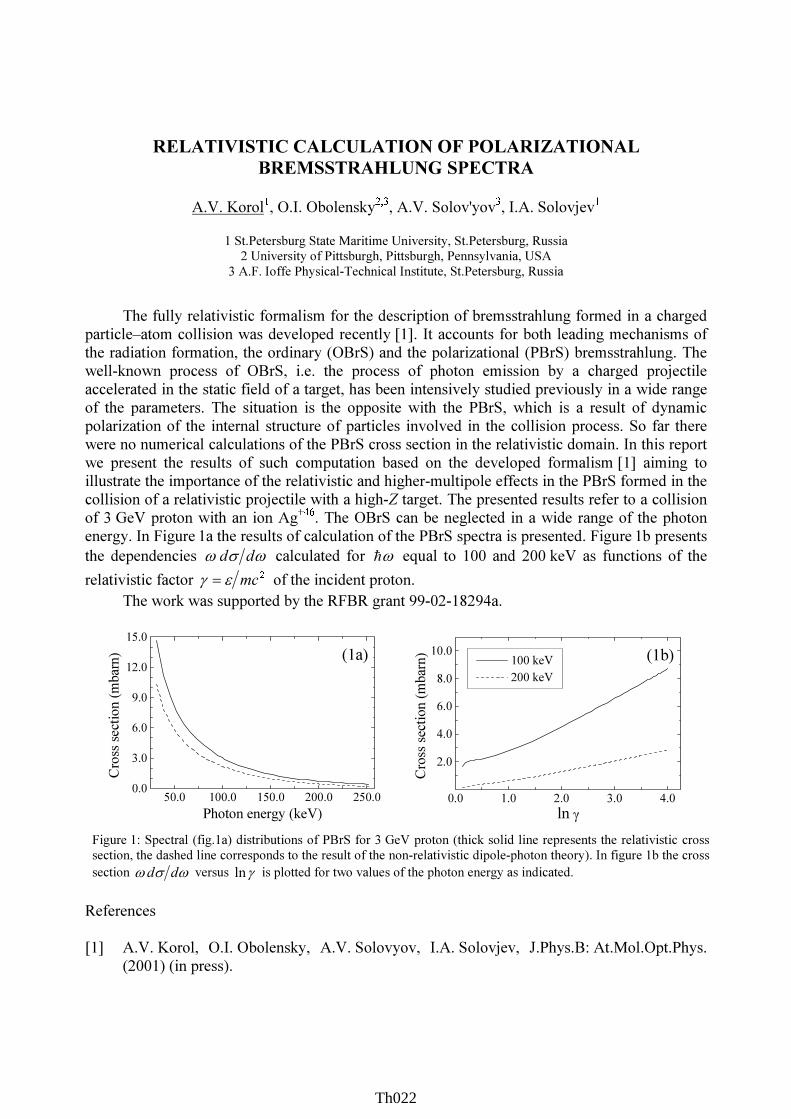
! "##
$%"" #&'( &#&
(# " &""# ) &*" #" )&# )*& +&,) * ) & -. &&"# ) &#"# )"# )/01)# *2/01 #(# , ', *& " 0 # *& " *# &# ) * & && )# &" )" # ) )* ,) " # * (# # ** ,# # 0 ,#&# " )&*2" # & "*& ) # &*& " # , &&&"# 0& &# &)# *, * # " &# &* ) # ) * ) "-. # *& "# &)## '* "" &# 0" )# &" &* & ,###' (# * ) " &"$3 *,#(# 0& & ),) " # *# % # "&&"# 0* &* )% * # ) * ) & && ) " 4 55 ) !55 "& " #
&"& "# &) *(# ,,** )# %0 66'5!'7!68
% 9* &/"1)"0"$3 */#&) * # && &# )# ) & *)# "# ' &)* '*## 1" # & & * )", "# *# )& )
" &
-. :#09*#/!551/* 1
;55 555 ;55 !555 !;5555
$5
<5
65
!5
;5
/1
= &/1
# / 155 5 !5 $5 85
!5
85
<5
75
55 /1
55 !55
= &/1
Th022Th001Th022

THE LOCAL GEOMETRICAL STRUCTURE OF AL-TRANSFERRIN PROBED BY XANES SPECTROSCOPY
A.V.Soldatov1, G.Smolentsev1, A.Congiu-Castellano2, F. Boffi 2
1 Department of Physics, Rostov State University, Rostov-Na-Donu, Russia 2 Dipartamento di Fisica and INFM, Universitia’ la Sapienza, Roma, Italy
Transferrin is a metalloprotein found in the plasma of vertebrates. It’s role in the transport of many metal ions has biomedical relevance; of particular interest is the transport of aluminum. Knowledge of the high resolution aluminum site structure is of major benefit for understanding the mechanism of the protein- metal binding.
We have applied multiple scattering theory to simulate the Al K-XANES of serum
transferrin. The method is based on the comparison between experimental data [1] and many theoretical calculations performing by varying structural parameters. Starting from geometrical configurations around the absorber 1a8e, 1a8f and 1b3e, chosen from Protein Data Bank (PDB) [2],[3], we have generated series of models which have different first coordination shell distances. The best agreement between theoretical and experimental results is reached using 1a8e model. Although the hexacoordinated ionic radius of Al3+ is smaller with respect to the ionic radius of Fe3+ (0.54 versus 0.65 Angstrom) average Me-O and Me-N bond length have been found to be very similar when Me atom is Al and Fe. Coordination of the Al ion by the water molecule has been examined. The comparison of theoretical spectra calculated with different Al-H2O distances with experimental data shows the Al-H2O bond length is 2.05 Angstrom. References [1] A. Congiu Castellano, F. Boffi, S. Della Longa, A.Giovannelli, M. Girasole, F. Natali,
MPompa, A. Soldatov, A. Bianconi Biometals 10, 363-367 (1997) [2] PDB ID: 1a8e,1a8f. R.T.A.Macgillivray, S.A.Moore, J.Chen, B.F.Anderson, H.Baker Y.
Luo, M.Bewley, C.A. Smith, M.E.P.Murphy, Y.Wang, A.B.Mason, R.C. Woodworth, G.D.Brayer, E.N.Baker; Biochemistry 37, 7919 (1998).
[3] PDB ID: 1b3e. M.C.Bewley, B.M.Tam, J.Grewal, S.He, S.Shewry, M.E.P.Murphy, A.B.Mason, R.C. Woodworth, E.N.Baker, R.T.A.Macgillivray. Biochemistry 38, 2535 (1999).
Th023Th001Th023

ON THE STRIPPING APPROXIMATION IN THEBREMSSTRAHLUNG PROCESS.
A.V. Korol1, A.G. Lyalin2, N.B. Avdonina3, R.H. Pratt3, O. I. Obolensky3 and A.V. Solov'yov4
1 St. Petersburg State Maritime University, St. Petersburg, Russia2 Institute of Physics, St. Petersburg State University, St. Petersburg, Russia
3 University of Pittsburgh, Pittsburgh, Pennsylvania, USA4 A. F. Ioffe Physical-Technical Institute, St. Petersburg, Russia
We discuss two different approaches [1,2] for the approximate treatment of thebremsstrahlung (BrS) process of non-relativistic electrons on many-electron atomic/ionic targets,described by a total amplitude which is a sum of ordinary and polarizational BrS amplitudes.The approaches are based on the so called "stripping" effect [3] and are useful for the calculationof the BrS spectra for photon energies ω greater than the ionization thresholds of the outeratomic shells.
Figure 1: BrS cross section of 5 and 25 keV electrons on Ar and Xe atoms. Dashed lines and solid linesrepresent the exactly calculated ordinary and total BrS respectively. Chain lines correspond to the strippingapproximation of Ref. [1], full circles to the corresponding approximation of Ref. [2].
This work is supported in part by NSF grant 9970293 and RFBR grant 99-02-18294-a.
References
[1] A. V. Korol, J. Phys. B 25, L341, (1992).[2] N. B. Avdonina and R. H. Pratt, J. Phys. B 32, 4261 (1999).[3] M. Ya. Amusia, N. B. Avdonina, L. V. Chernysheva and M. Yu. Kuchiev, J. Phys. B 18,
L791, (1985).
Th024Th001Th024

ATOMIC ORIGIN OF CORE-LEVEL SHIFTS BY PHOTOELECTRONDIFFRACTION
R. Gunnella1
1 INFM, Univ. of Camerino , 62032 Camerino (MC)-Italy
Surface core-level shifts of photoemission peaks richen adequately the wealth ofinformation available to a photoemission investigation. In fact the intensity and resolutionpresently available at new synchrotron radiation sources makes surface core-level photoemissionable to solve chemistry and structure of surfaces and interfaces with a sensitivity which is notcommonly reachable by other surface science techniques. In spite of these many assets toexploit, only seldom an indisputable approach to photoemission core-level shifts data is reported,mainly because of the unknown atomic origin of such core level shifts. To this aim the use ofmethods to assign atomic origins to surface core-level peaks is necessary and hopefully leadingto great advantages in the study of surface properties. A method to cope with such a challengingtask is the photoelectron diffraction from surface shifted core-levels (SCLS-PD) [1-3]. We shallpresent the rationale of the analyses of SCLS –PD for several semiconductors (Si(001)-2x1,As/Si(111), As(Sb)/Si(001)-2x1, Ge(001)-c(4x2)) [1-7] and metal surfaces systems ( 0/Ag(100))[8] and the status of the evolution of photoelectron diffraction analyses from both sides ofdeconvolution of raw data and the calculations of photoemission angular cross-section by meansof full multiple scattering approach [2-3] with complex potential. Results will be compared withfinal state calculations present in literature.
The quantitative analyses of several SCLS’s will be compared with the semi-classicalanalyses of core level intensities and escape depth attenuation. In particular some conclusionswill be drawn about the limits of application of the semi-classical approach to the analyses ofcore level shifts. The question of branching ratio variations (mainly in d core levels) [9] will beaddressed and the applications of a spin dependent multiple scattering calculations will be shownto the aim of increasing the level of completeness of the investigation.
References[1] E.L.Bullock et al. , Phys. Rev.Lett.74 , 2756 (1995).[2] R. Gunnella et al., Phys. Rev.B 57 ,4154 (1998).[3] R.Gunnella et al. , Comput.Phys.Comm.132, 251 (2000).[4] R.Gunnella et al., Surf.Sci.,352-354 ,332 (1996).[5] P. De Padova et al. , Surf. Sci to be published (2001).[6] R. Gunnella, submitted (2001).[7] L. Ferrari et al., Surf. Sci to be published (2001).[8] M. Rocca et al., Phys. Rev.B 61 213 (2000).[9] E.L.Bullock et al. , Surf. Sci. 352-354 ,352 (1996).
Th025Th001Th025

Resonant X-Ray Scattering on YTiO3 and YVO3
Manabu Takahashi and Jun-ichi Igarashi
Faculty of Engineering, Gunma University, Kiryu, Gunma 376-8515, Japan
We investigate the eect of the crystal structure to the resonant X-ray scattering
(RXS) intensities on the Ti K edge region of YTiO3 and V K edge region of YVO3 using
the band structure calculation combined with the local density approximation.
The resonant X-ray scattering spectroscopy has attracted much attention because this
experimental method is considered as one of the most powerful tools which can directly
observe the orbital order in the strongly correlated systems. Despite much eort so far,
how and to what extent the RXS spectra re ect the orbital order are still controver-
sial, especially on the perovskite compounds, because the JahnTeller distortion and the
GdFeO3 type distortion, which can also gives rise to the RXS intensity, are present.
In this study we exclude the eect of the orbitally polarized 3d state. The calculated
spectra consist of several peaks as a function of photon energy in agreement with the recent
experiments[1,2]. It is also found that the spectra for the (100) re ection are strongly
aected by the JahnTeller distortion (see Fig. 1), although the spectra for the (001) and
(011) re ections are not so aected. This result is consistent with the experiment on YVO3
[1]. Because the eects of the orbitally polarized 3d state are excluded in our calculation,
our results show that the RXS intensity arises due to the distorted crystal structure, i.e.,
the tilt of the TiO6 or VO6 octahedra and the Jahn-Teller distortion, which considerably
modies the 4p states in the intermediate states of the dipolar process. This casts doubt
on a simple interpretation that the resonant x-ray scattering is a direct observation of the
orbital order.
0 10 20 30Energy [eV]
0.0
0.5
1.0
1.5
Inte
nsity
[arb
. uni
ts]
0 10 20 30 40Energy [eV]
LT (100) HT (100)σ−π’ σ−π’
Fig. 1 Calculated RXS spectra as a function of photon energy for the 0 (100) re ection on YVO3. In
the left panel the crystal structure in the low temperature phase is assumed and the right panel that in
the high temperature phase is assumed. The Jahn-Teller distortion almost vanish in the high temperature
phase. The origin of energy corresponds to the energy of photon which excites an electron from the 1s
state to the Fermi level.
References
[1] M. Noguchi, A. Nakazawa, T. Arima, Y. Wakabayashi, H. Nakao, and Y. Murakami:
Phys. Rev. B 62 (2000) R9271
[2] H. Nakao, Y. Wakabayashi, T. Kiyama and Y. Murakami: unpublished.
Th026Th001Th026

Resonant x-ray scattering from the quadrupole
ordered phase of rare-earth compounds
Tatsuya Nagao and Jun-ichi Igarashi
Faculty of Engineering, Gunma University, Kiryu 376-8515, Japan
We report the calculated results of the resonant x-ray scattering (RXS) spectra for the superlattice
spots near Ce LIII absorption edge in the quadrupolar ordered phase of CeB6. We treat the 5d states
of Ce as a band and the 4 f states as localized states. We obtain a large intensity in the dipolar
process, which arises mainly from the 5 d states modulated by the quadrupole order of the 4 f states
through the intra-atomic Coulomb interaction. This contrasts with the RXS spectra near the Mn K
edge in LaMnO3[1], where the 4 p states are so extended that they are mainly modulated by the Jahn-
Teller distortion through neighboring oxygen potentials[2,3,4]. As shown in Fig. 1, the temperature
dependence of the RXS intensity is found to resemble closely to the variation of the order parameter
of the quadrupole order[5], in agreement with the recent experiment. The magnetic eld dependence
indicates that the induced dipolar and octapolar order have little in uence on the RXS intensity. We
also discuss the azimuthal angle dependence of the intensity.
0 3 6T [K]
0
4
8
12
Inte
nsity
(×
10−
4 )
σ − σ’σ − π’
H // (1,1,−2)
H=4[T]
H=3[T]
H=2[T]
H=1[T]
H=0[T]
Figure 1: Temperature dependence of the RXS intensities. The elds are applied in (1; 1;2) direction. Solid and broken
lines are the intensities for the 0 and
0 polarizations, respectively.
References
[1] Y. Murakami, J. P. Hill, D. Gibbs, M. Blume, I. Koyama, M. Tanaka, H. Kawata, T. Arima, Y.
Tokura, K. Hirota and Y. Endoh, Phys. Rev. Lett. 81 (1998) 582.
[2] I. S. Elmov, V. I. Anisimov and G. Sawatzky, Phys. Rev. Lett. 82 (1999) 4264.
[3] M. Benfatto, Y. Joly and C. R. Natoli, Phys. Rev. Lett. 83 (1999) 636.
[4] M. Takahashi, J. Igarashi and P. Fulde, J. Phys. Soc. Jpn. 68 (1999) 2530.
[5] R. Shiina, H. Shiba and P. Thalmeier, J. Phys. Soc. Jpn. 66 (1997) 1741.
Th027Th001Th027

THEORETICAL STUDY OF PHOTOIONIZATION PROCESSES INORGANOMETALLIC COMPOUNDS
G. Fronzoni, M. Stener and P. Decleva
Dipartimento di Scienze Chimiche, Universita’ di Trieste,Via L. Giorgieri 1, I-34127 TRIESTE – ITALY
Density Functional calculations have been carries out to determine the photoionization cross
sections and the asymmetry parameter profiles of organometallic compounds, using an explicit
treatment of the continuum wave-function. An accurate numerical treatment is employed to
ensure convergence of the calculated photoemission profiles without further potential
approximation. All valence and carbon and metal core ionizations are investigated over a wide
energy range. A very satisfactory agreement is obtained with the many experimental data
available for this molecule, indicating that the present LDA level of theory is generally adequate
to interpret the complete photoemission spectra in organometallic compounds, with the only
exception of autoionization resonances, allowing to extract from the spectra chemically relevant
information and to resolve uncertain assignment. The analysis of the calculated cross sections
allows to definitely uphold the experimental assignment of the first four outer valence
ionizations and furthermore suggests that characteristic behaviours can be recognized also in the
core metal cross section profiles.
Th028Th001Th028

CALCULATIONS OF PHOTOEMISSION PROFILES OF C60 ANDENDOHEDRAL COMPOUNDS
P. Decleva, G. Fronzoni and M. Stener
Dipartimento di Scienze Chimiche, Universita’ di Trieste,Via L. Giorgieri 1, I-34127 TRIESTE – ITALY
Extensive calculations of cross section and asymmetry parameter of C60 and M@C60
(M = alkaline or alkaline-earth metal) have been carried out employing a local density approach
and a convergent one center expansion. Good agreement with available experimental data is
obtained for C60, and new resonances predicted in M@C60.
In particular results for total cross section and HOMO/HOMO-1 oscillations up to high
energy will be presented. Resonances in M@C60 are interpreted by analysing the final dipole
projected continuum wavefunction.
Th029Th001Th029

!"#$%"&'#($)*$$+"),)#-#.,/)0$%&,#--1,#$%'#.,/&
!"#"$%&'()*+,-.%/.0..1"$%.2*3+4%.5/.%67.8"!"9()&6-+():%.5/.%/.;"<"=3&6%,>:.?6+@4@3@).>A.#)6)&%B.%67.?6>&C%64D.9()*4+@&-.>A.E3++4%6.2D%7)*-.>A.<D4)6D)+0.FG.8)646+,-0GGHHHG0.1>+D>I0.E3++4%0.)J*%4B.:C-%&K4C4D"&%+"&35/.2"L"?>AA)..M(-+4D%B.N)D(64D%B.?6+@4@3@)0.M>B4@),(64D()+,%-%.OP0.GHQROG0.<@"M)@)&+53&C0.E3++4%
N().D>&&)B%@4>6.+%@)BB4@).G+JG.O+JGS.F</F+SO</.>A.;).G+.T(>@>4>64'%@4>6.UGV..I%+.@().A4&+@
)W%*TB).>A.%.L%6>J@-T).B46)+(%T).46.T(>@>)B)D@&>6.+T)D@&%".N().%+-**)@&-.>A.@().+%@)BB4@)
B46)+(%T)+.D>*)+.A&>*.@I>.74AA)&)6@.)AA)D@+.X.A&>*.46@)&A)&)6D).5)@I))6.74&)D@.+(%,)J>AA
)WD4@%@4>6.UG0OV.%67.)WD4@%@4>6.:4%.&)+>6%6D).%67.A&>*.+@&>6C.7)T&)++4>6.>A.@().B>IJ546746C
)6)&C-.+47).>A.%.+%@)BB4@).B46).UOV".N().A4&+@.)AA)[email protected]+.+4*4B%&.@>.@(%@.@%,46C.TB%D).46.&)+>6%6@
T(>@>%5+>&5@4>60.I(4B).@().+)D>67.4+.%.D>6+)Y3)6D).>A.@().D>&&)B%@4>6.6%@3&).>A.T(>@>)B)D@&>6
+%@)BB4@).&)+>6%6D)+.UOV".?6.@().T&)+)[email protected]>&,.@().B46)+(%T).>A.@().+%@)BB4@).G+JG.O+JGS.F</F+SO</.4+
D%BD3B%@)7.*%,46C.3+).>A.T)&@3&5%@4>6.)WT%6+4>6.3T.@>.@().F&7.>&7)&.%67.B4*4@)7.63*5)&.>A.@().Q@(
>&7)&.74%C&%*+.4+.%B+>.@%,)6.46@>>.%DD>36@".N()>&)@4D%B.&)+3B@+.%&).46.)WD)BB)6@.%C&))*)[email protected]@(
@().)WT)&4*)6@".S+)).L4C3&)/".N()>&-.4+.%TTB4)7.@>.>@()&.T(>@>)B)D@&>6.+%@)BB4@)+.%B+>"
N().I>&,.4+.+3TT>&@)7.5-.?6@)&6%@4>6%B.<D4)6D).%67.N)D(6>B>C-.9)6@)&.SC&%[email protected][/"
L4C3&)".N()>&)@4D%B.%67.)WT)&4*)6@%B.UGV.ST>46@+/.+%@)BB4@).B46)+(%T) "
E)A)&)6D)+G".<"<:)6++>60.\"]&4D++>60.;"1%&@)6++>60.#"^)6746..%67._"#)B43+0.`"]B)D@&>6<T)D@&>+D"E)B%@"M()6>*".23.SGH[[/.FOa"O".!"#"$%&'()*+,-.%67.L"M"8%&,46+0.]3&".M(-+".`".b.4.SGHHH/.GaH"
!! !" !# !$ !% "& "' "( ")&*&&
&*&'
&*&(
&*&)
&*&+
&*&!
&*&"
,-.'
/ 0 1 2 , . 3 4 5 , 6 , 7 8 9 5 : , - ;
5, <4 , 7=55>0 , ? 79
Th030Th001Th030

Energies and autoionization widths in the lithium
iso-electronic sequence
J. E. Hansena and G. Verbockhavena,b
aDepartment of Physics and Astronomy, University of Amsterdam,
Valckenierstraat 65, NL-1018XE Amsterdam, The Netherlands
bPresent address: Department of Theoretical Chemistry, University of Nijmegen, The Netherlands
Energies and autoionization widths are presented for autoionizing states in Li I,
Be II and B III lying between the 1s2 and the 1s2s 3S ionization limits. A
conguration interaction expansion combined with a B-spline basis set has been
used to compute the properties of the lowest 2Se, 2Po and 2De states which are, in
the LS approximation, the only terms allowed to autoionize. The comparison with
theoretical and experimental data shows the high accuracy of the B-spline approach
applied to singly core-excited states. The error on the energies is found, in the case
of Li I, to be well below 10 meV in general, while for Be II and B III, for which
much less is known, the theoretical results points to the need for more accurate
measurements. Several new identications have been made and some identications
revised in the experimental data.
Th031Th001Th031
MULTIPLE SCATTERING THEORY OF PHOTOELECTRON ANGULARDISTRIBUTIONS FROM ORIENTED DIATOMIC MOLECULES
R. Díez Muiño1,2, D. Rolles2,3, F. J. García de Abajo2,4, C. S. Fadley2,5, and M. A. Van Hove2,5,
1 Donostia International Physics Center, 20018 San Sebastián (Spain)2 Lawrence Berkeley National Laboratory, Berkeley, California 94720 (USA)
3 Fritz-Haber-Institut der Max-Planck-Gesellschaft, D-14195, Berlin (Germany)4 Centro Mixto CSIC-UPV/EHU, 20080 San Sebastián (Spain)
5 University of California at Davis, Davis, California 95616 (USA)
Angular distributions of electrons photoemitted from oriented molecules have become anexciting new tool for studying electronic structure and dynamics [1-3]. We use multiplescattering photoelectron diffraction (MSPD) theory to calculate the final-state wavefunction ofthe electron leaving the molecule, and then subsequently its angular distribution. For low (E < 50eV) kinetic energies of the photoemitted electron, the electron scattering cannot be adequatelyrepresented by spherically-symmetric potentials. We thus include non-spherical scatteringpotentials in our formalism through non-diagonal scattering matrices.
As examples, we calculate the angular distributions of photoelectrons emitted from the Kshell of oriented gas-phase CO and N2 molecules, as recently measured by several groups [1-3].We show that intramolecular scattering and interference are responsible for the experimentallymeasured patterns. Particularly important are the energies for which shape resonances appear inthe continuum, with the angular distributions showing radical changes over such resonances. Wecalculate the final photoelectron angular patterns for different polarizations of the light (linearand circular), and discuss the issue of coherence in the photoemission from equivalent centers ofhomonuclear molecules (such as N2). This MSPD approach represents a more accurate andversatile method for dealing with such angular distributions as compared to prior calculations ofthese effects [4].
References
[1] F. Heiser et al., Phys. Rev. Lett. 79, 2435 (1997).[2] E. Shigemasa et al., Phys. Rev. Lett. 80, 1622 (1998).[3] T. Weber et al., (submitted to J. of Phys. B).[4] D. Dill, J. Siegel and J. L. Dehmer, J. Chem. Phys. 65, 3158 (1976).
Th032Th001Th032

HIGH RESOLUTION SPECTROSCOPY
Th033

Th034

HIGH-RESOLUTION X-RAY PHOTOELECTRON SPECTROSCOPYSTUDIES OF THIOL-DERIVED SELF-ASSEMBLED MONOLAYERS
M. Zharnikov1, K.Heister1, L.S.O. Johansson2, H.T. Rong1, M. Buck1,3, M. Grunze1
1 Angewandte Physikalische Chemie, Universität Heidelberg, 69120 Heidelberg, Germany2 Department of Physics, Karlstad University, 65188 Karlstad, Sweden
3 School of Chemistry, University of St Andrews, Fife KY16 9ST St Andrews, Scotland
We have firstly applied the synchrotron-based high resolution XPS to study thiol-derivedself-assembled monolayers (SAMs) with an emphasis on the SAM/metal interface. Themeasurements were performed at the synchrotron storage ring MAX II at MAX-Lab in Lund,Sweden. The variable photon energy of the synchrotron light and a high energy resolution of thespectrometer (better than 0.1 eV) enabled us to resolve the bulk and surface components of thesubstrate emission peaks (Au4f/Ag3d) and monitor the evolution of these components upon theformation of SAMs from both thioaliphatic [C12: CH3(CH2)11SH] and thioaromatic [BPT:CH3(C6H4)2SH] molecules (Fig. 1). Simultaneously, the interaction of the thiol-derivedmolecules with the substrate was followed by monitoring the S 2p doublet attributed to the sulfurhead group of these molecules (Fig. 2). Only one sulfur species was found in the densely packedSAMs, which implies an equivalent bonding geometry for all adsorbed molecules. In SAMscomprising of specially designed, mixed aliphatic-aromatic molecules a periodical, "odd-even"shift of the S 2p binding energy with the varying length of the aliphatic part was observed. Thisshift was attributed to the distortion of the substrate-S-C bonding angle resulting from either thefavorable or unfavorable package conditions occurring at the varying length of the aliphatic part.This work has been supported by the German Bundesministerium für Bildung und Forschungthrough grant No. 05 SL8VHA 2 and by DAAD (313/S-PPP-pz).
Figure 1: Au 4f HRXPS spectra of clean andC12/BPT covered gold substrate.
Figure 2: S 2p HRXPS spectra of AT and BPT SAMson Au and Ag. The BEs and FWHMs of the S 2p3/2,1/2peaks are indicated.
Th035

High Resolution Si 2p Photoelectron Spectroscopy For Molecular Adsorption on Si(100)c(4x2)
Y. Yamashita, M. Nagao, S. Machida, K. Hamaguchi,F. Yasui, K. Mukai, and J. Yoshinobu
The Institute for Solid State Physics, The University of Tokyo 5-1-5 Kashiwanoha, Kashiwa, Chiba 277-8581, Japan
(e-mail:[email protected])
In recent years, there has been a great interest in molecule-silicon systems, concerningthe application to molecular scale devices [1,2]. For the systems, the interface bonding betweenmolecule and Si substrate is very important. High resolution Si 2p spectroscopy provides crucialinformation about the interface bonding and the charge transfer between molecule and Si. In thepresent study, we have investigated several molecule-silicon systems by means of highresolution Si 2p photoelectron spectroscopy.
The experiments were performed using a BL-16B with an undulator radiation source ofPhoton Factory at High Energy Accelerator Research Organization in Tsukuba, Japan. In theexperiments, the total energy resolution was estimated to be below 80 meV at the photon energyof 130 eV. Photoelectron spectra were measured at ~100 K for clean Si(100)c(4x2) surface andchemisorption layer on Si(100)c(4x2).
For the clean Si(100)c(4x2) surface, we could resolve five components in the Si 2pspectra by carefully analyzing the spectra recorded at several photon energies and emissionangles. They are attributed to the bulk, up dimer atom, down dimer atom, subsurface, andunidentified species [3]. After adsorption of unsaturated hydrocarbon molecules (ethylene,cyclopentene, and 1,4-cyclohexadiene), the peaks corresponding to the up and down atoms of theasymmetric dimers almost vanish, while new peaks are observed between 215 and 398 meVrelative to the bulk Si peak. These new peaks are assigned to the Si-C bonds, considering thatthe C atom is more electronegative than the Si atom and the area intensity of the Si-C peak isalmost the same as the sum of consumed intensities of both up and down dimer atom peaks.Furthermore, we have estimated the charge transfers between the adsorbed molecules and the Sisurface, where they depend on the molecules.
References
[1] R. A. Wolkow, Annu. Rev. Phys. Chem., 50 (1999) 413.[2] J. T. Yates Jr, Science, 279 (1998) 335.[3] Y.Yamashita, et al, J. Electron Spec. Relat. Phenom., 114-116 (2001) 389-393.
Th036

HIGH-RESOLUTION ANGLE-RESOLVED ION-YIELD SPECTRA OF NO2 IN THE N AND O K-EDGE REGIONS
K. Okada1, K. Ueda2, Y. Shimizu3, N. Saito4, A. De Fanis2, Y. Tamenori5, K. Kubozuka6,
S. Tanimoto1, T. Ibuki7, and I. Koyano6
1 Department of Chemistry, Hiroshima University, Higashi-Hiroshima 739-8526, Japan 2 Institute of Multidisciplinary Research for Advanced Materials, Tohoku University, Sendai 980-8577, Japan
3 Institute for Molecular Science, Okazaki 444-8585, Japan 4 National Institute of Advanced Industrial Science and Technology, Tsukuba 305-8568, Japan 5 SPring-8/Japan Synchrotron Radiation Research Institute, Mikazuki, Hyogo 679-5198, Japan
6 Department of Material Science, Himeji Institute of Technology, Kamigori, Hyogo 678-1297, Japan 7 Kyoto University of Education, Kyoto 612-8522, Japan
The photochemistry of nitrogen dioxide (NO2) molecule is practically of interest from the
environmental viewpoint, playing a critical role in the stratospheric NOx cycle and also in the atmospheric photochemical smog cycle [1]. The NO2 molecule presents some similarities to the CO2 molecule from the physicochemical point of view, because it is an oxide where the central atom is replaced by the nitrogen. It is a bent triatomic molecule with terminal oxygen atoms, similar to O3 in this sense. Despite these fundamental interests and practical needs for photochemical information for NO2, spectroscopic studies are still rare, especially in the soft X-ray region. Thus, in the present study we have measured the high-resolution angle-resolved ion-yield spectra of NO2 in the N and O K-edge regions. It is well known that the inner-shell angle-resolved ion-yield spectroscopy is a powerful probe of symmetries of the excited states as well as the geometric structures [2].
The experiments were performed on the soft X-ray photochemistry beamline BL27SU at SPring-8. A pair of energetic-ion detectors of retarding-potential type is mounted horizontally and vertically in the main chamber. Angle-resolved energetic-ion yield curves of the NO2 were measured with the applied retarding voltage of 6.4 V. The sample gas was introduced coaxially with the photon beam from a gas nozzle positioned downstream. We also measured the total ion-yield (TIY) curve simultaneously with the energetic-ion yield curves.
The N 1s and O 1s spectra of NO2 obtained in the present study are similar to those reported by Zhang et al. [3], but are resolved much better especially for the Rydberg transitions. For example, peaks with the principal quantum numbers of up to 6, at least, are discernable in the present N 1s TIY spectrum. Under the axial-recoil approximation and utilizing the simple vector algebra, the symmetries of the inner-shell excited states can be deduced from angular distribution of the fragment ions. A shoulder at 409.97 eV in the TIY spectrum, for example, is assigned as the transition to 3pb1, because this peak is observed only in the spectrum recorded in the direction perpendicular to the polarization vector. In this way, we could establish the assignments unambiguously of the N 1s and O 1s inner-shell spectra of NO2 based on the angular distribution data for the energetic ions. References [1] I. M. Campbell, “Energy and the Atmosphere,” Wiley, London (1977). [2] A. P. Hitchcock and J. J. Neville, in: T. K. Sham (Ed.), “Chemical Applications of
Synchrotron Radiation,” World Scientific, Singapore, in press. [3] W. Zhang, K. H. Sze, C. E. Brion, X. M. Tong, and J. M. Li, Chem. Phys. 140, 265 (1990).
Th037

PHOTOELECTRON SPECTROMETRY OF ATOMIC Fe IN
THE REGION OF THE 3p! 3d GIANT RESONANCE
S. B. Whiteld1, R. Wehlitz2, M. O. Krause3, and C. D. Caldwell4
1Dept. of Physics and Astronomy, University of WisconsinEau Claire, Eau Claire, WI 547022Synchrotron Radiation Center, Stoughton, WI 53589
3Dept. of Physics, University of Central Florida, Orlando, FL 328164National Science Foundation, 4201 Wilson Blvd., Arlington, VA 22230
To date, wide ranging and systematic studies of open-shell atoms are still largely lacking
[1], particularly when compared to the enormous amount of work that has been carried out
on closed-shell atoms, chie y the rare gases. Due to the non-isotropic charge distribution in
the ground state of most open-shell atoms, interesting eects in the photoionization process
can arise which will not occur in a closed-shell atom.
0
2
4
6
3d-1(6S)
No
rma
lize
d C
ou
nts
(x
103 )
0
10
20
303d-1(4G)
0
2
4
6
3d-1(4P)
0
3
6
93d-1(4D)
48 50 52 54 56 58 60 62 64 66 68
0
5
10
15
20
3d-1(4F)
Photon Energy (eV)
Figure 1: Atomic Fe 3d-mainlines in the region of
the 3p! 3d giant resonance.
Atomic Fe, [Ar]3d64s2(5D4), is an in-
triguing candidate for study because of its
partially lled d subshell. In this poster we
will present a systematic and comprehensive
study of the partial cross sections of the 3d
and 4s mainlines and associated satellites in
the region of the 3p ! 3d giant resonance.
One characteristic of open-shell atoms is the
multiplet structure of the residual photoion.
Following the removal of a 3d electron in
atomic Fe, ve 3d photopeaks are produced:
the 3d1(6S), 3d1(4G), 3d1(4P ), 3d1(4D),
and 3d1(4F ). The relative partial cross
sections of each of these lines is shown in
gure 1. All spectra have been normalized
with respect to each other so that a direct
comparison of their relative intensity can
be made. As can be seen from the data,
all lines except the 3d1(6S) clearly show
the presence of two broad asymmetric reso-
nances. Our results are in accord with ear-
lier measurements at lower resolution with
poorer statistics [2]. In contrast to those
measurements, however, we were able to completely separate the 3d(4G) and 3d(4P ) peaks.
References
[1] M. O. Krause, Nucl. Instrum. Meth. B 87, 178 (1994).
[2] M. Meyer, Th. Prescher, E. von Raven, M. Richter, E. Schmidt, B. Sonntag, and
H.-E. Wetzel, Z. Phys. D 2, 347 (1986).
Th038
Vikki Goddard, Head of Planning and Development 26/02/01
Disorder broadening of core level lineshapes in alloys:Surface contributions.
P. Weightman and A. NewtonSurface Science Research Centre, University of Liverpool, Liverpool, L69 3BX, UK.
The electrostatic energy of arrays of charges has attracted attention since the work of Madelungand the concepts of electronegativity and ionicity are important in chemistry. However “chargetransfer” is not a quantum mechanical observable and the lack of an agreed definition has limitedthe usefulness of the concept. This is a particular difficulty in the study of metal alloys where theeffects of charge transfer between alloy constituents play an important role in order-disordertransitions.
Recently a new method of defining and measuring charge transfer based on highresolution measurements of core level photoelectron lines has been developed [1,2]. In theanalysis of such data it is important to allow for the effects of surface core level shifts. In thiswork the influence of surface core level shifts on the analysis of the disorder broadening of corelevel lineshapes in CuPd alloys is considered.
1 R.J. Cole, N.J. Brooks and P. Weightman, Phys. Rev. Lett. 78 3777-80 (1997)2 R.J. Cole, N.J. Brooks and P. Weightman, Phys. Rev. B56 12,178-82 (1997).
Th039

HIGH-RESOLUTION SURFACE CORE-LEVELS OFGaAs(001) SURFACES
K. Ono1, T. Mano1, K. Nakamura1, M. Mizuguchi1, S. Nakazono1, H. Kiwata1, K. Horiba1,T. Kihara1, J. Okabayashi2, A. Kakizaki3, M. Oshima1
1 Graduate School of Engineering, University of Tokyo, Tokyo 113-8656, Japan2 Department of Physics, University of Tokyo, Tokyo 113-0033, Japan
3 Institute for materials Structure Science, KEK, Tsukuba 305-0801, Japan
GaAs(001) surface is the most widely used surface for high-speed and opto-electronicdevices. This surface has been extensively investigated in the last two decades with its varioussurface reconstructions. However, only few photoemission studies have been done because ofthe difficulty in the combination of synchrotron radiation photoemission system with MBE.
In this contribution, we have installed an MBE system to the photoemission endstation atBL-1C of the Photon Factory [1], and measured a high-resolution core-levels for GaAs(001) –c(4x4), (2x4), (4x2) and (4x6) surfaces. An n+-GaAs(001) epiready substrate was used. Afterremoving surface oxides, a 3000Å GaAs buffer layer was grown under optimized conditions.The surface structures were monitored by RHEED during the growth. The photoemissionmeasurements were carried out with the photon energy of 100 eV. Figure 1 shows thephotoemission spectra of As 3d and Ga 3d core-levels with 0˚ and 60˚ emission angles. Thesurface structures were checked by LEED before and after each measurement. We havedetermined the surface core-level shift (SCLS) from chemically inequivalent surface sites andcompared with the previously proposed surface structure models. We have successfullydetermined the surface structures and chemical bondings for the reconstructed surfaces.
Figure 1: (a) Ga 3d, and (b) As 3d photoemission spectra for the c(4x4)-GaAs(001) surface with 0˚ and 60K emission angles.
References[1] K. Ono et al., Nucl. Inst. Meth. A, in press.
Th040

,17(5)(5(1&(())(&76,1$872,21,=$7,2163(&75$2%6(59('$7/DG(;&,7$7,216,1/D)$1'/D&O
55XXV$.LNDV(1PPLVWH$6DDUDQG,0DUWLQVRQ
,QVWLWXWHRI3K\VLFV8QLYHUVLW\RI7DUWX5LLD7DUWX(VWRQLD'HSDUWPHQWRI$WRPLF6SHFWURVFRS\/XQG8QLYHUVLW\3URIHVVRUVJDWDQ6/XQG6ZHGHQ
5HVRQDQWSKRWRHPLVVLRQE\XVLQJWXQHDEOHUDGLDWLRQZLWKKLJKPRQRFKURPDWLFLW\KDVEHHQDQ LPSRUWDQW WRRO LQ WKH VWXG\ RI LQWHUIHUHQFH SKHQRPHQD LQ WKH UHJLRQ RI DXWRLRQL]DWLRQUHVRQDQFHV$UHVRQDQWHQKDQFHPHQWRI WKHHOHFWURQHPLVVLRQIURPFRUH OHYHOV LVFDXVHGE\DQLQGLUHFW SURFHVV DVVRFLDWHG ZLWK WKH $XJHU GHFD\ RI WKH LQWHUPHGLDWH VWDWH UHDFKHG E\ WKHSKRWRH[FLWDWLRQZKLFK KDV WKH VDPH LQLWLDO DQG ILQDO VWDWHV DV D GLUHFW SKRWRHPLVVLRQ SURFHVV$GGLQJ WKH DPSOLWXGHV RI ERWK SDWKV JLYH ULVH WR LQWHUIHUHQFHV WKDW SURGXFH WKH FKDUDFWHULVWLF)DQRW\SHSURILOHIRUH[DPSOHLQWKHFRQVWDQWLQLWLDOVWDWHVSHFWUD
7KHUHVRQDQWSKRWRHPLVVLRQVSHFWUDIURPODQWKDQXPGSDQGVFRUHOHYHOVLQ/D)DQG/D&OKDYHEHHQPHDVXUHGLQWKHYLFLQLW\RIWKH0DEVRUSWLRQHGJHVRI/D,WLVVKRZQWKDWWKHVSHFWUD H[FLWHG DW G GI DXWRLRQL]DWLRQ UHVRQDQFHV H[KLELW D YHU\ VWURQJ LQWHUIHUHQFHHIIHFWV7KHDQRPDORXVEHKDYLRXURIWKHLQWHQVLW\UDWLRRIGDQGGDVZHOODVSDQGSSKRWROLQHVRI/DDWWKHUHVRQDQFHH[FLWDWLRQHQHUJLHVLVIRXQGDQGDWWULEXWHGWRWKHVWURQJWHUPGHSHQGHQFHRIWKHDXWRLRQL]DWLRQSURFHVV)RULQVWDQFHLQ)LJZHKDYHGHPRQVWUDWHGKRZWKHGHVWUXFWLYH LQWHUIHUHQFHIRU ODUJHUSKRWRQHQHUJLHV\LHOGV WR WKHFRPSOHWHFDQFHOODWLRQRI/DVSKRWROLQH7KHH[SHULPHQWVKDYHEHHQSHUIRUPHGDWEHDPOLQH'DW0$;,,DQGDWEHDPOLQHRI0$;,VWRUDJHULQJLQ0$;ODE/XQG6ZHGHQ
/DV/DS&OV9%
,QWHQV
LW\DUEX
%LQGLQJ(QHUJ\H9
/D0
3KR
WRQ(QH
UJ\H
9
$EVRUSWLRQ
)LJXUH5HVRQDQWSKRWRHPLVVLRQVSHFWUDIRU/D&O LQWKHUHJLRQRI/DS DQG V SKRWROLQHV OHIW SDQHO H[FLWHG DURXQG WKH ODQWKDQXP 0
DEVRUSWLRQPD[LPXPULJKWSDQHO
Th041

HIGH-RESOLUTION SURFACE CORE-LEVELS OFGaAs(111)B SURFACES
K. Ono1, K. Nakamura1, T. Mano1, M. Mizuguchi1, S. Nakazono1, H. Kiwata1, K. Horiba1,T. Kihara1, J. Okabayashi2, A. Kakizaki3, M. Oshima1
1 Graduate School of Engineering, University of Tokyo, Tokyo 113-8656, Japan2 Department of Physics, University of Tokyo, Tokyo 113-0033, Japan
3 Institute for materials Structure Science, KEK, Tsukuba 305-0801, Japan
GaAs is the most widely used compound semiconductor for high-speed and opto-electronicdevices. GaAs(111)B surface is used as a substrate for InGaAs quantum wells which exhibit alarge piezoelectric effect in opto-electronic devices. Although GaAs(001) surface has beenextensively investigated in the last two decades, GaAs(111)B surface is very poorly understood.
We have installed an MBE system to the photoemission endstation at BL-1C of the PhotonFactory [1], and measured high-resolution core-levels for GaAs(111)B – (2x2) and (√19x√19)surfaces. An n+-GaAs(111)B epiready substrate was used. After removing surface oxides, a1000Å GaAs buffer layer was grown under optimized conditions. The surface structures weremonitored by RHEED during the growth. The photoemission measurements were carried outwith the photon energy of 100 eV. The photoemission spectra of As 3d (results in (2x2) surfaceis shown in Fig. 1) and Ga 3d core-levels with 0˚ and 60˚ emission angles were measured. Thesurface structures were checked by LEED before and after each measurement. We havedetermined the surface core-level shift (SCLS) from chemically inequivalent surface sites andcompared with the proposed surface structure models. We have successfully determined thesurface structures and chemical bondings for the reconstructed surfaces of GaAs(111)B.
As 3d100eV
52 53 54 55 56
Pho
toel
ectr
on In
tens
ity (
arb.
uni
t)
Kinetic Energy (eV)
60˚
0˚
Figure 1: As 3d photoemission spectra for the (2x2)-GaAs(111)B surfacewith 0˚ and 60˚ emission angles.
References[1] K. Ono et al., Nucl. Inst. Meth. A, in press.
Th042

HIGH-RESOLUTION Si 2P CORE-LEVEL STUDY OFTHE K/Si(111)-(3x1) SURFACE
Kazuyuki Sakamoto, H. M. Zhang, Roger I. G. Uhrberg
Department of Physics and Measurement Technology, Linköping University, S-581 83 Linköping, Sweden
Semiconductor surfaces modified by adsorption of metal atoms have been a topic of
experimental investigation for the creation of nanoscale quantum structures with high perfection.Among the great number of metal induced surface reconstructions, the alkali metal (AM)adsorbed Si(111)-(3x1) surface is one of the most well known. Several structural models have
been proposed until now for the atomic geometry of this surface. Among them, the honeycomb-chain-channel (HCC) model [1] is the energetically most stable one. However, though thepresence of at least three Si 2p surface components is suggested for the HCC model theoretically
[1], only two components are observed experimentally [2] up to now. Since the Si 2p core-levelreflects well the underlying surface geometry and the bonding configuration of the adsorbates, itis important to measure the Si 2p core-level with high-resolution to obtain a proper
understanding on the structure of the AM/Si(111)-(3x1) surface.
In this study, we have measured the Si 2p core-level of the K/Si(111)-(3x1) surface byphotoelectron spectroscopy. The high-resolution core-level PES studies were performed at
beamline 33 at the MAX-I synchrotron radiation facility in Lund, Sweden. For the most surfacesensitive measurement, we have used a photon energy of 130 eV and an emission angle of 60˚from the surface normal direction, and for the most bulk sensitive measurement, a photon energy
of 108 eV and an emission angle of 0˚ were used. Analyzing the spectra by a least-squares-fittingmethod using spin-orbit split Voigt functions, we recognize the presence of five Si 2p surfacecomponents. Among these five components, the energy shifts of three of them agree well with
the previous theoretical calculation [1]. The good agreement of these three components showsthe appropriateness of the HCC model. Moreover, the agreement in energy shifts suggests theirorigins to be the first layer Si atoms. We will also discuss the origin of the two other components
in relation to the HCC model.
References
[1] see for example, M.-H. Kang, J.-H. Kang and S. Jeong, Phys. Rev. B 58, R13359 (1998).
[2] see for example, T. Okuda et al., Surf. Sci. 321, 105 (1994).
Th043

Determination of the Scandium 2p ionization thresholds using highresolution electron spectroscopy
T. Richter1, B. Obst1∗, M. Martins2, P. Zimmermann1
1 Technische Universitat Berlin, Institut fur Atomare und Analytische Physik,
Hardenbergstraße 36, D-10623 Berlin
2 Freie Universitat Berlin, Institut fur Experimentalphysik,
Arminallee 14, D-14195 Berlin
Up to now only values for the Scandium 3p ionization thresholds have been measured [1].As an outcome of photoionization studies in the region of 2p excitation carried out at theBESSY II synchrotron radiation facility, data for the atomic 2p ionization thresholds cannow be presented (Figure 1). The data were acquired at the U49/1-SGM beamline using ahigh resolution hemispherical electron analyzer (Scienta SES 200).
The experimental results show a very good agreement with numerically calculated data.The calculations were carried out using the relativistic Hartree-Fock algorithm (Cowan code).Line assignments were done based on the numerical data.
408410412414416418
Ionisation energy / eV
0
100
200
300
Inte
nsi
ty /
a.u
.
Figure 1: Energy resolved photoelectron spectrum of directly ionized 2p Scandium electrons.
The structure is dominated by the fine structure splitting of the 2p core hole.
References
[1] K. Tiedtke, Ch. Gerth, M. Martins, B. Obst, P. Zimmermann The multiplet structure
of the 3p photoelectron spectrum of atomic Sc J. Phys. B 33, L755 (2000)
∗present address: Institut fur Plasmaphysik, c/o Fritz-Haber-Institut, Faradayweg 4-6, D-14195 Berlin
Th044

ELECTRONIC STRUCTURE
Th045Th045

Th046Th046

Th047Th047

Resonant Photoemission Study of RFe4P12 (R= La, Ce, Pr)
H. Ishii, T. Miyahara, Y. Takayama, K. Obu, M. Shinoda, C. Lee, S. Yuasa, T. D. Matsuda, H. Sugawara and H. Sato
Graduate School of Science, Tokyo Metropolitan University, Minami-Ohsawa 1-1, Hachioji, Tokyo 192-0397, Japan
Ternary intermetallic compounds RFe4P12 (R= rare earth) with the filled skutterudite structure exhibit
various interesting properties. According to the measurements using a high quality single crystal [1], CeFe4P12 shows the complex temperature dependence of resistivity unexpected for a simple single-gap semiconductor; PrFe4P12 exhibits the Kondo-like anomalies in the transport properties. In this study, we investigated the electronic states of RFe4P12 (R= La, Ce, Pr) by the high-resolution resonant photoemission spectroscopy.
The photoemission experiments were performed using synchrotron radiation at the beam line BL-11D of the Photon Factory, High Energy Accelerator Research Organization (KEK). The instrumental resolution was about 65 meV. The samples were cooled to 20 K.
Figures 1 and 2 show the resonant photoemission spectra of CeFe4P12 and PrFe4P12, respectively. The intense band located at the binding energy of ~0.7 eV is mainly due to the Fe 3d band. The 4f spectra were obtained by subtracting the resonance minimum spectra (hn = 114 eV and 115 eV) from the resonance maximum spectra (hn = 122 eV and 124 eV). The solid lines in Figs. 1 and 2 indicate the Ce 4f and Pr 4f spectra, respectively. In the Ce 4f spectrum, the f 0 and f 1 peaks are located at the binding energies of ~2.8 eV and ~0.5 eV, respectively. The large intensity ratio of the f 1 peak to the f 0 peak indicates the strong hybridization between the Ce 4f and the valence band states. However, the f5/2
1 peak located near EF was not observed apparently. We performed the analysis of the Ce 4f and Ce 3d-4f absorption spectra [2] using a single impurity Anderson model. The number of 4f electrons was estimated to be ~0.85. In the Pr 4f spectrum, the f 1 and f 2 peaks are located at the binding energies of ~4.6 eV and ~0.5 eV, respectively. The spectrum indicates that PrFe4P12 is a strongly hybridized system in Pr compounds. However, we could not observe a peak structure corresponding to the tail of the Kondo resonance peak in the vicinity of EF. Figure 1: Resonant photoemission spectra of CeFe4P12. Figure 2: Resonant photoemission spectra of PrFe4P12. Reference [1] H. Sato et al.: Phys. Rev. B 62 (2000) 15125. [2] T. Miyahara et al.: Jpn. J. Appl. Phys. 38 Suppl. 38-1 (1999) 396.
02468
122 eV114 eVCe 4f
INTE
NSI
TY
BINDING ENERGY (eV)
CeFe4P12
02468
124 eV115 eVPr 4f
INTE
NSI
TY
BINDING ENERGY (eV)
PrFe4P12
Th048Th048

10 8 6 4 2 0
C C C CC C
C C C C
C C C
x
A
B
C
D
benzene
=EF
Binding Energy / eV
Phot
oele
ctro
n In
tens
ity
Figure 1: Photoelectron spectra of cumulenetype carbyne model compounds and benzene.
Electronic Structures of Linear Carbon Chain Molecules
S. Hino1,2, Y. Okada1, K. Iwasaki1,2, M. Kijima3 H. Shirakawa3
1 Graduate School for Science and Technology, Chiba University, Chiba 263-8522 Japan2 Faculty of Engineering, Chiba University, Chiba 263-8522 Japan
3 Institute of Material Science, Tsukuba University Tsukuba 305-8573 Japan
Carbyne is a name of linearly bonded carbon atoms and it can be classified into twocategories by its bonding conditions; cumulene type having (=C=C=C=C=) bonds and polyynetype having –C≡C–C≡C– bond [1]. Carbyne is believed to be unstable so that it cannot beisolated with macroscopic quantity. Because of this nature, carbyne has not been investigatedintensively, but it is considered as an ultimate form of carbon nanotubes so that its applicationsuch as field emitter, molecular conductive wire and fibers with mechanical strength areexpected. There could be a large difference in the electronic structures of these two types, but itis difficult to deal with them because of lack of the specimens. In order to clarify the differencewe measure ultraviolet photoelectron spectra of their model compounds and examine theirelectronic structure with an aid of MO calculation.
Figure 1 shows photoelectron spectra of cumulene type model compounds terminated byphenyl groups. A spectrum of solid benzene [2] is also shown to distinguish the contributionfrom phenyl groups. Structures labeled B, C and D seem to be due to electrons derived fromphenyl groups. Hence structure A, the smallest binding energy component, can be attributed tocumulene type carbon chain. The longer the chainlength, the smaller the binding energy of the highestoccupied molecular orbital (HOMO). This could bean indication that carbyne of long carbon chain isnot stable. MO calculation also supports thisbinding energy tendency of the HOMO of cumulenetype molecules.
Photoelectron spectra of polyyne type modelcompounds also revealed that the HOMO isattributed to polyyne chain. Chain length depend-ence of the HOMO energy level has not beenexamined yet, but MO calculation suggests that itsdecrease saturates when the number of the carbonatoms exceed more than ten.
References
[1] Whittker, A. G., Science 200, 763-764(1978).
[2] Demuth J. E., and Eastman, D.E., Phys. Rev.Lett. 32, 1123-1127 (1974).
Th049Th049

PHOTOELECTRON SPECTRA OF SUBMONOLAYERC60F48 FILMS ON D-METAL SUBSTRATES.
N.Yu. Svetchnikov, A.A. Kolmakov, V.G. Stankevitch. Russian Research Center Kurchatov Institute,
Moscow 123182, Russian Federation.
Photoelectron valence band spectra of submonolayer (~0.1-1.0 ML) fullerene C60F48 films,evaporated in situ onto d- metal foils of Au, Pt, Ta, W (VB= 5d-6s), Ni (3d-4s), were obtainedunder He II- lamp excitation (40.8 eV) at the UHV set-up (property of the Spectromicroscopybeamline of ELETTRA) at RT. Spectral structure transformatioms versus film thickness andsubstrate material were under investigations (Fig.1) [1]. For film thickness starting from ~0.5ML up to 1.0 ML the spectral features were found to be close to those measured for thickfilms (~5 - 10 ML and higher) [2]: with a main peak at a Eb=9 eV (below the Fermi-level) of aF2p origin and a broad peak at 11.4 eV (C2p or C2s), with a total VB width about 14 eV.However, a new small intensity band with a Eb=1.5 eV (FWHM§eV) was found to appearat film thickness of (0.4-0.5) ML and to decrease beyond 1 ML. This feature was absent inthick film spectra. It may be attributed to a strong ion-covalent bonding between d-metal andfilm at low coverage, thus giving rise to conduction band changes of the near surface metallayer, with a new antibonding state below Ef. The likely type of structure has been reportedfor several of C60/Metal systems [3]. For film thickness exceeding 0.3 ML, our spectra were
References[1] N.Yu.Svetchnikov, et al. Surface Investigations: 8 (2000) 33-37.[2] Mitsumoto R., et al. J. Electr. Spectr.: Rel. Phen. 78 (1996) 453.[3] Maxwell A.J., et al. Phys. Rev. B 49 (1994) 10717.
found to be rather weakly dependenton substrate material, excepting forNi where this new band was found atEb=1.7 eV, correlating with a strongerC60/M bonding found for Ni.
Figure 1. Typical photoelectron spectra takenat 300 K, ~10-10 mbar, immediately afterC60F48 film evaporation in situ from powderonto an Au foil (shown from bottom to top,E=0 corresponds to Ef ): 1 - pure Au foil,2 - about 0.1 ML of C60F48 coverage,3 - 0.3 ML,4 - about 1.0 ML: shown are a main peak atEb=9 eV, a shoulder near 6.6 eV, a broadpeak at 11.4 eV, and a new small intensityband at 1.5 eV.(The energy resolution of a hemisphericalelectron energy analyser is about 150 meV. )
Th050Th050

THREE-DIMENSIONAL BAND MAPPING BY COMBINED VERY-LOW-ENERGY ELECTRON DIFFRACTION AND PHOTOEMISSION
V.N. Strocov1,2, R. Claessen1, H.I. Starnberg2, P.O. Nilsson2, G. Nicolay3, S. Hüfner3, P. Blaha4,A. Kimura5, A. Harasawa5, S. Shin5, A. Kakizaki5
1 Universität Augsburg, D-86135 Augsburg, Germany2 Chalmers University of Technology, SE-41296 Göteborg, Sweden
3 Experimentalphysik, Universität des Saarlandes, D-66041 Saarbrücken, Germany4 Institute für Physikalische und Theoretische Chemie, Technische Universität Wien, A-1060 Wien, Austria
5 Institute for Solid State Physics, University of Tokyo, Kashiwa, Chiba 277-8581, Japan
Mapping of the electronic band structureE(k) resolvedin the three-dimensionalk using angle-resolved photoemission(PE) spectroscopy has a principal constraint: the final statedispersion in the surface-perpendicular wavevectork⊥ must beknown. As the final states are the time-reversed LEED states,the optimal method for their determination is Very-Low-Energy Electron Diffraction (VLEED): The critical points(CPs) in the final statek⊥-dispersion like the edges of localband gaps are reflected by the extrema in the derived elasticelectron transmission dT/dE (Fig. 1). Moreover, the final statelifetime can be determined from the VLEED spectral widths.
The VLEED-PE three-dimensional band mapping can berealized, firstly, using model final bands fitted to the VLEEDexperimental CPs. This method has recently enabled consistentmapping of the valence band for some layered materials [1].Alternatively, a direct angle-dependent method can berealized: The final bands are mapped directly along certainBrillouin zone symmetry lines by plotting CPs as a function ofthe incidentK //; photoemission out of these bands is then usedto map the valence bands in the Constant-Final-State mode.This method has recently been demonstrated on Cu [2] (Fig.2). It gives an access to a variety of lines in the Brillouin zoneusing only one crystal surface. Both combined VLEED-PEmethods, incorporating the non-free-electron and self-energyeffects in the final states, enable accurate three-dimensionalband mapping under control of the intrinsic accuracy.
References
[1] V.N. Strocovet al. Phys. Rev. Lett.79, 467 (1997);J. Phys. Cond. Matter10, 5749 (1998)
[2] V.N. Strocovet al. Phys. Rev. Lett.81, 4943 (1998);Phys. Rev. B63 (2001)
Fig. 1. Determination of the PE finalbands by VLEED: the critical pointsare reflected by the dT/dE extrema.
dT/dE→k⊥k // =K//
Fig. 2. Angle-dependent VLEED-PEband mapping on Cu(110): VLEEDsurface-projected final bands with thegaps alongΓXKΓ indicated. Notenon-free-electron dispersions at largerK //; PE valence band determined withthe final state energies in these gaps.
Γ X K Γ
-2
-4
-6
-8hν
20
10
30 ΓΓ
X K
Y Γ X
Γ X ΓK
VLEED
PE
Th051Th051

ELECTRONIC STRUCTURE OF Cu REVISITED:SELF-ENERGY EFFECTS IN UNOCCUPIED AND OCCUPIED STATES
V.N. Strocov1, R. Claessen1, P.O. Nilsson2, P. Blaha3, F. Aryasetiawan4, G. Nicolay5, S. Hüfner5
1 Universität Augsburg, D-86135 Augsburg, Germany2 Chalmers University of Technology, SE-41296 Göteborg, Sweden
3 Institute für Physikalische und Theoretische Chemie, Technische Universität Wien, A-1060 Wien, Austria4 Department of Theoretical Physics, University of Lund, Sölvegatan 14A, S-223 62 Lund, Sweden
5 Experimentalphysik, Universität des Saarlandes, D-66041 Saarbrücken, Germany
Quasiparticle dispersionsE(k) for unoccupied states above the vacuum level can bemapped using Very-Low-Energy Electron Diffraction (VLEED) [1]. This technique is based onthe fact that the sharp changes in the elastic electron reflectivityR(E) reveal the critical points inthe k⊥-dispersion of the bands effectively coupling to vacuum.Plotting the dR/dE extrema as a function of the incident electronK // then directly yieldsE(k) along certain symmetry lines in theBrillouin zone under full control of the three-dimensionalk. TheVLEED derived unoccupied bands can then be used inphotoemission (PE) spectroscopy to achieve three-dimensionalmapping of the quasiparticle dispersions in the valence band.
We report on mapping of unoccupied and occupied bandsin Cu, a prototype weakly-correlated system, under full control ofthe three-dimensionalk using, respectively, VLEED and PE. Theexperimental quasiparticleE(k) was compared with a DensityFunctional Theory (DFT) calculation performed by a state-of-artfull-potential LAPW method (Fig.1). The deviations are the self-energy correctionsRe∆Σ due to the difference of the excited-stateexchange-correlation from the DFT ground-state one. They showa significant band- andk-dependence such as e.g. a sign changebetween the valenced- andsp-bands. This behavior is correlatedwith the spatial distribution of the one-electron wavefunctions:strong localization in the core region of high electron densityresults in a stronger self-energy shift from the Fermi level [2].The established view that for weakly-correlated Cu the excitationspectra are well described by DFT resulted thus from fortuitousinaccuracies of earlier calculations. An inclusion of the excited-state exchange-correlation within the GW approximation vastlyimproves description of the quasiparticle energies (Fig.1).
References
[1] V.N. Strocovet al. Phys. Rev. Lett.79, 467 (1997);ibid. 81,4943 (1998)
[2] P.O. Nilsson and C.G. Larsson, Phys. Rev. B27, 6143 (1983)
expt10
20
-10
-5
0
∆1
∆1
∆5
∆2'
Γ X
VLEED
PE
Fig. 1. Experimental E(k)compared with the DFTresults. The significant andband-dependent deviations aredue to the self-energy effects.They are reproduced by thequasiparticle GW calculations.
GWDF
Th052Th052

DICHROISM IN THE RESONANT 4F PHOTOIONISATION OF ATOMICEUROPIUM
J. Schulz1, Ph. Wernet1, R. Müller2, M. Martins3, P. Zimmermann2, B. Sonntag1
1 II. Inst. für Experimentalphysik, Uni-Hamburg, Luruper Chaussee 149, D-22761 Hamburg2 Inst. f. Atomare und Analytische Physik, TU-Berlin, Hardenbergstraße 36, D-10623 Berlin
3 Inst. für Experimentalphysik, FU-Berlin, Arnimallee 14, D-14195 Berlin
In the vicinity of the 4d-1 photoionization thresholds the cross section of the europium 4f-1
photoionization is dominated by the well known giant resonance, which is due to the interferencebetween direct 4f-1 photoionization and the excitation of a 4d electron into the 4f shell followedby a fast autoionization [1]:
( )
+
→→→
2/9,2/7,2/58
6072610
2/9,2/7,2/58278292/7
82710 6446)(4)(4
644 PlFsfdPsFfDd
Ssfd ε
Preparing oriented / aligned free europium atoms by optical pumping with circularly /linearly polarized laser radiation we probed the linear magnetic dichroism in the angulardistribution (LMDAD) and the linear alignment dichroism (LAD) in the 4f photoionizationspectra excited by linearly polarized undulator radiation at the BW3 beamline at HASYLAB.
Both the LMDAD and the LAD change dramatically when tuning the photon energythrough the giant resonance. The characteristic features of the spectra can be explained by modelcalculations based on the description of the dichroism in the photoelectron spectra of polarizedatoms [2] and Fanos [3] treatment of the interaction of discrete states with underlying continua.
The results of the model calculations are corroborated by HF-calculations which reproducethe energy dependence of the LMDAD / LAD in more detail. Our LMDAD spectra are incontrast to the corresponding spectra reported for solid Gd which display only small differencesfor excitation on and off resonance [4].
References
[1] M. Richter, M. Meyer, M. Pahler, T. Prescher, E. v. Raven, B. Sonntag and H.-E. Wetzel.Phys. Rev. A 40, 7007 (1989)
[2] A. Verweyen, A. N. Grum-Grzhimailo and N. M. Kabachnik. Phys. Rev. A 60, 2076(1999)
[3] U. Fano, Phys. Rev. 124, 1866 (1961)[4] S. R. Mishra, T. R. Cummins, G. D. Waddill, W. J. Gammon, G. van der Laan, K.W.
Goodman and J. G. Tobin, Phys. Rev. Lett. 81, 1306 (1998)
Th053Th053

! " #" $%&
! " #$% #
#" & %'% &" # (" ) # %#&
$ $ " % % * % & +,! ) %# ' $
- % % &% (% !'%
. % /-!( %'% '% ) ) 0)) 12 +& $
+,#-#'#$ ) " % & /)% ( -%
# " 3/ + * ) # 4' #) '
& &"5&"67%& . % & $ -%
% () % %''# % -% # /) 8
# '#% &
* ) % " & +, ) %'# #') 1
%#) $ "$")%.) ' %" 1
-% 1) 0 "&( ) '%
'%' & %# & & ') (% #) # "$%
% # &'#% ) % %
67 595&":#;'<"= > ?@8!
Th054Th054

A NEGATIVE SPIN-POLARIZATION STRUCTURE OF NI(110): PROBED BY SPIN- AND ANGLE-RESOLVED PHOTOELECTRON
SPECTROSCOPY
S. Qiao1, A. Kimura2, H. Narita2, K. Yaji2, E. Kotani2, A. Kakizaki3, A. Harasawa4, T. Kinoshita4, K. Shimada1, H. Namatame1, M. Taniguchi1,2
1 Hiroshima Synchrotron Radiation Center, Hiroshima University, Kagamiyama 2-313, Higashi-Hiroshima,
Hiroshima 739-8526, Japan 2 Graduate School of Science, Hiroshima University, Kagamiyama 1-3-1, Higashi-Hiroshima,
Hiroshima 739-8526, Japan 3 Photon Factory, KEK, Oho 1-1, Tsukuba, Ibaraki 305-0801, Japan
4 Synchrotron Radiation Laboratory, Institute for Solid State Physics, The University of Tokyo, 5-1-5 Kashiwanoha, Kashiwa-shi, Chiba 277-8581, Japan
Nickel is one of the typical itinerant ferromagnetic 3d transition metals and many experimental and theoretical studies have been performed so far. Spin- and angle-resolved photoelectron (SARPE) spectroscopy has been used to study its spin-dependent electronic states. However, all the measurements reported by other groups are performed only in normal-emission manner, which can only provides the information on the electronic states in a limited wave vector region, for Ni(110) the ΓK line ( Γ point) of the bulk (surface) Brillouin zone.
We already reported the SARPE measurements of Ni(110), Ni(110)-p(2x1)O and Ni(110)-
c(2x2)S along Γ line of Ni(110) surface Brillouin zone using He I radiation [1]. We found that the structure at about 1.3 eV binding energy had unusual character near the point. Although the majority-spin state is located at higher binding energy than that of minority-spin ones, the spin polarization of this structure is observed to be negative, - 9 ± 1 %, which means the intensity of minority-spin electrons is higher than that of majority-spin ones. After the adsorption of oxygen and sulfur on the Ni(110) surface, the degree of negative spin polarization is found to decrease.
Before we can clarify the reason of the negative spin polarization, we must answer the following questions:
1) Is this structure a surface or a bulk related state? 2) What is the spacial symmetry of this electronic structure? To solve these questions, we have performed the SARPE measurements for Ni(110) using
undulator radiation from BL-19A of Photon Factory along the LW line of its bulk Brillouin zone. The results will be reported. References [1] S. Qiao, A. Kimura, M. Sawada, A. Kakizaki, J. Electron Spectrosc. Ralat. Phonom
.,
88-91, 229(1998).
vuvABS673
Th055Th055

Electronic structures of carbon nanotubes aligned vertically on a SiCsurface
H. W. Yeom,1H. Ko,1 S. Y. Baek,1 E. Rotenberg,2 K. Kong,3 B. D. Yu,3 M. Kusunoki4
1. IPAP & ASSRC,Yonsei University, Seoul 120-749, Korea2. Advanced Light Source, Berkeley, CA, USA
3. Dept. of Physics, Seoul City University, Seoul, Korea,4. Japan Fine Ceramics Center, Nagoya, Japan
Introduction - Carbon nanotube (CNT) is another exotic and exciting form of carbonmaterials, which has an unprecedented electronic properties such as non-Fermi-liquid (NFL)behavior. Moreover, CNT attracts great technological interests due to numerous possibilities ofelaborated applications. However, the experimental approach to CNT by conventionalspectroscopy tools is significantly prohibited by the difficulties in preparing well-definedsamples in macroscopic quantity.
Experiment and Calculation – We prepared a closely packed and vertically aligned multi-wall CNT on SiC single crystal substrate [1]. The electronic properties of the CNT arecharacterized by high-resolution photoemission and x-ray absorption using synchrotron radiation(on BL-7.3.1 of Advanced Light Source, Berkeley and on BL-8A1 of Pohang Light Source).Empirical and ab initio theoretical calculation was also done to understand the novel features ofspectroscopic results.
Results – The C 1s photoemission of CNT are measured which exhibit characteristic satellitestructures due to the interband transitions between the molecular levels. These satellite structuresare discussed along with the C 1s near-edge absorption spectra, which reveals the unoccupiedmolecular levels. These data show the spectral features, which differs from those of the graphitefor the first time. The valence band photoemission spectra also measured in a various photonenergies. This series of valence band spectra exhibits the occupied electronic levels clearly and,in particular, the main p-band show a distinctive oscillation upon photon energy scan. Similarbehavior was previously noticed for C60 [2], which was interpreted as the topologicalquantization of the final states. The physical origin of the oscillation is discussed along with theelaborated ab initio calculations.
References[1] M. Kusunoki et al., Phil. Mag. Lett. 79, 153 (1999)[2] Y. B. Xu et al., Phys. Rev. Lett. 76, 3538 (1996).
Th056Th056

Electron correlation effects on L X-rays following
photoionization
Yaming Zou1, Roger Hutton2, Maski Oura3, Hitoshi Yamaoka3, Kiyoshi Kawatsura4, Katsumi Takahiro4 and Naoki Takeshima4
1Applied Physics Department, Shanghai Jiaotong University, China. 2Physics Department, University of Lund, Sweden.
3The Institute of Physical and Chemical Research, Harima Institute, Japan. 4 Kyoto Institute of Technology, Kyoto, Japan.
4
Since L X-rays originate in electron transitions between L and M, N or outer shells, they can provide important information on inter-shell and intra-shell electron correlations in atoms. When studying line position, relative intensity and line shape dependence of the L X-rays on, for example, photon energy in photo-ionization, interesting information on the excitation and ionization dynamics can be obtained. In this experiment, we measured Lh,, La
and Lb X-rays following photo-ionization of Ba at synchrotron radiation (SR) photon energies between 5.6 and 30 KeV. Specific attention was paid to the threshold energies for single L electron ionization, single L electron plus M or N electron ionization and double L electron ionization. Some results are shown in the following figures. The top figure shows the L X-ray spectra below (line, at SR photon energy of 5.60 KeV) and above (dots, at SR photon energy of 5.64 KeV) the L2 threshold. The bottom figure shows the intensity ratio of Lb3 / Lb2,15. The sudden change in the ratio is considered to be from the contribution of L electron correlations. Further analysis is in progress and further discussion will be presented.
Th057Th057

Low Temperature VUV Spectroscopy of Lithium Hydride Single Crystals
V.A.Pustovarov1, M.Kirm2, G.Zimmerer2 and S.O.Cholakh1
1Urals State Technical University, 620002, Ekaterinburg, K-2, Russia2II. Institut of Experimental Physics, Hamburg University, D22761 Hamburg, Germany
The simple electronic structure of Li+ and H– ions, having 1s2 configuration, gives for LiH aspecial place among the numerous binary crystals and in many aspects it serves as an ideal modelsystem for other ionic compounds. However, the study of electronic excitations in LiH crystalscomplicated due to its high reactivity. As a result LiOH, Li2CO3 and other compounds can beformed on the crystal surface. These circumstances lead to the considerable distortion of themeasured optical properties of LiH. This is the reason that even such general characteristics as thereflection spectra (RS) in VUV range remain insufficiently studied and show controversial resultsup to now. The attempts of such measurements of RS in VUV region have been earlier under-taken several times [1-3]. However, the changes in the RS as a function of time after the cleavingwere observed in all these works. Therefore, unfortunately no true RS have been measured andaccordingly no reliable spectra of optical constants have been calculated for LiH crystal so far.
The aim of the present work was to measure the RS and excitation spectra for emissions offree excitons and impurity centers in LiH crystals in the energy range 4-35 eV at low tempera-tures. The experiments were performed at the SUPERLUMI station of HASYLAB at DESY. TheLiH samples were cleaved directly before measurements in the ultrahigh vacuum of 2.3*10-10
mbar at T=9 K. The RS were recorded simultaneously with time-resolved excitation spectra im-mediately after cleaving of the crystal. The first high intensity reflection peak at E=4.950 eV cor-responds to the creation of an exciton with n=1. A group of broad peaks in the region of 6.3-14eV are due to the transitions from the valence band to conduction band at the different points ofthe Brillouin zone. On the basis of the band structure calculations an approximate assignment ofoptical transitions for LiH can be made. The reflection coefficient has very small value in the re-gion of 17-35 eV. This fact is stipulated by a “poor” structure of filled electronic states, that haveonly two 1s shells. The luminescence spectra of pure LiH crystals consist of emission peaks nearthe fundamental absorption edge. This luminescence is due to the radiative decay (τ<1 ns) of freeexcitons interacting with the LO-phonons. At energies above 15 eV (E>3Eg), a considerable in-crease of luminescence intensity of free excitons as well as Bi3+ center emission is observed. Sucha behaviour is interpreted as the manifestation of photon multiplication effect in LiH.
The present work is partially supported E\ 5)%5 JUDQW 5XVVLDQ 0LQLVWU\
RI (GXFDWLRQ JUDQW DQG WKH Deutche Forschungsgemeinshaft (grant ZI-159/4-1).
References[1] G.S. Zavt, S.O. Cholakh, V.A. Pustovarov, A.N. Polienko, Fiz. Tverd. Tela, 29, 558 (1987).[2] R.A. Kink, M.F. Kink, T.A. Soovik, V.G. Stankevich, N. Yu.Svechnikov, A. Kolmakov,
S.O. Cholakh and V.A.Pustovarov, Nucl. Instr. and Meth. in Phys. Res. A261, 138 (1987).[3] R.Kink, A.Löhmus, H.Niedrais, P.Vaino, S.L.Sorensen, S.Huldt and I.Martinson, Phys.
Scripta, 43, 517 (1991).
Th058Th058

ANISOTROPY OF EXCITON RELAXATION IN BeO CRYSTALS
V.Yu.Ivanov1, M.Kirm2, A.V.Korotaev1, A.V.Kruzhalov1, V.A.Pustovarov1 and G.Zimmerer2
1 Urals State Technical University, 620002, Ekaterinburg, K-2, Russia2 II. Institute of Experimental Physics, Hamburg University, D22761, Germany
The creation, structure and evolution of self-trapped excitons (STE) in alkali-halide crystals(AHC) have been investigated in detail, whereas in oxides the properties of STE are under discus-sion. The STE are typical for oxide crystals with the low local symmetry of oxygen ions (SiO2, α-Al2O3). The excitonic structure near the fundamental absorption edge is expressed poorly in suchcompounds. On the contrary, the well advanced excitonic structure and the edge luminescence offree excitons have been observed in high symmetry oxide crystals (MgO, CaO), where no intrinsicself-trapping of excitations takes place. Therefore, the analysis of STE creation and evolution ismore difficult in oxides because the excitation spectra in the edge region are less informative thanin AHC [1]. BeO crystals demonstrate the well-expressed excitonic structure in reflection spectraand the edge luminescence is observed also. The wide emission bands peaking at 4.9 and 6.7 eVare interpreted as radiative decay of two types of STE. The optical anisotropy of the BeO crystals(wurtzite type lattice) enables to take advantage from the polarization of synchrotron radiation.
In this work the pathways of creation and radiative relaxation of the triplet and singlet STEare investigated in detail for the oriented BeO crystals. The time-resolved emission (2.5-10.2 eV),luminescence excitation and reflection spectra measured at low temperatures under selectiveVUV-excitation (8-35 eV) were studied using synchrotron radiation from the DORIS storage ringat the SUPERLUMI station of HASYLAB, DESY. For the ESRIIC orientation of BeO crystalsthe excitonic relaxation from the n=1 state forms the STE with characteristic emissions at 5.0 eV(τ=4.4 ns) and 4.7 eV (τ≈54 ns) at T=10 K. The excitons with the n=2,3 states predominantly re-lax to the STE state with the emission band at 4.0 eV (τ=2.2 ns) and simultaneously exhibit aVUV-emission peaking at 6.7 eV (τ=340 mcs). The situation is different for the ESR⊥ C orienta-tion of BeO crystals. In this case, only the VUV-luminescence at 6.7 eV is the most effectivelyexcited in the region of n=1 excitons, while the UV-luminescence forms a single band at 4.6 eV (τ≈58 ns). The fast component of decay kinetics is revealed more weakly as well. The emissionband at 4.0 eV has the biggest Stokes shift in BeO and its spectral position is close to the knownF+-center luminescence peaking at 3.92 eV. From this viewpoint, the assumption concerning theexistence of short-live colour centers, the pathways of the creation and variety of STE states inBeO will be discussed. The influence of crystal orientation on the optical properties is observedalso at creation of electron-hole pairs, including the region of photon multiplication >23 eV.
7KLV ZRUN LV SDUWLDOO\ VXSSRUW E\ 5)%5 JUDQW 5XVVLDQ 0LQLVWU\ RI (Gu-FDWLRQ JUDQW DQG WKH Deutche Forschungsgemeinshaft (grant ZI-159/4-1).
References
[1] T.Matsumoto, M.Shirai, K.Kan’no, J. Phys. Soc. Japan 64, 987 (1995).
Th059Th059

Electronic structures of the nitrogen and boron doped diamondsby photoemission spectroscopy
Y. K. Chang1, Y. Y. Chen1, A. P. Chiu2, W. F. Pong2, M.–H. Tsai3, C. L. Yueh2
J. W. Chiou2, J. C. Jan2, Y. D. Chang2, T. W. Pi4, I. N. Lin5
1 Institute of Physics, Academia Sinica, Taipei 107, Taiwan2 Department of Physics, Tamkang University, Tamsui 251, Taiwan
3 Department of Physics, National Sun Yat-Sen University, Kaohsiung 804, Taiwan4 Synchrotron Radiation Research Center, Hsin-Chu 300, Taiwan
5 Department of Materials Science and Engineering, Materials Science Center, National Tsing-HuaUniversity, Hsin-Chu 300, Taiwan
The valence-band photoemission spectroscopy measurements have been performedfor nitrogen (N-) and boron (B-) doped diamond films with various N(B)concentrations. The valence-band photoemission spectra of N-doped diamond filmsare very similar to those of B-doped diamond films, indicating that N-dopeddiamond films have similar valence-band electronic structures to those of the B-doped diamond films. The valence-band photoelectron spectra reveal that N(B)dopants cause the broadening of both s- and p-bond features and the enhancementand reduction of the s- and p-bond features, respectively.
Th060Th060

Surface photovoltage effect on GaAs-GaAsP super-lattice studied with combination of synchrotron radiation and laser
Senku Tanaka1, Sam D Moré 2, Tomohiro Nishitani3, Kazutoshi Takahashi 2, Tsutomu Nakanishi 3 and Masao Kamada 1, 2
1 The Graduate University for Advanced Studies, Okazaki 444-8585, Japan2 UVSOR Facility, Institute for Molecular Science, Okazaki 444-8585, Japan
3 Department of Physics, Nagoya University, Nagoya 464-8602, Japan
The negative electron affinity (NEA) surfaces of a p-type GaAs and its super-lattice havebeen attracting much interest, since they are useful as electron sources with high quantum yieldand high degree of spin-polarization, respectively. In studies of GaAs photo-cathodes, it has beenpointed out that the electron density saturates when photo-cathodes are excited with intensepulsed lasers. It is suggested that the surface photovoltage (SPV) effect plays an important roleto cause the saturation. Togawa et al. [1] proposed the use of super-lattice photo-cathodes with aheavily doped overlayer as polarized electron sources, since quantum wells are expected tosuppress the transport of photo-carriers and the overlayer promotes the fast recovery of thephoto-carriers. Hence, the purpose of the present work is to investigate the SPV effect on thesuper-lattice from a viewpoint of basic surface science.
The core-level photoelectron spectroscopy with VUV radiation is one of the most powerfultools to investigate the surface electronic properties, since the escape depth of the photoelectronsis very small in the range of some tens of eV. We apply this spectroscopy to observe the laser-induced core-level shift due to the SPV effect. In this study, we present the energy shifts of Ga-3d and As-3d photoelectrons on clean and NEA surfaces of a GaAs-GaAsP super-lattice. Thetime-dependence of the core-level shifts is also shown to study the dynamical behavior of theSPV effect.
The experimental system was constructed at BL5A of the UVSOR facility. The Ti:Sapphire lasers (Mira 900-F and RegA) were used as the exciting light sources to cause the SPVeffect. The laser light was transported to the view-port of the main sample chamber using anoptical fiber and focused on the sample surface using a quartz lens. SR was monochromatizedby an SGM-TRAIN type monochromator and then SR photons of about 100 eV were introducedon the sample surface to observe the photoelectron spectra. By using the timing circuits, shutterand time-to-amplitude converters, the time-dependence of the SPV effect was also observed.
It was found that the core-level shift of the super-lattice surface is remarkably smaller thanthat of the bulk GaAs(100) surface. It is confirmed that the SPV value of the super-lattice issuppressed as compared with the bulk GaAs. It was also observed that there are at least twocomponents in the recover process of the SPV effect on the clean super-lattice surface, whileonly one component exists on the NEA surface. It is suggested that the SPV effect originatesfrom both of bulk and surface electronic structures.
References
[1] K. Togawa et al., Nucl. Instr. and Meth. in Phys. Res. A. 414, 431 (1998).
Th061Th061

Forbidden C 1s Natural Circular Dichroism
S. Turchini1, N. Zema2, S. Zennaro1, L. Alagna1 and T. Prosperi1
1) Istituto di Chimica dei Materiali-CNR , via Salaria Km 29,3, C.P. 10,
00016 Monterotondo Stazione, Roma, Italy 2) Istituto di Struttura della Materia-CNR, via del Fosso del Cavaliere n. 100, 00133, Roma, Italy
The coupling of the polarisation of the light with the symmetry of molecules and solids plays a great role in the study of the electronic and structural properties. Natural Circular Dichroism (NCD) since the work of Pasteur is a well established technique in the Infra Red - Ultra Violet range giving information on the stereochemical properties of the molecules. In the last years with the construction of synchrotron insertion devices able to produce circularly polarised light it was possible to begin the extension of the experimental methods and the theoretical interpretation of the Natural Circular Dichroism in the X-Ray region. The X-Ray Absorption Spectroscopy gives information on the local electronic and structural properties via the atomic character of the core excitation. In the XNCD the final goal is to characterise the local chirality. Natural Circular Dichroism [1] is the difference between absorption spectra with right and left circular polarised light. It arises as a second order process in two distinct terms in the development of the light-matter interaction Hamiltonian. The first one is the interference electric dipole-electric quadrupole (E1·E2), the second is the electric dipole-magnetic dipole (E1·M1). The E1·M1 term is present in oriented and non oriented systems , E1·E2 only in the oriented . Because of the pseudotensor/pseudoscalar character of the matrix elements the effect vanishes in molecules or crystals whose point symmetry group includes rotoreflection elements. The XNCD was detected in enantiomeric systems only in the E1·E2 interference term [2]. We propose the first enantiomeric measurements of XNCD in the E1·M1 term, which has the advantage to be present also in unoriented systems. The measurements were performed at the 4.2 Circular Polarisation beamline at ELETTRA (Trieste) with the electromagnetic elliptical wiggler driven in alternate current mode. In the X-NCD the source of the symmetry breaking is only the inversion of the helicity of the light. The inversion of the helicity with frequency 0.1 Hz gives the possibility to measure the dichroism at each photon energy to maximise monochromator reproducibility and minimise beam instabilities errors. The absorption spectra of optical isomers of some organic compounds were measured in the gas phase at the C 1s edge with a Samson absorption cell. The asymmetry ratio is of the order of magnitude of 10-3. The XNCD is forbidden by the zero magnetic dipole associated to a sàp transition. However if the hybridisation between the C 1s and the valence states is considered, the net magnetic dipole is not negligible. References [1] Y.N. Chiu, J. Chem. Phys., 52,1042 (1970) [2] L. Alagna, T. Prosperi, S. Turchini, J. Goulon, A. Rogalev, C. Ginet-Goulon, C.R. Natoli, R.D. Peacock and B. Stewart, PRL 80, 402 (1998)
Th062Th062

1D.3+272$%62537,21$1'5(621$17.//$8*(563(&75$,11D)$1'1D&O
$.LNDV(1PPLVWH55XXV$6DDU,0DUWLQVRQ
,QVWLWXWHRI3K\VLFV8QLYHUVLW\RI7DUWX5LLD7DUWX(VWRQLD'HSDUWPHQWRI$WRPLF6SHFWURVFRS\/XQG8QLYHUVLW\3URIHVVRUVJDWDQ6/XQG
7KHDLPRIWKLVVWXG\LVWRREWDLQWKHH[SHULPHQWDOHYLGHQFHIRUWKHH[LVWHQFHRI WKHFRUHH[FLWRQVLQWKH1DVSKRWRDEVRUSWLRQVSHFWUDRIVRGLXPKDOLGHV)RU WKLVSXUSRVH WKH UHVRQDQW$XJHUVSHFWURVFRS\KDVEHHQXVHGEHFDXVHLWJLYHVDSRVVLELOLW\WRVHSDUDWHWKHGHFD\SURGXFWVRIFRUHH[FLWHGDQGFRUHLRQL]HGVWDWHV,QFDVHRIWKHH[FLWHGVWDWHWKHDGGLWLRQDO³VSHFWDWRU´HOHFWURQVFUHHQVWKHRXWJRLQJ$XJHUHOHFWURQIURPWKHFRUHKROHDQGNLQHWLFHQHUJ\RIUHVXOWLQJHOHFWURQLVKLJKHUWKDQWKHHQHUJ\RIWKH$XJHUHOHFWURQRULJLQDWLQJIURPWKHGHFD\RIFRUHLRQL]HGVWDWH
7KH H[SHULPHQWV ZHUH SHUIRUPHG DW EHDPOLQH ' DW WKH 0$;,, VWRUDJH ULQJ 7KHEHDPOLQH LV HTXLSSHG ZLWK WKH =HLVV 6;PRQRFKURPDWRU DQG 6FLHQWD 6(6 HOHFWURQVSHFWURPHWHU7KHVDPSOHVZHUHLQVLWXHYDSRUDWHGWKLQILOPVZLWKWKLFNQHVVDERXWQP7KHSKRWRDEVRUSWLRQ ZDV PHDVXUHG DV WKH FXUUHQW WKURXJKWKHVDPSOHKROGHU
$V DQ H[DPSOH ZH SUHVHQW DW )LJXUH WKH.//$XJHUVSHFWUDRI1DLQ1D)PHDVXUHGLQWKHYLFLQLW\RIWKH1DVWKUHVKROG,WFDQEHVHHQWKDWDW H[FLWDWLRQ HQHUJLHV DURXQG H9 DQG DWH9WKHUHDUHWKHDGGLWLRQDOSHDNVLQWKHHQHUJ\ VSHFWUXP RI $XJHU HOHFWURQV 6XFK DQ DGGLWLRQDO SHDN DW ORZ ELQGLQJ HQHUJ\ VLGH RI WKH$XJHUSHDNLVW\SLFDOIRUWKHGHFD\RIFRUHH[FLWHGVWDWHZKHUHDGGLWLRQDOHOHFWURQDFWVDV³VSHFWDWRU´$VWKHVSKRWRH[FLWDWLRQRIDWRPLF1DDQG1H LVGRPLQDWHG E\ WKH V S WUDQVLWLRQV ZH VXJJHVWWKDW WKH VWURQJHU ³VSHFWDWRU´ VWUXFWXUH LQ $XJHUVSHFWUD DW H9ELQGLQJ HQHUJ\ LV GXH WR WKH VHTXHQFH RI WUDQVLWLRQV V VS VSS 7KHZHDNHU³VSHFWDWRU´VWUXFWXUHDWH9ELQGLQJHQHUJ\ LV PRVW SUREDEO\ GXH WR WKH WUDQVLWLRQVV VV VSVDQGV VG VSG
,QFRQFOXVLRQRXUUHVXOWVVKRZWKDWWKHFRUHH[FLWRQVSOD\LPSRUWDQWUROHLQWKHQHDUHGJHVWUXFWXUHRI.SKRWRDEVRUSWLRQRI1D,QFDVHRI1D)ZKHUHSKRWRDEVRUSWLRQKDVDEURDGWKUHVKROGSHDNFRUHH[FLWRQVKDYHLGHQWLILHGWKURXJKWKHLUGHFD\SURGXFWV
S
VS
G
S
S
S
'
[
[
[
[
1D)
S
61DV
,QWHQVLW\
%LQGLQJ(QHUJ\H9
[
3KRWRQ(QHUJ\H9
$EVRUSWLRQ
)LJXUH1D.//UHVRQDQW$XJHUVSHFWUDRI1D)7KH1D. SKRWRDEVRUSWLRQ VSHFWUXP LV VKRZQ LQWKH LQVHW 7KH QXPEHU DW HDFK VSHFWUXP FRUUHVSRQGVWRWKHYHUWLFDOEDUZLWKWKHVDPHQXPEHULQWKHLQVHWDQGVKRZVWKHSKRWRQHQHUJ\XVHG
Th063Th063

ATOMIC AND ELECTRONIC STRUCTUREOF i-Al-Pd-Mn QUASICRYSTAL SURFACES
D. Naumovic 1, D. Popovic 1, C. Beeli2, K. Kunze3, P. Aebi1
1 Institut de Physique, Université de Fribourg, Pérolles, CH-1700 Fribourg, Switzerland2 Laboratory of Solid State Physics, ETHZ, Hönggerberg, CH-8093 Zürich, Switzerland
3 Institute of Geology, ETHZ, Sonneggstrasse 5, CH-8092 Zürich, Switzerland
An electronic structure study of icosahedral (i) Al-Pd-Mn quasicrystal [1] surfaces usingultraviolet photoemission spectroscopy (UPS) was performed in combination with an atomicstructure survey of the surfaces using X-ray photoelectron diffraction (XPD), low-energy electrondiffraction (LEED) and electron backscattering diffraction (EBSD). In structural surface studies ithas been noticed that different surface terminations are possible depending on the samplepreparation: sputtering, heat treatment, ... . It is, however, not clear what are the electronicstructure fingerprints of such differently prepared surfaces. Therefore we present a combinedgeometrical and electronic structure study on differently prepared i-Al-Pd-Mn monograin surfaces.Surfaces with drastically different electronic properties, ranging from crystalline to quasicrystallinebehaviour, and atomic surface arrangements -disordered or ordered with crystalline or quasi-crystalline structures- have been prepared using Ar+ sputtering and subsequent annealing ofdifferent faces (cut perpendicularly to 2-, 3- and 5-fold symmetric axes) of i-Al-Pd-Mn [2].Furthermore, we studied the oxidation of the different possible surface phases. It appears clearlythat the alloy constituting metals oxidize less in a quasicrystalline environment [3].
1.2 0.8 0.4 0.0 -0.4binding energy [eV]
sputtered metallic
5-fold i-AlPdMnValence bandh = 21.2 eV
icosahedral (550°C)
decagonal (650°C)
UPS
crys
talll
ine
quas
icry
stal
lline
XPD in
tens
ity
IcosahedralAl67Pd27Mn6
DecagonalAl75Pd13Mn12
EBSD
Figure 1: Icosahedral and decagonal quasicrystalline phases on the 5-foldsymmetric surface of an icosahedral Al-Pd-Mn quasicrystal and measuredwith XPD, EBSD and UPS.
References
[1] i-Al-Pd-Mn monograin samples have been provided by Y. Calvayrac (CECM-CNRS, Vitry-sur-Seine, France), T. A. Lograsso and D.W. Delaney (Ames Laboratory, Ames, USA).
[2] D. Naumovic et al., Phys. Rev. B60 (1999) R16330; D. Naumovic et al., Mat. Sci. andEng.: A 294-296 (2000) 882; and references therein.
[3] D. Popovic , Diploma Thesis, University of Fribourg (2000).
Th064Th064

EXPERIMENTAL SURFACE STATES DISPERSION OF THE BaINDUCED Si (111) RECONSTRUCTED SURFACES
Taichi OKUDA1, Ki-Seok AN2, Hidenori ASHIMA3, Hideo TAKEDA3,Shinsuke NAKAZONO4, Ken-ya NAKAMURA4,
Ayumi HARASAWA1, AND Toyohiko KINOSHITA1
1 Institute for Solid State Physics, The University of Tokyo, 5-1-5 Kashiwanoha, Kashiwa 277-8581, Japan2 Korea Research Institute of Chemical Technology, Jang-dong 100, Yusung-ku, Taejon 305-600, Korea
3 Department of Physics, Graduate School of Science, Tohoku University, Sendai,980-8578, Japan4Graduate School of Engineering, University of Tokyo, 7-3-1 Hongo, Bunkyo-ku, Tokyo 113-8656, Japan
The geometrical and electronic structures of the alkali metal(AM) or alkali earth metal(AEM)induced Si(111)3´1 surface have not reached to consensus in spite of the extensive investigationmore than a decade. One of the most interesting issue of the surface is the semiconductingcharacter of the AEM induced 3´1 surface despite the odd number of surface electrons with1/3ML coverage[1]. In order to solve the problem, we have performed the detailed investigationof the surface-state band structure of the single domain Si(111)3´1-Ba surface by means of theangle-resolved photoelectron spectroscopy(ARPES) using synchrotron radiation. All the ARPES measurements have been done at the BL-18A of Photon Factory (KEK,Tsukuba) applying the different photon energies(hn = 12.5, 21.2, and 27.0 eV) and experimentalgeometry(A// and A^, see inset of the figure). The single domain surface was obtained bydepositing Ba onto the vicinal n-type Si(111) wafer (20-30 Wcm) from getter source. Figure shows the experimental banddispersion of the prominent surfacestates (circles and squares with solidcurves) as well as that of the calculatedones (dashed curves) for the honeycombchained channel(HCC) model by Erwinand Weitering[2]. Nearly perfectagreement of the experimental surfacestates(S1 , S2 , and S3) with the calculatedones (S2
-, S2+, and S1
+) suggests that theHCC model is one of the promisingmodel for the Si structure of the 3´1surface. However, the theoreticallypredicted metal state (S1
- in the figure)resulting from the odd number ofelectrons with the 1/3ML Ba on the 3´1surface is hardly observed in ourmeasurement. The inconsistency can beexplained by the idea that the coverage ofAEM is half of that of AM on the 3x1 surface, i.e. 1/6 ML.References[1] K-S. An et al. Surf. Sci. 337, L789 (1995).[2] S.C. Erwin, and H.H. Weitering, Phys. Rev. Lett.81, 2296 (1998).
Figure. Summary of the band dispersion of the surfacestates(circles and squares with solid curves) as well as those of
calculation (dashed curves from ref.[2]). Dark shaded area is bulkband projection and inset is the experimental geometry.
Th065Th065

GAPS IN DIVALENT AND MIXED VALENT HEXABORIDES
J.D. Denlinger1, J.A. Clack2, J.W. Allen2, G.-H. Gweon2,D.M. Poirier3, C.G. Olson3, J.L. Sarrao4, and Z. Fisk5
1 Advanced Light Source, Lawrence Berkeley National Laboratory, Berkeley, CA 94720, USA2 Randall Laboratory of Physics, University of Michigan, Ann Arbor, MI 48109-1120, USA
3 Ames Laboratory, Iowa State University, Ames, IA 50011, USA4 Los Alamos National Laboratory, Los Alamos, NM 87545, USA
5 National High Magnetic Field Lab, Florida State University, Tallahassee, FL 32316, USA
We present the first experimental views of the global band structure of divalent cubichexaborides SrB6 and EuB6, and of mixed-valent SmB6 using angle-resolved photoemission(ARPES) and x-ray emission spectroscopy. The divalent hexaborides, surprisingly, do not showthe expected bulk semi-metal band-structure consisting of small electron- and hole-band overlapat the X-point. Instead an X-point electron pocket separated by ≈1 eV from a filled “hole” bandis measured (Fig. 1). While surface effects may play an important role in these hexaboridesystems [1], there is recent theoretical support [2]for the interpretation of this photoemission resultas showing a true bulk band gap at the X-pointwith near-surface electron doping. This result hasimportant consequences for the understanding ofthe novel electronic properties of these divalenthexaborides, including the high Curie temperatureferromagnetism in La-doped CaB6 [3].
In contrast, transport and optical spectroscopyof mixed valent SmB6, nf ≈2.6, have longsuggested a small gap for which variousmechanism have been proposed, including 4f-5dhybridization gap reduced by Kondorenormalization and an excitonic gap due to the4f-5d Coulomb interaction. Using high-reso-lution ARPES, the localized 4f and 5d bandingredients of these models have been directlyobserved, with an ≈16 meV gap between EF andthe lowest lying final state 4f6→4f5 multiplet.
Supported by the U.S. DOE at U. Mich. (DE-FG02-90ER45416) and by the U.S. NSF at U.Mich. (DMR-9971611), at Ames Lab (W-7405-ENG-82) and at the SRC (DMR-95-31009).
References[1] J. D. Denlinger, et al., cond-mat/0009022.[2] H. J. Tromp, et al., cond-mat/0011109.[3] D. P. Young, et al., Nature 397, 412 (1999).
8
6
4
2
0
Bin
ding
Ene
rgy
(eV
)
0.60.40.20.0kx (Å
-1)
Γ ΧEuB6
Figure 1: Experimental band structure of EuB6
showing a 0.8 eV band gap (arrow) just below anX-point electron pocket.
Th066Th066

Electronic Structure of CoSe2
H. Sato1, F. Nagasaki1, Y. Kani1, S. Senba2, Y. Ueda3, A. Kimura1 and M. Taniguchi1,2
1 Graduate School of Science, Hiroshima University, Kagamiyama 1-3-1, Higashi-Hiroshima 739-8526, Japan
2 Hiroshima Synchrotron Radiation Center, Hiroshima University,
Kagamiyama 2-313, Higashi-Hiroshima 739-8526, Japan
3 Kure National College of Technology, Agaminami 2-2-11, Kure 737-8506, Japan
The valence-band and conduction-band electronic structure of pyrite-type CoSe2, which isan exchange-enhancement Pauli paramagnet, has been investigated by means of ultraviolet photo-emission, synchrotron-radiation photoemission and inverse-photoemission spectroscopies (UPS,SRPES and IPES). The UPS spectra were measured using a He discharge lump (hν=21.2 and 40.8eV), while the IPES spectrum was obtained by monitoring the emitted photons centered at 9.4 eV.The SRPES experiments were carried out at BL-3B of KEK-PF.
Figure 1 shows the UPS spectrum measured at hν=21.2 eV (He I), SRPES spectrum at hν=50eV and IPES spectrum of CoSe2 at room temperature. Energy is referred to the Fermi level. In thevalence bands, the structures at -1.0, -3.0 and -6.3 eV and a shoulder in the shallower energy side ofthe main peak at -1.0 eV are observed. The main peak and the shoulder in the SRPES spectrum areprominent in comparison with the UPS spectrum. Due to the photo-ionization cross sections of theCo 3d and Se 4p states [1], the main peak and shoulder are attributed to be the Co t2g and eg states,respectively, while the Se 4p states mainly contribute to the structures at -3.0 and -6.3 eV. Thefeature of the SRPES spectrum is very similar to that of CoS2 [2], although the band-structurecalculation predicts the energy shift of the t2g-bands between CoS2 and CoSe2 [3]. Self energycorrections to the theoretical calculations suggest that the electron correlation effect is more impor-tant for CoSe2 than CoS2. On the other hand, in theconduction bands, the structures at 0.6 and 2.0 eVare observed. In comparison with the bremsstrahl-ung isochromat spectrum of CoS2 with the emittedphoton energy of hν=1486.6 eV, the structure at0.6 eV is mainly due to the unoccupied Co eg-bands,while that at 2.0 eV to the Se 4p bands. This indi-cates that the Co eg-bands contribute to the Fermilevel.
[1] J. J. Yeh and I. Lindau, At. Data Nucl. DataTables 32, 1 (1985).
[2] K. Mamiya et al., Physica B237-238,390 (1997).
[3] H. Yamada et al., J. Mag. Mag. Mat. 177-181, 607 (1998).
Energy (eV)
Inte
nsity (
arb
. units)
-10 1050-5
CoSe2
UPS He I
hν=21.2 eV
SRPES
hν=50 eV
IPES
Figure 1: UPS, SRPES and IPES spectra of CoSe2.
Th067Th067

ANGLE-RESOLVED SOFT X-RAY PHOTOEMISSION FOR THE
VALENCE BAND OF GRAPHITE
Tomohiro Matsushita1, Yuji Saito2, Takeshi Nakatania 2, Akira Sekiyama3 and Shigemasa Suga3
1 Japan Synchrotron Radiation Research Institute (JASRI), SPring-8,Mikazuki-cho, Sayo-gun, Hyogo 679-5198, Japan
2 Synchrotron Radiation Research Center, Japan Atomic Energy Research Institute (JAERI), SPring-8,Mikazuki-cho, Sayo-gun, Hyogo 679-5148, Japan
3 Graduate School of Engineering Science, Osaka University
1-3 Machikaneyam a, Toyonaka, Osaka 560-8531, Japan
The angle-resolved photoemission in the soft X-ray region has been so far used to the photoelectrondiffraction to study the crystal (surface) structure. In this energy region, the observation of the band struc-ture was considered to be difficult, because the momentum of the incident photon can not be negligible,the emitted electron is strongly influenced by the electron diffraction effects, and the cross section of thevalence band is very small. But it was reported that the band near the Fermi level can be observed in thisregime[1]. We observed the photoemissiom spectra of valence band of HOPG (highly oriented pyrolyticgraphite). The HOPG is not a single-crystal but it has a highly oriented layer structure. We can then obtainthe projection of the valence bands. The measurement was carried out at T=200K and the photon energywas 980eV. The nearly normally emitted photoelectrons were detected. The measurement was carriedout on BL25SU in SPring-8 by use of an electron analyzer SES200. The bright light source and the verygood performance of the analyzer have enabled the observation of the band structure.
Figure 1 shows the experimental re-sults. The white area in figure 1 correspondsto the graphite bands. The intensity de-pends strongly on both energy and angleof the photoelectron. Figure 2 is the bandstructure of the kish-graphite (single-crys-tal). The photoemission diffraction effectsmay be negligible in this experimental con-figuration and the results can be understoodon the basis of the band model.
References[1] S. Suga and A. Sekiyama, unpublished.[2] H. Nishimoto et.al. J.Phys. Condens. Matter 8(1996)2715. -6
deg-4-2024
Degree
980e
V97
597
096
596
095
595
0Ki
netic
Ene
rgy
(eV)
Figure 1: the experimentally ob-tained band structure of graph-
ite.
Figure 2: The band struc-ture of kish-graphite[2].
Th068Th068

THE X-RAY ABSORPTION SPECTROSCOPY IN NACO2O4, LACOO3
AND SRCOO3
Tomohiro Matsushita1, Akane Agui2, Masaichiro Mizumaki1, Yuji Saito2, Takeshi Nakatani2,Naoshi Ikeda1 and Shin Nakamura3
1 Japan Synchrotron Radiation Research Institute (JASRI), SPring-8,Mikazuki-cho, Sayo-gun, Hyogo 679-5198, Japan
2 Synchrotron Radiation Research Center, Japan Atomic Energy Research Institute (JAERI), SPring-8,Mikazuki-cho, Sayo-gun, Hyogo 679-5148, Japan
3 School of Science and Engineering, Teikyo University,1-1 Toyosatodai, Utsunomiya 320, Japan
The soft X-ray core-level absorption spectroscopy is a powerful tool in the investigation of theelectronic structure. We can obtain the information of electronic structure for the interested atom. TheNaCo
2O
4 has particular properties of electronic
states[1-5]. The crystal structure of NaCo2O
4 has
layer structure and the Co atom is surrounded by sixoxygen atoms under distorted octahedral coordina-tion. It is considered that NaCo
2O
4 consists of equal
amounts of Co3+ and Co4+ ions.
We observed the XAS to investigate the elec-tronic structure of Co site.The measurements werecarried out at a soft X-ray beamline BL23SU ofSPring-8. The XAS was obtained by measuring thetotal electron yield of the sample. The XAS spectraof LaCoO
3 and SrCoO
3 were also measured under
the same condition to compare. LaCoO3 and SrCoO
3
contains Co3+ and Co4+, respectively. Co 2p XASspectra of NaCo
2O
4, LaCoO
3 and SrCoO
3 are
shown in Fig. 1. The spectra of NaCo2O
4 is different
from both other spectra, but it resembles SrCoO3
rather than PrCoO3. It may imply that NaCo
2O
4 has
nearly Co4+ state.
References
[1] S. Nakamura et al. J. Phys. Soc. Jpn. 65 (1996) 358.[2] K. Takahata et al. Phys. Rev. B 61, (2000)12551.[3] R. Ray et al. Phys. Rev. B 59(1999) 9454.[4] T. Kawata et al.Phys. Rev. B 60(1999) 10584 .[5] Y. Ando et al. Phys. Rev. B 60(1999) 10580.
Figure 1: The XAS spectra of NaCo2O
4, LaCoO
3
and SrCoO3.
Inte
nsi
ty (
a.u
.)
810800790780Photon energy (eV)
NaCo2O4
SrCoO3
LaCoO3
T=300K
Th069Th069

Photon energy dependence of umklapp scattered transitions and three-dimensional band dispersion of Kish graphite
F. Matsui1, Y. Hori1, H. Totsuka2, H. Miyata1, T. Matsushita3, H. Namba2 and H. Daimon1
1 Graduate School of Material Science, Nara Institute of Science and Technology (NAIST)
2 Department of Physics, Faculty of Science and Engineering, Ritsumeikan University 3 Japan Synchrotron Radiation Research Institute (JASRI)
The band structure of single-crystalline graphite (Kish graphite) from the entire Brillouin zone has been directly measured by using a two-dimensional display-type spherical mirror analyzer with a linearly polarized synchrotron radiation. Figure 1 shows the stereoscopic plot of π and σ bands. Two bands are intersecting at the binding energy of 4 ~ 5 eV. Due to the angular dependence of the dipole transition probability, σ band appears preferentially within the plane perpendicular to the polarization [1]. For the same reason, π band intensity is expected to diminish within this plane [2], however, a small intensity can still be identified. This can be understood as the result of the umklapp scattered transitions from other K symmetry points. Photon energy dependence of such transition intensity is analyzed in detail.
Furthermore, the evolution of photoemission patterns with the photon energy change is investigated. Figures 2(a) and (b) show the typical two-dimensional patterns of π band at binding energy of 2.0 eV. Remarkable difference in the features around K symmetry points is observed. This is related to the change in the transfer integrals among C2pz atomic orbitals, which can be explained in terms of the band dispersion along the surface normal direction.
Figure 1: Valence band dispersion of single-crystalline graphite plotted in three dimensions. Photon
energy of 40 eV is used for the excitation. Hexagonal lines represent the first Brillouin zone. Polarization plane is indicated by vertical dotted lines.
Figure 2: Observed two-dimensional photoemission angular dependence patterns from valence band of single crystal graphite at the binding energy of 2.0 eV with the photon energies of (a) 40 eV and (b) 54 eV. Dashed lines connect K symmetry points. The band dispersion along the surface normal direction leads to the difference in the features of π band.
References [1] H. Daimon et al. Surface Science 438 (1999) 214-222. [2] H. Nishimoto et al. J. Electrospectroscopy and Related Phenomena 78 (1996) 465-468.
2(a) 2(b)
hν = 40 eV hν = 54 eV
0 eV 5 eV
1
σ band π band
Th070Th070

EXCITONIC SIDE BANDS OF INNER-SHELL EXCITATIONS IN RARE-GAS SOLIDS
S. Vielhauer, M. Kirm, V. Kisand, E. Negodin, E. Sombrowski, B. Steeg, and G. Zimmerer
II. Institut für Experimentalphysik, Universität Hamburg,Luruper Chaussee 149, D-22761 Hamburg, Germany
The creation of secondary valence excitons in rare-gas solids has been investigated re-cently with time-resolved photoluminescence techniques [1]. Following selective excitation withphotons exceeding the band gap energy Eg, above a threshold Eth = Eg + Eex (Eex: energy of va-lence exciton), 'simultaneous' creation (within experimental time resolution) of a free electron-hole pair and an exciton has been established. In the present work, the techniques have been ap-plied to inner-shell excitations, in particular to Xe 4d, Kr 3d and Ar 2p excitations. The meas-urements were performed with synchrotron radiation at beamline BW3 of HASYLAB/DESY.
Although the inner-shell excitations spectrally overlap with the valence continuum, the pe-culiarities of the time-resolved luminescence of valence excitons allows for a discriminationbetween prompt secondary excitons, and excitons originating from delayed electron-hole recom-bination. The luminescence of prompt valence excitons yields a pronounced resonance with athreshold Eth, core = Ei + Eex (Ei: ionization energy of the core level), superimposed on the back-ground of the valence continuum (Figure 1). The resonance is split into two components origi-nating from the spin-orbit splitting of the core state.
The resonances are ascribed to ele-mentary excitations consisting of simulta-neous core ionization and creation of avalence exciton. This type of excitationwas already predicted by Devreese et al.[2]. It is superimposed on ordinary inelas-tic scattering of photoelectrons with suffi-cient kinetic energy to create (within theexperimental time resolution) prompt sec-ondary excitons as well. There is experi-mental evidence that additional excitonside bands exist, indicating more complexelementary excitations consisting of a coreionization accompanied by more than onevalence exciton.
References
[1] B. Steeg, E. Gminder, M. Kirm, V. Kisand, S. Vielhauer, and G. Zimmerer, J. ElectronSpectroscopy 101-103 (1999), 879.
[2] J. T. Devreese, A. B. Kunz, and T. C. Collins, Solid State Comm. 11 (1972), 673.
50
60
70
80
90
100
110
60 70 80 90 100 110 120 130
200
250
300
350
400
Xe
free
exci
ton
lum
ines
cen
ce(a
rb.u
nit
s)
Excitation energy (eV)
Xe: short timewindow (0 - 1.2 ns)
Kr
free
exci
ton
lum
ines
cenc
e(a
rb.u
nit
s)
Kr: short timewindow (0 - 1.6 ns)
Figure 1: Time resolved excitation spectra of the free excitonemission in solid Xe (60-95 eV) and Kr (85-130 eV). The reso-nances are shaded.
Th071Th071

Optical Absorption and Luminescence of C60F2X Compounds.
P.V.Dudin1, S.V.Amarantov1, V.G.Stankevitch1, O.V.Boltalina2, V.N.Bezmelnitsyn1, A.V.Ryzkov1,M.Danailov3.
1 – RRC Kurchatov Institute, Russia, Moscow
2 - Moscow State University, Chemical Faculty, Russia, Miscow
3 – Sincrotrone Trieste, Italy, Trieste.
The series of C60
and fluorine based compounds were investigated. The C60
F48
, C60
F36
, C60
F24
,and C
60F
18 films were taken, so the degree of fluorination in series was gradually varied in the wide
range. We have investigated the reduction of initial C60
electronic structure under the influence ofgrowing number of attached fluorines. Consequently we clarify the electronic structure of C
60 with
truncated upper electronic states[1]. From the other hand, these new C60
-based compounds couldhave new and interesting properties.
The structures of C60
F48
, C60
F36
and C60
F18
mol-ecules are known. The most interesting structure appearsin the case of C
60F
18. The fluorines are attached to the one
side of the molecule, and the point symmetry is reducedstrongly from I
h of C
60 to the C
3V. This asymmetry causes
the strong dipole moment of the molecule – more then 10Db[2].
The reduction of low-energy p-electron subsystemreveals itself in the lowering of optical absorption in thevisible region and the gradual shift of luminescence as awhole to the higher energies. The absorption of C
60F
24
and C60
F18
films resembles one of C60
strongly, thusshowing the similarity of electronic strictures of C
60 and
these compounds. This resemblance disappears in the ab-sorption spectra of C
60F
48 and C
60F
36. The absorption of
these compounds looks like the one of C6H
6, because the
p-bonds is isolated.The luminescence of C
60F
18 film has unexpected
two-part structure (see Figure 1), with the first part closeto the C
60 luminescence spectra, and the second one lying approximately in the same region with
C60
F36
. We attribute this splitting of luminescence spectra to the two different channels for therelaxation of electronic excitation. The first one is connected with fluorinated part of C
60F
18 mol-
ecule, the second one – with the free of fluorine atoms part.
1. P.V.Dudin et al., Surface Investigations, vol.12, 1999, pp. 73-80.2. I.S.Neretin et al., Angewandandte Chemie, International Edition, 2000, v.39/18, pp 3273-3276.
Figure 1. Luminescence spectra of C60
F18
atdifferent temperatures
Th072Th072

The surface band structure of Li/Be(1010).
L.I. Johansson1, T. Balasubramanian2 and C. Virojanadara1
1 Department of Physics and Meas. Technology, Linköping University, S-58183 Linköping, Sweden2. Max-laboratory, Lund University, S-22100 Lund, Sweden
The two dimensional band structure of Li/Be(0001) and H/Be(0001) show distinctdifferences [1,2] compared to the clean close packed surface. At the Γ point the Be surface stateshifts down in energy by more than one eV and at the M point only one instead of two surfacestates are visible.
A detailed investigation of the surface band structure of the Be(1010) surface was recentlycarried out [3]. The refined calculations predicted more surface states than previous calculationsand the experimental results verified the existence of all but one. Four surface states werepredicted in the band gap at the L point but only three were possible to resolve experimentally.
In the present investigation changes induced in the surface band structure of Be(1010)upon Li adsorption were studied using angle resolved photoemission. Li films were depositedwith the sample at room temperatue. The surface band structure of Li/Be(1010) was mappedover the Surface Brillouin Zone. Shifts and changes in Fermi level crossings have been observed.These results will be presented and discussed.
References[1] G.M. Watson et al, Phys. Rev. Lett. 65 (1990) 468.[2] K.B. Ray et al, Surf. Sci. 285 (1993) 66.[3] T. Balasubramanian et al, to be published.
Th073Th073

Angle-Resolved Photoemission Study of the Si(111)3 1-Ag Surface.
M. Gurnett, J. B. Gustafsson, S. M. Widstrand, and L.S.O Johansson
Department of Physics, Karlstad University, S-651 88 Karlstad, Sweden
We report the investigation of the Si(111)3´1-Ag surface by means of angle-resolved photoemission (ARUPS) using synchrotron radiation. A 2° misorientedShiraki-etched Si(111) wafer was used in order to obtain a predominantly single-domain3´1 phase. Sufficiently large regions with a homogeneous 3´1-Ag reconstruction wasobtained by desorption of Ag from the Si(111)Ö3´Ö3-Ag surface. The surface structureswere confirmed by low-energy electron diffraction (LEED) and core-level spectroscopy.Special care was taken to avoid mixed Ö3´Ö3/3´1/7´7 phases.
ARUPS measurements were performed using 17 and 21.2 eV photon energy.Spectra were recorded in both the G - M and the G - A directions of the 3´1 surfaceBrillouin zone (SBZ), corresponding to the [112 ] and the [10 1 ] crystallographicdirections. Due to the single-domain nature of the 3´1 phase, the ambiguities ininterpreting data from a multi-domain surface were avoided.
At least two dispersive surface-related states were identified in both directions. Atthe M point of the 1´1 SBZ, their energies are 1.2 eV and 1.7 eV below the Fermilevel. These results are compared to previous ARUPS measurements on Si(111)3´1-Na[1] and Si(111)3´1-Mg [2] surfaces, as well as to recent theoretical calculations [3]. Thedispersion of the two main surface bands are in reasonably good qualitative agreementwith the calculated surface bandstructure for a so-called honecomb-chain-channelmodel for M/Si(111)3´1 with Li atoms [3].
References:[1] T. Okuda, K. Sakamoto, H. Nishimoto, H. Daimon, S. Suga, T. Kinoshita and A.
Kakizaki, Phys. Rev. B 55, 6762 (1997).[2] K. S. An, R. J. Park, J. S. Kim, C. Y. Park, C. Y. Kim, J. W. Chung, T. Abukawa,
S. Kono, T. Kinoshita, A. Kakizaki and T. Ishii, Surf. Sci. 337, L789 (1995).[3] S. C. Erwin and H. H. Weitering, Phys. Rev. Lett. 81, 2296 (1998).
Th074Th074

Complete Screening and Quasi-Atomic MVV Auger Lineshapes due to DoubleCore Ionization
A. de Siervo, R. Landers and G. G. Kleiman
Instituto de Física ‘Gleb Wataghin’, Universidade Estadual de Campinas, Caixa Postal 6165,13081-970Campinas, SP, Brazil
MVV spectra of Rh, Pd and Ag were measured with and without ionization of their L3
levels. Extra (MMMVV) structure corresponds to the M45M45 → M45VV transition following theL3M45M45 transition. We interpret the MMMVV structure for Pd as quasi-atomic in nature fromits similarity to the corresponding Ag spectral shape and from its agreement with atomiccalculations. The Pd quasi-atomic MMMVV spectrum arises from a two final-state hole boundstate in the Pd d-band filled by screening of the core-holes. These findings represent the firstunambiguous observation of the influence of complete screening on spectral features [1].
References
[1] A. de Siervo, R. Landers and G. G. Kleiman, Phys. Rev. Lett. 86, 1362 (2001).
Th075Th075

ENERGY DEPENDENT SPIN-ORBIT BRANCHING RATIO INSOFT-X-RAY PHOTOELECTRON SPECTROSCOPY FROM Pt(111)
J. Morais 1, A.Oelsner 2, G.H.Fecher 2, G.Schönhense 2
1 Universidade Federal do Rio Grande do Sul, Instituto de Física, Porto Alegre, Brazil2 Johannes Gutenberg – Universität, Institut für Physik, 55099 Mainz,Germany
The spin-orbit branching ratio (B.R.), that is the intensity ratio of the lines of a spin orbitdoublet, is one of the quantities that can be easily measured in photoemission experiments. Itsstatistical value is simply determined by the multiplicity of the initial states. In photoemissionfrom solids or adsorbates the situation changes since electron diffraction has to be accounted andthe observation is restricted to the half space above the sample. Indeed, structural informationmay be obtained from B.R. measurements.
We have investigated the spin-orbit branching-ratio in the photoemission from the 4f stateof Pt(111). In particular, we determined the energy dependence of the B.R. for differentobservation angles using an rotatable electron analyzer mounted on a single-axis-goniometer.The measurements were carried out using linearly polarized synchrotron radiation from LNLS(Brazil). The results show that the B.R. deviates significantly from the statistical value. We willdiscuss the observed oscillations of the B.R. (see Fig. 1) in terms of photoelectron diffraction.For normal emission case, we have observed resonance-like behavior, as seen at about 320 eV inFig. 1. Most probably this is due to the Pt-4d excitation.
(Funded by CAPES, CNPq, FAPERGS, LNLS from Brazil, and DAAD from Germany).
290 300 310 320 330 340 350
1.20
1.22
1.24
1.26
1.28
1.30
1.32
1.34
Bra
nchi
ng R
atio
Photon Energy (eV)
Pt 4f7/2
/4f5/2
Figure 1: Photon energy dependent Pt 4f B.R. from Pt(111) at normalemission.
Th076Th076

RESONANT UPS STUDIES ON RARE EARTH DOPED a-Si:H
J. Morais1, R. Landers2, L.R. Tessler2
1 Universidade Federal do Rio Grande do Sul, Instituto de Física, Porto Alegre, Brazil2 Instituto de Física “Gleb Wataghin”, UNICAMP, Campinas, Brazil
The effects of adding rare earth (R.E.) on silicon is a very active area. In particular, thephotoluminescence of Er3+ at 1.54 mm is quite important due to its potential applications tophotonics [1]. This luminescence is due to the transition from the first excited to the fundamentalstate of the incomplete 4f electronic level. One interesting point concerning Er-doped silicon isthe electronic structure of the Er3+ impurities. It is still not clear if the 4f levels can be treated asfrozen core levels or if their overlap with s and p states of their neighbors must be consideredexplicitly. For doped crystalline Si, the 4f levels have been supposed anywhere between 20 eVbelow the valence band and within the energy gap.
In this paper we report on the first ultraviolet photoemission spectroscopy (UPS)measurements on R.E.-doped a-Si:H. Samples doped with different R.E. contents were preparedby co-sputtering from a Si target partially covered with metallic Er platelets. Also, we preparedsamples by ion beam implantation on c-Si (Float Zone (FZ) and Czockralski (Cz)). In order toenhance the R.E. states relative to the Si and H states, the excitation energy was varied aroundthe R.E. 4d ® 4f excitation threshold with a synchrotron light source (LNLS-Brazil). As thephoton energy aproaches the resonance one peak appears, which corresponds to the R.E.4f state.Figure 1 showns one example for the a-Si:H<Er> sample. We attribute the peak at 10.0±0.5 eVbinding energy to the Er 4f level. These are the only occupied states that can be related to thepresence of Er, indicating that these levels are not valence states and consequently can be treatedas frozen core levels. (Support from CAPES, CNPq, FAPERGS and LNLS are gratefullyacknowledged).
Er 4f ~ 10 eV
184 eV
180 eV
174 eV176 eV
178 eV
173 eV
170 eV
168 eV
164 eV
Pea
k In
tens
ity (
a.u.
)
Bind ing Energy (eV)
Figure 1: Valence band of the a-Si:H<Er>as we cross the Er 4d ® 4f treshold.
References
[1] Rare Earth Doped Semiconductors II, ed. A. Polman, S. Coffa and R. Schwartz, (Mater.Res. Soc. Proc. 422, Pittsburgh, 1996)
Th077Th077

Local electronic structure of doping atoms in MA2Can-1CunO2n+3 high-Tc superconductors with [M-12(n-1)n] type structures
E.Z. Kurmaev1, A. Moewes2, N.D. Zhigadlo3,4, D.L. Ederer5
1Institute of Metal Physics, Russian Academy of Sciences-Ural Division, 620219 Yekaterinburg GSP-170, Russia
2 Department of Physics and Physics Engineering, University of Saskatchevan, 116 Science Place Saskatoon, Saskatchewan S7N 5E2, Canada
3National Institute for Research in Inorganic Materials (NIRIM), 1-1 Namiki, Tsukuba, Ibaraki, 305-0044, Japan
4 Institute of Solid State and Semiconductor Physics, P. Brovki Str.17, 220072 Minsk, Belarus 5Department of Physics, Tulane University, New Orleans,LA 70118, USA
Results of X-ray fluorescence measurements of MA2Can-1CunO2n+3 compounds with [M-12(n-1)n] type structure (C0.8N0.2Sr2CuO5.3, [Cu0.25(C,N)0.75]Sr2CaCu2Oy, Cu0.5V0.5Sr2CaCu2O7.5, Cu0.5V0.5Sr2Ca2Cu3O9.4, Cu0.5V0.5Sr2(Ca3.6Sr0.4)Cu5O13.5 and Cu0.5V0.5Sr2(Ca4.7Sr0.3)Cu6O15.3) are presented. The fluorescence soft X-ray emission measurements are performed with synchrotron radiation at the undulator beamline 8.0 at the Advanced Light Source (ALS) of Lawrence Berkeley National Laboratory. The carbon, nitrogen, oxygen Kα (2p→1s transition) and vanadium L2,3 XES (3d4s→2p3/2,1/2 transition) were taken, employing the University of Tennessee at Knoxville’s soft X-ray fluorescence (SXF) endstation [1]. The XES were obtained in the non-resonance regime with diffraction grating (600 lines/mm, R=10 m) and energy resolution of 0.3-0.4 eV for carbon, nitrogen and oxygen spectra and about of 0.8 eV for the vanadium spectra. The experiments show that C-atoms form a distorted CO3 oxyacid group with a partial substitution of copper and nitrogen atoms in the M-sites. It is concluded that the CO3
2- group in (C,N) Sr2Can-1CunOy and (Cu,C,N) Sr2Can-1CunOy is substituted by the NO2
- which induces the creation of hole carriers in these compounds. We have found that V-atoms in the given compounds, form (VO4)
3- tetrahedrons and have a pentavalent state. A spectral estimation of the oxygen concentration shows that the oxygen content under high-pressure/high temperature synthesis conditions is not changed considerably from the start to the final product.
References [1] J.J. Jia, T.A. Callcott, J. Yurkas, A. W.Ellis, F.J. Himpsel , M.G. Samant, J. Stöhr, D.L.
Ederer, J.A. Carlisle, E.A. Hudson, L.J. Terminello, D.K. Shuh, and R.C.C. Perera, Rev. Sci. Instrum. 66 (1995) 1394
Th078Th078

Vacuum Ultraviolet Absorption Spectra of Solid Hydrogen Halides
Makoto WATANABE1, Kazumasa OKADA2 and Toshio IBUKI3
1. Institute of Multidisciplinary Research for Advanced Materials, Tohoku University Katahira 2-1-1, Aoba-ku, Sendai 980-8577, Japan
2. Department of Chemistry, Hiroshima University Kagamiyama 1-3-1, Higashi-Hiroshima 739-8526, Japan
3. Department of Chemistry, Kyoto University of Education Fujinomoricho 1, Fukakusa, Fushimi-ku, Kyoto 612-8522, Japan
Absorption spectra of solid HCl, HBr and HI films deposited on LiF single crystals cooled around 100 K and those annealed have been obtained in the 4-11.5 eV region. The experimental results are shown in Fig. 1. For each hydrogen halide, the first peak A around the absorption edge in the solid corresponds to the dissociative band in the isolated molecule. Therefore the peak A is due to the local excitation in a molecule and regarded as a Frenkel exciton peak. The peak of as-deposited films became clearer after annealing. This is an irreversible process, which suggests the structural transition from an amorphous phase to a crystalline (fcc) phase. The first peak A is single in HCl but splits into two (A
1, A
2) in HBr and HI,
which are attributed to the spin-orbit splitting of the p-orbitals of Br and I, respectively. The peak A3 in solid HI seems to correspond to the transition from the p-orbitals to d-orbitals in I. The features are quite similar to those of sodium halides. The broad structures B and C above the peaks A do not resemble the structures of their isolated molecules in the same energy region, which consist of many lines. Therefore in solid hydrogen halides, the higher excited states are not localized but spread, so that the many-line structures are smeared out and become bands. The hydrogen halides can be regarded as rare gases in the united atom scheme, so that the spectra of the solid hydrogen halides have been also discussed with the band calculations of solid rare gases.
4 6 8 100.0
0.5
1.0
1.5
2.0
2.5
3.0
CB
A3
A2
A1
120 K 187 K
HI
Photon Energy (eV)
6 8 100.0
0.2
0.4
0.6
0.8
1.0CB
A2A
1
103 K 161 K
HBr
Opt
ica
l Den
sity
7 8 9 10 110.0
0.2
0.4
0.6
0.8
1.0
1.2
C
B
A
104 K 152 K
HCl
Figure 1: Absorption spectra of solid HCl, HBr and HI.
Th079Th079

A Photoemission and Inverse-Photoemission Study of CoSb3
Y. Ueda1, H. Sato2, F. Nagasaki2, C. Hirai2, A. Kimura2,M. Taniguchi2,3, M. Nakatake and H. Namatame3
1 Kure National College of Technology, Agaminami 2-2-11, Kure 737-8506, Japan
2 Graduate School of Science, Hiroshima University, Kagamiyama 1-3-1, Higashi-Hiroshima 739-8526, Japan
3 Hiroshima Synchrotron Radiation Center, Hiroshima University, Kagamiyama 2-313,
Higashi-Hiroshima 739-8526, Japan
The valence-band and conduction-band electronic structure of CoSb3 crystal with askutterudite-type structure, which attracts considerable interests as one of thermoelectric materialsrecently [1], has been investigated by means of ultraviolet photoemission and inverse-photoemis-sion spectroscopies (UPS and IPES). The UPS spectra were measured using a He discharge lump(hν=21.2 and 40.8 eV), while the IPES spectrum was obtained by monitoring the emitted photonscentered at 9.4 eV with a home-made bandpass photon-detector. Crystals were grown using aninduction furnace followed by thermal annealing at 750 ˚C for 134 hours. Characterization of thecrystals were performed by both X-ray powder diffraction and electron-probe micro-analysis, re-vealing the samples to be a single phase with the skutterudite structure. Clean surfaces were ob-tained by scraping with a diamond file.
Figure 1 shows UPS spectra measured at hν=21.2 and 40.8 eV and IPES spectrum of CoSb3.Energy is defined with respect to the Fermi level. In the valence bands, the structures at -1.1, -2.5and -5.8 eV are observed. The main peak at -1.1 eV becomes slightly prominent in the UPS spec-trum at hν=40.8 eV, in comparison with that at hν=21.2 eV. Taking into account the photo-ioniza-tion cross sections of the Co 3d and Sb 5p states, and the crystal field splitting of the Co 3d statesdue to the Sb-square rings around a Co ion site (t2g states are lower in energy than eg states and theCo ion is in low spin states), the main peak at -1.1 eV is attributed to be the fully occupied Co t2gstates, while the structures at -1.1 and -2.5 eV to the hybridization bands between Co 3d and Sb 5pstates. Relative intensity does not change so much between the UPS spectra at 21.2 and 40.8 eV,which means that the degree of the hybridization is considerably strong. The whole feature of theexperimental spectra is qualitatively consistent with the band-structure calculation [3]. On the otherhand, in the conduction bands, a broad feature is observedfrom the Fermi level to around 4 eV and a dip is slightlyfound at ~1 eV. The structures near the Fermi level andaround 3.5 eV are considered to be the Co eg states andhybridization bands between the Co 3d and Sb 5p states,respectively. The results of the Co 3d partial density ofstates obtained with the synchrotron radiation resonantphotoemission and resonant inverse-photoemission mea-surements will also be presented in detail at the confer-ence.
[1] G. D. Mahan, Solid State Phys. 51, 81 (1998).[2] J. J. Yeh and I. Lindau, At. Data Nucl. Data Tables
32, 1 (1985).[3] J. O. Sofo and G. D. Mahan, Phys. Rev. B 58, 15620
(1998).Figure 1: UPS and IPES spectra of CoSb3.
Energy (eV)
Inte
nsity
(arb
.uni
ts)
0 5 10-5-10
UPShν=21.2 eV
UPShν=40.8 eV
IPES
CoSb3
Th080Th080
M4,5 X-RAY RESONANT RAMAN SCATTERING FROM Gd WITH FINAL4p HOLE: CALCULATIONS AND EXPERIMENT
M. Taguchi1, L. Braicovich2, N.B. Brookes3, G. Ghiringhelli2, J.L. Parlebas4, A. Tagliaferri3
1 The Abdus Salam International Center for Theoretical Physics, P.O. Box 586, 34100 Trieste, Italy2 INFM, Dipartimento di Fisica, Politecnico di Milano, piazza Leonardo da Vinci 32, 20133 Milano, Italy
3 ESRF – European Synchrotron Radiation Facility, BP 220, 38043 Grenoble, France4 Institut de Physique et de Chimie des Matériaux de Strasbourg, 23, rue du Loess, 67037 Strasbourg, France
We consider the x-ray resonant Raman scattering (RRS) in Gd at the M4,5 threshold with a finalstate containing a 4p hole. As it is known, the concept itself of core hole in a well defined 4porbital is not adequate since the final state must be described as a superposition of the twoconfigurations having one 4p hole and two 4d holes respectively (final state configurationinteraction). Thus the ground state configuration 4f n (n=7 in Gd) gives origin to a final spectruminterpreted as the effect of the sequence (3d104f n)®(3d94f n+1)®[(3d104f n+14p5)–(3d104f n+24p64d8)] with the interacting final state configurations within the square brackets asdiscussed recently in RRS from Gd [1]. A detailed theoretical account has been done in theprototypical case of La [2]. Up to now La has been the only case where RRS calculations wereavailable mainly due to the substantial computational effort needed for heavier rare earths. Theaim of the present communication is to present the first M4,5–RRS calculations on Gd and tocompare them with the experiment. To date the calculations feasible with an acceptable effort arebased on a finite system (i.e. a single Gd ion). Moreover it is not possible to include thesimulation of the non-dispersive part of the spectrum, typical of an extended system, and theCoster-Kronig (CK) decay channel, converting the intermediate state M4 hole into a M5 hole.Even in consideration of these rather drastic approximations the comparison with the experimenthappens to be particularly interesting:(i) with M5 excitation the model reproduces very well the experimental results, including thefeatures appearing at lower hnout and due to final states containing the antibonding mixture of theconfigurations. The calculations can nicely reproduce also the dispersing part when excitingbetween M5 and M4. (ii) with M4 excitation the measurements show a substantial increase of the energy extension ofthe spectra. This is well reproduced by the calculation. The model reproduces well the spectralregion at higher outgoing hnout containing the bonding combination of the above configurations.(iii) with M4 excitation it is possible to decompose, within the error bars, the measured spectrumas the sum of the calculated M4 spectrum and of the spectrum measured at M5. Thus themeasured M5 spectrum reproduces rather well the CK converted spectrum. This is not trivialbecause the outer shell configuration created in the CK process is different from that created inthe direct M5 excitation.
In conclusion, the presented results, holding on a demanding computational case, show thatRRS with final states containing a 4p hole is becoming a feasible and useful spectroscopy.
References[1] A.Tagliaferri,L. Braicovich, G. van der Laan, G. Ghiringhelli, N.B. Brookes, C. Dallera, M. Finazzi, E.
Weschke, Z. Hu, and G. Kaindl, Phys. Rev. B 60, 5782 (1999).[2] M. Taguchi, L. Braicovich, G. Ghiringhelli, A. Tagliaferri, F. Borgatti, C. Dallera,
K. Giarda, and N.B. Brookes (Phys. Rev. B, in press).
Th081Th081

CATION AND ANION ELECTRONIC EXCITATIONS IN MgO AND BaF2
CRYSTALS UNDER EXCITATION BY PHOTONS UP TO 75 eV
M. Kirm1, A. Lushchik2, Ch. Lushchik2, S. Vielhauer1, and G. Zimmerer1
1 II. Institut für Experimentalphysik der Universität Hamburg, Hamburg 22761, Germany2 Institute of Physics, University of Tartu, Riia 142, Tartu 51 014, Estonia
Recently significant attention has been paid to the investigation of the relaxation,multiplication, self-trapping and the decay of intrinsic electronic excitations in alkali halides andwide-gap oxides using synchrotron radiation under normal incidence conditions (energy rangebelow 40 eV). Applying luminescent methods we have succeeded in showing that the creation ofsecondary anion excitons (with the formation energy Ee) or electron-hole pairs by hotphotoelectrons (PEs) takes place in alkali halides after the absorption of VUV photons [1]. Suchprocesses occur above the threshold energy Eg+Ee or Egc+Ee due to the PEs formed at theionization of anions and cations, respectively (Eg is the energy gap and Egc is the ionizationenergy of cations). However, the 2p-3s and 2p-3d cation excitons in MgO (50-65 eV [2]) andsecondary cation excitations (≥ 2Egc) in BaF2 are located in the energy range above 35 eV and aresignificantly less studied.
The luminescence properties of MgO and BaF2 crystals at temperatures from 8 to 300 Kwere investigated under excitation by photons up to 75 eV at the BW3 beam-line of HASYLAB,DESY. The time-resolved excitation spectra were recorded for the free exciton (FE) emission(7.69 eV) in MgO as well as for the large- and small-radius bound exciton emissions peaking at7.65 eV and 6.8 eV in Ca2+ doped MgO, studied earlier under electron excitation [3]. The decaytime of FEs in pure MgO practically coincides with the instrumental time response (FWHM∼ 300 ps). In MgO at 8 K, the decay of cation excitons is accompanied by the formation of anionexcitons. The excitation spectra for the fast radiative recombination of valence electrons (2p F−)with cation holes (5p Ba2+), known as cross-luminescence (τ=0.9 ns, emission at 4-7 eV), and theslow self-trapped exciton emission peaking at ~ 4 eV in BaF2 crystals were studied as well. InBaF2, a sharp increase of the intensity of cross-luminescence (5.63 eV) takes place in the region38-43 eV, where the formation of secondary holes by hot PEs in the 5p shell of Ba2+ ions isexpected. Secondary cation excitons are formed as a result of the multiplication of cationexcitations as well. However, the decay of both secondary and primary cation excitons(formation regions 37-39 eV and 17-18 eV, respectively) does not cause the appearance of thecross-luminescence. The relaxation and decay processes of primary and secondary cationexcitations in MgO and BaF2 will be discussed.
References
[1] A. Lushchik, E. Feldbach, R. Kink, Ch. Lushchik, M. Kirm, and I. Martinson, Phys. Rev.B (1996) 5379.
[2] A.N. Vasil’ev, V.N. Kolobanov, I.L. Kuusmann, Ch.B. Lushchik, and V.V. Mikhailin,Sov. Phys. Solid State 27 (1985) 1616.
[3] E. Feldbach, Ch.B. Lushchik, and I.L. Kuusmann, Sov. JETP Letters 39 (1984) 61.
Th082Th082

Photoabsorption and Resonant Photoelectron Spectroscopy ofa Rare-earth Borocarbide LaB2C2
Hiroshi Oji1, Shinji Hasegawa1, Takaki Hatsui1, K. Suzuki2, and N. Kosugi1
1 Institute for molecular Science, Myodaiji, Okazaki 444-8585, JAPAN2 Graduate School of Engineering, Yokohama National University, Tokiwadai, Yokohama 240-8501, JAPAN
Rare-earth borocarbides RB2C2 (R: rare-earth (RE) metals) are intercalation compounds inwhich RE metal cations are intercalated in the planar BC sheets with fused 4- and 8-memberedrings. These compounds are interesting electronic and magnetic properties. For example, RB2C2
are metallic conductor, and some of them show superconducting behavior (Tc=2.4 K for LuB2C2)[1]. Therefore it is important to know their electronic structure in order to clarify the mechanismof these properties. Resonant photoelectron spectroscopy is a powerful tool to investigate theelectronic structure of materials, because the partial density of states at the core-excited atom areenhanced in resonant photoelectron spectra [2]. In this study, the La 3d photoabsorption andresonant valence photoelectron spectra of lanthanum borocarbide (LaB2C2) were measured toinvestigate the electronic structure of LaB2C2.
Photoabsorption and resonant photoelectron spectra were measured at the soft X-raybeamline BL1A of the UVSOR facility of the Institute for Molecular Science. A piece ofpolycrystalline LaB2C2 was scraped by a diamond file in the preparation chamber before themeasurements. The base pressure of measurement and preparation chambers was ~3 X 10 -10Torr.
The off- (hn = 826.4 eV) and on- (850.6 eV) resonant and photoelectron spectra of LaB2C2
in the valence region are shown in Fig. 1. Abscissa represents the binding energy relative to theFermi level (EF). La 3d photoabsorption spectrum of LaB2C2 is also indicated in the inset. A La5p band (~20eV) and some bands near to the EF (0-7 eV) are significantly enhanced in the on-resonant spectrum. The latter resonant enhancement suggests some occupied density of statesnear to EF are localized on La atom. This does not support the complete donation of the threevalence electrons of La to the BC sheet, and means that some valence electrons are still on La.
References[1] J. van Duijn et al, Phys. Rev. B62 (2000) 6410.[2] B. Kessler et al, Phys. Rev. Lett, 79 (1997) 2289.
Fig. 1. La 3d photoabsorption and resonant photoelectron spectra of LaB2C2.
Th083Th083

RESONANT SOFT X-RAY EMISSION SPECTROSCOPY OF BINARY AND TERNARY VANADIUM OXIDES
T. Schmitt1, L.-C. Duda1, J.E. Downes2, J.-H. Guo1, G. Dhalenne4, A. Revcolevschi4,
M. Klemm3, S. Horn3, K.E. Smith2, and J. Nordgren1
1 Department of Physics, Uppsala University, Ångström Laboratory, Box 530, S-75121 Uppsala, Sweden 2 Department of Physics, Boston University, Boston, MA 02215, USA
3 Experimentalphysik II, Institut für Physik, Universität Augsburg, D-86135 Augsburg, Germany 4 Laboratoire de Chimie des Solides, Unité Associe au CNRS 446, Université de Paris-Sud, Bâtiment 414,
F-91405 Orsay, Cedex, France
3d transition metal oxides display a broad variety of electronic, magnetic and structural materials properties. The binary vanadium oxides V2O3 [1] and VO2 [1, 2] exhibit insulator-to-metal transitions at 160 K and 340 K, respectively. NaV2O5 is regarded to be the second example for an inorganic spin-Peierls (SP) [3] compound, showing many materials properties consistent with a SP-transition at 34 K. LiV2O4 is a conducting nonmagnetic metal down to the lowest temperatures and is known to be the first heavy fermion (HF) d-electron material.
In the present work the electronic structure of these vanadium oxides has been studied by
means of soft x-ray absorption spectroscopy (SXAS) and resonant soft x-ray emission spectroscopy (RSXES). The soft x-ray emission was recorded with a high-resolution Rowland-mount grazing-incidence grating spectrometer [6] with a two-dimensional detector.
RSXES spectra were recorded for a series of excitation energies on resonances of the V L-
and O K-absorption band. The V L- and O K-emission bands of the RSXES spectra posses considerable overlap. By resonant excitation we can tune the energy to the absorption thresholds thereby eliminating this overlap. Hereby we obtain the V 3d and O 2p projected density-of-states (DOS) of the valence band. Resonant inelastic x-ray scattering (RIXS) is found to be weak in V2O3, which we explain as being due to its metallic character at room temperature (RT). In contrast, VO2 , which is semiconducting at RT, shows considerable RIXS features at the O K-emission band. Distinct RIXS structures are also visible in RSXES spectra of the insulator NaV2O5. Our observation, that RIXS is stronger for insulators and semiconductors than for metals can be taken advantage of for studying insulator-to-metal transitions in vanadium compounds. References [1] R. Zimmermann, et al., J. Phys.: Condens. Matter 10, 5697 (1998). [2] E.Z. Kurmaev, et al., J. Phys.: Condens. Matter 10, 4081 (1998). [3] M. Lohmann, et al., Phys. Rev. Lett. 85, 1742 (2000). [4] A. Krimmel, et al., Phys. Rev. Lett. 82, 2919 (1999). [5] G. Mihaly, et al., Phys. Rev. B 61, R7831 (2000). [6] J. Nordgren, et al., Rev. Sci. Instrum. 66, 1690 (1989).
Th084Th084

Quantum-well-state development in monolayer-like Au,Ag films on W(110)
A. M. Shikin, O. Rader, W. Gudat
BESSY, Albert-Einstein-Str. 15, D-12489 Berlin, Germany
A significant number of experiments devoted to the study of Quantum Well (QW) states inthin metallic films can be well described from the viewpoint of confinement of electron waves inthe spacing between substrate and vacuum. As result of this, formation of standing waves takesplace, which display themselves in photoemission spectra as periodic oscillations of the spectralintensity near the upper edge of the valence band. The aim of the present work is to investigateQW states, which are formed in ultrathin Au and Ag films grown on top of the W(110) surface,beginning from submonolayer coverages and up to thicknesses where the well-developedclassical type QW states are formed leading to oscillations of the spectral intensity successivelyshifted towards the Fermi level upon Au,Ag deposition. As a result of our investigation a seriesof spectra has been obtained with sharp features corresponding to both QW states of sp and dcharacter. To further investigate the nature of the experimental features, the dispersion of theQW states has been measured and analysed in dependence on the emission angle relative to thesurface normal. The assignment of the observed QW state behavior to sp- and d-character wascarried out with results of the tight-binding- approximation and an evaluation made on the basisof the phase accumulation model.
Th085Th085

Evolution of the band structure of epitaxial Pb on √3 x √3 Au/Si(111)
Th. Schmidt1, *, B. Ressel1, S. Heun1, K.C. Prince1, and E. Bauer2
1 Sincrotrone Trieste, Strada Statale 14, km 163.5, Basovizza, Trieste, Italy,2 Dept. of Physics and Astronomy, Arizona State University, Tempe, AZ 85287-1504, USA
* present address: Experimentelle Physik II, Am Hubland, Universitaet Wuerzburg,D-97074 Wuerzburg.
The development of the three dimensional band structure from the two-dimensionalstructure of Pb as a function of film thickness has been studied by Spectroscopic PhotoemissionMicroscopy. The layers were grown epitaxially on √3 x √3 Au/Si(111) in the layer by layermode.
At sub-monolayer coverage (0.55 –1 ML) no dispersion with k perpendicular is observedfor the Pb states or the Au 5d derived states, as expected for two-dimensional systems. Onlydispersion as a function of parallel momentum is observed, and changes of relative intensity.However already at 2 ML, dispersion-like effects can be observed with shifts in binding energyof the observed maxima as a function of photon energy for normal emission. This is moreappropriately interpreted in a molecular orbital type picture as combinations of atomic orbitals,rather than a band picture. At 5.5 ML, marked dispersion is observed in the Pb 6p bands and thebehaviour in photoemission is that of a developed band structure.
As Pb is deposited, the Pb 5d peak shifts by about 0.4 eV to lower binding energy whilethe Au 5d peak shows a corresponding shift to higher binding energy.
The dispersion behaviour can also be presented in the form of cuts in k space, fig. 1, togive a more intuitive illustration of the band behaviour. Furthermore photoelectron diffractionpatterns, fig. 2, are indicative of the structural changes that occur on growth.
k// <110> <112> (a) (b)Fig. 1 Fig. 2
Figure captions:Fig. 1. Cuts through k space perpendicular to the surface and along the <110> and <112> azimuths, showing one-dimensional dispersion. Coverage: 1 ML of Pb on √3 x √3 Au/Si(111). The strong horizontal bands ar e due to theAu 5d states. The weaker bands above are Pb 6p derived.Fig. 2. A photoelectron diffraction pattern of 2 ML of Pb on √3 x √3 Au/Si(111). Photon energy 52 eV, core level(a) Pb 5d3/2, (b) Pb5d5/2.
Th086Th086

STRUCTURAL AND ELECTRONIC PROPERTIES OF √7× √3 In/Si(111)
Eli Rotenberg,1 H. W. Yeom,2 J. Schaefer,3 M. Rocha,4 B. Krenzer,4 S. D. Kevan,4 P. V.Bogdanov,5 S. A. Kellar,5 X. J. Zhou,5 Z. X. Shen5
1. MS2-400, Advanced Light Source, Lawrence Berkeley Natl Lab, Berkeley CA 94720 USA2 . Atomic-scale Surface Science Research Center (ASSRC), & Institute of of Physics and Applied Physics, Yonsei
University, 134 Shinchon, Seoul 120-749, Korea3. Institut für Physik, Universität Augsburg, 86135 Augsburg, Bavaria, Germany
5. Department of Physics, Stanford University, Stanford, CA 94305 USA4. Department of Physics, University of Oregon, Eugene OR 97403 USA
We present angle-resolved photoemission measurements for √7× √3 In/Si(111), a metallic
monolayer [1] whose bandstructure suggests a nearly ideal trivalent two-dimensional electron
gas. We prepared surfaces using vicinal substrates which were both single-domain and free of
other, coexisting reconstructions. X-ray photoelectron diffraction confirms 4-fold coordination
in the In layer. The dominant reciprocal space features (in both diffraction and bandstructure)
resemble those of a distorted square lattice with secondary features relating to the √7× √3
symmetry. The material appears to be stabilized by gap formation at the √7× √3 Brillouin zone
boundary in the [11-2] direction.. [1] A dramatic sharpening of the bands at low temperature
suggests a remarkably large electron-phonon coupling interaction.
Figure 1: (left) Fermi surface of √7× √3 In/Si(111). The dominant circular featuressuggest a trivalent metal on a square lattice. (right)
References
[1] J. Kraft, S. L. Surnev, and F. P. Netzer, Surface Science 340, 36 (1995).
Th087Th087

Excitation of Luminescence in C60F2X Compounds.
S.V.Amarantov1, D.A.Spasskiy2, V.G.Stankevich1, P.V.Dudin1, S.N.Ivanov2.
1 - RRC Kurchatov Institute, Moscow, Russia
2 - Moscow State University, Physical Faculty, Russia
We have studied the excitation spectra of photoluminescence in film samplesof C60F18, C60F24, C60F36, C60F48 and of pure C60. The excitation was made usingpowerful (1 kWt) Xe lamp for the region 3-5 eV and synchrotron radiation of KSRSSiberia-1 storage ring for 4-11 eV.
The special interest to these measurements was caused by the C60. Previously[1], [2] it was demonstrated that the strongly delocalized π-orbital of this moleculehave a lot of features in this region. Namely, the π-plasmon, π-σ plasmon excitationsexist here. These are collectivized electronic states of valence electrons of C60. Fromthe other hand, we have shown [3] that π-part of electronic structure partiallyconserve its intrinsic structure in C60 fluorides, and this is revealed in absorption andluminescence. Therefore the interest was to study the interaction between collectivedegrees of freedom of C60 electron subsystem and the optical emission.
The spectra presented have features in the high-energy region and the smoothincrease near band gap. The possible reasons of this behavior are discussed.
1. E.Sohmen, J.Fink, W.Kratschmer, Z.Phys.B:Condensed Matter, 86, 87, (1992)
2. A.Lucas, G.Gensterblum, J.J.Pireaux, P.A. Thiry, R.Caudano, J.P.Vigneron, andPh.Lambin. Phys.Rev.B., 45, 13694 (1992).
3. P.V.Dudin, S.V.Amarantov, V.G.Stankevitch, O.V.Boltalina, V.N.Bezmelnitsyn,A.V.Ryzkov, M.Danailov, submitted to Nuclear Instruments and Methods inPhysics Research A.
Th088Th088

Photon energy dependence of rare earth photoemission multiplets
J. Szadea, G. Skoreka, M. Neumannb, B. Schneiderb, F. Fangmeyerb, M. Matteuccic,G. Paoluccic, A. Goldonic
aInstitute of Physics, University of Silesia, Uniwersytecka 4, 40-007 Katowice, PolandbInstitute of Physics, University of Osnabrück, D-49069 Osnabrück, Germany
cELETTRA Sincrotrone Trieste, I-34012 Basovizza, Italy
In our previous study an unexpected dependence of the multiplet structure on photonenergy has been found for the Gd 4d and 5p levels [1]. With the present study we found that thestructure of the 4d multiplet depends on photon energy also for europium and terbium. Itconcerns mainly the feature, which is visible for all rare earth 4d PE (photoemission) spectra athigh binding energy (BE), separated from the main lines by about 25 eV. For both Eu and Tbthe high BE features are not detectable for photon energies below about 500 eV and theirintensity increases with energies above that threshold. A possible explanation relates that featureto the 5p→5d excitation. The 4d satellit es which are close to the main peaks (up to about 6 eV)have been related for Gd to the excitations within the 4f unfill ed shell . For Eu and Tb theirbehaviour is different than for Gd and it may be connected to the different structure of thevalence band and different 4f-conduction electron interactions.
The Gd 5p multiplet also shows a structure dependent on photon energy. The structure ofthe multiplet, which is well resolved in the XPS regime (1486 eV), is not visible at photonenergies lower than 1000 eV. It concerns mainly the high binding energy features at about 27eV, which may be attributed to the 5p1/2 sublevel. Despite of the better experimental overallenergy resolution for the synchrotron studies, the component lines of the multiplet show largerline-widths. This means that the li fe-time of the photo-excited states depends on photon energy.Photoemission studies in the region of the giant 4d-4f resonance (120-180 eV) indicate apossible explanation of the effect. The relative intensity of two 5p spin-orbit split componentschanges drastically when energy is tuned through the threshold and above that threshold onlyone structure-less line in Gd 5p PE is observed for a very broad energy region (200-1000 eV).We suppose that it may be connected to the more effective relaxation of the photoexcited 5pstates, especially by the Auger process from the 4f shell .
Surprisingly the PE from the Gd 4p level shows the opposite tendency as concerns theintensity of the second peak of the spin-orbit split l evel.
[1] Szade J, Neumann M, Karla I, Schneider B, Fangmeyer F, Matteucci M 2000 Solid StateComm. 113 709
Th089Th089

X-RAY PHOTOELECTRON DETERMINATION OF THE Ln5p,4f – ELECTRONICSTATE DENSITY OF LANTHANIDES IN OXIDES
Yu.A.Teterin1), M.V.Ryzhkov2), A.Yu.Teterin1), A.S.Nikitin1), K.E.Ivanov1)
1)Russian Research Center "Kurchatov Institute", 1, Kurchatov sq., Moscow 123182RUSSIA
2)Institute of Solid State Chemistry of Ural Dept. of RAS, Ekaterinburg, RUSSIA
Earlier the Ln4f electrons before chemical bond formation were traditionallysuggested to be promoted to, for instance, the Ln5d atomic orbitals. The calculation resultsshow that the Ln4f atomic shells can participate directly in the formation of molecularorbitals in lanthanide compounds. This important fact needs experimental corroboration.Another important phenomenon we have thoroughly studied recently is effectiveparticipation of the filled inner valence Ln5p atomic shells in formation of the outer(OVMO) and inner (IVMO) valence molecular orbitals. The comparability of theexperimental and theoretical partial Ln4f and Ln5p electron densities can serve a criterionof correctness of the electronic structure calculation of lanthanide compounds. The presentwork analyses the fine structure of the low-energy (0 – 50 eV Eb) X-ray photoelectronspectra of lanthanide (La through Lu excepted for Pm) oxides, and compares it with thenon-relativistic Xα- Discrete Variation calculation results for the clusters reflecting theclose environment of lanthanides in oxides.
The obtained results show that the Ln4fn- electrons of lanthanides in oxides bytheir spectral parameters have much in common with the M3d- electrons in oxides of the3d-transition metals, in whose compounds the M3d atomic orbitals take an active part information of the molecular orbitals. According to these data, the Ln4f shell in lanthanidesis rather outer and can participate in formation of molecular orbitals in compounds. TheXPS data at least do not contradict the theoretical suggestion about the significantparticipation of the Ln4f- electrons in formation of the molecular orbitals in the studiedmaterials. Indeed, the noticeable difference between the experimental and theoretical Ln4frelative line intensities is in agreement with the fact that the atomic wave functions for theLn4f- electrons can differ from those for the lanthanide ions in compounds. A significantgrowth of the 4f line intensity (photoemission cross-section) while going from Lu (Z=71)to Hf (Z=72), Ta (Z=73), W (Z=74) and further proves that the Ln4f- electrons inlanthanide oxides are significantly more delocalized than in the further elements.
The spectra in the Ln5p – O2s binding energy region of the studied lanthanideoxides were found to exhibit the complicated structure instead of detached peaks due tothe electrons of the Ln5p3/2,5/2 and O2s atomic shells. Taking into account the energydifferences between the inner (Ln3d) and outer (Ln5p) electronic shells for some metalliclanthanides and their oxides, the Ln5p atomic shells were shown to participate in theformation of the inner valence molecular orbitals. That agrees qualitatively with thecalculation results.
The present work was supported by the ISTC (grant No 1358).
Th090Th090

LOCAL VIBRONIC CHARACTER OF ELECTRON STATES IN SOLIDC60
L. Kjeldgaard1, T. Kaambre1, P. A. Bruhwiler1, J. Schiessling1, I. Marenne2, L. Qian1, M. G.Garnier3, M. Nagasono3, D. Nordlund1,3, P. Rudolf2, J.-E. Rubensson1, N. Martensson1 and J.
Nordgren1
1 Uppsala University, Uppsala, Sweden2 LISE, Namur, Belgium3 MaxLab, Lund, Sweden
Results from 1s resonant photoelectron spectroscopy (RPES) investigation of solid C60will be presented. RPES results in the same final state as valence photoemission, but RPES takesplace via an intermediate excited state. To illustrate the impact of this on the vibrational couplingwe sketch a simple energy vs. general coordinate diagram in the figure below, including discretevibrational modes for illustrative purposes. We assume vertical transitions as usual in theFranck-Condon approximation.
We find a marked dispersion in the valence band of all the participator structures, whichwe interpret as a result of localised electron--phonon coupling throughout the valence bands andan indication that varying the vibrational coupling has a dramatic effect on the electron state.
Figure 1: a) PES and RPES, showing the connection between the final electronicstates. b) Energy level schematic of the same processes, showing simplifiedvibrational potentials for the ground, 1s-excited, and valence-hole states. Thedashed line represents the PES transition, and the solid lines the resonant channelstudied here. On the right the C 1s XAS of the LUMO is shown with a preliminaryanalysis of the line shape. The HOMO and LUMO bands indicated there are thosecorresponding to travelling states, as measured in PES and inverse PES [1,2]. Thusthe LUMO resonance lies in the fundamental gap of solid C60, confirmingvibrational excitation as the explanation for the observed line shape [1,2].
References
[1] Bruhwiler et al. Phys. Rev. Lett., 71, p. 3721, 1993.[3] P. Rudolf , M. S. Golden, and P. A. Bruhwiler, J. Elec. Spec. Relat. Phenom., 100, p. 409,
1999.
Th091

TIME RESOLVED PHOTOLUMINESCENCE INNER CORE EXCITATION IN ZnCdSe MQWs
K. Kobayashi1, M. Oura1, J. H. Chang2, M. Watanabe1, Y. Harada1, T. Suzuki3, S. Shin1,4
and T. Yao2
1 RIKEN/SPring-8, 1-1-1 Kouto, Mikazuki-cho, Sayo-gun, Hyogo 679-5148, Japan 2 Institute for Materials Research, Tohoku University, 2-1-1 Katahira, Aoba-ku, Sendai 980-0812
3 JASRI/SPring-8, 1-1-1 Kouto, Mikazuki-cho, Sayo-gun, Hyogo 679-5198, Japan 4 Institute for Solid State Physics, University of Tokyo, Kashiwanoha, Kashiwa, Chiba 277-8581, Japan
The core hole generation in quantum confinement structures gives rise to several interesting physical problems such as 1)hetero interface core excitons, 2)competition between
core hole potential and quantum confinement potential, and 3)core hole decay dynamics in the confinement structures.
We have applied photoluminescence inner core excitation (PLICE) as a local probe for these problems in several semiconductor quantum structures[1]. The results strongly suggest that the excitation spectra probe the buried quantum structures, however, they still provide no sound evidence that proves the degree of local sensitivity. Inevitable involvement of hot electron-hole pair generation due to Auger decay of core holes, and their diffusion are thought to degrade the local sensitivity in the steady state measurements.
Here we report our recent time resolved (tr) PLICE measurements, which we performed to improve the local sensitivity of the method, in ZnSe single crystalline thin layers and ZnCdSe multi quantum wells (MQW) on GaAs substrates. The experiments were done at BL19B of Photon Factory,
KEK. The photoluminescence (PL) fundamental band peaks at around 443nm in ZnSe. In case of MQWs, it peaks in the range of 520nm-555nm, corresponding to the degree of confinement. These bands show a very fast component, of which profile is determined by SR bunch profile, and two delayed components with latent time of 0.3nsec and 1nsec. The excitation spectra of integrated fast PL bands in the Zn 2p excitation regime is shown in the figure. The results clearly indicate that the confinement potential drastically affects the core absorption in the quantum structures, and that tr-PLICE has high local sensitivity for the study of the problems mentioned above. [1] K. Kobayashi, T. Ota, K. Maehashi, H. Nakashima, Y. Ishiwata, and S. Shin, Physica E 7
(2000),595-599.
3.0
2.5
2.0
1.5
1.0
10601050104010301020Ex cita ion Ene rgy (eV)
ZnSe 443nm
Zn0.5C d0.5Se MQW
555nm
Zno.65Cd0.35Se MQW
520nm
Zn 0.5Cd0.5Se MQW
540nm
Zn 2p3/2
Excitation
Th092Th092

CASCADE EFFECTS IN THE SOFT X-RAY EMISSION SPECTRA OF LANTHANUM COMPOUNDS
A. Moewes1, A.G. Kochur2, E.Z. Kurmaev3
1 University of Saskatchewan, Department of Physics, Saskatoon, Canada
2 Rostov State University of Transport Communications, Rostov-na-Donu 344038, Russia 3 Institute of Metal Physics, Russian Academy of Sciences-Ural Division, 620219 Yekaterinburg GSP-170, Russia
We studied cascade effects in the soft x-ray emission spectra (XES) of Lanthanum
compounds. The integral La 4d XES intensity is found to be enhanced for LaF3 when the
excitation energy is tuned through the deeper laying La 3d-threshold. The increase of the
intensity of the 5p-4d emission when scanning across the 3d-4f photo excitation resonance is
shown to be conditioned by the photon emission during the cascading decay of the resonantly
excited 3d94f1 state. The corresponding spectrum has a very complex satellite structure
reflecting the multitude of transitions taking place in a variety of multivacancy configurations
created by the cascade. It extends over an energy range of about 15 eV. Integral intensity of the
3d94f1 cascade produced 5p-4d emission is compared with calculations that take self-absorption
as well as cascade effects into account.
Th093Th093

Tu002Tu002Tu002Th094

AUTHOR INDEX
I001

Inv002Inv002Inv002I002

Author Index
A Abbate M. Tu049
Abela R. Tu131, We053
Abramsohn D. We088
Abukawa T. We055, We056
Achleitner A. We029
Ackermann G. D. We068
Adachi J. Mo068, Mo074, Mo092
Ade H. W. Tu048
Adelung R. We147
Aebi P. Inv015, Th064
Afanas'ev I. M. Tu095
Agostino R. G. Tu081
Ågren H. Mo062
Agui A. We083, We084, Th069
Aguilar A. Mo075
Ahmad M. Mo045
Ahuja R. We074
Aita O. We091, We137
Aiura Y. We140, We150
Akerman G. Mo115
Akimitsu J. We156
Akinaga H. Tu027, We099
Aksela H. Mo007, Mo037, Mo043, Mo048, Mo078, Mo081, Mo083
Aksela S. Mo007, Mo037, Mo043, Mo048, Mo057, Mo078, Mo081, Mo087
Alagia M. Mo046, Mo055, Mo094, Mo100
Alagna L. Th062
Alcaraz C. Tu090
Alitalo S. Mo081
Alivisatos A. P. Tu069
Allen J. W. Th047, Th066
Al-Moussalami S. Mo089, Tu030
Aloise S. Mo089
Alonso J. A. We165
Alov N. V. Tu062
Altarelli M. Th013
Altieri S. We108
Altun Z. Mo113
Alvarez I. Mo075
Alves M. C. M. Tu054
Amarantov S. V. Tu074, Th072, Th088
Amemiya K. Tu059, We012, We066, We093
Amusia M. Y. Th011, Th012, Th030
An K. S. We039, Th065
Anders S. Inv038
Andersen J. N. Inv008
Andersen T. Mo067
Andersen T. H. We035
Anderson E. Tu134
Andersson L. M. Mo104
Ando M. Tu150
Andreev E. P. Tu095
Andreic Z. Tu147
Andrus C. Tu083
Ankudinov A. L. We018
Aoto T. Mo034, Mo036
Apollonov V. V. Tu160
Arai A. We006
Araki T. Tu043, Tu070
Arenholz E. Tu117
Arita M. Tu108, Tu110, We149
Armitage N. P. Inv051
Arranz A. We049
Arvanitis D. We018
Aryasetiawan F. Th052
Ascenzi D. Mo111
Asensio M. C. Inv049, We049, We133, We164
I003

Author Index
Ashima H. Th065
Askov V. V. Tu157
Asokan K. Tu019, We141
Ast C. We154
Attili A. Tu112
Attwood D. Tu134
Augustsson A. Tu051
Auwärter W. Inv052
Avakyan S. V. Tu095
Avaldi L. Inv007, Mo055, Mo085
Avdonina N. B. Th024
Aversa L. Tu065
Avila J. We049, We164
B Baba Y. Mo021, We064
Baberschke K. We018
Bacarril-Espinoza F. G. We139
Backus S. Inv023
Baek S. Y. Th056
Baer Y. We145, We146
Bahou M. Mo052, Mo097
Bakshaev Y. L. Tu033
Balasubramanian T. We022, Th073
Baldwin K. G. H. Inv006
Baltenkov A. S. Th007
Bancroft G. M. Mo087, Tu066
Banfi G. P. Tu112, Tu154, Tu155
Bansmann J. We102
Baraldi A. We009, We010, We029, We058, We072, We079
Barbee T. W. Jr. Tu126
Barbo F. Tu005
Barinov A. Tu061, We008, We027, We044, We051
Baroni S. Inv045
Barrett N. We133
Bartels R. Inv023
Bassi D. Mo111
Bässler M. Mo062, Mo096, Mo104, Mo106, Mo110, Mo112, We074
Battera G. Mo085
Bauer E. Inv054, Th086
Baumberger F. Inv052
Baumvol I. J. R. Tu055
Bausk N. V. We037
Bech L. We035
Bechthold P.S. Mo107, Mo108
Becker U. Mo063, Mo064, Mo066, We082
Beeli C. Th064
Beetz T. Inv028
Beidermann C. Mo039
Belasri A. Tu148
Belkacem A. We068
Belkhou R. We044, We050, We051
Belsky A. Tu075
Belsky A. N. Tu149
Benemanskaya G. V. We033
Berger H. We045, We158, We160, We161
Bergmann U. Inv026
Bernardinello A. Tu033
Bernstorff S. Tu064, Tu073
Berrah N. Mo049, Mo054, Mo073, Mo102, Mo115
Bertolo M. Tu005, Tu081, We045
Besnad-Ramage M. J. We041
Betemps R. Tu131
Beyer H. J. Mo010
Bezmelnitsyn V. N. Th072
Bianco A. Tu005
Biasiol G. Tu061
Bizau J. M. Mo101, Mo102
I004

Author Index
Björneholm O. Inv003, Mo060, Mo062, Mo096, Mo104, Mo106, Mo109, Mo110
Blaha P. Inv052, We133, We136, Th051, Th052
Blancard C. Mo101
Blasco J. Inv040, We148
Blinov P. I. Tu033
Blistanov A. A. Tu160
Bluhm H. We065
Bobashev S. V. Tu157, Tu158, Tu163
Boeglin C. We119
Boffi F. Th023
Bogdanov P. Inv047
Bogdanov P. V. Th087
Bolognesi P. Mo055, Mo082, Mo085
Boltalina O. V. Th072
Bonanni B. Tu061
Bondino F. We058
Bondybey V. E. Tu034
Boody F. P. Tu033
Borchert H. Tu030
Boronin A. I. We026
Børve K. J. Mo112
Bostedt C. Inv014, Tu057
Botkine M. Tu131
Bottari A. Tu154
Bouabdallah R. Tu121
Bourgeois S. We043, We112
Bournel F. We071
Bovet M. Inv015
Bower C. Tu068
Bowler M. Tu129
Bozek J. D. Mo054, Mo102, Mo115
Braicovich L. We126, Th081
Brandão R. Tu055
Braun J. We095
Bressler P. Tu035
Brochier R. Inv010
Brookes N. B. We111, We126, We128, Th081
Brooks R. Mo067
Browning R. Mo058, Mo059
Brück E. We128
Brühwiler P. A. We074, Th091
Brünken S. Mo027, Mo044
Bruno F. Tu085, We032, We108
Buatier de Mongeot F. We072
Bucar K. Mo046, We076
Buck M. Th035
Bucksbaum P. Inv023
Burmeister F. Mo062, Mo104, Mo109
Butorin S. Tu051
Butorin S. M. We120, We129, We130
C Cabrini S. Inv016
Cai Y. Q. We101
Caldwell C. D. Th038
Callcott T. A. Inv014
Callcott T. D. Tu057
Camilloni R. Mo048, Mo055, Mo085
Campuzano J. C. We168
Caneiro A. Tu049
Canepa M. Tu085
Canton B. Mo102
Canton-Rogan S. E. Mo054
Capelli R. Tu118
Capozi M. Tu065, We021
Carbone C. We094, We105, We116
Carbone M. We040, We041
Cardoso E. S. Mo109
Casais M. T. We165
I005

Author Index
Casaletto M. P. We041
Casalis L. We008
Cautero G. Tu005, Tu112
Cavanagh S. J. Mo055
Ceballos G. We018
Cedola A. Tu123
Cejnarová A. Tu033
Celestino T. Mo116
Cepek C. We005, We063
Champeaux J. P. Mo101
Chandesris D. We043, We112
Chang C. Tu134
Chang C. L. Tu018
Chang J. H. We151, Th092
Chang L. W. We158
Chang Y. D. Th060
Chang Y. K. Tu020, Th060
Charrier A. We133
Chassé A. Tu041, We098, Th016
Chassé T. Tu035, Tu041, Tu047, We030
Chattarji D. Mo033
Chaturvedi D. We167
Chen G. Th054
Chen R. Tu009
Chen Y. Y. Tu018, Tu020, Th060
Cheng B. M. Mo052, Mo097
Cheng C. L. Tu018
Cheng W. T. Mo049
Cherepkov N. A. Mo066, Mo068
Cherifi S. We119
Chernenko A. S. Tu033
Chernov S. P. Tu160
Chernov V. A. Tu123
Chernysheva L. V. Th011, Th030
Chesnokov A. V. Tu033
Chevalier L. Inv010
Chew E. P. Mo052
Chi G. C. Tu019
Chiarello G. We057
Chiba H. Mo015, Mo035, Mo038
Chien F. Z. Tu020
Chim R. Y. L. Mo077, Mo098
Chiou J. W. Tu019, Tu020, Th060
Chiu A. P. Th060
Cho B. Tu017
Cho E. S. We039
Cho T. Tu119
Cholakh S. O. Th058
Christov I. Inv023
Chuang T. J. Inv033
Chung C. Y. Mo052
Chung S. Tu017
Chung Y. Mo071
Chung Y. D. Tu027, Tu037
Chung Y. S. Mo071
Chvostova D. Tu079
Cimino R. Tu005
Cisneros C. Mo075
Clack J. A. Th066
Claessen R. We133, We136, Th051, Th052
Colavita E. We057
Collins D. Mo065
Collins D. J. Mo077
Collins S. A. Mo026
Comelli G. Tu112, We029, We058, We072, We079
Compant La Fontaine A. Mo101
Comtet G. We040, We041
Congiu-Castellano A. Th023
Connerade J. P. Mo005, Th019
Cooper D. R. Mo055
I006

Author Index
Coreno M. Mo048, Mo055, Mo099, Mo100, Mo111, Tu072
Cornelius S. We023
Corni F. Tu064
Costello J. T. Mo114, Tu138
Couillaud C. Mo101
Couprie M. E. Inv025
Covington A. M. Mo075
Cramer S. P. Inv026, Tu042
Crotti C. Mo116
Cubaynes D. Mo101, Mo102
Cupolillo A. We057
Cvetko D. Tu085, We031
Czasch A. Mo015, Mo038
D da Rosa E. B. O. Tu055
D'Addato S. We028, We031
Daimon H. Th070
Dal Corso A. Inv045
Dalela B. We167
Dalela S. We167
Dallmeyer A. We094, We105, We116
Damascelli A. Inv051
Dan’ko S. A. Tu033
Danailov M. Th072
Danger J. We043, We112
de Boer J. L. We111
de Castro A. R. B. Tu030
De Fanis A. Mo010, Mo012, Mo013, Mo014, Mo015, Mo053, Th037
de Gironcoli S. Inv045
De Padova P. Inv010
de Siervo A. Th075
de Simone M. Mo048, Mo055, Mo099, Mo100, Mo111, Tu072
de Souza G. G. B. Tu093
de Vries M. A. We128
Decleva P. Tu072, Th028, Th029
Delande D. Mo095
Delaunay M. Mo101
Delaunay R. We103, We124
Demekhin P. V. Mo028, Mo029
Demeter M. We156
Denbeaux G. Inv030
Denecke R. We020, We069, We070
Denlinger J. We142
Denlinger J. D. Tu083, Th047, Th066
Desnica U. V. Tu073
Desnica-Frankovic I. D. Tu073
Deville J. P. We119
Dhalenne G. We157, Th084
Dhesi S. S. We128
Di Fabrizio E. Inv016, Tu100
Di Fonzo S. Tu123, We104
Dickow M. We089
Diehl S. Mo102
Diez Muiño R. Th032
Ding H. We168
Ding. X. M. Th054
Dmitruk L. N. Tu082
Doi Y. I. Tu024
Dolmatov V. K. Mo005, Th007
Domashevskaya E. P. We139
Domke M. Mo095
Dong C. L. Tu018
Downes J. E. Th084
Dreiner S. We054
Drescher M. Mo066
Drouard S. We164
Drube W. We112
Dubcek P. Tu064, Tu073
I007

Author Index
Duda L. C. We120, We157, Th084
Dudin P. V. Tu074, Tu109, Th072, Th088
Dujardin G. We040, We041
Dumas P. We049
Dunn K. F. Mo058, Mo059
Dunwoody P. M. Tu014
Dürr H. A. Tu111, We073
E Eberhardt W. Mo107, Mo108, Tu077,
Tu111, We073, We105, We118
Ebert H. Inv046, Th018
Eck S. Inv018
Ecker M. Inv042, We061
Edamoto K. We034
Ederer D. E. Inv014
Ederer D. L. Tu057, Th078
Eguchi R. We127
Ehresmann A. Mo018, Mo028, Mo029
Eickhoff T. We112
Einmüller T. Inv036
Eisaki H. Inv047
Eisebitt S. Mo108, Tu077, We118
Ejima T. Tu031, Tu107, Tu132, We110
Ejiri A. Te071
Ellwi S. S. Tu147
Enge L. We088
Erenburg S. B. We037
Erman P. Mo061, Mo093
Esch F. We058, We079
F Fadley C. S. Inv013, Inv031, We065,
Th032
Falcone R. W. Tu156
Fangmeyer F. Th089
Faradzhev N. S. Tu125
Farnetti E. Mo116
Farrell S. P. Tu050
Fayard B. Inv032
Fecher G. H. Tu103, We013, We095, We096, We097, We158, Th076
Fedorov A. V. We155
Fedorova T. A. Th021
Feifel R. Mo060, Mo062, Mo096, Mo104, Mo106, Mo110
Feldhaus J. Inv020, Tu102, Tu153, Tu163
Felfli Z. Th011
Fell B. Tu129
Feng D. L. Inv051
Feng J. Tu117
Fergusson S. Mo115
Ferrari L. Tu065, We021, We042
Ferrini G. Tu112, Tu154, Tu155, We153
Feser M. Inv028
Feulner P. Inv042, We061
Filatova E. Th020
Finarelli D. Tu155
Finetti P. Tu113, Tu118
Fink A. We029
Fink R. Tu048, Tu052, We038
Fink R. F. Mo062, Mo096, Mo104
Fischer C. H. Tu083
Fischer P. Inv036
Fisher B. O. Mo065
Fisk Z. Th066
Flaminni R. We044
Flammini R. We050, We051
Flavell W. Tu129
I008

Author Index
Flavell W. R. Tu014
Flechsig U. Tu131, We053
Fleet M. E. Tu050
Flesch R. Mo041, Mo042, Mo050, Mo088, Mo089
Floreano L. Tu085, We005, We031
Föhlisch A. Inv042, We061, We114
Folkmann F. Mo067
Follath R. Mo103
Fompeyrine J. We109
Fondacaro A. Tu112
Fontana S. Tu005
Foran G. J. Tu046
Formoso V. We057
Forró L. We160
Franceschi P. Mo111, Tu072
Franciosi A. Tu005
Franco N. Inv014, Tu057
Franke K. Inv053
Fraser G. Tu135, Tu136
Frey S. Tu006, Tu007
Friedrich S. Inv026, Tu042
Fritzsche S. Mo035
Fronzoni G. Tu072, Th028, Th029
Frost F. Tu047
Fu S. Tu137
Fu Z. X. We025
Fuchs O. Tu083
Fujikawa C. Tu151
Fujikawa T. We098
Fujiki T. Tu023, We024
Fujimori A. Inv047, We048, We099, We144
Fujimori S. We144
Fujimoto H. Tu070
Fujino H. Tu108, We149
Fujisawa H. We138
Fujisawa M. We142
Fukui K. Tu024
Fullerton E. E. We109, We118
Funk T. Inv026, Tu042
Furlani C. Tu072
Furukawa T. Tu119
G Gaál R. We160
Galimberti A. Tu118
Gallet J. J. We125
Gallus O. We145, We146
Gambardella P. We105
Ganduglia-Pirovano M. V. Inv044, We009
Garaibeh M. F. Mo075
Garcia de Abajo F. J. Th032
García J. Inv040, We148
Garg K. B. We167
Garnier M. G. Th091
Garzella D. Inv025
Gatsenko L. V. Mo050
Gatto A. Inv025
Gaupp A. We088
Gautier-Soyer M. We113
Gavioli L. We160
Gazzadi G. Tu113, We032, We042
Gebhardt R. K. We030
Geissler J. Inv036
Gejo T. Mo022, Mo024, Mo076, Mo080, Th015
Gel’mukhanov F. K. Mo062
Gerth C. Tu153, Tu163
Gessner O. Mo064, We082
Getzlaff M. We147
Ghiringhelli G. We111, We126, Th081
Giacomello D. We072
I009

Author Index
Giannessi L. Inv025
Giarda K. We126
Gibson N. D. Mo115
Gibson S. T. Inv006
Giertz A. Mo104, Mo112
Giglia A. Tu113, Tu118
Gille P. Inv053
Giovanardi C. We108
Giovannini M. We145, We146
Gisselbrecht M. Mo060
Glatzel P. Inv026
Glover C. Mo084
Glover C. J. Tu046
Glover T. E. Tu156, We068
Gluskin E. Inv022
Gminder E. Mo011
Gnatchenko E. V. Tu162
Godehusen K. Mo027, Mo044
Goedkoop J. B. We128
Goldberg K. Tu134
Goldoni A. We005, We010, We011, We058, We063, We079, We153, Th089
Gómez A. Mo084
Gomoyunova M. V. Tu125
Gonzalez-Calbet J. M. Tu049
Gorczyca T. W. Mo054
Gordeev E. M. Tu033
Göring E. Inv036
Goscinski O. Mo104
Gota S. We113
Gotter R. We031, We043, We057, We108
Grad G. Inv052
Grebennikov V. I. We120
Greber T. Inv052, Tu127
Gregoratti L. Inv041, Tu061, We008, We027, We044, We051
Greig D. We023
Greiner W. Th019
Grémaud B. Mo095
Grice S. C. Tu014
Grigorashchenko O. N. Tu034
Grimmer H. Tu091, We088
Grioni M. We160, We161, We162
Groh U. Tu083
Groso A. Tu122, We009, We011
Grum-Grzhimailo A. Mo088
Grüner G. We162
Grunze M. Tu006, Tu007, Th035
Gu W. Inv026
Gudat W. Mo103, We116, Th085
Gullikson E. Tu134, Tu139, We103
Gullikson E. M. Tu011
Gumenchuk G. B. Tu034
Gunnella R. Th025
Günster S. Inv025
Günther S. Inv019, Inv041
Guo G. Y. Th047
Guo J. Tu051
Guo J. H. We129, We157, Th084
Gurnett M. Th074
Gustafsson J. B. Th074
Guyon P. M. Mo064
Guyot H. We164
Gweon G. H. Th066
H Haack N. We018
Haase M. Tu030
Hague C. F. Inv037, We103, We107, We113, We124, We125
Hall R. I. Mo045, Mo046, Mo047, We076
Hamada N. We140
I010

Author Index
Hamaguchi K. Th036
Hamdy H. Mo010
Hammond P. Mo046
Han Z. Tu039
Hansen J. E. Th031
Hara T. Tu151
Harada Y. Tu060, Tu101, Tu106, We127, We151, Th092
Harasawa A. Tu038, We017, We062, We098, Th051, Th055, Th065
Haruyama Y. We062
Hase I. We168
Hasegawa N. Tu152
Hasegawa S. Tu028, Tu058, Th083
Hasui S. Tu094
Hatano T. Tu115, Tu132, We110
Hatherly P. Mo061, Tu129
Hatherly P. A. Mo065, Mo077
Hatsui T. Mo070, Mo076, Th015, Th083
Hattass M. Mo015
Hävecker M. We065
Hayaishi T. Mo034, Mo035, Mo036
Hayano H. Tu150
Hayashi K. We087
Hayoz J. Inv015
Hecht J. D. Tu047
Heckmann O. Inv010
Heimann P. A. Tu156, We068
Heinäsmäki S. Mo043, Mo083
Heinonen M. We167
Heinzmann U. Mo066
Heister K. Tu006, Tu007, Th035
Hellner L. We040, We041
Hemmers O. Mo051, Mo069
Hempelmann A. Mo064
Hengsberger M. Inv052, Tu127
Hentges R. Mo063
Hergenhahn U. Inv004
Heske C. Tu083
Hester J. R. Tu046
Heun S. Inv054, Tu061, Tu068, Th086
Hibbert A. Mo115
Hibma T. We108
Higurashi I. Mo034, Mo036
Hikosaka Y. Mo045, Mo047
Hilgers H. Tu026
Hillebrecht F. U. Inv035
Hillesheimer H. We074
Hinks D. G. We155
Hino S. Tu036, Th049
Hinojosa G. Mo075
Hinz M. Inv041
Hirai C. Th080
Hirai M. Tu023, We024
Hiraoka K. We149
Hiraya A. Mo019, Mo023, Mo080, Mo090, Tu101, Tu105
Hirsch J. S. Tu138
Hitchcock A. P. Inv029
Hitz D. Mo101
Hjelte I. Mo062, Mo096, Mo104, Mo110
Hochedez J. F. Tu128
Höchst H. We162
Hoechst H. We154
Hoesch M. Inv052, Tu127
Hoffmann S. V. We035
Holland D. Tu129
Hong C. K. Tu010, Tu098
Hong I. H. Inv033
Hong Y. Tu137
Hopersky A. N. Mo040
I011

Author Index
Hori Y. Th070
Horiba K. Tu040, Tu044, We048, We099, We150, Th040, Th042
Horisberger M. Tu091
Horn K. Inv053, We036
Horn S. Th084
Hoshino K. Mo013, Mo014
Hoshino M. Mo035
Hotta Y. Tu124
Hoyer E. Tu117
Hricovini K. Inv010
Hsu L. S. Th047
Hsu P. C. We158
Hu G. Tu039
Hu J. Tu069
Hu Y. F. Mo087
Huang D. J. Inv050
Hudej R. We063
Huetz A. Mo026, Mo082
Hüfner S. Th051, Th052
Huhne T. Inv046
Humphrey I. Tu129
Hunnekuhl M. Mo041
Huo D. We137
Husain S. We141
Hussain Z. Inv047, We065, We068
Hutton R. Mo039, Th057
Huttula M. Mo007, Mo037, Mo048, Mo061, Mo078
Huttula S. M. Mo043, Mo083
Hwang C. C. Tu016, Tu022, We016, We039
Hwang C. N. Tu037
Hwu Y. Tu122, We158
I Ibuki T. Mo019, Mo022, Mo023,
Mo024, Th037, Th079
Ichikawa K. We091, We137
Igarashi J. I. Th026, Th027
Igeta M. We110
Iimori T. We017, We101
Ikeda N. Th069
Ikeda T. Tu120
Ikeura-Sekiguchi H. Inv029, We064
Ilakovac V. Inv010
Imada S. Tu067, We092, We100, We115, We117
Imamura M. Tu028
Imazono T. We006, We007, We156
Imbihl R. Inv019, Inv041
Ingold G. We053
Ino A. We144
Ionel D. We168
Ipatov A. N. Th006
Ishida S. We115
Ishida T. Th015
Ishiguro E. Tu056, Tu101, Tu114
Ishii H. Tu043, Tu058, Tu063, Tu070, We080, We081, Th048
Ishii K. Mo068
Ishii Y. We127
Ishikawa S. We006
Ishiwata Y. We127
Ito E. Tu043, Tu063, Tu070
Ito H. Tu139
Ito K. Mo045, Mo047, Mo068, Mo074, Mo092, Tu028
Ito T. We090, We142, We168
Itoh M. Tu025
Itoh Y. Mo034, Mo036
I012

Author Index
Ivanov D. S. Tu157
Ivanov K. E. We166, Th090
Ivanov M. I. Tu033
Ivanov S. N. Tu074, Th088
Ivanov V. K. Th005, Th006, Th008, Th017
Ivanov V. Y. Th059
Ivanova T. M. Tu080
Iwami M. Tu023, We024
Iwasaki K. Tu036, Tu130, Th049
Iwasaki M. Tu059, We066
Iwasaki T. We143
Iwata S. Mo091
Iwazumi T. We143
J Jacobi S. Tu102
Jacobsen C. Inv028
Jagutzki O. Mo038, Tu106
Jakob P. We061
Jan J. C. Tu019, Tu020, We141, Th060
Janek J. Inv019
Jang L. Y. Tu018
Janousch M. We053
Janowitz C. We154
Jark W. Tu123, We104
Jarvis G. K. Mo077
Jastrabik L. Tu079
Je J. H. Tu122
Jeong K. Tu037
Jewitt D. E. Tu014
Jha S. N. Tu065
Jian S. We155
Johal T. K. Tu005
Johansson L. I. We022, Th073
Johansson L. S. O. Tu006, Th035, Th074
Johnson P. D. Inv048, We155
Johnson R. L. We147
Johnson S. Tu156
Jones S. A. Tu014
Journel L. We124, We125
Juan C. Y. Mo079
Juha L. Tu033
Jupille J. We043, We112
Jurvansuu M. Mo007, Mo043, Mo057, Mo081, Mo087
K Kaambre T. Th091
Kabachnik N. M. Mo035
Kabasawa E. We142
Kado M. Tu152
Kaindl G. Mo095
Kaiser N. Inv025
Kakeshita T. Inv047
Kakizaki A. Tu040, We086, We087, We140, Th040, Th042, Th051, Th055
Kaku M. Tu144
Kamada M. Tu024, Tu025, We034, Th061
Kamakura N. We075
Kamenskikh I. Tu075, Tu076
Kamenskikh I. A. Tu078, Tu082
Kamezawa T. Tu023
Kamimori K. Mo019, Mo023
Kanaev A. V. Mo008, Mo009
Kanameda Y. Mo091
Kanashima T. Tu056, Tu114
Kang I. Tu156
Kang T. H. Tu010, Tu016, Tu017, Tu022, We016
Kani Y. Tu029, Th067
Kann G. Mo108
I013

Author Index
Kanngießer B. Mo006, Mo027, Mo044
Kanomata T. We100, We115
Kappler J. P. We125
Kapteyn H. Inv023
Karawajczyk A. Mo061, Mo093
Karg F. Tu083
Karimov D. N. Tu160
Karis O. We074
Karlsson H. O. Mo104
Karlsson L. Mo062, Mo104, Mo110
Kashenock G. Y. Th005, Th017
Kashiwakura T. We143
Kasrai M. Tu066
Kato K. Mo080
Kato Y. Tu152
Kaulich B. Inv016, Inv032, Tu061, Tu100, We008, We027
Kawachi T. Tu152
Kawai K. Tu120
Kawamata S. We091
Kawamori E. Tu119
Kawatsura K. Th057
Kawawa T. We056
Kelez N. Tu117
Kellar S. A. Inv047, Th087
Keller C. We009, We029
Kendziora C. We155
Kennedy E. T. Mo114, Tu138
Kennedy R. A. Mo077
Kern K. We105
Kevan S. D. We136, Th087
Khaidukov N. M. Tu013, Tu145
Khan N. Tu014
Khomenkova L. I. We139
Kida H. Tu023
Kihara T. Tu038, Tu040, Tu044, We048, Th040, Th042
Kijima M. Th049
Kikas A. Th041, Th063
Kim B. Tu010, Tu016, Tu017, Tu022, We016
Kim C. Inv051
Kim G. B. Tu010, Tu098
Kim H. J. Tu022
Kim J. B. Tu008
Kim J. W. Tu037
Kim K. Tu017
Kim K. J. Tu010, Tu016, Tu022, We016
Kim W. We106
Kim Y. Y. Tu010
Kimura A. Tu094, We149, Th051, Th055, Th067, Th080
Kimura T. Inv051
Kimura Y. We075
King G. C. Mo055
King M. R. F. Tu135, Tu136
Kink M. Tu143
Kink R. Tu143
Kinne M. We070
Kinoshita T. Tu038, We017, We062, We098, Th055, Th065
Kipp L. Tu032, We147
Kirikova N. Y. Tu145
Kirm M. Tu013, Tu021, Tu039, Tu082, Tu145, Tu146, We025, We067, Th058, Th059, Th071, Th082
Kirschner J. We092
Kirz J. Inv028
Kisand V. We067, Th071
Kishida H. We144
Kiskinova M. Inv019, Inv041, We008, We027, We044, We051, We072
Kitajima M. Mo013, Mo014, Mo035
I014

Author Index
Kitajima Y. We064
Kitakami O. We007
Kivimäki A. Mo048, Mo057, Mo081, Mo087
Kiwata H. Tu038, Tu040, Tu044, Th040, Th042
Kiwata T. We048
Kjeldgaard L. Th091
Kjeldsen H. Mo067
Klauser R. Inv033
Kleibert A. We102
Kleiman G. G. Th075
Kleinpoppen H. We082
Klemm M. Th084
Klepeis J. E. Inv014, Tu057
Klijn J. We147
Klingeler R. Mo108
Knöchel C. Inv027
Knop-Gericke A. Tu035, We065
Knudsen H. Mo067
Knulst W. Tu159
Ko H. Th056
Kobayashi A. Mo030, Mo031, Mo032
Kobayashi K. Tu060, Tu106, Tu108, We151, Th092
Kochur A. G. Mo006, Th093
Kodolov V. I. Tu084
Koike F. Mo035
Koike M. Tu089
Koitzsch C. Inv015
Kojima K. We149
Kokalj A. Inv045
Kolbasov B. N. Tu074
Kolmakov A. A. Th050
Kolobanov V. Tu075, Tu076
Kolobanov V. A. Tu078
Komori F. We017, We101
Kondo Y. Tu107, Tu132
Kondoh H. Tu059, We052, We066
Kong K. Th056
Kono S. We055, We056
Koprinarov I. N. Inv029
Korol A. V. Th021, Th022, Th024
Korolev V. D. Tu033
Korotaev A. V. Th059
Korsunskaya N. E. We139
Kortus J. We156
Koscheev S. V. We026
Kostov K. We061
Kosugi N. Mo070, Mo076, Mo106, We046, Th015, Th083
Kotani A. We084, Th010
Kotani E. Tu094, Th055
Kovalenko N. V. Tu123
Koyano I. Mo012, Mo013, Mo014, Mo015, Mo025, Mo038, Th037
Koyano M. We138
Kozhakhmetov S. K. We123
Krapf A. We154
Krása J. Tu033
Krasnikov S. A. Tu035
Krause M. O. Th038
Kravárik J. Tu033
Kravtsova A. N. Tu050
Krempasky J. Tu131, We074
Krenzer B. Th087
Krill G. We125
Krisch M. Inv012
Kristianpoller N. Tu009
Krivec R. Th012
Kronast F. Tu111
Krug C. Tu055
Krupa J. C. Tu145
I015

Author Index
Kruzhalov A. V. Th059
Kubes P. Tu033
Kubodera S. Tu012, Tu144
Kubota S. Tu071, Tu115
Kubota Y. Tu119
Kubozuka K. Mo012, Mo013, Mo015, Mo038, Th037
Kuch W. We092
Kukk E. Mo007, Mo037, Mo043, Mo049, Mo061, Mo073, Mo078, Mo083
Kulipanov G. Inv024
Kulov M. A. Th008
Kumar A. We036
Kumar R. We141
Kumigashira H. We090, We138, We168
Kunze H. J. Tu147
Kunze K. Th064
Kuo C. T. Mo079
Kurakin Y. A. Tu157
Kurita R. We138
Kurmaev E. Z. We120, We156, Th078, Th093
Kusaka M. Tu023, We024
Kusunoki M. Th056
Kuvaldin E. V. Tu095
Kuwano T. We075
Kuznetsov A. P. Tu084
L La Rosa S. Tu005, Tu045, Tu081,
We045
La Y. H. Tu022
Laarman T. Mo008, Mo009
Laarmann T. Mo056
Labis J. Tu023, We024
Lablanquie P. Mo045, Mo046, Mo047, We076
Ladonin D. Y. Mo014, Th014
Laffon C. We071
Lagomarsino S. Tu123
Lagutin B. M. Mo028, Mo029
Lai B. Tu122
Lai W. Y. Tu020
Lakshmi A. P. Mo005
Lam S. K. Tu013, Tu145
Lambourne J. Mo046
Landers R. Th075, Th077
Landis S. Tu111
Langer B. Mo063, Mo066, Mo073, We082
Lanzara A. Inv047
Lapkin K. V. Th005
Larabell C. A. Inv027, Inv030
Larciprete R. We005, We010, We011, We058, We061, We063, We079
Latimer C. J. Mo058, Mo059
Lau J. T. We114
Lauer S. Mo018
Lavollée M. Mo015, Mo038
Lazzarino M. Tu061
Le Fèvre P. We043, We112
Le Lay G. Inv017
Lebedev A. M. Tu074, Tu109
Lebedinskaya M. L. Tu095
Lee C. Tu008
Lee C. Tu150, We081
Lee C. Th048
Lee C. H. We039
Lee J. F. Tu018, Tu020
Lee J. M. Tu020
Lee K. W. Tu010
Lee L. C. Mo097
Lee M. K. Tu010, Tu037, Tu098
I016

Author Index
Lee R. W. Tu156
Lee T. H. Inv033
Lee Y. P. Mo052, Mo097
LeGros M. Inv027
LeGros M. A. Inv030
Leiro J. We167
Leonov N. B. Tu095
Lewis B. R. Inv006
Li Z. We035
Li Z. S. Th054
Liberti G. Tu081
Liebel H. Mo018, Mo028, Mo029
Lin I. N. Th060
Lindau I. Inv021
Lindenberg A. M. Tu156
Lindle D. W. Mo051, Mo069
Link S. We073
Liu C. N Mo054
Liu P. C. Inv026
Lizzit S. We009, We010, We011, We029, We058, We061, We072, We079
Lo D. Tu013, Tu145
Locatelli A. Inv025, Inv054, We058
Locquet J. P. We109
Lokajczyk T. Tu153
Lomonova E. E. Tu082
Lorenz M. Tu034
Lörgen M. We118
Lotrakul M. Mo051, Mo069
Lozzi L. Tu045
Lu D. H. Inv051
Lu E. D. Inv047
Lu P. Tu152
Luches P. Tu085, We031, We108
Luchkina M. I. Tu050
Luerßen B. Inv019
Luiten O. J. Tu159
Lukic D. Mo051, Mo069
Lunell S. We074
Lüning J. Inv038, Tu069, We109, We118
Luo Y. We005
Lürßen B. Inv041
Lushchik A. Tu021, Th082
Lushchik C. Tu021, Th082
Lüttgens G. Mo107
Lux-Steiner M. C. Tu083
Lyakhovskaya I. I. Tu133, We156, We169
Lyalin A. G. Th019, Th024
Lyashenko V. L. Tu066
M Machida M. Mo013, Mo015
Machida S. Th036
Mackie R. A. Mo058, Mo059
Maeda F. We047
Maeno Y. Inv051
Maggioni G. Tu140
Magnan H. We043, We112
Magnano E. We094
Magnuson M. We107
Mahne N. We042
Mai Z. H. Tu020
Maiti K. We094, We105
Majkova E. Tu097
Makarova L. G. Tu084
Makhov V. N. Tu013, Tu145, Tu146
Makino H. We062
Maksimov J. Tu143
Malagoli M. C. We094, We105
Malzer W. Mo044
Manabe T. We144
I017

Author Index
Manago T. Tu027
Mandelzweig V. B. Th012
Mangeney C. We071
Mano T. Tu040, Tu044, We048, We099, Th040, Th042
Manson S. T. Mo005, Mo113, Mo115, Th007
Manzke R. We154
Mao Z. Q. Inv051
Marbach H. Inv019, Inv041
Marcon M. We126
Marenne I. Th091
Margaritondo G. Tu122, We045, We158, We160, We161, We162
Marinho R. R. T. Mo060
Mariot J. M. We124, We125
Marks S. Tu117
Marmoret R. Mo101
Marquette A. Mo088
Marquette M. Mo089
Marr P. G. Tu014
Marsi M. Inv025, Inv054, We044, We051
Mårtensson N. We074, Th091
Martin D. We031
Martin P. Tu149
Martinez-Lope M. J. We165
Martins M. Mo027, Mo049, Mo073, Mo075, Mo086, Mo095, We089, Th044, Th053
Martinson I. Tu021, Tu143, Th041, Th063
Mascaraque A. We164
Masciovecchio C. Tu099, We063
Mase K. Mo080
Massa N. E. We165
Masuoka T. Mo030, Mo031, Mo032
Matila T. Mo037, Mo078, Mo081
Matsuda I. We019
Matsuda T. D. We080, Th048
Matsui F. Th070
Matsui S. We062
Matsui T. Mo034, Mo036
Matsumura D. We012, We093
Matsushita T. We083, We084, We117, Th068, Th069, Th070
Matteucci M. We083, Th089
Matthew A. D. We023
Mayne A. We040
Mazin I. I. Inv051
Mazuritsky M. I. Tu066
Mazzoldi P. Tu140
McGinley C. Mo089, Tu030
McGuinness C. Mo114
McLaughlin B. Mo075
Meiß H. Mo041
Meltchakov E. We104
Menshikov K. A. Tu109
Menzel D. Inv042, We009, We029, We061
Mergel V. Tu104
Mertins H. C. Tu091, We088, We104
Meyer C. We147
Meyer M. Mo088, Mo089
Michaelsen C. Tu102
Miguel J. We128
Mikhailin V. Tu075, Tu076
Mikhailin V. V. Tu078, Tu082
Mikheev L. D. Tu161
Milat O. Tu064
Mimura K. We091, We137
Minar J. Th018
Miotti L. Tu055
Miron C. Mo062, Mo104, Mo106
Mirone A. We103, We113, We124
Mishima Y. Mo080, Mo090
I018

Author Index
Misoguti L. Inv023
Missalla T. Tu156
Mistrov D. A. Mo050
Mitani M. Mo091
Mitchell G. Tu048
Mitsuke K. Tu130
Mitsumoto R. Tu043
Miyahara T. Tu150, We080, We081, Th048
Miyamae T. Tu043, Tu058
Miyasaka H. Tu120
Miyata H. Th070
Miyata N. We006, We007, We156
Miziguchi M. Tu040
Mizohata H. We091, We137
Mizokawa T. We111
Mizuguchi M. Tu027, Tu040, Tu044, We048, We099, Th040, Th042
Mizumaki M. We083, We084, We085, Th069
Mocek T. Tu033
Moewes A. Th078, Th093
Moia T. We108
Möller T. Mo008, Mo009, Mo056, Mo089, Tu030
Moon J. C. We039
Moon S. Tu017
Morais J. Tu054, Tu055, Tu104, We096, We097, Th076, Th077
Moras P. Tu065, We021, We042
Moré S. D. Th061
Moretuzzo M. We072
Morgante A. Tu085, We005, We031, We043, We057
Morgenstern M. We147
Morihara A. Tu094
Morikawa Y. Tu023, We024
Morimoto O. We140
Morin C. Inv029
Morin P. Mo106
Morioka Y. Mo034, Mo036
Morita M. Mo080, Mo090
Moritomo Y. We140
Moroni R. Tu085
Morrison G. R. We027
Moshammer R. Mo038
Mosnier J. P. Mo114
Motoki S. Mo068, Mo074, Mo092
Msezane A. Z. Th011
Mukai K. Th036
Müller N. Mo066
Müller R. We089, We154, Th053
Müller-Albrecht R. Mo018
Munakata M. We056
Muntwiler M. Inv052, Tu127
Murakami E. Mo034, Mo036
Muramatsu Y. Mo015, Mo038, Tu011, Tu139
Muranaka T. We156
Murnane M. Inv023
Muro T. Tu067, We080, We100, We117
Muschiol U. Tu096
Museur L. Mo008, Mo009
N Nacci C. We014
Nagai K. Tu139
Nagao M. Th036
Nagao T. Th027
Nagaoka S. Mo019, Mo023
Nagasaki F. Tu029, We149, Th067, Th080
Nagashima K. Tu152
I019

Author Index
Nagasono M. Mo076, We046, Th015, Th091
Nahar S. Mo101
Nahm T. U. We106
Nahon L. Inv025, Tu090
Naitoh Y. We017
Nakai S. We143
Nakajima H. We140
Nakajima N. We086
Nakamura J. We142
Nakamura K. Y. Tu040, Tu044, We015, We048, We099, Th040, Th042, Th065
Nakamura M. Inv047
Nakamura S. Th069
Nakanishi T. Th061
Nakatake M. Th080
Nakatani T. We083, Th069
Nakatania T. Th068
Nakatsuji K. We017, We101
Nakayama K. We098
Nakazawa M. We083, We084, We085, Th010
Nakazono S. Tu040, Tu044, We015, We048, Th040, Th042, Th065
Naletto G. Tu113
Namatame H. Tu029, Tu094, Tu108, Tu110, We149, Th055, Th080
Namba H. Th070
Nambu A. We052, We066
Namikawa K. Tu139, Tu150
Nanbu S. Mo106
Nannarone S. Tu113, Tu118, We028, We032, We042
Narimura T. Tu108
Narita H. Th055
Narita T. Tu043
Nasu K. We134
Nath K. G. Tu068
Naulleau P. Tu134
Naumovic D. Inv015, Th064
Naves de Brito A. Mo062, Mo104, Mo106, Mo109, Mo110
Nayandin O. Mo054
Nee J. B. Mo072, Mo079
Neeb M. Mo107, Mo108
Neff H. J. Inv052
Negishi H. We117
Negodin E. Tu145, Tu146, Th071
Nelson A. J. Tu053
Nenashev A. V. We037
Neogi A. Mo114, Tu138
Nepijko S. A. Tu096
Netzer F. P. Inv018
Neubauer R. We069
Neuhäuser M. Tu026
Neumann M. We120, We152, We156, Th089
Neville J. J. Mo105
Newton A. We031, Th039
Nicolay G. Th051, Th052
Nicolosi P. Tu138, Tu140
Niebergall L. Th016
Nietubyc R. We114
Nieuwenhuys B. E. We072
Nikiforov A. I. We037
Nikitin A. S. We166, Th090
Nikolaeva O. A. Tu084
Nilsson A. Mo084, We046
Nilsson P. O. We133, Th051, Th052
Nishikawa Y. We149
Nishimura S. Tu043
Nishitani T. Th061
Niwano M. We075
I020

Author Index
Nobusada K. Th009
Noda T. Inv047, We034
Nolting F. Inv038, Tu069, We053, We109
Nõmmiste E. Mo081, Th041, Th063
Nordgren J. Tu051, We120, We129, We130, We157, Th084, Th091
Nordlund D. Mo084, We046, Th091
Novikov S. A. Mo040
Nutarelli D. Inv025
Nyberg M. We005
O O’Sullivan G. Mo114
Obolensky O. I. Th022, Th024
Obst B. Mo086, Th044
Obu K. Tu150, We080, We081, Th048
Ochiai A. We090
Ochiai Y. Tu036
Odaka M. We143
Odelius M. We074
Oelsner A. Tu103, Tu104, We013, We095, We096, We097, Th076
Ogasawara H. Mo084, Th010
Ogino T. Tu068
Ogletree D. F. We065
Ogurtsov A. N. Mo011, Tu034
Oh J. H. Tu037, We039, We055
Oh S. J. We106
Ohashi H. Mo019, Mo023, Tu056, Tu114
Ohi A. Tu023, We024
Ohldag H. Inv038
Ohno S. We017, We101
Ohr R. Tu026
Ohresser P. We119
Öhrwall G. Mo051, Mo069
Ohta T. Tu043, Tu059, We012, We019, We052, We066, We093
Ohtsubo T. Tu012
Oji H. Mo070, Mo076, Tu063, Th083
Oka K. We142
Okabayashi J. Tu027, Tu040, Tu044, We048, We099, Th040, Th042
Okabayashi Y. We091, We137
Okada K. Mo012, Mo013, Mo014, Mo015, Mo019, Mo022, Mo023, Mo024, Mo025, Mo053, We135, We144, Th037, Th079
Okada Y. Th049
Okaji A. Mo030, Mo031, Mo032
Okajima T. Tu070
Okamoto H. We144
Okamoto J. We081
Okamoto M. Mo012, Mo013, Mo014, Mo035, Tu056
Okamoto Y. Tu119
Okane T. We144
Okino F. Tu043
Oku T. Tu120
Okuda K. We091
Okuda T. Tu038, We017, We019, We062, We098, Th065
Okudaira K. K. Tu028, Tu058
Okuyama M. Tu056, Tu114
Olson C. G. Th066
Ono K. Tu027, Tu037, Tu038, Tu040, Tu044, We015, We039, We048, We099, We150, Th040, Th042
Onsgaard J. We035
Onuma T. Mo034, Mo036
I021

Author Index
Oppeneer P. M. We088
Orani D. Tu005
Ortega R. Inv032
Osanna A. Inv028
O'Shea J. N. We074
Oshima M. Tu027, Tu037, Tu038, Tu040, Tu044, We015, We039, We048, We099, We150, Th040, Th042
Ostertag C. We095
Osterwalder J. Inv052, Tu127
Otani C. Tu120
Ottaviani G. Tu064
Ottaviano L. We014
Ouchi Y. Tu043, Tu063, Tu070
Oura M. Tu060, Tu106, We151, Th057, Th092
Ouvarova T. C. Tu160
Ozawa K. We034
P Padmore H. A. Tu117, Tu156, We068
Pagliara S. We005
Pajasova L. Tu079
Pampuch C. We116, We159
Paolicelli G. Tu112, Tu154
Paolucci G. Inv043, We010, We011, We058, We063, We072, We079, Th089
Papagno L. We057
Parent P. We071
Park C. Tu017
Park C. Y. Tu022, We039
Park J. W. Tu022
Parlebas J. L. Th081
Parmigiani F. Tu112, Tu154, Tu155, We153
Pasquali L. Tu113, We028, We032
Passacantando M. Tu045
Patelli A. Tu140
Patil D. Inv026
Patthey L. Tu131, We053, We074
Pavlychev A. Mo014
Pavlychev A. A. Mo042, Mo050, Th014
Pazhetnov E. M. We026
Pedio M. Mo116, Tu065, We014, We021, We042
Pelizzo M. G. Tu113, Tu140
Peloi M. Tu112, Tu154, Tu155, We153
Penc B. We163
Penent F. Mo046, Mo047, We076
Penent P. Mo045
Pennanen V. Mo037, Mo078, Mo081
Perera R. C. C. Tu011, Tu139, We142
Pérez-Dieste V. We049
Perfetti L. We160, We161, We162
Perfetti P. Inv010, We021
Perlov A. Inv046
Persson P. We074
Pesci A. Tu065, We014, We021, We042
Petaccia L. We014
Peters J. F. We128
Petrov I. D. Mo029
Pezzi R. Tu055
Pflughoefft M. Tu030
Phaneuf R. A. Mo075
Pi T. W. Th060
Piamonteze C. We165
Piancastelli M. N. Mo062, Mo096, Mo104, Mo106, Mo110, We041
Piccin M. Tu005
Pillo T. We145, We146
Pivac B. Tu064
Plenge J. Mo041
I022

Author Index
Pleslic S. Tu147
Plogmann S. We120
Plucinski L. We147
Poirier D. M. Th066
Poletto L. Tu138, Tu140
Polozkov R. G. Th017
Pong W. F. Tu019, Tu020, We141, Th060
Pontes F. C. Tu092
Pontius N. Mo107
Poole M. W. Inv025
Popovic D. Inv015, Th064
Postnikov A. V. We152
Potkin L. I. Tu078
Potts A. W. We027
Powell F. Tu083
Prado F. Tu049
Präg A. Tu033
Pratt R. H. Th024
Preobrajenski A. B. Tu035, Tu041, Tu047, We030
Presacco R. Tu118
Prince K. C. Mo048, Mo055, Mo099, Mo100, Tu072, Th086
Profeta G. We014
Proietti M. G. Inv040, We148
Pronin I. I. Tu125
Prosperi T. Tu116, We124, Th062
Prudnikova G. V. We159
Prümper G. Mo063, We082
Purandare R. C. Tu005
Pustovarov V. A. Th058, Th059
Püttner R. Mo081, Mo087, Mo095
Q Qi Z. Tu015
Qian L. Th091
Qiao S. Tu094, Th055
Qiu Z. Q. Inv039
Quaresima C. Inv010
Quinn F. M. Tu129, Tu135, Tu136, Tu164
Quitmann C. Tu131, We053
R Rabitz H. Inv023
Rachlew E. Mo061
Rader O. We116, We159, Th085
Radtke C. Tu055
Radtke R. Mo039
Radzhabov E. Tu076
Rahmim A. We118
Ramos A. Y. We165
Ramsey M. G. Inv018
Rao K. V. R. Tu019, We141
Ray C. We068
Reddish T. J. Mo026
Reginelli A. We045, We160, We161
Rehder D. Tu042
Rehr J. J. We018
Reichardt G. Mo103
Reif M. We114
Renault E. Inv025
Rendall M. We023
Requejo F. G. We065
Ressel B. Th086
Reuter K. Inv044, We009
Revcolevschi A. We157, Th084
Rhie H. S. We073
Richter B. Tu052, We038
Richter C. Inv010
Richter M. Tu163
Richter R. Mo046, Mo055, Mo094, Mo100
I023

Author Index
Richter T. Mo027, Mo086, Th044
Ridgway M. C. Tu046
Riedler M. Tu030
Rigato V. Tu140
Rioual S. Mo082, Mo085
Ristau D. Inv025
Rius i Riu J. Mo061, Mo093
Roca L. We146
Rocco M. L. M. Tu092, Tu093
Rocha M. Th087
Rockenberger J. Tu069
Rodriguez Morales M. We139
Rogalev A. We125
Rohlfing M. We133
Rojas C. We160, We161
Rolles D. Th032
Romanato F. Inv016
Romanov P. V. Tu074
Romberg R. Inv042, We061
Rong H. T. Th035
Ronning F. Inv051
Roper M. D. Mo065
Rosei R. Tu112, We058, We072
Ross K. J. Mo010
Rossnagel K. Tu032, We147
Rotenberg E. Inv053, We136, Th056, Th087
Roth M. We020
Rouvellou B. Mo082, Mo085
Rubensson J. E. Inv011, Th091
Rubini S. Tu005
Rude B. Mo102, Mo115, Tu083
Rudenkov V. V. Tu034
Rudolf M. Tu061
Rudolf P. Th091
Rueff J. P. Inv012
Rühl E. Mo041, Mo042, Mo050, Mo088, Mo089
Rullier-Albenque F. We160
Rumiz L. We072
Ruocco A. Tu112, Tu154
Rus B. Tu033
Ruus R. Th041, Th063
Ryzhkov M. V. We166, Th090
Ryzkov A. V. Th072
S Saalem F. We130
Saar A. Th041, Th063
Sacchi M. Inv037, We103, We113, We124
Sæthre L. J. Mo112
Saito K. Mo022, Mo024, Mo091, Tu132, We110
Saito N. Mo012, Mo013, Mo014, Mo015, Mo016, Mo017, Mo023, Mo038, Mo053, Th037
Saito Y. Th068, Th069
Saitoh T. We086, We140
Saitoh Y. Tu067, We083, We084, We085, We100, We117
Sakai O. We137
Sakamoto K. Th043
Sakiyama D. We091, We137
Sako E. O. Mo091
Sakuma T. Tu139
Sakurai J. We137
Sakurai Y. Tu043
Salek P. Mo062
Salgado T. D. M. Tu055
Salhi M. A. Tu148
Salmassi F. We103
Salmeron M. We065
I024

Author Index
Salomé M. Inv032
Salomon K. Tu073
Sánchez M. C. Inv040, We148
Sánchez-Royo J. F. We049
Sancrotti M. We063
Sands A. M. Mo059
Sangaletti L. We005, We153
Sankari R. Mo048
Santaniello A. Tu081, We057, We108
Sant'Anna M. M. Mo075
Santucci S. Tu045, We014
Sarma D. D. We152
Sarrao J. L. Th066
Sasaki J. Mo019, Mo023
Sasaki K. We143
Sasaki M. We117
Sasaki W. Tu012, Tu144
Såthe C. We130
Sato H. Tu029, Tu120, We080, We149, Th048, Th067, Th080
Sato K. We056
Sato T. We168
Savchenko E. V. Mo011, Tu034
Savushkin A. V. Tu095
Sawada M. We087
Sayre D. Inv028
Schaefer J. Th087
Schaefer T. Inv028
Schäfer J. We136
Schäfers F. Tu091, We088, We104
Schaffers K. I. Tu053
Schartner K. H. Mo029
Schedel-Niedrig T. Tu083
Scheer M. We104
Scheffler M. Inv044, We009
Scherbina L. V. We139
Scherer R. We118
Schicketanz M. Tu104, We096, We097
Schiessling J. Th091
Schlachter A. S. Mo075, Mo095
Schlapbach L. Inv015
Schlögl R. Tu035, We065
Schlueter R. Tu117
Schmerber G. We125
Schmidt A. A. Tu157
Schmidt N. Mo044
Schmidt T. Inv034, Tu052, Tu131, We038, We053, Th086
Schmidt-Böcking H. Mo015, Mo038, Tu104
Schmidtke B. Mo066
Schmitt T. We157, Th084
Schmoranzer H. Mo018, Mo028, Mo029
Schnadt J. We074
Schneider B. We152, Th089
Schneider C. M. Tu096
Schneider G. Inv027, Inv030
Schneider M. We154
Schoenlein R. W. Tu156, We068
Scholl A. Inv038, We109
Schöll A. Tu048, Tu052, We038
Schönhense G. Tu026, Tu096, Tu103, Tu104, We013, We095, We096, We097, Th076
Schulz J. We089, Th053
Schürmann M. We054
Schürmann M. C. Mo041
Schütz G. Inv036
Schwarzkopf O. Mo103
Scully S. W. J. Mo058
Seccombe D. P. Mo026, Mo098
Seddon E. A. Tu164, We023
Sedo K. Tu119
Segovia P. We145, We146
I025

Author Index
Seki K. Tu043, Tu058, Tu063, Tu070
Sekiguchi T. Mo021, We064
Sekitani T. Mo091
Sekiyama A. Tu067, We117, Th068
Selg M. Tu143
Selles P. Mo082
Sellin I. A. Mo051, Mo069
Semaoune R. Th019
Semenov S. K. Mo068, Th019
Senba S. Tu029, Th067
Senba Y. Mo080
Sentis M. L. Tu161
Senz V. We102
Seo J. W. We109
Serova A. E. Tu095
Sette F. Inv012
Seyama A. We075
Shabanova I. N. Tu084
Shamoto S. We168
Shapiro D. Inv028
Shashkov A. Y. Tu033
Shchukarev A. V. Tu080
Sheinerman S. Mo045
Sheinerman S. A. Mo082
Shen K. M. Inv051
Shen T. H. We023
Shen Z. X. Inv047, Inv051, Th087
Sheng L. Tu137
Sheng Z. Mo020
Shi C. Tu015, Tu039
Shi C. S. We025
Shi J. Tu039
Shi J. Y. We025
Shi M. Tu131
Shigemasa E. Mo076, Mo092, Th015
Shiino O. We150
Shikin A. M. We159, Th085
Shimada K. Tu094, Tu108, Tu110, We149, Th055
Shimizu H. M. Tu120
Shimizu Y. Mo012, Mo019, Mo023, Mo035, Th037
Shimomura M. We055, We056
Shimoyama I. Mo021, We064
Shin H. J. Tu010, Tu037, Tu098
Shin S. Tu060, Tu101, Tu105, Tu106, We127, We142, We151, Th051, Th092
Shinoda M. We080, We081, Th048
Shinohara M. We075
Shiozawa H. Tu150, We081
Shirai M. Tu027
Shirakawa H. Th049
Shmaenok L. A. Tu163
Shozo I. Tu121
Shpinkov I. Tu075, Tu076
Shpinkov I. N. Tu078, Tu082
Shuh D. K. We129
Shukla A. Inv012
Shulakov A. S. Tu077
Siegbahn H. We074
Siegwart H. We109
Sievers J. We073
Simon M. Mo106
Singh D. J. Inv051
Singhal R. K. We167
Sirotti F. We050
Skibowski M. Tu032, We147
Skorek G. Th089
Smith K. E. Th084
Smith N. V. We073
Smith-Gicklhorn A. M. Tu034
Smolentsev G. Th023
Snell G. Mo049, Mo066, Mo073
I026

Author Index
Sock M. Inv018
Södergren S. We074
Soejima K. Mo026, Mo068, Mo082, Mo092
Sokell E. Mo054
Sokolov N. S. We028
Soldatov A. V. Tu050, Tu066, Th023
Solovjev I. A. Th021, Th022
Solov'yov A. V. Th017, Th019, Th022, Th024
Sombrowski E. Th071
Sonder E. Tu073
Sonntag B. We089
Sorba L. Tu061
Sorensen S. L. Mo060, Mo062, Mo096, Mo104, Mo106, Mo110
Sorokin A. A. Tu163
Soukup L. Tu079
Souma S. We090
Spangenberg M. We023
Spasski D. A. Tu082
Spasskiy D. A. Th088
Spassky D. A. Tu078
Spezzani C. We103
Stampfl C. We009
Stanescu S. We119
Stankevitch V. G. Tu109, Th050, Th072, Th088
Stankiewicz M. Mo061, Mo065, Mo093
Starke U. We036
Starnberg H. I. We133, Th051
Starowicz P. We163
Stedile F. C. Tu055
Steeg B. Tu102, Tu153, Th071
Steele W. F. We068
Stefani G. Mo085, Tu112, Tu154
Steier C. Tu117
Stein A. Inv028
Steinrück H. P. We069, We070
Stekhin I. E. Tu050
Stener M. Th028, Th029
Stepanova Z. A. Tu157
Stepina N. P. We037
Stichler M. We009, We029
Stöhr J. Inv038, We109, We118
Stranges S. Mo046, Mo094
Strocov V. N. We133, Th051, Th052
Subías G. Inv040, We148
Suetin N. V. Tu013
Suga S. Inv009, Tu067, We092, We100, We115, We117, Th068
Suganuma S. Tu043
Sugawara H. We080, Th048
Sukegawa K. Tu152
Sukhorukov V. L. Mo006, Mo028, Mo029
Sumimoto M. Tu070
Sur C. Mo033
Suraban W. We086
Surnev S. Inv018
Susini J. Inv016, Inv032, Tu100
Suturin S. M. We028
Suzuki I. H. Mo016, Mo017, Mo019, Mo023, Tu089
Suzuki K. Th083
Suzuki S. Tu068
Suzuki T. Tu106, We151, Th092
Svensson S. Mo060, Mo062, Mo096, Mo104, Mo106, Mo110, Mo112
Svetchnikov N. Tu005
Svetchnikov N. Y. Tu045, Th050
Szade J. Th089
Szargan R. Tu035
Szytula A. We163
I027

Author Index
T Tagliaferri A. We126, Th081
Taguchi M. Th013, Th081
Taguchi Y. We091, We137
Tai L. Tu150
Takahashi K. Tu024, We034, Th061
Takahashi M. Tu132, Th026
Takahashi N. We023
Takahashi O. Mo091
Takahashi T. Inv056, We090, We138, We168
Takahashi Y. Mo074
Takahiro K. Th057
Takata Y. Mo070, Tu043, Tu101, Tu105
Takatsuka H. Tu107
Takayama H. Tu094
Takayama Y. Tu150, We080, We081, Th048
Takeda H. Th065
Takeda Y. Tu108, We149
Takenaka H. Tu139, Tu152
Takeshima N. Th057
Takeuchi T. Tu060, We127
Takizawa Y. Tu120
Taleb-Ibrahimi A. Inv025, We044, We050, We051
Tallarida M. We036
Tamenori Y. Mo019, Mo023, Mo025, Tu114, Th037
Tanaka A. We111
Tanaka H. Mo014, Mo035
Tanaka K. Mo091, Tu024
Tanaka M. Tu152
Tanaka S. We062, Th061
Taniguchi M. Tu029, Tu094, Tu108, Tu110, We149, Th055, Th067, Th080
Tanimoto S. Mo022, Mo024, Mo053, Th037
Tao Y. Tu015
Tappe W. Mo042, Mo050
Tayagaki T. Tu024
Tchaplyguine M. Mo060
Tcheremiskine V. I. Tu161
Tennant D. Inv028
Terekhov V. A. Tu080, We139
Terfort A. Tu007
Terminello L. J. Inv014, Tu053, Tu057
Tessler L. R. Th077
Teterin A. Y. We166, Th090
Teterin Y. A. We166, Th090
Tezuka Y. We142
Theis W. Inv053
Themlin J. M. We133
Thomas A. G. Tu014
Thorne R. E. We136
Thornton G. Tu135, Tu136
Tiedje T. We118
Tiedtke K. Mo027, Tu153, Tu163
Tixier S. We118
Tjeng L. H. We111
Tjernberg O. We111
Tkachenko A. A. Tu162
Tok E. S. We158
Tokura Y. Inv051
Tokushima T. Mo090, Tu101, Tu105
Tolentino H. C. N. We165
Tomita N. We134
Tommasini R. Tu112
Tondello G. Tu113, Tu140
Toney M. F. We109
Tonini R. Tu064
Torchynska T. V. We139
Torelli P. We050, We103
I028

Author Index
Tosi P. Mo111
Totsuka H. Th070
Touhara H. Tu043
Toulemonde O. We128
Treusch R. Tu153
Tronc M. We071
Trovò M. Inv025
Tsai M. H. Tu020, Th060
Tsai W. L. Tu122, We158
Tsang K. L. Inv033
Tseng C. Y. Mo079
Tseng P. K. Tu020
Tu S. J. Mo072
Tuckett R. P. Mo077, Mo098
Tumakaev G. K. Tu157
Tumanov V. I. Tu033
Turchini S. Tu116, We124, Th062
Turischev S. Y. We139
Turri G. Mo048, Mo085, Mo115
Tyliszczak T. Inv029
U Uchida S. Inv047
Ueda K. Inv005, Mo012, Mo013, Mo014, Mo015, Mo025, Mo035, Mo038, Mo053, Th037
Ueda Y. Tu029, Th067, Th080
Ueno N. Tu028, Tu058
Uhlig I. We030
Uhrberg R. I. G. Th043
Ulm G. Tu163
Umbach E. Tu048, Tu052, Tu083, We038
Umishita K. Tu036
Underwood J. We103
Uozumi T. We091
Urakawa J. Tu150
Urquhart S. G. Tu048
V Valbusa U. We072
Valdaitsev D. A. Tu125
Valeri S. We108
Valla T. We155
Vallet-regi M. Tu049
van der Laan G. We126
van der Veen F. Tu131, We053
van der Wiel M. J. Tu159
Van Hove M. A. Inv055, Th032
van Kampen P. Mo089, Mo114
VanBuuren T. Inv014, Tu053, Tu057
Vasil’ev A. Tu075
Vasil'chenko E. Tu021
Verbockhaven G. Th031
Verdini A. Tu085, We005, We043, We057
Verhoeven J. Tu159
Verkhovtseva E. T. Tu162
Verucchi R. Tu065
Veseth L. Mo093
Viefhaus J. Mo066, We082
Vielhauer S. Mo011, We067, Th071, Th082
Vikhnin V. S. We033
Vinogradov A. S. Tu035
Vinogradov A. V. Tu080
Virojanadara C. We022, Th073
Vogt S. Inv027
Voit J. We161, We162
Voky L. Mo115
Vollweiler F. Mo018
von Haeften K. Mo056
Voronin N. A. Tu095
I029

Author Index
W Wabnitz H. Mo056
Wachowiak A. We147
Wada K. We062
Wada S. I. Mo091
Walker R. P. Inv025, Tu116
Walter C. W. Mo115
Wan L. Inv047
Wang H. Inv026, Mo062, Mo104
Wang W. Tu015
Wang X. Th054
Waring K. Inv006
Warren S Tu014
Watabe C. Tu119
Watanabe H. Tu120, We075
Watanabe M. Tu060, Tu101, Tu106, Tu107, Tu132, We006, We110, We127, We151, We156, Th079, Th092
Watanabe N. Tu054
Watanabe T. We143
Watanabe Y. Tu068, Tu119, We047
Weber T. Mo038
Wegelin F. Tu026
Wehlitz R. Th038
Wei D. H. Inv033
Wei Y. Tu015, Tu039
Weibel D. E. Tu092, Tu093
Weightman P. Th039
Weightmann P. We031
Weimar R. Inv042, We061
Weinacht T. Inv023
Weinelt M. We020
Weiß D. Inv027, Tu009
Weller H. Tu030
Wells B. O. We155
Wende H. We018
Wernet P. We089, Th053
West J. B. Mo010, Mo067, Tu129, Tu164
Westphal C. We054
Whang C. K. Tu010
Whelan C. We020, We070
Whelan C. M. We069
White C. W. Tu073
Whitfield S. B. Th038
Widdra W. We029
Widstrand S. M. Th074
Wiebe J. We147
Wiedenhoeft M. Mo054
Wiesendanger R. Inv031, We147
Wiesner K. Mo062, Mo096, Mo104, Mo110
Wilcoxon J. P. Tu057
Wilhein T. Inv016, Tu100
Wills A. Mo063
Wills A. A. Mo054, Mo115
Winiarczyk P. Mo061, Mo093
Wirick S. Inv028
Wirth I. Mo108
Wu G. We064
Wuilleumier F. J. Mo101, Mo102
Wurth W. We009, We029, We061, We114
X Xu S. We140
Xu X. Tu137
Y Yablonskikh M. V. We120
Yager D. Inv030
Yagishita A. Mo034, Mo036, Mo068, Mo074, Mo092
I030

Author Index
Yaji K. Th055
Yakimov A. I. We037
Yamada M. We017, We099, We101
Yamada N. We142
Yamaguchi H. We142
Yamaguchi N. Tu119, Tu151
Yamamoto M. Tu097, Tu115, Tu124
Yamamoto S. Tu150
Yamane H. Tu028
Yamaoka H. Th057
Yamasaki A. We115, We117
Yamashita M. Mo090, We144
Yamashita Y. Th036
Yamaura T. Tu144
Yamazaki H. We142
Yamazaki T. We143
Yanagihara M. We006, We007, We156
Yang J. C. Mo079
Yao T. We151, Th092
Yarmoshenko Y. M. We120
Yarzhemsky V. G. Th030
Yasui F. Th036
Yatsu K. Tu119
Yazici A. N. Tu009
Yeom H. W. Tu027, Tu037, We015, We019, We055, Th056, Th087
Yin G. C. Inv033
Yin M. Tu015
Yokoo A. Tu038
Yokoyama T. Tu043, Tu059, Tu063, We012, We052, We066, We093
Yonamoto Y. We012, We093
Yoshida H. Mo019, Mo023, Mo053, Mo080, Mo090
Yoshida T. Inv047
Yoshigoe A. We083
Yoshii H. Mo034, Mo036
Yoshii K. We085
Yoshikawa M. Tu119
Yoshimura D. Tu043, Tu058, Tu063
Yoshimura K. We055
Yoshinobu J. Th036
Young A.T. Tu117
Yu B. D. Th056
Yu S. Mo020
Yu S. W. Mo051, Mo069
Yuasa S. Th048
Yueh C. L. Th060
Yusof Z. We155
Z Zacchigna M. We045
Zacharias H. We054
Zadneprovsky B. I. Tu078
Zaharko O. Tu091, We088
Zampieri G. Tu049
Zanoni R. We041
Zema N. Tu116, Th062
Zennaro S. Tu116, Th062
Zeysing B. Tu007
Zhang G. Tu039
Zhang G. B. We025
Zhang H. M. Th043
Zhang T. We023
Zhang X. We025
Zhang Y. Tu137
Zharnikov M. Tu006, Tu007, Th035
Zhigadlo N. D. Th078
Zholents A. A. Tu156
Zhou H. L. Mo115
Zhou O. Tu068
Zhou W. Mo077
I031

Author Index
Zhou W. D. Mo098
Zhou X. Mo020
Zhou X. J. Inv047, Th087
Zhou Y. X. We025
Zhu W. Tu068
Zhu X. M. We130
Ziethen C. Tu026, Tu096, Tu103
Zimina A. V. Tu077
Zimmerer G. Mo011, Tu013, Tu039, Tu076, Tu078, Tu082, Tu145, Tu146, We025, We067, Th058, Th059, Th071, Th082
Zimmermann B. Mo064, Mo066, We082
Zimmermann P. Mo006, Mo027, Mo044, Mo086, We089, Th044, Th053
Zitnik M. Mo046, We076
Zolotorev M. S. Tu156
Zou Y. Mo039, Tu052, We038, Th057
Zuhr R. A. Tu073
Zweigart S. Tu083
Zwick F. We162
I032