MEMS Reliability Review
12
482 IEEE TRANSACTIONS ON DEVICE AND MATERIALS RELIABILITY, VOL. 12, NO. 2, JUNE 2012 MEMS Reliability Review Yunhan Huang, Arvind Sai Sarathi Vasan, Ravi Doraiswami, Michael Osterman, Member, IEEE, and Michael Pecht, Fellow, IEEE Abstract—Microelectromechanical systems (MEMS) represents a technology that integrates miniaturized mechanical and electro- mechanical components (i.e., sensors and actuators) that are made using microfabrication techniques. MEMS devices have become an essential component in a wide range of applications, ranging from medical and military to consumer electronics. As MEMS technology is implemented in a growing range of areas, the reli- ability of MEMS devices is a concern. Understanding the failure mechanisms is a prerequisite for quantifying and improving the reliability of MEMS devices. This paper reviews the common fail- ure mechanisms in MEMS, including mechanical fracture, fatigue, creep, stiction, wear, electrical short and open, contamination, their effects on devices’ performance, inspection techniques, and approaches to mitigate those failures through structure optimiza- tion and material selection. Index Terms—Contamination, creep, dielectric breakdown, fail- ure analysis, fatigue, life testing, microelectromechanical systems, microstructure, reliability. I. I NTRODUCTION M ICROELECTROMECHANICAL SYSTEMS (MEMS) are expected to penetrate consumer markets in a vast number of areas including accelerometers, gyroscopes, pressure sensors, resonators, relays, switches, and micro pumps and valves. MEMS are attractive because of their high throughput, cost efficiency, small size, and high integration capability with electric circuits. They have also found potential applications in RF/microwave, optical communication, energy scavenging, and bio-medical areas. Texas Instruments’ Digital Micromir- ror Device (DMD) for digital projectors [1], Analog Device’s accelerometer for airbag deployment [2], STMicroelectronics’ gyroscopes in iPhones, and MEMS printer heads for inkjet printers are only a few examples of commercial uses of MEMS technology. Even though numerous MEMS designs and product concepts are proposed each year, only a small number have actually suc- ceeded in penetrating the market. One of the major challenges for the commercialization of MEMS technology is the lack of proper understanding of MEMS reliability. To understand MEMS reliability issues, potential failure mechanisms must be determined and understood for anticipated usage conditions. Manuscript received February 28, 2012; accepted March 7, 2012. Date of publication March 19, 2012; date of current version June 6, 2012. The authors are with the Center for Advanced Life Cycle Engineering, University of Maryland, College Park, MD 20742 USA (e-mail: hyh@calce. umd.edu; [email protected]; [email protected]; osterman@calce. umd.edu; [email protected]). Color versions of one or more of the figures in this paper are available online at http://ieeexplore.ieee.org. Digital Object Identifier 10.1109/TDMR.2012.2191291 The following list summarizes the common failure mecha- nisms of MEMS devices and their root causes. Each failure mechanism will be discussed individually in the subsequent sections. • Mechanical Fracture • Overload, shock • Corrosion • Fatigue • Stiction • Van der Waals force • Capillary force • Chemical bonding • Electrostatic charging • Residual stress • Charge accumulation • Electric stress • Radiation • Improper handling • Wear • Adhesion • Abrasion • Corrosion • Surface fatigue • Creep and fatigue • Intrinsic stress • Applied stress • Thermal stress • Electric short and open • Dielectric material degradation • ESD, high electric field • Electromigration • Oxidation • Contamination • Intrinsic (e.g., crystal growth) • Manufacturing-induced • Usage environment-induced II. MECHANICAL FRACTURE Mechanical fracture is the local separation of an object or material into two or more pieces under the action of stress. In MEMS devices that contain movable structures, including accelerometers, gyroscopes, and micromirrors, fracture can result from various causes: mechanical shock and overload [3], corrosion [4], stress corrosion cracking (SCC) [5]–[8], and material fatigue [9]. An example of a fractured MEMS cantilever is presented in Fig. 1. 1530-4388/$31.00 © 2012 IEEE
-
Upload
independent -
Category
Documents
-
view
0 -
download
0
Transcript of MEMS Reliability Review

482 IEEE TRANSACTIONS ON DEVICE AND MATERIALS RELIABILITY, VOL. 12, NO. 2, JUNE 2012
MEMS Reliability ReviewYunhan Huang, Arvind Sai Sarathi Vasan, Ravi Doraiswami, Michael Osterman, Member, IEEE, and
Michael Pecht, Fellow, IEEE
Abstract—Microelectromechanical systems (MEMS) representsa technology that integrates miniaturized mechanical and electro-mechanical components (i.e., sensors and actuators) that are madeusing microfabrication techniques. MEMS devices have becomean essential component in a wide range of applications, rangingfrom medical and military to consumer electronics. As MEMStechnology is implemented in a growing range of areas, the reli-ability of MEMS devices is a concern. Understanding the failuremechanisms is a prerequisite for quantifying and improving thereliability of MEMS devices. This paper reviews the common fail-ure mechanisms in MEMS, including mechanical fracture, fatigue,creep, stiction, wear, electrical short and open, contamination,their effects on devices’ performance, inspection techniques, andapproaches to mitigate those failures through structure optimiza-tion and material selection.
Index Terms—Contamination, creep, dielectric breakdown, fail-ure analysis, fatigue, life testing, microelectromechanical systems,microstructure, reliability.
I. INTRODUCTION
M ICROELECTROMECHANICAL SYSTEMS (MEMS)are expected to penetrate consumer markets in a vast
number of areas including accelerometers, gyroscopes, pressuresensors, resonators, relays, switches, and micro pumps andvalves. MEMS are attractive because of their high throughput,cost efficiency, small size, and high integration capability withelectric circuits. They have also found potential applicationsin RF/microwave, optical communication, energy scavenging,and bio-medical areas. Texas Instruments’ Digital Micromir-ror Device (DMD) for digital projectors [1], Analog Device’saccelerometer for airbag deployment [2], STMicroelectronics’gyroscopes in iPhones, and MEMS printer heads for inkjetprinters are only a few examples of commercial uses of MEMStechnology.
Even though numerous MEMS designs and product conceptsare proposed each year, only a small number have actually suc-ceeded in penetrating the market. One of the major challengesfor the commercialization of MEMS technology is the lackof proper understanding of MEMS reliability. To understandMEMS reliability issues, potential failure mechanisms must bedetermined and understood for anticipated usage conditions.
Manuscript received February 28, 2012; accepted March 7, 2012. Date ofpublication March 19, 2012; date of current version June 6, 2012.
The authors are with the Center for Advanced Life Cycle Engineering,University of Maryland, College Park, MD 20742 USA (e-mail: [email protected]; [email protected]; [email protected]; [email protected]; [email protected]).
Color versions of one or more of the figures in this paper are available onlineat http://ieeexplore.ieee.org.
Digital Object Identifier 10.1109/TDMR.2012.2191291
The following list summarizes the common failure mecha-nisms of MEMS devices and their root causes. Each failuremechanism will be discussed individually in the subsequentsections.
• Mechanical Fracture• Overload, shock• Corrosion• Fatigue
• Stiction• Van der Waals force• Capillary force• Chemical bonding• Electrostatic charging• Residual stress
• Charge accumulation• Electric stress• Radiation• Improper handling
• Wear• Adhesion• Abrasion• Corrosion• Surface fatigue
• Creep and fatigue• Intrinsic stress• Applied stress• Thermal stress
• Electric short and open• Dielectric material degradation• ESD, high electric field• Electromigration• Oxidation
• Contamination• Intrinsic (e.g., crystal growth)• Manufacturing-induced• Usage environment-induced
II. MECHANICAL FRACTURE
Mechanical fracture is the local separation of an object ormaterial into two or more pieces under the action of stress.In MEMS devices that contain movable structures, includingaccelerometers, gyroscopes, and micromirrors, fracture canresult from various causes: mechanical shock and overload[3], corrosion [4], stress corrosion cracking (SCC) [5]–[8],and material fatigue [9]. An example of a fractured MEMScantilever is presented in Fig. 1.
1530-4388/$31.00 © 2012 IEEE

HUANG et al.: MEMS RELIABILITY REVIEW 483
Fig. 1. Mechanical fracture of a silicon cantilever. A clear brittle fracturesignature is observed [15] (Courtesy of Sandia National Laboratories).
Mechanical shocks can induce highly dynamic loads onstructures, causing cracking, chipping, and fracture problems.Researchers have indicated through experiments the need forrobust models to predict and explain the various reported fail-ures in MEMS devices and structures [10]. Beliveau et al. [11]characterized experimentally the response times and linearity ofoutput signals of several commercial accelerometers to shockloads up to 70 kg. Brown et al. [12], [13] studied MEMSsensors subjected to harsh environments. Tanner et al. [14]tested MEMS microengines against shock pulses of varioustime durations and amplitudes and observed broken mechanicalcomponents, e.g., gear anchor, pin joint, and linkage arm, intheir comb-drive actuators. M. Younis et al. [3] presented aGalerkin-based reduced-order model that is capable of accu-rately capturing the dynamic behavior of micro-cantilevers andclamped–clamped micro-beams under shock pulsing of variousamplitudes (low-g and high-g). Avoiding stress concentrationby filleting sharp points, lines, and corners is an effective wayto prevent fracture.
Corrosion is disintegration of a material into its constituentatoms due to chemical reactions with its surroundings. It canbe a contributor to mechanical fracture and is generally cat-egorized into three classes according to its causes: pitting,intergranular, and crevice. In pitting corrosion the localizationbegins at microscopic heterogeneities such as scratches andinclusion, whereas in crevice corrosion the localized aggressiveenvironment is in a macroscopic crevice [16]. Zhang et al.[17] proved that the maximum sustainable load of a micro-sized Ni cantilever beam decreases as the time of exposure toa corrosive environment (3.0% NaCl solution at room tempera-ture) increases. They also pointed out that a corrosion-inducedfracture first occurs in the range of a notch of a higher tensilestress concentration and exhibits clear evidence of a trans-columnar fracture. Several other factors, such as moisture andtemperature, have been found to increase the corrosion rate ofsome metals, such as Al, and the junctions of dissimilar metals.
Stress corrosion cracking (SCC) is a form of crevice corro-sion that occurs on a material in an area of high stress con-centration. It has been found that metal structures with severeSCC can appear bright and shiny even while being filled withmicroscopic cracks, which makes it difficult to detect failure inadvance [18]. SCC can also be a concern with silicon becausesilicon in air is always covered by a thin native oxide layerand results in crack growth when it is under tensile stress. Asthe crack propagates, the silicon comes closer to the SiO2/air
Fig. 2. SCC failure mechanism in silicon substrate when subjected to a tensilestrength [18].
interface, thereby facilitating the oxidation of the silicon deeperinto the structure. This process continues until the remainingpart of the structure can no longer stand the concentrated stressand it finally fractures. The process is illustrated in Fig. 2.Additionally, fatigue is one of the main causes of material frac-ture, especially for metals and alloys. Fatigue-induced failuremechanisms are discussed later in this paper.
Diagnosis of fracture failure can be conducted by visualinspection with an optical microscope, or scanning electronmicroscope (SEM). A SEM is a type of electron microscopethat images a sample by scanning it with a finely-focused, high-energy electron beam in a raster pattern. In conventional SEMimaging, specimens must be electrically conductive at the sur-face, and electrically grounded to prevent the accumulation ofelectrostatic charge at the surface. For nonconductive samples,an ultrathin coating of electrically conductive material, e.g.,gold, tungsten, graphite, either by sputtering or by evaporationis needed. Characterization of the fracture surfaces using SEMwill produce clues about and crack initiation sites and fracturepropagation, which are helpful for determining the root causeof a fracture.
III. STICTION
Due to the high ratio of surface area to volume in someMEMS devices, surface forces can play a dominant role relativeto volume forces, e.g., gravity, and sometimes cause micro-scopic structures to stick together when they come into contact.Therefore, stiction is a serious problem for MEMS devices thatcontain moving parts. The stiction force can be determinedby calculating the adhesion energy, which is defined as theenergy required separating surfaces once they are in contact[19]. The adhesion energy, E(z), of two perfectly flat surfacesat a separation distance z per unit area due to surface forces canbe approximated by [20]
E(z) =∑
i
ci
zni(1)
where ci is a constant for force i depending on the propertiesof the surfaces and their environment, and n is the power ofthe interaction ranging from 0 to 2 for different forces. Apartfrom the highest parts (asperities) on the two surfaces touchingeach other, the other points also contribute the overall adhesionenergy. Hence, we use a distance distribution function h(z) inmodel to describe the distance between two points located ontwo surfaces [21]. Given the distance distribution function, we

484 IEEE TRANSACTIONS ON DEVICE AND MATERIALS RELIABILITY, VOL. 12, NO. 2, JUNE 2012
Fig. 3. Examples of mixed adhesion (the areas in the circles): (a) no adhesion (good release); (b) only lateral adhesion; and (c) lateral and vertical adhesion [25].(Courtesy of IOP Publishing Ltd).
can rewrite the adhesion energy equation by taking into accountall contributions of different forces as follows:
E =
∞∫
0
ci
znih(z) dz. (2)
A number of experimental techniques have been devel-oped to detect the interactions involved in microstructures.Maboudian [22] reviewed different experimental methods usedfor examining adhesion and friction at the micrometer scale.Spengen et al. [23] examined the influence of sticking surfaceson the reliability of a MEMS accelerometer. The sources ofstiction can be classified into five categories: Van der Waal’sadhesion, capillary adhesion, chemical bonding, electrostaticcharge, and residual stress [24]. Fig. 3 shows images of differenttypes of stiction that occur in MEMS devices.
A. Van der Waals Force
Van der Waals force is caused by the interaction of atomsor molecules arising from permanent or induced dipoles atsurfaces in close contact [26]. For two adjacent closely spacedplates, the Van der Waals force can be described by the follow-ing equation:
FvdW =A
6πD3(3)
where D is the distance between the two plates and A is theHamaker constant (e.g., 1.6 eV for silicon), which is dependenton the permittivity, refractive index and main absorption fre-quency of the surface materials [27]. Positive Hamaker constantcorresponds to an attractive force. The Van der Waals forcedecreases very fast at distances larger than about 20 nm. On theother hand, when two surfaces get so close that their electron-shells are deformed, the repelling forces between atoms willreduce the strength of the Van der Waals force. Therefore, tosimplify the calculation, only the inter-atomic distance range,which is between 0.165 nm and 20 nm, is considered [12]. Thus,(2) can be rewritten as [20]:
EvdW =
20 nm∫
0.165 nm
A
24πz2h(z)dz. (4)
Minimizing the real contact area and optimizing the surface-roughness distribution can minimize the Van der Waals forceand, thus, the associated stiction. This will be discussed in detailat the end of this section.
B. Capillary Force
The capillary force in MEMS devices can be derived fromtwo sources: in-use processes and manufacturing processes. Itis known that monolayers of water exist on almost all surfaces.Although the thin water film formed by the monolayer onsurfaces can reduce surface wear by functioning as a lubricant,monolayers are usually unfavorable for MEMS structures, espe-cially those with moving parts, because of the induced capillaryforce. To make matters worse, most dielectric layers, such asSiO2, are hydrophilic in nature, which further contributes tocapillary stiction [28]. The second source of capillary adhesionis the manufacturing process. When a device is removed froman aqueous solution after the wet etching of an underlyingsacrificial layer during a release process, the liquid meniscusformed on hydrophilic surfaces pulls the microstructure towardthe substrate and stiction occurs. This release-stiction problemcan be alleviated by dry HF etching or supercritical CO2 drying.
One interesting finding discovered by Bowden and Tabor[29] is that the adhesion energy due to capillary condensationdepends only on the amount of surfaces wetted, and not onhow close the surfaces are together in the wetted area. Thus,the equation for the adhesion energy due to capillary forces canbe expressed as
E =
dcap∫
0
2γ1 cos(θ)h(z) dz (5)
in which dcap is the characteristic distance closer than whichwater will fill all spaces, γ1 is the surface tension of water, andθ is the contact angle [30], [31].
C. Chemical Bonding
Another common contributor to stiction is chemical bondingbetween contact surfaces [32]. One common example is hydro-gen bonding, which is associated with water on surfaces. Thefirst monolayer of water on a surface is chemisorbed to the sur-face in the form of hydroxyl. Subsequent layers are physisorbedas water. Both molecules have strong dipoles due to the positivecharge located in the hydrogen and the negative charge in theoxygen. When surfaces come into contact, the dipoles on eithersurface create an attractive force. Hydrogen bonding can onlyoccur between molecules with a permanent dipole containingstrong electronegative atoms such as oxygen, fluorine, andnitrogen. The hydrogen bonding strength is generally smallerthan covalent bonding but larger than Van der Waals bonding.The total adhesive force between the surfaces depends on the

HUANG et al.: MEMS RELIABILITY REVIEW 485
Fig. 4. Parallel-plate model of a typical RF MEMS. Fe is the electrostaticforce generated by normal operating voltage V . Fm is the mechanical restoringforce due to the deformation of the membrane or cantilever in RF MEMSassuming that the spring constant is k. A bias force F ′
e is generated by theaccumulated charge in the dielectric layer due to various reasons. Its directioncan be either downward or upward.
number of these bonds, and thus, on the relative humidityas well as the hydrophobicity of the surfaces. The reductionof hydrogen bonding can be accomplished by changing thehydrophobic/hydrophilic nature of the surfaces [33], [34].
D. Electrostatic Charging
Stiction can be caused by electrostatic force on two neigh-boring surfaces with different contact potentials, tribochargingof rubbing surfaces, and ion and/or electron injection andtrapping in dielectric layers. Stiction is especially common inelectrostatic MEMS devices requiring high operating voltages,such as RF MEMS, whose typical equivalent structure is shownin Fig. 4.
The operating voltage (typically 20 V–50 V) over a thin di-electric layer can subject the switch to an ultrahigh electric field,where electrons and ions are potentially prone to be injectedand trapped inside the dielectric. A bias force is generated bythese accumulated charges [35]. When the bias force becomeslarge enough to overcome the mechanical restoring force ofthe membrane, it causes the membrane to remain in the downposition even after the removal of the operating voltage.
E. Residual Stress
Many MEMS devices need to be released from substratesduring the microfabrication process. Residual stress can beintroduced in the thin film deposition step through evaporation,sputtering, and chemical vapor deposition (CVD). Residualstress comes into play during the release process (removal ofthe sacrificial layer). After being released, the microstructuresare free to move, deform, or bend, which can cause adjacentsurfaces to come into contact, and with the help of the surfaceforces described above, stiction occurs. An example of thedeformation due to residual stress is depicted in Fig. 5. DeBoer [36]–[38] first distinguished two kinds of adhered beamsdue to residual stress. Yee et al. [39] derived a stiction modelon freestanding thin film beams that takes into account the netinternal bending moment caused by the residual stress gradientin structural polysilicon.
Adhesion and stiction can be reduced by modifying thestructural stiffness, interfacial topography, and surface chem-istry characteristics [41]. Merlijn van Spengen et al. [20] re-viewed major approaches for preventing stiction in MEMS,
Fig. 5. SEM image showing MEMS structures bending up after release.Vertical residual stress was generated due to the absence of the annealingprocess [40]. (Courtesy of Prof. Kristofer S.J. Pister).
Fig. 6. Spring whiskers on a micromirror [44]. (Courtesy of TexasInstruments).
including the use of rough surfaces, the use of hydrophobicsurfaces, prevention of water from coming in contact withMEMS structures, deposition of an anti-stiction coating, anddesign of a moving structure that is stiff enough to overcomestiction force. Man et al. demonstrated the elimination of theadhesion of polysilicon microstructures to their substrates bydepositing a relatively conformal, 10–20-nm-thick hydrophobichydrorocarbon (FC) coating formed by plasma polymerizationof C4F10 precursor on a field-free zone. The coating was provedvery resistant to chemicals, high temperatures, and wear [42].However, this approach has a drawback, which is that it is chal-lenging to find coating materials that are compatible with themicrofabrication processes and packaging techniques. Taii et al.[43] presented a surface treatment technique that effectivelyavoided both process stiction and in-use stiction of MEMSdevices by using vapor HF (hydrofluoric) acid for sacrificialrelease, UV ozone for oxidation, and vapor HMDS (hexam-ethyldisilazane) for SAM (self-assembled monolayer) coatingof small surface free energy. HMDS-SAM-coated silicon sur-faces have been found to have an adhesive strength that is 20%of that between the oxidized silicon surfaces. Another way tocombat the stiction problem is to add miniature springs to theedges of movable parts. Van Kessel [44], as shown in Fig. 6, haspresented a way of depositing alumina whiskers on the edgesof the mirror landing tips in order to prevent microstructures
486 IEEE TRANSACTIONS ON DEVICE AND MATERIALS RELIABILITY, VOL. 12, NO. 2, JUNE 2012
Fig. 7. Illustration showing the design of a rotary MEMS with Multi-UserMEMS Processes (MUMPs). POLY 1 is designed to be suspended over POLY0 substrate to perform the rotating function. However, malfunctions may occurwhen POLY 1 sticks to a POLY 0 either during the release process or in usage.Therefore, dimples are designed to prevent the POLY 1 part from touchingthe POLY 0 substrate. (POLY 1 is the rotor of an electrostatic MEMS motor;the 1st and 2nd OXIDE will be removed to release the structure at the endof the fabrication process) [47].
from contact. Additionally, the use of rough surfaces by alteringsurface topography [24], [30] is another option because itreduces the surface energy by reducing the amount of surfacearea in intimate contact. Adding dimples using reactive ionetching (RIE) on the back side of the to-be-released structures isalso a method widely used in the design stage to prevent stiction[45]. An example of the use of dimples in the design stage ispresented in Fig. 7. The idea is to separate the freestandingstructures and substrates so that the surfaces of these structureswill not reach a distance where the surface adhesion is largerthan the restoring force. Lastly, hermetic packaging is a goodsolution for preventing stiction by keeping the water vaporlevels low and preventing capillary condensation. The methodof determining the hermeticity of MEMS packaging is specifiedby MIL-STD-883F, method 1014 [46].
IV. WEAR
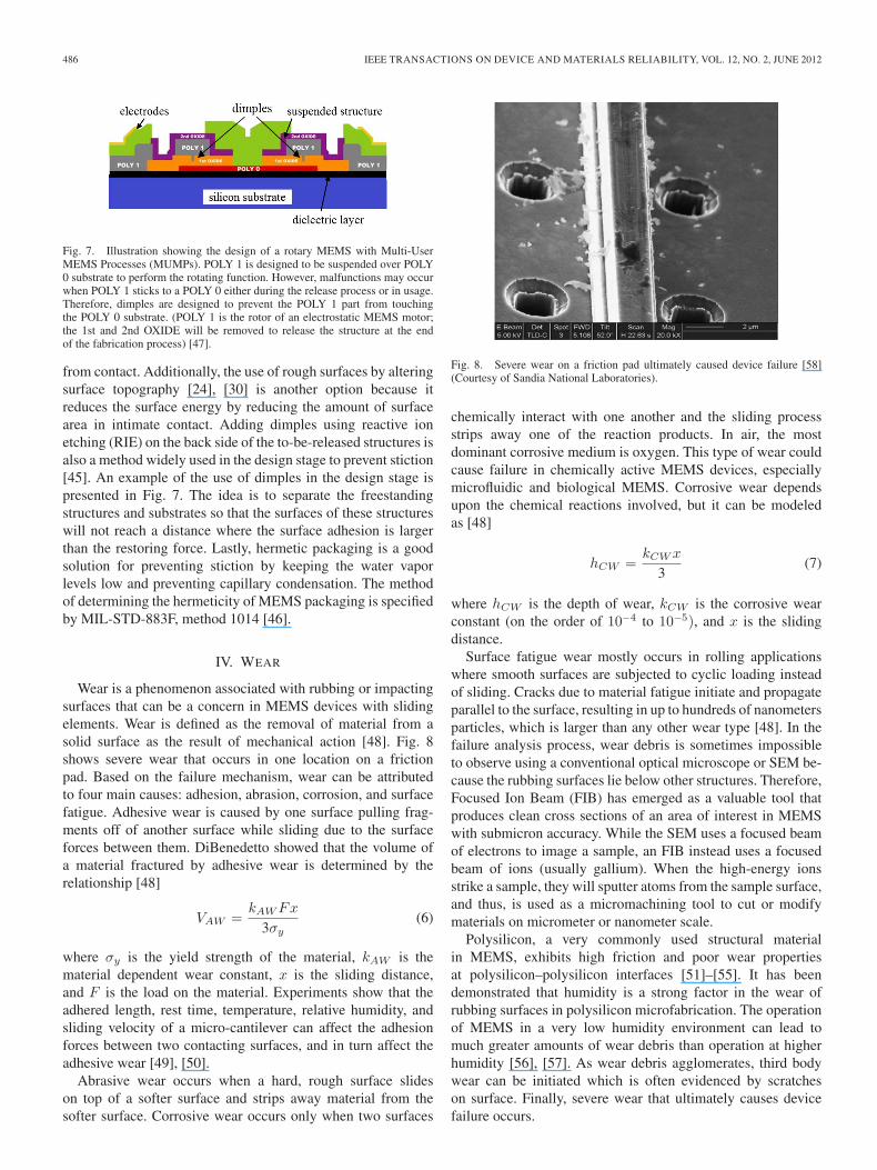
Wear is a phenomenon associated with rubbing or impactingsurfaces that can be a concern in MEMS devices with slidingelements. Wear is defined as the removal of material from asolid surface as the result of mechanical action [48]. Fig. 8shows severe wear that occurs in one location on a frictionpad. Based on the failure mechanism, wear can be attributedto four main causes: adhesion, abrasion, corrosion, and surfacefatigue. Adhesive wear is caused by one surface pulling frag-ments off of another surface while sliding due to the surfaceforces between them. DiBenedetto showed that the volume ofa material fractured by adhesive wear is determined by therelationship [48]
VAW =kAW Fx
3σy(6)
where σy is the yield strength of the material, kAW is thematerial dependent wear constant, x is the sliding distance,and F is the load on the material. Experiments show that theadhered length, rest time, temperature, relative humidity, andsliding velocity of a micro-cantilever can affect the adhesionforces between two contacting surfaces, and in turn affect theadhesive wear [49], [50].
Abrasive wear occurs when a hard, rough surface slideson top of a softer surface and strips away material from thesofter surface. Corrosive wear occurs only when two surfaces
Fig. 8. Severe wear on a friction pad ultimately caused device failure [58](Courtesy of Sandia National Laboratories).
chemically interact with one another and the sliding processstrips away one of the reaction products. In air, the mostdominant corrosive medium is oxygen. This type of wear couldcause failure in chemically active MEMS devices, especiallymicrofluidic and biological MEMS. Corrosive wear dependsupon the chemical reactions involved, but it can be modeledas [48]
hCW =kCW x
3(7)
where hCW is the depth of wear, kCW is the corrosive wearconstant (on the order of 10−4 to 10−5), and x is the slidingdistance.
Surface fatigue wear mostly occurs in rolling applicationswhere smooth surfaces are subjected to cyclic loading insteadof sliding. Cracks due to material fatigue initiate and propagateparallel to the surface, resulting in up to hundreds of nanometersparticles, which is larger than any other wear type [48]. In thefailure analysis process, wear debris is sometimes impossibleto observe using a conventional optical microscope or SEM be-cause the rubbing surfaces lie below other structures. Therefore,Focused Ion Beam (FIB) has emerged as a valuable tool thatproduces clean cross sections of an area of interest in MEMSwith submicron accuracy. While the SEM uses a focused beamof electrons to image a sample, an FIB instead uses a focusedbeam of ions (usually gallium). When the high-energy ionsstrike a sample, they will sputter atoms from the sample surface,and thus, is used as a micromachining tool to cut or modifymaterials on micrometer or nanometer scale.
Polysilicon, a very commonly used structural materialin MEMS, exhibits high friction and poor wear propertiesat polysilicon–polysilicon interfaces [51]–[55]. It has beendemonstrated that humidity is a strong factor in the wear ofrubbing surfaces in polysilicon microfabrication. The operationof MEMS in a very low humidity environment can lead tomuch greater amounts of wear debris than operation at higherhumidity [56], [57]. As wear debris agglomerates, third bodywear can be initiated which is often evidenced by scratcheson surface. Finally, severe wear that ultimately causes devicefailure occurs.

HUANG et al.: MEMS RELIABILITY REVIEW 487
A proven way to reduce wear failure is by applying protectiveinterfaces to MEMS structures. Such interfaces include solidfilms [59]–[73], some of which are also used as anti-stictioncoatings, gas phase lubrication [74], and combining a boundmono-layer and a mobile phase on the surface [75]. Mayer[68] demonstrated less wear particle generation with a 10-nmthick Al2O3 coating on polysilicon structure via atomic-layerdeposition (ALD) than a native oxide layer in a MEMS micro-engine. Smallwood et al. [76] proposed applying a diamond-like carbon (DLC) coating to protect MEMS structures againstwear. Tests have shown that DLC-coated devices that run in airhave a sixteen-fold increase in reliability performance over theiruncoated counterparts. Bandorf [77] developed a disc setup toinvestigate the friction and wear of various DLC coatings de-posited on substrates of varying hardness. He found that frictionand wear were greatly reduced when a substrate of high elasticmodulus was used. Guo et al. [78] proposed another categoryof thin films capable of being fabricated on MEMS surfaces:organic film, such as PFTS (perfluorodecyltrichlorosilane,C6F13CH2SiCl3).
V. FATIGUE AND CREEP
Fatigue is progressive and localized structural damage thatoccurs when a material is subjected to cyclic loadings that areless than its yield or ultimate tensile stress limit. Therefore,fatigue is mostly limited to active components such as resonat-ing membranes, cantilevers, and comb drives, while passivestructures, by design, normally are not exposed to enoughmechanical stress cycles to induce fatigue. Fatigue starts witha crack that initiates at an area of high stress concentrationand slowly propagates through the material until failure oc-curs. Muhlstein and Brown [79] and Shrotriya [80] observedsignificant changes in surface topography in polysilicon duringcyclic actuation and attributed it to stress-assisted interactionsbetween water molecules and the SiO2 layer on the surfaces ofthe notched specimens in the regions where the cyclic stresseswere highest. Tsuchiya et al. [81] reported that no fatigue wasobserved in silicon when cyclic loading was less than 50% ofthe silicon fracture strength.
Creep is the inelastic time-dependent deformation of a solidmaterial under the influence of an applied mechanical stress.Creep can occur below the yield strength of a given material.Fig. 9 shows the typical three-stage strain–time relationship ofcreep. In the primary stage, the strain rate decreases due towork hardening, which refers to the strengthening of a metalby plastic deformation resulting from dislocation movementsin the crystal structure of the material. In the secondary stage,the strain–time relationship reaches a minimum and becomesroughly constant as a result of the balance between workhardening and annealing (thermal softening). The characterizedcreep strain rate typically refers to the rate in this secondarystage. In the tertiary stage, the strain rate exponentially in-creases with strain due to a reduction in cross-sectional areacaused by phenomena such as necking or internal void for-mation. Tertiary creep is typically followed by separation orfracture of the material by tensile stress, which is referred toas creep rupture.
Fig. 9. Illustration of material creep. The creep curve consists of three stages.The time scale is linear. The value of strain varies from material to material.
Creep can be a reliability concern for some types of MEMS,such as RF MEMS and Digital Micromirror Devices (DMDs)[82], [83], where long hold times at stressed states occur.Sontheimer [84], [85] attributed what is called the hinge mem-ory phenomenon in DMDs, which refers to mirrors returning toa non-flat state as a result of metal creep of the hinge materialeven when the bias voltage is removed. Tregilgas [86] reportedon the creep effect in aluminum thin films, which often serveas functional structures, such as hinges and joints in MEMSdevices. Since the creep effect in aluminium thin films is rela-tively large for applications where billions of operating cyclesare required, alternative materials must be found to replace it.Modlinski [87]–[89] studied the creep resistance of a num-ber of aluminium compounds—Al98.3Cu1.7, Al99.7V0.2Pd0.1,Al93.5Cu4.4Mg1.5Mn0.6, and Al99.6Cu0.4—and found that thecreep resistivity of these alloys can be changed by a hardeningprocess in which the grain interior is strengthened by produc-ing extremely small and uniformly dispersed precipitate. Theydemonstrated that Al93.5Cu4.4Mg1.5Mn0.6 is the most resis-tant to long-term deformation and is a very promising bridgematerial for RF MEMS switches. Another important function-ing material is polysilicon. Its plastic deformation under hightemperature was studied by Tuck et al. [90], who developed amicro-test and measured the high temperature plastic deforma-tion within polysilicon. They found that no measurable creepoccurred when the temperature was below 1072 K and that thecreep rate increases as temperature and stress increase at highertemperatures. In many cases, MEMS structures are usuallysubjected to stress, either thermally-induced or mechanically-induced, before final fracture. X-ray diffraction (XRD) canyield the residual stress in materials by measuring the atomicstructure of materials based on observing the scattered intensityof an X-ray beam hitting a sample as a function of incident andscattered angle, polarization, and wavelength.
VI. ELECTRIC SHORT AND OPEN
After decades of improving the reliability of semiconductordevices, electric short failure rates have been reduced to areasonable range. However, the influence of dielectric prop-erties and behavior on MEMS devices is different from thaton semiconductor devices and is still not fully understood.This difference in influence is primarily due to three factors.First, there are various contributors to electric shorts in MEMS,some of which are dielectric degradation, charge injection andaccumulation, ohmic contact, and electromigration. Second,

488 IEEE TRANSACTIONS ON DEVICE AND MATERIALS RELIABILITY, VOL. 12, NO. 2, JUNE 2012
the characteristic length scale and electric stress of dielectricsin MEMS are often an order of magnitude or more than insemiconductor devices. The typical lateral dimensions of di-electrics in MEMS are tens to hundreds of micrometers, whichis much larger than those in semiconductor devices. Thus,MEMS devices inevitably have a higher probability of intro-ducing defect sites in dielectrics than in semiconductor devices.Third, higher applied voltages in MEMS can also increasethe probability of dielectric breakdown. Below we discuss themajor causes of electric shorts in MEMS devices. The inspec-tion tools for electric failure include, but are not limited to,probes with electric test equipment such as an ohm meter, photoemission microscopy (PEM), SEM, and X-ray diffraction. PEMprovides photoelectron distribution by collecting the electronsoriginates from the sample when the sample is excited byappropriate radiation, ranging from UV light to X-ray. Bycomparing a malfunctioning device to a properly operationalunit, one can pinpoint the dielectrics that have been damagedby electrostatic discharge.
A. Dielectric Breakdown due to Operational Voltage
The electric field generated by the normal driving voltages ofMEMS devices is one cause of electric shorts. Although MEMSdevices do not necessarily operate under high voltages, theirthin dielectric layer make them experience high electric field.For example, in a typical capacitive RF MEMS, a dielectric of500 nm with an actuation voltage of 50 V across it will experi-ence an electric field of 1 × 10⁸ V/m. Conduction is no longergoverned by Ohm’s law, but by nonlinear conduction, suchas Schottky-type and Poole–Frenkel-type conduction, which isdue to charged particle injection and via traps [91]. With suchan ultrahigh field strength, the dielectric layer can be brokendown, resulting in an electric short. Zafar et al. [92] presenteda model for calculating the trapped charge density.
B. Dielectric Breakdown Due to Electrostatic Discharge
Electrostatic discharge (ESD) involves the transfer of elec-trical charge between two objects at different potentials, eitherthrough direct contact or through an induced electric field. ESDcan result in a very high current passing through a dielectricmaterial within a very short period of time and cause materialbreakdown and sometimes burnout, which is the partial or com-plete melting of a large device area. Despite a great deal of ef-fort during the past decade, ESD still affects production yields,manufacturing costs, product quality, and product reliability.In semiconductor devices, ESD accounts for more than 25%of failures, including gate oxide breakdown, junction spiking,and latch-up [93]. In MEMS devices, where dielectrics playmore roles, including sacrificial, structural, optical, masking,passivation, etch stop, insulator, and encapsulation layers, ESDproblems in the dielectric are especially destructive [94]–[98]and an important area for improvement of reliability. Commonsources of ESD are the human body [99], charged devices,charged environment, and cosmic rays. A human body routinelydevelops an electric potential in excess of 1000 V, which canhave a catastrophic effect on a MEMS device [100].
A standard procedure has been established for testing andclassifying microcircuits as well as some MEMS devices ac-cording to their susceptibility to damage or degradation byexposure to a defined ESD [101]. Olszewski et al. [102] createdan experiment to test the effects of ESD with and without mois-ture on an RF MEMS switch by measuring the changes in thecapacitance–voltage curve. If the MEMS devices are designedto operate in an ionizing (nuclear) radiation environment, suchas outer space or a nuclear power plant, the possibility ofcharge accumulation due to radiation in the dielectrics shouldbe taken into account. Knudson and Lee [103], [104] tested theperformance of MEMS accelerometers under nuclear radiationand found that the change in output voltage was caused bycharge buildup in dielectric layers beneath the moving mass.McClure [105] proposed a mechanism for creating a chargedistribution in the dielectric of the MEMS device exposed tonuclear radiation. Newman et al. [106] presented the contactsurface of a wafer-packaged RF MEMS switch damaged byESD. It exhibits 914 billion switch cycles at 20 kHz with anincident RF frequency of 10 GHz without degradation, whichhas the longest lifetime of operation ever reported.
Researchers have developed many ways to solve the ESDproblem in dielectrics. Low field strengths, trap-free dielectric,and leaky dielectric layers have been proposed as solutions[107]. Wairaven et al. [108] proposed two sets of approachesto solve two classes of problems: manufacturing-related andin-use-related approaches. Some of the ESD precaution andproper handling procedures include leave ESD-sensitive com-ponents in their antistatic packaging until ready to be used;dissipate static electricity before handling any ESD-sensitivecomponents by touching a grounded metal object, such as anunpainted metal chassis; use wrist straps and floor mats or otherantistatic devices to prevent possible ESD from damaging thecomponents.
C. Electric Failure Due to Ohmic Contact
Electric failures are prone to occur at ohmic contacts thatare the interfaces of two different conductive materials withdifferent Fermi levels. As two contacts come together, only thehighest peaks touch and are subject to a full current load, whichcauses a sudden rise in temperature and a “melt-down” of thosepeaks. Contact resistance at an interface can be calculated bythe following equation [109]:
RC =ρe
na+
ρe
D(8)
where Rc is the contact resistance, ρe is the electrical resistivity,a is the average contact asperity radius, n is the number ofasperities per unit area, and D is the diameter of the area overwhich the contacts are distributed. Once the temperature at aninterface caused by Joule heating reaches a high enough level,the contact material will melt, usually causing severe problemsin MEMS, such as superheating of the surrounding air and itsionization, arcing, material transfer, or welding [110]. Othercauses of ohmic contact failure include surface contamination,erosion, and surface changes due to absorption or oxidation.

HUANG et al.: MEMS RELIABILITY REVIEW 489
The quality of ohmic contact can be represented by contactresistance. Kwon et al. [111] studied the electrical behavior andlifetime of RF MEMS contact switches made of Au, Pt, Ir, andAuPt alloys at different contact forces and current conditionsand found that Au-to-Pt, Pt-to-Pt, and Au-to-Ir are alternativematerials that can enhance the reliability of high-power RFMEMS switches. Dickrell [112] investigated the contact resis-tance degradation of a hot-switched low-force Au-Pt contactusing a modified nano-indentation apparatus and found that thecontact resistance increased by two orders of magnitude overthe initial resistance in only 5 to 10 cycles, indicating that theelectrical contact surface was being contaminated in situ. Re-cently, low-loss ohmic switches have been created through byfabricating dimples on one of the electrodes during deposition[113]. It is believed that a more even distribution of the electro-static force across the plate can result in uniform pressure overthe contact area, yielding lower contact resistance. Gaddi et al.[114] proposed an approach for achieving low-loss contactswith a standard surface micromachining technology. Ducarougeet al. [115] have demonstrated a power RF MEMS devicecapable of handling 3.8 W at 20 GHz by carefully designing thecontact line. Sputter cleaning of the surface prior to depositionalong with deposition of Ni as a first layer can provide for muchimproved ohmic contact stability and homogeneity [116].
VII. CONTAMINATION
Many MEMS devices rely on the movement of mechanicalcomponents to perform their designated functions. However,the introduction of unintended materials, which is called con-tamination, can render the device inoperable. Contaminationcan be introduced from various sources, including manufac-turing processes such as surface cleaning, metal deposition,patterning, releasing, and annealing; dusty in-use operationenvironments where foreign particles penetrate through MEMSpackages; and intrinsic problems such as crystal growth, e.g.,tin whiskers. Fig. 10 shows a MEMS actuator after beingsubjected to high mechanical shocks. A particle contaminantwas found close to a comb-finger actuator, which resulted in anelectric short. In most cases, contamination has been attributedto the energetic decomposition of existing contaminant speciesinto highly resistive compounds [117], [118].
Contamination can affect the mechanical aspect of a MEMSdevice by blocking moving parts. Contamination can also resultin electric degradation and failure, including limiting of thefrequency response of high-frequency devices due to the in-creasing RC time constant, power dissipation via Joule heating,electromigration, and delamination at contact areas [119]. Allthese effects lead to limitations on the lifetimes and to failuresof MEMS devices.
Contaminants either become wedged between MEMS com-ponents or rest on top of surfaces. Hence, contamination-induced failure is not difficult to identify, as particles arerelatively easy to diagnose using optical microscopes and SEMor FIB once the device is decapsulated and the MEMS com-ponent is exposed. Yet, precautions must be taken during thedecapsulation process. Tabata and Tsuchiya [120] have shownthat contaminants can be easily detected using an interferome-
Fig. 10. Particle contamination was found within the actuator region of amicroengine subjected to a high shock top impact. Notice that the contactbetween the particle, stationary comb fingers, and the shuttle resulted in electricshort of the drive signal to the ground plane [14]. (Courtesy of Sandia NationalLaboratories).
ter, and dust particles that are greater than 0.3 μm in diametercan be prevented from entering a MEMS pressure sensor byusing a dust collector at the edge of the package. In manycased, contaminants are induced via poor packages with voidsor cracks. A scanning acoustic microscope (SAM) is useful fordetecting lid seal integrity in hermetically sealed packages. It isa nondestructive technique which directs focused sound from atransducer at a small point on an object of interest, measures“time of flight” of the sound, and determines the object’sgeometry and microstructure of its surface. For identifying con-taminants, Energy Dispersive X-ray Spectrometer (EDS) is auseful instrument which is commonly used in conjunction withthe SEM. It allows users to measure compositional gradients,element concentrations or distributions at microstructural level,and thus, to identify contaminants and failure sites.
VIII. CONCLUSION
The ability to quantify the reliability of MEMS devices foranticipated use conditions is vital for their successful com-mercialization. Quantification can be achieved only if engi-neers have a clear understanding of failure mechanisms andunderlying physics of MEMS products. This paper summarizedfailure mechanisms that have been identified in MEMS devices,their physical root causes, their effects on device behavior andfunctionality, as well as test methods and inspection techniques.Additionally, various approaches to improve MEMS reliabil-ity are covered, including creep prevention through the useof creep-resistant materials for moving structural parts, wearprevention through the deposition of a lubricant layer, stictionprevention through the fabrication of dimples and whiskers,fracture prevention through filleting sharp lines and corners,and contamination-induced failure prevention via better her-metic sealing.
MEMS engineers have borrowed many tools and methodsfrom IC fabrication to test MEMS devices. However, due tothe nature of MEMS interaction with the environment, andtheir electromechanical complications, identification potentialfailure sites and mechanisms is still a labor-intensive work.Fortunately, most MEMS devices, regardless of function andapplication, share basic components (e.g., membrane, can-tilever) that exhibit common failure mechanisms (e.g., fatigue,

490 IEEE TRANSACTIONS ON DEVICE AND MATERIALS RELIABILITY, VOL. 12, NO. 2, JUNE 2012
stiction). Therefore, understanding those mechanisms providesa foundation for the lifetime models and field requirement-based test guidance that help MEMS engineers design againstpossible failures and test MEMS more efficiently.
ACKNOWLEDGMENT
The authors would like to thank the Center for AdvancedLife Cycle Engineering (CALCE), University of Maryland, forsupporting this research. CALCE has provided a knowledgeand resource base to support this study of MEMS reliability andtesting evaluation. More than 100 national and international or-ganizations and companies support the center. Also, the authorswould like to thank Sandia National Laboratories, Texas Instru-ments, Dr. L. Hornbeck, Prof. K. S.J. Pister from UC Berkeley,IOP Publishing Ltd., M. Zimmerman, D. Mahadevo, B. Kwong,L. Krishnan, and G. Kumaraswamy for their valuable edits andcomments.
REFERENCES
[1] R. M. Boysel, T. G. McDonald, G. A. Magel, G. C. Smith, andJ. L. Leonard, “Integration of deformable mirror devices with opticalfibers and waveguides,” in Proc. SPIE, 1992, vol. 1793, pp. 34–39.
[2] W. Kuehnel and S. Sherman, “A surface micromachined silicon ac-celerometer with on-chip detection circuitry,” Sens. Actuators A, Phys.,vol. 45, no. 1, pp. 7–16, Oct. 1994.
[3] M. Younis, D. Jordy, and J. M. Pitarresi, “Computationally efficient ap-proaches to characterize the dynamic response of microstructures undermechanical shock,” J. Mciroelectromech. Syst., vol. 16, no. 3, pp. 628–638, Jun. 2007.
[4] ASM Handbook, vol. 13, “Corrosion,” ISBN 0-87170-007-7, ASM Int.,Novelty, OH, 1987.
[5] W. van Arsdell and S. B. Brown, “Subcritical crack growth in sili-con MEMS,” J. Mciroelectromech. Syst., vol. 8, no. 3, pp. 319–327,Sep. 1999.
[6] S. B. Brown, W. van Arsdell, and C. L. Muhlstein, “Materials reliabilityin MEMS devices,” in Proc. Int. Conf. Solid-State Sens. Actuators Dig.TRANSDUCERS, New York, 1997, vol. 1, pp. 591–593.
[7] S. B. Brown and E. Jansen, “Reliability and long term stability ofMEMS,” in Proc. Summer Topical Meetings Dig., Optical MEMS Appl.,New York, 1996, pp. 9–10.
[8] S. B. Brown, G. Povirk, and J. Connally, “Measurement of slow crackgrowth in silicon and nickel micromechanical devices,” in Proc. IEEEMicro Electro Mech. Syst. Investig. Micro Struct., Sens., Actuators,Mach. Syst., New York, 1993, pp. 99–104.
[9] J. A. Connally and S. B. Brown, “Micromechanical fatigue testing,”in Proc. Int. Conf. Solid-State Sens. Actuators Dig., Transducers,New York, 1991, pp. 953–956.
[10] G. X. Li and J. R. Shemansky, “Drop test and analysis on micro-machined structures,” Sens. Actuators A, Phys., vol. 85, no. 1–3,pp. 280–286, Aug. 2000.
[11] A. Béliveau, G. T. Spencer, K. A. Thomas, and S. L. Roberson, “Eval-uation of MEMS capacitive accelerometers,” IEEE Des. Test Comput.,vol. 16, no. 4, pp. 48–56, Oct.–Dec. 1999.
[12] T. G. Brown and B. S. Davis, “Dynamic high-g loading of MEMSsensors: Ground and flight testing,” in Proc. SPIE-Int. Soc. Opt. Eng.,Sep. 1998, vol. 3512, pp. 228–235.
[13] T. G. Brown, B. Davis, D. Hepner, J. Faust, C. Myers, C. Muller,T. Harkins, M. Hollis, C. Miller, and B. Placzankis, “Strap-down micro-electromechanical (MEMS) sensors for high-g munition applications,”IEEE Trans. Magn., vol. 37, no. 1, pp. 336–342, Jan. 2001.
[14] D. M. Tanner, J. A. Walraven, K. Helgesen, L. W. Irwin, N. F. Smith, andN. Masters, “MEMS reliability in shock environments,” in Proc. IEEEInt. Reliab. Phys. Symp., 2000, pp. 129–138.
[15] M. P. de Boer, B. D. Jensen, and F. Bitsie, “A small area in-situ MEMStest structure to measure fracture strength by electrostatic probing,” inSPIE Proc., vol. 3875, Materials and Device Characterization in Micro-machining, Santa Clara, CA, Sep. 1999, p. 97.
[16] J. R. Davis, Corrosion of Aluminum and Aluminum Alloys. Novelty,OH: ASM Int., 1999.
[17] Q. Zhang, X. Guo, Y. Liu, N. Dai, and P. Lu, “Corrosion and fatigue inmicro-sized Ni cantilever beams,” Trans. Nonferrous Met. Soc. China,vol. 17, pp. s213–s217, 2007.
[18] Metals Handbook (Desk Edition) Chapter 32 (Failure Analysis), Ameri-can Society for Metals, ASM Int., Novelty, OH, 1997. pp. 32-24–32-26.
[19] C. H. Mastrangelo and C. H. Hsu, “A simple experimental techniquefor the measurement of the work of adhesion of microstructures,” inProc. IEEE Solid-State Sens. Actuator Workshop, New York, 1992,pp. 208–212.
[20] W. M. van Spengen, R. Puers, and I. de Wolf, “On the physics of stictionand its impact on the reliability of microstructures,” in J. Adhesion Sci.Technol., 2003, vol. 17, no. 4, pp. 563–582.
[21] W. M. van Spengen, I. De Wolf, and B. Puers, “Auto-adhesion model forMEMS surfaces taking into account the effect of surface roughness,” inProc. SPIE, 2000, vol. 4175, pp. 104–112.
[22] R. Maboudian, “Adhesion and friction issues associated with reliableoperation of MEMS,” MRS Bull., vol. 23, no. 6, pp. 47–51, 1998.
[23] W. M. van Spengen, R. Puers, and I. De Wolf, “The prediction of stic-tion failures in MEMS,” IEEE Trans. Device Mater. Rel., vol. 3, no. 4,pp. 167–172, Dec. 2003.
[24] K. Komvopoulos, “Surface engineering and microtribology for micro-electromechanical systems,” Wear, vol. 200, no. 1/2, pp. 305–327,Dec. 1996.
[25] O. Raccurt, F. Tardif, F. Arnaud d’Avitaya, and T. Vareine, “Influenceof liquid surface tension on stiction of SOI MEMS,” J. Micromech.Microeng., vol. 14, no. 7, pp. 1083–1090, Jul. 2004.
[26] F. W. Delrio, M. P. de Boer, J. A. Knapp, E. Davidreedy, Jr., P. J. Clews,and A. L. Dunn, “The role of van der Waals forces in adhesion ofmicromachined surfaces,” Nature Materials, vol. 4, no. 8, pp. 629–634,Aug. 2005.
[27] B. Bhushan, Handbook of Micro/Nanotribology. Boca Raton, FL: CRCPress, 1999.
[28] F. W. DelRio, M. L. Dunn, and M. P. de Boer, “Capillary adhesion modelfor contacting micromachined surfaces,” Script. Mater., vol. 59, no. 9,pp. 916–920, Nov. 2008.
[29] F. P. Bowden and D. Tabor, Lubrication of Solids. Oxford, U.K.:Clarendon, 1950.
[30] R. Maboudian and R. T. Howe, “Critical Review: Adhesion in surfacemicromechanical structures,” J. Vac. Sci. Technol. B, vol. 15, no. 1, pp. 1–20, Jan. 1997.
[31] A. W. Adamson, Physical Chemistry of Surfaces, 5th ed. New York:Wiley, 1990.
[32] W. M. van Spengen, R. Puers, and I. De Wolf, “A physical modelto predict stiction in MEMS,” s, vol. 12, no. 5, pp. 702–713,Sep. 2002.
[33] C. F. Herrmann, F. W. DelRio, V. M. Bright, and S. M. George, “Hy-drophobic coatings using atomic layer deposition and non-chlorinated,”in Proc. IEEE MEMS , 2004, pp. 653–656.
[34] M. R. Houston and R. Maboudian, “Stability of ammonium fluoride-treated Si(100),” J. Appl. Phys., vol. 78, no. 6, pp. 3801–3808,Sep. 1995.
[35] W. D. Greaso, “Analysis of the effect of ESD on the operation ofMEMS,” IEEE Trans. Ind. Appl., vol. 45, no. 6, pp. 2185–2191,Nov./Dec. 2009.
[36] M. P. de Boer, J. A. Knapp, T. M. Mayer, and T. A. Michalske, “The roleof interfacial properties on MEMS performance and reliability,” in Proc.SPIE, 1999, vol. 3825, pp. 2–15.
[37] M. P. de Boer and T. A. Michalske, “Accurate method for determiningadhesion of cantilever beams,” J. Appl. Phys., vol. 86, no. 2, pp. 817–827, Jul. 1999.
[38] M. P. de Boer, M. R. Tabbara, M. T. Dugger, P. J. Clews, andT. A. Michalske, “Measuring and modeling electrostatic adhesion inmicromachines,” in Proc. IEEE Int. Conf. Solid State Sens. Actuators,1997, vol. 1, pp. 229–232.
[39] Y. Yee, M. Park, and K. Chun, “A sticking model of suspended polysil-icon microstructure including residual stress gradient and postreleasetemperature,” J. Microelectromech. Syst., vol. 7, no. 3, pp. 339–344,Sep. 1998.
[40] [Online]. Available: www-bsac.EECS.Berkeley.edu/~pister/245[41] W. A. de Groot, J. R. Webster, D. Felnhofer, and E. P. Gusev, “Review
of device and reliability physics of dielectrics in electrostatically drivenMEMS devices,” IEEE Trans. Device Mater. Rel., vol. 9, no. 2, pp. 190–202, Jun. 2009.
[42] P. F. Man, B. P. Gogoi, and C. H. Mastrangelo, “Elimination ofpost-release adhesion in microstructures using conformal fluorocar-bon coatings,” J. Microelectromech. Syst., vol. 6, no. 1, pp. 25–34,Mar. 1997.

HUANG et al.: MEMS RELIABILITY REVIEW 491
[43] Y. Taii, K. Kakushima, R. Yokokawa, S. Ono, T. Takahashi, K. Isamoto,C. Chong, H. Fujita, and H. Toshiyoshi, “Suppression of stiction force byall-vapor processes using HF, Ozone, and HMDS for MEMS devices,”IEEJ Trans. Sens. Micromach., vol. 127, no. 4, pp. 221–227, 2007.
[44] P. F. Van Kessel, L. J. Hornbeck, R. E. Meier, and M. R. Douglass, “AMEMS-based projection display,” Proc. IEEE, vol. 86, no. 8, pp. 1687–1704, Aug. 1998.
[45] D. A. Koester, R. Mahadevan, A. Shishkoff, and K. W. Markus, MUMPsDesign Handbook. Durham, NC: Cronos Integrated Microsystems,1999.
[46] Method 1014, a United States Defense Standard, MIL-STD-883F,2004.
[47] [Online]. Available: http://www.europractice-ic.com/MEMS_memscap.php
[48] A. T. DiBenedetto, The Structure and Properties of Materials.New York: McGraw-Hill, 1967.
[49] S. M. Ali and L. M. Phinney, “Investigation of adhesion during operationof MEMS cantilevers,” in Proc. SPIE, 2004, vol. 5343, p. 215.
[50] N. S. Tambe and B. Bhushan, “Scale dependence of micro/nano-frictionand adhesion of MEMS/NEMS materials, coatings and lubricants,”Nanotechnology, vol. 15, no. 11, pp. 1561–1570, Nov. 2004.
[51] M. G. Lim, J. C. Chang, D. P. Shultz, R. T. Howe, and R. M. White,“Polysilicon microstructures to characterize static friction,” in Proc.Micro Electro Mech. Syst. Annu. Int. Workshop MEMS Conf. Ser., 1990,pp. 82–88.
[52] Y. C. Tai and R. S. Muller, “Frictional study of IC-processed micromo-tors,” Sens. Actuators A, Phys., vol. 21, no. 1–3, pp. 180–183, Feb. 1990.
[53] K. J. Gabriel, F. Behi, and R. Mahadevan, “In situ friction and wearmeasurements in integrated polysilicon mechanisms,” Sens. ActuatorsA, Phys., vol. 21, no. 1–3, pp. 184–188, Feb. 1990.
[54] W. Wang, Y. Wang, H. Bao, B. Xiong, and M. Bao, “Friction and wearproperties in MEMS,” Sens. Actuators A, Phys., vol. 97/98, pp. 486–491,Apr. 2002.
[55] U. Beerschwinger, D. Mathieson, R. L. Reuben, and S. J. Yang, “A studyof wear on MEMS contact morphologies,” J. Micromech. Microeng.,vol. 4, no. 3, pp. 95–105, Sep. 1994.
[56] D. M. Tanner, J. A. Walraven, L. W. Irwin, M. T. Dugger, N. F. Smith,W. P. Eaton, W. M. Miller, and S. L. Miller, “The effect of humidity onthe reliability of a surface micro-machined microengine,” in Proc. IRPS,San Diego, CA, 1999, pp. 189–197.
[57] S. T. Patton, W. D. Cowan, and J. S. Zabinski, “Performance and relia-bility of a new MEMS electrostatic lateral output motor,” in Proc. IRPS,San Diego, CA, 1999, pp. 179–188.
[58] G. Subhash, A. D. Corwin, and M. P. de Boer, “Operational wear andfriction in MEMS devices,” in Proc. 11th ICF, 2005.
[59] J. K. Luo, Y. Q. Fu, H. R. Le, J. A. Williams, S. M. Spearing, andW. I. Milne, “Diamond and diamond-like carbon MEMS,” inJ. Micromech. Microeng., 2007, vol. 17, no. 17, pp. 147–163.
[60] O. Auciello, J. Birrell, J. A. Carlisle, J. E. Gerbi, X. Xiao, B. Peng, andH. D. Espinosa, “Materials science and fabrication processes for a newMEMS technology based on ultrananocrystalline diamond thin films,” inJ. Phys.: Condens. Matter, 2004, vol. 16, no. 16, pp. 539–552.
[61] R. W. Ashurst, C. Yau, C. Carraro, R. Maboudian, and M. T. Dugger,“Dichlorodimethylsilane as an anti-stiction monolayer for MEMS:A comparison to the octadecyltrichlosilane self-assembled monolayer,”J. Microelectromech. Syst., vol. 10, no. 1, pp. 41–49, Mar. 2001.
[62] U. Srinivasan, M. R. Houston, R. T. Howe, and R. Maboudian,“Alkyltrichlorosilane-based self-assembled monolayer films for stictionreduction in silicon micromachines,” J. Microelectromech. Syst., vol. 7,no. 2, pp. 252–260, Jun. 1998.
[63] R. Maboudian and R. T. Howe, “Stiction reduction processes forsurface micromachines,” Tribol. Lett., vol. 3, no. 3, pp. 215–221,Sep. 1997.
[64] S. H. Lee, M.-J. Kwon, J.-G. Park, Y.-K. Kim, and H.-J. Shin, “Thesurface modification with fluorocarbon thin films for the prevention ofstiction in MEMS,” in Mater. Res. Soc. Symp. Proc., vol. 518, MaterialResearch Society, 1998, pp. 143–148.
[65] J.-M. Kim, C.-W. Baek, J.-H. Park, D.-S. Shin, Y.-S. Lee, and Y.-K. Kim,“Continuous anti-stiction coatings using self-assembled monolayersfor gold microstructures,” J. Micromech. Microeng., vol. 12, no. 5,pp. 688–695, Sep. 2002.
[66] D. C. Senft and M. T. Dugger, “Friction and wear in surface micro-machined tribological test devices,” in Proc. SPIE, 1997, vol. 3224,pp. 31–38.
[67] S. G. Radhakrishnan, R. E. Robertson, P. M. Adams, and R. C. Cole,“Integrated TiC coatings for moving MEMS,” Thin Solid Films 420-421,pp. 553–564, 2002.
[68] T. M. Mayer, J. W. Elam, S. M. George, P. G. Kotula, and R. S. Goeke,“Atomic-layer deposition of wear-resistant coatings for microelectro-mechanical devices,” Appl. Phys. Lett., vol. 82, no. 17, pp. 2883–2885,April 2003.
[69] S. T. Patton, W. D. Cowan, K. C. Eapen, and J. S. Zabinski, “Effect ofsurface chemistry on the tribological performance of a MEMS electro-static lateral output motor,” Tribol. Lett., vol. 9, no. 3/4, pp. 199–209,Jan 2001.
[70] R. Maboudian, W. R. Ashurst, and C. Carraro, “Self-assembled mono-layers as anti-stiction coatings for MEMS: Characteristics and recentdevelopments,” Sens. Actuators A, Phys., vol. 82, no. 1–3, pp. 219–223,May 2000.
[71] S. Sundararagan and B. Bhushan, “Static Friction and surface roughnessstudies of surface micromachined electrostatic micromotors using anatomic force/friction force microscope,” J. Vac. Sci. Technol. A, Vac.Surf. Films, vol. 19, no. 4, pp. 1777–1785, Jul. 2001.
[72] U. Srinivasan, M. R. Houston, R. T. Howe, and R. Maboudian, “Self-assembled fluorocarbon films for enhanced stiction reduction,” in Proc.Int. Conf. Solid-State Sens. Actuators, Transducers, Chicago, IL, 1997,pp. 1399–1402.
[73] X.-Y. Zhu and J. E. Houston, “Molecular lubricants for silicon-basedmicroelectromechanical systems (MEMS): A novel assembly strategy,”Tribol. Lett., vol. 7, no. 2/3, pp. 87–90, Sep. 1999.
[74] S. A. Henck, “Lubrication of digital micromirror devices,” Tribol. Lett.,vol. 3, pp. 239–247, 1997.
[75] K. C. Eapen, S. T. Patton, and J. S. Zabinski, “Lubrication of micro-electromechanical systems (MEMS) using bound and mobile phases offomblin Z-Dol®,” Tribol. Lett., vol. 12, no. 1, pp. 35–41, 2002.
[76] S. A. Smallwood, K. C. Eapenb, S. T. Pattonb, and J. S. Zabinskic,“Performance results of MEMS coated with a conformal DLC,” Wear,vol. 260, no. 11/12, pp. 1179–1189, Jun. 2006.
[77] R. Bandorf, H. Lüthje, and T. Staedler, “Influencing factors on microtri-bology of DLC films for MEMS and microactuators,” Diamond Relat.Mater., vol. 13, no. 4–8, pp. 1491–1493, Aug. 2004.
[78] Z. Guo, F. Zhou, S. Fan, D. Zheng, and H. Zhuang, “Researchdevelopment of measuring methods on the tribology characters formovable MEMS devices: A review,” Microsyst. Technol., vol. 15, no. 3,pp. 343–354, Mar. 2009.
[79] Failure Analysis Associates, Inc. NSF/AFOSR/ASME Workshop, Tri-bology Issues and Opportunities in MEMS, Nov. 9–11, 1997. Reliabilityand Fatigue Testing of MEMS Christopher Muhlstein and Stuart Brown.
[80] P. Shrotriya, S. M. Allameh, and W. O. Soboyejo, “On the evolutionof surface morphology of polysilicon MEMS structures during fatigue,”Mech. Mater., vol. 36, no. 1/2, pp. 35–44, Jan./Feb. 2004.
[81] T. Tsuchiya, A. Inoue, J. Sakata, M. Hashimoto, A. Yokoyama, andM. Sugimoto, “Fatigue test of single crystal silicon resonator,” in Proc.Tech. Dig. 16th Sens. Symp., Kawasaki, Japan, 1998, pp. 277–280.
[82] M. R. Douglass, “DMD reliability: A MEMS success story,” in SPIEProc., 2003, vol. 4980, p. 1.
[83] M. R. Douglass, “Lifetime estimates and unique failure mechanisms ofthe digital micromirror device (DMD),” in Proc. 36th Annu. Int. Reliab.Phys. Symp., Reno, NV, 1998, pp. 9–16.
[84] A. B. Sontheimer, “Digital micromirror device (DMD) hinge memorylifetime reliability modeling,” in Proc. 40th Annu. Int. Reliab. Phys.Symp., Dallas, TX, 2002, pp. 118–121.
[85] A. B. Sontheimer, “Effects of operating conditions on DMD hinge mem-ory lifetime,” in Proc. 41st Annu. Int. Reliab. Phys. Symp., Dallas, TX,2003, pp. 473–477.
[86] J. H. Tregilgas, “Micromechanical device having an improved beam,”U.S. Patent 5 552 924, Sep. 3, 1996.
[87] R. Modlinski, P. Ratchev, A. Witvrouw, R. Puers, and I. de Wolf, “Creep-resistant aluminum alloys for use in MEMS,” J. Micromech. Microeng.,vol. 15, no. 7, pp. S165–S170, Jul. 2005.
[88] R. Modlinski, A. Witvrouw, P. Ratchev, R. Puers, J. M. J. den Toon-der, and I. De Wolf, “Creep characterization of Al alloy thin films foruse in MEMS applications,” Microelectron. Eng., vol. 76, no. 1–4,pp. 272–278, Oct. 2004.
[89] R. Modlinski, A. Witvrouw, P. Ratchev, A. Jourdain, V. Simons,H. A. C. Tilmans, J. M. J. den Toonder, R. Puers, and I. de Wolf, “Creepas a reliability problem in MEMS,” Microelectron. Reliab., vol. 44,no. 9–11, pp. 1733–1738, Sep.–Nov. 2004.
[90] K. Tuck, A. Jungen, A. Geisberger, M. Ellis, and G. Skidmore, “Astudy of creep in polysilicon MEMS devices,” J. Eng. Mater. Technol.,vol. 127, no. 1, pp. 90–96, Jan. 2005.
[91] D. Nataraj, K. Senthil, S. Narayandass, and D. Mangalaraj, “Conductionstudies on bismuth selenide thin films,” Cryst. Res. Technol., vol. 34,no. 7, pp. 867–872, Aug. 1999.

492 IEEE TRANSACTIONS ON DEVICE AND MATERIALS RELIABILITY, VOL. 12, NO. 2, JUNE 2012
[92] S. Zafar, A. Callegari, E. Gusev, and M. V. Fischetti, “Charge trapping inhigh k gate dielectric stacks,” in IEDM Tech. Dig., 2002, pp. 517–520.
[93] C. Duvvury and A. Amerasekera, “ESD: A pervasive reliability concernfor IC technologies,” Proc. IEEE, vol. 81, no. 5, pp. 690–702, May 1993.
[94] H. S. Newman, “RF MEMS switches and applications,” in Proc. IEEEIRPS, 2002, pp. 111–115.
[95] G. M. Rebeitz and J. B. Muldavin, “RF MEMS switches and switchcircuits,” IEEE Microw. Mag., vol. 2, no. 4, pp. 59–71, Dec. 2001.
[96] J. DeNatale, R. Mihailovich, and J. Waldrop, “Techniques for reliabilityanalysis of RF MEMS switch,” in Proc. IEEE IRPS, 2002, pp. 116–117.
[97] W. M. van Spengen, R. Mertens, and I. De Wolf, “Experimental charac-terization of stiction due to charging in RF MEMS,” in IEDM Tech. Dig.,2002, pp. 901–904.
[98] D. Becher, R. Chan, M. Hattendorf, and M. Feng, “Reliability studyof low-voltage RFNEMS switches,” in Proc. GaAs MANTECH Conf.,San Diego, 2002, p. 54.
[99] J. C. Lee, A. Hoque, G. D. Croft, J. J. Liou, R. Young, andJ. C. Bernier, “An electrostatic discharge failure mechanism insemiconductor devices, with applications to electrostatic dischargemeasurements using transmission line pulsing technique,” Solid StateElectron., vol. 44, no. 10, pp. 1771–1781, Oct. 2000.
[100] B. Stark, MEMS Reliability Assurance Guidelines for SpaceApplications. Pasadena, CA: JPL Publ., 1999.
[101] Electronic Industries Association, Electrostatic Discharge (ESD) Sensi-tivity Testing Machine Model (MM), 1997. EIA/JESD22-A115A.
[102] Z. Olszewski, R. Duane, and C. O’Mahony, Effect of EnvironmentHumidy on the C–V Characteristics of RF-MEMS Capacitive Switch,Tyndall Nat. Inst., Lee Maltings, Prospect Row, Cork, Ireland.
[103] A. R. Knudson, S. Buchner, P. McDonald, W. J. Stapor, A. B. Campbell,K. S. Grabowski, and D. L. Knies, “The effects of radiation on MEMSaccelerometers,” IEEE Trans. Nucl. Sci., vol. 43, no. 6, pp. 3122–3126,Dec. 1996.
[104] C. I. Lee, A. H. Johnston, W. C. Tang, and C. E. Barnes, “Total doseeffects on microelectromechanical systems (MEMS): Accelerometers,”IEEE Trans. Nucl. Sci., vol. 43, no. 6, pp. 3127–3132, Dec. 1996.
[105] S. S. McClure, L. D. Edmonds, R. Mihailovich, A. H. Johnston,P. Alonzo, J. DeNatale, J. Lehman, and C. Yui, “Radiation effects inmicro-electromechanical systems (MEMS): RF relays,” IEEE Trans.Nucl. Sci., vol. 49, no. 6, pp. 3197–3202, Dec. 2002.
[106] H. S. Newman, J. L. Ebel, D. Judy, and J. Maciel, “Lifetime measure-ments on a high-reliability RF-MEMS contact switch,” IEEE Microw.Wireless Compon. Lett., vol. 18, no. 2, pp. 100–102, Feb. 2008.
[107] J. C. Ehmke, C. L. Goldsmith, Z. J. Yao, andS. M. Eshelman, “Method and apparatus for switching high frequencysignals,” U.S. Patent 639 167 521, May 21, 2002.
[108] J. A. Wairaven, J. M. Soden, D. M. Tanner, P. Tangyunyong, E. I. Cole, Jr.,R. E. Anderson, and L. W. Irwin, “Electrostatic discharge/electrical over-stress susceptibility in MEMS: A new failure model,” in Proc. SPIE,2000, vol. 4180, pp. 30–39.
[109] R. S. Mroczkowski, Electronic Connector Handbook. New York:McGraw-Hill, 1998.
[110] M. S. Machate, “Joule heat effects on reliability of RF MEMSswitches,” M.S. thesis, Worcester Polytechnic Inst., Worcester, MA,May 29, 2003.
[111] H. Kwon, D.-J. Choi, J.-H. Park, H.-C. Lee, Y.-H. Park, Y.-D. Kim,H.-J. Nam, Y.-C. Joo, and J.-U. Bu, “Contact materials and reliabilityfor high power RF-MEMS switches,” in MEMS 2007, Kobe, Japan,Jan. 21–25, 2007.
[112] D. J. Dickrell, III and M. T. Dugger, “The effects of surface conta-mination on resistance degradation of hot-switched low-force MEMSelectrical contacts,” in Proc. 51st IEEE Holm Conf., Sep. 26–28, 2005,pp. 255–258.
[113] A. Pothier, P. Blondy, D. Cros, S. Verdeyme, P. Guillon, C. Champeaux,P. Tristant, and A. Catherinot, “Low loss ohmic switches for RF fre-quency applications,” in Proc. 32nd Eur. Microw. Conf., Milan, Italy,Sep. 23–27, 2002, pp. 1–4.
[114] R. Gaddi, M. Bellei, A. Gnudi, B. Margesin, and F. Giacomozzi,“Interdigitated low-loss ohmic RF MEMS switches,” in Proc. NSTI-Nanotechnol., 2004, vol. 2, pp. 327–330.
[115] B. Ducarouge, D. Dubuc, F. Flourens, S. Melle, E. Ongareau, K. Grenier,A. Boukabache, V. Conedera, P. Pons, E. Perret, H. Aubert, and R. Plana,“Power capabilities of RF MEMS,” in Proc. 24th Int. Conf. Microelec-tron., May 16–19, 2004, pp. 65–70.
[116] Y. C. Shih, M. Murakami, E. L. Wilkie, and A. C. Callegari, “Ef-fect of interfacial microstructure on uniformity and thermal stability ofAuNiGe ohmic contact to n-type GaAs,” J. Appl. Phys., vol. 62, no. 2,pp. 582–590, Jul. 1987.
[117] B. J. Wang, N. Saka, and E. Rabinowicz, “The failure mechanism oflow-voltage electrical relays,” in Proc. 38th IEEE Holm Conf. Elect.Contacts, 1992, pp. 191–202.
[118] C. N. Neufeld and W. F. Rieder, “Electrical characteristics of vari-ous contact contaminations,” IEEE Trans. Compon., Packag., Manuf.Technol, vol. 18, no. 2, pp. 369–374, Jun. 1995.
[119] A. Zangwill, “Physics at surfaces,” in Approaches Contacts FromPoint of View of Surface States and Reconstruction. Cambridge, U.K.:Cambridge Univ. Press, 1988.
[120] O. Tabata, T. Tsuchiya, O. Brand, G. K. Fedder, C. Hierold, andJ. G. Korvink, Reliability of MEMS: Testing of Materials andDevices. Hoboken, NJ: Wiley-VCH, 2008. 3527314946.
Yunhan Huang received the B.S. degree fromShanghai Jiao Tong University, Shanghai, China. Heis currently working toward the Ph.D. degree in Cen-ter for Advanced Life Cycle Engineering, Universityof Maryland, College Park. His Ph.D. thesis is thedegradation and reliability improvement of radio-frequency MEMS.
He has one paper published on the 60th ElectronicComponents and Technology Conference (ECTC)2010 and one paper accepted by ECTC 2012. Heis the holder of one patent: MEMS Barcode Device
for Monitoring Medical Systems at Point of Care. U.S. Patent 2012/0018514published on January 26, 2012.
Arvind Sai Sarathi Vasan received the B.E. de-gree in electronics and communication engineeringin SSN Institutions, Chennai, India. He is currentlyworking toward the Ph.D. degree in mechanical en-gineering in Center for Advanced Life Cycle Engi-neering, University of Maryland, College Park.
His main areas of interest include prognostics ofelectronics, diagnostics, and machine learning.
Ravi Doraiswami received the M.Tech. (lasers andelectro-optical engineering) and M.Sc. degrees (ma-terials science) from the College of Engineering,Anna University, Chennai, India, and the Ph.D. de-gree in mechanical engineering with mechatronicsspecialization from the Indian Institute of Technol-ogy, New Delhi, India.
He is currently with CALCE, University of Mary-land, College Park, where he was an Assistant Re-search Scientist. He has over ten years of experiencein the areas related to applied SOC, SIP and SOP
systems, design, materials process, fabrication, test, and evaluation and reli-ability as an Assembly Technology Lead Engineer with Packaging ResearchCenter, Georgia Institute of Technology, Atlanta. Novel technologies developedby him, to fabricate 5–10-μm-pitch nano nickel–tin flip-chip interconnects,shape-memory organic capacitors, and nanoelectrode systems inside microtube,have found applications in biosensors, MEMS, microelectronics fabrication,and packaging technologies.
HUANG et al.: MEMS RELIABILITY REVIEW 493
Michael Osterman received the Ph.D. degree inmechanical engineering from the University ofMaryland, College Park.
He is a Senior Research Scientist and the Direc-tor of Center for Advanced Life Cycle Engineering(CALCE) Electronic Products and System Consor-tium, University of Maryland. He heads the devel-opment of simulation-assisted reliability assessmentsoftware for CALCE and simulation approaches forestimating time to failure of electronic hardwareunder test and field conditions. He is one of the
principal researchers in the CALCE effort to develop simulation models forthe failure of Pb-free solders. In addition, he has lead CALCE in the studyof tin whiskers since 2002 and has authored several articles related to thetin-whisker phenomenon. Further, he has written various book chapters andnumerous articles in the area of electronic packaging.
Dr. Osterman is a member of ASME and SMTA.
Michael Pecht (M’83–SM’90–F’92) received theM.S. and Ph.D. degrees in engineering mechanicsfrom the University of Wisconsin, Madison.
He is the Founder of Center for Advanced LifeCycle Engineering, University of Maryland, CollegePark, which is funded by over 150 of the world’sleading electronics companies at more than U.S.$6million/year. He is also a Chair Professor in mechan-ical engineering and a Professor in applied mathe-matics with the University of Maryland. He is theChief Editor for Microelectronics Reliability. He has
written more than twenty books on electronic product development, use, andsupply chain management and over 400 technical articles. He consults for22 major international electronics companies, providing expertise in strategicplanning, design, test, prognostics, IP, and risk assessment of electronic prod-ucts and systems.
Dr. Pecht is a Professional Engineer, an ASME fellow, a SAE fellow, andan IMAPS fellow. Prior to 2008, he was the recipient of European Micro andNano-Reliability Award for outstanding contributions to reliability research,3M Research Award for electronics packaging, and the IMAPS William D.Ashman Memorial Achievement Award for his contributions in electronicsreliability analysis. In 2008, he was the recipient of the highest reliability honor,the IEEE Reliability Society’s Lifetime Achievement Award. In 2010, he wasthe recipient of the IEEE Exceptional Technical Achievement Award. He servedas a Chief Editor of the IEEE TRANSACTIONS ON RELIABILITY for 8 yearsand on the Advisory Board of IEEE Spectrum. He is an Associate Editor for theIEEE TRANSACTIONS ON COMPONENTS AND PACKAGING TECHNOLOGY.