
I - OVERVIEW OF MEMS AND MICROSYSTEMS – SECA3007
104
1 SCHOOL OF ELECTRICAL AND ELECTRONICS DEPARTMENT OF ELECTRONICS AND COMMUNICATION UNIT – I - OVERVIEW OF MEMS AND MICROSYSTEMS – SECA3007
-
Upload
khangminh22 -
Category
Documents
-
view
1 -
download
0
Transcript of I - OVERVIEW OF MEMS AND MICROSYSTEMS – SECA3007
1
SCHOOL OF ELECTRICAL AND ELECTRONICS
DEPARTMENT OF ELECTRONICS AND COMMUNICATION
UNIT – I - OVERVIEW OF MEMS AND MICROSYSTEMS – SECA3007
2
I. Introduction
(Title of chapter -- Times New Roman- Bold – Font Size 14 and Centred)
The term MEMS is an abbreviation of microelectromechanical system. A MEMS contains components of sizes in 1 micrometre (µm) to 1 millimetre (mm). A MEMS is constructed to achieve a certain engineering function or functions by electromechanical or electrochemical means. The core element in MEMS generally consists of two principal components.
1. a sensing or actuating element and 2. a signal transduction unit.
Figure 1. Illustrates the functional relationship between these two components in a microsensor
Figure 1. MEMS as a microsensor
Micro sensors are built to sense the existence and the intensity of certain physical, chemical, or biological quantities, such as temperature, pressure, force, sound, light, nuclear radiation, magnetic flux, and chemical compositions. There are many different types of microsensors developed for a variety of applications, and they are widely used in industry, Common sensors include biosensors, chemical sensors, optical sensors, and thermal and pressure sensors. There are many other types of microsensors that are either available in the marketplace or being developed. They include chemical sensors for detecting chemicals or toxic gases such as CO, CO 2, NO, O3, and NH3, etc. either from exhaust from a combustion or a fabrication process, or from the environment for air quality control.
Figure 2. Illustrates the functional relationship between the actuating element and the transduction unit in a microactuator. The transduction unit converts the input power supply into the form such as voltage for a transducer, which functions as the actuating element. One popular actuation method involves electrostatic forces generated by charged parallel conducting plates, or electrodes separated by a dielectric material such as air.
The application of input voltage to the plates (i.e., the electrodes in a capacitor) can result in electrostatic forces that prompt relative motion of these plates in normal direction of aligned plates or parallel movement for misaligned plates. These motions are set to accomplish the
3
required actions. Electrostatic actuation is used in many microactuators. One such application is in a microgripper si shown in the figure 3.
Figure.2 MEMS as a microactuator.
Figure.3 MEMS using electrostatic actuation
Microsystem:
A microsystem is an engineering system that contains MEMS components that are designed to perform specific engineering functions. MEMS components can be produced in the size of micrometres.
A microsystem includes three major components of micro sensors, actuators, and a processing unit as shown in the Figure 4
Signals received by a sensor in a microsystem are converted into forms compatible with the actuator through the signal transduction and processing unit. Example airbag deployment system in an automobile
Microsystem Products
4
Microgears. Micromotors. Microturbines. Micro-optical components,
Figure.4 Components of a microsystem
Microsystems and Microelectronics
There are significant differences in the design and packaging of microsystems from that of integrated circuits and microelectronics.
Microsystems involve more different materials than microelectronics. Polymers and metallic materials are common in microsystems produced by LIGA processes. Packaging materials for microsystems include glasses, plastic, and metals, which are excluded in microelectronics
Microsystems are designed to perform a greater variety of functions than microelectronics. The latter are limited to specific electrical functions only.
Many microsystems involves moving parts such as microvalves, pumps, and gears. Many require fluid flow through the systems such as biosensors and analytic systems. Micro-optical systems need to provide input/output (I/O) ports for light beams. Microelectronics does not have any moving component or access for lights or fluids.
Integrated circuits are primarily a two-dimensional structure that is confined to the silicon die surface, whereas most microsystems involve are in three dimensions. Mechanical engineering design is essential in the product development of microsystems
The integrated circuits in microelectronics are isolated from the surroundings once they are packaged. The sensing elements and many core elements in
5
microsystems, should be in contact with working media, which creates many technical problems in design and packaging.
Manufacturing and packaging of microelectronics are mature technologies with well-documented industry standards. The production of microsystems is far from that level of maturity. In microsystems, the packaging of these products is in its infant stage at the present time
Table 1.1Comparison of Microelectronics and Microsystems
Microelectronics Microsystems Uses Single crystal silicon die, silicon compounds and plastic
Uses single-crystal silicon die and few other materials such as GaAs, quartz, polymers and metals
Transmits electricity for specific electric functions
Performs a great variety of specific biological chemical, electromechanical and optical functions
Stationary Structures Primarily 2-D structures
May involve moving Components Complex 3-D structures
Complex patterns with high density over substrates
Simpler patterns over substrates
Fewer components in assembly Many components to be assembled IC die is completely protected from contacting media
Sensor die is interfaced with contacting media
Mature IC design methodology Lack of engineering design methodology and standards
Large number of electrical feed throughs and leads
Fewer electrical feedthroughs and leads
Industrial standards available No industrial standards to follow Mass production Batch production or on customer-needs basis Fabrication techniques are proved and we documented
Many microelectronics fabrication techniques can be used for production
Manufacturing techniques are proved and well documented
Distinct manufacturing techniques
Packaging technology is relative well established
Packaging technology is at the infant stage
MICROSENSORS:
A sensor is a device that converts one form of energy into another and provides the user with a usable energy output in response to a specific measurable input. Different types of Microwave sensors are
Acoustic Wave Sensors Biomedical Sensors and Biosensors Chemical Sensors Optical Sensors Pressure Sensors Thermal Sensors
6
1. Acoustic Wave Sensors
The principal application of an acoustic wave sensor is to measure chemical compositions in a gas. These sensors generate acoustic waves by converting mechanical energy to electrical. Acoustic wave devices are also used to actuate fluid flow in microfluidic systems. Actuation energy for this type of sensor is provided by two principal mechanisms: piezoelectric and magnetostrictive.
2. Biomedical Sensors and Biosensors BioMEMS encompasses
biosensors, bio instruments and surgery tools and systems for biotesting and analysis for quick, accurate, and low-cost testing of
biological substances
Major technical issues involved in the application of MEMS in biomedicine are:
Functionality for biomedical operations Adaptivity to existing instruments and equipment Compatibility with biological systems of patients Controllability, mobility, and easy navigation for operations such as those
required in a laparoscopy surgery Fabrication of MEMS structures with a high aspect ratio, defined as the ratio
of the dimensions in the depth of the structure to the dimensions of the surface.
There are generally two types of sensors used in biomedicine:
1. Biomedical sensors and 2. biosensors.
Biomedical sensors:
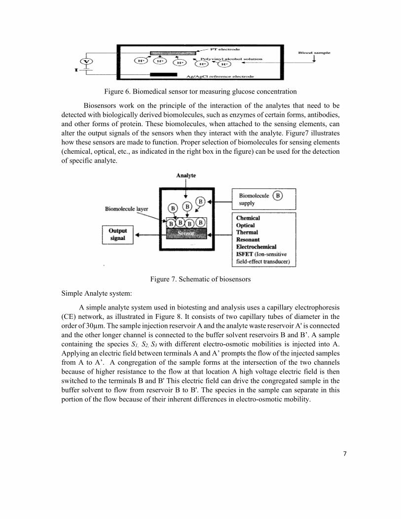
It’s used to measure biological substances as well as for medical diagnosis purposes. The miniaturized biomedical sensors have many advantages like they need minute amount of samples and can perform analyses much faster. Electrochemical sensors work on the principle that certain biological substances, such as glucose in human blood can release certain elements by chemical reaction, these elements can alter the electricity flow pattern in the sensor, which can be readily detected, a small sample of blood is introduced to a sensor with a polyvinyl alcohol solution. Two electrodes are present in the sensor; a platinum film electrode and a thin Ag/AgCl film is shown in figure 6. The chemical reaction takes place between the glucose and the oxygen in the polyvinyl alcohol solution
Glucose + 02 gluconolactone + H2O2 The H2O2 produced by this chemical reaction is electrolyzed by applying a potential to the platinum electrode, with production of positive hydrogen ions, which will flow toward this electrode. The amount of glucose concentration in the blood sample can thus be measured by measuring the current flow between the electrodes
7
Figure 6. Biomedical sensor tor measuring glucose concentration
Biosensors work on the principle of the interaction of the analytes that need to be detected with biologically derived biomolecules, such as enzymes of certain forms, antibodies, and other forms of protein. These biomolecules, when attached to the sensing elements, can alter the output signals of the sensors when they interact with the analyte. Figure7 illustrates how these sensors are made to function. Proper selection of biomolecules for sensing elements (chemical, optical, etc., as indicated in the right box in the figure) can be used for the detection of specific analyte.
Figure 7. Schematic of biosensors
Simple Analyte system:
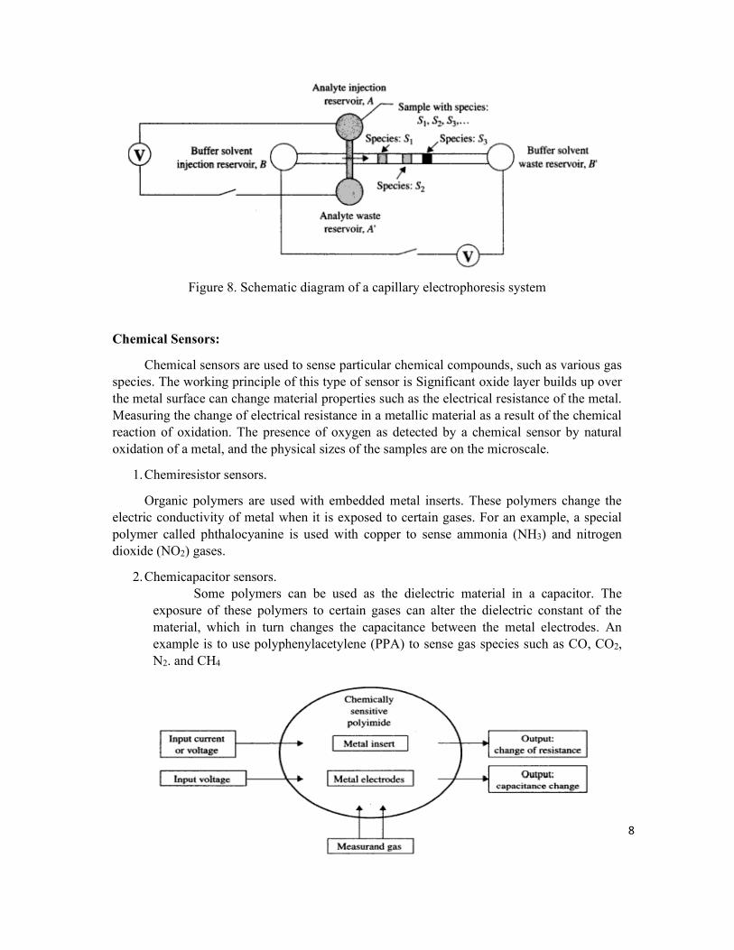
A simple analyte system used in biotesting and analysis uses a capillary electrophoresis (CE) network, as illustrated in Figure 8. It consists of two capillary tubes of diameter in the order of 30µm. The sample injection reservoir A and the analyte waste reservoir A' is connected and the other longer channel is connected to the buffer solvent reservoirs B and B’. A sample containing the species S1, S2, S3 with different electro-osmotic mobilities is injected into A. Applying an electric field between terminals A and A’ prompts the flow of the injected samples from A to A’. A congregation of the sample forms at the intersection of the two channels because of higher resistance to the flow at that location A high voltage electric field is then switched to the terminals B and B' This electric field can drive the congregated sample in the buffer solvent to flow from reservoir B to B'. The species in the sample can separate in this portion of the flow because of their inherent differences in electro-osmotic mobility.
8
Figure 8. Schematic diagram of a capillary electrophoresis system
Chemical Sensors:
Chemical sensors are used to sense particular chemical compounds, such as various gas species. The working principle of this type of sensor is Significant oxide layer builds up over the metal surface can change material properties such as the electrical resistance of the metal. Measuring the change of electrical resistance in a metallic material as a result of the chemical reaction of oxidation. The presence of oxygen as detected by a chemical sensor by natural oxidation of a metal, and the physical sizes of the samples are on the microscale.
1. Chemiresistor sensors.
Organic polymers are used with embedded metal inserts. These polymers change the electric conductivity of metal when it is exposed to certain gases. For an example, a special polymer called phthalocyanine is used with copper to sense ammonia (NH3) and nitrogen dioxide (NO2) gases.
2. Chemicapacitor sensors. Some polymers can be used as the dielectric material in a capacitor. The exposure of these polymers to certain gases can alter the dielectric constant of the material, which in turn changes the capacitance between the metal electrodes. An example is to use polyphenylacetylene (PPA) to sense gas species such as CO, CO2, N2. and CH4
9
Figure 9. Working Principle of Chemical Sensors 3. Chemimechanical sensors:
There are certain materials, e.g., polymers, that change shape when they are exposed to chemicals (including moisture). Such chemicals can be found by measuring the change of the dimensions of the material. An example of such sensor is a moisture sensor using pyraline P1-2722.
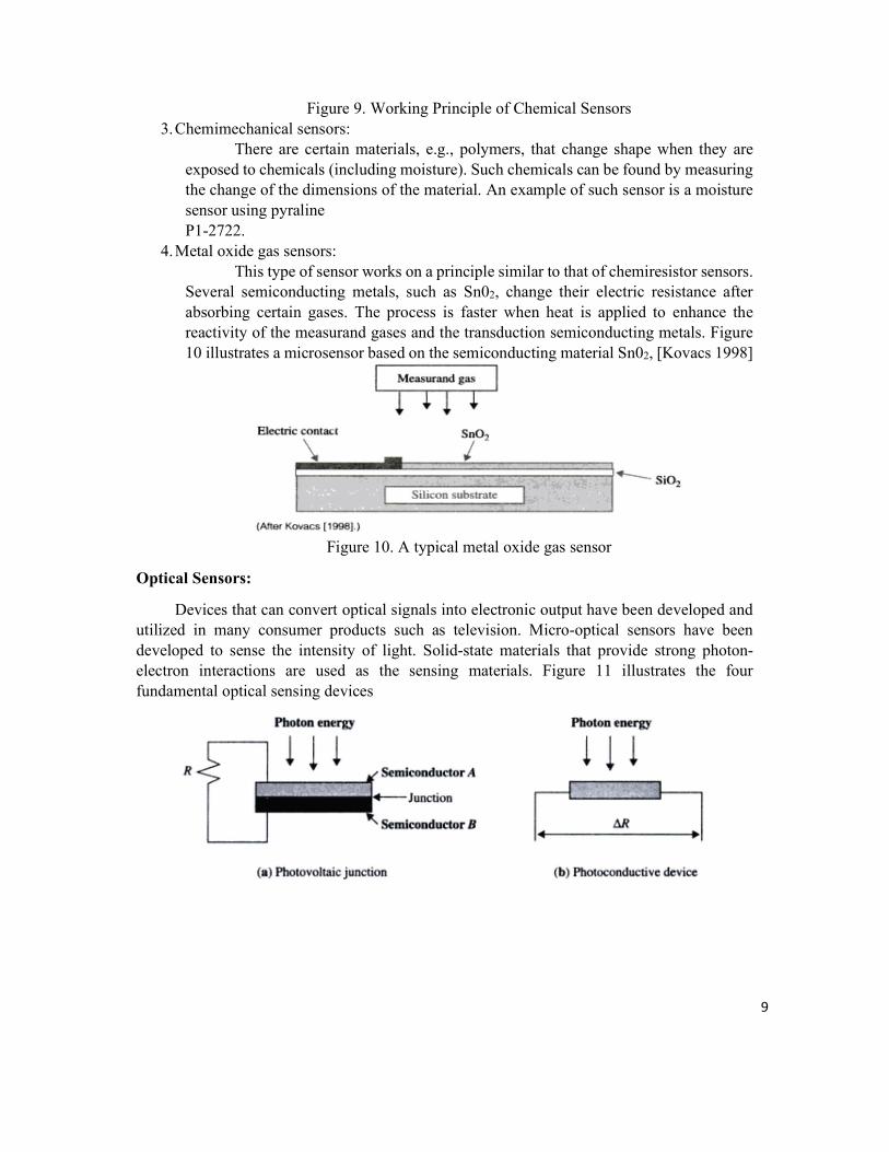
4. Metal oxide gas sensors: This type of sensor works on a principle similar to that of chemiresistor sensors. Several semiconducting metals, such as Sn02, change their electric resistance after absorbing certain gases. The process is faster when heat is applied to enhance the reactivity of the measurand gases and the transduction semiconducting metals. Figure 10 illustrates a microsensor based on the semiconducting material Sn02, [Kovacs 1998]
Figure 10. A typical metal oxide gas sensor
Optical Sensors:
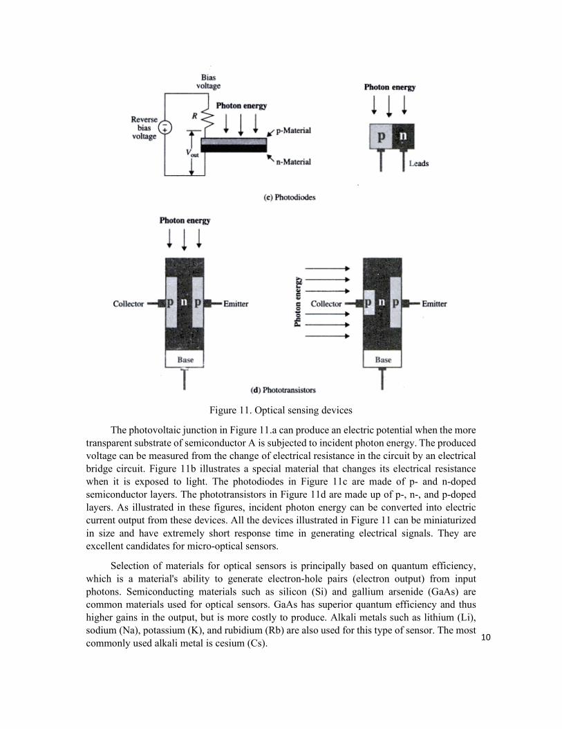
Devices that can convert optical signals into electronic output have been developed and utilized in many consumer products such as television. Micro-optical sensors have been developed to sense the intensity of light. Solid-state materials that provide strong photon-electron interactions are used as the sensing materials. Figure 11 illustrates the four fundamental optical sensing devices
10
Figure 11. Optical sensing devices
The photovoltaic junction in Figure 11.a can produce an electric potential when the more transparent substrate of semiconductor A is subjected to incident photon energy. The produced voltage can be measured from the change of electrical resistance in the circuit by an electrical bridge circuit. Figure 11b illustrates a special material that changes its electrical resistance when it is exposed to light. The photodiodes in Figure 11c are made of p- and n-doped semiconductor layers. The phototransistors in Figure 11d are made up of p-, n-, and p-doped layers. As illustrated in these figures, incident photon energy can be converted into electric current output from these devices. All the devices illustrated in Figure 11 can be miniaturized in size and have extremely short response time in generating electrical signals. They are excellent candidates for micro-optical sensors.
Selection of materials for optical sensors is principally based on quantum efficiency, which is a material's ability to generate electron-hole pairs (electron output) from input photons. Semiconducting materials such as silicon (Si) and gallium arsenide (GaAs) are common materials used for optical sensors. GaAs has superior quantum efficiency and thus higher gains in the output, but is more costly to produce. Alkali metals such as lithium (Li), sodium (Na), potassium (K), and rubidium (Rb) are also used for this type of sensor. The most commonly used alkali metal is cesium (Cs).
11
Pressure Sensors
These sensors function on the principle of mechanical deformation and stresses of thin diaphragms induced by the measurand pressure. Mechanically induced diaphragm deformation and stresses are then converted into electrical signal output through several means of transduction.
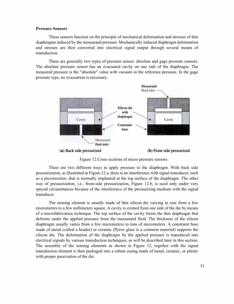
There are generally two types of pressure sensor: absolute and gage pressure sensors. The absolute pressure sensor has an evacuated cavity on one side of the diaphragm. The measured pressure is the "absolute" value with vacuum as the reference pressure. In the gage pressure type, no evacuation is necessary.
Figure 12.Cross sections of micro pressure sensors
There are two different ways to apply pressure to the diaphragm. With back side pressurization, as illustrated in Figure 12.a, there is no interference with signal transducer, such as a piezoresistor, that is normally implanted at the top surface of the diaphragm. The other way of pressurization, i.e., front-side pressurization, Figure 12.b, is used only under very special circumstances because of the interference of the pressurizing medium with the signal transducer.
The sensing element is usually made of thin silicon die varying in size from a few micrometers to a few millimeters square. A cavity is created from one side of the die by means of a microfabrication technique. The top surface of the cavity forms the thin diaphragm that deforms under the applied pressure from the measurand fluid. The thickness of the silicon diaphragm usually varies from a few micrometers to tens of micrometers. A constraint base made of metal (called a header) or ceramic (Pyrex glass is a common material) supports the silicon die. The deformation of the diaphragm by the applied pressure is transduced into electrical signals by various transduction techniques, as will be described later in this section. The assembly of the sensing elements as shown in Figure 12, together with the signal transduction element is then packaged into a robust casing made of metal, ceramic, or plastic with proper passivation of the die.
12
Figure 13. Micro Pressure sensor Assembly
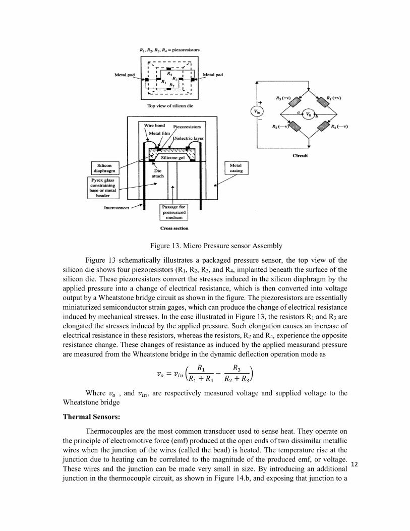
Figure 13 schematically illustrates a packaged pressure sensor, the top view of the silicon die shows four piezoresistors (R1, R2, R3, and R4, implanted beneath the surface of the silicon die. These piezoresistors convert the stresses induced in the silicon diaphragm by the applied pressure into a change of electrical resistance, which is then converted into voltage output by a Wheatstone bridge circuit as shown in the figure. The piezoresistors are essentially miniaturized semiconductor strain gages, which can produce the change of electrical resistance induced by mechanical stresses. In the case illustrated in Figure 13, the resistors R1 and R3 are elongated the stresses induced by the applied pressure. Such elongation causes an increase of electrical resistance in these resistors, whereas the resistors, R2 and R4, experience the opposite resistance change. These changes of resistance as induced by the applied measurand pressure are measured from the Wheatstone bridge in the dynamic deflection operation mode as
𝑣 = 𝑣𝑅
𝑅 + 𝑅−
𝑅
𝑅 + 𝑅
Where 𝑣 , and 𝑣 , are respectively measured voltage and supplied voltage to the Wheatstone bridge
Thermal Sensors:
Thermocouples are the most common transducer used to sense heat. They operate on the principle of electromotive force (emf) produced at the open ends of two dissimilar metallic wires when the junction of the wires (called the bead) is heated. The temperature rise at the junction due to heating can be correlated to the magnitude of the produced emf, or voltage. These wires and the junction can be made very small in size. By introducing an additional junction in the thermocouple circuit, as shown in Figure 14.b, and exposing that junction to a
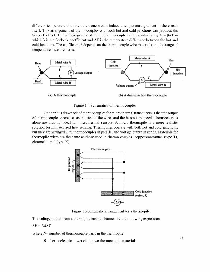
13
different temperature than the other, one would induce a temperature gradient in the circuit itself. This arrangement of thermocouples with both hot and cold junctions can produce the Seebeck effect. The voltage generated by the thermocouple can be evaluated by V = β∆T in which β is the Seebeck coefficient and ∆T is the temperature difference between the hot and cold junctions. The coefficient β depends on the thermocouple wire materials and the range of temperature measurements.
Figure 14. Schematics of thermocouples
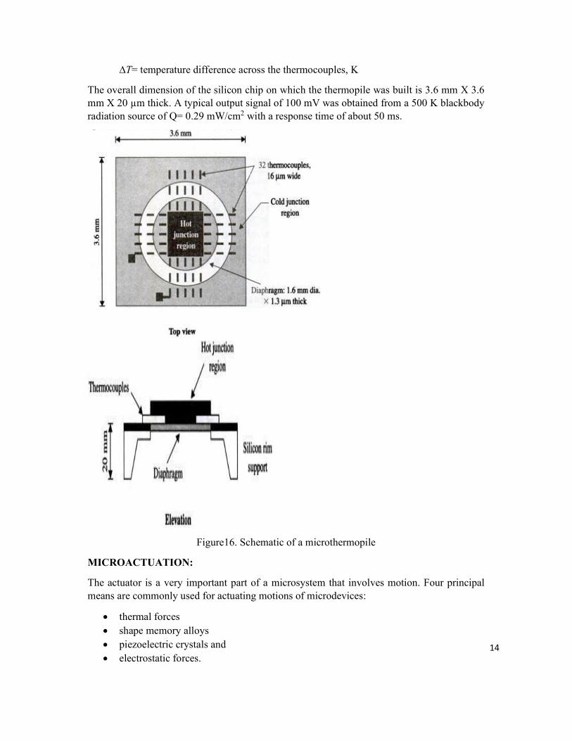
One serious drawback of thermocouples for micro thermal transducers is that the output of thermocouples decreases as the size of the wires and the beads is reduced. Thermocouples alone are thus not ideal for microthermal sensors. A micro thermopile is a more realistic solution for miniaturized heat sensing. Thermopiles operate with both hot and cold junctions, but they are arranged with thermocouples in parallel and voltage output in series. Materials for thermopile wires are the same as those used in thermo-couples- copper/constantan (type T), chrome/alumel (type K)
Figure 15 Schematic arrangement tor a thermopile
The voltage output from a thermopile can be obtained by the following expression
∆V = Nβ∆T
Where N= number of thermocouple pairs in the thermopile
Β= thermoelectric power of the two thermocouple materials
14
∆T= temperature difference across the thermocouples, K
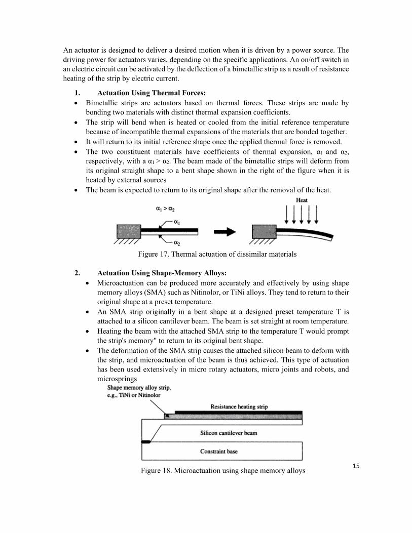
The overall dimension of the silicon chip on which the thermopile was built is 3.6 mm X 3.6 mm X 20 µm thick. A typical output signal of 100 mV was obtained from a 500 K blackbody radiation source of Q= 0.29 mW/cm2 with a response time of about 50 ms.
Figure16. Schematic of a microthermopile
MICROACTUATION:
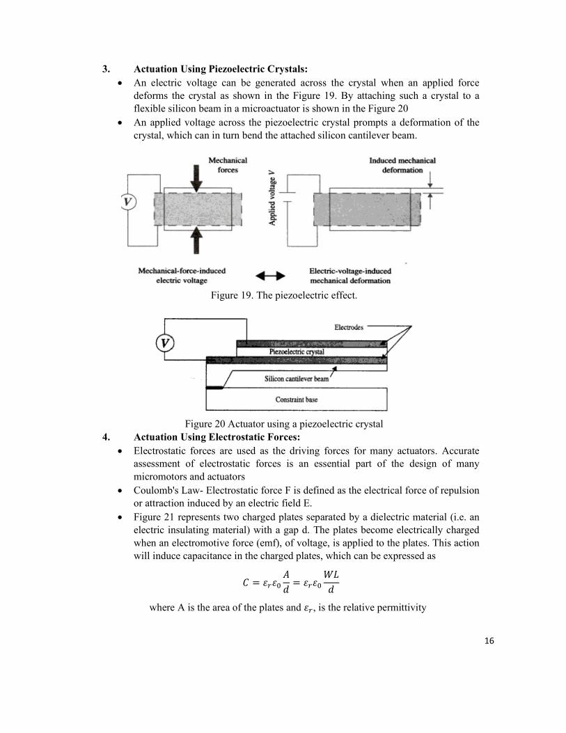
The actuator is a very important part of a microsystem that involves motion. Four principal means are commonly used for actuating motions of microdevices:
thermal forces shape memory alloys piezoelectric crystals and electrostatic forces.
15
An actuator is designed to deliver a desired motion when it is driven by a power source. The driving power for actuators varies, depending on the specific applications. An on/off switch in an electric circuit can be activated by the deflection of a bimetallic strip as a result of resistance heating of the strip by electric current.
1. Actuation Using Thermal Forces: Bimetallic strips are actuators based on thermal forces. These strips are made by
bonding two materials with distinct thermal expansion coefficients. The strip will bend when is heated or cooled from the initial reference temperature
because of incompatible thermal expansions of the materials that are bonded together. It will return to its initial reference shape once the applied thermal force is removed. The two constituent materials have coefficients of thermal expansion, α1 and α2,
respectively, with a α1 > α2. The beam made of the bimetallic strips will deform from its original straight shape to a bent shape shown in the right of the figure when it is heated by external sources
The beam is expected to return to its original shape after the removal of the heat.
Figure 17. Thermal actuation of dissimilar materials
2. Actuation Using Shape-Memory Alloys:
Microactuation can be produced more accurately and effectively by using shape memory alloys (SMA) such as Nitinolor, or TiNi alloys. They tend to return to their original shape at a preset temperature.
An SMA strip originally in a bent shape at a designed preset temperature T is attached to a silicon cantilever beam. The beam is set straight at room temperature.
Heating the beam with the attached SMA strip to the temperature T would prompt the strip's memory" to return to its original bent shape.
The deformation of the SMA strip causes the attached silicon beam to deform with the strip, and microactuation of the beam is thus achieved. This type of actuation has been used extensively in micro rotary actuators, micro joints and robots, and microsprings
Figure 18. Microactuation using shape memory alloys
16
3. Actuation Using Piezoelectric Crystals: An electric voltage can be generated across the crystal when an applied force
deforms the crystal as shown in the Figure 19. By attaching such a crystal to a flexible silicon beam in a microactuator is shown in the Figure 20
An applied voltage across the piezoelectric crystal prompts a deformation of the crystal, which can in turn bend the attached silicon cantilever beam.
Figure 19. The piezoelectric effect.
Figure 20 Actuator using a piezoelectric crystal
4. Actuation Using Electrostatic Forces: Electrostatic forces are used as the driving forces for many actuators. Accurate
assessment of electrostatic forces is an essential part of the design of many micromotors and actuators
Coulomb's Law- Electrostatic force F is defined as the electrical force of repulsion or attraction induced by an electric field E.
Figure 21 represents two charged plates separated by a dielectric material (i.e. an electric insulating material) with a gap d. The plates become electrically charged when an electromotive force (emf), of voltage, is applied to the plates. This action will induce capacitance in the charged plates, which can be expressed as
𝐶 = 𝜀 𝜀𝐴
𝑑= 𝜀 𝜀
𝑊𝐿
𝑑
where A is the area of the plates and 𝜀 , is the relative permittivity
17
Figure. 21 Electric potential in two parallel plates
The charges that are stored in either plate can be discharged instantly by short circuiting the plates with a conductor. The energy associated with this electric potential can be expressed as
𝑈 = −1
2𝑐𝑣 = 𝜀 𝜀
𝑊𝐿
2𝑑
The designation of forces indicated in Figure 22, expressions for the two forces in the two directions
𝐹 =1
2
𝜀 𝜀 𝐿𝑉
𝑑
In width direction
𝐹 =1
2
𝜀 𝜀 𝑊𝑉
𝑑
In Length direction
Figure. 22 Electrostatic forces on parallel plates
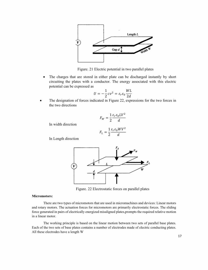
Micromotors:
There are two types of micromotors that are used in micromachines and devices: Linear motors and rotary motors. The actuation forces for micromotors are primarily electrostatic forces. The sliding force generated in pairs of electrically energized misaligned plates,prompts the required relative motion in a linear motor.
The working principle is based on the linear motion between two sets of parallel base plates. Each of the two sets of base plates contains a number of electrodes made of electric conducting plates. All these electrodes have a length W
18
Figure 23. Working principle of electrostatic micromotors
• The bottom base plate has an electrode pitch of W whereas the top base plate has a slightly different pitch, say W+ W/3 . The two sets of base plates are initially misaligned by W/3.
• We may set the bottom plates as stationary so the top plates can slide over the bottom plates in the horizontal plane.
• Thus, on energizing the pair of electrodes A and A' can cause the motion of the top plates moving to the left until A and A' are fully aligned.
• At that moment, the electrodes B and B' are misaligned by the same amount, W/3.
• One can energize the misaligned pair B - B' and prompt the top plates to move by another W/3 distance toward the left.
• We may envisage that by then the C-C' pair is misaligned by W/3 and the subsequent energizing of that pair would produce a similar motion of the top plates to the left by another distance of W/3.
• The motion will be completed by yet another sequence of energizing the last pair, D-D'
• We may thus conclude that with carefully arranged electrodes in the top and bottom base plates and proper pitches, one can create the necessary electrostatic forces that are required to provide the relative motion between the two sets of base plates.
• It is readily seen that the smaller the preset misalignment of the electrode plates, the smoother the motion becomes. Rotary micromotors can be made to work by a similar principle
• A major problem in micromotor design and construction is the bearings for the rotors
Micromotors built on the principles of electrostatic forces are described in de-tail by Fan. Rotary motors driven by electrostatic forces can be constructed in a similar way. Figure 23 shows a top view of an electrostatically driven micromotor. The electrodes are installed in the outer surface of the rotor poles and the inner surface of the stator poles. As in the case of linear motors, pitches of electrodes in rotor poles and stator poles are mismatched in such a way that they will generate an electrostatic driving force due to misalignment of the energized pairs of electrodes.
19
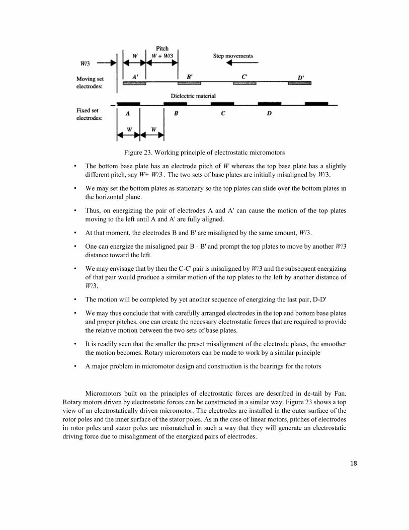
Figure 24 Schematic of a micro rotary motor
The ratio of poles in the stator to those in the rotor is 3:2. The air gap between rotor poles and stator poles can be as small as 2 µm. The outside diameter of the stator poles is in the neighborhood of I00 µm, whereas the length of the rotor poles is about 20 to 25 µm. One serious problem that is encountered by engineers in the design and manufacture of micro rotary motors is the wear and lubrication of the bearings. Typically these motors rotate at over I0,000 revolutions per minute (rpm). With such high rotational speed, the bearing quickly wears off, which results in wobbling of the rotors. Much effort is needed for the solution of this problem. Consequently, micro tribology, which deals with friction, wear and lubrication, has become a critical research area in microtechnology.
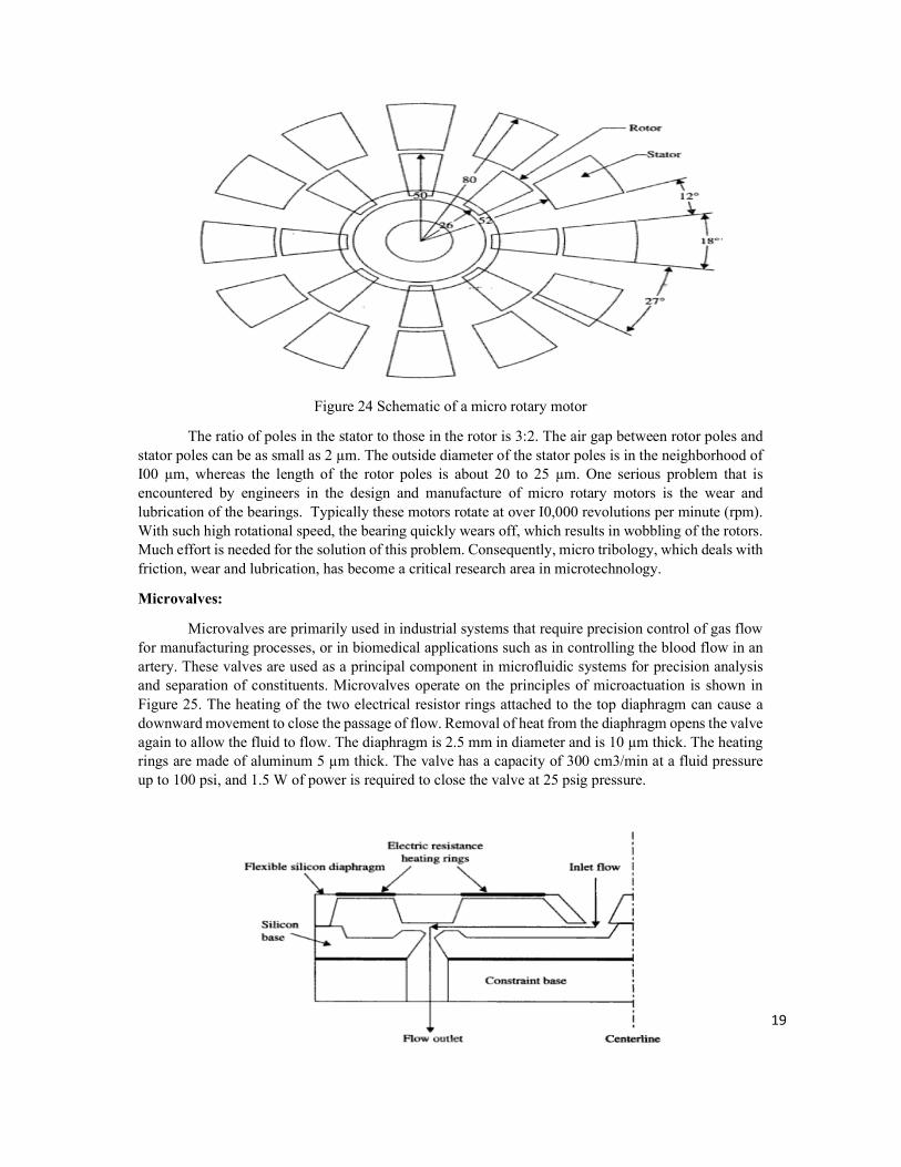
Microvalves:
Microvalves are primarily used in industrial systems that require precision control of gas flow for manufacturing processes, or in biomedical applications such as in controlling the blood flow in an artery. These valves are used as a principal component in microfluidic systems for precision analysis and separation of constituents. Microvalves operate on the principles of microactuation is shown in Figure 25. The heating of the two electrical resistor rings attached to the top diaphragm can cause a downward movement to close the passage of flow. Removal of heat from the diaphragm opens the valve again to allow the fluid to flow. The diaphragm is 2.5 mm in diameter and is 10 µm thick. The heating rings are made of aluminum 5 µm thick. The valve has a capacity of 300 cm3/min at a fluid pressure up to 100 psi, and 1.5 W of power is required to close the valve at 25 psig pressure.
20
Figure 25 Schematic diagram of a micro valve
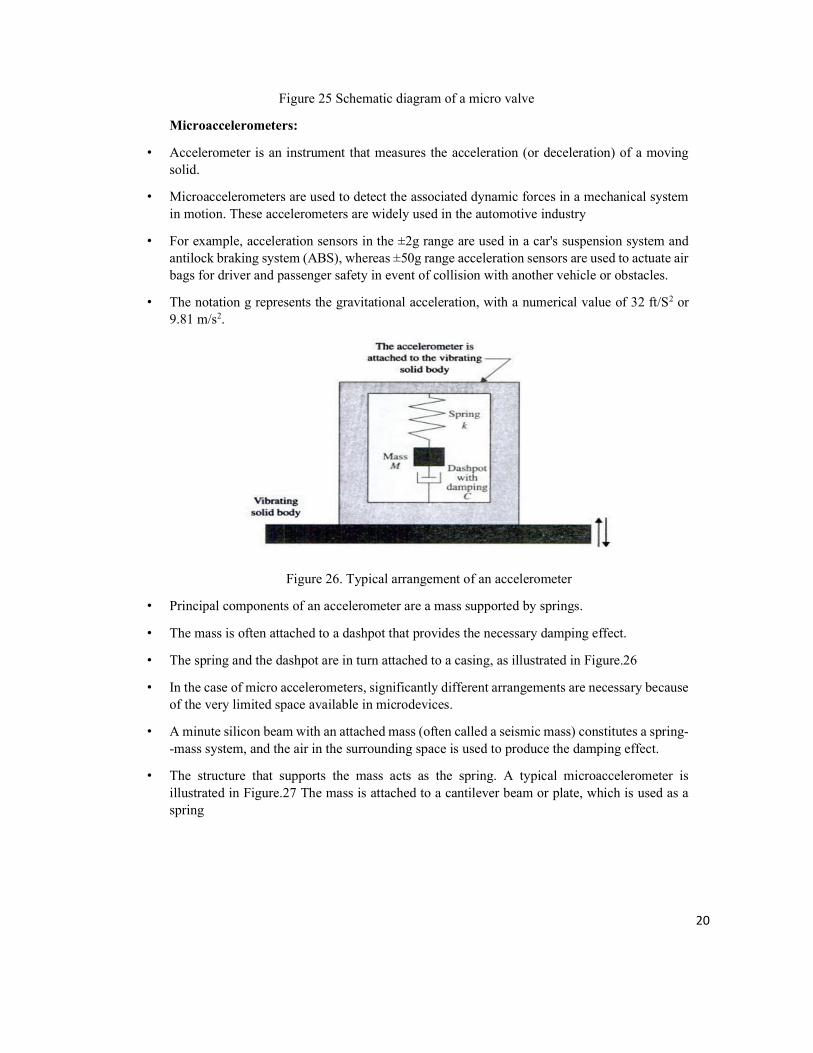
Microaccelerometers:
• Accelerometer is an instrument that measures the acceleration (or deceleration) of a moving solid.
• Microaccelerometers are used to detect the associated dynamic forces in a mechanical system in motion. These accelerometers are widely used in the automotive industry
• For example, acceleration sensors in the ±2g range are used in a car's suspension system and antilock braking system (ABS), whereas ±50g range acceleration sensors are used to actuate air bags for driver and passenger safety in event of collision with another vehicle or obstacles.
• The notation g represents the gravitational acceleration, with a numerical value of 32 ft/S2 or 9.81 m/s2.
Figure 26. Typical arrangement of an accelerometer
• Principal components of an accelerometer are a mass supported by springs.
• The mass is often attached to a dashpot that provides the necessary damping effect.
• The spring and the dashpot are in turn attached to a casing, as illustrated in Figure.26
• In the case of micro accelerometers, significantly different arrangements are necessary because of the very limited space available in microdevices.
• A minute silicon beam with an attached mass (often called a seismic mass) constitutes a spring--mass system, and the air in the surrounding space is used to produce the damping effect.
• The structure that supports the mass acts as the spring. A typical microaccelerometer is illustrated in Figure.27 The mass is attached to a cantilever beam or plate, which is used as a spring
21
Figure 27. Schematic structure of a microaccelerometer
• A piezoresistor is implanted on the beam or plate to measure the deformation of the attached mass, from which the amplitudes and thus the acceleration of the vibrating mass can be correlated.
• Since acceleration (or deceleration) is related to the driving dynamic force that causes the vibration of the solid body to which the casing is attached, accurate measurement of acceleration can thus enable engineers to measure the applied dynamic force.
• It is not surprising to find that microaccelerometers are widely used as a trigger to activate airbags in automobiles in an event of collision, and also to sense the excessive vibration of the chassis of a vehicle from its suspension system.
• There are many different types of accelerometers available commercially. Signal transducers used in microaccelerometers include piezoelectric piezoresistive, capacitive, and resonant members
Figure 28 Schematic arrangement of a micro inertia sensor
• The sensing element, i.e., the accelerometer, has a special configuration as illustrated in Figure 28.a
• A thin beam is attached to two tethers at both ends. The tethers are made of elastic material and are anchored at one side as shown in the figure.
• The thin beam acts as the seismic mass called the proof mass with an electrode plate attached.
• The electrode plate that is attached to the proof mass is placed between two fixed electrodes
22
• In the event of an acceleration of the unit, the proof mass will displace in the direction opposite to the acceleration, as shown in Figure 28.b
• The movement of the proof mass induced by the acceleration can be correlated with the capacitance change between the pair of the electrodes.
REFERENCES
1. Vijay K. Varadan, K. J. Vinoy and K. A. Jose , “RF MEMS & Their Applications”, John Wiley & Sons, 2003.
2. Tai - Rai Hsu, “MEMS and Microsystems Design and Manufacturing”, Tata MC Graw Hill, New Delhi, Edition 2002.
3. Gabriel M Rebeiz, “RF MEMS - Theory Design and Technology”, John Wiley and Sons, 2003. 4. Nadim Maluf, “An introduction to Micro electro mechanical system design”, Artech House ,2000.
PART A
S.NO Questions 1. Explain the difference between MEMS and microsystems 2. Mention the type of sensor used to identify the presence of oxygen. Explain the operation of the sensor
3.
A parallel capacitor is made of two square plates with the dimensions L= W= 1000 µm (or 1 mm), as shown in Figure. Determine the normal electrostatic force if the gap between these two plates is d= 2 µm. The plates are separated by static air
4. Identify the right actuator used for Automatic Greenhouse Ventilation and explain the operation of the sensor
5. Identify the sensor in the diagram and explain its operation
23
6. Distinguish between Microelectronics and Microsystem. 7. Summarize the advantages and disadvantages of piezoelectric sensing and actuation. 8. Give the principle of electrostatic sensors and actuators. 9. Generalize the role of actuators and sensors in the context of MEMS. 10. Write the principle of pressure sensor in MEMS.
PART B
S.NO Questions 1. Aside from seat belts, airbags are the first thing drivers think of when it comes to staying safe on the
road. In the case of a crash or collision, airbags coming to the rescue is a reassurance set in the back of many drivers’ minds. Identify the sensors needed for the airbag deployment and explain it in detail.
2. Describe the role of semiconductor materials in the design of MEMS 3. Analyze the functional relationship between the actuating element and the transduction unit in a
Micro actuator. 4. Tabulate the difference between Microelectronics and MEMS. 5. Explain in detail the operation of electrostatic micro motor with appropriate sketches
24
UNIT – II - MEMS FABRICATION– SECA3007
25
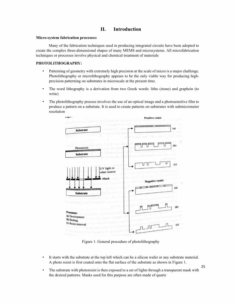
II. Introduction
Micro-system fabrication processes:
Many of the fabrication techniques used in producing integrated circuits have been adopted to create the complex three-dimensional shapes of many MEMS and microsystems. All microfabrication techniques or processes involve physical and chemical treatment of materials
PHOTOLITHOGRAPHY:
• Patterning of geometry with extremely high precision at the scale of micro is a major challenge. Photolithography or microlithography appears to be the only viable way for producing high-precision patterning on substrates in microscale at the present time.
• The word lithography is a derivation from two Greek words: litho (stone) and graphein (to write)
• The photolithography process involves the use of an optical image and a photosensitive film to produce a pattern on a substrate. It is used to create patterns on substrates with submicrometer resolution
Figure 1. General procedure of photolithography
• It starts with the substrate at the top left which can be a silicon wafer or any substrate material. A photo resist is first coated onto the flat surface of the substrate as shown in Figure 1.
• The substrate with photoresist is then exposed to a set of lights through a transparent mask with the desired patterns. Masks used for this purpose are often made of quartz
26
• Patterns on the mask are photographically reduced from macro-sizes to the desired micro scales. Photoresist materials change their solubility when they are exposed to light, they become soluble under light and called as positive photoresists. The retained photoresist materials create the imprinted patterns after the development
• The Portion of the substrate under the shadow of the photoresists is protected from the subsequent etching. A permanent pattern is thus created in the substrate after the removal of the photoresist.
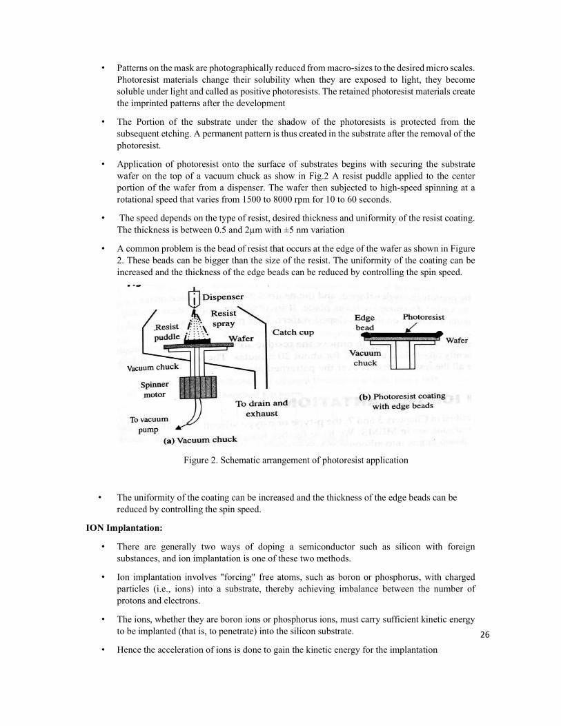
• Application of photoresist onto the surface of substrates begins with securing the substrate wafer on the top of a vacuum chuck as show in Fig.2 A resist puddle applied to the center portion of the wafer from a dispenser. The wafer then subjected to high-speed spinning at a rotational speed that varies from 1500 to 8000 rpm for 10 to 60 seconds.
• The speed depends on the type of resist, desired thickness and uniformity of the resist coating. The thickness is between 0.5 and 2µm with ±5 nm variation
• A common problem is the bead of resist that occurs at the edge of the wafer as shown in Figure 2. These beads can be bigger than the size of the resist. The uniformity of the coating can be increased and the thickness of the edge beads can be reduced by controlling the spin speed.
Figure 2. Schematic arrangement of photoresist application
• The uniformity of the coating can be increased and the thickness of the edge beads can be reduced by controlling the spin speed.
ION Implantation:
• There are generally two ways of doping a semiconductor such as silicon with foreign substances, and ion implantation is one of these two methods.
• Ion implantation involves "forcing" free atoms, such as boron or phosphorus, with charged particles (i.e., ions) into a substrate, thereby achieving imbalance between the number of protons and electrons.
• The ions, whether they are boron ions or phosphorus ions, must carry sufficient kinetic energy to be implanted (that is, to penetrate) into the silicon substrate.
• Hence the acceleration of ions is done to gain the kinetic energy for the implantation
27
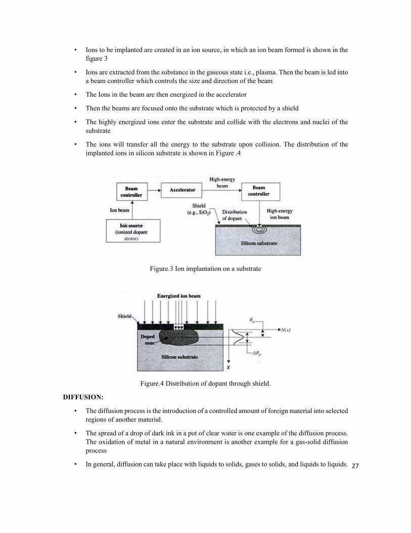
• Ions to be implanted are created in an ion source, in which an ion beam formed is shown in the figure 3
• Ions are extracted from the substance in the gaseous state i.e., plasma. Then the beam is led into a beam controller which controls the size and direction of the beam
• The Ions in the beam are then energized in the accelerator
• Then the beams are focused onto the substrate which is protected by a shield
• The highly energized ions enter the substrate and collide with the electrons and nuclei of the substrate
• The ions will transfer all the energy to the substrate upon collision. The distribution of the implanted ions in silicon substrate is shown in Figure .4
Figure.3 Ion implantation on a substrate
Figure.4 Distribution of dopant through shield.
DIFFUSION:
• The diffusion process is the introduction of a controlled amount of foreign material into selected regions of another material.
• The spread of a drop of dark ink in a pot of clear water is one example of the diffusion process. The oxidation of metal in a natural environment is another example for a gas-solid diffusion process
• In general, diffusion can take place with liquids to solids, gases to solids, and liquids to liquids.
28
• In microfabrication, diffusion is used to oxidize a wafer surface, depositing desired thin films of different materials on the base substrates and building up epitaxial layers over single-crystal substrates in IC fabrication.
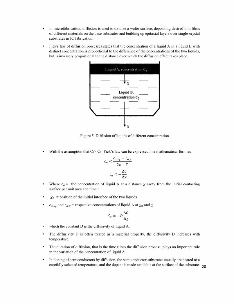
• Fick's law of diffusion processes states that the concentration of a liquid A in a liquid B with distinct concentration is proportional to the difference of the concentrations of the two liquids, but is inversely proportional to the distance over which the diffusion effect takes place.
Figure 5. Diffusion of liquids of different concentration
• With the assumption that C1> C2 , Fick’s law can be expressed in a mathematical form as
𝑐 ∝𝑐 , − 𝑐 ,
𝜒 − 𝜒
𝑐 ∝ −Δ𝑐
Δ𝑥
• Where 𝑐 = the concentration of liquid A at a distance 𝜒 away from the initial contacting surface per unit area and time t
• 𝜒 = position of the initial interface of the two liquids
• 𝑐 , and 𝑐 , = respective concentrations of liquid A at 𝜒 and 𝜒
𝐶 = −𝐷Δ𝐶
Δ𝜒
• which the constant D is the diffusivity of liquid A.
• The diffusivity D is often treated as a material property, the diffusivity D increases with temperature.
• The duration of diffusion, that is the time r into the diffusion process, plays an important role in the variation of the concentration of liquid A
• In doping of semiconductors by diffusion, the semiconductor substrates usually are heated to a carefully selected temperature, and the dopant is made available at the surface of the substrate.
29
• A mask made of a material that is resistant to the diffusion of the dopant covers the substrate surface during the doping process.
• The opening made on the mask allows the dopant to be diffused into the substrate surface, and thereby controls the region to be doped.
• The dopant can diffuse into the substrate until a maximum concentration is reached. This maximum concentration of dopant through diffusion is called solid solubility.
𝐽 = −𝐷∂𝐶
∂𝑥
• J = atoms or molecules, or ion flux, of the foreign materials to be diffused into the substrate material (atoms/m.s)
• D = diffusion coefficient, or diffusivity, of the foreign material in the substrate material (m2/s)
• C = concentration of the foreign material in the substrate (atoms/m3)
• Unlike ion implantation, diffusion is a slow doping process and takes place at elevated temperatures. It is also used as thin-film buildings in microelectronics and microsystems.
• The atoms of the dopant gas move (diffuse) into the crystal vacancies, or interstitials, of the silicon substrate
• Fick's law gives the dopant flux in the substrate in the 𝜒 direction during a diffusion process.
𝐹 = −𝐷∂𝑁(𝑥)
∂𝑥
• F = dopant flux, the number of dopant atoms passing through a unit area of the substrate in a unit time, atoms/cm2-s.
• D = diffusion coefficient, or diffusivity, of the dopant to the substrate, cm2/s
• N= dopant concentration in the substrate per unit volume, atoms/cm3
• The distribution of dopant in the substrate at any given time during the diffusion
∂𝑁(𝑥, 𝑡)
∂𝑡= 𝐷
∂ 𝑁(𝑥, 𝑡)
∂𝑥
• The result depends on the intital and boundary conditions .They are
• Initial condition: 𝑁(𝑥, 0) = 0 , 𝑖. 𝑒 there is no impurity in the substrate when the diffusion process begins
• Boundary conditions:
• 𝑁(0, 𝑡) = 𝑁𝑠, which is the concentration at the surface exposed to the gaseous dopant
• 𝑁(∞, 𝑡) = 0 i. e. , the diffusion of foreign substance is localized, and the concentration fas away
30
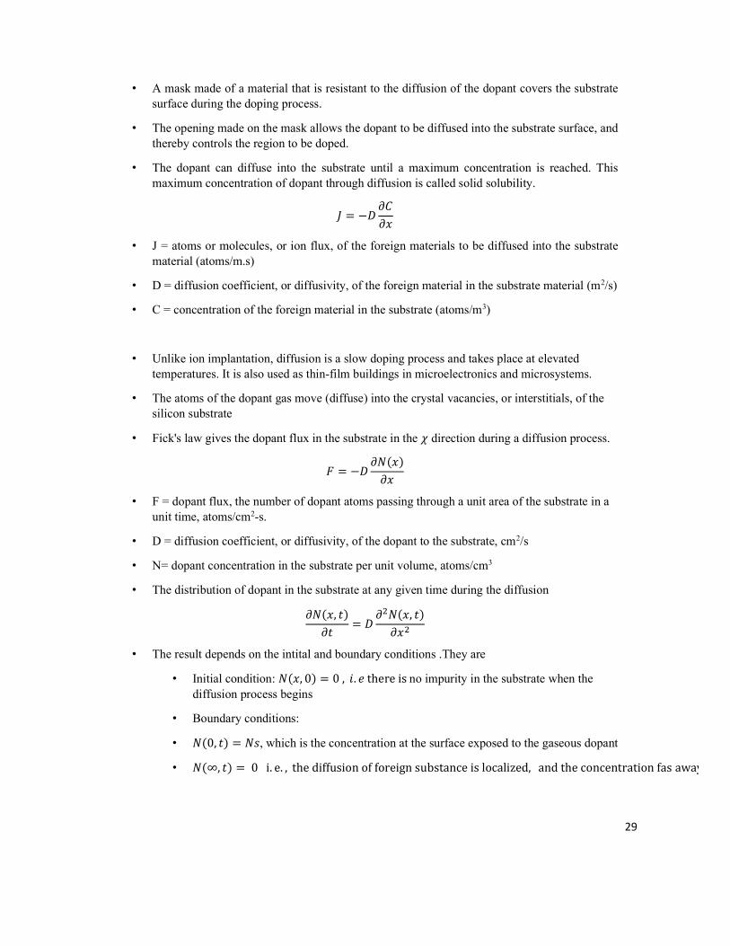
OXIDATION:
• Silicon dioxide is produced by thermal oxidation in an electric resistance furnace. The furnace consists of a large fused quartz tube with resistance heating coils surround the tube to provide the necessary high temperature in the tube
• The furnace tube used in industry is 30cm in diameter and 3m in length
• In the thermal oxidation process, wafers are placed in fused quartz cassettes that are pushed into the preheated furnace tube at a temperature in the range of 900 to 1200C.
• Oxygen is blown into the tubular furnace for the oxidation of wafer surfaces. Often, steam is used instead of oxygen for accelerated oxidation.
• The timing,temperature, and gas flow are strictly controlled in order to achieve the desired quality and thickness of the Si02 film.
Figure. 6 Facility for thermal oxidation of silicon dioxide
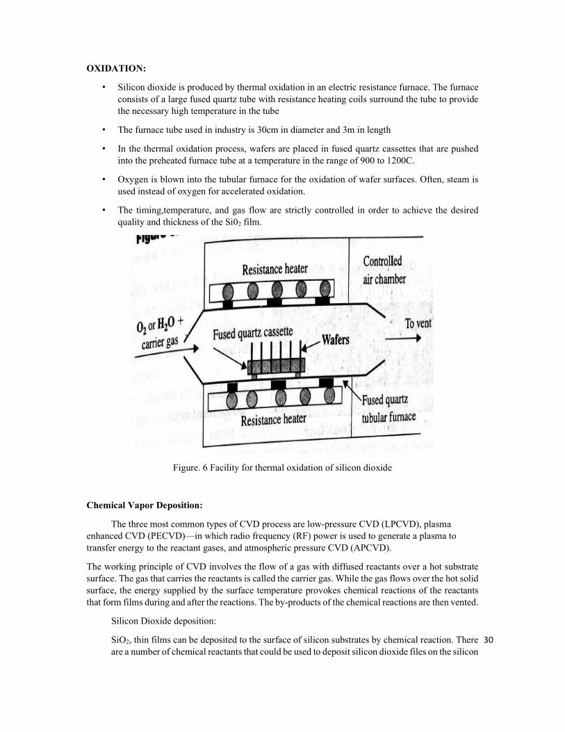
Chemical Vapor Deposition:
The three most common types of CVD process are low-pressure CVD (LPCVD), plasma enhanced CVD (PECVD)—in which radio frequency (RF) power is used to generate a plasma to transfer energy to the reactant gases, and atmospheric pressure CVD (APCVD).
The working principle of CVD involves the flow of a gas with diffused reactants over a hot substrate surface. The gas that carries the reactants is called the carrier gas. While the gas flows over the hot solid surface, the energy supplied by the surface temperature provokes chemical reactions of the reactants that form films during and after the reactions. The by-products of the chemical reactions are then vented.
Silicon Dioxide deposition:
SiO2, thin films can be deposited to the surface of silicon substrates by chemical reaction. There are a number of chemical reactants that could be used to deposit silicon dioxide files on the silicon
31
substrates like SiCl4, SiBr4 and SiH2Cl2. The carrier gases that can be used in these processes are 02, NO, NO2 and CO2 with H2.
SiH + O → SiO + 2H
Figure 7. Two typical CVD reactors
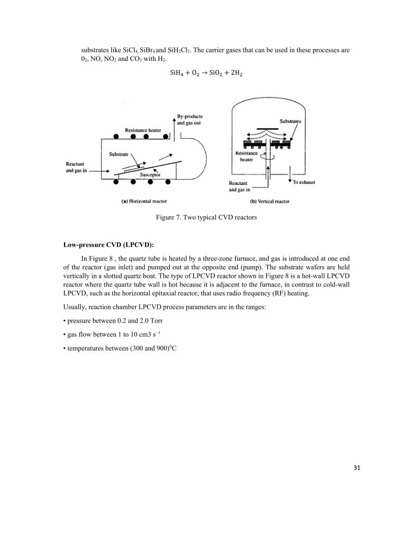
Low-pressure CVD (LPCVD):
In Figure 8 , the quartz tube is heated by a three-zone furnace, and gas is introduced at one end of the reactor (gas inlet) and pumped out at the opposite end (pump). The substrate wafers are held vertically in a slotted quartz boat. The type of LPCVD reactor shown in Figure 8 is a hot-wall LPCVD reactor where the quartz tube wall is hot because it is adjacent to the furnace, in contrast to cold-wall LPCVD, such as the horizontal epitaxial reactor, that uses radio frequency (RF) heating.
Usually, reaction chamber LPCVD process parameters are in the ranges:
• pressure between 0.2 and 2.0 Torr
• gas flow between 1 to 10 cm3 s−1
• temperatures between (300 and 900)0C
32
Figure-8 Typical layout of low-pressure chemical vapor deposition reactor
33
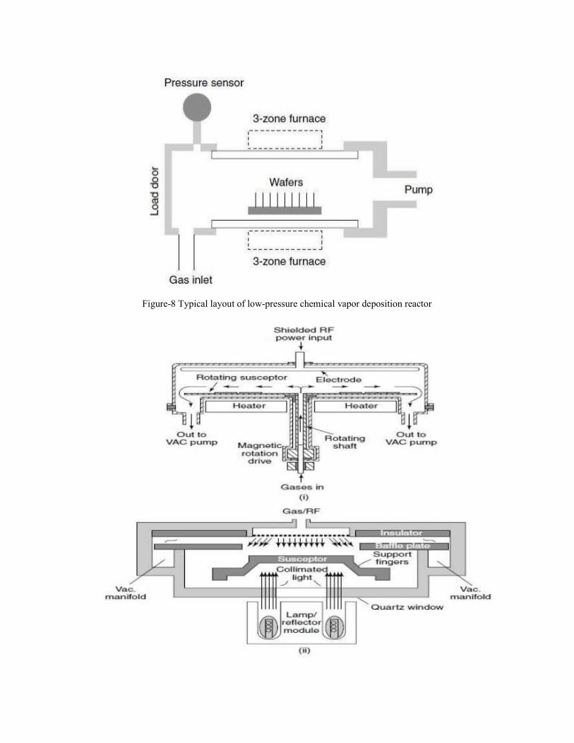
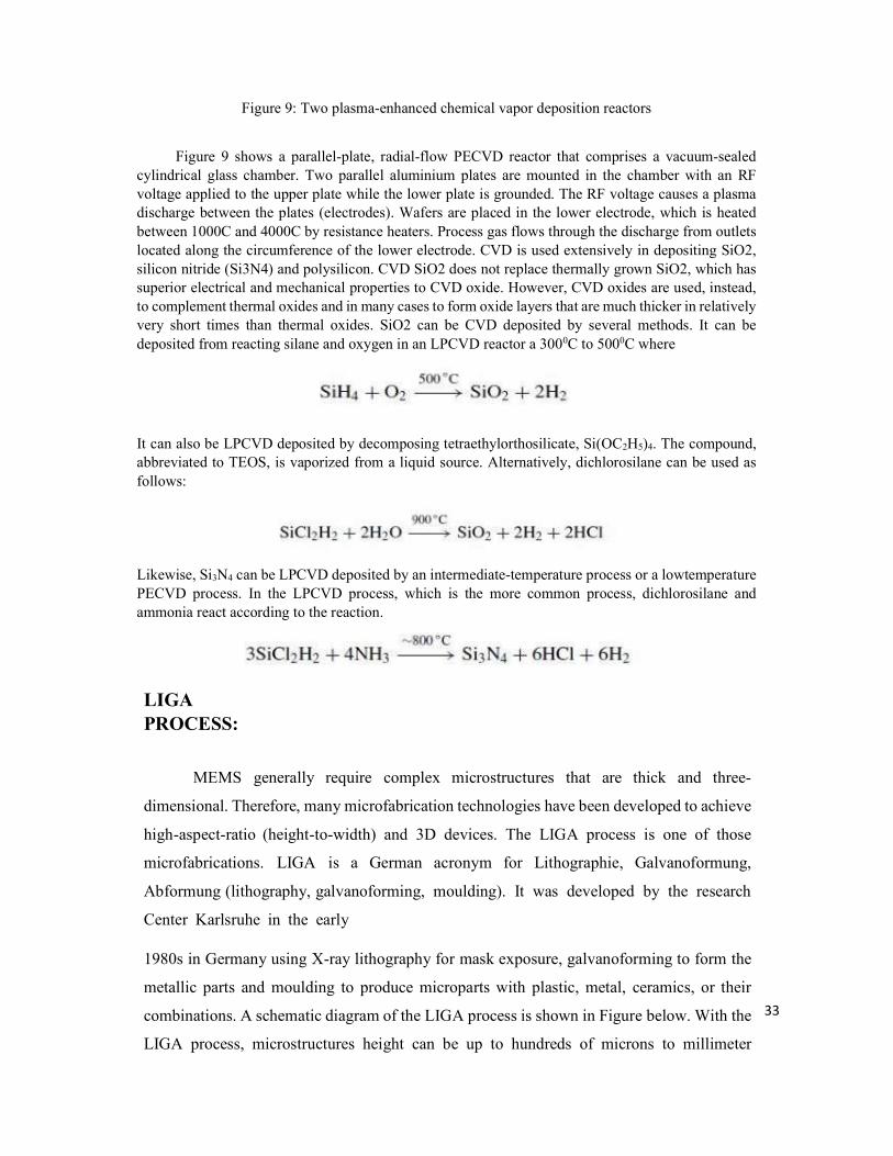
Figure 9: Two plasma-enhanced chemical vapor deposition reactors
Figure 9 shows a parallel-plate, radial-flow PECVD reactor that comprises a vacuum-sealed cylindrical glass chamber. Two parallel aluminium plates are mounted in the chamber with an RF voltage applied to the upper plate while the lower plate is grounded. The RF voltage causes a plasma discharge between the plates (electrodes). Wafers are placed in the lower electrode, which is heated between 1000C and 4000C by resistance heaters. Process gas flows through the discharge from outlets located along the circumference of the lower electrode. CVD is used extensively in depositing SiO2, silicon nitride (Si3N4) and polysilicon. CVD SiO2 does not replace thermally grown SiO2, which has superior electrical and mechanical properties to CVD oxide. However, CVD oxides are used, instead, to complement thermal oxides and in many cases to form oxide layers that are much thicker in relatively very short times than thermal oxides. SiO2 can be CVD deposited by several methods. It can be deposited from reacting silane and oxygen in an LPCVD reactor a 3000C to 5000C where
It can also be LPCVD deposited by decomposing tetraethylorthosilicate, Si(OC2H5)4. The compound, abbreviated to TEOS, is vaporized from a liquid source. Alternatively, dichlorosilane can be used as follows:
Likewise, Si3N4 can be LPCVD deposited by an intermediate-temperature process or a lowtemperature PECVD process. In the LPCVD process, which is the more common process, dichlorosilane and ammonia react according to the reaction.
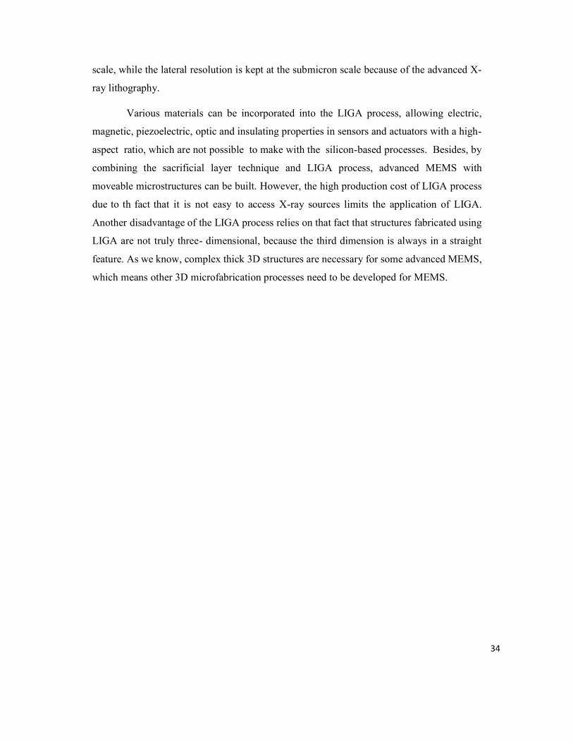
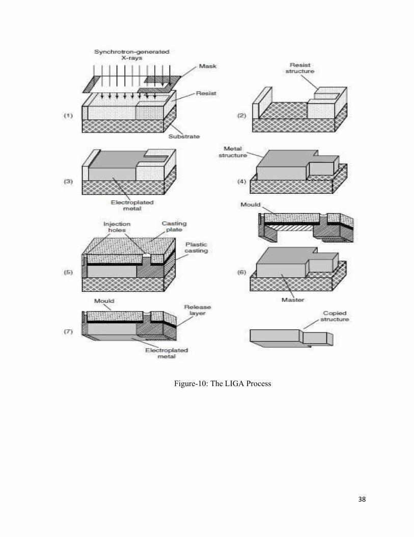
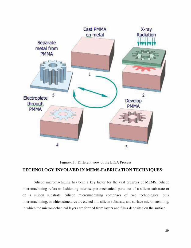
LIGA PROCESS:
MEMS generally require complex microstructures that are thick and three-
dimensional. Therefore, many microfabrication technologies have been developed to achieve
high-aspect-ratio (height-to-width) and 3D devices. The LIGA process is one of those
microfabrications. LIGA is a German acronym for Lithographie, Galvanoformung,
Abformung (lithography, galvanoforming, moulding). It was developed by the research
Center Karlsruhe in the early
1980s in Germany using X-ray lithography for mask exposure, galvanoforming to form the
metallic parts and moulding to produce microparts with plastic, metal, ceramics, or their
combinations. A schematic diagram of the LIGA process is shown in Figure below. With the
LIGA process, microstructures height can be up to hundreds of microns to millimeter
34
scale, while the lateral resolution is kept at the submicron scale because of the advanced X-
ray lithography.
Various materials can be incorporated into the LIGA process, allowing electric,
magnetic, piezoelectric, optic and insulating properties in sensors and actuators with a high-
aspect ratio, which are not possible to make with the silicon-based processes. Besides, by
combining the sacrificial layer technique and LIGA process, advanced MEMS with
moveable microstructures can be built. However, the high production cost of LIGA process
due to th fact that it is not easy to access X-ray sources limits the application of LIGA.
Another disadvantage of the LIGA process relies on that fact that structures fabricated using
LIGA are not truly three- dimensional, because the third dimension is always in a straight
feature. As we know, complex thick 3D structures are necessary for some advanced MEMS,
which means other 3D microfabrication processes need to be developed for MEMS.
38
Figure-10: The LIGA Process
39
Figure-11: Different view of the LIGA Process
TECHNOLOGY INVOLVED IN MEMS-FABRICATION TECHNIQUES:
Silicon micromachining has been a key factor for the vast progress of MEMS. Silicon
micromachining refers to fashioning microscopic mechanical parts out of a silicon substrate or
on a silicon substrate. Silicon micromachining comprises of two technologies: bulk
micromachining, in which structures are etched into silicon substrate, and surface micromachining,
in which the micromechanical layers are formed from layers and films deposited on the surface.
40
Bulk micromachining and surface micromachining are the two major micromachining
processes of silicon; silicon wafer bonding is usually necessary for silicon microfabrication.
LIGA and three dimensional (3D) microfabrications have been used for high-aspect ratio and 3D
microstructures fabrication for MEMS.
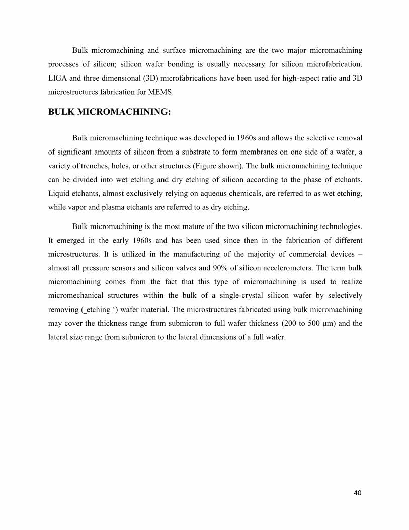
BULK MICROMACHINING:
Bulk micromachining technique was developed in 1960s and allows the selective removal
of significant amounts of silicon from a substrate to form membranes on one side of a wafer, a
variety of trenches, holes, or other structures (Figure shown). The bulk micromachining technique
can be divided into wet etching and dry etching of silicon according to the phase of etchants.
Liquid etchants, almost exclusively relying on aqueous chemicals, are referred to as wet etching,
while vapor and plasma etchants are referred to as dry etching.
Bulk micromachining is the most mature of the two silicon micromachining technologies.
It emerged in the early 1960s and has been used since then in the fabrication of different
microstructures. It is utilized in the manufacturing of the majority of commercial devices –
almost all pressure sensors and silicon valves and 90% of silicon accelerometers. The term bulk
micromachining comes from the fact that this type of micromachining is used to realize
micromechanical structures within the bulk of a single-crystal silicon wafer by selectively
removing (‗etching ‘) wafer material. The microstructures fabricated using bulk micromachining
may cover the thickness range from submicron to full wafer thickness (200 to 500 μm) and the
lateral size range from submicron to the lateral dimensions of a full wafer.
41
Figure-12: Bulk silicon micromachining: (a) isotropic etching; (b) anisotropic etching; (c)
anisotropic etching with buried etch-stop layer; (d) dielectric membrane released by back- side
bulk etching; (e) dopant dependent wet etching.
For etching such thick silicon substrate, anisotropic wet etchants such as solutions of
potassium hydroxide (KOH), ethylenediamine pyrocatechol (EDP), tetramethylammonium
hydroxide (TMAH) and hydrazine-water are used. These etchants have different etch rates in
different crystal orientations of the silicon. Wet etching in most case is done from the back side
of the wafer while the plasma-etching is being applied to the front side. In recent years, a
vertical-walled bulk micromachining technique known as SCREAM (single-crystal reactive
etching and metallization), which is a combination of anisotropic and isotropic plasma etching, is
42
used. The etch process can be made selective by the use of dopants (heavily doped regions etch
slowly), or may even be halted electrochemically (e.g., etching stops upon encountering a region
of different polarity in a biased p–n junction). A region at which wet etching tends to slow down
or diminish is called an etch-stop ‘. There are several ways in which an etch-stop region can be
created; doping-selective etching (DSE) and bias-dependent DSE. Wet etching occurs by dipping
substrate into an etching bath or spraying it with etchants which may be acid or alkaline. Wet
etching can either be isotropic etching or anisotropic etching depending on the structure of the
materials or the etchants used. If the material is amorphous or polycrystalline, wet etching is always
isotropic etching (Figure a). During isotropic etching (etchants used are acid solution), resist is
always undercut, meaning the deep etching is not practical for MEMS. Single-crystal silicon can
be anisotropically etched. The etching features are determined by the etching speed, which is
dependent on the crystal ‘s orientation. The etching slows down significantly at the (111)
planes of silicon, relative to other planes. With the chosen wafers with different crystal orientation,
different buck machined features can be achieved (Figures b and c). Most common etchants used
for anisotropic etching of silicon include alkali hydroxide etchants (KOH, NaOH, etc.),
ammonium-based solutions {NH4OH, TMAH [(CH3)4NOH], etc.} and EDP (ethylene diamine
pyrocatechol, and water). By combining anisotropic etching with boron implantation (P+ etch-
stop), and electrochemical etch-stop technique, varied silicon microstructures can be bulk
machined.
Dry etching occurs through chemical or physical interaction between the ions in the gas
and the atoms of the substrate. Nonplasma, isotropic dry etching can be possible using xenon
difluoride or a mixture of interhalogen gases and provides very high selectivity for aluminum,
silicon dioxide, silicon nitride, photoresist, etc. The most common dry etching of bulk silicon is
plasma etching and reactive ion etching (RIE) etching, where the external energy in the form of
RF powder drives chemical reactions in low-pressure reaction chambers. A wide variety of
chlorofluorocarbon gases, sulfur hexafluoride, bromine compounds and oxygen are commonly
used as reactants. The anisotropic dry etching processes are widely used in MEMS because of
the geometry flexibility and less chemical contamination than in wet etching sometimes.
With bulk-micromachined silicon microstructures, the wafer-bonding technique is
necessary for the assembled MEMS devices. Surface micromachining, however, can be used to
build the monolithic MEMS devices.
43
SURFACE MICROMACHINING:
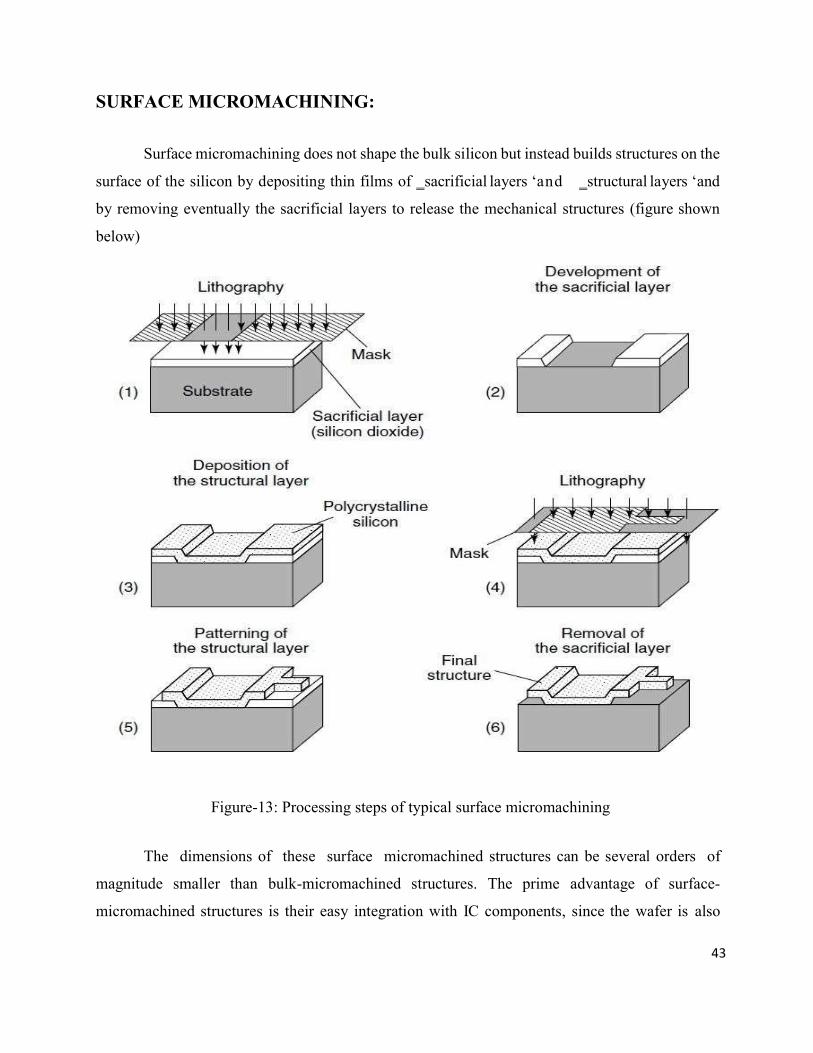
Surface micromachining does not shape the bulk silicon but instead builds structures on the
surface of the silicon by depositing thin films of ‗sacrificial layers ‘and ‗structural layers ‘and
by removing eventually the sacrificial layers to release the mechanical structures (figure shown
below)
Figure-13: Processing steps of typical surface micromachining
The dimensions of these surface micromachined structures can be several orders of
magnitude smaller than bulk-micromachined structures. The prime advantage of surface-
micromachined structures is their easy integration with IC components, since the wafer is also
44
the working for IC elements. It should be noted that as miniaturization in immensely increased
by surface micromachining, the small mass structure involved may be insufficient for a number
of mechanical sensing and actuation applications. Surface micromachining requires a compatible
set of structural materials, sacrificial materials and chemical etchants. The structural materials must
possess the physical and chemical properties that are suitable for the desired application. In
addition, they must have satisfactory mechanical properties; e.g., high yield and fracture stresses,
minimal creep and fatigue and good wear resistance. The sacrificial materials must have good
mechanical properties to avoid device failure during fabrication. These properties include good
adhesion and low residual stresses in order to eliminate device failure by delamination and/or
cracking. The etchants to remove the sacrificial materials must have excellent etch selectivity
and they must be able to etch off the sacrificial materials without affecting the structural ones. In
addition, the etchants must have proper viscosity and surface tension characteristics. The common
IC compatible materials used in surface micromachining are: (1) polysilicon/Silicon dioxide; low-
pressure chemical vapor deposition (LPCVD) deposited polysilicon as the structural material and
LPCVD deposited oxide as the sacrificial material.
The oxide is readily dissolved in HF solution without the polysilicon being affected.
Together with this material system, silicon nitride is often used for electrical insulation. (2)
Polyimide/aluminum; in this case polyimide is the structural materialand aluminum is the
sacrificial material. Acid-based etchants are used to dissolve the aluminum sacrificial layer. (3)
Silicon nitride/polysilicon; silicon nitride is used as the structural material, whereas polysilicon is
the sacrificial material. For this material system, silicon anisotropic etchants such as KOH and EDP
are used to dissolve polysilicon. (4) Tungsten/silicon dioxide; CVD deposited tungsten is used as
the structural material with oxide as the sacrificial material. HF solution is used to remove
the sacrificial oxide. Other IC-compatible materials such as silicon carbide, diamond-like carbon,
zinc oxide, gold, etc. are also used.
Surface micromachining could also be performed using dry etching methods. Plasma
etching of the silicon substrate with SF6/O2-based and CF4/H2-based gas mixtures is
advantageous since high selectivities for photoresist, silicon dioxide and aluminum masks can be
achieved. However, when using plasma etching, a large undercut of the mask is observed. This is
due to the isotropic fluorine atom etching of silicon which is known to be high compared with
45
the vertical etch induced by ion bombardment. In contrast, reactive ion etching of poly-Si using a
chlorine/fluorine gas combination produces virtually no undercut and almost vertical etch profiles
when using photoresist as a masking material. Thus, rectangular silicon patterns which are up to
30mm deep can be formed using chlorine/fluorine plasmas out of polysilicon films and the silicon
wafer surface. Silicon microstructures fabricated by surface micromachining are usually planar
structures (or are two dimensional). Other techniques involving the use of thin- film structural
materials released by the removal of an underlying sacrificial layer have helped to extend
conventional surface micromachining into the third dimension. By connecting polysilicon plates
to the substrate and to each other with hinges, 3D micromechanical structures can be assembled
after release. Another approach to 3D structures used the conformal deposition of polysilicon and
sacrificial oxide films to fill deep trenches previously etched in the silicon substrate.
ETCHING:
In order to form a functional MEMS structure on a substrate, it is necessary to etch (remove
or take away) the thin films previously deposited and/or the substrate itself. In general, there are
two classes of etching processes:
1. Wet etching where the material is dissolved when immersed in a chemical solution
2. Dry etching where the material is sputtered or dissolved using reactive ions or a vapor
phase etchant
Wet etching:
This is the simplest etching technology. All it requires is a container with a liquid
solution that will dissolve the material in question. Unfortunately, there are complications since
usually a mask is desired to selectively etch the material. One must find a mask that will not
dissolve or at least etches much slower than the material to be patterned. Secondly, some single
crystal materials, such as silicon, exhibit anisotropic etching in certain chemicals. Anisotropic
etching in contrast to isotropic etching means different etch rates in different directions in the
material. The classic example of this is the <111> crystal plane sidewalls that appear when etching
a hole in a <100> silicon wafer in a chemical such as potassium hydroxide (KOH). The result is a
pyramid shaped hole instead of a hole with rounded sidewalls with an isotropic etchant.

46
When to use wet etching?
This is a simple technology, which will give good results if you can find the combination
of etchant and mask material to suit your application. Wet etching works very well for etching thin
films on substrates, and can also be used to etch the substrate itself. The problem with substrate
etching is that isotropic processes will cause undercutting of the mask layer by the same
distance as the etch depth. Anisotropic processes allow the etching to stop on certain crystal
planes in the substrate, but still results in a loss of space, since these planes cannot be vertical to
the surface when etching holes or cavities. If this is a limitation for you, you should consider dry
etching of the substrate instead. However, keep in mind that the cost per wafer will be 1-2 orders
of magnitude higher to perform the dry etching
If we are making very small features in thin films (comparable to the film thickness), we
may also encounter problems with isotropic wet etching, since the undercutting will be at least
equal to the film thickness. With dry etching it is possible etch almost straight down without
undercutting, which provides much higher resolution.
47
Figure-14: Difference between anisotropic and isotropic wet etching.
DRY ETCHING:
The dry etching technology can split in three separate classes called reactive ion etching
(RIE), sputter etching, and vapor phase etching.
In RIE, the substrate is placed inside a reactor in which several gases are introduced. A
plasma is struck in the gas mixture using an RF power source, breaking the gas molecules into
48
ions. The ions are accelerated towards, and reacts at, the surface of the material being etched,
forming another gaseous material. This is known as the chemical part of reactive ion etching. There
is also a physical part which is similar in nature to the sputtering deposition process. If the ions
have high enough energy, they can knock atoms out of the material to be etched without a chemical
reaction. It is a very complex task to develop dry etch processes that balance chemical and physical
etching, since there are many parameters to adjust. By changing the balance it is possible to
influence the anisotropy of the etching, since the chemical part is isotropic and the physical part
highly anisotropic the combination can form sidewalls that have shapes from rounded to vertical.
A special subclass of RIE which continues to grow rapidly in popularity is deep RIE
(DRIE). In this process, etch depths of hundreds of microns can be achieved with almost vertical
sidewalls. The primary technology is based on the so-called "Bosch process", named after the
German company Robert Bosch which filed the original patent, where two different gas
compositions are alternated in the reactor. The first gas composition creates a polymer on the
surface of the substrate, and the second gas composition etches the substrate. The polymer is
immediately sputtered away by the physical part of the etching, but only on the horizontal surfaces
and not the sidewalls. Since the polymer only dissolves very slowly in the chemical part of the
etching, it builds up on the sidewalls and protects them from etching. As a result, etching aspect
ratios of 50 to 1 can be achieved. The process can easily be used to etch completely through
a silicon substrate, and etch rates are 3-4 times higher than wet etching.
Sputter etching is essentially RIE without reactive ions. The systems used are very
similar in principle to sputtering deposition systems. The big difference is that substrate is now
subjected to the ion bombardment instead of the material target used in sputter deposition.
Vapor phase etching is another dry etching method, which can be done with simpler
equipment than what RIE requires. In this process the wafer to be etched is placed inside a chamber,
in which one or more gases are introduced. The material to be etched is dissolved at the surface in
a chemical reaction with the gas molecules. The two most common vapor phase etching
technologies are silicon dioxide etching using hydrogen fluoride (HF) and silicon etching using
xenon diflouride (XeF2), both of which are isotropic in nature. Usually, care must be taken in the
design of a vapor phase process to not have bi-products form in the chemical reaction that condense
on the surface and interfere with the etching process.
49
When required to use dry etching?
The first thing to be noted about this technology is that it is expensive to run compared to
wet etching. If you are concerned with feature resolution in thin film structures or you need vertical
sidewalls for deep etchings in the substrate, you have to consider dry etching. If you are concerned
about the price of your process and device, you may want to minimize the use of dry etching. The
IC industry has long since adopted dry etching to achieve small features, but in many cases
feature size is not as critical in MEMS. Dry etching is an enabling technology, which comes at a
sometimes-high cost.
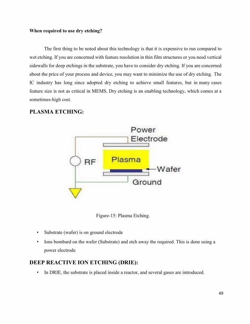
PLASMA ETCHING:
Figure-15: Plasma Etching.
• Substrate (wafer) is on ground electrode
• Ions bombard on the wafer (Substrate) and etch away the required. This is done using a
power electrode
DEEP REACTIVE ION ETCHING (DRIE):
• In DRIE, the substrate is placed inside a reactor, and several gases are introduced.
50
• Uses high density plasma to alternately etch and deposit etch resistant polymer on
sidewalls.
Chemical part: A plasma is struck in the gas mixture which breaks the gas molecules into
ions. The ions accelerate towards, and react with the surface of the material being etched,
forming another gaseous material.
Physical part: if the ions have high enough energy, they can knock atoms out of the material
to be etched without a chemical reaction.
REFERENCES:
1. Tai Ram Hsu, Mems and Microsystems, Design and Manufacture, TMH, 2008. 2. Mohammedhad-el-hak, MEMS Introduction & Fundamentals, CRC Press, 2005. 3. Marc J. Madou, Fundamentals of Microfabrication and Nanotechnology, 3rd Edition,
2011, CRC Press. ISBN 9780849331800
4. Harsingh Nalwa, Encyclopedia of Nanoscience and Nanotechnology, American Scientific Publishers, 2007.
5. Neelina Malsch, Biomedical Nanotechnology. CRC, 2005
PART A
S.NO Questions 1. Differentiate CVD and PVD. 2. Summarize the advantages in Surface Micromachining. 3. Which material is popularly used as the sacrificial layer in surface micro machining process? 4. What is micromachining? 5. What is micro fabrication? 6. With neat labelled figures, demonstrate the steps involved in photolithography. 7. Give the applications of MEMS in biomedical. 8. Why silicon is used as a substrate material. 9. What is sputtering? 10. Define diffusion
PART B
S.NO Questions 1. Summarize the processing steps of photolithography with neat sketch. 2. Describe about physical vapour deposition with relevant diagrams. 3. List out the various etching process and explain in detail with relevant diagrams 4. Give short notes on diffusion process used in MEMS industry. 5. Show how oxidation principle is used in Micro system fabrication. 6. Compare and contrast PECVD, APCVD and LPCVD. 7. Examine about ion implantation technique to produce Microsystems. 8. Explain briefly LIGA process.

51
UNIT – III - MICROSENSORS AND ACTUATORS– SECA3007
52
I. Introduction
Micro-sensing for MEMS
Electromechanical Transducers:
Various microsensing and microactuation mechanisms have been developed for MEMS
for diverse applications. Many microsensors based on different sensing principles for MEMS
have been developed including chemical sensors, gas sensors, optical sensors, biosensors,
thermal sensors and mechanical sensors.
Piezoresistive sensing:
Piezoresistive sensing utilizes resistors where the resistance is varied through external pressure,
to measure such physical parameters as pressure, force and flow rate or to be used as
accelerometer
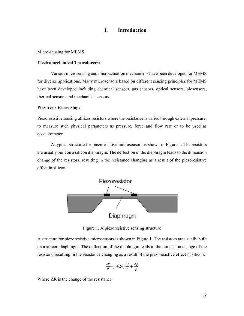
A typical structure for piezoresistive microsensors is shown in Figure 1. The resistors
are usually built on a silicon diaphragm. The deflection of the diaphragm leads to the dimension
change of the resistors, resulting in the resistance changing as a result of the piezoresistive
effect in silicon:
Figure 1. A piezoresistive sensing structure
A structure for piezoresistive microsensors is shown in Figure 1. The resistors are usually built
on a silicon diaphragm. The deflection of the diaphragm leads to the dimension change of the
resistors, resulting in the resistance changing as a result of the piezoresistive effect in silicon:
=(1+2ν) +
Where ΔR is the change of the resistance
53
R is the original resistance
ν is the Poisson ratio
𝛥𝑙 is the length change of the resistor
𝑙 is the original length of the resistor
𝛥𝜌 and ρ represent the resistivity change and resistivity of the resistor
The resistance of the resistors used for this type of piezoresistive microsensor is proportional
to the external pressure when the resistivity change is ignored, since the dimension change is
proportional to the applied pressure.
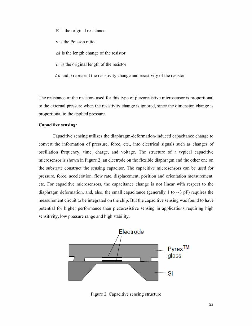
Capacitive sensing:
Capacitive sensing utilizes the diaphragm-deformation-induced capacitance change to
convert the information of pressure, force, etc., into electrical signals such as changes of
oscillation frequency, time, charge, and voltage. The structure of a typical capacitive
microsensor is shown in Figure 2; an electrode on the flexible diaphragm and the other one on
the substrate construct the sensing capacitor. The capacitive microsensors can be used for
pressure, force, acceleration, flow rate, displacement, position and orientation measurement,
etc. For capacitive microsensors, the capacitance change is not linear with respect to the
diaphragm deformation, and, also, the small capacitance (generally 1 to ∼3 pF) requires the
measurement circuit to be integrated on the chip. But the capacitive sensing was found to have
potential for higher performance than piezoresistive sensing in applications requiring high
sensitivity, low pressure range and high stability.
Figure 2. Capacitive sensing structure
54
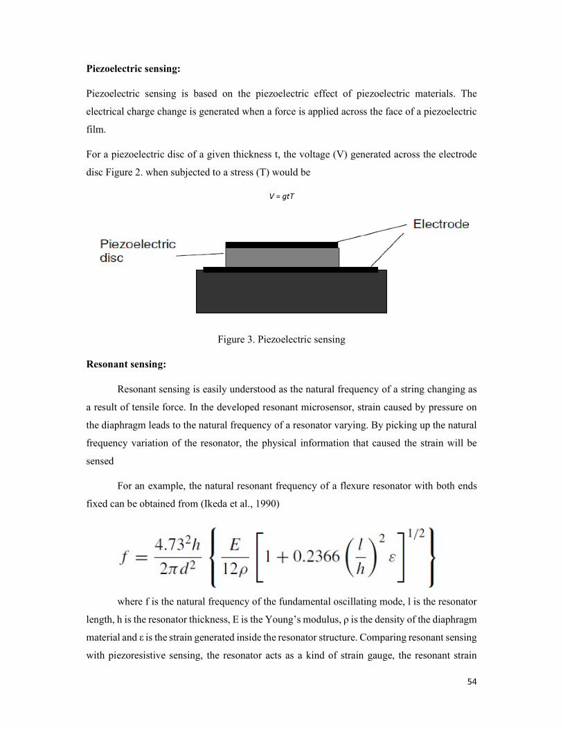
Piezoelectric sensing:
Piezoelectric sensing is based on the piezoelectric effect of piezoelectric materials. The
electrical charge change is generated when a force is applied across the face of a piezoelectric
film.
For a piezoelectric disc of a given thickness t, the voltage (V) generated across the electrode
disc Figure 2. when subjected to a stress (T) would be
V = gtT
Figure 3. Piezoelectric sensing
Resonant sensing:
Resonant sensing is easily understood as the natural frequency of a string changing as
a result of tensile force. In the developed resonant microsensor, strain caused by pressure on
the diaphragm leads to the natural frequency of a resonator varying. By picking up the natural
frequency variation of the resonator, the physical information that caused the strain will be
sensed
For an example, the natural resonant frequency of a flexure resonator with both ends
fixed can be obtained from (Ikeda et al., 1990)
where f is the natural frequency of the fundamental oscillating mode, l is the resonator
length, h is the resonator thickness, E is the Young’s modulus, ρ is the density of the diaphragm
material and ε is the strain generated inside the resonator structure. Comparing resonant sensing
with piezoresistive sensing, the resonator acts as a kind of strain gauge, the resonant strain
55
gauge, which relates the strain to the resonant frequency. Therefore, the gauge factor of the
above resonant strain gauge can be determined as:
If a strain is 100 ppm, for a 1.2-mm long, 20-micron wide and 5-micron thick resonator
strain gauge, the gauge factor can be as high as 3000, whereas the piezoresistive strain gauge
factor is only about 2. Since the gauge factor relates directly to the sensitivity of the sensor, the
resonant sensing can be used to obtain highly sensitive microsensors. However, resonant
sensing usually requires a more complex sensor structure than piezoresistive sensing does; the
resonant strain gauges need to be encapsulated from the fluid
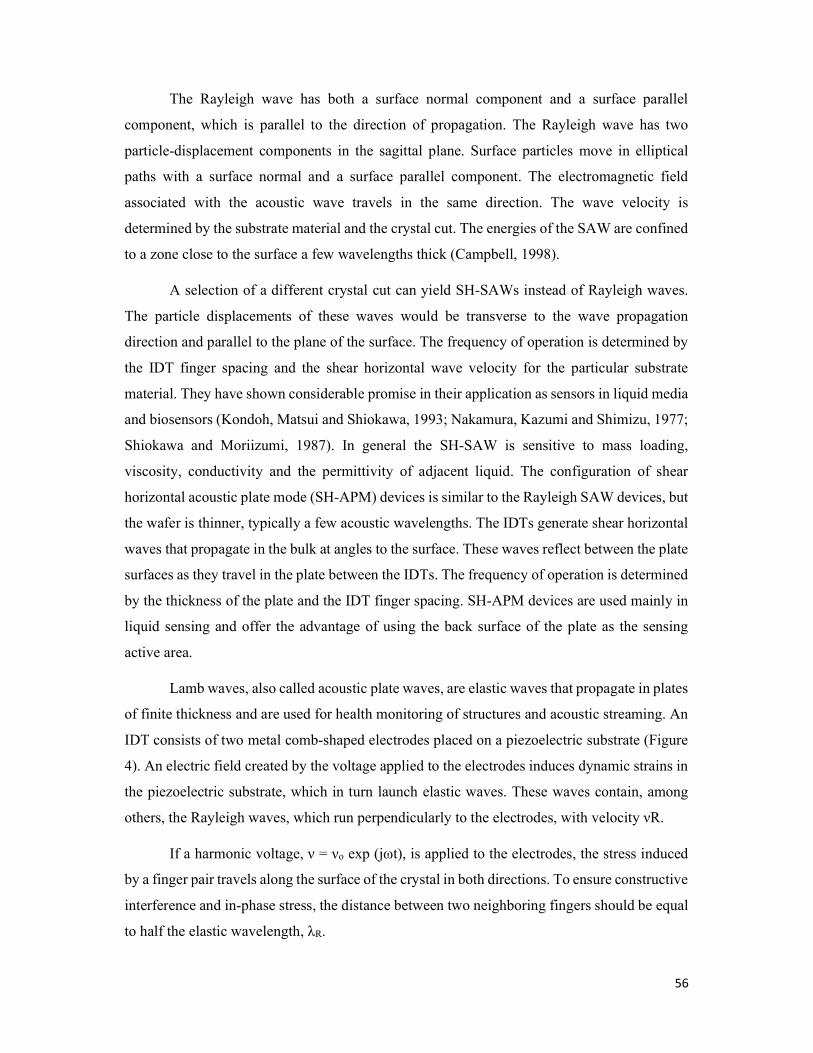
Surface acoustic wave sensors
Surface acoustic wave (SAW) based sensors form an important part of the sensor family
and in recent years have seen diverse applications ranging from gas and vapor detection to
strain measurement A new breed of SAW-based actuator modelled on MEMS-based
microactuators have also been recently announced (Campbell, 1998). IDT and SAW devices
were first used in radar and communication equipment as filters and delay lines and recently
were found to be attractive sensors for various physical variables such as temperature, pressure,
force, electric field, magnetic field, and chemical compounds. A SAW device usually is a
piezoelectric wafer with IDT and reflectors on its surface. The IDT provides for the cornerstone
of SAW technology. Its function is to convert the electrical energy into mechanical energy, and
vice versa, for generating as well as detecting the SAW. The type of acoustic wave generated
in a piezoelectric material depends mainly on the substrate material properties, the crystal cut
and the structure of the electrodes utilized to transform the electrical energy into mechanical
energy. The possibilities of various types of acoustic devices for sensor applications have been
explored, focusing primarily on Rayleigh SAWs and shear horizontal surface acoustic waves
(SH-SAWs), Love wave mode devices, the acoustic plate mode (APM) and flexural plate
waves (FPW).
56
The Rayleigh wave has both a surface normal component and a surface parallel
component, which is parallel to the direction of propagation. The Rayleigh wave has two
particle-displacement components in the sagittal plane. Surface particles move in elliptical
paths with a surface normal and a surface parallel component. The electromagnetic field
associated with the acoustic wave travels in the same direction. The wave velocity is
determined by the substrate material and the crystal cut. The energies of the SAW are confined
to a zone close to the surface a few wavelengths thick (Campbell, 1998).
A selection of a different crystal cut can yield SH-SAWs instead of Rayleigh waves.
The particle displacements of these waves would be transverse to the wave propagation
direction and parallel to the plane of the surface. The frequency of operation is determined by
the IDT finger spacing and the shear horizontal wave velocity for the particular substrate
material. They have shown considerable promise in their application as sensors in liquid media
and biosensors (Kondoh, Matsui and Shiokawa, 1993; Nakamura, Kazumi and Shimizu, 1977;
Shiokawa and Moriizumi, 1987). In general the SH-SAW is sensitive to mass loading,
viscosity, conductivity and the permittivity of adjacent liquid. The configuration of shear
horizontal acoustic plate mode (SH-APM) devices is similar to the Rayleigh SAW devices, but
the wafer is thinner, typically a few acoustic wavelengths. The IDTs generate shear horizontal
waves that propagate in the bulk at angles to the surface. These waves reflect between the plate
surfaces as they travel in the plate between the IDTs. The frequency of operation is determined
by the thickness of the plate and the IDT finger spacing. SH-APM devices are used mainly in
liquid sensing and offer the advantage of using the back surface of the plate as the sensing
active area.
Lamb waves, also called acoustic plate waves, are elastic waves that propagate in plates
of finite thickness and are used for health monitoring of structures and acoustic streaming. An
IDT consists of two metal comb-shaped electrodes placed on a piezoelectric substrate (Figure
4). An electric field created by the voltage applied to the electrodes induces dynamic strains in
the piezoelectric substrate, which in turn launch elastic waves. These waves contain, among
others, the Rayleigh waves, which run perpendicularly to the electrodes, with velocity νR.
If a harmonic voltage, ν = νo exp (jωt), is applied to the electrodes, the stress induced
by a finger pair travels along the surface of the crystal in both directions. To ensure constructive
interference and in-phase stress, the distance between two neighboring fingers should be equal
to half the elastic wavelength, λR.
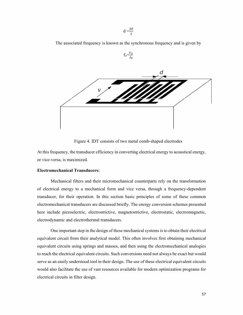
57
d =
The associated frequency is known as the synchronous frequency and is given by
fo=𝑉𝑅
𝜆𝑅
Figure 4. IDT consists of two metal comb-shaped electrodes
At this frequency, the transducer efficiency in converting electrical energy to acoustical energy,
or vice-versa, is maximized.
Electromechanical Transducers:
Mechanical filters and their micromechanical counterparts rely on the transformation
of electrical energy to a mechanical form and vice versa, through a frequency-dependent
transducer, for their operation. In this section basic principles of some of these common
electromechanical transducers are discussed briefly. The energy conversion schemes presented
here include piezoelectric, electrostrictive, magnetostrictive, electrostatic, electromagnetic,
electrodynamic and electrothermal transducers.
One important step in the design of these mechanical systems is to obtain their electrical
equivalent circuit from their analytical model. This often involves first obtaining mechanical
equivalent circuits using springs and masses, and then using the electromechanical analogies
to reach the electrical equivalent circuits. Such conversions need not always be exact but would
serve as an easily understood tool in their design. The use of these electrical equivalent circuits
would also facilitate the use of vast resources available for modern optimization programs for
electrical circuits in filter design.
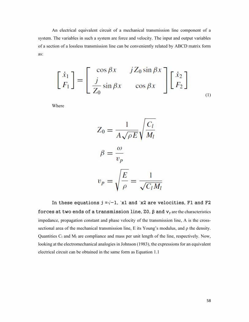
58
An electrical equivalent circuit of a mechanical transmission line component of a
system. The variables in such a system are force and velocity. The input and output variables
of a section of a lossless transmission line can be conveniently related by ABCD matrix form
as:
(1)
Where
In these equations j =√−1, ˙x1 and ˙x2 are velocities, F1 and F2
forces at two ends of a transmission line, Z0, β and νp are the characteristics
impedance, propagation constant and phase velocity of the transmission line, A is the cross-
sectional area of the mechanical transmission line, E its Young’s modulus, and ρ the density.
Quantities Cl and Ml are compliance and mass per unit length of the line, respectively. Now,
looking at the electromechanical analogies in Johnson (1983), the expressions for an equivalent
electrical circuit can be obtained in the same form as Equation 1.1
59
(2)
In Equation (2) V and I are the voltage and current on the transmission line (with
subscripts representing its ports). The other quantities in the matrix are also represented by
equivalent electrical parameters as:
(3)
(4)
In Equations (3) and (4) Ll and Cl represent the inductance and capacitance per unit
length of the line, and ε and μ are the permittivity and permeability of the transmission
medium.
Piezoelectric transducers:
When subjected to mechanical stress, certain anisotropic crystalline materials generate
charge. This effect is widely used in ultrasonic transducers. Lead zirconate titanates (PZTs) are
the most common ceramic materials used as piezoelectric transducers. These crystals contain
several randomly oriented domains if no electric potential is applied during the fabrication
process of the material. This results in little changes in the dipole moment of such a material
when a mechanical stress is applied. When external stress is applied to such a material, the
crystal lattices get distorted, causing changes in the domains and a variation in the charge
distribution within the material. The converse effect of producing strain is caused when these
domains change shape by the application of an electric field.
60
The development of the equivalent circuit for a piezoelectric bar is illustrated in Figure
5. The bar vibrates in the direction (with force F and velocity x) shown in the figure, by the
application of an applied voltage (V). The reactance (jX) curve in Figure 5 (b) can be obtained
by ignoring higher order modes of vibration, and the losses. One circuit configuration that
results in similar reactance characteristics is shown Figure 5(c). The electromechanical
equivalent circuit can be constructed from this, incorporates a gyrator with a resistance A and
an inverter of reactance jκ in addition to the corresponding spring constant K and mass M. The
gyrator represents the nonreciprocal nature of the piezoelectric transducer. The inverter is
required here since the gyrator converts the parallel resonant circuit to a series circuit (Johnson,
1983). The series combination of inverter and gyrator functions as a transformer with an
imaginary turns ratio jκ/A
Figure 5. Development of equivalent circuit of a piezoelectric transducer.
In general the piezoelectric transduction phenomenon is quadratic in nature, but may
be assumed to be linear for small deformations. The electromechanical coupling can then be
written as
Q = d1F (5)
x = d2V (6)
61
In these equations, d1 and d2 represent the piezoelectric charge modulus d.
When both voltage and force are present, the following piezoelectric coupling equations
are used:
Q = d1F + C0V (7)
x = d2V + CmF (8)
where C0 is the free capacitance and Cm the short-circuit compliance of the transducer. The
electromechanical coupling coefficient is another important non-dimensional quantity
representing the performance of piezoelectric transducers. This is the ratio of mechanical work
available to the electrical energy stored in the transducer (Hom et al., 1994). The coupling
coefficient depends on the type of material, mode of stress and the polarization of electric field.
For a linear piezoelectric material, this is
η = (9)
where d is a constant for piezoelectric material, S is the elastic compliance and ε is the
permittivity of the material. PZT thin films have been developed using standard thin-film
deposition techniques such as sputtering, and physical or chemical vapor deposition. Their use
in sensors and actuators is inherently limited by the quality and repeatability of thin films
obtained by these techniques. Compared with bulk material processing techniques thin-film
performance is severely hampered by the surface properties where the film is deposited
(Muralt, 2000). Nonferroelectric AlN thin films are also explored, for sensor applications
where voltage output is required. Compared with other electromechanical conversion schemes
these require low voltage input but have generally low electromechanical conversion
efficiency.
Electrostrictive transducers:
Electrostriction is the phenomenon of mechanical deformation of materials due to an
applied electric field. This is a fundamental phenomenon present to varying degrees in all
materials, and occurs as a result of the presence of polarizable atoms and molecules. An applied
electric field can distort the charge distribution within the material, resulting in modifications
to bond length, bond angle or electron distribution functions, which in turn affects the
macroscopic dimensions of the material.
The electric field E and the electric displacement D in a material are related by
62
D= Є0E+P (10)
where ε0 is the free space permittivity (= 8.85 × 10⁻¹² Fm−1) and P is the polariza on of the
material. The first law of thermodynamics for a electrically deformable material is
dU = Tij dSij + Ek dDk + T dS (11)
In Equation (11), U is the internal energy for unit volume of the material, T is the stress tensor,
S is the infinitesimal strain tensor, T is the temperature and S is its entropy per unit volume.
The elastic Gibbs function of a material is defined as
G = U − TijSij – ε0EkEk − T S (12)
Taking the derivative of Equation (12) and making use of Equation (10) we get:
dG = dU − Tij dSij − Sij dTij − Ek(dDk − dPk) − T dS − S dT (13)
Substituting for dU from Equation (11), this simplifies to:
dG = −Sij dTij + EkPk − S dT (14)
The derivative of the Gibbs function G can be obtained using the chain rule as:
dG = Tij + Pk + T (15)
Comparing terms in Equation (14) and (15)
Sij = − (16)
Ek = (17)
S =− (18)
Assuming isotropic dielectric behaviour, the Gibbs energy function for an elastic material
63
(19)
The first term on the right-hand side describes the elastic behaviour of the material, sP being its
elastic compliance at constant polarization. The electromechanical coupling is denoted in the
second term with the electrostrictive coefficients forming the matrix Q. The last term is the
dielectric behaviour of the material. Ps is the spontaneous polarization, and k is a material
constant related to its dielectric constant. Since the material is assumed to be isotropic, the
magnitude of polarization is given as:
|P| = 𝑃𝑘𝑃𝑘 (20)
Temperature-dependent material coefficients used in Equation (19) such as sP, Q, Ps and k are
obtained from electrical and mechanical measurements.
Substituting Equation (19) into Equation (16) we get the constitutive equations for
electrostrictive materials as:
Sij = sP ijklTkl + QijmnPmPn (21)
This shows the total strain in a material is the sum of elastic strain and polarization induced
strain. The second term on the right-hand side of Equation (21) represents the electrostrictive
effect. Thus this contribution is proportional to the square of the polarization in the material.
This constitutive relation is valid even at large field intensities. Terms in the matrix Q are the
electrostriction coefficients and are obtained from measurements. The phenomenon of
electrostriction is very similar to piezoelectricity. One of the fundamental difference between
the two is the closeness of transition temperature of the material to the operating temperatures.
This accounts for the improved strain and hysteresis properties for electrostrictive materials.
However, a larger number of coefficients are required to model electromechanical coupling for
electrostriction. The polarization in piezoelectric materials is spontaneous, while that in
electrostrictive materials is field induced. The properties of electrostrictive materials are more
temperature-dependent, and the operating temperature range for these materials is narrower
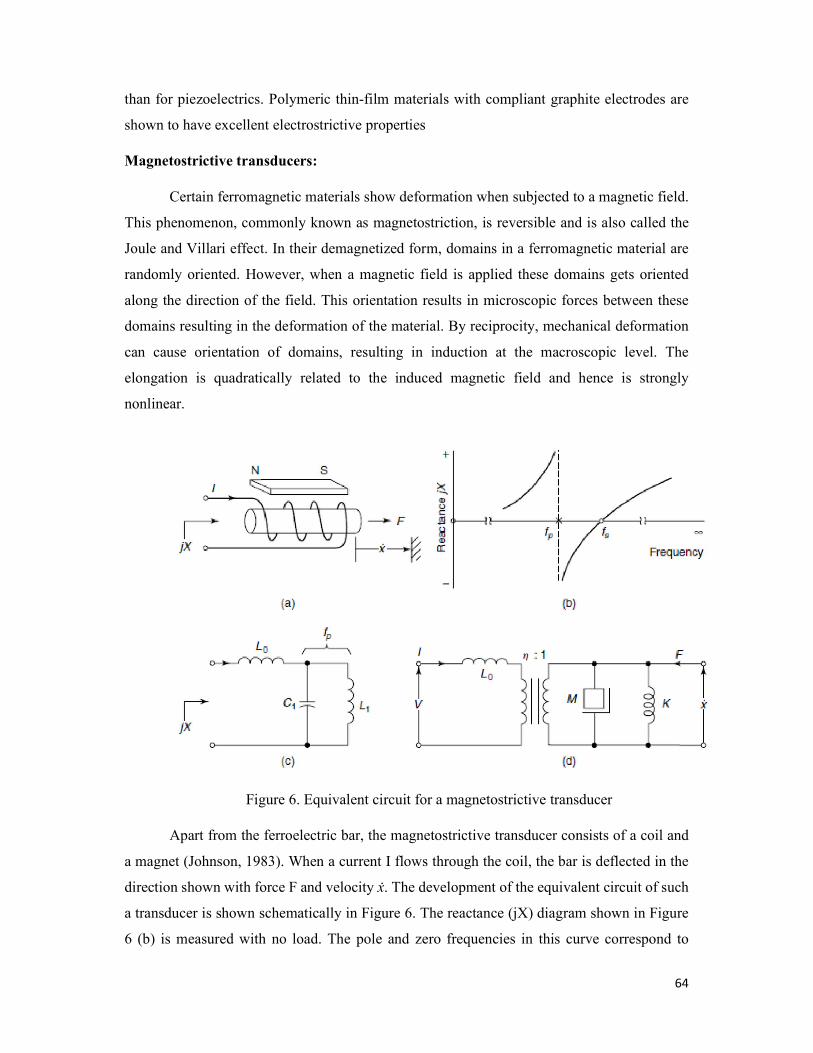
64
than for piezoelectrics. Polymeric thin-film materials with compliant graphite electrodes are
shown to have excellent electrostrictive properties
Magnetostrictive transducers:
Certain ferromagnetic materials show deformation when subjected to a magnetic field.
This phenomenon, commonly known as magnetostriction, is reversible and is also called the
Joule and Villari effect. In their demagnetized form, domains in a ferromagnetic material are
randomly oriented. However, when a magnetic field is applied these domains gets oriented
along the direction of the field. This orientation results in microscopic forces between these
domains resulting in the deformation of the material. By reciprocity, mechanical deformation
can cause orientation of domains, resulting in induction at the macroscopic level. The
elongation is quadratically related to the induced magnetic field and hence is strongly
nonlinear.
Figure 6. Equivalent circuit for a magnetostrictive transducer
Apart from the ferroelectric bar, the magnetostrictive transducer consists of a coil and
a magnet (Johnson, 1983). When a current I flows through the coil, the bar is deflected in the
direction shown with force F and velocity ẋ. The development of the equivalent circuit of such
a transducer is shown schematically in Figure 6. The reactance (jX) diagram shown in Figure
6 (b) is measured with no load. The pole and zero frequencies in this curve correspond to
65
parallel and series resonances of the system. It is not very hard to obtain the component values
of an LC circuit shown in Figure 6 (c) which result in the same pole and zero frequencies as
with the system in Figure 6 (a). Therefore Figure 6 (c) is an idealized electrical equivalent
circuit for the transducer shown in Figure 6 (a). This is an idealized model as it does not take
into consideration the losses in the system.
It is now possible to translate this electrical equivalent circuit to the electromechanical
circuit shown in Figure 6 (d). This has electrical and mechanical components (mass M and
spring K) connected with an electromechanical transformer. The turns ratio of this transformer
is decided by the amount of coupling, known as the electromechanical coupling coefficient.
This is defined as the ratio of the energy stored in the mechanical circuit to the total input
energy.
The electromechanical coupling for a magnetostrictive transducer shown in Figure 6
(a) relates the force at one end of the rod (the other end being constrained) to the current i in
the coil as
F = i (22)
where F is the magnetostrictive force, 𝑔 is the magnetostrictive strain modulus, E is the
Young’s modulus of the material, Rm is the total reluctance of the magnetic circuit, and N is
the number of turns in the coil. The ratio on the right-hand side of Equation (22) is the
electromechanical coupling. The same value for the coefficient relates the induced voltage V
at the terminals of the coil with the rate of change in displacement at the free end of the bar:
V = ẋ (23)
Electrostatic actuators:
Electrostatic actuation is the most common type of electromechanical energy
conversion scheme in micromechanical systems. This is a typical example of an energy-storage
transducer. Such transducers store energy when either mechanical or electrical work is done on
them. Assuming that the device is lossless, this stored energy is conserved and later converted
to the other form of energy. The structure of this type of transducer commonly consists of a
capacitor arrangement, where one of the plates is movable by the application of a bias voltage.
This produces displacement, a mechanical form of energy.
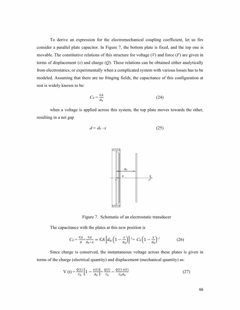
66
To derive an expression for the electromechanical coupling coefficient, let us firs
consider a parallel plate capacitor. In Figure 7, the bottom plate is fixed, and the top one is
movable. The constitutive relations of this structure for voltage (V) and force (F) are given in
terms of displacement (x) and charge (Q). These relations can be obtained either analytically
from electrostatics, or experimentally when a complicated system with various losses has to be
modeled. Assuming that there are no fringing fields, the capacitance of this configuration at
rest is widely known to be:
C0 = Є
(24)
when a voltage is applied across this system, the top plate moves towards the other,
resulting in a net gap
d = d0 –x (25)
Figure 7. Schematic of an electrostatic transducer
The capacitance with the plates at this new position is
C0 = Є
=Є
= Є𝐴 𝑑 1 − -1= C0 1 − -1 (26)
Since charge is conserved, the instantaneous voltage across these plates is given in
terms of the charge (electrical quantity) and displacement (mechanical quantity) as:
V (t) = ( )
1 −( )
= ( )
−( ) ( )
(27)
67
The electrostatic force between the plates can be obtained from Coulomb’s law. By the
principle of conservation of energy, the mechanical work done in moving the plate should
balance with an equal variation in electrical energy. Thus the net work done is
dW = dW electrical + F Coulomb dx ≡ 0 (28)
F Coulomb=𝜕
(29)
Where 𝑊 = 𝐶𝑉 (30)
Substituting Equations (25) – (27) in Equation (30), and then back in Equation (29),
the electrostatic force becomes
F Coulomb=−( )
(31)
the voltage across the plates can be expressed in terms of a static charge Q0, and a dynamic
component as:
𝑉(𝑡) = + − 𝑥 − 𝑥 (32)
Where
Q(t) = Q0 + Qd (33)
Considering only the dynamic component of voltage, and using the assumptions Qd <<Q0
and x << d0, we get
𝑉 (𝑡) ≈ − 𝑥 (34)
This electromechanical relation is obviously linear. A similar procedure would lead to the
linearization of the other electromechanical coupling equation between the force and charge
as:
F Coulomb=− 𝑄 (35)
The electrostatic coupling equations in the sinusoidal state are written in the form:
𝑉𝑐𝑎 =𝐼
𝑗𝜔𝐶0−
𝑉0
𝑗𝜔𝑑0𝜈 (36)
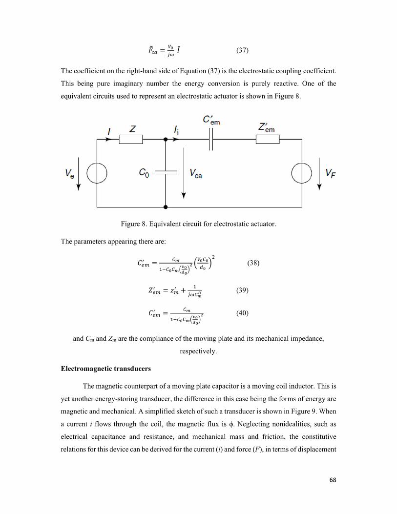
68
𝐹 = 𝐼 (37)
The coefficient on the right-hand side of Equation (37) is the electrostatic coupling coefficient.
This being pure imaginary number the energy conversion is purely reactive. One of the
equivalent circuits used to represent an electrostatic actuator is shown in Figure 8.
Figure 8. Equivalent circuit for electrostatic actuator.
The parameters appearing there are:
𝐶 = (38)
𝑍 = 𝑧 + (39)
𝐶 = (40)
and Cm and Zm are the compliance of the moving plate and its mechanical impedance,
respectively.
Electromagnetic transducers
The magnetic counterpart of a moving plate capacitor is a moving coil inductor. This is
yet another energy-storing transducer, the difference in this case being the forms of energy are
magnetic and mechanical. A simplified sketch of such a transducer is shown in Figure 9. When
a current i flows through the coil, the magnetic flux is ϕ. Neglecting nonidealities, such as
electrical capacitance and resistance, and mechanical mass and friction, the constitutive
relations for this device can be derived for the current (i) and force (F), in terms of displacement
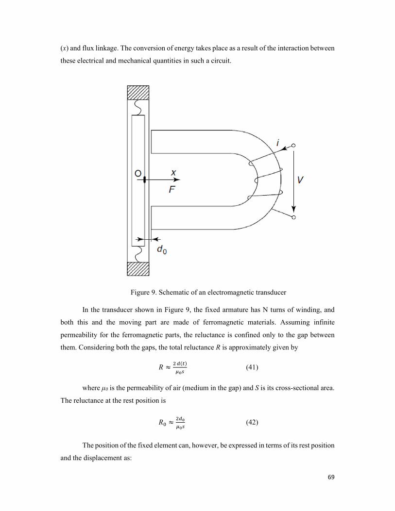
69
(x) and flux linkage. The conversion of energy takes place as a result of the interaction between
these electrical and mechanical quantities in such a circuit.
Figure 9. Schematic of an electromagnetic transducer
In the transducer shown in Figure 9, the fixed armature has N turns of winding, and
both this and the moving part are made of ferromagnetic materials. Assuming infinite
permeability for the ferromagnetic parts, the reluctance is confined only to the gap between
them. Considering both the gaps, the total reluctance R is approximately given by
𝑅 ≈( )
(41)
where μ0 is the permeability of air (medium in the gap) and S is its cross-sectional area.
The reluctance at the rest position is
𝑅 ≈ (42)
The position of the fixed element can, however, be expressed in terms of its rest position
and the displacement as:
70
d(t) = d0 − x(t) (43)
Substituting Equations (42) and (43) into Equation (41), we get
𝑅 = 𝑅 1 − (44)
The inductance of the coil is expressed in terms of its reluctance as:
𝐿 = = 𝐿 1 − (45)
This may, however, be simplified for very small displacements using Taylor series expansions.
Ignoring higher-order terms, the inductance of this coil becomes
𝐿 ≈ 𝐿 1 + (46)
The voltage induced on the coil is
𝑉 = −( )
(47)
Substituting Equation (46) into Equation (47), the induced voltage is given as:
𝑉 ≈ −𝐿 − 𝐿 𝑖 (48)
where 𝑣 is the velocity of the moving plate. This leads to a nonlinear relationship for the
electromechanical coupling. The stored magnetic energy is
𝑊 = 𝐿 =ɸ
(49)
Assuming the principle of conservation of energy, this balances with the mechanical energy
spent on the displacement. At any instant of time dt, the magnetic force used up for generating
the displacement is given by
𝐹 = (50)
As done with the electrostatic case, the nonlinearities of these expressions for
electromechanical coupling can be linearized, by defining the components of the flux as:
𝜑 = 𝜑 + 𝜑 (51)
71
Assuming that the dynamic component ϕd << ϕ0, the relation between induced magnetic voltage
and the dynamic component of current becomes [from Equation (48)]
𝑉 = −𝐿 − 𝐿 𝐼 = −𝐿 − 𝜈 (51)
The dynamic component of the magnetic force can be approximated as
(𝐹 )d = 0
𝑑0𝑖𝑑
+𝜑02
𝐿0𝑑02 𝑥 (52)
Miniaturization of an electromagnetic actuator requires fabrication of magnetic thin films and
current-carrying coils. Although few attempts have been made in this direction, the overall size
of devices developed so far are not very small. Coupled with this is the difficulty in isolating
magnetic field between adjacent devices, which makes fabrication of integrated microdevices
challenging.
REFERENCES
5. Vijay K. Varadan, K. J. Vinoy and K. A. Jose , “RF MEMS & Their Applications”, John Wiley & Sons, 2003.
6. Tai - Rai Hsu, “MEMS and Microsystems Design and Manufacturing”, Tata MC Graw Hill, New Delhi, Edition 2002.
7. Gabriel M Rebeiz, “RF MEMS - Theory Design and Technology”, John Wiley and Sons, 2003. 8. Nadim Maluf, “An introduction to Micro electro mechanical system design”, Artech House ,2000.
PART A
S.NO Questions 1. Define Actuators? Mention the different types of Actuation systems. 2. Design a micro actuator with a mems micro accelerometer suitable for an engineering application 3. Summarize the properties of Piezo electric materials. 4. Summarize the advantages and disadvantages of using piezoresistive sensors. 5. Generalize the principle of piezoelectric accelerometer. 6. Give the principle of operation of electrostatic sensors and actuators. 7. Summarize the advantages and disadvantages of electrostatic sensing and actuation. 8. Give the principle of operation of comb drive actuators. 9. Compare the working of Electrodynamic transducers and Electromagnetic transducers 10. Give the principle of Electromechanical transducers
PART B
S.NO Questions 1. Discuss the electrostatic piezoelectric transducer in detail. 2. Explain capacitive type transducers. 3. With neat diagram explain Piezo electric accelerometer. 4. Discuss on electrostatic actuation model with neat diagram.
72
UNIT – IV - MEMS DESIGN AND INTRODUCTION TO OPTICAL RF MEMS– SECA3007
73
III. Introduction
Micro system Design
A major difference between mechanical engineering design of microsystems and that
of other products is that the design for microsystems requires the integration of the related
manufacturing and fabrication processes. Mechanical engineering design of traditional
products and systems rarely requires the consideration of the consequences of the
manufacturing process. For example, components such as gears, bearings, and fasteners in a
mechanical system can be purchased from suppliers without the knowledge of how these
components are produced. In microsystems, which involve MEMS components. however, the
situation is quite different Components for MEMS are fabricated by various physical-chemical
means These fabrication and manufacturing processes often involve high temperature and
harsh physical and chemical treatments of delicate materials used for the components. These
processes can have serious repercussions in the performance of microsystems and hence must
be taken into design considerations. Tolerance of the finished components and the intrinsic
effects such as residual stresses and strains inherent from microfabrication processes are just
two obvious examples of such
In general, microsystem design involves three major tasks that are mutually coupled:
1) process flow design
2) electromechanical and structural design and
3) design verifications that include packaging and testing.
Material selections in microsystem design are also much more complex than those involved in
traditional products. Selections of materials for microsystems not only involve the materials
for the basic structure of the systems, but also the materials in the process flow, such as proper
etchants and thin films for depositions.
Design Considerations
An overview of the ingredients that we will be involved with in microsystem design
as show in Figure .1
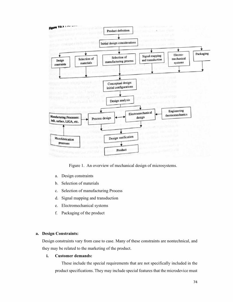
74
Figure 1. An overview of mechanical design of microsystems.
a. Design constraints
b. Selection of materials
c. Selection of manufacturing Process
d. Signal mapping and transduction
e. Electromechanical systems
f. Packaging of the product
a. Design Constraints:
Design constraints vary from case to case. Many of these constraints are nontechnical, and
they may be related to the marketing of the product.
i. Customer demands:
These include the special requirements that are not specifically included in the
product specifications. They may include special features that the microdevice must
75
provide in extraordinary circumstances. It is not hard to conceive that a
microdevice, such as a sensor or actuator installed in a toy for young children,
requires very different considerations in terms of safety and rough-handling than
the same device installed in a product for mature office and laboratory workers.
ii. Time to market (TTM).
This factor is critical, as most high-tech products have what is called a "window
for marketing," and these windows are becoming narrower and narrower as
technology advances. The shrinking window for marketing specific products is also
due to increasingly stiff competition in the marketplace. A microsystem product
needs to enter the market at a critical time to capture that market and hence
maximize the profit. TTM usually dictates how much time the design engineer has
to design and produce the product.
iii. Environmental conditions
Three critical conditions are involved: thermal, mechanical, and chemical. A
device operating at elevated temperature requires much more attention in terms of
thermal stresses and strains, material deterioration, and degradation of signal
transduction. A micropressure sensor designed for monitoring cylinder pressure in
an internal combustion engine obviously requires more sophisticated design
analysis and careful selection of material than the ones used to monitor the tire
pressure in an automobile. Mechanical environment relates to the mechanical
stability of the support for the microsystem. A vibratory support may shake joints
loose and also result in breakdown of electric leads in the system. Last a chemical
working medium can degrade both the MEMS and the packaging materials.
Chemical and moisture contents in fluid media can lead to undesirable oxidation
and corrosion of the Components in contact. Moisture is also main as on for the
stiction of microswitches in optoelectronic network systems. Clogging of
microchannels in microvalves and pumps in microfluidics is a possibility if the
system is not properly designed and manufactured.
iv. Physical size and weight limitations:
These constraints are normally covered in the product specification. They can
affect the overall configurations of the product with imposition of limitations on
some key design parameters.
76
v. Applications:
It is important to know whether the microsystem is intended for once-only
application, or for repeated usage. If the latter is the case, then one needs to design
for the life expectancy of the product, as well as the possibility of creep and fatigue
failure of the components.
vi. Fabrication facility:
This relates to the selection of manufacturing methods for the product.
The availability of a fabrication facility for the intended product is a critical factor
in meeting TTM as well as the cost for the production of the product.
vii. Costs.
This factor can dictate the overall direction of the design. In today's competitive
marketplace, cost is a critical factor for the marketability of the product In this early
design stage of the product, engineers should be seriously involved in the cost
analysis of the product, which will be translated into constraints on many design
parameters such as selection of materials and fabrication methods.
Selection of Materials:
As process flow is an integrated part of the design process, materials such as
etchants and thin films for depositions need to be carefully evaluated and selected for
the systems design.
Principal Substrate Materials:
There are two types of substrate materials;
i. passive substrate materials for support only these include polymers, plastics,
ceramics, etc., and
ii. active substrate materials such as silicon, GaAs, and quartz for the sensing or
actuating components in a microsystem.
Silicon:
Mechanically stable, inexpensive and ready machinability.
An excellent candidate material for microsensors and accelerometers
77
GaAs:
Has fast response to an externally applied influence, such as photons in light rays
even at elevated temperature
Can be used as thermal insulation.
Its high piezoelectricity makes this material suitable for precision microactuation
Suitable for surface micromachining
A Good candidate material for optical shutters, choppers, and actuators.
A desirable material for both microdevices and microcircuits.
Unfortunately, it is more expensive than other substrate materials such as silicon
Quartz:
More mechanically stable than silicon or silicon family compounds even at
high temperature
Virtually immune to therma1 expansion. It is thus the ideal material for high.
temperature applications
Excellent resonance capability for precision microactuation.
Unfortunately, it is hard to shape into desirable configurations
Polymers:
Used primarily as passive substrate material.
Low cost in both materials and the production processes.
Easily formed into the desired shapes.
Has flexibility in "alloying" for specific purposes.
Sensitive to environmental conditions such as temperature and moisture.
Vulnerable to chemical attacks.
Most polymers age; i.e., they deteriorate with time.
Other Substrates in the Silicon Family:
Silicon dioxide (Si02):
Can be easily grown on a silicon substrate surface or by deposition.
Excellent for both thermal and electrical insulation.
Can be used as good masking material for wet etching of silicon substrates.

78
Silicon carbide (SiC):
Dimensionally and chemically stable even at high temperature.
Dry etching with aluminium masks can easily pattern it.
An excellent passivation material for deep etching.
Silicon nitride (Si3N4):
An excellent barrier for water and sodium ions in diffusion processes.
A good masking material for deep etching and ion implantation.
An excellent material for optical wave guidance.
A good protective material for high strength electric insulation at high
temperature
Polycrystalline silicon:
Widely used as resistors, gates for transistors, and for thin-film transistors
A good material for controlling the electrical characteristics of substrates
Packaging Materials
Ceramics (alumina, silicon carbide)
Glasses (Pyrex, quartz
Adhesives (solder alloys, epoxy resins, silicone rubbers)
Wire bonds (gold, silver, aluminium, copper, and tungsten)
Headers and casings (plastics, aluminium, stainless steel)
Die protectors (silicone gel, silicone oil)
Selection of Manufacturing Processes
Three principal manufacturing processes that are available for producing
microdevices and systems.
1) Bulk Micromanufacturing
Relatively straightforward in operation. It involves well-documented
fabrication processes, mainly the etching processes.
The least expensive of the three manufacturing techniques.
Suitable for simple geometry; e.g., the dies for micropressure sensors.
79
A major drawback is the low aspect ratio, (The ratio of the dimension in
depth to that of the plane defines the aspect ratio in MEMS industry. The
height of microstructures in bulk micromachining is limited by standard
silicon wafer thickness.)
The process involves removal of material from bulk substrates--resulting in
high material consumption.
2) Surface Micromachining
Requires the building layers of materials over the substrate
Requires the design and fabrication of complex masks for deposition and
etching in the processes.
Etching of sacrificial layers is necessary after layer buildings-a wasteful
practice.
More expensive than the bulk manufacturing technique because of its
complex fabrication procedures.
Major advantages are: (1) it is less constrained by the thickness of silicon
wafers than that in bulk manufacturing. (2) it provides wide choices of
materials to be used in layer buildings, and (3) it is suitable for complex
geometries such as microvalves and comb-driven actuators.
3) LIGA and SLIGA and other High-Aspect-Ratio Processes
The most expensive micromanufacturing techniques of all
Both the LIGA and SLIGA processes require a special synchrotron radiation
facility for deep x-ray lithography. This facility is not readily accessible to
most of the MEMS industry
These processes also require the development of microinjection molding
technology and facilities.
Major advantages are: (1) they offer great flexibility in aspect ratio of
geometry. A high aspect ratio of 200 is achievable by the LIGA process (2)
They offer the most flexibility in microstructure configurations and
geometry. (3) There is virtually no restriction on the materials for the
microstructure including metals by the LIGA process. (4) These are the best
of the three manufacturing processes for mass production.
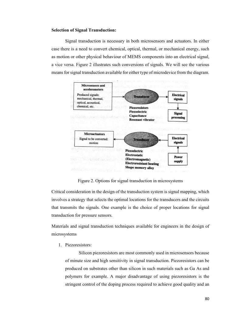
80
Selection of Signal Transduction:
Signal transduction is necessary in both microsensors and actuators. In either
case there is a need to convert chemical, optical, thermal, or mechanical energy, such
as motion or other physical behaviour of MEMS components into an electrical signal,
a vice versa. Figure 2 illustrates such conversions of signals. We will see the various
means for signal transduction available for either type of microdevice from the diagram.
Figure 2. Options for signal transduction in microsystems
Critical consideration in the design of the transduction system is signal mapping, which
involves a strategy that selects the optimal locations for the transducers and the circuits
that transmits the signals. One example is the choice of proper locations for signal
transduction for pressure sensors.
Materials and signal transduction techniques available for engineers in the design of
microsystems
1. Piezoresistors:
Silicon piezoresistors are most commonly used in microsensors because
of minute size and high sensitivity in signal transduction. Piezoresistors can be
produced on substrates other than silicon in such materials such as Ga As and
polymers for example. A major disadvantage of using piezoresistors is the
stringent control of the doping process required to achieve good quality and an
81
even more serious drawback is the strong temperature dependence of resistivity.
The sensitivity of piezoresistors deteriorates rapidly with increasing
temperature. Proper temperature compensation in signal processing is required
for applications at elevated temperatures.
2. Piezoelectric:
PZT crystals are used primarily for displacement transducers and for
accelerometers. Barium titanate (BaTiO3) is commonly used to transduce
signals from microaccelerometers. Most piezoelectric materials are brittle.
Special consideration should be given to packaging this material to avoid brittle
fracture. Size and machinability are two problems in using piezoelectric
materials. Piezoelectrics are suitable for use in accelerometers for measuring
dynamic or impact forces that exist in short periods of time, as sustained
piezoelectric action will cause overheating of the crystals and thus deteriorate
their conversion capability.
3. Capacitance.
The method is particularly attractive for high temperature applications,
the nonlinear input/ output relationships between the change of the gap of the
electrodes and the output voltage.
4. Resonant Vibrator:
The working principle of signal transduction using resonant vibration. It
offers higher resolution and accuracy for signal transduction in micropressure
sensors, its application to other microdevices is limited by the complexity of
fabrication, such as fusion bonding of the silicon beam to the substrate, as in the
case of micropressure sensors. The required space for the vibrating members is
another drawback of this transduction method.
5. Electroresistant heating:
This technique is widely used in microactuation, such as in microvalves
and pumps in fluidics. The technique is simple and straightforward. However,
the requirements for precise control of the heating of the actuating element with
thermal inertia may affect the timely response of the intended actuation. Also,
the contact of the heated element with the working medium can cause local heat
transfer, which may in turn alter the flow pattern of the working medium in the
case of microvalves. The technique thus has serious drawbacks in liquid-based
82
microfluidic systems. Sealing of heat transmitting fluids often causes problems
in the packaging and operations of these microsystems.
6. Shape memory alloy:
Shape memory alloy (SMA) is a good actuating material when it is used
in conjunction with electroresistant heating. A major drawback is the limited
availability of SMA, and often the deformation of SMA cannot be accurately
predicted because of its sensitivity to temperature.
Electromechanical System:
No microsystem can function without electrical power. Electrical
circuitry that provides the flow of electric current, or maintains voltage and/or
current supply in the case of actuators, is an integrated part of the system. In the
case of microsensors, the electronic signals produced by the transducers need to
be led to the outside of the device, and be conditioned and processed by a
suitable electrical system. Whatever the electrical system for the intended
product, a preliminary assessment on the interface between the mechanical
actions and the electrical system is needed in order to configure the product.
Packaging:
The cost of packaging a micropressure sensor can be as low as 20
percent of the overall cost of the product with simple plastic encapsulation, or
as high as 95 percent of the overall cost with complex passivation and stainless
steel or tungsten casings for special-purpose units. The design parameters that
affect packaging thus need to be considered at this early stage in the design
process. Design engineers need to consider the following major factors that will
affect the packaging of the product:
Die passivation
Media protection
System protection
Electric interconnect
Electrical interface
Electromechanical isolation
Signal conditioning and processing
Mechanical joints
Processes for tunnelling and thin-film lifting
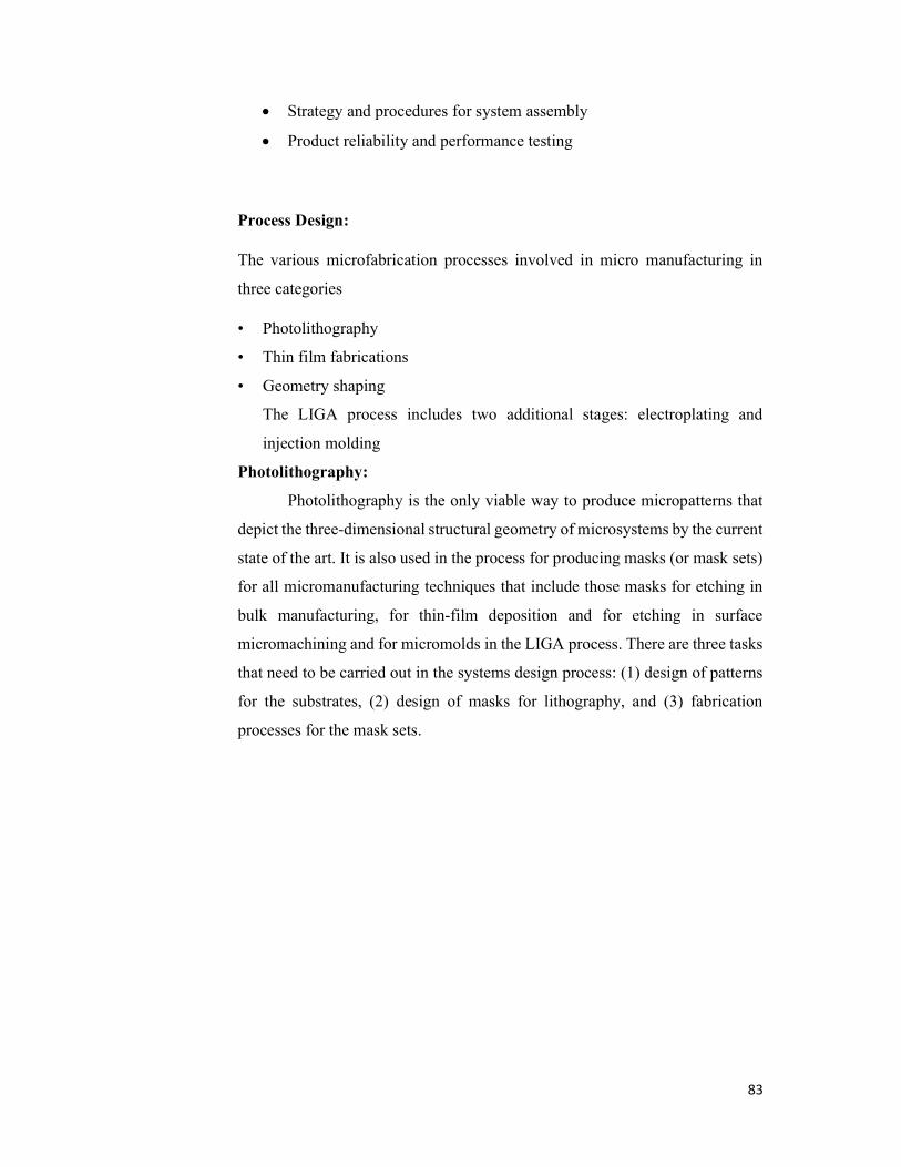
83
Strategy and procedures for system assembly
Product reliability and performance testing
Process Design:
The various microfabrication processes involved in micro manufacturing in
three categories
• Photolithography
• Thin film fabrications
• Geometry shaping
The LIGA process includes two additional stages: electroplating and
injection molding
Photolithography:
Photolithography is the only viable way to produce micropatterns that
depict the three-dimensional structural geometry of microsystems by the current
state of the art. It is also used in the process for producing masks (or mask sets)
for all micromanufacturing techniques that include those masks for etching in
bulk manufacturing, for thin-film deposition and for etching in surface
micromachining and for micromolds in the LIGA process. There are three tasks
that need to be carried out in the systems design process: (1) design of patterns
for the substrates, (2) design of masks for lithography, and (3) fabrication
processes for the mask sets.
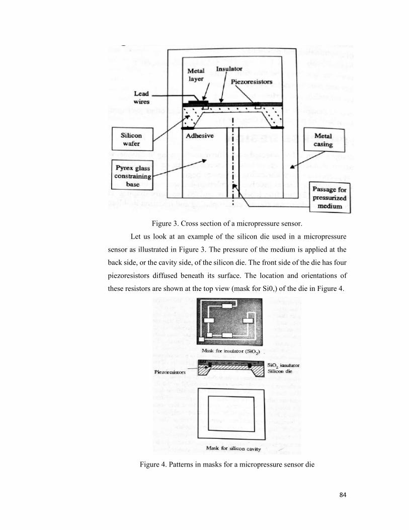
84
Figure 3. Cross section of a micropressure sensor.
Let us look at an example of the silicon die used in a micropressure
sensor as illustrated in Figure 3. The pressure of the medium is applied at the
back side, or the cavity side, of the silicon die. The front side of the die has four
piezoresistors diffused beneath its surface. The location and orientations of
these resistors are shown at the top view (mask for Si0,) of the die in Figure 4.
Figure 4. Patterns in masks for a micropressure sensor die
85
We can visualize that two masks are required for the silicon die, one for
the etching of the cavity and the other for the diffusion of the piezoresistors and
the deposition of thin films for electrical conductors connecting these four
resistors. Deep etching is required for the production of many cavities in silicon
dies, Si3N4 is a more suitable masking material. The patterns for both masks are
quite different. The pattern for cavity etching is simply a square opening,
whereas the pattern for the doping of piezoresistors and the connecting leads is
quite complicated. The white lines for the Si02 mask are for the electrical
connection of the resistors in a Wheatstone bridge. The two square pads at the
lower left corner of the top mask are the leads to the signal conditioning and
processing units outside the pressure sensor.
Thin-Film Fabrication: There are several ways to produce thin films over
the substrate's surface. Many of these processes requires high temperature
environments which result in residual stresses and residual strains.
Geometry Shaping:
The complex geometry of silicon-based microdevice components can be
produced either by depositing thin films of various materials over the substrates
by removing portions of material from the bulk substrates. An effective process
for removing material from substrates is etching. The chemical (wet etching)
plasma-assisted (dry) etching can be used to estimate the rates of etching
Mechanical Design:
The principal objective of mechanical design is to ensure the structural
integrity and the reliability of the microsystem when it is subjected to specified
loading at both normal operating and overload conditions. The latter condition
relates to possible mishandling or unexpected surges of load due to system
malfunction. Design methodologies developed for machines and structures in
macro- and mesoscales are used here with provisions to accommodate the
necessary modifications according to the scaling laws
Thermomechanical Loading:
Most of the loads that a microsensor or actuator is subjected to are
common to macrostructures. These can be categorized in the following way:
86
• Concentrated forces, such as the contact forces between actuating members
and the fluid passages in microvalves
• Distributed forces, such as the pressure loads on the diaphragms in
micropressure sensors
• Dynamic or inertia forces, as in the case of microaccelerometers
• Thermal stress induced by mismatch of coefficients of thermal expansion in
layered structures
• Friction forces between moving components in a microsystem; examples
are the bearing of a rotary micromotor, a linear motor , or a micropump
The following forces are unique to microsystems structures:
• Electrostatic forces for actuation.
• Surface forces due to piezoelectricity. These forces are generated by the
mechanical deformation of piezoelectric crystals with the application of
electric voltages. They are used to drive actuators
• Van der Waals forces that exist between closely spaced surfaces. A van der
Waals force is a form of electrostatic force but at the molecular level.
Accurate estimation of the force is not straightforward as a result of the
physical change of atomic cohesion involved in generating these forces.
Thermomechanical Stress Analysis:
Stress analysis is a major effort in design analysis. Thermomechanical
stress analysis of microsystems can be handled by the formulations by a finite
element method. In the case of microsystems, there is a strong presence of
intrinsic stresses resulting from the involved microfabrication processes. One of
such stresses is the residual stress and strain resulted from these fabrication
processes. These inherited residual stresses must be evaluated and included in
the subsequent stress analysis. Other possible sources for intrinsic stresses
induced in thin films on thick substrates include the following
• Doping of substrates with impurities would cause intrinsic stresses because
of lattice mismatch and variation of atomic sizes
• Atomic peening due to ion bombardment by sputtering atoms and working
gas densification of the thin film
• Microvoids in the thin film as result of the escape of working gases
87
• Gas entrapment
• Shrinkage of polymers during cure
• Change of grain boundaries due to change of interatomic spacing during and
after deposition or diffusion
An important consideration in using finite element analysis for
thermomechanical analysis of MEMS and microsystem structures is that we
must ensure that proper finite element formulations are chosen. Many
constitutive laws, and thus constitutive equations derived for continua at
macroscale, require substantial modifications for structures in submicrometer
scale
REFERENCES
9. Vijay K. Varadan, K. J. Vinoy and K. A. Jose , “RF MEMS & Their Applications”, John Wiley & Sons, 2003.
10. Tai - Rai Hsu, “MEMS and Microsystems Design and Manufacturing”, Tata MC Graw Hill, New Delhi, Edition 2002.
11. Gabriel M Rebeiz, “RF MEMS - Theory Design and Technology”, John Wiley and Sons, 2003. 12. Nadim Maluf, “An introduction to Micro electro mechanical system design”, Artech House ,2000.
PART A
S.NO Questions 1. Relate factors involved in the performance of optical MEMS. 2. List the actuators for optical MEMS. 3. Interpret the operation of optical mirrors. 4. Interpret the need stress analysis in MEMS 5. List the applications of MEMS-driven mirrors 6. Interpret the need of Optical MEMS in display industry 7. List the applications of Scanning-based MEMS displays 8. Outline the part of optical MEMS for sensing 9. Give the Actuation principles for MEMS optical scanners 10. List the type of MEMS optical scanners
PART B
S.NO Questions 1. Describe about Optical MEMS from Micromirrors to Complex Systems. 2. Explain about optical applications of MEMS devices. 3. Assess the need for actuators and the types of actuators used for active optical MEMS applications 4. Discuss the categories and Sources in Optical MEMS. 5. Describe about the Capacitive RF MEMS switch and it’s performance

88
UNIT – V - MEMS PACKAGING AND APPLICATIONS– SECA3007
89
IV. MEMS Packaging and Applications
MEMS packaging:
MEMS is a relatively new field which developed so closely with silicon processing that
most of the early packaging technologies were borrowed from the microelectronics field.
Packaging of a micromachine is the science of establishing interconnections between the
systems and providing an appropriate operating environment for the electromechanical circuits
to process the gathered information. Most MEMS devices need physical access to the outside
world to react mechanically with an external parameter or to sense a physical variable. MEMS
not only condition the signals but also move, which requires care in handling. The state-of-the-
art of current sensing technologies is that the device normally accesses the outside world via
electrical connections alone and the rest of the systems are totally sealed and isolated. Inertial
and optical devices are sometimes special cases, but, in general, the packaging approach of
MEMS is fundamentally different from microelectronic packaging. Unlike electronic
packaging, where most of the standard packages can be used for a wide variety of applications,
the MEMS packaging therefore tends to be customized to the specific applications, which can
be summed up in three words: cost, performance and reliability.
Packaging can span from consumer to midrange systems to high-performance weapon-
grade applications. No sharp boundaries exist between these classes. However, the gradual shift
of optimization parameters, controls the performance, reliability and cost. The size of the
package, the choice of its shape and material, the alignment of the device, the mounting for the
isolation of shock and vibration, and the seal are some of the many concerns in MEMS
packaging. Many important lessons that have seen learned throughout years of experience in
the microelectronics industry can be adapted to the packaging of MEMS devices. A MEMS
package contains many electrical and mechanical components, which need to be
interconnected. Electrical inputs need to be interfaced with the circuits. MEMS can be
extremely fragile. They must be protected from mechanical damage and hostile environments.
MEMS packaging involves the components of mechanical and electrical structures and the
combination of there to form a system.
The key issue facing the packaging of the MEMS device is die separation. The current
standard die separation method adopted for silicon is to cut the wafer using a diamond
90
impregnated blade. The blade and the wafer are flooded with high-purity water while the blade
spins at 45 000 rpm. This creates no problem for standard integrated circuits (ICs) because the
surface is essentially sealed against the effects of water and silicon dust. However, if the MEMS
device is exposed to water and debris, the system may break or become clogged and the
moisture may have adverse effects, for example in case of radio frequency (RF) switches.
Efforts to protect these surfaces with photoresist and other coatings have had only limited
success.
ROLE OF MEMS PACKAGES:
The aim of a package is to facilitate the integration of all components such that it
minimizes the cost, mass and complexity. The main functions of a MEMS package can be
summarized as providing: mechanical support, an electrical interface to the other system
components and protection from the environment. The packaging provides an interface
between the chip and the physical world. The package should protect the device, at the same
time letting it perform its intended functions with less attenuation of signal in a given
environment at low cost. The packaging becomes more expensive when protection is required
for relatively fragile structures integrated into the device. For a standard integrated circuit, the
packaging process can take up to 95% of the total manufacturing cost. Issues in MEMS
packaging are much more difficult to solve because of stringent requirements in processing,
handling and the nature of fragile microstructures; the diversity also complicates the packaging
problem. Many MEMS sensors often require a sensing media interface with a sensing area. For
example, a pressure sensor packaging requires incorporation of a pressure port to transmit fluid
pressure to the sensor. This makes a major difference between standard semiconductor device
packages and MEMS packages.
Mechanical support:
Owing to the fundamental nature of MEMS as a mechanical device, the protection and
isolation of the device from thermal and mechanical shock, vibration, acceleration and other
physical damage during operation become critical. The mechanical stress affecting a system
depends on the application. For example, for the same space-borne application, the device
package for a military aircraft is different from those used in communication satellites because
the operating environments are different. The coefficient of thermal expansion of the package
should be equal to that of silicon for reliability because the thermal cycle may cause cracking
or delamination if the materials are unmatched. If the packaging solution is creating excessive
91
stress in the sensing structure, it can cause a change of device performance. Once the MEMS
devices are wire bonded and other electrical connections are made, the assembly must be
protected by covering the base or by encapsulating the assembly in plastic or ceramic materials
since the electrical connections are usually made through the walls. Managing package-induced
stress in the device becomes important for MEMS package design.
Electrical interface:
Wire bonds and other electrical connections to the device should be made by protecting
the device from scratches and other physical damages. Direct current (dc) and RF signals to
the MEMS systems are given through these connections to interface the MEMS device with
the systems. Also, these packages should be able to distribute RF signals to other components
inside the package. High-frequency RF signals can be introduced into the package by metal
transmission lines or coaxial lines or the function can be electromagnetically coupled into the
device. The final connection between the MEMS and the RF lines is usually made with wire
bonds or flip-chip die attachments and multilayer interconnections.
Protection from the environment:
Many of the MEMS devices and sensors are designed to measure outside variables from
the surrounding environment. The hermetic packaging generally applicable to microelectronic
devices is not suitable in many cases of MEMS devices. These devices might be integrated
with the circuits or mounted to a circuit board and protected from mechanical damage. Only
special attention to packaging will protect a micromachined device from aggressive
surroundings. Protection starts at the dice level. Elements that cause corrosion or physical
damage to the metal lines as well as other components such as moisture remains a concern for
many MEMS devices. The moisture that may be introduced into the package during fabrication
and before sealing can damage the materials. For example, aluminium lines can corrode quickly
in presence of moisture, and gold lines degrade slowly in moisture. Junctions of dissimilar
metals can also corrode in the presence of moisture. MEMS packages need to be hermetic, with
good barriers against liquids and gases.
In most space-borne applications, the parts are hermetically sealed to give a perceived
increase in reliability and to minimize outgassing. When epoxies or cyanate esters are used for
die attach, they outgas when they cure. Outgassing is a concern for many devices since the
particles could deposit onto components and reduce device performance. For example,
outgassing leads to stiction and corrosion of the device. Die attach materials with a low
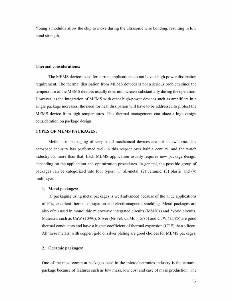
92
Young’s modulus allow the chip to move during the ultrasonic wire bonding, resulting in low
bond strength.
Thermal considerations:
The MEMS devices used for current applications do not have a high power dissipation
requirement. The thermal dissipation from MEMS devices is not a serious problem since the
temperature of the MEMS devices usually does not increase substantially during the operation.
However, as the integration of MEMS with other high-power devices such as amplifiers in a
single package increases, the need for heat dissipation will have to be addressed to protect the
MEMS device from high temperatures. This thermal management can place a high design
consideration on package design.
TYPES OF MEMS PACKAGES:
Methods of packaging of very small mechanical devices are not a new topic. The
aerospace industry has performed well in this respect over half a century, and the watch
industry for more than that. Each MEMS application usually requires new package design,
depending on the application and optimization procedures. In general, the possible group of
packages can be categorized into four types: (1) all-metal, (2) ceramic, (3) plastic and (4)
multilayer.
1. Metal packages:
IC packaging using metal packages is well advanced because of the wide applications
of ICs, excellent thermal dissipation and electromagnetic shielding. Metal packages are
also often used in monolithic microwave integrated circuits (MMICs) and hybrid circuits.
Materials such as CuW (10/90), Silver (Ni-Fe), CuMo (15/85) and CuW (15/85) are good
thermal conductors and have a higher coefficient of thermal expansion (CTE) than silicon.
All these metals, with copper, gold or silver plating are good choices for MEMS packages.
2. Ceramic packages:
One of the most common packages used in the microelectronics industry is the ceramic
package because of features such as low mass, low cost and ease of mass production. The
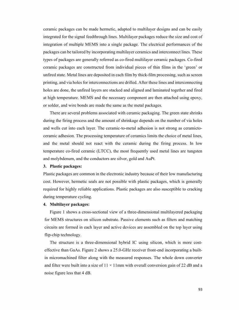
93
ceramic packages can be made hermetic, adapted to multilayer designs and can be easily
integrated for the signal feedthrough lines. Multilayer packages reduce the size and cost of
integration of multiple MEMS into a single package. The electrical performances of the
packages can be tailored by incorporating multilayer ceramics and interconnect lines. These
types of packages are generally referred as co-fired multilayer ceramic packages. Co-fired
ceramic packages are constructed from individual pieces of thin films in the ‘green’ or
unfired state. Metal lines are deposited in each film by thick-film processing, such as screen
printing, and via holes for interconnections are drilled. After these lines and interconnecting
holes are done, the unfired layers are stacked and aligned and laminated together and fired
at high temperature. MEMS and the necessary component are then attached using epoxy,
or solder, and wire bonds are made the same as the metal packages.
There are several problems associated with ceramic packaging. The green state shrinks
during the firing process and the amount of shrinkage depends on the number of via holes
and wells cut into each layer. The ceramic-to-metal adhesion is not strong as ceramicto-
ceramic adhesion. The processing temperature of ceramics limits the choice of metal lines,
and the metal should not react with the ceramic during the firing process. In low
temperature co-fired ceramic (LTCC), the most frequently used metal lines are tungsten
and molybdenum, and the conductors are silver, gold and AuPt.
3. Plastic packages:
Plastic packages are common in the electronic industry because of their low manufacturing
cost. However, hermetic seals are not possible with plastic packages, which is generally
required for highly reliable applications. Plastic packages are also susceptible to cracking
during temperature cycling.
4. Multilayer packages:
Figure 1 shows a cross-sectional view of a three-dimensional multilayered packaging
for MEMS structures on silicon substrate. Passive elements such as filters and matching
circuits are formed in each layer and active devices are assembled on the top layer using
flip-chip technology.
The structure is a three-dimensional hybrid IC using silicon, which is more cost-
effective than GaAs. Figure 2 shows a 25.0-GHz receiver front-end incorporating a built-
in micromachined filter along with the measured responses. The whole down converter
and filter were built into a size of 11 × 11mm with overall conversion gain of 22 dB and a
noise figure less that 4 dB.
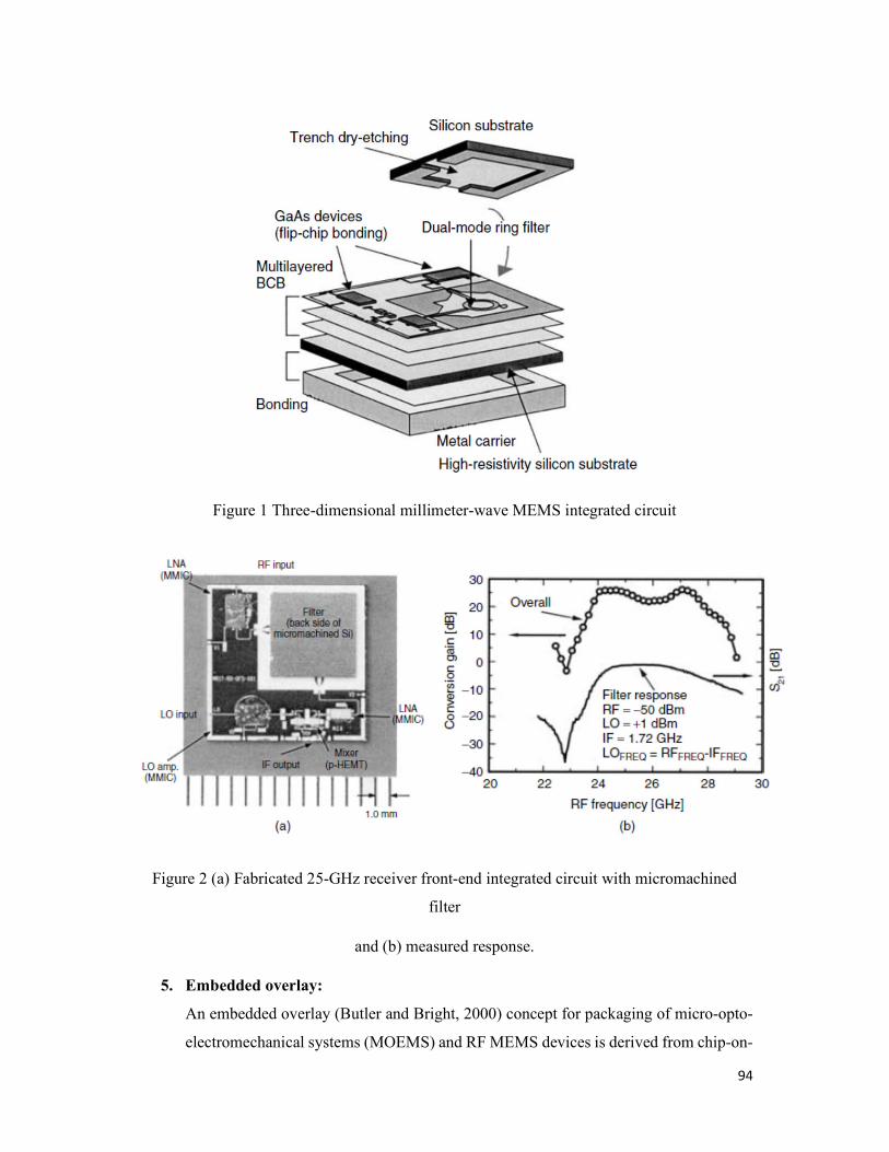
94
Figure 1 Three-dimensional millimeter-wave MEMS integrated circuit
Figure 2 (a) Fabricated 25-GHz receiver front-end integrated circuit with micromachined
filter
and (b) measured response.
5. Embedded overlay:
An embedded overlay (Butler and Bright, 2000) concept for packaging of micro-opto-
electromechanical systems (MOEMS) and RF MEMS devices is derived from chip-on-
95
flex (COF) process currently used for microelectronics packaging. COF is a high-
performance multichip packaging technology in which dies are encased in a moulded
plastic substrate and interconnections are made via a thin-film structure formed over
the components. The electrical interconnections are made through a patterned overlay
while the die is embedded in a plastic substrate, as shown in Figure 3. Chips are attached
face down on the COF overlay using polyimide or thermoplastic adhesives. The
substrate is formed after bonding the chips around the components using a plastic
mould-forming process such as transfer, compression or injection moulding at 210 ◦C.
The electrical connections are made by drilling via holes using a continuous argon ion
laser at 35 m nm. Ti/Cu metallization is sputtered and patterned to form the electrical
interconnections. The use of varying laser ablation power levels with plasma cleaning
and high-pressure water scrubs provides an effective means of removing the COF
overlay without damaging the embedded MEMS devices. Figure 4 shows the 5 × 5
array of micromirrors packaged in COF/MEMS modules with integrated micromirror
control circuitry
Figure. 3 Chip-on-flex MEMS packaging concept
6. Wafer-level packaging:
MEMS packaging should be considered from the beginning of device development.
Cost-efficient MEMS packaging focuses on wafer-level packaging (Gilleo, 2001a,
Reichal and Grosser, 2001). Designing the packaging schemes and incorporating then
into the device manufacturing process itself can reduce the cost. Versatile packaging
may be needed for many devices in which MEMS and microelectronics are on a single
chip. Each MEMS device may have its own packaging methods, which may be
absolutely suitable for its functioning. Since MEMS devices have movable structures
96
on the surface of the wafer, addition of a cap wafer on the silicon substrate makes them
suitable for many applications.
The cap provides protection against handling damage as well as avoiding
atmospheric
damping. This is done by bonding the substrate with an active device to a second wafer,
either of the same material or of different material. The bonding is done by using glass
frit or by anodic bond created by electrical potential. Precision-aligned wafer bonding
is the key technology for high-volume, low-cost packaging of MEMS devices (Helsel
et al., 2001; Mirza, 2000). State-of-the-art silicon wafer bonding can provide assembly
level packaging solutions for many MEMS devices.
Figure .4 COF/MEMS package of 5 × 5 array of micromirrors
The wafer-level package, which protects the device at the wafer stage itself, is
a clear choice to make at the product design stage itself. This involves an extra
fabrication process, where a micromachined wafer has to be bonded to a second wafer
with appropriate cavities etched on it. Figure 5 shows a schematic diagram of wafer-
level packaging. This enables the MEMS device to move freely in vacuum or inert
atmosphere with hermetic bonding, which prevents any contamination of the structure.
97
Etching the cavities in blank silicon wafer and placing it over the MEMS device and
bonding them together can make a hermetic seal.
Figure .5 Silicon wafer-level packaging of RF MEMS
Anisotrophic wet etching of bulk silicon along certain crystal planes using strong
alkaline solutions such as KOH can create thin diaphragms, through-wafer via holes
and V-grooves. The fastest etch rates for the silicon are the {100} and {110} crystal
planes and the slowest is for the {111} plane with typical masking layers such as silicon
dioxide or low-pressure chemical vapor deposition (LPCVD) silicon nitride. Examples
of successful development and packaging using silicon micromachining are the ink-jet
heads and silicon piezoresistive pressure sensors for automotive and industrial control
applications. Many of these devices require silicon wafer bonding to another substrate
as a first-level packaging solution. Anodic (electrostatic) bonding of silicon to glass,
low temperature glass-frit bonding of silicon to silicon, silicon direct wafer bonding,
eutectic bonding and epoxy bonding are examples of a few methods available to bond
silicon wafer to other silicon
7. Microshielding and self-packaging:
The micromachining technology has proved a flexible approach for the development of
low-loss transmission lines as well as micropackages that provide self-packaging
(Hindreson et al., 2000) to individual planar circuit components.
98
Figure 6 Topology of self-packaging transmission lines: (a) dielectric membrane
supported line; (b) dielectric shielded line.
Figure 7 Self-packaged circuit constructed out of two silicon wafers
99
Figure 8 (a) Typical MEMS packaging with co-planar waveguide (CPW) line; (b) top
view
and (c) side view Note: HRS, high-resistivity silicon.
As shown in Figure 6, the metal conductors are supported by membrane and a lower
cavity is below the conducting line. In Figures 7 and 8, the upper wafer has an air-filled
cavity that is mounted over the metallic conductors. Integration of both upper and lower
shielded circuits results in a self-packaged RF circuit.
FLIP-CHIP ASSEMBLY:
Flip-chip is the most favored assembly technology for high-frequency applications
because the short bump interconnect can reduce parasitic impedances. In flip chips, an IC
die is placed on a circuit board with bond pads facing down and directly joining the bare
die with the substrate. The bumps form electrical contact as well as a mechanical joint to
the die. This reduces the electrical path length and the associated capacitance and
inductance, which is particularly suited for high-density RF applications. The minimization
of parasitic capacitance and inductance can reduce the signal delay in high-speed circuits.
Flip-chip bonding involves the bonding of die, top-face down on a package substrate.
Electrical connections are made by means of plated solder bumps between bond pads on
the die and metal pads on the substrate (Oppermann et al., 2000). The attachment is intimate
with relatively small spacing (∼100µm) between the die and the substrate. In flip-chip
assemblies the bumps form the electrical contacts to the substrate as well as serving as a
mechanical joint.
Figure 9 shows the flip-chip design of a MEMS package. Since the active surface of
the MEMS is placed towards the substrate, the cavity will protect the movable MEMS. The
stand-off distance can be accurately controlled by the bump height. Flipchip technology is
a very flexible assembly method for different applications. Another concept in wafer-level
packaging is to apply a microcap to the device and then package with standard procedures.
Figure 10 shows the concept of cap-on-chip packaging for MEMS.
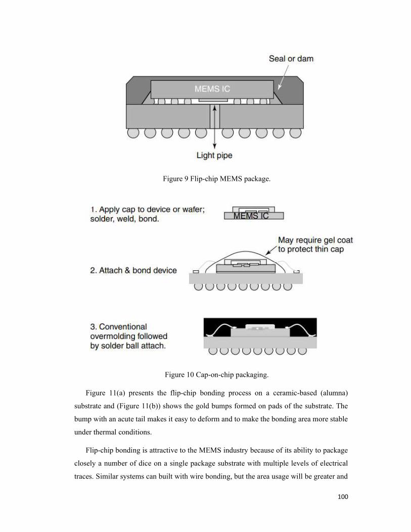
100
Figure 9 Flip-chip MEMS package.
Figure 10 Cap-on-chip packaging.
Figure 11(a) presents the flip-chip bonding process on a ceramic-based (alumna)
substrate and (Figure 11(b)) shows the gold bumps formed on pads of the substrate. The
bump with an acute tail makes it easy to deform and to make the bonding area more stable
under thermal conditions.
Flip-chip bonding is attractive to the MEMS industry because of its ability to package
closely a number of dice on a single package substrate with multiple levels of electrical
traces. Similar systems can built with wire bonding, but the area usage will be greater and
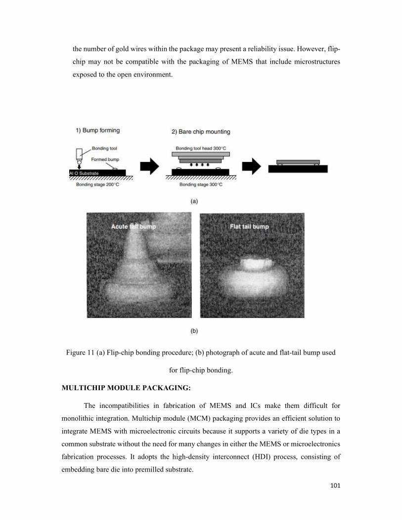
101
the number of gold wires within the package may present a reliability issue. However, flip-
chip may not be compatible with the packaging of MEMS that include microstructures
exposed to the open environment.
Figure 11 (a) Flip-chip bonding procedure; (b) photograph of acute and flat-tail bump used
for flip-chip bonding.
MULTICHIP MODULE PACKAGING:
The incompatibilities in fabrication of MEMS and ICs make them difficult for
monolithic integration. Multichip module (MCM) packaging provides an efficient solution to
integrate MEMS with microelectronic circuits because it supports a variety of die types in a
common substrate without the need for many changes in either the MEMS or microelectronics
fabrication processes. It adopts the high-density interconnect (HDI) process, consisting of
embedding bare die into premilled substrate.
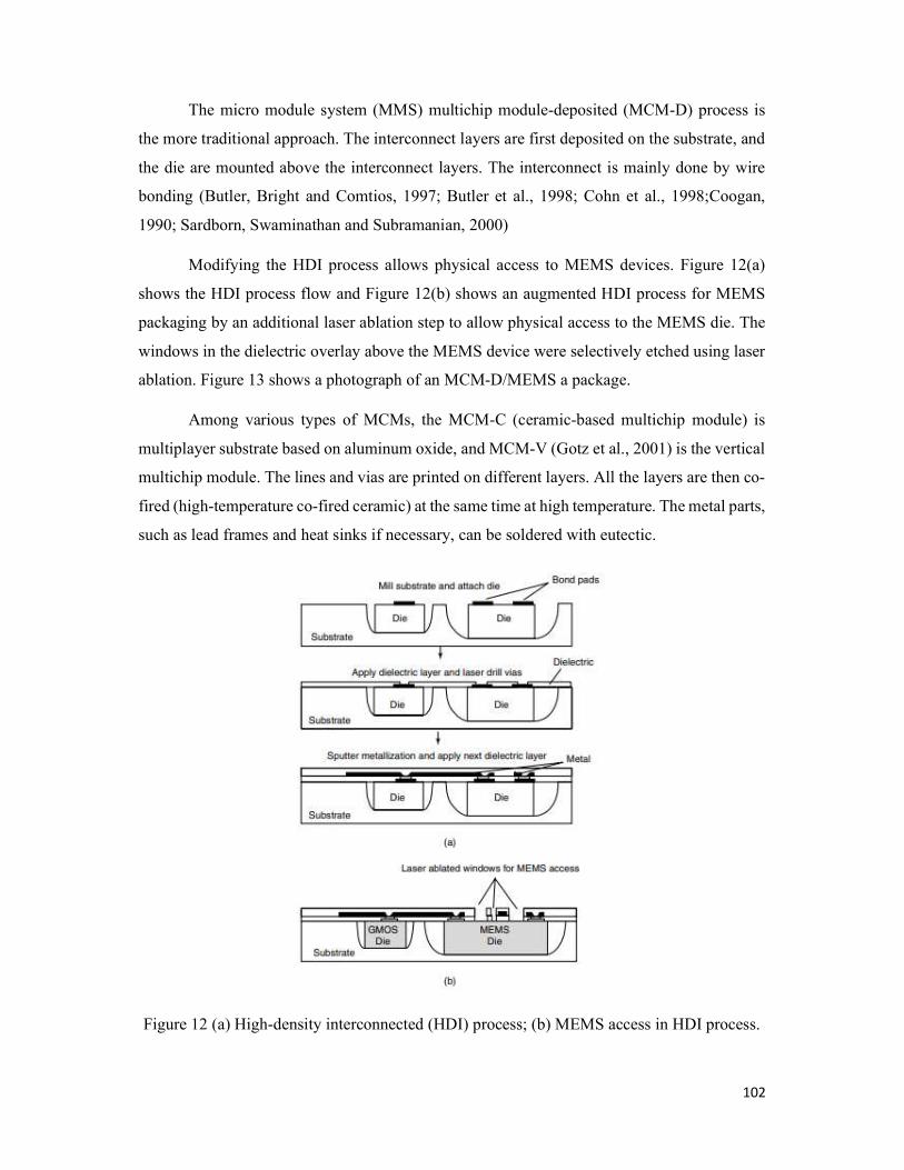
102
The micro module system (MMS) multichip module-deposited (MCM-D) process is
the more traditional approach. The interconnect layers are first deposited on the substrate, and
the die are mounted above the interconnect layers. The interconnect is mainly done by wire
bonding (Butler, Bright and Comtios, 1997; Butler et al., 1998; Cohn et al., 1998;Coogan,
1990; Sardborn, Swaminathan and Subramanian, 2000)
Modifying the HDI process allows physical access to MEMS devices. Figure 12(a)
shows the HDI process flow and Figure 12(b) shows an augmented HDI process for MEMS
packaging by an additional laser ablation step to allow physical access to the MEMS die. The
windows in the dielectric overlay above the MEMS device were selectively etched using laser
ablation. Figure 13 shows a photograph of an MCM-D/MEMS a package.
Among various types of MCMs, the MCM-C (ceramic-based multichip module) is
multiplayer substrate based on aluminum oxide, and MCM-V (Gotz et al., 2001) is the vertical
multichip module. The lines and vias are printed on different layers. All the layers are then co-
fired (high-temperature co-fired ceramic) at the same time at high temperature. The metal parts,
such as lead frames and heat sinks if necessary, can be soldered with eutectic.
Figure 12 (a) High-density interconnected (HDI) process; (b) MEMS access in HDI process.
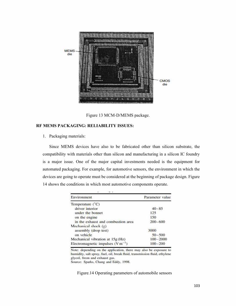
103
Figure 13 MCM-D/MEMS package.
RF MEMS PACKAGING: RELIABILITY ISSUES:
1. Packaging materials:
Since MEMS devices have also to be fabricated other than silicon substrate, the
compatibility with materials other than silicon and manufacturing in a silicon IC foundry
is a major issue. One of the major capital investments needed is the equipment for
automated packaging. For example, for automotive sensors, the environment in which the
devices are going to operate must be considered at the beginning of package design. Figure
14 shows the conditions in which most automotive components operate.
Figure.14 Operating parameters of automobile sensors
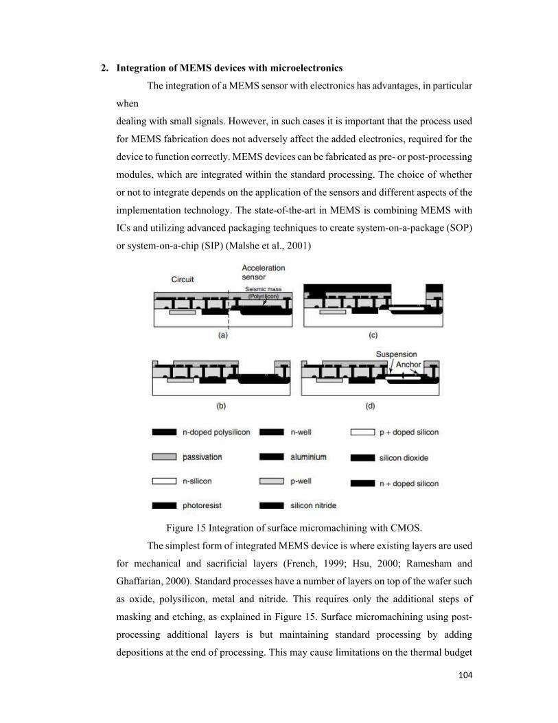
104
2. Integration of MEMS devices with microelectronics
The integration of a MEMS sensor with electronics has advantages, in particular
when
dealing with small signals. However, in such cases it is important that the process used
for MEMS fabrication does not adversely affect the added electronics, required for the
device to function correctly. MEMS devices can be fabricated as pre- or post-processing
modules, which are integrated within the standard processing. The choice of whether
or not to integrate depends on the application of the sensors and different aspects of the
implementation technology. The state-of-the-art in MEMS is combining MEMS with
ICs and utilizing advanced packaging techniques to create system-on-a-package (SOP)
or system-on-a-chip (SIP) (Malshe et al., 2001)
Figure 15 Integration of surface micromachining with CMOS.
The simplest form of integrated MEMS device is where existing layers are used
for mechanical and sacrificial layers (French, 1999; Hsu, 2000; Ramesham and
Ghaffarian, 2000). Standard processes have a number of layers on top of the wafer such
as oxide, polysilicon, metal and nitride. This requires only the additional steps of
masking and etching, as explained in Figure 15. Surface micromachining using post-
processing additional layers is but maintaining standard processing by adding
depositions at the end of processing. This may cause limitations on the thermal budget
105
if aluminum is used as the metallization. Plasma-enhanced chemical vapor deposition
(PECVD) can lower the temperature compatible with aluminum metallization.
In general, there are three main methods that have been used for monolithic
integration of CMOS and MEMS; (a) electronics first (University of California,
Berkeley, CA), (b) MEMS in the middle (Analog Devices, Cambridge, MA), and (c)
MEMS first (Sandia National Laboratories, Livermore, CA) (O’Neal et al., 1999). Each
of these methods has its own advantages as well as disadvantages. Sandia fabricated
MEMS first and etched a trench and covered it with sacrificial oxide, which protects
the MEMS devices from the CMOS processing steps. After the trench is completely
filled with SiO2, the surface is planarized, which serves as the starting material for
CMOS foundry. The sacrificial oxide covering the MEMS device is removed after the
fabrication of the CMOS device.
The alternative approach for monolithic integration with MEMS is the multi-
chip module (MCM) in which IC and MEMS dice can be placed in the same package.
Several sensors, actuators or a combination can be combined in a single chip using the
MCM technique (Butler et al., 1998). The main disadvantage is the probable signal loss
due to parasitic effects between the components and the apparent added packaging
expenses.
Co-planar MMICs packaged using a silicon (1 to ∼300 cm) substrate is found
to reduce the parasitic effects, coupling and resonance compared with the unpackaged
devices (Kim, Kwon and Lee, 2000). Common resistive silicon without gold plating
can be an ideal packaging solution for low-cost and high-performance co-planar lines.
3. Wiring and interconnections:
MEMS packages must protect the micromachined parts from environments and
at the same time provide interconnections to electrical signals as well as access to and
interaction with external environments. In hermetic packages, the electrical
interconnections through a package must confirm hermetic sealing. Wire bonding is the
popular technique to connect the die to the package electrically. Bonding of gold wires
is easier than bonding of aluminum wires. The use of wire bonding has serious
limitations in MEMS packaging because of the application of ultrasonic energy at a
frequency between 50 and 100 kHz. Unfortunately, these frequencies may simulate
oscillation of microstructures. Since most microstructures have resonant frequencies in
the same range, the chance of structural failure during the wire bonding is high (Maluf,
2000)
106
4. Reliability and key failure mechanisms
Reliability requirements for various MEMS will be significantly different for
different applications, especially with systems with unique MEMS devices. Hence
standard reliability testing is not possible until a common set of reliability requirements
is developed. The understanding of reliability of the systems comes from the knowledge
of failure behavior and the failure mechanisms. The main failure mechanisms of MEMS
devices are summarized as follows.
Stiction: stiction and wear are the real concern and cause for most of the failure
of MEMS. Stiction occurs as a result of microscopic adhesion when two
surfaces come into contact. Wear due to corrosive environment is another aspect
of failure
Delamination: MEMS may fail because of the delamination of bonded thin-film
materials. Bond failure of dissimilar and similar materials such as wafer-to-
wafer bonding can also cause delamination (Sandborn, Swaminathan and
Subramanian, 2000).
Dampening: dampening is critical for MEMS because of the mechanical nature
of the parts and the resonant frequency. Dampening can be caused by many
variables, including atmospheric gases. Good sealing is critical for MEMS
devices. Since MEMS devices have mechanical moving parts, they are more
susceptible to environmental failure than are packaging systems.
Mechanical failure: the changes in elastic properties affect the resonant and
damping characteristics of the beam and that will change the sensor
performance.
THERMAL ISSUES:
Heat-transfer analysis and thermal management become more complex by
packing different functional components into a tight space. The miniaturization also
raises issues such as coupling between system configurations and the overall heat
dissipation to environment. The configuration of the system shell becomes important
for the heat dissipation from system to the environment (Lin, 2000; Nakayama, 2000).
Heat spreading in a thin space is one of the most important modes of heat transfer in
107
compact electronic equipment and microsystems. As the system shrinks, the space
available for installation of a fan or pump inside the system shell disappears and the
generated heat has to be dissipated through the shell to the surrounding environment.
In general, strategies of heat transfer in a microsystem can be presented as: first, to
diffuse heat as rapidly as possible from the heat source; second, to maximize the heat
dissipation from system shell to the environment.
REFERENCES
13. Vijay K. Varadan, K. J. Vinoy and K. A. Jose , “RF MEMS & Their Applications”, John Wiley & Sons, 2003.
14. Tai - Rai Hsu, “MEMS and Microsystems Design and Manufacturing”, Tata MC Graw Hill, New Delhi, Edition 2002.
15. Gabriel M Rebeiz, “RF MEMS - Theory Design and Technology”, John Wiley and Sons, 2003. 16. Nadim Maluf, “An introduction to Micro electro mechanical system design”, Artech House ,2000
PART A
S.NO Questions 1. Write short notes on Polymers and Packaging materials in MEMS. 2. Explain the various levels in the system packaging with a diagram 3. Explain the principal design considerations in packaging design 4. What are the three levels of microsystem packaging 5. Interpret the need of Die preparation in packaging technologies 6. Summarize the various surface bonding techniques in packaging 7. Illustrate the need of sealing in microsystem packaging 8. Summarize the common materials used for microsystem packaging 9. Examine the way to measure the change of electrical resistance using Wheatstone bridge 10. Examine the way to measure the capacitance using Wheatstone bridge
PART B
S.NO Questions 1. Explain different types of mechanical sensor packaging in detail. 2. Describe various Sealing Techniques MEMS Mechanical Sensor Packaging 3. What is the method of electrical interconnection in sensor packaging? 4. Illustrate the major steps involved in Pressure sensor packaging