Above-IC RF MeMS DevICeS FoR CoMMunICAtIon ...
191
POUR L'OBTENTION DU GRADE DE DOCTEUR ÈS SCIENCES PAR ingénieur en microtechnique diplômé EPF de nationalité suisse et originaire de Teufenthal (AG) acceptée sur proposition du jury: Lausanne, EPFL 2007 Prof. M. A. Ionescu, Dr Ph. Flückiger, directeurs de thèse Prof. N. de Rooij, rapporteur Prof. G. Fedder, rapporteur Prof. R. Plana, rapporteur ABOVE-IC RF MEMS DEVICES FOR COMMUNICATION APPLICATIONS Raphaël FRITSCHI THÈSE N O 3778 (2007) ÉCOLE POLYTECHNIQUE FÉDÉRALE DE LAUSANNE PRÉSENTÉE LE 13 AVRIL 2007 À LA FACULTÉ DES SCIENCES ET TECHNIQUES DE L'INGÉNIEUR Laboratoire d'électronique générale SECTION DE GÉNIE ÉLECTRIQUE ET ÉLECTRONIQUE
-
Upload
khangminh22 -
Category
Documents
-
view
0 -
download
0
Transcript of Above-IC RF MeMS DevICeS FoR CoMMunICAtIon ...
POUR L'OBTENTION DU GRADE DE DOCTEUR ÈS SCIENCES
PAR
ingénieur en microtechnique diplômé EPFde nationalité suisse et originaire de Teufenthal (AG)
acceptée sur proposition du jury:
Lausanne, EPFL2007
Prof. M. A. Ionescu, Dr Ph. Flückiger, directeurs de thèseProf. N. de Rooij, rapporteur Prof. G. Fedder, rapporteur Prof. R. Plana, rapporteur
Above-IC RF MeMS DevICeS FoR CoMMunICAtIon ApplICAtIonS
Raphaël FRITSChI
ThÈSE NO 3778 (2007)
ÉCOLE POLYTEChNIQUE FÉDÉRALE DE LAUSANNE
PRÉSENTÉE LE 13 AvRIL 2007
à LA FACULTÉ DES SCIENCES ET TEChNIQUES DE L'INGÉNIEUR
Laboratoire d'électronique générale
SECTION DE GÉNIE ÉLECTRIQUE ET ÉLECTRONIQUE


A mes parents


Science is like sex: sometimes something useful comes out, but that is not the reason we are doing it.
Richard P. Feynman

Contents
Abstract .................................................................................................................................... xi
Version abrégée .....................................................................................................................xiii
Chapter 1 Introduction............................................................................................................ 1 1.1 MOTIVATION AND SCOPE OF THE THESIS ..................................................................... 4 1.2 ORGANIZATION OF THIS THESIS ................................................................................... 5
Chapter 2 Metal surface micromachining process................................................................ 7 2.1 INTRODUCTION TO SILICON MICROMACHINING TECHNIQUES ....................................... 9
2.1.1 History of micromachining ................................................................................ 9 2.1.2 Surface micromachining .................................................................................... 9
2.1.2.1 Basic idea ....................................................................................................... 9 2.1.2.2 Stiction.......................................................................................................... 10 2.1.2.3 Sacrificial layer materials............................................................................ 11
2.2 THIN FILM SILICON AS A SACRIFICIAL LAYER FOR SURFACE MICROMACHINING......... 12 2.2.1 Isotropic dry etching of silicon......................................................................... 12
2.2.1.1 Plasma-free etching in gas phase................................................................. 12 2.2.1.2 Plasma etching ............................................................................................. 12
2.2.2 Process optimization for SF6 plasma releasing ................................................ 14 2.2.2.1 Inductively coupled plasma (ICP) etching equipment ................................. 14 2.2.2.2 Design of experiment.................................................................................... 15 2.2.2.3 Influence of the different parameters ........................................................... 17 2.2.2.4 Optimized parameters .................................................................................. 25 2.2.2.5 Releasing of aluminum membranes.............................................................. 26
2.2.3 Comparison with state-of-the-art dry releasing processes ............................... 27 2.3 METAL SURFACE MICROMACHINING FOR ABOVE-IC RF MEMS APPLICATIONS ....... 27
2.3.1 Choice of materials........................................................................................... 27 2.3.1.1 CMOS post-process compatibility................................................................ 27 2.3.1.2 Structural material ....................................................................................... 28 2.3.1.3 Silicon sacrificial layer deposition technique .............................................. 29 2.3.1.4 Summary of chosen materials ...................................................................... 29
2.3.2 Successive improvements in the fabrication process steps .............................. 29 2.3.2.1 Patterning of the a-Si sacrificial layer......................................................... 30 2.3.2.2 Residual stress control in sputtered a-Si sacrificial layer ........................... 32 2.3.2.3 Metal 1-to-Metal 2 via.................................................................................. 33 2.3.2.4 CMP planarization of the sacrificial layer .................................................. 34
2.3.3 Final process flow ............................................................................................ 36 2.3.4 Characterization of sputtered Al-Si (1%) alloy................................................ 38
2.3.4.1 Electrical properties extraction ................................................................... 38
CONTENTS
viii
2.3.4.2 Mechanical properties extraction ................................................................ 39 2.3.4.3 Summary of sputtered Al-Si (1%) properties ............................................... 42
2.4 CONCLUSIONS ........................................................................................................... 42
Chapter 3 MEMS tunable capacitors................................................................................... 43 3.1 STATE-OF-THE-ART ................................................................................................... 45
3.1.1 Introduction to tunable capacitors .................................................................... 45 3.1.2 Principle of MEMS tunable capacitors ............................................................ 45 3.1.3 Gap tuning ........................................................................................................ 46
3.1.3.1 Electrostatic actuation ................................................................................. 46 3.1.3.2 Electro-thermal actuation ............................................................................ 51 3.1.3.3 Piezoelectric actuation................................................................................. 52
3.1.4 Area tuning....................................................................................................... 53 3.1.4.1 Electrostatic actuation ................................................................................. 53
3.1.5 Relative permittivity tuning ............................................................................. 55 3.1.5.1 Movable dielectrics ...................................................................................... 55 3.1.5.2 Voltage-tunable ferroelectric thin films ....................................................... 55
3.1.6 Summary of state-of-the-art MEMS tunable capacitors .................................. 55 3.2 SINGLE-AIR-GAP ARCHITECTURE............................................................................... 62
3.2.1 Electromechanical design................................................................................. 62 3.2.1.1 Pull-in effect ................................................................................................. 62 3.2.1.2 Release voltage............................................................................................. 63 3.2.1.3 Equivalent spring constant........................................................................... 65 3.2.1.4 Summary of electromechanical design......................................................... 65
3.2.2 RF design.......................................................................................................... 66 3.2.2.1 Equivalent circuit model .............................................................................. 66
3.2.3 Characterization ............................................................................................... 68 3.2.3.1 S-parameter measurements .......................................................................... 68 3.2.3.2 Thermal characterization............................................................................. 74
3.3 DOUBLE-AIR-GAP ARCHITECTURE FOR EXTENDED CAPACITANCE TUNING RANGE..... 77 3.3.1 Electromechanical design................................................................................. 77
3.3.1.1 Tuning range ................................................................................................ 77 3.3.1.2 Summary of electromechanical design......................................................... 78
3.3.2 RF design.......................................................................................................... 79 3.3.2.1 Biasing configuration................................................................................... 80 3.3.2.2 Equivalent circuit model .............................................................................. 80
3.3.3 Characterization ............................................................................................... 80 3.3.3.1 S-parameter measurements .......................................................................... 80
3.4 WAFER-LEVEL PACKAGING ....................................................................................... 85 3.4.1 Brief description of the process........................................................................ 85 3.4.2 Effect on RF performance ................................................................................ 87
3.5 CONCLUSIONS ........................................................................................................... 89
Chapter 4 Voltage-controlled oscillators (VCOs) ............................................................... 91 4.1 INTRODUCTION.......................................................................................................... 93
4.1.1 State-of-the-art of MEMS-based LC VCOs..................................................... 93 4.2 DESCRIPTION OF THE INTEGRATED CIRCUIT............................................................. 100
4.2.1 Different realizations of the LC tank.............................................................. 101 4.2.2 Measurement set-up ....................................................................................... 101
4.3 VCO WITH STANDARD DIODE VARICAPS ................................................................. 101 4.3.1 Layout............................................................................................................. 101
ix
4.3.2 Simulated results ............................................................................................ 102 4.3.3 Characterization ............................................................................................. 102
4.4 VCO DEMONSTRATOR WITH WIRE-BONDED MEMS TUNABLE CAPACITOR............. 104 4.4.1 Assembly........................................................................................................ 104 4.4.2 Characterization ............................................................................................. 104
4.5 VCO DEMONSTRATOR WITH ABOVE-IC MEMS LC TANK...................................... 107 4.5.1 Surface micromachined suspended planar spiral inductors ........................... 107
4.5.1.1 Realization.................................................................................................. 107 4.5.1.2 RF design.................................................................................................... 107 4.5.1.3 Characterization......................................................................................... 109
4.5.2 First attempt at MEMS L & C co-integration ................................................ 111 4.5.3 Post-processing of the BiCMOS wafers......................................................... 112 4.5.4 Two-in-one double-air-gap capacitor............................................................. 114
4.5.4.1 Principle ..................................................................................................... 114 4.5.4.2 Design......................................................................................................... 115
4.5.5 Layouts of the VCOs...................................................................................... 116 4.5.5.1 VCO with X-FAB inductors and above-IC MEMS tunable capacitor ....... 116 4.5.5.2 VCO with above-IC MEMS LC tank .......................................................... 117
4.5.6 Characterization ............................................................................................. 118 4.5.6.1 VCO with X-FAB inductors and above-IC MEMS tunable capacitor ....... 118 4.5.6.2 VCO with above-IC MEMS LC tank .......................................................... 120
4.6 SUMMARY OF THE PHASE NOISE PERFORMANCE OF THE DIFFERENT VCOS ............. 122 4.7 INFLUENCE OF THE POST-PROCESSING ON BICMOS PERFORMANCE ....................... 123
4.7.1 Effect on bipolar transistor characteristics ..................................................... 123 4.7.2 Effect on MOS transistor characteristics........................................................ 124
4.8 CONCLUSIONS ......................................................................................................... 126
Chapter 5 Capacitive switches and application to V-TTDLs........................................... 127 5.1 COPLANAR WAVEGUIDE (CPW) MEMS SHUNT CAPACITIVE SWITCHES ................. 129
5.1.1 Introduction to MEMS switches .................................................................... 129 5.1.2 Description of the CPW MEMS shunt capacitive switch .............................. 129 5.1.3 Simulation and calculation ............................................................................. 130 5.1.4 Experimental results....................................................................................... 134
5.2 APPLICATION TO VARIABLE TRUE-TIME DELAY LINES (V-TTDLS).......................... 137 5.2.1 Introduction .................................................................................................... 137 5.2.2 Description and modeling .............................................................................. 138 5.2.3 Experimental results....................................................................................... 139
5.3 CONCLUSIONS ......................................................................................................... 142
Chapter 6 Suspended-gate MOSFET (SG-MOSFET)...................................................... 143 6.1 INTRODUCTION........................................................................................................ 145 6.2 ARCHITECTURE AND PRINCIPLE............................................................................... 145 6.3 UNIFIED ANALYTICAL DC MODEL........................................................................... 146 6.4 FABRICATION PROCESS............................................................................................ 149 6.5 EXPERIMENTAL RESULTS......................................................................................... 150 6.6 CONCLUSIONS ......................................................................................................... 153
Chapter 7 Summary and outlook ....................................................................................... 155 7.1 SUMMARY OF MAIN ACHIEVEMENTS........................................................................ 157 7.2 OUTLOOK ................................................................................................................ 158
References ............................................................................................................................. 159

CONTENTS
x
Acknowledgments................................................................................................................. 171
Curriculum vitae .................................................................................................................. 173
Publications........................................................................................................................... 175
Abstract
Wireless communications are showing an explosive growth in emerging consumer and military applications of radiofrequency (RF), microwave, and millimeter-wave circuits and systems. Applications include wireless personal connectivity (Bluetooth), wireless local area networks (WLAN), mobile communication systems (GSM, GPRS, UMTS, CDMA), satellite communications and automotive electronics.
Future cell phones and ground communication systems as well as communication satellites will require more and more sophisticated technologies. The increasing demand for size and weight reduction, cost savings, low power consumption, increased frequency and higher functionality and reconfigurability as part of multiband and multistandard operation is necessitating the use of highly integrated RF front-end circuits. Chip scaling has made a major contribution to this goal, but today a situation has been reached where the presence of numerous off-chip passive RF components imposes a critical bottleneck to further integration and miniaturization of wireless transceivers.
Microelectromechanical systems (MEMS) technology is a rapidly emerging enabling technology that is intended to replace the discrete passives by their integrated counterparts.
In this thesis, an original metal surface micromachining process, which is compatible with CMOS post-processing, for above-IC integration of RF MEMS tunable capacitors and suspended inductors is presented.
A detailed study on SF6 inductively coupled plasma (ICP) releasing has been performed in order to ascertain the optimal process parameters. This study has emphasized the fact that temperature plays an important role in this process by limiting silicon dioxide etching. Moreover, the optimized recipe has been found to be independent of the sacrificial layer used (amorphous or polycrystalline silicon) and its thickness. Using this recipe, 15.6 μm/min Si underetch rate with high Si: SiO2 selectivity (> 20000: 1) has been obtained.
Single-air-gap and double-air-gap parallel-plate MEMS tunable capacitors have been designed, fabricated and characterized in the pF range, from 1 MHz to 13.5 GHz. It has been shown that an optimized design of the suspended membrane and direct symmetrical current feed at both ports can significantly improve the quality factor and increase the self-resonant frequency, pushing it to 12 GHz and beyond. The maximum capacitance tuning range obtained for a single-air-gap capacitor is 29% for a bias voltage of 20 V. The maximum capacitance tuning range obtained for a double-air-gap capacitor is 207% for a bias voltage of 70 V.
ABSTRACT
xii
The post-processing of X-FAB BiCMOS wafers has been successfully demonstrated to fabricate monolithically integrated VCOs with above-IC MEMS LC tank. Comparing a suspended inductor and the X-FAB inductor with the same design, it has been shown that increasing the thickness of the spiral from 2.3 to 4 μm and having the spiral suspended 3 μm above the passivation layers lead to an improvement factor of 2 for the peak quality factor and a shift of the self-resonant frequency beyond 15 GHz. No significant variation on bipolar and MOS transistors characteristics due to the post-processing has been observed and we conclude that the variation due to post-processing is in the same range as the wafer-to-wafer variation.
Based on our metal surface micromachining process, coplanar waveguide (CPW) MEMS shunt capacitive switches and variable true-time delay lines (V-TTDLs) have been designed, fabricated and characterized in the 1 - 20 GHz range.
A novel MEMS device architecture: the SG-MOSFET, which combines a solid-state MOS transistor and a metal suspended gate has been proposed as DC current switch. The corresponding fabrication process using polysilicon as a sacrificial layer has been developed to release metal gate suspended over gate oxide by SF6 plasma. Very abrupt current switches have been demonstrated with subthreshold slope better than 10 mV/decade (better than the theoretical solid-state bulk or SOI MOSFET limit of 60 mV/decade) and ultra-low gate leakage (less than 0.001 pA/μm2) due to the air-gap.
Keywords: MEMS tunable capacitors, above-IC integration, metal surface micromachining process, VCOs with above-IC MEMS LC tank, capacitive switches, variable true-time delay lines (V-TTDLs), suspended-gate MOSFET.
Version abrégée
Les communications sans fil ont montré une croissance explosive dans les applications grand public et militaires pour des circuits et systèmes radiofréquence (RF), micro-ondes et ondes millimétriques. Ces applications comprennent les objets de communication sans fil personnels (Bluetooth), les réseaux de communication locaux (WLAN), les systèmes de communication mobile (GSM, GPRS, UMTS, CDMA), les communications par satellites et l’électronique pour l’industrie automobile.
Les téléphones mobiles du futur, les systèmes de communication terrestres, aussi bien que satellitaires nécessiteront une technologie de plus en plus sophistiquée. La demande croissante pour la réduction de taille, de poids et de coût, la faible consommation, la fréquence croissante et l’augmentation de la fonctionnalité et de la reconfigurabilité requiert l’utilisation de circuits RF front-end à haute densité d’intégration. La réduction de taille des puces électroniques a beaucoup contribué à cette fin, cependant de nos jours, la présence de nombreux composants RF passifs hors-puce ont amené à une limite d’intégration et de miniaturisation pour les émetteurs/récepteurs sans fil.
La technologie MEMS (microsystèmes électromécaniques) est une technologie émergente, sensée remplacer les éléments passifs discrets par des dispositifs intégrés.
Dans cette thèse, un procédé de fabrication par micro-usinage de surface de couches minces métalliques, compatible avec les procédés CMOS, est proposé pour l’intégration monolithique de condensateurs variables MEMS et de bobines suspendues.
Une étude détaillée sur la libération de microstructures par plasma SF6 ICP a été menée dans le but de définir les paramètres de procédé idéaux. Cette étude a mis à jour le fait que la température joue un rôle important dans ce procédé, en limitant la gravure de l’oxyde de silicium. La recette de gravure optimisée est indépendante de la couche sacrificielle utilisée (silicium amorphe ou polycristallin) et de son épaisseur. En utilisant cette recette, une vitesse de sous-gravure du silicium de 15.6 μm/min avec une sélectivité élevée par rapport au SiO2 (> 20000: 1) a été obtenue.
Des condensateurs variables MEMS à plaques parallèles et simple/double espacement ont été designés, fabriqués et caractérisés dans la gamme du pF, de 1 MHz à 13.5 GHz. Il a été démontré qu’un design optimisé de la membrane suspendue et une polarisation en courant directe et symétrique à chaque port permet d’améliorer significativement le facteur de qualité et de repousser la fréquence de résonance au-delà de 12 GHz. Le taux d’accordabilité maximal de la capacité obtenu pour un condensateur à simple espacement est de 29% pour
VERSION ABRÉGÉE
xiv
une polarisation de 20 V. Pour un condensateur à double espacement, ce taux passe à 207% pour une polarisation de 70 V.
Le post-processing de plaques X-FAB BiCMOS pour l’intégration monolithique d’oscillateurs contrôlés en tension (VCOs) à circuit résonant MEMS LC above-IC a été démontré avec succès. En comparant une bobine suspendue et une bobine X-FAB ayant le même design, il a été montré que le fait d’augmenter l’épaisseur de la spirale de 2.3 à 4 μm et d’avoir la spirale suspendue 3 μm au-dessus des couches de passivation du circuit permet de doubler le maximum du facteur de qualité et de déplacer la fréquence de résonance au-delà de 15 GHz. Aucune détérioration significative des caractéristiques MOS et bipolaire n’a été observée malgré le post-processing. Il a été conclu que l’influence du post-processing est du même ordre de grandeur que la variation de plaque à plaque.
Sur la base du procédé de fabrication par micro-usinage de surface de couches minces métalliques, des commutateurs capacitifs montés sur guide d’onde coplanaire et des lignes à retard variables (V-TTDLs) ont été designés, fabriqués et caractérisés dans la gamme de 1 à 20 GHz.
Une nouvelle architecture de dispositif MEMS: le transistor MOS à grille suspendue (SG-MOSFET) a été proposée comme commutateur de courant DC. Cette architecture combine un transistor MOS et une grille métallique suspendue. Le procédé de fabrication correspondant utilisant le polysilicium comme couche sacrificielle a été développé pour la libération par plasma SF6 de la grille métallique suspendue sur l’oxyde de grille. Des commutateurs de courant DC avec une pente sous-seuil plus faible que 10 mV/décade (surpassant la valeur théorique limite de 60 mV/décade pour le transistor MOS) et de très bas courants de fuite dans la grille (< 0.001 pA/μm2) ont été démontrés.
Mots-clés: Condensateurs variables MEMS, intégration monolithique above-IC, procédé de fabrication par micro-usinage de surface de couches minces métalliques, oscillateurs contrôlés en tension (VCOs) à circuit résonant MEMS LC above-IC, commutateurs capacitifs, lignes à retard variables (V-TTDLs), transistor MOS à grille suspendue.

Chapter 1 Introduction

Wireless communications are showing an explosive growth in emerging consumer and military applications of radiofrequency (RF), microwave, and millimeter-wave circuits and systems. Applications include wireless personal connectivity (Bluetooth), wireless local area networks (WLAN), mobile communication systems (GSM, GPRS, UMTS, CDMA), satellite communications and automotive electronics.
Future cell phones and ground communication systems as well as communication satellites will require more and more sophisticated technologies. The increasing demand for size and weight reduction, cost savings, low power consumption, increased frequency and higher functionality and reconfigurability as part of multiband and multistandard operation is necessitating the use of highly integrated RF front-end circuits. Chip scaling has contributed a lot to this goal, but today a situation has been reached where the presence of numerous off-chip (or discrete) passive RF components such as high-Q inductors, ceramic and SAW filters, quartz-crystal reference resonators, diode varicaps and GaAs PIN diode or FET switches imposes a critical bottleneck against further integration and miniaturization of wireless transceivers [1, 2].
Microelectromechanical systems (MEMS) technology is a rapidly emerging enabling technology that can replace the discrete passives by their integrated counterparts. RF MEMS components that are currently under development in laboratories around the world include switches, high-Q voltage-tunable capacitors, high-Q micromachined inductors, thin film bulk acoustic resonators (FBARs), transmission line resonators, micromechanical resonators and filters and micromachined antennas [3-5].
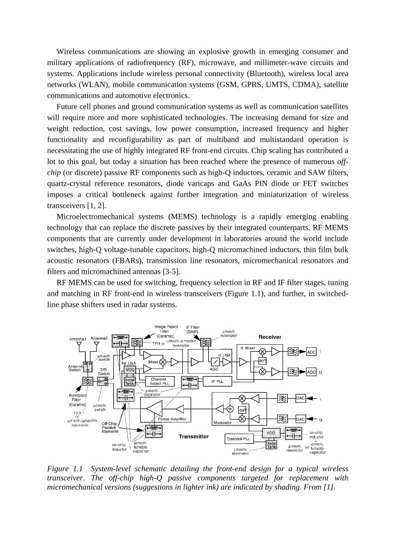
RF MEMS can be used for switching, frequency selection in RF and IF filter stages, tuning and matching in RF front-end in wireless transceivers (Figure 1.1), and further, in switched-line phase shifters used in radar systems.
Figure 1.1 System-level schematic detailing the front-end design for a typical wireless transceiver. The off-chip high-Q passive components targeted for replacement with micromechanical versions (suggestions in lighter ink) are indicated by shading. From [1].
INTRODUCTION
4
The integration of MEMS can either be achieved by hybrid or monolithic approach, leading to a system-in-package (SiP) or a system-on-chip (SoC) solution, respectively.
In SiP, passive and active components are integrated at the package level using technologies like low-temperature co-fired ceramic (LTCC) technology [6, 7] or multi-layer thin-film multi-chip module (MCM-D) technology [8].
In SoC, the MEMS devices are directly fabricated on IC wafers. Several approaches have be reported. The first one is based on post-CMOS fabrication steps for releasing micromechanical structures made of stack of oxide, aluminum and poly-Si layers [9, 10]. The second approach is called above-IC integration and involves a complete surface micromachining process on top of ICs. This has already been applied to monolithically integrate RF MEMS switches [11, 12] and thin-film bulk acoustic resonators (FBAR) [13] with ICs. In the third one, called in-IC integration, the micromechanical structures are fabricated in parallel at the same level as the transistors, the thin silicon-on-insulator (SOI) layer playing the structural role. With this approach thin-SOI NEMS accelerometers have been built [14]. The fourth one is called MEMS-first approach. The micromachined structures are fabricated on SOI wafers and vacuum-encapsulated in epitaxially-sealed (epitaxially-grown polycrystalline and single-crystal silicon) chambers buried under the wafer surface and then CMOS process can be performed on single-crystal silicon [15, 16].
In order to follow the electronic system demands on scaling, performance and functionality, 3D integration is gaining more and more interest. This is particularly the case of 3D stacked SoC [17, 18] which allows the heterogeneous integration of different optimized technologies, such as silicon, compound semiconductors and other substrates, MEMS and integrated passive devices, with 3D interconnects to meet the specifications for radio, analog, logic, memory, etc. and reach the desired performance levels and circuit density.
1.1 MOTIVATION AND SCOPE OF THE THESIS The starting point of this thesis was to develop RF MEMS passives (with main focus on
capacitors) integrable with advanced CMOS RF ICs. Then emerged the idea of using thin film silicon as a sacrificial layer for low-temperature surface micromachining and hence release the micromechanical structures by SF6 plasma.
Based on that, a surface micromachining process has been developed with two main constraints. First, the fabrication process should be compatible with CMOS post-processing and second, it aims at fabricating radiofrequency (RF) MEMS electrostatically-actuated capacitive membrane-based devices for above-IC integration.
Two European projects, WIDE-RF “Innovative MEMS Devices for Wideband Reconfigurable RF Microsystems” (IST-2001-33286) and integrated project MIMOSA “Microsystems Platform for Mobile Services and Applications” (IST-2002-507045), have been the driving forces of the work presented in this thesis.
In particular, the choice of MEMS tunable capacitors and capacitive switches as targeted devices has led to two circuit demonstrators: voltage-controlled oscillators (VCOs) and variable true-time delay lines (V-TTDLs). Both involve a strong collaboration with colleagues
ORGANIZATION OF THIS THESIS
5
in our lab and in the Laboratory of Electromagnetism and Acoustics (EPFL-LEMA), respectively.
The initial idea also helped a lot in developing the novel suspended-gate MOSFET (SG-MOSFET) architecture.
1.2 ORGANIZATION OF THIS THESIS This introduction is the first of seven chapters included in this thesis manuscript. Chapter 2 begins with an introduction to silicon micromachining techniques with more
emphasis on surface micromachining. It describes a study on SF6 inductively coupled plasma (ICP) releasing for silicon thin film sacrificial layer. It details the chronological improvements that have been brought to the fabrication process based on the SF6 plasma releasing, leading to a metal surface micromachining process compatible with CMOS post-processing for above-IC integration of radiofrequency (RF) MEMS devices. It also presents the extraction of the electrical and mechanical properties of the sputtered Al-Si (1%) alloy used.
Chapter 3 contains a review of MEMS tunable capacitors classifying them according to their tuning principle, such as gap tuning, area tuning and relative permittivity tuning. Then it describes two architectures of electrostatic gap-tuning capacitors based on the metal surface micromachining process described in chapter 2: the standard single-air-gap parallel-plate structure and the double-air-gap architecture for extended capacitance tuning range. The electromechanical and RF designs as well as the RF, electromechanical and thermal characterizations are presented. Finally, a wafer-level packaging technique and its effect on RF performance is described.
Chapter 4 focuses on voltage-controlled oscillators (VCOs) designed in X-FAB 0.6-μm BiCMOS process. Different realizations of the LC tank are presented and characterized. First with standard diode varicaps and then with wire-bonded MEMS tunable capacitor. The realization and characterization of suspended planar spiral inductors fabricated by surface micromachining and the post-processing of BiCMOS wafers are then described as preliminary steps in realizing the VCO demonstrator with above-IC MEMS LC tank. The third realization involves X-FAB spiral inductors and above-IC two-in-one double-air-gap capacitor. The last one is a VCO with above-IC MEMS LC tank. The influence of the post-processing on BiCMOS performance is evaluated by measuring the effect on bipolar and MOS transistors characteristics.
In chapter 5, the fabrication process is used to build coplanar waveguide (CPW) MEMS shunt capacitive switches. A lumped-element circuit model is presented and compared to EM full-wave simulation and measurements. In the second part of this chapter, these switches are used as distributed loading capacitors in variable true-time delay lines (V-TTDLs).
Chapter 6 deals with a novel MEMS device architecture: the suspended-gate MOSFET (SG-MOSFET), which combines a solid-state MOS transistor and a metal suspended gate. A unified analytical model is developed and used to investigate main electrostatic characteristics. In the fabrication process, polysilicon is used as a sacrificial layer for releasing the metal gate. Finally, its potential application as DC current switch is proposed.

INTRODUCTION
6
Chapter 7 is a summary of the work presented in this thesis and gives a short outlook on possible and interesting future research activities in the field of above-IC RF MEMS devices for communication applications.
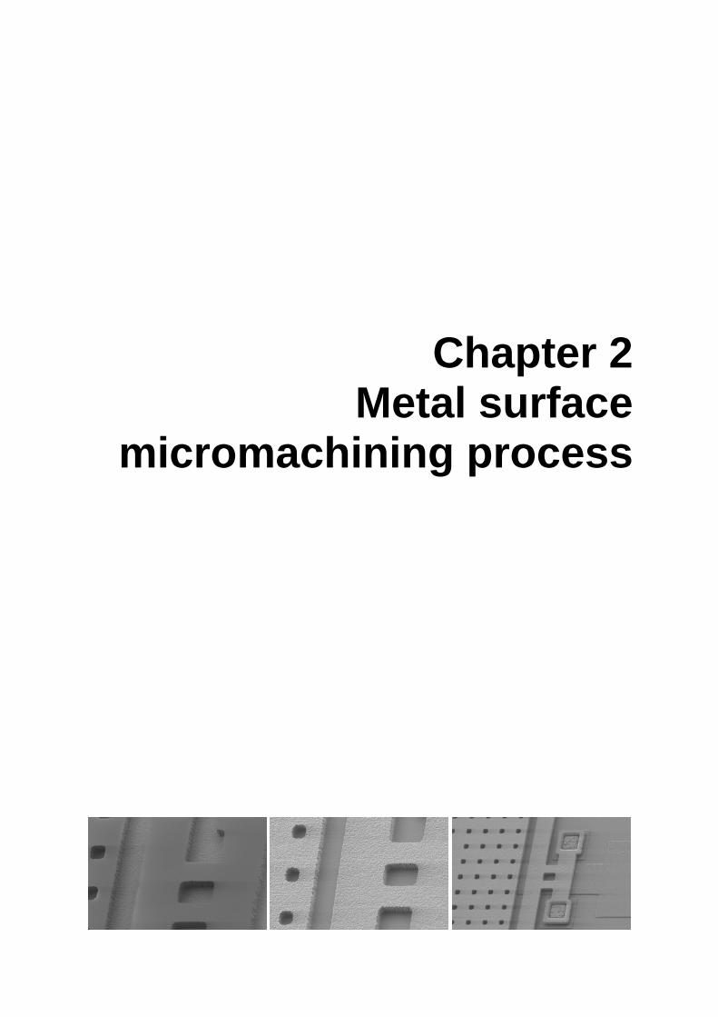
Chapter 2 Metal surface
micromachining process

Previous page left SEM microphotograph of 5 μm-thick AZ9260 positive-tone photoresist mask. (Scale: the small square holes are 6 x 6 μm2)
Previous page center SEM microphotograph of
4 μm-thick aluminum layer after plasma etching.
Previous page rightSEM microphotograph close-up view of a
suspended aluminum membrane after releasing.
2.1 INTRODUCTION TO SILICON MICROMACHINING TECHNIQUES
2.1.1 History of micromachining There has been activity in silicon-based micromachining since the early 1960’s, when the
integrated circuit (IC) technology was developed. Photolithography is used to define patterns that are subsequently selectively etched in chemical processing steps to define the geometries of thin films deposited on the substrate. This sequence of steps is repeated to produce electronic integrated circuits and this is known as the planar process developed in the 1960’s [19-21].
Two basic methods have evolved from this process to fabricate micromechanical structures, which we call now microelectromechanical systems (MEMS). One method builds the mechanical parts by anisotropically etching the bulk silicon substrate, it is therefore called bulk micromachining [22]. A second technique uses deposited films to make the mechanical parts extending above the surface of the silicon substrate; this technique is called surface micromachining. To make a mechanical part from the deposited layer material, an underlying sacrificial layer is selectively etched, thus releasing the element except where it is anchored to the substrate.
The surface micromachining concept was demonstrated in the mid-1960’s by Nathanson et al. at Westinghouse Research Laboratory using a freestanding gold cantilever beam as resonant gate for a field-effect transistor (FET) [23]. In the early 1980’s, Howe and Muller at the University of California, Berkeley, first fabricated polycrystalline silicon (poly-Si) microstructures using a silicon dioxide sacrificial layer [24, 25]. Unlike the resonant-gate transistor work on metal structures, poly-Si surface micromachining was quickly recognized as a promising technology and employed at both academic and industrial laboratories. The review paper by Petersen in 1982 [26] helped in gaining a larger acceptance of micromachined silicon as a structural material. Since then, many new surface micromachining techniques have been developed, leading to a great variety of possible structural and sacrificial layer systems.
2.1.2 Surface micromachining
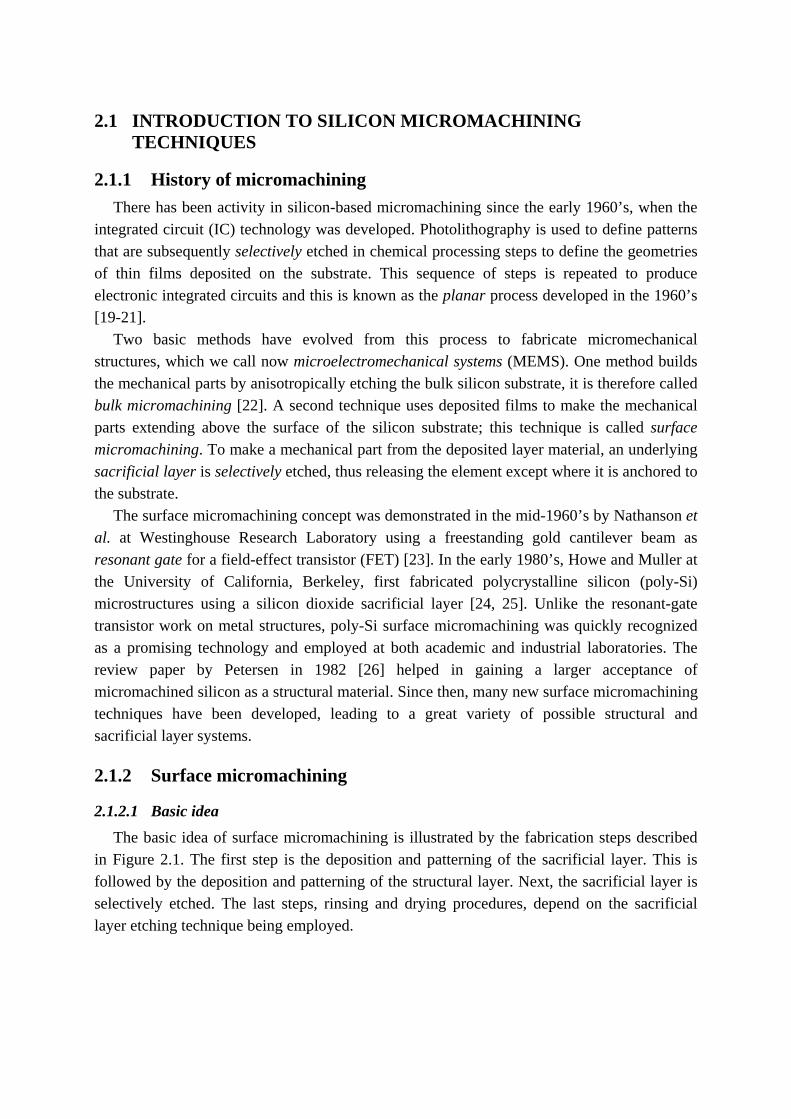
2.1.2.1 Basic idea The basic idea of surface micromachining is illustrated by the fabrication steps described
in Figure 2.1. The first step is the deposition and patterning of the sacrificial layer. This is followed by the deposition and patterning of the structural layer. Next, the sacrificial layer is selectively etched. The last steps, rinsing and drying procedures, depend on the sacrificial layer etching technique being employed.
METAL SURFACE MICROMACHINING PROCESS
10
(a) (b)
(c) (d)
Silicon substrate
Patterned sacrificial layer
Patterned structural layer
Figure 2.1 Basic process scheme of surface micromachining: (a) deposition and patterning of the sacrificial layer, (b) deposition and patterning of the structural layer, (c) sacrificial layer selective etching, (d) rinsing and drying procedures (if needed). Adapted from [20].
2.1.2.2 Stiction Stiction of thin films occurs after releasing with wet chemical etchants. Two different
mechanisms play a role in stiction [27]. First, a temporary physical contact between surface micromachined structures and the substrate is induced by capillary forces during drying of the rinse liquid. After this, permanent attachment is caused by van der Waals forces and hydrogen bridges which are induced by the small separation distance during this contact.
Several methods have been investigated to prevent or reduce stiction. The released structures can be freeze-dried using isopropyl alcohol (IPA) and cyclohexane [28], dried with a supercritical CO2 technique [29] or dried by coating the released microstructures with hydrophobic self-assembled monolayer (SAM) films prior to removal from aqueous stage [30]. Another method is to temporary increase the mechanical stiffness of the structure. It has been demonstrated for SiO2 sacrificial layer. A portion of the oxide layer can be substituted by a spun-on polymer spacer after a partial etch of the oxide. After completion of the sacrificial etching, the polymer spacer prevents collapse during evaporative drying. Last, an isotropic oxygen plasma etches the polymer to release the structure [31].
Released-induced stiction can also be completely avoided by using plasma or gas phase etching techniques (see next paragraph and section 2.2).
INTRODUCTION TO SILICON MICROMACHINING TECHNIQUES
11
2.1.2.3 Sacrificial layer materials Three types of sacrificial layer materials are briefly described.
Silicon dioxide sacrificial layer Since the early 1980’s, silicon dioxide sacrificial layer [32] have been widely used notably
in combination with poly-Si [24, 25] or poly-SiGe [33] structural layer. As polycrystalline silicon is typically deposited using gas-phase decomposition of silane (SiH4) in a low pressure chemical vapor deposition (LPCVD) furnace at about 600 °C, it is not compatible with other sacrificial materials.
Silicon dioxide can be deposited by several techniques such as LPCVD or plasma enhanced CVD (PECVD) using silane or tetraethosiloxane (for tetraethyl orthosilicate (TEOS) oxide) as reactant gas. SiO2 layers are isotropically etched in wet hydrofluoric (HF) acid solutions (such as HF/H20, buffered HF (BHF), or HNO3/HF mixtures) or by HF vapor phase etching (VPE) [34]. All these solutions exhibit very poor selectivity to aluminum. Selective releasing of aluminum MEMS has been demonstrated by using Pad-etch solution, which is a mixture of ammonium fluoride (NH4F), acetic acid (CH3COOH), ethylene glycol (C2H6O2) and water [32].
By repeating the basic sacrificial oxide and structural polysilicon fabrication steps, one can build extremely complex structures. Examples are the Sandia Ultra-planar, Multi-level MEMS Technology 5 (SUMMiT V) fabrication process [35] and the Multi-User MEMS Processes (MUMPs) [36].
Polymer sacrificial layer Polymer sacrificial layers such as polyimide can be isotropically etch in oxygen plasma in
barrel reactors. Polyimide has a glass transition temperature comprised between 290 and 400 °C (depending of the series [37]) and hence has been used for releasing materials deposited at low temperature such as physical vapor deposited (PVD) metals [38-40] and sputtered silicon [41, 42].
Another example of polymer sacrificial layer is polystyrene [43]. With this method, SU-8 microstructures have been released by dissolving polystyrene in toluene.
Metal sacrificial layer The use of metal sacrificial layer has been reported in combination of other metals as
structural layer, for example in [44] where copper is selectively wet etched on substrates with Ni-Fe alloy (Permalloy) and gold.
IC standard aluminum metallization can also be used as a sacrificial layer for releasing dielectrics microstructures [45].
METAL SURFACE MICROMACHINING PROCESS
12
2.2 THIN FILM SILICON AS A SACRIFICIAL LAYER FOR SURFACE MICROMACHINING
In the previous section, it has been clearly shown that a dry releasing step can eliminate the release-induced stiction problem and therefore leads to an increased yield for the overall MEMS process.
Based on EPFL-CMI experience on deep anisotropic silicon etching with high etch rate and commercially available high-density ICP etch equipments, we have investigated the use of silicon thin film as sacrificial layer for surface micromachining.
2.2.1 Isotropic dry etching of silicon Silicon can be etched in fluorine- and chlorine-based plasma or gas phase etching [46].
Chlorine-based plasma is not relevant for releasing because the etching is not spontaneous. It is only used for anisotropic etching.
2.2.1.1 Plasma-free etching in gas phase For plasma-free dry etching, the etch gases must provide both the elements that form the
desorbable products and strong oxidizing agents. These demands are satisfied by halogen compounds [47]: noble gas fluorides, such as XeF2, and halogen fluorides, such as ClF3 [48] and BrF3 [49, 50].
Among them, xenon difluoride has been extensively investigated [51-59]. XeF2 has the capability at room temperature to spontaneously etch silicon at significant rates without requiring a plasma to generate reactive species. Practically, the process is a pulsed etching: the duration of the etch is controlled by the number of cycles. A cycle consists of exposing the wafer to XeF2 at its room temperature equilibrium pressure, followed by pumping down the chamber. The etch rate has been reported to be extremely load-dependent [52] and the limiting step in the etching process appears to be the supply of fluorine atoms to the reaction site [53]. XeF2 alone does not etch silicon dioxide and nitride, but can etch these dielectrics in presence of ion or electron bombardment and under UV irradiation. This may help to explain why fluorine atoms are non selective in standard plasma processes [54]. Commercial XeF2 etchers are now available [60]. Moreover, as XeF2 etching is a room temperature process, it can be used to release polymer microstructures.
2.2.1.2 Plasma etching Sulfur hexafluoride (SF6) is the preferred plasma etchant for isotropic etch of silicon [61].
It has been widely used in deep anisotropic silicon etching in conjunction with a passivation gas, like C4F8, in the so-called Bosch process [62], or O2, in the cryogenic process [63].
THIN FILM SILICON AS A SACRIFICIAL LAYER FOR SURFACE MICROMACHINING
13
The basic chemical reactions that occur in SF6 plasma are as following [64]: Dissociation -
56- e FSFSF e ++→+ (2.1)
-45
- e FSFSF e ++→+ (2.2) -
34- e FSFSF e ++→+ (2.3)
Ionization -56
- e 2 FSFSF e ++→+ + (2.4) -
236- e FFSFSF e +++→+ + (2.5)
-34
- e FSFSF e ++→+ + (2.6)
Attachment FSFSF e 56- +→+ − (2.7)
FSFSF e 34- +→+ − (2.8)
-34
- e 2 FSFSF e ++→+ + (2.9)
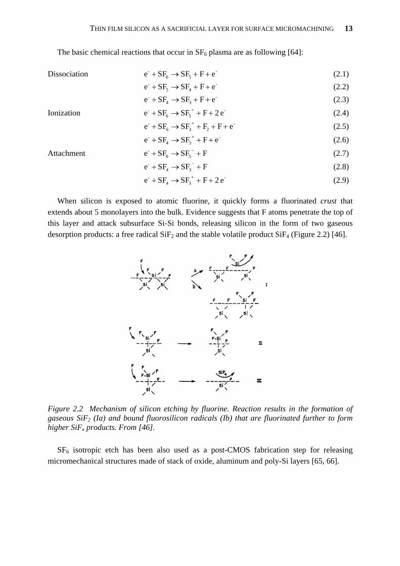
When silicon is exposed to atomic fluorine, it quickly forms a fluorinated crust that extends about 5 monolayers into the bulk. Evidence suggests that F atoms penetrate the top of this layer and attack subsurface Si-Si bonds, releasing silicon in the form of two gaseous desorption products: a free radical SiF2 and the stable volatile product SiF4 (Figure 2.2) [46].
Figure 2.2 Mechanism of silicon etching by fluorine. Reaction results in the formation of gaseous SiF2 (Ia) and bound fluorosilicon radicals (Ib) that are fluorinated further to form higher SiFx products. From [46].
SF6 isotropic etch has been also used as a post-CMOS fabrication step for releasing
micromechanical structures made of stack of oxide, aluminum and poly-Si layers [65, 66].
METAL SURFACE MICROMACHINING PROCESS
14
2.2.2 Process optimization for SF6 plasma releasing Both sputtered amorphous and LPCVD polycrystalline silicon thin films are investigated in
this study because they are directly linked to two different applications of interest. Sputtered amorphous silicon (a-Si) is an interesting candidate for use as sacrificial layer in aluminum membrane-based MEMS devices such as MEMS tunable capacitors (see section 2.3 and chapter 3) and capacitive switches (see chapter 5), while LPCVD polycrystalline silicon (poly-Si) is of interest in the suspended-gate MOSFET (SG-MOSFET) (see chapter 6).
The key challenge was to improve the releasing step by obtaining a high aspect ratio (i.e. length-to-thickness ratio), a maximal etch rate of the Si sacrificial layer and a high selectivity to silicon dioxide.
The experiments have been performed in a high-density ICP etcher (Alcatel 601E, now Adixen AMS 200DSE) taking advantage of the independent control of radicals, ion flux and chuck temperature. Etching was performed using pure sulfur hexafluoride (SF6), which is commonly used to achieve deep anisotropic silicon etching with high etch rate, high uniformity (± 5%) and high Si: SiO2 selectivity (more than 150: 1). However, by increasing chemical etching and limiting physical etching, underetching of thin silicon layer with high selectivity to SiO2 can also be performed in ICP etcher.
2.2.2.1 Inductively coupled plasma (ICP) etching equipment
The Alcatel 601E machine belongs to a new generation of dry etching equipment with high performance, thanks to the combination of the latest technologies:
- ICP type plasma (inductively coupled plasma); - Substrate holder which can be biased and temperature controlled (cryogenic and tunable
from room temperature down to -170 °C); - Powerful pumping systems which lead to high secondary vacuum and the possibility of
working with high gas flow rates while maintaining low pressure. Compared to reactors with capacitive coupling (commonly named RIE: reactive ion
etching), this type of machine has the following advantages: - The possibility of biasing the substrate holder independently of inductive plasma
creation; - The generation of low pressure (0.5 to 10 Pa) high density (1010 to 1012 cm-3) plasma
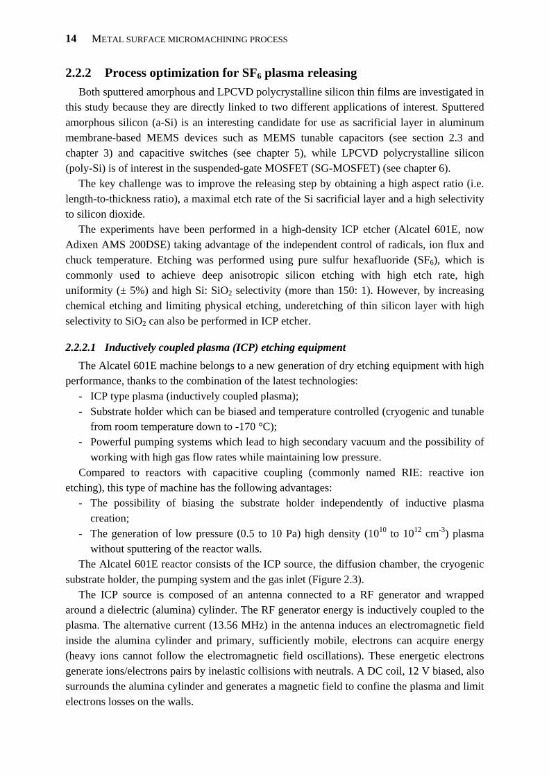
without sputtering of the reactor walls. The Alcatel 601E reactor consists of the ICP source, the diffusion chamber, the cryogenic
substrate holder, the pumping system and the gas inlet (Figure 2.3). The ICP source is composed of an antenna connected to a RF generator and wrapped
around a dielectric (alumina) cylinder. The RF generator energy is inductively coupled to the plasma. The alternative current (13.56 MHz) in the antenna induces an electromagnetic field inside the alumina cylinder and primary, sufficiently mobile, electrons can acquire energy (heavy ions cannot follow the electromagnetic field oscillations). These energetic electrons generate ions/electrons pairs by inelastic collisions with neutrals. A DC coil, 12 V biased, also surrounds the alumina cylinder and generates a magnetic field to confine the plasma and limit electrons losses on the walls.
THIN FILM SILICON AS A SACRIFICIAL LAYER FOR SURFACE MICROMACHINING
15
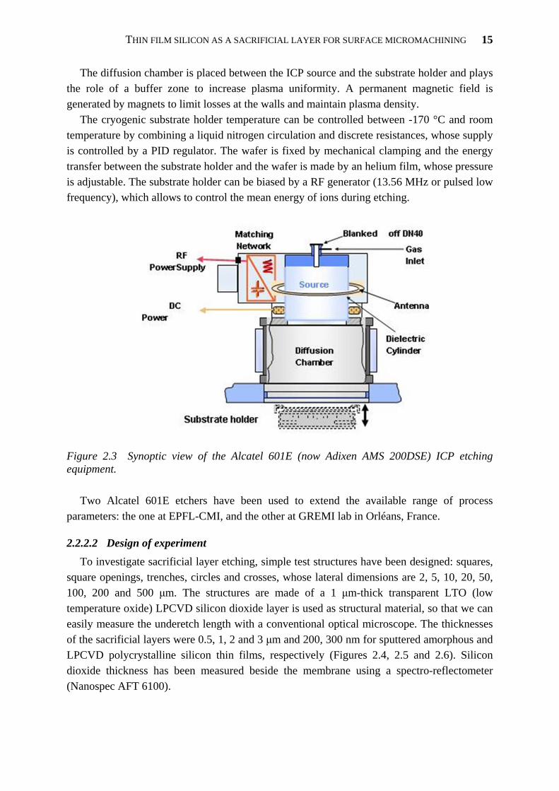
The diffusion chamber is placed between the ICP source and the substrate holder and plays the role of a buffer zone to increase plasma uniformity. A permanent magnetic field is generated by magnets to limit losses at the walls and maintain plasma density.
The cryogenic substrate holder temperature can be controlled between -170 °C and room temperature by combining a liquid nitrogen circulation and discrete resistances, whose supply is controlled by a PID regulator. The wafer is fixed by mechanical clamping and the energy transfer between the substrate holder and the wafer is made by an helium film, whose pressure is adjustable. The substrate holder can be biased by a RF generator (13.56 MHz or pulsed low frequency), which allows to control the mean energy of ions during etching.
Figure 2.3 Synoptic view of the Alcatel 601E (now Adixen AMS 200DSE) ICP etching equipment.
Two Alcatel 601E etchers have been used to extend the available range of process
parameters: the one at EPFL-CMI, and the other at GREMI lab in Orléans, France.
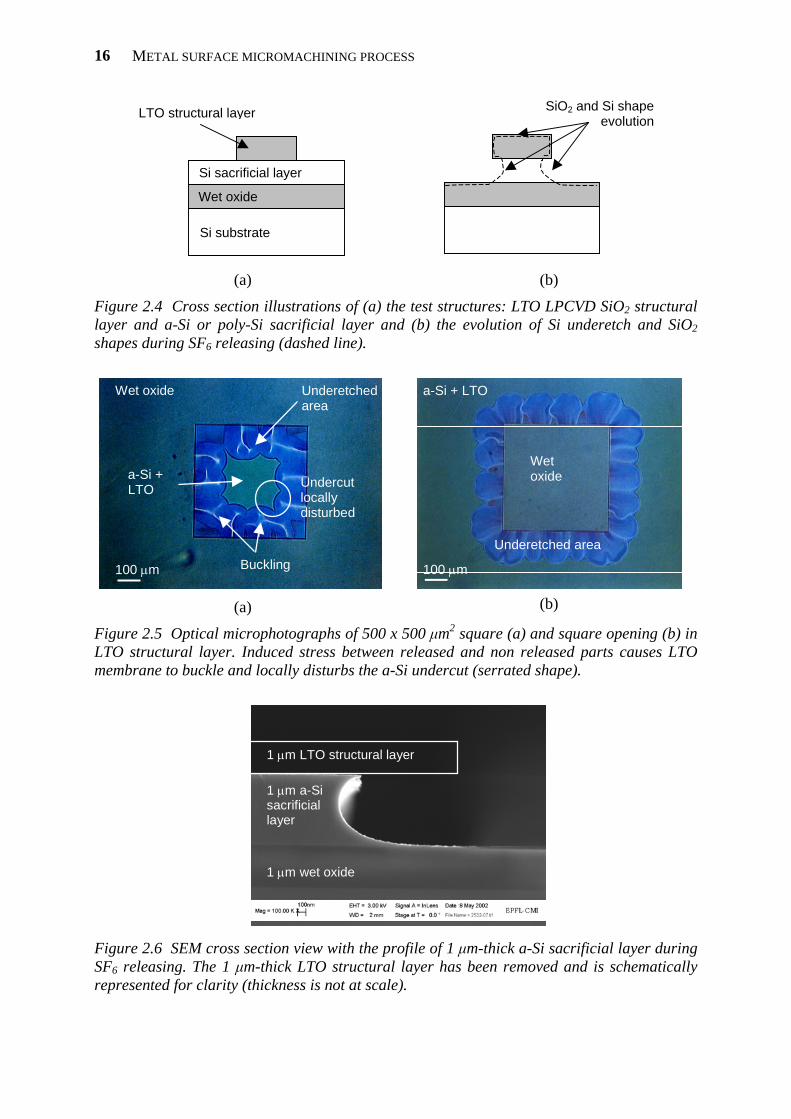
2.2.2.2 Design of experiment To investigate sacrificial layer etching, simple test structures have been designed: squares,
square openings, trenches, circles and crosses, whose lateral dimensions are 2, 5, 10, 20, 50, 100, 200 and 500 μm. The structures are made of a 1 μm-thick transparent LTO (low temperature oxide) LPCVD silicon dioxide layer is used as structural material, so that we can easily measure the underetch length with a conventional optical microscope. The thicknesses of the sacrificial layers were 0.5, 1, 2 and 3 μm and 200, 300 nm for sputtered amorphous and LPCVD polycrystalline silicon thin films, respectively (Figures 2.4, 2.5 and 2.6). Silicon dioxide thickness has been measured beside the membrane using a spectro-reflectometer (Nanospec AFT 6100).
METAL SURFACE MICROMACHINING PROCESS
16
LTO structural layer
Si substrate
Wet oxide
Si sacrificial layer
(a)
SiO2 and Si shape evolution
(b)
Figure 2.4 Cross section illustrations of (a) the test structures: LTO LPCVD SiO2 structural layer and a-Si or poly-Si sacrificial layer and (b) the evolution of Si underetch and SiO2 shapes during SF6 releasing (dashed line).
Wet oxide
a-Si + LTO
Underetched area
100 μm Buckling
Undercut locally disturbed
(a)
Wet oxide
a-Si + LTO
Underetched area
100 μm
(b)
Figure 2.5 Optical microphotographs of 500 x 500 μm2 square (a) and square opening (b) in LTO structural layer. Induced stress between released and non released parts causes LTO membrane to buckle and locally disturbs the a-Si undercut (serrated shape).
1 μm a-Si sacrificial layer
1 μm wet oxide
1 μm LTO structural layer
Figure 2.6 SEM cross section view with the profile of 1 μm-thick a-Si sacrificial layer during SF6 releasing. The 1 μm-thick LTO structural layer has been removed and is schematically represented for clarity (thickness is not at scale).

THIN FILM SILICON AS A SACRIFICIAL LAYER FOR SURFACE MICROMACHINING
17
Based on the etching recipes used at EPFL-CMI prior to this work for 1 μm-thick a-Si and 400 nm-thick poly-Si sacrificial layers (Table 2.1) and on the capabilities of the two Alcatel 601E ICP etchers available, the experimental plasma parameters have been determined (Table 2.2).
Table 2.1 Etching recipes used at EPFL-CMI prior to this work for 2 μm-thick a-Si and 400 nm-thick poly-Si sacrificial layers. These recipes were the basis for determining the experimental plasma parameters (Table 2.2).
Sacrificial layer material thickness [μm]
a-Si 2
poly-Si 0.4
Plasma settings ICP source power [W] bias power [W] SF6 flow rate [sccm] pressure [Pa] chuck temperature [°C]
1500 0 200 3 20
1500 0 200 18 20
Releasing features Si underetch rate [μm/min] SiO2 etch rate [Å/min] Si: SiO2 selectivity
1.9 12.6 1500: 1
0.3 1.7 1750: 1
Table 2.2 Experimental plasma parameters. Central parameters are highlighted in bold.
Experimental plasma parameters ICP source power [W] Bias power [W] SF6 flow rate [sccm] Pressure [Pa] Chuck temperature [°C]
1000, 1500, 2000, 2500, 3000 0 100, 300, 500, 700, 900 3, 5, 10, 15, 18 -110, -40, -20, 0, 20, 40
2.2.2.3 Influence of the different parameters In the following, we present a detailed experimental study to determine the influence of the
most relevant etching parameters: (i) process time, (ii) SF6 flow rate, (iii) pressure, (iv) ICP source power, (v) chuck temperature, as well as design and sacrificial layer parameters: (vi) opening feature size of the structures, (vii) silicon sacrificial layer thickness, (vii) a-Si deposition temperature.
Subsequently, their impact on the: (i) silicon underetch rate, (ii) silicon dioxide etch rate, and (iii) Si: SiO2 selectivity are reported. Finally, the SiO2 thickness under membranes is also measured.
To evaluate the influence of the parameters separately, each experiment has the central parameters (Table 2.2) as starting point and one parameter is varied.
METAL SURFACE MICROMACHINING PROCESS
18
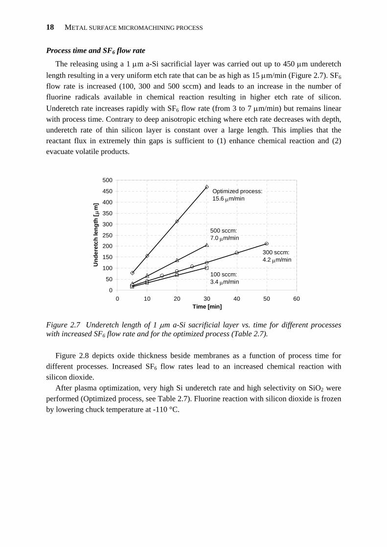
Process time and SF6 flow rate
The releasing using a 1 μm a-Si sacrificial layer was carried out up to 450 μm underetch length resulting in a very uniform etch rate that can be as high as 15 μm/min (Figure 2.7). SF6 flow rate is increased (100, 300 and 500 sccm) and leads to an increase in the number of fluorine radicals available in chemical reaction resulting in higher etch rate of silicon. Underetch rate increases rapidly with SF6 flow rate (from 3 to 7 μm/min) but remains linear with process time. Contrary to deep anisotropic etching where etch rate decreases with depth, underetch rate of thin silicon layer is constant over a large length. This implies that the reactant flux in extremely thin gaps is sufficient to (1) enhance chemical reaction and (2) evacuate volatile products.
0
50
100
150
200
250
300
350
400
450
500
0 10 20 30 40 50 60Time [min]
Und
eret
ch le
ngth
[ μm
]
300 sccm:4.2 μm/min
500 sccm:7.0 μm/min
Optimized process:15.6 μm/min
100 sccm:3.4 μm/min
Figure 2.7 Underetch length of 1 μm a-Si sacrificial layer vs. time for different processes with increased SF6 flow rate and for the optimized process (Table 2.7).
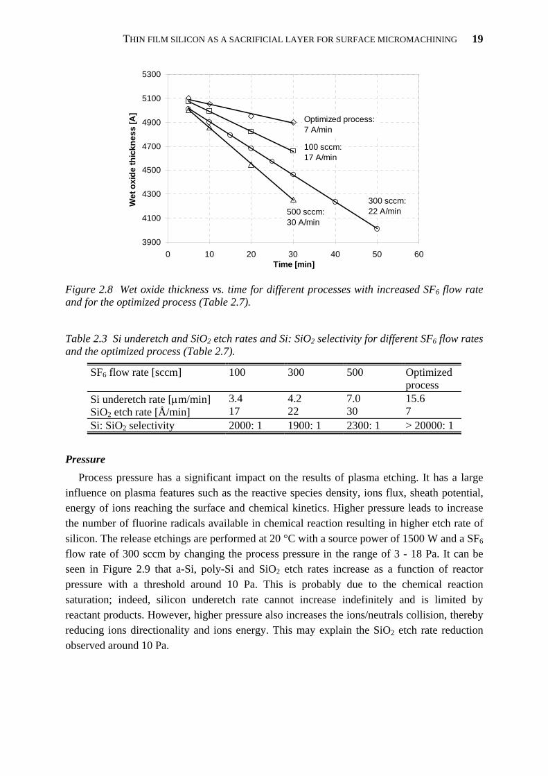
Figure 2.8 depicts oxide thickness beside membranes as a function of process time for
different processes. Increased SF6 flow rates lead to an increased chemical reaction with silicon dioxide.
After plasma optimization, very high Si underetch rate and high selectivity on SiO2 were performed (Optimized process, see Table 2.7). Fluorine reaction with silicon dioxide is frozen by lowering chuck temperature at -110 °C.
THIN FILM SILICON AS A SACRIFICIAL LAYER FOR SURFACE MICROMACHINING
19
3900
4100
4300
4500
4700
4900
5100
5300
0 10 20 30 40 50 60Time [min]
Wet
oxi
de th
ickn
ess
[A]
300 sccm:22 A/min500 sccm:
30 A/min
Optimized process:7 A/min
100 sccm:17 A/min
Figure 2.8 Wet oxide thickness vs. time for different processes with increased SF6 flow rate and for the optimized process (Table 2.7).
Table 2.3 Si underetch and SiO2 etch rates and Si: SiO2 selectivity for different SF6 flow rates and the optimized process (Table 2.7).
SF6 flow rate [sccm] 100 300 500 Optimized process
Si underetch rate [μm/min] SiO2 etch rate [Å/min]
3.4 17
4.2 22
7.0 30
15.6 7
Si: SiO2 selectivity 2000: 1 1900: 1 2300: 1 > 20000: 1
Pressure
Process pressure has a significant impact on the results of plasma etching. It has a large influence on plasma features such as the reactive species density, ions flux, sheath potential, energy of ions reaching the surface and chemical kinetics. Higher pressure leads to increase the number of fluorine radicals available in chemical reaction resulting in higher etch rate of silicon. The release etchings are performed at 20 °C with a source power of 1500 W and a SF6 flow rate of 300 sccm by changing the process pressure in the range of 3 - 18 Pa. It can be seen in Figure 2.9 that a-Si, poly-Si and SiO2 etch rates increase as a function of reactor pressure with a threshold around 10 Pa. This is probably due to the chemical reaction saturation; indeed, silicon underetch rate cannot increase indefinitely and is limited by reactant products. However, higher pressure also increases the ions/neutrals collision, thereby reducing ions directionality and ions energy. This may explain the SiO2 etch rate reduction observed around 10 Pa.

METAL SURFACE MICROMACHINING PROCESS
20
0
1
2
3
4
5
6
0 5 10 15 20
Pressure [Pa]
Si u
nder
etch
rate
[ μm
/min
]
0
5
10
15
20
25
30
35
40
SiO2 etch rate [A
/min]
1 um a-Si400 nm poly-SiWet oxide
Figure 2.9 Si sacrificial layer underetch rate and SiO2 etch rate vs. pressure.
Table 2.4 Si underetch and SiO2 etch rates and Si: SiO2 selectivity for different pressures.
Pressure [Pa] 3 5 10 15 18 a-Si underetch rate [μm/min] poly-Si underetch rate [μm/min] SiO2 etch rate [Å/min]
N.A. 1.9 N.A.
3.6 N.A. 16
5.0 4.6 25
5.5 5.0 28
5.7 5.0 30
a-Si: SiO2 selectivity poly-Si: SiO2 selectivity
N.A. N.A.
2200: 1 N.A.
2000: 1 1840: 1
1960: 1 1780: 1
1900: 1 1670: 1
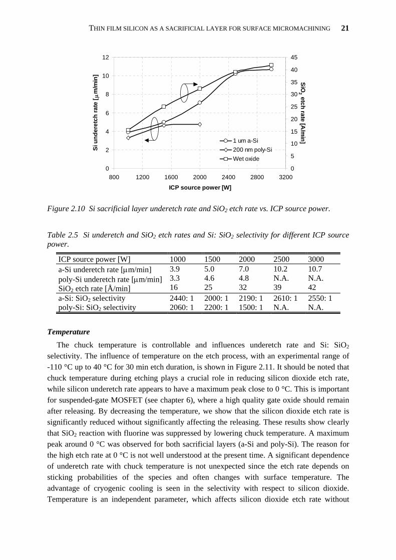
ICP source power Increasing ICP source power extends the electron energy distribution function (EEDF) and
therefore, a larger number of electrons with high energy are available for dissociation and ionization. Evolution of sacrificial layer and silicon dioxide etch rates is shown in Figure 2.10. It can be seen that increasing ICP source power increases SiO2 and sacrificial layer etch rate. A threshold is observed around 1500 W for the 200 nm poly-Si sacrificial layer and around 2500 W for the 1 μm a-Si sacrificial layer. This is due to the saturation of reactant species, which depends on thickness of the sacrificial layer and source power. In fact four fluorine atoms react with one silicon atom to form SiF4 molecule, which is a volatile product at room temperature, SiF4 molecules are then desorpted from the surface and pumped away.
THIN FILM SILICON AS A SACRIFICIAL LAYER FOR SURFACE MICROMACHINING
21
0
2
4
6
8
10
12
800 1200 1600 2000 2400 2800 3200
ICP source power [W]
Si u
nder
etch
rate
[ μm
/min
]
0
5
10
15
20
25
30
35
40
45
SiO2 etch rate [A
/min]1 um a-Si
200 nm poly-SiWet oxide
Figure 2.10 Si sacrificial layer underetch rate and SiO2 etch rate vs. ICP source power.
Table 2.5 Si underetch and SiO2 etch rates and Si: SiO2 selectivity for different ICP source power.
ICP source power [W] 1000 1500 2000 2500 3000 a-Si underetch rate [μm/min] poly-Si underetch rate [μm/min] SiO2 etch rate [Å/min]
3.9 3.3 16
5.0 4.6 25
7.0 4.8 32
10.2 N.A. 39
10.7 N.A. 42
a-Si: SiO2 selectivity poly-Si: SiO2 selectivity
2440: 1 2060: 1
2000: 1 2200: 1
2190: 1 1500: 1
2610: 1 N.A.
2550: 1 N.A.
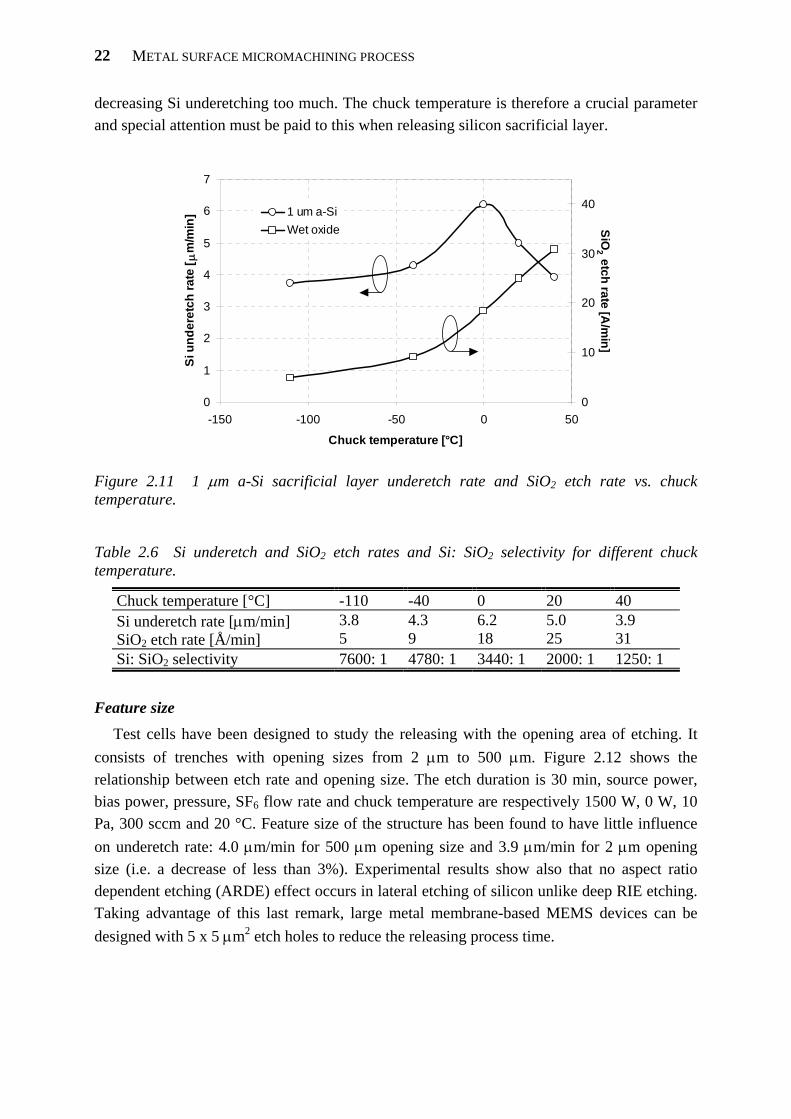
Temperature
The chuck temperature is controllable and influences underetch rate and Si: SiO2 selectivity. The influence of temperature on the etch process, with an experimental range of -110 °C up to 40 °C for 30 min etch duration, is shown in Figure 2.11. It should be noted that chuck temperature during etching plays a crucial role in reducing silicon dioxide etch rate, while silicon underetch rate appears to have a maximum peak close to 0 °C. This is important for suspended-gate MOSFET (see chapter 6), where a high quality gate oxide should remain after releasing. By decreasing the temperature, we show that the silicon dioxide etch rate is significantly reduced without significantly affecting the releasing. These results show clearly that SiO2 reaction with fluorine was suppressed by lowering chuck temperature. A maximum peak around 0 °C was observed for both sacrificial layers (a-Si and poly-Si). The reason for the high etch rate at 0 °C is not well understood at the present time. A significant dependence of underetch rate with chuck temperature is not unexpected since the etch rate depends on sticking probabilities of the species and often changes with surface temperature. The advantage of cryogenic cooling is seen in the selectivity with respect to silicon dioxide. Temperature is an independent parameter, which affects silicon dioxide etch rate without
METAL SURFACE MICROMACHINING PROCESS
22
decreasing Si underetching too much. The chuck temperature is therefore a crucial parameter and special attention must be paid to this when releasing silicon sacrificial layer.
0
1
2
3
4
5
6
7
-150 -100 -50 0 50
Chuck temperature [°C]
Si u
nder
etch
rate
[ μm
/min
]
0
10
20
30
40SiO
2 etch rate [A/m
in]
1 um a-SiWet oxide
Figure 2.11 1 μm a-Si sacrificial layer underetch rate and SiO2 etch rate vs. chuck temperature.
Table 2.6 Si underetch and SiO2 etch rates and Si: SiO2 selectivity for different chuck temperature.
Chuck temperature [°C] -110 -40 0 20 40 Si underetch rate [μm/min] SiO2 etch rate [Å/min]
3.8 5
4.3 9
6.2 18
5.0 25
3.9 31
Si: SiO2 selectivity 7600: 1 4780: 1 3440: 1 2000: 1 1250: 1
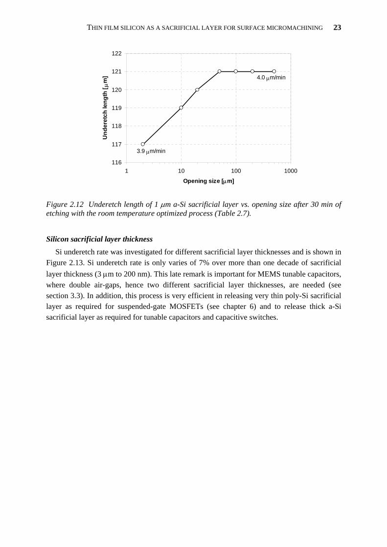
Feature size Test cells have been designed to study the releasing with the opening area of etching. It
consists of trenches with opening sizes from 2 μm to 500 μm. Figure 2.12 shows the relationship between etch rate and opening size. The etch duration is 30 min, source power, bias power, pressure, SF6 flow rate and chuck temperature are respectively 1500 W, 0 W, 10 Pa, 300 sccm and 20 °C. Feature size of the structure has been found to have little influence on underetch rate: 4.0 μm/min for 500 μm opening size and 3.9 μm/min for 2 μm opening size (i.e. a decrease of less than 3%). Experimental results show also that no aspect ratio dependent etching (ARDE) effect occurs in lateral etching of silicon unlike deep RIE etching. Taking advantage of this last remark, large metal membrane-based MEMS devices can be designed with 5 x 5 μm2 etch holes to reduce the releasing process time.
THIN FILM SILICON AS A SACRIFICIAL LAYER FOR SURFACE MICROMACHINING
23
116
117
118
119
120
121
122
1 10 100 1000
Opening size [μm]
Und
eret
ch le
ngth
[ μm
]
3.9 μm/min
4.0 μm/min
Figure 2.12 Underetch length of 1 μm a-Si sacrificial layer vs. opening size after 30 min of etching with the room temperature optimized process (Table 2.7).
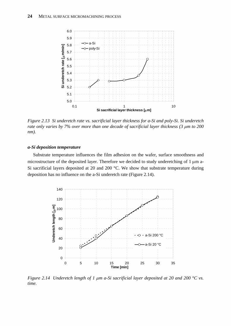
Silicon sacrificial layer thickness
Si underetch rate was investigated for different sacrificial layer thicknesses and is shown in Figure 2.13. Si underetch rate is only varies of 7% over more than one decade of sacrificial layer thickness (3 μm to 200 nm). This late remark is important for MEMS tunable capacitors, where double air-gaps, hence two different sacrificial layer thicknesses, are needed (see section 3.3). In addition, this process is very efficient in releasing very thin poly-Si sacrificial layer as required for suspended-gate MOSFETs (see chapter 6) and to release thick a-Si sacrificial layer as required for tunable capacitors and capacitive switches.
METAL SURFACE MICROMACHINING PROCESS
24
5.0
5.1
5.2
5.3
5.4
5.5
5.6
5.7
5.8
5.9
6.0
0.1 1 10Si sacrificial layer thickness [μm]
Si u
nder
etch
rate
[ μm
/min
] a-Sipoly-Si
Figure 2.13 Si underetch rate vs. sacrificial layer thickness for a-Si and poly-Si. Si underetch rate only varies by 7% over more than one decade of sacrificial layer thickness (3 μm to 200 nm).
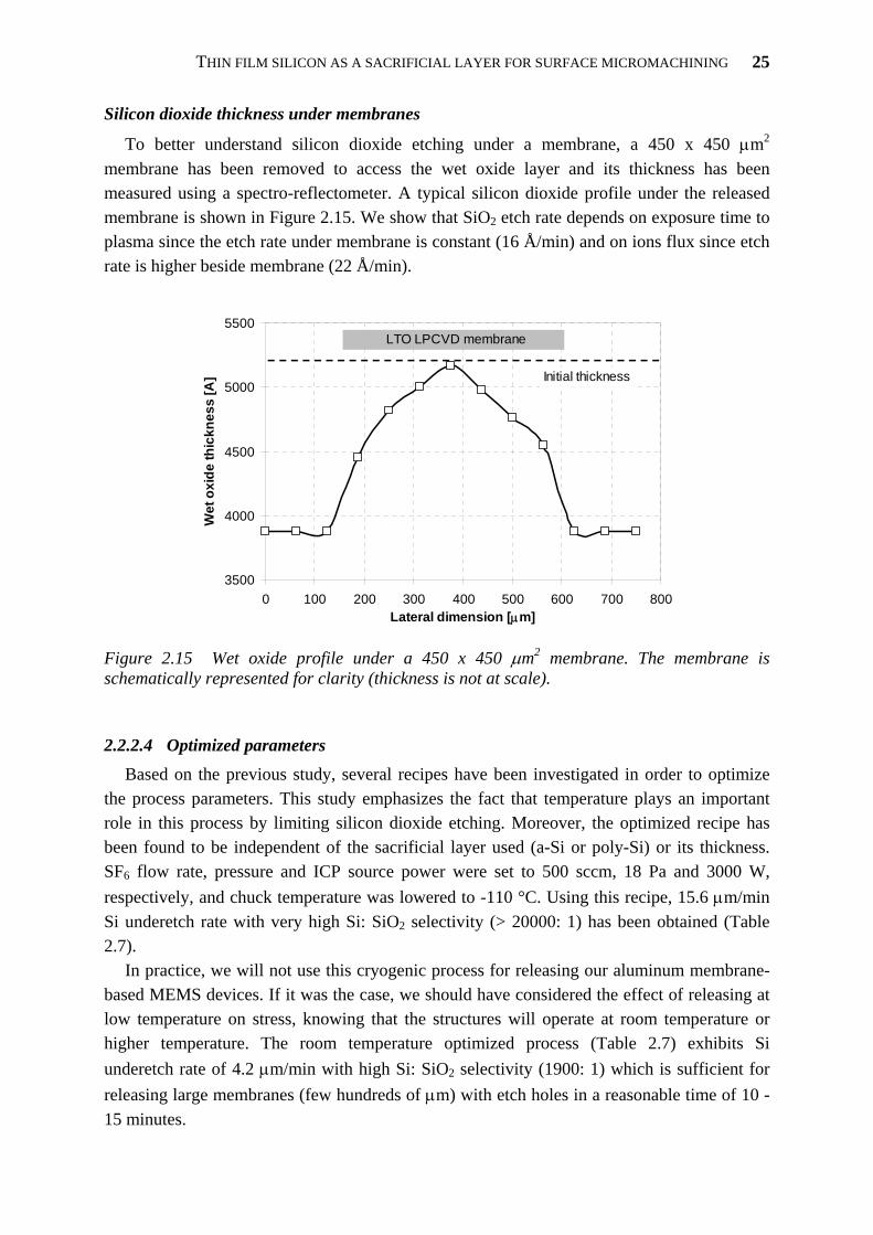
a-Si deposition temperature
Substrate temperature influences the film adhesion on the wafer, surface smoothness and microstructure of the deposited layer. Therefore we decided to study underetching of 1 μm a-Si sacrificial layers deposited at 20 and 200 °C. We show that substrate temperature during deposition has no influence on the a-Si underetch rate (Figure 2.14).
0
20
40
60
80
100
120
140
0 5 10 15 20 25 30 35Time [min]
Und
eret
ch le
ngth
[ μm
]
a-Si 200 °C
a-Si 20 °C
Figure 2.14 Underetch length of 1 μm a-Si sacrificial layer deposited at 20 and 200 °C vs. time.
THIN FILM SILICON AS A SACRIFICIAL LAYER FOR SURFACE MICROMACHINING
25
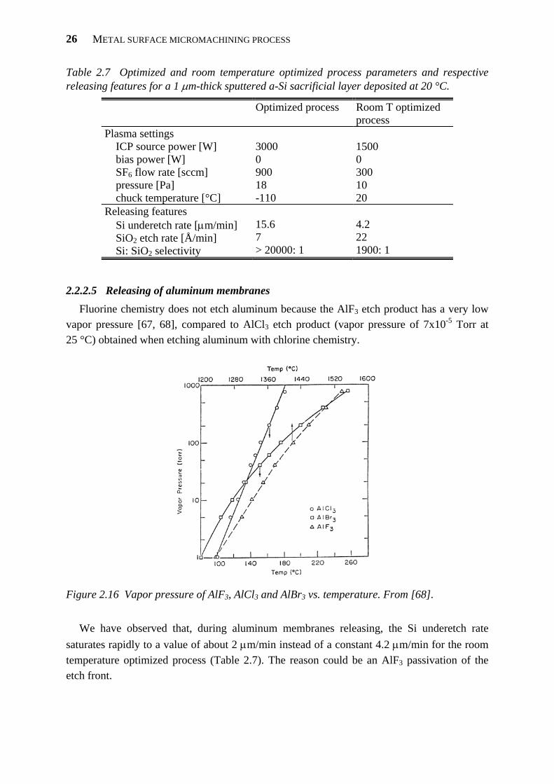
Silicon dioxide thickness under membranes
To better understand silicon dioxide etching under a membrane, a 450 x 450 μm2 membrane has been removed to access the wet oxide layer and its thickness has been measured using a spectro-reflectometer. A typical silicon dioxide profile under the released membrane is shown in Figure 2.15. We show that SiO2 etch rate depends on exposure time to plasma since the etch rate under membrane is constant (16 Å/min) and on ions flux since etch rate is higher beside membrane (22 Å/min).
3500
4000
4500
5000
5500
0 100 200 300 400 500 600 700 800Lateral dimension [μm]
Wet
oxi
de th
ickn
ess
[A] Initial thickness
LTO LPCVD membrane
Figure 2.15 Wet oxide profile under a 450 x 450 μm2 membrane. The membrane is schematically represented for clarity (thickness is not at scale).
2.2.2.4 Optimized parameters Based on the previous study, several recipes have been investigated in order to optimize
the process parameters. This study emphasizes the fact that temperature plays an important role in this process by limiting silicon dioxide etching. Moreover, the optimized recipe has been found to be independent of the sacrificial layer used (a-Si or poly-Si) or its thickness. SF6 flow rate, pressure and ICP source power were set to 500 sccm, 18 Pa and 3000 W, respectively, and chuck temperature was lowered to -110 °C. Using this recipe, 15.6 μm/min Si underetch rate with very high Si: SiO2 selectivity (> 20000: 1) has been obtained (Table 2.7).
In practice, we will not use this cryogenic process for releasing our aluminum membrane-based MEMS devices. If it was the case, we should have considered the effect of releasing at low temperature on stress, knowing that the structures will operate at room temperature or higher temperature. The room temperature optimized process (Table 2.7) exhibits Si underetch rate of 4.2 μm/min with high Si: SiO2 selectivity (1900: 1) which is sufficient for releasing large membranes (few hundreds of μm) with etch holes in a reasonable time of 10 - 15 minutes.
METAL SURFACE MICROMACHINING PROCESS
26
Table 2.7 Optimized and room temperature optimized process parameters and respective releasing features for a 1 μm-thick sputtered a-Si sacrificial layer deposited at 20 °C.
Optimized process Room T optimized process
Plasma settings ICP source power [W] bias power [W] SF6 flow rate [sccm] pressure [Pa] chuck temperature [°C]
3000 0 900 18 -110
1500 0 300 10 20
Releasing features Si underetch rate [μm/min] SiO2 etch rate [Å/min] Si: SiO2 selectivity
15.6 7 > 20000: 1
4.2 22 1900: 1
2.2.2.5 Releasing of aluminum membranes Fluorine chemistry does not etch aluminum because the AlF3 etch product has a very low
vapor pressure [67, 68], compared to AlCl3 etch product (vapor pressure of 7x10⁻⁵ Torr at 25 °C) obtained when etching aluminum with chlorine chemistry.
Figure 2.16 Vapor pressure of AlF3, AlCl3 and AlBr3 vs. temperature. From [68].
We have observed that, during aluminum membranes releasing, the Si underetch rate
saturates rapidly to a value of about 2 μm/min instead of a constant 4.2 μm/min for the room temperature optimized process (Table 2.7). The reason could be an AlF3 passivation of the etch front.

METAL SURFACE MICROMACHINING FOR ABOVE-IC RF MEMS APPLICATIONS
27
2.2.3 Comparison with state-of-the-art dry releasing processes Table 2.4 gives a comparison between the results we have obtained with the SF6 optimized
and room temperature optimized processes (Table 2.7) and the state-of-the-art dry releasing processes. SF6 plasma has been chosen because it exhibits much higher etch rate than O2 plasma and HF vapor phase etching and moreover it presents a high selectivity to SiO2 and aluminum.
Table 2.8 Comparison between the results we have obtained with the SF6 optimized and room temperature optimized processes (Table 2.7) and the state-of-the-art dry releasing processes.
Process Sacrificial layer material
Underetch rate [μm/min]
Selectivity to SiO2
SF6 ICP plasma Optimized process
a-Si and poly-Si 15.6 > 20000: 1
SF6 ICP plasma Room T optimized process
a-Si and poly-Si 4.2 1900: 1
SF6 ICP plasma [65] bulk Si 4.5 N.A. XeF2 gas phase [60] Si 2-4 > 1000: 1 BrF3 gas phase [49] Si 1-14 > 3000: 1 O2 plasma * polyimide
PI26xx [37] ~ 1 very high
HF vapor phase [69] thermal oxide 0.07-0.1 - (* at EPFL-CMI, Tepla300 microwave plasma stripper, barrel reactor)
2.3 METAL SURFACE MICROMACHINING FOR ABOVE-IC RF MEMS APPLICATIONS
2.3.1 Choice of materials The development of a new surface micromachining process requires the choice of different
materials: sacrificial and structural layer and insulating layers. The choice is dictated by on the one hand the functionality of the MEMS devices and associated applications and on the other hand by the clean room process available.
The process presented in this section is intended to be compatible with CMOS post-processing for above-IC integration in order to fabricate radiofrequency (RF) MEMS devices. These devices are mainly electrostatically-actuated capacitive membrane-based devices (see following chapters).
2.3.1.1 CMOS post-process compatibility In order to make integrated devices, the steps used to fabricate the micromechanical
structures must not adversely impact the underlying circuitry. High temperatures, plasma or X-ray damage, electrostatic discharge (ESD), metal diffusion
into silicon, contamination, or physical etching of the CMOS must all be avoided.
METAL SURFACE MICROMACHINING PROCESS
28
Among these, temperature is the main concern in above-IC approach since the underlying circuitry is completely passivated by multiple dielectric layers except for some areas of the top interconnect metallization layer, where we want an electrical contact between the circuitry and the post-processed devices. High temperatures must be avoided since the aluminum metallization in standard CMOS melts at 660 °C. However, the metallization will fail at the junctions well before that temperature is reached. As a practical limit, the maximum post-process temperature on CMOS wafers with Al interconnects is generally considered to be 450 °C [70]. However Sedky et al. have shown that 0.35 μm CMOS technology can withstand annealing temperatures up to 525 °C for 90 min [71].
This rules out the deposition of many LPCVD films, such as LPCVD poly-Si and silicon nitride, which typically takes place at temperatures in excess of 575 °C, for structural and insulating layers but leaves place for metals and sputtered silicon [41, 42].
X-ray damage, a by-product of e-beam evaporation and, to a lesser extent, plasma processes, is also a concern. The X-rays ionize atoms in the gate region resulting in shifts in the threshold voltage of the affected transistors [72]. For these reasons it is advisable to avoid e-beam evaporation when integrating microstructures with circuits.
Circuits are commonly protected against ESD. Metals such as copper, silver and gold heavily diffuse into silicon at low temperature and
are not tolerated in standard CMOS fabrication. Contamination by alkali atoms is a concern during etching of silicon in KOH solutions.
The K+ ions are mobile in oxide and can shift threshold voltages if they reach the gate.
2.3.1.2 Structural material The choice of structural material for RF MEMS is a compromise between electrical and
mechanical properties and process limitations. RF MEMS need highly conductive materials in order to reduce series resistive losses. This
rules out LPCVD poly-Si and poly-SiGe, even if heavily doped, and also sputtered silicon. The four most conductive metals are Ag, Cu, Au, and Al (Table 2.9).
Table 2.9 Electrical resistivity for bulk metals at room temperature [73].
Material Electrical resistivity [10-8 Ωm]
Ag Cu Au Al
1.6 1.7 2.2 2.7
Among them, silver is the best electrical conductor but is uncommon in surface
micromachining. Copper is replacing aluminum as interconnect material (Cu-damascene process) in advanced CMOS technologies and also as material for high-Q micromachined inductors but requires diffusion barrier layers. Gold is the preferred conductor for transmission lines in monolithic microwave ICs (MMICs).
METAL SURFACE MICROMACHINING FOR ABOVE-IC RF MEMS APPLICATIONS
29
These three materials (Ag, Cu, Au) can be patterned by wet etching but cannot be plasma etched. Moreover they are not allowed in some clean room equipment at EPFL-CMI, as they may contaminate other on-going processes.
Aluminum and aluminum alloys with small amounts (few percents) of Cu and / or Si have been widely investigated in IC technology as interconnect material [70] but also in MEMS processes [38, 74, 75].
2.3.1.3 Silicon sacrificial layer deposition technique Amorphous silicon (a-Si) thin films can be deposited at low temperature (< 300 °C) by
PECVD [76] or sputtering. Some PECVD tests were performed in Alcatel 601D PECVD system using pure silane
(SiH4) and argon as dilution gas. The a-Si deposited layers exhibited poor quality and a thickness uniformity of more than 10%.
The first a-Si sputtered films were deposited by RF sputtering in the Balzers BAS450 single chamber multi-target magnetron sputtering system. Results shown a low deposition rate of 8 nm/min but a good thickness uniformity of 4%.
a-Si depositions are currently made by DC sputtering using a boron-doped target (5 - 30 mΩcm) in the Pfeiffer Vacuum Spider 600 high vacuum magnetron sputter cluster system. The obtained deposition rate is 100 nm/min with a thickness uniformity in the same range as the BAS450 system.
2.3.1.4 Summary of chosen materials Sputtered aluminum alloy with 1% of silicon (Al-Si (1%)) was chosen for the structural
material. Due to the unavailability of a PECVD system for depositing insulating layers at low temperature, the SiO2 layer covering the aluminum bottom electrodes of the devices was also sputtered. This means that all the physical layers are deposited in the Spider 600 system.
Table 2.10 Summary of the materials used in the metal surface micromachining process developed for above-IC RF MEMS applications. All of them are sputter-deposited in Spider 600 system.
Layer Material Structural Insulating Sacrificial
Al-Si (1%) SiO2 a-Si
2.3.2 Successive improvements in the fabrication process steps The following paragraphs chronologically describe the improvements that have been
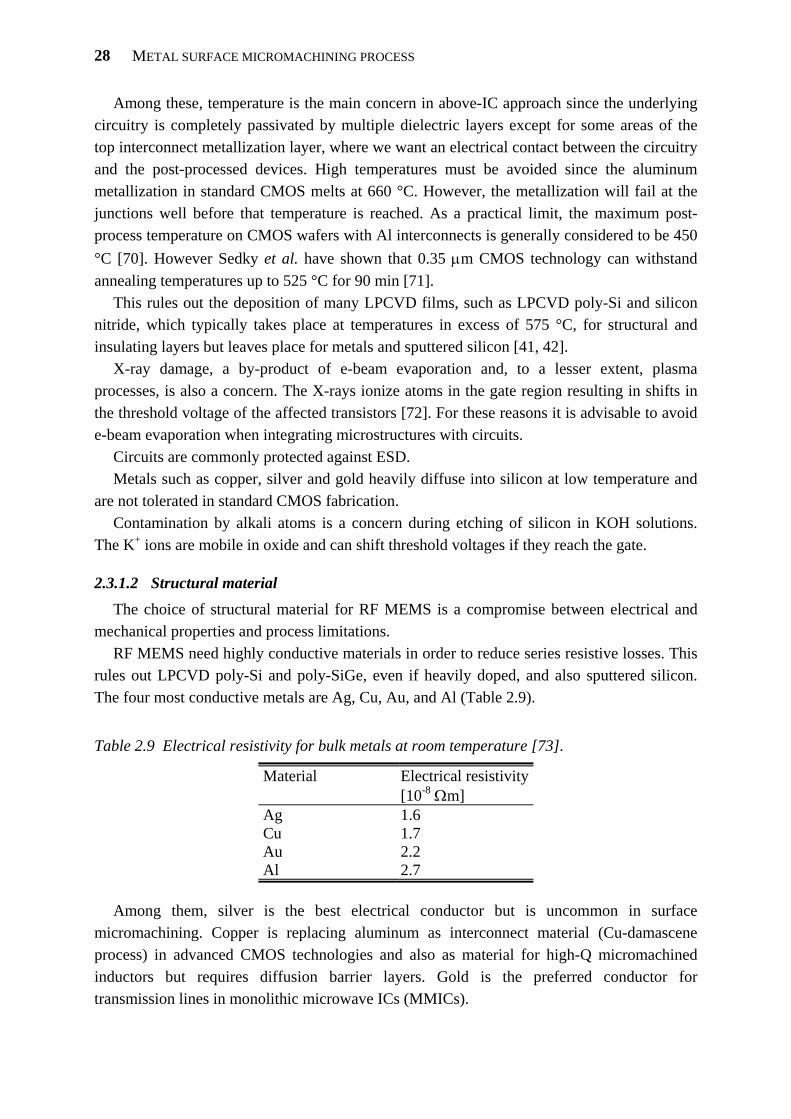
brought to the fabrication process based on the initial process (Process I) shown in Figure 2.17.
METAL SURFACE MICROMACHINING PROCESS
30
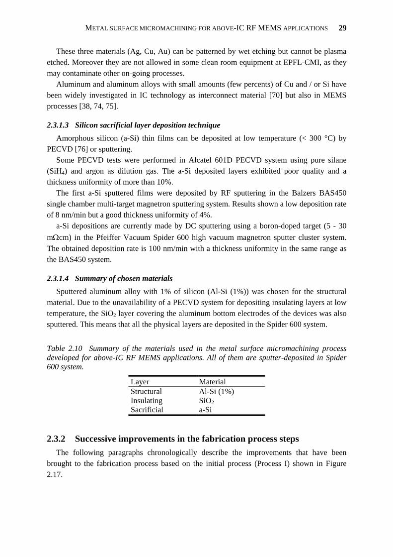
Metal 1
Metal 2
Si substrateWet oxideAl-Si (1%)SiO2
Figure 2.17 Initial process (Process I) cross section illustration. Both metal layers have a 1 μm thickness.
In Process I, bottom electrodes, signal and ground paths and pads are made of Metal 1 and the top suspended electrode, anchors and the pad connected to the latter electrode are made of Metal 2. Both metal layers have the same 1 μm thickness due to constraints with RF probing (all the pads in G-S-G configuration should have the same thickness for probing). The sacrificial layer was patterned either by SF6 isotropic plasma or with the continuous SF6/C4F8 anisotropic process leading to vertical sidewalls and hence to very poor aluminum step coverage (Figure 2.18). It was also difficult to control the thinning of the sacrificial layer, required for the double air-gap architecture (see section 3.3), with such processes.
Figure 2.18 SEM microphotograph of a mechanical anchor, after releasing, showing very poor aluminum step coverage due to vertical sidewalls obtained by fluorine-based plasma. The step is to 2 μm high and the Metal 2 thickness is 1 μm.
2.3.2.1 Patterning of the a-Si sacrificial layer
To alleviate the two problems mentioned above, we have investigated chlorine-based plasma chemistry (pure Cl2, STS Multiplex ICP etcher) to pattern and thin the sacrificial layer. The process developed uses a photoresist (PR) mask (Shipley S1818 positive-tone photoresist) and has an etch rate of 200 - 400 nm/min. The PR: a-Si selectivity obtained was 1: 1 leading to a 2-angle slope in a-Si, explained by the combination of 2 mechanisms: PR slope transfer and PR faceting (Figure 2.19). The aluminum step coverage is improved
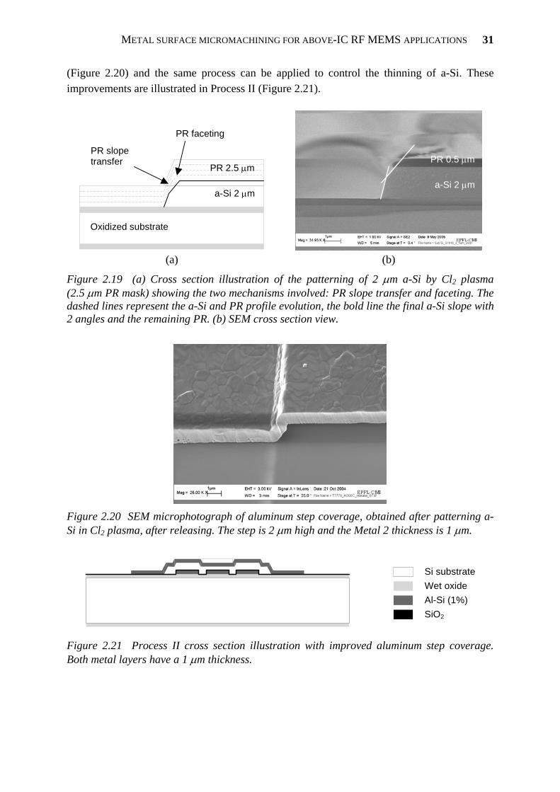
METAL SURFACE MICROMACHINING FOR ABOVE-IC RF MEMS APPLICATIONS
31
(Figure 2.20) and the same process can be applied to control the thinning of a-Si. These improvements are illustrated in Process II (Figure 2.21).
PR faceting
PR slope transfer
a-Si 2 μm
Oxidized substrate
PR 2.5 μm
(a)
a-Si 2 μm
PR 0.5 μm
(b)
Figure 2.19 (a) Cross section illustration of the patterning of 2 μm a-Si by Cl2 plasma (2.5 μm PR mask) showing the two mechanisms involved: PR slope transfer and faceting. The dashed lines represent the a-Si and PR profile evolution, the bold line the final a-Si slope with 2 angles and the remaining PR. (b) SEM cross section view.
Figure 2.20 SEM microphotograph of aluminum step coverage, obtained after patterning a- Si in Cl2 plasma, after releasing. The step is 2 μm high and the Metal 2 thickness is 1 μm.
Si substrateWet oxideAl-Si (1%)SiO2
Figure 2.21 Process II cross section illustration with improved aluminum step coverage. Both metal layers have a 1 μm thickness.
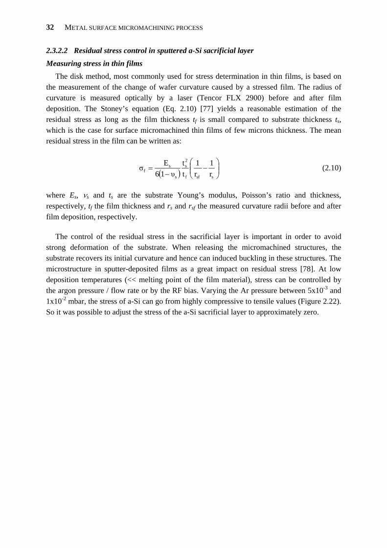
METAL SURFACE MICROMACHINING PROCESS
32
2.3.2.2 Residual stress control in sputtered a-Si sacrificial layer
Measuring stress in thin films The disk method, most commonly used for stress determination in thin films, is based on
the measurement of the change of wafer curvature caused by a stressed film. The radius of curvature is measured optically by a laser (Tencor FLX 2900) before and after film deposition. The Stoney’s equation (Eq. 2.10) [77] yields a reasonable estimation of the residual stress as long as the film thickness tf is small compared to substrate thickness ts, which is the case for surface micromachined thin films of few microns thickness. The mean residual stress in the film can be written as:
( ) ⎟⎟⎠
⎞⎜⎜⎝
⎛−
−=
ssff
2s
s
sf r
1r1
tt
υ16Eσ (2.10)
where Es, νs and ts are the substrate Young’s modulus, Poisson’s ratio and thickness, respectively, tf the film thickness and rs and rsf the measured curvature radii before and after film deposition, respectively.
The control of the residual stress in the sacrificial layer is important in order to avoid strong deformation of the substrate. When releasing the micromachined structures, the substrate recovers its initial curvature and hence can induced buckling in these structures. The microstructure in sputter-deposited films as a great impact on residual stress [78]. At low deposition temperatures (<< melting point of the film material), stress can be controlled by the argon pressure / flow rate or by the RF bias. Varying the Ar pressure between 5x10⁻³ and 1x10⁻² mbar, the stress of a-Si can go from highly compressive to tensile values (Figure 2.22). So it was possible to adjust the stress of the a-Si sacrificial layer to approximately zero.
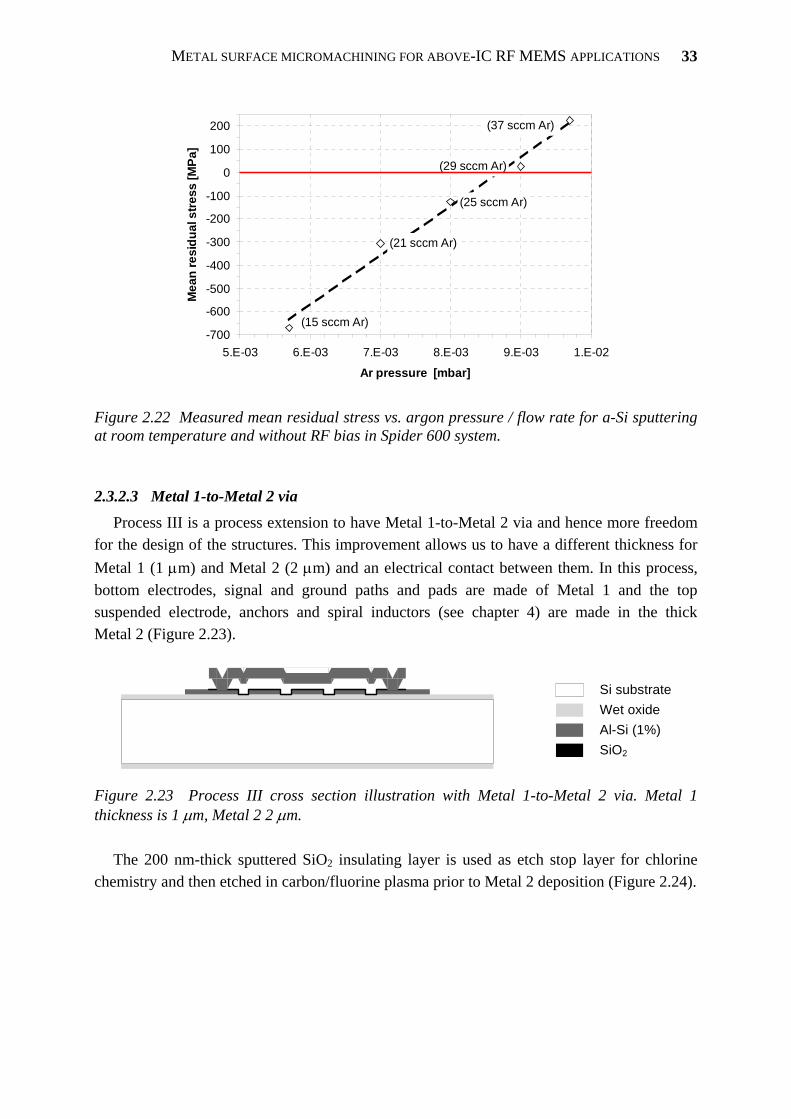
METAL SURFACE MICROMACHINING FOR ABOVE-IC RF MEMS APPLICATIONS
33
(37 sccm Ar)
(29 sccm Ar)
(25 sccm Ar)
(21 sccm Ar)
(15 sccm Ar)-700
-600
-500
-400
-300
-200
-100
0
100
200
5.E-03 6.E-03 7.E-03 8.E-03 9.E-03 1.E-02
Ar pressure [mbar]
Mea
n re
sidu
al s
tress
[MPa
]
Figure 2.22 Measured mean residual stress vs. argon pressure / flow rate for a-Si sputtering at room temperature and without RF bias in Spider 600 system.
2.3.2.3 Metal 1-to-Metal 2 via Process III is a process extension to have Metal 1-to-Metal 2 via and hence more freedom
for the design of the structures. This improvement allows us to have a different thickness for Metal 1 (1 μm) and Metal 2 (2 μm) and an electrical contact between them. In this process, bottom electrodes, signal and ground paths and pads are made of Metal 1 and the top suspended electrode, anchors and spiral inductors (see chapter 4) are made in the thick Metal 2 (Figure 2.23).
Si substrateWet oxideAl-Si (1%)SiO2
Figure 2.23 Process III cross section illustration with Metal 1-to-Metal 2 via. Metal 1 thickness is 1 μm, Metal 2 2 μm.
The 200 nm-thick sputtered SiO2 insulating layer is used as etch stop layer for chlorine
chemistry and then etched in carbon/fluorine plasma prior to Metal 2 deposition (Figure 2.24).
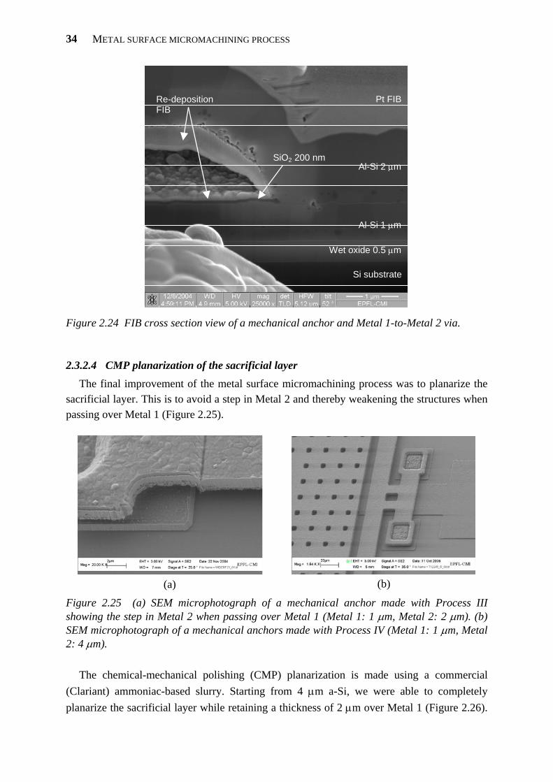
METAL SURFACE MICROMACHINING PROCESS
34
Si substrate
Wet oxide 0.5 μm
Al-Si 1 μm
Al-Si 2 μm
Pt FIBRe-deposition FIB
SiO2 200 nm
Figure 2.24 FIB cross section view of a mechanical anchor and Metal 1-to-Metal 2 via.
2.3.2.4 CMP planarization of the sacrificial layer The final improvement of the metal surface micromachining process was to planarize the
sacrificial layer. This is to avoid a step in Metal 2 and thereby weakening the structures when passing over Metal 1 (Figure 2.25).
(a)
(b)
Figure 2.25 (a) SEM microphotograph of a mechanical anchor made with Process III showing the step in Metal 2 when passing over Metal 1 (Metal 1: 1 μm, Metal 2: 2 μm). (b) SEM microphotograph of a mechanical anchors made with Process IV (Metal 1: 1 μm, Metal 2: 4 μm).
The chemical-mechanical polishing (CMP) planarization is made using a commercial
(Clariant) ammoniac-based slurry. Starting from 4 μm a-Si, we were able to completely planarize the sacrificial layer while retaining a thickness of 2 μm over Metal 1 (Figure 2.26).
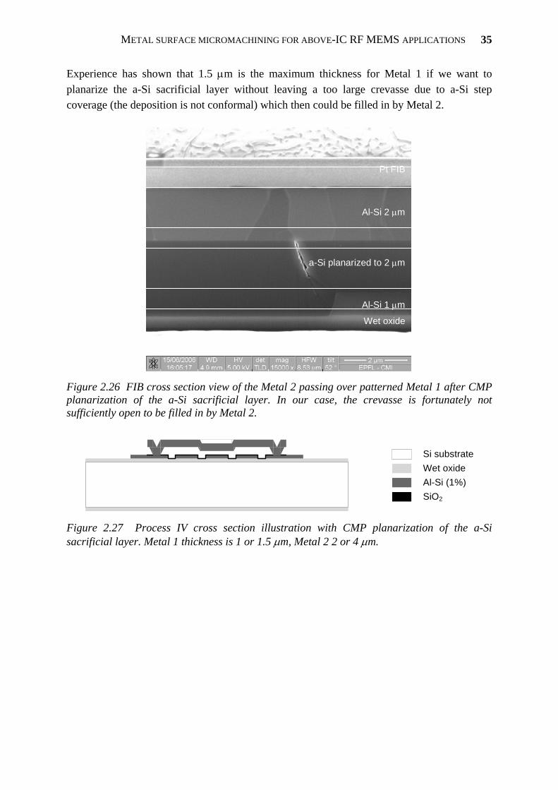
METAL SURFACE MICROMACHINING FOR ABOVE-IC RF MEMS APPLICATIONS
35
Experience has shown that 1.5 μm is the maximum thickness for Metal 1 if we want to planarize the a-Si sacrificial layer without leaving a too large crevasse due to a-Si step coverage (the deposition is not conformal) which then could be filled in by Metal 2.
a-Si planarized to 2 μm
Al-Si 1 μm
Wet oxide
Al-Si 2 μm
Pt FIB
Figure 2.26 FIB cross section view of the Metal 2 passing over patterned Metal 1 after CMP planarization of the a-Si sacrificial layer. In our case, the crevasse is fortunately not sufficiently open to be filled in by Metal 2.
Si substrateWet oxideAl-Si (1%)SiO2
Figure 2.27 Process IV cross section illustration with CMP planarization of the a-Si sacrificial layer. Metal 1 thickness is 1 or 1.5 μm, Metal 2 2 or 4 μm.
METAL SURFACE MICROMACHINING PROCESS
36
2.3.3 Final process flow Figure 2.28 shows the complete fabrication process sequence for Process IV. The MEMS structures are fabricated on 525 μm-thick high resistivity silicon substrate (> 8
kΩcm) to reduce the substrate losses (Figure 2.28a). The substrate is thermally oxidized (500 nm-thick) (Figure 2.28b). A 1 or 1.5 μm-thick Al-Si (1%) layer (Metal 1) is deposited by sputtering (Spider 600 system) (Figure 2.28c) and patterned by dry etching in a standard Cl2/BCl3 gas mixture (STS Multiplex ICP etcher) using a photoresist mask (Shipley S1818 positive-tone photoresist) (Figure 2.28d). Then a 200 nm-thick sputtered silicon dioxide layer is deposited at 200 °C (Spider 600 system) as an insulating layer (Figure 2.28e). A 4 μm-thick amorphous silicon layer is then sputtered (Spider 600 system) (Figure 2.28f). Prior to planarization, the a-Si layer is etched with continuous SF6/C4F8 anisotropic process (Alcatel 601E ICP etcher) to have access to the alignment structures in Metal 1 and to monitor the a-Si thickness during CMP (this step is not shown in Figure 2.28). Then it is planarized by CMP (Steag Mecapol E460 machine) to a thickness of 2 μm (Figure 2.28g). The thickness of this layer will determine the nominal gap of the suspended membranes. The a-Si sacrificial layer is twice patterned by chlorine-based chemistry (STS Multiplex ICP etcher) using a photoresist mask (Shipley S1818). The first step is to thin the sacrificial layer to 1 μm, which is required for the double air-gap architecture (see section 3.3) (Figure 2.28h). The second step is to pattern the mechanical anchors and the Metal 1-to-Metal 2 contacts (Figure 2.28i). The SiO2 insulating layer plays the role of etch stop layer for the chlorine chemistry in this latter step. It is then etched at 0 °C in carbon/fluorine plasma (Adixen AMS 200DSE ICP etcher), which is selective to aluminum. A 2 or 4 μm-thick Al-Si (1%) structural layer (Metal 2) is deposited by sputtering (Spider 600 system) (Figure 2.28j) and patterned by dry etching in a standard Cl2/BCl3 gas mixture (STS Multiplex ICP etcher) using a photoresist mask (Clariant AZ9260 Novolak-based positive-tone photoresist) (Figure 2.28k). For wafers, which will be wafer-level packaged afterwards (see section 3.4), annealing is done at 300 °C for 20 min in N2/H2 forming gases. The aluminum membranes releasing is done in SF6 plasma with a high selectivity to both SiO2 and aluminum using the room temperature optimized process (Table 2.7) (Figures 2.28l and 2.29). Finally, the SiO2 insulating layer over Metal 1 is etched in carbon/fluorine plasma (Alcatel 601E ICP etcher) where it is not covered by Metal 2 (Figure 2.28m).
To summarize, Process IV involves 5 photolithographic steps and one CMP planarization step and has a low thermal budget, the maximum temperature is 300 °C for 20 min, making it compatible with CMOS post-processing.
METAL SURFACE MICROMACHINING FOR ABOVE-IC RF MEMS APPLICATIONS
37
(a) High resistivity Si substrate
(b) Wet oxidation
(c) Aluminum sputtering (Metal 1)
(d) Metal 1 patterning
(e) Dielectrics deposition (SiO2)
(f) Sacrificial layer deposition (a-Si)
(h) a-Si thinning (central electrode)
(i) a-Si + SiO2 patterning (anchors)
(j) Aluminum sputtering (Metal 2)
(k) Metal 2 patterning
(l) Releasing
(m) SiO2 patterning (pads)
(g) CMP planarizationSi substrateWet oxideAl-Si (1%)SiO2
a-Si
Figure 2.28 Complete fabrication process sequence (Process IV).
METAL SURFACE MICROMACHINING PROCESS
38
Si substrate
0.5 μm wet oxide
1 μm Al-Si (1%)
2 μm air-gap
1 μm Al-Si (1%)
Figure 2.29 FIB cross section view of a 2-μm air-gap. Metal 1 thickness is 1 μm, Metal 2 1 μm.
2.3.4 Characterization of sputtered Al-Si (1%) alloy
2.3.4.1 Electrical properties extraction
Resistivity
The resistivity of Al-Si (1%) has been measured with four-point probe technique (KLA Tencor OmniMap RS75). The measured value is 3.3x10⁻⁸ Ωm, which corresponds to typical thin film values reported [70].
Metal 1-to-Metal 2 via resistance The test structures consist of 5 x 20-via-chain resistance measurement structures (Figure
2.30). The via sizes are 5 x 5, 10 x 10, 20 x 20 and 40 x 40 μm2. It is possible to measure 20, 40, 61, 81 and 100 vias in series by using the appropriate pads.
(a)
(b)
Figure 2.30 Optical microphotograph (a) and SEM close-up view (b) of a 20 x 20 μm2 100-via-chain resistance measurement structure (Metal 1: 1 μm, Metal 2: 4 μm).
METAL SURFACE MICROMACHINING FOR ABOVE-IC RF MEMS APPLICATIONS
39
The test structures were measured using a Karl Süss PM8 manual prober coupled to a HP 4155B semiconductor parameter analyzer. The measurements show very low Metal 1-to-Metal 2 via resistance, even for 5 x 5 μm2 vias (Table 2.11). The larger the via size the smaller the resistance.
Table 2.11 Measured mean Metal 1-to-Metal 2 via resistance for different via sizes. Metal 1: 1 μm, Metal 2: 4 μm.
Via size [μm2] Resistance/via [mΩ] 5 x 5 10 x 10 20 x 20 40 x 40
36.41 ± 0.14 28.27 ± 0.33 21.66 ± 0.08 13.98 ± 0.16
2.3.4.2 Mechanical properties extraction All thin films foster a state of residual stress. Stress-causing factors can be categorized as
either intrinsic or extrinsic. The intrinsic stresses develop during the film nucleation and can be due to growth mechanisms, lattice mismatch between film and substrate and interstitial or substitutional impurities. The extrinsic stresses are imposed by external factors such as temperature gradients or package-induced stresses. They results from the mismatch of the coefficient of thermal expansion between film and substrate [19].
The residual stress in a thin film can be written as:
σ(z)σσ 0 += (2.11) where σ0 is the mean residual stress, σ(z) is the stress gradient with z in the thickness direction.
Mean residual stress
The mean residual stress σ0 can be measured with the wafer curvature technique. Several 1, 2 and 4 μm-thick sputtered Al-Si (1%) thin films deposited by DC sputtering at room temperature have been measured.
The results give a slightly tensile stress of 72 ± 19 MPa.
Stress gradient
When releasing cantilever beams, σ0 is relaxed and σ(z) remains. The equivalent bending moment due to a stress gradient is
∫ dz(z)wzM t/2
t/2−= σ (2.12) where w is the beam width, t is the beam thickness.
METAL SURFACE MICROMACHINING PROCESS
40
For a linear stress gradient, one can define the stress as:
( ) z Eγzσ = (2.13) where E is the Young’s modulus and γ is the linear stress gradient. Using Eq. 2.12, γ can be written as:
EIM
Ewt12Mγ 3 == (2.14)
where I is the moment of inertia of a rectangular beam (I = wt3/12). A moment applied at the endpoint of a cantilever with length l results in a deflection at the tip of
2l γ
2EIMlΔz
22
== . (2.15)
Δz can be measured with an optical profilometer (Veeco Wyko NT1100) and then we
calculate the stress gradient γ . Measurements have been performed on arrays of cantilever beams and on several wafers
(with and without annealing at 300 °C before releasing). The beam lengths were 30 to 500 μm. The beam width and thickness were 10 μm and 4 μm, respectively. Cantilever beams with air-gap of 2 and 1 μm were available (Figure 2.31).
Figure 2.31 300, 400 and 500 μm-long cantilever beams bending up due to stress gradient. The beam width and thickness were 10 μm and 4 μm, respectively. The a-Si sacrificial layer was 2 μm-thick.
The results show the impact on stress gradient of annealing the structures before releasing (Figure 2.32). We can also see the difference between cantilever beams having a 2 μm air-gap and a 1 μm air-gap obtained by thinning the a-Si sacrificial layer (Figures 2.32 and 2.33). The surface state and roughness for growing and the microstructure of the sputtered thin films are different and hence the stress gradient is modified.

METAL SURFACE MICROMACHINING FOR ABOVE-IC RF MEMS APPLICATIONS
41
0
2
4
6
8
10
12
14
16
0 100 200 300 400 500
Cantilever beam length l [μm]
Def
lect
ion
at ti
p Δ
z [ μ
m]
Wafer #1: no annealing
Wafer #3: annealing @ 300 °Cbefore releasing
γ = 4x10⁻⁵ μm-1
γ = 10-4 μm-1
Figure 2.32 Measured deflection at the tip vs. length for 30 to 500 μm-long cantilever beams on 2 wafers. The beam width and thickness and the air-gap are 10 μm, 4 μm and 2 μm, respectively. The calculated stress gradient is given (dashed lines: parabolic fit).
0.0
0.5
1.0
1.5
2.0
0 100 200 300 400 500
Cantilever beam length l [μm]
Def
lect
ion
at ti
p Δ
z [ μ
m] Wafer #1: no annealing
Wafer #2: no annealing
γ = 0.8x10⁻⁵ μm-1
γ = 10-5 μm-1
Figure 2.33 Measured deflection at the tip vs. length for 30 to 500 μm-long cantilever beams on 2 wafers. The beam width and thickness and the air-gap are 10 μm, 4 μm and 1 μm, respectively. The calculated stress gradient is given (dashed lines: parabolic fit).
METAL SURFACE MICROMACHINING PROCESS
42
2.3.4.3 Summary of sputtered Al-Si (1%) properties Table 2.12 gives a summary of sputtered Al-Si (1%) properties compared with the ones for
Al thin films and bulk Al.
Table 2.12 Summary of sputtered Al-Si (1%) properties compared with the ones for Al thin films (in literature) and bulk Al.
Sputtered Al-Si (1%)
Al thin films Bulk Al [73, 79]
Electrical properties resistivity [10-8 Ωm]
3.3
2.7 - 3.0 [70]
2.7
Mechanical properties Young’s modulus [GPa] Poisson’s ratio mean residual stress [MPa] stress gradient [μm-1]
50 * 0.35 # 72 ± 19 0.8 - 10x10-5
47 - 74 [80] 55 ± 6 [81] 0.35 # N.A. N.A.
70 0.35 - -
(* assumed to be the same than for Al thin films, mean value from [80, 81], # assumed to be the same than for bulk Al)
2.4 CONCLUSIONS The principle of surface micromachining and its usefulness for RF MEMS devices
fabrication have been explained as an introduction. It has been shown that the use of a dry release step (gas phase or plasma) can substantially increase the yield for the overall MEMS process by eliminating the release-induced stiction problem.
Silicon thin films have been investigated as sacrificial layer for surface micromachining. A detailed and original study on SF6 inductively coupled plasma (ICP) releasing has been performed in order to find the optimized process parameters. This study has emphasized the fact that temperature plays an important role in this process by limiting silicon dioxide etching. Moreover, the optimized recipe has been found to be independent of the sacrificial layer used (amorphous or polycrystalline silicon) and its thickness. Using this recipe, 15.6 μm/min Si underetch rate with high Si: SiO2 selectivity (> 20000: 1) has been obtained.
Based on this SF6 plasma releasing, a metal surface micromachining process has been developed for MEMS capacitors and switches. This involves a sputtered Al-Si (1%) structural layer and sputtered a-Si sacrificial layer. A chronological description of the improvements that have been introduced to the fabrication process leads to the final process: Process IV. The electrical and mechanical properties of the sputtered Al-Si (1%) alloy have been extracted.
The process presented in this chapter is compatible with CMOS post-processing for above-IC integration of radiofrequency (RF) MEMS devices. The following chapters will apply it in order to fabricate electrostatically-actuated capacitive membrane-based devices.
Chapter 3 MEMS tunable capacitors

Previous page left SEM microphotograph of a single-air-gap circular tunable capacitor. (Scale: the pads are 100 x 100 μm2)
Previous page center SEM microphotograph of a double-air-
gap tunable capacitor.
Previous page rightSEM microphotograph of a single-air-gap
tunable capacitor with a frame for thermal stress geometrical
compensation.
3.1 STATE-OF-THE-ART
3.1.1 Introduction to tunable capacitors A tunable capacitor, also called varactor or varicap, is a passive device in which the
capacitance can be tuned or varied. This functionality is widely used in RF communications applications, such as low noise amplifiers (LNAs), tunable matching networks, tunable filters and voltage-controlled oscillators (VCOs).
Conventional solid-state varactor implementations include Si (on-chip) or GaAs (off-chip) p-n or Schottky-barrier junction diodes as well as MOS capacitors [82-84]. They generally suffer from excessive series resistive losses, and hence a low quality factor and a low electrical self-resonant frequency, and exhibit strong non-linear behavior.
The figures of merit used for tunable capacitors include unbiased capacitance C0, tuning range TR, equivalent series resistance Rs or quality factor Q, associated parasitic inductance Ls or electrical self-resonant frequency SRF and linearity in response to RF power.
3.1.2 Principle of MEMS tunable capacitors The MEMS tunable capacitors vary the capacitance by adjusting device physical
dimensions via an electromechanical actuator. The dielectric layer used is typically air, which eliminates the majority of the dielectric losses. Neglecting the fringing effects, a parallel-plate capacitor has a capacitance C given by:
dA ε εC 0r= (3.1)
where εr is the relative permittivity or dielectric constant of the medium in the gap, ε0 is the permittivity of free space, A the area of the plates and d the gap between the plates.
The quality factor Q of a capacitor is defined as:
diss
e
PWω
cycleper lost energy capacitor in the storedenergy π2 Q
=
= (3.2)
where We is the peak energy stored in the capacitor and Pdiss is the power dissipated. If we consider the capacitor simply modeled as a capacitance C in series with a resistance Rs:
CR ω1
RI21
Cω1I
21
ωQs
s2
22
== (3.3)
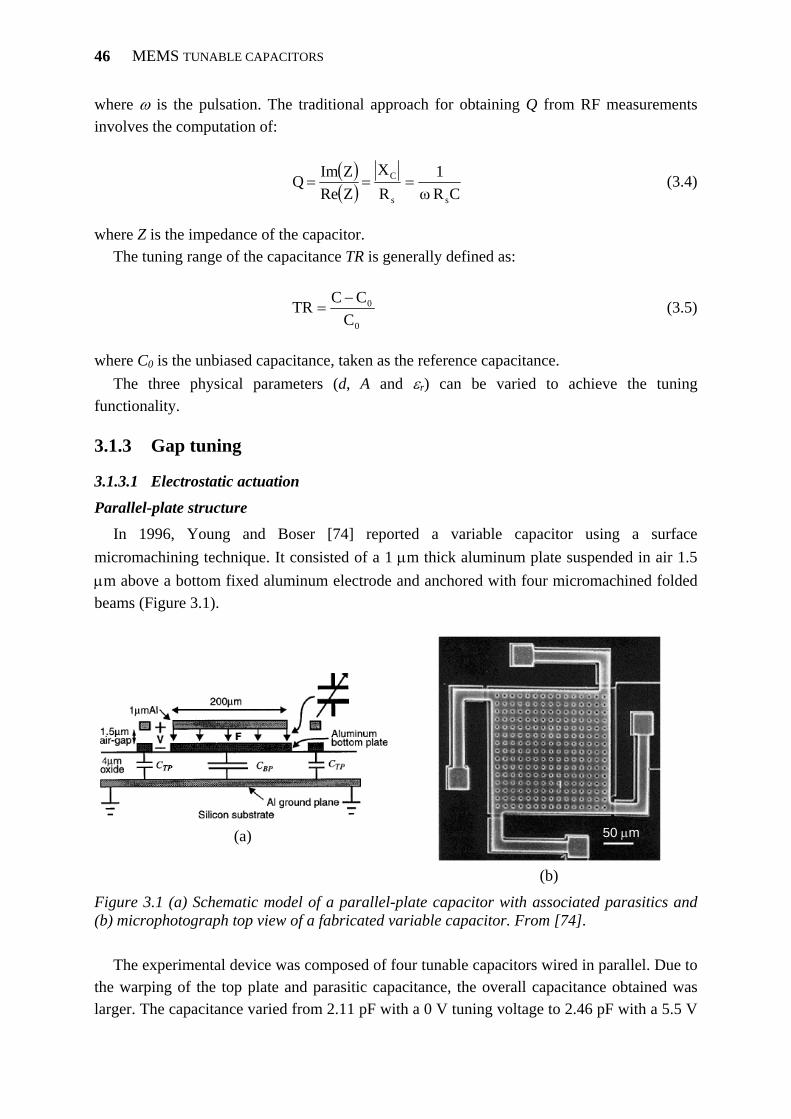
MEMS TUNABLE CAPACITORS
46
where ω is the pulsation. The traditional approach for obtaining Q from RF measurements involves the computation of:
( )( ) CR ω
1RX
ZReZIm Q
ss
C === (3.4)
where Z is the impedance of the capacitor.
The tuning range of the capacitance TR is generally defined as:
0
0
CC CTR −
= (3.5)
where C0 is the unbiased capacitance, taken as the reference capacitance.
The three physical parameters (d, A and εr) can be varied to achieve the tuning functionality.
3.1.3 Gap tuning
3.1.3.1 Electrostatic actuation
Parallel-plate structure In 1996, Young and Boser [74] reported a variable capacitor using a surface
micromachining technique. It consisted of a 1 μm thick aluminum plate suspended in air 1.5 μm above a bottom fixed aluminum electrode and anchored with four micromachined folded beams (Figure 3.1).
(a)
50 μm
(b)
Figure 3.1 (a) Schematic model of a parallel-plate capacitor with associated parasitics and (b) microphotograph top view of a fabricated variable capacitor. From [74].
The experimental device was composed of four tunable capacitors wired in parallel. Due to the warping of the top plate and parasitic capacitance, the overall capacitance obtained was larger. The capacitance varied from 2.11 pF with a 0 V tuning voltage to 2.46 pF with a 5.5 V
STATE-OF-THE-ART
47
tuning voltage. This corresponds to a tuning range of 16%. The equivalent series resistance was 1.2 Ω at 1 GHz, corresponding to a Q factor of 62.
When an electric field is applied to a parallel-plate system, the movable plate moves towards the fixed plate as a result of the electrostatic force. When the critical voltage, called the pull-in voltage, is reached, the plate snaps down to the bottom plate and the applied voltage no longer controls the beam. The equilibrium between the electrostatic attracting force and the restoring force of the suspension beams holds only for a deflection smaller than one third of the initial gap. This restricts the theoretical limit to 50% to any electrostatically-actuated parallel-plate system (see section 3.2).
To extend the usable range of electrostatic actuators, several methods have been suggested, including series stabilizing negative feedback capacitance [85, 86], leveraged bending design and nonlinear mechanical strain stiffening [87]. Two extensions of the parallel-plate structure have also been proposed: the three-parallel-plate structure and the double-air-gap structure, which will be described later in this paragraph.
In 1998, Fan et al. [88] reported a surface micromachined micro-elevator by self-assembly (MESA) technique. This technique could raise a platform to several hundred micrometers above silicon surface. It was applied to suspended inductors and variable capacitors. The MESA structure consisted of three parts: the central platform (the suspended capacitor plate), the side-support plates and the micro-actuator plates. These plates were connected with micro-hinges. The MESA platform could be raised above the silicon surface by biasing the two actuator arrays to move towards each other at the same speed. Scratch drive actuator (SDA) arrays were employed to move up and down the suspended platform and hence varying the gap spacing between the plates. The MESA structures were fabricated using the three-polysilicon-layer MUMPs process. Since the capacitance is inversely proportional to the gap spacing, the capacitance decreased rapidly from 500 to 20 fF when the suspended plate was raised from the substrate to a height of 250 μm. The tuning range was 2400%. They reported the difficulty to achieve fine tuning adjustment.
Bakri-Kassem and Mansour [89] proposed a concept based on a two movable-plate nitride-loaded MEMS tunable capacitor, which seems to overcome the theoretical limit of 50% tuning range for parallel-plate capacitors. The capacitance tuning was 117% for 21 V, before plates collapse, and continued to increase until 280% and 495% for 39 V at 1 and 1.5 GHz, respectively.
Goldsmith et al. [90] demonstrated a six-bit switched-capacitor composed of MEMS membrane bistable capacitors, having a dielectric layer on top of the fixed electrode so as not to short the two electrodes after pull-in. A 2100% tuning range was achieved between the two stable states. Even if the tuning range is very high, it doesn’t fulfill the continuous tuning requirements of many applications.
An electrostatic digitally controlled MEMS tunable capacitor fabricated using MUMPs process and flip-chip technology was reported by Hoivik et al. [91]. The capacitor consisted of an array of individual plates of equal area, which were connected to the bonding pads by springs of varying width. This created a cascading snap-down effect when actuated by
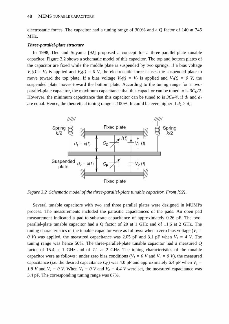
MEMS TUNABLE CAPACITORS
48
electrostatic forces. The capacitor had a tuning range of 300% and a Q factor of 140 at 745 MHz.
Three-parallel-plate structure In 1998, Dec and Suyama [92] proposed a concept for a three-parallel-plate tunable
capacitor. Figure 3.2 shows a schematic model of this capacitor. The top and bottom plates of the capacitor are fixed while the middle plate is suspended by two springs. If a bias voltage V1(t) = V1 is applied and V2(t) = 0 V, the electrostatic force causes the suspended plate to move toward the top plate. If a bias voltage V2(t) = V2 is applied and V1(t) = 0 V, the suspended plate moves toward the bottom plate. According to the tuning range for a two-parallel-plate capacitor, the maximum capacitance that this capacitor can be tuned to is 3CD/2. However, the minimum capacitance that this capacitor can be tuned to is 3CD/4, if d1 and d2 are equal. Hence, the theoretical tuning range is 100%. It could be even higher if d2 > d1.
Figure 3.2 Schematic model of the three-parallel-plate tunable capacitor. From [92].
Several tunable capacitors with two and three parallel plates were designed in MUMPs
process. The measurements included the parasitic capacitances of the pads. An open pad measurement indicated a pad-to-substrate capacitance of approximately 0.26 pF. The two-parallel-plate tunable capacitor had a Q factor of 20 at 1 GHz and of 11.6 at 2 GHz. The tuning characteristics of the tunable capacitor were as follows: when a zero bias voltage (V1 = 0 V) was applied, the measured capacitance was 2.05 pF and 3.1 pF when V1 = 4 V. The tuning range was hence 50%. The three-parallel-plate tunable capacitor had a measured Q factor of 15.4 at 1 GHz and of 7.1 at 2 GHz. The tuning characteristics of the tunable capacitor were as follows : under zero bias conditions (V1 = 0 V and V2 = 0 V), the measured capacitance (i.e. the desired capacitance CD) was 4.0 pF and approximately 6.4 pF when V1 = 1.8 V and V2 = 0 V. When V1 = 0 V and V2 = 4.4 V were set, the measured capacitance was 3.4 pF. The corresponding tuning range was 87%.
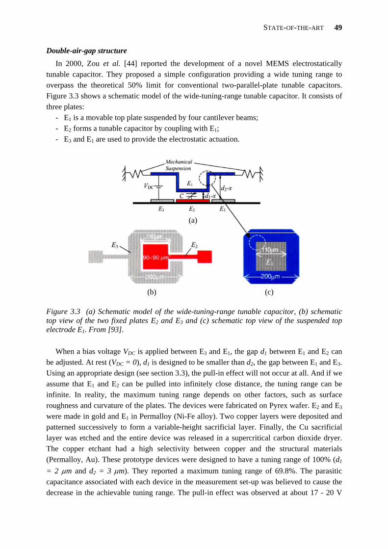
STATE-OF-THE-ART
49
Double-air-gap structure In 2000, Zou et al. [44] reported the development of a novel MEMS electrostatically
tunable capacitor. They proposed a simple configuration providing a wide tuning range to overpass the theoretical 50% limit for conventional two-parallel-plate tunable capacitors. Figure 3.3 shows a schematic model of the wide-tuning-range tunable capacitor. It consists of three plates:
- E1 is a movable top plate suspended by four cantilever beams; - E2 forms a tunable capacitor by coupling with E1; - E3 and E1 are used to provide the electrostatic actuation.
(a)
(b) (c)
Figure 3.3 (a) Schematic model of the wide-tuning-range tunable capacitor, (b) schematic top view of the two fixed plates E2 and E3 and (c) schematic top view of the suspended top electrode E1. From [93].
When a bias voltage VDC is applied between E3 and E1, the gap d1 between E1 and E2 can
be adjusted. At rest (VDC = 0), d1 is designed to be smaller than d2, the gap between E1 and E3. Using an appropriate design (see section 3.3), the pull-in effect will not occur at all. And if we assume that E1 and E2 can be pulled into infinitely close distance, the tuning range can be infinite. In reality, the maximum tuning range depends on other factors, such as surface roughness and curvature of the plates. The devices were fabricated on Pyrex wafer. E2 and E3 were made in gold and E1 in Permalloy (Ni-Fe alloy). Two copper layers were deposited and patterned successively to form a variable-height sacrificial layer. Finally, the Cu sacrificial layer was etched and the entire device was released in a supercritical carbon dioxide dryer. The copper etchant had a high selectivity between copper and the structural materials (Permalloy, Au). These prototype devices were designed to have a tuning range of 100% (d1 = 2 μm and d2 = 3 μm). They reported a maximum tuning range of 69.8%. The parasitic capacitance associated with each device in the measurement set-up was believed to cause the decrease in the achievable tuning range. The pull-in effect was observed at about 17 - 20 V
MEMS TUNABLE CAPACITORS
50
depending on the thickness of the Permalloy layer. Hysteresis was observed when the bias voltage decreased from 20 to 0 V to recover from the pull-in effect.
Based on this concept, several works have been presented since. Nieminen et al. [94] reported MEMS capacitors made of electroplated gold and having a tuning range of 171% and Q factor of 66 and 53 at 1 and 2 GHz, respectively. Dussopt and Rebeiz [95] reported MEMS varactors composed of a movable bridge in shunt configuration on a CPW line. The measurements showed a tuning range of 46% for a tuning voltage of 25 V and Q factors between 95 - 100 at 34 GHz. Xiao et al. [96] fabricated folded-spring, dual-comb-drive, vertical-plate variable capacitors with displacement limiting bumpers combining ultra-thin silicon wafers, SU-8 bonding and DRIE technology. Due to the presence of the bumpers, the variable capacitor had two tuning regimes: first a parabolic region that achieved roughly 290% tuning range, then a linear region that achieved an additional 310%, making the total tuning range about 600%. Gallant and Wood [97] demonstrated tunable micromachined capacitors made of nickel and gold having a wide tuning range of 410% and 630%, respectively. In 2003, De Coster et al. [75] presented RF MEMS tunable capacitors fabricated in the Philips PASSI process [98], a standard surface micromachining process which used a 5 μm-thick aluminum layer as structural layer. They reported a tuning range of 310% at 21 V tuning voltage for a dual-gap capacitor. Rijks et al. [99], using the same process, demonstrated a continuous and reversible capacitance tuning with a tuning range up to 1600%, the highest ever reported for parallel-plate tunable capacitors. The actuation voltage was 20 V and Q factors between 150 to 500 in the frequency range of 1 to 6 GHz were measured. Peroulis and Katehi [100] proposed a MEMS varactor made of 13 μm-thick electroplated gold and special suspension design, on high-resistivity silicon substrate. The measured capacitance values are in the range of 40 - 160 fF, corresponding to a 300% tuning range, and are achieved with voltages of 20 - 34 V. The results also showed very high self-resonant frequencies (> 100 GHz) and Q factors greater than 80 at 40 GHz.
Cantilever structure (zipper mode) In 1998, Hung and Senturia [101] reported a tunable capacitor with programmable
capacitance-voltage characteristic based on a contact electrostatic zipper actuator. The zipper actuator varactor consisted of a conductive cantilever beam over a shaped bottom electrode. The capacitance between the beam and the bottom electrode was controlled by an applied DC voltage and the C-V characteristic of the device was determined by the geometry of the bottom electrode. When an increasing voltage was applied between the beam and the bottom electrode, the beam first bent downward, then collapsed toward the substrate due to the pull-in effect. Dimples in the cantilever hold the beam a small distance off the bottom electrode. This eliminated problems of hysteretic effects due to dielectric charging and stiction. At first, only the beam tip contacted the substrate, but as additional voltage was applied, the tip flattened and the beam zipped along the substrate toward the cantilever anchor, increasing the area of the beam close to the bottom electrode, thus changing the device capacitance. The device was optimized to obtain a linear characteristic in the zipping regime voltage range, 25 - 30 V. Initial beam pull-in occured around 10 V. From 10 to 20 V, only the tip of the beam contacted
STATE-OF-THE-ART
51
the substrate. Above 20 V, the device was in the zipping regime. The capacitance varied from 0.55 to 1.0 pF under a bias voltage of 35 V, which represented a tuning range of 80%. The tuning range was only 25% in the linear C-V characteristic part.
In 1999, Park et al. [102] reported a tunable filter using micromachined cantilever-type variable capacitors. The cantilever structure was suspended 6.4 μm above a coplanar waveguide (CPW) ground plate. Capacitance was controlled by the gap between the movable cantilever beam and the CPW. The application of a DC voltage between these two electrodes caused the cantilever to deflect downward and hence increased the capacitance. To avoid DC voltage short, a dielectric layer was deposited on the CPW ground plate underneath the cantilever. Experimental results showed pull-in voltages of 53 V for the 1.8 μm-thick beam and 70 V for the 2.4 μm-thick one.
Ionis et al. [103] proposed a differential multi-fingered MEMS tunable capacitor based on zipper actuator. The capacitance was tuned between 3.1 to 4.6 pF for 35 V, hence the tuning range was 46%. A Q factor of 6.5 at 1.5 GHz was measured.
3.1.3.2 Electro-thermal actuation
Electro-thermal actuators can also overcome the pull-in effect of electrostatic parallel-plate capacitors. Several works have been presented in this direction.
In 1998, Wu et al. [104] reported a thermal actuator used to control the gap of a tunable capacitor. The vertical thermal actuator was driven by differential thermal expansions of the thick/thin polysilicon arms. It worked on a similar principle as the thermal actuator described by Reid et al. [105, 106], which consisted of two polysilicon parallel beams one on top of the other separated by an air-gap. At one end, the arms were connected together with a via, while at the other end, each arm was separately anchored to the substrate. The bottom arm, called the cold arm, was wider than the top arm, called the hot arm. Driving a current through the arms resulted in the generation of thermal energy. The hot arm had a higher resistance resulting in a greater expansion. As the hot arm expanded, it drove the tip of the actuator downward to the substrate. The temperature of the hot arm was raised to a point where the polysilicon began to reflow (plastic deformation). This resulted in a bow in the middle of the hot arm hence a decrease in the length of the hot arm. When the current was removed from the system, the tip of the actuator deflected back away from the substrate and past its original position. They reported a capacitance change which achieved a range of 2.6 pF which corresponds to an air-gap from 2 to 0.2 μm. The relationship between capacitance and voltage had an excellent repeatability and the component could reach the same measured capacitance at the same voltage ± 0.05 V. To enhance these results, they proposed to remove the silicon substrate to avoid any RF interference and presented a new approach with a flip-chip assembly of the MEMS on ceramics. Harsh et al. [107] reported further results with the same technology: a tuning range of 600% under a bias voltage of 2.8 V. Q factors as high as 1050 at 1 GHz and 100 at 10 GHz were also measured. Feng et al. reported series-mounted [108] and shunt-mounted [109] two-parallel-plate MEMS tunable capacitors in a coplanar waveguide (CPW). For the series configuration, the capacitance value, measured at 13 MHz and including the parasitic capacitance of the pads, which was of the order of 0.5 - 0.6 pF,
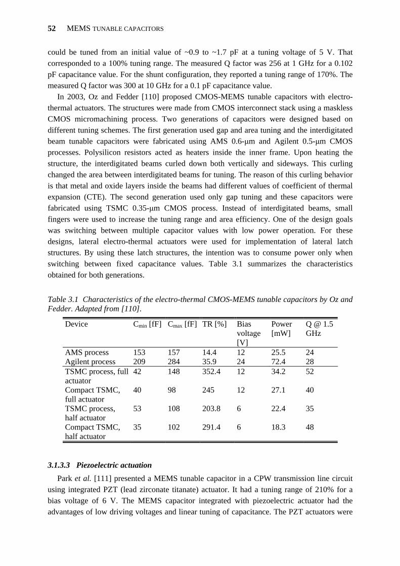
MEMS TUNABLE CAPACITORS
52
could be tuned from an initial value of ~0.9 to ~1.7 pF at a tuning voltage of 5 V. That corresponded to a 100% tuning range. The measured Q factor was 256 at 1 GHz for a 0.102 pF capacitance value. For the shunt configuration, they reported a tuning range of 170%. The measured Q factor was 300 at 10 GHz for a 0.1 pF capacitance value.
In 2003, Oz and Fedder [110] proposed CMOS-MEMS tunable capacitors with electro-thermal actuators. The structures were made from CMOS interconnect stack using a maskless CMOS micromachining process. Two generations of capacitors were designed based on different tuning schemes. The first generation used gap and area tuning and the interdigitated beam tunable capacitors were fabricated using AMS 0.6-μm and Agilent 0.5-μm CMOS processes. Polysilicon resistors acted as heaters inside the inner frame. Upon heating the structure, the interdigitated beams curled down both vertically and sideways. This curling changed the area between interdigitated beams for tuning. The reason of this curling behavior is that metal and oxide layers inside the beams had different values of coefficient of thermal expansion (CTE). The second generation used only gap tuning and these capacitors were fabricated using TSMC 0.35-μm CMOS process. Instead of interdigitated beams, small fingers were used to increase the tuning range and area efficiency. One of the design goals was switching between multiple capacitor values with low power operation. For these designs, lateral electro-thermal actuators were used for implementation of lateral latch structures. By using these latch structures, the intention was to consume power only when switching between fixed capacitance values. Table 3.1 summarizes the characteristics obtained for both generations.
Table 3.1 Characteristics of the electro-thermal CMOS-MEMS tunable capacitors by Oz and Fedder. Adapted from [110].
Device Cmin [fF] Cmax [fF] TR [%] Bias voltage [V]
Power [mW]
Q @ 1.5 GHz
AMS process 153 157 14.4 12 25.5 24 Agilent process 209 284 35.9 24 72.4 28 TSMC process, full actuator
42 148 352.4 12 34.2 52
Compact TSMC, full actuator
40 98 245 12 27.1 40
TSMC process, half actuator
53 108 203.8 6 22.4 35
Compact TSMC, half actuator
35 102 291.4 6 18.3 48
3.1.3.3 Piezoelectric actuation Park et al. [111] presented a MEMS tunable capacitor in a CPW transmission line circuit
using integrated PZT (lead zirconate titanate) actuator. It had a tuning range of 210% for a bias voltage of 6 V. The MEMS capacitor integrated with piezoelectric actuator had the advantages of low driving voltages and linear tuning of capacitance. The PZT actuators were
STATE-OF-THE-ART
53
fabricated on silicon substrate by bulk micromachining and were diced and bonded to gold transmission lines on a quartz substrate using flip-chip technology. The bias voltages applied to the control pad moved the PZT actuator vertically onto the dielectric layer on top of the fixed electrodes. The CPW transmission line played the role of fixed bottom electrode and the PZT actuator was used as the movable top electrode. The capacitor showed a quality factor of 210 at 1 GHz.
Kawakubo et al. [59] reported a MEMS tunable capacitor using a piezoelectric bimorph actuator. The actuator was made of singly or doubly clamped folded Al/AlN bimorph stack beams. The poly-Si sacrificial layer was etched selectively with XeF2. They obtained a tuning range of 200%, 2.5 V operation, and of 400%, 4.5 V operation, for singly and doubly clamped folded bimorph actuators, respectively.
3.1.4 Area tuning
3.1.4.1 Electrostatic actuation Larson et al. [112] reported in 1991 a MEMS tunable capacitor based on interdigitated
comb-drive structures. An electrostatic sliding micro-motor was used to actuate a three-finger comb-drive structure to change the overlap area between the capacitor finger electrodes. The initiation voltage for this sliding micro-motor was fairly high, in the range of 80 to 200 V because of the small fringing capacitance between the stator and rotor and the high static coefficient of friction. The structural material of the comb-drive structures was gold plated layer on GaAs substrate. Photoresist was used as sacrificial layer and removed in a suitable solvent. As a result, the structure was moved mechanically, as opposed to electrostatically, to demonstrate the overlap area change and the capacitance tuning. A capacitance value change from 35 to 100 fF was observed for a finger overlap distance change from 150 to 375 µm, respectively. Further study was required to obtain electromechanical motion and capacitance tuning functionality, but no improvements were reported afterwards.
Yao et al. [113] in 1998 reported a MEMS tunable capacitor based on interdigitated comb-drive structures. By applying a tuning voltage between the fingers, an electrostatic force is created to move the suspended structures relative to each other and change the overlap distance between the fingers and hence the total capacitance. Figure 3.4 shows a schematic model of a comb-drive structure. The capacitance for n fingers is approximately given by:
⎟⎟⎠
⎞⎜⎜⎝
⎛ ++
−≅
gx)h(lε
xdwhε2n C 00 (3.6)
where w and h are the finger width and thickness, respectively, l is the overlap distance, g is the gap between two fingers, d is the distance between a finger tip and the bottom of the other comb-drive structure and x the displacement. The electrostatic force is:
⎟⎟⎠
⎞⎜⎜⎝
⎛+
−=
∂∂
=gh
x)(dwhVnεV
xC
21F 2
20
2e . (3.7)
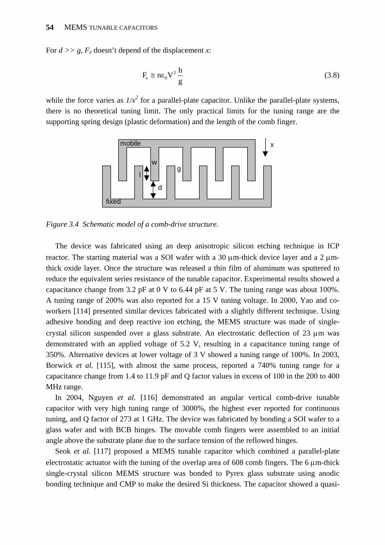
MEMS TUNABLE CAPACITORS
54
For d >> g, Fe doesn’t depend of the displacement x:
ghVnεF 2
0e ≅ (3.8)
while the force varies as 1/x2 for a parallel-plate capacitor. Unlike the parallel-plate systems, there is no theoretical tuning limit. The only practical limits for the tuning range are the supporting spring design (plastic deformation) and the length of the comb finger.
x
g l
d
w
mobile
fixed
Figure 3.4 Schematic model of a comb-drive structure.
The device was fabricated using an deep anisotropic silicon etching technique in ICP
reactor. The starting material was a SOI wafer with a 30 μm-thick device layer and a 2 μm-thick oxide layer. Once the structure was released a thin film of aluminum was sputtered to reduce the equivalent series resistance of the tunable capacitor. Experimental results showed a capacitance change from 3.2 pF at 0 V to 6.44 pF at 5 V. The tuning range was about 100%. A tuning range of 200% was also reported for a 15 V tuning voltage. In 2000, Yao and co-workers [114] presented similar devices fabricated with a slightly different technique. Using adhesive bonding and deep reactive ion etching, the MEMS structure was made of single-crystal silicon suspended over a glass substrate. An electrostatic deflection of 23 μm was demonstrated with an applied voltage of 5.2 V, resulting in a capacitance tuning range of 350%. Alternative devices at lower voltage of 3 V showed a tuning range of 100%. In 2003, Borwick et al. [115], with almost the same process, reported a 740% tuning range for a capacitance change from 1.4 to 11.9 pF and Q factor values in excess of 100 in the 200 to 400 MHz range.
In 2004, Nguyen et al. [116] demonstrated an angular vertical comb-drive tunable capacitor with very high tuning range of 3000%, the highest ever reported for continuous tuning, and Q factor of 273 at 1 GHz. The device was fabricated by bonding a SOI wafer to a glass wafer and with BCB hinges. The movable comb fingers were assembled to an initial angle above the substrate plane due to the surface tension of the reflowed hinges.
Seok et al. [117] proposed a MEMS tunable capacitor which combined a parallel-plate electrostatic actuator with the tuning of the overlap area of 608 comb fingers. The 6 μm-thick single-crystal silicon MEMS structure was bonded to Pyrex glass substrate using anodic bonding technique and CMP to make the desired Si thickness. The capacitor showed a quasi-
STATE-OF-THE-ART
55
linear tuning characteristic but a narrow tuning range of 10% at 8 V, resulting from the fringing fields.
In 2005, Cruau et al. [118] presented a MEMS tunable capacitor which relied on the displacement of an insulated conductor in the air-gap of a V-shaped capacitor. The system had two RF electrodes with comb fingers, fixed on the opposite sides of a micromachined cavity in the substrate. The mobile conductor, also a comb structure, followed the V shape of the cavity. It could be displaced laterally by electrostatic actuation to misalign the fingers and hence vary the capacitance. The feasibility was demonstrated for fixed glass prototypes with tuning range up to 340%.
3.1.5 Relative permittivity tuning
3.1.5.1 Movable dielectrics In 2000, Yoon and Nguyen [119] reported a tunable capacitor based on a movable
dielectrics. The capacitance tuning was obtained via a movable dielectric plate suspended by dielectric spring beams between two fixed conductive plates. The dielectric was free to move and could be electrostatically displaced to alter either the overlap between it and the capacitor plates (lateral spring design) or the fringing fields between them (vertical spring design). When a DC bias voltage was applied between the two plates, the charges on the capacitor plates exerted an electrostatic force on the induced charges in the dielectric into the gap. The fragmented shape of the structure was designed to minimize the travel distance (or voltage) required for a given change in capacitance and to provide etchant access during the sacrificial layer releasing. Results showed Q factors as high as 291 at 1 GHz for a capacitance value of 1.21 pF and a tuning range of 7.7% under 10 V bias voltage for the lateral spring design. For the vertical spring design, the Q factor was 218 at 1 GHz for a capacitance value of 1.14 pF and a tuning range of 40% under 10 V bias voltage.
3.1.5.2 Voltage-tunable ferroelectric thin films A tunable capacitor based on tuning the dielectric constant is not truly considered a MEMS
capacitor, but is included here for completeness and comparison. These capacitors employ ferroelectric thin films like barium strontium titanate BaSrTiO3 (BST) which have an electric field tunable dielectric constant. Tunable capacitors based on this principle have the advantage that they can be quite rugged as there are no movable parts. Tuning range and quality factor are limited, but are acceptable for many applications. Tombak et al. [120] obtained a tuning range of 71% at 9 V, with Q factors dropping below 20 for frequencies exceeding 300 MHz for a BST capacitor. Erker et al. [121] applied a BST capacitor in a phase shifter. They reported a capacitance decrease by a factor of 2.2 (corresponding to a tuning range of 55%) with an applied bias of 20 V. They also reported that the capacitor had a quality factor of 10 at 30 GHz.
3.1.6 Summary of state-of-the-art MEMS tunable capacitors Table 3.2 gives a summary of state-of-the-art MEMS tunable capacitors.
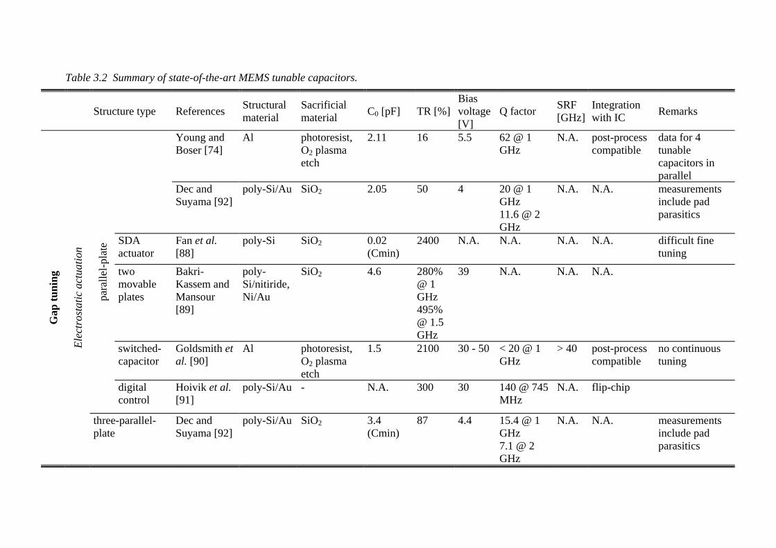
Table 3.2 Summary of state-of-the-art MEMS tunable capacitors.
Structure type References Structural
material Sacrificial material C0 [pF] TR [%]
Bias voltage [V]
Q factor SRF [GHz]
Integration with IC Remarks
Young and Boser [74]
Al photoresist, O2 plasma etch
2.11 16 5.5 62 @ 1 GHz
N.A. post-process compatible
data for 4 tunable capacitors in parallel Dec and
Suyama [92] poly-Si/Au SiO2 2.05 50 4 20 @ 1
GHz 11.6 @ 2 GHz
N.A. N.A. measurements include pad parasitics
SDA actuator
Fan et al. [88]
poly-Si SiO2 0.02 (Cmin)
2400 N.A. N.A. N.A. N.A. difficult fine tuning
two movable plates
Bakri-Kassem and Mansour [89]
poly-Si/nitiride, Ni/Au
SiO2 4.6 280% @ 1 GHz 495% @ 1.5 GHz
39 N.A. N.A. N.A.
switched-capacitor
Goldsmith et al. [90]
Al photoresist, O2 plasma etch
1.5 2100 30 - 50 < 20 @ 1 GHz
> 40 post-process compatible
no continuous tuning
para
llel-p
late
digital control
Hoivik et al. [91]
poly-Si/Au - N.A. 300 30 140 @ 745 MHz
N.A. flip-chip
Gap
tuni
ng
Elec
tros
tatic
act
uatio
n
three-parallel-plate
Dec and Suyama [92]
poly-Si/Au SiO2 3.4 (Cmin)
87 4.4 15.4 @ 1 GHz 7.1 @ 2 GHz
N.A. N.A. measurements include pad parasitics
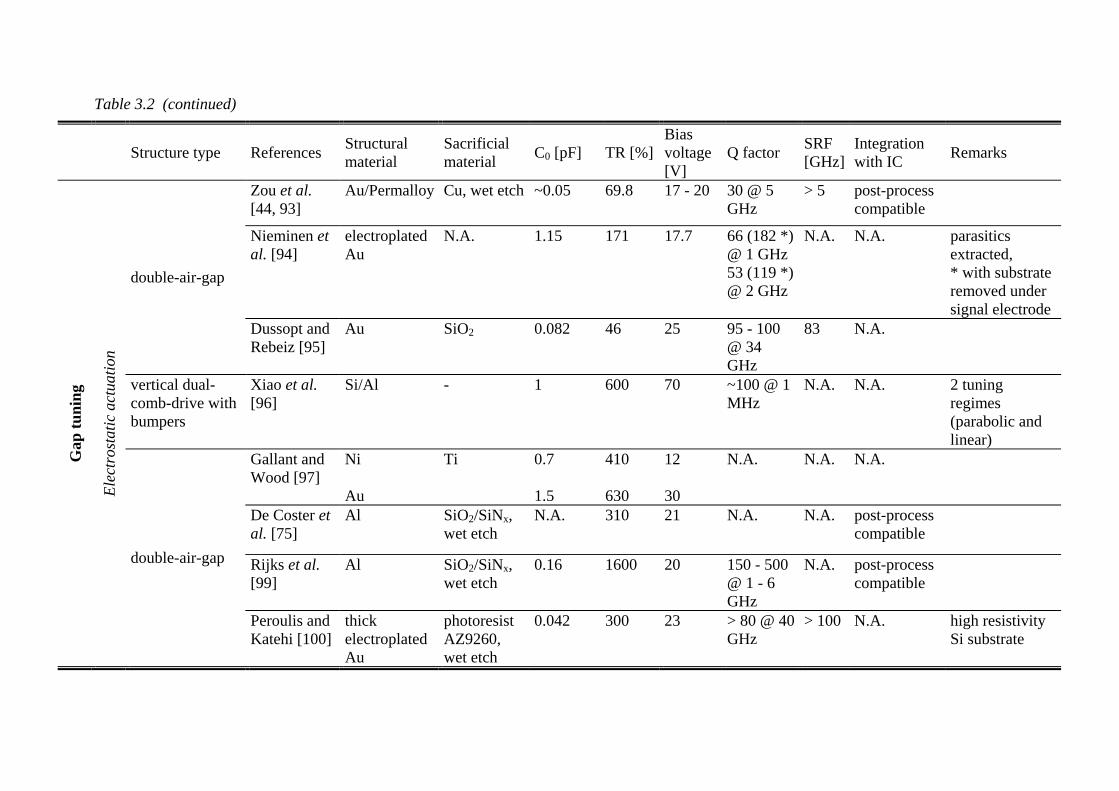
Table 3.2 (continued)
Structure type References Structural
material Sacrificial material C0 [pF] TR [%]
Bias voltage [V]
Q factor SRF [GHz]
Integration with IC Remarks
Zou et al. [44, 93]
Au/Permalloy Cu, wet etch ~0.05 69.8 17 - 20 30 @ 5 GHz
> 5 post-process compatible
Nieminen et al. [94]
electroplated Au
N.A. 1.15 171 17.7 66 (182 *) @ 1 GHz 53 (119 *) @ 2 GHz
N.A. N.A. parasitics extracted, * with substrate removed under signal electrode
double-air-gap
Dussopt and Rebeiz [95]
Au SiO2 0.082 46 25 95 - 100 @ 34 GHz
83 N.A.
vertical dual-comb-drive with bumpers
Xiao et al. [96]
Si/Al - 1 600 70 ~100 @ 1 MHz
N.A. N.A. 2 tuning regimes (parabolic and linear)
Gallant and Wood [97]
Ni Au
Ti 0.7 1.5
410 630
12 30
N.A. N.A. N.A.
De Coster et al. [75]
Al SiO2/SiNx, wet etch
N.A. 310 21 N.A. N.A. post-process compatible
Rijks et al. [99]
Al SiO2/SiNx, wet etch
0.16 1600 20 150 - 500 @ 1 - 6 GHz
N.A. post-process compatible
Gap
tuni
ng
Elec
tros
tatic
act
uatio
n
double-air-gap
Peroulis and Katehi [100]
thick electroplated Au
photoresist AZ9260, wet etch
0.042 300 23 > 80 @ 40 GHz
> 100 N.A. high resistivity Si substrate
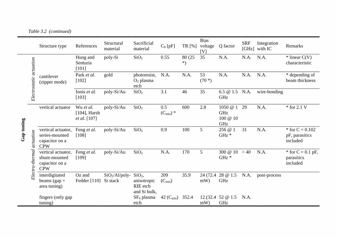
Table 3.2 (continued)
Structure type References Structural
material Sacrificial material C0 [pF] TR [%]
Bias voltage [V]
Q factor SRF [GHz]
Integration with IC Remarks
Hung and Senturia [101]
poly-Si SiO2 0.55 80 (25 *)
35 N.A. N.A. N.A. * linear C(V) characteristic
Park et al. [102]
gold photoresist, O2 plasma etch
N.A. N.A. 53 (70 *)
N.A. N.A. N.A. * depending of beam thickness
Elec
tros
tatic
act
uatio
n
cantilever (zipper mode)
Ionis et al. [103]
poly-Si/Au SiO2 3.1 46 35 6.5 @ 1.5 GHz
N.A. wire-bonding
vertical actuator Wu et al. [104], Harsh et al. [107]
poly-Si/Au SiO2 0.5 (Cmin) *
600 2.8 1050 @ 1 GHz 100 @ 10 GHz
29 N.A. * for 2.1 V
vertical actuator, series-mounted capacitor on a CPW
Feng et al. [108]
poly-Si/Au SiO2 0.9 100 5 256 @ 1 GHz *
31 N.A. * for C = 0.102 pF, parasitics included
vertical actuator, shunt-mounted capacitor on a CPW
Feng et al. [109]
poly-Si/Au SiO2 N.A. 170 5 300 @ 10 GHz *
> 40 N.A. * for C = 0.1 pF, parasitics included
Gap
tuni
ng
Elec
tro-
ther
mal
act
uatio
n
interdigitated beams (gap + area tuning) fingers (only gap tuning)
Oz and Fedder [110]
SiO2/Al/poly-Si stack
SiO2, anisotropic RIE etch and Si bulk, SF6 plasma etch
209 (Cmin) 42 (Cmin)
35.9 352.4
24 (72.4 mW) 12 (32.4 mW)
28 @ 1.5 GHz 52 @ 1.5 GHz
N.A. N.A.
post-process
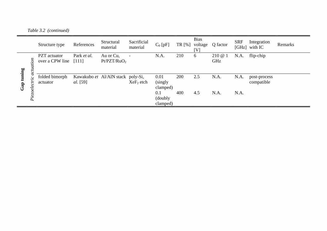
Table 3.2 (continued)
Structure type References Structural
material Sacrificial material C0 [pF] TR [%]
Bias voltage [V]
Q factor SRF [GHz]
Integration with IC Remarks
PZT actuator over a CPW line
Park et al. [111]
Au or Cu, Pt/PZT/RuO2
- N.A. 210 6 210 @ 1 GHz
N.A. flip-chip
Gap
tuni
ng
Piez
oele
ctri
c ac
tuat
ion
folded bimorph actuator
Kawakubo et al. [59]
Al/AlN stack poly-Si, XeF2 etch
0.01 (singly clamped) 0.1 (doubly clamped)
200 400
2.5 4.5
N.A. N.A.
N.A. N.A.
post-process compatible
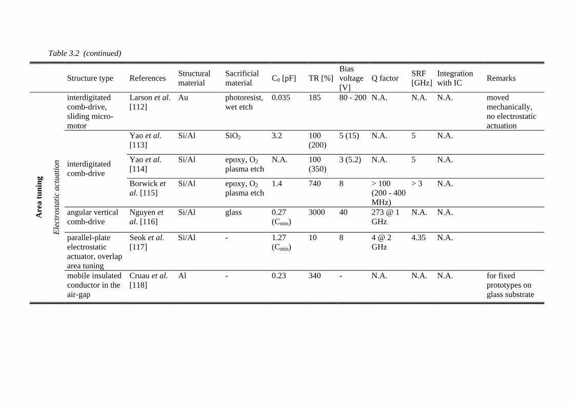
Table 3.2 (continued)
Structure type References Structural
material Sacrificial material C0 [pF] TR [%]
Bias voltage [V]
Q factor SRF [GHz]
Integration with IC Remarks
interdigitated comb-drive, sliding micro-motor
Larson et al. [112]
Au photoresist, wet etch
0.035 185 80 - 200 N.A. N.A. N.A. moved mechanically, no electrostatic actuation
Yao et al. [113]
Si/Al SiO2 3.2 100 (200)
5 (15) N.A. 5 N.A.
Yao et al. [114]
Si/Al epoxy, O2 plasma etch
N.A. 100 (350)
3 (5.2) N.A. 5 N.A. interdigitated comb-drive
Borwick et al. [115]
Si/Al epoxy, O2 plasma etch
1.4 740 8 > 100 (200 - 400 MHz)
> 3 N.A.
angular vertical comb-drive
Nguyen et al. [116]
Si/Al glass 0.27 (Cmin)
3000 40 273 @ 1 GHz
N.A. N.A.
parallel-plate electrostatic actuator, overlap area tuning
Seok et al. [117]
Si/Al - 1.27 (Cmin)
10 8 4 @ 2 GHz
4.35 N.A.
Are
a tu
ning
Elec
tros
tatic
act
uatio
n
mobile insulated conductor in the air-gap
Cruau et al. [118]
Al - 0.23 340 - N.A. N.A. N.A. for fixed prototypes on glass substrate
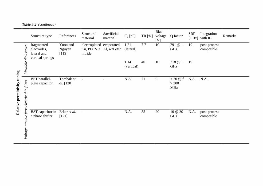
Table 3.2 (continued)
Structure type References Structural
material Sacrificial material C0 [pF] TR [%]
Bias voltage [V]
Q factor SRF [GHz]
Integration with IC Remarks
Mov
able
die
lect
rics
fragmented electrodes, lateral and vertical springs
Yoon and Nguyen [119]
electroplated Cu, PECVD nitride
evaporated Al, wet etch
1.21 (lateral) 1.14 (vertical)
7.7 40
10 10
291 @ 1 GHz 218 @ 1 GHz
19 19
post-process compatible
BST parallel-plate capacitor
Tombak et al. [120]
- - N.A. 71 9 < 20 @ f > 300 MHz
N.A. N.A.
Rel
ativ
e pe
rmitt
ivity
tuni
ng
Volta
ge-tu
nabl
e fe
rroe
lect
ric
thin
film
s
BST capacitor in a phase shifter
Erker et al. [121]
- - N.A. 55 20 10 @ 30 GHz
N.A. post-process compatible
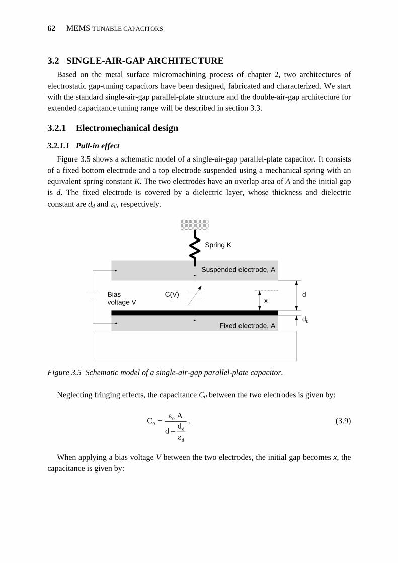
MEMS TUNABLE CAPACITORS
62
3.2 SINGLE-AIR-GAP ARCHITECTURE Based on the metal surface micromachining process of chapter 2, two architectures of
electrostatic gap-tuning capacitors have been designed, fabricated and characterized. We start with the standard single-air-gap parallel-plate structure and the double-air-gap architecture for extended capacitance tuning range will be described in section 3.3.
3.2.1 Electromechanical design
3.2.1.1 Pull-in effect
Figure 3.5 shows a schematic model of a single-air-gap parallel-plate capacitor. It consists of a fixed bottom electrode and a top electrode suspended using a mechanical spring with an equivalent spring constant K. The two electrodes have an overlap area of A and the initial gap is d. The fixed electrode is covered by a dielectric layer, whose thickness and dielectric constant are dd and εd, respectively.
Spring K
Fixed electrode, A
Suspended electrode, A
Bias voltage V
C(V) x
dd
d
Figure 3.5 Schematic model of a single-air-gap parallel-plate capacitor.
Neglecting fringing effects, the capacitance C0 between the two electrodes is given by:
d
d
00
εdd
A εC+
= . (3.9)
When applying a bias voltage V between the two electrodes, the initial gap becomes x, the
capacitance is given by:
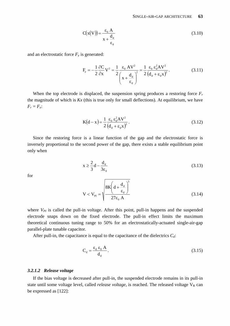
SINGLE-AIR-GAP ARCHITECTURE
63
( )( )
d
d
0
εdx
A εVxC+
= (3.10)
and an electrostatic force Fe is generated:
( )2dd
22d0
2
d
d
202
e xεdAVε ε
21
εdx
AV ε21V
xC
21F
+=
⎟⎟⎠
⎞⎜⎜⎝
⎛+
=∂∂
−= . (3.11)
When the top electrode is displaced, the suspension spring produces a restoring force Fr
the magnitude of which is Kx (this is true only for small deflections). At equilibrium, we have Fr = Fe:
( )( )2
dd
22d0
xεdAVε ε
21xdK
+=− . (3.12)
Since the restoring force is a linear function of the gap and the electrostatic force is
inversely proportional to the second power of the gap, there exists a stable equilibrium point only when
d
d
3εdd
32x −≥ (3.13)
for
A 27εεdd8K
VV0
3
d
d
PI
⎟⎟⎠
⎞⎜⎜⎝
⎛+
=< (3.14)
where VPI is called the pull-in voltage. After this point, pull-in happens and the suspended electrode snaps down on the fixed electrode. The pull-in effect limits the maximum theoretical continuous tuning range to 50% for an electrostatically-actuated single-air-gap parallel-plate tunable capacitor.
After pull-in, the capacitance is equal to the capacitance of the dielectrics Cd:
d
0dd d
A ε εC = . (3.15)
3.2.1.2 Release voltage If the bias voltage is decreased after pull-in, the suspended electrode remains in its pull-in
state until some voltage level, called release voltage, is reached. The released voltage VR can be expressed as [122]:
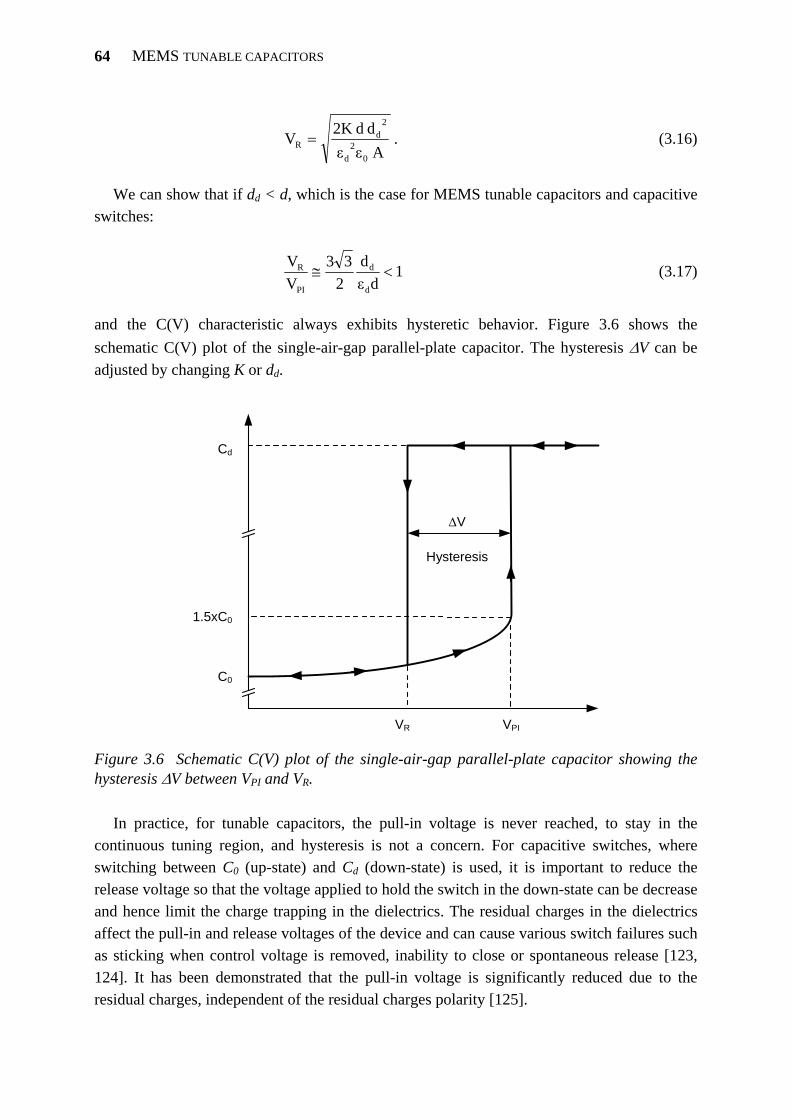
MEMS TUNABLE CAPACITORS
64
A εεd d2K V
02
d
2d
R = . (3.16)
We can show that if dd < d, which is the case for MEMS tunable capacitors and capacitive
switches:
1dε
d2
33VV
d
d
PI
R <≅ (3.17)
and the C(V) characteristic always exhibits hysteretic behavior. Figure 3.6 shows the schematic C(V) plot of the single-air-gap parallel-plate capacitor. The hysteresis ΔV can be adjusted by changing K or dd.
C0
VR VPI
Hysteresis
ΔV
1.5xC0
Cd
Figure 3.6 Schematic C(V) plot of the single-air-gap parallel-plate capacitor showing the hysteresis ΔV between VPI and VR.
In practice, for tunable capacitors, the pull-in voltage is never reached, to stay in the
continuous tuning region, and hysteresis is not a concern. For capacitive switches, where switching between C0 (up-state) and Cd (down-state) is used, it is important to reduce the release voltage so that the voltage applied to hold the switch in the down-state can be decrease and hence limit the charge trapping in the dielectrics. The residual charges in the dielectrics affect the pull-in and release voltages of the device and can cause various switch failures such as sticking when control voltage is removed, inability to close or spontaneous release [123, 124]. It has been demonstrated that the pull-in voltage is significantly reduced due to the residual charges, independent of the residual charges polarity [125].
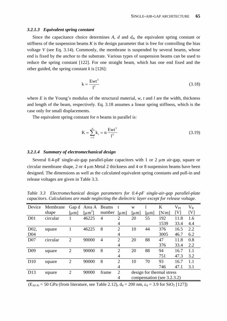
SINGLE-AIR-GAP ARCHITECTURE
65
3.2.1.3 Equivalent spring constant Since the capacitance choice determines A, d and dd, the equivalent spring constant or
stiffness of the suspension beams K is the design parameter that is free for controlling the bias voltage V (see Eq. 3.14). Commonly, the membrane is suspended by several beams, whose end is fixed by the anchor to the substrate. Various types of suspension beams can be used to reduce the spring constant [122]. For one straight beam, which has one end fixed and the other guided, the spring constant k is [126]:
3
3
lEwtk = (3.18)
where E is the Young’s modulus of the structural material, w, t and l are the width, thickness and length of the beam, respectively. Eq. 3.18 assumes a linear spring stiffness, which is the case only for small displacements.
The equivalent spring constant for n beams in parallel is:
3
3n
1ii l
EwtnkK == ∑=
(3.19)
3.2.1.4 Summary of electromechanical design
Several 0.4-pF single-air-gap parallel-plate capacitors with 1 or 2 μm air-gap, square or circular membrane shape, 2 or 4 μm Metal 2 thickness and 4 or 8 suspension beams have been designed. The dimensions as well as the calculated equivalent spring constants and pull-in and release voltages are given in Table 3.3.
Table 3.3 Electromechanical design parameters for 0.4-pF single-air-gap parallel-plate capacitors. Calculations are made neglecting the dielectric layer except for release voltage.
Device Membrane shape
Gap d [μm]
Area A [μm2]
Beams number
t [μm]
w [μm]
l [μm]
K [Ν/m]
VPI [V]
VR [V]
D01 circular 1 46225 4 2 4
20 55 192 1539
11.8 33.4
1.6 4.4
D02, D04
square 1 46225 8 2 4
10 44 376 3005
16.5 46.7
2.2 6.2
D07 circular 2 90000 4 2 4
20 88 47 376
11.8 33.4
0.8 2.2
D09 square 2 90000 8 2 4
20 88 94 751
16.7 47.3
1.1 3.2
D10 square 2 90000 8 2 4
10 70 93 746
16.7 47.1
1.1 3.1
D13 square 2 90000 frame 2 4
design for thermal stress compensation (see 3.2.3.2)
(EAl-Si = 50 GPa (from literature, see Table 2.12), dd = 200 nm, εd = 3.9 for SiO2 [127])
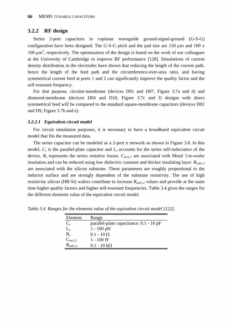
MEMS TUNABLE CAPACITORS
66
3.2.2 RF design Series 2-port capacitors in coplanar waveguide ground-signal-ground (G-S-G)
configuration have been designed. The G-S-G pitch and the pad size are 150 μm and 100 x 100 μm2, respectively. The optimization of the design is based on the work of our colleagues at the University of Cambridge to improve RF performance [128]. Simulations of current density distribution in the electrodes have shown that reducing the length of the current path, hence the length of the feed path and the circumference-over-area ratio, and having symmetrical current feed at ports 1 and 2 can significantly improve the quality factor and the self-resonant frequency.
For that purpose, circular-membrane (devices D01 and D07, Figure 3.7a and d) and diamond-membrane (devices D04 and D10, Figure 3.7c and f) designs with direct symmetrical feed will be compared to the standard square-membrane capacitors (devices D02 and D9, Figure 3.7b and e).
3.2.2.1 Equivalent circuit model
For circuit simulation purposes, it is necessary to have a broadband equivalent circuit model that fits the measured data.
The series capacitor can be modeled as a 2-port π network as shown in Figure 3.8. In this model, Cs is the parallel-plate capacitor and Ls accounts for the series self-inductance of the device. Rs represents the series resistive losses. Cins1,2 are associated with Metal 1-to-wafer insulation and can be reduced using low dielectric constant and thicker insulating layer. Rsub1,2 are associated with the silicon substrate. These parameters are roughly proportional to the inductor surface and are strongly dependent of the substrate resistivity. The use of high resistivity silicon (HR-Si) wafers contribute to increase Rsub1,2 values and provide at the same time higher quality factors and higher self-resonant frequencies. Table 3.4 gives the ranges for the different elements value of the equivalent circuit model.
Table 3.4 Ranges for the elements value of the equivalent circuit model [122].
Element Range Cs Ls Rs Cins1,2 Rsub1,2
parallel-plate capacitance: 0.1 - 10 pF 1 - 100 pH 0.1 - 10 Ω 1 - 100 fF 0.1 - 10 kΩ
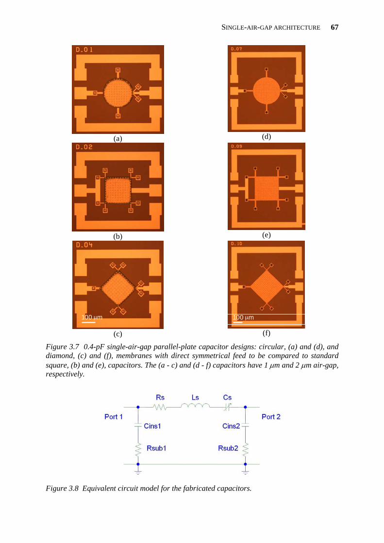
SINGLE-AIR-GAP ARCHITECTURE
67
(a)
(d)
(b)
(e)
100 μm
(c)
100 μm
(f)
Figure 3.7 0.4-pF single-air-gap parallel-plate capacitor designs: circular, (a) and (d), and diamond, (c) and (f), membranes with direct symmetrical feed to be compared to standard square, (b) and (e), capacitors. The (a - c) and (d - f) capacitors have 1 μm and 2 μm air-gap, respectively.
Figure 3.8 Equivalent circuit model for the fabricated capacitors.
MEMS TUNABLE CAPACITORS
68
3.2.3 Characterization
3.2.3.1 S-parameter measurements The devices described in Figure 3.7 were fabricated using Process IV (see Figure 2.27) on
BiCMOS wafers, hence standard low resistivity silicon substrates. Metal 1 and Metal 2 thicknesses were 1 μm and 2 or 4 μm, respectively. We present here the RF measurements of tunable capacitors having a 4 μm-thick Metal 2. The measurements were performed at room temperature and atmospheric pressure in a nitrogen environment.
The usual procedure undertaken for characterizing the performance of RF and microwave passive devices involves the measurement of the scattering parameters, S-parameters. The scattering matrix, [S] matrix, provides a complete description of a network. While the impedance, [Z], and admittance, [Y], matrices relate the total voltages and currents at the ports of the network, the scattering matrix relates the voltage waves incident on the ports to those reflected from the ports [129]. The S-parameters can be measured directly with a vector network analyzer.
The measurement set-up consists of a Süss MicroTec PMC 150 probing system and an HP 8719D vector network analyzer, operating in the 50 MHz to 13.51 GHz frequency range. The DC voltage is supplied by an HP 6624A DC source and coupled to the RF signal on each port through an HP 33150A bias tee. The probes were Süss MicroTec coplanar G-S-G 150 μm-pitch /Z/ probes. A standard short-open-load-through (SOLT) calibration is performed before the measurement session using Süss MicroTec CSR-3 calibration substrate.
Capacitance and quality factor extraction The calibrated S-parameter data are converted into Y-parameter data. Equivalent
capacitance and quality factor for each of port 1 and 2 are defined as:
⎟⎟⎠
⎞⎜⎜⎝
⎛−
=
11
1
Y1Im f 2π
1C
⎟⎟⎠
⎞⎜⎜⎝
⎛
⎟⎟⎠
⎞⎜⎜⎝
⎛−
=
11
111
Y1Re
Y1Im
Q (3.20)
⎟⎟⎠
⎞⎜⎜⎝
⎛−
=
22
2
Y1Im f 2π
1C
⎟⎟⎠
⎞⎜⎜⎝
⎛
⎟⎟⎠
⎞⎜⎜⎝
⎛−
=
22
222
Y1Re
Y1Im
Q (3.21)
where f is the frequency and 1/Yxx is the impedance seen at one port when the other is connected to the ground. The self-resonant frequency SRF is intuitively defined as the one where Q1 or Q2 goes to zero, which means that the device behaves as an inductor and becomes unusable beyond this frequency. Based on the extracted parameters Cs and Ls (Table 3.5), the self-resonant frequency can be calculated as:

SINGLE-AIR-GAP ARCHITECTURE
69
ssLC2π1SRF = (3.22)
The extraction of equivalent capacitance, quality factor and self-resonant frequency at bias
voltage equal to 0 V for ports 1 and 2 is illustrated in Figures 3.9 and 3.10 for D01 and D09 capacitors, respectively. The results for all the designed 0.4-pF single-air-gap parallel-plate capacitors are given in Table 3.5. All the devices exhibit an asymmetrical behavior when comparing Q factor at ports 1 and 2: Q1 is always higher than Q2. This can be explained by the fact that the current feed at port 2 is completely realized by the thin Metal 1 while at port 1 it is a combination of Metal 1 and the 4 μm-thick Metal 2. Figures 3.9 and 3.10 also show that keeping the capacitance unchanged while reducing the area and the air-gap by half, hence reducing the current path lengths, can significantly increase the self-resonant frequency, pushing it to 12 GHz and beyond.
-1
0
1
2
3
4
5
0 2 4 6 8 10 12 14
Frequency [GHz]
C [p
F]
-10
0
10
20
30
40
50
Q factor
Port 1Port 2
SRF = 12.3 GHz
Figure 3.9 Equivalent capacitance, quality factor and self-resonant frequency extracted from measured Y-parameters at bias voltage = 0 V for ports 1 and 2 for D01 capacitor (circular membrane, 1 μm air-gap).
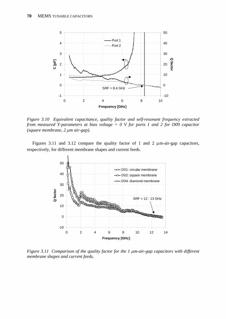
MEMS TUNABLE CAPACITORS
70
-1
0
1
2
3
4
5
0 2 4 6 8 10
Frequency [GHz]
C [p
F]
-10
0
10
20
30
40
50
Q factor
Port 1Port 2
SRF = 8.4 GHz
Figure 3.10 Equivalent capacitance, quality factor and self-resonant frequency extracted from measured Y-parameters at bias voltage = 0 V for ports 1 and 2 for D09 capacitor (square membrane, 2 μm air-gap).
Figures 3.11 and 3.12 compare the quality factor of 1 and 2 μm-air-gap capacitors, respectively, for different membrane shapes and current feeds.
-10
0
10
20
30
40
50
0 2 4 6 8 10 12 14
Frequency [GHz]
Q fa
ctor
D01: circular membraneD02: square membrane
D04: diamond membrane
SRF = 12 - 13 GHz
Figure 3.11 Comparison of the quality factor for the 1 μm-air-gap capacitors with different membrane shapes and current feeds.
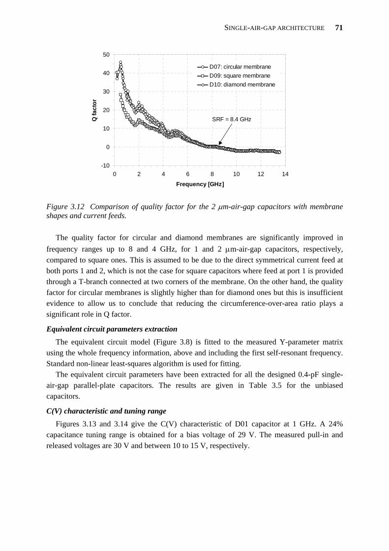
SINGLE-AIR-GAP ARCHITECTURE
71
-10
0
10
20
30
40
50
0 2 4 6 8 10 12 14
Frequency [GHz]
Q fa
ctor
D07: circular membraneD09: square membraneD10: diamond membrane
SRF = 8.4 GHz
Figure 3.12 Comparison of quality factor for the 2 μm-air-gap capacitors with membrane shapes and current feeds.
The quality factor for circular and diamond membranes are significantly improved in
frequency ranges up to 8 and 4 GHz, for 1 and 2 μm-air-gap capacitors, respectively, compared to square ones. This is assumed to be due to the direct symmetrical current feed at both ports 1 and 2, which is not the case for square capacitors where feed at port 1 is provided through a T-branch connected at two corners of the membrane. On the other hand, the quality factor for circular membranes is slightly higher than for diamond ones but this is insufficient evidence to allow us to conclude that reducing the circumference-over-area ratio plays a significant role in Q factor.
Equivalent circuit parameters extraction
The equivalent circuit model (Figure 3.8) is fitted to the measured Y-parameter matrix using the whole frequency information, above and including the first self-resonant frequency. Standard non-linear least-squares algorithm is used for fitting.
The equivalent circuit parameters have been extracted for all the designed 0.4-pF single-air-gap parallel-plate capacitors. The results are given in Table 3.5 for the unbiased capacitors.
C(V) characteristic and tuning range
Figures 3.13 and 3.14 give the C(V) characteristic of D01 capacitor at 1 GHz. A 24% capacitance tuning range is obtained for a bias voltage of 29 V. The measured pull-in and released voltages are 30 V and between 10 to 15 V, respectively.
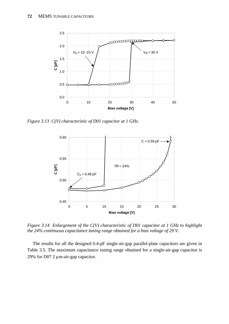
MEMS TUNABLE CAPACITORS
72
0.0
0.5
1.0
1.5
2.0
2.5
0 10 20 30 40 50
Bias voltage [V]
C [p
F]VPI = 30 VVR = 10 -15 V
Figure 3.13 C(V) characteristic of D01 capacitor at 1 GHz.
0.45
0.50
0.55
0.60
0 5 10 15 20 25 30
Bias voltage [V]
C [p
F]
C0 = 0.48 pF
C = 0.59 pF
TR = 24%
Figure 3.14 Enlargement of the C(V) characteristic of D01 capacitor at 1 GHz to highlight the 24% continuous capacitance tuning range obtained for a bias voltage of 29 V.
The results for all the designed 0.4-pF single-air-gap parallel-plate capacitors are given in
Table 3.5. The maximum capacitance tuning range obtained for a single-air-gap capacitor is 29% for D07 2 μm-air-gap capacitor.
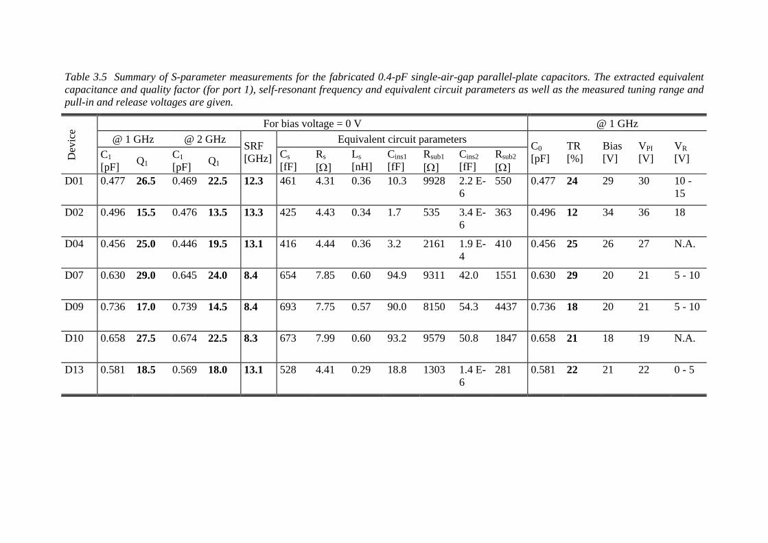
Table 3.5 Summary of S-parameter measurements for the fabricated 0.4-pF single-air-gap parallel-plate capacitors. The extracted equivalent capacitance and quality factor (for port 1), self-resonant frequency and equivalent circuit parameters as well as the measured tuning range and pull-in and release voltages are given.
For bias voltage = 0 V @ 1 GHz @ 1 GHz @ 2 GHz Equivalent circuit parameters
Dev
ice
C1 [pF] Q1
C1 [pF] Q1
SRF [GHz] Cs
[fF] Rs [Ω]
Ls [nH]
Cins1 [fF]
Rsub1 [Ω]
Cins2 [fF]
Rsub2 [Ω]
C0 [pF]
TR [%]
Bias [V]
VPI [V]
VR [V]
D01 0.477 26.5 0.469 22.5 12.3 461 4.31 0.36 10.3 9928 2.2 E-6
550 0.477 24 29 30 10 - 15
D02 0.496 15.5 0.476 13.5 13.3 425 4.43 0.34 1.7 535 3.4 E-6
363 0.496 12 34 36 18
D04 0.456 25.0 0.446 19.5 13.1 416 4.44 0.36 3.2 2161 1.9 E-4
410 0.456 25 26 27 N.A.
D07 0.630 29.0 0.645 24.0 8.4 654 7.85 0.60 94.9 9311 42.0 1551 0.630 29 20 21 5 - 10
D09 0.736 17.0 0.739 14.5 8.4 693 7.75 0.57 90.0 8150 54.3 4437 0.736 18 20 21 5 - 10
D10 0.658 27.5 0.674 22.5 8.3 673 7.99 0.60 93.2 9579 50.8 1847 0.658 21 18 19 N.A.
D13 0.581 18.5 0.569 18.0 13.1 528 4.41 0.29 18.8 1303 1.4 E-6
281 0.581 22 21 22 0 - 5
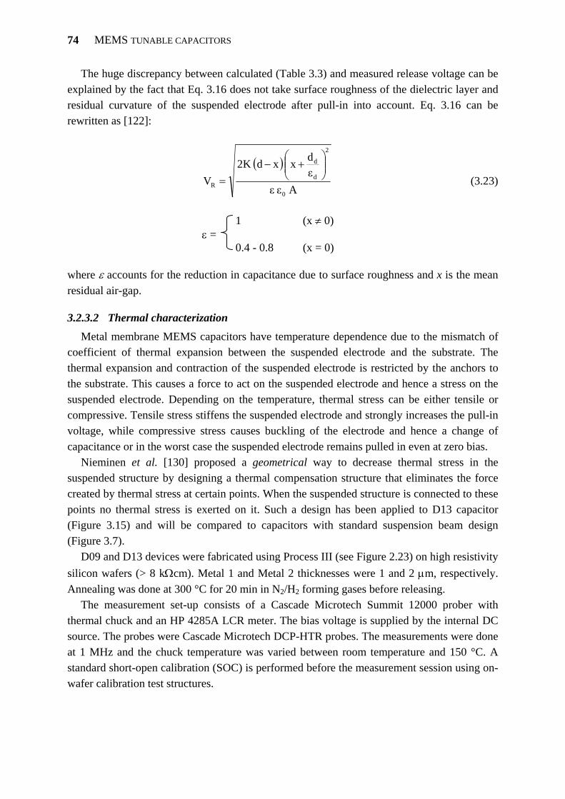
MEMS TUNABLE CAPACITORS
74
The huge discrepancy between calculated (Table 3.3) and measured release voltage can be explained by the fact that Eq. 3.16 does not take surface roughness of the dielectric layer and residual curvature of the suspended electrode after pull-in into account. Eq. 3.16 can be rewritten as [122]:
( )
A ε εεdx xd2K
V0
2
d
d
R
⎟⎟⎠
⎞⎜⎜⎝
⎛+−
= (3.23)
1 (x ≠ 0) ε =
0.4 - 0.8 (x = 0) where ε accounts for the reduction in capacitance due to surface roughness and x is the mean residual air-gap.
3.2.3.2 Thermal characterization
Metal membrane MEMS capacitors have temperature dependence due to the mismatch of coefficient of thermal expansion between the suspended electrode and the substrate. The thermal expansion and contraction of the suspended electrode is restricted by the anchors to the substrate. This causes a force to act on the suspended electrode and hence a stress on the suspended electrode. Depending on the temperature, thermal stress can be either tensile or compressive. Tensile stress stiffens the suspended electrode and strongly increases the pull-in voltage, while compressive stress causes buckling of the electrode and hence a change of capacitance or in the worst case the suspended electrode remains pulled in even at zero bias.
Nieminen et al. [130] proposed a geometrical way to decrease thermal stress in the suspended structure by designing a thermal compensation structure that eliminates the force created by thermal stress at certain points. When the suspended structure is connected to these points no thermal stress is exerted on it. Such a design has been applied to D13 capacitor (Figure 3.15) and will be compared to capacitors with standard suspension beam design (Figure 3.7).
D09 and D13 devices were fabricated using Process III (see Figure 2.23) on high resistivity silicon wafers (> 8 kΩcm). Metal 1 and Metal 2 thicknesses were 1 and 2 μm, respectively. Annealing was done at 300 °C for 20 min in N2/H2 forming gases before releasing.
The measurement set-up consists of a Cascade Microtech Summit 12000 prober with thermal chuck and an HP 4285A LCR meter. The bias voltage is supplied by the internal DC source. The probes were Cascade Microtech DCP-HTR probes. The measurements were done at 1 MHz and the chuck temperature was varied between room temperature and 150 °C. A standard short-open calibration (SOC) is performed before the measurement session using on-wafer calibration test structures.
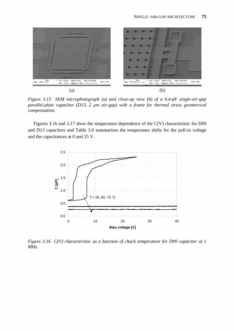
SINGLE -AIR-GAP ARCHITECTURE
75
(a)
(b)
Figure 3.15 SEM microphotograph (a) and close-up view (b) of a 0.4-pF single-air-gap parallel-plate capacitor (D13, 2 μm air-gap) with a frame for thermal stress geometrical compensation.
Figures 3.16 and 3.17 show the temperature dependence of the C(V) characteristic for D09
and D13 capacitors and Table 3.6 summarizes the temperature shifts for the pull-in voltage and the capacitances at 0 and 25 V.
0.0
0.5
1.0
1.5
2.0
2.5
0 10 20 30 40
Bias voltage [V]
C [p
F]
T = 25, 50, 75 °C
Figure 3.16 C(V) characteristic as a function of chuck temperature for D09 capacitor at 1 MHz.
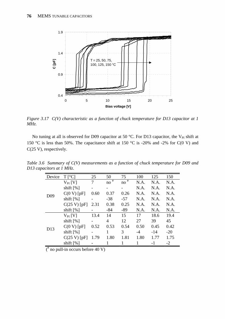
MEMS TUNABLE CAPACITORS
76
0.4
0.9
1.4
1.9
0 5 10 15 20 25
Bias voltage [V]
C [p
F] T = 25, 50, 75, 100, 125, 150 °C
Figure 3.17 C(V) characteristic as a function of chuck temperature for D13 capacitor at 1 MHz.
No tuning at all is observed for D09 capacitor at 50 °C. For D13 capacitor, the VPI shift at
150 °C is less than 50%. The capacitance shift at 150 °C is -20% and -2% for C(0 V) and C(25 V), respectively.
Table 3.6 Summary of C(V) measurements as a function of chuck temperature for D09 and D13 capacitors at 1 MHz.
Device T [°C] 25 50 75 100 125 150 VPI [V] 7 no # no # N.A. N.A. N.A. shift [%] - - - N.A. N.A. N.A. C(0 V) [pF] 0.60 0.37 0.26 N.A. N.A. N.A. shift [%] - -38 -57 N.A. N.A. N.A. C(25 V) [pF] 2.31 0.38 0.25 N.A. N.A. N.A.
D09
shift [%] - -84 -89 N.A. N.A. N.A. VPI [V] 13.4 14 15 17 18.6 19.4 shift [%] - 4 12 27 39 45 C(0 V) [pF] 0.52 0.53 0.54 0.50 0.45 0.42 shift [%] - 1 3 -4 -14 -20 C(25 V) [pF] 1.79 1.80 1.81 1.80 1.77 1.75
D13
shift [%] - 1 1 1 -1 -2 (# no pull-in occurs before 40 V)
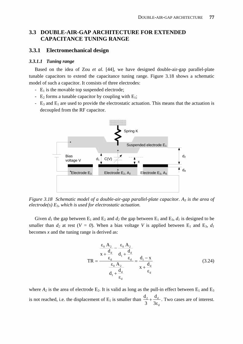
DOUBLE-AIR-GAP ARCHITECTURE
77
3.3 DOUBLE-AIR-GAP ARCHITECTURE FOR EXTENDED CAPACITANCE TUNING RANGE
3.3.1 Electromechanical design
3.3.1.1 Tuning range Based on the idea of Zou et al. [44], we have designed double-air-gap parallel-plate
tunable capacitors to extend the capacitance tuning range. Figure 3.18 shows a schematic model of such a capacitor. It consists of three electrodes:
- E1 is the movable top suspended electrode; - E2 forms a tunable capacitor by coupling with E1; - E3 and E1 are used to provide the electrostatic actuation. This means that the actuation is
decoupled from the RF capacitor.
d2 d1 Bias voltage V C(V)
dd
x
Spring K
Suspended electrode E1
Electrode E2, A2 Electrode E3, A3 Electrode E3
Figure 3.18 Schematic model of a double-air-gap parallel-plate capacitor. A3 is the area of electrode(s) E3, which is used for electrostatic actuation.
Given d1 the gap between E1 and E2 and d2 the gap between E1 and E3, d1 is designed to be
smaller than d2 at rest (V = 0). When a bias voltage V is applied between E1 and E3, d1 becomes x and the tuning range is derived as:
d
d
1
d
d1
20
d
d1
20
d
d
20
εdx
xd
εdd
A εεdd
A ε
εdx
A ε
TR+
−=
+
+−
+= (3.24)
where A2 is the area of electrode E2. It is valid as long as the pull-in effect between E1 and E3
is not reached, i.e. the displacement of E1 is smaller than d
d2
3εd
3d
+ . Two cases are of interest.

MEMS TUNABLE CAPACITORS
78
If d
d21 3ε
d3dd +> , the pull-in effect is reached when
d
d21 3ε
d3ddx −−= . Eq. 3.24 gives the
maximum tuning range:
d
d21
d
d2
εd2d3d
εdd
TR+−
+= . (3.25)
If d
d21 3ε
d3dd +≤ , the pull-in effect will not occur at all and the maximum tuning range is
reached for 0x = :
d
1d
dd εTR = . (3.26)
In reality, the maximum tuning range depends on other factors, such as surface roughness
and curvature of the suspended electrode. The choice of d1 and d2 was 1 and 2 μm, respectively. These values give a tuning range of
186% (dd = 200 nm) (Eq. 3.25) and 200% when neglecting the dielectric layer.
3.3.1.2 Summary of electromechanical design
Several 0.4-pF double-air-gap parallel-plate capacitors with 1 and 2 μm air-gap, rectangular or circular membrane shape, square or circular E2 shape, 2 or 4 μm Metal 2 thickness and 4 or 8 suspension beams have been designed. The dimensions as well as the calculated equivalent spring constants and pull-in and release voltages are given in Table 3.7.
Table 3.7 Electromechanical design parameters for 0.4-pF double-air-gap parallel-plate capacitors. Calculations are made neglecting the dielectric layer except for release voltage.
Device Membrane shape
E2 shape A3 [μm2]
Beams number
t [μm]
w [μm]
l [μm]
K [Ν/m]
VPI [V]
VR [V]
D14 circular circular 46225 4 2 4
20 110 24 192
11.8 33.4
0.8 2.2
D15 rectangular circular 46225 8 2 4
20 110 48 385
16.7 47.2
1.1 3.1
D16 rectangular circular 46225 8 2 4
20 110 48 385
16.7 47.2
1.1 3.1
D17 rectangular square 46225 8 2 4
20 110 48 385
16.7 47.2
1.1 3.1
D18 rectangular square 46225 8 2 4
20 110 48 385
16.7 47.2
1.1 3.1
(EAl-Si = 50 GPa (from literature, see Table 2.12), dd = 200 nm, εd = 3.9 for SiO2 [127])

DOUBLE-AIR-GAP ARCHITECTURE
79
3.3.2 RF design Series 2-port capacitors in coplanar waveguide ground-signal-ground (G-S-G)
configuration have been designed. The design is optimized to improve RF performance again. For that purpose, all-circular (device D14, Figure 3.19a) and circular electrode E2 (devices
D15 and D16, Figure 3.19b and c) designs will be compared to the standard square electrode E2 capacitors (devices D17 and D18, Figure 3.19d and e).
(a)
(b)
(c)
(d)
100 μm
(e)
Figure 3.19 0.4-pF double-air gap parallel-plate capacitor RF designs: (a) all-circular, (b) and (c) circular E2, and (d) and (e) square E2.
MEMS TUNABLE CAPACITORS
80
3.3.2.1 Biasing configuration For all the designs, electrode E3 is grounded and the bias voltage is applied to electrode E1
through port 1. But to really decouple the electrostatic actuation from the RF capacitor, the potential of E2 VE2 should also be controlled. The bias voltage is also applied to electrode E2 through port 2, so that electrode E2 does not participate in the electrostatic actuation. The measured C(V) characteristics (see 3.3.3.1) will show what happens when VE2 is equal to zero.
3.3.2.2 Equivalent circuit model The equivalent circuit model is the same than the one used for single-air-gap capacitors
(see Figure 3.8).
3.3.3 Characterization
3.3.3.1 S-parameter measurements The devices described in Figure 3.19 were fabricated using Process IV (see Figure 2.27) on
BiCMOS wafers, hence standard low resistivity silicon substrates. Metal 1 and Metal 2 thicknesses were 1 μm and 2 or 4 μm, respectively. We present here the RF measurements of tunable capacitors having a 4 μm-thick Metal 2. The measurements were performed at room temperature and atmospheric pressure in a nitrogen environment.
The measurement set-up consists of a Süss MicroTec PMC 150 probing system and an HP 8719D vector network analyzer, operating in the 50 MHz to 13.51 GHz frequency range. The DC voltage is supplied by an HP 6624A DC source and coupled to the RF signal on each port through an HP 33150A bias tee. The probes were Süss MicroTec coplanar G-S-G 150 μm-pitch /Z/ probes. A standard short-open-load-through (SOLT) calibration is performed before the measurement session using Süss MicroTec CSR-3 calibration substrate.
Capacitance and quality factor extraction
Equivalent capacitance and quality factor for each of port 1 and 2 are defined in Eqs. (3.20) and (3.21).
The extraction of equivalent capacitance, quality factor and self-resonant frequency at bias voltage equal to 0 V for ports 1 and 2 is illustrated in Figure 3.20 for D14 capacitor. The results for all the designed 0.4-pF double-air-gap parallel-plate capacitors are given in Table 3.8. All the devices exhibit an asymmetrical behavior when comparing Q factor at ports 1 and 2: Q1 is always higher than Q2. This can be explained by the fact that the current feed at port 2 is completely realized by the thin Metal 1 while at port 1 it is a combination of Metal 1 and the 4 μm-thick Metal 2.
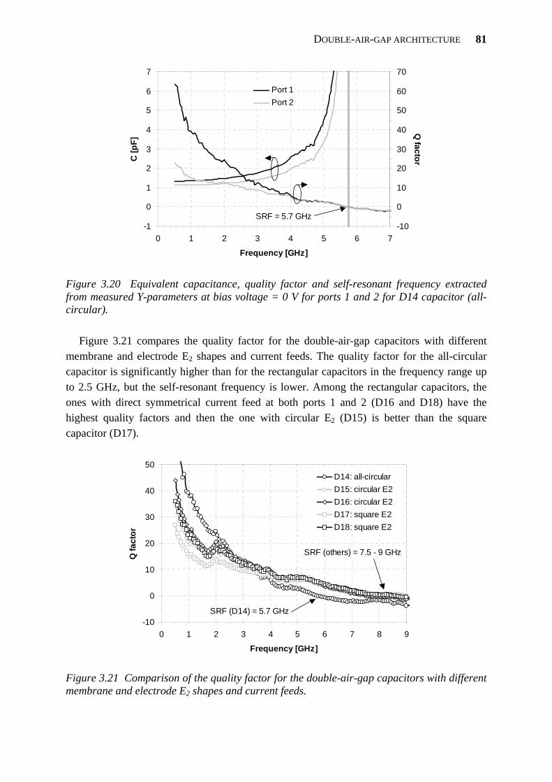
DOUBLE-AIR-GAP ARCHITECTURE
81
-1
0
1
2
3
4
5
6
7
0 1 2 3 4 5 6 7
Frequency [GHz]
C [p
F]
-10
0
10
20
30
40
50
60
70
Q factor
Port 1Port 2
SRF = 5.7 GHz
Figure 3.20 Equivalent capacitance, quality factor and self-resonant frequency extracted from measured Y-parameters at bias voltage = 0 V for ports 1 and 2 for D14 capacitor (all-circular).
Figure 3.21 compares the quality factor for the double-air-gap capacitors with different
membrane and electrode E2 shapes and current feeds. The quality factor for the all-circular capacitor is significantly higher than for the rectangular capacitors in the frequency range up to 2.5 GHz, but the self-resonant frequency is lower. Among the rectangular capacitors, the ones with direct symmetrical current feed at both ports 1 and 2 (D16 and D18) have the highest quality factors and then the one with circular E2 (D15) is better than the square capacitor (D17).
-10
0
10
20
30
40
50
0 1 2 3 4 5 6 7 8 9
Frequency [GHz]
Q fa
ctor
D14: all-circularD15: circular E2D16: circular E2D17: square E2D18: square E2
SRF (others) = 7.5 - 9 GHz
SRF (D14) = 5.7 GHz
Figure 3.21 Comparison of the quality factor for the double-air-gap capacitors with different membrane and electrode E2 shapes and current feeds.
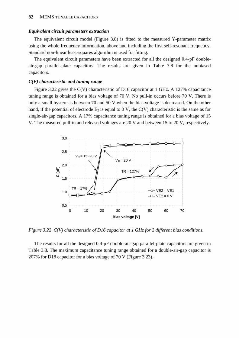
MEMS TUNABLE CAPACITORS
82
Equivalent circuit parameters extraction The equivalent circuit model (Figure 3.8) is fitted to the measured Y-parameter matrix
using the whole frequency information, above and including the first self-resonant frequency. Standard non-linear least-squares algorithm is used for fitting.
The equivalent circuit parameters have been extracted for all the designed 0.4-pF double-air-gap parallel-plate capacitors. The results are given in Table 3.8 for the unbiased capacitors.
C(V) characteristic and tuning range Figure 3.22 gives the C(V) characteristic of D16 capacitor at 1 GHz. A 127% capacitance
tuning range is obtained for a bias voltage of 70 V. No pull-in occurs before 70 V. There is only a small hysteresis between 70 and 50 V when the bias voltage is decreased. On the other hand, if the potential of electrode E2 is equal to 0 V, the C(V) characteristic is the same as for single-air-gap capacitors. A 17% capacitance tuning range is obtained for a bias voltage of 15 V. The measured pull-in and released voltages are 20 V and between 15 to 20 V, respectively.
0.5
1.0
1.5
2.0
2.5
3.0
0 10 20 30 40 50 60 70
Bias voltage [V]
C [p
F]
VE2 = VE1VE2 = 0 V
TR = 127%
VPI = 20 VVR = 15 -20 V
TR = 17%
Figure 3.22 C(V) characteristic of D16 capacitor at 1 GHz for 2 different bias conditions.
The results for all the designed 0.4-pF double-air-gap parallel-plate capacitors are given in
Table 3.8. The maximum capacitance tuning range obtained for a double-air-gap capacitor is 207% for D18 capacitor for a bias voltage of 70 V (Figure 3.23).
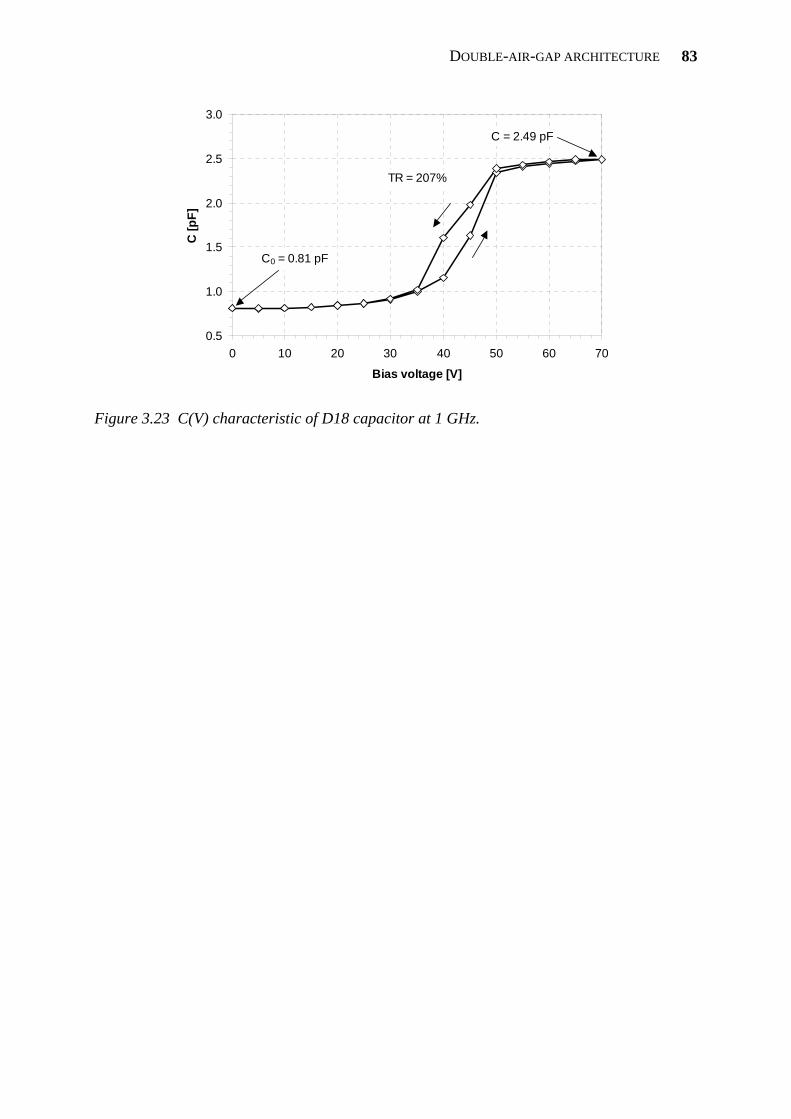
DOUBLE-AIR-GAP ARCHITECTURE
83
0.5
1.0
1.5
2.0
2.5
3.0
0 10 20 30 40 50 60 70
Bias voltage [V]
C [p
F]
C0 = 0.81 pF
C = 2.49 pF
TR = 207%
Figure 3.23 C(V) characteristic of D18 capacitor at 1 GHz.
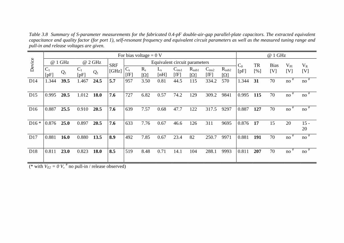
Table 3.8 Summary of S-parameter measurements for the fabricated 0.4-pF double-air-gap parallel-plate capacitors. The extracted equivalent capacitance and quality factor (for port 1), self-resonant frequency and equivalent circuit parameters as well as the measured tuning range and pull-in and release voltages are given.
For bias voltage = 0 V @ 1 GHz @ 1 GHz @ 2 GHz Equivalent circuit parameters
Dev
ice
C1 [pF] Q1
C1 [pF] Q1
SRF [GHz] Cs
[fF] Rs [Ω]
Ls [nH]
Cins1 [fF]
Rsub1 [Ω]
Cins2 [fF]
Rsub2 [Ω]
C0 [pF]
TR [%]
Bias [V]
VPI [V]
VR [V]
D14 1.344 39.5 1.467 24.5 5.7 957 3.50 0.81 44.5 115 334.2 570 1.344 31 70 no # no #
D15 0.995 20.5 1.012 18.0 7.6 727 6.82 0.57 74.2 129 309.2 9841 0.995 115 70 no # no #
D16 0.887 25.5 0.910 20.5 7.6 639 7.57 0.68 47.7 122 317.5 9297 0.887 127 70 no # no #
D16 * 0.876 25.0 0.897 20.5 7.6 633 7.76 0.67 46.6 126 311 9695 0.876 17 15 20 15 - 20
D17 0.881 16.0 0.880 13.5 8.9 492 7.85 0.67 23.4 82 250.7 9971 0.881 191 70 no # no #
D18 0.811 23.0 0.823 18.0 8.5 519 8.48 0.71 14.1 104 288.1 9993 0.811 207 70 no # no #
(* with VE2 = 0 V, # no pull-in / release observed)
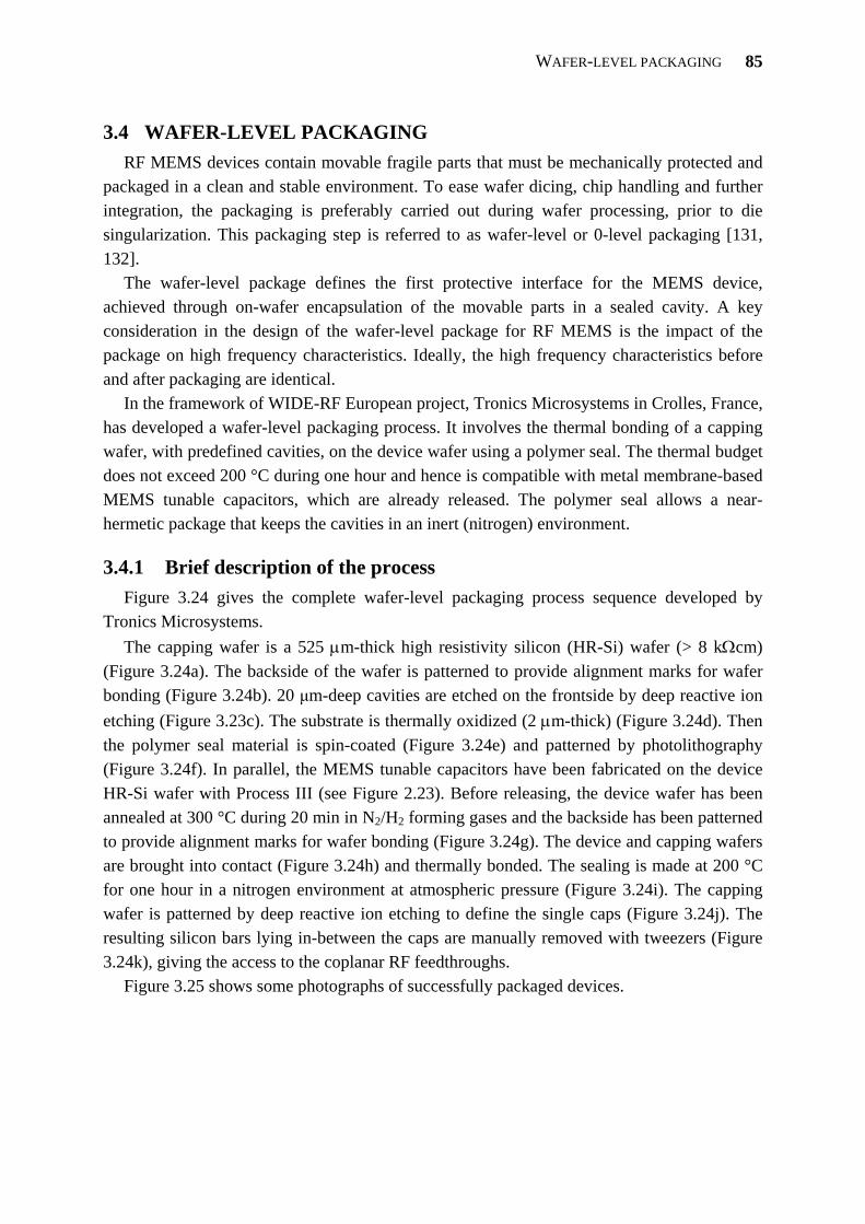
WAFER-LEVEL PACKAGING
85
3.4 WAFER-LEVEL PACKAGING RF MEMS devices contain movable fragile parts that must be mechanically protected and
packaged in a clean and stable environment. To ease wafer dicing, chip handling and further integration, the packaging is preferably carried out during wafer processing, prior to die singularization. This packaging step is referred to as wafer-level or 0-level packaging [131, 132].
The wafer-level package defines the first protective interface for the MEMS device, achieved through on-wafer encapsulation of the movable parts in a sealed cavity. A key consideration in the design of the wafer-level package for RF MEMS is the impact of the package on high frequency characteristics. Ideally, the high frequency characteristics before and after packaging are identical.
In the framework of WIDE-RF European project, Tronics Microsystems in Crolles, France, has developed a wafer-level packaging process. It involves the thermal bonding of a capping wafer, with predefined cavities, on the device wafer using a polymer seal. The thermal budget does not exceed 200 °C during one hour and hence is compatible with metal membrane-based MEMS tunable capacitors, which are already released. The polymer seal allows a near-hermetic package that keeps the cavities in an inert (nitrogen) environment.
3.4.1 Brief description of the process Figure 3.24 gives the complete wafer-level packaging process sequence developed by
Tronics Microsystems. The capping wafer is a 525 μm-thick high resistivity silicon (HR-Si) wafer (> 8 kΩcm)
(Figure 3.24a). The backside of the wafer is patterned to provide alignment marks for wafer bonding (Figure 3.24b). 20 μm-deep cavities are etched on the frontside by deep reactive ion etching (Figure 3.23c). The substrate is thermally oxidized (2 μm-thick) (Figure 3.24d). Then the polymer seal material is spin-coated (Figure 3.24e) and patterned by photolithography (Figure 3.24f). In parallel, the MEMS tunable capacitors have been fabricated on the device HR-Si wafer with Process III (see Figure 2.23). Before releasing, the device wafer has been annealed at 300 °C during 20 min in N2/H2 forming gases and the backside has been patterned to provide alignment marks for wafer bonding (Figure 3.24g). The device and capping wafers are brought into contact (Figure 3.24h) and thermally bonded. The sealing is made at 200 °C for one hour in a nitrogen environment at atmospheric pressure (Figure 3.24i). The capping wafer is patterned by deep reactive ion etching to define the single caps (Figure 3.24j). The resulting silicon bars lying in-between the caps are manually removed with tweezers (Figure 3.24k), giving the access to the coplanar RF feedthroughs.
Figure 3.25 shows some photographs of successfully packaged devices.
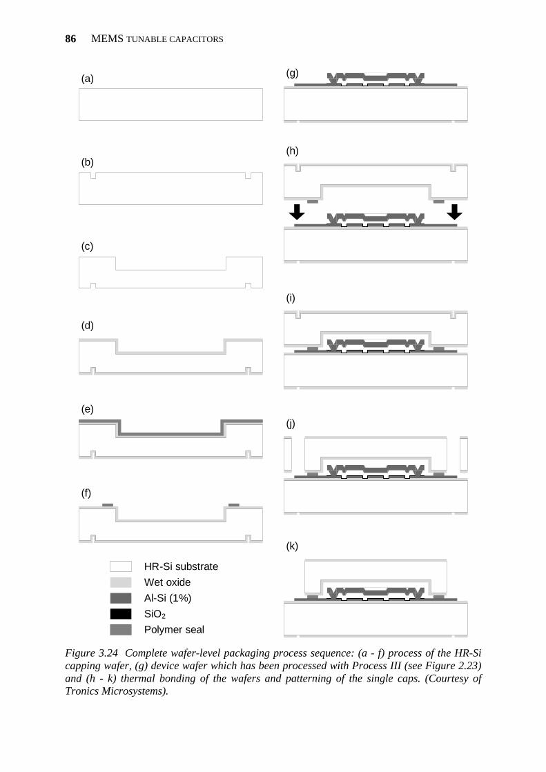
MEMS TUNABLE CAPACITORS
86
(a)
HR-Si substrateWet oxideAl-Si (1%)SiO2
Polymer seal
(b)
(c)
(d)
(e)
(f)
(h)
(i)
(j)
(k)
(g)
Figure 3.24 Complete wafer-level packaging process sequence: (a - f) process of the HR-Si capping wafer, (g) device wafer which has been processed with Process III (see Figure 2.23) and (h - k) thermal bonding of the wafers and patterning of the single caps. (Courtesy of Tronics Microsystems).
WAFER-LEVEL PACKAGING
87
(a)
(b)
(c)
(d)
Figure 3.25 (a) Photograph of a wafer with packaged devices, (b) close-up view of the HR-Si caps, (c) SEM microphotograph of a cap with the coplanar RF feedthroughs and (d) infrared microphotograph of a packaged MEMS tunable capacitor. (Courtesy of Tronics Microsystems).
3.4.2 Effect on RF performance There are four main issues that determine the RF characteristics of the wafer-level
package: (1) the resistive losses of the RF feedthroughs, (2) the reflection at the package boundary and (3) the losses and (4) the detuning of the transmission lines due to proximity coupling to the cap [133].
The impact of the package on RF performance has been investigated by measuring the S-parameters of traversing CPW lines on HR-Si substrates with and without the HR-Si package. The cavity depth is 20 μm. Figure 3.26 shows the measured return (S11) and insertion (S21) losses of a traversing CPW line on HR-Si (1.55 mm-long, 70 μm-wide, 1 μm-thick Al-Si (1%)) with and without HR-Si package. No significant impact on the matching and the insertion loss is observed.
The HR-Si package could be modeled as a 2-port π network as shown in Figure 3.27.
Cavity
Polymer seal
Metal lines
MEMS capacitor
100 μm
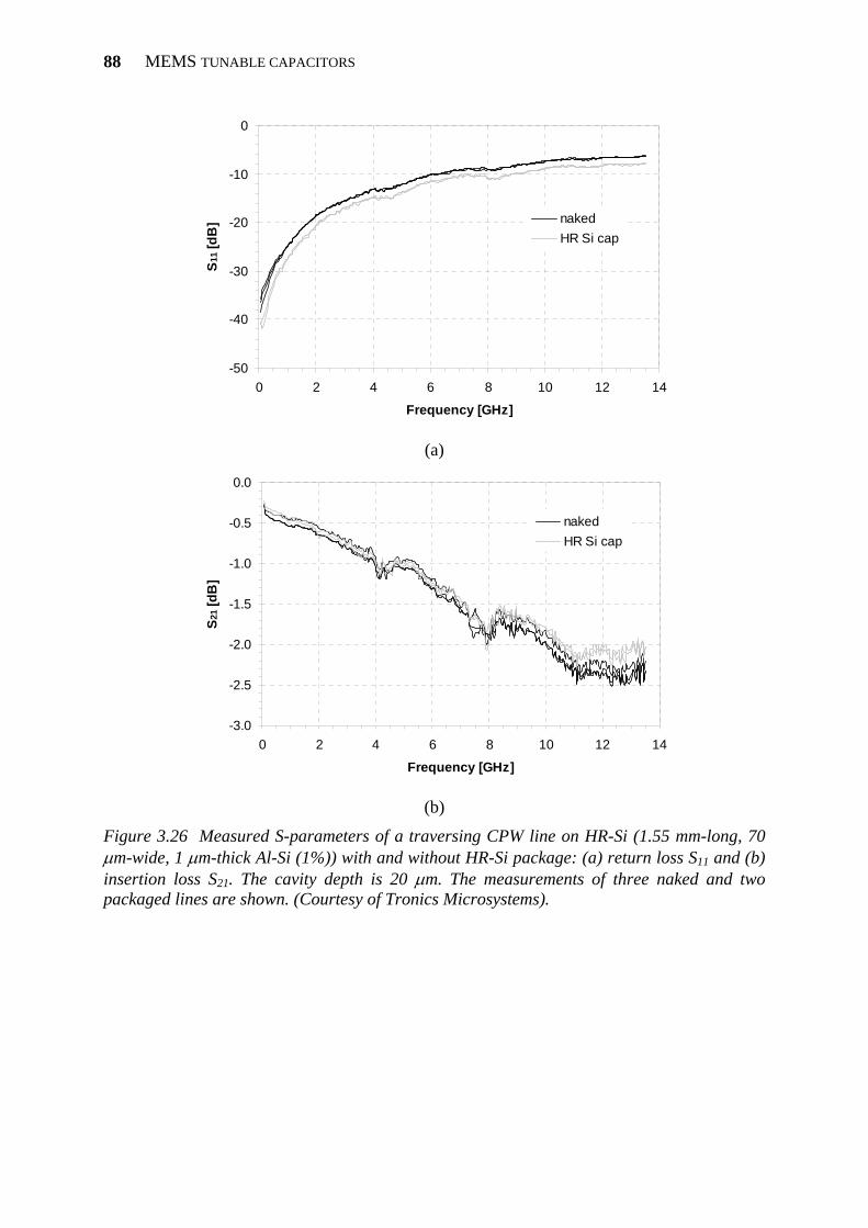
MEMS TUNABLE CAPACITORS
88
-50
-40
-30
-20
-10
0
0 2 4 6 8 10 12 14
Frequency [GHz]
S11 [
dB] naked
HR Si cap
(a)
-3.0
-2.5
-2.0
-1.5
-1.0
-0.5
0.0
0 2 4 6 8 10 12 14
Frequency [GHz]
S21 [
dB]
nakedHR Si cap
(b)
Figure 3.26 Measured S-parameters of a traversing CPW line on HR-Si (1.55 mm-long, 70 μm-wide, 1 μm-thick Al-Si (1%)) with and without HR-Si package: (a) return loss S11 and (b) insertion loss S21. The cavity depth is 20 μm. The measurements of three naked and two packaged lines are shown. (Courtesy of Tronics Microsystems).
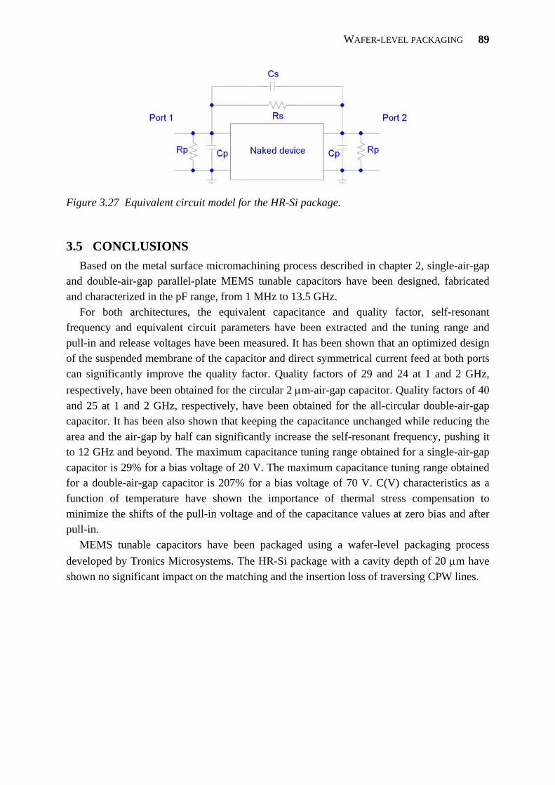
WAFER-LEVEL PACKAGING
89
Figure 3.27 Equivalent circuit model for the HR-Si package.
3.5 CONCLUSIONS Based on the metal surface micromachining process described in chapter 2, single-air-gap
and double-air-gap parallel-plate MEMS tunable capacitors have been designed, fabricated and characterized in the pF range, from 1 MHz to 13.5 GHz.
For both architectures, the equivalent capacitance and quality factor, self-resonant frequency and equivalent circuit parameters have been extracted and the tuning range and pull-in and release voltages have been measured. It has been shown that an optimized design of the suspended membrane of the capacitor and direct symmetrical current feed at both ports can significantly improve the quality factor. Quality factors of 29 and 24 at 1 and 2 GHz, respectively, have been obtained for the circular 2 μm-air-gap capacitor. Quality factors of 40 and 25 at 1 and 2 GHz, respectively, have been obtained for the all-circular double-air-gap capacitor. It has been also shown that keeping the capacitance unchanged while reducing the area and the air-gap by half can significantly increase the self-resonant frequency, pushing it to 12 GHz and beyond. The maximum capacitance tuning range obtained for a single-air-gap capacitor is 29% for a bias voltage of 20 V. The maximum capacitance tuning range obtained for a double-air-gap capacitor is 207% for a bias voltage of 70 V. C(V) characteristics as a function of temperature have shown the importance of thermal stress compensation to minimize the shifts of the pull-in voltage and of the capacitance values at zero bias and after pull-in.
MEMS tunable capacitors have been packaged using a wafer-level packaging process developed by Tronics Microsystems. The HR-Si package with a cavity depth of 20 μm have shown no significant impact on the matching and the insertion loss of traversing CPW lines.

Chapter 4 Voltage-controlled oscillators (VCOs)

Previous pageOptical microphotograph of a voltage-
controlled oscillator (VCO)with above-IC MEMS LC tank. (Scale: the width of the EPFL logo is 450 μm)
4.1 INTRODUCTION Integrated LC voltage-controlled oscillators (VCOs) are common functional blocks in
modern radiofrequency communication systems and are widely used in phase-locked loops (PLLs) and frequency synthesizers to realize a precise reference frequency. Very stringent requirements are placed on the spectral purity of reference oscillators and the demand for increased efforts to improve the phase-noise performance [134]. Since the phase noise of LC oscillators is inversely proportional to the quality factor of the LC tank, inductors and varactors with high Q factors are needed. Recent progress in MEMS technologies has opened new possibilities in realizing such high-Q passive components.
4.1.1 State-of-the-art of MEMS-based LC VCOs In 1997, Young and Boser [135] reported a low-noise micromachined voltage-controlled
oscillator. Parallel-plate MEMS variable capacitors along with a discrete commercially available 8.2-nH inductor and a separately-fabricated CMOS circuit were attached to a test-board surface and wire-bonded to form the VCO. The measurement results showed that the prototype oscillated at a center frequency of 714 MHz and could be tuned from 707 to 721 MHz over a DC voltage of 5.5 V. The phase noise was -107 dBc/Hz at an offset frequency of 100 kHz. In 1999, Young et al. [136] proposed a VCO prototype with the same MEMS variable capacitors and a 5 mm-long bondwire 6-nH inductor. It achieved -105 dBc/Hz phase noise at 100 kHz offset frequency from a 1.028-GHz carrier. The oscillator could be tuned over 20 MHz with 3 V and dissipated 3.8 mA from a 3.3 V supply. In 2001, Young et al. [137] implemented a VCO with always the same MEMS variable capacitors but with a micromachined three-dimensional coil inductor. It achieved -106 dBc/Hz phase noise at 100 kHz offset frequency from a 863-MHz carrier. At 3 MHz offset frequency, the phase noise is -136 dBc/Hz. The oscillator is tunable from 851 to 863 MHz with 3 V.
In 2000, Dec and Suyama [138] reported a 1.9-GHz CMOS VCO where the resonant circuit consisted of micromachined electromechanically tunable capacitors and a bondwire 3.5-nH inductor. The tunable capacitors were implemented in a MUMPs polysilicon surface micromachining process. The active circuits were fabricated in a 0.5-μm CMOS process. The VCO was assembled in a ceramic package where the MUMPs and CMOS chips were bonded together. The experimental VCO achieved a phase noise of -98 dBc/Hz and -126 dBc/Hz at 100 kHz and 600 kHz offsets from the carrier, respectively. The tuning range of the VCO was 9%. The VCO circuit and the output buffer consumed 15 and 30 mW from a 2.7-V power supply, respectively. They demonstrated further results with the same approach [139]. The oscillator operated at 2.4 GHz, achieved a phase noise of -122 dBc/Hz at 1 MHz offset from the carrier and exhibited a tuning range of 3.4%.
In 2002, Innocent et al. [140] proposed two 5-GHz oscillators in 0.35-μm CMOS. The active part was flip-chip mounted on the passive part which was realized in two different technologies. The version with MOS varicaps used an MCM inductor while the version with MEMS varicaps used an inductor in the MEMS technology. The MOS varicap-based VCO had a worst case phase noise of -89 dBc/Hz at 100 kHz offset, in the middle of its tuning
VOLTAGE-CONTROLLED OSCILLATORS (VCOS)
94
range. The MEMS-varicap based VCO had a phase noise of -94 dBc/Hz at 100 kHz offset with zero tuning voltage. The phase noise was expected to stay almost constant over the tuning range, so it was a 5 dB improvement over the MOS varicap-based VCO.
In 2004, Ramachandran et al. [141] reported a voltage-controlled oscillator whose LC tank consisted of micromachined high-Q 6.25-nH inductors, MEMS reconfigurable capacitors for digital tuning between 1.8 and 3.1 GHz and foundry-provided varactor diodes for analog tuning of 150 MHz around these two set points. The carrier frequencies obtained as a result of the digital tuning were 2.75 (Cmin configuration) and 2.15 GHz (Cmax configuration). Along with analog tuning, the minimum and maximum frequencies obtained were 2.1 and 2.8 GHz, respectively, resulting in a tuning range of 30% for a center frequency of 2.45 GHz. The VCO achieved a phase noise of -104, -118, -122 and -129 dBc/Hz at 100, 600 kHz, 1 and 3 MHz offsets from a carrier at 2.2 GHz, respectively.
In 2006, Paillard et al. [142] reported an hybrid 1.3 - 1.8 GHz MCM VCO dedicated to C and Ku band receivers frequency conversion modules in satellite payloads. The LC tank consisted of MEMS tunable capacitors and gold bondwires as high-Q inductors. RF measurements demonstrated VCO oscillations around 1.60 GHz with continuous tuning between 1.70 and 1.45 GHz when the MEMS tunable capacitors were actuated between 0 and 25 V. The phase noise measured for an actuation voltage of 20 V was better than -100 dBc/Hz at 100 kHz and -125 dBc/Hz at 1 MHz offset from the carrier.
Gaddi et al. [143] proposed a reconfigurable MEMS-enabled LC-tank network for a multi-band RF oscillator, made of ohmic RF MEMS switches, spiral suspended inductors and metal-insulator-metal (MIM) capacitors all integrated on a high resistivity silicon MEMS substrate. The LC-tank is connected to a differential cross-coupled nMOS pair on a separate CMOS substrate, by chip-on-chip integration and wire bonding. Two resonant frequencies of 1.375 and 3.605 GHz were obtained for the standalone LC tank for the up-state and down-state of switch, respectively. The complete oscillator showed a 17% frequency down-shift for the up-state LC-tank configuration compared to the LC tank giving an oscillator frequency of 1.17 GHz. The phase noise was -125 dBc/Hz at 1 MHz frequency offset.
In 2006, Kawashima et al. [144] proposed a dual-band VCO integrated with RF MEMS devices using flip-chip mounting. A wide frequency band switching capability was realized using low-loss RF MEMS switches and high-Q inductors to switch one series-connected inductors. The analog tuning was obtained with standard varactors. When the RF MEMS switches were turned off and the tuning voltage varied from 0 to 6V, the carrier frequency of the fabricated VCO varied from 4.443 to 4.695 GHz. When the RF MEMS switches were turned on and the tuning voltage varied from 0V to 6V, the carrier frequency of the fabricated VCO varied from 5.106 to 5.411 GHz. The measured phase noise at lower band was -103 dBc/Hz at a 1 MHz offset from the carrier frequency of 4.443 GHz. The measured phase noise at high band was -97 dBc/Hz at a 1 MHz offset from the carrier frequency of 5.106 GHz.
In 2006, Coustou et al. [145] reported the comparison of 10-GHz VCOs with two realizations of the LC tank: first a full monolithic architecture in which the variable LC tank was composed of spiral inductors and p+/n-well varactors and then a MEMS-based
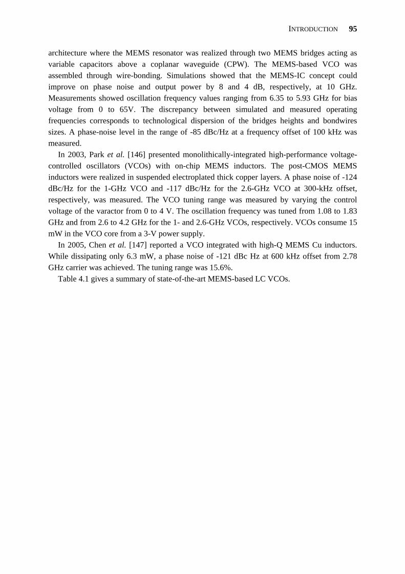
INTRODUCTION
95
architecture where the MEMS resonator was realized through two MEMS bridges acting as variable capacitors above a coplanar waveguide (CPW). The MEMS-based VCO was assembled through wire-bonding. Simulations showed that the MEMS-IC concept could improve on phase noise and output power by 8 and 4 dB, respectively, at 10 GHz. Measurements showed oscillation frequency values ranging from 6.35 to 5.93 GHz for bias voltage from 0 to 65V. The discrepancy between simulated and measured operating frequencies corresponds to technological dispersion of the bridges heights and bondwires sizes. A phase-noise level in the range of -85 dBc/Hz at a frequency offset of 100 kHz was measured.
In 2003, Park et al. [146] presented monolithically-integrated high-performance voltage-controlled oscillators (VCOs) with on-chip MEMS inductors. The post-CMOS MEMS inductors were realized in suspended electroplated thick copper layers. A phase noise of -124 dBc/Hz for the 1-GHz VCO and -117 dBc/Hz for the 2.6-GHz VCO at 300-kHz offset, respectively, was measured. The VCO tuning range was measured by varying the control voltage of the varactor from 0 to 4 V. The oscillation frequency was tuned from 1.08 to 1.83 GHz and from 2.6 to 4.2 GHz for the 1- and 2.6-GHz VCOs, respectively. VCOs consume 15 mW in the VCO core from a 3-V power supply.
In 2005, Chen et al. [147] reported a VCO integrated with high-Q MEMS Cu inductors. While dissipating only 6.3 mW, a phase noise of -121 dBc Hz at 600 kHz offset from 2.78 GHz carrier was achieved. The tuning range was 15.6%.
Table 4.1 gives a summary of state-of-the-art MEMS-based LC VCOs.
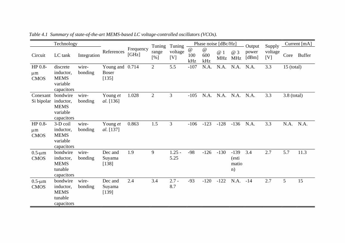
Table 4.1 Summary of state-of-the-art MEMS-based LC voltage-controlled oscillators (VCOs).
Technology Phase noise [dBc/Hz] Current [mA]
Circuit LC tank Integration References Frequency
[GHz]
Tuning range [%]
Tuning voltage [V]
@ 100 kHz
@ 600 kHz
@ 1 MHz
@ 3 MHz
Output power [dBm]
Supply voltage [V] Core Buffer
HP 0.8-μm CMOS
discrete inductor, MEMS variable capacitors
wire-bonding
Young and Boser [135]
0.714 2 5.5 -107 N.A. N.A. N.A. N.A. 3.3 15 (total)
Conexant Si bipolar
bondwire inductor, MEMS variable capacitors
wire-bonding
Young et al. [136]
1.028 2 3 -105 N.A. N.A. N.A. N.A. 3.3 3.8 (total)
HP 0.8-μm CMOS
3-D coil inductor, MEMS variable capacitors
wire-bonding
Young et al. [137]
0.863 1.5 3 -106 -123 -128 -136 N.A. 3.3 N.A. N.A.
0.5-μm CMOS
bondwire inductor, MEMS tunable capacitors
wire-bonding
Dec and Suyama [138]
1.9 9 1.25 - 5.25
-98 -126 -130 -139 (estimation)
3.4 2.7 5.7 11.3
0.5-μm CMOS
bondwire inductor, MEMS tunable capacitors
wire-bonding
Dec and Suyama [139]
2.4 3.4 2.7 - 8.7
-93 -120 -122 N.A. -14 2.7 5 15
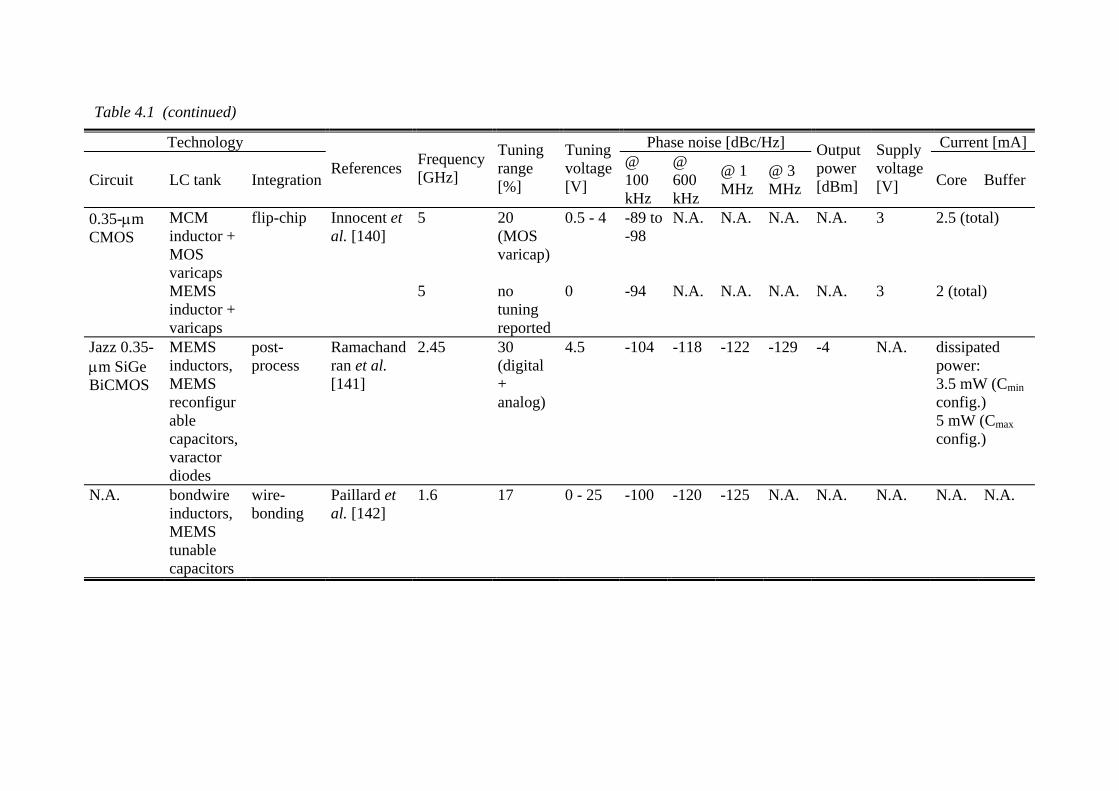
Table 4.1 (continued)
Technology Phase noise [dBc/Hz] Current [mA]
Circuit LC tank Integration References Frequency
[GHz]
Tuning range [%]
Tuning voltage [V]
@ 100 kHz
@ 600 kHz
@ 1 MHz
@ 3 MHz
Output power [dBm]
Supply voltage [V] Core Buffer
0.35-μm CMOS
MCM inductor + MOS varicaps MEMS inductor + varicaps
flip-chip Innocent et al. [140]
5 5
20 (MOS varicap) no tuning reported
0.5 - 4 0
-89 to -98 -94
N.A. N.A.
N.A. N.A.
N.A. N.A.
N.A. N.A.
3 3
2.5 (total) 2 (total)
Jazz 0.35-μm SiGe BiCMOS
MEMS inductors, MEMS reconfigurable capacitors, varactor diodes
post-process
Ramachandran et al. [141]
2.45 30 (digital + analog)
4.5 -104 -118 -122 -129 -4 N.A. dissipated power: 3.5 mW (Cmin config.) 5 mW (Cmax config.)
N.A. bondwire inductors, MEMS tunable capacitors
wire-bonding
Paillard et al. [142]
1.6 17 0 - 25 -100 -120 -125 N.A. N.A. N.A. N.A. N.A.
Table 4.1 (continued)
Technology Phase noise [dBc/Hz] Current [mA]
Circuit LC tank Integration References Frequency
[GHz]
Tuning range [%]
Tuning voltage [V]
@ 100 kHz
@ 600 kHz
@ 1 MHz
@ 3 MHz
Output power [dBm]
Supply voltage [V] Core Buffer
STM 0.13-μm CMOS
ohmic RF MEMS switches, spiral suspended inductors, MIM capacitors
chip-on-chip, wire-bonding
Gaddi et al. [143]
1.17 no tuning reported for the oscillator
0 -100 -120 -125 N.A. 1.8 1.2 3 (bias)
SiGe BiCMOS
RF MEMS switches, MEMS inductors, standard varactors
flip-chip Kawashima et al. [144]
4.443 5.106
22 (digital + analog)
0 - 6 (analog)
N.A. N.A. -103 -97
N.A. -13 -13
2 N.A. N.A.
STM 0.35-μm SiGe BiCMOS
spiral inductors from BiCMOS process, MEMS variable capacitors above CPW
wire-bonding
Coustou et al. [145]
6.35 7 0 - 65 -85 N.A. N.A. N.A. N.A. N.A. N.A. N.A.
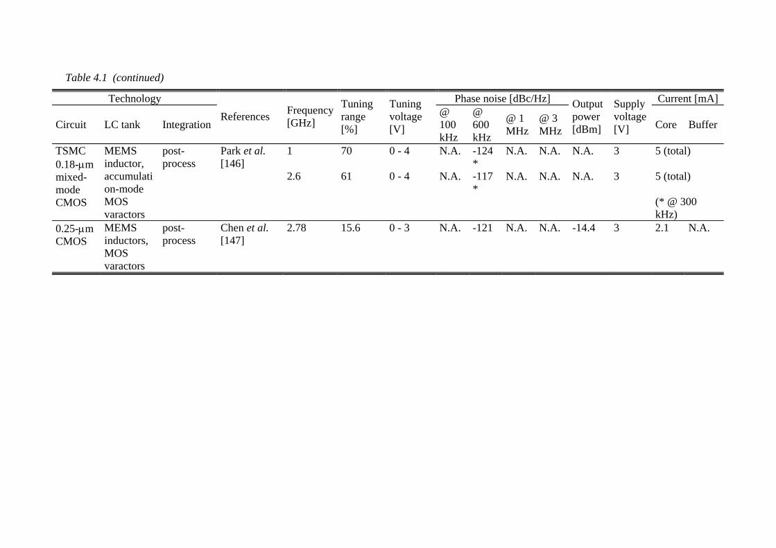
Table 4.1 (continued)
Technology Phase noise [dBc/Hz] Current [mA]
Circuit LC tank Integration References Frequency
[GHz]
Tuning range [%]
Tuning voltage [V]
@ 100 kHz
@ 600 kHz
@ 1 MHz
@ 3 MHz
Output power [dBm]
Supply voltage [V] Core Buffer
TSMC 0.18-μm mixed-mode CMOS
MEMS inductor, accumulation-mode MOS varactors
post-process
Park et al. [146]
1 2.6
70 61
0 - 4 0 - 4
N.A. N.A.
-124 * -117 *
N.A. N.A.
N.A. N.A.
N.A. N.A.
3 3
5 (total) 5 (total) (* @ 300 kHz)
0.25-μm CMOS
MEMS inductors, MOS varactors
post-process
Chen et al. [147]
2.78 15.6 0 - 3 N.A. -121 N.A. N.A. -14.4 3 2.1 N.A.
VOLTAGE-CONTROLLED OSCILLATORS (VCOS)
100
4.2 DESCRIPTION OF THE INTEGRATED CIRCUIT Integrated voltage-controlled oscillators (VCOs) have been implemented using the X-FAB
XB06 0.6-μm BiCMOS process [148]. Its key features include 0.6-μm double polysilicon, double metal n-well CMOS process, high frequency npn transistors with polysilicon emitter and buried collector and special inductors in third thick metal M3 (2.3 μm-thick Al-Cu (0.5%)).
The designed VCO is a cross-coupled LC topology. The LC tank of the VCO is realized by using either X-FAB components and / or MEMS devices. The targeted operating frequency band is the 2.4 GHz ISM (Industrial, Medical and Scientific) band.
The electrical schematic of the VCO integrated circuit is shown in Figure 4.1. It consists of three sub-circuits:
- The cross-coupled LC voltage-controlled oscillator; - The amplitude control sub-circuit which controls the output amplitude of the VCO; - The output buffer which is designed in order to deliver power to a 50 Ω load. The inductance and varicap capacitance values are approximately 2 nH and 0.4 pF,
respectively.
Figure 4.1 Electrical schematic of the voltage-controlled oscillator (VCO) integrated circuit with three sub-circuits: the cross-coupled LC oscillator, the amplitude control part and the output buffer.
Four signals are imposed from outside the IC: - The supply voltage VDD which is 5 V in this technology; - The voltage signal VCTRL to control the center frequency of the oscillator through the
capacitance value of the varactors; - The voltage signal VAMPL to control the output amplitude of the oscillator; - The bias current IBUF of the output buffer.
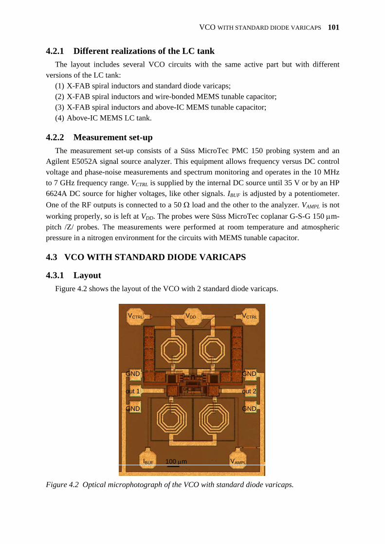
VCO WITH STANDARD DIODE VARICAPS
101
4.2.1 Different realizations of the LC tank The layout includes several VCO circuits with the same active part but with different
versions of the LC tank: (1) X-FAB spiral inductors and standard diode varicaps; (2) X-FAB spiral inductors and wire-bonded MEMS tunable capacitor; (3) X-FAB spiral inductors and above-IC MEMS tunable capacitor; (4) Above-IC MEMS LC tank.
4.2.2 Measurement set-up The measurement set-up consists of a Süss MicroTec PMC 150 probing system and an
Agilent E5052A signal source analyzer. This equipment allows frequency versus DC control voltage and phase-noise measurements and spectrum monitoring and operates in the 10 MHz to 7 GHz frequency range. VCTRL is supplied by the internal DC source until 35 V or by an HP 6624A DC source for higher voltages, like other signals. IBUF is adjusted by a potentiometer. One of the RF outputs is connected to a 50 Ω load and the other to the analyzer. VAMPL is not working properly, so is left at VDD. The probes were Süss MicroTec coplanar G-S-G 150 μm-pitch /Z/ probes. The measurements were performed at room temperature and atmospheric pressure in a nitrogen environment for the circuits with MEMS tunable capacitor.
4.3 VCO WITH STANDARD DIODE VARICAPS
4.3.1 Layout Figure 4.2 shows the layout of the VCO with 2 standard diode varicaps.
IBUF
VDDVCTRL
VAMPL
out 1 out 2
GND
GND
GND
GND
VCTRL
100 μm
Figure 4.2 Optical microphotograph of the VCO with standard diode varicaps.
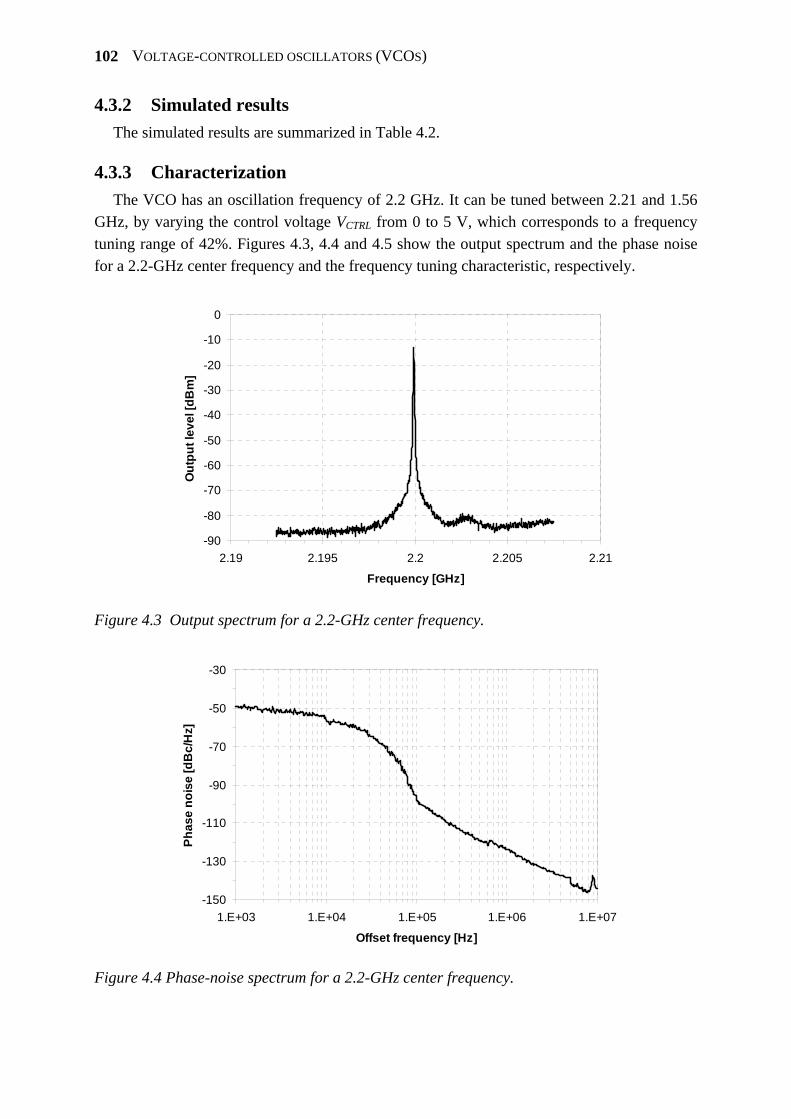
VOLTAGE-CONTROLLED OSCILLATORS (VCOS)
102
4.3.2 Simulated results The simulated results are summarized in Table 4.2.
4.3.3 Characterization The VCO has an oscillation frequency of 2.2 GHz. It can be tuned between 2.21 and 1.56
GHz, by varying the control voltage VCTRL from 0 to 5 V, which corresponds to a frequency tuning range of 42%. Figures 4.3, 4.4 and 4.5 show the output spectrum and the phase noise for a 2.2-GHz center frequency and the frequency tuning characteristic, respectively.
-90
-80
-70
-60
-50
-40
-30
-20
-10
0
2.19 2.195 2.2 2.205 2.21
Frequency [GHz]
Out
put l
evel
[dB
m]
Figure 4.3 Output spectrum for a 2.2-GHz center frequency.
-150
-130
-110
-90
-70
-50
-30
1.E+03 1.E+04 1.E+05 1.E+06 1.E+07
Offset frequency [Hz]
Phas
e no
ise
[dB
c/H
z]
Figure 4.4 Phase-noise spectrum for a 2.2-GHz center frequency.
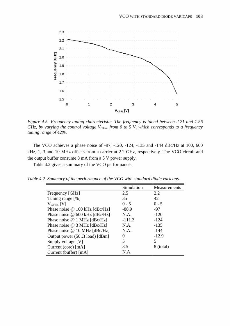
VCO WITH STANDARD DIODE VARICAPS
103
1.5
1.6
1.7
1.8
1.9
2.0
2.1
2.2
2.3
0 1 2 3 4 5
VCTRL [V]
Freq
uenc
y [G
Hz]
Figure 4.5 Frequency tuning characteristic. The frequency is tuned between 2.21 and 1.56 GHz, by varying the control voltage VCTRL from 0 to 5 V, which corresponds to a frequency tuning range of 42%.
The VCO achieves a phase noise of -97, -120, -124, -135 and -144 dBc/Hz at 100, 600
kHz, 1, 3 and 10 MHz offsets from a carrier at 2.2 GHz, respectively. The VCO circuit and the output buffer consume 8 mA from a 5 V power supply.
Table 4.2 gives a summary of the VCO performance.
Table 4.2 Summary of the performance of the VCO with standard diode varicaps.
Simulation Measurements Frequency [GHz] Tuning range [%] VCTRL [V] Phase noise @ 100 kHz [dBc/Hz] Phase noise @ 600 kHz [dBc/Hz] Phase noise @ 1 MHz [dBc/Hz] Phase noise @ 3 MHz [dBc/Hz] Phase noise @ 10 MHz [dBc/Hz] Output power (50 Ω load) [dBm] Supply voltage [V] Current (core) [mA] Current (buffer) [mA]
2.5 35 0 - 5 -88.9 N.A. -111.3 N.A. N.A. 0 5 3.5 N.A.
2.2 42 0 - 5 -97 -120 -124 -135 -144 -12.9 5 8 (total)
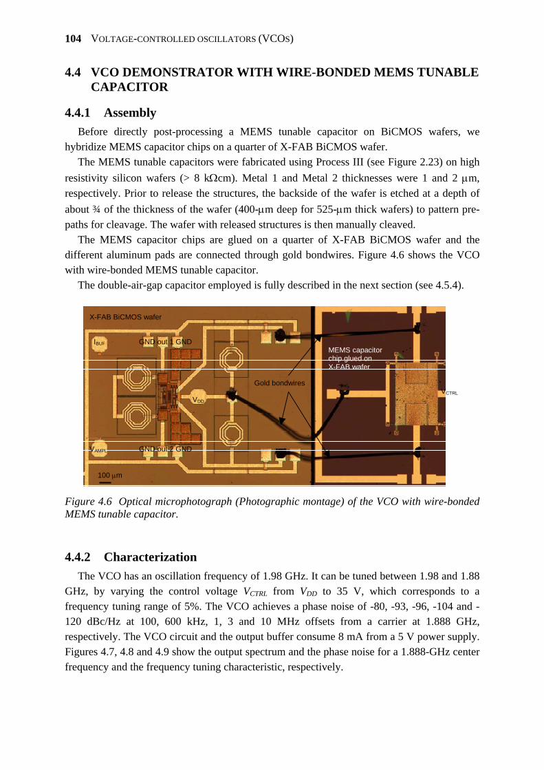
VOLTAGE-CONTROLLED OSCILLATORS (VCOS)
104
4.4 VCO DEMONSTRATOR WITH WIRE-BONDED MEMS TUNABLE CAPACITOR
4.4.1 Assembly Before directly post-processing a MEMS tunable capacitor on BiCMOS wafers, we
hybridize MEMS capacitor chips on a quarter of X-FAB BiCMOS wafer. The MEMS tunable capacitors were fabricated using Process III (see Figure 2.23) on high
resistivity silicon wafers (> 8 kΩcm). Metal 1 and Metal 2 thicknesses were 1 and 2 μm, respectively. Prior to release the structures, the backside of the wafer is etched at a depth of about ¾ of the thickness of the wafer (400-μm deep for 525-μm thick wafers) to pattern pre-paths for cleavage. The wafer with released structures is then manually cleaved.
The MEMS capacitor chips are glued on a quarter of X-FAB BiCMOS wafer and the different aluminum pads are connected through gold bondwires. Figure 4.6 shows the VCO with wire-bonded MEMS tunable capacitor.
The double-air-gap capacitor employed is fully described in the next section (see 4.5.4).
100 μm
IBUF
VDD VCTRL
VAMPL
GND out 1 GND
GND out 2 GND
X-FAB BiCMOS wafer
Gold bondwires
MEMS capacitor chip glued on X-FAB wafer
Figure 4.6 Optical microphotograph (Photographic montage) of the VCO with wire-bonded MEMS tunable capacitor.
4.4.2 Characterization The VCO has an oscillation frequency of 1.98 GHz. It can be tuned between 1.98 and 1.88
GHz, by varying the control voltage VCTRL from VDD to 35 V, which corresponds to a frequency tuning range of 5%. The VCO achieves a phase noise of -80, -93, -96, -104 and -120 dBc/Hz at 100, 600 kHz, 1, 3 and 10 MHz offsets from a carrier at 1.888 GHz, respectively. The VCO circuit and the output buffer consume 8 mA from a 5 V power supply. Figures 4.7, 4.8 and 4.9 show the output spectrum and the phase noise for a 1.888-GHz center frequency and the frequency tuning characteristic, respectively.
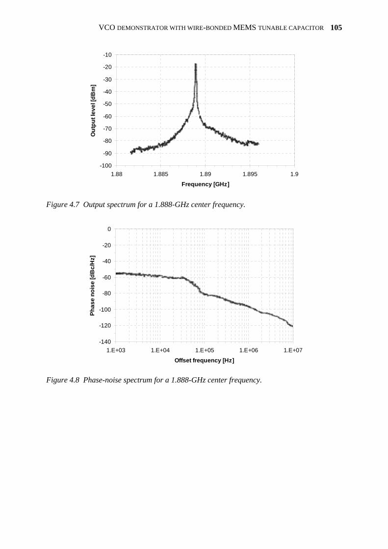
VCO DEMONSTRATOR WITH WIRE-BONDED MEMS TUNABLE CAPACITOR
105
-100
-90
-80
-70
-60
-50
-40
-30
-20
-10
1.88 1.885 1.89 1.895 1.9
Frequency [GHz]
Out
put l
evel
[dB
m]
Figure 4.7 Output spectrum for a 1.888-GHz center frequency.
-140
-120
-100
-80
-60
-40
-20
0
1.E+03 1.E+04 1.E+05 1.E+06 1.E+07
Offset frequency [Hz]
Phas
e no
ise
[dB
c/H
z]
Figure 4.8 Phase-noise spectrum for a 1.888-GHz center frequency.
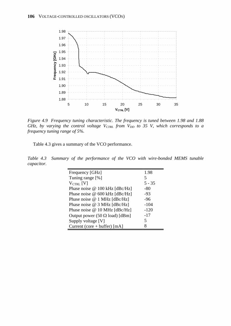
VOLTAGE-CONTROLLED OSCILLATORS (VCOS)
106
1.88
1.89
1.90
1.91
1.92
1.93
1.94
1.95
1.96
1.97
1.98
5 10 15 20 25 30 35VCTRL [V]
Freq
uenc
y [G
Hz]
Figure 4.9 Frequency tuning characteristic. The frequency is tuned between 1.98 and 1.88 GHz, by varying the control voltage VCTRL from VDD to 35 V, which corresponds to a frequency tuning range of 5%.
Table 4.3 gives a summary of the VCO performance.
Table 4.3 Summary of the performance of the VCO with wire-bonded MEMS tunable capacitor.
Frequency [GHz] Tuning range [%] VCTRL [V] Phase noise @ 100 kHz [dBc/Hz] Phase noise @ 600 kHz [dBc/Hz] Phase noise @ 1 MHz [dBc/Hz] Phase noise @ 3 MHz [dBc/Hz] Phase noise @ 10 MHz [dBc/Hz] Output power (50 Ω load) [dBm] Supply voltage [V] Current (core + buffer) [mA]
1.98 5 5 - 35 -80 -93 -96 -104 -120 -17 5 8
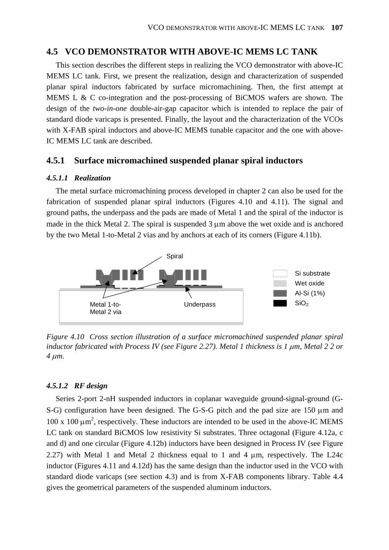
VCO DEMONSTRATOR WITH ABOVE-IC MEMS LC TANK
107
4.5 VCO DEMONSTRATOR WITH ABOVE-IC MEMS LC TANK This section describes the different steps in realizing the VCO demonstrator with above-IC
MEMS LC tank. First, we present the realization, design and characterization of suspended planar spiral inductors fabricated by surface micromachining. Then, the first attempt at MEMS L & C co-integration and the post-processing of BiCMOS wafers are shown. The design of the two-in-one double-air-gap capacitor which is intended to replace the pair of standard diode varicaps is presented. Finally, the layout and the characterization of the VCOs with X-FAB spiral inductors and above-IC MEMS tunable capacitor and the one with above-IC MEMS LC tank are described.
4.5.1 Surface micromachined suspended planar spiral inductors
4.5.1.1 Realization The metal surface micromachining process developed in chapter 2 can also be used for the
fabrication of suspended planar spiral inductors (Figures 4.10 and 4.11). The signal and ground paths, the underpass and the pads are made of Metal 1 and the spiral of the inductor is made in the thick Metal 2. The spiral is suspended 3 μm above the wet oxide and is anchored by the two Metal 1-to-Metal 2 vias and by anchors at each of its corners (Figure 4.11b).
Underpass
Spiral
Metal 1-to-Metal 2 via
Si substrateWet oxideAl-Si (1%)SiO2
Figure 4.10 Cross section illustration of a surface micromachined suspended planar spiral inductor fabricated with Process IV (see Figure 2.27). Metal 1 thickness is 1 μm, Metal 2 2 or 4 μm.
4.5.1.2 RF design Series 2-port 2-nH suspended inductors in coplanar waveguide ground-signal-ground (G-
S-G) configuration have been designed. The G-S-G pitch and the pad size are 150 μm and 100 x 100 μm2, respectively. These inductors are intended to be used in the above-IC MEMS LC tank on standard BiCMOS low resistivity Si substrates. Three octagonal (Figure 4.12a, c and d) and one circular (Figure 4.12b) inductors have been designed in Process IV (see Figure 2.27) with Metal 1 and Metal 2 thickness equal to 1 and 4 μm, respectively. The L24c inductor (Figures 4.11 and 4.12d) has the same design than the inductor used in the VCO with standard diode varicaps (see section 4.3) and is from X-FAB components library. Table 4.4 gives the geometrical parameters of the suspended aluminum inductors.
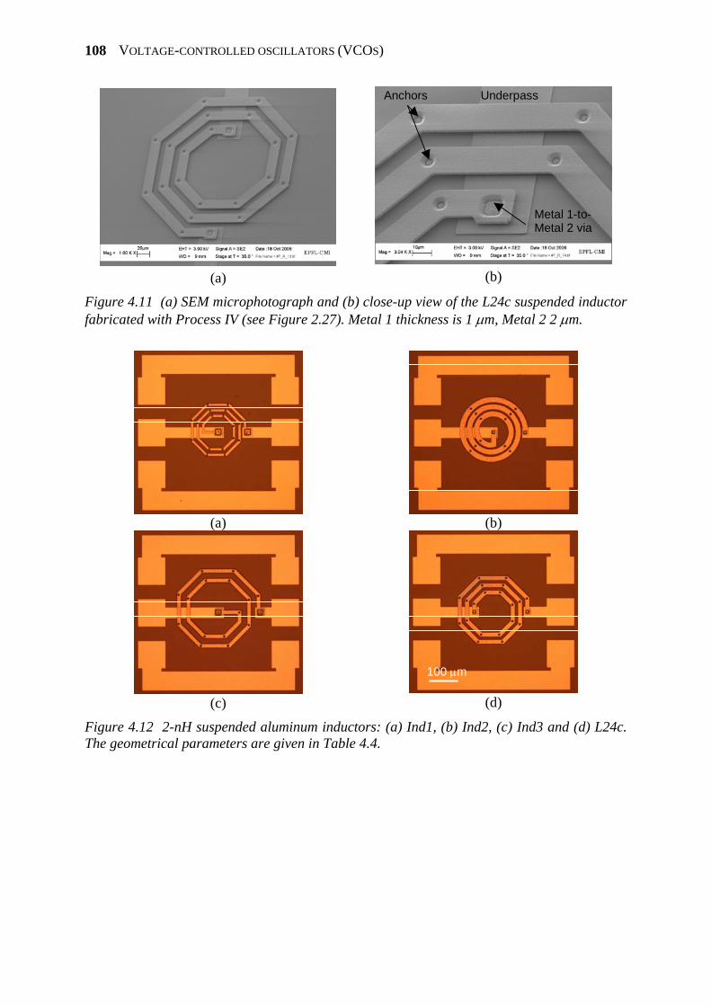
VOLTAGE-CONTROLLED OSCILLATORS (VCOS)
108
(a)
Underpass Anchors
Metal 1-to-Metal 2 via
(b)
Figure 4.11 (a) SEM microphotograph and (b) close-up view of the L24c suspended inductor fabricated with Process IV (see Figure 2.27). Metal 1 thickness is 1 μm, Metal 2 2 μm.
(a)
(b)
(c)
100 μm
(d)
Figure 4.12 2-nH suspended aluminum inductors: (a) Ind1, (b) Ind2, (c) Ind3 and (d) L24c. The geometrical parameters are given in Table 4.4.
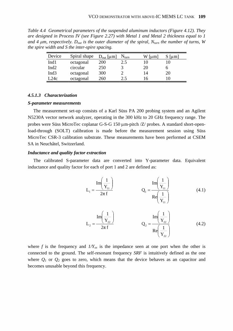
VCO DEMONSTRATOR WITH ABOVE-IC MEMS LC TANK
109
Table 4.4 Geometrical parameters of the suspended aluminum inductors (Figure 4.12). They are designed in Process IV (see Figure 2.27) with Metal 1 and Metal 2 thickness equal to 1 and 4 μm, respectively. Dout is the outer diameter of the spiral, Nturn the number of turns, W the spire width and S the inter-spire spacing.
Device Spiral shape Dout [μm] Nturn W [μm] S [μm] Ind1 octagonal 200 2.5 10 10 Ind2 circular 250 3 20 6 Ind3 octagonal 300 2 14 20 L24c octagonal 260 2.5 16 10
4.5.1.3 Characterization
S-parameter measurements
The measurement set-up consists of a Karl Süss PA 200 probing system and an Agilent N5230A vector network analyzer, operating in the 300 kHz to 20 GHz frequency range. The probes were Süss MicroTec coplanar G-S-G 150 μm-pitch /Z/ probes. A standard short-open-load-through (SOLT) calibration is made before the measurement session using Süss MicroTec CSR-3 calibration substrate. These measurements have been performed at CSEM SA in Neuchâtel, Switzerland.
Inductance and quality factor extraction The calibrated S-parameter data are converted into Y-parameter data. Equivalent
inductance and quality factor for each of port 1 and 2 are defined as:
f2πY1Im
L 111
⎟⎟⎠
⎞⎜⎜⎝
⎛
=
⎟⎟⎠
⎞⎜⎜⎝
⎛
⎟⎟⎠
⎞⎜⎜⎝
⎛
=
11
111
Y1Re
Y1Im
Q (4.1)
f2πY1Im
L 222
⎟⎟⎠
⎞⎜⎜⎝
⎛
=
⎟⎟⎠
⎞⎜⎜⎝
⎛
⎟⎟⎠
⎞⎜⎜⎝
⎛
=
22
222
Y1Re
Y1Im
Q (4.2)
where f is the frequency and 1/Yxx is the impedance seen at one port when the other is connected to the ground. The self-resonant frequency SRF is intuitively defined as the one where Q1 or Q2 goes to zero, which means that the device behaves as an capacitor and becomes unusable beyond this frequency.
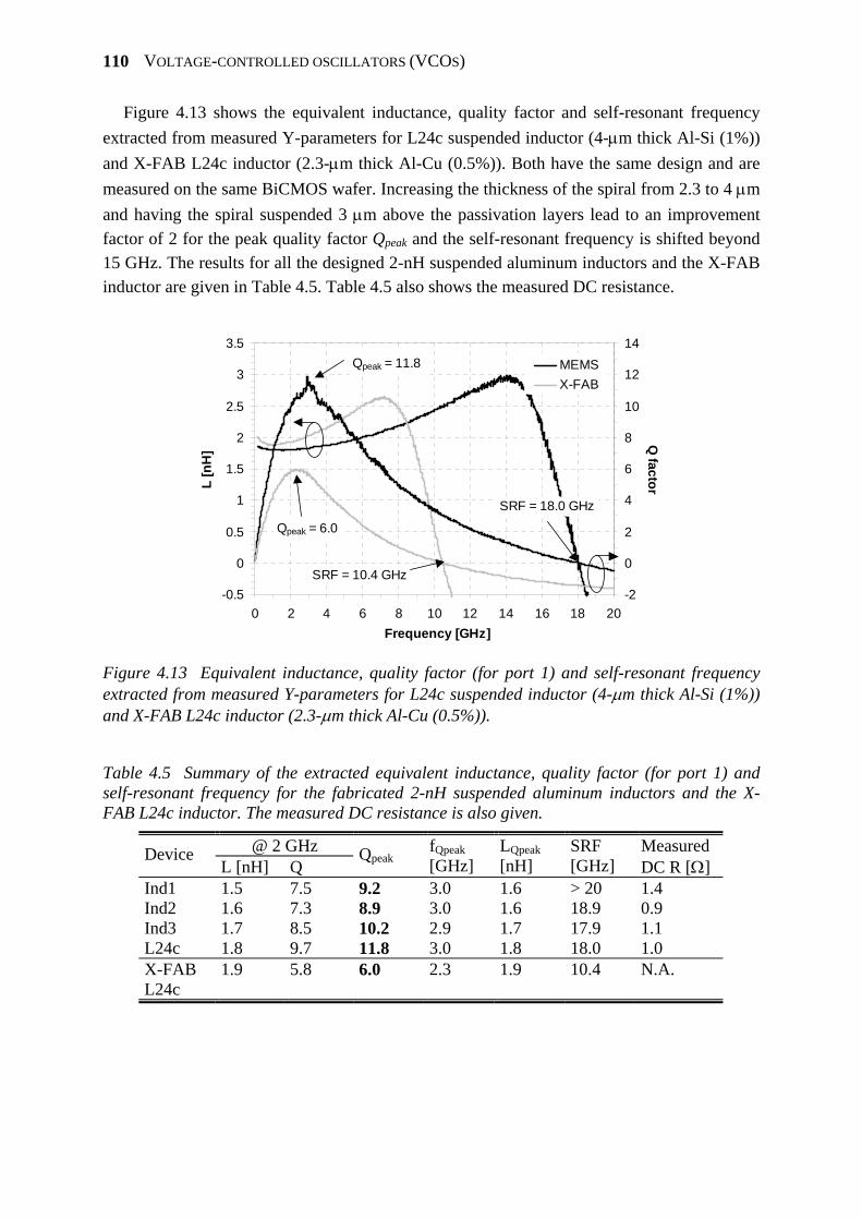
VOLTAGE-CONTROLLED OSCILLATORS (VCOS)
110
Figure 4.13 shows the equivalent inductance, quality factor and self-resonant frequency extracted from measured Y-parameters for L24c suspended inductor (4-μm thick Al-Si (1%)) and X-FAB L24c inductor (2.3-μm thick Al-Cu (0.5%)). Both have the same design and are measured on the same BiCMOS wafer. Increasing the thickness of the spiral from 2.3 to 4 μm and having the spiral suspended 3 μm above the passivation layers lead to an improvement factor of 2 for the peak quality factor Qpeak and the self-resonant frequency is shifted beyond 15 GHz. The results for all the designed 2-nH suspended aluminum inductors and the X-FAB inductor are given in Table 4.5. Table 4.5 also shows the measured DC resistance.
-0.5
0
0.5
1
1.5
2
2.5
3
3.5
0 2 4 6 8 10 12 14 16 18 20Frequency [GHz]
L [n
H]
-2
0
2
4
6
8
10
12
14
Q factor
MEMSX-FAB
SRF = 10.4 GHz
SRF = 18.0 GHz
Qpeak = 11.8
Qpeak = 6.0
Figure 4.13 Equivalent inductance, quality factor (for port 1) and self-resonant frequency extracted from measured Y-parameters for L24c suspended inductor (4-μm thick Al-Si (1%)) and X-FAB L24c inductor (2.3-μm thick Al-Cu (0.5%)).
Table 4.5 Summary of the extracted equivalent inductance, quality factor (for port 1) and self-resonant frequency for the fabricated 2-nH suspended aluminum inductors and the X-FAB L24c inductor. The measured DC resistance is also given.
@ 2 GHz Device L [nH] Q
Qpeak fQpeak [GHz]
LQpeak [nH]
SRF [GHz]
Measured DC R [Ω]
Ind1 1.5 7.5 9.2 3.0 1.6 > 20 1.4 Ind2 1.6 7.3 8.9 3.0 1.6 18.9 0.9 Ind3 1.7 8.5 10.2 2.9 1.7 17.9 1.1 L24c 1.8 9.7 11.8 3.0 1.8 18.0 1.0 X-FAB L24c
1.9 5.8 6.0 2.3 1.9 10.4 N.A.
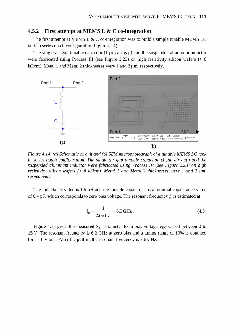
VCO DEMONSTRATOR WITH ABOVE-IC MEMS LC TANK
111
4.5.2 First attempt at MEMS L & C co-integration The first attempt at MEMS L & C co-integration was to build a simple tunable MEMS LC
tank in series notch configuration (Figure 4.14). The single-air-gap tunable capacitor (1-μm air-gap) and the suspended aluminum inductor
were fabricated using Process III (see Figure 2.23) on high resistivity silicon wafers (> 8 kΩcm). Metal 1 and Metal 2 thicknesses were 1 and 2 μm, respectively.
Port 1 Port 2
(a)
Port 2
Port 1 GND
(b)
Figure 4.14 (a) Schematic circuit and (b) SEM microphotograph of a tunable MEMS LC tank in series notch configuration. The single-air-gap tunable capacitor (1-μm air-gap) and the suspended aluminum inductor were fabricated using Process III (see Figure 2.23) on high resistivity silicon wafers (> 8 kΩcm). Metal 1 and Metal 2 thicknesses were 1 and 2 μm, respectively.
The inductance value is 1.5 nH and the tunable capacitor has a minimal capacitance value
of 0.4 pF, which corresponds to zero bias voltage. The resonant frequency f0 is estimated at:
GHz 6.5LC 2π
1f0 == . (4.3)
Figure 4.15 gives the measured S21 parameter for a bias voltage VDC varied between 0 to
15 V. The resonant frequency is 6.2 GHz at zero bias and a tuning range of 10% is obtained for a 11-V bias. After the pull-in, the resonant frequency is 3.6 GHz.
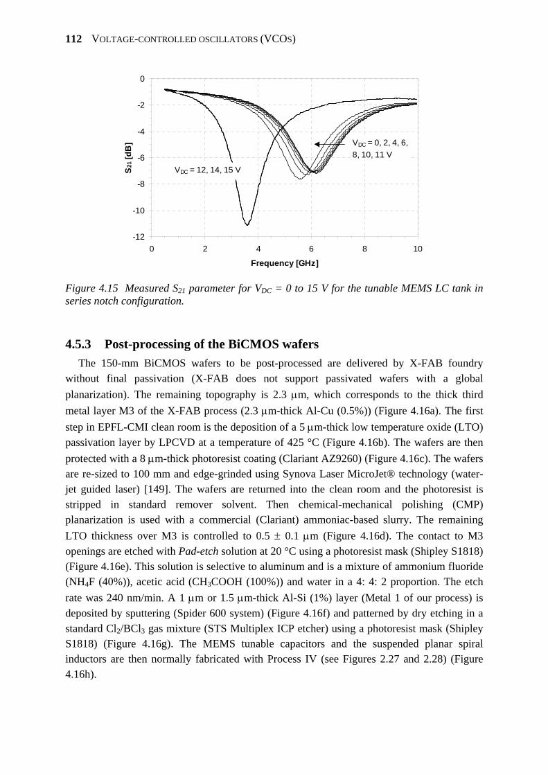
VOLTAGE-CONTROLLED OSCILLATORS (VCOS)
112
-12
-10
-8
-6
-4
-2
0
0 2 4 6 8 10
Frequency [GHz]
S21
[dB
] VDC = 0, 2, 4, 6, 8, 10, 11 V
VDC = 12, 14, 15 V
Figure 4.15 Measured S21 parameter for VDC = 0 to 15 V for the tunable MEMS LC tank in series notch configuration.
4.5.3 Post-processing of the BiCMOS wafers The 150-mm BiCMOS wafers to be post-processed are delivered by X-FAB foundry
without final passivation (X-FAB does not support passivated wafers with a global planarization). The remaining topography is 2.3 μm, which corresponds to the thick third metal layer M3 of the X-FAB process (2.3 μm-thick Al-Cu (0.5%)) (Figure 4.16a). The first step in EPFL-CMI clean room is the deposition of a 5 μm-thick low temperature oxide (LTO) passivation layer by LPCVD at a temperature of 425 °C (Figure 4.16b). The wafers are then protected with a 8 μm-thick photoresist coating (Clariant AZ9260) (Figure 4.16c). The wafers are re-sized to 100 mm and edge-grinded using Synova Laser MicroJet® technology (water-jet guided laser) [149]. The wafers are returned into the clean room and the photoresist is stripped in standard remover solvent. Then chemical-mechanical polishing (CMP) planarization is used with a commercial (Clariant) ammoniac-based slurry. The remaining LTO thickness over M3 is controlled to 0.5 ± 0.1 μm (Figure 4.16d). The contact to M3 openings are etched with Pad-etch solution at 20 °C using a photoresist mask (Shipley S1818) (Figure 4.16e). This solution is selective to aluminum and is a mixture of ammonium fluoride (NH4F (40%)), acetic acid (CH3COOH (100%)) and water in a 4: 4: 2 proportion. The etch rate was 240 nm/min. A 1 μm or 1.5 μm-thick Al-Si (1%) layer (Metal 1 of our process) is deposited by sputtering (Spider 600 system) (Figure 4.16f) and patterned by dry etching in a standard Cl2/BCl3 gas mixture (STS Multiplex ICP etcher) using a photoresist mask (Shipley S1818) (Figure 4.16g). The MEMS tunable capacitors and the suspended planar spiral inductors are then normally fabricated with Process IV (see Figures 2.27 and 2.28) (Figure 4.16h).
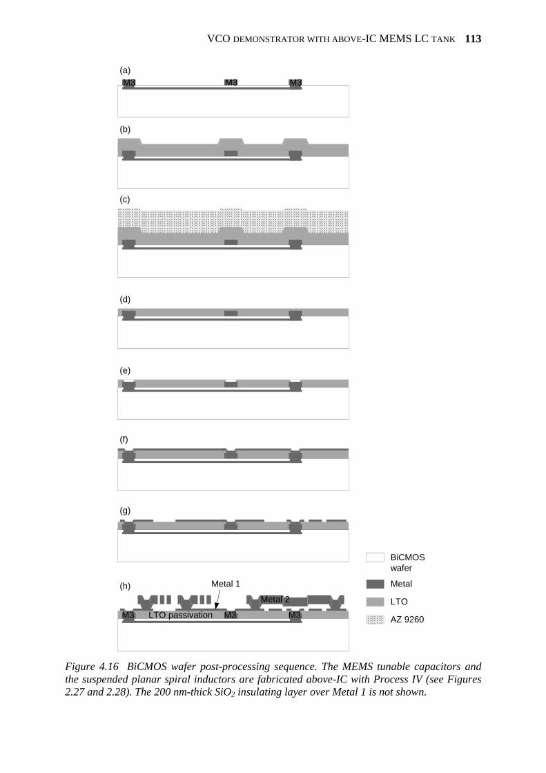
VCO DEMONSTRATOR WITH ABOVE-IC MEMS LC TANK
113
(a)
(b)
(c)
(d)
(e)
(f)
(g)
(h)
BiCMOSwafer
LTO
Metal
AZ 9260M3 M3 M3
Metal 2
Metal 1
LTO passivation
M3 M3 M3
Figure 4.16 BiCMOS wafer post-processing sequence. The MEMS tunable capacitors and the suspended planar spiral inductors are fabricated above-IC with Process IV (see Figures 2.27 and 2.28). The 200 nm-thick SiO2 insulating layer over Metal 1 is not shown.
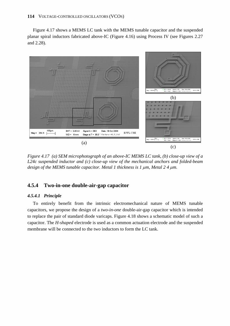
VOLTAGE-CONTROLLED OSCILLATORS (VCOS)
114
Figure 4.17 shows a MEMS LC tank with the MEMS tunable capacitor and the suspended planar spiral inductors fabricated above-IC (Figure 4.16) using Process IV (see Figures 2.27 and 2.28).
(b)
(a)
(c)
Figure 4.17 (a) SEM microphotograph of an above-IC MEMS LC tank, (b) close-up view of a L24c suspended inductor and (c) close-up view of the mechanical anchors and folded-beam design of the MEMS tunable capacitor. Metal 1 thickness is 1 μm, Metal 2 4 μm.
4.5.4 Two-in-one double-air-gap capacitor
4.5.4.1 Principle To entirely benefit from the intrinsic electromechanical nature of MEMS tunable
capacitors, we propose the design of a two-in-one double-air-gap capacitor which is intended to replace the pair of standard diode varicaps. Figure 4.18 shows a schematic model of such a capacitor. The H-shaped electrode is used as a common actuation electrode and the suspended membrane will be connected to the two inductors to form the LC tank.
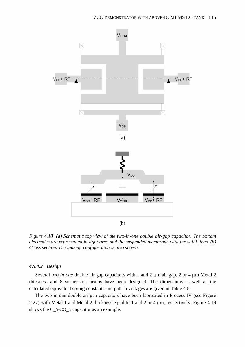
VCO DEMONSTRATOR WITH ABOVE-IC MEMS LC TANK
115
VDD+ RF VDD+ RF
VCTRL
VDD
VDD+ RF VDD+ RF
VDD
VCTRL
(a)
(b)
Figure 4.18 (a) Schematic top view of the two-in-one double air-gap capacitor. The bottom electrodes are represented in light grey and the suspended membrane with the solid lines. (b) Cross section. The biasing configuration is also shown.
4.5.4.2 Design
Several two-in-one double-air-gap capacitors with 1 and 2 μm air-gap, 2 or 4 μm Metal 2 thickness and 8 suspension beams have been designed. The dimensions as well as the calculated equivalent spring constants and pull-in voltages are given in Table 4.6.
The two-in-one double-air-gap capacitors have been fabricated in Process IV (see Figure 2.27) with Metal 1 and Metal 2 thickness equal to 1 and 2 or 4 μm, respectively. Figure 4.19 shows the C_VCO_5 capacitor as an example.
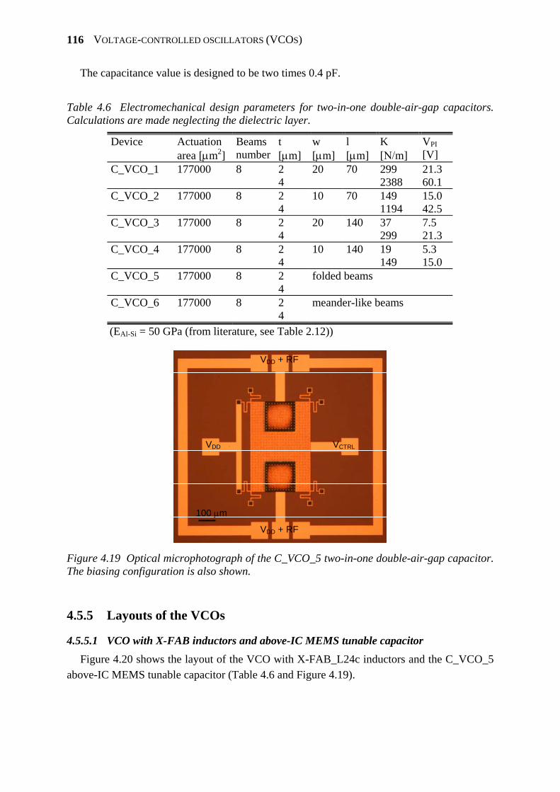
VOLTAGE-CONTROLLED OSCILLATORS (VCOS)
116
The capacitance value is designed to be two times 0.4 pF.
Table 4.6 Electromechanical design parameters for two-in-one double-air-gap capacitors. Calculations are made neglecting the dielectric layer.
Device Actuation area [μm2]
Beams number
t [μm]
w [μm]
l [μm]
K [Ν/m]
VPI [V]
C_VCO_1 177000 8 2 4
20 70 299 2388
21.3 60.1
C_VCO_2 177000 8 2 4
10 70 149 1194
15.0 42.5
C_VCO_3 177000 8 2 4
20 140 37 299
7.5 21.3
C_VCO_4 177000 8 2 4
10 140 19 149
5.3 15.0
C_VCO_5 177000 8 2 4
folded beams
C_VCO_6 177000 8 2 4
meander-like beams
(EAl-Si = 50 GPa (from literature, see Table 2.12))
VDD VCTRL
VDD + RF
VDD + RF
100 μm
Figure 4.19 Optical microphotograph of the C_VCO_5 two-in-one double-air-gap capacitor. The biasing configuration is also shown.
4.5.5 Layouts of the VCOs
4.5.5.1 VCO with X-FAB inductors and above-IC MEMS tunable capacitor Figure 4.20 shows the layout of the VCO with X-FAB_L24c inductors and the C_VCO_5
above-IC MEMS tunable capacitor (Table 4.6 and Figure 4.19).
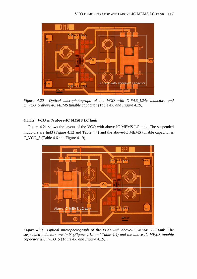
VCO DEMONSTRATOR WITH ABOVE-IC MEMS LC TANK
117
100 μm
IBUF
VDD VCTRL
VAMPL
GND out 1 GND
GND out 2 GND LC tank with above-IC capacitor
Figure 4.20 Optical microphotograph of the VCO with X-FAB_L24c inductors and C_VCO_5 above-IC MEMS tunable capacitor (Table 4.6 and Figure 4.19).
4.5.5.2 VCO with above-IC MEMS LC tank Figure 4.21 shows the layout of the VCO with above-IC MEMS LC tank. The suspended
inductors are Ind3 (Figure 4.12 and Table 4.4) and the above-IC MEMS tunable capacitor is C_VCO_5 (Table 4.6 and Figure 4.19).
100 μm
IBUF
VDD VCTRL
VAMPL GND out 1 GND
GND out 2 GND Above-IC MEMS LC tank
Figure 4.21 Optical microphotograph of the VCO with above-IC MEMS LC tank. The suspended inductors are Ind3 (Figure 4.12 and Table 4.4) and the above-IC MEMS tunable capacitor is C_VCO_5 (Table 4.6 and Figure 4.19).
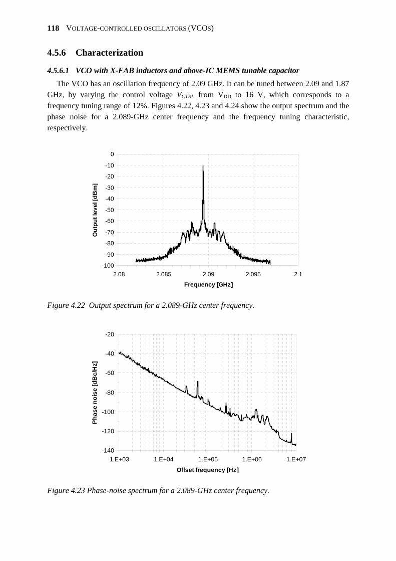
VOLTAGE-CONTROLLED OSCILLATORS (VCOS)
118
4.5.6 Characterization
4.5.6.1 VCO with X-FAB inductors and above-IC MEMS tunable capacitor The VCO has an oscillation frequency of 2.09 GHz. It can be tuned between 2.09 and 1.87
GHz, by varying the control voltage VCTRL from VDD to 16 V, which corresponds to a frequency tuning range of 12%. Figures 4.22, 4.23 and 4.24 show the output spectrum and the phase noise for a 2.089-GHz center frequency and the frequency tuning characteristic, respectively.
-100
-90
-80
-70
-60
-50
-40
-30
-20
-10
0
2.08 2.085 2.09 2.095 2.1
Frequency [GHz]
Out
put l
evel
[dB
m]
Figure 4.22 Output spectrum for a 2.089-GHz center frequency.
-140
-120
-100
-80
-60
-40
-20
1.E+03 1.E+04 1.E+05 1.E+06 1.E+07
Offset frequency [Hz]
Phas
e no
ise
[dB
c/H
z]
Figure 4.23 Phase-noise spectrum for a 2.089-GHz center frequency.
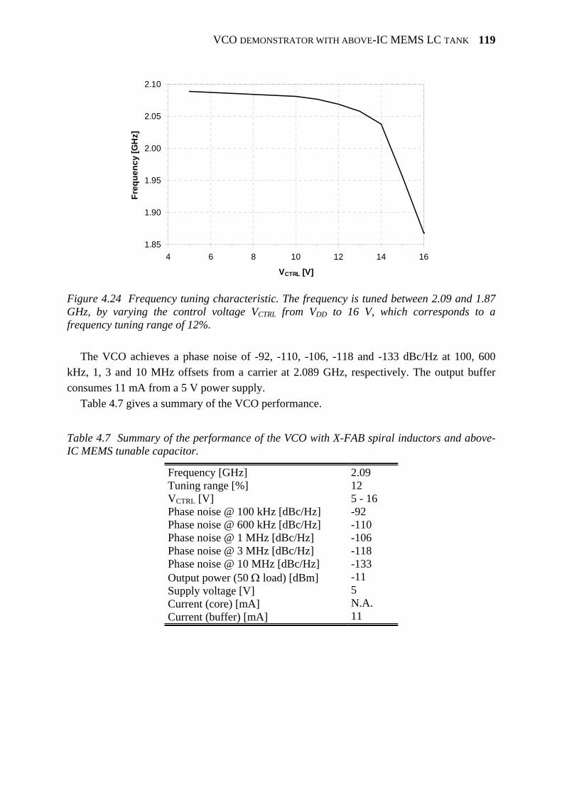
VCO DEMONSTRATOR WITH ABOVE-IC MEMS LC TANK
119
1.85
1.90
1.95
2.00
2.05
2.10
4 6 8 10 12 14 16
VCTRL [V]
Freq
uenc
y [G
Hz]
Figure 4.24 Frequency tuning characteristic. The frequency is tuned between 2.09 and 1.87 GHz, by varying the control voltage VCTRL from VDD to 16 V, which corresponds to a frequency tuning range of 12%.
The VCO achieves a phase noise of -92, -110, -106, -118 and -133 dBc/Hz at 100, 600
kHz, 1, 3 and 10 MHz offsets from a carrier at 2.089 GHz, respectively. The output buffer consumes 11 mA from a 5 V power supply.
Table 4.7 gives a summary of the VCO performance.
Table 4.7 Summary of the performance of the VCO with X-FAB spiral inductors and above-IC MEMS tunable capacitor.
Frequency [GHz] Tuning range [%] VCTRL [V] Phase noise @ 100 kHz [dBc/Hz] Phase noise @ 600 kHz [dBc/Hz] Phase noise @ 1 MHz [dBc/Hz] Phase noise @ 3 MHz [dBc/Hz] Phase noise @ 10 MHz [dBc/Hz] Output power (50 Ω load) [dBm] Supply voltage [V] Current (core) [mA] Current (buffer) [mA]
2.09 12 5 - 16 -92 -110 -106 -118 -133 -11 5 N.A. 11
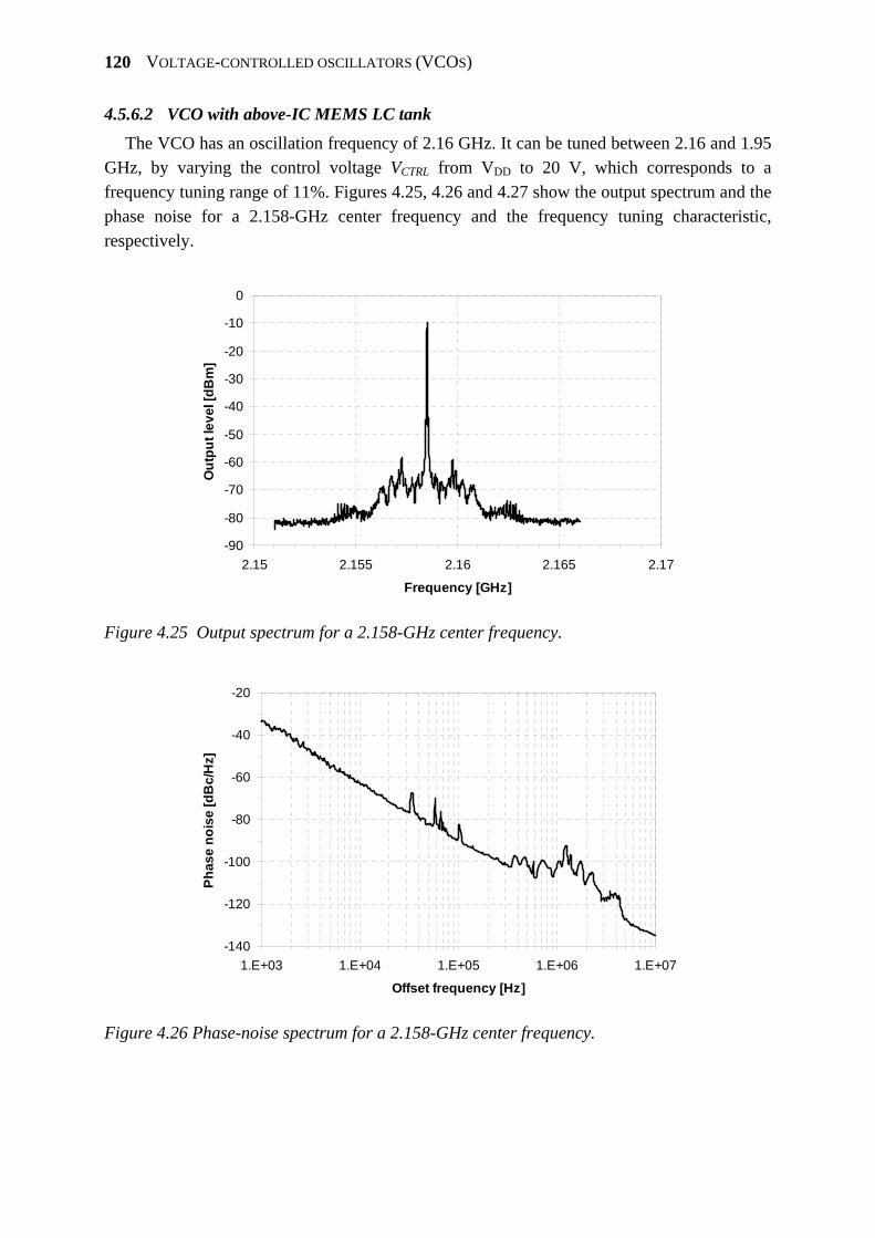
VOLTAGE-CONTROLLED OSCILLATORS (VCOS)
120
4.5.6.2 VCO with above-IC MEMS LC tank The VCO has an oscillation frequency of 2.16 GHz. It can be tuned between 2.16 and 1.95
GHz, by varying the control voltage VCTRL from VDD to 20 V, which corresponds to a frequency tuning range of 11%. Figures 4.25, 4.26 and 4.27 show the output spectrum and the phase noise for a 2.158-GHz center frequency and the frequency tuning characteristic, respectively.
-90
-80
-70
-60
-50
-40
-30
-20
-10
0
2.15 2.155 2.16 2.165 2.17
Frequency [GHz]
Out
put l
evel
[dB
m]
Figure 4.25 Output spectrum for a 2.158-GHz center frequency.
-140
-120
-100
-80
-60
-40
-20
1.E+03 1.E+04 1.E+05 1.E+06 1.E+07
Offset frequency [Hz]
Phas
e no
ise
[dB
c/H
z]
Figure 4.26 Phase-noise spectrum for a 2.158-GHz center frequency.
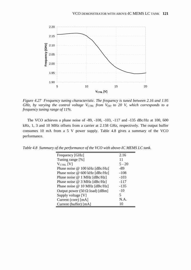
VCO DEMONSTRATOR WITH ABOVE-IC MEMS LC TANK
121
1.90
1.95
2.00
2.05
2.10
2.15
2.20
5 10 15 20
VCTRL [V]
Freq
uenc
y [G
Hz]
Figure 4.27 Frequency tuning characteristic. The frequency is tuned between 2.16 and 1.95 GHz, by varying the control voltage VCTRL from VDD to 20 V, which corresponds to a frequency tuning range of 11%.
The VCO achieves a phase noise of -89, -108, -103, -117 and -135 dBc/Hz at 100, 600
kHz, 1, 3 and 10 MHz offsets from a carrier at 2.158 GHz, respectively. The output buffer consumes 10 mA from a 5 V power supply. Table 4.8 gives a summary of the VCO performance.
Table 4.8 Summary of the performance of the VCO with above-IC MEMS LC tank.
Frequency [GHz] Tuning range [%] VCTRL [V] Phase noise @ 100 kHz [dBc/Hz] Phase noise @ 600 kHz [dBc/Hz] Phase noise @ 1 MHz [dBc/Hz] Phase noise @ 3 MHz [dBc/Hz] Phase noise @ 10 MHz [dBc/Hz] Output power (50 Ω load) [dBm] Supply voltage [V] Current (core) [mA] Current (buffer) [mA]
2.16 11 5 - 20 -89 -108 -103 -117 -135 -10 5 N.A. 10
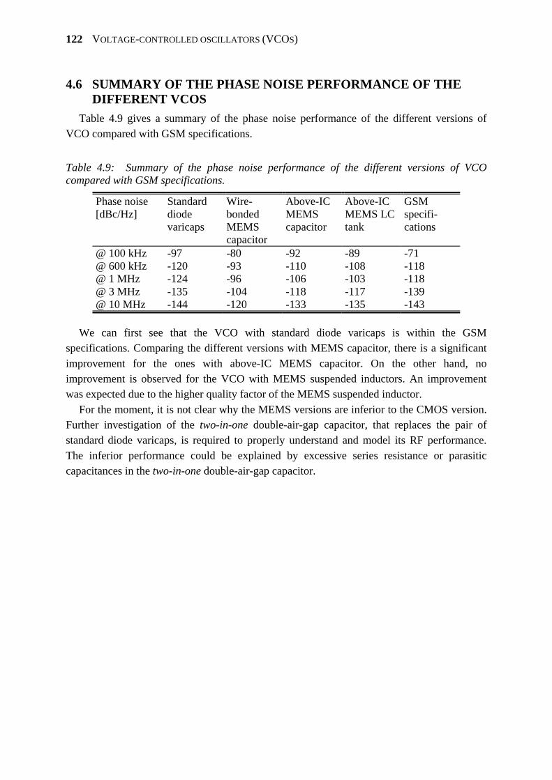
VOLTAGE-CONTROLLED OSCILLATORS (VCOS)
122
4.6 SUMMARY OF THE PHASE NOISE PERFORMANCE OF THE DIFFERENT VCOS
Table 4.9 gives a summary of the phase noise performance of the different versions of VCO compared with GSM specifications.
Table 4.9: Summary of the phase noise performance of the different versions of VCO compared with GSM specifications.
Phase noise [dBc/Hz]
Standard diode varicaps
Wire-bonded MEMS capacitor
Above-IC MEMS capacitor
Above-IC MEMS LC tank
GSM specifi-cations
@ 100 kHz @ 600 kHz @ 1 MHz @ 3 MHz @ 10 MHz
-97 -120 -124 -135 -144
-80 -93 -96 -104 -120
-92 -110 -106 -118 -133
-89 -108 -103 -117 -135
-71 -118 -118 -139 -143
We can first see that the VCO with standard diode varicaps is within the GSM
specifications. Comparing the different versions with MEMS capacitor, there is a significant improvement for the ones with above-IC MEMS capacitor. On the other hand, no improvement is observed for the VCO with MEMS suspended inductors. An improvement was expected due to the higher quality factor of the MEMS suspended inductor.
For the moment, it is not clear why the MEMS versions are inferior to the CMOS version. Further investigation of the two-in-one double-air-gap capacitor, that replaces the pair of standard diode varicaps, is required to properly understand and model its RF performance. The inferior performance could be explained by excessive series resistance or parasitic capacitances in the two-in-one double-air-gap capacitor.
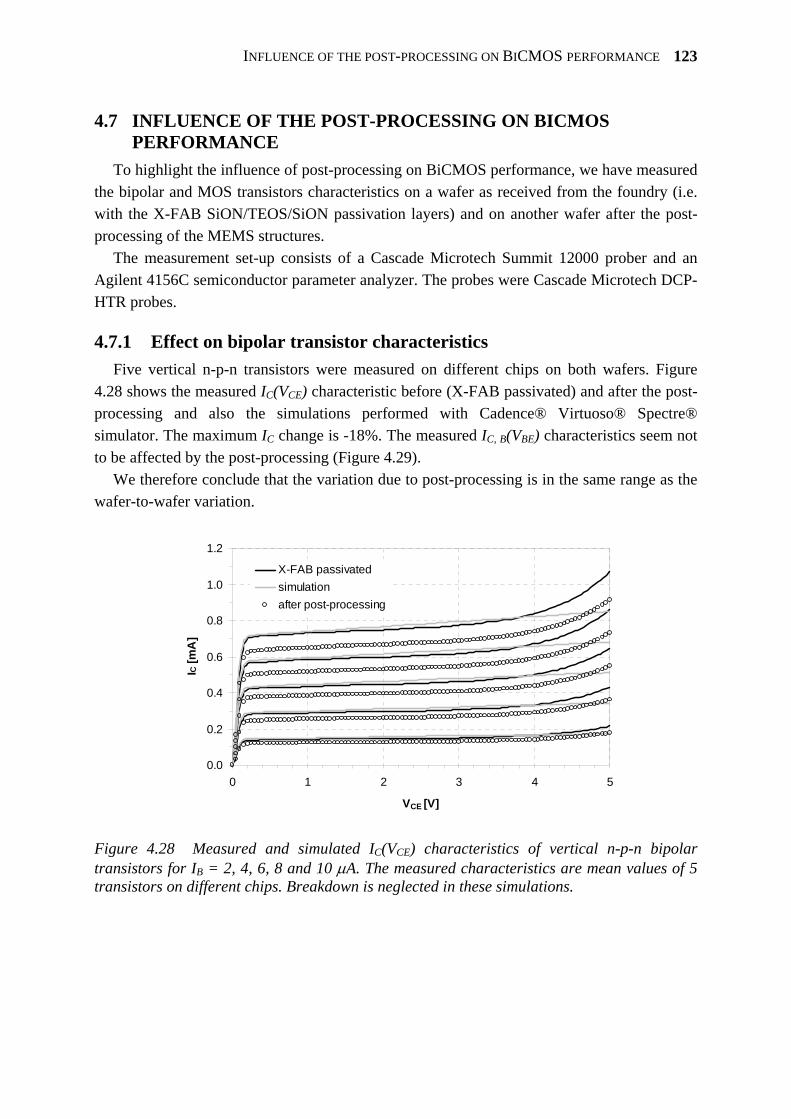
INFLUENCE OF THE POST-PROCESSING ON BICMOS PERFORMANCE
123
4.7 INFLUENCE OF THE POST-PROCESSING ON BICMOS PERFORMANCE
To highlight the influence of post-processing on BiCMOS performance, we have measured the bipolar and MOS transistors characteristics on a wafer as received from the foundry (i.e. with the X-FAB SiON/TEOS/SiON passivation layers) and on another wafer after the post-processing of the MEMS structures.
The measurement set-up consists of a Cascade Microtech Summit 12000 prober and an Agilent 4156C semiconductor parameter analyzer. The probes were Cascade Microtech DCP-HTR probes.
4.7.1 Effect on bipolar transistor characteristics Five vertical n-p-n transistors were measured on different chips on both wafers. Figure
4.28 shows the measured IC(VCE) characteristic before (X-FAB passivated) and after the post-processing and also the simulations performed with Cadence® Virtuoso® Spectre® simulator. The maximum IC change is -18%. The measured IC, B(VBE) characteristics seem not to be affected by the post-processing (Figure 4.29).
We therefore conclude that the variation due to post-processing is in the same range as the wafer-to-wafer variation.
0.0
0.2
0.4
0.6
0.8
1.0
1.2
0 1 2 3 4 5
VCE [V]
IC [m
A]
X-FAB passivatedsimulationafter post-processing
Figure 4.28 Measured and simulated IC(VCE) characteristics of vertical n-p-n bipolar transistors for IB = 2, 4, 6, 8 and 10 μA. The measured characteristics are mean values of 5 transistors on different chips. Breakdown is neglected in these simulations.
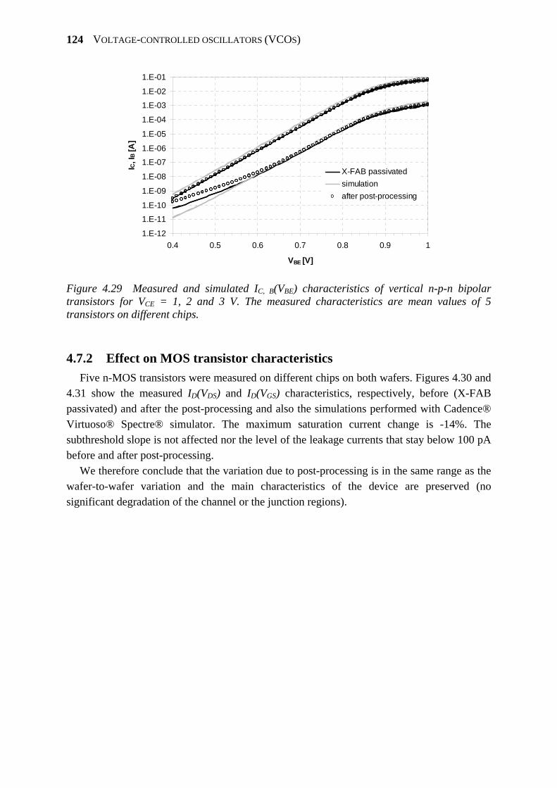
VOLTAGE-CONTROLLED OSCILLATORS (VCOS)
124
1.E-12
1.E-11
1.E-10
1.E-09
1.E-08
1.E-07
1.E-06
1.E-05
1.E-04
1.E-03
1.E-02
1.E-01
0.4 0.5 0.6 0.7 0.8 0.9 1
VBE [V]
IC, I
B [A
]
X-FAB passivatedsimulationafter post-processing
Figure 4.29 Measured and simulated IC, B(VBE) characteristics of vertical n-p-n bipolar transistors for VCE = 1, 2 and 3 V. The measured characteristics are mean values of 5 transistors on different chips.
4.7.2 Effect on MOS transistor characteristics Five n-MOS transistors were measured on different chips on both wafers. Figures 4.30 and
4.31 show the measured ID(VDS) and ID(VGS) characteristics, respectively, before (X-FAB passivated) and after the post-processing and also the simulations performed with Cadence® Virtuoso® Spectre® simulator. The maximum saturation current change is -14%. The subthreshold slope is not affected nor the level of the leakage currents that stay below 100 pA before and after post-processing.
We therefore conclude that the variation due to post-processing is in the same range as the wafer-to-wafer variation and the main characteristics of the device are preserved (no significant degradation of the channel or the junction regions).
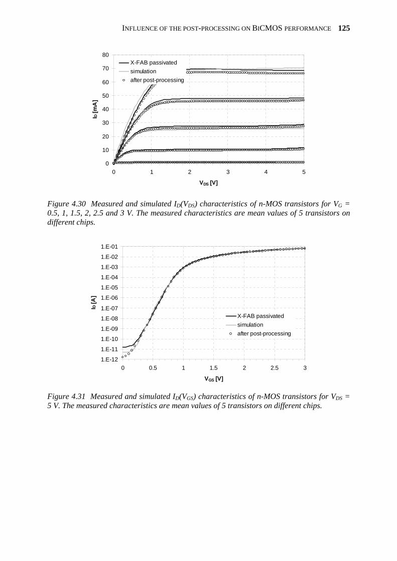
INFLUENCE OF THE POST-PROCESSING ON BICMOS PERFORMANCE
125
0
10
20
30
40
50
60
70
80
0 1 2 3 4 5
VDS [V]
ID [m
A]
X-FAB passivatedsimulationafter post-processing
Figure 4.30 Measured and simulated ID(VDS) characteristics of n-MOS transistors for VG = 0.5, 1, 1.5, 2, 2.5 and 3 V. The measured characteristics are mean values of 5 transistors on different chips.
1.E-12
1.E-11
1.E-10
1.E-09
1.E-08
1.E-07
1.E-06
1.E-05
1.E-04
1.E-03
1.E-02
1.E-01
0 0.5 1 1.5 2 2.5 3
VGS [V]
ID [A
]
X-FAB passivatedsimulationafter post-processing
Figure 4.31 Measured and simulated ID(VGS) characteristics of n-MOS transistors for VDS = 5 V. The measured characteristics are mean values of 5 transistors on different chips.
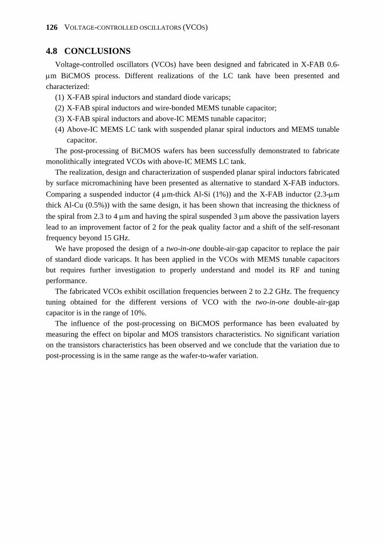
VOLTAGE-CONTROLLED OSCILLATORS (VCOS)
126
4.8 CONCLUSIONS Voltage-controlled oscillators (VCOs) have been designed and fabricated in X-FAB 0.6-
μm BiCMOS process. Different realizations of the LC tank have been presented and characterized:
(1) X-FAB spiral inductors and standard diode varicaps; (2) X-FAB spiral inductors and wire-bonded MEMS tunable capacitor; (3) X-FAB spiral inductors and above-IC MEMS tunable capacitor; (4) Above-IC MEMS LC tank with suspended planar spiral inductors and MEMS tunable
capacitor. The post-processing of BiCMOS wafers has been successfully demonstrated to fabricate
monolithically integrated VCOs with above-IC MEMS LC tank. The realization, design and characterization of suspended planar spiral inductors fabricated
by surface micromachining have been presented as alternative to standard X-FAB inductors. Comparing a suspended inductor (4 μm-thick Al-Si (1%)) and the X-FAB inductor (2.3-μm thick Al-Cu (0.5%)) with the same design, it has been shown that increasing the thickness of the spiral from 2.3 to 4 μm and having the spiral suspended 3 μm above the passivation layers lead to an improvement factor of 2 for the peak quality factor and a shift of the self-resonant frequency beyond 15 GHz.
We have proposed the design of a two-in-one double-air-gap capacitor to replace the pair of standard diode varicaps. It has been applied in the VCOs with MEMS tunable capacitors but requires further investigation to properly understand and model its RF and tuning performance.
The fabricated VCOs exhibit oscillation frequencies between 2 to 2.2 GHz. The frequency tuning obtained for the different versions of VCO with the two-in-one double-air-gap capacitor is in the range of 10%.
The influence of the post-processing on BiCMOS performance has been evaluated by measuring the effect on bipolar and MOS transistors characteristics. No significant variation on the transistors characteristics has been observed and we conclude that the variation due to post-processing is in the same range as the wafer-to-wafer variation.
Chapter 5 Capacitive switches and
application to V-TTDLs

Previous pageOptical microphotograph of on-wafer RF
measurements of capacitive switches with coplanar G-S-G probes.
5.1 COPLANAR WAVEGUIDE (CPW) MEMS SHUNT CAPACITIVE SWITCHES
5.1.1 Introduction to MEMS switches The use of microelectromechanical systems (MEMS) for radiofrequency (RF) switching
applications was first demonstrated in 1979 using bulk-micromachined cantilever switches [150]. Since then, RF MEMS switches have been extensively studied all over the world by research groups [151, 152].
The switches can be categorized by the following three characteristics: (1) RF circuit configuration; (2) Mechanical structure; (3) Contact type. The two common circuit configurations are series [39, 153-156] and shunt (or parallel)
[157-160] connected. Both are single pole single throw (SPST) configurations. Following electrical convention, the number of poles is the number of input ports to the switch, while the number of throws is the number of output ports. The mechanical structure is either a cantilever [39, 153, 156] or a bridge (or membrane) [155, 157-160]. Contact types can be capacitive (metal-insulator-metal (MIM)) [155, 157-160] and ohmic (metal-to-metal) [39, 153, 154, 156]. Any switch is assumed to be binary and digital in the sense that it can lie in one of only two possible actuation states. Each type of switch has certain advantages in terms of performance, manufacturability and reliability.
5.1.2 Description of the CPW MEMS shunt capacitive switch A coplanar waveguide (CPW) MEMS shunt capacitive switch is depicted in Figure 5.1. It
consists of a membrane suspended above the central conductor of the CPW by four suspension beams (Figure 5.2). The CPW line has a W/S/W dimension of 85/60/85 μm for measurements between 1 to 20 GHz. The membrane, also called bridge, is actuated by applying a bias voltage V between the central conductor of the CPW line and the ground. The suspension beams were designed to have a pull-in voltage of about 10 V. When a bias voltage higher than the pull-in voltage is applied, the bridge snaps down (down state) and the central conductor of the CPW line is shorted to ground.
The devices were fabricated using Process II (see Figure 2.21) on low resistivity silicon substrates (0.1 - 100 Ωcm). Both Metal 1 and Metal 2 layers have a 1 μm thickness. The SiO2 insulating layer over Metal 1 was 130 nm-thick.
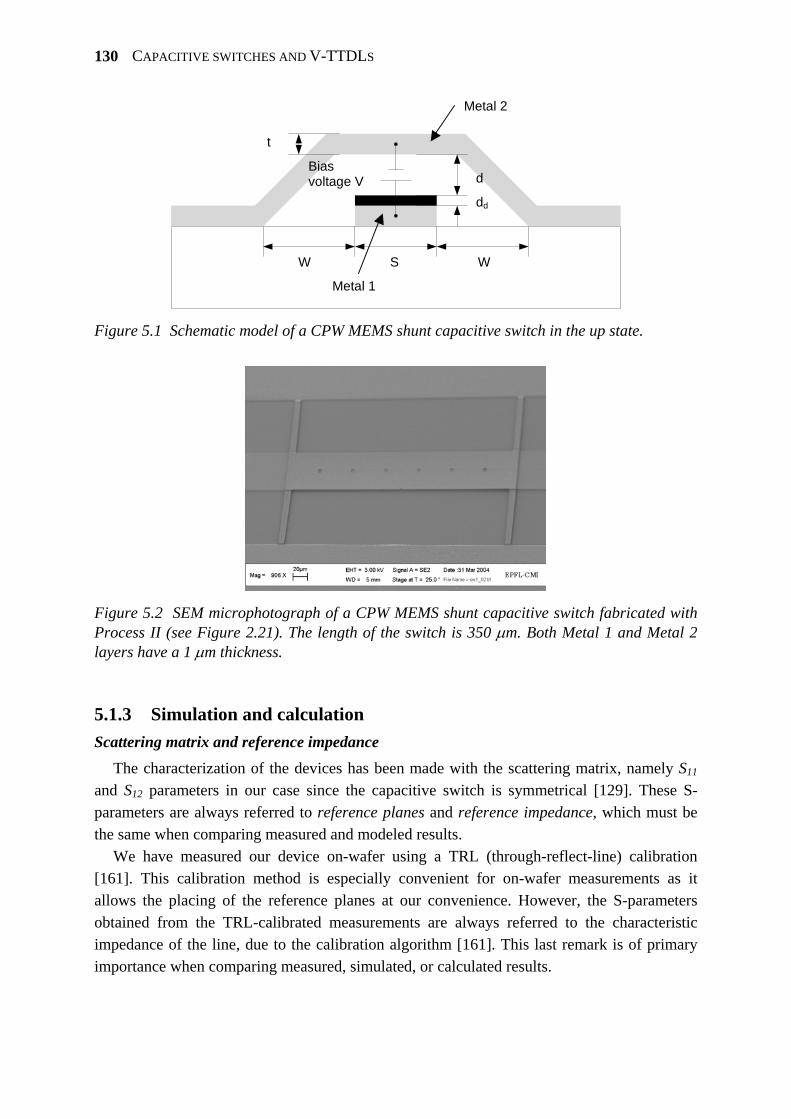
CAPACITIVE SWITCHES AND V-TTDLS
130
Bias voltage V
W WS
t
d
dd
Metal 2
Metal 1
Figure 5.1 Schematic model of a CPW MEMS shunt capacitive switch in the up state.
Figure 5.2 SEM microphotograph of a CPW MEMS shunt capacitive switch fabricated with Process II (see Figure 2.21). The length of the switch is 350 μm. Both Metal 1 and Metal 2 layers have a 1 μm thickness.
5.1.3 Simulation and calculation Scattering matrix and reference impedance
The characterization of the devices has been made with the scattering matrix, namely S11 and S12 parameters in our case since the capacitive switch is symmetrical [129]. These S-parameters are always referred to reference planes and reference impedance, which must be the same when comparing measured and modeled results.
We have measured our device on-wafer using a TRL (through-reflect-line) calibration [161]. This calibration method is especially convenient for on-wafer measurements as it allows the placing of the reference planes at our convenience. However, the S-parameters obtained from the TRL-calibrated measurements are always referred to the characteristic impedance of the line, due to the calibration algorithm [161]. This last remark is of primary importance when comparing measured, simulated, or calculated results.
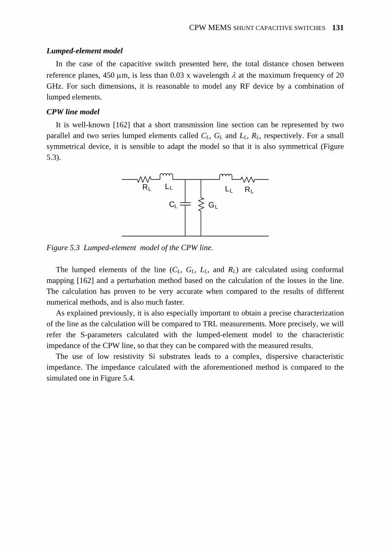
CPW MEMS SHUNT CAPACITIVE SWITCHES
131
Lumped-element model In the case of the capacitive switch presented here, the total distance chosen between
reference planes, 450 μm, is less than 0.03 x wavelength λ at the maximum frequency of 20 GHz. For such dimensions, it is reasonable to model any RF device by a combination of lumped elements.
CPW line model It is well-known [162] that a short transmission line section can be represented by two
parallel and two series lumped elements called CL, GL and LL, RL, respectively. For a small symmetrical device, it is sensible to adapt the model so that it is also symmetrical (Figure 5.3).
GLCL
RLLLLLRL
Figure 5.3 Lumped-element model of the CPW line.
The lumped elements of the line (CL, GL, LL, and RL) are calculated using conformal
mapping [162] and a perturbation method based on the calculation of the losses in the line. The calculation has proven to be very accurate when compared to the results of different numerical methods, and is also much faster.
As explained previously, it is also especially important to obtain a precise characterization of the line as the calculation will be compared to TRL measurements. More precisely, we will refer the S-parameters calculated with the lumped-element model to the characteristic impedance of the CPW line, so that they can be compared with the measured results.
The use of low resistivity Si substrates leads to a complex, dispersive characteristic impedance. The impedance calculated with the aforementioned method is compared to the simulated one in Figure 5.4.
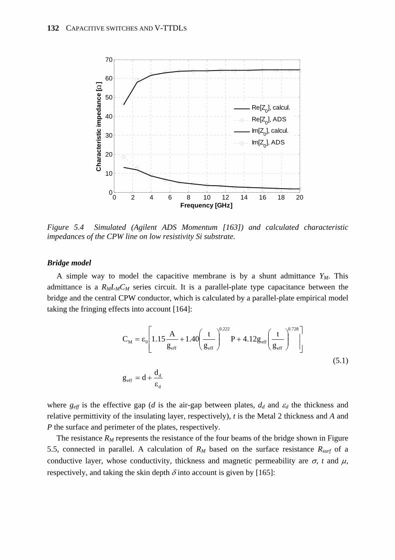
CAPACITIVE SWITCHES AND V-TTDLS
132
0 2 4 6 8 10 12 14 16 18 200
10
20
30
40
50
60
70
Frequency [GHz]
Cha
ract
eris
tic im
peda
nce
[ Ω]
Re[Z0], calcul.
Re[Z0], ADS
Im[Z0], calcul.
Im[Z0], ADS
Figure 5.4 Simulated (Agilent ADS Momentum [163]) and calculated characteristic impedances of the CPW line on low resistivity Si substrate.
Bridge model A simple way to model the capacitive membrane is by a shunt admittance YM. This
admittance is a RMLMCM series circuit. It is a parallel-plate type capacitance between the bridge and the central CPW conductor, which is calculated by a parallel-plate empirical model taking the fringing effects into account [164]:
d
deff
0.728
effeff
0.222
effeff0M
εddg
gt4.12gP
gt1.40
gA1.15εC
+=
⎥⎥⎦
⎤
⎢⎢⎣
⎡⎟⎟⎠
⎞⎜⎜⎝
⎛+⎟⎟
⎠
⎞⎜⎜⎝
⎛+=
(5.1)
where geff is the effective gap (d is the air-gap between plates, dd and εd the thickness and relative permittivity of the insulating layer, respectively), t is the Metal 2 thickness and A and P the surface and perimeter of the plates, respectively.
The resistance RM represents the resistance of the four beams of the bridge shown in Figure 5.5, connected in parallel. A calculation of RM based on the surface resistance Rsurf of a conductive layer, whose conductivity, thickness and magnetic permeability are σ, t and μ, respectively, and taking the skin depth δ into account is given by [165]:
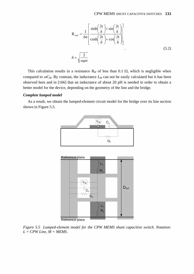
CPW MEMS SHUNT CAPACITIVE SWITCHES
133
ωμσ2δ
δ2tcos
δ2tcosh
δ2tsin
δ2tsinh
δσ1Rsurf
=
⎥⎥⎥⎥
⎦
⎤
⎢⎢⎢⎢
⎣
⎡
⎟⎠⎞
⎜⎝⎛+⎟
⎠⎞
⎜⎝⎛
⎟⎠⎞
⎜⎝⎛+⎟
⎠⎞
⎜⎝⎛
=
. (5.2)
This calculation results in a resistance RM of less than 0.1 Ω, which is negligible when
compared to ωCM. By contrast, the inductance LM can not be easily calculated but it has been observed here and in [166] that an inductance of about 20 pH is needed in order to obtain a better model for the device, depending on the geometry of the line and the bridge.
Complete lumped model As a result, we obtain the lumped-element circuit model for the bridge over its line section
shown in Figure 5.5.
YM
GL
CL
YM
GL
CL
RL
LL
LL
RL
Reference plane
Reference plane
Dref
Figure 5.5 Lumped-element model for the CPW MEMS shunt capacitive switch. Notation: L = CPW Line, M = MEMS.
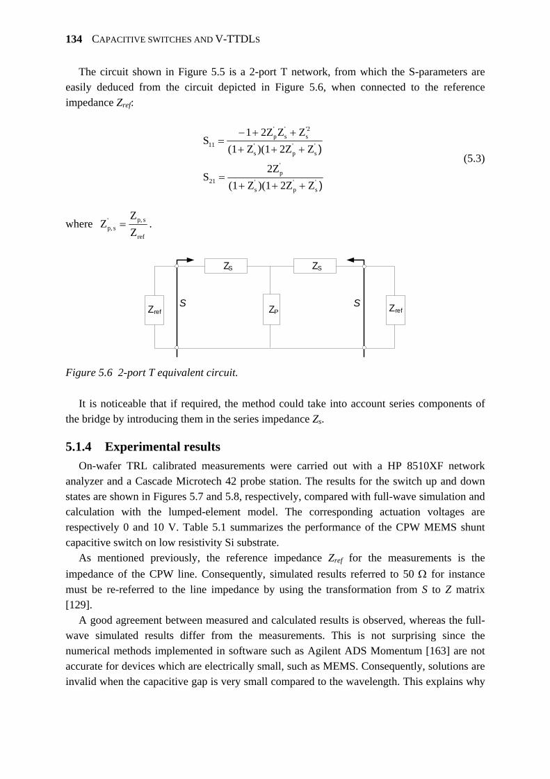
CAPACITIVE SWITCHES AND V-TTDLS
134
The circuit shown in Figure 5.5 is a 2-port T network, from which the S-parameters are easily deduced from the circuit depicted in Figure 5.6, when connected to the reference impedance Zref:
)
)
's
'p
's
'p
21
's
'p
's
'2s
's
'p
11
Z2Z)(1Z(12Z
S
Z2Z)(1Z(1ZZ2Z1
S
+++=
+++
++−=
(5.3)
where ref
s p,'s p, Z
ZZ = .
ZS
ZP
ZS
ZrefZrefS S
Figure 5.6 2-port T equivalent circuit.
It is noticeable that if required, the method could take into account series components of
the bridge by introducing them in the series impedance Zs.
5.1.4 Experimental results On-wafer TRL calibrated measurements were carried out with a HP 8510XF network
analyzer and a Cascade Microtech 42 probe station. The results for the switch up and down states are shown in Figures 5.7 and 5.8, respectively, compared with full-wave simulation and calculation with the lumped-element model. The corresponding actuation voltages are respectively 0 and 10 V. Table 5.1 summarizes the performance of the CPW MEMS shunt capacitive switch on low resistivity Si substrate.
As mentioned previously, the reference impedance Zref for the measurements is the impedance of the CPW line. Consequently, simulated results referred to 50 Ω for instance must be re-referred to the line impedance by using the transformation from S to Z matrix [129].
A good agreement between measured and calculated results is observed, whereas the full-wave simulated results differ from the measurements. This is not surprising since the numerical methods implemented in software such as Agilent ADS Momentum [163] are not accurate for devices which are electrically small, such as MEMS. Consequently, solutions are invalid when the capacitive gap is very small compared to the wavelength. This explains why
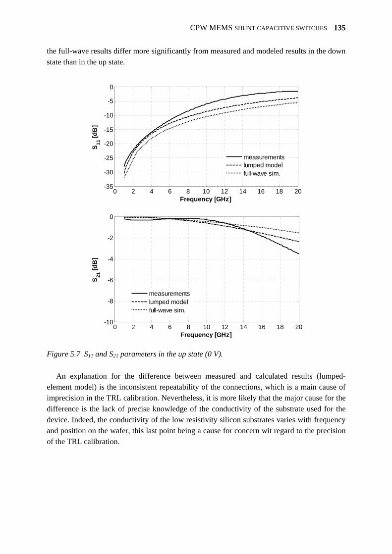
CPW MEMS SHUNT CAPACITIVE SWITCHES
135
the full-wave results differ more significantly from measured and modeled results in the down state than in the up state.
0 2 4 6 8 10 12 14 16 18 20-35
-30
-25
-20
-15
-10
-5
0
Frequency [GHz]
S 11 [d
B]
0 2 4 6 8 10 12 14 16 18 20-10
-8
-6
-4
-2
0
Frequency [GHz]
S 21 [d
B]
measurementslumped modelfull-wave sim.
measurementslumped modelfull-wave sim.
Figure 5.7 S11 and S21 parameters in the up state (0 V).
An explanation for the difference between measured and calculated results (lumped-
element model) is the inconsistent repeatability of the connections, which is a main cause of imprecision in the TRL calibration. Nevertheless, it is more likely that the major cause for the difference is the lack of precise knowledge of the conductivity of the substrate used for the device. Indeed, the conductivity of the low resistivity silicon substrates varies with frequency and position on the wafer, this last point being a cause for concern wit regard to the precision of the TRL calibration.
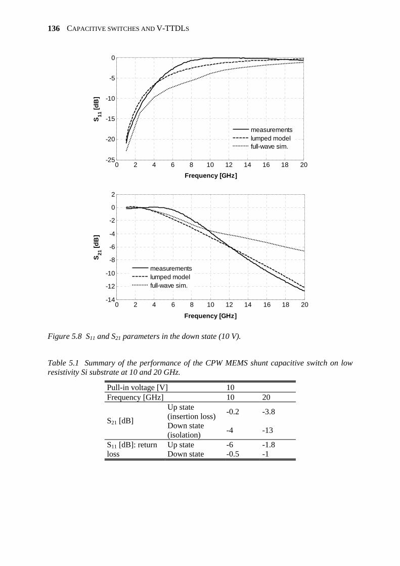
CAPACITIVE SWITCHES AND V-TTDLS
136
0 2 4 6 8 10 12 14 16 18 20-25
-20
-15
-10
-5
0
Frequency [GHz]
S 11 [d
B]
0 2 4 6 8 10 12 14 16 18 20-14
-12
-10
-8
-6
-4
-2
0
2
Frequency [GHz]
S 21 [d
B]
measurementslumped modelfull-wave sim.
measurementslumped modelfull-wave sim.
Figure 5.8 S11 and S21 parameters in the down state (10 V).
Table 5.1 Summary of the performance of the CPW MEMS shunt capacitive switch on low resistivity Si substrate at 10 and 20 GHz.
Pull-in voltage [V] 10 Frequency [GHz] 10 20
Up state (insertion loss) -0.2 -3.8
S21 [dB] Down state (isolation) -4 -13
Up state -6 -1.8 S11 [dB]: return loss Down state -0.5 -1
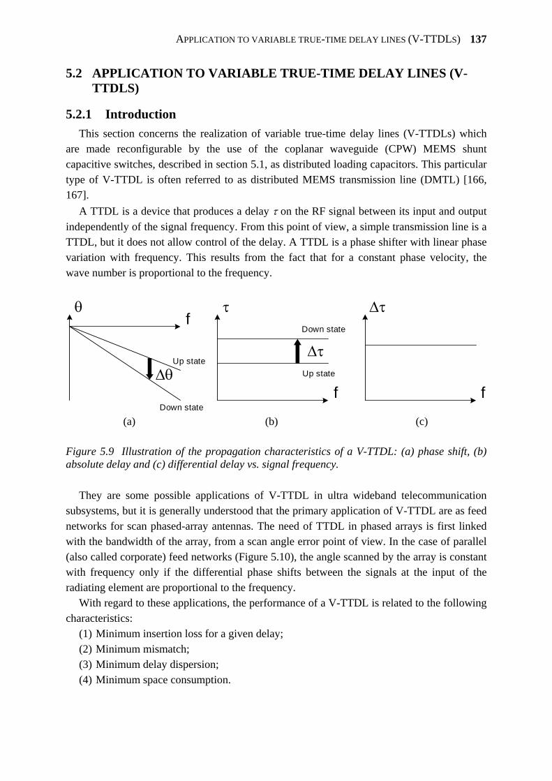
APPLICATION TO VARIABLE TRUE-TIME DELAY LINES (V-TTDLS)
137
5.2 APPLICATION TO VARIABLE TRUE-TIME DELAY LINES (V-TTDLS)
5.2.1 Introduction This section concerns the realization of variable true-time delay lines (V-TTDLs) which
are made reconfigurable by the use of the coplanar waveguide (CPW) MEMS shunt capacitive switches, described in section 5.1, as distributed loading capacitors. This particular type of V-TTDL is often referred to as distributed MEMS transmission line (DMTL) [166, 167].
A TTDL is a device that produces a delay τ on the RF signal between its input and output independently of the signal frequency. From this point of view, a simple transmission line is a TTDL, but it does not allow control of the delay. A TTDL is a phase shifter with linear phase variation with frequency. This results from the fact that for a constant phase velocity, the wave number is proportional to the frequency.
fθ
Δθf
τ
Δτ
f
Δτ
Up state
Down state
Up state
Down state
(a) (b) (c)
Figure 5.9 Illustration of the propagation characteristics of a V-TTDL: (a) phase shift, (b) absolute delay and (c) differential delay vs. signal frequency.
They are some possible applications of V-TTDL in ultra wideband telecommunication
subsystems, but it is generally understood that the primary application of V-TTDL are as feed networks for scan phased-array antennas. The need of TTDL in phased arrays is first linked with the bandwidth of the array, from a scan angle error point of view. In the case of parallel (also called corporate) feed networks (Figure 5.10), the angle scanned by the array is constant with frequency only if the differential phase shifts between the signals at the input of the radiating element are proportional to the frequency.
With regard to these applications, the performance of a V-TTDL is related to the following characteristics:
(1) Minimum insertion loss for a given delay; (2) Minimum mismatch; (3) Minimum delay dispersion; (4) Minimum space consumption.
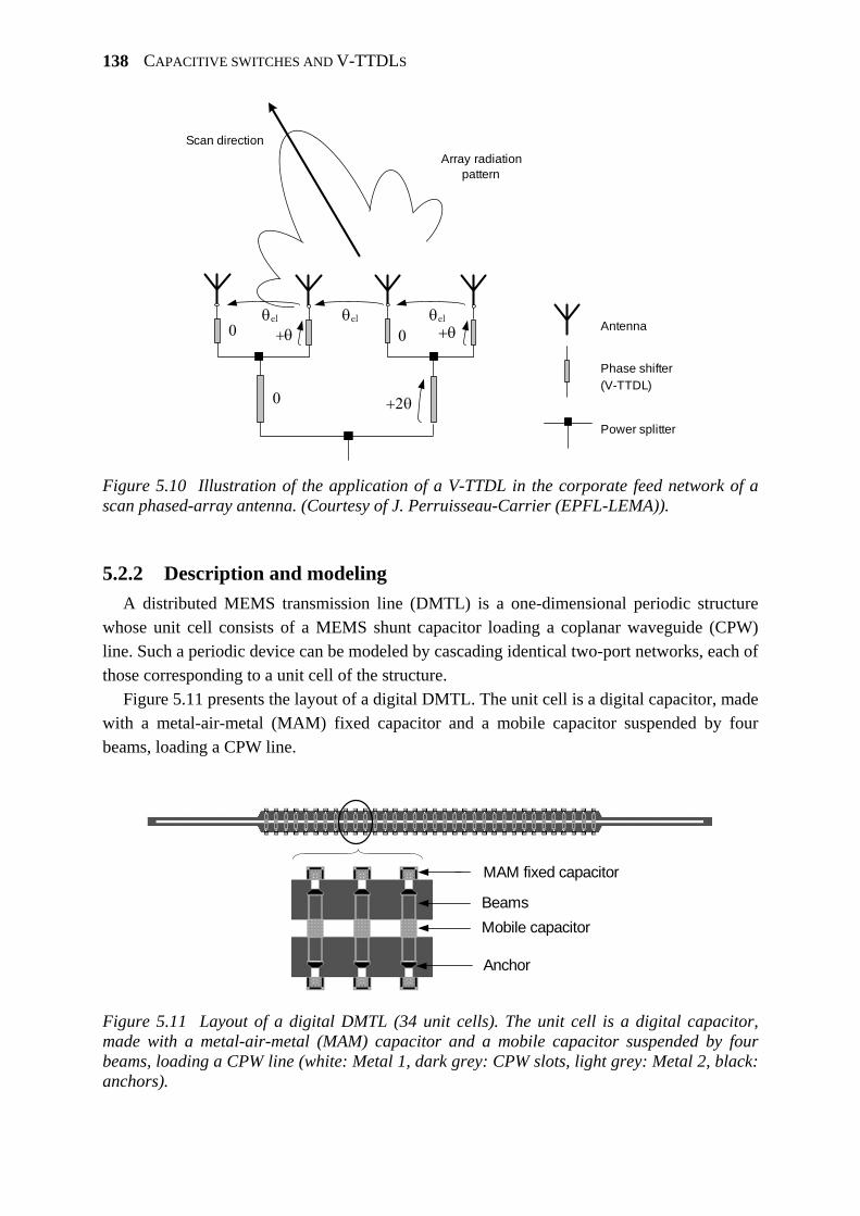
CAPACITIVE SWITCHES AND V-TTDLS
138
αs
+θ +θθel
+2θ
θel0
Phase shifter(V-TTDL)
Power splitter
0
0
Antenna
Scan directionArray radiation
pattern
θel
Figure 5.10 Illustration of the application of a V-TTDL in the corporate feed network of a scan phased-array antenna. (Courtesy of J. Perruisseau-Carrier (EPFL-LEMA)).
5.2.2 Description and modeling A distributed MEMS transmission line (DMTL) is a one-dimensional periodic structure
whose unit cell consists of a MEMS shunt capacitor loading a coplanar waveguide (CPW) line. Such a periodic device can be modeled by cascading identical two-port networks, each of those corresponding to a unit cell of the structure.
Figure 5.11 presents the layout of a digital DMTL. The unit cell is a digital capacitor, made with a metal-air-metal (MAM) fixed capacitor and a mobile capacitor suspended by four beams, loading a CPW line.
MAM fixed capacitor
Mobile capacitorBeams
Anchor
Figure 5.11 Layout of a digital DMTL (34 unit cells). The unit cell is a digital capacitor, made with a metal-air-metal (MAM) capacitor and a mobile capacitor suspended by four beams, loading a CPW line (white: Metal 1, dark grey: CPW slots, light grey: Metal 2, black: anchors).
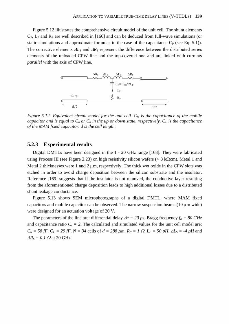
APPLICATION TO VARIABLE TRUE-TIME DELAY LINES (V-TTDLS)
139
Figure 5.12 illustrates the comprehensive circuit model of the unit cell. The shunt elements CP, LP and RP are well described in [166] and can be deduced from full-wave simulations (or static simulations and approximate formulas in the case of the capacitance CP (see Eq. 5.1)). The corrective elements ΔLS and ΔRS represent the difference between the distributed series elements of the unloaded CPW line and the top-covered one and are linked with currents parallel with the axis of CPW line.
ΔLSΔLS
CP=CM//2CF
LP
RPZ0 , γ0
d/2 d/2
ΔRSΔRS
Figure 5.12 Equivalent circuit model for the unit cell. CM is the capacitance of the mobile capacitor and is equal to Cu or Cd in the up or down state, respectively. CF is the capacitance of the MAM fixed capacitor. d is the cell length.
5.2.3 Experimental results Digital DMTLs have been designed in the 1 - 20 GHz range [168]. They were fabricated
using Process III (see Figure 2.23) on high resistivity silicon wafers (> 8 kΩcm). Metal 1 and Metal 2 thicknesses were 1 and 2 μm, respectively. The thick wet oxide in the CPW slots was etched in order to avoid charge deposition between the silicon substrate and the insulator. Reference [169] suggests that if the insulator is not removed, the conductive layer resulting from the aforementioned charge deposition leads to high additional losses due to a distributed shunt leakage conductance.
Figure 5.13 shows SEM microphotographs of a digital DMTL, where MAM fixed capacitors and mobile capacitor can be observed. The narrow suspension beams (10 μm wide) were designed for an actuation voltage of 20 V.
The parameters of the line are: differential delay Δτ = 20 ps, Bragg frequency fB = 80 GHz and capacitance ratio Cr = 2. The calculated and simulated values for the unit cell model are: Cu = 58 fF, CF = 29 fF, N = 34 cells of d = 288 μm, RP = 1 Ω, LP = 50 pH, ΔLS = -4 pH and ΔRS = 0.1 Ω at 20 GHz.
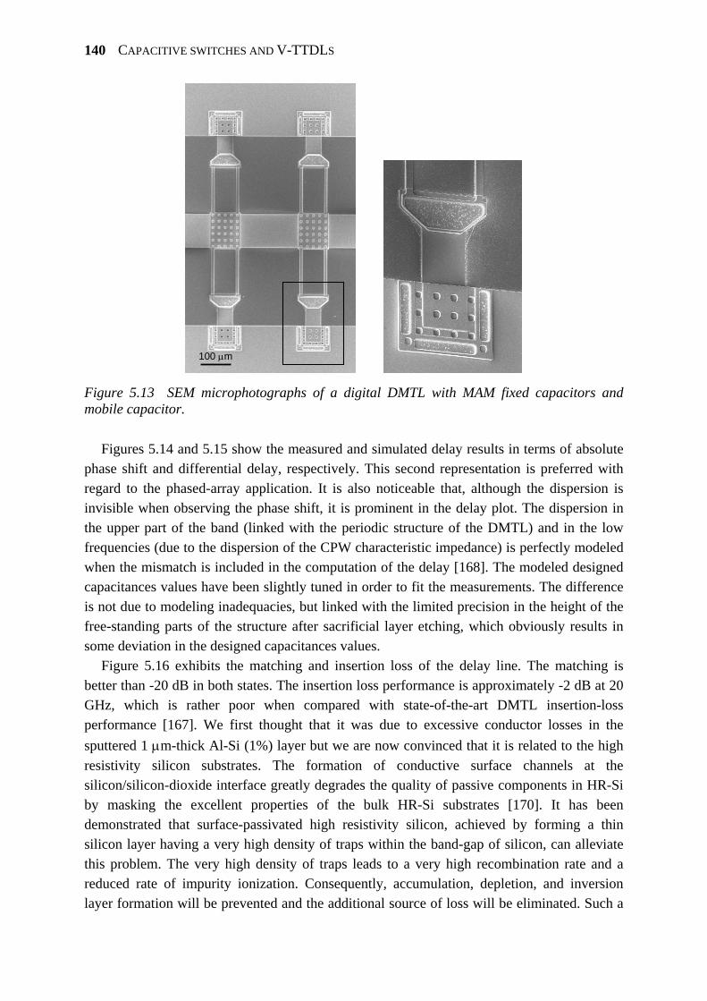
CAPACITIVE SWITCHES AND V-TTDLS
140
100 μm
Figure 5.13 SEM microphotographs of a digital DMTL with MAM fixed capacitors and mobile capacitor.
Figures 5.14 and 5.15 show the measured and simulated delay results in terms of absolute
phase shift and differential delay, respectively. This second representation is preferred with regard to the phased-array application. It is also noticeable that, although the dispersion is invisible when observing the phase shift, it is prominent in the delay plot. The dispersion in the upper part of the band (linked with the periodic structure of the DMTL) and in the low frequencies (due to the dispersion of the CPW characteristic impedance) is perfectly modeled when the mismatch is included in the computation of the delay [168]. The modeled designed capacitances values have been slightly tuned in order to fit the measurements. The difference is not due to modeling inadequacies, but linked with the limited precision in the height of the free-standing parts of the structure after sacrificial layer etching, which obviously results in some deviation in the designed capacitances values.
Figure 5.16 exhibits the matching and insertion loss of the delay line. The matching is better than -20 dB in both states. The insertion loss performance is approximately -2 dB at 20 GHz, which is rather poor when compared with state-of-the-art DMTL insertion-loss performance [167]. We first thought that it was due to excessive conductor losses in the sputtered 1 μm-thick Al-Si (1%) layer but we are now convinced that it is related to the high resistivity silicon substrates. The formation of conductive surface channels at the silicon/silicon-dioxide interface greatly degrades the quality of passive components in HR-Si by masking the excellent properties of the bulk HR-Si substrates [170]. It has been demonstrated that surface-passivated high resistivity silicon, achieved by forming a thin silicon layer having a very high density of traps within the band-gap of silicon, can alleviate this problem. The very high density of traps leads to a very high recombination rate and a reduced rate of impurity ionization. Consequently, accumulation, depletion, and inversion layer formation will be prevented and the additional source of loss will be eliminated. Such a
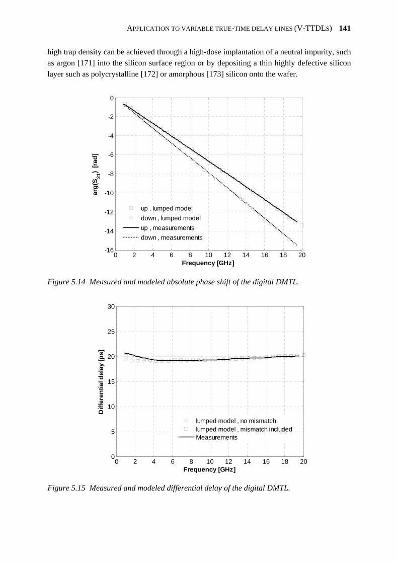
APPLICATION TO VARIABLE TRUE-TIME DELAY LINES (V-TTDLS)
141
high trap density can be achieved through a high-dose implantation of a neutral impurity, such as argon [171] into the silicon surface region or by depositing a thin highly defective silicon layer such as polycrystalline [172] or amorphous [173] silicon onto the wafer.
0 2 4 6 8 10 12 14 16 18 20-16
-14
-12
-10
-8
-6
-4
-2
0
Frequency [GHz]
arg(
S 21)
[rad]
up , lumped modeldown , lumped modelup , measurementsdown , measurements
Figure 5.14 Measured and modeled absolute phase shift of the digital DMTL.
0 2 4 6 8 10 12 14 16 18 200
5
10
15
20
25
30
Frequency [GHz]
Diff
eren
tial d
elay
[ps]
lumped model , no mismatchlumped model , mismatch includedMeasurements
Figure 5.15 Measured and modeled differential delay of the digital DMTL.
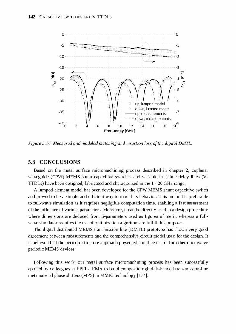
CAPACITIVE SWITCHES AND V-TTDLS
142
0 2 4 6 8 10 12 14 16 18 20-40
-35
-30
-25
-20
-15
-10
-5
0
Frequency [GHz]
S 11 [d
B]
-8
-7
-6
-5
-4
-3
-2
-1
0
S 21 [
dB]
up, lumped modeldown, lumped modelup, measurementsdown, measurements
Figure 5.16 Measured and modeled matching and insertion loss of the digital DMTL.
5.3 CONCLUSIONS Based on the metal surface micromachining process described in chapter 2, coplanar
waveguide (CPW) MEMS shunt capacitive switches and variable true-time delay lines (V-TTDLs) have been designed, fabricated and characterized in the 1 - 20 GHz range.
A lumped-element model has been developed for the CPW MEMS shunt capacitive switch and proved to be a simple and efficient way to model its behavior. This method is preferable to full-wave simulation as it requires negligible computation time, enabling a fast assessment of the influence of various parameters. Moreover, it can be directly used in a design procedure where dimensions are deduced from S-parameters used as figures of merit, whereas a full-wave simulator requires the use of optimization algorithms to fulfill this purpose.
The digital distributed MEMS transmission line (DMTL) prototype has shown very good agreement between measurements and the comprehensive circuit model used for the design. It is believed that the periodic structure approach presented could be useful for other microwave periodic MEMS devices.
Following this work, our metal surface micromachining process has been successfully
applied by colleagues at EPFL-LEMA to build composite right/left-handed transmission-line metamaterial phase shifters (MPS) in MMIC technology [174].
Chapter 6 Suspended-gate MOSFET
(SG-MOSFET)

Previous pageSEM microphotograph of a suspended-
gate MOSFET with meander suspension beams. The drain/source metal contacts
are also visible.(Scale: metal gate is 13 x 60 μm2)
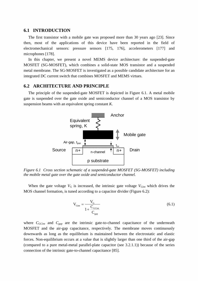
6.1 INTRODUCTION The first transistor with a mobile gate was proposed more than 30 years ago [23]. Since
then, most of the applications of this device have been reported in the field of electromechanical sensors: pressure sensors [175, 176], accelerometers [177] and microphones [178].
In this chapter, we present a novel MEMS device architecture: the suspended-gate MOSFET (SG-MOSFET), which combines a solid-state MOS transistor and a suspended metal membrane. The SG-MOSFET is investigated as a possible candidate architecture for an integrated DC current switch that combines MOSFET and MEMS virtues.
6.2 ARCHITECTURE AND PRINCIPLE The principle of the suspended-gate MOSFET is depicted in Figure 6.1. A metal mobile
gate is suspended over the gate oxide and semiconductor channel of a MOS transistor by suspension beams with an equivalent spring constant K.
n+n+
p substrate
n-channel
Mobile gate
AnchorEquivalent spring, K
Air-gap, tgap
DrainSourcetox
Figure 6.1 Cross section schematic of a suspended-gate MOSFET (SG-MOSFET) including the mobile metal gate over the gate oxide and semiconductor channel.
When the gate voltage VG is increased, the intrinsic gate voltage VGint which drives the
MOS channel formation, is tuned according to a capacitor divider (Figure 6.2):
gap
GCint
GGint
CC1
VV+
= (6.1)
where CGCint and Cgap are the intrinsic gate-to-channel capacitance of the underneath MOSFET and the air-gap capacitance, respectively. The membrane moves continuously downwards as long as the equilibrium is maintained between the electrostatic and elastic forces. Non-equilibrium occurs at a value that is slightly larger than one third of the air-gap (compared to a pure metal-metal parallel-plate capacitor (see 3.2.1.1)) because of the series connection of the intrinsic gate-to-channel capacitance [85].
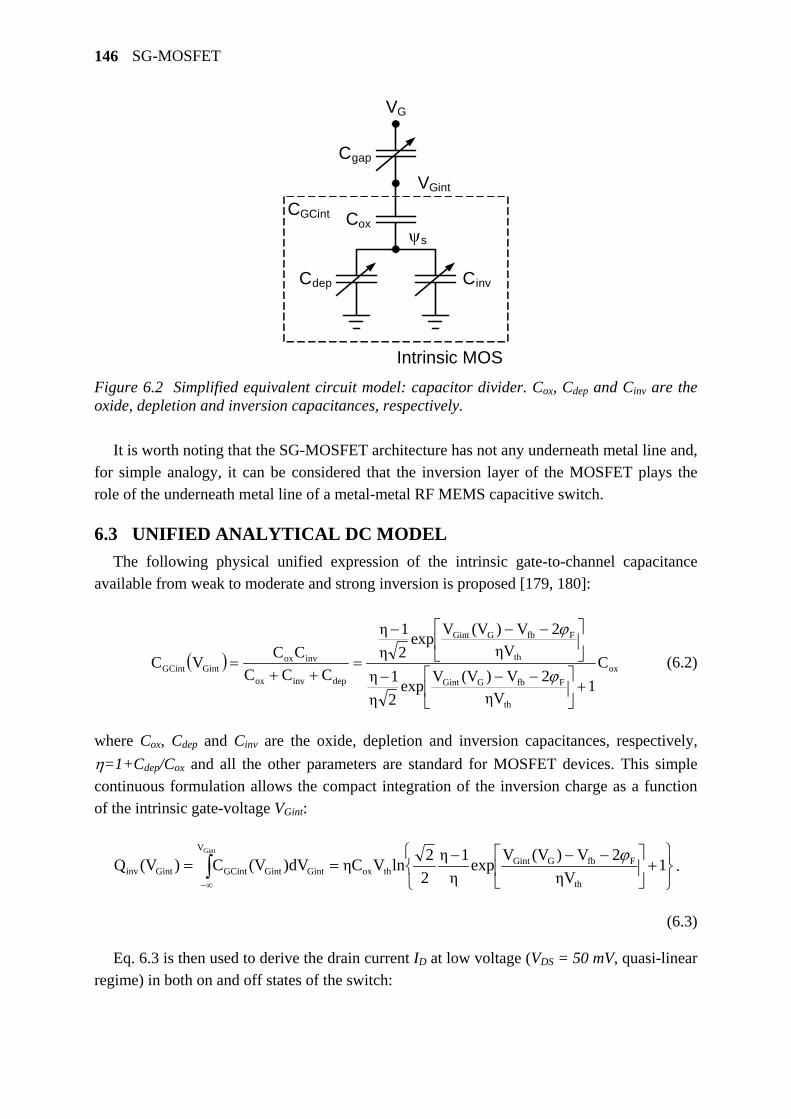
SG-MOSFET
146
Cgap
ψs
Intrinsic MOS
Cox
Cdep Cinv
VG
VGint
CGCint
Figure 6.2 Simplified equivalent circuit model: capacitor divider. Cox, Cdep and Cinv are the oxide, depletion and inversion capacitances, respectively.
It is worth noting that the SG-MOSFET architecture has not any underneath metal line and,
for simple analogy, it can be considered that the inversion layer of the MOSFET plays the role of the underneath metal line of a metal-metal RF MEMS capacitive switch.
6.3 UNIFIED ANALYTICAL DC MODEL The following physical unified expression of the intrinsic gate-to-channel capacitance
available from weak to moderate and strong inversion is proposed [179, 180]:
( ) ox
th
FfbGGint
th
FfbGGint
depinvox
invoxGintGCint C
1ηV
2V)(VVexp2η1η
ηV2V)(VVexp
2η1η
CCCCCVC
+⎥⎦
⎤⎢⎣
⎡ −−−
⎥⎦
⎤⎢⎣
⎡ −−−
=++
=ϕ
ϕ
(6.2)
where Cox, Cdep and Cinv are the oxide, depletion and inversion capacitances, respectively, η=1+Cdep/Cox and all the other parameters are standard for MOSFET devices. This simple continuous formulation allows the compact integration of the inversion charge as a function of the intrinsic gate-voltage VGint:
⎭⎬⎫
⎩⎨⎧
+⎥⎦
⎤⎢⎣
⎡ −−−== ∫
∞−
1ηV
2V)(VVexpη
1η22lnVηC)dV(VC)(VQ
th
FfbGGintthox
V
GintGintGCintGintinv
Gint ϕ.
(6.3)
Eq. 6.3 is then used to derive the drain current ID at low voltage (VDS = 50 mV, quasi-linear
regime) in both on and off states of the switch:
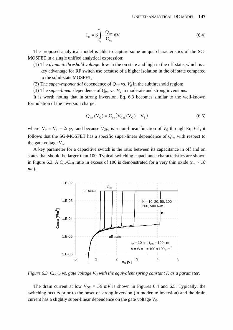
UNIFIED ANALYTICAL DC MODEL
147
∫ −=D
S
V
V ox
invD dV
CQβI (6.4)
The proposed analytical model is able to capture some unique characteristics of the SG-
MOSFET in a single unified analytical expression: (1) The dynamic threshold voltage: low in the on state and high in the off state, which is a
key advantage for RF switch use because of a higher isolation in the off state compared to the solid-state MOSFET;
(2) The super-exponential dependence of Qinv vs. Vg in the subthreshold region; (3) The super-linear dependence of Qinv vs. Vg in moderate and strong inversions. It is worth noting that in strong inversion, Eq. 6.3 becomes similar to the well-known
formulation of the inversion charge:
( )TGGintoxGinv V)(VVC)(VQ −= (6.5) where FfbT 2ηVV ϕ+= and because VGint is a non-linear function of VG through Eq. 6.1, it
follows that the SG-MOSFET has a specific super-linear dependence of Qinv with respect to the gate voltage VG.
A key parameter for a capacitive switch is the ratio between its capacitance in off and on states that should be larger than 100. Typical switching capacitance characteristics are shown in Figure 6.3. A Con/Coff ratio in excess of 100 is demonstrated for a very thin oxide (tox ~ 10 nm).
1.E-06
1.E-05
1.E-04
1.E-03
1.E-02
0 1 2 3 4 5VG [V]
CG
Cin
t [F/
m2 ]
tox = 10 nm, tgap = 190 nm
A = W x L = 100 x 100 μm2
~Cox
K = 10, 20, 50, 100200, 500 N/m
on state
off state
Figure 6.3 CGCint vs. gate voltage VG with the equivalent spring constant K as a parameter.
The drain current at low VDS = 50 mV is shown in Figures 6.4 and 6.5. Typically, the
switching occurs prior to the onset of strong inversion (in moderate inversion) and the drain current has a slightly super-linear dependence on the gate voltage VG.
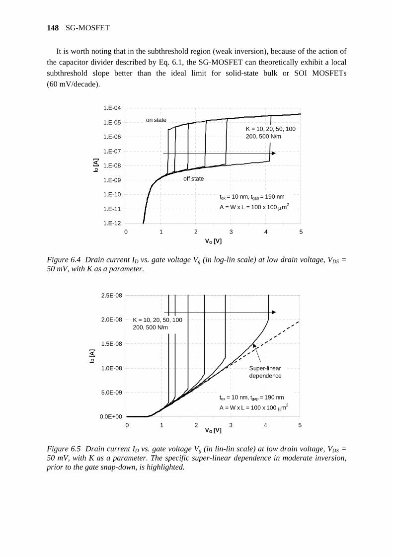
SG-MOSFET
148
It is worth noting that in the subthreshold region (weak inversion), because of the action of the capacitor divider described by Eq. 6.1, the SG-MOSFET can theoretically exhibit a local subthreshold slope better than the ideal limit for solid-state bulk or SOI MOSFETs (60 mV/decade).
1.E-12
1.E-11
1.E-10
1.E-09
1.E-08
1.E-07
1.E-06
1.E-05
1.E-04
0 1 2 3 4 5VG [V]
ID [A
]
tox = 10 nm, tgap = 190 nm
A = W x L = 100 x 100 μm2
K = 10, 20, 50, 100200, 500 N/m
on state
off state
Figure 6.4 Drain current ID vs. gate voltage Vg (in log-lin scale) at low drain voltage, VDS = 50 mV, with K as a parameter.
0.0E+00
5.0E-09
1.0E-08
1.5E-08
2.0E-08
2.5E-08
0 1 2 3 4 5VG [V]
ID [A
]
Super-linear dependence
tox = 10 nm, tgap = 190 nm
A = W x L = 100 x 100 μm2
K = 10, 20, 50, 100200, 500 N/m
Figure 6.5 Drain current ID vs. gate voltage Vg (in lin-lin scale) at low drain voltage, VDS = 50 mV, with K as a parameter. The specific super-linear dependence in moderate inversion, prior to the gate snap-down, is highlighted.
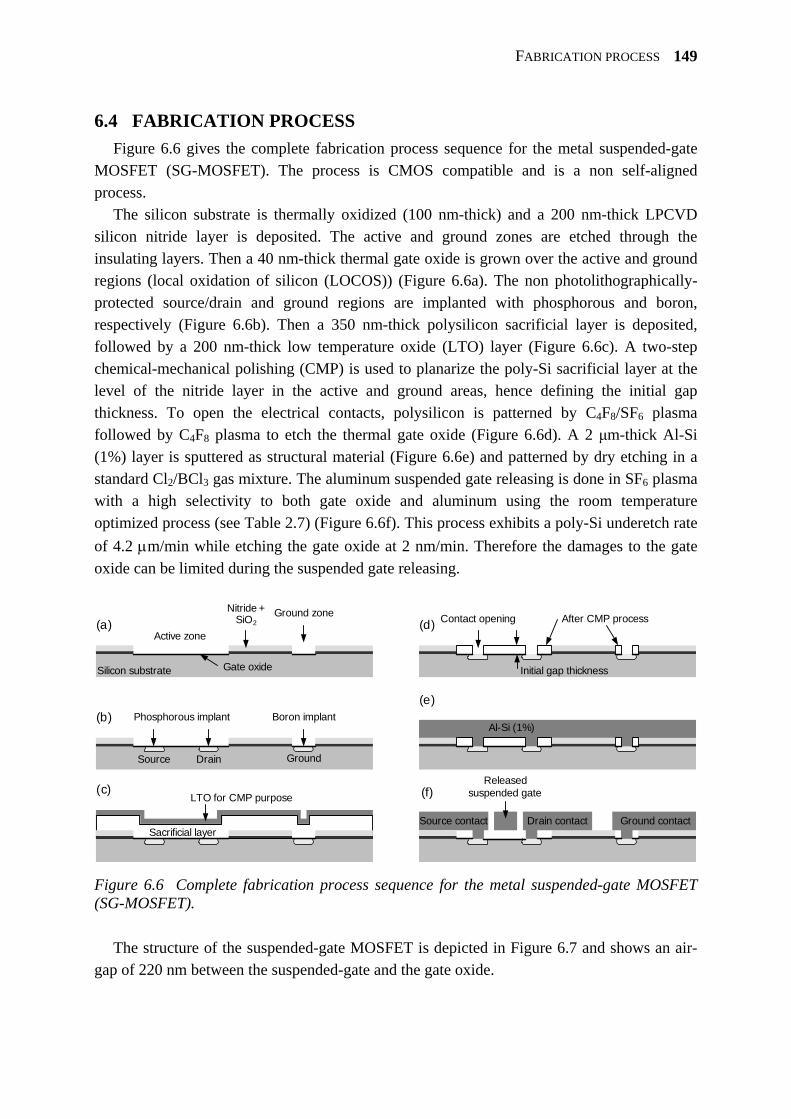
FABRICATION PROCESS
149
6.4 FABRICATION PROCESS Figure 6.6 gives the complete fabrication process sequence for the metal suspended-gate
MOSFET (SG-MOSFET). The process is CMOS compatible and is a non self-aligned process.
The silicon substrate is thermally oxidized (100 nm-thick) and a 200 nm-thick LPCVD silicon nitride layer is deposited. The active and ground zones are etched through the insulating layers. Then a 40 nm-thick thermal gate oxide is grown over the active and ground regions (local oxidation of silicon (LOCOS)) (Figure 6.6a). The non photolithographically-protected source/drain and ground regions are implanted with phosphorous and boron, respectively (Figure 6.6b). Then a 350 nm-thick polysilicon sacrificial layer is deposited, followed by a 200 nm-thick low temperature oxide (LTO) layer (Figure 6.6c). A two-step chemical-mechanical polishing (CMP) is used to planarize the poly-Si sacrificial layer at the level of the nitride layer in the active and ground areas, hence defining the initial gap thickness. To open the electrical contacts, polysilicon is patterned by C4F8/SF6 plasma followed by C4F8 plasma to etch the thermal gate oxide (Figure 6.6d). A 2 μm-thick Al-Si (1%) layer is sputtered as structural material (Figure 6.6e) and patterned by dry etching in a standard Cl2/BCl3 gas mixture. The aluminum suspended gate releasing is done in SF6 plasma with a high selectivity to both gate oxide and aluminum using the room temperature optimized process (see Table 2.7) (Figure 6.6f). This process exhibits a poly-Si underetch rate of 4.2 μm/min while etching the gate oxide at 2 nm/min. Therefore the damages to the gate oxide can be limited during the suspended gate releasing.
Sacrificial layer
Ground zone After CMP process
Phosphorous implant
Nitride + SiO2 Contact opening
Al-Si (1%)
Active zone
Boron implant
LTO for CMP purpose(c)
(b)
Source Drain Ground
(a)
Silicon substrate Gate oxide
(d)
Initial gap thickness
(e)
(f)
Ground contactDrain contactSource contact
Released suspended gate
Figure 6.6 Complete fabrication process sequence for the metal suspended-gate MOSFET (SG-MOSFET).
The structure of the suspended-gate MOSFET is depicted in Figure 6.7 and shows an air-
gap of 220 nm between the suspended-gate and the gate oxide.
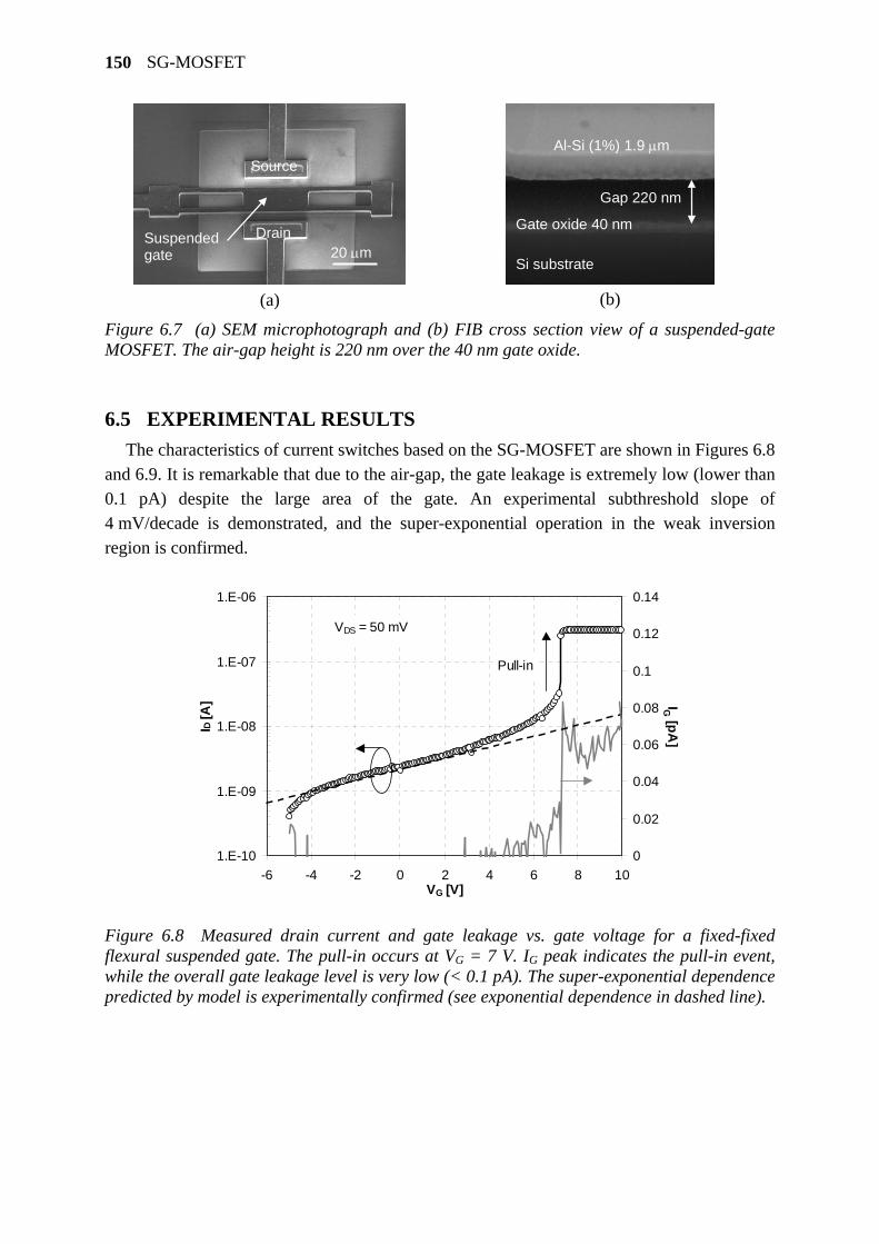
SG-MOSFET
150
Source
Drain Suspended gate 20 μm
(a)
Gap 220 nm
Gate oxide 40 nm
Al-Si (1%) 1.9 μm
Si substrate
(b)
Figure 6.7 (a) SEM microphotograph and (b) FIB cross section view of a suspended-gate MOSFET. The air-gap height is 220 nm over the 40 nm gate oxide.
6.5 EXPERIMENTAL RESULTS The characteristics of current switches based on the SG-MOSFET are shown in Figures 6.8
and 6.9. It is remarkable that due to the air-gap, the gate leakage is extremely low (lower than 0.1 pA) despite the large area of the gate. An experimental subthreshold slope of 4 mV/decade is demonstrated, and the super-exponential operation in the weak inversion region is confirmed.
1.E-10
1.E-09
1.E-08
1.E-07
1.E-06
-6 -4 -2 0 2 4 6 8 10VG [V]
ID [A
]
0
0.02
0.04
0.06
0.08
0.1
0.12
0.14
IG [pA]
VDS = 50 mV
Pull-in
Figure 6.8 Measured drain current and gate leakage vs. gate voltage for a fixed-fixed flexural suspended gate. The pull-in occurs at VG = 7 V. IG peak indicates the pull-in event, while the overall gate leakage level is very low (< 0.1 pA). The super-exponential dependence predicted by model is experimentally confirmed (see exponential dependence in dashed line).
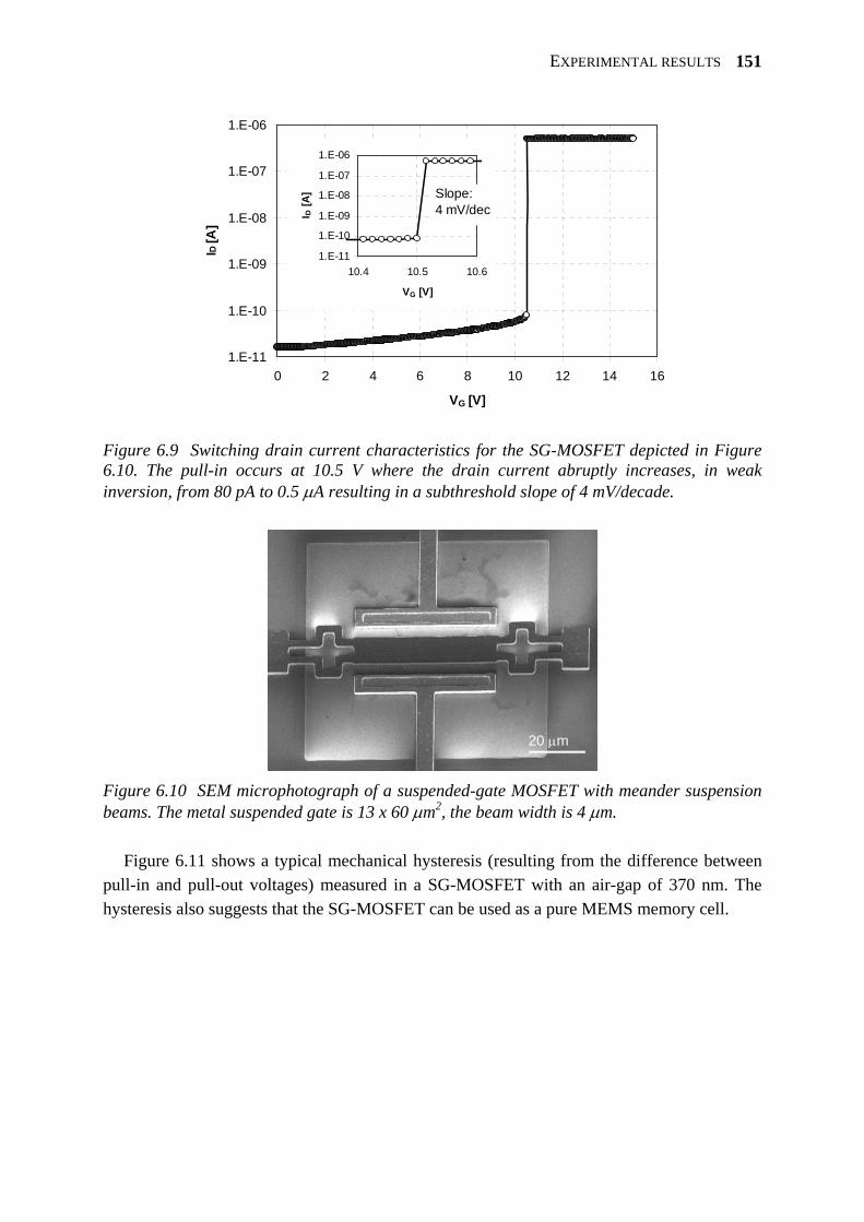
EXPERIMENTAL RESULTS
151
1.E-11
1.E-10
1.E-09
1.E-08
1.E-07
1.E-06
0 2 4 6 8 10 12 14 16
VG [V]
ID [A
]
1.E-11
1.E-10
1.E-09
1.E-08
1.E-07
1.E-06
10.4 10.5 10.6
VG [V]I D
[A] Slope:
4 mV/dec
Figure 6.9 Switching drain current characteristics for the SG-MOSFET depicted in Figure 6.10. The pull-in occurs at 10.5 V where the drain current abruptly increases, in weak inversion, from 80 pA to 0.5 μA resulting in a subthreshold slope of 4 mV/decade.
20 μm
Figure 6.10 SEM microphotograph of a suspended-gate MOSFET with meander suspension beams. The metal suspended gate is 13 x 60 μm2, the beam width is 4 μm.
Figure 6.11 shows a typical mechanical hysteresis (resulting from the difference between pull-in and pull-out voltages) measured in a SG-MOSFET with an air-gap of 370 nm. The hysteresis also suggests that the SG-MOSFET can be used as a pure MEMS memory cell.
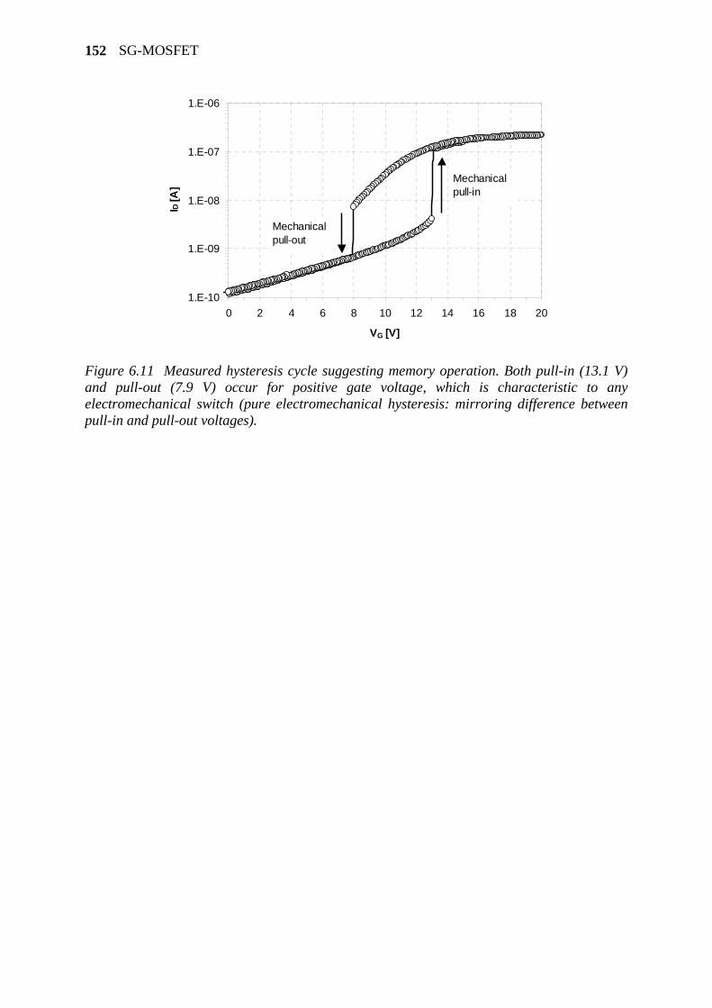
SG-MOSFET
152
1.E-10
1.E-09
1.E-08
1.E-07
1.E-06
0 2 4 6 8 10 12 14 16 18 20
VG [V]
ID [A
]Mechanical pull-in
Mechanical pull-out
Figure 6.11 Measured hysteresis cycle suggesting memory operation. Both pull-in (13.1 V) and pull-out (7.9 V) occur for positive gate voltage, which is characteristic to any electromechanical switch (pure electromechanical hysteresis: mirroring difference between pull-in and pull-out voltages).
CONCLUSIONS
153
6.6 CONCLUSIONS A novel MEMS device architecture: the SG-MOSFET, which combines a solid-state MOS
transistor and a metal suspended gate has been proposed as hybrid MEMS-MOS current switch.
A unified physical analytical model has been used to investigate main electrostatic characteristics and the influence of some design parameters. It has been shown that the control of the gate oxide thickness (< 20 nm) is essential for a high Con/Coff ratio (> 100). Other key results concern the specific super-exponential and super-linear drain current dependence on the gate voltage, at low drain voltage, and the possibility to obtain a subthreshold slope better than the theoretical solid-state bulk or SOI MOSFET limit of 60 mV/decade.
A fabrication process using polysilicon as a sacrificial layer has been developed to release metal gate suspended over gate oxide. The aluminum suspended gate releasing has been done in SF6 plasma using the room temperature optimized process described in chapter 2.
We have demonstrated very abrupt current switches, with subthreshold slope better than 10 mV/decade and ultra-low gate leakage (less than 0.001 pA/μm2) due to the air-gap.
Further investigation in our group about suspended-gate MOSFET devices has led to other
applications, where their figures of merit as CMOS-compatible architectures can bring new MEMS functionality to the solid-state MOS devices, such as: (i) ultra-low voltage micromechanical resonator based on resonant suspended-gate MOSFET [181] and (ii) 1T MEMS memory based on suspended-gate MOSFET [182].


Chapter 7 Summary and outlook

7.1 SUMMARY OF MAIN ACHIEVEMENTS The main achievements of this thesis can be summarized as follows: - A detailed and original study on SF6 inductively coupled plasma (ICP) releasing has
been performed in order to find the optimized process parameters. This study has emphasized the fact that temperature plays an important role in this process by limiting silicon dioxide etching. Moreover, the optimized recipe has been found to be independent of the sacrificial layer used (amorphous or polycrystalline silicon) and its thickness. Using this recipe, 15.6 μm/min Si underetch rate with high Si: SiO2 selectivity (> 20000: 1) has been obtained.
- Based on this SF6 plasma releasing, a metal surface micromachining process which is compatible with CMOS post-processing has been developed for the above-IC integration of MEMS tunable capacitors and suspended inductors. This involves a sputtered Al-Si (1%) structural layer and a sputtered a-Si sacrificial layer.
- It has been shown that an optimized design of the suspended membrane of single-air-gap and double-air-gap parallel-plate MEMS tunable capacitors and direct symmetrical current feed at both ports can significantly improve the quality factor and increase the self-resonant frequency, pushing it to 12 GHz and beyond. The maximum capacitance tuning range obtained for a single-air-gap capacitor is 29% for a bias voltage of 20 V. The maximum capacitance tuning range obtained for a double-air-gap capacitor is 207% for a bias voltage of 70 V.
- The post-processing of BiCMOS wafers has been successfully demonstrated to fabricate monolithically integrated VCOs with above-IC MEMS LC tank.
- Comparing a suspended inductor and the X-FAB inductor with the same design, it has been shown that increasing the thickness of the spiral from 2.3 to 4 μm and having the spiral suspended 3 μm above the passivation layers lead to an improvement factor of 2 for the peak quality factor and a shift of the self-resonant frequency beyond 15 GHz.
- No significant variation on bipolar and MOS transistors characteristics due to the post-processing has been observed and we conclude that the variation due to post-processing is in the same range as the wafer-to-wafer variation.
- Based on our metal surface micromachining process, coplanar waveguide (CPW) MEMS shunt capacitive switches and variable true-time delay lines (V-TTDLs) have been designed, fabricated and characterized in the 1 - 20 GHz range.
- A novel MEMS device architecture: the SG-MOSFET, which combines a solid-state MOS transistor and a metal suspended gate has been proposed as DC current switch. The corresponding fabrication process using polysilicon as a sacrificial layer has been developed to release metal gate suspended over gate oxide by SF6 plasma. Very abrupt current switches have been demonstrated with subthreshold slope better than 10 mV/decade (better than the theoretical solid-state bulk or SOI MOSFET limit of 60 mV/decade) and ultra-low gate leakage (less than 0.001 pA/μm2) due to the air-gap.
SUMMARY AND OUTLOOK
158
7.2 OUTLOOK RF MEMS devices and technology have recently experienced huge progress and gain of
credibility for industrialization; FBARs are today considered by many companies (Infineon, Samsung, Agilent, etc) as candidates for RF filters. On the other side, MEMS passive devices have also gained the needed maturity in order to be considered as true replacement components for the off-chip passives. With the above-IC integration approach, which was the final target of this work, the MEMS passives are today not only a solution for better performance and increased compactness but also a cost-effective alternative. For instance, NXP announced the take-off in the 2007-2008 frame of the MEMS passives into product.
Looking into the future, we believe that RF MEMS will play a role in communication applications beyond the replacement approach. It is clear that the resonator devices, which are making full circuit functions (like filtering or mixing) in a single device will open a true electromechanical signal processing era, with impact on new front-end architectures. Moreover, as shown in the last part of our work, some new hybrid devices integrated in-CMOS process could also contribute to a much faster integration of the new MEMS functions with CMOS. A lot of innovations are then expected at different levels:
- At technology level: to provide movable structures into traditional silicon processing; - At device level: to design and develop device architectures that can combine, as the
resonant gate transistor, principles of MEMS and solid-state devices to address low power and high performance;
- At circuit/system level: in order to exploit, by new adapted circuit architectures, the features brought by MEMS.
We are convinced that the future hybridization of MEMS and traditional ICs is a very interesting and promising alternative to the exclusive scaling of CMOS for future applications and products. The research and applications in the More-than-Moore era have just started to appear.
References
[1] C.T.-C. Nguyen, L.P.B. Katehi, and G.M. Rebeiz, "Micromachined devices for wireless communications", Proceedings of the IEEE, vol. 86, no. 8, pp. 1756-1768, Aug. 1998.
[2] H.A.C. Tilmans, "MEMS components for wireless communications", in Proceedings 16th European Conference on Solid-State Transducers (EUROSENSORS XVI), Prague, Czech Republic, Sept. 15-18, 2002, pp. 1-34.
[3] J.J. Yao, "RF MEMS from a device perspective", Journal of Micromechanics and Microengineering, vol. 10, no. 4, pp. R9-R38, Dec. 2000.
[4] S. Lucyszyn, "Review of radio frequency microelectromechanical systems technology", IEE Proceedings - Science, Measurement and Technology, vol. 151, no. 2, pp. 93-103, March 2004.
[5] P. Gammel, G. Fischer, and J. Bouchaud, "RF MEMS and NEMS technology, devices, and applications", Bell Labs Technical Journal, vol. 10, no. 3, pp. 29-59, Fall 2005.
[6] K. Lim, S. Pinel, M. Davis, A. Sutono, C.-H. Lee, D. Heo, A. Obatoynbo, J. Laskar, E.M. Tantzeris, and R. Tummala, "RF-system-on-package (SOP) for wireless communications", IEEE Microwave Magazine, vol. 3, no. 1, pp. 88-99, March 2002.
[7] S. Chakraborty, K. Lim, A. Sutono, E. Chen, S. Yoo, A. Obatoyinbo, S.-W. Yoon, M. Maeng, M.F. Davis, S. Pinel, and J. Laskar, "A 2.4-GHz radio front end in RF system-on-package technology", IEEE Microwave Magazine, vol. 3, no. 2, pp. 94-104, June 2002.
[8] H.A.C. Tilmans, W. De Raedt, and E. Beyne, "MEMS for wireless communications: 'from RF-MEMS components to RF-MEMS-SiP'", Journal of Micromechanics and Microengineering, vol. 13, no. 4, pp. S139-S163, July 2003.
[9] H. Lakdawala, X. Zhu, H. Luo, S. Santhanam, L.R. Carley, and G.K. Fedder, "Micromachined high-Q inductors in a 0.18-μm copper interconnect low-k dielectric CMOS process", IEEE Journal of Solid-State Circuits, vol. 37, no. 3, pp. 394-403, March 2002.
[10] G.K. Fedder, "CMOS-MEMS resonant mixer-filters", in IEEE International Electron Devices Meeting (IEDM '05) Technical Digest, Washington, DC, USA, Dec. 5-7, 2005, pp. 283-286.
[11] P. Robert, D. Saias, C. Billard, S. Boret, N. Sillon, C. Maeder-Pachurka, P.L. Charvet, G. Bouche, P. Ancey, and P. Berruyer, "Integrated RF-MEMS switch based on a combination of thermal and electrostatic actuation", in 12th International Conference on Solid-State Sensors, Actuators and Microsystems (TRANSDUCERS '03) Digest of Technical Papers, Boston, MA, USA, 8-12 June 2003, 2003, pp. 1714-1717.
REFERENCES
160
[12] D. Saias, P. Robert, S. Boret, C. Billard, G. Bouche, D. Belot, and P. Ancey, "An above IC MEMS RF switch", IEEE Journal of Solid-State Circuits, vol. 38, no. 12, pp. 2318-2324, Dec. 2003.
[13] M.-A. Dubois, J.-F. Carpentier, P. Vincent, C. Billard, G. Parat, C. Muller, P. Ancey, and P. Conti, "Monolithic Above-IC Resonator Technology for Integrated Architectures in Mobile and Wireless Communication", IEEE Journal of Solid-State Circuits, vol. 41, no. 1, pp. 7-16, Jan. 2006.
[14] E. Ollier, L. Duraffourg, M.-T. Delaye, R. Dianoux, S. Deneuville, V. Nguyen, H. Grange, T. Baron, P. Andreucci, D. Renaud, and P. Robert, "Thin SOI NEMS accelerometers compatible with in-IC integration", in Proceedings 20th Eurosensors Conference (EUROSENSORS XX), Göteborg, Sweden, Sept. 17-20, 2006, paper W2B-O6.
[15] A. Partridge, M. Lutz, and S. Kronmueller, "Microelectromechanical systems and devices having thin film encapsulated mechanical structures", Patent, US 7075160 B2, 2006.
[16] R.N. Candler, M.A. Hopcroft, B. Kim, W.-T. Park, R. Melamud, M. Agarwal, G. Yama, A. Partridge, M. Lutz, and T.W. Kenny, "Long-term and accelerated life testing of a novel single-wafer vacuum encapsulation for MEMS resonators", Journal of Microelectromechanical Systems, vol. 15, no. 6, pp. 1446-1456, Dec. 2006.
[17] E. Beyne, "3D interconnection and packaging: impending reality or still a dream?" in IEEE International Solid-State Circuits Conference (ISSCC '04) Digest of Technical Papers, San Francisco, CA, USA, Feb. 15-19, 2004, pp. 138-139.
[18] E. Beyne, "3D system integration technologies", in International Symposium on VLSI Technology, Systems, and Applications, Hsinchu, Taiwan, April 24-26, 2006, pp. 1-9.
[19] M. Madou, Fundamentals of microfabrication. Boca Raton, FL, USA: CRC Press LCC, 1997.
[20] M. Elwenspoek, and H.V. Jansen, Silicon micromachining. Cambridge, UK: Cambridge University Press, 1998.
[21] J.M. Bustillo, R.T. Howe, and R.S. Muller, "Surface micromachining for microelectromechanical systems", Proceedings of the IEEE, vol. 86, no. 8, pp. 1552-1574, Aug. 1998.
[22] G.T.A. Kovacs, N.I. Maluf, and K.E. Petersen, "Bulk micromachining of silicon", Proceedings of the IEEE, vol. 86, no. 8, pp. 1536-1551, Aug. 1998.
[23] H.C. Nathanson, W.E. Newell, R.A. Wickstrom, and J.R. Davis, Jr., "The resonant gate transistor", IEEE Transactions on Electron Devices, vol. 14, no. 3, pp. 117-133, March 1967.
[24] R.T. Howe, and R.S. Muller, "Polycrystalline silicon micromechanical beams", Journal of the Electrochemical Society, vol. 130, no. 6, pp. 1420-1423, June 1983.
[25] R.T. Howe, and R.S. Muller, "Resonant-microbridge vapor sensor", IEEE Transactions on Electron Devices, vol. 33, no. 4, pp. 499-506, April 1986.
[26] K.E. Petersen, "Silicon as a mechanical material", Proceedings of the IEEE, vol. 70, no. 5, pp. 420-457, May 1982.
[27] R. Legtenberg, A.C. Tilmans, J. Elders, and M. Elwenspoek, "Stiction of surface micromachined structures after rinsing and drying: model and investigation of adhesion mechanisms", Sensors and Actuators A, vol. 43, no. 1-3, pp. 230-238, May 1994.
[28] R. Legtenberg, and H.A.C. Tilmans, "Electrostatically driven vacuum-encapsulated polysilicon resonators Part I. Design and fabrication", Sensors and Actuators A, vol. 45, no. 1, pp. 57-66, Oct. 1994.
161
[29] C.W. Dyck, J.H. Smith, S.L. Millera, E.M. Russick, and C.L. Adkins, "Supercritical carbon dioxide solvent extraction from surface micromachined micromechanical structures", Proceedings of SPIE, vol. 2879, no. 11 (Part 1), pp. 225-235, Oct. 1996.
[30] K. Deng, R.J. Collins, M. Mehregany, and C.N. Sukenik, "Performance impact of monolayer coating of polysilicon micromotors", in Proceedings IEEE Workshop on Micro Electro Mechanical Systems (MEMS '95), Amsterdam, The Netherlands, Jan. 29-Feb. 2, 1995, pp. 368-373.
[31] C.H. Mastrangelo, and G.S. Saloka, "A dry-release method based on polymer columns for microstructure fabrication", in Proceedings 'An Investigation of Micro Structures, Sensors, Actuators, Machines and Systems', IEEE Micro Electro Mechanical Systems (MEMS '93), Fort Lauderdale, FL, USA, Feb. 7-10, 1993, pp. 77-81.
[32] J. Bühler, F.-P. Steiner, and H. Baltes, "Silicon dioxide sacrificial layer etching in surface micromachining", Journal of Micromechanics and Microengineering, vol. 7, no. 1, pp. R1-R13, March 1997.
[33] S. Sedky, A. Witvrouw, and K. Baert, "Poly SiGe, a promising material for MEMS post-processing on top of standard CMOS wafers", in 11th International Conference on Solid-State Sensors and Actuators (TRANSDUCERS '01) and EUROSENSORS XV Digest of Technical Papers, Munich, Germany, June 10-14, 2001, pp. 988-991.
[34] T. Overstolz, P.A. Clerc, W. Noell, M. Zickar, and N.F. de Rooij, "A clean wafer-scale chip-release process without dicing based on vapor phase etching", in 17th IEEE International Conference on Micro Electro Mechanical Systems (MEMS '04) Technical Digest, Maastricht, The Netherlands, Jan. 25-29, 2004, pp. 717-720.
[35] Sandia National Laboratories, http://mems.sandia.gov/tech-info/summit-v.html. [36] MEMSCAP, Inc., http://www.memscap.com/en_mumps.html. [37] HD MicroSystems, L.L.C., http://www.hdmicrosystems.com/prod/process.html. [38] C.W. Storment, D.A. Borkholder, V. Westerlind, J.W. Suh, N.I. Maluf, and G.T.A.
Kovacs, "Flexible, dry-released process for aluminum electrostatic actuators", Journal of Microelectromechanical Systems, vol. 3, no. 3, pp. 90-96, Sept. 1994.
[39] J.J. Yao, and M.F. Chang, "A surface micromachined miniature switch for telecommunications applications with signal frequencies from DC up to 4 GHz", in Proceedings 8th International Conference on Solid-State Sensors and Actuators (TRANSDUCERS '95) and EUROSENSORS IX, Stockholm, Sweden, June 25-29, 1995, pp. 384-387.
[40] A. Bagolini, L. Pakula, T.L.M. Scholtes, H.T.M. Pham, P.J. French, and P.M. Sarro, "Polyimide sacrificial layer and novel materials for post-processing surface micromachining", Journal of Micromechanics and Microengineering, vol. 12, no. 4, pp. 385-389, July 2002.
[41] K.A. Honer, and G.T.A. Kovacs, "Sputtered silicon for integrated MEMS applications", in Solid-State Sensor and Actuator Workshop Technical Digest, Hilton Head Island, SC, USA, June 4-8, 2000, pp. 308-311.
[42] K.A. Honer, and G.T.A. Kovacs, "Integration of sputtered silicon microstructures with pre-fabricated CMOS circuitry", Sensors and Actuators A, vol. 91, no. 3, pp. 386-397 2001.
[43] C. Luo, J. Garra, T. Schneider, R. White, J. Currie, and M. Paranjape, "A new method to release SU-8 structures using polystyrene for MEMS applications", in Proceedings 16th European Conference on Solid-State Transducers (EUROSENSORS XVI), Prague, Czech Republic, Sept. 15-18, 2002, pp. 168-171.
[44] J. Zou, C. Liu, J. Schutt-Aine, J. Chen, and S.-M. Kang, "Development of a wide tuning range MEMS tunable capacitor for wireless communication systems", in IEEE
REFERENCES
162
International Electron Devices Meeting (IEDM '00) Technical Digest, San Francisco, CA, USA, Dec. 11-13, 2000, pp. 403-406.
[45] O. Paul, D. Westberg, M. Hornung, V. Ziebart, and H. Baltes, "Sacrificial aluminum etching for CMOS microstructures", in Proceedings 10th Annual International Workshop on Micro Electro Mechanical Systems (MEMS '97), Nagoya, Japan, Jan. 26-30, 1997, pp. 523-528.
[46] D.L. Flamm, "Mechanisms of silicon etching in fluorine- and chlorine-containing plasmas", Pure and Applied Chemistry, vol. 62, no. 9, pp. 1709-1720, Sept. 1990.
[47] D.E. Ibbotson, J.A. Mucha, D.L. Flamm, and J.M. Cook, "Plasmaless dry etching of silicon with fluorine-containing compounds", Journal of Applied Physics, vol. 56, no. 10, pp. 2939-2942, Nov. 1984.
[48] H. Stahl, A. Hoechst, F. Fischer, L. Metzger, R. Reichenbach, F. Laermer, S. Kronmueller, K. Breitschwerdt, R. Gunn, S. Watcham, C. Rusu, and A. Witvrouw, "Thin film encapsulation of acceleration sensors using polysilicon sacrificial layers", in 12th International Conference on Solid-State Sensors, Actuators and Microsystems (TRANSDUCERS '03) Digest of Technical Papers, Boston, MA, USA, June 8-12, 2003, pp. 1899-1902.
[49] X.-Q. Wang, X. Yang, K. Walsh, and Y.-C. Tai, "Gas-phase silicon etching with bromine trifluoride", in 9th International Conference on Solid State Sensors and Actuators (TRANSDUCERS '97) Digest of Technical Papers, Chicago, IL, USA, June 16-19, 1997, pp. 1505-1508.
[50] Y.-C. Tai, and X.-O. Wang, "Gas phase silicon etching with bromine trifluoride", Patent, US 6436229 B2, 2002.
[51] H.F. Winters, and J.W. Coburn, "The etching of silicon with XeF2 vapor", Applied Physics Letters, vol. 34, no. 1, pp. 70-73, Jan. 1979.
[52] E. Hoffman, B. Warneke, E. Kruglick, J. Weigold, and K.S.J. Pister, "3D structures with piezoresistive sensors in standard CMOS", in Proceedings IEEE Workshop on Micro Electro Mechanical Systems (MEMS '95), Amsterdam, The Netherlands, Jan. 29-Feb. 2, 1995, pp. 288-293.
[53] D.E. Ibbotson, D.L. Flamm, J.A. Mucha, and V.M. Donnelly, "Comparison of XeF2 and F-atom reactions with Si and SiO2", Applied Physics Letters, vol. 44, no. 12, pp. 1129-1131, June 1984.
[54] K.R. Williams, and R.S. Muller, "Etch rates for micromachining processing", Journal of Microelectromechanical Systems, vol. 5, no. 4, pp. 256-269, Dec. 1996.
[55] M.J.M. Vugts, M.F.A. Eurlings, L.J.F. Hermans, and H.C.W. Beijerincka, "Si/XeF2 etching: Reaction layer dynamics and surface roughening", Journal of Vacuum Science and Technology A, vol. 4, no. 5, pp. 2780-2789, Sept./Oct. 1996.
[56] L. Metzger, F. Fischer, and W. Mokwa, "Polysilicon sacrificial layer etching using XeF2 for silicon acceleration sensors with high aspect ratio", in 16th European Conference on Solid-State Transducers (EUROSENSORS XVI), Prague, Czech Republic, Sept. 15-18, 2002, pp. 429-432.
[57] B. Bahreyni, and C. Shafaia, "Investigation and simulation of XeF2 isotropic etching of silicon", Journal of Vacuum Science and Technology A, vol. 20, no. 6, pp. 1850-1854, Nov./Dec. 2002.
[58] K.R. Williams, K. Gupta, and M. Wasilik, "Etch rates for micromachining processing-Part II", Journal of Microelectromechanical Systems, vol. 12, no. 6, pp. 761-778, Dec. 2003.
[59] T. Kawakubo, T. Nagano, M. Nishigaki, K. Abe, and K. Itaya, "Piezoelectric RF MEMS tunable capacitor with 3V operation using CMOS compatible materials and
163
process", in IEEE International Electron Devices Meeting (IEDM '05) Technical Digest, Washington, DC, USA, Dec. 5-7, 2005, pp. 303-306.
[60] Xactix, Inc., http://www.xactix.com/. [61] K.M. Eisele, "SF6, a preferable etchant for plasma etching silicon", Journal of the
Electrochemical Society, vol. 128, no. 1, pp. 123-126, Jan. 1981. [62] F. Laermer, A. Schilp, K. Funk, and M. Offenberg, "Bosch deep silicon etching:
improving uniformity and etch rate for advanced MEMS applications", in 12th IEEE International Conference on Micro Electro Mechanical Systems (MEMS '99) Technical Digest, Orlando, FL, USA, Jan. 17-21, 1999, pp. 211-216.
[63] S. Aachboun, P. Ranson, C. Hibert, and M. Boufnichel, "Cryogenic etching of deep narrow trenches in silicon", Journal of Vacuum Science and Technology A, vol. 18, no. 4, pp. 1848-1852, July 2000.
[64] K.A. Honer, "Surface micromachining techniques for integrated microsystems", PhD dissertation, Stanford University, Stanford, CA, USA, 2001.
[65] X. Zhu, D.W. Greve, and G.K. Fedder, "Characterization of silicon isotropic etch by inductively coupled plasma etch in post-CMOS processing", in Proceedings 13th Annual International Conference on Micro Electro Mechanical Systems (MEMS '00), Miyazaki, Japan, Jan. 23-27, 2000, pp. 568-573.
[66] C.-L. Dai, K. Yen, and P.-Z. Chang, "Applied electrostatic parallelogram actuators for microwave switches using the standard CMOS process", Journal of Micromechanics and Microengineering, vol. 11, no. 6, pp. 697-702, Nov. 2001.
[67] D.R. Stull, "Vapor pressure of pure substances. Organic and inorganic compounds", Industrial and Engineering Chemistry, vol. 39, no. 4, pp. 517-550, April 1947.
[68] S. Wolf, and R.N. Tauber, Silicon processing for the VLSI era: Process technology, vol. 1. Sunset Beach, CA, USA: Lattice Press, 1986.
[69] Idonus Sarl, http://www.idonus.com/. [70] S.M. Sze, VLSI technology, 2nd ed. New York: McGraw-Hill, 1988. [71] S. Sedky, A. Witvrouw, H. Bender, and K. Baert, "Experimental determination of the
maximum post-process annealing temperature for standard CMOS wafers", IEEE Transactions on Electron Devices, vol. 48, no. 2, pp. 377-385, Feb. 2001.
[72] R. Bright, and A. Reisman, "Annealing of ionizing radiation induced defects in insulated gate field effect transistors using elevated pressure", Journal of the Electrochemical Society, vol. 140, no. 5, pp. 1482-1488, May 1993.
[73] CRC Handbook of chemistry and physics, 77th ed. Boca Raton, FL, USA: CRC Press, 1996.
[74] D.J. Young, and B.E. Boser, "A micromachined variable capacitor for monolithic low-noise VCO's", in Solid-State Sensor and Actuator Workshop Technical Digest, Hilton Head Island, SC, USA, June 2-6, 1996, pp. 86-89.
[75] J. De Coster, R. Puers, H.A.C. Tilmans, J.T.M. van Beek, and T.G.S.M. Rijks, "Variable RF MEMS capacitors with extended tuning range", in 12th International Conference on Solid-State Sensors, Actuators and Microsystems (TRANSDUCERS '03) Digest of Technical Papers, Boston, MA, USA, June 8-12, 2003, pp. 1784-1787.
[76] G. Bruno, P. Capezzuto, and A. Madan, Plasma deposition of amorphous silicon-based materials. San Diego, CA, USA: Academic Press, 1995.
[77] G.G. Stoney, "The tension of metallic films deposited by electrolysis", Proceedings of the Royal Society of London. Series A, Containing Papers of a Mathematical and Physical Character, vol. 82, no. 553, pp. 172-175, May 1909.
[78] J.A. Thornton, "The microstructure of sputter-deposited coatings", Journal of Vacuum Science and Technology A, vol. 4, no. 6, pp. 3059-3065, Nov./Dec. 1986.
[79] WebElements Ltd, http://www.webelements.com/.
REFERENCES
164
[80] M. Chinmulgund, R.B. Inturi, and J.A. Barnard, "Effect of Ar gas pressure on growth, structure, and mechanical properties of sputtered Ti, Al, TiAl, and Ti3Al films", Thin Solid Films, vol. 270, no. 1-2, pp. 260-263, Dec. 1995.
[81] C.-L. Dai, "In situ electrostatic microactuators for measuring the Young’s modulus of CMOS thin films", Journal of Micromechanics and Microengineering, vol. 13, no. 5, pp. 563-567, Sept. 2003.
[82] M. Soyuer, K.A. Jenkins, J.N. Burghartz, and M.D. Hulvey, "A 3-V 4-GHz nMOS voltage-controlled oscillator with integrated resonator", IEEE Journal of Solid-State Circuits, vol. 31, no. 12, pp. 2042-2045, Dec. 1996.
[83] A.-S. Porret, T. Melly, C.C. Enz, and E.A. Vittoz, "Design of high-Q varactors for low-power wireless applications using a standard CMOS process", IEEE Journal of Solid-State Circuits, vol. 35, no. 3, pp. 337-345, March 2000.
[84] P. Andreani, and S. Mattisson, "On the use of MOS varactors in RF VCOs", IEEE Journal of Solid-State Circuits, vol. 35, no. 6, pp. 905-910, June 2000.
[85] J.I. Seeger, and S.B. Crary, "Stabilization of electrostatically actuated mechanical devices", in 9th International Conference on Solid State Sensors and Actuators (TRANSDUCERS '97) Digest of Technical Papers, Chicago, IL, USA, June 16-19, 1997, pp. 1133-1136.
[86] E.K. Chan, and R.W. Dutton, "Electrostatic micromechanical actuator with extended range of travel", Journal of Microelectromechanical Systems, vol. 9, no. 3, pp. 321-328, Sept. 2000.
[87] E.S. Hung, and S.D. Senturia, "Extending the travel range of analog-tuned electrostatic actuators", Journal of Microelectromechanical Systems, vol. 8, no. 4, pp. 497-505, Dec. 1999.
[88] L. Fan, R.T. Chen, A. Nespola, and M.C. Wu, "Universal MEMS platforms for passive RF components: suspended inductors and variable capacitors", in Proceedings 11th Annual International Workshop on Micro Electro Mechanical Systems (MEMS '98), Heidelberg, Germany, Jan. 25-29, 1998, pp. 29-33.
[89] M. Bakri-Kassem, and R.R. Mansour, "Two movable-plate nitride-loaded MEMS variable capacitor", IEEE Transactions on Microwave Theory and Techniques, vol. 52, no. 3, pp. 831-837, March 2004.
[90] C.L. Goldsmith, A. Malczewski, Z.J. Yao, S. Chen, J. Ehmke, and D.H. Hinzel, "RF MEMS variable capacitors for tunable filters", International Journal of RF and Microwave Computer-Aided Engineering, vol. 9, no. 4, pp. 362-374, July 1999.
[91] N. Hoivik, M.A. Michalicek, Y.C. Lee, K.C. Gupta, and V.M. Bright, "Digitally controllable variable high-Q MEMS capacitor for RF applications", in IEEE MTT-S International Microwave Symposium Digest, Phoenix, AZ, USA, May 20-25, 2001, pp. 2115-2118.
[92] A. Dec, and K. Suyama, "Micromachined electro-mechanically tunable capacitors and their applications to RF IC's", IEEE Transactions on Microwave Theory and Techniques, vol. 46, no. 12, pp. 2587-2596, Dec. 1998.
[93] J. Zou, C. Liu, and J.E. Schutt-Ainé, "Development of a wide-tuning-range two-parallel-plate tunable capacitor for integrated wireless communication systems", International Journal of RF and Microwave Computer-Aided Engineering, vol. 11, no. 5, pp. 322-329, Sept. 2001.
[94] H. Nieminen, V. Ermolov, K. Nybergh, S. Silanto, and T. Ryhänen, "Microelectromechanical capacitors for RF applications", Journal of Micromechanics and Microengineering, vol. 12, no. 2, pp. 177-186, March 2002.
165
[95] L. Dussopt, and G.M. Rebeiz, "High-Q millimeter-wave MEMS varactors: extended tuning range and discrete-position designs", in IEEE MTT-S International Microwave Symposium Digest, Seattle, WA, USA, June 2-7, 2002, pp. 1205-1208.
[96] Z. Xiao, W. Peng, R.F. Wolffenbuttel, and K.R. Farmer, "Micromachined variable capacitor with wide tuning range", in Solid-State Sensor and Actuator Workshop Technical Digest, Hilton Head Island, SC, USA, June 2-6, 2002, pp. 346-349.
[97] A.J. Gallant, and D. Wood, "The role of fabrication techniques on the performance of widely tunable micromachined capacitors", Sensors and Actuators A, vol. 110, no. 1-3, pp. 423-431, Feb. 2004.
[98] J. van Beek, M. van Delden, A. Jansman, A. Boogaard, and A. Kemmeren, "The integration of RF passives using thin-film technology on high-ohmic Si in combination with thick-film interconnect", in Proceedings 34th International Symposium on Microelectronics (IMAPS '01), Baltimore, MD, USA, Oct. 9-11, 2001, pp. 467-470.
[99] T.G.S.M. Rijks, J.T.M. van Beek, P.G. Steeneken, M.J.E. Ulenaers, J. De Coster, and R. Puers, "RF MEMS tunable capacitors with large tuning ratio", in 17th IEEE International Conference on Micro Electro Mechanical Systems (MEMS '04) Technical Digest, Maastricht, The Netherlands, Jan. 25-29, 2004, pp. 777-780.
[100] D. Peroulis, and L.P.B. Katehi, "Electrostatically-tunable analog RF MEMS varactors with measured capacitance range of 300%", in IEEE MTT-S International Microwave Symposium Digest, Philadelphia, PA, USA, June 8-13, 2003, pp. 1793-1796.
[101] E.S. Hung, and S.D. Senturia, "Tunable capacitors with programmable capacitance-voltage characteristic", in Solid-State Sensor and Actuator Workshop Technical Digest, Hilton Head Island, SC, USA, June 8-11, 1998, pp. 292-295.
[102] J.Y. Park, H.-T. Kim, Y. Kwon, and Y.-K. Kim, "A tunable millimeter-wave filter using coplanar waveguide and micromachined variable capacitors", in 10th International Conference on Solid-State Sensors and Actuators (TRANSDUCERS '99) Digest of Technical Papers, Sendai, Japan, June 7-10, 1999, pp. 1272-1275.
[103] G.V. Ionis, A. Dec, and K. Suyama, "A zipper-action differential micro-mechanical tunable capacitor", in Proceedings Microelectromechanical Systems Conference, Berkeley, CA, USA, Aug. 24-26, 2001, pp. 29-32.
[104] H.D. Wu, K.F. Harsh, R.S. Irwin, W. Zhang, A.R. Mickelson, Y.C. Lee, and J.B. Dobsa, "MEMS designed for tunable capacitors", in IEEE MTT-S International Microwave Symposium Digest, Baltimore, MD, USA, June 7-12, 1998, pp. 127-129.
[105] J.R. Reid, V.M. Bright, and J.H. Comtois, "Automated assembly of flip-up micromirrors", in 9th International Conference on Solid State Sensors and Actuators (TRANSDUCERS '97) Digest of Technical Papers, Chicago, IL, USA, June 16-19, 1997, pp. 347-350.
[106] K.F. Harsh, W. Zhang, V.M. Bright, and Y.C. Lee, "Flip-chip assembly for Si-based RF MEMS", in 12th IEEE International Conference on Micro Electro Mechanical Systems (MEMS '99) Technical Digest, Orlando, Florida, USA, Jan. 17-21, 1999, pp. 273-278.
[107] K.F. Harsh, B. Su, W. Zhang, V.M. Bright, and Y.C. Lee, "The realization and design considerations of a flip-chip integrated MEMS tunable capacitor", Sensors and Actuators A, vol. 80, no. 2, pp. 108-118, March 2000.
[108] Z. Feng, W. Zhang, B. Su, K.F. Harsh, K.C. Gupta, V. Bright, and Y.C. Lee, "Design and modeling of RF MEMS tunable capacitors using electro-thermal actuators", in IEEE MTT-S International Microwave Symposium Digest, Anaheim, CA, USA, June 13-19, 1999, pp. 1507-1510.
REFERENCES
166
[109] Z. Feng, H. Zhang, W. Zhang, B. Su, K.C. Gupta, V.M. Bright, and Y.C. Lee, "MEMS-based variable capacitor for millimeter-wave applications", in Solid-State Sensor and Actuator Workshop Technical Digest, Hilton Head Island, SC, USA, June 4-8, 2000, pp. 255-258.
[110] A. Oz, and G.K. Fedder, "RF CMOS-MEMS capacitor having large tuning range", in 12th International Conference on Solid-State Sensors, Actuators and Microsystems (TRANSDUCERS '03) Digest of Technical Papers, Boston, MA, USA, June 8-12, 2003, pp. 851-854.
[111] J.Y. Park, Y.J. Yee, H.J. Nam, and J.U. Bu, "Micromachined RF MEMS tunable capacitors using piezoelectric actuators", in IEEE MTT-S International Microwave Symposium Digest, Phoenix, AZ, USA, May 20-25, 2001, pp. 2111-2114.
[112] L.E. Larson, R.H. Hackett, M.A. Melendes, and R.F. Lohr, "Micromachined microwave actuator (MIMAC) technology: a new tuning approach for microwave integrated circuits", in IEEE Microwave and Millimeter-Wave Monolithic Circuits Symposium Digest of Papers, Boston, MA, USA, June 10-11, 1991, pp. 27-30.
[113] J.J. Yao, S. Park, and J. DeNatale, "High tuning-ratio MEMS-based tunable capacitors for RF communications applications", in Solid-State Sensor and Actuator Workshop, Hilton Head Island, SC, USA, June 8-11, 1998, pp. 124-127.
[114] J.J. Yao, S. Park, R. Anderson, and J. DeNatale, "A low power / low voltage electrostatic actuator for RF MEMS applications", in Solid-State Sensor and Actuator Workshop Technical Digest, Hilton Head Island, SC, USA, June 4-8, 2000, pp. 246-249.
[115] R.L. Borwick III, P.A. Stupar, J. DeNatale, R. Anderson, C. Tsai, K. Garrett, and R. Erlandson, "A high Q, large tuning range MEMS capacitor for RF filter systems", Sensors and Actuators A, vol. 103, no. 1-2, pp. 33-41, Jan. 2003.
[116] H.D. Nguyen, D. Hah, P.R. Patterson, R. Chao, W. Piyawattanametha, E.K. Lau, and M.C. Wu, "Angular vertical comb-driven tunable capacitor with high-tuning capabilities", Journal of Microelectromechanical Systems, vol. 13, no. 3, pp. 406-413, June 2004.
[117] S. Seok, W. Choi, and K. Chun, "A novel linearly tunable MEMS variable capacitor", Journal of Micromechanics and Microengineering, vol. 12, no. 1, pp. 82-86, Jan. 2002.
[118] A. Cruau, G. Lissorgues, P. Nicole, D. Placko, and A.M. Ionescu, "V-shaped micromechanical tunable capacitors for RF applications", Microsystem Technologies, vol. 12, no. 1-2, pp. 15-20, Dec. 2005.
[119] J.-B. Yoon, and C.T.-C. Nguyen, "A high-Q tunable micromechanical capacitor with movable dielectric for RF applications", in IEEE International Electron Devices Meeting (IEDM '00) Technical Digest, San Francisco, CA, USA, Dec. 11-13, 2000, pp. 489-492.
[120] A. Tombak, J.-P. Maria, F. Ayguavives, Z. Jin, G.T. Stauf, A.I. Kingon, and A. Mortazawi, "Tunable barium strontium titanate thin film capacitors for RF and microwave applications", IEEE Microwave and Wireless Components Letters, vol. 12, no. 1, pp. 3-5, Jan. 2002.
[121] E.G. Erker, A.S. Nagra, Y. Liu, P. Periaswamy, T.R. Taylor, J. Speck, and R.A. York, "Monolithic Ka-band phase shifter using voltage tunable BaSrTiO/sub 3/ parallel plate capacitors", IEEE Microwave and Guided Wave Letters, vol. 10, no. 1, pp. 10-12, Jan. 2000.
[122] G.M. Rebeiz, RF MEMS: Theory, Design and Technology. Hoboken, NJ, USA: Wiley InterScience, John Wiley & Sons, 2003.
167
[123] J.R. Reid, "Dielectric charging effects on capacitive MEMS actuators", in IEEE MTT-S International Microwave Symposium, RF MEMS Workshop, Phoenix, AZ, USA, May, 2001.
[124] J. DeNatale, and R. Mihailovich, "RF MEMS reliability", in 12th International Conference on Solid-State Sensors, Actuators and Microsystems (TRANSDUCERS '03) Digest of Technical Papers, Boston, MA, USA, June 8-12, 2003, pp. 943-946.
[125] O. Bochobza-Degani, E. Socher, and Y. Nemirovsky, "On the effect of residual charges on the pull-in parameters of electrostatic actuators", in 11th International Conference on Solid-State Sensors and Actuators (TRANSDUCERS '01) and EUROSENSORS XV Digest of Technical Papers, Munich, Germany, June 10-14, 2001, pp. 292-295.
[126] R.J. Roark, and W.C. Young, Roark's Formulas for Stress & Strain, 6th ed. New York: McGraw-Hill, 1989.
[127] S.M. Sze, Semiconductor Devices: Physics and Technology, 2nd ed. New York: John Wiley & Sons, 2002.
[128] S. Ayoz, H.M. Tuncer, F. Udrea, A.M. Ionescu, and R. Fritschi, "A current density distribution approach to the optimisation of RF-MEMS variable capacitors", in Proceedings of SPIE, Smart Sensors, Actuators, and MEMS II, vol. 5836, Microtechnologies for the New Millennium, Smart Sensors, Actuators, and MEMS Conference, Sevilla, Spain, May 9-11, 2005, pp. 527-534.
[129] D.M. Pozar, Microwave Engineering, 2nd ed. New York: John Wiley & Sons, 1998. [130] H. Nieminen, V. Ermolov, S. Silanto, K. Nybergh, and T. Ryhänen, "Design of a
temperature-stable RF MEMS capacitor", Journal of Microelectromechanical Systems, vol. 13, no. 5, pp. 705-714, Oct. 2004.
[131] H.A.C. Tilmans, H. Ziad, H. Jansen, O. Di Monaco, A. Jourdain, W. De Raedt, X. Rottenberg, E. De Backer, A. Decaussernaeker, and K. Baert, "Wafer-level packaged RF-MEMS switches fabricated in a CMOS fab", in IEEE International Electron Devices Meeting (IEDM '01) Technical Digest, Washington, DC, USA, Dec. 2-5, 2001, pp. 921-924.
[132] J. Oberhammer, and G. Stemme, "BCB contact printing for patterned adhesive full-wafer bonded 0-level packages", Journal of Microelectromechanical Systems, vol. 14, no. 2, pp. 419-425, April 2005.
[133] A. Jourdain, X. Rottenberg, G. Carchon, and H.A.C. Tilmans, "Optimization of 0-level packaging for RF-MEMS devices", in 12th International Conference on Solid-State Sensors, Actuators and Microsystems (TRANSDUCERS '03) Digest of Technical Papers, Boston, MA, USA, June 8-12, 2003, pp. 1915-1918.
[134] D. Ham, and A. Hajimiri, "Concepts and methods in optimization of integrated LC VCOs", IEEE Journal of Solid-state Circuits, vol. 36, no. 6, pp. 896-909, June 2001.
[135] D.J. Young, and B.E. Boser, "A micromachine-based RF low-noise voltage-controlled oscillator", in Proceedings IEEE Custom Integrated Circuits Conference, Santa Clara, CA, USA, May 5-8, 1997, pp. 431-434.
[136] D.J. Young, J.L. Tham, and B.E. Boser, "A micromachine-based low phase-noise GHz voltage-controlled oscillator for wireless communications", in 10th International Conference on Solid-State Sensors and Actuators (TRANSDUCERS '99) Digest of Technical Papers, Sendai, Japan, June 7-10, 1999, pp. 1386-1389.
[137] D.J. Young, B.E. Boser, V. Malba, and A.F. Bernhardt, "A micromachined RF low phase noise voltage-controlled oscillator for wireless communications", International Journal of RF and Microwave Computer-Aided Engineering, vol. 11, no. 5, pp. 285-300, Sept. 2001.
REFERENCES
168
[138] A. Dec, and K. Suyama, "A 1.9-GHz CMOS VCO with micromachined electromechanically tunable capacitors", IEEE Journal of Solid-state Circuits, vol. 35, no. 8, pp. 1231-1237, Aug. 2000.
[139] A. Dec, and K. Suyama, "Microwave MEMS-based voltage-controlled oscillators", IEEE Transactions on Microwave Theory and Techniques, vol. 48, no. 11 (Part 1), pp. 1943-1949, Nov. 2000.
[140] M. Innocent, P. Wambacq, S. Donnay, H.A.C. Tilmans, H. De Man, and W. Sansen, "MEMS variable capacitor versus MOS variable capacitor for a 5GHz voltage controlled oscillator", in Proceedings 28th European Solid-State Circuits Conference (ESSCIRC '02), Firenze, Italy, Sept. 24-26, 2002, pp. 487-490.
[141] D. Ramachandran, A. Oz, V.K. Saraf, G.K. Fedder, and T. Mukherjee, "MEMS-enabled reconfigurable VCO and RF filter", in IEEE Radio Frequency Integrated Circuits (RFIC) Symposium Digest of Papers, Fort Worth, TX, USA, June 6-8, 2004, pp. 251-254.
[142] M. Paillard, G. Puyatier, T.G.S.M. Rijks, A. Jourdain, P.G. Steeneken, J.T.M. van Beek, J. De Coster, C. Drevon, H.A.C. Tilmans, and J.L. Cazaux, "MEMS-based MCM VCO for space applications", in Proceedings 36th European Microwave Conference (EuMC '06), Manchester, UK, Sept. 10-15, 2006, pp. 1068-1071.
[143] R. Gaddi, A. Gnudi, E. Franchi, D. Guermandi, P. Tortori, B. Margesin, and F. Giacomozzi, "Reconfigurable MEMS-enabled LC-tank for multi-band CMOS oscillator", in IEEE MTT-S International Microwave Symposium Digest, Long Beach, CA, USA, June 12-17, 2005, pp. 1353-1356.
[144] M. Kawashima, Y. Yamaguchi, K. Kuwabara, N. Sato, K. Machida, and K. Uehara, "A dual-dand VCO integrated with RF-MEMS switches and inductors", in Proceedings 36th European Microwave Conference (EuMC '06), Manchester, UK, Sept. 10-15, 2006, pp. 795-798.
[145] A. Coustou, D. Dubuc, K. Grenier, E. Fourn, O. Llopis, and R. Plana, "Capabilities of a 10 GHz MEMS based VCO", in Proceedings 1st European Microwave Integrated Circuits Conference (EuMIC '06), Manchester, UK, Sept. 10-13, 2006, pp. 157-160.
[146] E.-C. Park, Y.-S. Choi, J.-B. Yoon, S. Hong, and E. Yoon, "Fully integrated low phase-noise VCOs with on-chip MEMS inductors", IEEE Transactions on Microwave Theory and Techniques, vol. 51, no. 1 (Part 2), pp. 289-296, Jan. 2003.
[147] H.-C. Chen, C.-H. Chien, H.-W. Chiu, S.-S. Lu, K.-N. Chang, K.-Y. Chen, and S.-H. Chen, "A low-power low-phase-noise LC VCO with MEMS Cu inductors", IEEE Microwave and Wireless Components Letters, vol. 15, no. 6, pp. 434-436, June 2005.
[148] X-FAB Semiconductor Foundries AG, http://www.xfab.com. [149] Synova SA, http://www.synova.ch. [150] K.E. Petersen, "Micromechanical membrane switches on silicon", IBM Journal of
Research and Development, vol. 23, no. 4, pp. 376-385, July 1979. [151] E.R. Brown, "RF-MEMS switches for reconfigurable integrated circuits", IEEE
Transactions on Microwave Theory and Techniques, vol. 46, no. 11, pp. 1868-1880, Nov. 1998.
[152] G.M. Rebeiz, and J.B. Muldavin, "RF MEMS switches and switch circuits", IEEE Microwave Magazine, vol. 2, no. 4, pp. 59-71, Dec. 2001.
[153] P.M. Zavracky, S. Majumder, and N.E. McGruer, "Micromechanical switches fabricated using nickel surface micromachining", Journal of Microelectromechanical Systems, vol. 6, no. 1, pp. 3-9, March 1997.
[154] M.-A. Grétillat, F. Grétillat, and N.F. de Rooij, "Micromechanical relay with electrostatic actuation and metallic contacts", Journal of Micromechanics and Microengineering, vol. 9, no. 4, pp. 324-331, Dec. 1999.
169
[155] S.P. Pacheco, L.P.B. Katehi, and C.T.-C. Nguyen, "Design of low actuation voltage RF MEMS switch", in IEEE MTT-S International Microwave Symposium Digest, Boston, MA, USA, June 11-16, 2000, pp. 165-168.
[156] J. Oberhammer, and G. Stemme, "Design and fabrication aspects of an S-shaped film actuator based DC to RF MEMS switch", Journal of Microelectromechanical Systems, vol. 13, no. 3, pp. 421-428, June 2004.
[157] C.L. Goldsmith, Z. Yao, S. Eshelman, and D. Denniston, "Performance of low-loss RF MEMS capacitive switches", IEEE Microwave and Guided Wave Letters, vol. 8, no. 8, pp. 269-271, Aug. 1998.
[158] Z.J. Yao, S. Chen, S. Eshelman, D. Denniston, and C. Goldsmith, "Micromachined low-loss microwave switches", Journal of Microelectromechanical Systems, vol. 8, no. 2, pp. 129-134, June 1999.
[159] J.B. Muldavin, and G.M. Rebeiz, "High-isolation CPW MEMS shunt switches - Part 1: Modeling", IEEE Transactions on Microwave Theory and Techniques, vol. 48, no. 6, pp. 1045 -1052, June 2000.
[160] J.B. Muldavin, and G.M. Rebeiz, "High-isolation CPW MEMS shunt switches - Part 2: Design", IEEE Transactions on Microwave Theory and Techniques, vol. 48, no. 6, pp. 1053-1056, June 2000.
[161] Agilent Technologies, Product Note 8510-8A, Agilent network analysis, Applying the 8510 TRL calibration for non-coaxial measurements.
[162] K.C. Gupta, R. Garg, I. Bahl, and P. Bhartia, Microstrip Lines and Slotlines, 2nd ed. Boston, MA, USA: Artech House, 1996.
[163] Agilent Advanced Design System (ADS) Momentum, http://eesof.tm.agilent.com/products/.
[164] A.K. Goel, High-speed VLSI Interconnections. New York: Wiley InterScience, John Wiley & Sons, 1994.
[165] S. Ramo, J.R. Whinnery, and T. Van Duzer, Fields and Waves in Communication Electronics, 3rd ed. New York: John Wiley & Sons, 1994.
[166] N.S. Barker, and G.M. Rebeiz, "Optimization of distributed MEMS transmission-line phase shifters - U-band and W-band designs", IEEE Transactions on Microwave Theory and Techniques, vol. 48, no. 11 (Part 1), pp. 1957-1966, Nov. 2000.
[167] J.-J. Hung, L. Dussopt, and G.M. Rebeiz, "Distributed 2- and 3-bit W-band MEMS phase shifters on glass substrates", IEEE Transactions on Microwave Theory and Techniques, vol. 52, no. 2, pp. 600-606, Feb. 2004.
[168] J. Perruisseau-Carrier, R. Fritschi, P. Crespo-Valero, and A.K. Skrivervik, "Modeling of periodic distributed MEMS - Application to the design of variable true-time delay lines", IEEE Transactions on Microwave Theory and Techniques, vol. 54, no. 1, pp. 383-392, Jan. 2006.
[169] Y. Wu, S. Gamble, B.M. Armstrong, V.F. Fusco, and J.A.C. Stewart, "SiO2 interface layer effects on microwave loss of high-resistivity CPW line", IEEE Microwave and Guided Wave Letters, vol. 9, no. 1, pp. 10-12, Jan. 1999.
[170] M. Spirito, F.M. De Paola, L.K. Nanver, E. Valletta, B. Rong, B. Rejaei, L.C.N. de Vreede, and J.N. Burghartz, "Surface-passivated high-resistivity silicon as a true microwave substrate", IEEE Transactions on Microwave Theory and Techniques, vol. 53, no. 7, pp. 2340-2347, July 2005.
[171] A.B.M. Jansman, J.T.M. van Beek, M.H.W.M. van Delden, A.L.A.M. Kemmeren, A. den Dekker, and F.P. Widdershoven, "Elimination of accumulation charge effects for high-resistive silicon substrates", in Proceedings 33rd European Solid-State Device Research Conference (ESSDERC '03), Estoril, Portugal, Sept. 16-18, 2003, pp. 3-6.
REFERENCES
170
[172] H.S. Gamble, B.M. Armstrong, S.J.N. Mitchell, Y. Wu, V.F. Fusco, and J.A.C. Stewart, "Low-loss CPW lines on surface stabilized high-resistivity silicon", IEEE Microwave and Guided Wave Letters, vol. 9, no. 10, pp. 395-397, Oct. 1999.
[173] B. Rong, J.N. Burghartz, L.K. Nanver, B. Rejaei, and M. van der Zwan, "Surface-passivated high-resistivity silicon substrates for RFICs", IEEE Electron Device Letters, vol. 25, no. 4, pp. 176-178, April 2004.
[174] J. Perruisseau-Carrier, and A.K. Skrivervik, "Composite right/left-handed transmission line metamaterial phase shifters (MPS) in MMIC technology", IEEE Transactions on Microwave Theory and Techniques, vol. 54, no. 4 (Part 1), pp. 1582-1589, April 2006.
[175] J.T. Suminto, and W.H. Ko, "Pressure-sensitive insulated gate field-effect transistor (PSIGFET)", Sensors and Actuators A, vol. 21, no. 1-3, pp. 126-132, Feb. 1990.
[176] E. Hynes, P. Elebert, D. McAuliffe, D. Doyle, M. O'Neill, W.A. Lane, H. Berney, M. Hill, and A. Mathewson, "The CAP-FET, a scaleable MEMS sensor technology on CMOS with programmable floating gate", in IEEE International Electron Devices Meeting (IEDM '01) Technical Digest, Washington, DC, USA, Dec. 2-5, 2001, pp. 917-920.
[177] D.M. Edmans, A. Gutierrez, C. Corneau, E. Maby, and H. Kaufman, "Micromachined accelerometer with a movable gate transistor sensing element", Proceedings of SPIE, Micromachined Devices and Components III, vol. 3224, pp. 314-324, Sept. 1997.
[178] A. Yoshikawa, and T. Suzuki, "Properties of a movable-gate-field-effect structure as an electromechanical sensor", Journal of Acoustical Society of America, vol. 64, no. 3, pp. 725-730, Sept. 1978.
[179] V. Pott, "Modeling, realization and characterization of the MOS transistor with metal suspended gate", MSc dissertation, EPFL, Lausanne, Switzerland, 2002.
[180] A.M. Ionescu, V. Pott, R. Fritschi, K. Banerjee, M.J. Declercq, P. Renaud, C. Hibert, P. Flückiger, and G.-A. Racine, "Modeling and design of a low-voltage SOI suspended-gate MOSFET (SG-MOSFET) with a metal-over-gate architecture", in Proceedings International Symposium on Quality Electronic Design (ISQED '02), San Jose, CA, USA, March 18-21, 2002, pp. 496-501.
[181] N. Abelé, K. Séguéni, K. Boucart, F. Casset, B. Legrand, L. Buchaillot, P. Ancey, and A.M. Ionescu, "Ultra-low voltage MEMS resonator based on RSG-MOSFET", in 19th IEEE International Conference on Micro Electro Mechanical Systems (MEMS '06) Technical Digest, Istanbul, Turkey, Jan. 22-26, 2006, pp. 882-885.
[182] N. Abelé, A. Villaret, A. Gangadharaiah, C. Gabioud, P. Ancey, and A.M. Ionescu, "1T MEMS memory based on suspended gate MOSFET", in IEEE International Electron Devices Meeting (IEDM '06) Technical Digest, San Francisco, CA, USA, Dec. 11-13, 2006, pp. 509-512.
Acknowledgments
I would like to express my gratitude to all the people who have contributed to this work with their advice, collaboration and encouragement:
Prof. Adrian M. Ionescu. It was a real pleasure to be part of your group and to do research
with you. Thank you very much for your motivation and for always encouraging me to work and publish hard.
Dr Philippe Flückiger. Thank you very much for the co-supervision of this thesis and for giving me the opportunity to work in such a nice clean room environment.
Prof. Philippe Renaud from EPFL-LMIS4 and EPFL-CMI, Prof. Nico F. de Rooij from the University of Neuchâtel, Prof. Gary K. Fedder from the Carnegie Mellon University in Pittsburgh (PA, USA) and Prof. Robert Plana from the Laboratoire d’Analyse et d’Architecture des Systèmes (CNRS-LAAS) in Toulouse. Thank you for kindly accepting to be members of my jury.
Dr Cyrille Hibert. I am sincerely indebted to you for your help and advice during this work. Thank you for sharing your knowledge about plasma etching and for your innovative ideas.
All present and former colleagues at the Electronics Laboratories (LEG) and the Center of MicroNanoTechnology (CMI). It was a real pleasure to share these years with you in such a friendly atmosphere.
Marcelo B. Pisani. Thank you for supporting me in the office, for the Matlab routines and the design and simulation of all the inductors.
Dr Dimitrios Tsamados. Thank you for the fruitful discussions and help with the RF measurements.
Dr Norbert Joehl, Dr Catherine Dehollain. Thank you for the VCO layout and measurements.
Nicolas Abelé. Thank you for continuing the SG-MOSFET project and for the great results you have had with it.
Dr Didier Bouvet. Thank you, Mister chemical-mechanical polishing! Dr Kevin Lister. Thank you for taking the time to deeply review this manuscript and make
it sounds more British. Danièle, Karine, Isabelle, Marie, Karin and Claudia. Thank you for your availability,
assistance and présence féminine.
ACKNOWLEDGMENTS
172
Julien Perruisseau-Carrier, Dr Pedro Crespo-Valero, Jean-François Zürcher and Prof. Anja K. Skrivervik at EPFL-LEMA. Thank you for the great collaboration we had on the microwave applications of my fabrication process and for the support with S-parameter measurements.
All the partners of the European projects WIDE-RF and IP MIMOSA and more particularly:
Suat Ayöz, Hatice M. Tuncer and Dr Florin Udrea at the University of Cambridge, Cambridge (UK). Thank you for the collaboration we had on the design and modeling of the MEMS tunable capacitors.
Marjorie Trzmiel and Christian Pisella at Tronics Microsystems SA in Crolles (France). Thank you for the wafer-level packaging of the MEMS tunable capacitors.
Dr Marc-Alexandre Dubois at CSEM SA in Neuchâtel. Thank you for the discussions
about sputter deposition and for the inductors measurements. Vincent Pott, Sébastien Frédérico, Eva Piñar Martinez, Samuel Rosset and Christine
Leroy. Thank you for the stimulating and valuable inputs with your diploma work to this thesis.
All the users of CMI clean room. Thank you for all the good times we add in the clean room.
Giancarlo Corradini at EPFL-LPM2. Grazie for the assembly of the VCO demonstrator with gold wire-bonding.
Grégoire Perregaux at Colibrys SA in Neuchâtel. Thank you for the measurements with optical profilometer.
Philippe Vollichard et le comité VIVAPOLY. Merci pour cette belle fête et les moments
partagés lors de l’organisation des éditions 2004, 2005 et 2006. Mes amis à Lausanne et ailleurs: Jean-Philippe, Valérie et Matthieu, Cyrille, Mylène,
Guérande et Carmen, Claudia, Faouzi, Yvan D. et Paulette, Mélanie et Nicolas W., Roland, Sébastien J., Laurent, Nicola, Guillaume, Serge, Marco, Paolo, Jari-Pascal, Nasser, Christian, José, Marc, Stefan et Dawn, Yvan M., Attilio, Samir, Sarra, Benoît, Denis, Aldo et Evka, Daniel, Alexandre et Sébastien G. Merci pour tous les apéros, dîners, soupers, soirées, lendemains, bières, grillades, fondues, week-ends, vacances, sorties à ski, en montagne et toute autre activité sportive, culturelle ou festive que nous avons partagés.
Mes parents, Béatrice et Maurice, mon frère, Stève, et ma belle-sœur, Anne. Merci pour
votre soutien et vos encouragements durant toutes ces années.
Curriculum vitae
PERSONAL DETAILS Name Raphaël Fritschi Date and place of birth April 15, 1977, Moutier (BE), Switzerland Origin Teufenthal (AG), Switzerland Email address [email protected] EDUCATION Aug. 2002 - at present Ecole Polytechnique Fédérale de Lausanne (EPFL), Switzerland
PhD degree in electrical and electronic engineering PhD thesis: Above-IC RF MEMS devices for communication applications Thesis directors: Prof. Mihai Adrian Ionescu and Dr Philippe Flückiger.
Oct. 1996 - March 2001 Ecole Polytechnique Fédérale de Lausanne (EPFL), Switzerland MSc degree in micro-engineering Ingénieur en microtechnique diplômé EPF Graduation work: Micro-fuses fabrication. Industrial project in collaboration with CSEM SA in Neuchâtel, Switzerland Advisor: Prof. Philippe Renaud.
Aug. 1992 - June 1996 Gymnase Français de Bienne, Switzerland Maturité (University entrance): science.
CURRICULUM VITAE
174
RESEARCH EXPERIENCE April 2001 - at present Ecole Polytechnique Fédérale de Lausanne (EPFL), Switzerland
Research assistant at the Laboratory of Micro/Nanoelectronic Devices (LEG2) and the Center of MicroNanoTechnology (CMI). Focus of research is on the development of above-IC CMOS compatible surface micromachining techniques for RF MEMS applications and for hybrid solid-state/M(N)EMS devices. Involvement in scientific and administrative activities in the following European projects: WIDE-RF (IST-2001-33286 FP5): Innovative MEMS
Devices for Wide-band Reconfigurable RF Microsystems. Partners: Thales, Tronics, Helic, INPG, Cambridge University
IP MIMOSA (IST-2002-507045 FP6): Microsystems Platform for Mobile Services and Applications. Main partners: ST, Nokia, CEA-LETI, CSEM, VTT, LAAS, Fraunhofer
NoE AMICOM (IST-2003-507352 FP6): The European Network of Excellence on RF MEMS and RF Microsystems. Main partners: IMEC, CEA-LETI, VTT, LAAS, Fraunhofer.
TEACHING EXPERIENCE April 2001 - at present Ecole Polytechnique Fédérale de Lausanne (EPFL), Switzerland
Teaching assistant at the Electronics Laboratories (LEG) and the Center of MicroNanoTechnology (CMI). Teaching activities include the supervision of labs, exercises and projects for undergraduate students in electronics and microfabrication.
Publications
REFEREED JOURNAL PAPERS [1] R. Fritschi, N. Joehl, C. Hibert, C. Dehollain, P. Flückiger, and A.M. Ionescu, "A 2.15-
GHz voltage-controlled oscillator with above-IC MEMS LC tank", IEEE/ASME Journal of Microelectromechanical Systems, submitted for publication.
[2] J. Perruisseau-Carrier, R. Fritschi, P. Crespo-Valero, and A.K. Skrivervik, "Modeling of periodic distributed MEMS - Application to the design of variable true-time delay lines", IEEE Transactions on Microwave Theory and Techniques, vol. 54, no. 1, pp. 383-392, Jan. 2006.
[3] R. Fritschi, S. Frédérico, C. Hibert, P. Flückiger, P. Renaud, D. Tsamados, J. Boussey, A. Chovet, R.K.M. Ng, F. Udrea, J.-P. Curty, C. Dehollain, M. Declercq, and A.M. Ionescu, "High tuning range AlSi RF MEMS capacitors fabricated with sacrificial amorphous silicon surface micromachining", Microelectronic Engineering, vol. 73-74, pp. 447-451, June 2004. (Special issue)
CONFERENCE PROCEEDINGS [4] C. Leroy, M.B. Pisani, R. Fritschi, C. Hibert, and A.M. Ionescu, "High quality factor
copper inductors on wafer-level quartz package for RF MEMS applications", in Proceedings 36th European Solid-State Device Research Conference (ESSDERC '06), Montreux, Switzerland, Sept. 18-22, 2006, pp. 190-193.
[5] A. Mehdaoui, M.B. Pisani, R. Fritschi, P. Ancey, and A.M. Ionescu, "Vertical co-integration of AlSi MEMS tunable capacitors and Cu inductors for tunable LC blocks", in 32nd International Conference on Micro- and Nano-Engineering (MNE '06), Barcelona, Spain, Sept. 17-20, 2006, pp. 813-814. (Extended version to be published in Microelectronic Engineering)
[6] N. Abelé, R. Fritschi, K. Boucart, F. Casset, P. Ancey, and A.M. Ionescu, "Suspended-gate MOSFET: bringing new MEMS functionality into solid-state MOS transistor", in IEEE International Electron Devices Meeting (IEDM '05) Technical Digest, Washington, DC, USA, Dec. 5-7, 2005, pp. 1075-1077. (Late news)
[7] J. Perruisseau-Carrier, R. Fritschi, and A.K. Skrivervik, "Design of enhanced multi-bit distributed MEMS variable true-time delay lines", in Proceedings IEEE PhD Research in Microelectronics and Electronics Conference (PRIME '05), Lausanne, Switzerland, July 25-28, 2005, pp. 163-166.
[8] N. Abelé, M. Fernandez-Bolaños, R. Fritschi, F. Casset, P. Ancey, and A.M. Ionescu, "AlSi-based RF MEMS devices with intrinsic MOS detection", in 6th Workshop on MEMS for Millimeter Wave Communications (MEMSWAVE '05), Lausanne, Switzerland, June 23-24, 2005, pp. 19-22.
PUBLICATIONS
176
[9] A. Mehdaoui, R. Fritschi, M.B. Pisani, F. Casset, A.M. Ionescu, and P. Ancey, "Mixed AlSi-copper technological process for quasi-vertical integration of RF MEMS passives", in 6th Workshop on MEMS for Millimeter Wave Communications (MEMSWAVE '05), Lausanne, Switzerland, June 23-24, 2005, pp. 105.
[10] R. Fritschi, M.B. Pisani, C. Hibert, P. Flückiger, and A.M. Ionescu, "Technology module for above-IC co-integration of RF MEMS capacitors and inductors", in 6th Workshop on MEMS for Millimeter Wave Communications (MEMSWAVE '05), Lausanne, Switzerland, 2005, pp. 107.
[11] S. Ayoz, H.M. Tuncer, F. Udrea, A.M. Ionescu, and R. Fritschi, "A current density distribution approach to the optimisation of RF-MEMS variable capacitors", in Proceedings of SPIE, Smart Sensors, Actuators, and MEMS II, vol. 5836, Microtechnologies for the New Millennium, Smart Sensors, Actuators, and MEMS Conference, Sevilla, Spain, May 9-11, 2005, pp. 527-534.
[12] J. Perruisseau-Carrier, R. Fritschi, P. Crespo-Valero, C. Hibert, J.-F. Zürcher, P. Flückiger, A. Skrivervik, and A.M. Ionescu, "Fabrication process and model for a MEMS parallel-plate capacitor above CPW line", in 5th Workshop on MEMS for Millimeter Wave Communications (MEMSWAVE '04), Uppsala, Sweden, June 30-July 2, 2004, pp. C21-C24.
[13] R. Fritschi, S. Frédérico, C. Hibert, P. Flückiger, P. Renaud, D. Tsamados, J. Boussey, A. Chovet, R.K.M. Ng, F. Udrea, J.-P. Curty, C. Dehollain, M. Declercq, and A.M. Ionescu, "High tuning range AlSi RF MEMS capacitors fabricated with sacrificial amorphous silicon surface micromachining", in Micro and Nano Engineering (MNE '03), Cambridge, UK, Sept. 22-25, 2003, pp. 520-521.
[14] R. Fritschi, J.-P. Curty, C. Hibert, P. Flückiger, C. Dehollain, M.J. Declercq, R.K.M. Ng, F. Udrea, D. Tsamados, J. Boussey, A. Chovet, P. Nicole, and A.M. Ionescu, "RF MEMS tunable capacitors for above-IC integration fabricated with dry etching of sacrificial amorphous silicon", in 4th Workshop on MEMS for Millimeter Wave Communications (MEMSWAVE '03), Toulouse, France, July 2-4, 2003, pp. F27-F30.
[15] S. Frédérico, C. Hibert, R. Fritschi, P. Flückiger, P. Renaud, and A.M. Ionescu, "Silicon sacrificial layer dry etching (SSLDE) for free-standing RF MEMS architectures", in Proceedings 16th IEEE Annual International Conference on Micro Electro Mechanical Systems (MEMS '03), Kyoto, Japan, Jan. 19-23, 2003, pp. 570-573.
[16] R. Fritschi, C. Hibert, P. Flückiger, A.M. Ionescu, C. Dehollain, M.J. Declercq, and P. Renaud, "A novel RF MEMS technological platform", in Proceedings 28th Annual Conference of the IEEE Industrial Electronics Society (IECON '02), Sevilla, Spain, Nov. 5-8, 2002, pp. 3052-3056.
[17] R. Fritschi, C. Hibert, P. Flückiger, and A.M. Ionescu, "Dry etching techniques of amorphous silicon for suspended metal membrane RF MEMS capacitors", in Materials Research Society Symposium Proceedings, vol. 729, MRS Spring Meeting, San Francisco, CA, USA, April 1-5, 2002, pp. 69-74.
[18] A.M. Ionescu, V. Pott, R. Fritschi, K. Banerjee, M.J. Declercq, P. Renaud, C. Hibert, P. Flückiger, and G.-A. Racine, "Modeling and design of a low-voltage SOI suspended-gate MOSFET (SG-MOSFET) with a metal-over-gate architecture", in Proceedings International Symposium on Quality Electronic Design (ISQED '02), San Jose, CA, USA, March 18-21, 2002, pp. 496-501.
[19] V. Pott, A.M. Ionescu, R. Fritschi, C. Hibert, P. Flückiger, G.-A. Racine, M. Declercq, P. Renaud, A. Rusu, D. Dobrescu, and L. Dobrescu, "The suspended-gate MOSFET (SG-MOSFET): a modeling outlook for the design of RF MEMS switches and tunable capacitors", in Proceedings International Semiconductor Conference (CAS '01), Sinaia, Romania, Oct. 9-13, 2001, pp. 137-140.
177
WORKSHOP PRESENTATIONS [20] R. Fritschi, N. Abelé, V. Pott, C. Hibert, P. Flückiger, P. Ancey, and A.M. Ionescu, "RF
MEMS switches for mobile communications: from metal-metal to suspended-gate MOS device architectures", AMICOM Workshop, European Microwave Week, Paris, France, Oct. 3-7, 2005. (Invited)
[21] J. Perruisseau-Carrier, R. Fritschi, C. Hibert, P. Flückiger, A.M. Ionescu, and A.K. Skrivervik, "Distributed MEMS variable true-time delay lines", EPFL MicroNanoFabrication Annual Review Meeting, Lausanne, Switzerland, May 10, 2005. (Invited)
[22] J. Perruisseau-Carrier, R. Fritschi, and A. Skrivervik, "Controllable true-time delay line and left-handed transmission lines in MMIC technology", EPFL Latsis Symposium, Lausanne, Switzerland, Feb. 28-March 2, 2005.
[23] A. Cruau, G. Lissorgues, P. Nicole, R. Fritschi, and A.M. Ionescu, "Fabrication of a V-shaped micromechanical tunable capacitor", European Micro Nano Systems (EMN '04), Paris, France, Oct. 20-21, 2004.
[24] A. Cruau, G. Lissorgues, R. Fritschi, A.M. Ionescu, P. Nicole, and D. Placko, "RF MEM varactor micromachined in a V shape", 4th Mediterranean Microwave Symposium (MMS '04), Marseille, France, June 1-3, 2004.
[25] R. Fritschi, C. Hibert, P. Flückiger, and A.M. Ionescu, "A CMOS compatible metal surface micromachining process with sacrificial silicon for RF MEMS applications", 3rd International Workshop on Micromachined Ultrasonic Transducers (MUT '03), Lausanne, Switzerland, June 26-27, 2003. (Invited)
[26] C. Hibert, Y. Deillon, S. Metz, R. Fritschi, and P. Flückiger, "Silicon, quartz and polymer deep anisotropic etching in the microsystems field using ICP etchers", 1st Swiss Plasma Processing Meeting, Zurich, Switzerland, Sept. 14, 2001.
PATENT PENDING [27] A.M. Ionescu, P. Flückiger, C. Hibert, R. Fritschi, and V. Pott, "Process for
manufacturing MEMS", Patent Application, US 20050227428 A1, 2005.