MEMS Fabrication - BME EET
183
© 2002 by CRC Press LLC 16 MEMS Fabrication 1 16.1 Wet Bulk Micromachining: Introduction 16.2 Historical Note 16.3 Silicon Crystallography Miller Indices • Crystal Structure of Silicon • Geometric Relationships between Some Important Planes in the Silicon Lattice 16.4 Silicon as a Substrate and Structural Material Silicon as Substrate • Silicon as a Structural Element in Mechanical Sensors 16.5 Wet Isotropic and Anisotropic Etching Wet Isotropic and Anisotropic: Empirical Observations • Chemical Etching Models 16.6 Etching With Bias and/or Illumination of the Semiconductor Electropolishing and Microporous Silicon 16.7 Etch-Stop Techniques Introduction • Boron Etch Stop • Electrochemical Etch-Stop Technique • Photo-Assisted Electrochemical Etch Stop (for n-Type Silicon) • Photo-Induced Preferential Anodization, PIPA (for p-Type Silicon) • Etch Stop at Thin Films-Silicon on Insulator 16.8 Problems with Wet Bulk Micromachining Introduction • Extensive Real Estate Consumption • Corner Compensation 16.9 Wet Bulk Micromachining Examples 16.10 Surface Micromachining: Introduction 16.11 Historical Note 16.12 Mechanical Properties of Thin Films Introduction • Adhesion • Stress in Thin Films • Strength of Thin Films 16.13 Surface Micromachining Processes Basic Process Sequence • Fabrication Step Details • Control of Film Stress • Dimensional Uncertainties • Sealing Processes in Surface Micromachining • IC Compatibility 16.14 Poly-Si Surface Micromachining Modifications Porous Poly-Si • Hinged Polysilicon • Thick Polysilicon • Milli-Scale Molded Polysilicon Structures 1 This chapter was originally published in Madou, M.J. (1997) “Wet Bulk Micromachining” and “Surface Micro- machining” (chaps. 4 and 5), in Fundamentals of Microfabrication , CRC Press, Boca Raton, FL. Marc J. Madou Nanogen, Inc.
-
Upload
khangminh22 -
Category
Documents
-
view
1 -
download
0
Transcript of MEMS Fabrication - BME EET
16MEMS Fabrication1
16.1 Wet Bulk Micromachining: Introduction16.2 Historical Note16.3 Silicon Crystallography
Miller Indices • Crystal Structure of Silicon • Geometric Relationships between Some Important Planes in the Silicon Lattice
16.4 Silicon as a Substrate and Structural MaterialSilicon as Substrate • Silicon as a Structural Element in Mechanical Sensors
16.5 Wet Isotropic and Anisotropic EtchingWet Isotropic and Anisotropic: Empirical Observations • Chemical Etching Models
16.6 Etching With Bias and/or Illumination of the SemiconductorElectropolishing and Microporous Silicon
16.7 Etch-Stop TechniquesIntroduction • Boron Etch Stop • Electrochemical Etch-Stop Technique • Photo-Assisted Electrochemical Etch Stop (for n-Type Silicon) • Photo-Induced Preferential Anodization, PIPA (for p-Type Silicon) • Etch Stop at Thin Films-Silicon on Insulator
16.8 Problems with Wet Bulk MicromachiningIntroduction • Extensive Real Estate Consumption • Corner Compensation
16.9 Wet Bulk Micromachining Examples16.10 Surface Micromachining: Introduction16.11 Historical Note16.12 Mechanical Properties of Thin Films
Introduction • Adhesion • Stress in Thin Films • Strength of Thin Films
16.13 Surface Micromachining ProcessesBasic Process Sequence • Fabrication Step Details • Control of Film Stress • Dimensional Uncertainties • Sealing Processes in Surface Micromachining • IC Compatibility
16.14 Poly-Si Surface Micromachining ModificationsPorous Poly-Si • Hinged Polysilicon • Thick Polysilicon • Milli-Scale Molded Polysilicon Structures
1This chapter was originally published in Madou, M.J. (1997) “Wet Bulk Micromachining” and “Surface Micro-
machining” (chaps. 4 and 5), in Fundamentals of Microfabrication, CRC Press, Boca Raton, FL.
Marc J. MadouNanogen, Inc.
© 2002 by CRC Press LLC

16.15 Non-Poly-Si Surface Micromachining ModificationsSilicon on Insulator Surface Micromachining
16.16 Resists as Structural Elements and Molds in Surface MicromachiningIntroduction • Polyimide Surface Structures • UV Depth Lithography • Comparison of Bulk Micromachining with Surface Micromachining
16.17 Materials Case StudiesIntroduction • Polysilicon Deposition and Material Structure • Amorphous and Hydrogenated Amorphous Silicon • Silicon Nitride • CVD Silicon Dioxides
16.18 Polysilicon Surface Micromachining Examples
16.1 Wet Bulk Micromachining: Introduction
In wet bulk micromachining, features are sculpted in the bulk of materials such as silicon, quartz, SiC, GaAs,InP, Ge and glass by orientation-dependent (anisotropic) and/or by orientation-independent (isotropic) wetetchants. The technology employs pools as tools [Harris, 1976], instead of the plasmas studied in Madou(1997, chap. 2). A vast majority of wet bulk micromachining work is based on single crystal silicon. Therehas been some work on quartz, some on crystalline Ge and GaAs, and a minor amount on GaP, InP andSiC. Micromachining has grown into a large discipline, comprising several tool sets for fashioning micro-structures from a variety of materials. These tools are used to fabricate microstructures either in parallel orserial processes. Madou (1997, Table 7.7) summarizes these tools. It is important to evaluate all the presentedmicromanufacturing methods before deciding on one specific machining method optimal for the applicationat hand—in other words, to zero-base the technological approach [Block, B., private communication]. Theprinciple commercial Si micromachining tools used today are the well-established wet bulk micromachiningand the more recently introduced surface micromachining (see Section 16.10). A typical structure fashionedin a bulk micromachining process is shown in Figure 16.1. This type of piezoresistive membrane structure,a likely base for a pressure sensor or an accelerometer, demonstrated that batch fabrication of miniaturecomponents does not need to be limited to integrated circuits (ICs). Despite all the emerging new micro-machining options, Si wet bulk micromachining, being the best characterized micromachining tool, remains
FIGURE 16.1 A wet bulk micromachining process is used to craft a membrane with piezoresistive elements. Siliconmicromachining selectively thins the silicon wafer from a starting thickness of about 400 µm. A diaphragm havinga typical thickness of 20 µm or less with precise lateral dimensions and vertical thickness control results.
© 2002 by CRC Press LLC

most popular in industry. An emphasis in this chapter is on the wet etching process itself. Other machiningsteps typically used in conjunction with wet bulk micromachining, such as additive processes and bondingprocesses, are covered in Madou (1997, chaps. 3 and 8, respectively).
Wet bulk micromachining had its genesis in the Si IC industry, but further development will requirethe adaptation of many different processes and materials. To emphasize the need for micromachinists tolook beyond Si as the ultimate substrate and/or building material, we have presented many examples ofnon-Si micromachinery throughout the book. The need to incorporate new materials and processes isespecially urgent for progress in chemical sensors and micro-instrumentation which rely on non-ICmaterials and often are relatively large. The merging of bulk micromachining with other new fabricationtools such as surface micromachining and electroplating and the adaptation of new materials such as Niand polyimides has fostered a powerful new, nontraditional precision engineering method. A trulymultidisciplinary engineering education will be required to design miniature systems with the mostappropriate building philosophy.
After a short historical note on wet bulk micromachining we begin this chapter with an introductionto the crystallography of single crystal Si and a listing of its properties, clarifying why Si is such animportant sensor material. Some empirical data on wet etching are reviewed and different models foranisotropic and isotropic etching behavior follow. Then, etch stop techniques, which catapulted micro-machining into an industrial manufacturing technique, are discussed. Subsequently, a discussion ofproblems associated with bulk micromachining such as IC incompatibility, extensive real-estate usage,and issues involving corner compensation is presented. Finally, examples of applications of wet bulkmicromachining in mechanical and chemical sensors are given.
16.2 Historical Note
The earliest use of wet etching of a substrate, using a mask (wax) and etchants (acid-base), appears tobe in the fifteenth century for decorating armor [Harris, 1976]. Engraving hand tools were not hardenough to work the armor and more powerful acid-base processes took over. By the early seventeenthcentury, etching to decorate arms and armor was a completely established process. Some pieces stemmingfrom that period have been found where the chemical milling was accurate to within 0.5 mm. The maskingin this traditional chemical milling was accomplished by cutting the maskant with a scribing tool andpeeling the maskant off where etching was wanted. Harris (1976) describes in detail all of the improve-ments that, by the mid-1960s, made this type of chemical milling a valuable and reliable method ofmanufacturing. It is especially popular in the aerospace world. The method enables many parts to beproduced more easily and cheaply than by other means and in many cases provides a means to designand produce parts and configurations not previously possible. Through the introduction of photosensitivemasks by Niépce in 1822 [Madou, 1997, chap. 1], chemical milling in combination with lithographybecame a reality and a new level of tolerances came within reach. The more recent major applicationsof lithography-based chemical milling are the manufacture of printed circuit boards, started during theSecond World War, and, by 1961, the fabrication of Si-integrated circuitry. Photochemical machining isalso used for such precision parts as color television shadow masks, integrated circuit lead frames, lightchopper and encoder discs, and decorative objects such as costume jewelry [Allen, 1986]. The geometryof a ‘cut’ produced when etching silicon integrated circuits is similar to the chemical-milling cut of theaerospace industry, but the many orders of magnitude difference in size and depth of the cut accountfor a major difference in achievable accuracy. Accordingly, the tolerances for fashioning integratedcircuitry are many orders of magnitude smaller than in the chemical milling industry.
In this book we are concerned with lithography and chemical machining used in the IC industry andin microfabrication. A major difference between these two fields is in the aspect ratio (height-to-widthratio) of the features crafted. In the IC industry one deals with mostly very small, flat structures withaspect ratios of 1 to 2. In the microfabrication field, structures typically are somewhat larger and aspectratios might be as high as 400.
© 2002 by CRC Press LLC

Isotropic etching has been used in silicon semiconductor processing since its beginning in the early1950s. Representative work from that period is the impressive series of papers by Robbins and Schwartz(1959, 1960) and Schwartz and Robbins (1961, 1976) on chemical isotropic etching, and Uhlir’s paperon electrochemical isotropic etching [Uhlir, 1956]. The usual chemical isotropic etchant used for siliconwas HF in combination with HNO3 with or without acetic acid or water as diluent [Robbins andSchwartz, 1959; 1960; Schwartz and Robbins, 1961; 1976]. The early work on isotropic etching in anelectrochemical cell (i.e., ‘electropolishing’) was carried out mostly in nonaqueous solutions, avoidingblack or red deposits that formed on the silicon surface in aqueous solutions [Hallas, 1971]. Turnershowed that if a critical current density is exceeded, silicon can be electropolished in aqueous HFsolutions without the formation of any deposits [Turner, 1958].
In the mid-1960s, the Bell Telephone Laboratories started the work on anisotropic Si etching in mixturesof, at first, KOH, water and alcohol and later in KOH and water. This need for high aspect ratio cuts insilicon arose for making dielectrically isolated structures in integrated circuits such as for beam leads.Chemical and electrochemical anisotropic etching methods were pursued [Stoller and Wolff, 1966; Stoller,1970; Forster and Singleton, 1966; Kenney, 1967; Lepselter, 1966; 1967; Waggener, 1970; Kragness andWaggener, 1973; Waggener et al., 1967a; 1967b; Bean and Runyan, 1977]. In the mid-1970s, a new surgeof activity in anisotropic etching was associated with the work on V-groove and U-groove transistors[Rodgers et al., 1976; 1977; Ammar and Rodgers, 1980].
The first use of Si as a micromechanical element can be traced back to a discovery and an idea fromthe mid-1950s and early 1960s, respectively. The discovery was the large piezoresistance in Si and Ge bySmith in 1954 [Smith, 1954]. The idea stems from Pfann et al. in 1961 [Pfann, 1961], who proposed adiffusion technique for the fabrication of Si piezoresistive sensors for stress, strain and pressure. As earlyas 1962 Tufte et al. (1962), at Honeywell, followed up on this suggestion. By using a combination of awet isotropic etch, dry etching and oxidation processes, Tufte et al. made the first thin Si piezoresistivediaphragms, of the type shown in Figure 16.1, for pressure sensors [Tufte et al., 1962]. Sensym/NationalSemiconductor (sold to Hawker Siddley in 1988) became the first to make stand-alone Si sensor products
Decorating armor. (From Harris, T. W., Chemical Milling, Clarendon Press, Oxford, 1976. With permission.)
© 2002 by CRC Press LLC

(1972). By 1974, National Semiconductor described a broad line of Si pressure transducers, in the firstcomplete silicon pressure transducer catalog [Editorial, 1974]. Other early commercial suppliers ofmicromachined pressure sensor products were Foxboro/ICT, Endevco, Kulite and Honeywell’s Microswitch.Other micromachined structures began to be explored by the mid- to late-1970s: Texas Instrumentsproduced a thermal print head (1977) [Editorial, 1977]; Hewlett Packard made thermally isolated diodedetectors (1980) [O’Neill, 1976]; fiberoptic alignment structures were made at Western Electric[Boivin, 1974]; and IBM produced ink jet nozzle arrays (1977) [Bassous et al., 1977]. Many Silicon Valleymicrosensor companies played and continue to play a pivotal role in the development of the market forSi sensor products.
European and Japanese companies followed the U.S. lead more than a decade later; for example,Druck Ltd. in the U.K. started exploiting Greenwood’s micromachined pressure sensor in the mid-1980s[Greenwood, 1984].
Petersen’s 1982 paper, extolling the excellent mechanical properties of single crystalline silicon, helpedgalvanize academia to get involved in Si micromachining in a major way [Petersen, 1982]. Before thattime most efforts had played out in industry and practical needs were driving the technology (marketpull). The new generation of micromachined devices often constitutes gadgetry only, and the field isperceived by many as a technology looking for applications (technology push). It has been estimated that
Some Private California MEMS Companies1972 Foxboro ICT (called SenSym ICT since 1999)1972 SenSym (called SenSym ICT since 1999)1975 Endevco1975 IBM Micromachining1976 Cognition (sold to Rosemount in 1978)1980 Irvine Sensors Corp.1981 ChemIcon Inc.1981 Microsensor Technology (sold to Tylan in 1986)1982 ICSensors (sold to EG&G in 1994)1982 Transensory Devices (sold to ICSensors in 1987)1985 NovaSensor (sold to Lucas in 1990)1986 Captor (sold to Dresser in 1991)1987 Aura1988 Nanostructures1988 Redwood Microsystems1988 TiNi Alloys1989 Abaxis1989 Advanced Recording Technologies1991 Incyte Genomics1991 Sentir1992 Silicon Microstructures1993 Affymetrix1993 Fluid IC (dissolved in 1995)1993 Nanogen1993 Silicon Micromachines1994 Berkeley Microsystems Incorporated (BMI)1995 Aclara Biosciences1995 Integrated Micromachines1995 MicroScape1996 Caliper1996 Cepheid1997 Microsensors1997 Mycometrix1998 Quantum Dot1998 Zyomyx1999 Symyx
© 2002 by CRC Press LLC
today there are more than 10,000 scientists worldwide involved in Si sensor research and development[Middlehoek and Dauderstadt, 1994]. In order to justify the continued investment, it has become anabsolute priority to understand the intended applications better and to be able to select a more specificmicromachining tool set intelligently and to identify large market applications [Madou, 1997, chap. 10].
16.3 Silicon Crystallography
16.3.1 Miller Indices
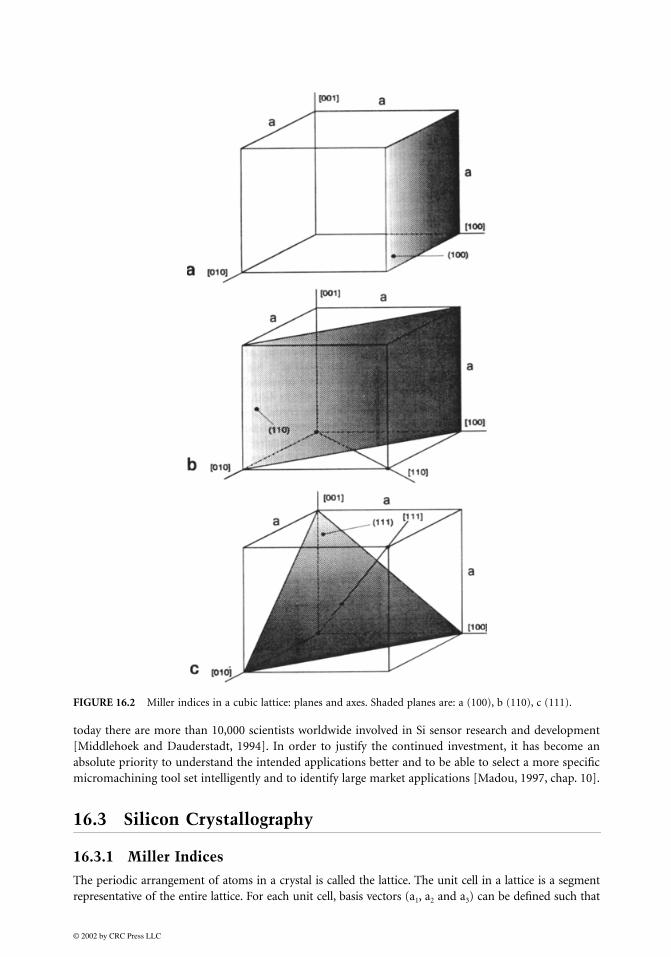
The periodic arrangement of atoms in a crystal is called the lattice. The unit cell in a lattice is a segmentrepresentative of the entire lattice. For each unit cell, basis vectors (a1, a2 and a3) can be defined such that
FIGURE 16.2 Miller indices in a cubic lattice: planes and axes. Shaded planes are: a (100), b (110), c (111).
© 2002 by CRC Press LLC

if that unit cell is translated by integral multiples of these vectors, one arrives at a new unit cell identical tothe original. A simple cubic-crystal unit cell for which a1 = a2 = a3 and the axes angles are α = β = γ = 90°is shown in Figure 16.2. In this figure, the dimension ‘a’ is known as the lattice constant. To identify aplane or a direction, a set of integers h, k and l called the Miller indices is used. To determine the Millerindices of a plane, one takes the intercept of that plane with the axes and expresses these intercepts asmultiples of the basis vectors a1, a2, a3. The reciprocal of these three integers is taken, and, to obtainwhole numbers, the three reciprocals are multiplied by the smallest common denominator. The resultingset of numbers is written down as (hkl). By taking the reciprocal of the intercepts, infinities (∞) areavoided in the plane identification. A direction in a lattice is expressed as a vector with components asmultiples of the basis vectors. The rules for determining the Miller indices of an orientation are: translatethe orientation to the origin of the unit cube and take the normalized coordinates of its other vertex.For example, the body diagonal in a cubic lattice as shown in Figure 16.2 is 1a, 1a and 1a or a diagonalalong the [111] direction. Directions [100], [010] and [001] are all crystallographically equivalent andare jointly referred to as the family, form or group of <100> directions. A form, group or family of faceswhich bear like relationships to the crystallographic axes—for example, the planes (001), (100), (010),(001), (100) and (010)—are all equivalent and they are marked as 100 planes. For illustration, in Figure16.3, some of the planes of the 100 family of planes are shown.
16.3.2 Crystal Structure of Silicon
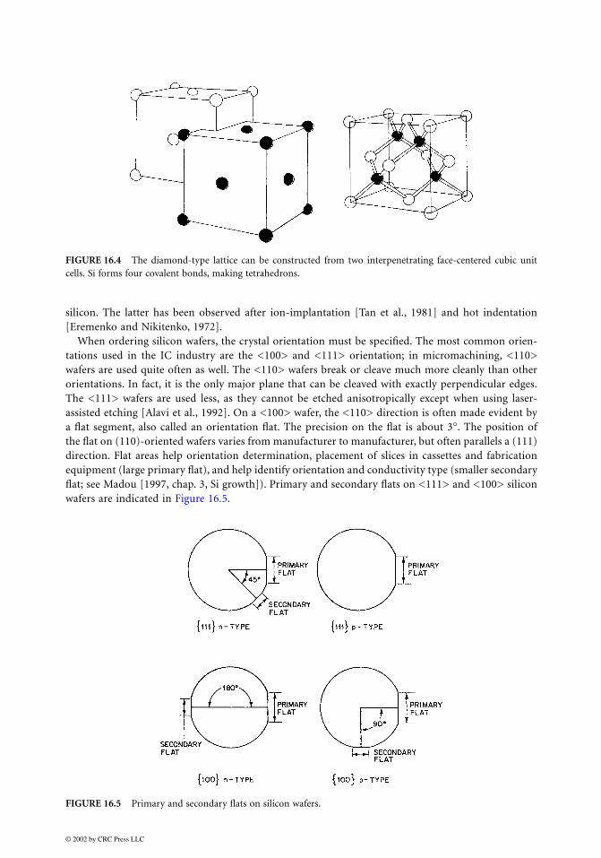
Crystalline silicon forms a covalently bonded structure, the diamond-cubic structure, which has thesame atomic arrangement as carbon in diamond form and belongs to the more general zinc-blendclassification [Kittel, 1976]. Silicon, with its four covalent bonds, coordinates itself tetrahedrally, andthese tetrahedrons make up the diamond-cubic structure. This structure can also be represented astwo interpenetrating face-centered cubic lattices, one displaced (1/4,1/4,1/4)a with respect to the other,as shown in Figure 16.4. The structure is face-centered cubic (fcc), but with two atoms in the unitcell. For such a cubic lattice, direction [hkl] is perpendicular to a plane with the three integers (hkl),simplifying further discussions about the crystal orientation, i.e., the Miller indices of a plane perpen-dicular to the [100] direction are (100). The lattice parameter ‘a’ for silicon is 5.4309 Å and silicon’sdiamond-cubic lattice is surprisingly wide open, with a packing density of 34%, compared to 74% fora regular face-centered cubic lattice. The 111 planes present the highest packing density and theatoms are oriented such that three bonds are below the plane. In addition to the diamond-cubicstructure, silicon is known to have several stable high-pressure crystalline phases [Hu et al., 1986] anda stress-induced metastable phase with a wurtzite-like structure, referred to as diamond-hexagonal
FIGURE 16.3 Miller indices for some of the planes of the 100 family of planes.
© 2002 by CRC Press LLC
silicon. The latter has been observed after ion-implantation [Tan et al., 1981] and hot indentation[Eremenko and Nikitenko, 1972].
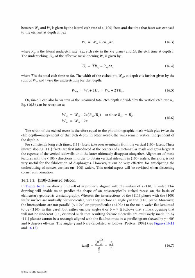
When ordering silicon wafers, the crystal orientation must be specified. The most common orien-tations used in the IC industry are the <100> and <111> orientation; in micromachining, <110>wafers are used quite often as well. The <110> wafers break or cleave much more cleanly than otherorientations. In fact, it is the only major plane that can be cleaved with exactly perpendicular edges.The <111> wafers are used less, as they cannot be etched anisotropically except when using laser-assisted etching [Alavi et al., 1992]. On a <100> wafer, the <110> direction is often made evident bya flat segment, also called an orientation flat. The precision on the flat is about 3°. The position ofthe flat on (110)-oriented wafers varies from manufacturer to manufacturer, but often parallels a (111)direction. Flat areas help orientation determination, placement of slices in cassettes and fabricationequipment (large primary flat), and help identify orientation and conductivity type (smaller secondaryflat; see Madou [1997, chap. 3, Si growth]). Primary and secondary flats on <111> and <100> siliconwafers are indicated in Figure 16.5.
FIGURE 16.4 The diamond-type lattice can be constructed from two interpenetrating face-centered cubic unitcells. Si forms four covalent bonds, making tetrahedrons.
FIGURE 16.5 Primary and secondary flats on silicon wafers.
© 2002 by CRC Press LLC

16.3.3 Geometric Relationships between Some Important Planes in the Silicon Lattice
To better appreciate the different three-dimensional shapes resulting from anisotropically etched singlecrystal Si (SCS) and to better understand the section further below on corner compensation, some ofthe more important geometric relationships between different planes within the Si lattice need furtherclarification. We will consider only silicon wafers with a (100) or a (110) as the surface planes. We willalso accept, for now, that in anisotropic alkaline etchants the 111 planes, which have the highest atom-packing density, are nonetching compared to the other planes. As the 111 planes are essentially notattacked by the etchant, the sidewalls of an etched pit in SCS will ultimately be bounded by this typeof plane, given that the etch time is long enough for features bounded by other planes to be etchedaway. The types of planes introduced initially depend on the geometry and the orientation of the maskfeatures.
16.3.3.1 [100]-Oriented Silicon
In Figure 16.6, the unity cell of a silicon lattice is shown together with the correct orientation of a [100]-type wafer relative to this cell [Peeters, 1994]. It can be seen from this figure that intersections of thenonetching 111 planes with the 100 planes (e.g., the wafer surface) are mutually perpendicular andlying along the <110> orientations. Provided a mask opening (say, a rectangle or a square) is accuratelyaligned with the primary orientation flat, i.e., the [110] direction, only 111 planes will be introducedas sidewalls from the very beginning of the etch. Since the nonetching character of the 111 planesrenders an exceptional degree of predictability to the recess features, this is the mask arrangement mostoften utilized in commercial applications. During etching, truncated pyramids (square mask) or truncatedV-grooves (rectangular mask) deepen but do not widen (Figure 16.7). The edges in these structures are<110> directions, the ribs are <211> directions, the sidewalls are 111 planes and the bottom is a (100)plane parallel with the wafer surface. After prolonged etching, the 111 family of planes is exposed downto their common intersection and the (100) bottom plane disappears, creating a pyramidal pit (squaremask) or a V-groove (rectangular mask) (Figure 16.7). As shown in Figure 16.7, no underetching of the
FIGURE 16.6 (100) silicon wafer with reference to the unity cube and its relevant planes. (From Peeters, E., ProcessDevelopment for 3D Silicon Microstructures with Application to Mechanical Sensor Design, KUL, Belgium, 1994. Withpermission.)
© 2002 by CRC Press LLC

etch mask is observed, due to the perfect alignment of the concave oxide mask opening with the <110>direction. Misalignment still results in pyramidal pits, but the mask will be undercut. For a mask openingwith arbitrary geometry and orientation (for example, a circle) and for sufficiently long etch times, theanisotropically etched recess in a 100 wafer is pyramidal with a base perfectly circumscribing the circularmask opening [Peeters, 1994]. Convex corners (>180°) in a mask opening will always be completelyundercut by the etchant after sufficiently long etch times. This can be disadvantageous (for example,when attempting to create a mesa rather than a pit) or it can be advantageous for undercutting suspendedcantilevers or bridges. In the section of this chapter on corner compensation, the issue of undercuttingwill be addressed in detail. The slope of the sidewalls in a cross section perpendicular to the wafer surfaceand to the wafer flat is determined by the angle α as in Figure 16.6 depicting the off-normal angle of theintersection of a (111) sidewall and a (110) cross-secting plane, and can be calculated from:
(16.1)
with L = a × or α = arctan = 35.26°, or 54.74° for the complementary angle. The tolerance onthis slope is determined by the alignment accuracy of the wafer surface with respect to the (100) plane.Wafer manufacturers typically specify this misalignment to 1° (0.5° in the best cases).
The width of the rectangular or square cavity bottom plane, W0, in Figure 16.8, aligned with the <110>directions, is completely defined by the etch depth, z, the mask opening, Wm, and the above-calculatedsidewall slope:
FIGURE 16.7 Anisotropically etched features in a (100) wafer with (A) Square mask (schematic) and (B) Rectan-gular mask (scanning electron microscope micrograph of resulting actual V- and U-grooves).
αtanLa---=
22
------- 22
-------
© 2002 by CRC Press LLC

or
(16.2)
The larger the opening in the mask, the deeper the point at which the 111 sidewalls of the pit intersect.The etch stop at the 111 sidewalls’ intersection occurs when the depth is about 0.7 times the maskopening. If the oxide opening is wide enough, Wm > 849 µm (for a typical 6-in. wafer with thickness tsi
= z = 600 µm), the 111 planes do not intersect within the wafer. The etched pit in this particular caseextends all the way through the wafer, creating a small orifice or via. If a high density of such vias throughthe Si is required, the wafer must be made very thin.
Corners in an anisotropically etched recess are defined by the intersection of crystallographic planes,and the resulting corner radius is essentially zero. This implies that the size of a silicon diaphragm is verywell defined, but it also introduces a considerable stress concentration factor. The influence of the zerocorner radius on the yield load of diaphragms can be studied with finite element analysis (FEA).
FIGURE 16.8 Relation of bottom cavity plane width with mask opening width.
Orifice (A via through Si wafer).
Anisotropic Etching of (100) Silicon
<100>
Wm
tsi = z
z = Etch depth
Wo
Si
<111
>54.74°
W0 Wm 2cotan(54.74°)z–=
W0 Wm 2 z–=
© 2002 by CRC Press LLC

One way to obtain vertical sidewalls instead of 54.7° sidewalls using a [100]-oriented Si wafer isillustrated in Figure 16.9. It can be seen in this figure that there are 100 planes perpendicular to thewafer surface and that their intersections with the wafer surface are <100> directions. These <100>directions enclose a 45° angle with the wafer flat (i.e., the <110> directions). By aligning the maskopening with these <100> orientations, 100 facets are initially introduced as sidewalls. The 110planes etch faster than the 100 planes and are not introduced. As the bottom and sidewall planesare all from the same 100 group, lateral underetch equals the vertical etch rate and rectangularchannels, bounded by slower etching 100 planes, result (Figure 16.10). Since the top of the etchedchannels is exposed to the etchant longer than the bottom, one might have expected the channels inFigure 16.10 to be wider at the top than at the bottom. With some minor corrections in Peeters’derivation [Peeters, 1994], we can use his explanation for why the sidewalls stay vertical. Assume thewidth of the mask opening to be Wm. At a given depth, z, into the wafer, the underlying Si is no longermasked by Wm, but rather by the intersection of the previously formed 100 facets with the bottomsurface. The width of this new mask is larger than the lithography mask Wm by the amount the latteris being undercut. Let’s call the new mask width W2 the effective mask width at a depth z. The relation
FIGURE 16.9 (100) silicon wafer with <100> mask-aligned features introduces vertical sidewalls. (From Peeters,E., Process Development for 3D Silicon Microstructures with Application to Mechanical Sensor Design, KUL, Belgium,1994. With permission.)
FIGURE 16.10 Vertical sidewalls in a (100) wafer.
© 2002 by CRC Press LLC
between Wm and Wz is given by the lateral etch rate of a 100 facet and the time that facet was exposedto the etchant at depth z, i.e.:
(16.3)
where Rxy is the lateral underetch rate (i.e., etch rate in the x-y plane) and ∆tz the etch time at depth z.The underetching, Uz, of the effective mask opening Wz is given by:
(16.4)
where T is the total etch time so far. The width of the etched pit, Wtot, at depth z is further given by thesum of Wm and twice the underetching for that depth:
(16.5)
Or, since T can also be written as the measured total etch depth z divided by the vertical etch rate Rz ,Eq. (16.5) can be rewritten as
(16.6)
The width of the etched recess is therefore equal to the photolithographic mask width plus twice theetch depth—independent of that etch depth, in other words; the walls remain vertical independent ofthe depth z.
For sufficiently long etch times, 111 facets take over eventually from the vertical 100 facets. Theseinward sloping 111 facets are first introduced at the corners of a rectangular mask and grow larger atthe expense of the vertical sidewalls until the latter ultimately disappear altogether. Alignment of maskfeatures with the <100> directions in order to obtain vertical sidewalls in 100 wafers, therefore, is notvery useful for the fabrication of diaphragms. However, it can be very effective for anticipating theundercutting of convex corners on 100 wafers. This useful aspect will be revisited when discussingcorner compensation.
16.3.3.2 [110]-Oriented Silicon
In Figure 16.11, we show a unit cell of Si properly aligned with the surface of a (110) Si wafer. Thisdrawing will enable us to predict the shape of an anisotropically etched recess on the basis ofelementary geometric crystallography. Whereas the intersections of the 111 planes with the (100)wafer surface are mutually perpendicular, here they enclose an angle γ in the (110) plane. Moreover,the intersections are not parallel (<110>) or perpendicular (<100>) to the main wafer flat (assumedto be <110> in this case), but rather enclose angles δ or δ + γ. It follows that a mask opening thatwill not be undercut (i.e., oriented such that resulting feature sidewalls are exclusively made up by111 planes) cannot be a rectangle aligned with the flat, but must be a parallelogram skewed by γ − 90°and δ degrees off-axis. The angles γ and δ are calculated as follows [Peeters, 1994] (see Figures 16.11and 16.12):
(16.7)
Wz Wm 2Rxy∆tz+=
Uz TRxy Rxy∆tz–=
Wtot Wz 2Uz+ Wm 2TRxy+= =
Wtot Wm 2z(Rxy/Rz) or since Rxy+ Rz,= =Wtot Wm 2z+=
βtan
12--a 2
2-------
a2--
----------- 22
-------= =
© 2002 by CRC Press LLC

(16.8)
From Figure 16.11, it can also be seen that the 111 planes are oriented perpendicular to the (110)wafer surface. This makes it possible to etch pits with vertical sidewalls (Figure 16.12). The bottom ofthe pit shown here is bounded by 110 and/or 100 planes, depending on the etch time. At short etchtimes, one mainly sees a flat 110 bottom. As the 110 planes are etching slightly faster than the 100planes, the flat 110 bottom is getting smaller and smaller and a V-shaped bottom bounded by 100planes eventually results. The angle ε as shown in Figure 16.12 equals 45°, being the angle enclosed bythe intersections of a 100 and a 110 bottom plane. The general rule does apply that an arbitrarywindow opening is circumscribed by a parallelogram with the given orientation and skewness forsufficiently long etch times. Another difference between (100)- and (110)-oriented Si wafers is that onthe (110) wafers it is possible to etch under microbridges crossing at a 90° angle a shallow V-groove(formed by (111) planes). In order to undercut a bridge on a (100) plane, the bridge cannot be perpen-dicular to the V-groove; it must be oriented slightly off normal [Elwenspoek et al., 1994].
16.3.3.3 Selection of [100]- or [110]-Oriented Silicon
In Table 16.1, we compare the main characteristics of etched features in [100]- and [110]-oriented wafers.This guide can help decide which orientation to use for a specific microfabrication application at hand.
From this table it is obvious that for membrane-based sensors, [100] wafers are preferred. The under-standing of the geometric considerations with [110] wafers is important, though, if one wants to fullyappreciate all the possible single crystal silicon (SCS) micromachined shapes, and it is especially helpful
FIGURE 16.11 (110) silicon wafer with reference to the unity cube and its relevant planes. The wafer flat is in a<110> direction. (From Peeters, E., Process Development for 3D Silicon Microstructures with Application to MechanicalSensor Design, KUL, Belgium, 1994. With permission.)
100
[001]
110
111110
100[010]
[100]
110
111
<110>
<110>
aa
a Flat
ε
β
γ
δ
δ
γ
γ 180° 2β– 180° 2arctan2
2-------
– 109.47°= = =
δ 90° β+ 90° arctan2
2-------
+ 125.26°= = =
ϕ 270° δ– 144.74°= =
© 2002 by CRC Press LLC

to understand corner compensation schemes (see below). Moreover, all processes for providing dielectricisolation require that the silicon be separated into discrete regions. To achieve a high component densitywith anisotropic etches on (100) wafers, the silicon must be made very thin because of the aspect ratiolimitations due to the sloping walls (see above). With vertical sidewall etching in a (100) wafer, the etchmask is undercut in all directions to a distance approximately equal to the depth of the etching. Verticaletching in (110) surfaces relaxes the etching requirement dramatically and enables more densely packed
FIGURE 16.12 (110) silicon wafer with anisotropically etched recess inscribed in the Si lattice. γ = 109.47°; δ =125.26°; ϕ = 144.74°; and ε = 45°. (From Peeters, E., Process Development for 3D Silicon Microstructures with Applicationto Mechanical Sensor Design, KUL, Belgium, 1994. With permission.)
TABLE 16.1 Selection of Wafer Type
[100] Orientation [110] Orientation
Inward sloping walls (54.74°) Vertical 111 wallsThe sloping walls cause a lot of lost real estate Narrow trenches with high aspect ratio are possibleFlat bottom parallel to surface is ideal for membrane
fabricationMultifaceted cavity bottom (110 and 100 planes) makes
for a poor diaphragmBridges perpendicular to a V-groove bound by (111)
planes cannot be underetchedBridges perpendicular to a V-groove bound by (111)
planes can be undercutShape and orientation of diaphragms convenient and
simple to designShape and orientation of diaphragms awkward and more
difficult to designDiaphragm size, bounded by nonetching 111 planes,
is relatively easy to controlDiaphragm size is difficult to control; the <100> edges are
not defined by nonetching planes
© 2002 by CRC Press LLC

structures such as beam leads or image sensors. Kendall describes and predicts a wide variety ofapplications for (110) wafers such as fabrication of trench capacitors, vertical multi-junction solar cells,diffraction gratings, infrared interference filters, large area cathodes and filters for bacteria [Kendall, 1975;1979].
16.4 Silicon as a Substrate and Structural Material
16.4.1 Silicon as Substrate
For many mechanical sensor applications, single crystal Si, based on its intrinsic mechanical stability andthe feasibility of integrating sensing and electronics on the same substrate, often presents an excellentsubstrate choice. For chemical sensors, on the other hand, Si, with few exceptions,
2 is merely the substrate
and the choice is not always that straightforward.In Table 16.2, we show a performance comparison of substrate materials in terms of cost, metal-
lization ease and machinability. Both ceramic and glass substrates are difficult to machine, and plasticsubstrates are not readily amenable to metallization. Silicon has the highest material cost per unitarea, but this cost often can be offset by the small feature sizes possible in a silicon implementation.Si with or without passivating layers, due to its extreme flatness, relative low cost and well-establishedcoating procedures, often is the preferred substrate especially for thin films. A lot of thin-filmdeposition equipment is built to accommodate Si wafers and, as other substrates are harder toaccommodate, this lends Si a convenience advantage. There is also a greater flexibility in design andmanufacturing with silicon technology compared to other substrates. In addition, although muchmore expensive, the initial capital equipment investment is not product specific. Once a first productis on line, a next generation or new products will require changes in masks and process steps but notin the equipment itself.
Disadvantages of using Si usually are most pronounced with increasing device size and low productionvolumes and when electronics do not need or cannot be incorporated on the same Si substrate. Thelatter could be either for cost reasons (e.g., in the case of disposables such as glucose sensors) or fortechnological reasons (e.g., the devices will be immersed in conductive liquids or they must operate attemperatures above 150°C).
An overwhelming determining factor for substrate choice is the final package of the device. A chemicalsensor on an insulating substrate almost always is easier to package than a piece of Si with conductiveedges in need of insulation.
Sensor packaging is so important in sensors that as a rule sensor design should start from the packagerather than from the sensor. In this context, an easier to package substrate has a huge advantage. Thelatter is the most important reason why recent chemical sensor development in industry has retrenchedfrom a move toward integration on silicon in the 1970s and early 1980s to a hybrid thick film on ceramicapproach in the late 1980s and early 1990s. In academic circles in the U.S. chemical sensor integrationwith electronics continued until the late 1980s; in Europe and Japan, such efforts are still going on[Madou, 1994].
2A notable exception is the ion-sensitive field effect transistor (ISFET) where the Si space charge is modulated by
the presence of chemicals for which the ISFET chemical coating is sensitive [Madou, 1997, chap. 10].
TABLE 16.2 Performance Comparison of Substrate Materials
Substrate Cost Metallization Machinability
Ceramic Medium Fair PoorPlastic Low Poor FairSilicon High Good Very goodGlass Low Good Poor
© 2002 by CRC Press LLC

16.4.2 Silicon as a Structural Element in Mechanical Sensors
16.4.2.1 Introduction
In mechanical sensors the active structural elements convert a mechanical external input signal (force,pressure, acceleration etc.) into an electrical signal output (voltage, current or frequency). The transferfunctions in mechanical devices describing this conversion are mechanical, electro-mechanical and electrical.
In the mechanical conversion, a given external load is concentrated and maximized in the activemember of the sensor. Structurally active members are typically high-aspect-ratio elements such assuspended beams or membranes. The electromechanical conversion is the transformation of the mechan-ical quantity into an electrical quantity such as capacitance, resistance, charge etc. Often the electricalsignal needs further electrical conversion into an output voltage, frequency or current. For electricalconversion into an output voltage, a Wheatstone bridge may be used as in the case of a piezoresistivesensor, and a charge amplifier may be used in the case of a piezoelectric sensor. To optimize all threetransfer functions, detailed electrical and mechanical modeling is required. One of the most importantinputs required for the mechanical models are the experimentally determined independent elasticityconstants or moduli. In what follows, we describe what makes Si such an important structural elementin mechanical sensors and present its elasticity constants.
16.4.2.2 Important Characteristics of Mechanical Structural Elements: Stress-Strain Curve and Elasticity Constants
Yield, tensile strength, hardness and creep of a material all relate to the elasticity curve, i.e., thestress–strain diagram of the material as shown in Figure 16.13. For small strain values, Hooke’s lawapplies, i.e., stress (force per unit area, N/m
2) and strain (displacement per unit length, dimensionless)
are proportional and the stress–strain curve is linear, with a slope corresponding to the elastic modulusE (Young’s modulus-N/m
2). This regime as in Figure 16.13 is marked as the elastic deformation regime.
For isotropic media such as amorphous and polycrystalline materials, the applied axial force per unitarea or tensile stress, σa, and the axial or tensile strain, εa, are thus related as:
(16.9)
with εa given by the dimensionless ratio of L2 − L1/L1, i.e., the ratio of the wire’s elongation to its originallength. The elastic modulus may be thought of as stiffness or a material’s resistance to elastic deformation.
FIGURE 16.13 Typical stress-strain behavior for a mate-rial showing elastic and plastic deformations, the propor-tional limit P and the yield strength σy, as determinedusing the 0.002 strain offset method (see text).
σa Eεa=
Elastic Plastic
Strain0.002
Str
ess P
σy
A
© 2002 by CRC Press LLC
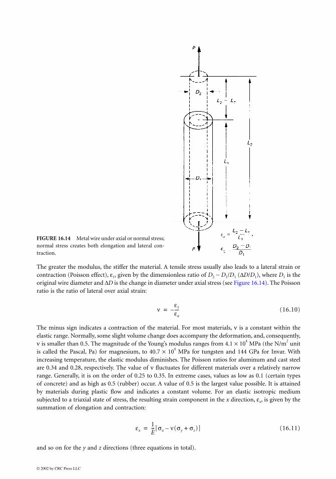
The greater the modulus, the stiffer the material. A tensile stress usually also leads to a lateral strain orcontraction (Poisson effect), ε1, given by the dimensionless ratio of D2 − D1/D1 (∆D/D1), where D1 is theoriginal wire diameter and ∆D is the change in diameter under axial stress (see Figure 16.14). The Poissonratio is the ratio of lateral over axial strain:
(16.10)
The minus sign indicates a contraction of the material. For most materials, ν is a constant within theelastic range. Normally, some slight volume change does accompany the deformation, and, consequently,ν is smaller than 0.5. The magnitude of the Young’s modulus ranges from 4.1 × 10
4 MPa (the N/m
2 unit
is called the Pascal, Pa) for magnesium, to 40.7 × 10⁴ MPa for tungsten and 144 GPa for Invar. With
increasing temperature, the elastic modulus diminishes. The Poisson ratios for aluminum and cast steelare 0.34 and 0.28, respectively. The value of ν fluctuates for different materials over a relatively narrowrange. Generally, it is on the order of 0.25 to 0.35. In extreme cases, values as low as 0.1 (certain typesof concrete) and as high as 0.5 (rubber) occur. A value of 0.5 is the largest value possible. It is attainedby materials during plastic flow and indicates a constant volume. For an elastic isotropic mediumsubjected to a triaxial state of stress, the resulting strain component in the x direction, εx, is given by thesummation of elongation and contraction:
(16.11)
and so on for the y and z directions (three equations in total).
FIGURE 16.14 Metal wire under axial or normal stress;normal stress creates both elongation and lateral con-traction.
νε1
εa----–=
εx1E---[σx ν(σy σz+ )– ]=
© 2002 by CRC Press LLC
For an analysis of mechanical structures we must consider not only compressional and tensile strainsbut also shear strains. Whereas normal stresses create elongation plus lateral contraction with accompa-nying volume changes, shear stresses (e.g., by twisting a body) create shape changes without volumechanges, i.e., shear strains. The one-dimensional shear strain, γ, is produced by the shear stress, τ (N/m
2).
For small strains, Hooke’s law may be applied again:
(16.12)
where G is called the elastic shear modulus or the modulus of rigidity. For any three-dimensional stateof shear stress, three equations of this type will hold. Isotropic bodies are characterized by two indepen-dent elastic constants only, since the shear modulus G, as can be shown [Chou and Pagano, 1967], relatesthe Young’s modulus and the Poisson ratio as:
(16.13)
Crystal materials, whose elastic properties are anisotropic, require more than two elastic constants,the number increasing with decreasing symmetry. Cubic crystals (bcc, fcc), for example, require 3 elasticconstants, hexagonal crystals require 5, and materials without symmetry require 21 [Kittel, 1976; Chouand Pagano, 1967]. The relation between stresses and strains is more complex in this case and dependsgreatly on the spatial orientation of these quantities with respect to the crystallographic axes. Hooke’slaw in the most generic form is expressed in two formulas:
(16.14)
where σij and σkl are stress tensors of rank 2 expressed in N/m2; εij and εkl are strain tensors of rank 2 and
are dimensionless; Eijkl is a stiffness coefficient tensor of rank 4 expressed in N/m2; and Sijkl is a compliance
coefficient tensor of rank 4 expressed in m2/N. The first expression is analogous to Eq. (16.9) and the
second expression is the inverse, giving the strains in terms of stresses. The tensor representations in Eq.(16.14) can also be represented as two matrices:
(16.15)
Components of tensors Eijkl and Sijkl are substituted by elements of the matrices Emn and Smn, respectively.To convert the ij indices to m and the kl indices to n, the following scheme applies:
11 → 1, 22 → 2, 33 → 3, 23 and 32 → 4, 13 and
31 → 5, 12 and 21 → 6, Eijkl → Emn and Sijkl → Smn
when m and n = 1,2,3; 2 Sijkl → Smn when m or n =
4,5,6; 4Sijkl → Smn when m and n = 4,5,6; σij →
σm when m = 1,2,3; and ε ij → εm when m = 4,5,6
With these reduced indices there are thus six equations of the type:
(16.16)
and hence 36 moduli of elasticity or Emn stiffness constants. There are also six equations of the type:
(16.17)
γ τG----=
GE
2(1 ν)+--------------------=
σij Eijkl εkl and εij⋅ Sijkl σkl⋅= =
σm Emnεn and εm
n=1
6
∑ Smnσn
n=1
6
∑= =
σx E11εx E12εy E13εz E14γ yz E15γ zx E16γ xy+ ++ + +=
εx S11σx S12σy S13σz S14τyz S15τzx S16τxy+ + + + +=
© 2002 by CRC Press LLC

defining 36 Smn constants which are called the compliance constants; see also Madou (1997, Eq. (9.29)).It can be shown that the matrices Emn and Smn, each composed of 36 coefficients, are symmetrical; hence,a material without symmetry elements has 21 independent constants or moduli. Due to symmetry ofcrystals, several more of these may vanish until, for our isotropic medium, they number two only (E andν). The stiffness coefficient and compliance coefficient matrices for cubic-lattice crystals with the vectorof stress oriented along the [100] axis are given as:
(16.18)
In cubic crystals, the three remaining independent elastic moduli are usually chosen as E11, E12 andE44. The Smn values can be calculated simply from these Emn values. Expressed in terms of the complianceconstants, one can show that 1/S11 = E = Young’s modulus, −S12/S11 = ν = Poisson’s ratio, and 1/S44 =G = shear modulus. In the case of an isotropic material, such as a metal wire, there is an additionalrelationship:
(16.19)
reducing the number of independent stiffnesses constants to two. The anisotropy coefficient α is defined as:
(16.20)
making α = 1 for an isotropic crystal. For an anisotropic crystal, the degree of anisotropy is given by thedeviation of α from 1. Single crystal silicon has moderately anisotropic elastic properties [Brantley, 1973;Nikanorov et al., 1972], with α = 1.57. Brantley (1973) gives the non-zero stiffness components, referredto the [100] crystal orientation as: E11 = E22 = E33 = 166 × 10
9 N/m
2, E12 = E13 = E23 = 64 × 10
9 N/m
2 and
E44 = E55 = E66 = 80 × 109 N/m
2:
(16.21)
with σ normal stress, τ shear stress, ε normal strain and γ shear strain. The values for Emn, in Eq.(16.21), compare with a Young’s modulus of 207 GPa for a low carbon steel. Variations on the valuesof the elastic constants on the order of 30%, depending on crystal orientation, must be considered;doping level (see below) and dislocation density have minor effects as well. From the stiffness coeffi-cients the compliance coefficients of Si can be calculated as S11 = 7.68 × 10
−12 m
2/N, S12 = −2.14 ×
10−12
m2/N, and S44 = 12.6 × 10
–12 m
2/N [Khazan, 1994]. A graphical representation of elastic constants
Emn
E11 E12 E12 0 0 0
E12 E11 E12 0 0 0
E12 E12 E11 0 0 0
0 0 0 E44 0 0
0 0 0 0 E44 0
0 0 0 0 0 E44
Smn
S11 S12 S12 0 0 0
S12 S11 S12 0 0 0
S12 S12 S11 0 0 0
0 0 0 S44 0 0
0 0 0 0 S44 0
0 0 0 0 0 S44
= =
E44
E11 E12–2
--------------------=
α2E44
E11 E12–--------------------=
σx
σy
σz
τxy
τxz
τyz
166(E11) 64(E12) 64(E12) 0 0 0
64(E12) 166(E11) 64(E12) 0 0 0
64(E12) 64(E12) 166(E11) 0 0 0
0 0 0 80(E44) 0 0
0 0 0 0 80(E44) 0
0 0 0 0 0 80(E44)
εx
εy
εz
γ xy
γ xz
γ yz
×=
© 2002 by CRC Press LLC

for different crystallographic directions in Si and Ge is given in Worthman and Evans (1965) and isreproduced in Figure 16.15. Figure 16.15A to D displays E and ν for Ge and Si in planes (100) and(110) as functions of direction. Calculations show that E, G and ν are constant for any direction inthe (111) plane. In other words, a plate lying in this plane can be considered as having isotropic elasticproperties. A review of independent determinations of the Si stiffness coefficients, with their respectivetemperature coefficients, is given in Metzger and Kessler (1970). Some of the values from that revieware reproduced in Table 16.3. Values for Young’s modulus and the shear modulus of Si can also befound in Greenwood (1988) and are reproduced in Table 16.4 for the three technically importantcrystal orientations.
16.4.2.3 Residual Stress
Most properties, such as the Young’s modulus, for lightly and highly doped silicon are identical. FromSection 16.10 on, we will see that the Young’s modulus for polycrystalline silicon is about 161 GPa.
FIGURE 16.15 Elasticity constants for Si and Ge. (A) Young’s modulus as a function of direction in the (100) plane.(B) Young’s modulus as a function of direction in the (110) plane. (C) Poisson ratio as a function of direction in the(100) plane. (D) Poisson’s ratio as a function of direction in the (110) plane. (From Worthman, J. J. and R. A. Evans,J. Appl. Phys., 36, 153–156, 1965. With permission.)
150
100
50
0 50 100 150 E' x 1 x 10⁹, N/m2
E' x 1 x 10⁹, N/m2
[010]
[010]
[011
]
[001
]
[001]
(100)- plane
Ge
Si
i'
150
100
50
0 50 100 150 E' x 1 x 10⁹, N/m2
E' x 1 x 10⁹, N/m2
[11-0]
[11-0]
[11-0]
[11-0]
[11- 1]
[11- 1]
[001
]
[001
][001]
[001]
(110)- plane
(110)- plane
Ge
Ge
Si
Si
i'
0 0.1 0.2 0.3 η'
η'
[010]
[011
]
[010]
[001
]
[001]
(100)- plane
0.3
0.2
0.1
GeSi
η'
η'
i'
j'
i'
j'
B D
A C
0.3
0.2
0.1
0 0.1 0.2 0.3
© 2002 by CRC Press LLC
Residual stress and associated stress gradients in highly boron doped single crystal silicon present somecontroversy. Highly boron-doped membranes, which are usually reported to be tensile, also have beenreported compressive [Huff and Schmidt, 1992; Maseeh and Senturia, 1990]. From a simple atom-radiusargument, one expects that a large number of substitutional boron atoms would create a net shrinkageof the lattice compared to pure silicon and that the residual stress would be tensile with a stress gradientcorresponding to the doping gradient. That is, an etched cantilever would be expected to bend up out ofthe plane of the silicon wafer. Maseeh and Santuria (1990) believe that the appearance of compressivebehavior in heavily boron-doped single crystal layers results from the use of an oxide etch mask. Theysuggest that plastic deformation of the p
+ silicon beneath the compressively stressed oxide can explain
the observed behavior. Ding and Ko (1991), who also found compressive behavior for nitride-coveredp
+ Si thin membranes, believe that the average stress in p
+ silicon is indeed tensile, but great care is
required to establish this fact because the combination of heavy boron doping and a high-temperaturedrive-in under oxidizing conditions can create an apparent reversal of both the net stress (to compressive)and of the stress gradient (opposite to the doping gradient). A proposed explanation is that at the oxide-silicon interface, a thin compressively stressed layer is formed during the drive-in which is not removedin buffered HF. It can be removed by reoxidation and etching in HF, or by etching in KOH.
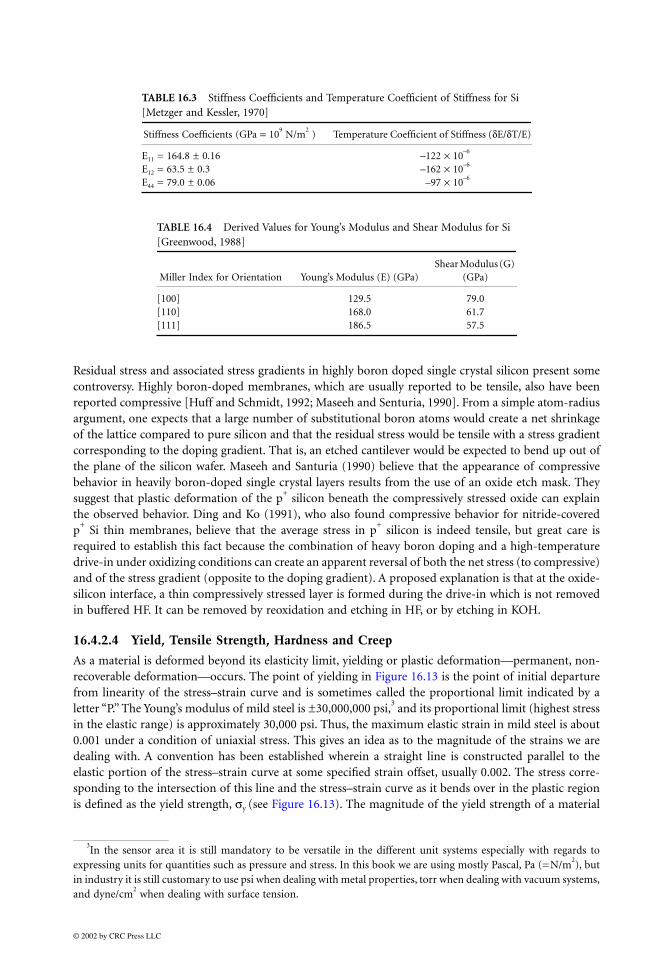
16.4.2.4 Yield, Tensile Strength, Hardness and Creep
As a material is deformed beyond its elasticity limit, yielding or plastic deformation—permanent, non-recoverable deformation—occurs. The point of yielding in Figure 16.13 is the point of initial departurefrom linearity of the stress–strain curve and is sometimes called the proportional limit indicated by aletter “P.” The Young’s modulus of mild steel is ±30,000,000 psi,
3 and its proportional limit (highest stress
in the elastic range) is approximately 30,000 psi. Thus, the maximum elastic strain in mild steel is about0.001 under a condition of uniaxial stress. This gives an idea as to the magnitude of the strains we aredealing with. A convention has been established wherein a straight line is constructed parallel to theelastic portion of the stress–strain curve at some specified strain offset, usually 0.002. The stress corre-sponding to the intersection of this line and the stress–strain curve as it bends over in the plastic regionis defined as the yield strength, σy (see Figure 16.13). The magnitude of the yield strength of a material
TABLE 16.3 Stiffness Coefficients and Temperature Coefficient of Stiffness for Si [Metzger and Kessler, 1970]
Stiffness Coefficients (GPa = 109 N/m
2 ) Temperature Coefficient of Stiffness (δE/δT/E)
E11 = 164.8 ± 0.16 –122 × 10–6
E12 = 63.5 ± 0.3 –162 × 10–6
E44 = 79.0 ± 0.06 –97 × 10–6
TABLE 16.4 Derived Values for Young’s Modulus and Shear Modulus for Si [Greenwood, 1988]
Miller Index for Orientation Young’s Modulus (E) (GPa)Shear Modulus (G)
(GPa)
[100] 129.5 79.0[110] 168.0 61.7[111] 186.5 57.5
3In the sensor area it is still mandatory to be versatile in the different unit systems especially with regards to
expressing units for quantities such as pressure and stress. In this book we are using mostly Pascal, Pa (=N/m2), but
in industry it is still customary to use psi when dealing with metal properties, torr when dealing with vacuum systems,and dyne/cm
2 when dealing with surface tension.
© 2002 by CRC Press LLC

is a measure of its resistance to plastic deformation. Yield strengths may range from 35 MPa (5000 psi)for a soft and weak aluminum to over 1400 MPa (200,000 psi) for high strength steels. The tensile strengthis the stress at the maximum of the stress–strain curve (Figure 16.16). This corresponds to the maximumstress that can be sustained by a structure in tension; if the stress is applied and maintained, fracture willresult. Both tensile strength and hardness are indicators of a metal’s resistance to plastic deformation.Consequently, they are roughly proportional [Callister, 1985]. Material deformation occurring at elevatedtemperatures and static material stresses is termed creep. It is defined as a time-dependent and perma-nent deformation of materials when subjected to a constant load or stress.
Silicon exhibits no plastic deformation or creep below 800°C; therefore, Si sensors are inherently veryinsensitive to fatigue failure when subjected to high cyclic loads. Silicon sensors have actually been cycledin excess of 100 million cycles with no observed failures. This ability to survive a very large number ofduty cycles is due to the fact that there is no energy absorbing or heat generating mechanism due tointergranular slip or movement of dislocations in silicon at room temperature. However, single crystalSi, as a brittle material, will yield catastrophically, when stress beyond the yield limit is applied, ratherthan deform plastically as metals do (see Figure 16.16). At room temperature, high modulus materialssuch as Si, SiO2 and Si3N4 often exhibit linear-elastic behavior at lower strain and transition abruptly tobrittle-fracture behavior at higher strain. Plastic deformation in metals is based on stress-induced dislo-cation generation in the grain boundaries and a subsequent dislocation migration that results in amacroscopic deformation from inter-grain shifts in the material. No grain boundaries exist in singlecrystal silicon (SCS), and plastic deformation can only occur through migration of the defects originallypresent in the lattice or of those that are generated at the surface. As the number of these defects is verylow in SCS, the material can be considered a perfect elastic material at normal temperatures. Perfectelasticity implies proportionality between stress and strain (i.e., load and flexure) and the absence ofirreversibilities or mechanical hysteresis. The absence of plastic behavior also accounts for the extremelylow mechanical losses in SCS, which enable the fabrication of resonating structures that exhibit exceptionallyhigh Q-factors. Values of up to 10
8 in vacuum have been reported. At elevated temperatures, and with metals
and polymers at ordinary temperatures, complex behavior in the stress–strain curve can occur. Considerableplasticity can be induced in SCS at elevated temperatures (>800°C), when the mobility of defects in the
FIGURE 16.16 Stress–strain curve. Tensile strength of a metal is the stress at the maximum of this curve. Abruptbrittle fracture of a high modulus material with no plastic deformation region like Si is indicated as well.
© 2002 by CRC Press LLC

lattice is substantially increased. Huff and Schmidt (1992) actually report a pressure switch exhibitinghysteresis based on buckling of plastically deformed silicon membranes. To eliminate plastic deformationof Si wafers, it is important that during high temperature steps the presence of films that could stress oreven warp the wafer in an asymmetric way, typically oxides or nitrides, be avoided.
16.4.2.5 Piezoresistivity in Silicon
Piezoresistance is the fractional change in bulk resistivity induced by small mechanical stresses applied toa material. Most materials exhibit piezoresistivity, but the effect is particularly important in some semi-conductors (more than an order of magnitude higher than that of metals). Monocrystalline silicon has ahigh piezoresistivity and, combined with its excellent mechanical and electronic properties, makes a superbmaterial for the conversion of mechanical deformation into an electrical signal. Actually, the history ofsilicon-based sensors started with the discovery of the piezoresistance effect in Si and Ge more than fourdecades ago [Smith, 1954]. The two main classes of piezoresistive sensors are membrane-type structures(typically pressure and flow sensors) and cantilever beams (typically acceleration sensors) with in-diffusedresistors (boron, arsenic or phosphorus) strategically placed in zones of maximum stress.
For a three-dimensional anisotropic crystal, the electrical field vector (E) is related to the current vector(i) by a 3-by-3 resistivity tensor [Khazan, 1994]. Experimentally the nine coefficients are always foundto reduce to six, and the symmetric tensor is given by:
(16.22)
For the cubic Si lattice, with the axes aligned with the <100> axes, ρ1, ρ2 and ρ3 define the dependenceof the electric field on the current along the same direction (one of the <100> directions); ρ4, ρ5 and ρ6
are cross-resistivities, relating the electric field to the current along a perpendicular direction.The six resistivity components in Eq. (16.22) depend on the normal (σ) and shear (τ) stresses in the
material as defined in the preceding section. Smith (1954) was the first to measure the resistivity coefficientsπ11, π12 and π44 for Si at room temperature. Table 16.5 lists Smith’s results [Smith, 1954]. The piezoresis-tance coefficients are largest for π11 in n-type silicon and π44 in p-type silicon, about –102.10
–11 and
138.10–11
Pa–1
, respectively.Resistance change can now be calculated as a function of the membrane or cantilever beam stress. The
contribution to resistance changes from stresses that are longitudinal (σl) and transverse (σt) with respectto the current flow is given by:
(16.23)
where
σl = Longitudinal stress component, i.e., stress component parallel to the direction of the current.
σt = Transversal stress component, i.e., the stress component perpendicular to the direction of thecurrent.
πl = Longitudinal piezoresistance coefficient.
πt = Transversal piezoresistance coefficient.
The piezoresistance coefficients πl and πt for (100) silicon as a function of crystal orientation arereproduced from Kanda in Figure 16.17A (for p-type) and B (for n-type) [Kanda, 1982]. By maximizingthe expression for the stress-induced resistance change in Eq. (16.23), one optimizes the achievablesensitivity in a piezoresistive silicon sensor.
E1
E2
E3
ρρρρ1 ρρρρ6 ρρρρ5
ρρρρ6 ρρρρ2 ρρρρ4
ρρρρ5 ρρρρ4 ρρρρ3
i1
i2
i3
⋅=
∆RR
------- σlπl σtπt+=
© 2002 by CRC Press LLC

The orientation of a membrane or beam is determined by its anisotropic fabrication. The surface ofthe silicon wafer is usually a (100) plane; the edges of the etched structures are intersections of (100) and(111) planes and are thus <110> directions. p-Type piezoresistors are most commonly used because theorientation of maximum piezoresistivity (<110>) happens to coincide with the edge orientation of a con-ventionally etched diaphragm and because the longitudinal coefficient is roughly equal in magnitude butopposite in sign as compared to the transverse coefficient (Figure 16.17A)[Peeters, 1994]. With the valuesin Table 16.5, πl and πt now can be calculated numerically for any orientation. The longitudinal piezore-sistive coefficient in the <110> direction is πl = 1/2(π11 + π12 + π44). The corresponding transversecoefficient is πt = 1/2(π11 + π12 – π44). From Table 16.5 we know that, for p-type resistors, π44 is moreimportant than the other two coefficients and Eq. (16.23) is approximated by:
(16.24)
For n-type resistors, π44 can be neglected, and we obtain:
(16.25)
Equations (16.24) and (16.25) are valid only for uniform stress fields or if the resistor dimensions aresmall compared with the membrane or beam size. When stresses vary over the resistors they have to beintegrated, which is most conveniently done by computer simulation programs.
To convert the piezoresistive effect into a measurable electrical signal, a Wheatstone bridge is oftenused. A balanced Wheatstone bridge configuration is constructed as in Figure 16.18A by locating fourp-piezoresistors midway along the edges of a square diaphragm as in Figure 16.18B (location of maximumstress). Two resistors are oriented so that they sense stress in the direction of their current axes and twoare placed to sense stress perpendicular to their current flow. Two longitudinally stressed resistors (A)are balanced against two transversally stressed resistors (B); two of them increase in value and the othertwo decrease in value upon application of a stress. In this case, from Eq. (16.24),
(16.26)
with σ in Pa. For a realistic stress pattern where σl = 10 MPa and σt = 50 MPa, Eq. (16.26) gives us a∆R/R ≈ 2.8% [Peeters, 1994].
By varying the diameter and thickness of the silicon diaphragms, piezoresistive sensors in the rangeof 0 to 200 MPa have been made. The bridge voltages are usually between 5 and 10 volts, and the sensitivitymay vary from 10 mV/kPa for low pressure to 0.001 mV/kPa for high pressure sensors.
Peeters (1994) shows how a more sensitive device could be based on n-type resistors when all the n-resistors oriented along the <100> direction are subjected to an uniaxial stress pattern in the longitudinalaxis, as shown in Figure 16.19. The overall maximum piezoresistivity coefficient (πl in the <100> direction)is substantially higher for n-silicon than it is for p-type silicon in any direction (maximum πt and πl in the
TABLE 16.5 Resistivity and Piezoresistance at Room Temperature [Smith, 1954; Khazan, 1994]
ρ (Ω cm) π11a π12
a π44a
p-Si 7.8 +6.6 –1.1 +138.1n-Si 11.7 –102.2 +53.4 –13.6
a Expressed in 10
–12 cm
2 dyne
–1 or 10
–11 Pa
1.
∆RR
-------π44
2-------(σl σt)–=
∆RR
-------π11 π12+
2--------------------(σ1 σt)+=
∆RR
------- 70 10 11– (σl σt)–⋅≈
© 2002 by CRC Press LLC

FIGURE 16.17 Piezoresistance coefficients π1 and πt for (100) silicon. (A) For p-type in the (001) plane (10–12
cm2/dyne). (B) For n-type in the (001) plane (10
–12 cm
–2/dyne). (From Kanda, Y., IEEE Trans. Electr. Dev., ED-29,
64–70, 1982. With permission.)
-110 -100-90 -80 -70 -60 -50 -40
(010)
-110 -100-90 -80 -70 -60 -50 -40 -30
90 80
70
60
50
40
30
20
10
0
0
170
160
150
140
130
120
110 10
010
20
30
40
50
60
70
80 90 100 11
0
120
130
140
150
160
170
-30 -20 20 30 40 50 60 70 80 90 100 110
(1-10)
(1-00)
(1-1-0)
(01-0)
Πt
Πl
1020
3040
5060
7080
9010
011
0-1
10-1
00-9
0-8
0-7
0-6
0-5
0-4
0-3
0-2
0-1
0
90 80
70
60
50
40
30
20
10
00
170
160
150
140
130
120
110 10
0
10
20
30
40
50
60
70
80 90 100 11
0
120
130
140
150
160
170
-20 20 30 40 50 60 70 80 90 100 110
(010)
(1-10)
(1-00)
(1-1-0)
(01-0)
Πl
Πt
1020
3040
5060
7080
9010
011
0-1
10-1
00-9
0-8
0-7
0-6
0-5
0-4
0-3
0-2
0-1
0
B
A
© 2002 by CRC Press LLC
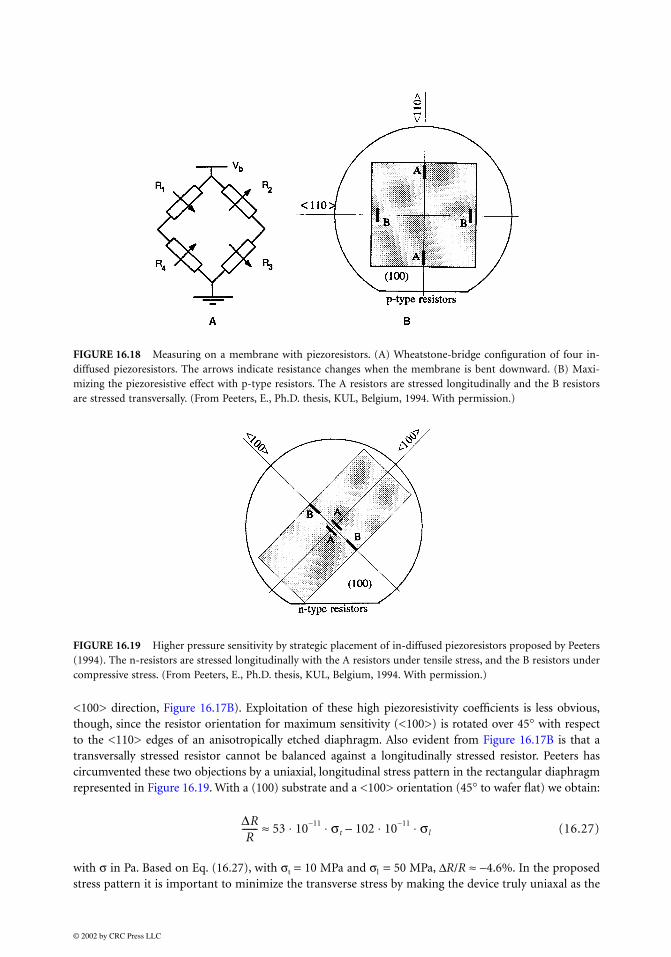
<100> direction, Figure 16.17B). Exploitation of these high piezoresistivity coefficients is less obvious,though, since the resistor orientation for maximum sensitivity (<100>) is rotated over 45° with respectto the <110> edges of an anisotropically etched diaphragm. Also evident from Figure 16.17B is that atransversally stressed resistor cannot be balanced against a longitudinally stressed resistor. Peeters hascircumvented these two objections by a uniaxial, longitudinal stress pattern in the rectangular diaphragmrepresented in Figure 16.19. With a (100) substrate and a <100> orientation (45° to wafer flat) we obtain:
(16.27)
with σ in Pa. Based on Eq. (16.27), with σt = 10 MPa and σl = 50 MPa, ∆R/R ≈ −4.6%. In the proposedstress pattern it is important to minimize the transverse stress by making the device truly uniaxal as the
FIGURE 16.18 Measuring on a membrane with piezoresistors. (A) Wheatstone-bridge configuration of four in-diffused piezoresistors. The arrows indicate resistance changes when the membrane is bent downward. (B) Maxi-mizing the piezoresistive effect with p-type resistors. The A resistors are stressed longitudinally and the B resistorsare stressed transversally. (From Peeters, E., Ph.D. thesis, KUL, Belgium, 1994. With permission.)
FIGURE 16.19 Higher pressure sensitivity by strategic placement of in-diffused piezoresistors proposed by Peeters(1994). The n-resistors are stressed longitudinally with the A resistors under tensile stress, and the B resistors undercompressive stress. (From Peeters, E., Ph.D. thesis, KUL, Belgium, 1994. With permission.)
∆RR
------- 53 10 11– σt 102 10 11– σl⋅⋅–⋅⋅≈
© 2002 by CRC Press LLC

longitudinal and transverse stress components have opposite effects and can even cancel out. In practice,a pressure sensor with an estimated 65% gain in pressure sensitivity over the more traditional configu-rations could be made in the case of an 80% uniaxiality [Peeters, 1994].
The piezoresistive effect is often described in terms of the gauge factor, G, defined as:
(16.28)
which is the relative resistance change divided by the applied strain. The gauge factor of a metal straingauge is typically around 2, for single crystal Si it is 90, and for poly-crystalline Si it is about 30 (see alsoSection 16.10).
16.4.2.6 Thermal Properties of Silicon
In Figure 16.20, the expansion coefficient of Si, W, SiO2, Ni-Co-Fe alloy and Pyrex® is plotted vs. absolutetemperature. Single crystal silicon has a high thermal conductivity (comparable with metals such as steeland aluminum) and a low thermal expansion coefficient. Its thermal expansion coefficient is closelymatched to Pyrex glass but exhibits considerable temperature dependence. A good match in thermalexpansion coefficient between the device wafer (e.g., Si) and the support substrate (e.g., Pyrex) is required.A poor match introduces stress, which degrades the device performance. This makes it difficult tofabricate composite structures of Pyrex and Si that are stress-free over a wide range of temperatures.Drift in silicon sensors often stems from packaging. In this respect, several types of stress-relief, subas-semblies for stress-free mounting of the active silicon parts play a major role; using silicon as the supportfor silicon sensors is highly desirable. The latter aspect is addressed in Madou (1997, chap. 8).
Although the Si band-gap is relatively narrow, by employing silicon on insulator (SOI) wafers, hightemperature sensors can be fashioned. For the latter application, relatively highly doped Si, which is relativelylinear in its temperature coefficient of resistance and sensitivity over a wide range, typically is employed.
When fabricating thermally isolated structures on Si, the large thermal conductivity of Si poses a con-siderable problem as the major heat leak occurs through the Si material. For thermally isolated structures,machining in glass or quartz with their lower thermal conductivity represents an important alternative.
FIGURE 16.20 Thermal expansion coefficient vs. absolute temperature. (From Greenwood, J.C., J. Phys. E: Sci. Instrum., 21 1114–1128, 1988. With permission.)
8
7
6
5
4
3
2
1
200
Si
SiO2
400 600 800
x10-6
The
rmal
exp
ansi
on
T (K)
W
Ni-Co-Fealloy
Pyrex
G1ε--
∆RR
-------=
© 2002 by CRC Press LLC

16.5 Wet Isotropic and Anisotropic Etching
16.5.1 Wet Isotropic and Anisotropic: Empirical Observations
16.5.1.1 Introduction
Wet etching of Si is used mainly for cleaning, shaping, polishing and characterizing structural andcompositional features [Uhlir, 1956]. Wet chemical etching provides a higher degree of selectivity thandry etching techniques. Wet etching often is also faster; compare a few microns to several tens ofmicrons per minute for isotropic etchants and about 1 µm/min for anisotropic etchants vs. 0.1 µm/minin typical dry etching. More recently though, with ECR dry etching, rates of up to 6 µm/min wereachieved (see Madou [1997, chap. 2]). Modification of wet etchant and/or temperature can alter theselectivity to silicon dopant concentration and type and, especially when using alkaline etchants, tocrystallographic orientation. Etching proceeds by reactant transport to the surface (1), surface reaction(2), and reaction product transport away from the surface (3). If (1) or (3) is rate determining, etchingis diffusion limited and may be increased by stirring. If (2) is the rate-determining step, etching isreaction rate limited and depends strongly on temperature, etching material and solution composition.Diffusion-limited processes have lower activation energies (of the order of a few Kcal/mol) thanreaction-rate controlled processes and therefore are relatively insensitive to temperature variations. Ingeneral, one prefers reaction rate limitation as it is easier to reproduce a temperature setting than astirring rate. The etching apparatus needs to have both a good temperature controller and a reliablestirring facility
[Kaminsky, 1985; Stoller et al., 1970].
Isotropic etchants, also polishing etchants, etch in all crystallographic directions at the same rate; theyusually are acidic, such as HF/HNO3/CH3COOH (HNA), and lead to rounded isotropic features in singlecrystalline Si. They are used at room temperature or slightly above (<50°C). Historically they were thefirst Si etchants introduced [Robbins and Schwartz, 1959; 1960; 1961; 1976; Uhlir, 1956; Hallas, 1971;Turner, 1958; Kern, 1978; Klein and D’Stefan, 1962]. Later it was discovered that some alkaline chemicalswill etch anisotropically, i.e., they etch away crystalline silicon at different rates depending on the orien-tation of the exposed crystal plane. Typically the pH stays above 12, while more elevated temperaturesare used for these slower type etchants (>50°C). The latter type of etchants surged in importance in thelate 1960s for the fabrication of dielectrically isolated structures in silicon [Stoller and Wolff, 1966; Stoller,1970; Forster and Singleton, 1966; Kenney, 1967; Lepselter, 1966; 1967; Waggener, 1970; Kragness, 1973;Waggener et al., 1967a; 1967b; Bean and Runyan, 1977; Rodgers et al., 1977; Rodgers et al., 1976; Ammarand Rodgers, 1980; Schnable and Schmidt, 1976]. Isotropic etchants typically show diffusion limitation,while anisotropic etchants are reaction rate limited.
Preferential or selective etching (also structural etchants) usually are isotropic etchants that show someanisotropy [Kern and Deckert, 1978]. These etchants are used to produce a difference in etch rate betweendifferent materials or between compositional or structural variations of the same material on the samecrystal plane. These type of etches often are the fastest and simplest techniques to delineate electricaljunctions and to evaluate the structural perfection of a single crystal in terms of slip, lineage and stackingfaults. The artifacts introduced by the defects etch into small pits of characteristic shape. Most of theetchants used for this purpose are acids with some oxidizing additives [Yang, 1984; Chu and Gavaler,1965; Archer, 1982; Schimmel and Elkind, 1973; Secco d’Aragona, 1972].
16.5.1.2 Isotropic Etching
Usage of Isotropic EtchantsWhen etching silicon with aggressive acidic etchants, rounded isotropic patterns form. The method iswidely used for:
1. Removal of work-damaged surfaces2. Rounding of sharp anisotropically etched corners (to avoid stress concentration)3. Removing of roughness after dry or anisotropic etching
© 2002 by CRC Press LLC

4. Creating structures or planar surfaces in single-crystal slices (thinning)5. Patterning single-crystal, polycrystalline, or amorphous films6. Delineation of electrical junctions and defect evaluation (with preferential isotropic etchants)
For isotropic etching of silicon, the most commonly used etchants are mixtures of nitric acid(HNO3) and hydrofluoric acids (HF). Water can be used as a diluent, but acetic acid (CH3COOH)is preferred because it prevents the dissociation of the nitric acid better and so preserves the oxidizingpower of HNO3 which depends on the undissociated nitric acid species for a wide range of dilution[Robbins and Schwartz, 1960]. The etchant is called the HNA system; we will return to this etchsystem below.
Simplified Reaction SchemeIn acidic media, the Si etching process involves hole injection into the Si valence band by an oxidant, anelectrical field, or photons. Nitric acid in the HNA system acts as an oxidant; other oxidants such as H2O2
and Br2 also work [Tuck, 1975]. The holes attack the covalently bonded Si, oxidizing the material. Thenfollows a reaction of the oxidized Si fragments with OH
– and subsequent dissolution of the silicon oxidation
products in HF. Consider the following reactions that describe these processes.The holes are, in the absence of photons and an applied field, produced by HNO3, together with water
and trace impurities of HNO2:
(Reaction 16.1)
The holes in Reaction 16.1 are generated in an autocatalytic process; HNO2 generated in the abovereaction re-enters into the further reaction with HNO3 to produce more holes. With a reaction of thistype, one expects an induction period before the oxidation reaction takes off, until a steady-state con-centration of HNO2 has been reached. This has been observed at low HNO3 concentrations [Tuck, 1975].After hole injection, OH
– groups attach to the oxidized Si species to form SiO2, liberating hydrogen in
the process:
(Reaction 16.2)
Hydrofluoric acid (HF) dissolves the SiO2 by forming the water-soluble H2SiF6. The overall reaction ofHNA with Si looks like:
Si + HNO3 + 6HF → H2SiF6 + HNO2 + H2O + H2 (bubbles) (Reaction 16.3)
The simplification in the above reaction scheme is that only holes are assumed. In the actual Siacidic corrosion reaction, both holes and electrons are involved. The question of hole and/or electronparticipation in Si corrosion will be considered after the introduction of the model for the Si/elec-trolyte interfacial energetics. We will learn from that model that the rate-determining step in acidicetching involves hole injection in the valence band, whereas in alkaline anisotropic etching it involveselectron injection in the conduction band by surface states. The reactivity of a hole injected in thevalence band is significantly greater than that of an electron injected in the conduction band. Theobservation of isotropy in acidic etchants and anisotropy in alkaline etchants centers on this difference inreactivity.
Iso-Etch CurvesBy the early 1960s, the isotropic HNA silicon etch was well characterized. Schwartz and Robbins publisheda series of four very detailed papers on the topic between 1959 and 1976 [Robbins and Schwartz, 1959;1960; 1961; 1976]. Most of the material presented below is based on their work.
HNO3 H2O HNO2 2HNO2 2OH− 2h+++→++
Si4+ 4OH− SiO2 H2+→+
© 2002 by CRC Press LLC

HNA etching results, represented in the form of iso-etch curves, for various weight percentages of theconstituents are shown in Figure 16.21. For this work, normally available concentrated acids of 49.2 wt%HF and 69.5 wt% HNO3 are used. Water as diluent is indicated by dash-line curves and acetic acid bysolid-line curves. Also, as in Wong’s representation [Wong, 1990], we have recalculated the curves fromSchwartz et al to express the etch rate in µm/min and divided the authors’ numbers by 2 as we areconsidering one-sided etching only. The highest etch rate is observed around a weight ratio HF-HNO3
of 2:1 and is nearly 100 times faster than anisotropic etch rates. Adding a diluent slows down the etching.From these curves, the following characteristics of the HNA system can be summarized:
1. At high HF and low HNO3 concentrations, the iso-etch curves describe lines of constant HNO3
concentrations (parallel to the HF-diluent axis); consequently, the HNO3 concentration controlsthe etch rate. Etching at those concentrations tends to be difficult to initiate and exhibits anuncertain induction period (see above). In addition, it results in relatively unstable siliconsurfaces proceeding to slowly grow a layer of SiO2 over a period of time. The etch is limited bythe rate of oxidation, so that it tends to be orientation dependent and affected by dopantconcentration, defects and catalysts (sodium nitrate often is used). In this regime the temper-ature influence is more pronounced, and activation energies for the etching reaction of 10 to20 Kcal/mol have been measured.
2. At low HF and high HNO3 concentrations, iso-etch curves are lines parallel to the nitric-diluentaxis, i.e., they are at constant HF composition. In this case, the etch rate is controlled by the abilityof HF to remove the SiO2 as it is formed. Etches in this regime are isotropic and truly polishing,producing a bright surface with anisotropies of 1% or less (favoring the <110> direction) whenused on <100> wafers [Wise et al., 1981]. An activation energy of 4 Kcal/mol is indicative of thediffusion limited character of the process; consequently, in this regime, temperature changes areless important.
3. In the region of maximal etch rate both reagents play an important role. The addition of aceticacid, as opposed to the addition of water, does not reduce the oxidizing power of the nitric aciduntil a fairly large amount of diluent has been added. Therefore, the rate contours remain parallelwith lines of constant nitric acid over a considerable range of added diluent.
FIGURE 16.21 Iso-etch curves. From Robbins and Schwartz (1960), recalculated for one-sided Si etching andexpressed in µm/min.
HF (49.23%)
10
20
30
40
50
60
70
80
90
102030405060708090
10
20
30
40
50
60
70
80
90
DILUENT
Composition in weight %Etch rates in µm / min
HNO3 (69.51%)
HC2H3O2 DILUENT
H2O DILUENT
190
38
7.6
© 2002 by CRC Press LLC
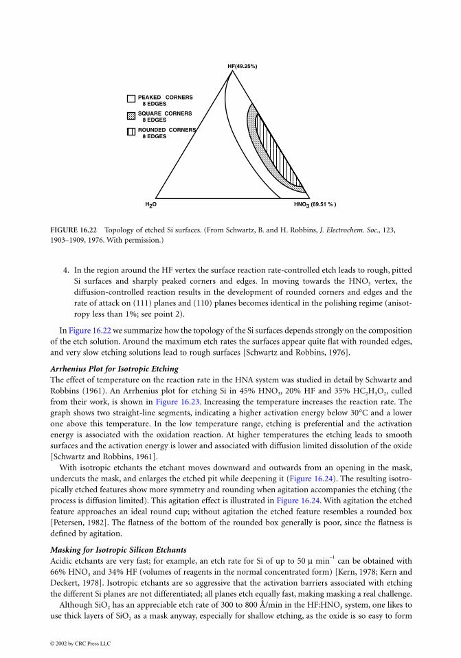
4. In the region around the HF vertex the surface reaction rate-controlled etch leads to rough, pittedSi surfaces and sharply peaked corners and edges. In moving towards the HNO3 vertex, thediffusion-controlled reaction results in the development of rounded corners and edges and therate of attack on (111) planes and (110) planes becomes identical in the polishing regime (anisot-ropy less than 1%; see point 2).
In Figure 16.22 we summarize how the topology of the Si surfaces depends strongly on the compositionof the etch solution. Around the maximum etch rates the surfaces appear quite flat with rounded edges,and very slow etching solutions lead to rough surfaces [Schwartz and Robbins, 1976].
Arrhenius Plot for Isotropic EtchingThe effect of temperature on the reaction rate in the HNA system was studied in detail by Schwartz andRobbins (1961). An Arrhenius plot for etching Si in 45% HNO3, 20% HF and 35% HC2H3O2, culledfrom their work, is shown in Figure 16.23. Increasing the temperature increases the reaction rate. Thegraph shows two straight-line segments, indicating a higher activation energy below 30°C and a lowerone above this temperature. In the low temperature range, etching is preferential and the activationenergy is associated with the oxidation reaction. At higher temperatures the etching leads to smoothsurfaces and the activation energy is lower and associated with diffusion limited dissolution of the oxide[Schwartz and Robbins, 1961].
With isotropic etchants the etchant moves downward and outwards from an opening in the mask,undercuts the mask, and enlarges the etched pit while deepening it (Figure 16.24). The resulting isotro-pically etched features show more symmetry and rounding when agitation accompanies the etching (theprocess is diffusion limited). This agitation effect is illustrated in Figure 16.24. With agitation the etchedfeature approaches an ideal round cup; without agitation the etched feature resembles a rounded box[Petersen, 1982]. The flatness of the bottom of the rounded box generally is poor, since the flatness isdefined by agitation.
Masking for Isotropic Silicon EtchantsAcidic etchants are very fast; for example, an etch rate for Si of up to 50 µ min
–1 can be obtained with
66% HNO3 and 34% HF (volumes of reagents in the normal concentrated form) [Kern, 1978; Kern andDeckert, 1978]. Isotropic etchants are so aggressive that the activation barriers associated with etchingthe different Si planes are not differentiated; all planes etch equally fast, making masking a real challenge.
Although SiO2 has an appreciable etch rate of 300 to 800 Å/min in the HF:HNO3 system, one likes touse thick layers of SiO2 as a mask anyway, especially for shallow etching, as the oxide is so easy to form
FIGURE 16.22 Topology of etched Si surfaces. (From Schwartz, B. and H. Robbins, J. Electrochem. Soc., 123, 1903–1909, 1976. With permission.)
PEAKED CORNERS 8 EDGES
SQUARE CORNERS 8 EDGES
ROUNDED CORNERS 8 EDGES
HF(49.25%)
HNO3 (69.51 % )H2O
© 2002 by CRC Press LLC

and pattern. A mask of nonetching Au or Si3N4 is needed for deeper etching. Photoresists do not standup to strong oxidizing agents such as HNO3, and neither does Al.
Silicon itself is soluble to a small extent in pure HF solutions; for a 48% HF, at 25°C, a rate of 0.3 Å/minwas observed for n-type, 2-ohm cm (111)-Si. It was established that Si dissolution in HF is not due tooxidation by dissolved oxygen. Diluted HF etches Si at a higher rate because the reaction in aqueoussolutions proceeds by oxidation of Si by OH
– groups [Hu and Kerr, 1967]. A typically buffered HF (BHF)
solution has been reported to etch Si at radiochemically measured rates of 0.23 to 0.45 Å/min, dependingon doping type and dopant concentration [Hoffmeister, 1969].
By reducing the dopant concentration (n or p) to below 1017
atoms/cm3 the etch rate of Si in HNA is
reduced by ~150 [Muraoka et al., 1973]. The doping dependence of the etch rate provides yet anothermeans of patterning a Si surface (see next section). A summary of masks that can be used in acidic etchingis presented in Table 16.6.
Dopant Dependence of Silicon Isotropic EtchantsThe isotropic etching process is fundamentally a charge-transfer mechanism. This explains the etch ratedependence on dopant type and concentration. Typical etch rates with an HNA system (1:3:8) for n- orp-type dopant concentrations above 10
18 cm
3 are 1 to 3 µm/min. As presented in the preceding section,
a reduction of the etch rate by 150 times is obtained in n- or p-type regions with a dopant concentrationof 10
17 cm
–3 or smaller [Muraoka et al., 1973]. This presumably is due to the lower mobile carrier
FIGURE 16.23 Etching Arrhenius plot. Temperature dependence of the etch rate of Si in HF:HNO3:CH3:COOH(1:4:3). (From Schwartz, B. and H. Robbins, J. Electrochem. Soc., 108, 365–372, 1961. With permission.)
1000/T (K-1)
Temperature (°C)50 45 40 35 30 25 20 15
200
10080
40
20
108
4
23.1 3.2 3.3 3.4 3.5 3.6
Reaction KineticsDiffusion Dominated-Smooth Surface
Reaction KineticsSurface Dominated-Etching isPreferential
45% HNO3, 20% HF, 35% HC2H3O2R
eact
ion
Rat
e (µ
m/m
in)
© 2002 by CRC Press LLC

concentration available to contribute to the charge transfer mechanisms. In any event, heavily dopedsilicon substrates with high conductivity can be etched more readily than lightly doped materials.Dopant-dependent isotropic etching can also be exploited in an electrochemical set-up as described inthe next section. Although doping does change the chemical etch rate, attempts to exploit these differencesfor industrial production have failed so far [Seidel, 1989]. This situation is different in electrochemicalisotropic etching (see next section).
FIGURE 16.24 Isotropic etching of Si with (A) and without (B) etchant solution agitation.
TABLE 16.6 Masking Materials for Acidic Etchantsa
Etchants
MaskingPiranha
(4:1, H2O2:H2SO4)Buffered HF
(5:1 NH4F:conc. HF) HNA
Thermal SiO2 0.1 µm/min 300–800 Å/min; limited etch time, thick layers often are used due to ease of patterning
CVD (450°C) SiO2 0.48 µm/min 0.44 µm/minCorning 7740 glass 0.063 µ/min 1.9 µ/minPhotoresist Attacks most
organic filmsGood for short while Resists do not stand up to strong oxidizing
agents like HNO3 and are not usedUndoped Si,
polysiliconForms 30 Å of SiO2 0.23 to 0.45 Å/min Si 0.7 to 40 µm/min at room temperature; at a
dopant concentration <1017
cm–3
(n or p)Black wax Usable at room temperatureAu/Cr Good Good GoodLPCVD Si3N4 1 Å/min Etch rate is 10–100 Å/min; preferred masking
material
a The many variables involved necessarily means that the given numbers are approximate only.
© 2002 by CRC Press LLC

Electrochemical Isotropic Silicon Etch-Etch StopSometimes, a high temperature or extremely aggressive chemical etching process can be replaced by anelectrochemical procedure utilizing a much milder solution, thus allowing a simple photoresist mask tobe employed [Kern and Deckert, 1978]. In electrochemical acidic etching, with or without illuminationof the corroding Si electrode, an electrical power supply is employed to drive the chemical reaction bysupplying holes to the silicon surface (W-EL see Figure 16.25). A voltage is applied across the siliconwafer and a counter electrode (C-EL usually platinum) arranged in the same etching solution. Oxidationis promoted by a positive bias applied to the silicon causing an accumulation of holes in the silicon atthe silicon/electrolyte interface. Under this condition, oxidation at the surface proceeds rapidly while theoxide is readily dissolved by the HF solution. No oxidant such as HNO3 is needed to supply the holes;excess electron-hole pairs are created by the electrical field at the surface and/or by optical excitation,thereby increasing the etch rate. This technique proved successful in removing heavily doped layers,leaving behind the more lightly doped membranes in all possible dopant configurations: p on p
+, p on
n+, n on p
+, and n on n
+ [Theunissen et al., 1970; Meek, 1971]. This electrochemical etch-stop technique
is demonstrated in the inset of Figure 16.25 [van Dijk et al., 1970]. A 5% HF solution is used, theelectrolyte cell is kept in the dark at room temperature, and the distance between the Si anode and thePt cathode in the electrochemical cell is 1 to 5 cm. Instead of using HF, one can substitute NH4F (5 wt%)for the electrochemical etching as described by Shengliang et al. (1987). Shengliang reports a selectivityof n-silicon to n
+-silicon (0.001 Ωcm) of 300 with the latter etchant. In the inset in Figure 16.25 the current
density vs. applied voltage across the anode and cathode during dissolution is plotted. The current densityis related to the dissolution rate of silicon. It can be seen that p-type and heavily doped n-type materialscan be dissolved at relatively low voltages, whereas n-type silicon with a lower doping level does not
FIGURE 16.25 Electrochemical etching apparatus. W-EL: working electrode (Si), C-EL: counter electrode (e.g.,Pt), Q = heat supplied. Inset: Current-voltage (Id/η) curves in electrochemical etching of Si of various doping. Etchrate dependence on dopant concentration and dopant type for HF-anodic etching of silicon. (From van Dijk, H.J.A.and J. de Jonge, J. Electrochem. Soc., 117, 553–554, 1970. With permission.)
© 2002 by CRC Press LLC

dissolve at the same low voltages. Experiments in this same set-up with homogeneously doped siliconwafers show that n-type silicon of about 3.10
18 cm
−3 (<0.01 Ωcm) completely dissolves in these etching
conditions, whereas n-type silicon of donor concentrations lower than 2.1016
cm−3
(>0.3 Ωcm) barelydissolves. For p-type silicon, dissolution is initiated when the acceptor concentration is higher than 5.10
15
cm−3
(<3 Ωcm) and the dissolution rate further increases with increasing acceptor concentration. Underspecific circumstances, namely high HF concentrations and low etching currents, porous Si may form[Bomchil et al., 1986].
The acidic electrochemical technique has not been used much in micromachining and is primarilyused to polish surfaces. Since the etching rate increases with current density, high spots on the surfaceare more rapidly etched and very smooth surfaces result. The method of isotropic electrochemical etchinghas some major advantages which could make it a more important micromachining tool in the future.The etched surfaces are very smooth (say with an average roughness, Ra, of 7 nm), the process is roomtemperature and IC compatible, simpler resists schemes can be used as the process is much milder thanetching in HNA, and etching can be controlled simply by switching a voltage on or off. We will pick upthe discussion of anodic polishing, photo etching, and formation of porous silicon in HF solutions aftergathering more insight in various etching models.
Preferential EtchingA variety of additives to the HNA system, mainly oxidants, can be included to modify the etch rate,surface finish or isotropy, rendering the etching baths preferential. It is clear that the effect of theseadditives will only show up in the reaction-controlled regime. Only additives that change the viscosity ofthe solution could modify the etch rate in the diffusion-limited regime, thereby changing the diffusioncoefficient of the reactants [Tuck, 1975; Bogenschutz et al., 1967]. We will not review the effect of theseadditives any further; refer to Table 16.7 and the cited literature for further study [Yang, 1984; Chu andGavaler, 1965; Archer, 1982; Schimmel and Elkind, 1973; Secco d’Aragona, 1972].
Problems with Isotropic EtchantsThere are several problems associated with isotropic etching of Si. First, it is difficult to mask with highprecision using a desirable and simple mask such as SiO2 (etch rate is 2 to 3% of the silicon etch rate).Second, the etch rate is very agitation sensitive in addition to being temperature sensitive. This makes itdifficult to control lateral as well as vertical geometries. Electrochemical isotropic etching (see above)and the development of anisotropic etchants in the late 1960s (see below) overcame many of theseproblems.
A comprehensive review of isotropic etchants solutions can be found in Kern and Deckert (1978).These authors also give a review of different techniques practiced in chemical etching such as immersionetching, spray etching, electrolytic etching, gas-phase etching, and molten salt etching (fusion techniques).In Table 16.7 some isotropic and preferential etchants and their specific applications are listed.
16.5.1.3 Anisotropic Etching
IntroductionAnisotropic etchants shape, also ‘machine,’ desired structures in crystalline materials. When carried outproperly, anisotropic etching results in geometric shapes bounded by perfectly defined crystallographicplanes. Anisotropic wet etching techniques, dating back to the 1960s at the Bell Laboratories, were devel-oped mainly by trial and error. Going over some experimental data, before embarking upon the models,seems fitting. Moreover, we must keep in mind that for higher index planes most models fail.
Figure 16.1 shows a cross-section of a typical shape formed using anisotropic etching. The thinnedmembranes with diffused resistors could be used for a piezoresistive pressure sensor or an accelerometer.In the usual application, the wafer is selectively thinned from a starting thickness of 300 to 500 µm toform a diaphragm having a final thickness of 10 to 20 µm with precisely controlled lateral dimensionsand a thickness control of the order of 1 µm or better. A typical procedure involves the steps summarizedin Table 16.8 [Elwenspoek et al., 1994].
© 2002 by CRC Press LLC

TABLE 16.7 Isotropic and Preferential Defect Etchants and Their Specific Applications
Etchant Application Remark
HF: 8 vol%, HNO3: 75 vol%, and CH3COOH: 17 vol%
n- and p-type Si, all planes, general etching
Planar etch; e.g., 5 µm/min at 25°C
1 part 49% HF, 1 part of (1.5 M CrO3) (by volume)
Delineation of defects on (111), (100), and (110) Si without agitation
Yang etcha
5 vol parts nitric acid (65%), 3 vol parts HF (48%), 3 vol parts acetic acid (96%), 0.06 parts bromine
Polishing etchant used to remove damage introduced during lapping
So-called CP4 etchant; Heidenreich, U.S. Patent 2619414
HF SiO2 Si etch rate for 48% HF at 25°C is 0.3 Å/min with n-type 2 Ω cm (111) Si
1HF, 3HNO3, 10CH3COOH (by volume)
Delineates defects in (111) Si; etches p
+ or n
+ and stops at p
– or n
–Dash etch; p- and n-Si at 1300 Å/min
in the [100] direction and 46 Å/min in the [111] direction at 25°C
b
1HF, 1(5 M CrO3) (by volume) Delineates defects in (111); needs agitation; does not reveal etch pits well on (100) well
Sirtl etchc
2HF, 1(0.15 M K2Cr2O7) (by volume) Yields circular (100) Si dislocation etch pits; agitation reduces etch time
Secco etchd
60 ml HF, 30 ml HNO3, 30 ml (5 M CrO3), 2 g Cu(NO3)2, 60 ml CH3COOH, 60 ml H2O
Delineates defects in (100) and (111) Si; requires agitation
Jenkins etche
2HF, 1 (1 M CrO3) (by volume) Delineates defects in (100) Si without agitation; works well on resistivities 0.6–15.0 Ωcm n- and p-types)
Schimmel etchf
2HF, 1 (1 M CrO3), 1.5 (H2O) (by volume)
Works well on heavily doped (100) silicon
Modified Schimmelf
HF/KMnO4/CH3COOH Epitaxial SiH3PO4 Si3N4 160–180°CKOH + alcohols Polysilicon 85°CH3PO4/HNO3/HC2H3O2 Al 40–50°CHNO3/BHF/water Si and polysilicon 0.1 µm min
–1 for single crystal Si
a Yang, K.H., J. Electrochem. Soc., 131, 1140 (1984).
b Dash, W.C., J. Appl. Phys., 27, 1193 (1956).
c Sirtl, E. and Adler, A., Z. Metallkd., 52, 529 (1961).
d Secco d’Aragona, F., J. Electrochem. Soc., 119, 948 (1972).
e Jenkins, M.W., J. Electrochem. Soc., 124, 757 (1977).
f Schimmel, D.G., J. Electrochem. Soc., 126, 479 (1979).
TABLE 16.8 Summary of the Process Steps Required for Anisotropic Etching of a Membrane [Elwenspoek et al., 1994]
Process Duration Process Temperature (°C)
Oxidation Variable (hours) 900–1200Spinning at 5000 rpm 20–30 sec Room temperaturePrebake 10 min 90Exposure 20 sec Room temperatureDevelop 1 min Room temperaturePost-bake 20 min 120Stripping of oxide (BHF:1:7) ±10 min Room temperatureStripping resist (acetone) 10–30 sec Room temperatureRCA1 (NH3(25%) + H2O + H2O2:1:5:1) 10 min BoilingRCA2 (HCl + H2O + H2O2:1:6:1) 10 min BoilingHF-dip (2% HF) 10 sec Room temperatureAnisotropic etch From minutes up to one day 70–100
© 2002 by CRC Press LLC

The development of anisotropic etchants solved the lateral dimension control lacking in isotropicetchants. Lateral mask geometries on planar photoengraved substrates can be controlled with an accuracyand reproducibility of 0.5 µm or better, and the anisotropic nature of the etchant allows this accuracyto be translated into control of the vertical etch profile. Different etch stop techniques, needed to controlthe membrane thickness, are available. The invention of these etch stop techniques truly made items asshown in Figure 16.1 manufacturable.
While anisotropic etchants solve the lateral control problem associated with deep etching, they arenot without problems. They are slower, even in the fast etching <100> direction, with etch rates of1 µm/min or less. That means that etching through a wafer is a time-consuming process: to etchthrough a 300-µm-thick wafer one needs 5 hours. They also must be run hot to achieve these etchrates (85 to 115°C), precluding many simple masking options. Like the isotropic etchants, their etchrates are temperature sensitive; however, they are not particularly agitation sensitive, considered tobe a major advantage.
Anisotropic EtchantsA wide variety of etchants have been used for anisotropic etching of silicon, including alkaline aqueoussolutions of KOH, NaOH, LiOH, CsOH, NH4OH, and quaternary ammonium hydroxides, with thepossible addition of alcohol. Alkaline organics such as ethylenediamine, choline (trimethyl-2-hydroxy-ethyl ammonium hydroxide) or hydrazine with additives such as pyrocathechol and pyrazine areemployed as well. Etching of silicon occurs without the application of an external voltage and is dopantinsensitive over several orders of magnitude, but in a curious contradiction to its suggested chemicalnature, it has been shown to be bias dependent [Allongue et al., 1993; Palik et al., 1987]. This contradictionwill be explained with the help of the chemical models presented below.
Alcohols such as propanol and isopropanol butanol typically slow the attack on Si [Linde and Austin,1992; Price, 1973]. The role of pyrocathechol [Finne and Klein, 1967] is to speed up the etch rate throughcomplexation of the reaction products. Additives such as pyrazine and quinone have been described ascatalysts by some [Reisman et al., 1979]; but this is contested by other authors [Seidel et al., 1990]. Theetch rate in anisotropic etching is reaction rate controlled and thus temperature dependent. The etchrate for all planes increases with temperature and the surface roughness decreases with increasing tem-perature, so etching at the higher temperatures gives the best results. In practice, etch temperatures of80 to 85°C are used to avoid solvent evaporation and temperature gradients in the solution.
Arrhenius Plots for Anisotropic EtchingA typical set of Arrhenius plots for <100>, <110> and <111> silicon etching in an anisotropic etchant(EDP, or ethylene-diamine/pyrocathechol) is shown in Figure 16.26 [Seidel et al., 1990]. It is seen thatthe temperature dependence of the etch rate is quite large and is less dependent on orientation. The slopediffers for the different planes, i.e., (111) > (100) > (110). Lower activation energies in Arrhenius plotscorrespond to higher etch rates. The anisotropy ratio (AR) derived from this figure is
AR = (hkl)1 etch rate/(hkl)2 etch rate (16.29)
The AR is approximately 1 for isotropic etchants and can be as high as 400/200/1 for (110)/(100)/(111)in 50 wt% KOH/H2O at 85°C. Generally, the activation energies of the etch rates of EDP are smaller thanthose of KOH. The (111) planes always etch slowest but the sequence for (100) and (110) can be reversed(e.g., 50/200/8 in 55 vol% ethylenediamine ED/H2O; also at 85°C). The (110) Si plane etches 8 timesslower and the (111) 8 times faster in KOH/H2O than in ED/H2O, while the (100) etches at the samerate [Kendall and Guel, 1985]. Working with alcohols and other organic additives often changes therelative etching rate of the different Si planes. Along this line, Seidel et al. (1990a; 1990b) found that thedecrease in etch rate by adding isopropyl alcohol to a KOH solution was 20% for <100>, but almost 90%for <110>. As a result of the much stronger decrease of the etch rate on a (110) surface, the etch ratioof (100):(110) is reversed.
© 2002 by CRC Press LLC
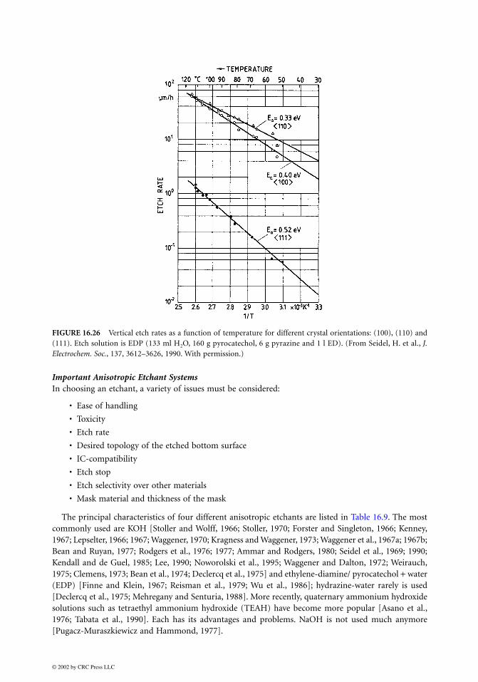
Important Anisotropic Etchant SystemsIn choosing an etchant, a variety of issues must be considered:
• Ease of handling
• Toxicity
• Etch rate
• Desired topology of the etched bottom surface
• IC-compatibility
• Etch stop
• Etch selectivity over other materials
• Mask material and thickness of the mask
The principal characteristics of four different anisotropic etchants are listed in Table 16.9. The mostcommonly used are KOH [Stoller and Wolff, 1966; Stoller, 1970; Forster and Singleton, 1966; Kenney,1967; Lepselter, 1966; 1967; Waggener, 1970; Kragness and Waggener, 1973; Waggener et al., 1967a; 1967b;Bean and Ruyan, 1977; Rodgers et al., 1976; 1977; Ammar and Rodgers, 1980; Seidel et al., 1969; 1990;Kendall and de Guel, 1985; Lee, 1990; Noworolski et al., 1995; Waggener and Dalton, 1972; Weirauch,1975; Clemens, 1973; Bean et al., 1974; Declercq et al., 1975] and ethylene-diamine/ pyrocatechol + water(EDP) [Finne and Klein, 1967; Reisman et al., 1979; Wu et al., 1986]; hydrazine-water rarely is used[Declercq et al., 1975; Mehregany and Senturia, 1988]. More recently, quaternary ammonium hydroxidesolutions such as tetraethyl ammonium hydroxide (TEAH) have become more popular [Asano et al.,1976; Tabata et al., 1990]. Each has its advantages and problems. NaOH is not used much anymore[Pugacz-Muraszkiewicz and Hammond, 1977].
FIGURE 16.26 Vertical etch rates as a function of temperature for different crystal orientations: (100), (110) and(111). Etch solution is EDP (133 ml H2O, 160 g pyrocatechol, 6 g pyrazine and 1 l ED). (From Seidel, H. et al., J.Electrochem. Soc., 137, 3612–3626, 1990. With permission.)
© 2002 by CRC Press LLC
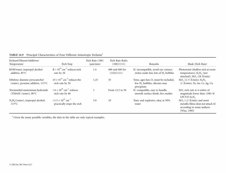
TABL
EtchanTempe Mask (Etch Rate)
KOH/addit
eye contact, of H2 bubbles
Photoresist (shallow etch at room temperature); Si3N4 (not attacked); SiO2 (28 Å/min)
Ethyle(wate
t be excluded, tes may
SiO2 (2–5 Å/min); Si3N4 (1 Å/min); Ta, Au, Cr, Ag, Cu
Tetram(TM
handle, , few studies
SiO2 etch rate is 4 orders of magnitude lower than (100) Si LPCVD Si3N4
N2H4/115°C
ay at 50% SiO2 (<2 Å/min) and most metallic films; does not attack Al according to some authors [Wise, 1985]
a Gi
© 2002
E 16.9 Principal Characteristics of Four Different Anisotropic Etchantsa
t/Diluent/Additives/rature Etch Stop
Etch Rate (100) (µm/min)
Etch Rate Ratio (100)/(111) Remarks
water, isopropyl alcohol ive, 85°C
B > 1020
cm–3
reduces etch rate by 20
1.4 400 and 600 for (110)/(111)
IC incompatible, avoidetches oxide fast, lots
ne diamine pyrocatechol r), pyrazine additive, 115°C
≥5 × 10¹⁹
cm–3
reduces the etch rate by 50
1.25 35 Toxic, ages fast, O2 musfew H2 bubbles, silicaprecipitate
ethyl ammonium hydroxide AH) (water), 90°C
>4 × 10²⁰
cm–3
reduces etch rate by 40
1 From 12.5 to 50 IC compatible, easy to smooth surface finish
(water), isopropyl alcohol, >1.5 × 10²⁰
cm–3
practically stops the etch
3.0 10 Toxic and explosive, okwater
ven the many possible variables, the data in the table are only typical examples.
by CRC Press LLC

Hydrazine-water is explosive at high hydrazine concentrations (rocket fuel) and is a suspected carcin-ogen. Its use should be avoided for safety reasons. A 50% hydrazine/water solution is stable, though, and,according to Mehregany and Senturia (1988), excellent surface quality and sharply defined corners areobtained in Si. Also on the positive side, the etchant has a very low SiO2 etch rate and will not attackmost metal masks except for Al, Cu and Zn. According to Wise, on the other hand, Al does not etch inhydrazine either, but the etch produces rough Si surfaces [Wise, 1985].
Ethylenediamine in EDP reportedly causes allergic respiratory sensitization, and pyrocathechol isdescribed as a toxic corrosive. The material is also optically dense, making end-point detection harder,and it ages quickly; if the etchant reacts with oxygen, the liquid turns to a red-brown color and it losesits good properties. If cooled down after etching, one gets precipitation of silicates in the solution.Sometimes one even gets precipitation during etching, spoiling the results. When preparing thesolution, the last ingredient added should be the water, since water addition causes the oxygensensitivity. All of the above make the etchant quite difficult to handle. But, a variety of masking materialscan be used in conjunction with this etchant and it is less toxic than hydrazine. No sodium or potassiumcontamination occurs with this compound and the etch rate of SiO2 is slow. The ratio of etch rates ofSi and SiO2 using EDP can be as large as 5000:1 (about 2 Å/min of SiO2 compared to 1 µm/min ofSi) which is much larger than the ratio in KOH a ratio of as high as 400:1 has been reported [Bean,1978]. Importantly, the etch rate slows down at a lower boron concentration than with KOH. A typicalfastest-to-slowest hierarchy of Si etch rates with EDP at 85°C according to Barth (1984) is (110) >(411) > (311) > (511) > (211) > (100) > (331) > (221) > (111).
The simple KOH water system is the most popular etchant. A KOH etch, in near saturated solutions(1:1 in water by weight) at 80°C, produces a uniform and bright surface. Nonuniformity of etch rate getsconsiderably worse above 80°C. Plenty of bubbles are seen emerging from the Si wafer while etching inKOH. The etching selectivity between Si and SiO2 is not very good in KOH, as it etches SiO2 too fast.KOH is also incompatible with the IC fabrication process and can cause blindness when it gets in contactwith the eyes. The etch rate for low index planes is maximal at around 4 M (see Figure 16.27A [Peeters,1994] and Lambrechts and Sansen [1992]). The surface roughness continuously decreases with increasingconcentration as can be gleaned from Figure 16.27B. Since the difference in etch rates for different KOHconcentrations is small, a highly concentrated KOH (e.g., 7 M) is preferred to obtain a smooth surfaceon low index planes.
Except at very high concentrations of KOH, the etched (100) plane becomes rougher the longerone etches. This is thought to be due to the development of hydrogen bubbles, which hinder thetransport of fresh solution to the silicon surface [Ternz, 1988]. Average roughness, Ra, is influencedstrongly by fluid agitation. Stirring can reduce the Ra values over an order of magnitude, probablycaused by the more efficient removal of hydrogen bubbles from the etching surface when stirring[Gravesen, 1986]. The silicon etch rate as a function of KOH concentration is shown in Figure 16.27C[Seidel et al., 1990].
Herr and Baltes (1991) found that the high-index crystal planes exhibit the highest etch rates for 6M KOH and that for lower concentrations the etch bottoms disintegrate into microfacets. In 6 M KOH,the etch-rate order is (311) > (144) > (411) > (133) > (211) > (122). These authors could not correlatethe particular etch rate sequence with the measured activation energies. This is in contrast to loweractivation energies corresponding to higher etching rates for low index planes as shown in Figure16.26. Their results obtained on large open area structures differ significantly from previous onesobtained by underetching special mask patterns. The vertical etching rates obtained here are substan-tially higher than the underetching rates described elsewhere, and the etch rate sequence for differentplanes is also significantly different. These results suggest that crevice effects may plan an importantrole in anisotropic etching.
Besides KOH [Clark and Edell, 1987], other hydroxides have been used, including NaOH [Allongueet al., 1993; Pugacz-Muraszkiewicz and Hammond, 1977], CsOH [Clark et al., 1988] and NH4OH[Schnakenberg et al., 1990]. A major disadvantage of KOH is the presence of alkali ions, which aredetrimental to the fabrication of sensitive electronic parts. Work is under way to find anisotropic etchants
© 2002 by CRC Press LLC

that are more compatible with CMOS processing and that are neither toxic nor harmful. Two examplesare ammonium hydroxide-water (AHW) mixtures [Schnakenberg et al., 1990] and tetramethyl ammo-nium hydroxide-water (TMAHW) mixtures [Tabata et al., 1990; Schnakenberg et al., 1990]. TMAHWsolutions do not decompose at temperatures below 130°C, a very important feature from the viewpointof production. They are nontoxic and can be handled easily. TMAHW solutions also exhibit excellentselectivity to silicon oxide and silicon nitride. At a solution temperature of 90°C and 22 wt% TMAH, amaximum (100) silicon etch rate of 1.0 µm/min is observed, 1.4 µm/min for (110) planes (this is higherthan those observed with EDP, AHW, hydrazine water and tetraethyl ammonium hydroxide [TEA], butslower than those observed for KOH and an anisotropy ratio, AR(100)/(111), of between 12.5 and50 [Tabata et al., 1992]). From the viewpoint of fabricating various silicon sensors and actuators, aconcentration above 22 wt% is preferable, since lower concentrations result in larger roughness on theetched surface. However, higher concentrations give a lower etch rate and lower etch ratio (100)/(111).Tabata (1995) also studied the etching characteristics of pH-controlled TMAHW. To obtain a low alu-minum etching rate of 0.01 µm/min, pH values below 12 for 22 wt% TMAHW were required. At thosepH values the Si(100) etching rate is 0.7 µm/min.
FIGURE 16.27 Anisotropic etching of silicon. (A) Silicon (100) etch rate (line) and nonuniformity of etchrate (column) in KOH at 80°C as a function of KOH concentration. The etch rate for all low index planes ismaximal at around 4 M. (B) Silicon (100) surface roughness (Ra) in aqueous KOH at 80°C as a function ofconcentration for a 1-hour etch time (thin line) and for an etch depth of 60 µm (thick line). (C) Silicon (100)etch rate as a function of KOH concentration at a temperature of 72°C. (A and B from Peeters, E., Ph.D. thesis,1996, KUL, Belgium. With permission. C from Seidel et al., J. Electrochem. Soc., 137, 3612–3626, 1990. Withpermission.)
© 2002 by CRC Press LLC

Surface Roughness and NotchingAnisotropic etchants frequently leave too rough a surface behind, and a slight isotropic etch is used to‘touch-up’. A distinction must be made between macroscopic and microscopic roughness. Macroscopicroughness, also referred to as notching or pillowing, results when centers of exposed areas etch with aseemingly lower average speed compared with the borders of the areas, so that the corners between sidewallsand (100) ground planes are accentuated. Membranes or double-sided clamped beams (microbridges)therefore tend to be thinner close to the clamped edges than in the center of the structure. This differencecan be as large as 1 to 2 µm, which is quite considerable if one is etching 10 to 20 µm thick structures.Notching increases linearly with etch depth but decreases with higher concentrations of KOH. Themicroscopic smoothness of originally mirror-like polished wafers can also be degraded into microscopicroughness. It is this type of short-range roughness we referred to in discussing Figure 16.27B above.
Masking for Anisotropic EtchantsEtching through a whole wafer (400 to 600 µm) takes several hours (a typical wet anisotropic etch ratebeing 1.1 µm/min), definitely not a fast process. When using KOH, SiO2 cannot be used as a maskingmaterial for features requiring that long an exposure to the etchants. The SiO2 etch rate as a function ofKOH concentration at 60°C is shown in Figure 16.28. There is a distinct maximum at 35 wt% KOH ofnearly 80 nm/hr. The shape of this curve will be explained further below on the basis of Seidel et al.’smodel. Experiments have shown that even a 1.5-µm-thick oxide is not sufficient for the complete etchingof a 380-µm-thick wafer (6 hours) because of pinholes in the oxide [Lambrechts and Sansen, 1992]. Theetch rate of thermally grown SiO2 in KOH-H2O somewhat varies and apparently depends not only onthe quality of the oxide, but also on the etching container and the age of the etching solution, as well asother factors [Kendall, 1979]. The Si/SiO2 selectivity ratio at 80°C in 7 M KOH is 30 ± 5. This ratioincreases with decreasing temperature; reducing the temperature from 80 to 60°C increases the selectivityratio from 30 to 95 in 7 M KOH [Kendall, 1975]. Thermal oxides are under strong compressive stressdue to the fact that in the oxide layer one silicon atom takes nearly twice as much space as in singlecrystalline Si (see also Madou [1997, chap. 3]). This might have severe consequences; for example, if theoxide mask is stripped on one side of the wafer, the wafer will bend. Atmospheric pressure chemicalvapor deposited (APCVD) SiO2 tends to exhibit pinholes and etches much faster than thermal oxide.
Macroscopic roughness (notching effect) and microscopic roughness.
© 2002 by CRC Press LLC

Annealing of APCVD oxide removes the pinholes but the etch rate in KOH remains greater by a factorof 2 to 3 than that of thermal oxide. Low pressure chemical vapor deposited (LPCVD) oxide is a maskmaterial of comparable quality as thermal oxide. The etch rate of SiO2 in EDP is smaller by two ordersof magnitude than in KOH.
For prolonged KOH etching, a high density silicon nitride mask has to be deposited. A low pressurechemical vapor deposited (LPCVD) nitride generally serves better for this purpose than a less denseplasma deposited nitride [Puers, 1991]. With an etch rate of less than 0.1 nm/min, a 400-Å layer of LPCVDnitride suffices to mask against KOH etchant. The etch selectivity Si/Si3N4 was found to be better than10
4 in 7 M KOH at 80°C. The nitride also acts as a good ion-diffusion barrier, protecting sensitive
electronic parts. Nitride can easily be patterned with photoresist and etched in a CF4/O2-based plasmaor, in a more severe process, in H3PO4 at 180°C (10 nm/min) [Buttgenbach, 1991]. Nitride films aretypically under a tensile stress of about 1 × 10
9 Pa. If in the overall processing of the devices, nitride
deposition does not pose a problem, KOH emerges as the preferential anisotropic wet etchant. For dopantdependent etching, EDP is the better etchant and generally better suited for deep etching since its oxideetch rate is negligible (<5 Å/min).
Oxide and nitride are masking for anisotropic etchants to varying degrees with both mask types beingused. When these layers are used to terminate an etch in the [100] direction, a low etch rate of the masklayer allows overetching of silicon, to compensate for wafer thickness variations. A KOH solution etchesSiO2 at a relatively fast rate of 1.4 to 3 nm/min so that Si3N4 or Au/Cr must be used as a mask againstKOH for deep and long etching.
Backside ProtectionIn many cases it is necessary to protect the backside of a wafer from an isotropic or anisotropic etchant.The backside is either mechanically or chemically protected. In the mechanical method the wafer is heldin a holder, often made from Teflon. The wafer is fixed between Teflon-coated O-rings which are carefullyaligned in order to avoid mechanical stress in the wafer. In the chemical method, waxes or other organiccoatings are spun onto the back side of the wafer. Two wafers may be glued back-to-back for fasterprocessing.
FIGURE 16.28 The SiO2 etch rate in nm/hr as a function of KOH concentration at 60°C. (From Seidel, H. et al.,J. Electrochem. Soc., 137, 3612–3626, 1990. With permission.)
© 2002 by CRC Press LLC

Etch Rate and Etch StopsThe Si etch rate, R, as a function of KOH concentration at 72°C, was shown in Figure 16.27C. The etchrate has a maximum at about 20% KOH. The best fit for this experimentally determined etch rate, formost KOH concentrations, is [Seidel et al., 1990a; 1990b]
(16.30)
Any model of anisotropic etching will have to explain this peculiar dependency on the water and KOHconcentration, as well as the fact that all anisotropic etchant systems of Table 16.9 exhibit drasticallyreduced etch rates for high boron concentrations in silicon (≥5 × 10
19 cm
−3 solid solubility limit). Other
impurities (P, Ge) also reduce the etch rate, but at much higher concentrations (see Figure 16.29 [Seidelet al., 1990]). Boron typically is incorporated using ion implantation (thin layers) or liquid/solid sourcedeposition (thick layers >1 µm). These doped layers are used as very effective etch stop layers (see below).Hydrazine or EDP, which displays a smaller (100)-to-(111) etch rate ratio (~35) than KOH, exhibits astronger boron concentration dependency. The etch rate in KOH is reduced by a factor of 5 to 100 fora boron concentration larger than 10
20 cm
−3. When etching in EDP, the factor climbs to 250 [Bogh, 1971].
With TMAHW solutions, the Si etch rate decreases to 0.01 µm/min for boron concentrations of about4 × 10
20 cm
−3 [Steinsland et al., 1995]. The mechanism eludes us, but Seidel et al.’s model (see below)
gives the most plausible explanation for now. Some of the different mechanisms to explain etch stopeffects that have been suggested follow:
1. Several observations suggest that doping leads to a more readily oxidized Si surface. Highly boron-or phosphorus-doped silicon in aqueous KOH spontaneously can form a thin passivating oxidelayer [Palik et al., 1982; 1985]. The boron-oxides and -hydroxides initially generated on the siliconsurface are not soluble in KOH or EDP etchants [Petersen, 1982]. The substitutional boron createslocal tensile stress in the silicon, increasing the bond strength so that a passivating oxide mightbe more readily formed at higher boron concentrations. Boron-doped silicon has a high defectdensity (slip planes), encouraging oxide growth.
2. Electrons produced during oxidation of silicon are needed in a subsequent reduction step (hydro-gen evolution in Reaction 16.2). When the hole density passes 10
19 cm
–3 these electrons combine
with holes instead, thus stopping the reduction process [Palik et al., 1982]. Seidel et al.’s modelfollows this explanation (see below).
FIGURE 16.29 Relative etch rate for (100) Si in EDP and KOH solutions as a function of concentration of boron,phosphorus and germanium. (From Seidel, H. et al., J. Electrochem. Soc., 137, 3626–3632, 1990. With permission.)
101
100
10-1
10-2
10-3
1018 1019 1020 1021 1022cm-3
DOPANT CONCENTRATION
B EDP S 110OC
P 10%KOH 21OC
Ge 34%KOH 60OC
Ge EDP S 79OC R
ELA
TIV
E E
TC
H R
ATE
R k[H2O]= 4[KOH]
14--
© 2002 by CRC Press LLC
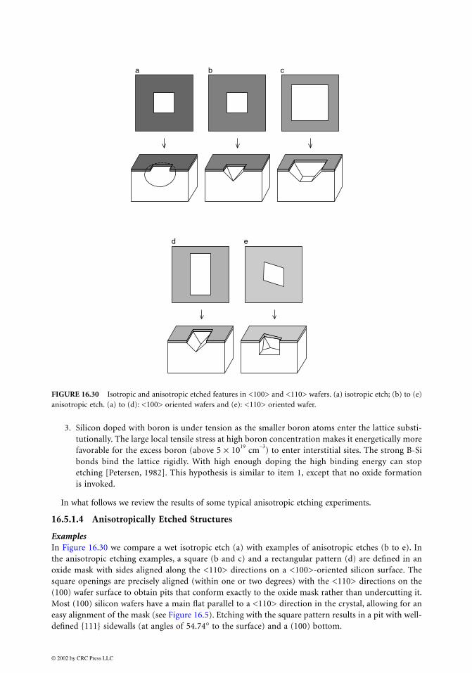
3. Silicon doped with boron is under tension as the smaller boron atoms enter the lattice substi-tutionally. The large local tensile stress at high boron concentration makes it energetically morefavorable for the excess boron (above 5 × 10
19 cm
−3) to enter interstitial sites. The strong B-Si
bonds bind the lattice rigidly. With high enough doping the high binding energy can stopetching [Petersen, 1982]. This hypothesis is similar to item 1, except that no oxide formationis invoked.
In what follows we review the results of some typical anisotropic etching experiments.
16.5.1.4 Anisotropically Etched Structures
ExamplesIn Figure 16.30 we compare a wet isotropic etch (a) with examples of anisotropic etches (b to e). Inthe anisotropic etching examples, a square (b and c) and a rectangular pattern (d) are defined in anoxide mask with sides aligned along the <110> directions on a <100>-oriented silicon surface. Thesquare openings are precisely aligned (within one or two degrees) with the <110> directions on the(100) wafer surface to obtain pits that conform exactly to the oxide mask rather than undercutting it.Most (100) silicon wafers have a main flat parallel to a <110> direction in the crystal, allowing for aneasy alignment of the mask (see Figure 16.5). Etching with the square pattern results in a pit with well-defined 111 sidewalls (at angles of 54.74° to the surface) and a (100) bottom.
FIGURE 16.30 Isotropic and anisotropic etched features in <100> and <110> wafers. (a) isotropic etch; (b) to (e)anisotropic etch. (a) to (d): <100> oriented wafers and (e): <110> oriented wafer.
a b c
d e
© 2002 by CRC Press LLC
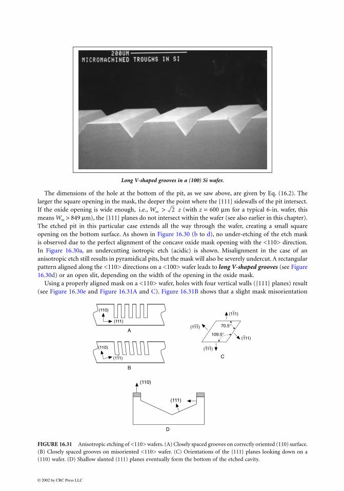
The dimensions of the hole at the bottom of the pit, as we saw above, are given by Eq. (16.2). Thelarger the square opening in the mask, the deeper the point where the 111 sidewalls of the pit intersect.If the oxide opening is wide enough, i.e., Wm > z (with z = 600 µm for a typical 6-in. wafer, thismeans Wm > 849 µm), the 111 planes do not intersect within the wafer (see also earlier in this chapter).The etched pit in this particular case extends all the way through the wafer, creating a small squareopening on the bottom surface. As shown in Figure 16.30 (b to d), no under-etching of the etch maskis observed due to the perfect alignment of the concave oxide mask opening with the <110> direction.In Figure 16.30a, an undercutting isotropic etch (acidic) is shown. Misalignment in the case of ananisotropic etch still results in pyramidical pits, but the mask will also be severely undercut. A rectangularpattern aligned along the <110> directions on a <100> wafer leads to long V-shaped grooves (see Figure16.30d) or an open slit, depending on the width of the opening in the oxide mask.
Using a properly aligned mask on a <110> wafer, holes with four vertical walls (111 planes) result(see Figure 16.30e and Figure 16.31A and C). Figure 16.31B shows that a slight mask misorientation
Long V-shaped grooves in a (100) Si wafer.
FIGURE 16.31 Anisotropic etching of <110> wafers. (A) Closely spaced grooves on correctly oriented (110) surface.(B) Closely spaced grooves on misoriented <110> wafer. (C) Orientations of the 111 planes looking down on a(110) wafer. (D) Shallow slanted (111) planes eventually form the bottom of the etched cavity.
2
D
(110)
A
(111)
(110)
B
(111)
(111)
(111)
(111)
(111)
70.5°
109.5°
C
(111)
(110)
© 2002 by CRC Press LLC

leads to all skewed sidewalls. A U-groove based on a rectangular mask with the long sides along the<111> directions and anisotropically etched in (110) silicon has a complex shape delineated by six111 planes, four vertical and two slanted (see Figure 16.31D). Before emergence of 111 planes, theU-groove is defined by four vertical (111) planes and a horizontal (110) bottom. Self-stopping occurswhen the tilted end planes intersect at the bottom of the groove. It is easy to etch long, narrow U-grooves very deeply into a <110> silicon wafer. However, it is impossible to etch a short, narrow U-groove deeply into a slice of silicon [Kendall, 1979], because the narrow dimension of the groove isquickly limited by slow-etching 111 planes that subtend an angle of 35° to the surface and causeetch termination. At a groove of length L = 1 mm on the top surface, etching will stop when it reachesa depth of 0.289 mm, i.e., Dmax = L/2 . For very long grooves, the tilted end planes are too far apartto intersect in practical cases, making the end effects negligible compared to the remaining U-shapedpart of the groove.
A laser can be used to melt or ‘spoil’ the shallow (111) surfaces, making it possible to etch deepvertical-walled holes through a (110) wafer as shown in Figure 16.32A [Schumacher et al., 1994; Barthet al., 1985; Seidel and Csepregi, 1988]. The technique is illustrated in Figure 16.32B. The absorbedenergy of a Nd:YAG laser beam causes a local melting or evaporation zone enabling etchants to etch theshallow (111) planes in the line-of-sight of the laser. Etching proceeds until ‘unspoiled’ (111) planes areencountered. Some interesting resulting possibilities, including partially closed microchannels, are shownin Figure 16.32C [Schumacher et al., 1994; Alavi et al., 1991]. Note that with this method it is possibleto use <111> wafers for micromachining. The light of the Nd:YAG laser is very well suited for thismicromachining technique due to the 1.17-eV photon energy, just exceeding the band gap energy of Si.Details on this laser machining process can be found, for example, in Alavi et al. (1991; 1992).
Especially when machining surface structures by undercutting, the orientation of the wafer is ofextreme importance. Consider, for example, the formation of a bridge in Figure 16.33A [Barth et al.,1985]. When using a (100) surface, a suspension bridge cannot form across the etched V-groove; twoindependent truncated V-grooves flanking a mesa structure result instead. To form a suspended bridgeit must be oriented away from the <110> direction. This in contrast with a (110) wafer where amicrobridge crossing a V-groove with a 90° angle will be undercut. Convex corners will be undercut byetchant, allowing formation of cantilevers as shown in Figure 16.33B. The diving board shown forms byundercutting starting at the convex corners.
To create vertical (100) faces, as shown in Figure 16.10, in general only KOH works (not EDP orTMAHW) and it has to happen in high-selectivity conditions (low temperature, low concentration:25 wt% KOH, 60°C). Interestingly, high concentration KOH (45 wt%) at higher temperatures (80°C)produces a smooth sidewall, controllable and repeatable at an angle of 80°. EDP produces 45° angledplanes and TMAHW usually makes a 30° angle [Palik et al., 1985].
Alignment PatternsWhen alignment of a pattern is critical, pre-etch alignment targets become useful to delineate theplanes of interest since the wafer flats often are aligned to ±1° only. In order to find the properalignment for the mask, a test pattern of closely spaced lines can be etched (see Figure 16.34). Thegroove with the best vertical walls determines the proper final mask orientation. Along this line, Ciarlo(1987) made a set of lines 3 mm long and 8 µm wide, fanning out like spokes in a wagon wheel atangles 0.1° apart. This target was printed near the perimeter of the wafer and then etched 100 µminto the surface. Again, by evaluating the undercut in this target the correct crystal direction couldbe determined. Alignment with better than 0.05° accuracy was accomplished this way. Similarly, toobtain detailed experimental data on crystal orientation dependence of etch rates, Seidel et al. (1990)used a wagon-wheel or star-shaped mask (e.g., made from CVD-Si3N4; SiH4 and NH3 at 900°C),consisting of radially divergent segments with an angular separation of one degree. Yet finer 0.1°patterns were made around the principal crystal directions. The etch pattern emerging on a <100>oriented wafer covered with such a mask is shown in Figure 16.35A. The blossom-like figure is dueto the total underetching of the passivation layer in the vicinity of the center of the wagon wheel,
3
© 2002 by CRC Press LLC

leaving an area of bare exposed Si. The radial extension of the bare Si area depends on the crystalorientation of the individual segments, leading to a different amount of total underetching. Theobservation of these blossom-like patterns was used for qualitative guidance of etching rates only. Inorder to establish quantitative numbers for the lateral etch rates, the width, w, of the overhangingpassivation layer was measured with an optical line-width measurement system (see Figure 16.35B).
FIGURE 16.32 Laser/KOH machining. (A) Holes through a (110) Si wafer created by laser spoiling and subsequentKOH etching. The two sets of (111) planes making an angle of 70° are the vertical walls of the hole. The (111) planesmaking a 35° angle with the surface tend to limit the depth of the hole but laser spoiling enables one to etch all theway through the wafer (see also B [c]). (B) After laser spoiling, the line-of-sight (111) planes are spoiled and etchingproceeds until unspoiled (111) planes are reached. (C) Some of the possible features rendered by laser spoiling.(From Schumacher, A. et al., Technische Rundschau, 86, 20–23, 1994. With permission.)
a)
c) d)
b)
35.26o
70.53o
70.53o54.74
o
C
© 2002 by CRC Press LLC

Laser beam reflection was used to identify the crystal planes and ellipsometry was used to monitorthe etching rate of the mask itself. Lateral etch rates determined in this way on <100>- and <110>-oriented wafers at 95°C in EDP (470 ml water, 11 ED, 176 g pyrocatechol) and at 78°C in a 50% KOHsolution are shown in Figure 16.36. Etch rates shown are normal to the actual crystal surface and areconveniently described in a polar plot in which the distance from the origin to the polar plot surface(or curve in two dimensions) indicates the etch rate for that particular direction. Note the deepminima at the 111 planes. It can also be seen that in KOH the peak etch rates are more pronounced.A further difference is that with EDP the minimum at 111 planes is steeper than with KOH. Forboth EDP and KOH, the etch rate depends linearly on misalignment. All the above observations haveimportant consequences for the interpretation of anisotropy of an etch (see below). The differencebetween KOH and EDP etching behavior around the 111 minima has the direct practical consequencethat it is more important for etching in EDP to align the crystallographic direction more preciselythan in KOH [Elwenspoek et al., 1994].
FIGURE 16.33 How to make (A) a suspension bridge from a (100) Si wafer and (B) a diving board from a (110)Si wafer [Barth et al., 1985].
(110)(110)
A
Cantilever beam during etching:
Si
Si
Cantilever beam after etching:
B
© 2002 by CRC Press LLC

When determining etch rates without using underetching masks but by using vertical etching of beveledsilicon samples, results are quite different than when working with masked silicon [Herr and Baltes, 1991].The etch rates on open areas of beveled structures are much larger than in underetching experimentswith masked silicon, and different crystal planes develop. Herr et al. conclude that crevice effects mayplay an important role in anisotropic etching. Elwenspoek et al.’s model [Elwenspoek, 1993; Elwenspoeket al. 1994], analyzed below, is the only model which predicts such a crevice effect. He explains why,when etchants are in a small restricted crevice area and are not refreshed fast enough, etching rates slowdown and increase anisotropy.
16.5.2 Chemical Etching Models
16.5.2.1 Introduction
Lots of conflicting data exist in the literature on the anisotropic etch rates of the different Si planes,especially for the higher index planes. This is not too surprising, given the multiple parameters influencingindividual results: temperature, stirring, size of etching feature (i.e., crevice effect), KOH concentration,addition of alcohols and other organics, surface defects, complexing agents, surfactants, pH, cationinfluence etc. More rigorous experimentation and standardization will be needed, as well as better etchingmodels, to better understand the influence of all these parameters on etch rates.
FIGURE 16.34 Test pattern of U-grooves in a <110> wafer to help in the alignment of the mask; final alignmentis done with the groove that exhibits the most perfect long perpendicular walls.
© 2002 by CRC Press LLC

Several chemical models explaining the anisotropy in etching rates for the different Si orientationshave been proposed. Presently we will list all of the proposed models and compare the two most recentand most detailed models (the one by Seidel et al. [1990a; 1990b] and the one by Elwenspoek [1993]and Elwenspoek et al. [1994]). Different Si crystal properties have been correlated with the anisotropyin silicon etching.
1. It has been observed that the 111 Si planes present the highest density of atoms per cm2 to the
etchant and that the atoms are oriented such that three bonds are below the plane. It is possiblethat these bonds become chemically shielded by surface bonded (OH) or oxygen, thereby slowingthe etch rate.
2. It also has been suggested that etch rate correlates with available bond density, the surfaces withthe highest bond density etching faster [Price, 1973]. The available bond densities in Si and otherdiamond structures follow the sequence 1:0.71:0.58 for the 100:110:111 surfaces. However,Kendall (1979) commented that bond density alone is an unlikely explanation because of themagnitude of etching anisotropy (e.g., a factor of 400), compared to the bond density variationsof at most a factor of 2.
FIGURE 16.35 (A) Etch pattern emerging on a wagon wheel-masked, <100>-oriented Si wafer after etching in anEDP solution. (B) Schematic cross section of a silicon test chip covered with a wagon wheel-shaped masking patternafter etching. The measurement of ‘w’ is used to construct polar diagrams of lateral underetch rates as shown inFigure 16.36. (From Seidel et al., J. Electrochem. Soc., 177, 3612–3626, 1990. With permission.)
© 2002 by CRC Press LLC
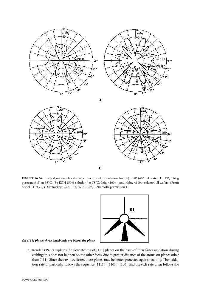
3. Kendall (1979) explains the slow etching of 111 planes on the basis of their faster oxidation duringetching; this does not happen on the other faces, due to greater distance of the atoms on planes otherthan (111). Since they oxidize faster, these planes may be better protected against etching. The oxida-tion rate in particular follows the sequence 111 > 110 > 100, and the etch rate often follows the
FIGURE 16.36 Lateral underetch rates as a function of orientation for (A) EDP (470 ml water, 1 l ED, 176 gpyrocatechol) at 95°C. (B) KOH (50% solution) at 78°C. Left, <100> - and right, <110>-oriented Si wafers. (FromSeidel, H. et al., J. Electrochem. Soc., 137, 3612–3626, 1990. With permission.)
On 111 planes three backbonds are below the plane.
© 2002 by CRC Press LLC

reverse sequence (see also Madou [1997, chap. 3 on Si oxidation]). In the most used KOH-H2O,however, the sequence is 110 > 100 > 111.
4. In yet another model, it is assumed that the anisotropy is due to differences in activation energiesand backbond geometries on different Si surfaces [Glembocki et al., 1985].
5. Seidel et al.’s model [Seidel et al., 1990a; 1990b] supports the previous explanation. They detail aprocess to explain anisotropy based on the difference in energy levels of backbond-associatedsurface states for different crystal orientations.
6. Finally, Elwenspoek (1993) and Elwenspoek et al. (1994) propose that it is the degree of atomicsmoothness of the various surfaces that is responsible for the anisotropy of the etch rates. Basically,this group argues that the kinetics of smooth faces (the (111) plane is atomically flat) is controlledby a nucleation barrier that is absent on rough surfaces. The latter, therefore, would etch fasterby orders of magnitude.
The reason why acidic media lead to isotropic etching and alkaline media to anisotropic etching was,until recently, not addressed in any of the models surveyed. In the following we will give our own modelas well as Elwenspoek et al.’s to explain isotropic vs. anisotropic etching behavior.
It is our hope that the reading of this section will inspire more detailed electrochemistry work on Sielectrodes. The refining of an etching model will be of invaluable help in writing more predictive Sietching software code.
16.5.2.2 Seidel et al.’s Model
Seidel et al.’s model is based on the fluctuating energy level model of the silicon/electrolyte interface andassumes the injection of electrons in the conduction band of Si during the etching process. Consider thesituation of a piece of Si immersed in a solution without applied bias at open circuit. After immersionof the silicon crystal into the alkaline electrolyte a negative excess charge builds up on the surface dueto the higher original Fermi level of the H2O/OH
− redox couple as compared to the Fermi level of the
solid, i.e., the work function difference is equalized. This leads to a downward bending of the energybands on the solid surface for both p- and n-type silicon (Figure 16.37A and B). The downward bendingis more pronounced for p-type than for n-type due to the initially larger difference of the Fermi levelsbetween the solid and the electrolyte.
Next, hydroxyl ions cause the Si surface to oxidize, consuming water and liberating hydrogen in theprocess. The detailed steps, based on suggestions by Palik et al. (1985), are:
(Reaction 16.4)
Silicate species were observed by Raman spectroscopy [Palik et al., 1983].The overall silicon oxidation reaction consumes four electrons first injected into the conduction band,
where they stay near the surface due to the downward bending of the energy bands (see Figure 16.37).Evidence for injection of four electrons rather than a mixed hole and electron mechanism was firstpresented by Raley et al. (1984). The authors could explain the measured etch-rate dependence on holeconcentration only by assuming that the proton or water reduction reaction is rate determining and thata four-electron injection mechanism with the conduction band is involved. These injected electrons arehighly ‘reducing’ and react with water to form hydroxide ions and hydrogen:
(Reaction 16.5)
(Reaction 16.6)
Si 2OH− Si(OH)22+ 2e−+→+
Si(OH)22+ 2OH− Si(OH)4 2e−+→+
Si(OH)4 4e− 4H2O Si(OH)62− 2H2+→++
4H2O 4e− 4H2O−→+
4H2O− 4OH− 4H+ 4e− 4OH− 2H2+→+ +→
© 2002 by CRC Press LLC

It is thought that the hydroxide ions in Reaction 16.6, generated directly at the silicon surface, reactin the oxidation step. The hydroxide ions from the bulk of the solution may not play a major role, asthey will be repelled by the negatively charged Si surface, whereas the hydroxide ions formed in situ donot need to overcome this repelling force. This would explain why the etch rates for an EDP solutionwith an OH
− concentration of 0.034 mol/l are nearly as large as those for KOH solutions with a hundred-
fold higher OH− concentration of 5 to 10 mol/l [Seidel et al., 1990]. The hydrogen formed in Reaction
16.6 can inhibit the reaction and surfactants may be added to displace the hydrogen (IBM, U.S. Patent4,113,551, 1978). Additional support for the involvement of four water molecules (Reaction 16.5) comesfrom the experimentally observed correlation between the fourth power of the water concentration andthe silicon etch rate for highly concentrated KOH solutions (Eq. (16.30) and Figure 16.27C). The weakdependence of the etching curve on the KOH concentration (~1/4 power) supports the assumption thatthe hydroxide ions involved in the oxidation reactions are mostly generated from water. A strong influenceof water on the silicon etch rate was also observed for EDP solutions. In molar water concentrations ofup to 60%, a large increase of the etch rate occurs [Finne and Klein, 1967]. The driving force for theoverall Reaction 16.4 is given by the larger Si-O binding energy of 193 kcal/mol as compared to a Si-Sibinding energy of only 78 kcal/mol. The role of cations, K
+, Na
+, Li
+, and even complicated cations such
as NH2(CH2)2 can probably be neglected [Seidel et al., 1990].The four electrons in Reaction 16.5 are injected into the conduction band in two steps. In the case of
100 planes there are two dangling bonds per surface atom for the first two of the four hydroxide
FIGURE 16.37 Band model of the silicon/electrolyte interface for moderately doped Si (electrolyte at pH > 12):(A) p-type Si and (B) n-type Si. We assume no applied bias and no illumination. The energy scale functions inrespect to the saturated calomel electrode (SCE), an often-used reference in electrochemistry. Notice that p-type Siexhibits more band bending as its Fermi level is lower in the band gap. For simplicity, we show only one energeticposition for surface states associated with dangling bonds and backbonds; in reality, there will be new surface statesarising during reactions as the individual dangling bonds and backbonds are taking on different energies as new Si-OH bonds are introduced.
EC
EC
EF
EV
EF
EV
A
B
surface states :
surface states :
dangling bond
backbonds
dangling bond
backbonds
AB’B
AB’B
OH-/H
OH-/H
H2O
H2O
NH3+
© 2002 by CRC Press LLC

ions to react with, injecting two electrons into the conduction band in the process. As a consequenceof the strong electronegativity of the oxygen atoms, the two bonded hydroxide groups on the siliconatom reduce the strength of the two silicon backbonds. With two new hydroxide ions approaching,two more electrons (now stemming from the Si-Si backbonds) are injected into the conduction bandand the silicon-hydroxide complex reacts with the two additional hydroxide ions. Seidel et al. (1990)claim that the step of activating the second two electrons from the backbonds into the conductionband is the rate-limiting step, with an associated thermal activation energy of about 0.6 eV for 100planes. The electrons in the backbonds are associated with surface states within the bandgap (seeFigure 16.37). The energy level of these surface states is assumed to be varying for different surfaceorientations, being lowest for 111 planes. The thermal activation of the backbonds corresponds toan excitation of the electrons out of these surface states into the conduction band. Since the energyfor the backbond surface state level is the lowest within the bandgap for 111 planes, these planeswill be hardest to etch. The 111 planes have only one dangling bond for a first hydroxide ion to reactwith. The second rate-limiting step involves breaking three lower energy backbonds. The lower energyof the backbond surface states for 111 Si atoms can be understood from the simple argument thattheir energy level is raised less by the electronegativity of a single binding hydroxide ion, comparedto two in the case of the silicon atoms in 100 planes. The high etch rate generally observed on 110surfaces is similarly explained by a high energy level of the backbond-associated surface states for theseplanes. Elwenspoek (1993) and Elwenspoek et al. (1994) do not accept this ‘two vs. three backbonds’argument. They point out that the silicon atoms in the 110 planes also have three backbonds, andactivation energy in these crystallographic directions should be comparable to that of 111 planes incontrast to experimental evidence. Seidel et al. would probably counter-argue here that the backbondsand the energy levels of the associated surface states is not necessarily the same for 111 and 110planes, as that energy will also be influenced by the effect of the orientation of these bonds. Anotherargument in favor of the high etching rates of 110 planes is the easier penetrability of 110 surfacesfor water molecules along channels in that plane.
The final step in the anisotropic etching is the removal of the reaction product Si(OH)4 by diffusion.If the production of Si(OH)4 is too fast, for solutions with a high water concentration, the Si(OH)4 leadsto the formation of a SiO2-like complex before Si(OH)4 can diffuse away. This might be observedexperimentally as a white residue on the wafer surface [Wu et al., 1985]. The high pH values in anisotropicetching are required to obtain adequate solubility of the Si(OH)4 reaction product and to remove the
Dangling bonds.
Si atoms on a (100) plane
Si
Si 2 dangling bonds2 backbonds
Si
Si atoms on a (111) plane
Si
Si 1 dangling bond
Si
Si
3 backbonds
© 2002 by CRC Press LLC

native oxide from the silicon surface. From silicate chemistry it is known that for pH values above 12the Si(OH)4 complex will undergo the following reaction by the detachment of two protons:
(Reaction 16.7)
(Reaction 16.8)
Pyrocathechol in an ethylenediamine etchant acts as complexing agent for reaction products such asSi(OH)4, converting these products into more complex anions:
(Reaction 16.9)
There is evidence by Abu-Zeid et al. (1985) of diffusion control contribution to the etch rate in EDP,probably because the hydroxide ion must diffuse through the layer of complex silicon reaction products(see Reaction 16.9). The same authors also found that the etch rate depends on the effective Si area beingexposed and on its geometry (crevice effect). That is why the silicon wafer is placed in a holder and thesolution is vigorously agitated in order to minimize the diffusion layer thickness. For KOH solutions, noeffect of stirring on etching rate was noticed. Stirring here is mainly used to decrease the surface roughness,probably through removal of hydrogen bubbles.
The influence of alcohol on the KOH etching rate in Eq. (16.30) mainly is due to a change in therelative water concentration and its concomitant pH change; it does not participate in the reaction (thiswas confirmed by Raman studies by Palik et al. [1983]). The reversal of etch rates for 110 and 100planes through alcohol addition to KOH/water etchants can be understood by assuming that the alcoholcovers the silicon surface [Palik et al., 1983], thus canceling the ‘channeling advantage’ of the 110 planes.In the case of EDP, alcohol has no effect, as the water concentration can be freely adjusted withoutsignificantly influencing the pH value due to the incomplete dissociation of EDP.
For the etching of SiO2 shown in Figure 16.28, Seidel et al. propose the following reaction:
(Reaction 16.10)
At KOH concentrations up to 35% a linear correlation occurs between etch rate and KOH concentration.The SiO2 etch rate in KOH solutions exceeds those in EDP by close to three orders of magnitude. Forhigher concentrations, the etch rate decreases with the square of the water concentration, indicating thatwater plays a role in this reaction. Seidel et al. speculate that at high pH values the silicon electrode is highlynegatively charged (the point of zero charge of SiO2 is 2.8), repelling the hydroxide ions while water takesover as reaction partner. An additional reason for the decrease is that the hydroxide concentration doesnot continue to increase with increasing KOH concentration for very concentrated solutions. The decreaseof the Si/SiO2 etch rate ratio with increasing temperature and pH value of the solution follows out ofthe larger activation energy of the SiO2 etch rate (0.85 eV) and its linear correlation with the hydroxideconcentration, whereas the silicon etch rate mainly depends on the water concentration.
The effect of water concentration and pH value on the etching process in the Seidel et al. model issummarized in Table 16.10 [Seidel, 1990]. For aqueous KOH solutions within a concentration range from10 to 60% the following empirical formula for the calculation of the silicon etch rate R proved to be inclose agreement with the experimental data:
(16.31)
The values for the fitting parameters were Ea = 0.595 eV and k0 = 2480 µm/hr (mol/l)–4.25
; for a (100)wafer Ea = 0.6 and k0 = 4500 µm/hr (mol/l)
−4.25. For the SiO2 etch, an activation energy of 0.85 eV was used.
Si(OH)4 SiO2(OH)22− 2H++→
2H+ 2OH− 2H2O→+
Si(OH)4 2OH− 3C6H4(OH)2 Si(C6H4O2)32−
6H2O+→+ +
SiO2 2OH− SiO2(OH)22−→+
R k0[H2O]4[KOH]14--
e Ea
kT------–
=
© 2002 by CRC Press LLC
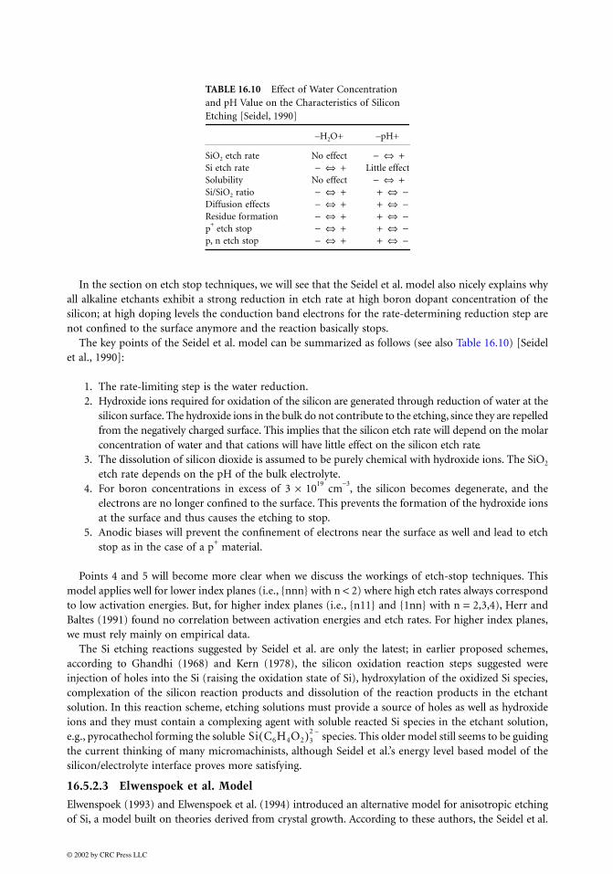
In the section on etch stop techniques, we will see that the Seidel et al. model also nicely explains whyall alkaline etchants exhibit a strong reduction in etch rate at high boron dopant concentration of thesilicon; at high doping levels the conduction band electrons for the rate-determining reduction step arenot confined to the surface anymore and the reaction basically stops.
The key points of the Seidel et al. model can be summarized as follows (see also Table 16.10) [Seidelet al., 1990]:
1. The rate-limiting step is the water reduction.2. Hydroxide ions required for oxidation of the silicon are generated through reduction of water at the
silicon surface. The hydroxide ions in the bulk do not contribute to the etching, since they are repelledfrom the negatively charged surface. This implies that the silicon etch rate will depend on the molarconcentration of water and that cations will have little effect on the silicon etch rate..
3. The dissolution of silicon dioxide is assumed to be purely chemical with hydroxide ions. The SiO2
etch rate depends on the pH of the bulk electrolyte.4. For boron concentrations in excess of 3 × 10
19 cm
−3, the silicon becomes degenerate, and the
electrons are no longer confined to the surface. This prevents the formation of the hydroxide ionsat the surface and thus causes the etching to stop.
5. Anodic biases will prevent the confinement of electrons near the surface as well and lead to etchstop as in the case of a p
+ material.
Points 4 and 5 will become more clear when we discuss the workings of etch-stop techniques. Thismodel applies well for lower index planes (i.e., nnn with n < 2) where high etch rates always correspondto low activation energies. But, for higher index planes (i.e., n11 and 1nn with n = 2,3,4), Herr andBaltes (1991) found no correlation between activation energies and etch rates. For higher index planes,we must rely mainly on empirical data.
The Si etching reactions suggested by Seidel et al. are only the latest; in earlier proposed schemes,according to Ghandhi (1968) and Kern (1978), the silicon oxidation reaction steps suggested wereinjection of holes into the Si (raising the oxidation state of Si), hydroxylation of the oxidized Si species,complexation of the silicon reaction products and dissolution of the reaction products in the etchantsolution. In this reaction scheme, etching solutions must provide a source of holes as well as hydroxideions and they must contain a complexing agent with soluble reacted Si species in the etchant solution,e.g., pyrocathechol forming the soluble species. This older model still seems to be guidingthe current thinking of many micromachinists, although Seidel et al.’s energy level based model of thesilicon/electrolyte interface proves more satisfying.
16.5.2.3 Elwenspoek et al. Model
Elwenspoek (1993) and Elwenspoek et al. (1994) introduced an alternative model for anisotropic etchingof Si, a model built on theories derived from crystal growth. According to these authors, the Seidel et al.
TABLE 16.10 Effect of Water Concentration and pH Value on the Characteristics of Silicon Etching [Seidel, 1990]
–H2O+ –pH+
SiO2 etch rate No effect − ⇔ +Si etch rate − ⇔ + Little effectSolubility No effect − ⇔ +Si/SiO2 ratio − ⇔ + + ⇔ −Diffusion effects − ⇔ + + ⇔ −Residue formation − ⇔ + + ⇔ −p
+ etch stop − ⇔ + + ⇔ −
p, n etch stop − ⇔ + + ⇔ −
Si C6H4O2( )32 –
© 2002 by CRC Press LLC

model does not clearly explain the fast etching of 110 planes. Those planes, having three backbonds likethe 111 planes, should etch equally slowly. The activation energy of the anisotropic etch rate dependson the etching system used; for example, etching in KOH is faster than in EDP, even when the pH of thesolution is the same. Seidel et al. attribute this dependence to diffusion that plays a greater role in EDPthan in KOH solutions. But Elwenspoek et al. point out that, at least for slow etching, the etch rate shouldnot be diffusion controlled but governed by surface reactions. With surface reactions, diffusion shouldhave a minor effect, analogous to growth at low pressure in an LPCVD reactor [Madou, 1997, chap. 3].Another comment focuses on the lack of understanding why certain etchants etch isotropically and othersetch anisotropically.
Elwenspoek et al. note the parallels in the process of etching and growing of crystals; slowly growingcrystal planes also etch slowly! A key to understanding both processes, growing or dissolution (etching),pertains to the concept of the energy associated with the creation of a critical nucleus on a single crystallinesmooth surface, i.e., the free energy associated with the creation of an island (growth) or a cavity (etching).Etching or growing of a material starts at active kink sites on steps. Kink sites are atoms with as manybonds to the crystal as to the liquid. Kinetics depend critically on the number of such kink sites. Thisaspect remained neglected in the discussion of etch rates of single crystals up to now.
The free energy change, ∆G, involved in creating an island or digging a cavity (of circular shape in anisotropic material) of radius r on or in an atomically smooth surface, is given by:
(16.32)
where N is the number of atoms forming the island or the number of atoms removed from the cavity,∆µ is the chemical potential difference between silicon atoms in the solid state and in the solution, andγ is the step free energy. The step free energy in Eq. (16.32) will be different at different crystallographicsurfaces. This can easily be understood from the following example. A perfectly flat 111 surface in theSi diamond lattice has no kink positions (three backbonds, one dangling bond per atom), while on the001 face every atom has two backbonds and two dangling bonds, i.e., every position is a kink position.Consequently, creating an adatom-cavity pair on 111 surfaces costs energy: three bonds must be brokenand only one is reformed. In the case of 001 faces, the picture is quite different. Creating an adatom-cavity pair now costs no energy because one has to break two bonds in order to remove an atom fromthe 001 face, but one gets them back by placing the atom back on the surface. The binding energy ∆Eof an atom in a crystal slice with orientation (hkl) divided by kT (Boltzmann constant times absolutetemperature) is known as the α factor of Jackson of that crystal face [Jackson, 1966], or:
(16.33)
At sufficiently low temperature, where entropy effects can be ignored, kTα is proportional to the stepfree energy γ and the number of adatom-cavity pairs is proportional to exp (−α). This number is verysmall on the 111 silicon faces at low temperature, but 1 on the 001 silicon faces at any temperature.The consequence for 111 and 001 planes is that, at sufficiently low temperatures, the first are atomicallysmooth and the latter are atomically rough. N in Eq. (16.32) can be further written out as:
(16.34)
where h is the height of the step, r is the diameter of the hole or island and ρ is the density (atoms percm
3) of the solid material. The result is
(16.35)
where ∆µ is counted positive and γ is positive in any case. In Figure 16.38 we show a plot of ∆G vs. r.Eq. (16.35) exhibits a maximum at:
∆G N– ∆µ 2πrγ+=
α ∆EkT-------=
N πr2hρ=
∆G πr2hρ∆µ–= 2πrγ+
© 2002 by CRC Press LLC
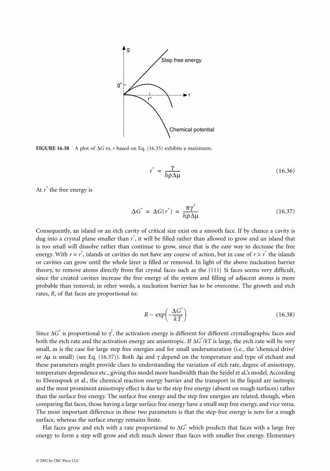
(16.36)
At r∗ the free energy is
(16.37)
Consequently, an island or an etch cavity of critical size exist on a smooth face. If by chance a cavity isdug into a crystal plane smaller than r
∗, it will be filled rather than allowed to grow and an island that
is too small will dissolve rather than continue to grow, since that is the easy way to decrease the freeenergy. With r = r
∗, islands or cavities do not have any course of action, but in case of r > r
∗ the islands
or cavities can grow until the whole layer is filled or removed. In light of the above nucleation barriertheory, to remove atoms directly from flat crystal faces such as the 111 Si faces seems very difficult,since the created cavities increase the free energy of the system and filling of adjacent atoms is moreprobable than removal; in other words, a nucleation barrier has to be overcome. The growth and etchrates, R, of flat faces are proportional to:
(16.38)
Since ∆G∗ is proportional to γ2
, the activation energy is different for different crystallographic faces andboth the etch rate and the activation energy are anisotropic. If ∆G
∗/kT is large, the etch rate will be very
small, as is the case for large step free energies and for small undersaturation (i.e., the ‘chemical drive’or ∆µ is small) (see Eq. (16.37)). Both ∆µ and γ depend on the temperature and type of etchant andthese parameters might provide clues to understanding the variation of etch rate, degree of anisotropy,temperature dependence etc., giving this model more bandwidth than the Seidel et al.’s model. Accordingto Elwenspoek et al., the chemical reaction energy barrier and the transport in the liquid are isotropicand the most prominent anisotropy effect is due to the step free energy (absent on rough surfaces) ratherthan the surface free energy. The surface free energy and the step free energies are related, though, whencomparing flat faces, those having a large surface free energy have a small step free energy, and vice versa.The most important difference in these two parameters is that the step-free energy is zero for a roughsurface, whereas the surface energy remains finite.
Flat faces grow and etch with a rate proportional to ∆G∗ which predicts that faces with a large free
energy to form a step will grow and etch much slower than faces with smaller free energy. Elementary
FIGURE 16.38 A plot of ∆G vs. r based on Eq. (16.35) exhibits a maximum.
Chemical potential
Step free energy
g
g*
r*r
r∗ γhρ∆µ--------------=
∆G∗ ∆G(r∗)πγ 2
hρ∆µ--------------= =
R∆G∗
kT----------–
exp∼
© 2002 by CRC Press LLC

analysis indicates that the only smooth face of the diamond lattice is the (111) plane. There may be otherflat faces, but with lower activation energies, due to reconstruction and/or adsorption, prominent can-didates in this category are 100 and 110 planes. On the other hand, a rough crystal face grows andetches with a rate directly proportional to ∆µ. The temperature at which γ vanishes and a face transitionsfrom smooth to rough is called the roughening transition temperature TR [Elwenspoek and van derWeerden, 1987; Bennema, 1984]. Above TR, the crystal is rough on the microscopic scale. Because thestep free energy is equal to zero, new Si units may be added or removed freely to the surface withoutchanging the number of steps. Rough crystal faces grow and dissolve with a rate proportional to ∆µ andtherefore proceed faster than flat surfaces. Imperfect crystals, e.g., surfaces with screw dislocations, etcheven faster with R proportional to ∆µ2
.For the state of a surface slightly above or below the roughening temperature, TR, thermal equilibrium
conditions apply. Etching, in most practical cases, is far from equilibrium and kinetic roughening mightoccur. Kinetic roughening [Bennema, 1984] occurs if the super- or undersaturation of the solution is solarge that the thermally created islands or cavities are the size of the critical nucleus. One can show thatif the super- or undersaturation is larger than ∆µc, given by:
(16.39)
( f0 being the area one atom occupies in a given crystal plane), the growth and etch mechanismchanges from a nucleation barrier-controlled mechanism to a direct growth/etch mechanism. Thegrowth rate and etch rate again become proportional to the chemical potential difference. It can thusbe expected that if the undersaturation becomes high enough, even the 111 faces could etchisotropically, as they indeed do in acidic etchants. If the undersaturation becomes so large that ∆G
∗
kT, the nucleation barrier breaks down. Each single-atom cavity acts as a nucleus made in vastnumbers by thermal fluctuations. The face in question etches with a rate comparable to the etch rateof a rough surface. This situation is called kinetic roughening. If all faces are kinetically rough, theetch rate becomes isotropic.
Isotropic etching requires conditions of kinetic roughening, because the etch rate is no longer domi-nated by a nucleation barrier but by transport processes in solution and the chemical reaction. To testthis aspect of the model, Elwenspoek et al. show that there is a transition from isotropic to anisotropicetching if the undersaturation becomes too small. This can occur if one etches with an acidic etchantvery long or if one etches through very small holes in a mask (crevice effect). In both cases, anisotropicbehavior becomes evident as aging or limited transport of the solution causes the undersaturation tobecome very small. No proof is available to indicate that acidic etchants are much more undersaturatedthan the alkaline etchants. Still, the above explains some phenomena that the Seidel et al.’s model failsto address. Another nice confirmation of the Elwenspoek et al. model is in the effect of misalignment onetch rate. A misalignment of the mask close to smooth faces implies steps; there is no need for nucleationin order to etch. Since the density of steps is proportional to the angle of misalignment, the etch rateshould be proportional to the misalignment angle, provided the distance between steps is not too large.Nucleation of new cavities becomes very probable. This has indeed been observed for the etch rate closeto the <111> directions [Seidel et al., 1990].
Where the Elwenspoek et al.’s model becomes a bit murky is in the classification of which surfaces aresmooth and which ones are rough. Elementary analysis classifies only the 111 planes as smooth at lowtemperatures. At this stage the model does not explain anything more than other models; every modelhas an explanation for the slower 111 etch rate. But these authors invoke the possibility of surfacereconstruction and/or adsorption of surface species which, by decreasing the surface-free energy, couldmake faces such as 001 and 110 flat as well but with lower activation energies. They also take heartin the fact that CVD experiments often end up showing flat 110, 100, 331 and, strongest of all,111 planes. Especially where the influence of the etchant is concerned a lot more convincing thermo-dynamic data to estimate ∆µ and γ are needed.
∆µc
πf0γ 2
kT------------=
© 2002 by CRC Press LLC

16.5.2.4 Isotropic vs. Anisotropic Etching of Silicon
In contrast to alkaline etching, with an acidic etchant such as HF, holes are needed for etching Si. Ann-type Si electrode immersed in HF in the dark will not etch due to lack of holes. The same electrodein an alkaline medium etches readily. A p-type electrode in an HF solution, where holes are availableunder the proper bias, will etch even in the dark. For HF etchants one might assume that the Ghandiand Kern model [Kern, 1978; Jackson, 1966], relying on the injection of holes, applies. In terms of theband model, this must mean that the silicon/electrolyte interface in acidic solutions exhibits quite differentenergetics from the alkaline case. It is not directly obvious why the energetics of the silicon/electrolyteinterface would be pH dependent. To the contrary, since the flatband potential of most oxide semicon-ductors as well as most oxide-covered semiconductors (such as Si) and the Fermi level of the H2O/OH
−
redox couple in an aqueous solution are both expected to change by 59 mV for each pH unit change[Madou and Morrison, 1989], one would expect the energetics of the interface to be pH independent.Since the electronegativity in a Si-F bond is higher than for a Si-OH bond, one might even expect thebackbond surface states to be raised higher in an HF medium, making an electron injection mechanismeven more likely than in alkaline media. To clarify this contradiction we will analyze the band model ofa Si electrode in an acidic medium in more detail. The band model shown in Figure 16.39 was constructedon the basis of a set of impedance measurements on an n-type Si electrode in a set of aqueous solutionsat different pH values. From the impedance measurements Mott-Schottky plots were constructed todetermine the pH dependency of the flat-band potential. From that, the position of the conduction bandand valence band edges (Ecs and Evs, respectively) of the Si electrode in an acidic medium at a fixed pHof 2.2 (the point of zero charge) was calculated at 0.74 eV vs. SCE (saturated calomel electrode as reference)for Ecs, and −0.36 eV vs. SCE for Evs [Madou et al., 1980; 1981].
We have assumed in Figure 16.39 that the bands are bent upwards at open circuit (see below forjustification), so that holes in the valence band are driven to the interface where they can react withSi atoms or with competing reducing agents from the electrolyte. Since we want to etch Si, we are onlyinterested in the reactions where Si itself is consumed. Reactions of holes with reducing agents are ofgreat importance in photoelectrochemical solar cells [Madou et al., 1981]. For n-type Si, holes can be(1) injected by oxidants from the solution (e.g., by adding nitric acid to the HF solution), (2) suppliedat the electrolyte/semiconductor interface by shining light on a properly biased n-Si wafer, or (3)created by impact ionization, i.e., Zener breakdown, of a sufficiently high reverse biased n-Si electrode[Levy-Clement et al., 1992]. With a p-Si wafer, a small forward bias supplies all the holes needed for theoxidation of the lattice even without light, as the conduction happens via a hole mechanism. An important
FIGURE 16.39 Band diagram for n-type Si in pH = 2.2 (no bias or illumination). Reference is the saturated calomelelectrode (SCE). In Figure 16.37 no energy values were given; here we provide actual positions of the conductionband edge, Ecs = 0.74 eV vs. SCE, and the valence band edge, Evs = 0.74 eV −1.1 eV = −0.36 eV vs. SCE (1.1 eV is theband gap of Si). These values were determined by means of Mott-Schottky plots [Madou et al., 1981]. The separationbetween the Fermi energy and the bottom of the conduction band is indicated by µ.
L
ECS
EVS
EV
EF
EC
Eox
Eoredox
Ered
ESCE
∝
0.74
© 2002 by CRC Press LLC

finding, explaining the different reaction paths in acidic and alkaline media comes from plotting the flatband potential as a function of pH. It was found that the band diagram of Si shifts with less than 59 mV perpH unit. Actually the shift is only about 30 mV per pH unit [Madou et al., 1981]. As shown in Figure 16.40,with increasing pH, the energy levels of the solution rise faster than the energy levels in the semiconductor.As a consequence it is more likely that electron injection takes place in alkaline media as the filled levelsassociated with the OH
− are closer to the conduction band, whereas in acidic media the filled levels of the
redox system overlap better with the valence band, favoring a hole reaction. A lower position of the redoxcouple with respect to the conduction band edge, Ecs, in acidic media explains the upward bending of thebands as drawn in Figure 16.39. With isotropic etching in acidic media, the reaction starts with a hole inthe valence band, equivalent to a broken Si-Si bond. In this case, the relative position of backbond relatedsurface states in different crystal orientations are of no consequence and all planes etch at the same rate.A study of the interfacial energetics helps to understand why isotropic etching occurs in acidic media andanisotropic etching in alkaline media.
A few words of caution on our explanation for the reactivity difference between acidic and alkalinemedia are in order. Little is known about the width of the bell-shaped curves describing the redox levelsin solution [Madou and Morrison, 1989]. Not knowing the surface concentrations of the reactive redoxspecies involved in the etching reactions further hinders a better understanding of the surface energeticsas the bell-shaped curves for oxidant and reductant will only be the same height (as they were drawnin Figures 16.39 and 16.40) if the concentration of oxidant and reductant are the same. Clearly, theabove picture is oversimplified; several authors have found that the dissolution of Si in HF might involveboth the conduction and valence band, a claim confirmed by photocurrent multiplication experiments[Matsumura and Morrison, 1983; Lewerenz et al., 1988]. These photomultiplication experiments showedthat one or two holes generated by light in the Si valence band were sufficient to dislodge one Si [Brantley,1973] unit, meaning that the rest of the charges were injected into the conduction band. Our contentionhere is only that the low pH dependence of the flat-band potential of a silicon electrode makes aconduction band mechanism more favorable with alkaline type etchants and a hole mechanism morefavorable in acidic media.
Continued attempts at modeling the etch rates of all Si planes are under way. For example, Heskethet al. (1993) attempted to model the etch rates of the different planes developing on silicon spheres in
FIGURE 16.40 Band model comparison of the Si/electrolyte interface at low and high pH. Increasing the pH by10 units shifts the redox-levels up by 600 mV, whereas the Si bands only move up by 300 mV. This leads to a differentband-bending and a different reaction mechanism, i.e., electron injection in the alkaline media (anisotropic) andhole injection in acidic media (isotropic).
ECS
EVS
EV
EF
EC
Eox
Eoredox
Ered
ESCE
∝
0.74
L
ECS
EVS
EV
EF
EC
Eox
Eoredox
Ered
ESCE
∝
1.04
pH = 12.2 in KOHpH = 2.2 in HF
© 2002 by CRC Press LLC

etching experiments with KOH and CsOH by calculating the surface free energy. The number of surfacebonds per centimeter square on a Si plane is indicative of the surface free energy, which can be estimatedby counting the bond density and multiplying by the bond energy. Using the unit cell dimension “a” ofSi of 5.431 Å, and a silicon-to-silicon bond energy of 42.2 kcal/mol, the surface free energy, ∆G, can berelated to, NB, the bond density, by the following expression:
(16.40)
Although Hesketh et al. could not explain the etching differences observed between CsOH and KOH(these authors identified a cation effect on the etch rate!), a plot of the calculated surface free energy vs.orientation yielded minima for all low index planes such as 100, 110 and 111, as well as for thehigh index 522 planes. Fewer bonds per unit area on the low index planes produce a lower surfaceenergy and lower etching rate. When Hesketh et al. added the in-plane bond density to the surface bonddensity, producing a total bond density, a correlation with the hierarchy of etch rates in CsOH and KOHwas found, i.e., 311, 522 > 100 > 111. The surfaces with the higher bond density etched faster,suggesting that the etch rate might be a function of the number of electrons available at the surface.Hesketh et al. imply that their result falls in line with the Seidel et al.’s model, although it is unclear howthe total bond density relates to surface state energies of backbonds. Moreover, Hesketh’s model does nottake into account the angles of the bonds, and in Elwenspoek’s view, the surface free energy actually doesnot determine the anisotropy.
More research could focus on the modeling of Si etch rates. The semiconductor electrochemistry of cor-roding Si electrodes will be a major tool in further developments. Interested readers may consult Sundaramand Chang (1993) in an article on Si etching in hydrazine and Palik et al. (1985) on the etch-stop mechanismin heavily doped silicon; both explain in some detail the silicon/electrolyte energetics. A more generic treatiseon semiconductor electrochemistry can be found in Morrison (1980).
16.6 Etching With Bias and/or Illumination of the Semiconductor
The isotropic and anisotropic etchants discussed so far require neither a bias nor illumination of thesemiconductor. The etching in such cases proceeds at open circuit and the semiconductor is shieldedfrom light. In a cyclic voltammogram, as shown in Figure 16.41, the operational potential is the restpotential, Vr, where anodic and cathodic currents are equal in magnitude and opposite in sign, resultingin the absence of flow of current in an external circuit. This does not mean that macroscopic changesdo not occur at the electrode surface, since the anodic and cathodic currents may be part of differentchemical reactions. Consider isotropic etching of Si in an HF/HNO3 etchant at open circuit where thelocal anodic reaction is associated with corrosion of the semiconductor:
(Reaction 16.11)
(Reaction 16.12)
(the involvement of holes ‘h+’ in the acidic reaction was discussed in the preceding section), while the
local cathodic reaction could be associated with reduction of HNO3:
(Reaction (16.13)
∆GNB
2------ 2.94 10 19– J
m2------××=
Anode: Si 2H2O nh+ → SiO2 4H+ (4 n)e−–+ ++ +
SiO2 6HF H2SiF6 2H2O+→+
Cathode: HNO3 3H+ NO H2O 3H++ +→+
© 2002 by CRC Press LLC

We will now explore Si etching while illuminating and/or applying a bias to the silicon sample. Tosimplify the situation, we will first consider the case of an oxidant-free solution so that all the holes mustcome from within the semiconductor. Anodic dissolution of n-Si in an HF containing solution requires asupply of holes to the surface. For an n-type wafer under reverse bias, very few holes will show at the surfaceunless the high reverse (anodic) bias is sufficient to induce impact ionization or Zener breakdown (seeFigure 16.41a). Alternatively, the interface can be illuminated, creating holes in the space charge regionwhich the field pushes towards the semiconductor/electrolyte interface (Figure 16.41b). In the forwarddirection, electrons from the Si conduction band (majority carriers) reduce oxidizing species in the solution(e.g., reduction of protons to hydrogen). A p-type Si sample exhibits high anodic currents even withoutillumination at small anodic (forward) bias (Figure 16.41c). Here the current is carried by holes. A p-typeelectrode illuminated under reverse bias gives rise to a cathodic photocurrent (Figure 16.41d). At relativelylow light intensities, the photocurrent plateaus for both n- and p-types (Figures 16.41b and 16.41d,respectively) depend linearly on light intensity. The photocurrent is cathodic for p-type Si (species arereduced by photoproduced electrons at the surface, e.g., hydrogen formation) and anodic for n-type Si(species are oxidized by photoproduced holes at the surface; either the lattice itself is consumed orreducing compounds in solution are). In Figure 16.42 we show the cyclic voltammograms of n-type andp-type Si in the presence of a hole-injecting oxidant. The most obvious effect is on the dark p-type Sielectrode. The injection of holes in the valence band increases the cathodic dark current dramatically.The current level measured in this manner for varying oxidant concentration or different oxidants couldbe used to estimate the efficiency of different isotropic Si etchants; a pointer to the fact that semicon-ductor electrochemistry has been underutilized as a tool to study Si etching. When n-type Si is consumedunder illumination, we experience photocorrosion (see Figure 16.41b). This photocorrosion phenom-enon has been a major barrier to the long-term viability of photoelectrochemical cells [Madou et al.,1980]. In what follows, photocorrosion is put to use for electropolishing and formation of microporousand macroporous layers [Levy-Clement et al., 1992].
FIGURE 16.41 Basic cyclic voltammograms (I vs. V) for n- and p-type Si in an HF solution, in the absence of ahole injecting oxidant: (a) n-type Si without illumination; (b) n-type Si under illumination; (c) p-type Si withoutillumination; (d) p-type Si under illumination. If the reactions on the dark Si electrode determining the rest potentialVr for n- and p-type are the same, then Vr is expected to be the same as well. For the clarity of the figure we havechosen the Vrs different here; in practice, Vr for n- and p-type Si in HF are found to be identical.
+
+
+Zener breakdown for n type Si
(b)
(c)(a)
-
Holes tothe surface
Electrons tothe surface
anodic currents
V VS SCE
cathodic currents
Zener breakdown for p type Si
(d)
Vr
Vr
© 2002 by CRC Press LLC

16.6.1 Electropolishing and Microporous Silicon
16.6.1.1 Electropolishing
Photoelectrochemical etching (PEC-etching) involves photocorrosion in an electrolyte in which thesemiconductor is generally chemically stable in the dark, i.e., no hole-injecting oxidants are present, asin the case of an HF solution (see Figure 16.41). For carrying out the experiments a set-up as shown inFigure 16.25 may be used with a provision to illuminate the semiconductor electrode. At high lightintensities the anodic curves for n- and p-type Si are the same, except for a potential shift of a few hundredmV (see Figure 16.43). Because of this equivalence, several of the etching processes described apply forboth forward biased p-type and n-type Si under illumination. The anodic curves in Figure 16.43 presenttwo peaks, characterized by iCRIT and iMAX. At the first peak, iCRIT, partial dissolution of Si in reactionssuch as:
Si + 2F− + 2h
+ → SiF2 (Reaction 16.14)
SiF2 + 2HF → SiF4 + H2 (Reaction 16.15)
leads to the formation of porous Si while hydrogen formation occurs simultaneously. The porous Sitypically forms when using low current densities in a highly concentrated HF solution—in other words,by limiting the oxidation of silicon due to a hole and OH
− deficiency. Above iCRIT , the transition from
the charge-supply-limited to the mass-transport-limited case, the porous film delaminates and brightelectropolishing occurs at potentials positive of iMAX. With dissolution of chemical reactants in theelectrolyte rate limiting, HF is depleted at the electrode surface and a charge of holes builds up at theinterface. Hills on the surface dissolve faster than depressions because the current density is higher onhigh spots. As a result, the surface becomes smoother, i.e., electropolishing takes place [Lehmann, 1993].
FIGURE 16.42 Basic cyclic voltammograms for n- and p-type Si in an HF solution and in the presence of a holeinjecting oxidant, e.g., HNO3: (a) n-type Si in the dark; (b) p-type Si in the dark. An increase of the cathodic darkcurrent on the p-type electrodes is most obvious. The current level is proportional to the oxidant concentration.
+
(a)
V VS SCE
+
(b)
Two differentconcentrationsof hole injectingoxidant
© 2002 by CRC Press LLC
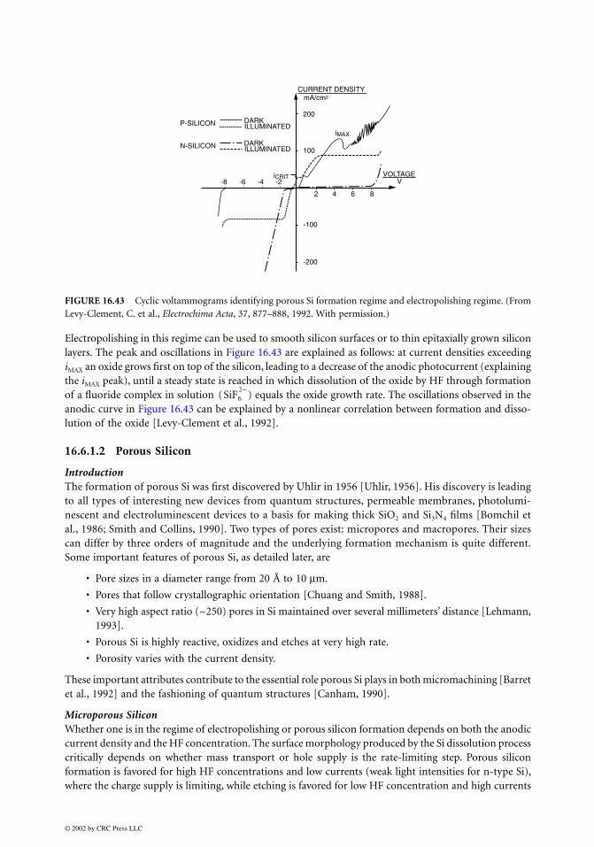
Electropolishing in this regime can be used to smooth silicon surfaces or to thin epitaxially grown siliconlayers. The peak and oscillations in Figure 16.43 are explained as follows: at current densities exceedingiMAX an oxide grows first on top of the silicon, leading to a decrease of the anodic photocurrent (explainingthe iMAX peak), until a steady state is reached in which dissolution of the oxide by HF through formationof a fluoride complex in solution ( ) equals the oxide growth rate. The oscillations observed in theanodic curve in Figure 16.43 can be explained by a nonlinear correlation between formation and disso-lution of the oxide [Levy-Clement et al., 1992].
16.6.1.2 Porous Silicon
IntroductionThe formation of porous Si was first discovered by Uhlir in 1956 [Uhlir, 1956]. His discovery is leadingto all types of interesting new devices from quantum structures, permeable membranes, photolumi-nescent and electroluminescent devices to a basis for making thick SiO2 and Si3N4 films [Bomchil etal., 1986; Smith and Collins, 1990]. Two types of pores exist: micropores and macropores. Their sizescan differ by three orders of magnitude and the underlying formation mechanism is quite different.Some important features of porous Si, as detailed later, are
• Pore sizes in a diameter range from 20 Å to 10 µm.
• Pores that follow crystallographic orientation [Chuang and Smith, 1988].
• Very high aspect ratio (~250) pores in Si maintained over several millimeters’ distance [Lehmann,1993].
• Porous Si is highly reactive, oxidizes and etches at very high rate.
• Porosity varies with the current density.
These important attributes contribute to the essential role porous Si plays in both micromachining [Barretet al., 1992] and the fashioning of quantum structures [Canham, 1990].
Microporous SiliconWhether one is in the regime of electropolishing or porous silicon formation depends on both the anodiccurrent density and the HF concentration. The surface morphology produced by the Si dissolution processcritically depends on whether mass transport or hole supply is the rate-limiting step. Porous siliconformation is favored for high HF concentrations and low currents (weak light intensities for n-type Si),where the charge supply is limiting, while etching is favored for low HF concentration and high currents
FIGURE 16.43 Cyclic voltammograms identifying porous Si formation regime and electropolishing regime. (FromLevy-Clement, C. et al., Electrochima Acta, 37, 877–888, 1992. With permission.)
200
100
-100
-200
-8 -6 -4 -2
2 4 6 8
P-SILICON DARKILLUMINATED
N-SILICON DARKILLUMINATED
iCRIT
iMAX
VOLTAGE
CURRENT DENSITYmA/cm2
V
SiF62−
© 2002 by CRC Press LLC
(strong light intensity for n-type Si), where mass transport is limiting. For current densities below iMAX
(Figure 16.43) holes are depleted at the surface and HF accumulates at the electrode/electrolyte interface.As a result, a dense network of fine holes forms [Unagami, 1980; Watanabe et al., 1975]. The formationof a porous silicon layer (PSL) in this regime has been explained as a self-adjusting electrochemicalreaction due to hole depletion by a quantum confinement in the microporous structure [Lehmann andGosele, 1991]. The structure of the pores in PSL can best be observed by transmission electron microscopy(TEM) and its thickness can be monitored with an IR microscope. The structure of the porous layerprimarily depends on the doping level of the wafer and on the illumination during etching. The poresizes decrease when etching occurs under illumination [Levy-Clement et al., 1992]. The pores formed inp-type Si show much smaller diameters than n-type ones for the same formation conditions. It is believedthat the porous silicon layer (PSL) consists of silicon hydrides and oxides. The pore diameter typicallyranges from 40 to 200 Å [Lehmann, 1996; Yamana et al., 1990; Arita and Sunohara, 1977]. This veryreactive porous material etches or oxidizes rapidly. Heat treatment in an oxidizing atmosphere (1100°Cin oxygen for 30 minutes is sufficient to make a 4-µm thick film) leads to oxidized porous silicon (OPS).The oxidation occurs throughout the whole porous volume and several micrometers-thick SiO2 layerscan be obtained in times that correspond to the growth of a few hundred nanometers on regular Sisurfaces. Porous silicon is low density and remains single crystalline, providing a suitable substrate forepitaxial Si film growth. These properties have been used to obtain dielectric isolation in ICs and to makesilicon-on-insulator wafers [Watanabe et al., 1975].
Porous Si can also be formed chemically through Reactions 16.11 and 16.13. In this case the differencebetween chemical polishing and porous Si formation conditions is more subtle. In the chemical polishingcase, all reacting surface sites switch constantly from being local anode (Reaction 16.11) to being localcathode (Reaction 16.13), resulting in nonpreferential etching. If surface sites do not switch fast betweenbeing local anode and cathode, charges have time to migrate over the surface. In this case, the originallocal cathode site remains a cathode for a longer time, and the corresponding local anode site, somewhereelse on the surface, also remains an anode in order to keep the overall reaction neutral. A preferentialetching results at the localized anode sites, making the surface rough and causing a porous silicon toform [Jung et al., 1993]. Any inhomogeneity, e.g., some oxide or a kink site at the surface might increasesuch preferential etching [Jung et al., 1993]. Unlike PSLs fabricated by electrochemical means, thechemically etched porous Si film thickness is self limiting.
Besides its use for dielectric isolation and the fabrication of SOI wafers, porous silicon has beenintroduced in a wide variety of other applications: Luggin capillaries for electrochemical referenceelectrodes, high surface area gas sensors, humidity sensors, sacrificial layers in silicon micromachining,etc. Recently PSL was shown to exhibit photoluminescent and electroluminescent behavior; light-emitting porous silicon (LEPOS) was demonstrated. Visible light emission from regular Si is very weakdue to its indirect bandgap. Pumping porous Si with a green light laser (argon) caused it to emit ared glow. If a LEPOS device could be integrated monolithically with other structures on silicon, a bigstep in micro-optics, photon data transmission, and processing would be achieved. To explain the blueshift of the absorption edge of LEPOS of about 0.5 eV compared to bulk silicon [Lehmann and Gosele,1991] and room temperature photoluminescence [Canham, 1990], Searson et al. (1993) have proposedan energy-level diagram for porous silicon where the valence band is lowered with res˙pect to bulksilicon to give a band-gap of about 1.8 eV. Not only may PSL formation, as seen above, be explainedinvoking quantum structures, but its remarkable optical properties may also be explained this way.Canham believes that the thin Si filaments may act as quantum wires. Significant quantum effectsrequire structural sizes below 5 nm (see Madou [1997, chap. 7]) and the porous Si definitely can havestructures of that size. By treatment of the porous Si with NH3 at high temperatures, it is possible tomake thick Si3N4 films. Even at 13 µm, these films show little evidence of stress in contrast tostoichiometric LPCVD nitride films [Smith and Collins, 1990].
Porous Si might represent a simple way of making the quantum structures of the future. Pore size ofPSL can be influenced by both light intensity and current density. The quantum aspect adds significantlyto the sudden big interest taken in porous Si.
© 2002 by CRC Press LLC

Macroporous SiliconIn addition to micropores, well-defined macropores can also be made in Si by photo and/or bias etchingin HF solutions. Macropores have sizes as large as 10 µm, visible with a scanning electron microscope(SEM) rather than TEM. The two types of pores often coexist, with micropores covering the walls ofmacropores. Sizes can differ by three orders of magnitude. This is not a matter of a broad fractal typedistribution of pores, but the formation mechanism is quite different.
Electrochemical etching of macropores or macroholes has been reported for n-type silicon in 2.5 to5% HF under high voltage (>10 V), low current density (10 mAcm
−2), under illumination, and in the
dark [Levy-Clement et al., 1992]. In the latter case, Zener breakdown in silicon (electric field strengthin excess of 3 × 10
5V/cm) causes the hole formation. The macropores are formed only with lightly doped
n-silicon at much higher anodic potentials than those used for micropore formation [Zhang, 1991]. Byusing a pore initiation pattern the macropores actually can be localized at any desired location. Thisdramatic effect is illustrated by comparing Figures 16.44A and B [Lehmann, 1993; 1996]. Pores orthogonalto the surface with depths up to a whole wafer thickness can be made and aspect ratios as large as 250become possible. The formation mechanism in this case cannot be explained on the basis of depletionof holes due to quantum confinement in the fine porous structures, given that these macropores exhibitsizes well beyond 5 nm. As with microporous Si, the surface morphology produced by the dissolutionprocess depends critically on whether mass transport or charge supply is the rate-limiting step. For pore
FIGURE 16.44 Macroporous Si; formation of random and localized macropores or macroholes. (A) Random:surface, cross section and a 45° bevel of an n-type sample (10
15/cm
3 phosphorus-doped) showing a random pattern
of macropores. Pore initiation was enhanced by applying 10-V bias in the first minute of anodization followed by149 min at 3 V. The current density was kept constant at 10 mA/cm
2 by adjusting the backside illumination. A
6% aqueous solution of HF was used as an electrolyte. The set-up used for anodization is sketched in the upperright corner. (B) Localized: surface, cross section and a 45° bevel of an n-type sample (10
15/cm
3 phosphorus-
doped) showing a predetermined pattern of macropores (3 V, 350 min, 2.5% HF). Pore growth was induced bya regular pattern of pits produced by standard lithography and subsequent alkaline etching (inset upper right).To measure the depth dependence of the growth rate, the current density was kept periodically at 5 mA/cm
2 for
45 min and then reduced to 3.3 mA/cm2 for 5 min. This reduction resulted in a periodic decrease of the pore
diameter, as marked by white labels in the figure. (From Lehmann, V., J. Electrochem. Soc., 140, 2836–2843, 1993.With permission.)
© 2002 by CRC Press LLC

formation one must work again in a charge depletion mode. Macropore formation, as micropore for-mation, is a self-adjusting electrochemical mechanism. In this case, the limitation is due to the depletionof the holes in the pore walls in n-Si wafers causing them to passivate. Holes keep on being collected bythe pore tip where they promote dissolution. No passivating layer is involved to protect the pore wall.The only decisive differences between pore tips and pore walls are their geometry and their location.Holes generated by light or Zener breakdown are collected at pore tips. Every depression or pit in thesurface initiates pore growth because the electrical field at a curved pore bottom is much larger than thatof a flat surface due to the effect of the radius of curvature. The latter leads to higher current and enhanceslocal etching [Zhang, 1991]. Zener breakdown and illumination of n-Si lead to different types of poregeometry [Lehmann, 1993; Theunissen, 1972; Lehmann and Foll, 1990]. Branched pores with sharp tipsform if holes are generated by breakdown (see Figure 16.45A) [Lehmann, 1993]. Unbranched pores withlarger tip radii result from holes created by illumination (see Figure 16.45B) [Lehmann and Foll, 1990].The latter difference can be understood as follows: the electric field strength is a function of bias, doping
FIGURE 16.45 Comparison of macropores made with breakdown holes (A) and macropores made with lightcreated holes (B). (A) An oxide replica of pores etched under weak backside illumination visualizes the branchingof pores produced by generation of charge carriers due to electrical breakdown (5 V, 3% HF, room temperature,10
15/cm
3 phosphorus-doped). (From Lehmann, V., J. Electrochem. Soc., 140, 2836–2844, 1993. With permission.)
(B) Single pore associated with KOH pit. (From Lehmann, V. and H. Foll, J. Electrochem. Soc., 137, 653–659, 1990.With permission.)
© 2002 by CRC Press LLC

density and geometry. High doping level density or sharp pore tips will lower the required bias forbreakdown, so macropores will tend to follow pores with the sharpest tips. Since every tip causes a newbreakdown and hole generation, the position of the original pore tip becomes independent of the otherpores, branching of the pores is possible, and fir-tree type pores can be observed. With illumination thepore radius may be larger as the breakdown field strength is not necessary to generate charge carriers,so the pores remain unbranched.
The Si anisotropy common with alkaline etchants surprisingly shows up here with an isotropic etchantsuch as HF. For example, with breakdown-supplied holes, <100>-directed macroholes with <110>branches form (see also Figure 16.45A) [Lehmann, 1993], leading to a complex network of cavernsbeneath the silicon surface. Pyramidal pore tips [Lehmann, 1993] also were observed when the currentdensity was limited by the bias (i < iCRIT). Isotropic pore pits form when the current is larger than thecritical current density, i.e., isotropy in HF etching can be changed into anisotropy when the supply ofholes is limited. We refer here to the Elwenspoek et al. model (see above) which predicts that in confinedspaces etching will tend to be more anisotropic, even when using a normally isotropic etchant such asHF. It was also determined that macrohole formation depends on the wavelength of the light used. Nohole formation occurs below about 800 nm. Depending on the wavelength, the shape of the hole can bemanipulated as well [Lehmann and Foll, 1990]. For wavelengths above 867 nm, the depth profile of theholes changed from conical to cylindrical. The latter was interpreted in terms of the influence of the localminority carrier generation rate. Carriers generated deep in the bulk would promote the hole growth atthe tips, whereas near-surface generation would lead to lateral growth.
Cahill et al. (1993) reported in 1993 the creation of 1- to 5-µm-size pores with pore spacings (center-to-center) from 200 to 1000 µm. Until this finding, the pores typically formed were spaced in the rangeof 4 to 30 µm center-to-center, while being 0.6 to 10 µm in diameter. Making highly isolated porespresents quite another challenge. In the previous work, the relative close spacing of the pores allowedthe authors to conclude that the regions between the pores were almost totally depleted and that practicallyall carriers were collected by the pore tips. In such a case, neither the pore side walls nor the wafer surfaceetched as all holes were swept to the pore tips. Since the surface was not attacked by pore-formingholes, the quality of the pore initiation mask lost its relevance. In Cahill et al.’s case, on the other hand,a long-lived mask (>20 hours) needed to be developed to help prevent pore formation everywhere exceptat initiation pits. The mask eventually used is shown in Figure 16.46; it shows a SiC layer sandwichedbetween two layers of silicon nitride. The silicon nitride directly atop the silicon served to insulate thesilicon carbide from the underlying substrate. As the silicon carbide proves very resistant to HF, loss ofthickness did not show during the procedure. The top nitride served to protect the carbide during aniso-tropic pit formation. By lowering the bias to less than two volts with respect to a saturated calomel electrode(SCE) side-branching was avoided.
It seems very likely that this macropore formation phenomenon could extend to all types of n-typesemiconductors. Some evidence with InP and GaAs supports this statement [Lehmann, 1993].
FIGURE 16.46 Long-lived macropore initiation mask.
© 2002 by CRC Press LLC

16.7 Etch-Stop Techniques
16.7.1 Introduction
In many cases it is desirable to stop etching in silicon when a certain cavity depth or a certain membranethickness is reached. Nonuniformity of etched devices due to nonuniformity of the silicon wafer thicknesscan be quite high. Taper of double-polished wafers, for example, can be as high as 40 µm [Lambrechtsand Sansen, 1992]! Even with the best wafer quality the wafer taper is still around 2 µm. The taper andvariation in etch depth lead to intolerable thickness variations for many applications. Etch-rate controltypically requires monitoring and stabilization of:
• Etchant composition
• Etchant aging
• Stabilization with N2 sparging (especially with EDP and hydrazine)
• Taking account of the total amount of material etched (loading effects)
• Etchant temperature
• Diffusion effects (constant stirring is required, especially for EDP)
• Stirring also leads to a smoother surface through bubble removal
• Trenching (also pillowing) and roughness decrease with increased stirring rate
• Light may affect the etch rate (especially with n-type Si)
• Surface preparation of the sample can have a big effect on etch rate (the native oxide retards etchstart; a dip in dilute HF is recommended)
With good temperature, etchant concentration, and stirring control the variation in etch depthtypically is 1% (see Figure 16.47) [Lambrechts and Sansen, 1992]. A good pretreatment of the surfaceto be etched is a standard RCA clean combined with a 5% HF dip to remove the native oxide immediatelyprior to etching in KOH.
In the early days of micromachining, one of the following techniques was used to etch a Si structureanisotropically to a predetermined thickness. In the simplest mode the etch time was monitored (Table16.9 lists some etch rates for different etchants) or a bit more complex; the infrared transmittance wasfollowed. For thin membranes the etch stop cannot be determined by a constant etch time methodwith sufficient precision. The spread in etch rates becomes critical if one etches membranes down tothicknesses of less than 20 µm; it is almost impossible to etch structures down to less than 10 µm witha timing technique. In the V-groove technique, V-grooves with precise openings (see Eq. (16.2)) wereused such that the V-groove stopped etching at the exact moment a desired membrane thickness wasreached (see Figure 16.48) [Samaun et al., 1973]. One can also design wider mask openings on thewafer’s edge so that the wafer is etched through at those sites at the moment the membrane has reachedthe appropriate thickness. Although Nunn and Angell (1975) claimed that an accuracy of about 1 µmcould be obtained using the V-groove method, none of the mentioned techniques are found to beproduction worthy. Nowadays the above methods are almost completely replaced by etch-stop tech-niques based on a change in etch rate dependant on doping level or chemical nature of a stoppinglayer. High resolution silicon micromachining relies on the availability of effective etch-stop layers. Itis actually the existence of impurity-based etch stops in silicon that has allowed micromachining tobecome a high-yield production process.
16.7.2 Boron Etch Stop
The most widely used etch-stop technique is based on the fact that anisotropic etchants, especially EDP,do not attack boron-doped (p+) Si layers heavily. This effect was first noticed by Greenwood (1969). Heassumed that the presence of a p-n junction was responsible.
© 2002 by CRC Press LLC

Bogh (1971) found that at an impurity concentration of about 7 × 10¹⁹
/cm3 resulted in the etch rate
of Si in EDP dropping sharply (see also Table 16.9), but without any requirement for a p-n junction. ForKOH-based solutions, Price (1973) found a significant reduction in etch rate for boron concentrationsabove 5 × 10
18 cm
−3. The model by Seidel et al., discussed above, provides an elegant explanation for the
etch stop at high boron concentrations. At moderate dopant concentration, we saw that the electrons
FIGURE 16.47 A map of the wafer thickness, the membrane thickness and the etch depth. (From Lambrechts, S.W.and W. Sansen, Biosensors: Microelectrochemical Devices, Institute of Physics Publishing, 1992. With permission.)
FIGURE 16.48 V-groove technique to monitor the thickness of a membrane. At the precise moment the V-grooveis developed, the membrane has reached the desired thickness.
(100)SiO2
(110)
(110)
Si
Wm
(111) planes
Membrane
Wm
z
© 2002 by CRC Press LLC
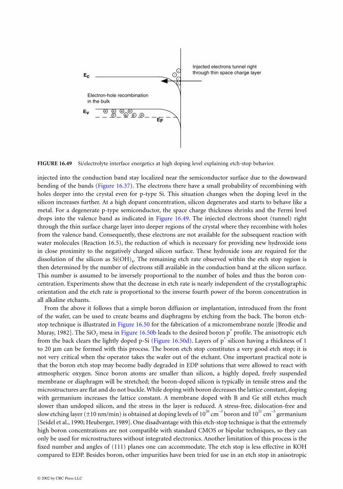
injected into the conduction band stay localized near the semiconductor surface due to the downwardbending of the bands (Figure 16.37). The electrons there have a small probability of recombining withholes deeper into the crystal even for p-type Si. This situation changes when the doping level in thesilicon increases further. At a high dopant concentration, silicon degenerates and starts to behave like ametal. For a degenerate p-type semiconductor, the space charge thickness shrinks and the Fermi leveldrops into the valence band as indicated in Figure 16.49. The injected electrons shoot (tunnel) rightthrough the thin surface charge layer into deeper regions of the crystal where they recombine with holesfrom the valence band. Consequently, these electrons are not available for the subsequent reaction withwater molecules (Reaction 16.5), the reduction of which is necessary for providing new hydroxide ionsin close proximity to the negatively charged silicon surface. These hydroxide ions are required for thedissolution of the silicon as Si(OH)4. The remaining etch rate observed within the etch stop region isthen determined by the number of electrons still available in the conduction band at the silicon surface.This number is assumed to be inversely proportional to the number of holes and thus the boron con-centration. Experiments show that the decrease in etch rate is nearly independent of the crystallographicorientation and the etch rate is proportional to the inverse fourth power of the boron concentration inall alkaline etchants.
From the above it follows that a simple boron diffusion or implantation, introduced from the frontof the wafer, can be used to create beams and diaphragms by etching from the back. The boron etch-stop technique is illustrated in Figure 16.50 for the fabrication of a micromembrane nozzle [Brodie andMuray, 1982]. The SiO2 mesa in Figure 16.50b leads to the desired boron p
+ profile. The anisotropic etch
from the back clears the lightly doped p-Si (Figure 16.50d). Layers of p+ silicon having a thickness of 1
to 20 µm can be formed with this process. The boron etch stop constitutes a very good etch stop; it isnot very critical when the operator takes the wafer out of the etchant. One important practical note isthat the boron etch stop may become badly degraded in EDP solutions that were allowed to react withatmospheric oxygen. Since boron atoms are smaller than silicon, a highly doped, freely suspendedmembrane or diaphragm will be stretched; the boron-doped silicon is typically in tensile stress and themicrostructures are flat and do not buckle. While doping with boron decreases the lattice constant, dopingwith germanium increases the lattice constant. A membrane doped with B and Ge still etches muchslower than undoped silicon, and the stress in the layer is reduced. A stress-free, dislocation-free andslow etching layer (±10 nm/min) is obtained at doping levels of 10
20 cm
−3 boron and 10
21 cm
–3 germanium
[Seidel et al., 1990; Heuberger, 1989]. One disadvantage with this etch-stop technique is that the extremelyhigh boron concentrations are not compatible with standard CMOS or bipolar techniques, so they canonly be used for microstructures without integrated electronics. Another limitation of this process is thefixed number and angles of (111) planes one can accommodate. The etch stop is less effective in KOHcompared to EDP. Besides boron, other impurities have been tried for use in an etch stop in anisotropic
FIGURE 16.49 Si/electrolyte interface energetics at high doping level explaining etch-stop behavior.
Injected electrons tunnel rightthrough thin space charge layer
Electron-hole recombinationin the bulk
Ec
EvEF
+ ++
++
++ +
--
--
© 2002 by CRC Press LLC

etchants. Doping Si with germanium has hardly any influence on the etch rate of either the KOH or EDPsolutions. At a doping level as high as 5 × 10
21 cm
–3 the etch rate is barely reduced by a factor of two
[Seidel et al., 1990].By burying the highly doped boron layer under an epitaxial layer of lighter doped Si the problem of
incompatibility with active circuitry can be avoided. A ±1% thickness uniformity is possible with modernepilayer deposition equipment (see, for example, Semiconductor International, July 1993, pp. 80–83). Awidely used method of automatically measuring the epi thickness is with infrared (IR) instruments,especially Fourier transform infrared (FTIR) [Rehrig, 1990]; see also Epitaxy later in this chapter and inMadou (1997, chap. 5).
16.7.3 Electrochemical Etch-Stop Technique
For the fabrication of piezoresistive pressure sensors, the doping concentration of the piezo resistor mustbe kept smaller than 1 × 10
19 cm
−3 because the piezoresistive coefficients drop considerably above this
value and reverse breakdown becomes an issue. Moreover, high boron levels compromise the quality ofthe crystal by introducing slip planes and tensile stress and prevent the incorporation of integratedelectronics. As a result, a boron stop often cannot be used to produce well-controlled thin membranesunless, as suggested above, the highly doped boron layer is buried underneath a lighter doped Si epi layer.Alternatively, a second etch-stop method, an electrochemical technique, can be used. In this case, a lightlydoped p-n junction is used as an etch stop by applying a bias between the wafer and a counter electrodein the etchant. This technique was first proposed by Waggener (1970). Other early work on electrochem-ical etch-stops with anisotropic etchants such as KOH and EDP was performed by Palik et al. (1982),Jackson et al. (1981), Faust and Palik (1983) and Kim and Wise (1983). In electrochemical anisotropicetching a p-n junction is made, for example, by the epitaxial growth of an n-type layer (phosphorus-doped, 10
15 cm
–3) on a p-type substrate (boron-doped, 30 Ωcm). This p-n junction forms a large diode
over the whole wafer. The wafer is usually mounted on an inert substrate, such as a sapphire plate, withan acid-resistant wax and is partly or wholly immersed in the solution. An ohmic contact to the n-typeepilayer is connected to one pole of a voltage source and the other pole of the voltage source is connected
FIGURE 16.50 Illustration of the boron etch stop in the fabrication of a membrane nozzle. (From Brodie, I. andJ. J. Muray, The Physics of Microfabrication, Plenum Press, New York, 1982. With permission.)
(a) OXIDATION
(b) LITHOGRAPHY AND DEVELOPMENT
(c) BORON DIFFUSION
(d) ANISOTROPIC ETCHING
(e) STRIPPING AND REOXIDATION
SiO2
SiO2
SiO2
SiO2
SiO2
Si
Si
Si
ORIFICE
ORIFICEMEMBRANE
p+
Si
Si
© 2002 by CRC Press LLC

via a current meter to a counterelectrode in the etching solution (see Figure 16.51A). In this arrangementthe p-type substrate can be selectively etched away and the etching stops at the p-n junction, leaving amembrane with a thickness solely defined by the thickness of the epilayer. The incorporation of a thirdelectrode (a reference electrode) in the three-terminal method depicted in Figure 16.51A allows for a moreprecise determination of the silicon potential with respect to the solution than a two-terminal set-up aswe illustrated in Figure 16.25.
At the Flade potential in Figure 16.51B, the oxide growth rate equals the oxide etch rate; a furtherincrease of the potential results in a steep fall of the current due to complete passivation of the siliconsurface. At potentials positive of the Flade potential, all etching stops. At potentials below the Fladepotential, the current increases as the potential becomes more positive. This can be explained by theformation of an oxide which etches faster than it forms, i.e., the silicon is etched away. Whereas electro-chemists like to talk about the Flade potential, physicists like to discuss matters in terms of the flat-band
FIGURE 16.51 Electrochemical etch stop. (A) Electrochemical etching set-up with potentiostatic control (three-electrode system). Potentiostatic control, mainly used in research studies, enables better control of the potential asit is referenced now to a reference electrode such as a saturated calomel electrode (SCE). In industrial settings,electrochemical etching is often carried out in a simpler two-electrode system, i.e., a Pt counter electrode and Siworking electrode [Kloeck et al., 1989]. (B) Cyclic voltammograms of n- and p-type silicon in an alkaline solutionat 60°C. Flade potentials are indicated with an arrow.
0.00
70.00
140.00
210.00
280.00
350.00
420.00
490.00
560.00
630.00
700.00
-1.6 -1.5 -1.4 -1.3 -1.2 -1.1 -1 -.9 -.8 -.7 -.6 -.5 -.4
n
epi-l
ayer
p s
ubst
rate
RE
coun
ter-
elec
trod
e
K O H
Potentiostat
I = 0
I CE
A
B
CURRENT vs APPLIED POTENTIAL
CU
RR
EN
T
(uR
)
VOLTAGE (V)
n-Sip-Si
© 2002 by CRC Press LLC
potential. The flat-band potential is that applied potential at which there are no more fields within thesemiconductor, i.e., the energy band diagram is flat throughout the semiconductor. The passivating SiO2
layer is assumed to start growing as soon as the negative surface charge on the silicon electrode is cancelledby the externally applied positive bias, a bias corresponding to the flat band potential. At these potentials,the formation of Si(OH)x complexes does not lead to further dissolution of silicon, because two neigh-boring Si-OH HO-Si groups will react by splitting of water, leading to the formation of Si-O-Si bonds.As can be learned from Figure 16.51B, the value of the Flade potential depends on the dopant type.Consequently, if a wafer with both n and p regions exposed to the electrolyte is held at a certain potentialin the passive range for n-type and the active range for p-type, the p-regions are etched away, whereasthe n-regions are retained. In the case of the diode shown in Figure 16.51A, where at the start of theexperiment only p-type Si is exposed to the electrolyte, one starts by applying a positive bias to the n-type epilayer (Vn). This reverse biases the diode, and only a reverse bias current can flow. The potentialof the p-type layer in this regime is negative of the flat-band potential and active dissolution takes place.At the moment that the p-n junction is reached, a large anodic current can flow and the applied positivepotential passivates the n-type epilayer. Etching continues on the areas where the wafer is thicker untilthe membrane is reached there, too. The thickness of the silicon membrane is thereby solely definedby the thickness of the epilayer; neither the etch uniformity nor the wafer taper will influence the result.A uniformity of better than 1% can be obtained on a 10-µm-thick membrane. The current vs. time curvecan be used to monitor the etching process; at first, the current is relatively low, i.e., limited by the reversebias current of the diode, then as the p-n junction is reached a larger anodic current can flow until allthe p-type material is consumed and the current falls again to give a plateau. The plateau indicates wehave reached the current associated with a passivated n-type Si electrode. The etch procedure can bestopped at the moment that the current plateau has been reached, and since the etch stop is thus basicallyone of anodic passivation one sometimes terms it an anodic oxidation etch stop. Registering an I vs. Vcurve as in Figure 16.51B will establish an upper limit on the applied voltage, Vn [McNeil et al., 1990]and such curves are used for in situ monitoring and controlling of the etch stop. A crude endpointmonitoring can be accomplished by the visual observation of cessation of hydrogen bubble formationaccompanying Si etching. Palik et al. presented a detailed characterization of Si membranes made byelectrochemical etch stop [Palik et al., 1988].
Hirata et al. (1988), using the same anodic oxidation etch stop in a hydrazine-water solution at 90± 5°C and a simple two-terminal electrochemical cell, obtained a pressure sensitivity variation of lessthan 20% from wafer to wafer (pressure sensitivity is inversely proportional to the square of membranethickness). A great advantage of this etch-stop technique is that it works with Si with low dopinglevels of the order of 10
16 cm
−3. Due to the low doping levels, it is possible to fabricate structures with
a very low, or controllable, intrinsic stress. Moreover, active electronics and piezo membranes can bebuilt into the Si without problems. A disadvantage is that the back of the wafer with the aluminumcontact has to be sealed hermetically from the etchant solution which requires complex fixturing andmanual wafer handling. The fabrication of a suitable etch holder is no trivial matter. The holder must(1) protect the epi-contact from the etchant, (2) provide a low-resistance ohmic contact to the epiand (3) must not introduce stress into wafers during etching [Peeters, 1994; Elwenspoek et al., 1994].Stress introduced by etch holders easily leads to diaphragm or wafer fracture and etchant seepage throughto the epi-side.
Using a four-electrode electrochemical cell, controlling the potentials of both the epitaxial layer andthe silicon wafer, as shown in Figure 16.52, can further improve the thickness control of the resultingmembrane by directly controlling the p/n bias voltage. The potential required to passivate n-type Si canbe measured using the three-electrode system in Figure 16.51A, but this system does not take into accountthe diode leakage. If the reverse leakage is too large, the potential of the n-Si, Vn, will approach thepotential of the p-Si, Vp. If there is a large amount of reverse diode leakage, the p-region may passivateprior to reaching the n-region and etching will cease. In the four-electrode configuration, the reverseleakage current is measured separately via a p-region contact, and the counter-electrode current maybe monitored for end-point detection. The four-electrode approach allows etch stopping on lower
© 2002 by CRC Press LLC

quality epis (larger leakage current) and should also enable etch stopping of p-epi on n-substrates.Kloeck et al. (1989) demonstrated that using such an electrochemical etch-stop technique and withcurrent monitoring, the sensitivity of pressure sensors fabricated on the same wafer could be controlledto within 4% standard deviation. These authors used a 40% KOH solution at 60 ± 0.5°C. Without theetch stop, the sensitivity from sensor to sensor on one wafer varied by a factor of 2.
The etching solution used in electrochemical etching can either be isotropic or anisotropic. Electro-chemical etch stop in isotropic media was discussed above. In this case one uses HF/H2O mixtures toetch the highly doped regions of p
+p, n
+n, n
+p, and p
+n systems [Theunissen et al., 1970; Meek, 1971;
Theunissen, 1972; Wen and Weller, 1972; van Dijk, 1972]. The rate-determining step in etching withisotropic etchants does not involve reducing water with electrons from the conduction band as it does inanisotropic etchants and the etch stop mechanism, as we learned earlier is obviously different. In isotropicmedia, the etch stop is simply a consequence of the fact that higher conductivity leads to higher corrosioncurrents and the etch slows down on lower conductivity layer. A major advantage of the KOH electro-chemical etch is that it retains all of the anisotropic characteristics of KOH without needing a heavilydoped p
+ layer to stop the etch [Saro and van Herwaarden, 1986].
In Figure 16.53, we review the etch-stop techniques discussed so far: diffused boron etch stop, buriedboron etch stop and electrochemical etch stop [Wise, 1985]. A comparison of the boron etch stop andthe electrochemical etch stop reveals that the IC compatibility and the absence of built-in stresses, bothdue to the low dopant concentration, are the main assets of the electrochemical etch stop.
16.7.4 Photo-Assisted Electrochemical Etch Stop (for n-Type Silicon)
A variation on the electrochemical diode etch-stop technique is the photo-assisted electrochemical etch-stop method illustrated in Figure 16.54 [Mlcak et al., 1993]. An n-type silicon region on a wafer may beselectively etched in an HF solution by illuminating and applying a reverse bias across a p-n junction,driving the p-layer cathodic and the n-layer anodic. Etch rates up to 10 µm/min for the n-type materialand a high resolution etch stop render this an attractive potential micromachining process. Advantages
FIGURE 16.52 Four-electrode electrochemical etch-stop configuration. Voltage distribution with respect to theSCE reference electrode (RE) for the four-electrode case. The fourth electrode enables an external potential to beapplied between the epitaxial layer and the substrate, thus maintaining the substrate at etching potentials. (FromKloeck et al., IEEE Trans. Electron. Dev., 36, 663–669, 1989. With permission.)
© 2002 by CRC Press LLC

also include the use of lightly doped n-Si, bias- and illumination intensity-controlled etch rates, in situprocess monitoring using the cell current and the ability to spatially control etching with optical maskingor laser writing. Using this method [Mlcak et al., 1993] prepared stress-free cantilever beam test samples.They diffused boron into a 10
15-cm
−3 (100) n-Si substrate through a patterned oxide mask, leaving exposed
a small n-type region which defines two p-type cantilever beams (see Figure 16.54).The boron diffusion resulted in a junction 3.3 µm underneath the surface. An ohmic contact on the
backside of the wafer was used to apply a variable voltage across the p-n junction, and both p and nareas were exposed to the HF electrolyte. The exposed n-region was etched to a depth of 150 µm byshining light on the whole sample. The resulting n-type Si surface was at first found to be rough, asporous Si up to 5 µm in height forms readily in HF solutions. The Si surface could be made smoother byetching at higher bias (4.3 V vs. SCE) and higher light intensity (2 W/cm
2) to a finish with features of
the order of 0.4 µm in height. Smoothing could also be accomplished by a 5-second dip inHNO3:HF:H3COOH or a 30-second dip in 25 wt%, 25°C, KOH. Yet another way of removing unwantedporous Si is a 1000°C wet oxidation to make oxidized porous Si (OPS) followed by an HF etch (see nextsection) [Yoshida et al., 1992].
16.7.5 Photo-Induced Preferential Anodization, PIPA (for p-Type Silicon)
Electrochemical etching requires the application of a metal electrode to apply the bias. The applicationof such a metal electrode often induces contamination and constitutes at least one extra process step,and extra fixturing is needed. With photo-induced preferential anodization (PIPA) it is not necessary todeposit metal electrodes. Here one relies on the illumination of a p-n junction to bias the p-type Sianodically, and the p-Si converts automatically into porous Si while the n-type Si acts as a cathode forthe reaction. The principle of photo-biasing for etching purposes was known and patented by Shockleyas far back as 1963 [Shockley, 1963]. In U.S. patent 3,096,262, he writes “ light can be used in placeof electrical connections for biasing of the sample .” This means a small isolated area of p-type
FIGURE 16.53 Typical cross sections of bulk micromachined wafers with various methods for etch-stop formationshown. (A) Diffused boron etch stop. (B) Boron etch stop as a buried layer. (C) Electrochemical etch stop. (FromWise, K.D., in Silicon Micromachining and Its Application to High Performance Integrated Sensors, Fung, C.D., Ed.,Elsevier, New York, 1985. With permission.)
Circuits
Circuits
Deap boron diffusion
Siliconsubstrate
Dielectrics
1 to 20 µm
250 to 500 µm
4 to 40 µmepilayer
250 to 500 µm
2 to 40 µmepilayer
250 to 500 µm
Active devices
Active devices
Boron buried layer
p-n JunctionElectrochemical
etch-stop
Circuits
A
B
C
…… …
© 2002 by CRC Press LLC

material on an n-type body may be preferentially biased for removal of material beyond the junction byetching.” The method was reinvented by Yoshida et al. (1992) and Peeters et al. (1993a; 1993b). The lattergroup called the method ‘PHET’ for photovoltaic electrochemical etch-stop technique, and the formergroup coined the PIPA acronym.
In PIPA, etch rates of up to 5 µm/min result in the formation of porous layers readily removed withSi etching solutions. An important advantage of the technique is that very small and isolated p-typeislands can be anodized at the same time. The method also lends itself to fabricate three-dimensionalstructures using p-type Si as sacrificial layers [Yoshida et al., 1992]. A disadvantage of the technology isthat one cannot control the process very well, as the current cannot be measured for endpoint detection.Application of PIPA to form a microbridge is shown in Figure 16.55. First, a buried p-Si layer doped to
FIGURE 16.54 Photoelectrochemical etching. (A) Schematic of the photoeletrochemical etching experiment appa-ratus. (B) Schematic of the spatial geometry of the diffused p-Si layer into n-Si used to form cantilever beam structures.(From Mlcak, R. et al., Photo-Assisted Electromechanical Machining of Micromechanical Structures, presented atMicro Electromechanical Systems, Ft. Lauderdale, FL, 1993. With permission.)
n-Si
In-diffused p-Si
n-Si
Lamp andOptics
Sapphire Window
HFelectrolyte Pt Counter
Electrode
ReferenceElectrode(SCE)
WorkingElectrode
IBM ATComputer
IEEE 488Interface
Solatron 1286Electrochemical
Interface
(Potentiostat)
OHMIC ContactVariableVoltageSupply
Teflon Seal
n-Si p-Si
A
B
© 2002 by CRC Press LLC
1018
cm−3
and an n-type layer doped to 1015
cm−3
are formed on an n-type substrate using epitaxy (Figure16.55a). Then p-type is preferentially anodized in 10% HF solution under 30 mW/cm
2 light intensity
for 180 minutes (Figure 16.55b), forming porous Si. The porous Si is then oxidized in wet oxygen at1000°C (Figure 16.55c). Finally, the sacrificial layer of oxidized porous silicon is etched and removedwith an HF solution (Figure 16.55d). The resulting surfaces of the n-type silicon are very smooth. It isinteresting to consider making complicated three-dimensional structures by going immediately to theelectropolishing regime instead. Yoshida et al. (1992) believe that porous silicon as a sacrificial inter-mediate is more suitable for fabricating complicated structures. The authors are probably referring tothe fact that electropolishing is much more aggressive and could not be expected to lead to the sameretention of the shape of the buried, sacrificial p-layers. Peeters et al. (1993) carry out their photovoltaicetching in KOH, thus skipping the porous Si stage of Yoshida et al. They, like Yosida et al., stress the factthat in one single etch step this technique can make a variety of complex shapes that would be impossiblewith electrochemical etching techniques. These authors found it necessary to coat the n-Si part of thewafer with Pt to get enough photovoltaic drive for the anodic dissolution; this metallization step makesthe process more akin to the photoelectrochemical etching and some of the advantage of the photo-biasing process is being lost.
16.7.6 Etch Stop at Thin Films-Silicon on Insulator
Yet another distinct way (the fourth) to stop etching is by employing a change in composition of material.An example is an etch stopped at a Si3N4 diaphragm. Silicon nitride is very strong, hard and chemicallyinert and the stress in the film can be controlled by changing the Si/N ratio in the LPCVD depositionprocess. The stress turns from tensile in stoichiometric films to compressive in silicon-rich films (fordetails see later in this chapter). A great number of materials are not attacked by anisotropic etchants.Hence, a thin film of such a material can be used as an etch stop.
Another example is the SiO2 layer in a silicon-on-insulator structure (SOI). A buried layer of SiO2,sandwiched between two layers of crystalline silicon, forms an excellent etch stop because of the goodselectivity of many etchants of Si over SiO2. The oxide does not exhibit the good mechanical properties ofsilicon nitride and is consequently used rarely as a mechanical member in a microdevice. As with the photo-induced preferential anodization (PiPA), no metal contacts are needed with an SOI etch stop, greatlysimplifying the process over an electrochemical etch stop technique.
FIGURE 16.55 Photo-assisted electrochemical etch stop (for n-type Si). Fabrication process for a microbridge andSEM picture of Si structure before and after PIPA. (From Yoshida et al., Photo-Induced Preferential Anodization forFabrication of Monocrystalline Micro-mechanical Structures, presented at Micro Electromechanical Systems, Trave-munde, 1992. With permission.)
(A) Forming a buried p-type layer
(B) Photoinduced preferential anodization
(C) Oxization of porous silicon
(D) Removing oxidized porous silicon
np
n
© 2002 by CRC Press LLC

16.8 Problems with Wet Bulk Micromachining
16.8.1 Introduction
Despite the introduction of better controllable etch-stop techniques, bulk micromachining remains adifficult industrial process to control. It is also not an applicable submicron technology, because wetchemistry is not able to etch reliably on that cale. For submicron structure definition dry etching is required(dry etching is also more environmentally safe). We will look now into some of the other problems associatedwith bulk micromachining, such as the extensive real estate consumption and difficulties in etching at convexcorners, and detail the solutions that are being worked on to avoid, control or alleviate those problems.
16.8.2 Extensive Real Estate Consumption
16.8.2.1 Introduction
Bulk micromachining involves extensive real estate consumption. This quickly becomes a problem inmaking arrays of devices. Consider the diagram in Figure 16.56, illustrating two membranes created byetching through a <100> wafer from the backside until an etch stop, say a Si3N4 membrane, is reached.In creating two of these small membranes a large amount of Si real estate is wasted and the resultingdevice becomes quite fragile.
16.8.2.2 Real Estate Gain by Etching from the Front
One solution to limiting the amount of Si to be removed is to use thinner wafers, but this solutionbecomes impractical below 200 µm as such wafers break too often during handling. A more elegantsolution is to etch from the front rather than from the back. Anisotropic etchants will undercut a maskingmaterial an amount dependent on the orientation of the wafer with respect to the mask. Such an etchantwill etch any <100> silicon until a pyramidal pit is formed, as shown in Figure 16.57. These pits havesidewalls with a characteristic 54.7° angle with respect to the surface of a <100> silicon wafer, since the
FIGURE 16.56 Two membranes formed in a <100>-oriented silicon wafer.
FIGURE 16.57 Three anisotropically etched pits etched from the front in a <100>-oriented silicon wafer.
Wafer Thickness
SlopeLength280 µm
MembraneLength L
400 µm
© 2002 by CRC Press LLC

delineated planes are 111 planes. This etch property makes it possible to form cantilever structures byetching from the front side, as the cantilevers will be undercut and eventually will be suspended over apyramidal pit in the silicon. Once this pyramidal pit is completed, the etch rate of the 111 planesexposed is extremely slow and practically stops. Process sequences, which depend on achieving this typeof a final structure, are therefore very uniform across a wafer and very controllable. The upper drawingsin Figure 16.57 represent patterned holes in a masking material: a square, a diamond and a square witha protruding tab. The drawings immediately below represent the etched pit in the silicon produced by theanisotropic etchant. Note in the first drawing that the square mask produces a four-sided pyramidal pit.In the second drawing, a similar shape oriented at 45° produces an etched pit which is oriented parallelto the pit etched in the first drawing. In the second drawing the corners of the diamond are undercut bythe etchant as it produces the final etch pit. The third drawing illustrates that any protruding member iseventually undercut by the anisotropic etchant, leaving a cantilever structure suspended over the etch pit.
16.8.2.3 Real Estate Gain by Using Silicon Fusion-Bonded Wafers
Using silicon fusion-bonded (SFB) wafers rather than conventional wafers also makes it possible to fabricatemuch smaller microsensors. The process is clarified in Figure 16.58 for the fabrication of a gauge pressuresensor [Bryzek et al., 1990]. The bottom, handle wafer has a standard thickness of 525 µm and is anisotro-pically etched with a square cavity pattern. Next, the etched handle wafer is fusion bonded to a top sensingwafer (see SFB and surface micromachining later in this chapter, and packaging in Madou [1997, chap. 8]).The sensor wafer consists of a p-type substrate with an n-type epilayer corresponding to the requiredthickness of the pressure-transducing membrane. The sensing wafer is thinned all the way to the epilayerby electrochemical etching and resistors are ion implanted. The handle wafer is ground and polished to thedesired thickness. For gauge measurement, the anisotropically etched cavity is truncated by the polishingoperation, exposing the backside of the diaphragm. For an absolute pressure sensor the cavity is left enclosed.With the same diaphragm dimensions and the same overall thickness of the chip, an SFB device is almost50% smaller than a conventional machined device (see Figure 16.59).
FIGURE 16.58 Fabrication process of an SFB-bonded gauge pressure sensor. (From Bryzek, J. et al., Silicon Sensorsand Microstructures, Novasensor, Fremont, CA, 1990. With permission.)
© 2002 by CRC Press LLC

16.8.3 Corner Compensation
16.8.3.1 Underetching
Underetching of a mask which contains no convex corners, i.e., corners turning outside in, in principlestems from mask misalignment and/or from a finite etching of the 111 planes. Peeters measuredthe widening of 111-walled V-grooves in a (100) Si wafer after etching in 7 M KOH at 80 ± 1° over24 hours as 9 ± 0.5 µm [Peeters, 1994]. The sidewall slopes of the V-groove are a well-defined 54.74°,and the actual etch rate R111 is related to the rate of V-groove widening Rv through:
(16.41)
with R111 the etch rate in nm/min and Rv the groove widening, also in nm/min. The V-groove wideningexperiment then results in a R111 of 2.55 ± 0.15 nm/min. In practice, this etch rate implies a maskunderetching of only 0.9 µm for an etch depth of 360 µm. For a 1-mm-long V-groove and a 1° misalign-ment angle, a total underetching of 18 µm is theoretically expected, with 95% due to misalignment andonly 5% due to etching of the 111 sidewalls [Peeters, 1994]. The total underetching will almost alwaysbe determined by misalignment, rather than by etching of 111 walls.
Mask underetching with masks that do include convex corners is usually much larger than the underetch-ing just described, as the etchant tends to circumscribe the mask opening with 111 walled cavities. Thisis usually called undercutting rather than underetching. It is advisable to avoid mask layouts with convexcorners. Often mesa-type structures are essential, though, and in that case there are two possible ways toreduce the undercutting. One is by chemical additives, reducing the undercut at the expense of a reducedanisotropy ratio, and the other is by a special mask compensating the undercut at the expense of morelost real estate.
FIGURE 16.59 Comparison of conventional and SFB processes. The SFB process results in a chip which is at least50% smaller than the conventional chip. (From Bryzek, J. et al., Silicon Sensors and Microstructures, Novasensor,Fremont, CA, 1990. With permission.)
R11112-- (54.74°)Rv or R111sin 0.408 Rv⋅= =
© 2002 by CRC Press LLC

16.8.3.2 Undercutting
When etching rectangular convex corners, deformation of the edges occurs due to undercutting. This isan unwanted effect, especially in the fabrication of, say, acceleration sensors, where total symmetry andperfect 90° convex corners on the proof mass are mandatory for good device prediction and specification.The undercutting is a function of etch time and thus directly related to the desired etch depth. An undercutratio is defined as the ratio of undercut to etch depth (δ/H).
Saturating KOH solutions with isopropanol (IPA) reduces the convex corner undercutting; unfortunately,this happens at the cost of the anisotropy of the etchant. This additive also often causes the formation ofpyramidical or cone-shaped hillocks [Peeters, 1994; Gravesen, 1986]. Peeters claims that these hillocks aredue to carbonate contamination of the etchant and he advises etching under inert atmosphere also andstock-piling all etchant ingredient under an inert nitrogen atmosphere [Peeters, 1994].
Undercutting can also be reduced or even prevented by so-called corner compensation structures whichare added to the corners in the mask layout. Depending on the etching solution, different corner com-pensation schemes are used. Commonly used are square corner compensation (EDP or KOH) and rotatedrectangle corner compensation methods (KOH). In Figure 16.60, these two compensation methods areillustrated. In the square corner compensation case, the square of SiO2 in the mask, outlining the squareproof mass feature for an accelerometer, is enhanced by adding an extra SiO2 square to each corner(Figure 16.60a). Both the proof mass and the compensation squares are aligned with their sides parallelto the <110> direction. In this way, two concave corners are created at the convex corner to be protected.Thus, direct undercutting is prevented. The three ‘sacrificial’ convex corners at the protective square
FIGURE 16.60 Formation of a proof mass by silicon bulk micromachining. (a,b) Square corner compensationmethod, using EDP as the etchant. (c,d) Rotated rectangle corner compensation method, using KOH as the etchant.
© 2002 by CRC Press LLC

are undercut laterally by the fast etching planes during the etch process. The dimension of thecompensation square, ws, for a 500-µm-thick wafer (4 in.) is about 500 µm. The resulting mesa structureafter EDP or KOH etching is shown in Figure 16.60b. In the rotated rectangle corner compensationmethod shown in Figure 16.60c, a properly scaled rectangle (wr should be twice the thickness of thewafer) is added to each of the mask corners. The four sides of the mesa square are still aligned along the<110> direction, but the compensation rectangles are rotated (45°) with their longer sides along the<100> directions. Using KOH as an etchant reveals the mesa shown in Figure 16.60d. A proof mass isfrequently dislodged by simultaneously etching from the front and the back. Corner compensationrequires significant amount of space around the corners, making the design less compact, and themethod is often only applicable for simple geometries.
Different groups around the world have been using different corner compensation schemes and they allclaim to have optimized spatial requirements. For an introduction to corner compensation, refer to Puersand Sansen (1990), and Sandmaier et al. (1991) for KOH etching use <110>-oriented beams, <110>-oriented squares and <010>-oriented bands for corner compensation. They found that spatial requirementsfor compensation structures could be reduced dramatically by combining several of these compensationstructures. The mask layouts for some of the different compensation schemes used by Sandmaier et al. areshown in Figure 16.61. To understand the choice and dimensioning of these compensation structures,as well as those in Figure 16.60, we will first look at the planes emerging at convex corners during KOH
FIGURE 16.61 Mask layout for various convex corner compensation structures. (From Sandmaier, H. et al., CornerCompensation Techniques in Anisotropic Etching of (100) Silicon Using Aqueous KOH, presented at Transducers’91, San Francisco, CA, 1991. With permission.)
© 2002 by CRC Press LLC

etching. Mayer et al. (1990) found that the undercutting of convex corners in pure KOH etch isdetermined exclusively by 411 planes. The 411 planes of the convex underetching corner, as shownin Figure 16.62, are not entirely laid free, however; rugged surfaces, where only fractions of the mainplanes can be detected, overlap the 411 planes under a diagonal line shown as AB in this figure. Theratio of 411 to 100 etching does not depend on temperature between 60 and 100°C. The value doesdecline with increasing KOH concentration from about 1.6 at 15% KOH to 1.3 at above 40% where thecurve flattens out [Mayer et al., 1990]. Ideally one avoids rugged surfaces and searches for well-definedplanes bounding the convex corner. In Figure 16.63 it is shown how a <110> beam is added to theconvex corner to be etched. The fast etching 411 planes, starting at the two convex corners, are laterallyunderetching a <110>-oriented beam (broken lines in Figure 16.63). It is clear that the longer this<110>-oriented beam is, the longer the convex corner is protected from undercutting. It is essentialthat by the end of the etch the beam has disappeared to maintain a minimum of rugged surface at theconvex edge. On the other hand, as is obvious from Figure 16.63, a complete disappearance of the beam
FIGURE 16.62 Planes occurring at convex corners during KOH etching. (From Mayer, G.K. et al., J. Electrochem.Soc., 137, 3947–3951, 1990. With permission.)
FIGURE 16.63 Dimensioning of the corner compensation structure with a <110>-oriented beam. (FromSandmaier, H. et al., Corner Compensation Techniques in Anisotropic Etching of (100) Silicon Using Aqueous KOH,presented at Transducers ’91, San Francisco, CA, 1991. With permission.)
© 2002 by CRC Press LLC
leads to a beveling at the face of the convex corner. The dimensioning of the compensating <110> beamworks then as follows: the length of the compensating beam is calculated primarily from the requiredetch depth (H) and the etch rate ratio R 411/R100 (≈δ/H), at the concentration of the KOH solutionused:
(16.42)
with H the etch depth; B<110> the width of the <110>-oriented beam; tan (30.9°) the geometry factor[Mayer et al., 1990]. The factor 2 is the first term of this equation results as the etch rate of the 411plane is determined normal to the plane and has to be converted to the <110> direction. The secondterm in Eq. (16.42) takes into account that the <110> beam needs to disappear completely by the timethe convex corner is reached. The resulting beveling in Figure 16.63 can be reduced by further alteringthe compensation structures. This is done by decelerating the etch front, which largely determines thecorner undercutting. One way to accomplish this is by creating more concave shapes right before theconvex corner is reached. In Figure 16.61A, splitting of the compensation beam creates such concavecorners, and by arranging two such double beams a more symmetrical final structure is achieved. Byusing these split beams, the bevelling at the corner is reduced by a factor of 1.4 to 2 and leads to bevelangles under 45°.
Corner compensation with <110>-oriented squares (as shown in Figure 16.60A) features considerablyhigher spatial requirements than the <110>-oriented beams. Since these squares are again undercut by411 planes that are linked to the rugged surfaces described above, the squares do not easily lead tosharp 111-defined corners. Dimensioning of the compensation square is done by using Eq. (16.42)again, where L1 is half the side length of the square, and for B<110> the side length is used. All fast-etchingplanes have to reach the convex corner at the same time. As before, the spatial requirements of thiscompensation structure can be reduced if it is combined with <110>-oriented beams. Such a combinationis shown in Figure 16.61B. The three convex corners of the compensation square are protected fromundercutting by the added <110> beams. During the first etch step, the <110>-oriented side beams areundercut by the etchant. Only after the added beams have been etched does the square itself compensatethe convex corner etching. The dimensioning of this combination structure is carried out in two steps. Firstthe <110>-oriented square is selected with a size that is permitted by the geometry of the device to beetched. From these dimensions, the etch depth corresponding to this size is calculated from Eq. (16.42).For the remaining etch depth the <110>-oriented beams are dimensioned like any other <110>-orientedbeam. If the side beam on corner b is selected about 30% longer than the other two side beams, the qualityof the convex corner can be further improved. In this case, the corner is formed by the etch fronts startingat the corners a and b (Figure 16.61B).
A drawback to all the above proposed compensation schemes is the impossibility, due to ruggedsurfaces always accompanying 411 planes, of obtaining a clean corner in both the top and the bottomof a convex edge. Buser and de Rooij (1988) introduced a compensation scenario where a convexcorner was formed by two 111 planes which were well defined all the way from the mask to the etchbottom. No rugged, undefined planes show in this case. The mask layout to create such an ideal convexcorner has bands that are added to convex corners in the <100> direction (see Figure 16.61C andFigure 16.60c and d). These bands will be underetched by vertical 100 planes from both sides. Withsuitable dimensioning of such a band, a vertically oriented membrane results, thinning, and eventuallyfreeing the convex edge shortly before the final intended etch depth is reached. In contrast to compen-sation structures undercut by 411 planes, posing problems with undefined rugged surfaces (see above),this compensation structure is mainly undercut by 100 planes. Over the temperature range of 50 to100°C and KOH concentrations ranging from 25 to 50 wt%, no undefined surfaces could be detectedin the case of structures undercut by 100 planes [Sandmaier et al., 1991]. The width of these <010>-oriented compensation beams, which determines the minimum dimension of the structures to etch,
L L1 L2– 2HR411R100-----------------
B<110>
2 (30.9°)tan-----------------------------–= =
© 2002 by CRC Press LLC

has to be twice the etching depth. These beams can either connect two opposite corners and protectboth from undercutting simultaneously, or they can be added to the individual convex corners (openbeam). With an open beam approach (see Figure 16.64) one has to be certain that the 100 planesreach the corner faster than the 411 planes. For that purpose the beams have to be wide enough toavoid complete underetching by 411 planes moving in from the front side, before they are completelyunderetched by 100 planes moving in from the side. For instance, in a 33% KOH etchant a ratiobetween beam length and width of at least 1.6 is required. To make these compensation structures smallerwhile at the same time maintaining 100 undercutting to define the final convex corner, Sandmaieret al. remarked that the shaping 100 planes do not need to be present at the beginning of the etchingprocess. These authors implement delaying techniques by adding fan-like <110>-oriented side beams toa main <100>-oriented beam (see Figure 16.61C). As described above, these narrow beams areunderetched by 411 planes and the rugged surfaces they entail until reaching the <100>-oriented beam.Then the 411 planes are decelerated in the concave corners between the side beams by the vertical100 planes with slower etching characteristics. The length of the <110>-oriented side beams is calcu-lated from:
(16.43)
with H being the etching depth at the deepest position of the device.The width of the side beams does not influence the calculation of their required length. In order to
avoid the rugged surfaces at the convex corner, the width of the side beams as well as the spaces betweenthem should be kept as small as possible. For an etching depth of 500 µm, a beam width of 20 µm anda space width of 2 µm are optimal [Sandmaier et al., 1991].
Depending on the etchant, different planes are responsible for undercutting. From the above we learnedthat in pure KOH solutions undercutting, according to Mayer et al. (1990) and Sandmaier et al. (1991),mainly proceeds through 411 planes or 100 planes. That the 411 planes are the fastest undercutting
FIGURE 16.64 Beam structure open on one side. The beam is oriented in the <010> direction. Dimensions inmicrons. B is the width of the beam.
L 110⟨ ⟩ HB 010⟨ ⟩
2------------–
R411R100-----------------=
© 2002 by CRC Press LLC

planes was confirmed by Seidel (1986); at the wafer surface, the sectional line of a (411) and a (111)plane point in the <410> direction, forming an angle of 30.96° with the <110> direction, and it was inthis direction that he found a maximum in the etch rate. In KOH and EDP etchants Bean (1978) identifiedthe fast undercutting planes as 331 planes. Puers and Sansen (1990), for alkali/alcohol/water, identifiedthe fast underetching planes as 331 planes, as well. Mayer et al. (1990), working with pure KOH, couldnot confirm the occurrence of such planes. Lee indicated that in hydrazine-water the fastest underetchingplanes are 211 planes [Lee, 1969]. Abu-Zeid (1984) reported that the main beveling planes are 212planes in ethylene-diamine-water solution (no added pyrocatechol). Wv and Ko (1989) found the mainbeveling planes at undercut corners to be 212 planes whether using KOH, hydrazine, or EPW solutionsare used. In view of our earlier remarks on the sensitivity of etching rates of higher index rates on a widevariety of parameters (temperature, concentration, etching size, stirring, cation effect, alcohol addition,complexing agent, etc.) these contradictory results are not too surprising. Along the same line, Wu andKo (1989) and Peurs et al. (1990) have suggested triangles to compensate for underetching, but Mayeret al. (1997) found them to lead to rugged surfaces at the convex corner. Combining a chemical etchantwith more limited undercutting (IPA in KOH) with Sandmaier’s reduced compensation structure schemescould further decrease the required size of the compensation features while retaining an acceptableanisotropy.
Corner compensation for <110>-oriented Si was explored by Ciarlo [1987]. Ciarlo comments thatboth corner compensation and corner rounding can be minimized by etching from both surfaces so asto minimize the etch time required to achieve the desired features. This requires accurate front-to-backalignment and double-sided polished wafers.
Employing corner compensation offers access to completely new applications such as rectangularsolids, orbiting V-grooves, truncated pyramids with low cross-sections on the wafer surface, bellowstructures for decoupling mechanical stresses between micromechanical devices and their packaging, etc.[Sandmaier et al., 1991].
16.9 Wet Bulk Micromachining Examples
Example 1. Dissolved Wafer Process
Figure 16.65 illustrates the dissolved wafer process Cho is optimizing for the commercial productionof low-cost inertial instruments [Cho, 1995]. This process, also in use by Draper Laboratory [Greiff,1995; Weinberg et al., 1996] for the same application, involves a sandwich of a silicon sensor anodicallybonded to a glass substrate. The preparation of the silicon part requires only two masks and threeprocessing steps. A recess is KOH-etched into a p-type (100) silicon wafer (step 1 with mask 1), followedby a high-temperature boron diffusion (step 2 with no mask). In step one RIE may be used as well.Cho claims that by maintaining a high-temperature uniformity in the KOH etching bath (±0.1°C),the accuracy and absolute variation of the etch across the wafer, wafer-to-wafer, and lot-to-lot, can bemaintained to <0.1 µm using pre-mixed, 45 wt% KOH. Cho is also using low-defect oxidation techniques(e.g., nitrogen annealing and dry oxidation) to form defect-free silicon surfaces. In the boron diffusionthe key is optimizing the oxygen content. In general, the optimal flow of oxygen is on the order of 3 to5% of the nitrogen flow, in which case the doping uniformity is on the order of ±0.2 µm. Varying theKOH etch depth and the shallow boron diffusion time, a wide variety of operating ranges andsensitivities for sensors can be obtained. Next, the silicon is patterned for a reactive ion etching (RIE)etch (step 3 with mask 2). Aspect ratios above 10 are accessible. Using some of the newest dry etchingtechniques depths in excess of 500 µm at rates above 4 µm/min (with a SF6 chemistry) are now possible[Craven and Pandhumsporn, 1995]. The glass substrate (#7740 Corning glass) preparation involvesetching a recess, depositing and in a one-mask step patterning a multi-metal system of Ti/Pt/Au. Theelectrostatic bonding of glass to silicon takes place at 335°C with a potential of 1000 V applied betweenthe two parts (electrostatic or anodic bonding is explained in detail in Madou [1997, chap. 8]).Commercial bonders have alignment accuracies on the order of <1 µm. The lightly doped silicon isdissolved in an EDP solution at 95°C. The keys to uniform EDP etching are temperature uniformity
© 2002 by CRC Press LLC
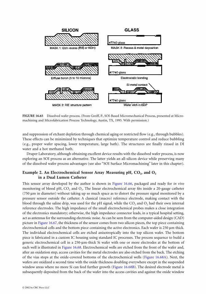
and suppression of etchant depletion through chemical aging or restricted flow (e.g., through bubbles).These effects can be minimized by techniques that optimize temperature control and reduce bubbling(e.g., proper wafer spacing, lower temperature, large bath). The structures are finally rinsed in DIwater and a hot methanol bath.
Draper Laboratory, although obtaining excellent device results with the dissolved wafer process, is nowexploring an SOI process as an alternative. The latter yields an all-silicon device while preserving manyof the dissolved wafer process advantages (see also “SOI Surface Micromachining” later in this chapter).
Example 2. An Electrochemical Sensor Array Measuring pH, CO2, and O2 in a Dual Lumen Catheter
This sensor array developed by the author is shown in Figure 16.66, packaged and ready for in vivomonitoring of blood pH, CO2 and O2. The linear electrochemical array fits inside a 20-gauge catheter(750 µm in diameter) without taking up so much space as to distort the pressure signal monitored by apressure sensor outside the catheter. A classical (macro) reference electrode, making contact with theblood through the saline drip, was used for the pH signal, while the CO2 and O2 had their own internalreference electrodes. The high impedance of the small electrochemical probes makes a close integrationof the electronics mandatory; otherwise, the high impedance connector leads, in a typical hospital setting,act as antennas for the surrounding electronic noise. As can be seen from the computer-aided design (CAD)picture in Figure 16.67, the thickness of the sensor comes from two silicon pieces, the top piece containingelectrochemical cells and the bottom piece containing the active electronics. Each wafer is 250 µm thick.The individual electrochemical cells are etched anisotropically into the top silicon wafer. The bottompiece is fabricated in a custom IC housing using standard IC processes. The process sequence to build ageneric electrochemical cell in a 250-µm-thick Si wafer with one or more electrodes at the bottom ofeach well is illustrated in Figure 16.68. Electrochemical wells are etched from the front of the wafer and,after an oxidation step, access cavities for the metal electrodes are also etched from the back. The etchingof the vias stops at the oxide-covered bottoms of the electrochemical wells (Figure 16.68A). Next, thewafers are oxidized a second time with the oxide thickness doubling everywhere except in the suspendedwindow areas where no more Si can feed further growth (Figure 16.68B). The desired electrode metal issubsequently deposited from the back of the wafer into the access cavities and against the oxide window
FIGURE 16.65 Dissolved wafer process. (From Greiff, P., SOI-Based Micromechanical Process, presented at Micro-machining and Microfabrication Process Technology, Austin, TX, 1995. With permission.)
© 2002 by CRC Press LLC

(Figure 16.68C). Finally, a timed oxide etch removes the sacrificial oxide window from above the under-lying metal, while preserving the thicker oxide layer in the other areas on the chip (Figure 16.68D) [Josephet al., 1989; Madou and Otagawa, 1989; Holland et al., 1988]. An SEM micrograph demonstrating stepD in Figure 16.68 is shown in Figure 16.69. The electrodes in the electrochemical cells of the top waferare further connected to the bottom wafer electronics by solder balls in the access vias of the top siliconwafer (see Figure 16.70). Separating the chemistry from the electronics in this way provides extra
FIGURE 16.66 An in vivo pH, CO2 and O2 sensor based on a linear array of electrochemical cells.
FIGURE 16.67 CAD of the electrochemical sensor array showing two pieces of Si (each 250 µm thick) on top ofeach other, mounted in a dual lumen catheter. The bottom part of the catheter is left open so pressure can bemonitored and blood samples can be taken.
© 2002 by CRC Press LLC

FIGURE 16.68 Fabrication sequence for a generic electrochemical cell in Si. Depth of the electrochemical well,number of electrodes and electrode materials can be varied.
FIGURE 16.69 SEM micrograph illustrating process step D from Figure 16.67. A 30 × 30-µm Pt electrode is shownat the bottom of an electrochemical well. This Pt electrode is further contacted to the electronics from the back.
© 2002 by CRC Press LLC

protection for the electronics from the electrolyte as well as from the electronics, and chemical sensormanufacture can proceed independently. Depending on the type of sensor element, one or more electrodesare fabricated at the bottom of the electrochemical cells. For example, shown in Figure 16.71 is an almostcompleted (Severinghaus) CO2 sensor with an Ag/AgCl electrode as the reference electrode (left in thefigure) and an IrOx pH-sensitive electrode, both at the bottom of one electrochemical well. The metalelectrodes are electrically isolated from each other by the SiO2 passivation layer over the surface of thesilicon wafer. To complete the CO2 sensor, we silk-screen a hydrogel containing an electrolytic mediuminto the silicon sensor cavity and dip-coat the sensor into a silicone-polycarbonate rubber solution toform the gas-permeable membrane. For hydrogel inside the micromachined well, we use poly(2-hydroxy-ethyl)methacrylate (PHEMA) or polyvinylalcohol (PVA).
FIGURE 16.70 Schematic of the bonding scheme between sensor wafer and IC. The schematic is a cut-through ofthe catheter.
FIGURE 16.71 SEM micrograph of an Ag/AgCl (left) and an IrOx (right) electrode at the bottom of an anisotro-pically etched well in Si. This electrochemical cell forms the basis for a Severinghaus CO2 sensor.
Membrane material
(gas permeable andbiocompatible)
Silicone polycarbonatecopolymer
Active sensor metal
Epoxy encapsulant
Metal encapsulationchannel
Hydrogel
Solder bumpSi
Si IC chip-250 µm thick
Sensor chip-250 µm thick
© 2002 by CRC Press LLC

The concept of putting the sensor chemistries and the electronics on opposite sides of a substrate isa very important design feature we decided upon several years ago in view of the overwhelming problemsencountered in building chemical sensors based on ISFETs or EGFETs [Madou and Morrison, 1989].
16.10 Surface Micromachining: Introduction
Bulk micromachining means that three-dimensional features are etched into the bulk of crystalline andnoncrystalline materials. In contrast, surface micromachined features are built up, layer by layer, on thesurface of a substrate (e.g., a single crystal silicon wafer). Dry etching defines the surface features in the x,yplane and wet etching releases them from the plane by undercutting. In surface micromachining, shapesin the x,y plane are unrestricted by the crystallography of the substrate. For illustration, in Figure 16.72 wecompare an absolute pressure sensor based on poly-Si and made by surface micromachining with one madeby bulk micromachining in single crystal Si.
The nature of the deposition processes involved determines the very flat surface micromachined features(Hal Jerman from EG&G’s ICSensors called them 2.5 D features [Jerman, 1994]). Specifically, low-pressurechemical vapor deposited (LPCVD) polycrystalline silicon (poly-Si) films generally are only a few micronshigh (low z). In contrast with wet bulk micromachining only the wafer thickness limits the feature height. Alow z may mean a drawback for some sensors. For example, it will be difficult to fashion a large inertial mass
FIGURE 16.72 Comparison of bulk micromachined and surface micromachined absolute pressure sensorsequipped with piezoresistive elements. (Top) Bulk micromachining in single crystal Si. (Bottom) Surface microma-chining with poly-Si.
Surface Micromachined Absolute Pressure Sensor
Si
SiO2
Al connect
Polysilicon piezoresistor
Glass support
Polysilicon freestandingdiaphragm
n+ Si
Pyrex Glass
© 2002 by CRC Press LLC

for an accelerometer from those thin poly-Si plates. Not only do many parameters in the LPCVD polysiliconprocess need to be controlled very precisely, subsequent high temperature annealing (say, at temperatures ofabout 580°C) is needed to transform the as-deposited amorphous silicon into polysilicon—the main structuralmaterial in surface micromachining. Even with the best possible process control, polysilicon has some materialdisadvantages over single crystal Si. For example, it generates a somewhat smaller yield strength (values between2 and 10 times smaller have been reported) [Biebl and von Philipsborn, 1993; Greek et al., 1995] and has alower piezoresistivity [Le Berre et al., 1996]. Moreover, since a grain diameter may constitute a significantfraction of the thickness of a mechanical member, the effective Young’s modulus may exhibit significantvariability from sensor to sensor [Howe, 1995]. An important positive attribute of poly-Si is that its materialproperties, although somewhat inferior to single crystal, are far superior compared to those of metal films,and, most of all, since they are isotropic, design is rendered dramatically simpler than with single crystalmaterial. Dimensional uncertainties are of greater concern than material issues. Although absolute dimensionaltolerances obtained with lithography techniques may be submicron, relative tolerances are poor, perhaps 1%on the length of a 100-µm-long feature. The situation becomes critical with yet smaller feature sizes [Madou,1997, chap. 7, Figure 7.1]. Although the relatively coarse dimensional control in the microdomain is not specificto surface micromachining, there is no crystallography to rely on for improved dimensional control as in thecase of wet bulk micromachining. Moreover, since the mechanical members in surface micromachining tendto be smaller, more post-fabrication adjustment of the features is required to achieve reproducible character-istics. Finally, the wet process for releasing structural elements from a substrate tends to cause sticking ofsuspended structures to the substrate, so-called stiction, introducing another disadvantage associated withsurface micromachining.
Some of the mentioned problems associated with surface micromachining have recently beenresolved by process modifications and/or alternative designs, and the technique has rapidly gainedcommercial interest, mainly because it is the most IC-compatible micromachining process developedto date. Moreover, in the last 5 to 10 years, processes such as silicon on insulator (SOI) [Diem et al.,1993], hinged poly-Si [Pister, 1992], Keller’s molded milli-scale polysilicon [Keller and Ferrari, 1994],thick poly-Si (10 µm and beyond) [Lange et al., 1995], as well as LIGA
1 and LIGA-like processes, have
further enriched the surface micromachining arsenal. Some preliminary remarks on each of thesesurface micromachining extensions follow.
Silicon crystalline features, anywhere between fractions of a micron to 100 µm high, can readily beobtained by surface micromachining of the epi-silicon or fusion-bonded silicon layer of SOI wafers[Noworolski et al., 1995]. Structural elements made from these single crystalline Si layers result in morereproducible and reliable sensors. SOI machining combines the best features of surface micromachining(i.e., IC compatibility and freedom in x,y shapes) with the best features of bulk micromachining (superiorsingle crystal Si properties). Moreover, SOI surface micromachining frequently involves fewer processsteps and offers better control over the thickness of crucial building blocks. Given the poor reproducibilityof mechanical properties and generally poor electronic characteristics of polysilicon films, SOI machiningmay surpass the poly-Si technology for fabricating high performance devices.
The fabrication of poly-Si planar structures for subsequent vertical assembly by mechanical rotationaround micromachined hinges dramatically increases the plethora of designs feasible with poly-Si [Pister,1992]. Today, erecting these poly-Si structures with the probes of an electrical probe station or, occasion-ally, assembly by chance in the HF etch or DI water rinse [Chu et al., 1995] represents too complicatedor unreliable postrelease assembly methods for commercial acceptance.
At the University of California at Berkeley, Keller introduced a combination of surface micromachiningand LIGA-like molding processes [Keller and Ferrari, 1994] in the so-called HEXSIL
2 process, a technology
enabling the fabrication of tall three-dimensional microstructures without postrelease assembly. Using CVDprocesses one can generally only deposit thin films (~2 to 5 µm) on flat surfaces. If however, these surfacesare the opposing faces of deep narrow trenches, the growing films will merge to form solid beams. Releasing
1LIGA is the acronym for the German Lithographie, Galvanoformung, Abformung (see chap. 17).
2HEXSIL is the acronym for HEXagonal honeycomb polySILicon.
© 2002 by CRC Press LLC
of such polysilicon structures and the incorporation of electroplating steps expand the surface microma-chining bandwidth in terms of choice of materials and accessible feature heights. In this fashion, high aspectratio structures normally associated with LIGA can now also be made of CVD polysilicon.
Applying classical LPCVD to obtain poly-Si deposition is a slow process. For example, a layer of 10 µmtypically requires a deposition time of 10 hours. Consequently, most micromachined structures are basedon layer thicknesses in the 2- to 5-µm range. Based on dichlorosilane (SiH2Cl2) chemistry, Lange et al.(1995) developed a CVD process in a vertical epitaxy batch reactor with deposition rates as high as0.55 µm/min at 1000°C. The process yields acceptable deposition times for thicknesses in the 10-µmrange. The highly columnar poly-Si films were deposited on sacrificial SiO2 layers and exhibit low internaltensile stress making them suitable for surface micromachining.
Finally, thick layers of polyimide and other new UV resists also receive a lot of attention as important newextensions of surface micromachining. Due to their transparency to exposing UV light, they can be transformedinto tall surface structures with LIGA-like high aspect ratios. They may be both electroplated and molded.
In this part of the chapter, we first review thin film material properties in general, focusing onsignificant differences with bulk properties of the same material, followed by a review of the main surfacemicromachining processes. Next, we clarify the recent extensions of the surface micromachining tech-nique listed above. Because of the complexity of the many parameters influencing thin film properties,we then present a set of case studies on the most commonly used thin film materials.
In the surface micromachining examples at the end of this chapter, we first look at a lateral resonator.Resonators have found an important industrial application in accelerometers introduced by AnalogDevices. The other example concerns a micromotor: an electrostatic linear motor with a slider steppingbetween two poly-Si rails. Micromotors may lack practical use as of yet, but, just as the ion-sensitive fieldeffect transistor (ISFET) galvanized the chemical sensor community in trying out new chemical sensingapproaches, micromotors energized the micromachining research community to fervently explore min-iaturization of a wide variety of mechanical sensors and actuators. Micromotors also brought about thechristening of the micromachining field into ‘Microelectromechanical Systems’ or MEMS.
16.11 Historical Note
The first example of a surface micromachine for an electro-mechanical application consisted of anunderetched metal cantilever beam for a resonant gate transistor made by Nathanson (1967). By 1970,a first suggestion for a magnetically actuated metallic micromotor emerged [Dutta, 1970]. Because offatigue problems metals rarely are counted on as mechanical components. The surface micromachiningmethod as we know it today was first demonstrated by Howe and Muller in the early 1980s and reliedon polysilicon as the structural material [Howe and Muller, 1982]. These pioneers and Guckel [Guckeland Burns, 1985], an early contributor to the field, produced free-standing LPCVD polysilicon structuresby removing the oxide layers on which the polysilicon features were formed. Howe’s first device consistedof a resonator designed to measure the change of mass upon adsorption of chemicals from the surround-ing air. A gas sensor does not necessarily represent a good application of a surface micromachinedelectrostatic structure since humidity and dust foul the thin air gap of such an unencapsulated micro-structure in a minimal amount of time. Later mechanical structures, especially hermetically sealedmechanical devices, provided proof that the IC revolution could be extended to electromechanical systems[Howe, 1995]. In these structures, the height (z-direction) typically is limited to less than 10 µm, ergothe name surface micromachining.
The first survey of possible applications of poly-Si surface micromachining was presented by Gabrielet al. (1989). Microscale movable mechanical pin joints, springs, gears, cranks, sliders, sealed cavities andmany other mechanical and optical components have been demonstrated in the laboratory [Muller, 1987;Fan et al., 1987]. In 1991, Analog Devices announced the first commercial product based on surfacemicromachining, namely, the ADXL-50, a 50-g accelerometer for activating air-bag deployment [Editor,1991]. A new wave of major commercial applications for surface micromachining could be based on
© 2002 by CRC Press LLC
Texas Instruments’ Digital Micromirror Device™. This surface micromachined movable mirror is adigital light switch that precisely controls a light source for projection display and hard copy applications[Hornbeck, 1995]. The commercial acceptance of this application will likely determine the staying powerof the surface micromachining option.
16.12 Mechanical Properties of Thin Films
16.12.1 Introduction
Thin films in surface micromachines must satisfy a large set of rigorous chemical, structural, mechanicaland electrical requirements. Excellent adhesion, low residual stress, low pinhole density, good mechanicalstrength and chemical resistance all may be required simultaneously. For many microelectronic thin films,the material properties depend strongly on the details of the deposition process and the growth conditions.In addition, some properties may depend on post-deposition thermal processing, referred to as annealing.Furthermore, the details of thin-film nucleation and/or growth may depend on the specific substrate oron the specific surface orientation of the substrate. Although the properties of a bulk material might bewell characterized, its thin-film form may have properties substantially different from those of the bulk.For example, thin films generally display smaller grain size than bulk materials. An overwhelming reasonfor the many differences stem from the properties of thin films, which exhibit a higher surface-to-volumeratio than large chunks of material and are strongly influenced by the surface properties.
For more details on deposition techniques in general, refer to Madou (1997, chap. 3); now we focuson the physical characteristics of the resulting thin deposits. Some terminology characterizing thin filmsand their deposition is introduced in Table 16.11.
Since thin films were not intended for load-bearing applications, their mechanical properties havelargely been ignored. The last 10 years saw the development of a strong appreciation for understandingthe mechanical properties as essential for improving the reliability and life-time in thin films, even innonstructural applications [Vinci and Braveman, 1991]. Surface micromachining contributes heavily tothis understanding. One of the most influential long-term contributions of surface micromachiningmight well lie in the elucidation of stress mechanism in thin films.
16.12.2 Adhesion
One cannot stress enough the importance of adhesion of various films to one another and to the substratein overall IC performance and reliability. As mechanical pulling forces might be involved, adhesion iseven more crucial in micromachining. If films lift from the substrate under a repetitive, applied mechanicalforce, the device will fail. Classical adhesion tests include the scotch tape test, abrasion method, scratching,deceleration (ultrasonic and ultracentrifuge techniques), bending, pulling etc. [Campbell, 1970]. Micro-machined structures, because of their sensitivity to thin-film properties, enable some innovative newways of in situ adhesion measurement. Figure 16.73 illustrates how a suspended membrane may be usedfor adhesion measurements. Figure 16.73A shows the membrane suspended but still adherent to thesubstrate. Figure 16.73B shows the membrane after it has been peeled from its substrate by an appliedload (gas pressure). Figure 16.73C illustrates the accompanying P(ressure)-V(olume) cycle, in which themembrane is inflated, peeled and then deflated. The shaded portion of Figure 16.73C illustrates the P-Vwork creating the new surface, which equals the average work of adhesion for the film-substrate interfacetimes the area peeled during the test [Senturia, 1987].
Cleanliness of a substrate is a condition sine qua non for good film adhesion. Roughness, providingmore bonding surface area and mechanical interlocking further improve it. Adhesion also improves withincreasing adsorption energy of the deposit and/or increasing number of nucleation sites in the earlygrowth stage of the film. Sticking energies between film and substrate range from less than 10 kcal/molein physisorption to more than 20 kcal/mole for chemisorption. The weakest form of adhesion involvesvan der Waals forces only (see also Table 16.11).
© 2002 by CRC Press LLC

TABLE 16.11 Thin Film Terms Used in Characterizing Deposition
Term Remark
Physisorbed film Bond energy < 10 kcal/moleChemisorbed film Bond energy > 20 kcal/moleNucleation Adatoms forming stable clustersCondensation Initial formation of nucleiIsland formation Nuclei grow in three dimensions, especially along the substrate surfaceCoalescence Nuclei contact each other and larger, rounded shapes formSecondary nucleation Areas between islands are filled in by secondary nucleation, resulting in a continuous filmGrain size of thin film Generally smaller than for bulk materials and function of deposition and annealing
conditions (higher T, larger grains)Surface roughness Lower at high temperatures except when crystallization starts; at low temperature the
roughness is higher for thicker films; also oblique deposition and contamination increase roughness
Epitaxial and amorphous films
Very low surface roughness
Density More porous deposits are less dense; density reveals a lot about the film structureCrystallographic structure Adatom mobility: amorphous, polycrystalline, single crystal or fiber texture, or preferred
orientation
FIGURE 16.73 Micromachined structure to evaluate adhesion. (A) Suspended membrane. (B) Partially detachedmembrane-outward peel. (C) Pressure-volume curve during inflate-deflate cycle. (From Senturia, S., Can We DesignMicrorobotic Devices Without Knowing the Mechanical Properties of Materials?, presented at Micro Robots andTekoperators Workshop, Hyannis, MA, 1987. With permission.)
0.007
0.006
0.005
0.004
0.003
0.002
0.001
0
0 50 100 150 200 250 300
Injected Volume (ul)
Pre
ssur
e
MP
a
inflating
peeling
deflating
SiSuspended membrane (e.g., polyimide)
A
B
C
P
© 2002 by CRC Press LLC

It is highly advantageous to include a layer of oxide-forming elements between a metal and an oxidesubstrate. These adhesion layers, such as Cr, Ti, Al etc., provide good anchors for subsequent metallization.Intermediate film formation allowing a continuous transition from one lattice to the other results in thebest adhesion. Adhesion also improves when formation of intermetallic metal alloys takes place.
16.12.3 Stress in Thin Films
16.12.3.1 Stress in Thin Films—Qualitative Description
Film cracking, delamination and void formation may all be linked to film stress. Nearly all films foster astate of residual stress, due to mismatch in the thermal expansion coefficient, nonuniform plastic defor-mation, lattice mismatch, substitutional or interstitial impurities and growth processes. Figure 16.74 listsstress-causing factors categorized as either intrinsic or extrinsic [Krulevitch, 1994]. The intrinsic stresses(also growth stresses) develop during the film nucleation. Extrinsic stresses are imposed by unintendedexternal factors such as temperature gradients or sensor package-induced stresses. Thermal stresses, themost common type of extrinsic stresses, are well understood and often easy to calculate (see below). Theyarise either in a structure with inhomogeneous thermal expansion coefficients subjected to a uniformtemperature change or in a homogeneous material exposed to a thermal gradient [Krulevitch, 1994].Intrinsic stresses in thin films often are larger than thermal stresses. They usually are a consequence of thenonequilibrium nature of the thin-film deposition process. For example, in chemical vapor deposition,depositing atoms (adatoms) may at first occupy positions other than the lowest energy configuration.With too high a deposition rate and/or too low adatom surface mobility, these first adatoms may becomepinned by newly arriving adatoms, resulting in the development of intrinsic stress. Other types of intrinsicstresses illustrated in Figure 16.74 include: transformation stresses occurring when part of a material under-
FIGURE 16.74 Examples of intrinsic and extrinsic residual stresses. (A) Nonuniform plastic deformation resultsin residual stresses upon unloading. M = bonding moment. (B) Thermal expansion mismatch between two materialsbonded together. α (1) and α (2) are thermal expansion coefficients. (C) Growth stresses evolve during film depo-sition. (D) Misfit stresses due to mismatches in lattice parameters in an epitaxial film and stresses from substitutionalor interstitial impurities. (E) Volume changes accompanying phase transformations cause residual stresses [Vinciand Braveman, 1991]. (After Krulevitch, P.A., Micromechanical Investigations of Silicon and Ni-Ti-Cu Thin Films,Ph.D. thesis, University of California, Berkeley, 1994.)
βα
+
-
+
+
+
-
-
-
Extrinsic IntrinsicA Non-uniform plastic deformation
M M
B Thermal expansion
C Growth
D Misfit / impurities
E Phase transformation
α (1)
α (2)
∆ T
σy
σy
© 2002 by CRC Press LLC
goes a volume change during a phase transformation, misfit stresses arising in epitaxial films due to latticemismatch between film and substrate, and impurities either interstitial or substitutional which cause intrinsicresidual stresses due to the local expansion or contraction associated with point defects. Intrinsic stress in athin film does not suffice to result in delamination unless the film is quite thick. For example, to overcomea low adsorption energy of 0.2 eV, a relatively high stress of about 5 × 10
9 dyn cm
–2 (10
7 dyn/cm
2 = 1 MPa)
is required [Campbell, 1970]. High stress can result in buckling or cracking of films.The stress developing in a film during the initial phases of a deposition may be compressive (i.e., the
film tends to expand parallel to the surface), causing buckling and blistering or delamination in extremecases (especially with thick films). Alternatively, thin films may be in tensile stress (i.e., the film tends tocontract), which may lead to cracking if forces high enough to exceed the fracture limit of the filmmaterial are present. Subsequent rearrangement of the atoms, either during the remainder of the depo-sition or with additional thermal processing, can lead to further densification or expansion, decreasingremaining tensile or compressive stresses, respectively.
The mechanical response of thin-film structures is affected by the residual stress, even if the structuresdo not fail. For example, if the residual stress varies in the direction of film growth, the resulting built-in bending moment will warp released structures, such as cantilever beams. The presence of residualstress also alters the resonant frequency of thin-film, resonant microstructures (see Eq. (16.59) below)[Pratt et al., 1992]. Also, residual stress can lead to degradation of electrical characteristics and yield lossthrough defect generation, such as 311 defects [Krulevitch, 1994]. Another observation found theresistivity of stressed metallic films to be higher than that of their annealed counterparts. In a few casesresidual stress has been used advantageously, such as in self-adjusting microstructures [Judy et al., 1991],and for altering the shape-set configuration in shape memory alloy films [Krulevitch, 1994].
In general, the stresses in films, by whatever means produced, are in the range of 108 to 5 × 10
10 dyn/cm
−2
and can be either tensile or compressive. For normal deposition temperatures (50 to a few hundreddegrees C), the stress in metal films typically ranges from 10
8 to 10
10 dyn cm
−2 and is tensile, the refractory
metals at the upper end, the soft ones (Cu, Ag, Au, Al) at the lower end. At low substrate temperatures,metal films tend to exhibit tensile stress. This often decreases in a linear fashion with increasing substratetemperature, finally going through zero or even becoming compressive. The changeover to compressivestress occurs at lower temperatures for lower melting point metals. The mobility of the adatoms is key tounderstanding the ranking for refractory and soft metals. A metal such as aluminum has a low meltingtemperature and a corresponding high diffusion rate even at room temperature, thus usually it is fairly stressfree. By comparison, tungsten has a relatively high melting point and a low diffusion rate and tends toaccumulate more stress when sputter-deposited. With dielectric films, stresses often are compressive andhave slightly lower values than commonly noted in metals.
Tensile films result, for example, when a process by-product is present during deposition and laterdriven off as a gas. If the deposited atoms are not sufficiently mobile to fill in the holes left by thesedeparting byproducts, the film will contract and go in tension. Nitrides deposited by plasma CVD usuallyare compressive due to the presence of hydrogen atoms in the lattice. By annealing, driving the hydrogenout, the films can turn highly tensile. Annealing also has a dramatic effect on most oxides. Oxides oftenare porous enough to absorb or give off a large amount of water. Full of water, they are compressive;devoid of water they are tensile. Thermal SiO2 is compressive, though, even when dry. If atoms arejammed in place (such as with sputtering) the film tends to act compressively. The stress in a thin filmalso varies with depth. The RF power of a plasma-enhanced CVD (PECVD) deposition influencss stress,e.g., a thin film may start out tensile, decrease as the power increases, and finally become compressivewith further RF power increase. CVD equipment manufacturers concentrate on building stress-controlcapabilities into new equipment by controlling plasma frequency (see also Madou [1997, chap. 3]).
16.12.3.2 Stress in Thin Films on Thick Substrates—Quantitative Analysis
The total stress in a thin film typically is given by:
σtot = σth + σint + σext (16.44)
© 2002 by CRC Press LLC

i.e., the sum of any intentional external applied stress (σext), the thermal stress (σth, an unintended externalstress) and different intrinsic components (σint). With constant stress through the film thickness, thestress components retain the form of
(16.45)
That is, the three nonvanishing stress components are functions of x and y alone. No stress occurs in thedirection normal to the substrate (z). With x, y as principal axes, the shear stress τxy also vanishes [Chouand Pagano, 1967] and Eq. (16.45) reduces to the following strain–stress relationships:
(16.46)
In the isotropic case ε = εx = εy so that σx = σy = σ, or:
(16.47)
where the Young’s modulus of the film and the Poissons’s ratio of the film act independently oforientation. The quantity E/l − ν often is called the biaxial modulus. Uniaxial testing of thin films isdifficult, prompting the use of the biaxial modulus, rather than Young’s uniaxial modulus. Plane stress,as described here, presents a good approximation several thicknesses away from the edge of the film (say,three thicknesses from the edge).
Thermal StressThermal stresses develop in thin films when high temperature deposition or annealing are involved,and usually are unavoidable due to mismatch of thermal expansion coefficients between film andsubstrate. The problem of a thin film under residual thermal stress can be modeled by consideringa thought experiment involving a stress-free film at high temperature on a thick substrate. Imaginedetaching the film from the high-temperature substrate and cooling the system to room temperature.Usually, the substrate dimensions undergo minor shrinkage in the plane while the film’s dimensionsmay reduce significantly. In order to reapply the film to the substrate with complete coverage, thefilm needs stretching with a biaxial tensile load to a uniform radial strain ε, followed by perfectbondage to the rigid substrate and load removal. The film stress is assumed to be the same in thestretched and free-standing film as in the film bonded to the substrate, i.e., no relaxation occurs inthe bonding process. To calculate the thermal residual stress from Eq. (16.47) the elastic moduli ofthe film must be known, as well as the volume change associated with the residual stress, i.e., thethermal strain, εth, resulting from the difference in the coefficients of thermal expansion between thefilm and the substrate.
Let us now consider whether, qualitatively, the above assumptions apply to the measurement of thinfilms on Si wafers. Such films typically measure 1 µm thick and are deposited on 4-in. wafers nominally
σx σx(x, y)=
σy σy(x, y)=
τxy τxy(x, y)=
τxz τyz σz 0= = =
εx
σx
E-----
νσy
E---------–=
εy
σy
E-----
νσx
E---------–=
σz 0=
σ E1 ν–------------
ε=
© 2002 by CRC Press LLC

550 µm thick. In this case, the substrate measures nearly three orders of magnitude thicker than the film,and, because the bending stiffness is proportional to the thickness cubed, the substrate essentially is rigidrelative to the film. The earlier assumptions clearly apply.
Figure 16.75 portrays a quantitative example where a polyimide film, strain-free at the depositiontemperature (Td) of 400°C, is cooled to room temperature Tr (25°C) on an Si substrate with a differentcoefficient of thermal expansion. The resulting strain is given by:
(16.48)
where αf and αs represent the coefficients of thermal expansion for the polyimide film and the Si substrate,respectively. The thermal strain can be of either sign, based on the relative values of αf and αs: positive istensile, negative is compressive. Polyimide features a thermal expansion (αf = 70 × 10
−6°C−1
) larger thanthe thermal expansion coefficient of Si (αs = 2.6 × 10
−6°C−1
); hence, a tensile stress is expected. With SiO2
grown or deposited on silicon at elevated temperatures, a compressive component [αf (0.35 × 10⁻⁶°C
−1) <
αs (2.6 × 10⁻⁶°C
−1)] is expected. Assuming that the coefficients of thermal expansion are temperature
independent, Eq. (16.48) simplifies to:
εth = (α f − α s)(Td − Tr) (16.49)
The calculated thermal strain εth for polyimide on Si then measures 25 × 10−3
at room temperature. Thebiaxial modulus (E/1 − ν), with E = 3 GPa and ν = 0.4, equals 5 GPa, and the residual stress σ, from Eq.(16.47), is 125 MPa and tensile.
Intrinsic StressThe intrinsic stress, σi, reflects the internal structure of a material and is less clearly understood than thethermal stress which it often dominates [Guckel et al., 1988]. Several phenomena may contribute to σi,making its analysis very complex. Intrinsic stress depends on thickness, deposition rate (locking indefects), deposition temperature, ambient pressure, method of film preparation, type of substrate used(lattice mismatch), incorporation of impurities during growth etc. Some semiquantitative descriptionsof various intrinsic stress-causing factors follow:
FIGURE 16.75 Thermal stress. Tension and compression are determined by the relative size of thermal expansioncoefficients of film and substrate. Suppose a strain-free film at deposition temperature, Td, is cooled to room temperature,Tr, on a substrate with a different coefficient of thermal expansion.
(deposition temperature) (room temperature)
Polyimide Film
T = Td T = Tr
tf << ts
tf
ts
εth = 0 εth = (α f - αs)(Td - T r)
αf > αs : tension (polyimide on Si)
αf < αs : compression (SiO2 on Si)
Substrate Substrate
εth (αf(T) αs(T))– td∫=
© 2002 by CRC Press LLC

• Doping (σint > 0 or σint < 0): When doping Si, the atomic or ionic radius of the dopant and thesubstitutional site determine the positive or negative intrinsic stress (σint > 0 or tensile, and σint < 0or compressive). With boron-doped poly-Si, an atom small compared to Si, the film is expectedto be tensile (σint > 0); with phosphorous doping, an atom large compared to Si, the film is expectedto be compressive (σint < 0).
• Atomic peening (σint < 0): Ion bombardment by sputtered atoms and working gas densifies thin films,rendering them more compressive. Magnetron sputtered films at low working pressure (<1 Pa) andlow temperature often exhibit compressive stress.
• Microvoids (σint > 0): Microvoids may arise when byproducts during deposition escape as gasesand the lateral diffusion of atoms evolves too slowly to fill all the gaps, resulting in a tensile film.
• Gas entrapment (σint < 0): As an example we can cite the hydrogen trapped in Si3N4. Annealingremoves the hydrogen, and a nitride film, compressive at first, may become tensile if the hydrogencontent is sufficiently low.
• Shrinkage of polymers during cure (σint > 0): The shrinkage of polymers during curing may leadto severe tensile stress, as becomes clear in the case of polyimides. Special problems are associatedwith measuring the mechanical properties of polymers as they exhibit a time-dependent mechan-ical response (viscoelasticity), a potentially significant factor in the design of mechanical structureswhere polymers are subjected to sustained loads [Maseeh and Senturia, 1990].
• Grain boundaries (σint = ?): Based on intuition one expects that the interatomic spacing in grainboundaries differs depending on the amount of strain, thus contributing to the intrinsic stress. Butthe origin of, for example, the compressive stress in polysilicon and how it relates to the grain structureand interatomic spacing are not yet completely clear (see also below on coarse and fine-grated Si).
For further reading on thin-film stress, refer to Hoffman (1975; 1976).
16.12.3.3 Stress-Measuring Techniques
IntroductionA stressed thin film will bend a thin substrate by a measurable degree. A tensile stress will bend andrender the surface concave; a compressive stress renders the surface convex. The most common methodsfor measuring the stress in a thin film are based on this substrate bending principle. The deformationof a thin substrate due to stress is measured either by observing the displacement of the center of acircular disk or by using a thin cantilevered beam as a substrate and calculating the radius of curvatureof the beam and hence the stress from the deflection of the free end. More sophisticated local stressmeasurements use analytical tools such as X-ray [Wong, 1978], acoustics, Raman spectroscopy [Nishiokaet al., 1985], infrared spectroscopy [Marco et al., 1991], and electron-diffraction techniques. Local stressdoes not necessarily mean the same as the stress measured by substrate bending techniques, since stressis defined microscopically, while deformations are induced mostly macroscopically. The relation betweenmacroscopic forces and displacements and internal differential deformation, therefore, must be modeledcarefully. Local stress measurements may also be made using in situ surface micromachined structuressuch as strain gauges made directly out of the film of interest itself [Mehregany et al., 1987]. Thedeflections of thin suspended and pressurized micromachined membranes may be measured by mechan-ical probe [Jaccodine and Schlegel, 1966], laser [Bromley et al., 1983], or microscope [Allen et al., 1987].Intrinsic stress influences the frequency response of microstructures (see Eq. (16.59)) which can bemeasured by laser [Zhang et al., 1991], spectrum analyzer [Pratt et al., 1991], or stroboscope. Whereasresidual stress can be determined from wafer curvature and microstructure deflection data, materialstructure of the film can be studied by X-ray diffraction and transmission electron microscopy (TEM).Krulevitch, among others, attempted to link the material structure of poly-Si and its residual strain[Krulevitch, 1994]. Following, we will review stress-measuring techniques, starting with the more tradi-tional ones and subsequently clarifying the problems and opportunities in stress measuring with surfacemicromachined devices.
© 2002 by CRC Press LLC

Disk MethodFor all practical purposes only stresses in the x and y directions are of interest in determining overallthin-film stress, as a film under high stress can only expand or contract by bending the substrateand deforming it in a vertical direction. Vertical deformations will not induce stresses in a substratebecause it freely moves in that direction. The latter condition enables us to obtain quite accuratestress values by measuring changes in bow or radius of curvature of a substrate. The residual stressesin thin films are large and sensitive optical or capacitive gauges may measure the associated substratedeflections.
The disk method, most commonly used, is based on a measurement of the deflection in the center ofthe disk substrate (say, a Si wafer) before and after processing. Since any change in wafer shape is directlyattributable to the stress in the deposited film, it is relatively straightforward to calculate stress by measuringthese changes. Stress in films using this method is found through the Stoney equation [Hoffman, 1976],relating film stress to substrate curvature:
(16.50)
where R represents the measured radius of curvature of the bent substrate, E/(1 − ν) the biaxial modulusof the substrate, T the thickness of the substrate, and t the thickness of the applied film [Singer, 1992].The underlying assumptions include:
• The disc substrate is thin and has transversely isotropic elastic properties with respect to the filmnormal.
• The applied film thickness is much less than the substrate thickness.
• The film thickness is uniform.
• Temperature of the disk substrate/film system is uniform.
• Disc substrate/film system is mechanically free.
• Disc substrate without film has no bow.
• Stress is equi-biaxial and homogeneous over the entire substrate.
• Film stress is constant through the film thickness.
For most films on Si we assume that t ≤ T; for example, t/T measures ~10−3
for thin films on Si.The legitimacy of the uniform thickness, homogeneous, and equi-biaxial stress assumptions dependon the deposition process. Chemical vapor deposition (CVD) is such a widely used process as itproduces relatively uniform films; however, sputter-deposited films can vary considerably over thesubstrate. In regard to the assumption of stress uniformity with film thickness, residual stress canvary considerably through the thickness of the film. Eq. (16.50) only gives an average film stress insuch cases. In cases where thin films are deposited onto anisotropic single crystal substrates, theassumption of a substrate with transversely isotropic elastic properties with respect to the filmnormal is not always satisfied. Using single crystal silicon substrates possessing moderately aniso-tropic properties (Eq. (16.20)) (<100>- or <111>-oriented wafers) satisfies the transverse isotropyargument. Any curvature inherent in the substrate must be measured before film deposition andalgebraically added to the final measured radius of curvature. To give an idea of the degree ofcurvature, 1 µm of thermal oxide may cause a 30-µm warp of a 4-in. silicon wafer, correspondingto a radius of curvature of 41.7 m.
Presently, five companies offer practical disk method-based instruments to measure stress onwafers: ADE Corp. (Newton, MA), GCA/Tropel (Fairport, NY), Ionic Systems (Salinas, CA), ScientificMeasurements Systems, Inc. (San Jose, CA), and Tencor Instruments (Mountain View, CA) [Singer, 1992].Figure 16.76A illustrates the sample output from Tencor’s optical stress analysis system. Figure 16.76Brepresents the measuring principle of Ionic Systems’ optical stress analyzer. None of the above tech-
σ 1R---
E6(1 ν)–--------------------
T2
t-----=
© 2002 by CRC Press LLC
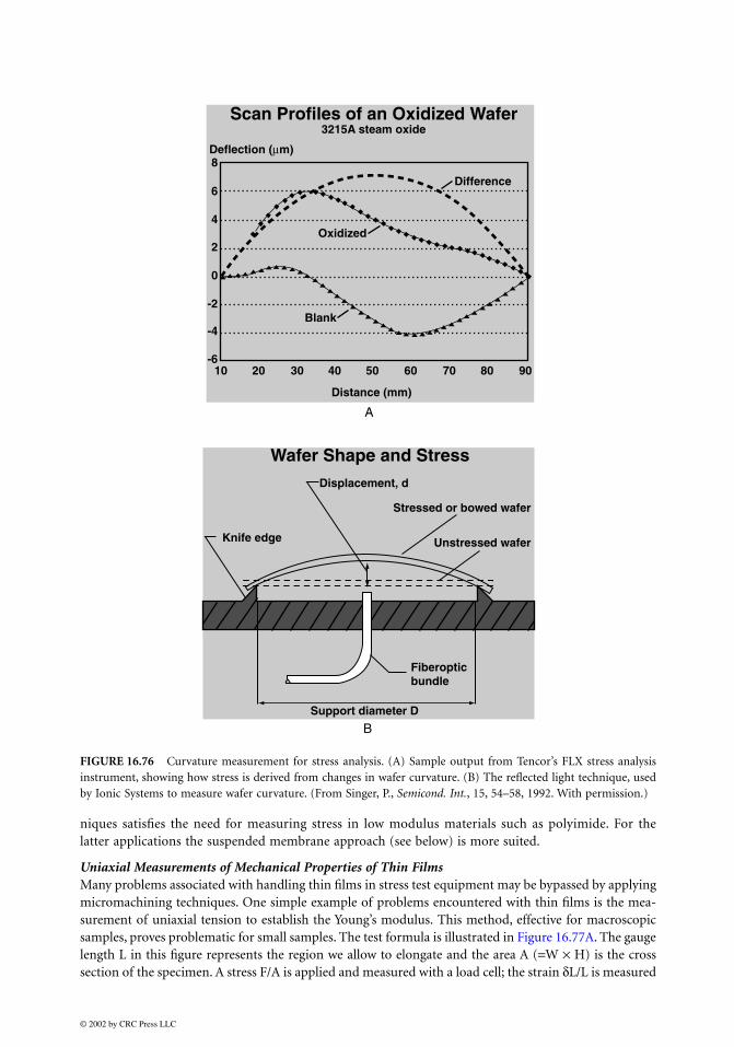
niques satisfies the need for measuring stress in low modulus materials such as polyimide. For thelatter applications the suspended membrane approach (see below) is more suited.
Uniaxial Measurements of Mechanical Properties of Thin FilmsMany problems associated with handling thin films in stress test equipment may be bypassed by applyingmicromachining techniques. One simple example of problems encountered with thin films is the mea-surement of uniaxial tension to establish the Young’s modulus. This method, effective for macroscopicsamples, proves problematic for small samples. The test formula is illustrated in Figure 16.77A. The gaugelength L in this figure represents the region we allow to elongate and the area A (=W × H) is the crosssection of the specimen. A stress F/A is applied and measured with a load cell; the strain δL/L is measured
FIGURE 16.76 Curvature measurement for stress analysis. (A) Sample output from Tencor’s FLX stress analysisinstrument, showing how stress is derived from changes in wafer curvature. (B) The reflected light technique, usedby Ionic Systems to measure wafer curvature. (From Singer, P., Semicond. Int., 15, 54–58, 1992. With permission.)
Scan Profiles of an Oxidized Wafer
Wafer Shape and Stress
Deflection (µm)8
6
4
2
-2
-4
-6
0
10 20 30 40 50 60 70 80 90
Distance (mm)
Displacement, d
Difference
Oxidized
Blank
3215A steam oxide
Stressed or bowed wafer
Unstressed wafer
Fiberopticbundle
Knife edge
Support diameter D
B
A
© 2002 by CRC Press LLC

with an LVDT or another displacement transducer (a typical instrument used is the Instron 1123). TheYoung’s modulus is then deduced from:
(16.51)
The obvious problem, for small or large samples, is how to grip onto the sample without changing A.Under elongation, A will indeed contract by (w + H)δνL. In general, making a dog-bone shaped structure(Instron specimen) solves that problem as shown in Figure 16.77B. Still, the grips introduced in anInstron sample can produce end effects and uncertainties in determining L. Making Instron specimensin thin films is even more of a challenge since the thin film needs to be removed from the surface, possiblychanging the stress state, while the removal itself may modify the film.
As in the case of adhesion, some new techniques for testing stress in thin films, based on microma-chining, are being explored. These microtechniques prove more advantageous than the whole wafer disctechnique in that they are able to make local measurements.
The fabrication of micro-Instron specimens of thin polyimide samples is illustrated in Figure 16.78A.Polyimide is deposited on a p
+ Si membrane in multiple coats. Each coat is prebaked at 130°C for 15 min.
After reaching the desired thickness the film is cured at 400°C in nitrogen for 1 hr (A). The polyimideis then covered with a 3000-Å layer of evaporated aluminum (B). The aluminum layer is patterned bywet etching (in phosphoric-acetic-nitric solution referred to as PAN etch) to the Instron specimen shape(C). Dry etching transfers the pattern to the polyimide (D). After removing the Al mask by wet etching,the p
+ support is removed by a wet isotropic etch (HNA) or a SF6 plasma etch (E), and finally the side
silicon is removed along four pre-etched scribe lines, releasing the residual stress (F). The remainingsilicon acts as supports for the grips of the Instron [Meseeh-Tehrani, 1990]. The resulting structure can
FIGURE 16.77 Measuring Young’s modulus. (A) With a bar-shaped structure. (B) With a dog-bone, Instron specimen.(After Senturia and Howe, 1990.)
F H
W
F
L
Young'sModulus
Stress : F/A (area A= W* H)
Strain : δ/L/L
L ="gauge length" (region we allow to elongate)
A, under elongation, will contract by (W+H) δ η Lunless a dog-bone-structure is used
E =F L
δLA
A
B
L
EFA---
LδL------
=
© 2002 by CRC Press LLC

FIGURE 16.78 Uniaxial stress measurement. (A) Fabrication process of a dog bone sample for measurement ofuniaxial strain. (B) Stress vs. strain for Du Pont’s 2525 polyimide. (Courtesy of Dr. F. Maseeh-Tehrani.)
© 2002 by CRC Press LLC
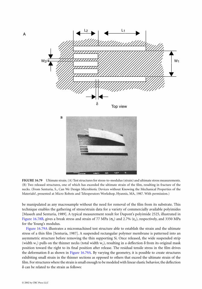
be manipulated as any macrosample without the need for removal of the film from its substrate. Thistechnique enables the gathering of stress/strain data for a variety of commercially available polyimides[Maseeh and Senturia, 1989]. A typical measurement result for Dupont’s polyimide 2525, illustrated inFigure 16.78B, gives a break stress and strain of 77 MPa (σb) and 2.7% (εb), respectively, and 3350 MPafor the Young’s modulus.
Figure 16.79A illustrates a micromachined test structure able to establish the strain and the ultimatestress of a thin film [Senturia, 1987]. A suspended rectangular polymer membrane is patterned into anasymmetric structure before removing the thin supporting Si. Once released, the wide suspended strip(width w1) pulls on the thinner necks (total width w2), resulting in a deflection δ from its original maskposition toward the right to its final position after release. The residual tensile stress in the film drivesthe deformation δ as shown in Figure 16.79A. By varying the geometry, it is possible to create structuresexhibiting small strain in the thinner sections as opposed to others that exceed the ultimate strain of thefilm. For structures where the strain is small enough to be modeled with linear elastic behavior, the deflectionδ can be related to the strain as follows:
FIGURE 16.79 Ultimate strain. (A) Test structures for stress-to-modulus (strain) and ultimate stress measurements.(B) Two released structures, one of which has exceeded the ultimate strain of the film, resulting in fracture of thenecks. (From Senturia, S., Can We Design Microbiotic Devices without Knowing the Mechanical Properties of theMaterials?, presented at Micro Robots and Teleoperators Workshop, Hyannis, MA, 1987. With permission.)
W2/4 W1
L2 L1
Top viewδ
A
© 2002 by CRC Press LLC

(16.52)
where the geometries are defined as illustrated in Figure 16.79A. Figure 16.79B displays a photograph oftwo released structures: one with thicker necks, the other with necks so thin that they fractured uponrelease of the film. Based on the residual tensile strain of the film and the geometry of the structures thatfailed, the ultimate strain of the particular polyimide used was determined to be 4.5%.
Using similar micromachined tensile test structures [Biebl and von Philipsborn, 1993] measured thefracture strength of undoped and doped polysilicon and found 2.84 ± 0.09 GPa for undoped materialand 2.11 ± 0.10 GPa in the case of phosphorous doping, 2.77 ± 0.08 GPa for boron doping and 2.70 ±0.09 GPa for arsenic doping. No statistically significant differences were observed between samplesreleased using concentrated HF or buffered HF. However, a 17% decrease of the fracture stress wasobserved for a 100% increase in etching time. These data contrast with Greek et al. (1995) in situ tensilestrength test result of 768 MPa for an undoped poly-Si film. A mean tensile strength almost ten timesless than that of single crystal Si (6 GPa) [Ericson and Schweitz, 1990]. We normally expect polycrystallinefilms to be stronger than single crystal films (see below under Strength of Thin Films). Greek et al. (1995)explain this discrepancy for poly-Si by pointing out that their polysilicon films have a very rough surfacecompared to single crystal material, containing many locations of stress concentration where a fracturecrack can be initiated.
Biaxial Measurements of Mechanical Properties of Thin Films: Suspended Membrane MethodsWe noted earlier that none of the disk stress-measuring techniques is suitable for measuring stress in lowmodulus tensile materials such as polyimides. Suspended membranes are very convenient for this pur-pose. The same micromachined test structure used for adhesion testing, sometimes called the blister test,as shown in Figure 16.73, can measure the tensile stress in low modulus materials. This type of teststructure ensues from shaping a silicon diaphragm by conventional anisotropic etching, followed byapplying the coating, and, finally, removing the supporting silicon from the back with an SF6 plasma[Senturia, 1987]. By pressurizing one side of the membrane and measuring the deflection, one can extractboth the residual stress and the biaxial modulus of the membrane. Pressure to the suspended film canbe applied by a gas or by a point-load applicator [Vinci and Braveman, 1991]. The load-deflection curveat moderate deflections (strains less than 5%) answers to:
(16.53)
where p represents the pressure differential across the film; d, the center deflection; a, the initial radius;t, the membrane thickness; and σ, the initial film stress. In the simplified Cabrera model for circularmembranes the constants C1 and C2 equal 4 respectively 8/3. For more rigorous solutions for both circularand rectangular membranes and references to other proposed models, refer to Maseeh-Tehrani [Maseeh-Tehrani, 1990]. The relation in Eq. (16.53) can simultaneously determine σ and the biaxial modulus E/1− ν; plotting pa
2/dt vs. (d/a)
2 should yield a straight line. The residual stress can be extracted from the
intercept and the biaxial modulus from the slope of the least-squares-best-fit line [Senturia, 1987]. Atypical result obtained via such measurements is represented in Figure 16.80. For the same Dupontpolyimide 2525, measuring a Young’s modulus of 3350 MPa in the uniaxial test (Figure 16.78B), themeasurements give 5540 MPa for the biaxial modulus and 32 MPa for the residual stress. The residualstress-to-biaxial modulus ratio, also referred to as the residual biaxial strain, thus reaches 0.6%. The latterquantity must be compared to the ultimate strain when evaluating potential reliability problems associ-ated with cracking of films. By loading the membranes to the elastic limit point, yield stress and straincan be determined as with the uniaxial test.
ε σE---
δ W1
L1
-------W2
L2
-------+
W1 W2–--------------------------= =
p C1σtd
a2--------- C2
E1 ν–------------
td3
a4-------+=
© 2002 by CRC Press LLC
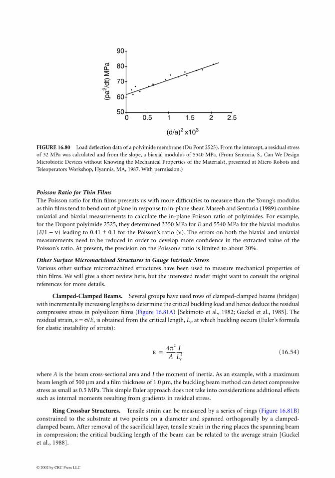
Poisson Ratio for Thin FilmsThe Poisson ratio for thin films presents us with more difficulties to measure than the Young’s modulusas thin films tend to bend out of plane in response to in-plane shear. Maseeh and Senturia (1989) combineuniaxial and biaxial measurements to calculate the in-plane Poisson ratio of polyimides. For example,for the Dupont polyimide 2525, they determined 3350 MPa for E and 5540 MPa for the biaxial modulus(E/1 − ν) leading to 0.41 ± 0.1 for the Poisson’s ratio (ν). The errors on both the biaxial and uniaxialmeasurements need to be reduced in order to develop more confidence in the extracted value of thePoisson’s ratio. At present, the precision on the Poisson’s ratio is limited to about 20%.
Other Surface Micromachined Structures to Gauge Intrinsic StressVarious other surface micromachined structures have been used to measure mechanical properties ofthin films. We will give a short review here, but the interested reader might want to consult the originalreferences for more details.
Clamped-Clamped Beams. Several groups have used rows of clamped-clamped beams (bridges)with incrementally increasing lengths to determine the critical buckling load and hence deduce the residualcompressive stress in polysilicon films (Figure 16.81A) [Sekimoto et al., 1982; Guckel et al., 1985]. Theresidual strain, ε = σ/E, is obtained from the critical length, Lc, at which buckling occurs (Euler’s formulafor elastic instability of struts):
(16.54)
where A is the beam cross-sectional area and I the moment of inertia. As an example, with a maximumbeam length of 500 µm and a film thickness of 1.0 µm, the buckling beam method can detect compressivestress as small as 0.5 MPa. This simple Euler approach does not take into considerations additional effectssuch as internal moments resulting from gradients in residual stress.
Ring Crossbar Structures. Tensile strain can be measured by a series of rings (Figure 16.81B)constrained to the substrate at two points on a diameter and spanned orthogonally by a clamped-clamped beam. After removal of the sacrificial layer, tensile strain in the ring places the spanning beamin compression; the critical buckling length of the beam can be related to the average strain [Guckelet al., 1988].
FIGURE 16.80 Load deflection data of a polyimide membrane (Du Pont 2525). From the intercept, a residual stressof 32 MPa was calculated and from the slope, a biaxial modulus of 5540 MPa. (From Senturia, S., Can We DesignMicrobiotic Devices without Knowing the Mechanical Properties of the Materials?, presented at Micro Robots andTeleoperators Workshop, Hyannis, MA, 1987. With permission.)
90
80
70
60
500 0.5 1 1.5 2 2.5
(d/a)2 x103
(pa2 /d
t) M
Pa
ε 4π2
A-------- I
Lc2-----=
© 2002 by CRC Press LLC

FIGURE 16.81 Some micromachined structures used for stress measurements. (A) Clamped-clamped beams:measuring the critical buckling length of clamped-clamped beams enables measurement of residual stress.(B) Crossbar rings: tensile stress can be measured by buckling induced in the crossbar of a ring structure. (C) Aschematic of a strain gauge capable of measuring tensile or compressive stress. (D) SEM microphotograph of twostrain gauges. (C and D from Lin, L., Selective Encapsulations of MEMS: Micro Channels, Needles, Resonators andElectromechanical Filters, Ph.D. thesis, University of California, Berkeley, 1993. With permission.)
Si
Polysiliconfreestandingdiaphragm
SiO2
BTensile material
Critical buckling length Lc
Anchor points
Polyimide
Spanning beam is compressed bytensile strain in the ring material
A
F= σ A= σ tW
Si
TensileStrain
Slope Beam
Anchor
Indicator Beam
CompressiveStrain
Vernier Gauge
Test Beam
Anchor
C
© 2002 by CRC Press LLC
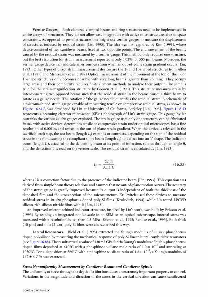
Vernier Gauges. Both clamped-clamped beams and ring structures need to be implemented inentire arrays of structures. They do not allow easy integration with active microstructures due to spaceconstraints. As opposed to proof structures one might use vernier gauges to measure the displacementof structures induced by residual strain [Lin, 1993]. The idea was first explored by Kim (1991), whosedevice consisted of two cantilever beams fixed at two opposite points. The end movement of the beamscaused by the residual strain was measured by a vernier gauge. This method only requires one structure,but the best resolution for strain measurement reported is only 0.02% for 500-µm beams. Moreover, thevernier gauge device may indicate an erroneous strain when an out-of-plane strain gradient occurs [Lin,1993]. Other types of direct strain measurement devices are the T- and H-shaped structures from Allenet al. (1987) and Mehregany et al. (1987) Optical measurement of the movement at the top of the T- orH-shape structures only becomes possible with very long beams (greater than 2.5 mm). They occupylarge areas and their complexity requires finite element methods to analyze their output. The same istrue for the strain magnification structure by Goosen et al. (1993). This structure measures strain byinterconnecting two opposed beams such that the residual strain in the beams causes a third beam torotate as a gauge needle. The rotation of the gauge needle quantifies the residual strain. A schematic ofa micromachined strain gauge capable of measuring tensile or compressive residual stress, as shown inFigure 16.81C, was developed by Lin at University of California, Berkeley [Lin, 1993]. Figure 16.81Drepresents a scanning electron microscope (SEM) photograph of Lin’s strain gauge. This gauge by faroutranks the various in situ gauges explored. The strain gauge uses only one structure, can be fabricatedin situ with active devices, determines tensile or compressive strain under optical microscopes, has a fineresolution of 0.001%, and resists to the out-of-plane strain gradient. When the device is released in thesacrificial etch step, the test beam (length Lt) expands or contracts, depending on the sign of the residualstress in the film, causing the compliant slope beam (length Ls) to deflect into an ‘s’ shape. The indicatorbeam (length Li), attached to the deforming beam at its point of inflection, rotates through an angle θ,and the deflection δ is read on the vernier scale. The residual strain is calculated as [Lin, 1993]:
(16.55)
where C is a correction factor due to the presence of the indicator beam [Lin, 1993]. This equation wasderived from simple beam theory relations and assumes that no out-of-plane motion occurs. The accuracyof the strain gauge is greatly improved because its output is independent of both the thickness of thedeposited film and the cross section of the microstructure. Krulevitch used these devices to measureresidual stress in in situ phosphorus-doped poly-Si films [Krulevitch, 1994], while Lin tested LPCVDsilicon-rich silicon nitride films with it [Lin, 1993].
An improved micromachined indicator structure, inspired by Lin’s work, was built by Ericson et al.(1995) By reading an integrated nonius scale in an SEM or an optical microscope, internal stress wasmeasured with a resolution better than 0.5 MPa [Ericson et al., 1995; Benitez et al., 1995]. Both thick(10-µm) and thin (2-µm) poly-Si films were characterized this way.
Lateral Resonators. Biebl et al. (1995) extracted the Young’s modulus of in situ phosphorus-doped polysilicon by measuring the mechanical response of poly-Si linear lateral comb-drive resonators(see Figure 16.88). The results reveal a value of 130 ± 5 GPa for the Young’s modulus of highly phosphorus-doped films deposited at 610°C with a phosphine-to-silane mole ratio of 1.0 × 10
−2 and annealing at
1050°C. For a deposition at 560°C with a phosphine to silane ratio of 1.6 × 10⁻³
, a Young’s modulus of147 ± 6 GPa was extracted.
Stress Nonuniformity Measurement by Cantilever Beams and Cantilever SpiralsThe uniformity of stress through the depth of a film introduces an extremely important property to control.Variations in the magnitude and direction of the stress in the vertical direction can cause cantilevered
εf
2Lsδ3LiLtC----------------=
© 2002 by CRC Press LLC

structures to curl toward or away from the substrate. Stress gradients present in the polysilicon film mustthus be controlled to ensure predictable behavior of designed structures when released from the substrate.To determine the thickness variation in residual stress, noncontact surface profilometer measurements onan array of simple cantilever beams [Core et al., 1993; Chu et al., 1992] or cantilever spirals can be used[Fan et al., 1990].
Cantilever Beams. The deflections resulting from stress variation through the thickness of simplecantilever beams after their release from the substrate is shown in Figure 16.82A. The bending moment causingdeflection of a cantilever beam follows out of pre-release residual stress and is given by (see Figure 16.82A):
(16.56)
FIGURE 16.82 (A) Micro-cantilever deflection for measuring stress non-uniformity. (a) No gradient; (b) high tensilestress near the surface; and (c) lower tensile stress near the surface. (B) Topographical contour map of polysiliconcantilever array. (From Core, T.A., W.K. Tsang, and S.J. Sherman, Solid State Technol., 36, 39–47, 1993. With permission.)
M zbσ(z) Zdt/2–
t/2
∫=
© 2002 by CRC Press LLC

where σ(z) represents the residual stress in the film as a function of thickness and b stands for cantileverwidth. Assuming a linear strain gradient Γ (physical dimensions 1/length) such that σ(z) = EΓz, Eq.(16.56) converts to:
(16.57)
where the moment of inertia, I, for a rectangular cross section is given by I = bt3/12. The measured
deflection z, i.e., the vertical deflection of the cantilever’s endpoint, from beam theory for a cantileverwith an applied end moment, is given as:
(16.58)
Figure 16.82B represents topographical contour map of an array of polysilicon cantilevers. The cantileversvary in length from 25 to 300 µm by 25-µm increments. Notice that the tip of the longest cantileverresides at a lower height (approximately 0.9 µm closer to the substrate) than the anchored support,indicating a downward bending moment [Core et al., 1993]. The gradients can be reduced or eliminatedwith a high-temperature anneal. With integrated electronics on the same chip, long high-temperatureprocessing must be avoided. Therefore, stress gradients can limit the length of cantilevered structuresused in surface-micromachined designs.
Cantilever Spirals. Residual stress gradients can also be measured by Fan’s cantilever spiral asshown in Figure 16.83A [Fan et al., 1990]. Spirals anchored at the inside spring upwards, rotate, andcontract with positive strain gradient (tending to curl a cantilever upwards), while spirals anchored atthe outside deflect in a similar manner in response to a negative gradient. Theoretically, positive andnegative gradients produce spirals with mirror symmetry [Fan et al., 1990]. The strain gradient can bedetermined from spiral structures by measuring the amount of lateral contraction, the change in height,or the amount of rotation. Krulevitch presented the computer code for the spiral simulation in his doctoralthesis [Krulevitch, 1994]. Figure 16.83B shows a simulated spiral with a bending moment of Γ = ±3.0 mm
−1
after release.Krulevitch compared all the above surface micromachined structures for stress and stress gradient
measurements on poly-Si films. His comments are summarized in Table 16.12 [Krulevitch, 1994]. Krulevitchfound that the fixed-fixed beam structures for determining compressive stress from the buckling criterionproduced remarkably self-consistent and repeatable results. Wafer curvature stress profiling proved reli-able for determining average stress and the true stress gradient as compared with micromachined spirals.Measurements of curled cantilevers could not be used much as the strain gradients mainly were negativefor poly-Si, leading to cantilevers contacting the substrate. The strain gauge dial structures were usefulover a rather limited strain-gradient range. With too large a strain gradient curling of the long beamsovershadows expansion effects and makes the vernier indicator unreadable.
16.12.4 Strength of Thin Films
Due to the high activation energy for dislocation motion in silicon (2.2 eV), hardly any plastic flowoccurs in single crystalline silicon for temperatures lower than 673°C. Grain boundaries in poly-Si blockdislocation motion; hence, polysilicon films can be treated as an ideal brittle material at room temperature[Biebl et al., 1995]. High yield strengths often are obtained in thin films with values up to 200 times aslarge as those found in the corresponding bulk material [Campbell, 1970]. In this light, the earlier quotedfracture stresses of poly-Si, between two and ten times smaller than that of bulk single crystal, are
Γ M(12)
Ebt3---------------- M
EI-----= =
zML2
2EI---------- ΓL2
2---------= =
© 2002 by CRC Press LLC

surprising. Greek et al. (1995) explain this deviation by pointing at the high surface roughness of poly-Sifilms compared to single crystal Si. They believe that a reduction in surface roughness would improvethe tensile fracture strength considerably.
Indentation (hardness) testing is very common for bulk materials where the direct relationship betweenbulk hardness and yield strength is well known. It can be measured by pressing a hard, specially shaped pointinto the surface and observing indentation. This type of measurement is of little use for measuring thin films
FIGURE 16.83 Cantilever spirals for stress gradient measurement. (A) SEM of micrographs of spirals from an as-deposited poly-Si. (Courtesy of Dr. L.S. Fan.) (B) Simulation of a thin-film micromachined spiral with Γ = 3.0 mm
–1.
(From Krulevitch, P.A., Micromechanical Investigations of Silicon and Ni-Ti-Cu Thin Films, Ph.D. thesis, Universityof California, Berkeley, 1994. With permission.)
TABLE 16.12 Summary of Various Techniques for Measuring Residual Film Stress
Measurement Technique Measurable Stress State Remarks
Wafer curvature Stress gradient, average stress Average stress over entire wafer; provides true stress gradient; approx. 5 MPa resolution
Vernier strain gauges Average stress Local stress; small dynamic range; resolution = 2 MPaSpiral cantilevers Stress gradient Local stress, provides equivalent linear gradientCurling beam cantilevers Large positive stress gradient Local stress, provides equivalent linear gradientFixed-fixed beams Average compressive stress Local stress measurement
Source: Krulevitch, P.A., Micromechanical Investigations of Silicon and Ni-Ti-Cu Thin Films, Ph.D. thesis, Universityof California, Berkeley, 1994. With permission.
B
© 2002 by CRC Press LLC

below 5 × 10⁴ Å. Consequently, very little is known about the hardness of thin films. Recently, specialized
instruments have been constructed (e.g., the Nanoindenter) in which load and displacement data are collectedwhile the indentation is being introduced in a thin film. This eliminates the errors associated with latermeasurement of indentation size and provides continuous monitoring of load/displacement data similarto a standard tensile test. Load resolution may be 0.25 µN, displacement resolution 0.2 to 0.4 nm, andx-y sample position accuracy 0.5 µm. Empirical relations have correlated hardness with Young’s modulusand with uniaxial strength of thin films. Hardness calculations must include both plastic and long-distanceelastic deformation. If the indentation is deeper than 10% of the film, corrections for elastic hardnesscontribution of the substrate must also be included [Vinci and Braveman, 1991]. Mechanical propertiessuch as hardness and modulus of elasticity can be determined on the micro- to picoscales using AFM[Bushan, 1996]. Bushan provides an excellent introduction to this field in Handbook of Micro/Nanotri-bology [Bushan, 1995].
16.13 Surface Micromachining Processes
16.13.1 Basic Process Sequence
A surface micromachining process sequence for the creation of a simple free-standing poly-Si bridge isillustrated in Figure 16.84 [Howe and Muller, 1983; Howe, 1985]. A sacrificial layer, also called a spacerlayer or base, is deposited on a silicon substrate coated with a dielectric layer as the buffer/isolation layer(Figure 16.84A). Phosphosilicate glass (PSG) deposited by LPCVD stands out as the best material forthe sacrificial layer because it etches even more rapidly in HF than SiO2. In order to obtain a uniformetch rate, the PSG film must be densified by heating the wafer to 950–1100°C in a furnace or a rapid
FIGURE 16.84 Basic surface micromachining process sequence. (A) Spacer layer deposition (the thin dielectricinsulator layer is not shown). (B) Base patterning with mask 1. (C) Microstructure layer deposition. (D) Patternmicrostructure with mask 2. (E) Selective etching of spacer layer.
A
B
C
D
E
Si
Phosphosilicate glass
Polysilicon
© 2002 by CRC Press LLC

thermal annealer (RTA) [Yun, 1992]. With a first mask the base is patterned as shown in Figure 16.84B.Windows are opened up in the sacrificial layer and a microstructural thin film, whether consisting ofpolysilicon, metal, alloy or a dielectric material, is conformably deposited over the patterned sacrificial layer(Figure 16.84C). Furnace annealing, in the case of polysilicon at 1050°C in nitrogen for one hour, reducesstress stemming from thermal expansion coefficient mismatch and nucleation and growth of the film.Rapid thermal annealing has been found effective for reducing stress in polysilicon as well [Yun, 1992]. Witha second mask, the microstructure layer is patterned, usually by dry etching in a CF4 + O2 or a CF3Cl + Cl2
plasma (Figure 16.84D) [Adams, 1988]. Finally, selective wet etching of the sacrificial layer, say in 49%HF, leaves a free-standing micromechanical structure (Figure 16.84E). The surface micromachiningtechnique is applicable to combinations of thin films and lateral dimensions where the sacrificial layercan be etched without significant etching or attack of the microstructure, the dielectric or the substrate.
16.13.2 Fabrication Step Details
16.13.2.1 Pattern Transfer to SiO2 Buffer/Isolation Layer
A blanket n+ diffusion of the Si substrate, defining a ground plane, often outlines the very first step in
surface micromachining, followed by a passivation step of the substrate, for example, with 0.15-µm-thickLPCVD nitride on a 0.5-µm thermal oxide. Suppose the buffer/isolation passivation layer as illustratedin Figure 16.85 itself needs to be patterned, perhaps to make a metal contact pad onto the Si substrate.Then, the appropriate fabrication step is a pattern transfer to the thin isolation film as shown in Figure 16.85,illustrating a wet pattern transfer to a 1-µm-thick thermal SiO2 film with a 1-µm resist layer. Typically,an isotropic etch such as buffered HF, e.g., BHF (5:1), which is 5 parts NH4F and 1 part conc. HF, isused (unbuffered HF attacks the photoresist). This solution etches SiO2 at a rate of 100 nm/min, and thecreation of the opening to the underlying substrate takes about 10 min. The etch progress may bemonitored optically (color change) or by observing the hydrophobic/hydrophilic behavior [Hermanssonet al., 1991] of the etched layer. With a resist opening, Lm, the undercut typically measures the samethickness as the oxide thickness, tSiO2
. In other words, the contact pad will have a size of Lm + 2tSiO2. The
undercut worsens with loss of photoresist adhesion during etching. Using an adhesion promoter such
FIGURE 16.85 Wet etch pattern transfer to a thin thermal SiO2 film for the fabrication of a contact pad to the Sisubstrate.
Si
Resist
SiO2
Lm
Lm + 2tSiO2
SiO2
Resist
© 2002 by CRC Press LLC

as HMDS (hexamethyldisilazane) prove useful in such case. A new bake after 5 min of etching is a goodprocedure to maintain the resist integrity. After the isotropic etch, the resist is stripped in a piranha etch bath.This strong oxidizer grows about 3 nm of oxide back in the cleared window. To remove the oxide resultingfrom the piranha, a dip in diluted BHF suffices. After cleaning and drying, the substrate is ready forcontact metal and base material deposition. Applying a dry etch (say, a CF4-H2 plasma) to open up thewindow in the oxide would eliminate undercutting of the resist, but requires a longer set-up time. Withan LPCVD low stress nitride on top of a thermal SiO2, an often-used combination for etching thebuffer/isolation layer is a dry etch (say, a SF6 plasma) followed by a 5:1 BHF [Tang, 1990].
16.13.2.2 Base Layer (also Spacer or Sacrificial Layer) Deposition and Etching
A thin LPCVD phosphosilicate glass (PSG) layer (say, 2 µm thick) is a preferred base, spacer, or sacrificiallayer material. Adding phosphorous to SiO2 to produce PSG enhances the etch rate in HF [Monk et al.,1992; Tenney and Ghezzo, 1973]. Other advantages to using doped SiO2 include its utility as a solid statediffusion dopant source to make subsequent polysilicon layers electrically conductive and helping to controlwindow taper (see below). As deposited phosphosilicate displays a nonuniform etch rate in HF and mustbe densified, typically carried out in a furnace at 950°C for 30 min to 1 hr in a wet oxygen ambient. Theetch rate in BHF can be used as the measure of the densification quality. The base window etching stops atthe buffer isolation layer, often a Si3N4/SiO2 layer which also forms the permanent passivation of the device.Windows in the base layer are used to make anchors onto the buffer/isolation layer for mechanical structures.
The edges of the etched windows in the base may need to be tapered to minimize coverage problemswith subsequent structural layers, especially if these layers are deposited with a line-of-sight depositiontechnique. An edge taper is introduced through an optimization of the plasma etch conditions (see Madou[1997, chap. 2]), through the introduction of a gradient of the etch rate, or by reflow of the etched spacer.In Figure 16.86A we depict the reflow process of a PSG spacer after patterning in a dry etch. Viscous flowat higher temperature smoothes the edge taper. The ability of PSG to undergo viscous deformation at agiven temperature primarily is a function of the phosphorous content in the glass; reflow profiles getprogressively smoother the higher the phosphorous concentration—reflecting the corresponding
FIGURE 16.86 Edge taper of spacer layer. (A) Taper by reflow of PSG. (B) Taper by ion implantation of PSG.
Si
Resist
Phosphosilicate glass
Damaged PSG layer
A
B
PSG Reflow
© 2002 by CRC Press LLC
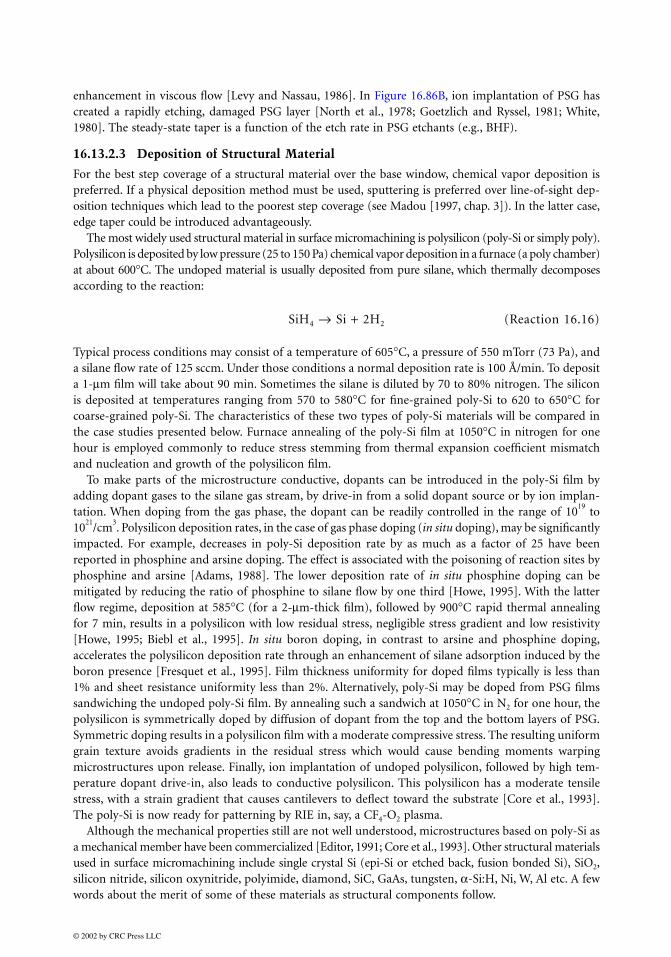
enhancement in viscous flow [Levy and Nassau, 1986]. In Figure 16.86B, ion implantation of PSG hascreated a rapidly etching, damaged PSG layer [North et al., 1978; Goetzlich and Ryssel, 1981; White,1980]. The steady-state taper is a function of the etch rate in PSG etchants (e.g., BHF).
16.13.2.3 Deposition of Structural Material
For the best step coverage of a structural material over the base window, chemical vapor deposition ispreferred. If a physical deposition method must be used, sputtering is preferred over line-of-sight dep-osition techniques which lead to the poorest step coverage (see Madou [1997, chap. 3]). In the latter case,edge taper could be introduced advantageously.
The most widely used structural material in surface micromachining is polysilicon (poly-Si or simply poly).Polysilicon is deposited by low pressure (25 to 150 Pa) chemical vapor deposition in a furnace (a poly chamber)at about 600°C. The undoped material is usually deposited from pure silane, which thermally decomposesaccording to the reaction:
SiH4 → Si + 2H2 (Reaction 16.16)
Typical process conditions may consist of a temperature of 605°C, a pressure of 550 mTorr (73 Pa), anda silane flow rate of 125 sccm. Under those conditions a normal deposition rate is 100 Å/min. To deposita 1-µm film will take about 90 min. Sometimes the silane is diluted by 70 to 80% nitrogen. The siliconis deposited at temperatures ranging from 570 to 580°C for fine-grained poly-Si to 620 to 650°C forcoarse-grained poly-Si. The characteristics of these two types of poly-Si materials will be compared inthe case studies presented below. Furnace annealing of the poly-Si film at 1050°C in nitrogen for onehour is employed commonly to reduce stress stemming from thermal expansion coefficient mismatchand nucleation and growth of the polysilicon film.
To make parts of the microstructure conductive, dopants can be introduced in the poly-Si film byadding dopant gases to the silane gas stream, by drive-in from a solid dopant source or by ion implan-tation. When doping from the gas phase, the dopant can be readily controlled in the range of 10
19 to
1021
/cm3. Polysilicon deposition rates, in the case of gas phase doping (in situ doping), may be significantly
impacted. For example, decreases in poly-Si deposition rate by as much as a factor of 25 have beenreported in phosphine and arsine doping. The effect is associated with the poisoning of reaction sites byphosphine and arsine [Adams, 1988]. The lower deposition rate of in situ phosphine doping can bemitigated by reducing the ratio of phosphine to silane flow by one third [Howe, 1995]. With the latterflow regime, deposition at 585°C (for a 2-µm-thick film), followed by 900°C rapid thermal annealingfor 7 min, results in a polysilicon with low residual stress, negligible stress gradient and low resistivity[Howe, 1995; Biebl et al., 1995]. In situ boron doping, in contrast to arsine and phosphine doping,accelerates the polysilicon deposition rate through an enhancement of silane adsorption induced by theboron presence [Fresquet et al., 1995]. Film thickness uniformity for doped films typically is less than1% and sheet resistance uniformity less than 2%. Alternatively, poly-Si may be doped from PSG filmssandwiching the undoped poly-Si film. By annealing such a sandwich at 1050°C in N2 for one hour, thepolysilicon is symmetrically doped by diffusion of dopant from the top and the bottom layers of PSG.Symmetric doping results in a polysilicon film with a moderate compressive stress. The resulting uniformgrain texture avoids gradients in the residual stress which would cause bending moments warpingmicrostructures upon release. Finally, ion implantation of undoped polysilicon, followed by high tem-perature dopant drive-in, also leads to conductive polysilicon. This polysilicon has a moderate tensilestress, with a strain gradient that causes cantilevers to deflect toward the substrate [Core et al., 1993].The poly-Si is now ready for patterning by RIE in, say, a CF4-O2 plasma.
Although the mechanical properties still are not well understood, microstructures based on poly-Si asa mechanical member have been commercialized [Editor, 1991; Core et al., 1993]. Other structural materialsused in surface micromachining include single crystal Si (epi-Si or etched back, fusion bonded Si), SiO2,silicon nitride, silicon oxynitride, polyimide, diamond, SiC, GaAs, tungsten, α-Si:H, Ni, W, Al etc. A fewwords about the merit of some of these materials as structural components follow.
© 2002 by CRC Press LLC

Silicon nitride and silicon oxide also can be deposited by CVD methods but usually exhibit too muchresidual stress which hampers their use as mechanical components. However, CVD of mixed siliconoxynitride can produce substantially stress-free components.
Amorphous Si (α-Si) can be stress annealed at temperatures as low as 400°C [Chang et al., 1991]. Thislow-temperature anneal makes the material compatible with almost any active electronic component.Unfortunately, very little is known about the mechanical properties of amorphous Si.
Hydrogenated amorphous Si (α-Si:H), with its interesting electronic properties, is even less understoodin terms of its mechanical properties. If the mechanical properties of hydrogenated amorphous Si werefound as good as those of poly-Si, the material might make a better choice than poly-Si as a MEMSmaterial given its better electronic characteristics.
Tungsten CVD deposition is IC compatible. The material has some unique mechanical properties (seeMadou [1997, chap. 8, Table 8.4]). Moreover, the material can be applied selectively. Selective CVDtungsten has the unique property that tungsten will only nucleate on silicon or metal surfaces but doesnot deposit on dielectrics such as oxides and nitrides [Chen and MacDonald, 1991].
Metals and polyimides, because they are easily deformed, usually do not qualify as mechanical membersbut have been used, for example, in plastically deformable hinges [Suzuki et al., 1994; Hoffman et al.,1995]. Aluminum constitutes the mirror material in Texas Instruments’ flexure-beam micromirror devices(FBMDs). The metal is used both for the L-shaped flexure hinges and the mirror itself [Lin, 1996].Polycrystalline diamond films, deposited by CVD, are potential high-temperature, harsh environmentMEMS candidates [Herb et al., 1990]. Problems include oxidation above 500°C for nonpassivated films,difficulty of making reliable ohmic contact to the material, and the reproducibility and surface roughnessof the films [Obermeier, 1995]. Poly-SiC films have been deposited by an APCVD process on 4-in.polysilicon-coated, silicon wafers. A surface micromachining process using the underlying polysiliconfilm as the sacrificial layer was developed. Poly-SiC is projected for use as structural material for hightemperatures and harsh environments, and to reduce friction and wear between moving components[Fleischman et al., 1996]. Surface micromachining of thin single crystalline Si layers in SOI and withpolyimides is discussed separately below.
16.13.2.4 Selective Etching of Spacer Layer
Selective EtchingTo create movable micromachines the microstructures must be freed from the spacer layers. The challengein freeing microstructures by undercutting is evident from Figure 16.87. After patterning the poly-Si by
FIGURE 16.87 Selective etching of spacer layer.
Si
Poly-Si
SiO2
n+ Si
Si3N4
Phosphosilicate glass
Rm (µm/min)
Rs (µm/min)
Ri (µm/min)
© 2002 by CRC Press LLC

RIE in, say, a SF6 plasma, it is immersed in an HF solution to remove the underlying sacrificial layer,releasing the structure from the substrate. Commonly, a layer of sacrificial phosphosilicate glass, between1 and 2000 µm long and 0.1 to 5 µm thick, is etched in concentrated, dilute or buffered HF. The spaceretch rate, Rs, should be faster than the attack on the microstructural element, Rm, and that of the insulatorlayer, Ri. For this type of complete undercutting, only wet etchants can be used. Etching narrow gapsand undercutting wide areas with BHF can take hours. To shorten the etch time, extra apertures in themicrostructures sometimes are provided for additional access to the spacer layer. The etch rate of PSG,the most common spacer material, increases monotonically with dopant concentration, and thickersacrificial layers etch faster than thinner layers [Monk et al., 1994].
The selectivity ratios for spacer layer, microstructure and buffer layer are not infinite [Lober andHowe, 1998], and in some instances even silicon substrate attack by BHF was observed under poly-silicon/spacer regions [Fan et al., 1988; Mehregany et al., 1988]. Heavily phosphorous-doped polysil-icon is especially prone to attack by BHF. Silicon nitride deposited by LPCVD etches much more slowlyin HF than oxide films, making it a more desirable isolation film. When depositing this film with asilicon-rich composition, the etch rate is even slower (15 nm/min) [Tang, 1990]. Eaton et al. (1995)compared oxide and nitride etching in a 1:1 HF:H2O and in a 1:1 HF:HCl solution and concludedthat the HCl-based etch yielded both faster oxide etch rates (617 nm/min vs. 330 nm/min) and slowernitride etch rates (2 nm/min vs. 3.6 nm/min), providing a much greater selectivity of the oxide tosilicon nitride (310 vs. 91!). The same authors also studied the optimum composition of a sacrificialoxide for the fastest possible etching in their most selective 1:1 HF:HCl etch. The faster sacrificial layeretch limited the damage to nitride structural elements. Their results are summarized in Table 16.13.A densified CVD SiO2 was used as a control, and a 5%/5% borophosphosilicate glass (BPSG) wasfound to etch the fastest.
Watanabe et al. (1995) using low pressure vapor HF, found high etch ratios of PSG and BPSG tothermal oxides of over 2000, with the BPSG etching slightly faster than the PSG. We will see further thatlow pressure vapor HF also leads to less stiction of structural elements to the substrate. In Table 16.14we present etch rate and etch ratios for Ri and Rs in BHF (7:1) for a few selected materials.
Detailed studies on the etching mechanism of oxide spacer layers were undertaken by Monk et al.(1994a; 1994b) They found that the etching reaction shifts from kinetic controlled to diffusion controlledas the etch channel becomes longer. This affects mainly large-area structures, as diffusion limitationswere observed only after approximately 200 µm of channel etching or 15 min in concentrated HF. Eatonand Smith (1996) developed a release etch model which is an extension of the work done by Monk et al.(1994a; 1994b) and Liu et al. (1993).
TABLE 16.13 Etch Rate in 1:1 HF:HCl of a Variety of Sacrificial Oxides
Thin Oxide Lateral Etch Rate (Å/min)
CVD SiO2 (densified at 1050°C for 30 min) 6170Ion-implanted and densified CVD SiO2 (P, 8 × 10
15/cm
2, 50 keV) 8330
Phosphosilicate (PSG) 11,3305%/5% borophosphosilicate (BPSG) 41,670
Source: Adapted from Eaton, W.P. and Smith, J.H., A CMOS-compatible, Surface Micro-machined Pressure Sensor for Aqueous Ultrasonic Application, presented at SPIE SmartStructure and Materials, 1995.
TABLE 16.14 Etching of Spacer Layer and Buffer Layer in BHF (7:1)
Material
Property LPCVD Si3N4 LPCVD SiO2 LPCVD 7% PSGEtch rate 7–12 Å/min (Ri) 700 Å/min (Rs) ~10,000 Å/min (Rs)Selectivity ratio 1 60–100 ~800–1200
© 2002 by CRC Press LLC

Etching is followed by rinsing and drying. Extended rinsing causes a native oxide to form on the surfaceof the polysilicon structure. Such a passivation layer often is desirable and can be formed more easily bya short dip in 30% H2O2.
Etchant-Spacer-Microstructure CombinationsA wide variety of etchant, spacer, and structural material combinations have been used; a limited listingis presented in Table 16.15. One interesting case concerns poly-Si as the sacrificial layer. This was used,for example, in the fabrication of a vibration sensor at Nissan Motor Co [Nakamura et al., 1985]. In thiscase poly-Si is etched in KOH from underneath a nitride/polysilicon/nitride sandwich cantilever. Also, asolution of HNO3 and BHF can be used to etch poly-Si, but it proves difficult to control. Using aqueoussolutions of NR4OH, where R is an alkyl group, provides a better etching solution for poly-Si, with greaterselectivity with respect to silicon dioxide and phosphosilicate glass. The relatively slow etch rate enablesbetter process control [Bassous and Liu, 1978] and the etchant does not contain alkali ions, making itmore CMOS compatible. With tetramethylammonium hydroxide (TMAH) the etch rate of CVD poly-Si,deposited at 600°C from SiH4, follows the rates of the (100) face of single crystal Si and is dopantdependent. The selectivity of Si/SiO2 and Si/PSG, at temperatures below 45°C are measured to be about1000. Hence, a layer of 500-Å PSG can be used as the etch mask for 10,000 Å of poly-Si.
16.13.2.5 Stiction
Stiction During ReleaseThe use of sacrificial layers enables the creation of very intricate movable polysilicon surface structures. Animportant limitation of such polysilicon shapes is that large-area structures tend to deflect through stressgradients or surface tension induced by trapped liquids and attach to the substrate/isolation layer duringthe final rinsing and drying step, a stiction phenomenon that may be related to hydrogen bonding or residualcontamination. Recently, great strides were made towards a better understanding and prevention of stiction.
The sacrificial layer removal with a buffered oxide etch followed by a long, thorough rinse in deionizedwater and drying under an infrared lamp typically represent the last steps in the surface micromachiningsequence. As the wafer dries, the surface tension of the rinse water pulls the delicate microstructure tothe substrate where a combination of forces, probably van der Waals forces and hydrogen bonding, keepsit firmly attached (see Figure 16.88) [Core et al., 1993]. Once the structure is attached to the substrateby stiction, the mechanical force needed to dislodge it usually is large enough to damage the microme-chanical structure [Lober and Howe, 1988; Guckel et al., 1987; Alley et al., 1988]. Basically, the samephenomena are thought to be involved in room temperature wafer bonding [Madou, 1997, chap. 8]. Wewill not further dwell upon the mechanics of the stiction process here, but the reader should refer to thetheoretical and experimental analysis of the mechanical stability and adhesion of microstructures undercapillary forces by Mastrangelo et al. (1993a; 1993b).
TABLE 16.15 Etchants-Spacer and Microstructural Layer
Etchant Buffer/Isolation Spacer Microstructure
Buffered HF (5:1, NH4F: conc. HF)a
LPCVD Si3N4/thermal SiO2 PSG Poly-SiRIE using CHF3 BHF (6:1)
bLPCVD Si3N4 LPCVD SiO2 CVD Tungsten
KOHc
LPCVD Si3N4/thermal SiO2 Poly-Si Si3N4
Ferric chlorided
Thermal SiO2 Cu PolyimideHF
eLPCVD Si3N4/thermal SiO2 PSG Polyimide
Phosphoric/acetic acid/nitric acid (PAN, or 5:8:1:1 Water:phosphoric:acetic:nitric)
fThermal SiO2 Al PECVD Si3N4 Nickel
Ammonium iodide/iodine alcoholg
Thermal SiO2 Au TiEthylene-diamine/pyrocathecol (EDP) Thermal SiO2 Poly-Si SiO2
(a) Howe and Muller (1983), Howe (1985), Guckel and Burns (1984); (b) Chen and MacDonald (1991); (c) Sugiyamaet al. (1986; 1987); (d) Kim and Allen (1991); (e) Suzuki et al. (1994); (f) Chang et al. (1991), Scheeper et al. (1991);(g) Yamada and Kuriyama (1991)
© 2002 by CRC Press LLC

Creating stand-off bumps on the underside of a poly-Si plate [Tang, 1990; Fan, 1989] or addingmeniscus-shaping microstructures to the perimeter of the microstructure are mechanical means to helpreduce sticking [Abe et al., 1995]. Fedder et al. (1992) used another mechanical approach to avoid stictionby temporarily stiffening the microstructures with polysilicon links. These very stiff structures are notaffected by liquid surface tension forces and the links are severed afterward with a high current pulseonce the potentially destructive processing is complete. Yet another mechanical approach to avoid stictioninvolves the use of sacrificial supporting polymer columns. A portion of the sacrificial layer is substitutedby polymer spacer material, spun-on after partial etch of the oxide glass. After completion of the oxideetch, the polymer spacer prevents stiction during evaporative drying. Finally, an isotropic oxygen plasmaetches the polymer to release the structure [Mastrangelo and Saloka, 1993].
Ideally, to ensure high yields, one should avoid contact between structural elements and the substrate duringprocessing. In a liquid environment, however, this may become impossible due to the large surface tensioneffects. Consequently, most solutions to the stiction problem involve reducing the surface tension of the finalrinse solution by physico-chemical means. Lober et al. (1988), for example, tried HF vapor and Guckel et al.(1989; 1990) used freeze-drying of water/methanol mixtures. Freezing and sublimating the rinse fluid in alow-pressure environment gives improved results by circumventing the liquid phase. Takeshima et al. (1991)used t-butyl alcohol freeze-drying. Since the freezing point of this alcohol lies at 25.6°C, it is possible to performfreeze-drying without special cooling equipment. More recently, attempts at supercritical drying resulted inhigh microstructure yields [Mulhern et al., 1993]. With this technique, the rinse fluid is displaced with a liquidthat can be driven into a supercritical phase under high pressure. This supercritical phase does not exhibitsurface tension. Typically, CO2 under about 75 atm is used (see also Madou [1997, chap. 1 under Cleaning]).
Kozlowski et al. (1995) substituted HF in successive exchange steps by the monomer divinylbenzeneto fabricate very thin (500 nm) micromachined polysilicon bridges and cantilevers. The monomer waspolymerized under UV light at room temperature and was removed in an oxygen plasma. Analog Devicesapplied a proprietary technique involving only standard IC process technology in the fabrication of amicro-accelerometer to eliminate yield losses due to stiction [Core et al., 1993].
Stiction After Release, i.e., In-Use StictionStiction remains a fundamental reliability issue due to contact with adjacent surfaces after release. Stictionfree passivation that can survive the packaging temperature cycle is not known at present [Howe, 1995].Attempted solutions are summarized below.
FIGURE 16.88 Stiction phenomenon in surface micromachining and the effect of surface tension on microme-chanical structures. (a) Unreleased beam. (b) Released beam before drying. (c) Released beam pulled to the substrateby capillary forces as the wafer dries [conc].
(a)
(b)
(c)
Polysilicon beamSpacer oxide
Rinse water
Substrate
Substrate
Substrate
© 2002 by CRC Press LLC

Adhesive energy may be minimized in a variety of ways, for example, by forming bumps on surfaces(see above) or roughening of opposite surface plates [Alley et al., 1993]. Also, self-assembled monolayercoatings have been shown to reduce surface adhesion and to be effective at friction reduction in bearingsat the same time [Alley et al., 1992]. Making the silicon surface very hydrophobic or coating it withdiamond-like carbon are other potential solutions for preventing postrelease stiction of polysilicon micro-structures. Man et al. (1996) eliminate post-release adhesion in microstructures by using a thin conformalfluorocarbon film. The film eliminates the adhesion of polysilicon beams up to 230 µm long even afterdirect immersion in water. The film withstands temperatures as high as 400°C and wear tests show thatthe film remains effective after 10
8 contact cycles. Along the same line, ammonium fluoride-treated Si
surfaces are thought to be superior to the HF-treated surfaces due to a more complete hydrogen termi-nation, leading to a cleaner hydrophobic surface [Houston et al., 1995]. Gogoi and Mastrangelo (1995)introduced electromagnetic pulses for postprocessing release of stuck microstructures.
16.13.3 Control of Film Stress
After reviewing typical surface micromachining process sequences we are ready to investigate some ofthe mechanical properties of the fabricated mechanical members. Consider a lateral resonator as shownin Figure 16.89A. Electrostatic force is applied by a drive comb to a suspended shuttle. Its motion isdetected capacitively by a sense comb. For many applications a tight control over the resonant frequency,f0, is required. A simple analytical approximation for f0 of this type of resonator can be deduced fromRayleigh’s method [Howe, 1987]:
(16.59)
where E represents the Young’s modulus of polysilicon; L, W and t are the length, width and thicknessof the flexures; and M stands for the mass of the suspended shuttle (of the order of 10
−9 kg, or less). For
typical values (L = 150 µm and W = t = 2 µm) and a small tensile residual stress, the resonant frequency f0
is between 10 and 100 kHz [Howe, 1995]. For typical values of L/W the stress term in Eq. (16.59)dominates the bending term. Any residual stress, σr, obviously will affect the resonant frequency. Consequently,stress and stress gradients represent critical stages for microstructural design. One of the many challengesof any surface-micromachining process is to control the intrinsic stresses in the deposited films. Severaltechniques can be used to control film stress. Some we detailed before, but we list them again forcompleteness:
• Large-grained poly-Si films, deposited around 625°C, have a columnar structure and are alwayscompressive. Compressive stress can cause buckling in constrained structures. Annealing athigh temperatures, between 900 and 1150°C, in nitrogen significantly reduces the compressivestress in as-deposited poly-Si [Guckel et al., 1985; Howe and Muller, 1983] and can eliminatestress gradients. No significant structural changes occur when annealing a columnar poly-Sifilm. The annealing process is not without danger in cases where active electronics are inte-grated on the same chip. Rapid thermal annealing might provide a solution (see IC Compat-ibility, below).
• Undoped poly-Si films are in an amorphous state when deposited at 580°C or lower. The stressand the structure of this low-temperature material depend on temperature and partial pressureof the silane. A low-temperature anneal leads to a fine-grained poly-Si with low tensile stress andvery smooth surface texture [Guckel et al., 1989]. Tensile rather than compressive films are anecessity if lateral dimensions of clamped structures are not to be restricted by compressivebuckling. Conducting regions are formed in this case by ion implantation. Fine-grained and large-grained poly-Si are compared in more detail further below.
f01
2π------ 4EtW3
ML3----------------
24σrtW5ML
-------------------+≈
© 2002 by CRC Press LLC

• Phosphorus [Murarka and Retajczyk, 1983; Orpana and Korhonen, 1991; Lin et al., 1993], boron[Orpana and Korhonen, 1991; Choi and Hearn, 1984; Ding and Ko, 1991], arsenic [Orpana andKorhonen, 1991] and carbon [Hendriks et al., 1983] doping have all been shown to affect the stateof residual stress in poly-Si films. In the case of single crystal Si, to compensate for strain inducedby dopants, one can implant with atoms with the opposite atomic radius vs. silicon. Similarapproaches would most likely be effective for poly-Si as well.
• Tang et al. (1990; 1989) developed a technique that sandwiches a poly-Si structural layer betweena top and bottom layer of PSG and lets the high temperature anneal drive in the phosphorussymmetrically, producing low stress poly-Si with a negligible stress gradient.
FIGURE 16.89 Layout of a lateral resonator with straight flexures. (A) Folded flexures (left) to release stress arecompared with straight flexures (right). (B) M is shuttle mass.
x
y Anchor
Sense comb
Sense contactpad
Flexure (length L, width W,thickness t)
Drive comb
Suspended shuttle(mass M)
Polysilicon
A
B
Drive combcontact pad
M MMM
© 2002 by CRC Press LLC

• Another stress reduction method is to vary the materials composition, something readily done inCVD processes. An example of this method is the Si enrichment of Si3N4 which reduces the tensilestress [Sekimoto et al., 1982; Guckel et al., 1986].
• During plasma-assisted film deposition processes, one can influence stress dramatically. In a physicaldeposition process such as sputtering, stress control involves varying gas pressure and substratebias. In plasma-enhanced chemical vapor deposition (PECVD) the RF power, through increasedion-bombardment, influences stress. In this way, the stress in a thin film starts out tensile, decreasesas the power increases and finally becomes compressive with further RF power increase. PECVDequipment manufacturers also are working to build stress control capabilities into new equipmentby controlling plasma frequency (see also Madou [1997, chap. 3]). In CVD, stress control involvesall types of temperature treatment programs.
• A clever mechanical design might facilitate structural stress relief [Tang et al., 1989]. By foldingthe flexures in the lateral resonator in Figure 16.89B, and by the overall structural symmetry, therelaxation of residual polysilicon stress is possible without structural distortion. By folding theflexures, the resonant frequency, f0, becomes independent of σr (see Eq. (16.59)). The springs inthe resonator structure provide freedom of travel along the direction of the comb-finger motions(x) while restraining the structure from moving sideways (y), thus preventing the comb fingersfrom shorting out the drive electrodes. In this design, the spring constant along the y directionmust be higher than along the x direction, i.e., ky kx. The suspension should allow for the reliefof the built-in stress of the polysilicon film and the axial stress induced by large vibrationalamplitudes. The folded-beam suspensions meet both criteria. They enable large deflections in thex direction (perpendicular to the length of the beams) while providing stiffness in the y direction(along the length of the beams). Furthermore, the only anchor points (see Figure 16.89B) for thewhole structure reside near the center, thus allowing the parallel beams to expand or contract inthe y direction, relieving most of the built-in and induced stress [Tang, 1990]. Tang also modeledand built spiral and serpentine springs supporting torsional resonant plates. An advantage of thetorsional resonant structures is that they are anchored only at the center, enabling radial relaxationof the built-in stress in the polysilicon film [Tang, 1990]. For some applications, the designapproach with folded flexures is an attractive way to eliminate residual stress. However, a penaltyfor using flexures is increased susceptibility to out-of-plane warpage from residual stress gradientsthrough the thickness of the polysilicon microstructure [Howe, 1995].
• Corrugated structural members, invented by Jerman for bulk micromachined sensors [Jerman,1990], also reduce stress effectively. In the case of a single crystal Si membrane, stress may bereduced by a factor of 1000 to 10,000 [Spiering et al., 1991]. One of the applications of suchcorrugated structures is the decoupling of a mechanical sensor of its encapsulation, by reducingthe influence of temperature changes and packaging stress [Spiering et al., 1991; Offereins et al.,1991]. Thermal stress alone can be reduced by a factor of 120 [Spiering et al., 1993]. Besides stressrelease, corrugated structures enable much larger deflections than do similar planar structures.This type of structural stress release was studied in some detail for single crystal Si [Zhang andWise, 1994] (see also earlier in this chapter), polyimide [van Mullem et al. 1991] and LPCVDsilicon nitride membranes [Scheeper et al., 1994]; but the quantitative influence of corrugatedpoly-Si structures still requires investigation. Figure 16.90 illustrates a fabrication sequence for apolyimide corrugated structure. The sacrificial Al in step 4 may be etched away by a mixture ofphosphoric acidic: acetic acid: nitric acid (PAN, see Table 16.15).
16.13.4 Dimensional Uncertainties
The often-expressed concerns about run-to-run variability in material properties of polysilicon or othersurface micromachined materials are somewhat misplaced, Howe points out [Howe, 1995]. He contraststhe relatively large dimensional uncertainties inherent to any lithography technique with poly-Si qualityfactors of up to 100,000 and long-term (>3 years) resonator frequency variation of less than 0.02 Hz.
© 2002 by CRC Press LLC

We follow his calculations here to prove the relative importance of the dimensional uncertainties. Theshuttle mass M of a resonator as shown in Figure 16.89 is proportional to the thickness (t) of thepolysilicon film, and neglecting the residual stress term, Eq. (16.59) reduces to:
(16.60)
In case the residual stress term dominates in Eq. (16.59), the resonant frequency is expressed as:
(16.61)
The width-to-length ratio is affected by systematic and random variations in the masking and etchingof the microstructural polysilicon. For 2-µm-thick structural polysilicon, patterned by a wafer stepperand etched with a reactive-ion etcher, a reasonable estimate for the variation in linear dimension ofetched features, ∆ is about 0.2 µm (10% relative tolerance).
From Eq. (16.60) the variation ∆ in lateral dimensions will result in an uncertainty δf0 in the lateralfrequency of:
(16.62)
for a case where the residual stress can be ignored. With a nominal flexure width of W = 2 µm, theresulting uncertainty in resonant frequency is 15%. For the stress-dominated case, Eq. (16.61) indicatesthat the uncertainty is
(16.63)
The same 2-µm-wide flexure would then lead to a 5% uncertainty in resonant frequency.
FIGURE 16.90 Schematic view of the fabrication process of a polyimide corrugated diaphragm. (From van Mullem,C.J. et al., Large Deflection Performance of Surface Micromachined Corrugated Diaphragms, presented at Transducers’91, San Francisco, CA, 1991. With permission.)
Si
Si Si
Si
A1
1 Etching Access Holes
3 Deposition Diaphragm 4 Releasing Diaphragm
2 Sacrificial layer definition
polyimide
f0WL
------
32--
∝
f0WL
------
12--
∝
δf0
f0
------ 32-- ∆
W-----
≈
δf0
f0
------ 12-- ∆
W-----
≈
© 2002 by CRC Press LLC

Interestingly, the stress-free case exhibits the most significant variation in the resonant frequency. Ineither case, resonant frequencies must be set by some postfabrication frequency trimming or otheradjustment.
In Chapter 7 of Madou (1997) we draw further attention to the increasing loss of relative manufacturingtolerance with decreasing structure size (see Figure 7.1 in Madou [1997]).
16.13.5 Sealing Processes in Surface Micromachining
Sealing cavities to hermetically enclose sensor structures is a significant attribute of surface microma-chining. Sealing cavities often embodies an integral part of the overall fabrication process and presentsa desirable chip level, batch packaging technique. The resulting surface packages (microshells) are muchsmaller than typical bulk micromachined ones (see Madou [1997, chap. 8 on Packaging]).
16.13.6 IC Compatibility
Putting detection and signal conditioning circuits right next to the sensing element enhances the per-formance of the sensing system, especially when dealing with high impedance sensors. A key benefit ofsurface micromachining, besides small device size and single-sided wafer processing, is its compatibilitywith CMOS processing. IC compatibility implies simplicity and economy of manufacturing. In theexamples at the end of this chapter we will discuss how Analog Devices used a mature 4-µm BICMOSprocess to integrate electronics with a surface micromachined accelerometer.
To develop an appreciation of integration issues involved in combining a CMOS line with surfacemicromachining, we highlight Yun’s [Yun, 1992] comparison of CMOS circuitry and surface micro-machining processes in Table 16.16A. Surface micromachining processes are similar to IC processesin several aspects. Both processes use similar materials, lithography and etching techniques. CMOSprocesses involve at least ten lithography steps where lateral small feature size plays an important role.Some processing steps, such as gate and contact patterning, are critical to the functionality andperformance of the CMOS circuits. Furthermore, each processing step is strongly correlated with othersteps. Change in any one of the processing steps will lead to modifications in a number of other stepsin the process. In contrast, surface micromachining is relatively simple. It usually consists of two tosix masks, and the feature sizes are much larger. The critical processing steps, such as structural poly-Si,
TABLE 16.16 Surface Micromachining and CMOS
A. Comparison of CMOS and Surface MicromachiningCMOS Surface Micromachining
Common features Silicon-based processes; same materials, same etching principles
Process flow Standard Application specificVertical dimension ~1 µm ~1–5 µmLateral dimension <1 µm 2–10 µmComplexity (# masks) >10 2–6
B. Critical Process Temperatures for MicrostructuresTemperature (°C) Material
LPCVD deposition 450 Low temperature oxide (LTO)/PSG
LPCVD deposition 610 Low stress poly-SiLPCVD deposition 650 Doped poly-SiLPCVD deposition 800 NitrideAnnealing 950 PSG densificationAnnealing 1050 Poly-Si stress annealing
(After Yun, W., A Surface Micromachined Accelerometer with IntegratedCMOS Detection Circuitry, Ph.D. Thesis, U.C. Berkeley, 1992.)
© 2002 by CRC Press LLC

often are self-aligned which eliminates lithographic alignment. The CMOS process is mature, quitegeneric and fine-tuned, while surface micromachining strongly depends on the application and stillneeds maturing.
Table 16.16B presents the critical temperatures associated with the LPCVD deposition of a variety offrequently used materials in surface micromachining. Polysilicon is used for structural layers and thermalSiO2, LPCVD SiO2 and PSG are used as sacrificial layers; silicon nitride is used for passivation. The highesttemperature process in Table 16.16B is 1050°C and is associated with the annealing step to release stressin the polysilicon layers. Doped polysilicon films deposited by LPCVD under conventional IC conditionsusually are in a state of compression that can cause mechanically constrained structures such as bridgesand diaphragms to buckle. The annealing step above about 1000°C promotes crystallite growth andreduces the strain. If one wants to build polysilicon microstructures after the CMOS active electronicshave been implemented (a so-called post-CMOS procedure), one has to avoid temperatures above 950°C,as junction migration will take place at those temperatures. This is especially true with devices incorpo-rating shallow junctions where migration might be a problem at temperatures as low as 800°C. Thedegradation of the aluminum metallization presents yet a bigger problem. Aluminum typically is usedas the interconnect material in the conventional CMOS process. At temperatures of 400 to 450°C, thealuminum metallization will start suffering. Anneal temperatures (densification of the PSG and stressanneal of the poly-Si) only account for some of the concerns; in general, several compatibility issuesmust be considered: (1) deposition and anneal temperatures, (2) passivation during micromachiningetching steps and (3) surface topography.
Yun (1992) compared three possible approaches to build integrated microdynamic systems: pre-, mixedand post-CMOS microstructural processes as shown in Figure 16.91. He concluded that building up themicrostructures after implementation of the active electronics offers the best results.
In a post-CMOS process, the electronic circuitry is passivated to protect it from the subsequentmicromachining processes. The standard IC processing may be performed at a regular IC foundry,while the surface micromachining occurs as an add-on in a specialized sensor fabrication facility.LPCVD silicon nitride (deposited at 800°C, see Table 16.16B) is stable in HF solutions and is thepreferred passivation layer for the IC during the long release etching step. PECVD nitride can bedeposited at around 320°C, but it displays relatively poor step coverage, while pin holes in the filmallow HF to diffuse through and react with the oxide underneath. LPCVD nitride is conformablydeposited. While it shows fewer pin holes, circuitry needs to be able to survive the 800°C depositiontemperature.
Aluminum metallization must be replaced by another interconnect scheme in order to raise thepost-CMOS temperature ceiling higher than 450°C. Tungsten, which is refractory, shows low resistivityand has a thermal expansion coefficient matching that of Si, is an obvious choice. One problem withtungsten metallization is that tungsten reacts with silicon at about 600°C to form WSi2, implying theneed for a diffusion barrier. The process sequence for the tungsten metallization developed at Berkeleyis shown in Figure 16.92. A diffusion barrier consisting of TiSi2 and TiN is used. The TiN film formsduring a 30-sec sintering step to 600°C in N2. Rapid thermal annealing with its reduced time at hightemperatures (10 sec to 2 min) and high ramp rates (~150°C/sec) allows very precise process controlas well as a dramatic reduction of thermal budgets, reducing duress for the active on-chip electronics.Titanium silicide is formed at the interface of titanium and silicon while titanium nitride formssimultaneously at the exposed surface of the titanium film. The TiSi2/TiN forms a good diffusionbarrier against the formation of WSi2 and at the same time provides an adhesion and contact layerfor the W metallization.
To avoid the junction migration in a post-CMOS process, rapid thermal annealing is used for boththe PSG densification and polysilicon stress anneal: 950°C for 30 sec for the PSG densification and1000°C for 60 sec for the stress anneal of the poly-Si. Alternatively, one could consider the use of fine-grained polysilicon which can yield a controlled tensile strain with low-temperature annealing [Guckelet al., 1988].
© 2002 by CRC Press LLC

Despite some advantages the post-CMOS process with tungsten metallization is not the preferredimplementation. Hillock formation in the W lines during annealing and high contact resistance remainproblems [Howe, 1995]. Moreover, the finely tuned CMOS fabrication sequence may also be affected bythe heavily doped structural and sacrificial layers.
The mixed CMOS/micromachining approach implements a processing sequence which puts theprocesses in a sequence to minimize performance degradation for both electronic and mechanicalcomponents. According to Yun this requires significant modifications to the CMOS fabricationsequence. Nevertheless, Analog Devices relied on such an interleaved process sequence to build thefirst commercially available integrated micro-accelerometer (see Example 1). The modificationsrequired on a standard BICMOS line were minimal: to facilitate integration of the IC and to surfacemicromachine the thickness of deposited microstructural films the line was limited to 1 to 4 µm.Relatively deep junctions permitted thermal processing for the sensor poly-Si anneal and intercon-nections to the sensor were made only via n
+ underpasses. No metallization is present in the sensor
area. This industrial solution remains truer to the traditional IC process experience than the post-CMOS procedure. Howe recently detailed another example of such a mixed process [Howe, 1995].In Howe’s scenario, the micromachining sequence is inserted after the completion of the electronic
FIGURE 16.91 Comparison of various options for process integration. (Adapted from Yun, W., A Surface Micro-machined Accelerometer with Integrated CMOS Detection Circuitry, Ph.D. thesis, University of California, Berkeley,1992. With permission.)
© 2002 by CRC Press LLC

structures, but prior to contact etching or aluminum metallization. By limiting the polysiliconannealing to 7 min at 900°C, only minor dopant redistribution is expected. Contact and metallizationlithography and etching become more complex now due to the severe topography of the poly-Simicrostructural elements.
The pre-CMOS approach is to fabricate microstructural elements before any CMOS process steps. Atfirst glance this seems like an attractive approach as no major modifications would be needed for processintegration. However, due to the vertical dimensions of microstructures, step coverage is a problem forthe interconnection between the sensor and the circuitry (the latest approach introduced by Howe facesthe same dilemma). Passivation of the microstructure during the CMOS process can also become prob-lematic. Furthermore, the fine-tuned CMOS fabrication sequence, such as gate oxidation, can be affectedby the heavily doped structural layers. Consequently, this approach is only used for some special appli-cations [Yun, 1992].
A unique pre-CMOS process was developed at Sandia National Labs [Smith et al., 1995]. In thisapproach, micromechanical devices are fabricated in a trench etched in a Si epilayer. After the mechanicalcomponents are complete, the trench is filled with oxide, planarized using chemical-mechanical polishing(CMP) (see Madou [1994, chap. 3]) and sealed with a nitride membrane. The flat wafer with theembedded micromechanical devices is then processed by means of conventional CMOS processing.Additional steps are added at the end of the CMOS process in order to expose and release the embeddedmicromechanical devices.
The SPIE “Smart Structures and Materials 1996” meeting in San Diego, CA, had two complete sessionsdedicated to the crucial issue of integrating electronics with polysilicon surface micromachining [Varadanand McWhorter, 1996].
FIGURE 16.92 Tungsten metallization process in a modified CMOS process. (Adapted from Yun, W., A SurfaceMicromachined Accelerometer with Integrated CMOS Detection Circuitry, Ph.D. thesis, University of California,Berkeley, 1992. With permission.)
Contact opening
PSG
Selective etching of Ti
TiNTiSi2
n+n+
n+
n+
Ti sputtering
W sputtering
Ti compound
Field oxide
Ti
Sintering in N2 at 600 0C(30 sec), RTA
♦Self-aligned process
♦No peeling of W up to 1050 0C
in Ar
♦Thin layer of nitride forms
during RTA in N2
© 2002 by CRC Press LLC

16.14 Poly-Si Surface Micromachining Modifications
16.14.1 Porous Poly-Si
In the first part of this chapter we discussed the transformation of single crystal Si into a porousmaterial with porosity and pore sizes determined by the current density, type and concentration ofthe dopant and the hydrofluoric acid concentration. A transition from pore formation to electropol-ishing is reached by raising the current density and/or by lowering the hydrofluoric acid concen-tration [Memming and Schwandt, 1966; Zhang et al., 1989]. Porous silicon can also be formed undersimilar conditions from LPCVD poly-Si [Anderson et al., 1994]. In this case pores roughly followthe grain boundaries of the polysilicon. Figure 16.93 illustrates the masking and process sequenceto prepare a wafer to make thin layers of porous Si between two insulating layers of low stress siliconnitride [Field, 1987]. The wafer, after the process steps outlined in Figure 16.93, is put in a Teflontest fixture, protecting the back from HF attack. An electrical contact is established on the back ofthe wafer and a potential is applied with respect to a Pt-wire counterelectrode immersed in the sameHF solution. Electrolytes consisting of 5 to 49% HF (wt) and current densities from 0.1 to 50 Acm
−2 are used. The advance of a pore-etching front, growing parallel to the wafer surface, may be
monitored using a line-width measurement tool. The highest observed rate of porous-silicon for-mation is 15 µm min
−1 (in 25%, wt HF). In the electro-polishing regime, at the highest currents,
the etch rate is diffusion limited but the reaction is controlled by surface reaction kinetics in theporous Si growth regime.
By changing the conditions from pore formation to electropolishing and back to porous Si, an enclosedchamber may be formed with porous poly-Si walls (plugs) and ‘floor and ceiling’ silicon nitride layers.Sealing of the cavities by clogging the microporous poly-Si was attempted by room temperature oxidationin air and in a H2O2 solution. Leakage through the porous plug persisted after those room temperatureoxidation treatments, but with a Ag deposition from a 400-mM AgNO3 solution and subsequent atmo-spheric tarnishing (48 h, Ag2S) the chambers appeared to be sealed, as determined from the lack of
FIGURE 16.93 Masking and process sequence preparing a wafer for laterally grown porous polysilicon. (FromField, L., Low-Stress Nitrides for Use in Electronic Devices (University of California, Berkeley, 1987), pp. 42 and 43.With permission.)
1. Deposit CVD silicon nitride on silicon wafer.
2. Pattern and plasma-etch silicon nitride.
2. Pattern and plasma-etch nitride and polysilicon.
3. Deposit CVD polysilicon.
4. Deposit CVD silicon nitride.
© 2002 by CRC Press LLC

penetration by methanol. This technology might open up possibilities for filling cavities with liquids andgases under low-temperature conditions. The chamber provided with a porous plug might also make asuitable on-chip electrochemical reference electrolyte reservoir.
Hydrofluoric acid can penetrate thin layers of poly-Si either at foreign particle inclusion sites, or atother critical film defects such as grain boundaries (see above). This way the HF can etch underlyingoxide layers, creating, for example, circular regions of free-standing poly-Si, so-called ‘blisters.’ The poly-Sipermeability associated with blistering of poly-Si films has been applied successfully by Judy and Howe(1993a; 1993b) to produce thin-shelled hollow beam electrostatic resonators from thin poly-Si filmsdeposited onto PSG. The possible advantage of using these hollowed structures is to obtain a yet higherresonator quality factor Q. The devices were made in such a way that the 0.3-µm-thick undoped poly-Si completely encased a PSG core. After annealing, the structures were placed in HF which penetratedthe poly-Si shell and dissolved away the PSG, eliminating the need for etch windows. It was not possibleto discern the actual pathways through the poly-Si using TEM.
Lebouitz et al. (1995) apply permeable polysilicon etch-access windows to increase the speed of creatingmicroshells for packaging surface micromachined components. After etching the PSG through the manypermeable Si windows, the shell is sealed with 0.8 µm of low stress LPCVD nitride.
16.14.2 Hinged Polysilicon
One way to achieve high vertical structures with surface micromachining is building large flat structureshorizontally and then rotating them on a hinge to an upright position. Pister et al. [Burgett et al., 1992;Ross and Pister, 1994; Lin et al., 1995; Yeh et al., 1994; Lin et al., 1996] developed the poly-Si hinges shown inFigure 16.94A; on these hinges, long structural poly-Si features (1 mm and beyond) can be rotated out ofthe plane of a substrate. To make the hinged structures, a 2-µm-thick PSG layer (PSG-1) is deposited on theSi substrate as the sacrificial material, followed by the deposition of the first polysilicon layer (2-µm-thickpoly-1). This structural layer of polysilicon is patterned by photolithography and dry etching to formthe desired structural elements, including hinge pins to rotate them. Following the deposition andpatterning of poly-1, another layer of sacrificial material (PSG-2) of 0.5-µm thickness is deposited.Contacts are made through both PSG layers to the Si substrate, and a second layer of polysilicon isdeposited and patterned (poly-2), forming a staple to hold the first polysilicon layer hinge to the surface.The first and second layers of poly are separated everywhere by PSG-2 in order for the first polysiliconlayer to freely rotate off the wafer surface when the PSG is removed in a sacrificial etch. After the sacrificialetch, the structures are rotated in their respective positions. This is accomplished in an electrical probestation by skillfully manipulating the movable parts with the probe needles. Once the components are inposition, high friction in the hinges tends to keep them in the same position. To obtain more preciseand stable control of position, additional hinges and supports are incorporated. To provide electricalcontact to the vertical poly-Si structures one can rely on the mechanical contact in the hinges, or poly-Sibeams (cables) can be attached from the vertical structure to the substrate.
Pister’s research team made a wide variety of hinged microstructures, including hot wire anemometers,a box dynamometer to measure forces exerted by embryonic tissue, a parallel plate gripper [Burgett et al.,1992], a micro-windmill [Ross and Pister, 1994], a micro-optical bench for free-space integrated optics[Lin et al., 1995] and a standard CMOS single piezoresistive sensor to quantify rat single heart cellcontractile forces [Lin et al., 1996]. One example from this group’s efforts is illustrated in Figure 16.94B,showing an SEM photograph of an edge-emitting laser diode shining light onto a collimating micro-Fresnel lens [Lin et al., 1995]. The micro-Fresnel lens in the SEM photo is surface micromachined in theplane and erected on a polysilicon hinge. The lens has a diameter of 280 µm. Alignment plates at the frontand the back sides of the laser are used for height adjustment of the laser spot so that the emitting spotfalls exactly onto the optical axis of the micro-Fresnel lens. After assembly, the laser is electrically contactedby silver epoxy. Although this hardly outlines standard IC manufacturing practices, excellent collimatingability for the Fresnel lenses has been achieved. The eventual goal of this work is a micro-optical bench(MOB) in which microlenses, mirrors, gratings and other optical components are pre-aligned in the mask
© 2002 by CRC Press LLC

layout stage using computer-aided design. Additional fine adjustment would be achieved by on-chipmicro-actuators and micropositioners such as rotational and translational stages.
Today, erecting these poly-Si structures with the probes of an electrical probe station or, occasionally,assembly by chance in the HF etch or deionized water rinse represent too complicated or too unreliablepostrelease assembly methods for commercial acceptance.
Friction in poly-Si joints, as made by Pister, is high because friction is proportional to the surface area(s
2) and becomes dominant over inertial forces (s
3) in the microdomain (see Madou [1997, chap. 9]).
Such joints are not suitable for microrobotic applications. Although attempts have been made to incor-porate poly-Si hinges in such applications [Yeh et al., 1994], plastically deformable hinges make moresense for microrobot machinery involving rotation of rigid components. Noting that the external skeletonof insects incorporates hard cuticles connected by elastic hinges, Suzuki et al. (1994) fabricated rigid
FIGURE 16.94 Microfabricated hinges. (A) Cross-section, side view and top view of a single-hinged plate beforeand after the sacrificial etch. (B) Schematic (top) and SEM micrograph of the self-aligned hybrid integration of anedge-emitting laser with a micro-Frensnel lens. (From Lin, L.Y. et al., Micromachined Integrated Optics for Free-Space Interconnections, presented at MEMS ’96, Amsterdam, 1995. With permission.)
Poly 2 staple holdingpoly 1 plate
Poly 2
Poly 2
Poly 1
Poly 1
Oxide
A
© 2002 by CRC Press LLC

poly-Si plates (E = 140 GPa) connected by elastic polyimide hinges (E = 3 GPa) as shown in Figure 16.95(see also section below on Polimide Surface Structures). Holes in the poly-Si plates shorten the PSG etchtime compared to plates without holes. The plates without holes remain attached to the substrate whilethe ones with holes are completely freed. Using electrostatic actuators, a structure as shown in Figure16.95 can be made to flap like the wing of a butterfly. By applying an AC voltage of 10 kHz, resonantvibration of such a flapping wing was observed [Suzuki et al., 1994].
FIGURE 16.94 (Continued).
FIGURE 16.95 Flexible polyimide hinge and poly-Si plate (butterfly wing). (From Suzuki, K. et al., J. Microelec-tromech. Syst., 3, 4–9, 1994. With permission.)
Edge-EmittingLaser
Contact Pad
Si Substrate
Self-AlignmentStructure
CollimatedBeam
Emitting spot near front surface
Fresnel Lens
Si wafer
PSG
poly Si Polyimide
© 2002 by CRC Press LLC

More recently, Hoffman et al. (1995) demonstrated aluminum plastically deformable hinges on oxidemovable thin plates. Oxide plates and Al hinges were etched free from a Si substrate by using XeF2, a vaporphase etchant exhibiting excellent selectivity of Si over Al and oxide. According to the authors, this process,due to its excellent CMOS compatibility, might open the way to designing and fabricating sophisticatedintegrated CMOS-based sensors with rapid turnaround time (see also Madou [1997, chap. 2]).
16.14.3 Thick Polysilicon
Applying classical LPCVD to obtain poly-Si deposition is a slow process. For example, a layer of 10µm typically requires a deposition time of 10 hr. Consequently, most micromachined structures arebased on layer thicknesses in the 2- to 5-µm range. Basing their process on dichlorosilane (SiH2Cl2)chemistry, Lange et al. (1995) developed a CVD process in a vertical epitaxy batch reactor withdeposition rates as high as 0.55 µm/min at 1000°C. The process yields acceptable deposition timesfor thicknesses in the 10-µm range (20 min). The highly columnar poly-Si films are deposited onsacrificial SiO2 layers and exhibit low internal tensile stress making them suitable for surface micro-machining. The surface roughness comprises about 3% of the thickness, which might preclude someapplications.
Kahn et al. (1996) made mechanical property test structures from thick undoped and in situ B-dopedpolysilicon films. The elastic modulus of the B-doped polysilicon films was determined as 150 ± 30 GPa.The residual stress of as-deposited undoped thick polysilicon was determined as 200 ± 10 MPa.
16.14.4 Milli-Scale Molded Polysilicon Structures
The assembly of tall three-dimensional features in the described hinged polysilicon approach iscomplicated by the manual assembly of the fabricated microparts resembling building a miniatureboat in a bottle. Keller at University of California, Berkeley, came up with an elegant alternative forbuilding tall, high-aspect-ratio microstructures in a process that does not require postrelease assemblysteps [Keller and Ferrari, 1994]. The technique involves deep dry etching of trenches in a Si substrate,deposition of sacrificial and structural materials in those trenches, and demolding of the depositedstructural materials by etching away the sacrificial materials. CVD processes can typically only depositthin films (~1 to 2 µm) on flat surfaces. If, however, these surfaces are the opposing faces of deepnarrow trenches, the growing films will merge to form solid beams. In this fashion, high-aspect-ratiostructures that would normally be associated with LIGA now also can be made of CVD polysilicon.The procedure is illustrated in Figure 16.96 [Keller and Ferrari, 1994; Keller and Howe, 1995]. Thefirst step is to etch deep trenches into a silicon wafer. The depth of the trenches equals the height ofthe desired beams and is limited to about 100 µm with aspect ratios of about 10 (say, a 10-µm-diameter hole with a depth of 100 µm). For trench etching, Keller uses a Cl2 plasma etch with thefollowing approximate etching conditions: flow rates of 200 sccm for He and 180 sccm for Cl2, aworking pressure of 425 mTorr, a power setting of 400 W and an electrode gap of 0.8 cm. The etchrate for Si in this mode equals 1 µm/min. Thermal oxide and CVD oxide act as masks with 1 µm ofoxide needed for each 20 µm of etch depth. Before the Cl2 etch a short 7-sec SF6 pre-etch removesany remaining native oxide in the mask openings. During the chlorine etch a white sidewall passivatinglayer must be controlled to maintain perfect vertical sidewalls. After every 30 min of plasma etching,the wafers are submerged in a silicon isotropic etch long enough to remove the residue [Keller andHowe, 1995]. Beyond 100 µm, severe undercutting occurs and the trench cross section becomessufficiently ellipsoidal to prevent molded parts from being pulled out. Advances in dry cryogenicetching are continually improving attainable etch depths, trench profiles and minimum trench diam-eter. We can expect continuous improvements in the tolerances of this novel technique. After plasmaetching, an additional 1 µm of silicon is removed by an isotropic wet etch to obtain a smoother trenchwall surface. Alternatively, to smooth sidewalls and bottom of the trenches a thermal wet oxide isgrown and etched away. The sacrificial oxide in step 2 is made by CVD phosphosilicate glass (PSG
© 2002 by CRC Press LLC

at 450°C, 140 Å/min), CVD low-temperature oxide (LTO at 450°C) or CVD polysilicon (580°C, 65Å/min). The latter is completely converted to SiO2 by wet thermal oxidation at 1100°C. The PSGneeds an additional reflowing and densifying anneal at 1000°C in nitrogen for 1 hr. This results inan etching rate of the sacrificial layer of ~20 µm/min in 49% HF. The mold shown in Figure 16.96displays three different trench widths and can be used to build integrated micromachines incorpo-rating doped and undoped poly-Si parts as well as metal parts. The remaining volume of the narrowesttrench after oxide deposition is filled completely with the first deposition of undoped polysilicon(poly 1) in step 3. The undoped poly will constitute the insulating regions in the micromachine.Undoped CVD polysilicon was formed in this case at 580°C, with a 100 SCCM silane flow rate, and
.
FIGURE 16.96 Schematic illustration of HEXSIL process. The mold wafer may be part of an infinite loop. (FromKeller and Ferrari [1994]. Courtesy of Mr. C. Keller.)
1. ETCH DEEP TRENCHES IN SILICON WAFER
2. DEPOSIT SACRIFICIAL OXIDE
3. DEPOSIT UNDOPED POLY
4. DEPOSIT IN-SITU DOPED POLY
5. BLANKET ETCH PLANAR SURFACE LAYER TO OXIDE
6. DEPOSIT ELECTROLESS NICKEL
7. LAP AND POLISH TO OXIDE LAYER
8. HF ETCH RELEASE AND MOLD EJECTION
9. GO TO STEP 2: REPEAT MOLD CYCLE
doped poly
undoped poly
electroless nickel
wafer
sacrificial oxide
© 2002 by CRC Press LLC

a 300-mTorr reactor pressure, resulting in a deposition rate of 0.39 µm/hr. The deposited film underthese conditions is amorphous or very fine-grained. Since the narrowest trenches are completely filledin by the first deposition, they cannot accept material from later depositions. The trenches ofintermediate width are lined with the first material and then completely filled in by the seconddeposition. In the case illustrated the second deposition (step 4) consists of in situ doped poly-Si andforms the resistive region in the micromachine under construction. To prevent diffusion of P fromthe doped poly deposited on top of the narrow undoped beams, a blanket etch in step 5 is used toremove the doped surface layer prior to the anneal of the doped poly. The third deposition, in step6 of the example case, consists of electroless nickel plating on poly-Si surfaces but not on oxidessurfaces and results in the conducting parts of the micromachine. By depositing structural layers inorder of increasing conductivity, as done here, regions of different conductivity can be separated byregions of narrow trenches containing only nonconducting material. Lapping and polishing in step7 with a 1-µm diamond abrasive in oil planarizes the top surface, readying it for HF etch release andmold ejection in step 8. Annealing of the polysilicon is required to relieve the stress before removingthe parts from the wafer so they remain straight and flat. In step 8 the sacrificial oxide is dissolvedin 49% HF. A surfactant such as Triton X100 is added to the etch solution to facilitate part ejectionby reducing surface adhesion between the part and the mold. The parts are removed from the wafer,and the wafer may be returned to step 2 for another mold cycle. An example micromachine, resultingfrom the described process, is the thermally actuated tweezers shown in Figure 16.97. These HEXSILtweezers measure 4 mm long, 2 mm wide and 80 µm tall. The thermal expansion beam to actuatethe tweezers consists of the in situ doped poly-Si; the insulating parts are made from the undopedpoly-Si material. Ni-filled poly-Si beams are used for the current supply leads. It is possible to combinethe HEXSIL process with classical poly-Si micromachining, as illustrated in Figure 16.98, whereHEXSIL forms a stiffening rib for a membrane filter fashioned by surface micromachining of a surfacepoly-Si layer. The surface poly-Si is deposited after HEXSIL. A critical need in HEXSIL technologyis controlled mold ejection. Keller and Howe (1995) have experimented with HEXSIL-producedbimorphs, making the structure spring up after release.
FIGURE 16.97 SEM micrograph of HEXSIL tweezers: 4 mm long, 2 mm wide and 80 µm tall. Lead wires forcurrent supply are made from Ni-filled poly-Si beams; in situ phosphorus-doped polysilicon provides the resistorpart for actuation. The width of the beam is 8 µm: 2 µm poly-Si, 4 µm Ni, and 2 µm poly-Si. (Courtesy of Mr. C. Keller.)
© 2002 by CRC Press LLC

16.15 Non-Poly-Si Surface Micromachining Modifications
16.15.1 Silicon on Insulator Surface Micromachining
16.15.1.1 Introduction
A major sensor use of silicon on insulator wafers is established in the production of high-temperature sensors.Compared to p-n junction isolation, which is limited to about 125°C, much higher temperature devicesare possible based on the dielectric insulation of SOI. Recently, a wide variety of SOI surface microma-chined structures have been explored, including pressure sensors, accelerometers, torsional micromirrors,light sources, optical choppers etc. [Diem et al., 1993; Noworolski et al., 1995]
Three major techniques currently are applied to produce SOI wafers (see also under Epitary in Madou[1997, chap. 3]): SIMOX (Separated by IMplanted OXygen), the Si fusion bonded (SFB) wafer techniqueand zone-melt recrystallized (ZMR) polysilicon. With SIMOX, standard Si wafers are implanted withoxygen ions and then annealed at high temperatures (1300°C). The oxygen and silicon combine to forma silicon oxide layer beneath the silicon surface. The oxide layer’s thickness and depth are controlled byvarying the energy and dose of the implant and the anneal temperature. In some cases, a CVD processdeposits additional epitaxial silicon on the top silicon layer. Attempts have also been made to implantnitrogen in Si to create abrupt etch stops. At high enough energies the implanted nitrogen is buried 1/2to 1 µm deep. At a high enough dose, the etching in that region stops. It is not necessary to implant thestoichiometric amount of nitrogen concentration; a dose lower by a factor of 2 to 3 suffices. Afterimplantation, it is necessary to anneal the wafer because the implantation destroys the crystal structureat the surface of the wafer.
The bonded wafer process starts with an oxide layer grown (typically about 1 µm) on a standard Si wafer.That wafer is then bonded to another wafer, with the oxide sandwiched between. For the bonding nomechanical pressure or other forces are applied. The sandwich is annealed at 1100°C for 2 hr in a nitrogenambient leading to a strong binding between the two wafers. One of the wafers is then ground to athickness of a few microns using mechanical and CMP.
A third process for making SOI structures is to recrystallize polysilicon (e.g., with a laser, an electron-beam or a narrow strip heater) deposited on an oxidized silicon wafer. This process is called zone meltingrecrystallization (ZMR). This technique is used primarily for local recrystallization and has not yet beenexplored much in micromachining applications.
FIGURE 16.98 SEM micrograph of surface micromachined membrane filter with a stiffening rib (50 µm high).Original magnification 1000×. (Courtesy of Mr. C. Keller.)
© 2002 by CRC Press LLC

The crystalline perfection of conventional silicon wafers in SFB and ZMR is completely maintainedin the SOI layer as the wafers do not suffer from implant-induced defects. By using plasma etching,wafers with a top Si layer thickness of as little as 1000 to 3000 Å with total thickness variations of lessthan 200 Å can be made [Dunn, 1993]. SOI layers of 2 µm thick are more standard [Abe and Matlock,1990].
Kanda (1991) reviews different types of SOI wafers in terms of their micromachining and IC applica-tions. Working with SOI wafers offers several advantages over bulk Si wafers: fewer process steps are neededfor feature isolation, parasitic capacitance is reduced, and power consumption is lowered. In the IC industrythese wafers are used for high-speed CMOS ICs, smart power ICs, three-dimensional ICs, and radiation-hardened devices [Kuhn and Rhee, 1973]. In micromachining, SOI wafers are employed to produce anetch stop in such mechanical devices as pressure and acceleration sensors and in high-temperature sensors,and ISFETs. Etched-back fusion-bonded Si wafers and SIMOX are already employed extensively to buildmicromachines. The two types of SOI wafers are commercially available. A tremendous amount of effortis spent in the IC industry on controlling the SOI thin Si layer thickness which will benefit any narrowtolerance micromachine. The silicon fusion bonded (SFB) method offers the more versatile MEMSapproach due to the associated potential for thicker single crystal layers and the option of incorporatingburied cavities, facilitating micromachine packaging. Sensors manufactured by means of SFB now arecommercially available [Pourahmadi et al., 1992]. The SIMOX approach is less labor intensive and holdsbetter membrane thickness control. An important expansion of the SOI technique is selective epitaxy. Thelatter enables a wide range of new mechanical structures (see Madou [1997, chap. 3]) and enables noveletch-stop methods [Gennissen et al., 1995], as well as electrical and/or thermal separation and independent
From Dunn, P.N., Solid State Technol., October, 32–35 (1993). With permission.
© 2002 by CRC Press LLC

optimization of active sensor and readout electronics [Bartek et al., 1995]. In all cases SOI machininginvolves dry anisotropic etching to etch a pattern into the Si layer on top of the insulator. These structuresthen become free by etching the sacrificial buried SiO2 insulator layer, which displays a thickness with veryhigh reproducibility (400 ± 5 nm) and uniformity (<±5 nm), especially in the case of SIMOX. Etched freecantilevers and membranes consist of single crystalline silicon with thicknesses ranging from microns andsubmicrons (SIMOX) up to hundreds of microns (SFB). Below we review three implementations of SOItechniques that may be crucial for future MEMS development.
16.15.1.2 Silicon Fusion Bonded Micromachining
Silicon fusion bonding enables the formation of thick single crystal layers with cavities built in. An exampleis shown in Figure 16.99 [Noworolski et al., 1995]. The device pictured involves two 4-in. <100> wafers:a handle wafer and a wafer used for the SOI surface. The p-type (3 to 7 Ωcm) handle wafer is thermallyoxidized at 1100°C to obtain a 1-µm-thick oxide. Thermal oxidation enables thicker oxides than the onesformed in SIMOX by ion implantation and avoids the potential implantation damage in the workingmaterial. To make a buried cavity, the oxide is patterned and etched. To produce yet deeper cavities, theSi handle wafer may be etched as well (as in Figure 16.99). In the case shown, the top wafer consists ofthe same p-type substrate material as the handle wafer with a 2- to 30-µm-thick n-type epitaxial layer.The epitaxial layer determines the thickness of the final mechanical material. The epitaxial layer is fusionbonded to the cavity side of the handle wafer (2 hr at 1100°C). The top wafer is then partially thinnedby grinding and polishing (Figure 16.99A). An insulator is deposited and patterned on the back side ofthe handle wafer to etch access holes to the insulator. After the insulator at the bottom of the etch hole isremoved by a buffered oxide etch (BOE), aluminum is sputtered and sintered to make contact to the n-typeepilayer for the electrochemical etch back of the remaining p-type material (Figure 16.99B). The finalsingle crystal silicon thickness is uniform to within ±0.05 µm (std. dev.) and does not require a costly,high accuracy polish step.
Draper Laboratory is using SOI processes in the development of inertial sensors, gyros and acceler-ometers as an alternative to their current devices fabricated by the dissolved wafer process (see Example 1,Section 16.9). The main advantage is that the former consists of an all Si process rather than a Si/Pyrexsandwich [Greiff, 1995].
FIGURE 16.99 (A) A wafer sandwich after grind-and-polish step. (B) A wafer after electrochemical etch-back inKOH, buried oxide removal and aluminum deposition. (From Noworolski, J.M. et al., Fabrication of SOI Waferswith Buried Cavities Using Silicon Fusion Bending and Electrochemical Etchback, presented at Transducers ’95,Stockholm, Sweden, 1995. With permission.)
Epitaxial layer
Oxide
A
BAluminum
© 2002 by CRC Press LLC

16.15.1.3 SIMOX Surface Micromachining
Both capacitive and piezoresistive pressure sensors were microfabricated from SIMOX wafers [Diem et al.,1993]. Figure 16.100 illustrates the process sequence by Diem et al. (1993) for fabricating an absolutecapacitive pressure sensor. The 0.2-µm silicon surface layer of the SIMOX wafer is thickened with dopedepi-Si to 4 µm. An access hole is RIE etched in the Si layer, and vacuum cavity and electrode gap areobtained by etching the SiO2 buried layer. Since the buried thick oxide layer exhibits a very high repro-ducibility and homogeneity over the whole wafer (0.4 µm ± 5 nm), the resulting vacuum cavity andelectrode gap after etching also are very well controlled. The small gap results in relatively high capacitancevalues between the free membrane and bulk substrate (20 pf/mm
2). Diaphragm diameter, controlled by
the SiO2 etching is up to several hundreds micrometers (±2 µm). The etching hole is hermetically sealedunder vacuum by plasma CVD deposition of nonstressed dielectric layer plugs.
With the above scheme Diem et al. realized an absolute pressure sensor with a size of less than 1.5 mm2.
The temperature dependence of a capacitive sensor is mainly due to the temperature coefficient of theoffset capacitance. Therefore, a temperature compensation is needed for high accuracy sensors. A drasticreduction of the temperature dependence is obtained by a differential measurement, especially if thereference capacitor resembles the sensing capacitor. A reference capacitor was designed with the mem-
o
FIGURE 16.100 Process sequence of a SIMOX absolute capacitive pressure sensor by Diem et al. (From Diem, B. et al.,SOI (SIMOX) as a Substrate for Surface Micromachining of Single Crystalline Silicon Sensors and Actuators, presentedat Seventh Int. Conf. on Solid-State Sensors and Actuators, Yokohama, Japan, 1993. With permission.)
SIMOX substrate
Dry etch access hole
Sacrificial layer etching
Thicken up epi Si to4 µm
Metallization and diaphragm definition
P P
Hermetic sealing of etching hole by plasma CVD ofnon-stressed dielectric plug
Si-substrate
0.2 µm epi-Si
0.4 µm buried oxide
© 2002 by CRC Press LLC

brane blocked by several plugs for pressure insensitivity. The localization and the number of plugs weremodeled by finite element analysis (FEA) (ANSYS software was used) to get a deformation lower than 1%of the active sensor’s deformation. Even without temperature calibration the high output of the differentialsignal resulted in an overall output error better than ±2% over the whole temperature range (−40°C to+125°C) compared to 10% for nondifferential measurements. The temperature coefficient of the sensi-tivity is about 100 ppm/°C which agrees with the theoretical variation of the Young modulus of silicon.A piezoresistive sensor could be achieved by implanted strain gauges in the membrane. Although SIMOXwafers are more expensive than regular wafers, they come with several process steps embedded and theymake packaging easier.
16.15.1.4 Selective Epitaxy Surface Micromachining
In the discussion on epitaxy in Madou (1997, chap. 3) we drew attention to the potential of selectiveepitaxy for creating novel microstructures. The example in Figure 3.21 in Madou illustrates the selectivedeposition of epi-Si on a Si substrate through a SiO2 window. The same figure also demonstrates thesimultaneous deposition of poly-Si on SiO2 and crystalline epi-Si on Si, creating the basis for a structurefeaturing an epi-Si anchor with poly-Si side arms.
Neudeck et al. (1990) and Schubert and Neudeck (1990) at Purdue and Gennissen et al. (1995) and Barteket al. (1995) at Twente proved that selective epitaxy can also be applied for automatic etch stop on buriedoxide islands. Figure 16.101 demonstrates how epitaxial lateral overgrowth (ELO) can bury oxide islands.After removal of the native oxides from the seed windows, epi is grown for 20 min at 950°C and at 60 torrusing a Si2H2Cl2-HCl-H2 gas system. The epi growth front moves parallel to the wafer surface while growingin the lateral direction, leaving a smooth planar surface. During epi growth the HCl prevents poly nucleationon the nonsilicon areas. The epi quality is strongly dependent on the orientation of the seed holes in theoxide. Seed holes oriented in the <100> direction lead to the best epi material and surface quality. Selectiveepi’s other big problem for fabrication remains sidewall defects [Bashir et al.]. The buried oxide islands stopthe KOH etch of the substrate, enabling formation of beams and membranes as shown in Figure 16.101B.This technique might form the basis of many high performance microstructures. The Purdue and Twentegroups also work on confined selective epitaxial growth (CSEG), a process pioneered by Schubert andNeudeck (1990). In this process a micromachined cavity is formed above a silicon substrate with a seedcontact window to the silicon substrate and access windows for epi-Si (Figure 16.101C) [Bartek et al., 1995].Low-stress, silicon-rich nitride layers act as structural layers to confine epitaxial growth; PSG is used assacrificial material. This confined selective epitaxial growth technique allows electrical and/or thermal isola-tion separation, as well as independent optimization of active sensor and readout electronic areas.
16.15.1.5 SOI vs. Poly-Si Surface Micromachining
The power of poly-Si surface micromachining mainly lays in its CMOS compatibility. When depositedon an insulator, both poly-Si and single crystal layers enable higher operating temperatures (>200°C)than bulk micromachined sensors featuring p-n junction isolation only (130°C max) [Luder, 1986]. Anadditional benefit for SOI-based micromachining is IC compatibility combined with single crystal Siperformance excellence. The maximum gauge factor (see Eq. (16.28)) of a poly-Si piezoresistor is about30, roughly 15 times larger than that of a metal strain gauge but only one third of that of an indiffusedresistor in single crystal Si [Obermeier and Kopystynski, 1992]. Higher piezoresistivity and fracture stresswould seem to favor SOI for sensor manufacture. But there is an important counter argument: thepiezoresistivity and fracture stress in poly-Si are isotropic, a major design simplification. Moreover, bylaser recrystallization the gauge factor of poly-Si might increase to above 50 [Voronin et al., 1992], andby appropriate boron doping the temperature coefficient of resistance (TCR) can actually reach 0 vs. aTCR of, say, 1.7 × 10
−3K
−1 for single crystal p-type Si. Neither technical nor cost issues will be the deciding
factor in determining which technology will become dominant in the next few years. Micromachiningis very much a hostage to trends in the IC industry: promising technologies such as GaAs and micro-machining do not necessarily take off in no small part because of the invested capital in some limitedsets of standard silicon technologies. On this basis SOI surface micromachining is the favored candidate:
© 2002 by CRC Press LLC
SOI extends silicon’s technological relevance and experiences increasing investment from the IC industry,benefiting SOI micromachining [Kanda, 1991].
Based on the above we believe that SOI micromachining not only introduces an improved method ofmaking many simple micromachines, but it also will probably become the favored approach of the ICindustry. A summary of SOI advantages is listed below:
• IC industry use in all types of applications such as MOS, bipolar digital, bipolar linear, powerdevices, BICMOS, CCDs, heterojunction bipolar [Burggraaf, 1991] etc.
• Batch packaging through embedded cavities
• CMOS compatibility
• Substrate industrially available at lower and lower cost (about $200 today)
• Excellent mechanical properties of the single crystalline surface layer
FIGURE 16.101 Micromachining with epi-Si. (A) Lateral overgrowth process of epi-Si (ELO, epitaxial lateral over-growth) out of <100>-oriented holes in an oxide mask. (B) KOH etch stop on buried oxide islands or front sidenitride. (C) Principle of confined selective epitaxial growth. (From papers presented at Transducers ’95, Stockholm,Sweden, 1995. With permission. )
access window
CSEG Si
Nitride ELO Oxide Substrate
membrane beam hole
A
B
C
PSG
nitride
silicon
substrate
substrate
substrate
seed window
Substrate
epitaxial lateral overgrowth oxide islands
© 2002 by CRC Press LLC

• Freedom of shapes in the x-y dimensions and continually improving dry etching techniques,resulting in larger aspect ratios and higher features
• Freedom of choice of a very well-controlled range of thicknesses of epi surface layers
• SiO2 buried layer as sacrificial and insulating layer and excellent etch stop
• Dramatic reduction of process steps as the SOI wafer comes with several ‘embedded’ process steps
• High temperature operation
16.16 Resists as Structural Elements and Molds in Surface Micromachining
16.16.1 Introduction
Polyimide and deep UV photoresists were covered already in Madou (1997, chap. 1 on lithography). Wenow reiterate some of the material covered there in the context of surface micromachining. Novel deepUV photoresists enable the molding of a wide variety of high aspect ratio microstructures in a widevariety of moldable materials or they are used directly as structural elements. LIGA (covered in Chapter17), employing X-rays to pattern resists, is really just an extension of the same principles.
16.16.2 Polyimide Surface Structures
Polyimide surface structures, due to their transparency to exposing UV light, can be made very high andexhibit LIGA-like high aspect ratios. By using multiple coats of spun-on polyimide, thick suspendedplates are possible. Moreover, composite polyimide plates can be made, depositing and patterning a metalfilm between polyimide coats. Polyimide surface microstructures are typically released from the substrateby selectively etching an aluminum sacrificial layer (see Figure 16.90), although Cu and PSG (e.g., in thebutterfly wing in Figure 16.95) have been used as well (see Table 16.15).
An early result in this field was obtained at SRI International, where polyimide pillars (spacers) about100 µm in height were used to separate a Si wafer, equipped with a field emitter array, from a displayglass plate in a flat panel display [Bordie et al., 1990]. The flat panel display and an SEM picture of thepillars are shown in Figure 16.102. The Probimide 348 FC formulation of Ciba-Geigy was used. Thisviscous precursor formulation (48% by weight of a polyamic ester, a surfactant for wetting and asensitizer) with a 3500-cs viscosity was applied to the Si substrate and formed into a film of a 125-µmthickness by spinning. A 30- to 40-min prebake at about 100°C removed the organic solvents from theprecursor. The mask with the pillar pattern was then aligned to the wafer coated with the precursor andsubjected to about 20 min of UV radiation. After driving off moisture by another baking operation thecoating, still warm, was spray developed (QZ 3301 from Ciba-Geigy), revealing the desired spacer matrix.By baking the polyimide at 100°C in a high vacuum (10
−9 Torr) the pillars shrunk to about 100 µm,
while the polyimide became more dense and exhibited greater structural integrity.More recently Frazier and Allen (1993) obtained a height-to-width aspect ratio of about 7 with
polyimide structures. Ultraviolet was used to produce structures with heights in the range of 30 to 50 µm.At greater heights, the verticality of the sidewalls was relatively poor. Spun-on thickness in excess of 60 µmin a single coat was obtained for both Ciba-Geigy and Du Pont commercial UV-exposable, negative-tonepolyimides. Using a G-line mask aligner, an exposure energy of 350 mJ/cm
2 was sufficient to develop
a pattern with the Ciba-Geigy QZ 3301 developer. Allen and his team combined polyimide insert moldswith electrodeposition to make a wide variety of metal structures [Ahn et al., 1993]. This polyimideapplication will be contrasted with LIGA in Chapter 17.
© 2002 by CRC Press LLC

16.16.3 UV Depth Lithography
Besides polyimides, research on novolak-type resists also is leading to higher three-dimensional features.Lochel et al. (1994; 1996a; 1996b) use novolak, positive tone resists of high viscosity (e.g., AZ 4000 series,Hoechst). They deposit in a multiple-coating process layers up to 200 µm thick in a specially designedspin coater incorporating a co-rotating cover. The subsequent UV lithography yields patterns with aspectratios up to 10, steep edges (more than 88°) and a minimum feature size down to 3 µm. By combining this
FIGURE 16.102 Polyimide structural elements. (A) Micromachined flat panel display. Number 39 represents oneof the spacer pillars in the matrix of polyimide pillars (100 µm high). The spacer array separates the emitter platefrom the front display plate. (B) SEM of the spacer matrix. (Courtesy of Dr. I. Brodie.) The height of the pillars issimilar to what can be accomplished with LIGA. Since only a simple UV exposure was used, this polyimide is referredto as poor man’s LIGA process, or pseudo-LIGA. (From Brodie, I. et al., U.S. Patent 4,923,421, 1990.)
© 2002 by CRC Press LLC

resist technology with sacrificial layers and electroplating, a wide variety of three-dimensional micro-structures resulted.
Along the same line, researchers at IBM have started experimenting with Epon SU-8 (Shell Chemical),an epoxy-based, onium-sensitized, UV transparent negative photoresist used to produce high-aspect-ratio (>10:1) features as well as straight sidewalled images in thick film (>200 µm) using standardlithography [Acosta et al., 1995; LaBianca et al., 1995]. SU-8 imaged films were used as stencils to platepermalloy for magnetic motors [Acosta et al., 1995].
Patterns generated with these thick resist technologies should now be compared with LIGA-generatedpatterns, not only in terms of aspect ratio, where LIGA presumably still produces better results, but alsoin terms of sidewall roughness and sidewall run-out. Such a comparison will determine which surfacemachining technique to employ for the job at hand.
16.16.4 Comparison of Bulk Micromachining with Surface Micromachining
Surface and bulk micromachining have many processes in common. Both techniques rely heavily onphotolithography; oxidation; diffusion and ion implantation; LPCVD and PECVD for oxide, nitride andoxynitride; plasma etching; use of polysilicon; metallizations with sputtered, evaporated and plated Al,Au, Ti, Pt, Cr and Ni. Where the techniques differ is in the use of anisotropic etchants, anodic and fusionbonding, (100) vs. (110) starting material, p
+ etch stops, double-sided processing and electrochemical
etching in bulk micromachining, and the use of dry etching in patterning and isotropic etchants in releasesteps for surface micromachines. Combinations of substrate and surface micromachining also frequentlyappear. The use of polysilicon avoids many challenging processing difficulties associated with bulkmicromachining and offers new degrees of freedom for the design of integrated sensors and actuators.The technology combined with sacrificial layers also allows the nearly indispensable further advantageof in situ assembly of the tiny mechanical structures, because the structures are preassembled as a conse-quence of the fabrication sequence. Another advantage focuses on thermal and electrical isolation ofpolysilicon elements. Polycrystalline piezoresistors can be deposited and patterned on membranes ofother materials, e.g., on a SiO2 dielectric. This configuration is particularly useful for high-temperatureapplications. The p-n junctions act as the only electrical insulation in the single crystal sensors, resultingin high leakage currents at high temperatures, whereas current leakage for the poly-Si/SiO2 structurevirtually does not exist. The limits of surface micromachining are quite striking. CVD silicon usuallycaps at layers no thicker than 1 to 2 µm because of residual stress in the films and the slow depositionprocess (thick poly-Si needs further investigation). A combination of a large variety of layers may producecomplicated structures, but each layer is still limited in thickness. Also, the wet chemistry needed toremove the interleaved layers may require many hours of etching (except when using the porous Si optiondiscussed above), and even then stiction often results.
The structures made from polycrystal silicon exhibit inferior electronic and slightly inferior mechanicalproperties compared to single crystal silicon. For example, poly-Si has a lower piezoresistive coefficient(resulting in a gauge factor of 30 vs. 90 for single crystal Si) and it has a somewhat lower mechanicalfracture strength. Poly-Si also warps due to the difference of thermal expansion coefficient betweenpolysilicon and single crystal silicon. Its mechanical properties strongly depend on processing proceduresand parameters.
Table 16.17 extends a comparison of surface micromachining with polysilicon and wet bulk micro-machining. The status depicted reflects the mid-1990s and only includes poly-Si surface micromachining.As discussed, SOI micromachining, thick poly-Si, hinged poly-Si, polyimide and millimeter-molded poly-Si structures have dramatically expanded the application bandwidth of surface micromachining. InChapter 17 on LIGA we will see how X-ray lithography can further expand the z direction for new surfacemicromachined devices with unprecedented aspect ratios and extremely low surface roughness. InTable 16.18 we compare physical properties of single crystal Si with those of poly-Si.
Summarizing, although polysilicon can be an excellent mechanical material, it remains a poor elec-tronic material. Reproducible mechanical characteristics are difficult and complex to consistently realize.
© 2002 by CRC Press LLC

Fortunately, SOI surface micromachining and other newly emerging surface micromachining techniquescan alleviate many of the problems [Petersen et al., 1991].
16.17 Materials Case Studies
16.17.1 Introduction
Thin-film properties prove not only difficult to measure but also to reproduce, given the many influencingparameters. Dielectric and polysilicon films can be deposited by evaporation, sputtering and molecular
TABLE 16.17 A Comparison of Bulk Micromachining with Surface Micromachining
Bulk Micromachining Surface Micromachining
Large features with substantial mass and thickness
Small features with low thickness and mass
Utilizes both sides of the wafer Multiple deposition and etching required to build up structures
Vertical dimensions: one or more wafer thicknesses
Vertical dimensions are limited to the thickness of the deposited layers (~2 µm), leading to compliant suspended structures with the tendency to stick to the support
Generally involves laminating Si wafer to Si or glass
Surface micromachined device has its built-in support and is more cost effective
Piezoresistive or capacitive sensing Capacitive and resonant sensing mechanismsWafers may be fragile near the end of the
productionCleanliness critical near end of process
Sawing, packaging, testing are difficult Sawing, packaging, testing are difficultSome mature products and producers No mature products or producersNot very compatible with IC technology Natural but complicated integration with circuitry;
integration is often required due to the tiny capacitive signals
Source: Adapted from Jerman, H., Bulk Silicon Micromachining, Banf, Canada, 1994.
TABLE 16.18 Comparison of Material Properties of Si Single Crystal with Crystalline Polysilicon
Material Property Single Crystal Si Poly-Si
Thermal conductivity (W/cm°K) 1.57 0.34Thermal expansion (10
–6/°K) 2.33 2−2.8
Specific heat (cal/g°K) 0.169 0.169Piezoresistive coefficients n-Si (π11 = −102.2); p-Si (π44 = +138.1);
e.g., gauge factor of 90Gauge factor of 30 (>50 with laser
recrystallization)Density (cm
3) 2.32 2.32
Fracture strength (GPa) 6 0.8 to 2.84 (undoped poly-Si)Dielectric constant 11.9 Sharp maxima of 4.2 and 3.4 eV at 295
and 365 nm, respectivelyResidual stress None VariesTemperature resistivity coefficient
(TCR) (°K−1
)0.0017 (p-type) 0.0012 nonlinear, + or – through selective
doping, increases with decreasing doping level, can be made 0!
Poisson ratio 0.262 max for (111) 0.23Young’s modulus (10
11N/m
2) 1.90 (111) 1.61
Resistivity at room temperature (ohm.cm)
Depends on doping 7.5 10−4
(always higher than for single crystal silicone)
Source: Based on Lin (1993), Adams (1988), and Heuberger (1989). (See also Madou [1997, chap. 8, Table 8.5].)
© 2002 by CRC Press LLC

beam techniques. In VLSI and surface micromachining, none of these techniques are as widely used asCVD techniques. The major problems associated with the former methods are defects caused by excessivewafer handling, low throughput, poor step coverage, and nonuniform depositions. From the comparisonof CVD techniques in Table 16.19 we can conclude that LPCVD, at medium temperatures, prevails aboveall others. VLSI devices and integrated surface micromachines require low processing temperatures toprevent movement of shallow junctions uniform step coverage, few process-induced defects (mainly fromparticles generated during wafer handling and loading) and high wafer throughput to reduce cost. Theserequirements are best met by hot-wall, low-pressure depositions [Iscoff, 1991] (see also Madou [1997,chap. 3]). While depositing a material with LPCVD the following process parameters can be varied:deposition temperature, gas pressure, flow rate and deposition time.
Table 16.20 cites some approximate mechanical properties of microelectronic materials. The numbersfor thin film materials must be approached as approximations; the various parameters affecting mechan-ical properties of thin films will become clear in the case studies below.
16.17.2 Polysilicon Deposition and Material Structure
16.17.2.1 Introduction
The IC industry applies polysilicon in applications ranging from simple resistors, gates for MOS tran-sistors, thin-film transistors (TFT) (with amorphous hydrogenated silicon: α-Si:H), DRAM cell plates
TABLE 16.19 Comparison of Different Deposition Techniques
Atmospheric Pressure CVD (APCVD)
Low Temperature LPCVD
Medium Temperature LPCVD
Plasma-Enhanced CVD (PECVD)
Temp (°C) 300–500 300–500 500–900 100–350Materials SiO2, P-glass SiO2, P-glass,
BP-glassPoly-Si, SiO2, P-glass,
BP-glass, Si3N4, SiONSiN, SiO2, SiO2, SiON
Uses Passivation, insulation, spacer
Passivation, insulation spacer
Passivation, gate metal, structural element, spacer
Passivation, insulation, structural elements
Throughput High High High LowStep coverage Poor Poor Conformal PoorParticles Many Few Few ManyFilm properties Good Good Excellent Poor
Note: P-glass = phosphorus-doped glass; BP-glass = borophosphosilicate glass.
Source: Adapted from Adams, A.C., in VLSI Technology, Sze, S.M., Ed., McGraw-Hill, New York, 1988, pp. 233–271.
TABLE 16.20 Approximate Mechanical Properties of Microelectronic Materials
E(GPa) ν α(1/°C) σ0
SubstratesSilicon 190 0.23 2.6 × 10
−6—
Alumina ~415 — 8.7 × 10⁻⁶
—Silica 73 0.17 0.4 × 10
−6—
FilmsPolysilicon 160 0.23 2.8 × 10
−6Varies
Thermal SiO2 70 0.20 0.35 × 10⁻⁶
Compressive, e.g., 350 MPaPECVD SiO2 — — 2.3 × 10
−6—
LPCVD Si3N4 270 0.27 1.6 × 10⁻⁶
TensileAluminum 70 0.35 25 × 10
−6 (high!) Varies
Tungsten (W) 410 (stiff!) 0.28 4.3 × 10⁻⁶
VariesPolyimide 3.2 0.42 20–70 × 10
−6 (very high) Tensile
Note: E = Young’s modulus, ν = Poisson ratio, α = coefficient of thermal expansion, σ0 = residual stress.
Source: Based on lecture notes from S.D. Senturia and R.T. Howe.
© 2002 by CRC Press LLC
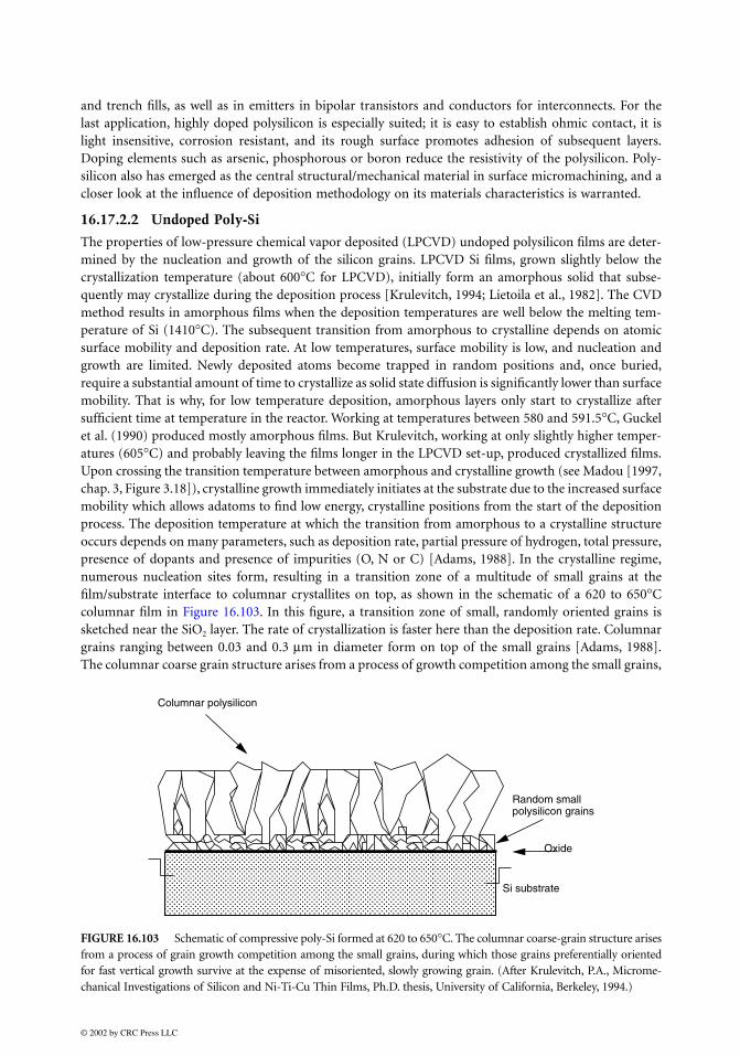
and trench fills, as well as in emitters in bipolar transistors and conductors for interconnects. For thelast application, highly doped polysilicon is especially suited; it is easy to establish ohmic contact, it islight insensitive, corrosion resistant, and its rough surface promotes adhesion of subsequent layers.Doping elements such as arsenic, phosphorous or boron reduce the resistivity of the polysilicon. Poly-silicon also has emerged as the central structural/mechanical material in surface micromachining, and acloser look at the influence of deposition methodology on its materials characteristics is warranted.
16.17.2.2 Undoped Poly-Si
The properties of low-pressure chemical vapor deposited (LPCVD) undoped polysilicon films are deter-mined by the nucleation and growth of the silicon grains. LPCVD Si films, grown slightly below thecrystallization temperature (about 600°C for LPCVD), initially form an amorphous solid that subse-quently may crystallize during the deposition process [Krulevitch, 1994; Lietoila et al., 1982]. The CVDmethod results in amorphous films when the deposition temperatures are well below the melting tem-perature of Si (1410°C). The subsequent transition from amorphous to crystalline depends on atomicsurface mobility and deposition rate. At low temperatures, surface mobility is low, and nucleation andgrowth are limited. Newly deposited atoms become trapped in random positions and, once buried,require a substantial amount of time to crystallize as solid state diffusion is significantly lower than surfacemobility. That is why, for low temperature deposition, amorphous layers only start to crystallize aftersufficient time at temperature in the reactor. Working at temperatures between 580 and 591.5°C, Guckelet al. (1990) produced mostly amorphous films. But Krulevitch, working at only slightly higher temper-atures (605°C) and probably leaving the films longer in the LPCVD set-up, produced crystallized films.Upon crossing the transition temperature between amorphous and crystalline growth (see Madou [1997,chap. 3, Figure 3.18]), crystalline growth immediately initiates at the substrate due to the increased surfacemobility which allows adatoms to find low energy, crystalline positions from the start of the depositionprocess. The deposition temperature at which the transition from amorphous to a crystalline structureoccurs depends on many parameters, such as deposition rate, partial pressure of hydrogen, total pressure,presence of dopants and presence of impurities (O, N or C) [Adams, 1988]. In the crystalline regime,numerous nucleation sites form, resulting in a transition zone of a multitude of small grains at thefilm/substrate interface to columnar crystallites on top, as shown in the schematic of a 620 to 650°Ccolumnar film in Figure 16.103. In this figure, a transition zone of small, randomly oriented grains issketched near the SiO2 layer. The rate of crystallization is faster here than the deposition rate. Columnargrains ranging between 0.03 and 0.3 µm in diameter form on top of the small grains [Adams, 1988].The columnar coarse grain structure arises from a process of growth competition among the small grains,
FIGURE 16.103 Schematic of compressive poly-Si formed at 620 to 650°C. The columnar coarse-grain structure arisesfrom a process of grain growth competition among the small grains, during which those grains preferentially orientedfor fast vertical growth survive at the expense of misoriented, slowly growing grain. (After Krulevitch, P.A., Microme-chanical Investigations of Silicon and Ni-Ti-Cu Thin Films, Ph.D. thesis, University of California, Berkeley, 1994.)
Random smallpolysilicon grains
Oxide
Si substrate
Columnar polysilicon
© 2002 by CRC Press LLC

during which those grains preferentially oriented for fast vertical growth survive at the expense ofmisoriented, slowly growing grains [van der Drift, 1967; Matson and Polysakov, 1977]. The lower thedeposition temperature, the smaller the initial grain size will be. At 700°C, films also are columnar;however, the grains are cylindrical extending through the thickness of the entire film and there is notransition zone near the SiO2 interface [Krulevitch, 1994].
Stress in poly-Si films was found to vary significantly with deposition temperature and silane pressure.Guckel et al. (1990) found that their mainly amorphous films, deposited at temperatures below 600°C,proved highly compressive with strain levels as high as –0.67%. At temperatures barely above 600°C,Krulevitch reports tensile films, whereas for yet higher temperatures (≥620°C) the stress again turnscompressive. While films deposited at temperatures greater than 630°C all turned out compressive, themagnitude of the compression decreased with increasing temperature. The stress gradient in the poly-Si films explains why compressive undoped and unannealed poly-Si beams tend to curl upward (positivestress gradient) when released from the substrate [Lober et al., 1988].
Using high resolution transmission electron microscopy, Guckel et al. (1990) and Krulevitch (1980)found a strong correlation between the material’s microstructure and the exhibited stress. Guckel et al.found that in their mainly amorphous films, deposited at temperatures below 600°C, a region near thesubstrate interface crystallized during growth with grains between 100 and 4000 Å. Krulevitch foundthat tensile, low-temperature films (605°C) have Si grains dispersed throughout the film thickness.Krulevitch suggests that the compressive stress in the higher temperature compressive films (≥620°C)relates to the competitive growth mechanism of the columnar grains. The same author concluded thatthermal sources of stress are insignificant.
Importantly, Guckel et al. discovered that annealing in nitrogen or under vacuum converts the low-temperature films with compressive built-in strain (−0.007) to a tensile strain with controllable strain levelsbetween 0 and + 0.003 (see Figure 16.104). During anneal no grain size increase was noticed (100 to 4000Å) but a slight increase in surface roughness was measured. This type of poly-Si is referred to as fine-grain
FIGURE 16.104 Anneal curves for poly-Si. Strain versus anneal time. Upper curves: low-temperature film. Lowercurve: high-temperature film. (From Guckel, H. et al., IEEE Trans. Electron. Dev., 35, 800–801, 1988. With permission.)
-0.004
-0.004
-0.005
-0.006
-0.007
-0.003
-0.003
-0.002
-0.002
-0.001
-0.001
0.0
600 oC
950oC
650oC
850oC
700oC
1050oC
Strain vs. Time
Anneal Curvesfor Polysilicon
Time (Min)
30 60 90 120 150 180
Tens
ion
Com
pres
sion
© 2002 by CRC Press LLC

poly-Si (also Wisconsin poly-Si). Guckel et al. explain this strain field reversal as follows: as the amorphousregion of the film crystallizes, it attempts to contract, but due to the substrate constrained newly crystallizedregion, a tensile stress results. Higher temperature films, during an anneal, also become less strained, but thestrain remains compressive (see lower curve in Figure 16.104). Moreover, in this case grain size does increaseand the surface turns considerably rougher. The latter is called coarse-grain poly-Si. Fine-grain poly-Si withits tensile strain is preferable; however, it cannot be doped to as low a resistivity as coarse-grain polysilicon.Hence, fine-grain polysilicon should be considered as a structural material rather than an electronic material.
Summarizing stress in poly-Si depends on the material’s microstructure, with tension arising from theamorphous to crystalline transformation during deposition and compression from the competitive graingrowth mechanism.
Polysilicon deposited at 600 to 650°C has a 110-preferred orientation. At higher temperatures, the100 orientation dominates. Dopants, impurities and temperature influence this preferred orientation[Adams, 1988]. Drosd and Washburn (1982) introduced a model explaining the experimental observationthat regrowth of amorphitized Si is faster for 100 surfaces, followed by 110 and 111 which are 2.3and 20 times slower, respectively. Interestingly, the latter also pinpoints the order of fastest to slowest etchingof the crystallographic planes in alkaline etchants. As discussed earlier in this chapter, Elwenspoek etal. (1994) used this observation of symmetry between etching and growing of Si planes as an importantinsight to develop a new theory explaining anisotropy in etching. In Table 16.21 we compare the discussedcoarse- and fine-grain poly-Si forms.
The above picture might further be complicated by the controlling nature of the substrate. For example,depositing amorphous Si (α − Si) at even lower temperatures of 480°C from disilane (Si2H6) and crystal-lizing it by subsequent annealing at 600°C demonstrated a large dependency of crystallite size on theunderlying SiO2 surface condition. Treating the surface with HF:H2O or NH4OH:H2O2:H2O leads to poly-Sifilms with a large grain size, two or three times as large as without SiO2 treatment, believed to be theconsequence of nucleation rate suppression [Shimizu and Ishihara, 1995].
T. Abe and M.L. Reed made low strain polysilicon thin film by DC-magnetics sputtering and post-annealing. The films showed very small regional stress and very smooth texture. The deposition rate was193 Å/min and the substrate was neither cooled nor heated. The average roughness was found to becomparable to the surface roughness of polished, bare silicon substrates [Abe and Reed, 1996].
16.17.2.3 Doped Poly-Si
To produce micromachines, doped poly-Si is used far more frequently than undoped poly-Si. Dopantsdecrease the resistivity to produce conductors and control stress. Polysilicon can be doped by diffusion,implantation or the addition of dopant gases during deposition (in situ doping). We only detail materialproperties of in situ doped poly-Si here.
TABLE 16.21 Comparison of Coarse-Grain and Fine-Grain Poly-Si
Coarse-Grain Poly-Si Fine-Grain Poly-Si
Temperature of deposition (°C)
620−650 570−591.5
Surface roughness Rough, >50Å Smooth, <15ÅGrain size Undoped: 160−320 Å as deposited;
in situ P-doped: 240−400 ÅVery small grains
As deposited strain –0.007 (compressive) −0.007 (compressive)Effect of high-
temperature annealGrains size increases, residual strain
decreases but remains compressive, reduced bending moment
Grain size increases to 100 Å [Guckel et al., 1988]; others have found 700–900 Å; large variation in strain (see Figure 16.102) from compressive to tensile
Dry and wet etch rate
Higher for doped material; depends on dopant concentration
Higher for doped material; depends on dopant concentration
Texture <110> as deposited, <311> in situ P-doped
No texture as deposited; depends on dopant concentration, <111> after 900–1000°C anneal
[Harbeke et al., 1983]
© 2002 by CRC Press LLC
Doping poly-Si films in situ reduces the number of processing steps required for producing dopedmicro-devices and also provides the potential for uniform doping through the film thickness. In situdoping of poly-Si with phosphorous is accomplished by maintaining a constant PH3 to SiH4 gas flowratio of about 1 vol % in a hot-wall LPCVD set-up. At this ratio the phosphorus content in the filmappears above the saturation limit and the excess dopant segregates at the grain boundaries [Adams,1988]. In situ phosphorus-doped poly-Si undergoes the same amorphous to crystalline growth transfor-mation observed in the undoped film, with the material’s microstructure depending on depositiontemperature as well as deposition pressure. The temperature of transformation is lower for the dopedfilms than for the undoped poly-Si and occurs between 580 and 620°C [Mulder et al., 1990; Kinsbronet al., 1983]. Phosphorus doping thus enhances crystallization in amorphous silicon [Lietoila et al., 1982]and, due to passivation of the poly-Si surface by the phosphine gas, reduces the poly-Si deposition rate[Mulder et al., 1990]. Decreases in deposition rate by as much as a factor of 25 have been reported[Meyerson and Olbricht, 1984]. Slower deposition rates allow more time for adatoms to find crystallinesites, resulting in crystalline growth at lower temperatures. From Table 16.21 we read that the grain sizeof phosphorus-doped poly-Si tends to be larger (240 to 400 Å) than for the undoped material and that311 planes show up as a texture facet in the doped material.
At lower deposition temperatures and higher pressures, the microstructure again consists of amor-phous and crystalline regions, while at higher temperatures and lower pressures columnar films resultand as deposited films exhibit compressive residual stress. The columnar films have a stress gradient thatincreases towards the film surface, as opposed to the gradient found in undoped columnar poly-Si. Thisgradient in stress most likely is due to nonuniform distribution of phosphorus throughout the film.Annealing at 950°C for 1 hour results in the same stress and stress gradient for initially columnar and initiallyamorphous/crystalline films (i.e., σf = −45 MPa and Γ = +0.2 mm
−1, respectively) [Krulevitch, 1994].
As with undoped poly-Si, phosphorus-doped poly-Si films with smooth surfaces (fine-grain) can beobtained by depositing in situ doped films in the amorphous state and then annealing [Harbeke et al.,1983; Hendriks and Mavero, 1991]. Phosphorus-doped poly-Si oxidizes faster than undoped poly-Si. Therate of oxidation is determined by the dopant concentration at the poly-Si surface [Adams, 1988].
Two drawbacks of in situ phosphorus doping are slower deposition rates [Kurokawa, 1982] and reducedfilm thickness uniformity [Meyerson and Olbricht, 1984], although uniformity can be improved bymodifying the reactor geometry [Mulder et al., 1990]. As discussed before, the lower deposition rate ofin situ phosphine doping can be mitigated by reducing the flow of phosphine/silane ratio by one third[Howe, 1995]. In contrast to in situ phosphine and arsine doping, which both decrease the depositionrate, diborane doping of poly-Si to make it p
+ accelerates the deposition rate [Adams, 1988].
The addition of oxygen to poly-Si increases the film’s resistivity and the resulting coating, semi-insulating poly-Si (SIPOS) acts as a passivating coating for high voltage devices in the IC industry. Thelatter material does not seem to have emerged in surface micromachining yet.
The values for the fracture stress of boron-, arsenic- and phosphorus-doped polysilicon are 2.77 ±0.08 Gpa, 2.70 ± 0.09 Gpa, and 2.11 ± 0.1 Gpa, respectively, compared with 2.84 ± 0.09 Gpa for undopedpolysilicon. The lower value for phosphorus-doped material has been attributed to high surface roughnessand with the large number of defects associated with extensive grain growth in highly phosphorus-dopedfilms [Biebl and von Philipsborn, 1993].
The quest for low temperature poly-Si deposition makes the 320°C PECVD deposition method espe-cially interesting. PECVD films, deposited in a 50-kHz parallel-plate diode reactor, can be doped in situand crystallized by rapid thermal annealing (RTA: 1100°C, 100 seconds). It was shown that small-grainedPECVD films annealed by RTA have good electrical properties and gauge factors between 20 and 30, i.e.,similar to those reported for other alternative types of polycrystalline silicon [Compton, 1992].
16.17.3 Amorphous and Hydrogenated Amorphous Silicon
Amorphous silicon behaves quite different from either fine- or coarse-grain poly-Si. The amorphousmaterial produces a high breakdown strength (7 to 9 MV/cm) oxide with low leakage currents (vs. a low
© 2002 by CRC Press LLC

breakdown voltage and large leakage currents for polycrystalline Si oxides). Amorphous polysilicon alsoattains a broad maximum in its dielectric function without the characteristic sharp structures near 295and 365 nm (4.2 and 3.4 eV) of crystalline poly-Si. Approximate refractive index values at a wavelengthof 600 nm are 4.1 for crystalline polysilicon and 4.5 for amorphous material [Adams, 1988]. As deposited,the material is under compression, but an anneal at temperatures as low as 400°C reduces the stresssignificantly, even leading to tensile behavior [Chang et al., 1991].
Hydrogenated amorphous silicon (α-Si:H) enables the fabrication of active semiconductor devices onforeign substrates at temperatures between 200 and 300°C. The technology, first applied primarily to themanufacturing of photovoltaic panels, now is quickly expanding into the field of large-area microelec-tronics such as active matrix liquid crystal displays (AMLCD). It is somehow surprising that microma-chinists have not taken more advantage of this material either for powering surface micromachines orto implement electronics cheaply on non-Si substrates.
Spear and LeComber (1975) showed that, in contrast to α-Si, α-Si:H could be doped both n- and p-type. Singly bonded hydrogen, incorporated at the Si dangling bonds, reduces the electronic defect densityfrom ~10
19/cm
3 to ~10
16/cm
3 (typical H concentrations are 5 to 10 atomic percent—several orders of
magnitude higher than needed to passivate all the Si dangling bonds). The lower defect density resultsin a Fermi level that is free to move, unlike in ordinary amorphous Si, where it is pinned. Other interestingelectronic properties are associated with α-Si:H—exposure of α-Si:H to light increases photoconductivityby four to six orders of magnitude, and its relatively high electron mobility (~1 cm
2/V sec
–1) enables
fabrication of useful thin-film transistors. Only recently did Lee et al. (1995) note that hydrogenatedamorphous silicon solar cells are an attractive means to realize an on-board power supply for integratedmicromechanical systems. They point out that the absorption coefficient of α-Si:H is more than an orderof magnitude larger than that of single crystal Si near the maximum solar photon energy region of 500nm. Accordingly, the optimum thickness of the active layer in an α-Si:H solar cell can measure 1 µm,much smaller than that of single crystal Si solar cells. By interconnecting 100 individual solar cells inseries, the measured open circuit potential reaches as high as 150 V under AM 1.5 conditions, a voltagehigh enough to drive on-board electrostatic actuators.
Hydrogenated amorphous silicon is manufactured by plasma-enhanced chemical vapor depositionfrom silane. Usually, planar RF-driven diode sources using SiH4 or SiH4/H2 mixtures are used. Typicalpressures of 75 mTorr and temperatures between 200 and 300°C allow silane decomposition with Sideposition as the dominant reaction. Decomposition occurs by electron impact ionization, producingmany different neutral and ionic species [Crowley, 1992]. Deposition rates for usable device quality α-Si:H generally do not exceed ~2 to 5 Å/sec, due to the effects of temperature, pressure and dischargepower. Table 16.22 gives state-of-the-art parameters for α-Si:H prepared by PECVD. Although its semi-conducting properties are inferior to single crystal Si, the material is finding more and more applications.Some examples are TFT switches for picture elements in AMLCDs [Holbrook and McKibben, 1992],page-wide TFT-addressed document scanners, high-voltage TFTs capable of switching up to 500 V etc.[Bohm, 1988]. An excellent source for further information on amorphous silicon is the book PlasmaDeposition of Amorphous Silicon-Based Materials [Bruno et al., 1995].
16.17.4 Silicon Nitride
Silicon nitride is a commonly used material in microcircuit and microsensor fabrication due to its manysuperior chemical, electrical, optical and mechanical properties. The material provides an extremely goodbarrier to the diffusion of water and to ions, particularly of Na
+. It also oxidizes slowly (about 30 times
less than silicon) and has highly selective etch rates over SiO2 and Si in many etchants. Some applicationsof silicon nitride are optical waveguides (nitride/oxide), encapsulant (diffusion barrier to water and ions),insulator (high dielectric strength), mechanical protection layer, etch mask, oxidation barrier and ionimplant mask (density is 1.4 times that of SiO2). Silicon nitride is also hard and can be used as, forexample, a bearing material in micromotors [Pool, 1988].
© 2002 by CRC Press LLC

Silicon nitride can be deposited by a wide variety of CVD techniques: APCVD, LPCVD and PECVD.Nitride often is deposited from SiH4 or other Si containing gases and NH3 in a reaction such as:
3SiCl2H2 + 4NH3 → Si3N4 + 6HCl + 6H2 (Reaction 16.17)
In this CVD process, the stoichiometry of the resulting nitride can be moved toward a silicon-richcomposition by providing excess silane or dichlorosilane compared to ammonia.
16.17.4.1 PECVD Nitride
Plasma-deposited silicon nitride, also plasma nitride or SiN, is used as the encapsulating material forthe final passivation of devices. The plasma-deposited nitride provides excellent scratch protection,serves as a moisture barrier and prevents sodium diffusion. Because of the low deposition temperature,300 to 350°C, the nitride can be deposited over the final device metallization. Plasma-deposited nitride
TABLE 16.22 Typical Opto-Electronic Parameters Obtained for PECVD α-Si:H
Symbol Parameter
UndopedHydrogen content ~10%Dark conductivity at 300 K σD ~10
−10 (Ω-cm)
−1
Activation energy Eσ 0.8−0.9 eVPre-exponent conductivity factor σ0 >10
3 (Ω-cm)
−1
Optical bank gap at 300 K Eg 1.7−1.8 eVTemperature variation of band gap Eg(T) 2–4 × 10
–4 eV/K
Density of states at the minimum gmin >1015−10
17 cm
3/eV
Density of states at the conduction band edge ~1015
/cm3
ESR spin density Ns ~1021
/cm3–eV
Infrared spectra 2000/640 cm−1
Photoluminescence peak at 77K ~1.25 eVExtended state mobility
Electrons µn or µe >10 cm2/V–s
Holes µp or µh ~1 cm2/V–s
Drift mobilityElectrons µn or µe ~1 cm
2/V–s
Holes µp or µh ~10−2
cm2/V–s
Conduction band tail slope 25 meVValence band tail slope 40 meVHole diffusion length ~1 µm
Doped amorphousn-Type
a σD 10−2
(Ω–cm)−1
Eg ~0.2 eVp-Type
b σD 10−3
(Ω–cm)−1
Eg ~0.3 eVDoped microcrystalline
n-Typec σD ≥1 (Ω–cm)
−1
Eg ≤0.05 eVp-Type
d σD ≥1 (Ω–cm)−1
Eg ≤0.05 eV
a −1% pH3 added to gas phase.b −1% B2H6 added to gas phase.c −1% PH3 added to dilute SiH4/H2, or 500 vppm PH3 added to SiF4/H2 (8:1) gas
mixtures. Relatively high powers are involved.d −1% B2H6 added to dilute SiH4/H2.
Source: Crowley, J.L., Solid State Technol., February, 94–98, 1992. With permission.
© 2002 by CRC Press LLC

and oxide both act as insulators between metallization levels, particularly useful when the bottommetal level is on aluminum or gold. The silicon nitride that results from PECVD in the gas mixtureof Reaction 16.2 has two shortcomings: high hydrogen content (in the range of 20 to 30 atomic percent)and high stress. The high compressive stress (up to 5 × 10
9 dyn/cm
2) can cause wafer warping and
voiding and cracking of underlying aluminum lines [Rosler, 1991]. The hydrogen in the nitride alsoleads to degraded MOSFET lifetimes. To avoid hydrogen incorporation, one may employ low or nohydrogen-containing source gases such as nitrogen instead of ammonia as the nitrogen source. Also,a reduced flow of SiH4 results in less Si-H in the film. The hydrogen content and the amount of stressin the film are closely linked. Compressive stress, for example, changes toward tensile stress uponannealing to 490°C in proportion to the Si-H bond concentration. By adding N2O to the nitridedeposition chemistry an oxynitride forms with lower stress characteristics; however, oxynitrides aresomewhat less effective as moisture and ion barriers than nitrides.
We discussed the effect of RF frequency on nitride stress, hydrogen content, density and the wet etchrate in detail in Madou (1997, chap. 3). We can conclude that low frequency (high energy bombardment)results in films with low compressive stress, lower etch rates and higher density. The higher the ion bom-bardment during PECVD, the higher the stress is. Stress also is affected by moisture exposure and temper-ature cycling (for a good review, see Wu and Rosler [1992]). We compare properties of silicon nitride formedby LPCVD and PECVD in Tables 16.23 and 16.24. Table 16.24 highlights typical process parameters.
16.17.4.2 LPCVD Nitride
In the IC industry, stoichiometric silicon nitride (Si3N4) is LPCVD deposited at 700 to 900°C andfunctions as an oxidation mask and as a gate dielectric in combination with thermally grown SiO2. Inmicromachining, LPCVD nitride serves as an important mechanical membrane material and isolation/bufferlayer. By increasing the Si content in silicon nitride the ensile film stress reduces (even to compressive),the film turns more transparent and the HF etch rate lowers. Such films result by increasing the dichlo-rosilane/ammonia ratio [Sakimoto et al., 1982].
Figure 16.105 illustrates the effect of gas flow ratio and deposition temperature on stress and thecorresponding refractive index and HF etch rate [Sakimoto et al., 1982].
TABLE 16.23 Properties of Silicon Nitridea
Deposition LPCVD PECVD
Temperature (°C) 700–800 250–350Density (g/cm
3) 2.9–3.2 2.4–2.8
Pinholes No YesThroughput High LowStep coverage Conformable PoorParticles Few ManyFilm quality Excellent PoorDielectric constant 6–7 6–9Resistivity (Ωcm) 10
1610
6–10
15
Refractive index 2.01 1.8–2.5Atom % H 4–8 20–25Energy gap 5 4–5Dielectric strength (10
6 V/cm) 10 5
Etch rate in conc. HF 200 Å/minEtch rate in BHF 5–10 Å/minResidual stress (10
9 dyn/cm
2) 1T 2 C–5T
Poisson ratio 0.27Young’s modulus 270 GPaTCE 1.6 × 10
–6/°C
Note: C = compressive; T = tensile.a See Adams (1988), Sinha and Smith (1978) and Retajczykand Sinha (1980).
© 2002 by CRC Press LLC

©
Silicon-rich or low-stress nitride emerges as an important micromechanical material. Low residual stressmeans that relatively thick films can be deposited and patterned without fracture. Low etch rate in HFmeans that films of silicon-rich nitride survive release etches better than stoichiometric silicon nitride. Theetch characteristics of LPCVD SiN are summarized in Table 16.25. The properties of a LPCVD SixNy film,deposited by reaction of SiCl2H2 and NH3 (5:1 by volume) at 850°C, were already summarized in Table 16.23.
16.17.5 CVD Silicon Dioxides
Silicon oxides, like other dielectrics, function as insulation between conducting layers, for diffusion andion implementation masks, for diffusion from doped oxides, for capping doped oxides to prevent the
TABLE 16.24 Silicon Nitride PECVD Process Conditions
Flow (sccm) SiH4 190–270NH3 1900N2 1000
Temperature (°C) T.C. 350 or 400Wafer ~330 or 380
Pressure (torr) 2.9rf power (watt) 1100Deposition rate (Å/min) 1200–1700Refractive index 2.0
Source: Wu, T.H.T. and R.S. Rosler, Solid State Technol., May,65–71, 1992. With permission.
FIGURE 16.105 Silicon nitride LPCVD deposition parameters. (A) Effect of gas-flow ratio and deposition tem-perature on stress in nitride films. (B) The corresponding index of refraction. (C) The corresponding HF etch rate.(From Sakimoto, M. et al., J. Vac. Sci. Technol., 21, 1017–1021, 1982. With permission.)
TABLE 16.25 Etching Behavior of LPCVD Si3N4
Etchant Temperature (°C) Etch Rate (Å/min) Selectivity of Si3N4:SiO2:Si
H3PO4 180 100 10:1:0.3CF4–4% O2 plasma — 250 3:2.5:17BHF 25 5 to 10 1:200:±0HF (40%) 25 200 1:>100:0.1
T = 7500CT = 8000C
T = 8500C
SiH2CI2/NH3 Ratio(b)
B
Ref
ract
ive
lnde
x
2 4 6 8
2.6
2.4
2.2
2.0
1.8
Refractive lndexE
tch
Rat
e (A
o
/min
)
14
12
10
8
6
4
2
020 21 22 23 24
C
800
600
400
200
-200
0
0 1 2 3 4 5 6 7 8
T = 7500CT = 8000C
T = 8500C
SiH2CI2/NH2 Ratio(a)
A
Res
idua
l Str
ess
(MP
a)
2002 by CRC Press LLC

loss of dopants, for gettering impurities and for passivation to protect devices from impurities, moistureand scratches. In micromachining, silicon oxides serve the same purposes but also act as sacrificialmaterial. Phosphorus-doped glass (PSG), also called P-glass or phosphosilicate glass, and borophospho-silicate glasses (BPSG) soften and flow at lower temperatures enabling the smoothing of topography.They etch much faster than SiO2, which benefits their application as sacrificial material. The depositionof thermal SiO2 is covered in Madou (1997, chap. 3). Now we consider CVD techniques to deposit dopedand undoped SiO2.
16.17.5.1 CVD Undoped SiO2
Several CVD methods will deposit SiO2. CVD silicon dioxide can be deposited on the wafer out of thevapor phase from the reaction of silane (SiH4) with oxygen at relative low temperatures (300 to 500°C)and low pressure. The silane/oxygen gas mixture has been applied at atmospheric pressure (AP) andplasma-enhanced conditions. The main advantage of silane/oxygen is the low deposition temperature;the main disadvantage is the poor step coverage.
In general, tetraethylorthosilicate (TEOS) brings about a better starting chemistry than the traditionalsilane-based CVD technologies. TEOS-based depositions lead to superior film quality in terms of stepcoverage and reflow properties. With an LPCVD reactor, the deposition temperature for TEOS is as highas 650 to 750°C, precluding its use over aluminum lines. In contrast, silicon dioxide is deposited byPECVD at 300 to 400°C from TEOS. CVD oxides in general feature porosity and low density. Lowfrequency (high energy) ion bombardment results in more compressive films, higher density and loweretch rates as well as better moisture resistance [Rosler, 1991]. Use of TEOS oxide, to replace SiH4-basedoxide in spin-on-glass (SOG) and photoresist planarization schemes, now has become commonplace fordevices with small features.
Yet another promising silicon dioxide deposition technology is the subatmospheric pressure CVD (SACVD).Both undoped and borophosphosilicate glass have been deposited in this fashion. The process involvesan ozone and TEOS reaction at a pressure of 600 Torr and at a temperature below 400°C. While offeringthe same good step coverage over submicron gaps, the films from the thermal reaction of ozone and TEOSexhibit relatively neutral stress and have a higher film density compared to low pressure processes. Thisincreased density gives the oxide greater moisture resistance, lower wet etch rate and smaller thermalshrinkage. Compared to a 60-Torr process, the film density has increased from 2.09 to 2.15 g/cm
3; the
wet etch rate decreased by more than 40%; and the thickness shrinkage changed from 12 to 4% after a30-min anneal in dry N2 at 1000°C [Lee et al., 1992].
16.17.5.2 CVD Phosphosilicate Glass Films
Adding a few percent of phosphine to the gas stream during deposition to obtain a lower melting pointfor the oxide (PH3) results in a phosphosilicate glass. Numerous applications of this material exist, such as:
1. Interlevel dielectric to insulate metallization levels2. Gettering and flow capabilities3. Passivation overcoat to provide mechanical protection for the chip from its environment4. Solid diffusion source to dope silicon with phosphorus5. Fast etching sacrificial material in surface micromachining
Both wet and dry etching rates of PSG are faster than the undoped material and depend on the dopantconcentration. Profiles over steps get progressively smoother with higher phosphorous concentrations,reflecting the corresponding enhancement in viscous flow [Levy and Nassau, 1986]. Increased ion bom-bardment (energy or density) in a PECVD PSG results in more stable phosphosilicate glass film withcompressive as-deposited stress. Table 16.26 summarizes typical PSG process conditions [Wu et al., 1992].
The addition of boron to P-glass further lowers its softening temperature. Flow occurs at temperaturesbetween 850 and 950°C, even with phosphorous concentration as low as 4 wt%. A BPSG doped at 4% boronand 6% phosphorus is normal. BPSG deposition conditions are shown in Table 16.27 [Bonifield et al., 1993].
© 2002 by CRC Press LLC

16.18 Polysilicon Surface Micromachining Examples
Example 1. Analog Devices Accelerometer
Accelerometers based on lateral resonators represent the main application of surface micromachining today.To facilitate integration of their 50-g surface micromachined accelerometer (ADXL-50) with on-boardelectronics, Analog Devices opted for a mature 4-µm BICMOS process [Core et al., 1993]. Figure 16.106presents a photograph of the finished capacitive sensor (center) with on-chip excitation, self-test and signalconditioning circuitry. The polysilicon-sensing element only occupies 5% of the total die area. The wholechip measures 500 × 625 µm and operates as an automotive airbag deployment sensor. The measurementaccuracy is 5% over the ±50-g range. Deceleration in the axis of sensitivity exerts a force on the central massthat, in turn, displaces the interleaved capacitor plates, causing a fractional change in capacitance. Inoperation, the device has a force-balance electronic control loop to prevent the mass from actual movement.Straight flexures were used for the layout of the lateral resonator shuttle mass (see Figure 16.89B).
In the sensor design, n+ underpasses connect the sensor area to the electronic circuitry, replacing the
usual heat-sensitive aluminum connect lines. Most of the sensor processing is inserted into the BICMOS
TABLE 16.26 Typical PSG Process Conditions
Flow (sccm) SiH4 150–230N2O 4500N2 1500PH3 150
a
Temperature (°C) T.C. 400Wafer ~380–390
Pressure (Torr) 2.2RF power (watt) 1200Deposition rate (Å/min) 4000–5000Refractive index 1.46
a 10% PH3 in N2.
b 5% PH3 in N2.
Source: Wu, T.H.T. and R.S. Rosler, Solid State Technol.,May, 65–71, 1992. With permission.
TABLE 16.27 Typical BPSG Process Conditions
Parameter Dimension NSGBPSG
Deposition temp. °C 400 400TEOS flow g/min 0.33 0.66O2 flow SLM 7.5 7.5O3/O2 volume % 1 4.5Carrier N2 flow SLM 18.0 18.0B conc. atomic % 4P conc. atomic % 6Exhaust mmH2O 2.0 2.0Growth rate Å/min 1200 1800Thickness Å 1000 5800
Note: NSG = non-doped silicate glass; BPSG = borophos-phosilicate glass.
From Bonifield, T., K. Hewes, B. Merritt, R. Robinson, S.Fisher, and D. Maisch, Semicond. Int., July, 200–204, 1993.With permission.
© 2002 by CRC Press LLC

process right after the borophosphosilicate glass planarization. After planarization, a designated sensorregion or moat is cleared in the center of the die (Figure 16.107a). A thin oxide is then deposited topassivate the n
+ underpass connects, followed by a thin, low-pressure, vapor-deposited nitride to act as
an etch stop (buffer layer) for the final poly-Si release etch (Figure 16.107b). The spacer or sacrificialoxide used is a 1.6-µm densified low-temperature oxide (LTO) deposited over the whole die (Figure16.107c). In a first timed etch, small depressions that will form bumps or dimples on the underside ofthe polysilicon sensor are created in the LTO layer. These will limit stiction in case the sensor comes incontact with the substrate. A subsequent etch cuts anchors into the spacer layer to provide regions ofelectrical and mechanical contact (Figure 16.107c). The 2-µm-thick sensor poly-Si is then deposited,implanted, annealed and patterned (Figure 16.108a). The relatively deep junctions of the BICMOS processpermit the polysilicon thermal anneal as well as brief dielectric densifications without resulting indegradation of the electronic functions. Next is the IC metallization which starts with the removal of thesacrificial spacer oxide from the circuit area along with the LPCVD nitride and LTO layer. A low-temperature oxide is deposited on the poly-Si sensor part and contact openings appear in the IC part ofthe die where platinum is deposited to form a platinum silicide (Figure 16.108b). The trimmable thin-film material, TiW barrier metal and Al/Cu interconnect metal are sputtered on and patterned in the ICarea. The circuit area is then passivated in two separate deposition steps. First, plasma oxide is depositedand patterned (Figure 16.108c), followed by a plasma nitride to form a seal with the earlier depositedLPCVD nitride (Figure 16.109a). The nitride acts as an HF barrier in the subsequent long etch release.The plasma oxide left on the sensor acts as an etch stop for the removal of the plasma nitride (Figure16.109a). Subsequently, the sensor area is prepared for the final release etch. The undensified dielectricsare removed from the sensor and the final protective resist mask is applied. The photoresist protects thecircuit area from the long-term buffered oxide etch (Figure 16.109b). The final device cross section isshown in Figure 16.109c.
FIGURE 16.106 Analog Devices’ ADXL-50 accelerometer with a surface micromachined capacitive sensor (center),on-chip excitation, self-test, and signal-conditioning circuitry. (From Core, T.A. et al., Solid State Technol., October,39–47 (1993). With permission.)
© 2002 by CRC Press LLC

FIGURE 16.107 Preparation of IC chip for poly-Si. (a) Sensor area post-BPSG planatization and moat mask. (b)Blanket deposition of thin oxide and thin nitride layer. (c) Bumps and anchors made in LTO spacer layer. (FromCore, T.A., W.K. Tsang, and S.J. Sherman, Solid State Technol., 36, 39–47, 1993. With permission.)
FIGURE 16.108 Poly-Si deposition and IC metallization. (a) Cross-sectional view after polysilicon deposition,implant, anneal, and patterning. (b) Sensor area after removal of dielectrics from circuit area, contact mask, and Ptsilicide. (c) Metallization scheme and plasma oxide passivation and patterning. (From Core, T.A., W.K. Tsang, andS.J. Sherman, Solid State Technol., 36, 39–47, 1993. With permission.)
© 2002 by CRC Press LLC
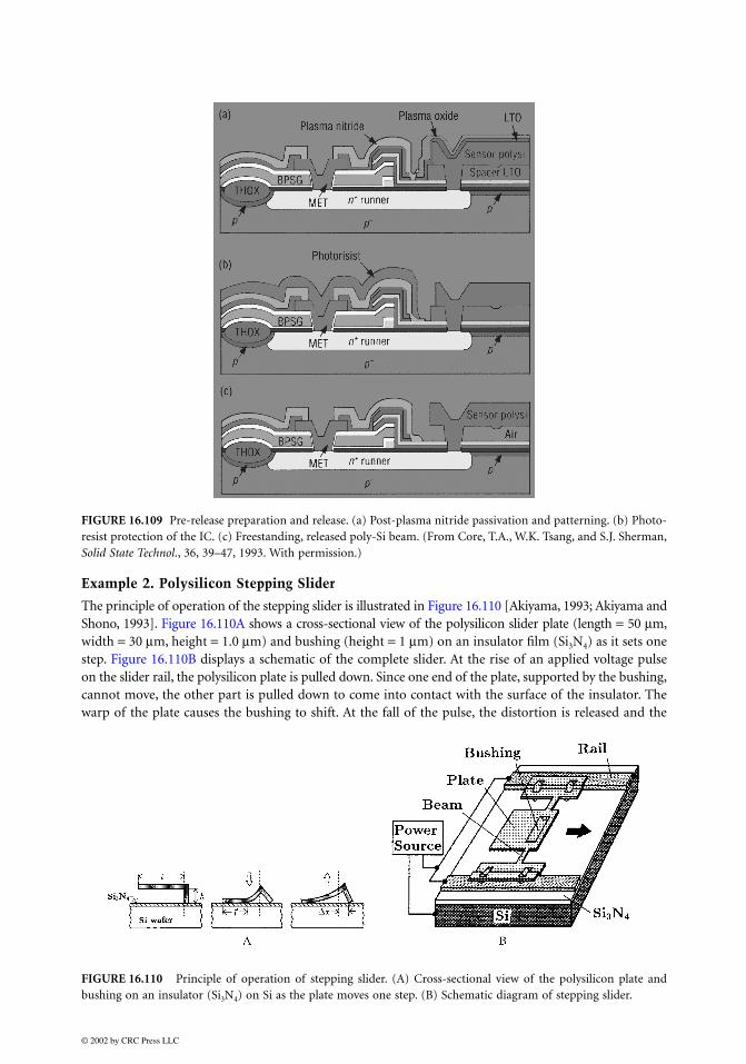
Example 2. Polysilicon Stepping Slider
The principle of operation of the stepping slider is illustrated in Figure 16.110 [Akiyama, 1993; Akiyama andShono, 1993]. Figure 16.110A shows a cross-sectional view of the polysilicon slider plate (length = 50 µm,width = 30 µm, height = 1.0 µm) and bushing (height = 1 µm) on an insulator film (Si3N4) as it sets onestep. Figure 16.110B displays a schematic of the complete slider. At the rise of an applied voltage pulseon the slider rail, the polysilicon plate is pulled down. Since one end of the plate, supported by the bushing,cannot move, the other part is pulled down to come into contact with the surface of the insulator. Thewarp of the plate causes the bushing to shift. At the fall of the pulse, the distortion is released and the
FIGURE 16.109 Pre-release preparation and release. (a) Post-plasma nitride passivation and patterning. (b) Photo-resist protection of the IC. (c) Freestanding, released poly-Si beam. (From Core, T.A., W.K. Tsang, and S.J. Sherman,Solid State Technol., 36, 39–47, 1993. With permission.)
FIGURE 16.110 Principle of operation of stepping slider. (A) Cross-sectional view of the polysilicon plate andbushing on an insulator (Si3N4) on Si as the plate moves one step. (B) Schematic diagram of stepping slider.
© 2002 by CRC Press LLC
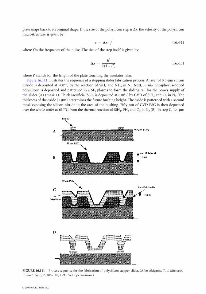
plate snaps back to its original shape. If the size of the polysilicon step is ∆x, the velocity of the polysiliconmicrostructure is given by:
(16.64)
where f is the frequency of the pulse. The size of the step itself is given by:
(16.65)
where I′ stands for the length of the plate touching the insulator film.Figure 16.111 illustrates the sequence of a stepping slider fabrication process. A layer of 0.3-µm silicon
nitride is deposited at 900°C by the reaction of SiH4 and NH3 in N2. Next, in situ phosphorus-dopedpolysilicon is deposited and patterned in a SF6 plasma to form the sliding rail for the power supply ofthe slider (A) (mask 1). Thick sacrificial SiO2 is deposited at 610°C by CVD of SiH4 and O2 in N2. Thethickness of the oxide (1 µm) determines the future bushing height. The oxide is patterned with a secondmask exposing the silicon nitride in the area of the bushing. Fifty nm of CVD PSG is then depositedover the whole wafer at 610°C from the thermal reaction of SiH4, PH3 and O2 in N2 (B). In step C, 1.4-µm
FIGURE 16.111 Process sequence for the fabrication of polysilicon stepper slider. (After Akiyama, T., J. Microelec-tromech. Syst., 2, 106–110, 1993. With permission.)
v ∆x f⋅=
∆xh2
2(I I′)–--------------------=
© 2002 by CRC Press LLC

polysilicon is deposited at 610°C from SiH4, coated with PSG and patterned with mask 3 to shape theslider plate. The silicon wafer is then heated in N2 at 1050°C for 60 min to release the residual strain inthe polysilicon and at the same time to activate and diffuse phosphorus from the PSG into the polysiliconslider. The last step (D) in the fabrication process is the release of the polysilicon slider, by dipping thewafer into 50% HF to fully dissolve the sacrificial oxide. Finally, the wafer is rinsed in deionized waterand IPA (isopropyl-alcohol) and dried in N2. In the fabrication process, to avoid washing away the sliderin the rinse, the slider is attached by polysilicon springs to the end of the rail. The springs are cut by thestep motion of the slider and subsequently the sliders can move along the rail. The velocity at the peakvoltage of 150 V is 30 µm/sec with a 1200-Hz pulse. Figure 16.112 shows an SEM photo of the resultingslider (top). Components of the slider are named on the scanned image (bottom).
References
Abe, T. and J. H. Matlock, “Wafer Bonding Technique for Silicon-on-Insulator Technology,” Solid StateTechnol., November, 39–40, 1990.
Abe, T. and M. L. Reed, “Low Strain Sputtered Polysilicon for Micromechanical Structures,” The Ninth AnnualInternational Workshop on Micro Electro Mechanical Systems, San Diego, CA, 1996, pp. 258–262.
FIGURE 16.112 SEM micrograph of the stepping slider (top) and scanned image (bottom). (From Akiyama, T., J.Microelectromech. Syst., 2, 106–110, 1993. With permission.)
© 2002 by CRC Press LLC

© 2002 by CRC Press LLC
Abe, T., W. C. Messner, and M. L. Reed, “Effective Methods to Prevent Stiction During Post–Release-Etch Processing,” Proceedings. IEEE Micro Electro Mechanical Systems (MEMS ’95), Amsterdam,Netherlands, 1995, pp. 94–9.
Abu-Zeid, M. M., “Corner Undercutting in Aniso-tropically Etched Isolation Contours,”
J. Electrochem.Soc.,
131, 2138–2142, 1984. Abu-Zeid, M. M., D. L. Kendall, G. R. de Guel, and R. Galeazzi, “Abstract 275,” JECS, Toronto, Canada,
1985, p. 400. Acosta, R. E., C. Ahn, I. V. Babich, E. I. Cooper, J. M. Cotte, W. J. Horkans, C. Jahnes, S. Krongelb, K. T.
Kwietniak, N. C. Labianca, E. J. M. O’Sullivan, A. T. Pomerene, D. L. Rath, L. T. Romankiw, andJ. A. Tornello, “Integrated Variable Reluctance Magnetic Mini–Motor,”
J. Electrochem. Soc.,
95–2,494–495, 1995.
Adams, A. C., “Dielectric and Polysilicon Film Deposition,” in
VLSI Technology,
Sze, S. M., Ed., McGraw-Hill, New York, 1988, pp. 233–71.
Ahn, C. H., Y. J. Kim, and M. G. Allen, “A Planar Variable Reluctance Magnetic Micromotor with a FullyIntegrated Stator and Wrapped Coils,” Proceedings. IEEE Micro Electro Mechanical Systems(MEMS ’93), Fort Lauderdale, FL, 1993, pp. 1–6.
Akiyama, T., “Controlled Stepwise Motion in Polysilicon Microstructures,”
J. Microelectromech. Syst.,
2,106–110, 1993.
Akiyama, T. and K. Shono, “A New Step Motion of Polysilicon Microstructures,” Proceedings IEEE MicroElectro Mechanical Systems (MEMS ’93), Fort Lauderdale, FL, 1993, pp. 272–277.
Alavi, M., S. Buttgenbach, A. Schumacher, and H. J. Wagner, “Laser Machining of Silicon for Fabricationof New Microstructures,” 6th International Conference on Solid-State Sensors and Actuators(Transducers ’91), San Francisco, CA, 1991, pp. 512–515.
Alavi, M., S. Buttgenbach, A. Schumacher, and H. J. Wagner, “Fabrication of Microchannels by LaserMachining and Anisotropic Etching of Silicon,”
Sensors and Actuators A,
32, 299–302, 1992. Allen, D. M.,
The Principles and Practice of Photochemical Machining and Photoetching,
Adam Hilger,Bristol and Boston, 1986.
Allen, M. G., M. Mehregany, R. T. Howe, and S. D. Senturia, “Microfabricated Structures for the In SituMeasurement of Residual Stress, Young’s Modulus and Ultimate Strain of Thin Films,”
Appl. Phys.Lett.,
51, 241–3, 1987. Alley, R. L., G. J. Cuan, R. T. Howe, and K. Komvopoulos, “The Effect of Release Etch Processing on
Surface Microstructure Stiction,” Technical Digest of the 1988 Solid-State Sensor and ActuatorWorkshop., Hilton Head Island, SC, 1988, pp. 202–7.
Alley, R. L., R. T. Howe, and K. Komvopoulos, “The Effect of Release-Etch Processing on SurfaceMicrostructure Stiction,” Technical Digest of the 1992 Solid State Sensor and Actuator Workshop,Hilton Head Island, SC, 1992, pp. 202–7.
Alley, R. L., P. Mai, K. Komvopoulos, and R. T. Howe, “Surface Roughness Modifications of InterfacialContacts in Polysilicon Microstructures,” 7th International Conference on Solid-State Sensors andActuators (Transducers ’93), Yokohama, Japan, 1993, pp. 288–91.
Allongue, P., V. Costa-Kieling, and H. Gerischer, “Etching of Silicon in NaOH Solutions, Part I and II,”
J. Electrochem. Soc.,
140, 1009–1018 (Part I) and 1018–1026 (Part II), 1993. Ammar, E. S. and T. J. Rodgers, “UMOS Transistors on (110) Silicon,”
IEEE Trans. Electron Devices,
ED–27, 907–914, 1980. Anderson, R. C., R. S. Muller, and C. W. Tobias, “Porous Polycrystalline Silicon: A New Material for
MEMS,”
J. Microelectromech. Syst.,
3, 10–18, 1994. Archer, V. D., “Methods for Defect Evaluation of Thin <100> Oriented Silicon in Epitaxial Layers Using
a Wet Chemical Etch,”
J. Electrochem. Soc.,
129, 2074–2076, 1982. Arita, Y. and Y. Sunohara, “Formation and Properties of Porous Silicon Film,”
J. Electrochem. Soc.,
124,285–295, 1977.
Asano, M., T. Cho, and H. Muraoko, “Applications of Choline in Semiconductor Technology,”
Electrochem.Soc. Extend. Abstr.,
354, 76–2, 911–913, 1976.

© 2002 by CRC Press LLC
Barret, S., F. Gaspard, R. Herino, M. Ligeon, F. Muller, and I. Ronga, “Porous Silicon as a Material inMicro-sensor Technology,”
Sensors and Actuators A,
33, 19–24, 1992. Bartek, M., P. T. J. Gennissen, P. J. French, and R. F. Wolffenbuttel, “Confined Selective Epitaxial Growth:
Potential for Smart Silicon Sensor Fabrication,” 8th International Conference on Solid-State Sensorsand Actuators (Transducers ’95), Stockholm, Sweden, June 1995, pp. 91–94.
Barth, P., “Si in Biomedical Applications,”
Micro-electronics—Photonics, Materials, Sensors and Technology,
1984. Barth, P. W., P. J. Shlichta, and J. B. Angel, “Deep Narrow Vertical-Walled Shafts in <110> Silicon,” 3rd
International Conference on Solid-State Sensors and Actuators, Philadelphia, PA, 1985,pp. 371–373.
Bashir, R. et al., “Characterization and Modeling of Sidewall Defects in Selective Epitaxial Growth ofSilicon,”
J. Vacuum Sci.
Bassous, E. and C.-Y. Liu,
Polycrystalline Silicon Etching with Tetramethylammonium Hydroxide,
U.S.Patent 4,113,551, 1978.
Bassous, E., H. H. Taub, and L. Kuhn, “Ink Jet Printing Nozzle Arrays Etched in Silicon,”
Appl. Phys.Lett.,
31, 135–137, 1977. Bean, K., “Anisotropic Etching of Silicon,”
IEEE Trans. Electron Devices,
ED–25, 1185–1193, 1978. Bean, K. E. and W. R. Runyan, “Dielectric Isolation: Comprehensive, Current and Future,”
J. Electrochem.Soc.,
124, 5C–12C, 1977. Bean, K. E., R. L. Yeakley, and T. K. Powell, “Orientation Dependent Etching and Deposition of Silicon,”
J. Electrochem. Soc.,
121, 87C, 1974. Benitez, M. A., J. Esteve, M. S. Benrakkad, J. R. Morante, J. Samitier, and J. Å. Schweitz, “Stress Profile
Characterization and Test Structures Analysis of Single and Double Ion Implanted LPCVD Poly-crystalline Silicon,” 8th International Conference on Solid-State Sensors and Actuators (Transduc-ers ’95), Stockholm, Sweden, June 1995, pp. 88–91.
Bennema, P., “Spiral Growth and Surface Roughening: Developments since Burton, Cabrera, and Frank,”
J. Cryst. Growth,
69, 182–197, 1984. Biebl, M. and H. von Philipsborn, “Fracture Strength of Doped and Undoped Panical Filters,” Ph.D.
thesis, University of California at Berkeley, 1993. Biebl, M., G. Brandl, and R. T. Howe, “Young’s Modulus of In Situ Phosphorous-Doped Polysilicon,” 8th
International Conference on Solid-State Sensors and Actuators (Transducers ’95), Stockholm,Sweden, June 1995, pp. 80–3.
Biebl, M., G. T. Mulhern, and R. T. Howe, “In Situ Phosphorous-Doped Polysilicon for Integrated MEMS,”8th International Conference on Solid-State Sensors and Actuators (Transducers ’95), Stockholm,Sweden, June 1995, pp. 198–201.
Block, B.,
Zero-Base the Technological Approach,
private communication. Bogenschutz, A. F., K.-H. Locherer, W. Mussinger, and W. Krusemark, “Chemical Etching of Semicon-
ductors in HNO
3
-HF-CH
3
COOH,”
J. Electrochem. Soc.,
114, 970–973, 1967. Bogh, A., “Ethylene Diamine-Pyrocatechol-Water Mixture Shows Etching Anomaly in Boron-Doped
Silicon,”
J. Electrochem. Soc.,
118, 401–402, 1971. Bohm, M., “Advances in Amorphous Silicon Based Thin Film Microelectronics,”
Solid State Technol.,
September, 125–131, 1988. Boivin, L. P., “Thin Film Laser–to Fiber Coupler,”
Appl. Opt.,
13, 391–395, 1974. Bomchil, G., R. Herino, and K. Barla, “Formation and Oxidation of Porous Silicon for Silicon on Insulator
Technologies,” in
Energy Beam-Solid Interactions and Transient Thermal Processes,
Nguyen, V. T.and Cullis, A., Eds., Les Editions de Physique, Les Ulis, 1986, p. 463.
Bonifield, T., K. Hewes, B. Merritt, R. Robinson, S. Fisher, and D. Maisch, “Extended Run Evaluation ofTEOS/Ozone BPSG Deposition,”
Semicond. Int.,
July, 200–204, 1993. Brantley, W. A., “Calculated Elastic Constants for Stress Problems Associated with Semiconductor
Devices,”
J. Appl. Phys.,
44, 534–535, 1973. Brodie, I. and J. J. Muray,
The Physics of Micro-fabrication,
Plenum Press, New York, 1982.
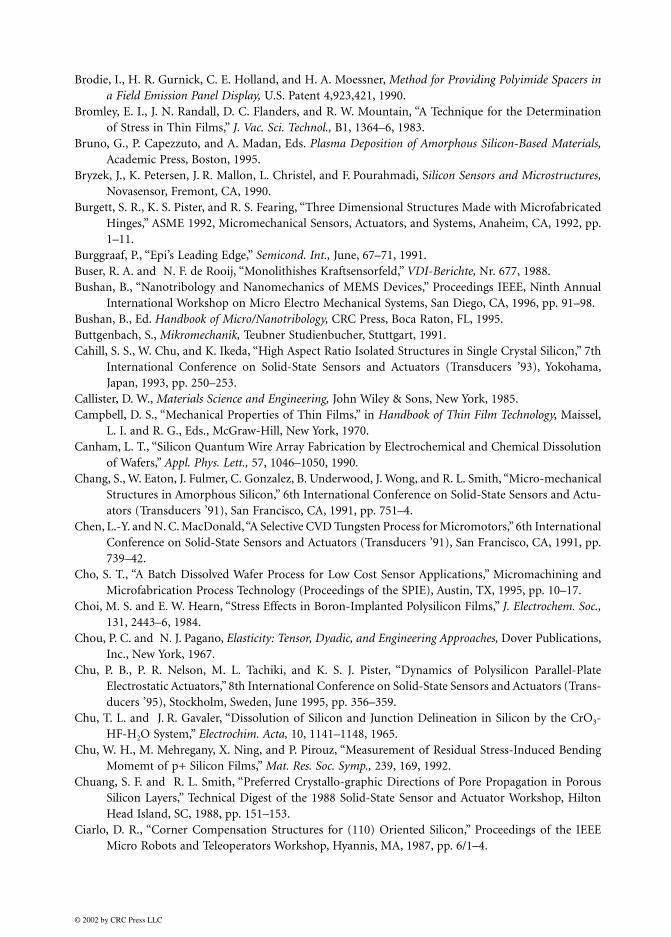
© 2002 by CRC Press LLC
Brodie, I., H. R. Gurnick, C. E. Holland, and H. A. Moessner,
Method for Providing Polyimide Spacers ina Field Emission Panel Display,
U.S. Patent 4,923,421, 1990. Bromley, E. I., J. N. Randall, D. C. Flanders, and R. W. Mountain, “A Technique for the Determination
of Stress in Thin Films,”
J. Vac. Sci. Technol.,
B1, 1364–6, 1983. Bruno, G., P. Capezzuto, and A. Madan, Eds.
Plasma Deposition of Amorphous Silicon-Based Materials,
Academic Press, Boston, 1995. Bryzek, J., K. Petersen, J. R. Mallon, L. Christel, and F. Pourahmadi, S
ilicon Sensors and Microstructures,
Novasensor, Fremont, CA, 1990. Burgett, S. R., K. S. Pister, and R. S. Fearing, “Three Dimensional Structures Made with Microfabricated
Hinges,” ASME 1992, Micromechanical Sensors, Actuators, and Systems, Anaheim, CA, 1992, pp.1–11.
Burggraaf, P., “Epi’s Leading Edge,”
Semicond. Int.,
June, 67–71, 1991. Buser, R. A. and N. F. de Rooij, “Monolithishes Kraftsensorfeld,”
VDI-Berichte,
Nr. 677, 1988. Bushan, B., “Nanotribology and Nanomechanics of MEMS Devices,” Proceedings IEEE, Ninth Annual
International Workshop on Micro Electro Mechanical Systems, San Diego, CA, 1996, pp. 91–98. Bushan, B., Ed.
Handbook of Micro/Nanotribology,
CRC Press, Boca Raton, FL, 1995. Buttgenbach, S.,
Mikromechanik,
Teubner Studienbucher, Stuttgart, 1991. Cahill, S. S., W. Chu, and K. Ikeda, “High Aspect Ratio Isolated Structures in Single Crystal Silicon,” 7th
International Conference on Solid-State Sensors and Actuators (Transducers ’93), Yokohama,Japan, 1993, pp. 250–253.
Callister, D. W.,
Materials Science and Engineering,
John Wiley & Sons, New York, 1985. Campbell, D. S., “Mechanical Properties of Thin Films,” in
Handbook of Thin Film Technology,
Maissel,L. I. and R. G., Eds., McGraw-Hill, New York, 1970.
Canham, L. T., “Silicon Quantum Wire Array Fabrication by Electrochemical and Chemical Dissolutionof Wafers,”
Appl. Phys. Lett.,
57, 1046–1050, 1990. Chang, S., W. Eaton, J. Fulmer, C. Gonzalez, B. Underwood, J. Wong, and R. L. Smith, “Micro-mechanical
Structures in Amorphous Silicon,” 6th International Conference on Solid-State Sensors and Actu-ators (Transducers ’91), San Francisco, CA, 1991, pp. 751–4.
Chen, L.-Y. and N. C. MacDonald, “A Selective CVD Tungsten Process for Micromotors,” 6th InternationalConference on Solid-State Sensors and Actuators (Transducers ’91), San Francisco, CA, 1991, pp.739–42.
Cho, S. T., “A Batch Dissolved Wafer Process for Low Cost Sensor Applications,” Micromachining andMicrofabrication Process Technology (Proceedings of the SPIE), Austin, TX, 1995, pp. 10–17.
Choi, M. S. and E. W. Hearn, “Stress Effects in Boron-Implanted Polysilicon Films,”
J. Electrochem. Soc.,
131, 2443–6, 1984. Chou, P. C. and N. J. Pagano,
Elasticity: Tensor, Dyadic, and Engineering Approaches,
Dover Publications,Inc., New York, 1967.
Chu, P. B., P. R. Nelson, M. L. Tachiki, and K. S. J. Pister, “Dynamics of Polysilicon Parallel-PlateElectrostatic Actuators,” 8th International Conference on Solid-State Sensors and Actuators (Trans-ducers ’95), Stockholm, Sweden, June 1995, pp. 356–359.
Chu, T. L. and J. R. Gavaler, “Dissolution of Silicon and Junction Delineation in Silicon by the CrO
3
-HF-H
2
O System,”
Electrochim. Acta,
10, 1141–1148, 1965. Chu, W. H., M. Mehregany, X. Ning, and P. Pirouz, “Measurement of Residual Stress-Induced Bending
Momemt of p+ Silicon Films,”
Mat. Res. Soc. Symp.,
239, 169, 1992. Chuang, S. F. and R. L. Smith, “Preferred Crystallo-graphic Directions of Pore Propagation in Porous
Silicon Layers,” Technical Digest of the 1988 Solid-State Sensor and Actuator Workshop, HiltonHead Island, SC, 1988, pp. 151–153.
Ciarlo, D. R., “Corner Compensation Structures for (110) Oriented Silicon,” Proceedings of the IEEEMicro Robots and Teleoperators Workshop, Hyannis, MA, 1987, pp. 6/1–4.
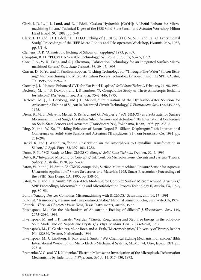
© 2002 by CRC Press LLC
Clark, J. D. L., J. L. Lund, and D. J. Edell, “Cesium Hydroxide [CsOH]: A Useful Etchant for Micro-machining Silicon,” Technical Digest of the 1988 Solid-State Sensor and Actuator Workshop, HiltonHead Island, SC, 1988, pp. 5–8.
Clark, L. D. and D. J. Edell, “KOH:H
2
O Etching of (110) Si, (111) Si, SiO
2
, and Ta: an ExperimentalStudy,” Proceedings of the IEEE Micro Robots and Tele-operators Workshop, Hyannis, MA, 1987,pp. 5/1–6.
Clemens, D. P., “Anisotropic Etching of Silicon on Sapphire,” 1973, p. 407. Compton, R. D., “PECVD: A Versatile Technology,”
Semicond. Int.,
July, 60–65, 1992. Core, T. A., W. K. Tsang, and S. J. Sherman, “Fabrication Technology for an Integrated Surface-Micro-
machined Sensor,”
Solid State Technol.,
36, 39–47, 1993. Craven, D., K. Yu, and T. Pandhumsoporn, “Etching Technology for “Through-The-Wafer” Silicon Etch-
ing,” Micromachining and Microfabrication Process Technology (Proceedings of the SPIE), Austin,TX, 1995, pp. 259–263.
Crowley, J. L., “Plasma Enhanced CVD for Flat Panel Displays,”
Solid State Technol.,
February, 94–98, 1992. Declercq, M. J., J. P. DeMoor, and J. P. Lambert, “A Comparative Study of Three Anisotropic Etchants
for Silicon,”
Electrochem. Soc. Abstracts,
75–2, 446, 1975. Declercq, M. J., L. Gerzberg, and J. D. Meindl, “Optimization of the Hydrazine-Water Solution for
Anisostropic Etching of Silicon in Integrated Circuit Technology,”
J. Electrochem. Soc.,
122, 545–552,1975.
Diem, B., M. T. Delaye, F. Michel, S. Renard, and G. Delapierre, “SOI(SIMOX) as a Substrate for SurfaceMicromachining of Single Crystalline Silicon Sensors and Actuators,” 7th International Conferenceon Solid-State Sensors and Actuators (Transducers ’93), Yokohama, Japan, 1993, pp. 233–6.
Ding, X. and W. Ko, “Buckling Behavior of Boron-Doped P
+
Silicon Diaphragms,” 6th InternationalConference on Solid-State Sensors and Actuators (Transducers ’91), San Francisco, CA, 1991, pp.201–204.
Drosd, R. and J. Washburn, “Some Observation on the Amorphous to Crystalline Transfomation inSilicon,”
J. Appl. Phys.,
53, 397–403, 1982. Dunn, P. N., “SOI:Ready to Meet CMOS Challenge,”
Solid State Technol.,
October, 32–5, 1993. Dutta, B., “Integrated Micromotor Concepts,” Int. Conf. on Microelectronic Circuits and Systems Theory,
Sydney, Australia, 1970, pp. 36–37. Eaton, W. P. and J. H. Smith, “A CMOS-compatible, Surface-Micromachined Pressure Sensor for Aqueous
Ultrasonic Application,” Smart Structures and Materials 1995. Smart Electronics (Proceedings ofthe SPIE), San Diego, CA, 1995, pp. 258–65.
Eaton, W. P. and J. H. Smith, “Release-Etch Modeling for Complex Surface Micromachined Structures,”SPIE Proceedings, Micromachining and Microfabrication Process Technology II, Austin, TX, 1996,pp. 80–93.
Editor, “Analog Devices Combines Micromachining with BICMOS,”
Semicond. Int.,
14, 17, 1991. Editorial, “Transducers, Pressure and Temperature, Catalog,” National Semiconductor, Sunnyvale, CA, 1974. Editorial,
Thermal Character Print Head,
Texas Instruments, Austin, 1977. Elwenspoek, M., “On the Mechanism of Anisotropic Etching of Silicon,”
J. Electrochem. Soc.,
140,2075–2080, 1993.
Elwenspoek, M. and J. P. van der Weerden, “Kinetic Roughening and Step Free Energy in the Solid-on-Solid Model and on Naphtalene Crystals,”
J. Phys. A: Math. Gen.,
20, 669–678, 1987. Elwenspoek, M., H. Gardeniers, M. de Boer, and A. Prak, “Micromechanics,” University of Twente, Report
No. 122830, Twente, Netherlands, 1994. Elwenspoek, M., U. Lindberg, H. Kok, and L. Smith, “Wet Chemical Etching Mechanism of Silicon,” IEEE
International Workshop on Micro Electro Mechanical Systems, MEMS ’94, Oiso, Japan, 1994, pp.223–8.
Eremenko, V. G. and V. I. Nikitenko, “Electron Microscope Investigation of the Microplastic DeformationMechanisms by Indentation,”
Phys. Stat. Sol. A,
14, 317–330, 1972.

© 2002 by CRC Press LLC
Ericson, F. and J. Å. Schweitz, “Micromechanical Fracture Strength of Silicon,”
J. Appl. Phys.,
68, 5840–4,1990.
Ericson, F., S. Greek, J. Soderkvist, and J. Å. Schweitz, “High Sensitive Internal Film Stress Measurementby an Improved Micromachined Indicator Structure,” 8th International Conference on Solid-StateSensors and Actuators (Transducers ’95), Stockholm, Sweden, June 1995, pp. 84–7.
Fan, L. S., “Integrated Micromachinery: Moving Structures on Silicon Chips,” Ph.D. thesis, University ofCalifornia at Berkeley, 1989.
Fan, L.-S., Y.-C. Tai, and R. S. Muller, “Pin Joints, Gears, Springs, Cranks, and Other Novel Microme-chanical Structures,” 4th International Conference on Solid-State Sensors and Actuators (Trans-ducers ’87), Tokyo, Japan, 1987, pp. 849–52.
Fan, L. S., Y. C. Tai, and R. S. Mulller, “Integrated Movable Micromechanical Structures for Sensors andActuators,”
IEEE Trans. Electron Devices,
35, 724–30, 1988. Fan, L. S., R. S. Muller, W. Yun, J. Huang, and R. T. Howe, “Spiral Microstructures for the Measurement
of Average Strain Gradients in Thin Films,” Proceedings. IEEE Micro Electro Mechanical Systems,(MEMS ’90), Napa Valley, CA, 1990, pp. 177–81.
Faust, J. W. and E. D. Palik, “Study of The Orientation Dependent Etching and Initial Anodization ofSi in Aqueous KOH,”
J. Electrochem. Soc.,
130, 1413–1420, 1983. Fedder, G. K., J. C. Chang, and R. T. Howe, “Thermal Assembly of Polysilicon Microactuators with
Narrow–Gap Electrostatic Comb Drive,” Technical Digest of the 1992 Solid State Sensor andActuator Workshop, Hilton Head Island, SC, 1992, pp. 63–8.
Field, L., “Low-Stress Nitrides for Use in Electronic Devices,” EECS/ERL Res. Summary, 42–43, Universityof California at Berkeley, 1987.
Finne, R. M. and D. L. Klein, “A Water-Amine-Complexing Agent System for Etching Silicon,”
J. Electrochem. Soc.,
114, 965–970, 1967. Fleischman, A. J., S. Roy, C. A. Zorman, M. Mehregany, and L. Matus, G., “Polycrystaline Silicon Carbide
for Surface Micromachining,” The Ninth Annual International Workshop on Micro ElectroMechanical Systems, San Diego, CA, 1996, pp. 234–238.
Forster, J. H. and J. B. Singleton, “Beam–Lead Sealed Junction Integrated Circuits,”
Bell LaboratoriesRecord,
44, 313–317, 1966. Frazier, A. B. and M. G. Allen, “Metallic Microstructures Fabricated Using Photosensitive Polyimide
Electro-plating Molds,”
J. Microelectromech. Syst.,
2, 87–94, 1993. Fresquet, G., C. Azzaro, and J.-P. Couderc, “Analysis and Modeling of In Situ Boron-Doped Polysilicon
Deposition by LP CVD,”
J. Electrochem. Soc.,
142, 538–47, 1995. Gabriel, K., J. Jarvis, and W. Trimmer, “Small Machines, Large Opportunities: A Report on the Emerging
Field of Microdynamics,” National Science Foundation, 1989. Gennissen, P. T. J., M. Bartke, P. J. French, P. M. Sarro, and R. F. Wolffenbuttel, “Automatic Etch Stop on
Buried Oxide Using Epitaxial Lateral Overgrowth,” 8th International Conference on Solid-StateSensors and Actuators (Transducers ’95), Stockholm, Sweden, June 1995, pp. 75–8.
Ghandi, S. K.,
The Theory and Practice of Micro-electronics,
John Wiley & Sons, New York, 1968. Glembocki, O. J., R. E. Stahlbush, and M. Tomkiewicz, “Bias-Dependent Etching of Silicon in Aqueous
KOH,”
J. Electrochem. Soc.,
132, 145–151, 1985. Goetzlich, J. and H. Ryssel, “Tapered Windows in Silicon Dioxide, Silicon Nitride, and Polysilicon Layers
by Ion Implantation,”
J. Electrochem. Soc.,
128, 617–9, 1981. Gogoi, B. P. and C. H. Mastrangelo, “Post-Processing Release of Microstructures by Electromagnetic
Pulses,” 8th International Conference on Solid-State Sensors and Actuators (Transducers ’95),Stockholm, Sweden, June 1995, pp. 214–7.
Goosen, J. F. L., B. P. van Drieenhuizen, P. J. French, and R. F. Wolfenbuttel, “Stress MeasurementStructures for Micromachined Sensors,” 7th International Conference on Solid-State Sensors andActuators (Transducers ’93), Yokohama, Japan, 1993, pp. 783–6.
Gravesen, P., “Silicon Sensors,” Status report for the industrial engineering thesis, DTH Lyngby, Denmark,1986.

© 2002 by CRC Press LLC
Greek, S., F. Ericson, S. Johansson, and J.-Å. Schweitz, “In Situ Tensile Strength Measurement of Thick-Film and Thin-Film Micromachined Structures,” 8th International Conference on Solid-StateSensors and Actuators (Transducers ’95), Stockholm, Sweden, June 1995, pp. 56–9.
Greenwood, J. C., “Ethylene Diamine-Cathechol-Water Mixture Shows Preferential Etching of p-n Junc-tion,”
J. Electrochem. Soc.,
116, 1325–1326, 1969. Greenwood, J. C., “Etched Silicon Vibrating Sensor,”
J. Phys. E, Sci. Instrum.,
17, 650–652, 1984a. Greenwood, J. C., “Silicon in Mechanical Sensors,”
J. Phys. E, Sci. Instrum.,
21, 1114–1128, 1988b. Greiff, P., “SOI-based Micromechanical Process,” Micromachining and Microfabrication Process Tech-
nology (Proceedings of the SPIE), Austin, TX, 1995, pp. 74–81. Guckel, H. and D. W. Burns, “Planar Processed Polysilicon Sealed Cavities for Pressure Transducer Arrays,”
IEEE International Electron Devices Meeting. Technical Digest, IEDM ’84, San Francisco, CA, 1984,pp. 223–5.
Guckel, H. and D. W. Burns, “A Technology for Integrated Transducers,” International Conference onSolid-State Sensors and Actuators, Philadelphia, PA, 1985, pp. 90–2.
Guckel, H., T. Randazzo, and D. W. Burns, “A Simple Technique for the Determination of MechanicalStrain in Thin Films with Applications to Polysilicon,”
J. Appl. Phys.,
57, 1671–5, 1985. Guckel, H., D. K. Showers, D. W. Burns, C. R. Rutigliano, and C. G. Nesler, “Deposition Techniques and
Properties of Strain Compensated LP CVD Silicon Nitride,” Technical Digest of the 1986 SolidState Sensor and Actuator Workshop, Hilton Head Island, SC, 1986.
Guckel, H., D. W. Burns, C. K. Nesler, and C. R. Rutigliano, “Fine Grained Polysilicon and Its Applicationto Planar Pressure Transducers,” 4th International Conference on Solid-State Sensors and Actuators(Transducers ’87), Tokyo, Japan, 1987, pp. 277–282.
Guckel, H., D. W. Burns, C. C. G. Visser, H. A. C. Tilmans, and D. Deroo, “Fine-grained Polysilicon Filmswith Built–in Tensile Strain,”
IEEE Trans. Electron Devices,
35, 800–1, 1988. Guckel, H., D. W. Burns, H. A. C. Tilmans, C. C. G. Visser, D. W. DeRoo, T. R. Christenson, P. J. Klomberg,
J. J. Sniegowski, and D. H. Jones, “Processing Conditions for Polysilicon Films with Tensile Strainfor Large Aspect Ratio Microstructures,” Technical Digest of the 1988 Solid State Sensor andActuator Workshop, Hilton Head Island, SC, 1988, pp. 51–6.
Guckel, H., D. W. Burns, H. A. C. Tilmans, D. W. DeRoo, and C. R. Rutigliano, “Mechanical Propertiesof Fine Grained Polysilicon: The Repeatability Issue,” Technical Digest of the 1988 Solid StateSensor and Actuator Workshop, Hilton Head Island, SC, 1988, pp. 96–9.
Guckel, H., J. J. Sniegowski, T. R. Christenson, S. Mohney, and T. F. Kelly, “Fabrication of MicromechanicalDevices from Polysilicon Films with Smooth Surfaces,”
Sensors and Actuators A,
20, 117–21, 1989. Guckel, H., J. J. Sniegowski, T. R. Christenson, and F. Raissi, “The Application of Fine-Grained, Tensile
Polysilicon to Mechanically Resonant Transducers,”
Sensors and Actuators A,
21, 346–351, 1990. Hallas, C. E., “Electropolishing Silicon,”
Solid State Technol.,
14, 30–32, 1971. Harbeke, G., L. Krausbauer, E. F. Steigmeier, and A. E. Widmer, “LP CVD Polycrystalline Silicon: Growth
and Physical Properties of In-Situ Phosphorous Doped and Undoped Films,”
RCA Rev.,
44,287–313, 1983.
Harris, T. W.,
Chemical Milling,
Clarendon Press, Oxford, 1976. Hendriks, M. and C. Mavero, “Phosphorous Doped Polysilicon for Double Poly Structures. Part I.
Morphology and Microstructure,”
J. Electrochem. Soc.,
138, 1466–1470, 1991. Hendriks, M., R. Delhez, and S. Radelaar, “Carbon Doped Polycrystalline Silicon Layers,” in
Studies inInorganic Chemistry,
Elsevier, Amsterdam, 1983, p. 193. Herb, J. A., M. G. Peters, S. C. Terry, and J. H. Jerman, “PECVD Diamond Films for Use in Silicon
Microstructures,”
Sensors and Actuators A,
23, 982–7, 1990. Hermansson, K., U. Lindberg, B. Hok, and G. Palmskog, “Wetting Properties of Silicon Surfaces,” 6th
International Conference on Solid-State Sensors and Actuators (Transducers ’91), San Francisco,CA, 1991, pp. 193–6.

© 2002 by CRC Press LLC
Herr, E. and H. Baltes, “KOH Etch Rates of High–Index Planes from Mechanically Prepared SiliconCrystals,” 6th International Conference on Solid-State Sensors and Actuators (Transducers ’91),San Francisco, CA, 1991, pp. 807–810.
Hesketh, P. J., C. Ju, S. Gowda, E. Zanoria, and S. Danyluk, “Surface Free Energy Model of SiliconAnisotropic Etching,”
J. Electrochem. Soc.,
140, 1080–1085, 1993. Heuberger, A.,
Mikromechanik,
Springer-Verlag, Heidelberg, 1989. Hirata, M., K. Suzuki, and H. Tanigawa, “Silicon Diaphragm Pressure Sensors Fabricated by Anodic
Oxidation Etch-Stop,”
Sensors and Actuators A,
13, 63–70, 1988. Hoffman, E., B. Warneke, E. Kruglick, J. Weigold, and K. S. J. Pister, “3D Structures with Piezoresistive
Sensors in Standard CMOS,” Proceedings. IEEE Micro Electro Mechanical Systems (MEMS ’95),Amsterdam, Netherlands, 1995, pp. 288–93.
Hoffman, R. W., “Stresses in Thin Films : The Relevance of Grain Boundaries and Impurities,”
Thin SolidFilms,
34, 185–90, 1975.Hoffman, R. W., “Mechanical Properties of Non-Metallic Thin Films,” in
Physics of Nonmetallic ThinFilms
(
NATO Advanced Study Institutes Series: Series B, Physics
), Dupuy, C. H. S. and Cachard, A.,Eds., Plenum Press, New York, 1976, pp. 273–353.
Hoffmeister, W., “Determination of the Etch Rate of Silicon in Buffered HF Using a
31
Si Tracer Method,”
Int. J. Appl. Radiation and Isotopes,
2, 139, 1969. Holbrook, D. S. and J. D. McKibben, “Microlithography for Large Area Flat Panel Display Substrates,”
Solid State Technol.,
May, 166–172, 1992. Holland, C. E., E. R. Westerberg, M. J. Madou, and T. Otagawa,
Etching Method for Producing anElectrochemical Cell in a Crystalline Substrate,
U.S. Patent 4,764,864, 1988. Hornbeck, L. J., “Projection Displays and MEMS: Timely Convergence for a Bright Future,” Micro-machining
and Microfabrication Process Technology (Proceedings of the SPIE), Austin, TX, 1995, p. 2. Houston, M. R., R. Maboudian, and R. Howe, “Ammonium Fluoride Anti-Stiction Treatment for Poly-
silicon Microstructures,” 8th International Conference on Solid-State Sensors and Actuators(Transducers ’95), Stockholm, Sweden, June 1995, pp. 210–3.
Howe, R. T., “Polycrystalline Silicon Microstructures,” in
Micromachining and Micropackaging of Transducers,
Fung, C. D., Cheung, P. W., Ko, W. H., and Fleming, D. G., Eds., Elsevier, New York, 1985, pp. 169–87. Howe, R. T., “Resonant Microsensors,” 4th International Conference on Solid-State Sensors and Actuators
(Transducers ’87), Tokyo, Japan, 1987, pp. 843–8. Howe, R. T., “Polysilicon Integrated Microsystems: Technologies and Applications,” 8th International
Conference on Solid-State Sensors and Actuators (Transducers ’95), Stockholm, Sweden, June,1995a, pp. 43–6.
Howe, R. T., “Recent Advances in Surface Micromachining,” 13th Sensor Symposium. Technical Digest,Tokyo, Japan, 1995b, pp. 1–8.
Howe, R. T. and R. S. Muller, “Polycrystalline Silicon Micromechanical Beams,” Spring Meeting of TheElectrochemical Society, Montreal, Canada, 1982, pp. 184–5.
Howe, R. T. and R. S. Muller, “Polycrystalline Silicon Micromechanical Beams,”
J. Electrochem. Soc.,
130,1420–1423, 1983a.
Howe, R. T. and R. S. Muller, “Stress in Polycrystalline and Amorphous Silicon Thin Films,”
J. Appl. Phys.,
54, 4674–5, 1983b. Hu, J. Z., L. D. Merkle, C. S. Menoni, and I. L. Spain, “Crystal Data for High–Presure Phases of Silicon,”
Phys. Rev. B,
34, 4679–4684, 1986. Hu, S. M. and D. R. Kerr, “Observation of Etching of n-type Silicon in Aqueous HF Solutions,”
J. Electrochem. Soc.,
114, 414, 1967. Huff, M. A. and M. A. Schmidt, “Fabrication, Packaging and Testing of a Wafer Bonded Microvalve,”
Technical Digest of the 1992 Solid State Sensor and Actuator Workshop, Hilton Head Island, SC,1992, pp. 194–197.
Iscoff, R., “Hotwall LP CVD Reactors: Considering the Choices,”
Semicond. Int.,
June, 60–64, 1991.

© 2002 by CRC Press LLC
Jaccodine, R. J. and W. A. Schlegel, “Measurements of Strains at Si-SiO
2
Interface,”
J. Appl. Phys.,
37,2429–34, 1966.
Jackson, K. A., “A Review of the Fundamental Aspects of Crystal Growth,” Crystal Growth, Boston, MA,1966, pp. 17–24.
Jackson, T. N., M. A. Tischler, and K. D. Wise, “An Electrochemical P-N Junction Etch-Stop for theFormation of Silicon Microstructures,”
IEEE Electron Device Lett.,
EDL–2, 44–45, 1981. Jerman, H., “Bulk Silicon Micromachining,” Hardcopies of viewgraphs, 1994, Banf, Canada. Jerman, J. H., “The Fabrication and Use of Micro-machined Corrugated Silicon Diaphragms,”
Sensorsand Actuators A,
23, 988–92, 1990. Joseph, J., M. Madou, T. Otagawa, P. Hesketh, and A. Saaman, “Catheter-Based Micromachined Electro-
chemical Sensors,” Catheter-Based Sensing and Imaging Technology (Proceedings of the SPIE),Los Angeles, CA, 1989, pp. 18–22.
Judy, M. W. and R. T. Howe, “Highly Compliant Lateral Suspensions Using Sidwall Beams,” 7th Inter-national Conference on Solid-State Sensors and Actuators (Transducers ’93), Yokohama, Japan,1993a, pp. 54–57.
Judy, M. W. and R. T. Howe, “Hollow Beam Polysilicon Lateral Resonators,” Proceedings IEEE MicroElectro Mechanical Systems (MEMS ’93), Fort Lauderdale, FL, 1993b, pp. 265–271.
Judy, M. W., Y. H. Cho, R. T. Howe, and A. P. Pisano, “Self-Adjusting Microstructures (SAMS),” Proceed-ings. IEEE Micro Electro Mechanical Systems (MEMS ’91), Nara, Japan, 1991, pp. 51–6.
Jung, K. H., S. Shih, and D. L. Kwong, “Developments in Luminescent Porous Si,”
J. Electrochem. Soc.,
140, 3046–3064, 1993. Kahn, H., S. Stemmer, K. Nandakumar, A. H. Heuer, R. L. Mullen, R. Ballarini, and M. A. Huff, “Mechan-
ical Properties of Thick, Surface Micromachined Polysilicon Films,” Ninth Annual InternationalWorkshop on Micro Electro Mechanical Systems, San Diego, CA, 1996, pp. 343–348.
Kaminsky, G., “Micromachining of Silicon Mechanical Structures,”
J. Vac. Sci. Technol.,
B3, 1015–1024, 1985.Kanda, Y., “A Graphical Representation of the Piezoresistance Coefficients in Silicon,”
IEEE Trans. ElectronDevices,
ED–29, 64–70, 1982. Kanda, Y., “What Kind of SOI Wafers are Suitable for What Type of Micromachining Purposes?” 6th
International Conference on Solid-State Sensors and Actuators (Transducers ’91), San Francisco,CA, 1991, pp. 452–5.
Keller, C. and M. Ferrari, “Milli-Scale Polysilicon Structures,” Technical Digest of the 1994 Solid StateSensor and Actuator Workshop, Hilton Head Island, SC, 1994, pp. 132–137.
Keller, C. G. and R. T. Howe, “Hexsil Bimorphs for Vertical Actuation,” 8th International Conference onSolid-State Sensors and Actuators (Transducers ’95), Stockholm, Sweden, June 1995a, pp. 99–102.
Keller, C. G. and R. T. Howe, “Nickel-Filled Hexsil Thermally Actuated Tweezers,” 8th InternationalConference on Solid-State Sensors and Actuators (Transducers ’95), Stockholm, Sweden, June1995b, pp. 376–379.
Kendall, D. L., “On Etching Very Narrow Grooves in Silicon,”
Appl. Phys. Lett.,
26, 195–198, 1975. Kendall, D. L., “Vertical Etching of Silicon at Very High Aspect Ratios,”
Ann. Rev. Mater. Sci., 9, 373–403,1979.
Kendall, D. L. and G. R. de Guel, “Orientation of the Third Kind: The Coming of Age of (110) Silicon,”in Micromachining and Micropackaging of Transducers, Fung, C. D., Ed., Elsevier, New York, 1985,pp. 107–124.
Kenney, D. M., Methods of Isolating Chips of a Wafer of Semiconductor Material, in U.S. Patent 3,332,137,1967.
Kermani, A., K. E. Johnsgard, and W. Fred, “Single Wafer RT CVD of Polysilicon,” Solid State Technol.,May, 71–73, 1991.
Kern, W. and C. A. Deckert, “Chemical Etching,” in Thin Film Processes, Vossen, J. L. and Kern, W., Eds.,Academic Press, Orlando, 1978.
Kern, W., “Chemical Etching of Silicon, Germanium, Gallium Arsenide, and Gallium Phosphide,” RCARev., 39, 278–308, 1978.
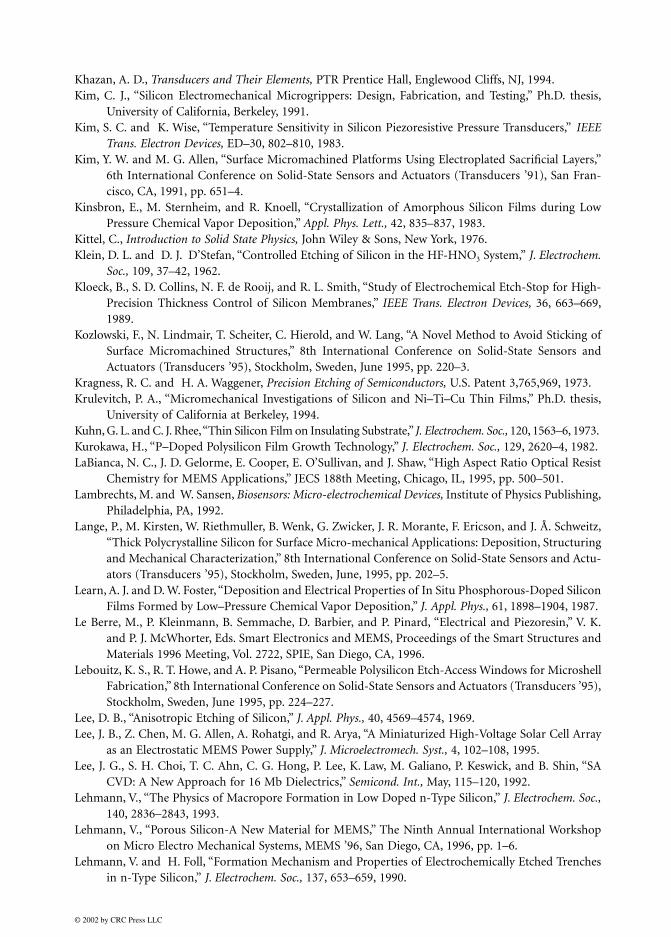
© 2002 by CRC Press LLC
Khazan, A. D., Transducers and Their Elements, PTR Prentice Hall, Englewood Cliffs, NJ, 1994. Kim, C. J., “Silicon Electromechanical Microgrippers: Design, Fabrication, and Testing,” Ph.D. thesis,
University of California, Berkeley, 1991. Kim, S. C. and K. Wise, “Temperature Sensitivity in Silicon Piezoresistive Pressure Transducers,” IEEE
Trans. Electron Devices, ED–30, 802–810, 1983. Kim, Y. W. and M. G. Allen, “Surface Micromachined Platforms Using Electroplated Sacrificial Layers,”
6th International Conference on Solid-State Sensors and Actuators (Transducers ’91), San Fran-cisco, CA, 1991, pp. 651–4.
Kinsbron, E., M. Sternheim, and R. Knoell, “Crystallization of Amorphous Silicon Films during LowPressure Chemical Vapor Deposition,” Appl. Phys. Lett., 42, 835–837, 1983.
Kittel, C., Introduction to Solid State Physics, John Wiley & Sons, New York, 1976. Klein, D. L. and D. J. D’Stefan, “Controlled Etching of Silicon in the HF-HNO3 System,” J. Electrochem.
Soc., 109, 37–42, 1962. Kloeck, B., S. D. Collins, N. F. de Rooij, and R. L. Smith, “Study of Electrochemical Etch-Stop for High-
Precision Thickness Control of Silicon Membranes,” IEEE Trans. Electron Devices, 36, 663–669,1989.
Kozlowski, F., N. Lindmair, T. Scheiter, C. Hierold, and W. Lang, “A Novel Method to Avoid Sticking ofSurface Micromachined Structures,” 8th International Conference on Solid-State Sensors andActuators (Transducers ’95), Stockholm, Sweden, June 1995, pp. 220–3.
Kragness, R. C. and H. A. Waggener, Precision Etching of Semiconductors, U.S. Patent 3,765,969, 1973. Krulevitch, P. A., “Micromechanical Investigations of Silicon and Ni–Ti–Cu Thin Films,” Ph.D. thesis,
University of California at Berkeley, 1994. Kuhn, G. L. and C. J. Rhee, “Thin Silicon Film on Insulating Substrate,” J. Electrochem. Soc., 120, 1563–6, 1973. Kurokawa, H., “P–Doped Polysilicon Film Growth Technology,” J. Electrochem. Soc., 129, 2620–4, 1982. LaBianca, N. C., J. D. Gelorme, E. Cooper, E. O’Sullivan, and J. Shaw, “High Aspect Ratio Optical Resist
Chemistry for MEMS Applications,” JECS 188th Meeting, Chicago, IL, 1995, pp. 500–501. Lambrechts, M. and W. Sansen, Biosensors: Micro-electrochemical Devices, Institute of Physics Publishing,
Philadelphia, PA, 1992. Lange, P., M. Kirsten, W. Riethmuller, B. Wenk, G. Zwicker, J. R. Morante, F. Ericson, and J. Å. Schweitz,
“Thick Polycrystalline Silicon for Surface Micro-mechanical Applications: Deposition, Structuringand Mechanical Characterization,” 8th International Conference on Solid-State Sensors and Actu-ators (Transducers ’95), Stockholm, Sweden, June, 1995, pp. 202–5.
Learn, A. J. and D. W. Foster, “Deposition and Electrical Properties of In Situ Phosphorous-Doped SiliconFilms Formed by Low–Pressure Chemical Vapor Deposition,” J. Appl. Phys., 61, 1898–1904, 1987.
Le Berre, M., P. Kleinmann, B. Semmache, D. Barbier, and P. Pinard, “Electrical and Piezoresin,” V. K.and P. J. McWhorter, Eds. Smart Electronics and MEMS, Proceedings of the Smart Structures andMaterials 1996 Meeting, Vol. 2722, SPIE, San Diego, CA, 1996.
Lebouitz, K. S., R. T. Howe, and A. P. Pisano, “Permeable Polysilicon Etch-Access Windows for MicroshellFabrication,” 8th International Conference on Solid-State Sensors and Actuators (Transducers ’95),Stockholm, Sweden, June 1995, pp. 224–227.
Lee, D. B., “Anisotropic Etching of Silicon,” J. Appl. Phys., 40, 4569–4574, 1969. Lee, J. B., Z. Chen, M. G. Allen, A. Rohatgi, and R. Arya, “A Miniaturized High-Voltage Solar Cell Array
as an Electrostatic MEMS Power Supply,” J. Microelectromech. Syst., 4, 102–108, 1995. Lee, J. G., S. H. Choi, T. C. Ahn, C. G. Hong, P. Lee, K. Law, M. Galiano, P. Keswick, and B. Shin, “SA
CVD: A New Approach for 16 Mb Dielectrics,” Semicond. Int., May, 115–120, 1992. Lehmann, V., “The Physics of Macropore Formation in Low Doped n-Type Silicon,” J. Electrochem. Soc.,
140, 2836–2843, 1993.Lehmann, V., “Porous Silicon-A New Material for MEMS,” The Ninth Annual International Workshop
on Micro Electro Mechanical Systems, MEMS ’96, San Diego, CA, 1996, pp. 1–6. Lehmann, V. and H. Foll, “Formation Mechanism and Properties of Electrochemically Etched Trenches
in n-Type Silicon,” J. Electrochem. Soc., 137, 653–659, 1990.

© 2002 by CRC Press LLC
Lehmann, V. and U. Gosele, “Porous Silicon Formation: A Quantum Wire Effect,” Appl. Phys. Lett., 58,856–858, 1991.
Lepselter, M. P., “Beam Lead Technology,” Bell. Sys. Tech. J., 45, 233–254, 1966. Lepselter, M. P., Integrated Circuit Device and Method, U.S. Patent 3,335,338, 1967. Levy, R. A. and K. Nassau, “Viscous Behavior of Phosphosilicate and Borophosphosilicate Galsses in VLSI
Processing,” Solid State Technol., October, 123–30, 1986. Levy-Clement, C., A. Lagoubi, R. Tenne, and M. Neumann-Spallart, “Photoelectrochemical Etching of
Silicon,” Electrochim. Acta, 37, 877–888, 1992. Lewerenz, H. J., J. Stumper, and L. M. Peter, “Deconvolution of Charge Injection Steps in Quantum Yield
Multiplication on Silicon,” Phys. Rev. Lett., 61, 1989–92, 1988. Lietoila, A., A. Wakita, T. W. Sigmon, and J. F. Gibbons, “Epitaxial Regrowth of Intrinsic,
31P–Doped and
Compensated (31P+11
B-Doped) Amorphous Si,” J. Appl. Phys., 53, 4399–4405, 1982. Lin, G., K. S. J. Pister, and K. P. Roos, “Standard CMOS Piezoresistive Sensor to Quantify Heart Cell
Contractile Forces,” The Ninth Annual International Workshop on Micro Electro MechanicalSystems, MEMS ’96, San Diego, CA, 1996, pp. 150–155.
Lin, L., R. T. Howe, and A. P. Pisano, “A Novel In Situ Micro Strain Gauge,” Proceedings IEEE MicroElectro Mechanical Systems, (MEMS ’93), Fort Lauderdale, FL, 1993, pp. 201–206.
Lin, L., “Selective Encapsulations of MEMS: Micro Channels, Needles, Resonators and ElectromechanicalFilters,” Ph.D. thesis, University of California at Berkeley, 1993.
Lin, L. Y., S. S. Lee, M. C. Wu, and K. S. J. Pister, “Micromachined Integrated Optics for Free-SpaceInterconnections,” Proceedings IEEE Micro Electro Mechanical Systems, (MEMS ’95), Amsterdam,Netherlands, 1995, pp. 77–82.
Lin, T.-H., “Flexure-Beam Micromirror Devices and Potential Expansion for Smart Micromachining,”Proceedings SPIE, Smart Electronics and MEMS, San Diego, CA, 1996, pp. 20–29.
Linde, H. and L. Austin, “Wet Silicon Etching with Aqueous Amine Gallates,” J. Electrochem. Soc., 139,1170–1174, 1992.
Liu, J., Y.-C. Tai, J. Lee, K.-C. Pong, Y. Zohar, and C.-H. Ho, “In Situ Monitoring and Universal Modelingof Sacrificial PSG Etching Using Hydrofluoric Acid,” Proceedings of Micro Electro MechanicalSystems, IEEE, Fort Lauderdale, FL, 1993, pp. 71–76.
Lober, T. A. and R. T. Howe, “Surface Micromachining for Electrostatic Microactuator Fabrication,”Technical Digest of the 1988 Solid State Sensor and Actuator Workshop, Hilton Head Island, SC,1988, pp. 59–62.
Lober, T. A., J. Huang, M. A. Schmidt, and S. D. Senturia, “Characterization of the Mechanisms ProducingBending Moments in Polysilicon Micro-Cantilever Beams by Interferometric Deflection Measure-ments,” Technical Digest of the 1988 Solid State Sensor and Actuator Workshop, Hilton HeadIsland, SC, 1988, pp. 92–95.
Lochel, B., A. Maciossek, H. J. Quenzer, and B. Wagner, “UV Depth Lithography and Galvanoformingfor Micromachining,” Electrochemical Microfabrication II, Miami Beach, FL, 1994, pp. 100–111.
Lochel, B., A. Maciossek, H. J. Quenzer, and B. Wagner, “Ultraviolet Depth Lithography and Galvano-forming for Micromachining,” J. Electrochem. Soc., 143, 237–244, 1996.
Loechel, B., M. Rothe, S. Fehlberg, G. Gruetzner, and G. Bleidiessel, “Influence of Resist Baking on thePattern Quality of Thick Photoresists,” SPIE–Micromachining and Microfabrication Process Tech-nology II, Austin, TX, 1996, pp. 174–181.
Luder, E., “Polcrystalline Silicon-Based Sensors,” Sensors and Actuators A, 10, 9–23, 1986. Madou, M. J., “Compatibility and Incompatibility of Chemical Sensors and Analytical Equipment with
Micromachining,” Technical Digest of the 1994 Solid-State Sensor and Actuator Workshop, HiltonHead Island, SC, 1994, pp. 164–171.
Madou, M. J. and S. R. Morrison, Chemical Sensing with Solid State Devices, Academic Press, New York,1989.
Madou, M. J. and T. Otagawa, Microelectrochemical Sensor and Sensor Array, U.S. Patent 4,874,500, 1989.

© 2002 by CRC Press LLC
Madou, M. J., K. W. Frese, and S. R. Morrison, “Photoelectrochemical Corrosion of Semiconductors forSolar Cells,” SPIE, 248, 88–95, 1980.
Madou, M. J., B. H. Loo, K. W. Frese, and S. R. Morrison, “Bulk and Surface Characterization of theSilicon Electrode,” Surf. Sci., 108, 135–152, 1981.
Man, P. F., B. P. Gogoi, and C. H. Mastrangelo, “Elimination of Post–Release Adhesion in Micro-structuresUsing Thin Conformal Fluorocarbon Films,” Ninth Annual International Workshop on MicroElectro Mechanical Systems, MEMS ’96, San Diego, CA, 1996, pp. 55–60.
Marco, S., J. Samitier, O. Ruiz, J. R. Morante, J. Esteve-Tinto, and J. Bausells, “Stress Measurements ofSiO2-Polycrystalline Silicon Structures for Micro-mechanical Devices by Means of Infrared Spec-troscopy Technique,” 6th International Conference on Solid-State Sensors and Actuators (Trans-ducers ’91), San Francisco, CA, 1991, pp. 209–12.
Maseeh, F. and S. D. Senturia, “Elastic Properties of Thin Polyimide Films,” in Polyimides: Materials,Chemistry and Characterization, Feger, C., Khojasteh, M. M., and McGrath, J. E., Eds., Elesevier,Amsterdam, 1989, pp. 575–584.
Maseeh, F. and S. D. Senturia, “Plastic Deformation of Highly Doped Silicon,” Sensors and Actuators A,23, 861–865, 1990.
Maseeh, F. and S. D. Senturia, “Viscoelasticity and Creep Recovery of Polyimide Thin Films,” TechnicalDigest of the 1990 Solid-State Sensor and Actuator Workshop, Hilton Head Island, SC, 1990, pp.55–60.
Maseeh-Tehrani, F., “Characterization of Mechanical Properties of Microelectronic Thin Films,” Ph.D.thesis, Massachusetts Institute of Technology, Cambridge, 1990.
Mastrangelo, C. H. and C. H. Hsu, “Mechanical Stability and Adhesion of Microstructures under CapillaryForces-Part I: Basic Theory,” J. Microelectromech. Syst., 2, 33–43, 1993a.
Mastrangelo, C. H. and C. H. Hsu, “Mechanical Stability and Adhesion of Microstructures under CapillaryForces-Part II: Experiments,” J. Microelectromech. Syst., 2, 44–55, 1993b.
Mastrangelo, C. H. and G. S. Saloka, “A Dry-Release Method Based on Polymer Columns for Micro-structure Fabrication,” Proceedings IEEE Micro Electro Mechanical Systems, (MEMS ’93), FortLauderdale, FL, 1993, pp. 77–81.
Matson, E. A. and S. A. Polysakov, “On the Evolutionary Selection Principle in Relation to the Growthof Polycrystalline Silicon Films,” Phys. Sta. Sol. (a), 41, K93–K95, 1977.
Matsumura, M. and S. R. Morrison, “Photoanodic Properties of an n-Type Silicon Electrode in AqueousSolution Containing Fluorides,” J. Electroanal. Chem., 144, 113–120, 1983.
Mayer, G. K., H. L. Offereins, H. Sandmeier, and K. Kuhl, “Fabrication of Non-Underetched ConvexCorners in Ansisotropic Etching of (100)-Silicon in Aqueous KOH with Respect to Novel Micro-mechanic Elements,” J. Electrochem. Soc., 137, 3947–3951, 1990.
McNeil, V. M., S. S. Wang, K.-Y. Ng, and M. A. Schmidt, “An Investigation of the Electrochemical Etchingof (100) Silicon in CsOH and KOH,” Technical Digest of the 1990 Solid-State Sensor and ActuatorWorkshop, Hilton Head Island, SC, 1990, pp. 92–97.
Meek, R. L., “Electrochemically Thinned N/N+ Epitaxial Silicon-Method and Applications,”J. Electrochem. Soc., 118, 1240–1246, 1971.
Mehregany, M. and S. D. Senturia, “Anisotropic Etching of Silicon in Hydrazine,” Sensors and Actuators A,13, 375–390, 1988.
Mehregany, M., R. T. Howe, and S. D. Senturia, “Novel Microstructures for the In Situ Measurement ofMechanical Properties of Thin Films,” J. Appl. Phys., 62, 3579–84, 1987.
Mehregany, M., K. J. Gabriel, and W. S. N. Trimmer, “Integrated Fabrication of Polysilicon Mechanisms,”IEEE Trans. Electron Devices, 35, 719–23, 1988.
Memming, R. and G. Schwandt, “Anodic Dissolution of Silicon in Hydrofluoric Acid Solutions,” Surf.Sci., 4, 109–24, 1966.
Metzger, H. and F. R. Kessler, “Der Debye-Sears Effect zur Bestimmung der Elastischen Konstanten vonSilicium,” Z. Naturf., A25, 904–906, 1970.

© 2002 by CRC Press LLC
Meyerson, B. S. and W. Olbricht, “Phosphorous-Doped Polycrystalline Silicon Via LPCVD I. ProcessCharacterization,” J. Electrochem. Soc., 131, 2361–2365, 1984.
Middlehoek, S. and U. Dauderstadt, “Haben Mikrosensoren aus Silizium eine Zukunft?” TechnischeRundschau, July, 102–105, 1994.
Mlcak, R., H. L. Tuller, P. Greiff, and J. Sohn, “Photo Assisted Electromechanical Machining of Micro-mechanical Structures,” Proceedings IEEE Micro Electro Mechanical Systems (MEMS ’93), FortLauderdale, FL, 1993, pp. 225–229.
Monk, D. J., D. S. Soane, and R. T. Howe, “LPCVD Silicon Dioxide Sacrificial Layer Etching for SurfaceMicromachining,” Smart Materials Fabrication and Materials for Micro-Electro-Mechanical Sys-tems, San Francisco, CA, 1992, pp. 303–310.
Monk, D. J., D. S. Soane, and R. T. Howe, “Hydrofluoric Acid Etching of Silicon Dioxide Sacrificial Layers.Part II. Modeling,” J. Electrochem. Soc., 141, 270–274, 1994a.
Monk, D. J., D. S. Soane, and R. T. Howe, “Hydrofluoric Acid Etching of Silicon Dioxide Sacrificial Layers.Part I. Experimental Observations,” J. Electrochem. Soc., 141, 264–269, 1994b.
Morrison, S. R., Electrochemistry on Semiconductors and Oxidized Metal Electrodes, Plenum Press, NewYork, 1980.
Mulder, J. G. M., P. Eppenga, M. Hendriks, and J. E. Tong, “An Industrial LP CVD Process for In SituPhosphorus-Doped Polysilicon,” J. Electrochem. Soc., 137, 273–279, 1990.
Mulhern, G. T., D. S. Soane, and R. T. Howe, “Supercritical Carbon Dioxide Drying of Micro-structures,”7th International Conference on Solid-State Sensors and Actuators (Transducers ’93), Yokohama,Japan, 1993, pp. 296–9.
Muller, R. S., “From IC’s to Microstructures: Materials and Technologies,” Proceedings of the IEEE MicroRobots and Teleoperators Workshop, Hyannis, MA, 1987, pp. 2/1–5.
Muraoka, H., T. Ohashi, and T. Sumitomo, “Controlled Preferential Etching Technology,” SemiconductorSilicon 1973, Chicago, IL, 1973, pp. 327–338.
Murarka, S. P. and T. F. J. Retajczyk, “Effect of Phosphorous Doping on Stress in Silicon and PolycrystallineSilicon,” J. Appl. Phys., 54, 2069–2072, 1983.
Nakamura, M., S. Hoshino, and H. Muro, “Monolithic Sensor Device for Detecting Mechanical Vibra-tion,” Densi Tokyo, 24 (IEE Tokyo Section), 87–8, 1985.
Nathanson, H. C., W. E. Newell, R. A. Wickstrom, and J. R. Davis, “The Resonant Gate Transistor,” IEEETrans. Electron Devices, ED–14, 117–133, 1967.
Neudeck, G. W. and et. al., “Three Dimensional Devices Fabricated by Silicon Epitaxial Lateral Overgroth,”J. Electron. Mater., 19, 1111–1117, 1990.
Nikanorov, S. P., Y. A. Burenkov, and A. V. Stepanov, “Elastic Properties of Silicon,” Sov. Phys.-Solid State,13, 2516–2518, 1972.
Nishioka, T., Y. Shinoda, and Y. Ohmachi, “Raman Microprobe Analysis of Stress in Ge and GaAs/Ge onSilicon Dioxide-Coated Silicon Substrates,” J. Appl. Phys., 57, 276–81, 1985.
North, J. C., T. E. McGahan, D. W. Rice, and A. C. Adams, “Tapered Windows in Phosphorous-DopedSilicon Dioxide by Ion Implantation,” IEEE Trans. Electron Devices, ED–25, 809–12, 1978.
Noworolski, J. M., E. Klaassen, J. Logan, K. Petersen, and N. Maluf, “Fabrication of SOI Wafers WithBuried Cavities Using Silicon Fusion Bonding and Electro-chemical Etchback,” 8th InternationalConference on Solid-State Sensors and Actuators (Transducers ’95), Stockholm, Sweden, June 1995,pp. 71–4.
Nunn, T. and J. Angell, “An IC Absolute Pressure Transducer with Built–in Reference Chamber,” Work-shop on Indwelling Pressure Transducers and Systems, Cleveland, OH, 1975, pp. 133–136.
O’Neill, P., “A Monolithic Thermal Converter,” Hewlett-Packard J., 31, 12–13, 1980. Obermeier, E., “High Temperature Microsensors Based on Polycrystalline Diamond Thin Films,” 8th
International Conference on Solid-State Sensors and Actuators (Transducers ’95), Stockholm,Sweden, June 1995, pp. 178–81.
Obermeier, E. and P. Kopystynski, “Polysilion as a Material for Microsensor Applications,” Sensors andActuators A, 30, 149–155, 1992.

© 2002 by CRC Press LLC
Offereins, H. L., H. Sandmaier, B. Folkmer, U. Steger, and W. Lang, “Stress Free Assembly Technique fora Silicon Based Pressure Sensor,” 6th International Conference on Solid-State Sensors and Actuators(Transducers ’91), San Francisco, CA, 1991, pp. 986–9.
Orpana, M. and A. O. Korhonen, “Control of Residual Stress in Polysilicon Thin Films by Heavy Dopingin Surface Micromachining,” 6th International Conference on Solid-State Sensors and Actuators(Transducers ’91), San Francisco, CA, 1991, pp. 957–60.
Palik, E. D., J. W. Faust, H. F. Gray, and R. F. Green, “Study of the Etch-Stop Mechanism in Silicon,”J. Electrochem. Soc., 129, 2051–2059, 1982.
Palik, E. D., H. F. Gray, and P. B. Klein, “A Raman Study of Etching Silicon in Aqueous KOH,”J. Electrochem. Soc., 130, 956–959, 1983.
Palik, E. D., V. M. Bermudez, and O. J. Glembocki, “Ellipsometric Study of the Etch-Stop Mechanismin Heavily Doped Silicon,” J. Electrochem. Soc., 132, 135–141, 1985.
Palik, E. D., O. J. Glembocki, and J. I. Heard, “Study of Bias-Dependent Etching of Si in Aqueous KOH,”J. Electrochem. Soc., 134, 404–409, 1987.
Palik, E. D., O. J. Glembocki, and R. E. Stahlbush, “Fabrication and Characterization of Si Membranes,”J. Electrochem. Soc., 135, 3126–3134, 1988.
Peeters, E., “Process Development for 3D Silicon Microstructures, with Application to Mechanical SensorDesign,” Ph.D. thesis, Catholic University of Louvain, Belgium, 1994.
Peeters, E., D. Lapadatu, W. Sansen, and B. Puers, “Developments in Etch-Stop Techniques,” 4th EuropeanWorkshop on Micromechanics (MME ’93), Neuchatel, Switzerland, 1993a.
Peeters, E., D. Lapadatu, W. Sansen, and B. Puers, “PHET, an Electrodeless Photovoltaic ElectrochemicalEtch-Stop Technique,” 7th International Conference on Solid-State Sensors and Actuators (Trans-ducers ’93), Yokohama, Japan, 1993b, pp. 254–257.
Petersen, K. E., “Silicon as a Mechanical Material,” Proc. IEEE, 70, 420–457, 1982. Petersen, K., D. Gee, F. Pourahmadi, R. Craddock, J. Brown, and L. Christel, “Surface Micromachined
Structures Fabricated with Silicon Fusion Bonding,” 6th International Conference on Solid-StateSensors and Actuators (Transducers ’91), San Francisco, CA, 1991, pp. 397–399.
Pfann, W. G., “Improvement of Semiconducting Devices by Elastic Strain,” Solid State Electron., 3,261–267, 1961.
Pister, K. S. J., “Hinged Polysilicon Structures with Integrated CMOS TFT’s,” Technical Digest of the 1992Solid-State Sensor and Actuator Workshop, Hilton Head Island, SC, 1992, pp. 136–9.
Pool, R., “Microscopic Motor Is a First Step,” Res. News, October, 379–380, 1988. Pourahmadi, F., L. Christel, and K. Petersen, “Silicon Accelerometer with New Thermal Self–Test Mech-
anism,” Technical Digest of the 1992 Solid State Sensor and Actuator Workshop, Hilton HeadIsland, SC, 1992, pp. 122–5.
Pratt, R. I., G. C. Johnson, R. T. Howe, and J. C. Chang, “Micromechanical Structures for Thin FilmCharacterization,” 6th International Conference on Solid-State Sensors and Actuators (Transducers ’91),San Francisco, CA, 1991, pp. 205–8.
Pratt, R. I., G. C. Johnson, R. T. Howe, and D. J. J. Nikkel, “Characterization of Thin Films Using Micro-mechanical Structures,” Mat. Res. Soc. Symp. Proc., 276, 197–202, 1992.
Price, J. B., “Anisotropic Etching of Silicon with KOH–H2O-Isopropyl Alcohol,” Semiconductor Silicon1973, Chicago, IL, 1973, pp. 339–353.
Puers, B. and W. Sansen, “Compensation Structures for Convex Corner Micromachining in Silicon,”Sensors and Actuators A, 23, 1036–1041, 1990.
Puers, R., “Mechanical Silicon Sensors at K.U. Leuven,” Proceeding Themadag: SENSOREN, Rotterdam,Netherlands, 1991, pp. 1–8.
Pugacz-Muraszkiewicz, I. J. and B. R. Hammond, “Application of Silicates to the Detection of Flaws inGlassy Passivation Films Deposited on Silicon Substrates,” J. Vac. Sci. Technol., 14, 49–53, 1977.
Raley, N. F., F. Sugiyama, and T. Van Duzer, “(100) Silicon Etch-Rate Dependence on Boron Concentrationin Ethylenediamine-Pyrocatechol-Water Solutions,” J. Electrochem. Soc., 131, 161–171, 1984.
Rehrig, D. L., “In Search of Precise Epi Thickness Measurements,” Semicond. Int., 13, 90–95, 1990.

© 2002 by CRC Press LLC
Reisman, A., M. Berkenbilt, S. A. Chan, F. B. Kaufman, and D. C. Green, “The Controlled Etching ofSilicon in Catalyzed Ethylene-Diamine-Pyrocathechol-Water Solutions,” J. Electrochem. Soc., 126,1406–1414, 1979.
Retajczyk, T. F. J. and A. K. Sinha, “Elastic Stiffness and Thermal Expansion Coefficients of VariousRefractory Silicides and Silicon Nitride Films,” Thin Solid Films, 70, 241–247, 1980.
Robbins, H. R. and B. Schwartz, “Chemical Etching of Silicon-I. The System, HF, HNO3 and H2O,” J.Electrochem. Soc., 106, 505–508, 1959.
Robbins, H. and B. Schwartz, “Chemical Etching of Silicon-II. The System HF, HNO3, H2O, andHC2C3O2,” J. Electrochem. Soc., 107, 108–111, 1960.
Rodgers, T. J., W. R. Hiltpold, J. W. Zimmer, G. Marr, and J. D. Trotter, “VMOS ROM,” IEEE J. Solid-State Circuits, SC–11, 614–622, 1976.
Rodgers, T. J., W. R. Hiltpold, B. Frederick, J. J. Barnes, F. B. Jenné, and J. D. Trotter, “VMOS MemoryTechnology,” IEEE J. Solid-State Circuits, SC–12, 515–523, 1977.
Rosler, R. S., “The Evolution of Commercial Plasma Enhanced CVD Systems,” Solid State Technol., June,67–71, 1991.
Ross, M. and K. Pister, “Micro-Windmill for Optical Scanning and Flow Measurement,” Eurosensors VIII(Sensors and Actuators A), Toulouse, France, 1994, pp. 576–9.
Sakimoto, M., H. Yoshihara, and T. Ohkubo, “Silicon Nitride Single-Layer X-Ray Mask,” J. Vac. Sci.Technol., 21, 1017–1021, 1982.
Samaun, S., K. D. Wise, and J. B. Angell, “An IC Piezo-resistive Pressure Sensor for Biomedical Instru-mentation,” IEEE Trans. Biomed. Eng., 20, 101–109, 1973.
Sandmaier, H., H. Offereins, L., K. Kuhl, and W. Lang, “Corner Compensation Techniques in AnisotropicEtching of (100)-Silicon Using Aqueous KOH,” 6th International Conference on Solid-State Sensorsand Actuators (Transducers ’91), San Francisco, CA, 1991, pp. 456–459.
Saro, P. M. and A. W. van Herwaarden, “Silicon Cantilever Beams Fabricated by ElectrochemicallyControlled Etching for Sensor Applications,” J. Electrochem. Soc., 133, 1722–1729, 1986.
Scheeper, P. R., W. Olthuis, and P. Bergveld, “Fabrication of a Subminiature Silicon Condenser Micro-phone Using the Sacrificial Layer Technique,” 6th International Conference on Solid-State Sensorsand Actuators (Transducers ’91), San Francisco, CA, 1991, pp. 408–11.
Scheeper, P. R., W. Olthuis, and P. Bergveld, “The Design, Fabrication, and Testing of Corrugated SiliconNitride Diaphragms,” J. Microelectromech. Syst., 3, 36–42, 1994.
Schimmel, D. G. and M. J. Elkind, “An Examination of the Chemical Staining of Silicon,” J. Electrochem.Soc., 125, 152–155, 1973.
Schnable, G. L. and P. F. Schmidt, “Applications of Electrochemistry to Fabrication of SemiconductorDevices,” J. Electrochem. Soc., 123, 310C–315C, 1976.
Schnakenberg, U., W. Benecke, and B. Lochel, “NH4OH-Based Etchants for Silicon Micromachining,”Sensors and Actuators A, 23, 1031–1035, 1990.
Schubert, P., J and G. W. Neudeck, “Confined Lateral Selective Epitaxial Growth of Silicon for DeviceFabrication,” IEEE Electron Device Lett., 11, 181–183, 1990.
Schumacher, A., H.-J. Wagner, and M. Alavi, “Mit Laser und Kalilauge,” Tech. Rundsch., 86, 20–23, 1994. Schwartz, B. and H. R. Robbins, “Chemical Etching of Silicon–III. A Temperature Study in the Acid
System,” J. Electrochem. Soc., 108, 365–372, 1961. Schwartz, B. and H. Robbins, “Chemical Etching of Silicon-IV. Etching Technology,” J. Electrochem. Soc.,
123, 1903–1909, 1976. Searson, P. C., S. M. Prokes, and O. J. Glembocki, “Luminescence at the Porous Silicon/Electrolyte
Interface,” J. Electrochem. Soc., 140, 3327–3331, 1993. Secco d’Aragona, F., “Dislocation Etch for (100) Planes in Silicon,” J. Electrochem. Soc., 119, 948–951, 1972. Seidel, H., Ph.D. thesis, FU Berlin, Germany, 1986. Seidel, H., “Nasschemische Tiefenatztechnik,” in Mikromechanik, Heuberger, A., Ed., Springer, Heidelberg,
1989.
© 2002 by CRC Press LLC
Seidel, H., “The Mechanism of Anisotropic Electro-chemical Silicon Etching in Alkaline Solutions,” TechnicalDigest of the 1990 Solid-State Sensor and Actuator Workshop, Hilton Head Island, SC, 1990, pp. 86–91.
Seidel, H. and L. Csepregi, “Advanced Methods for the Micromachining of Silicon,” 7th Sensor Sympo-sium. Technical Digest, Tokyo, Japan, 1988, pp. 1–6.
Seidel, H., L. Csepregi, A. Heuberger, and H. Baumgartel, “Anisotropic Etching of Crystalline Silicon inAlkaline Solutions–Part I. Orientation Dependence and Behavior of Passivation Layers,”J. Electrochem. Soc., 137, 3612–3626, 1990a.
Seidel, H., L. Csepregi, A. Heuberger, and H. Baumgartel, “Anisotropic Etching of Crystalline Silicon inAlkaline Solutions-Part II. Influence of Dopants,” J. Electrochem. Soc., 137, 3626–3632, 1990b.
Senturia, S., “Can we Design Microrobotic Devices Without Knowing the Mechanical Properties ofMaterials?” Proceedings of the IEEE Micro Robots and Teleoperators Workshop, Hyannis, MA,1987, pp. 3/1–5.
Senturia, S. D. and R. T. Howe, “Mechanical Properties and CAD,” Lecture Notes, MIT, Boston, MA, 1990. Shengliang, Z., Z. Zongmin, and L. Enke, “The NH4F Electrochemical Etching Method of Silicon Dia-
phragm for Miniature Solid-State Pressure Transducer,” 4th International Conference on Solid-State Sensors and Actuators (Transducers ’87), Tokyo, Japan, 1987, pp. 130–133.
Shimizu, T. and S. Ishihara, “Effect of SiO2 Surface Treatment on the Solid-Phase Crystallization ofAmorphous Silicon Films,” J. Electrochem. Soc., 142, 298–302, 1995.
Shockley, W., Method of making Thin Slices of Semiconductive Material, U.S. Patent 3,096,262, 1963. Singer, P., “Film Stress and How to Measure It,” Semicond. Int., 15, 54–8, 1992. Sinha, A. K. and T. E. Smith, “Thermal Stresses and Cracking Resistance of Dielectric Films,” J. Appl.
Phys., 49, 2423–2426, 1978. Slater, T., Vertical (100) Etching, personal communication, October 1995. Smith, C. S., “Piezoresistance Effect in Germanium and Silicon,” Phys. Rev., 94, 42–49, 1954. Smith, J., S. Montague, J. Sniegowski, and P. McWhorter, “Embedded Micromechanical Devices for
Monolithic Integration of MEMs with CMOS,” IEEE International Electron Devices Meeting.Technical Digest, IEDM ’95, Washington, D.C., 1995, pp. 609–12.
Smith, R. L. and S. D. Collins, “Thick Films of Silicon Nitride,” Sensors and Actuators A, 23, 830–834, 1990. Spear, W. E. and P. G. Le Comber, “Substitutional Doping of Amorphous Silicon,” Solid State Commun.,
17, 1193–1196, 1975. Spiering, V. L., S. Bouwstra, J. Burger, and M. Elwenspoek, “Membranes Fabricated with a Deep Single
Corrugation for Package Stress Reduction and Residual Stress Relief,” 4th European Workshop onMicromechanics (MME ’93), Neuchatel, Switzerland, 1993, pp. 223–7.
Spiering, V. L., S. Bouwstra, R. M. E. J. Spiering, and M. Elwenspoek, “On-Chip Decoupling Zone forPackage-Stress Reduction,” 6th International Conference on Solid-State Sensors and Actuators(Transducers ’91), San Francisco, CA, 1991, pp. 982–5.
Steinsland, E., M. Nese, A. Hanneborg, R. W. Bernstein, H. Sandmo, and G. Kittilsland, “Boron Etch-Stop in TMAH Solutions,” 8th International Conference on Solid-State Sensors and Actuators(Transducers ’95), Stockholm, Sweden, June 1995, pp. 190–193.
Stoller, A. I., “The Etching of Deep Vertical–Walled Patterns in Silicon,” RCA Rev., 31, 271–275, 1970. Stoller, A. I. and N. E. Wolff, “Isolation Techniques for Integrated Circuits,” Proc. Second International
Symp. on Microelectronics, Munich, Germany, 1966. Stoller, A. I., R. F. Speers, and S. Opresko, “A New Technique for Etch Thinning Silicon Wafers,” RCA
Rev., 265–270, 1970. Sugiyama, S., T. Suzuki, K. Kawahata, K. Shimaoka, M. Takigawa, and I. Igarashi, “Micro-Diaphragm
Pressure Sensor,” IEEE International Electron Devices Meeting. Technical Digest, IEDM ’86, LosAngeles, CA, 1986, pp. 184–7.
Sugiyama, S., K. Kawakata, M. Abe, H. Funabashi, and I. Igarashi, “High-Resolution Silicon PressureImager with CMOS Processing Circuits,” 4th International Conference on Solid-State Sensors andActuators (Transducers ’87), Tokyo, Japan, 1987, pp. 444–447.

© 2002 by CRC Press LLC
Sundaram, K. B. and H.-W. Chang, “Electrochemical Etching of Silicon by Hydrazine,” J. Electrochem.Soc., 140, 1592–1597, 1993.
Suzuki, K., I. Shimoyama, and H. Miura, “Insect–Model Based Microrobot with Elastic Hinges,”J. Microelectromech. Syst., 3, 4–9, 1994.
Tabata, O., “pH-Controlled TMAH Etchants for Silicon Micromachining,” 8th International Conferenceon Solid-State Sensors and Actuators (Transducers ’95), Stockholm, Sweden, June 1995, pp. 83–86.
Tabata, O., R. Asahi, and S. Sugiyama, “Anisotropic Etching with Quarternary Ammonium hydroxideSolutions,” 9th Sensor Symposium. Technical Digest, Tokyo, Japan, 1990, pp. 15–18.
Tabata, O., R. Asahi, H. Funabashi, K. Shimaoka, and S. Sugiyama, “Anisotropic Etching of Silicon inTMAH Solutions,” Sensors and Actuators A, 34, 51–57, 1992.
Takeshima, N., K. J. Gabriel, M. Ozaki, J. Takahashi, H. Horiguchi, and H. Fujita, “Electrostatic Parallel-ogram Actuators,” 6th International Conference on Solid-State Sensors and Actuators (Transducers’91), San Francisco, CA, 1991, pp. 63–6.
Tan, T. Y., H. Foll, and S. M. Hu, “On the Diamond-Cubic to Hexagonal Phase Transformation in Silicon,”Phil. Mag. A, 44, 127–140, 1981.
Tang, W. C.–K., “Electrostatic Comb Drive for Resonant Sensor and Actuator Applications,” Ph.D. thesis,University of California at Berkeley, 1990.
Tang, W. C., T. H. Nguyen, and R. T. Howe, “Laterally Driven Polysilicon Resonant Microstructures,”Sensors and Actuators A, 20, 25–32, 1989.
Tang, W. C., T.-C. H. Nguyen, and R. T. Howe, “Laterally Driven Polysilicon Resonant Microstructures,”Proceedings IEEE Micro Electro Mechanical Systems, (MEMS ’89), Salt Lake City, UT, 1989, pp.53–9.
Tenney, A. S. and M. Ghezzo, “Etch Rates of Doped Oxides in Solutions of Buffered HF,” J. Electrochem.Soc., 120, 1091–1095, 1973.
Ternez, L., Ph.D. thesis, Uppsala University, 1988. Theunissen, M. J. J., “Etch Channel Formation During Anodic Dissolution of n-type Silicon in Aqueous
Hydrofluoric Acid,” J. Electrochem. Soc., 119, 351–360, 1972. Theunissen, M. J., J. A. Apples, and W. H. C. G. Verkuylen, “Applications of Preferential Electrochemical
Etching of Silicon to Semiconductor Device Technology,” J. Electrochem. Soc., 117, 959–965, 1970. Tuck, B., “Review-The Chemical Polishing of Semiconductors,” J. Mater. Sci., 10, 321–339, 1975. Tufte, O. N., P. W. Chapman, and D. Long, “ Silicon Diffused–element Piezoresistive Diaphragms,”
J. Appl. Phys., 33, 3322, 1962. Turner, D. R., “Electropolishing Silicon in Hydrofluoric Acid Solutions,” J. Electrochem. Soc., 105, 402–408,
1958. Uhlir, A., “Electrolytic Shaping of Germanium and Silicon,” Bell Syst. Tech. J., 35, 333–347, 1956. Unagami, T., “Formation Mechanism of Porous Silicon Layer by Anodization in HF Solution,”
J. Electrochem. Soc., 127, 476–483, 1980. van der Drift, A., “Evolutionary Selection, A Principle Governing Growth Orientation in Vapour–Depos-
ited Layers,” Philips Res. Rep., 22, 267–288, 1967. van Dijk, H. J. A., “Method of Manufacturing a Semiconductor Device and Semiconductor Device
Manufactured by Said Method,” U.S. Patent 3,640,807, 1972. van Dijk, H. J. A. and J. de Jonge, “Preparation of Thin Silicon Crystals by Electrochemical Thinning of
Epitaxially Grown Structures,” J. Electrochem. Soc., 117, 553–554, 1970. van Mullem, C. J., K. J. Gabriel, and H. Fujita, “Large Deflection Performance of Surface Micromachined
Corrugated Diaphragms,” 6th International Conference on Solid-State Sensors and Actuators(Transducers ’91), San Francisco, CA, 1991, pp. 1014–7.
Varadan, V. K. and P. J. McWhorter, Eds. Smart Electronics and MEMS, Proceedings of the Smart Structuresand Materials 1996 Meeting, Vol. 2722, SPIE, San Diego, CA, 1996.
Vinci, R. P. and J. C. Braveman, “Mechanical Testing of Thin Films,” 6th International Conference onSolid-State Sensors and Actuators (Transducers ’91), San Francisco, CA, 1991, pp. 943–8.

© 2002 by CRC Press LLC
Voronin, V. A., A. A. Druzhinin, I. I. Marjamora, V. G. Kostur, and J. M. Pankov, “Laser–RecrystallizedPolysilicon Layers in Sensors,” Sensors and Actuators A, 30, 143–147, 1992.
Waggener, H. A., “Electrochemically Controlled Thinning of Silicon,” Bell. Syst. Tech. J., 49, 473–475, 1970. Waggener, H. A. and J. V. Dalton, “Control of Silicon Etch Rates in Hot Alkaline Solutions by Externally
Applied Potentials,” J. Electrochem. Soc., 119, 236C, 1972. Waggener, H. A., R. C. Krageness, and A. L. Tyler, “Two–way Etch,” Electronics, 40, 274, 1967a. Waggener, H. A., R. C. Kragness, and A. L. Tyler, “Anisotropic Etching for Forming Isolation Slots in
Silicon Beam Leaded Integrated Circuits,” IEEE International Electron Devices Meeting. TechnicalDigest, IEDM ’67, Washington, D.C., 1967b, p. 68.
Watanabe, H., S. Ohnishi, I. Honma, H. Kitajima, H. Ono, R. J. Wilhelm, and A. J. L. Sophie, “SelectiveEtching of Phosphosilicate Glass with Low Pressure Vapor HF,” J. Electrochem. Soc., 142, 237–43, 1995.
Watanabe, Y., Y. Arita, T. Yokoyama, and Y. Igarashi, “Formation and Properties of Porous Silicon andIts Applications,” J. Electrochem. Soc., 122, 1351–1355, 1975.
Weinberg, M., J. Bernstein, J. Borenstein, J. Campbell, J. Cousens, B. Cunningham, R. Fields, P. Greiff,B. Hugh, L. Niles, and J. Sohn, “Micromachining Inertial Instruments,” Micromachining andMicro-fabrication Process Technology II, Austin, TX, 1996, pp. 26–36.
Weirauch, D. F., “Correlation of the Anisotropic Etching of Single-Crystal Silicon Spheres and Wafers,”J. Appl. Phys., 46, 1478–1483, 1975.
Wen, C. P. and K. P. Weller, “Preferential Electro-chemical Etching of p+ Silicon in an Aqueous HF–H2SO4
Electrolyte,” J. Electrochem. Soc., 119, 547–548, 1972. White, L. K., “Bilayer Taper Etching of Field Oxides and Passivation Layers,” J. Electrochem. Soc., 127,
2687–93, 1980. Wise, K. D., “Silicon Micromachining and Its Applications to High Performance Integrated Sensors,” in
Micromachining and Micropackaging of Transducers, Fung, C. D., Cheung, P. W., Ko, W. H. andFleming, D. G., Eds., Elsevier, New York, 1985, pp. 3–18.
Wise, K. D., M. G. Robinson, and W. J. Hillegas, “Solid State Processes to Produce Hemispherical Com-ponents for Inertial Fusion Targets,” J. Vac. Sci. Technol., 18, 1179–1182, 1981.
Wong, A., “Silicon Micromachining,” 1990, Viewgraphs, presented in Chicago, IL. Wong, S. M., “Residual Stress Measurements on Chromium Films by X-ray Diffraction Using the sin2 Y
Method,” Thin Solid Films, 53, 65–71, 1978. Worthman, J. J. and R. A. Evans, “Young’s Modulus, Shear Modulus and Poisson’s Ratio in Silicon and
Germanium,” J. Appl. Phys., 36, 153–156, 1965. Wu, T. H. T. and R. S. Rosler, “Stress in PSG and Nitride Films as Related to Film Properties and
Annealing,” Solid State Technol., May, 65–71, 1992. Wu, X. and W. A. Ko, “A Study on Compensating Corner Undercutting in Anisotropic Etching of (100)
Silicon,” 4th International Conference on Solid-State Sensors and Actuators (Transducers ’87),Tokyo, Japan, 1987, pp. 126–129.
Wu, X.-P. and W. H. Ko, “Compensating Corner Undercutting in Anisotropic Etching of (100) Silicon,”Sensors and Actuators A, 18, 207–215, 1989.
Wu, X. P., Q. H. Wu, and W. H. Ko, “A Study on Deep Etching of Silicon Using EPW,” 3rd InternationalConference on Solid-State Sensors and Actuators (Transducers ’85), Philadelphia, PA, 1985, pp.291–4.
Wu, X. P., Q. H. Wu, and W. H. Ko, “A Study on Deep Etching of Silicon Using Ethylene-Diamine-Pyrocathechol-Water,” Sensors and Actuators A, 9, 333–343, 1986.
Yamada, K. and T. Kuriyama, “A New Modal Mode Controlling Method for A Surface Format SurroundingMass Accelerometer,” 6th International Conference on Solid-State Sensors and Actuators (Trans-ducers ’91), San Francisco, CA, 1991, pp. 655–8.
Yamana, M., N. Kashiwazaki, A. Kinoshita, T. Nakano, M. Yamamoto, and W. C. Walton, “Porous SiliconOxide Layer Formation by the Electrochemical Treatment of a Porous Silicon Layer,” J. Electrochem.Soc., 137, 2925–7, 1990.
Yang, K. H., “An Etch for Delineation of Defects in Silicon,” J. Electrochem. Soc., 131, 1140–1145, 1984.

© 2002 by CRC Press LLC
Yeh, R., E. J. Kruglick, and K. S. J. Pister, “Towards an Articulated Silicon Microrobot,” ASME 1994,Micromechanical Sensors, Actuators, and Systems, Chicago, IL, 1994, pp. 747–754.
Yoshida, T., T. Kudo, and K. Ikeda, “Photo-Induced Preferential Anodization for Fabrication of Mono-crystalline Micromechanical Structures,” Proceedings IEEE Micro Electro Mechanical Systems,(MEMS ’92), Travemunde, Germany, 1992, pp. 56–61.
Yun, W., “A Surface Micromachined Accelerometer with Integrated CMOS Detection Circuitry,” Ph.D.thesis, University of California at Berkeley, 1992.
Zhang, L. M., D. Uttamchandani, and B. Culshaw, “Measurement of the Mechanical Properties of SiliconMicroresonators,” Sensors and Actuators A, 29, 79–84, 1991.
Zhang, X. G., “Mechanism of Pore Formation on n-Type Silicon,” J. Electrochem. Soc., 138, 3750–3756,1991.
Zhang, X. G., S. D. Collins, and R. L. Smith, “Porous Silicon Formation and Electropolishing of Siliconby Anodic Polarization in HF Solution,” J. Electrochem. Soc., 136, 1561–5, 1989.
Zhang, Y. and K. D. Wise, “Performance of Non-Planar Silicon Diaphragms under Large Deflections,”J. Microelectromech. Syst., 3, 59–68, 1994.