
MEMS multi-pole electromagnets: Compact electron optics ...
159
University of California Los Angeles MEMS multi-pole electromagnets: Compact electron optics and undulators A dissertation submitted in partial satisfaction of the requirements for the degree Doctor of Philosophy in Electrical Engineering by Jere Harrison 2014
-
Upload
khangminh22 -
Category
Documents
-
view
3 -
download
0
Transcript of MEMS multi-pole electromagnets: Compact electron optics ...

University of California
Los Angeles
MEMS multi-pole electromagnets:
Compact electron optics and undulators
A dissertation submitted in partial satisfaction
of the requirements for the degree
Doctor of Philosophy in Electrical Engineering
by
Jere Harrison
2014

c© Copyright by
Jere Harrison
2014

Abstract of the Dissertation
MEMS multi-pole electromagnets:
Compact electron optics and undulators
by
Jere Harrison
Doctor of Philosophy in Electrical Engineering
University of California, Los Angeles, 2014
Professor Rob N. Candler, Co-chair
Professor Jack W. Judy, Co-chair
MEMS electromagnets occupy a unique niche in the design space of magnetic devices: they
are small enough that length-scaling enables Tesla-scale field intensity and kTesla-scale field
gradient, but large enough that power dissipation does not exceed practical power density
limits for conductive cooling. This work demonstrates the first application of MEMS electro-
magnets to charged particle beam optics. Particle beam optics are an important component
in beam transport systems for medical and scientific instruments such as Hadron therapy for
cancer treatment and free electron lasers for high energy coherent light production. These
MEMS devices promise smaller and higher performance instruments using the performance
scaling that results from reducing the electromagnet gap. This work demonstrated a MEMS
multi-pole Ni80Fe20-yoke electromagnet with a 600-µm pole-pole gap producing a 24-mT
dipole field at 3 A, steering a 34-keV electron beam in two dimensions without measurable
hysteresis. The same multi-pole electromagnet producing a 220-T/m quadrupole field gra-
dient at 4.7 A was used to focus a 34-keV electron beam. The spatial distribution of the
quadrupole field was characterized using a novel electron beam-probe method. Simulations
project that 4-pole electromagnets with 100 µm pole-pole gap electromagnets and a 200 µm
thick Co57Ni13Fe30 yoke will produce 850 mT dipole fields and 20,000 T/m quadrupole field
gradients, exceeding all published quadrupole optics by more than an order of magnitude.
ii

The dissertation of Jere Harrison is approved.
Pietro Musuemci
Jack W. Judy, Committee Co-chair
Rob N. Candler, Committee Co-chair
University of California, Los Angeles
2014
iii

Dedicated to the memory of Ira Goldberg,
whose insights form the basis for this work,
and the memory of Hannah Bartle,
whose wit, laughter, and love taught me to love life.
iv

Table of Contents
1 Introduction . . . . . . . . . . . . . . . . . . . . . . . . . . . . . . . . . . . . . . 1
1.1 Historical improvement of beam quality . . . . . . . . . . . . . . . . . . . . . 2
1.2 Multi-pole field scaling . . . . . . . . . . . . . . . . . . . . . . . . . . . . . . 4
1.3 Undulator scaling . . . . . . . . . . . . . . . . . . . . . . . . . . . . . . . . . 7
2 Prior art . . . . . . . . . . . . . . . . . . . . . . . . . . . . . . . . . . . . . . . . 11
2.1 Steering magnets . . . . . . . . . . . . . . . . . . . . . . . . . . . . . . . . . 11
2.2 Focusing magnets . . . . . . . . . . . . . . . . . . . . . . . . . . . . . . . . . 13
2.3 Undulators . . . . . . . . . . . . . . . . . . . . . . . . . . . . . . . . . . . . . 15
3 Design . . . . . . . . . . . . . . . . . . . . . . . . . . . . . . . . . . . . . . . . . 18
3.1 Electromagnets . . . . . . . . . . . . . . . . . . . . . . . . . . . . . . . . . . 18
3.1.1 Magnetic circuits and geometry . . . . . . . . . . . . . . . . . . . . . 20
3.2 Multi-pole electromagnets . . . . . . . . . . . . . . . . . . . . . . . . . . . . 22
3.3 Undulators . . . . . . . . . . . . . . . . . . . . . . . . . . . . . . . . . . . . . 26
3.3.1 Optimization of undulator geometry for higher field . . . . . . . . . . 32
3.3.2 Undulator sextupole focusing . . . . . . . . . . . . . . . . . . . . . . 33
3.3.3 Magnetic field uniformity . . . . . . . . . . . . . . . . . . . . . . . . . 36
3.4 Challenges for free electron laser system using MEMS optics . . . . . . . . . 38
3.4.1 Heat dissipation . . . . . . . . . . . . . . . . . . . . . . . . . . . . . . 39
3.4.2 Wakefields . . . . . . . . . . . . . . . . . . . . . . . . . . . . . . . . . 41
3.4.3 Electron beam induced heating . . . . . . . . . . . . . . . . . . . . . 45
3.5 Micro-undulator system examples . . . . . . . . . . . . . . . . . . . . . . . . 45
3.5.1 Undulator radiation source with a high average current beam . . . . . 46
v

3.5.2 High-gain soft x-ray FEL amplifier . . . . . . . . . . . . . . . . . . . 48
4 Fabrication . . . . . . . . . . . . . . . . . . . . . . . . . . . . . . . . . . . . . . 51
4.1 The UCLA RF-switch process . . . . . . . . . . . . . . . . . . . . . . . . . . 51
4.1.1 Bottom winding layer . . . . . . . . . . . . . . . . . . . . . . . . . . . 53
4.1.2 Magnet yoke . . . . . . . . . . . . . . . . . . . . . . . . . . . . . . . . 55
4.1.3 Planarization layer . . . . . . . . . . . . . . . . . . . . . . . . . . . . 56
4.1.4 Top winding layer . . . . . . . . . . . . . . . . . . . . . . . . . . . . . 57
4.2 Multi-pole electromagnet process . . . . . . . . . . . . . . . . . . . . . . . . 59
4.2.1 Bottom winding layer . . . . . . . . . . . . . . . . . . . . . . . . . . . 60
4.2.2 Winding vias . . . . . . . . . . . . . . . . . . . . . . . . . . . . . . . 61
4.2.3 Magnet yoke . . . . . . . . . . . . . . . . . . . . . . . . . . . . . . . . 62
4.2.4 Planarization layer . . . . . . . . . . . . . . . . . . . . . . . . . . . . 62
4.2.5 Top winding layer . . . . . . . . . . . . . . . . . . . . . . . . . . . . . 63
4.2.6 Through-wafer etch . . . . . . . . . . . . . . . . . . . . . . . . . . . . 65
4.2.7 Packaging . . . . . . . . . . . . . . . . . . . . . . . . . . . . . . . . . 65
5 Characterization . . . . . . . . . . . . . . . . . . . . . . . . . . . . . . . . . . . 69
5.1 Impedance analysis . . . . . . . . . . . . . . . . . . . . . . . . . . . . . . . . 69
5.2 Beam experiments . . . . . . . . . . . . . . . . . . . . . . . . . . . . . . . . 70
5.2.1 Electron beam transverse positioning . . . . . . . . . . . . . . . . . . 72
5.2.2 Electron beam steering . . . . . . . . . . . . . . . . . . . . . . . . . . 74
5.2.3 Beam-probe field mapping . . . . . . . . . . . . . . . . . . . . . . . . 75
5.2.4 Electron beam focusing . . . . . . . . . . . . . . . . . . . . . . . . . . 77
6 Future work . . . . . . . . . . . . . . . . . . . . . . . . . . . . . . . . . . . . . . 80
vi

6.1 High-speed focusing experiment . . . . . . . . . . . . . . . . . . . . . . . . . 80
6.2 Undulator radiation experiments . . . . . . . . . . . . . . . . . . . . . . . . 81
7 Conclusion . . . . . . . . . . . . . . . . . . . . . . . . . . . . . . . . . . . . . . . 83
A Experiment data processing scripts . . . . . . . . . . . . . . . . . . . . . . . 84
A.1 Beam data pre-processing MATLAB script . . . . . . . . . . . . . . . . . . . 84
A.2 Beam-steering data processing MATLAB script . . . . . . . . . . . . . . . . 95
A.3 Beam-focusing data processing MATLAB script . . . . . . . . . . . . . . . . 109
B Free electron laser simulation scripts . . . . . . . . . . . . . . . . . . . . . . 119
B.1 GENESIS FEL simulation script . . . . . . . . . . . . . . . . . . . . . . . . . 119
B.2 GENWAKE wakefield simulation script . . . . . . . . . . . . . . . . . . . . . 121
C Fabrication Traveler . . . . . . . . . . . . . . . . . . . . . . . . . . . . . . . . . 122
References . . . . . . . . . . . . . . . . . . . . . . . . . . . . . . . . . . . . . . . . . 128
vii

List of Figures
1.1 Normalized transverse rms emittance vs. year for high-current electron sources. 3
1.2 Illustration showing the layout of a 4-pole electromagnet producing dipole
steering fields or quadrupole focusing fields . . . . . . . . . . . . . . . . . . . 5
1.3 Illustration of electron deflection by a normalized dipole field. . . . . . . . . 5
1.4 Illustration of electron focusing by a normalized quadrupole field’. . . . . . . 6
1.5 Illustration of an undulator light source. . . . . . . . . . . . . . . . . . . . . 8
1.6 Peak brightness vs. photon energy for existing light sources . . . . . . . . . . 10
2.1 Deflection strength and maximum frequency response vs magnet bore for sev-
eral commercial slow deflection electromagnets. . . . . . . . . . . . . . . . . 12
2.2 Deflection strength vs. sweep frequency for beam sweeping electromagnets. . 12
2.3 Magnet pulse rise time and power vs. magnetic gap for ‘kicker’ electromagnets. 13
2.4 Quadrupole field gradient vs. beam aperture for resistive, superconducting,
and permanent magnet quadrupoles. . . . . . . . . . . . . . . . . . . . . . . 14
2.5 Undulator strength vs. undulator period for several research undulators and
operating light source undulators. . . . . . . . . . . . . . . . . . . . . . . . . 17
3.1 Illustration of a magnetic circuit. . . . . . . . . . . . . . . . . . . . . . . . . 21
3.2 Scanning electron micrograph of a MEMS ‘racetrack’ transformer. . . . . . . 21
3.3 Illustration of a 2-pole magnetic circuit. . . . . . . . . . . . . . . . . . . . . . 22
3.4 Illustration of a 4-pole magnetic circuit. . . . . . . . . . . . . . . . . . . . . . 23
3.5 Illustration of a combined-function electromagnet electronically shifting the
quadrupole field centroid. . . . . . . . . . . . . . . . . . . . . . . . . . . . . 23
3.6 Calculated flux density along a quadrupole pole tip vs. pole taper angle. . . 24
3.7 Simulated transverse magnetic dipole field profile. . . . . . . . . . . . . . . . 25
viii

3.8 Simulated transverse magnetic quadrupole field profile. . . . . . . . . . . . . 26
3.9 Illustration of a two period cross-section of two undulator designs. . . . . . . 27
3.10 Illustration of a simple reluctance model of the two undulator designs illus-
trated in Figure 3.9. . . . . . . . . . . . . . . . . . . . . . . . . . . . . . . . 28
3.11 Plot showing the scaling of the transverse magnetic flux density in the center
of the undulator vs. gap and period. . . . . . . . . . . . . . . . . . . . . . . 29
3.12 Plot showing the ratio of the MMF required to saturate the magnetic yoke. . 30
3.13 Plot showing the maximum MMF that can be generated by a 32-turn coil
dissipating 10 kW/cm2. . . . . . . . . . . . . . . . . . . . . . . . . . . . . . . 31
3.14 Plot of the spatial harmonics of the undulator field in undulator design 2. . . 32
3.15 Natural focusing sextupole field with additional magnetic material. . . . . . 34
3.16 Transverse magnetic flux density at different positions for undulator design 1. 36
3.17 Transverse magnetic flux density at different positions for undulator design 2. 37
3.18 Plot showing the scaling of the surface power dissipation density generated by
the undulator windings at saturation. . . . . . . . . . . . . . . . . . . . . . . 39
3.19 Temperature distribution simulation of a λu = 400 µm undulator cross-section. 40
3.20 Temperature distribution simulation of a λu = 100 µm undulator cross-section. 40
3.21 Resistive wall component of the longitudinal wakefield. . . . . . . . . . . . . 42
3.22 Longitudinal wakefield for a 100 pC gaussian electron bunch between two
parallel aluminum plates. . . . . . . . . . . . . . . . . . . . . . . . . . . . . . 43
3.23 Spectral distribution of a gaussian electron bunch and the resistive wall impedance
per unit length for an aluminum waveguide. . . . . . . . . . . . . . . . . . . 45
3.24 3-D FEL simulation of the average micro-undulator radiation power across
the electron bunch with and without longitudinal wakefields. . . . . . . . . . 49
4.1 Illustration of the RF-switch process used for an early attempt at MEMS
undulators and focusing optics. . . . . . . . . . . . . . . . . . . . . . . . . . 52
ix

4.2 Image showing the trench sidewall angle. . . . . . . . . . . . . . . . . . . . . 53
4.3 Image of a quadrupole electromagnet and undulator during the bottom wind-
ing layer step. . . . . . . . . . . . . . . . . . . . . . . . . . . . . . . . . . . . 54
4.4 Image of a quadrupole electromagnet and undulator after the magnet yoke
electroplating step. . . . . . . . . . . . . . . . . . . . . . . . . . . . . . . . . 55
4.5 Image of a quadrupole electromagnet and undulator after the planarization-
layer step. . . . . . . . . . . . . . . . . . . . . . . . . . . . . . . . . . . . . . 56
4.6 Image of a undulator via structure showing unwanted cross-linked photoresist. 57
4.7 Via-coverage process development. . . . . . . . . . . . . . . . . . . . . . . . . 58
4.8 Image of a quadrupole electromagnet and undulator after the top winding
layer step. . . . . . . . . . . . . . . . . . . . . . . . . . . . . . . . . . . . . . 58
4.9 Illustration of the revised multi-pole electromagnet process. . . . . . . . . . . 59
4.10 Image of a quadrupole electromagnet and undulator after the via-layer step. 61
4.11 Image of an undulator yoke during planarization. . . . . . . . . . . . . . . . 62
4.12 Image of a quadrupole electromagnet and undulator after the magnet step. . 63
4.13 Image of a quadrupole electromagnet and undulator after the planarization-
layer step. . . . . . . . . . . . . . . . . . . . . . . . . . . . . . . . . . . . . . 63
4.14 Images of a quadrupole electromagnet and undulator after the top winding
layer step. . . . . . . . . . . . . . . . . . . . . . . . . . . . . . . . . . . . . . 64
4.15 Image of a quadrupole electromagnet that failed due to the loss of the seed
layer between loading the electroplating tool and starting deposition. . . . . 64
4.16 Image of a quadrupole electromagnet after through-wafer etching the electron
beam path. . . . . . . . . . . . . . . . . . . . . . . . . . . . . . . . . . . . . 65
4.17 Image of a quadrupole electromagnet packaged in a copper beam testing fix-
ture with a laser-machined 50-µm electron-beam aperture. . . . . . . . . . . 66
x

4.18 Image of a quadrupole electromagnet fixture mounted on a vacuum bellow
before insertion into an experiment chamber. . . . . . . . . . . . . . . . . . . 67
4.19 Image of the 50 µm wide copper aperture. . . . . . . . . . . . . . . . . . . . 67
4.20 Illustration of the orthogonal slit-based aperture. . . . . . . . . . . . . . . . 68
5.1 Measured resistance and inductance of the 600-µm gap thick-film MEMS
quadrupole before packaging. . . . . . . . . . . . . . . . . . . . . . . . . . . 70
5.2 Measured resistance and inductance of the 4 electromagnets in the 600-µm
gap thick-film MEMS quadrupole after packaging. . . . . . . . . . . . . . . . 70
5.3 Photograph and illustration of the electron beam experiment. . . . . . . . . 71
5.4 Illustration of the electron beam centering by translating the horizontal and
vertical slits while switching the electromagnet on and off. . . . . . . . . . . 72
5.5 Illustration of the electron beam translated off-axis by moving the vertical slit
along the x-axis. . . . . . . . . . . . . . . . . . . . . . . . . . . . . . . . . . . 73
5.6 Illustration of the electron beam translated off-axis by moving the vertical slit
along the y-axis. . . . . . . . . . . . . . . . . . . . . . . . . . . . . . . . . . . 73
5.7 Measured electron beam deflection left, right, up and down across the MCP. 74
5.8 Electron beam steering field calculation. . . . . . . . . . . . . . . . . . . . . 75
5.9 Measured x-axis transverse field profile. . . . . . . . . . . . . . . . . . . . . . 76
5.10 Measured y-axis transverse field profile. . . . . . . . . . . . . . . . . . . . . . 76
5.11 Measured transverse field gradient. . . . . . . . . . . . . . . . . . . . . . . . 77
5.12 Illustration of the quadrupole focus sweep experiment. . . . . . . . . . . . . 77
5.13 Beam width after focusing with the electromagnet powered in quadrupole
configuration. . . . . . . . . . . . . . . . . . . . . . . . . . . . . . . . . . . . 78
6.1 Illustration of the PEGASUS beamline and undulator radiation experiment. 81
xi

List of Tables
3.1 Optimized quadrupole geometries. . . . . . . . . . . . . . . . . . . . . . . . . 24
3.2 Optimized undulator geometries . . . . . . . . . . . . . . . . . . . . . . . . . 33
3.3 High-average-power soft x-ray source based on a 400-µm period MEMS un-
dulator . . . . . . . . . . . . . . . . . . . . . . . . . . . . . . . . . . . . . . . 47
3.4 High-gain soft x-ray FEL amplifier based on a 400-µm period MEMS undulator 49
6.1 Parameters of the microundulator experiment at the Pegasus beamline . . . 82
xii

Acknowledgments
Special thanks to Jack Judy for starting me on this journey, my friends for keeping me sane
through it, and Rob Candler for seeing me to the end of it.
xiii

Vita
1985 Born, Phoenix, Arizona, USA
2004-2005 Design Engineer Intern
ADTRAN, Inc.
Phoenix, Arizona
2005-2008 Undergraduate Research Assistant
Arizona State University
Tempe, Arizona
2008 Bachelor of Science in Electrical Engineering, summa cum laude
Arizona State University
Tempe, Arizona
Minor in Mathematics and an honors degree from Barrett Honors College
Thesis: Characterization of nano-structure tuned MEMS microphones
2006-2008 Engineer
Department of Defense
Fort Meade, Maryland
2009 Process Engineer Intern
Innovative Micro Technology
Goleta, California
2009-2012 Teaching Assistant and Graduate Student Researcher
University of California, Los Angeles
Los Angeles, California
xiv

2011 Master of Science in Electrical Engineering
University of California, Los Angeles
Los Angeles, California
Thesis: Design analysis and fabrication process development for a micro-
fabricated magnetostatic RF switch
2012-2014 Ph.D. Candidate
University of California, Los Angeles
Los Angeles, California
2014 Doctor of Philosophy in Electrical Engineering
University of California, Los Angeles
Los Angeles, California
2014-Present Chief Technology Officer
Theia Scientific Corporation
Los Angeles, California
Publications and Presentations
SS Je, J Harrison, I Deligoz, B Bakkaloglu, S Kiaei, and J Chae, “Microdevices and front-
end interface circuitry for hearing aids”, Proceedings of the Sensor, Signal and Information
Processing (SenSIP) Workshop, Sedona, AZ, 05/11-14/2008.
SS Je, J Kim, J Harrison, MN Kozicki, and J Chae, “In situ tuning of omnidirectional
micro-electro-mechanical-systems microphones to improve performance fit in hearing aids”,
Applied Physics Letters, vol. 93, no. 12, 035015, 2008.
SS Je, J Harrison, M Kozicki, and J Chae, “In situ tuning of micro devices for directional
xv

microphone application”, Technical Digest of the 2008 Solid-state Sensors, Actuators and
Microsystems Workshop, Hilton Head Isl., SC, 06/01/2008 Transducer Research Foundation,
Cleveland, pp. 232-235, 2008.
SS Je, J Harrison, MN Kozicki, B Bakkaloglu, S Kiaei, and J Chae, “In situ tuning of a
MEMS microphone using electrodeposited nano structures”, Journal of Micromechanics and
Microengineering, vol. 19, no. 3, 2009.
M Glickman, P Tseng, J Harrison, IB Goldberg, P Johnson, P Smeys, T Niblock, JW
Judy, “CMOS-compatible back-end process for in-plane actuating ferromagnetic MEMS”,
Technical Digest of the 2009 Solid-state Sensors, Actuators and Microsystems Conference
(TRANSDUCERS 2009), Denver, CO, 6/21/2009, IEEE, New Jersey, pp. 248-251.
M Glickman, J Harrison, T Niblock, I Goldberg, P Tseng, and JW Judy, “High Permeability
Permalloy for MEMS”, Technical Digest of the 2010 Solid-state Sensors, Actuators and
Microsystems Workshop, Hilton Head Isl., SC, 06/06/2010 Transducer Research Foundation,
Cleveland, pp. 328-332, 2010.
M Glickman, P Tseng, J Harrison, T Niblock, IB Goldberg, and JW Judy, “High-performance
lateral-actuating magnetic MEMS switch”, Journal of Microelectromechanical Systems, vol.
20, no. 4, pp. 842-851, 2011.
J Harrison, X Wu, and R Candler, “CMOS-Compatible Surface-Micromachined RF-Relay”,
2011 UCLA Annual Research Review, November 14, 2011.
M Culjat, C Wottawa, W Grundfest, R Candler, O Paydar, J Harrison, X Wu, and R
Fan, Sterilizible force sensor for surgical or remote grasper tools, US Provisional Patent
61/693,915, 2012.
xvi

J Harrison, A Joshi, J Lake, R Candler, and P Musumeci, “Surface-micromachined magnetic
undulator with period length between 10 µm and 1 mm for advanced light sources”, Physical
Review Special Topics: Accelerators and Beams, vol. 15, 070703, 2012.
J Harrison and A Joshi, Surface micromachined magnetic undulator, US Patent Application
WO2013112226 A3, 2013.
R Candler, O Stafsudd, P Musumeci, J Harrison, and A Joshi, Surface micro-machined
multi-pole electromagnets, US Provisional Patent 61/892,968, 2013.
J Harrison and R Candler, “Microfabricated multi-pole electromagnets for particle beam
manipulation”, 2013 UCLA Annual Research Review, December 11, 2013.
R Candler and J Harrison, Stacked micro-machined multi-pole electromagnet, US Provi-
sional Patent US 61/892,976, 2014.
J Harrison, O Paydar, Y Hwang, J Wu, E Threlkeld, P Musumeci, and R Candler, “Fabri-
cation process for thick-film micromachined multi-pole electromagnets”, Journal of Micro-
electromechanical Systems, vol. 23, no. 3, pp. 505-507, 2014.
J Harrison, J Wu, O Paydar, Y Hwang, E Threlkeld, J Rosenzweig, P Musumeci, and R
Candler, “High-gradient electromagnets for particle beam manipulation”, Technical Digest
of the 2014 Solid-state Sensors, Actuators and Microsystems Workshop, Hilton Head Isl.,
SC, 06/08/2014 Transducer Research Foundation, Cleveland, pp. 60-63, 2014.
J Lake and J Harrison, Post process tuning of quality factor using a stress layer to modify
structure and anchor stress, US Provisional Patent 61/940,244, 2014.
J Harrison, A Joshi, Y Hwang, O Paydar, J Lake, P Musumeci, and R Candler, “Surface-
xvii

micromachined electromagnets for 100 µm-scale undulators and focusing optics”, Physics
Procedia, vol. 52, pp. 19-26, 2014.
xviii
CHAPTER 1
Introduction
CONTINUOUS IMPROVEMENTS over the last century in the understanding and
control of charged particle beams have led to revolutionary scientific discoveries
[Gol76, CKS13], live-saving medical technologies [Wil46, GKP10], and advanced tools for
manufacturing [MS60, BEH86] and metrology [KR32, RPB57]. Magnetic optics play a key
role in these particle beam systems, controlling the motion, focus, and dispersion of high-
energy particle beams.
Manipulation of charged particle beam motion is accomplished through the Lorentz force,
γm~a = ~F = q( ~E+~v× ~B), where γ is the Lorentz factor, m is the particle mass, a is particle
acceleration, F is relativistic Lorentz force, q is the particle charge, E is electric field, v is
particle velocity, and B is magnetic flux density. Static electric fields are limited by field
emission and Paschen breakdown to 100 MV/m-scale, while electromagnet heating limits
resistive electromagnets to Tesla-scale intensity. For particles traveling faster than 1/3 the
speed of light, a Tesla-scale magnetic fields displace a beam more strongly than a 100 MV/m-
scale electric field, making magnetic optics the preferred technology. Further, magnetic
fields only produce forces transverse to particle motion, conserving beam momentum and
simplifying beam transport systems.
The last 30 years have also seen a revolution in manufacturing technology, where tool-
ing developed for the integrated circuit industry has been employed on a more general set
of problems. Micro-electromechanical systems, or MEMS, is the science, techniques, and
systems developed in the size-scale between 1 µm and 1 mm—beyond the precision of tra-
ditional machining, but larger than systems produced by the chemistry and self-assembly
techniques of nanotechnology. Today, MEMS manufacturing techniques are being employed
1

wherever performance can be improved or cost can be reduced by shrinking the size of a
system. This has led to high-performance microphones [WBB06], accelerometers [FHW04],
and gyroscopes [TSS09] in every cellular phone, high-resolution projectors [Hor97] in every
theater and conference room, micro-scale DNA biosensors [BNN11] in medical laboratories,
portable chemical sensors [KBC12] for environmental monitoring, and even chip-scale atomic
clocks [KSS04] in satellites.
This dissertation presents the first application of MEMS to magnetic optics for charged
particle beams. This chapter introduces the scaling laws that motivate this work. Chapter 2
discusses prior work in the area of magnetic optics. Chapter 3 presents the design techniques
employed in this work for magnetic optics and systems. Chapter 4 presents the fabrication
techniques used to manufacture the devices presented in this work. Chapter 5 presents
the characterization of the manufactured devices. Chapter 6 discusses the ongoing work to
produce light from a microfabricated undulator. Chapter 7 concludes this work. Appendices
A, B, and C contain data processing and simulation scripts and the fabrication traveller used
during the manufacture of these MEMS magnetic optics.
1.1 Historical improvement of beam quality
A typical particle beam system starts with a charged particle source, a cathode in the case of
an electron beam or a plasma in the case of an ion beam, followed by an acceleration stage,
either by a static potential or a phase-matched periodic electric field, and a beam transport
system consisting of dipoles, quadrupoles, and sextupoles to condition the beam and project
it to a desired location. The performance of particle beam-based systems is directly tied to
the quality of the charged particle beam, which has led to a concerted research effort over
several decades to to improve the performance of particle beam system components.
One measure of beam quality that underlies compatibility with miniaturized optics is
emittance—the spread in position and momentum of a particle beam. The normalized root-
mean-square (rms) transverse emittance (εn) sets the minimum product of a beam’s spot
size and angular divergence and is conserved throughout linear transformations of the beam,
2
such as deflection, focusing, and dispersion. With a small emittance (mm-mrad-scale), a
particle beam can be focused for insertion into the sub-mm bore of MEMS beam optics.
Early charged particle beams had emittance greater than 10 mm×mrad and several per-
cent energy spread, leading to mm-scale transverse beam sizes, rapid angular divergence,
and a longitudinal spread in focal length. Field emission electron sources and radiation
damping in synchrotron storage rings can produce beams with 0.01 mm-mrad-scale emit-
tance, but suffer from other limitations. The emitting area of field emission sources are too
small to produce the large beam current (100+ A) required for light sources and beams in a
storage ring have large emittance until they have traversed the ring many times. Photoinjec-
tor technology [RBH94] producing reliable electron beams with sub-1-mm-mrad transverse
emittance was developed in the late 2000’s, making MEMS magnetic optics and undulators
a possible alternative to traditionally machined devices. Beams from thermionic sources and
laser-plasma wakefield sources have recently become compatible with MEMS-scale beam op-
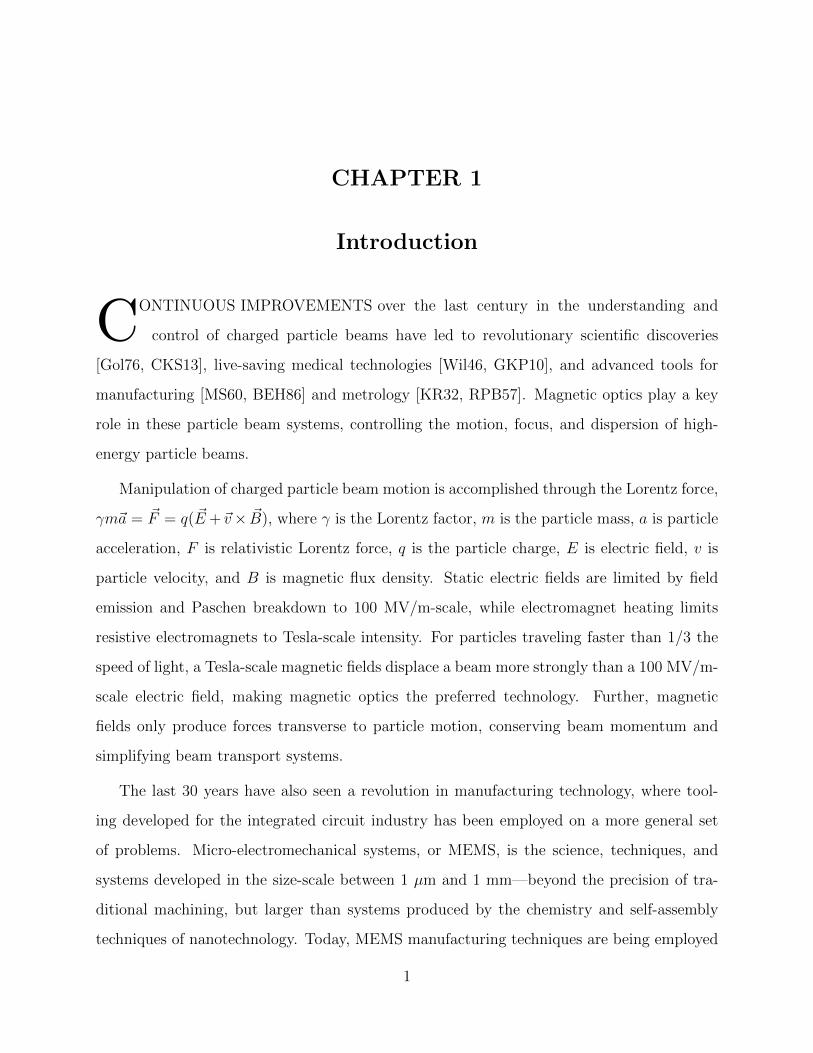
tics as well. Figure 1.1 shows improvement of normalized rms transverse emittance over time
for several commissioned electron guns.
Figure 1.1: Normalized transverse rms emittance vs. commissioning year for high-cur-rent electron sources [Dow10, SGF88, RBH94, DCS95, OS99, Shi06, DSB07, MME08,Cen14, SBK10, Sch13]. Emittance is reported in the standard convention of the productof spot-width in mm and divergence in mrad. The beams circulating in synchrotron storagerings have emittance on the order of 10−3 mm×mrad because of radiation damping.
3

Recent breakthroughs in compact laser accelerators using dielectric structures [NVP12]
and plasma wakes [WIW10, WRP12] promise to dramatically reduce the size of particle
accelerators while maintaining the ultra-low emittance and low energy spread of modern
RF-photoinjector sources, promising a dramatic reduction in the size and cost of particle
beam sources. The size and performance of particle beam optics and undulators, however,
has not seen the same rapid progress as beam sources.
1.2 Multi-pole field scaling
Lorentz force optics producing dipole, quadruple, and higher order fields control the direction,
focus, and dispersion in particle beams [Lee04]. Improving the size and performance of the
beam transport system is necessary to realize the potential of the next generation of beam
sources and systems. The large angular divergence of laser plasma wakefield accelerated
beams, for example, necessitate immediate and high-gradient focusing to minimize bunch
elongation and reduction in beam current [WFP11]. High gradient focusing of high-current
beams will also improve the efficiency of particle-beam based light sources, matching the
particle beam width to the optimal size of the optical beam in free electron laser [Xie00] and
inverse Compton scattering (ICS) sources [SLC96, PBH00].
Many linear manipulations of the 3-D momentum and position of a charged particle
beam are possible with well controlled magnetic fields. A simple 4-pole electromagnet can
produce both steering and focusing fields (Figure 1.2), and the field intensity from these
electromagnets improves with a reduction in the gap between the electromagnet poles.
Particle beam deflection is accomplished with a dipole magnetic field. Solving the Lorentz
force for a particle moving through a dipole field results in the momentum-normalized equa-
tion of motion, R−1 = qB/p, where R is the radius of curvature, B is the magnetic field, q
is the particle charge, and p is the particle momentum. For a small-gap dipole electromag-
net with a high-permeability yoke, magnetic circuit analysis approximates magnetic field
intensity as B = µnI/2r, where µ is the permeability of free space, n is the number of
electromagnet turns, I is the electromagnet current and r is the distance between the center
4

Figure 1.2: Illustration showing the layout of a 4-pole electromagnet producing (a) dipolesteering fields or (b) quadrupole focusing fields. Gray shows the electromagnet yoke andpoles, orange shows the top of the electromagnet windings, blue shows the electron beamlocation, and cyan lines show the flow of magnetic flux. The inset plots show example fieldmagnitude along the marked transverse direction of the electromagnet.
of the gap and pole tip. Simple scaling of the transverse dimensions from the cm-scale of
traditional systems to sub-mm-scale of MEMS results in more than 2 orders of magnitude
improvement in field intensity for a fixed electromagnet drive current. This allows much
‘thinner’ optics for a given deflection angle. The deflection of a charged particle beam by a
simple normalized dipole field is shown in Figure 1.3.
Figure 1.3: Illustration of electron deflection by a normalized dipole field.
5

Focusing is necessary to transport the beam over a distance without loss or to improve
the beam intensity at a point, and is accomplished for high-energy particle beams with
quadrupole magnetic fields. A particle beam focused by a quadrupole field can be described
using a momentum-normalized focusing strength, k = qg/p, where q is the particle charge
and g is the field gradient. For a monochromatic particle beam, the focal length transverse
to the field gradient is f−1 = kl, where l is the effective magnetic length of the quadrupole, or
the normalized interaction distance between the particle and the field. The field gradient in
a small-gap quadrupole with a high-permeability yoke can be approximated as g = 2µnI/r2.
Reducing a cm-scale gap in a set of quadrupole beam optics to sub-mm-size leads to more
than 4 orders of magnitude improvement in field gradient for a fixed electromagnet drive
current, and can enable record-setting focusing performance.
Lorentz forces in a quadrupole field imply that particles distributed on one transverse
axis focus while particles distributed on an orthogonal transverse axis defocus. Net focusing
then requires 2 or more quadrupoles rotated 90 to each other. The reduction in size-scale
and improvement in field gradient enables dramatic reductions in the size and overhead
of a particle-beam focusing lattice. The focusing of a charged particle beam by a simple
normalized quadrupole field is shown in Figure 1.4.
Figure 1.4: Illustration of electron focusing by a normalized quadrupole field’.
For both dipole and quadrupole fields, the strength of a multi-pole electromagnet is re-
lated inversely to the distance between the pole tips, while material parameters such as the
yoke’s magnetic saturation or the maximum current density of the electromagnet windings
is not directly affected by scaling. Additionally, smaller electromagnet gaps reduce the to-
6
tal magnetic flux necessary for a given field. This is reflected in the electromagnet design
as a reduced number of turns, lowering the resistance, inductance,∫A~B/I = L, and the
RLC circuit time constant. A circuit time constant shorter than the time between electron
pulses allows short-duty-cycle pulsing of the electromagnets, enabling dynamic pulse-to-pulse
reconfiguration of the electromagnet array while reducing system power consumption and re-
laxing thermal design constraints. As a result, scaling down from traditional centimeter-scale
out-of-vacuum magnetic optics to sub-mm-scale in-vacuum surface-micromachined magnetic
optics provides a clear path for improvements in steering, focusing, and chromatic correc-
tion while dramatically reducing the size, weight, and power consumption of a particle-beam
transport system.
1.3 Undulator scaling
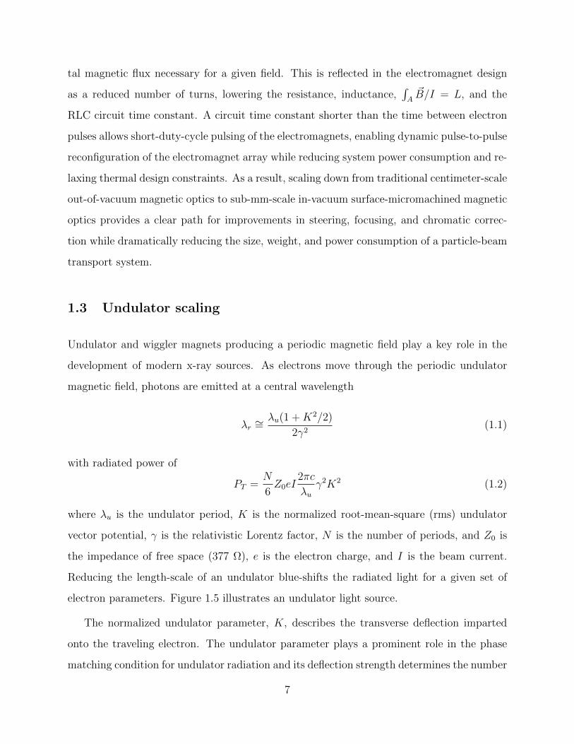
Undulator and wiggler magnets producing a periodic magnetic field play a key role in the
development of modern x-ray sources. As electrons move through the periodic undulator
magnetic field, photons are emitted at a central wavelength
λr ∼=λu(1 +K2/2)
2γ2(1.1)
with radiated power of
PT =N
6Z0eI
2πc
λuγ2K2 (1.2)
where λu is the undulator period, K is the normalized root-mean-square (rms) undulator
vector potential, γ is the relativistic Lorentz factor, N is the number of periods, and Z0 is
the impedance of free space (377 Ω), e is the electron charge, and I is the beam current.
Reducing the length-scale of an undulator blue-shifts the radiated light for a given set of
electron parameters. Figure 1.5 illustrates an undulator light source.
The normalized undulator parameter, K, describes the transverse deflection imparted
onto the traveling electron. The undulator parameter plays a prominent role in the phase
matching condition for undulator radiation and its deflection strength determines the number
7
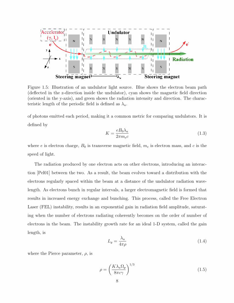
Figure 1.5: Illustration of an undulator light source. Blue shows the electron beam path(deflected in the z-direction inside the undulator), cyan shows the magnetic field direction(oriented in the y-axis), and green shows the radiation intensity and direction. The charac-teristic length of the periodic field is defined as λu.
of photons emitted each period, making it a common metric for comparing undulators. It is
defined by
K =eB0λu2πmec
(1.3)
where e is electron charge, B0 is transverse magnetic field, me is electron mass, and c is the
speed of light.
The radiation produced by one electron acts on other electrons, introducing an interac-
tion [Pel01] between the two. As a result, the beam evolves toward a distribution with the
electrons regularly spaced within the beam at a distance of the undulator radiation wave-
length. As electrons bunch in regular intervals, a larger electromagnetic field is formed that
results in increased energy exchange and bunching. This process, called the Free Electron
Laser (FEL) instability, results in an exponential gain in radiation field amplitude, saturat-
ing when the number of electrons radiating coherently becomes on the order of number of
electrons in the beam. The instability growth rate for an ideal 1-D system, called the gain
length, is
Lg =λu
4πρ(1.4)
where the Pierce parameter, ρ, is
ρ =
(KλuΩp
8πcγ
)1/3
(1.5)
8

and Ωp is the relativistic plasma frequency. For an undulator with many gain lengths of
distance, the intensity grows as
I ∼ I0
9ez/Lg . (1.6)
Conventional undulator technology uses permanent magnet and high-permability-yoke
or superconducting electromagnetic undulators with period λu > 1 mm. To access the
λr = 1 nm x-ray region of the electromagnetic spectrum with these period lengths, a minimum
beam energy of 500 MeV (γ ∼ 1000) is required. Modern radio-frequency (RF)-accelerator
gradients still remain below 20 MV/m, requiring at at least 25 m of linear accelerator for
a 500 MeV beam. This component drives the size and cost of high energy beam systems,
often requiring national-scale facilities to house them. If a beam of sufficiently high quality or
phase space density is transported through a long undulator, the free-electron laser instability
develops causing coherent radiation generation with exponential optical gain [BPN84].
These linear accelerator FEL light sources, known today as 4th generation light sources,
are the most intense sources of coherent light ever made, and under great demand for scientific
experiments, drug discovery, and medical imaging. Undulators with period range between
100 µm and 1 mm would enable access to this region of the electromagnetic spectrum with
medium energy (<100 MeV) electron beams. These microundulators could take advantage
of the continuous progress in the generation of high brightness electron beams and would
constitute an attractive solution for lowering the energy requirements of electron accelerators
for next generation FEL-based x-ray sources, dramatically reducing cost [BPN84]. At the
same time, microundulators would also constitute a valid alternative to inverse Compton
scattering [SLC96] sources, as short wiggling periods and long interaction lengths could be
obtained without the use of high power laser systems. Figure 1.6 compares the wavelengths
and light intensity accessible by several light source technologies, highlighting the application
space that MEMS microundulators and focusing optics are intended for.
9
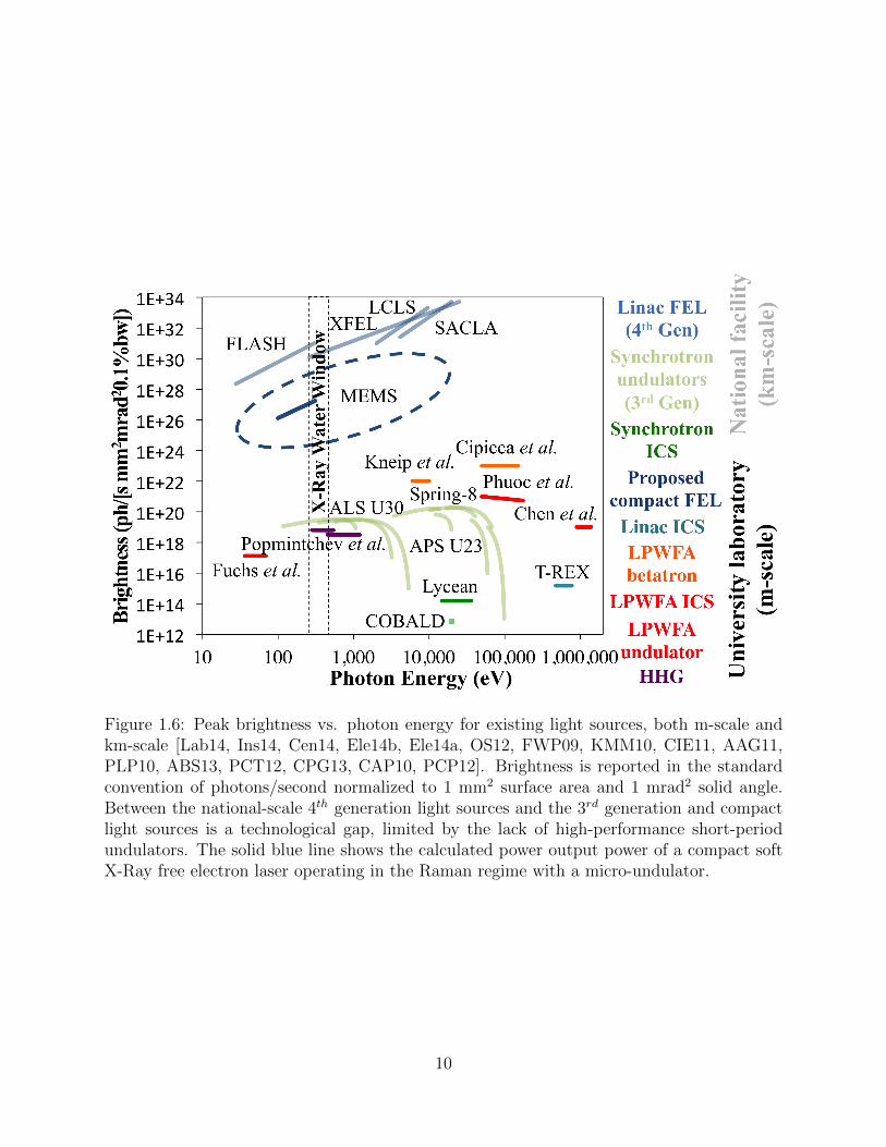
Figure 1.6: Peak brightness vs. photon energy for existing light sources, both m-scale andkm-scale [Lab14, Ins14, Cen14, Ele14b, Ele14a, OS12, FWP09, KMM10, CIE11, AAG11,PLP10, ABS13, PCT12, CPG13, CAP10, PCP12]. Brightness is reported in the standardconvention of photons/second normalized to 1 mm2 surface area and 1 mrad2 solid angle.Between the national-scale 4th generation light sources and the 3rd generation and compactlight sources is a technological gap, limited by the lack of high-performance short-periodundulators. The solid blue line shows the calculated power output power of a compact softX-Ray free electron laser operating in the Raman regime with a micro-undulator.
10

CHAPTER 2
Prior art
THERE have been continuous improvements in magnetic optics and undulators as the
underlying physics have been explored and as materials and manufacturing preci-
sion has improved. Steering magnets, focusing optics, and undulators have all seen several
orders of magnitude improvement in strength and operating frequency, enabling several new
generations of beam systems at each new performance level.
2.1 Steering magnets
Steering magnets for particle beam systems can be generalized into three groups: slow
magnets used for constant beam deflection, fast (kHz) sweeping magnets for beam steering in
electron and ion beam microscopy, and very fast pulse (µs) ‘kicker’ magnets at slow repetition
rates (Hz) for injecting and extracting beam pulses from circulation in synchrotron storage
rings. Figure 2.1 shows an assortment of commercially available slow steering magnets,
Figure 2.2 compares an assortment of fast sweeping magnets, and Figure 2.3 shows an
assortment of kicker magnets.
While miniaturization has clear performance benefits for operating frequency and dipole
field intensity, the deflection angle of a steering magnet, θ = qBLm/p is also dependent on
Lm, the normalized distance the charged particles travel through the magnetic field. MEMS
manufacturing places upper limits on the size of individual devices due to limitations on
aspect ratio during patterning and material deposition, preventing the scaling of the elec-
tromagnet gap while maintaining the interaction length. These limitations makes MEMS
steering electromagnets promising for fast sweeping stages, short period undulators, or kick-
11

Figure 2.1: Integrated deflection strength (B×Lm) and maximum frequency response vsmagnet bore for several commercial slow deflection electromagnets [Tec14d, Tec14e, Tec14a,Tec14b, Tec14c, Dan14b]. Black shows the integrated deflection strength and gray showsthe fastest operating frequency.
Figure 2.2: Integrated deflection strength (B × Lm) vs. sweep frequency for several beamsweeping electromagnets [Tec14d, Tec14e, DKG03, LSC01, Leb99, LCC99, TLK87, SPD07,BVS01, BKJ01].
12

Figure 2.3: Magnet pulse rise time and power draw vs. magnetic gap for several ‘kicker’ elec-tromagnets [NTY11, GPR97, ZSH04, AAB09, OCW05, OCW02, BCD07, ELM03, ADD05,YOG08, Nak09, FMS12, KTK06, KM14, Dan14c, Lee12]. Black shows the rise time of themagnetic pulse and gray shows the power draw during the pulse. The repititon rate andintegrated deflection strength (B × Lm) of some example kickers are annotated on the plot.
ers for compact low-energy storage rings, but limits their use for constant deflection magnets
or kicker electromagnets in high-energy synchrotron storage rings.
2.2 Focusing magnets
Improvements of quadrupole focusing optics has centered on integrated strength, field qual-
ity, and tuneability, depending on the needs of the application. Improvements in integrated
focusing strength have focused on reducing the electromagnet gap, using permanent magnets,
or using very high electromagnet drive currents. Permanent magnet quadrupoles lack tune-
ability, but can produce very high field gradients in a small gap without power consumption.
Lim et al. used this strategy to demonstrate a 5-mm bore Halbach configured permanent
magnet quadrupole producing 560 T/m for high-intensity inverse Compton scattering exper-
iments [LFT05]. Very high electromagnet drive currents in a macro-scale quadrupole electro-
magnet requires specialized electromagnet geometries to reduce inductance and also requires
13

high-voltage energy-storage systems to provide power for the pulse, but can produce very
high gradients. Winkler et al. demonstrated this with a 1-Hz 20-kA pulsed quadrupole elec-
tromagnet that produced 1400-T/m gradient across a 20-mm gap [WCB03]. Improvements
in field quality have relied on electromagnets with very precisely machined magnetic pole
tips. Rebrov et al. demonstrated a quadrupole electromagnet producing 650-T/m gradients
across a 13-mm gap with less than 0.1% higher order multipole field components [RPP07]
using precision electrical-discharge machining tools. Improvements in tuneability have relied
on secondary coils used to tune other multi-pole components of the field. Volk et al., for
example, used field shimming coils to provide 6-T/m of tuneability to a 36-T/m gradient
permanent magnet quadrupole [Spe01]. Each of these performance metrics can improve
directly with miniaturization and MEMS fabrication technologies. Figure 2.4 compares a
variety of quadrupole focusing electromagnets.
Figure 2.4: Quadrupole field gradient vs. beam aperture for several resistive, supercon-ducting, and permanent magnet quadrupoles used in operating beamlines [Spe01, Dan14a,WCB03, TOO01, LHR98, KAC09, CDF09, KAK12, BGL99, RPP07, WFP11, ZCK13,MIK04b, LFT05, MLM12, MIK04a, TPC12, SPR07]. The gray line denotes the projectedperformance of optimized MEMS quadrupole electromagnets.
14

2.3 Undulators
Macro-scale undulators have been well established since Hanz Motz used an undulator and
an electron beam to produce the first man-made coherent infrared light [MTW53]. Since
then, national-scale user facilities have been set up in many developed countries, providing
access to a variety of difficult to reach wavelengths. Undulators in synchrotron facilities
such as SPRING-8 in Japan, BESSY in Germany, and the Advanced Light Source and
Advanced Photon Source in the United States produce light from deep ultraviolet to hard
X-rays. Undulators at the end of ultra-bright linear accelerators are known as 4th generation
light sources, and produce ultra-bright coherent beams of VUV to hard X-rays at facilities
such as the Linac Coherent Light Source in the United States, SACLA in Japan, and the
European XFEL in Germany. Most of these undulators utilize permanent magnets, but some
electromagnetic [KBH98] and superconducting undulators [HKM98] are also in service.
Undulator designs with period lengths in the mm to sub-mm range have been pursued
to reduce the size and cost of high-energy light sources since the mid-1980’s. V. Granatstein
proposed a design for mm-scale pulsed electromagnetic undulators [GDM85]. G. Ramian
proposed using periodic grooves ground into samarium cobalt blocks to produce a mm-
scale undulating field [REK86]. K.P. Paulson built and characterized this undulator design,
demonstrating that machined permanent magnets could be used to reduce the period length
to 4 mm. His work noted the unsolved drawbacks inherent in small machined permanent
magnets of smaller magnetic fields, continuous offset and long-period field errors, and large
end fields [Pau90]. Paulson proposed integrated electromagnets and magnetic end-caps as
potential solutions, but this was not pursued further at the time due to the expected manufac-
turing complexities. Tatchyn et al. proposed and fabricated hybrid-bias-permanent-magnet
undulators with period lengths in the range of λu = 700 - 800 µm. Magnetic testing of these
‘micropole’ undulators showed magnetic fields as high as 0.38 T [TC87]. These undulators
demonstrated 1 pW of 66-eV soft x-ray/VUV radiation from a 70-MeV 1-nA linear accel-
erator at Lawrence Livermore National Laboratory [TTH89]. The magnetic field in these
devices was limited by the low remnant field of the NdFeB permanent magnets (0.73 T) and
15

by the 200+ µm gap, which still was not wide enough to fully accommodate the electron
beam available at the time. Electron beam size, positioning, and stability were identified as
primary limitations on further developing the technology. Another limitation was identified
in the transverse and longitudinal disturbances to the electron beam energy by wakefields
within the undulator [TCT89]. In subsequent years, the emittance and stability of electron
beams have improved by orders of magnitude [DBD09].
Since these early efforts, the range of undulator period lengths between 10 µm and 700 µm
has remained inaccessible. Laser undulators at these wavelengths are limited by a lack of
high intensity gain media. Permanent magnets, on the other hand, are limited by crystal
grain and magnetic domain size limits [AW09]. Machining technology does not exist to man-
ufacture superconducting undulators with sub-mm period, and the only other feasible alter-
native, ‘slow light’ cavity undulators, have yet to be experimentally demonstrated [PBM09].
Figure 2.5 compares the performance of several demonstrated undulators.
Recent progress on surface-micromachined magnetic materials [GHN10, OTH98] and
devices [OHC06, GTH09, GTH11] has enabled soft-magnet inductors and actuators to be
fabricated by photolithography and electroforming with precision on the range of a few µm in
the lateral dimensions and film thicknesses in excess of 50 µm. These surface-micromachined
inductors are the predecessors to this work.
16
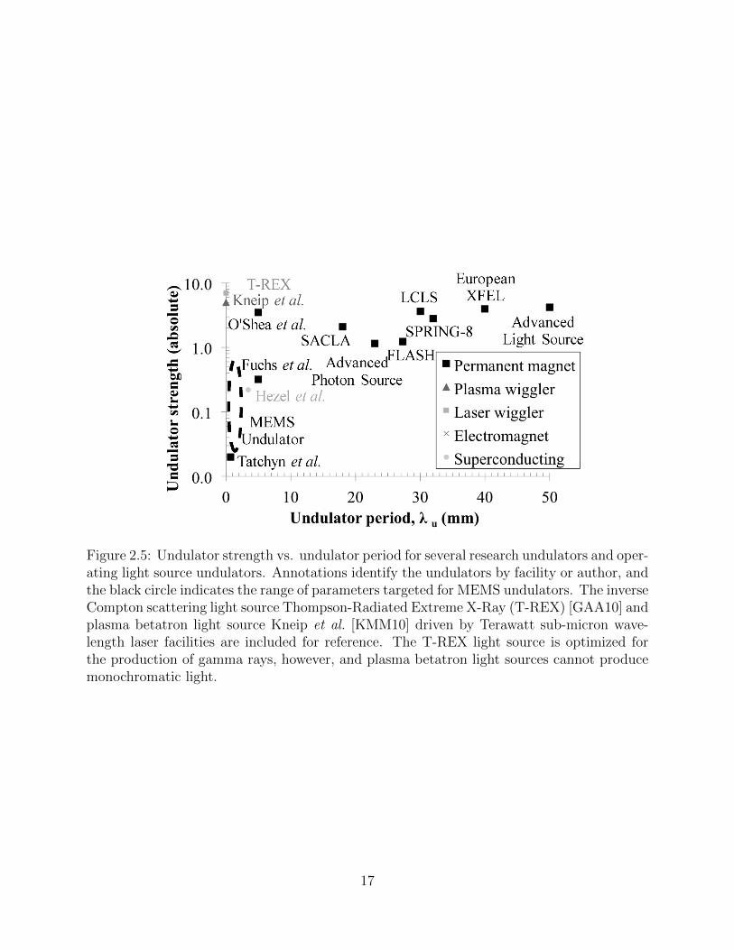
Figure 2.5: Undulator strength vs. undulator period for several research undulators and oper-ating light source undulators. Annotations identify the undulators by facility or author, andthe black circle indicates the range of parameters targeted for MEMS undulators. The inverseCompton scattering light source Thompson-Radiated Extreme X-Ray (T-REX) [GAA10] andplasma betatron light source Kneip et al. [KMM10] driven by Terawatt sub-micron wave-length laser facilities are included for reference. The T-REX light source is optimized forthe production of gamma rays, however, and plasma betatron light sources cannot producemonochromatic light.
17

CHAPTER 3
Design
HIGH-PERFORMANCE and manufacturable designs for MEMS-based electromagnet
systems require a combination of analytical and computational modeling at the
device and system level. Guided by the scaling laws for these devices and the process
constraints discovered during manufacturing, quadrupole and undulator electromagnets were
modeled as magnetic circuits, optimized using 3-D finite element method (FEM) simulations,
and the resulting parameters were used in 3-D physics simulations modeling a MEMS-based
light source.
3.1 Electromagnets
Soft-magnet electromagnets require an actively powered coil producing magneto-motive-force
(MMF) to generate magnetic flux, a magnetic yoke to direct the flux across a free-space gap,
and engineered magnetic pole tips to concentrate the magnetic flux density. The maximum
field that can be generated is limited by the saturation magnetization of the magnetic yoke,
which is as high as 1.1 T for electroplated alloys of NiFe [GHN10] and 2.1 T for electroplated
alloys of CoNiFe [OTH98]. Other limitations on peak free-space field result from the lost
magnetic flux that fringes across the yoke before reaching the undulator or quadrupole
magnetic gap. Peak flux densities in these devices may range from 10 mT to over 1 T in the
gap, depending on the design. The pole separation for quadrupoles and period length for
undulators is limited at a lower bound by the resolution of the thick photoresist mold that is
used in the magnetic yoke fabrication process, typically ∼ 10 µm, and at an upper bound by
wafer bow due to the volume of deposited material, typically ∼ 0.1 mm3 of permalloy and
18

copper for a 9 mm2 silicon die. Overall device size is limited by the size of the silicon wafer
used in fabrication, typically 100 mm in a university cleanroom and 300 mm in a commercial
cleanroom.
Several obstacles have prevented soft-magnet MEMS devices from achieving widespread
use. The complex fabrication process required to produce integrated 3-D coils has lim-
ited most previous devices to less efficient planar coils or external magnetic flux sources,
two options that would prevent the scaling of microfabricated undulator period length
and quadrupole gap diameter to the sub-mm level. Depositing high-quality ferromagnetic
films thicker than 10 µm requires expertise in electrochemistry and controlled atmosphere
tools [GHN10], a significant barrier to entry in the field. Additionally, microfabrication re-
quires an assortment of cleanroom fabrication tools and a complicated skill set for the tool
operator. Thick magnetic film devices, in particular, use atypical processes such as thick
photoresist electroplating molds and photolithography over high aspect-ratio topology.
The electromagnet geometry is primarily limited by two effects during manufacturing,
diffraction and uneven absorption during photolithography and high internal stress in the
photoresist electroplating molds. The diffraction limited critical dimension for photolithog-
raphy, where adjacent lines and spaces follow precisely from the mask pattern, is expressed
by
bcrit =3
2
√λlz
2(3.1)
where bcrit is the feature width that can be precisely resolved, λl is the wavelength of the
photolithography light source, and z is the thickness of the photoresist [Mad02]. For the
100 µm thick photoresist electroplating mold proposed for the electromagnet yoke exposed
with an i-line (365 nm) mercury arc-vapor lamp, experimental results confirm the simple
estimates based on equation 3.1 and yield a limit between 5 µm and 10 µm for minimum
geometry feature size [FWT99]. Thick chemically-amplified photoresists have experimentally
demonstrated 7 µm lateral features in 100 µm thick SU-8 10 [FWT99], 15 µm lateral features
in 1.5 mm thick SU-8 [CCD10] and 18 µm lateral features in 180 µm thick KMPR [LJ08].
19

The resolution limitations imposed by internal stress in the photoresist can be signifi-
cantly coarser than the effects of diffraction and dose absorption in negative-tone thick-film
photoresists. For some geometries, the internal stress of the negative-tone photoresist elec-
troplating mold used during fabrication of the yoke and windings will exceed the adhesion
strength between the mold and the preceding film. Fabrication test structures have shown
electroplating mold failure with negative tone photoresists for length-to-width ratios less
than 4 to 1 for 50 µm thick films and 10 to 1 for 25 µm thick films. For example, the limita-
tions for an undulator with a 100 µm yoke width and height are 50 µm spacing between pole
tips and 10 µm spacing between windings given the limitation stated above. Positive tone
photoresists do not suffer from stress limitations, but are limited in thickness by exposure-
induced opacity and do not achieve the vertical sidewall aspect-ratio required to produce
magnetic films for uniform field distribution.
3.1.1 Magnetic circuits and geometry
The achievable peak magnetic flux density and uniformity is governed by the geometry of
the flux source. Different geometric designs can be analyzed using Hopkinson’s/Rowland’s
magnetic analogy to Ohm’s law
φ =FRtotal
(3.2)
where φ is the total magnetic flux, F is the MMF, and Rtotal is the total reluctance of all
flux paths (Figure 3.1). The reluctance of a flux path is
R =L
µTW(3.3)
where L is the magnetic flux pathlength, µ is the magnetic permeability, T is the yoke
thickness, and W is the yoke width. Reluctances in parallel add like electrical resistors
in parallel (R−1parallel = R−1
1 + R−12 ), while reluctances in series add like resistors in series
(Rseries = R1 +R2). The total magnetic flux delivered to the undulator gap will be reduced
by the fringing flux paths in parallel with the desired flux path in the system. Because there
are numerous fringing flux-paths for complicated 3-D geometries, magnetic circuit analysis
20

is primarily useful as an optimization tool for seeding 3-D the geometric parameters of a
finite element model.
Figure 3.1: Illustration of a magnetic circuit. Gray denotes the ferromagnetic yoke materialand the electric circuit symbols denote magnetomotive force source (windings) and magneticreluctance around the magnetic circuit path.
For a multi-pole electromagnet with a high permeability magnetic yoke, the fraction of
generated magnetic flux that is channeled into the gap is a function of the reluctance of the
magnetic path across the gap relative to the magnetic reluctance of all other return paths in
parallel. Careful design of the flux path is required to minimize the reluctance of the desired
path and maximize the reluctance of all other paths.
The ‘racetrack’ solenoidal coil is an area-efficient design that fits the windings and yoke
into a compact solenoidal configuration, ideal for multi-pole electromagnets and short period
undulators (Figure 3.2). The solenoidal coil design can fit an order of magnitude or more
windings into a given surface area than the simpler and more common planar MEMS coil
design.
Figure 3.2: Scanning electron micrograph of a surface-micromachined ‘racetrack’ transformerfabricated at UCLA.
21

3.2 Multi-pole electromagnets
An electromagnet with an even number of poles can produce dipole fields by energizing poles
on one side as ‘North’ and poles on the other side as ‘South’. Figure 3.3 shows one flux path
through a 2-pole electromagnet producing a dipole field.
Figure 3.3: Illustration of a 2-pole magnetic circuit. Gray denotes the ferromagnetic yokematerial, cyan the magnetic flux lines, and circuit symbols denote the magnetic circuit paths.
An electromagnet with 4-N poles can produce quadrupole fields by energizing the poles
in each quadrant with fields in alternating directions. Figure 3.4 shows one set of flux paths
through a 4-pole electromagnet producing a quadrupole field.
Dipole, quadrupole, and higher order fields are orthogonal to each other, allowing the
linear superposition of fields by adding the electrical current configuration of each electromag-
net winding for each desired multi-pole field. A 4-pole electromagnet that can superimpose
a dipole field on a quadrupole field is known as a combined-function quadrupole, and can
either steer and focus a been simultaneously, or use the dipole field to electrically shift the
quadrupole field centroid about the electromagnet gap. Figure 3.5 illustrates the soft-tuning
of a MEMS quadrupole field centroid.
Magnetic circuit analysis of several 4-pole electromagnet geometries indicated that the
pole tip taper angle most significantly influenced field strength. Figure 3.6 shows a model of
22

Figure 3.4: Illustration of a 4-pole magnetic circuit. Grey denotes ferromagnetic yoke mate-rial, orange denotes the electromagnet windings, and cyan denotes magnetic flux lines. Theinset shows the in-plane magnetic circuit parameters.
Figure 3.5: Illustration of a combined-function electromagnet electronically shifting thequadrupole field centroid from left to right. The inset shows the transverse y-componentof the magnetic flux density across the transverse x-axis of the quadrupole center.
the magnetic flux density along a quadrupole magnet pole of a 600 µm-gap electromagnet
for a variety of pole taper angles. Figure 3.6(a) and (b) illustrate the difference in field for
the case of an electromagnet with a 10 and 35 pole taper angle.
Table 3.1 shows the result of a parameterized 3-D FEM optimization of quadrupole
electromagnet geometry seeded by optimized geometries with a NiFe yoke (Bsat = 1.1 T)
using magnetic circuit analysis. The quadruple that was actually fabricated and tested is
included as the last entry in the table.
23

(a) Quadrupole with 10 taper angle (b) Quadrupole with 35 taper angle
Figure 3.6: Calculated flux density along a quadrupole pole tip vs. pole taper angle.
Table 3.1: Optimized quadrupole geometries. The fabricated quadrupole is bolded.Electromagnet Winding Yoke Taper Field Dipole
gap (µm) pitch (µm) thickness (µm) angle () gradient (T/m) strength (T)100 45 200 30 10000 0.425200 45 200 30 6800 0.400300 65 200 38 3300 0.320400 75 200 40 2200 0.300600 100 200 35 1000 0.200600 85 55 10 220 0.024
24

The field produced by -1.0 A in each coil of the fabricated quadrupole electromagnet
was simulated using the 3-D magnetostatic simulation package in the finite element method
multiphysics software COMSOL. Figure 3.7 shows the simulated dipole field profile and
Figure 3.8 shows the simulated field profile for a quadrupole field. The magnetic length
was 686 µm for the dipole field simulation and 384 µm for the quadruple field simulation.
The inductance calculated by integrating the stored magnetic energy (E =∫B2/(2µ)dv)
matched the measured inductance for the quadrupoles described in Chapter 5 within 6%
before packaging and 21% after packaging. Post-packaging measurements were through
20 wire bonds reworked with a chlorine plasma etch, potentially explaining the variation
between measurements.
Figure 3.7: Simulated transverse magnetic dipole field profile for I = -1.0-A drive current.Integration across the model volume yields a 32.2-nH inductance. Dividing the z-integratedfield by the peak field yields a 686-µm magnetic length, which is the normalized interactiondistance of a charged particle.
These simulations show that the yoke for the electromagnet as-fabricated saturates with
I = ±2.35-A drive current when producing a dipole field and I = ±4.7 A when producing
a quadrupole field while the poles are only 25% saturated with magnetic field. The yoke
width in these devices was limited by a 3-mm die size, limiting the maximum field. A 4×
field strength improvement could be realized by simply extending the yoke width without
further optimization, however, this design was selected given the fabrication design rules in
place at the time.
25

Figure 3.8: (a) Simulated transverse magnetic quadrupole field profile for I = -1.0-A drivecurrent. (b) Dividing the z-integrated field gradient by the peak field yields a 384-µmmagnetic length, which is the normalized interaction distance of a charged particle.
3.3 Undulators
The flux path configuration for an undulator allows more flexibility in design. It is possible
to generate the magnetic flux on one side of the undulator (Design 1) or on both sides of
the undulator axis as in a typical electromagnetic undulator (Design 2) [Cla04], as shown
in Figure 3.9. Directing the flux through MMF sources located only on one side of the
undulator axis to a short yoke on the other side of a gap (Design 1) allows doubling the
yoke width and spacing for a given undulator period length, but at the cost of additional
parasitic magnetic fringing between the short yokes. As a result, directing the flux through
MMF sources on both sides of the undulator axis (Design 2) achieves a larger peak magnetic
field but also a longer minimum period length for a given yoke thickness.
Figure 3.10 shows a reluctance model of the undulator neglecting 3-D fringing and period-
to-period fringing. Period-to-period fringing is negligible if the yokes of each period are
disconnected. The equations for the total, fringing, and return flux path reluctances can be
obtained from Figure 3.10 and are shown below.
26

Figure 3.9: Illustration of a two period cross-section of two undulator designs withλu = 100 µm. Undulator design 1 allows further scaling. The magnetic yoke is shown ingray, the solenoid winding interconnect cross-sections are shown in orange, and the intendedmagnetic flux path is shown in blue.
Rtotal = Ryoke,f +(R−1
fringe +R−1return
)−1
Rfringe =(R−1
window,y +R−1window,g
)−1Design 1
Rreturn = 2 Rgap +Ryoke,g
Rtotal = Ryoke,f +(R−1
fringe +R−1return
)−1
Rfringe = Rwindow Design 2
Rreturn = 2 Rgap +(R−1
yoke +R−1window
)−1
Magnetic saturation sets the upper bound for efficient generation of magnetic flux in the
undulator yoke. The magnetic flux density in the yoke is
Byoke =φtotal
WyTy
(3.4)
where Wy is the yoke width and Ty is the yoke thickness.
27

Figure 3.10: Illustration of a simple reluctance model of the two undulator designs illustratedin Figure 3.9.
Magnetic circuit analysis shows that the flux remaining at the magnetic pole tips is
φtip =φtotal
1 +Rreturn/Rfringe
. (3.5)
To get an analytical estimate of the field, we assume a linear and uniform magnetic material.
The magnetic flux at the pole tip and the MMF at saturation can then be found by increasing
φtip up to the point where Byoke = Bsat (2.1 T for CoNiFe).
The transverse magnetic flux density at the center of the undulator is reduced by fringing
in the axial direction and can be significantly less than the flux density in the cross section
of the yoke. The magnetic field of a standard (Design 2) undulator including 2D fringing
was analyzed by Poole et al. and is given by
Bpeak =φtip
WyTy
1
cosh(ξ)
(1− sinh(ξ)/(3sinh(3ξ))
1− sinh(ξ)/(3sinh(ξ))
)(3.6)
28

where ξ = πg/λu [PW80], g is the gap between pole tips, and λu is the undulator period
length.
Figure 3.11 shows the magnetic flux density of the undulator (Design 2) plotted at satura-
tion using equations 3.4 and 3.6, varying the undulator period and gap. When all geometric
parameters are scaled together, the peak magnetic flux density remains constant. To ver-
ify the analytical scaling law, a variety of undulator geometries were simulated using the
2D finite element method (FEM) magnetostatic package in COMSOL Multiphysics with
a nonlinear CoNiFe material model derived from vibrating sample magnetometry (VSM)
studies of electroplated Ni80Fe20 [GHN10] scaled to the saturation magnetization and initial
permeability described in Osaka et al. [OTH98].
Figure 3.11: Plot showing the scaling of the transverse magnetic flux density in the centerof the undulator vs. gap and period. Values of Ly = λu/4, Wy = λu/4 and Bsat = 2.1 T areused. Lines denote calculations and diamonds denote simulations.
Analytical results approximate the simulated fields well while 1 ≤ λu/g ≤ 8. For large
ratios of period to gap, the undulator tip curvature focuses the field and using φtip/WyTy as
the flux density at the tip is inadequate. For small ratios of period to gap, longer fringing
paths across the window that were neglected become relevant and Rwindow is inadequate.
Figure 3.12 shows the MMF in Amp-turn required to generate 1 T for many different ge-
29
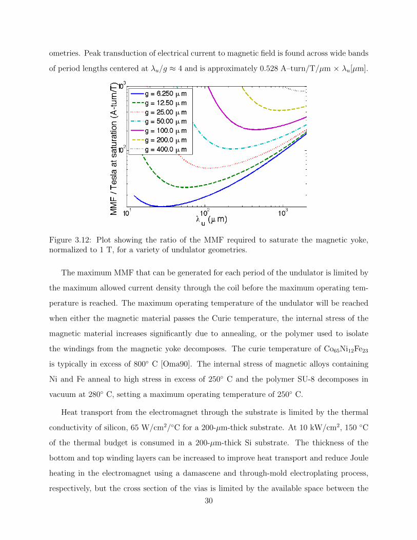
ometries. Peak transduction of electrical current to magnetic field is found across wide bands
of period lengths centered at λu/g ≈ 4 and is approximately 0.528 A–turn/T/µm × λu[µm].
Figure 3.12: Plot showing the ratio of the MMF required to saturate the magnetic yoke,normalized to 1 T, for a variety of undulator geometries.
The maximum MMF that can be generated for each period of the undulator is limited by
the maximum allowed current density through the coil before the maximum operating tem-
perature is reached. The maximum operating temperature of the undulator will be reached
when either the magnetic material passes the Curie temperature, the internal stress of the
magnetic material increases significantly due to annealing, or the polymer used to isolate
the windings from the magnetic yoke decomposes. The curie temperature of Co65Ni12Fe23
is typically in excess of 800 C [Oma90]. The internal stress of magnetic alloys containing
Ni and Fe anneal to high stress in excess of 250 C and the polymer SU-8 decomposes in
vacuum at 280 C, setting a maximum operating temperature of 250 C.
Heat transport from the electromagnet through the substrate is limited by the thermal
conductivity of silicon, 65 W/cm2/C for a 200-µm-thick substrate. At 10 kW/cm2, 150 C
of the thermal budget is consumed in a 200-µm-thick Si substrate. The thickness of the
bottom and top winding layers can be increased to improve heat transport and reduce Joule
heating in the electromagnet using a damascene and through-mold electroplating process,
respectively, but the cross section of the vias is limited by the available space between the
30

magnetic yokes. Figure 3.13 shows the maximum MMF that can be generated for different
uniformly scaled geometries dissipating 10 kW/cm2.
Figure 3.13: Plot showing the maximum MMF that can be generated by a 32-turn coildissipating 10 kW/cm2.
As an example, let us consider a λu = 100 µm g = 25 µm undulator with a 50 µm
thick yoke, saturated with 160 A-turns of MMF. Assuming a 32 turn 0.8 Ω coil, we have
J = 2.5×10¹⁰ A/m2 winding current density, and each period of the undulator will dissipate
5 W. The base of the 200 µm thick substrate needs to be maintained at a temperature below
-143 C to keep the undulator from exceeding 250 C. This undulator should be capable of
operation when cryogenically cooled by liquid nitrogen. To improve the thermal performance
of the undulator, we can reduce the electromagnet yoke thickness to match the size of the
gap between the poles. If a 25 µm thick yoke is used, the base of the substrate must be kept
below 41 C and the undulator can operate at room temperature.
The optimal design for the undulator electromagnet is obtained as a compromise between
i) reducing the length of the racetrack yoke to minimize the fringing flux losses to reduce
the required MMF for a given field and ii) increasing the winding cross-section to reduce the
current density and improve heat transport.
31

3.3.1 Optimization of undulator geometry for higher field
Another design option is to reduce the undulator magnetic gap width below λu/4. This causes
the field down the undulator axis to deviate from sinusoidal uniformity, radiating power into
higher order harmonics. This deviation can be corrected by shaping the magnetic pole
tips. Increasing the radius of curvature of the poles slightly reduces the peak field, but also
reduces the contribution of higher order (odd) harmonics in the magnetic field (Figure 3.14).
Increasing the radius of curvature from 12.5 µm to 32 µm reduces the third harmonic from
11.5% of the total spectral content to 4.6% and increases the peak of the fundamental
harmonic by 7%.
Figure 3.14: Plot of the spatial harmonics of the undulator field in undulator design 2 withλu = 100 µm and g = 12.5 µm for several pole tip curvature radii. Data was taken fromfrom 2D magnetostatic FEM simulations.
For periods longer than 100 µm, tapering the yoke from a wide back to a λu/4 width
pole reduces the magnetic reluctance (see Figure 3.9) and spreads out the flux at the back
corners of the yoke where the undulator first saturates. 2D nonlinear magnetostatic FEM
simulations show that a λu = 400 µm undulator with yoke tapering and a 50 µm wide
magnetic gap produces a saturated peak field of 1500 mT, 45% greater than the un-tapered
32

yoke. As the undulator period is scaled down, this optimization becomes unfeasible due to
the space requirements for the electromagnet winding vias. Table 3.2 lists the peak magnetic
flux density simulated for a variety of optimized undulator geometries using a CoNiFe yoke
(Bsat = 2.1 T).
Table 3.2: Optimized undulator geometries using undulator design 2λu (µm) Undulator gap (µm) Bpeak (mT) K
25 6.25 540 8.9×10⁻⁴
25 12.5 230 3.8×10⁻⁴
100 25 727 4.8×10⁻³
100 50 334 2.2×10⁻³
400 50 1500 4.0×10⁻²
400 100 970 2.6×10⁻²
The strength of the coupling between the radiation and the relativistic beam is related
to the normalized undulator parameter, K
K =eBpeakλu
2√
2πmec(3.7)
where e is the charge of an electron, Bpeak is the peak on-axis transverse magnetic field, λu
is the undulator period, me is the electron mass, and c is the speed of light. The achievable
undulator parameter in the range of λu = 25 µm to λu = 1 mm scales between K = 9×10⁻⁴
and K = 0.1. This is comparable with the shortest period undulators discussed in recent
literature, K = 0.03 for a 706 µm hybrid permanent ‘micropole’ undulator [TTH89], K = 0.4
for a λu = 5 mm permanent magnet undulator [EGB07], and K = 0.2 for a λu = 3.8 mm
superconducting undulator [HKM98].
3.3.2 Undulator sextupole focusing
It is not uncommon for traditional permanent magnet undulators to operate with GeV
beams. Scaling the undulator design to the micron-scale eliminates the need for GeV electron
sources for X-ray photon energies, and enables more than an order of magnitude increase in
photon energy over currently available sources with the same electron accelerator. Shorter
undulator scales and lower energy electrons, however, place other demands on the electron
33

beam characteristics in order to maintain focus and alignment for long distances in sub-
100 µm magnetic gaps. The undulator can either rely on upstream beam optics to maintain
focus or be designed to achieve a large magnetic spatial gradient in transverse directions,
producing a sextuple field to confine the beam.
Relying on upstream beam optics, the length that the electron beam will remain focused
is given by
Lu = 2σ20γ/ε. (3.8)
Assuming a normalized transverse beam emittance of ε = 1 mm-mrad, a σ = 20 µm beam
width and 120 MeV beam energy, the electron beam will remain focused for a distance of
19 cm, a distance compatible with the length of these microfabricated undulator sections.
In order to reach power saturation, many additional stages of focusing optics and undulator
segments must be used, or the undulator must be designed to provide natural-focusing in
both transverse directions.
Natural-focusing in the out-of-plane transverse direction can be provided by generating
an out-of-plane field gradient. This field can be accomplished with additional magnetic
material above and below the magnetic pole tips (Figure 3.15).
(a) Field intensity without flux lens (b) Field intensity with flux lens
Figure 3.15: Natural focusing sextupole field with additional magnetic material.
The natural focusing strength can be derived from the Lorentz force on an electron moving
through the undulator with a field in the transverse y and z directions [HK07]. The natural
34

focusing strength in the y direction in a flat-pole electromagnetic undulator is defined by
kn =2πK√2λuγ
2π
λu(3.9)
Typical natural focusing values in a short undulator X-ray FEL, such as a high-gain FEL
using a MEMS undulator proposed below (Table 3.4), are kn = 1.6 m−1. The natural focusing
strength stays constant with scaling of the undulator period, but increases linearly with a
reduction in electron beam energy.
Natural focusing can be provided in both directions, as shown in Figure 3.15. The
strength in the transverse directions, however, is limited to
k2nx + k2
ny = k2n0 (3.10)
providing transverse electron acceleration back toward the undulator center:
d2xβndz2
= −k2nxxβn (3.11)
d2yβndz2
= −k2nyyβn. (3.12)
Natural focusing in both directions can reduce or eliminate the need for quadrupole fo-
cusing optics in some low-energy beam cases, dramatically simplifying the construction of
the FEL. Additionally, longitudinal modulation of the electron bunch phase relative to the
radiation field, an effect that is detrimental to micro-bunching of the beam, can be avoided
with the elimination of the FODO quadrupole focusing lattice [Sch85]. The additional pat-
terned material used to provide focusing in the transverse out-of-plane direction comes at the
expense of added fabrication complexity, but has the potential to provide a simpler compact
FEL.
35

3.3.3 Magnetic field uniformity
The low K value of these undulators implies that magnetic field non-uniformity has a rel-
atively small effect on the undulator resonance condition. However, beam position and
focusing will be more sensitive to the magnetic field profile because the electron beam occu-
pies much of the space between the magnetic pole tips. 3-D magnetostatic FEM simulations
of the field in a 100 µm period, 50 µm × 50 µm gap undulator were performed with COM-
SOL Multiphysics to visualize the transverse behavior of the field. Figs. 3.16 and 3.17 show
the transverse magnetic flux density at different positions in the undulator.
Figure 3.16: Transverse magnetic flux density at different positions for undulator design 1with λu = 100 µm and g = 50 µm driven far below magnetic saturation. The plot spans 5of 7 periods of an undulator with y = z = 0 µm at the center.
36

Figure 3.17: Transverse magnetic flux density at different positions for undulator design 2with λu = 100 µm and g = 50 µm driven far below magnetic saturation. The plot spans 5of 7 periods of an undulator with y = z = 0 µm at the center.
The z-dependence of the magnetic field seen in both designs is explained by the fact that
out-of-plane magnetic fringing reduces the transverse magnetic flux density away from the
center of the undulator. Conversely, in the undulator plane (along y-direction), the magnetic
flux is larger as we approach the magnetic flux sources. This effect is more pronounced in
undulator design 1, where the flux source is only on one side (see Figure 3.17).
In order to estimate the magnitude of the magnetic field errors in this undulator, we
observe from equation 3.6 that the on-axis magnetic field varies inversely with the thickness
of the yoke. The precise thickness of binary and trinary magnetic alloys is difficult to control
37

across a patterned feature. A typical random variation in the thickness of the undulator
yoke with σt = 0.01 Ty corresponds to a σB,t = 0.01 Bu variation in the undulator field.
Non-uniformity in the photolithography exposure tool dose (< 1% for modern projection
and 1.5% for contact lithography tools) will cause variation in the critical dimensions of
the yoke. Using the lumped parameter model for optical lithography [Mac07] and assum-
ing a high-contrast negative-tone photoresist and features that are larger than the critical
dimension defined in equation 3.1, a σI = 0.01 I0 variation in exposure dose will result in
approximately a σCD = 0.01 bcrit critical dimension variation. For a 100 µm thick electro-
magnet yoke electroplating mold, the undulator gap would then vary by σg = 60 nm. A
Taylor expansion to first order of terms containing the gap in equation 3.6, ξ = πg/λu, at
g/λu = 1/2 show that the magnetic field varies with Bu ∝ 1.05 − 0.525 ξ. A σg = 60 nm
uncorrelated variation in the gap of a λu = 100 µm g = 50 µm and λu = 400 µm g = 100 µm
undulator will result in a σB,g = 0.005 Bu and σB,g = 0.0004 Bu variation in undulator field,
respectively.
The total effect of these uncorrelated transverse field errors on the undulator phase match-
ing condition, defined in equation 1.1, will be limited by the small K of the undulator. A
σB = 0.011 Bu total variation in the transverse field intensity with K = 0.003 will result in
a 1×10⁻⁷ rms error in the phase matching condition of a λu = 100 µm undulator.
Electrically tuning individual undulator electromagnets can mitigate these errors. For un-
dulator design 1, Hopkins analysis neglecting fringing yields a tuning range from B = 0 to Bpeak.
For undulator design 2, full tuning range can be achieved when the yoke is unconnected be-
tween undulator periods. When the yoke reluctance between periods is much less than Rtotal
and there are many periods, however, tuning range approaches zero.
3.4 Challenges for free electron laser system using MEMS optics
Integrating a microfabricated electromagnetic undulator with a beam line poses several chal-
lenges that are not typically encountered with macroscopic permanent magnet, supercon-
ducting, or laser undulators. The undulator transverse structure is sub-mm size, and it must
38

be placed inside the vacuum beam line, complicating alignment, electrical interconnects,
heat extraction, and beam focusing. Spatial measurements of the actual magnetic field will
be complicated by the small undulator gap. Further, the proximity of the undulator surface
to the electron bunch influences the beam characteristics.
3.4.1 Heat dissipation
Heat extraction is a serious challenge when operating electromagnetic undulators under
vacuum. Further aggravating heat extraction from the undulator is the reduced cross-section
of the windings as the undulator period scales down, driving up both current density and
coil resistance. Depending on the geometry, the undulator dissipates 100s of W/cm2 to 10s
of kW/cm2 during operation (Figure 3.18).
Figure 3.18: Plot showing the scaling of the surface power dissipation density generated bythe undulator windings at saturation.
For a saturated 400 µm period undulator with a magnetic gap of 50 µm, 3820 W/cm2 must
be extracted from the undulator to maintain a steady-state temperature. Figure 3.19 shows
the 2D temperature distribution simulated using COMSOL Multiphysics across a 50 µm
tall winding cross section of a λu = 400 µm undulator on a 200 µm thick silicon wafer.
Here, the base of the wafer must be held at less than 138 C to keep the structural polymer
39

from exceeding a safe temperature of 250 C. Figure 3.20 shows the simulated temperature
distribution across a 25 µm tall winding cross section of a λu = 100 µm undulator on a
200 µm thick silicon wafer. Here, the base of the wafer must be held at less than 32 C.
Figure 3.19: Temperature distribution simulation (Kelvin) of a λu = 400 µm undulatorwinding cross-section driven with 5 A, producing 1.2 T, fabricated on a 200 µm thick Siwafer.
Figure 3.20: Temperature distribution simulation (Kelvin) of a λu = 100 µm undulatorwinding cross-section driven with 0.8 A, producing 0.3 T, fabricated on a 200 µm thick Siwafer.
For geometries that generate more surface heat density, conductive heat transfer from
room temperature is not sufficient to keep the undulator below the structural polymer’s
40

decomposition temperature. To address this limitation, the structural polymer may be
removed by an O2 plasma etch prior to operation, the undulator must be run pulsed, or a
circulating liquid or cryogenic cooler may be used to extract heat from the undulator. Given
the τ = 100 ns - 100 µs response of the undulator inductors, pulsed operation at 1 kHz
with a 10% duty cycle would allow all undulator designs to be driven with the substrate
held at room temperature. Integrated two-phase microjet impingement cooling [WZJ04] is
another potential solution to dramatically increase heat transport allowing continuous wave
operation without cryogenic cooling.
3.4.2 Wakefields
Wakefields generated by the electron beam in sub-mm gaps are significantly stronger than in
mm- or cm-scale undulator beam pipes and have the potential to seriously affect the electron
beam energy spread and propagation. There are two main sources for the wakefields, the
resistive wall effect and the surface roughness effect.
The resistive wall wakefield is a result of electrical currents induced in the walls of the
undulator electron beam waveguide. These finite currents will excite both transverse mag-
netic and transverse electric waveguide modes, resulting in longitudinal energy modulation
and transverse instability of the electron bunch.
Longitudinal wakefields will induce a significant energy spread in the electron bunch as
it travels through the undulator when the length of the electron bunch is comparable to a
characteristic distance,
s0 =
(cg2
8Z0σ
)1/3
(3.13)
where c is the speed of light, g is the undulator gap (approximating the waveguide cross-
section as round rather than rectangular), Z0 is the impedance of free space, and σ is the
conductivity of the undulator waveguide walls [BS96].
Studies by Bane et al. showed that a rectangular aluminum beam pipe reduced longitudi-
41

nal wakefields by 50% compared to an equivalent sized round copper beam pipe [Ban07]. An
aluminum covered rectangular beam pipe is compatible with the fabrication process proposed
here, and the wakefield effects for this configuration are calculated below. A g = 100 µm
undulator with an aluminum covered waveguide has a characteristic distance s0 = 724 nm
and a loss factor of kz = 0.1 MV/pC/m. The longitudinal energy modulation of a of a
750 Apeak 100 pC electron bunch by short-range resistive wall wakefields were calculated
using the GENESIS module Genwake for a variety of undulator gap sizes and plotted in
Figure 3.21.
Figure 3.21: Resistive wall component of the longitudinal wakefield for a 750 Apeak 100 pCgaussian electron bunch between two parallel aluminum plates separated by g.
The other contribution to the undulator wakefield is due to the boundary conditions
on the electric field induced by a rough waveguide wall. This field distortion will impact
the energy of subsequent electrons in the bunch with an inductive load on the electron
beam [BNC97]. To illustrate this effect, surface roughness wakefields were calculated using
the GENESIS module Genwake for an aluminum coated g = 100 µm and g = 400 µm
waveguide with a variety of surface roughnesses, Rq, and shown in Figure 3.22.
The surface morphology of evaporated or sputtered metal films is typically characterized
by nm-scale surface roughness that follows the underlying topology. The proposed micro-
undulator fabrication process uses SU-8 polymer patterned by UV photolithography to define
42

Figure 3.22: Longitudinal wakefield for a 100 pC gaussian electron bunch between twoparallel aluminum plates separated by g = 100 µm (top) and g = 400 µm (bottom).
the sidewall topology. The sidewall of these SU-8 features have a surface roughness below the
measurement capabilities (∼ 5 nm) of the scanning electron microscopes used in this work
(S-4700, Hitachi Instruments, Inc., San Jose, CA, USA). Tapping mode atomic force micro-
scope measurements have been reported with Rq ∼ 4 nmrms sidewall surface roughness over a
correlation length of 46 nm for proton beam patterned SU-8 [SBS04] and Rq ∼ 4 nmrms side-
wall surface roughness without a reported correlation length for UV-patterned SU-8 [ZSC10].
These values are strongly affected by fabrication process conditions, especially the tempera-
ture and duration of subsequent anneal bakes and the temperature, duration, and chemistry
of subsequent plasma etching steps. Scanning tip profile measurements of SU-8 films during
43

the proposed fabrication process have shown surface roughness ranging from Rq ∼ 1 nmrms
to Rq ∼ 100 nmrms, depending on the exposure of the SU-8 to fabrication process conditions.
Because the FEL instability requires that the energy bandwidth in an FEL slice of the
electron pulse be less than the FEL gain (Pierce) parameter, the energy chirp imparted
by wakefields can prevent the micro-undulator from operating as a FEL [BS05]. Taking
the parameters from the high-gain soft-x-ray FEL amplifier example below, E = 210 MeV,
Lg = 53 cm, Lc = 1.5 µm, and ρ = 4.5×10⁻⁵, the induced energy spread across a FEL slice
must be less than ∼18 keV/m for FEL operation.
In order to further mitigate the longitudinal energy modulation by wakefields, one needs
to reduce the amplitude of the electron distribution or minimize the overlap of the spectral
components of the beam longitudinal distribution with the impedance response of the struc-
ture. One possibility is to reduce the electron bunch charge and length. This wakefield will
be reduced approximately in proportion with the reduction in charge, however, sub-micron
bunch lengths may become comparable to the slippage length in the undulator, halting the
FEL process. Figure 3.23 demonstrates the overlap between Fourier transformed σ = 1.6 µm
and σ = 16 µm Gaussian electron bunches with the same 750 A current, and a g = 100 µm
rectangular waveguide wake function ([Cha93], equation 2.75).
Bane et al. suggested that vanishingly small periodic fins in a rectangular waveguide
beam-pipe would shift the resonant frequency of the cavities between fins beyond the high-
frequency cutoff of a finite energy electron beam, ω = 2γc/g ([BS03], footnote 17). This
analysis was carried out to study surface roughness wakefields, but hints at an interesting
strategy to mitigate the effects of wakefields in a waveguide. Periodic structures are a
common method for eliminating unwanted propagating modes in microwave waveguides.
Neglecting higher order modes, additional wakefields caused by the waveguide discontinuities,
and the evanescent fields in the waveguide stop-bands, 15 µm fins spaced 15 µm apart in a
100 µm wide waveguide should reduce the resistive wall wakefield.
44

Figure 3.23: Spectral distribution of a 750 Apeak 10 pC and 100 pC gaussian electron bunch(dashed) and the resistive wall impedance per unit length for a g = 100 µm aluminumwaveguide (solid).
3.4.3 Electron beam induced heating
Energy dissipation in the undulator waveguide by longitudinal wakefields will also cause
Joule heating, further complicating thermal management of the undulator.
A 116 MeV electron beam with continuous 1 mA electron current will dissipate 200 W in
5 cm of a g = 100 µm undulator waveguide. Wakefield induced joule heating will dissipate
334 µJ per shot into each meter of undulator length for a 100 pC bunch in a g = 100 µm
Rq = 10 nmrms aluminum-coated undulator waveguide due to the wakefields shown in Fig-
ure 3.22. At a repetition rate of 1 MHz, wakefields will dissipate <1 kW/cm2 in the waveg-
uide.
The total of all electron induced heat loads is less than the expected electromagnet
dissipation at saturation.
3.5 Micro-undulator system examples
While there are many potential applications of micro-undulators, two use cases are presented
here: an undulator radiation source with a high average current beam and a high-gain soft
45

x-ray FEL amplifier.
3.5.1 Undulator radiation source with a high average current beam
The first example takes advantage of the relatively low power requirements of an electro-
magnetic micro-undulator. Competitive approaches to ultrashort wavelength undulators are
all based on high power laser pulses which typically have limited repetition rates (< 1 kHz).
In fact, it is common to invoke complex designs involving recirculating cavities and multi-
interaction schemes to get a high average photon yield with a laser based source [JSG07].
Conversely, only a few amps of current are required to drive the electromagnetic micro-
undulator, and it is practical to apply current continuously to the micro-coils and have the
magnetic field on at all times. It is then natural to couple this undulator with an electron
beam from a CW or high duty cycle electron accelerator.
As an example, we consider injecting a 1 mA 116 MeV beam with parameters typical
of proposed Energy Recovery Linacs [MH10] into a micro-undulator with 400 µm period,
100 µm gap, and 18 cm total length. The magnetic field of the micro-undulator in this case
can be as high as 1 T. The resonant wavelength for this case is λr = 3.9 nm. Assuming the
undulator natural focusing is equal in the the two planes, the undulator beta function, a
parameter proportional to the depth of focus and inversely proportional to the beam width,
is
β? =
√2γλuK2π
. (3.14)
Due to the small value of K, this only provides weak focusing. In principle, strong focusing
could be added to the micro-undulator. But this would require a careful magnetic design
because the yoke operates very close to saturation and non-linear effects may take place. The
total undulator length is then set by the distance of the upstream optics required to focus
the beam to a rms beam size small enough to fit the beam through the undulator. For the
sake of discussion, we shall require σ0 < 20 µm to minimize the portion of the beam incident
on the undulator poles (0.1%, or ∼100 W). Assuming a normalized transverse emittance of
46
εn = 1 mm-mrad, we can estimate the undulator length Lu = 2σ20γ/εn
∼= 18 cm.
The total number of photons produced can be estimated using the fact that each electron
traversing the undulator will emit (π/3)αK2 photons per undulator period (α is the fine
structure constant) in a narrow cone with half-width√λr/(Nuλu) = 0.1 mrad. The number
of photons per second is 3×10¹³ s−1. This photon flux is larger than the state-of-the-
art in advanced multi-interaction Inverse Compton Scattering schemes. Another important
advantage of this scheme is the spectral brightness. The bandwidth of the radiation could
be affected by various factors, such as beam energy spread and emittance. The contribution
to the bandwidth due to the undulator itself could be very narrow (< 0.1%). This is not
easily achieved in ICS sources where many factors, such as the laser bandwidth or diffraction
effects in the focusing geometry, come into play in broadening the spectrum of the generated
x-rays [RW06]. The parameters of this example are listed in Table 3.3.
Table 3.3: High-average-power soft x-ray source based on a 400-µm period MEMS undulator
E-beam energy 116 MeVE-beam current 1 mABeam emittance 1 mm-mradUndulator period 400 µmUndulator gap 100 µmPeak magnetic field 1.0 TK (rms) 0.026Nu 450Undulator length 18 cmλr 3.9 nmEr 319 eVAverage radiation power 800 µWTotal photon flux 1013 s−1
The main problem limiting the obtainable x-ray flux using the micro-undulator is the
small normalized vector potential K. An interesting possibility to increase the number of
photons produced is to substantially decrease undulator gap, increasing the peak magnetic
field. In this case, wakefields will broaden the radiation and higher (odd) harmonics appear
in the undulator spectrum because the magnetic field on the undulator axis is no longer
47

sinusoidal. Nevertheless, the number of photons generated by the beam can be significantly
larger.
Even with this preliminary design it is interesting to note that the micro-undulator
opens the possibility of production of nearly monochromatic short wavelength radiation by
relatively low energy electron beams without the need for expensive and bulky high average
power laser systems.
3.5.2 High-gain soft x-ray FEL amplifier
The second example that we analyze is the possibility of using an ultra-high-brightness
beam in conjunction with the micro-undulator. This is a very exciting case, since the energy
requirements to access high gain FEL amplification and production of coherent radiation
at short wavelength will be strongly reduced, bringing a significant advantage in terms of
size and cost for a x-ray laser. While the potential of this device is exciting, wakefields will
significantly impact the FEL process, requiring new strategies to mitigate these effects before
a micro-FEL can be realized.
We consider an example where the micro-undulator period is 400 µm, gap is 100 µm, and
produces a magnetic field amplitude of 1 T. Assuming an input beam energy of 210 MeV, the
resonant wavelength of the system is 1.2 nm. The matched beam size for a 0.05 mm-mrad
normalized emittance beam is 13 µm. It is straightforward to calculate the 1D FEL param-
eter ρ = 4.5× 10⁻⁵. The 1D gain length of the system is 41 cm and taking into account the
3-D effects using Ming Xie’s fitting formulas [Xie00] we get 53 cm gain length. In particular,
this could be attractive to a variety of FEL test facilities in the 200 - 300 MeV energy range
(SPARC, PSI, SDL) which have already demonstrated kA-class beams and sub-mm-mrad
emittance. With some improvements to the beam brightness, it could be possible for these
facilities to achieve the parameters used in our FEL simulation, which are reported in Ta-
ble 3.4.
Exponential amplification of the undulator radiation was simulated with the 3-D FEL
code GENESIS [RMG07] including in-slice longitudinal space charge effects without wake-
48

Table 3.4: High-gain soft x-ray FEL amplifier based on a 400-µm period MEMS undulatorE-beam energy 210 MeVE-beam peak current 750 ABeam emittance 0.05 mm-mradUndulator period 400 µmUndulator gap 100 µmPeak magnetic field 1.0 TK (rms) 0.026Nu 20000Undulator length 8 mλr 1.2 nmEr 1 keVPeak radiation power 6.7 MWPeak photon flux 1022 s−1
fields and with resistive wall and surface roughness wakefields. Wakefields were calculated
using the GENESIS module Genwake assuming a g = 100 µm aluminum covered waveguide
with 10 nm surface roughness. Figure 3.24 shows the power output averaged across the
100 pC electron bunch from the beginning of the undulator to the saturation regime.
Figure 3.24: 3-D FEL simulation of the average micro-undulator radiation power across theelectron bunch with and without longitudinal wakefields.
Without wakefields, we can extract a gain length for the FEL of 51 cm and estimate
5.5 MW of coherent radiation power in 8 m of undulator from the time independent GEN-
ESIS simulation. The difference between the simulated gain length and the gain length
49

calculated using Ming Xie’s formula is likely due to space charge forces which are included
in the GENESIS simulation, but not in Ming Xie’s formulas. The space charge term in
the FEL growth eigenfunction, σ2SC/ρ, has a stabilizing effect competing with the FEL in-
stability [MPB85]. This stabilization increases the gain length, affecting the performance
of short-period FELs. Preliminary work to obtain a simple fitting formula to including
space charge effects has been made in Marcus et al. [MHR11], although three dimensional
simulations are still required to self-consistently include the emittance effects.
Wakefields in the small gap of the undulator modulate the electron energy across the
electron bunch. The finite electron bandwidth increases the length of the lethargy regime,
prevents the FEL instability from developing in FEL slices where the wakefield-induced
bandwidth is greater than 18 keV/m, and causes premature FEL saturation. GENESIS
simulation shows that these effects increase the FEL gain length to 1.3 m, reduce the average
power across the bunch to 110 kW at saturation, and cause FEL saturation after 6 m of
undulator. Radiation bandwidth at saturation is 13%.
In practice, a high performance FEL design with a sub-mm gap undulator will require
a larger Pierce parameter, shorter gain length, and a waveguide that mitigates the effects
of wakefields. A low-emittance ultra-high current electron beam, such as the 10s of kA
beams reported from laser-wakefield accelerators [GTV04, GNP08], could be an option to
reduce the gain length below 10 cm and increase the Pierce parameter beyond 1×10⁴. Real
improvement in power output would be limited, however, because wakefields scale up with the
peak current. A design that directly addresses longitudinal wakefields in the waveguide could
include periodic fins to eliminate propagating transverse magnetic modes of the wakefield.
Since the maximum size of substrates and nanofabrication tooling is limited, a power
saturated FEL micro-undulator will involve aligning 10s of 8+ cm undulator sections with
sub-µm accuracy. Harmonic production will be limited due to the very small undulator
K value. These results show potential for surface-micromachined magnetic undulators to
couple with high-brightness beams for ultra-compact FELs operating in the exponential gain
region.
50

CHAPTER 4
Fabrication
MAGNETIC MEMS at UCLA has benefitted from two decades of research in Prof.
Judy’s laboratory, JUDYLAB, and the generous contributions of expertise and
equipment by Dr. Ira Goldberg. The surface-micromachined racetrack solenoid electromag-
net manufacturing process started in JUDYLAB with Dr. Michael Glickman [GTH11], build-
ing long-throw MEMS relays. Building on this research, the UCLA RF-switch was developed
in Prof. Candler’s Sensors and Technology Laboratory as an extension of the magnetic re-
lay with changes to increase the relay force and throw: a thicker magnet yoke and greater
winding cross section. Fabrication process development continued from these RF-switches
to magnetic beam optics, where the same benefits of high energy density and high magnetic
gradients could be utilized for particle beam systems [HJL12, HJH14].
4.1 The UCLA RF-switch process
The UCLA RF-switch was a project between the successful UCLA MEMS relay and the
magnetic beam optics that forms the majority of this dissertation. Several process changes
to the UCLA relay were made to enable the increased yoke thickness necessary for longer
actuation distance, and this increase in yoke thickness enabled the realization of effective
particle beam optics. The final metallization step of the 3-D solenoid process in the UCLA
magnetic relay process was replaced with a patterned planarizing photoresist film and a
dual-damascene metallization step. The winding cross section in the UCLA magnetic relay
had been limited to 1.8 µm by the process that defined the bottom layer of the windings,
a plasma etch into oxide and a self aligned evaporative lift-off. This process was replaced
51

with a single-damascene process into oxide-coated silicon, increasing the bottom layer of the
windings to 10-µm thickness.
The final metallization step in the relay process required a continuous lithographic pat-
tern from the bottom layer of the windings, over the high-aspect-ratio magnet yoke sidewall,
across the magnet yoke, and down the high-aspect-ratio sidewall to the other side. Negative-
tone photoresists suffer from poor pattern fidelity at the base of the sidewall, where shad-
owing prevents cross linking of the polymer between adjacent windings. Increasing dose to
compensate for shadowing leads to unacceptably high stress in the thick film, and delamina-
tion during the through-mold electroplating process. Positive-tone photoresists suffer similar
shadowing challenges, but increasing the dose can resolve the pattern without increasing the
stress. Thick positive-tone photoresists, however, become opaque with increasing dose. This
limits the maximum photoresist thickness that can be patterned with a single exposure and
development cycle, and the maximum yoke thickness of the UCLA magnetic relay process.
A planarizing photoresist layer step was added to address the step-coverage issues with
thicker (>20 µm) yokes. The subsequent negative-tone photoresist electroplating mold can
then resolve the top winding layer without shadowing.
Figure 4.1 illustrates the RF-Switch process and the following text describes it in detail.
Figure 4.1: Illustration of the RF-switch process used for an early attempt at MEMS undu-lators and focusing optics.
52

4.1.1 Bottom winding layer
The pattern for the bottom coil windings is photolithographically defined on a high-resistivity
silicon wafer using a 5-µm-thick sacrificial high-aspect-ratio negative-tone photoresist (KMPR
1007, Microchem Corp., Newton, MA, USA). Using this soft mask, 10-µm trenches are
anisotropically etched in the silicon wafer using the Bosch process [LS96] with a deep re-
active ion etcher (SLR-770, Plasma-Therm, St Petersburg, FL, USA). The duration of the
second etching step of the Bosch process is reduced by 20% to provide a slightly canted
sidewall (Figure 4.2). This improves coverage of the metallization adhesion layer in a later
step. The photoresist is removed in an organic photoresist stripper (ALEG-380, J.T. Baker,
Phillipsburg, NJ, USA) and the wafer surface is cleaned in an O2 plasma (Matrix 105 Plasma
Stripper, Matrix Integrated Systems, Richmond, CA, USA).
Figure 4.2: Image showing the trench sidewall angle.
A 100-nm insulating layer of silicon nitride is deposited by inductively-coupled plasma-
enhanced chemical vapor deposition (STS MESC Multiplex CVD, SPTS Technologies Lim-
ited, Newport, United Kingdom) to isolate the bottom windings from the silicon substrate.
The wafer is sputter-etched for 5 minutes, and an electroforming seed is deposited on the
surface of the silicon nitride by RF sputtering with a 20-kV wafer bias (CVC 601, Consoli-
dated Vacuum Corporation (was CVC, now VEECO), Plainview, New York, USA). Wafer
53

bias is necessary for adequate coverage over the 10-µm wafer topology. The seed layer con-
sists of 30 nm of titanium to provide adhesion to the substrate, 300 nm of copper to carry
the electroplating current and compatibility with copper electroplating, and 30 nm of tita-
nium to protect the copper from oxidation. The exposed seed layer is etched to copper in
1% hydrofluoric acid and a 12-µm-thick copper film is electroplated from a phosphorized
copper anode in a sulfate based solution (Technic Elevate copper 6320, Technic Inc., Rhode
Island, USA). The film is polished back down to the silicon surface (PM5, Logitech Ltd.,
Glasgow, Scotland), yielding the bottom of the electromagnet winding pattern. Figure 4.3
shows devices after the bottom-winding-layer damascene process.
Figure 4.3: Image of a quadrupole electromagnet (left) and undulator (right) during thebottom winding layer step.
The thickness of the bottom metal layer cannot exceed 10 µm with this process due to
non-uniform polishing with the CMP. Thickness could be increased by filling blank areas of
the wafer with a pattern to normalize the down-force across the wafer.
A 300-nm insulating layer of silicon nitride is deposited by inductively-coupled plasma-
enhanced chemical vapor deposition (STS MESC Multiplex CVD) to isolate the bottom
windings from the conductive magnet yoke.
54

4.1.2 Magnet yoke
An electroforming seed is deposited by sputtering (CVC 601) on the surface of the silicon
nitride. The seed layer consists of 30 nm of titanium to provide adhesion to the substrate,
300 nm of copper to carry the electroplating current and provide a surface compatible with
magnetic alloy (NiFe, CoNiFe, or CoNiP) electroplating, and another 30 nm of titanium to
protect the copper from oxidation before plating and to provide adhesion between the metal
and the electroplating mold.
A 60-µm film of high sidewall-aspect-ratio negative-tone photoresist (KMPR 1025) is
photolithographically patterned into the geometry of the magnet yoke. The exposed seed
layer is etched to copper in 1% hydrofluoric acid, and the magnetic alloy that forms the
electromagnet yoke is electroplated through the mold using the process detailed by Glickman
et al. [GTH09]. The mold is removed by delamination after soaking 8 hours in heated organic
photoresist stripper (ALEG-380, J.T. Baker, Phillipsburg, NJ, USA). The electroplating seed
is stripped by consecutive immersions in 1% hydrofluoric acid, a mixture of 5% acetic acid
and 15% hydrogen peroxide, and 1% hydrofluoric acid. Figure 4.4 shows devices after the
magnet yoke electoplating mold is stripped.
Figure 4.4: Image of a quadrupole electromagnet (left) and undulator (right) after the magnetyoke electroplating step.
55

4.1.3 Planarization layer
A 55-µm layer of structural photoresist (Microchem SU-8 2025) is spun on the wafer to
isolate the conductive magnet yoke from the top layer of the coil windings. The photoresist
is patterned using photolithography to define the coil winding interconnects and the electron
beam path and annealed under vacuum for 8 hours at 230C.
The silicon nitride covering the copper at the base of the vias is etched with an inductively
coupled CF4 plasma (STS MESC Multiplex AOE) to expose the bottom windings of the coil.
Figure 4.5 shows devices after the planarization layer is polished.
Figure 4.5: Image of a quadrupole electromagnet (left) and undulator (right) after the pla-narization-layer step. The inset figure shows a via with the oxide etched at the base.
A systematic manufacturing defect appeared at this step. Patterns in the negative tone
planarizing photoresist in the center of concave features in the magnet yoke became cross-
linked even when the magnet yoke was completely covered by the photomask. This is shown
in Figure 4.6. This unwanted photoresist caused open-circuited windings in the undulator
structure, resulting in reduced die yield. This problem was addressed in the next iteration
of the fabrication process by electroplating via pillars through a pattern prior to the magnet
yoke step.
56
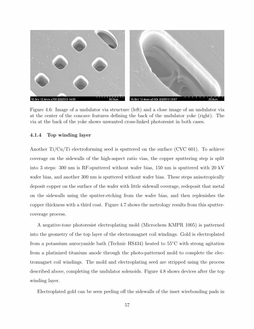
Figure 4.6: Image of a undulator via structure (left) and a close image of an undulator viaat the center of the concave features defining the back of the undulator yoke (right). Thevia at the back of the yoke shows unwanted cross-linked photoresist in both cases.
4.1.4 Top winding layer
Another Ti/Cu/Ti electroforming seed is sputtered on the surface (CVC 601). To achieve
coverage on the sidewalls of the high-aspect ratio vias, the copper sputtering step is split
into 3 steps: 300 nm is RF-sputtered without wafer bias, 150 nm is sputtered with 20 kV
wafer bias, and another 300 nm is sputtered without wafer bias. These steps anisotropically
deposit copper on the surface of the wafer with little sidewall coverage, redeposit that metal
on the sidewalls using the sputter-etching from the wafer bias, and then replenishes the
copper thickness with a third coat. Figure 4.7 shows the metrology results from this sputter-
coverage process.
A negative-tone photoresist electroplating mold (Microchem KMPR 1005) is patterned
into the geometry of the top layer of the electromagnet coil windings. Gold is electroplated
from a potassium aurocyanide bath (Technic HS434) heated to 55C with strong agitation
from a platinized titanium anode through the photo-patterned mold to complete the elec-
tromagnet coil windings. The mold and electroplating seed are stripped using the process
described above, completing the undulator solenoids. Figure 4.8 shows devices after the top
winding layer.
Electroplated gold can be seen peeling off the sidewalls of the inset wirebonding pads in
57

Figure 4.7: Via-coverage process development.
Figure 4.8: Image of a quadrupole electromagnet (left) and undulator (right) after the topwinding layer step.
58

the quadrupole and undulator devices. This is due to a combination of internal stress in the
deposited gold and poor adhesion of the seed layer due to poor titanium sidewall coverage,
as shown by energy dispersive x-ray spectroscopy (EDX) metrology in Figure 4.7.
4.2 Multi-pole electromagnet process
The RF-switch process described was re-designed to address the specific challenges posed by
thick-film multi-pole electromagnets [HPH14]. The new process is illustrated in Figure 4.9
and discussed below.
Figure 4.9: Illustration of the revised multi-pole electromagnet process.
Several changes were included throughout the process. The thickness of the bottom
winding layer was increased to 20 µm with a deeper etch and a thicker deposit of copper. A
59

fill pattern was etched into blank areas of the wafer to improve down-force uniformity during
the CMP step, producing a inset metal with better than 10% thickness uniformity across the
wafer. Reliability of the top-to-bottom winding interconnection was improved by through-
mold electroplating the vias rather than filling them from the top with a dual Damascene
process. To ensure that there was no photolithographic defects due to diffraction from the
mask and reflection off the yoke, the winding via step was inserted between the bottom
winding layer process and the magnet yoke process. Bubbles from trapped gas during the
spin coat of the planarization layer were removed before soft baking with a short vacuum
step.
4.2.1 Bottom winding layer
The pattern for the bottom of the windings is photolithographically defined on a silicon
wafer using 5-µm-thick photoresist (KMPR 1005). A regular hole array is patterned filling
unused space to make the polishing down-pressure uniform in a later polishing step. Using
this soft mask, 20-µm-deep trenches are etched in the silicon using a deep reactive ion etcher
(Plasma-Therm SLR-770). The photoresist is stripped in ALEG-380 and 5:1 H2SO4:H2O2.
A 500-nm SiO2 film is grown by thermal oxidation (Mini 3600, Tystar Corp., Torrance,
CA, USA) to isolate the bottom windings from the silicon. The wafer is sputter-etched
for 5 minutes, and an electroforming seed is deposited on the SiO2 by RF sputtering with
20-kV wafer bias (CVC 601). The seed-layer consists of 30-nm titanium for adhesion to the
substrate and 300-nm copper to carry the electroplating current. Seed layer oxidation is
etched in 1% hydrofluoric acid and a 25-µm copper film is electroplated from a phosphorized
copper anode in a sulfate-based solution (Technic Elevate 6320) at 5 mA/cm2. The wafer
is polished down to silicon with chemical mechanical polishing, CMP, (Logitech PM5) using
100-nm alumina slurry, yielding the winding bottom layer inlayed in the substrate.
60
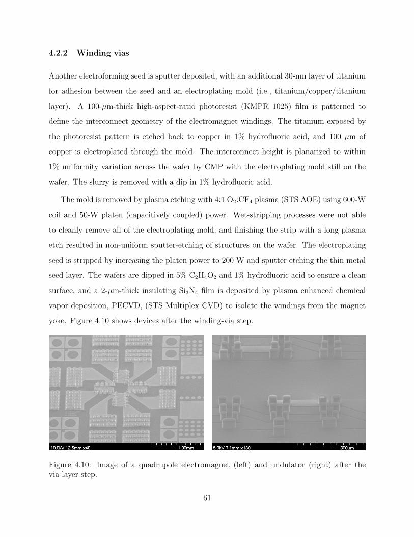
4.2.2 Winding vias
Another electroforming seed is sputter deposited, with an additional 30-nm layer of titanium
for adhesion between the seed and an electroplating mold (i.e., titanium/copper/titanium
layer). A 100-µm-thick high-aspect-ratio photoresist (KMPR 1025) film is patterned to
define the interconnect geometry of the electromagnet windings. The titanium exposed by
the photoresist pattern is etched back to copper in 1% hydrofluoric acid, and 100 µm of
copper is electroplated through the mold. The interconnect height is planarized to within
1% uniformity variation across the wafer by CMP with the electroplating mold still on the
wafer. The slurry is removed with a dip in 1% hydrofluoric acid.
The mold is removed by plasma etching with 4:1 O2:CF4 plasma (STS AOE) using 600-W
coil and 50-W platen (capacitively coupled) power. Wet-stripping processes were not able
to cleanly remove all of the electroplating mold, and finishing the strip with a long plasma
etch resulted in non-uniform sputter-etching of structures on the wafer. The electroplating
seed is stripped by increasing the platen power to 200 W and sputter etching the thin metal
seed layer. The wafers are dipped in 5% C2H4O2 and 1% hydrofluoric acid to ensure a clean
surface, and a 2-µm-thick insulating Si3N4 film is deposited by plasma enhanced chemical
vapor deposition, PECVD, (STS Multiplex CVD) to isolate the windings from the magnet
yoke. Figure 4.10 shows devices after the winding-via step.
Figure 4.10: Image of a quadrupole electromagnet (left) and undulator (right) after thevia-layer step.
61

4.2.3 Magnet yoke
An electroforming seed is deposited as described in the winding-via step. A 100-µm film
of KMPR 1025 photoresist is patterned into the geometry of the magnet yoke. Between
pouring the photoresist and spinning, the film is de-gassed in a vacuum oven at 30 Torr
for 30 seconds. The exposed seed layer is etched to copper in 1% hydrofluoric acid, and a
Ni80Fe20 electromagnet yoke (Bsat = 1.1 T, µr = 8000) is plated through the mold using the
process detailed by Glickman et al. [GTH09]. Planarization, mold and seed stripping, and
layer isolation proceed as described in the winding via step. Figure 4.11 shows an undulator
yoke test structure that was not fully planarized. This planarization step is necessary to
guarantee field uniformity locally and across the wafer. Figure 4.12 shows devices after the
magnet yoke step.
Figure 4.11: Image of an undulator yoke during planarization.
4.2.4 Planarization layer
A 100-µm-thick film of photoresist (SU-8 2025) is used to provide a planar surface for defining
the top of the coil windings. The SU-8 is de-gassed in the same manner as KMPR in the pre-
vious step, patterned and baked to expose the winding vias, and planarized to 10 µm above
the yoke before development to improve thickness uniformity. The film is then annealed in
vacuum for 8 hours at 200C. Figure 4.13 shows devices after the planarization-layer step.
62

Figure 4.12: Image of a quadrupole electromagnet (left) and undulator (right) after themagnet-yoke step.
Figure 4.13: Image of a quadrupole electromagnet (left) and undulator (right) after theplanarization-layer step.
4.2.5 Top winding layer
The copper in the vias is exposed by etching the Si3N4 with C4F8 plasma (STS AOE).
A seed layer is sputtered on the surface as described in the winding-via step. A 25-µm-
thick KMPR 1005 layer is patterned into the geometry of the top winding layer, and 20-µm
copper is electroplated through the mold. The mold and seed are stripped using the process
described in the winding via step, completing the multi-pole electromagnets. The SU-8 is
etched using the mold stripping process described in the winding via step to avoid thermal
expansion issues during operation. Figure 4.14 shows devices after the top winding step.
63

Figure 4.14: Images after the top winding layer step of a quadrupole electromagnet beforeetching back the planarizing photoresist layer (left) and undulator after etching back theplanarizing photoresist layer (right).
Many devices failed after this step due to an insufficiently thick seed layer. The 300-nm-
thick copper seed layer etches at∼100 nm/min, and the titanium and SU-8 below etch rapidly
once exposed to the plating solution. If the seed layer is broken through before deposition
begins to add material, pits can form and be filled with metal, shorting the winding to the
yoke, or the entire winding trace can be lost. Figure 4.15 shows a quadrupole electromagnet
that failed completely due to this manufacturing defect. Occasional high-resistance shorts
from the top metal layer to the electromagnet yoke that were due to this problem were
correctable with a short current pulse.
Figure 4.15: Image of a quadrupole electromagnet that failed due to the loss of the seedlayer in the time between loading the electroplating tool and starting deposition.
64
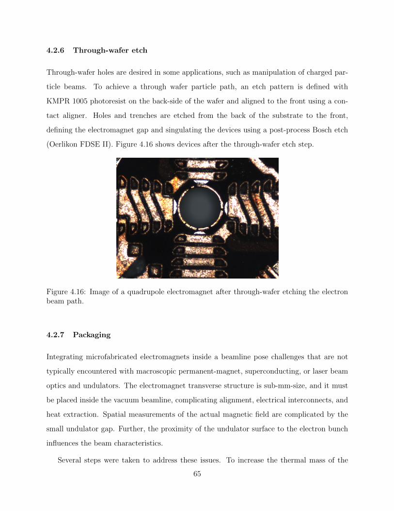
4.2.6 Through-wafer etch
Through-wafer holes are desired in some applications, such as manipulation of charged par-
ticle beams. To achieve a through wafer particle path, an etch pattern is defined with
KMPR 1005 photoresist on the back-side of the wafer and aligned to the front using a con-
tact aligner. Holes and trenches are etched from the back of the substrate to the front,
defining the electromagnet gap and singulating the devices using a post-process Bosch etch
(Oerlikon FDSE II). Figure 4.16 shows devices after the through-wafer etch step.
Figure 4.16: Image of a quadrupole electromagnet after through-wafer etching the electronbeam path.
4.2.7 Packaging
Integrating microfabricated electromagnets inside a beamline pose challenges that are not
typically encountered with macroscopic permanent-magnet, superconducting, or laser beam
optics and undulators. The electromagnet transverse structure is sub-mm-size, and it must
be placed inside the vacuum beamline, complicating alignment, electrical interconnects, and
heat extraction. Spatial measurements of the actual magnetic field are complicated by the
small undulator gap. Further, the proximity of the undulator surface to the electron bunch
influences the beam characteristics.
Several steps were taken to address these issues. To increase the thermal mass of the
65

electromagnet, it is mounted in a 1-mm-thick conventionally machined oxygen-free high-
conductivity (OFHC) copper fixture. Either a 610-µm or 50-µm hole is made in the fixture
with a size 73 drill or laser mill to provide an aperture for the electron beam. To con-
nect the macroscopic coaxial feedthroughs on the beam pipe to the MEMS electromagnet,
a vacuum-compatible high-thermal-conductivity PCB (Duroid 6002, Rogers Corp., Rogers,
CT, USA) is mechanically mounted on the copper fixture with 0-80 screws, connected to
the feedthroughs with vacuum-compatible (PTFE coated) 16 AWG wires (5858 WH005,
Alpha Wire, Elizabeth, NJ, USA), and connected to the electromagnet with 15-µm Al wire-
bonds. Figure 4.17 and 4.18 shows a packaged quadrupole electromagnet. The electromagnet
die has withstood 70-A pulses on a probe station without failure, but the 20 15-µm diameter
Al wirebonds in the package failed at 5.5 A. The development of a flip-chip bonding process
between the electromagnet die and the package PCB would address wire bond failure and
increase the tolerable average drive current.
Figure 4.17: Image of a quadrupole electromagnet packaged in a copper beam testing fixturewith a laser-machined 50-µm electron-beam aperture.
To produce a well-controlled beam for the experiments using the DC-photogun, three
approaches were taken to manufacture an aperture for the electron beam upstream of the
MEMS electromagnets: a mechanically drilled 610-µm-wide hole in the 1-mm-thick OFHC
copper MEMS die fixture, a laser milled 50-µm-wide hole in the 1-mm-thick OFHC copper
66

Figure 4.18: Image of a quadrupole electromagnet fixture mounted on a vacuum bellowbefore insertion into an experiment chamber. The aluminum shield visible on the side of theimage bolts over the quadrupole, protecting it from handling damage.
MEMS die fixture, and a translatable aperture made from two orthogonal 20-µm-wide steel
slits. The 610-µm-wide hole was machined using a drill press in the UCLA Center for High
Frequency Electronics (CHFE). The 50-µm-wide hole, shown in Figure 4.19, was machined
by Laserod Corp.
Figure 4.19: Image of the 50 µm wide copper aperture.
67

The orthogonal slit aperture, illustrated in Figure 4.20, is pair of Thorlabs S20R slits that
were chemically stripped of the optical coatings to prevent charging by the electron beam.
To clean the oil off the black oxide-coated stainless steel, the slits were soaked in acetone for 1
minute and rinsed in isopropanol. The slits were then soaked in 10% hydrochloric acid for 30
minutes to oxidize the ferrous oxide to ferrous chloride. Vigorous agitation in methanol was
then used to dissolve the ferrous chloride. The slit surface was gently brushed with a kimwipe
to clean off the remaining ferrous chloride. After thoroughly washing the slits in water, the
slits were soaked in sodium hydroxide for 10 minutes to reduce the anodized aluminum
surface to aluminum metal. The slits were then washed in water and gently brushed with
a kimwipe. To ensure that the entirety of both slits were electrically conducting, 10 nm of
gold germanium was sputtered on both sides in a Denton Desktop Sputter system.
Figure 4.20: Illustration of the orthogonal slit-based aperture.
68

CHAPTER 5
Characterization
ELECTROMAGNET PERFORMANCE was investigated with impedance character-
ization before and after packaging and a series of electron beam experiments. Impedance
analysis provided the circuit parameters of the device and frequency response, beam deflec-
tion and focusing experiments demonstrated the reconfigurability and performance of the
device and beam-probe field-mapping of the electromagnet demonstrated the spatial distri-
bution of the fields produced.
5.1 Impedance analysis
Each electromagnet was measured using an impedance analyzer (Agilent 4294A) with a
set of coaxial probes (APT 740CJ) in a four-terminal pair configuration. Before packaging,
electromagnet impedance measurements of the 600 µm gap quadrupoles showed 58.2±1.2-mΩ
resistance and 30.4±1.9-nH inductance at 100 kHz. These measurements agree well with the
71-mΩ resistance and 32.2-nH inductance expected from 3-D FEM simulation. Figure 5.1
shows the electromagnet resistance and inductance for these devices before packaging and
Figure 5.2 shows the electromagnet resistance and inductance after packaging.
There was insufficient yield among the undulator devices to measure the impedance of a
complete 50-period (100-pole) undulator side. Measurements of individual periods, however,
yielded measurements of 137±1.0-mΩ resistance and 17.0±2.0-nH inductance at 100 kHz.
These measurement agree well with the 137-Ω resistance and 17.7-nH inductance expected
from 3-D FEM simulation.
69

Figure 5.1: Measured resistance (blue) and inductance (red) of the 600-µm gap thick-filmMEMS quadrupole between 10 kHz and 5 MHz before packaging (shown in Figure 4.17).Line thickness indicates measurement precision.
Figure 5.2: Measured resistance and inductance of the 4 electromagnets in the 600-µmgap thick-film MEMS quadrupole between 10 kHz and 4 MHz after packaging (shown inFigure 4.17). Measurement precision below 200 kHz is limited to 10%.
5.2 Beam experiments
To demonstrate beam steering and focusing, the MEMS quadrupole was mounted in the
path of an electron beam and powered in dipole or quadrupole configuration (Figure 5.3).
By varying the electrical current in individual coils, the beam was focused or deflected. The
magnetic field or field gradient at the transverse location of the beam in the electromagnet
70

could then be calculated from the change in beam location or beam shape.
The electron beam used in these experiments was generated using a sub-ps UV laser
pulse illuminating a photocathode embedded in a static electric field (DC photogun). A
solenoid electromagnet adjusts the beam focus exiting the photocathode, and a set of steering
electromagnets adjusts position and angle during an 835 mm drift length to an experiment
chamber. The chamber houses the MEMS quadrupole behind a pair of micrometer-mounted
orthogonal 20-µm slits (Thorlabs S20R) that have been stripped of anodizing and iron oxide
coatings to form an electron beam aperture. After another 115 mm drift length, an imaging
system composed of a Chevron micro-channel plate (MCP) intensifier, phosphor screen, and
cooled CCD camera (Hamamatsu Flash 2.8) records the beam position and shape.
Figure 5.3: Photograph and illustration of the electron beam experiment. The black borderedinset illustration shows MEMS quadrupole fixture ’q’ entering the chamber from above,vertical slit ’y’ entering the chamber horizontally, and horizontal slit ’x’ entering the chamberfrom below. The white bordered inset picture shows the MEMS quadrupole. Cyan arrowsillustrate the UV laser path from left to right and blue arrows illustrate the electron beampath from right to left.
We acquired a background shot with the electron beam off for each image, which was
subtracted from the data before calculating beam centroid and rms size. The experiment used
71

a slightly under-focused 34 keV sub-pC electron beam pulsed at 1 kHz repetition rate. The
aperture was centered by switching the electromagnet on and off in quadrupole configuration
and adjusting the position until the beam location did not change. Each measurement
consisted of 25 images taken with 250 ms exposure time.
5.2.1 Electron beam transverse positioning
The transverse position of the electron beam in the electromagnet gap was controlled by
two micrometer-mounted slits forming a 20 µm × 20 µm aperture. Before each experiment,
the aperture was centered by switching the electromagnet on and off in quadrupole mode
while adjusting the aperture position until there was no position change between the on
and off state. This procedure is illustrated in Figure 5.4. Set up for experiments requiring
a beam positioned off-axis started by centering the beam, then translating one slit of the
electron beam aperture. Translating the aperture along the x-axis and y-axis is illustrated
in Figure 5.5 and 5.6. Off-axis beam measurements recorded the beam position with the
electromagnet off as the reference to avoid mechanical location uncertainty.
Figure 5.4: Illustration of the electron beam centering by translating the horizontal andvertical slits while switching the electromagnet on and off.
72

Figure 5.5: Illustration of the electron beam translated off-axis by moving the vertical slitalong the x-axis.
Figure 5.6: Illustration of the electron beam translated off-axis by moving the vertical slitalong the y-axis.
73

5.2.2 Electron beam steering
To measure beam deflection performance, the electromagnet aperture was centered and cur-
rent was stepped from -1.5 A to +1.5 A and back to -1.5 A in 0.5 A increments in an x-dipole
field configuration and then repeated in a y-dipole configuration. Figure 5.7 shows the mea-
sured movement of the beam centroid with data from measurements back and forth along
the x- and y-axis overlaid. The beam was deflected the same distance in each direction, indi-
cating that the electromagnets were well matched. Less than 0.7% electromagnet hysteresis
was measured, well within the experimental error, indicating that these electromagnets will
not require compensation for their hysteresis during operation.
Figure 5.7: Measured beam deflection left, right, up and down across the MCP. Blackdeflection data was taken while increasing the current and grey data was taken while reducingthe current. No hysteresis is visible from the measurements.
The experiment was repeated from -5.5 A to 5.5 A to explore electromagnet performance
near saturation. Figure 5.8 shows the measured beam deflection and the field strength
calculated from the measurements. Electromagnet saturation occurred between 2 A and
3 A drive current in dipole configuration and was expected at 2.35 A from simulation. The
wirebonds in the electromagnet package failed at +5.5 A.
74

Figure 5.8: Electron beam steering experiment using a 4-pole electromagnet to deflect a34-kV electron beam. Field strength assumes 686-µm magnetic length from FEM simulationat -1 A (the circled operating point). An equation fitting the field implied by the deflectiondata is shown.
5.2.3 Beam-probe field mapping
Field uniformity experiments were taken in quadrupole configuration from -1 A to 1 A current
in 0.5 A increments. For each electromagnet current dataset, the aperture was stepped in
equal intervals across the entire electromagnet bore in the horizontal direction and then
in the vertical direction. The magnetic field was calculated from the measured electron
beam deflection at each aperture position using Lorentz force and the normalized magnetic
length from FEM simulation at -1 A quadrupole configuration drive current. Figure 5.9
and Figure 5.10 show the field calculated from beam deflection measurements across the
horizontal and vertical transverse axis of the electromagnet.
The field gradient, shown in Figure 5.11, scales linearly and with hysteresis less than the
measurement error. The difference between the horizontal and vertical field gradient could
be due to poor control of the quadrupole electromagnet axis in the experiment chamber. The
experiment setup obstructed observation of electromagnet orientation inside the chamber and
the azimuth angle was hand-set to pass the beam. Simulations indicate that a 15 azimuth
75

Figure 5.9: Measured x-axis transverse field profile measured with a 20 µm electron beamprobe. Error bars and regression lines show the field across the center of the gap. 54 T/mgradients at 1 A are expected from FEM simulations.
Figure 5.10: Measured y-axis transverse field profile measured with a 20 µm electron beamprobe. Error bars and regression lines show the field across the center of the gap. 54 T/mgradients at 1 A are expected from FEM simulations.
angle error would reduce the field gradient shown in Figure 5.9 from the 54 T/m to the
47 T/m calculated from the beam deflection measurements across the horizontal axis of the
electromagnet. The 57 T/m field gradient calculated from measurements across the vertical
axis could have resulted from slight mis-centering of the aperture before the measurement
started.
76

Figure 5.11: Transverse field gradient measured with a 20 µm electron beam probe. Gradientmeasured along the horizontal axis is black and measured along the vertical axis is gray.
5.2.4 Electron beam focusing
To measure the performance of the quadrupole focusing the beam, the electromagnet aper-
ture was centered and the current was configured for quadrupole mode and stepped from
-1.5 A to +1.5 A and back to -1.5 A in 0.1 A increments. The experiment setup is shown in
Figure 5.12.
Figure 5.12: Illustration of the quadrupole focus sweep experiment.
The measured beam rms width is shown in Figure 5.13, and a focused beam waist is
obtained at the MCP plane in the y-axis for I = 0.9 A and in the x-axis for I = -0.9 A. The
77
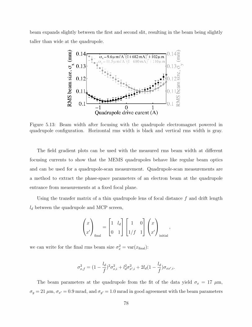
beam expands slightly between the first and second slit, resulting in the beam being slightly
taller than wide at the quadrupole.
Figure 5.13: Beam width after focusing with the quadrupole electromagnet powered inquadrupole configuration. Horizontal rms width is black and vertical rms width is gray.
The field gradient plots can be used with the measured rms beam width at different
focusing currents to show that the MEMS quadrupoles behave like regular beam optics
and can be used for a quadrupole-scan measurement. Quadrupole-scan measurements are
a method to extract the phase-space parameters of an electron beam at the quadrupole
entrance from measurements at a fixed focal plane.
Using the transfer matrix of a thin quadrupole lens of focal distance f and drift length
ld between the quadrupole and MCP screen,
xx′
final
=
1 ld
0 1
1 0
1/f 1
xx′
initial
,
we can write for the final rms beam size σ2x = var(xfinal):
σ2x,f = (1− ld
f)2σ2
x,i + l2dσ2x′,i + 2ld(1−
ldf
)σxx′,i.
The beam parameters at the quadrupole from the fit of the data yield σx = 17 µm,
σy = 21 µm, σx′ = 0.9 mrad, and σy′ = 1.0 mrad in good agreement with the beam parameters
78

expected following the 20 µm aperture, validating our model for the MEMS quadrupole
performance.
79

CHAPTER 6
Future work
MANY EXPERIMENTS demonstrating the unique performance of MEMS particle
beam optics have not yet been carried out. Experiments using the Photoelec-
tron Generated Amplified Spontaneous Radiation Source (PEGASUS) in the UCLA Particle
Beam Physics Laboratory (PBPL), shown in Figure 6.1, rather than the 100 kV DC-photogun
will enable state-of-the-art control of the electron beam in both time and phase-space for
these experiments at the relativistic beam energies relevant to applications in electron-beam-
based light sources.
6.1 High-speed focusing experiment
Experiments demonstrating the higher operating frequency or faster magnetic field response
enabled by MEMS focusing and deflecting optics could lead to fast beam-dither stages for
transmission electron microscopes or kicker beam extraction magnets in synchrotrons that
minimally affect the circulating beam. A proof of principle experiment using the Pegasus
accelerator in PBPL will reproduce the experimental conditions of the quadrupole demon-
strated with the DC-photogun, but with 4 MeV electrons and controlled phase between the
electron bunch and the MEMS quadrupole focusing current pulse. By stepping through 180
relative phase at pulse widths between 1 s and 1 µs, the frequency response of the quadrupole
electromagnet will be experimentally demonstrated.
80
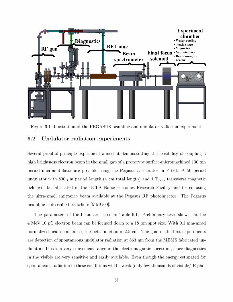
Figure 6.1: Illustration of the PEGASUS beamline and undulator radiation experiment.
6.2 Undulator radiation experiments
Several proof-of-principle experiment aimed at demonstrating the feasibility of coupling a
high brightness electron beam in the small gap of a prototype surface-micromachined 100 µm
period microundulator are possible using the Pegasus accelerator in PBPL. A 50 period
undulator with 800 µm period length (4 cm total length) and 1 Tpeak transverse magnetic
field will be fabricated in the UCLA Nanoelectronics Research Facility and tested using
the ultra-small emittance beam available at the Pegasus RF photoinjector. The Pegasus
beamline is described elsewhere [MMG09].
The parameters of the beam are listed in Table 6.1. Preliminary tests show that the
4 MeV 10 pC electron beam can be focused down to a 18 µm spot size. With 0.1 mm-mrad
normalized beam emittance, the beta function is 2.5 cm. The goal of the first experiments
are detection of spontaneous undulator radiation at 863 nm from the MEMS fabricated un-
dulator. This is a very convenient range in the electromagnetic spectrum, since diagnostics
in the visible are very sensitive and easily available. Even though the energy estimated for
spontaneous radiation in these conditions will be weak (only few thousands of visible/IR pho-
81

Table 6.1: Parameters of the microundulator experiment at the Pegasus beamlineE-beam energy 11 MeVE-beam peak current 100 AmpBeam emittance 0.1 mm-mradUndulator period 800 µmUndulator gap 200 µmPeak magnetic field 1 TK (rms) 0.1Nu 50Undulator length 4 cmλr 863 nmEr 1.43 eV
ton generated), we will be able to use intensified CCD cameras with single photon detection
capabilities to characterize the radiation.
Another feasible experiment will be to use the 800 nm Ti:Sa laser system available in the
Pegasus laboratory to microbunch the 4 MeV beam at 800 nm with a seed radiation pulse.
This is an application for which microundulators might be uniquely suited. Currently, there
is no way to efficiently couple a low energy electron beam and an optical or near infrared
laser. The period of conventional undulator magnets is too long to tune at the resonance
condition and harmonic coupling coefficients quickly decrease in amplitude with increasing
harmonic number. This coupling can be used to diagnose and manipulate the longitudinal
phase space of low energy beams at the optical scale. Coupling this scheme with recent ideas
on longitudinal space charge amplification [SY10], which naturally works better at lower
beam energy, might open a path towards a new kind of radiation source.
82

CHAPTER 7
Conclusion
THIS PROJECT demonstrated the first application of magnetic MEMS to focusing
and steering electromagnets for charged particle beams. A 600-µm magnetic gap
4-pole electromagnet was designed, fabricated, and tested with a 34 keV electron beam,
demonstrating digitally controlled steering and focusing.
The performance of these magnetic optics improves considerably as size is reduced into
the micro-scale. Simple scaling of the prototype results presented in this work indicated that
multi-kT/m gradients can be obtained using MEMS fabrication techniques. Such MEMS
quadrupoles hold the potential to revolutionize the field of charged particle optics with a
wide range of applications including electron microscopes and compact light sources.
Undulators with magnetic gap and undulator period in the range of 100 µm were designed
and a compatible fabrication process was developed. This period range is presently not
covered by other undulator technology and is very attractive since it bridges the gap between
traditional permanent magnet undulators and laser undulators employed in inverse Compton
scattering sources.
83

APPENDIX A
Experiment data processing scripts
Images of the MCP from the beam experiments were recorded with a matlab script that
recorded the experimental parameters in the image filename. The images were sorted into
directories corresponding to each experiment type (deflection, focusing, field characteriza-
tion), and the quadImageProcess() script was run on the directory to extract measurement
metadata from the images.
The plotQuadData() and plotDipoleData() scripts were run with the processed metadata
input to plot the measurement results.
A.1 Beam data pre-processing MATLAB script
function [files] = quadImageProcess(directory)
% [files] = quadImageProcess(pwd())
%
% Old experiment is 133 microns / pixel
% Old experiment is 16.5 cm from the MCP
%
% New experiment is is 40 microns / pixel
%
% New MCP setup is closer to the quadrupole
%
% NOTE: Focusing statistics are only for changes to the x and y axis.
% Anything at a different angle, such as 2 electromagnets being driven, will
% not process unless rotateOn is set to 1 and the commented code is
% modified to accommodate the change at imrotate( ...
%
% cSum = [files.c1]+[files.c3];
% cDiff = [files.c1]-[files.c3];
% centroidX = [files.centroidX];
% centroidY = [files.centroidY];
84

% majorAxis = [files.majorAxis];
% minorAxis = [files.minorAxis];
% orientation = [files.orientation];
%
% New additions!
% uniformityTest = 0; processes the data with a fixed iris
% uniformityTest = 1; processes the data with to orthogonal moving slits.
% This adds two new double precision variables to the ’files’ structure,
% irisX and irisY. irisX is the x-axis position (converted to meters) of
% the vertical slit and irisY is the y-axis position of the horizontal
% slit. The November26 experiment (data taken December 5 after stripping
% the insulating films off of the x and y iris) uses 20 micron slits. Slit
% 1 is 26 microns and is the x-moving vertical slit. Slit 2 is 23.5 microns
% and and is the y-moving horizontal slit.
%% Processing parameters
rotateOn = 0;
uniformityTest = 0;
%calibration data (meters/step) for the y-moving horizontal slit.
%Taken from StepperCalibration.xlsx
slit2Step = 286.3e-6/5000;
%% Parsing parameters
delimiter = ’_’;
%% Get file names
files = dir(directory);
%% Parse file names
fprintf([’Parsing file names in ’ directory ’ to metadata...’]);
%list of position reference files with the form:[... ; X Y fileIndex ; ...]
posReferenceList = [];
for fileIndex = 1:length(files)
delimiters = 0;
for parseIndex = 1:length(files(fileIndex).name);
if (strcmp(files(fileIndex).name(parseIndex),delimiter))
delimiters = [delimiters parseIndex];
end
end
if strcmp(files(fileIndex).name,’Background.bmp’)
files(fileIndex).isFile = 1;
files(fileIndex).isBackground = 1;
elseif length(delimiters)>3%First delimiter is set at 1.
if exist(’item’)
clear(’item’)
85

end
for delimiterIndex = 1:length(delimiters)-1
item(delimiterIndex) = ...
files(fileIndex).name(delimiters(delimiterIndex)+...
1:delimiters(delimiterIndex+1)-1);
end
files(fileIndex).c0 = 0;
files(fileIndex).c1 = 0;
files(fileIndex).c2 = 0;
files(fileIndex).c3 = 0;
files(fileIndex).mc0 = 0;
files(fileIndex).mc1 = 0;
files(fileIndex).mc2 = 0;
files(fileIndex).mc3 = 0;
files(fileIndex).isFile = 1;
files(fileIndex).isBackground = 0;
files(fileIndex).isPosReference = 0;
files(fileIndex).offsetX = 0;
files(fileIndex).offsetY = 0;
files(fileIndex).slitX = 0;
files(fileIndex).slitY = 0;
files(fileIndex).exposureTime = .1;
files(fileIndex).MeasurementNumber = 1;
files(fileIndex).posReferenceIndex = 0;
files(fileIndex).posReferenceUsed = 0;
files(fileIndex).SNR = 0;
for itemIndex = 1:length(item)
if strcmp(itemitemIndex,’c0’)
files(fileIndex).c0 = str2num(itemitemIndex+1);
elseif strcmp(itemitemIndex,’c1’)
files(fileIndex).c1 = str2num(itemitemIndex+1);
elseif strcmp(itemitemIndex,’c2’)
files(fileIndex).c2 = str2num(itemitemIndex+1);
elseif strcmp(itemitemIndex,’c3’)
files(fileIndex).c3 = str2num(itemitemIndex+1);
elseif strcmp(itemitemIndex,’mc0’)
files(fileIndex).mc0 = str2num(itemitemIndex+1);
elseif strcmp(itemitemIndex,’mc1’)
files(fileIndex).mc1 = str2num(itemitemIndex+1);
elseif strcmp(itemitemIndex,’mc2’)
files(fileIndex).mc2 = str2num(itemitemIndex+1);
elseif strcmp(itemitemIndex,’mc3’)
files(fileIndex).mc3 = str2num(itemitemIndex+1);
elseif strcmp(itemitemIndex,’beamOff’) || ...
strcmp(itemitemIndex,’BeamOff’) || ...
86

strcmp(itemitemIndex,’Off’)
files(fileIndex).isBackground = 1;
elseif strcmp(itemitemIndex,’beamOn’) || ...
strcmp(itemitemIndex,’BeamOn’) || ...
strcmp(itemitemIndex,’On’)
files(fileIndex).isBackground = 0;
elseif strcmp(itemitemIndex,’roi’)
files(fileIndex).offsetX = str2num(itemitemIndex+1);
files(fileIndex).offsetY = str2num(itemitemIndex+2);
elseif strcmp(itemitemIndex,’window’)
files(fileIndex).offsetX = str2num(itemitemIndex+1);
files(fileIndex).offsetY = str2num(itemitemIndex+2);
elseif strcmp(itemitemIndex,’slitX’);
files(fileIndex).slitX = str2num(itemitemIndex+1)/1e6;
elseif strcmp(itemitemIndex,’slitY’);
files(fileIndex).slitY = str2num(itemitemIndex+1)/1e6;
if ~files(fileIndex).c0 && ~files(fileIndex).c1 && ...
~files(fileIndex).c2 && ~files(fileIndex).c3 && ...
~files(fileIndex).isBackground
files(fileIndex).isPosReference = 1;
posReferenceList = [posReferenceList;...
[files(fileIndex).slitX,files(fileIndex).slitY,...
fileIndex]];
end
elseif strcmp(itemitemIndex,’exp’)
files(fileIndex).exposureTime = ...
.001*str2num(itemitemIndex+1);
elseif strcmp(itemitemIndex,’rep’)
files(fileIndex).MeasurementNumber = ...
str2num(itemitemIndex+1);
elseif strcmp(itemitemIndex,’Is’)
files(fileIndex).solenoidCurrent = ...
str2num(itemitemIndex+1);
end
end
elseif length(delimiters)>2 && length(delimiters)<5
for delimiterIndex = 1:length(delimiters)-1
item(delimiterIndex) = ...
files(fileIndex).name(delimiters(delimiterIndex)+...
1:delimiters(delimiterIndex+1)-1);
end
files(fileIndex).isFile = 1;
files(fileIndex).isBackground = 0;
files(fileIndex).c1 = str2num(item1);
files(fileIndex).c3 = str2num(item2);
87

else
files(fileIndex).isBackground = 0;
files(fileIndex).isFile = 0;
end
end
fprintf(’\n’);
referenceIndex = [];
deleteIndex = [];
fprintf(’Parsing file metadata...\n’);
for fileIndex = 1:length(files)
if files(fileIndex).isFile
info = imfinfo([directory ’/’ files(fileIndex).name]);
try
%NECESSARY for threshold processing
files(fileIndex).depth = info.NumColorsUsed;
catch
files(fileIndex).depth = 2^(info.BitDepth);
end
if files(fileIndex).isBackground
referenceIndex = [referenceIndex fileIndex];
end
else
deleteIndex = [deleteIndex fileIndex];
end
end
fprintf(’Parsing background reference image metadata...\n’);
index = 1;
for index = 1:length(referenceIndex)
referenceImage(index).data = ...
imread([directory ’/’ files(referenceIndex(index)).name]);
referenceImage(index).sizeX = size(referenceImage(index).data,1);
referenceImage(index).sizeY = size(referenceImage(index).data,2);
referenceImage(index).offsetX = files(referenceIndex(index)).offsetX;
referenceImage(index).offsetY = files(referenceIndex(index)).offsetY;
referenceImage(index).exposureTime = ...
files(referenceIndex(index)).exposureTime;
index = index+1;
end
if uniformityTest == 1
fprintf(’Parsing position refence image metadata...\n’);
index=1;
for index = setxor(1:length(files),posReferenceList(:,3))’
if files(index).isFile
for posIndex = posReferenceList(:,3)’
88

if files(index).slitX == files(posIndex).slitX && ...
files(index).slitY == ...
files(posIndex).slitY && ...
~files(index).posReferenceIndex && ...
~(files(posIndex).posReferenceUsed== ...
files(index).c0)
%May need to be modified when there are multipole
%position references (passed 0 multiple times)
files(index).posReferenceIndex = posIndex;
%Files will be sorted in this list, so this should keep
%the same image from being used by multiple repitions
%of the same current.
files(posIndex).posReferenceUsed = files(index).c0;
end
end
%What if it doesn’t find a reference file? It’ll return -0- for
%.posReferenceIndex and cause a problem in plotQuadData2.
if ~files(index).posReferenceIndex && files(index).c0
fprintf([...
’ Error: no position reference found for file\n’...
’ ’ files(index).name ’\n’])
end
end
end
end
clear(’item’,’index’,’fileIndex’,’delimiters’,’delimiterIndex’,...
’delimiter’,’info’,’parseIndex’,’referenceImageIndex’,’posIndex’);
%% Process the images for centroid location, minor axis, major axis,
%and ellipse orientation
% intensity ratio at **two** standard deviations from the centroid
% One standard deviation is pretty close to the centroid (couple pixels)
threshold(1) = exp(-1);
threshold(2) = exp(-4/2);
threshold(3) = exp(-9/3);
threshold(4) = exp(-16/4);
threshSelect = 2;% How many standard deviations for measurement?
threshMeasure = 1;
for fileIndex = 1:length(files)
fprintf([’Processing ’ files(fileIndex).name ’, ’ num2str(fileIndex)...
89

’ of ’ num2str(length(files)) ’... \n’]);
if files(fileIndex).isFile && ~files(fileIndex).isBackground
% Remove background noise and damage to the MCP & CCD from the
% image.
files(fileIndex).image = ...
imread([directory ’/’ files(fileIndex).name]);
files(fileIndex).proc = files(fileIndex).image;
usableReference = [];
for referenceImageIndex = 1:length(referenceImage)
if (size(files(fileIndex).proc,1) == ...
referenceImage(referenceImageIndex).sizeX && ...
size(files(fileIndex).proc,2) == ...
referenceImage(referenceImageIndex).sizeY && ...
files(fileIndex).offsetX == ...
referenceImage(referenceImageIndex).offsetX && ...
files(fileIndex).offsetY == ...
referenceImage(referenceImageIndex).offsetY && ...
files(fileIndex).exposureTime == ...
referenceImage(referenceImageIndex).exposureTime)
usableReference = [usableReference referenceImageIndex];
end
end
try
reference = ...
single(zeros(referenceImage(usableReference(1)).sizeX,...
referenceImage(usableReference(1)).sizeY));
catch
reference = single(zeros(size(files(fileIndex).proc,1),...
size(files(fileIndex).proc,2)));
files(fileIndex).noNormalization = 1;
end
for index = 1:length(usableReference)
reference = reference + 1/length(usableReference)*...
(single(referenceImage(usableReference(index)).data));
end
reference = uint16(reference);
files(fileIndex).proc = files(fileIndex).proc - reference;
files(fileIndex).threshSelect = im2bw(files(fileIndex).proc,...
single(max(max(files(fileIndex).proc)))/...
(files(fileIndex).depth-1)*threshold(threshSelect));
[files(fileIndex).threshLabeled num]= ...
bwlabel(files(fileIndex).threshSelect);
stats = regionprops(files(fileIndex).threshLabeled,’centroid’,...
’MajorAxisLength’,’MinorAxisLength’,’Orientation’,’Area’);
[val,statIndex] = max([stats.Area]);
90

measureLocationX = round(stats(statIndex).Centroid(2));
measureLocationY = round(stats(statIndex).Centroid(1));
files(fileIndex).threshMeasure = im2bw(files(fileIndex).proc, ...
single(max(max(files(fileIndex).proc(...
measureLocationX,measureLocationY))))/ ...
(files(fileIndex).depth-1)...
*threshold(threshMeasure));
[files(fileIndex).threshLabeled num]= ...
bwlabel(files(fileIndex).threshMeasure);
spotLocationX = stats(statIndex).Centroid(1);
spotLocationY = stats(statIndex).Centroid(2);
stats = regionprops(files(fileIndex).threshLabeled,’centroid’,...
’MajorAxisLength’,’MinorAxisLength’,’Orientation’,’Area’);
statIndex = 0;
for index = 1:length(stats)
if spotLocationX - 4 < stats(index).Centroid(1) && ...
stats(index).Centroid(1) < spotLocationX + 4 && ...
spotLocationY - 4 < stats(index).Centroid(2) && ...
stats(index).Centroid(2) < spotLocationY + 4
statIndex = index;
end
end
if statIndex
files(fileIndex).area = stats(statIndex).Area;
files(fileIndex).centroidX = stats(statIndex).Centroid(1);
files(fileIndex).centroidY = stats(statIndex).Centroid(2);
files(fileIndex).majorAxis = stats(statIndex).MajorAxisLength;
files(fileIndex).minorAxis = stats(statIndex).MinorAxisLength;
%Angle coutnerclockwise from the x-axis
files(fileIndex).orientation = stats(statIndex).Orientation;
% Rotate image by stats.orientation and perform a gaussian fit
beamSpotWindow = 20;%(20 makes 41x41, 25 makes 51x51)
if round(files(fileIndex).centroidY-beamSpotWindow) < 1
beamSpotWindow = round(files(fileIndex).centroidY)-1;
end
if round(files(fileIndex).centroidY+beamSpotWindow) > ...
size(files(fileIndex).proc,1)
beamSpotWindow = size(files(fileIndex).proc,1)-...
round(files(fileIndex).centroidY)-1;
end
if round(files(fileIndex).centroidX-beamSpotWindow) < 1
beamSpotWindow = round(files(fileIndex).centroidX)-1;
end
if round(files(fileIndex).centroidX+beamSpotWindow) > ...
size(files(fileIndex).proc,2)
91

beamSpotWindow = size(files(fileIndex).proc,2)-...
round(files(fileIndex).centroidX)-1;
end
%Check again to make sure that it isn’t in the corner.
if round(files(fileIndex).centroidY-beamSpotWindow) < 1
beamSpotWindow = round(files(fileIndex).centroidY)-1;
end
if round(files(fileIndex).centroidY+beamSpotWindow) > ...
size(files(fileIndex).proc,1)
beamSpotWindow = size(files(fileIndex).proc,1)-...
round(files(fileIndex).centroidY)-1;
end
if round(files(fileIndex).centroidX-beamSpotWindow) < 1
beamSpotWindow = round(files(fileIndex).centroidX)-1;
end
if round(files(fileIndex).centroidX+beamSpotWindow) > ...
size(files(fileIndex).proc,2)
beamSpotWindow = size(files(fileIndex).proc,2)-...
round(files(fileIndex).centroidX)-1;
end
edge1 = round(files(fileIndex).centroidY-beamSpotWindow);
files(fileIndex).edge1 = edge1;
edge2 = round(files(fileIndex).centroidY+beamSpotWindow);
files(fileIndex).edge2 = edge2;
edge3 = round(files(fileIndex).centroidX-beamSpotWindow);
files(fileIndex).edge3 = edge3;
edge4 = round(files(fileIndex).centroidX+beamSpotWindow);
files(fileIndex).edge4 = edge4;
if edge1 < 1 || edge3 < 1 || ...
edge2 > size(files(fileIndex).proc,1) || ...
edge4 > size(files(fileIndex).proc,2)
deleteIndex = [deleteIndex fileIndex];
fprintf([’ Dumping ’ files(fileIndex).name ’, ’ ...
num2str(fileIndex) ’ of ’ num2str(length(files)) ...
’ (bounds:’ num2str(edge1) ’,’ num2str(edge2) ’,’ ...
num2str(edge3) ’,’ num2str(edge4) ’)\n’])
else
beamSpot =(files(fileIndex).proc(edge1:edge2,edge3:edge4));
if rotateOn
beamSpotProc = imrotate(beamSpot,...
mod(90,files(fileIndex).orientation),...
’bicubic’,’crop’);
else
beamSpotProc = beamSpot;
92

end
beamSpotCSx = beamSpotProc(:,1+beamSpotWindow);
files(fileIndex).beamSpotCSx = beamSpotCSx;
beamSpotCSy = beamSpotProc(1+beamSpotWindow,:);
files(fileIndex).beamSpotCSy = beamSpotCSy;
%Integrate across image for increased SNR
beamSpotIntX = sum(beamSpotProc,1);
files(fileIndex).beamSpotIntX = beamSpotIntX;
beamSpotIntY = sum(beamSpotProc,2);
files(fileIndex).beamSpotIntY = beamSpotIntY;
%Set up fitting initial parameters.
minFx = min(beamSpotIntX);
maxFx = max(beamSpotIntY);
minFy = min(beamSpotIntX);maxFy = max(beamSpotIntY);
ezfitFunX = [’y = a*exp(-((x-x_0)^2)/(2*sigma^2))+y0;a=’...
num2str(maxFx-minFx) ’;x_0=’ ...
num2str(round(length(beamSpotIntX)/2)+1) ...
’;sigma=3;y0=’ num2str(minFx)];
ezfitFunY = [’y = a*exp(-((x-x_0)^2)/(2*sigma^2))+y0;a=’...
num2str(maxFy-minFy) ’;x_0=’ ...
num2str(round(length(beamSpotIntY)/2)+1) ...
’;sigma=3;y0=’ num2str(minFy)];
%Fit offset gaussian to beam spot shape.
Fx = ezfit(beamSpotIntX,ezfitFunX);
Fy = ezfit(beamSpotIntY,ezfitFunY);
files(fileIndex).fitIntX = Fx;
files(fileIndex).fitIntY = Fy;
if files(fileIndex).fitIntX.r < 0.95
deleteIndex = [deleteIndex fileIndex];
fprintf([’ Dumping ’ files(fileIndex).name ’, ’ ...
num2str(fileIndex) ’ of ’ num2str(length(files))...
’ (fit R = ’ num2str(files(fileIndex).fitIntX.r)...
’)\n’]);
elseif files(fileIndex).fitIntY.r < 0.95
deleteIndex = [deleteIndex fileIndex];
fprintf([’ Dumping ’ files(fileIndex).name ’, ’ ...
num2str(fileIndex) ’ of ’ num2str(length(files))...
’ (fit R = ’ num2str(files(fileIndex).fitIntX.r)...
’)\n’]);
end
%Fit gaussian to beam spot shape.
Fx = ezfit(single(beamSpotCSx),...
’y = a*exp(-((x-x_0)^2)/(2*sigma^2))+y0;a=500;x0=21;sigma=20;y0=50’);
Fy = ezfit(single(beamSpotCSy),...
’y = a*exp(-((x-x_0)^2)/(2*sigma^2))+y0;a=500;x0=21;sigma=20;y0=50’);
93

files(fileIndex).fitCSX = Fx;
files(fileIndex).fitCSY = Fy;
files(fileIndex).SNR = max(max(...
files(fileIndex).proc(edge1:edge2,edge3:edge4)))/ ...
mean(mean(files(fileIndex).proc([1:edge1 edge2:end],...
[1:edge3 edge4:end])));
end
else
deleteIndex = [deleteIndex fileIndex];
fprintf([’ Dumping ’ files(fileIndex).name ’, ’ ...
num2str(fileIndex) ’ of ’ num2str(length(files))...
’ (centroid)\n’])
files(fileIndex).area = NaN;
files(fileIndex).centroidX = NaN;
files(fileIndex).centroidY = NaN;
files(fileIndex).majorAxis = NaN;
files(fileIndex).minorAxis = NaN;
files(fileIndex).orientation = NaN;
if files(fileIndex).exposureTime ~= 0.001
’stop temporarily and inspect’;
end
end
end
end
save([directory ’/filesNew.mat’],’files’);
deleteIncrement = 1;
deleteArray = unique([deleteIndex referenceIndex]);
if uniformityTest
% Update index references to relative position files and delete.
for index = deleteArray
for index2 = index:length(files)
files(index2).posReferenceIndex = ...
files(index2).posReferenceIndex-1;
end
end
end
%clear this file from the array
files(unique([deleteIndex referenceIndex])) = [];
clear(’lastfit’);
save([directory ’/filesNew.mat’],’files’);
fprintf([’Finished ’ directory ’.\n’]);
94

A.2 Beam-steering data processing MATLAB script
function [files] = plotQuadData2(files)
% [plotData,focusMajorMean,focusMajorStd,...
% focusMinorMean,focusMinorStd,FocusMajorSubMinorMean,...
% focusMajorSubMinorStd]
%% Data handling parameters
manualCheck = 0;
automaticCheck = 0;
uniformityTest = 0;
imageCenteredOn = 0;
imageUncenteredOn= 1;
%% Fundamental parameters
%Electron properties
e0 = -1.60217646e-19; %C
m0 = 9.10938188e-31; %kg
Ebeam = 34e3;
restmass = 510998.93;%eV
%Fundamental constants
c = 299792458; %m/s
h = 6.626068e-34; %m^2*kg/s
eps0 = 8.85418782e-12; %F/m;
mu0 = 1.25663706e-6; %H/m
gamma = Ebeam./restmass+1;%absolute
beta = sqrt(1-1./gamma.^2);%absolute
%MCP Pixel Size (10/22/13)
pixelSize = 57.15e-3/(1725-358); % From MCP_pixelsize.png
MCP_distance = 11.5e-2;%From Evan
magLengthDipole = 686e-6;
magLengthQuad = magLengthDipole;
%% Deflection statistics sorting
fprintf([’Drive current data: ’ num2str(unique([files.c0])) ’\n’])
focusCurrent = [-4000:1000:4000];
%slitXLoc = unique([files.slitX]);
%slitYLoc = unique([files.slitY]);
exposureTimeCheck = .05; % s
solenoidCurrentCheck = 2080; %mA
imageRep = [1];
roiXsel = [1070];
slitSel = unique([files.slitX]);
95

exemptionIndex = [5 0];
exemptionSelection = [2];
exemptionCounter = 1;
%Pick out the index of the dipole data
transportIndex = [];
transportIndexIndex = 0;
fprintf(’Finding quadruple data’);
if uniformityTest
dataLength = length(slitSel);
for dataIndex = 1:dataLength
fprintf(’.’);
tempIndex = find([files.c0]==focusCurrent);
tempIndexSubset = find([files(tempIndex).exposureTime]==...
exposureTimeCheck);
tempIndexReplace = tempIndex(tempIndexSubset);
tempIndex = []; tempIndex = tempIndexReplace;
tempIndexSubset = find([files(tempIndex).solenoidCurrent]==...
solenoidCurrentCheck);
tempIndexReplace = tempIndex(tempIndexSubset);
tempIndex = []; tempIndex = tempIndexReplace;
tempIndexSubset = find([files(tempIndex).slitX]==...
slitSel(dataIndex));
tempIndexReplace = tempIndex(tempIndexSubset);
tempIndex = []; tempIndex = tempIndexReplace;
if ~isempty(imageRep)
if ~isempty(exemptionIndex) && dataIndex == ...
exemptionIndex(exemptionCounter)
tempIndexSubset = find(...
[files(tempIndex).MeasurementNumber]==...
exemptionSelection(exemptionCounter));
exemptionCounter = exemptionCounter + 1;
else
tempIndexSubset = find(...
[files(tempIndex).MeasurementNumber]==imageRep);
end
tempIndexReplace = tempIndex(tempIndexSubset);
tempIndex = []; tempIndex = tempIndexReplace;
end
if ~isempty(roiXsel)
tempIndexSubset = find([files(tempIndex).offsetX]==roiXsel);
tempIndexReplace = tempIndex(tempIndexSubset);
tempIndex = []; tempIndex = tempIndexReplace;
end
plotIndex = 1;
96

for plotIndex = 1:length(tempIndex)
transportIndexIndex = transportIndexIndex + 1;
transportIndex(transportIndexIndex) = tempIndex(plotIndex);
data(dataIndex,plotIndex) = tempIndex(plotIndex);
scale(dataIndex,plotIndex) = 1/2 * ...
(files(tempIndex(plotIndex)).fitCSX.m(1) + ...
files(tempIndex(plotIndex)).fitCSY.m(1));
end
end
fprintf(’.\n’);
else
dataLength = length(focusCurrent);
for dataIndex = 1:dataLength
fprintf(’.’);
tempIndex = find([files.c0]==focusCurrent(dataIndex));
tempIndexSubset = find([files(tempIndex).exposureTime]==...
exposureTimeCheck);
tempIndexReplace = tempIndex(tempIndexSubset);
tempIndex = []; tempIndex = tempIndexReplace;
tempIndexSubset = find([files(tempIndex).solenoidCurrent]==...
solenoidCurrentCheck);
tempIndexReplace = tempIndex(tempIndexSubset);
tempIndex = []; tempIndex = tempIndexReplace;
tempIndexSubset = find([files(tempIndex).slitX]==slitSel);
tempIndexReplace = tempIndex(tempIndexSubset);
tempIndex = []; tempIndex = tempIndexReplace;
if ~isempty(imageRep)
if ~isempty(exemptionIndex) && dataIndex == ...
exemptionIndex(exemptionCounter)
tempIndexSubset = find(...
[files(tempIndex).MeasurementNumber]==...
exemptionSelection(exemptionCounter));
exemptionCounter = exemptionCounter + 1;
else
tempIndexSubset = find(...
[files(tempIndex).MeasurementNumber]==imageRep);
end
tempIndexReplace = tempIndex(tempIndexSubset);
tempIndex = []; tempIndex = tempIndexReplace;
end
if ~isempty(roiXsel)
tempIndexSubset = find([files(tempIndex).offsetX]==roiXsel);
tempIndexReplace = tempIndex(tempIndexSubset);
tempIndex = []; tempIndex = tempIndexReplace;
end
97

plotIndex = 1;
for plotIndex = 1:length(tempIndex)
transportIndexIndex = transportIndexIndex + 1;
transportIndex(transportIndexIndex) = tempIndex(plotIndex);
data(dataIndex,plotIndex) = tempIndex(plotIndex);
scale(dataIndex,plotIndex) = 1/2 * ...
(files(tempIndex(plotIndex)).fitCSX.m(1) + ...
files(tempIndex(plotIndex)).fitCSY.m(1));
end
end
fprintf(’.\n’);
end
dataEnd = zeros(1,size(data,1));
exposureTime = zeros(1,size(data,1));
for dataIndex = 1:size(data,1)
fprintf([’Processing data for ’ num2str(data(dataIndex,1)) ’.’]);
%Select the center of the spot and make an averaged and scaled image.
for plotIndex = 1:length(data(dataIndex,:))
fprintf(’.’);
if plotIndex == 1 && data(dataIndex,plotIndex)
imscale(dataIndex,plotIndex) = ...
(65535/100)/scale(dataIndex,plotIndex);
if imageCenteredOn
beamSpotWindow = 3;
edge1 = round(files(...
data(dataIndex,plotIndex)).centroidY-beamSpotWindow);
edge2 = round(files(...
data(dataIndex,plotIndex)).centroidY+beamSpotWindow);
edge3 = round(files(...
data(dataIndex,plotIndex)).centroidX-beamSpotWindow);
edge4 = round(files(...
data(dataIndex,plotIndex)).centroidX+beamSpotWindow);
plotData(:,:,dataIndex) = imscale(dataIndex,plotIndex)* ...
(files(data(dataIndex,plotIndex)).proc(...
edge1:edge2,edge3:edge4));
elseif imageUncenteredOn
plotData(:,:,dataIndex) = imscale(dataIndex,plotIndex * ...
(files(data(dataIndex,plotIndex)).proc);
end
exposureTime(dataIndex) = exposureTime(dataIndex) + ...
files(data(dataIndex,plotIndex)).exposureTime;
elseif data(dataIndex,plotIndex)
imscale(dataIndex,plotIndex) = ...
98

(65535/100)/scale(dataIndex,plotIndex);
if imageCenteredOn
beamSpotWindow = 3;
edge1 = round(files(...
data(dataIndex,plotIndex)).centroidY-beamSpotWindow);
edge2 = round(files(...
data(dataIndex,plotIndex)).centroidY+beamSpotWindow);
edge3 = round(files(...
data(dataIndex,plotIndex)).centroidX-beamSpotWindow);
edge4 = round(files(...
data(dataIndex,plotIndex)).centroidX+beamSpotWindow);
plotData(:,:,dataIndex) = ...
plotData(:,:,dataIndex) + ...
imscale(dataIndex,plotIndex) * ...
(files(data(dataIndex,plotIndex)).proc(...
edge1:edge2,edge3:edge4));
elseif imageUncenteredOn
plotData(:,:,dataIndex) = plotData(:,:,dataIndex) + ...
imscale(dataIndex,plotIndex) * ...
(files(data(dataIndex,plotIndex)).proc);
end
exposureTime(dataIndex) = exposureTime(dataIndex) + ...
files(data(dataIndex,plotIndex)).exposureTime;
elseif ~dataEnd(dataIndex)
dataEnd(dataIndex) = plotIndex-1;
break
end
end
if ~dataEnd(dataIndex)
dataEnd(dataIndex) = length(data(dataIndex,:));
end
if automaticCheck
fprintf(’\n’);
%Check for likely MCP damage overlap
centroidX(dataIndex) = mean([files(...
data(dataIndex,1:dataEnd(dataIndex))).centroidX]);
centroidY(dataIndex) = mean([files(...
data(dataIndex,1:dataEnd(dataIndex))).centroidY]);
cenotroidMismatchTol = 2.25;
for plotIndex = 1:dataEnd(dataIndex)
if files(data(dataIndex,plotIndex)).centroidX > ...
centroidX(dataIndex)+cenotroidMismatchTol/2 || ...
files(data(dataIndex,plotIndex)).centroidX < ...
centroidX(dataIndex)-cenotroidMismatchTol/2
99

deleteIndex = [deleteIndex data(dataIndex,plotIndex)];
fprintf([’ Found centroid mismatch in data at index ’ ...
num2str(data(dataIndex,plotIndex)) ’\n’]);
fprintf([’ X shifted ’ ...
num2str(files(data(dataIndex,plotIndex)).centroidX-...
centroidX(dataIndex)) ’ from mean ’ ...
num2str(centroidX(dataIndex)) ’\n’]);
fprintf(’ Please re-run with the returned file metadata\n’);
elseif files(data(dataIndex,plotIndex)).centroidY > ...
centroidY(dataIndex)+cenotroidMismatchTol/2 || ...
files(data(dataIndex,plotIndex)).centroidY < ...
centroidY(dataIndex)-cenotroidMismatchTol/2
deleteIndex = [deleteIndex data(dataIndex,plotIndex)];
fprintf([’ Found centroid mismatch in data at index ’ ...
num2str(data(dataIndex,plotIndex)) ’\n’]);
fprintf([’ Y shifted ’ ...
num2str(files(data(dataIndex,plotIndex)).centroidY- ...
centroidY(dataIndex)) ’ from mean ’ ...
num2str(centroidY(dataIndex)) ’\n’]);
fprintf(’ Please re-run with the returned file metadata\n’);
end
end
end
if manualCheck
centroidX = 115;
centroidY = 146;
for plotIndex = 1:dataEnd(dataIndex)
figure(6);imshow(files(data(dataIndex,plotIndex)).proc*...
((65535/10)/scale(dataIndex,plotIndex)*99/...
dataEnd(dataIndex)),’InitialMagnification’, ’fit’);
fprintf([’Automatic centroid flag @ ’ num2str(centroidX) ..
’x, ’ num2str(centroidY) ’y\n.’]);
fprintf([’\nX Centroid:’ ...
num2str(files(data(dataIndex,plotIndex)).centroidX) ...
’\n’]);
fprintf([’Y Centroid:’ ...
num2str(files(data(dataIndex,plotIndex)).centroidY) ...
’\n’]);
fprintf([’P Rotation:’ ...
num2str(files(data(dataIndex,plotIndex)).orientation) ...
’\n’]);
fprintf([’X SigmaInt:’ ...
num2str(arrayfun(@(x) x.fitIntX.m(2), ...
files(data(dataIndex,plotIndex)))) ’\n’]);
100

fprintf([’Y SigmaInt:’ num2str(arrayfun(@(x) ...
x.fitIntY.m(2), files(data(dataIndex,plotIndex)))) ’\n’]);
fprintf([’X SigmaCS: ’ num2str(arrayfun(@(x) ...
x.fitCSX.m(2), files(data(dataIndex,plotIndex)))) ’\n’]);
fprintf([’Y SigmaCS: ’ num2str(arrayfun(@(x) ...
x.fitCSY.m(2), files(data(dataIndex,plotIndex)))) ’\n’]);
fprintf([’X SigmaX/Y:’ num2str(arrayfun(@(x) ...
x.fitIntX.m(2), files(data(dataIndex,plotIndex))) ...
./ arrayfun(@(x) x.fitIntY.m(2), ...
files(data(dataIndex,plotIndex)))) ’\n’]);
deleteCurrent = input(’1 to delete, 0 to keep: ’);
fprintf(’\n’);
if (~deleteCurrent && ( files(...
data(dataIndex,plotIndex)).centroidX<centroidX-10|| ...
files(data(dataIndex,plotIndex)).centroidX > ...
centroidX + 10 || ...
files(data(dataIndex,plotIndex)).centroidY < ...
centroidY - 10 || ...
files(data(dataIndex,plotIndex)).centroidY > ...
centroidY + 10))
%Track the centroid progress and ask for verification if
%the mean centroid is far away from the present spot
%centroid
deleteCurrent = ...
input([’Are you sure? Look at the centroid. ’ ...
’1 to delete, 0 to keep:’]);
fprintf(’\n’)
end
if deleteCurrent
deleteIndex = [deleteIndex data(dataIndex,plotIndex)];
fprintf([’ Labeled metadata at index ’ ...
num2str(data(dataIndex,plotIndex)) ’ for deletion.\n’]);
fprintf([’ Metadata corresponds to I=’ ...
num2str(focusCurrent(dataIndex)) ’\n\n’]);
else
centroidX = mean([centroidX ...
files(data(dataIndex,plotIndex)).centroidX]);
centroidY = mean([centroidY ...
files(data(dataIndex,plotIndex)).centroidY]);
end
end
end
%Calculate statistics
dataSet = data(dataIndex,1:dataEnd(dataIndex));
101

referenceDataSet = [files(data(dataIndex,...
1:dataEnd(dataIndex))).posReferenceIndex];
%Quality parameter statistics
focusFitXRmean(dataIndex) = mean([arrayfun(@(x) x.fitIntX.r, ...
files(dataSet))]);
focusFitYRmean(dataIndex) = std([arrayfun(@(x) x.fitIntY.r, ...
files(dataSet))]);
focusFitXRstd(dataIndex) = std([arrayfun(@(x) x.fitIntX.r, ...
files(dataSet))]);
focusFitYRstd(dataIndex) = std([arrayfun(@(x) x.fitIntY.r, ...
files(dataSet))]);
focusFitXx0mean(dataIndex) = mean([arrayfun(@(x) x.fitIntX.m(3), ...
files(dataSet))]);
focusFitYx0mean(dataIndex) = mean([arrayfun(@(x) x.fitIntY.m(3), ...
files(dataSet))]);
focusFitXx0std(dataIndex) = std([arrayfun(@(x) x.fitIntX.m(3), ...
files(dataSet))]);
focusFitYx0std(dataIndex) = std([arrayfun(@(x) x.fitIntY.m(3), ...
files(dataSet))]);
focusSNRmean(dataIndex) = mean([files(dataSet).SNR]);
focusSNRstd(dataIndex) = mean([files(dataSet).SNR]);
%Data statistics
focusMajorMean(dataIndex) = mean([files(dataSet).majorAxis]);
focusFxMean(dataIndex) = mean([arrayfun(@(x) x.fitIntX.m(2), ...
files(dataSet))]);
focusMajorStd(dataIndex) = std([files(dataSet).majorAxis]);
focusFxStd(dataIndex) = std([arrayfun(@(x) x.fitIntX.m(2), ...
files(dataSet))]);
focusFx2Std(dataIndex) = std([arrayfun(@(x) x.fitIntX.m(2), ...
files(dataSet))].^2);
focusMinorMean(dataIndex) = mean([files(dataSet).minorAxis]);
focusFyMean(dataIndex) = mean([arrayfun(@(x) x.fitIntY.m(2), ...
files(dataSet))]);
focusMinorStd(dataIndex) = std([files(dataSet).minorAxis]);
focusFyStd(dataIndex) = std([arrayfun(@(x) x.fitIntY.m(2), ...
files(dataSet))]);
focusFy2Std(dataIndex) = std([arrayfun(@(x) x.fitIntY.m(2), ...
files(dataSet))].^2);
focusMajorSubMinorMean(dataIndex) = ...
mean([files(dataSet).majorAxis] - [files(dataSet).minorAxis]);
focusMajorSubMinorStd(dataIndex) = ...
std([files(dataSet).majorAxis] - [files(dataSet).minorAxis]);
focusMajorDivMinorMean(dataIndex) = ...
mean([files(dataSet).majorAxis] ./ [files(dataSet).minorAxis]);
focusMajorDivMinorStd(dataIndex) = ...
102

std([files(dataSet).majorAxis] ./ [files(dataSet).minorAxis]);
focusOrientationMean(dataIndex) = mean([files(dataSet).orientation]);
focusOrientationStd(dataIndex) = std([files(dataSet).orientation]);
focusFxSubFyMean(dataIndex) = ...
mean([arrayfun(@(x) x.fitIntX.m(2), files(dataSet))] - ...
[arrayfun(@(x) x.fitIntY.m(2), files(dataSet))]);
focusFxSubFyStd(dataIndex) = ...
std([arrayfun(@(x) x.fitIntX.m(2), files(dataSet))] - ...
[arrayfun(@(x) x.fitIntY.m(2), files(dataSet))]);
focusFxDivFyMean(dataIndex) = ...
mean([arrayfun(@(x) x.fitIntX.m(2), files(dataSet))] ./ ...
[arrayfun(@(x) x.fitIntY.m(2), files(dataSet))]);
focusFxDivFyStd(dataIndex) = ...
std([arrayfun(@(x) x.fitIntX.m(2), files(dataSet))] ./ ...
[arrayfun(@(x) x.fitIntY.m(2), files(dataSet))]);
focusDeflectXmean(dataIndex) = mean([files(dataSet).centroidX]);
focusDeflectXstd(dataIndex) = std([files(dataSet).centroidX]);
focusDeflectYmean(dataIndex) = mean([files(dataSet).centroidY]);
focusDeflectYstd(dataIndex) = std([files(dataSet).centroidY]);
fprintf(’.\n’)
end
%% Deflection statistics plotting
coefficient = gamma*m0*beta*c/magLengthQuad/e0;
’hold’
% X Deflection
%for 11/26/13 and later datasets
figure(8);
errorbar(1e-3*focusCurrent,pixelSize*1e3*...
(focusDeflectXmean-focusDeflectXmean(1)),...
-pixelSize*1e3*focusDeflectXstd,1e3*pixelSize*focusDeflectXstd,’.k’);
set(gca,’LineWidth’,2,’FontSize’,30,...
’FontWeight’,’normal’,’FontName’,’Times’);
xlabel(’Dipole drive curent (A)’,’FontSize’,40);
ylabel([’Beam deflection, x (mm)’],’FontSize’,40);
title(’20 \mum iris centered in 600 \mum gap quadrupole electromagnet’,...
’FontSize’,40)
undofit;
fit08 = ezfit(1e-3*focusCurrent,pixelSize*1e3* ...
(focusDeflectXmean-focusDeflectXmean(1)),’poly3’);
undofit;
showfit(fit08);
axis([-1.75 1.75 -2 2]);
%for 10/22/13 dataset
figure(80);errorbar(1e-3*focusCurrent,pixelSize*1e3* ...
103

(focusDeflectXmean-focusDeflectXmean(5)),...
-pixelSize*1e3*focusDeflectXstd,1e3*pixelSize*focusDeflectXstd,’.k’);
set(gca,’LineWidth’,2,’FontSize’,40, ...
’FontWeight’,’normal’,’FontName’,’Times’);
xlabel(’Dipole drive curent (A)’,’FontSize’,50);
ylabel([’Beam deflection (mm)’],’FontSize’,50);
title(’50 \mum iris centered in 600 \mum gap quadrupole electromagnet’, ...
’FontSize’,40)
undofit;
fit80 = ezfit(1e-3*focusCurrent(2:end-1),...
pixelSize*1e3*(focusDeflectXmean(2:end-1)-focusDeflectXmean(5)),’poly3’);
undofit;
fout080 = showfit(fit80);
set(fout080.heqbox,’BackgroundColor’,’none’);
set(fout080.heqbox,’FontSize’,40);
set(fout080.heqbox,’LineStyle’,’n’);
set(fout080.heqbox,’FontName’,’Times New Roman’)
axis([-4.2 4.2 -3.5 3.5]);
figure(83);
errorbar(1e-3*focusCurrent,coefficient*tan(pixelSize* ...
(focusDeflectXmean-focusDeflectXmean(5))/(MCP_distance)),...
-coefficient*tan(pixelSize*focusDeflectXstd/(MCP_distance)), ...
coefficient*tan(pixelSize*focusDeflectXstd/(MCP_distance)),’.k’);
set(gca,’LineWidth’,2,’FontSize’,40,...
’FontWeight’,’normal’,’FontName’,’Times’);
xlabel(’Dipole drive curent (A)’,’FontSize’,50);
ylabel([’Field Strength (T)’],’FontSize’,50);
title(’50 \mum iris centered in 600 \mum gap quadrupole electromagnet’, ...
’FontSize’,40)
undofit;
fit83 = ezfit(1e-3*focusCurrent(2:end-1),...
coefficient*tan(pixelSize*(focusDeflectXmean(2:end-1)-...
focusDeflectXmean(5))/MCP_distance),’poly3’);
undofit;
fout083 = showfit(fit83);
set(fout083.heqbox,’BackgroundColor’,’none’);
set(fout083.heqbox,’FontSize’,40);
set(fout083.heqbox,’LineStyle’,’n’);
set(fout083.heqbox,’FontName’,’Times New Roman’)
axis([-4.2 4.2 -3.5*.022932/2.8092 3.5*.022932/2.8092]);
% Y Deflection
figure(9);
errorbar(1e-3*focusCurrent,1e3*pixelSize* ...
(focusDeflectYmean-focusDeflectYmean(1)),...
-1e3*pixelSize*focusDeflectYstd,1e3*pixelSize*focusDeflectYstd,’.k’);
104

set(gca,’LineWidth’,2,’FontSize’,30, ...
’FontWeight’,’normal’,’FontName’,’Times’);
xlabel(’Dipole drive curent (A)’,’FontSize’,40);
ylabel([’Beam deflection, y (mm)’],’FontSize’,40);
title(’20 \mum iris centered in 600 \mum gap quadrupole electromagnet’, ...
’FontSize’,40)
axis([-1.75 1.75 -2 2]);
undofit;
fit09 = ezfit(1e-3*focusCurrent,pixelSize*1e3* ...
(focusDeflectYmean-focusDeflectYmean(1)),’poly3’);
showfit(fit09);
% Beam shape
figure(6);
errorbar(1e-3*focusCurrent,pixelSize*1e3*focusFxMean, ...
-pixelSize*1e3*focusFxStd,1e3*pixelSize*focusFxStd,’.k’);
set(gca,’LineWidth’,2,’FontSize’,30, ...
’FontWeight’,’normal’,’FontName’,’Times’);
xlabel(’Dipole drive curent (A)’,’FontSize’,40);
ylabel([’Beam RMS envelope, x (mm)’],’FontSize’,40);
title(’20 \mum iris centered in 600 \mum gap quadrupole electromagnet’, ...
’FontSize’,40)
axis([-1.75 1.75 0.05 0.145]);
figure(7);
errorbar(1e-3*focusCurrent,1e3*pixelSize*focusFyMean, ...
-1e3*pixelSize*focusFyStd,1e3*pixelSize*focusFyStd,’.k’);
set(gca,’LineWidth’,2,’FontSize’,30, ...
’FontWeight’,’normal’,’FontName’,’Times’);
xlabel(’Dipole drive curent (A)’,’FontSize’,40);
ylabel([’Beam RMS envelope, y (mm)’],’FontSize’,40);
title(’20 \mum iris centered in 600 \mum gap quadrupole electromagnet’, ...
’FontSize’,40)
axis([-1.75 1.75 0.05 0.145]);
%for 10/22/13 dataset
figure(80);
errorbar(1e-3*focusCurrent,...
pixelSize*1e3*(focusDeflectYmean-focusDeflectYmean(5)),...
-pixelSize*1e3*focusDeflectXstd,1e3*pixelSize*focusDeflectXstd,’.k’);
set(gca,’LineWidth’,2,’FontSize’,40, ...
’FontWeight’,’normal’,’FontName’,’Times’);
xlabel(’Dipole drive curent (A)’,’FontSize’,50);
ylabel([’Beam deflection (mm)’],’FontSize’,50);
title(’50 \mum iris centered in 600 \mum gap quadrupole electromagnet’, ...
’FontSize’,40)
undofit;
fit80 = ezfit(1e-3*focusCurrent(2:end-1),...
105

pixelSize*1e3*(focusDeflectYmean(2:end-1)-focusDeflectYmean(5)),’poly3’);
undofit;
fout080 = showfit(fit80);
set(fout080.heqbox,’BackgroundColor’,’none’);
set(fout080.heqbox,’FontSize’,40);
set(fout080.heqbox,’LineStyle’,’n’);
set(fout080.heqbox,’FontName’,’Times New Roman’)
axis([-4.2 4.2 -3.5 3.5]);
figure(83);errorbar(1e-3*focusCurrent,...
coefficient*tan(pixelSize*...
(focusDeflectYmean-focusDeflectYmean(5))/(MCP_distance)),...
-coefficient*tan(pixelSize*focusDeflectXstd/(MCP_distance)), ...
coefficient*tan(pixelSize*focusDeflectXstd/(MCP_distance)),’.k’);
set(gca,’LineWidth’,2,’FontSize’,40, ...
’FontWeight’,’normal’,’FontName’,’Times’);
xlabel(’Dipole drive curent (A)’,’FontSize’,50);
ylabel([’Field Strength (T)’],’FontSize’,50);
title(’50 \mum iris centered in 600 \mum gap quadrupole electromagnet’, ...
’FontSize’,40)
undofit;
fit83 = ezfit(1e-3*focusCurrent(2:end-1), ...
coefficient*tan(pixelSize*(focusDeflectYmean(2:end-1)- ...
focusDeflectYmean(5))/MCP_distance),’poly3’);
undofit;
fout083 = showfit(fit83);
set(fout083.heqbox,’BackgroundColor’,’none’);
set(fout083.heqbox,’FontSize’,40);
set(fout083.heqbox,’LineStyle’,’n’);
set(fout083.heqbox,’FontName’,’Times New Roman’)
axis([-4.2 4.2 -3.5*.041658/2.8092 3.5*.041658/2.8092]);
% Combined X Deflection (Blue is the first dataset, connects at +1.5A)
figure(10);
errorbar(1e-3*focusCurrent,...
pixelSize*1e3*(focusDeflectXmean-focusDeflectXmean(1)),...
-pixelSize*1e3*focusDeflectXstd,1e3*pixelSize*focusDeflectXstd,’.b’);
set(gca,’LineWidth’,2,’FontSize’,30, ...
’FontWeight’,’normal’,’FontName’,’Times’);
xlabel(’Dipole drive curent (A)’,’FontSize’,40);
ylabel([’Beam Deflection, x (mm)’],’FontSize’,40);
title(’20 \mum iris centered in 600 \mum gap quadrupole electromagnet’, ...
’FontSize’,40)
hold on;
figure(10);
errorbar(1e-3*focusCurrent2, ...
pixelSize*1e3*(focusDeflectXmean2-focusDeflectXmean2(1)),...
106

-pixelSize*1e3*focusDeflectXstd2,1e3*pixelSize*focusDeflectXstd2,’.r’);
set(gca,’LineWidth’,2,’FontSize’,30, ...
’FontWeight’,’normal’,’FontName’,’Times’);
xlabel(’Dipole drive curent (A)’,’FontSize’,40);
ylabel([’Beam Deflection, x (mm)’],’FontSize’,40);
title(’20 \mum iris centered in 600 \mum gap quadrupole electromagnet’, ...
’FontSize’,40)
hold off;
undofit;
fit081 = ezfit(1e-3*focusCurrent, ...
pixelSize*1e3*(focusDeflectXmean-focusDeflectXmean(1)),’poly3’);
showfit(fit081);
fit082 = ezfit(1e-3*[focusCurrent2 focusCurrent(end)], ...
pixelSize*1e3*([focusDeflectXmean2 focusDeflectXmean(end)]- ...
focusDeflectXmean2(1)),’poly3’);
showfit(fit082);
axis([-1.75 1.75 -2 2]);
% Combined Y Deflection
% (Blue is the first dataset (lower Rep#, connects at -1.5A)
figure(10);
errorbar(1e-3*focusCurrent, ...
pixelSize*1e3*(focusDeflectYmean-focusDeflectYmean(1)),...
-pixelSize*1e3*focusDeflectYstd,1e3*pixelSize*focusDeflectYstd,’.r’);
set(gca,’LineWidth’,2,’FontSize’,30, ...
’FontWeight’,’normal’,’FontName’,’Times’);
xlabel(’Dipole drive curent (A)’,’FontSize’,40);
ylabel([’Beam deflection, y (mm)’],’FontSize’,40);
title(’20 \mum iris centered in 600 \mum gap quadrupole electromagnet’, ...
’FontSize’,40)
axis([-1.75 1.75 -2 2]);
hold on;
figure(10);
errorbar(1e-3*focusCurrent2, ...
pixelSize*1e3*(focusDeflectYmean2-focusDeflectYmean2(1)),...
-pixelSize*1e3*focusDeflectYstd2,1e3*pixelSize*focusDeflectYstd2,’.b’);
set(gca,’LineWidth’,2,’FontSize’,30, ...
’FontWeight’,’normal’,’FontName’,’Times’);
xlabel(’Dipole drive curent (A)’,’FontSize’,40);
ylabel([’Beam deflection, y (mm)’],’FontSize’,40);
title(’20 \mum iris centered in 600 \mum gap quadrupole electromagnet’, ...
’FontSize’,40)
axis([-1.75 1.75 -2 2]);
hold off;
undofit;
fit081 = ezfit(1e-3*focusCurrent, ...
107

pixelSize*1e3*(focusDeflectYmean-focusDeflectYmean(1)),’poly3’);
showfit(fit081);
fit082 = ezfit(1e-3*focusCurrent2, ...
pixelSize*1e3*(focusDeflectYmean2-focusDeflectYmean2(1)),’poly3’);
showfit(fit082);
axis([-1.75 1.75 -2 2]);
figure(1);plot(1,1); %images of average beam at each current point
subplotSize = ceil(sqrt(length(focusCurrent)));
for dataIndex = 1+2:2:length(focusCurrent)-2
subplot(1,length(1+2:2:length(focusCurrent)-2),(dataIndex-1)/2);
dataScaleAbs = 65535/max(max(max(plotData(:,:,:))));
dataScaleTime = 100/exposureTime(dataIndex);
dataScaleEnd = 1/dataEnd(dataIndex);
dataScale = 99/dataEnd(dataIndex);
imshow(plotData(:,:,dataIndex)*dataScale);
set(gca,’LineWidth’,2,’FontSize’,30,...
’FontWeight’,’normal’,’FontName’,’Times’);
title([’I = ’ num2str(focusCurrent(dataIndex)) ’ mA’],...
’FontSize’,30,’FontWeight’,’normal’,’FontName’,’Times’);
end
figure(2);plot(1,1); %images of average beam at each current point
subplotSize = ceil(sqrt(length(focusCurrent)));
for dataIndex = 1:length(focusCurrent)
subplot(subplotSize,subplotSize,dataIndex);
dataScaleAbs = 65535/max(max(max(plotData(:,:,:))));
dataScaleTime = 100/exposureTime(dataIndex);
dataScaleEnd = 1/dataEnd(dataIndex);
dataScale = 99/dataEnd(dataIndex);
imshow(plotData(:,:,dataIndex)*dataScale);
set(gca,’LineWidth’,2,’FontSize’,30,...
’FontWeight’,’normal’,’FontName’,’Times’);
title([’I = ’ num2str(focusCurrent(dataIndex)) ’ mA’],...
’FontSize’,30,’FontWeight’,’normal’,’FontName’,’Times’);
end
%% Data cleaning
if ~isempty(unique(deleteIndex))
fprintf([’Found centroid mismatch in data. Deleted ’ ...
num2str(length(unique(deleteIndex))) ’ metadata entries.’ ]);
fprintf(’Please rerun with new metadata.\n’);
files(unique([deleteIndex])) = [];
end
’hold’;
108

A.3 Beam-focusing data processing MATLAB script
function [files] = plotQuadData(files)
% [plotData,focusMajorMean,focusMajorStd,...
% focusMinorMean,focusMinorStd,FocusMajorSubMinorMean,...
% focusMajorSubMinorStd]
manualCheck = 0;
automaticCheck = 0;
%Dataset 10/22/2013 doesn’t have focusing data for c0=2000mA.
focusCurrent = [-1500:100:1400];
imageRep = 2;
%focusCurrent = 0;
exposureTimeCheck = .25; % s
solenoidCurrentCheck = 1870; %mA
%Pick out the index of the focusing data
transportIndex = [];
transportIndexIndex = 0;
fprintf(’Finding quadruple data’);
for dataIndex = 1:length(focusCurrent)
fprintf(’.’);
tempIndex = find([files.c0]==focusCurrent(dataIndex));
tempIndexSubset =find([files(tempIndex).c1]==-focusCurrent(dataIndex));
tempIndexReplace = tempIndex(tempIndexSubset);
tempIndex = []; tempIndex = tempIndexReplace;
tempIndexSubset = find([files(tempIndex).c2]==focusCurrent(dataIndex));
tempIndexReplace = tempIndex(tempIndexSubset);
tempIndex = []; tempIndex = tempIndexReplace;
tempIndexSubset =find([files(tempIndex).c3]==-focusCurrent(dataIndex));
tempIndexReplace = tempIndex(tempIndexSubset);
tempIndex = []; tempIndex = tempIndexReplace;
%Select the datasets for long enough exposure times.
%if abs(focusCurrent(dataIndex)) <= 5000
tempIndexSubset = find([files(tempIndex).exposureTime]==...
exposureTimeCheck);
tempIndexReplace = tempIndex(tempIndexSubset);
tempIndex = []; tempIndex = tempIndexReplace;
tempIndexSubset = find([files(tempIndex).solenoidCurrent]==...
solenoidCurrentCheck);
tempIndexReplace = tempIndex(tempIndexSubset);
tempIndex = []; tempIndex = tempIndexReplace;
%end
if ~isempty(imageRep)
109

tempIndexSubset = find([files(tempIndex).MeasurementNumber]==...
imageRep);
tempIndexReplace = tempIndex(tempIndexSubset);
tempIndex = []; tempIndex = tempIndexReplace;
end
plotIndex = 1;
for plotIndex = 1:length(tempIndex)
transportIndexIndex = transportIndexIndex + 1;
transportIndex(transportIndexIndex) = tempIndex(plotIndex);
data(dataIndex,plotIndex) = tempIndex(plotIndex);
scale(dataIndex,plotIndex) = 1/2 * ...
(files(tempIndex(plotIndex)).fitCSX.m(1) + ...
files(tempIndex(plotIndex)).fitCSY.m(1));
end
end
fprintf(’.\n’);
deleteIndex = [];
dataEnd = zeros(1,length(focusCurrent));
exposureTime = zeros(1,length(focusCurrent));
for dataIndex = 1:length(focusCurrent)
fprintf([’Processing data for ’ num2str(focusCurrent(dataIndex)) ...
’ mA quadrupole current ’]);
%Select the center of the spot and make an averaged and scaled image.
for plotIndex = 1:length(data(dataIndex,:))
fprintf(’.’);
if plotIndex == 1 && data(dataIndex,plotIndex)
edge1 = round(files(data(dataIndex,plotIndex)).centroidY-20);
edge2 = round(files(data(dataIndex,plotIndex)).centroidY+20);
edge3 = round(files(data(dataIndex,plotIndex)).centroidX-20);
edge4 = round(files(data(dataIndex,plotIndex)).centroidX+20);
imscale(dataIndex,plotIndex) = ...
(2^16/100)/scale(dataIndex,plotIndex);
plotData(:,:,dataIndex) = imscale(dataIndex,plotIndex) * ...
(files(data(dataIndex,plotIndex)).proc(...
edge1:edge2,edge3:edge4));
exposureTime(dataIndex) = exposureTime(dataIndex) + ...
files(data(dataIndex,plotIndex)).exposureTime;
elseif data(dataIndex,plotIndex)
edge1 = round(files(data(dataIndex,plotIndex)).centroidY-20);
edge2 = round(files(data(dataIndex,plotIndex)).centroidY+20);
edge3 = round(files(data(dataIndex,plotIndex)).centroidX-20);
edge4 = round(files(data(dataIndex,plotIndex)).centroidX+20);
110

imscale(dataIndex,plotIndex) = ...
(2^16/100)/scale(dataIndex,plotIndex);
plotData(:,:,dataIndex) = plotData(:,:,dataIndex) + ...
imscale(dataIndex,plotIndex) * ...
(files(data(dataIndex,plotIndex)).proc(...
edge1:edge2,edge3:edge4));
exposureTime(dataIndex) = exposureTime(dataIndex) + ...
files(data(dataIndex,plotIndex)).exposureTime;
elseif ~dataEnd(dataIndex)
dataEnd(dataIndex) = plotIndex-1;
break
end
end
if ~dataEnd(dataIndex)
dataEnd(dataIndex) = length(data(dataIndex,:));
end
if automaticCheck
fprintf(’\n’);
%Check for MCP damage overlap w/ the beam spot
centroidX(dataIndex) = ...
mean([files(data(dataIndex,1:dataEnd(dataIndex))).centroidX]);
centroidY(dataIndex) = ...
mean([files(data(dataIndex,1:dataEnd(dataIndex))).centroidY]);
cenotroidMismatchTol = 2.25;
for plotIndex = 1:dataEnd(dataIndex)
if files(data(dataIndex,plotIndex)).centroidX > ...
centroidX(dataIndex)+cenotroidMismatchTol/2 || ...
files(data(dataIndex,plotIndex)).centroidX < ...
centroidX(dataIndex)-cenotroidMismatchTol/2
deleteIndex = [deleteIndex data(dataIndex,plotIndex)];
fprintf([’ Found centroid mismatch in data at index ’ ...
num2str(data(dataIndex,plotIndex)) ’\n’]);
fprintf([’ X shifted ’ ...
num2str(files(data(dataIndex,plotIndex)).centroidX- ...
centroidX(dataIndex)) ’ from mean ’ ...
num2str(centroidX(dataIndex)) ’\n’]);
fprintf(’ Please re-run with the returned file metadata\n’);
elseif files(data(dataIndex,plotIndex)).centroidY > ...
centroidY(dataIndex)+cenotroidMismatchTol/2 || ...
files(data(dataIndex,plotIndex)).centroidY < ...
centroidY(dataIndex)-cenotroidMismatchTol/2
deleteIndex = [deleteIndex data(dataIndex,plotIndex)];
fprintf([’ Found centroid mismatch in data at index ’ ...
num2str(data(dataIndex,plotIndex)) ’\n’]);
111

fprintf([’ Y shifted ’ ...
num2str(files(data(dataIndex,plotIndex)).centroidY- ...
centroidY(dataIndex)) ’ from mean ’ ...
num2str(centroidY(dataIndex)) ’\n’]);
fprintf(’ Please re-run with the returned file metadata\n’);
end
end
end
if manualCheck
centroidX = 115;
centroidY = 146;
for plotIndex = 1:dataEnd(dataIndex)
figure(6);imshow(files(data(dataIndex,plotIndex)).proc* ...
((2^16/10)/scale(dataIndex,plotIndex)* ...
99/dataEnd(dataIndex)),’InitialMagnification’, ’fit’);
fprintf([’Automatic centroid flag @ ’ num2str(centroidX) ...
’x, ’ num2str(centroidY) ’y\n.’]);
fprintf([’\nX Centroid:’ ...
num2str(files(data(dataIndex,plotIndex)).centroidX) ’\n’]);
fprintf([’Y Centroid:’ ...
num2str(files(data(dataIndex,plotIndex)).centroidY) ’\n’]);
fprintf([’P Rotation:’ ...
num2str(files(data(dataIndex,plotIndex)).orientation) ’\n’]);
fprintf([’X SigmaInt:’ num2str(arrayfun(@(x) ...
x.fitIntX.m(2), files(data(dataIndex,plotIndex)))) ’\n’]);
fprintf([’Y SigmaInt:’ num2str(arrayfun(@(x) ...
x.fitIntY.m(2), files(data(dataIndex,plotIndex)))) ’\n’]);
fprintf([’X SigmaCS: ’ num2str(arrayfun(@(x) ...
x.fitCSX.m(2), files(data(dataIndex,plotIndex)))) ’\n’]);
fprintf([’Y SigmaCS: ’ num2str(arrayfun(@(x) ...
x.fitCSY.m(2), files(data(dataIndex,plotIndex)))) ’\n’]);
fprintf([’X SigmaX/Y:’ num2str(arrayfun(@(x) ...
x.fitIntX.m(2), files(data(dataIndex,plotIndex))) ./ ...
arrayfun(@(x) x.fitIntY.m(2), ...
files(data(dataIndex,plotIndex)))) ’\n’]);
deleteCurrent = input(’1 to delete, 0 to keep: ’);
fprintf(’\n’);
if (~deleteCurrent && ...
( files(data(dataIndex,plotIndex)).centroidX < ...
centroidX - 10 || ...
files(data(dataIndex,plotIndex)).centroidX > ...
centroidX + 10 || ...
files(data(dataIndex,plotIndex)).centroidY < ...
centroidY - 10 || ...
112

files(data(dataIndex,plotIndex)).centroidY > ...
centroidY + 10))
%Track the centroid progress and ask for verification if
%the mean centroid is far away from the present spot
%centroid
deleteCurrent = input([’Are you sure? ’ ...
’Look at the centroid. 1 to delete, 0 to keep:’]);
fprintf(’\n’)
end
if deleteCurrent
deleteIndex = [deleteIndex data(dataIndex,plotIndex)];
fprintf([’ Labeled metadata at index ’ ...
num2str(data(dataIndex,plotIndex)) ...
’ for deletion.\n’]);
fprintf([’ Metadata corresponds to I=’ ...
num2str(focusCurrent(dataIndex)) ’\n\n’]);
else
centroidX = mean([centroidX ...
files(data(dataIndex,plotIndex)).centroidX]);
centroidY = mean([centroidY ...
files(data(dataIndex,plotIndex)).centroidY]);
end
end
end
%Calculate statistics
dataSet = data(dataIndex,1:dataEnd(dataIndex));
referenceDataSet = ...
[files(data(dataIndex,1:dataEnd(dataIndex))).posReferenceIndex];
%Quality parameter statistics
focusFitXRmean(dataIndex) = ...
mean([arrayfun(@(x) x.fitIntX.r, files(dataSet))]);
focusFitYRmean(dataIndex) = ...
std([arrayfun(@(x) x.fitIntY.r, files(dataSet))]);
focusFitXRstd(dataIndex) = ...
std([arrayfun(@(x) x.fitIntX.r, files(dataSet))]);
focusFitYRstd(dataIndex) = ...
std([arrayfun(@(x) x.fitIntY.r, files(dataSet))]);
focusFitXx0mean(dataIndex) = ...
mean([arrayfun(@(x) x.fitIntX.m(3), files(dataSet))]);
focusFitYx0mean(dataIndex) = ...
mean([arrayfun(@(x) x.fitIntY.m(3), files(dataSet))]);
focusFitXx0std(dataIndex) = ...
std([arrayfun(@(x) x.fitIntX.m(3), files(dataSet))]);
focusFitYx0std(dataIndex) = ...
113

std([arrayfun(@(x) x.fitIntY.m(3), files(dataSet))]);
focusSNRmean(dataIndex) = mean([files(dataSet).SNR]);
focusSNRstd(dataIndex) = mean([files(dataSet).SNR]);
%Data statistics
focusMajorMean(dataIndex) = mean([files(dataSet).majorAxis]);
focusFxMean(dataIndex) = ...
mean([arrayfun(@(x) x.fitIntX.m(2), files(dataSet))]);
focusMajorStd(dataIndex) = std([files(dataSet).majorAxis]);
focusFxStd(dataIndex) = ...
std([arrayfun(@(x) x.fitIntX.m(2), files(dataSet))]);
focusFx2Std(dataIndex) = ...
std([arrayfun(@(x) x.fitIntX.m(2), files(dataSet))].^2);
focusMinorMean(dataIndex) = mean([files(dataSet).minorAxis]);
focusFyMean(dataIndex) = ...
mean([arrayfun(@(x) x.fitIntY.m(2), files(dataSet))]);
focusMinorStd(dataIndex) = std([files(dataSet).minorAxis]);
focusFyStd(dataIndex) = ...
std([arrayfun(@(x) x.fitIntY.m(2), files(dataSet))]);
focusFy2Std(dataIndex) = ...
std([arrayfun(@(x) x.fitIntY.m(2), files(dataSet))].^2);
focusMajorSubMinorMean(dataIndex) = ...
mean([files(dataSet).majorAxis] - [files(dataSet).minorAxis]);
focusMajorSubMinorStd(dataIndex) = ...
std([files(dataSet).majorAxis] - [files(dataSet).minorAxis]);
focusMajorDivMinorMean(dataIndex) = ...
mean([files(dataSet).majorAxis] ./ [files(dataSet).minorAxis]);
focusMajorDivMinorStd(dataIndex) = ...
std([files(dataSet).majorAxis] ./ [files(dataSet).minorAxis]);
focusOrientationMean(dataIndex) = mean([files(dataSet).orientation]);
focusOrientationStd(dataIndex) = std([files(dataSet).orientation]);
focusFxSubFyMean(dataIndex) = ...
mean([arrayfun(@(x) x.fitIntX.m(2), files(dataSet))] - ...
[arrayfun(@(x) x.fitIntY.m(2), files(dataSet))]);
focusFxSubFyStd(dataIndex) = ...
std([arrayfun(@(x) x.fitIntX.m(2), files(dataSet))] - ...
[arrayfun(@(x) x.fitIntY.m(2), files(dataSet))]);
focusFxDivFyMean(dataIndex) = ...
mean([arrayfun(@(x) x.fitIntX.m(2), files(dataSet))] ./ ...
[arrayfun(@(x) x.fitIntY.m(2), files(dataSet))]);
focusFxDivFyStd(dataIndex) = ...
std([arrayfun(@(x) x.fitIntX.m(2), files(dataSet))] ./ ...
[arrayfun(@(x) x.fitIntY.m(2), files(dataSet))]);
focusDeflectXmean(dataIndex) = mean([files(dataSet).centroidX]);
focusDeflectXstd(dataIndex) = std([files(dataSet).centroidX]);
focusDeflectYmean(dataIndex) = mean([files(dataSet).centroidY]);
114

focusDeflectYstd(dataIndex) = std([files(dataSet).centroidY]);
fprintf(’.\n’)
end
%% Least squares fit beam parameters
%Electron properties
e0 = -1.60217646e-19; %C
m0 = 9.10938188e-31; %kg
Ebeam = 34e3;
restmass = 510998.93;%eV
%Fundamental constants
c = 299792458; %m/s
h = 6.626068e-34; %m^2*kg/s
eps0 = 8.85418782e-12; %F/m;
mu0 = 1.25663706e-6; %H/m
gamma = Ebeam./restmass+1;%absolute
beta = sqrt(1-1./gamma.^2);%absolute
%Quadrupole constants -- I added a mT/m to keep f from hitting inf @ I = 0
Bgrad = focusCurrent*39.8e-3;%39.8 Tesla/m @ 1000 mA
quadL = 371e-6;
MCP_distance = 11.5e-2;%From Evan
magLengthQuad = 370.7e-6;%From simulation
magLengthDipole = 686e-6;
Kappa = (e0*Bgrad)/(gamma*m0*beta*c);
f=1./(Kappa*quadL);
%Drift constants
% Distance between the MCP and the quadrupole. 10/22/13
driftL = 12.1e-2;
%MCP Pixel Size (10/22/13)
pixelSize = 57.15e-3/(1725-358); % From MCP_pixelsize.png
transportIndex = 0;
dataCurrent = [];
for dataIndex = 1:length(focusCurrent)
for plotIndex = 1:dataEnd(dataIndex)
%Don’t put anything higher than this in this loop
transportIndex = transportIndex + 1;
dataCurrent(transportIndex) = focusCurrent(dataIndex);
sigmaX(transportIndex) = ...
(pixelSize*arrayfun(@(x) x.fitIntX.m(2), ...
files(data(dataIndex,plotIndex))));
sigmaY(transportIndex) = ...
(pixelSize*arrayfun(@(x) x.fitIntY.m(2), ...
files(data(dataIndex,plotIndex))));
T1(transportIndex,:)=[1 -2*driftL*(focusCurrent(dataIndex)*1e-3)...
driftL^2*(focusCurrent(dataIndex)*1e-3)^2 driftL^2 ...
115

2*driftL -2*driftL^2*(focusCurrent(dataIndex)*1e-3)];
T2(transportIndex,:)=[1 -2*driftL*(focusCurrent(dataIndex)*1e-3)...
driftL^2*(focusCurrent(dataIndex)*1e-3)^2 driftL^2 ...
2*driftL -2*driftL^2*(focusCurrent(dataIndex)*1e-3)];
end
end
transportParamX = sigmaX.^2’\T1;
transportParamY = sigmaY.^2’\T2;
%% Plot data
fprintf(’Plotting data\n’)
figure(1);plot(1,1); %images of average beam at each current point
subplotSize = ceil(sqrt(length(focusCurrent)));
for dataIndex = 1+2:2:length(focusCurrent)-2
subplot(1,length(1+2:2:length(focusCurrent)-2),(dataIndex-1)/2);
dataScaleAbs = 65535/max(max(max(plotData(:,:,:))));
dataScaleTime = 100/exposureTime(dataIndex);
dataScaleEnd = 1/dataEnd(dataIndex);
dataScale = 99/dataEnd(dataIndex);
imshow(plotData(:,:,dataIndex)*dataScale);
set(gca,’LineWidth’,2,’FontSize’,12,...
’FontWeight’,’normal’,’FontName’,’Times’);
title([’I = ’ num2str(focusCurrent(dataIndex)) ’ mA’],...
’FontSize’,14,’FontWeight’,’normal’,’FontName’,’Times’);
end
figure(2);plot(1,1); %images of average beam at each current point
subplotSize = ceil(sqrt(length(focusCurrent)));
for dataIndex = 1:length(focusCurrent)
subplot(subplotSize,subplotSize,dataIndex);
dataScaleAbs = 65535/max(max(max(plotData(:,:,:))));
dataScaleTime = 100/exposureTime(dataIndex);
dataScaleEnd = 1/dataEnd(dataIndex);
dataScale = 99/dataEnd(dataIndex);
imshow(plotData(:,:,dataIndex)*dataScale);
set(gca,’LineWidth’,2,’FontSize’,30,...
’FontWeight’,’normal’,’FontName’,’Times’);
title([’I = ’ num2str(focusCurrent(dataIndex)) ’ mA’],...
’FontSize’,30,’FontWeight’,’normal’,’FontName’,’Times’);
end
% Ratio of beam shape
figure(3);
errorbar(focusCurrent,focusFxDivFyMean,...
116

-focusFxDivFyStd,focusFxDivFyStd,’.’);
set(gca,’LineWidth’,2,’FontSize’,22,...
’FontWeight’,’normal’,’FontName’,’Times’);
xlabel(’Quadruople drive curent (mA)’,’FontSize’,30);
ylabel([’Electron beam shape’ 10 ...
’(x-axis width / y-axis width)’],’FontSize’,30);
axis([-5500 5500 0.5 1.5]);
%plot average beam width at each current point
figure(6);
errorbar(1e-3*focusCurrent,pixelSize*1e3*focusFxMean,...
-pixelSize*1e3*focusFxStd,1e3*pixelSize*focusFxStd,’.k’);
set(gca,’LineWidth’,2,’FontSize’,30,...
’FontWeight’,’normal’,’FontName’,’Times’);
xlabel(’Quadruople drive curent (A)’,’FontSize’,40);
ylabel([’Beam RMS envelope, x (mm)’],’FontSize’,40);
title(’20 \mum iris centered in 600 \mum gap quadrupole electromagnet’,...
’FontSize’,40)
axis([-1.75 1.75 0.095 0.145]);
undofit;
fit6 = ezfit(1e-3*focusCurrent(1:15),pixelSize*1e3*focusFxMean(1:15),...
’poly2’);
showfit(fit6);
figure(7);errorbar(1e-3*focusCurrent,1e3*pixelSize*focusFyMean,...
-1e3*pixelSize*focusFyStd,1e3*pixelSize*focusFyStd,’.k’);
set(gca,’LineWidth’,2,’FontSize’,30,...
’FontWeight’,’normal’,’FontName’,’Times’);
xlabel(’Quadruople drive curent (A)’,’FontSize’,40);
ylabel([’Beam RMS envelope, y (mm)’],’FontSize’,40);
title(’20 \mum iris centered in 600 \mum gap quadrupole electromagnet’,...
’FontSize’,40)
axis([-1.75 1.75 0.095 0.145]);
undofit;
fit7 = ezfit(1e-3*focusCurrent(end-15:end),...
1e3*pixelSize*focusFyMean(end-15:end),’poly2’);
showfit(fit7);
%plotting each fit
figure(4);plot(1,1);
set(gca,’FontSize’,12,’FontWeight’,’normal’,’FontName’,’Times’)
subplotSize = ceil(sqrt(length(focusCurrent)));
for dataIndex = 1:length(focusCurrent)
subplot(subplotSize,subplotSize,dataIndex);
hold on;
for plotIndex = 1:dataEnd(dataIndex)
fitIntX = files(data(dataIndex,plotIndex)).fitIntX;
117

fitIntX.x = 40e-3*fitIntX.x;
fitIntX.m(3) = 40e-3*fitIntX.m(3);
fitIntX.m(2) = 40e-3*fitIntX.m(2);
showfit(fitIntX,’fitcolor’,’blue’,’fitlinewidth’,1);
title([’ I = ’ num2str(focusCurrent(dataIndex)) ’ mA’],...
’FontSize’,14,’FontWeight’,’normal’,’FontName’,’Times’);
% xlabel(’Y-position (mm)’);
% ylabel(’Image intensity (counts)’);
axis([40e-3*[0 41] 0 max([arrayfun(@(x) x.fitIntY.m(1), ...
files(data(dataIndex,1:dataEnd(dataIndex))))])])
end
end
hold off;
%plotting each fit
figure(5);plot(1,1);
set(gca,’FontSize’,12,’FontWeight’,’normal’,’FontName’,’Times’)
subplotSize = ceil(sqrt(length(focusCurrent)));
for dataIndex = 1:length(focusCurrent)
subplot(subplotSize,subplotSize,dataIndex);
hold on;
for plotIndex = 1:dataEnd(dataIndex)
fitIntY = files(data(dataIndex,plotIndex)).fitIntY;
fitIntY.x = 40e-3*fitIntY.x;
fitIntY.m(3) = 40e-3*fitIntY.m(3);
fitIntY.m(2) = 40e-3*fitIntY.m(2);
showfit(fitIntY,’fitcolor’,’red’,’fitlinewidth’,1);
title([’ I = ’ num2str(focusCurrent(dataIndex)) ’ mA’],...
’FontSize’,14,’FontWeight’,’normal’,’FontName’,’Times’);
% xlabel(’Y-position (mm)’);
% ylabel(’Image intensity (counts)’);
axis([40e-3*[0 41] 0 max([arrayfun(@(x) x.fitIntY.m(1), ...
files(data(dataIndex,1:dataEnd(dataIndex))))])])
end
end
hold off;
if ~isempty(unique(deleteIndex))
fprintf([’Found centroid mismatch in data. Deleted ’ ...
num2str(length(unique(deleteIndex))) ’ metadata entries.’ ]);
fprintf(’Please rerun with new metadata.\n’);
files(unique([deleteIndex])) = [];
end
’hold’;
118

APPENDIX B
Free electron laser simulation scripts
The simulation scripts used to calculate the radiation from the MEMS undulators are pro-
vided below. The simulation software can be downloaded from the UCLA PBPL website.
B.1 GENESIS FEL simulation script of a λr = 1 nm FEL using a
λu = 400 µm undulator
$newrun
aw0 = 0.02641E-00
xkx = 5.00000E-01
xky = 5.00000E-01
wcoefz = 0.00000E+00 0.00000E+00 0.00000E+00
xlamd = 4.00000E-04
fbess0 = 0.00000E+00
delaw = 9.30000E-07
iertyp = 2
iwityp = 0
awd = 0.02641E-00
iseed = -1
npart = 1024
gamma0 = 4.10960E+02
delgam = 4.11000E-03
rxbeam = 1.2000E-05
rybeam = 1.2000E-05
alphax = 0.00000E-00
alphay = 0.00000E-00
emitx = 0.05000E-06
emity = 0.05000E-06
xbeam = 0.00000E+00
ybeam = 0.00000E+00
pxbeam = 0.00000E+00
pybeam = 0.00000E+00
119

isravg = 0
isrsig = 0
cuttail= -1.00000E+00
xlamds = 1.1850723E-09
prad0 = 1.00000E+00
zrayl = 1.20000E+00
zwaist = 0.10000E-00
ncar = 121
lbc = 0
rmax0 = 0.00000E+00
dgrid = 4.00000E-04
nscr = 1
nscz = 1
nptr = 40
nwig = 19800
zsep = 4.00000E+00
delz = 2.00000E+00
nsec = 1
iorb = 1
zstop = -1.00000E+00
magin = 1
magout = 1
ildgam = 5
ildpsi = 7
ildx = 1
ildy = 2
ildpx = 3
ildpy = 4
itgaus = 0
nbins = 8
lout = 1 1 1 1 1 0 1 1 1 1 1 1 1 1 0 0 0 0 0 0 0 0 0 0
iphsty = 1
ishsty = 1
ippart = 100
ispart = 100
ipradi = 0
isradi = 0
idump = 0
iotail = 1
idmpfld= 0
idmppar= 0
nharm = 1
ntail = 0
nslice = 408
shotnoise = 0.00000E+00
120

ipseed = -1
iall = 0
itdp = 0
iscan = 23
nscan = 3
svar = 5.00000E-05
ilog = 0
filetype = ’ORIGINAL’
beamfile = ’1nm_400um.beam’
maginfile = ’1nm_400um.lat’
magoutfile= ’1nm_400um.line’
outputfile= ’1nm_400um.dat’
$end
B.2 GENWAKE wakefield energy modulation script for a 750 A,
100 pC, gaussian beam in a 400 µm wide aluminum waveguide
radius = 100e-6
roundpipe = 0
h_rough = 0e-9
l_rough = 50e-9
sigma = 5.96e7
tau = 8.09e-06
current = 750
profile = gauss
bunchlength = 1.6e-5
outputfile = 1nm_400um100um100pCCu.beam
comploss = 100
121

APPENDIX C
Fabrication Traveler
122

0.00
Mea
sure
waf
ers
Tool
Rec
ipe
0:30
:00
ME
AS
UR
E W
AFE
RS
0.01
Mea
sure
resi
stiv
ityre
smap
0:10
:00
Mea
sure
waf
er re
sist
ivity
0.02
Mea
sure
thic
knes
sca
liper
0:10
:00
Mea
sure
waf
er th
ickn
ess
0.03
Mea
sure
waf
er b
owfle
xus
0:10
:00
Cha
ract
eriz
e w
afer
bow
1.00
ME
T1 p
roce
ssTo
olR
ecip
e16
:25:
40W
IND
ING
BO
TTO
M M
ETA
L P
RO
CE
SS
1.01
ME
T1 fi
ll - L
ithog
raph
y de
hydr
atio
n ba
keho
tpla
te15
0 C
0:10
:00
1.02
ME
T1 fi
ll - L
ithog
raph
y ad
hesi
onH
MD
S0:
10:0
01.
03M
ET1
fill
- Lith
ogra
phy
spin
spin
ner
5um
KM
PR
1005
0:01
:00
500R
PM
10s
ec, 4
000R
PM
30s
ec, 5
00R
PM
10s
ec- (
5um
)1.
04M
ET1
fill
- Lith
ogra
phy
soft
bake
hotp
late
100
C0:
02:3
01.
05M
ET1
fill
- Lith
ogra
phy
expo
sure
344.
020
- KS
_MA
618
0 m
J M
U3M
ET1
v10:
00:2
11.
06M
ET1
fill
- Lith
ogra
phy
post
exp
osur
e ba
keho
tpla
te10
0 C
0:02
:00
1.07
ME
T1 fi
ll - L
ithog
raph
y de
velo
pM
F26-
A0:
02:0
0
1.08
ME
T1 fi
ll - D
escu
mTe
gal o
r Mat
rix50
0 m
Torr
200
W o
r3.
45To
rr 1
00C
80W
0:02
:00
1.09
ME
T1 fi
ll - M
easu
re D
RIE
etc
h ra
teU
NA
XIS
_DR
IEb5
9_jh
0:02
:00
Mea
sure
mod
ified
bos
ch 5
9 et
ch ra
te (t
ypic
ally
bet
wee
n18
69 a
nd 2
374
nm/m
in) o
n un
oxid
ized
Si (
mig
ht n
eed
an H
Fdi
p)
1.10
ME
T1 fi
ll - E
tch
ME
T1 tr
ench
in S
iU
NA
XIS
_DR
IEb5
9_jh
0:05
:21
Etc
h 15
um
tren
ch fo
r ME
T1 fi
ll in
to c
lean
uno
xidi
zed
Si
(mig
ht n
eed
an H
F di
p)1.
11M
ET1
fill
- Stri
p P
RN
MP
(ALE
G35
5)80
C0:
30:0
0S
trip
phot
ores
ist w
ith w
afer
ups
ide
dow
n in
cas
sette
1.12
ME
T1 fi
ll - D
escu
mTe
gal o
r Mat
rix50
0 m
Torr
200
W o
r3.
45To
rr 1
00C
80W
0:02
:00
1.13
ME
T1 fi
ll - O
xide
dep
ositi
on13
1.01
1 - F
urna
ce50
0 nm
4:00
:00
Dep
osit
500
nm S
iO2
insu
latio
n
1.14
ME
T1 fi
ll - S
eed
laye
r dep
ositi
onC
VC
See
d Ti
CuT
i6:
00:0
0
2 m
in 8
00 W
sup
tter e
tch,
dep
osit
30 n
m T
i (8
min
w/ 6
5Wbi
as),
300
nm C
u (5
5min
w/o
ut b
ias
+ 55
min
w/ 6
5W b
ias
+55
min
w/o
ut b
ias)
, and
30
nm T
i (8
min
w/ 6
5 W
bia
s). I
fw
afer
bia
s po
wer
sup
ply
refle
cted
pow
er ri
ses,
then
bre
aker
2 on
the
RF
mat
chin
g ne
twor
k ha
s tri
pped
and
nee
ds to
be
rese
t (pu
sh b
utto
n in
side
the
back
of t
he ra
ck)
1.15
ME
T1 fi
ll - T
i etc
h1%
HF
beak
er0:
00:1
0E
tch
until
Cu
visi
ble.
Que
nch
with
DI
1.16
ME
T1 fi
ll - C
oppe
r fill
ele
ctro
plat
ing
Cu
plat
ing
tank
318
mA
3:46
:18
Dep
osit
25 m
icro
ns C
u, w
/ agi
taio
n, 3
in a
node
ape
rture
1.17
ME
T1 fi
ll - M
easu
re w
afer
bow
Flex
us o
r Dek
tek
0:10
:00
Cha
ract
eriz
e w
afer
bow
for c
ompe
nsat
ion
1.18
ME
T1 fi
ll - S
tress
com
pens
atio
nC
arbo
lite
Ove
n95
C w
ith h
igh
N2
flow
0:30
:00
Waf
er b
ow s
houl
d be
<5
mic
ron
1.19
ME
T1 fi
ll - C
oppe
r pla
nariz
atio
nLo
gite
ch_C
DP
CU
_cm
p0:
40:0
095
%A
LUM
TX10
0 / 5
%E
VE
RFL
O, 1
5mL/
min
, 5ps
i, 40
RP
M.
Che
ck a
t 30m
in. D
on't
over
polis
h1.
20M
ET1
fill
- Mea
sure
resi
stan
ce te
st s
truct
ure
prob
esta
tion
0:10
:00
2.00
VIA
pro
cess
Tool
Rec
ipe
14:2
5:37
IND
UC
TOR
VIA
FIL
L P
RO
CE
SS
2.01
VIA
- S
eed
laye
r dep
ositi
onC
VC
See
d Ti
CuT
i6:
00:0
0
2 m
in 7
00 W
sup
tter e
tch,
dep
osit
60 n
m T
i (8
min
w/ 6
5Wbi
as),
300
nm C
u (1
20 m
in w
/ no
bias
), an
d 60
nm
Ti (
8 m
inw
/ 65W
bia
s).
2.02
VIA
- M
easu
re s
eed
thic
knes
sD
ekte
k0:
10:0
0m
easu
re th
ickn
ess
from
dum
my
waf
er
2.03
VIA
- If
new
bot
tle, d
egas
KM
PR
1025
in b
ottle
hotp
late
HP
to 5
5 C
0:30
:00
Deg
as p
hoto
resi
st (r
educ
es S
B b
ubbl
es).
Then
coo
l bac
k to
room
tem
p2.
04V
IA -
Lith
ogra
phy
dehy
drat
ion
bake
hotp
late
150
C0:
10:0
0
Mic
roun
dula
tor f
abric
atio
n pr
oces
sv.
3.0
3/11
/201
3S
TLS
tep
Pro
cess
nam
eTo
olR
ecip
eTi
me
Des
crip
tion

2.05
VIA
- Li
thog
raph
y ad
hesi
onH
MD
S0:
10:0
0
2.06
VIA
- V
acuu
m d
esic
catio
nY
ES
ove
n30
C 4
0 To
rr0:
01:0
0P
ull b
ubbl
es o
ut fr
om fe
atur
es. T
ape
foil
dow
n in
ove
n. U
sea
VE
RY
big
PR
pud
dle
2.07
VIA
- Li
thog
raph
y sp
insp
inne
r75
um
KM
PR
1025
0:05
:00
500R
PM
20s
ec, 1
100R
PM
30
sec
(75u
m)
2.08
VIA
- Li
thog
raph
y re
stsp
inne
rre
st 5
min
0:05
:00
rest
on
spin
ner 5
min
utes
to le
vel
2.09
VIA
- Li
thog
raph
y cl
ean
acet
one
+ w
ipe
clea
n 1m
m fr
om e
dge
0:01
:00
Cle
an e
dge
bead
, the
n 50
0rpm
for 1
0s2.
10V
IA -
Lith
ogra
phy
soft
bake
hotp
late
65 C
on
Al p
late
0:05
:00
dega
s re
sist
2.11
VIA
- Li
thog
raph
y so
ft ba
keho
tpla
te10
0 C
on
Al p
late
0:25
:00
set H
P to
~10
5 (C
NS
I)2.
12V
IA -
Lith
ogra
phy
rest
> 1
hour
rest
2:00
:00
Red
uce
stre
ss
2.13
VIA
- Li
thog
raph
y ex
posu
re34
4.02
0 - K
S_M
A6
749
mJ
MU
3VIA
v1w
/Filt
er0:
01:0
6W
afer
mig
ht s
tick
to m
ask.
Use
a b
lade
.2.
14V
IA -
Lith
ogra
phy
post
exp
osur
e ba
keho
tpla
te10
0 C
on
Al p
late
0:06
:00
set H
P to
~10
5 (C
NS
I)2.
15V
IA -
Lith
ogra
phy
rest
15 m
in re
st0:
15:0
0R
educ
e st
ress
(nitr
ogen
)
2.16
VIA
- Li
thog
raph
y de
velo
pS
U-8
dev
elop
er0:
08:0
0
vigo
rous
agi
tatio
n- u
se th
e st
irrin
g ho
tpla
te w
ith th
e X
stir
bar
rota
ting
at 9
00 R
PM
and
the
waf
er u
psid
e do
wn
in a
cass
ette
. Whe
n fin
ishe
d, ri
nse
with
SU
8 de
velo
per,
then
IPA
, the
n w
ater
.2.
17V
IA -
Des
cum
Mat
rix3.
75 T
orr,
80 W
, 100
C0:
03:0
0de
scum
2.18
VIA
- C
heck
edg
e pa
ssiv
atio
n
If ox
ide
is g
one
from
waf
er e
dge
due
to C
MP
, rub
som
eA
Z521
4 fro
m a
cle
anw
ipe
onto
the
waf
er e
dge
and
bake
it in
the
Car
bolit
e ov
en a
t 100
C fo
r 10
min
utes
.
2.19
VIA
- Ti
etc
h1%
-5%
HF
beak
er0:
00:1
0E
tch
until
Cu
visi
ble.
Wai
t ano
ther
min
ute-
cop
per s
houl
dbe
com
e vi
sibl
e in
all
the
vias
. Que
nch
with
DI
2.20
VIA
- C
U V
ia e
lect
ropl
atin
gC
u pl
atin
g ta
nk18
mA
4:55
:21
Dep
osit
65um
2.21
VIA
- P
olis
h fla
tLo
gite
ch C
DP
1 P
SI,
100n
m A
lum
ina
0:20
:00
Pol
ish
rate
is a
bout
1um
/min
. Sto
p w
hen
met
al lo
oks
flat.
2.22
VIA
- S
trip
PR
& S
eed
STS
_AO
EK
MP
RIS
O1
0:50
:00
Dry
etc
h of
PR
and
see
d. F
inis
h w
ith K
MP
RIS
O2
if th
ere
isse
ed re
mai
ning
in a
reas
with
a h
igh
dens
ity o
f via
s.2.
23V
IA -
Mea
sure
VIA
hei
ght
Dek
tek
0:05
:00
Mea
sure
thic
knes
s of
stru
ctur
e ac
ross
waf
er2.
24V
IA -
Cle
an P
EC
VD
cha
mbe
rS
TSM
ES
Cet
chde
p2:
30:0
0R
un a
sta
ndar
d et
ch +
dep
ositi
on o
n th
e ch
ambe
r
2.25
VIA
- M
easu
re P
EC
VD
nitr
ide
dep
rate
STS
ME
SC
ltlfs
inst
j0:
10:0
0M
esur
e lo
w fr
eque
ncy
nitri
de d
ep ra
te o
n a
dum
my
(~44
.4n
m/m
in)
2.26
VIA
- M
easu
re P
EC
VD
oxi
de d
ep ra
teS
TSM
ES
Cltl
fsio
stj
0:10
:00
Mes
ure
low
freq
uenc
y ox
ide
dep
rate
on
a du
mm
y (~
36.7
nm/m
in, h
as is
sues
sta
rting
dep
ositi
on)
2.27
VIA
- N
itrid
e de
posi
tion
STS
ME
SC
ltlfs
inst
j0:
15:0
0de
posi
t 540
nm
Nitr
ide
2.28
VIA
- O
xide
dep
ositi
onS
TSM
ES
Cltl
fsio
stj
0:10
:00
depo
sit 5
00 n
m O
xide
2.29
VIA
- N
itrid
e de
posi
tion
STS
ME
SC
ltlfs
inst
j0:
15:0
0de
posi
t 450
nm
Nitr
ide
2.30
VIA
- M
easu
re th
ickn
ese
Film
tek
& S
EM
0:30
:00
Mea
sure
thic
knes
s an
d in
spec
t cov
erag
e at
edg
e of
ME
T1.
Rep
eat P
EC
VD
if in
adeq
uate
cov
erag
e.3.
00M
AG
pro
cess
Tool
Rec
ipe
30:1
2:53
IND
UC
TOR
YO
KE
& P
OLE
PR
OC
ES
S
3.01
MA
G -
See
d la
yer d
epos
ition
CV
CS
eed
TiC
uTi
6:00
:00
4 m
in 7
00 W
sup
tter e
tch,
dep
osit
60 n
m T
i (8
min
w/ 6
5Wbi
as),
300
nm C
u (1
20 m
in w
/ no
bias
), an
d 60
nm
Ti (
8 m
inw
/ 65W
bia
s).
3.02
MA
G -
Lith
ogra
phy
dehy
drat
ion
bake
hotp
late
150
C0:
10:0
03.
03M
AG
- Li
thog
raph
y ad
hesi
onH
MD
S0:
10:0
0
Mic
roun
dula
tor f
abric
atio
n pr
oces
sv.
3.0
3/11
/201
3S
TLS
tep
Pro
cess
nam
eTo
olR
ecip
eTi
me
Des
crip
tion

3.04
MA
G -
Vac
uum
des
icca
tion
YE
S o
ven
30 C
40
Torr
0:01
:00
Pul
l bub
bles
out
from
feat
ures
. Tap
e fo
il do
wn
in o
ven.
Use
a V
ER
Y b
ig P
R p
uddl
e3.
05M
AG
- Li
thog
raph
y sp
insp
inne
r70
um
KM
PR
1025
0:05
:00
500R
PM
20s
ec, 1
100R
PM
30
sec
(120
um)
3.06
MA
G -
Lith
ogra
phy
rest
spin
ner
rest
5 m
in0:
05:0
0re
st o
n sp
inne
r 5 m
inut
es to
leve
l3.
07M
AG
- Li
thog
raph
y cl
ean
acet
one
+ w
ipe
clea
n 1m
m fr
om e
dge
0:01
:00
Cle
an e
dge
bead
, the
n 50
0rpm
for 1
0s3.
08M
AG
- Li
thog
raph
y so
ft ba
keho
tpla
te65
C o
n A
l pla
te0:
05:0
0de
gas
resi
st3.
09M
AG
- Li
thog
raph
y so
ft ba
keho
tpla
te10
0 C
on
Al p
late
0:30
:00
set H
P to
~10
5 (C
NS
I)3.
10M
AG
- Li
thog
raph
y re
st>
1 ho
ur re
st2:
00:0
0R
educ
e st
ress
3.11
MA
G -
Lith
ogra
phy
expo
sure
344.
020
- KS
_MA
610
00 m
J M
U3M
AG
v2w
/Filt
er0:
01:2
3W
afer
mig
ht s
tick
to m
ask.
Use
a b
lade
. Ext
ra d
ose
to m
ake
up fo
r sha
dow
ing
3.12
MA
G -
Lith
ogra
phy
post
exp
osur
e ba
keho
tpla
te10
0 C
on
Al p
late
0:04
:00
set H
P to
~10
0 (C
NS
I)3.
13M
AG
- Li
thog
raph
y re
st15
min
rest
0:15
:00
Red
uce
stre
ss (n
itrog
en)
3.14
MA
G -
Lith
ogra
phy
deve
lop
SU
-8 d
evel
oper
0:12
:00
vigo
rous
agi
tatio
n- u
se th
e st
irrin
g ho
tpla
te w
ith th
e X
stir
bar
rota
ting
at 7
00 R
PM
and
the
waf
er u
psid
e do
wn
in a
cass
ette
. Whe
n fin
ishe
d, ri
nse
with
SU
8 de
velo
per,
then
IPA
, the
n w
ater
.3.
15M
AG
- D
escu
mM
atrix
3.75
Tor
r, 80
W, 1
00C
0:03
:00
desc
um
3.16
MA
G -
Che
ck e
dge
pass
ivat
ion
If ox
ide
is g
one
from
waf
er e
dge
due
to C
MP
, rub
som
eA
Z521
4 fro
m a
cle
anw
ipe
onto
the
waf
er e
dge
and
bake
it in
the
Car
bolit
e ov
en a
t 100
C fo
r 10
min
utes
.
3.17
MA
G -
Ti e
tch
1%-5
% H
F be
aker
0:00
:10
Etc
h un
til C
u vi
sibl
e in
the
VS
M c
ircle
s. W
ait a
noth
erm
inut
e- c
oppe
r sho
uld
beco
me
visi
ble
in a
ll th
e sm
all '
fill'
hole
s. Q
uenc
h w
ith D
I3.
18M
AG
- M
agne
tic a
lloy
elec
tropl
atin
gA
lloy
plat
ing
tank
10 m
A15
:00:
00D
epos
it 50
um a
t 5m
A/c
m^2
, 30R
PM
agi
tatio
n, 3
.0 p
H3.
19M
AG
- M
easu
re a
lloy
conc
entra
tion
ED
X in
the
SE
M0:
45:0
0M
easu
re a
tom
ic c
once
ntra
tion
3.20
MA
G -
Pol
ish
flat
Logi
tech
CD
P1
PS
I, 10
0nm
Alu
min
a0:
20:0
0P
olis
h ra
te is
abo
ut 1
um/m
in. S
top
whe
n m
etal
look
s fla
t.
3.21
MA
G -
Stri
p P
RS
TS_A
OE
KM
PR
ISO
10:
50:0
0D
ry e
tch
of P
R a
nd s
eed.
Fin
ish
with
KM
PR
ISO
2 if
Cu
is n
otex
pose
d3.
22M
AG
- S
trip
seed
Cu
5% a
cetic
15%
H2O
20:
00:1
0E
tch
until
Ti v
isib
le. O
vere
tch
15 s
ec. Q
uenc
h w
ith D
I3.
23M
AG
- S
trip
seed
Ti
1% H
F be
aker
0:00
:10
Etc
h un
til n
o vi
sibl
e m
etal
. Ove
retc
h 15
sec
.Que
nch
with
DI
3.24
MA
G -
Mea
sure
mag
net t
hick
ness
Dek
tek
0:30
:00
Mea
sure
thic
knes
s of
stru
ctur
e ac
ross
waf
er3.
25M
AG
- C
lean
PE
CV
D c
ham
ber
STS
ME
SC
etch
dep
2:30
:00
3.26
MA
G -
Mea
sure
PE
CV
D n
itrid
e de
p ra
teS
TSM
ES
Cltl
fsin
stj
0:05
:00
Mes
ure
stan
dard
low
tem
pera
ture
nitr
ide
dep
rate
(typ
ical
lyar
ound
30
nm/m
in)
3.27
MA
G -
Nitr
ide
depo
sitio
nS
TSM
ES
Cltl
fsin
stj
0:30
:00
depo
sit 9
00 n
m lo
w te
mpe
ratu
re n
itrid
e4.
00S
U-8
pro
cess
Tool
Rec
ipe
15:1
6:19
WIN
DIN
G IN
TER
CO
NN
EC
T P
RO
CE
SS
4.01
SU
8 - D
egas
pho
tore
sist
hotp
late
55 C
0:30
:00
Deg
as p
hoto
resi
st (e
limin
ates
SB
bub
bles
)4.
02S
U8
- Lith
ogra
phy
dehy
drat
ion
bake
hotp
late
150
C0:
10:0
0N
o H
MD
S fo
r per
man
ent S
U-8
on
oxid
e4.
03S
U8
- Vac
uum
des
icca
tion
YE
S o
ven
35 C
40
Torr
0:01
:00
Pul
l bub
bles
out
from
feat
ures
. Tap
e fo
il do
wn
in o
ven.
4.04
SU
8 - L
ithog
raph
y sp
insp
inne
r85
um
SU
-8 2
025
0:02
:00
500R
PM
20s
ec, 1
450R
PM
30s
ec, t
hen
EB
R
4.05
SU
8 - L
ithog
raph
y so
ft ba
keho
tpla
te65
C0:
03:0
0If
you
have
to re
wor
k be
fore
pos
t exp
osur
e ba
ke, D
isso
lve
in S
U8
deve
lope
r
4.06
SU
8 - L
ithog
raph
y so
ft ba
keho
tpla
te95
C0:
06:0
0If
you
have
to re
wor
k af
ter P
EB
, ram
p A
LEG
tem
pera
ture
. It
still
pro
babl
y w
ill n
ot s
urvi
ve.
Mic
roun
dula
tor f
abric
atio
n pr
oces
sv.
3.0
3/11
/201
3S
TLS
tep
Pro
cess
nam
eTo
olR
ecip
eTi
me
Des
crip
tion

4.07
SU
8 - L
ithog
raph
y re
st1
hour
rest
2:00
:00
Red
uce
stre
ss
4.08
SU
8 - L
ithog
raph
y ex
posu
re34
4.02
0 - K
S_M
A6
300
mJ
MU
3SU
8v1
w/
Filte
r0:
00:1
9us
e U
V fi
lter -
ext
ra d
ose
to m
ake
up fo
r sha
dow
4.09
SU
8 - L
ithog
raph
y po
st e
xpos
ure
bake
hotp
late
65 C
0:03
:00
4.10
SU
8 - L
ithog
raph
y po
st e
xpos
ure
bake
hotp
late
95 C
0:06
:00
4.11
SU
8 - L
ithog
raph
y re
st1
hour
rest
2:00
:00
Red
uce
stre
ss (n
itrog
en)
4.12
SU
8 - P
olis
h fla
tLo
gite
ch C
DP
1 P
SI,
50nm
Sili
ca0:
08:0
0P
olis
h ra
te is
abo
ut 1
um
/min
. Sto
p be
fore
hitt
ing
the
met
al
4.13
SU
8 - L
ithog
raph
y de
velo
pS
U-8
dev
elop
er0:
04:0
0
vigo
rous
agi
tatio
n- u
se th
e st
irrin
g ho
tpla
te w
ith th
e X
stir
bar
rota
ting
at 9
00 R
PM
and
the
waf
er u
psid
e do
wn
in a
cass
ette
. Whe
n fin
ishe
d, ri
nse
with
SU
8 de
velo
per,
then
IPA
, the
n w
ater
.4.
14S
U8
- Des
cum
Mat
rix3.
75To
rr, 8
0W, 1
00C
0:03
:00
Rep
eat u
ntil
VIA
is c
lear
4.15
SU
8 - V
acuu
m b
ake
YE
S o
ven
180
C10
:00:
00P
erm
enan
t har
d ba
ke (2
hou
r ram
p up
, 4 h
our b
ake,
and
4ho
ur ra
mp
dow
n)5.
00M
ET2
pro
cess
Tool
Rec
ipe
12:1
9:49
WIN
DIN
G T
OP
ME
TAL
PR
OC
ES
S5.
01M
ET2
- O
xide
etc
hS
TS_A
OE
ljydb
oxj
0:02
:00
Insp
ect f
or c
lear
ed o
xide
5.02
ME
T2 -
Mea
sure
cap
acita
nce
test
stru
ctur
espr
obes
tatio
n0:
10:0
0
5.03
ME
T2 -
See
d la
yer d
epos
ition
CV
CS
eed
TiC
uTi
6:00
:00
2 m
in 8
00 W
sup
tter e
tch,
dep
osit
30 n
m T
i (8
min
w/ 6
5 W
bias
), 30
0 nm
Cu
(55
min
with
no
bias
, 55m
in w
/ 65
W b
ias,
55m
in w
ithou
t bia
s), a
nd 3
0 nm
Ti (
8 m
in w
/ 65
W b
ias)
.5.
04M
ET2
- Li
thog
raph
y de
hydr
atio
n ba
keho
tpla
te15
0 C
on
Al p
late
0:15
:00
Use
Al p
late
!5.
05M
ET2
- Li
thog
raph
y ad
hesi
onH
MD
S0:
10:0
0
5.06
ME
T2 -
Vac
uum
des
sica
teY
ES
ove
n35
C 4
0 To
rr0:
01:0
0P
our v
ery
larg
e pu
ddle
-- b
igge
r tha
n al
l fea
ture
s. P
ull
bubb
les
out f
rom
feat
ures
. Tap
e fo
il do
wn
in o
ven.
5.07
ME
T2 -
Lith
ogra
phy
spin
spin
ner
20 u
m K
MP
R10
250:
01:0
050
0 R
PM
10
sec
100
RP
M/s
, 150
0 R
PM
10
sec
300
RP
M/s
,40
00 R
PM
30
sec
300
RP
M/s
5.08
ME
T2 -
Lith
ogra
phy
soft
bake
hotp
late
100
C c
over
ed0:
10:0
0co
ver w
ith b
eake
r to
bake
5.09
ME
T2 -
Lith
ogra
phy
expo
sure
344.
020
- KS
_MA
650
0 m
J m
u3M
ET2
v10:
00:4
1w
/ UV
filte
r
5.10
ME
T2 -
Lith
ogra
phy
post
exp
osur
e ba
keho
tpla
te10
0 C
cov
ered
on
Al
plat
e0:
05:0
0co
ver w
ith b
eake
r to
bake
5.11
ME
T2 -
Lith
ogra
phy
deve
lop
SU
-8 d
evel
oper
0:04
:00
vigo
rous
agi
tatio
n- u
se th
e st
irrin
g ho
tpla
te w
ith th
e X
stir
bar
rota
ting
at 9
00 R
PM
and
the
waf
er u
psid
e do
wn
in a
cass
ette
. Whe
n fin
ishe
d, ri
nse
with
SU
8 de
velo
per,
then
IPA
, the
n w
ater
.5.
12M
ET2
- D
escu
mM
atrix
3.75
Tor
r, 80
W, 5
0C0:
03:0
0ca
nnot
be
any
rest
ste
ps in
this
lith
ogra
phy
5.13
ME
T2 -
Ti e
tch
1% H
F be
aker
0:00
:10
Etc
h un
til C
u vi
sibl
e. Q
uenc
h w
ith D
I5.
14M
ET2
- C
u el
ectro
plat
ing
Cu
plat
ing
tank
18 m
A1:
29:2
4D
epos
it 10
um a
t 5m
A/c
m^2
, agi
tatio
n, 0
.5in
ano
de a
pertu
re5.
15M
ET2
- G
old
elec
tropl
atin
gG
old
CN
pla
ting
tank
18 m
A0:
03:0
4D
epos
it 1u
m a
t 5m
A/c
m^2
, 300
RP
M a
gita
tion,
55C
tem
p5.
16M
ET2
- S
trip
PR
NM
P (A
LEG
355)
80 C
2:00
:00
Stri
p ph
otor
esis
t ups
ide
dow
n in
hal
f cas
sette
5.17
ME
T2 -
Stri
p P
RS
TS_A
OE
KM
PR
ISO
10:
10:0
0D
ry e
tch
of P
R a
nd s
eed.
Fin
ish
with
KM
PR
ISO
2 if
Cu
is n
otex
pose
d
5.18
ME
T2 -
Insp
ect s
trip
0:05
:00
All
PR
mus
t be
gone
bef
ore
seed
stri
p. P
ay a
ttent
iaon
to th
eed
ge a
t the
gap
. Rep
eat s
trip
proc
ess
if ne
cess
ary.
5.19
ME
T2 -
Stri
p se
ed T
i1%
HF
beak
er0:
00:1
0E
tch
until
Cu
visi
ble.
Ove
retc
h 15
sec
. Que
nch
with
DI
5.20
ME
T2 -
Stri
p se
ed C
u5%
ace
tic 1
5% H
2O2
0:00
:10
Etc
h un
til T
i vis
ible
. Ove
retc
h 15
sec
. Que
nch
with
DI
Mic
roun
dula
tor f
abric
atio
n pr
oces
sv.
3.0
3/11
/201
3S
TLS
tep
Pro
cess
nam
eTo
olR
ecip
eTi
me
Des
crip
tion

5.21
ME
T2 -
Stri
p se
ed T
i1%
HF
beak
er0:
00:1
0E
tch
until
no
visi
ble
met
al. O
vere
tch
15 s
ec. Q
uenc
h w
ith D
I5.
22M
ET2
- M
easu
re re
sist
ance
test
stru
ctur
espr
obes
tatio
n0:
10:0
05.
23M
ET2
- M
easu
re c
apac
itanc
e te
st s
truct
ures
prob
esta
tion
0:10
:00
5.24
ME
T2 -
Mea
sure
impe
danc
e te
st s
truct
ures
prob
esta
tion
0:10
:00
5.25
ME
T2 -
Etc
h S
U8
off
STS
AO
EK
MP
RIS
O1
1:00
:00
Thic
k fil
m n
egat
ive
phot
ores
ist e
tch.
~50
mic
rons
/ ho
ur
6.00
Die
Pre
pera
tion
Tool
Rec
ipe
5:16
:14
DR
IE T
HR
OU
GH
WA
FER
FO
R B
EA
M H
OLE
S A
ND
DIC
ING
6.01
DR
IE -
Lith
ogra
phy
dehy
drat
ion
bake
hotp
late
150
C o
n A
l pla
te0:
15:0
06.
02D
RIE
- Li
thog
raph
y ad
hesi
onH
MD
S0:
10:0
06.
03D
RIE
- Li
thog
raph
y sp
insp
inne
r10
um
KM
PR
1005
0:01
:00
500
RP
M 1
0 se
c, 1
000
RP
M 3
0 se
c, 5
00 R
PM
10s
ec6.
04D
RIE
- Li
thog
raph
y so
ft ba
keho
tpla
te10
0 C
cov
ered
0:03
:00
6.05
DR
IE -
Lith
ogra
phy
expo
sure
344.
020
- KS
_MA
618
0mJ
mu3
DR
Iv1
0:00
:14
Bac
ksid
e al
ignm
ent
6.06
DR
IE -
Lith
ogra
phy
post
exp
osur
e ba
keho
tpla
te10
0 C
cov
ered
0:02
:00
6.07
DR
IE -
Lith
ogra
phy
deve
lop
SU
-8 d
evel
oper
0:02
:00
6.08
DR
IE -
Des
cum
Mat
rix3.
75 T
orr,
80 W
, 100
C0:
01:0
06.
09D
RIE
- E
tch
back
side
oxi
deS
TS A
OE
ljydb
ox0:
02:0
0C
heck
to m
ake
sure
it is
dow
n to
bar
e si
licon
6.10
DR
IE -
Bac
ksid
e te
chFD
RIE
UC
LA F
AS
T N
AN
O5x
10m
in2:
00:0
0ex
amin
e at
50
min
utes
and
cal
cula
te th
e re
mai
ning
etc
htim
e6.
11D
RIE
- C
lean
wet
ben
chac
eton
e/m
etha
nol/I
PA
0:10
:00
6.12
DR
IE -
Sor
t sin
gula
ted
dies
0:30
:00
6.13
DR
IE -
Mea
sure
VS
M c
ircle
VS
M2:
00:0
0M
easu
re M
H c
urve
of m
agne
tic a
lloy
Tota
lnu
mbe
rof st
eps:
Tota
lP
roce
ssTi
me
133
94:2
6:32
Mic
roun
dula
tor f
abric
atio
n pr
oces
sv.
3.0
3/11
/201
3S
TLS
tep
Pro
cess
nam
eTo
olR
ecip
eTi
me
Des
crip
tion

References
[AAB09] A Anghel, F Atchison, B Blau, B Van den Brandt, M Daum, R Doelling, M Dubs,P-A Duperrex, A Fuchs, D George, et al. “The PSI ultra-cold neutron source.”Nuclear Instruments and Methods in Physics Research Section A: Accelerators,Spectrometers, Detectors and Associated Equipment, 611(2):272–275, 2009.
[AAG11] F Albert, SG Anderson, DJ Gibson, RA Marsh, SS Wu, CW Siders, CPJ Barty,and FV Hartemann. “Design of narrow-band Compton scattering sources fornuclear resonance fluorescence.” Physical Review Special Topics - Acceleratorsand Beams, 14(5):050703, 2011.
[ABS13] K Achterhold, M Bech, S Schleede, G Potdevin, R Ruth, R Loewen, and F Pfeif-fer. “Monochromatic computed tomography with a compact laser-driven X-raysource.” Nature Scientific Reports, 3, 2013.
[ADD05] D Anicic, M Daum, G Dzieglewski, D George, M Horvat, G Janser, F Jenni,I Jirousek, K Kirch, T Korhonen, et al. “A fast kicker magnet for the PSI 600 MeVproton beam to the PSI ultra-cold neutron source.” Nuclear Instruments andMethods in Physics Research Section A: Accelerators, Spectrometers, Detectorsand Associated Equipment, 541(3):598–609, 2005.
[AW09] DP Arnold and N Wang. “Permanent magnets for MEMS.” Journal of Micro-electromechanical Systems, 18(6):1255 –1266, dec. 2009.
[Ban07] KLF Bane. “Wakefields of sub-picosecond electron bunches.” In Proceedings ofthe 46th Workshop of the INFN ELOISATRON Project: Erice, Italy, 9-14 October2005, volume 28, p. 46. World Scientific Pub. Co. Inc., Singapore, 2007.
[BCD07] MJ Barnes, F Caspers, L Ducimetiere, N Garrel, and T Kroyer. “An improvedbeam screen for the LHC injection kickers.” In Proceedings of the 2007 ParticleAccelerator Conference, pp. 1574–1576. IEEE, 2007.
[BEH86] EW Becker, W Ehrfeld, P Hagmann, A Maner, and D Munchmeyer. “Fabrica-tion of microstructures with high aspect ratios and great structural heights bysynchrotron radiation lithography, galvanoforming, and plastic moulding (LIGAprocess).” Microelectronic engineering, 4(1):35–56, 1986.
[BGL99] MBH Breese, GW Grime, W Linford, and M Harold. “An extended magneticquadrupole lens for a high-resolution nuclear microprobe.” Nuclear Instrumentsand Methods in Physics Research Section B: Beam Interactions with Materialsand Atoms, 158(1):48–52, 1999.
[BKJ01] MBH Breese, DG de Kerckhove, C Jeynes, RMA Peel, and CW Murray. “Anelectrostatic beam rocking system on the Surrey nuclear microprobe.” NuclearInstruments and Methods in Physics Research Section B: Beam Interactions withMaterials and Atoms, 181(1):54–59, 2001.
128

[BNC97] KLF Bane, CK Ng, and AW Chao. “Estimate of the impedance due to wallsurface roughness.” In Proceedings of the 1997 Particle Accelerator Conference,Vancouver, Canada, volume 2, pp. 1738–1740. IEEE, New York, 1997.
[BNN11] CC Boehme, MP Nicol, P Nabeta, JS Michael, E Gotuzzo, et al. “Feasibility, di-agnostic accuracy, and effectiveness of decentralised use of the Xpert MTB/RIFtest for diagnosis of tuberculosis and multidrug resistance: a multicentre imple-mentation study.” The lancet, 377(9776):1495–1505, 2011.
[BPN84] R Bonifacio, C Pellegrini, and LM Narducci. “Collective instabilities and high-gain regime in a free electron laser.” Optics Communications, 50(6):373–378,1984.
[BS96] KLF Bane and M Sands. “The short-range resistive wall wakefields.” In AIPConference Proceedings, volume 367, p. 131, 1996.
[BS03] KLF Bane and G Stupakov. “Impedance of a rectangular beam tube with smallcorrugations.” Physical Review Special Topics - Accelerators and Beams, 6(2),2003.
[BS05] KLF Bane and G Stupakov. “Resistive wall wakefield in the LCLS undulator.”Technical report, United States Department of Energy, Washington, DC, 2005.
[BVS01] AA Bettiol, JA Van Kan, TC Sum, and F Watt. “A LabVIEW-based scanningand control system for proton beam micromachining.” Nuclear Instruments andMethods in Physics Research Section B: Beam Interactions with Materials andAtoms, 181(1):49–53, 2001.
[CAP10] M-C Chen, P Arpin, T Popmintchev, M Gerrity, B Zhang, M Seaberg, D Pop-mintchev, MM Murnane, and HC Kapteyn. “Bright, coherent, ultrafast soft x-rayharmonics spanning the water window from a tabletop light source.” Physical Re-view Letters, 105(17):173901, 2010.
[CCD10] BP Chaudhri, F Ceyssens, P De Moor, C Van Hoof, and R Puers. “A high aspectratio SU-8 fabrication technique for hollow microneedles for transdermal drugdelivery and blood extraction.” Journal of Micromechanics and Microengineering,20:064006, 2010.
[CDF09] S Caspi, DR Dietderich, H Felice, P Ferracin, R Hafalia, CR Hannaford, AF Li-etzke, J Lizarazo, G Sabbi, XR Wang, et al. “Test results of LARP quadrupolemagnets using a shell-based support structure (TQS).” IEEE Transactions onApplied Superconductivity, 19(3):1221–1225, 2009.
[Cen14] Stanford Linear Accelerator Center. “LCLS parameters.”, January 2014.
[Cha93] A Chao. Physics of collective beam instabilities in high energy accelerators. Wiley,1993.
129

[CIE11] S Cipiccia, MR Islam, B Ersfeld, RP Shanks, E Brunetti, G Vieux, X Yang,RC Issac, SM Wiggins, GH Welsh, et al. “Gamma-rays from harmonically res-onant betatron oscillations in a plasma wake.” Nature Physics, 7(11):867–871,2011.
[CKS13] S Chatrchyan, V Khachatryan, AM Sirunyan, A Tumasyan, W Adam, et al.“Study of the mass and spin-parity of the Higgs boson candidate via its decaysto Z boson pairs.” Physical Review Letters, 110(8):081803, 2013.
[Cla04] JA Clarke. The science and technology of undulators and wigglers, volume 4.Oxford University Press, USA, 2004.
[CPG13] S Chen, ND Powers, I Ghebregziabher, CM Maharjan, C Liu, G Golovin, S Baner-jee, J Zhang, N Cunningham, A Moorti, et al. “MeV-energy X-rays from inverseCompton scattering with laser-wakefield accelerated electrons.” Physical ReviewLetters, 110(15):155003, 2013.
[Dan14a] Danfysik. “ALBA Storage Ring Dipoles.”, 2014.
[Dan14b] Danfysik. “Green Magnets.”, April 2014.
[Dan14c] Danfysik. “Rutherford-ISIS Slow Kicker Systems.”, April 2014.
[DBD09] Y Ding, A Brachmann, FJ Decker, D Dowell, P Emma, J Frisch, S Gilevich,G Hays, P Hering, Z Huang, et al. “Measurements and simulations of ultralowemittance and ultrashort electron beams in the linac coherent light source.” Phys-ical Review Letters, 102(25):254801, 2009.
[DCS95] BM Dunham, LS Cardman, and CK Sinclair. “Emittance measurements for theIllinois/CEBAF polarized electron source.” In Proceedings of the 1995 ParticleAccelerator Conference, volume 2, pp. 1030–1032. IEEE, 1995.
[DKG03] L Daudin, H Khodja, and JP Gallien. “Development of position–charge–timetagged spectrometry for ion beam microanalysis.” Nuclear Instruments and Meth-ods in Physics Research Section B: Beam Interactions with Materials and Atoms,210:153–158, 2003.
[Dow10] D Dowell. “Classes of electron guns and injectors [Lecture notes].”, June 2010.
[DSB07] BM Dunham, CK Sinclair, IV Bazarov, Y Li, X Liu, and KW Smolenski. “Per-formance of a very high voltage photoemission electron gun for a high brightness,high average current ERL injector.” In Proceedings of the 2007 Particle Acceler-ator Conference, pp. 1224–1226. IEEE, 2007.
[EGB07] T Eichner, F Gruner, S Becker, M Fuchs, D Habs, R Weingartner, U Schramm,H Backe, P Kunz, and W Lauth. “Miniature magnetic devices for laser-based,table-top free-electron lasers.” Physical Review Special Topics - Accelerators andBeams, 10:082401, Aug 2007.
130

[Ele14a] Deutsches Elektronen-Synchrotron. “The European X-ray laser project XFEL.”,April 2014.
[Ele14b] Deutsches Elektronen-Synchrotron. “Free-electron laser FLASH.”, April 2014.
[ELM03] E Efstathiadis, YY Lee, JL Mi, C Pai, JM Paley, BL Roberts, RT Sanders,YK Semertzidis, and DS Warburton. “A fast non-ferric kicker for the muon(<i >g </ i >- 2) experiment.” Nuclear Instruments and Methods in PhysicsResearch Section A: Accelerators, Spectrometers, Detectors and Associated Equip-ment, 496(1):8–25, 2003.
[FHW04] LE Felton, N Hablutzel, WA Webster, and KP Harney. “Chip scale packaging ofa MEMS accelerometer.” In Proceedings of the 54th Electronic Components andTechnology Conference, 2004., volume 1, pp. 869–873. IEEE, 2004.
[FMS12] K Fan, H Matsumoto, T Sugimoto, S Fukuoka, H Someya, T Toyama, K Ishii,et al. “Design and test of injection kickers for JPARC main ring.” In Proceedingsof 2012 International Particle Accelerator Conference, New Orleans, USA, 2012.
[FWP09] M Fuchs, R Weingartner, A Popp, Z Major, S Becker, J Osterhoff, I Cortrie,B Zeitler, R Horlein, GD Tsakiris, U Schramm, TP Rowlands-Rees, SM Hooker,D Habs, F Krausz, S Karsch, and F Gruner. “Laser-driven soft-X-ray undulatorsource.” Nature Physics, 5:826–829, November 2009.
[FWT99] W Flack, S White, and B Todd. “Process characterization of one hundred micronthick photoresist films.” In Proceedings of Advances in Resist Technology andProcessing XVI, pp. 474–490. SPIE, Bellingham, WA, 1999.
[GAA10] DJ Gibson, F Albert, SG Anderson, SM Betts, MJ Messerly, et al. “Designand operation of a tunable MeV-level Compton-scattering-based γ-ray source.”Physical Review Special Topics-Accelerators and Beams, 13(7):070703, 2010.
[GDM85] VL Granatstein, WW Destler, and ID Mayergoyz. “Small-period electromagnetwigglers for free-electron lasers.” Applied Physics Letters, 47(6):643–645, 1985.
[GHN10] M Glickman, J Harrison, T Niblock, P Tseng, and JW Judy. “High PermeabilityPermalloy for MEMS.” In Hilton Head 2010, A Solid-State Sensors, Actuatorsand Microsystems Workshop, pp. 328–331. Transducer Research Foundation, Inc.,San Diego, CA, 2010.
[GKP10] J Grutters, A Kessels, M Pijls-Johannesma, D De Ruysscher, MA Joore, andP Lambin. “Comparison of the effectiveness of radiotherapy with photons, protonsand carbon-ions for non-small cell lung cancer: a meta-analysis.” Radiotherapyand Oncology, 95(1):32–40, 2010.
[GNP08] CGR Geddes, K Nakamura, GR Plateau, C Toth, E Cormier-Michel, E Esarey,CB Schroeder, JR Cary, and WP Leemans. “Plasma-density-gradient injectionof low absolute-momentum-spread electron bunches.” Physical Review Letters,100(21):215004, 2008.
131

[Gol76] E Goldstein. “Vorlaufige Mittheilungen uber electrishe Entladungen inVerdunnten Gasen.” Berlin Akd. Monatsber, 279, 1876.
[GPR97] BI Grishanov, FV Podgorny, J Ruemmler, and VD Shiltsev. “Very fast kickerwith high repetition rate for accelerator applications.” Nuclear Instruments andMethods in Physics Research Section A: Accelerators, Spectrometers, Detectorsand Associated Equipment, 396(1):28–34, 1997.
[GTH09] M Glickman, P Tseng, J Harrison, IB Goldberg, P Johnson, P Smeys, T Niblock,and JW Judy. “CMOS-compatible back-end process for in-plane actuating ferro-magnetic MEMS.” In Proceedings of the 15th International Conference on Solid-State Sensors, Actuators Microsystems (Transducers 2009), Denver, CO, pp. 248–251. IEEE, IEEE, June 2009.
[GTH11] M Glickman, P Tseng, J Harrison, T Niblock, IB Goldberg, and JW Judy. “High-Performance Lateral-Actuating Magnetic MEMS Switch.” Journal of Microelec-tromechanical Systems, 20(4):842 –851, aug. 2011.
[GTV04] CGR Geddes, C. Toth, J. Van Tilborg, E. Esarey, CB Schroeder, D. Bruhwiler,C. Nieter, J. Cary, and WP Leemans. “High-quality electron beams from a laserwakefield accelerator using plasma-channel guiding.” Nature, 431(7008):538–541,2004.
[HJH14] J Harrison, A Joshi, Y Hwang, O Paydar, L Lake, P Musumeci, and RN Candler.“Surface-micromachined electromagnets for 100 µm-scale undulators and focusingoptics.” In Physics and Applications of High Brightness Beams Workshop, HBEB2013. Elsevier, 2014.
[HJL12] J Harrison, A Joshi, J Lake, RN Candler, and P Musumeci. “Surface-micromachined magnetic undulator with period length between 10 µm and 1 mmfor advanced light sources.” Physical Review Special Topics - Accelerators andBeams, 16:070703, 2012.
[HK07] Z Huang and KJ Kim. “Review of x-ray free-electron laser theory.” PhysicalReview Special Topics - Accelerators and Beams, 10(3), 2007.
[HKM98] T Hezel, B Krevet, HO Moser, JA Rossmanith, R Rossmanith, and Th Schnei-der. “A superconductive undulator with period length of 3.8 mm.” Journal ofSynchrotron Radiation, 5:448–450, 1998.
[Hor97] LJ Hornbeck et al. “Digital light processingTM for high-brightness, high-resolution applications.” In Proceedings of the SPIE, volume 3013, pp. 27–40,1997.
[HPH14] J Harrison, O Paydar, Y Hwang, J Wu, E Threlkeld, P Musumeci, and RN Can-dler. “Fabrication process for thick-film micromachined multi-pole electromag-nets.” JMEMS Letters, 23(3), 2014.
132

[Ins14] Japan Synchrotron Radiation Research Institute. “Spring-8 Web Site.”, April2014.
[JSG07] I Jovanovic, M Shverdin, D Gibson, and C Brown. “High-power laser pulse recir-culation for inverse Compton scattering-produced γ-rays.” Nuclear Instrumentsand Methods in Physics Research Section A: Accelerators, Spectrometers, Detec-tors and Associated Equipment, 578(1):160–171, 2007.
[KAC09] VVS Kashikhin, N Andreev, G Chlachidze, J DiMarco, VV Kashikhin, MJ Lamm,ML Lopes, M Tartaglia, JC Tompkins, G Velev, et al. “Test results of a super-conducting quadrupole model designed for linear accelerator applications.” IEEETransactions on Applied Superconductivity, 19(3):1176–1181, 2009.
[KAK12] VS Kashikhin, N Andreev, J Kerby, Y Orlov, N Solyak, M Tartaglia, and G Velev.“Superconducting splittable quadrupole magnet for linear accelerators.” IEEETransactions on Applied Superconductivity, 22(3):4002904–4002904, 2012.
[KBC12] SK Kim, DR Burris, H Chang, J Bryant-Genevier, and ET Zellers. “Microfabri-cated gas chromatograph for on-site determination of trichloroethylene in indoorair arising from vapor intrusion. 1. Field evaluation.” Environmental science &technology, 46(11):6065–6072, 2012.
[KBH98] R Klein, J Bahrdt, D Herzog, and G Ulm. “The PTB electromagnetic undulatorfor BESSY II.” Journal of Synchrotron Radiation, 5(3):451–452, 1998.
[KM14] K Koseki and H Matsumoto. “The fast extraction kicker for J-PARC with anovel pulse compression system.” Nuclear Instruments and Methods in PhysicsResearch Section A: Accelerators, Spectrometers, Detectors and Associated Equip-ment, 739:63–67, 2014.
[KMM10] S Kneip, C McGuffey, JL Martins, SF Martins, C Bellei, V Chvykov, F Dol-lar, R Fonseca, C Huntington, G Kalintchenko, A Maksimchuk, SPD. Mangles,T Matsuoka, SR Nagel, CAJ Palmer, J Schreiber, KT Phuoc, AGR Thomas,V Yanovsky, LO Silva, K Krushelnick, and Z Najmudin. “Bright spatially co-herent synchrotron X-rays from a table-top source.” Nature Physics, 6:980–983,2010.
[KR32] M Knoll and E Ruska. “Das elektronenmikroskop.” Zeitschrift fur Physik, 78(5-6):318–339, 1932.
[KSS04] S Knappe, V Shah, P Schwindt, L Hollberg, J Kitching, L Liew, and J More-land. “A microfabricated atomic clock.” Applied Physics Letters, 85(9):1460–1462, 2004.
[KTK06] J Kamiya, T Takayanagi, T Kawakubo, S Murasugi, and E Nakamura. “KickerMagnet System of the RCS in J-PARC.” IEEE Transactions on Applied Super-conductivity, 16(2):168–171, 2006.
[Lab14] Lawrene Berkeley National Laboratory. “ALS Beamlines Directory.”, April 2014.
133

[LCC99] S Lebed, M Cholewa, Z Cioch, B Cleff, P Golonka, DN Jamieson, GJF Legge,S Lazarski, A Potempa, C Sarnecki, et al. “Design and first results of the nuclearmicroprobe in Cracow.” Nuclear Instruments and Methods in Physics ResearchSection B: Beam Interactions with Materials and Atoms, 158(1):44–47, 1999.
[Leb99] S Lebed. “Optimization of the ion-optical components for the new Cracow scan-ning nuclear microprobe.” Nuclear Instruments and Methods in Physics ResearchSection B: Beam Interactions with Materials and Atoms, 155(3):322–325, 1999.
[Lee04] SY Lee. Accelerator physics. World Scientific, 2004.
[Lee12] SC Leemann. “Injection with a single dipole kicker into the MAX IV storagerings.” Nuclear Instruments and Methods in Physics Research Section A: Accel-erators, Spectrometers, Detectors and Associated Equipment, 693:117–129, 2012.
[LFT05] J Lim, P Frigola, G Travish, and JB Rosenzweig. “Adjustable, short focal lengthpermanent-magnet quadrupole based electron beam final focus system.” PhysicalReview Special Topics - Accelerators and Beams, 8(7), 2005.
[LHR98] W Lou, D Hartill, D Rice, D Rubin, and J Welch. “Stability considerations ofpermanent magnet quadrupoles for CESR phase-III upgrade.” Physical ReviewSpecial Topics - Accelerators and Beams, 1(2):022401, 1998.
[LJ08] CH Lee and K Jiang. “Fabrication of thick electroforming micro mould using aKMPR negative tone photoresist.” Journal of Micromechanics and Microengi-neering, 18:055032, 2008.
[LS96] F Laermer and A Schilp. “Method of anisotropically etching silicon.”, March 261996. US Patent 5,501,893.
[LSC01] S Lebed, Z Stachura, M Cholewa, GJF Legge, J Lekki, S Maranda, A Potempa,C Sarnecki, Z Szklarz, J Styczen, et al. “The new Cracow scanning nuclearmicroprobe.” Nuclear Instruments and Methods in Physics Research Section B:Beam Interactions with Materials and Atoms, 181(1):95–98, 2001.
[Mac07] CA Mack. Fundamental principles of optical lithography: the science of microfab-rication. Wiley-Interscience, Chichester, West Sussex, England, 2007.
[Mad02] MJ Madou. Fundamentals of microfabrication: the science of miniaturization.CRC Press, LLC, Boca Raton, FL, 2002.
[MH10] CE Mayes and GH Hoffstaetter. “Cornell energy recovery linac lattice and lay-out.” In Proceedings of the 1998 International Particle Accelerator Conference,Kyoto, Japan., volume 10, p. 2356, 2010.
[MHR11] G Marcus, E Hemsing, and J Rosenzweig. “Gain length fitting formula for free-electron lasers with strong space-charge effects”.” Physical Review Special Topics- Accelerators and Beams, 14(8), 2011.
134

[MIK04a] T Mihara, Y Iwashita, M Kumada, E Antokhin, E Sugiyama, and CM Spencer.“A super strong permanent magnet for the final focus quadrupole in a linearcollider.” In Proceedings of the 2004 Asian Particle Accelerator Conference,Gyeongju, Korea, pp. 22–26, May 2004.
[MIK04b] T Mihara, Y Iwashita, M Kumada, A Evgeny, and CM Spencer. “Super strongpermanent magnet quadrupole for a linear collider.” IEEE Transactions on Ap-plied Superconductivity, 14(2):469–472, 2004.
[MLM12] JJ Melone, KWD Ledingham, T McCanny, T Burris-Mog, U Schramm,R Grotzschel, S Akhmadaliev, D Hanf, KM Spohr, M Bussmann, et al. “Char-acterisation of permanent magnetic quadrupoles for focussing proton beams.”Nuclear Instruments and Methods in Physics Research Section A: Accelerators,Spectrometers, Detectors and Associated Equipment, 676:126–134, 2012.
[MME08] P Musumeci, JT Moody, RJ England, JB Rosenzweig, and T Tran. “Experimen-tal generation and characterization of uniformly filled ellipsoidal electron-beamdistributions.” Physical Review Letters, 100(24):244801, 2008.
[MMG09] JT Moody, P Musumeci, MS Gutierrez, JB Rosenzweig, and CM Scoby. “Longitu-dinal phase space characterization of the blow-out regime of RF photoinjector op-eration.” Physical Review Special Topics - Accelerators and Beams, 12(7):070704,2009.
[MPB85] JB Murphy, C. Pellegrini, and R. Bonifacio. “Collective instability of a freeelectron laser including space charge and harmonics.” Optics Communications,53(3):197–202, 1985.
[MS60] G Mollenstedt and R Speidel. “Elektronenoptischer Mikroschreiber unter elek-tronenmikroskopischer Arbeitskontrolle:(Informations-Speicherung auf kleinstemRaum).” Physikalische Blatter, 16(4):192–198, 1960.
[MTW53] H Motz, W Thon, and RN Whitehurst. “Experiments on radiation by fast electronbeams.” Journal of Applied Physics, 24(7):826–833, 1953.
[Nak09] E Nakamura. “Fast-rise high-field kicker magnet operating in saturation.” Nu-clear Instruments and Methods in Physics Research Section A: Accelerators, Spec-trometers, Detectors and Associated Equipment, 612(1):50–55, 2009.
[NTY11] E Nakamura, M Takayama, and S Yabukami. “Fast beam injection and ejectionmethod using a short-pulsed septum magnet for Hadron accelerators.” NuclearInstruments and Methods in Physics Research Section A: Accelerators, Spectrom-eters, Detectors and Associated Equipment, 640(1):29–37, 2011.
[NVP12] B Naranjo, A Valloni, S Putterman, and JB Rosenzweig. “Stable charged-particleacceleration and focusing in a laser accelerator using spatial harmonics.” PhysicalReview Letters, 109(16):164803, 2012.
135

[OCW02] T Ohkawa, Y Chiba, M Wakasugi, and T Katayama. “Magnetic field measure-ments of the kicker magnet for MUSES.” In Proceedings of the 2002 EuropeanParticle Accelerator Conference, Paris, France, June 2002.
[OCW05] T Ohkawa, Y Chiba, and M Wakasugi. “Development of the kicker magnet forMUSES.” Nuclear Instruments and Methods in Physics Research Section A: Ac-celerators, Spectrometers, Detectors and Associated Equipment, 547(2):287–293,2005.
[OHC06] B. Orlando, R. Hida, R. Cuchet, M. Audoin, B. Viala, D. Pellissier-Tanon, X. Gag-nard, and P. Ancey. “Low-resistance integrated toroidal inductor for power man-agement.” IEEE Transactions on Magnetics, 42(10):3374 –3376, oct. 2006.
[Oma90] Y Omata. “Magnetic properties of Fe-Co-Ni films with high saturation magneti-zation prepared by evaporation and electrodeposition.” IEEE Translation Journalon Magnetics in Japan, 5(1):17 –28, jan. 1990.
[OS99] PG O’Shea and L Spentzouris. “Particle beam sources working group report.” InAIP Conference Proceedings, volume 472, p. 980742, 1999.
[OS12] Y Otake and RIKEN SPring. “Overview of SACLA machine status.” In Pro-ceedings of 26th Linear Accelerator Conference, Tel-Aviv, Israel, pp. 427–431.LINAC2012, 2012.
[OTH98] T Osaka, M Takai, K Hayashi, Y Sogawa, K Ohashi, Y Yasue, M Saito, andK Yamada. “New soft magnetic CoNiFe plated films with high Bs = 2.0-2.1 T.”IEEE Transactions on Magnetics, 34(4):1432 –1434, jul 1998.
[Pau90] KP Paulson. “Micro-undulator research at UCSB.” Nuclear Instruments andMethods in Physics Research Section A: Accelerators, Spectrometers, Detectorsand Associated Equipment, 296(1-3):624–630, 1990.
[PBH00] IV Pogorelsky, I Ben-Zvi, T Hirose, S Kashiwagi, V Yakimenko, et al. “Demon-stration of 8×10¹⁸ photons/second peaked at 1.8 A in a relativistic Thomsonscattering experiment.” Physical Review Special Topics - Accelerators and Beams,3(9):090702, 2000.
[PBM09] T Plettner, RL Byer, C McGuinness, and P Hommelhoff. “Photonic-based laserdriven electron beam deflection and focusing structures.” Physical Review SpecialTopics - Accelerators and Beams, 12:101302, Oct 2009.
[PCP12] T Popmintchev, MC Chen, D Popmintchev, P Arpin, S Brown, S Alisauskas,G Andriukaitis, T Balciunas, OD Mucke, A Pugzlys, et al. “Bright coherent ul-trahigh harmonics in the keV x-ray regime from mid-infrared femtosecond lasers.”Science, 336(6086):1287–1291, 2012.
[PCT12] K Ta Phuoc, S Corde, C Thaury, V Malka, A Tafzi, JP Goddet, RC Shah,S Sebban, and A Rousse. “All-optical Compton gamma-ray source.” NaturePhotonics, 6(5):308–311, 2012.
136

[Pel01] C Pellegrini. “The free electron laser collective instability and the developmentof X-Ray FELs.” In Proceedings of the 2001 Particle Accelerator Conference,Chicago, USA. IEEE, IEEE, 2001.
[PLP10] G Priebe, D Laundy, PJ Phillips, DM Graham, SP Jamison, S Vassilev, EA Sed-don, JB Rosenzweig, GA Krafft, T Heinzl, et al. “First results from the DaresburyCompton backscattering X-ray source (COBALD).” In SPIE Optical Engineer-ing and Applications, pp. 780513–780513. International Society for Optics andPhotonics, 2010.
[PW80] MW Poole and RP Walker. “Some limitations on the design of plane periodicelectromagnets for undulators and free electron lasers.” Nuclear Instruments andMethods, 176(3):487–495, 1980.
[RBH94] J Rosenzweig, N Barov, S Hartman, M Hogan, S Park, C Pellegrini, G Travish,R Zhang, P Davis, G Hairapetian, et al. “Initial measurements of the UCLA RFphotoinjector.” Nuclear Instruments and Methods in Physics Research Section A:Accelerators, Spectrometers, Detectors and Associated Equipment, 341(1):379–385, 1994.
[REK86] G Ramian, L Elias, and I Kimel. “Micro-undulator FELS.” Nuclear Instrumentsand Methods in Physics Research Section A: Accelerators, Spectrometers, Detec-tors and Associated Equipment, 250(1):125–133, 1986.
[RMG07] S Reiche, P Musumeci, and K Goldammer. “Recent upgrade to the free-electronlaser code genesis 1.3.” In Proceedings of the 2007 Particle Accelerator Confer-ence, Albuguerque, NM, pp. 1269–1271. IEEE, 2007.
[RPB57] S Rubin, TO Passell, and LE Bailey. “Chemical analysis of surfaces by nuclearmethods.” Analytical Chemistry, 29(5):736–743, 1957.
[RPP07] VA Rebrov, AG Ponomarev, VK Palchik, and NG Melnik. “The new design ofmagnetic quadrupole lens doublet manufactured from a single piece.” NuclearInstruments and Methods in Physics Research Section B: Beam Interactions withMaterials and Atoms, 260(1):34–38, 2007.
[RW06] J Rosenzweig and O Williams. “Limits on production of narrow band photonsfrom inverse Compton scattering.” In AIP Conference Proceedings, volume 877,p. 437, 2006.
[SBK10] F Stephan, CH Boulware, M Krasilnikov, J Bahr, G Asova, et al. “Detailedcharacterization of electron sources yielding first demonstration of European X-rayFree-Electron Laser beam quality.” Physical Review Special Topics - Acceleratorsand Beams, 13(2), 2010.
[SBS04] TC Sum, AA Bettiol, HL Seng, J.A. Kan, and F. Watt. “Direct measurement ofproton-beam-written polymer optical waveguide sidewall morphorlogy using anatomic force microscope.” Applied Physics Letters, 85(8):1398–1400, 2004.
137

[Sch85] ET Scharlemann. “Wiggle plane focusing in linear wigglers.” Journal of AppliedPhysics, 58(6):2154 –2161, sep 1985.
[Sch13] MAH Schmeißer. “Emittance measurements of a superconducting high frequencyelectron gun.” Forschungsbeleg, Humboldt Universitat zu Berlin, July 2013.
[SGF88] RL Sheffield, ER Gray, and JS Fraser. “The Los Alamos Photoinjector Program.”Nuclear Instruments and Methods in Physics Research Section A: Accelerators,Spectrometers, Detectors and Associated Equipment, 272(1):222–226, 1988.
[Shi06] T Shintake et al. “Status of Japanese XFEL Project and SCSS test accelerator.”In Proceedings of the 28th Free Electron Laser Conference, Berlin, Germany, p. 33,2006.
[SLC96] RW Schoenlein, WP Leemans, AH Chin, P Volfbeyn, TE Glover, P Balling,M Zolotorev, KJ Kim, S Chattopadhyay, and CV Shank. “Femtosecond x-raypulses at 0.4 A generated by 90 Thomson scattering: a tool for probing thestructural dynamics of materials.” Science, 274(5285):236, 1996.
[SPD07] NA Sayko, AG Ponomarev, and AA Drozdenko. “Beam scanning control anddata acquisition on the Sumy nuclear microprobe.” Nuclear Instruments andMethods in Physics Research Section B: Beam Interactions with Materials andAtoms, 260(1):101–104, 2007.
[Spe01] CM Spencer. “Adjustable Permanent Quadrupoles for the Next Linear Collider.”SLAC-PUB 8859, Stanford Linear Accelerator Center, Menlo Park, CA (US),2001.
[SPR07] VE Storizhko, AG Ponomarev, VA Rebrov, AI Chemeris, AA Drozdenko,AB Dudnik, VI Miroshnichenko, NA Sayko, PA Pavlenko, and LP Peleshuk.“The Sumy scanning nuclear microprobe: Design features and first tests.” Nu-clear Instruments and Methods in Physics Research Section B: Beam Interactionswith Materials and Atoms, 260(1):49–54, 2007.
[SY10] EA Schneidmiller and MV Yurkov. “Using the longitudinal space charge insta-bility for generation of vacuum ultraviolet and X-ray radiation.” Physical ReviewSpecial Topics - Accelerators and Beams, 13(11):110701–+, November 2010.
[TC87] R Tatchyn and PL Csonka. “Attainment of submillimeter periods and a 0.3-Tpeak field in a novel micropole undulator device.” Applied Physics Letters,50(7):377–379, 1987.
[TCT89] R Tatchyn, P Csonka, and A Toor. “Perspectives on micropole undulators insynchrotron radiation technology.” Review of Scientific Instruments, 60(7):1796–1804, 1989.
[Tec14a] Radiabeam Technologies. “EMD-01-100-925 Dipole.”, April 2014.
[Tec14b] Radiabeam Technologies. “EMD-01-130-1088 Dipole.”, April 2014.
138

[Tec14c] Radiabeam Technologies. “EMD-01-201-787 Dipole.”, April 2014.
[Tec14d] Radiabeam Technologies. “STM-01-340-110 Small Steering Magnet.”, April 2014.
[Tec14e] Radiabeam Technologies. “STM-01-340-138 Medium Stering Magnet.”, April2014.
[TLK87] UA Tapper, NE Lovestam, Erik Karlsson, and Klas G Malmqvist. “A computer-controlled magnetic post-lens scanning system for the Lund proton microprobe.”Nuclear Instruments and Methods in Physics Research Section B: Beam Interac-tions with Materials and Atoms, 28(2):317–324, 1987.
[TOO01] K Tsuchiya, N Ohuchi, T Ogitsu, T Ozaki, and R Sugahara. “Superconductingfinal focusing system for KEKB.” In Proceedings of the 2001 Particle AcceleratorConference, volume 1, pp. 181–185. IEEE, 2001.
[TPC12] G Tosin, P Palma Sanchez, JF Citadini, and C Castro Vergasta. “Super hybridquadrupoles.” Nuclear Instruments and Methods in Physics Research SectionA: Accelerators, Spectrometers, Detectors and Associated Equipment, 674:67–73,2012.
[TSS09] AA Trusov, AR Schofield, and AM Shkel. “Performance characterization of anew temperature-robust gain-bandwidth improved MEMS gyroscope operated inair.” Sensors and Actuators A: Physical, 155(1):16–22, 2009.
[TTH89] R Tatchyn, A Toor, J Hunter, R Hornady, D Whelan, G Westenskow, P Csonka,T Cremer, and E Kallne. “Generation of soft X-ray/VUV photons with a hy-brid/bias micropole undulator on the LLNL linac.” Journal of X-Ray Scienceand Technology, 1(1):79–98, 1989.
[WBB06] JW Weigold, TJ Brosnihan, J Bergeron, and X Zhang. “A MEMS condensermicrophone for consumer applications.” In 19th IEEE International Conferenceon Micro Electro Mechanical Systems, 2006. (MEMS 2006 Istanbul), pp. 86–89.IEEE, 2006.
[WCB03] M Winkler, V Chichkine, K-H Behr, H Geissel, S Eliseev, A Kalimov, G Li,G Munzenberg, WR Plaß, C Scheidenberger, et al. “Development and test of iron-free quadrupole lenses with high magnetic flux densities.” Nuclear Instrumentsand Methods in Physics Research Section B: Beam Interactions with Materialsand Atoms, 204:454–459, 2003.
[WFP11] R Weingartner, M Fuchs, A Popp, S Raith, et al. “Imaging laser-wakefield-accelerated electrons using miniature magnetic quadrupole lenses.” Physical Re-view Special Topics - Accelerators and Beams, 14(5), 2011.
[Wil46] RR Wilson. “Radiological use of fast protons.” Radiology, 47(5):487–491, 1946.
[WIW10] SM Wiggins, RC Issac, GH Welsh, E Brunetti, RP Shanks, et al. “High qualityelectron beams from a laser wakefield accelerator.” Plasma Physics and ControlledFusion, 52(12):124032, 2010.
139

[WRP12] R Weingartner, Sebastian Raith, A Popp, S Chou, et al. “Ultralow emittanceelectron beams from a laser-wakefield accelerator.” Physical Review Special Topics- Accelerators and Beams, 15(11):111302, 2012.
[WZJ04] EN Wang, L Zhang, L Jiang, JM Koo, JG Maveety, EA Sanchez, KE Goodson,and TW Kenny. “Micromachined jets for liquid impingement cooling of VLSIchips.” Journal of Microelectromechanical Systems, 13(5):833 – 842, oct. 2004.
[Xie00] M Xie. “Exact and variational solutions of 3-D eigenmodes in high gain FELs.”Nuclear Instruments and Methods in Physics Research Section A: Accelerators,Spectrometers, Detectors and Associated Equipment, 445(1):59–66, 2000.
[YOG08] Y Yamaguchi, A Ozawa, A Goto, I Arai, T Fujinawa, N Fukunishi, T Kikuchi,T Ohnishi, T Ohtsubo, H Sakurai, et al. “Rare-RI ring project at RIKEN RIbeam factory.” Nuclear Instruments and Methods in Physics Research Section B:Beam Interactions with Materials and Atoms, 266(19):4575–4578, 2008.
[ZCK13] Y Zhu, F Chen, W Kang, and X Sun. “Magnetic field design of the BAPShigh precision quadrupole magnet.” In Proceedings of 2013 International ParticleAccelerator Conference, Shanghai, China, pp. 3531–3533, 2013.
[ZSC10] R Zheng, W Sun, and X Chen. “Characterizing and smoothing of striated sidewallmorphology on UV-exposed thick SU-8 structures for micromachining millime-ter wave circuits.” Journal of Micromechanics and Microengineering, 20:035007,2010.
[ZSH04] W Zhang, J Sandberg, H Hahn, J Mi, C Pai, Y Tan, N Tsoupas, J Tuozzolo,W Warburton, J Wei, et al. “SNS extraction fast Kicker pulsed power system.”In Proceedings of the 2004 European Particle Accelerator Conference, Lucerne,Switzerland, pp. 1810–1812, 2004.
140