MEMS Piezoelectric Accelerometer for Vibration Sensing in ...
111
MEMS Piezoelectric Accelerometer for Vibration Sensing in Harsh Environments June 21st, 2019 Spring Semester Master Thesis By: Bradley Petkus Responsible: Guillermo Villanueva
-
Upload
khangminh22 -
Category
Documents
-
view
6 -
download
0
Transcript of MEMS Piezoelectric Accelerometer for Vibration Sensing in ...

MEMS Piezoelectric Accelerometer for Vibration Sensing in Harsh Environments
June 21st, 2019
Spring Semester
Master Thesis
By: Bradley Petkus
Responsible: Guillermo Villanueva

2
Contents Abstract ......................................................................................................................................................... 4
Acknowledgements ....................................................................................................................................... 5
1 Introduction .......................................................................................................................................... 6
1.1 Accelerometer Fundamentals ....................................................................................................... 7
1.2 Transduction Methods .................................................................................................................. 7
1.3 Accelerometer Device Parameters ............................................................................................. 10
1.4 Summary ..................................................................................................................................... 11
2 Literature Review ................................................................................................................................ 12
2.1 Accelerometer Transduction Method Comparison .................................................................... 12
2.2 Piezoelectric Accelerometer Operating Space ............................................................................ 13
2.3 Piezoelectric Accelerometer History and State of the Art .......................................................... 15
2.4 Summary ..................................................................................................................................... 23
3 Accelerometer Design Tradeoffs ........................................................................................................ 25
3.1 Piezoelectricity and Charge Generation ..................................................................................... 25
3.2 Maximum Displacement ............................................................................................................. 30
3.3 Resonance Frequency ................................................................................................................. 36
3.4 Summary ..................................................................................................................................... 38
4 Finite Element Modeling ..................................................................................................................... 39
4.1 Meshing and Nonlinearity ........................................................................................................... 40
4.2 Model-to-Model Verification with Scaling Laws ......................................................................... 42
4.3 Boundary Conditions for Static Analysis ..................................................................................... 45
4.4 Cases ........................................................................................................................................... 49
4.5 Material Selection ....................................................................................................................... 51
4.6 Simple Design Comparison ......................................................................................................... 53
4.7 Final Design ................................................................................................................................. 54
4.7 Discussion .................................................................................................................................... 63
5 Microfabrication ................................................................................................................................. 65
5.1 Process Flow................................................................................................................................ 65
5.2 Mask Design ................................................................................................................................ 68
5.3 Experimental Work ..................................................................................................................... 72
5.3 Discussion of Non-idealities ........................................................................................................ 86
5.4 Summary ..................................................................................................................................... 96

3
6 Conclusion ........................................................................................................................................... 97
References .................................................................................................................................................. 98
Appendix ................................................................................................................................................... 102

4
Abstract This master thesis presents a detailed overview of various MEMS accelerometers used as vibrometers in
harsh environments. Commercial and scientific literature accelerometers are compared to determine the
best accelerometer for said application. This comparison resulted in the selection of a piezoelectric
accelerometer with charge output as the best transduction method. Further inspection into the state of
the art yielded a piezoelectric accelerometer with a circular geometry design that utilized the bending
mode for sensing. Analytical equations paired with COMSOL aided in the design of piezoelectric
accelerometers for high and low frequency application in harsh environments. A novel method for
vibration sensing was also explored which utilizes a thick layer of SU-8 on a SiN membrane to maximize
charge sensitivity. Process flows for said accelerometers were designed and carried out in the CMi
cleanroom. Fabrication non-idealities for said accelerometers are discussed as well as their potential
solutions.

5
Acknowledgements I am deeply thankful for the guidance my professor provided me throughout this project. With his
direction, this project was able to move forward with unwavering confidence. Also his die-hard support
for FC Barcelona made this project a pleasure to work on. I would also like to thank Damien Maillard and
Kaitlin Howell for answering my numerous cleanroom questions and for their support during difficult
portions of my process flow. Additionally, I also want to thank Soumya Yandrapalli for teaching me
COMSOL and for providing support throughout the project.
I would like to thank the CMi staff for providing me trainings and 24/7 cleanroom support. The fabrication
of the devices would have been impossible without them.
Lastly, I want to thank my wife and our families for their unwavering support during this whole experience.
I would not be the person I am today without them.

6
1 Introduction Microelectromechanical systems, or MEMS, are a desirable technology for industry as the footprint of
sensors, actuators, and electronics are reduced to a critical dimension ranging from one micron to several
millimeters [8,26]. Fabricating MEMS devices in a batch on a single wafer, containing up to 1000s of
devices, potentially decreases fabrication costs of each device. As industry pursues the potential economic
savings from microfabrication, MEMS can also incorporate integrated circuits with micromachining
techniques to form smart sensors [1]. MEMS sensors specifically increase spatial resolution with a smaller
footprint. Potential applications of such sensors vary from accelerometers, pressure sensors, chemical
sensors, 3D printers, and energy harvesting [8,22,26].
At present, micromachined accelerometers are the second most produced Si-based sensors behind
pressure sensors [27]. These inertial sensors are of great importance within their wide-range of
applications from the automotive, aerospace, biomedical, and consumer product industries [4,27,28]. The
table below summarizes the application of such accelerometers based on their g-range.
Table 1: Microfabricated accelerometers can be designed for a wide range of applications depending on the g-range, or dynamic range, of the accelerometer. Some common applications for different g-ranges are summarized in Brown et al. [27].
G-range [g] Common Applications
<10 Consumer Applications <100 Car Airbag <1000 Crash Testing 10,000-30,000 Structural destruction, munition, blast testing
Each of these applications require MEMS accelerometers to operate in different environments without it
affecting the accelerometer’s operating capacity. Harsh environments can consist of extreme levels of
temperature, radiation, acceleration, and pressure [4]. MEMS have demonstrated robustness to high-g
shock and high temperature [4,26]. The aerospace industry, as an example, can benefit greatly as airplane
engines with high g-ranges provide a harsh operating environment exhibiting both of the aforementioned
disturbances [37].
Passenger and aerospace company expectations for a low ground time and high aircraft availability drives
aircraft manufacturers to employ reliable and accurate sensing technology [37,47]. Accelerometers are
an ideal choice to survey an aircraft’s readiness as these can measure a wide range of vibrations that are
attributed to the engine’s condition and health [1, 47].
The requirements for accelerometers used in aircraft engines are demanding. They require [37,47]:
● small footprint
● linear response to a large acceleration
● large bandwidth and moderate noise floor
● robustness to moisture
● stability across various temperatures
● high-g shock resistance

7
MEMS accelerometers demonstrate potential to meet all of these aforementioned high performance
requirements at low cost via batch fabrication technology. The goal of this research is to model and
fabricate such an accelerometer.
1.1 Accelerometer Fundamentals An accelerometer implemented as a vibration sensor is called a vibrometer. A vibrometer can be modeled
as a spring-mass-damper system [1,16]:
Figure 1: An accelerometer can be modeled as a spring-mass-damper system [16]. A rigid frame is accelerated which causes the proof mass to oscillate, where the spring determines the frequency at which the mass oscillates. The resistance, or damper, causes friction to stop the mass from oscillating after some time [1].
This system typically consists of a proof mass suspended by anchored beams with some stiffness and a
damping factor influencing the behavior of the mass motion [27]. Often times, the beams are
implemented as a membrane for symmetricity and stability, as demonstrated in the figure below.
Figure 2: Schematic of Basic Accelerometer Design consisting of an accelerated proof mass and a thin membrane clamped on both ends. The force due to vibration can be modeled as a force applied only to the proof mass because of the difference in mass between the proof mass and membrane.
1.2 Transduction Methods From an applied external acceleration, the beams experience stress as they inhibit the proof mass motion.
To quantitatively measure a meaningful value to sense the accelerometer’s membrane deflection one
must select a transduction method. There are several different transduction methods to create an
effective accelerometer, see the table below.

8
Table 2: Common accelerometer transduction methods typically have voltage outputs. Piezoelectric and optical transduction methods can offer charge and optical outputs with an added benefit. The piezoelectric charge output devices do not consume power while sensing (excluding external electronics). The optical output method does not require any electronics, however this technology is less popular and established in the accelerometer industry [12]
Transduction Methods Output
Piezoelectric Charge or Voltage
Piezoresistive Voltage
Capacitive Voltage
Optical Optical
Thermal Voltage
All of the following sections analyze transduction methods with no moving parts for sensing purposes.
1.2.1 Piezoelectric Transduction
Piezoelectric transduction occurs when a force compresses a piezoelectric material to generate charge
proportional to the applied acceleration [1]. Electronics are not integrated into piezoelectric
accelerometers with charge output, so there is no power consumption, and these accelerometers are
used for AC measurements. Piezoelectric accelerometers with voltage output operate the same way,
however electronics must be added to convert the charge signal to voltage [12].
Figure 3: A cantilever with a proof mass utilizes a piezoelectric layer for charge generation by using an elastic substrate layer to offset the neutral axis. A voltage, Ve, is measured from the electrodes sandwiching the strained piezoelectric layer [9].
1.2.2 Piezoresistive Transduction
Piezoresistive detection measures the change in resistance in a semiconductor strain gauge bonded to a
cantilever beam [12]. An applied acceleration moves the beam and therefore causes a change in
resistance in the device. Four strain gauges are typically constructed in a Wheatstone bridge configuration
to generate a voltage signal [12].

9
Figure 4: An Elsevier schematic of a piezoresistive monolithically integrated triaxial accelerometer consists of three separate individual axis accelerometers. The X and Y axis piezoresistive accelerometers utilize bending cantilever designs, whereas the z-axis accelerometer utilizes a clamped beam design with two masses [27].
1.2.3 Capacitive Transduction
Capacitive accelerometers detect changes of capacitance between two plates [1]. Typically, between two
fixed plates, there is a center moveable plate which moves due to an applied acceleration [5,28]. These
accelerometers are also placed in a Wheatstone bridge configuration to provide a voltage signal [12].
Figure 5: A in-plane capacitive accelerometer utilizes a seismic mass oscillating in-plane, where the mounted electrodes on the seismic mass oscillate between two fixed electrodes. The capacitance between the fixed and movable electrodes are measured to detect the accelerations [5].
1.2.4 Optical Transduction
Optical accelerometers use fiber Bragg gratings to detect changes in the grating’s reflection characteristics
due to an applied acceleration [29]. This provides several advantages as this does not require electronics
to be integrated and it provides an optical signal.

10
Figure 6: A highly sensitive fiber optic accelerometer utilizes a femtosecond laser and a bragg grating in a fiber optic cable to measure laser power output from two core resonances. One of the resonances is sensitive to the core bending which is used to detect vibrations at low frequencies [29].
1.2.5 Thermal Transduction
Thermal accelerometers utilize a heater with thermocouples in a low pressure chamber [24]. The
temperature profile of the thermocouples is symmetric without an applied acceleration as the warm air
in the chamber is stationary. Thus, with an applied acceleration the warm air in the chamber moves and
a new temperature profile is measured. Electronics are integrated and a voltage signal is measured.
Figure 7: The thermal accelerometer is based on the temperature profile of the thermocouples. Without an applied acceleration the temperature of both thermocouples is the same. With an applied acceleration, the thermocouples measure the change in temperature profile, which is used to measure an acceleration [24].
1.3 Accelerometer Device Parameters Each of these transduction methods have advantages and disadvantages. Accelerometer parameters that
ultimately determine performance are:
Dynamic Range
Overload Shock Limit

11
Power Consumption
Volume
Weight
Resonant Frequency
Operating Temperature Range
Bandwidth
The definition of some of these key parameters are the following:
● Dynamic range is the minimum and maximum detectable acceleration of the accelerometer;
● Overload shock limit is the maximum acceleration the accelerometer can endure without
breaking;
● Operating temperature of the accelerometer is the temperature range where the accelerometer
can properly function;
● Bandwidth is the frequency range the accelerometer can detect the vibrations at a stable
sensitivity.
1.4 Summary Accelerometers are one of the most popular MEMS devices today. One of the applications of a MEMS
accelerometer is measuring the vibrations of an engine to monitor the motor’s health. This device can
lower aircraft ground time and increase aircraft availability which is of utmost interest for airline
companies. MEMS accelerometers are typically modeled as a spring-mass-damper system. This system
consists of a proof mass suspended by beams. The deflection of the beams caused by an acceleration can
be quantitatively measured using a variety of transduction methods. Accelerometer device performance
is dependent on several parameters. Each transduction method has its own advantages and disadvantages
for device performance which must be compared to select the best method for sensing vibrations.

12
2 Literature Review A literature review was conducted to best select which transduction method yields the most desirable
parameters for a high performance accelerometer that can operate in harsh environments.
2.1 Accelerometer Transduction Method Comparison Elies compares the performance of more than 100 accelerometers from 27 different manufacturers across
8 countries [12]. Seven transduction principles were used among the accelerometers. Capacitive,
piezoresistive, and piezoelectric (with charge and voltage output) were the most common principles.
Some of the most significant figures are shown below:

13
Figure 8: Elias et al. compares more than 100 piezoresistive, piezoelectric, capacitive, resistive, optical, and thermal uniaxial and triaxial accelerometers based on several factors including their frequency response, resonance frequencies, dynamic ranges, overload shock limit, and operating temperatures [12]. Piezoelectric devices show the best dynamic range, overload shock limit, and operating temperature. Piezoresisitive accelerometers demonstrate the widest frequency response.
In summary of Elies’s work, piezoelectric accelerometers have superior dynamic range, overload shock
limit, and widest operating temperature range. Capacitive accelerometers typically have the smallest
volume and lowest power consumption. Piezoelectric accelerometers with charge output are excluded
from the power consumption study because they do not require power to operate. Lastly, piezoresistive
accelerometers have the widest frequency response. Thus, due to the aforementioned advantages of
piezoelectric accelerometers with charge output, this principle was selected as the preferred method of
transduction for this Master Project’s accelerometer design.
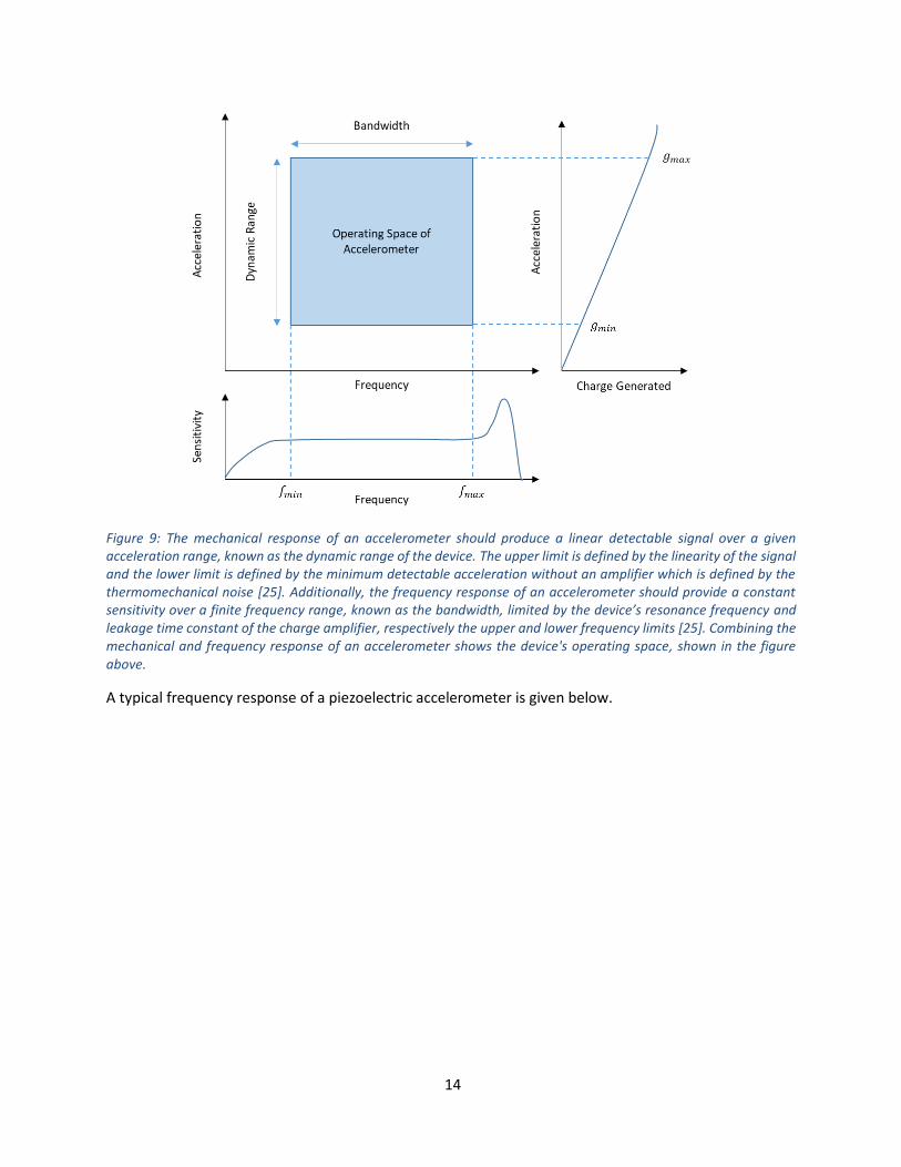
2.2 Piezoelectric Accelerometer Operating Space The key design parameters of a piezoelectric accelerometer are the dynamic range and bandwidth. Recall,
the dynamic range is defined by the minimum and maximum detectable acceleration of the
accelerometer. For a piezoelectric accelerometer that produces charge for a given acceleration, the
minimum detectable acceleration is dependent on the charge amplifier. The maximum detectable
acceleration is dependent on the linearity of the charge generation. The bandwidth of an accelerometer
is dependent on the resonant frequency of the designed device, the quality factor, and thermomechanical
noise. The thermomechanical noise sets the minimum operating frequency, whereas the resonant
frequency of the structure and quality factor determine the maximum operating frequency. The linear
regime between the minimum and maximum operating frequencies is the bandwidth of the
accelerometer. Combining the frequency and mechanical responses of the device produces the following
diagram which describes the operating space of an accelerometer:
14
Figure 9: The mechanical response of an accelerometer should produce a linear detectable signal over a given acceleration range, known as the dynamic range of the device. The upper limit is defined by the linearity of the signal and the lower limit is defined by the minimum detectable acceleration without an amplifier which is defined by the thermomechanical noise [25]. Additionally, the frequency response of an accelerometer should provide a constant sensitivity over a finite frequency range, known as the bandwidth, limited by the device’s resonance frequency and leakage time constant of the charge amplifier, respectively the upper and lower frequency limits [25]. Combining the mechanical and frequency response of an accelerometer shows the device's operating space, shown in the figure above.
A typical frequency response of a piezoelectric accelerometer is given below.

15
Figure 10: Metra provides several accelerometer design rules. One of the major design rules concerns the bandwidth of the accelerometer. Given the resonant frequency of the accelerometer, the 1 dB limit where the measuring error is about 10 % is about 1/3 of the resonant frequency. The 0.5 dB limit where the measuring error is about 5% is around 1/5 of the resonant frequency. For charge output accelerometers, the lower frequency limit is limited by the leakage time constant of the charge amplifier and not typically stated on the frequency response curve [43].
Given these key design parameters for the piezoelectric accelerometer with charge output, it is desirable
to maximize the resonant frequency, dynamic range, and sensitivity. Several companies have been
manufacturing these piezoelectric accelerometers for almost a century, so it is useful to analyze their
accelerometer design and performance to develop the next generation of piezoelectric accelerometers.
2.3 Piezoelectric Accelerometer History and State of the Art The following brief overview of the piezoelectric accelerometer history is summarized from Patrick
Walter’s work on accelerometer history starting from 1920 [35].
McCollum and Peters created the first commercialized accelerometer in 1923. It weighed 1.75 pounds
with a footprint of 3/4 x 1-7/8 x 8-1/2 inches and a reported resonant frequency of less than 2 kHz. The
device used resistive transduction to measure an applied acceleration, similar to piezoresistive, but
instead of using a semiconductor it employed a metal in the strain gauge. Applications of the device
ranged from dynamometers to bridges and aircraft. In 1936, Southwark-Bulletin commercialized a two-
axis resistive accelerometer with a dynamic range of up to 100 g with applications in aircraft shock
absorbers, vibration recording of underground pipes, and measuring the force of explosions. At this point
in time, the price of such an accelerometer was a monumental 420 USD. Today, in 2019, the equivalent
price is 7,260 USD. In 1950, the Statham resistance strain gauge could measure up to 500 g, but with poor
signal to noise ratios and a temperature operating range of only ± 20 F from room temperature. A paper
by Weiss in the early 1950s declared measuring transients as an issue for the strain gauge accelerometers
because the natural frequency of the devices was too low, which ultimately led to the rise of piezoelectric
accelerometers. Since piezoelectric materials have a high elastic modulus, a high resonant frequency is
more easily achievable to extend the accelerometer’s useable flat frequency response. Before 1960, no
strain gauge accelerometer had a useable flat response above 200 Hz whereas piezoelectric
accelerometers were achieving flat responses up to 10 kHz. The late 1940s is when piezoelectric
accelerometer companies began to emerge. In 1942, Brüel & Kjær (B&K), a piezoelectric accelerometer

16
company from Denmark, emerged and in 1950 produced a compression design with sensitivities of around
70-100 mV/g and a resonance of 5 kHz. By 1972, B&K produced a shear mode design which has evolved
to withstand 100,000 g at low cost. B&K was purchased by AGIV, a German company, in 1992 and still
produces piezoelectric accelerometers today. Several other major companies, such as Columbia National
Laboratories, Gulton Manufacturing, Kistler Instrument Company, PCB Piezotronics, Endevco, Wilcoxon
Research, and Calibration Activities, emerged in the late 1940s/1950s and have followed a similar trend
in the piezoelectric accelerometer industry.
Upon inspecting the Endevco product catalog, commercialized accelerometers are typically selected from
the following criteria [27]:
Sensitivity
Dynamic Range
Footprint
Resonance Frequency
Operating Temperature
Some typical uniaxial charge output piezoelectric accelerometer products for harsh environments are
tabulated below [50-52].

17
End
evc
o M
od
el
Pac
kage
d D
ime
nsi
on
s (H
eig
ht
x D
iam
ete
r)Se
nsi
tivi
ty [
pC
/g]
Acc
ele
rom
ete
r Ty
pe
Dyn
amic
Ran
ge [
g]M
axim
um
Op
era
tin
g Te
mp
[C
]R
eso
nan
t Fr
eq
ue
ncy
[kH
z]A
pp
lica
tio
n
2248
16.5
1 m
m x
11.
09 m
m3
No
t G
ive
n30
0048
225
Turb
ine
En
gin
e T
est
ing
2225
16.8
mm
x 1
4.2
mm
0.75
An
nu
lar
She
ar20
000
177
100
Hig
h g
Sh
ock
2225
M5A
16.9
mm
x 1
4.2
mm
0.02
5A
nn
ula
r Sh
ear
1000
0066
80H
igh
g S
ho
ck
2273
AM
126
.9 m
m x
15.
8 m
m10
No
t G
ive
n30
0039
927
Hig
h T
em
pe
ratu
re, N
ucl
ear
2272
A22
.9 m
m x
15.
7 m
m3
No
t G
ive
n10
000
399
30H
igh
Te
mp
era
ture
, Nu
cle
ar
7201
-10
19.8
mm
x 1
5.88
mm
10Sh
ear
2000
260
48H
igh
Te
mp
era
ture
, Nu
cle
ar
222.
79 m
m x
3.5
8 m
m0.
4R
adia
l Sh
ear
4000
149
54A
irb
orn
e F
ligh
t Te
stin
g
2220
E8.
6 m
m x
9.5
3 m
m3
An
nu
lar
She
ar50
0026
050
Air
bo
rne
Fli
ght
Test
ing
Kis
tle
r M
od
el
Pac
kage
d D
ime
nsi
on
s (H
eig
ht
x D
iam
ete
r)Se
nsi
tivi
ty [
pC
/g]
Acc
ele
rom
ete
r Ty
pe
Dyn
amic
Ran
ge [
g]M
axim
um
Op
era
tin
g Te
mp
[C
]R
eso
nan
t Fr
eq
ue
ncy
[kH
z]A
pp
lica
tio
n
8044
A18
.79
mm
x 1
0.92
mm
0.3
Qu
artz
3000
020
490
Sho
ck, C
ryo
to
Hig
h T
em
p
8202
A16
mm
x 1
2,19
mm
10Sh
ear
2000
248.
945
Hig
h T
em
pe
ratu
re
8203
A27
.94
mm
x 1
7 m
m50
She
ar10
0024
8.9
24H
igh
Te
mp
era
ture
8274
A21
.59
mm
x 9
.53
mm
5.5
She
ar20
0016
5.6
50H
igh
Te
mp
era
ture
8278
A3.
3 m
m x
12.
44 m
m1.
3Sh
ear
500
176.
740
Hig
h T
em
pe
ratu
re
PC
B M
od
el
Pac
kage
d D
ime
nsi
on
s (H
eig
ht
x D
iam
ete
r)Se
nsi
tivi
ty [
pC
/g]
Acc
ele
rom
ete
r Ty
pe
Dyn
amic
Ran
ge [
g]M
axim
um
Op
era
tin
g Te
mp
[C
]R
eso
nan
t Fr
eq
ue
ncy
[kH
z]A
pp
lica
tio
n
357A
093.
6 m
m x
11.
4 m
m x
6.4
mm
1.5
She
ar50
017
6.7
13M
oto
Ho
usi
ng
356A
7018
.5 m
m x
22.
9 m
m x
10.
2 m
m2.
7Sh
ear
500
254
35En
gin
es,
Tu
rbin
es
350A
9618
mm
x 1
4.28
mm
0.06
5Sh
ear
1000
0066
120
Sho
ck
357A
082.
8 m
m x
4.1
mm
x 6
.9 m
m0.
3Sh
ear
1000
177
70M
oto
Ho
usi
ng
357C
103.
6 m
m x
11.
4 m
m x
6.4
mm
1.7
She
ar50
017
750
Engi
ne
Bra
cke
t
357B
0320
.6 m
m x
12.
7 m
m10
She
ar20
0026
038
Engi
ne
s, T
urb
ine
s
357B
6125
.4 m
m x
15.
87 m
m10
Co
mp
ress
ion
3000
482
27H
igh
Te
mp
357B
7146
.2 m
m x
25.
4 m
m10
Co
mp
ress
ion
500
482
16H
igh
Te
mp

18
In addition, recent research papers have been published on the current state of the art uniaxial
piezoelectric accelerometers. Their device parameters have been tabulated below.
Table 3: From scientific literature, the state of the art of micromachined uniaxial piezoelectric accelerometers with charge output are designed to be approximately 1-2 mm in radius. The resonance frequencies are on the order of 5-25 kHz, with charge sensitivities varying from 75 fC/g to 15 pC/g. At higher resonance frequencies greater than 20 kHz, the charge sensitivity significantly drops to less than 1 pC/g. All of the scientific articles below utilize the bending 𝑑31 mode for charge generation.
Reference Sensitivity
[pC/g] Resonance
Frequency [kHz] Device Radius
[mm] PZE Material
[39] 14.2 14.4 1 AlN
[34] 0.13 25.2 1.8 PZT
[18] 0.23 23.5 1.8 PZT
[13] 1.12 6.1 2 AlN
[13] .08 19.9 1 AlN
[14] .075 18.9 0.9 AlN
According to the aforementioned literature and commercialized accelerometers, there are commonly
three different designs for piezoelectric accelerometers with charge output. The three common operating
modes of piezoelectric energy harvesters are:
Bending mode, 𝑑31
Compression mode, 𝑑33
Shear mode, 𝑑15
Here, the constant, 𝑑, refers to the piezoelectric strain constant. This constant defines the amount of
charge generated per an applied force. Piezoelectric ceramics are anisotropic materials, so the subscripts
are the directions referring to the direction of the polarization and the direction of the applied force
caused by stress or strain [46]. The polarization of the piezoelectric material coincides with the z-axis, see
the figure below.

19
Figure 11: Each axis represents the direction in which a force can be applied to influence the charge generation of a piezoelectric material. The scripts 4, 5, and 6 represent a plane of applied stress to generate charge in a piezoelectric material. [41]
Piezoelectricity is further discussed in Section 3. Each piezoelectric accelerometer design will now be
discussed.
The bending mode is where the material responds to a stress along direction 1 with an induced electric
field in direction 3 [6]. The piezoelectric constant associated with this operating mode is 𝑑31. The Figure
below demonstrates an example of a piezoelectric harvester utilizing the bending mode.
Figure 12: The basic design of a bending mode piezoelectric accelerometer consists of a cantilever with a proof mass on the end. The cantilever is typically composed of a piezoelectric material sandwiched between two detection electrodes. The vertical displacement of the cantilever generates a voltage signal from the bending piezoelectric material [6].
The basic principle of the bending mode is that when the piezoelectric material on the cantilever bends,
it induces a strain/stress. This stress creates a piezoelectric potential which causes electrons to flow into
the connected circuit. As the cantilever bends back and forth, electrons periodically change direction to
generate an alternating current [6]. This is why piezoelectric accelerometers with charge output all
operate in AC mode instead of DC. Only an alternating acceleration can be measured by piezoelectric
accelerometers, which also makes them more suitable for higher frequency applications.
The compression mode is based on the 𝑑33 piezoelectric constant where the piezoelectric material is
stressed in the same direction of the generated electric field [6]. The 𝑑33 piezoelectric constant is generally
higher than the 𝑑31, which means devices with higher power output is possible. However, there are
several polarization issues associated with the 𝑑33 piezoelectric energy harvesters which limits the gap

20
between electrodes inhibiting its performance [6]. The difference in polarization of the bending and
compression modes is illustrated in the figure below.
Figure 13: The difference between the bending mode (a) and compression mode (b) for extracting charge in piezoelectric accelerometers is displayed above. For the compression mode, as the length between the electrodes increase, it becomes more difficult to pole the piezoelectric material in the correct direction for maximum charge generation efficiency. It is easier to pole the bending mode to maximize the charge generation efficiency since the electrodes are aligned on top of one another. The bending arrows in the compression mode schematic demonstrate the iniefficiency of the poling if the electrodes are placed too far apart [6].
The shear mode design utilizes the 𝑑15 piezoelectric constant where the shear stress is applied in the σ31
direction while the piezoelectric material is polarized in direction 1 [6]. The charge is extracted
perpendicular to both the direction of the stress and polarization [6]. This is tricky because this requires
two sets of electrodes. One set for polarizing and the other for operating. The shear mode generally
displays superior power generation compared to the other modes, however this design requires a difficult
fabrication process. A schematic of a shear mode is shown below.
Figure 14: An energy harvester generates charge from shear stress by utilizing the 𝑑15 piezoelectric constant. A voltage is measured perpendicular to the polarized direction of the piezoelectric material [6]. This can be difficult to measure because this requires an extra set of electrodes to measure in addition to the poling electrodes [6].
Each of the accelerometer designs have advantages and disadvantages. The company Metra Mess- und
Frequenztechnik, or MMF, compares their strengths and weaknesses in the table below [43].

21
Table 4: MMF compares the three common piezoelectric accelerometer with charge output designs which reveals the bending mode as the best charge generator among the three cases, which is paramount for smaller devices [43].
Bending Compression Shear
Advantages Best Sensitivity-to-Mass Ratio
High Sensitivity-to-Mass Ratio
Robust
Low Temperature Transient Sensitivity
Low Base Strain Sensitivity
Drawbacks Fragile
Moderate Temperature Transient Sensitivity
High Temperature Transient Sensitivity
Lower Sensitivity-to-Mass Ratio
First, let us define temperature transient sensitivity and base strain sensitivity. Temperature transient
sensitivity is caused by the pyroelectric effect and non-uniform thermal expansion [25]. The pyroelectric
effect is present in piezoelectric materials because temperature changes cause charge to build up
perpendicular to the polarized direction of the piezoelectric material, which results in an undesirable
signal. The non-uniform thermal expansion occurs due to different materials in the device structure having
different coefficients of thermal expansion. This can cause stress in the piezoelectric layer and therefore
generate charge. The temperature transient only plays a significant role in the signal at low frequencies
and low accelerations [25]. Base strain sensitivity is caused by the surface the accelerometer is attached
to, such as its mounting surface [25]. If the mounting surface is exposed to significant amounts of flexure,
then this can cause an undesirable signal in the accelerometer’s sensing element.
Shear mode accelerometers are the best in minimizing these sensitivities, but these sensitivities are not
of major interest as the device materials can be selected to match coefficients of thermal expansion and
it is assumed the mounting surface of the accelerometer will not be subject to large amounts of flexure.
Therefore, due to the design complexity and lower sensitivity-to-mass ratio, the shear mode design will
not be pursued. The compression mode poses a strong candidacy for an accelerometer in harsh
environments, but the high temperature transient sensitivity could pose a major issue in the long run and
scaling the device size down may not generate enough charge as desired. Thus, the bending mode design
has been selected because it has the best sensitivity-to-mass ratio and an easy fabrication process [22].
The fragility of the device will be analyzed with a stress analysis in the final design to ensure robustness.
The temperature transient sensitivity will be addressed in the material selection by choosing materials
with similar temperature coefficients of expansion to reduce this sensitivity.
From literature the most common bending mode designs are circular and square membranes with a mass
in the center, see the figure below.

22
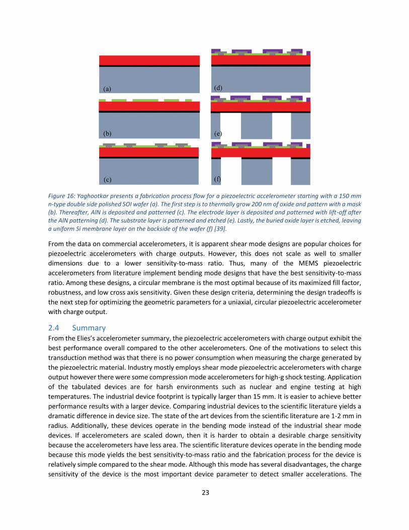
Figure 15: Schematics of common MEMS circular and square piezoelectric accelerometers with the same critical dimensions. The shaded region designates the gap between the proof mass and device substrate and the black dashed lines illustrate the outer edges of the proof mass. Contact pads are designated for both the inner and outer electrodes to extract charge from the piezoelectric layer [39].
These designs are similar to cantilevers with a proof mass, however the designs are simply rotated about
the cantilever’s end mass. These designs are common because the fully clamped membrane design
increases their stability and their symmetricity maximizes their fill factors. These designs result in a higher
charge generation and better robustness. Yaghootkar et al. reports a much higher cross axis sensitivity for
square piezoelectric accelerometers, so selecting the circular design is ideal for a uniaxial piezoelectric
accelerometer [34,39].
From the scientific literature, a typical process flow for fabricating a circular piezoelectric accelerometer
utilizes a Silicon-On-Insulator (SOI) wafer. A SOI wafer enables one to have a uniform thickness of the
device layer by using the buried oxide layer as a mask during the substrate layer etch. Yaghootkar et al.
employs the following process flow to guarantee a uniform device (membrane) layer [39].
23
Figure 16: Yaghootkar presents a fabrication process flow for a piezoelectric accelerometer starting with a 150 mm n-type double side polished SOI wafer (a). The first step is to thermally grow 200 nm of oxide and pattern with a mask (b). Thereafter, AlN is deposited and patterned (c). The electrode layer is deposited and patterned with lift-off after the AlN patterning (d). The substrate layer is patterned and etched (e). Lastly, the buried oxide layer is etched, leaving a uniform Si membrane layer on the backside of the wafer (f) [39].
From the data on commercial accelerometers, it is apparent shear mode designs are popular choices for
piezoelectric accelerometers with charge outputs. However, this does not scale as well to smaller
dimensions due to a lower sensitivity-to-mass ratio. Thus, many of the MEMS piezoelectric
accelerometers from literature implement bending mode designs that have the best sensitivity-to-mass
ratio. Among these designs, a circular membrane is the most optimal because of its maximized fill factor,
robustness, and low cross axis sensitivity. Given these design criteria, determining the design tradeoffs is
the next step for optimizing the geometric parameters for a uniaxial, circular piezoelectric accelerometer
with charge output.
2.4 Summary From the Elies’s accelerometer summary, the piezoelectric accelerometers with charge output exhibit the
best performance overall compared to the other accelerometers. One of the motivations to select this
transduction method was that there is no power consumption when measuring the charge generated by
the piezoelectric material. Industry mostly employs shear mode piezoelectric accelerometers with charge
output however there were some compression mode accelerometers for high-g shock testing. Application
of the tabulated devices are for harsh environments such as nuclear and engine testing at high
temperatures. The industrial device footprint is typically larger than 15 mm. It is easier to achieve better
performance results with a larger device. Comparing industrial devices to the scientific literature yields a
dramatic difference in device size. The state of the art devices from the scientific literature are 1-2 mm in
radius. Additionally, these devices operate in the bending mode instead of the industrial shear mode
devices. If accelerometers are scaled down, then it is harder to obtain a desirable charge sensitivity
because the accelerometers have less area. The scientific literature devices operate in the bending mode
because this mode yields the best sensitivity-to-mass ratio and the fabrication process for the device is
relatively simple compared to the shear mode. Although this mode has several disadvantages, the charge
sensitivity of the device is the most important device parameter to detect smaller accelerations. The

24
scientific literature utilizes a circular geometry of the bending mode device for uniaxial applications
because the design is stable, maximizes the fill factor of the device footprint, and does not have poor cross
axis sensitivity compared to the square geometry design. Thus, the piezoelectric accelerometer design
chosen is a circular membrane with a centered proof mass that utilizes the bending mode for charge
generation.

25
3 Accelerometer Design Tradeoffs The resonant frequency of any structure can be easily described by the standard equation:
𝑓 =1
2𝜋√
𝑘
𝑚 (1)
Where 𝑓 is the resonance frequency of the structure, 𝑘 is the stiffness of the structure, and 𝑚 is the mass.
For a standard piezoelectric accelerometer, the sensitivity is described by the displacement per
acceleration, hence the equation:
𝑆𝑥 =𝑥
𝑎=
𝑚
𝑘 (2)
Where 𝑆𝑥 is the mechanical sensitivity, 𝑥 is the displacement, and 𝑎 is the acceleration. Therefore, we find
the relationship between mechanical sensitivity and the resonant frequency to be:
𝑆𝑥 =1
𝑓2 (3)
This relationship leads to a troublesome optimization problem: it is difficult to have a device that operates
at high frequencies while achieving high sensitivities. However, there are a couple ways to increase the
sensitivity of a piezoelectric accelerometer device without changing the device structure that sacrifices a
high resonant frequency:
Piezoelectric Material Selection
Maximize 𝑧𝑜𝑓𝑓𝑠𝑒𝑡
3.1 Piezoelectricity and Charge Generation Recall, piezoelectric materials generate charge proportional to the amount of force exerted on the
material. This effect arises from the crystal structure of the piezoelectric material. For example, quartz
piezoelectric properties arise from its hexagonal lattice’s asymmetric structure under applied stress, see
the figure below.

26
Figure 17: A quartz hexagonal crystal structure is electrically neutral with no applied stress. However, under stress, atoms are moved around so excess silicon atoms appear on the opposite side of the crystal where the excess oxygen atoms appear on, generating opposite charge at opposite surfaces. This stems from the asymmetric property of the quartz crystal lattice [48].
The result of the asymmetric crystal structure is the direct piezoelectric effect which states the generation
of charges is caused by the dipole moments in the crystal material [16]. Hence, without applied force
these crystals are electrically neutral. When the piezoelectric material is compressed or stretched, the
deformation in the structure leads to the imbalance of positive and negative charges, ultimately causing
electric charge to appear [17]. The following constitutive equations describe the electromechanical
coupling of linear piezoelectric material [7, 16, 17]:
𝜀𝑖 = 𝑆𝑖𝑗𝐸𝜎𝑗 + 𝑑𝑚𝑖𝐸𝑚 (4)
𝐷𝑚 = 𝑑𝑚𝑖𝜎𝑖 + 𝜖𝑖𝑘𝜎 𝐸𝑘 (5)
Where 𝜀 is the strain vector, 𝜎 is the stress vector, 𝑑 is the piezoelectric strain constant, 𝜖 is the
permittivity, 𝐸 is the applied electric field vector, 𝑆 is the matrix of compliance coefficients. The
superscripts, 𝐸 and 𝜎 refer to a measurement at constant applied electric field and stress, respectively.
For a piezoelectric sensor, the first component in the Equation (5) is most important as a mechanically
applied stress generates a displacement field. Integrating this displacement field over the area results in
the total charge generated for sensing [14]. The converse piezoelectric effect, where an applied electric
field results in the expansion of the piezoelectric material, will not be discussed here because an
accelerometer uses the piezoelectric as a sensor instead of an actuator [33].
Piezoelectric charge coefficients relate mechanical stimulus and electrical response quantitatively. For the
bending mode design, the 𝑑31 component of the piezoelectric materials of interest will be used because
polarization is induced along the z-axis per unit stress applied along the x-axis. The piezoelectric strain
constants are tabulated below:

27
Table 5: The piezoelectric materials considered are found in EPFL's CMi cleanroom. AlN deposition is conducted via sputtering, whereas PZT deposition is conducted via pulsed laser deposition.
Piezoelectric Material 𝑑31, Piezoelectric Strain Constant [C/N]
AlN -1.92 x 10⁻¹²
PZT-4 -1.23 x 10⁻¹⁰
PZT-5H -2.74 x 10⁻¹⁰
PZT appears to generate more charge per applied force however it is important to check the Curie
temperature of these materials. The Curie temperature is the transition temperature at which the
materials lose their permanent magnetic properties [19]. Typically, piezoelectric materials with superior
charge generation have lower Curie temperatures, see the table below [46]:
Table 6: The Curie temperature of a piezoelectric material is the temperature at which the material begins to lose its magnetic properties. Typically, materials like AlN, with lower piezoelectric strain constants, have higher Curie temperatures which make them more suitable for high temperature applications [46].
Piezoelectric Material Curie Temperature [C]
AlN Theoretical: 700
Oxidized Tested: 600
PZT-4 325
PZT-5H 195
AlN and PZT are two readily available piezoelectric materials in EPFL’s CMi cleanroom and will be the only
piezoelectric materials considered in this study. For harsh environments, it is more desirable to have a
higher Curie temperature, thus AlN has been selected as the piezoelectric material for this application.
The safe maximum operating temperature for piezoelectric materials is typically set at half the curie
temperature [19]. The coupling, elasticity, and permittivity matrices used for AlN in this report are
respectively:
𝑒 = [0 0 00 0 0
−1.92 −1.92 4.96
0 −3.84 0−3.84 0 0
0 0 0]𝑝𝐶
𝑁 (6)
𝑐 =
[ 410 149 99149 410 14999 149 410
0 0 00 0 00 0 0
0 0 00 0 00 0 0
125 0 00 125 00 0 125]
𝐺𝑃𝑎 (7)
𝜀 = [
9 0 00 9 00 0 9
] 𝑥 8.854 𝑥 10−12𝐹
𝑚
(8)
Given AlN has a lower 𝑑31 constant compared to PZT, the 𝑧𝑜𝑓𝑓𝑠𝑒𝑡 parameter becomes increasingly more
important to achieve higher sensitivities. The charge generated by a strained piezoelectric sensor is given
by the following equation [31]:

28
𝐼𝐷(𝑡) = ∫𝜕𝐷(𝑡)
𝜕𝑡
𝐴𝑒𝑙𝑒𝑐
= 𝑗𝜔 (9)
𝑗𝜔 ∈ 𝐴𝑒𝑙𝑒𝑐
𝑡𝑃𝑍𝐸𝑉𝑖𝑛 + 𝑗𝜔𝑋𝑛
𝐷𝑑31
𝐶11
𝑤𝑧𝑜𝑓𝑓𝑠𝑒𝑡
𝐿𝑢𝑛(𝜔) (10)
Here, 𝐼𝐷 is the displacement current, 𝐷 is the displacement field, 𝜔 is the frequency, 𝑉𝑖𝑛 is the input
voltage across the piezoelectric material, 𝑋𝑛𝐷 is the detection proportionality term, 𝑤 is the width of the
piezoelectric material, 𝐿 is the length of the piezoelectric material, and 𝑢𝑛 is the deflection of the
piezoelectric material. Maxwell’s equations state that a change in the displacement field over time results
in a displacement current, as displayed by Equation (9). Specifically for piezoelectric materials in the
detection mode, there is no input voltage, so 𝑉𝑖𝑛 is set to zero. Therefore, the generated charge is
proportional to the piezoelectric constant, geometric parameters, deflection, and 𝑧𝑜𝑓𝑓𝑠𝑒𝑡. The 𝑧𝑜𝑓𝑓𝑠𝑒𝑡 is
the distance the piezoelectric material is from the neutral axis of the structure. It is important to note that
the charge generation, 𝐶𝑥, is therefore proportional to the deflection, 𝑆𝑥, and the 𝑧𝑜𝑓𝑓𝑠𝑒𝑡.
𝐶𝑥 ∝ 𝑆𝑥𝑧𝑜𝑓𝑓𝑠𝑒𝑡 (11) The neutral axis is defined as the point in a material where the stress is equal to zero. The neutral axis, 𝑧𝑛,
is calculated by the following equation [23]:
𝑧𝑛 =∑ 𝐴𝑖𝐸𝑖𝑧𝑖
𝑛𝑖=1
∑ 𝐴𝑖𝐸𝑖𝑛𝑖=1
(12)
Where 𝐴𝑖 is the cross sectional area of the i-th layer, 𝐸𝑖 is the elastic modulus of the i-th layer, and 𝑧𝑖 is
the position of the i-th layer. For a multi-layer structure, as shown below, the piezoelectric material is
perfectly aligned to the neutral axis and therefore the 𝑧𝑜𝑓𝑓𝑠𝑒𝑡 is zero.
Figure 18: A multi-layer structure of two identical Pt electrodes sandwiching an AlN layer gives a 𝑧𝑜𝑓𝑓𝑠𝑒𝑡 of zero
because AlN layer is aligned to the neutral axis. To produce a charge, the 𝑧𝑜𝑓𝑓𝑠𝑒𝑡 must be non-zero. This can be
overcome by adding an additional layer to offset the AlN layer from the neutral axis.
Thus, given an applied force, there is no charge generation because the 𝑧𝑜𝑓𝑓𝑠𝑒𝑡 is zero. Placing this
structure on another layer would create a non-zero 𝑧𝑜𝑓𝑓𝑠𝑒𝑡 and enable the piezoelectric material to
generate a charge.

29
Figure 19: A non-zero 𝑧𝑜𝑓𝑓𝑠𝑒𝑡 is created by adding another layer to make the multi-layer structure non-symmetric.
The cross section of the multi-layer structure above demonstrates a strain equal to zero at the neutral axis of the structure. By adding the beam below the piezoelectric transducer, the strain is maximized at the piezoelectric layer, hence a non-zero 𝑧𝑜𝑓𝑓𝑠𝑒𝑡 to generate charge [45].
For a bending piezoelectric material, the charges accumulate on the surface and are collected by
electrodes, see the Figure below.
Figure 20: Here, the multilayer structure has a non-zero 𝑧𝑜𝑓𝑓𝑠𝑒𝑡 due to the added Si layer pulling the neutral axis away
from the AlN layer. Charge is collected on separate Pt electrodes to avoid cancellation of charge.
To avoid cancellation of charges during collection, the top Pt electrode is separated and the bottom Pt
electrode is implemented as a shared ground electrode. Hence, the two electrodes will be connected in
series to maximize extraction of the charge generated from the bending piezoelectric structure. Wang et
al. developed an analytical equation to calculate the charge generation of a square shaped piezoelectric
accelerometer in static mode [36]:
𝑄 = 0.0691𝑑31𝑏𝐸𝑝𝑧𝑒
𝐸𝐼𝑒𝑞(ℎ𝑝𝑧𝑒
2+ 𝑎) 𝑙2𝑚�̈� (13)
𝐸𝐼𝑒𝑞 =
1
3𝑏𝐸𝐵(ℎ3 − 3𝑎ℎ2 + 3𝑎2ℎ) +
1
3𝑏𝐸𝑝(ℎ𝑝𝑧𝑒
3 + 3𝑎2ℎ𝑝𝑧𝑒
+ 3𝑎ℎ𝑝𝑧𝑒2 )
(14)
Here, 𝑄 is the total charge generated, �̈� is the applied acceleration, 𝑙 is the length of the beam, 𝑏 is the
width of the beam, ℎ𝑝𝑧𝑒 is the piezoelectric thickness, 𝑎 is the 𝑧𝑜𝑓𝑓𝑠𝑒𝑡, ℎ is the thickness of the substrate

30
layer, 𝐸𝐵 and 𝐸𝑝𝑧𝑒 are the bielastic moduli of the substrate and piezoelectric layers, and 𝑚 is the mass of
the proof mass. From Equation (13) it is easy to calculate the expected charge generated by a piezoelectric
structure given geometric constraints, material properties, and the applied acceleration. From Equation
(13) it is apparent that minimizing the thickness of the piezoelectric layer maximizes the 𝑧𝑜𝑓𝑓𝑠𝑒𝑡 for
maximum charge generation.
Figure 21: Minimizing the thickness of the piezoelectric layer maximizes the charge generation of a piezoelectric material because it maximizes the 𝑧𝑜𝑓𝑓𝑠𝑒𝑡. Here, Equation (13) models the charge sensitivity of a circular uniaxial Si-
AlN accelerometer with a 2 mm device radius and 14 um membrane thickness based on the thickness of the AlN layer. As the thickness of the piezoelectric layer approaches less than 100 nm, the charge sensitivity is maximized and relatively constant.
3.2 Maximum Displacement After determining the piezoelectric material and design tradeoffs for the harsh environment
accelerometer, it is important to optimize the device geometry to maximize the membrane deflection to
generate as much charge signal as possible. Recall, depending on the charge amplifier available for a
piezoelectric accelerometer, the minimum detectable acceleration is dependent on the minimum charge
detectable. Therefore, if the desired detectable acceleration is 0.001 𝑔 and the minimum detectable
charge is 0.01 𝑝𝐶, then the required charge generation from the accelerometer must be:
𝑀𝑖𝑛𝑖𝑚𝑢𝑚 𝐷𝑒𝑡𝑒𝑐𝑡𝑎𝑏𝑙𝑒 𝐶ℎ𝑎𝑟𝑔𝑒
𝐷𝑒𝑠𝑖𝑟𝑒𝑑 𝐷𝑒𝑡𝑒𝑐𝑡𝑎𝑏𝑙𝑒 𝐴𝑐𝑐𝑒𝑙.= 10 𝑝𝐶/𝑔 (15)
Solid mechanics equations are useful for optimizing the circular piezoelectric accelerometer device to
achieve maximum deflection. For the following sections, all sample calculations are completed with the
given parameters:

31
Table 7: Summary of all parameters used for sample calculations in Section 4, unless otherwise stated.
Parameter Value Units
Silicon, Density 2330 𝑘𝑔/𝑚3
Silicon, Young’s Modulus 165 𝐺𝑃𝑎
Silicon Nitride, Density 3100 𝑘𝑔/𝑚3
Silicon Nitride, Young’s Modulus 250 𝐺𝑃𝑎
Silicon, Poisson Ratio 0.22 -
Silicon Nitride, Poisson Ratio 0.23 -
Membrane Radius 1000 𝑢𝑚
Silicon Membrane Thickness 10 𝑢𝑚
Silicon Nitride Membrane Thickness 200 𝑛𝑚
Silicon Mass Radius 370 𝑢𝑚
Silicon Mass Thickness 350 𝑢𝑚
To maximize the deflection of the accelerometer, it is important to develop the theory that describes the
solid mechanics of a typical accelerometer structure. Recall, the circular MEMS piezoelectric
accelerometer is comprised of two main components: a membrane and a proof mass. In solid mechanics,
it is easy to describe this structure as a circular annular plate with constant thickness via the schematic
below [40].
Figure 22: A schematic of an annular plate with a uniform line load, 𝑤, at a radius, 𝑟0, is presented in Roark’s formulas for stress and strain. From this model, the maximum displacement of the structure, 𝑦𝑏 , can be derived based on the applied load. Equation (16) simplifies this model to fit a displacement behavior more similar to that of an oscillating circular accelerometer than a bending cantilever beam [40].
Here, 𝑦𝑏 is the max displacement, 𝑏 is the radius of the mass, 𝑎 is the radius of the membrane, 𝜃𝐴 is the
angle of the membrane at the membrane edge at maximum deflection, 𝜃𝑏 is the angle of the membrane
at the mass edge at maximum deflection, 𝑟0 is the radial location of a unit line loading, 𝑤 is the unit line
load expressed as force per circumferential length, 𝑄𝑎 is the unit shear force at the membrane edge, 𝑄𝑏
is the unit shear force at the mass edge, 𝑀𝑟𝑏 is the unit radial bending moment at the mass edge, and 𝑀𝑟𝑎
is the unit radial bending moment at the membrane edge. We can simplify this structure to better
describe the design of a MEMS accelerometer by making the following simplifications to Figure 5:
𝜃𝑏 = 0,𝑄𝑏 = 0, 𝜃𝑎 = 0 (16) Fixing the outer edge and guiding the inner edge, we now have the following configuration:

32
Figure 23: A schematic of an annular plate with guided inner edge and fixed outer edge with uniform line load, 𝑤, at a radius, 𝑟0, as depicted in Roark’s formulas for stress and strain. The behavior of this bending membrane more closely resembles that of an oscillating accelerometer structure. Equation (17) models the maximum displacement, 𝑦𝑏 , of the structure based on the ratio of the membrane to mass radius, the thickness of the membrane, and material properties [40].
To further simplify the model above, the uniform load line will be at the inner edge, 𝑟0 = 𝑏. Equation (17)
describes the max displacement of this structure [40]:
𝑦𝑏 =𝑤𝑎3
𝐷(𝐶2𝐿6
𝐶5− 𝐿3) (17)
𝐿6 =
𝑟04𝑎
[(𝑟0𝑎
)2
− 1 + 2𝑙𝑛𝑎
𝑟0] (18)
𝐿3 =
𝑟04𝑎
{[(𝑟0𝑎
)2
+ 1] 𝑙𝑛𝑎
𝑟0+ (
𝑟0𝑎
)2
− 1} (19)
𝐶2 =
1
4[1 − (
𝑏
𝑎)2
(1 + 2𝑙𝑛𝑎
𝑏)] (20)
𝐶5 =
1
2[1 − (
𝑏
𝑎)2
] (21)
𝐷 = 𝐸𝑡3/12(1 − 𝑣2) (22) Here, 𝑡 is the thickness of the membrane, 𝐸 is the elastic modulus of the membrane material, and 𝑣 is the
Poisson coefficient. Equation (17) is used to optimize the ratio between the seismic mass radius to
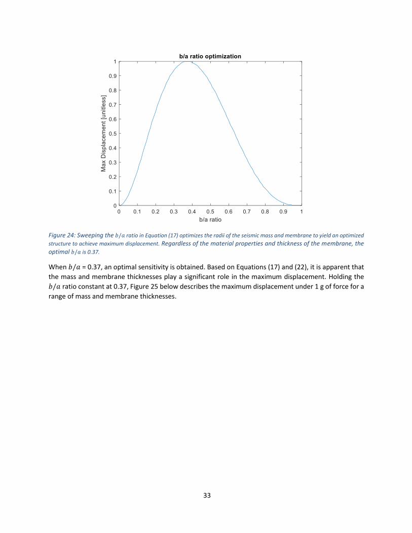
membrane radius, 𝑏/𝑎, to obtain the largest displacement possible under 1 g of force.
33
Figure 24: Sweeping the 𝑏/𝑎 ratio in Equation (17) optimizes the radii of the seismic mass and membrane to yield an optimized
structure to achieve maximum displacement. Regardless of the material properties and thickness of the membrane, the optimal 𝑏/𝑎 is 0.37.
When 𝑏/𝑎 = 0.37, an optimal sensitivity is obtained. Based on Equations (17) and (22), it is apparent that
the mass and membrane thicknesses play a significant role in the maximum displacement. Holding the
𝑏/𝑎 ratio constant at 0.37, Figure 25 below describes the maximum displacement under 1 g of force for a
range of mass and membrane thicknesses.
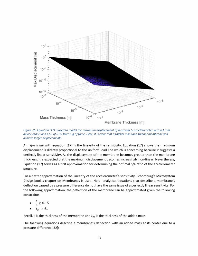
34
Figure 25: Equation (17) is used to model the maximum displacement of a circular Si accelerometer with a 1 mm device radius and 𝑏/𝑎 of 0.37 from 1 g of force. Here, it is clear that a thicker mass and thinner membrane will achieve larger displacements.
A major issue with equation (17) is the linearity of the sensitivity. Equation (17) shows the maximum
displacement is directly proportional to the uniform load line which is concerning because it suggests a
perfectly linear sensitivity. As the displacement of the membrane becomes greater than the membrane
thickness, it is expected that the maximum displacement becomes increasingly non-linear. Nevertheless,
Equation (17) serves as a first approximation for determining the optimal b/a ratio of the accelerometer
structure.
For a better approximation of the linearity of the accelerometer’s sensitivity, Schomburg’s Microsystem
Design book’s chapter on Membranes is used. Here, analytical equations that describe a membrane’s
deflection caused by a pressure difference do not have the same issue of a perfectly linear sensitivity. For
the following approximation, the deflection of the membrane can be approximated given the following
constraints:
𝑏
𝑎≥ 0.15
𝑡𝑀 ≥ 6𝑡
Recall, 𝑡 is the thickness of the membrane and 𝑡𝑀 is the thickness of the added mass.
The following equations describe a membrane’s deflection with an added mass at its center due to a
pressure difference [32]:

35
∆𝑝 =t𝑦𝑏
𝑎 2 (𝑎𝑝
𝑡 2
𝑎 2
𝐸𝑀
1 − 𝑣𝑀2 + 4𝜎0 + 𝑏𝑝
𝑦𝑏2
𝑎 2𝐸𝑀) (23)
𝑎𝑝 =
16
3
1
1 − (𝑏
4
𝑎 4) − 4 (
𝑏 2
𝑎 2) 𝑙𝑛 (
𝑎 𝑏
)
(24)
𝑏𝑝 =
(7 − 𝑣𝑀) (1 + (𝑏
2
𝑎 2) + (
𝑏 4
𝑎 4))
3 +(3 − 𝑣𝑀)2
(1 + 𝑣𝑀) (𝑏
2
𝑎 2)
(1 − 𝑣𝑀)(1 − (𝑏
4
𝑎 4))(1 − (
𝑏 2
𝑎 2))
(25)
Here, 𝑦𝑏 is the membrane deflection, 𝛥𝑝 is the pressure difference, 𝑡 is the thickness of the membrane,
𝜎0 is the residual stress in the membrane layer, 𝑣𝑀 is the Poisson coefficient of membrane material, 𝐸𝑚
is the Young’s modulus of membrane material, 𝑎𝑝 and 𝑏𝑝 are coefficients relating the added mass’s
influence to the deflection of the membrane structure. The ratio of b/a is kept constant at 0.37 from the
optimization via Equation (17) to achieve maximum sensitivity.
The coefficients 𝑎𝑝 and 𝑏𝑝 quantify the effect of the proof mass size on the deflection of the membrane.
As the radius of the proof mass increases, 𝑎𝑝 and 𝑏𝑝 increase which causes the deflection as a function of
the applied pressure to decrease and become more linear. 𝑎𝑝 is the linear term and 𝑏𝑝 is the nonlinear
term, so 𝑎𝑝 outscales 𝑏𝑝 for larger proof mass radii, as demonstrated in the figure below [32].
Figure 26: From Equation (23), the linear term 𝑎𝑝 outscales nonlinear term 𝑏𝑝 as the radius of the proof mass
increases, especially for 𝑏/𝑎 greater than 0.9. Thus, to achieve a more linear deflection, a larger 𝑏/𝑎 ratio should be implemented at the cost of the accelerometer’s sensitivity.

36
3.3 Resonance Frequency Recall, Equation (3) which states that the sensitivity is proportional to the inverse of the resonant
frequency squared. Based on the geometric constraints of an unstressed circular diaphragm, the resonant
frequency in Equation (1) can be approximated with the following inputs [38]:
𝑘 =192𝜋𝐻
𝑎2 (26)
𝑚𝑒𝑞 = 𝜌𝑀𝜋𝑏2𝑡𝑀 + 𝜌𝑚𝜋𝑎2𝑡𝑚 (27)
𝐻 =𝐸𝑡𝑚
3
12(1 − 𝑣2) (28)
Although this equation does not account for a proof mass centered on the diaphragm, it serves as a good
first approximation. This approximation yields an inverse relationship between the resonant frequency
and proof mass thickness as expected, see the figure below:
Figure 27: Here, the first approximation of an unstressed annular accelerometer structure as a function of mass thickness is plotted. From the previous sections, a thicker mass yields a more sensitive device. However, this relationship shows the sensitivity is gained at the cost of the resonant frequency of the device.
If the membrane layer is stressed with a central proof mass, the resonant frequency from Dong et al. can
be used [10]:
𝑓 = √𝑇
2𝜋𝑚 𝑙𝑛(𝑎𝑏) (29)

37
Where 𝑇 is the initial tension in the membrane and 𝑚 is the added mass. Assuming a 𝑆𝑖3𝑁4 membrane
with a thickness of 200 nm, a mass thickness of 350 um, b/a ratio of 0.37, and initial stress of 200 MPa,
the resonant frequency as a function of mass thickness is:
Figure 28: The first approximation for the resonant frequency as a function of mass thickness for a circular
accelerometer structure with a 200 MPa stressed 𝑆𝑖3𝑁4 membrane is plotted. This relationship shows a more dramatic drop in resonant frequency for thicker proof masses compared to unstressed membranes.
From these analytical equations, it is apparent the tradeoff between sensitivity and speed must be
optimized according to one’s desired application. The figure below displays the major tradeoff between
the resonant frequency and charge generation of such a device depending on the maximum device radius
allowed.

38
Figure 29: For a 14 um thick membrane circular Si accelerometer with a 350 um mass thickness and b/a ratio of 0.37, the theoretical resonant frequency and charge generation are modeled above. As expected, the resonant frequency and charge generation are inversely proportional to one another. It is clear an optimization must be conducted to achieve a desirable resonant frequency and charge generation.
3.4 Summary The maximum displacement, resonant frequency, and charge generation of an unstressed circular
piezoelectric accelerometer are all modeled using analytical equations from literature. Analytical
equations modeling the charge generation of a stressed membrane layer have not been found which
forces us to rely on the finite element modeling (FEM) for these values. The analytical equations are used
as a reference for the FEM to ensure the FEM exhibits the expected device behavior.

39
4 Finite Element Modeling The analytical equations from the previous section were satisfactory in approximating the displacement,
linearity, charge generation, and resonant frequency for a circular accelerometer model. However, finite
element modeling software, such as COMSOL, can obtain a more realistic model to base finalized design
parameters on. Finite element modeling (FEM) is a tool that can be used to solve field problems
numerically [3]. Here, FEM cuts a structure into several elements that are connected with nodes. These
nodes hold information that can be used to solve a series of simultaneous algebraic equations. In contrast
to partial differential equations (PDE) that have an infinite number of degrees of freedom (DOF), FEM has
a finite number of DOF that can be defined by the User [3]. FEM is very useful for solving these governing
PDEs with defined boundary conditions that are difficult to solve analytically because FEM is able to solve
the approximate system numerically by minimizing an error function. The nodes that define the entire
domain of interest share a field quantity that interpolates a polynomial over each element, where
adjacent elements share the same DOF at connecting nodes [3]. Thus, obtaining algebraic equations for
each element is easy and can be combined with the following sample equation:
{𝐹} = [𝐾]{𝑢} (30)
Where 𝐹 is the force vector, 𝐾 is the stiffness matrix of system properties, and 𝑢 is the unknown
displacement behavior. Simply dividing the force vector by the stiffness matrix yields the unknown
variables at the nodes. FEM has several advantages because it can handle [3]:
Complex geometry
Wide arrays of engineering problems
Complex restraints
Complex loads
Multiphysics Coupling
However, it is important to note that FEM has some disadvantages:
Unable to examine response to changes in various parameters
Solutions have inherent errors and are only approximations
User mistakes can be fatal
Due to these advantages and disadvantages, FEM should only be used to confirm other various models in
an effort to avoid fatal User mistakes. Typically, prior to solving a system of algebraic equations, ‘Pre-
Processing’ is first required to define different parameters of the system to be solved, such as:
Select Element Type
Build Geometry
Define Material Properties
Mesh
Define Loads and Boundary Conditions
Once these are defined, the system can then be solved with various types of analysis. This step is called
‘Solution’, which is performed by the computer.
Select Analysis Type
Select Solution Settings

40
Perform Numerical Analysis
Finally, the User will receive the results from the computer and perform ‘Post-Processing’ to analyze the
data.
4.1 Meshing and Nonlinearity After constructing the geometry of a model and defining the boundary conditions of the model, meshing
is the next step in FEM. Meshing is subdividing the model into nodes, but depending on the mesh
refinement the number of nodes will vary. A highly refined mesh with a large number of nodes will obtain
a more accurate solution compared to a less refined mesh with only a few nodes. However, increasing the
mesh resolution increases the computation time. Thus, it is optimal to perform a mesh convergence
analysis to determine the minimum number of nodes where the solution is still accurate without
sacrificing computation time. A typical mesh convergence analysis is displayed below:
Figure 30: For some cantilever, increasing the number of mesh elements causes the COMSOL model to converge to a stable value at approximately 2000 elements. This procedure is called mesh analysis and convergence. This process is carried out for all COMSOL simulations to ensure reliable results and maximized efficiency.
COMSOL can implement four different element types to mesh a domain. For simplicity, only a 3D model
will be discussed here as its reasoning can be extrapolated to a 2D model.

41
Figure 31: Four different element types of meshing elements are available for meshing in COMSOL (left to right): Tetrahedral, Brick, Prism, and Pyramid [49]. The tetrahedral mesh element is the easiest to implement as this can be used to mesh any structure. However, to save time, it is often best to implement the brick and prism element types. In 2D, the brick and prism elements to be implemented are the quadrilateral element type.
The tetrahedral element type can mesh to any geometry and thus requires the least user interaction. The
other three element types may not always be able to mesh to some geometries, but implementing them
can significantly reduce the number of elements in a simulation and save computation time while
obtaining satisfactory results. For example, it is useful to implement the brick and prism element types
with high aspect ratios for a slow varying solution like membrane with small deflections.
It is more important to determine where the high resolution mesh should be in a model as this can save
computation time by not over refining mesh domains that are less important. For example, a deflecting Si
cantilever with a piezoelectric layer is to be studied for charge generation. The stress is of major
importance as this directly affects the amount of charge the piezoelectric generates as the cantilever
deflects. Increasing the amount of elements in the cantilever thickness does not benefit the simulation as
the deflection is slow varying along the cantilever thickness, but inversely along the length of the
cantilever. Increasing the number of elements along the length of the cantilever, specifically near the edge
of the cantilever where stress is the highest, would be of utmost importance as this produces a higher
resolution of the stress that plays a direct role in the charge generation.
Nonlinear geometries are also important to discuss for COMSOL because deviations begin to occur at large
deflections for vibrating structures, as demonstrated in the figure below.

42
Figure 32: Deflection of a 1 um thick cantilever structure under a load at its free end. As the deflection increases above the thickness of the cantilever, the linear approximation begins to deviate from the nonlinear calculation. To avoid inaccuracies in the models, all COMSOL models have been implemented using nonlinear calculations.
Accelerometers typically do not desire nonlinearity in its deflections thus, even though the designs should
stay within the linear regime, it is best to include geometric nonlinearity to obtain the most realistic
solution possible.
4.2 Model-to-Model Verification with Scaling Laws Analytical equations have been proposed to approximate the resonant frequency, deflection, and charge
generation of a circular accelerometer for unstressed and stressed cases. These analytical models will be
used to verify the COMSOL solutions by comparing dynamic range, sensitivity, and resonant frequencies.
After verification, COMSOL will be used to further optimize device dimensions and implement a more
realistic model beyond the analytical approach.
Scaling laws are useful indicators of how different parameters scale based on geometry. The analytical
equations from Section 3 are helpful in directly writing how the resonant frequency, displacement, and
charge generation scale for a circular piezoelectric accelerometer. The scaling laws according to these
analytical equations are as such:

43
Table 8: The following table summarizes the theoretical scaling laws extracted from the analytical equations in Section 3. Stressed and unstressed membrane layers are compared for resonance frequency, charge generation, and deflection. These values are compared with COMSOL to verify if the FEM agrees with the theory.
Power Law No Stress 𝑓 Stressed 𝑓 No Stress 𝐶𝑥 Stressed 𝐶𝑥 No Stress 𝑆𝑥 Stressed 𝑆𝑥
𝑎 -2 -1.5 4 3 4 3
𝑡𝑚 1.5 1 -2 -1 -3 -2
It is important to compare how the COMSOL model compares with these scaling laws to ensure strong
agreement between predicted values. If there is poor agreement, it is paramount to compare boundary
conditions and assumptions between the two models to understand the difference. Several simulations
were conducted in COMSOL to verify these scaling laws in the table above. A couple figures are produced
below to verify the strong agreement fitted via Power Law.
Figure 33: The natural frequency of a circular accelerometer as a function of the stressed membrane radius calculated in COMSOL shows strong agreement with the scaling laws predicted by the analytical equations from Section 3. A power law was used to fit the COMSOL data which demonstrated a near perfect R-squared value.
y = 5E+06x-1.579
R² = 0.9987
0
20
40
60
80
100
120
140
160
180
0 500 1000 1500 2000 2500 3000
Nat
ura
l Fre
qu
ency
[k
Hz]
Membrane Radius [um]

44
Figure 34: The deflection of a circular accelerometer as a function of the stressed membrane radius calculated in COMSOL shows strong agreement with the scaling laws predicted by the analytical equations in Section 3. A power law was used to fit the COMSOL data which demonstrated a near perfect R-squared value.
Figure 35: Charge generation of a circular accelerometer as a function of the stressed membrane radius calculated in COMSOL shows strong agreement with the scaling laws predicted by the analytical equations from Section 3. A power law was used to fit the COMSOL data which demonstrated a near perfect R-squared value.
A table summarizing the scaling laws measured in COMSOL is displayed below.
Table 9: The scaling laws extracted from COMSOL shows strong agreement with the theoretical scaling laws, which ultimately verifies the analytical equations as good references for the FEM.
Power Law No Stress 𝑓 Stressed 𝑓 No Stress 𝐶𝑥 Stressed 𝐶𝑥 No Stress 𝑆𝑥 Stressed 𝑆𝑥
𝑎 -1.91 -1.58 4 3.31 3.93 3.15
𝑡𝑚 1.4 0.96 -1.86 -1.04 -2.78 -1.9
y = 1E-20x3.15
R² = 0.9986
0.00E+00
1.00E-10
2.00E-10
3.00E-10
4.00E-10
5.00E-10
6.00E-10
7.00E-10
0 500 1000 1500 2000 2500 3000
Def
lect
ion
[m
/g]
Membrane Radius [um]
y = 6E-10x3.3136
R² = 0.9968
0
20
40
60
80
100
120
140
0 500 1000 1500 2000 2500 3000
Ch
arge
Gen
erat
ion
[fC
/g]
Membrane Radius [um]

45
The percent difference among all of COMSOL’s values are less than or equal to approximately 10%, which
solidifies the analytical equations as a good reference to the FEM.
4.3 Boundary Conditions for Static Analysis To model a circular membrane with a centered proof mass, a 2D symmetric model was first selected. This
decision decreases computation time as less elements are required to model a 3D object. Thus, a
symmetric boundary condition is placed in the center of the model.
Figure 36: The figure above displays a 2D COMSOL model of a membrane with a proof mass. The red line is centered at the middle of the device's proof mass to illustrate radial symmetry along this axis.
The next boundary condition is a fixed boundary condition at the edge of the membrane to ensure the
membrane is clamped at all the edges. This implies the remaining boundaries are free to move.
The load boundary condition is applied to the whole structure in the downward y-direction. The force of
the load is 1 g, but may be varied to sweep in a range. The force is applied in the DC mode; hence a static
analysis is used. A static analysis is more simple to implement compared to a dynamic analysis, so in the
interest of time the static analysis is pursued in this thesis.
To verify the resonance frequency and deflection calculated in COMSOL, it is important to directly
compare with theory.

46
Figure 37: Equation (17) was used for calculating the analytical maximum displacement of a circular accelerometer which held a strong agreement with the COMSOL model. Since the max deflection is less than the thickness of the membrane, this can be approximated as linear from the small angle approximation. COMSOL includes nonlinear geometries, so it is expected that the two models deviate for accelerations that cause deflections greater than the membrane thickness.

47
Figure 38: Equation (26) approximates the stiffness of an unstressed circular diaphragm without a central proof mass. To improve the resonant frequency approximation, the proof mass was taken into account in the denominator of equation (1). This equation served as a first approximation for modeling the resonant frequency of a circular accelerometer. COMSOL shows a lower resonant frequency compared to the analytical approximation which should be expected since the stiffness is not specifically designed for a circular membrane with a proof mass. However, the two resonant frequencies being on the same order of magnitude still represents a good agreement between the two models.
For a piezoelectric material sandwiched between two electrodes for charge collection, a ground boundary
condition was applied to one of the two boundaries. The remaining boundary was determined from
Sawsen et al. who connected the second electrode to COMSOL’s circuit boundary condition [7,30]. Liu Bin
models the piezoelectric material as a capacitor, 𝐶𝑎, in parallel with its high internal leakage resistance,
𝑅𝑎 [25]. The accelerometer’s motion is an ideal charge source, 𝑄𝑎, which is measured by COMSOL’s built-
in function ‘Total Charge’ [25]. A schematic of Liu Bin’s circuit model of a piezoelectric accelerometer with
charge output is displayed below.

48
Figure 39: COMSOL implements a circuit model to measure the charge generated by the piezoelectric material. Here, COMSOL measures the charge generated by the piezoelectric material, which acts as a capacitor with an internal leakage resistance. COMSOL’s built-in function ‘Total Charge’ at the piezoelectric boundary measures the charge generated by the piezoelectric material.
This system can be interpreted as such: the deformation of the piezoelectric material generates a
polarization within in the piezoelectric which results in a displacement field. This field generates surface
charges on the piezoelectric which creates an electric field and therefore a change in voltage across the
capacitor-like material. The circuit reacts by bringing charges to the piezoelectric surface to balance the
piezoelectric charges generated. COMSOL calculates the total charge brought to the surface with a built-
in function which is equivalent to the charge generated.
Comparing the charge generation in COMSOL to the theoretical charge generation in Equation (13), we
find a strong agreement between FEM and theory in the figure below:

49
The percent difference between the analytical and FEM calculations is approximately 6% - 8.8 %. The
difference between the two analysis is that Equation (13) assumes all the charge can be extracted from
the piezoelectric surface. The charge extracted from the square shaped piezoelectric accelerometer
surface in this analysis is multiplied by 2π in order to directly compare with a circular accelerometer of
the same piezoelectric material dimensions. The COMSOL model used has a 25 um gap between the inner
and outer electrodes and therefore reduces the amount of charge extracted by approximately 5 % which
is the majority of the deviation between the two models. With this verification, calculating the charge via
FEM can be performed with confidence.
4.4 Cases Given an accelerometer may be designed with high sensitivity and low speed or high speed and low
sensitivity, it is best to choose two sets of specifications. The first case will exhibit a high sensitivity and
low speed with the following parameters:
Case A
o Dynamic Range: >500 g
o Charge Generation: >1 pC/g
o Resonant Frequency: >1 kHz
The second case will exhibit the opposite with a high speed and low sensitivity:
Figure 40: Equation (13) and COMSOL show a strong agreement for approximating the charge for an unstressed circular piezoelectric Si membrane accelerometer. Equation (13) was specifically derived for piezoelectric accelerometers, so it is expected that a strong agreement is reached between these two models.
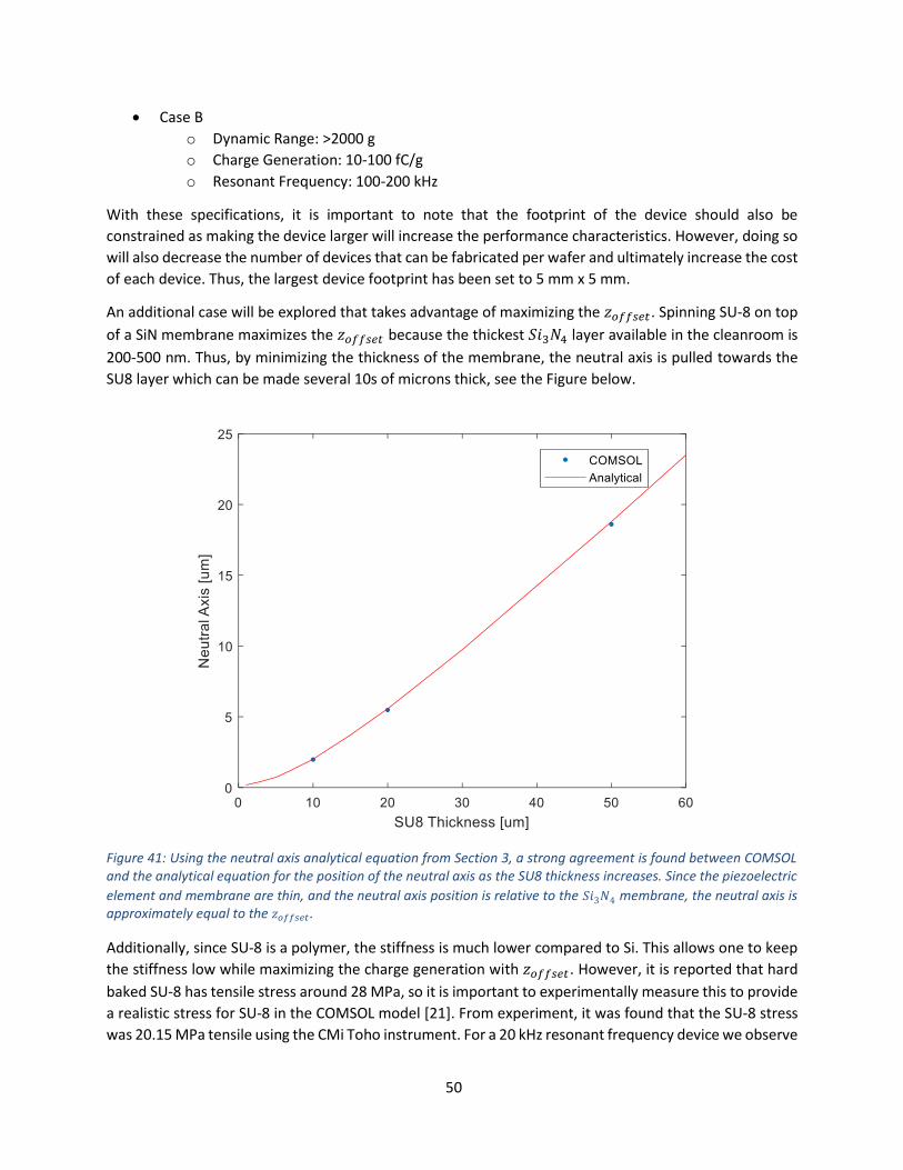
50
Case B
o Dynamic Range: >2000 g
o Charge Generation: 10-100 fC/g
o Resonant Frequency: 100-200 kHz
With these specifications, it is important to note that the footprint of the device should also be
constrained as making the device larger will increase the performance characteristics. However, doing so
will also decrease the number of devices that can be fabricated per wafer and ultimately increase the cost
of each device. Thus, the largest device footprint has been set to 5 mm x 5 mm.
An additional case will be explored that takes advantage of maximizing the 𝑧𝑜𝑓𝑓𝑠𝑒𝑡. Spinning SU-8 on top
of a SiN membrane maximizes the 𝑧𝑜𝑓𝑓𝑠𝑒𝑡 because the thickest 𝑆𝑖3𝑁4 layer available in the cleanroom is
200-500 nm. Thus, by minimizing the thickness of the membrane, the neutral axis is pulled towards the
SU8 layer which can be made several 10s of microns thick, see the Figure below.
Figure 41: Using the neutral axis analytical equation from Section 3, a strong agreement is found between COMSOL and the analytical equation for the position of the neutral axis as the SU8 thickness increases. Since the piezoelectric
element and membrane are thin, and the neutral axis position is relative to the 𝑆𝑖3𝑁4 membrane, the neutral axis is approximately equal to the 𝑧𝑜𝑓𝑓𝑠𝑒𝑡.
Additionally, since SU-8 is a polymer, the stiffness is much lower compared to Si. This allows one to keep
the stiffness low while maximizing the charge generation with 𝑧𝑜𝑓𝑓𝑠𝑒𝑡. However, it is reported that hard
baked SU-8 has tensile stress around 28 MPa, so it is important to experimentally measure this to provide
a realistic stress for SU-8 in the COMSOL model [21]. From experiment, it was found that the SU-8 stress
was 20.15 MPa tensile using the CMi Toho instrument. For a 20 kHz resonant frequency device we observe

51
that SU-8 on a 200 nm low stress SiN membrane outperforms a Si membrane as the radius of the device
increases, see the Figure below.
Figure 42: COMSOL was used to model SU-8 with 20.15 MPa of tensile stress on a 200 nm thick 168 MPa tensile stress
𝑆𝑖3𝑁4 membrane to maximize the 𝑧𝑜𝑓𝑓𝑠𝑒𝑡 while minimizing the stiffness to maximize charge generation. For larger
device radii, the low stress 𝑆𝑖3𝑁4 membrane with SU-8 outperforms accelerometers implementing a Si membrane only. Charge generation at specific membrane radii are plotted here when the device resonant frequency = 20 kHz. Here, the charge generated is only reported for the outer electrode.
SU8 has never been used to modify piezoelectric accelerometers to increase the performance, so this is a
novel method to explore. Given these results, an SU-8 case is also created as a third specification for high
sensitivity devices operating in low temperature environments at moderate frequencies:
Case C
o Resonant Frequency: 20 kHz
o Charge Generation > Si Only Case
4.5 Material Selection EPFL’s center for micro and nanotechnology, CMi, has different wafers available for micromachining.
Silicon wafers available on the CMi website are given in the table below.
Table 10: The table below summarizes the Si Wafers readily available for purchase in the CMi cleanroom from the CMi website [42]. For double side polished wafers (DS), the maximum available Si substrate layer is approximately 380 um, which limits the maximum thickness of the proof mass.
Si Wafer Name Diameter [mm] Thickness [um] Conductivity Type Resistivity Range
[Ohm cm]

52
100/P/SS/01-100 100 ± 0.5 525 ± 25 P or N 0.1-100
100/P/DS/1-10 100 ± 0.2 380 ± 10 P 1-10
100/P/SS/01-05 100 ± 0.2 525 ± 20 P 0.1-0.5
100P/DS/01-05 100 ± 0.2 380 ± 10 P 0.1-0.5
100/P/SS/15-25 100 ± 0.2 525 ± 20 P 15-25
150/P/SS/15-25 150 ± 0.2 675 ± 20 P 15-25
SOI wafers are also available, however these are much more expensive. SOI wafers would guarantee a
uniform membrane thickness. However, for prototyping, it is more desirable to pursue the Si wafers
summarized in the table above and add layers of 𝑆𝑖𝑂2 and 𝑆𝑖3𝑁4 with an acceptable level of non-
uniformity in the etch to reduce costs. The following layers are available at a range of thicknesses for
deposition onto the Si wafers [42]:
Dry Oxide
o 100 nm - 200 nm
Wet Oxide
o 200 nm – 2 um
LPCVD 𝑆𝑖3𝑁4
o 100 nm - 500 nm
LPCVD LS 𝑆𝑖3𝑁4
o 100 nm – 500 nm
Adding these layers are of major interest as they can be used as an insulator and etch mask on the wafer,
as demonstrated by Beeby et al [2]. Thus, given the available wafers for micromachining, a double sided
Si wafer with oxide and/or 𝑆𝑖3𝑁4 are strong candidates for the starting wafer.
To extract the charge from the AlN piezoelectric material, Pt has shown to be an ideal candidate as the
electrode material because it has been shown it adheres well to AlN [11]. Additionally, Pt doesn’t oxidize
and it is easily machined in the CMi cleanroom via dry etching. Al would be an alternative candidate,
however it does not adhere as well to the AlN and it is not easily micromachined in the cleanroom.
Although, Al may be used as a protective layer for the wafer after one of the two sides are finished
processing.
Comparing the prospective materials’ coefficients of thermal expansion shows that there will be a
moderate temperature transient sensitivity at low frequencies due to small differences in thermal
expansion coefficients [44].

53
Table 11: The coefficients of thermal expansion for the materials of interest are all on the same order of magnitude, which helps minimize the non-uniform thermal expansion at higher temperatures [44]. Silica poses the greatest risk for temperature transient sensitivity as it is an order of magnitude lower than the other materials considered.
Material Coefficient of Thermal Expansion [1e-6/K]
Silicon 7-8
Silicon Nitride 1.4-3.7
Silica, 𝑆𝑖𝑂2 0.55
AlN 4.3-5.6
Pt 9
For the SU-8 case, an appropriate solution of SU-8 must be purchased to reach the desirable thicknesses
of the SU-8 on 𝑆𝑖3𝑁4 model. Gersteltec GM 1070 was purchased because this could be spun for a broad
range of thicknesses ranging from 12 um to 90 um. Recall, the larger SU-8 thicknesses are more desirable
as this maximizes the 𝑧𝑜𝑓𝑓𝑠𝑒𝑡 for charge generation.
4.6 Simple Design Comparison Although the state of the art for bending charge mode piezoelectric accelerometers focused on circular
proof mass structures, it important to verify if simpler designs cannot satisfy the same performance
requirements. A simpler design will reduce the number of fabrication steps involved and increase the
economic savings that would be spent on a more complex design that performs the same task. Two
simpler accelerometer models are proposed:
Cantilever with Proof Mass
Clamp-Clamp (C-C) Beam with Proof Mass
To compare these two models to the circular accelerometer model, the geometry must be adjusted so all
three models are directly comparable. The dimensions of the circular accelerometer are arbitrarily set to
2000 um device diameter, 13 um unstressed Si membrane, and 411 um membrane thickness. The
dimensions of the three accelerometers are compared in the table below.
Table 12: The circular accelerometer model is compared to the cantilever and C-C beam models with equivalent geometric dimensions. These geometric parameters are implemented in COMSOL to compare performances to see if a simpler model can be used instead of a slightly more complex model.
Model Length/Diameter
[um] Membrane Thickness
[um] Width [um]
Mass Thickness [um]
b/a ratio [unitless]
Circular 2000 13 - 411 0.5
Cantilever 2000 13 1570 206 0.5
C-C Beam 2000 13 1570 206 0.5

54
Figure 43: Schematic of the cantilever and C-C beam accelerometer design. The piezoelectric layer fully covers the surface of the cantilever, whereas the piezoelectric layer only covers the outer edge of the C-C beam accelerometer.
These geometric parameters are used as inputs in COMSOL. The performance results of each model is
tabulated below.
Table 13: The three models’ performance metrics are compared. The cantilever model generates the most charge, however at the expense of a low resonant frequency and poor cross axis sensitivity. The C-C beam model provides a lower charge generation and resonant frequency compared to the circular model. The resonant frequencies of the cantilever and C-C beam are verified by the analytical equations presented in Tom Irvine’s work [20].
Model Charge Generation
[fC/g] Resonant Frequency
[kHz] Dynamic Range
[g] Max Cross Axis Sensitivity [%]
Circular 95 20 > 1000 < 0.01
Cantil. 1500 1.15 < 500 49
C-C Beam
50 16.7 > 1000 10
The cross axis sensitivity is calculated by dividing the sensitivity along the main axis by the sensitivity along
the secondary axis. In this case, the main axis is in the z-direction and the secondary axis is in the radial
direction as shown in the following equation:
𝐶𝑟𝑜𝑠𝑠 𝐴𝑥𝑖𝑠 𝑆𝑒𝑛𝑠𝑖𝑡𝑖𝑣𝑖𝑡𝑦 = 𝑆𝑧
𝑆𝑟 (31)
From the table above, the cantilever model generates the most charge at the cost of a lower resonant
frequency and an unacceptably high cross axis sensitivity. Due to the high cross axis sensitivity, this model
is not a candidate for a uniaxial piezoelectric accelerometer. Similarly, the C-C beam model demonstrates
an acceptable, but lower resonant frequency and charge generation compared to the circular model
design. But due to a high cross axis sensitivity it is not considered either. Thus, due to a higher charge
generation, resonant frequency, and low cross axis sensitivity, the circular model design is the most
optimal for obtaining maximum performance among these three models.
4.7 Final Design For the final design of the uniaxial piezoelectric accelerometer, an optimization of the maximum charge
generation is first performed to compared to the b/a ratio optimization performed in the solid mechanic’s
section. COMSOL’s optimization yields an optimal b/a ratio of 0.5, instead of Roark’s 0.37, with an optimal
outer electrode to device radius (OE/a) ratio of 0.7, see the figure below.

55
Figure 44: Optimization of the b/a ratio yields a different maximum compared to Roark’s analytical equations, 0.5 > 0.37. Optimization of the outer electrode to device radius results in an optimal ratio of 0.7. The inner electrode is placed 25 um from the outer electrode with the same outer-inner radius difference, which yields an approximately equal charge generation. The 25 um gap also avoids any possibility of short circuiting during the process flow.
The OE/a ratio is optimized because of charge cancellation. The inner electrode was placed 25 um from
the outer electrode with the same outer-inner radius difference. The charge generated by the inner
electrode is approximately equal to the charge generated by the outer electrode. The total charge
generation of the accelerometer is the sum of the charge collected by the two electrodes.
From the analytical equations in the previous sections, it is easy to determine approximate values to input
into COMSOL via the follow figures.

56
Figure 45: Analytical equations are used to create a surface plot of the circular accelerometer resonant frequency as a function of the membrane radius and thickness. Given a strong agreement between the COMSOL and analytical equations from the model-to-model verification section, selecting a resonant frequency from this plot will provide approximate values to input into COMSOL for the final design. A 350 um mass thickness is kept constant in this analysis.

57
Figure 46: Analytical equations are used to create a surface plot of the circular accelerometer’s charge generation as a function of the membrane radius and thickness. Given a strong agreement between the COMSOL and analytical equations from the model-to-model verification section, selecting a charge generation value from this plot will provide approximate geometric values to input into COMSOL for the final design. A 350 um mass thickness is kept constant in this analysis. No stress is applied to the membrane layer.
An unstressed Si membrane circular accelerometer model satisfies the resonant frequency, charge
generation, and dynamic range requirements for the low frequency case. Comparing the COMSOL final
result to the analytical models are shown below. Please note, the stressed 𝑆𝑖3𝑁4 membrane circular
accelerometer did not yield high enough charge generation, so it is not discussed in this section, please
see Appendix B for its results.

58
Figure 47: For the low frequency case, a device radius of 2000 um was selected because a device with a 1000 um radius could not generate 1 pC/g.
An unstressed Si membrane circular accelerometer model satisfies the resonant frequency, charge
generation, and dynamic range requirements for the high frequency case as well. Comparing the COMSOL
final result to the analytical models are shown below.

59
Figure 48: For the high frequency case, a device radius of 2000 um was selected with a membrane thickness of 120 um.
The results from the high and low frequency simulations are tabulated below.

60
Table 14: Parameterization in COMSOL was conducted based on the analytical approximations. The final design parameters and performance satisfy the low and high frequency cases presented in the earlier section. The mass thickness was limited by the thickness of the wafer purchased, which is why a 1000 um device was ultimately not pursued for the low frequency case. Both cases were not designed for specifically 1 kHz, 100 kHz, 1 pC/g, or 10 fC/g to give the design lead way due to the fabrication non-idealities.
Parameters/Performance Low Frequency Case High Frequency Case
Membrane Thickness [um] 14 120
Mass Thickness [um] 350 350
Membrane Radius [um] 2000 2000
Electrode Thickness [nm] 50 50
AlN Thickness [nm] 100 100
b/a ratio [unitless] 0.5 0.5
Charge Generation [fC/g] 1068 21.2
Resonant Frequency [kHz] 6.42 115.1
Displacement Sensitivity [m/g] 6.12e-9 2.2e-11
Dynamic Range [g] 500 2000
Linearity [%] 3.03 0.01
Cross Axis Sensitivity [%] < 0.01 < 0.01
A stress analysis was additionally conducted to ensure the device integrity at the maximum g
performance. The yield strength of a material can be approximated as 0.2 % of the Young’s modulus. If
the stress analysis results in a yield strength less than 0.2 % of Si’s Young’s Modulus, 330 MPa, then the
design will not experience any permanent damage at high g forces within the dynamic range.
For the low frequency design, a von Mises stress analysis in COMSOL yields a maximum stress of 35.5 MPa
at 500 g which is less than 330 MPa.

61
Figure 49: A von Mises stress analysis was conducted in COMSOL to determine if the maximum stress at 500 g for the low frequency design would cause permanent deformation if it was greater than the yield strength of Si. From the analysis, a maximum stress of 35.5 MPa at 500 g was found, which is significantly less than the yield strength of Si, 330 MPa.
For the high frequency design, a von Mises stress analysis in COMSOL yields a maximum stress of 2.82
MPa at 2000 g which is less than 330 MPa.

62
Figure 50: von Mises stress analysis was conducted in COMSOL to determine if the maximum stress at 2000 g for the high frequency design would cause permanent deformation if it was greater than the yield strength of Si. From the analysis, a maximum stress of 2.2 MPa at 2000 g was found, which is significantly less than the yield strength of Si, 330 MPa.
As for the SU-8 case, a parametric sweep was used in COMSOL to determine the final geometric
parameters. The table below summarizes the Si only versus the SU-8 on 𝑆𝑖3𝑁4 case for 20 kHz resonant
frequencies.

63
Table 15: The Si membrane accelerometer can improve its charge generation by adding a thick layer of SU8 on top
of the device. Changing the membrane material to 𝑆𝑖3𝑁4 additionally helps by further increasing the 𝑧𝑜𝑓𝑓𝑠𝑒𝑡 in the
direction of the SU-8 layer because the SiN is 200 nm thick and hardly affects the neutral axis of the structure.
Parameters/Performance Si SU-8 on SiN
Membrane Thickness [nm] 16.25 200
Mass Thickness [um] 350 350
Membrane Radius [um] 1250 1250
b/a ratio [unitless] 0.5 0.5
SU8 Thickness [um] - 40
Charge Generation [fC/g] 125 169.2
Resonant Frequency [kHz] 20 20.3
Displacement Sensitivity [m/g] 6.29e-10 6.03e-10
Dynamic Range [g] 500 500
Linearity [%] 0.17 1.03
Cross Axis Sensitivity [%] <0.01 < 0.01
The stress analysis for the SU-8 on 𝑆𝑖3𝑁4 at 500 g yields a maximum stress of 201 MPa which is less than
the yield strength of 𝑆𝑖3𝑁4 which is 500 MPa.
It is important to note that a major assumption from the above models includes assuming no stress in the
AlN and electrode layers. There are reports of highly compressive residual stress in AlN based piezoelectric
accelerometers that cause the resonant frequency to reduce significantly and cause non-linear deflections
[15]. Gupta et al. performs these simulations for AlN layers that are several hundred nanometers thick,
thus to reduce the effect of any stress present in the sputtered AlN layer the thickness is set at 100 nm.
Setting the AlN thickness at 100 nm also helps avoid short circuiting the top and bottom electrodes due
to fencing that may occur during the fabrication process. This will be discussed further in Section 5.
4.7 Discussion The first major design constraint for the circular piezoelectric accelerometer design was the wafer
selection. Instead of purchasing a 400 CHF SOI wafer, which would guarantee a good membrane thickness
uniformity, a double sided polished Si wafer is selected to lower fabrication costs. The maximum thickness
of the Si substrate layer is approximately 380 um, which limits the proof mass thickness to 380 um.
However, the proof mass thickness must be less than 380 um to ensure the proof mass does not crash
onto the mounted surface during large vibrations. An arbitrary maximum proof mass thickness of 350 um
ensures a 30 um gap to take away any possibility of the proof mass crashing into the mounted surface.
Recall, the proof mass is maximized to achieve maximum charge sensitivity.
The second major design constraint is the device footprint limit of 5 mm. From the analytical and FEM, a
larger device radius results in a better charge generation. Since the thickness of the proof mass and device
radius are constrained, the remaining parameters to be toggled are the membrane thickness, stress in the
membrane layer, and the position of the electrode placement.
The membrane thickness for the unstressed membrane layer relies on the 𝑧𝑜𝑓𝑓𝑠𝑒𝑡 for charge generation.
For small membrane thicknesses, larger deflections may be obtained, but the 𝑧𝑜𝑓𝑓𝑠𝑒𝑡 is small, so the gain

64
in charge generation from the larger deflections is greatly reduced. Thus, thicker membranes with a larger
device radius is most optimal for achieving high charge sensitivity.
For a stressed membrane layer, such as 𝑆𝑖3𝑁4, the membrane thickness is 200-500 nm. The 𝑧𝑜𝑓𝑓𝑠𝑒𝑡 is
minimized using this membrane which causes the charge generation to be too small. However, by adding
a thick SU8 layer on top of the device, the 𝑧𝑜𝑓𝑓𝑠𝑒𝑡 is increased substantially. This leads to the design of a
low temperature uniaxial piezoelectric accelerometer that outperforms the basic MEMS Si accelerometer
for larger device radii.
COMSOL and the analytical equations shared relatively similar values for membrane deflection and charge
generation. However, the two models deviated more for the resonance frequency calculations. This is
largely due to COMSOL calculating the resonance frequency with nonlinear approximations. The analytical
model is a good first approximation however, the two models increasingly deviate at smaller device radii.
COMSOL also predicts a different optimal b/a ratio that is much higher than the analytical value. Roark’s
stress and strain formula book predicts a b/a ratio of 0.37, whereas COMSOL predicts an optimal value of
0.5. This deviation is likely due to the addition of the electrode and charge generating layers on top of the
membrane layer in the COMSOL simulation which changes the stiffness of the membrane layer.
A stress analysis is important to ensure device robustness during operation. If the stress in the membrane
layer is greater than the yield strength of the membrane material, then the membrane layer may be
permanently damaged and malfunction from large accelerations. From the final design parameters, the
von Mises stress calculated in COMSOL yields maximum stress values lower than the yield strength of the
membrane material at the maximum design acceleration.

65
5 Microfabrication EPFL’s CMi cleanroom was used to carry out device fabrication. This cleanroom is a host to a plethora of
different instruments to fabricate the simulated accelerometer. Two different process flows are
presented:
Si Membrane-based Accelerometer
𝑆𝑖3𝑁4 Membrane-based Accelerometer with SU-8
5.1 Process Flow The first process flow presented is the Si-membrane based accelerometer. This accelerometer is
fabricated with a bottom-up approach on the front side of the wafer. The first step is to use
photolithography to pattern the ground electrode where a seed layer and Pt layer is deposited. The resist
is then stripped and the whole wafer is then coated with the AlN charge generating layer and Pt top
electrode. Photolithography is once again used to pattern the layers above the GND electrode. The
exposed regions are then etched down to the 𝑆𝑖𝑂2 layer. The resist is stripped and Al is deposited on the
front side for protection. From this point forward, the accelerometer is processed on the back side.
Photolithography is used to pattern the 𝑆𝑖𝑂2 layer to expose the Si substrate layer. Resist is stripped and
the backside is re-patterned with photoresist covering the proof mass regions of the Si. Two Si etch steps
are required as the final design states a proof mass thickness of 350 um. The first Si etch removes the Si
until a specific thickness is reached. The resist is stripped and a second Si etch removes the difference of
the remaining thickness, specified later in this section. After the Si etches, the protective Al layer is then
etched. The wafer is diced prior to the Al etch in order to take advantage of the protective layer to increase
the survivability of the devices during the dicing process.
Table 16: Process flow to fabricate the Si membrane-based accelerometer.
(a) Start (b) Front side: Photolithography of GND Electrode Layer
(c) Sputter Seed + Pt Layer + Liftoff (d) Sputter AlN + Pt
(e) Photolithography of Top Electrode Layer
(f) Etch Pt + AlN, then PR Strip

66
(g) Al Deposition (h) Back side: Photolithography of Outer Accelerometer Radius + 𝑆𝑖𝑂2 Etch
(i) Photolithography of Accelerometer Mass
(j) Si Etch
(k) PR Strip (l) Si Etch
(m) Front side: Dice + Etch Al Legend
The second process flow presented is the SU-8 on 𝑆𝑖3𝑁4 membrane accelerometer. Similarly, steps (a)-
(e) are the same as the first process flow presented. However, during the Pt and AlN etch in step (f), the
AlN layer is only partially etched. This is in an effort to protect the 𝑆𝑖3𝑁4 layer as this will etch in Chlorine
chemistry. KOH is used to strip the remaining AlN and photoresist as this does not etch 𝑆𝑖3𝑁4.
The remaining steps are very similar to the Si membrane accelerometer, however 𝑆𝑖3𝑁4 on the back side
is being etched and the second Si etch removes all the Si until the 𝑆𝑖3𝑁4 membrane layer on the front side
is reached. In addition, instead of an Al protective layer, a hard baked SU8 layer is used instead with a
thickness specified by the COMSOL model.
Table 17: Process flow to fabricate the SU-8 on 𝑆𝑖3𝑁4 membrane accelerometer.
(a) Start (b) Front side: Photolithography of GND Electrode Layer

67
(c) Sputter Seed + Pt Layer + Liftoff (d) Sputter AlN + Pt
(e) Photolithography of Top Electrode Layer
(f) Etch Pt + AlN, then PR Strip
(g) Spin SU8 + Hard Bake (h) Backside: Photolithography of Outer Accelerometer Radius + 𝑆𝑖𝑂2 Etch
(i) Photolithography of Accelerometer Mass
(j) First Si Etch
(k) PR Strip (l) Second Si Etch
(m) Dice Legend

68
5.2 Mask Design The mask design of the circular piezoelectric accelerometer is based on Gesing et al.’s AlN piezoelectric
accelerometer. However, Gesing et al.’s device utilizes an SOI wafer, whereas our situation employs a
double side polished Si prime wafer. Nevertheless, the electrode design is more or less the same.
Figure 51: The mask design is inspired by Gesing et al.'s AlN piezoelectric accelerometer. Gesing et al.’s accelerometer is fabricated from an SOI wafer, so the process flow is very similar to ours. Gesing et al’s mask design is displayed above for each layer [14].
The CMi’s maskless aligner (MLA) was used to pattern all of the layers in the process flows. CleWin 4 was
used to write the GDS files for the mask design. A total of four layers are present in the designed mask.
The figure below shows the first layer that was used to pattern the ground electrode on the front side of
the wafer. The ground electrode is composed of the seed and Pt layers. Here, a ring sets the base of the
accelerometer at its center. A contact pad is attached to measure the charge generation. 20 um font is
additionally written in this layer to be easily readable by a light microscope.
Figure 52: This is a screenshot of a GDS file from CleWin 4 illustrating the ground electrode layer of the designed accelerometers. The size of the accelerometer is written in the ground electrode layer with a font size easily readable by a light microscope. A contact pad for the ground electrode is included. The diameter of the ground layer is 20 um larger than the diameter of the second mask layer to provide a buffer in the case of misalignment between layer 1 and layer 2.
The second layer consists of the top electrode layer and the piezoelectric layer. These layers are deposited
in the following order: AlN, Pt. Two concentric rings are used in this layer to separate the two top

69
electrodes to avoid charge cancellation during collection. A contact pad for each electrode is included in
the mask, see the figure below.
Figure 53: This is a screenshot of a GDS file from CleWin 4 illustrating the AlN charge generating layer and top electrode layer of the designed accelerometers. This layer is designed for the STS etch step where the AlN and Pt layers are etched except for the layers in the region shaded in the figure above. Contact pads are included for the inner and outer electrodes. A 25 um gap is employed between the two electrodes to prevent a short circuit.
The third layer was used on the back side to open up the 𝑆𝑖𝑂2/𝑆𝑖3𝑁4 layer to expose the Si layer aligned
to the front side electrode pattern. This layer consists of solid disks where etching of the 𝑆𝑖𝑂2/𝑆𝑖3𝑁4 layers
are to take place, see the figure below.
Figure 54: This is a screenshot of a GDS file of the third mask from CleWin 4 illustrating the 𝑆𝑖𝑂2/𝑆𝑖3𝑁4 backside etch. This layer is patterned on the wafer after the front side of the wafer is finished and protected by a 2 um Al layer or hard baked SU8 layer. The diameter of this etch is 20 um larger than the next layer to provide a buffer in the case of misalignment between layer 3 and layer 4.
The final layer is also used on the back side to etch around the Si mass. Here, the center of the ring is equal
to the diameter of the Si proof mass and the outer ring diameter is equal to the membrane diameter.

70
Figure 55: This is a screenshot of a GDS file of the fourth mask from CleWin 4 illustrating the first Si etch on the
backside of the wafer. This layer is patterned after the 𝑆𝑖𝑂2/𝑆𝑖3𝑁4 layer is etched and removed so the exposed Si layer can be etched. The unshaded area in the middle of the gray ring is the diameter of the proof mass and the outer diameter of the gray ring is the diameter of the designed membrane.
Figure 56: The four masks are aligned and overlapping in the CleWin 4 GDS file. The alignment is dependent on the alignment marks from layers 1 and 3. The backside alignment during layer 3 poses the greatest threat to any large misalignments that could be critical in the device performance.
The radii of the accelerometers were varied from 500 um to 2250 um on 15 mm by 15 mm chips.

71
Figure 57: To maximize the number of accelerometer designs fabricated per wafer, various accelerometers of different device radii are designed from 500 um to 2250 um. Each individual chip is 5 mm by 5 mm. Be sure to note that each device does not have its own optimized thickness. The process flow only allows one thickness for the entire wafer. This means there will only be one device size on the wafer optimized to meet each case’s performance standards.
The total wafer footprint consists of:
Table 18: Total wafer footprint summarized for various accelerometer radii.
Accelerometer Radius [um] Number of Devices per Wafer
500 147 750 21
1000 126 1250 42 1500 21 1750 21 2000 21 2250 21
The alignment marks for the wafer are displayed below:

72
Figure 58: The first and third mask layers incorporate alignment marks so the second and fourth mask layers can align to them, respectively. The third mask layer aligns to the first mask layer’s alignment marks via back side alignment on the MLA and then forms its own alignment marks during the exposure process. This enables the fourth mask layer to align to the third mask layer to minimize alignment error.
5.3 Experimental Work The following wafers were ordered and used for fabricating the piezoelectric accelerometers, see the
table below.
Table 19: Each wafer purchased from CMi was first characterized prior to processing. The thickness of the Si and added layers are important for the etching steps later in the process flow, especially the Si etch step.
Wafer Number
Wafer Type Si Layer Thickness
[um] Added Layer
Thickness [nm]
7137 Silicon 100/P/DS/1-10 TTV2 & Wet oxide 500nm / PME
385 490
6947 Silicon 100/P/DS/1-10 TTV2 & Wet oxide 500nm / PME
385 490
7092 Silicon 100/P/DS/1-10 TTV2 & Wet oxide 500nm / PME
387 490
6903 Silicon 100/P/DS/1-10 TTV2 & Wet oxide 500nm / PME
385.5 490
7827 Silicon 100/P/DS/1-10 TTV2 & Wet oxide 500nm / PME
386 490
7237 Silicon 100/P/DS/1-10 TTV2 & Wet oxide 500nm / PME
387 490
6022 Silicon 100/P/DS/1-10 TTV2 & LPCVD L.S. SiN 200 nm
382.6 204
6023 Silicon 100/P/DS/1-10 TTV2 & LPCVD L.S. SiN 200 nm
382.6 204
Step: GND Electrode Layer
The first step for the blank wafer is to do photolithography on the front side of the wafer. The EVG 150
was used as the coating and developing machine of choice because it is automated and therefore reduces
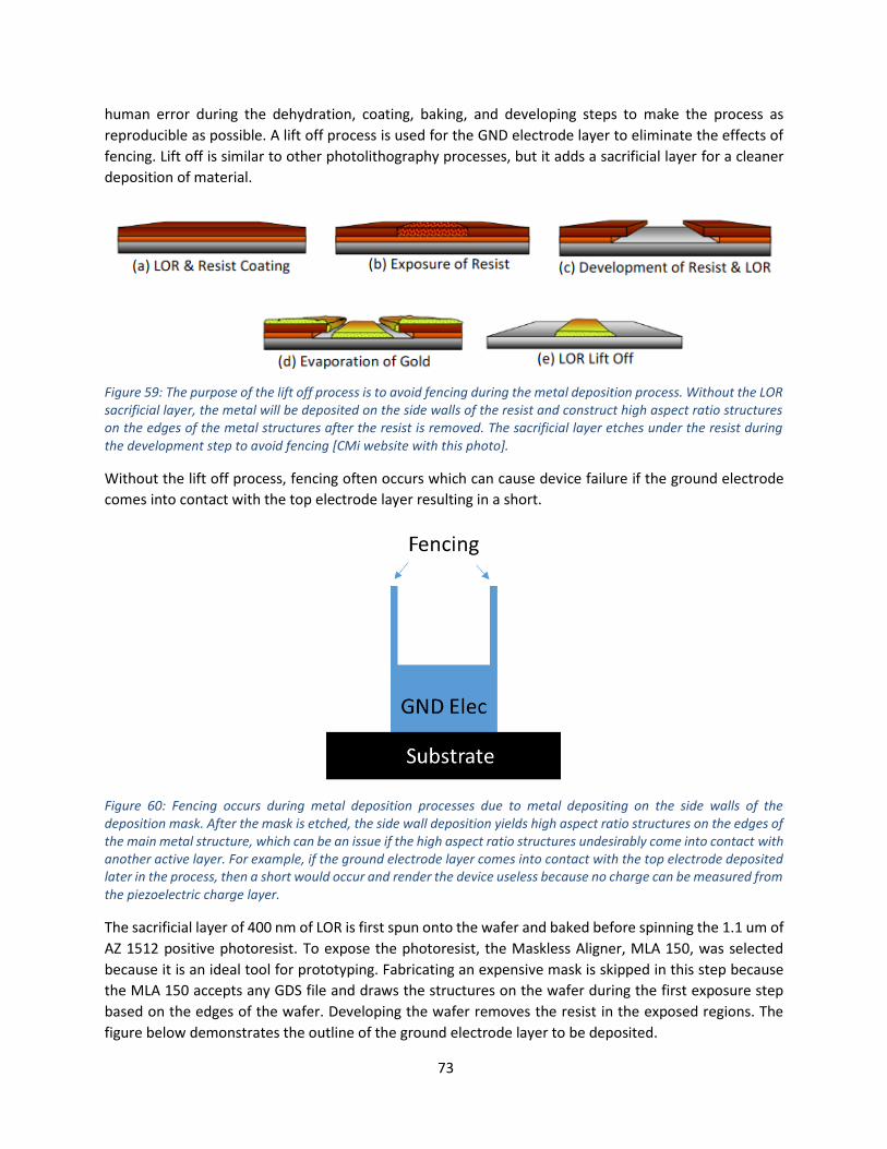
73
human error during the dehydration, coating, baking, and developing steps to make the process as
reproducible as possible. A lift off process is used for the GND electrode layer to eliminate the effects of
fencing. Lift off is similar to other photolithography processes, but it adds a sacrificial layer for a cleaner
deposition of material.
Figure 59: The purpose of the lift off process is to avoid fencing during the metal deposition process. Without the LOR sacrificial layer, the metal will be deposited on the side walls of the resist and construct high aspect ratio structures on the edges of the metal structures after the resist is removed. The sacrificial layer etches under the resist during the development step to avoid fencing [CMi website with this photo].
Without the lift off process, fencing often occurs which can cause device failure if the ground electrode
comes into contact with the top electrode layer resulting in a short.
Figure 60: Fencing occurs during metal deposition processes due to metal depositing on the side walls of the deposition mask. After the mask is etched, the side wall deposition yields high aspect ratio structures on the edges of the main metal structure, which can be an issue if the high aspect ratio structures undesirably come into contact with another active layer. For example, if the ground electrode layer comes into contact with the top electrode deposited later in the process, then a short would occur and render the device useless because no charge can be measured from the piezoelectric charge layer.
The sacrificial layer of 400 nm of LOR is first spun onto the wafer and baked before spinning the 1.1 um of
AZ 1512 positive photoresist. To expose the photoresist, the Maskless Aligner, MLA 150, was selected
because it is an ideal tool for prototyping. Fabricating an expensive mask is skipped in this step because
the MLA 150 accepts any GDS file and draws the structures on the wafer during the first exposure step
based on the edges of the wafer. Developing the wafer removes the resist in the exposed regions. The
figure below demonstrates the outline of the ground electrode layer to be deposited.

74
Figure 61: After spin coating 400 nm of LOR and 1.1 um of AZ 1512, the MLA is used to pattern the ground electrodes. The development of the exposed regions on the wafer yields a brown color and the unexposed regions are dark yellow under the optical microscope. Here, the image of Wafer 7137 shows a satisfactory photolithography step prior to Pt deposition.
The parameters used on the MLA are tabulated below.
Table 20: The MLA consists of three general steps such as: converting the GDS file, aligning the wafer to the GDS mask design, and exposing the GDS mask design onto the wafer. During the exposure step, a 405 nm laser is used to draw the structures strip by strip. The two main parameters to choose during this exposure are the dosage and defocus of the laser. Recommended values for 1.1 um AZ1512 on 400 nm LOR is 35 mJ/cm2 and a defocus of -2, but an overexposure dose of 50% is used. This ensures all the resist is exposed at the cost of less resolution at the edge of the pattern due to a higher intensity of diffraction. Since the smallest structures on the wafer are 25 um, the overexposure does not pose a problem.
MLA Parameters Value
Dosage 55 mJ/cm2
Defocus -2
The ground electrode layer is deposited via the sputtering tool called the SPIDER 600. Since Pt does not
adhere well to 𝑆𝑖𝑂2, a seed layer is first sputtered to improve the adhesion of Pt onto the surface. The
tables below summarize the parameters used for this deposition.

75
Table 21: The SPIDER has four chambers for deposition. Each chamber has a different target for sputtering. For the ground electrode, two chambers were used to sputtering an AlN seed layer with a Pt electrode layer on top. The deposition was conducted at room temperature in both cases. Wafer 7137 and 6947 both sputtered 64 nm of Pt instead of 50 nm of Pt due to a calculation error, however 50 nm of Pt was sputtered correctly onto the remaining wafers.
Layer Material Deposition
Temperature [C]
Target Thickness
[nm]
Measured Thickness
[nm]
Deposition Rate
[nm/min]
Deposition Time [s]
Seed AlN RT 15 65.63 ±
5.43
50 18
Ground Electrode
Pt RT 50 270 11
Table 22: The parameters for sputtering AlN on Pt using the SPIDER are dependent on the Ar/N2 flow ratio and power supplied during the sputtering process [11]. These values are off the shelf recipes from previous users, so no optimization of the deposition rates were required.
Material Ar/N2 Flow Ratio [sccm/sccm] Power [W]
AlN 10/40 1500
Pt 15/0 1000
The wafer is placed in a lift off bath filled with Remover 1165 for 1.5 days. A minute of sonication is first
applied at the beginning of the lift off. Two minutes of sonication is applied at the end of the lift off
process. The wafer is then placed in an IPA bath for two minutes to stop the lift off process. A fast fill rinse
and trickle tank are used as a DI water rinse before drying the wafer with a nitrogen gun. The ground
electrode layer after the lift off process is illustrated below.
Figure 62: This image of Wafer 7137 after the lift off process shows the deposited Pt layer in yellow and 𝑆𝑖𝑂2layer in brown on the optical microscope. The resolution of the device labeling is satisfactory and easily readable on an optical microscope. The device label refers to the radius of the accelerometer’s membrane.

76
No fencing was observed during this step. Profilometry illustrates the effectiveness of the lift off process.
Figure 63: Profilometry shows no fencing on the device structures after the lift off process. Here, the alignment mark height is approximately 65 nm for Wafer 7092 with a standard deviation of approximately 5 nm. This measurement is within the expected range of the total combined thickness of the 15 nm of AlN and 50 nm of Pt that was deposited.
Step: Piezoelectric and Top Electrode Layer
After the lift off process, the wafer is placed back in the SPIDER 600 to sputter the active AlN piezoelectric
charge generation layer and the top electrode layer. The parameters used for this deposition are
summarized in the tables below.
Table 23: After the lift off process, the wafers are placed back into the SPIDER to sputter 100 nm of AlN with 50 nm of Pt on top for the piezoelectric charge generation layer and top electrode layer, respectively. The recipe for AlN deposition at high temperature was taken from another CMi user and the recipe for Pt deposition at room temperature was repeated from the earlier process. From the measured thickness of the Pt on AlN + ground electrode layer, it is apparent that the AlN deposition at high temperature is much faster than what was reported by a fellow CMi user. The thickness of the AlN is approximately 170-210 nm, which suggests a deposition rate closer to 102-126 nm/min.
Layer Material Deposition
Temperature [C]
Target Thickness
[nm]
Measured Thickness
[nm]
Estimated Deposition
Rate [nm/min]
Deposition Time [s]
Active PZE AlN 300 100
285-325
60 100
Top Electrode
Pt RT 50 270 11

77
Table 24: The parameters input into the recipes for the SPIDER are tabulated below. The Ar/N2 flow ratio and power ultimately control the deposition rates and quality of deposition.
Material Ar/N2 Flow Ratio Power [W]
AlN 10/40 1500
Pt 15/0 1000
Following the sputtering of these two layers, a photolithography step was used to pattern the
piezoelectric and top electrode layer. A thick 5 um AZ 9260 photoresist was deposited in the EVG and then
patterned in the MLA using the alignment marks created by the ground electrode layer. After
development, a post exposure bake at 85 C for 2.5 hours was used to solidify the photoresist layer.
The next step in the process flow is the first critical step. Etching the 100 nm AlN and 50 nm Pt layers in
the exposed regions are critical for patterning the front side of the wafer. The STS Multiplex dry etcher
was used for dry etching the AlN and Pt layers using Cl2/Ar chemistry. The STS Multiplex utilizes an
inductively coupled plasma to provide high density plasma and ion current at low pressure. This bombards
Ar ions in the presence of Cl gas onto the wafer to etch the AlN and Pt layers. This step is difficult because
the ground electrode layer should not be etched during this process. To avoid this, end point detection
was used to determine when the AlN and Pt layers were being etched. The end point detection system
measures the intensity of a light beam reflecting off the wafer during the etching process. As the layers
are etched, the intensity changes so one can determine what layer is being etched at that moment. By
etching in small increments based on the end point detection, the final etch time was found with the help
of the Filmetrics tool. Filmetrics measures the reflectivity of the wafer and fits the reflectivity spectrum to
a model based on the material and thickness of the layers. The etch rates of the AlN and Pt layers in the
STS Multiplex are tabulated below.
Table 25: The STS Multiplex dry etcher uses Cl2/Ar chemistry to etch the AlN and Pt deposited in the prior step. This is to define the structures covered by the photoresist in the photolithography step by removing the material not covered by the photoresist mask. End point detection and looking at the color of the wafer during the etching process helped define when the etching process was finished. A longer etch time was used to ensure the 100 nm AlN layer was completely etched even if the ground contact pads were slightly etched. If any AlN is left over, then it would be impossible to measure the charge generation of the accelerometer from the contact pads because AlN is not conducting. Filmetrics was used to verify the complete etching of the AlN by measuring the thickness of the
𝑆𝑖𝑂2/𝑆𝑖3𝑁4 layer on the Si wafer.
Layer Thickness [nm] Approximate Etch
Rate [nm/min] Approximate Etch
Time [s] Actual Etch Time
[s]
Pt 50 50 60 110
AlN 170-210 300 34-42

78
Figure 64: (Left) The end point detection curve shows the first 50 seconds of etching the Pt layer. (Right) The wafer shows a non-uniform etch in the STS due to the different colors varying radially across the wafer. At this point, the rest of the Pt layer still needs to be etched, as well as the AlN layer.
Figure 65: (Left) The end point detection curve shows etching the wafer for a total of 110 seconds completely etches the Pt and AlN layers. The first downward curve represents the etching of the Pt layer and the second downward curve represents the etching of the AlN layer. (Right) The wafer shows uniform thickness across the whole wafer since
there is no longer a radial variation in color. Filmetrics yields a 𝑆𝑖𝑂2 thickness less than the initial 490 nm measured at the beginning of the process flow, which means all the AlN has been etched. Since the ground contact pads are still visible, the Pt ground electrode layer has not been completely etched.
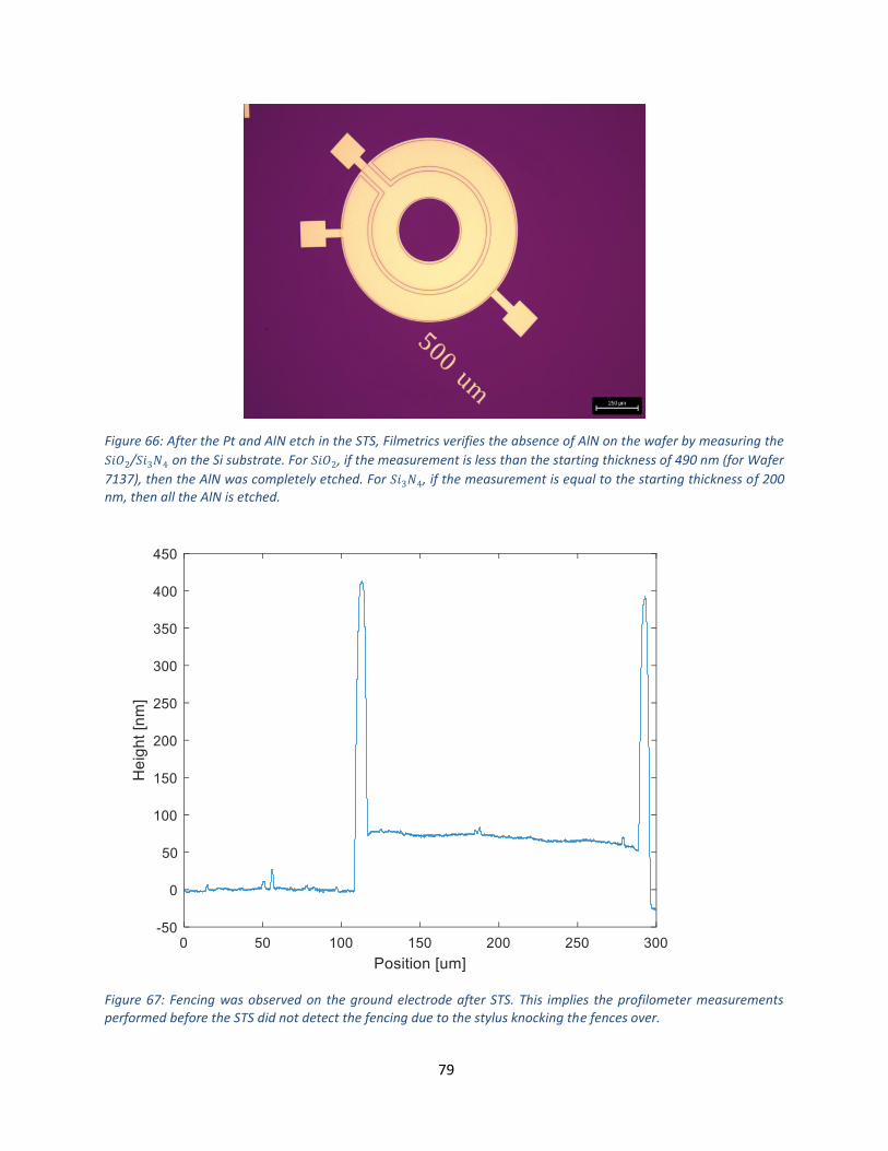
79
Figure 66: After the Pt and AlN etch in the STS, Filmetrics verifies the absence of AlN on the wafer by measuring the
𝑆𝑖𝑂2/𝑆𝑖3𝑁4 on the Si substrate. For 𝑆𝑖𝑂2, if the measurement is less than the starting thickness of 490 nm (for Wafer
7137), then the AlN was completely etched. For 𝑆𝑖3𝑁4, if the measurement is equal to the starting thickness of 200 nm, then all the AlN is etched.
Figure 67: Fencing was observed on the ground electrode after STS. This implies the profilometer measurements performed before the STS did not detect the fencing due to the stylus knocking the fences over.

80
After etching the AlN and Pt layers, the photoresist is stripped. Thereafter, 2 microns of Al are deposited
on the front side of the device for protection during backside processing. The Al is deposited via
evaporation using the EVA 760.
Figure 68: The EVA 760 evaporates 2 um of Al onto the wafer for protection during the back side processing steps. The satisfactory alignment of the top and ground electrode layers is clearly visible in the optical microscope image. The ground electrode contact pad is on the bottom right of the image, whereas the top electrodes are on the upper left side of the image.
Table 26: An off the shelf recipe from CMi was used to deposit the 2 um Al protective layer. The thickness of this layer is measured via profilometry.
Layer Target Thickness [um] Measured Thickness [um]
Al 2 1.87
Step: 𝑆𝑖𝑂2/𝑆𝑖3𝑁4 Etch Layer
The wafer is now processed on the backside for the remaining steps of the process flow. A
photolithography step is first conducted on the backside to pattern the 𝑆𝑖𝑂2/𝑆𝑖3𝑁4 layer prior to the Si
Etch. This step is necessary because the 𝑆𝑖𝑂2/𝑆𝑖3𝑁4 layers will be used as an etch mask during the second
Si etch step. The EVG and MLA are used to spin coat and pattern 5 um of AZ 9260 onto the wafer once
again. During the exposure step, the alignment marks on the front side of the wafer are used for the
backside alignment. The photoresist is then developed and baked after exposure with the same
parameters as the step before.
For the 𝑆𝑖𝑂2etch, the AMS 200 plasma etcher was used with Fluorine chemistry. The etch recipe used
etches 𝑆𝑖𝑂2and photoresist in a 1:1 ratio. Since the photoresist layer is 5 um, there is more than enough
to protect the unexposed regions during this etch. For the 𝑆𝑖3𝑁4 etch, the SPTS APS dielectric etcher was
used with Fluorine chemistry. The parameters used during this step are tabulated below.

81
Table 27: The AMS 200 plasma etcher was used to etch the 𝑆𝑖𝑂2layer with Fluorine chemistry in a 1:1 ratio with
photoresist. A 10 second etch time was added to ensure all the 𝑆𝑖𝑂2has been etched. Only 10% of the PR mask layer
is etched during this step which poses no issues to the unexposed 𝑆𝑖𝑂2layer which will be used as a mask during the
second Si etch. The SPTS APS dielectric etcher was used to etch the 𝑆𝑖3𝑁4 layer selectively to ensure the Si layer is minimally etched (35 nm/min).
Layer Approximate Etch Rate [nm/min]
Thickness [nm] Estimated Etch Time [s]
Etch Time [s]
𝑆𝑖𝑂2 280 500 107 117
𝑆𝑖3𝑁4 255 200 47 120
Figure 69: Prior to etching the Si layer, 𝑆𝑖𝑂2 must be etched in desired regions so that the layer may be used as a
mask during the second Si etch step. Here, the 𝑆𝑖𝑂2 layer has been etched and the resist has been stripped off the wafer. The bare Si is exposed in the light yellow circle regions; the dark green region surrounding the bare Si is the
𝑆𝑖𝑂2 mask layer.
Filmetrics is used to verify all the 𝑆𝑖𝑂2/𝑆𝑖3𝑁4 is etched.
Step: Si Etch
The resist mask for the 𝑆𝑖𝑂2/𝑆𝑖3𝑁4 etch is stripped before starting the next photolithography step. The
EVG and MLA are used to spin coat and pattern 5 um of AZ 9260 onto the wafer once again. During the
exposure step, the pattern is aligned to the exposure marks on the backside of the wafer created during
the 𝑆𝑖𝑂2/𝑆𝑖3𝑁4 etch step. After developing and baking the resist, the AMS 200 was used to implement
the Bosch process to etch the Si layer using Fluorine chemistry. The amount of Si removed in the first etch
is:
1𝑠𝑡 𝑆𝑖 𝐸𝑡𝑐ℎ = 𝑡𝑆𝑖 − 𝑡𝑚𝑒𝑚𝑏 − (𝑡𝑆𝑖 − 𝑡𝑚𝑎𝑠𝑠 )
2𝑛𝑑 𝑆𝑖 𝐸𝑡𝑐ℎ = 𝑡𝑆𝑖 − 𝑡𝑚𝑎𝑠𝑠
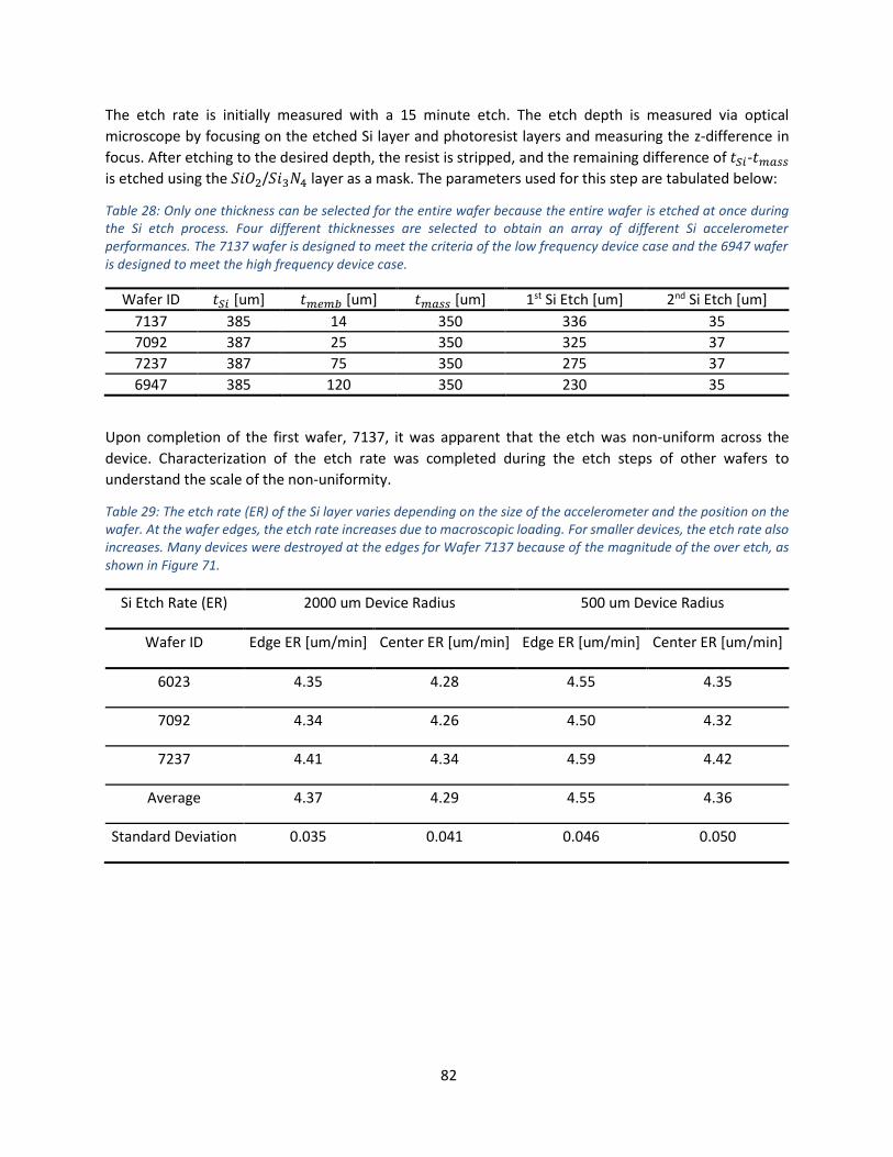
82
The etch rate is initially measured with a 15 minute etch. The etch depth is measured via optical
microscope by focusing on the etched Si layer and photoresist layers and measuring the z-difference in
focus. After etching to the desired depth, the resist is stripped, and the remaining difference of 𝑡𝑆𝑖-𝑡𝑚𝑎𝑠𝑠
is etched using the 𝑆𝑖𝑂2/𝑆𝑖3𝑁4 layer as a mask. The parameters used for this step are tabulated below:
Table 28: Only one thickness can be selected for the entire wafer because the entire wafer is etched at once during the Si etch process. Four different thicknesses are selected to obtain an array of different Si accelerometer performances. The 7137 wafer is designed to meet the criteria of the low frequency device case and the 6947 wafer is designed to meet the high frequency device case.
Wafer ID 𝑡𝑆𝑖 [um] 𝑡𝑚𝑒𝑚𝑏 [um] 𝑡𝑚𝑎𝑠𝑠 [um] 1st Si Etch [um] 2nd Si Etch [um]
7137 385 14 350 336 35
7092 387 25 350 325 37
7237 387 75 350 275 37
6947 385 120 350 230 35
Upon completion of the first wafer, 7137, it was apparent that the etch was non-uniform across the
device. Characterization of the etch rate was completed during the etch steps of other wafers to
understand the scale of the non-uniformity.
Table 29: The etch rate (ER) of the Si layer varies depending on the size of the accelerometer and the position on the wafer. At the wafer edges, the etch rate increases due to macroscopic loading. For smaller devices, the etch rate also increases. Many devices were destroyed at the edges for Wafer 7137 because of the magnitude of the over etch, as shown in Figure 71.
Si Etch Rate (ER) 2000 um Device Radius 500 um Device Radius
Wafer ID Edge ER [um/min] Center ER [um/min] Edge ER [um/min] Center ER [um/min]
6023 4.35 4.28 4.55 4.35
7092 4.34 4.26 4.50 4.32
7237 4.41 4.34 4.59 4.42
Average 4.37 4.29 4.55 4.36
Standard Deviation 0.035 0.041 0.046 0.050

83
Figure 70: Prior to the first Si etch, 5 um AZ 9260 resist is patterned on the wafer. The yellow ring in the image is the bare Si, the dark green circle in the middle of the yellow ring is the photoresist after development. The green-brown
cloud pattern around the ring is all covered in photoresist. The cloud pattern is composed of 𝑆𝑖𝑂2 and is only found
on Wafer 6947 due to improper 𝑆𝑖𝑂2 etching in the SPTS u-etcher which used a HF Vapor Etch instead of a plasma
etch in the SPTS APS or AMS 200. The HF Vapor diffused through photoresist and started etching the 𝑆𝑖𝑂2 directly which forms small etch pockets, hence the cloud pattern.
Figure 71: After the first Si etch, the resist is stripped. Wafer 7137 displays an approximate 30 um misalignment offset
between the 𝑆𝑖𝑂2 and Si etch masks. This misalignment is noticeable with half a yellow ring present on the outer edge of the left half of the membrane circle. The proof mass is yellow and is bare Si before the second Si etch. The brown
color is the 𝑆𝑖𝑂2 layer which will be used as a mask during the second Si etch. The grainy ring around the proof mass is a parabolic curve shaped Si layer due to Si etch non-uniformity. The Si gap is etched faster in the center of the gap, which causes the parabolic curve shape of the layer on the backside of the membrane. The maximum difference in etch depth between the edge and center of the gap is 5 um.

84
The parabolic curve shaped Si layer caused by the Si etch non-uniformity can vary up to 5 um between
the edge and center of the gap, between the proof mass and substrate layer.
Figure 72: As previously mentioned, the devices on the edges of the wafer experience a higher etch rate. In addition, the smaller devices etch faster than the larger ones. A combination of these two phenomena lead to many of the smaller devices on the edge of the wafer to be completely over etched as a result. In the figure above, the backside of the membrane shows some Si on the edges of the gap in gray with a grainy texture. The middle of the gap is in yellow which is the electrode layer. From this image, it is apparent the etch rate is the highest in the middle of the gap between the Si substrate layer and proof mass.
Step: Al Etch
After the final Si etch, the protective layer needs to be removed. However, this protective layer is used
during the dicing step to protect the front side. After dicing, the 2 um Al layer is etched in ANP. ANP is
composed of a mixture of acetic acid, nitric acid, and phosphoric acid. The parameters used for this step
are tabulated below.
Table 30: The Al was etched by ANP at 35 C over a period of 10 minutes. 15 mm by 15 mm and 5 mm by 5 mm devices were placed in boats to etch in a bath of ANP. The etch was done when the devices visibly looked completely etched, thus when no more silver color from the Al was visible.
Layer Estimated Etch Rate [nm/min] Thickness [um] Estimated Etch Time Actual Etch Time
Al 300 2 6’40’’ 10’
The front side of the devices are displayed below after the ANP etch.

85
Figure 73: After the Al etch in ANP, the front side of the wafer is ready for testing. In the image above, the yellow
area is covered in Pt on AlN. The purple background is a partially etched 𝑆𝑖𝑂2 layer on Si from the second Si etch since
𝑆𝑖𝑂2 was used as a mask layer.
Figure 74: Residuals were present on many of the devices after the ANP etch. This is due to an improperly dried wafer prior to the evaporation of the Al because none of these particles were present prior to the Al deposition process. However, another possible cause is discussed in the next section that may be due to delamination.

86
5.3 Discussion of Non-idealities
Wafer 7137
This is the first wafer to be fully processed. As previously mentioned, a major non-ideality for this wafer
was the over etching of the Si membrane. This wafer was designed for a 14 um membrane thickness. Due
to a higher Si etch rate on the edges of the wafer, many devices were broken after the second Si etch. The
following figure shows an over etched device from the edge of the wafer, however the over etch shows
reasonable front side to back side alignment.
Figure 75: Wafer 7137 was designed for 14 um membrane thickness across the whole wafer. Due to non-uniformity in the Si etch on the AMS 200, the devices on the outer-most edge of the wafer were over etched. In the gray ring, we see the backside of the AlN/Pt ground layer. The black circle in the middle of the trench is the gap between the inner and outer electrodes. This over etch also shows reasonable alignment between the front and back side of the wafer.
A maximum 30 um misalignment between the third and fourth mask layers were also present on this
wafer.

87
Figure 76: The layer in green is the 𝑆𝑖𝑂2 layer and the layer in gray is the Si layer. On the left side of the figure, we
observe a 30 um misalignment between the 𝑆𝑖𝑂2 etch and first Si etch layers for Wafer 7137. This misalignment was not observed for the other wafers, so this issue is considered an outlier.
Wafer 6947
This wafer is the second wafer processed. This wafer specifically is different from the others due to
mistakenly using the SPTS u-etcher to etch the 𝑆𝑖𝑂2 layer on the backside of the wafer. The u-etcher uses
HF vapor to etch the 𝑆𝑖𝑂2, so photoresist is not allowed to be used as a mask. After processing this wafer
in the u-etcher, it was clear the HF vapor diffused through the photoresist mask and began etching random
regions of 𝑆𝑖𝑂2 on the backside of the wafer, forming crater-like structures in the 𝑆𝑖𝑂2 layer. Residuals
from the 𝑆𝑖𝑂2 HF Vapor etch also resulted in etched pieces of 𝑆𝑖𝑂2 to be scattered on the wafer after the
photoresist was stripped.

88
Figure 77: Wafer 6947 is the only wafer exposed to the HF Vapor etch on the SPTS u-etcher. The HF Vapor diffused
through the photoresist layer, etching 𝑆𝑖𝑂2 and forming crater-like structures in the photoresist covered 𝑆𝑖𝑂2 areas.
After stripping the photoresist, 𝑆𝑖𝑂2 residuals were present on the wafer.
The wafer was further processed to see if it would be salvageable as there were several devices without
any imperfections. After the Si etches, it was clear the residuals from the HF vapor process caused uneven
etching on the Si due to the 𝑆𝑖𝑂2 residuals.
Figure 78: The 𝑆𝑖𝑂2 residuals on Wafer 6947 caused non-uniform etching of the Si layer. The inner circle is the Si proof mass colored in gray and the outer ring is the Si membrane layer with a Si aggregate covering a portion of the trench.
The Si etch here shows an aggregate of Si on the Si mass and membrane due to a piece of 𝑆𝑖𝑂2 covering the area prior to the first Si etch step.

89
After the Al etch, the front side of the device was inspected. Delamination of the Pt layer from the AlN
charge generating layer was observed. Interestingly, the delamination was only occurring in one direction.
Figure 79: Prior to the Al evaporation step, no issues with delamination or particles on the wafer were observed. After etching the Al layer, delamination of the Pt top electrode layer is observed. The Pt layer is colored in dark yellow and
the AlN layer is colored in bright yellow. The 𝑆𝑖𝑂2 layer is colored in pink.
This is the only wafer that exhibited delamination at this scale. Causes for this delamination may be due
to poor adhesion between the Pt and AlN layer, however the fact that the other wafers do not exhibit
delamination at this scale weakens this theory.
Wafer 7237
This wafer was part of the second batch of devices. This wafer displayed no issues on the front side of the
process. On the backside, before the Si etch, the alignment between layers 2 and 3 were less than 1 um.

90
Figure 80: Wafer 7237 shows no misalignment (< 1 um) between the 𝑆𝑖𝑂2 etch layer and Si etch layers. The backside also shows no residuals. The center of the gray circle is the photoresist covering the Si proof mass prior to the first Si
etch. The brown layer outside of the ring is the 𝑆𝑖𝑂2 layer covered in photoresist. The light gray ring is the exposed Si layer ready for the first Si etch.
After the Si etches, the backside looked promising.
Figure 81: Wafer 7237 shows no residuals after the first Si etch. The center proof mass still has photoresist on it in
this photo. The grainy ring is the exposed Si after the first Si etch. The area outside the ring is the 𝑆𝑖𝑂2 layer covered in photoresist.

91
After the Al etch, the front side looks acceptable from afar.
Figure 82: At 10x magnification, Wafer 7237 looks good on the front side of the wafer after the Al etch. The 𝑆𝑖𝑂2 layer is colored in pink and the Pt layer is colored in yellow in the figure above.
However, upon zooming in, it appears a bit of Pt delamination is occurring which is what is causing the
residuals after the Al etch.
Figure 83: At 40x magnification, Wafer 7237 shows slight delamination of the top electrode Pt layer, shown in yellow. The spot focused here is the gap between the inner and outer electrodes.

92
Wafer 6023
This wafer is different from the previously discussed wafers because instead of 500 nm of 𝑆𝑖𝑂2, this wafer
has 200 nm of low stress 𝑆𝑖3𝑁4 on the front and backside of the wafer. This wafer is designed for the SU8
on 𝑆𝑖3𝑁4 membrane device. Recall, a KOH etch is used to remove the AlN layer after the STS is used to
etch away the Pt during the formation of the top electrode and charge generating layer. The figure below
shows the success of this method as the AlN is completely etched away and the 𝑆𝑖3𝑁4 layer is left
untouched.
Figure 84: Wafer 6023 has 200 nm of low stress 𝑆𝑖3𝑁4 on the front and back side of the wafer. Pictured here is the KOH etch used to remove the remaining AlN left after the top electrode Pt layer was etched away by the STS. KOH
does not etch 𝑆𝑖3𝑁4, so this was a good decision because the structures look as expected. The 𝑆𝑖3𝑁4 layer is colored in blue; the Pt layer is colored in light gray. Good alignment of the top electrode and bottom electrode is present because the bottom electrode protrudes from the bottom of the structure by approximately 10 um.
However, it should be noted that for Wafer 6022, another 𝑆𝑖3𝑁4 on Si wafer, the top Pt layer was not
completely etched in the center of the wafer, so the KOH could not remove the AlN in the center of the
wafer.
For the back side of the wafer, the SPTS APS dielectric etcher was used to etch the 200 nm of 𝑆𝑖3𝑁4 to
expose the Si layer. Alignment between the 𝑆𝑖3𝑁4 etch layer and Si etch layer is measured to be less than
1 um.

93
Figure 85: The backside of wafer 6023 shows good alignment between the 𝑆𝑖3𝑁4 etch layer and Si etch layers. The dark gray circle is the photoresist covering the area of the proof mass prior to the first Si etch. The white ring is the
exposed Si layer. The blue area surrounding the ring is the 𝑆𝑖3𝑁4 mask layer.
The issue pertaining to Wafer 6023 is the second Si etch. The total thickness of the Si substrate layer for
6023 is 383.6 um.
Table 31: The second Si etch is complicated for Wafer 6023. The 𝑆𝑖3𝑁4 membrane layer is only 200 nm and this layer is etched at a rate of 50 nm/min in the AMS 200 using the SOI_accurate recipe. The etch rates (ER) vary across the wafer depending on the size of the device and the position on the wafer. The current etch depths are presented for a
large and small accelerometer design position on the wafer edge and center. The etch time to reach the 𝑆𝑖3𝑁4 membrane for the second Si etch is tabulated. The maximum difference in etch time is 5.5 minutes which is greater
than the 4 minutes it would take to etch 200 nm of 𝑆𝑖3𝑁4. It is difficult to determine the etch time of the wafer since
many 𝑆𝑖3𝑁4 membranes will be completely etched or partially covered in Si.
2000 um 500 um
Wafer ID Edge Depth [um] Center Depth [um] Edge Depth [um] Center Depth [um]
6023
346.59 340.5 362.53 346.17
Edge ER [um/min] Center ER [um/min] Edge ER [um/min] Center ER [um/min]
4.37 4.29 4.55 4.36
Etch Time to reach 𝑆𝑖3𝑁4 [min]
Etch Time to reach 𝑆𝑖3𝑁4 [min]
Etch Time to reach 𝑆𝑖3𝑁4 [min]
Etch Time to reach 𝑆𝑖3𝑁4 [min]
8.47 10.05 4.63 8.58
𝑆𝑖3𝑁4 is etched at 50 nm/min in the AMS 200 using the SOI_accurate recipe. Thus, it takes 4 minutes to
etch through the 𝑆𝑖3𝑁4 membrane. From the table above, it is difficult to determine what the final etch
time should be since many 𝑆𝑖3𝑁4 membranes will be covered in Si, partially etched, or completely etched
since the time difference to reach the 𝑆𝑖3𝑁4 membrane varies by as much as 5.5 minutes. At this time,
this wafer has not received its second Si etch.

94
It is also important to note that this wafer has Al on the front side of the wafer instead of hard baked SU8.
This wafer follows a different process flow than the process flow described at the beginning of this section
by mistake since this wafer was included in the Al evaporation step alongside the other wafers. The
process flow followed by this wafer is displayed below.

95
Table 32: Process flow followed by Wafer 6023 uses an Al deposition during the Si etch processes and then spins SU8 on top of the wafer at the end of the process flow prior to dicing.
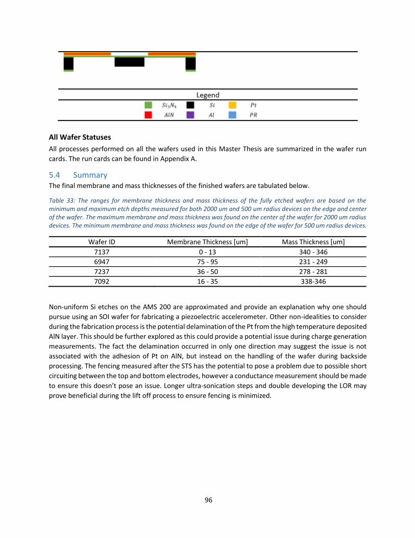
96
All Wafer Statuses
All processes performed on all the wafers used in this Master Thesis are summarized in the wafer run
cards. The run cards can be found in Appendix A.
5.4 Summary The final membrane and mass thicknesses of the finished wafers are tabulated below.
Table 33: The ranges for membrane thickness and mass thickness of the fully etched wafers are based on the minimum and maximum etch depths measured for both 2000 um and 500 um radius devices on the edge and center of the wafer. The maximum membrane and mass thickness was found on the center of the wafer for 2000 um radius devices. The minimum membrane and mass thickness was found on the edge of the wafer for 500 um radius devices.
Wafer ID Membrane Thickness [um] Mass Thickness [um]
7137 0 - 13 340 - 346
6947 75 - 95 231 - 249
7237 36 - 50 278 - 281
7092 16 - 35 338-346
Non-uniform Si etches on the AMS 200 are approximated and provide an explanation why one should
pursue using an SOI wafer for fabricating a piezoelectric accelerometer. Other non-idealities to consider
during the fabrication process is the potential delamination of the Pt from the high temperature deposited
AlN layer. This should be further explored as this could provide a potential issue during charge generation
measurements. The fact the delamination occurred in only one direction may suggest the issue is not
associated with the adhesion of Pt on AlN, but instead on the handling of the wafer during backside
processing. The fencing measured after the STS has the potential to pose a problem due to possible short
circuiting between the top and bottom electrodes, however a conductance measurement should be made
to ensure this doesn’t pose an issue. Longer ultra-sonication steps and double developing the LOR may
prove beneficial during the lift off process to ensure fencing is minimized.

97
6 Conclusion This project explored the various types of accelerometers and their role as vibrometers in harsh
environments. Commercial and scientific literature accelerometers were compared which resulted in
selecting the piezoelectric charge output accelerometer that utilizes the bending mode in a circular
geometry as the best accelerometer for this application. Analytical equations were discussed to provide
first approximations for the displacement, resonant frequency, and charge generation of the selected
accelerometer design. Thereafter, COMSOL was then used to provide a more realistic model which was
compared to the analytical equations to ensure the FEM was working as expected.
The material selection for the accelerometer was based on the materials readily available in the CMi
cleanroom. From the COMSOL model, a Si membrane, Si mass, and AlN piezoelectric layer was selected
for both the high and low frequency applications. A novel accelerometer design was also explored which
utilized a layer of SU-8 on top of 𝑆𝑖3𝑁4 to maximize the charge generation.
Process flows for the Si accelerometer and SU-8 on 𝑆𝑖3𝑁4 accelerometer were developed and carried out
in the CMi cleanroom. Several non-idealities occurred during the process flow which resulted in non-
uniform membranes, delamination of Pt on one of the wafers, and fencing.
For future work, characterization of the devices is required. The thermomechanical noise should be
measured to determine the resonant frequency of the devices. Additionally, the conductance across the
top and bottom electrode should also be measured to ensure fencing is not an issue. The charge
generation of the device should also be measured, as well as the bandwidth and dynamic range of the
device. These measurements will provide good experimental data to compare with the analytical and
COMSOL models.

98
References [1] Badri, Abdellatef EO, and Jyoti K. Sinha. Performance Improvement of MEMS Accelerometers in Vibration Based Diagnosis. Diss. University of Manchester, 2011. [2] Beeby, S. P., N. Ross, and N. M. White. "Thick film PZT/micromachined silicon accelerometer." Electronics Letters 35.23 (1999): 2060-2062. [3] J. Blaauwendraad, Plates and FEM: Surprises and Pitfalls, Solid Mechanics and Its Applications 171,
DOI 10.1007/978-90-481-3596-7_2, © Springer Science+Business Media B.V. 2010
[4] Brown, T. Gordon. "Harsh military environments and microelectromechanical (MEMS) devices."
SENSORS, 2003 IEEE. Vol. 2. IEEE, 2003.
[5] Büsching, Felix, et al. "Comparison and validation of capacitive accelerometers for health care
applications." Computer methods and programs in biomedicine 106.2 (2012): 79-88.
[6] Caliò, Renato, et al. "Piezoelectric energy harvesting solutions." Sensors 14.3 (2014): 4755-4790. [7] Chen, N., and V. Bedekar. "Modeling, simulation and optimization of piezoelectric bimorph transducer
for broadband vibration energy harvesting." J. Mater. Sci. Research 6.4 (2016): 5-18.
[8] Chollet, Franck, and Haobing Liu. "A (not so) short introduction to Micro Electro Mechanical Systems."
Creative Commons Publisher, version 5 (2012).
[9] Domínguez-Pumar, Manuel, Joan Pons-Nin, and Juan A. Chávez-Domínguez. "MEMS technologies for
energy harvesting." Nonlinearity in Energy Harvesting Systems. Springer, Cham, 2016. 23-63.
[10] Dong, Lin, Michael Grissom, and Frank T. Fisher. "Resonant frequency of mass-loaded membranes for vibration energy harvesting applications." AIMS Energy 3.3 (2015): 344-359. [11] Dubois, Marc-Alexandre, and Paul Muralt. "Stress and piezoelectric properties of aluminum nitride thin films deposited onto metal electrodes by pulsed direct current reactive sputtering." Journal of Applied Physics 89.11 (2001): 6389-6395. [12] Elies, S., and S. Ebenhoch. "Performance analysis of commercial accelerometers of different technologies." Proceedings of the 16th International Conference on Sensor Device Technologies and Applications. 2015. [13] Gesing, Andre Loch, et al. "Middle ear ossicular chain vibration detection by means of an optimized MEMS piezoelectric accelerometer." IEEE Sensors Journal 19.6 (2018): 2079-2086. [14] Gesing, A. L., et al. "On the design of a MEMS piezoelectric accelerometer coupled to the middle ear
as an implantable sensor for hearing devices." Scientific reports 8.1 (2018): 3920.
[15] Gupta, Nidhi, et al. "Influence of residual stress on performance of AlN thin film based piezoelectric
MEMS accelerometer structure." Microsystem Technologies (2019): 1-9.

99
[16] T. Hehn and Y. Manoli, CMOS Circuits for Piezoelectric Energy Harvesters, Springer Series in Advanced
Microelectronics 38, DOI 10.1007/978-94-017-9288-2_2, © Springer Science+Business Media Dordrecht
2015
[17] Heywang, Walter, Karl Lubitz, and Wolfram Wersing, eds. Piezoelectricity: evolution and future of a technology. Vol. 114. Springer Science & Business Media, 2008. [18] Hindrichsen, Christian Carstensen, et al. "Circular piezoelectric accelerometer for high band width
application." SENSORS, 2009 IEEE. IEEE, 2009.
[19] Hooker, Matthew W. "Properties of PZT-based piezoelectric ceramics between-150 and 250 C." (1998). [20] Irvine, Tom, Configuration Frequency Hz, and Fixed-Fixed Same as Free-Free. "Bending frequencies
of beams, rods, and pipes–revision S." Compare 500 (2012): 50.
[21] Jiguet, Sébastien, et al. "Effect of filler behavior on nanocomposite SU8 photoresist for moving micro-parts." Microelectronic engineering 83.4-9 (2006): 1273-1276. [22] Kollias, A. T., and J. N. Avaritsiotis. "A study on the performance of bending mode piezoelectric
accelerometers." Sensors and Actuators A: Physical 121.2 (2005): 434-442.
[23] Kosheleva, Natalia, et al. "Development of a Simplified Numerical Model for the Design of 2G High-Temperature Superconductors." IEEE Transactions on Applied Superconductivity 26.3 (2016): 1-5. [24] Lee, D. S. "Thermal accelerometer based predictive drop sensor." Sensors and Actuators A: Physical 135.2 (2007): 889-894. [25] Liu, Bin. "Transducers for Sound and Vibration-FEM Based Design." (2001). [26] J. Ma, “Advanced MEMS-based technologies and displays,” vol. 37, pp. 2–10, 2015.
[27] Narasimhan, Vinayak, Holden Li, and M. Jianmin. "Micromachined high-g accelerometers: a review."
Journal of Micromechanics and Microengineering 25.3 (2015): 033001.
[28] Rebello, Joel. Design and analysis of a MEMS vibration sensor for automotive mechanical systems.
University of Toronto, 2009.
[29] Rong, Qiangzhou, et al. "Highly sensitive fiber-optic accelerometer by grating inscription in specific
core dip fiber." Scientific reports 7.1 (2017): 11856.
[30] Sawsen, Rouabah, and Chaabi Abdelhafid. "Simulation of Piezoelectric Nanofibers for Harvesting Energy Applications." [31] Schmid, Silvan, Luis Guillermo Villanueva, and Michael Lee Roukes. Fundamentals of nanomechanical
resonators. Vol. 49. Springer International Publishing, 2016.
[32] W.K. Schomburg, Introduction to Microsystem Design, RWTHedition, DOI 10.1007/978-3-642-19489-
4_6, # Springer-Verlag Berlin Heidelberg 2011

100
[33] Tadigadapa, S., and K. Mateti. "Piezoelectric MEMS sensors: state-of-the-art and perspectives." Measurement Science and technology 20.9 (2009): 092001. [34] Tahmasebipour, Mohammad, and Ali Vafaie. "A Highly Sensitive Three Axis Piezoelectric
Microaccelerometer for High Bandwidth Applications." Micro and Nanosystems 9.2 (2017): 111-120.
[35] Walter, Patrick L. "The history of the accelerometer: 1920s-1996-prologue and epilogue, 2006."
Sound & vibration 41.1 (2007): 84-90.
[36] Wang, Qing-Ming, et al. "Analysis of thin film piezoelectric microaccelerometer using analytical and
finite element modeling." Sensors and Actuators A: Physical 113.1 (2004): 1-11.
[37] Williams, Matthew D. Development of a MEMS piezoelectric microphone for aeroacoustic
applications. Diss. University of Florida, 2011.
[38] Wygant, Ira O., Mario Kupnik, and Butrus T. Khuri-Yakub. "Analytically calculating membrane
displacement and the equivalent circuit model of a circular CMUT cell." 2008 IEEE Ultrasonics Symposium.
IEEE, 2008.
[39] Yaghootkar, Bahareh, Soheil Azimi, and Behraad Bahreyni. "A high-performance piezoelectric
vibration sensor." IEEE Sensors Journal 17.13 (2017): 4005-4012.
[40] Young, Warren Clarence, Richard Gordon Budynas, and Ali M. Sadegh. Roark's formulas for stress and strain. Vol. 7. New York: McGraw-Hill, 2002.
[41] APC International, Ltd. Piezoelectric ceramics: principles and applications. APC International, 2002. [42] “Center of MicroNanoTechnology CMi.” CMi, cmi.epfl.ch/.
[43] Weber, Manfred. “Vibration Measurement.” Vibration Measurement, Metra Mess- Und
Frequenztechnik, 4 Apr. 2019, www.mmf.de/.
[44] “Properties.” AZoM.com, Granta Design Limited and Ceram Research Limited, www.azom.com/ .
[45] Abreu, Gustavo LCM, José F. Ribeiro, and Valder Steffen Jr. "Experiments on optimal vibration control
of a flexible beam containing piezoelectric sensors and actuators." Shock and vibration 10.5-6 (2003): 283-
300.
[46] “Ceramic Materials (PZT) - Boston Piezo-Optics Inc.” Boston Piezo Optics Inc.,
bostonpiezooptics.com/ceramic-materials-pzt. “Efficiently Mesh Your Model Geometry with
Meshing Sequences.” COMSOL Multiphysics, www.comsol.com/blogs/efficiently-mesh-your-
model-geometry-with-meshing-sequences/.
[47] “Accelerometers - Meggitt - Enabling the Extraordinary.” Meggitt, Emperor & ID,
www.meggitt.com/products-services/accelerometers/.
[48] “Utilizing Piezoelectricity and Photovoltaics to Increase Hybrid Car Efficiency.” Tired Tires,
dev.nsta.org/evwebs/2014102/news/default.html.

101
[49] “Efficiently Mesh Your Model Geometry with Meshing Sequences.” COMSOL Multiphysics,
www.comsol.com/blogs/efficiently-mesh-your-model-geometry-with-meshing-sequences/.
[50] “Accelerometers.” MSS, buy.endevco.com/accelerometer.html?applications=NaN.
[51] “Accéléromètres.” Accéléromètres | Kistler,
www.kistler.com/fr/produits/composants/accelerometres/.
[52] “Accelerometers/Vibration Sensors.” Accelerometers - Sensors for Shock, Vibration and
Acceleration, www.pcb.com/TestMeasurement/Accelerometers.

102
Appendix

EPFL Center of MicroNanoTechnology
Batch 3 Wafer 7237 6/21/2019 Page 1/
Projet : Piezoelectric Accelerometer + SU8Operator : Bradley PetkusCreated : 24.05.19 Last revision : 09.05.19Substrates : Silicon 100/P/DS/1-10 TTV2 & Wet oxide 500nm / PME
Step N° Description Equipment Program / Parameters Target Actual Remarks Name Date
0 WAFER PREPARATION0.1 Stock out 0.2 Check 1 PHOTOLITHOGRAPHY - GND Electrode Front Side Mask1.1 Dehydratation Z6/EVG150 1.2 AZ 1512 Coating Z6/EVG150 AZ1512_on_LOR_400nm_NoEBR 1.1 um1.3 PR bake Z6/EVG150 1.4 PR expose Z16/MLA150 Petkus_Accelerometer_FirstLayer 75 mJ/cm2 -2 Defocus Mode: Quality, 24 min/Wafer1.5 PR develop Z6/EVG1501.6 Inspection Z6/uScope Resolution and alignment 2 SPUTTER2.1 AlN Deposition Z4/ Spyder600 1500 W, 18 sec 15 nm2.2 Pt Deposition Z4/ Spyder600 1000 W, 11 sec (Room Temp) 50 nm2.3 Inspection Z6/uScope+Z4/Profilometer3 LIFT-OFF3.1 Remover 1165 Z1/ Plade_Solvent PT 1 1.5 Days3.2 Remover 1165 + US Z1/ Plade_Solvent Bac US 1 min If needed3.3 IPA Z1/ Plade_Solvent PT 2 2 mins For inspection3.4 Fast Fill Rinse Z1/ Plade_Solvent DI Rinse3.5 Trickle tank Z1/ Plade_Solvent DI Rinse3.6 Optical Inspection Z6/ uScope
4 SPUTTER4.1 AlN Deposition Z4/ Spyder600 1500 W, 100 sec (300 C) 100 nm 1 nm/s4.2 Pt Deposition Z4/ Spyder600 1000 W, 11 sec (Room Temp) 50 nm4.3 Inspection Z6/uScope+Z4/Profilometer fencing!
5 PHOTOLITHOGRAPHY - Top Electrode Front Side Mask5.1 Dehydratation Z6/EVG150
AZ9260_5um_NoEBR
5.2 AZ 9260 Coating Z6/EVG150 5 um5.3 PR bake Z6/EVG150 5.4 PR expose Z16/MLA1505.5 PR develop Z6/EVG1505.6 DI Rinse Z6/Wetbench 15 sec DI Spin Dry/N2 Gun5.7 PR PEB Z13/SU8 Hotplate 85 C, 3 hrs5.8 Inspection Z6/uScope+Z4/Profilometer
6 Metal Etch6.1 Pt Etch Z2/STS Aln_set 50 nm6.2 AlN Etch Z2/STS Aln_set 100 nm 1 min 50 sec

EPFL Center of MicroNanoTechnology
Batch 3 Wafer 7237 6/21/2019 Page 2/
Projet : Piezoelectric Accelerometer + SU8Operator : Bradley PetkusCreated : 24.05.19 Last revision : 09.05.19Substrates : Silicon 100/P/DS/1-10 TTV2 & Wet oxide 500nm / PME
Step N° Description Equipment Program / Parameters Target Actual Remarks Name Date
6.3 Inspection Z15/Filmetrics SiO2 on Si <490 nm 472 nm7 PR Strip
7.1 Plasma O2 clean Z2/Tepla GiGabatch PR_Strip_High_Power_2min7.2 Remover 1165 Z2/UFT_Resist Bath 1 : main remover 5min, 70°C7.3 Remover 1165 Z2/UFT_Resist Bain 2 : clean remover 55min, 70°C7.4 Fast fill rinse Z2/UFT_Resist DI Rinse7.5 Trickle tank Z2/UFT_Resist DI Rinse7.6 Plasma O2 clean Z2/Tepla GiGabatch PR_Strip_High_Power_2min needs UFT 2x7.7 Inspection Z6/uScope Pr burnt from STS
8 Al Evaporation8.1 Remover 1165 Z11/Evap760 250_Al_160 20 kA (2 um) about 2.5 um8.2 Optical Inspection Z1/ uScope
9 PHOTOLITHOGRAPHY - SiO2 Back Side Mask9.1 Dehydratation Z6/EVG150
AZ9260_5um_NoEBR
9.2 AZ 9260 Coating Z6/EVG150 5 um9.3 PR bake Z6/EVG150 9.4 PR expose Z16/MLA150 350 mJ/cm2 Defoc:2 Petkus_accel_SiO2BS9.5 PR develop Z6/EVG1509.6 DI Rinse Z6/Wetbench 15 sec DI Spin Dry/N2 Gun9.7 PR PEB Z13/SU8 Hotplate 85 C, 3 hrs9.8 Inspection Z6/uScope+Z4/Profilometer Resolution and alignment10 Oxide Plasma Etch- Fluorine Chemistry
10.1 SiO2 Etch Z2/AMS200 SiO2_PR_1:1 500nm 117 sec 10s Overetch (280 nm/min)10.2 Inspection Z15/Filmetrics+Z4/Profilometer
11 RESIST STRIP11.1 Remover 1165 Z2/UFT_Resist Bath 1 : main remover 5min, 70°C11.2 Remover 1165 Z2/UFT_Resist Bain 2 : clean remover 55min, 70°C11.3 Fast fill rinse Z2/UFT_Resist DI Rinse11.4 Trickle tank Z2/UFT_Resist DI Rinse11.5 Inspection Z2/uScope
12 PHOTOLITHOGRAPHY - Si Back Side Mask 12.1 Dehydratation Z6/EVG150
AZ9260_5um_NoEBR
12.2 AZ 9260 Coating Z6/EVG150 5 um12.3 PR bake Z6/EVG150 12.4 PR expose Z16/MLA150 350 mJ/cm2 Defoc:2 Petkus_accel_SiBS12.5 PR develop Z6/EVG150

EPFL Center of MicroNanoTechnology
Batch 3 Wafer 7237 6/21/2019 Page 3/
Projet : Piezoelectric Accelerometer + SU8Operator : Bradley PetkusCreated : 24.05.19 Last revision : 09.05.19Substrates : Silicon 100/P/DS/1-10 TTV2 & Wet oxide 500nm / PME
Step N° Description Equipment Program / Parameters Target Actual Remarks Name Date
12.6 DI Rinse Z6/Wetbench 15 sec DI Spin Dry/N2 Gun12.7 PR PEB Z13/SU8 Hotplate 85 C, 3 hrs12.8 Inspection Z6/uScope+Z4/Profilometer Resolution and alignment <1 um misalignment
13 Si Plasma Etch-Fluorine Chemistry
13.1 Si Etch Z2/AMS200 SOI_accurate 275 um271.5 to 276.5 um 62'30''
13.2 Inspection Z4/Profilometer14 RESIST STRIP
14.1 Remover 1165 Z2/UFT_Resist Bath 1 : main remover 5min, 70°C14.2 Remover 1165 Z2/UFT_Resist Bain 2 : clean remover 55min, 70°C14.3 Fast fill rinse Z2/UFT_Resist DI Rinse14.4 Trickle tank Z2/UFT_Resist DI Rinse14.5 Inspection Z2/uScope
15 Si Plasma Etch-Fluorine Chemistry15.1 Si Etch Z2/AMS200 SOI_accurate 37 um 8'24''15.1 Si Etch Z2/AMS200 SOI_accurate 30 um 6'49''
15.2 Inspection Z4/Profilometer 342 um337-352 um
16 Al Etch (Frontside)16.1 Si Etch Z2/Plade Wet Bench ANP chemistry 2 um 10 min 300 nm/min16.2 Inspection Z4/Profilometer

EPFL Center of MicroNanoTechnology
Batch 3 Wafer 7237 6/21/2019 Page 4/

EPFL Center of MicroNanoTechnology
Batch 3 Wafer 7237 6/21/2019 Page 5/

EPFL Center of MicroNanoTechnology
Batch 3 Wafer 7237 6/21/2019 Page 6/

Appendix B – Silicon Nitride Membrane COMSOL Data

Z-Offset [um] Electrode Thickness [um] PZE Thickness [um] Elec/Memb Ratio Mass/Memb Ratio Material (Membrane/PZE/Elec)
5 1.02 0.05 0.738888889 0.466666667 SiN/AlN/Al
5 0.025 0.05 0.738888889 0.466666667 SiN/AlN/Al
2.5 0.025 0.05 0.738888889 0.466666667 SiN/AlN/Al
0.5 0.025 0.05 0.738888889 0.466666667 SiN/AlN/Al
0.25 0.025 0.05 0.738888889 0.466666667 SiN/AlN/Al
0.1 0.025 0.05 0.738888889 0.466666667 SiN/AlN/Al

Stress [Mpa] Device Radius [um] Membrane Thickness [um] Max Displacement [m/g] Resonant Frequency [kHz] Charge [fC/g]
168 900 10 2.10E-10 34.6 12.6
168 900 10 2.18E-10 33.9 11.7
168 900 5 5.89E-10 20.6 14.5
168 900 1 3.57E-09 8.341 15.1
168 900 0.5 7.30E-09 5.8 15.7
168 900 0.2 1.85E-08 3.66 17.6