Novel Piezoelectric-Based Power Supply for Driving Piezoelectric Actuators Designed for Active...
14
Journal of Electroceramics, 7, 197–210, 2001 C 2002 Kluwer Academic Publishers. Manufactured in The Netherlands. Novel Piezoelectric-Based Power Supply for Driving Piezoelectric Actuators Designed for Active Vibration Damping Applications ALFREDO V ´ AZQUEZ CARAZO 1,2 & KENJI UCHINO 1 1 International Center for Actuators and Transducers, Materials Research Institute, The Pennsylvania State University, University Park, PA 16802, USA 2 Department of Research and Development Engineering, Face Electronics, LC, 427 W. 35th Street, Norfolk, Virginia 23508, USA Submitted March 13, 2001; Revised October 18, 2001; Accepted October 29, 2001 Abstract. This paper describes a novel step-up DC-AC piezoelectric-based power supply for driving piezoelectric actuators. Piezoelectric actuators have been demonstrated to be very attractive in applications requiring fast response and high actuation force, such as active damping applications. These actuators are commonly installed in self- powered systems (cars, helicopters, aircrafts, satellites, etc.) with limitation in the battery performance, dimensions and maximum weight. Nevertheless, the required driving electrical AC voltage for these actuators is typically in the range of 100 V to 1000 V, quite far from the 9 to 24 V of common batteries. Thus, the use of heavy, large and EMI- noisy electromagnetic transformers becomes necessary which is a drawback for the compact size required. This paper introduces an alternative system for driving piezoelectric actuators using a novel design of piezoelectric transformer, the Transoner R . The proposed solution allows a reduction in size, weight and magnetic noise generation compared to the classical electromagnetic-based systems. The work represents a completely novel approach to the possibilities of piezoelectric transformers for powering high voltage piezoelectric actuators. The solution offers significant advantages in environments requiring high integration, low weight, and low electromagnetic interferences operated with batteries. A circuit configuration capable of converting a 24 V DC input voltage up to 600 V pp AC output voltage with frequency and magnitude control is implemented. Experimental results are presented for a standard multilayer piezoelectric actuator driven at 100 V pp within the range of 10 Hz to 500 Hz. Keywords: piezoelectric transformer, Transoner R , piezoelectric actuator, piezoelectric converter, active vibration systems 1. Introduction Two basic techniques have been developed within the prior art in order to damp the noise and vibrations in air- craft and space applications: passive and active attenu- ation systems (Fig. 1). Passive vibration reduction sys- tems have proved to be successful in the past and they are still widely used in many applications. However, recent reductions in the cost and size of digital comput- ers, and advances in control system technology, have made active vibration systems viable. Passive attenuation systems include passive blan- kets, passive Tuned Vibration Absorbers (TVAs) and adaptative TVAs [1, 2]. In these systems, barrier ab- sorbent materials in the fuselages are used to damp the vibrations from the main gear rotor to the cabin. Barrier materials must be relatively dense to be effective in ab- sorbing mechanical vibrations. The higher the density of the material the greater the weight. Thus, the addition of weight to the fuselage of an aircraft to enhance vibra- tion absorption has the adverse effect of reducing fuel economy, payload, and flight range. Passive systems are relatively simple, they have no direct power supply requirements and they have good stability. However, they are only effective for a particular frequency or for a very narrow range of frequencies. Thus, they tend to be characterized by a lack of adaptability with respect to changes in flight conditions, rotor rotational frequency and changes in structural dynamics (due to cargo, fuel and passenger changes), and this is a particularly severe
-
Upload
independent -
Category
Documents
-
view
0 -
download
0
Transcript of Novel Piezoelectric-Based Power Supply for Driving Piezoelectric Actuators Designed for Active...

Journal of Electroceramics, 7, 197–210, 2001C© 2002 Kluwer Academic Publishers. Manufactured in The Netherlands.
Novel Piezoelectric-Based Power Supply for Driving PiezoelectricActuators Designed for Active Vibration Damping Applications
ALFREDO VAZQUEZ CARAZO1,2 & KENJI UCHINO1
1International Center for Actuators and Transducers, Materials Research Institute, The Pennsylvania State University,University Park, PA 16802, USA
2Department of Research and Development Engineering, Face Electronics, LC, 427 W. 35th Street, Norfolk, Virginia 23508, USA
Submitted March 13, 2001; Revised October 18, 2001; Accepted October 29, 2001
Abstract. This paper describes a novel step-up DC-AC piezoelectric-based power supply for driving piezoelectricactuators. Piezoelectric actuators have been demonstrated to be very attractive in applications requiring fast responseand high actuation force, such as active damping applications. These actuators are commonly installed in self-powered systems (cars, helicopters, aircrafts, satellites, etc.) with limitation in the battery performance, dimensionsand maximum weight. Nevertheless, the required driving electrical AC voltage for these actuators is typically in therange of 100 V to 1000 V, quite far from the 9 to 24 V of common batteries. Thus, the use of heavy, large and EMI-noisy electromagnetic transformers becomes necessary which is a drawback for the compact size required. This paperintroduces an alternative system for driving piezoelectric actuators using a novel design of piezoelectric transformer,the Transoner©R. The proposed solution allows a reduction in size, weight and magnetic noise generation compared tothe classical electromagnetic-based systems. The work represents a completely novel approach to the possibilitiesof piezoelectric transformers for powering high voltage piezoelectric actuators. The solution offers significantadvantages in environments requiring high integration, low weight, and low electromagnetic interferences operatedwith batteries. A circuit configuration capable of converting a 24 V DC input voltage up to 600 Vpp AC outputvoltage with frequency and magnitude control is implemented. Experimental results are presented for a standardmultilayer piezoelectric actuator driven at 100 Vpp within the range of 10 Hz to 500 Hz.
Keywords: piezoelectric transformer, Transoner©R, piezoelectric actuator, piezoelectric converter, active vibrationsystems
1. Introduction
Two basic techniques have been developed within theprior art in order to damp the noise and vibrations in air-craft and space applications: passive and active attenu-ation systems (Fig. 1). Passive vibration reduction sys-tems have proved to be successful in the past and theyare still widely used in many applications. However,recent reductions in the cost and size of digital comput-ers, and advances in control system technology, havemade active vibration systems viable.
Passive attenuation systems include passive blan-kets, passive Tuned Vibration Absorbers (TVAs) andadaptative TVAs [1, 2]. In these systems, barrier ab-sorbent materials in the fuselages are used to damp the
vibrations from the main gear rotor to the cabin. Barriermaterials must be relatively dense to be effective in ab-sorbing mechanical vibrations. The higher the densityof the material the greater the weight. Thus, the additionof weight to the fuselage of an aircraft to enhance vibra-tion absorption has the adverse effect of reducing fueleconomy, payload, and flight range. Passive systemsare relatively simple, they have no direct power supplyrequirements and they have good stability. However,they are only effective for a particular frequency or fora very narrow range of frequencies. Thus, they tend tobe characterized by a lack of adaptability with respect tochanges in flight conditions, rotor rotational frequencyand changes in structural dynamics (due to cargo, fueland passenger changes), and this is a particularly severe

198 Vazquez Carazo and Uchino
Fig. 1. Passive and active damping systems.
limitation. In addition, passive dampers are effective inattenuating high frequency noise and vibration but theymust be very massive if low frequency signals have tobe eliminated.
In applications where a higher level of vibration at-tenuation is desired, active vibration systems [3–7] pro-vide alternative means of controlling the disturbanceswithin the aircraft’s cabin. Active systems offer the po-tential to meet increasingly stringent comfort require-ments over significant areas of the aircraft structure.In principle, active vibration systems include actuatorsto provide the active control forces for isolating vi-bration. Known active systems include reference sig-nals, such as from accelerometers or vibration sen-sors, to provide a reference signal of the vibrationsof engines. A controller processes the reference sig-nals to generate drive signals of the appropriate phaseand magnitude (anti-vibration) to reduce vibrationtransmission.
Piezoelectric actuators have been demonstrated tobe a reliable solution for active damping applicationsdue to their fast response and high actuation force [8, 9].Particularly, this type of actuator has been consideredin helicopter applications for reducing the vibrationalnoise and enhancing the comfort of the pilot and per-formance of the devices located in the cabin. However,two important issues [10, 11] in using piezoelectric ac-tuators for active control are: (1) the high electric volt-age and significant power required for these devices,and (2) the complexities involved with active control(added hardware, control law design, and implementa-tion). In this paper we describe a novel solution for thefirst issue.
Solid State Actuators made with piezoelectricmaterials have evolved greatly in the last decade.Piezoelectric actuators include multilayer actua-tors, unimorphs, bimorphs, multimorph actuators,MOONIES, CYMBALL, RAINBOW, CRESCENT,and THUNDER©R [9, 12]. We have chosen a standardmultilayer actuator for implementing the proposed con-verter, but the solution is extended to all existingactuator technologies.
Typically, piezoelectric actuators require an ACdriving electrical voltage in the range of 100 Vmax (lowvoltage actuators) to 1000 Vmax (high voltage actuators)[9]. Nevertheless, the battery level in helicopters andother similar self-powered systems is set in the rangeof 24 V DC. Thus, step-up conversion is necessary inorder to drive the piezoelectric actuator. This task is typ-ically made with heavy, large, and electromagneticallynoisy electromagnetic transformers. This represents aserious drawback for the general performance of thehelicopters. Thus, an objective in the existing activedamping systems for helicopter and aircraft applica-tions is focused on replacing the conventional magnetictransformer for a lighter, smaller and electromagneti-cally compatible device.
A very promising alternative to the electromag-netic transformer for compact, light, no electromag-netic noise, non-flammable, and high efficiency de-manding applications is the piezoelectric transformer(PT). C.A. Rosen described the first piezoelectric trans-former, PT, in 1956 [13, 14]. Since then, PTs have beensuccessfully applied in high voltage applications, suchas inverters to light up the cold cathode fluorescentlamps (CCFL) for backlighting the color liquid crystaldisplays (LCD) in laptop computers applications [15],with typical equivalent impedance of 100 k� or more.However, under such conditions the power capabilitiesof this PT is very low, around 5 to 10 W, with powerdensities limited to 5 W/cm3. This low power capabilitymakes these transformers useless for power conversionapplications. Thus, a new PT with high power transferperformance is required for power converter applica-tions. A novel concept of PTs, Transoner©R [16, 17],has recently been proposed by Face Electronics, LC,Virginia, USA, for achieving high power transfer de-mands. Consequently, Transoners are particularly welladapted to power converter applications requiring highpower densities, small size, low weight, isolation be-tween primary and secondary and low electromagneticinterferences. Currently, Transoners are manufacturedto achieve power levels up to 110 W and power densities

Novel Piezoelectric-Based Power 199
higher than 40 W/cm3. A sample of Transoner has beensuccessfully used in this application.
The authors propose a novel DC-AC converter usinga piezoelectric transformer for driving piezoelectricactuators. The piezoelectric-based converter consistsof three main blocks: (i) a resonant inverter which con-verts the battery DC voltage into an AC voltage; (ii) ahigh power piezoelectric transformer driven at AC res-onant voltage which amplifies the AC output voltageregarding to the input one; (iii) a half-bridge PWMinverter which generates the driving actuator signalthrough an inductive filter. The proposed system is im-plemented and the experimental results are shown.
2. Design Considerations
2.1. Spectrum of the Vibrations in a Helicopter
The blades of a helicopter are subjected to periodicalternating forces. These forces cause stresses and re-actions in the hub of the rotor and significant bendingand torsional moments applied to the shaft of the ro-tor. These alternating stresses are repeated regularly oneach revolution of the rotor and induce, essentially, hor-izontal and vertical vibrations which propagate throughthe fuselage. Particularly, these vibrations are very sub-stantial in the cockpit of the aircraft. The vibrationsthus generated represent an important drawback in he-licopter applications since they can: (i) limit the max-imum speed of the aircraft, (ii) weaken its structuralstrength, (iii) impair the comfort of the occupants ofthe aircraft and (iv) significantly affect essential con-trol devices for safe navigation, such as the automaticpilot or the helicopter electrical or nocturnal flightcontrol.
In forward flight, the rotor blade experiences asym-metrical loading during each revolution and due tothese oscillatory air loads the blade response is richin harmonic content. In transferring from the rotatingframe to the fixed fuselage frame most of the forces andmoments generated at the rotor head cancel, while theremainder coalesce into the blade passing frequency,nω (where n is the number of blades and ω is the ro-tational speed of the rotor). Consequently, the fuselagevibration spectrum is dominated by the blade pass-ing frequency nω, its harmonics, and subharmonics.Typically, the targeted vibrations have the fundamen-tal frequency between 50–100 Hz, with the next highermodes ranging up to 400–600 Hz [10, 18]. In this work
we consider an actuation spectrum between 10 Hz upto 500 Hz.
2.2. Actuator Power Requirements
A critical issue that arises when using piezoelectricactuators is the electric power consumption necessaryto drive them. Applications are found to depend uponthe electrical characteristics of the PZT transducers,namely the capacitive and resistive behavior of the ac-tuator, which in turn affect their power consumptioncharacteristics. When operated far below the resonantfrequency a piezoelectric actuator behaves as a capac-itive load. This is the case of the present applicationsince the majority of helicopter vibrations occur at lowfrequency away from the resonance range of the actu-ator. In such conditions, the displacement generated inthe actuator is, in a first approximation, proportional tothe electric charge. An equivalent circuit of the piezo-electric actuator is shown in Fig. 2, where the paral-lel resistance represents the dielectric losses of the ac-tuator. Dielectric losses can be estimated through thedielectric dissipation factor of the actuator, tgϕ [19],defined as the tangent of the loss angle (the ratio ofthe parallel resistance to the parallel reactance). Typ-ically, the dissipation factor is in the range of 0.2 to0.5%. Thus, the actuator basically behaves, in a firstapproximation, as a reactive load.
Another aspect to consider in the evaluation of thepower consumption of the piezoelectric actuator is thedependence of its capacitance on the electrical and me-chanical conditions. A number of researchers have in-vestigated the power consumption characteristics ofPZT actuators used for active damping. Research by
Fig. 2. Equivalent circuit for a piezoelectric actuator operatingoff-resonance.
200 Vazquez Carazo and Uchino
Brennan and McGowan [20] shows that the powerconsumption of piezoelectric materials used for ac-tive vibration control is independent of the mechanicalmotion of the host structure when the structure is com-pletely controlled. From these findings, they concludethat the power requirements of the piezoelectric actu-ator are only dependent upon its geometry, materialproperties, and the driving voltage and frequency ofthe control signal. Nevertheless, they also note a linearvariation of the capacitance of the actuator with the ap-plied field, which can be important to avoid large errorsin predicting power requirements. Jordan et al. ana-lyzed these non-linearities for PZT-5A based-actuatorsin reference [21]. In this paper, we will estimate thereactive power required for the actuator. A more exten-sive analysis including active power (mechanical powerand losses in the actuator and the switching amplifier)is postponed for a future work.
In order to estimate the reactive power required, weassume that the actuator is driven with a unipolar si-nusoidal wave. This is a general practice to limit therisk of depolarization and also to reduce the fatigue ofthe actuator. Voltage, current and reactive power in theactuator are obtained in Eqs. (1) to (4):
v(t) = Vpp
2[1 − cos(2π · f · t)] (1)
i(t) = Vpp · C · π · f · sin(2π · f · t) (2)
p(t) = v(t) · i(t) = V 2pp
2· C · π · f · [sin(2π · f · t)
− sin(2π · f · t) · cos(2π · f · t)] (3)
Pavg = 1
T
∫ T
0v(t) · i(t) · dt = V 2
pp · C · f (4)
where v(t), i(t) and p(t) are the time-domain expres-sions for the current, voltage and instantaneous reactivepower in the actuator, Vpp is the voltage peak to peakand can be estimated as the DC voltage switched by theamplifier, C is the equivalent capacitance of the actua-tor (Fig. 2) and f is the frequency of the driving actu-ator signal. Pavg is the average reactive power, relatedto the steady-state conditions of charging/dischargingthe actuator.
2.3. Actuator Control and Driving Circuit
Space and aircraft applications have only a little spaceavailable. This limitation requires integrated amplifierswith a small number of external components and low
power dissipation. Traditional linear amplifiers (classesA, B, C) have been used so far for driving piezoelectricactuators [22]. These amplifiers operate below satura-tion and have low efficiency, high power consumption,and high power dissipation (needed for heat removal).The previous drawbacks limited the maximum possi-ble efficiency to 78.5% in class-B push-pull amplifiersfor a sine wave. In practice the actual efficiency of lin-ear amplifiers dropped typically up to 65% [23] forsine wave and is much lower (15–20%) for real refer-ence signals [24]. Switching amplifiers have appearedrecently as an alternative to linear amplifiers in appli-cations where high efficiency and lower consumptionare required [23–25]. The theoretical maximum effi-ciency for all types of switching amplifiers is 100% atall outputs. This fact makes these amplifiers attractivefor applications requiring high efficiency and reduceddimensions. The actual efficiency of these amplifiers inpractice is reduced typically to 85% for class D, E, or Famplifiers [23]. Recently, class-D amplifiers have beensuccessfully considered in active damping applicationsand other applications involving piezoelectric actuatorcontrol [26–29].
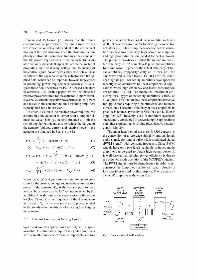
The main idea behind the class-D [30] concept isthe conversion of a reference signal (vibration signal,audio signal, etc.) into a pulse width modulated signal(PWM signal) with constant frequency. Since PWMsignals have only two levels, a simple switched modeamplifier can be used to obtain high output power. Itis well known that the high power efficiency is due tothe switched mode operation of the MOSFET switches.The PWM signal must be demodulated in order to re-construct the (amplified) reference signal. Usually alow pass filter is used for this purpose. The structure ofa class-D amplifier is shown in Fig. 3.
Fig. 3. Structure of a class-D amplifier.

Novel Piezoelectric-Based Power 201
Fig. 4. Piezoelectric-based power converter driving a piezoelectric actuator.
3. Operating Principle of the Proposed System
The developed piezoelectric power supply consistsof three power conversion stages, as is schematicallyshown in Fig. 4. For the particular approach consid-ered in this paper, we assume that the input main powersupply is a 24 V DC battery of the helicopter. Similaranalysis can be extended to different battery levels anddifferent applications.
3.1. First Stage: DC to AC Inverter for Drivingthe Piezoelectric Transformer
The battery voltage is led to a first resonant inverterwhich generates the driving input of the PT. The fre-quency of the resonant inverter is selected to excitethe first mechanical resonance of the PT. Under thiscondition, the piezoelectric transformer vibrates in itsfundamental radial mode and produces a large AC out-put voltage. Due to the high quality factor, Q, of thePT the output voltage is completely sinusoidal with thesame frequency as the PT’s input voltage.
3.2. Second Stage: AC to DC Rectifier
The output voltage from the piezoelectric transformeris rectified by using a single-phase diode bridge rectifierand filtered through an electrolytic capacitor in orderto obtain a DC voltage. Since the power supply has tobe kept relatively stable, the capacitor, C , is selected tobe at least 10 times the piezoelectric actuator capaci-tance. In addition, it is necessary to guarantee that the
piezoelectric transformer will deliver a constant out-put voltage independently of the load condition. Thisis achieved using a feedback frequency tracking circuitbetween the input and output of the piezoelectric trans-former which maintains the voltage constant. A moredetailed description on feedback techniques for piezo-electric transformer operating in DC/DC converter canbe found in reference [31].
3.3. Third Stage: DC to AC Inverter with Frequencyand Magnitude Control
The resultant DC voltage from the rectifier is switchedby the half-bridge amplifier to drive the actuator. Asshown in Fig. 4, the rectifier converts into a DCvoltage the AC output voltage from the piezoelec-tric transformer, and the inverter converts DC intoadjustable-magnitude, adjustable frequency AC signal.The filtering capacitor, C , is an energy storage elementand actuates as a DC link between the rectifier andthe output inverter. Frequency and magnitude actuatorcontrol are achieved using PWM technique from a ref-erence input signal from a vibration sensor. The signalarriving to the actuator is finally filtered through aninductance, which eliminates the high frequency com-ponents used for the PWM switching.
Figure 5 summarizes the proposed system applied tohelicopter vibration damping. A piezoelectric actuatoris used as an active vibration device. Vibration sensorscan be used to detect noise and/or vibration to be con-trolled within the pilot cabin. Actuators and sensors areelectrically connected to the driver/controller. The con-trol system, driver/controller, acts responsive to input

202 Vazquez Carazo and Uchino
Fig. 5. Particular application of the proposed system in active damp-ing for aircraft.
Fig. 6. Operation of the output DC/AC converter.
from the sensor to drive the actuator in a manner to re-duce or eliminate noise and/or vibration generated bythe vibrational energy sources (engines).
In the operation of the output inverter, Fig. 6, thepiezoelectric actuator is charged when the switch S1 isclosed and S2 is opened (Fig. 6(a)). A current, iL(t),is then established through the series circuit formed bythe switch S1, the inductance L , and the actuator. Thiscurrent flow causes energy to be stored in the induc-tance due to the positive potential difference betweenthe filtering capacitor and the actuator. The reactive en-ergy stored in the filtering capacitor C is then deliveredto the actuator. When the charging switch S1 is opened,Fig. 6(b), the current iL(t) continues flowing throughthe series circuit formed by the piezoelectric actuator,the inductance L , and the internal diode of the switchS2, diode D6. This energy flow causes all of the energystored in the inductance to flow into the piezoelectric
actuator. Thus, the voltage arising at the piezoelectricactuator (as well as its external dimensions) increasein response to the energy supplied to the actuator. Atthis point, the discharging switch, S2, is closed and theconditions indicated in Fig. 6(c) arise. A series circuitformed by the actuator, the inductance, and the switchS2 is then formed. Thus, the energy stored in the actua-tor is transferred to the inductance L and a current iL(t)is established as indicated in Fig. 6(c). The voltage aris-ing on the actuator, as well as its external dimensions,decreases in response to the energy transfer from the ac-tuator to the inductance. When the discharging switchS2 is then opened, the conditions indicated in Fig. 6(d)appear. In this situation, the energy flow causes the en-ergy stored in the inductance L to flow back into thecapacitor. Thus, the energy is exchanged between thepower supply and the piezoelectric actuator without,ideally, any losses. The driver circuit needs to be ableto charge and discharge the actuator capacitance for allthe voltage and frequency operation range. Particularly,switched amplifiers are able to recycle this energy withhigh efficiency, so that the needed line-power has onlyto cover the (much smaller) active part of the power bal-ance. This active power is (a) drawn from the systemas mechanical power, (b) dissipated by self heating ofthe actuator due to the dielectric losses, (c) dissipatedin the series resistance of the filtering inductance and(d) dissipated in the switches of the amplifiers duringthe “on” and “off” actuation.
4. Construction
4.1. Piezoelectric Actuator
The 10 × 10 × 20 mm3 multilayer actuator from TokinCorp. [32], was utilized as actuator for active control.Because the majority of spacecraft vibrations occur atlow frequencies, the capacitance and the dielectric dis-sipation of the actuator were measured from 1 Hz upto the first resonance peak. The NF 5090 FrequencyResponse Analyzer from NF Electronics Instruments,Japan, was used for measuring the admittance of thesample and thus evaluates the power consumption. Asinusoidal input voltage of 5 Vpp was used for the mea-surements. The admittance and phase curves are shownin Fig. 7. The capacitance measured was 6 µF for theoperating range up to 500 Hz.
The maximum required average power is estimatedusing Eq. (4) and considering the maximum operation

Novel Piezoelectric-Based Power 203
Fig. 7. Admittance and phase spectrum for the stack actuatorTOKIN-101016.
voltage and frequency. In our application, the frequencyrange is extended up to 500 Hz and the input voltage isexpected to be up to 100 Vpp, and then:
Pavg = V 2pp · C · f = 30 W (5)
Since an active damping actuator needs to operate indynamic conditions changing frequently the operationfrequency, it is also necessary to estimate the maxi-mum peak power required from the amplifier. This peakpower is associated with the peak current required tocharge and discharge the actuator in dynamic condi-tions:
Pmax = π · V 2pp · C · f = 94.24 W (6)
In addition to the power consumed by the actuator,the battery needs to supply power to the driving cir-cuitry (gates drivers, PWM function generator circuit,etc). This power, estimated to be less than 750 mW(±15 VDC under 25 mA), does not play a role in thepower transfer through the converter, since it was di-rectly taken from the main supplying battery with anauxiliary linear regulator.
4.2. High Power Piezoelectric Transformer:The Transoner©R
Transoner-type PTs differ from Rosen-type transform-ers in two key aspects: (a) the design and (b) the elec-tromechanical coupling between input and output parts.Transoners are constructed by multilayering single
individual disks in the thickness direction. Particularly,the output part consists of several thin layers connectedin parallel in order to have low impedance and thusachieve high power transfer characteristics under lowor medium loads (1 �–10 k� range), depending onthe selected design. Transoner is the first multilayertransformer developed which uses radial-extensionalvibration in the input and output parts. Transoners aretypically driving in their first radial-extensional vibra-tion mode. The vibrations under such conditions fol-low a Bessel function and are dependent on the inputand output radial coupling coefficient. Typically, forPZT-based materials, the radial electromechanical cou-pling coefficient is up to twice as high as the transver-sal coupling factor k31, typically used in Rosen-typetransformers. In addition, the coupling area betweenthe input and output layers is extended to all the sur-face area in comparison to the smaller transverse areain Rosen-type transformers. This makes larger the socalled “force factor” [31] of the transformer, which is ameasure of its power capabilities. Therefore, the powertransmission of Transoner-type transformers is greatlyimproved. An additional advantage of Transoner PTsis their simplicity to be designed with input and out-put isolated from each other, an important require-ment in applications involving full-bridge rectifiers(see Fig. 5). Figure 8 shows the isolated Transoner usedfor this application with 25 mm diameter and a totalthickness of 6 mm and power capabilities higher than70 W.
The NF 5090 Frequency Response Analyzer fromNF Electronic Instruments, Japan, was used for mea-suring the input and output voltages and currents. Thisequipment has the capability to acquire AC signals upto 200 V. Current was measured by using the AM503BAC/DC current probe amplifier and the A6302 cur-rent probe both from Tektronix, Inc., Wilsonville, OR,USA. Input and output voltages were measured withhigh impedance probe P5100 (10 M�, 2.5 pF) fromTektronix. The load effect was characterized by con-necting a resistance bridge with a range from 1 k� to10 k�. The input driving voltage to the transformer wastaken from the oscillator output of the Frequency An-alyzer. This output generates sinusoidal AC signals upto ±10 V/±100 A. The oscillator output was driventhrough the NF4025 High Speed Power Amplifier,from NF Electronic Instrument, in order to increasethe voltage and power range of the input voltage tothe sample. The monitored voltage and current weredriven through a GPIB connection to a computer for

204 Vazquez Carazo and Uchino
Fig. 8. Piezoelectric transformer, Transoner©R , operating in radial-extensional vibration mode.
Fig. 9. Efficiency and step-up ratio spectrum (10–500 Hz) for the PTLB2-B Transoner©R from Face Electronics.
computing power, efficiency and step-up ratio. Figure 9shows the efficiency and step-up spectrums of thepiezoelectric transformer for a broad spectrum in therange from 10 kHz to 500 kHz. The 1 k� resistance
was connected as a load in the output of the transformerand 800 measuring points were taken through the NF5090 Frequency Response Analyzer. Higher step-upratio was obtained around 470 kHz, nevertheless the ef-ficiency decreased up to 40% with significant heat gen-eration. On the contrary, the first resonance frequencyaround 78 kHz showed a high efficiency combined witha large step-up ratio.
Figures 10 and 11 illustrate a zoom particularly re-ferring to the first transversal resonance around 78 kHz,showing the efficiency and step-up spectrums for thetransformer. A 400 points sweeping voltage of 10 Vp
input was applied during the measurements. Differ-ent resistive loads were connected in the output of thetransformer to evaluate their dependence. Maximumefficiency (Fig. 10) for the first radial resonance wasobtained under 1 k� load, rising 91%. Under the sameconditions, the measured step-up ratio was 2.77, as il-lustrated in Fig. 11. The step-up ratio increased underhigher loads, with decreasing the efficiency.
4.3. Half-Bridge Inverter (Class-D Amplifier)
The complete circuit diagram of the PWM powerMOSFET-based amplifier has been depicted in Fig. 4.

Novel Piezoelectric-Based Power 205
Fig. 10. Efficiency spectrum for the PT LB2-B Transoner©R in thefirst radial mode under different resistive loads.
Fig. 11. Step-up ratio spectrum for the PT LB2-B Transoner©R in thefirst radial mode under different resistive loads.
The design is divided into three main parts namely aPWM modulator, a power stage and a LC low pass filter(demodulator).
4.3.1. Pulse width modulator. As shown in Fig. 12,the PWM modulator circuit consists of (1) a trian-gular waveform, (2) a reference vibration signal, (3)a comparator level sensitive circuit and (4) a highspeed Power MOSFET driver. The generation of thePWM waveform is achieved by comparing directly thereference vibration signal with the triangular carrierwave to determine the switching instants and thereforethe resultant pulse widths. The triangular waveform
Fig. 12. PWM circuit generator and MOSFET driver.
(T (t)) was generated by using two operational am-plifiers included in the CA3240 integrated circuit. Aramp generation plus an integrator circuit implementedthe waveform. The selected carrier frequency was40.5 kHz, which is more than 40 times longer than themaximum broadband of the reference signal (<1 kHz).The triangular carrier waveform has a fixed amplitudeof 11 Vpp.
Vibrational energy (reference signal, M(t)) is takendirectly from a vibration or an acceleration sensor. De-pending on the type of sensor used or the magnitudeof the signal read, it could be necessary to use a pre-amplifier or a signal adapter circuit. In general, in theclosed loop configuration, the control signal will comefrom the integration of the error signal from the exter-nal control signal and a feedback signal. Nevertheless,in the present study we consider an open-loop topologyand the reference signal is taken directly from the sen-sor. The reference signal (or the error signal, dependingon whether the open or closed loop is used) and the car-rier signal are fed simultaneously into two comparatorsto generate the PWM pulses. One of the comparatorsis working as a non-inverter and the other one as aninverter respective to the control signal. This allows toget two complementary PWM signals, one the inverseof the other one. These two timing signals permit thecontrol of the turn on and off of both of the switchesof the half-bridge. The two comparators were built ina double operational amplifier chip, CA3240 (Fig. 12).The output timing signals were led to a high and lowIR2113 driver from International Rectifier. The IR2113is a high voltage, high speed Power MOSFET driverwith independent high and low side referenced outputlevels. The gate drive supplies the gate control voltagein the range of 10 to 20 V for turn-on the switches and

206 Vazquez Carazo and Uchino
Fig. 13. Power-stage of the implemented Class-D amplifier (Half-Bridge inverter).
permits full voltage switching operation voltage up to600 V.
4.3.2. Power stage circuit. A prototype of switch-ing amplifier based on the Class-D (half-bridge) con-figuration has been developed as shown in Fig. 13. Thehalf-bridge inverter has two controlled static switch-ing element, implemented by two n-channel modeHEXFET©R Power MOSFET IRPFE50 from Interna-tional Rectifier, CA, USA. Each switch, labeled asS1 and S2, has an internal built-in anti-parallel diode(D5 and D6 respectively) necessary for the correctoperation of the circuit. The two gates of the PowerMOSFETs are electrically connected to the driving cir-cuit responsible for generating the timing/control sig-nals. The pulse-width of the pulse-width modulatedsignal (PWM) within the driver is varied by the driverresponsive to control signal from controller circuit toprovide in the switching electrical output signal of theFET driver circuit, the frequency signal range of thevibrational energy to be controlled. Actuator is electri-cally connected to the driver and generates a comple-mentary vibration to the sensed vibration in order todamp it.
4.3.3. Demodulator filter. A low pass filter is usedto remove unwanted high frequencies. The filter isdesigned such that the carrier and its associated har-monics are significantly attenuated without reducingthe amplitude of the desired signal component. Thecut frequency of the filter can be determined from the
Fig. 14. Demodulating (low-pass LC filter) output circuit.
transfer function of the L-C output circuit due to the fil-tering inductance L and the serial actuator capacitanceC (Fig. 14) as follows:
H( jω) = Vout
Vin=
1C · L
−ω2 + j · ω · RL + 1
C · L
(7)
where R is the resistance due to the wire of the induc-tance. The cut frequency is obtained as:
f0 = 1
2π · √C · L(8)
The output inductor is a key element in the perfor-mance of the class-D amplifier system. It is importantthat these inductors have a high enough current ratingand a relatively constant inductance over the frequencyrange and temperature. The current rating should behigher than the maximum current expected in all theload conditions to avoid magnetically saturating theinductor. When saturation occurs, the inductor losesits functionally and looks like a short circuit to thePWM signal, which increases the harmonic distortionconsiderably.
In the present application we selected L = 100 mH,which guarantee a low frequency pass band of 1290 Hzwith an equivalent actuator capacitance of C = 6 µF.
5. Experimental Operation of the System
5.1. Experimental Results of the Transformer
In the operation of the complete system (Fig. 5), the firststep is to drive the piezoelectric transformer at its firstmechanical resonance. A DC-AC ZVS (Zero VoltageSwitching) resonant inverter [33, 34] was used to gen-erate the driving input signal of the PT at 78 kHz. Theamplitude of the driving switched voltage was selectedas 40 Vpp, which was considered the bipolar equivalentvoltage that should be achieved from a 24 VDC battery.

Novel Piezoelectric-Based Power 207
Fig. 15. Input driving voltage to the piezoelectric transformer(78.4 kHz) and output DC voltage after being rectified.
The output signal from the transformer was led to arectifier and a capacitor filter of 250 V/10 µF, whichserves as a power voltage for the amplifier.
Figure 15 shows the input voltage to the piezoelec-tric transformer and the resultant output voltage afterthe rectifier. The measurements were taken with the PTdriven at 78.4 kHz and 40 Vpp input. The rectifier out-put was connected to the amplifier circuit controllingthe actuator in order to verify the behavior of the loadin the DC voltage after rectification. A fixed referencesignal of 5 Vpp (54% modulation index, see Eq. (6))for a frequency range up to 1.5 kHz was applied tothe amplifier. The reference signal was swept by us-ing a Hewlett Packard 33120A Function Generation.The DC voltage generated for the piezoelectric trans-former after rectification and the output voltage throughthe actuator were measured. The output voltage in thepiezoelectric transformer, after rectification, was main-tained in the range of 120 V for all the control signalsup to 800 Hz. When the frequency was increased abovethis range, the power capabilities were reduced, as ex-pected, and the voltage decreased. Consequently, thedriving voltage in the actuator was also affected. Themeasurements were repeated for different modulationindex without appreciable fluctuation in the rectifiedDC voltage.
5.2. Experimental Results of the DC-ACOutput Converter
In the operation of the piezoelectric actuator, there isthe need to adjust the AC frequency and the AC voltage
with regard to the reference signal. Frequency is eas-ily adjusted by variation of the frequency of the clockoscillator of the switching control circuit. This auto-matically happens if we keep constant the modulatingtriangular wave, T (t), and the frequency of the refer-ence signal (sensed vibration) is varied. Voltage ad-justment can be made by varying the input DC voltageto the inverter by changing the modulation index M ,defined as:
M = Amplitude of reference wave
Amplitude of carrier(9)
From the previous equation, it is clear that the maxi-mum control signal must be limited to 11 Vpp (100%index modulation) for the higher expected vibration.Figure 16 shows the carrier triangular signal used forthe PWM control circuit. The amplitude and frequencyof the carrier were fixed at 11 Vpp and 40.5 kHz, re-spectively. In the same figure, as a particular example, isillustrated a control signal (modulating signal) of 6 Vpp
and 1 kHz. The modulation index, in these particularconditions, is 54.5%.
Figure 17 shows the PWM timing signal in thegate of the Power MOSFETs for controlling the ONand OFF states measured in the output of the IR2113driver integrated circuit (Fig. 11). This PWM voltageis switched between 14 V and 0 V, which guarantee thecorrect switching of the MOSFETs.
The output current and voltage waveforms inthe piezoelectric actuator are indicated in Fig. 18. In
Fig. 16. Carrier (triangular) and reference (vibration) waveforms be-fore the comparator input.

208 Vazquez Carazo and Uchino
Fig. 17. PWM timing signal for the gate-MOSFET control.
Fig. 18. Output actuator voltage and consumed current after filtering.
Fig. 19. View of the developed piezoelectric converter driving a multilayer actuator.
this case, the waveforms correspond with a controlsignal of 5 Vpp (54% modulation index) and 1 kHz.The current waveform has the typical triangular shapedue to the filtering effect of the 100 mH output in-ductance and is modulated by the control signal of1 kHz. The half bridge amplifier and grounded ac-tuator configuration guarantees that the voltage inthe actuator is always positive. In Fig. 18, the ACcomponent has been represented. It can be observedhow the voltage output is completely sinusoidal asexpected due to the filtering effect of the induc-tance, which removes all the high frequency switchingharmonics.
6. Prototype Performance
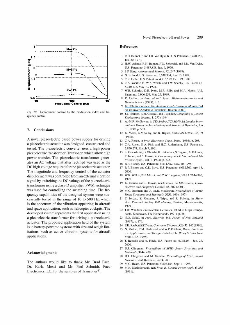
A general view of the prototype constructed is shownin Fig. 19. The performance of the complete systemwas analyzed by testing the system at different levelsof modulation indexes namely 11, 54 and 74% in therange from 10 to 1000 Hz. The free displacement ofthe actuator under these conditions was measured us-ing the SDP-2810 Eddy-current displacement sensorfrom Kaman Measuring Systems and the results areshown in Fig. 20. The curves show how the displace-ment in the actuator can be varied in frequency andamplitude by modifying the control signal. During themeasurements, the input driving voltage in the piezo-electric transformer was maintained as 40 Vpp/78.4 kHzbeing the switching voltage (voltage after the rectifier)120 VDC.
Novel Piezoelectric-Based Power 209
Fig. 20. Displacement control by the modulation index and fre-quency control.
7. Conclusions
A novel piezoelectric based power supply for drivinga piezoelectric actuator was designed, constructed andtested. The piezoelectric converter uses a high powerpiezoelectric transformer, Transoner, which allow highpower transfer. The piezoelectric transformer gener-ates an AC voltage that after rectified was used as theDC high voltage required for the piezoelectric actuator.The magnitude and frequency control of the actuatordisplacement was controlled from an external vibrationsignal by switching the DC voltage of the piezoelectrictransformer using a class-D amplifier. PWM techniquewas used for controlling the switching time. The fre-quency capabilities of the designed system were suc-cessfully tested in the range of 10 to 500 Hz, whichis the spectrum of the vibration appearing in aircraftand space application, such as helicopter cockpits. Thedeveloped system represents the first application usinga piezoelectric transformer for driving a piezoelectricactuator. The proposed application field of the systemis in battery-powered systems with size and weigh lim-itations, such as active vibration systems for aircraftapplications.
Acknowledgments
The authors would like to thank Mr. Brad Face,Dr. Karla Mossi and Mr. Paul Schmidt, FaceElectronics, LC, for the samples of Transoner©R.
References
1. R.H. Bennet Jr. and J.D. Van Dyke Jr., U.S. Patent no. 3,490,556,Jan. 20, 1970.
2. H.W. Adams, R.H. Bennet, J.W. Schendel, and J.D. Van Dyke,U.S. Patent no. 3,487,888, Jan. 6, 1970.
3. S.P. King, Aeronautical Journal, 92, 247 (1998).4. G. Billoud, U.S. Patent no. 5,638,304, Jun. 10, 1997.5. C.R. Fuller, U.S. Patent no. 4,715,559, Dec. 29, 1987.6. C.A. Yoerkie Jr., W.A. Weish, and T.W. Sheehy, U.S. Patent no.
5.310.137, May 10, 1994.7. W.E. Schmidt, D.E. Ivers, M.R. Jolly, and M.A. Norris, U.S.
Patent no. 5,906,254, May 25, 1999.8. K. Uchino, in Proc. of Intl. Symp. Michromechatronics and
Human Science (1999), p. 3.9. K. Uchino, Piezoelectric Actuators and Ultrasonic Motors, 3rd
ed. (Kluwer Academic Publishers, Boston, 2000).10. J.T. Pearson, R.M. Goodall, and I. Lyndon, Computing & Control
Engineering Journal, 5, 277 (1994).11. A.-M.R. McGowan, in CEAS/AIAA/ICASE/NASA Langley Inter-
national Forum on Aeroelasticity and Structural Dynamics, Jun01, 1999, p. 553.
12. K. Mossi, G.V. Selby, and R. Bryant, Materials Letters, 35, 39(1998).
13. C.A. Rosen, in Proc. Electronic Comp. Symp. (1956). p. 205.14. C.A. Rosen, K.A. Fish, and H.C. Rothenberg, U.S. Patent no.
2,830,274, March 7, 1961.15. S. Kawashima, O. Ohnishi, H. Hakamata, S. Tagami, A. Fukuota,
T. Inoue, and S. Hirose, in Proceedings IEEE International Ul-trasonic Symp., Vol. 1 (1994), p. 525.
16. R.P. Bishop, U.S. Patent no. 5,834,882, Nov. 10, 1998.17. R.P. Bishop and C.D. Boyd, U.S. Patent no. 6,052,300, Apr. 18,
2000.18. W.K. Wilkie, P.H. Mirick, and C.W. Langston, NASA TM-4760,
1997.19. K. Uchino and S. Hirose, IEEE Trans. on Ultrasonics, Ferro-
electrics and Frequency Control, 48, 307 (2001).20. M.C. Brennan and A.-M.R. McGowan, Proceedings of SPIE:
Smart Structures and Materials, 3039, 660 (1997).21. T. Jordan, Z. Ounaies, J. Tripp, and P. Tcheng, in Mate-
rials Research Society Fall Meeting, Boston, Massachusetts,1999.
22. J.W. Wanders, Piezoelectric Ceramics, 1st ed. (Philips Compo-nents, Eindhoven, The Netherlands, 1991), p. 26.
23. N.O. Sokal, in Proc. Electron. Ind. Forum of New England(1997), p. 179.
24. F.H. Raab, IEEE Trans. Consumer Electron., CE-32, 145 (1986).25. N. Mohan, T.M. Undeland, and W.P. Robbins, Power Electron-
ics: Applications, and Design, 2nd ed. (John Wiley & Sons, NewYork, USA, 1995).
26. J. Reineke and A. Hock, U.S. Patent no. 6,081,061, Jun. 27,2000.
27. D.J. Clingman, Proceedings of SPIE: Smart Structures andMaterials, 3044, 459.
28. D.J. Clingman and M. Gamble, Proceedings of SPIE: SmartStructures and Materials, 3674, 280.
29. M.C. Heath, U.S. Patent no. 5,802,184, Sept. 1, 1998.30. M.K. Kazimierczuk, IEE Proc. B, Electric Power Appl., 6, 285
(1991).

210 Vazquez Carazo and Uchino
31. S. Hamamura, D. Kurose, T. Ninomiya, and M. Yamamoto,in IEEE 7th International Power Electronics Congress Proc.,Oct. 2000, p. 3.
32. www.tokin.com.33. H. Tanaka, T. Ninomiya, M. Shoyama, and T. Zaitsu, in Power
Electronics Specialists Conference, PESC 98, 29th in AnnualIEEE, 1998, Vol. 1, p. 655.
34. T. Ninomiya, M. Shoyama, T. Zaitsu, and T. Inoue, in 20thInternational Conference on Industrial Electronic Control andInstrumentation, IECON ’94, Sept. 1994, Vol. 3, p. 1665.