Polymer Actuators for Micro Robotic Applications
82
Polymer Actuators for Micro Robotic Applications By Erik Edqvist Licentiate Thesis in Engineering Physics with Specialization in Materials Science Materials Science Programme, Department of Engineering Sciences, Uppsala University, S-751 21 Uppsala, Sweden UPTEC 07001 Lic UPPSALA UNIVERSITY 2007
-
Upload
khangminh22 -
Category
Documents
-
view
0 -
download
0
Transcript of Polymer Actuators for Micro Robotic Applications

Polymer Actuators for Micro Robotic Applications
By
Erik Edqvist
Licentiate Thesis in Engineering Physics with Specialization in Materials Science
Materials Science Programme, Department of Engineering Sciences, Uppsala University, S-751 21 Uppsala, Sweden
UPTEC 07001 Lic
UPPSALA UNIVERSITY 2007


Abstract
In this thesis a multilayer actuator structure is developed for the I-SWARM project. In order to build an energy efficient and low voltage actuator system for the 3x3x3 mm3 robot, the resonance drive mode in combination with a ten layer multilayer structure build upon the most suitable substrate material was used. Two different sizes of the locomotion module were built. The first one is five times larger than the small version. It has five active layers and is simpler to work with and to test. The small module has three 2x0.4 mm can-tilevers on a 3x3mm body and ten active layers. The multilayer process involve easily defined flexible printed circuit (FPC) board as substrate material, spin coating piezoelectric poly(vinylidenefluoride- tetrafluoroethylene) P(VDF-TrFE) as active stack material, and evaporated aluminum electrodes on each active polymer layer. By using different shadow masks for each electrode layer, special inter con-tact areas can be contacted from above after the polymer has been removed by an Inductively Coupled Plasma (ICP) etch. The contours of the locomo-tion module was etched in a Reactive Ion Etch (RIE) equipment. Both the cupper layer in the FPC and the electrode layers of the active stack, were used as etch mask. The deflections of the cantilevers were measured at low voltages to ensure as realistic drive voltage as possible for the I-SWARM robot. The large struc-ture showed a 250 µm deflection at 4 V and 170 Hz resulting in a Q-value of 19. The deflection of the small structure was 8 µm at 3.3 V and 5000 Hz and the measured Q-value was 31.

List of papers
Paper I Snis N., Edvist E., Simu U., and Johansson S., Mono-lithic Multilayer P(VDF-TrFE) Resonators, Sensors and Actuators a-Physical, Submitted, 2006.
Paper II Edqvist E., Snis N., Simu U., and Johansson S., Multi-
layer Electroactive Polymer Unimorph Actuators for the I-SWARM project. Sensors and Actuators a-Physical, Submitted, 2006.
Paper III Edqvist E., Snis N., and Johansson S., Gentle dry etch-
ing of P(VDF-TrFE) multilayer micro actuator struc-tures by use of an ICP, manuscript, 2007.
Contribution to the papers: Paper I Major part of manufacturing, minor part of evaluation,
minor part of writing. Paper II Major part of manufacturing, part of evaluation, part of
writing. Paper III Major part of planning, all manufacturing, part of
evaluation, major part of writing.
Tack
Tack Stefan och Urban för ert engagemang och finansiering av min forskning. Tack Jan-Åke för hjälp med administrativa saker och råd-givning. Tack Janne, Anders och Fredrik för hjälp i renrummet. Det finns en rad personer som har varit goda vänner och inspirerat mig. Micke har med sin kunnighet inom MST varit en mycket god förebild och löparkamrat. Niklas har med sin entusiasm, kunnighet och avslappnade sätt inspirerat otal gånger. Tack Hanna, Sara, Linda och alla andra MST:are. Nisse och Mattias, tack för det lilla extra! Tack alla mysiga tribologer, så väl seniorer som juniorer som gjort diskussionerna kring fika- och köksbord bra mycket trevligare. Utan stödet från min familj hade den här licentiatavhandlingen inte kommit till. Tack Emma för de trevliga luncherna och alla upplyftande möten som verkligen har lyst upp min vardag. Hoppas att jag kan få fortsätta och stötta dig.


Contents
Introduction................................................................................................. xiii Introduction to the I-SWARM project .....................................................15
Definition of swarm behaviour. ...........................................................16 Mass production ..................................................................................17 The gradual development of the robot.................................................18
Piezoelectricity..............................................................................................20 The piezoelectric formulas .......................................................................21
PVDF ............................................................................................................22 PVDF-TrFE..............................................................................................23
Poling or Polarization ..........................................................................24 Improved P(VDF-TrFE)...........................................................................25
Radiating the P(VDF-TrFE) ................................................................25 Adding a third monomer......................................................................25
Our way to improve the module...............................................................27
The motion ....................................................................................................28 Static and resonating mode ......................................................................29 The Q-value..............................................................................................30 The inevitable reality................................................................................30
Substrate........................................................................................................32 Lithographic definition of the FPC ..........................................................33
The multilayer process ..................................................................................35
Etching structures in P(VDF-TrFE)..............................................................37 RIE ...........................................................................................................37 ICP and the Bosch process .......................................................................40
Thickness control ..........................................................................................41
Summery of papers .......................................................................................43
References.....................................................................................................45

Abbreviations and Physical Explanations
Aspect ratio: The relationship between width and depth of a
trench. Autonomous: (Greek: Auto-Nomos - nomos meaning "law")
means freedom from external authority, here no connecting wires.
Bimorphs: A cantilever with a minimum of two layers. At
least two layers can be activated. Curie point: The point where there exist a phase shift from
ferroelectric properties to paraelectric proper-ties. A paraelectric material can not be piezo-electric.
Dipoles: A charge dislocation introduced in a molecule
due to a non symmetric location of atoms with different electric properties.
Electrostrictive material: A property of all electrical non-conductors, or
dielectrics, that produce a relatively slight me-chanical deformation, under the application of an electric field.
Ferroelectric material: A material with one or more ferroelectric
phases. In analogy with a ferromagnetic mate-rial, a ferroelectric material will change its po-larization when an external electric field is in-duced.
Ferroelectric relaxor: An electro strictive material with a time and
frequency dependency of the strain. The effect is caused by diffusion at atomic level.
FPC: Flexible Printed Circuit board

ICP: Inductive Coupled Plasma MST: Micro Structure Technology RIE: Reactive Ion Etching Paraelectric phase: Occurs in a material with dipoles that are un-
aligned and thus have the potential to align in an external electric field and strengthen it but as soon as the electric field is switched off the polarisation of the material vanish.
Piezoelectric effect: A coupling between the mechanical and the
electrical properties of some crystalline materi-als.
Pheromones: Chemical substances emitted by animals to
their environment. Other animals can react with specific behaviours to the substances.
Polarization: The vector field that results from permanent or
induced electric dipole moments in a dielectric material.
Pyroelectric material: The ability of certain materials to generate an
electrical potential when they are heated or cooled.
Unimorph: Cantilever made out of at least two different
material layers. Only one layer can be acti-vated.


Introduction
The word robot can be derived from two words in two different languages. The Czech word robota that means heavy, monotonous or forced labour or the Polish word robotnik that means worker. It was first used by a Czech screen player in 1920 [1]. The general assumption of what a robot is capable to do changes a lot if we add the word micro in front. Micro robots are far from the smart robots found in the movies or in science fiction novels. They still can not be digested and moved controlled inside a human body. Some scientists call just a walking platform for robot, other have more strict defini-tion including the possibility of performing different tasks with instruments. Creating motion with small objects can be tricky since the macro world mo-tors, gearboxes and wheels is too complicated to miniaturize, produce and assemble. Still the need and demand for small motors or actuators, capable of performing different task like focusing the lens system in cell phones, switching mirrors in optical fiber networks, and make precise micro motions are a billion dollar markets. Usually selected materials with special proper-ties are used to create the motion in the micro world, they are called actua-tors. For many years piezo electric ceramics have been such a material. Piezo ceramics are well investigated and today commercially established. There are micro motors, ultrasonic transducers, microphones and many more applications on the market. The search for new, cheaper and interesting ma-terials continues and many researchers are today focusing on producing po-lymer actuators. Polymer based actuators are interesting to study due to a variety of proper-ties and applications possibilities. Polymer actuators are believed to become an important part in future muscle equipped prosthesis. Sadly the current war in Afghanistan and Iraq will most likely push this development faster than the ongoing competition among researcher to build an artificial arm, capable of wresting a human arm. Other properties like the mass fabrication as well as the cost aspect are catching the interest from the industry for pushing the development further. This licentiate thesis will focus on one possible way to manufacture a poly-mer based locomotion module for a micro robotic application. Through out the years many different micro robotic projects have been presented. From

simple once with just the basic locomotion capability to more advanced once. Ebefors used a technique of silicon with etched v-groves filled with polyimide to create actuation by resistively heat the polyimide [2]. Koyanagi et al produced a three legged piezo ceramic based robot, capable of perform-ing an inch worm like motion [3]. Guo et al constructed a fish like underwa-ter micro robot with actuators made out of ionic conducting polymer films [4]. The more advanced robots have sensors or tools attached to them. Tsu-ruta et al developed an advanced robot for inspecting 10 mm pipes equipped with a ceramic piezoelectric actuator and a CCD camera [5]. Martel et al developed the NanoWalker: an advanced micro robot that could be equipped with a scanning tunnel microscope (STM) tip attached under the tripod leg structure. The NanoWalker is interesting since it is autonomous, communi-cates with Infra red (IR) light, and the size is 32x32 mm [6]. Uppsala University has participated in two large EU-funded micro robotic projects, Miniman and Micron. In Miniman an eight legged locomotion module was produced by Urban Simu [7]. The same type of module as the locomotion module, was also placed on the top of the robot, which allowed a ball with a needle to be rotated. Miniman was wire connected to an external control unit and power supply. In Micron the aim was to integrate power as well as communication into the robot, making it autonomous. Niklas Snis, developed a circular disk with three integrated cantilevers which in the end was chosen as the arm motor for the robot [8]. Rickard Gustavsson and Ur-ban Simu developed a gripper actuator that was attached to the top of the arm.
Introduction to the I-SWARM project The work presented in this thesis is sponsored within the EU sixth frame work programme under the Intelligent Small World Autonomous Robots for Micro-manipulation (I-SWARM) project. The objectivities of the project are to present a swarm of 1000 mass produced (3x3 mm) micro robots capable of performing swarm behaviours. The two objectives of swarm behaviours and mass production are closely linked together since no large swarm of robots has been manufactured so far. A contributing reason for this is the manufac-turing cost for the robots. Most academic robotic projects have been assem-bled by hand, putting an upper limit to the number produced. The largest now operational swarm of micro robots is actually a part of the I-SWARM project and is referred to as the Jasmine robot swarm, consisting of some 50-100 <3 cm3 robots [9]. The I-SWARM projected started in 2004 and is supposed to be finished in December 2007. The participants in the consortium are spread all over Europe and include:
• Institute for Process Control and Robotics, Universität Karlsruhe, Germany
• Department of Engineering Sciences, DMS, Uppsala University, Sweden
• Institut de production et robotique, Swiss Federal Institute of Tech-nology (EPFL), Switzerland
• Fraunhofer-Institut für Biomedizinische Technik, St. Ingbert, Ger-many (FhI)
• Institute of Zoology, Karl-Franzens-University Graz, Austria • National Technical University of Athens, Greece • Microsystems and Machine Vision Laboratory, Sheffield Hallam
University, United Kingdom • Scuola Superiore di Studi, Universitari e Perfezionamento Sant’Anna
(SSSA), Pisa, Italy • Universitat de Barcelona (UB), Spain • Institute of Parallel and Distributed Systems, University of Stuttgart,
Germany Some of the participants have participated in earlier EU-project like Miniman and Micron. The hardware part of the robot design is divided into different modules, see Fig. 1. The solar cells (1) are produced in Switzerland in col-laboration between the EPFL and a subcontractor. The SSSA and a subcon-tractor are producing the Infra Red (IR) communication module (2). The FhI have built the special motion arena with a communication beamer and a
15

strong lamp for powering the robots and is also responsible for the capacitors (3). At UB the Integrated Circuit (IC) is being designed (4) and will later be manufactured by a micro electronic foundry in France. Our group has been given the objectives to develop the locomotion module (5) for the robot as well as the final assembly steps regarding the surface mounting process.
Fig. 1 The current design of the I-SWARM robot. The solar panel (1), the IR-transmitters, photo cells and reflective mirror (2), the tantalum capacitors, the integrated circuit (4), and finally the locomotion module made at Uppsala Uni-versity.
Definition of swarm behaviour Swarm robotics can be described as the interaction between a large amount of simple individuals that can be programmed to collectively accomplish objectives that they as individuals would not be able to carry out [10]. For guidance the consortium turned to nature, which provide many good models of organized insect swarms. Almost any ordinary person is aware of the hier-archy and organisation in bee and ant swarms. But the effects and methods controlling the swarm like navigation, often done by pheromones in nature, are hard to mechanically re-create. The software part of the consortium is planning for different scenarios that the swarm should be able to perform. These include basic tasks like collision avoidance and receiving the position for each individual robot. But there are also more complex tasks like finding two points, call certain robots to a specified location, and finding the shortest route between two points. Not only collective perception and actions will be studied. With the combined intelligence of many small individuals some researchers believe, that at certain number of units the swarm will start to
16

show artificial intelligence. By producing so many robots that it could be physical possible to find this number, the I-SWARM project will try define it for this particular intelligence level.
Mass production In order to mass produce 1000 micro robots, surface mounting machines have to be used in order to save PhD students. Before insertion into the ma-chine the circuit board is stencil or screen printed in order to get the solder onto the right spots. The surface mounting machine is loaded with tapes con-taining the circuit components and then the circuit board is inserted in one end and the components are picked and placed onto the board by a sliding arm. Finally the whole board is brought into an oven and the solder is heated and reflown, connecting the components to the board. Since surface mount-ing machines usually are found in the industry and not on a university, Upp-sala University has started a joint venture with Note Norrtelje AB in order to surface mount the I-SWARM robot in 2007. There are many challenging aspects of the assembly due to the robot size and since normal solder paste can not be used. The Curie temperature of the P(VDF-TrFE) impose an upper limit of 120 ºC well below the solder tem-perature. Instead of solder paste, conductive adhesive, a new adhesion method to Note, will be used. The folding of the Flexible Printed Circuit (FPC) board as well as making sure that the different modules have the right interfaces are other challenging tasks for the assembly.
17
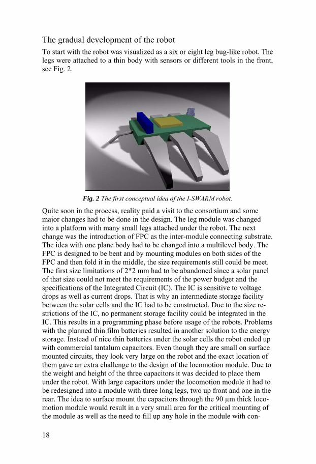
The gradual development of the robot To start with the robot was visualized as a six or eight leg bug-like robot. The legs were attached to a thin body with sensors or different tools in the front, see Fig. 2.
Fig. 2 The first conceptual idea of the I-SWARM robot.
Quite soon in the process, reality paid a visit to the consortium and some major changes had to be done in the design. The leg module was changed into a platform with many small legs attached under the robot. The next change was the introduction of FPC as the inter-module connecting substrate. The idea with one plane body had to be changed into a multilevel body. The FPC is designed to be bent and by mounting modules on both sides of the FPC and then fold it in the middle, the size requirements still could be meet. The first size limitations of 2*2 mm had to be abandoned since a solar panel of that size could not meet the requirements of the power budget and the specifications of the Integrated Circuit (IC). The IC is sensitive to voltage drops as well as current drops. That is why an intermediate storage facility between the solar cells and the IC had to be constructed. Due to the size re-strictions of the IC, no permanent storage facility could be integrated in the IC. This results in a programming phase before usage of the robots. Problems with the planned thin film batteries resulted in another solution to the energy storage. Instead of nice thin batteries under the solar cells the robot ended up with commercial tantalum capacitors. Even though they are small on surface mounted circuits, they look very large on the robot and the exact location of them gave an extra challenge to the design of the locomotion module. Due to the weight and height of the three capacitors it was decided to place them under the robot. With large capacitors under the locomotion module it had to be redesigned into a module with three long legs, two up front and one in the rear. The idea to surface mount the capacitors through the 90 µm thick loco-motion module would result in a very small area for the critical mounting of the module as well as the need to fill up any hole in the module with con-
18

ducting adhesive, which indeed could result in short circuit of the different layers in the module. If the three legs are not fixed and have the same type of support, the resonating frequency will be different for all three legs and the probability of a controllable motion will be less. The solution to capacitor problem and probably to the fixation problem was to place the capacitors on an extra piece of FPC in front of the robot and fold it forward between the two legs. With a good amount of adhesive on the backside, the extra FPC actually could strengthen the support of the legs. From this short description of the project, it is fairly obvious that the current limitations to this project also would be limiting factors for the next genera-tion of even smaller micro robots. The energy storage problem and the inte-grated circuit size issue have to be solved in order to further reduce the size.
19

Piezoelectricity
Piezoelectricty is a coupling between the mechanical and the electrical prop-erties of some certain crystalline materials. For devices following materials are usually used: quartz, Rochelle salts, barium titanate, lead titanate zircon-ate ceramics (PZT), and polyvinylidene flouride (PVDF). Piezoelectricity was discovered in the 1880 by Jacques and Pierre Curie when working on quartz crystals. They found out that the quarts crystals changed its dimension when an electrical field was induced. They later also verified the reversed effect [11]. The piezoelectric effect was put into use in 1917 when Paul Langévin improved his underwater sonar equipment from 1916. He replaced an electrostatic projector and a carbon-button microphone with quartz crystals glued between two steal plates [12]. Since then the de-velopment of underwater sonars have continued. Other applications for pie-zoelectric materials are microphones, vibrators in cell phones, micro motors, transducers in ultrasonic cleaners, energy converters for mobile systems, spark generators inside igniters, and pyroelectric sensors [13]. In 1924 Brain discovered that also polymers could be piezoelectric. A lot of the earliest work was carried out on carnauba wax and resin. In 1950 the piezoelectric effect was reported by Bazhenov. In 1955 Fukada verified ex-perimentally both the direct and the inverse piezoelectric effects of wood. In 1953 Yasuda et al showed that bone could produce electricity by bending deformation. The induced polarization produced callus at the negative com-pressed regions. This effect was later verified by Yasuda and Fukada in 1957 when they showed that dry tendon has a d14 of -2.0 pC/N comparable of quartz crystals that has a d11 of 2,2 pC/N. In 1969 great things happened not just on the surface of the moon, Kawai discovered a new large family of piezoelectric polymers that still is investigated and modified in different ways to increase performance. The polymer is called poly(vinylidene-fluoride), P(VDF). In comparison to tendon and quartz crystals, stretched PVDF has a d31 of 20 pC/N [14].
20

The piezoelectric formulas There are two important formulas for describing a material piezoelectric behaviour, the constitutive piezoelectric equations for strain S and displace-ment D:
kkijklEijklij EdTsS +=
jTijjkijki ETdD ε+=
where T is the stress and s the elastic compliance (at constant electric field), d is the piezoelectric strain coefficient, E is the electric field, and ε is the dielectric permittivity [15]. To simplify things, many of the tensor are equal and can be reduced. One of the tensor coefficient that is important for the type of actuator applications described in this thesis, is the d31 where the 3 denotes that the poling axis is parallel to the z-axle and the strain is induced in the x-axle, see Fig. 3. For a piezoelectric material with zero stress and an electric field in the poling axle (z axle) the strains induced, simplifies to a deformation in the x, y, and z axels. For the cantilever actuator application, the longitude strain is the most important in order to achieve useful deflec-tions.
3311 EdS =
3312 EdS =
3333 EdS =
Fig. 3 The direction convention for the piezoelectric coefficients.
21

PVDF
There are many compelling properties of piezoelectric polymer PVDF to a micro structure engineer. PVDF show good chemical and thermal stability, it can be easily processed and miniaturized, it is lightweight, cheap, and can be casted in different shapes. In comparison to piezo ceramic material it does not need to be sintered at high temperatures, which allows it to be integrated with other temperature sensitive components. There are at least four different crystalline forms of PVDF. Three of them α (Form II), β (Form I), and γ (Form III) are designated major phase forms and the fourth δ (form IV) is referred to as a minor phase. The different phases are due to changes in the carbon bonds (C-C) along the chain back bone. The β phase has all the C-C bonds in an s-trans type like (TTTT) and the α phase has an alternating s-trans and s-gauche (TGTĜ). The γ phase has an s-guache bond every fourth repeating unit (T3GT3Ĝ). The δ sub phase is a γ phase with every other chain rotated. The interesting ferroelectric β phase can in simple PVDF be obtain by stretching a solution casted film, usually these films con-sists of α phase and γ phase. As seen in Fig. 4a, the fluorine atoms in the β phase, are positioned on one side of the unit cell resulting in a net dipole moment. In the α phase, Fig. 4b, neighbouring chains are packed in a certain way, so that the individual dipole moments from the carbon-fluorine atoms are cancelled out [16].
22

Fig. 4 a) The β phase chain with the fluorine atoms on one side of the chain resulting in a dipole of 2,1 D. b) The dipole moment is cancelled out in the α phase, due to the
tight packing of chains.
When spin coating or casting a thin film of PVDF there are many parameters that will effect what type of phase the PVDF coating will result in. The sol-vent polarity, the temperature of the solvent and the evaporation rate all ef-fect the resulting phase. It has also been shown that the humidity, the sub-strate evaporation rate, surface type, the location on the substrate, and the annealing temperature are important factors for what type of phase composi-tion the coated film will end up with [16]. These factors are important for the surface roughness and the robustness of the process and have to be further investigated.
PVDF-TrFE Since PVDF has to be stretched in order to be transformed in to the crystal-line β phase it would be more manufacturing friendly if the wanted properties could be reached without the stretching step. By using bulk polymerisation the PVDF monomer can be connected with a tetrafluoroethylene (TrFE) monomer creating a copolymer called poly(vinylidenefluoride-tetrafluoroethylene), P(VDF-TrFE) [17]. When the mixture is less than 85/15 mol% the copolymer is naturally in the β phase, in which there exist ferro-electric domains which are polar but not ordered in any direction [18]. This is the material that we have chosen to work with in the group. There are other alternated versions of the P(VDF-TrFE) that could reach higher strains,
23

as described below. The decision to work on regular P(VDF-TrFE) was based on the fact that the improved versions of P(VDF-TrFE) are patent and the irradiation process is some what complicated to perform. The bulk po-lymerisation method is more interesting but in order to minimize risks in the project, we chose the regular P(VDF-TrFE). A material with too high strains (3-5 %) could for instance caused the multilayer electrodes to break. The thickness of the casted film has an important effect on the crystallinity of the film. Below 120 nm the crystallinity of the P(VDF-TrFE) film (75/25 mol%) is no longer thickness independent [19]. Kimura and Ohigashi showed that P(VDF-TrFE) film with a thickness of 500 nm to 2,5 µm have the same ferroelectric properties as thicker films [20]. Our films are some 2-4 µm thick and hence should have the same ferroelectric properties as thicker films. The spin coated films of the copolymer will most likely be depending on the same process parameters as the monomer, which were mention earlier. The PVDF-TrFE (65/35 mol %) grains used in this work was bought from Solvay, France and dissolved in Methyl-Ethyl-Keton (MEK) to a concentra-tion of 1:10 (by weight).
Poling or Polarization To order the polar domains and induce a piezoelectric effect, the copolymer has to be introduced to a high electric poling field. The poling step follows a hysterisis curve and will decrease over time. There are different methods to create the field. In one electrodes are attached on the coated polymer film and a DC field or a low frequency AC could be applied over the cross section [21]. Another method is to use a Corona discharger which does not need electrodes [22]. Despite that the electrode poling step can introduce short circuits and decrease the active polymer layer, this method was chosen as a final step in the end of the manufacturing process. A Corona discharge method would have required a poling step for each multilayer and a final poling step appeared less redundant. The low frequency AC voltage poling has not been tried out on the multilayer structure, but it would be interesting to do so.
24

Improved P(VDF-TrFE) In piezo ceramics the hysteresis loop can be reduced by reducing the coher-ent polarization region of the material. By introducing defects of some sort in a piezo polymer the result can be a reduction of the polarization areas and hence the hysteresis.
Radiating the P(VDF-TrFE) The search for improved material properties of the P(VDF-TrFE) polymer got Zhang et al to perform high energy electron irradiation of the polymer films [23]. The resulting films showed a reduced or in some cases eliminated polarisation hysteresis due to the fact that the macroscopic polar domains found in untreated P(VDF-TrFE) were decreased. The authors called the resulting domains for nanopolar regions. The thin hysteresis was explained by the authors as the expansion and contraction of nanopolar regions under an external field. Differences in the lattice constant for the polar and non polar regions would explain the large electro strictive strain. After irradia-tion the features of the polymer had changed into a ferroelectric relaxor ca-pable of reaching electro strictive strains of 4 % at 150 MV/m compared to regular P(VDF-TrFE) [24].
Adding a third monomer Another way to transform P(VDF-TrFE) into a relaxor is to add a third monomer. Xu et al altered the P(VDF-TrFE) by adding chlorotrifluorethyl-ene, which resulted in a trimonomer called poly(vinylidene-fluoride-tetrafluoroethylene-chlorotrifluorethylene), P(VDF-TrFE-CTFE). According to the authors this extra third monomer converts the normal ferroelectric P(VDF-TrFE) into a ferroelectric relaxor capable of reaching electrostrictive strains of 4% at 150 MV/m compared to regular P(VDF-TrFE) which would give a strain of 0,15% under the same condition. The effect is believed to be due to the large chlorine atoms cause conformation changes and steric repul-sion in the chain segment, raises the inter-chain and intra-chain energy of the TGTG bonds. That would destabilize the polar order and explain the ferro-electric behaviour [25]. Cheng et al also tried to add a third monomer. Both the hexafluoropropene (HFP) and the CFTE monomer were tested but they found a 1% lower strain for 150MV/m with the third monomer solution than with the irradiated version. In accordance to the irradiated samples, the same effect on the hysteresis and a higher dielectric constant were observed [26]. Petchsuk and Chung studied the HFP monomer more in detail and they found that the trimonomer performed better than the irradiated at lower voltages, which in some ways contradict Cheng et al. They found that very small amounts of added HFP (2,46 mol %) in a stretched P(VDF-TrFE) film re-
25

sulted in a 2,5 % strain at 50 MV/m, which was higher than corresponding irradiated film had shown [27]. Both these ways to improve the strain of the P(VDF-TrFE) show that even higher strains than presented in this thesis could be achievable with the mul-tilayer structure. With the improved PVDF-TrFE new issues like the electric conducting capability and the cycle effect of a thin layer electrode in connec-tion with percentage strains have to be addressed. Maybe the electrode should be polymer based to allow for such high strains?
26
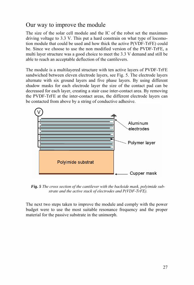
Our way to improve the module The size of the solar cell module and the IC of the robot set the maximum driving voltage to 3.3 V. This put a hard constrain on what type of locomo-tion module that could be used and how thick the active P(VDF-TrFE) could be. Since we choose to use the non modified version of the PVDF-TrFE, a multi layer structure was a good choice to meet the 3.3 V demand and still be able to reach an acceptable deflection of the cantilevers. The module is a multilayered structure with ten active layers of PVDF-TrFE sandwiched between eleven electrode layers, see Fig. 5. The electrode layers alternate with six ground layers and five phase layers. By using different shadow masks for each electrode layer the size of the contact pad can be decreased for each layer, creating a stair case inter-contact area. By removing the PVDF-TrFE at the inter-contact areas, the different electrode layers can be contacted from above by a string of conductive adhesive.
F -
Thebudma
ig. 5 The cross section of the cantilever with the backside mask, polyimide substrate and the active stack of electrodes and P(VDF-TrFE).
next two steps taken to improve the module and comply with the power get were to use the most suitable resonance frequency and the proper
terial for the passive substrate in the unimorph.
27

The motion
The three legs of the locomotion module, are cantilevers with the condition of being supported in one end. To create a deflection the applied voltage expand the P(VDF-TrFE) and since it is attached to the passive substrate it will bend the whole cantilever in the direction of the substrate. The concept of an active material on a passive substrate is usually referred to as a uni-morph. The tip deflection of a unimorph fixed in one end can roughly be described with:
UdtL
tot31
2
43
=δ
Where L is the length and ttot the total thickness of the unimorph, see Fig. 6. The active material property d31 is the piezoelectric strain coefficient which was explained earlier. U is the applied drive voltage.
Fig. 6 The fixed cantilever from the side.
Since the unimorph indeed is made out of different materials, this simple formula does not take this into consideration. In paper I (Smits et al) and paper II (Monturet et al) two different formulas are presented to compensate for the different materials and their properties. Both the Smits formula and Monturet formula can be used for these type of unimorphs if the different layers in the active and passive part are compensated for by effective mate-rial values, both for the passive part as well for the active P(VDF-TrFE)-electrode stack. Since the aluminium electrodes in the stack are not dielec-tric, the piezoelectric strain coefficient also have to be compensated for this fact. When using these effective material values the true thickness of each
28

material has a large influence of the result. Wrong layer thicknesses of mate-rials with a high Youngs Modulus will affect the discrepancy between meas-ured and theoretical values a lot. By performing SEM cross section studies on the substrate layer, using the Focus Ion Beam (FIB) to measure the P(VDF-TrFE) layer and use a glass substrate with a tape on it for each evaporation cycle, the thickness of each polymer and electrode layer can be measured. With three vibrating cantilevers the module will be able to move forward in the direction of the two legs. It will also be able to move backwards. To turn right or left, the robot will use the same principle as a tank, it will drive one of the two front legs, see Fig. 7.
Fig. 7 The robot will be able to move forward, back ward and turn right and left.
Static and resonating mode Even with the multilayer structure, it would not be possible to create enough motion with the 3.3 V at static deflection. In order to save energy and still create a large deflection for the cantilevers, a resonant driving mode was chosen. Unimorph cantilevers can be driven in static or in dynamic mode. The static mode is when there is a deflection without any frequency dependency. If the signal used to create the motion is made frequency dependent the cantilevers will be in dynamic mode. With increased frequency different modes will correspond to the eigen frequency and at some of these the deflection will increase drastically. These are the modes where the locomotion module could carry the weight of the robot and create a motion with the of 3.3 V voltage applied. This is the beauty of the dynamic mode, but it demands ac-curacy when picking the node frequency. Without the dynamic mode the weight of the I-SWARM robot would probably preclude any motion.
29

The Q-value There is an important parameter for a system operating in the dynamic mode called the Q-value or quality factor. The Q-value for a resonating object is expressed as the resonance frequency fr divided by the full width of the reso-nance peak at half of its maximum deflection ∆fFWHM.
FWHM
rf
fQ
∆=
A dynamic mode can have a very narrow and high frequency tip which will result in a high Q-value but since the frequency interval for the large deflec-tion is so narrow, the chance for finding a frequency that will be acceptable for all three cantilevers is smaller. The other extreme is a low Q-value with a small deflection but a larger acceptable frequency interval. The trick is to find both an acceptable deflection and a large enough frequency interval. These restrains will result in a Q-value of 20-40.
The inevitable reality Still the most efficient formulas can not compensate for how the robot will behave in reality. A bad support of cantilevers, different layer thicknesses, a bad inter-electrode contact or cracks in some electrode layers can resulting in lower cantilever deflections than calculated. There are also indications in the literature that the crystallinity of the PVDF-TrFE varies over a casted area. This of cause could result in variations between the three legs or between individual robots. A solution to the problem with different resonance fre-quency for the individual robots would be to use communication beamer and the position tracking system. By varying the resonance frequency and scan for motion the optimal frequency for each single robot could be found. This solution would not solve the problem if the resonance frequency varies too much for the three cantilevers in one module. In the presented calculations the cantilevers are fixed in one end and oscillate in the other end. As soon as the robot is put on a surface, the tip formed as an arrow in the FPC, will be in contact and this will change the resonance frequency. Our aim is to be oper-ating the structure at the second resonance mode to utilize a positive effect on the relationship between the load capacity and dynamic deflection. The formulas for these frequencies are presented in paper II.
30

The assembly of the locomotion module is critical to its performance since all the formulas used, are using the boundary condition of one end being supported. As planned right now the locomotion module is to be connected to the FPC by four drops of conducted adhesive at the electrode inter-contact areas. This will most likely not be enough to ensure a fix and firm support point for all three legs. A under filling type of adhesive most likely has to be used.
31

Substrate
The first prototype of the locomotion module had eight legs and used four active layers of PVDF-TrFE sandwiched between five electrode layers, see Fig. 8. A polycarbonate film used for dicing Silicon wafers was chosen as substrate. Despite having problems with the removal of PVDF-TrFE at the interlayer contact areas and the assembly to the rest of the body, the structure both displayed a static as well as a resonating deflection. But the deflection and the Q-value were low. As a result of that the work in paper I was carried out.
Fig. 8 The first prototype made on a polycarbonate substrate and with cupper elec-
trodes.
The main resulted from paper I was the conclusion that the selection of sub-strate material is important both from a processing stand point as well as a resonating behaviour point. Out of the four compared materials: steel, FPC, polycarbonate, and aluminium the FPC showed the highest static and reso-nating deflection, combined with well known processing features. In the 1960s Du Point developed the first polyimide, a PMDA-ODA which they called Kaptone. The PMDA is the dianhydride (1,2,4,5-tertracarboxylic benzene dianhydride) and the ODA is the diamine (4,4´-diaminophenyl eter). Polyimide is usually chosen for FPC instead of polyester when properties like thermal stability, good mechanical properties and a low dielectric con-
32

stant are preferred [28]. This implies a higher manufacturing cost but the performance and reliability is higher than for polyester. All the work in this thesis has been on a FPC from Espanex (Nippon Steel Chemical Japan). The Espanex FPC is manufactured by using low expansion polyimide and cop-per-clad laminated sheets. Both single (18-50) and double sided (18-50-18) as well as (12-25-12) has been used in this work. The single side Expanex with 18 µm cupper and 50 µm polyimide has proven to be the best combina-tion to build multi layer structures on. The reason for this is that single sided polyimide side is much smother than a double sided Expanex with one cup-per side completely removed. The 18-50 type is also stiff enough to carry the entire robot compared to the 12-25 type. SEM studies of polished Expanex substrate casted in epoxy, showed that the given thickness of 18 µm cupper and 50 µm polyimide vary with 3-5 µm and this will of course explain some deviation between calculated and measured values.
Lithographic definition of the FPC The FPC substrate is patterned by a well established lithographical method. As mentioned in the first paper a Q value of 40 corresponds to a length toler-ance of ±0.5% which would be 50 µm for the I-Swarm cantilevers. This tol-erance level can be met with standard lithographical methods. The contours of the module and guide holes are first draw in a CAD program and trans-ferred to a special mask writer machine where a mask is written on a chrome coated glass plate. The FPC is then cut into a 10x10 cm sheet and placed in a spinner where the resist is applied. By spin coat the resist, good thickness and uniformity control can be achieved. The resist is then cured in a oven for 10 minutes and then the substrate and the mask are placed in a mask aligner where they are aligned and the substrate is exposed to ultraviolet (UV) light. The substrate is dipped in a developing solution where the exposed parts are removed. To harden the resist the substrate is again cured in an oven for ten minutes. The exposed cupper surface can be etched in a wet chemical cupper etch. The polyimide layer can be etch in a dry etch. The dry etch utilize a plasma to bombard the substrate with ions and physically nock out substrate molecules as well as creating chemical inert particles that can react with the polyimide. The remaining cupper layer will then act as a mask for the sur-faces that are not supposed to be etched. Since it is only the guide holes and the contours of the substrate that are to be defined with this etch step, the locomotion module contours are protected by an aluminium foil, see Fig. 9.
33

F
ig. 9 The cupper side of the FPC before and after etching in the dry etch. The polyimide layer can bee seen as the brown area in the picture.34

The multilayer process
When the substrate has been patterned it is mounted with adhesive to an etched stainless steel foil with four guide holes. The cupper side is mounted against the foil. By placing the substrate and the foil in the substrate holder and align them under a microscope a fairly accurate placement of the sub-strate in relation to the different shadow masks can be achieved. This is a critical step but by making sure that the contours of the substrate module is larger than the shadow masks, the evaporated electrodes will be within the substrate area. In future substrate masks and stainless steal foils it would be good to include two or more pass marks for this step, to ensure that the placement of the substrate is as good as it can be. The substrate is then placed in the spinner where a first layer of PVDF-TrFE is coated on the polyimide side of the substrate. After that the substrate is annealed in an oven for six hours to evaporate all solution. Next the substrate is aligned with the first shadow mask in the substrate holder with the help of four guide pins. Then the substrate holder is placed in an evaporation cham-ber. At low pressure aluminium is resistively heated and due to the vacuum in the chamber it is evaporated through the shadow mask creating a common ground electrode layer on the PVDF-TrFE. A second layer of PVDF-TrFE is spin casted on the first and again annealed in the oven for six hour. The next shadow mask is the phase electrode mask with individual electrodes for each leg. These steps are repeated in total eleven times with new shadow masks for each step. The result is an unit with three cantilevers, each consisting of ten active PVDF-TrFE layers, five phase electrode layers and six ground electrode layers, see Fig. 10a and 10b. A critical part of the multilayer proc-ess is to get an accurate alignment between the different electrode layers. Despite the four guide pins, there can still be some slight misalignment.
Fig. 10 a): The locomotion module left. b) Top view of the electrode configuration withthe three round phase electrode areas as well as the ground electrode area.35

The substrate is then removed from the stainless steel foil, turned around and placed in the Reactive Ion Etching (RIE) equipment, to remove the polyim-ide along the contours of the locomotion modules. The substrate is turned around again and placed in a special Deep-RIE etch holder and etched with the electrodes as mask. After the different electrode layers have been ex-posed by the plasma, see Fig. 11, they can be contacted with a string of con-ductive adhesives. Finally the structure can be polarized. As can be seen in Fig. 11 there are pin holes and some surface variation on the different elec-trodes. This implies that future work again has to address the surface rough-ness control of the electrodes. The key to a smooth surface of the electrode is to control the important parameters of the spin coating of P(VDF-TrFE) and the annealing.
Thestepstruworcarr
36
Fig. 11 The D-RIE etched ground contact area. The different electrodes can beinter-connected from above by a string of conductive adhesive. The surface
roughness and pin holes of the electrodes are visible.
development of the multilayer structures has been carried out in a two s development period. The first period focused on a five time larger cture than the final one. This structure had only five active layers and the k is described in paper II. In the final paper the miniaturization step is ied through and the ten active layers are implemented.

Etching structures in P(VDF-TrFE)
The chosen multi layer structure demands an etching step to uncover the electrode at the interlayer contact areas. The standard way to etch in MST is usually to use a photo resist mask to selectively expose areas to a wet chemi-cal etch. These etch solution usually contains H2O and are isotropic. The difference between isotropic and anisotropic etching are found in the way the substrate is etched. An isotropic etch will etch in all directions compared to an anisotropic that will mainly etch in one direction. Historical in MST the material has been Si and the photoresist has been removed with acetone after the etching step. Since acetone dissolve P(VDF-TrFE) and water has a par-ticular way to penetrate between P(VDF-TrFE) and some surfaces it has been coated on, the wet chemical way, at first seemed as a less successful one. The dry etching systems developed for Si-etching seemed more interesting since they usually give good anisotropic etch results.
RIE RIE is an important etch process to create three dimensional structures in MST. It utilizes a plasma of ionized gas molecules that bombard the sub-strate. The process demands a vacuum chamber, a gas, and two electrodes, a cathode and an anode. If the voltage drop between the electrodes is higher than the ionisation energy of the gas, interaction between accelerating elec-trons and gas molecules will start an avalanching effect and ionize the gas molecules, hence create a Plasma. The plasma is by definition positive since it attracts more electrons than positive ions. The positive charged particles are attracted to the chamber walls and to the cathode. Upon hitting the cath-ode surface Auger electrodes are released and that sustains the balance be-tween consumed and created electrons, which result in a constant potential in the inner part of the plasma. To enhance the ionization by the electrons in the plasma and to operate the process at higher pressures ~1 mTorr, and to be able to etch insulating materials, the plasma can be powered with a Radio Frequency (RF) generator and matching network [29].
37

The ionized ions, compounds and molecules of the plasma can be used in different ways [29]: 1. Either the ions are used as particles to bombard, or sputter the surface. The sputter effect is less selective for different materials, it varies due to the ge-ometry and the binding structure of the surface atoms. The pressure of the chamber as well as the incline angle of the ions are properties that affect the etch rate and how isotropic the etch become. Sputtering can redeposit materi-als on the substrate. Masks usually have to be thicker than the deepest etch depth wanted to compensate for the poor selectivity. By using a low pressure plasma, and the consequent longer free mean path, this method can result in a perpendicular approach of the ions and reactive molecules. The result will be a more anisotropic etch. 2. The ionization of the gas can create chemical reactive molecules and parti-cles. The selectivity is far greater than the sputter case since differences in the chemical properties are the key to how the reactive molecules bind to the substrate. In our process the polymers can be etched with an oxygen or CF4 plasma, but the Aluminium masks probably would require a chloride based gas. The etch process can be described briefly as follows, see Fig. 12: The ionization of the gas create reactive molecules, ions and radicals (1) that dif-fuse down to the substrate surface (2), and adsorb on to it (3). At the surface the reactive particles react with the top layer substrate atoms (4) and these new molecules and compounds desorb from the surface (5) and are carried away from the substrate (6). If the chemical properties divert a lot, the etch profile can show a high degree of isotropic. 3. The combination of these two cases. With the correct applied pressure and effect, the combination of the two processes can enhance the etching dra-matically. The ion bombardment can both clean the surface and there by enhance the exposure of the surface to the reactive particles. The chemical process taken place at the surface can also be catalyzed by the ion bombard-ment.
38
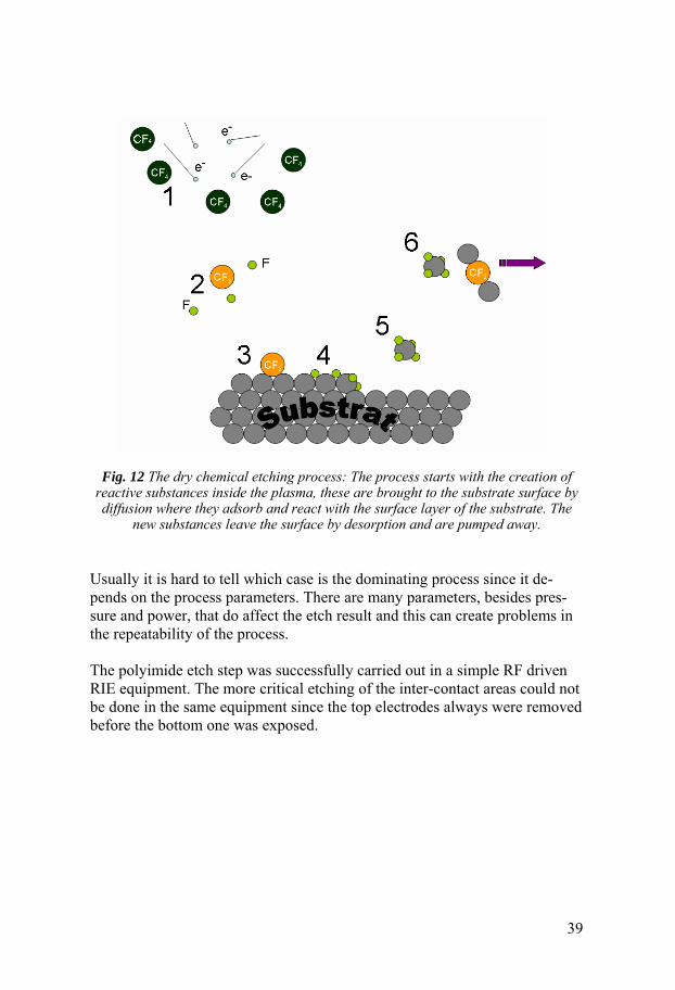
Fig. 12 The dry chemical etching process: The process starts with the creation of reactive substances inside the plasma, these are brought to the substrate surface by diffusion where they adsorb and react with the surface layer of the substrate. The
new substances leave the surface by desorption and are pumped away.
Usually it is hard to tell which case is the dominating process since it de-pends on the process parameters. There are many parameters, besides pres-sure and power, that do affect the etch result and this can create problems in the repeatability of the process. The polyimide etch step was successfully carried out in a simple RF driven RIE equipment. The more critical etching of the inter-contact areas could not be done in the same equipment since the top electrodes always were removed before the bottom one was exposed.
39

ICP and the Bosch process In order to etch substrate with high aspect ratio the RIE system was further developed and patent by Robert Bosch GmbH. By cycling the etch step in a coil equipped RIE euipment and include a polymerisation step to cover the substrate with a fluorine polymer, a cleaning step, and start etching again, high aspect ratio like 1:20 or 1:30 can be achieved [30]. The polymerization step passivate the walls in a etch trench and allows for a down ward directed etch by particles guided by the magnetic field from the coupled coils. Since the polymer used in the Bosch process is a Teflon like, fluorine based one, the idea to etch PVDF-TrFE with this method was not that far away. The problems were more related to the fact that usually only Si-wafers are allowed in the expensive and complicated Inductive Coupled Plasma (ICP) equipment. With some modifications to process gases, cycle length and the proper chosen power, the contact area of the locomotion module could be etched with good process control. This is mainly the work carried out in pa-per III. The polymerisation step of the Bosch process was cancelled, making the process a well controlled, coupled, and cycled process, something that could not be done in the RIE equipment. Even in this case it is hard to tell which ablation process is the dominating one. A hint could be the fact that the etch selectivity for the top electrode is some 200 to the deepest etched polymer area, the chemical reactive scenario seems to be an important proc-ess but the influence of direct ion bombardment can probably not be ne-glected.
40

Thickness control
In a multilayer structure, the thickness of each individual layer is important. If the deviation between each individual layer is too large, the result will be different capacitance for different layers. For instance a 1 µm ticker P(VDF-TrFE) layer in one layer will result in a capacitance drop of 50 pF. This will affect the polarization and hence the optimal performance of the unimorphs. Each individual electrode layer could easily be measured by including a small glass substrate with a tape attached to it in the evaporation step. The step could then be measured in an interference microscope or by a profilome-ter. The individual PVDF-TrFE layers are harder to measure. Two major ways have been tried and both have limitations and are time demanding and de-structive. Locomotion units have been casted in epoxy and polished down to a nice cross section cut. This method never gave any precise thickness of the individual layers, but a good total thickness accuracy in accordance to a Heidenhain Probe, a profilometer, an interference microscopes, and a mi-crometer screw. The second and most interesting method was to use a FIB instrument to etch down a suitable large trench and then polish one end of the trench and meas-ure the individual layers, see Fig. 13. Still tilt compensations and instrument alignment accuracy puts a limitation to the accuracy of the measurements.
41

Figure 13 A typical FIB trench and the measurement of each individual PVDF-TrFE layer, still more work have to be done on the control of each individual layer.
42

Summery of papers
I: Snis N., Edvist E., Simu U., and Johansson S., Monolithic Multilayer P(VDF-TrFE) Resonators. The first paper focus on the selection of the proper substrate material for an optimal Q-value and the ability to process the chosen substrate. Four differ-ent materials were compared after a stack of six active layers had been build upon each of them. The stack was produced by spin coating P(VDF-TrFE) and evaporate aluminium on each polymer layer. The interlayer contact was done from the side and the stack was diced into cantilevers to study each resonant behaviour. The different substrate showed different Q-values from 30 to 77. The FPC had a Q-value of 64 and a well developed process tech-nique which made it the selected substrate material for the I-Swarm project.
II: Edqvist E., Snis N., Simu U., and Johansson S., Multilayer Electroactive Polymer Unimorph Actuators for the I-SWARM project.In this paper the multilayer manufacturing process is further developed. The actuator unit investigated is an up scaled version of the final I-SWARM lo-comotion unit. It consist of three cantilevers (10x2mm) supported on a quad-ratic body. The outline of the actuator unit is patterned in the cupper layer of the flexible printed circuit board by lithographic methods. The interlayer contact is provided by an stair case like area, created by different shadow masks for each aluminium electrode layer. The contours of the unit and the contact area are etched by Reactive Ion Etching (RIE). The cupper and the electrode layers are used as etch mask. When the polymer is removed the different electrode layers can be connected from above with conductive ad-hesive. The cantilevers presented have five active P(VDF-TrFE) layers. A 4V signal resulted in a tip deflection of 250 µm. The measured Q-value was 19.
43

III: Edqvist E., Snis N., and Johansson S., Gentle dry etching of P(VDF-TrFE) multilayer micro actuator structures by use of an ICP.This paper address the structuring of P(VDF-TrFE) and how the to etch the multilayer structure with intact top electrodes. The final size of the locomo-tion unit for the I-SWARM project is manufactured and tested. The uni-morph has ten active layers and eleven electrode layers. A modified Bosch process in an Inductive Couple Plasma (ICP) etcher is used to remove all P(VDF-TrFE) not covered by the electrodes. All the eleven electrode layers are exposed during the etch step and are contacted by conductive adhesive. Good agreement between theoretical and measured capacitance values were measured after the conductive adhesive was applied. The cantilevers were operated under similar voltage condition as the I-SWARM robot. A cantile-ver tip deflection of 8.3 µm was measured at 5000 Hz with a square wave signal of 3.3 V. The measured Q-value was 31.
44

References
[1] Wikipedia, "Robot," http://sv.wikipedia.org/wiki/Portal:Huvudsida, 10 December 2006.
[2] T. Ebefors, "Polyimide V-groove joints for three-dimensional silicon transducers - exemplified through a 3D tubulent gas flow sensor and micro-robotic devices," in S3, vol. PhD Stockholm: KTH, 2000.
[3] T. Koyanagi, R. Fukui, A. Torii, and A. Ueda, "Miniature robots with three degrees of freedom," presented at Proceedings of the 2000 International Symposium on Micromechatronics and Human Sci-ence, 2000.
[4] S. X. Guo, T. Fukuda, and K. Asaka, "A new type of fish-like un-derwater microrobot," Ieee-Asme Transactions on Mechatronics, vol. 8, pp. 136-141, 2003.
[5] K. Tsuruta, S. T., T. Shibata, and N. Kawahara, "Control Circuit in an In-pipe wirelsess inspection robot," presented at 2000 Interna-tional symposium on micromechatronics and human science, 2000.
[6] S. Martel, K. Doyle, G. Martinez, I. Hunter, and S. Lafontaine, "In-tegrating a complex electronic system in a small scale autonomous instrumented robot: The NanoWalker Project," Proceedings of SPIE - The International Society for Optical Engineering,, vol. 3834, pp. 63-74, 1999.
[7] U. Simu and S. Johansson, "Fabrication of monolithic piezoelectric drive units for a miniature robot," Journal of Micromechanics and Microengineering, vol. 12, pp. 582-589, 2002.
[8] N. Snis, U. Simu, and S. Johansson, "A piezoelectric disc-shaped motor using a quasi-static walking mechanism," Journal of Micro-mechanics and Microengineering, vol. 15, pp. 2230-2234, 2005.
[9] S. Kornienko, O. Kornienko, and P. Levi, "Minimalistic approach towards communication and perception in microrobotic swarms," presented at IEE/RSJ International Conference on Intelligent Robots and Systems, Alberta, Canada, 2005.
[10] P. Valdastri, P. Corradi, A. Menciassi, T. Schmickl, K. Crailsheim, J. Seyfried, and P. Dario, "Micromanipulation, communication and
45

swarm intelligence issues in a swarm microrobotic platform," Robot-ics and Autonomous Systems, vol. 54, pp. 789-804, 2006.
[11] A. A. Hood and Pines J. Darryl, "A multi-functional sensor for si-multaneous measurement of structureborne sound vibration," pre-sented at SPIE Smart Structures and Integrated Systems, Newport Beach, CA, , 1999.
[12] J. Woo, "Paul Langévin (1872 -- 1946)," http://www.ob-ultrasound.net/langevin.html, 1 December 2006.
[13] N. Neumann and R. Kohler, "Application of pyroelectric P(VDF/TrFE) thin films in integrated sensors and arrays," Proceed-ings of SPIE - The International Society for Optical Engineering, vol. 2021, pp. 35-44, 1993.
[14] E. Fukada, "History and recent progress in piezoelectric polymers," Ieee Transactions on Ultrasonics Ferroelectrics and Frequency Control, vol. 47, pp. 1277-1290, 2000.
[15] S. Johansson, Actuator materials and microactuation. Uppsala, 2004.
[16] M. Benz and W. B. Euler, "Determination of the crystalline phases of poly(vinylidene fluoride) under different preparation conditions using differential scanning calorimetry and infrared spectroscopy," Journal of Applied Polymer Science, vol. 89, pp. 1093-1100, 2003.
[17] Y. Higashihata, J. Sako, and T. Yagi, "Piezoelectricity of Vi-nylidene Fluoride-trifluoroethylene Copolymers," Ferroelectrics, vol. 32, pp. 85-92, 1981.
[18] Q. Zhang, Electroactive polymer (EAP) Actuators as Artifical Mus-cles Reality, Potential, and Challenges. Bellingham: SPIE- The In-ternational Society of Optical Engineering, 2001.
[19] F. Xia, B. Razavi, Z. Y. Cheng, and Q. M. Zhang, "Finite size effect in thin and ultra-thin ferroelectric polymer films," Materials Re-search Society Symposium - Proceedings, vol. 698, pp. 79-84, 2002.
[20] K. Kimura and H. Ohigashi, "Ferroelectric properties of poly(vinylidenefluoride-trifluoroethylene) copolymer thin films," Applied Physics Letters vol. 43, pp. 834-836, 1983.
[21] L. F. Brown, R. L. Carlson, and Sempsrott, "Spin-cast P(VDF-TrFE) films for high performance medical ultrasound transducers," IEEE Ultrasonics Symposium, pp. 1725-1727, 1997.
[22] R. Gerhard-Multhaupt, "Polarisation of Poly(vinylidene fluoride," presented at IEE Conference Publication 1984.
46

[23] Q. M. Zhang, V. Bharti, and X. Zhao, "Giant electrostriction and relaxor ferroelectric behavior in electron-irradiated poly(vinylidene fluoride-trifluoroethylene) copolymer," Science, vol. 280, pp. 2101-2104, 1998.
[24] Z. Y. Cheng, V. Bharti, T. B. Xu, H. S. Xu, T. Mai, and Q. M. Zhang, "Electrostrictive poly(vinylidene fluoride-trifluoroethylene) copolymers," Sensors and Actuators a-Physical, vol. 90, pp. 138-147, 2001.
[25] H. S. Xu, Z. Y. Cheng, D. Olson, T. Mai, Q. M. Zhang, and G. Kavarnos, "Ferroelectric and electromechanical properties of poly(vinylidene-fluoride-trifluoroethylene-chlorotrifluoroethylene) terpolymer," Applied Physics Letters, vol. 78, pp. 2360-2362, 2001.
[26] Z. Y. Cheng, H. S. Xu, T. Mai, M. Chung, and Q. M. Zhang, "P(VDF-TrFE)-based Electrostrictive Co/Ter-polymers and its De-vice Performance," presented at Smart Structures and Materials 2001: Electroactive Polymer Actuators and Devices, 2001.
[27] A. Petchsuk and T. C. Chung, "Synthesis and electrical property of VDF/TrFE/HFP terpolymers, Materials research society symposium proceedings," vol. 600, pp. 53-60, 2000.
[28] C. Feger and H. Franke, "Polyimides in High-Performance Electron-ics Packaging and Optoelectronic Applications," in Polyimides fun-damentals and applications, M. Ghosh and K. Mittal, Eds. New York: Marcel Dekker Inc. , 1996, pp. 75-814.
[29] J. L. Vossen, "Thin film processes II," 1:st ed. San Diego: Academic Press Inc, 1991, pp. 866.
[30] M. J. Madou, Fundamentals of Microfabrication, the science of Miniaturization, Second edition ed. Boca Raton: CRC Press LLC, 2001.
47

48

Paper I


Monolithic Multilayer P(VDF-TrFE) Resonators
N. Snis, E. Edqvist, U. Simu, S. Johansson Department of Engineering Sciences, Uppsala University, Uppsala, Sweden
AbstractThis work is part of an EU project (I-SWARM) aiming at building 1000 autonomous robots with the size of 3x3x3 mm3. The actuators described here are up-scaled versions of the final locomotion module to be used for the robots. The piezoelectric copolymer P(VDF-TrFE) has successfully been processed to obtain a monolithic multilayered active stack of 6 active layers on top of steel, polycarbonate, flexible printed circuit (FPC) and aluminum substrates. The multilayer stack was fabricated by spin coating and metal evaporation deposition techniques. The substrates with the active stacks were diced into cantilevers to examine the resonant behavior. By changing substrates the Q-value could be varied between 30 and 77. FPC demonstrated the best performance in terms of static and resonant deflection. The FPC showed a Q-value of 64 and was found to be suitable for making effective resonant miniature actuators. The influence of the Q-value in terms of geometric fabrication tolerances for the resonator is also discussed.
Keywords: P(VDF-TrFE), Piezoelectric, Polymer, micro-robot, resonance, multilayer, Q-value.
Introduction This work is part of an EU project (I-SWARM) aiming at building 1000 autonomous robots with the size of 3x3x3 mm3. The robotic swarm will be an experimental platform for studying collective swarm behavior. The high number of robots calls for automatic assembly of the robot and mass-fabrication of the modules for power supply, electronics, locomotion, sensors and communication. Perhaps the biggest challenge when building autonomous micro robots of this small size is to supply all the modules with enough power. One solution to save energy is to use mechanical amplification by operating the electroactive locomotion unit at one of its mechanical resonances. Resonant operation reduces the driving voltage of an electroactive material and a further and necessary voltage decrease can be accomplished by a reduction of the thickness of the electroactive material by introducing a multilayer fabrication process. When choosing a resonant drive mechanism one significant parameter is the Q-value, i.e. the quality of the resonance. A high Q-value means a sharp resonance peak and a high magnification of the static cantilever deflection. Having a high Q-value puts high demands on the processing of the actuators since a small change in the geometry of the actuator will result in a change in resonance frequency. The output frequency from the electronics also has to be very precise if an actuator with high Q-value is fabricated. Frequency tracking electronics is not considered a realistic solution for the I-SWARM robots. On the other hand a low Q-value results in a low magnification of the actuator output. Since the Q-value of the presented actuator is highly dependent of the substrate material several different substrates are evaluated in terms of the Q-value at the first resonance of the actuator.
This work presents multilayered actuators built with a batch fabrication based technique [1]. The actuators described here are up-scaled versions of the final locomotion module to be used for the I-SWARM robots. The actuators are made as cantilevers that use the piezoelectric copolymer polyvinylidene-trifluoroethylene, P(VDF-TrFE) on top of a passive substrate material. The copolymer is chosen because it is compatible with batch processing, which involves spin coating from solution at room temperature and it withstands ordinary evaporation deposition techniques used for the coating of the polymer with electrodes. The fabrication process and the resonant behavior of the cantilevers are presented.
1

TheoryThe Q-value for a cantilever can be expressed as the resonance frequency fr divided by the full width of the resonance peak at half of its maximum deflection fFWHM.
FWHM
rf
fQ (1)
The free static deflection of a heterogeneous bimorph (unimorph) can be estimated with help of the formulas by Smits [2]. To calculate the deflection of the P(VDF-TrFE) multilayer on top of the passive substrate the active stack is treated as one material with an effective thickness tp, Young’s modulus Yp and density p.
eap tnntt )1( (2)
))1((1eeaapp tYntnYtY (3)
))1((1eeaapp tnntt (4)
Subscripts a and e are for the P(VDF-TrFE) and electrodes while n is the number of active polymer layers. The static deflection can then be expressed as
nVKBLd
Afree
2313 (5)
p
s
s
p
ps Yt
Yt
YYA 1
(6)
pp
ss
Yt
Yt
pss tttB
)( (7)
ps
ps
s
p
p
s
ps
sp
ps
ps
YYtt
Y
t
Yt
YYtt
YYtt
K22
2
4
2
433 644 (8)
where the subscripts s and p are for the substrate and the active polymer stack respectively. V is the operating voltage, L the length of the actuator and d31 is the piezoelectric coefficient for the polymer.
Simulated values for the resonance frequency were generated by finite element analysis (FEM) program (COSMOS®).
ExperimentalThe actuator is designed as a cantilever with a total length of 15 mm and a width of 2 mm. Of the 15 mm length 5 mm is used for contacting and 10 mm is electroactive.
Four different substrate materials were selected: a 100μm stainless steel, a 100 μm aluminum, a flexible printed circuit (FPC) cupper/poly-imide laminate (ESPANEX 12-50-12 μm Cu-PI-Cu) and a 300 μm polycarbonate substrate. The substrates were cleaned with acetone and ethanol. The FPC and steel substrate were ultrasonically cleaned 10 minutes with a detergent from TiSurf (1:20, at 60 °C) and rinsed in water. Moreover the FPC substrate was etched 1 minute in concentrated HCl and rinsed in water. Finally the FPC and steel substrate were etched for 1 minute in HNO3:H2O 1:10. The aluminum substrate was etched for 10 minutes in a 5% KOH bath. On top of these substrates a 10 μm polyvinylidene-triflurorethylene P(VDF-TrFE) 65:35 (Solvay S.A. Belgium) layer was spun cast. The P(VDF-TrFE) was dissolved 1:5 in a Methyl-Ethyl-Ketone solvent (99%) and spun at 600 rpm and heat treated at 120°C for 3 hours. The 300 nm thick aluminum (Balzers 99.999%) electrodes were evaporated (Edwards FL400) through shadow masks defining the electrode pattern. This process was repeated until 6 P(VDF-TrFE) layers and 7 electrodes were fabricated. Each batch resulted in 22 cantilevers.
2

The cantilevers were then cut out of the substrates with a dicing saw (DISCO DAD 361). The internal electrodes become visible at the sides of the cantilever after dicing (figure 1). The thickness of the internal P(VDF-TrFE) layers was measured with an optical microscope (Olympus).
Fig. 1 The internal electrodes become visible at the sides of the cantilever after dicing.
The inactive 5 mm of the cantilevers were then glued (Loctite 454) to a holder (epoxy laminate PCB). The active polymer stack was then peeled from the substrate approximately 2 mm from the glued end by a scalpel. A plastic tape was inserted between the stack and the substrate, to avoid short circuit, and then conducting epoxy (CW2400) was applied to the sides of the stack connecting every other layer at each side. Finally another PCB was put on top of the cantilever to enable a good clamping of the cantilever beam schematically shown if figure 2.
Fig. 2 The cantilever was clamped between two PCBs and electrically connected by conductive epoxy.
The cantilevers were polarized with a field of 16 V/μm at 80°C for 25 minutes. When cooled to room temperature the field was turned off. Before measuring the capacitance (Keithley 3322 LCZ Meter) the electrodes were short circuited for 2 minutes.
Amplified (FLC Electronics AB Sweden) square shaped waveforms (Agilent 33120A) were used to drive the cantilevers. The tip deflection was measured with an optical probe (Philtec D20) with a spot size of 510 μm, which converts the amount of reflected light to a voltage signal monitored by an oscilloscope (Hewlett Packard 5450A).
ResultsIn total 88 multilayered cantilevers were fabricated, 22 of each substrate. The individual thickness of the active polymer layers was measured to 9.2 ± 1.1 μm.
Fig. 3 shows the tip deflection of the cantilevers versus frequency. The amplitude of the applied voltage was 66 Volts corresponding to a unipolar electric field of 7.2 MV/m. The FPC based actuators demonstrates resonance peaks at 570 Hz, stainless steel at 760 Hz, polycarbonate at 745 Hz and the
3

aluminum at 791 Hz. The peaks at lower frequencies are believed to be related to the square wave signal, further discussed below.
0
20
40
60
80
100
0 200 400 600 800 1000Frequency (Hz)
Tip
defle
ctio
n (µ
m)
SteelFPCPolycarbonateAluminum
Fig. 3 Tip deflection versus frequency for the different actuators.
By normalizing the frequency and the tip deflection the quality of the resonance can be studied (Fig. 4). Equation (1) and the fFWHM from figure 4 give the Q-values. Stainless steel yields the highest Q-value of 77 while polycarbonate has the lowest value of 30 (Table 1).
0,0
0,5
1,0
0,97 0,99 1,01 1,03Normalized frequency
Nor
mal
ized
tip
defle
ctio
n
SteelFPCPolycarbonateAluminum
Fig. 4 The normalized resonance peaks for the different actuators are shown. The stainless steel has the highest Q-value while the polycarbonate has the lowest.
The tip deflection was measured statically and at the first resonance which is presented together with the ratio in table 1. The cantilever with FPC substrate has the largest tip deflection both statically (1.6 μm) and at resonance (102.7 μm). Polycarbonate substrate yields the lowest resonant deflection (21.5 μm) while stainless steel yields the lowest static deflection (0.4 μm).
Table 1. Theoretical and experimental results for the different cantilevers. Substrate Steel FPC Polycarbonate Aluminum Young’s Modulus (GPa) 200 44 a 1.6 69Density (kg/m3) 7800 - 1450 2700 Substrate thickness (μm) 100 74 300 100 Theoretical Capacitance (pF) 1150 1150 1150 1150 Measured Capacitance @ 1kHz (pF) 353 535 269 279 Theoretical static deflection (μm) 0.4 5.6 a 3.2 2.1 Measured static deflection (μm) 0.4 1.6 0.8 0.7 Simulated resonance frequency (Hz) b 817 569 737 796 Measured resonance frequency (Hz) 760 570 745 791 Measured resonant deflection (μm) 34.1 102.7 21.5 33.9 Measured Q-factor 77 41 30 48Ratio between resonant and static deflection 85 64 27 48a Effective Y acc. to eq. (3); polyimide for FPC: Y(PI)=4GPA, (PI)=1340kg/m3
b COSMOS® simulations with effective values for the active stack
4

DiscussionUsing equations (5) to (8) with an effective thickness and Young’s modulus, given by equations (2) and (3), of the active polymer stack the static deflection can be estimated. Using n = 6, V = 66 Volt and d31= 10 pm/V [3] the theoretical values becomes 0.4, 5.6, 3.2 and 2.1 μm for the steel, FPC, polycarbonate and aluminum based actuators respectively. The calculated value agrees well with the measured value for steel (table 1). For the other substrates the measured deflection is lower than the theoretical and is discussed further below.
The adhesion of the active stack to the substrate is a crucial process parameter. During cutting of the processed actuators the cutting disc is cooled with water. The cooling water may penetrate the interface between the substrate and active stack due to the hydrophobic nature of P(VDF-TrFE). Tendencies of detachment of the active stack from the substrate were noted for the stainless steel (figure 5) and the aluminum substrate. For the aluminum substrate complete detachment occurred and the polymer/electrode stack had to be glued back on to the substrate with cyanoacrylate (Loctite 454). For the FPC substrate this effect was not noticed.
Fig. 5 The batch with stainless steel substrate after it was diced by the cutting saw is shown. Detachment zones are indicated by the arrows.
The detachment noticed for some substrates is believed to be substantially reduced by changing the surface chemistry and roughness initial to processing the first P(VDF-TrFE) layer.
Theoretical value of the capacitance is the same for all resonators as the active stack is processed equally on all substrates. The dielectric constant of copolymer has been estimated to 10 from measurements on more simple structures where good electrical contacts to the electrodes could be confirmed. In the literature dielectric constants for 65/35 copolymer ranging from 9.0 to 13.1 can be found [4-5]. By using the expression for a parallel plate capacitor and the dielectric constant of 10 the capacitance should be 1150 pF, but the measured capacitance is lower (table 1). The loss of capacitance i.e. loss of active electromechanical material also decrease the static deflection as seen in the measurements. The variation in capacitance and deflection between different cantilevers and from the theoretical value may be due to insufficient polarization. During polarization flash-over between the electrodes may occur and the polarization voltage is limited by this phenomenon. If flash-over occurs it burns away the co-polymer and some of the electrode material, hence lowering the capacitance. However the over-flash is self healing as only a limited area of the electrodes is lost. There is also a risk that some of the internal electrodes are not electrically connected. Loosing one of the internal electrodes typically result in a 33% reduction of capacitance. The reason for the apparent variation in capacitance and static deflection will be further investigated in future work.
The resonance peaks visible in figure 3 for frequencies lower than 500Hz can be explained by a Fourier series expansion of the applied square wave signal.
...55sin
33sin
1sin4
0:10:1 xxx
xx
f (9)
5
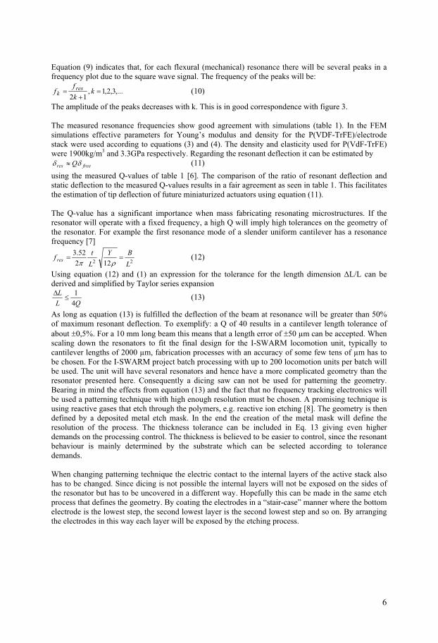
Equation (9) indicates that, for each flexural (mechanical) resonance there will be several peaks in a frequency plot due to the square wave signal. The frequency of the peaks will be:
,...3,2,1,12
kkf
f resk (10)
The amplitude of the peaks decreases with k. This is in good correspondence with figure 3.
The measured resonance frequencies show good agreement with simulations (table 1). In the FEM simulations effective parameters for Young’s modulus and density for the P(VDF-TrFE)/electrode stack were used according to equations (3) and (4). The density and elasticity used for P(VdF-TrFE) were 1900kg/m3 and 3.3GPa respectively. Regarding the resonant deflection it can be estimated by
freeres Q (11) using the measured Q-values of table 1 [6]. The comparison of the ratio of resonant deflection and static deflection to the measured Q-values results in a fair agreement as seen in table 1. This facilitates the estimation of tip deflection of future miniaturized actuators using equation (11).
The Q-value has a significant importance when mass fabricating resonating microstructures. If the resonator will operate with a fixed frequency, a high Q will imply high tolerances on the geometry of the resonator. For example the first resonance mode of a slender uniform cantilever has a resonance frequency [7]
22 12252.3
LBY
Ltf res (12)
Using equation (12) and (1) an expression for the tolerance for the length dimension L/L can be derived and simplified by Taylor series expansion
QLL
41 (13)
As long as equation (13) is fulfilled the deflection of the beam at resonance will be greater than 50% of maximum resonant deflection. To exemplify: a Q of 40 results in a cantilever length tolerance of about 0,5%. For a 10 mm long beam this means that a length error of 50 μm can be accepted. When scaling down the resonators to fit the final design for the I-SWARM locomotion unit, typically to cantilever lengths of 2000 μm, fabrication processes with an accuracy of some few tens of μm has to be chosen. For the I-SWARM project batch processing with up to 200 locomotion units per batch will be used. The unit will have several resonators and hence have a more complicated geometry than the resonator presented here. Consequently a dicing saw can not be used for patterning the geometry. Bearing in mind the effects from equation (13) and the fact that no frequency tracking electronics will be used a patterning technique with high enough resolution must be chosen. A promising technique is using reactive gases that etch through the polymers, e.g. reactive ion etching [8]. The geometry is then defined by a deposited metal etch mask. In the end the creation of the metal mask will define the resolution of the process. The thickness tolerance can be included in Eq. 13 giving even higher demands on the processing control. The thickness is believed to be easier to control, since the resonant behaviour is mainly determined by the substrate which can be selected according to tolerance demands.
When changing patterning technique the electric contact to the internal layers of the active stack also has to be changed. Since dicing is not possible the internal layers will not be exposed on the sides of the resonator but has to be uncovered in a different way. Hopefully this can be made in the same etch process that defines the geometry. By coating the electrodes in a “stair-case” manner where the bottom electrode is the lowest step, the second lowest layer is the second lowest step and so on. By arranging the electrodes in this way each layer will be exposed by the etching process.
6

The results from table 1 show that the FPC-based cantilevers obtained the highest static and harmonic deflection. This is convenient since the FPC-substrate allows more complicated geometric structures as it is compatible with lithographic and etching steps. Future work will be concentrated on the FPC substrates since this material allows for further miniaturization and simple batch processing with high tolerances needed in the I-SWARM project.
ConclusionsThe piezoelectric polymer P(VDF-TrFE) has successfully been processed to obtain a monolithic multilayered active stack of 6 active layers on top of steel, polycarbonate, FPC and aluminum substrates. The substrates with the active stacks were diced into cantilevers to examine the resonant behavior. By changing substrates the Q-value could be varied between 30 and 77. FPC showed the best performance in terms of static and resonant deflection. The Q-value of FPC was 64 and showed good adhesion to the multilayered copolymer stack. Moreover FPC has been used successfully in industrial mass fabrication processes including lithography and hence well suited as a substrate material for the actuators designated for the I-SWARM project.
Acknowledgement This work was funded by the European Commission IST priority, FET “beyond robotics” project number 507006. Göran Gustafsson Foundation is also gratefully acknowledged.
References[1] T. Lilliehorn, T. Blom, U. Simu, S. Johansson, M. Nilsson and M. Almqvist, Multilayer piezoelectric
copolymer transducers, Ultrasonics Symposium, 2005 IEEE, Vol 3, 18-21 Sept. 2005, pp. 1618 – 1620. [2] J. G. Smits, W-S. Choi, The Constituent Equations of Piezoelectric Heterogeneous Bimorphs, IEEE Trans.
Ultrason. Ferroelectr. Freq. Control. 28 (1991) (3), pp. 256-270. [3] K. Koga, H. Ohigashi, Piezoelectricity and related properties of vinylidene fluoride and trifluorethylene
copolymers, J. Appl. Phys. 59 (1986) (6), pp. 2142-50. [4] R. Köhler, N. Neumann, G. Hofmann, Pyroelectric Single-element and linear array sensors based on
P(VDF/TrFE) thin films, Sens. Actuators A: Phys. 45 (1994), pp. 209-218. [5] D. Setiadi, P.P.L. Regtien, P.M. Sarro, Application of VDF&TrFE copolymer for pyroelectric image
sensors, Sens. Actuators A: Phys. 41-42 (1994), pp. 585-592. [6] Uchino K., Ferroelectric Devices, Marcel Dekker, Inc., USA, 2000 [7] Huang T. C. Eigenvalues and Modifying Quotients of Vibration of Beams, and Eigenfunctions of Vibration
of Beams, Univ. Wis. Eng. Exp. Sta. Repts. Nos. 25 and 26, (1964). [8] S. Karlsson and S. Johansson, A New Flexible Technique for Microsystems, Proc. SPIE’s Int. Symp.
Microelectr. Micro Electro Mech. Systems, Surfers Paradise, Australia, 1999.
7

8

Paper II


Multilayer Electroactive Polymer Unimorph Actuators for the I-SWARM project
E. Edqvist, N. Snis, U. Simu, and S. Johansson Department of Engineering Sciences, Uppsala University, Box 534, SE-751 21 Uppsala, Sweden
AbstractIn this article the previously presented multilayered poly (vinylidenefluoride-trifluoroethylene P(VDF-TrFE) actuator manufacturing process is further developed. The actuator unit investigated in this study consists of three unimorph cantilevers (10x2 mm). The outline of the actuator unit is patterned in the cupper layer of the flexible printed circuit board by lithographic methods. A stair case type of contact area is created by the use of different shadow masks for each aluminium electrode layer. The contours of the unit and the contact area are etched by Reactive Ion Etching (RIE) using the cupper and the electrode layers as etch mask. After the removal of all P(VDF-TrFE) that is not covered by the aluminium electrodes, the different electrode layers can be connected from above with conductive adhesive. The cantilevers presented have five active P(VDF-TrFE) layers and six layers with alternating ground and phase electrodes. By the multilayer principle the drive voltage can be decreased and by utilizing the resonating behaviours, the stroke can be further improved. A 4V signal resulted in a tip deflection of 250 m.
KeywordsMultilayer, actuator, PVDF-TrFE, RIE etching, resonating structure.
Introduction In this paper we present the further development of the multilayer processing technology for piezoelectric polymer actuators that was presented previously [1]. The emphasis is put on a on a locomotion unit consisting of three unimorph cantilevers that operate at resonance. The locomotion unit presented in this article is part of the European Commission sponsored Intelligent Small World Autonomous Robots for Micro-manipulation (I-SWARM) project, with the objective to present a swarm of operational (3x3 mm) microrobots. Piezoceramics have previously been the dominating actuator material used for locomotion of microrobots [2-5], but polymers are advantageous in many ways. In particular the low cost of materials, vast processing opportunities and possible miniaturisation should be mentioned. These advantages are at the expense of higher mechanical and dielectric losses and lower piezoelectric constants. Although the maximum piezoelectric strain level (0.1 %) of conventional piezo polymer is the same, the piezoelectric polymers require higher electrical fields to reach the same maximum strain as the piezoceramic materials. However, thin films are more easily made in polymers than in piezoceramics compensating for the lower piezoelectric constant. Multilayer structures in piezoceramic actuators are commonly used to reduce the drive voltage to levels feasible in Microsystems, but have been sparsely utilized for piezoelectric polymers. The ability to drive the locomotion structure at low voltages is crucial for the I-SWARM project. To compensate for the lower strains at low voltage, the locomotion unit for the I-SWARM project is supposed to operate at a resonating frequency.
The most widely used ferroelectric polymers are poly(vinylidene fluoride), P(VDF), and the copolymer poly(vinylidene fluoride-trifluoroethylene), P(VDF-TrFE). PVDF exist in different crystalline modifications among which the polar -form, typically obtained by stretching, is of most interest as actuator material. In the copolymer P(VDF-TrFE) the -form is obtained directly from melt or solution, improving the ability to form thin films without a need for subsequent mechanical
1

deformation. Spin cast copolymer films with a thickness down to about 100 nm have shown maintained ferroelectric behaviour [6, 7]. One of the most common and interesting applications of the piezopolymers is ultrasonic transducers, since the acoustic impedance of these materials are well matched to e.g. water, in contrast to piezoceramics. Multilayer transducers [8] have also been proposed to lower the impedance and to increase the electrical field and spin cast single layer transducers [9-12] have been presented. Earlier the first monolithic multilayer copolymer transducer built by spin casting and without the need for performing adhesive lamination of single layers was presented [13]. In this paper the process is further developed, the thickness of the copolymer layers are reduced and reactive ion etching is introduced to define the locomotion unit.
Design and unimorph behaviour The multilayer unimorph is manufactured on a passive substrate part, in this paper a FPC, with one copper layer closest to the active stack, and a polyimide part. The choice of substrate for the monolithic actuator structure was based on a previously done resonating behavior study [1]. The active stack consist of thin P(VDF-TrFE) layers sandwiched between aluminium electrodes, Fig 1. Every other electrode is connected to ground and the intermediate electrodes are connected to the drive signal.
P(VDF-TrFE) layersAluminumelectrodes
V
Cupper layer
Polyimide substrate
Fig. 1 Schematic drawing of the multilayer unimorph cross section. The total thickness is about 58 µm.
The locomotion unit consists of three identical unimorphs. Fig. 2. Each leg has a contact pad for drive voltage signal and there is one ground connecting all three unimorphs. This design allows for a turning ability in both directions as well as a forward and backward motion. At the pads, all layers are exposed from above in a stair case manner since all copolymer that are not covered with a metal layer should be removed in the dry etch process used to shape the devices, Fig. 3.
2

Fig. 2 a) Actuator structure with three unimorphs (left). b) Dimensions of the structure (right).
Fig. 3 Top view of one contact pad.
The free static deflection of the unimorph legs can be estimated with help of formulas for heterogeneous bimorphs [14]. To calculate the deflection of the P(VDF-TrFE) multilayer on top of the passive substrate the active multilayer is treated as one material with an effective thickness ta, Young’s modulus Ya and piezoelectric coefficient d31
a.epa tnntt )1( (2)
))1((1eeppaa tYntnYtY (3)
p
aa
ppa dYtYnt
d 3131(4)
Subscripts p and e are for the P(VDF-TrFE) and electrodes while n is the number of active polymer layers. The Cu-polyimide substrate is treated analogously. The static deflection can then be expressed as:
)4641()1(3 4232
312
sa
a
ttnUdL (5)
with
3

s
a
YY
and
s
a
tt
The subscripts s and a stand for the substrate and the active multilayer respectively. Y is the Young’s modulus, U is the applied voltage, n the number of active layers, d31
a is the effective piezoelectric coefficient of the active multilayer, L the length of the leg, ta and ts the thickness of the active multilayer and the substrate respectively. The d31 coefficient for our 65:35 P(VDF-TrFE) is estimated to be 10 pm/V [15]. A reasonable estimation of the resonance frequency for a uniform cantilever (beam supported in one end) is [16]
4
2
122 LtYKf
eff
ueffnr (6)
with Yeff being the effective Young’s modulus, L the length, t the thickness, eff the effective density,
and a constant where n refers to the mode of vibration. YnK eff and eff can be calculated as volume averages in analogy with e.g. equation (3). From [16] we find that the two first modes are K1= 3.52 and K2 =22.0.
The capacitance is an important parameter, and can be used for quality control.
ur t
LbNC 0 (7)
with N being the number of active layers, r the dielectric constant [17], L the length, b the width, and the thickness of the active layer. Alternatively to quality control, the relative permittivity can be
derived from this. The relative permittivity used for the calculations is 9.0 [18]. The deflection of the unimorph is amplified at resonance and the amplification factor is related to the quality factor
ut
12 fff
Q rm (8)
where f1 and f2 are the frequencies at which the deflection amplitude is one half its maximum value.
ExperimentalThe polymer slurry was prepared out of 65/35 P(VDF-TrFE) grains (Solvay, France), which were dissolved in a Methyl-Ethyl-Keton (MEK) Solution (1:10 by weight) on a heating pad. The substrate consisted of a double sided polyimide FPC (Espanex , Nippon Steel Chemical Co, Ltd, Japan). Standard lithographic processes including MicroChem SU8 resist and a Karl Süss MA6 maskaligner were used to pattern the guide holes for the mask alignment in the cupper layer on the backside of the FPC. On the front side of the FPC the guide holes and the contours of the locomotion unit including the contact areas were patterned. The lithographically defined areas were removed by wet chemical Cu-etching. The guide holes was then dry etched from the backside in a plasma mixture of O2/CHF3(50 sccm O2, 5 sccm CHF3, 80 mTorr, 100 W) in an equipment built at Uppsala University. The remaining photoresist were removed with acetone and the back side of the FPC was completely stripped in the Cu-etching bath. The FPC was fixed on a glass plate with epoxy adhesives. The first aluminium (Balzers, 99.999 %) electrode layer was subsequently evaporated (Edwards, at 1 10-6 mTorr) through a shadow mask on the Cu layer. The shadow mask was manufactured out of etched stainless steel foils (HP-Etch AB, Sweden) and used four guide holes to align the mask with the substrate in a mask holder. Each mask allowed a batch fabrication of three locomotion units. Before the alignment the substrate was rinsed
4

with ethanol. The glass plate was then put in the spinner and a thin layer of PVDF-TrFE was spun cast (1000 rpm for 30 s) on to it. Then the substrate was annealed for three hours at 120°C to evaporate all the MEK. This concluded the production of the first single layer and the multilayer structure was produced by repeating this process with a new mask at each step. Six metal layers with five intermediate copolymer layers were deposited. Each Al film was measured on a separate reference glass substrate using a profilometer (Dektak). The cross section of the unimorph was cut up with a Focused Ion Beam (FIB) and the thickness of the active layers was measured on the resulting SEM picture. The structure was etched first for 3 hours on the backside and then etched for another two hours on the front side. The same equipment and plasma mixture as used for the etching of guide holes was used for the etching of the back side. For the front side etching, a plasma consisting of SF6 and O2was used. (1 sccm SF6, 39 sccm O2, 20 mTorr, 100W) was used.
Due to the design of the electrode masks all individual internal electrode layers should be exposed after the front side etching. To ensure that all remains of the PVDF-TrFE were removed, the contact area had to be cleaned with a fine tip of a cloth merged in MEK. These contact areas could then be contacted with thin cupper wires and conducting adhesive (Circuit Works®, CW2400, ITW Chemtronics, USA). The polarisation was carried out at 80°C for 20 min with a voltage of 100 V, applied over the layers. The sample was then removed from the oven and cooled to room temperature for 10 minutes with maintained voltage level. After the polarisation the capacitance for each leg was measured (LCZ-meter, Keithley). A waveform generator and a power supply (WFG 400, PA 19-4, FLC Electronics AB, Sweden) was used to drive the unimorph at different voltages. The locomotion unit was glued on to a printed circuit board and the tip deflection was measured with an optical probe (D-20, Philtec), measuring the intensity of the reflected light with a spot size of 0.5 mm. A square wave signal with an amplitude of 4 V was used when measuring tip deflections as a function of frequency and voltage. Static deflections were measured at a few Hz.
ResultsMultiple units of the locomotion unit were successfully fabricated, Fig 4. The unimorph cantilevers (legs) have the dimensions 10x2 mm (length x width). The spun coated P(VDF-TrFE) layers were 5.8, 5.8, 5.6, 4.2, and 3,4 m thick and the electrode layers were 120±60nm thick, resulting in an overall thickness of the PI substrate and multilayer structure of 58 m. In Fig. 5. the cross section of the actuator can be seen. The total thickness of the actuator was measured both with a Heidenhain probe (300-102, Germany) and a SEM after a cross section had been cut. The SEM picture revealed that the cupper layer was thinner than stated by the supplier. It also varied along the cross section. The polyimide layer was measured to 15 μm. With the measured thickness of the active layers a theoretical capacitance of 6.6 nF could be calculated for each leg using equation (7). The measured capacitance was 4.5 nF.
5

Fig. 4 Three actuator structures consisting of three unimorphs before etching. The circular contact pads are clearly visible through the P(VDF-TrFE) layers.
Fig. 5 SEM picture showing a FIB cross section of the active part of the unimorph with the five active P(VDF-TRFE) layers.
The etch process left some residuals on the edge of the structure, Fig. 6. The multilayer dimensional accuracy varied some between the batches, this can also be seen in Fig. 6.
6

Fig. 6 a) Etch residuals after back-side dry-etching can be seen on the edges of the released unimorph (left). b)The alignment accuracy of the electrode layers are visible (right).
The tip peak to peak deflection as a function of the frequency using a drive voltage of 4 V is shown in Fig. 7. A deflection of 250 m was measured at 170 Hz. The smaller peaks below 170 Hz are explained in [1].
Fig. 7 The unimorph tip deflection as a function of the frequency at a drive voltage of 4 V. The first natural resonance peak is at 170 Hz.
The measured values as well as theoretical values are presented in table A. To find the quality factor, equation (6) was used and the resonance peak at 170 Hz resulted in a value of 19.
7

Table 1. Theoretical and measured values of the capacitance, quasi-static deflection, resonant deflection, resonance frequency and Q-value are presented.
Theoretical capacitance [nF] 6,6Measured capacitance [nF] 4.5Theoretical static deflection peak to peak [ m] 9,8Measured static deflection peak to peak [ m] 6.0Theoretical resonance frequency [Hz] 242Measured resonance frequency [Hz] 170Measured dynamic deflection [ m] 250Measured Q 19Ratio dynamic/static deflection 42
DiscussionOne of the main drawbacks with piezoelectric polymers is the high drive voltage required to obtain useful strain. With the multilayer process presented in this paper, driving at typical voltage levels of integrated circuits is possible. To the authors’ knowledge multilayer patterned structures like the unimorph cantilevers investigated in this article have not been presented before. An advantage of the usage of polymer actuators and this particular process is the low annealing temperature and the fact that no final sintering step is need as with the piezo ceramics. This allows more diverse set of substrates to be used and the process to be compatible with integrated circuits as long as the integrated circuits can be isolated during the polarisation step.
Fluorinated polymers are not easily dry etched and P(VDF-TrFE) is no exception. The dry etch recipe used in this paper is by no means optimised and residuals are left on the upper surface and at the edges of the locomotion unit. Primarily this is a problem for the electrical connection of the multilayer structure. The manual cleaning of the electrodes on the contact pads has to be replaced with an optimized etch recipe. Moreover the residual material at the edges of the structure might have an affect on the resonance frequency. Some of the residuals were removed by rinsing in an ultrasonic ethanol bath. It is believed that a proper etch recipe can be developed, and that will be our focus in future studies. At the present stage of development the dry etching works satisfactory for singulation, i.e. cutting out the units from the FPC.
In the previous article [1] the alignment issues with using a shadow mask was discussed. For this batch an improved shadow mask holder was manufactured using shorter guide pins allowing for a higher linear accuracy between the layers. The etch compensation for the guide holes of the mask were also less than previously tested structures. An optical inspection under microscope had to be done to make sure that each mask was as aligned as possible to the previous layer. A misalignment of about 100 mcould be seen on some of the structures.
The etch residuals seen in Fig. 6 could to some extent change the resonating frequency of the cantilever but the factor with the largest effect on the resonating frequency would be the length of the cantilever. In this experiment the length and the rest of the contour of the cantilevers were defined by the front side cupper layer. The electrod layers are aligned to each other and the contour by the guide pins. The alignment tolerance in this process should be as in figure 6 b), about 100 μm, a too large tolerance for future actuator structures. To maintain at least 50% of the dynamic stroke a Q-value of 25 would correspond to a length tolerance of about 1% [1]. In the planned I-SWARM robots the legs will be about 3 mm and this would demand e.g. a length tolerance of 30 μm. At first such tolerance requirements appear difficult to reach even with further improved shadow mask alignment. Still, the most important parameter is the variation of length rather than the absolute length value. By making the contour width of the cantilever larger than the electrode, the alignment of the electrodes on the front side is not expected to be as critical as the control of the cantilever outline. In future we will
8

therefore investigate the effects of patterning the cupper layer on the backside of the FPC for dry etch singulation and exclude the front side Cu pattern. The discrepancy in the capacitance values could to some extent be explained by an unknown real electrode area. Misalignment of the electrode layers as well as loss of part of layers or complete layers after polarisation and contacting, decreases the surface and hence the capacitance. During polarisation at high voltages electrical field breakdown occur. Thereby material is burnt away and a part of the active area may be lost. The residuals on the surface after the dry etch process could prevent the conducting glue from getting in contact with the metal layers and the contact with a whole layer may then be lost. It is difficult to conclude if the manual cleaning of the contact pads resulted in contact with all electrode layers. Most probably the main reason for the discrepancy in capacitance value is due to loss of contact with one or several electrode layers, and this question will be one of the most important in our future work.
There is some discrepancy between the measured deflection and the theoretical calculated value. The measured static deflection is lower than expected. The discrepancy can to some extend be explained by the usage of effective values of the Young’s modulus. The theoretical estimation of the deflection should give a lower limit of the stroke The calculation uses an average value for the Young’s modulus of the substrate while the stiffer material, the Cu, is centred in the middle of the cantilever and will have less effect on the bending than if it would be distributed evenly in the substrate. The thickness variance of the cupper layer could also explain some of the discrepancy. Experimentally measured static deflection is therefore somewhat low. It is reasonable to assume that this is due to a loss of electrode area, in analogy with the reduction in capacitance of the cantilever. The dynamic deflection has a lower Q-value than in previous work [1], 19 in comparison with 41 and two important factors should be the reduced metal content and the more flexible cantilever support. A Q-value of around 20 is still rather good in the considered application with no possibility to use frequency tracking electronics and with the discussed limitations in reducing the relative size variations of the cantilevers. The relation between the Q-value and the ratio between dynamic and static deflection is more or less similar to what we have measured earlier. If we include that the first sinusoidal component (Fourier series) of the supplied square wave signal has an amplitude that is 4/ larger than the drive voltage, the ratio can be reduced from 41 to 32, since the quasi-static measurements should correspond to the drive voltage. A dynamic/static deflection ratio of 32 appears reasonably consistent with the Q-value of 19. The peak at 170 Hz should be the first flexural resonance mode. The peaks lower than 100 Hz are believed to be artefacts due to the square wave signal, the first flexural resonance should occur as well at 1/3, 1/5, 1/7 etc. of the drive frequency since the square wave can be considered as the sum of a series of sinusoidal components as discussed in [1].
In this paper the commercially available P(VDF-TrFE) copolymer with a low piezoelectric strain (0.1 %) was chosen as active material in the multilayer unimorph, but it has already been shown that this copolymer can be modified to give much better performance. Material that exhibit very large electrostriction (5 %) at high electrical field can be obtained by high energy electron irradiation of the copolymer or by adding a third bulky polymer to form terpolymers [19-22]. These high performance materials can likely be fabricated using the same process scheme presented here. The result of such a combination would most likely be very large strokes.
Conclusions and future work With the multilayer technology presented in this paper the usefulness of piezopolymers in actuator applications increases. Benefiting from the thin copolymer layers in a multilayer actuator and the magnification achieved by using an unimorph structure large stroke can be obtained even at low drive voltage. Driving the structure at resonance the stroke can be further improved. A 4V signal resulted in a tip deflection of 250 m. With the modified versions of the P(VDF-TrFE) even higher strains could be reached. Future work will include the miniaturization of the evaluation structure so that the size will be acceptable for the I-SWARM size restrictions of 3*3 mm. The miniaturization step will include better alignment processes and an improved etch recipe. The thickness of the active layers also has to be optimized to avoid large discrepancies.
9

AcknowledgementsThis work was funded by the European Commission IST priority, FET “beyond robotics” project number 507006, which is gratefully acknowledged. The Göran Gustafsson Foundation is also acknowledged for their financial sport.
References[1] N. Snis, E. Edqvist, U. Simu, and S. Johansson, "Monolithic Multilayer P(VDF-TrFE) Resonators,"
Sensors and Actuators a-Physical, vol. Submitted, 2006. [2] U. Simu and S. Johansson, "Fabrication of monolithic piezoelectric drive units for a miniature robot,"
Journal of Micromechanics and Microengineering, vol. 12, pp. 582-589, 2002. [3] N. Snis, U. Simu, and S. Johansson, "A piezoelectric disc-shaped motor using a quasi-static walking
mechanism," Journal of Micromechanics and Microengineering, vol. 15, pp. 2230-2234, 2005. [4] F. De Ambroggi, L. Fortuna, and G. Muscato, "PLIF: Piezo Light Intelligent Flea new micro-robot
controlled by self-learning techniques," presented at 1997 lEEE International Conference on Robotics and Automation, Albuquerque, New Mexico - April, 1997.
[5] S. Martel, K. Doyle, G. Martinez, I. Hunter, and S. Lafontaine, "Integrating a complex electronic system in a small scale autonomous instrumented robot: The NanoWalker Project," Proceedings of SPIE - The International Society for Optical Engineering,, vol. 3834, pp. 63-74, 1999.
[6] Q. M. Zhang, H. S. Xu, F. Fang, Z. Y. Cheng, F. Xia, and H. You, "Critical thickness of crystallization and discontinuous change in ferroelectric behavior with thickness in ferroelectric polymer thin films," Journal of Applied Physics, vol. 89, pp. 2613-2616, 2001.
[7] O. H. Kimura K, "Ferroelectric properties of poly(vinylidenefluoride-trifluoroethylene) copolymer thin films," Applied Physics Letters vol. 43, pp. 834-836, 1983.
[8] P. J. D. Swartz R G, "On the generation of high-frequency acoustic energy with polyvinylidene fluoride," IEEE Transactions on Sonics and Ultrasonics, vol. SU-27, pp. 295-303, 1980.
[9] A. S. Fiorillo, J. Vanderspiegel, P. E. Bloomfield, and D. Esmailzandi, "A P(Vdf-Trfe)-Based Integrated Ultrasonic Transducer," Sensors and Actuators a-Physical, vol. 22, pp. 719-725, 1990.
[10] M. Z. Sleva, R. D. Briggs, and W. D. Hunt, "A micromachined poly(vinylidene fluoride-trifluoroethylene) transducer for pulse-echo ultrasound applications," Ieee Transactions on Ultrasonics Ferroelectrics and Frequency Control, vol. 43, pp. 257-262, 1996.
[11] L. F. Brown, R. L. Carlson, and Sempsrott, "Spin-cast P(VDF-TrFE) films for high performance medical ultrasound transducers," IEEE Ultrasonics Symposium, pp. 1725-1727, 1997.
[12] M. Robert, G. Molingou, K. Snook, J. Cannata, and K. K. Shung, "Fabrication of focused poly(vinylidene fluoride-trifluoroethylene) P(VDF-TrFE) copolymer 40-50 MHz ultrasound transducers on curved surfaces," Journal of Applied Physics, vol. 96, pp. 252-256, 2004.
[13] T. Lilliehorn, T. Blom, U. Simu, M. Nilsson, M. Almqvist, and S. Johansson, "Multilayer piezoelectric copolymer transducer," IEEE Ultrasonics Symposium, 2005.
[14] V. Monturet and B. Nogarede, "Optimal dimensioning of a piezoelectric bimorph actuator," European Physical Journal-Applied Physics, vol. 17, pp. 107-118, 2002.
[15] K. Koga and H. Ohigashi, "Piezoelectricity and Related Properties of Vinylidene Fluoride and Trifluoroethylene Copolymers," Journal of Applied Physics, vol. 59, pp. 2142-2150, 1986.
[16] W. C. Young and R. G. Budynas, Roark's Formulas for Stress and Strain - 7th edition: McGraw-Hill, international edition 2002.
[17] N. Neumann, R. Kohler, and G. Hofmann, "Application of P(Vdf Trfe) Thin-Films in Pyroelectric Detectors," Ferroelectrics, vol. 118, pp. 319-324, 1991.
[18] R. Kohler, N. Neumann, and G. Hofmann, "Pyroelectric Single-Element and Linear-Array Sensors Based on P(Vdf Trfe) Thin-Films," Sensors and Actuators a-Physical, vol. 45, pp. 209-218, 1994.
[19] Q. M. Zhang, V. Bharti, and X. Zhao, "Giant electrostriction and relaxor ferroelectric behavior in electron-irradiated poly(vinylidene fluoride-trifluoroethylene) copolymer," Science, vol. 280, pp. 2101-2104, 1998.
[20] A. Petchsuk and T. C. Chung, "Synthesis and electrical property of VDF/TrFE/HFP terpolymers, Materials research society symposium proceedings," vol. 600, pp. 53-60, 2000.
[21] H. S. Xu, Z. Y. Cheng, D. Olson, T. Mai, Q. M. Zhang, and G. Kavarnos, "Ferroelectric and electromechanical properties of poly(vinylidene-fluoride-trifluoroethylene-chlorotrifluoroethylene) terpolymer," Applied Physics Letters, vol. 78, pp. 2360-2362, 2001.
[22] Z. Y. Cheng, V. Bharti, T. B. Xu, H. S. Xu, T. Mai, and Q. M. Zhang, "Electrostrictive poly(vinylidene fluoride-trifluoroethylene) copolymers," Sensors and Actuators a-Physical, vol. 90, pp. 138-147, 2001.
10

Paper III


Gentle dry etching of P(VDF-TrFE) multilayer micro actuator structures by use of an ICP
E. Edqvist, N. Snis, U. Simu, and S. Johansson Department of Engineering Sciences, Uppsala University, Box 534, SE-751 21 Uppsala, Sweden
AbstractThis paper focus on structuring a multilayer micro actuator consisting of poly(vinylidenefluoride-tetrafluoroethylene) P(VDF-TrFE) and evaporated aluminium electrodes. The unimorph actuator has ten active layers of P(VDF-TrFE) sandwiched between phase and ground electrodes. A modified Bosch process in an Inductive Couple Plasma (ICP) etcher is used to remove all P(VDF-TrFE) not covered by the electrodes. Since each electrode mask is slightly different from the others the result is a staircase like inter-contact area that can be contacted from above using conductive adhesive. The chosen ICP etch has resulted in good agreement between theoretical and measured capacitance values after establishment of the interlayer electrode contact. The tip deflection of the 2 mm long cantilever was measured to 8.3 m at 5000 Hz with a square wave signal of 3.3 V. The results are promising for the batch fabrication of the locomotion unit for the EU-funded I-SWARM robot.
KeywordsMultilayer, micro actuator, PVDF-TrFE, ICP etching, resonating structure.
Introduction The polymer Polyvinylidene Fluoride P(VDF) can be found in a lot of applications ranging from inner sheath of oil pipelines to ultrasonic devices. It has a monomer chain of (Ch2-CF2-)n and as most fluorinated polymers like polytetrafluoroethylene, has good physical resistance to most form of chemical attacks [1]. Other interesting properties are biocompatibility and mechanical flexibility. In 1969 Kawai discovered that elongated and poled films of P(VDF) are piezoelectric [2]. Since then the usage of P(VDF) for different applications like ultrasonic sonars[3], shock sensors [4], pyroelectric sensors [5] have increased. The need to modify the surface of P(VDF) by plasticizers like phthalates and fatty acid esters has been done in applications for years [6], but methods to micro structure the material is less know. This article will focus on how to structure and etch multilayer actuators of poly(vinylidene-fluoride-tetrafluoroethylene) P(VDF-TrFE), (-CF2-CFH-)n.
The ability to structure and sculpture materials is the foundation of micro structure engineering. When processing silicon based materials this is normally achieved by wet chemical etching or dry chemical by the assistance of a plasma. When changing substrate to polymer with thin films of P(VDF) most of the processes for silicon substrates are difficult to adapt. According to the literature, different attempts have been done to structure P(VDF).
In the eighties P(VDF) attracted attention by membranes and filters manufactures. The polymer was irritated by heavy ions and then etched in different solution to enhance the ion perforated structure. The most common solution found in the literature is KNO3 in combination with KMnO4. Different molar as well as different temperature ranges are presented [6-10], but also a solution like NAOH [11] have been used.
1

Applications that utilize some of the piezoelectric properties of P(VDF-TrFE), usually demand good accuracy in any etching process and different methods have been reported. In the manufacturing process of a P(VDF-TrFE) based pyroelectric sensor, Setiadi and Regtien [12] used 30 ºC Methyl-Ethyl-Keton (MEK) to etch a silicon dioxide patterned matrix array of sensors. The same solution was reported to be used in combination with a mask by Isler and Washington [13]. Moanohara et al used a direct pattern transfer method to photo etch P(VDF) by using x-rays [14]. The deepest etch depth reported was 9 μm. Dargahi et al has recently presented a way to wet chemical etch thick P(VDF-TrFE) films in combination with photo resist [15].
The wet chemical etch method require extra lithographic steps, like adding and stripping photo resist. These including H2O based solutions and due to initial poor results with P(VDF-TrFE) films peeling of the substrate at H2O contact the method seemed less compelling. The poor results in combination with the design of the multilayer inter-contact areas implied that physical dry etching should be the main method to structure the multilayer actuator. To our knowledge there are few references of plasma assisted etching of P(VDF). Wirges et al [16] reported an improved adherence on flourpolymer for photo resist, after a short exposure to a nitrogen plasma. Once the lithographic process was done the sample was etched with reactive ion etching in a N2O plasma. Oxygen plasmas were briefly reported to structure films made out of P(VDF-TrFE) by [5, 17]. No mixture or parameters were given in these articles.
The dry etch method used in this paper is well established in the Silicone based MST community as the Bosch process. The deep plasma assisted etching of Teflon-like films, acting as passivation layers for the Silicon etching, is very well described in the literature and there are many functional recipes to use. The idea was to enhance the polymer etching part of the Bosch process and skipping the silicon etching part [18, 19]. The result could be an possible way to gently etch the P(VDF-TrFE) with remaining top electrodes acting as etch masks.
The work presented in this article is part of the European sponsored Intelligent Small World Autonomous Robots for Micro-manipulation (I-SWARM) project, with the objective to present a swarm of operational (3x3 mm) robots. In this paper we present a recipe to etch P(VDF-TrFE) multilayered structures in a Plasma Therm Inductive Coupled Plasma (ICP) equipment using a modified Bosch process. The new process gives an improved robustness to the previously presented multilayer process. The presented multilayer structure is also tested under realistic I-SWARM operation condition.
2

Experiment
The I-SWARM robot will have a maximum of 3.3 V available to be used by the locomotion unit. We have previously presented a multilayer technique and a large locomotion unit to reach sufficient motion performance at low drive voltages [20]. The structures used in this paper are the true scale of the I-SWARM locomotion unit. It has three cantilevers attached to a quadratic body where the electric contacts for the different layers can be connected. The cantilevers size are 2.15x0.4 mm and the quadratic body is 3x3 mm, see Fig 1.
Fig. 1 The size of the locomotion unit with the different electrodes and inter-contact areas visible.
The three legged bimorph locomotion unit utilizes a Flexible Printed Circuit (FPC) board as the passive substrate material and the active part of the unimorph is manufactured by spin coating P(VDF-TrFE) layers between shadow evaporated aluminium electrodes. By alternating the phase and the ground layer a multilayer unimorph can be manufactured, Fig 2a. To connect the different layers, staircase inter-contact areas are designed for each phase electrodes and the common ground electrode. By removing the layers of P(VDF-TrFE) at the inter-contact area by dry etching, the electrodes are exposed from above, Fig 2b, and can be connected by printing conductive adhesives on top.
Fig. 2 a) The cross section of the unimorph. Ten layers of active P(VDF-TrFE) are sandwiched between aluminium electrodes (left) b) The etched inter contact ground area with six ground electrodes that can be
electrically joined by printing a string of conductive adhesive on top (right).
3

A single sided 18-50 polyimide FPC with 18 μm cupper and 50 μm polyimide, was used as substrate. The cupper layer was lithographically defined with the same process as in [20]. The defined cupper side was turned up side down and the FPC was aligned and fixed with spray adhesives on a stainless steel foil with the same type of guide holes as presented in [20]. The stainless steel foil has the same size and thickness as the shadow masks. The alignment was performed in the substrate holder from [20] under a optical microscope. Each P(VDF-TrFE) layer was coated in a spinner and then annealed for three hours at 60ºC and at 120 ºC for another three hours. The electrodes were resistively evaporated through the shadow masks, a slightly different one for each layer.
In order to be able to etch the substrate in the ICP (Plasma Therm, SLR Series), a special two part substrate holder with the size and appearance of a 4 inch silicon wafer was manufactured. The thickness of the bottom part of the holder is 2 mm and it has four guide pins that are used to mount the FPC. The top part of the holder, also 2mm thick, has four holes for the guide pins and four screws to secure it to the bottom part. A 4x4 cm hole in the top part allowed the plasma to etch the actuator unit.
A standard Bosch recipe was used as start recipe. After initial adjustments to the pressure and gas concentration, the individual cycle time was increased. Small strings of three or four actuator modules were used to fine tune the right substrate bias power level and number of cycles as listed in table 1.
Table 1 The parameters that were tested during the ICP etching of P(VDF-TrFE). Parameter interval tested
Substrate power [W] 5-15Number of cycles 15-45
After each test cycle the specimens were examined under an optical microscope and in a SEM to determine etch rate, condition of the top electrode, and amount of residuals left on lower electrodes.
The process was repeated until a functional recipe was found. The etched structures were then contacted with conductive adhesive (Circuit Works®, CW2400, ITW Chemtronics, USA). By using a fine xyz-probe station the electric capacitance could be measured on each individual actuator leg (LCZ-meter, Keithley). The substrate was then turned and etched on the backside in the RIE equipment, to define the cantilever contours. The defined Cu backside of the FPC was used as etch mask. After the capacitance had been measured again some extra conductive adhesive was applied on the contact areas and thin Cu wires was connected to each area. The units were then poled at 120 V for 20 minutes (Stabilised power supply type SF120.2, Danbride, Denmark) in an oven at 80ºC and then the capacitance was measured again. Some units were defined by a scalpel instead of being etched in the RIE.
The etch depth was measured in a profilometer (Dektak), an interference microscope, and by tilting the sample and measure the distance in the SEM. To estimate the P(VDF-TrFE) layer a trench was made in one of the three cantilever structures by a Focus Ion Beam (FIB). The electrode thickness was quantified by measuring the step height on co-evaporate glass substrate with the profilometer, a method also used in [20].
The locomotion unit was glued on to a printed circuit board and the tip deflection was measured with an optical probe (D-6, Philtec). A square wave signal with an amplitude of 3.3 V was applied to measure the tip deflection.
ResultsThree batches of 36 units per batch were manufactured up to the final RIE etching step of the cantilever contours. The units presented in this paper are five times smaller than the units presented in [20] and have ten active P(VDF-TrFE) layers. The individual layer thicknesses in one cantilever were
4

measured from the FIB cut in Fig. 3, and are presented in table 2. The electrode thicknesses are also presented in table 2. The total thickness of the active stack and the passive substrates was 101 μm.
Table 2 The thickness of the individual layers and electrodes of one unit.P(VDF-TrFE) layer thickness [µm] Electrode thickness [µm] t1 2,1 e1 0,09t2 2,0 e2 0,07t3 2,1 e3 0,12t4 4,0 e4 0,16t5 3,1 e5 0,11t6 3,9 e6 0,07t7 2,2 e7 0,08t8 2,6 e8 0,05t9 2,4 e9 0,09t10 3,1 e10 0,13
e11 0,17
Fig. 3 The ten layers of P(VDF-TrFE) and the eleven electrode layers are clearly visible in the trench.
With the estimated layer thicknesses and the relative permittivity of 9.0 from [5], a capacitance value for one cantilever could be calculated to 360 pF by using the theoretical area. Six units were defined in the RIE after the ICP step and three units were cut with a scalpel. The measured capacitance for the cantilevers before polarisation and after polarisation are presented in table 3.
5

Table 3 The capacitance value for the cantileversBefore polarisation [pF]Average capacitance 307Highest capacitance value 440
After polarisation Average capacitance 86Highest capacitance value 328
The original Bosch process is presented in table 4. The final ICP recipe that was chosen consists of different steps: a stabilizing step, an ignition step, the deposition step as well as two etch steps. The stabilizing and ignition step were not changed. Since the deposition step could not be removed from the process, the cycle time was minimized. The changed gas combinations, substrate effect, and cycle time for the two last steps are presented in table 5. The etch process resulted in sharp and well defined edges and the deepest etch depth obtained with intact top electrodes was 40 μm as seen in Fig. 4. The depth was reached after 103 minutes.
Tabell 4 The original Bosch Recipe on a Plasma Therm ICP C4F8
[sccm] SF6
[sccm] O2
[sccm] Ar
[sccm] Substrate
[W] Coil[W]
Pressure[mBar]
Time [s]
Deposition 70 0,5 - 30 1 825 22 5Step 1 0,5 50 - 30 9 825 23 2Step 2 0,5 100 - 30 9 825 23 6Table 5 The final recipe for etching P(VDF-TrFE)
C4F8[sccm]
SF6[sccm]
O2[sccm]
Ar[sccm]
Substrate[W]
Coil[W]
Pressure[mBar]
Time [s]
Deposition 70 0,5 - 30 1 825 22 0Step 1 5 10 - 30 5 825 10 120Step 2 0,5 - 40 20 5 825 10 30
Fig. 4 The deepest etch depth with intact top Al-electrodes was 40µm.
6

Fig. 5 shows that the top electrode still is intact and the bottom electrode is not covered with visible polymeric residuals. By looking closer at the edge on the lower ground electrode, it can be seen in Fig 6, that the etch process has etched 5 μm into the polyimide substrate.
Fig. 5 A phase inter- contact area with all the five clean electrodes ready to be contacted by conductive adhesive.
The edge structure of the electrode can in some cases become perforated by the etch as can be seen in Fig 6. Flakes of the electrode seems to be bending downwards decreasing the distance to the next layer.
Fig. 6 A close up of the lowest ground electrode. The edge of the electrode layer show signs of being perforated. The picture also show that the polyimide has been etched about 5 µm.
Similar edge effects were seen on other edges. Small flakes of the electrode were bending downwards to the next electrode layer, decreasing the distance compared to the rest of the electrode.
7
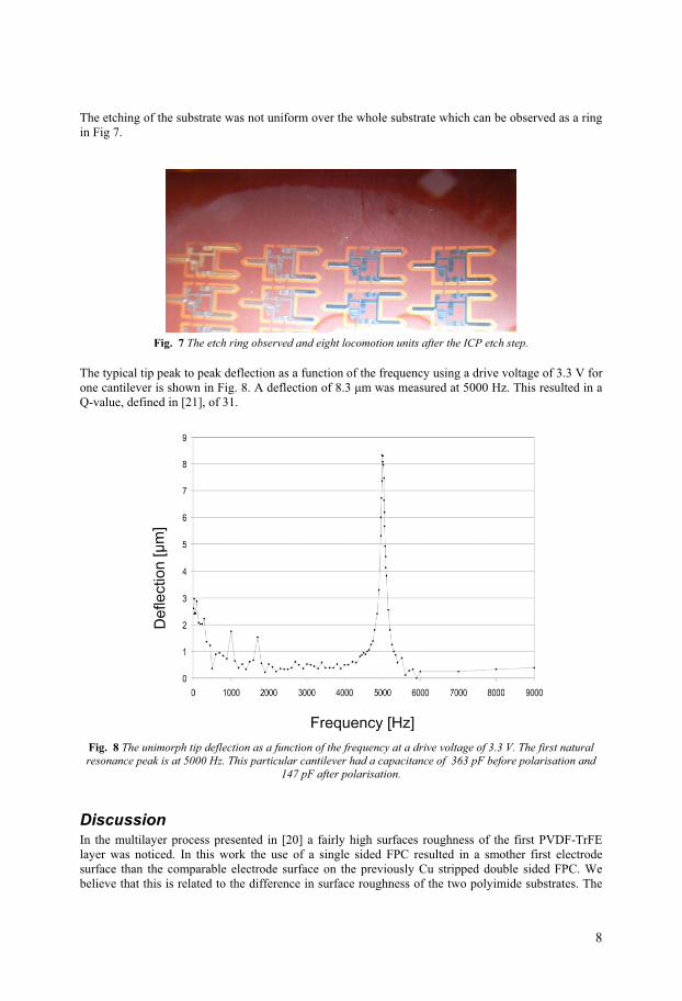
The etching of the substrate was not uniform over the whole substrate which can be observed as a ring in Fig 7.
Fig. 7 The etch ring observed and eight locomotion units after the ICP etch step.
The typical tip peak to peak deflection as a function of the frequency using a drive voltage of 3.3 V for one cantilever is shown in Fig. 8. A deflection of 8.3 m was measured at 5000 Hz. This resulted in a Q-value, defined in [21], of 31.
Fig. 8 The unimorph tip deflection as a function of the frequency at a drive voltage of 3.3 V. The first natural resonance peak is at 5000 Hz. This particular cantilever had a capacitance of 363 pF before polarisation and
147 pF after polarisation.
DiscussionIn the multilayer process presented in [20] a fairly high surfaces roughness of the first PVDF-TrFE layer was noticed. In this work the use of a single sided FPC resulted in a smother first electrode surface than the comparable electrode surface on the previously Cu stripped double sided FPC. We believe that this is related to the difference in surface roughness of the two polyimide substrates. The
8

alignment of the FPC substrate against the stainless steel foil and the usage of the foil, improved the alignment of the individual electrode layers, which resulted in a overall better alignment than in [20].
The FIB cut in Fig. 3 revealed that the control of the layer thickness still can be improved. Layer t4, t6 and to some extend t5 in table 2 are thicker than the rest of the layers. The difference in layer thickness could affect the polarisation degree for the thicker layers and imply a lower tip deflection than in the optimal case of thickness control. For the next batch manufacturing, more process parameters affecting the layer thickness have to be investigated. We believe that an even better thickness control is achievable.
In [20] we used a plasma mixture of O2/CHF3 in an equipment build at Uppsala University, to etch the contours of the actuator unit. The mixture etched through the polyimide part of the FPC, but did not work as well on the P(VDF-TrFE) part of the unimorph. Either the lower layers of the P(VDF-TrFE) were not etched and the top electrodes were removed, or the etch left such an amount of residuals on the electrode area, that the inter-connection between the layers could not be guaranteed. One example of an etched multilayer structure in the RIE can be seen in Fig. 9. The residuals on the surfaces are seen as the white dots in the picture.
Fig. 9 An etched sample from the RIE equipment. The picture shows the ground inter-contact area after 165 minutes of etching in the RIE equipment. Only the top layer is free of the polymer residuals (white areas).
A SF6/O2 plasma mixture was also used with the same result. The residuals on the inter-contact areas typically had to be removed manually, which would be a time consuming and impossible step in the batch wise manufacture constrains in the I-SWARM project.
The original Bosch recipes have gas combinations that are chosen to etch fluorine polymers. The original gases were first tested, but a visual inspection of the plasma suggested a change of the gas mixtures. The pressure was decreased to increase the chemical etching of the process. Once the right combination of gases had been chosen in order to obtain a plasma with the appearance of similar processes, the power and cycle time were varied. By reducing the power and decrease the cycles the top electrodes were saved and the etching capability utilized. The high selectivity of the etch process is visible in Fig. 4, where the polymer layer clearly can be seen under the metal electrode. The sharp edges and few charging polymer residuals on the electrodes in Fig. 5 are quit different from Fig. 9 where the residuals are obvious. With the stack thickness of the measured unit and the etched distance in the polyimide a selectivity of at least 200 has been achieved for the top electrode, a gentle etch process compared to previous results. The presented capacitance values indicates that the ICP method presented, have solved the etch problems of the inter-contact areas reported in [20].
9
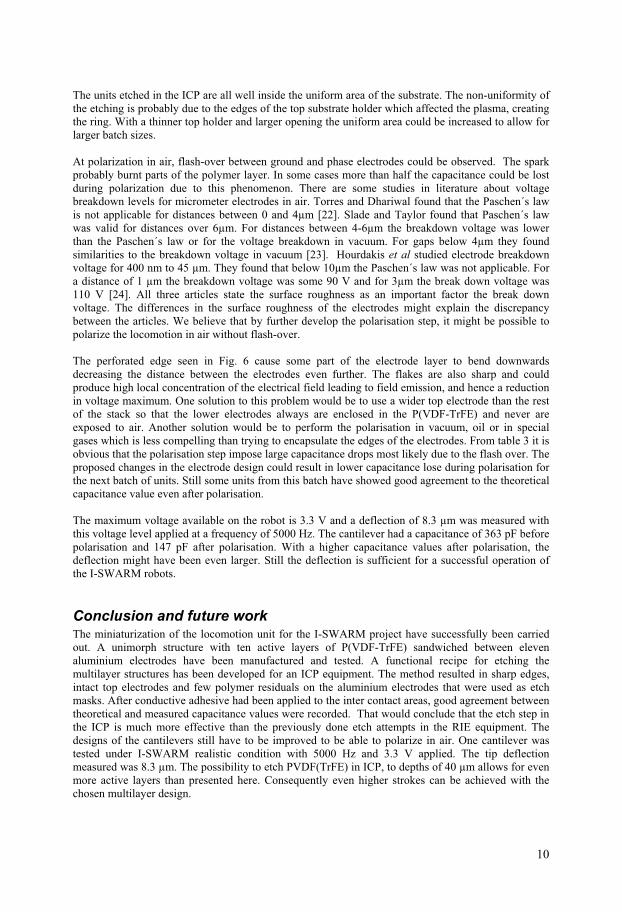
The units etched in the ICP are all well inside the uniform area of the substrate. The non-uniformity of the etching is probably due to the edges of the top substrate holder which affected the plasma, creating the ring. With a thinner top holder and larger opening the uniform area could be increased to allow for larger batch sizes.
At polarization in air, flash-over between ground and phase electrodes could be observed. The spark probably burnt parts of the polymer layer. In some cases more than half the capacitance could be lost during polarization due to this phenomenon. There are some studies in literature about voltage breakdown levels for micrometer electrodes in air. Torres and Dhariwal found that the Paschen´s law is not applicable for distances between 0 and 4μm [22]. Slade and Taylor found that Paschen´s law was valid for distances over 6μm. For distances between 4-6μm the breakdown voltage was lower than the Paschen´s law or for the voltage breakdown in vacuum. For gaps below 4μm they found similarities to the breakdown voltage in vacuum [23]. Hourdakis et al studied electrode breakdown voltage for 400 nm to 45 μm. They found that below 10μm the Paschen´s law was not applicable. For a distance of 1 μm the breakdown voltage was some 90 V and for 3μm the break down voltage was 110 V [24]. All three articles state the surface roughness as an important factor the break down voltage. The differences in the surface roughness of the electrodes might explain the discrepancy between the articles. We believe that by further develop the polarisation step, it might be possible to polarize the locomotion in air without flash-over.
The perforated edge seen in Fig. 6 cause some part of the electrode layer to bend downwards decreasing the distance between the electrodes even further. The flakes are also sharp and could produce high local concentration of the electrical field leading to field emission, and hence a reduction in voltage maximum. One solution to this problem would be to use a wider top electrode than the rest of the stack so that the lower electrodes always are enclosed in the P(VDF-TrFE) and never are exposed to air. Another solution would be to perform the polarisation in vacuum, oil or in special gases which is less compelling than trying to encapsulate the edges of the electrodes. From table 3 it is obvious that the polarisation step impose large capacitance drops most likely due to the flash over. The proposed changes in the electrode design could result in lower capacitance lose during polarisation for the next batch of units. Still some units from this batch have showed good agreement to the theoretical capacitance value even after polarisation.
The maximum voltage available on the robot is 3.3 V and a deflection of 8.3 μm was measured with this voltage level applied at a frequency of 5000 Hz. The cantilever had a capacitance of 363 pF before polarisation and 147 pF after polarisation. With a higher capacitance values after polarisation, the deflection might have been even larger. Still the deflection is sufficient for a successful operation of the I-SWARM robots.
Conclusion and future workThe miniaturization of the locomotion unit for the I-SWARM project have successfully been carried out. A unimorph structure with ten active layers of P(VDF-TrFE) sandwiched between eleven aluminium electrodes have been manufactured and tested. A functional recipe for etching the multilayer structures has been developed for an ICP equipment. The method resulted in sharp edges, intact top electrodes and few polymer residuals on the aluminium electrodes that were used as etch masks. After conductive adhesive had been applied to the inter contact areas, good agreement between theoretical and measured capacitance values were recorded. That would conclude that the etch step in the ICP is much more effective than the previously done etch attempts in the RIE equipment. The designs of the cantilevers still have to be improved to be able to polarize in air. One cantilever was tested under I-SWARM realistic condition with 5000 Hz and 3.3 V applied. The tip deflection measured was 8.3 μm. The possibility to etch PVDF(TrFE) in ICP, to depths of 40 μm allows for even more active layers than presented here. Consequently even higher strokes can be achieved with the chosen multilayer design.
10

Future work will include an increased batch of actuator units for the mass fabrication step in the I-SWARM project. The last top electrode has to be wider than the rest of the electrodes in the multilayer so that the edges can be protected by P(VDF-TRFE) during the poling step. The uniformity of the etch process for a 6 inch wafer also has to be investigated. The manual individual contacting of the etched units have to be replaced with a batch wise contacting step. The next shadow mask set will also include masks for a batch wise polarization of the units.
AcknowledgementsThis work was funded by the European Commission IST priority, FET “beyond robotics” project number 507006, which is gratefully acknowledged. The Göran Gustafsson Foundation is also acknowledged for their financial sport. The help from Anders Heljestrand and Torvald Andersson with the ICP equipment is greatly appreciated. A special thanks goes to Emmanouel Hourdakis for his help with the voltage breakdown values.
Referensces
[1] T. Moore, "Fluorinated resins: polymers for jobs where all else fails," Plastic World, vol. 44, pp. 66-68, 1986.
[2] E. Fukada, "History and recent progress in piezoelectric polymers," Ieee Transactions on Ultrasonics Ferroelectrics and Frequency Control, vol. 47, pp. 1277-1290, 2000.
[3] H. R. Gallantree, "A PMF Array for a 360° Scanning Sonar," presented at Ultrasonics Symposium Proceedings, Atlanta, Ga, USA, 1983.
[4] F. Bauer, "PVDF shock sensors: Applications to polar materials and high explosives," IeeeTransactions on Ultrasonics Ferroelectrics and Frequency Control, vol. 47, pp. 1448-1454, 2000.
[5] R. Kohler, N. Neumann, and G. Hofmann, "Pyroelectric Single-Element and Linear-Array Sensors Based on P(Vdf Trfe) Thin-Films," Sensors and Actuators a-Physical, vol. 45, pp. 209-218, 1994.
[6] D. Glennon, T. G. Nevell, J. Tsibouklis, and R. J. Ewen, "The effects of etching on the surface of plasticized poly(vinylidene fluoride)," Materials Research Bulletin, vol. 33, pp. 1139-1142, 1998.
[7] W. Holländer, W. Dunkhorst, R. Brandt, and P. Vater, "Measurement of absorbing aerosols with piezo-electric filters from Polyvinylidenefluoride (PVDF): first results," Journal of Aerosol Science, vol. 18, pp. 907-910, 1987.
[8] T. Komaki, N. Ishikawa, T. Sakurai, N. Morishita, and M. Iwasaki, "Polyvinylidene fluoride micro filter formation by 35C9+, 58Ni10+, and 63Cu11+ ion bombardment and alkali etching," Nuclear Instruments and Methods in Physics Research, vol. B34, pp. 332-336, 1988.
[9] R. Mazzei, G. G. Bermudez, N. Betz, and E. Cabanillas, "Swift heavy ion induced graft polymerization in track etched. membranes' submicroscopic pores," Nuclear Instruments & Methods in Physics Research Section B-Beam Interactions with Materials and Atoms, vol. 226, pp. 575-584, 2004.
[10] A. Grasselli and N. Betz, "Making porous membranes by chemical etching of heavy-ion tracks in beta-PVDF films," Nuclear Instruments & Methods in Physics Research Section B-Beam Interactions with Materials and Atoms, vol. 236, pp. 501-507, 2005.
[11] C. Daubresse, T. SergentEngelen, E. Ferain, Y. J. Schneider, and R. Legras, "Characterisation of energetic heavy ion track in PVDF: Production of PVDF track-etched membrane and application," Nuclear Instruments & Methods in Physics Research Section B-Beam Interactions with Materials and Atoms, vol. 105, pp. 126-129, 1995.
[12] D. Setiadi, P. P. L. Regtien, and P. M. Sarro, "Application of Vdf Trfe Copolymer for Pyroelectric Image Sensors," Sensors and Actuators a-Physical, vol. 42, pp. 585-592, 1994.
11

[13] B. Isler and G. Washington, "Spatial aperture shading of polyvinylidene fluoride applied to distributed systems for uniform damping control," Smart Materials & Structures, vol. 12, pp. 384-392, 2003.
[14] H. M. Manohara, E. Morikawa, J. Choi, and P. T. Sprunger, "Pattern transfer by direct photo etching of poly(vinylidene fluoride) using X rays," Journal of Microelectromechanical Systems, vol. 8, pp. 417-422, 1999.
[15] J. Dargahi, N. Purushotham, and S. Sokhanvar, "Design and microfabrication of a hybrid piezoelectric-capacitive tactile sensor," Sensor Review, vol. 26, pp. 186-192, 2006.
[16] W. Wirges, S. Bauer-Gogonea, S. Bauer, and R. Gerhard-Multhaupt, "Plasma-deposited fluorocarbon coatings for passive and active integrated optical devices," Proceedings of SPIE - The International Society for Optical Engineering, vol. 2213 pp. 303-310, 1994.
[17] P. Bauer, L. Audaire, J. J. Simonne, and F. Bauer, "VDF-TrFE copolymer pyroelectric sensor," Journal De Physique Iii, vol. 7, pp. 1209-1220, 1997.
[18] F. Laermer and A. Schilp, "Methode of anisotropically etching in silicon," Robert Bosch GmbH: U.S. Patent 5,501,893.
[19] A. A. Ayon, R. Braff, C. C. Lin, H. H. Sawin, and M. A. Schmidt, "Characterization of a time multiplexed inductively coupled plasma etcher," Journal of the Electrochemical Society, vol. 146, pp. 339-349, 1999.
[20] E. Edqvist, N. Snis, U. Simu, and S. Johansson, "Multilayer Electroactive Polymer Unimorph Actuators for the I-SWARM project," Sensors and Actuators a-Physical, vol. Submitted, 2006.
[21] N. Snis, E. Edqvist, U. Simu, and S. Johansson, "Monolithic Multilayer P(VDF-TrFE) Resonators," Sensors and Actuators a-Physical, vol. Submitted, 2006.
[22] J. W. Torres and R. S. Dhariwal, "Electric field breakdown at micrometre separations," Nanotechnology, vol. 10, pp. 102-107, 1999.
[23] P. Slade and E. Taylor, "Electrical Breakdown in Atmospheric Air Between Closely Spaced(0.2μm-40μm) Electrical Contacts," IEEE Transactions on Components and Packaging Technologies, vol. 25, pp. 390-396, 2002.
[24] E. Hourdakis, B. J. Simonds, and N. M. Zimmerman, "Submicron gap capacitor for measurement of breakdown voltage in air," Review of Scientific Instruments, vol. 77, pp. -, 2006.
12