An Analog Interface Circuit for Capacitive Angle Encoder ...
12
sensors Article An Analog Interface Circuit for Capacitive Angle Encoder Based on a Capacitance Elimination Array and Synchronous Switch Demodulation Method Bo Hou , Bin Zhou * , Xiang Li , Zhenyi Gao , Qi Wei * and Rong Zhang * Engineering Research Center for Navigation Technology, Department of Precision Instrument, Tsinghua University, Beijing 100084, China * Correspondence: [email protected] (B.Z.); [email protected] (Q.W.); [email protected] (R.Z.); Tel.: +86-010-6279-5692 (B.Z.); +86-010-6277-1335 (R.Z.) Received: 30 May 2019; Accepted: 11 July 2019; Published: 15 July 2019 Abstract: This paper presents an analog interface application-specific integrated circuit (ASIC) for a capacitive angle encoder, which is widely used in control machine systems. The encoder consists of two parts: a sensitive structure and analog readout circuit. To realize miniaturization, low power consumption, and easy integration, an analog interface circuit including a DC capacitance elimination array and switch synchronous demodulation module was designed. The DC capacitance elimination array allows the measurement circuit to achieve a very high capacitance to voltage conversion ratio at a low supply voltage. Further, the switch synchronous demodulation module effectively removes the carrier signal and greatly reduces the sampling rate requirement of the analog-to-digital converter (ADC). The ASIC was designed and fabricated with standard 0.18 μm CMOS processing technology and integrated with the sensitive structure. An experiment was conducted to test and characterize the performance of the proposed analog interface circuit. The encoder measurement results showed a resolution of 0.01 ◦ , power consumption of 20 mW, and accuracy over the full absolute range of 0.1 ◦ , which indicates the great potential of the encoder for application in control machine systems. Keywords: angle encoder; capacitance elimination array; switch synchronous demodulation method; application-specific integrated circuit 1. Introduction Measuring the angular position is important in the automotive industry [1–5]. Angle sensors are widely used in unmanned aerial vehicles (UAVs), small robots, and high-precision gimbal systems. These applications require angle sensors to have a small size, light weight, low power consumption, and low cost [6–10]. Angular position sensors commonly available in the market include gratings and inductive synchronizers [11,12]. These sensors have high precision but have the disadvantages of large volume, complicated processing circuit, high cost, and high-power consumption. They are difficult to apply in fields such as drone robots and UAVs. In view of these shortcomings, many angular displacement sensors based on the principles of capacitance and inductance of printed circuit board (PCB) technology have been presented [6,13–17]. These sensors have a simple structure, low manufacturing cost, small size, and high precision with a greatly reduced volume compared to gratings and magnetic grids. Capacitive encoders have been gaining interest due to their simple design, potential for further miniaturization, and insensitivity to magnetic field variations. Karali et al. [14] developed new economical capacitive rotary encoder based on analog synchronous demodulation. The carrier signal is removed by multiply demodulation in the analog system, Sensors 2019, 19, 3116; doi:10.3390/s19143116 www.mdpi.com/journal/sensors
-
Upload
khangminh22 -
Category
Documents
-
view
0 -
download
0
Transcript of An Analog Interface Circuit for Capacitive Angle Encoder ...
sensors
Article
An Analog Interface Circuit for Capacitive AngleEncoder Based on a Capacitance Elimination Arrayand Synchronous Switch Demodulation Method
Bo Hou , Bin Zhou * , Xiang Li , Zhenyi Gao , Qi Wei * and Rong Zhang *
Engineering Research Center for Navigation Technology, Department of Precision Instrument,Tsinghua University, Beijing 100084, China* Correspondence: [email protected] (B.Z.); [email protected] (Q.W.);
[email protected] (R.Z.); Tel.: +86-010-6279-5692 (B.Z.); +86-010-6277-1335 (R.Z.)
Received: 30 May 2019; Accepted: 11 July 2019; Published: 15 July 2019
Abstract: This paper presents an analog interface application-specific integrated circuit (ASIC) for acapacitive angle encoder, which is widely used in control machine systems. The encoder consists oftwo parts: a sensitive structure and analog readout circuit. To realize miniaturization, low powerconsumption, and easy integration, an analog interface circuit including a DC capacitance eliminationarray and switch synchronous demodulation module was designed. The DC capacitance eliminationarray allows the measurement circuit to achieve a very high capacitance to voltage conversion ratio ata low supply voltage. Further, the switch synchronous demodulation module effectively removes thecarrier signal and greatly reduces the sampling rate requirement of the analog-to-digital converter(ADC). The ASIC was designed and fabricated with standard 0.18 µm CMOS processing technologyand integrated with the sensitive structure. An experiment was conducted to test and characterizethe performance of the proposed analog interface circuit. The encoder measurement results showed aresolution of 0.01, power consumption of 20 mW, and accuracy over the full absolute range of 0.1,which indicates the great potential of the encoder for application in control machine systems.
Keywords: angle encoder; capacitance elimination array; switch synchronous demodulation method;application-specific integrated circuit
1. Introduction
Measuring the angular position is important in the automotive industry [1–5]. Angle sensors arewidely used in unmanned aerial vehicles (UAVs), small robots, and high-precision gimbal systems.These applications require angle sensors to have a small size, light weight, low power consumption,and low cost [6–10].
Angular position sensors commonly available in the market include gratings and inductivesynchronizers [11,12]. These sensors have high precision but have the disadvantages of large volume,complicated processing circuit, high cost, and high-power consumption. They are difficult to apply infields such as drone robots and UAVs. In view of these shortcomings, many angular displacementsensors based on the principles of capacitance and inductance of printed circuit board (PCB) technologyhave been presented [6,13–17]. These sensors have a simple structure, low manufacturing cost,small size, and high precision with a greatly reduced volume compared to gratings and magneticgrids. Capacitive encoders have been gaining interest due to their simple design, potential for furtherminiaturization, and insensitivity to magnetic field variations.
Karali et al. [14] developed new economical capacitive rotary encoder based on analog synchronousdemodulation. The carrier signal is removed by multiply demodulation in the analog system,
Sensors 2019, 19, 3116; doi:10.3390/s19143116 www.mdpi.com/journal/sensors

Sensors 2019, 19, 3116 2 of 12
which greatly reduces the sampling rate requirement for the analog-to-digital converter (ADC). Theoverall system is cheaper than digital counterparts. However, the demodulation circuit is sensitiveto temperature and requires the two analog blocks to be highly symmetric. During demodulation,synchronous and quadrature demodulation techniques are widely used, especially for applicationsrequiring high levels of performance in harsh environments [13]. The capacitive encoder producesa phase/frequency modulated signal that cannot be demodulated by the traditional amplitudedemodulation techniques of resolvers. With the increase in embedded technologies, digital-baseddemodulation techniques are becoming common in the literature. The central digital computationalblock can be a fast microcontroller or a field programmable gate array (FPGA)-based embeddedsystem. Hou et al. [18] presented a novel single-excitation capacitive angular position sensor (CAPS)that outputs two amplitude modulated signals, which can be demodulated by traditional amplitudedemodulation techniques such as resolvers. However, the traditional resolver demodulation chiphas a high-power consumption and poor expansion as nonlinear error information of the sensor isdifficult to observe and obtain. Further, because of the presence of the DC capacitance C0, the swingamplitude of the output signal is limited. This results in a high-power supply voltage to achieve a highcapacitance resolution.
Many demodulation schemes are available for angle sensors [19–22], but there is no integratedcircuit that has been specifically designed for it. The common capacitive angular displacement sensorusually needs a high supply voltage which leads to large power consumption, and the demodulationcircuit is complex and difficult to integrate. It is urgent to design an analog-interfacing circuit toeffectively solve the problem of high power consumption, large size, and difficult integration of theencoder demodulation circuit.
This paper proposes a simple but effective input interfacing scheme that uses a capacitanceelimination array and the switch synchronous demodulation method. To achieve miniaturization, lowpower consumption and easy integration, an analog interface circuit that includes a DC capacitanceelimination array and switch synchronous demodulation module was designed. The DC capacitanceelimination array allows the measurement circuit to achieve very high capacitance to voltage ratios ata low supply voltage. The switch synchronous demodulation module effectively removes the carriersignal and greatly reduces the sampling rate required by the ADC.
2. Capacitive Angular Encoder
The encoder is composed of two main parts: a stator and rotor. Capacitive rotary encoders arebased on a rotating disk on a fixed plate or between two fixed plates stator and rotor. As an encoderrotates, the capacitance between stator and rotor change, and the angle of the shaft can be extracted.The rotor has been printed a petal-form sensitive electrode and a coupling electrode. The stator hasbeen printed one excitation electrode and four sets of collection electrodes. The petal-form shapesensitive electrode on rotor is connected with coupling electrode. The sensor is excited by a squarewave voltage. The carrier excitation voltage is applied to the stator excitation electrodes:
UE = AE · squ(ωt) (1)
where ω is the frequency of the excitation voltage, AE is the amplitude and squ(·) means squarewave function.
Via capacitive coupling between the rotor and stator, a four-way modulation of the angularinformation capacitance signal can be obtained on the collector electrode of the stator:
US+ = k · (C0 + ∆C sin(φ)) · squ(ωt)US− = k · (C0 − ∆C sin(φ)) · squ(ωt)UC+ = k · (C0 + ∆C cos(φ)) · squ(ωt)UC− = k · (C0 − ∆C cos(φ)) · squ(ωt)
(2)

Sensors 2019, 19, 3116 3 of 12
where C0 is the DC capacitance, φ is the modulated angle information, and ∆C is the magnitude ofthe useful angular signal information. US+, US−, UC+, and UC− are the voltage signals after beingconverted by the capacitance–voltage (C–V) model of the four detection capacitors. k is the ratio ofC–V model. The existence of the DC capacitance limits the swing amplitude of the output signal. Thedifferential sensitivity principle is more effectively reduce common mode interference.
Two differential amplifier modules are used to eliminate the DC component output. Finally, twoorthogonal amplitude modulated signals US and UC can be obtained.
US = A · ∆C sin(φ) · sin(ωt)UC = A · ∆C cos(φ) · sin(ωt)
(3)
A capacitive encoder structure was designed and fabricated with PCB technology to test theproposed analog interfacing circuit. Based on the design diameters, the DC capacitance C0 was 1 pF,and the sensitive capacitance ∆C was approximately 1 pF.
3. Signal Processing of the ASIC
3.1. Processing Circuit Introduction
The integrated analog-interfacing circuit includes the DC capacitance elimination array, C–Vconversion module, switch synchronous demodulation module, and filter. Figure 1 shows a blockdiagram of the proposed architecture. During operation, an external oscillator generates two differentialexcitation signals: UE and −UE. The positive signal UE acts on the capacitive encoder, and the negative−UE accesses the DC capacitance cancellation array. When the sensor is working, the DC capacitance C0
of the four-way measurement capacitance can be eliminated by combining the capacitance eliminationarray and negative signal −UE. The differential output charge amplifier converts the change incapacitance to an equivalent voltage. Then, the switch demodulation module is used to eliminatethe carrier signal. The related voltage signal is further filtered and amplified by the low pass filtermodule. Then, the voltage is quantized to obtain a digital signal. The presented circuit can effectivelydetect the capacitance change of capacitive angle encoder and is applicable in a wide range of size andcapacitance value of encoder.
Sensors 2019, 19, x 3 of 12
being converted by the capacitance–voltage (C–V) model of the four detection capacitors. k is the ratio of C–V model. The existence of the DC capacitance limits the swing amplitude of the output signal. The differential sensitivity principle is more effectively reduce common mode interference.
Two differential amplifier modules are used to eliminate the DC component output. Finally, two orthogonal amplitude modulated signals SU and CU can be obtained.
sin( ) sin( )cos( ) sin( )
S
C
U A C tU A C t
φ ωφ ω
= ⋅ Δ ⋅ = ⋅ Δ ⋅
(3)
A capacitive encoder structure was designed and fabricated with PCB technology to test the proposed analog interfacing circuit. Based on the design diameters, the DC capacitance 0C was 1 pF, and the sensitive capacitance CΔ was approximately 1 pF.
3. Signal Processing of the ASIC
3.1. Processing Circuit Introduction
The integrated analog-interfacing circuit includes the DC capacitance elimination array, C–V conversion module, switch synchronous demodulation module, and filter. Figure 1 shows a block diagram of the proposed architecture. During operation, an external oscillator generates two differential excitation signals: EU and EU− . The positive signal EU acts on the capacitive encoder, and the negative EU− accesses the DC capacitance cancellation array. When the sensor is working, the DC capacitance 0C of the four-way measurement capacitance can be eliminated by combining the capacitance elimination array and negative signal EU− . The differential output charge amplifier converts the change in capacitance to an equivalent voltage. Then, the switch demodulation module is used to eliminate the carrier signal. The related voltage signal is further filtered and amplified by the low pass filter module. Then, the voltage is quantized to obtain a digital signal. The presented circuit can effectively detect the capacitance change of capacitive angle encoder and is applicable in a wide range of size and capacitance value of encoder.
LPFilter
C0+CS
DC Capacitor Eliminate array
DC Capacitor Eliminate array
C0
SwichDemo-dulator
C-V Converter
Oscillator
Σ
Σ
LPFilter
SwichDemo-dulator
C-V Converter
Cos(t)
Σ
Σ
-Sin(t)C0—CS
C0+CC
C0—CC
-Cos(t)
Sin(t)
EU
Structure ASIC
EU−
Figure 1. Block diagram of the proposed architecture.
3.2. On-Chip DC Capacitance Elimination Array
The on-chip capacitor array incorporated on the ASIC is purposefully to eliminate the DC capacitance 0C and compensate for the inconsistency of the two sensitive capacitors. Equation (1) shows that there is a DC 0C for the four-measurement capacitance. Therefore, if 0C cannot be
Figure 1. Block diagram of the proposed architecture.

Sensors 2019, 19, 3116 4 of 12
3.2. On-Chip DC Capacitance Elimination Array
The on-chip capacitor array incorporated on the ASIC is purposefully to eliminate the DCcapacitance C0 and compensate for the inconsistency of the two sensitive capacitors. Equation (1)shows that there is a DC C0 for the four-measurement capacitance. Therefore, if C0 cannot be eliminated,the supply voltage (VDD) cannot fully applied to the sensing capacitance ∆C. C0 severely restricts theoutput signal swing. To compensate this offset, two identical sets of on-chip parallel DC capacitors aselimination array are included within the ASIC. Each set is connected to either CS+ or CS−, whichevervalue is controlled by external pins.
An external oscillator generates two differential excitation signals UE and UE. UE acts on thecapacitive angular encoder as a carrier excitation signal, and UE accesses the DC capacitance eliminationarray. The two differential excitation signals can be expressed as
UE = AE · squ(ωt) (4)
UE = −AE · squ(ωt) (5)
The DC capacitance cancellation array is used to cancel the DC capacitance of the four sensingcapacitors. Normally, the capacitance error of the sensor is completed after processing, so the design ofthis module enables the DC error of the sensor to be corrected. In the design, the eight control switchesS1, S2, S3, . . . , S8 are used to control the value of elimination capacitors. In the capacitance eliminationarray, the capacitance value of single bit is C, and switch Sn is corresponding to a capacitor of 2nC(n = 1, 2, . . . , 8), so the value of each elimination capacitor ranges from 0 to 28
·C. The main connectionrelationship is shown in Figure 2. In the design, C was set to 49 fF.
Sensors 2019, 19, x 4 of 12
eliminated, the supply voltage (VDD) cannot fully applied to the sensing capacitance CΔ . 0C severely restricts the output signal swing. To compensate this offset, two identical sets of on-chip parallel DC capacitors as elimination array are included within the ASIC. Each set is connected to either SC + or SC − , whichever value is controlled by external pins.
An external oscillator generates two differential excitation signals EU and EU . EU acts on the capacitive angular encoder as a carrier excitation signal, and EU accesses the DC capacitance elimination array. The two differential excitation signals can be expressed as
( )E EU A squ tω= ⋅ (4)
( )E EU A squ tω= − ⋅ (5)
The DC capacitance cancellation array is used to cancel the DC capacitance of the four sensing capacitors. Normally, the capacitance error of the sensor is completed after processing, so the design of this module enables the DC error of the sensor to be corrected. In the design, the eight control switches S1, S2, S3, ..., S8 are used to control the value of elimination capacitors. In the capacitance elimination array, the capacitance value of single bit is C, and switch Sn is corresponding to a capacitor of 2nC (n = 1, 2, …, 8), so the value of each elimination capacitor ranges from 0 to 82 C⋅ . The main connection relationship is shown in Figure 2. In the design, C was set to 49 fF.
LPF
clk
clk
clk clk- +
-+
CfUE
Cs-
Cs+
INp (OutP)
(OutN)
+ +
- -
S1
C1
S2
C2
S3
C3
S8
C8……
…
……
S8
C8
-UE
-UE
-UE / clkUE / clk
CRFCVref
(a)
(b)
Cf
Rf
Rf
INN
Figure 2. DC cancellation capacitor and switching demodulation: (a) capacitance elimination array and (b) synchronous switch demodulation.
If the value of elimination capacitors is ELIC , the charge on the C–V conversion can be expressed as
0
( ) ( ( ))[( sin( )) ] ( )
S E ELI E
ELI E
Q CU C k A squ t C A squ tC C k C A squ tφ
+= = ⋅ ⋅ ⋅⋅ + ⋅ − ⋅= + Δ ⋅ − ⋅ ⋅ (6)
where k is the conversion ratio and is determined by sensitive structure. This operation tries to adjust the capacitance ELIC to ensure 0 = ELIC k C⋅ .
Then, Equation (6) can be simplified as
( sin( )) ( )EQ C k A squ tφ= Δ ⋅ ⋅ ⋅ (7)
According to the output function of the charge amplifier,
1(1 )( )Of
f
j AQUA j CR
ωω
−=+ +
(8)
Thus, the output voltage is only determined by the input charge and the parameters of the feedback circuit ( fR , fC ). Further, when fR is large enough to satisfy 1 f fR Cω<< ( 810fR = Ω in this paper), 1 fR can be omitted. The output can be expressed as
Figure 2. DC cancellation capacitor and switching demodulation: (a) capacitance elimination arrayand (b) synchronous switch demodulation.
If the value of elimination capacitors is CELI, the charge on the C–V conversion can be expressed as
Q = CU = CS+ · k ·AE · squ(t) + CELI · (−AE · squ(t))= [(C0 + ∆C sin(φ)) · k−CELI] ·AE · squ(t)
(6)
where k is the conversion ratio and is determined by sensitive structure. This operation tries to adjustthe capacitance CELI to ensure C0 · k = CELI.
Then, Equation (6) can be simplified as
Q = (∆C sin(φ)) · k ·AE · squ(t) (7)
According to the output function of the charge amplifier,
UO =− jωAQ
(1 + A)( 1R f
+ jωC f )(8)

Sensors 2019, 19, 3116 5 of 12
Thus, the output voltage is only determined by the input charge and the parameters of thefeedback circuit (R f , C f ). Further, when R f is large enough to satisfy 1/R f << ωC f (R f = 108 Ω in thispaper), 1/R f can be omitted. The output can be expressed as
UO =− jωAQ
(1 + A) jωC f= −
AQ(1 + A)C f
≈ −QC f
(9)
The output voltage is only related to the charge Q and feedback capacitance C f :
INP =(∆C sin(φ)) · k ·AE · squ(t)
C f(10)
INN = −(∆C sin(φ)) · k ·AE · squ(t)
C f(11)
If C0 exists in the circuit, then after it enters the charge amplifier, because of the limited powersupply voltage V, using the cancellation capacitor can ensure that the scale factor of the capacitor-voltageratio is maximized at low voltage, as Figure 3 shows. This can effectively suppress the DC error,and precision measurement with a low supply voltage can be easily achieved.
Sensors 2019, 19, x 5 of 12
(1 ) C (1 )C COf f f
j AQ AQ QUA j Aω
ω−= = − ≈ −+ +
(9)
The output voltage is only related to the charge Q and feedback capacitance C f :
( sin( )) ( )C
EP
f
C k A squ tIN φΔ ⋅ ⋅ ⋅= (10)
( sin( )) ( )C
EN
f
C k A squ tIN φΔ ⋅ ⋅ ⋅= − (11)
If C0 exists in the circuit, then after it enters the charge amplifier, because of the limited power supply voltage V, using the cancellation capacitor can ensure that the scale factor of the capacitor-voltage ratio is maximized at low voltage, as Figure 3 shows. This can effectively suppress the DC error, and precision measurement with a low supply voltage can be easily achieved.
Figure 3. Effect of the offset capacitance on the scaling factor.
The amplifier in this C–V conversion circuit adopts the complementary recycling folded cascode (CRFC) architecture [23] due to its larger gain-bandwidth-product (GBW) and slew rate compared with conventional folded cascode op-amp as shown in Figure 4. It has NMOS and PMOS transistors as complementary input differential pairs, and in both branches, the recycling folded cascode (RFC) technique [24] is introduced to achieve more biasing current efficiency. The CRFC amplifier improves its GBW by a factor of 1/3 compared with the RFC under the same biasing current and capacitive load.
M0Vbp1
VINN
M1a M1b M2b
M11 M12Vbn2
M3a M4aM3b M4b
M5 M6
VOUTP
M7 M8
Vbp2VINP
M2a
Vbn2
M14a M14b M15aM15b
VINP
M13Vbn1
M16 M17
Vbp2
VINN
VOUTN
M9a M9b M10b M10a
GND Figure 4. The structure of CRFC operational transconductance amplifier (OTA).
3.3. Synchronous Switch Demodulation and Low-Pass Filter
In the proposed configuration, the signals INP and INN is demodulated by the switch demodulation module. The demodulation process is shown in Figure 5. The demodulated output signals are then buffered and fed to the low-pass filter. In this design, a filter which owns the cutoff
Figure 3. Effect of the offset capacitance on the scaling factor.
The amplifier in this C–V conversion circuit adopts the complementary recycling folded cascode(CRFC) architecture [23] due to its larger gain-bandwidth-product (GBW) and slew rate comparedwith conventional folded cascode op-amp as shown in Figure 4. It has NMOS and PMOS transistorsas complementary input differential pairs, and in both branches, the recycling folded cascode (RFC)technique [24] is introduced to achieve more biasing current efficiency. The CRFC amplifier improvesits GBW by a factor of 1/3 compared with the RFC under the same biasing current and capacitive load.
Sensors 2019, 19, x 5 of 12
(1 ) C (1 )C COf f f
j AQ AQ QUA j Aω
ω−= = − ≈ −+ +
(9)
The output voltage is only related to the charge Q and feedback capacitance C f :
( sin( )) ( )C
EP
f
C k A squ tIN φΔ ⋅ ⋅ ⋅= (10)
( sin( )) ( )C
EN
f
C k A squ tIN φΔ ⋅ ⋅ ⋅= − (11)
If C0 exists in the circuit, then after it enters the charge amplifier, because of the limited power supply voltage V, using the cancellation capacitor can ensure that the scale factor of the capacitor-voltage ratio is maximized at low voltage, as Figure 3 shows. This can effectively suppress the DC error, and precision measurement with a low supply voltage can be easily achieved.
Figure 3. Effect of the offset capacitance on the scaling factor.
The amplifier in this C–V conversion circuit adopts the complementary recycling folded cascode (CRFC) architecture [23] due to its larger gain-bandwidth-product (GBW) and slew rate compared with conventional folded cascode op-amp as shown in Figure 4. It has NMOS and PMOS transistors as complementary input differential pairs, and in both branches, the recycling folded cascode (RFC) technique [24] is introduced to achieve more biasing current efficiency. The CRFC amplifier improves its GBW by a factor of 1/3 compared with the RFC under the same biasing current and capacitive load.
M0Vbp1
VINN
M1a M1b M2b
M11 M12Vbn2
M3a M4aM3b M4b
M5 M6
VOUTP
M7 M8
Vbp2VINP
M2a
Vbn2
M14a M14b M15aM15b
VINP
M13Vbn1
M16 M17
Vbp2
VINN
VOUTN
M9a M9b M10b M10a
GND Figure 4. The structure of CRFC operational transconductance amplifier (OTA).
3.3. Synchronous Switch Demodulation and Low-Pass Filter
In the proposed configuration, the signals INP and INN is demodulated by the switch demodulation module. The demodulation process is shown in Figure 5. The demodulated output signals are then buffered and fed to the low-pass filter. In this design, a filter which owns the cutoff
Figure 4. The structure of CRFC operational transconductance amplifier (OTA).

Sensors 2019, 19, 3116 6 of 12
3.3. Synchronous Switch Demodulation and Low-Pass Filter
In the proposed configuration, the signals INP and INN is demodulated by the switch demodulationmodule. The demodulation process is shown in Figure 5. The demodulated output signals are thenbuffered and fed to the low-pass filter. In this design, a filter which owns the cutoff frequency on10 kHz has been applied to reduce noise of switches. The low-pass filter provides an analog outputcorresponding to the input angle information being fed to the ADC.
Sensors 2019, 19, x 6 of 12
frequency on 10 kHz has been applied to reduce noise of switches. The low-pass filter provides an analog output corresponding to the input angle information being fed to the ADC.
Vref
Vref2ωπ
t
t
t
t
INp
INN
-UE
VOUT-
VOUT+(a)
(b)
(c)
(d)
Figure 5. Diagram of the synchronous switch demodulation method: (a) two signals after the C–V conversion module and switching signal; (b) output signal of INP and INN after the switch demodulated; (c) Signals after differential; and (d) the differential signal is output after filtering.
The voltage signal after synchronous switch demodulation is given by
2 ( sin( )) +C
EInP P N SW
f
C k AU U U Noiseφ⋅ Δ ⋅ ⋅= − = (12)
where SWNoise is the noise due to the synchronization error of the switch demodulation, as shown in Figure 5c. It can be decreased after the low-pass filter.
In order to achieve a supply voltage of 5 V, a reference voltage Vref of 2.5 V is applied to the analog circuit. The output signal after the bandpass filter (BPF) can be expressed as
2OUT ref P P
f
CV V VC+ −Δ= + (13)
where P PV − is the peak-to-peak amplitude of the excitation signal. Similarly, because of the fully differential nature of the operational transconductance amplifier (OTA), OUTV − can be written as
2OUT ref P P
f
CV V VC− −Δ= − (14)
Thus, the final differential output value can be obtained:
4OUT P P
f
CV VC −ΔΔ = (15)
The sensitivity of the proposed configuration is double that of conventional architectures. In general, VP−P is equal to the supply voltage (Vcc) of the system. The gain of the charge amplifier can be programmed by selecting the proper feedback capacitance Cf. In this design, three control pins provide eight programmable gains.
4. Measurement Results
4.1. Characteristics Test of the ASIC
The proposed analog interface circuit was designed and fabricated with SMIC 0.18 µm CMOS processing technology. A microphotograph of the chip is shown in Figure 6a. The scale factor, offset capacitance, zero offset stability, and noise level of the ASIC chip have been tested. The test circuit diagram and chip layout are shown in Figure 6b. An oscillator chip was used to generate the carrier signal to actuate the encoder.
Figure 5. Diagram of the synchronous switch demodulation method: (a) two signals after the C–Vconversion module and switching signal; (b) output signal of INP and INN after the switch demodulated;(c) Signals after differential; and (d) the differential signal is output after filtering.
The voltage signal after synchronous switch demodulation is given by
UInP = UP −UN =2 · (∆C sin(φ)) · k ·AE
C f+ NoiseSW (12)
where NoiseSW is the noise due to the synchronization error of the switch demodulation, as shown inFigure 5c. It can be decreased after the low-pass filter.
In order to achieve a supply voltage of 5 V, a reference voltage Vref of 2.5 V is applied to the analogcircuit. The output signal after the bandpass filter (BPF) can be expressed as
VOUT+ = Vre f +2∆CC f
VP−P (13)
where VP−P is the peak-to-peak amplitude of the excitation signal. Similarly, because of the fullydifferential nature of the operational transconductance amplifier (OTA), VOUT− can be written as
VOUT− = Vre f −2∆CC f
VP−P (14)
Thus, the final differential output value can be obtained:
∆VOUT =4∆CC f
VP−P (15)
The sensitivity of the proposed configuration is double that of conventional architectures.In general, VP−P is equal to the supply voltage (Vcc) of the system. The gain of the charge amplifier canbe programmed by selecting the proper feedback capacitance Cf. In this design, three control pinsprovide eight programmable gains.

Sensors 2019, 19, 3116 7 of 12
4. Measurement Results
4.1. Characteristics Test of the ASIC
The proposed analog interface circuit was designed and fabricated with SMIC 0.18 µm CMOSprocessing technology. A microphotograph of the chip is shown in Figure 6a. The scale factor,offset capacitance, zero offset stability, and noise level of the ASIC chip have been tested. The testcircuit diagram and chip layout are shown in Figure 6b. An oscillator chip was used to generate thecarrier signal to actuate the encoder.Sensors 2019, 19, x 7 of 12
Oscillator
(a) (b)
Figure 6. ASIC circuit test chart: (a) microphotograph of the circuit chip and (b) test circuit diagram.
4.1.1. Scale Factor
In the scale factor test experiment, the measured capacitance was changed and increased in increments of 0.1 pF. The capacitors 0.1 pF, 0.2 pF, 0.3 pF, et al., was picked out via capacitance measurement instrument. Then, the capacitors are replaced to the circuit board in turn. The connected capacitor should be increased in increments of 0.1 pF without consider the parasitic capacitance. The output voltage was measured, and the data were imported into MATLAB to graph the results, as shown in Figure 7. The linearity was excellent, and the slope was 4.111 V/pF, which is basically consistent with the design value. The residual is shown as the red line. This was mainly because the value of the connected capacitance could not be accurately determined, so the linearity of the measured value had a residual of about 30 mV. This test proved that the design functioned correctly.
Figure 7. Relationship between the output voltage and access capacitance.
4.1.2. Noise Test
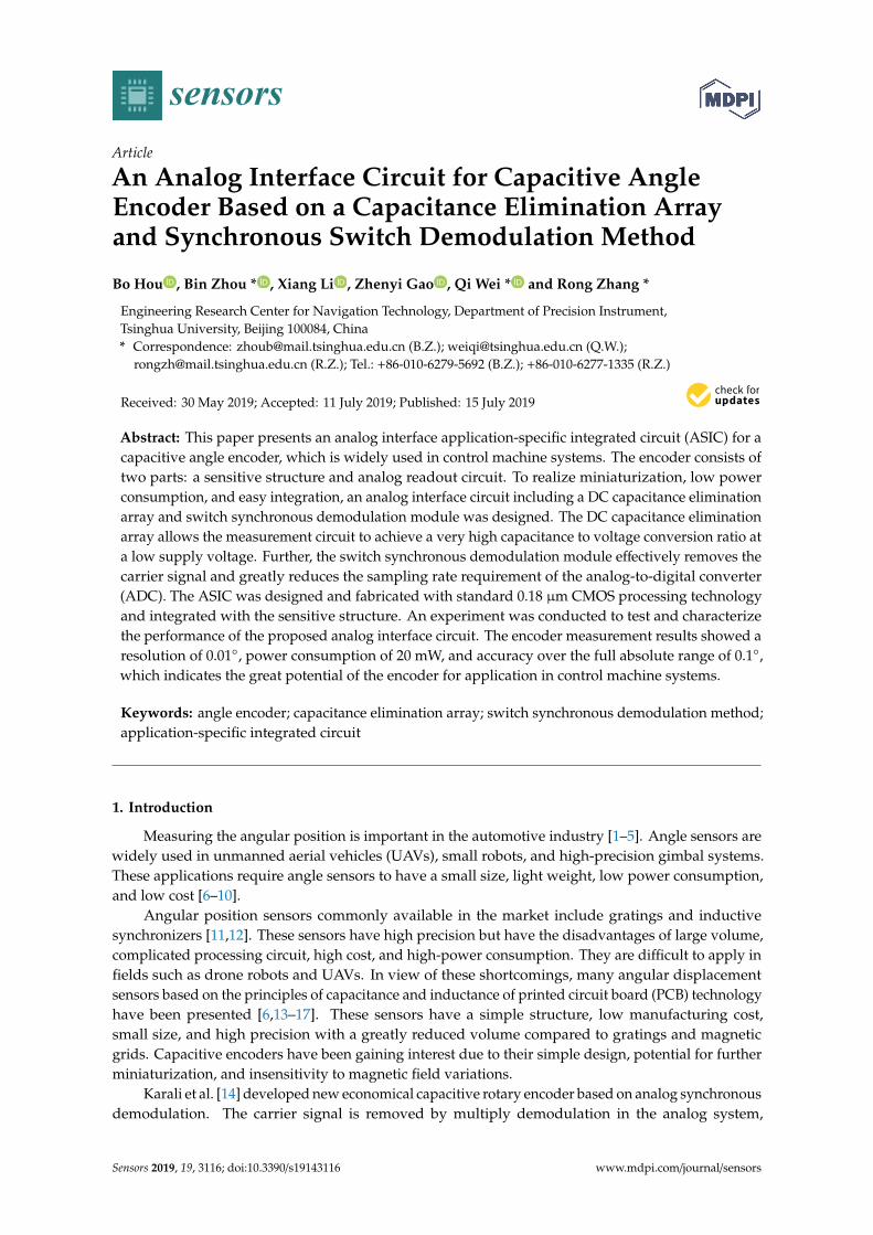
Next, the noise of the circuit was tested. The output noise of the interface circuit was tested with 35670A produced by Agilent Technologies Inc. The noise spectrum of the output voltage is shown in Figure 8. The floor for the output voltage noise of the signal was 400 nV. The points marked in the figure indicate a power frequency interference of 50 Hz. This would have a strong influence and needs to be reduced by careful shielding during operation. In addition, the noise also exhibits a strong 1/f characteristic, mainly due to the low-pass filter after switching demodulation.
The capacitance resolution RC was calculated according to the noise floor and conversion coefficient:
C f CR N S= (16)
Here, the calculation of the capacitance resolution was affected by two main factors. The previous test result showed that 400 nVfN = and 4.111 V pFCS = . According to Equation (16), the
Out
put v
olta
ge (m
V)
Erro
r (m
V)
Figure 6. ASIC circuit test chart: (a) microphotograph of the circuit chip and (b) test circuit diagram.
4.1.1. Scale Factor
In the scale factor test experiment, the measured capacitance was changed and increased inincrements of 0.1 pF. The capacitors 0.1 pF, 0.2 pF, 0.3 pF, et al., was picked out via capacitancemeasurement instrument. Then, the capacitors are replaced to the circuit board in turn. The connectedcapacitor should be increased in increments of 0.1 pF without consider the parasitic capacitance.The output voltage was measured, and the data were imported into MATLAB to graph the results,as shown in Figure 7. The linearity was excellent, and the slope was 4.111 V/pF, which is basicallyconsistent with the design value. The residual is shown as the red line. This was mainly because thevalue of the connected capacitance could not be accurately determined, so the linearity of the measuredvalue had a residual of about 30 mV. This test proved that the design functioned correctly.
Sensors 2019, 19, x 7 of 12
Oscillator
(a) (b)
Figure 6. ASIC circuit test chart: (a) microphotograph of the circuit chip and (b) test circuit diagram.
4.1.1. Scale Factor
In the scale factor test experiment, the measured capacitance was changed and increased in increments of 0.1 pF. The capacitors 0.1 pF, 0.2 pF, 0.3 pF, et al., was picked out via capacitance measurement instrument. Then, the capacitors are replaced to the circuit board in turn. The connected capacitor should be increased in increments of 0.1 pF without consider the parasitic capacitance. The output voltage was measured, and the data were imported into MATLAB to graph the results, as shown in Figure 7. The linearity was excellent, and the slope was 4.111 V/pF, which is basically consistent with the design value. The residual is shown as the red line. This was mainly because the value of the connected capacitance could not be accurately determined, so the linearity of the measured value had a residual of about 30 mV. This test proved that the design functioned correctly.
Figure 7. Relationship between the output voltage and access capacitance.
4.1.2. Noise Test
Next, the noise of the circuit was tested. The output noise of the interface circuit was tested with 35670A produced by Agilent Technologies Inc. The noise spectrum of the output voltage is shown in Figure 8. The floor for the output voltage noise of the signal was 400 nV. The points marked in the figure indicate a power frequency interference of 50 Hz. This would have a strong influence and needs to be reduced by careful shielding during operation. In addition, the noise also exhibits a strong 1/f characteristic, mainly due to the low-pass filter after switching demodulation.
The capacitance resolution RC was calculated according to the noise floor and conversion coefficient:
C f CR N S= (16)
Here, the calculation of the capacitance resolution was affected by two main factors. The previous test result showed that 400 nVfN = and 4.111 V pFCS = . According to Equation (16), the
Out
put v
olta
ge (m
V)
Erro
r (m
V)
Figure 7. Relationship between the output voltage and access capacitance.
4.1.2. Noise Test
Next, the noise of the circuit was tested. The output noise of the interface circuit was tested with35670A produced by Agilent Technologies Inc. The noise spectrum of the output voltage is shown inFigure 8. The floor for the output voltage noise of the signal was 400 nV. The points marked in thefigure indicate a power frequency interference of 50 Hz. This would have a strong influence and needs
Sensors 2019, 19, 3116 8 of 12
to be reduced by careful shielding during operation. In addition, the noise also exhibits a strong 1/fcharacteristic, mainly due to the low-pass filter after switching demodulation.
Sensors 2019, 19, x 8 of 12
capacitance resolution of the circuit was 10−19 F. The capacitance of the micro-sensitive structure described above varied from 0.3 to 0.5 pF. Thus, the circuit could satisfy the demodulation of the angular position information of the sensitive structure.
Figure 8. Noise spectrum of the ASIC voltage output.
4.2. Characteristics Test of Encoder
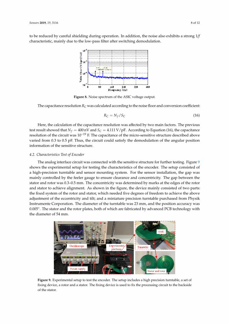
The analog interface circuit was connected with the sensitive structure for further testing. Figure 9 shows the experimental setup for testing the characteristics of the encoder. The setup consisted of a high-precision turntable and sensor mounting system. For the sensor installation, the gap was mainly controlled by the feeler gauge to ensure clearance and concentricity. The gap between the stator and rotor was 0.3–0.5 mm. The concentricity was determined by marks at the edges of the rotor and stator to achieve alignment. As shown in the figure, the device mainly consisted of two parts: the fixed system of the rotor and stator, which needed five degrees of freedom to achieve the above adjustment of the eccentricity and tilt; and a miniature precision turntable purchased from Physik Instrumente Corporation. The diameter of the turntable was 23 mm, and the position accuracy was 0.005°. The stator and the rotor plates, both of which are fabricated by advanced PCB technology with the diameter of 54 mm.
Figure 9. Experimental setup to test the encoder. The setup includes a high precision turntable, a set of fixing device, a rotor and a stator. The fixing device is used to fix the processing circuit to the backside of the stator.
4.2.1. Angle Stability Test
The long-term stability of the encoder was tested. Keithley 2010 was used to collect the output voltage data, which were then saved and processed with a computer. Figure 10a,b show the long-
Figure 8. Noise spectrum of the ASIC voltage output.
The capacitance resolution RC was calculated according to the noise floor and conversion coefficient:
RC = N f /SC (16)
Here, the calculation of the capacitance resolution was affected by two main factors. The previoustest result showed that N f = 400 nV and SC = 4.111 V/pF. According to Equation (16), the capacitanceresolution of the circuit was 10−19 F. The capacitance of the micro-sensitive structure described abovevaried from 0.3 to 0.5 pF. Thus, the circuit could satisfy the demodulation of the angular positioninformation of the sensitive structure.
4.2. Characteristics Test of Encoder
The analog interface circuit was connected with the sensitive structure for further testing. Figure 9shows the experimental setup for testing the characteristics of the encoder. The setup consisted ofa high-precision turntable and sensor mounting system. For the sensor installation, the gap wasmainly controlled by the feeler gauge to ensure clearance and concentricity. The gap between thestator and rotor was 0.3–0.5 mm. The concentricity was determined by marks at the edges of the rotorand stator to achieve alignment. As shown in the figure, the device mainly consisted of two parts:the fixed system of the rotor and stator, which needed five degrees of freedom to achieve the aboveadjustment of the eccentricity and tilt; and a miniature precision turntable purchased from PhysikInstrumente Corporation. The diameter of the turntable was 23 mm, and the position accuracy was0.005. The stator and the rotor plates, both of which are fabricated by advanced PCB technology withthe diameter of 54 mm.
Sensors 2019, 19, x 8 of 12
capacitance resolution of the circuit was 10−19 F. The capacitance of the micro-sensitive structure described above varied from 0.3 to 0.5 pF. Thus, the circuit could satisfy the demodulation of the angular position information of the sensitive structure.
Figure 8. Noise spectrum of the ASIC voltage output.
4.2. Characteristics Test of Encoder
The analog interface circuit was connected with the sensitive structure for further testing. Figure 9 shows the experimental setup for testing the characteristics of the encoder. The setup consisted of a high-precision turntable and sensor mounting system. For the sensor installation, the gap was mainly controlled by the feeler gauge to ensure clearance and concentricity. The gap between the stator and rotor was 0.3–0.5 mm. The concentricity was determined by marks at the edges of the rotor and stator to achieve alignment. As shown in the figure, the device mainly consisted of two parts: the fixed system of the rotor and stator, which needed five degrees of freedom to achieve the above adjustment of the eccentricity and tilt; and a miniature precision turntable purchased from Physik Instrumente Corporation. The diameter of the turntable was 23 mm, and the position accuracy was 0.005°. The stator and the rotor plates, both of which are fabricated by advanced PCB technology with the diameter of 54 mm.
Figure 9. Experimental setup to test the encoder. The setup includes a high precision turntable, a set of fixing device, a rotor and a stator. The fixing device is used to fix the processing circuit to the backside of the stator.
4.2.1. Angle Stability Test
The long-term stability of the encoder was tested. Keithley 2010 was used to collect the output voltage data, which were then saved and processed with a computer. Figure 10a,b show the long-
Figure 9. Experimental setup to test the encoder. The setup includes a high precision turntable, a set offixing device, a rotor and a stator. The fixing device is used to fix the processing circuit to the backsideof the stator.

Sensors 2019, 19, 3116 9 of 12
4.2.1. Angle Stability Test
The long-term stability of the encoder was tested. Keithley 2010 was used to collect the outputvoltage data, which were then saved and processed with a computer. Figure 10a,b show the long-termvoltage stability of two orthogonal signals. The voltage variation of the two signals did not exceed 2 mV.The demodulated angle is shown in Figure 10c, and the fluctuation did not exceed 0.002. The maincause of the fluctuation in the long-term stability test was the environmental impact, especially thevibration acting on the sensitive structure.
Sensors 2019, 19, x 9 of 12
term voltage stability of two orthogonal signals. The voltage variation of the two signals did not exceed 2 mV. The demodulated angle is shown in Figure 10c, and the fluctuation did not exceed 0.002°. The main cause of the fluctuation in the long-term stability test was the environmental impact, especially the vibration acting on the sensitive structure.
(a) (b)
(c)
Figure 10. Stability measurement results: (a) and (b) show the stable voltage output and (c) shows stable angle output.
4.2.2. Step Test
In order to verify the sensitivity of the ASIC and sensitive structure, the step size was tested. To determine the resolution of the proposed encoder, a step test with an increment of 0.01° and delay of 2.5 s was performed. The corresponding output angle response is shown in Figure 11. The resolution of the proposed angle sensor was considerably better than 0.01°; thus, it meets most application requirements.
Out
put a
ngle
(deg
)
Sampling point Figure 11. Output response of the step test with 0.01° increments.
Figure 10. Stability measurement results: (a) and (b) show the stable voltage output and (c) showsstable angle output.
4.2.2. Step Test
In order to verify the sensitivity of the ASIC and sensitive structure, the step size was tested.To determine the resolution of the proposed encoder, a step test with an increment of 0.01 anddelay of 2.5 s was performed. The corresponding output angle response is shown in Figure 11.The resolution of the proposed angle sensor was considerably better than 0.01; thus, it meets mostapplication requirements.
Sensors 2019, 19, x 9 of 12
term voltage stability of two orthogonal signals. The voltage variation of the two signals did not exceed 2 mV. The demodulated angle is shown in Figure 10c, and the fluctuation did not exceed 0.002°. The main cause of the fluctuation in the long-term stability test was the environmental impact, especially the vibration acting on the sensitive structure.
(a) (b)
(c)
Figure 10. Stability measurement results: (a) and (b) show the stable voltage output and (c) shows stable angle output.
4.2.2. Step Test
In order to verify the sensitivity of the ASIC and sensitive structure, the step size was tested. To determine the resolution of the proposed encoder, a step test with an increment of 0.01° and delay of 2.5 s was performed. The corresponding output angle response is shown in Figure 11. The resolution of the proposed angle sensor was considerably better than 0.01°; thus, it meets most application requirements.
Out
put a
ngle
(deg
)
Sampling point Figure 11. Output response of the step test with 0.01° increments.
Figure 11. Output response of the step test with 0.01 increments.

Sensors 2019, 19, 3116 10 of 12
4.2.3. Linearity Test
In this test, two orthogonal amplitude modulated signals US and UC were collected and drawn,as shown in Figure 12a. The output voltage approximately varied from 1 V to −1 V, and the two signalswere orthogonal to the theoretical output. The measurement data verified the correctness of the sensorprocessing of the sensitive structure and the backend ASIC design. The angular accuracy was furthercompared. The two signals were inversely cut to obtain the angle information shown in Figure 12b,and the linear characteristics were compared. The measured integral nonlinearity error is ±0.05.The main reasons which caused the nonlinear error are installation errors and manufacturing errors.
Sensors 2019, 19, x 10 of 12
4.2.3. Linearity Test
In this test, two orthogonal amplitude modulated signals SU and CU were collected and drawn, as shown in Figure 12a. The output voltage approximately varied from 1 V to −1 V, and the two signals were orthogonal to the theoretical output. The measurement data verified the correctness of the sensor processing of the sensitive structure and the backend ASIC design. The angular accuracy was further compared. The two signals were inversely cut to obtain the angle information shown in Figure 12b, and the linear characteristics were compared. The measured integral nonlinearity error is ±0.05°. The main reasons which caused the nonlinear error are installation errors and manufacturing errors.
(a)
(b)
(c)
Figure 12. Linearity test results: (a) two amplitude modulated signal outputs without the DC and carrier signal, (b) demodulated angle value, and (c) the corresponding nonlinear error of (b).
4.3. Summary of the Encoder
The performance of the analog-interfacing circuit and angle encoder are summarized in Table 1. A capacitance resolution of 10−19 F was achieved under DC conditions. The test results showed that the angle stability was up to 0.003°, the accuracy was 0.05°, and the power consumption was less than 20 mW. The main reason for the limited accuracy was that the frontend ASIC circuit had a large 1/f noise. The proposed device has the advantages of small volume and low power consumption and has the outstanding potential for use in portable electronics, robot arms and aerial heads. For more
0 20 40 60 80 100Time (s)
-2
-1
0
1
2sincos
0 20 40 60 80 100Time (s)-0.1
-0.05
0
0.05
0.1Nonlinear error
Figure 12. Linearity test results: (a) two amplitude modulated signal outputs without the DC andcarrier signal, (b) demodulated angle value, and (c) the corresponding nonlinear error of (b).
4.3. Summary of the Encoder
The performance of the analog-interfacing circuit and angle encoder are summarized in Table 1.A capacitance resolution of 10−19 F was achieved under DC conditions. The test results showed thatthe angle stability was up to 0.003, the accuracy was 0.05, and the power consumption was less than20 mW. The main reason for the limited accuracy was that the frontend ASIC circuit had a large 1/fnoise. The proposed device has the advantages of small volume and low power consumption and hasthe outstanding potential for use in portable electronics, robot arms and aerial heads. For more flexible

Sensors 2019, 19, 3116 11 of 12
expansion, the proposed circuit can be simply combined with a low-powered microcontroller unit(MCU) with dual ADC (e.g., Atmel ATSAML22G), for accurate angle calculation. The proposed circuithas a wide application range and high market demand.
Table 1. Performance of the analog-interfacing circuit and angular encoder.
Properties Values
Process technology Smic 0.18 µm CMOSSupply voltage 5 V
Scale factor 4 V/pFExcitation frequency 250 kHz
Eliminated capacitance Max.: 12495 fFMin.: 49 fF
Max. nonlinearity 0.06% FSNoise floor 400 nV
√Hz
Power consumption <20 mWChip area 3 mm2
Resolution <0.01
Stability 0.002
Precision ±0.05
5. Conclusions
This paper proposes an analog interface circuit for a capacitive angle encoder. Based on thecapacitance elimination array and switch synchronous demodulation method, the circuit combineswith a sensitive structure to achieve a measurement resolution of better than 0.01 and precision ofbetter than±0.05. Test and measurement results confirmed that the integrated system worked properly.The proposed analog-interfacing circuit effectively solves the problem of high power consumptionand large volume of the encoder demodulation circuit. Encoders with the proposed analog interfacecircuit can be widely used in UAVs, small robots, high-precision gimbal systems, etc., because of itslow power consumption and easy integration.
Author Contributions: R.Z. and B.Z. designed the sensing element and conceived and designed the experiments;B.H., Z.G. and Q.W. performed the experiments; B.Z., X.L., and B.H. performed the experiments and analyzed thedata; B.H., X.L., R.Z., B.Z., X.L., and Q.W. wrote the paper.
Funding: The authors would like to acknowledge support from National Natural Science Foundation of Chinaunder grant No. 91648116.
Acknowledgments: This work was supported by the National Science Foundation of China. The authors thankChao Li, Zhihui Lin, and Mingliang Song of Tsinghua University for their discussions and support.
Conflicts of Interest: The authors declare no conflicts of interest.
References
1. Lin, C.C.; Tsai, N.C. Measurement of Position Deviation and Eccentricity for µ-Disc-Type InductiveMicro-Motor. Mech. Syst. Signal Process. 2015, 64–65, 296–312. [CrossRef]
2. Al-Emadi, N.; Ben-Brahim, L.; Benammar, M. A New Tracking Technique for Mechanical Angle Measurement.Measurement 2014, 54, 58–64. [CrossRef]
3. Han, S.; Han, S. Resolver Angle Estimation Using Parameter and State Estimation. Measurement 2016, 93,460–464. [CrossRef]
4. Wang, Y.; Zhu, Z.; Zuo, Z. A Novel Design Method for Resolver-to-Digital Conversion. IEEE Trans.Ind. Electron. 2015, 62, 3724–3731. [CrossRef]
5. Azimloo, H.; Rezazadeh, G.; Shabani, R. Development of a Capacitive Angular Velocity Sensor for the Alarmand Trip Applications. Measurement 2015, 63, 282–286. [CrossRef]
6. Krklješ, D.; Vasiljevic, D.; Stojanovic, G. A Capacitive Angular Sensor with Flexible Digitated Electrodes.Sens. Rev. 2014, 34, 382–388. [CrossRef]

Sensors 2019, 19, 3116 12 of 12
7. Liu, X.; Peng, K.; Chen, Z.; Pu, H.; Yu, Z. A New Capacitive Displacement Sensor with Nanometer Accuracyand Long Range. IEEE Sens. J. 2016, 16, 2306–2316. [CrossRef]
8. Anandan, N.; George, B. A Wide-Range Capacitive Sensor for Linear and Angular Displacement Measurement.IEEE Trans. Ind. Electron. 2017, 64, 5728–5737. [CrossRef]
9. Paul, S.; Chang, J. Design of Absolute Encoder Disk Coding Based on Affine n Digit N-ary Gray Code.In Proceedings of the 2016 IEEE International Instrumentation and Measurement Technology ConferenceProceedings, Taipei, Taiwan, 23–26 May 2016.
10. Dziwinski, T. A Novel Approach of an Absolute Encoder Coding Pattern. IEEE Sens. J. 2015, 15, 397–401.[CrossRef]
11. Zhang, J.; Wu, Z. Automatic Calibration of Resolver Signals via State Observers. Meas. Sci. Technol. 2014, 25,095008. [CrossRef]
12. Hwang, S.H.; Kim, H.J.; Kim, J.M.; Liu, L.; Li, H. Compensation of Amplitude Imbalance and ImperfectQuadrature in Resolver Signals for PMSM Drives. IEEE Trans. Ind. Appl. 2011, 47, 134–143. [CrossRef]
13. Zheng, D.Z.; Zhang, S.B.; Wang, S.; Hu, C.; Zhao, X.M. Capacitive Rotary Encoder Based on QuadratureModulation and Demodulation. IEEE Trans. Instrum. Measurement 2015, 64, 143–153. [CrossRef]
14. Karali, M.; Karasahin, A.T.; Keles, O.; Kocak, M.; Erismis, M.A. A New Capacitive Rotary Encoder Based onAnalog Synchronous Demodulation. Electr. Eng. 2018, 100, 1975–1983. [CrossRef]
15. Kimura, F.; Gondo, M.; Yamamoto, A.; Higuchi, T. Resolver Compatible Capacitive Rotary PositionSensor. In Proceedings of the 35th Annual Conference of IEEE Industrial Electronics, Porto, Portugal,3–5 November 2009.
16. Zhang, Z.; Ni, F.; Dong, Y.; Guo, C.; Jin, M.; Liu, H. A Novel Absolute Magnetic Rotary Sensor. IEEE Trans.Ind. Electron. 2015, 62, 4408–4419. [CrossRef]
17. Gasulla, M.; Li, X.; Meijer, G.C.M.; van der Ham, L.; Spronck, J.W. A Contactless Capacitive Angular-PositionSensor. IEEE Sens. J. 2003, 3, 607–614. [CrossRef]
18. Hou, B.; Zhou, B.; Song, M.; Lin, Z.; Zhang, R. A Novel Single-Excitation Capacitive Angular Position SensorDesign. Sensors 2016, 16, 1196. [CrossRef] [PubMed]
19. Kar, S.K.; Chatterjee, P.; Mukherjee, B.; Swamy, K.B.M.M.; Sen, S. A Differential Output Interfacing ASIC forIntegrated Capacitive Sensors. IEEE Trans. Instrum. Meas. 2018, 67, 196–203. [CrossRef]
20. Utz, A.; Walk, C.; Haas, N.; Fedtschenko, T.; Stanitzki, A.; Mokhtari, M.; Görtz, M.; Kraft, M.; Kokozinski, R.An Ultra-Low Noise Capacitance to Voltage Converter for Sensor Applications in 0.35 µm CMOS. J. Sens.Sens. Syst. 2017, 6, 285–301. [CrossRef]
21. Chu, Y.; Dong, J.; Chi, B.; Liu, Y. A Novel Digital Closed Loop MEMS Accelerometer Utilizing a ChargePump. Sensors 2016, 16, 389. [CrossRef]
22. Wu, J.; Fedder, G.K.; Carley, L.R. A Low-Noise Low-Offset Capacitive Sensing Amplifier for a 50-µg/HzMonolithic CMOS MEMS Accelerometer. IEEE J. Solid-State Circuits 2004, 39, 722–730.
23. Li, X.; Wei, Q.; Zhou, B.; Chen, Z.; Zhang, R. Data-driven complementary recycling folded cascode OTA.J. Phys. Conf. Ser. 2018, 1074, 012083. [CrossRef]
24. Assaad, R.S.; Silva-Martinez, J. The Recycling Folded Cascode: A General Enhancement of the FoldedCascode Amplifier. IEEE J. Solid-State Circuits 2009, 44, 2535–2542. [CrossRef]
© 2019 by the authors. Licensee MDPI, Basel, Switzerland. This article is an open accessarticle distributed under the terms and conditions of the Creative Commons Attribution(CC BY) license (http://creativecommons.org/licenses/by/4.0/).
![[IN FIRST-ANGLE PROJECTION METHOD]](https://static.fdokumen.com/doc/165x107/6312eb38b1e0e0053b0e36b0/in-first-angle-projection-method.jpg)