Morphological Classification of Hybrid Microsystems Assembly
15
MORPHOLOGICAL CLASSIFICATION OF HYBRID MICROSYSTEMS ASSEMBLY Iwan ~urniawan', Marcei ~ichem', and Marian ~ a r t e k ~ recision Manufactwing and Assembly, 33niE, TU D~~~~;~H~TEC~DIMES, TU Delft Abstract: Keywords: This paper presents a morphological classification of approaches to the assembly of hybrid microsystems or hybrid MEMS. The need for the presented classification comes kom the fact that at the moment only limited well structured knowledge is available on how to assemble hybrid MEMS. The classification is based and evaluated on the basis of cases found in literature. The scheme is used in a case study to analyze the assembly process of die encapsulation. microassembly, packaging, hybrid n~icrosystems, MEMS 1. MICROSYSTEMS AND THE ASSEMBLY CHALLENGE Microsystems. which are also known as MEMS - Micro Electro Mechanical Systems, originate in the field of microelectronics. During the last several years, the development of microsystems has led to systems with more complex functionality. Monolithic integration, even if it can deal with such a system elegantly, is usually outperformed by hybrid solution, where different parts from different technological domains are integrated into composed system, particularly in terms of fabrication yield, overall system cost and time to market. Despite the impressive developments in the research stage, hybrid microsysteins are not yet widely available in the market. The industries' hesitation to introduce such products to the market is mainly caused by the
-
Upload
independent -
Category
Documents
-
view
1 -
download
0
Transcript of Morphological Classification of Hybrid Microsystems Assembly
MORPHOLOGICAL CLASSIFICATION OF HYBRID MICROSYSTEMS ASSEMBLY
Iwan ~urniawan', Marcei ~ i chem ' , and Marian ~ a r t e k ~
recision Manufactwing and Assembly, 33niE, TU D ~ ~ ~ ~ ; ~ H ~ T E C ~ D I M E S , TU Delft
Abstract:
Keywords:
This paper presents a morphological classification of approaches to the assembly of hybrid microsystems or hybrid MEMS. The need for the presented classification comes kom the fact that at the moment only limited well structured knowledge is available on how to assemble hybrid MEMS. The classification is based and evaluated on the basis of cases found in literature. The scheme is used in a case study to analyze the assembly process of die encapsulation.
microassembly, packaging, hybrid n~icrosystems, MEMS
1. MICROSYSTEMS AND THE ASSEMBLY CHALLENGE
Microsystems. which are also known as MEMS - Micro Electro Mechanical Systems, originate in the field of microelectronics. During the last several years, the development of microsystems has led to systems with more complex functionality. Monolithic integration, even if it can deal with such a system elegantly, is usually outperformed by hybrid solution, where different parts from different technological domains are integrated into composed system, particularly in terms of fabrication yield, overall system cost and time to market.
Despite the impressive developments in the research stage, hybrid microsysteins are not yet widely available in the market. The industries' hesitation to introduce such products to the market is mainly caused by the
134 Iwan Kurniawan, Marcel Tichem, and Marian Bavtek
immaturity of the microsystems production process, especially the assembly and packaging process.
The assembly of a microsystem highly depends on parameters like material propesties, fabrication processes, and device functionalities. The strategy for the assembly process must be carefully considered and chosen early in the design stage to secure the parameters' compatibility. Therefore, knowledge about the nature of the assembly process, the possible solution, the advantage and limitation, is required.
The aim of this paper is to report on a morphological classification of the assembly process for hybrid microsystems, as the first attempt to put basis for well structured assembly approaches. A case study on die encapsulation is used to demonstrate the usefulness of the classification scheme.
2. THE MORPHOLOGICAL CLASSIFICATION
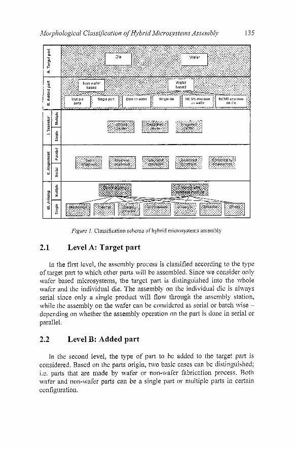
The morphological classification scheme consists of five category levels (Figure 1). The first two levels, level A and B, are the classification of the parts that need to be assembled together. These parts can be loose parts or sub-assemblies. Levels I, 11, and I11 consist of the assembly step classification, which are transfer, alignment, and joining, respectively. Each category level has several class alternatives, which lead to various possibilities of the overall assembly process configuration.
Morphological ClassiJication of Hybrid Microsystems Assembly 135
Figure I. Classification scheme of hybrid microsystems assen~bly
2.1 Level A: Target part
In the first level, the assembly process is classified according to the type of target part to which other parts will be assembled. Since we consider only wafer based microsystems, the target part is distinguished into the whole wafer and the individual die. The asse~nbly on the individual die is always serial since only a single product will flow through the assembly station, while the assembly on the wafer can be considered as serial or batch wise - depending on whether the assembly operation on the part is done in serial or parallel.
2.2 Level B: Added part
In the second level, the type of part to be added to the target part is considered. Based on the parts origin, two basic cases can be distinguished; i.e. parts that are made by wafer or non-wafer fabrication process. Both wafer and non-wafer parts can be a single part or multiple parts in certain configuration.
136 Iwan Kztmiawan, Marcel Tichem, and Marian Bartek
Single and multiple non-wafer parts The non-wafer parts are all the elements/structures that are not made
by wafer fabrication technology, e.g. bond wire, solder ball, micro-lens, etc. The part can be a single part, e.g. a loose micro-lens, or a configuration of many parts, which will be added to the target part at the same time, e.g. micro-lenses array. Dies on wafer and single die
The added part may have to be fabricated on another wafer for material and/or fabrication compatibility reasons. The "dies on wafer" concerned here are dies having the same order and pitch with the dies on the target wafer and can be transferred directly for wafer-to-wafer bonding. In some cases, the wafer may need to be cut into "single die" due to some reasons like the pitch and/or order mismatched between the target and the added wafer, the ease of testing and inspection, the requirement to achieve certain bonding quality, and so on.
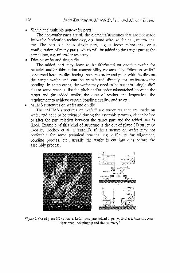
6 MEMS structures on wafer and on die The "MEMS structures on wafer" are structures that are made on
wafer and need to be released during the assembly process, either before or after the part relation between the target part and the added part is fixed. Example of this kind of structure is the out of plane 3D structure used by Dechev et all (Figure 2). If the structure on wafer may not preferable for some technical reasons, e.g. difficulty for alignment, bonding process, etc., usually the wafer is cut into dies before the assembly process.
Figure 2. Out of plane 3D structure. Left: microparts joined to perpendicular to base structure. Right: snap-lock plug tip and slot geometry
Morphological ClassiJication of Hybrid Microsystems Assembly 137
2.3 Level I: Transfer
The third level of the classification deals with how the added part is transferred to the target part. The number of parts to be transferred, i.e. single or multiple, and the role of transfer carrier, i.e. the interface between the part and the gripper, are considered the most important classification parameters in this level.
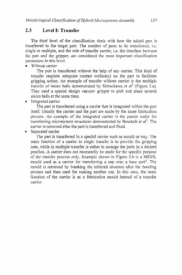
Without carrier The part is transferred without the help of any carrier. This kind of
transfer requires adequate contact surface(s) on the part to facilitate gripping action. An example of transfer without carrier is the multiple transfer of micro balls demonstrated by Shimokawa et a12 (Figure 3.a). They used a special design vacuum gripper to pick and place several micro balls at the same time. Integrated carrier
The part is transferred using a carrier that is integrated within the part itself. Usually the carrier and the part are made by the same fabrication process. An example of the integrated carrier is the parent wafer for transferring microsystem structures demonstrated by Boustedt et a13. The carrier is removed after the part is transferred and fixed. Separated carrier
The part is transferred in a special carrier such as mould or tray. The main function of a carrier in single transfer is to provide the gripping area, while in multiple transfer is rather to arrange the parts in a desired position. A carrier does not necessarily be made for the specific purpose of the transfer process only. Example shown in Figure 3.b is a HEXIL mould used as a carrier for transferring a cap onto a base part4. The mould is retrieved by breaking the tethered structure after the bonding process and then used for making another cap. In this case, the main function of the carrier is as a fabrication mould instead of a transfer carrier.
138 Iwan Kurniawan, Marcel Tichem, and Marian Bartek
(2fArranping Balls Vacuum
(a) I breakable tether (b)
n~icrostructure using a separated carrier4 Figure 3. (a) Multiple transfer of micro balls without using carrier2 (b) Single transfer of a
2.4 Level 11: Alignment
In this level, the way to achieve the desired parts position, relative to each other, is considered. The classification in this level is done by evaluating how the coarse and the fine alignment between the parts are performed.
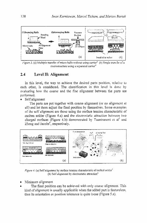
Self alignment The parts are put together with coarse alignment (or no alignment at
all) and let them adjust the final position by themselves. Some examples of the self alignment are those using the surface tension characteristic of molten solder (Figure 4.a) and the electrostatic attraction between two charged surfaces (Figure 4.b) demonstrated by Tuantranont et a15 and zheng and ~ a c o b s ~ , r~spectively.
Figure 4. (a) Self alignment by surface tension characteristic of melted solderS (b) Self alignment by electrostatic attraction6
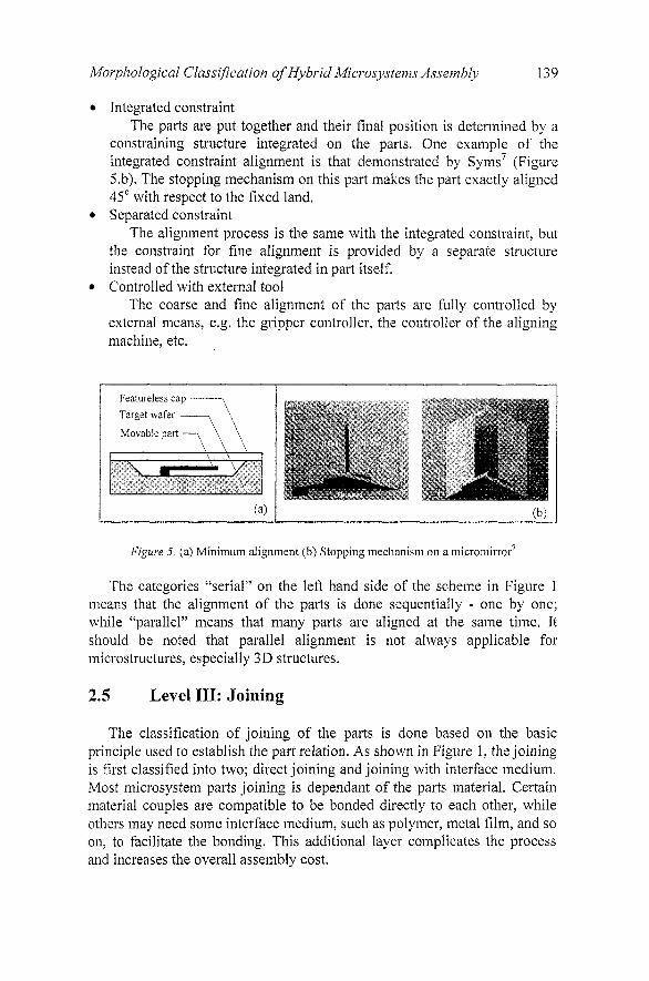
Minimum alignment e The final position can be achieved with only coarse alignment. This
kind of alignment is usually applicable when the added part is featureless, thus its orientation or position tolerance is quite loose (Figure 5.a).
Morphological Classification of Hybrid Microsystems Assembly 139
Integrated constraint The pasts are put together and their final position is determined by a
constraining structure integrated on the parts. One example of the integrated constraint alignment is that demonstrated by syms7 (Figure 5.b). The stopping mechanism on this part makes the past exactly aligned 45"vith respect to the fixed land. Separated constraint
The alignment process is the same with the integrated constraint, but the constraint for fine alignment is provided by a separate structure instead of the structure integrated in part itself. Controlled with external tool
The coarse and fine alignment of the pasts are fully controlled by external means, e.g. the gripper controller, the controller of the aligning machine, etc.
Featureless c a p - Target wafer
Movab le part
Figure 5. (a) Minimum alignment (b) Stopping mechanism on a micromirror7
The categories "serial" on the left hand side of the scheme in Figure 1 means that the alignment of the pasts is done sequentially - one by one; while "parallel" means that many parts are aligned at the same time. It should be noted that parallel alignment is not always applicable for microstructures, especially 3D structures.
2.5 Level 111: Joining
The classification of joining of the parts is done based on the basic principle used to establish the past relation. As shown in Figure 1, the joining is first classified into two; direct joining and joining with interface medium. Most microsystem parts joining is dependant of the parts material. Certain material couples are compatible to be bonded directly to each other, while others may need some interface medium, such as polymer, metal film, and so on, to facilitate the bonding. This additional layer complicates the process and increases the overall assembly cost.
140 Iwan Kurniawan, Mavcel Tichem, and Marian Bartek
The joining is classified further according to the physical parameters used to establish the final join. These physical parameters are considered to have potential influence to the joined parts. In this way, the consequences of their application to the part performance can be predicted immediately in the early selection. Since the inventions of new joining methods are still expected to come in the future, category "others" is added in this level. The explanation of each joining class is as follows:
Mechanical Joining by means of mechanical principle is adapted from the
principles used in macro domain. However, due to the difficulties imposed by the small size, there is only limited number of principles can be applied for microsystems. One example of the mechanical joining is the snap lock join demonstrated by Dechev et all (Figure 2). There is no interface medium needed between the two parts. Thermal
Many microsystems joining processes involve thermal energy. The temperature applied to establish the part relation can vary up to more than a thousand degree Celsius. In some applications, pressure is also applied to assist the joining process. Two examples of the thermal joining are eutectic and silicon fusion bonding (SFB). Depending on the parts material, the thermal joining can be performed either directly or by employing an interface medium. Electric potential
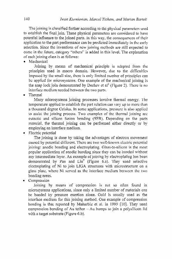
The joining is done by taking the advantages of electron movement caused by potential different. There are two well-known electric potential joining: anodic bonding and electroplating. Glass-to-silicon is the most popular application of anodic bonding since they can be bonded without any intermediate layer. An example of joining by electroplating has been demonstrated by Pan and in^ (Figure 6.4. They used selective electroplating of Ni to join LIGA structures with microstructure on a glass plate, where Ni served as the interface medium between the two bonding areas. Compression
Joining by means of compression is not so often found in microsystems applications, since only a limited number of materials can be bonded by pressure exertion alone. Gold is usually used as the interface medium for this joining method. One example of compression bonding is that reported by Maharbiz et al. in 1999 [lo]. They used compression bonding of Au tether - Au bumps to join a polysilicon lid with a target substrate (Figure 6.b).
i2lorphological Classification of Hybrid Microsystems Assembly 141
I
F ~ g i w 6, ( a ) Bonding of'L1GA structure by Ni selecti\,e c.1cctroplarmg' (b) Co~n]~rcs.iion
A
bonding of AU-AU"'
j nnG '0 mtd~w. ' ' - Fnbrico'e
AJ & l a c ' <kid
Etch scisdkiciui
Ultrasonic This joining method is based on the phenomena of metals softening
when exposed to ultrasonic wave". The most common applications of ultrasonic bonding are A1 or gold wire bonding for electrical connection. The use of interface medium is dependent on the part material in use. Adhesive
Quite a large variety of adhesives is available in the market for bonding applications. In general, a strong adhesive bond can be achieved by applying enough heat and pressure, using hardener, or by photo curing. The physical properties of adhesives vary and can be chosen according to the application needs, e.g. isolation, electrical conductor, or even optical join. The terms "single" and "multiple" are added in the classification scheme
to show that the process throughput is influenced by the selected joining net hod.
3. CASE STUDY: DIE ENCAPSULATION
Microsystems are very sensitive and need to be protected from any disturbance imposed by the environment. This is usually done by covering the microsystem die with a suitable cap either during or after the fabrication process.
The classification scheme described in section 2 can be used as a tool to find alternatives for such an assembly case. By combining different alternative in each classification level, many assembly paths can be chosen for die encapsulation. Each path will have its own advantages as well as
142 Iwan Kurniawan, Marcel Tichem, and Marian Bartek
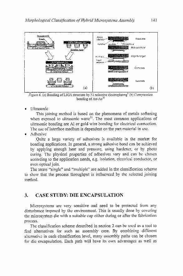
disadvantages, which may set a limit to its applicability. As an example, two assembly paths (Figure 7) are selected and discussed in the next sub section.
Figwe 7. Alternatives of die encapsulation path
3.1 Die to die assembly
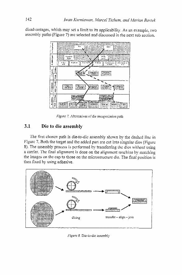
The first chosen path is die-to-die assembiy shown by the dashed line in Figure 7. Both the target and the added part are cut into singular dies (Figure 8). The assembly process is performed by transferring the dies without using a carrier. The final alignment is done on the alignment machine by matching the images on the cap to those on the microstructure die. The final position is then fixed by using adhesive.
dicing
- rzTQ '-A m
----+ izzz3l / transfer - ahgn -jam
- -
Figure 6. Die-to-die assembly
Morphological Classzjkation of Hybrid Microsystems Assernbly 143
The main disadvantage of die-to-die assembly is that it is very time consuming and rather expensive. The advantage, on the other hand, is that each microsystem can be inspected and tested prior to the encapsulation process. Thus, only the "known good die" will be processed further and the defected die can be rejected immediately or sent away for reparation. Furthermore, the bonding quality of each dies assembly can be controlled individually.
The selection of alternatives in each classification level maj7 give certain consequences to the device functionality, which can restrict their applicability. Microsystems like absolute pressure sensor or resonator, for example, may need special environment condition, e.g. vacuum, dry, inert gas filled environment, and so on, to be able to perform optimally. For such microsystems, hermetic sealing is an important requirement. Thus, adhesive or other joining method using polymer as the intermediate layer can be discarded immediately, since they do not capable of hermetic sealing. When the hermetic sealing is not an important issue, however, these alternatives are very interesting due to their cheap cost.
3.2 Wafer to wafer assembly
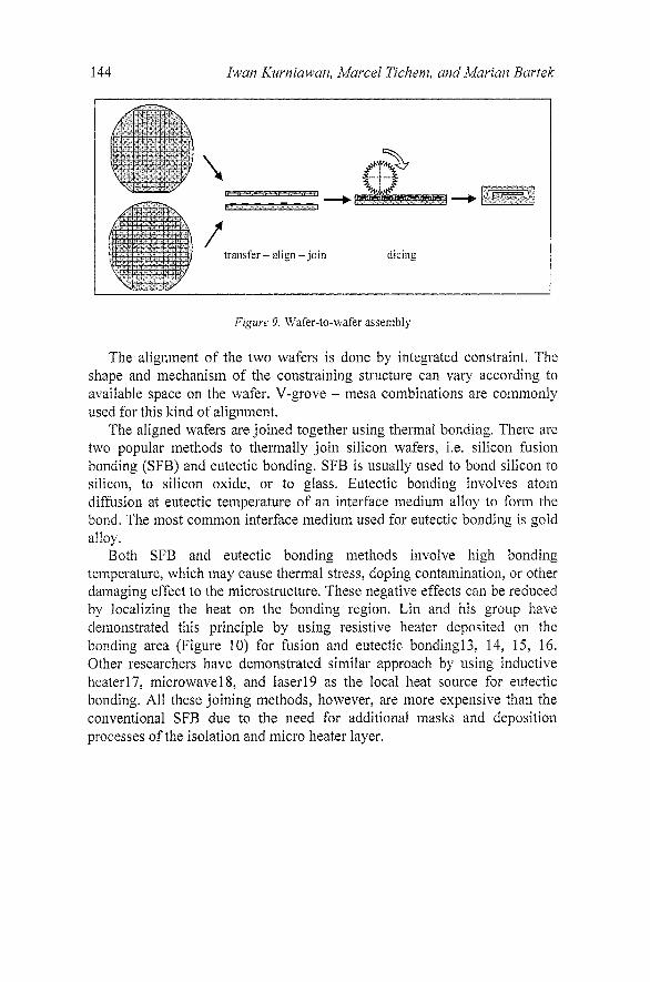
The second path is shown by the full line in Figure 7. The target and the added parts are wafer and dies (caps) on wafer, respectively. The caps wafer has pitch and order that match to those of the corresponding microsystems on the target wafer. The wafer-to-wafer assembly process is illustrated in Figure 9.
The wafers are transferred without using a carrier. The wafers dimension is usually quite big that they can provide enough gripping space. Unless it is required for fabrication purpose, like in the case of nickel caps made by electroplating shown by CT Panl2, normally no part carrier is needed for wafer transfer.
144 Iwan Kurniawan, Marcel Tichem, and Marian Bavtek
transfer - align - join dicing
Figure 9. Wafer-to-wafer assembly
The alignment of the two wafers is done by integrated constraint. The shape and mechanism of the constraining structure can vary according to available space on the wafer. V-grove - mesa combinations are commonly used for this kind of alignment.
The aligned wafers are joined together using thermal bonding. There are two popular methods to thermally join silicon wafers, i.e. silicon fusion bonding (SFB) and eutectic bonding. SFB is usually used to bond silicon to silicon, to silicon oxide, or to glass. Eutectic bonding involves atom diffusion at eutectic temperature of an interface medium alloy to form the bond. The most common interface medium used for eutectic bonding is gold alloy.
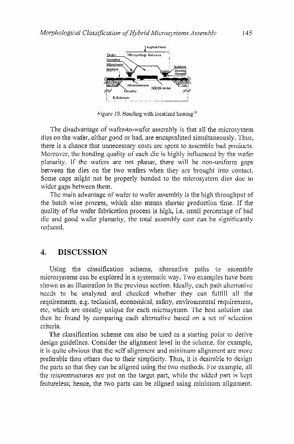
Both SFB and eutectic bonding methods involve high bonding temperature, which may cause thermal stress, doping contamination, or other damaging effect to the microstructure. These negative effects can be reduced by localizing the heat on the bonding region. Lin and his group have demonstrated this principle by using resistive heater deposited on the bonding area (Figure 10) for fusion and eutectic bondingl3, 14, 15, 16. Other researchers have demonstrated similar approach by using inductive heaterl7, microwavel8, and laser19 as the local heat source for eutectic bonding. All these joining methods, however, are more expensive than the conventional SFB due to the need for additional masks and deposition processes of the isolation and micro heater layer.
Morphological Class$cation of Hybrid Microsystems Assembly 145
Figure 10. Bonding with localized heatingi3
The disadvantage of wafer-to-wafer assembly is that all the microsystem dies on the wafer, either good or bad, are encapsulated simultaneously. Thus, there is a chance that unnecessary costs are spent to assemble bad products. Moreover, the bonding quality of each die is highly influenced by the wafer planarity. If the wafers are not planar, there will be non-uniform gaps between the dies on the two wafers when they are brought into contact. Some caps might not be properly bonded to the microsystem dies due to wider gaps between them.
The main advantage of wafer to wafer assembly is the high throughput of the batch wise process, which also means shorter production time. If the quality of the wafer fabrication process is high, i.e. small percentage of bad die and good wafer planarity, the total assembly cost can be significantly reduced.
4. DISCUSSION
Using the classification scheme, alternative paths to assemble microsystems can be explored in a systematic way. Two examples have been shown as an illustration in the previous section. Ideally, each path alternative needs to be analyzed and checked whether they can fulfill all the requirements, e.g. technical, economical, safety, environmental requirement, etc, which are usually unique for each microsystem. The best solution can then be found by comparing each alternative based on a set of selection criteria.
The classification scheme can also be used as a starting point to derive design guidelines. Consider the alignment level in the scheme, for example, it is quite obvious that the self alignment and minimum alignment are more preferable than others due to their simplicity. Thus, it is desirable to design the parts so that they can be aligned using the two methods. For example, all the microstructures are put on the target part, while the added part is kept featureless; hence, the two parts can be aligned using minimum alignment.
146 hvan Kurniawan, Marcel Tichem, and Marian Bartek
With design guidelines, the classification scheme can serve as a tool to solve the assembly cases of hybrid microsystems in a well structured way.
5. CONCLUSION
A morphological classification of the assembly process for hybrid microsystems has been presented in this paper. A case study demonstrated that the scheme can be used to find alternative paths for assembly process.
Future research will be performed to further explore the scheme and to derive design guidelines for microsystems assembly with the help of this scheme.
REFERENCES
1. N. Dechev, W.L. Cleghorn, and J.K. Mills, hficroassembly of3-D itiicrostruc~ures Using a Compliance, Passive Microgripper, Journal of MEMS, vol. 13, no. 2, April 2004.
2. K. Shimokawa, E. Hashino, Y. Ohzeki, and K. Tatsumi, Micro-Ball Bumpfor Flip Chip Interconnections, IEEE Electronic Components and Technology Conference, 1998.
3. K. Boustedt, K. Persson, and D. Stranneby, Flip Chip as an Enabler for MEIWS Packaging, IEEE Electronic Components and Technology Conference, 2002.
4. M.J. Madou, Fundamentals ofMicrofabrication, 2nd edition, CRC Press LCC, pp. 482- 486,2002.
5. A. Tuantranont, V.M. Bright, W. Zhang, J. Zhang; and Y.C. Lee, SeljlAligned Assembly of .Vicrolens Arrays with Micromirrors, Proc. SPIE, vol, 3878, pp. 90-100, 1999.
6. W. Zheng and H.O. Jacobs, Shape-and-Solder-Directed Self-Assembly to Package Semiconductor Device Segments, Applied Physics Letters, vol. 85, no. 16, October 2004.
7. R.R.A. Syms, Surface Tension Powered Self-Assembly of 3 -0 ~biicro-Optomecl~a~zical Structure, Journal of MEMS, vol. 8, no. 4, December 1999.
8. V. Kaajakari, and A. Lal, Thernlokinetic Actuation for Batch Assembly of iWjcroscale Hinged Structures, Journal of MEMS, vol. 12, no. 4, August 2003.
9. L.W. Pan and L. Lin, Butch Transfer of LIGA Microstructures by Selective Electroplating and Bonding, Journal of MES, vol. 10, no. 1, March 2001.
10. M.M. Maharbiz, M.B. Cohn, R.T. Howe, R. Horowitz, and A.P. Pisano, Batch Micropackaging by Compression-Bonded Wafer- Wa$r Trander; IEEE, 1999.
11. G.G. Harman and J. Albers, The Ultrasonic Welding itiechanism as Applied to A1uminun1- and Gold-Wire Bonding in Microelectronics, IEEE Trans. on Parts, Hybrids, and Packaging, vol. PHP-13, no. 4, December 1997.
12. C.T. Pan, Seleclive Low Tenzperature Microcap Packaging Technique Through Flip Chip and Wafer Level Alignment, Journal of Micromechanics and Microengineering, vol. 14, pp 522-529,2004,
13. L. Lin, MEMS Post-Packaging by Localized Heating and Bonding, IEEE Trans. on Adv. Packaging, vol. 23, no. 4, November 2000.
14. Y.T. Cheng, L. Lin, and K. Najafi, Localized Silicon Fusion and Eulectic Bonding for MEMS Fabrication and Packaging, Journal of MEMS, vol. 9, no.1, March 2000.

Morphological Classification of Hybrid Microsystems Assembly 147
15. Y.T. Cheng, L. Lin, and Najafi, K., Localized Bonding with PSG or hdiunt Solder as Intermediate Layer, IEEE, 1999.
16. Y.T. Cheng, W.T. Hsu, K. Najafi, C.T.-C. Nguyen, and L. Lin, Vacuunz Packaging Tecl~nology Using Localized Aluminz~nz/Silicon-to-Glass Bonding, Journal of MEMS, vol. 11, no. 5, October 2002.
17. H.-A. Yang, M. Wu, and W. Fang, Loca1i:edInductiotz HeatingSolder Bonding for Wafer Level MEMS Packaging, Journal of Micromechanics and Microegineering, 2005.
18. N. Budraa, B. Ng, D. Wang, S. Ahsan, Y. Zhang, E. Cho, B. McQuiston, and J. Mai, Microwave Processing Techniques for High Density Interconnects and Hj)briciization, IEEE, 2004.
19. A. Mohan, C.B.O. O'Neal, A.P. Malshe, and R.B. Foster, A Wafer Level Packaging Approach for MEMS and Related Microsystems Using Selective Laser-Assisted Bonding (LAB), IEEE Elec. Comp. and Tech. Conference, 2005.