
Photolithography Overview for Microsystems - nanoHUB
16
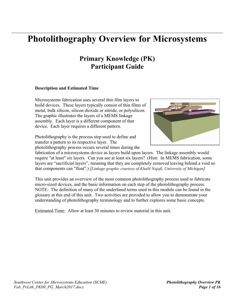
Southwest Center for Microsystems Education (SCME) Photolithography Overview PK Fab_PrLith_PK00_PG_March2017.docx Page 1 of 16 Photolithography Overview for Microsystems Primary Knowledge (PK) Participant Guide Description and Estimated Time Microsystems fabrication uses several thin film layers to build devices. These layers typically consist of thin films of metal, bulk silicon, silicon dioxide or nitride, or polysilicon. The graphic illustrates the layers of a MEMS linkage assembly. Each layer is a different component of that device. Each layer requires a different pattern. Photolithography is the process step used to define and transfer a pattern to its respective layer. The photolithography process occurs several times during the fabrication of a microsystems device as layers build upon layers. The linkage assembly would require "at least" six layers. Can you see at least six layers? (Hint: In MEMS fabrication, some layers are “sacrificial layers”, meaning that they are completely removed leaving behind a void so that components can "float".) [Linkage graphic courtesy of Khalil Najafi, University of Michigan] This unit provides an overview of the most common photolithography process used to fabricate micro-sized devices, and the basic information on each step of the photolithography process. NOTE: The definition of many of the underlined terms used in this module can be found in the glossary at this end of this unit. Two activities are provided to allow you to demonstrate your understanding of photolithography terminology and to further explores some basic concepts. Estimated Time: Allow at least 30 minutes to review material in this unit.
-
Upload
khangminh22 -
Category
Documents
-
view
0 -
download
0
Transcript of Photolithography Overview for Microsystems - nanoHUB
Southwest Center for Microsystems Education (SCME) Photolithography Overview PK Fab_PrLith_PK00_PG_March2017.docx Page 1 of 16
Photolithography Overview for Microsystems
Primary Knowledge (PK)
Participant Guide
Description and Estimated Time
Microsystems fabrication uses several thin film layers to build devices. These layers typically consist of thin films of metal, bulk silicon, silicon dioxide or nitride, or polysilicon. The graphic illustrates the layers of a MEMS linkage assembly. Each layer is a different component of that device. Each layer requires a different pattern. Photolithography is the process step used to define and transfer a pattern to its respective layer. The photolithography process occurs several times during the fabrication of a microsystems device as layers build upon layers. The linkage assembly would require "at least" six layers. Can you see at least six layers? (Hint: In MEMS fabrication, some layers are “sacrificial layers”, meaning that they are completely removed leaving behind a void so that components can "float".) [Linkage graphic courtesy of Khalil Najafi, University of Michigan] This unit provides an overview of the most common photolithography process used to fabricate micro-sized devices, and the basic information on each step of the photolithography process. NOTE: The definition of many of the underlined terms used in this module can be found in the glossary at this end of this unit. Two activities are provided to allow you to demonstrate your understanding of photolithography terminology and to further explores some basic concepts. Estimated Time: Allow at least 30 minutes to review material in this unit.
Southwest Center for Microsystems Education (SCME) Photolithography Overview PK Fab_PrLith_PK00_PG_March2017.docx Page 2 of 16
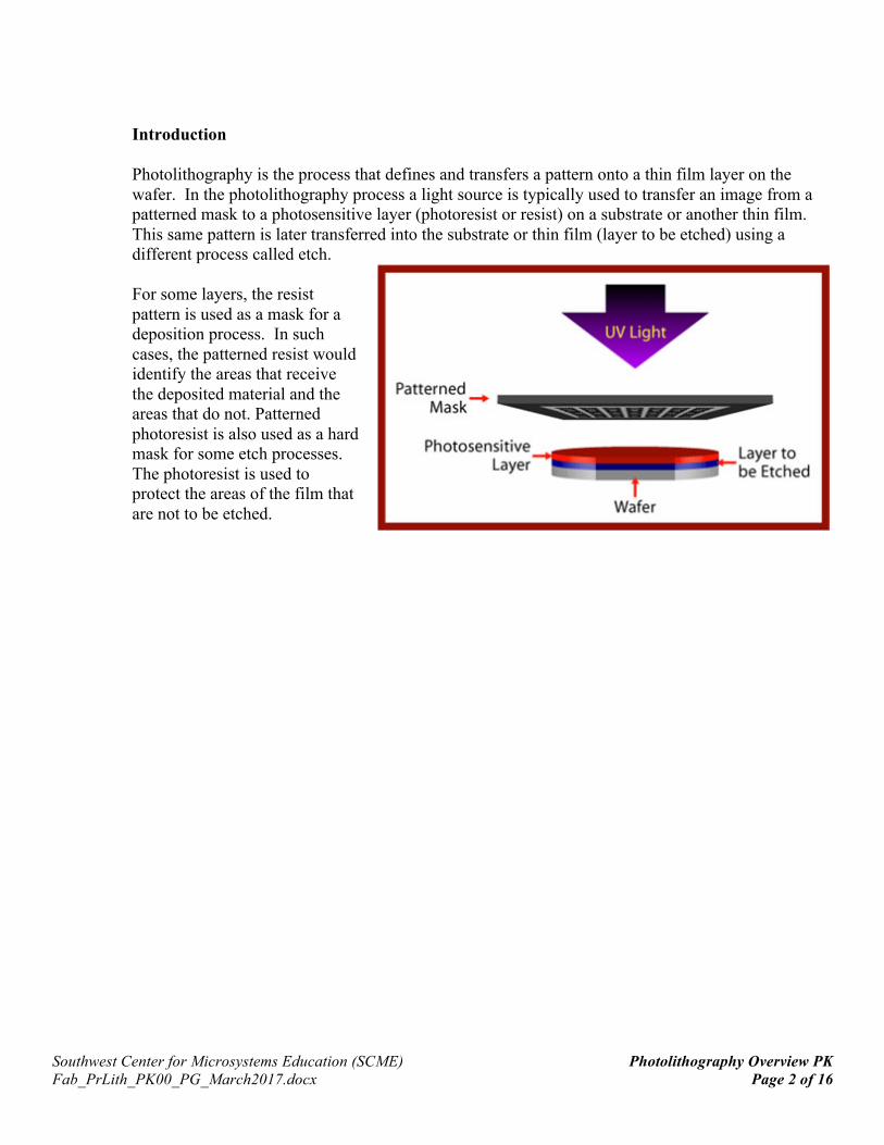
Introduction Photolithography is the process that defines and transfers a pattern onto a thin film layer on the wafer. In the photolithography process a light source is typically used to transfer an image from a patterned mask to a photosensitive layer (photoresist or resist) on a substrate or another thin film. This same pattern is later transferred into the substrate or thin film (layer to be etched) using a different process called etch. For some layers, the resist pattern is used as a mask for a deposition process. In such cases, the patterned resist would identify the areas that receive the deposited material and the areas that do not. Patterned photoresist is also used as a hard mask for some etch processes. The photoresist is used to protect the areas of the film that are not to be etched.
Southwest Center for Microsystems Education (SCME) Photolithography Overview PK Fab_PrLith_PK00_PG_March2017.docx Page 3 of 16
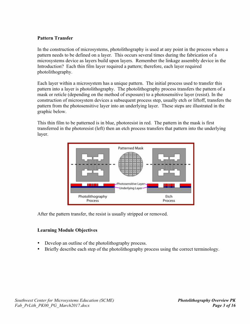
Pattern Transfer In the construction of microsystems, photolithography is used at any point in the process where a pattern needs to be defined on a layer. This occurs several times during the fabrication of a microsystems device as layers build upon layers. Remember the linkage assembly device in the Introduction? Each thin film layer required a pattern; therefore, each layer required photolithography. Each layer within a microsystem has a unique pattern. The initial process used to transfer this pattern into a layer is photolithography. The photolithography process transfers the pattern of a mask or reticle (depending on the method of exposure) to a photosensitive layer (resist). In the construction of microsystem devices a subsequent process step, usually etch or liftoff, transfers the pattern from the photosensitive layer into an underlying layer. These steps are illustrated in the graphic below. This thin film to be patterned is in blue, photoresist in red. The pattern in the mask is first transferred in the photoresist (left) then an etch process transfers that pattern into the underlying layer.
After the pattern transfer, the resist is usually stripped or removed.
Learning Module Objectives
• Develop an outline of the photolithography process. • Briefly describe each step of the photolithography process using the correct terminology.

Southwest Center for Microsystems Education (SCME) Photolithography Overview PK Fab_PrLith_PK00_PG_March2017.docx Page 4 of 16
Steps of Photolithography
Steps of Photolithography - Coat, Expose, Develop
There are three basic steps to photolithography: • Coat - A photosensitive material (photoresist or resist) is applied to the substrate surface. • Expose - The photoresist is exposed using a light source, such as Near UV (Ultraviolet), Deep
UV or X-ray. • Develop - The exposed photoresist is subsequently dissolved with a chemical developer. The
type of photoresist (positive or negative) determines which part of the resist is dissolved.
Photolithography vs. Photography
The photolithography process is analogous to a twentieth century photographic process that uses exposed film as the patterned mask (referred to as a "negative" in photography). The exposed film is removed from a camera and developed to create the patterned mask or negative. In a dark room, the negative (patterned mask) is placed between a light source and a prepared sheet of photosensitive paper. • The paper has been coated with a light-sensitive photographic
emulsion. • The paper is exposed when the light travels through the negative. • The exposed paper is placed in a liquid developer, which
chemically reacts with the emulsion, transferring the negative’s image to the photographic paper.
Photographer/Painter: Jean-Pol Grandmont, shot and develop
(b&W) and scanner [Courtesy of Jean-Pol Grandmont]
Southwest Center for Microsystems Education (SCME) Photolithography Overview PK Fab_PrLith_PK00_PG_March2017.docx Page 5 of 16
Coat Process: Step 1 - Surface Conditioning
The first step of the Coat Process is Surface Conditioning. Surface conditioning prepares the wafer to accept the photoresist by providing a clean surface, coated with an intermediate chemical (such as HMDS or Hexamethyldisalizane) that creates a hydrophobic surface which boosts adhesion of the photoresist to the wafer’s surface. HMDS is the most commonly used intermediate chemical. There are several reasons for conditioning the wafer’s surface: • The presence of other molecules or particles can create problems for resist adhesion and
subsequent resist thickness uniformity; therefore, the wafer must be thoroughly cleaned and dried.
• Intermediates such as HMDS prepare the surface for adhesion of photoresist. • Photoresist is an organic material that must interface with the substrate material which, in most
cases, is inorganic. As an intermediate, HMDS allows this interface to occur. • Different surface materials can have different surface tensions or affinity for organic materials
such as photoresist. Again, as an intermediate between the underlying surface and the photoresist, HMDS acts as a buffer and promotes the adhesion of photoresist to surface materials.
• Photoresist adheres best to a hydrophobic surface. A hydrophobic surface is defined as a surface that does not like (phobic) water (hydro). A layer of HMDS provides a hydrophobic surface.
Southwest Center for Microsystems Education (SCME) Photolithography Overview PK Fab_PrLith_PK00_PG_March2017.docx Page 6 of 16
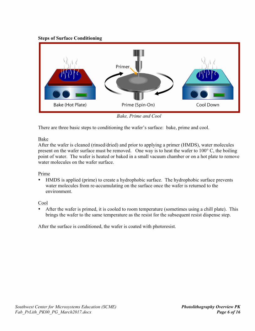
Steps of Surface Conditioning
Bake, Prime and Cool
There are three basic steps to conditioning the wafer’s surface: bake, prime and cool. Bake After the wafer is cleaned (rinsed/dried) and prior to applying a primer (HMDS), water molecules present on the wafer surface must be removed. One way is to heat the wafer to 100° C, the boiling point of water. The wafer is heated or baked in a small vacuum chamber or on a hot plate to remove water molecules on the wafer surface. Prime • HMDS is applied (prime) to create a hydrophobic surface. The hydrophobic surface prevents
water molecules from re-accumulating on the surface once the wafer is returned to the environment.
Cool • After the wafer is primed, it is cooled to room temperature (sometimes using a chill plate). This
brings the wafer to the same temperature as the resist for the subsequent resist dispense step. After the surface is conditioned, the wafer is coated with photoresist.
Southwest Center for Microsystems Education (SCME) Photolithography Overview PK Fab_PrLith_PK00_PG_March2017.docx Page 7 of 16
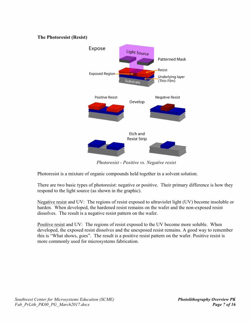
The Photoresist (Resist)
Photoresist - Positive vs. Negative resist
Photoresist is a mixture of organic compounds held together in a solvent solution. There are two basic types of photoresist: negative or positive. Their primary difference is how they respond to the light source (as shown in the graphic). Negative resist and UV: The regions of resist exposed to ultraviolet light (UV) become insoluble or harden. When developed, the hardened resist remains on the wafer and the non-exposed resist dissolves. The result is a negative resist pattern on the wafer. Positive resist and UV: The regions of resist exposed to the UV become more soluble. When developed, the exposed resist dissolves and the unexposed resist remains. A good way to remember this is “What shows, goes”. The result is a positive resist pattern on the wafer. Positive resist is more commonly used for microsystems fabrication.
Southwest Center for Microsystems Education (SCME) Photolithography Overview PK Fab_PrLith_PK00_PG_March2017.docx Page 8 of 16
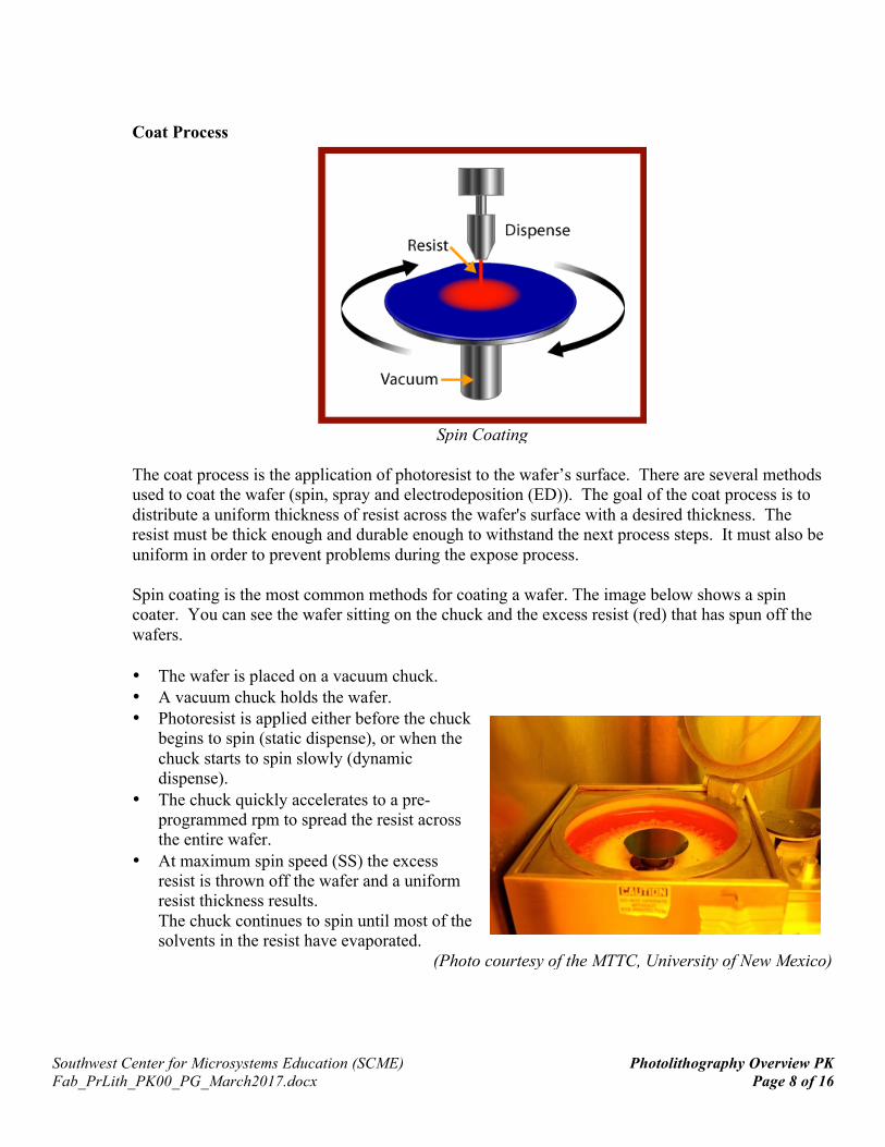
Coat Process
Spin Coating
The coat process is the application of photoresist to the wafer’s surface. There are several methods used to coat the wafer (spin, spray and electrodeposition (ED)). The goal of the coat process is to distribute a uniform thickness of resist across the wafer's surface with a desired thickness. The resist must be thick enough and durable enough to withstand the next process steps. It must also be uniform in order to prevent problems during the expose process. Spin coating is the most common methods for coating a wafer. The image below shows a spin coater. You can see the wafer sitting on the chuck and the excess resist (red) that has spun off the wafers. • The wafer is placed on a vacuum chuck. • A vacuum chuck holds the wafer. • Photoresist is applied either before the chuck
begins to spin (static dispense), or when the chuck starts to spin slowly (dynamic dispense).
• The chuck quickly accelerates to a pre-programmed rpm to spread the resist across the entire wafer.
• At maximum spin speed (SS) the excess resist is thrown off the wafer and a uniform resist thickness results. The chuck continues to spin until most of the solvents in the resist have evaporated.
(Photo courtesy of the MTTC, University of New Mexico)
Southwest Center for Microsystems Education (SCME) Photolithography Overview PK Fab_PrLith_PK00_PG_March2017.docx Page 9 of 16
Photoresist Thickness Activity
If you need a break or would like to learn more about the coating process, you may stop and complete the activity “Photoresist Thickness”. In this activity you will further explore the coat process and the factors that determine the photoresist thickness.
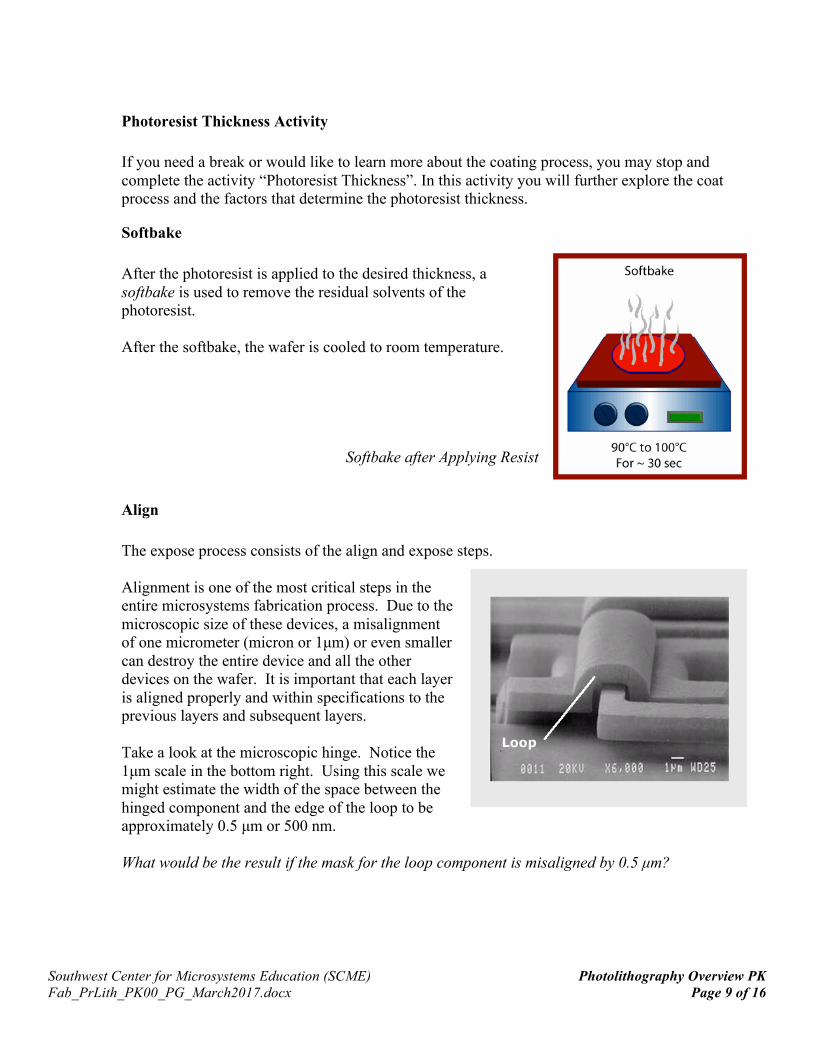
Softbake
After the photoresist is applied to the desired thickness, a softbake is used to remove the residual solvents of the photoresist. After the softbake, the wafer is cooled to room temperature.
Softbake after Applying Resist
Align
The expose process consists of the align and expose steps. Alignment is one of the most critical steps in the entire microsystems fabrication process. Due to the microscopic size of these devices, a misalignment of one micrometer (micron or 1µm) or even smaller can destroy the entire device and all the other devices on the wafer. It is important that each layer is aligned properly and within specifications to the previous layers and subsequent layers. Take a look at the microscopic hinge. Notice the 1µm scale in the bottom right. Using this scale we might estimate the width of the space between the hinged component and the edge of the loop to be approximately 0.5 µm or 500 nm. What would be the result if the mask for the loop component is misaligned by 0.5 µm?
Southwest Center for Microsystems Education (SCME) Photolithography Overview PK Fab_PrLith_PK00_PG_March2017.docx Page 10 of 16
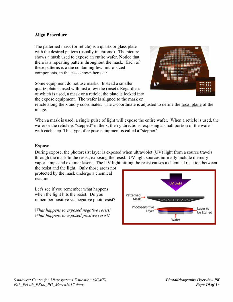
Align Procedure
The patterned mask (or reticle) is a quartz or glass plate with the desired pattern (usually in chrome). The picture shows a mask used to expose an entire wafer. Notice that there is a repeating pattern throughout the mask. Each of these patterns is a die containing few micro-sized components, in the case shown here - 9. Some equipment do not use masks. Instead a smaller quartz plate is used with just a few die (inset). Regardless of which is used, a mask or a reticle, the plate is locked into the expose equipment. The wafer is aligned to the mask or reticle along the x and y coordinates. The z-coordinate is adjusted to define the focal plane of the image. When a mask is used, a single pulse of light will expose the entire wafer. When a reticle is used, the wafer or the reticle is “stepped” in the x, then y directions, exposing a small portion of the wafer with each step. This type of expose equipment is called a "stepper".
Expose During expose, the photoresist layer is exposed when ultraviolet (UV) light from a source travels
through the mask to the resist, exposing the resist. UV light sources normally include mercury vapor lamps and excimer lasers. The UV light hitting the resist causes a chemical reaction between the resist and the light. Only those areas not protected by the mask undergo a chemical reaction. Let's see if you remember what happens when the light hits the resist. Do you remember positive vs. negative photoresist? What happens to exposed negative resist? What happens to exposed positive resist?

Southwest Center for Microsystems Education (SCME) Photolithography Overview PK Fab_PrLith_PK00_PG_March2017.docx Page 11 of 16
The Develop Process
In the develop process, portions of the photoresist are dissolved by a chemical developer. With positive resist (the more commonly used resist), the exposed resist is dissolved while the unexposed resist remains on the wafer. With negative resist, the unexposed resist is dissolved while the exposed resist remains. The develop process leaves a visible pattern (seen by the naked eye) within the resist.
Develop Processes
Immersion and Spray-on
Develop is usually a wet process. The wafers are physically placed in the develop solution (immersion) or the developer is sprayed onto the wafer. The timing of this process is critical. Too long of a time leads to an "overdeveloped resist"; too little of a time leads to an "underdeveloped resist" – both of which negatively affect line width. An underdeveloped resist could prevent access to the underlying layer by leaving too much resist on the wafer. To stop the chemical reaction of the developer with the photoresist, the wafers are rinsed with de-ionized (DI) water then spin-dried.

Southwest Center for Microsystems Education (SCME) Photolithography Overview PK Fab_PrLith_PK00_PG_March2017.docx Page 12 of 16
Hardbake
Hardbake Temperatures
A post-develop hardbake is used to harden the photoresist for the subsequent process. In order to do this, the temperature of the hardbake is higher than that of the softbake after coat. The hard bake temperature for positive resist is approximately 120°C to 140°C. However, too high of a temperature could cause the photoresist to reflow, destroying the pattern. After the hardbake, the wafer is cooled to room temperature.
Inspect – What to Look for
Wafers are inspected immediately after the photolithography process and before subsequent processes such as etch. The inspection specifications vary depending on the product requirements. Three critical parameters of the photolithography process are alignment, line widths and defects. Alignment – the pattern must be positioned accurately to the previously layer. Line width or critical dimension (CD) – the pattern images are in focus and have the correct size. Defects– things that could affect subsequent processes and eventually the operation of the devices (i.e. particles, scratches, peeling (lifting) of the resist, holes in the resist, scumming (an underdeveloped or underexposed pattern)) The inspection step ensures that the pattern is properly aligned to the previous layers and that the critical dimensions are correct. Because of the 3-dimensional characteristic of MEMS devices, inspection is more challenging than with integrated circuits.
Southwest Center for Microsystems Education (SCME) Photolithography Overview PK Fab_PrLith_PK00_PG_March2017.docx Page 13 of 16
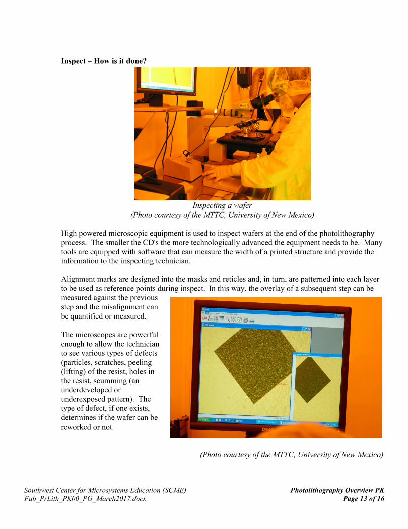
Inspect – How is it done?
Inspecting a wafer
(Photo courtesy of the MTTC, University of New Mexico)
High powered microscopic equipment is used to inspect wafers at the end of the photolithography process. The smaller the CD's the more technologically advanced the equipment needs to be. Many tools are equipped with software that can measure the width of a printed structure and provide the information to the inspecting technician. Alignment marks are designed into the masks and reticles and, in turn, are patterned into each layer to be used as reference points during inspect. In this way, the overlay of a subsequent step can be measured against the previous step and the misalignment can be quantified or measured. The microscopes are powerful enough to allow the technician to see various types of defects (particles, scratches, peeling (lifting) of the resist, holes in the resist, scumming (an underdeveloped or underexposed pattern). The type of defect, if one exists, determines if the wafer can be reworked or not.
(Photo courtesy of the MTTC, University of New Mexico)
Southwest Center for Microsystems Education (SCME) Photolithography Overview PK Fab_PrLith_PK00_PG_March2017.docx Page 14 of 16
Review Questions
What are some of the critical parameters that should be inspected during the photolithography process and as a final inspection? Critical dimensions are getting smaller. Objects are getting smaller. In microsystems technology, some objects are required to "float" above the substrate. What do you think are some of the limitations, if any, of the photolithography process described here when applied to these advancing technologies?
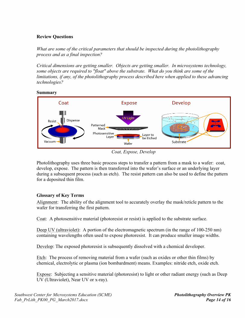
Summary
Coat, Expose, Develop
Photolithography uses three basic process steps to transfer a pattern from a mask to a wafer: coat, develop, expose. The pattern is then transferred into the wafer’s surface or an underlying layer during a subsequent process (such as etch). The resist pattern can also be used to define the pattern for a deposited thin film.
Glossary of Key Terms Alignment: The ability of the alignment tool to accurately overlay the mask/reticle pattern to the
wafer for transferring the first pattern. Coat: A photosensitive material (photoresist or resist) is applied to the substrate surface. Deep UV (ultraviolet): A portion of the electromagnetic spectrum (in the range of 100-250 nm) containing wavelengths often used to expose photoresist. It can produce smaller image widths. Develop: The exposed photoresist is subsequently dissolved with a chemical developer. Etch: The process of removing material from a wafer (such as oxides or other thin films) by chemical, electrolytic or plasma (ion bombardment) means. Examples: nitride etch, oxide etch. Expose: Subjecting a sensitive material (photoresist) to light or other radiant energy (such as Deep UV (Ultraviolet), Near UV or x-ray).

Southwest Center for Microsystems Education (SCME) Photolithography Overview PK Fab_PrLith_PK00_PG_March2017.docx Page 15 of 16
Focal Plane: The plane perpendicular to the axis of a lens or optical system that contains the focal point. Intermediate: Something that lies or occurs between two states, forms or extremes. In photolithography, HMDS is an intermediate lying between the photoresist and the previous layer. Liftoff: A method for patterning films that are deposited. A pattern is defined on a substrate using photoresist. A film, usually metallic, is blanket-deposited all over the substrate, covering the photoresist and areas in which the photoresist has been cleared. During the actual lifting-off, the photoresist under the film is removed with solvent, taking the film with it, and leaving only the film which was deposited directly on the substrate. Mask: A glass plate covered with an array of patterns used in the photomasking process. Each pattern consists of opaque and clear areas that respectively prevent or allow light through. Near UV: A portion of the electromagnetic spectrum (in the range of 400 nm – 300 nm) containing wavelengths often used to expose photoresist. Photolithography: The transfer of a pattern or image from one medium to another, as from a mask to a wafer. Resist: Thin film used in lithography to transfer a circuit pattern to the underlying substrate. Reticle: An exposure mask with the image of a single die, or small cluster of die (called a field). The image on the reticle is stepped across the wafer and is exposed multiple times. Substrate: The base material on or in which MEMS components and circuits are constructed. Thin film: Thin material layers ranging from fractions of a nanometer to several micrometers in thickness. UV (Ultraviolet) light: A portion of the electromagnetic spectrum from 250 to 400 nm. High-pressure mercury sources emit UV light for photoresist exposure. The region below 250nm is known as deep UV (DUV). X-ray: A form of electromagnetic radiation with a wavelength in the range of 10 to 0.01 nanometers.
References • Photolithography Lab.ppt, Fabian Lopez, Central New Mexico Community College
• Photolithography. Module 40. MATEC. NSF Center. Arizona. • "Comparing the costs of photoresist coating using spin, spray, and electrodeposition systems".
Nga P. Pham and Pasqualina M. Sarro, Delft University of Technology. MicroMagazine.com. 2007.
• "Photolithography". Wikipedia. http://en.wikipedia.org/wiki/Photolithography

Southwest Center for Microsystems Education (SCME) Photolithography Overview PK Fab_PrLith_PK00_PG_March2017.docx Page 16 of 16
Disclaimer The information contained herein is considered to be true and accurate; however the Southwest Center for Microsystems Education (SCME) makes no guarantees concerning the authenticity of any statement. SCME accepts no liability for the content of this unit, or for the consequences of any actions taken on the basis of the information provided.
Support for this work was provided by the National Science Foundation's Advanced Technological Education (ATE) Program through Grants. For more learning modules related to microtechnology, visit the SCME website (http://scme-nm.org).