Automotive, Sensorless BLDC Controller - Allegro MicroSystems
Upload
khangminh22Category
view
1download
0
Bulk Micromachining for Microsystems
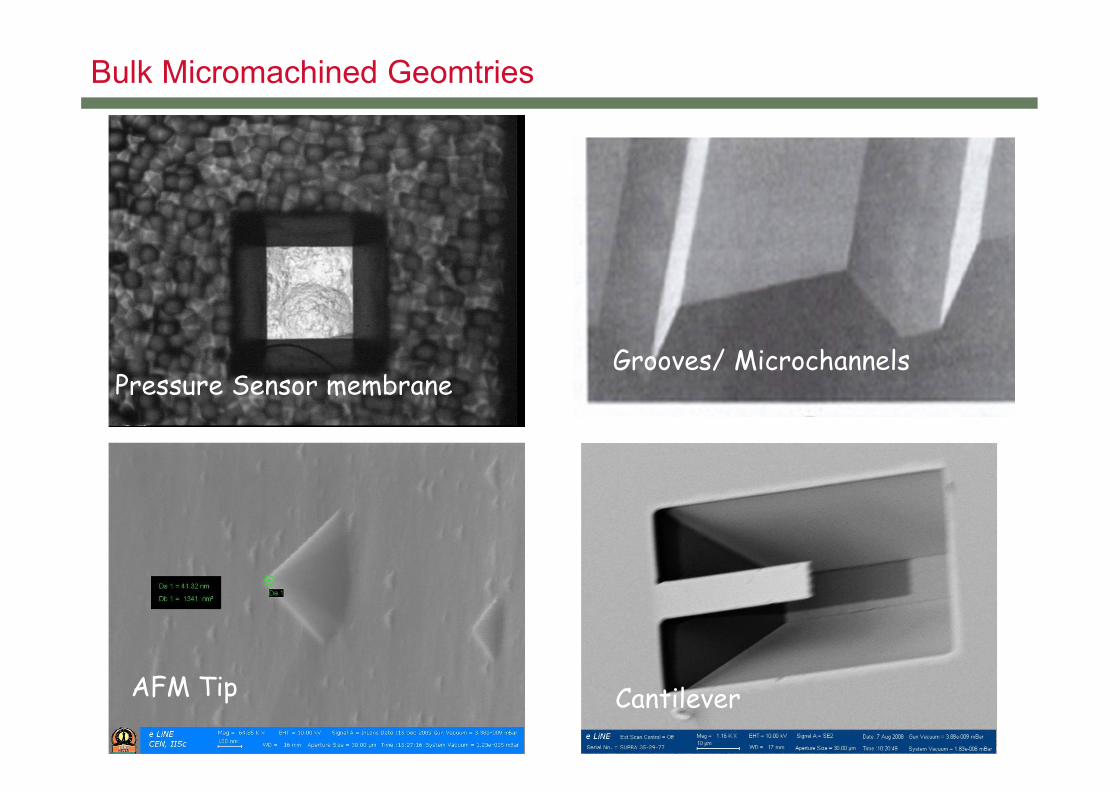
Bulk Micromachined Geomtries
Pressure Sensor membrane
AFM Tip Cantilever
Grooves/ Microchannels

Bulk Micromachinging
Microstructures formed by surface micromachining are thin. For simpler fabrication of microstructures and/or to create larger
vertical space around them etching into the substrate volume would be required
Thin diaphragms, cavities, and cantilevers can be formed by this approach.
In general silicon etching can be isotropic or anisotropic
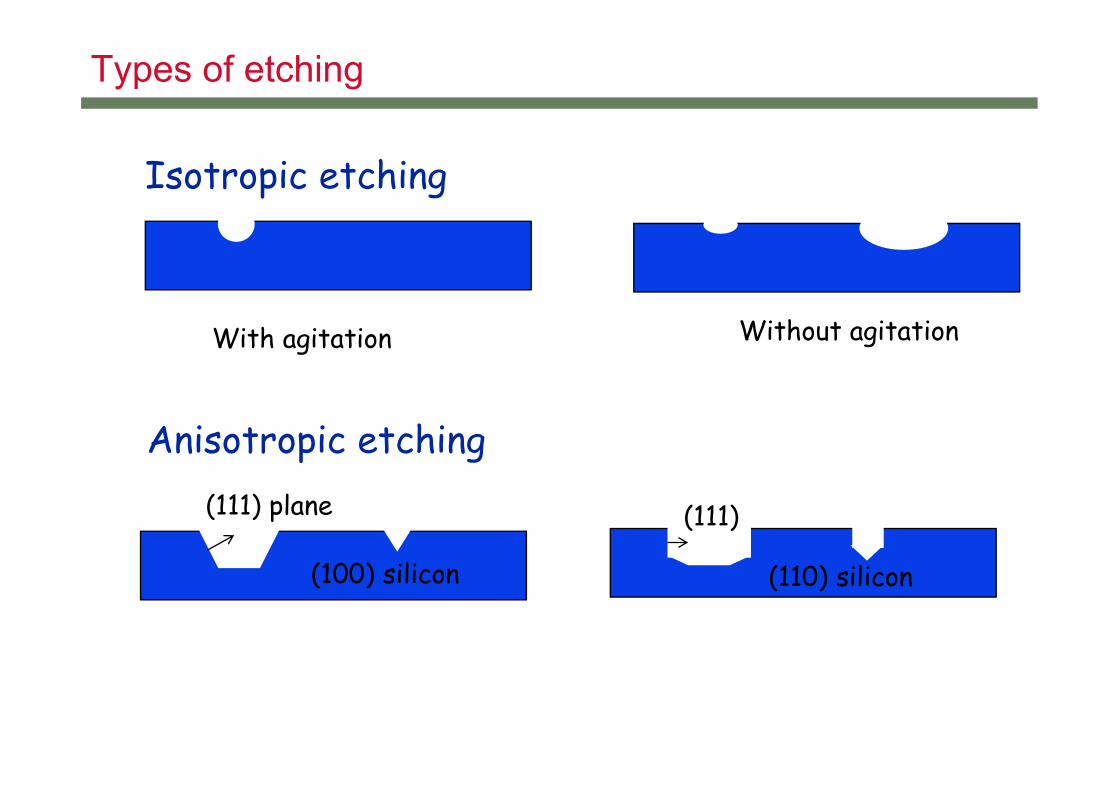
Types of etching
(100) silicon
(111) plane
(110) silicon
(111)
With agitation Without agitation
Isotropic etching
Anisotropic etching
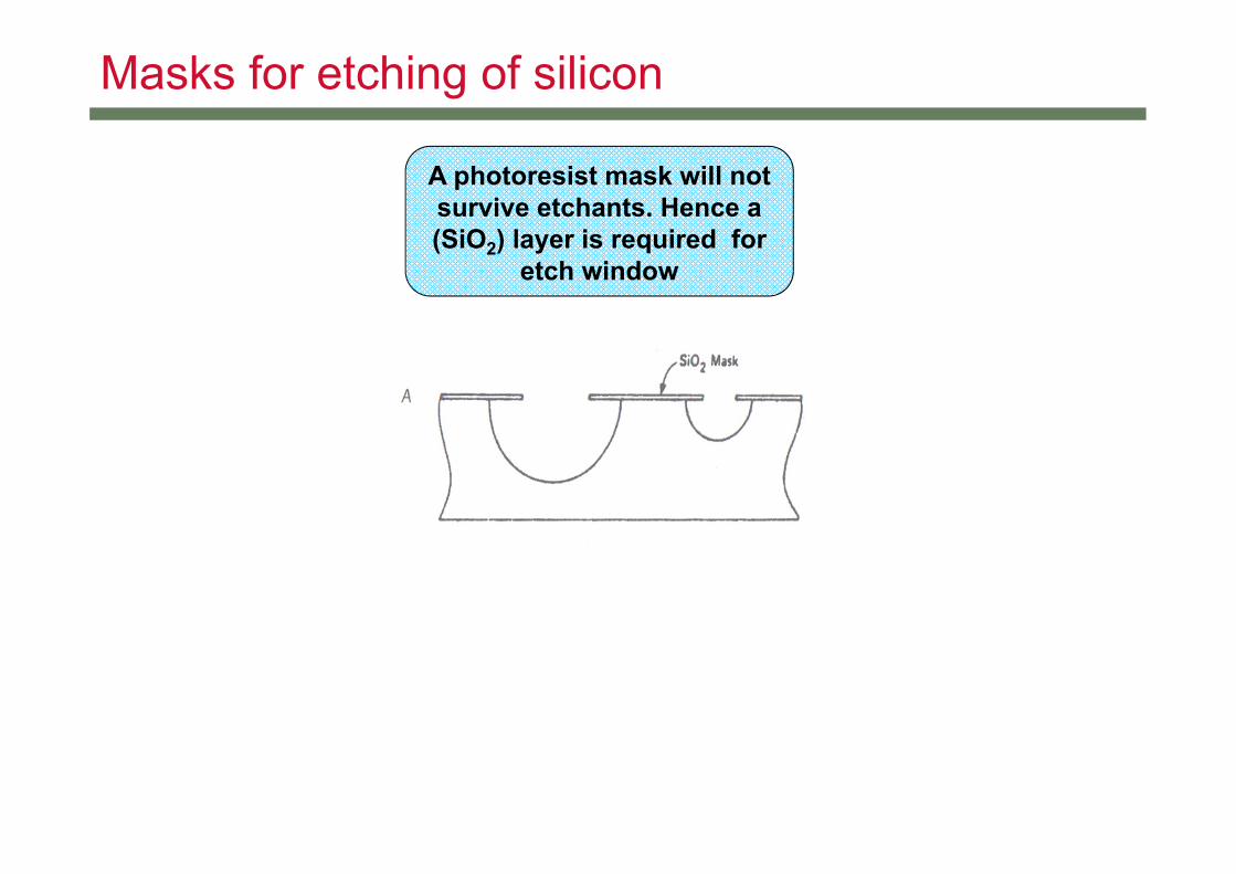
Masks for etching of silicon
A photoresist mask will not survive etchants. Hence a (SiO2) layer is required for
etch window

Fabrication of Microsystems
Wafer Cleaning
Deposition(Evaporation, sputtering, CVD, etc)
[Metals, Semiconductors, Dielectrics]
Resist processing & Pattern transfer
Etching(wet; dry: RIE, DRIE)
[Substrate: isotropic, anisotropic; thin films]
Wafer level Bonding /Packaging
Release etch Final Packaging,
Testing
Repeat for each
new layer
Dicing
Die attach
Processing of bonded w
afer
Required only for devices with surface micromachined parts
Microsystems may require non-electrical interfaces
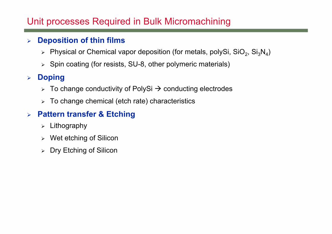
Unit processes Required in Bulk Micromachining
Deposition of thin films Physical or Chemical vapor deposition (for metals, polySi, SiO2, Si3N4)
Spin coating (for resists, SU-8, other polymeric materials)
Doping To change conductivity of PolySi conducting electrodes
To change chemical (etch rate) characteristics
Pattern transfer & Etching Lithography
Wet etching of Silicon
Dry Etching of Silicon

Thin Film Deposition process
Source Transport Condensation on substrate
The nature of the film deposited depends on process parameters like substrate, deposition temperature, gaseous environment, rate of deposition etc.
In Physical vapor Deposition (PVD) process, this transfer takes place by a physical means such as evaporation or impact Favorable conditions are created to transfer the material from the source (target)
to the destination (substrate).
In chemical Vapor Deposition (CVD) process films are deposited through a chemical reaction.
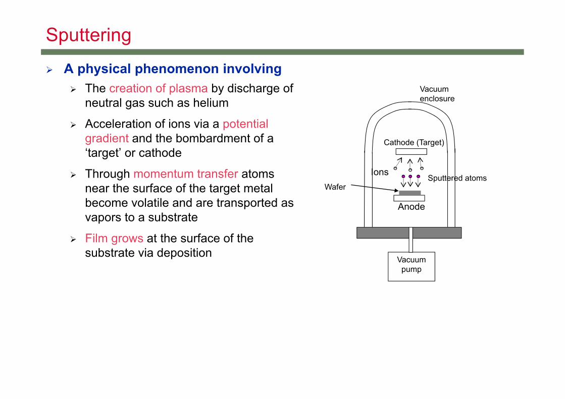
Sputtering
A physical phenomenon involving The creation of plasma by discharge of
neutral gas such as helium
Acceleration of ions via a potential gradient and the bombardment of a ‘target’ or cathode
Through momentum transfer atoms near the surface of the target metal become volatile and are transported as vapors to a substrate
Film grows at the surface of the substrate via deposition
Vacuum pump
Cathode (Target)
Anode
WaferSputtered atoms
Ions
Vacuum enclosure
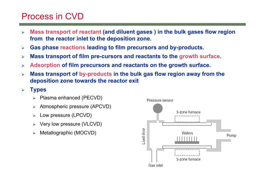
Process in CVD Mass transport of reactant (and diluent gases ) in the bulk gases flow region
from the reactor inlet to the deposition zone. Gas phase reactions leading to film precursors and by-products. Mass transport of film pre-cursors and reactants to the growth surface. Adsorption of film precursors and reactants on the growth surface. Mass transport of by-products in the bulk gas flow region away from the
deposition zone towards the reactor exit Types
Plasma enhanced (PECVD)
Atmospheric pressure (APCVD)
Low pressure (LPCVD)
Very low pressure (VLCVD)
Metallographic (MOCVD)

LPCVD of Si Compounds
22C500
24 H2SiOOSiH
CVD is used to form SiO2 layers that are much thicker in relatively very short times than thermal oxides.
SiO2 can be deposited from reacting silane and oxygen in LPCVD reactor at 300 to 500°C where
SiO2 can also be LPCVD deposited by decomposing dichlorosilane
HCl2H2SiOOH2HSiCl 22C900
222
Si3N4 can be LPCVD or PECVD process. In the LPCVD process, dichlorosilane and ammonia react according to the reaction
243C800 ~
322 H6HCl6NSiNH4HSiCl3
SiO2 can also be LPCVD deposited by from tetraethyl orthosilicate (TEOS or, Si(OC2H5)4)
by vaporizing this from a liquid source.

Pattern Transfer Techniques
In Lithography Resist coating Spin coating Soft baking UV exposure Development Post
baking Etching of thin film Resist striping
In lift off process a photoresist pattern is generated initially on the substrate instead of etching the unwanted material. The basic criterion for the lift off technique is that the thickness of deposited film should be
significantly less than that of the photoresist and the developed patterns have vertical side walls.
Metal layers with high resolution can be patterned using lift off technique. Metals such as gold (which can be etched with aqua regia) can be patterned with simple processes by lift off.
Lift-off
Thin film Deposition
Removal of unwanted material
Lithography
Coating of Resist
Metal Deposition
Removal of resist & unwanted metal
UV exposure & Development
Coating of Resist
UV exposure & Development
Etching of thin films
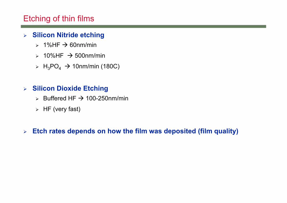
Silicon Nitride etching 1%HF 60nm/min
10%HF 500nm/min
H3PO4 10nm/min (180C)
Silicon Dioxide Etching Buffered HF 100-250nm/min
HF (very fast)
Etch rates depends on how the film was deposited (film quality)

Etching Some definitions
Aspect ratio Ratio of height to lateral dimensions of etched microstructures.
Selectivity ability of the process to choose between the layer to be removed and the interleaving
layers (usually 40:1 is required)
Etch rate the speed with which the process progresses
Etch profile slope of the etch wall
Wet etching involves Transporting of the reactants by diffusion at the surface
Chemical reaction at the surface
Reaction products transported away from the surface
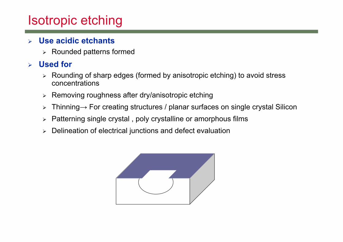
Isotropic etching Use acidic etchants
Rounded patterns formed
Used for Rounding of sharp edges (formed by anisotropic etching) to avoid stress
concentrations Removing roughness after dry/anisotropic etching Thinning→ For creating structures / planar surfaces on single crystal Silicon Patterning single crystal , poly crystalline or amorphous films Delineation of electrical junctions and defect evaluation

Iso etching…
Difficulties in isotropic etching Masking.
Etch rate is agitation and temperature sensitive,
Difficult to control lateral and vertical etch rates
Wet etchants for electronics materialsMaterial Etchant Etch rate (Å/min)
Si 3ml HF+5ml HNO3 + 3ml CH3COOH 3.5x10⁵
GaAs 8ml H2SO4 +1ml H2O2+1ml H2O 0.8x10⁵
SiO2 28ml HF + 170ml H2O + 113g NH4F 15ml HF + 10ml HNO3+ 300ml H2O
1000120
Si3N4 Buffered HFH3PO4
5100
Al 1ml HNO3 + 4ml CH3COOH + 4ml H3PO4 + 1ml H2O
350
Au 4g KI + 1g I2 + 40ml H2O 1x10⁵
Cu FeCl3

Anisotropic etching of Silicon Anisotropic etching means different etch rates in different directions in the material
(e.g., Crystalline Si)

Anisotropically etched features
(110)(100)
(110)
SiO2
111
54.740
(100) wafer with a square mask
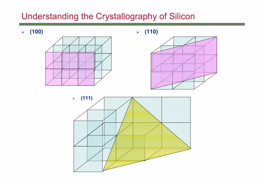
Understanding the Crystallography of Silicon (100) (110)
(111)
Crystal Structure of Silicon
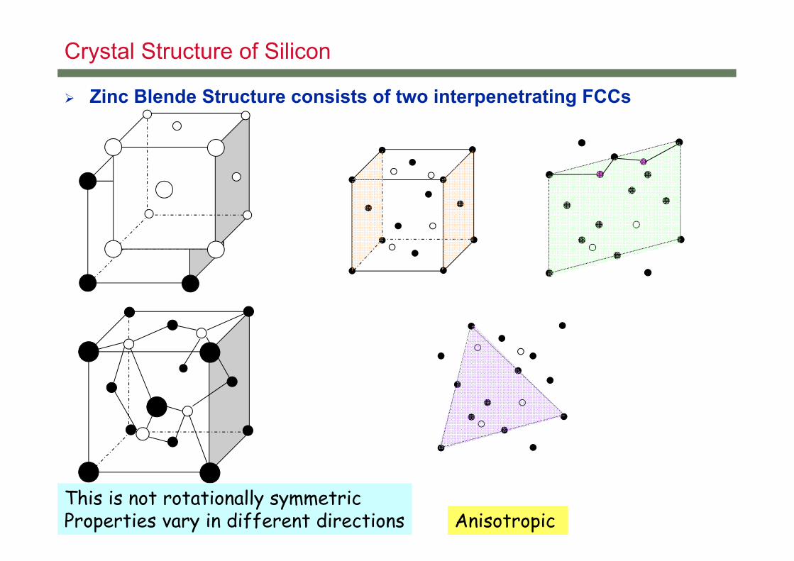
Zinc Blende Structure consists of two interpenetrating FCCs
This is not rotationally symmetricProperties vary in different directions Anisotropic
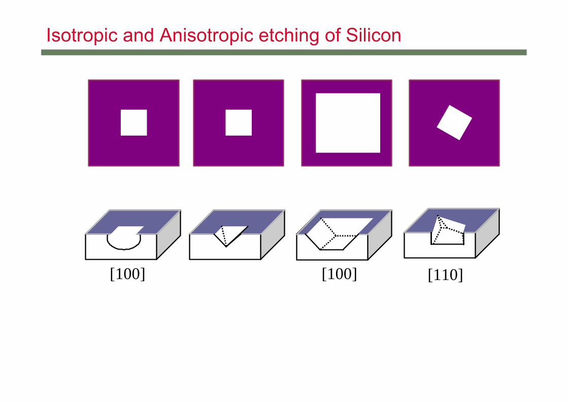
Isotropic and Anisotropic etching of Silicon
[100] [100] [110]

Special Cases
(a) If the masking window is misaligned with the crystal directions, the etch profile is bounded by a superscribing regular geometry.
(b) Similar results for non-rectangular etch windows.
(c) A free standing cantilever of the masking layer results by anisotropic etching with aligned geometry shown.
[110] [110] [110]

Bulk micromachining for a cantilever
Top view of substrate Side view
Oxidized silicon wafer
SiSiO2
Photolithography to define cantilever dimensions and oxide etching
photo resist
Cantilever structure
Oxide etched by BHF

Cantilevers formed by Bulk etching
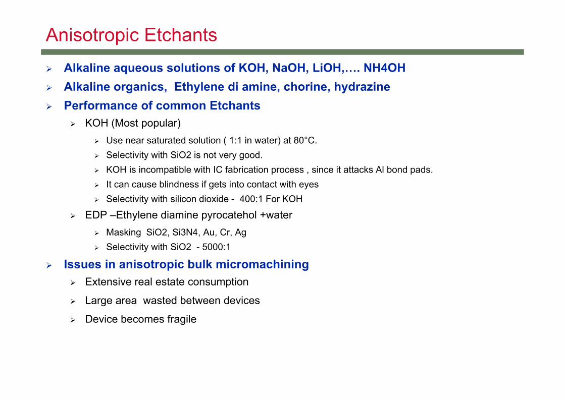
Anisotropic Etchants Alkaline aqueous solutions of KOH, NaOH, LiOH,…. NH4OH Alkaline organics, Ethylene di amine, chorine, hydrazine Performance of common Etchants
KOH (Most popular) Use near saturated solution ( 1:1 in water) at 80°C. Selectivity with SiO2 is not very good. KOH is incompatible with IC fabrication process , since it attacks Al bond pads. It can cause blindness if gets into contact with eyes Selectivity with silicon dioxide - 400:1 For KOH
EDP –Ethylene diamine pyrocatehol +water Masking SiO2, Si3N4, Au, Cr, Ag Selectivity with SiO2 - 5000:1
Issues in anisotropic bulk micromachining Extensive real estate consumption
Large area wasted between devices
Device becomes fragile
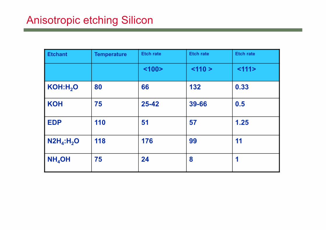
Anisotropic etching Silicon
Etchant Temperature Etch rate Etch rate Etch rate
<100> <110 > <111>
KOH:H2O 80 66 132 0.33
KOH 75 25-42 39-66 0.5
EDP 110 51 57 1.25
N2H4:H2O 118 176 99 11
NH4OH 75 24 8 1

Etch variation
Silicon etch rate and etched Si surface roughness v/s concentration of KOH solution and Iso Propyl Alcohol at 75˚C and 900 RPM, stirring rate.

Selection of Silicon Crystal Orientation
(100) Oriented Si (110) Oriented SiInward sloping walls (54.74°) Vertical {1 1 1} walls
The sloping walls cause a lot of lost real estate Narrow trenches with high aspect ratio are possibleFlat bottom parallel to surface is ideal for membrane fabrication
Multifaceted cavity bottom ({110} and {100 } planes) makes for a poor diaphragm
Bridges perpendicular to a V-groove bound by (111 ) planes cannot be underetched
Bridges perpendicular to a V-groove bound by (111) planes can be undercut
Shape and orientation of diaphragms convenient and simple to design
Shape and orientation of diaphragms are awkward and more difficult to design
Diaphragm size, bounded by nonetching {111} planes, is relatively easy to control
Diaphragm size is difficult to control (the <100> edges are not defined by nonetching planes)

Silicon etching
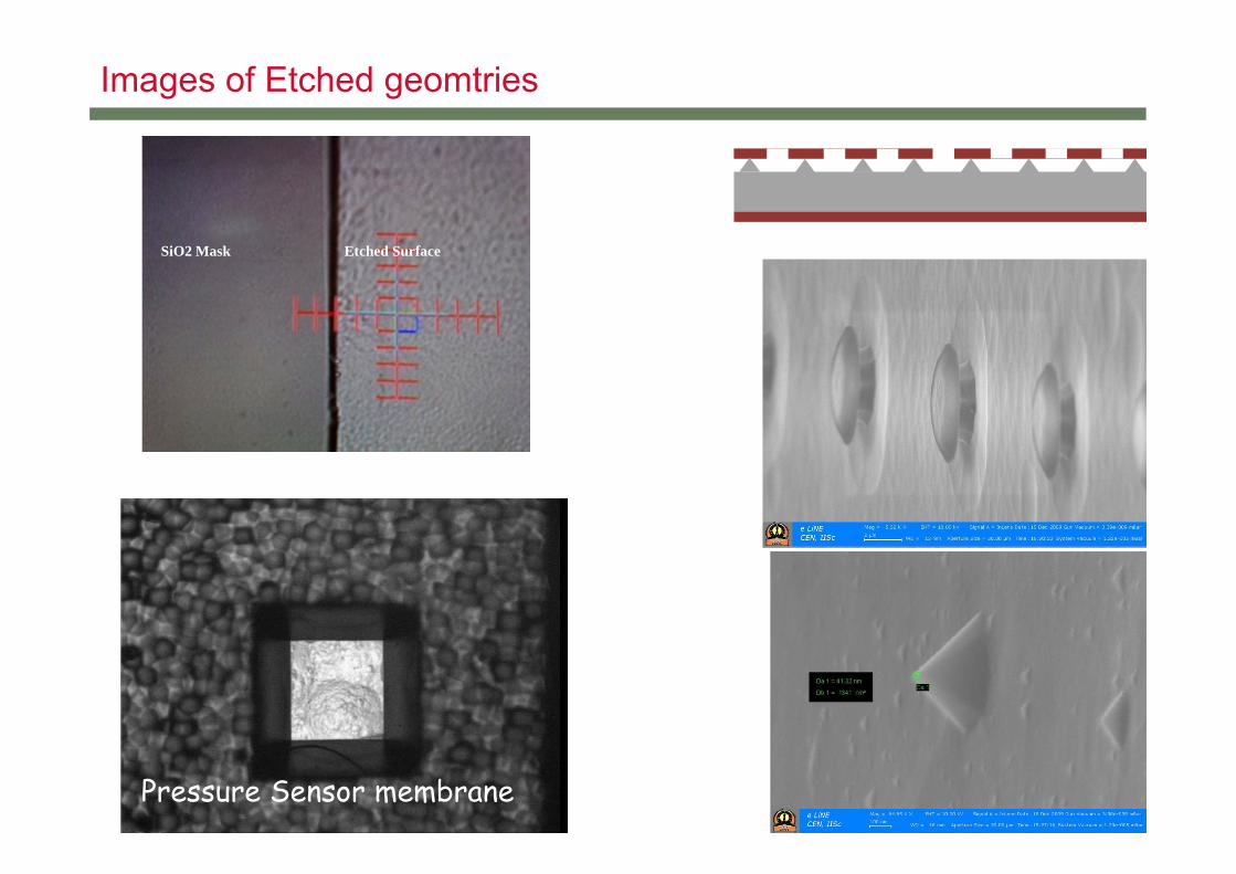
Images of Etched geomtries
SiO2 Mask Etched Surface
Pressure Sensor membrane

Etch stop technique Etch stop is a region at which the wet etching slows down
Dopant selective etching (DSE) Technique is useful for heavily doped layers, leaving behind lightly doped
Advantages of DSE Independent of crystal orientation Smooth surface finish Offers possibilities for fabricating release structures with arbitrary lateral geometry
Disadvantages High boron conc. introduces mechanical stress into the material
Etchant (Diluent) Temp. (C) (100) Etch-rate (m/min) for boron doping << 1019cm-3
Etch-rate (m/min) for boron doping 1020 cm-3
EDP (H2O) 115 0.75 0.015
KOH (H2O) 85 1.4 0.07NaOH (H2O) 65 0.25-1.0 0.025-0.1

Doped regions
For doping of semiconductors, controlled quantities of impurity atoms are introduced into the selected regions of the surface through masks on the top of the wafer.
Diffusion and Ion implantation are common methods for this.
Used as etch stop layers N and P regions can be formed for
active semiconductors Diffusion
Wafer placed in a high temp furnace and a carrier gas is passed. Boron and phosphorous are commonly used dopants
The deposited wafer is heated in a furnace for drive in; oxidising or inert gas to redistribute dopants in the wafer to desired depth
Silicon dioxide is used as the masking layer
Phosphorus DiffusionMake Tempress
Temperature Range 800- 1200 ˚C
Dopant Source POCl3
Bubbler Gas Nitrogen (0.4ltr/min)
Carrier Gas Nitrogen (4 ltr/min)
Flow rate of Oxygen 0.6 l/min
Boron Diffusion
Make Tempress
Temperature Range 900-1200˚C
Dopant Source Boron Nitride Disc
Process Ambient Nitrogen
Flow rate of N2 4 ltr/min

Dry Etching Techniques
Material removal for IC’s , MEMS By physical
By ion bombardment
By chemical Chemical reaction through a reactive species at the surface
Or Combination
Plasma etch

Dry Etching vs Wet Etching Wet Etching
No expensive equipment required
Corrosive Acids or alkalies used
Waste products are also corrosive
Difficult to automate
Limitations in the aspect ratio for vertical structures
Dry Etching Carried out in plasma reactor
Safe non-toxic gases, e.g. O2 & CF4used
Waste products are easily discharged
Ease of automation
Extended processes for high aspect ratio

(a) Sputtering Physical removal of Si Very good anisotropy
Poor selectivity
(b) Chemical Etching Gas phase species react with Si to
form volatile product
Very good selectivity Poor anisotropy
+Ion
NeutralPhoto-resistVolatile
Product
(a)
(b)
Etching Mechanisms in Plasma

(c)Energetic ion-enhanced etching Impinging ions damage surface, increasing
reactivity (Cl2 etching of undoped Si) Good selectivity & anisotropy
(d) Inhibitor ion-enhanced etching Requires two different species –etchants
(Cl2) and inhibitors(C2F6) Very good selectivity and anisotropy
Neutral+Ion
Inhibitor
PR
VolatileProduct
Neutral + Ion
VolatileProduct
PR
(d)
(c)
Etching Mechanisms in Plasma

Reactive Ion Etching (RIE) Wet etching causes
undercut Unidirectional etching is
possible with RIE High fidelity pattern transfer Steps involved in RIE
Etching 1. Reactive etching species
are generated by electron/ molecule collisions
2. Etchant species diffuse through stagnant region to the surface of the film to be etched
3. Etchant species adsorb onto surface
4. Reaction takes place 5. Etched product desorbs
from the surface 6. Etch products diffuse back
into bulk gas and removed by vacuum
http://www.ee.byu.edu/cleanroom/rie_etching.phtml
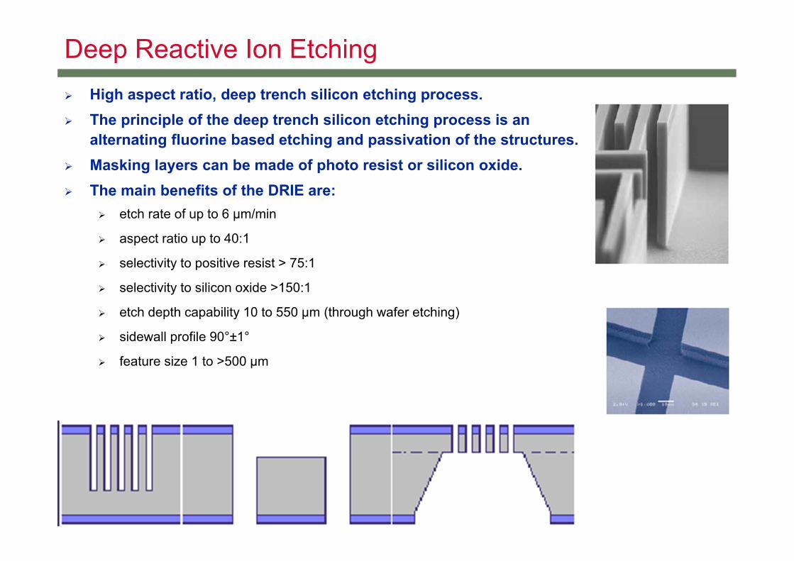
Deep Reactive Ion Etching High aspect ratio, deep trench silicon etching process. The principle of the deep trench silicon etching process is an
alternating fluorine based etching and passivation of the structures. Masking layers can be made of photo resist or silicon oxide. The main benefits of the DRIE are:
etch rate of up to 6 µm/min
aspect ratio up to 40:1
selectivity to positive resist > 75:1
selectivity to silicon oxide >150:1
etch depth capability 10 to 550 µm (through wafer etching)
sidewall profile 90°±1°
feature size 1 to >500 µm
Deep Reactive Ion Etching (DRIE)
Process alternates between etching and polymer deposition SF6/Ar used for etching CHF3/Ar used for polymerization Selectivities:photoresist(100:1), SiO2(200:1) Aspect ratio up to 30:1(sidewall angle 90±2o) Etch rates of 2 to 3m/min

Integration with Electronics
CMOS First
MEMS First
Notice that in both cases, electronics are integrated on chip It is also possible to have the electronics in a separate die and
integrate these on a package (Multi-chip modules)
Thicker structures and closed cavities can be formed by Wafer bonding techniques
Electronics
MEMS
ElectronicsMEMS
Anode
Cathode
Glass
Silicon
V+
-
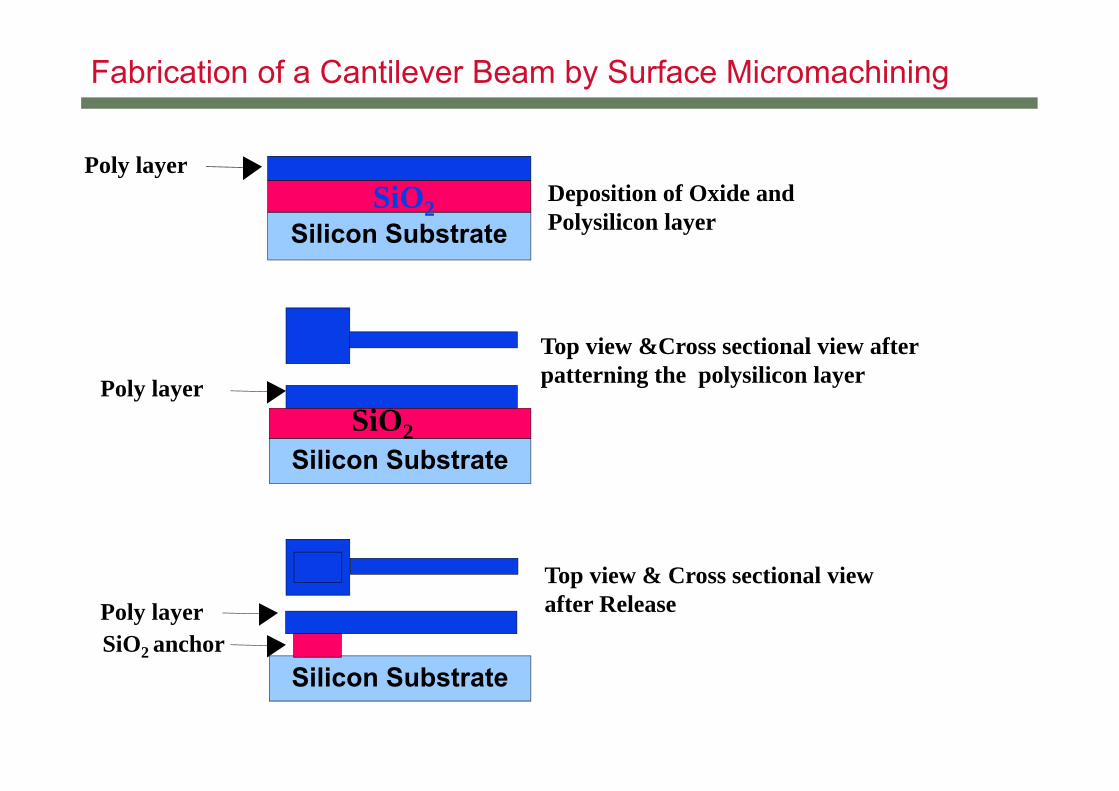
Poly layerDeposition of Oxide and Polysilicon layer
Top view &Cross sectional view after patterning the polysilicon layerPoly layer
Top view & Cross sectional view after Release
SiO2 anchorSilicon Substrate
Poly layer
Silicon SubstrateSiO2
Silicon SubstrateSiO2
Fabrication of a Cantilever Beam by Surface Micromachining

Summary: Silicon Micromachining
Surface micromachining Surface micro machining (SM) build structures on the surface of the silicon
SM Involves Deposition of thin film of sacrificial & structural layer Removal of sacrificial layer to release the mechanical structure
Micro structure fabricated using SM are usually planar structure
Dimensions of the SM structures can be several orders of magnitude smaller than bulk machined structure
Bulk micromachining Allows selective removal of significant amounts of silicon from a substrate to form
membranes on one side of the wafer A variety of holes Or other structures
BM can be divided into two; Wet etching
Liquid etchant (aqueous chemicals) Dry etching
Vapor and plasma etchant

Comparison of Micromachining Techniques
Bulk micromachining Emerged during 1960s
Used pressure sensors, Si valves
Used to realize structures within bulk of a single crystal Si wafer by selectively removing wafer material
Structures may have thickness range from sub-micron to full wafer thickness, and lateral dimensions as large as few mm
Key step is etching Wet isotropic Wet anisotropic Plasma isotropic Reactive ion etching
Surface micromachining Emerged during 1980s
Structures are mainly located on the surface of the Si wafer and consists of thin films
The dimensions of these structures are several orders of magnitude smaller than structures generated by bulk micromachining
Involves Deposition of sacrificial layer Deposition and selective etching of
structural layer(s) Removal of sacrificial layer
High Aspect Ratio Microsystems
Wafer Bonding techniques
High Aspect Ratio Methods for Silicon LIGA and other molding techniques Polymeric microsystems (low cost fabrication) Low Temperature Co-fired Ceramics (LTCC)
Copyright © 2022 FDOKUMEN