
Electronics, Photonics, Microsystems - dbc.wroc.pl.
119
Projekt współfinansowany ze środków Unii Europejskiej w ramach Europejskiego Funduszu Społecznego ROZWÓJ POTENCJAŁU I OFERTY DYDAKTYCZNEJ POLITECHNIKI WROCŁAWSKIEJ Wrocław University of Technology Electronics, Photonics, Microsystems Sergiusz Patela, Marcin Wielichowski, Szymon Lis, Konrad Ptasiński OPTICAL FIBERS Wrocław 2011
-
Upload
khangminh22 -
Category
Documents
-
view
0 -
download
0
Transcript of Electronics, Photonics, Microsystems - dbc.wroc.pl.

Projekt współfinansowany ze środków Unii Europejskiej w ramach Europejskiego Funduszu Społecznego
ROZWÓJ POTENCJAŁU I OFERTY DYDAKTYCZNEJ POLITECHNIKI WROCŁAWSKIEJ
Wrocław University of Technology
Electronics, Photonics, Microsystems
Sergiusz Patela, Marcin Wielichowski,
Szymon Lis, Konrad Ptasiński
OPTICAL FIBERS
Wrocław 2011

Wrocław University of Technology
Electronics, Photonics, Microsystems
Sergiusz Patela, Marcin Wielichowski, Szymon Lis, Konrad Ptasiński
OPTICAL FIBERS
Developing Engine Technology
Wrocław 2011

Copyright © by Wrocław University of Technology
Wrocław 2011
Reviewer: Anna Sankowska
ISBN 978-83-62098-27-9
Published by PRINTPAP Łódź, www.printpap.pl
Table of Contents
1 Optical Fibers – Introduction ................................................................................................ 5
2 Fundamental properties of optical waveguides ................................................................... 9
3 Wave theory of optical fibers ............................................................................................. 15
4 Mode equation for a planar waveguide ............................................................................. 24
5 Optical and mechanical properties of optical fibers ........................................................... 31
6 Technology of optical fibers ............................................................................................... 37
7 Passive devices (fundamentals and examples) ................................................................... 46
8 Active devices – telecom sources and detectors................................................................. 64
9 Connecting of passive and active photonic elements ......................................................... 79
10 Dispersion of optical fibers ................................................................................................. 87
11 Telecommunication fiber optic system .............................................................................. 95
12 Measurements of optical fiber ........................................................................................... 99
13 Optical Time Domain Reflectometer (OTDR) .................................................................... 109
3

1 Optical Fibers – Introduction
Contemporary long distance telecommunications are based almost exclusively on optical
fiber cables. The optical fibers are extensively used also for other applications, such as access
networks, sensors or lightening.
Fig. 1.1 Total length of fiber installed in the world.
Optical fibers are considered to be very advanced and hard to get transmission media.
However, adding up all the fiber installed in the world, we get total of 150 million km. That’s the
distance equal to that from the Earth to the Sun.
Fig. 1.2 Length of fiber installed every day.
Even if the astronomical amount of fiber has been installed to, large amount of fiber is still
installed every day. That daily amount is approximately equal to the diameter of the Earth.
Initially optical fibers were used for long distance telecommunications. Today new fiber is
installed mainly in metropolitan and access networks.
At this point, one may ask a question: “Well, a lot of fiber has been installed, but what are
the consequences? Does it really matter?”. The answer is, that with all the power supply lines
installed, electronic devices and electrical appliances are available everywhere, so there is
possibility that soon photonics devices will be as popular as electrical or electronic. Fiber optics
is the main factor enabling photonics development.
Till now ~150 millions km of optical fiber has been installed
Fiber to the Sun, and in 24 hours through the Earth
Every day ~15 000 km is installed.
• Long distance communications,• Metropolitan networks• Fiber to the (every home)
4

Fig. 1.3 Schematic diagram of fiber optic system.
Communication systems consist of three main components: a transmitter of the signal, a
communication line and a receiver. Additionally, one has to consider limiting factors of the
transmission capabilities of the systems – these are sometime called “noise”. In the case of
optical communication system a light source takes the role of the transmitter, an optical fiber
serves as the transmission line, and a photodiode is used as the receiver. The main limiting
factor of optical transmission line are attenuation and dispersion.
1.1 Fundamental features of fiber-optic transmission
To understand advantages and limitation of optical fiber transmission, one has to take
into account the following three factors:
o Transmission speed - In fiber optic transmission a signal is conducted by light -
electromagnetic wave of frequency 3x10¹⁴
Hz, (300 THz). Capacity of any
transmission channel can be multiplied by sending simultaneously many colors of
light through one fiber.
o Link span- Very low attenuation of silica glass and total internal reflection at the
boundaries of the core make long-range repeater-less transmission possible.
o Optical-fiber modes. Wave nature of light and fiber modes - Many waveguide
parameters and construction details can be explained only if one takes into
account the fact that light is a wave, guided by a structure of very low transversal
dimensions.
In optical fibers, light is guided in the form of “modes”. In a waveguide or cavity, the mode
is one of the possible patterns of electromagnetic field. Available patterns are derived from
Maxwell's equations and the applicable boundary conditions. Two examples of modes:
o waveguide mode - fiber optic mode
o cavity mode - laser mode
Light source(transmitter)
Light detector(receiver)
Electrical output signal
LightguideElectrical input signal
„noise”
5
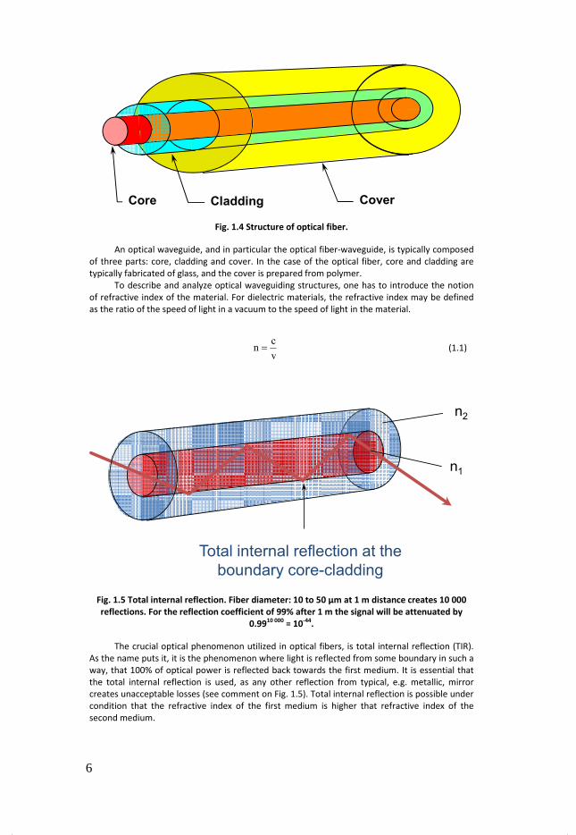
Fig. 1.4 Structure of optical fiber.
An optical waveguide, and in particular the optical fiber-waveguide, is typically composed
of three parts: core, cladding and cover. In the case of the optical fiber, core and cladding are
typically fabricated of glass, and the cover is prepared from polymer.
To describe and analyze optical waveguiding structures, one has to introduce the notion
of refractive index of the material. For dielectric materials, the refractive index may be defined
as the ratio of the speed of light in a vacuum to the speed of light in the material.
v
cn = (1.1)
Fig. 1.5 Total internal reflection. Fiber diameter: 10 to 50 µm at 1 m distance creates 10 000
reflections. For the reflection coefficient of 99% after 1 m the signal will be attenuated by
0.9910 000
= 10-44
.
The crucial optical phenomenon utilized in optical fibers, is total internal reflection (TIR).
As the name puts it, it is the phenomenon where light is reflected from some boundary in such a
way, that 100% of optical power is reflected back towards the first medium. It is essential that
the total internal reflection is used, as any other reflection from typical, e.g. metallic, mirror
creates unacceptable losses (see comment on Fig. 1.5). Total internal reflection is possible under
condition that the refractive index of the first medium is higher that refractive index of the
second medium.
Core Cladding Cover
Total internal reflection at the boundary core-cladding
n1
n2
6

For the fiber diameter of 10 mµ at the distance of 1 m the light beam will be reflected
approximately 10 000 times. For the reflection coefficient of 99% after 1 m the signal will be
attenuated by 0.9910 000
= 10-44
.
1.2 Classification of optical waveguides
In principle, surrounding high refractive index material with low refractive index cladding
enables building of a light guiding structure. Different structures are possible. Waveguides may
be classified according to several factors:
o Geometry: planar, strip or fiber waveguides
o Mode structure: single-mode, multi-mode
o Refractive index distribution: step or gradient index
o Material: glass, polymer, semiconductor
o Guiding mechanism – standard (TIR) and photonic crystal waveguides
Different possible structures of optical waveguides are explained in the pictures below.
Fig. 1.6 Basic classification of waveguides: fiber versus planar waveguides.
Fig. 1.7 Single and multimode waveguides.
Fiber waveguide Planar waveguide
Core Cladding Cover
Guiding film
Substrate
Cladding
Singlemode waveguide
n
ρ r
1.52
1.54
Core
Cladding
n
ρ r
1.468
12,5 µm < ρ < 100 µm, 0,8 µm < λ < 1,6 µm, 0,01 < ∆ < 0.03
2 µm < ρ < 5 µm0,8 µm < λ < 1,6 µm0,003 < ∆ < 0.01
SMF-28 ∆ 0,36%
Multimode step index fiber
7

Fig. 1.8 Step-index and gradient waveguides.
Fig. 1.9 Waveguide classification: materials.
Fig. 1.10 Standard and photonic waveguides.
1.3 Non-telecommunication waveguide applications
Optical waveguides are mainly used in telecommunications, however there are other
popular and interesting applications. Optical waveguides may be used in industry for sensing,
illumination and displays. There are important applications of optical fiber in medicine, such as
n
r
1 .5 2
1 .5 4
a = 2 5 µm 6 2 ,5 µm
n
r
1 .5 2
1 .5 4
a = 2 5 µm 6 2 ,5 µm
•SiO2 (doped)
•ZBLAN (Zr, Ba, La, Al, Na)
•Plastic Optical Fibers (PMMA)
•Epitaxial multilayers (eg. GaAs/AlGaAs)
•Dielectric layers (Ta2O5, ZnO, Si3N3/SiO2)
•Polymer (PMMA, PS)
fibers
layers
core Clad. cover core
Guiding layer
substrate
Clad.
8

endoscopy or surgery. Another interesting group of applications include art works and clothes
with optical fibers embedded for decorative purposes.
1.4 10 advantages of optical fibers
Optical fiber waveguides are important for future communication systems. Below is a list
of ten advantages of optical fibers that make them superior to copper cables.
1. High information capacity of a single fiber.
2. Low loss, repeater-less transmission over long distances is possible.
3. Absolute immunity from EMI (electro-magnetic interference).
4. Low weight.
5. Small dimensions (diameter).
6. High work safety (low risk of fire, explosion, ignition).
7. Transmission safety (almost impossible data taping).
8. Relatively low cost (getting lower).
9. High reliability.
10 Simplicity of installation.
2 Fundamental properties of optical waveguides
2.1 Parameters of optical waveguides - classification
Optical waveguides are characterized by a number of parameters. Four parameter
categories are listed below together with names of the most commonly used parameters.
o optical
o attenuation
o dispersion
o cut-off wavelengths
o refractive indices
o numerical aperture
o modal properties
o temperature stability of parameters
o geometrical
o transversal dimensions
o tolerances
o mechanical
o tensile strength
o allowable bending radius
o additional parameters (defined for specialty fibers)
o active dopant,
o beating length.
In lectures that follow we will study the above parameters in detail.
2.2 Telecommunication windows and generations of fiber optic
systems
Attenuation of a standard, silica-glass telecommunication fiber in the function of light
wavelength, is depicted in figure Fig. 2.1. Three attenuation minima, known as the
telecommunication windows, can be seen. Telecommunication windows are separated by
9

spectral ranges in which absorption peaks caused by the -OH ions, are located. The peak at
1.4 μm, the one separating the second window and the third window, can be removed or
minimized by means of special fiber manufacturing techniques that enable ultra-low -OH
concentrations. From a historical perspective, the earliest optical transmission systems utilized
the first telecommunication window. Then, the next-generation systems were based on the
second window, while in today’s systems, the third telecommunication window is widely
utilized.
Fig. 2.1 Attenuation of silica-glass fiber.
Names and wavelength ranges of fiber optics telecommunication bands within the third
transmission window:
o S : 1460 – 1530 nm
o C : 1530 – 1565 nm
o L : 1565 – 1625 nm
o U : 1625 – 1675 nm
2.3 Fundamental parameters of optical waveguides – attenuation
Optical waveguide attenuation is a gradual decrease in energy (optical power) carried by
the lightwave as it propagates along the waveguide. Numerical value of attenuation – the
attenuation coefficient – is expressed in the units of [dB / km], which translates into: what part
(in decibels, dB) of the initial optical power is lost due to attenuation assuming the light has
travelled a path of the length of 1 kilometer (km) inside the waveguide. Optical waveguides we
are mostly dealing with throughout this lecture, are optical fibers. Below, there are some typical
values of attenuation usually found in silica-glass optical fibers.
Single mode fibers
o 1310 nm 0.33-0.42 dB/km
o 1550 nm 0.18-0.25 dB/km
Multimode fibers (gradient)
o 850 nm 2.4-2.7 (50/125) 2.7-3.2 (62.5/125) dB/km
o 1300 nm 0.5-0.8 0.6-0.9 dB/km
Values in brackets denote fiber’s core and cladding diameters, respectively. The diameters
are expressed in micrometers (μm). Numbers expressed in nanometers (nm) are wavelengths of
light for which given attenuation values were measured.
2.4 Characterization of optical waveguide – measurement units
Optical wavelength, i.e. length of one period of lightwave, is expressed in
0.6 0.8 1.0 1.2 1.4 1.6 1.8
0.3
0.5
1
0.1
3
5
10
30
50
wavelength
[µm]
Attenuation
[dB/km]
I window
II window
III transmission window
Attenuation of silica-glass fiber
10

o μm = 10-6
m
o nm = 10-9
m
The above units were chosen for convenience as optical wavelengths used in
telecommunications are of the order of 10-6
m, i.e. about one micrometer (cf. paragraph 2.2).
Usually, when optical wavelength is given, it is assumed that light propagates in vacuum. The
actual wavelength in e.g. a bulk of silica glass is smaller by a factor equal to the silica glass
refractive index.
Waveguide attenuation is calculated according to the formula:
L
P
P10log
[dB/km]A WE
WY
= (2.1)
where L is the waveguide length. Note that for the output power (POUT) being lower than
the input power (PIN), which is always the case, when no optical amplifiers are present,
attenuation value is less than zero. The minus sign is, however, customarily omitted in optical
fiber specifications.
If one kilometer of an optical waveguide (e.g. optical fiber) has an attenuation of 3 dB, this
means that only half (50%) of the input power exits the waveguide as the output power
(POUT = 0.5 * PIN). This example and several more are listed below.
o 3 dB ≈ 50%
o 20 dB = 1%
o 30 dB = 0.1%
o 40 dB = 0.01%
In general, x dB = 100 * 10-(x/10)
%.
2.5 Effective waveguide thickness
In the following paragraphs we will use laws of geometrical optics to describe some
physical phenomena related to lightwave propagation in optical fibers. The application of
geometrical optics provides an intuitive picture of the fundamental properties of optical fibers.
In a more complete description of the problem, i.e. of lightwave propagation in structures
having the cross-sectional dimensions comparable to wavelength, it is necessary to employ the
wave optics methods. When using the wave optics methods, it is, however, more difficult to get
an intuitive physical insight into fundamental properties of optical waveguides.
Let us define a parameter using the following relation (Bass, 2001a), (Agrawal, 2002)
( ) 2/12
2
2
1
0
2nnV −
⋅⋅=
λρπ
(2.2)
where: n1, n2 - refractive index of core and cladding, ρ - core radius, and λ0 – light
wavelength. The parameter V is called the effective (or characteristic) waveguide thickness and
it can be used for estimating the applicability of the geometrical-optics tools to study any optical
waveguide under consideration. The greater the effective thickness V, the higher the number of
modes that are supported (guided) by the waveguide. We can use geometrical-optics tools
(methods of analysis) if V>> 1.
It is clear from (2.2) that V will take lower values with decreasing the core-cladding
refractive index difference (n1-n2). However, with decreasing the light wavelength(λ0), the value
of V will become higher. This means, in general, that for low core-cladding refractive index
differences, a sufficiently short light wavelength can be selected to make the waveguide support
more guided modes (e.g. make it multimode).
11

2.6 Laws of reflection and refraction
We will now consider a ray of light hitting (impinging on) a boundary between two
dielectric materials as it is illustrated in figure Fig. 2.2. Indexes of refraction (refractive indexes)
of the materials equal nco and ncl. The subscripts used stand for the core and cladding,
respectively, because all the formulas derived here will later be used to describe optical fibers.
Fig. 2.2 Illustration of the a) law of reflection and b) law of refraction.
Depending on the value of the incidence angle (i.e. value of angle at which light hits the
boundary), two different phenomena may occur:
o total internal reflection – when optical power is completely reflected off the
boundary, and
o refraction – when optical power is only partly reflected, and the remaining part is
refracted, i.e. it crosses the boundary and its propagation direction changes.
Laws of reflection and refraction give further description of the above phenomena.
2.6.1 Law of reflection
In figure Fig. 2.2 a), a light beam (light ray) hitting the dielectric boundary surface is
completely reflected – it undergoes the total internal reflection. Note that all angles are
measures to the so called surface normal, which is perpendicular to the surface.
The law of reflection states that:
1) The angle of incidence θx, angle of reflection θx, and the (surface) normal are all in
the same plane.
2) The angle of incidence equals the angle of reflection.
2.6.2 Law of refraction
In figure Fig. 2.2 b) a light beam (light ray) hitting the dielectric boundary surface is both
reflected and refracted. Refraction is a process of bending of light as it goes from one media to
another. Law of refractions states that:
1) The incidence angle and the refraction angle are strictly related. The relation is
expressed with the Snell’s law (which will be discussed in the next paragraph).
Similarly to the law of reflection, all angles and the normal are in the same plane.
2.7 Snell’s law and critical angle
Values of all the angles indicated in figure Fig. 2.2, are connected with strict relationships.
These relationships are mathematically expressed as Snell’s law and as a formula for the critical
angle.
Snell’s law, also called law of refraction or refractive law, states that the refraction angle
θt relates to the incidence angle θx in the following way
( ) ( )tclcco nn θθ sinsin = (2.3)
nco
ncl
θx
θc
θx
x
z
nco
ncl
θx
θc
θx
x
z
θt
a) b)
12

Now, looking at diagram b) in figure Fig. 2.2 we can see that once refraction angle θt
reaches the value of 90° transmission of optical power across the boundary does not occur any
more. So, the condition of total internal reflection is fulfilled. The (value of) incidence angle at
which the above takes place, is called the critical angle and is denoted as θc in the diagram. Using
Snell’s law, i.e. substituting θt = 90° into (2.3), we arrive at the following equation
( ) ( )°= 90sinsin clcco nn θ (2.4)
This equation can easily be solved to get the formula for the critical angle θc
=co
clc
n
narcsinθ (2.5)
The notion of the critical angle is fundamental for the classification of waveguide rays and
for the derivation of the numerical aperture formula. Both subjects are discussed in subsequent
paragraphs.
2.8 Classification of waveguide rays
Depending on light ray’s propagation direction within optical waveguide and on the type
of the waveguide itself, there can occur three types of waveguide rays, i.e. three possibilities of
how light propagates when it is completely or partly bound within the waveguide. The case
when light is not bound within the waveguide at all, will not be discussed here. The three types
of waveguide rays are depicted in figure Fig. 2.3.
Fig. 2.3 Illustration of a) guided rays, b) leaky rays, and c) substrate rays.
Considering the values of the angle θx, waveguide rays can be classified as:
o guided rays: 90°≥θx>θc
o leaky rays: θc≥θx≥ 0
o substrate rays (substrate modes): θc2≥θx≥θc1 (only occurring in asymmetrical
waveguides)
The θx is the angle at which light rays impinge on the core-cladding and the core-substrate
boundaries.
In other words, when light undergoes the total internal reflection at both the dielectric
boundaries defining the waveguide, we get the guided rays. In an ideal (theoretical) optical
waveguide, guided rays propagate without any loss – entire optical power remains trapped
within the waveguide independently of how long the propagation distance is. In real-life optical
waveguides (both planar waveguides and fibers) propagation losses are greater than zero due to
other physical mechanisms (like e.g. dielectric boundary roughness) not considered in the
simplified model discussed here.
Unlike the guided rays, the leaky rays are an inherently lossy type of light propagation
within waveguide – optical power gradually “leaks” out of the waveguide along the propagation
distance. This is because leaky rays do not undergo the total internal reflection neither at the
core-cladding, nor at the core-substrate boundary.
In an asymmetrical waveguide, i.e. a one, in which values of the cladding refractive index
(ncl) and the substrate refractive index (ns) are different, the substrate rays can propagate. Again,
nco
ncl
θx
θc
θx
nco
ncl
θx
θc
θx
a) b)
nco
θx
θc1
θxns
θc2
c)
13

this type of light propagation within waveguide shows inherent losses – optical power “leaks”
out of the waveguide. This leakage, however, is now only present at the core-substrate
boundary. At the core-cladding boundary, light undergoes the total internal reflection. Note that
we have implicitly assumed nc < ns here. In case of planar waveguides, this relation is often
fulfilled because air (nc ≈ 1) plays the role of the cladding in some of the popular waveguide
types (e.g. the silicon-on-insulator (SOI) planar waveguides). Optical fibers are in principle of the
symmetric type, and thus substrate modes (substrate rays) are not the case when optical fibers
are considered.
2.9 Numerical aperture
By means of the critical angle discussed in 2.7it is possible to explain, why there is only a
limited interval of input angle values that allow an external ray of light to become a guided ray
within the waveguide. There is a limiting input angle (value) that still ensures the occurrence of
the guided rays. This limiting angle is called the acceptance angle of the waveguide. A
dimensionless quantity that equals the sine function computed for the acceptance angle is called
the numerical aperture (NA) of the waveguide. A waveguide under consideration (it needs to be
of the symmetric type) together with an input ray and a propagating (guided) ray are shown in
figure Fig. 2.4.
Fig. 2.4 Idea of the acceptance angle (see text).
One can also say that angle 2 α (see figure) is the full angle of the cone of light rays that
can pass through the system.
For a given optical waveguide (planar or fiber), numerical aperture value is calculated with
the formula (Bass, 2001a), (Agrawal, 2002)
22sin clco nn�A −== α (2.6)
As we can see, NA only depends on waveguide’s core and cladding refractive indexes. In
particular, NA does not depend on e.g. waveguide’s core width or, in the case of fibers, core
diameter. A detailed derivation of (2.6) is presented below.
2.9.1 Derivation of the formula for NA
For clarity of the derivation, some of the formulas already discussed, will be repeated
here.
From Snell’s law (the law of refraction) we have
( ) ( ) clclcco nnn =°= 90sinsin θ (2.7)
From the relation of the sum of angles in a triangle
°=°++ 18090cm θθ (2.8)
( ) ( ) clmcocco nnn =−°= θθ 90sinsin (2.9)
( ) clmco nn =−° θ90sin (2.10)
From trigonometric identities
θc
α nco
ncl
θm
14

( ) clmco nn =θcos (2.11)
clmco nn =− θ2sin1 (2.12)
Now, let us square both sides of the equation(2.12)
( ) 222sin1 clmco nn =− θ (2.13)
2222sin clmcoco nnn =− θ (2.14)
Applying the reflection law to the glass-air boundary
( )αθ 222sin1sin =mcon (2.15)
222sin clco nn =− α (2.16)
Finally we arrive at
22sin clco nn�A −== α (2.17)
Applying an approximate relation
2
22
2 co
clco
clco
clco
co
clco
co
clco
n
nn
nn
nn
n
nn
n
nn −≈
++−
=−
=∆ (2.18)
∆=− 2222 coclco nnn (2.19)
∆= 2con�A (2.20)
The formula (2.18) is correct as long as nco ≈ ncl , i.e. the difference between the core and
the cladding refractive index values is small compared to the values of the indexes themselves.
This assumption is called the weakly guiding approximation. The weakly guiding approximation
always holds for the typical silica-glass telecommunication fibers.
2.10 Problems
Problem 1
Derive the formula for Numerical Aperture of a waveguide immersed in water.
Calculate Numerical Aperture and acceptance angle assuming that:
refractive index of water = 1.33
refractive index of the waveguide core = 1.5
relative difference of core-cladding indices = 1%
3 Wave theory of optical fibers
In this chapter we will discuss the Maxwell’s equations applied to the electromagnetic
wave propagation within a uniform, lossless medium. We will also go into some details of the
derivation of the wave equation for the dielectric planar waveguide together with appropriate
boundary conditions. The following lecture is based on three books (Garmire & Tamir, 1975;
Midwinter, 1983; Tadeusiak A., Crosignani B., 1987).
15

3.1 Maxwell’s field Equation (SI unit)
In order to describe the electromagnetic wave propagation in optical waveguide, one
needs to use the Maxwell’s equations. Generally speaking, they connect the electric field with
the magnetic field. Maxwell’s equations for a lossless, uniform medium take the form
∇ × ��� = − ���� (3.1)
∇ × ���� = ������ + � (3.2)
∇ ∙ B��� = 0 (3.3)
∇ ∙ D��� = ρ (3.4)
where E and H – vectors of electric and magnetic fields, respectively, B and D – vectors of
magnetic and electric flux densities, respectively, J – (electric) current density, and t – time.
Medium in which electromagnetic wave propagates, may be described with the electric
permittivity ε and the magnetic permeability μ, the quantities that connect field vectors with
flux density vectors according to the equations
���� = ���� = ����� + ��� (3.5)
�� = ����� = ������ + ���� (3.6)
where P – vector of electric polarization of the medium, M – vector of magnetization of
the medium, and ε0 and μ0 are electric permittivity of vacuum and magnetic permeability of
vacuum, respectively.
In table Tab 3.1 there is a list of all the parameters (quantities) present in Maxwell’s
equations together with symbols that are customarily used in literature and with SI units. Table
3.2 lists values of physical constants present in Maxwell’s equations.
Tab. 3.1 Physical quantities in Maxwell’s equations.
Symbol Physical quantity SI unit Abbreviation
E Electric field strength volts per meter V / m
D Electric displacement coulombs per
square meter C / m2
P Polarization
H Magnetic field strength amperes per
meter A / m
M Magnetization
j Electric current density amperes per
square meter A / m
2
B Magnetic flux density or
magnetic induction
tesla T
ρ Electric charge density coulombs per
cubic meter
C / m3
16
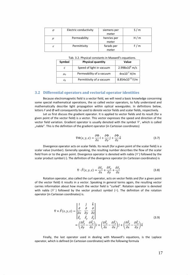
σ Electric conductivity siemens per
meter
S / m
µ Permeability henries per
meter
H / m
ε Permittivity farads per
meter
F / m
Tab. 3.2. Physical constants in Maxwell’s equations.
Symbol Physical quantity Value
c Speed of light in vacuum 2.998x10⁸ m/s
µ0 Permeability of a vacuum 4πx10-7
H/m
ε0 Permittivity of a vacuum 8.854x10⁻¹²
F/m
3.2 Differential operators and vectorial operator identities
Because electromagnetic field is a vector field, we will need a basic knowledge concerning
some special mathematical operations, the so called vector operators, to fully understand and
mathematically describe light propagation within optical waveguides. In definitions below,
letters F and Φ will consequently be used to denote vector fields and scalar fields, respectively.
Let us first discuss the gradient operator. It is applied to vector fields and its result (for a
given point of the vector field) is a vector. This vector expresses the speed and direction of the
vector field variation. Gradient operator is usually denoted with the symbol ∇ , which is called
„nabla”. This is the definition of the gradient operator (in Cartesian coordinates)
∇Φ��, �, � = �Φ�� !̂ + �Φ�� #̂ + �Φ�� $% (3.7)
Divergence operator acts on scalar fields. Its result (for a given point of the scalar field) is a
scalar value (number). Generally speaking, the resulting number describes the flow of the scalar
field from or to the given point. Divergence operator is denoted with nabla (∇ ) followed by the
scalar product symbol (·). The definition of the divergence operator (in Cartesian coordinates) is
∇ ∙ &���, �, � = �&'�� + �&(�� + �&)�� (3.8)
Rotation operator, also called the curl operator, acts on vector fields and (for a given point
of the vector field) it results in a vector. Speaking in general terms again, the resulting vector
carries information about how much the vector field is “curled”. Rotation operator is denoted
with nabla (∇ ) followed by the vector product symbol (×). The definition of the rotation
operator (in Cartesian coordinates) is.
∇ × &���, �, � = **!̂ #̂ $%��� ��� ���&�' &�( &�) **
= +�&�)�� − �&�(�� , !̂ + +�&�'�� − �&�)�� , #̂ + +�&�(�� − �&�'�� , $%
(3.9)
Finally, the last operator used in dealing with Maxwell’s equations, is the Laplace
operator, which is defined (in Cartesian coordinates) with the following formula
17

∇-Φ = �-Φ��- + �-Φ��- + �-Φ��- (3.10)
There are many formulas, the so called vector calculus identities, that describe mutual
relations between operators we have discussed above. Out of a larger set of vector calculus
identities, four are of special significance (usefulness) in Maxwell’s equations-related
calculations. The identities are:
o rotation of vector’s F rotation equals the gradient of divergence minus the vector
laplacian
./ ./&� = ∇ × 0∇ × &�1 = ∇0∇ ∙ &�1 − ∇-&� (3.11)
o divergence of vector product of vectors F and G equals the scalar product of
vector G and rotation of vector F minus scalar product of vector F and rotation of
vector G
∇ ∙ 0&� × 2�1 = 2� ∙ 0∇ × &�1 − &� ∙ 0∇ × 2�1 (3.12)
o rotation of scalar product of scalar Φ and vector F equals the rotation of vector F
multiplied by scalar Φ plus the rotation of vector product of scalar Φ and vector
F
∇ × 0ΦF��1 = Φ∇ × F�� + ∇Φ × F�� (3.13)
o divergence of scalar product of scalar Φ and vector F equals the divergence of
vector F multiplied by scalar Φ plus divergence of scalar Φ multiplied by vector F
∇ ∙ 0Φ&�1 = Φ∇ ∙ &� + &� ∙ ∇Φ (3.14)
3.3 Boundary conditions
Maxwell’s equations discussed in 3.1 describe the electromagnetic wave propagation in an
infinite medium. In real-life problems, however, propagation media are finite (of finite
dimensions) and thus a problem of a boundary between two different media arises. A model
situation is depicted in figure Fig. 3.1. A fundamental tool in dealing with the media boundary
problem is the Ostrogradsky-Gauss theorem (also known as the divergence theorem). It relates
the outward flow of a vector field on a surface to the behavior of the vector field inside the
surface. The theorem states this relation in the following way
4 ∇ ∙ &�56 = 7 &� ∙ 58� 9
: (3.15)
Fig. 3.1 Refractive index change at the boundary between two different materials – boundary
conditions, where S is the boundary of V oriented by outward-pointing normal.
1
2
n
S
18

3.3.1 Bound. conditions for field B
Using the third Maxwell’s equation (3.3), which states that there are no point sources of
magnetic field (otherwise divergence of B could be different than zero) and using the
Ostrogradsky-Gauss theorem (3.15), we determine the magnetic flux density for each of the
media
0 = ; ∇ ∙ ��56 = ; ��58� = <= ∙ ��- − <= ∙ ��> = <= ∙ ���- − ��> 9
: (3.16)
In calculations, we assume the integrals over volume boundaries (i.e. over surfaces
bounding the volume) to be zero.
3.3.2 Boundary condition for field D
We now apply a similar procedure to the electric field but this time the fourth Maxwell’s
equation (3.4) is used and, in analogy to the magnetic field, we find the boundary conditions for
the electric flux density
? = ; @56 = <= ∙ ��- − �> (3.17)
3.4 Boundary conditions for field strength vectors
Boundary conditions for the electric field vector E and the magnetic field vector H we will
find by utilizing the Stokes’ theorem. Stokes’ theorem relates the surface integral of the curl
(rotation) of a vector field over a surface S to the line integral of the vector field over its
boundary
7 ∇ × &� ∙ 58� = A &� ∙ 5B� C
9 (3.18)
This idea is illustrated in figure Fig. 3.2.
Fig. 3.2 The Stokes’ theorem idea - the surface integral of the curl of a vector field over a
surface S to the line integral of the vector field over its boundary.
Starting off with the Maxwell’s equation relating the rotations of magnetic and electric
fields (3.2), we can use the Stokes’ theorem for deriving the boundary conditions for the
magnetic field vector. Integrating both sides of the equation over the surface, we make the left-
hand side of the equation to take shape of Stokes’ theorem. Due to a small area of integration,
the surface integral of the electric density flux differential equals zero. Let us designate by K the
surface density of current. Then, the boundary conditions so derived are given by (3.20).
Taking an integral over a surface
1
2
C
19
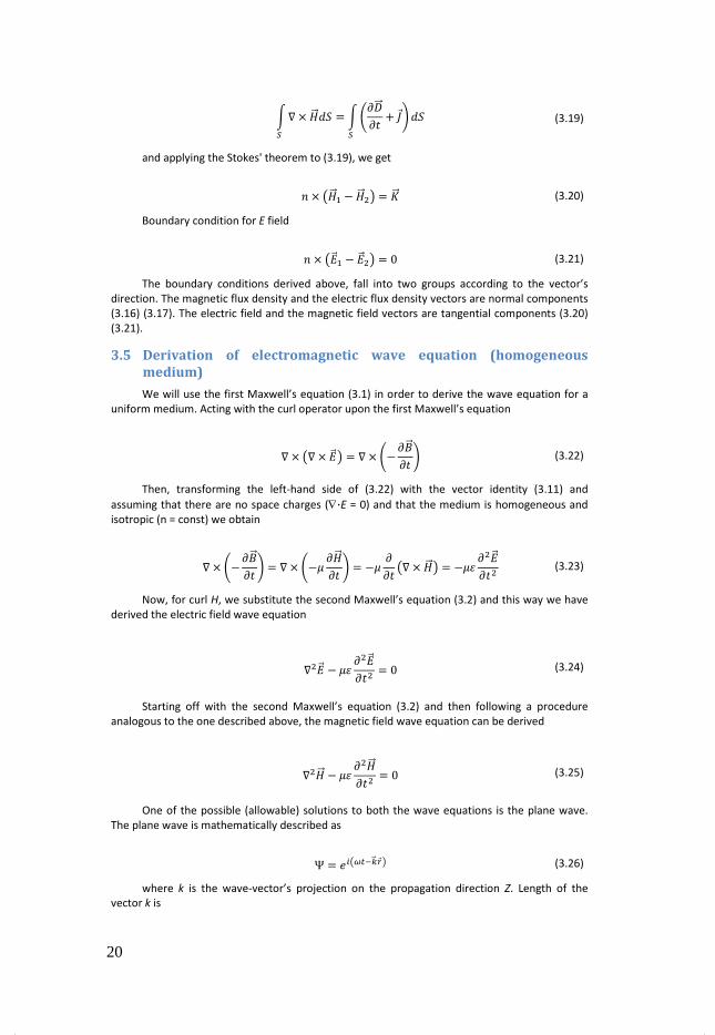
; ∇ × ����58 = ; +������ + ��, 58 9
9 (3.19)
and applying the Stokes' theorem to (3.19), we get
< × 0����> − ����-1 = D��� (3.20)
Boundary condition for E field
< × 0���> − ���-1 = 0 (3.21)
The boundary conditions derived above, fall into two groups according to the vector’s
direction. The magnetic flux density and the electric flux density vectors are normal components
(3.16) (3.17). The electric field and the magnetic field vectors are tangential components (3.20)
(3.21).
3.5 Derivation of electromagnetic wave equation (homogeneous
medium)
We will use the first Maxwell’s equation (3.1) in order to derive the wave equation for a
uniform medium. Acting with the curl operator upon the first Maxwell’s equation
∇ × 0∇ × ���1 = ∇ × +− ���� , (3.22)
Then, transforming the left-hand side of (3.22) with the vector identity (3.11) and
assuming that there are no space charges (∇·E = 0) and that the medium is homogeneous and
isotropic (n = const) we obtain
∇ × +− ���� , = ∇ × +−� ������ , = −� �� 0∇ × ����1 = −�� �-����- (3.23)
Now, for curl H, we substitute the second Maxwell’s equation (3.2) and this way we have
derived the electric field wave equation
∇-��� − �� �-����- = 0 (3.24)
Starting off with the second Maxwell’s equation (3.2) and then following a procedure
analogous to the one described above, the magnetic field wave equation can be derived
∇-���� − �� �-�����- = 0 (3.25)
One of the possible (allowable) solutions to both the wave equations is the plane wave.
The plane wave is mathematically described as
Ψ = FG0HIJK��L�1 (3.26)
where k is the wave-vector’s projection on the propagation direction Z. Length of the
vector k is
20
|$| = NO�� (3.27)
3.6 Simplifying wave equation for the planewave solution
In planar waveguides, the electromagnetic wave propagates within the so called guiding
layer, i.e. a medium having the refractive index value higher than that of the surrounding media.
Schematic view of planar waveguide is shown in figure Fig. 3.3.
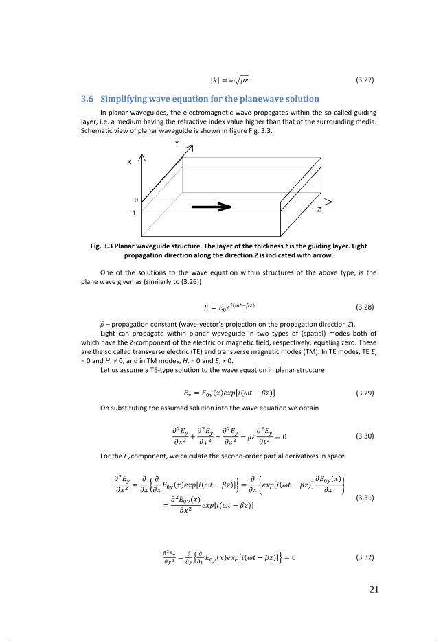
Fig. 3.3 Planar waveguide structure. The layer of the thickness t is the guiding layer. Light
propagation direction along the direction Z is indicated with arrow.
One of the solutions to the wave equation within structures of the above type, is the
plane wave given as (similarly to (3.26))
� = ��FG�HIJP) (3.28)
β – propagation constant (wave-vector’s projection on the propagation direction Z).
Light can propagate within planar waveguide in two types of (spatial) modes both of
which have the Z-component of the electric or magnetic field, respectively, equaling zero. These
are the so called transverse electric (TE) and transverse magnetic modes (TM). In TE modes, TE Ez
= 0 and Hz ≠ 0, and in TM modes, Hz = 0 and Ez ≠ 0.
Let us assume a TE-type solution to the wave equation in planar structure
�( = ��(�� F�QRS�N − T� U (3.29)
On substituting the assumed solution into the wave equation we obtain
�-�(��- + �-�(��- + �-�(��- − �� �-�(�- = 0 (3.30)
For the Ey component, we calculate the second-order partial derivatives in space
�-�(��- = ��� V ��� ��(�� F�QRS�N − T� UW = ��� XF�QRS�N − T� U ���(�� �� Y= �-��(�� ��- F�QRS�N − T� U (3.31)
Z[\]Z([ = ZZ( ^ ZZ( ��(�� F�QRS�N − T� U_ = 0 (3.32)
Y
Z
X
0
-t
21

�-�(��- = ��� V ��� ��(�� F�QRS�N − T� UW = ��� `−ST��(�� F�QRS�N − T� Ua= −T-��(�� F�QRS�N − T� U (3.33)
and in time
�-�(�- = �� V �� ��(�� F�QRS�N − T� UW = �� `SN��(�� exp RS�N − T� Ua= −N-��(�� F�QRS�N − T� U (3.34)
After substituting the partial derivatives (3.31), (3.32), (3.33), and (3.34) into (3.30), we get
�-��(�� ��- F�QRS�N − T� U + 0 − T-��(�� F�QRS�N − T� U− ��`−N-��(�� F�QRS�N − T� Ua = 0 (3.35)
Using the TE-type plane wave (3.29), we reduce (3.35) to the following form
�-��� ��- − RT- − ��N-U��� = 0 (3.36)
With the following dependencies in mind
< = ef , e = 1O���� , f = 1√�� , i� = ej (3.37)
we have
$ = 2li = 2li� < = Ne < = Nm (3.38)
Using (3.38) we can express the product of magnetic permeability, electric permittivity,
and wave frequency squared, as the wave-vector squared
��N- = n N1√�� o-
= pNm q- = $- (3.39)
Finally, we arrive at the final form of the wave equation for TE modes of planar waveguide
�-��(��- + R$- − T-U��( = 0 (3.40)
22
In the next step, boundary conditions will be found for a guided TE mode of planar
structure. Each TE mode has only one non-zero component of the electric filed vector (Ey) and
two non-zero components of the magnetic filed vector (Hz and Hx). From equation (3.21), the
boundary conditions for Ey are
��(> = ��(- (3.41)
Boundary conditions for the two magnetic field components Hz and Hx can be found from
(3.20), with the surface current density K = 0 assumed (zero current density it is correct, as we
deal with dielectrics, and not with conducting materials). We are interested in the component Hz
�(��, �, = ��(�� FG�HIJP) (3.42)
From the first of Maxwell's equations (3.1) and the definition of the curl (rotation)
operator (3.9)
��(�� − ��'�� = − �)� (3.43)
Substituting the formula (3.6) for the magnetic flux density
���(�� − ���'�� = −SN���) (3.44)
Calculating H0z, from (3.44), we get
��) = − 1SN� ���(�� = SN� ���(�� (3.45)
Due to magnetic field vector continuity (3.46) at the boundary between two media
��)> = ��)- (3.46)
Finally, the searched boundary conditions are (3.41) and
���(>�� = ���(-�� (3.47)
23

4 Mode equation for a planar waveguide
4.1 Wave equation for a planar waveguide.
Fig. 4.1Light propagation in a planar waveguide structure – the total internal reflection.
Let us consider a planar waveguide structure consisting of three layers as presented in
figure Fig. 4.1. Lest us assume that layers of the refractive indexes n1 and n3 are semi-infinite, i.e.
they extend to infinity in the directions +x and –x, respectively. An advantage of such an
assumption is the lack of reflections along the x-direction anywhere except for the nc – nf and
the nf – ns boundaries. Now, substituting, into the wave equation
02
22 =−∇
t
EE
∂∂
µεr
r (4.1)
a solution of the form (plane wave)
( )[ ]rktizyxEErrr
−= ωexp),,(0 (4.2)
we get
[ ] 022
2
2
=−− Ekx
Eβ
∂∂
r
(4.3)
where
nc
nkω
λπ
λπ
===0
22 (4.4)
( )θβ sin0 fnk= (4.5)
which is exactly the result already discussed in Chapter 3. In a TE-polarized plane wave
propagating along the z-direction, there are three nonzero field vector components: Ey, Hx i Hz.
Considering only the electric field, we omit the magnetic field components along the z- and x-
directions. Moreover, the electric field component Ey does not depend on y and z because
waveguide layers extend to infinity along these directions, thus no reflections or standing waves
can occur. Spatial distribution of Ey along the x-direction in the planar waveguide under
consideration (figure Fig. 4.1) takes the form of a system of three equations involving four
unknowns (variables) (Hunsperger, 2009)
( ) ( ) ( )
( ) ( ) ( )
−≤≤∞−
+
≤≤−
−
∞≤≤
=
+
−
txehxh
qhxC
xthxh
qhxC
xCe
xE
txp
qx
y
sincos
0sincos
0
(4.6)
θk
β
nc
ns
nf
-t
0
24

On substituting the equation (4.2) into (4.1) and using the expression (4.6), the
coefficients p, q, and h can be determined (Hunsperger, 2009)
22
0
22
2
0
222
2
0
222
βββ
−=
−=
−=
knh
knq
knp
f
c
s
(4.7)
4.2 TE and TM modes
Fig. 4.2 Electromagnetic wave propagation in a planar waveguide. There is shown the TE-
polarization case (1) and the nonzero components of the electric and magnetic field vectors
(2).
A schematic depiction of TE-polarized mode propagation in a planar waveguide is shown
in figure Fig. 4.2. The red and the blue colors represent the electric and the magnetic field vector
components, respectively.
As a reminder, electromagnetic waves propagating in planar waveguides fall into two
categories:
o the TE modes (TE-polarized modes) with the nonzero components: Ey, Hx, Hz
o the TE modes (TE-polarized modes) with the nonzero components: Hy, Ex, Ez
E field
H field
Ey Hz
HxH
25

4.3 Electrical field distribution for the first three modes of a planar
waveguide
Fig. 4.3 Electric field distribution for the first three lowest-order modes of a planar waveguide.
The figure Fig. 4.3 presents the Ey spatial distributions for the three lowest-order modes of
a planar waveguide. The planar waveguide parameters used in calculations are: ns = 1.5, nf = 2, nc
= 1 and the light wavelength is λ = 633 nm.
4.4 Boundary conditions
Boundary conditions were discussed in Chapter 3.
4.5 Boundary conditions for a planar waveguide
=
=
−=
=
tx
s
y
f
y
x
f
y
c
y
EE
EE
00
000
(4.8)
=
=
−=
=
tx
s
y
f
y
x
f
y
c
y
x
E
x
E
x
E
x
E
∂
∂
∂
∂
∂
∂
∂
∂
00
0
00
(4.9)
Planar waveguide boundary conditions (derived in Chapter 3) – field continuity at
boundaries between the waveguide layers (dielectric boundaries) nc – nf and nf – ns.
4.6 Boundary conditions for a planar waveguide – verification
By substituting the equation (4.6) into the boundary conditions from the system of
equations (4.8), we can check whether the solutions assumed are correct. At the dielectric
boundary nc – nf, i.e. at the point x = 0, the value of the electric field vector y-component equals
C. At the opposite side of the nf layer (guiding layer), i.e. at the nf – ns boundary (x = -t), the
electric field takes the value of ( ) ( )
− hth
qhtC sincos . A condition from the system of
equations (4.8) is met, thus the correctness of the solutions assumed has been confirmed.
The second boundary condition enforces the field continuity at the dielectric boundaries
x = 0 i x = -t. First derivative of the electric field distribution at the point x = 0 equals –qC and it
meets the condition from (4.9). Thus, constants present in the equations are correct.
-2 -1.5 -1 -0.5 0.5 1
-2
-1
1
2
E [j.w.]
X [µm]
26

4.7 Derivation of the mode equation
Making the electric field continuity condition (4.9) be true at the dielectric boundary nf –
ns, we derive the mode equation
( ) ( ) ( ) ( )
+=− hth
qhtphtqhth sincoscossin (4.10)
4.8 Transformation of mode equation into a tangent based form
Dividing both sides of the equation (4.10) by cos(ht), we get
( ) ( )hth
pq
h
p
h
qht tantan
2+=− (4.11)
Then, by grouping like terms
( ) ( )h
q
h
pht
h
pqht +=− tantan
2 (4.12)
and applying some straightforward algebraic manipulations, we arrive at a mode equation
form that involves the tangent (tan) function (Hunsperger, 2009)
( ) ( )2/1tan
hpqh
qpht
−+
= (4.13)
The mode equation form shown above will be later used in the derivation of the additive
form of the mode equation.
4.9 Additive form of mode equation
In order to find all the mode equation solutions that represent all the possible waveguide
modes, one needs to transform the tangent-function form (4.13) into the additive form
(Hunsperger, 2009)
( ) ,...2,1,0,222cos2 0 ==Φ−Φ− mmtnk csf πθ (4.14)
where m is the waveguide mode number, Φs and Φc are the Fresnel coefficients. Both the
coefficients describe the electromagnetic wave phase shift due to reflection at the dielectric
boundaries nc – nf and nf – ns.
We transform the tangent-function form of the mode equation into a form that will allow
the of application of the following trigonometric identity
vuuv
vuarctanarctan
1arctan +=
−+
(4.15)
( ) ( )( )
−
+=
−
+=
−+
=
h
q
h
ph
q
h
p
h
pq
qph
hpqh
qpht
11
1
/1tan
2
2 (4.16)
4.10 Derivation of additive form of mode equation
Let us derive the additive form of the mode equation. Utilizing the arctangent (arctan)
function properties, the left-hand side of (4.16) takes the form
( )[ ] ,tanarctan: πmhthtL ±= (4.17)
27

Then, by handling the right-hand side of the equation in a similar way and applying the
trigonometric identity (4.15), we get
+
=
−
+
h
q
h
p
h
q
h
ph
q
h
p
R arctanarctan
1
arctan: (4.18)
Finally, after grouping like terms, we arrive at the additive form of the planar waveguide
mode equation
+
=±h
q
h
pmht arctanarctanπ (4.19)
mh
q
h
pht π=
−
− arctanarctan (4.20)
4.11 Total internal reflection is accompanied by a phase shift – TE mode
(Fresnel coefficients)
Using the formulas (4.7), we will determine the Fresnel coefficients for the additive form
of the planar waveguide mode equation (4.14). From (4.20) we can see, that the Fresnel
coefficient Φs equals the arctangent of the quotient of p and h
22
0
2
2
0
22
ββ
−−
=kn
kn
h
p
f
s (4.21)
Substituting the propagation constant given by (4.5) and applying some straightforward
trigonometric manipulations, we get a formula for the Fresnel coefficient Φs
( ) θ
θ
θ
θ
θ
θ
cos
sin
sin1
sin
sin
sin222
22
222
2
0
222
0
2
2
0
22
0
22
f
sf
f
sf
ff
sf
n
nn
n
nn
knkn
knkn
h
p −=
−
−=
−
−= (4.22)
−=
=Φθ
θ
cos
sinarctanarctan
222
f
sf
sn
nn
h
p (4.23)
In an analogous way, the coefficient Φc can be determined
22
0
2
2
0
22
ββ
−−
=kn
kn
h
q
f
c (4.24)
( ) θ
θ
θ
θ
θ
θ
cos
sin
sin1
sin
sin
sin222
22
222
2
0
222
0
2
2
0
22
0
22
f
cf
f
cf
ff
cf
n
nn
n
nn
knkn
knkn
h
q −=
−
−=
−
−= (4.25)
−=
=Φθ
θ
cos
sinarctanarctan
222
f
cf
cn
nn
h
q (4.26)
28
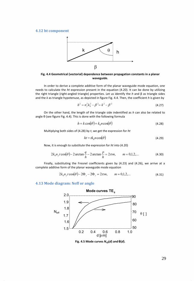
4.12 ht component
Fig. 4.4 Geometrical (vectorial) dependence between propagation constants in a planar
waveguide.
In order to derive a complete additive form of the planar waveguide mode equation, one
needs to calculate the ht expression present in the equation (4.20). It can be done by utilizing
the right triangle (right-angled triangle) properties. Let us identify the h and β as triangle sides
and the k as triangle hypotenuse, as depicted in figure Fig. 4.4. Then, the coefficient h is given by
2222
0
22 ββ −=−= kknh f (4.27)
On the other hand, the length of the triangle side indentified as h can also be related to
angle θ (see figure Fig. 4.4). This is done with the following formula
( ) ( )θθ coscos 0nkkh == (4.28)
Multiplying both sides of (4.28) by t, we get the expression for ht
( )θcos0ntkht = (4.29)
Now, it is enough to substitute the expression for ht into (4.20)
( ) ,...2,1,0,2arctan2arctan2cos2 0 ==−− mmh
p
h
qtnk f πθ (4.30)
Finally, substituting the Fresnel coefficients given by (4.23) and (4.26), we arrive at a
complete additive form of the planar waveguide mode equation
( ) ,...2,1,0,222cos2 0 ==Φ−Φ− mmtnk csf πθ (4.31)
4.13 Mode diagram: Neff or angle
Fig. 4.5 Mode curves Neff(d) and θθθθ(d).
k
β
θ h
0.2 0.4 0.6 0.8 1.0d [µm]
1.5
1.6
1.7
1.8
1.9
2.0
Neff
Mode curves TE0
50
60
70
80
90
θ [ ]
29

Let us compare the mode curves defined as Neff(d) and θ(d). Such a comparison visible in
figure Fig. 4.5 was plotted for a planar waveguide of the following parameters: nf = 2, ns = 1.5, nc
= 1. For the increasing values of the waveguide thickness d, the waveguide mode effective
refractive index Neff increases. In a similar way behaves the angle θ that is the angle at which a
given mode propagates. The higher the waveguide thickness, the higher the propagation angle
(θ).
4.14 Mode diagram: TE and TM
Fig. 4.6Mode curves Neff(d) calculated for the TE-polarized (solid lines) and the TM-polarized
(dashed lines) planar waveguide modes.
Figure Fig. 4.6 presents a comparison of the behavior of Neff(d) for the TE-polarized and
the TM-polarized three lowest-order planar waveguide modes. The calculations were performed
for a waveguide of the parameters: nf = 2, ns = 1.5, nc = 1. On a closer inspection of the diagram,
it becomes clear that up to the thickness of about 0.3 μm, the planar waveguide under
consideration remains single-mode (supports only one mode). In other words, for the thickness
values higher than the mentioned 0.3 μm, the effective refractive index of the second-order
mode becomes higher than the substrate refractive index and the second-order mode can
propagate in the waveguide. Waveguide modes of higher orders become guided (i.e. able to
propagate in the waveguide) in a similar fashion as we have just discussed for the second-order
mode. To summarize, the thicker the waveguide, the higher the number of guided modes.
4.15 Mode measurements - prism coupler method
Fig. 4.7 Idea of the prism coupling (prism coupler method).
Coupling light into a thin structure of a planar waveguide is an important problem in the
measurements of the planar waveguide guided modes. Among a number of possible methods of
light coupling into sub-micrometer waveguide structures, one of the most popular is the so
called prism coupling. In prism coupling, light enters the planar waveguide through waveguide’s
top surface. As shown in figure Fig. 4.7, the prism is positioned above the planar waveguide. A
thin air-gap exists between prism base and waveguide top surface. The air-gap thickness is of the
order of half the light wavelength or less. Laser light enters the prism and undergoes the total
internal reflection at prism base. An evanescent wave that is created in the total internal
0.2 0.4 0.6 0.8 1
d [um]
1.5
1.6
1.7
1.8
1.9
2
Neff
i
i’ θp
θfnf
np
'sinsin1 ini p=⋅A α
( ) 180'90 =+++ iA α
30
reflection phenomenon penetrates the air gap and thus light can be coupled into the waveguide.
(Chang, 2009)
By using a triangle property (triangle angles sum up to 180°) and some other basic
geometrical relationships, we can determine angle θp at which light impinges on (hits) the prism
base surface
( )[ ] ''901809090 iAiAp +=+−−−=−= αθ (4.32)
Utilizing the Snell’s law (law of refraction) and some trigonometric identities, we first
calculate angle i’
pn
ii
sin'sin = (4.33)
=
pn
ii
sinarcsin' (4.34)
Then, after substituting (4.34) into (4.32), we get a formula for angle θp
+=
p
pn
iA
sinarcsinθ (4.35)
4.16 Effective refractive index evaluation
The guided mode effective refractive index obeys the following relation
effffpp �nn == θθ sinsin (4.36)
Thus, by substituting the θp given by (4.35) into (4.36), we can express Neff as
+⋅=
p
peffn
iAn�
sinarcsinsin (4.37)
This means that the guided mode effective refractive index can be determined by means
of measuring angle i at which light is coupled into the prism.
4.17 Mode separation TE-TM, use of Maxwell’s equations
Maxwell’s equations were discussed in detail in Chapter 3.
5 Optical and mechanical properties of optical fibers
The following chapter is based on the ITU standard: ITU-T G.650 “Definition and Test
Methods for the Relevant Parameters of Single-Mode Fibers” - Series G: Transmission Systems
and Media, Digital Systems and Networks Transmission Media Characteristics - Optical Fiber by
International Telecommunication Union.
Telecommunication optical cables are highly developed transmission media, optimized for
communication application. The fibers are characterized by multiple parameters. The main
source of definitions of this parameters is a series of standards published by International
Telecommunication Union. The short list of the most important standard is given below.
31

o G.650 Definition and test methods for the relevant parameters of single-mode
fibers
o G.651 Characteristics of a 50/125 µm multimode graded index optical fiber
cable
o G.652 Characteristics of a single-mode optical fiber cable
o G.653 Characteristics of a dispersion-shifted single-mode optical fiber cable
o G.654 Characteristics of a 1550 nm wavelength loss-minimized single-mode
optical fiber cable
o G.655 Characteristics of a non-zero dispersion single mode optical fiber cable
In this lecture the main properties of optical fibers are described and their definitions are
given. In another lecture measurement methods of this parameters will be given.
Parameters of optical fiber waveguides are classified into three main groups:
o Optical parameters
o Geometrical parameters
o Mechanical parameters
According to this classification standardized parameters of the single mode optical fiber
can be classified as follows:
o Optical parameters
o Attenuation
o Chromatic dispersion
o Mode field diameter
o Cut-off wavelength
o Polarization mode dispersion
o Geometrical parameters
o Cladding diameter, mode field concentricity error and cladding
non‑circularity
o Mechanical parameters
o Proof testing
The most important parameters will be covered in the following chapters.
5.1 Mode field diameter
The mode field is the single-mode field distribution of the LP01 mode giving rise to a
spatial intensity distribution in the fiber. The Mode Field Diameter (MFD) 2w represents a
measure of the transverse extent of the electromagnetic field intensity of the mode in a fiber
cross-section. For the reason of simplification of measurement method of this parameter, it is
defined from the far field intensity distribution F2(θ), θ being the far-field angle, through the
following equation:
( )
( )
21
2
0
32
2
0
2
cossin
cossin2
2
=
∫
∫π
π
θθθθ
θθθθ
πλ
dF
dF
w (5.1)
Theoretical ground for this equation, is a knowledge that far field distribution of optical
field is related to the near field distribution (i.e. light intensity distribution at the output face of
the fiber) through the Fourier transform. [Iizuka K. Engineering Optics. Springer; 1985].
32

5.1.1 Other mode-field parameters
The mode field centre is the position of the centroid of the spatial intensity distribution in
the fiber. The centroid is located at rc and is the normalized intensity-weighted integral of the
position vector r.
( )( )∫∫
∫∫=
Area
Areac
dArI
dArrIr (5.2)
The mode field concentricity error is the distance between the mode field center and the
cladding center.
5.2 Cladding diameter, mode field concentricity error and cladding
non‑‑‑‑circularity
o By definition cladding is the outermost region of constant refractive index in the
fiber cross-section.
o Cladding centre: for a cross-section of an optical fiber it is the centre of that circle
which best fits the outer limit of the cladding.
o Cladding diameter is the diameter of the circle defining the cladding centre.
o Cladding diameter deviation is the difference between the actual and the nominal
values of the cladding diameter.
o Cladding tolerance field: for a cross-section of an optical fiber it is the region
between the circle circumscribing the outer limit of the cladding, and the largest
circle, concentric with the first one, that fits into the outer limit of the cladding.
Both circles shall have the same centre as the cladding.
o Cladding non-circularity: the difference between the diameters of the two circles
defined by the cladding tolerance field divided by the nominal cladding diameter.
Fig. 5.1 Cladding diameter, cladding center and cladding non circularity
Fig. 5.2 Cladding non-circularity and cladding diameter deviation
33
5.3 Cut-off wavelength - theoretical definition
Theoretical cut-off wavelength is the shortest wavelength at which a single mode can
propagate in a single-mode fiber. At wavelengths below the theoretical cut-off wavelength,
several modes propagate and the fiber is no longer single-mode but multimode.
In optical fibers, the change from multimode to single-mode behavior does not occur at an
isolated wavelength, but rather smoothly over a range of wavelengths. Cut-off wavelength is
defined as the wavelength greater than the wavelength for which the ratio between the total
power, including launched higher order modes and the fundamental mode power has decreased
to less than 0.1 dB. According to this definition, the second order (LP11) mode undergoes
19.3 dB more attenuation than the fundamental (LP01) mode when the modes are equally
excited.
Cut-off wavelength depends on the length and bends of the fiber and its strain condition.
Consequently, there are three types of cut-off wavelength defined:
o cable cut-off wavelength (measured prior to installation ),
o fiber cut-off wavelength (measured on uncabled primary-coated fiber)
o jumper cable cut-off wavelength.
5.4 Attenuation
The attenuation A(λ) at wavelength λ between two cross-sections 1 and 2 separated by
distance L of a fiber is defined, as:
( ) ( )( )
( )dBlog102
1
λλ
λP
PA = (5.3)
where P1(λ) is the optical power traversing the cross-section 1, and P2(λ) is the optical
power traversing the cross-section 2 at the wavelength λ.
For a uniform fiber, it is possible to define an attenuation per unit length, or an
attenuation coefficient which is independent of the length of the fiber:
( ) ( )length)(dB/unit
L
Aa
λλ = (5.4)
5.5 Chromatic dispersion
Chromatic-dispersion definition: the spreading of a light pulse in an optical fiber caused by
the different group velocities of the different wavelengths composing the source spectrum.
The chromatic dispersion may be due to the following contributions:
o material dispersion,
o waveguide dispersion,
o profile dispersion.
Change of the delay of a light pulse for a unit fiber length caused by a unit wavelength
change. It is usually expressed in ps/(nm · km).
The duration of a light pulse per unit source spectrum width after having traversed a unit
length of fiber is equal to the chromatic dispersion coefficient, if the following prerequisites are
given:
1) the source has a wide spectrum;
2) the duration of the pulse at the fiber input is short as compared to that at the output,
the wavelength is different from the zero-dispersion wavelength
34

Fig. 5.3 Illustration of the chromatic dispersion. A pulse is widened as it travels along the fiber.
Other dispersion parameters that may be used to characterize single mode
telecommunication fibers include:
o Zero-dispersion slope. The slope of the chromatic dispersion coefficient versus
wavelength curve at the zero-dispersion wavelength.
o Zero-dispersion wavelength. That wavelength at which the chromatic dispersion
vanishes.
o Source wavelength offset. For G.653 fibers only. The absolute difference between
the source operating wavelength and 1550 nm.
o Dispersion offset. For G.653 fibers only. The absolute displacement of the zero-
dispersion wavelength from 1550 nm.
5.6 Polarization mode dispersion
Polarization mode dispersion is the Differential Group Delay time (DGD) between two
orthogonally polarized modes, which causes pulse spreading in digital systems and distortions in
analogue systems. Two factors have to be taken into account here:
o Real fibers cannot be perfectly circular and can undergo local stresses;
consequently, the propagating light is split into two local polarization modes
travelling at different velocities. These asymmetry characteristics vary randomly
along the fiber and in time, leading to a statistical behavior of PMD.
o For a given fiber at a given time and optical frequency, there always exist two
polarization states, called Principal States of Polarization such that the pulse
spreading due to PMD vanishes, if only one PSP is excited. The maximum pulse
spread due to PMD occurs when both PSPs are equally excited.
Definition of principal States of Polarization (PSP): when operating an optical fiber at a
wavelength longer than the cut-off wavelength in a quasi-monochromatic regime, the output
PSPs are the two orthogonal output states of polarization for which the output polarizations do
not vary when the optical frequency is varied slightly. The corresponding orthogonal input
polarization states are the input PSPs. Two issues have to be taken into account here. The local
birefringence changes along the fiber, and the PSP depends on the fiber length (contrary to hi-bi
fibers). If a signal has a bandwidth broader than the PSPs bandwidth, second order PMD effects
come into play. They may imply a depolarization of the output field, together with an additional
chromatic dispersion effect.
Definition of the Differential Group Delay (DGD): the Differential Group Delay (DGD) is the
time difference in the group delays of the PSPs. The DGD between two modes is wavelength
dependent and can vary in time due to environmental conditions. Variations by one order of
magnitude are typical. The statistical distribution of the differential group delays is determined
by the mean polarization mode coupling length, h, the average modal birefringence and the
degree of coherence of the source. For a standard optical fiber cable of length L, such that L >>
h, as is mostly the case in practice, strong mode coupling occurs between the polarization
modes. In such a case, the probability distribution of the DGDs is a Maxwellian distribution.
PMD is statistical parameter, and may be defined by three different statistical parameters.
Statistical parameters of interests here are so called central moments that show the
deviation of the random variable from the mean:
o The first statistical moment called the mean
t or L
D
35

o The second central moment, called the variance
According to the G.650 standard PMD may be characterized as follows.
o The second moment (variance) PMD delay Ps is defined as twice the root mean
square deviation (2σ) of the time dependent light intensity distribution I(t) at the
output of the fiber, deprived of the chromatic dispersion contribution, when a
short pulse is launched into the fiber, that is:
( ) ( )( )
( )( )
21
21
22
22 22
−=><−><=∫∫
∫∫
dttI
tdttI
dttI
dtttIttPs (5.5)
t represents the arrival time at the output of the fiber. In practical cases the broadening
due to chromatic dispersion must be taken into account to obtain Ps.
o The mean differential group delay Pm is the differential group delay δτ(ν) between
the principal states of polarization, averaged over the optical frequency range (ν1,
ν2):
( )
12
2
1
vv
cvv
p
v
v
m −=∫δτ
(5.6)
Averaging over temperature, time or mechanical perturbations is generally an acceptable
alternative to averaging over frequency
o The r.m.s. differential group delay Pr is defined as
( )21
2
1
12
2
−=∫
vv
dvv
P
v
v
r
δτ
(5.7)
PMD coefficient is calculated in two different ways fot two separate cases:
o Weak mode coupling (short fibers):
[ ] LPLPLPkmpsPMD rmsc /or,/,// = (5.8)
o Strong mode coupling (long fibers):
[ ] L/, or PL/, PL/Pkmps/PMD rmsc = (5.9)
Strong mode coupling is mostly observed in installed cables longer than 2 km. Under
normal conditions, the differential group delays are random functions of optical wavelength, of
time, and vary at random from one fiber to the other. Therefore, in most cases, the PMD
coefficient has to be calculated using the square root formula
36
6 Technology of optical fibers
6.1 Telecommunication windows and generations of fiber optic
systems
The telecommunication windows, and the telecommunication system generations were
discussed in Chapter 2.
6.2 Attenuation of silica glass fiber
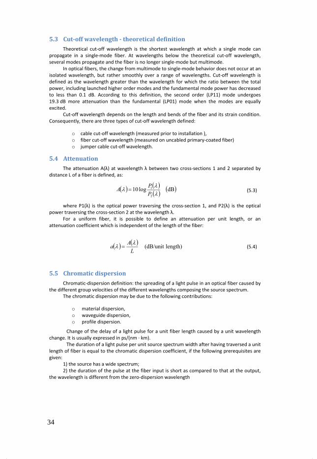
Fig. 6.1 Silica glass fiber attenuation in function of light wavelength.
Fiber attenuation is a gradual decrease in energy (optical power) carried by the lightwave
as it propagates along the fiber. Numerical values of attenuation are expressed in the units of
[dB / km], which translates into: what part (in decibels, dB) of the initial optical power is lost due
to attenuation assuming the light has travelled a path of the length of 1 kilometer (km) inside
the fiber. Whereas reasons of attenuation occurrence are common to all silica glass fibers, the
attenuation values strongly depend on parameters of a given fiber (e.g. on manufacturing
process, fiber type, and others).
We will describe the attenuation of silica glass fiber in two contexts. Firstly, in the context
of physical mechanisms standing behind the attenuation. Secondly, in the context of how the
attenuation value varies with the wavelength of propagating light.
Three groups of physical mechanisms can be named. They are (Bass, 2001b), (J.-ming Liu,
2005), (Agrawal, 2002):
o intrinsic absorption,
o extrinsic absorption, and
o scattering.
All mechanisms of the types listed above occur with different strength depending on the
light wavelength. In telecommunications, we are interested in characterizing the absorption
strength
o in the short-wavelength region (ultraviolet and visible), i.e. for lightwaves shorter
than about 800 nm,
o in the infrared region, i.e. for lightwaves longer than about 1600 nm, and
o in the near-infrared region, i.e. between 800 and 1600 nm where the
telecommunication windows are located.
Rayleigh scattering ~ λ -4
Absorption OH –
2.
Molecular
absorption:
oxides Si,Ge,P,BCr
++
Fe++
0.6 0.8 1.0 1.2 1.4 1.6 1.8
0.3
0.5
1
0.1
3
5
10
30
50
Wavelength [µm]
3.
wet glass
dry glass (1 ppb OH – )
Att
en
ua
tio
n [d
B/k
m]
37

Optical power lost due to absorption is transformed into heat - fiber's temperature is
increased. This temperature change of fiber material can usually be neglected unless we deal
with high levels of optical power. Some of the scattering mechanisms include the transformation
of light into heat, as well. However, a scattering mechanism we will discuss later in this lecture,
only alters the direction of light propagation, thus making some part of optical power propagate
out of the fiber core.
The intrinsic absorption is the one that occurs when light interacts with the chemical
ingredients (chemical structure) of pure glass. In silica fibers, the intrinsic absorption becomes
significantly high (strong)
o in the short-wavelength spectral region (below 800 nm) where it is caused by the
electromagnetic field interaction with electrons (electronic absorption), and
o in the infrared spectral region (above 1600 nm) where it is caused by the
electromagnetic field interaction with chemical bonds (Si-O bonds) that connect
the silicon and oxygen atoms (molecular absorption).
Reasons of the extrinsic absorption lie in the interaction of light with impurities contained
in glass. Though unwanted, impurities are always present in actual silica fibers. The most
significant types of such impurities are:
o ions of the following metals - iron (Fe), nickel (Ni) and chromium (Cr) (see the
diagram for spectral ranges of absorption associated with individual ions), and
o the hydroxyl ions (OH-) showing the strongest absorption around 2700 and 4200
nm (the fundamental OH- absorption) and - what is of special interest to
telecommunications - absorption around 1380, 950 and 720 nm (the overtone
OH- absorption).
All the discussed ions occur in silica fibers due to imperfections of fiber manufacturing
processes. In particular, the OH- ions come from water.
Among several other scattering mechanisms, the most pronounced in silica fibers is
o the Rayleigh scattering (i.e. scattering described by Rayleigh's model) caused by
silica refractive index inhomogeneities of the sizes much below (<10%) the light
wavelength; this type of scattering shows the λ-4
dependence (compare the thick
dashed line in the diagram).
Finally, from the viewpoint of individual spectral ranges, the absorption and scattering
mechanisms we have discussed so far, contribute to the total attenuation of silica fiber as
follows (J.-ming Liu, 2005):
o in the short-wavelength range, the Rayleigh scattering is dominant and it
outweighs the other factor present in this spectral range, the electronic
absorption,
o in the infrared range, only the molecular absorption defines the silica fiber
attenuation,
o in the near-infrared range, absorption on OH- ions is a decisive factor;
particularly, the low-attenuation (low-loss) spectral ranges in between the
neighboring OH- absorption peaks are used as transmission windows in
telecommunications; fiber transmission can, however, be significantly degraded
within those windows if fiber quality is not high enough.
6.3 Properties of silica glass
For convenience, a summary of the already discussed silica glass-related facts is given in a
list below.
o Chemical formula SiO2
o Lowest fiber loss 0.2 dB/km
o Bandgap of fused silica 9 eV (~137 nm)
o (Pure germania bandedge ~185 nm)
o Infrared edge (vibrational resonances) ~2 mm
38

o Rayleigh scattering ~ λ-4
(i.e. its intensity changes proportionally to the -4th
power
of light wavelength)
o OH– ions infrared absorption: fundamental 2.27 and overtones 1.37, 0.95 and
0.725 mm
6.4 Structure of silica glass
In telecommunication fibers, the silica glass used never consists of a perfectly regular,
uniform net (crystal lattice) of silicon (Si) and oxygen (O) atoms. There is always a certain density
of lattice defects present in fiber material. The defects, independent of their origin, result in
local fluctuations of the fiber material (i.e. the silica-glass) refractive index. Structure of silica
glass compared to silica crystal is shown in figure Fig. 6.2.
Fig. 6.2 Structure of silica crystal: two dimensional crystal lattice is presented.
Before all, the fiber material atoms are not located at perfectly regular positions because
fiber material is not the silica crystal but the silica glass. In general, a perfect regularity of atom
geometrical configuration can only be expected in crystals. In glasses, due to the process of
melting that glasses undergo when they are produced, the crystal-like regularity is lost.
In the specific situation of the silica glass application in optical fibers, a second source of
glass structure irregularities appear. It is the presence of the so called modifiers, i.e. chemical
substances (chemical compounds) that are introduced into glass to alter its optical properties.
Adding of the modifier substances in the process of fiber manufacturing is called doping and it
will be discusses in greater detail in paragraph 6.6.
6.5 Three main steps in fabrication of optical fibers
Optical fibers are fabricated using a number of different methods (technologies). These
methods fall into two main categories:
o fiber production from preform, and
o direct fiber production (without preform).
Only methods from the first category are of importance in mass production of silica glass
fibers. The second category includes methods that are often used for plastic fibers (e.g. a
method of extrusion).
In this lecture we will only focus on the preform-based fabrication technologies. There are
three main steps in each preform-based fabrication technology of silica glass fibers:
o manufacturing of the pure glass preform,
o drawing of the fiber from the preform, and
o tests and measurements.
In the following slides, we will explore in more detail how the pure glass preform is
manufactured and how the preform is then transformed into the final product – the silica glass
fiber.
6.6 Chemicals and chemical reactions
All the preform manufacturing technologies share some basic chemical reactions, which
are used for:
modifiers
39

o creating the silica (SiO2) itself, o increasing the refractive index of silica, or
o decreasing the refractive index of silica.
The primary chemicals are:
silicon tetrachloride (SiCl4), germanium tetrachloride (GeCl4). Then, basic chemical reactions of manufacturing of optical glass proceed as follows
(Gambling, 2000), (Bass, 2001b), (Agrawal, 2002):
SiCl4 + O2 → SiO2 +2Cl2
GeCl4 + O2 → GeO2 +2Cl2
In the first reaction, a white silica powder is created. Before being transformed into glass
(vitrified) at a later stage of the preform manufacturing process, this silica powder is often called
the soot in the fiber production terminology. In the second reaction, germanium dioxide (GeO2)
is created. When present in silica, germanium dioxide plays a role of a refractive index-increasing
dopant.
Two other reactions commonly used in preform manufacturing are:
4POCl3 + 3O2 → 2P2O5 +6Cl2
4BCl3 + 3O2 → 2B2O3 +6Cl2
The reaction substrates are: phosphorus oxychloride (POCl3) and boron trichloride (BCl3).
Both the reactions create substances that modify the refractive index of silica. Phosphorus
pentoxide (P2O5) is a refractive index-increasing dopant and boron oxide (B2O3) is a refractive
index-decreasing dopant.
The possibility of adjusting the silica glass refractive index by means of dopants is a crucial
element of the entire silica fiber fabrication technology. This is because the transversal (radial)
distribution of preform’s refractive index defines the refractive index distribution of a fiber that
will later be created (drawn) from the preform. The part of preform’s volume that will create the
core of the fiber must then have a higher refractive index than the rest of preform’s volume
(which will create the cladding of the fiber).
6.7 MCVD or IVD
Fig. 6.3 The MCVD preform-manufacturing setup.
In the Modified Chemical Vapor Deposition (MCVD) (also called the Inside Vapor
Deposition, IVD) (Paschotta, 2008a), (Wang, Nie, Xu, & L. Liu, 2006), (Agrawal, 2002), a mixture
of gaseous reactants is fed into
o a rotating target silica tube
o that is heated by a moving torch,
o and at the end of the process, the tube is collapsed.
Silica tube
Reactants,
vapors and
gases
Sintered glass
Oxygen-hydrogen torch
Torch motionTube rotation
Particle accumulation
ahead of torch
Exhaust
1600 C
SiCCl4, GeCl4, O2 Cl2, O2, SiO2
40

At a temperature of 1600°C, the silica soot is deposited on tube walls. Thanks to the
rotation, radial symmetry of the deposition is ensured. In turn, longitudinal symmetry of the
deposition (i.e. along preform’s length) is enabled by the torch movement – it is shifted back and
forth on a regular basis. In fact, soot deposition takes place only near the current location of the
torch. When the MCVD method is used up to about 100 silica glass layers are deposited.
Once the deposition process is complete, the tube is collapsed at a temperature of
2000°C. This gives the preform its final shape – the remaining void volume within the preform is
removed. The collapse process will also be discussed later.
The MCVD technology was developed 1974 by Bell Laboratories.
6.8 OVD
Fig. 6.4 The OVD preform-manufacturing setup.
In the Outside Vapor Deposition (OVD) (Paschotta, 2008a), (Wang, Nie, Xu, & L. Liu, 2006),
(Agrawal, 2002), unlike the previously discussed MCVD, the deposition takes place on target’s
surface. In other words, instead of a silica tube,
o a rotating target rod (mandrel) is used,
o and the deposition is realized by means of a moving burner’s flame containing all
the chemicals needed;
o finally, the rod is removed and the preform is collapsed.
Materials commonly used for the target rod are: aluminum oxide or graphite. In contrast
to the MCVD, where the initial target (silica tube) becomes part of the resulting preform, in the
OVD, the initial target is removed before the final preform collapse takes place. Moreover,
whereas the MCVD’s burner only supplies heat to promote chemical reactions within the tube,
in the OVD, the flame leaving the burner also contains all the chemicals required for the
deposition.
The OVD technology was developed in 1973 by Corning.
SiCl4,
CH4, O2,
etc.
Target rod
Soot
preform
41
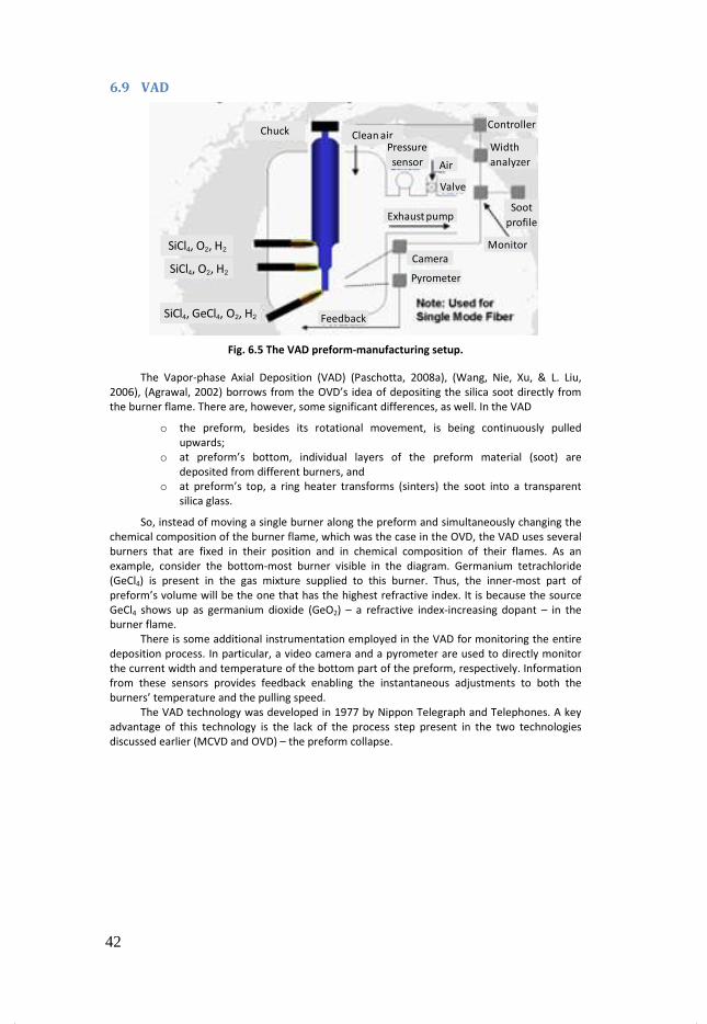
6.9 VAD
Fig. 6.5 The VAD preform-manufacturing setup.
The Vapor-phase Axial Deposition (VAD) (Paschotta, 2008a), (Wang, Nie, Xu, & L. Liu,
2006), (Agrawal, 2002) borrows from the OVD’s idea of depositing the silica soot directly from
the burner flame. There are, however, some significant differences, as well. In the VAD
o the preform, besides its rotational movement, is being continuously pulled
upwards;
o at preform’s bottom, individual layers of the preform material (soot) are
deposited from different burners, and
o at preform’s top, a ring heater transforms (sinters) the soot into a transparent
silica glass.
So, instead of moving a single burner along the preform and simultaneously changing the
chemical composition of the burner flame, which was the case in the OVD, the VAD uses several
burners that are fixed in their position and in chemical composition of their flames. As an
example, consider the bottom-most burner visible in the diagram. Germanium tetrachloride
(GeCl4) is present in the gas mixture supplied to this burner. Thus, the inner-most part of
preform’s volume will be the one that has the highest refractive index. It is because the source
GeCl4 shows up as germanium dioxide (GeO2) – a refractive index-increasing dopant – in the
burner flame.
There is some additional instrumentation employed in the VAD for monitoring the entire
deposition process. In particular, a video camera and a pyrometer are used to directly monitor
the current width and temperature of the bottom part of the preform, respectively. Information
from these sensors provides feedback enabling the instantaneous adjustments to both the
burners’ temperature and the pulling speed.
The VAD technology was developed in 1977 by Nippon Telegraph and Telephones. A key
advantage of this technology is the lack of the process step present in the two technologies
discussed earlier (MCVD and OVD) – the preform collapse.
Chuck Clean air
Monitor
Width
analyzer
SiCl4, O2, H2
SiCl4, O2, H2
SiCl4, GeCl4, O2, H2
Pressure
sensor Air
Valve
Soot
profile
Controller
Exhaust pump
Camera
Pyrometer
Feedback
42

6.10 Collapse
Fig. 6.6 The collapse process setup (top). It is applied to fiber preforms fabricated by means of
the MCVD and OVD technologies (bottom).
Both MCVD (IVD) and OVD preforms are collapsed at the process finish. At an elevated
temperature, i.e. at 2000°C as compared to 1600°C used during the deposition,
o preform diameter is reduced, thus void volume within the preform is removed;
o also preform material initially being porous, undergoes sintering into its final pore-
free form.
The collapsing process is usually carried out in helium atmosphere. This gas easily
permeates into the porous material and then, after the gas has exited the material during
sintering, the preform is practically pore-free.
A potentially significant disadvantage of the preform collapse lies in the possibility of the
creation of fiber centerline defects, i.e. deviations of the fiber core position from fiber’s
geometrical center. Performance of multimode fibers is especially sensitive to centerline defects
because these defects can severely increase the differential mode delay of a multimode fiber.
6.11 Double Crucible method
Fig. 6.7 The Double Crucible fiber-manufacturing setup.
A fiber manufacturing method that completely avoids the need of the preform fabrication,
is the Double Crucible method. In fact, it was invented and applied before the deposition-based
methods we have discussed earlier. In the Double Crucible method
o two containers (crucibles) keep the molten glass of two kinds: the first kind that
will create fiber core, and the second one intended for fiber cladding;
IVD
(MCVD)
OVD
diffusion area
external crucible opening: R = 0.5 to 1.5 mm
internal crucible opening: R = 0.5 to 1.5 mm
molten glass for fiber core
molten glass for fiber cladding
43

o the two materials come into contact with each other near the bottom of the
external crucible and they are then drawn in to the final fiber.
The Double Crucible method gives a considerable ease in selecting the fiber material
types. However, minimizing the material contamination to the extremely low levels attainable in
the deposition-based methods, becomes very difficult.
6.12 Preferred technologies and the biggest manufacturers
A statistical overviews related to the market (the leading manufacturers) and to the
manufacturing technologies of the telecommunication-grade silica-glass fibers are given in
tables Tab. 1.1 and Tab. 1.2, respectively.
Tab. 1.1 Silica-glass fiber biggest manufacturers.
The biggest manufacturers (1996)
Corning 6 mln km
AT&T (Lucent) 4 mln km
Siecor 2 mln km
Tab. 1.2 Silica-glass fiber preferred manufacturing technologies.
Technology
OVD 50% growing
MCVD 23% decreasing
VAD 23% growing
PCVD 2%
MCVD-plasma 2%
44

6.13 Attenuation of a PMMA step-index POF
Fig. 6.8 Attenuation of a PMMA step-index plastic optical fiber (after data of Toray Industries
Ltd.) (Schubert, 2003).
Around the 650 nm light wavelength, the preferred communication window of the
PMMA-based fibers is located. The attenuation is about 150 dB/km, which is a much higher
value than that characteristic of the silica-glass fibers. So high an attenuation makes plastic
fibers suitable for use in the short-range (several dozen meters) optical data-links only.
As stated above, plastic optical fibers cannot compete with silica-glass fibers in terms of
attenuation and also the maximum transmission speeds are relatively lower. Nevertheless,
plastic fibers possess several features that are found advantageous in the short-distance
computer networking and other applications (Paschotta, 2008b). The features are:
o transmission possible in the visible spectral range,
o relatively large fiber core diameters and high numerical aperture values enable an
easy coupling of light into the fiber, and
o plastic fiber installation is by far easier than is the case with silica-glass fibers;
o in particular, the installation can thus be done at significantly lower costs as
neither highly trained personnel nor expensive installation equipment is needed.
Of course, due to large core diameters, plastic fiber support the multimode propagation
only (which limits the maximum transmission speeds). On the other hand, larger core makes the
plastic fiber splicing notably more tolerant of any fiber positioning inaccuracies that may occur
during splicing. Moreover, thanks to specific mechanical properties of PMMA, plastic fiber
termination does not require any precise cleaving procedures (methods). Simple cutting is
sufficient.
Plastic fiber-based optical links were first introduced in the 1960s.
6.14 Plastic fiber fabrication technologies
Ideas of the two different technologies of plastic fiber fabrication are schematically
depicted in figure Fig. 6.9.
45
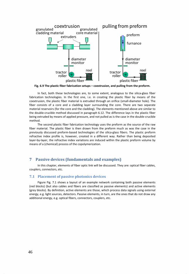
Fig. 6.9 The plastic fiber fabrication setups – coextrusion, and pulling from the preform.
In fact, both these technologies are, to some extent, analogous to the silica-glass fiber
fabrication technologies. In the first one, i.e. in creating the plastic fiber by means of the
coextrusion, the plastic fiber material is extruded through an orifice (small-diameter hole). The
fiber consists of a core and a cladding layer surrounding the core. There are two separate
material reservoirs (for the core and the cladding). The elements mentioned above are similar to
the double-crucible method discussed in paragraph 6.12. The difference lays in the plastic fiber
being extruded by means of applied pressure, and not pulled as is the case in the double-crucible
method.
The second plastic fiber fabrication technology uses the preform as the source of the raw
fiber material. The plastic fiber is then drawn from the preform much as was the case in the
previously discussed preform-based technologies of the silica-glass fibers. The plastic preform
refractive index profile is, however, created in a different way. Rather than being deposited
layer-by-layer, the refractive index variations are induced within the plastic preform volume by
means of a (chemical) process of the copolymerization.
7 Passive devices (fundamentals and examples)
In this chapter, elements of fiber optic link will be discussed. They are: optical fiber cables,
couplers, connectors, etc.
7.1 Placement of passive photonics devices
Figure Fig. 7.1 shows a layout of an example network containing both passive elements
(red blocks) (but also cables and fibers are classified as passive elements) and active elements
(grey blocks). By definition, active elements are those, which process data signals using external
energy, e.g. light sources, detectors. Passive elements, in turn, are the ones that do not draw any
additional energy, e.g. optical fibers, connectors, couplers, etc.
pulling from preform
diametermonitor
reeltractor
roller
granulated cladding material
granulated core material
coextrusion
plastic fiber plastic fiber
tractorroller
diametermonitor
extruders
furnance
preform
reel
46
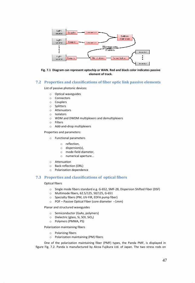
Fig. 7.1 Diagram can represent optochip or WAN. Red and black color indicates passive
7.2 Properties and classifications of
List of passive photonic devices:
o Optical waveguides
o Connectors
o Couplers
o Splitters
o Attenuators
o Isolators
o WDM and DWDM multiplexers and demultiplexers
o Filters
o Add-and-drop multiplexers
Properties and parameters:
o Functional parameters
o reflection,
o dispersion(s),
o mode
o numerical aperture...
o Attenuation
o Back-reflection (ORL)
o Polarization dependence
7.3 Properties and classifications of optical fibers
Optical fibers
o Single mode fibers standard e.g.
o Multimode fibers, 62.5/125, 50/125, G
o Specialty fibers (PM, UV
o POF – Passive Optical Fiber (core diameter
Planar and structured waveguides
o Semiconductor (GaAs, polymers)
o Dielectric (glass, Si, SOI, SiO
o Polymers (PMMA, PS)
Polarization maintaining fibers
o Polarizing fibers
o Polarization maintaining (PM) fibers
One of the polarization maintaining fiber (PMF) types, the Panda PMF, is displayed in
figure Fig. 7.2. Panda is manufactur
Fig. 7.1 Diagram can represent optochip or WAN. Red and black color indicates passive
element of track.
Properties and classifications of fiber optic link passive elements
List of passive photonic devices:
Optical waveguides
WDM and DWDM multiplexers and demultiplexers
drop multiplexers
Properties and parameters:
Functional parameters
reflection,
dispersion(s),
mode-field diameter,
numerical aperture...
reflection (ORL)
Polarization dependence
Properties and classifications of optical fibers
Single mode fibers standard e.g. G-652, SMF-28, Dispersion Shifted Fiber (DSF)
Multimode fibers, 62.5/125, 50/125, G-651
Specialty fibers (PM, UV-FIR, EDFA pump fiber)
Passive Optical Fiber (core diameter ∼1mm)
Planar and structured waveguides
Semiconductor (GaAs, polymers)
ric (glass, Si, SOI, SiO2)
Polymers (PMMA, PS)
Polarization maintaining fibers
Polarizing fibers
Polarization maintaining (PM) fibers
One of the polarization maintaining fiber (PMF) types, the Panda PMF, is displayed in
figure Fig. 7.2. Panda is manufactured by Alcoa Fujikura Ltd. of Japan. The two stress rods on
Fig. 7.1 Diagram can represent optochip or WAN. Red and black color indicates passive
fiber optic link passive elements
28, Dispersion Shifted Fiber (DSF)
One of the polarization maintaining fiber (PMF) types, the Panda PMF, is displayed in
ed by Alcoa Fujikura Ltd. of Japan. The two stress rods on
47

either side of the core induce birefringence in the core.
i.e. light will travel faster down one axis than the other.
the stress rods is the slow axis. Industry standard is to have connectors aligned to the slow axis.
Other PMF types are presented in figures Fig. 7.3, Fig. 7.4, and Fig. 7.5.
Fig. 7.2 Panda type of PMF (“Single Mode
Polarization Maintaining Fiber,” 2010)
Fig. 7.4 Over-Inner Clad
PM fibers are primarily used with:
o high performance transmission lasers and modulators in DWDM systems
at 10 Gb/s and above
o fiber lasers and Raman amplifiers
o polarization sensitive devices such as waveguide modulators
o sensor applications (particularly interferometric sensors)
7.4 Properties and classifications of optical fiber cables
Optical cable can contain a single optical fiber as well as multiple optical fibers as shown in
figures Fig. 7.6 and Fig. 7.7, respectively. Cables can also be classified according to how optical
fibers are placed (packed) within cable structure
cables) or loosely (loose-tube fiber optic cables). Other classifications consider the following
parameters:
o number of fibers
o Simplex
o Zip-cord (duplex)
o Multi-fiber
o technology
o tight-buffered
o loose tube
o field of application, working environm
o distribution, raiser, breakout;
o indoor, outdoor;
o short distance, long distance;
o military grade, oceanic, …
either side of the core induce birefringence in the core. This creates a slow axis and a fast axis,
i.e. light will travel faster down one axis than the other. The direction that bisects the core
Industry standard is to have connectors aligned to the slow axis.
Other PMF types are presented in figures Fig. 7.3, Fig. 7.4, and Fig. 7.5.
(“Single Mode
Polarization Maintaining Fiber,” 2010).
Fig. 7.3 Bow-tie (“Single Mode Polarization
Maintaining Fiber,” 2010)
Inner Clad Fig. 7.5 Over Core
PM fibers are primarily used with:
high performance transmission lasers and modulators in DWDM systems
at 10 Gb/s and above
fiber lasers and Raman amplifiers
polarization sensitive devices such as waveguide modulators
sensor applications (particularly interferometric sensors)
Properties and classifications of optical fiber cables
contain a single optical fiber as well as multiple optical fibers as shown in
figures Fig. 7.6 and Fig. 7.7, respectively. Cables can also be classified according to how optical
fibers are placed (packed) within cable structure – either tightly (tight-buff
tube fiber optic cables). Other classifications consider the following
cord (duplex)
fiber
buffered
loose tube
field of application, working environment
distribution, raiser, breakout;
indoor, outdoor;
short distance, long distance;
military grade, oceanic, …
This creates a slow axis and a fast axis,
The direction that bisects the core and
Industry standard is to have connectors aligned to the slow axis.
(“Single Mode Polarization
Maintaining Fiber,” 2010).
Fig. 7.5 Over Core
high performance transmission lasers and modulators in DWDM systems working
contain a single optical fiber as well as multiple optical fibers as shown in
figures Fig. 7.6 and Fig. 7.7, respectively. Cables can also be classified according to how optical
buffered fiber optic
tube fiber optic cables). Other classifications consider the following
48
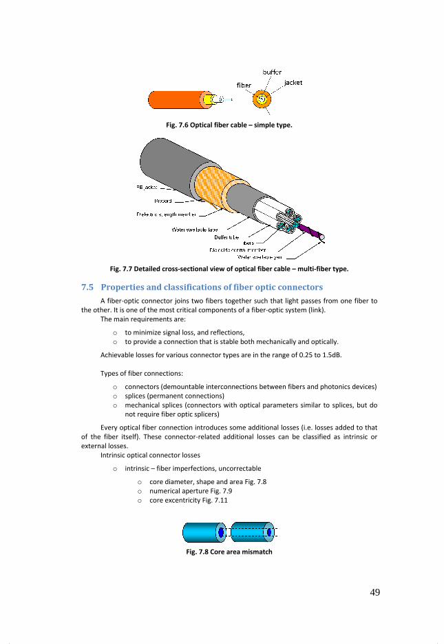
Fig. 7.6 Optical fiber cable
Fig. 7.7 Detailed cross
7.5 Properties and classifications of fiber optic connectors
A fiber-optic connector joins two fibers together such that light passes from one fiber to
the other. It is one of the most critical components of a fiber
The main requirements are:
o to minimize signal loss, and reflections,
o to provide a connection that is stable both mechanically and optically.
Achievable losses for various connector types are in the range of 0.25 to 1.5dB.
Types of fiber connections:
o connectors (demountable interconnections
o splices (permanent connections)
o mechanical splices (connectors with optical parameters similar to splices, but do
not require fiber optic splicers)
Every optical fiber connection introduces some additional losses (i.e.
of the fiber itself). These connector
external losses.
Intrinsic optical connector losses
o intrinsic – fiber imperfections, uncorrectable
o core diameter, shape and area Fig. 7.
o numerical aperture Fig. 7.9
o core excentricity Fig. 7.11
Fig. 7.6 Optical fiber cable – simple type.
Fig. 7.7 Detailed cross-sectional view of optical fiber cable – multi
classifications of fiber optic connectors
optic connector joins two fibers together such that light passes from one fiber to
the other. It is one of the most critical components of a fiber-optic system (link).
The main requirements are:
signal loss, and reflections,
to provide a connection that is stable both mechanically and optically.
Achievable losses for various connector types are in the range of 0.25 to 1.5dB.
Types of fiber connections:
connectors (demountable interconnections between fibers and photonics devices)
splices (permanent connections)
mechanical splices (connectors with optical parameters similar to splices, but do
not require fiber optic splicers)
Every optical fiber connection introduces some additional losses (i.e.
of the fiber itself). These connector-related additional losses can be classified as intrinsic or
Intrinsic optical connector losses
fiber imperfections, uncorrectable
core diameter, shape and area Fig. 7.8
numerical aperture Fig. 7.9
core excentricity Fig. 7.11
Fig. 7.8 Core area mismatch
multi-fiber type.
classifications of fiber optic connectors
optic connector joins two fibers together such that light passes from one fiber to
optic system (link).
to provide a connection that is stable both mechanically and optically.
Achievable losses for various connector types are in the range of 0.25 to 1.5dB.
between fibers and photonics devices)
mechanical splices (connectors with optical parameters similar to splices, but do
losses added to that
related additional losses can be classified as intrinsic or
49

Fig. 7.9 Numerical aperture mismatch
Figure Fig. 7.10 shows losses (attenuation) introduced by a larger
connection between fibers in the
increase in losses is already visible at small values of the core diameter difference. The
connection losses increase becomes linear for difference values of 6% and higher.
Fig. 7.10 Approximate loss in dB due to larger
numerical aperture difference for two butt
Fig. 7.11 Beam profile mismatch.
External optical connector losses
o external – connector design, minimized by careful
o longitudinal separation Fig. 7.12
o angular misalignment Fig. 7.14
o lateral offset Fig. 7.16
o end-face smoothness, flatness, perpendicularity
Connection attenuation in the function of separation (distance) between fiber
visible in figure Fig. 7.13. For high numerical aperture fibers, the strongest impact of the fiber
end separation is observed. Then, for lower numerical aperture fibers, the end separation
becomes less significant.
Fig. 7.9 Numerical aperture mismatch
Figure Fig. 7.10 shows losses (attenuation) introduced by a larger-to-smaller butt
connection between fibers in the function of core diameter difference. A significant, rapid
increase in losses is already visible at small values of the core diameter difference. The
connection losses increase becomes linear for difference values of 6% and higher.
loss in dB due to larger-to-smaller core diameter difference or fiber
numerical aperture difference for two butt-joined optical fibers.
Fig. 7.11 Beam profile mismatch.
External optical connector losses
connector design, minimized by careful design
longitudinal separation Fig. 7.12
angular misalignment Fig. 7.14
lateral offset Fig. 7.16
face smoothness, flatness, perpendicularity
Fig. 7.12 End separation.
Connection attenuation in the function of separation (distance) between fiber
visible in figure Fig. 7.13. For high numerical aperture fibers, the strongest impact of the fiber
end separation is observed. Then, for lower numerical aperture fibers, the end separation
smaller butt-join
function of core diameter difference. A significant, rapid
increase in losses is already visible at small values of the core diameter difference. The
connection losses increase becomes linear for difference values of 6% and higher.
smaller core diameter difference or fiber
joined optical fibers.
Connection attenuation in the function of separation (distance) between fiber ends is
visible in figure Fig. 7.13. For high numerical aperture fibers, the strongest impact of the fiber
end separation is observed. Then, for lower numerical aperture fibers, the end separation
50

Fig. 7.13 Variation of connecto
between two step-index air
Figure Fig. 7.15 shows how a relatively small difference in fiber ends’ angular position can
be a reason for noticeable losses. Misalignments as low as several degrees are enough to make
the connector loss reach 1dB.
Fig. 7.15 Connector power loss due to axial angular misalignment of the cores of two step
index optical fiber butt
From figure Fig. 7.17 we can find that shifting of fiber cores in opposite directions by 10%
(relative to fibers’ core diameter) gives rise to an attenuation of the order of 1dB. Obviously,
further increase in lateral core misalignment (di
even further.
Fig. 7.13 Variation of connector power loss with end-separation distance
index air-gap optical fiber ends for several values of numerical aperture
(NA) (Senior & Jamro, 2009).
Fig. 7.14 Angular misalignment.
Figure Fig. 7.15 shows how a relatively small difference in fiber ends’ angular position can
be a reason for noticeable losses. Misalignments as low as several degrees are enough to make
1dB.
Fig. 7.15 Connector power loss due to axial angular misalignment of the cores of two step
index optical fiber butt-joined ends (Senior & Jamro, 2009)
Fig. 7.16 Lateral offset
From figure Fig. 7.17 we can find that shifting of fiber cores in opposite directions by 10%
(relative to fibers’ core diameter) gives rise to an attenuation of the order of 1dB. Obviously,
further increase in lateral core misalignment (displacement) increases the connection losses
separation distance-to-diameter ratio
gap optical fiber ends for several values of numerical aperture
Figure Fig. 7.15 shows how a relatively small difference in fiber ends’ angular position can
be a reason for noticeable losses. Misalignments as low as several degrees are enough to make
Fig. 7.15 Connector power loss due to axial angular misalignment of the cores of two step-
(Senior & Jamro, 2009).
From figure Fig. 7.17 we can find that shifting of fiber cores in opposite directions by 10%
(relative to fibers’ core diameter) gives rise to an attenuation of the order of 1dB. Obviously,
splacement) increases the connection losses
51

Fig. 7.17 Connector power loss due to transverse (lateral) displacement of the cores of two
step-index optical fiber butt
7.6 Losses
Total value of optical losses in optical links consists of intrinsic losses introduced by link
elements, and of back-reflections at boundaries (interfaces) between two different media.
o Loss introduced by an element of optical link
where Pin is the optical power fed into the link, and P
output.
o Reflection losses
coefficients n1 and n
o Reflection coefficient expressed in dB is, by definition, the optical return loss (ORL)
– it describes what part of the signal returns toward the source.
rstR5o Attenuation caused by reflections (dB)
in fiber after reflection
Reflection losses at the material
o glass n = 1.5 R = 4% or
o GaAs n = 3.2 R = 27% or
o Si n = 4 R = 36% or
7.7 A simple f-o connector
In telecommunication systems as well as in other optical systems (setups) where
connections between fibers need to be utilized, it is important to maintain a possibly low level of
Fig. 7.17 Connector power loss due to transverse (lateral) displacement of the cores of two
index optical fiber butt-joined ends (Senior & Jamro, 2009)
Total value of optical losses in optical links consists of intrinsic losses introduced by link
reflections at boundaries (interfaces) between two different media.
by an element of optical link
uR5U = 10B/v �wxI�Gy
is the optical power fed into the link, and Pout is the optical power at link’s
Reflection losses – reflection coefficient at dielectric interface (refraction
and n2)
s = �<> − <- -�<> + <- -
Reflection coefficient expressed in dB is, by definition, the optical return loss (ORL)
it describes what part of the signal returns toward the source.
R5U = 10 log�s = 10B/v +�<> − <- -�<> + <- -,
Attenuation caused by reflections (dB) – describes what part of the signal remains
in fiber after reflection
u = 10B/v +1 − �<> − <- -�<> + <- -,
Reflection losses at the material-air interface– examples
R = 4% or -14dB
R = 27% or -6 dB
R = 36% or -4 dB
o connector
In telecommunication systems as well as in other optical systems (setups) where
connections between fibers need to be utilized, it is important to maintain a possibly low level of
Fig. 7.17 Connector power loss due to transverse (lateral) displacement of the cores of two
(Senior & Jamro, 2009).
Total value of optical losses in optical links consists of intrinsic losses introduced by link
reflections at boundaries (interfaces) between two different media.
(7.1)
is the optical power at link’s
reflection coefficient at dielectric interface (refraction
(7.2)
Reflection coefficient expressed in dB is, by definition, the optical return loss (ORL)
(7.3)
describes what part of the signal remains
(7.4)
In telecommunication systems as well as in other optical systems (setups) where
connections between fibers need to be utilized, it is important to maintain a possibly low level of
52

losses introduced by incorrect fiber positioning (fiber misalignments). At the same time, quick
and easy fiber connection preparation may also be a vital requirement. Many fiber connection
methods have been introduced and standardized. Figure Fig. 7.18 pre
methods of fiber connection making. It employs a fluid in which fiber ends are immersed
(immersion fluid) to decrease the refractive index difference between fiber core and the
surrounding medium (air). Back
this approach are difficulties in connecting / disconnecting the fibers quickly. Because of this, the
most frequently used solution is based on furnishing fiber ends with appropriate mechanical
connectors (see figure Fig. 7.19), which then allow to connect fibers in a repetitive, quick, and
precise manner.
Fig. 7.18 A simple f
Fig. 7.19 An actual fiber optic connector with a ferrule for fiber alignment
Connectors Basics, Styles, Trends,” 2010)
Subsequent figures below (Fig. 7.20
connector types. Figure Fig. 7.20 shows a connection in which air fills the gap between fiber
ends. It is not a recommended approach as it increases the back
losses resulting from geometrical reasons (i.e. from fiber cores’ di
relative position of the cores). The remaining figures present fiber connections in which the
physical contact (PC) approach is employed. Minimizing the air gap width leads to a decrease in
connection loss down to a level of about
(APC) connectors are considered.
losses introduced by incorrect fiber positioning (fiber misalignments). At the same time, quick
and easy fiber connection preparation may also be a vital requirement. Many fiber connection
methods have been introduced and standardized. Figure Fig. 7.18 presents one of the simplest
methods of fiber connection making. It employs a fluid in which fiber ends are immersed
(immersion fluid) to decrease the refractive index difference between fiber core and the
surrounding medium (air). Back-reflections at fibers’ ends are thus minimized. A disadvantage of
this approach are difficulties in connecting / disconnecting the fibers quickly. Because of this, the
most frequently used solution is based on furnishing fiber ends with appropriate mechanical
gure Fig. 7.19), which then allow to connect fibers in a repetitive, quick, and
Fig. 7.18 A simple f-o connector with hole for index-matching fluid.
Fig. 7.19 An actual fiber optic connector with a ferrule for fiber alignment
Connectors Basics, Styles, Trends,” 2010).
Subsequent figures below (Fig. 7.20 – Fig. 7.23) present some of the popular fiber optic
connector types. Figure Fig. 7.20 shows a connection in which air fills the gap between fiber
ends. It is not a recommended approach as it increases the back-reflection losses as well as
losses resulting from geometrical reasons (i.e. from fiber cores’ dimensions together with
relative position of the cores). The remaining figures present fiber connections in which the
physical contact (PC) approach is employed. Minimizing the air gap width leads to a decrease in
connection loss down to a level of about -40dB or even less when the angular physical contact
(APC) connectors are considered.
losses introduced by incorrect fiber positioning (fiber misalignments). At the same time, quick
and easy fiber connection preparation may also be a vital requirement. Many fiber connection
sents one of the simplest
methods of fiber connection making. It employs a fluid in which fiber ends are immersed
(immersion fluid) to decrease the refractive index difference between fiber core and the
ends are thus minimized. A disadvantage of
this approach are difficulties in connecting / disconnecting the fibers quickly. Because of this, the
most frequently used solution is based on furnishing fiber ends with appropriate mechanical
gure Fig. 7.19), which then allow to connect fibers in a repetitive, quick, and
matching fluid.
Fig. 7.19 An actual fiber optic connector with a ferrule for fiber alignment (“Fiber Optic
Fig. 7.23) present some of the popular fiber optic
connector types. Figure Fig. 7.20 shows a connection in which air fills the gap between fiber
reflection losses as well as
mensions together with
relative position of the cores). The remaining figures present fiber connections in which the
physical contact (PC) approach is employed. Minimizing the air gap width leads to a decrease in
0dB or even less when the angular physical contact
53

Fig. 7.20 Air Gap (“Fiber Optic Connectors
Basics, Styles, Trends,” 2010)
Fig. 7.22 PC (“Fiber Optic Connectors Basics,
Styles, Trends,” 2010)
7.7.1 Fiber-optic connector types
There are more than 100 types of fiber optic connectors. Main connector types are
described by TIA/EIA-604 standards. They are called
Standards (FOCIS) and are published with a document number format TIA
following FOCIS documents exist:
o FOCIS 1: Biconic
o FOCIS 2: ST
o FOCIS 3: SC
o FOCIS 4: FC
o FOCIS 5: MTP/MPO
o FOCIS 6: Panduit FJ
o FOCIS 7: 3M Volition
o FOCIS 8: Mini-MAC (Withdrawn)
o FOCIS 9: Mini MPO (Withdrawn)
o FOCIS 10: Lucent LC
o FOCIS 11: Siecor SCDC/SCQC (not yet approved)
o FOCIS 12: Siecor/Amp MT
o FOCIS 15: MF
o FOCIS 16: LSH (LX-
In fiber optic systems, the most frequently
Termination) and the SC (Subscriber Connector)
7.29, respectively. Both the dimensions (form factor) and the connection precision of most of
the fiber connector types are at acceptable levels. The ST connectors feature a circular casing
and the SC connectors use a rectangular one. Both the connector types use a bayonet
connection mechanism. Additionally, there are also the duplex
optical networks (links) in which the transmit and receive channels are separated (into separate
fibers). The duplex-type SC connectors make the installation of such optical links much less
error-prone. In figures below, there are several of the fiber optic connector
commonly used in telecommunication systems and in other optical systems setups. Dimension
and some construction details of the three most popular types are shown in figure Fig. 7.35.
(“Fiber Optic Connectors
yles, Trends,” 2010)
Fig. 7.21 Flat PC (“Fiber Optic Connectors
Basics, Styles, Trends,” 2010)
(“Fiber Optic Connectors Basics,
Styles, Trends,” 2010) Fig. 7.23 APC (“Fiber Optic Connectors Basics,
Styles, Trends,” 2010)
optic connector types
There are more than 100 types of fiber optic connectors. Main connector types are
standards. They are called Fiber Optic Connector Intermateability
and are published with a document number format TIA-604-
following FOCIS documents exist:
FOCIS 5: MTP/MPO
FOCIS 6: Panduit FJ
FOCIS 7: 3M Volition
MAC (Withdrawn)
FOCIS 9: Mini MPO (Withdrawn)
FOCIS 10: Lucent LC
FOCIS 11: Siecor SCDC/SCQC (not yet approved)
FOCIS 12: Siecor/Amp MT-RJ
-5)
In fiber optic systems, the most frequently used connectors were the ST (Single
Subscriber Connector) connectors visible in figures Fig. 7.30 and Fig.
7.29, respectively. Both the dimensions (form factor) and the connection precision of most of
at acceptable levels. The ST connectors feature a circular casing
and the SC connectors use a rectangular one. Both the connector types use a bayonet
connection mechanism. Additionally, there are also the duplex-type SC connectors dedicated for
works (links) in which the transmit and receive channels are separated (into separate
type SC connectors make the installation of such optical links much less
prone. In figures below, there are several of the fiber optic connector
commonly used in telecommunication systems and in other optical systems setups. Dimension
and some construction details of the three most popular types are shown in figure Fig. 7.35.
(“Fiber Optic Connectors
Basics, Styles, Trends,” 2010)
(“Fiber Optic Connectors Basics,
Styles, Trends,” 2010)
There are more than 100 types of fiber optic connectors. Main connector types are
Fiber Optic Connector Intermateability
-XX. To date, the
used connectors were the ST (Single
connectors visible in figures Fig. 7.30 and Fig.
7.29, respectively. Both the dimensions (form factor) and the connection precision of most of
at acceptable levels. The ST connectors feature a circular casing
and the SC connectors use a rectangular one. Both the connector types use a bayonet
type SC connectors dedicated for
works (links) in which the transmit and receive channels are separated (into separate
type SC connectors make the installation of such optical links much less
prone. In figures below, there are several of the fiber optic connector types most
commonly used in telecommunication systems and in other optical systems setups. Dimension
and some construction details of the three most popular types are shown in figure Fig. 7.35.
54

Fig. 7.24 SMA 905
Fig. 7.27 SMA 906
Fig. 7.30 ST
Fig. 7.33 Biconic
Fig. 7.35 The three main connector types.
For the PC-type (physical contact) connectors it
precisely held in a fixed position regardless of the ambient temperature changes or mechanical
vibrations. Otherwise, a correct contact between the connected fibers could not be ensured. In
the PC-type connectors, optical fiber is fastened inside a small, rigid tube called a ferrule.
Because fiber and ferrule diameters are precisely matched (and an adhesive is used), fiber’s
position is properly fixed (see figure Fig. 7.36). In figure Fig. 7.37, some statistical
concerning the FC-PC connector properties are given. As we can see in the respective diagrams,
values of the connection loss (insertion loss) and the back
level of -50dB and 0.15dB, respectively.
Fig. 7.25 HMS-10/HP
Fig. 7.26 FC, FC
Fig. 7.28 Diamond
Fig. 7.29 SC
Fig. 7.31 DIN 47256
Fig. 7.32 FDDI
Fig. 7.34 D-4
Fig. 7.35 The three main connector types.
type (physical contact) connectors it is of major importance that optical fiber is
precisely held in a fixed position regardless of the ambient temperature changes or mechanical
vibrations. Otherwise, a correct contact between the connected fibers could not be ensured. In
rs, optical fiber is fastened inside a small, rigid tube called a ferrule.
Because fiber and ferrule diameters are precisely matched (and an adhesive is used), fiber’s
position is properly fixed (see figure Fig. 7.36). In figure Fig. 7.37, some statistical
PC connector properties are given. As we can see in the respective diagrams,
values of the connection loss (insertion loss) and the back-reflection loss (return loss) are at the
50dB and 0.15dB, respectively.
Fig. 7.26 FC, FC/PC
Fig. 7.29 SC
Fig. 7.32 FDDI
is of major importance that optical fiber is
precisely held in a fixed position regardless of the ambient temperature changes or mechanical
vibrations. Otherwise, a correct contact between the connected fibers could not be ensured. In
rs, optical fiber is fastened inside a small, rigid tube called a ferrule.
Because fiber and ferrule diameters are precisely matched (and an adhesive is used), fiber’s
position is properly fixed (see figure Fig. 7.36). In figure Fig. 7.37, some statistical data
PC connector properties are given. As we can see in the respective diagrams,
reflection loss (return loss) are at the
55

Fig. 7.36 D
Fig. 7.37 Return and insertion losses for FC/PC (Fiber Pigtail/Patchcord) joint.
7.7.2 Small Form Factor (SFF) connectors
In telecommunication systems of large integration, dimensions of single connector plays a
key role in minimizing the size of fiber optic distribution box. Standard connector types are
relatively big compared to a single fiber or to other switching elements. Thus, these are the
connector dimensions, which often determine the amount of space needed to ac
optical system.
Comparison of standard and small form factor (SFF) connector dimensions (FC and LC) are
shown in Fig. 7.38.
Fig. 7.36 Details of ferrule construction (FC-PC).
Fig. 7.37 Return and insertion losses for FC/PC (Fiber Pigtail/Patchcord) joint.
Small Form Factor (SFF) connectors
In telecommunication systems of large integration, dimensions of single connector plays a
in minimizing the size of fiber optic distribution box. Standard connector types are
relatively big compared to a single fiber or to other switching elements. Thus, these are the
connector dimensions, which often determine the amount of space needed to ac
Comparison of standard and small form factor (SFF) connector dimensions (FC and LC) are
Fig. 7.37 Return and insertion losses for FC/PC (Fiber Pigtail/Patchcord) joint.
In telecommunication systems of large integration, dimensions of single connector plays a
in minimizing the size of fiber optic distribution box. Standard connector types are
relatively big compared to a single fiber or to other switching elements. Thus, these are the
connector dimensions, which often determine the amount of space needed to accommodate an
Comparison of standard and small form factor (SFF) connector dimensions (FC and LC) are
56

Fig. 7.38 From the left: SC-DC, LC, MT-RJ, Duplex S.C.(for comparison), Volition, and Opti-Jack
(“Fiber Optic Connector Reference,” 2010).
7.7.3 Connector’s technology
In order to ensure the optical fiber is maintained by a connector in a fixed, precisely
adjusted position regardless of ambient conditions (temperature, humidity, etc.), much care
must be taken during the technological process of the connector production (connector
assembly process). In the first two process steps, optical fiber is fastened to the ferrule hole with
an adhesive. Precision and quality of adhesion will then be a decisive factor of whether the fiber
position inside the connector is maintained despite varying environmental conditions over an
extended period of time. In subsequent steps, polishing of fiber end is performed. Quality of
polishing affects the back-reflection loss of the final product. International standards precisely
define the parameter values that must be attained by a connector in order to avoid the creation
of an excessive air gap between the fibers (fiber ends) being connected.
The connector assembly process steps are listed below:
o Epoxy glued, cured in room temperature (overnight) or in ovens (minutes)
o HotMelt (3M) glue already in place, softened during installation
o Prepolished, ready for splicing (UniCam® )
o Crimp and polish (LightCrimp AMP)
7.8 Mechanical splices
Besides fiber optic connectors, there are also the so called mechanical splices that can be
used for connecting the optical fibers. Thanks to a rigid structure, mechanical splices are able to
stably hold fibers at their prescribed positions, thus maintaining efficient fiber-to-fiber light
coupling. Unlike the standard fiber optic splices, mechanical fiber optic splices are reusable. They
are also easy to install and, consequently, lower costs and shorter installation times are involved.
Mechanical splice disadvantages are losses, especially the back reflections, being significantly
higher than that characteristic of fiber optic connectors. It is because of a thicker air gap present
in mechanical splices. Also not all commercially available mechanical splice solutions ensure
sufficient connection stability under varying environmental conditions.
57

Fig. 7.39 Elastomeric Lab Splice. Allows
hundreds of uses.
Fig. 7.41 AMP Corelink. sl 0.15dB on 125
fiber.
Fig. 7.42 Siemon Ultra Splice. sl
lbs.
7.9 Other types of optical link passive elements
7.9.1 Technology and construction of optical splitters/ couplers
Optical splitters are devices that are used
or more optical signals. In telecommunication systems, splitters are employed when optical
signal is supposed to be delivered to multiple locations. Device performing an inverse function, is
the optical coupler in which optical signals coming from multiple fibers are merged and then fed
into a single output fiber. Both the devices share a common principle of operation
evanescent coupling. Optical fiber modal field is not completely bounded within fiber
rather extends into fiber cladding as well. The part of modal field outside the core (field tails) is
an evanescent wave (i.e. its power vanishes exponentially along fiber radius). Now, when cores
of two different fibers are brought together clos
will take place due to tails of both the modal fields each one penetrating the opposite fiber’s
core. It is how evanescent coupling works and, in fact, how the discussed splitters and couplers
are constructed. Some more construction (fabrication) details are discussed below.
One of the methods of fiber optic coupler fabrication is described in figure Fig. 7.44. Two
fibers are overlapped after their claddings have been partially removed by polishing.
Fig. 7.39 Elastomeric Lab Splice. Allows
hundreds of uses.
Fig. 7.40 3M Fibrlok. il<0.2dB,
-35dB. V-groove technology
Thermal stability of -400°°°°C to 800
insertion loss, fr - fiber retention, orl
return loss.
Fig. 7.41 AMP Corelink. sl 0.15dB on 125µµµµm
Fig. 7.42 Siemon Ultra Splice. sl -0.2dB, fr > 2 Fig. 7.43 Corning Cable System CAM Splice.
0.5dB.
Other types of optical link passive elements
Technology and construction of optical splitters/ couplers
Optical splitters are devices that are used to divide a single optical signal (beam) into two
or more optical signals. In telecommunication systems, splitters are employed when optical
signal is supposed to be delivered to multiple locations. Device performing an inverse function, is
pler in which optical signals coming from multiple fibers are merged and then fed
into a single output fiber. Both the devices share a common principle of operation
evanescent coupling. Optical fiber modal field is not completely bounded within fiber
rather extends into fiber cladding as well. The part of modal field outside the core (field tails) is
an evanescent wave (i.e. its power vanishes exponentially along fiber radius). Now, when cores
of two different fibers are brought together close enough, gradual exchange of optical power
will take place due to tails of both the modal fields each one penetrating the opposite fiber’s
core. It is how evanescent coupling works and, in fact, how the discussed splitters and couplers
me more construction (fabrication) details are discussed below.
One of the methods of fiber optic coupler fabrication is described in figure Fig. 7.44. Two
fibers are overlapped after their claddings have been partially removed by polishing.
<0.2dB, fr>7.75 lbs. orl
groove technology - no epoxy.
C to 800°°°°C il -
fiber retention, orl - optical
Fig. 7.43 Corning Cable System CAM Splice.
to divide a single optical signal (beam) into two
or more optical signals. In telecommunication systems, splitters are employed when optical
signal is supposed to be delivered to multiple locations. Device performing an inverse function, is
pler in which optical signals coming from multiple fibers are merged and then fed
into a single output fiber. Both the devices share a common principle of operation – the
evanescent coupling. Optical fiber modal field is not completely bounded within fiber core, it
rather extends into fiber cladding as well. The part of modal field outside the core (field tails) is
an evanescent wave (i.e. its power vanishes exponentially along fiber radius). Now, when cores
e enough, gradual exchange of optical power
will take place due to tails of both the modal fields each one penetrating the opposite fiber’s
core. It is how evanescent coupling works and, in fact, how the discussed splitters and couplers
me more construction (fabrication) details are discussed below.
One of the methods of fiber optic coupler fabrication is described in figure Fig. 7.44. Two
fibers are overlapped after their claddings have been partially removed by polishing.
58

Fig. 7.44 Steps in fabricating a polished fiber optic coupler.
Figure Fig. 7.45 shows a different method of fiber optic coupler fabrication. Here, core
proximity is achieved by means of thermal fusion.
s
Fig. 7.45 Thermally fusing couplers.
7.9.2 Polarization controllers
A tri-waveplate controller (figure Fig. 7.46) consists of a half-wave plate sandwiched
between two quarter-wave plates, with all three plates free to rotate independently about the
optical beam. The first quarter-wave plate converts the light beam of generally elliptical
polarization state into a linear polarization state. The half-wave plate then rotates the linear
polarization state of the optical beam to a desired orientation. Finally, the second quarter-wave
plate converts the linear polarization into any desired polarization state. The wave plates are
sensitive to light beam’s wavelength because a wave plate is half-wave (or quarter wave) only if
the relative retardation between the slow and fast axes is half (or quarter) of the optical beam’s
wavelength. Consequently, the tri-waveplate controller is inherently sensitive to wavelength.
59

Fig. 7.46 Polarization controllers – classical solution (“Harness Optical Polarization with Ease
and Elegance,” 2008).
A Lefevre controller (figure Fig. 7.47) operates on the same physical principle as the tri-
waveplate controller, except that the waveplates are made of fiber coils and the signal beam
does not travel in free space. However, it also shares the same limitation of wavelength
sensitivity.
Fig. 7.47 Polarization controllers – fiber solution (“Harness Optical Polarization with Ease and
Elegance,” 2008).
The Yao (commercially known as PolaRITETM
) controller (figure Fig. 7.48) uses a rotatable
fiber squeezer to create a waveplate of variable retardation and can convert an arbitrary
polarization state into any desired polarization state. It operates in principle like the Babinet-
Soleil compensator and shares the same advantage of wavelength insensitivity.
60

Fig. 7.48 Polarization controllers – fiber solution (“Harness Optical Polarization with Ease and
Elegance,” 2008) (“Polarization Controller, Manual,” 2010).
7.9.3 Fiber Bragg gratings in optical communications
In telecommunication systems (especially the (D)WDM ones) there arises a need for
selecting a desired wavelength out of multiple wavelengths that are simultaneously present in
light beam. Such an operation is usually realized by means of an optical fiber in which Bragg
grating of precisely controlled (designed) properties has been induced. The Bragg grating acts as
an optical filter that extracts light of the desired wavelength(-s) from the entire optical
transmission carried by an optical link. What is also important, other frequencies present in the
transmission, are passed through the grating unaffected (see figure Fig. 7.49).
Fig. 7.49 Fiber-optic Bragg grating (DWDM filter) (“Basics of Fiber Bragg Grating,” 2010)
(“Harness Optical Polarization with Ease and Elegance,” 2008).
7.9.4 Lenses
Geometrical path along which the light beam propagates, depends on what is the spatial
distribution of the propagation medium refractive index. For example, graded-index (GRIN)
lenses (figure Fig. 7.50) are often used to focus light. Thanks to the refractive index varying along
the GRIN lens radius, it is possible to make the output lightwave focus at a prescribed distance
behind the lens end-facet (the total length of the lens also needs to be properly adjusted).
Another example is a telecommunication graded-index fiber (figure Fig. 7.51). The refractive
index reaches its maximum value at fiber center (fiber axis), and it gradually decreases along
fiber radius. This type of the refractive index transversal profile, if designed and manufactured
properly, allows light beams within the fiber to propagate along sinusoidal paths. This, in turn,
can significantly decrease the light beams’ interaction with fiber cladding. In multimode step-
index fibers, excessive level of such an interaction severely limits the maximum transmission
speeds attainable. This problem will be discussed in greater detail in the chapter devoted to
optical fiber dispersion.
61

Fig. 7.50 Gradient index (GRIN) lenses, refractive index distribution
7.9.5 Multiplexers
In the WDM telecommunication systems, where many lightwave frequencies are
transmitted in a single physical channel (single fiber)
signals form multiple physical channels (fibers) and couple them into a single output channel
(fiber). Devices of the functionality described, are called the optical multiplexers. The working
principle of an optical multiplexer is schematically shown in figure Fig. 7.52. Probably the
simplest device that can realize the optical multiplexer (and demultiplexer) functionality, is the
prism. However, prism-based solutions are not utilized in fiber optic telecommunicati
because spatial separation of light beams that only slightly differ in frequency, is not effective
enough when it is realized with the prism. Instead, the so called optical add/drop multiplexers
(OADMs) are utilized. Their construction is usuall
schematically depicted in figure Fig. 7.53. Generally speaking, optical add/drop multiplexers
enable the extraction (the “drop” function) of the desired optical frequencies (wavelengths), i.e.
WDM data channels, from the entire optical transmission, i.e. from all the WDM data channels
being transmitted. Then, if such a functionality is needed, an OADM allows another data streams
to be launched (the “add” function) into the “empty” (previously dropped) WDM channel
Fig. 7.50 Gradient index (GRIN) lenses, refractive index distribution
Fig. 7.51 Microlense in fiber.
In the WDM telecommunication systems, where many lightwave frequencies are
transmitted in a single physical channel (single fiber), devices are needed which collect optical
signals form multiple physical channels (fibers) and couple them into a single output channel
(fiber). Devices of the functionality described, are called the optical multiplexers. The working
al multiplexer is schematically shown in figure Fig. 7.52. Probably the
simplest device that can realize the optical multiplexer (and demultiplexer) functionality, is the
based solutions are not utilized in fiber optic telecommunicati
because spatial separation of light beams that only slightly differ in frequency, is not effective
enough when it is realized with the prism. Instead, the so called optical add/drop multiplexers
(OADMs) are utilized. Their construction is usually based on optical fibers. OADM operation is
schematically depicted in figure Fig. 7.53. Generally speaking, optical add/drop multiplexers
enable the extraction (the “drop” function) of the desired optical frequencies (wavelengths), i.e.
from the entire optical transmission, i.e. from all the WDM data channels
being transmitted. Then, if such a functionality is needed, an OADM allows another data streams
to be launched (the “add” function) into the “empty” (previously dropped) WDM channel
Fig. 7.50 Gradient index (GRIN) lenses, refractive index distribution
In the WDM telecommunication systems, where many lightwave frequencies are
, devices are needed which collect optical
signals form multiple physical channels (fibers) and couple them into a single output channel
(fiber). Devices of the functionality described, are called the optical multiplexers. The working
al multiplexer is schematically shown in figure Fig. 7.52. Probably the
simplest device that can realize the optical multiplexer (and demultiplexer) functionality, is the
based solutions are not utilized in fiber optic telecommunications. It is
because spatial separation of light beams that only slightly differ in frequency, is not effective
enough when it is realized with the prism. Instead, the so called optical add/drop multiplexers
y based on optical fibers. OADM operation is
schematically depicted in figure Fig. 7.53. Generally speaking, optical add/drop multiplexers
enable the extraction (the “drop” function) of the desired optical frequencies (wavelengths), i.e.
from the entire optical transmission, i.e. from all the WDM data channels
being transmitted. Then, if such a functionality is needed, an OADM allows another data streams
to be launched (the “add” function) into the “empty” (previously dropped) WDM channels.
62

Fig. 7.52 Devices that allow mixing several (up to 100s) wavelength channels in one fiber.
Fig. 7.53 Adding and dropping information into optical transmission path without disturbing
other channels.
An example of a fabricated DWDM multiplexer structure is visible in figure Fig. 7.54. The
DWDM channel multiplexing is performed in the following way. Four input planar waveguides
supply the optical signals to a free-space propagation area where all the signals interfere. The
resulting optical field enters an array of specially designed planar waveguides – neighboring
waveguides differ in length by ΔL. Thus, optical signals propagating along these waveguides
acquire different phase shifts before they enter the second free-space propagation area. The
phase shifts are adjusted (by an appropriate selection of ΔL) so that optical interference in the
second area results in the desired optical frequencies being coupled to their respective output
waveguides.
63

Fig. 7.54 Arrayed waveguide grating with stress releas
compensation. The SiO2 -on
Wildermuth, Lanker, Hunzi
8 Active devices – telecom sources and detectors
8.1 List of active photonic devices
1. Lasers and light emitting diodes
2. Detectors
3. Amplifiers
4. Modulators
5. Switches
6. Tunable filters
+ Passive devices
Σ. Integrated optoelectronic circuits
8.2 Waveguide light sources
In fiber-optic telecommunications, the most frequently used light sources are
electroluminescence diodes (LEDs) and lasers. Their general classification is given below.
Light emitting diodes (LED)
o surface emitting diodes
o edge emitting diodes
o RCE (resonance cavity enhanced) LEDs
Lasers (LD)
o FP (Fabry-Perot) lasers
o DFB (distributed feedback) and DBR (distributed Bragg reflector) lasers
o VCSEL (vertical cavity surface emitting) lasers
o waveguide lasers
Fig. 7.54 Arrayed waveguide grating with stress release grooves for birefringence
on-Si waveguide cross section is shown in the inset
Wildermuth, Lanker, Hunziker, & Melchior, 1999).
telecom sources and detectors
List of active photonic devices
1. Lasers and light emitting diodes
optoelectronic circuits
Waveguide light sources - classification
optic telecommunications, the most frequently used light sources are
electroluminescence diodes (LEDs) and lasers. Their general classification is given below.
s (LED)
surface emitting diodes
edge emitting diodes
RCE (resonance cavity enhanced) LEDs
Perot) lasers
DFB (distributed feedback) and DBR (distributed Bragg reflector) lasers
VCSEL (vertical cavity surface emitting) lasers
e grooves for birefringence
Si waveguide cross section is shown in the inset (Nadler,
optic telecommunications, the most frequently used light sources are
electroluminescence diodes (LEDs) and lasers. Their general classification is given below.
DFB (distributed feedback) and DBR (distributed Bragg reflector) lasers
64
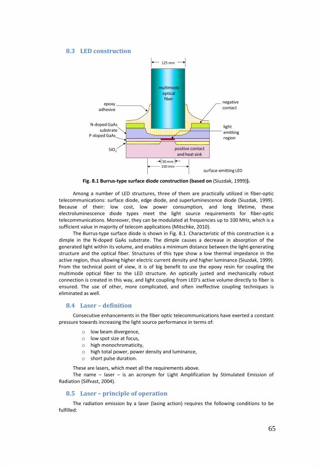
8.3 LED construction
Fig. 8.1 Burrus-type surface diode construction (based on (Siuzdak, 1999)).
Among a number of LED structures, three of them are practically utilized in fiber-optic
telecommunications: surface diode, edge diode, and superluminescence diode (Siuzdak, 1999).
Because of their: low cost, low power consumption, and long lifetime, these
electroluminescence diode types meet the light source requirements for fiber-optic
telecommunications. Moreover, they can be modulated at frequencies up to 100 MHz, which is a
sufficient value in majority of telecom applications (Mitschke, 2010).
The Burrus-type surface diode is shown in Fig. 8.1. Characteristic of this construction is a
dimple in the N-doped GaAs substrate. The dimple causes a decrease in absorption of the
generated light within its volume, and enables a minimum distance between the light-generating
structure and the optical fiber. Structures of this type show a low thermal impedance in the
active region, thus allowing higher electric current density and higher luminance (Siuzdak, 1999).
From the technical point of view, it is of big benefit to use the epoxy resin for coupling the
multimode optical fiber to the LED structure. An optically justed and mechanically robust
connection is created in this way, and light coupling from LED’s active volume directly to fiber is
ensured. The use of other, more complicated, and often ineffective coupling techniques is
eliminated as well.
8.4 Laser – definition
Consecutive enhancements in the fiber optic telecommunications have exerted a constant
pressure towards increasing the light source performance in terms of:
o low beam divergence,
o low spot size at focus,
o high monochromaticity,
o high total power, power density and luminance,
o short pulse duration.
These are lasers, which meet all the requirements above.
The name – laser – is an acronym for Light Amplification by Stimulated Emission of
Radiation (Silfvast, 2004).
8.5 Laser – principle of operation
The radiation emission by a laser (lasing action) requires the following conditions to be
fulfilled:
125 mm
epoxy
adhesive
negative
contact
light
emitting
region
positive contact
and heat sink
surface-emitting LED
50 mm
150 mm
N-doped GaAs
substrate
P-doped GaAs
SiO2
multimode
optical
fiber
65

1. Presence of metastable states (ms)
2. Energy pumping (to put atom into ms)
3. Population inversion
4. Stimulated emission
5. Optical feedback (FB)
8.6 Population inversion
There are three basic processes in the light-matter interaction. All of them result in a
change of the quantum state of an atom, ion or particle. The processes are:
o absorption,
o spontaneous emission,
o stimulated emission.
In absorption, a photon becomes absorbed by an atom, and the atom transits from its
basis state to an excited state. The second process, spontaneous emission, is a spontaneous
transition of an atom from a higher-energy state to a lower-energy state. This transition results
in a photon being emitted by the atom (photon emission). Properties of the emitted photon are
completely uncorrelated (incoherent light is generated) (Siuzdak, 1999). Finally, the last light-
matter interaction process, stimulated emission, also includes the photon emission and atom’s
transition from a higher- to a lower-energy state. In this process, however, the transition does
not occur spontaneously. It is instead triggered by an external photon whose energy, which is
important, equals the energy difference between the higher- and the lower-energy state.
Fig. 8.2 Absorption, emission and illustration of population inversion (based on (Siuzdak,
1999)).
8.7 Optical feedback – Fabry-Perot resonator
For exciting the atoms’ electrons from their basis state (lowest-energy level) to an excited
state (higher-energy level), a strong external light source is used, the so called optical pump.
Pump’s light wavelength must be chosen appropriately. Within the laser’s active volume,
spontaneous emission results in light amplification, i.e. in an increase in the number of photons
having identical properties. Besides the amplification, for the lasing action to take place also an
appropriate feedback mechanism is needed. A positive-feedback setup most commonly used in
lasers is the Fabry-Perot cavity. It is usually realized by means of two mirrors M1, M2 placed at
opposite ends of the active medium. The light undergoes multiple reflections off the mirrors,
and additional photons are generated each time light passes through the active medium. The M2
mirror is a semitransparent one, thus allowing part of the amplified radiation (light) to exit the
cavity. It is important to note that the positive feedback only occurs when lightwaves that
propagate in the same direction, after multiple reflections are in phase i.e. interfere
constructively (lightwaves being out of phase would cancel each other, would interfere
destructively) (Siuzdak, 1999).
population
n1
n2
absorption, n1 > n2
population
n1
n2
amplification, n2 > n1
66

Fig. 8.3 Fabry-Perot resonator serving as an optical feedback element for the laser.
8.8 Lasers – classification
Considering the lasing medium types, lasers can be divided as follows:
1. Solid state lasers: lasing medium placed in a solid state matrix. Examples:
neodymium laser-YAG <Yttrium Aluminum Garnet> 1.064 μm, ruby laser
2. Gas lasers
a. Atomic He-Ne, 632.8 nm
b. Molecular CO2 , 10.6 mm
c. Ion Ar+, main wavelengths 488, 514 nm
d. Excimer (ionized fluorides of noble gases) UV sources
3. Dye lasers (liquid) Liquid solution of organic dye. Possible wavelength tuning (VIS,
NIR). Tuning range depends on selected dye – for Rodamine 6G � 0.570 - 0.650
μm.
4. Semiconductor lasers (LD)
8.9 Pumping in semiconductor lasers: p-n junction current
In semiconductors, the population inversion, which is needed for the lasing action to
occur, is attained by the injection of electrons into the conduction band. It can be realized in a
p-n junction by means of a strong doping of both the materials having different conduction
types. At high densities of injected carriers (electrons), an active region in the junction is formed
where the population inversion takes place. Stimulated emission of radiation is possible there.
Note that laser diodes (semiconductor lasers) can only be made of semiconductors possessing
the direct bandgap (direct energy gap). They are e.g.: GaAs, InGaAs, GaN, InGaAsP. Lasers can
not be made of indirect bandgap semiconductors, like e.g.: Si, Ge.
Optical pump
Optical pump
Laser
beam
M1M2
67

Fig. 8.4 Recombination of electron-hole pair and emission of a photon.
8.10 Simple semiconductor laser (homostructure)
Early semiconductor lasers were based on the homojunction structure and could only
work at low temperatures. The p-n junction was created within a single crystal of a
semiconductor material. Cavity mirrors in such lasers are usually created as cleavage planes of
the semiconductor crystal or as properly polished and sputtered surfaces of the active layer. Low
dimensions and a weakly defined generation volume result in a relatively low coherence of the
emitted radiation.
Fig. 8.5 Cross-section of a homojunction laser diode (based on (Mitschke, 2010)).
8.11 Heterostructure laser (cross section)
Heterojunction (heterostructure junction) is a junction made of semiconductors having
different energy gaps (bandgaps), like e.g.: GaAs and AlxGa1-xAs, where x is a molar fraction
describing the aluminum content. In heterostructure junctions that contain semiconductors of
the same conductivity types (n-n or p-p), density of minority carriers can be reduced. This
enables the radiative recombination to be bound within a small active volume. In turn,
heterojunctions consisting of different conduction-type semiconductors show better carrier
injection efficiency.
An example of the heterojunction laser is a laser incorporating the so called buried layer
(BH – buried heterostructure). In this case, light is guided within a waveguide formed along the
junction. The waveguide is created by introducing step-like variations in semiconductor’s
refractive index. The refractive index difference of the order of 0.2 – 0.3 strongly bounds the
emitted mode, which leads to a high stability of mode’s spatial distribution, and consequently to
the generation of only one lateral mode in this type of laser structures (Siuzdak, 1999).
Conduction band
Valence band
n type p typejunction n type p typejunction
Ele
ctro
n e
ne
rgy
hνEg
Conduction band
Valence band
+-
Input current
Junction
Cleaved
mirror
Output
radiation
68
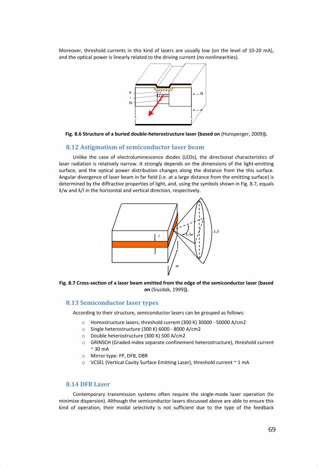
Moreover, threshold currents in this kind of lasers are usually low (on the level of 10-20 mA),
and the optical power is linearly related to the driving current (no nonlinearities).
Fig. 8.6 Structure of a buried double-heterostructure laser (based on (Hunsperger, 2009)).
8.12 Astigmatism of semiconductor laser beam
Unlike the case of electroluminescence diodes (LEDs), the directional characteristics of
laser radiation is relatively narrow. It strongly depends on the dimensions of the light-emitting
surface, and the optical power distribution changes along the distance from the this surface.
Angular divergence of laser beam in far field (i.e. at a large distance from the emitting surface) is
determined by the diffractive properties of light, and, using the symbols shown in Fig. 8.7, equals
λ/w and λ/l in the horizontal and vertical direction, respectively.
Fig. 8.7 Cross-section of a laser beam emitted from the edge of the semiconductor laser (based
on (Siuzdak, 1999)).
8.13 Semiconductor laser types
According to their structure, semiconductor lasers can be grouped as follows:
o Homostructure lasers, threshold current (300 K) 30000 - 50000 A/cm2
o Single heterostructure (300 K) 6000 - 8000 A/cm2
o Double heterostructure (300 K) 500 A/cm2
o GRINSCH (Graded-index separate confinement heterostructure), threshold current
~ 30 mA
o Mirror type: FP, DFB, DBR
o VCSEL (Vertical Cavity Surface Emitting Laser), threshold current ~ 1 mA
8.14 DFB Laser
Contemporary transmission systems often require the single-mode laser operation (to
minimize dispersion). Although the semiconductor lasers discussed above are able to ensure this
kind of operation, their modal selectivity is not sufficient due to the type of the feedback
P
N
N
n
i
l λ /wλ /l
w
69
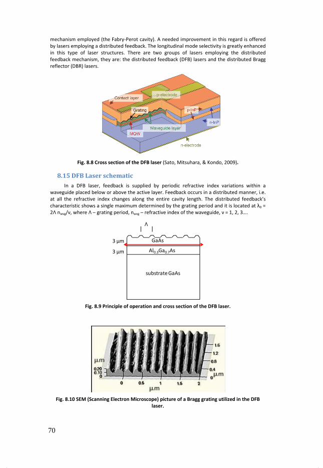
mechanism employed (the Fabry-Perot cavity). A needed improvement in this regard is offered
by lasers employing a distributed feedback. The longitudinal mode selectivity is greatly enhanced
in this type of laser structures. There are two groups of lasers employing the distributed
feedback mechanism, they are: the distributed feedback (DFB) lasers and the distributed Bragg
reflector (DBR) lasers.
Fig. 8.8 Cross section of the DFB laser (Sato, Mitsuhara, & Kondo, 2009).
8.15 DFB Laser schematic
In a DFB laser, feedback is supplied by periodic refractive index variations within a
waveguide placed below or above the active layer. Feedback occurs in a distributed manner, i.e.
at all the refractive index changes along the entire cavity length. The distributed feedback’s
characteristic shows a single maximum determined by the grating period and it is located at λ0 =
2Λ nwvg/ν, where Λ – grating period, nwvg – refractive index of the waveguide, ν = 1, 2, 3….
Fig. 8.9 Principle of operation and cross section of the DFB laser.
Fig. 8.10 SEM (Scanning Electron Microscope) picture of a Bragg grating utilized in the DFB
laser.
substrate GaAs
Al0.3Ga0.7As
GaAs3 μm
3 μm
Λ
70

8.16 VCSEL Laser
The next semiconductor laser structure utilized in fiber-optic telecommunications is the
one employing a vertical optical resonator – the Vertical Cavity Surface Emitting Laser (VCSEL).
The VCSEL structure is completely different from that of the classical Fabry-Perot resonator-
based structures. The active layer is bound from top and from bottom with multilayer reflectors.
The multilayer reflectors act as selective mirrors just like mirrors used in the DBR lasers. In such
a structure, the cavity (resonator) is very short, usually shorter than the emitted light
wavelength, and this enforces the single-mode operation of the laser (Mitschke, 2010). Thanks
to a small volume of the resonant cavity, VCSELs attain low threshold current levels and high
efficiency. Vertical emission is a significant advantage as well. In addition, VCSEL lasers
production costs are relatively low.
Fig. 8.11 Cross section of the vertical cavity surface emitting laser (VCSEL) (Giovanni, 2010).
8.17 Beam profiles of VCSEL and edge-emitting lasers
Fig. 8.12 Comparison of cross sections of the beams emitted from the edge emitting laser (a)
and the VCSEL (b) (based on (Milligan, 2004)).
VCSEL lasers generate a light beam of more advantageous geometrical profile than that of
beams generated by the edge lasers. It should be noted that the edge laser beam profile is
71

elliptical, and shows an angular divergence strongly dependent on the light-emitting surface
dimensions. In VCSEL lasers, due to a circular internal aperture, the propagating light beam has a
conic shape. The cone’s base is circular and the divergence angle has a value of about 5°.
8.18 Optical Laser parameters
Lasers are commonly characterized with the following optical parameters:
o center wavelength,
o FWHM, spectral line spread,
o beam divergence.
8.19 Center wavelength and FWHM
Fig. 8.13 Modal spectrum of light emitted by edge emitting laser. Shown are FWHM and the
center wavelength(“Illustrated Fiber-Optics Glossary,” 2010).
Center Wavelength: In a laser, the nominal value central operating wavelength. It is the
wavelength defined by a peak mode measurement where the effective optical power resides -
Fig. 8.13. In an LED, the average of the two wavelengths measured at the half amplitude points
of the power spectrum (“Illustrated Fiber-Optics Glossary,” 2010).
8.20 Laser Classifications (Safety Classes)
Laser classification according to the operational safety is (DeCusatis, 2008):
o Class I - lasers cannot emit laser radiation at known hazard levels.
o Class I.A. - special designation that applies only to lasers that are "not intended for
viewing," such as a supermarket laser scanner. The upper power limit of Class I.A.
is 4.0 mW.
o Class II - low-power visible lasers that emit above Class I levels but at a radiant
power not above 1 mW. The concept is that the human aversion reaction to bright
light will protect a person.
o Class IIIA - intermediate-power lasers (cw: 1-5 mW), which are hazardous only for
intrabeam viewing. Most pen-like pointing lasers are in this class.
o Class IIIB - These are moderate-power lasers.
o Class IV - high-power lasers (cw: 500 mW, pulsed: 10 J/cm2), which are hazardous
to view under any condition (directly or diffusely scattered), and are a potential
fire hazard and a skin hazard.
Wavelength Range (nm)
Center Wavelength
FWHM
% o
f S
pe
ctra
l Em
issi
on
1292
25
50
75
100
1296 1300 1304 1308
72

The safe optical power level depends on the emitted light – the shorter the light
wavelength, the lower the allowable optical power. The safe optical power also depends on the
device configuration.
8.21 Detector – definition
Person or thing that detects.
UV detectors, IR detectors, …
telecommunications detectors, …
8.22 Optical-to-electrical converters
In case of fiber-optic telecommunications, when we say “detector”, we think of an optical-
to-electrical (O/E) converter: a device used to convert optical signals to electrical signals. Also
known as OEC
8.23 Detectors – main classification
In terms of the physical principle standing behind the photodetector’s operation,
photodetectors fall into the following categories:
o Quantum detectors
A photodetector in which an electrical charge is produced when incident photons
change electrons within the detecting material from nonconducting to conducting
states. E.g. photoconductive detector; photovoltaic cell.
o Thermal detectors
The functional process includes absorption of infrared radiation, which causes a
temperature change, consequently altering the physical properties of the
detector's elements.
8.24 Detectors sensitivity
One of the most prominent parameters characterizing the photodetectors utilized in fiber-
optic telecommunications, is the photodetector spectral sensitivity. It informs about the
detection spectral range and detection sensitivity available to a detector under consideration.
Thermal detectors are characterized with a constant (but relatively low) sensitivity within a
broad spectral range. These features make the thermal detectors a particularly versatile
solution. For a specific device type, quantum detectors are usually a more efficient solution.
Despite having a narrower detection spectral range, quantum detectors significantly outperform
thermal detectors in terms of sensitivity. A comparison between the detection sensitivity of
thermal detectors and silicon-based quantum detectors (an ideal and an actual device) is shown
in figure Fig. 8.14.
73

Fig. 8.14 Comparison of spectral sensitivity of quantum and thermal detectors (based on
(Senior & Jamro, 2009)).
8.25 Quantum efficiency
In most cases, the quantum detectors utilize the carrier photogeneration in a reverse
biased p-n junction. Carrier pairs (electron-hole pairs) generated by photons, are being
separated within the junction by an electric field – the electric current (photocurrent) occurs.
Photocurrent intensity Ip is directly proportional to the optical power Pin reaching the detector
(Senior & Jamro, 2009)
inp RPI = (8.1)
where R is the detection sensitivity [A/W] of the detector.
Detector’s sensitivity is associated with its quantum efficiency η, which is defined as
Rq
h
hP
qI
photonsincidentofnumber
electronsgeneratedofnumber
in
p νν
η === (8.2)
Thus, sensitivity
( )λνηλ
νη
/,24.1
ch
qR =≈= (8.3)
where l = [mm], q = 1.602*10-19
[C], c = 3*108
[m/s], h = 6.62*10-34
[J.s].
8.26 Detectors – other classifications
There are multiple different classifications possible of fiber-optics detectors. Some of
them are given below.
Detector can be classified according to:
o Physical principle of operation (thermal, quantum)
o Applications (telecommunications, ..., astronomy)
o Design (single elements, ..., arrays, CCD)
Other, designer specific classifications:
o Spectral sensitivity
o sensitivity (photon counters, ..., power detector)
o material (metal, semiconductor, dielectric)
0
1
0 200 400 600 800 1000
wavelength [nm]
Sen
siti
vity
[a
.u.]
Thermal detector
Ideal quantum detector
Actual quantum detector
][
24,1][
meVE
µλ=
74

o price (photoconductor � photodiode � photomultiplier)
8.27 Absorption coefficient of semiconductors
Quantum efficiency is also related to the absorption coefficient of material of which
detector is constructed. Absorption of semiconductor materials depends on light wavelength as
shown (for selected semiconductors) in figure Fig. 8.15. For wavelengths exceeding some
threshold value, absorption coefficient falls down to zero. The mentioned threshold value of
light wavelength is called the absorption edge wavelength. For lightwaves longer than that of
the absorption edge wavelength, photon energy is lower than the bandgap energy of given
semiconductor material. This, in turn, prevents the electron-hole pairs (photo)generation, thus
there is photocurrent flow and the detector cannot work.
Fig. 8.15 Absorption coefficient of selected semiconductor materials in the function of light
wavelength (Senior & Jamro, 2009).
8.28 PIN photodiode
A photodetector type commonly used in fiber-optic telecommunications is the PIN
photodiode. It differs from the classical photodiode by an additional semiconductor layer.
Whereas classical photodiodes employ the p-n junction, PIN photodiode structures contain an
additional layer of undoped semiconductor (this layer is usually called the intrinsic region)
(an intrinsic semiconductor is a pure semiconductor without any significant dopant species
present) inserted between the p-doped layer and the n-doped layer. Thanks to the intrinsic layer
(region), width of depleted region within diode is increased. The undoped semiconductor
possesses a high electric resistance. This makes the voltage drop (electric potential difference)
across the intrinsic layer to be relatively high. Photocurrent contribution coming from (electric)
carriers drift (drift velocities are much higher than diffusion velocities) dominates here and is the
reason for high operating speeds of PIN photodiodes (DeCusatis, 2008).
wavelength [µm]
Absorption coefficient [cm
-1]
Penetration depth [µm]
0.4 0.6 0.8 1.0 1.2 1.4 1.6 1.8
105
104
103
102
101
GaAs
Si
Ge
103
102
101
100
10-1
75

Fig. 8.16 Cross section of a PIN photodiode structure (based on (“Illustrated Fiber-Optics
Glossary,” 2010)).
8.29 APD photodiode
Another photodetector type utilized in fiber-optic telecommunications is the APD
(Avalanche Photodiode) photodiode. APD internal structure is presented in figure Fig. 8.17. APD
diodes incorporate an additional layer in which electric field of a high intensity arises after
appropriate external voltage is applied. Kinetic energies of electrons and holes within this layer,
can reach values that are sufficient for the generation of new electron-hole pairs. This is called
the avalanche effect. In avalanche photodiodes (APDs), a single carrier generated via photon
absorption (a photogenerated carrier) can, thanks to the avalanche effect, generate additional,
secondary carriers, which eventually leads to an increase in the electric current flowing through
the photodiode. Disadvantages of APD photodiodes are the need for a specialized biasing
circuitry (usually 100-400 V) and a significant temperature dependence of the avalanche effect
coefficient (Siuzdak, 1999).
Fig. 8.17 Cross section of an APD photodiode structure (based on (“Illustrated Fiber-Optics
Glossary,” 2010)).
8.30 Other types of semiconductor detectors
Besides the PIN-type and APD-type photodiodes, there are also many other construction
variants of photodetectors used in fiber-optic telecommunication. Figure Fig. 8.18 shows four,
most frequently used constructions.
Fiber cladding
Fiber coreIncident light
Metal contact (-)
Anti-reflection
coating
Intrinsic regionP+ region
Electron HoleElectron - Hole
N+ region
Metal contact (+)
Fiber claddingFiber core
Incident light
Electric field
Anti-reflection
coating
P regionP+ region
N+ region
Metal contact (+)
Metal contact (-)
76

Fig. 8.18 Semiconductor detector types utilized in fiber optic telecommunications.
8.31 Photodiode parameters
Among parameters describing the photodiodes, the most significant are:
1. Sensitivity
2. Spectral response
3. Capacitance
4. Dark current
8.32 Dark current
Dark current is the induced current that exists in a reversed-biased photodiode in the
absence of incident optical power. Usually caused by the shunt resistance of the photodiode. A
bias voltage across the diode (and the shunt resistance) causes current to flow in the absence of
light.
8.33 Receiver Sensitivity
Receiver sensitivity is the minimum acceptable value of received power needed to achieve
an acceptable BER or performance. It takes into account power penalties caused by use of a:
o transmitter with worst-case values of extinction ratio, jitter, pulse rise times and
fall times,
o optical return loss,
o receiver connector degradations, and
o measurement tolerances.
8.34 BER
Bit error rate (BER) is the fraction of bits transmitted that are received incorrectly.
The bit error rate of a system can be estimated as follows (“Illustrated Fiber-Optics
Glossary,” 2010):
=
B�
IQBER M�
0
2
4 (8.4)
Where N0is the noise power spectral density [A2/Hz], IMINis the minimum effective signal
amplitude [A], B is the bandwidth [Hz], and Q(x) is the cumulative distribution function (assumed
to be the Gaussian distribution).
8.35 Dispersion penalty
The result of dispersion in which pulses and edges smear making it difficult for the
receiver to distinguish between ones and zeros. This results in a loss of receiver sensitivity
compared to a short fiber and measured in dB.
Ring contact
p+
i
n+
contact n
PIN
n+p
p+
APD (Avalanche Photo Diode)
i
Semitransparent contact Au
contact (n)n
n+
SI (semi insulating)
Schotky diode
Interdigital electrodes
n+
SI
+ - + - + -
MSM
77

The equations for calculating dispersion penalty are as follows (“Illustrated Fiber-Optics
Glossary,” 2010):
[ ]kmpsD /λωτ ⋅= (8.5)
( ) ( ) [ ]kmHzf /4ln πτ ⋅= (8.6)
[ ]HzLfFF = (8.7)
( )2FRL FFc ⋅=η (8.8)
( ) [ ]dBdB LL η+⋅= 1log10 (8.9)
where meanings of the symbols used are: ω – laser spectral width [nm], Dλ – fiber
dispersion [ps/nm/km], τ – system dispersion [ps/km], f – bandwidth-distance product of the
fiber [Hz·km], L – fiber length [km), FF – fiber bandwidth [Hz], C – a constant equal to 0.5, FR –
receiver data rate [b/s], and dBL – dispersion penalty [dB].
8.36 Spectral characteristics of semiconductor photodiodes
Fig. 8.19 Spectral sensitivity of silicon photodiodes.
Spectral characteristics show photodetector sensitivity in the function of light wavelength.
Shapes of individual curves are strictly connected with material being used in the detector and
with absorption characteristics of this material. In figure Fig. 8.19 there are shown spectral
characteristics of three silicon-based photodiode types: standard, UV+ and Blue+. All the
presented characteristics are similar in shape and all sensitivity maxima lay in the near infrared
(NIR) spectral range. By changing the doping level (of silicon) and the geometry of individual
layers it is possible to “tune” photodiodes, i.e. to adjust their spectral characteristics in order to
match the requirements of concrete applications. Such an adjustment may for example be the
extending of photodiode’s characteristics to reach the UV spectral range.
200 300 400 500 600 700 800 900 1000 11000
0.1
0.2
0.3
0.4
0.5
0.6
0.7UV VIS NIR
Standard silicon photodiodeUV+
Blue+
Wavelength [nm]
Se
nsi
tiv
ity
[A/W
]
78

8.37 Detector sensitivity specified in power units (W or dBm)
Fig. 8.20 Sensitivity of photodetector expressed in units of power.
Plot in figure Fig. 8.20 compares the sensitivities of PIN and APD photodetectors in the
function of the modulation frequency. Scales in both the W and dBm optical power units are
shown. In addition, sensitivity of a 500 nm central wavelength, 25% quantum efficiency
photomultiplier is shown. All the characteristics assume: SNR = 5, BER = 10-9
.
8.38 Receiver module
Receiver: A terminal device that includes a detector and signal processing electronics. It
functions as an optical-to-electrical converter (“Illustrated Fiber-Optics Glossary,” 2010).
Fig. 8.21 Schematic diagram of telecommunication transmitter and receiver modules.
9 Connecting of passive and active photonic elements
9.1 Introduction
In optoelectronics the package accounts for 60 to 80 percent of current manufacturing
expenses in component assembly (in microelectronic the proportion is reversed).
APD
10k 100k 1M 10M 100M 1G
Po
we
r[W
]
1E-13
1E-12
1E-11
1E-10
1E-9
1E-8
1E-7
Frequency [Hz]
PIN
Photomultiplier
500 nm,
Quantum eff. 25%
-40
-50
-60
-70
-80
-90
Po
we
r[d
Bm
]
79

Fig. 9.1 Manufacturing expenses of electronic and optoelectronic circuits
Development of packaging technologies is crucial for the development of integrated
optoelectronic.
Packaging is a sequence of technologies that involve:
o connecting,
o protecting,
o and manufacturing of the devices.
Fig. 9.2 Micro versus optoelectronic packaging - similarities and differences
Optoelectronic device fabrication includes the following steps:
o Wafer processing
o Thin film processing
o Device and subassembly packaging
o Fiber handling and alignment
o The finishing steps: tuning, adjusting and testing
The optoelectronic technology is very challenging. It involves multiple, proprietary
fabrication techniques and processes involved, coupled with a lack of package and material
handling standards.
In the figure below a complete assembly process of optoelectronic devices is presented.
90
10
Wafer processing Packaging
8020
O-e device Packaging
Microelectronics devices
• high frequency design
• optimized automatic assembly
• planar design
• electrical connection
• components easily recognized (with metal lines as the references)
Optoelectronic devices
• high frequency design
• optimized for manual assembly
• 3D design, difficult visual inspection
• electrical and optical connections
• fiducial markings necessary to enable visualization and recognition of some elements
80

Fig. 9.3 Optoelectronic devices assembly process
The main technologies used for optoelectronic device assembly are listed in the following
table:
Tab. 9.1 Technologies for optoelectronic device assembly
Process Description
Eutectic component attach (for heat
dissipation)
In-situ pulse heat, Au-Sn preform
Epoxy component attach Electrically conductive and nonconductive adhesives
Wire bond Au wire (25m diameter), Au ribbon (75m wide)
Fiber alignment Passive of active
Active component alignment Laser, detector, lens, fiber
9.2 Optics of optoelectronic packaging
The critical factor in optoelectronic device packaging is efficient light coupling. Optical loss
factors include:
o Efficiency of power transfer (insertion loss)
o Reflections reduction (back reflection)
Usually computer modeling is required prior to fabrication process. Modeling
methodology depends on device dimensions. Wave optics or ray optics approach is selected
accordingly.
Power density profile of guided light beams can be approximated by Gaussian function:
( ) ( )
−=
2
0
2exp0w
rprp (9.1)
Chip
fabrication
Cleave facets Facet
coatings
Package and
wire bondBurn-in test
and bin
Mount and
subassembly
Align and
bond fiber
Test and
labeling
81

2wo is called the mode-field diameter (MFD) - It is diameter at e-2
~ 13.5% of Pmax
D
c
BACD
MFD
+=
λλ
(9.2)
A, B, C, D = empirical parameters, λc – mode cutoff wavelength
9.3 Classifications and packaging systems
Approach towards optoelectronic devices assembly changes over time.
1. Early days - manual assembly
2. Contemporary - semiautomatic or automatic assembly; small or medium scale
production
3. The future - fully automatic assembly; massive scale production; short time to market
for new components
Nowadays optoelectronic packages are complex devices themselves - composed of
optical, microwave and thermal elements – optoelectronic packaging adding to this complexity.
Because of this complexity new diagnostic methods will be necessary for optoelectronic devices
and packages. Diagnostic methods for optoelectronic packaging:
o Operational properties
o optical (power/sensitivity, coupling efficiencies, optical bandwidth)
o electrical DC
o electrical RF
o Structural properties (conformity with design detail, internal cracks and voids)
o Thermal properties
It should be noted that 3D visualization is required for optical and optoelectronic
elements of the package.
Contemporary optoelectronic packaging systems can be classified according to the
manual labor included.
Tab. 9.2 Optoelectronic packaging - classification according to the packaging system
design
Alignment type Notes
1 Passive Possible very high adjustment accuracy. Inexpensive equipment.
Different dies are needed for different application .
2 Active Universal equipment, can be expensive if high precision is required.
Feedback during positioning guarantees device performance.
3 Mixed
Below an example of mixed optoelectronic packaging is shown. Schematic shows the
construction of the package and the principle of the mixed packaging (note infrared die-
bonding).
82

Fig. 9.4 Example of mixed optoelectronic packaging
9.4 Optoelectronic package requirements
The table below summarizes optoelectronic devices that will require dedicated packages
design and technology.
Tab. 9.3 Different types of photonics devices to be packaged
Device types applications
1 Laser diodes FP, VCSEL, DFB, DBR Telecommunications,
datacom., sensors,
automotive industry.
6 Detectors Mainly
semiconductor
All kinds of systems
2 DWDM multiplexers
and switches
Grating, waveguide,
FBG
High speed fiber optic
transmission (SM)
3 Filters Interference, FBG High speed fiber optic
transmission (SM),
sensors
4 Couplers Fused, integrated
optics
Fiber optic systems of
all kinds. SM, MM,
POF fibers.
5 Isolators Magnetooptic
rotators
High speed telecom.
In connection with
high quality lasers.
83
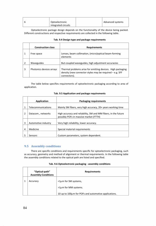
6 Optoelectronic
integrated circuits
Advanced systems
Optoelectronic package design depends on the functionality of the device being packed.
Different constructions and respective requirements are collected in the following table.
Tab. 9.4 Design type and package requirements
Construction class Requirements
1 Free space Lenses, beam collimation, (micro)optical beam-forming
elements
2 Waveguides But-coupled waveguides, high adjustment accuracies
3 Photonics devices arrays Thermal problems arise for emitting devices. High packaging
density (new connector styles may be required – e.g. SFF
connectors).
The table below specifies requirements of optoelectronic packaging according to area of
application.
Tab. 9.5 Application and package requirements
Application Packaging requirements
1 Telecommunications Mainly SM fibers, very high accuracy, 20+ years working time
2 Datacom., networks High accuracy and reliability, SM and MM fibers, in the future
possibly POFs in massive market (FTTH)
3 Automotive industry Very high reliability, lower accuracy.
4 Medicine Special material requirements
5 Sensors Custom parameters, system dependent.
9.5 Assembly conditions
There are specific conditions and requirements specific for optoelectronic packaging, such
as accuracy, geometry and method of alignment or thermal requirements. In the following table
the assembly conditions related to the optical path are listed and specified.
Tab. 9.6 Optoelectronic packaging - assembly conditions
“Optical-path”
Assembly-Conditions
Requirements
1 Accuracy <1µm for SM systems,
>1µm for MM systems.
10 up to 100µm for POFs and automotive applications.
84

2 Alignment (levels of
freedom)
X, Y, Z with different accuracies in different directions. Φ (angle).
3 Alignment method Visual (microscope, camera, image processing) or infrared (“see
through the surface”, observation of “hot” active transmission
devices (near infrared).
4 Other assembly issues Optical connection efficiency
Electrical (electronic protection, ESD)
Thermal
Hermetization
In systems with hierarchical structure, hierarchy level may influence packaging – summary
of related issues is given in the table below.
Tab. 9.7 Communication system level packaging hierarchy
Level Contents general Contents optical Interconnection
distance
1. System level System service
functions
Network
interconnections
100 m
2. Cabinet level Functioning of the
system on the rack
Cabinet level
interconnection
~ 10 m
3. Unit level Interconnection
between packages
Interconnection
between modules
< 1 m
4. Board level Board functioning.
Power supply
On-board device
interconnections and
signal transmission
~ 10 cm
5. Fiber level Placement Optical fiber
placement
~ 1 cm
6. Beam level Stability, precision Beam focusing ~ 1 µm
9.6 Generic optoelectronic package
Design of an optoelectronic package depends of a specific application. However, certain
elements are common for different packages. Diagram of a generic optoelectronic package,
comprising all basic elements is presented in the following picture.
85

Fig. 9.5 “Generic” optoelectronic package
9.7 Design solutions
Probably the most important issue in packaging of fiber-optical devices is efficiency of
light coupling between optical fiber and an active device, e.g. coupling between a laser-chip and
single mode fiber. Several solutions to this problem are illustrated in the following two figures.
Fig. 9.6 Comparison of different LD – fiber coupling techniques
electrical connections
support and temperature stabilization module
active element(s) with adjustment system
window, flat or lens
fiber
cover (hermetization)
fiber holder and adjustment segment
special optical elements (isolators, filters, F)
Butt coupling
Tapered waveguide coupling
86

Fig. 9.7 LD coupling with lenses possibilities
9.8 Some notes about materials
Materials for packages should be selected according to application area of the packaged
device. Below is a list of selection criteria of the materials
o Temperature properties (resistance, stability, resistance above 100C, 200C for
short time, thermal coefficients of expansion)
o Optical properties (attenuation, refractive index)
o Mechanical properties
o Manufacturability
o Environmental resistance (weatherability)
o Price, availability
Selection criteria should also include envisioned application area of the devices.
o Telecommunications systems. High performance, very high reliability and
longevity (up to 30 years), very high unit price. Based on metal, glass, ceramic
o Access network systems. High performance and reliability, medium life times (10
years). Low unit price. Based on polymer materials.
10 Dispersion of optical fibers
10.1 Dispersion
By a general definition, dispersion is any phenomenon in which the velocity of
propagation of an electromagnetic wave is wavelength dependent.
In communication technology, dispersion is used to describe any process by which an
electromagnetic signal propagating in a physical medium is degraded because the various wave
components (of different frequencies and wave vectors) have different propagation velocities
Single lens
double lens
cylindrical lens
GRIN lens
87

10.2 Dispersion in optical fibers
In optical fiber communications dispersion relates to a few well defined fiber parameters,
namely:
o Mode dispersion [200-800 MHz·km]
o Chromatic dispersion [0-20 ps/km·nm]
o Material disp.
o Waveguide disp.
o Polarization dispersion ≤ 0.2 [ps/km1/2
]
Mode dispersion (modal dispersion, intermodal dispersion) is characteristic of multimode
fibers only. Different propagating modes of multimode fiber have slightly different propagation
constants. In other words, lightwave propagation velocity varies depending on which mode light
propagates in. The most frequently used mode dispersion unit of measure is [MHz·km]. This unit
emphasizes the impact of the mode dispersion on a maximum frequency (data rate) that can be
transmitted over the given fiber. For example, 200 MHz·km indicates: over a fiber that is 1
kilometer (km) long, data stream of the frequency 200 megahertz (MHz) can be transmitted. If
the length of the fiber is increased to 2 kilometers, then the maximum data stream frequency
will be 100 megahertz.
Chromatic dispersion is a collective name for the next two types of dispersion – material
dispersion and waveguide dispersion. Unlike mode dispersion where lightwave propagation
velocity depends on the propagating mode number, in the chromatic dispersion, velocity of light
within waveguide depends on light wavelength. Chromatic dispersion is measured (expressed) in
the units of [ps/km·nm]. For example, 90 ps/km·nm means: two wavelengths that differ by 1
nanometer (nm) will have a differential delay of (will be delayed to one another by) 90
picosecond (ps) after traveling a one-kilometer (km) length of fiber.
Material dispersion directly results from the fiber material’s refractive index being
dependent on light wavelength. In the normal dispersion regime, found in most materials, within
spectral ranges of low absorption, refractive index decreases as wavelength increases.
Waveguide dispersion originates solely from the fact that light propagation takes place
within fiber (waveguide). Waveguide dispersion is independent of waveguide’s material optical
properties. Optical field properties (shape, propagation constant) of a propagating mode change
with wavelength.
Polarization dispersion is caused by fiber’s birefringence, i.e. different propagation
velocities (different propagation constants) experienced by lightwaves polarized in orthogonal
directions. In real-world fibers, a linearly polarized lightwave, i.e. polarized in only one of the
two orthogonal directions, will “split” into lightwaves propagating in two orthogonal
polarizations. The polarization initially absent will be excited because of inhomogeneities in
fiber’s cross-section. These inhomogeneities are fluctuations in fiber material’s refractive index,
and in stress locally exerted on fiber. Polarization dispersion unit of measure is [ps/km1/2
]. For
example, 0.2 ps/km1/2
in a 100 km long fiber means a 2 picosecond (ps) differential delay
between orthogonal polarizations after a propagation distance of 100 kilometers (km)
(0.2 * 1001/2
= 2).
10.3 Mode dispersion. Pulse broadening in step index fiber
In multimode fibers, besides the chromatic dispersion also occurs the so called mode
dispersion. Mode dispersion results from different values of group velocity at which individual
optical modes propagate within fiber. Even an ideally monochromatic optical signal (signal
containing light of only one wavelength, which is only possible in theory), once it is coupled into
a multimode fiber it will be affected by the mode dispersion. It is because multiple optical modes
will be excited in fiber by the input signal. Each one of the excited modes will then reach output
optical detector at a slightly different time. This phenomenon can be explained within the
framework of geometrical optics (ray optics) as shown in figure Fig. 10.1. From the schematic
depiction of light ray propagation paths we can see that different modes travel different
distances before they reach the detector. As an result, data pulse temporal broadening occurs.
88

Fig. 10.1 Geometrical optics explanation of the mode dispersion. Portions of the input optical
pulse energy propagate as different waveguide modes. As propagation path lengths of the
modes differ, propagation times are also different – temporal pulse broadening occurs.
10.4 Dispersion of single mode fiber
The general remarks concerning the chromatic dispersion (from paragraph 10.2) are
shown in greater detail in figure Fig. 10.2.
Fig. 10.2 Dispersion of single mode fiber. Both the contributions of the chromatic dispersion –
the waveguide dispersion and the material dispersion – show opposite types of wavelength
dependence (Agrawal, 2002).
In fact, both the contributions of the chromatic dispersion show opposite types of
wavelength dependence. Whereas material dispersion values increase with light wavelength,
the waveguide dispersion tends to lower values at the same time. A wavelength denoted as λZD
in figure Fig. 10.2, for which both the above dispersion types cancel, is called the zero-dispersion
wavelength. Its spectral location can be adjusted by a proper fiber cross-section design
(geometry, material doping). Zero-dispersion wavelength can e.g. be located within the second
telecommunication window (i.e. around 1.3 μm) thus making the fiber show both low
attenuation and low dispersion – a solution especially useful in long-haul fibers.
10.5 Dispersion shifted fibers (DSF)
Considering the spectral distribution of chromatic dispersion values, three types of
telecommunication optical fibers are used:
o fibers showing standard dispersion,
θcα n co
n cl
t
TB TB+∆T
1.1 1.2 1.3 1.4 1.5 1.6 1.7-30
-20
-10
0
10
20
30
Wavelength [µm]
Dis
pe
rsio
n [
ps/
(km
·nm
)]
Dispersion (total)
Dispersion (material)
Dispersion (waveguide)λZD
89

o dispersion shifted fibers, and
o dispersion-flattened fibers.
All three cases are presented in figure Fig. 10.3.
Fig. 10.3 Dispersion characteristics types found in the telecommunication silica-glass fibers
(Agrawal, 2002).
In dispersion shifted fibers, the zero-dispersion wavelength lies within the third
telecommunication window. However, the general character of the dispersion spectral
distribution remains similar to that of normal dispersion. This is changed in dispersion-flattened
fibers where dispersion distribution is significantly different. It is designed to be flat thus able to
maintain low dispersion values over a relatively broad spectral range.
In silica-glass single-mode fibers, the zero-dispersion wavelength location within the third
telecommunication window (i.e. the case of standard dispersion) can be achieved using the
simplest fiber cross-section structure, the step-index fiber. Achieving dispersion flattening or
dispersion shifting requires the utilization of more sophisticated fiber cross-section structures
(i.e. more sophisticated types of refractive index distributions along fiber radius). For example,
refractive index distribution can then be designed to have several maxima and minima along
fiber radius, which is in contrast with only one step-like change present in step-index fibers.
10.6 Dispersion of optical fibers
Below, there is a summary of the typical values of the dispersion-related parameters. All
the values are given for the telecommunication silica-glass fibers of various types.
Bandwidth of multimode fibers [MHz·km]
o 850 nm 400-800 (50/125) 160-400 (62.5/125)
o 1300 nm 400-1500 300-1200
Chromatic dispersion of singlemode fibers [ps/km·nm]
o 1285-1330 nm ≤ 3.5
o 1550 nm ≤ 18
Polarization-mode dispersion
o PMD of the fiber ≤ 0.2 [ps/km1/2
]
Meanings of the individual parameters together with the units of measure being used,
were explained in the paragraph 10.2.
10.7 Methods for chromatic dispersion measurements
The following paragraphs of this chapter are based on the ITU standard: ITU-T G.650
“Definition and Test Methods for the Relevant Parameters of Single-Mode Fibers” - Series G:
1.1 1.2 1.3 1.4 1.5 1.6 1.7-20
-10
0
10
20
StandardDispersion
flattened
Dispersion
shifted
Dis
pe
rsio
n [
ps/
(km
·nm
)]
Wavelength [µm]
90

Transmission Systems and Media, Digital Systems and Networks Transmission Media
Characteristics - Optical Fiber by International Telecommunication Union.
The ITU-T G.650 standard provides information concerning the recommended methods
(techniques) to be used for the determination of the fiber chromatic dispersion. In particular,
directives are given on how measurement setups should be constructed. A review of the setups
will be given in subsequent paragraphs. Here, let us list the measurement methods
recommended by the ITU standard. The methods are:
o Reference test method: The phase-shift technique
o First alternative test method: The interferometric technique
o Second alternative test method: The pulse delay technique
The method designations (reference, first alternative, ...) come from the discussed
standard.
All the three methods listed above, despite certain differences, share a common idea of
how, in fact, they derive the fiber chromatic dispersion. In short, the idea is as follows:
o to measure the light pulse time delay τ in the function of light wavelength λ; in
other words, light pulse propagation times in fiber of a given length (e.g. 1 km) are
measured at several (usually four to eight) light wavelengths;
o then, based on the measurement data points (i.e. time delays measured above),
an analytic form of the relation τ(λ) is found (by a numerical fitting procedure);
o finally, the chromatic dispersion coefficient D is found by simply calculating the
first derivative of τ(λ), i.e. D = dτ(λ)/dλ; by definition, the chromatic dispersion
coefficient informs on how much the pulse time delay (τ) changes when light
wavelength (λ) is changed by a unit value (usually 1 nm); this is why the derivative
of τ(λ) in respect to λ is calculated.
Note that the need for finding an analytic form of τ(λ) actually results from the small
number of light wavelength values at which measurements are made. This number is
determined by the measurement device construction, i.e. by how many different light sources
the device contains. An example of the analytic expression for τ(λ) will be discussed in paragraph
10.11.
10.8 Reference test method: The phase-shift technique
This is the reference method characteristics as stated by the ITU standard:
o The fiber chromatic dispersion coefficient is derived from the measurement of the
relative group delay experienced by the various wavelengths during propagation
through a known length of fiber.
o The group delay is measured in the frequency domain, by detecting, recording and
processing the phase shift of a sinusoidally modulated signal.
o The chromatic dispersion may be measured at a fixed wavelength or over a
wavelength range.
10.8.1 Measurement setup
Configuration of a measurement setup recommended to be used in the reference
method, is shown in figure Fig. 10.4.
91

Fig. 10.4 Block diagram of a measurement setup recommended for the reference method of
chromatic dispersion measurements (“Recommendation ITU-T G.650 (04/1997),” 1997).
The delay detector visible in the figure measures the relative phase shift between the
optical signal that has passed the fiber under test, and the electrical signal of reference. Both the
signals are modulated sinusoidally. The phase shift (φ) is then converted into the time delay (τ)
with the formula τ = φ/(2πf), where f is the modulation frequency.
The optical source: Laser diodes, {laser diode array}, wavelength tunable laser diodes
(WTL) {e.g. an external cavity laser (ECL)}, LEDs or broadband sources, (e.g. an Nd:YAG laser with
a Raman fiber). At least one data point must be within 100 nm of λ0.
10.9 First alternative test method: The interferometric technique
The first alternative method is characterized by the ITU standard as follows:
o The interferometric test method allows the chromatic dispersion to be measured,
using a short piece of fiber (several meters).
o According to the interferometric measuring principle, the wavelength-dependent
time delay between the test sample and the reference path is measured by a
Mach-Zehnder interferometer. The reference path can be an air path or a
single-mode fiber with known spectral group delay.
10.9.1 Measurement setup
Configuration of a measurement setup recommended for application in the first
alternative method, is shown in figure Fig. 10.5.
Signal channel
Source(s)Cladding mode
stripper Fiber
Signal generator
Wavelength
selector*Photodetector
Delay
de-
tector
Reference channel
(optical or electrical)
Signal
processor
computer
* When needed.
Time delay
92

Fig. 10.5 Block diagram of a measurement setup recommended for the first alternative
method of chromatic dispersion measurements (“Recommendation ITU-T G.650 (04/1997),”
1997).
The two fibers, the reference one and the one under test, constitute the two arms of a
Mach-Zehnder interferometer. The light pulse time delays are measured by means of balancing
the interferometer, i.e. equating the optical lengths of both the interferometer arms. In the
setup visible in figure Fig. 10.5, the balancing is done with the linear positioning device (see end
of the reference fiber).
The light source must be suitable, e.g. a YAG laser with a Raman fiber or a lamp and LED
optical sources, etc.
10.9.2 Determination of spectral group delay
In the case of using a reference fiber in one of the interferometer arms (as of figure Fig.
10.5), the pulse time delay in the function of light wavelength must be known for the reference
fiber. Otherwise, the time delay for pulses propagating over the test fiber, could not be
determined. It is explained in more detail in figure Fig. 10.6.
T1507740-92
Light
source Wavelength
selector
Beam
splitter 1
Reference signal
Reference fibre
Test fibre
Linear
positioning
device
Beam
splitter 2
Positioning
distance x
Detector Lock-in
amplifier a)
a) When needed.
93

Fig. 10.6 Determining the time delay of pulses propagating in the test fiber, requires the prior
knowledge of the pulse time delays occurring in the reference fiber (“Recommendation ITU-T
G.650 (04/1997),” 1997).
10.10 Second alternative test method: The pulse delay technique
The ITU standard gives the following characteristics of the second alternative method:
o The fiber chromatic dispersion coefficient is derived from the measurement of the
relative group delay experienced by the various wavelengths during propagation
through a known length of fiber.
o The group delay is measured in the time domain, by detecting, recording and
processing the delay experienced by pulses at various wavelengths.
o The chromatic dispersion may be measured at a fixed wavelength or over a
wavelength range.
Measurements employing the second alternative method are performed with the use of
the measurement setup shown in the figure Fig. 10.4, i.e. the one used in the reference method.
10.11 Dispersion calculations
As explained in the paragraph 10.7, an analytic expression for τ(λ) needs to be found.
More precisely, some general form of the expression is assumed a priori, and only the numerical
values of the expression coefficients need to be determined. Description of one of the
expression types discussed the ITU standard, is cited below.
The measured group delay per unit fiber length versus wavelength shall be fitted by the
three-term Sellmeier expression
( )2
2
000
8
−+=λλ
λτλτS
(10.1)
Here τ0 is the relative delay minimum at the zero-dispersion wavelength λ0. The chromatic
dispersion coefficient D(λ) = dτ/dλ can be determined from the differentiated Sellmeier
expression
( )
−=
3
4
00
4 λλ
λλS
D (10.2)
1400 1600 1800
– 10
– 5
0
5
10
λ1
λ0
λn
x (mm)
τg (ps) T1507760-92
∆τ λg( )
1
x1 xn
1200
x0
∆τ λg ( )n
∆τ λg( )
1
∆τ λg( )
2
∆τ λg ( )3
Relative group delay
Reference fibre
Test fibre
Wavelength λ (nm)
94

Here S0 is the zero-dispersion slope, i.e. the value of the dispersion slope S(λ) = dD/dλ at
λ0.
11 Telecommunication fiber optic system
Transmitting signals in the optical domain has, in fact, a long history. Simple mirror-based
systems would inform about enemy threat for centuries. Light would enable a quick
transmission of messages and, thanks to its directional propagation properties, the message
exchange was secret enough. In later years, the application of the total internal reflection
phenomenon enabled the optical signals to be transmitted over much longer distances. Today,
we know that actually it is not the propagation speed that makes light so useful in information
exchange, but rather the very high frequency of the electromagnetic waves of light. This very
high frequency directly translates into a broad frequency spectrum available to signals being
transmitted (significantly broader than that achievable in e.g. the radio transmission
techniques). In this chapter, examples will be given of optical networks, their limitations, and of
the concept of the WDM and TDM systems.
11.1 Fiber optic link
In figure Fig. 11.1 below, the simplest optical fiber-based telecommunication system is
presented. Electrical signal entering the transmitter is converted into optical signal, which is then
coupled into optical fiber. Fiber’s optical properties enable the optical signal to travel (be
transmitted over) distances dozens of kilometers long without the need for any intermediate
signal regeneration. Such long distances are possible even though certain level of an external
noise affects the transmission. Finally, the receiver brings the optical signal back to the electrical
domain.
Fig. 11.1 Elements of fiber-optic communication system.
11.2 Attenuation of optical fibers
Attenuation of the telecommunication silica-glass fibers, the telecommunication windows,
and the telecommunication system generations were discussed in Chapter 2.
11.3 Reasons to use optical fiber in networks
It is fast, easy and inexpensive to install fiber optic networks
o Capacity ->hundreds of thousands of phone channels,
o Losses -> 0.2dB/km for modern single mode fiber,
o Fiber amplifiers -> possibility to extend the transmission distance in an easy way,
Light sources
Photodetectors
Optical fiber waveguides
Dispersion compensators
Switches and modulators
Amplifiers
Multiplexers
95
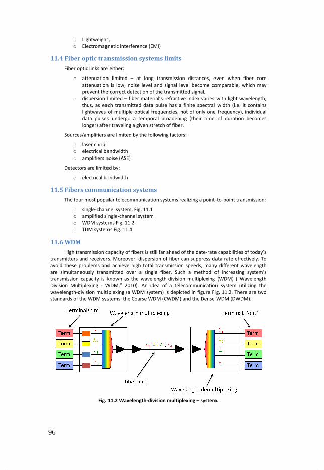
o Lightweight,
o Electromagnetic interference (EMI)
11.4 Fiber optic transmission systems limits
Fiber optic links are either:
o attenuation limited
attenuation is low, noise level and signal level become comparable, which may
prevent the correct detection of the transmitted signal,
o dispersion limited
thus, as each transmitted data pulse has a finite spectral width (i.e. it contains
lightwaves of multiple optical frequencies, not of only one frequency), individual
data pulses undergo a temporal broadening (their tim
longer) after traveling a given stretch of fiber.
Sources/amplifiers are limited by the following factors:
o laser chirp
o electrical bandwidth
o amplifiers noise (ASE)
Detectors are limited by:
o electrical bandwidth
11.5 Fibers communication sys
The four most popular telecommunication systems realizing a point
o single-channel system, Fig. 11.1
o amplified single-channel system
o WDM systems Fig. 11.2
o TDM systems Fig. 11.4
11.6 WDM
High transmission capacity of fibers is still far ahead of the date
transmitters and receivers. Moreover, dispersion of fiber can suppress data rate effectively. To
avoid these problems and achieve high total transmission speed
are simultaneously transmitted over a single fiber. Such a method of increasing system’s
transmission capacity is known as the wavelength
Division Multiplexing - WDM,” 2010)
wavelength-division multiplexing (a WDM system) is depicted in figure Fig. 11.2. There are two
standards of the WDM systems: the Coarse WDM (CWDM) and the Dense WDM (DWDM).
Fig. 11.2 Wavelength
Electromagnetic interference (EMI)
Fiber optic transmission systems limits
Fiber optic links are either:
ttenuation limited – at long transmission distances, even when fiber core
attenuation is low, noise level and signal level become comparable, which may
prevent the correct detection of the transmitted signal,
dispersion limited – fiber material’s refractive index varies with light wavelength;
thus, as each transmitted data pulse has a finite spectral width (i.e. it contains
lightwaves of multiple optical frequencies, not of only one frequency), individual
data pulses undergo a temporal broadening (their time of duration becomes
longer) after traveling a given stretch of fiber.
Sources/amplifiers are limited by the following factors:
electrical bandwidth
amplifiers noise (ASE)
electrical bandwidth
Fibers communication systems
The four most popular telecommunication systems realizing a point-to-point transmission:
channel system, Fig. 11.1
channel system
WDM systems Fig. 11.2
TDM systems Fig. 11.4
High transmission capacity of fibers is still far ahead of the date-rate capabilities of today’s
transmitters and receivers. Moreover, dispersion of fiber can suppress data rate effectively. To
avoid these problems and achieve high total transmission speeds, many different wavelength
are simultaneously transmitted over a single fiber. Such a method of increasing system’s
transmission capacity is known as the wavelength-division multiplexing (WDM)
WDM,” 2010). An idea of a telecommunication system utilizing the
division multiplexing (a WDM system) is depicted in figure Fig. 11.2. There are two
ds of the WDM systems: the Coarse WDM (CWDM) and the Dense WDM (DWDM).
Fig. 11.2 Wavelength-division multiplexing – system.
at long transmission distances, even when fiber core
attenuation is low, noise level and signal level become comparable, which may
e index varies with light wavelength;
thus, as each transmitted data pulse has a finite spectral width (i.e. it contains
lightwaves of multiple optical frequencies, not of only one frequency), individual
e of duration becomes
point transmission:
rate capabilities of today’s
transmitters and receivers. Moreover, dispersion of fiber can suppress data rate effectively. To
s, many different wavelength
are simultaneously transmitted over a single fiber. Such a method of increasing system’s
division multiplexing (WDM) (“Wavelength
. An idea of a telecommunication system utilizing the
division multiplexing (a WDM system) is depicted in figure Fig. 11.2. There are two
ds of the WDM systems: the Coarse WDM (CWDM) and the Dense WDM (DWDM).
96

o Coarse WDM
spectral distance between adjacent (neighboring) channels is 20
8 channels are allowed. Working frequencies are in the range of 1310 to 1610
Non-stabilized DFB lasers can be used. Total bit rate
to 3.125 Gbit/s
o Dense WDM
for very large data
allowed: 40 up to 160,and spacing between channels is relatively small: down to
100 GHz. DFB lasers must be temperature
a single fiber is 10
Fig. 11.3 Wavelength
Maximal electronics speed remains unchanged (speed of individual channels).
Multiplexing and demultiplexing is performed wi
Fig. 11.3 an idea of a WDM system working in the third telecommunication window is presented.
Individual channels (colored arrows) have spectral width that is much narrower than spectral
width of the entire window. This is the reason why a considerably high numbers of optical
signals can be transmitted over a single fiber without the channels being distorted by each
other. Thus, the total transmission capacity of the system can be greatly increased, while
transmission speed of an individual frequency channel still remains within the capabilities of the
available transmitters and receivers.
11.7 TDM
Different channels can be carried in a single fiber by time switching. To increase the bit
rate, an extremely narrow time slot is needed Fig. 11.4.
Fig. 11.4 Time division multiplexing of two channels into one train of pulses.
A schematic of time-division multiplexing of two channels into one train of pulses. Each
pulse represents the bit value ‘1’, and lack of pulse r
Coarse WDM – ITU standard G.694.2 (“Recommendation G.694.2,” 2003)
spectral distance between adjacent (neighboring) channels is 20
8 channels are allowed. Working frequencies are in the range of 1310 to 1610
stabilized DFB lasers can be used. Total bit rate transmitted in single fiber is 1
to 3.125 Gbit/s – FTTH.
Dense WDM – ITU standard G.694.1 (“Recommendation G.694.1,” 2002)
for very large data-rate transmissions, because large number of channels
allowed: 40 up to 160,and spacing between channels is relatively small: down to
100 GHz. DFB lasers must be temperature-stabilized. Total bit rate transmitted in
single fiber is 10 Gbit/s up to 40 Gbit/s. Used in internet backbone networks.
Fig. 11.3 Wavelength-division multiplexing – idea.
Maximal electronics speed remains unchanged (speed of individual channels).
Multiplexing and demultiplexing is performed with optical, usually passive, elements. In figure
Fig. 11.3 an idea of a WDM system working in the third telecommunication window is presented.
Individual channels (colored arrows) have spectral width that is much narrower than spectral
window. This is the reason why a considerably high numbers of optical
signals can be transmitted over a single fiber without the channels being distorted by each
other. Thus, the total transmission capacity of the system can be greatly increased, while
nsmission speed of an individual frequency channel still remains within the capabilities of the
available transmitters and receivers.
Different channels can be carried in a single fiber by time switching. To increase the bit
ime slot is needed Fig. 11.4.
Fig. 11.4 Time division multiplexing of two channels into one train of pulses.
division multiplexing of two channels into one train of pulses. Each
pulse represents the bit value ‘1’, and lack of pulse represents the bit value ‘0’.
Recommendation G.694.2,” 2003) – the
spectral distance between adjacent (neighboring) channels is 20 nm, and only 4 or
8 channels are allowed. Working frequencies are in the range of 1310 to 1610 nm.
transmitted in single fiber is 1
(“Recommendation G.694.1,” 2002) – used
nsmissions, because large number of channels are
allowed: 40 up to 160,and spacing between channels is relatively small: down to
stabilized. Total bit rate transmitted in
Gbit/s. Used in internet backbone networks.
Maximal electronics speed remains unchanged (speed of individual channels).
th optical, usually passive, elements. In figure
Fig. 11.3 an idea of a WDM system working in the third telecommunication window is presented.
Individual channels (colored arrows) have spectral width that is much narrower than spectral
window. This is the reason why a considerably high numbers of optical
signals can be transmitted over a single fiber without the channels being distorted by each
other. Thus, the total transmission capacity of the system can be greatly increased, while
nsmission speed of an individual frequency channel still remains within the capabilities of the
Different channels can be carried in a single fiber by time switching. To increase the bit
Fig. 11.4 Time division multiplexing of two channels into one train of pulses.
division multiplexing of two channels into one train of pulses. Each
epresents the bit value ‘0’.
97

Fig. 11.5 Time division multiplexing on one light wavelength.
Typical contemporary transmission line: TDM on one light wavelength Fig. 11.5. Individual
channels’ data rates sum up at optical input/output ports as shown in Fi
speed of(data rates in) individual channels requires optical modules of a very high frequency.
Fig. 11.6 Time division multiplexing
11.8 Solitons
Solitons are ultra short optical pulses that propagate through optical fiber but avoid
temporal broadening thanks to nonlinear phenomena they induce in fiber material. Usually,
short optical pulses propagating in fiber undergo a temporal broadening due to t
dispersion. Such a broadening can severely limit the telecommunication system transmission
capabilities.
Fig. 11.7 Solitons and normal transmission.
Fig. 11.5 Time division multiplexing on one light wavelength.
Typical contemporary transmission line: TDM on one light wavelength Fig. 11.5. Individual
channels’ data rates sum up at optical input/output ports as shown in Fig. 11.6. Increasing the
speed of(data rates in) individual channels requires optical modules of a very high frequency.
Fig. 11.6 Time division multiplexing – a 1000 of 1 Mb/s channels require a data link of 1
total transmission capacity.
olitons are ultra short optical pulses that propagate through optical fiber but avoid
temporal broadening thanks to nonlinear phenomena they induce in fiber material. Usually,
short optical pulses propagating in fiber undergo a temporal broadening due to t
dispersion. Such a broadening can severely limit the telecommunication system transmission
Fig. 11.7 Solitons and normal transmission.
Typical contemporary transmission line: TDM on one light wavelength Fig. 11.5. Individual
g. 11.6. Increasing the
speed of(data rates in) individual channels requires optical modules of a very high frequency.
Mb/s channels require a data link of 1 Gb/s
olitons are ultra short optical pulses that propagate through optical fiber but avoid
temporal broadening thanks to nonlinear phenomena they induce in fiber material. Usually,
short optical pulses propagating in fiber undergo a temporal broadening due to the chromatic
dispersion. Such a broadening can severely limit the telecommunication system transmission
98

Utilizing the balance between the nonlinear Kerr effect (11.1) and the chromatic
dispersion, the soliton can propagate without (temporal) widening. Normal transmission and
soliton transmission are visible on the left-hand side and the right-hand side of figure Fig. 11.7,
respectively.
Nonlinear refractive index – at points, where local optical power density is high enough
(enough to induce any noticeable effects) – the refractive index increases according to the
formula
< = <� + <-}�-~ = <� + 12 <-�- (11.1)
As has already been mentioned, the refractive index nonlinearity described by (11.1)
compensates (prevents) the temporal broadening of the soliton pulse.
12 Measurements of optical fiber
The following chapter is based on the ITU standard: ITU-T G.650 “Definition and Test
Methods for the Relevant Parameters of Single-Mode Fibers” - Series G: Transmission Systems
and Media, Digital Systems and Networks Transmission Media Characteristics - Optical Fiber by
International Telecommunication Union (“Recommendation ITU-T G.650 (04/1997),” 1997).
12.1 Test Methods
Reference Test Method (RTM)
A test method in which a characteristic of a specified class of optical fibers or optical fiber
cables is measured strictly according to the definition of this characteristic and which gives
results which are accurate, reproducible and relatable to practical use.
Alternative Test Method (ATM)
A test method in which a given characteristic of a specified class of optical fibers or optical
fiber cables is measured in a manner consistent with the definition of this characteristic and
gives results which are reproducible and relatable to the reference test method and to practical
use.
12.2 Parameters of singlemode optical fiber
1. Mode field diameter
2. Cladding diameter, mode field concentricity error and cladding non-circularity
3. Cut-off wavelength
4. Attenuation
5. Chromatic dispersion
6. Proof testing
7. Polarization mode dispersion
12.3 Mode field diameter
The mode field is the single-mode field distribution of the LP01 mode giving rise to a
spatial intensity distribution in the fiber. Some examples of shapes of mode field spatial density
distributions can be found in figure Fig. 12.6 (in paragraph 12.14).
The Mode Field Diameter (MFD) 2w represents a measure of the transverse extent of the
electromagnetic field intensity of the mode in a fiber cross-section and it is defined from the far
field intensity distribution F2(θ), θ being the far-field angle, through the following equation:
99
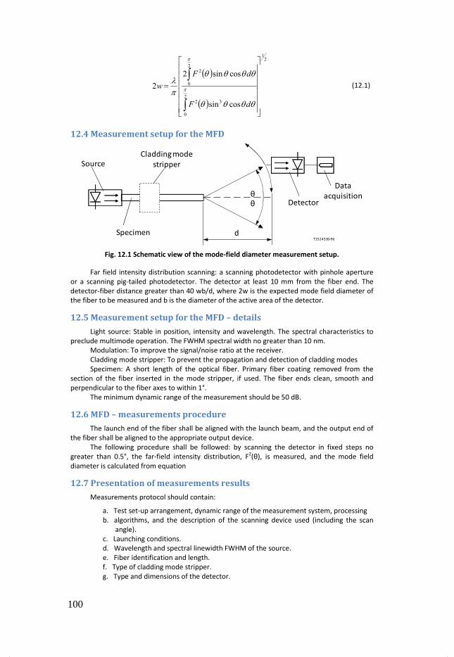
( )
( )
21
2
0
32
2
0
2
cossin
cossin2
2
=
∫
∫π
π
θθθθ
θθθθ
πλ
dF
dF
w (12.1)
12.4 Measurement setup for the MFD
Fig. 12.1 Schematic view of the mode-field diameter measurement setup.
Far field intensity distribution scanning: a scanning photodetector with pinhole aperture
or a scanning pig-tailed photodetector. The detector at least 10 mm from the fiber end. The
detector-fiber distance greater than 40 wb/d, where 2w is the expected mode field diameter of
the fiber to be measured and b is the diameter of the active area of the detector.
12.5 Measurement setup for the MFD – details
Light source: Stable in position, intensity and wavelength. The spectral characteristics to
preclude multimode operation. The FWHM spectral width no greater than 10 nm.
Modulation: To improve the signal/noise ratio at the receiver.
Cladding mode stripper: To prevent the propagation and detection of cladding modes
Specimen: A short length of the optical fiber. Primary fiber coating removed from the
section of the fiber inserted in the mode stripper, if used. The fiber ends clean, smooth and
perpendicular to the fiber axes to within 1°.
The minimum dynamic range of the measurement should be 50 dB.
12.6 MFD – measurements procedure
The launch end of the fiber shall be aligned with the launch beam, and the output end of
the fiber shall be aligned to the appropriate output device.
The following procedure shall be followed: by scanning the detector in fixed steps no
greater than 0.5°, the far-field intensity distribution, F2(θ), is measured, and the mode field
diameter is calculated from equation
12.7 Presentation of measurements results
Measurements protocol should contain:
a. Test set-up arrangement, dynamic range of the measurement system, processing
b. algorithms, and the description of the scanning device used (including the scan
angle).
c. Launching conditions.
d. Wavelength and spectral linewidth FWHM of the source.
e. Fiber identification and length.
f. Type of cladding mode stripper.
g. Type and dimensions of the detector.
T1524530-96
d
θ
θ
Source
Specimen
Cladding mode
stripper
Detector
Data
acquisition
100

h. Temperature of the sample and environmental conditions (when necessary).
i. Indication of the accuracy and repeatability.
j. Mode field diameter.
12.8 MFD measurement – 1st alternative method (1)
The variable aperture technique, determined from the complementary aperture
transmission function a(x)
( ) ( )( )
21
0
222/2
−∞
+= ∫ dx
Dx
xxaDw πλ (12.2)
where:
The aperture radius x = D · tan θ
D the distance between the aperture and the fiber
complementary aperture transmission function a(x):
( ) ( )max
1P
xPxa −= (12.3)
where Pmax is the power transmitted by the largest aperture and x is the aperture radius.
12.9 Variable aperture MFD measurement method
Fig. 12.2 Schematic view of the mode-field diameter measurement setup – the first alternative
method.
Aperture apparatus: at least twelve apertures spanning the half-angle range of numerical
apertures from 0.02 to 0.25 (0.4 for fibers covered by Recommendation G.653) should be used.
12.10 MFD measurement – 2nd alternative method
The near-field scan. MFD is determined from the near-field intensity distribution f2(r) : (r
being the radial coordinate):
( )
( )
21
0
2
0
2
222
=
∫
∫∞
∞
drdr
rdfr
drrrf
w (12.4)
where: r is the radial coordinate
Far field and near field methods are equivalent through Henkel transform
T1524530-96
d
θ
θ
Source
Specimen
Cladding mode
stripper
Detector
Data
acquisition
Variable aperture
Focusing lens
101

12.11 2nd alternative measurement setup – near field scan
Fig. 12.3 Schematic view of the mode-field diameter measurement setup – the second
alternative method.
For calibration, the magnification of the optics should have been measured by scanning
the length of a specimen whose dimensions are independently known with sufficient accuracy.
12.12 2nd alternative measurement procedure
The near-field of the fiber is enlarged by the magnifying optics and focused onto the plane
of the detector.
The near-field intensity distribution, f2(r), is scanned and the mode field diameter is
calculated from the equation.
Alternatively, the near-field intensity distribution may be transformed into the far-field
domain using a Hankel transform and the resulting transformed far-field F2(θ) may be used to
compute the mode field diameter from the equation for the primary method.
12.13 Test methods for the cladding diameter, mode field
concentricity error and cladding non-circularity
Reference test method: The transmitted near-field technique.
Source - see measurements of MFD
The magnifying optics consists of a microscope objective which magnifies the specimen
output near-field, focusing it onto the plane of the scanning detector.
Detector
a. scanning photodetector with pinhole aperture;
b. scanning mirror with fixed pinhole aperture and photodetector;
c. scanning vidicon, charge coupled devices or other pattern/intensity recognition
devices.
First alternative test method: The refracted near-field technique. Measurement of the
refractive index distribution across the entire fiber (core and cladding). The geometrical
characteristics of the fiber then obtained from the refractive index distribution.
Fig. 12.4 Measurement of the refractive index distribution across the entire fiber
d
Source
Specimen
Cladding mode
stripperMagnifying optics
Scanning
Detector
Data
acquisition
source detector
fiber
102

Second alternative test method: The side-view technique. Intensity distributions in the
observation plane along the line perpendicular to the fiber axis are recorded. Refractive index
profiles and geometrical parameters are then obtained through suitable algorithms.
Fig. 12.5 Measurement of the refractive index profiles and geometrical parameters by the
side-view technique.
12.14 Cut-off wavelength
Theoretical cut-off wavelength is the shortest wavelength at which a single mode can
propagate in a single-mode fiber. This parameter can be computed from the refractive index
profile of the fiber. At wavelengths below the theoretical cut-off wavelength, several modes
propagate and the fiber is no longer single-mode but multimode.
Cut-off wavelength is defined as the wavelength greater than that at which the ratio
between the total power, including launched higher order modes, and the fundamental mode
power has decreased to less than 0.1 dB. According to this definition, when all modes are
equally excited, the second order (LP11) mode is attenuated by 19.3 dB as compared to the
fundamental mode (LP01).
Fig. 12.6 LP modes of an optical fiber.
12.15 Test methods for the cut-off wavelength
Measurement purpose: to assure effective single-mode operation above a specified
wavelength.
Reference test method for the cut-off wavelength (λc) of the primary coated fiber and
reference test method for the cut-off wavelength (λcj) of jumper cables: The transmitted power
technique.
The transmitted power technique uses the variation with wavelength of the transmitted
power of a short length of the fiber under test, under defined conditions, compared to a
reference transmitted power. There are two possible ways to obtain this reference power:
a. the test fiber with a loop of smaller radius; or
b. a short (1-2 m) length of multimode fiber.
source detector
fiber
V
LP 02
LP21
LP01
LP11
1
654321
b
103
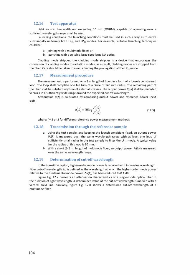
12.16 Test apparatus
Light source: line width not exceeding 10 nm (FWHM), capable of operating over a
sufficient wavelength range, shall be used.
Launching conditions: the launching conditions must be used in such a way as to excite
substantially uniformly both LP01 and LP11 modes. For example, suitable launching techniques
could be:
a. jointing with a multimode fiber; or
b. launching with a suitable large spot-large NA optics.
Cladding mode stripper: the cladding mode stripper is a device that encourages the
conversion of cladding modes to radiation modes; as a result, cladding modes are stripped from
the fiber. Care should be taken to avoid affecting the propagation of the LP11 mode.
12.17 Measurement procedure
The measurement is performed on a 2 m length of fiber, in a form of a loosely constrained
loop. The loop shall complete one full turn of a circle of 140 mm radius. The remaining part of
the fiber shall be substantially free of external stresses. The output power P1(λ) shall be recorded
versus λ in a sufficiently wide range around the expected cut-off wavelength.
Attenuation α(λ) is calculated by comparing output power and reference power (next
slide)
( ) ( )( )λλ
λiP
Pa 1log10= (12.5)
where: i = 2 or 3 for different reference power measurement methods
12.18 Transmission through the reference sample
a. Using the test sample, and keeping the launch conditions fixed, an output power
P2(λ) is measured over the same wavelength range with at least one loop of
sufficiently small radius in the test sample to filter the LP11 mode. A typical value
for the radius of this loop is 30 mm.
b. With a short (1-2 m) length of multimode fiber, an output power P3(λ) is measured
over the same wavelength range.
12.19 Determination of cut-off wavelength
In the transition region, higher-order mode power is reduced with increasing wavelength.
Fiber cut-off wavelength, λc, is defined as the wavelength at which the higher-order mode power
relative to the fundamental mode power, Δa(λ), has been reduced to 0.1 dB.
Figure Fig. 12.7 presents an attenuation characteristics of a single-mode optical fiber in
the function of light wavelength. A determined value of the cut-off wavelength is marked with a
vertical solid line. Similarly, figure Fig. 12.8 shows a determined cut-off wavelength of a
multimode fiber.
104

Fig. 12.7 Single-mode reference cut-off plot.
Fig. 12.8 Multimode reference cut-off plot.
12.20 Test methods for the attenuation:
o Reference test method: The cut-back technique
o First alternative test method: The backscattering technique
o Second alternative test method: The insertion loss technique
12.21 The cut-back technique
The cut-back technique is a direct application of the definition in which the power levels
P1 and P2 are measured at two points of the fiber without change of input conditions. P2 is the
power emerging from the far end of the fiber and P1 is the power emerging from a point near
the input after cutting the fiber.
( ) ( )( )
( )dBlog102
1
λλ
λP
PA = (12.6)
Measurements may be made at one or more spot wavelengths, or alternatively, a spectral
response may be required over a range of wavelengths.
Trans Upper
Wavelength [nm]
Att
en
ua
tio
n[d
B] Cut-off
1188 nm
Wavelength [nm]
Cut-off1232 nm
Att
en
ua
tio
n[d
B]
Trans Upper
105

12.22 Attenuation: measurement set-up
Diagrams of suitable test equipments, to obtain one loss or the loss spectrum
measurements respectively, are shown as examples in Fig. 12.9 and Fig. 12.10.
Fig. 12.9 Arrangement of test equipment to make one loss measurement
Fig. 12.10 Arrangement of test equipment used to obtain the loss spectrum measurement
12.23 First alternative test method: The backscattering technique
A test method for the attenuation coefficient of single-mode optical fiber based on
bidirectional backscattering measurements is described. This technique can also be applied to
check the attenuation uniformity, optical continuity, physical discontinuities, splice losses and
the length of the fiber. The measurement is performed with Optical Time Domain
Reflectometer.
OTDR (Optical Time Domain Reflectometer) is the fundamental device used in building
and exploitation of optical fiber networks. It enables measurements of parameters of optical
fibers and localization of “events” occurring in the optical tract. Schematic diagram OTDR
measurement is presented in the following figure.
Fig. 12.11 Optical Time Domain Reflectometer (OTDR)
Lightsource Mode
filter
Fiberon test Cladding
modestripper
Detector
Launchingsystem
Claddingmode
stripper Amplifier
Levelmeasurement
Biascircuit
Halogenlamp
Launchingsystem
Claddingmode
stripper
Fiberon test
Claddingmode
stripperDetector
Monochromator Modefilter
Lightmodulator
Reference signal
Lock-inamplifier
Controller
Plotter
106

Reflectometry measurement is based on analysis of back-scattered light power as a
function of time (or distance from the measurement location). A block diagram of the OTDR is
shown below.
Fig. 12.12 Reflectometer – a block diagram
12.24 Second alternative test method: The insertion loss technique
The insertion loss technique consists of the evaluation of the power loss due to the
insertion of the fiber under test between a launching and a receiving system, previously
interconnected (reference condition). The powers P1 and P2 are thus evaluated in a less
straightforward way than in the cut-back method. Therefore, this method is not intended for use
on factory lengths of fibers and cables.
The insertion loss technique is less accurate than a cut-back one, but has the advantage of
being non-destructive for the fiber under test and for the semi-connectors possibly fixed at both
ends. Therefore, it is particularly suitable for field use, and mainly intended for use with
connectorized cable lengths.
Two options are considered in the following for this technique. They differ in the nature of
the launching and receiving systems.
In Fig. 12.13 the quality of the semi-connectors possibly fixed to the fiber under test (and
in general the quality of the used interconnection devices) influences the results, in Fig. 12.14
this influence is nearly excluded.
As a consequence, option from Fig. 12.14 has in general a better accuracy, and it is more
suitable when the actual attenuation of the fiber alone is needed. Conversely, when the fiber
section under test is fitted with semi-connectors and has to be cascaded with other elements,
the results from Fig. 12.13 are more meaningful, as they take into account the deviation of the
semi-connectors from the nominal loss.
Laser diode Coupler
Photodetector
Amplifier
ConnectorFiber
Control and data processing unit
User interface
Display
107
Fig. 12.13 The insertion loss technique - “Laboratory” variant.
Fig. 12.14 The insertion loss technique – “Field” variant.
12.25 Visual fault locator
The visual fault locator (VFL) is a very versatile tool capable of verifying optical cable
integrity and locating optical link faults. Measurement capabilities of a VFL are shown in figure
Fig. 12.15.
Fig. 12.15 Measurement capabilities visual fault locator (VLT).
1 2
21
Bias and/or
modulation
Lightsource
Launching
systemMode
filter
MF MF
Mode
filter
Claddingmode
stripper
Claddingmode
stripper
Fibreundertest
Reference condition
Detector
Measurement
system
Bias and/ormodulation
Light
source
Launching
system
Fiberunder test
Detector
Measuringsystem
Reference system
Modefilter
Claddingmode
stripper
MF
Localization of bendsLocalization of faulty
splices
Localization of faulty
connectors Fiber identificationCheckup of connector
and fiber surfaces
Works in the dead
zone of the OTDR
108

12.26 Microscope (x 500)
The microscope enables the observation and assessment of the end-face surfaces of
optical fibers that are about to be connected with each other. Microscopes feature an internal
light source, which illuminates the investigated fiber end-face surface. The observation field is
magnified by a system of lenses and can be acquired by a CCD camera.
Fig. 12.16 Microscope designed for the observation end-face surfaces of optical fibers.
12.27 Traffic or signal detectors
Principle of operation: light is leaking from a bend or stressed fiber. Two detectors placed
on two sides of the bent can detect presence of an optical signal and direction of propagation.
Applications:
o Signal detection,
o Power-signal indicator,
o Identification of modulated signal 2 kHz.
13 Optical Time Domain Reflectometer (OTDR)
13.1 Definition and fundamentals
OTDR (Optical Time Domain Reflectometer) is the fundamental device used in building
and exploitation of optical fiber networks. If you have to choose one tool to service your
network - the OTDR is the right one. The reason is, that it can measure almost every parameter
of optical fiber connection. The OTDR can perform multiple jobs: it can locate events, can
evaluate those events or anomalies, is can also measure distance to those events. In addition it
can measure insertion loss, attenuation of fiber, return loss.
Optical Time Domain Reflectometer or OTDR works on principle of injecting a pulse of
light at one end of the fiber, and measuring the backscattered and reflected light coming back.
The measured signal is than plotted as signal power in dB versus distance.
Badane włókno
Źródłoświatła
Układoptyczny
Light source
Optical
system
Fiber under
test
109

Fig. 13.1 Reflectometry measurement is based on analysis of back
function of time (or distance from the measurement location).
The first optical reflectometer was build and described in 1976 by Barnoski
Jensen, 1976). Schematic diagram of the first reflectometer is provided on the figureFig. 13.2.
Fig. 13.2 Schematic diagram of the first reflectometer. Light source
A taper was used to tap a portion of optical power from the fiber
Optical fiber is made of very pure glass, however there are small impurities that scatter
small portion of the guided light. Those impurities may be purposefully put into the fiber core
those are called dopants and they increase refractive index of the c
impurities or inhomogeneities that are the property of the silica glass structure. Those minor
impurities scatter light in all directions, and part of the scattered light is reflected back towards
the source, in our case toward the OTD
phenomena that is used in reflectometric measurements is Fresnel scattering
that occurs when light encounters boundary of two media with different refractive indices. An
example is the end of the fiber, or fiber connector where light travels between glass and air.
A block diagram of the measurement device working on the principle of backreflection is
presented on Fig. 13.3
Fig. 13.1 Reflectometry measurement is based on analysis of back-scattered light power as a
function of time (or distance from the measurement location).
reflectometer was build and described in 1976 by Barnoski
. Schematic diagram of the first reflectometer is provided on the figureFig. 13.2.
Fig. 13.2 Schematic diagram of the first reflectometer. Light source – pulsed laser diode GaAs.
A taper was used to tap a portion of optical power from the fiber (Barnoski & Jensen, 1976)
Optical fiber is made of very pure glass, however there are small impurities that scatter
small portion of the guided light. Those impurities may be purposefully put into the fiber core
those are called dopants and they increase refractive index of the cores. There are also
impurities or inhomogeneities that are the property of the silica glass structure. Those minor
impurities scatter light in all directions, and part of the scattered light is reflected back towards
the source, in our case toward the OTDR. This scattering is called Rayleigh scattering. The second
phenomena that is used in reflectometric measurements is Fresnel scattering
that occurs when light encounters boundary of two media with different refractive indices. An
is the end of the fiber, or fiber connector where light travels between glass and air.
A block diagram of the measurement device working on the principle of backreflection is
scattered light power as a
function of time (or distance from the measurement location).
reflectometer was build and described in 1976 by Barnoski (Barnoski &
. Schematic diagram of the first reflectometer is provided on the figureFig. 13.2.
pulsed laser diode GaAs.
oski & Jensen, 1976).
Optical fiber is made of very pure glass, however there are small impurities that scatter
small portion of the guided light. Those impurities may be purposefully put into the fiber core -
ores. There are also
impurities or inhomogeneities that are the property of the silica glass structure. Those minor
impurities scatter light in all directions, and part of the scattered light is reflected back towards
R. This scattering is called Rayleigh scattering. The second
phenomena that is used in reflectometric measurements is Fresnel scattering - the scattering
that occurs when light encounters boundary of two media with different refractive indices. An
is the end of the fiber, or fiber connector where light travels between glass and air.
A block diagram of the measurement device working on the principle of backreflection is
110

Fig. 13.3 Reflectometer – a block diagram.
What does OTDR measure:
• distance (actualy OTDR measures round trip time travel of each pulse, but knowing the
speed of light in vacuum, and refractive index of the material one can calculate the
distance.)
• The formula to calculate distance from time:
• Fiber distance = (speed of light in vacuum x time) / (2 x refractive index)
• Fiber loss (attenuation), in dB/km
• Event loss (attenuation), in dB
• Reflectance (ration of reflected power to incident power of an event ) , in -dB.
Reflectance is expressed as negative numbers in dB units. The higher the number, the
better, e.g. if we compare two connectors with reflectances of -55 dB and -65 dB - the
second one is better.
• Optical Return Loss (ORL), similar as reflectance but ORL may refer to a whole segment
of a fiber as well as to a single event. ORL is usually expressed as positive number.
Results measured by the OTDR are displayed as an OTDR trace or reflectogram. Example
of the reflectogram is presented on Fig. 13.4.
111

Fig. 13.4 Example of a reflectogram (OTDR trace).
Amount of backscattered power that is available for OTDR analysis is described by the
following equation (Personick, 1977):
( ) ( ) ( ){ }2/2exp2/0 tWSPtP Sb vv αα −= (13.1)
Where:
Pb – back-scaterred Rayleigh power
P0 – peak optical power
S - Rayleigh scattering recapture rate
αS – Rayleigh scattering loss in Nepers per meter
v – group velocity of light in fiber
α(vt/2) – total attenuation at distance of vt/2 [in Nepers]
t - time
W – pulse length [in units of time]
The equation is valid under assumption that vα/2<<W
13.2 Parameters and specifications
Fundamental specifications of the reflectometer include:
• Dynamics,
• Measurement range,
• Dead zone length,
• Measurement wavelength.
Values measured by the OTDR:
• Distance (distance between events, length of a fiber),
• Attenuation of connectors, macrobends, and splices,
• Attenuation of a fiber per unit length,
• Reflections (reflection coefficient, optical return loss (ORL)).
13.2.1 Events and interpretation of traces
The following picture are borrowed from the 2009 JDSU presentation „Perfoming and analyzing OTDR traces”(Yount, 2009)
112

• Front-end reflection or dead zone located at the far left end of a trace.
anything accurately within the dead zone of the front
• Dead zone describe the minimum distance between events that this events can be
distinguished. Dead zones can be minimized with shorter pulses used for the measurement.
• Connector. With OTDR we can measure attenuation and reflectance of a connector.
• Fusion splices - permanent connection of two fibers. The splices are prepared with a fusion
splicing machine (or a fiber splicer). The main difference between
that now there is no reflection.
end reflection or dead zone located at the far left end of a trace.
anything accurately within the dead zone of the front-end reflection.
Dead zone describe the minimum distance between events that this events can be
distinguished. Dead zones can be minimized with shorter pulses used for the measurement.
EDZ - Event Dead Zone
Connector. With OTDR we can measure attenuation and reflectance of a connector.
permanent connection of two fibers. The splices are prepared with a fusion
splicing machine (or a fiber splicer). The main difference between a connector an a splice is
that now there is no reflection.
Direction A-B
end reflection or dead zone located at the far left end of a trace. One can't measure
Dead zone describe the minimum distance between events that this events can be
distinguished. Dead zones can be minimized with shorter pulses used for the measurement.
Connector. With OTDR we can measure attenuation and reflectance of a connector.
permanent connection of two fibers. The splices are prepared with a fusion
a connector an a splice is
113

• In some cases, OTDR displays an erroneous image for a splice, called a gainer. The error is
caused by different light scattering levels in two joined pieces of fiber.
To eliminate the "gainer" error, one has to measure the fiber in two directions and average
the obtained results.
• Macrobend.
Macrobends result from physical bending of a fiber. Microbend losses are very sensitive to
wavelength - they are much higher for 1550 nm than for 1310 nm. Macrobend events are
similar to splice events, but splice losses doesn't depend on wavelength that much. There is
no reflectance observable for macrobend losses.
• Fiber end or break is characterized by high refle
• Ghosts. Ghosts are "events" that are not there. They are artifacts created by strong
reflections between real events.
In some cases, OTDR displays an erroneous image for a splice, called a gainer. The error is
caused by different light scattering levels in two joined pieces of fiber.
Direction B-A
To eliminate the "gainer" error, one has to measure the fiber in two directions and average
Macrobends result from physical bending of a fiber. Microbend losses are very sensitive to
uch higher for 1550 nm than for 1310 nm. Macrobend events are
similar to splice events, but splice losses doesn't depend on wavelength that much. There is
no reflectance observable for macrobend losses.
Fiber end or break is characterized by high reflectance and very noisy signal afterwards.
Ghosts. Ghosts are "events" that are not there. They are artifacts created by strong
reflections between real events.
In some cases, OTDR displays an erroneous image for a splice, called a gainer. The error is
To eliminate the "gainer" error, one has to measure the fiber in two directions and average
Macrobends result from physical bending of a fiber. Microbend losses are very sensitive to
uch higher for 1550 nm than for 1310 nm. Macrobend events are
similar to splice events, but splice losses doesn't depend on wavelength that much. There is
ctance and very noisy signal afterwards.
Ghosts. Ghosts are "events" that are not there. They are artifacts created by strong
114

• For ghost events there is no attenuation, and the distance is exactly equal to distance
between other events.
13.3 Other fiber optic measurement devices
13.3.1 Optical power meters
Active element: photodiode
o Silicon for the wavelength of 1100 nm,
o InGaAs or germanium– for 1300 i 1550 nm
Power meter is equipped with
o Constant currentt amplifier
o Analog-digital converter
o Data processing and display circuits.
o Exchangeable adapters (ST, FC/PC, SC, E2000, and other).
Signal power is displayed in logarithmic scale, as absolute power in dBm, relative in dBr, or on
linear scale in units of mW, pW, nW.
Main parameters of optical power meters:
o Dynamic range,
o measuring range,
o measurement wavelengths,
o linearity.
13.3.2 Measurement light sources
• Lasers, dedicated for measurements of singlemode fibers.
• LEDs, for measurements of multimode fibers.
Laser must be stable and reliable. The light source module, should be connectable with different
optical connectors.
Main parameters of light measurement sources:
• Output power,
• Emitted light wavelength,
• Spectral width,
• Source stability.
13.3.3 Visual fault locator
Visual fault locators are devices that couple visible light to the optical fiber. Faults and
possible problem locations are than visible as areas where light is leaking from the fiber or cable.
The following picture illustrates possible applications of the visual fault locator.
115

Fig. 13.5 Different applications of a Visual Vault Locator.
13.3.4 Microscope
With a microscope one can visually check and evaluate front faces of optical fibers. The
microscope is equipped with an internal light source, which illuminates a face of optical fiber.
The picture is amplified by a set of lenses, and can be registered with a CCD camera.
13.3.5 Fiber identivier (Optical trafic detector)
Operation principle of the device is based on detection of light, leeking from a bended
fiber. Two photodetectors, located at two ends of the bend register leeking light.
Applications of fiber identifier:
• detection of optical transmission presence and direction,
• Measurement of optical power level in optical fiber,
• Detection of modulate signal (2 kHz).
Maximal diameter of an optical bufer 3 mm.
116

References
Agrawal, G. P. (2002). Fiber-Optic Communication Systems (3rd ed., p. 580). Wiley-Interscience.
Barnoski, M. K., & Jensen, S. M. (1976). Fiber waveguides: a novel technique for investigating
attenuation characteristics. Applied Optics, 15(9), 2112-2115. OSA. doi:
10.1364/AO.15.002112.
Basics of Fiber Bragg Grating. (2010). . Retrieved February 1, 2011, from http://www.aos-
fiber.com/eng/About.html.
Bass, M. (2001a). Optical Fiber Communication Technology and System Overview. Handbook of optics. Volume IV, Fiber optics and nonlinear optics (p. 916).
Bass, M. (2001b). Optical Fibers and Fiber-Optic Communications. Handbook of optics. Volume IV, Fiber optics and nonlinear optics (2nd ed., p. 916). McGraw-Hill.
Chang, W. S. C. (2009). Fundamentals of Guided-Wave Optoelectronic Devices (p. 199).
Cambridge University Press. Retrieved February 1, 2011, from
http://books.google.com/books?id=EWKIg5D5MccC&pgis=1.
DeCusatis, C. (2008). Handbook of fiber optic data communication: a practical guide to optical ... (p. 784). Academic Press. Retrieved February 1, 2011, from
http://books.google.com/books?id=ynvMx7mMgJAC&pgis=1.
Fiber Optic Connector Reference. (2010). . Retrieved February 1, 2011, from
http://www.ertyu.org/steven_nikkel/fiberconnect.html.
Fiber Optic Connectors Basics, Styles, Trends. (2010). . Retrieved February 1, 2011, from
http://www.fiberoptics4sale.com/wordpress/fiber-optic-connectors-basics-styles-trends/.
Gambling, W. A. (2000). The Rise and Rise of Optical Fibers. IEEE Journal of Selected Topics in Quantum Electronics, 6(6), 1084-1093.
Garmire, E., & Tamir, T. (1975). Integrated optics. Tamir (p. 315). Springer. Retrieved February 1,
2011, from http://books.google.com/books?id=EVsJSQAACAAJ&pgis=1.
Giovanni, G. (2010). Introduction: semiconductor lasers. Retrieved from
http://www.fi.isc.cnr.it/users/giovanni.giacomelli/Semic/Samples/samples.html.
Harness Optical Polarization with Ease and Elegance. (2008). . Retrieved February 1, 2011, from
http://www.generalphotonics.com/Articles.aspx?a=1004.
Hunsperger, R. G. (2009). Integrated Optics. (T. Tamir, Ed.)Applied Optics, 7(Ic), 399-457.
Springer New York. Retrieved from http://www.springerlink.com/index/10.1007/b98730.
Illustrated Fiber-Optics Glossary. (2010). . Retrieved from
http://www.infocellar.com/networks/fiber-optics/glossaries/c.htm.
Liu, J.-ming. (2005). Photonic Devices (p. 1104). Cambridge University Press.
Midwinter, J. E. (1983). Światłowody telekomunikacyjne (p. 345). Wydawnictwa Naukowo-
Techniczne. Retrieved February 1, 2011, from
http://books.google.com/books?id=w_qPAQAACAAJ&pgis=1.
Milligan, B. (2004). Long-range VCSELs take aim at putting zap into structured cabling. Retrieved
from http://www.cablinginstall.com/index/display/article-
display/215305/articles/cabling-installation-maintenance/volume-12/issue-
11/contents/technology/long-range-vcsels-take-aim-at-putting-zap-into-structured-
cabling.html.
Mitschke, F. (2010). Fiber Optics: Physics and Technology (p. 301). Springer. Retrieved January
31, 2011, from http://books.google.com/books?id=343fg_YU5U4C&pgis=1.
Nadler, C. K., Wildermuth, E. K., Lanker, M., Hunziker, W., & Melchior, H. (1999). Polarization
insensitive, low-loss, low-crosstalk wavelength multiplexer modules. IEEE Journal of Selected Topics in Quantum Electronics, 5(5), 1407-1412. doi: 10.1109/2944.806898.
Paschotta, R. (2008a). Fiber Fabrication. Encyclopedia of Laser Physics and Technology. Retrieved
from http://www.rp-photonics.com/fiber_fabrication.html.
Paschotta, R. (2008b). Plastic Optical Fibers. Encyclopedia of Laser Physics and Technology.
Retrieved from http://www.rp-photonics.com/plastic_optical_fibers.html.
Personick, S. D. (1977). PHOTON PROBE - AN OPTICAL-FIBER TIME-DOMAIN REFLECTOMETER.
Bell Syst Tech J, 56(3), 355-366. Retrieved November 2, 2010, from
117

http://www.scopus.com/inward/record.url?eid=2-s2.0-
0017472705&partnerID=40&md5=ac5db5d291a652ef1712c6f11afeb0b5.
Polarization Controller, Manual. (2010). . Retrieved from http://www.newport.com/Polarization-
Controller-Manual/849509/1033/catalog.aspx.
Recommendation G.694.1. (2002). . Retrieved from http://www.itu.int/rec/T-REC-G.694.1-
200206-I/en.
Recommendation G.694.2. (2003). . Retrieved from http://www.itu.int/rec/T-REC-G.694.2-
200312-I/en.
Recommendation ITU-T G.650 (04/1997). (1997). Networks. ITU. Retrieved from
http://www.itu.int/rec/T-REC-G.650-199704-S/en.
Sato, T., Mitsuhara, M., & Kondo, Y. (2009). InAs Quantum-well Distributed Feedback Lasers
Emitting at 2.3 μm for Gas Sensing Applications. NTT Technical Review, 7(1), 1-7.
Schubert, E. F. (2003). Light-emitting diodes (p. 326). Cambridge University Press.
Senior, J. M., & Jamro, M. Y. (2009). Optical fiber communications: principles and practice (p.
1075). Pearson Education. Retrieved February 1, 2011, from
http://books.google.com/books?id=7HtqsEOMkXUC&pgis=1.
Silfvast, W. T. (2004). Laser fundamentals (p. 642). Cambridge University Press. Retrieved
February 1, 2011, from http://books.google.com/books?id=x3VB2iwSaxsC&pgis=1.
Single Mode Polarization Maintaining Fiber. (2010). . Retrieved from
http://www.thorlabs.com/NewGroupPage9.cfm?ObjectGroup_ID=1596.
Siuzdak, J. (1999). Wstęp do współczesnej telekomunikacji światłowodwej (2nd ed., p. 392).
Warszawa: Wydawnictwa Łączności i Telekomunikacji.
Tadeusiak A., Crosignani B., M. G. (1987). Światłowody w telekomunikacji. Wydawnictwa
Komunikacji i Łączności.
Wang, X., Nie, Q., Xu, T., & Liu, L. (2006). A review of the fabrication of optic fiber. Proceedings SPIE Vol. 6034 (p. 60341D).
Wavelength Division Multiplexing - WDM. (2010). . Retrieved from
http://zone.ni.com/devzone/cda/ph/p/id/303.
Yount, T. (2009). Performing and Analyzing OTDR Traces. Retrieved March 17, 2011, from
http://www.jdsu.com/en-us/Test-and-Measurement/Training/Pages/performing-and-
analyzing-otdr-traces.aspx.
118