Photonic Integration and Photonics-Electronics Convergence ...
111
PHOTONIC INTEGRATION AND PHOTONICS-ELECTRONICS CONVERGENCE ON SILICON PLATFORM EDITED BY : Koji Yamada, Jifeng Liu, Toshihiko Baba, Laurent Vivien and Dan-Xia Xu PUBLISHED IN : Frontiers in Materials and Frontiers in Physics
-
Upload
khangminh22 -
Category
Documents
-
view
0 -
download
0
Transcript of Photonic Integration and Photonics-Electronics Convergence ...
PHOTONIC INTEGRATION AND PHOTONICS-ELECTRONICS CONVERGENCE ON SILICON PLATFORM
EDITED BY : Koji Yamada, Jifeng Liu, Toshihiko Baba, Laurent Vivien and Dan-Xia Xu
PUBLISHED IN : Frontiers in Materials and Frontiers in Physics

1 October 2015 | Photonic integration and photonics-electronics convergenceFrontiers in Materials and Frontiers in Physics
Frontiers Copyright Statement
© Copyright 2007-2015 Frontiers Media SA. All rights reserved.
All content included on this site, such as text, graphics, logos, button
icons, images, video/audio clips, downloads, data compilations and
software, is the property of or is licensed to Frontiers Media SA
(“Frontiers”) or its licensees and/or subcontractors. The copyright in the
text of individual articles is the property of their respective authors, subject to
a license granted to Frontiers.
The compilation of articles constituting this e-book, wherever published,
as well as the compilation of all other content on this site, is the exclusive
property of Frontiers. For the conditions for downloading and
copying of e-books from Frontiers’ website, please see the Terms for
Website Use. If purchasing Frontiers e-books from other websites
or sources, the conditions of the website concerned apply.
Images and graphics not forming part of user-contributed materials may
not be downloaded or copied without permission.
Individual articles may be downloaded and reproduced in accordance
with the principles of the CC-BY licence subject to any copyright or
other notices. They may not be re-sold as an e-book.
As author or other contributor you grant a CC-BY licence to others to
reproduce your articles, including any graphics and third-party materials
supplied by you, in accordance with the Conditions for Website Use and
subject to any copyright notices which you include in connection with your
articles and materials.
All copyright, and all rights therein, are protected by national and
international copyright laws.
The above represents a summary only. For the full conditions see the
Conditions for Authors and the Conditions for Website Use.
ISSN 1664-8714 ISBN 978-2-88919-693-7
DOI 10.3389/978-2-88919-693-7
About Frontiers
Frontiers is more than just an open-access publisher of scholarly articles: it is a pioneering approach to the world of academia, radically improving the way scholarly research is managed. The grand vision of Frontiers is a world where all people have an equal opportunity to seek, share and generate knowledge. Frontiers provides immediate and permanent online open access to all its publications, but this alone is not enough to realize our grand goals.
Frontiers Journal Series
The Frontiers Journal Series is a multi-tier and interdisciplinary set of open-access, online journals, promising a paradigm shift from the current review, selection and dissemination processes in academic publishing. All Frontiers journals are driven by researchers for researchers; therefore, they constitute a service to the scholarly community. At the same time, the Frontiers Journal Series operates on a revolutionary invention, the tiered publishing system, initially addressing specific communities of scholars, and gradually climbing up to broader public understanding, thus serving the interests of the lay society, too.
Dedication to quality
Each Frontiers article is a landmark of the highest quality, thanks to genuinely collaborative interactions between authors and review editors, who include some of the world’s best academicians. Research must be certified by peers before entering a stream of knowledge that may eventually reach the public - and shape society; therefore, Frontiers only applies the most rigorous and unbiased reviews. Frontiers revolutionizes research publishing by freely delivering the most outstanding research, evaluated with no bias from both the academic and social point of view.By applying the most advanced information technologies, Frontiers is catapulting scholarly publishing into a new generation.
What are Frontiers Research Topics?
Frontiers Research Topics are very popular trademarks of the Frontiers Journals Series: they are collections of at least ten articles, all centered on a particular subject. With their unique mix of varied contributions from Original Research to Review Articles, Frontiers Research Topics unify the most influential researchers, the latest key findings and historical advances in a hot research area! Find out more on how to host your own Frontiers Research Topic or contribute to one as an author by contacting the Frontiers Editorial Office: [email protected]

PHOTONIC INTEGRATION AND PHOTONICS-ELECTRONICS CONVERGENCE ON SILICON PLATFORM
Topic Editors:Koji Yamada, National Institute of Advanced Industrial Science and Technology, JapanJifeng Liu, Thayer School of Engineering, USA Toshihiko Baba, Yokohama National University, Japan Laurent Vivien, Institute of Fundamental Electronics, France Dan-Xia Xu, National Research Council, Canada
Silicon photonics technology, which has the DNA of silicon electronics technology, promises to provide a compact photonic integration platform with high integration density, mass-producibility, and excellent cost performance. This technology has been used to develop and to integrate various photonic functions on silicon substrate. Moreover, photonics-electronics convergence based on silicon substrate is now being pursued. Thanks to these features, silicon photonics will have the potential to be a superior technology used in the construction of energy-efficient cost-effective apparatuses for various applications, such as communications, information processing, and sensing.
Considering the material characteristics of silicon and difficulties in microfabrication technology, however, silicon by itself is not necessarily an ideal material. For example,
silicon is not suitable for light emitting devices because it is an indirect transition material. The resolution and dynamic range of silicon-based interference devices, such as wavelength filters, are significantly limited by fabrication errors in microfabrication processes.
2 October 2015 | Photonic integration and photonics-electronics convergenceFrontiers in Materials and Frontiers in Physics
Multifunctional integration on a silicon photonic platform. Photograph by Dr. Patrick Lo Guo-Qiang.
Taken from: Luo X, Cao Y, Song J, Hu X, Cheng Y, Li C, Liu C, Liow T-Y, Yu M, Wang H, Wang QJ and Lo PG-Q (2015) High-throughput multiple dies-to-wafer bonding technology and III/V-on-Si hybrid lasers for heterogeneous integration of optoelectronic integrated circuits. Front. Mater. 2:28. doi: 10.3389/fmats.2015.00028

For further performance improvement, therefore, various assisting materials, such as indium-phosphide, silicon-nitride, germanium-tin, are now being imported into silicon photonics by using various heterogeneous integration technologies, such as low-temperature film deposition and wafer/die bonding. These assisting materials and heterogeneous integration technologies would also expand the application field of silicon photonics technology. Fortunately, silicon photonics technology has superior flexibility and robustness for heterogeneous integration. Moreover, along with photonic functions, silicon photonics technology has an ability of integration of electronic functions. In other words, we are on the verge of obtaining an ultimate technology that can integrate all photonic and electronic functions on a single Si chip.
This e-Book aims at covering recent developments of the silicon photonic platform and novel functionalities with heterogeneous material integrations on this platform.
Citation: Yamada, K., Liu, J., Baba, T., Vivien, L., Xu, D.-X., eds. (2015). Photonic integration and photonics-electronics convergence on silicon platform. Lausanne: Frontiers Media. doi: 10.3389/978-2-88919-693-7
Cover image: Large-scale photonic integration on silicon wafer.Photograph by Koji Yamada
3 October 2015 | Photonic integration and photonics-electronics convergenceFrontiers in Materials and Frontiers in Physics
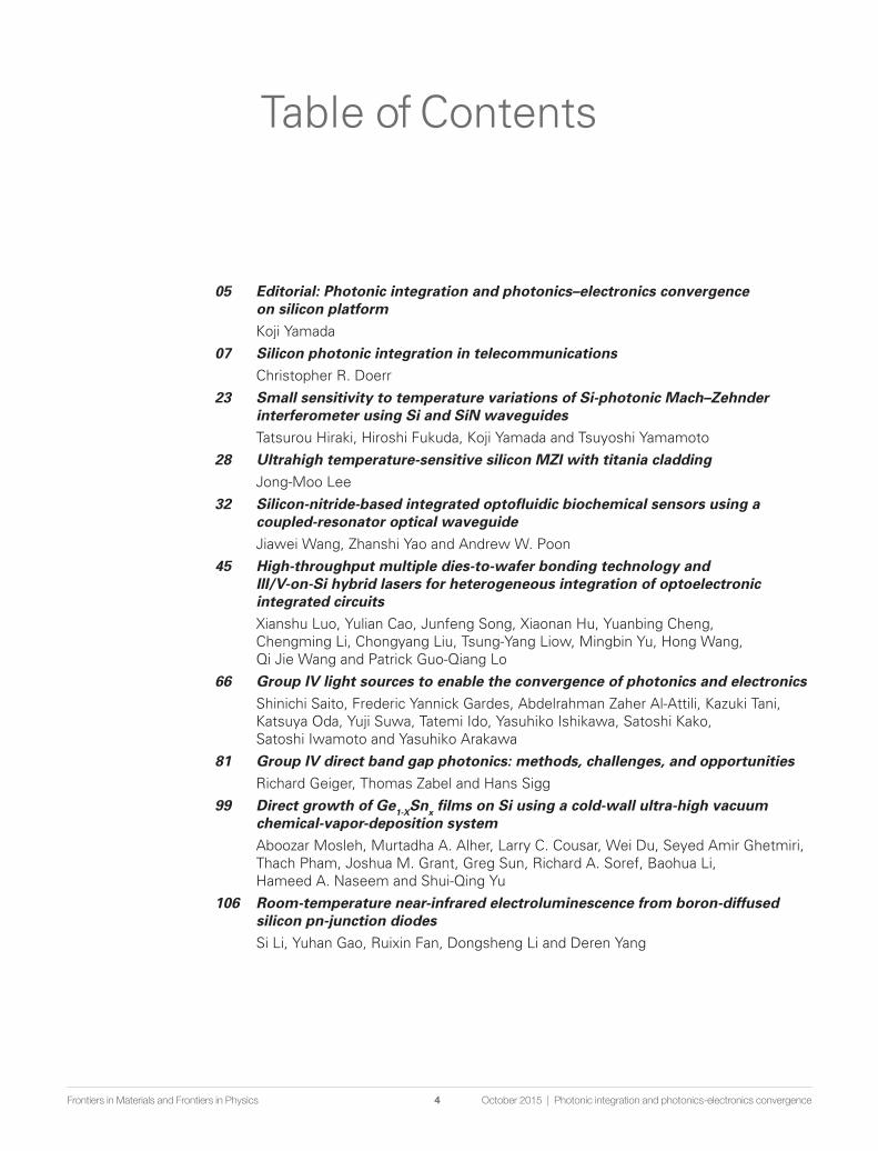
05 Editorial: Photonic integration and photonics–electronics convergence on silicon platform
Koji Yamada
07 Silicon photonic integration in telecommunications Christopher R. Doerr
23 Small sensitivity to temperature variations of Si-photonic Mach–Zehnder interferometer using Si and SiN waveguides
Tatsurou Hiraki, Hiroshi Fukuda, Koji Yamada and Tsuyoshi Yamamoto
28 Ultrahigh temperature-sensitive silicon MZI with titania cladding Jong-Moo Lee
32 Silicon-nitride-based integrated optofluidic biochemical sensors using a coupled-resonator optical waveguide
Jiawei Wang, Zhanshi Yao and Andrew W. Poon
45 High-throughput multiple dies-to-wafer bonding technology and III/V-on-Si hybrid lasers for heterogeneous integration of optoelectronic integrated circuits
Xianshu Luo, Yulian Cao, Junfeng Song, Xiaonan Hu, Yuanbing Cheng, Chengming Li, Chongyang Liu, Tsung-Yang Liow, Mingbin Yu, Hong Wang, Qi Jie Wang and Patrick Guo-Qiang Lo
66 Group IV light sources to enable the convergence of photonics and electronics Shinichi Saito, Frederic Yannick Gardes, Abdelrahman Zaher Al-Attili, Kazuki Tani,
Katsuya Oda, Yuji Suwa, Tatemi Ido, Yasuhiko Ishikawa, Satoshi Kako, Satoshi Iwamoto and Yasuhiko Arakawa
81 Group IV direct band gap photonics: methods, challenges, and opportunities Richard Geiger, Thomas Zabel and Hans Sigg
99 Direct growth of Ge1-XSnx films on Si using a cold-wall ultra-high vacuum chemical-vapor-deposition system
Aboozar Mosleh, Murtadha A. Alher, Larry C. Cousar, Wei Du, Seyed Amir Ghetmiri, Thach Pham, Joshua M. Grant, Greg Sun, Richard A. Soref, Baohua Li, Hameed A. Naseem and Shui-Qing Yu
106 Room-temperature near-infrared electroluminescence from boron-diffused silicon pn-junction diodes
Si Li, Yuhan Gao, Ruixin Fan, Dongsheng Li and Deren Yang
Table of Contents
4 October 2015 | Photonic integration and photonics-electronics convergenceFrontiers in Materials and Frontiers in Physics

October 2015 | Volume 2 | Article 655
Editorialpublished: 14 October 2015
doi: 10.3389/fmats.2015.00065
Frontiers in Materials | www.frontiersin.org
Edited and reviewed by: Lorenzo Pavesi,
University of Trento, Italy
*Correspondence:Koji Yamada
Specialty section: This article was submitted to
Optics and Photonics, a section of the
journal Frontiers in Materials
Received: 24 September 2015Accepted: 29 September 2015
Published: 14 October 2015
Citation: Yamada K (2015) Editorial: Photonic
integration and photonics–electronics convergence on silicon platform.
Front. Mater. 2:65. doi: 10.3389/fmats.2015.00065
Editorial: Photonic integration and photonics–electronics convergence on silicon platformKoji Yamada*
National Institute of Advanced Industrial Science and Technology, Tsukuba, Japan
Keywords: silicon photonics, photonic integration, additional waveguide system, iii–V semiconductors, germanium-based emitter, wafer bonding, telecommunications applications, bio-chemical applications
Silicon-based photonics technology, which is based on the same paradigm of silicon (Si) electronics technology, promises to provide us with a compact photonic integration platform with high integra-tion density, mass manufacturing, and excellent cost performance. This technology has been used to develop various photonic devices based on silicon, such as waveguides, filters, and modulators. In addition, germanium (Ge) photodetectors have been built on a silicon-based photonic platform. These photonic devices have already been monolithically integrated on silicon chips. Moreover, pho-tonics–electronics convergence based on silicon photonics is now being pursued. These emerging compact photonics–electronics convergent modules have the potential to be used in the fabrication of energy-efficient cost-effective systems for various applications, such as communications, informa-tion processing, and sensing.
The last decade first saw the development of Si-based photonic technologies for communication applications, and commercial products are now available for short-range data communications. For medium-/long-range telecommunication applications, in which stringent technical standards are applied to guarantee long-distance data transmission, intensive R&D is now providing us with technologies for high-performance Si-based photonic modules with complex device integrations (Doerr, 2015). In such high-performance applications, various assisting technologies should be implemented on the silicon photonic platform. For example, the resolution and dynamic range of silicon-based interference devices, such as wavelength filters, are considerably limited by fabrication errors in microfabrication processes. To overcome such limitations, additional waveguide systems, based on silicon nitride and silicon-rich silica, have been implemented (Yamada et al., 2014; Doerr, 2015).
Additional waveguide systems can also provide novel functionalities for further performance improvements. For example, the thermo-optic response of photonic devices can be controlled by combining silicon nitride and silicon waveguides, which could guarantee temperature-insensitive operation of data transmission systems (Hiraki et al., 2015). Thermo-optic responses can also be widely controlled by using titania as a cladding material in a Si waveguide (Lee, 2015). Moreover, an additional waveguide system can expand the application field of the Si photonic platform. For instance, silicon nitride waveguides, which are transparent to visible light, can be used to construct compact bio-sensing systems on a small Si chip (Wang et al., 2015).
Light-source integration, which is the most important open issue for the Si photonic platform, requires the help of other materials. For this purpose, III–V semiconductor materials have been bonded on silicon by using various hybrid integration techniques, such as direct die-to-wafer bonding (Fang et al., 2006; Luo et al., 2015). For monolithic integration, Ge-based light sources are now being studied intensively. The most important technology for Ge-based light sources is band-gap engineering, which aims to achieve a direct transition in Ge, which is originally an indirect-transition material. The recent status of Ge-based light sources on Si is reviewed in this special issue (Saito et al., 2014; Geiger et al., 2015). Mechanical stress and heavily doped n-type carriers

October 2015 | Volume 2 | Article 656
Yamada Photonic integration on silicon platform
Frontiers in Materials | www.frontiersin.org
would significantly contribute to making Ge a direct-transi-tion material. GeSn alloy is also a very attractive material for light sources on a Si platform because Sn, which can easily be dissolved in Ge, offers an important degree of freedom in band-gap engineering (Mosleh et al., 2015). Another approach now being investigated for monolithic integration of light sources is Si-based electro-luminescence at room tempera-ture, although its physical origin has not fully understood (Li et al., 2015).
The Si-based photonic platform requires various assisting materials for accomplishing practical photonic functions.
Fortunately, it has superior flexibility and robustness for integrat-ing these materials. Along with photonic functions, the Si-based photonic platform can integrate electronic functions monolithi-cally. In other words, we are on the verge of obtaining an ultimate technology that can integrate all photonic and electronic functions on a single Si chip.
aCKNoWlEdGMENtS
I would like to acknowledge all the authors, reviewers, edi-tors, and publishers, who have supported this Research Topic.
rEFErENCES
Doerr, C. R. (2015). Silicon photonic integration in telecommunications. Front. Phys. 3:37. doi:10.3389/fphy.2015.00037
Fang, A. W., Park, H., Cohen, O., Jones, R., Paniccia, M. J., and Bowers, J. E. (2006). Electrically pumpled hybrid AlGaInAs-silicon evanescent laser. Opt. Express 14, 9203–9216. doi:10.1364/OE.14.009203
Geiger, R., Zabel, T., and Sigg, H. (2015). Group IV direct band gap photonics: methods, challenges, and opportunities. Front. Mater. 2:52. doi:10.3389/fmats.2015.00052
Hiraki, T., Fukuda, H., Yamada, K., and Yamamoto, T. (2015). Small sensitivity to temperature variations of Si-photonic Mach-Zhender interferometer using Si and SiN waveguides. Front. Mater. 2:26. doi:10.3389/fmats.2015.00026
Lee, J.-M. (2015). Ultrahigh temperature-sensitive silicon MZI with titania clad-ding. Front. Mater. 2:36. doi:10.3389/fmats.2015.00036
Li, S., Gao, Y., Fan, R., Li, D., and Yang, D. (2015). Room-temperature near-infrared electroluminescence from boron-diffused silicon pn-junction diodes. Front. Mater. 2:8. doi:10.3389/fmats.2015.00008
Luo, X., Cao, Y., Song, J., Hu, X., Cheng, Y., Li, C., et al. (2015). High-throughput multiple dies-to-wafer bonding technology and III/V-on-Si hybrid lasers for heterogeneous integration of optoelectronic integrated circuits. Front. Mater. 2:28. doi:10.3389/fmats.2015.00028
Mosleh, A., Alher, M. A., Cousar, L. C., Du, W., Ghetmiri, S. A., Pham, T., et al. (2015). Direct growth of Ge1-xSnx films on Si using a cold-wall ultra-high
vacuum chemical-vapor-deposition system. Front. Mater. 2:30. doi:10.3389/fmats.2015.00030
Saito, S., Gardes, F. Y., Al-Attili, A. Z., Tani, K., Oda, K., Suwa, Y., et al. (2014). Group IV light sources to enable the convergence of photonics and electronics. Front. Mater. 1:15. doi:10.3389/fmats.2014.00015
Wang, J., Yao, Z., and Poon, A. W. (2015). Silicon-nitride-based integrated optoflu-idic biochemical sensors using a coupled-resonator optical waveguide. Front. Mater. 2:34. doi:10.3389/fmats.2015.00034
Yamada, K., Tsuchizawa, T., Nishi, H., Kou, R., Hiraki, T., Takeda, K., et al. (2014). High-performance silicon photonics technology for tele-communications applications. Sci. Technol. Adv. Mater. 15, 024603. doi:10.1088/1468-6996/15/2/024603
Conflict of Interest Statement: The author declares that the research was con-ducted in the absence of any commercial or financial relationships that could be construed as a potential conflict of interest.
Copyright © 2015 Yamada. This is an open-access article distributed under the terms of the Creative Commons Attribution License (CC BY). The use, distribution or reproduction in other forums is permitted, provided the original author(s) or licensor are credited and that the original publication in this journal is cited, in accordance with accepted academic practice. No use, distribution or reproduction is permitted which does not comply with these terms.
REVIEWpublished: 05 August 2015
doi: 10.3389/fphy.2015.00037
Edited by:
Qiaoliang Bao,
Soochow University, China
Reviewed by:
Lukas Novotny,
ETH Zurich, Switzerland
Satoshi Iwamoto,
The University of Tokyo, Japan
Xiangping Li,
Swinburne University
of Technology, Australia
*Correspondence:
Christopher R. Doerr,
Acacia Communications, 1301 Route
36, Hazlet, NJ 07730 USA
Specialty section:
This article was submitted to
Optics and Photonics,
a section of the journal
Frontiers in Physics
Received: 11 February 2015
Paper pending published:
23 March 2015
Accepted: 13 May 2015
Published: 05 August 2015
Citation:
Doerr CR (2015) Silicon photonic
integration in telecommunications.
Front. Phys. 3:37.
doi: 10.3389/fphy.2015.00037
Silicon photonic integration intelecommunicationsChristopher R. Doerr *
Acacia Communications, Hazlet, NJ, USA
Silicon photonics is the guiding of light in a planar arrangement of silicon-based materials
to perform various functions. We focus here on the use of silicon photonics to create
transmitters and receivers for fiber-optic telecommunications. As the need to squeeze
more transmission into a given bandwidth, a given footprint, at a given cost increases,
silicon photonics makes more and more economic sense.
Keywords: integrated optics, silicon photonics, optical fiber, optical communications, coherent, gratings,
waveguides
1. Introduction
Until circa 2002, fiber-optic communication for metropolitan distances (80—600 km) and long-haul distances (600–15,000 km) employedmostly simple on-off keying (OOK) transmission. On-offkeying is simply turning on and off the light to transmit “1” s and “0” s. Higher performance, i.e., alower bit-error rate (BER) for the same received optical power and/or for the same optical signal-to-noise ratio (OSNR), can be obtained by using phase-modulated formats, such as binary phase-shiftkeying (BPSK) or quadrature phase-shift keying (QPSK). They maximize the distance betweenconstellation points for the same average signal power. In these “advanced” modulation formats[1], the term “symbol” is used to represent each data portion in time, because each symbol cancarry multiple bits of information. Early BSPK and QPSK were detected by differential detection,i.e., by interfering one symbol with the previous symbol in an interferometer in the receiver.
However, bandwidth needs have been constantly growing exponentially. It is expensive to installnew optical fibers, ∼ $30 k per mile [2], so carriers and data-center operators needed to sendmore bits per second in the same fiber in the same optical bandwidth. One key way is to use bothoptical polarizations, because this doubles the available bandwidth. Although signal orthogonalityis maintained, their polarizations are essentially randomly changed during propagation throughfiber. To unscramble them requires significant signal processing. Optical coherent detection allowsthis to be done by digital electronics.
Optical coherent detection was a hot topic in the 1980s, because it is a form of opticalamplification. However, the invention of the erbium-doped fiber amplifier (EDFA) eliminatedthat advantage and coherent interest died away. Another advantage of coherent detection is theability to receive the full optical field, both the real and imaginary parts of both polarizations. Withimprovements in complementary metal-oxide-semiconductor (CMOS) electronics, digital signalprocessing (DSP) became available circa 2002 to handle coherent detection even up to 100-Gb/s,causing a revival of coherent detection. In the past, coherent detection was simply single quadratureand single polarization. Now it is dual quadrature and dual polarization.
100-Gb/s coherent systems have proven to be extremely compelling. They allow an upgrade ofa 10-Gb/s channel to a 100-Gb/s channel with actually improved reach. Industry analyses showthe number of metro and long-haul 100-Gb/s coherent transceivers sold per year to be on a steepupwards ramp as 10-Gb/s OOK transceivers are replaced by 100-Gb/s coherent transceivers.
Frontiers in Physics | www.frontiersin.org August 2015 | Volume 3 | Article 377

Doerr Silicon photonic integration in telecommunications
FIGURE 1 | 100-Gb/s coherent transceiver form-factor evolution. It went from a full line card, to a multi-source agreement (MSA) module, to a 100-Gb/s
form-factor pluggable (CFP) module. The D in D-CFP means that it is a digital module and the DSP is included inside, as opposed to a module that contains only the
optics.
However, the price of 100-Gb/s coherent transceivers isexpected to drop significantly. This is because users want topay the same price per connection even though the bit ratekeeps increasing. However, not only must the price drop, but thefootprint and power consumption as well. As seen in Figure 1,100-Gb/s modules have gone from full line cards to 5 × 7in2 screwed-on modules to 3.2 × 5.7 in2 pluggable modulestoday. Today’s 100-Gb/s pluggable form factor is called a CFP.Tomorrow’s will be a CFP2, which is half the size, and eventually aCFP4, which is a quarter the size. Power consumptions have gonefrom more than 100 W on a line card, to 70 W for the screwed-on module, to 28 W for the CFP. The next step, the CFP2, allowsonly 12W.
There are two main components in a coherent transceiver—the DSP chip and the optics. Today’s coherent CFP contains both.There is a, possibly temporary, trend to take the DSP out of themodule and put it on the line card. Such modules are called“analog” modules, rather than digital. With today’s technology, itis not possible to have both the optics andDSP be under 12W, themaximum power in a CFP2. However, in 1–2 years, technologywill likely be ready for a “digital” CFP2.
To meet these requirements of lower price, lower power andsmaller footprint, one must make advancements in technology.For the DSP, one can take advantage of the steady reduction intransistor size in industry, which reduces power and footprint.Node size and introduction year are shown inTable 1 [3]. Today’scoherent DSPs use 20–28 nm. Tomorrow’s will use 14 nm.
For the optics, one must use photonic integration, the focus ofthis article. Most of today’s coherent transceivers are built usingseparate LiNbO3/planar lightwave circuit (PLC) modulators andInP/PLC receivers, as shown in Figure 2. More andmore, smallerInP modulators and InP receivers are being used. In today’scoherent CFP, there is a single silicon photonic (SiPh) integratedcircuit (PIC) containing both the transmitter and receiver [4].Not shown is a separate tunable laser.
Finally, a dominant cost for the DSP and optics is thepackaging; one can further reduce cost, power, and footprint byco-packaging the DSP and optics. Such transceivers are expectedin 2–3 years.
Figure 3 shows many of the elements that may be integratedin a PIC. The blue are passive, the red are active (have an intendeddynamic interaction between light and matter), and the greenare electronic components. PICs have been around more than 20
TABLE 1 | Node size and first year of commercial introduction for CMOS
electronics.
Node size Year
10 µm 1971
6 µm 1974
3 µm 1977
1.5 µm 1982
1 µm 1985
800 nm 1989
600 nm 1994
350 nm 1995
250 nm 1997
180 nm 1999
130 nm 2001
90 nm 2004
65 nm 2006
45 nm 2008
32 nm 2010
22 nm 2012
14 nm 2014
10 nm 2016
7 nm 2018
5 nm 2020
years. The main advantages of photonic integration are a smallfootprint, due to strongly confining waveguides and lens-freeconnections between parts; low power, due to an obviation of50- RF lines; higher bandwidth RF connections; and low price,due to fewer touch points, no mechanical adjustments, less testequipment, and less material. The main disadvantages of PICsare typically a higher insertion loss and the inability to optimizecomponents independently.
2. PIC Material Systems
Figure 4 shows the most popular PIC material systems. From leftto right there are silica-on-silicon PICs, also called PLCs; silicon-on-insulator PICs, also called silicon photonics; lithium niobite(LiNbO3); and III–V PICs, such as InP and GaAs. This articlefocuses on silicon photonics. In silicon photonics, the light ismostly guided in silicon, which has an indirect bandgap of 1.12
Frontiers in Physics | www.frontiersin.org August 2015 | Volume 3 | Article 378

Doerr Silicon photonic integration in telecommunications
FIGURE 2 | 100-Gb/s coherent optics evolution, going from LiNbO3
modulators and planar lightwave circuit (PLC)-based receivers to
InP-based modulators and receivers to silicon photonic modulators
and receivers.
eV (1.1 µm). The silicon is a pure crystal grown in a boule andthen sliced into wafers, today typically 300mm in diameter, asshown in Figure 5. The surfaces are oxidized to form SiO2 layers.One wafer is bombarded with hydrogen atoms to a specifieddepth. Then the two wafers are placed together in a vacuum,and the oxide layers bond to each other. The assembly is crackedat the hydrogen implantation line. Then the silicon layer wherethe crack was is polished, and one is left with a thin layer ofcrystalline silicon on a layer of oxide on a full silicon “handle”wafer. The waveguides are formed from this thin crystalline layer.While these silicon-on-insulator (SOI) wafers are what makeslow-loss silicon photonic waveguides possible, they are actuallyused mostly for low-power CMOS circuits, because of the lowleakage currents they offer.
There is a wide family of possible silicon-based opticalwaveguides, shown in Figure 6. They range from micro-scaleGe-doped SiO2 waveguides to nano-scale Si wire waveguides. Byadding Ge, one can make photodetectors and electro-absorptionmodulators. Potentially even optical amplifiers. By doping thesilicon one can make optical modulators. From left to right at thebottom are silicon wire waveguides, silicon nitride waveguides,
FIGURE 3 | Some of the possible PIC integration elements.
FIGURE 4 | Popular PIC material systems. The second from the left is a silicon wire waveguide and is the focus of this article.
Frontiers in Physics | www.frontiersin.org August 2015 | Volume 3 | Article 379
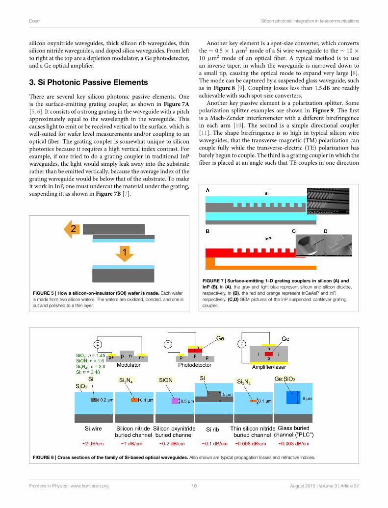
Doerr Silicon photonic integration in telecommunications
silicon oxynitride waveguides, thick silicon rib waveguides, thinsilicon nitride waveguides, and doped silica waveguides. From leftto right at the top are a depletion modulator, a Ge photodetector,and a Ge optical amplifier.
3. Si Photonic Passive Elements
There are several key silicon photonic passive elements. Oneis the surface-emitting grating coupler, as shown in Figure 7A
[5, 6]. It consists of a strong grating in the waveguide with a pitchapproximately equal to the wavelength in the waveguide. Thiscauses light to emit or be received vertical to the surface, which iswell-suited for wafer level measurements and/or coupling to anoptical fiber. The grating coupler is somewhat unique to siliconphotonics because it requires a high vertical index contrast. Forexample, if one tried to do a grating coupler in traditional InPwaveguides, the light would simply leak away into the substraterather than be emitted vertically, because the average index of thegrating waveguide would be below that of the substrate. To makeit work in InP, one must undercut the material under the grating,suspending it, as shown in Figure 7B [7].
FIGURE 5 | How a silicon-on-insulator (SOI) wafer is made. Each wafer
is made from two silicon wafers. The wafers are oxidized, bonded, and one is
cut and polished to a thin layer.
Another key element is a spot-size converter, which convertsthe ∼ 0.5 × 1 µm2 mode of a Si wire waveguide to the ∼ 10 ×
10 µm2 mode of an optical fiber. A typical method is to usean inverse taper, in which the waveguide is narrowed down toa small tip, causing the optical mode to expand very large [8].The mode can be captured by a suspended glass waveguide, suchas in Figure 8 [9]. Coupling losses less than 1.5 dB are readilyachievable with such spot-size converters.
Another key passive element is a polarization splitter. Somepolarization splitter examples are shown in Figure 9. The firstis a Mach-Zender interferometer with a different birefringencein each arm [10]. The second is a simple directional coupler[11]. The shape birefringence is so high in typical silicon wirewaveguides, that the transverse-magnetic (TM) polarization cancouple fully while the transverse-electric (TE) polarization hasbarely begun to couple. The third is a grating coupler in which thefiber is placed at an angle such that TE couples in one direction
FIGURE 7 | Surface-emitting 1-D grating couplers in silicon (A) and
InP (B). In (A), the gray and light blue represent silicon and silicon dioxide,
respectively. In (B), the red and orange represent InGaAsP and InP,
respectively. (C,D) SEM pictures of the InP suspended cantilever grating
coupler.
FIGURE 6 | Cross sections of the family of Si-based optical waveguides. Also shown are typical propagation losses and refractive indices.
Frontiers in Physics | www.frontiersin.org August 2015 | Volume 3 | Article 3710

Doerr Silicon photonic integration in telecommunications
and TM the other [12]. The fourth is a 2D grating coupler[13]. The fiber mode with its electric field perpendicular to thewaveguide propagation direction will couple to that waveguide.The fiber can be either tilted and couple to two waveguidesor be normal to the surface and couple to four waveguides.The 2D grating coupler has the added advantage of acting as apolarization rotator, in that all the light on the chip has the samepolarization yet was two orthogonal polarizations in the fiber.
4. Si Photonic Active Elements
Asmentioned above, a photonic active element has an intentionaldynamic interaction between light andmatter. A typical photonicactive element is an optical modulator. All the Si opticalmodulators today are based on the plasma free carrier effect. Thecomplex refractive index of the silicon changes by changing the
FIGURE 8 | Spot-size converter for silicon wire waveguides. The silicon
is inverse tapered inside a suspended glass waveguide. The silicon substrate
has been etched away under the suspended glass waveguide.
number of free electrons and holes, either by doping, electricalmeans, or optical means, as shown in Equations (1, 2), obtainedby fitting to data in Soref and Bennett at 1550-nm wavelength[14]. The holes have a larger ratio of real to imaginary indexchange, i.e., more phase change for a given loss change, andthus are usually favored for making the phase modulators inMach-Zehnder and ring modulators.
1nr = −8.8× 10⁻²²Ne − 8.5× 10⁻¹⁸N0.8h (1)
ni = 1.0× 10⁻²²Ne + 7.4× 10⁻²³Nh (2)
Various Si modulator types are shown in Figure 10A. In thecarrier injection modulator, the light is in intrinsic siliconinside a very wide p-i-n junction, and electrons and holes areinjected. Such a modulator is slow, however, typically 500-MHzbandwidth, because it takes a long time for the free electronsand holes to recombine after injection. Thus, such structuresare usually used as variable optical attenuators (VOAs) ratherthan modulators [15, 16]. In the carrier depletion modulator,the light is partly in a narrow p-n junction, and the depletionwidth of the p-n junction is varied by an applied electric field.Such a modulator can operate at over 50 Gb/s [17], but hasa high background insertion loss. A typical VπL is 2 V-cm.The metal-oxide-semiconductor (MOS) (really semiconductor-oxide-semiconductor) modulator contains a thin oxide layer inthe p-n junction [18]. It allows for some carrier accumulationas well as carrier depletion, allowing for a smaller VπL of ∼0.2V-cm, but with the drawbacks of higher optical loss and highercapacitance per unit length. There are also SiGe electroabsorptionmodulators [19] that rely on band-edgemovement in SiGe. Thereare also graphene modulators that rely on switching the graphenebetween an absorbing metal and a transparent insulator [20].
Various Si-based photodetectors are shown in Figure 10B.The absorption material is Ge. Ge absorbs light with wavelengthsup to about 1.6 µm. Shown on the left is a p-i-n configuration
FIGURE 9 | Various polarization splitters.
Frontiers in Physics | www.frontiersin.org August 2015 | Volume 3 | Article 3711

Doerr Silicon photonic integration in telecommunications
FIGURE 10 | (A) Cross sections of various silicon-based optical modulator designs and (B) photodetector designs.
FIGURE 11 | Configurations for integrating optical gain into silicon photonics. Fabrication insertion point becoming later in the process as one moves from left
to right.
[21], the most successful commercially today. It consists of p-doped silicon on which Ge is grown. Ge and Si have a 4% latticemismatch, so to minimize dislocations, a thin layer of SiGe isgrown first. The top of the Ge is n doped. Shown in the middle isa metal-semiconductor-metal (MSM) photodiode [22] and at theright avalanche photodiodes (APDs) [23]. The APD avalancheregion is in Si, which has a lower noise than avalanche regionsin III–V materials.
There is still no clear-winning solution for integrating opticalgain with silicon photonics. Some of the various option are shownin Figure 11, organized by assembly level. On the far left is
monolithic integration, including using epitaxially grown Ge asan optical gain material [24], Er-doped glass waveguides, suchas Al2O3, (which require optical pumping) [25], and epitaxiallygrown GaAs quantum dots [26]. The next column is wafer-to-wafer assembly, including oxide bonding [27] and organicbonding [28] of III–V gain regions. The next column is die-to-wafer assembly, including inserting III–V die into cavities in theSi wafer and then patterning the waveguides [29]. The advantagesof all the left three columns is that the full device can be testedon the wafer level, before it is diced out. The far right columnis die-to-die assembly, including butt coupling of a Si die and a
Frontiers in Physics | www.frontiersin.org August 2015 | Volume 3 | Article 3712

Doerr Silicon photonic integration in telecommunications
III–V die and coupling with a lens and a grating coupler [30].Commercial deployment is tending to move from the right to leftof this figure.
An element that is partway between an active and passiveelement is an optical isolator. Optical isolators are required tostop back reflections from causing noise and oscillations in lasersand optical amplifiers. An isolator requires a non-reciprocalelement [31]. In silicon photonics, two main types of isolatorshave been reported: magneto-optic and modulation-based.In magneto-optic isolators, garnets are placed on the side ortop of the waveguide [32, 33]. In a modulation-based isolator,the optical field is modulated with either a traveling wave ora time delay between multiple modulators [34]. Figure 12
shows a modulation-based isolator design based on a parallelarrangement of phase modulators in series [35]. Each modulatoris driven by a sine wave. In the forward direction, the secondmodulator in each arm undoes the modulation of the firstmodulator; but in the backward direction, the two modulatorsadd constructively. Thus, there is no effect at all on the signal inthe forward direction but in the backward direction it is stronglyphase modulated. If the phase modulation amplitude is just right,then a continuous-wave signal passing backwards is completelyattenuated at its original frequency. This gives narrow-bandisolation. By having multiple such narrow-band isolators inparallel, driven by the same frequency but appropriate differentRF drive phases in each arm, one can achieve broadbandisolation. A two-arm version was demonstrated in siliconphotonics, achieving ∼3 dB of isolation. The modulationwas done by carrier injection in the silicon waveguide. Theisolation can be improved by reducing the residual amplitudemodulation in the phase modulators, by increasing the speed ofthe modulators, and/or by increasing the number of arms in theinterferometer.
5. PIC Material System Comparison
Table 2 shows a comparison between InP and Si. InP is a muchmore expensive material than Si because of the rarity of In. Sicircuits tend to have a higher yield than InP circuits because thereis much less epitaxy involved in Si circuits. In Si circuits, usuallythe only epitaxy is Ge, used in the photodetectors, whereas inInP all of the waveguides, even the passive ones, must be grownby epitaxy. Epitaxy tends to have a higher defect density thancrystal growth from a boule. InP waveguides have high indexcontrast only laterally, whereas Si waveguides have high indexcontrast laterally and vertically. This allows much smaller bendradii and other more compact structures in Si. InGaAsP has adirect bandgap, whereas Si and Ge do not. Thus, the InP materialsystem has a much more efficient laser. The native oxide of theInP system is much less robust than the native oxide of Si, whichis SiO2. Silicon is a stronger material than InP, allowing for muchlarger wafers, 75 mm compared to 300mm (going to 450mmsoon). InP modulators usually depend on the quantum-confinedStark effect, which is temperature sensitive because of the bandedge movement with temperature. Silicon modulators have veryminimal temperature dependence.
Silicon photonics is usually considered only for low-cost,short-reach, high-volume (>1M/year) products. This is becauseit is assumed that a large number of wafer starts is requiredto pay for mask and development costs and that siliconphotonics has a significant performance penalty for metro andlong-haul products. However, the real situation is actually theopposite. This is because in low-cost, short-reach, high-volumeapplications, there is tremendous competition from verticalcavity surface-emitting lasers (VCSELs) and directly modulatedlasers (DMLs), and silicon photonics’ weakness of not havingan easy way to integrate lasers is a significant disadvantage.On the other hand, in metro and long-haul applications, it isbetter to keep the laser separate anyway as it is preferable tointegrate the silicon photonics and DSP together, which is a hotenvironment. Also, coherent detection can make up for many
FIGURE 12 | (A) configuration of an optical isolator that uses a tandem
arrangement of phase shifters. There are N arms in the interferometer. The
more the arms, the higher the broadband isolation. (B,C) 2-arm version built in
silicon photonics.
TABLE 2 | Pros and cons of InP and Si for photonic integrated circuits.
InP Si
Expensive material Cheap material
• In is scarce • 27% mass Earth’s crust is Si
Medium yield High yield
• W.g. material from epitaxy • W.g. material from original boule
Small footprint Extremely small footprint
• High index contrast in 1D • High index contrast in 2D
Native laser No native laser
Poor native oxide Excellent native oxide
Low dark current Medium dark current
Small wafers (75 mm typ.) Large wafers (300 mm typ.)
• 75 mm typical • 300 mm typical
• Brittle material • Strong material
Modulator temperature sensitive Modulator temperature insensitive
• Band edge moves with temperature • Carrier density not v. temp. dep.
Frontiers in Physics | www.frontiersin.org August 2015 | Volume 3 | Article 3713

Doerr Silicon photonic integration in telecommunications
FIGURE 13 | Simulation results from 3D sparse FDTD. (A) is the top
view of the structure being simulated, which is a directional coupler. (B)
Shows a screen shot from a simulation using a quasi-TE launch. The top two
figures show the top views of the quasi-TE and quasi-TM signals, and the
lower two figures show the corresponding cross-section views. (C) Shows a
screen shot from a simulation using a quasi-TM launch.
FIGURE 14 | Silicon photonics 8-PSM transceiver. Courtesy of Luxtera.
FIGURE 15 | Silicon photonics 8-WDM receiver. The upper figure shows a photograph of the chip, the lower left figure shows the measured responsivities to the 8
detectors vs. wavelength, and the lower right figure shows the measured bit-error rate at 1.25 Gb/s for one of the channels using a polarization scrambler.
Frontiers in Physics | www.frontiersin.org August 2015 | Volume 3 | Article 3714

Doerr Silicon photonic integration in telecommunications
of silicon photonics’ imperfections, such as the dark currentis much smaller than the local oscillator photocurrent. Also,the argument that one needs a large number of wafer startsto pay for mask and development costs is fallacious, becausesilicon photonics is done in a very large node size compared to
FIGURE 16 | Measured PAM-2, -4, and -8 optical eye diagrams at 28
Gbaud using a silicon photonics modulator.
FIGURE 17 | 80-Gb/s dual-polarization transmitter in InP. It consists of
two electro-absorption InGaAsP modulators, a polarization splitter, and a
polarization combiner. The incoming laser has its polarization oriented at 45.
state-of-the-art CMOS, and thus themasks and runs are relativelyinexpensive.
6. PIC Design
PICs are usually laid out in using mathematical scripts. Thisis because usually in PICs, path lengths matter, when ininterferometers or because of skew. The PIC is made bypatterning multiple layers, typically 10 to 30, on a wafer. Theselayers consist of many polygon shapes, typically in a GDSIIformat. Before sending the files to the photomask shop, thereis a strong desire to be able to simulate the PIC to verify thedesign. There are multiple levels of simulation. The lowest levelis 3D electromagnetic (EM) simulation, in which simulationis done at the sub-wavelength level. Interaction with atomsin the materials is done on the macroscopic scale. Typicalmethods are the 3D finite-difference time domain (3D FDTD)[36] and eigenmode expansion (EME) methods [37]. Thesemethods are the most accurate but simulation times for anentire PIC are prohibitive. The next level is 2.5D EM simulation,such as the finite-difference beam propagation method (FD-BPM). These methods are significantly faster, with a tradeoffof accuracy. Also, BPMs can handle only paraxial propagation,e.g., they cannot be used to simulate a resonator. The nextlevel is 2D EM simulation, such as 2D FDTD and 2D BPM.Again, these are faster, but limited. These cannot simulatee.g., a polarization rotator. The next level up is transmissionand/or scattering matrix simulation. Each main component isreduced to an element with inputs and outputs, and connectingwaveguides are reduced to phase shift and attenuation elements.These simulations are extremely fast. A transmission matrix is
FIGURE 18 | DP-DQPSK receiver in silicon photonics. Uses optical
polarization tracking. The upper figure shows a schematic, and the lower
figure a device photograph. The incoming signal is separated into two
polarizations by a 2D grating coupler, a series of couplers and phase shifters
demultiplex the two signals, which had been mixed during fiber transmission,
and two Mach-Zehnder delay interferometers demodulate the signals.
Frontiers in Physics | www.frontiersin.org August 2015 | Volume 3 | Article 3715

Doerr Silicon photonic integration in telecommunications
FIGURE 19 | 7-core-fiber silicon photonics receiver. The upper right
figure shows a photograph of the fiber cross section, showing the seven
cores. The top shows the schematic for each channel in the silicon photonic
circuit shown in the bottom figure. The incoming fiber is tilted at the proper
angle to the 1D grating couplers such that TE polarization couples to the left
and TM polarization couples to the right.
FIGURE 20 | PIC for coupling to the multimodes of a ring-core fiber by
using a circular grating coupler connected to a star coupler. The upper
figure shows a schematic of the silicon photonic circuit photograph shown at
the bottom. The circuit contains a circular grating coupler connected to an
array of waveguides of equal length.
multiplied by the incoming signals to find the outgoing signals.A scattering matrix (whose elements are called s-parameters) ismultiplied by the incoming and outgoing signals on one side ofthe element to find the incoming and outgoing signals on theother side of the element. Basically, scattering matrices includereflections within the element. Scattering matrices are typicallytwice as large in each dimension as transmission matrices.
However, relying on EM simulation of some elements andscattering/transmission matrices to simulate the entire PIC doesnot guarantee that the design is error-free before tape out. Forexample, a miscalculated path length, a multimode waveguide
FIGURE 21 | First reported vector modulator. It was in GaAs.
without sufficient high-order mode rejection, or two waveguidesthat pass too close to each other and have undesired coupling areunlikely to be caught.
A technique called sparse FDTD allows one to do 3D and2D FDTD simulation directly on the entire PIC design to verifythe design [38]. While it is unlikely any EM simulation toolcan simulate a very large PIC, sparse FDTD can simulate quitelarge portions. In conventional 3D FDTD, one starts with all sixcomponents of the EM fields in a specified quantized volume.Time is advanced a step, and the new field components arecalculated in the volume, and so on. So many calculations everystep takes a very long time. In sparse 3D FDTD, rather than docalculations for every point in the volume every step, a list offield components is maintained, theoretically in an arbitrarilylarge volume, is maintained and calculations are done on these.At each time step points neighboring the field components are
Frontiers in Physics | www.frontiersin.org August 2015 | Volume 3 | Article 3716

Doerr Silicon photonic integration in telecommunications
added, and field components with power below a certain level arediscarded. For certain structures this calculation can be orders ofmagnitude faster than conventional 3D FDTD. However, sparseFDTD performs poorly with dispersive structures, because thenthe optical field spreads out too much, making the list too long.Example screen shots from 3D FDTD simulation of a PBS likethat shown in Figure 9B are shown in Figure 13 [39].
7. Short Reach PICs
Short reach communications typically means less than 2 km, butcan sometimes include up to 40 km. Short reach is usually forintra-data center, connecting racks, or client-side optics. There isan emerging need for very short reach communications in whichboards are connected optically within a rack. Such optics are nolonger considered “transceivers” and for the sake of focus are leftout of this article.
Because of the fast growth and turn-over in data centers thereis usually insufficient time for standards to develop. This allows
for a wide diversity of solutions. These various solutions do notinteroperate, but the users do not care so much, as long as pricesare low.
Today, most of the short reach links are based on vertical-cavity surface-emitting lasers (VCSELs) over multimode fiber,i.e., do not involve PICs at all. VCSELs are very inexpensive andeasy to couple to multimode fiber. It is nearly impossible for PICsto compete against VCSELs on price. However, the bandwidth-distance product for a VCSEL over multimode fiber is ∼ 2 GHz-km. At 25Gb/s, this limits distances to∼100m. Also, multimodefiber (MMF) costs more than standard single-mode fiber (SSMF),because many more km of SSMF have been produced thanMMF.Thus, when new data centers are built, it can be advantageousto outfit them with SSMF. Single-mode VCSELs are difficult tomake today, so this is a good opportunity for PICs. However,VCSEL technology is constantly improving, providing a constantchallenge to PICs in short-reach applications.
A successful PIC short-reach commercial solution today isbased on parallel single-mode fibers (PSM). Figure 14 shows an
FIGURE 22 | Early reported silicon photonic vector modulators.
FIGURE 23 | 2-bit optical DAC in silicon photonics.
Frontiers in Physics | www.frontiersin.org August 2015 | Volume 3 | Article 3717

Doerr Silicon photonic integration in telecommunications
8-fiber PSM solution (4 fibers out and 4 fibers in) based onsilicon photonics from Luxtera [40]. The chip contains a 1.4-µm laser in a small hermetic assembly on top of the PIC. Thiswavelength was chosen as optimum for the grating couplers thatcouple the laser light into the PIC. This laser is split four waysto four 10-Gb/s on-off-keying (OOK) distributed-driven Mach-Zehnder-interferometer modulators (MZMs). The CMOS driveelectronics are monolithically integrated with the photonics.Distributed driven means that the modulator is broken into Nsections in series, each with a separate driver timed appropriately.This saves power consumption over a traveling-wave modulator,because a traveling-wave modulator has a termination resistorinto which power must be dumped.
Another successful PIC short-reach solution is based onwavelength-division multiplexing (WDM). Typically fourwavelengths, each modulated with OOK at 25 Gb/s, aremultiplexed in the transmitter and demultiplexed at the receiver.
The advantage over PSM is requiring only two fibers insteadof eight, and the disadvantage is requiring four lasers insteadof one. WDM makes more sense as the cost of transceiversdrops compared to the cost of fiber and installing it, especiallyribbon fibers. Figure 15 shows an 8-channel CWDM receiver insilicon photonics [41]. It uses a silicon nitride spot-size converterand arrayed waveguide grating (AWG), which is polarizationindependent via variation of waveguide widths, silicon outputmultimode waveguides, and Ge photodetectors.
Yet another solution is to use multi-level modulation, calledpulse amplitude modulation (PAM). Figure 16 shows PAM4 andPAM8 eye diagrams at 28Gb/s generated by a silicon photonicsMZM.
One can also use polarization-division multiplexing (PDM),also called dual-polarization (DP) transmission. In this case,different signals are in each polarization. Figure 17 shows adual-polarization 80-Gb/s modulator in InP [42]. Such a design
FIGURE 24 | Early (A) InP and (B) silicon integrated coherent receivers.
FIGURE 25 | Single-chip silicon photonic coherent transceiver.
Frontiers in Physics | www.frontiersin.org August 2015 | Volume 3 | Article 3718
Doerr Silicon photonic integration in telecommunications
could be readily made in silicon photonics. In the fiber, thetwo signals will stay predominantly orthogonally polarized,but the polarization will vary unpredictably with time. At thereceiver, if one does not use coherent detection, one needs tooptically demultiplex the two polarizations. Figure 18 showsa device in silicon photonics that can optically demultiplexpolarization [43, 44]. It does this by receiving two orthogonalpolarizations from the fiber, these polarizations not necessarilythat of the signals, and then interferes the two with acontrollable phase and coupling ratio to demultiplex them. Todo this in an endless fashion, i.e., without ever needing phase-shifter resets back to zero, one needs multiple interferometerstages.
In the far future onemay find the data center interconnectionsso crowded that one must reduce the number of fiber strandsand instead put multiple cores and/or modes in a single fiber.Figure 19 shows a PIC for receiving from a 7-core fiber, usingpolarization diversity [45]. It includes optical filters for WDM.Figure 20 shows a PIC for receiving from a multi-mode ring-core fiber [46]. A multi-mode ring core fiber is advantageousbecause the modes can be accessed without waveguide crossingsand conveniently demultiplexed by a star coupler.
8. Metro and Long-reach PICs
Unlike short-reach links, which we saw have many choices oftransmission type, metro and long-reach links demand intradyne
coherent transmission. This is because long fiber routes areexpensive to install/obtain, and thus the user wants to pushas much information over each fiber as possible. Coherentreceivers make it possible to receiveWDM, PDM, and high-orderconstellations with high-performance, because the completeoptical field is received and acted on by a DSP. In intradynecoherent communications, the transmitted signal comes froma dual-polarization vector modulator, and the received signalis interfered with a continuous-wave (CW) laser signal whosefrequency is close to the carrier of the signal (within∼2–3 GHz),but does not need to be exact.
The first reported vector modulator was a GaAs PIC,shown in Figure 21 [47]. It consists of two MZMs in a largerinterferometer. Figure 22 show some early vector modulatorsin silicon photonics. The modulator in Figure 22A containstwo vector modulators, one for each polarization, along withthe polarization splitting optics [48]. The single-polarizationmodulator in Figure 22B uses a thin-oxide layer in the p-njunction to obtain a low VπL product and is driven directlyby CMOS inverters [49]. By using multiple segments in themodulator, one can create an optical digital-to-analog converter(DAC). The segment lengths are in a geometric sequence.Figure 23 shows a demonstration that achieved 16-QAMmodulation at 13 Gbaud using a silicon photonic optical DAC[50].
The first reported coherent receivers were in InP, asshown in Figure 24A [51–55]. Figure 24B shows an early
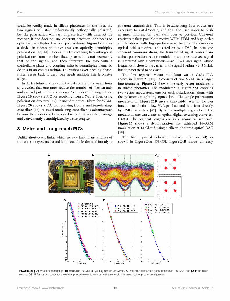
FIGURE 26 | (A) Measurement setup, (B) measured 30-Gbaud eye diagram for DP-QPSK, (C) real-time-processed constellations at 120 Gb/s, and (D–F) bit-error
rate vs. OSNR for various cases for the silicon photonics single-chip coherent transceiver in an optical loop back configuration.
Frontiers in Physics | www.frontiersin.org August 2015 | Volume 3 | Article 3719

Doerr Silicon photonic integration in telecommunications
FIGURE 27 | 100-Gb/s coherent CFP module using silicon photonics.
dual-polarization, dual-quadrature receiver in silicon photonics[56]. It uses a 2-D grating coupler as a fiber coupler, polarizationsplitter, and polarization rotator.
Figure 25 shows a recent silicon photonic PIC that containsthe full vector modulator and full coherent receiver on a singlechip [4]. This is lower cost and smaller footprint than separatetransmitter and receiver chips. There are three fibers connectedto the module: laser input, which is split between transmitter andreceiver; transmitter output; and receiver input. The fibers areconnected in a 3-fiber array, reducing cost and assembly time. Itis co-packaged in a hermetic gold box with four drivers and fourtransimpedance amplifiers. It does not require any temperaturecontrol, allowing the total power consumption to be less than5 W, −5 to 80C. A silicon photonics modulator does havesome imperfections compared to Pockels-effect modulators, likeGaAs and LiNbO3. It has residual amplitude modulation, diodenonlinearity, capacitance change with voltage, and bandwidthlimitations. A simulation including these effects shows that theimperfection performance penalty is only 0.1 dB compared to anideal modulator.
Each PIC was tested in a socket in an optical loop-backconfiguration using a 100-Gb/s DSP for real-time measurements,as shown in Figure 26A. Optical loop-back insures that anypotential crosstalk between the transmitter and receiver wouldshow up as degradation. Figure 26B shows a measured 30-Gbaud DP-QPSK eye diagram. There are five levels in sucha signal. Figure 26C shows measured real-time-processed 120-Gb/s DP-QPSK constellations. Measured BER vs. OSNR curvesat multiple wavelengths across the C-band are shown in
Figure 26D shown for comparison is the performance of discreteoptics. The performance of the silicon PIC is nearly the sameas the discrete optics. Figure 26E shows the performance atvarious temperatures, showing that the silicon photonics canindeed work without temperature control. Figure 26F shows theperformance up to 3000 km without significant penalty. Thisshows that the chirp of the silicon photonics modulator is low.
Figure 27 shows this PIC in a 100-Gb/s CFP module. As onecan see, the module is tightly packed and would be very difficultto make with discrete optics.
This single-chip coherent transceiver contains all the opticsneeded for a coherent transmitter except the tunable laser. Asmentioned earlier, it is probably better to keep the laser separateanyways because this chip can be co-packaged with the DSP,which runs very hot.
9. Conclusion
The touted advantage of silicon photonics is the die are lowercost than any other solution. While this may be true, it isof limited help in short-reach applications, where the lackof an integrated laser puts silicon photonics at a significantdisadvantage compared to the incumbents, such as VCSELs andDMLs. Instead, the less-touted advantages of silicon photonics:high yield, low modulator temperature sensitivity, high chipstrength, and ability to do polarization handling; make it idealfor metro and long-haul applications. Spending its adolescencein metro and long-haul, silicon photonics will have time todevelop mature laser integration methods, more routine foundryservices, and sophisticated packaging solutions so it can latertake on the short-reach incumbents. By that time, coherenttransmission may be cost- and power-effective enough to workin very short links, bringing its advantages of high sensitivity,high spectral efficiency, high-order modulation, and wavelengthselection.
Acknowledgments
The author is indebted to Long Chen, Diedrik Vermeulen,TorbenNielsen, Scott Stulz, Saeid Azemati, GregMcBrien, BennyMikkelsen, Christian Rasmussen, Mehrdad Givehchi, Seo YeonPark, Jonas Geyer, Xiao-Ming Xu, and many others.
References
1. Winzer P. Advanced optical modulation formats. Proc IEEE (2006) 94:952–85.doi: 10.1109/jproc.2006.873438
2. Wellbrock G. Where do we go from here? In: OIDA Workshop on State of the
Art Integrated Photonics.Washington, DC (2014).3. Wikipedia. Semiconductor Device Fabrication (2008).4. Doerr CR, Chen L, Vermeulen D, Nielsen T, Azemati S, Stulz S, et al.
Single-chip silicon photonics 100-Gb/s coherent transceiver. In: Optical FiberCommunication Conference: Postdeadline Papers. San Jose, CA (2014).
5. Taillaert D, Van Laere F, Ayre M, Bogaerts W, Van Thourhout D, Bienstman P,et al. Grating couplers for coupling between optical fibers and nanophotonicwaveguides. Jpn J Appl Phys. (2006) 45:6071–7. doi: 10.1143/JJAP.45.6071
6. Mekis A, Gloeckner S, Masini G, Narasimha A, Pinguet T. A grating-coupler-enabled CMOS photonics plaform. J Sel Topics Quant Electron (2011) 17:597–608.
7. Chen L, Zhang L, Doerr CR, Dupuis N, Weimann NG, Kopf RF. Efficientmembrane grating couplers on InP. IEEE Photon Tech Lett. (2010) 22:890–2.doi: 10.1109/LPT.2010.2047391
8. Shoji T, Tsuchizawa T, Watanabe T, Yamada K, Morita H. Lowloss mode size converter from 0.3 um square Si wire waveguidesto singlemode fibres. Electron Lett. (2002) 38:1669. doi: 10.1049/el:20021185
9. Chen L, Doerr CR, Chen YK, Liow TY. Low-loss and broadbandcantilever couplers between standard cleaved fibers and high-index-contrastSiN or Si waveguides. IEEE Photon Tech Lett. (2010) 22:1744–6. doi:10.1109/LPT.2010.2085040
Frontiers in Physics | www.frontiersin.org August 2015 | Volume 3 | Article 3720

Doerr Silicon photonic integration in telecommunications
10. Yamazaki H, Yamada T, Goh T, Kaneko A, Sano A. Integrated 100-Gb/sPDM-QPSK modulator using a hybrid assembly technique with silica-based PLCs and LiNbO3 phase modulators. In: European Conference and
Exposition on Optical Communications Brussels: IEEE (2008). 1–4. doi:10.1109/ECOC.2008.4729119
11. Fukuda H, Yamada K, Tsuchizawa T, Watanabe T, Shinojima H, ItabashiSI. Silicon photonic circuit with polarization diversity. Opt Express (2008)16:4872–80. doi: 10.1364/OE.16.004872
12. Tang Y, Dai D, He S. Proposal for a grating waveguide serving asboth a polarization splitter and an efficient coupler for silicon-on-insulatornanophotonic circuits. IEEE Photonics Technol Lett. (2009) 21:242–4. doi:10.1109/LPT.2008.2010528
13. Taillert D, Chong H, Borel PI, Frandsen LH, Rue RMDL, Baets R. Acompact two-dimensional grating coupler used as a polarization splitter.IEEE Photonics Technol Lett. (2003) 15:1249–51. doi: 10.1109/LPT.2003.816671
14. Soref R, Bennett B. Electrooptical effects in silicon. IEEE J Quantum Electron.
(1987) 23:123–9. doi: 10.1109/JQE.1987.107320615. Zheng D, Smith B. Improved efficiency Si-photonic attenuator. Opt Express
(2008) 16:16754–65. doi: 10.1364/OE.16.01675416. Dong P, Chen L. Monolithically integrated VOA-MUX with power monitors
based on submicron silicon photonics platform. Opt Fiber Commun LosAngeles, CA: IEEE (2012) 9–11. doi: 10.1364/ofc.2012.otu2i.5
17. Thomson DJ, Gardes FY, Fedeli JM, Zlatanovic S, Hu Y, Ping B, et al. 50-Gb/ssilicon optical modulator. IEEE Photonics Technol Lett. (2012) 24:234–6. doi:10.1109/LPT.2011.2177081
18. Liu A, Jones R, Liao L, Samara-Rubio D, Rubin D. A high-speed silicon opticalmodulator based on a metal âAS oxide âAS semiconductor capacitor. Nature(2004) 427:615–8. doi: 10.1038/nature02310
19. Liu J, Beals M, Pomerene A, Bernardis S, Sun R, Cheng J, et al. Waveguide-integrated, ultralow-energy GeSi electro-absorption modulators. Nat
Photonics (2008) 2:433–7. doi: 10.1038/nphoton.2008.9920. Liu M, Yin X, Ulin-Avila E, Geng B, Zentgraf T, Ju L, et al. A
graphene-based broadband optical modulator. Nature (2011) 474:64–7. doi:10.1038/nature10067
21. Ahn D, Hong Cy, Liu J, Giziewicz W, Beals M, Kimerling LC, et al. Highperformance, waveguide integrated Ge photodetectors. Opt Express (2007)15:3916–21. doi: 10.1364/OE.15.003916
22. Assefa S, Xia F, Bedell S, Zhang Y. CMOS-integrated 40GHz germaniumwaveguide photodetector for on-chip optical interconnects. In: Optical FiberCommunication Conference (2009). p. 10–2. Available online at: http://www.opticsinfobase.org/abstract.cfm?id=177916
23. Kang Y, Liu H, Morse M, Paniccia M. Monolithic germanium / siliconavalanche photodiodes with 340 GHz gain-bandwidth product. Nat Photonics(2008) 3:59–63. doi: 10.1038/nphoton.2008.247
24. Michel J, Camacho-aguilera RE, Cai Y, Patel N, Bessette JT, Dutt BR, et al.An electrically pumped Ge-on-Si laser. In: Optical Fiber Communication
Conference. Los Angeles, CA: IEEE (2012). p. 5–7.25. Purnawirman, Sun J, Adam TN, Leake G, Coolbaugh D, Bradley JDB, et al.
C-and L-band erbium-doped waveguide lasers with wafer-scale silicon nitridecavities. Opt Lett. (2013) 38:2–5. doi: 10.1364/OL.38.001760
26. Liu AY, Zhang C, Norman J, Snyder A, Lubyshev D, Fastenau JM, et al. Highperformance continuous wave 1.3 µ m quantum dot lasers on silicon. Appl
Phys Lett. (2014) 104:3–7. doi: 10.1063/1.486322327. Fang A, Park H, Cohen O, Jones R, Paniccia M. Electrically pumped hybrid
AlGaInAs-silicon evanescent laser. Opt Express (2006) 14:9203–10. doi:10.1364/OE.14.009203
28. Roelkens G, Brouckaert J, Van Thourhout D, Baets R, NoÌLtzel R, SmitM. Adhesive bonding of InPâLTInGaAsP dies to processed silicon-on-insulator wafers using DVS-bis-benzocyclobutene. J. Electrochem Soc. (2006)153:G1015. doi: 10.1149/1.2352045
29. Marchena E, Creazzo T, Krasulick SB, Yu PKL, Van Orden D, Spann JY, et al.Integrated tunable CMOS laser. In: Optical Fiber Communication Conference
(2013). Available online at: http://www.opticsinfobase.org/abstract.cfm?URI=oe-21-23-28048
30. Snyder B, Corbett B, O’Brien P. Hybrid integration of the wavelength-tunablelaser with a silicon photonic integrated circuit. J Lightwave Technol. (2013)31:3934–42. doi: 10.1109/JLT.2013.2276740
31. Jalas D, Petrov A, Eich M, Freude W, Fan S, Yu Z, et al. What is and what isnot an optical isolator. Nat Photonics (2013) 7:579–82.
32. Levy M, Osgood RMJr, Hegde H, Cadieu FJ, Wolfe R, Fratello VJ. Integratedoptical isolators with sputter-deposited thin-film magnets. IEEE Photonics
Technol Lett. (1996) 8:903–5. doi: 10.1109/68.50226533. Shoji Y, Mizumoto T, Yokoi H, Hseih IW, Osgood R. Magneto-optical isolator
with silicon waveguides fabricated by direct bonding. Appl Phys Lett. (2008)92:071117. doi: 10.1063/1.2884855
34. Bhandare S, Ibrahim SK, Sandel D, Zhang H, Wust F, Noe R. Novelnonmagnetic 30-dB traveling-wave single-sideband optical isolator integratedin III/V material. IEEE J Sel Top Quantum Electron. (2005) 11:417–21. doi:10.1109/JSTQE.2005.845620
35. Doerr CR, Chen L, Vermeulen D. Silicon photonics broadband modulation-based isolator. Opt Express (2014) 22:4493. doi: 10.1364/OE.22.004493
36. Yee KS. Numerical solution of initial boundary value problems involvingMaxwell’s equations in isotropic media. Antennas Propagation IEEE
Trans Livermore, CA: IEEE (1966). 302–7. doi: 10.1109/TAP.1966.1138693
37. Bienstman P, Baets R. Optical modelling of photonic crystals and VCSELsusing eigenmode expansion and perfectly matched layers. Opt Quantum
Electron. (2001) 33:327–41. doi: 10.1023/A:101088253123838. Doerr CR. Sparse finite difference time domain method. IEEE Photonics
Technol Lett. (2013) 25:2259–62. doi: 10.1109/LPT.2013.228518139. Doerr CR. 3D sparse finite-difference time-domain simulation of silicon
photonic integrated circuits. In:Optical Fiber Communication Conference. LosAngeles, CA (2015).
40. Narasimha A, Analui B, Liang Y, Member S, Sleboda TJ, Abdalla S, et al. Afully integrated 4 x 10-Gb / s DWDM optoelectronic transceiver implementedin a standard 1.3 um CMOS SOI technology. IEEE J Solid State Circ. (2007)42:2736–44. doi: 10.1109/JSSC.2007.908713
41. Doerr CR, Chen L, Buhl LL, Chen YK. Eight-channel SiO2/Si3N4/Si/GeCWDM receiver. IEEE Photonics Technol Lett. (2011) 23:1201–03. doi:10.1109/LPT.2011.2158091
42. Doerr CR, Zhang L. Monolithic 80-Gb / s dual-polarization On-off-keyingmodulator in InP. J Lightwave Technol. (2008) 2:19–21.
43. Doerr CR, Chen L. Monolithic PDM-DQPSK receiver in silicon. In: OpticalCommunication (ECOC), 2010 36th European Conference and Exhibition on
(IEEE) (2010). p. 1–3. Available online at: http://ieeexplore.ieee.org/xpls/abs_all.jsp?arnumber=5621418
44. Doerr CR, Fontaine NK, Buhl LL. PDM DQPSK silicon receiver withintegrated monitor and minimum number of controls. IEEE Photonics
Technol Lett. (2012) 24:697–9. doi: 10.1109/LPT.2012.218704845. Doerr CR, Taunay TF. Silicon photonics core-, wavelength-, and polarization-
diversity receiver. IEEE Photonics Technol Lett. (2011) 23:597–9. doi:10.1109/LPT.2011.2118748
46. Doerr CR, Fontaine N, HiranoM, Sasaki T, Buhl L,Winzer P. Silicon photonicintegrated circuit for coupling to a ring-core multimode fiber for space-division multiplexing. In: European Conference and Exposition on Optical
Communications (2011). Available online at: http://www.opticsinfobase.org/abstract.cfm?URI=ECOC-2011-Th.13.A.3
47. Griffin R, Johnstone R,Walker R,Wadsworth S, Carter A,Wale M. IntegratedDQPSK transmitter for dispersion-tolerant and dispersion-managed DWDMtransmission. OFC 2003 Optical Fiber Communications Conference (2003). p.7–8. doi: 10.1109/OFC.2003.1248559
48. Dong P, Xie C, Chen L, Buhl LL, Chen YK. 112-Gb/s monolithicPDM-QPSK modulator in silicon. Opt Express (2012) 20:B624–9. doi:10.1364/OE.20.00B624
49. Milivojevic B, Raabe C, Shastri A,WebsterM,Metz P, Sunder S, et al. 112Gb / sDP-QPSK transmission over 2427km SSMF using small-size silicon photonicIQmodulator and low-power CMOS driver. In:Optical Fiber Communications
Conference. San Jose, CA (2013). p. 5–7.50. Shastri A,WebsterM, Jeans G,Metz P, Sunder S, Chattin B, et al. Experimental
demonstration of ultra-low-power single polarization 56 Gb / s QAM-16generation without DAC using CMOS photonics. In: European Conference
and Exposition on Optical Communications. Cannes (2014). p. 16–8.51. Koch T, Koren U, Gnall R, Choa F, Hernandez-Gil F, Burrus C, et al.
GaInAs/GaInAsP multiple-quantum-well integrated heterodyne receiver.Electron Lett. (1989) 25:1621. doi: 10.1049/el:19891086
Frontiers in Physics | www.frontiersin.org August 2015 | Volume 3 | Article 3721

Doerr Silicon photonic integration in telecommunications
52. Takeuchi H, Kasaya K, Kondo Y, Yasaka H, Oe K, Imamura Y. Monolithicintegrated coherent receiver on InP substrate. IEEE Photonics Technol Lett.
(1989) 1:398. doi: 10.1109/68.4339253. Deri RJ, Pennings E, Scherer A, Gozdz A, Caneau C, Andreadakis N,
et al. Ultracompact monolithic integration of balanced, polarization diversityphotodetectors for coherent lightwave receivers. IEEE Photonics Technol Lett.
(1992) 4:1238. doi: 10.1109/68.16695454. Bach H, Matiss A, Leonhardt CC, Kunkel R, Schmidt D, Schell M, et al.
Monolithic 90 hybrid with balanced PIN photodiodes for 100 Gbit / s PM-
QPSK receiver applications. Optical Fiber Communication Conference (2009).p. 4–6.
55. Doerr CR, Zhang L, Winzer PJ. Monolithic InP multiwavelength coherentreceiver using a chirped arrayed waveguide grating. J Lightwave Technol.
(2011) 29:536–41. doi: 10.1109/JLT.2010.2097240
56. Doerr CR, Winzer PJ, Chen YK, Chandrasekhar S, Rasras MS, Chen L, et al.Monolithic polarization and phase diversity coherent receiver in silicon. JLightwave Technol. (2010) 28:520–5. doi: 10.1109/JLT.2009.2028656
Conflict of Interest Statement: The author declares that the research wasconducted in the absence of any commercial or financial relationships that couldbe construed as a potential conflict of interest.
Copyright © 2015 Doerr. This is an open-access article distributed under the terms
of the Creative Commons Attribution License (CC BY). The use, distribution or
reproduction in other forums is permitted, provided the original author(s) or licensor
are credited and that the original publication in this journal is cited, in accordance
with accepted academic practice. No use, distribution or reproduction is permitted
which does not comply with these terms.
Frontiers in Physics | www.frontiersin.org August 2015 | Volume 3 | Article 3722

MATERIALSORIGINAL RESEARCH ARTICLE
published: 30 March 2015doi: 10.3389/fmats.2015.00026
Small sensitivity to temperature variations of Si-photonicMach–Zehnder interferometer using Si and SiNwaveguidesTatsurou Hiraki 1,2*, Hiroshi Fukuda3, KojiYamada1,2 andTsuyoshiYamamoto1
1 NTT Device Technology Laboratories, NTT Corporation, Kanagawa, Japan2 NTT Nanophotonics Center, NTT Corporation, Kanagawa, Japan3 NTT Device Innovation Center, NTT Corporation, Kanagawa, Japan
Edited by:Toshihiko Baba, Yokohama NationalUniversity, Japan
Reviewed by:Junichi Fujikata, Photonics ElectronicsTechnology Research Association,JapanYosuke Terada, Yokohama NationalUniversity, Japan
*Correspondence:Tatsurou Hiraki , Device TechnologyLaboratories, NTT corporation, 3-1,Morinosato Wakamiya, Atsugi-shi,Kanagawa 243-0198, Japane-mail: [email protected]
We demonstrated a small sensitivity to temperature variations of delay-line Mach–Zehnderinterferometer (DL MZI) on a Si photonics platform. The key technique is to balance athermo-optic effect in the two arms by using waveguide made of different materials. Withsilicon and silicon nitride waveguides, the fabricated DL MZI with a free-spectrum range of~40 GHz showed a wavelength shift of -2.8 pm/K with temperature variations, which is 24times smaller than that of the conventional Si-waveguide DL MZI. We also demonstratedthe decoding of the 40-Gbit/s differential phase-shift keying signals to on-off keying signalswith various temperatures. The tolerable temperature variation for the acceptable powerpenalty was significantly improved due to the small wavelength shifts.
Keywords: silicon photonics, thermo-optic effect, Mach-Zehnder interferometer, waveguide, silicon nitride
INTRODUCTIONSilicon (Si) photonics is one of the most promising technologiesfor overcoming the limitations on integration in commerciallyavailable silica-based planar-lightwave circuits. This is becauseit provides ultra-compact waveguides and makes the monolithicintegration of active and passive devices possible (Lockwood andPavesi, 2010; Vivien and Pavesi, 2013). Many compact devices,such as arrayed-waveguide gratings, Mach–Zehnder interferom-eters (MZIs), and ring resonators, have been reported using Si(Fukazawa et al., 2004; Xia et al., 2007) and silicon nitride (SiN)waveguides (Gondarenko et al., 2009; Chen et al., 2011). One ofthe issues with these devices is performance degradation with tem-perature variations due to the thermo-optic (TO) coefficient’s ofSi (~1.86× 10⁻⁴/K) and SiN (4 ~ 5× 10⁻⁵/K) being higher thanthat of the silica (~1.0× 10⁻⁵/K). To overcome this issue, athermaldesigns of Si-waveguide delay line (DL) MZIs have used differenteffective-index changes with temperature (dneff/dT) in the twoarms to balance the TO effects in them (Uenuma and Motooka,2009; Guha et al., 2010; Hai and Liboiron-Ladouceur, 2011). Inthe previous studies, dneff/dT was controlled by means of the dif-ferent optical confinement in the Si cores of narrow and wideSi waveguides. However, the dneff/dT of the narrow waveguidessignificantly depended on the core width; therefore, inevitablefabrication errors made it difficult to minimize the TO effect.To prevent the problem, the dneff/dT should be controlled bychanging the TO coefficients of the materials, without using a nar-row waveguide. In our previous work, we reported control of therefractive indices and TO coefficients of complementary metal-oxide semiconductor (CMOS) compatible materials by changingthe atomic composition of SiOx, SiOxNy, and SiN (Tsuchizawaet al., 2011; Nishi et al., 2012; Hiraki et al., 2013). Using these
materials, in this work, we minimized the temperature sensitivityof the DL MZI. In the following sections, we show the details ofthe design and fabrication of the DL MZI and present experimen-tal results. In addition, as a feasibility demonstration, we show thethermal stability of the decoding of differential phase-shift eying(DPSK) signals to on-off keying (OOK) signals at 40 Gbit/s.
DESIGN AND FABRICATIONFigure 1 shows a schematic of the DL MZI. The temperature sen-sitivity could be minimized by balancing the TO effect between thetwo arms, while keeping the differential delay between them. Theinterference condition is expressed as following equation (Guhaet al., 2010)
mλ = neff ,2L2 − neff ,1L1
Here, m is an integer for constructive interference or a half-integer destructive interference, neff, 1 and neff, 2 are the effectiveindices, and L1 and L2 are the physical lengths of arm 1 and 2.Then, the temperature sensitivity of the interference spectrumcould be obtained by differentiating above equation with respectto temperature, as expressed by following
dλ
dT=
(dneff ,2
dTL2 −
dneff ,1
dTL1
)/
m −
(dneff ,2
dλL2 −
dneff ,1
dλL1
)Athermal condition is given by the numerator of this equation
to be 0. Since we have two design parameters L1 and L2, we canmake dλ/dT to be 0 while keeping the differential delay. The keytechnique is to control dneff/dT by changing the core materials ofthe two arms. In this work, we used Si and SiN waveguides in the
www.frontiersin.org March 2015 | Volume 2 | Article 26 | 23
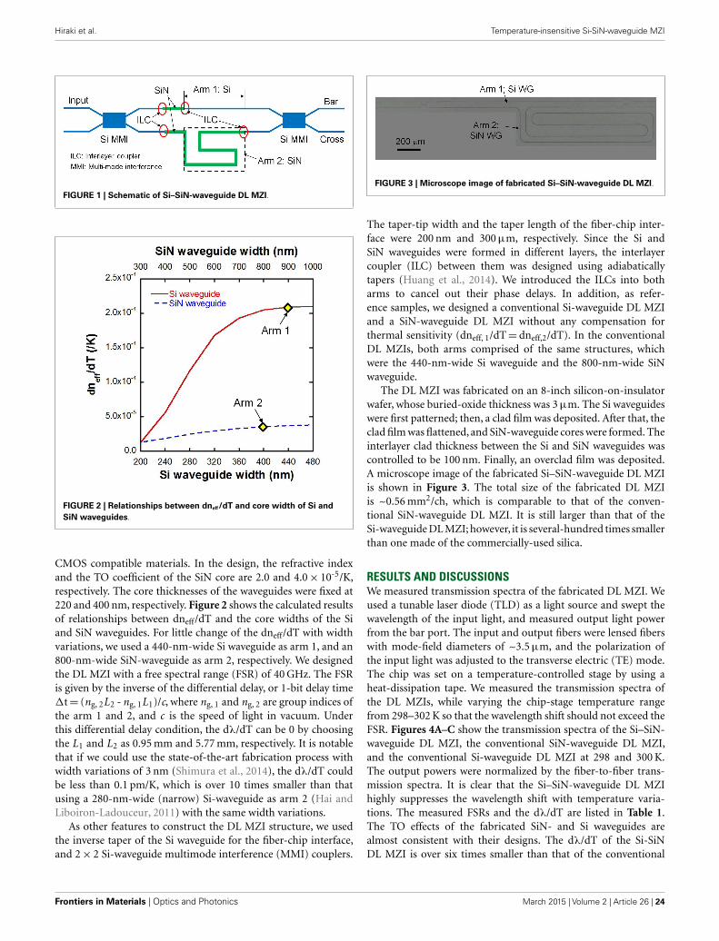
Hiraki et al. Temperature-insensitive Si-SiN-waveguide MZI
FIGURE 1 | Schematic of Si–SiN-waveguide DL MZI.
FIGURE 2 | Relationships between dneff/dT and core width of Si andSiN waveguides.
CMOS compatible materials. In the design, the refractive indexand the TO coefficient of the SiN core are 2.0 and 4.0× 10⁻⁵/K,respectively. The core thicknesses of the waveguides were fixed at220 and 400 nm, respectively. Figure 2 shows the calculated resultsof relationships between dneff/dT and the core widths of the Siand SiN waveguides. For little change of the dneff/dT with widthvariations, we used a 440-nm-wide Si waveguide as arm 1, and an800-nm-wide SiN-waveguide as arm 2, respectively. We designedthe DL MZI with a free spectral range (FSR) of 40 GHz. The FSRis given by the inverse of the differential delay, or 1-bit delay time∆t= (ng, 2L2 - ng, 1L1)/c, where ng, 1 and ng, 2 are group indices ofthe arm 1 and 2, and c is the speed of light in vacuum. Underthis differential delay condition, the dλ/dT can be 0 by choosingthe L1 and L2 as 0.95 mm and 5.77 mm, respectively. It is notablethat if we could use the state-of-the-art fabrication process withwidth variations of 3 nm (Shimura et al., 2014), the dλ/dT couldbe less than 0.1 pm/K, which is over 10 times smaller than thatusing a 280-nm-wide (narrow) Si-waveguide as arm 2 (Hai andLiboiron-Ladouceur, 2011) with the same width variations.
As other features to construct the DL MZI structure, we usedthe inverse taper of the Si waveguide for the fiber-chip interface,and 2× 2 Si-waveguide multimode interference (MMI) couplers.
FIGURE 3 | Microscope image of fabricated Si–SiN-waveguide DL MZI.
The taper-tip width and the taper length of the fiber-chip inter-face were 200 nm and 300 µm, respectively. Since the Si andSiN waveguides were formed in different layers, the interlayercoupler (ILC) between them was designed using adiabaticallytapers (Huang et al., 2014). We introduced the ILCs into botharms to cancel out their phase delays. In addition, as refer-ence samples, we designed a conventional Si-waveguide DL MZIand a SiN-waveguide DL MZI without any compensation forthermal sensitivity (dneff, 1/dT= dneff,2/dT). In the conventionalDL MZIs, both arms comprised of the same structures, whichwere the 440-nm-wide Si waveguide and the 800-nm-wide SiNwaveguide.
The DL MZI was fabricated on an 8-inch silicon-on-insulatorwafer, whose buried-oxide thickness was 3 µm. The Si waveguideswere first patterned; then, a clad film was deposited. After that, theclad film was flattened, and SiN-waveguide cores were formed. Theinterlayer clad thickness between the Si and SiN waveguides wascontrolled to be 100 nm. Finally, an overclad film was deposited.A microscope image of the fabricated Si–SiN-waveguide DL MZIis shown in Figure 3. The total size of the fabricated DL MZIis ~0.56 mm2/ch, which is comparable to that of the conven-tional SiN-waveguide DL MZI. It is still larger than that of theSi-waveguide DL MZI; however, it is several-hundred times smallerthan one made of the commercially-used silica.
RESULTS AND DISCUSSIONSWe measured transmission spectra of the fabricated DL MZI. Weused a tunable laser diode (TLD) as a light source and swept thewavelength of the input light, and measured output light powerfrom the bar port. The input and output fibers were lensed fiberswith mode-field diameters of ~3.5 µm, and the polarization ofthe input light was adjusted to the transverse electric (TE) mode.The chip was set on a temperature-controlled stage by using aheat-dissipation tape. We measured the transmission spectra ofthe DL MZIs, while varying the chip-stage temperature rangefrom 298–302 K so that the wavelength shift should not exceed theFSR. Figures 4A–C show the transmission spectra of the Si–SiN-waveguide DL MZI, the conventional SiN-waveguide DL MZI,and the conventional Si-waveguide DL MZI at 298 and 300 K.The output powers were normalized by the fiber-to-fiber trans-mission spectra. It is clear that the Si–SiN-waveguide DL MZIhighly suppresses the wavelength shift with temperature varia-tions. The measured FSRs and the dλ/dT are listed in Table 1.The TO effects of the fabricated SiN- and Si waveguides arealmost consistent with their designs. The dλ/dT of the Si-SiNDL MZI is over six times smaller than that of the conventional
Frontiers in Materials | Optics and Photonics March 2015 | Volume 2 | Article 26 | 24
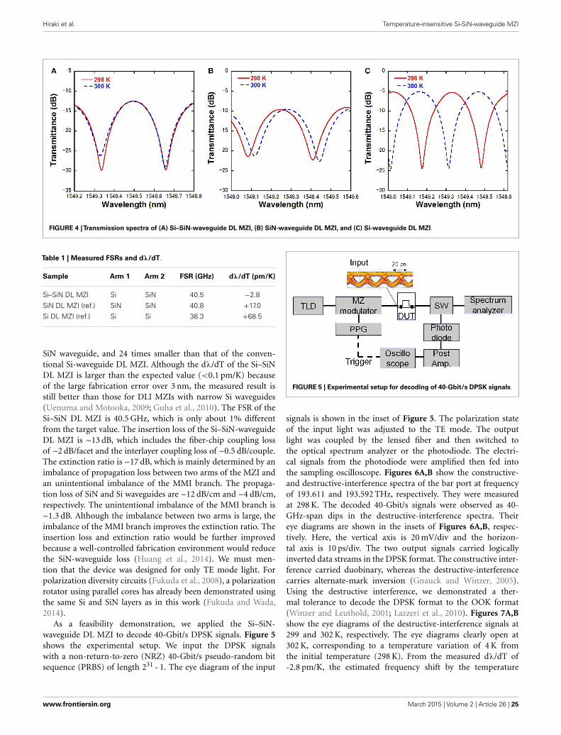
Hiraki et al. Temperature-insensitive Si-SiN-waveguide MZI
FIGURE 4 |Transmission spectra of (A) Si–SiN-waveguide DL MZI, (B) SiN-waveguide DL MZI, and (C) Si-waveguide DL MZI.
Table 1 | Measured FSRs and dλ/dT.
Sample Arm 1 Arm 2 FSR (GHz) dλ/dT (pm/K)
Si–SiN DL MZI Si SiN 40.5 −2.8
SiN DL MZI (ref.) SiN SiN 40.8 +17.0
Si DL MZI (ref.) Si Si 38.3 +68.5
SiN waveguide, and 24 times smaller than that of the conven-tional Si-waveguide DL MZI. Although the dλ/dT of the Si–SiNDL MZI is larger than the expected value (<0.1 pm/K) becauseof the large fabrication error over 3 nm, the measured result isstill better than those for DLI MZIs with narrow Si waveguides(Uenuma and Motooka, 2009; Guha et al., 2010). The FSR of theSi–SiN DL MZI is 40.5 GHz, which is only about 1% differentfrom the target value. The insertion loss of the Si–SiN-waveguideDL MZI is ~13 dB, which includes the fiber-chip coupling lossof ~2 dB/facet and the interlayer coupling loss of ~0.5 dB/couple.The extinction ratio is ~17 dB, which is mainly determined by animbalance of propagation loss between two arms of the MZI andan unintentional imbalance of the MMI branch. The propaga-tion loss of SiN and Si waveguides are ~12 dB/cm and ~4 dB/cm,respectively. The unintentional imbalance of the MMI branch is~1.3 dB. Although the imbalance between two arms is large, theimbalance of the MMI branch improves the extinction ratio. Theinsertion loss and extinction ratio would be further improvedbecause a well-controlled fabrication environment would reducethe SiN-waveguide loss (Huang et al., 2014). We must men-tion that the device was designed for only TE mode light. Forpolarization diversity circuits (Fukuda et al., 2008), a polarizationrotator using parallel cores has already been demonstrated usingthe same Si and SiN layers as in this work (Fukuda and Wada,2014).
As a feasibility demonstration, we applied the Si–SiN-waveguide DL MZI to decode 40-Gbit/s DPSK signals. Figure 5shows the experimental setup. We input the DPSK signalswith a non-return-to-zero (NRZ) 40-Gbit/s pseudo-random bitsequence (PRBS) of length 231 - 1. The eye diagram of the input
FIGURE 5 | Experimental setup for decoding of 40-Gbit/s DPSK signals.
signals is shown in the inset of Figure 5. The polarization stateof the input light was adjusted to the TE mode. The outputlight was coupled by the lensed fiber and then switched tothe optical spectrum analyzer or the photodiode. The electri-cal signals from the photodiode were amplified then fed intothe sampling oscilloscope. Figures 6A,B show the constructive-and destructive-interference spectra of the bar port at frequencyof 193.611 and 193.592 THz, respectively. They were measuredat 298 K. The decoded 40-Gbit/s signals were observed as 40-GHz-span dips in the destructive-interference spectra. Theireye diagrams are shown in the insets of Figures 6A,B, respec-tively. Here, the vertical axis is 20 mV/div and the horizon-tal axis is 10 ps/div. The two output signals carried logicallyinverted data streams in the DPSK format. The constructive inter-ference carried duobinary, whereas the destructive-interferencecarries alternate-mark inversion (Gnauck and Winzer, 2005).Using the destructive interference, we demonstrated a ther-mal tolerance to decode the DPSK format to the OOK format(Winzer and Leuthold, 2001; Lazzeri et al., 2010). Figures 7A,Bshow the eye diagrams of the destructive-interference signals at299 and 302 K, respectively. The eye diagrams clearly open at302 K, corresponding to a temperature variation of 4 K fromthe initial temperature (298 K). From the measured dλ/dT of-2.8 pm/K, the estimated frequency shift by the temperature
www.frontiersin.org March 2015 | Volume 2 | Article 26 | 25
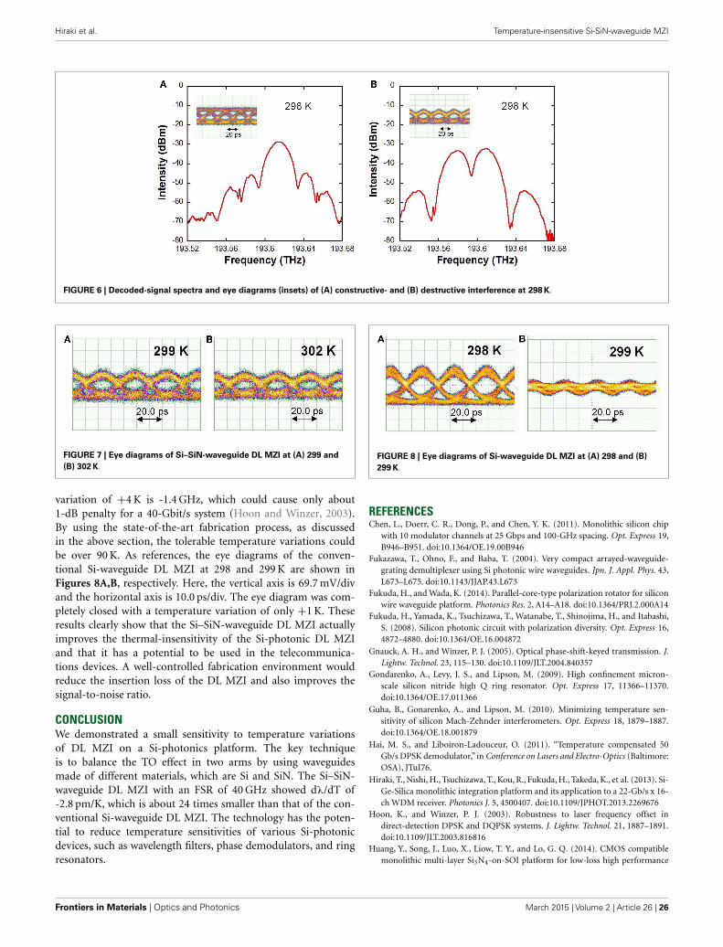
Hiraki et al. Temperature-insensitive Si-SiN-waveguide MZI
FIGURE 6 | Decoded-signal spectra and eye diagrams (insets) of (A) constructive- and (B) destructive interference at 298 K.
FIGURE 7 | Eye diagrams of Si–SiN-waveguide DL MZI at (A) 299 and(B) 302 K.
variation of +4 K is -1.4 GHz, which could cause only about1-dB penalty for a 40-Gbit/s system (Hoon and Winzer, 2003).By using the state-of-the-art fabrication process, as discussedin the above section, the tolerable temperature variations couldbe over 90 K. As references, the eye diagrams of the conven-tional Si-waveguide DL MZI at 298 and 299 K are shown inFigures 8A,B, respectively. Here, the vertical axis is 69.7 mV/divand the horizontal axis is 10.0 ps/div. The eye diagram was com-pletely closed with a temperature variation of only +1 K. Theseresults clearly show that the Si–SiN-waveguide DL MZI actuallyimproves the thermal-insensitivity of the Si-photonic DL MZIand that it has a potential to be used in the telecommunica-tions devices. A well-controlled fabrication environment wouldreduce the insertion loss of the DL MZI and also improves thesignal-to-noise ratio.
CONCLUSIONWe demonstrated a small sensitivity to temperature variationsof DL MZI on a Si-photonics platform. The key techniqueis to balance the TO effect in two arms by using waveguidesmade of different materials, which are Si and SiN. The Si–SiN-waveguide DL MZI with an FSR of 40 GHz showed dλ/dT of-2.8 pm/K, which is about 24 times smaller than that of the con-ventional Si-waveguide DL MZI. The technology has the poten-tial to reduce temperature sensitivities of various Si-photonicdevices, such as wavelength filters, phase demodulators, and ringresonators.
FIGURE 8 | Eye diagrams of Si-waveguide DL MZI at (A) 298 and (B)299 K.
REFERENCESChen, L., Doerr, C. R., Dong, P., and Chen, Y. K. (2011). Monolithic silicon chip
with 10 modulator channels at 25 Gbps and 100-GHz spacing. Opt. Express 19,B946–B951. doi:10.1364/OE.19.00B946
Fukazawa, T., Ohno, F., and Baba, T. (2004). Very compact arrayed-waveguide-grating demultiplexer using Si photonic wire waveguides. Jpn. J. Appl. Phys. 43,L673–L675. doi:10.1143/JJAP.43.L673
Fukuda, H., and Wada, K. (2014). Parallel-core-type polarization rotator for siliconwire waveguide platform. Photonics Res. 2, A14–A18. doi:10.1364/PRJ.2.000A14
Fukuda, H., Yamada, K., Tsuchizawa, T., Watanabe, T., Shinojima, H., and Itabashi,S. (2008). Silicon photonic circuit with polarization diversity. Opt. Express 16,4872–4880. doi:10.1364/OE.16.004872
Gnauck, A. H., and Winzer, P. J. (2005). Optical phase-shift-keyed transmission. J.Lightw. Technol. 23, 115–130. doi:10.1109/JLT.2004.840357
Gondarenko, A., Levy, J. S., and Lipson, M. (2009). High confinement micron-scale silicon nitride high Q ring resonator. Opt. Express 17, 11366–11370.doi:10.1364/OE.17.011366
Guha, B., Gonarenko, A., and Lipson, M. (2010). Minimizing temperature sen-sitivity of silicon Mach-Zehnder interferometers. Opt. Express 18, 1879–1887.doi:10.1364/OE.18.001879
Hai, M. S., and Liboiron-Ladouceur, O. (2011). “Temperature compensated 50Gb/s DPSK demodulator,” in Conference on Lasers and Electro-Optics (Baltimore:OSA), JTuI76.
Hiraki, T., Nishi, H., Tsuchizawa, T., Kou, R., Fukuda, H., Takeda, K., et al. (2013). Si-Ge-Silica monolithic integration platform and its application to a 22-Gb/s x 16-ch WDM receiver. Photonics J. 5, 4500407. doi:10.1109/JPHOT.2013.2269676
Hoon, K., and Winzer, P. J. (2003). Robustness to laser frequency offset indirect-detection DPSK and DQPSK systems. J. Lightw. Technol. 21, 1887–1891.doi:10.1109/JLT.2003.816816
Huang, Y., Song, J., Luo, X., Liow, T. Y., and Lo, G. Q. (2014). CMOS compatiblemonolithic multi-layer Si3N4-on-SOI platform for low-loss high performance
Frontiers in Materials | Optics and Photonics March 2015 | Volume 2 | Article 26 | 26

Hiraki et al. Temperature-insensitive Si-SiN-waveguide MZI
silicon photonics dense integration. Opt. Express 22, 21859–21865. doi:10.1364/OE.22.021859
Lazzeri, E., Nguyen, A. T., Serafino, G., Kataoka, N., Wada, N., Bogoni, A., et al.(2010). “All-optical NRZ-DPSK to RZ-OOK format conversion using opticaldelay line interferometer and semiconductor optical amplifier,” in Photonics inSwitching Conference (Monterey), JTuB45.
Lockwood, D. J., and Pavesi, L. (eds) (2010). Silicon Photonics. Berlin: Springer.Nishi, H., Tsuchizawa, T., Kou, R., Shinojima, H., Yamada, T., Kimura, H., et al.
(2012). Monolithic integration of a silica AWG and Ge photodiodes on Siphotonic platform for one-chip WDM receiver. Opt. Express 20, 9312–9321.doi:10.1364/OE.20.009312
Shimura, D., Horikawa, T., Okayama, H., Jeong, S.-H., Tokushima, M., Sasaki, H.,et al. (2014). “High precision Si waveguide devices designed for 1.31µm and1.55µm wavelengths on 300mm-SOI,” in Conference on Group IV Photonics.Vancouver: IEEE.
Tsuchizawa, T., Yamada, K., Watanabe, T., Sungbong, P., Nishi, H., Kou, R., et al.(2011). Monolithic integration of silicon-, germanium-, and silica-based opticaldevices for telecommunications applications. IEEE J. Sel. Top. Quant. Electron.17, 516–525. doi:10.1109/JSTQE.2010.2089430
Uenuma, M., and Motooka, T. (2009). Temperature-independent silicon waveguideoptical filter. Opt. Lett. 34, 599–601. doi:10.1364/OL.34.000599
Vivien, L., and Pavesi, L. (eds). (2013). Handbook of Silicon Photonics. New York:Taylor and Francis.
Winzer, P. J., and Leuthold, J. (2001). Return-to-zero modulator using a single NRZdrive signal and an optical delay interferometer. IEEE Photon. Technol. Lett. 13,1298–1300. doi:10.1109/68.969887
Xia, F., Rooks, M., Sekaric, L., and Vlasov, Y. (2007). Ultra-compact high orderring resonator filters using submicron silicon photonic wires for on-chip opticalinterconnects. Opt. Express 15, 11934–11941. doi:10.1364/OE.15.011934
Conflict of Interest Statement: The authors declare that the research was conductedin the absence of any commercial or financial relationships that could be construedas a potential conflict of interest.
Received: 16 January 2015; accepted: 16 March 2015; published online: 30 March 2015.Citation: Hiraki T, Fukuda H, Yamada K and Yamamoto T (2015) Small sensitivity totemperature variations of Si-photonic Mach–Zehnder interferometer using Si and SiNwaveguides. Front. Mater. 2:26. doi: 10.3389/fmats.2015.00026This article was submitted to Optics and Photonics, a section of the journal Frontiersin Materials.Copyright © 2015 Hiraki, Fukuda, Yamada and Yamamoto. This is an open-accessarticle distributed under the terms of the Creative Commons Attribution License (CCBY). The use, distribution or reproduction in other forums is permitted, provided theoriginal author(s) or licensor are credited and that the original publication in thisjournal is cited, in accordance with accepted academic practice. No use, distribution orreproduction is permitted which does not comply with these terms.
www.frontiersin.org March 2015 | Volume 2 | Article 26 | 27

ORIGINAL RESEARCHpublished: 05 May 2015
doi: 10.3389/fmats.2015.00036
Edited by:Jifeng Liu,
Thayer School of Engineering, USA
Reviewed by:Raul J. Martin-Palma,
Universidad Autonoma de Madrid,Spain
Venu Gopal Achanta,Tata Institute of Fundamental
Research, India
*Correspondence:Jong-Moo Lee,
Electronics and TelecommunicationsResearch Institute, 161 Gajong-dong,Yusong-gu, Daejeon 305-350, Korea
Specialty section:This article was submitted to Optics
and Photonics, a section of thejournal Frontiers in Materials
Received: 30 January 2015Accepted: 08 April 2015Published: 05 May 2015
Citation:Lee J-M (2015) Ultrahigh
temperature-sensitive silicon MZI withtitania cladding.
Front. Mater. 2:36.doi: 10.3389/fmats.2015.00036
Ultrahigh temperature-sensitivesilicon MZI with titania claddingJong-Moo Lee 1,2*
1 Electronics and Telecommunications Research Institute, Daejeon, South Korea, 2 School of Advanced Device Technology,University of Science and Technology, Daejeon, South Korea
We present a possibility of intensifying temperature sensitivity of a silicon Mach-Zehnderinterferometer (MZI) by using a highly negative thermo-optic property of titania (TiO2). Tem-perature sensitivity of an asymmetric silicon MZI with a titania cladding is experimentallymeasured from +18 to −340pm/°C depending on design parameters of MZI.
Keywords: silicon, photonics, temperature, sensor, titania
Introduction
There have been many efforts to adjust temperature-dependent wavelength shift (TDWS) ofa photonic waveguide device using a cladding material with a negative thermo-optic coeffi-cient (TOC) differently from a core material with a positive TOC (Kokubun et al., 1998; Leeet al., 2007, 2008; Alipour et al., 2010; Guha et al., 2013; Bovington et al., 2014; Lee, 2014).Polymers have been popularly used as the cladding material with a negative TOC (Kokubunet al., 1998; Lee et al., 2007, 2008), and titania (TiO2) is recently attracting attention with ahighly negative TOC (Alipour et al., 2010; Guha et al., 2013; Bovington et al., 2014; Lee, 2014)and its merit of complementary-metal-oxide-semiconductor (CMOS) compatibility in fabrica-tion when it is used for a silicon photonic waveguide device. Silicon has a very high TOC of1.8× 10−4/°C and there have been many efforts to reduce the high TDWS of silicon photonicdevices such as a ring resonator by using polymer (Kokubun et al., 1998; Lee et al., 2007,2008) or titania cladding (Alipour et al., 2010; Guha et al., 2013; Lee, 2014) with a highlynegative TOC.
In case of silicon photonic Mach-Zehnder interferometer (MZI), there were reports showing theway to reduce the TDWS of MZI without using a cladding with a negative TOC (Uenuma andMoooka, 2009; Guha et al., 2010; Dwivedi et al., 2013). TDWS of silicon MZI was shown to bereduced by using different widths of waveguide (Uenuma and Moooka, 2009; Guha et al., 2010)or by using different polarization (Dwivedi et al., 2013) in each of the MZI arm, respectively. Thedifference in each of the MZI arm can induce a different temperature-dependent phase change forthe each arm, resulting reduction in TDWS of MZI.
The previous efforts of silicon photonic devices using a negative thermo-optic cladding havebeen focused on reducing the TDWS, but there have been demands also on high TDWS insuch applications of low power temperature tuning (Masood et al., 2013) and integrated-photonictemperature sensors (Irace and Breglio, 2003; Kim et al., 2010; Deng et al., 2014). So, it would also beattractive if there is amethod to intensify the TDWSof the silicon device by using a claddingmaterialsuch as titania with a very high TOC. There have been MZIs using titania for chemical sensing (Qiet al., 2002; Celo et al., 2009), but no reports on temperature sensors using titania cladding to thebest of our knowledge.
In this regard, here, we combine the method used to in reducing TDWS of silicon MZI withdifferent dimension for each arm and the method of adding titania cladding on the silicon MZI toshow the possibility of ultrahigh temperature-sensitive silicon MZI.
Frontiers in Materials | www.frontiersin.org May 2015 | Volume 2 | Article 3628

Lee Ultrahigh temperature-sensitive MZI
Experiment and Results
Design and FabricationTemperature dependence of a silicon MZI can be adjusted byasymmetric geometry of two waveguide arms with different effec-tive refractive indexes induced by different cross-sectional dimen-sion as in reference Uenuma and Moooka (2009) and Guha et al.(2010). Silicon MZIs in this experiment are designed with varia-tions in the length of MZI arm and cross-sectional dimension ofeach MZI arm as in Figure 1. Figure 1A shows AsyL, which isfor asymmetry in the length of each MZI arm of 80 μm, L for thecommon length of MZI arm, which is varied from 110 to 360 μm,w0 for the common width of waveguide core, which is 450 nm,w1 for the cross-sectional dimension of a waveguide core whichis 1350 nm and shaped as a rib waveguide shown in Figure 1B or450 nm and shaped as a channel waveguide for a comparison, andw2 for the cross-sectional dimension of a waveguide core which is350 or 450 nm for a comparison. Figures 1B,C show the cross-sectional structure of the waveguide with a silica cladding anda titania cladding, respectively. The rib waveguide is formed byshallow etch of 70 nm for the width w1, and there are tapers atthe both ends of the rib waveguide for an adiabatic transfer to thechannel waveguide with the width of w0.
Figure 2 shows a microscopic image and scanning electronmicroscope (SEM) image of the fabricated MZIs. There are manyvariations for the length, L, in design, but we limit our discus-sion here to the two extreme case of L, 110 and 360 μm. Sili-con waveguide core with the width of 450 nm was patterned byDUV lithography on a silicon-on-insulator (SOI) wafer with a220-nm thick silicon layer on a 2-μm thick buried oxide (BOX)layer. The fabrication of the devices except a deposition of titaniacladding were processed using a standard CMOS fabrication pro-cess through ePIXfab. There were two types of fabricated device:one with a silica (SiO2) cladding and the other without an upper
FIGURE 1 | (A) Schematic diagram of asymmetric MZI with arms different inlength and cross-sectional dimension of waveguide, and schematic diagramof the cross-section of the arms in (B) with silica cladding and (C) with titaniacladding, respectively.
cladding. We deposited 400 nm thickness of titania cladding onthe fabricated device without an upper cladding, using electron-beam evaporation. The initial vacuum level of the electron-beamevaporation was 5× 10⁻⁷ Torr, and it was kept at 8× 10⁻⁵ Torrwith O2 during the deposition. The temperature of a plate holdingSOI chip wasmaintained at 150°C during the evaporation, and thespeed of deposition was about 3Å/s. The refractive index of titaniawas measured using ellipsometry as 2.13 at 1550 nm.
Measured ResultsOne pair of single-mode fibers is coupled to the silicon devicesfor measurement through grating couplers which are with 630-nm pitch and 70 nm depth of the shallow etch. Figure 3 showsnormalized transmission spectra of a silicon MZI with a silica
FIGURE 2 | A microscope image and a SEM image of silicon MZIsfabricated in this experiment.
FIGURE 3 | Normalized transmission spectra of MZI with silicacladding as the temperature varied from 15 to 55°C when L=360 μm,w1= 1350nm, and w2= 350nm.
Frontiers in Materials | www.frontiersin.org May 2015 | Volume 2 | Article 3629

Lee Ultrahigh temperature-sensitive MZI
cladding when the temperature varied from 15 to 55°C. Themain design parameters of the silicon MZI are 360 μm for L,1350 nm for w1, and 350 nm for w2. Figure 3 shows TDWS of thesilicon MZI is +48m/°C, which was reduced from +74 pm/°C ofa ring resonator included in the same chip for a comparison. Thenormalized transmissions can be regarded as the insertion lossof the silicon MZI, because they were calculated by subtractingthe amount of fiber-to-fiber transmission of a straight siliconwaveguide from the amount of fiber-to-fiber transmission of thesiliconMZI device. Figure 3 shows that the insertion loss throughthe silicon MZI is negligibly small.
Figure 4 shows normalized transmission spectra of a siliconMZI, whose design is the same as in Figure 3 but with a titaniacladding instead of the silica cladding, when the temperaturevaried from 25 to 35°C. Figure 4 shows TDWS of the silicon MZIis intensified with opposite sign by the titania cladding as high as−340 pm/°C, which is about seven times bigger than the TDWS ofthe same design ofMZIwith a silica cladding and five times biggerthan the TDWS of the ring resonator with a silica cladding.
Figure 5 shows the relative wavelength shift of various MZIswith silica or titania cladding in this experiment compared to theTDWS of the ring resonator with the silica cladding. The radius ofthe ring resonator with the silica cladding was 5 μm and TDWSof the ring resonator was measured at +74 pm/°C as in Figure 6.TDWS of a silicon MZI with the same cross-section dimensionof 450 nm and titania cladding was measured as +18 pm/°C asin Figure 5. TDWS of another titania-covered silicon MZI with1350 nm for w1, 450 nm for w2, and 110 μm for L was measuredas−70 pm/°C as in Figure 5.
Discussion
The experimental results show that we can adjust TDWS of thetitania-covered silicon MZIs with proper design and can inten-sify the temperature sensitivity highly enough to be useful inapplications requiring an ultrahigh temperature sensitivity suchas thermo-optic tuning devices or photonic temperature sensors.
FIGURE 4 | Normalized transmission spectra of MZI with titaniacladding as the temperature varied from 25 to 35°C when L=360 μm,w1=1350nm, and w2=350nm.
The input and output fibers are coupled to the silicon waveg-uide through grating couplers with the pitch of 630 nm. The fiberwas coupled at the vertical angle of 10° for the waveguide withsilica cladding and 15° for the waveguide with titania cladding.There was not a big difference in the coupling loss of the gratingcouplers for the silica cladding and titania cladding. It was about5 dB/facet for the silica cladding and 5.5 dB/facet for the titaniacladding. The slightly excessive loss of the grating coupler in caseof titania cladding is expected to be reduced by optimizing thedesign of gratings or the thickness of titania if it is required. Thenormalized transmission in Figures 3 and 4 were calculated bysubtracting the amount of fiber-to-fiber transmission of a straightsilicon waveguide from the amount of fiber-to-fiber transmissionof the siliconMZI device for each case of silica cladding and titaniacladding, respectively. So, the normalized transmission spectrashow the insertion loss of MZI compared to a straight waveguide.
The refractive index of titania cladding was measured usingellipsometry as 2.13 at 1550 nm, and TOC of titania film was
FIGURE 5 | Relative wavelength shift depending on temperature ofMZI with silica and titania cladding, respectively, in comparison with+74pm/°C or a ring resonator with silica cladding. w350 and w450 arefor 350 and 450 nm width, respectively, of the MZI narrow arm. L110 andL360 are for 110 and 360 μm length, respectively, of the MZI arm.
FIGURE 6 | Normalized transmission spectra of the ring resonator withsilica cladding mentioned in Figure 5, as the temperature varied from15 to 55°C.
Frontiers in Materials | www.frontiersin.org May 2015 | Volume 2 | Article 3630

Lee Ultrahigh temperature-sensitive MZI
not directly measured but estimated from −5 to −7× 10⁻⁴/°Cby the measured TDWS of a ring resonator with titania claddingas in reference Lee (2014). The absolute value of TOC of titaniais several times higher than TOC of silicon or polymer, andthat is the reason we used it as highly negative thermo-opticcladding in this experiment. The reason for the highly negativeTOC of the titania cladding and the variation of TOC is not fullyunderstood yet, and finding the reason remains for our futureresearch.
Conclusion
We experimentally showed that TDWS of a silicon MZI canbe reduced or intensified by proper design of the width andlength of arms of MZI when it is used with a highly negative
thermo-optic titania cladding. We experimentally showed tem-perature sensitivity of an asymmetric silicon MZI with a titaniacladding could be adjusted from +18 to −340 pm/°C dependingon design parameters such as the width and length of MZI. Webelieve these results show the possibility of ultrahigh temperature-sensitive silicon MZI for new applications requiring ultrahightemperature sensitivity such as thermo-optic tuning devices orphotonic temperature sensors.
Acknowledgments
Wewould like to thank ePIXfab (www.epixfab.eu) for the fabrica-tion of SOI waveguide before our deposition of titania cladding.This work was supported by Korean IT R&D program MOTIE[N019800001] and [10044735].
ReferencesAlipour, P., Atabaki, A. H., Eftekhar, A. A., and Adibi, A. (2010). “Athermal
performance in titania-clad microring resonators on SOI,” in OSA TechnicalDigest. Integrated Photonics Research, Silicon and Nanophotonics and Photonicsin Switching, Paper IMC6; 2010 Jul 25-28, (Monterey, CA: Optical Society ofAmerica).
Bovington, J., Wu, R., Cheng, K. T., and Bowers, J. E. (2014). Thermal stressimplications in athermal TiO2 waveguides on a silicon substrate. Opt. Express21, 661–666. doi:10.1364/OE.22.000661
Celo, D., Post, E., Summers, M., Smy, T., Brett, M. J., and Albert, J. (2009).Interferometric sensing platform with dielectric nanostructured thin films.Opt.Express 17, 6655–6664. doi:10.1364/OE.17.006655
Deng, Q. Z., Li, X. B., Chen, R. B., and Zhou, Z. (2014). “Low-cost silicon photonictemperature sensor using broadband light source,” in IEEE 11th InternationalConference, Group IV Photonics (GFP), WP23; 2014 Aug 27-29, (Paris).
Dwivedi, S., D’heer, H., and Bogaerts, W. (2013). A compact all-silicon temperatureinsensitive filter forWDMand bio-sensing applications. IEEE Photonics Technol.Lett. 25, 2167–2170. doi:10.1109/LPT.2013.2282715
Guha, B., Cardenas, J., and Lipson, M. (2013). Athermal silicon microring res-onators with titanium oxide cladding. Opt. Express 21, 26557–26563. doi:10.1364/OE.21.026557
Guha, B., Gondarenko, A., and Lipson, M. (2010). Minimizing temperature sen-sitivity of silicon Mach-Zehnder interferometers. Opt. Express 18, 1879–1887.doi:10.1364/OE.18.001879
Irace, A., and Breglio, G. (2003). All-silicon optical temperature sensor basedon multi-mode interference. Opt. Express 11, 2807–2812. doi:10.1364/OE.11.002807
Kim, G. D., Lee, H. S., Park, C. H., Lee, S. S., Lim, B. T., Bae, H. K., et al. (2010).Silicon photonic temperature sensor employing a ring resonator manufacturedusing a standard CMOS process.Opt. Express 18, 22215–22221. doi:10.1364/OE.18.022215
Kokubun, Y., Yoneda, S., andMatsuura, S. (1998). Temperature-independent opticalfilter at 1.55μm wavelength using a silica-based athermal wavelength. Electron.Lett. 34, 367–369. doi:10.1049/el:19980245
Lee, J. M. (2014). Influence of titania cladding on SOI grating coupler and 5 μm-radius ring resonator. Opt. Commun. 338, 101–105. doi:10.1016/j.optcom.2014.10.039
Lee, J. M., Kim, D. J., Ahn, H. Y., Park, S. H., and Kim, G. O. (2007). Temperaturedependence of silicon nanophotonic ring resonator with a polymeric overlayer.J. Lightwave Technol. 25, 2236–2243. doi:10.1109/JLT.2007.899792
Lee, J. M., Kim, D. J., Kim, G. H., Kwon, O. K., Kim, K. J., and Kim, G. O. (2008).Controlling temperature dependence of silicon waveguide using slot structure.Opt. Express 16, 1645–1652. doi:10.1364/OE.16.001645
Masood, A., Pantouvakiy, M., Lepagey, G., Verheyeny, P., Campenhouty, J. V.,Absily, P., et al. (2013). “Comparison of heater architectures for thermal controlof silicon photonic circuits,” in IEEE 10th International Conference, Group IVPhotonics (GFP), ThC2; 2013 Aug 28-30, (Seoul).
Qi, Z., Matzuda, N., Itoh, K., Murabayashi, M., and Labers, C. R. (2002). A designfor improving the sensitivity of Mach-Zehnder interferometer to chemicaland biological measurands. Sens Actuators B Chem 81, 254–258. doi:10.1016/S0925-4005(01)00960-1
Uenuma, M., and Moooka, T. (2009). Temperature-independent silicon waveguideoptical filter. Opt. Lett. 34, 599–601. doi:10.1364/OL.34.000599
Conflict of Interest Statement: The author declares that the research was con-ducted in the absence of any commercial or financial relationships that could beconstrued as a potential conflict of interest.
Copyright © 2015 Lee. This is an open-access article distributed under the terms of theCreative CommonsAttribution License (CCBY). The use, distribution or reproductionin other forums is permitted, provided the original author(s) or licensor are creditedand that the original publication in this journal is cited, in accordance with acceptedacademic practice. No use, distribution or reproduction is permitted which does notcomply with these terms.
Frontiers in Materials | www.frontiersin.org May 2015 | Volume 2 | Article 3631
ORIGINAL RESEARCHpublished: 27 April 2015
doi: 10.3389/fmats.2015.00034
Edited by:Dan-Xia Xu,
National Research Council Canada,Canada
Reviewed by:Koji Yamada,
Nippon Telegraph and TelephoneCorporation, Japan
Weidong Zhou,University of Texas at Arlington, USA
Robert Halir,Universidad de Málaga, Spain
*Correspondence:Andrew W. Poon,
Photonic Device Laboratory,Department of Electronic and
Computer Engineering, The HongKong University of Science andTechnology, Clear Water Bay,Kowloon, Hong Kong, China
Specialty section:This article was submitted to Optics
and Photonics, a section of thejournal Frontiers in Materials
Received: 31 January 2015Accepted: 01 April 2015Published: 27 April 2015
Citation:Wang J, Yao Z and Poon AW (2015)
Silicon-nitride-based integratedoptofluidic biochemical sensors using
a coupled-resonator opticalwaveguide
Front. Mater. 2:34.doi: 10.3389/fmats.2015.00034
Silicon-nitride-based integratedoptofluidic biochemical sensorsusing a coupled-resonator opticalwaveguideJiawei Wang, Zhanshi Yao and Andrew W. Poon *
Photonic Device Laboratory, Department of Electronic and Computer Engineering, The Hong Kong University of Science andTechnology, Hong Kong, China
Silicon nitride (SiN) is a promising material platform for integrating photonic componentsandmicrofluidic channels on a chip for label-free, optical biochemical sensing applicationsin the visible to near-infrared wavelengths. The chip-scale SiN-based optofluidic sensorscan be compact due to a relatively high refractive index contrast between SiN and thefluidic medium, and low-cost due to the complementary metal-oxide-semiconductor(CMOS)-compatible fabrication process. Here, we demonstrate SiN-based integratedoptofluidic biochemical sensors using a coupled-resonator optical waveguide (CROW) inthe visible wavelengths. The working principle is based on imaging in the far field the out-of-plane elastic-light-scattering patterns of the CROWsensor at a fixed probewavelength.We correlate the imaged pattern with reference patterns at the CROW eigenstates. Oursensing algorithm maps the correlation coefficients of the imaged pattern with a library ofcalibrated correlation coefficients to extract a minute change in the cladding refractiveindex. Given a calibrated CROW, our sensing mechanism in the spatial domain onlyrequires a fixed-wavelength laser in the visible wavelengths as a light source, with theprobe wavelength located within the CROW transmission band, and a silicon digitalcharge-coupled device/CMOS camera for recording the light scattering patterns. This isin sharp contrast with the conventional optical microcavity-based sensing methods thatimpose a strict requirement of spectral alignment with a high-quality cavity resonanceusing a wavelength-tunable laser. Our experimental results using a SiN CROW sensorwith eight coupled microrings in the 680 nm wavelength reveal a cladding refractiveindex change of ~1.3×10⁻⁴ refractive index unit (RIU), with an average sensitivity of~281±271RIU−1 and a noise-equivalent detection limit of 1.8×10⁻⁸ ~1.0×10⁻⁴ RIUacross the CROW bandwidth of ~1 nm.
Keywords: silicon nitride, biochemical sensor, integrated optofluidics, coupled-resonator optical waveguide,microring resonators, CMOS-compatible, elastic light scattering, visible wavelengths
Introduction
In recent years, the increasing demands of medical diagnostics outside a clinic or a laboratory andself-monitoring for personal healthcare have highly motivated the rapid research and developmentof portable, low-cost biochemical sensors (Estevez et al., 2012). Particularly, miniaturized, label-free
Frontiers in Materials | www.frontiersin.org April 2015 | Volume 2 | Article 3432

Wang et al. Silicon-nitride coupled-microresonator biochemical sensors
biochemical sensors are highly desired in order to be readilydeployed at or carried to the sensing environment and to read-out in real-time, quantitative biochemical information about theenvironment (Vollmer et al., 2008). Among various demonstratedchip-scale photonic biochemical sensors, optical microresonator-based biosensors featuring optical resonances with a high quality(Q) factor (103 ~ 104) promise a high sensitivity [few tens tohundreds of nanometer resonance shift per refractive index unit(RIU)], a low detection limit (10−7 ~ 10−4 RIU) and a compactfootprint (few to hundreds of micrometer square) (De Vos et al.,2007; Ciminelli et al., 2013; Sedlmeir et al., 2014). However, suchhigh-Qmicrocavity-based sensorsworking in the spectral domainare constrained by a narrow resonance bandwidth as the sensingwindow, which requires a strict resonance alignment and thusmay compromise the reliability of the sensor system. Besides, thesensing implementation typically requires a precisionwavelength-scanning setup, such as a wavelength-tunable laser, which maylimit the portability of the sensor system.
Other than microcavity-based biochemical sensors, integratedinterferometric optical biochemical sensors also attract increasingattentions. Various kinds of interferometer structures, includingMach–Zehnder interferometers (MZI) (Densmore et al., 2008;Kozma et al., 2009; Duval et al., 2013; Halir et al., 2013; Danteet al., 2015), Young interferometers (Ymeti et al., 2007), andHartman interferometers (Xu et al., 2007) have been adopted asintegrated interferometric biochemical sensors, demonstrating ahigh sensitivity (102 ~ 104 rad/RIU) along with a low detectionlimit (10−7 ~ 10−5 RIU). One key merit of such integrated inter-ferometric sensors is that they require a relatively simple configu-ration, which typically comprises a fixed-wavelength laser sourceand a photodetector. However, these interferometric sensors arenot tolerant to equipment noises that cause output intensity vari-ations, such as laser intensity variations.
Previously, our research group has proposed a coupled-resonator optical waveguide (CROW)-based biochemical sensingscheme using what we termed “pixelized pattern detection” inthe spatial domain (Lei and Poon, 2011). The scheme employsthe discrete transition of the CROW eigenstate excited at a fixedlaser wavelength upon a small change in the cladding refrac-tive index, Δn, and detects the resulting change in mode-field-intensity distribution by far-fieldmeasurement of the out-of-planeelastic-light-scattering intensity patterns. Such a sensing schemein principle only requires relatively simple optical sources andimaging systems including a fixed-wavelength laser and a cam-era. Recently, we have experimentally demonstrated a proof ofconcept of such a chip-scale CROW-based sensor on the silicon-on-insulator (SOI) platform in the 1550 nm telecommunicationwavelengths (Wang et al., 2014). We have extended the schemeby detecting the continuous modulation of the CROW mode-field-intensity distribution at a fixed wavelength upon a Δn bycorrelating the elastic-light-scattering patterns with reference pat-terns at the CROW eigenstates. Compared with interferometricsensors, the correlation analysis allows our sensing scheme tobe more tolerant to equipment noises that are common to allpixels of the CROW sensor yet do not cause a spectral shift,including laser intensity variations. Our previous experimentdemonstrated a Δn of ~1.5× 10⁻⁴ RIU and a noise-equivalentdetection limit (NEDL) of 2× 10⁻⁷ ~ 9× 10⁻⁴ RIU. However, the
choice of the SOI platform and the experimental setup config-uration (including a 1550 nm laser, an optical amplifier and anInGaAs camera) render our previous work not practical for point-of-care optical biochemical sensing applications. Particularly, inorder to leverage the wide availability of smartphones for bio-chemical sensing (Lakshminarayanan et al., 2015), it would beadvantageous to switch the operational wavelength of the sensorfrom the telecommunication wavelengths to the visible or near-infrared wavelengths that can be readily recorded using high-resolution silicon charge-coupled device (CCD)/complementarymetal-oxide-semiconductor (CMOS) cameras.
In this paper, we report our experimental demonstration ofthe CROW-based biochemical sensors in the visible wavelengthsin the silicon-nitride (SiN) platform. The SiN platform is trans-parent to the visible and near-infrared wavelengths (Gorin et al.,2008; Subramanian et al., 2013) and its fabrication process isCMOS-compatible. After the CROW calibration steps, our sens-ing scheme in principle only requires a fixed-wavelength, low-output-power, visible laser source, and a silicon CCD/CMOScamera for recording out-of-plane light-scattering patterns fromthe top-view. This offers a promising opportunity to integratethe CROW sensor with a smartphone that is equipped with acompact laser source and a high-resolution camerawith a properlydesigned optical interface for future smartphone-based point-of-care applications.
Principle and Methods
Principle and the Sensing AlgorithmFigure 1 illustrates the principle of the CROW-based biochemicalsensor following our previous work (Wang et al., 2014). Here,we outline the key concepts of the principle for understandingthis work. Figure 1A schematically shows a SiN CROW sen-sor comprising eight coupled microring resonators with identi-cal design, coupled to input and output bus waveguides in anadd-drop filter configuration. For a perfect CROW compris-ing C coupled identical single-mode resonators, the inhomoge-neously broadened transmission spectrum features a combinationof split mode resonances, with eachmode slightly shifted from theoriginal resonance frequency due to inter-cavity-coupling effect.Therefore, the eigenstate number N within each transmissionband always equals to the resonator number C. While a perfectCROW exhibits distinctive mode-field-amplitude distributionsat eigenstates, the pair of symmetric and anti-symmetric split-modes at different eigenfrequencies have non-distinctive mode-field-intensity distributions. In practice, a CROW inevitably suf-fers from fabrication imperfections. The coupled resonators areno longer identical nor are identically coupled. The symme-try breaking between the pair of symmetric and anti-symmetricsplit-modes therefore results in distinctive mode-field-intensitydistributions at all discernable eigenstates. The resulting phasedisorders and coupling disorders can result in the split moderesonances to be spectrally overlapped. Therefore, in the presenceof structural non-uniformity, N could be equal to or smaller thanC (N ≤C).
Figure 1B schematically illustrates the inhomogeneouslybroadened transmission bands upon applying cladding refrac-tive indices n0 and n0 +Δn, for an imperfect eight-microring
Frontiers in Materials | www.frontiersin.org April 2015 | Volume 2 | Article 3433

Wang et al. Silicon-nitride coupled-microresonator biochemical sensors
FIGURE 1 | Principle of SiN CROW-based biochemical sensorsusing out-of-plane elastic light scattering at the visiblewavelengths. (A) Schematic of a SiN CROW-based sensor integratedwith a microfluidic channel. An objective lens and a CMOS/CCD cameraare applied on top of the optofluidic chip in order to image theout-of-plane elastic-light-scattering pattern. (B) Illustration of
characterizing an imperfect eight-microring CROW, including theinhomogeneously broadened transmission bands upon a buffer solution(n0) and a test solution (n0 +Δn), and pixelized mode-field-intensitydistributions at eigenstate wavelength λj upon n0, A(λj). Insets: pixelizedmode-field-intensity distributions at probe wavelength, λp, (i) upon n0[B(λp)]; and (ii) upon n0 + Δn [T(λp)].
CROW exhibiting a complete set of eight distinctive eigenstatemode-field-intensity distributions. With the mode-field intensityof each microring integrated as a pixel, we denote the pixelizedone-dimensional pattern at the eigenstate as Aj, with j index-ing the eigenstate. Any mode-field-amplitude distribution at anarbitrary wavelength, λp, within the CROW transmission bandupon n0 can be expressed by a linear superposition of the com-plete set of eigenstate mode-field-amplitude distributions uponn0. Therefore, we are able to uniquely identify any pixelizedmode-field-intensity profile at λp upon n0, B(λp), as shown ininset (i), with Aj by a correlation analysis. Upon a small Δnapplied homogenously to the cladding, we can uniquely iden-tify by the correlation analysis any pixelized mode-field-intensitydistribution at λp upon n0 +Δn, T(λp), as shown in inset (ii),with Aj.
As in our previous work (Wang et al., 2014), we adopt the Pear-son’s correlation coefficient, ρ, in order to analyze the degree ofcorrelation between a pixelized pattern at an arbitrary probewavelength λp, B(λp), and the pixelized patterns at the eigenstatewavelengths λj, A(λj). For a CROW with a number of coupledsingle-mode cavities, C, and a number of discernable eigenstates,N (≤C), we define ρ at λp for A(λj) as follows:
ρj(λp) =
C∑i=1
(A(i,λj)− A(λj))(B(i,λp)− B(λp))√C∑
i=1(A(i,λj)− A(λj))
2√
C∑i=1
(B(i,λp)− B(λp))2
(1)where j= 1, 2, . . ., N is the eigenstate number, and i= 1, 2, . . .,C is the cavity (pixel) number. A(i, λj) and B(i, λp) are the pixelvalues normalized to the total intensity of the entire patterns,
respectively. The bar sign denotes the mean of the entire pixelizedpattern over C pixels.
We adopt the Pearson’s correlation coefficient approach todescribe the linear dependence of the measured and calibratedintensity distributions. The Pearson’s correlation approach isinsensitive to both level and scale variations of the intensitydistributions. Therefore, the approach is tolerant to equipmentnoise sources, such as uniform background light imaged onto thecamera and the intensity variation of the laser source, which arecommon to all pixels and do not cause a spectral shift. However,this approach still suffers from the noises that cause a spectralshift, such as a wavelength drift of the laser source and thermalvariations in the test environment.
Here, we detail our sensing algorithm following our previouswork (Wang et al., 2014). Figure 2 shows a flow chart illustratingour sensing algorithm including calibration. We first generate alibrary of correlation coefficients
ρ′j(λ0)
, defined at a fixedreference wavelength λ0 centered at the CROW transmissionband. The library is calibrated over a range of Δn values, Δnd,given by an integermultiple of aminimum refractive index changeinterval Δni. The
ρ′j(λ0)
thus comprises a library of data arrayof N (rows)×M (columns), whereM is given by Δnd/Δni.
For sensing, we firstmeasure the pixelizedmode-field-intensitypattern in a buffer solution at a fixed probe wavelength λp (whichis generally offset from λ0) as B(λp) (Figure 1B). We correlateB(λp) with the eigenstate patterns Aj in order to extractρj(λp). We look for the closest match of ρj(λp) with the library
ρ′j(λ0)
, using only the principal (largest) component, ρp,and the second-principal (second-largest) component, ρs, ofρj(λp) in order to streamline the pattern recognition process
Frontiers in Materials | www.frontiersin.org April 2015 | Volume 2 | Article 3434

Wang et al. Silicon-nitride coupled-microresonator biochemical sensors
FIGURE 2 | A flow chart showing the sensing algorithm includingcalibration of CROW-based sensors.
(Wang et al., 2014). We thus obtain a unique equivalent refractiveindex change for the buffer solution, ΔnB, which is only due tothe offset between λp and λ0. We repeat the same procedure formeasuring the pattern at λp upon the test solution, T(λp), andobtain another unique equivalent refractive index change ΔnT.Finally, we obtain Δn=ΔnT −ΔnB.
Transfer-Matrix Modeling of Imperfect CROWSensorsWe model imperfect SiN CROWs in 680 nm wavelengths usingtransfer-matrix method with empirical inputs (Wang et al., 2014)(see Supplementary Materials S1 and S2). We measure and accu-mulate statistics of the measured waveguide widths and couplinggap widths from scanning-electron microscope (SEM) character-ization of our fabricated devices. We sample six waveguide widthsand three coupling gap width in one coupling region, andmeasurea total of eighteen coupling regions in two representative eight-microring CROW devices (see Supplementary Material S3). Thestatistics of the waveguide widths and the coupling gap widthsapproximately follow two Gaussian distributions. We extract thefabricated waveguide width of 427.5± 1.1 nm and coupling gapspacing of 129.1± 1.0 nm. In the modeling, we assume that thetwo Gaussian distributions are independent, and we generate a setof varied waveguide widths and coupling gap spacing randomlydistributed across the CROW using the Gaussian number gener-ator in Matlab.
We study the effects of these empirical inputs on the deviceparameters, including the waveguide effective refractive index,neff, and the inter-cavity coupling coefficient,κ.We calculate usingthe numerical finite-element method (FEM) (COMSOL RFmod-ule) the neff of a SiN channel ridge waveguide for the transverse-magnetic (TM)-polarizedmode, as a function of waveguide widtharound 427.5 nm at a fixed waveguide height of 300 nm upon awater upper-cladding. We adopt the measured material refractiveindex of the deposited 300 nm-thick SiN film as a function ofwavelength using ellipsometry. The mean value of the calculatedneff is 1.5994± 0.0003 at 686 nm. We choose the TM polarizationmode in order to obtain a large evanescent field exposure nearthe waveguide top surface for better light–analyte interaction.We calculate the coupling coefficient in each directional couplingregion as a function of the coupling gap spacing, assuming thewaveguide width is fixed at 427.5 nm. We estimate the waveguidepropagation loss upon a water upper-cladding to be relativelyhigh at ~17 dB/cm based on our measurements. We attribute thisprimarily to surface-roughness-induced scattering losses from thewaveguide sidewall. We apply the designed racetrack arc radiusand interaction length into the modeled CROW. We find fromour FEM calculations a linear relationship between Δn and theresulting effective refractive index change Δneff, which we applyto our transfer-matrix modeling (see Supplementary Materials S1and S2).
Device FabricationWe fabricate the CROW devices in a 4′′ silicon wafer. The siliconwafer is first grown with a ~2 μm-thick thermal oxide. We grownitrogen-rich SiN by plasma-enhanced chemical vapor deposi-tion (PECVD) (SiH4:NH3 = 25:40 (sccm), 300°C, 13.56MHz).The thickness of SiN layer is ~300 nm. We fabricate the CROWdevice pattern by electron-beam lithography (JEOL JBX-6300FS)using a positive electron-beam resist ZEP-520A. We transfer thedevice pattern to the SiN layer by inductively coupled plasmaetching with C4F8 and SF6 gases (STS ICP DRIE Silicon Etcher).Figure 3A shows the optical micrograph of the fabricated SiNeight-microring CROW device. The racetrack microring com-prises two half circles with a radius of 20 μm and two straightwaveguides with an interaction length (Lc) of 4 μm.We design thewaveguide width to be 450 nm and the coupling gap spacing tobe 100 nm. Figure 3B shows a zoom-in-view optical microscopeimage of the CROW. Figure 3C shows a SEM picture of thecoupling region.
We fabricate amicrofluidic chamber on a polydimethylsiloxane(PDMS) layer. We pattern a SU8 film by contact photolithogra-phy as a mold in order to form the PDMS microfluidic channelby imprinting. The designed dimension of microfluidic channelis 8mm× 2mm× 50 μm (length, width, and height). We usea puncher to make two holes, each with a diameter of 1mm,as an inlet and outlet for solution delivery. The diced siliconchip and the PDMS microfluidic layer are treated with oxy-gen plasma and directly bonded, with the microfluidic chan-nel encompassing the CROW sensor. The bonded PDMS–SiNinterface is stable enough for repeating the sensing experimentsfor many times under a relatively high fluidic pump pressure.Figure 3D schematically shows the cross-sectional view of theoptofluidic chip.
Frontiers in Materials | www.frontiersin.org April 2015 | Volume 2 | Article 3435

Wang et al. Silicon-nitride coupled-microresonator biochemical sensors
FIGURE 3 | (A) Optical micrograph of the fabricated eight-microringCROW. (B) Zoom-in-view picture of the CROW.(C) Scanning-electron microscope image of an inter-cavity couplingregion of the CROW. (D) A cross-sectional view of the SiN chip
integrated with a microfluidic channel. (E) Schematic of theexperimental setup. HWP, half-wave plate; PBS, polarizing beamsplitter; LWD OB, long-working-distance objective lens; OB, objectivelens; PD, photodetector; MMLF, multimode lensed fiber.
Experimental MethodFigure 3E schematically shows the experimental setup. Thewavelength-tunable laser light in the 680 nm wavelengths is end-fired into a tapered 3 μm-wide SiN waveguide through an objec-tive lens (NA= 0.65). The laser power before coupling into thechip is ~2mW. The polarization is controlled by a half-waveplate before a polarizing beam splitter. The output light from thethroughput- or drop-port is collected using a multimode lensedfiber to a silicon power meter and a lock-in amplifier.
For elastic-light-scattering pattern imaging from the top view,we use a long-working-distance microscope objective lens (20×Mitutoyo Plan Apo, NA= 0.42) and a CCD camera (Diagnos-tic Instruments, Inc., RT3) with 1600× 1200 pixels (7.4 μm-sizedpixels). The camera has an effective differential cooling of −43°Cand an 8-bit analog-to-digital conversion in data readout. We fixthe exposure time as 60ms and the gain of ~1. For backgroundsubtraction, we set the probe wavelength in between the CROWtransmission bands in order to obtain a background image.
In order to acquire the library of calibrated correlation coef-ficients, we scan the laser wavelength in steps of 0.02 nm over~2 free spectral ranges (FSRs) of the CROW sensor. We recordat each wavelength eight successive images over a time period of4 s (at 2 frames/s). We take average of these successive images inorder to reduce the systematic equipment noise contribution. Inthe sensing tests, we inject the buffer and test solutions, and startrecording the images after the scattering pattern is stabilized uponan essentially static fluidic medium. We record over 50 successiveimages during a time period of 25 s at a fixed probe wavelength.
In order to calibrate the spectral sensitivity of the CROW, weprepare NaCl solutions with mass concentrations from 1 to 5%(in steps of 1%) and test the transmission band spectral shiftsupon a Δn. Between each measurement, we rinse the chip byinjecting deionized (DI) water using a fluidic pump.We obtain theresonance spectral shifts by fitting the throughput-transmission
spectra with a sum of multiple inverted Lorentzian lineshapes,each centered at the resonance (eigenstate) wavelength. The over-all transmission band shift is taken as the average value of thespectral shifts of all the eigenstates.
Results
Modeling ResultsFigure 4 shows the modeling results for N =C (see Supple-mentary Material S4 for modeling results corresponding to thecase N <C). Figure 4A schematically shows an imperfect SiNCROW with varied waveguide width and coupling gap width ofeach microring. Inset shows the numerically calculated waveg-uide mode-field-amplitude profile in the TM mode at 686 nmwavelength. Figure 4B shows themodeled throughput- and drop-transmission spectra of an imperfect eight-microring CROW.We define the CROW transmission bandwidth, ΔλBW, as thespectral range between the first and last discernable eigenstateswithin the transmission band. Figure 4C shows the modeledpixelized patterns at the eight eigenstates. Figure 4D showsthe calculated library
ρ′j(λ0)
as a function of Δn, withΔnd = 2.523× 10⁻² and Δni = 3.6× 10⁻⁴ RIU. Figure 4E showsthe calculated differential correlation coefficients per unit Δn,given as |d
(ρ′j(λ0))
/d (Δn) |.We define the CROW sensitivity (in units of RIU−1) at
an arbitrary λp within the transmission band as the larger|d(
ρ′j(λp))
/d (Δn) | of the ρp and ρs. Figure 4F shows themodeled sensitivity as a non-linear function of λp. The sensitivityin the transmission band spans a range from ~73 to ~1440 RIU−1,with an average sensitivity of ~553± 290 RIU−1. We quantifythe non-uniformity of the sensitivity by the ratio of SD valueto average sensitivity value. A lower ratio value suggests a moreuniform sensitivity. The extracted non-uniformity ratio from
Frontiers in Materials | www.frontiersin.org April 2015 | Volume 2 | Article 3436
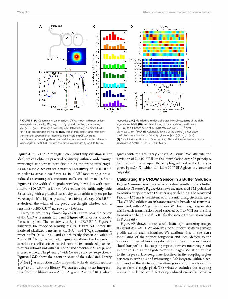
Wang et al. Silicon-nitride coupled-microresonator biochemical sensors
FIGURE 4 | (A) Schematic of an imperfect CROW model with non-uniformwaveguide widths (W0, W1, W2, . . .WN+1) and coupling gap spacing(g1, g2, . . . gN+1). Inset (i): numerically calculated waveguide mode-fieldamplitude profile in the TM mode. (B) Modeled throughput- and drop-porttransmission spectra of an imperfect eight-microring CROW usingtransfer-matrix modeling. Green and red dashed-lines indicate the referencewavelength λ0 of 688.06 nm and the probe wavelength λp of 688.14 nm,
respectively. (C) Modeled normalized pixelized intensity patterns at the eighteigenstates, I–VIII. (D) Calculated library of the correlation coefficientsρ′1 − ρ′
8 as a function of Δn at λ0, with Δnd = 2.523×10⁻² andΔni = 3.6×10⁻⁴ RIU. (E) Calculated library of the differential correlationcoefficients as a function of Δn at λ0, given as |d
(ρ′j (λ0)
)/d (Δn) |.
(F) Calculated sensitivity as a function of λp. The red dashed-line indicates asensitivity of 772RIU−1 at λp = 688.14 nm.
Figure 4F is ~0.52. Although such a sensitivity variation is notideal, we can obtain a practical sensitivity within a wide enoughwavelength window without fine-tuning the probe wavelength.As an example, we can set a practical sensitivity of ~100 RIU−1
in order to sense a Δn down to 10−5 RIU (assuming a noise-induced uncertainty of correlation coefficients of ~±10−3). FromFigure 4F, the width of the probe wavelength window with a sen-sitivity >100 RIU−1 is 1.1 nm. We consider this sufficiently widefor sensing with a practical sensitivity at an arbitrarily set probewavelength. If a higher practical sensitivity of, say, 200 RIU−1
is desired, the width of the probe wavelength window with asensitivity >200 RIU−1 narrows to ~1.06 nm.
Here, we arbitrarily choose λp at 688.14 nm near the centerof the CROW transmission band (Figure 4B) in order to modelthe sensing test. The sensitivity at λp is ~772 RIU−1. Figure 5illustrates the modeled sensing results. Figure 5A shows themodeled pixelized patterns at λp, B(λp) and T(λp), assuming awater buffer (n0 = 1.331) and an arbitrarily chosen Δn value of2.50× 10−3 RIU, respectively. Figure 5B shows the two sets ofcorrelation coefficients extracted from the two modeled pixelizedpatternswithout andwithΔn. Theρp andρs withoutΔn areρ4 andρ5, respectively. The ρp and ρs with Δn are ρ5 and ρ3, respectively.Figures 5C,D show the zoom-in view of the calculated library
ρ′j(λ0)
as a function of Δn. Insets show the detailed mappingsof ρp and ρs with the library. We extract using linear interpola-tion from the library Δn=ΔnT −ΔnB = 2.52× 10⁻³ RIU, which
agrees with the arbitrarily chosen Δn value. We attribute thedeviation of 2× 10⁻⁵ RIU to the interpolation error. In principle,the maximum error upon the sampling interval in the library isgiven by±Δni/2, which is ~1.8× 10⁻⁴ RIU given the assumedΔni value.
Calibrating the CROW Sensor in a Buffer SolutionFigure 6 summarizes the characterization results upon a buffersolution (DI water). Figure 6A shows themeasured TM-polarizedtransmission spectrawithDIwater upper-cladding. ThemeasuredFSR of ~1.80 nm is consistent with the microring circumference.The CROW exhibits an inhomogeneously broadened transmis-sion band, with a ΔλBW of ~1.10 nm. We discern eight eigenstateswithin each transmission band (labeled by I to VIII for the firsttransmission band, and I′–VIII′ for the second transmission bandin Figure 6A).
Figure 6B shows the measured elastic-light-scattering imagesat eigenstates I–VIII. We observe a non-uniform scattering imageprofile across each microring. We attribute this to the extramodulation of the surface roughness and local defects to theintrinsic mode-field-intensity distributions. We notice an obvious“local hotspot” in the coupling region between microring 3 andmicroring 4 in all the light-scattering images. We attribute thatto the larger surface roughness localized in the coupling regionbetween microring 3 and microring 4. We integrate within a cer-tain window the elastic-light-scattering intensity of each micror-ing to form a single pixel. The window excludes the couplingregion in order to avoid scattering-induced crosstalks between
Frontiers in Materials | www.frontiersin.org April 2015 | Volume 2 | Article 3437
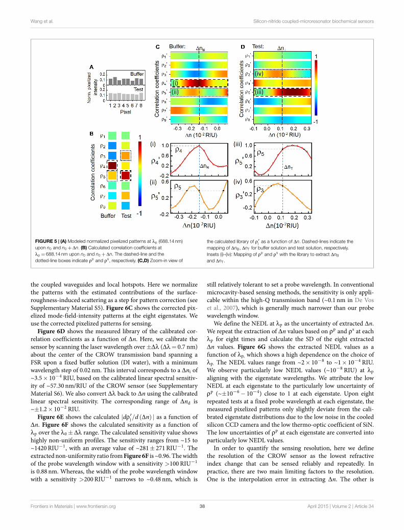
Wang et al. Silicon-nitride coupled-microresonator biochemical sensors
FIGURE 5 | (A) Modeled normalized pixelized patterns at λp (688.14 nm)upon n0 and n0 +Δn. (B) Calculated correlation coefficients atλp = 688.14 nm upon n0 and n0 +Δn. The dashed-line and thedotted-line boxes indicate ρp and ρs, respectively. (C,D) Zoom-in view of
the calculated library of ρ′j as a function of Δn. Dashed-lines indicate the
mapping of ΔnB, ΔnT for buffer solution and test solution, respectively.Insets (i)–(iv): Mapping of ρp and ρs with the library to extract ΔnBand ΔnT.
the coupled waveguides and local hotspots. Here we normalizethe patterns with the estimated contributions of the surface-roughness-induced scattering as a step for pattern correction (seeSupplementary Material S5). Figure 6C shows the corrected pix-elized mode-field-intensity patterns at the eight eigenstates. Weuse the corrected pixelized patterns for sensing.
Figure 6D shows the measured library of the calibrated cor-relation coefficients as a function of Δn. Here, we calibrate thesensor by scanning the laser wavelength over±Δλ (Δλ = 0.7 nm)about the center of the CROW transmission band spanning aFSR upon a fixed buffer solution (DI water), with a minimumwavelength step of 0.02 nm. This interval corresponds to a Δni of~3.5× 10⁻⁴ RIU, based on the calibrated linear spectral sensitiv-ity of ~57.30 nm/RIU of the CROW sensor (see SupplementaryMaterial S6). We also convert Δλ back to Δn using the calibratedlinear spectral sensitivity. The corresponding range of Δnd is~±1.2× 10⁻² RIU.
Figure 6E shows the calculated |dρ′j/d (Δn) | as a function of
Δn. Figure 6F shows the calculated sensitivity as a function ofλp over the λ0 ±Δλ range. The calculated sensitivity value showshighly non-uniform profiles. The sensitivity ranges from ~15 to~1420 RIU−1, with an average value of ~281± 271 RIU−1. Theextractednon-uniformity ratio fromFigure 6F is ~0.96. Thewidthof the probe wavelength window with a sensitivity >100 RIU−1
is 0.88 nm. Whereas, the width of the probe wavelength windowwith a sensitivity >200 RIU−1 narrows to ~0.48 nm, which is
still relatively tolerant to set a probe wavelength. In conventionalmicrocavity-based sensing methods, the sensitivity is only appli-cable within the high-Q transmission band (~0.1 nm in De Voset al., 2007), which is generally much narrower than our probewavelength window.
We define the NEDL at λp as the uncertainty of extracted Δn.We repeat the extraction of Δn values based on ρp and ρs at eachλp for eight times and calculate the SD of the eight extractedΔn values. Figure 6G shows the extracted NEDL values as afunction of λp, which shows a high dependence on the choice ofλp. The NEDL values range from ~2× 10⁻⁸ to ~1× 10⁻⁴ RIU.We observe particularly low NEDL values (~10−8 RIU) at λpaligning with the eigenstate wavelengths. We attribute the lowNEDL at each eigenstate to the particularly low uncertainty ofρp (~±10−6 − 10−4) close to 1 at each eigenstate. Upon eightrepeated tests at a fixed probe wavelength at each eigenstate, themeasured pixelized patterns only slightly deviate from the cali-brated eigenstate distributions due to the low noise in the cooledsilicon CCD camera and the low thermo-optic coefficient of SiN.The low uncertainties of ρp at each eigenstate are converted intoparticularly low NEDL values.
In order to quantify the sensing resolution, here we definethe resolution of the CROW sensor as the lowest refractiveindex change that can be sensed reliably and repeatedly. Inpractice, there are two main limiting factors to the resolution.One is the interpolation error in extracting Δn. The other is
Frontiers in Materials | www.frontiersin.org April 2015 | Volume 2 | Article 3438

Wang et al. Silicon-nitride coupled-microresonator biochemical sensors
FIGURE 6 | (A) Measured TM-polarized throughput- and drop-porttransmission spectra of the eight-microring SiN CROW with DI waterupper-cladding. Green and red dashed-lines indicate the referencewavelength λ0 (686.86 nm) and three probe wavelengths, λp1 (687.06 nm),λp2 (687.38 nm), and λp3 (686.42 nm). (B) Measured elastic-light-scatteringimages with DI water upper-cladding at the eight eigenstates I–VIII. Thewhite-line box indicates the integration window for pixelization.(C) Normalized pixelized mode-field intensity patterns at the eight CROWeigenstates I–VIII. (D) Calculated library of the calibrated correlation
coefficients ρ′1 − ρ′
8 as a function of Δn. White dashed-lines indicate theΔnB values at λp1, λp2, and λp3. (E) Calculated differential correlation
coefficients as a function of Δn, given as |d(
ρ′j (λ0)
)/d (Δn) |.
(F) Calculated sensitivity as a function of λp. Red dashed-lines indicatesensitivities of 214, 279, and 541RIU−1 at probe wavelengths λp1, λp2, andλp3, respectively. (G) Extracted noise-equivalent detection limit (NEDL) as afunction of λp. Red dashed-lines indicate NEDL values of ~4×10⁻⁶
,
~2×10⁻⁸, and ~1×10⁻⁶ RIU at λp1, λp2, and λp3, respectively. Greendashed-lines indicate the eight eigenstate wavelengths λj.
the NEDL taking into account all the noise sources that ourcorrelation approach is not tolerant to. Therefore, given a cali-bration interval of Δni (3.5× 10⁻⁴ RIU), the worst resolution is~1.8× 10⁻⁴ RIU given±Δni/2 (1.8× 10⁻⁴ RIU) and the NEDL(~1.8× 10⁻⁸ − 1.0× 10⁻⁴ RIU in Figure 6G). The interpolation-error-limited resolution (±Δni/2) suggests that a Δn below Δni/2may not be tested reliably or repeatedly. The resolution can beimproved by adopting a finer Δni.
We also calibrate the CROW sensor in the adjacent trans-mission band (see Supplementary Material S7). The pixelizedmode-field intensity patterns at eigenstates I′–VIII′ show ahigh similarity with the corresponding patterns at eigenstatesI–VIII, respectively. The extracted sensitivity and NEDL range
are both close to the calibrated results of the first transmissionband.
Blind Sensing Test ResultsWe implement blind sensing tests at three different probe wave-lengths (λp1, λp2, and λp3) within the CROW transmission band.We prepare one buffer solution (DI water) and three NaCl solu-tions, X, Y, and Z, with different mass concentration valuesunknown to the researcher conducting the sensing tests.We studythe images upon the buffer solution at the initial stage and uponrinsing after each sensing test. We confirm that the pixelized pat-tern returns to the baseline pattern (see Supplementary MaterialS8). Table 1 summarizes the experimental sensing results.
Frontiers in Materials | www.frontiersin.org April 2015 | Volume 2 | Article 3439

Wang et al. Silicon-nitride coupled-microresonator biochemical sensors
TABLE 1 | Sensing results at the three probe wavelengths upon the buffer solution and the three test solutions.
λp Solution ρp ρs ΔnB or ΔnT
(×10−3 RIU)Δn (× 10−3 RIU) Sensed
concentration (%)
λp1 (687.06 nm) Buffer (DI water) ρ3 (0.927±0.003) ρ6 (0.866±0.002) ~−3.54±0.02 – –X (NaCl) ρ6 (0.924±0.003) ρ2 (0.838±0.003) ~4.21±0.01 ~7.75±0.02 ~4.35±0.01Y (NaCl) ρ4 (0.946±0.002) ρ5 (0.854±0.003) ~−2.46±0.03 ~1.08±0.04 ~0.61±0.03Z (NaCl) ρ3 (0.903±0.002) ρ6 (0.854±0.008) ~−3.41±0.01 ~0.13±0.03 ~0.073±0.014
λp2 (687.38 nm) Buffer (DI water) ρ1 (0.99996±0.00003) ρ7 (0.622±0.001) ~−9.1800±0.0001 – –X (NaCl) ρ4 (0.941±0.007) ρ5 (0.875±0.005) ~−0.79±0.02 ~8.39±0.02 ~4.70±0.01Y (NaCl) ρ2 (0.841±0.012) ρ6 (0.807±0.012) ~−8.16±0.02 ~1.03±0.02 ~0.58±0.01Z (NaCl) ρ1 (0.989±0.001) ρ7 (0.622±0.003) ~−9.14±0.01 ~0.05±0.01 ~0.03±0.01
λp3 (686.42 nm) Buffer (DI water) ρ7 (0.851±0.001) ρ2 (0.485±0.002) ~7.775±0.003 – –X (NaCl) ρ1 (0.205±0.015) ρ7 (−0.013±0.014) – – –Y (NaCl) ρ2 (0.519±0.006) ρ8 (0.305±0.009) ~8.81±0.01 ~1.04±0.01 ~0.58±0.01Z (NaCl) ρ7 (0.783±0.005) ρ2 (0.477±0.005) ~7.90±0.01 ~0.13±0.01 ~0.069±0.005
Prepared concentration values: X: (4.5± 0.1)%, Y: (0.60±0.02)%, Z: (0.070± 0.002)%.
Sensing at an Arbitrarily Set Probe Wavelength λp1
Figure 7 shows the sensing results at an arbitrarily set probe wave-length λp1 (687.06 nm) near the center of the CROW transmissionband. The sensitivity at λp1 is ~214 RIU−1 (see Figure 6F). TheNEDL at λp1 is ~4× 10⁻⁶ RIU (see Figure 6G). Figure 7A showsthe measured elastic-light-scattering images of the CROW uponthe buffer solution and the three test solutions at λp1. Figure 7Bshows the corresponding pixelized patterns. Figure 7C shows thecorresponding calculated correlation coefficients. Figures 7D–Gshow the mapping of ρp and ρs in the buffer solution and thethree test solutions with the library. Insets (i)–(viii) show themapping ρp and ρs to the corresponding ΔnB or ΔnT using linearinterpolations in between Δni.
We acquire for solution X a ΔnX of ~(7.75± 0.02)× 10−3 RIUand for solution Y a ΔnY of ~(1.08± 0.04)× 10−3 RIU, both cor-responding to a relatively large Δn but still within Δnd. We acquirefor solution Z (Figure 7G) a ΔnZ of ~(1.3± 0.3)× 10−4 RIU. Forall three solutions, we convert from the measured Δn values thesensed concentration values (see Table 1), which show a goodagreement with the prepared values.
Sensing at λp2 Aligned with Eigenstate IFigure 8 shows the sensing results at a specifically chosen probewavelength λp2 (687.38 nm) aligned with eigenstate I. The sensi-tivity at λp2 is ~279 RIU−1 (see Figure 6F). The NEDL at λp2 is~2× 10⁻⁸ RIU (see Figure 6G), which is much lower comparedwith that at λp2. Figure 8A shows the measured elastic-light-scattering images upon the buffer solution and the three testsolutions. Figure 8B shows the corresponding pixelized patterns.Figure 8C shows the corresponding calculated correlation coef-ficients. Figures 8D–G show the mapping of ρp and ρs values inthe buffer solution and the three test solutions with the library (seeSupplementary Material S9 for detailed mappings).
We acquire for solution X a ΔnX of ~(8.40± 0.02)× 10−3 RIUand for solution Y a ΔnY of ~(1.03± 0.02)× 10−3 RIU. Bothsensing results agree with the prepared concentrations of solu-tions X and Y. For solution Z (Figure 8G), we acquire a ΔnZ of~(0.5± 0.1)× 10−4 RIU, corresponding to a mass concentrationof ~(0.03± 0.01)%. This, however, shows a significant devia-tion from the prepared concentration [~(0.070± 0.002)%]. We
attribute this deviation to a not sufficiently fine calibration of thelibrary and the error from linear interpolation. The calibratedresponse of ρp around the eigenstate is in the proximity to themaximum (unity). The limited sampling resolution ofΔni maynotbe sufficient to describe the response around an extremum.
Sensing at λp3 Near Eigenstate VIIFigure 9 shows the sensing results at another specifically chosenprobe wavelength λp3 (686.42 nm). We specifically set λp3 at theblue-edge of the transmission band near eigenstate VII. The sen-sitivity at λp3 is ~541 RIU−1 (see Figure 6F). The NEDL at λp3 is~1× 10⁻⁶ RIU (see Figure 6G). We consider λp3 as a near opti-mized choice with a relatively high sensitivity and a low NEDL.Figure 9A shows the measured elastic-light-scattering imagesupon the buffer solution and the three test solutions. Figure 9Bshows the corresponding pixelized patterns. Figure 9C shows thecorresponding calculated correlation coefficients. Figures 9D–Fshow the mapping of ρp and ρs values with the library (seeSupplementary Material S9 for detailed mappings).
For solution X, however, we observe an almost dark scatteringpattern, which suggests that λp3 upon solution X is relativelyshifted out of the transmission band. Both the extracted ρp andρs values out of ρj(λp3) upon solution X are particularly low. Bymapping the extracted ρj(λp3) values with the library, we find nomatch to indicate the corresponding Δnx. Therefore, in the casethat there is a chance to measure a large Δn near Δnd (in the orderof 10−2 ~ 10−3RIU in this case), it is better to position λp closeto the red-side of the transmission band in order to leverage thedynamic range given by ΔλBW in full.
For solution Y, we acquire a ΔnY of ~(1.04± 0.02)× 10−3RIU.For solution Z, we acquire a ΔnZ of ~(1.24± 0.1)× 10−4 RIU.Both sensing results agree with the prepared concentrations ofsolutions Y and Z. Compared with the sensing result of solutionZ at λp1, we obtain a more accurate value of ΔnZ with a muchimproved uncertainty. We attribute this to a higher sensitivity anda lower NEDL at λp3 than those at λp1.
Discussion
Here, we benchmark our work with other silicon- and SiN-basedon-chip optical biochemical sensors that have been demonstrated
Frontiers in Materials | www.frontiersin.org April 2015 | Volume 2 | Article 3440

Wang et al. Silicon-nitride coupled-microresonator biochemical sensors
FIGURE 7 | (A) Measured elastic-light-scattering images of CROW upon thebuffer solution and the three blind-test solutions X, Y, and Z at an arbitrarily setprobe wavelength λp1. The white-line box indicates the integration window forpixelization. (B) Normalized pixelized patterns upon the buffer solution andsolutions X, Y, and Z at λp1. (C) Calculated correlation coefficients upon the
buffer solution and solutions X, Y and Z at λp1. Dashed-line and dotted-lineboxes indicate ρp and ρs, respectively. (D–G) Zoom-in view of the library toextract Δn. (D) Upon the buffer solution. (E) Upon solution X. (F) Upon solutionY. (G) Upon solution Z. Insets (i)–(viii): Mapping of ρp and ρs upon the buffersolution and solutions X, Y, and Z.
in recent years, including our previous work (Wang et al., 2014),as summarized in Table 2. All of the work including this workhave attained a detection limit of 10−7 ~ 10−4 RIU. Two of themicrocavity-based sensors (Ghasemi et al., 2013; Doolin et al.,2015) and three of the MZI-based sensors (Duval et al., 2013;Misiakos et al., 2014; Dante et al., 2015) operate on the SiN-basedplatform in the visible wavelengths.
Most of the reported microcavity-based sensors in the liter-ature (except Ghasemi et al., 2013; Doolin et al., 2015) operatein the telecommunication wavelengths (1.3/1.55 μm) and requirea wavelength-tunable laser and a non-silicon photodetector.Whereas, our CROW sensor operating in the visible wavelengthsonly requires in principle a fixed-wavelength visible laser diodeand a silicon CCD/CMOS camera after the library preparation.
In terms of the sensor calibration, the main difference betweenour library preparation and the conventional calibration processfor a microcavity-based sensor is the recording of the pixelizedpatterns instead of single intensity values. A typical calibrationfor a conventional microcavity-based sensor [e.g., De Vos et al.(2007) and Iqbal et al. (2010)] involves scanning laser wavelengthacross a narrow transmission band. As an example, in the work of
DeVos et al., calibrating the spectral sensitivity of amicroring sen-sor of Q~ 20,000 involved measuring the microring transmissionspectrum three times for each of the four given NaCl solutionswith different concentrations (De Vos et al., 2007). In contrast,our library preparation involves scanning laser wavelength acrossthe CROW transmission band, recording the pixelized patterns ateach wavelength step corresponding to the refractive index inter-val Δni and deriving the corresponding correlation coefficientswith the eigenstate patterns. The pattern recording and additionalcomputation of the correlation coefficients render our librarypreparation more reliable and tolerant to the equipment noisesthat are common to all pixels compared with recording singleintensity values multiple times.
A major issue requiring further developments is the signifi-cant variation of sensitivity values upon different probe wave-lengths. We can modify the CROW design in order to attaina more uniform sensitivity (see Supplementary Material S10).Our modeling results suggest that an imperfect CROW with areduced cavity size along with an enhanced inter-cavity couplingcoefficient offers a more uniform sensitivity. Upon a small cavityradius R= 10 μm and a strong inter-cavity coupling coefficient
Frontiers in Materials | www.frontiersin.org April 2015 | Volume 2 | Article 3441
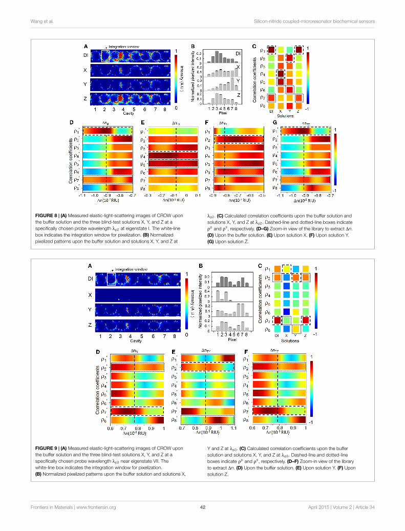
Wang et al. Silicon-nitride coupled-microresonator biochemical sensors
FIGURE 8 | (A) Measured elastic-light-scattering images of CROW uponthe buffer solution and the three blind-test solutions X, Y, and Z at aspecifically chosen probe wavelength λp2 at eigenstate I. The white-linebox indicates the integration window for pixelization. (B) Normalizedpixelized patterns upon the buffer solution and solutions X, Y, and Z at
λp2. (C) Calculated correlation coefficients upon the buffer solution andsolutions X, Y, and Z at λp2. Dashed-line and dotted-line boxes indicateρp and ρs, respectively. (D–G) Zoom-in view of the library to extract Δn.(D) Upon the buffer solution. (E) Upon solution X. (F) Upon solution Y.(G) Upon solution Z.
FIGURE 9 | (A) Measured elastic-light-scattering images of CROW uponthe buffer solution and the three blind-test solutions X, Y, and Z at aspecifically chosen probe wavelength λp3 near eigenstate VII. Thewhite-line box indicates the integration window for pixelization.(B) Normalized pixelized patterns upon the buffer solution and solutions X,
Y and Z at λp3. (C) Calculated correlation coefficients upon the buffersolution and solutions X, Y, and Z at λp3. Dashed-line and dotted-lineboxes indicate ρp and ρs, respectively. (D–F) Zoom-in view of the libraryto extract Δn. (D) Upon the buffer solution. (E) Upon solution Y. (F) Uponsolution Z.
Frontiers in Materials | www.frontiersin.org April 2015 | Volume 2 | Article 3442

Wang et al. Silicon-nitride coupled-microresonator biochemical sensors
TABLE 2 | Summary of silicon- and silicon-nitride-based on-chip optical biochemical sensors.
Device config. Reference Materialplatform
Operationalwavelength (nm)
Footprint(μm2)
Q-factor Sensitivity(RIU−1)
DetectedΔn (RIU)
Detectionlimit (RIU)
MZI Densmore et al. (2008) SOI ~1550 ~40,000 N/A 920 π rad ~7×10⁻⁴ ~1×10⁻⁵
Duval et al. (2013) Si3N4 658 ~108 N/A 4950 π rad ~3×10⁻⁴ ~2×10⁻⁷
Misiakos et al. (2014) SiN ~600–900 ~107 N/A 581 rad ~4×10⁻⁵ ~1×10⁻⁵
Dante et al. (2015) Si3N4 660 ~60,000 N/A 6000 π rad ~2×10⁻⁴ ~4×10⁻⁷
Microdisk Wang et al. (2013) SOI ~1550 ~3 ~100 130 nm ~9×10⁻³ ~8×10⁻⁴
Doolin et al. (2015) Si3N4 ~770 ~900 10000 200 nm ~4×10⁻⁴ ~10−6
Microring withslot-waveguide
Barrios et al. (2007) Si3N4 ~1300 ~20,000 1800 212 nm ~10−3 ~2×10⁻⁴
Claes et al. (2009) SOI ~1550 ~240 ~450 298 nm ~4×10⁻³ ~4.2×10⁻⁵
Carlborg et al. (2010) Si3N4 ~1300 ~20,000 – 248 nm ~3×10⁻⁴ ~5×10⁻⁶
Microring De Vos et al. (2007) SOI ~1550 ~110 20,000 70 nm ~9×10⁻⁴ ~10−5
Iqbal et al. (2010) SOI ~ 1550 ~900 43,000 163 nm ~10−6 –Ghasemi et al. (2013) SiN ~656 ~400 – 48 nm – –Liu et al. (2014) SOI ~1550 ~1600 15000 6000 rad ~4×10⁻⁴ ~2.5×10⁻⁶
Eight-microringCROW in thespatial domain
Wang et al. (2014) SOI ~1550 ~1716 N/A ~199 ~1.5×10⁻⁴ 2×10⁻⁷ ~9×10⁻⁴
(This work) SiN ~680 ~14080 N/A ~281±271 ~1.3×10⁻⁴ 2×10⁻⁸ ~1×10⁻⁴
κ ~ 0.9, we obtain for an imperfect eight-microring CROW amodeled sensitivity of ~384± 153 RIU−1, with an improved non-uniformity ratio of ~0.40 compared to the modeled ratio of~0.52 following our experimental device parameters. Assuminga practical sensitivity of ~100 RIU−1, the width of the mod-eled probe wavelength window with a sensitivity >100 RIU−1
is 2.2 nm, which is much improved compared to the modeledwidth of 1.1 nm following the experimental device parameters. Ifa higher practical sensitivity of 300 RIU−1 is desired, the modeledprobe wavelength window width with a sensitivity >300 RIU−1
is ~1.56 nm, which is still sufficiently wide for practical appli-cations. Based on our current imperfect CROW model, we canfurther design the CROW with tailored non-uniform parametersto optimize the sensitivity and sensitivity variation.
In summary, we demonstrated a SiN CROW-based sensingscheme in the spatial domain in the visible wavelengths. Givena calibrated CROW sensor, this sensing scheme in principleonly requires a low-power, fixed-wavelength laser source in thevisible wavelengths and a silicon CCD or CMOS camera toimage the elastic-light-scattering patterns in the far field. Ourproof-of-concept experiment using an eight-microring CROWon the SiN-on-silica platform showed an average sensitivity of
~281± 271 RIU−1 and a NEDL of 2× 10⁻⁸ ~ 1× 10⁻⁴ RIU. Ourblind sensing tests using NaCl solutions showed a detectionof ~1.26× 10⁻⁴ RIU. Therefore, we have shown that such achip-scale, microresonator-based SiN CROW sensor operatingin the visible wavelengths is promising as a potentially high-performance, portable, and low-cost optical biochemical sensorfor applications such as point-of-care biochemical analyses andself-monitoring of personal healthcare using smartphones.
Acknowledgments
This work is supported by grants from the Research GrantsCouncil of the Hong Kong Special Administrative Region, China(Project No. 618010, 617612, and 617913). The authors acknowl-edge the HKUST Nanoelectronics Fabrication Facility for fabri-cating the optofluidic chip.
Supplementary Material
The Supplementary Material for this article can be foundonline at http://www.frontiersin.org/Journal/10.3389/fmats.2015.00034/abstract
ReferencesBarrios, C. A., Gylfason, K. B., Sánchez, B., Griol, A., Sohlström, H., Holgado,
M., et al. (2007). Slot-waveguide biochemical sensor. Opt. Lett. 32, 3080–3082.doi:10.1364/ol.32.003080
Carlborg, C. F., Gylfason, K. B., Kazmierczak, A., Dortu, F., Polo, M. B., Catala,A. M., et al. (2010). A packaged optical slot-waveguide ring resonator sensorarray for multiplex label-free assays in labs-on-chips. Lab. Chip 10, 281–290.doi:10.1039/b914183a
Ciminelli, C., Campanella, C. M., Dell’olio, F., Campanella, C. E., and Armenise,M. N. (2013). Label-free optical resonant sensors for biochemical applications.Prog. Quant. Electron. 37, 51–107. doi:10.1016/j.pquantelec.2013.02.001
Claes, T., Molera, J. G., De Vos, K., Schachtb, E., Baets, R., and Bienstman, P.(2009). Label-free biosensing with a slot-waveguide-based ring resonatorin silicon on insulator. Photonics J. IEEE 1, 197–204. doi:10.1109/jphot.2009.2031596
Dante, S., Duval, D., Fariña, D., González-Guerrero, A. B., and Lechuga, L. M.(2015). Linear readout of integrated interferometric biosensors using a peri-odic wavelength modulation. Laser Photon. Rev. 9, 248–255. doi:10.1002/lpor.201400216
De Vos, K., Bartolozzi, I., Schacht, E., Bienstman, P., and Baets, R. (2007). Silicon-on-insulator microring resonator for sensitive and label-free biosensing. Opt.Express 15, 7610–7615. doi:10.1364/oe.15.007610
Densmore, A., Xu, D.-X., Janz, S., Waldron, P., Mischki, T., Lopinski, G.,et al. (2008). Spiral-path high-sensitivity silicon photonic wire molecular sensorwith temperature-independent response.Opt. Lett. 33, 596–598. doi:10.1364/ol.33.000596
Doolin, C., Doolin, P., Lewis, B. C., and Davis, J. P. (2015). Refractometric sensingof Li salt with visible-light Si3N4 microdisk resonators. Appl. Phys. Lett. 106,081104. doi:10.1063/1.4913618
Duval, D., Osmond, J., Dante, S., Dominguez, C., and Lechuga, L. M. (2013). Grat-ing couplers integrated on Mach-Zehnder interferometric biosensors operating
Frontiers in Materials | www.frontiersin.org April 2015 | Volume 2 | Article 3443

Wang et al. Silicon-nitride coupled-microresonator biochemical sensors
in the visible range. Photonics J. IEEE 5, 3700108. doi:10.1109/jphot.2013.2251873
Estevez, M.-C., Alvarez, M., and Lechuga, L. M. (2012). Integrated optical devicesfor lab-on-a-chip biosensing applications. Laser Photon. Rev. 6, 463–487. doi:10.1002/lpor.201100025
Ghasemi, F., Eftekhar, A. A., Gottfried, D. S., Song, X., Cummings, R. D., and Adibi,A. (2013). “Self-referenced silicon nitride array microring biosensor for toxindetection using glycans at visible wavelength,” in SPIE BiOS (San Francisco, CA:International Society for Optics and Photonics).
Gorin, A., Jaouad, A., Grondin, E., Aimez, V., and Charette, P. (2008). Fabricationof silicon nitride waveguides for visible-light using PECVD: a study of theeffect of plasma frequency on optical properties. Opt. Express 16, 13509–13516.doi:10.1364/oe.16.013509
Halir, R., Vivien, L., Le Roux, X., Xu, D.-X., and Cheben, P. (2013). Direct andsensitive phase readout for integrated waveguide sensors. Photonics J. IEEE 5,6800906. doi:10.1109/jphot.2013.2276747
Iqbal, M., Gleeson, M. A., Spaugh, B., Tybor, F., Gunn, W. G., Hochberg, M., et al.(2010). Label-free biosensor arrays based on silicon ring resonators and high-speed optical scanning instrumentation. IEEE J. Sel. Top. Quantum Electron. 16,654–661. doi:10.1109/jstqe.2009.2032510
Kozma, P., Hamori, A., Cottier, K., Kurunczi, S., and Horvath, R. (2009). Gratingcoupled interferometry for optical sensing. Appl. Phys. B 97, 5–8. doi:10.1007/s00340-009-3719-1
Lakshminarayanan, V., Zelek, J., and Mcbride, A. (2015). “Smartphone Science” ineye care and medicine. Opt. Photonics News 26, 44–51. doi:10.1364/opn.26.1.000044
Lei, T., and Poon, A. W. (2011). Modeling of coupled-resonator opticalwaveguide (CROW) based refractive index sensors using pixelized spatial detec-tion at a single wavelength. Opt. Express 19, 22227–22241. doi:10.1364/oe.19.022227
Liu, J., Zhou, X., Qiao, Z., Zhang, J., Zhang, C., Xiang, T., et al. (2014). Inte-grated optical chemical sensor based on an SOI ring resonator using phase-interrogation. Photonics J. IEEE 6, 1–7. doi:10.1109/jphot.2014.2352973
Misiakos, K., Raptis, I., Makarona, E., Botsialas, A., Salapatas, A., Oikonomou, P.,et al. (2014). All-siliconmonolithicMach-Zehnder interferometer as a refractive
index and bio-chemical sensor. Opt. Express 22, 26803–26813. doi:10.1364/OE.22.026803
Sedlmeir, F., Zeltner, R., Leuchs, G., and Schwefel, H. G. (2014). High-Q MgF2whispering gallery mode resonators for refractometric sensing in aqueousenvironment. Opt. Express 22, 30934–30942. doi:10.1364/oe.22.030934
Subramanian, A., Dhakal, A., Peyskens, F., Selvaraja, S., Baets, R., Neutens, P., et al.(2013). Low-loss singlemode PECVD silicon nitride photonic wire waveguidesfor 532–900 nm wavelength window fabricated within a CMOS pilot line.Photonics J. IEEE 5, 2202809. doi:10.1109/jphot.2013.2292698
Vollmer, F., Arnold, S., and Keng, D. (2008). Single virus detection from thereactive shift of a whispering-gallery mode. Proc. Natl. Acad. Sci. U.S.A. 105,20701–20704. doi:10.1073/pnas.0808988106
Wang, J., Yao, Z., Lei, T., and Poon, A. W. (2014). Silicon coupled-resonatoroptical-waveguide-based biosensors using light-scattering pattern recognitionwith pixelizedmode-field-intensity distributions. Sci. Rep. 4, 07528. doi:10.1038/srep07528
Wang, X., Guan, X., Huang, Q., Zheng, J., Shi, Y., and Dai, D. (2013). Suspendedultra-small disk resonator on silicon for optical sensing.Opt. Lett. 38, 5405–5408.doi:10.1364/ol.38.005405
Xu, J., Suarez, D., and Gottfried, D. S. (2007). Detection of avian influenza virususing an interferometric biosensor. Anal. Bioanal. Chem. 389, 1193–1199.doi:10.1007/s00216-007-1525-3
Ymeti, A., Greve, J., Lambeck, P. V., Wink, T., Van Hövell, S. W., Beumer, T. A., et al.(2007). Fast, ultrasensitive virus detection using a Young interferometer sensor.Nano Lett. 7, 394–397. doi:10.1021/nl062595n
Conflict of Interest Statement: The authors declare that the research was con-ducted in the absence of any commercial or financial relationships that could beconstrued as a potential conflict of interest.
Copyright © 2015 Wang, Yao and Poon. This is an open-access article distributedunder the terms of the Creative Commons Attribution License (CC BY). The use, dis-tribution or reproduction in other forums is permitted, provided the original author(s)or licensor are credited and that the original publication in this journal is cited, inaccordance with accepted academic practice. No use, distribution or reproduction ispermitted which does not comply with these terms.
Frontiers in Materials | www.frontiersin.org April 2015 | Volume 2 | Article 3444

MATERIALSORIGINAL RESEARCH ARTICLE
published: 07 April 2015doi: 10.3389/fmats.2015.00028
High-throughput multiple dies-to-wafer bondingtechnology and III/V-on-Si hybrid lasers for heterogeneousintegration of optoelectronic integrated circuitsXianshu Luo1,Yulian Cao2, Junfeng Song1, Xiaonan Hu2,Yuanbing Cheng2, Chengming Li 2,Chongyang Liu2,Tsung-Yang Liow 1, MingbinYu1, Hong Wang2, Qi Jie Wang2 and Patrick Guo-Qiang Lo1*1 Institute of Microelectronics, Agency for Science, Technology and Research (A*STAR), Singapore, Singapore2 Photonics Center of Excellence (OPTIMUS), School of Electrical and Electronic Engineering, Nanyang Technological University, Singapore, Singapore
Edited by:Laurent Vivien, Université Paris-Sud,France
Reviewed by:Junichi Fujikata, Photonics ElectronicsTechnology Research Association,JapanYasuhiko Ishikawa, The University ofTokyo, Japan
*Correspondence:Patrick Guo-Qiang Lo, Institute ofMicroelectronics, Agency for Science,Technology and Research (A*STAR),Singapore Science Park II, 11 SciencePark Road, 117685 Singaporee-mail: [email protected]
Integrated optical light source on silicon is one of the key building blocks for optical intercon-nect technology. Great research efforts have been devoting worldwide to explore variousapproaches to integrate optical light source onto the silicon substrate. The achievementsso far include the successful demonstration of III/V-on-Si hybrid lasers through III/V gainmaterial to silicon wafer bonding technology. However, for potential large-scale integration,leveraging on mature silicon complementary metal oxide semiconductor (CMOS) fabrica-tion technology and infrastructure, more effective bonding scheme with high bonding yieldis in great demand considering manufacturing needs. In this paper, we propose and demon-strate a high-throughput multiple dies-to-wafer (D2W) bonding technology, which is thenapplied for the demonstration of hybrid silicon lasers. By temporarily bonding III/V dies to ahandle silicon wafer for simultaneous batch processing, it is expected to bond unlimited III/Vdies to silicon device wafer with high yield. As proof-of-concept, more than 100 III/V diesbonding to 200 mm silicon wafer is demonstrated. The high performance of the bondinginterface is examined with various characterization techniques. Repeatable demonstrationsof 16-III/V die bonding to pre-patterned 200 mm silicon wafers have been performed forvarious hybrid silicon lasers, in which device library including Fabry–Perot (FP) laser, lateral-coupled distributed-feedback laser with side wall grating, and mode-locked laser (MLL).From these results, the presented multiple D2W bonding technology can be a key enablertoward the large-scale heterogeneous integration of optoelectronic integrated circuits.
Keywords: silicon photonics, hybrid lasers, heterogeneous integration, die-to-wafer bonding, optoelectronicintegrated circuits
INTRODUCTIONIn the future generation of datacom and computercom, whichdemand ever higher bandwidth and lower power, the conventionalelectrical interconnection routing the electronic signals becomesbandwidth-limited along with prohibitively high power consump-tion (Beausoleil et al., 2008). One solution to the challenge is theoptical interconnect technology (Goodman et al., 1984; Miller,2000, 2009; Ohashi et al., 2009), in which high bandwidth opticalsignals are routed by low-loss optical fiber and waveguides. In con-trast to the electrical interconnection (i.e., the copper wire), opticalinterconnect has many merits, e.g., high speed, low crosstalk,immunity to electromagnetic interference, low overall power con-sumption (Alduino and Paniccia, 2007). Most importantly, withthe up scaling potential, optical interconnect is expected to providemuch higher transmission capacity and longer signal transmissiondistance than the electrical interconnect.
Although it was proposed initially 30 years ago (Goodman et al.,1984), there was no significant development progress with soliddemonstrations of optical interconnect for very-large-scale inte-gration (VLSI). The situation has changed since the concept ofsilicon photonics (Pavesi and Lockwood, 2004; Reed and Knights,
2004; Lipson, 2005; Guillot and Pavesi, 2006; Jalali and Fathpour,2006; Soref, 2006; Poon et al., 2009a,b; Vivien and Pavesi, 2013;Xu et al., 2014), which utilizes low-cost silicon material along withleveraging on the advancement of silicon complementary metaloxide semiconductor (CMOS) process, integration, and matureinfrastructure. Envisioned by Soref and Lorenzo (1985), siliconphotonics has emerged and progressed steadily. Especially in thepast decade, we have been witnessing rapid growth in research anddevelopment activities along with product development effortsexploiting silicon photonics technology for the optical intercon-nect (Pavesi and Lockwood, 2004; Reed and Knights, 2004; Lipson,2005; Guillot and Pavesi, 2006; Jalali and Fathpour, 2006; Soref,2006; Fedeli et al., 2008; Poon et al., 2009a,b; Michel et al., 2010;Reed et al., 2010; Feng et al., 2012; Liow et al., 2013; Vivien andPavesi, 2013; Dong et al., 2014a,b; Lim et al., 2014; Xu et al., 2014).For instance, to minimize the small core silicon waveguide prop-agation losses, considerable research work has been devoted tominimize the waveguide sidewall roughness by using the deepultra-violet (DUV) photolithography and optimized patterningtechnique (Dumon et al., 2004; Bogaerts et al., 2005) and sidewallsmoothing technique [e.g., double thermal oxidations (Sparacin
www.frontiersin.org April 2015 | Volume 2 | Article 28 | 45
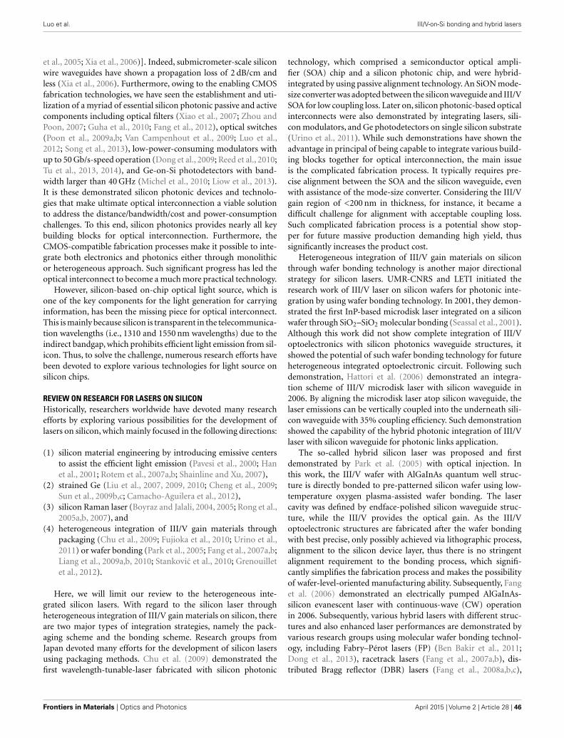
Luo et al. III/V-on-Si bonding and hybrid lasers
et al., 2005; Xia et al., 2006)]. Indeed, submicrometer-scale siliconwire waveguides have shown a propagation loss of 2 dB/cm andless (Xia et al., 2006). Furthermore, owing to the enabling CMOSfabrication technologies, we have seen the establishment and uti-lization of a myriad of essential silicon photonic passive and activecomponents including optical filters (Xiao et al., 2007; Zhou andPoon, 2007; Guha et al., 2010; Fang et al., 2012), optical switches(Poon et al., 2009a,b; Van Campenhout et al., 2009; Luo et al.,2012; Song et al., 2013), low-power-consuming modulators withup to 50 Gb/s-speed operation (Dong et al., 2009; Reed et al., 2010;Tu et al., 2013, 2014), and Ge-on-Si photodetectors with band-width larger than 40 GHz (Michel et al., 2010; Liow et al., 2013).It is these demonstrated silicon photonic devices and technolo-gies that make ultimate optical interconnection a viable solutionto address the distance/bandwidth/cost and power-consumptionchallenges. To this end, silicon photonics provides nearly all keybuilding blocks for optical interconnection. Furthermore, theCMOS-compatible fabrication processes make it possible to inte-grate both electronics and photonics either through monolithicor heterogeneous approach. Such significant progress has led theoptical interconnect to become a much more practical technology.
However, silicon-based on-chip optical light source, which isone of the key components for the light generation for carryinginformation, has been the missing piece for optical interconnect.This is mainly because silicon is transparent in the telecommunica-tion wavelengths (i.e., 1310 and 1550 nm wavelengths) due to theindirect bandgap, which prohibits efficient light emission from sil-icon. Thus, to solve the challenge, numerous research efforts havebeen devoted to explore various technologies for light source onsilicon chips.
REVIEW ON RESEARCH FOR LASERS ON SILICONHistorically, researchers worldwide have devoted many researchefforts by exploring various possibilities for the development oflasers on silicon, which mainly focused in the following directions:
(1) silicon material engineering by introducing emissive centersto assist the efficient light emission (Pavesi et al., 2000; Hanet al., 2001; Rotem et al., 2007a,b; Shainline and Xu, 2007),
(2) strained Ge (Liu et al., 2007, 2009, 2010; Cheng et al., 2009;Sun et al., 2009b,c; Camacho-Aguilera et al., 2012),
(3) silicon Raman laser (Boyraz and Jalali, 2004, 2005; Rong et al.,2005a,b, 2007), and
(4) heterogeneous integration of III/V gain materials throughpackaging (Chu et al., 2009; Fujioka et al., 2010; Urino et al.,2011) or wafer bonding (Park et al., 2005; Fang et al., 2007a,b;Liang et al., 2009a,b, 2010; Stankovic et al., 2010; Grenouilletet al., 2012).
Here, we will limit our review to the heterogeneous inte-grated silicon lasers. With regard to the silicon laser throughheterogeneous integration of III/V gain materials on silicon, thereare two major types of integration strategies, namely the pack-aging scheme and the bonding scheme. Research groups fromJapan devoted many efforts for the development of silicon lasersusing packaging methods. Chu et al. (2009) demonstrated thefirst wavelength-tunable-laser fabricated with silicon photonic
technology, which comprised a semiconductor optical ampli-fier (SOA) chip and a silicon photonic chip, and were hybrid-integrated by using passive alignment technology. An SiON mode-size converter was adopted between the silicon waveguide and III/VSOA for low coupling loss. Later on, silicon photonic-based opticalinterconnects were also demonstrated by integrating lasers, sili-con modulators, and Ge photodetectors on single silicon substrate(Urino et al., 2011). While such demonstrations have shown theadvantage in principal of being capable to integrate various build-ing blocks together for optical interconnection, the main issueis the complicated fabrication process. It typically requires pre-cise alignment between the SOA and the silicon waveguide, evenwith assistance of the mode-size converter. Considering the III/Vgain region of <200 nm in thickness, for instance, it became adifficult challenge for alignment with acceptable coupling loss.Such complicated fabrication process is a potential show stop-per for future massive production demanding high yield, thussignificantly increases the product cost.
Heterogeneous integration of III/V gain materials on siliconthrough wafer bonding technology is another major directionalstrategy for silicon lasers. UMR-CNRS and LETI initiated theresearch work of III/V laser on silicon wafers for photonic inte-gration by using wafer bonding technology. In 2001, they demon-strated the first InP-based microdisk laser integrated on a siliconwafer through SiO2–SiO2 molecular bonding (Seassal et al., 2001).Although this work did not show complete integration of III/Voptoelectronics with silicon photonics waveguide structures, itshowed the potential of such wafer bonding technology for futureheterogeneous integrated optoelectronic circuit. Following suchdemonstration, Hattori et al. (2006) demonstrated an integra-tion scheme of III/V microdisk laser with silicon waveguide in2006. By aligning the microdisk laser atop silicon waveguide, thelaser emissions can be vertically coupled into the underneath sili-con waveguide with 35% coupling efficiency. Such demonstrationshowed the capability of the hybrid photonic integration of III/Vlaser with silicon waveguide for photonic links application.
The so-called hybrid silicon laser was proposed and firstdemonstrated by Park et al. (2005) with optical injection. Inthis work, the III/V wafer with AlGaInAs quantum well struc-ture is directly bonded to pre-patterned silicon wafer using low-temperature oxygen plasma-assisted wafer bonding. The lasercavity was defined by endface-polished silicon waveguide struc-ture, while the III/V provides the optical gain. As the III/Voptoelectronic structures are fabricated after the wafer bondingwith best precise, only possibly achieved via lithographic process,alignment to the silicon device layer, thus there is no stringentalignment requirement to the bonding process, which signifi-cantly simplifies the fabrication process and makes the possibilityof wafer-level-oriented manufacturing ability. Subsequently, Fanget al. (2006) demonstrated an electrically pumped AlGaInAs-silicon evanescent laser with continuous-wave (CW) operationin 2006. Subsequently, various hybrid lasers with different struc-tures and also enhanced laser performances are demonstrated byvarious research groups using molecular wafer bonding technol-ogy, including Fabry–Pérot lasers (FP) (Ben Bakir et al., 2011;Dong et al., 2013), racetrack lasers (Fang et al., 2007a,b), dis-tributed Bragg reflector (DBR) lasers (Fang et al., 2008a,b,c),
Frontiers in Materials | Optics and Photonics April 2015 | Volume 2 | Article 28 | 46

Luo et al. III/V-on-Si bonding and hybrid lasers
distributed-feedback (DFB) lasers (Fang et al., 2008a,b,c), micror-ing lasers (Liang et al., 2009a,b, 2012), wavelength tunable lasers(Keyvaninia et al., 2013a,b,c), multiple-wavelength lasers (VanCampenhout et al., 2008; Kurczveil et al., 2011), and mode-lockedlasers (MLL) (Fang et al., 2008a,b,c).
Besides such direct bonding method, wafer bonding can alsobe realized through an adhesive material as the bonding interlayer.Among all kinds of adhesive bonding materials, divinylsiloxane-bisbenzocyclobutene (DVS-BCB or BCB) is the most popular onefor hybrid silicon lasers due to the merits such as the high bond-ing strength and the sustainability in the subsequent III/V process.IMEC has used BCB-assisted adhesive bonding method for hetero-geneous integration (Roelkens et al., 2005). In 2006, Roelkens et al.(2006) demonstrated the first electrically injected InP/InGaAsPlaser integrated on silicon waveguide circuit using BCB-assistedadhesive bonding technology. Similar to Seassal et al. (2001), theoptical laser is purely made with III/V layer with the laser facetsbeing defined by dry etching. With optimized mode-size converter,the optical light can be vertically coupled down to the underneathsilicon waveguide with high efficiency. By designing hybrid modewaveguide comprising silicon waveguide and III/V gain medium,they also demonstrated a hybrid FP laser (Stankovic et al., 2011)and a DFB laser (Stankovic et al., 2012; Keyvaninia et al.,2013a,b,c),and multiple-wavelength laser (Keyvaninia et al., 2013a,b,c) usingsuch adhesive bonding technology.
Apart from BCB, some kinds of metal can also be adopted asthe bonding interlayer for adhesive bonding. AuGeNi is one of themost popular metals for metal bonding as it not only functionsas a bonding media but can also be used for the Ohmic contactto the InGaAsP structure. Tanabe et al. (2010) demonstrated aInAs/GaAs quantum-dot laser on Si substrate by metal-assistedwafer bonding with room temperature operation at 1.3 µm wave-length. Meanwhile, Hong et al. (2010) also demonstrated an FPlaser through selective-area metal bonding using AuGeNi. The sil-icon waveguide in such demonstration is with 5 µm and 800 nmthickness. The demonstrated FP laser is with threshold currentdensity of 1.7 kA/cm and a maximum output power of 3 mW.However, the drawback of the AuGeNi-assisted bonding is the Aucontamination. Thus, Tatsumi et al. (2012) further demonstratedan Au-free metal-assisted wafer bonding for lasers on silicon chip.Besides, Creazzo et al. (2013) also demonstrated another typeof silicon laser by using metal-assisted bonding of III/V epitax-ial material directly onto the silicon substrate. The demonstratedthat silicon laser had a threshold of ~50 mA and maximum opticalpower of ~8 mW. The benefit of such metal-assisted bonding is theadvantage of effective thermal dissipation, which shows a thermalresistant of only 21°C/W.
Beyond these two major heterogeneous integration schemes,there are also other methods for III/V-on-Si lasers, including directIII/V epitaxy on silicon substrate (Liu et al., 2011; Lee et al., 2012)and III/V epitaxial layer transfer-printing to silicon wafers (Justiceet al., 2012; Yang et al., 2012). However, while the direct epitaxymethod faces major challenges of high-density dislocations due tothe lattice mismatch between III/V material and silicon after manyyears of research, the transfer-printing method for hybrid siliconlaser needs further demonstrations to show the repeatability andreliability.
From these analyses, it shows that among various approaches,the hybrid silicon laser through wafer bonding technology canbe considered as the most successful and promising one for sili-con photonic heterogeneous integration circuits due to the ever-demonstrated advanced performances and the fabrication processcompatibility with silicon photonics. Table 1 summarizes some ofthe representative demonstrations of hybrid silicon lasers throughwafer bonding technology.
WAFER BONDING TECHNOLOGIES FOR ON-CHIP SILICON LASERSIn general, there are two mainstreams of wafer bonding methodsapplying to heterogeneous integrated silicon photonics, namelythe molecular bonding through interfacial bonds, and the adhe-sive bonding assisted with another adhesive material as bondinginterface such as polymer or metal. Such wafer bonding tech-nology is a mature process, which is widely applicable for SOIwafer fabrication, MEMS technology, and optoelectronic devicefabrication. As a lot of review papers already exist (Lasky, 1986;Maszara, 1991; Tong and Goesele, 1999; Alexe and Gösele, 2004;Christiansen et al., 2006), we thus only focus the discussion onthe application of hybrid silicon lasers. According to the existingdemonstrations, we further summarize here the major bondingtechnologies as below:
(1) wafer-to-wafer (W2W) molecular bonding,(2) die-to-wafer (D2W) molecular bonding,(3) BCB-assisted D2W adhesive bonding, and(4) metal-assisted adhesive bonding.
The W2W molecular bonding for hybrid silicon lasers is mainlydriven by the UCSB group. Through such plasma-activated low-temperature W2W molecular bonding (Pasquariello and Hjort,2002), they, together with their collaborators, have demonstratedvarious hybrid silicon lasers, starting from the first-hybrid FPlaser (Fang et al., 2006), followed by racetrack-shaped laser (Fanget al., 2007a,b), DBR lasers (Fang et al., 2008a,b,c), DFB lasers(Fang et al., 2008a,b,c), MLL (Fang et al., 2008a,b,c), and multi-wavelength arbitrary waveform generation (AWG) laser (Kurczveilet al., 2011). However, for the conventional III/V-to-Si W2W bond-ing without thick oxide interlayer, the generated gas by-productsof H2 and H2O are easily trapped inside the bonding interface andform the interfacial voids, which subsequently affect the bondingquality. In order to effectively remove such trapped gases, someproper outgas channels are designed, such as in-plane outgassingchannels (IPOC) (Kissinger and Kissinger, 1993) or vertical out-gassing channels (VOC) (Liang and Bowers, 2008). IPOS is formedby etching some lateral channels extended to the chip edges, sothat the by-product gases can be directed to outside the bondinginterface to the chip edge during post bonding annealing. How-ever, for some close-loop structures, such as microrings, there isno way to design such IPOS. In order to solve such issue, VOCis proposed by etching some array of holes down to the BOXlayer. The generated by-product gases can migrate to the closestVOC and are absorbed by SOI BOX. As both IPOS and VOC canbe formed during the waveguide etching, there is no particulardesign requirement from the fabrication point of view. However,as the formation of such outgas channels affects the silicon layer
www.frontiersin.org April 2015 | Volume 2 | Article 28 | 47

Luo et al. III/V-on-Si bonding and hybrid lasers
Table 1 | Representative demonstrations of hybrid silicon lasers through wafer bonding technology.
Laser types Bonding type Waveguide scheme Performances Reference
λ (nm) T (°C) I th (mA) Pout (mW) SE (mW/mA) Z t (°C/W)
Fabry–Perot
laser
Molecular
bonding
Hybrid WG (75 vs. 3% mode
confinement within Si WG
and QW)
1577 CW @ 15 65 1.8 0.013a 40 Fang et al.
(2006)
DBR laser Molecular
bonding
Hybrid waveguide with
inverse taper (66 vs. 4.4%
mode confinement within Si
WG and QW)
1569 CW @ 15 65 11 0.088a 40 Fang et al.
(2008a,b,c)
D2W molecular
bonding with
oxide interlayer
Hybrid waveguide with
adiabatic mode transformer
1570 Pulse @ 20 100 7.2 0.021a – Ben Bakir
et al. (2011)
W2W molecular
bonding with
oxide interlayer
Hybrid waveguide with
inverse taper, thermal tunable
microring for wavelength
tuning
1553 CW @ 20 40 4 0.025a – Keyvaninia
et al.
(2013a,b,c)
Metal-assisted
D2W bonding
III/V gain material
butt-coupling with Si
waveguide through a
waveguide coupler
1562 CW @ 20 41 8 0.038 21 Creazzo
et al. (2013)
DFB laser Molecular
bonding
Hybrid waveguide with
inverse taper (59.2 vs. 5.2%
mode confinement within Si
WG and QW)
1600 CW @ 10 25 5.4 0.072a 132 Fang et al.
(2008a,b,c)
D2D BCB
adhesive
bonding
Hybrid waveguide (70 vs. 3%
mode confinement within Si
WG and QW)
1308 CW @ 20 20 2.1 0.026 – Stankovic
et al. (2011)
Selective-area
metal bonding
Hybrid WG (94% mode
confinement within Si)
1554 Pulse @ RT 35 3 0.05 – Hong et al.
(2010)
Microdisk
laser
D2W molecular
bonding
InP microdisk laser light
vertically coupling to Si WG
1590 CW @ 20 0.9 0.012 0.008 – Van Camp-
enhout
et al. (2008)
Microring
laser
Molecular
bonding
Racetrack microring, hybrid
waveguide
1590 CW @ 15 175 29 0.089 – Fang et al.
(2007a,b)
Molecular
bonding
Hybrid microring with side
coupled Si WG
– CW @ 10 7.5 2.5 0.2 – Liang et al.
(2011)
aData are extracted from the power–current curves.
pattern density, which will finally affect the bonding strength, itis desirable to take into account the design tradeoff between thebonding strength and the gas removal effectiveness.
Alternatively, plasma-assisted D2W molecular bonding has alsobeen investigated for hybrid silicon lasers mainly by LETI. Forlarge-scale manufacturability for potential massive production,the key enabling capability is the multiple dies to wafer bond-ing with high yield. Kostrzewa et al. (2006) first demonstrateda molecular bonding of multiple InP dies to a 200 mm siliconCMOS wafer with only 1 mm× 1 mm die size (Kostrzewa et al.,2006). For strong hydrophilic molecular bonding, both InP and
silicon wafers were covered with oxide layer. Pick-and-place tech-nology was used in order to align the InP dies to specific spotsin silicon wafer, as well as to supply mechanical force to thedies through pick-and-place head. Using such D2W bonding,they demonstrated electrically pumped microdisk lasers integratedwith a silicon waveguide circuit (Van Campenhout et al., 2007).However, in such D2W bonding, as the cleaning of the dies is per-formed ahead of the pick-and-place process, the bonding surfacecould be contaminated, and subsequently affecting the bondingquality and bonding yield. Furthermore, with the considerationof the pick-and-place time of 30 s/die, it takes approximately an
Frontiers in Materials | Optics and Photonics April 2015 | Volume 2 | Article 28 | 48
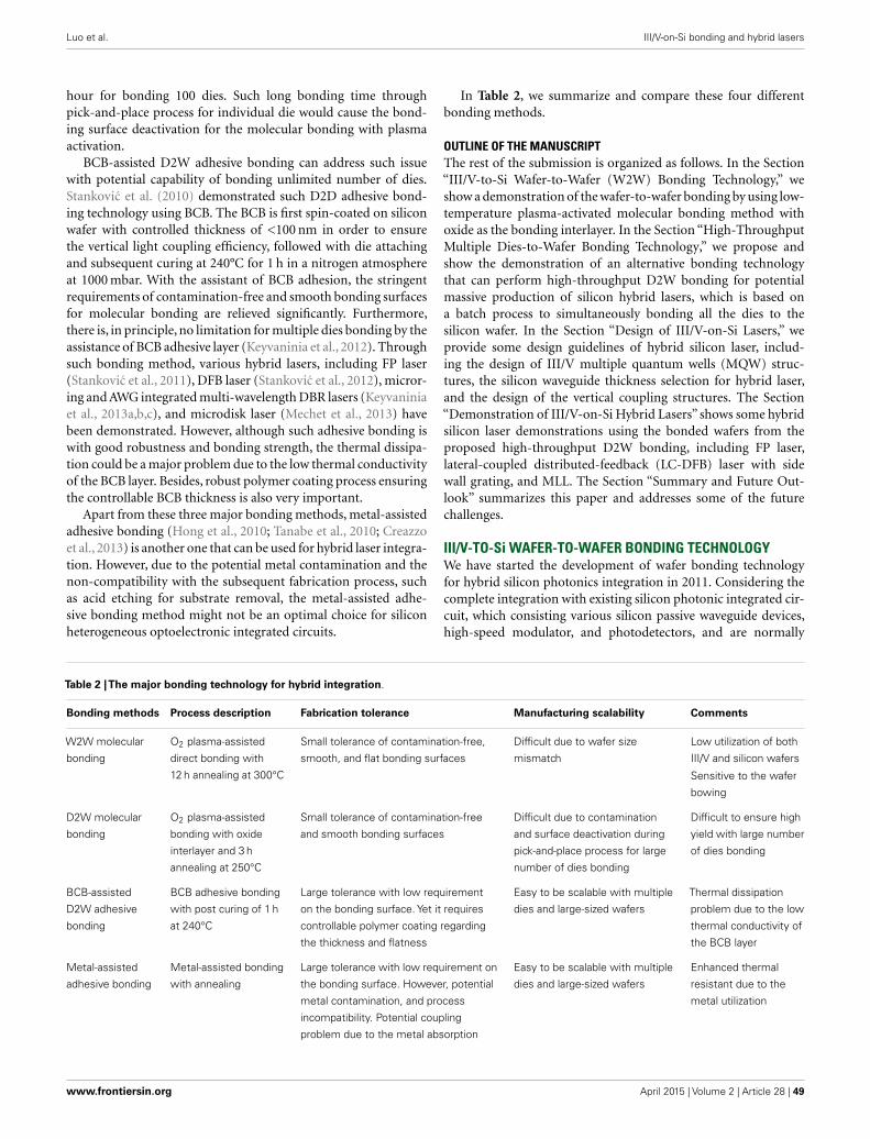
Luo et al. III/V-on-Si bonding and hybrid lasers
hour for bonding 100 dies. Such long bonding time throughpick-and-place process for individual die would cause the bond-ing surface deactivation for the molecular bonding with plasmaactivation.
BCB-assisted D2W adhesive bonding can address such issuewith potential capability of bonding unlimited number of dies.Stankovic et al. (2010) demonstrated such D2D adhesive bond-ing technology using BCB. The BCB is first spin-coated on siliconwafer with controlled thickness of <100 nm in order to ensurethe vertical light coupling efficiency, followed with die attachingand subsequent curing at 240°C for 1 h in a nitrogen atmosphereat 1000 mbar. With the assistant of BCB adhesion, the stringentrequirements of contamination-free and smooth bonding surfacesfor molecular bonding are relieved significantly. Furthermore,there is, in principle, no limitation for multiple dies bonding by theassistance of BCB adhesive layer (Keyvaninia et al., 2012). Throughsuch bonding method, various hybrid lasers, including FP laser(Stankovic et al., 2011), DFB laser (Stankovic et al., 2012), micror-ing and AWG integrated multi-wavelength DBR lasers (Keyvaniniaet al., 2013a,b,c), and microdisk laser (Mechet et al., 2013) havebeen demonstrated. However, although such adhesive bonding iswith good robustness and bonding strength, the thermal dissipa-tion could be a major problem due to the low thermal conductivityof the BCB layer. Besides, robust polymer coating process ensuringthe controllable BCB thickness is also very important.
Apart from these three major bonding methods, metal-assistedadhesive bonding (Hong et al., 2010; Tanabe et al., 2010; Creazzoet al., 2013) is another one that can be used for hybrid laser integra-tion. However, due to the potential metal contamination and thenon-compatibility with the subsequent fabrication process, suchas acid etching for substrate removal, the metal-assisted adhe-sive bonding method might not be an optimal choice for siliconheterogeneous optoelectronic integrated circuits.
In Table 2, we summarize and compare these four differentbonding methods.
OUTLINE OF THE MANUSCRIPTThe rest of the submission is organized as follows. In the Section“III/V-to-Si Wafer-to-Wafer (W2W) Bonding Technology,” weshow a demonstration of the wafer-to-wafer bonding by using low-temperature plasma-activated molecular bonding method withoxide as the bonding interlayer. In the Section “High-ThroughputMultiple Dies-to-Wafer Bonding Technology,” we propose andshow the demonstration of an alternative bonding technologythat can perform high-throughput D2W bonding for potentialmassive production of silicon hybrid lasers, which is based ona batch process to simultaneously bonding all the dies to thesilicon wafer. In the Section “Design of III/V-on-Si Lasers,” weprovide some design guidelines of hybrid silicon laser, includ-ing the design of III/V multiple quantum wells (MQW) struc-tures, the silicon waveguide thickness selection for hybrid laser,and the design of the vertical coupling structures. The Section“Demonstration of III/V-on-Si Hybrid Lasers” shows some hybridsilicon laser demonstrations using the bonded wafers from theproposed high-throughput D2W bonding, including FP laser,lateral-coupled distributed-feedback (LC-DFB) laser with sidewall grating, and MLL. The Section “Summary and Future Out-look” summarizes this paper and addresses some of the futurechallenges.
III/V-TO-Si WAFER-TO-WAFER BONDING TECHNOLOGYWe have started the development of wafer bonding technologyfor hybrid silicon photonics integration in 2011. Considering thecomplete integration with existing silicon photonic integrated cir-cuit, which consisting various silicon passive waveguide devices,high-speed modulator, and photodetectors, and are normally
Table 2 |The major bonding technology for hybrid integration.
Bonding methods Process description Fabrication tolerance Manufacturing scalability Comments
W2W molecular
bonding
O2 plasma-assisted
direct bonding with
12 h annealing at 300°C
Small tolerance of contamination-free,
smooth, and flat bonding surfaces
Difficult due to wafer size
mismatch
Low utilization of both
III/V and silicon wafers
Sensitive to the wafer
bowing
D2W molecular
bonding
O2 plasma-assisted
bonding with oxide
interlayer and 3 h
annealing at 250°C
Small tolerance of contamination-free
and smooth bonding surfaces
Difficult due to contamination
and surface deactivation during
pick-and-place process for large
number of dies bonding
Difficult to ensure high
yield with large number
of dies bonding
BCB-assisted
D2W adhesive
bonding
BCB adhesive bonding
with post curing of 1 h
at 240°C
Large tolerance with low requirement
on the bonding surface. Yet it requires
controllable polymer coating regarding
the thickness and flatness
Easy to be scalable with multiple
dies and large-sized wafers
Thermal dissipation
problem due to the low
thermal conductivity of
the BCB layer
Metal-assisted
adhesive bonding
Metal-assisted bonding
with annealing
Large tolerance with low requirement on
the bonding surface. However, potential
metal contamination, and process
incompatibility. Potential coupling
problem due to the metal absorption
Easy to be scalable with multiple
dies and large-sized wafers
Enhanced thermal
resistant due to the
metal utilization
www.frontiersin.org April 2015 | Volume 2 | Article 28 | 49

Luo et al. III/V-on-Si bonding and hybrid lasers
with thick oxide cladding, we adopt the low-temperature plasma-activated molecular bonding method (Pasquariello and Hjort,2002) with oxide as the bonding interlayer. Furthermore, suchthick cladding oxide also serves as the diffusion and absorptionmedium for the bonding by-products gases, thus with enhancedbonding quality and bonding yield.
For the initial development, we deposit 1.1 µm PECVD oxideon top of silicon wafers, followed with chemical mechanic pol-ishing (CMP) to remove 100 nm oxide in order to ensure thesmooth bonding interface. For all the bonding process describedhereafter, we will use the similar PECVD oxide as cladding fol-lowed with CMP to smooth the bonding surface. Thus, we char-acterize and compare the oxide properties in terms of wafer-level uniformity and surface roughness before and after CMP.Figures 1A,B show the wafer-level oxide thickness before andafter CMP. The non-uniformity is only ~1% after CMP, whichsuggests a very flat surface. Figures 1C,D show the AFM resultsbefore and after CMP. As deposited, the surface is relativelyrough, with RMS of ~2.5 nm, while after CMP, the surface rough-ness is reduced significantly with RMS of ~0.4 nm, which ismore suitable for wafer molecular bonding (Christiansen et al.,2006).
The bonding process starts with the wafer cleaning, separatelyfor silicon wafer and III/V wafer. First, standard SPM clean for10 min is performed to the silicon wafer in order to remove anyorganic contaminants, followed with 5 min SC1 clean with mega-sonic to remove any particle on the surface. The III/V wafer is sepa-rately cleaned in the NH4OH solution (NH4OH:DI water= 1:15)for 1 min. Second, O2 plasma activation in a RIE chamber isperformed for both silicon wafer and III/V wafer, subsequentlyfollowed with DI water rinse. These two bonded wafers are thenphysically contacted with each other immediately after drying andplaced inside to the EVG 520 bonder for pre-bonding under N2
for 3 min with 1000 N mechanic force. After that, post bondingannealing at 300°C in vacuum is applied to the bonded pair for12 h. Figure 2A shows the optical image of a 50 mm InP waferbonding to a 200 mm silicon wafer before unloading from thebonder track.
The bonded wafers are first characterized by scanning acousticmicroscope (SAM) using Sonix HS3000. Figure 2B shows the typi-cal CSAM image for the bonded wafer. We observe that larger than98% of the 50 mm InP area is bonded to the silicon wafer, withonly limited voids, which are attributed to the particles remain-ing on bonding surface. Besides, the bonding quality in the wafer
FIGURE 1 |The oxide thickness (A) before and (B) after CMP. The AFM results of the wafer surface roughness (C) before and (D) after CMP.
Frontiers in Materials | Optics and Photonics April 2015 | Volume 2 | Article 28 | 50
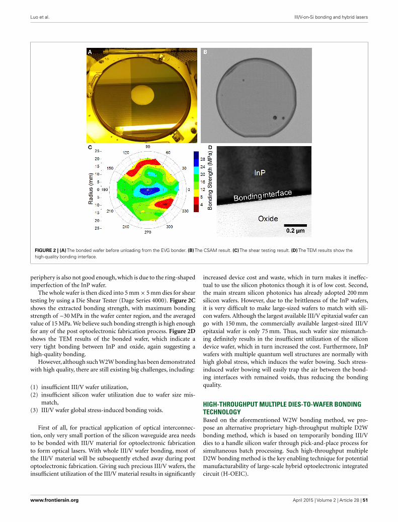
Luo et al. III/V-on-Si bonding and hybrid lasers
FIGURE 2 | (A) The bonded wafer before unloading from the EVG bonder. (B) The CSAM result. (C) The shear testing result. (D) The TEM results show thehigh-quality bonding interface.
periphery is also not good enough, which is due to the ring-shapedimperfection of the InP wafer.
The whole wafer is then diced into 5 mm× 5 mm dies for sheartesting by using a Die Shear Tester (Dage Series 4000). Figure 2Cshows the extracted bonding strength, with maximum bondingstrength of ~30 MPa in the wafer center region, and the averagedvalue of 15 MPa. We believe such bonding strength is high enoughfor any of the post optoelectronic fabrication process. Figure 2Dshows the TEM results of the bonded wafer, which indicate avery tight bonding between InP and oxide, again suggesting ahigh-quality bonding.
However, although such W2W bonding has been demonstratedwith high quality, there are still existing big challenges, including:
(1) insufficient III/V wafer utilization,(2) insufficient silicon wafer utilization due to wafer size mis-
match,(3) III/V wafer global stress-induced bonding voids.
First of all, for practical application of optical interconnec-tion, only very small portion of the silicon waveguide area needsto be bonded with III/V material for optoelectronic fabricationto form optical lasers. With whole III/V wafer bonding, most ofthe III/V material will be subsequently etched away during postoptoelectronic fabrication. Giving such precious III/V wafers, theinsufficient utilization of the III/V material results in significantly
increased device cost and waste, which in turn makes it ineffec-tual to use the silicon photonics though it is of low cost. Second,the main stream silicon photonics has already adopted 200 mmsilicon wafers. However, due to the brittleness of the InP wafers,it is very difficult to make large-sized wafers to match with sili-con wafers. Although the largest available III/V epitaxial wafer cango with 150 mm, the commercially available largest-sized III/Vepitaxial wafer is only 75 mm. Thus, such wafer size mismatch-ing definitely results in the insufficient utilization of the silicondevice wafer, which in turn increased the cost. Furthermore, InPwafers with multiple quantum well structures are normally withhigh global stress, which induces the wafer bowing. Such stress-induced wafer bowing will easily trap the air between the bond-ing interfaces with remained voids, thus reducing the bondingquality.
HIGH-THROUGHPUT MULTIPLE DIES-TO-WAFER BONDINGTECHNOLOGYBased on the aforementioned W2W bonding method, we pro-pose an alternative proprietary high-throughput multiple D2Wbonding method, which is based on temporarily bonding III/Vdies to a handle silicon wafer through pick-and-place process forsimultaneous batch processing. Such high-throughput multipleD2W bonding method is the key enabling technique for potentialmanufacturability of large-scale hybrid optoelectronic integratedcircuit (H-OEIC).
www.frontiersin.org April 2015 | Volume 2 | Article 28 | 51
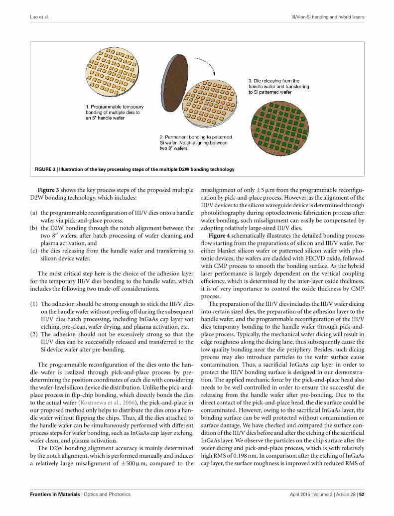
Luo et al. III/V-on-Si bonding and hybrid lasers
FIGURE 3 | Illustration of the key processing steps of the multiple D2W bonding technology.
Figure 3 shows the key process steps of the proposed multipleD2W bonding technology, which includes:
(a) the programmable reconfiguration of III/V dies onto a handlewafer via pick-and-place process,
(b) the D2W bonding through the notch alignment between thetwo 8′′ wafers, after batch processing of wafer cleaning andplasma activation, and
(c) the dies releasing from the handle wafer and transferring tosilicon device wafer.
The most critical step here is the choice of the adhesion layerfor the temporary III/V dies bonding to the handle wafer, whichincludes the following two trade-off considerations.
(1) The adhesion should be strong enough to stick the III/V dieson the handle wafer without peeling off during the subsequentIII/V dies batch processing, including InGaAs cap layer wetetching, pre-clean, wafer drying, and plasma activation, etc.
(2) The adhesion should not be excessively strong so that theIII/V dies can be successfully released and transferred to theSi device wafer after pre-bonding.
The programmable reconfiguration of the dies onto the han-dle wafer is realized through pick-and-place process by pre-determining the position coordinates of each die with consideringthe wafer-level silicon device die distribution. Unlike the pick-and-place process in flip-chip bonding, which directly bonds the diesto the actual wafer (Kostrzewa et al., 2006), the pick-and-place inour proposed method only helps to distribute the dies onto a han-dle wafer without flipping the chips. Thus, all the dies attached tothe handle wafer can be simultaneously performed with differentprocess steps for wafer bonding, such as InGaAs cap layer etching,wafer clean, and plasma activation.
The D2W bonding alignment accuracy is mainly determinedby the notch alignment, which is performed manually and inducesa relatively large misalignment of ±500 µm, compared to the
misalignment of only ±5 µm from the programmable reconfigu-ration by pick-and-place process. However, as the alignment of theIII/V devices to the silicon waveguide device is determined throughphotolithography during optoelectronic fabrication process afterwafer bonding, such misalignment can easily be compensated byadopting relatively large-sized III/V dies.
Figure 4 schematically illustrates the detailed bonding processflow starting from the preparations of silicon and III/V wafer. Foreither blanket silicon wafer or patterned silicon wafer with pho-tonic devices, the wafers are cladded with PECVD oxide, followedwith CMP process to smooth the bonding surface. As the hybridlaser performance is largely dependent on the vertical couplingefficiency, which is determined by the inter-layer oxide thickness,it is of very importance to control the oxide thickness by CMPprocess.
The preparation of the III/V dies includes the III/V wafer dicinginto certain sized dies, the preparation of the adhesion layer to thehandle wafer, and the programmable reconfiguration of the III/Vdies temporary bonding to the handle wafer through pick-and-place process. Typically, the mechanical wafer dicing will result inedge roughness along the dicing lane, thus subsequently cause thelow quality bonding near the die periphery. Besides, such dicingprocess may also introduce particles to the wafer surface causecontamination. Thus, a sacrificial InGaAs cap layer in order toprotect the III/V bonding surface is designed in our demonstra-tion. The applied mechanic force by the pick-and-place head alsoneeds to be well controlled in order to ensure the successful diereleasing from the handle wafer after pre-bonding. Due to thedirect contact of the pick-and-place head, the die surface could becontaminated. However, owing to the sacrificial InGaAs layer, thebonding surface can be well protected without contamination orsurface damage. We have checked and compared the surface con-dition of the III/V dies before and after the etching of the sacrificialInGaAs layer. We observe the particles on the chip surface after thewafer dicing and pick-and-place process, which is with relativelyhigh RMS of 0.198 nm. In comparison, after the etching of InGaAscap layer, the surface roughness is improved with reduced RMS of
Frontiers in Materials | Optics and Photonics April 2015 | Volume 2 | Article 28 | 52

Luo et al. III/V-on-Si bonding and hybrid lasers
FIGURE 4 |The fabrication process flow of the multiple D2W bondingtechnology. The process includes two different folds, i.e., the bondingwafers preparation including the III/V dies adhesion to handle wafer for
batch process and the silicon device wafer fabrication, and D2W bondingthrough dies releasing from handle wafer and transferring to silicon devicewafer.
FIGURE 5 | Demonstration of 104 III/V dies bonding to silicon wafer. (A) Photo image of the bonded wafer, (B) CSAM results, (C) shear testing results.
0.182 nm, which is far below the required RMS of <1 nm for waferdirect bonding (Christiansen et al., 2006).
Prior the physical contact of the wafers for molecular bonding,the silicon wafer is performed with standard SPM clean for 10 minand SC1 clean with mega sonic for 5 min, while III/V die-attachedhandle wafer is first performed with sacrificial InGaAs cap layeretching in H3PO4 solution for 1 min, followed with standard cleanin NH4OH solution for 2 min. After that, O2 plasma activation isapplied to both silicon wafer and III/V dies in a RIE chamber for1 min, followed with DI water rinsing and wafer drying. The III/Vdies and the silicon wafer are then physically contacted with eachother by notch alignment between two 8′′ wafers, followed withpre-bonding in the 200 mm EVG bonder for 2 min with 1000 Nmechanical force applied. The III/V dies are released from the han-dle wafer after pre-bonding, and all III/V dies are now transferredto the silicon device wafer. Finally, the bonded pairs are placed backto the EVG bonder for post-bonding annealing at 300°C for 12 h.
As a proof-of-concept demonstration, we show here the bond-ing of 104 InP dies to an 8′′ silicon wafer. The silicon wafer iscovered with 1 µm PECVD oxide after CMP. The InP dies arediced into 5 mm× 5 mm in size. Figure 5A shows the photo image
of the bonded wafers with nearly all InP dies are successfullybonded to the silicon wafer. The only missing piece is peeled offduring pick-and-place process. The CSAM shown in Figure 5Bsuggests a successful bonding. The dark areas, which suggest lessstrong bonding, come from the dies located in the InP wafer edge.Figure 5C shows the sheer testing results. The maximum bondingstrength is larger than 20 MPa, with an averaged bonding strengthof ~13 MPa, which is comparable with that of W2W bondingunder the same process.
All in all, we believe that there are at least two significantimplications of the proposed multiple D2W bonding technology:
(1) The significantly increased bonding efficiency owing to thesimultaneous batch process. Through the batch process of theIII/V dies (pre-clean, plasma activation, etc.), it is possible tobond unlimited number of dies. It also helps to avoid poten-tial contamination by performing the pick-and-place beforecleaning process, and eliminates the time link constraint ofthe bonding surface deactivation. This is the most signif-icant processing advantage comparing to the conventionalpick-and-place method.
www.frontiersin.org April 2015 | Volume 2 | Article 28 | 53

Luo et al. III/V-on-Si bonding and hybrid lasers
(2) The scalability to whatever-sized silicon wafers. Such multi-ple D2W bonding technology can easily be adopted for evenlarger-sized silicon wafers, such as 300 mm wafer. This is themost critical step toward the potential manufacturability ofH-OEIC.
DESIGN OF III/V-on-Si LASERSA hybrid III/V-on-silicon laser consists of a III/V epitaxial-layeredstructure and a silicon waveguide. It is a device that emits laserbeams from silicon waveguides by electrical/optical injection tothe III/V region. In this section, we will discuss the design ofhybrid III/V-on-silicon lasers with regard to two fundamentallaser elements,namely,optical gain medium and optical waveguidecavity.
DESIGN OF III/V MQW STRUCTURESThere are two main material systems for the fabrication of long-wavelength lasers emitting at 1.55 µm, which are InGaAsP/InPand InGaAlAs/InP systems. Both kinds of materials can be usedto fabricate hybrid lasers. InGaAlAs MQWs exhibit a larger con-duction band discontinuity (Ec= 0.72Eg), and smaller valenceband discontinuity compared with InGaAsP MQW. This leadsto an improved electron confinement, which can improve thetemperature characteristics of semiconductor laser diodes. Thus,InGaAlAs/InP material system is more suitable for high speed anduncooled operation of semiconductor laser diode. In this study,we select this material system for the hybrid silicon lasers demon-stration. The MQW region includes eight Al0.055Ga0.292In0.653Asquantum wells separated by nine Al0.055Ga0.292In0.653As barriers.The gain spectrum of the MQW is calculated and the wavelength ofpeak gain is designed at 1550 nm when the carrier injection densityincreases from 5× 10¹⁷ to 5× 10¹⁸/cm3 as shown in Figure 6A.Figure 6B shows the measured photoluminescence (PL) spec-trum for III/V epitaxial wafer at room temperature with the peakwavelength at about 1550 nm.
DESIGN OF HYBRID LASER VERTICAL WAVEGUIDE STRUCTUREAs mentioned, the optical gain comes from overlying III/V stacklayer, which needs to be structured to efficiently inject electronsor holes into the MQW regions. A high overlap between the opti-cal mode and the MQW benefits to achieve a high optical gain,
which means that the optical mode needs to be well confined inthe III/V waveguide. However, on the other hand, the light hasto be confined sufficiently inside the silicon output waveguidefor the efficient light extraction. In view of this, there are mainlytwo kinds of waveguide structures considering the optical powerdistribution for the hybrid laser with optical mode predominantlyconfined either in the silicon waveguide or in the III/V overlay. Thisleads to two different optical cavity designs. In the first design, theoptical cavity comprises both III/V and silicon waveguides and themode is mainly guided within the Si waveguide and evanescentlycoupled with the III/V waveguide. Such structure is also called asoverlapped structure with hybrid mode (Fang et al., 2006, 2007a,b,2008a,b,c, 2009). It has the advantage of making the coupling to apassive silicon waveguide straightforward and wavelength selectivefeatures can easily be defined in the silicon waveguide layer usingCMOS fabrication techniques, which provides an accurate mech-anism to control the emission wavelength of the laser. However, itrequires a controllable thin bonding layer (<50 nm) for efficientoptical coupling, which may increase the difficulty of bondingprocess. Furthermore, due to the weak interaction between theoptical mode and gain material, it usually requires longer lasercavity, and thus resulting in high power consumption. In the sec-ond design, the mode in the hybrid section is mainly guided by theIII/V waveguide, and the light is coupled from the III/V waveguideto the silicon waveguide through waveguide mode transformer,such as inverse tapers (Yariv and Sun, 2007; Sun et al., 2009a; BenBakir et al., 2011). In such design, the bonding interface can berelatively thick (typically from 30 to 150 nm) due to the releasedcoupling constrain for the bonding interface. The advantage isthat the optical mode experiences a high optical gain in the centralregion of the laser structure. However, the challenge of this struc-ture is the fabrication of low-loss tapered waveguides. Hereafter,we name such design as adiabatic tapered coupling structure.
Silicon waveguide thickness selectionThe selection of the silicon waveguide thickness depends on thedetailed device dimensions/structures and the fabrication process.For indium phosphide (InP)-based gain waveguides, the effectiverefractive index is typically larger than 3.2 if the waveguide widthand height are larger than 1 µm. In order to achieve this index forsilicon waveguides for effective coupling with the InP-based gain
FIGURE 6 | (A) The calculated gain spectrum under different carrier injection concentration. (B) The measured photoluminescence (PL) spectrum for III/Vepitaxial wafer.
Frontiers in Materials | Optics and Photonics April 2015 | Volume 2 | Article 28 | 54
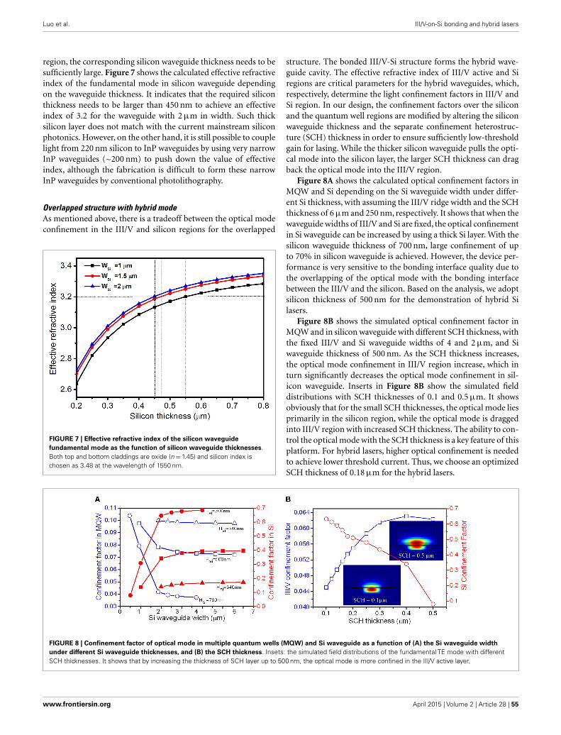
Luo et al. III/V-on-Si bonding and hybrid lasers
region, the corresponding silicon waveguide thickness needs to besufficiently large. Figure 7 shows the calculated effective refractiveindex of the fundamental mode in silicon waveguide dependingon the waveguide thickness. It indicates that the required siliconthickness needs to be larger than 450 nm to achieve an effectiveindex of 3.2 for the waveguide with 2 µm in width. Such thicksilicon layer does not match with the current mainstream siliconphotonics. However, on the other hand, it is still possible to couplelight from 220 nm silicon to InP waveguides by using very narrowInP waveguides (~200 nm) to push down the value of effectiveindex, although the fabrication is difficult to form these narrowInP waveguides by conventional photolithography.
Overlapped structure with hybrid modeAs mentioned above, there is a tradeoff between the optical modeconfinement in the III/V and silicon regions for the overlapped
FIGURE 7 | Effective refractive index of the silicon waveguidefundamental mode as the function of silicon waveguide thicknesses.Both top and bottom claddings are oxide (n=1.45) and silicon index ischosen as 3.48 at the wavelength of 1550 nm.
structure. The bonded III/V-Si structure forms the hybrid wave-guide cavity. The effective refractive index of III/V active and Siregions are critical parameters for the hybrid waveguides, which,respectively, determine the light confinement factors in III/V andSi region. In our design, the confinement factors over the siliconand the quantum well regions are modified by altering the siliconwaveguide thickness and the separate confinement heterostruc-ture (SCH) thickness in order to ensure sufficiently low-thresholdgain for lasing. While the thicker silicon waveguide pulls the opti-cal mode into the silicon layer, the larger SCH thickness can dragback the optical mode into the III/V region.
Figure 8A shows the calculated optical confinement factors inMQW and Si depending on the Si waveguide width under differ-ent Si thickness, with assuming the III/V ridge width and the SCHthickness of 6 µm and 250 nm, respectively. It shows that when thewaveguide widths of III/V and Si are fixed, the optical confinementin Si waveguide can be increased by using a thick Si layer. With thesilicon waveguide thickness of 700 nm, large confinement of upto 70% in silicon waveguide is achieved. However, the device per-formance is very sensitive to the bonding interface quality due tothe overlapping of the optical mode with the bonding interfacebetween the III/V and the silicon. Based on the analysis, we adoptsilicon thickness of 500 nm for the demonstration of hybrid Silasers.
Figure 8B shows the simulated optical confinement factor inMQW and in silicon waveguide with different SCH thickness, withthe fixed III/V and Si waveguide widths of 4 and 2 µm, and Siwaveguide thickness of 500 nm. As the SCH thickness increases,the optical mode confinement in III/V region increase, which inturn significantly decreases the optical mode confinement in sil-icon waveguide. Inserts in Figure 8B show the simulated fielddistributions with SCH thicknesses of 0.1 and 0.5 µm. It showsobviously that for the small SCH thicknesses, the optical mode liesprimarily in the silicon region, while the optical mode is draggedinto III/V region with increased SCH thickness. The ability to con-trol the optical mode with the SCH thickness is a key feature of thisplatform. For hybrid lasers, higher optical confinement is neededto achieve lower threshold current. Thus, we choose an optimizedSCH thickness of 0.18 µm for the hybrid lasers.
FIGURE 8 | Confinement factor of optical mode in multiple quantum wells (MQW) and Si waveguide as a function of (A) the Si waveguide widthunder different Si waveguide thicknesses, and (B) the SCH thickness. Insets: the simulated field distributions of the fundamental TE mode with differentSCH thicknesses. It shows that by increasing the thickness of SCH layer up to 500 nm, the optical mode is more confined in the III/V active layer.
www.frontiersin.org April 2015 | Volume 2 | Article 28 | 55

Luo et al. III/V-on-Si bonding and hybrid lasers
For such hybrid III/V-on-silicon lasers, another challenge arisesfrom the control of the bonding layer thickness. Generally, a thinbonding layer (<50 nm) is needed for efficient optical couplingbetween III/V and silicon regions, while the thicker bonding layerbenefits to the bonding quality of III/V layer and the bondingyield improvement. For direct bonding without oxide interlayer,it is easy to achieve such thin thickness, which is usually only thenative oxide. However, this process is particularly sensitive to sur-face roughness and particles contamination, which would limitthe bonding quality and bonding yield. DVS-BCB bonding can beused for the heterogeneous integration of III/V material on siliconto improve the yield. However, it is difficult to obtain a control-lable thin bonding interlayer of <50 nm. In our case, we choosesilicon oxide as interlayer between III/V and silicon, which is alsocompatible with the mainstream silicon phonics, in which all thedevices are with oxide cladding.
Figure 9A shows the calculated optical confinement factor inMQW and silicon waveguide as the function of interlayer oxidethickness. In the simulation, we assume the fixed silicon thicknessof 500 nm, the silicon waveguide width of 3 µm, and III/V ridgewaveguide with of 6 µm. We observe from the results that the Siconfinement factor largely decreases when the interlayer thicknessincreases from 10 to 100 nm. Only approximately 5% optical lightis confined in the silicon waveguide when the interlayer thicknessis 100 nm.
Additionally, the interlayer of oxide at the bonding interfacealso affects the characteristics temperature of hybrid III/V-on-silicon laser due to the poor thermal conductivity of as low as
1.3 W/m/K. The modal gain of laser is dependent on the tem-perature of the active region. As the temperature of active regionincreases, the modal gain decreases due to the increased carrierleakage out or not reaching the active region, and/or increasednon-radiative recombination. The decrease of modal gain leads tohigh threshold current and low output optical power. In orderto investigate the effect of interlayer on the thermal charac-teristics of the hybrid lasers, a two-dimensional model of thedevice structure is conducted using COMSOL by mapping outthe heat dissipation of each layer. Figure 9B shows the simula-tion structure. In the simulation, the structure parameters areas follows: III/V ridge width, Si ridge width and thickness, andthe laser cavity length are assumed to be 6 µm, 1 µm, 500 nm,and 1000 µm, respectively. Injection current is 500 mA and thecorresponding voltage is 4 V. Figure 9C shows the calculatedworking temperatures in the III/V active region with differentthicknesses of the oxide interlayer. The increase of temperaturein the III/V active region versus interlayer thickness is about0.02 K/nm. For illustration purpose, Figure 9D shows as anexample the thermal distribution within the layered structurefor the oxide interlayer thickness of 0 nm. The thermal distri-butions for the other thicknesses are similar. Actually, we canconclude from the study that the main hurdle for the heat dis-sipation is the SOI BOX layer, which can be seen from the resultswithout oxide bonding interlayer (thickness= 0 nm). Thus, forenhanced thermal management, novel designs such as thermalshunt (Liang et al., 2012) are required to effectively remove thegenerated heat.
FIGURE 9 | (A) The confinement factor of the optical mode in the MQWand silicon layers, respectively, as a function of the interlayer thickness.(B) The simulation structure of the thermal distribution. (C) The temperature
changes in the III/V active region with regard to the oxide interlayerthickness. (D) The simulated thermal distribution with the interlayerthickness is 0 nm.
Frontiers in Materials | Optics and Photonics April 2015 | Volume 2 | Article 28 | 56

Luo et al. III/V-on-Si bonding and hybrid lasers
Adiabatic tapered coupling structureFor the adiabatic tapered coupling structure, the mode in thehybrid section is mainly guided by the III/V waveguide, and thelight is coupled from the III/V waveguide to the silicon wave-guide through a tapered waveguide. It shows that a tapering length~100 µm is required for a sufficient light coupling with mini-mized optical loss. By using such tapered coupling, it eliminates thetricky tradeoff between the modal gain and vertical coupling effi-ciency, which is inherent in the overlapped waveguide structures.Therefore, hybrid lasers with a short cavity as pure III/V laser arepossible. Up to now, the hybrid lasers with the high performancesare achieved using such tapered coupling scheme (Levaufre et al.,2014; Zhang et al., 2014).
In order to efficiently couple the light between the Si-III/Vhybrid waveguide and the silicon waveguide, the III/V waveguideand silicon waveguides are tapered simultaneously in the same
direction. Here, we adopt a three-dimensional approximatedmodel based on beam propagation method (BPM) in order tooptimize the tapering structure of the silicon waveguide and III/Vwaveguide for an efficient coupling. Figure 10A schematicallyillustrates the design of such waveguide tapering structure. Thecoupling efficiency largely depends on the tapering design, espe-cially the III/V waveguide taper width and taper length. Here, wesimulate such dependency by varying the taper width and taperlength, while fixing the III/V waveguide width of 5 µm, the siliconwaveguide width of 1 µm, and the silicon taper length of 100 µm.
Figures 10B,C, respectively, show the simulated coupling effi-ciency from III/V-Si hybrid waveguide to silicon waveguide asfunctions of the III/V waveguide taper width and tape length.It suggests that the coupling efficiency from III/V-Si hybrid wave-guide to Si waveguide can be as high as 85% by using an 80-µm-long III/V waveguide taper and a 100-µm-long silicon waveguide
FIGURE 10 | (A) Schematics of the tapering structure for the verticalcoupling between III/V waveguide and silicon waveguide. WInP: III/Vwaveguide width, Wend: III/V waveguide taper width, Wd: siliconwaveguide width, LTaper1: silicon waveguide taper length, LTaper2: III/V
waveguide taper length. The whole structure is cladded with oxide.Coupling efficiency of III/V waveguide to Si waveguide as functions of(B) the III/V waveguide taper width, and (C) the III/V waveguide taperlength.
www.frontiersin.org April 2015 | Volume 2 | Article 28 | 57
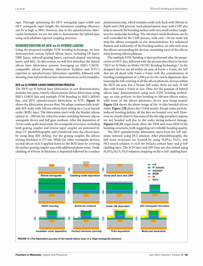
Luo et al. III/V-on-Si bonding and hybrid lasers
tape. Through optimizing the III/V waveguide taper width andIII/V waveguide taper length, the maximum coupling efficiencycan be as high as 99%. However, due to the optoelectronic fabri-cation limitation, we are not able to demonstrate the hybrid laserusing such adiabatic tapered coupling structure.
DEMONSTRATION OF III/V-on-Si HYBRID LASERSUsing the proposed multiple D2W bonding technology, we havedemonstrated various hybrid silicon lasers, including FP lasers,DBR lasers, sidewall-grating lasers, racetrack-shaped microringlasers, and MLL. In this section, we will first introduce the hybridsilicon laser fabrication process, leveraging on IME’s CMOS-compatible silicon photonic fabrication facilities and NTU’sexpertise in optoelectronics fabrication capability, followed withshowing some hybrid silicon laser demonstrations as the examples.
III/V-on-Si HYBRID LASER FABRICATION PROCESSThe III/V-on-Si hybrid laser fabrication in our demonstrationsincludes two parts, namely silicon passive device fabrication usingIME’s CMOS line and multiple D2W bonding in IME’s MEMSline, and III/V optoelectronics fabrication in NTU. Figure 11shows the fabrication process flow. We adopt commercially avail-able SOI wafer with 340 nm silicon layer sitting on a 2 µm buriedoxide (BOX) layer. The fabrication starts with the blanket siliconepitaxy to ~500 nm for refractive index matching between siliconwaveguide device and InP gain medium. After the deposition of70 nm oxide as the hard mask, the waveguide structures, includingboth grating coupler and inverse taper coupler are patterned bydeep UV photolithography and transferred onto the silicon layerby using deep RIE etching. For the grating coupler, the siliconetching thickness is 377 nm. While for other waveguide devices,second silicon etch is applied down to the BOX layer by coveringthe surface grating coupler area with additional photo resist. Oxidecladding of 650 nm in thickness is deposited followed by a surface
planarization step, which includes oxide etch-back with 500 nm indepth and CMP process. Such planarization steps with CMP alsohelp to smooth the bonding surface with very small surface rough-ness for molecular bonding. The interlayer oxide thickness can bewell controlled by the CMP process, with only ~50 nm oxide leftatop the silicon waveguide in our demonstration. For enhancedflatness and uniformity of the bonding surface, we only etch awaythe silicon surrounding the devices, remaining most of the siliconareas forming silicon plateaus.
The multiple D2W bonding is then performed after the prepa-ration of III/V dies, followed with the process described in Section“III/V-to-Si Wafer-to-Wafer (W2W) Bonding Technology.” As thedesigned devices are all within an area of 8 mm× 8 mm, the InPdies are all diced with 9 mm× 9 mm with the consideration ofbonding misalignment of ±500 µm for the notch alignment, thusensuring the full covering of all the silicon photonic devices withinthe III/V die area. For a 50 mm InP wafer, there are only 16 fulldies with 9 mm× 9 mm in size. Thus, for the purpose of hybridsilicon laser demonstration using such D2W bonding technol-ogy, we only perform 16-dies bonding to 200 mm silicon wafers,with some of the silicon photonics device area being wasted.Figure 12A shows the photo image of the 16-dies bonded siliconwafer. Figure 12B shows the CSAM results. Except some particle-induced bonding defects, all the dies are bonded very well. How-ever, we clearly observe that some of the die edge periphery regionsare not bonded well due to the wafer dicing induced damage.Figures 12C,D, respectively, show the TEM and cross-SEM of thebonding structures, both suggesting very reliable bonding quality.
The III/V optoelectronic fabrication starts from the InP sub-strate removal using HCl solution. After photolithography, theInP mesa structures are formed by using H3PO4, H2O2, andHCl mixed solution to etch the InGaAs contact layer and p-InPcladding layer. The SCH layer and QW layer are also etched usingH3PO4:H2O2:H2O solution, stopping on the n-InP cladding layer.
FIGURE 11 |The fabrication process of the hybrid silicon laser in a ridge waveguide structure.
Frontiers in Materials | Optics and Photonics April 2015 | Volume 2 | Article 28 | 58

Luo et al. III/V-on-Si bonding and hybrid lasers
Then, an SiO2 insulator layer with the thickness of 300 nm isdeposited, followed with the contact opening for p-type and n-typeinjection by one-time photolithography and the oxide is etched byHF solution. After that, Ti/Au metal contacts are formed by sput-tering, with wet etching to form a Ti/Au slot between the n-typeand p-type contacts using diluted HF and KI solution, respectively.
FABRY–PEROT LASERSThe CW operation of the optical laser requires good thermalmanagement to remove the generated heat. In the case of FPlasers, another way is to design narrow ridge waveguide to gen-erate less heat. In our demonstration, we design a FP laser withridge waveguide width of 6 µm. The laser facets are formed bylapping down the Si substrate to around 60 µm, followed withmechanical cleaving. The length of the FP laser is ~720 µm. Thedemonstrated FP laser is able to work at room temperature withCW operation. Figure 13A shows the measured P–I curves underdifferent temperatures. The threshold current at 264 K is ~45 mA,
FIGURE 12 | (A) The optical image of the 16-dies bonded silicon wafer.(B) CSAM results. (C) TEM of the bonding structure. (D) Cross-SEM of thebonding structures.
and increases significantly to ~100 mA at room temperature. Weattribute such fast increase of the threshold to the thick oxideinterlayer, which prohibits the heat dissipation efficiently. Themeasured output power from a single facet without any reflec-tion coating is more than 1 mW. This includes the coupling lossdue to the un-optimized testing setup for light collection, which isestimated only with ~20% light collection efficiency. The thermaldissipation is very important for CW lasing. Figure 13B showsthe measured lasing spectra under different temperatures. Thewavelength shift with temperature is about 0.75 nm/K.
LATERAL-COUPLED DISTRIBUTED-FEEDBACK LASERS WITH SIDE WALLGRATINGThe FP laser is fabricated by lapping down the silicon substrate andmechanical cleaving to form the facets. From the optical commu-nication and optical interconnect applications point of view, suchFP lasers are not practical for photonic integration. Furthermore,how to achieve good facet is still a main challenge and a key limit-ing factor for high-performance hybrid lasers as reflection coatingis always required in order to optimize the cavity transmissionand reflection. In view of this, optical resonators, Bragg gratingstructures that form the cavities through fabrication are the goodcandidates for on-chip hybrid laser. We here show as an exampleof a hybrid laser using LC-DFB structure as the laser cavity.
Figure 14A schematically shows the perspective view of the LC-DFB hybrid laser with illustration of the key parameters, includingthe Bragg grating period Λ, the silicon ridge width D, and the grat-ing teeth width, W 1. Considering the fabrication limitation, wedesign third-order later Bragg grating in order to achieve single-mode operation. With regard to the silicon thickness of 500 nm,the grating period Λ is 670 nm with filling factor of 0.5. The ridgewidth D and the teeth width W1 are, respectively, designed with2 and 1 µm. The Bragg grating is centered beneath the III/V gainregion, which is with the width of 12 µm. Both LC-DFB struc-ture and III/V gain region are designed with the same lengths. Inorder to extract the output laser light for easy characterization, thevertical grating couplers are adopted. For the vertical grating cou-pler, the period is designed to be 640 nm with filling factor of 0.5,and the silicon etch depth is 377 nm. Such grating coupler designis purely based on theoretical calculation, without any process
FIGURE 13 | (A) The power–current characteristic curves and (B) the lasing spectra of a typical hybrid silicon FP laser measured under different temperature.
www.frontiersin.org April 2015 | Volume 2 | Article 28 | 59

Luo et al. III/V-on-Si bonding and hybrid lasers
FIGURE 14 | (A) The perspective view of the hybrid LC-DFB laserintegrating with surface grating coupler, with illustration of the keydesign parameters. Λ: grating period, D: the ridge width, and W1: thegrating teeth width. (B) Top-view optical microscope image of a LC-DFBhybrid laser integrated with vertical surface coupler. (C–E) The SEM of
the LC-DFB structures and the grating coupler. (F) The cross SEM ofthe vertical layered structure. (G) The light power output and (H) thelaser spectrum of the hybrid silicon laser with sidewall Bragg gratingstructure. The output power is directly measured from the surfacegrating coupler.
verification and optimization. For this demonstration, we did notdesign any mode transformer between III/V layer and silicon wave-guide layer, thus expecting some transition loss. Figure 14B showsthe optical microscope image of the fabricated hybrid LC-DFBlaser with integrated vertical grating couplers. The LC-DFB struc-ture and the III/V gain region are designed with same length of700 µm, while the silicon device including two grating couplers is~2750 µm. Due to the optoelectronic fabrication limitation, thereis no designed taper between III/V waveguide and silicon wave-guide, thus expecting relatively high transition loss. Figures 14C–Eshow the SEM images of the fabricated LC-DFB and vertical grat-ing coupler, while Figure 14F shows the cross-sectional SEM of thevertical structures, illustrating the Si waveguide, the III/V layer, andthe Ti/Au layer.
Figures 14G,H show the measured P–I curve and the spec-trum of the LC-DFB hybrid laser under pulse operation. Thethreshold current is ~120 mA, corresponding to a threshold cur-rent density of ~1.42 kA/cm2. From the spectrum, we see clearlysingle-mode operation with the peak wavelength at 1559.8 nm anda side-mode-suppression ratio (SMSR) larger than 20 dB. This isexpected from the LC-DFB design. However, the maximum output
power is only ~10 µW upon 250 mA current injection, which alsocan be observed from the spectrum measurement. We attribute therelatively low output power to the following two reasons, namely,the accumulated optical loss, and the inefficient vertical light cou-pling. First of all, the optical loss, which mainly includes the surfacegrating coupler coupling loss, the Bragg grating scattering loss, andthe non-radiative recombination loss from the bonding interface,affects the light output significantly. From the reference measure-ment for the device only with passive silicon waveguide yet bondedIII/V layer, the accumulated total loss is >40 dB, which is mainlydue to the unoptimized surface grating coupler. Second, the oxideinterlayer in our design, which might not be able to control pre-cisely, will affect the light coupling efficiently from III/V layer tosilicon waveguide. Furthermore, the polarization sensitivity of thesurface grating coupler can also induce additional optical loss.Thus, the optimized grating coupler design for the light extractionfrom the silicon waveguide and the vertical light transition struc-ture for light coupling from III/V layer to silicon waveguide cansignificantly increase the laser output power. Besides, by optimiza-tion of the Bragg grating period and silicon waveguide thickness,the SMSR can also be enhanced.
Frontiers in Materials | Optics and Photonics April 2015 | Volume 2 | Article 28 | 60

Luo et al. III/V-on-Si bonding and hybrid lasers
PASSIVELY MODE-LOCKED LASERSSemiconductor MLLs are excellent candidates for generating stableultra-short optical pulses, which have a corresponding wide opti-cal spectrum of phase correlated modes and high repetition rate.Optical frequency combs emitted by MLLs can have high extinc-tion ratios, low jitter, and low chirp, which can be utilized in a vari-ety of applications including AWG, optical clock generation andrecovery, coherent communications systems, high-speed analog-to-digital conversion (ADC), and optical time-division multiplex-ing (OTDM), etc. Integration of MLLs on silicon is very promisingas it combines the low-loss and low-dispersion characteristicsof silicon material with high gain III/V material, thus ensuringimproved performance. Furthermore, it will be possible for semi-conductor MLLs to generate ultra-short optical pulses with lowrepetition rate on the silicon platform owing to the long cavitylength. Here, we show our preliminary demonstration of a passiveMLL using the developed heterogeneous integration platform.
The optical cavity of the MLL is defined by a 1250-µm-long gain section, a saturable absorber (SA) with the length of30-100µm, and cleaved facet at the waveguide end. The gainsection and SA are separated by a 20 µm electrical isolation regionwith isolation resistance >1 kΩ. The SA is made up of the sameactive material as the gain section. The difference between the SAand gain section is that SA absorbs the light in the cavity uponapplying a reverse bias, while the gain section amplifying lightupon forward current injections.
The laser optical output is collected by a photodiode locatedin front of the cleaved facet. The typical threshold current withan unbiased 50-µm-long SA section is 88 mA. The device has amaximum single facet CW output power of 1 mW at room temper-ature when the injection current is 140 mA. The series resistanceis about 8.5 Ω, while the slope efficiency is about 0.02 mW/mA.Figure 15A shows the measured optical spectra at different injec-tion currents. It shows that the widest optical emission is centeredat about 1605 nm with a full-width at half-maximum (FWHM) of5.4 nm at the injection current of 110 mA measured by an opticalspectrum analyzer (OSA). Assuming the generated optical pulse ischirp-free and the shape of the pulse is with a Sech-function, thewidth of the optical pulse is calculated to 0.5 ps.
Passive mode locking of the device is obtained by forward bias-ing the gain section (I gain) and reverse biasing (V sa) or un-biasingthe SA section. The mode locking behavior of the device is charac-terized by measuring the radio frequency (RF) spectrum using thespectrum analyzer (Agilent E4448A). Figure 15B shows the mea-sured RF spectrum of the III/V-on-Si MLL at the injection currentto the gain section (I gain) of 110 mA and reverse biasing the SAsection at −0.9 V. The resolution bandwidth (RBW) during mea-surement is 1 MHz. The repetition frequency is about 30.0 GHzwith signal-to-noise ratio above 30 dB. By changing I gain, it canbe tuned to more than 30 GHz, giving clear evidence of passivelymode locking of light signal. The measured RF linewidth of theinjection locked laser is about 7 MHz by Lorentzian fitting the RFspectrum.
SUMMARY AND FUTURE OUTLOOKKEY ACHIEVEMENTSIn summary, we reviewed in this paper the recent demonstra-tions of optical light source in silicon for the application of H-OEIC, with major focus on hybrid silicon lasers through waferbonding technology. Furthermore, we proposed a proprietaryhigh-throughput multiple dies-to-wafer (D2W) bonding tech-nology by temporarily bonding III/V dies to a handle siliconwafer through pick-and-place process for subsequent simulta-neous batch processing. Such high-throughput multiple D2Wbonding technology features the merits of high bonding yieldwith unlimited III/V dies and scalability to whatever-size sili-con wafers, thus is the key enabling technique toward potentialmanufacturability of large-scale H-OEIC. As proof-of-conceptdemonstration, we showed the III/V dies to silicon wafer bond-ing with up to 104 dies. Repeatable demonstrations of 16-III/Vdies bonding to pre-patterned 200 mm silicon wafers are per-formed for the fabrication of hybrid silicon lasers with variouslaser cavities, including FP lasers, LC-DFB laser with side wallgrating, and MLL.
CHALLENGES AND FUTURE OUTLOOKHowever, there are still many key issues need to be addressed beforethe hybrid silicon laser applied to optical interconnects system.
FIGURE 15 | (A) The measured optical spectra of the III/V-on-silicon mode-locked laser at different injection currents to the gain section while the SA section isfloating. (B) Measured RF spectrum of the III/V-on-Si MLL at 110 mA injection current and saturation voltage of −0.9V. The RBW during measurement is 1 MHz.
www.frontiersin.org April 2015 | Volume 2 | Article 28 | 61

Luo et al. III/V-on-Si bonding and hybrid lasers
Here, we will only discuss three of the most important issues,including:
(1) the thermal management;(2) the integration with other silicon photonic devices with full
wafer processing capability; and(3) the new platform beyond silicon for high-performance
advanced hybrid lasers.
Thermal management is one of the major obstacles for achiev-ing high-performance hybrid silicon lasers for practical applica-tions (Sysak et al., 2011). Due to the poor thermal conductivity ofthe SOI BOX layer as well as the inter oxide layer between bondingsurface, such layers would prevent the efficient heat dissipation tothe silicon substrate, thus resulting in the poor laser performances,such as lower laser power. One of the simple ways to increase thethermal dissipation efficiency is to design the contact electrodeswith thick and large area metal, serving as the top surface heatsink. Another efficient way for thermal dissipation is to remove theBOX layer in some areas and refill it with high thermal conductivematerials such as polycrystalline silicon or metals, serving as ther-mal shunt (Liang et al., 2012). However, although such approachhas been demonstrated with enhanced thermal management andincreased laser performance, it still requires further developmentin order to further improve the performance.
The integration of such hybrid laser with the existing siliconphotonics building blocks is another key issue before it is appliedfor H-OEIC. For most of the demonstrated hybrid silicon lasers,the silicon waveguide is normally with more than 500 nm thick-ness in order to ensure the optical index matching with III/Vmaterial for efficient light coupling to silicon waveguide. Suchthick waveguide design is actually not compatible with the main-stream silicon photonics, with most of the key building blocksare demonstrated in 220 nm silicon wafers (Xu et al., 2014). Thus,novel designs taking care of both of these design considerationsare required. Recently, Dong et al. (2014a,b) demonstrated novelintegration scheme with associated transition structure via epitax-ial growth of silicon in a pre-defined trench. Such epitaxial-grownsilicon mesa also serves as the bonding interface with III/V gainmaterial. Thus, the rest of the device area leaves with 220 nm siliconfor other existing silicon photonic devices. Such novel demonstra-tion sets a path toward the integration of hybrid silicon laser withexisting silicon photonics building blocks. However, for practicalintegration with high-speed modulator and photodetector, whichinvolves even complicated integration process with multiple oxideetch-back and CMP, it is still very challenging on how to ensurethe flatness and smoothness of the bonding surface. More sophis-ticated design and further demonstration with integration of suchare highly demanded.
The third issue is associated with current new demonstrationtrend that utilizes extremely low-loss SiN or SiON waveguide asthe passive waveguide layer (Bovington et al., 2014; Luo et al.,2014). As we know, for some advanced type of hybrid lasers, suchas the MLLs, extremely low optical loss is required for achievinghigh performances. The state-of-the-art demonstration of the sil-icon waveguide is still with propagation loss of ~2 dB/cm, whichis higher comparing that of SiN waveguide of 0.1 dB/m (Bauters
et al., 2011). Thus, III/V-SiN platform for hybrid lasers is anotherinterest research area, which can address the loss issue. The inte-gration between SiN waveguide and other SOI-based devices isalso CMOS-compatible and ready for further application (Huanget al., 2014).
ACKNOWLEDGMENTSThis work was supported by A*STAR SERC Future Data Cen-ter Technologies Thematic Strategic Research Programme underGrant No. 112 280 4038, and A*STAR – MINDEF Scienceand Technology Joint Funding Programme under Grant No.122331 0076.
REFERENCESAlduino, A., and Paniccia, M. (2007). Interconnects: wiring electronics with light.
Nat. Photonics 1, 153–155. doi:10.1038/nphoton.2007.17Alexe, M., and Gösele, U. (2004). Wafer Bonding: Applications and Technology. Berlin:
Springer-Verlag.Bauters, J. F., Heck, M. J., John, D. D., Barton, J. S., Blumenthal, D. J., Bowers, J. E.,
et al. (2011). “Ultra-low-loss (< 0.1 dB/m) planar silica waveguide technology,”in Paper Presented at the IEEE Photonics Conference (Arlington, VA: MarriottCrystal Gateway).
Beausoleil, R. G., Kuekes, P. J., Snider, G. S., Wang, S.-Y., and Williams, R. S.(2008). Nanoelectronic and nanophotonic interconnect. Proc. IEEE 96, 230–247.doi:10.1109/JPROC.2007.911057
Ben Bakir, B., Descos,A., Olivier, N., Bordel, D., Grosse, P.,Augendre, E., et al. (2011).Electrically driven hybrid Si/III-V Fabry-Pérot lasers based on adiabatic modetransformers. Opt. Express 19, 10317–10325. doi:10.1364/OE.19.010317
Bogaerts, W., Baets, R., Dumon, P., Wiaux, V., Beckx, S., Taillaert, D., et al. (2005).Nanophotonic waveguides in silicon-on-insulator fabricated with CMOS tech-nology. J. Lightwave Technol. 23, 401–412. doi:10.1109/JLT.2004.834471
Bovington, J., Heck, M., and Bowers, J. (2014). Heterogeneous lasers and couplingto Si 3 N 4 near 1060 nm. Opt. Lett. 39, 6017–6020. doi:10.1364/OL.39.006017
Boyraz, O., and Jalali, B. (2004). Demonstration of a silicon Raman laser. Opt. Express12, 5269–5273. doi:10.1364/OPEX.12.005269
Boyraz, O., and Jalali, B. (2005). Demonstration of directly modulated silicon Ramanlaser. Opt. Express 13, 796–800. doi:10.1364/OPEX.13.000796
Camacho-Aguilera, R. E., Cai, Y., Patel, N., Bessette, J. T., Romagnoli, M., Kimerling,L. C., et al. (2012). An electrically pumped germanium laser. Opt. Express 20,11316–11320. doi:10.1364/OE.20.011316
Cheng, S.-L., Lu, J., Shambat, G., Yu, H.-Y., Saraswat, K., Vuckovic, J., et al. (2009).Room temperature 1.6 µm electroluminescence from Ge light emitting diodeon Si substrate. Opt. Express 17, 10019–10024. doi:10.1364/OE.17.010019
Christiansen, S. H., Singh, R., and Gosele, U. (2006). Wafer direct bonding: fromadvanced substrate engineering to future applications in micro/nanoelectronics.Proc. IEEE 94, 2060–2106. doi:10.1109/JPROC.2006.886026
Chu, T., Fujioka, N., and Ishizaka, M. (2009). Compact, lower-power-consumptionwavelength tunable laser fabricated with silicon photonic-wire waveguide micro-ring resonators. Opt. Express 17, 14063–14068. doi:10.1364/OE.17.014063
Creazzo, T., Marchena, E., Krasulick, S. B., Yu, P. K., Van Orden, D., Spann, J. Y.,et al. (2013). Integrated tunable CMOS laser. Opt. Express 21, 28048–28053.doi:10.1364/OE.21.028048
Dong, P., Hu, T.-C., Liow, T.-Y., Chen,Y.-K., Xie, C., Luo, X., et al. (2014a). Novel inte-gration technique for silicon/III-V hybrid laser. Opt. Express 22, 26854–26861.doi:10.1364/OE.22.026854
Dong, P., Liu, X., Chandrasekhar, S., Buhl, L. L., Aroca, R., and Chen, Y.-K. (2014b).Monolithic silicon photonic integrated circuits for compact 100 Gb/s coherentoptical receivers and transmitters. IEEE J. Sel. Top. Quantum Electron. 20, 1–8.doi:10.1109/JSTQE.2013.2295181
Dong, P., Hu, T.-C., Zhang, L., Dinu, M., Kopf, R., Tate, A., et al. (2013). 1.9 µmhybrid silicon/iii-v semiconductor laser. Electron. Lett. 49:664. doi:10.1049/el.2013.0674
Dong, P., Liao, S., Feng, D., Liang, H., Zheng, D., Shafiiha, R., et al. (2009). Low Vpp, ultralow-energy, compact, high-speed silicon electro-optic modulator. Opt.Express 17, 22484–22490. doi:10.1364/OE.17.022484
Frontiers in Materials | Optics and Photonics April 2015 | Volume 2 | Article 28 | 62
Luo et al. III/V-on-Si bonding and hybrid lasers
Dumon, P., Bogaerts, W., Wiaux, V., Wouters, J., Beckx, S., Van Campenhout, J., et al.(2004). Low-loss SOI photonic wires and ring resonators fabricated with deepUV lithography. IEEE Photonics Technol. Lett. 16, 1328–1330. doi:10.1109/LPT.2004.826025
Fang, A. W., Jones, R., Park, H., Cohen, O., Raday, O., Paniccia, M. J., et al. (2007a).Integrated AlGaInAs-silicon evanescent racetrack laser and photodetector. Opt.Express 15, 2315–2322. doi:10.1364/OE.15.002315
Fang, A. W., Park, H., Kuo, Y.-H., Jones, R., Cohen, O., Liang, D., et al. (2007b).Hybrid silicon evanescent devices. Mater. Today 10, 28–35. doi:10.1016/S1369-7021(07)70177-3
Fang, A. W., Koch, B. R., Gan, K.-G., Park, H., Jones, R., Cohen, O., et al. (2008a).A racetrack mode-locked silicon evanescent laser. Opt. Express 16, 1393–1398.doi:10.1364/OE.16.001393
Fang, A. W., Koch, B. R., Jones, R., Lively, E., Liang, D., Kuo, Y.-H., et al. (2008b). Adistributed Bragg reflector silicon evanescent laser. IEEE Photonics Technol. Lett20, 1667–1669. doi:10.1109/LPT.2008.2003382
Fang, A. W., Lively, E., Kuo, Y.-H., Liang, D., and Bowers, J. E. (2008c). A distributedfeedback silicon evanescent laser. Opt. Express 16, 4413–4419. doi:10.1364/OE.16.001393
Fang, A. W., Park, H., Cohen, O., Jones, R., Paniccia, M. J., and Bowers, J. E. (2006).Electrically pumped hybrid AlGaInAs-silicon evanescent laser. Opt. Express 14,9203–9210. doi:10.1364/OE.14.009203
Fang, A. W., Sysak, M. N., Koch, B. R., Jones, R., Lively, E., Kuo, Y.-H., et al. (2009).Single-wavelength silicon evanescent lasers. IEEE J. Sel. Top. Quantum Electron.15, 535. doi:10.1364/OE.22.005448
Fang, Q., Song, J., Luo, X., Jia, L., Yu, M., Lo, G., et al. (2012). High efficiencyring-resonator filter with NiSi heater. IEEE Photonics Technol. Lett. 24, 350–352.doi:10.1109/LPT.2011.2177816
Fedeli, J., Di Cioccio, L., Marris-Morini, D.,Vivien, L., Orobtchouk, R., Rojo-Romeo,P., et al. (2008). Development of silicon photonics devices using microelec-tronic tools for the integration on top of a CMOS wafer. Adv. Opt. Tech. 2008.doi:10.1155/2008/412518
Feng, S., Lei, T., Chen, H., Cai, H., Luo, X., and Poon, A. W. (2012). Silicon pho-tonics: from a microresonator perspective. Laser Photonics Rev. 6, 145–177.doi:10.1002/lpor.201100020
Fujioka, N., Chu, T., and Ishizaka, M. (2010). Compact and low power consump-tion hybrid integrated wavelength tunable laser module using silicon waveguideresonators. J. Lightwave Technol. 28, 3115–3120. doi:10.1109/JLT.2010.2073445
Goodman, J. W., Leonberger, F. J., Kung, S.-Y., and Athale, R. A. (1984). Opticalinterconnections for VLSI systems. Proc. IEEE 72, 850–866. doi:10.1109/PROC.1984.12943
Grenouillet, L., Dupont, T., Philippe, P., Harduin, J., Olivier, N., Bordel, D., et al.(2012). Hybrid integration for silicon photonics applications. Opt. Quant. Elec-tron. 44, 527–534. doi:10.1038/nnano.2014.215
Guha, B., Kyotoku, B. B., and Lipson, M. (2010). CMOS-compatible athermal siliconmicroring resonators. Opt. Express 18, 3487–3493. doi:10.1364/OE.18.003487
Guillot, G., and Pavesi, L. (2006). Optical Interconnects: The Silicon Approach. Berlin:Springer-Verlag.
Han, H.-S., Seo, S.-Y., and Shin, J. H. (2001). Optical gain at 1.54 µm in erbium-doped silicon nanocluster sensitized waveguide. Appl. Phys. Lett. 79, 4568–4570.doi:10.1063/1.1419035
Hattori, H. T., Seassal, C., Touraille, E., Rojo-Romeo, P., Letartre, X., Hollinger,G., et al. (2006). Heterogeneous integration of microdisk lasers on silicon stripwaveguides for optical interconnects. IEEE Photonics Technol. Lett. 18, 223–225.doi:10.1109/LPT.2005.861542
Hong, T., Ran, G.-Z., Chen, T., Pan, J.-Q., Chen, W.-X., Wang, Y., et al. (2010). Aselective-area metal bonding InGaAsP–Si laser. IEEE Photonics Technol. Lett. 22,1141–1143. doi:10.1364/OE.22.005448
Huang, Y., Song, J., Luo, X., Liow, T.-Y., and Lo, G.-Q. (2014). CMOS com-patible monolithic multi-layer Si3N4-on-SOI platform for low-loss high per-formance silicon photonics dense integration. Opt. Express 22, 21859–21865.doi:10.1364/OE.22.021859
Jalali, B., and Fathpour, S. (2006). Silicon photonics. J. Lightwave Technol. 24,4600–4615. doi:10.1109/JLT.2006.885782
Justice, J., Bower, C., Meitl, M., Mooney, M. B., Gubbins, M. A., and Corbett, B.(2012). Wafer-scale integration of group III-V lasers on silicon using transferprinting of epitaxial layers. Nat. Photonics 6, 610–614. doi:10.1038/nphoton.2012.204
Keyvaninia, S., Muneeb, M., Stankovic, S., Roelkens, G., Van Thourhout, D., andFedeli, J. (2012). “Multiple die-to-wafer adhesive bonding for heterogeneousintegration,” in Paper Presented at the 16th European Conference on IntegratedOptics (ECIO-2012). Sitges, Barcelona, Spain.
Keyvaninia, S., Roelkens, G., Van Thourhout, D., Jany, C., Lamponi, M., Le Liepvre,A., et al. (2013a). Demonstration of a heterogeneously integrated III-V/SOI sin-gle wavelength tunable laser. Opt. Express 21, 3784–3792. doi:10.1364/OE.21.003784
Keyvaninia, S., Verstuyft, S., Pathak, S., Lelarge, F., Duan, G.-H., Bordel, D., et al.(2013b). III-V-on-silicon multi-frequency lasers. Opt. Express 21, 13675–13683.doi:10.1364/OE.21.013675
Keyvaninia, S., Verstuyft, S., Van Landschoot, L., Lelarge, F., Duan, G.-H., Mes-saoudene, S., et al. (2013c). Heterogeneously integrated III-V/silicon distributedfeedback lasers. Opt. Lett. 38, 5434–5437. doi:10.1364/OL.38.005434
Kissinger, G., and Kissinger, W. (1993). Void-free silicon-wafer-bond strengthen-ing in the 200–400 C range. Sens. Actuators A 36, 149–156. doi:10.1016/0924-4247(93)85009-5
Kostrzewa, M., Di Cioccio, L., Zussy, M., Roussin, J., Fedeli, J., Kernevez, N., et al.(2006). InP dies transferred onto silicon substrate for optical interconnects appli-cation. Sens. Actuators A 125, 411–414. doi:10.1016/j.sna.2005.07.023
Kurczveil, G., Heck, M. J., Peters, J. D., Garcia, J. M., Spencer, D., and Bowers, J. E.(2011). An integrated hybrid silicon multiwavelength AWG laser. IEEE J. Sel. Top.Quantum Electron. 17, 1521–1527. doi:10.1109/JSTQE.2011.2112639
Lasky, J. (1986). Wafer bonding for silicon-on-insulator technologies. Appl. Phys.Lett. 48, 78–80. doi:10.1063/1.96768
Lee, A., Jiang, Q., Tang, M., Seeds, A., and Liu, H. (2012). Continuous-waveInAs/GaAs quantum-dot laser diodes monolithically grown on Si substrate withlow threshold current densities. Opt. Express 20, 22181–22187. doi:10.1364/OE.20.022181
Levaufre, G., Le Liepvre, A., Jany, C., Accard, A., Kaspar, P., Brenot, R., et al.(2014). “Hybrid III-V/silicon tunable laser directly modulated at 10Gbit/s forshort reach/access networks,” in Paper Presented at the Optical Communication(ECOC), 2014 European Conference on, Cannes France.
Liang, D., and Bowers, J. (2008). Highly efficient vertical outgassing channels forlow-temperature InP-to-silicon direct wafer bonding on the silicon-on-insulatorsubstrate. J. Vac. Sci Technol. B 26, 1560–1568. doi:10.1116/1.2943667
Liang, D., Fang,A. W., Chen, H.-W., Sysak, M. N., Koch, B. R., Lively, E., et al. (2009a).Hybrid silicon evanescent approach to optical interconnects. Appl. Phys. A 95,1045–1057. doi:10.1007/s00339-009-5118-1
Liang, D., Fiorentino, M., Okumura, T., Chang, H.-H., Spencer, D. T., Kuo, Y.-H., et al. (2009b). Electrically-pumped compact hybrid silicon microring lasersfor optical interconnects. Opt. Express 17, 20355–20364. doi:10.1364/OE.17.020355
Liang, D., Fiorentino, M., Srinivasan, S., Bowers, J. E., and Beausoleil, R. G. (2011).Low threshold electrically-pumped hybrid silicon microring lasers. IEEE J. Sel.Top. Quantum Electron. 17, 1528–1533. doi:10.1109/JSTQE.2010.2103552
Liang, D., Roelkens, G., Baets, R., and Bowers, J. E. (2010). Hybrid integrated plat-forms for silicon photonics. Materials 3, 1782–1802. doi:10.1038/nnano.2014.215
Liang, D., Srinivasan, S., Fiorentino, M., Kurczveil, G., Bowers, J., and Beausoleil,R. (2012). “A metal thermal shunt design for hybrid silicon microring laser,”in Paper Presented at the Optical Interconnects Conference, 2012 (Santa Fe,NM: IEEE).
Lim, A. E.-J., Song, J., Fang, Q., Li, C., Tu, X., Duan, N., et al. (2014). Review of sili-con photonics foundry efforts. IEEE J. Sel. Top. Quantum Electron. 20, 8300112.doi:10.1109/JSTQE.2013.2293274
Liow, T.-Y., Song, J., Tu, X., Lim, A.-J., Fang, Q., Duan, N., et al. (2013). Siliconoptical interconnect device technologies for 40 Gb/s and beyond. IEEE J.Sel. Top. Quantum Electron. 19, 8200312–8200312. doi:10.1109/JSTQE.2012.2218580
Lipson, M. (2005). Guiding, modulating, and emitting light on silicon-challengesand opportunities. J. Lightwave Technol. 23, 4222. doi:10.1109/JLT.2005.858225
Liu,H.,Wang,T., Jiang,Q.,Hogg,R.,Tutu, F.,Pozzi,F., et al. (2011). Long-wavelengthInAs/GaAs quantum-dot laser diode monolithically grown on Ge substrate. Nat.Photonics 5, 416–419. doi:10.1364/OE.20.022181
Liu, J., Sun, X., Camacho-Aguilera, R., Kimerling, L. C., and Michel, J. (2010). Ge-on-Si laser operating at room temperature. Opt. Lett. 35, 679–681. doi:10.1364/OL.35.000679
www.frontiersin.org April 2015 | Volume 2 | Article 28 | 63
Luo et al. III/V-on-Si bonding and hybrid lasers
Liu, J., Sun, X., Kimerling, L. C., and Michel, J. (2009). Direct-gap optical gainof Ge on Si at room temperature. Opt. Lett. 34, 1738–1740. doi:10.1364/OL.34.001738
Liu, J., Sun, X., Pan, D., Wang, X., Kimerling, L. C., Koch, T. L., et al. (2007). Tensile-strained, n-type Ge as a gain medium for monolithic laser integration on Si. Opt.Express 15, 11272–11277. doi:10.1364/OE.15.011272
Luo, X., Song, J., Feng, S., Poon, A. W., Liow, T.-Y., Yu, M., et al. (2012). Siliconhigh-order coupled-microring-based electro-optical switches for on-chip opti-cal interconnects. IEEE Photonics Technol. Lett. 24, 821–823. doi:10.1109/LPT.2012.2188829
Luo, X., Song, J., Zhou, H., Liow, T. Y., Yu, M., and Lo, P. G. Q. (2014). United StatesPatent No. US 2014/0153600 A1.
Maszara, W. (1991). Silicon-on-insulator by wafer bonding: a review. J. Electrochem.Soc. 138, 341–347. doi:10.1149/1.2085575
Mechet, P., Verstuyft, S., De Vries, T., Spuesens, T., Regreny, P., VanThourhout, D., et al. (2013). Unidirectional III-V microdisk lasers heteroge-neously integrated on SOI. Opt. Express 21, 19339–19352. doi:10.1364/OE.21.019339
Michel, J., Liu, J., and Kimerling, L. C. (2010). High-performance Ge-on-Si pho-todetectors. Nat. Photonics 4, 527–534. doi:10.1038/nphoton.2010.157
Miller, D. A. (2000). Optical interconnects to silicon. IEEE J. Sel. Top. QuantumElectron. 6, 1312–1317. doi:10.1109/2944.902184
Miller, D. A. (2009). Device requirements for optical interconnects to silicon chips.Proc. IEEE 97, 1166–1185. doi:10.1109/JPROC.2009.2014298
Ohashi, K., Nishi, K., Shimizu, T., Nakada, M., Fujikata, J., Ushida, J., et al. (2009).On-chip optical interconnect. Proc. IEEE 97, 1186–1198. doi:10.1109/JPROC.2009.2020331
Park, H., Fang, A., Kodama, S., and Bowers, J. (2005). Hybrid silicon evanescent laserfabricated with a silicon waveguide and III-V offset quantum wells. Opt. Express13, 9460–9464. doi:10.1364/OPEX.13.009460
Pasquariello, D., and Hjort, K. (2002). Plasma-assisted InP-to-Si low temperaturewafer bonding. IEEE J. Sel. Top. Quantum Electron. 8, 118–131. doi:10.1109/2944.991407
Pavesi, L., Dal Negro, L., Mazzoleni, C., Franzo, G., and Priolo, F. (2000). Opticalgain in silicon nanocrystals. Nature 408, 440–444. doi:10.1038/35044012
Pavesi, L., and Lockwood, D. J. (2004). Silicon Photonics. Berlin: Springer-Verlag.Poon, A. W., Luo, X., Xu, F., and Chen, H. (2009a). Cascaded microresonator-
based matrix switch for silicon on-chip optical interconnection. Proc. IEEE 97,1216–1238. doi:10.1109/JPROC.2009.2014884
Poon, A. W., Luo, X., Zhou, L., Li, C., Lee, J. Y., Xu, F., et al. (2009b).“Microresonator-based devices on a silicon chip: novel shaped cavities and resonance coherentinterference,” in Practical Applications of Microresonators in Optics and Photonics,ed. A. B. Matsko (Boca Raton, FL: CRC Press), 211–263.
Reed, G. T., and Knights, A. P. (2004). Silicon Photonics: An Introduction. England:John Wiley & Sons.
Reed, G. T., Mashanovich, G., Gardes, F., and Thomson, D. (2010). Silicon opticalmodulators. Nat. Photonics 4, 518–526. doi:10.1038/nphoton.2010.219
Roelkens, G., Van Thourhout, D., and Baets, R. (2005). Ultra-thin benzocy-clobutene bonding of III–V dies onto SOI substrate. Electron. Lett. 41, 561–562.doi:10.1049/el:20050807
Roelkens, G., Van Thourhout, D., Baets, R., and Smit, M. (2006). Laser emis-sion and photodetection in an InP/InGaAsP layer integrated on and cou-pled to a Silicon-on-Insulator waveguide circuit. Opt. Express 14, 8154–8159.doi:10.1364/OE.14.008154
Rong, H., Jones, R., Liu, A., Cohen, O., Hak, D., Fang, A., et al. (2005a). Acontinuous-wave Raman silicon laser. Nature 433, 725–728. doi:10.1038/nature03273
Rong, H., Liu, A., Jones, R., Cohen, O., Hak, D., Nicolaescu, R., et al. (2005b). Anall-silicon Raman laser. Nature 433, 292–294. doi:10.1038/nature03273
Rong, H., Xu, S., Kuo, Y.-H., Sih, V., Cohen, O., Raday, O., et al. (2007). Low-threshold continuous-wave Raman silicon laser. Nat. Photonics 1, 232–237.doi:10.1038/nphoton.2007.29
Rotem, E., Shainline, J. M., and Xu, J. M. (2007a). Electroluminescence of nanopat-terned silicon with carbon implantation and solid phase epitaxial regrowth. Opt.Express 15, 14099–14106. doi:10.1364/OE.15.014099
Rotem, E., Shainline, J. M., and Xu, J. M. (2007b). Enhanced photoluminescencefrom nanopatterned carbon-rich silicon grown by solid-phase epitaxy. Appl.Phys. Lett. 91, 051127. doi:10.1063/1.2766843
Seassal, C., Rojo-Romeo, P., Letartre, X., Viktorovitch, P., Hollinger, G., Jalaguier,E., et al. (2001). InP microdisk lasers on silicon wafer: CW room temperatureoperation at 1.6 µm. Electron. Lett. 37, 222–223. doi:10.1049/el:20010173
Shainline, J. M., and Xu, J. (2007). Silicon as an emissive optical medium. LaserPhotonics Rev. 1, 334–348. doi:10.1002/lpor.200710021
Song, J., Luo, X., Tu, X., Jia, L., Fang, Q., Liow, T.-Y., et al. (2013). On-chip quasi-digital optical switch using silicon microring resonator-coupled Mach-Zehnderinterferometer. Opt. Express 21, 12767–12775. doi:10.1364/OE.21.012767
Soref, R. (2006). The past, present, and future of silicon photonics. IEEE J. Sel. Top.Quantum Electron. 12, 1678–1687. doi:10.1021/ar900141y
Soref, R., and Lorenzo, J. (1985). Single-crystal silicon: a new material for 1.3 and1.6 µm integrated-optical components. Electron. Lett. 21, 953–954. doi:10.1049/el:19850673
Sparacin, D. K., Spector, S. J., and Kimerling, L. C. (2005). Silicon waveguidesidewall smoothing by wet chemical oxidation. J. Lightwave Technol. 23, 2455.doi:10.1109/JLT.2005.851328
Stankovic, S., Jones, R., Sysak, M. N., Heck, J. M., Roelkens, G., and Van Thourhout,D. (2011). 1310-nm hybrid III–V/Si Fabry–Pérot laser based on adhesivebonding. IEEE Photonics Technol. Lett. 23, 1781–1783. doi:10.1109/LPT.2011.2169397
Stankovic, S., Jones, R., Sysak, M. N., Heck, J. M., Roelkens, G., and Van Thourhout,D. (2012). Hybrid III–V/Si distributed-feedback laser based on adhesivebonding. IEEE Photonics Technol. Lett. 24, 2155–2158. doi:10.1109/LPT.2012.2223666
Stankovic, S., Van Thourhout, D., Roelkens, G., Jones, R., Heck, J., and Sysak, M.(2010). Die-to-die adhesive bonding for evanescently-coupled photonic devices.ECS Trans. 33, 411–420. doi:10.1149/1.3483531
Sun, X., Liu, H.-C., and Yariv, A. (2009a). Adiabaticity criterion and the shortest adi-abatic mode transformer in a coupled-waveguide system. Opt. Lett. 34, 280–282.doi:10.1364/OL.34.000280
Sun, X., Liu, J., Kimerling, L. C., and Michel, J. (2009b). Direct gap pho-toluminescence of n-type tensile-strained Ge-on-Si. Appl. Phys. Lett. 95,011911–011911–011913. doi:10.1364/OL.38.000652
Sun, X., Liu, J., Kimerling, L. C., and Michel, J. (2009c). Room-temperature directbandgap electroluminesence from Ge-on-Si light-emitting diodes. Opt. Lett. 34,1198–1200. doi:10.1364/OL.34.001198
Sysak, M. N., Liang, D., Jones, R., Kurczveil, G., Piels, M., Fiorentino, M., et al. (2011).Hybrid silicon laser technology: a thermal perspective. IEEE J. Sel. Top. QuantumElectron. 17, 1490–1498. doi:10.1109/JSTQE.2011.2109940
Tanabe, K., Guimard, D., Bordel, D., Iwamoto, S., and Arakawa, Y. (2010). Electri-cally pumped 1.3 µm room-temperature InAs/GaAs quantum dot lasers on Sisubstrates by metal-mediated wafer bonding and layer transfer. Opt. Express 18,10604–10608. doi:10.1364/OE.18.010604
Tatsumi, T., Tanabe, K., Watanabe, K., Iwamoto, S., and Arakawa, Y. (2012). 1.3 µmInAs/GaAs quantum dot lasers on Si substrates by low-resistivity, Au-free metal-mediated wafer bonding. J. Appl. Phys. 112, 033107. doi:10.1063/1.4742198
Tong, Q.-Y., and Goesele, U. (1999). Semiconductor Wafer Bonding: Science and Tech-nology. Wiley, 1998.
Tu, X., Chang, K.-F., Liow, T.-Y., Song, J., Luo, X., Jia, L., et al. (2014). Siliconoptical modulator with shield coplanar waveguide electrodes. Opt. Express 22,23724–23731. doi:10.1364/OE.22.023724
Tu, X., Liow, T.-Y., Song, J., Luo, X., Fang, Q., Yu, M., et al. (2013). 50-Gb/s siliconoptical modulator with traveling-wave electrodes. Opt. Express 21, 12776–12782.doi:10.1364/OE.21.012776
Urino, Y., Shimizu, T., Okano, M., Hatori, N., Ishizaka, M., Yamamoto, T., et al.(2011). First demonstration of high density optical interconnects integrated withlasers, optical modulators, and photodetectors on single silicon substrate. Opt.Express 19, B159–B165. doi:10.1364/OE.19.00B159
Van Campenhout, J., Green, W. M., Assefa, S., and Vlasov, Y. A. (2009). Low-power,2x2 silicon electro-optic switch with 110-nm bandwidth for broadband recon-figurable optical networks. Opt. Express 17, 24020–24029. doi:10.1364/OE.17.024020
Van Campenhout, J., Liu, L., Romeo, P. R., Van Thourhout, D., Seassal, C., Regreny,P., et al. (2008). A compact SOI-integrated multiwavelength laser source basedon cascaded InP microdisks. IEEE Photonics Technol. Lett. 20, 1345–1347.doi:10.1109/LPT.2008.926857
Van Campenhout, J., Rojo Romeo, P., Regreny, P., Seassal, C.,Van Thourhout, D.,Ver-stuyft, S., et al. (2007). Electrically pumped InP-based microdisk lasers integrated
Frontiers in Materials | Optics and Photonics April 2015 | Volume 2 | Article 28 | 64

Luo et al. III/V-on-Si bonding and hybrid lasers
with a nanophotonic silicon-on-insulator waveguide circuit. Opt. Express 15,6744–6749. doi:10.1364/OE.15.006744
Vivien, L., and Pavesi, L. (2013). Handbook of Silicon Photonics. Boca Raton, FL: CRCPress.
Xia, F., Sekaric, L., and Vlasov, Y. (2006). Ultracompact optical buffers on a siliconchip. Nat. Photonics 1, 65–71. doi:10.1038/nphoton.2006.42
Xiao, S., Khan, M. H., Shen, H., and Qi, M. (2007). Multiple-channel silicon micro-resonator based filters for WDM applications. Opt. Express 15, 7489–7498.doi:10.1364/OE.15.009386
Xu, D.-X., Schmid, J. H., Reed, G. T., Mashanovich, G. Z., Thomson, D. J.,Nedeljkovic, M., et al. (2014). Silicon photonic integration platform-have wefound the sweet spot? IEEE J. Sel. Top. Quantum Electron. 20, 189–205.doi:10.1109/JSTQE.2014.2299634
Yang, H., Zhao, D., Chuwongin, S., Seo, J.-H., Yang, W., Shuai, Y., et al. (2012).Transfer-printed stacked nanomembrane lasers on silicon. Nat. Photonics 6,615–620. doi:10.1038/nphoton.2012.160
Yariv, A., and Sun, X. (2007). Supermode Si/III-V hybrid lasers, optical ampli-fiers and modulators: a proposal and analysis. Opt. Express 15, 9147–9151.doi:10.1364/OE.15.009147
Zhang, C., Srinivasan, S., Tang, Y., Heck, M. J., Davenport, M. L., and Bowers, J. E.(2014). Low threshold and high speed short cavity distributed feedback hybridsilicon lasers. Opt. Express 22, 10202–10209. doi:10.1364/OE.22.010202
Zhou, L., and Poon, A. W. (2007). Electrically reconfigurable silicon micror-ing resonator-based filter with waveguide-coupled feedback. Opt. Express 15,9194–9204. doi:10.1364/OE.15.009194
Conflict of Interest Statement: The authors declare that the research was conductedin the absence of any commercial or financial relationships that could be construedas a potential conflict of interest.
Received: 08 January 2015; paper pending published: 13 February 2015; accepted: 17March 2015; published online: 07 April 2015.Citation: Luo X, Cao Y, Song J, Hu X, Cheng Y, Li C, Liu C, Liow T-Y, Yu M, WangH, Wang QJ and Lo PG-Q (2015) High-throughput multiple dies-to-wafer bondingtechnology and III/V-on-Si hybrid lasers for heterogeneous integration of optoelectronicintegrated circuits. Front. Mater. 2:28. doi: 10.3389/fmats.2015.00028This article was submitted to Optics and Photonics, a section of the journal Frontiersin Materials.Copyright © 2015 Luo, Cao, Song , Hu, Cheng , Li, Liu, Liow, Yu, Wang , Wang andLo. This is an open-access article distributed under the terms of the Creative CommonsAttribution License (CC BY). The use, distribution or reproduction in other forums ispermitted, provided the original author(s) or licensor are credited and that the originalpublication in this journal is cited, in accordance with accepted academic practice. Nouse, distribution or reproduction is permitted which does not comply with these terms.
www.frontiersin.org April 2015 | Volume 2 | Article 28 | 65

MATERIALSREVIEW ARTICLE
published: 17 September 2014doi: 10.3389/fmats.2014.00015
Group IV light sources to enable the convergence ofphotonics and electronicsShinichi Saito1*, FredericYannick Gardes1, Abdelrahman Zaher Al-Attili 1, KazukiTani 2,3,4, Katsuya Oda2,3,4,Yuji Suwa2,3,4,Tatemi Ido2,3,4,Yasuhiko Ishikawa5, Satoshi Kako3,6, Satoshi Iwamoto3,6 andYasuhiko Arakawa3,6
1 Faculty of Physical Sciences and Engineering, University of Southampton, Southampton, UK2 Photonics Electronics Technology Research Association (PETRA), Tokyo, Japan3 Institute for Photonics-Electronics Convergence System Technology (PECST), Tokyo, Japan4 Central Research Laboratory, Hitachi Ltd., Tokyo, Japan5 Department of Materials Engineering, Graduate School of Engineering, The University of Tokyo, Tokyo, Japan6 Institute of Industrial Science, The University of Tokyo, Tokyo, Japan
Edited by:Jifeng Liu, Dartmouth College, USA
Reviewed by:Androula Galiouna Nassiopoulou,National Centre for ScientificResearch Demokritos, GreeceRaul J. Martin-Palma, UniversidadAutonoma de Madrid, SpainJifeng Liu, Dartmouth College, USA
*Correspondence:Shinichi Saito, Nano Research Group,Electronics and Computer Science,Faculty of Physical Sciences andEngineering, Highfield Campus,University of Southampton,Southampton SO17 1BJ, UKe-mail: [email protected]
Group IV lasers are expected to revolutionize chip-to-chip optical communications in termsof cost, scalability, yield, and compatibility to the existing infrastructure of silicon industriesfor mass production. Here, we review the current state-of-the-art developments of siliconand germanium light sources toward monolithic integration. Quantum confinement of elec-trons and holes in nanostructures has been the primary route for light emission from silicon,and we can use advanced silicon technologies using top-down patterning processes to fab-ricate these nanostructures, including fin-type vertical multiple-quantum-wells. Moreover,the electromagnetic environment can also be manipulated in a photonic crystal nanocavityto enhance the efficiency of light extraction and emission by the Purcell effect. Germaniumis also widely investigated as an active material in Group IV photonics, and novel epitaxialgrowth technologies are being developed to make a high quality germanium layer on a sil-icon substrate.To develop a practical germanium laser, various technologies are employedfor tensile-stress engineering and high electron doping to compensate the indirect valleysin the conduction band.These challenges are aiming to contribute toward the convergenceof electronics and photonics on a silicon chip.
Keywords: silicon, photonics, CMOS, germanium, epitaxy, luminescence, quantum, strain
1. INTRODUCTIONAs the integration of transistors in a chip increases, the demandsof the interconnections are expanding, since more informationwill be transferred between chips optically (Miller, 2009). Theadvantage of optical interconnection over electrical wiring isfundamentally coming from the elementary particles, photons,used for signal transmission. We can transmit photons with-out an electrical connection throughout an optical fiber, sincephotons do not have charge. Of course, optical loss exists, butstill the total energy consumption of the optical interconnec-tion can be much lower than that of the electrical connection,especially for the long-distance communications at higher datarate, even including the energy required to convert electrons tophotons and vice versa (Miller, 2009). Si photonics is revolu-tionizing optical interconnections in terms of cost, power, band-width, and scalability (Zimmermann, 2000; Pavesi and Lockwood,2004; Reed and Knights, 2004; Pavesi and Guillot, 2006; Reed,2008; Deen and Basu, 2012; Fathpour and Jalali, 2012; Vivienand Pavesi, 2013). III-V (Wale, 2008; Evans et al., 2011) and Si-based platform technologies (Reed and Knights, 2004; Gunn, 2006;Rylyakov et al., 2011; Arakawa et al., 2013; Urino et al., 2013) arecompeting for the next generation of optical interconnections.The critical missing component for Si photonics is a mono-lithic light source compatible with the existing infrastructure of
complementary-metal-oxide-semiconductor (CMOS) technolo-gies for fabrication. The hybrid integration of III-V devices onan Si substrate (Fang et al., 2006) or feeding of an optical fiber toan Si waveguide coupled with a grating from a III-V laser diode(Gunn, 2006) would be the near-term solution, but it is desirable torealize monolithic light sources for the long term. Comprehensivereviews on developing practical lasers on Si have been published byvarious authors (Cullis et al., 1997; Ossicini et al., 2006; Daldossoand Pavesi, 2009; Liang and Bowers, 2010; Steger et al., 2011; Liuet al., 2012; Michel and Romagnoli, 2012; Boucaud et al., 2013;Shakoor et al., 2013; Liu, 2014). Here, we review this active fieldfocusing on the progress of Si and germanium (Ge) light sourcesfabricated by standard CMOS processes.
Photoluminescence (PL) (Canham, 1990) and electrolumi-nescence (EL) (Koshida and Koyama, 1992) from porous-Si arethe most famous achievements to overcome the fundamentallimitations of the indirect band-gap character of Si. The max-imum PL (Gelloz and Koshida, 2000) and EL (Gelloz et al.,2005) quantum efficiency exceeded 23 and 1%, respectively. Themechanism of light emission from porous-Si is considered tooriginate from quantum confinement effects (Canham, 1990;Koshida and Koyama, 1992; Cullis et al., 1997; Nassiopoulou,2004; Ossicini et al., 2006; Daldosso and Pavesi, 2009) in theself-organized nanostructure. The typical length scale to expect
Frontiers in Materials | Optics and Photonics September 2014 | Volume 1 | Article 15 | 66

Saito et al. Group IV light sources
quantum confinement would be comparable to the exciton Bohrradius, which is about 5 nm for Si and 18 nm for Ge (Cullis et al.,1997). On the other hand, the gate length fabricated by CMOStechnologies is comparable to the exciton Bohr radius so that wecan fabricate various quantum structures, including quantum dots(Arakawa and Sakaki, 1982), nano-wires, and quantum-wells, bylithographically controlled top-down processes. In addition, novelcavity structures (Iwamoto and Arakawa, 2012) can be fabricatedto enhance the internal quantum efficiency by the Purcell effect(Purcell, 1946) as well as the extraction efficiency by improvedcoupling to a lens. Ge is also intensively studied, since the directband-gap energy is closer to the indirect transition energy thanthat of Si. Highly, n-type doping and strain engineering are effec-tive to enhance the light emissions from Ge (Liu et al., 2012; Micheland Romagnoli, 2012; Boucaud et al., 2013; Liu, 2014), and someof these recent advances are reviewed in this paper.
2. STRATEGIES TO ENHANCE LIGHT EMISSION FROMGROUP IV MATERIALS
2.1. THEORETICAL STUDY OF LIGHT EMISSION FROM SILICONBoth Si and Ge are known to be poor light emitters because of theirindirect band-gap structures. Even so, there are some methods formaking direct transitions to occur in these materials. These possi-bilities were examined theoretically by first-principles calculationsbased on density functional theory using plane-wave-based ultra-soft pseudo-potentials (Vanderbilt, 1990; Laasonen et al., 1993).Generalized gradient approximation (Perdew et al., 1996) is usedfor the calculation of Si, and hybrid functional (Perdew et al., 1996)is used for Ge. The optical matrix elements are calculated with theaid of core-repair terms (Kageshima and Shiraishi, 1997).
The lowest conduction band (LCB) of bulk Si has a minimumnear the X -point, and six electron valleys exist near X -points.Two valleys among the six are projected onto 0-point in two-dimensional momentum (k)-space when an Si quantum-well(QW) with (001) surfaces is fabricated; this is called a valley-projection. Because the top of the valence band is also projectedonto 0, direct transitions are possible in an Si(001) QW.
Optical gain of Si(001) QWs is shown in Figure 1 as a functionof the thickness (Suwa and Saito, 2009). Here, losses due to tran-sitions within conduction bands and those within valence bandsare not taken into account. The thinner QW shows the larger gain,since the surface of the QW plays an important role in this directtransition and it dominates if the QW is thin. Figure 1 also showsthat the surface structure of the QW affects the efficiency of lightemission strongly.
Experimentally, optical gain from the Si quantum dots (Pavesiet al., 2000) embedded in an insulating matrix (Pavesi et al., 2000;Nassiopoulou, 2004; Ossicini et al., 2006; Pavesi and Guillot, 2006)has been reported. It was confirmed that the interface states asso-ciated with oxygen atoms were important to explain the positiveoptical gain (Pavesi et al., 2000; Nassiopoulou, 2004; Ossicini et al.,2006; Pavesi and Guillot, 2006). It will be interesting to make thesestructures by top-down CMOS processes.
2.2. THEORETICAL STUDY OF LIGHT EMISSION FROM GERMANIUMGe has two important differences from Si. One is that Ge has theminimum of the LCB at the L-point (L-valley), while Si has it
FIGURE 1 | Optical gain of Si(001) thin films calculated from directtransitions across the energy gap only.
near the X -point. The other is that Ge has a local minimum ofthe LCB at the 0-point (0-valley), while Si does not. An L-valleyis projected onto the 0-point in the two-dimensional k-space forGe(111) QW. For Ge(001) QW, no L-valley is projected onto the0-point. The small 0-valley, which is not occupied unless a largenumber of electrons are injected, is always projected onto the0-point independently of the direction of the QW. While thereare two approaches to obtain efficient light emission from Geby direct transitions, using L-valleys of a Ge(111) QW or usingthe 0-valley of bulk Ge, we think the latter is more promis-ing. This is due to the fact that the calculated optical matrixelement for the 0-valley is very large compared to that for theL-valleys.
To enhance light emission from bulk Ge, applying tensile strainis known to be effective (Liu et al., 2010). Tensile strain makesthe energy difference between the 0 and L-valleys small, and thatmakes electron injection into the0-valley easier. Also heavy n-typedoping is known to be effective, because electrons can be injectedinto the 0-valley if the L-valleys are already occupied by dopedelectrons.
In order to predict required strength of strain and amountof doping, we calculated optical gains of bulk Ge with andwithout strain. Figure 2 shows calculated optical gain as func-tions of injected electron density and hole densities. Here, theapplied strain is assumed to be 0.25% biaxial tensile strain parallelto (001) surface and optical losses due to free carrier absorp-tions (Wang et al., 2013) are taken into account. This resultshows that even bulk Ge without strain can have a positiveoptical gain, but number of electrons required for that is verylarge (1020 cm−3). Despite the relatively small amount of thestrain (0.25%), the impact on the gain is clear. Owing to thisenhancement, only half the electron density (5× 1019 cm−3) isneeded to have positive gain. In experiment, applying 0.25%strain is rather easy, and making higher strain will be possi-ble, as we see in the following sections. Therefore, Ge laserswill be realized when an appropriate strain and carrier injectionare achieved.
www.frontiersin.org September 2014 | Volume 1 | Article 15 | 67

Saito et al. Group IV light sources
3. ELECTRO-LUMINESCENCE FROM SILICONQUANTUM-WELL
As we reviewed in Section 1, it is well established that efficientrecombination is observed in Si nanostructures by quantum con-finement effects (Canham, 1990; Koshida and Koyama, 1992;Cullis et al., 1997; Ossicini et al., 2006; Daldosso and Pavesi, 2009).The nanostructures include quantum dots (Arakawa and Sakaki,1982), nano-wires (Canham, 1990; Koshida and Koyama, 1992),quantum-well (QW) (Saito et al., 2006a,b, 2008, 2009; Saito, 2011),and fins (Saito et al., 2011a,b). One of the difficulties in develop-ing an efficient light-emitting diode (LED) made of Si comes fromthe trade-off between quantum confinement and carrier injection.The surface of these Si nanostructures is easily oxidized to SiO2,and the band offsets between Si and SiO2 are too high to expectefficient current injection except for tunneling. In order to over-come this trade-off, lateral carrier injection into the Si QW wasproposed (Saito et al., 2006a,b, 2008, 2009; Hoang et al., 2007;Noborisaka et al., 2011; Saito, 2011). As shown in Figures 3A–C,the Si QW LEDs were fabricated by local thinning of a silicon-on-insulator (SOI) substrate, and the Si QW was directly connected tothe thick Si diffusion electrodes (Saito et al., 2006a,b). Both elec-trons and holes are laterally injected to the Si QW in these planar
FIGURE 2 | Optical gain of germanium as a function of injectedelectron density and hole density is shown. Those without strain andwith 0.25% biaxial tensile strain parallel to (001) surface are shown.
p-i-n diodes (Saito et al., 2006a,b, 2008, 2009; Noborisaka et al.,2011; Saito, 2011). Another advantage of these device structuresis the fabrication of the Si QW through the LOCal-Oxidation ofSi (LOCOS) process. The LOCOS process was originally devel-oped for isolation of CMOS transistors (Sze and Lee, 2012; Taurand Ning, 2013). It was also used to evaluate the carrier mobilityin the ultra-thin Si QW (Uchida and Takagi, 2003). Oxidation isone of the most precisely controlled processes in CMOS technolo-gies, and we can routinely oxidize a large Si wafer (typically 8–10′′
in diameter) within the local variation of <0.1 nm. Besides, theinterface between Si and SiO2 is excellent with low interface trapdensity (<1011 cm−2) (Sze and Lee, 2012; Taur and Ning, 2013).The excellent interfacial quality and strong quantum confinementin Si nanostructures are critical to ensure high quantum efficiency(Gelloz et al., 2005). As shown in Figure 3E, EL is observed exclu-sively from the thin Si QW and EL from thick Si electrodes isnegligible (Saito et al., 2006a). This supports the mechanism of ELbased on quantum confinement (Ossicini et al., 2006; Suwa andSaito, 2009). The high carrier density in the thin Si QW also con-tributes to enhance the emissions (Saito et al., 2006a). By applyingthe back gate to the Si substrate, we can modulate the intensities oflight emission, and the device can be called as an Si light-emittingtransistor (Saito et al., 2006b).
The next step toward the practical light source for Si photonicsis to couple the light from Si to a cavity and a waveguide (WG).An Si-based WG cannot be used for emission from Si QW dueto the absorption. An Si3N4 WG was fabricated on top of the SiQW by conventional lithography and dry etching (Saito et al., 2008,2009). To enhance the optical confinement in the WG of the Si Res-onant Cavity LED (RCLED), part of the supporting substrate wasremoved by using double sided aligner and anisotropic wet etch-ing (Saito et al., 2008, 2009), as shown in Figure 3B. Evanescentcoupling between the propagating optical mode and Si QW wasexpected, and the enhanced EL from the edge of the waveguide wasobserved (Figure 3F). More recently, SOI substrates with superioruniformities with thick Buried-OXide (BOX) (>2µm) becameavailable, and by using these wafers, strong optical confinementwithin the Si3N4 WG was ensured without removing the support-ing Si substrate (Saito, 2011), as shown in Figure 3C. In fact, thenear-field image of the propagating optical mode was taken at theedge of the WG (Figure 3G).
FIGURE 3 | Development of an Si light source. (A) Si QW LED, (B) Si RCLED, (C) Si QW LED with thick BOX, (D) Si FinLED, and (E–H) EL images from thesedevices. (E,F) are plan views. (G,H) are near-field images at the edge of WG.
Frontiers in Materials | Optics and Photonics September 2014 | Volume 1 | Article 15 | 68
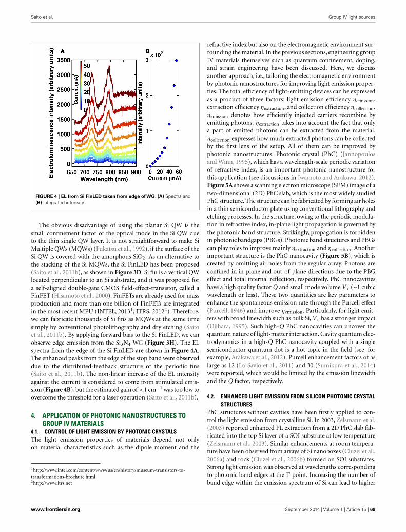
Saito et al. Group IV light sources
FIGURE 4 | EL from Si FinLED taken from edge of WG. (A) Spectra and(B) integrated intensity.
The obvious disadvantage of using the planar Si QW is thesmall confinement factor of the optical mode in the Si QW dueto the thin single QW layer. It is not straightforward to make SiMultiple QWs (MQWs) (Fukatsu et al., 1992), if the surface of theSi QW is covered with the amorphous SiO2. As an alternative tothe stacking of the Si MQWs, the Si FinLED has been proposed(Saito et al., 2011b), as shown in Figure 3D. Si fin is a vertical QWlocated perpendicular to an Si substrate, and it was proposed fora self-aligned double-gate CMOS field-effect-transistor, called aFinFET (Hisamoto et al., 2000). FinFETs are already used for massproduction and more than one billion of FinFETs are integratedin the most recent MPU (INTEL, 20131; ITRS, 20122). Therefore,we can fabricate thousands of Si fins as MQWs at the same timesimply by conventional photolithography and dry etching (Saitoet al., 2011b). By applying forward bias to the Si FinLED, we canobserve edge emission from the Si3N4 WG (Figure 3H). The ELspectra from the edge of the Si FinLED are shown in Figure 4A.The enhanced peaks from the edge of the stop band were observeddue to the distributed-feedback structure of the periodic fins(Saito et al., 2011b). The non-linear increase of the EL intensityagainst the current is considered to come from stimulated emis-sion (Figure 4B), but the estimated gain of<1 cm−1 was too low toovercome the threshold for a laser operation (Saito et al., 2011b).
4. APPLICATION OF PHOTONIC NANOSTRUCTURES TOGROUP IV MATERIALS
4.1. CONTROL OF LIGHT EMISSION BY PHOTONIC CRYSTALSThe light emission properties of materials depend not onlyon material characteristics such as the dipole moment and the
1http://www.intel.com/content/www/us/en/history/museum-transistors-to-transformations-brochure.html2http://www.itrs.net
refractive index but also on the electromagnetic environment sur-rounding the material. In the previous sections, engineering groupIV materials themselves such as quantum confinement, doping,and strain engineering have been discussed. Here, we discussanother approach, i.e., tailoring the electromagnetic environmentby photonic nanostructures for improving light emission proper-ties. The total efficiency of light-emitting devices can be expressedas a product of three factors: light emission efficiency ηemission,extraction efficiency ηextraction, and collection efficiency ηcollection.ηemission denotes how efficiently injected carriers recombine byemitting photons. ηextraction takes into account the fact that onlya part of emitted photons can be extracted from the material.ηcollection expresses how much extracted photons can be collectedby the first lens of the setup. All of them can be improved byphotonic nanostructures. Photonic crystal (PhC) (Jannopoulosand Winn, 1995), which has a wavelength-scale periodic variationof refractive index, is an important photonic nanostructure forthis application (see discussions in Iwamoto and Arakawa, 2012).Figure 5A shows a scanning electron microscope (SEM) image of atwo-dimensional (2D) PhC slab, which is the most widely studiedPhC structure. The structure can be fabricated by forming air holesin a thin semiconductor plate using conventional lithography andetching processes. In the structure, owing to the periodic modula-tion in refractive index, in-plane light propagation is governed bythe photonic band structure. Strikingly, propagation is forbiddenin photonic bandgaps (PBGs). Photonic band structures and PBGscan play roles to improve mainly ηextraction and ηcollection. Anotherimportant structure is the PhC nanocavity (Figure 5B), which iscreated by omitting air holes from the regular array. Photons areconfined in in-plane and out-of-plane directions due to the PBGeffect and total internal reflection, respectively. PhC nanocavitieshave a high quality factor Q and small mode volume V c (~1 cubicwavelength or less). These two quantities are key parameters toenhance the spontaneous emission rate through the Purcell effect(Purcell, 1946) and improve ηemission. Particularly, for light emit-ters with broad linewidth such as bulk Si, V c has a stronger impact(Ujihara, 1995). Such high-Q PhC nanocavities can uncover thequantum nature of light-matter interaction. Cavity quantum elec-trodynamics in a high-Q PhC nanocavity coupled with a singlesemiconductor quantum dot is a hot topic in the field (see, forexample, Arakawa et al., 2012). Purcell enhancement factors of aslarge as 12 (Lo Savio et al., 2011) and 30 (Sumikura et al., 2014)were reported, which would be limited by the emission linewidthand the Q factor, respectively.
4.2. ENHANCED LIGHT EMISSION FROM SILICON PHOTONIC CRYSTALSTRUCTURES
PhC structures without cavities have been firstly applied to con-trol the light emission from crystalline Si. In 2003, Zelsmann et al.(2003) reported enhanced PL extraction from a 2D PhC slab fab-ricated into the top Si layer of a SOI substrate at low temperature(Zelsmann et al., 2003). Similar enhancements at room tempera-ture have been observed from arrays of Si nanoboxes (Cluzel et al.,2006a) and rods (Cluzel et al., 2006b) formed on SOI substrates.Strong light emission was observed at wavelengths correspondingto photonic band edges at the 0 point. Increasing the number ofband edge within the emission spectrum of Si can lead to higher
www.frontiersin.org September 2014 | Volume 1 | Article 15 | 69

Saito et al. Group IV light sources
luminescence intensity. This is experimentally verified by increas-ing the lattice constant of PhC so that normalized frequenciescorresponding to the Si emission wavelengths are increased (Fujitaet al., 2008). Si light-emitting diodes (LEDs) with PhC patternshave also been demonstrated (Nakayama et al., 2010a; Iwamotoand Arakawa, 2012). The device schematically shown in Figure 6Awas fabricated using a SOI substrate. Firstly, a lateral p-i-n junctionwas formed into the top 200-nm-thick Si layer by area-selectiveimplantations of boron and phosphorous ions. Then, a PhC struc-ture was patterned. To keep mechanical stability and better thermalconductivity, the buried-oxide (BOX) layer was not removed. AnSEM image of the central part of a device is shown in Figure 6A.The i-region is 5µm in length and 250µm in width. EL spectrafrom devices with different PhC periods and from a device withoutPhC are shown in the inset of Figure 6B. EL emission increasedas the period a increased. Figure 6B shows the integrated inten-sities from these devices as a function of injected current. Theintegrated intensity from the device with a= 750 nm is ~14 timesstronger than that from an unpatterned LED. This enhancementis mainly caused by the improvement of ηextraction and ηcollection
due to the photonic band structures as discussed above. ηemission
is also expected to be enhanced in PhC nanocavities. Figure 7shows room-temperature µ-PL spectra measured at the center of
FIGURE 5 | SEM images of a regular PhC structure with a triangularlattice (A) and a L3-type PhC nanocavity, in which three air holes alonga 0-K direction are omitted (B).
an L3-type PhC nanocavity compared to a non-patterned region(see the inset). The L3 PhC nanocavity was also fabricated intoan SOI substrate. In this sample, the BOX layer was etched outin order to confine the photons strongly in the vertical direction.The PL intensity from the cavity was much larger than that fromthe non-patterned region. In addition, sharp peaks are observedonly in the spectrum from the cavity. These peaks originate fromthe cavity resonant modes. For this particular sample with the airhole radius r = 0.37a, large enhancement of PL over 300 times wasobtained for a cavity mode at 1,191 nm. As discussed in Section1, this enhancement can be attributed to three factors. Detailedanalysis including numerical simulation indicated that ηemission isimproved by ~5 times (Iwamoto et al., 2007). The enhancementfactors in ηemission ranging ~5−10 have been reported for Si inter-band transition (Fujita et al., 2008) and for light emission fromoptically active defects in Si (Lo Savio et al., 2011). The temper-ature dependence of cavity mode emission (Hauke et al., 2010;Lo Savio et al., 2011) and the dependence of PL on cavity modevolume V c (Nakayama et al., 2012) suggest that the Purcell effectplays a role in this enhancement. The enhancement in ηemission
reported so far is still too small for practical applications. How-ever, this research would provide important insights for furtherdevelopment of light-emitting devices using group IV materials.Indeed, these pioneering works have stimulated theoretical inves-tigations, which discuss the possibility of lasing oscillation in Si(Escalante and Martínez, 2012, 2013). Recent advances in this fieldare developments of Si LEDs with PhC nanocavities (Nakayamaet al., 2011; Shakoor et al., 2013). Shakoor et al. (2013) recentlyreported Si LEDs using L3-type nanocavity structure, in whichoptically active defects created by hydrogen bombardment are usedas light emission centers. They carefully designed the cavity struc-ture to improving ηcollection and obtained sharp light emission ataround 1.5µm with a power density of 0.4 mW/cm2. The strain-induced dislocations (Ng et al., 2001; Kittler et al., 2013) will alsobe compatible to PhC nanocavities, since the emission energiesare smaller than the band gap of Si. The combination of PhCnanocavities and defect engineering is very promising, and a wallplug efficiency of 0.7× 10⁻⁸ was reported (Shakoor et al., 2013).
FIGURE 6 | (A) Schematic representation of a silicon PhC LED is shown. The SEM image shows the center area of a device. (B) Integrated EL intensities forsilicon PhC LED with various periods a and for an SOI LED with a flat surface. The inset shows corresponding EL spectra at 10 mA.
Frontiers in Materials | Optics and Photonics September 2014 | Volume 1 | Article 15 | 70

Saito et al. Group IV light sources
FIGURE 7 | Room-temperature µ-PL spectra measured at the center ofa PhC nanocavity and at a non-patterned area. The spectrum for thelatter is magnified by ten times for better viewing.
4.3. APPLICATION OF PHOTONIC CRYSTAL STRUCTURES TO OTHEREMITTERS IN GROUP IV MATERIALS
Erbium ions have been investigated as one of the promisinglight emitters in Si. PhC nanocavities have been also applied toenhance the light emission from Er ions (Wang et al., 2012; Savioet al., 2013). Narrowing the cavity linewidth in Er-doped siliconnitride PhC nanocavities has been also demonstrated under opti-cal pumping condition (Gong et al., 2010). As discussed in theprevious sections, Ge is, at present, the most important materialfor future light-emitting devices in Si photonics. PhC (Nakayamaet al., 2010b) and PhC nanocavities (Kurdi et al., 2008; Ngo et al.,2008) have been applied to increase the light emission from bulkGe. Applying advanced strain/doping engineering technologies tophotonic nanostructures would open a new route for boosting thelight emission efficiency of Ge.
5. GENERATION OF TENSILE STRAIN IN Ge LAYERSEPITAXIALLY GROWN ON Si SUBSTRATE
In epitaxial growth of Ge on an Si substrate, a compressive strainin Ge, derived from the 4.2% lattice mismatch with Si, should berelaxed after growth beyond the critical thickness, while it has beenreported by one of the authors that, during the cooling from thegrowth temperature to room temperature, a biaxial tensile strainas large as 0.2% is built-in due to the thermal expansion mis-match (Ishikawa et al., 2003, 2005; Cannon et al., 2004; Liu et al.,2005). It is known that the strain in semiconductors causes shiftsin band edge energies, e.g., de Walle, 1989, modifying the gap ener-gies, i.e., properties of optical transitions. The 0.2% tensile strainin Ge reduces the direct bandgap energy from 0.80 to ~0.77 eV,and as a result, the optical absorption edge (or the longer limit ofdetection wavelength) shifts from 1.55 to >1.60µm, causing theincrease of optical absorption coefficient at 1.55µm (Ishikawaet al., 2003, 2005; Cannon et al., 2004; Liu et al., 2005). Thisproperty is effective for the detection of near-infrared (NIR) light
used in the optical fiber communications (1.3–1.6µm). A fur-ther attractive feature of the tensile strain in Ge is the reductionof energy difference in the conduction band between the direct0 valley and indirect L-valley (e.g., Fischetti and Laux, 1996;Wada et al., 2006; Camacho-Aguilera et al., 2012; Nama et al.,2013; Süess et al., 2013). This feature stimulates researchers toobtain efficient NIR light emission from tensile-strained Ge dueto the enhanced direct transition around the 0 point (e.g., Liuet al., 2007; Lim et al., 2009). In this section, the grown-in ten-sile strain in Ge on Si, generated due to the thermal expansionmismatch, is described. Figure 8A shows typical ω− 2θ x-raydiffraction (XRD) curves taken for 0.6-µm-thick Ge grown ona 525-µm-thick Si(001) substrate with the Cu Kα radiation asthe x-ray source (0.15406 nm in wavelength). The samples weregrown by ultrahigh-vacuum chemical vapor deposition with asource gas of GeH4 (9%) diluted in Ar. The growth tempera-ture was 600°C, while a lower temperature of 370°C was usedat the initial stage of Ge growth (~50 nm) in order to preventthe islanding, leading to Ge layers uniform in thickness (Luanet al., 1999; Ishikawa and Wada, 2010). After the growth, high-temperature annealing was carried out for one of the samples at800°C for 20 min. Such annealing is often performed in order toreduce the threading-dislocation density (Luan et al., 1999). In ourcase, the density was reduced from 1× 10⁹ to 1− 2× 108 cm−2. InFigure 8A, the peaks due to the (004) diffraction are clearly seen ataround 2θ ~ 66° for both of the as-grown and annealed samples.It is important that the peaks were located at larger diffractionangles than that for unstrained Ge, indicating the reduction ofout-of-plane lattice constant, i.e., the increase of in-plane latticeconstant due to the generation of tensile strain. According to thepeak positions, the in-plane biaxial tensile strain was estimatedto be 0.11 and 0.22% for the as-grown and annealed samples,respectively.
As mentioned above, such a tensile strain is generated in Gedue to the mismatch of thermal expansion coefficient with Si.As schematically shown in Figure 8B, the compressive strain inGe due to the 4.2% lattice mismatch should be relaxed at thegrowth/annealing temperature, while the shrinkage in the Gelattice during the cooling should be prevented by the thick Si sub-strate, since Si has a smaller thermal expansion coefficient thanthat of Ge. This means that a tensile (compressive) stress/strain isgenerated in Ge (Si), as in the bottom of Figure 8B. Taking intoaccount the balance of forces together with the balance of momentsin the stacked structure of Ge and Si, the tensile (compressive)strain in Ge (Si) is theoretically expressed as:
∈|| (Ge) =1
R
[Y1t 3
1 + Y2t 32
6Y1t1 (t1 + t2)+
(t1
2− z1
)](1)
∈|| (Si) = & −1
R
[Y1t 3
1 + Y2t 32
6Y2t2 (t1 + t2)−
(t2
2− z2
)], (2)
where,αi, Yi, ti, and zi represent the thermal expansion coefficient,the Young’s modulus, the layer thickness, and the location in thelayer measured from the bottom of the layer for the i-th layer (1for Ge and 2 for Si), respectively. The radius of curvature R is
www.frontiersin.org September 2014 | Volume 1 | Article 15 | 71

Saito et al. Group IV light sources
FIGURE 8 | (A) ω− 2θ XRD curves for 0.6-µm-thick Ge on Si (001) substrate, (B) schematic illustration showing the generation of tensile stress/strain in Ge, and(C) theoretical curves and experimental data for biaxial tensile strain in Ge.
represented from
1
R=
6 (t1 + t2)Y1Y2t1t2∫ TRT
TGR/AN(α1 − α2) dT
3(t1 + t2)2Y1Y2t1t2 +
(Y1t 3
1 + Y2t 32
)(Y1t1 + Y2t2)
, (3)
where T GR/AN and T RT represent the growth/annealing tempera-ture before cooling and the room temperature (after the cooling),respectively. Since the first term is dominant in the right side ofequation (1), the strains are almost independent of z i, the locationwithin the layer. Therefore, equations (1) and (2) are simplified to:
∈|| (Ge) ∼1
R
Y1t 31 + Y2t 3
2
6Y1t1 (t1 + t2)(4)
∈|| (Si) ∼ −1
R
Y1t 31 + Y2t 3
2
6Y2t2 (t1 + t2). (5)
The lines in Figure 8C represent the strains calculated for the Gethickness of 0.6µm and the Si thickness of 525µm. Note thatalmost identical results can be obtained when the thickness of Sisubstrate t 2 is much larger (more than ~100 times) than the Gethickness t 1. The parameters used in the calculation can be foundin Ishikawa et al. (2005). It is found that a tensile strain on theorder of 0.1% is generated in Ge at room temperature, while thecompressive strain in Si is negligible. It is also found that highergrowth/annealing temperature generates larger tensile strain afterthe cooling. These properties are qualitatively in good agreementwith the XRD results in Figure 8A. However, quantitatively, thetensile strain observed by XRD was smaller than the theoreticalone. This is probably ascribed to the residual compressive strainin Ge at the growth/annealing temperature (Ishikawa et al., 2005).From the viewpoint of optoelectronic integration of Ge deviceson an Si platform, Si-on-insulator (SOI) wafers have been widelyused. For Ge layers grown on SOI wafers, a similar amount oftensile strain should be generated, since the elastic deformation,derived from the thermal expansion mismatch, is governed by thethick Si substrate, rather than the buried SiO2 and the top Si layerswith the thicknesses on the order of 1µm or below. Patterning of
the Ge layer as well as deposition of dielectric films embedding astrain could intentionally modify the strain in the Ge.
6. DIRECT GERMANIUM EPITAXIAL GROWTH PROCESS ONSILICON
The Ge was epitaxially grown by using a cold-wall rapid ther-mal chemical vapor deposition system. Germane (GeH4) wasused as a source gas, which was supplied with H2 carrier gas.As the starting point of improving the crystallinity and control-ling the lattice strain, Ge layers with good surface morphologywere grown at 420°C under relatively high pressure of 7,000 Pa.Then, the Ge layers were annealed in the same H2 atmosphereto improve the crystallinity. Figure 9 shows a reciprocal spacemap (RSM) of XRD (XRD-RSM) from the 130-nm-thick Ge layerdirectly grown on the Si substrate before and after H2 anneal-ing. An intense Si (-1-13) peak was observed, which representedthe diffraction from the Si substrate under the Ge layer. Since theXRD-RSM was measured by using semiconductor array detec-tors, errors in the counts occur if the diffraction intensity isvery high; therefore, the streak line observed around the Si (-1-13) peak does not represent any actual diffraction. Since a Ge(-1-13) diffraction peak was observed from the Ge layer with-out annealing (Figure 9A), it could be confirmed that a singlecrystalline Ge layer was obtained by using low-temperature epi-taxial growth. The displacement of the diffraction peak shows thatthe as-grown Ge layer still contained a compressive strain justafter the low-temperature epitaxial growth at 420°C due to thelarger lattice constant of Ge compared to that of the Si substrate.It has been reported that cyclic annealing at a relatively highertemperature can reduce the threading-dislocation density (Luanet al., 1999) in Ge layers. This has led to studies on the effectof annealing on the crystallinity and lattice strain of Ge layers.After low-temperature epitaxial growth of Ge layers at 420°C, thetemperature was increased to the annealing temperature in thesame H2 atmosphere as that during the epitaxial growth, and theGe layers were then annealed at various temperatures for 10 min.XRD-RSMs of Ge layers annealed at a temperature (T GR/AN) of700°C after the low-temperature epitaxial growth are shown inFigure 9B. The Ge (-1-13) diffraction peaks became much steeperand the peak intensity increased when the annealing temperature
Frontiers in Materials | Optics and Photonics September 2014 | Volume 1 | Article 15 | 72

Saito et al. Group IV light sources
FIGURE 9 | XRD-RSM of (-1-13) diffraction from Ge layer grown on Sisubstrate, (A) after low-temperature epitaxial growth and (B) afterpost-annealing.
FIGURE 10 | Photoluminescence spectra from Ge layers annealed withdifferent temperatures are shown. Peak wavelength ofphotoluminescence from Ge layers red-shifted as annealing temperatureincreased, consistent with temperature induced tensile strain. Inset showslattice strain of Ge layers grown on Si substrate along <001> and <110>crystal orientations as a function of annealing temperature. Dotted lineindicates lattice strain calculated with difference between thermalexpansion coefficients of Si and Ge.
was increased, indicating that the crystallinity of the Ge layers wasincreased by the post-annealing.
The inset of Figure 10 shows the lattice strain in the Gelayers in the <001> and <110> crystal orientations as a func-tion of the annealing temperature. We used standard Si wafers
for this experiment, so that <001> is perpendicular to the sur-face of the Ge film, while <110> is in the plane of Ge film.The lattice strain in the <110> crystal orientation increased asT GR/AN increased, and the strain in the <001> crystal orien-tation showed an opposite dependence. Although the Ge layercontained a compressive strain in the <110> crystal orienta-tion at T GR/AN= 420°C, i.e., without annealing, this strain starteddecreasing when T GR/AN was increased, and the Ge was completelyun-strainedat T GR/AN= 530°C. Furthermore, the sign of the lat-tice strain changed from compressive to tensile after annealing atT GR/AN> 530°C, and the tensile strain at T GR/AN= 700°C reached0.19%. This result is consistent with previous studies (Cannonet al., 2004). Normally, a grown layer with a larger lattice constantcompared to a substrate contains a compressive strain within thegrowth plane. However, since the Ge layers grown on the Si sub-strate were almost completely relaxed even after low-temperaturegrowth, the Ge lattice could be dislocated at the Ge/Si interface bypost-annealing, and the lattice strain of the Ge layer was relaxedduring annealing at the relatively higher temperature with thevolumes of Ge and Si determined by the thermal expansion coeffi-cients (Singh, 1968; Okada and Tokumaru, 1984). After annealing,the volume of the Ge layer and the Si substrate both shrunk asthe temperature decreased, and there was barely any change to thelattice alignment at low-temperature. The volume of the Si sub-strate returned to its original value because it was thick enough.However, the volume of the Ge layer could not return due to itslarger thermal expansion coefficients. Therefore, the tensile latticestrain remained only in the Ge layers after cooling (Cerdeira et al.,1972). The ideal lattice strain in<110> crystal orientation was alsoplotted in the inset of Figure 10, which was calculated with onlythe difference of the thermal expansion coefficients between Siand Ge, so these values indicate the maximum lattice strain. Sincethere are large discrepancies between calculation and measuredvalues, it seems that relaxation ratio has a large effect on the latticestrain even at the lower temperatures. PL spectra from the post-annealed Ge layers with various annealing temperatures are shownin Figure 10. Although Ge is an indirect bandgap material and theL-valley has the lowest energy level in the conduction band, wewere able to observe recombination between electrons and holesat the 0-valley as luminescence at a wavelength of 1,550 nm, evenfrom the bulk Ge (dashed line in Figure 10). A comparison withthe post-annealed Ge layers shows that although the spectrum wasvery weak and broad for the as-grown Ge layer, an obvious peakcould be observed from annealed samples at T GR/AN> 530°C.Moreover, the PL intensity increased and the peak shape becamesharper as the annealing temperature was increased. The PL spec-trum is strongly affected by crystallinity, because non-radiativerecombination was significantly increased with defects such asdislocation and stacking faults. Therefore, these results suggestthat the crystallinity of the Ge layers was improved by the post-annealing. The peak was observed at a shorter wavelength fromthe Ge layer annealed at 500°C compared with that from bulk Ge,and a red shift of the PL peaks occurred after post-annealing ata higher temperature. In addition, the peak wavelength from theunstrained Ge was 1,550 nm, which is almost the same value as thatof the bulk Ge. These results show that the bandgap energy at the0-point was varied by the lattice strain in the Ge layers (Cerdeira
www.frontiersin.org September 2014 | Volume 1 | Article 15 | 73
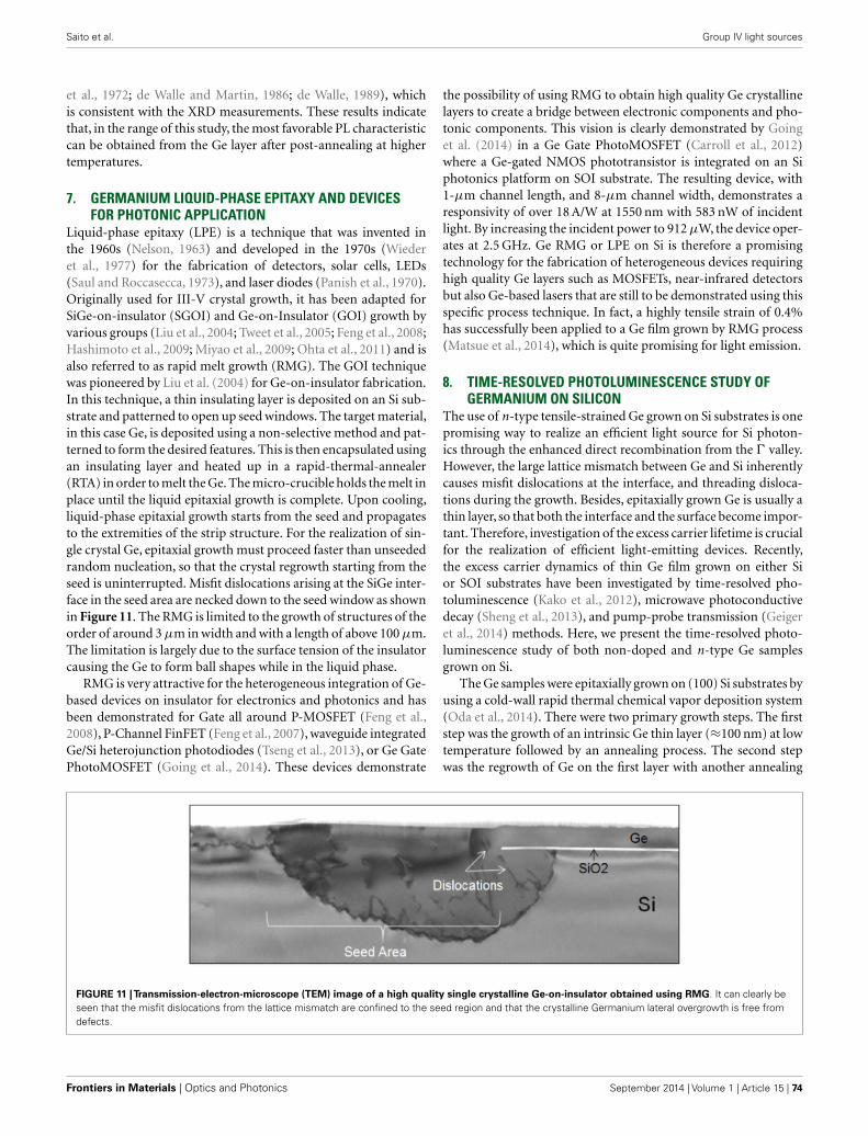
Saito et al. Group IV light sources
et al., 1972; de Walle and Martin, 1986; de Walle, 1989), whichis consistent with the XRD measurements. These results indicatethat, in the range of this study, the most favorable PL characteristiccan be obtained from the Ge layer after post-annealing at highertemperatures.
7. GERMANIUM LIQUID-PHASE EPITAXY AND DEVICESFOR PHOTONIC APPLICATION
Liquid-phase epitaxy (LPE) is a technique that was invented inthe 1960s (Nelson, 1963) and developed in the 1970s (Wiederet al., 1977) for the fabrication of detectors, solar cells, LEDs(Saul and Roccasecca, 1973), and laser diodes (Panish et al., 1970).Originally used for III-V crystal growth, it has been adapted forSiGe-on-insulator (SGOI) and Ge-on-Insulator (GOI) growth byvarious groups (Liu et al., 2004; Tweet et al., 2005; Feng et al., 2008;Hashimoto et al., 2009; Miyao et al., 2009; Ohta et al., 2011) and isalso referred to as rapid melt growth (RMG). The GOI techniquewas pioneered by Liu et al. (2004) for Ge-on-insulator fabrication.In this technique, a thin insulating layer is deposited on an Si sub-strate and patterned to open up seed windows. The target material,in this case Ge, is deposited using a non-selective method and pat-terned to form the desired features. This is then encapsulated usingan insulating layer and heated up in a rapid-thermal-annealer(RTA) in order to melt the Ge. The micro-crucible holds the melt inplace until the liquid epitaxial growth is complete. Upon cooling,liquid-phase epitaxial growth starts from the seed and propagatesto the extremities of the strip structure. For the realization of sin-gle crystal Ge, epitaxial growth must proceed faster than unseededrandom nucleation, so that the crystal regrowth starting from theseed is uninterrupted. Misfit dislocations arising at the SiGe inter-face in the seed area are necked down to the seed window as shownin Figure 11. The RMG is limited to the growth of structures of theorder of around 3µm in width and with a length of above 100µm.The limitation is largely due to the surface tension of the insulatorcausing the Ge to form ball shapes while in the liquid phase.
RMG is very attractive for the heterogeneous integration of Ge-based devices on insulator for electronics and photonics and hasbeen demonstrated for Gate all around P-MOSFET (Feng et al.,2008), P-Channel FinFET (Feng et al., 2007), waveguide integratedGe/Si heterojunction photodiodes (Tseng et al., 2013), or Ge GatePhotoMOSFET (Going et al., 2014). These devices demonstrate
the possibility of using RMG to obtain high quality Ge crystallinelayers to create a bridge between electronic components and pho-tonic components. This vision is clearly demonstrated by Goinget al. (2014) in a Ge Gate PhotoMOSFET (Carroll et al., 2012)where a Ge-gated NMOS phototransistor is integrated on an Siphotonics platform on SOI substrate. The resulting device, with1-µm channel length, and 8-µm channel width, demonstrates aresponsivity of over 18 A/W at 1550 nm with 583 nW of incidentlight. By increasing the incident power to 912µW, the device oper-ates at 2.5 GHz. Ge RMG or LPE on Si is therefore a promisingtechnology for the fabrication of heterogeneous devices requiringhigh quality Ge layers such as MOSFETs, near-infrared detectorsbut also Ge-based lasers that are still to be demonstrated using thisspecific process technique. In fact, a highly tensile strain of 0.4%has successfully been applied to a Ge film grown by RMG process(Matsue et al., 2014), which is quite promising for light emission.
8. TIME-RESOLVED PHOTOLUMINESCENCE STUDY OFGERMANIUM ON SILICON
The use of n-type tensile-strained Ge grown on Si substrates is onepromising way to realize an efficient light source for Si photon-ics through the enhanced direct recombination from the 0 valley.However, the large lattice mismatch between Ge and Si inherentlycauses misfit dislocations at the interface, and threading disloca-tions during the growth. Besides, epitaxially grown Ge is usually athin layer, so that both the interface and the surface become impor-tant. Therefore, investigation of the excess carrier lifetime is crucialfor the realization of efficient light-emitting devices. Recently,the excess carrier dynamics of thin Ge film grown on either Sior SOI substrates have been investigated by time-resolved pho-toluminescence (Kako et al., 2012), microwave photoconductivedecay (Sheng et al., 2013), and pump-probe transmission (Geigeret al., 2014) methods. Here, we present the time-resolved photo-luminescence study of both non-doped and n-type Ge samplesgrown on Si.
The Ge samples were epitaxially grown on (100) Si substrates byusing a cold-wall rapid thermal chemical vapor deposition system(Oda et al., 2014). There were two primary growth steps. The firststep was the growth of an intrinsic Ge thin layer (≈100 nm) at lowtemperature followed by an annealing process. The second stepwas the regrowth of Ge on the first layer with another annealing
FIGURE 11 |Transmission-electron-microscope (TEM) image of a high quality single crystalline Ge-on-insulator obtained using RMG. It can clearly beseen that the misfit dislocations from the lattice mismatch are confined to the seed region and that the crystalline Germanium lateral overgrowth is free fromdefects.
Frontiers in Materials | Optics and Photonics September 2014 | Volume 1 | Article 15 | 74

Saito et al. Group IV light sources
process. In situ n-type doping was carried out during the secondgrowth step by supplying phosphine. The Ge becomes biaxiallystrained (≈0.15%) due to the difference of the thermal expansioncoefficients between Si and Ge. Time-resolved photoluminescencemeasurements were performed using a time-correlated single-photon counting method employing a superconducting single-photon detector (SSPD) with a time resolution of about 50 ps. ATi:Sapphire pulsed laser was used as the excitation source (wave-length 710 nm, repetition rate 80 MHz, and pulse-duration 100 fs).The laser beam was focused on the sample surface using an objec-tive lens. The photoluminescence from the samples was collectedby the same objective and focused on to an optical fiber connectedto the SSPD. Photoluminescence ranging from 1.2 to 1.8µm wasdetected.
Figure 12A shows a time-resolved photoluminescence decaycurve measured from a nominally undoped Ge sample (thickness500 nm). In order to limit the effects of lateral diffusion, the laserspot size was set to≈10µm. The decay is a single exponential witha lifetime of 1 ns, which corresponds to the excess carrier lifetimeof 2 ns. Germanium has an indirect bandgap, and as such, its excesscarrier dynamics are determined by non-radiative recombinationprocesses, such as Shockley-Read Hall (SRH) recombination andsurface recombination processes. The photoluminescence decaylifetime, τPL, of undoped Ge is then related to the excess carrierlifetime, τ ex, as 2τPL= τ ex. The lifetime of excess carriers τ ex ofan indirect semiconductor film depends on the thickness and canbe represented by Sproul (1994) and Gaubas and Vanhellemont(2006) as:
1
τex=
1
τB+
1d2S +
d2
π2D
, (6)
where τB is the bulk lifetime, S is the surface recombination veloc-ity, D is the ambipolar diffusion constant, and d is the layer
FIGURE 12 | (A) Time-resolved PL curve for an undoped Ge sample. Theinset shows the measured excess carrier lifetimes for two Ge thicknesseswith simulated lifetimes using the equations shown in the text.(B) Time-resolved PL curves of an n-type sample for two excitation powers,150 kW/cm2 (black line) and 15 kW/cm2 (red line).
thickness. The excess carrier lifetimes obtained for undoped Gelayers with different thicknesses (filled black circles) are shown inthe inset of Figure 12A together with the black curve, which is afit to the data using equation (6) with parameters of τB= 3.5 ns,S= 5.5× 103 cm/s, and D= 30 cm2/s (The ambipolar diffusionconstant Da could be estimated by changing the spot size and mea-suring the photoluminescence decay time). Both SRH bulk recom-bination and the surface recombination processes determine theexcess carrier dynamics in our undoped Ge samples.
Figure 12B shows time-resolved photoluminescence decaycurves measured at two different excitation power densities froman n-type Ge sample (thickness 500 nm, doping concentration7× 1019 cm−3). The measured decay depends on both the exci-tation power density and time (in contrast to those measuredfrom undoped samples, which are independent of the excita-tion power). The instantaneous lifetime (that measured at aparticular point during the decay) depends on the photolumi-nescence intensity, and thus the excess carrier density. Basedon the SRH non-radiative recombination model, the lifetime ofexcess carriers depends on their density (Linnros, 1998). Thisdependence can be simplified to τ hl= τ n+ τ p (τ ll= τ p for n-type doping) in the two extreme conditions where the carrierdensity is high (low) when compared to the doping concentra-tion (τ n and τ p are the inverse capture rates of the electronsand holes, respectively). The photoluminescence lifetime can beexpressed as 2τPL= τ hl (high excess carrier density) and τPL= τ ll
(low excess carrier density). Therefore, from our measurements,we estimate τ ll= 0.14 ns, τ hl= 0.8 ns based on SRH theory. Theestimated τ hl value is shorter than those found from the undopedsamples. This difference might be attributed to an increaseddislocation density introduced by the doping, but the estima-tion of τ hl could be underestimation because the Auger processbecomes important for doped samples (Gaubas and Vanhelle-mont, 2006). Further investigation is needed in order to obtaina better understanding.
9. ELECTRO-LUMINESCENCE FROM GERMANIUMRealization of monolithic light sources compatible with the exist-ing Si photonics platform is one of the most difficult challenges.Ge has attracted much attention as for possible future monolithiclight sources owing to its emission wavelengths of ~1.6µm suitablefor an Si-based WG, in addition to the CMOS compatibility andthe pseudo-direct band-gap character (Menéndez and Kouvetakis,2004; Liu et al., 2007, 2012; Liang and Bowers, 2010; Michel et al.,2010; Boucaud et al., 2013; Liu, 2014). Recently, laser operationfrom Ge pumped optically (Liu et al., 2010) and electrically (Chenget al., 2007; Camacho-Aguilera et al., 2012) has been reported.However, there is no report so far to reproduce their results. Theoptical gain from Ge is also achieved by the tensile-stress engineer-ing (de Kersauson et al., 2011). The precise nature of the opticalgain in Ge is still controversial (Carroll et al., 2012), but the highcrystalline quality of Ge is one of the most critical factor to avoidnon-radiative recombinations at dislocations. It is confirmed byseveral groups (Michel et al., 2010; Liu et al., 2012; Boucaud et al.,2013; Liu, 2014) that the primary challenges for engineering Geas an active layer are: (i) crystallinity, (ii) high n-type doping, (iii)tensile strain, as confirmed theoretically (Suwa and Saito, 2010,
www.frontiersin.org September 2014 | Volume 1 | Article 15 | 75

Saito et al. Group IV light sources
2011; Virgilio et al., 2013a,b). Here, we review some of the Ge lightsources developed on SOI substrates.
9.1. DEVICE STRUCTURE AND FABRICATION PROCESSAs we discussed in section for Si light sources, lateral carrier injec-tion is a natural choice for electrical pumping, since fabricationprocesses are based on planar CMOS technologies. We show sev-eral candidates for Ge light sources suitable for lateral carrierinjection in Figure 13.
Figures 13A,E,I show schematic views and a transmission-electron-microscope (TEM) image of a Ge FinLED (Saito et al.,2011a), which uses Ge fins as MQWs embedded in Si3N4 WG.Ge fins were fabricated by the oxidation condensation technique(Tezuka et al., 2009) applied to SiGe fins (Saito et al., 2011a). Rel-atively, high crystallinity is expected in Ge fins, since the latticemismatch between Si and Ge would be relaxed by stretching thefins during the oxidation (Saito et al., 2011a). In fact, the low darkcurrent density of 1.86× 10⁻⁵ A/cm−2 at a reverse bias of 1−Vand the strong breakdown current density of >1 MA/cm−2 wereconfirmed (Saito et al., 2011a).
In order to enhance the overlap between an optical modeand fins, Ge fins with (111) orientation at the sidewall were alsodeveloped (Tani et al., 2012), as shown in Figures 13B,F,J. Toimprove the patterning accuracy, Si (111) fins were fabricatedby anisotropic wet etching, and n-Ge was re-grown after thecondensation oxidation of SiGe fins (Tani et al., 2011).
Further increase of the coupling is realized by using a bulkGe WG (Liu et al., 2007; Camacho-Aguilera et al., 2012; Tani et al.,2013a,b), as shown in Figures 13C,G,K for schematic views and thescanning electron microscope (SEM) image, rather than using GeQW or Ge fins. The p- and n-type diffusion regions were formedin the 40 nm-thick SOI layer, and the Ge waveguide with 500-nm width and 500-µm length was directly grown on the SOIdiode. The SOI thickness was designed to minimize the optical
loss due to free carrier absorption in the diffusion electrodes. TheGe waveguide was doped with 1× 1019 cm−3 of phosphorus, andthe surface of the Ge waveguide was then passivated with GeO2
formed by low-temperature oxidation to reduce interfacial traps(Tani et al., 2012, 2013a). Then, metal electrodes were made onboth diffusion regions.
To enhance light emission efficiency from Ge by tensile stress,several techniques have been developed, e.g., the use of the thermalexpansion of relaxed Ge grown on Si (Ishikawa et al., 2003), thegrowth on buffer layers with larger lattice parameter (Huo et al.,2011), the mechanical deformation using membrane structures(Kurdi et al., 2010), the stress concentration in a membrane struc-ture (Nama et al., 2013), and using external stressors (Ortollandet al., 2009; Ghrib et al., 2013). Considering the process compati-bility to the lateral carrier injection, the Si3N4 film with the tensilestress of 250-MPa was employed (Tani et al., 2013a), as shown inFigures 13D,H,L.
9.2. IMPACT OF STRESS ENGINEERING FOR LATERAL GERMANIUMON SILICON DIODE
Figure 14A shows EL spectra of the Ge waveguide with 500-nmwidth and 500-µm length taken from the top of the substrateunder continuous current injection of 60-mA. EL peak wave-length of the device with an SiN stressor is slightly longer thanthat without the SiN stressor due to the tensile strain-inducedband-gap shrinkage, although the exact band-gap energy can-not be quantitatively estimated due to the additional peak shiftscaused by heating under high currents. Moreover, as shown inFigure 14B, the peak intensity of the EL of the device withSiN stressor is 1.65 times larger than that without SiN stressors.Figure 14C shows two-dimensional stress mapping calculated bya finite element modeling of the Ge waveguide on the Si sub-strate covered by Si3N4 stressor. The tensile stress of 100 MPa
FIGURE 13 | Development of a Ge light source. (A) i -Ge FinLED, (B) n-Ge FinLED, (C) n-Ge-WG-on-Si LED without SiN, and (D) n-Ge-WG-on-Si LED with SiN.(A–D) Cross section, (E–H) plan views, and (I–L) microscope images.
Frontiers in Materials | Optics and Photonics September 2014 | Volume 1 | Article 15 | 76

Saito et al. Group IV light sources
FIGURE 14 | Strain engineering for n-Ge-WG-on-Si LED. (A) Spectra and (B) integrated intensity from experiments. (C) Stress mapping simulation.
is localized on the side wall of the Ge waveguide, while the in-plane compressive stress of 40 MPa exists on the top part of theGe waveguide. The increase of the light emission efficiency was22% caused by the tensile stress, after subtracting of the addi-tional increase of 35% caused by the light extraction efficiencydue to the reduced reflectance at the surface of the Ge waveguideby the 500 nm-thick Si3N4 layer (Tani et al., 2013a). Therefore, thestress engineering by Si3N4 is an appropriate option to improvethe performance of Ge light sources. Recently, there are significantadvances in stress engineering by manipulating free-standing Gestructures (Jain et al., 2012; Boztug et al., 2013; Süess et al., 2013;Sukhdeo et al., 2014), and enhanced direct recombination has beenachieved.
10. CONCLUSION AND FUTURE OUTLOOKIn this paper, we reviewed the recent progress on the developmentsof silicon and germanium light sources. There are many processoptions to fabricate silicon- and germanium-based nanostructuresby using modern silicon technologies. For active materials, pla-nar silicon single-quantum-well (Saito et al., 2006a,b, 2008, 2009;Hoang et al.,2007; Noborisaka et al.,2011; Saito,2011) or multiple-quantum-wells made of silicon or germanium fins (Saito et al.,2011a,b) can be used. To enhance the recombination rates andthe extraction efficiencies, photonic crystal structures have beenintroduced (Fujita et al., 2008; Nakayama et al., 2010a; Iwamotoand Arakawa, 2012). The further increase of the efficiency canbe achieved by introducing tensile strain and n-type doping ofthe germanium (Ishikawa et al., 2003; Menéndez and Kouvetakis,2004; Liu et al., 2007, 2012; Kurdi et al., 2010; Michel et al., 2010;Huo et al., 2011; Boucaud et al., 2013; Ghrib et al., 2013; Namaet al., 2013; Tani et al., 2013a; Liu, 2014).
Considering the success of the laser operation using the bulkgermanium waveguides (Liu et al., 2010; Camacho-Aguilera et al.,2012), the next step will be to reduce the threshold current forpumping. It is critical to develop a process technology to fabricatea high crystalline quality germanium quantum-well compatiblewith the silicon photonics platform. If practical silicon or ger-manium laser diodes are available in the future, these group IVlasers will realize the convergence of electronics and photonics ona silicon chip.
ACKNOWLEDGMENTSWe would like to thank research collaborators, engineers, andline managers in Hitachi, the University of Tokyo, and Uni-versity of Southampton for supporting this project. We arealso grateful to Prof. H. N. Rutt for his careful reading ofthe manuscript and constructive comments. Funding: parts ofthe studied discussed here was supported by Japan Society forthe Promotion of Science (JSPS) through its “Funding Pro-gram for World-Leading Innovation R&D on Science and Tech-nology (FIRST Program),” the Project for Developing Innova-tion Systems, and Kakenhi 216860312, MEXT, Japan. This workis also supported by EU, FP7, Marie-Curie, Carrier Integra-tion Grant (CIG), PCIG13-GA-2013-618116, and University ofSouthampton, Zepler Institute, Research Collaboration Stimu-lus Fund.
REFERENCESArakawa, Y., Iwamoto, S., Nomura, M., Tandaechanurat, A., and Ota, Y. (2012).
Cavity quantum electrodynamics and lasing oscillation in single quantum dot-photonic crystal nanocavity coupled systems. IEEE J. Selec. Top. Quant. Elec. 18,1818–1829. doi:10.1109/JSTQE.2012.2199088
Arakawa, Y., Nakamura, T., and Urino, Y. (2013). Silicon photonics for next genera-tion system integration platform. Commun. Mag. IEEE 51, 72–77. doi:10.1109/MCOM.2013.6476868
Arakawa, Y., and Sakaki, H. (1982). Multidimensional quantum well laser and tem-perature dependence of its threshold current. Appl. Phys. Lett. 40, 939–941.doi:10.1063/1.92959
Boucaud, P., Kurdi, M. E., Ghrib, A., Prost, M., de Kersauson, M., Sauvage, S.,et al. (2013). Recent advances in germanium emission. Photon. Res. 1, 102–109.doi:10.1364/PRJ.1.000102
Boztug, C., Sanchez-Perez, J. R., Yin, J., Lagally, M. G., and Paiella, R. (2013).Graiting-coupled mid-infrared light emission from tensile strained germaniumnanomembranes. Appl. Phys. Lett. 103, 201114. doi:10.1002/smll.201201090
Camacho-Aguilera, R. E., Cai, Y., Patel, N., Bessette, J. T., Romagnoli, M., Kimerling,L. C., et al. (2012). An electrically pumped germanium laser. Opt. Express 20,11316–11320. doi:10.1364/OE.20.011316
Canham, L. T. (1990). Silicon quantum wire array fabrication by electrochem-ical and chemical dissolution of wafers. Appl. Phys. Lett. 57, 1046–1048.doi:10.1063/1.103561
Cannon, D. D., Liu, J., Ishikawa, Y., Wada, K., Danielson, D. T., Jongthammanu-rak, S., et al. (2004). Tensile strained epitaxial Ge film on Si(100) substrate withpotential application to L-band telecommunications. Appl. Phys. Lett. 84, 906.doi:10.1063/1.1645677
Carroll, L., Friedli, P., Neunschwander, S., Sigg, H., Cecchi, S., Isa, F., et al. (2012).Direct-gap gain and optical absorption in germanium correlated to the density
www.frontiersin.org September 2014 | Volume 1 | Article 15 | 77

Saito et al. Group IV light sources
of photoexcited carriers, doping, and strain. Phys. Rev. Lett. 109, 057402.doi:10.1103/PhysRevLett.109.057402
Cerdeira, F., Buchenauer, C. J., Pollak, F. H., and Cardona, M. (1972). Stress-inducedshifts of first-order Raman frequencies of diamond- and zinc-blende-type semi-conductors. Phys. Rev. B 5, 580–593. doi:10.1103/PhysRevB.5.580
Cheng, T. H., Kuo, P. S., Lee, C. T., Liao, M., Hung, T. A., and Liu, C. W. (2007).“Electrically pumped Ge laser at room temperature,” in IEEE Int. Conf. ElectronDevices Meeting (IEDM), Washington, 659–662.
Cluzel, B., Pauc, N., Calvo, V., Charvolin, T., and Hadji, E. (2006a). Nanobox arrayfor silicon-on-insulator luminescence enhancement at room temperature. Appl.Phys. Lett. 88, 133120. doi:10.1063/1.2191089
Cluzel, B., Calvo, V., Charvolin, T., Picard, E., Noé, P., and Hadji, E. (2006b). Single-mode room-temperature emission with a silicon rod lattice. Appl. Phys. Lett. 89,201111. doi:10.1063/1.2364876
Cullis, A. G., Canham, L. T., and Calcott, P. D. J. (1997). The structural and lumi-nescence properties of porous silicon. J. Appl. Phys. 82, 909–965. doi:10.1063/1.366536
Daldosso, N., and Pavesi, L. (2009). Nanosilicon photonics. Laser Photon. Rev. 3,508–534. doi:10.1002/lpor.200810045
de Kersauson, M., Kurdi, M. E., David, S., Checoury, X., Fishman, G., Sauvage, S.,et al. (2011). Optical gain in single tensile-strained germanium photonic wire.Opt. Express 19, 17925–17934. doi:10.1364/OE.19.017925
de Walle, C. G. V. (1989). Band lineups and deformation potentials in the model-solid theory. Phys. Rev. B 39, 1871. doi:10.1103/PhysRevB.39.1871
de Walle, C. G. V., and Martin, R. M. (1986). Theoretical calculations of het-erojunction discontinuities in the Si/Ge system. Phys. Rev. B 34, 5621–5634.doi:10.1103/PhysRevB.34.5621
Deen, M. J., and Basu, P. K. (2012). Silicon Photonics Fundamentals and Devices. WestSussex: Wiley.
Escalante, J. M., and Martínez, A. (2012). Theoretical study about the gain in indi-rect bandgap semiconductor optical cavities. Physica B Condens. Matter 407,2044–2049. doi:10.1016/j.physb.2012.02.002
Escalante, J. M., and Martínez, A. (2013). Optical gain by simultaneous photonand phonon confinement in indirect bandgap semiconductor acousto-opticalcavities. Opt. Quant. Electron. 45, 1045–1056. doi:10.1007/s11082-013-9715-z
Evans, P., Fisher, M., Malendevich, R., James, A., Studenkov, P., Goldfarb, G., et al.(2011). “Multi-channel coherent PM-QPSK InP transmitter photonic integratedcircuit (PIC) operating at 112 gb/s per wavelength,” in Optical Fiber Communi-cation Conference (OFC) (Los Angeles: (IEEE) PDPC, OSA).
Fang, A. W., Park, H., Cohen, O., Jones, R., Paniccia, M. J., and Bowers, J. E. (2006).Electrically pumped hybrid AlGaInAs-silicon evanescent laser. Opt. Express 14,9203–9210. doi:10.1364/OE.14.009203
Fathpour, S., and Jalali, B. (eds) (2012). Silicon Photonics for Telecommunications andBiomedicine. Boca Raton: CRC Press.
Feng, J., Thareja, G., Kobayashi, M., Chen, S., Poon, A., Bai, Y., et al. (2008). High-performance gate-all-around GeOI p-MOSFETs fabricated by rapid melt growthusing plasma nitridation and ALD Al2O3 gate dielectric and self-aligned NiGecontacts. IEEE Electron Device Lett. 29, 805–807. doi:10.1109/LED.2008.2000613
Feng, J., Woo, R., Chen, S., Liu,Y., Griffin, P. B., and Plummer, J. D. (2007). P-channelgermanium FinFET based on rapid melt growth. IEEE Electron Device Lett. 28,637–639. doi:10.1109/LED.2007.899329
Fischetti, M. V., and Laux, S. E. (1996). Band structure, deformation potentials,and carrier mobility in strained Si, Ge, and SiGe alloys. J. Appl. Phys. 80, 2234.doi:10.1063/1.363052
Fujita, M., Tanaka, Y., and Noda, S. (2008). Light emission from silicon inphotonic crystal nanocavity. IEEE J. Selec. Top. Quant. Elec. 14, 1090–1097.doi:10.1109/JSTQE.2008.918941
Fukatsu, S., Usami, N., Chinzei, T., Shiraki, Y., Nishida, A., and Nakagawa, K. (1992).Electroluminescence from strained SiGe/Si quantum well structures grown bysolid source si molecular beam epitaxy. Jpn. J. Appl. Phys. 31, L1015–L1017.doi:10.1143/JJAP.31.L1015
Gaubas, E., and Vanhellemont, J. (2006). Dependence of carrier lifetime in ger-manium on resistivity and carrier injection level. Appl. Phys. Lett. 89, 142106.doi:10.1063/1.2358967
Geiger, R., Frigerio, J., Süess, M. J., Chrastina, D., Isella, G., Spolenak, R., et al.(2014). Excess carrier lifetimes in Ge layers on Si. Appl. Phys. Lett. 104, 062106.doi:10.1063/1.4865237
Gelloz, B., Kojima, A., and Koshida, N. (2005). Highly efficient and stable lumi-nescence of nanocrystalline porous silicon treated by high-pressure water vaporannealing. Appl. Phys. Lett. 87, 031107. doi:10.1063/1.2001136
Gelloz, B., and Koshida, N. (2000). Electroluminescence with high and stable quan-tum efficiency and low threshold voltage from anodically oxidized thin poroussilicon diode. J. Appl. Phys. 88, 4319–4324. doi:10.1063/1.1290458
Ghrib, A., Kurdi, M. E., de Kersauson, M., Prost, M., Sauvage, S., Checoury, X., et al.(2013). Tensile-strained germanium microdisks. Appl. Phys. Lett. 102, 221112.doi:10.1063/1.4809832
Going, R. W., Loo, J., Liu, T.-J. K., and Wu, M. C. (2014). Germanium gate Pho-toMOSFET integrated to silicon photonics. IEEE J. Selec. Top. Quant. Elec. 20,8201607. doi:10.1109/JSTQE.2013.2294470
Gong, Y., Makarova, M., Selçuk Yerci, R. L., Stevens, M. J., Baek, B., Nam, S. W.,et al. (2010). Linewidth narrowing and Purcell enhancement in photonic crystalcavities on an Er-doped silicon nitride platform. Opt. Express 18, 2601–2612.doi:10.1364/OE.18.002601
Gunn, C. (2006). Cmos photonics for high-speed interconnects. Micro IEEE 26,58–66. doi:10.1109/MM.2006.32
Hashimoto, T., Yoshimoto, C., Hosoi, T., Shimura, T., and Watanabe, H. (2009). Fab-rication of local Ge-on-insulator structures by lateral liquid-phase epitaxy: effectof controlling interface energy between Ge and insulators on lateral epitaxialgrowth. Appl. Phys. Express 2, 066502. doi:10.1143/APEX.2.066502
Hauke, N., Zabel, T., Müller, K., Kaniber, M., Laucht, A., Bougeard, D., et al.(2010). Enhanced photoluminescence emission from two-dimensional siliconphotonic crystal nanocavities. New J. Phys. 98, 053005. doi:10.1088/1367-2630/12/5/053005
Hisamoto, D., Lee, W., Kedzierski, J., Takeuchi, H., Asano, K., Kuo, C., et al. (2000).FinFET-a self-aligned double-gate MOSFET scalable to 20 nm. IEEE Trans. Elec-tron Devices 47, 2320–2325. doi:10.1109/16.887014
Hoang, T., LeMinh, P., Holleman, J., and Schmitz, J. (2007). Strong efficiencyimprovement of SOI-LEDs through carrier confinement. IEEE Electron DeviceLett. 28, 383–385. doi:10.1109/LED.2007.895415
Huo, Y., Lin, H., Chen, R., Makarova, M., Rong, Y., Li, M., et al. (2011). Strongenhancement of direct transition photoluminescence with highly tensile-strained Ge grown by molecular beam epitaxy. Appl. Phys. Lett. 98, 011111.doi:10.1063/1.3534785
Ishikawa, Y., and Wada, K. (2010). Germanium for silicon photonics. Thin SolidFilms 518, S83–S87. doi:10.1016/j.tsf.2009.10.062
Ishikawa, Y., Wada, K., Cannon, D. D., Liu, J., Luan, H.-C., and Kimerling, L. C.(2003). Strain-induced band gap shrinkage in Ge grown on Si substrate. Appl.Phys. Lett. 82, 2044. doi:10.1063/1.1564868
Ishikawa, Y., Wada, K., Liu, J., Cannon, D. D., Luan, H.-C., Michel, J., et al. (2005).Strain-induced enhancement of near-infrared absorption in Ge epitaxial layersgrown on Si substrate. J. Appl. Phys. 98, 013501. doi:10.1063/1.1943507
Iwamoto, S., and Arakawa, Y. (2012). Enhancement of light emission from siliconby utilizing photonic nanostructures. IEICE Trans. Electron E95-C, 206–212.doi:10.1587/transele.E95.C.206
Iwamoto, S., Arakawa, Y., and Gomyo, A. (2007). Observation of enhanced photolu-minescence from silicon photonic crystal nanocavity at room temperature. Appl.Phys. Lett. 91, 211104. doi:10.1063/1.2816892
Jain, J. R., Hryciw, A., Baer, T. M., Miller, D. A. B., Brongersma, M. L., and Howe, R.T. (2012). A micromachining-based technology for enhancing germanium light-emission via tensile strain. Nat. Photonics 6, 398–405. doi:10.1038/nphoton.2012.111
Jannopoulos, J. D., and Winn, R. D. M. J. N. (1995). Photonic Crystals. Princeton,NJ: Princeton University Press.
Kageshima, H., and Shiraishi, K. (1997). Momentum-matrix-element calculationusing pseudopotentials. Phys. Rev. B 56, 14985. doi:10.1103/PhysRevB.56.14985
Kako, S., Okumura, T., Oda, K., Suwa, Y., Saito, S., Ido, T., et al. (2012). “Time-resolved photoluminescence study of highly n-doped germanium grown on sil-icon,” in The 9th International Conference on Group IV Photonics (GFP), Vol. 7,San Diego, 340–342.
Kittler, M., Reiche, M., and Arguirov, T. (2013). “1.55 µm light emitter based ondislocation d1-emission in silicon,” in Microelectronics Technology and Devices(SBMicro), Symposium on IEEE, Curitiba.
Koshida, N., and Koyama, H. (1992). Visible electroluminescence from porous sili-con. Appl. Phys. Lett. 60, 347–349. doi:10.1063/1.106652
Frontiers in Materials | Optics and Photonics September 2014 | Volume 1 | Article 15 | 78

Saito et al. Group IV light sources
Kurdi, M. E., Bertin, H., Martincic, E., de Kersauson, M., Fishman, G., Sauvage,S., et al. (2010). Control of direct band gap emission of bulk germanium bymechanical tensile strain. Appl. Phys. Lett. 96, 041909. doi:10.1063/1.3297883
Kurdi, M. E., Davida, S., Checourya, X., Fishmana, G., Boucauda, P., Kermarrecb,O., et al. (2008). Two-dimensional photonic crystals with pure germanium-on-insulator. Opt. Commun. 281, 846–850. doi:10.1016/j.optcom.2007.10.008
Laasonen, K., Pasquarello, A., Car, R., Lee, C., and Vanderbilt, D. (1993). Car-Parrinello molecular dynamics with Vanderbilt ultrasoft pseudopotentials. Phys.Rev. B 47, 10142. doi:10.1103/PhysRevB.47.10142
Liang, D., and Bowers, J. E. (2010). Recent progress in lasers on silicon recent progressin lasers on silicon recent progress in lasers on silicon recent progress in laserson silicon. Nat. Photonics 4, 511–517. doi:10.1088/0034-4885/76/3/034501
Lim, P. H., Park, S., Ishikawa, Y., and Wada, K. (2009). Enhanced direct bandgapemission in germanium by micromechanical strain engineering. Opt. Express17, 16358–16365. doi:10.1364/OE.17.016358
Linnros, J. (1998). Carrier lifetime measurements using free carrier absorp-tion transients. I. Principle and injection dependence. J. Appl. Phys. 84, 275.doi:10.1063/1.368024
Liu, J. (2014). Monolithically integrated Ge-on-Si active photonics. Photonics 1,162–197. doi:10.3390/photonics1030162
Liu, J., Camacho-Aguilera, R., Bessette, J. T., Sun, X., Wang, X., Cai, Y., et al. (2012).Ge-on-Si optoelectronics. Thin Solid Films 520, 3354–3360. doi:10.1016/j.tsf.2011.10.121
Liu, J., Cannon, D. D., Wada, K., Ishikawa, Y., Jongthammanurak, S., Danielson,D. T., et al. (2005). Tensile strained Ge p-i-n photodetectors on Si platform forC and L band telecommunications. Appl. Phys. Lett. 87, 011110. doi:10.1063/1.2037200
Liu, J., Sun, X., Camacho-Aguilera, R., Kimerling, L. C., and Michel, J. (2010). Ge-on-Si laser operating at room temperature. Opt. Lett. 35, 679–681. doi:10.1364/OL.35.000679
Liu, J., Sun, X., Pan, D., Wang, X., Kimerling, L. C., Koch, T. L., et al. (2007). Tensile-strained, n-type Ge as a gain medium for monolithic laser integration on Si. Opt.Express 15, 11272–11277. doi:10.1364/OE.15.011272
Liu, Y., Deal, M. D., and Plummer, J. D. (2004). High-quality single-crystal Ge oninsulator by liquid-phase epitaxy on Si substrates. Appl. Phys. Lett. 84, 2563.doi:10.1063/1.1691175
Lo Savio, R., Portalupi, S. L., Gerace, D., Shakoor, A., Krauss, T. F., O’Faolain, L., et al.(2011). Room-temperature emission at telecom wavelengths from silicon pho-tonic crystal nanocavities. Appl. Phys. Lett. 98, 201106. doi:10.1063/1.3591174
Luan, H.-C., Lim, D. R., Lee, K. K., Chen, K. M., Sandland, J. G., Wada, K., et al.(1999). High-quality Ge epilayers on Si with low threading-dislocation densities.Appl. Phys. Lett. 75, 2909. doi:10.1063/1.125187
Matsue, M., Yasutake, Y., Fukatsu, S., Hosoi, T., Shimura, T., and Watanabe, H.(2014). Strain-induced direct band gap shrinkage in local Ge-on-insulator struc-tures fabricated by lateral liquid-phase epitaxy. Appl. Phys. Lett. 104, 031106.doi:10.1063/1.4862890
Menéndez, J., and Kouvetakis, J. (2004). Type-I Ge/Ge1−x−vSixSnv strained-layer heterostructure with a direct Ge bandgap. Appl. Phys. Lett. 85, 1175.doi:10.1063/1.1784032
Michel, J., Liu, J., and Kimerling, L. C. (2010). High-performance ge-on-si photode-tectors. Nat. Photonics 4, 527–534. doi:10.1038/nphoton.2010.157
Michel, J., and Romagnoli, M. (2012). Germanium as the Unifying Material for SiliconPhotonics. Bellingham: SPIE. doi:10.1117/2.1201206.004285
Miller, D. A. B. (2009). Device requirements for optical interconnections to siliconchips. Proc. IEEE 97, 1166–1185. doi:10.1109/JPROC.2009.2014298
Miyao, M., Tanaka, T., Toko, K., and Tanaka, M. (2009). Giant Ge-on-insulator for-mation by Si-Ge mixing-triggered liquid-phase epitaxy. Appl. Phys. Express 2,045503. doi:10.1143/APEX.2.045503
Nakayama, S., Ishida, S., Iwamoto, S., and Arakawa, Y. (2012). Effect of cavity modevolume on photoluminescence from silicon photonic crystal nanocavities. Appl.Phys. Lett. 98, 171102.
Nakayama, S., Iwamoto, S., Ishida, S., and Arakawa, Y. (2010a). “Demonstration ofa silicon photonic crystal slab led with efficient electroluminescence,” in Inter-national Conference on Solid State Devices and Materials (SSDM 2010) D-4-3,Tokyo.
Nakayama, S., Iwamoto, S., Ishida, S., Bordel, D., Augedre, E., Calvelier, L., et al.(2010b). Enhancement pf photoluminescence from germanium by utilizing air-bridge-type photonic crytsal slab. Physica E 42, 2556–2559. doi:10.1016/j.physe.2010.05.026
Nakayama, S., Iwamoto, S., Kako, S., Ishida, S., and Arakawa, Y. (2011). “Demon-stration of silicon nanocavity led with enhanced luminescence,” in InternationalConference on Solid State Devices and Materials, Nagoya, I–8–2.
Nama, D., Sukhdeo, D. S., Kang, J.-H., Petykiewicz, J., Lee, J. H., Jung, W. S.,et al. (2013). Strain-induced pseudoheterostructure nanowires confining car-riers at room temperature with nanoscale-tunable band profiles. Nano Lett. 13,3118–3123. doi:10.1021/nl401042n
Nassiopoulou,A. G. (2004). Silicon Nanocrystals in SiO2 Thin Layers,Vol. 9. Valencia:American Scientific Publishers, 793–813.
Nelson, H. (1963). Epitaxial growth from the liquid state and its application to thefabrication of tunnel and laser diodes. RCA Rev. 24, 603–615.
Ng, W. L., Lourenço, M. A., Gwilliam, R. M., Ledain, S., Shao, G., and Homewood,K. P. (2001). An efficient room-temperature silicon-based light-emitting diode.Nature 410, 192–194. doi:10.1038/35069092
Ngo, T.-P., Kurdi, M. E., Checoury, X., Boucaud, P., Damlencourt, J. F., Kermar-rec, O., et al. (2008). Two-dimensional photonic crystals with germanium oninsulator obtained by a condensation method. Appl. Phys. Lett. 93, 241112.doi:10.1063/1.3054332
Noborisaka, J., Nishiguchi, K., Ono, Y., Kageshima, K., and Fujiwara, A. (2011).Strong stark effect in electroluminescence from phosphorous-doped silicon-on-insulator metal-oxide-semiconductor field-effect transistors. Appl. Phys. Lett. 98,033503. doi:10.1063/1.3543849
Oda, K., Tani, K., Saito, S.-I., and Ido, T. (2014). Improvement of crystallinity bypost-annealing and regrowth of Ge layers on Si substrates. Thin Solid Films 550,509–514. doi:10.1016/j.tsf.2013.10.136
Ohta, Y., Tanaka, T., Toko, K., Sadoh, T., and Miyao, M. (2011). Growth-direction-dependent characteristics of Ge-on-insulator by Si-Ge mixing triggered meltinggrowth. Solid State Electron. 60, 18–21. doi:10.1016/j.sse.2011.01.039
Okada, Y., and Tokumaru, Y. (1984). Precise determination of lattice parameter andthermal expansion coefficient of silicon between 300 and 1500 K. J. Appl. Phys.56, 314. doi:10.1063/1.333965
Ortolland, C., Okuno,Y.,Veheyen, P., Kerner, C., Stapelmann, C.,Aoulaiche, M., et al.(2009). Stress memorization technique-fundamental understanding and low-cost integration for advanced CMOS technology using a nonselective process.IEEE Trans. Electron Devices 56, 1690–1697. doi:10.1109/TED.2009.2024021
Ossicini, S., Pavesi, L., and Priolo, F. (2006). Light Emitting Silicon for Microphotonics.Berlin: Springer.
Panish, M. B., Hayashi, I., and Sumski, S. (1970). Double heterostructure injectionlasers with room temperature thresholds as low as 2300 a/cm2. Appl. Phys. Lett.16, 326. doi:10.1063/1.1653213
Pavesi, L., and Guillot, G. (eds) (2006). Optical Interconnects The Silicon Approach.Berlin: Springer.
Pavesi, L., and Lockwood, D. J. (eds) (2004). Silicon Photonics. Berlin: Springer.Pavesi, L., Negro, L. D., Mazzoleni, C., Franzò, G., and Priolo, F. (2000). Optical gain
in silicon nanocrystals. Nature 408, 440–444.Perdew, J. P., Burke, K., and Wang, Y. (1996). Generalized gradient approximation
for the exchange-correlation hole of a many-electron system. Phys. Rev. B 54,16533. doi:10.1103/PhysRevB.54.16533
Purcell, E. M. (1946). Spontaneous emission probabilities at radio frequencies. Phys.Rev 69, 681.
Reed, G. (2008). Silicon Photonics the State of the Art. West Sussex: Wiley.Reed, G. T., and Knights, A. P. (2004). Silicon Photonics. West Sussex: Wiley.Rylyakov, A., Schow, C., Lee, B., Green, W., Campenhout, J. V.,Yang, M., et al. (2011).
“A 3.9ns 8.9mW 4×4 silicon photonic switch hybrid integrated with CMOSdriver,” in Int. Solid-State Circuits Conference (ISSCC) (San Francisco: IEEE),222–224.
Saito, S. (2011). “Silicon and germanium quantum well light-emitting diode,” inIEEE 8th Int. Conf. Group IV Photonics, London, 166–168.
Saito, S., Hisamoto, D., Shimizu, H., Hamamura, H., Tsuchiya, R., Matsui, Y., et al.(2006a). Electro-luminescence from ultra-thin silicon. Jpn. J. Appl. Phys. 45,L679–L682. doi:10.1143/JJAP.45.L679
Saito, S., Hisamoto, D., Shimizu, H., Hamamura, H., Tsuchiya, R., Matsui, Y., et al.(2006b). Silicon light-emitting transistor for on-chip optical interconnection.Appl. Phys. Lett. 89, 163504. doi:10.1063/1.2360783
Saito, S., Oda, K., Takahama, T., Tani, K., and Mine, T. (2011a). Germanium finlight-emitting diode. Appl. Phys. Lett. 99, 241105. doi:10.1364/OE.22.005927
Saito, S., Takahama, T., Tani, K., Takahashi, M., Mine, T., Suwa, Y., et al. (2011b).Stimulated emission of near-infrared radiation in silicon fin light-emitting diode.Appl. Phys. Lett. 98, 261104. doi:10.1063/1.3605255
www.frontiersin.org September 2014 | Volume 1 | Article 15 | 79

Saito et al. Group IV light sources
Saito, S., Sakuma, N., Suwa, Y., Arimoto, H., Hisamoto, D., Uchiyama, H., et al.(2008). “Observation of optical gain in ultra-thin silicon resonant cavity light-emitting diode,” in IEEE Int. Conf. Electron Devices Meeting (IEDM), San Fran-cisco, 19.5.
Saito, S., Suwa, Y., Arimoto, H., Sakuma, N., Hisamoto, D., Uchiyama, H., et al.(2009). Stimulated emission of near-infrared radiation by current injectioninto silicon (100) quantum well. Appl. Phys. Lett. 95, 241101. doi:10.1063/1.3273367
Saul, R. H., and Roccasecca, D. D. (1973). Vapor-doped multislice LPE for efficientGaP green LED’s. J. Electrochem. Soc. 120, 1128–1131. doi:10.1149/1.2403644
Savio, R. L., Miritello, M., Shakoor, A., Cardile, P., Welna, K., Andreani, L. C., et al.(2013). Enhanced 1.54 µm emission in Y-Er disilicate thin films on silicon pho-tonic crystal cavities. Opt. Express 21, 10278–10288. doi:10.1364/OE.21.010278
Shakoor, A., Lo Savio, R., Cardile, P., Portalupi, S. L., Gerace, D., Welna, K.,et al. (2013). Room temperature all-silicon photonic crystal nanocavity lightemitting diode at sub-bandgap wavelengths. Laser Photon. Rev. 7, 114–121.doi:10.1002/lpor.201200043
Sheng, J. J., Leonhardt, D., Han, S. M., Johnston, S. W., Cederberg, J. G., and Carroll,M. S. (2013). Empirical correlation for minority carrier lifetime to defect densityprofile in germanium on silicon grown by nanoscale interfacial engineering. J.Vac. Sci. Technol. B Microelectron. 31, 051201. doi:10.1116/1.4816488
Singh, H. P. (1968). Determination of thermal expansion of germanium,rhodium and iridium by x-rays. Acta Crystallogr. A 24, 469–471. doi:10.1107/S056773946800094X
Sproul, A. B. (1994). Dimensionless solution of the equation describing the effectof surface recombination on carrier decay in semiconductors. J. Appl. Phys. 76,2851. doi:10.1063/1.357521
Steger, M., Yang, A., Sekiguchi, T., Saeedi, K., Thewalt, M. L. W., Henry, M. O.,et al. (2011). Photoluminescence of deep defects involving transition met-als i Si: new insights from highly enriched 28Si. J. Appl. Phys. 110, 081301.doi:10.1063/1.3651774
Süess, M. J., Geiger, R., Minamisawa, R. A., Schiefler, G., Frigerio, J., Chrastina, D.,et al. (2013). Analysis of enhanced light emission from highly strained germa-nium microbridges. Nat. Photonics 7, 466–472. doi:10.1038/nphoton.2013.67
Sukhdeo, D. S., Nam, D., Kang, J. H., Brongersma, M. L., and Saraswat, K. C. (2014).Direct bandgap germanium-on-silicon inferred from 5.7%<100> uniaxial ten-sile strain. Photon. Res. 2, A8–A13. doi:10.1364/PRJ.2.0000A8
Sumikura, H., Kuramochi, E., Taniyama, H., and Notomi, M. (2014). Ultrafast spon-taneous emission of copper-doped silicon enhanced by an optical nanocavity.Sci. Rep. 4, 5040. doi:10.1038/srep05040
Suwa, Y., and Saito, S. (2009). Intrinsic optical gain of ultrathin silicon quantumwells from first-principles calculations. Phys. Rev. B 79, 233308. doi:10.1103/PhysRevB.79.233308
Suwa, Y., and Saito, S. (2010). “First-principles study of light emisson from germa-nium guantum-well,” in IEEE 22nd Int. Semiconductor Laser Conference (ISLC),Kyoto, 131–132.
Suwa, Y., and Saito, S. (2011). “First-principles study of light emission from sili-con and germanium due to direct transitions,” in IEEE 8th Int. Conf. Group IVPhotonics, London, 222–224.
Sze, S. M., and Lee, M. K. (2012). Semiconductor Devices: Physics and Technology,3rd Edn. Singapore: John Wiley and Sons.
Tani, K., Oda, K., Kasai, J., Okumura, T., Mine, T., Saito, S., et al. (2013a). “Ger-manium waveguides on lateral silicon-on-insulator diodes for monolithic lightemitters and photo detectors,” in Group IV Photonics (GFP), IEEE 10th Interna-tional Conference (Seoul: IEEE), 134–135.
Tani, K., Oda, K., Okumura, T., Takezaki, T., Kasai, J., Mine, T., et al. (2013b).“Enhanced electroluminescence from germanium waveguides by local tensilestrain with silicon nitride stressors,” in International Conference on Solid StateDevices and Materials (SSDM) (Fukuoka: SSDM), K–6–3.
Tani, K., Saito, S., Oda, K., Miura, M., Mine, T., Sugawara, T., et al. (2011). “Ge(111)-fin light-emitting diodes,” in IEEE 8th Int. Conf. Group IV Photonics, London,217–219.
Tani, K., Saito, S., Oda, S., Okumura, T., Mine, T., and Ido, T. (2012). “Lateral car-rier injection to germanium for monolithic light sources,” in Group IV Photonics(GFP), IEEE 9th Int. Conf, San Diego, 328–330.
Taur, Y., and Ning, T. H. (2013). Fundamentals of Modern VLSI Devices, 2nd Edn.Cambridge: Cambridge University Press.
Tezuka, T., Toyoda, E., Irisawa, T., Hirashita, N., Moriyama, Y., Sugiyama, N.,et al. (2009). Structural analyses of strained SiGe wires formed by hydrogen
thermal etching and Ge-condensation processes. Appl. Phys. Lett. 94, 081910.doi:10.1063/1.3086884
Tseng, C.-K., Chen, W.-T., Chen, K.-H., Liu, H.-D., Kang, Y., Na, N., et al. (2013).A self-assembled microbonded germanium/silicon heterojunction photodiodefor 25 Gb/s high-speed optical interconnects. Sci. Rep. 3, 3225. doi:10.1038/srep03225
Tweet, D. J., Lee, J. J., Maa, J.-S., and Hsu, S. T. (2005). Characterization and reduc-tion of twist in Ge on insulator produced by localized liquid phase epitaxy. Appl.Phys. Lett. 87, 141908. doi:10.1063/1.2077860
Uchida, K., and Takagi, S. (2003). Carrier scattering induced by thickness fluctuationof silicon-on-insulator film in ultrathin-body metal–oxide–semiconductor field-effect transistors. Appl. Phys. Lett. 82, 2916. doi:10.1063/1.1571227
Ujihara, K. (1995). “Effects of atomic broadening on spontaneous emission in anoptical microcavity,” in Spontaneous Emission and Laser Oscillation in Microcav-ities, eds H. Yokoyama and K. Ujihara (Boca Raton, FL: CRC Press), 81–107.
Urino, Y., Horikawa, T., Nakamura, T., and Arakawa, Y. (2013). “High density opticalinterconnects integrated with lasers, optical modulators and photodetectors ona single silicon chip,” in Optical Fiber Communication Conference (OFC), (Ana-heim: OSA), OM2J.
Vanderbilt, D. (1990). Soft self-consistent pseudopotentials in a generalized eigen-value formalism. Phys. Rev. B 41, 7892(R). doi:10.1103/PhysRevB.41.7892
Virgilio, M., Manganelli, C. L., Grosso, G., Pizzi, G., and Capellini, G. (2013a).Radiative recombination and optical gain spectra in biaxially strained n-typegermanium. Phys. Rev. B 87, 235313. doi:10.1103/PhysRevB.87.235313
Virgilio, M., Manganelli, C. L., Grosso, G., Schroeder, T., and Capellini, G. (2013b).Photoluminescence, recombination rate, and gain spectra in optically excitedn-type and tensile strained germanium layers. J. Appl. Phys. 114, 243102.doi:10.1063/1.4849855
Vivien, L., and Pavesi, L. (eds) (2013). Handbook of Silicon Photonics. Taylor andFrancis.
Wada, K., Liu, J., Jongthammanurak, S., Cannon, D. D., Danielson, D. T., Ahn, D.,et al. (2006). Si Microphotonics for Optical Interconnection. Berlin: Springer Ver-lag.
Wale, M. (2008). “Photonic integration – an industrial perspective,” in EuropeanPhotonic Integration Forum (Brussels: European Photonics Integration Forum).
Wang, X., Li, H., Camacho-Aguilera, R., Cai, Y., Kimerling, L. C., Michel, J., et al.(2013). Infrared absorption of n-type tensile-strained Ge-on-Si. Opt. Lett. 38,652–654. doi:10.1364/OL.38.000652
Wang, Y., Zhang, J., Wu, Y., An, J., Li, J., Wang, H., et al. (2012). Light emissionenhancement from Er-doped silicon photonic crystal double-heterostructuremicrocavity. IEEE Photon. Technol. Lett. 24, 1041–1135. doi:10.1109/LPT.2011.2173183
Wieder, H. H., Clawson, A. R., and McWilliams, G. E. (1977). InxGa1−xAsvP1−v/InPheterojunction photodiodes. Appl. Phys. Lett. 31, 468. doi:10.1063/1.89718
Zelsmann, M., Picard, E., Charvolin, T., Hadji, E., Heitzmann, M., Dalzotto, B.,et al. (2003). Seventy-fold enhancement of light extraction from a defectlessphotonic crystal made on silicon-on-insulator. Appl. Phys. Lett. 83, 2542–2544.doi:10.1063/1.1614832
Zimmermann, H. (2000). Integrated Silicon Opto-Electronics. Berlin: Springer.
Conflict of Interest Statement: The authors declare that the research was conductedin the absence of any commercial or financial relationships that could be construedas a potential conflict of interest.
Received: 12 June 2014; paper pending published: 28 July 2014; accepted: 29 August2014; published online: 17 September 2014.Citation: Saito S, Gardes FY, Al-Attili AZ, Tani K, Oda K, Suwa Y, Ido T,Ishikawa Y, Kako S, Iwamoto S and Arakawa Y (2014) Group IV light sourcesto enable the convergence of photonics and electronics. Front. Mater. 1:15. doi:10.3389/fmats.2014.00015This article was submitted to Optics and Photonics, a section of the journal Frontiersin Materials.Copyright © 2014 Saito, Gardes, Al-Attili, Tani, Oda, Suwa, Ido, Ishikawa, Kako,Iwamoto and Arakawa. This is an open-access article distributed under the terms of theCreative Commons Attribution License (CC BY). The use, distribution or reproductionin other forums is permitted, provided the original author(s) or licensor are creditedand that the original publication in this journal is cited, in accordance with acceptedacademic practice. No use, distribution or reproduction is permitted which does notcomply with these terms.
Frontiers in Materials | Optics and Photonics September 2014 | Volume 1 | Article 15 | 80
July 2015 | Volume 2 | Article 5281
Reviewpublished: 15 July 2015
doi: 10.3389/fmats.2015.00052
Frontiers in Materials | www.frontiersin.org
Edited by: Koji Yamada,
National Institute of Advanced Industrial Science and Technology,
Japan
Reviewed by: Shinichi Saito,
University of Southampton, UK Krishna C. Saraswat,
Stanford University, USA
*Correspondence: Hans Sigg,
Laboratory for Micro- and Nanotechnology, Paul Scherrer Institut, Villigen PSI, CH 5232,
Switzerland [email protected]
Specialty section: This article was submitted to Optics
and Photonics, a section of the journal Frontiers in Materials
Received: 13 May 2015Accepted: 29 June 2015Published: 15 July 2015
Citation: Geiger R, Zabel T and Sigg H (2015) Group IV direct band gap photonics:
methods, challenges, and opportunities. Front. Mater. 2:52.
doi: 10.3389/fmats.2015.00052
Group iv direct band gap photonics: methods, challenges, and opportunitiesRichard Geiger, Thomas Zabel and Hans Sigg*
Laboratory for Micro- and Nanotechnology, Paul Scherrer Institut, Villigen, Switzerland
The concept of direct band gap group IV materials may offer a paradigm change for Si-photonics concerning the monolithic implementation of light emitters: the idea is to integrate fully compatible group IV materials with equally favorable optical properties as the chemically incompatible group III–V-based systems. The concept involves either mechanically applied strain on Ge or alloying of Ge with Sn, which permits to drastically improve the radiative efficiency of Ge. The favorable optical properties result from a modified band structure transformed from an indirect to a direct one. The first demon-stration of such a direct band gap laser has recently been accomplished in GeSn. This demonstration proves the capability of this new concept, which may permit a qualitative as well as a quantitative expansion of Si-photonics in not only traditional but also new areas of applications. This review aims to discuss the challenges along this path in terms of fabrication, characterization, and fundamental understanding, and will elaborate on evoking opportunities of this new class of group IV-based laser materials.
Keywords: Si photonics, germanium, strain, GeSn, direct band gap, laser
introduction
The Si-based optical platform is rapidly changing the landscape of photonics by offering powerful solutions, for example, for data links (Miller, 2010) and sensing (Passaro et al., 2012) to name only two out of many. This development has taken place in spite of the fact that Si itself is a poor emitter of light. This is without a doubt due to the fact that Si technology as used in very large-scale integration (VLSI) and complementary metal-oxide-semiconductor (CMOS) technology is extremely mature and advanced. This fact seemingly compensates for the shortfalls in concepts for Si to generate light.
Nowadays, group III–V materials are implemented to integrate active light sources onto the Si platform by using involved coupling schemes and/or heterogeneous integration (Fang et al., 2013). However, because these materials are chemically intolerant to Si, their integration bears a lot of burdens, which raises the fabrication costs. Strongly preferred are materials that are compatible to Si, tolerated by the technology (preferentially CMOS), and capable of producing light similar in efficiency to traditional group III–V semiconductor systems.
In direct band gap systems, light generation is based on radiative recombination of electrons and holes, both with practically the same momentum as schematically shown in Figure 1A. In unstrained, i.e., “regular” bulk Ge, however, the excited electrons will preferentially occupy the lower conduction band energy states of the L-valley. In Ge, the momentum of the electrons does, thus, not match those of the holes, which occupy the degenerated heavy- and light-mass valence bands at the Γ-point (c.f. Figure 1B). The appearing momentum mismatch requires a phonon for the recombination. But note that except the position of the indirect L-valley, which is in Ge 140 meV below the Γ valley minimum, the band alignments near the Γ-point in system A (say InGaAs, one of the most prominent group III–V systems used for lasing) and B are very similar. To achieve the favorable direct recombination
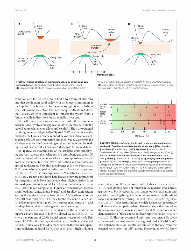
0 0.5 1.0 1.5 2.0
0 1 2 3 4 5
0 2 4 6 8 10
0 20 40 60 80 100 %
E/Eoffset (%)
uniaxial [100](%)
biaxial(001) (%)
GexSn1-x (Sn%)
FiGURe 2 | Relative offset of the Γ- and L-conduction band minima realized in Ge either by uniaxial tensile strain along [100] direction [dark blue: (Capellini et al., 2013), light blue: (Nam et al., 2013; Sukhdeo et al., 2014), olive: (Süess et al., 2013; Geiger et al., 2014c)], biaxial tensile strain on (001) oriented substrate [black: (Liu et al., 2010); violet: (Ghrib et al., 2013, 2015)] or by alloying with Sn [yellow: (Chen et al., 2013a); orange (Gupta et al., 2013b); red: (wirths et al., 2015)]. The shown offset versus Sn concentration relates to the unstrained case. About 100% (0%) offset refers to 140 meV (vanishing energy offset). Hence, the dash-dotted line marks the transition from an indirect to a direct band gap semiconductor.
July 2015 | Volume 2 | Article 5282
Geiger et al. Group IV direct band gap photonics
Frontiers in Materials | www.frontiersin.org
condition also for Ge, we need to find a way to inject electrons into that conduction band valley with its energetic minimum at the Γ-point. This is realized in the most straightforward fashion when all unwanted electron levels are energetically shifted above the Γ-states, which is equivalent to transfer the system from a fundamentally indirect to a fundamentally direct one.
We will discuss the two methods that make this conversion possible. One involves the application of tensile strain, while the second approach relies on alloying Ge with Sn. Thus, the obtained band alignments are depicted in Figure 1C. With either one of the methods, the Γ-valley can be reduced below the indirect one at L enabling efficient carrier injection into the Γ-valley. Moreover, the VB degeneracy is lifted depending on the strain state and its load-ing, biaxial or uniaxial, c.f. Section “Modeling” for more details.
In Figure 2, we show the state-of-the-art of the strain and alloy-ing approach toward the realization of a direct band gap group IV material. For our discussion, we selected those approaches that are potentially compatible with CMOS fabrication and are suited for optical applications. Very thin membranes (Sánchez-Pérez et al., 2011), nanowires clamped in bulky mechanical strain apparatus (Greil et al., 2012), Ge bulk layers on III–V substrates (Huo et al., 2011), etc., are not considered here because they are unpractical for integration on Si. Not considered either is light emission from Si-based quantum wells and defects; for a recent review, see Saito et al. (2014). In our compilation, Figure 2, we benchmark the two strain loadings (uniaxial and biaxial) and Sn alloy composition against the achieved relative band offset, ΔE/E0, where an offset ΔE of 100% is equal to E0 ~ 140 meV for the case of unstrained Ge. An offset parameter of 0 meV (0%) corresponds, thus, to Γ- and L-valleys having their band edges at the same energy.
The black arrow on the left hand side of the second line in Figure 2 marks the case of highly n-doped Ge (Liu et al., 2010), where a maximum of 0.25% biaxial strain is accomplished. This value of 0.25% is the one typically obtained from direct epitaxy of Ge on Si. It arises due to the difference between the thermal expan-sion coefficients of Si and Ge (Michel et al., 2010). High n-doping
heavy hole
light hole
Offset > kT
indirect valley
L
direct valley
Γindirect valley
L
heavy hole
light hole
Offset 0.14 eV
momentum transfer
direct valley
Γ
momentum space
heavy hole
light hole
CONDUCTION BAND
VALENCE BANDS
direct valley
Γ
A B C
FiGURe 1 | Band structure in momentum space (A) direct band gap semiconductor. Electron/hole recombination occurs at the Γ-point. (B) Unstrained Ge. Electrons occupy the conduction band states of the
L-valleys. Radiative recombination is hindered by the momentum mismatch. (C) Due to strain (or alloying with Sn), the band gap of Ge (GeSn) shrinks and the population of electrons at the Γ-point increases.
is introduced to fill the parasitic indirect states (Xiaochen et al., 2010). Such doping does not transform the material into a direct gap system, but it appeared that under optical excitation and electrical pumping the light emission shows an intensity threshold as well as linewidth narrowing (Liu et al., 2010; Camacho-Aguilera et al., 2012). These results became widely known as the optically and electrically pumped Ge-laser. However, since the time when these announcements were made in 2010 and 2012, only one other demonstration of these effects has been reported so far (Koerner et al., 2015). This very recent and only result concerns a Ge diode structure with an unstrained active region doped at 3 × 1019 cm−3. The obtained emission spectra are similar to the one from the original work from the MIT group. However, as we will show

July 2015 | Volume 2 | Article 5283
Geiger et al. Group IV direct band gap photonics
Frontiers in Materials | www.frontiersin.org
below, these spectra significantly differ in several aspects – the intensity, the linewidth, and the Fabry–Perot (FP) multi-mode behavior – from those obtained with the here discussed direct band gap lasers. Moreover, as will be discussed in Section “Lifetime, Gain, and Loss,” these Ge-lasing observations are contradicted by gain experiments (Carroll et al., 2012) as well as by theoretical analysis performed by several groups (Liu et al., 2007; Chow, 2012; Dutt et al., 2012; Peschka et al., 2015) when the lasing cur-rent density threshold is calculated using realistic non-radiative lifetimes (Geiger et al., 2014a). As the experimental foundation for understanding this peculiar threshold behavior of low strained (and in one case even unstrained) Ge is ambiguous, we will focus here on reports concerning direct band gap group IV systems, which includes the first unmistakable proof of interband lasing in a group IV system. Without doubt, with the advent of direct band gap systems showing unambiguous lasing, an excellent opportunity is created, which will help to unravel in the very near future above raised questions regarding the lasing in highly n-doped Ge.
Coming back to Figure 2: the arrows colored in violet depict 1.0 and 1.5% biaxially tensilely strained structures that have been achieved via deposition of Si–Nitride (SiN) stressor layers (Ghrib et al., 2013, 2015). This strain is equivalent to a band offset of ~70 and 30 meV, which corresponds to 50 and 30% of the unstrained band offset value, respectively. So far, the highest strain values are obtained in suspended microbridges under uniaxial loading as is shown on the top stroke. There, the ~0.25% biaxial prestrain is enhanced and transformed into uniaxial strain. The arrows in olive (Süess et al., 2013; Geiger et al., 2014c) and blue (Nam et al., 2013; Sukhdeo et al., 2014) mark recent achievements from the two leading groups. The latest result (Sukhdeo et al., 2014) indicates that the bridge technology can indeed provide direct band gap strained Ge. SiN stressor layers on suspended microbridges or FP cavities deliver far less strain and offset reductions (Capellini et al., 2013, 2014). As shown by the red arrows on the third stroke, alloying Ge with Sn also provides optical group IV material with a fundamental direct band gap. The transition from fundamental indirect to direct occurs at a Sn concentration of ~9% for relaxed GeSn. Depending on the strain loading, i.e., tensile or compressive, the crossover shifts to a higher or lower Sn concentration. Hence, a 20-nm thick GeSn layer with 8% Sn sandwiched between Ge claddings and processed into microdisks is not as close to the direct transition as a relaxed layer with 6% Sn because of the −1% biaxial compressive loading (Chen et al., 2013a). The GeSn alloy above the crossover in Figure 2 exhibits 0.7% in-plane strain at a Sn concentration of 13%. This system shows lasing at low temperature (Wirths et al., 2015). We will present this recent result and will, thereby, clarify the characteristic of the experimental observation of lasing.
The availability of direct band gap group IV semiconductors as compiled in Figure 2, together with the rise of promising results, in particular, the demonstration of lasing in the GeSn system, has motivated the writing of this review. It is meant to present the current understanding evoked from the research undertaken at many places worldwide. Although some of the following descrip-tions are exemplified for only one of the systems (strain or Sn alloying), we will argue that the physics of this two direct gap systems can be understood by analogy. By merely emphasizing the
similarities of the physics and the characterization methods used for investigations, we hope to provide a comprehensive overview that will support and interest many scientists to enter this highly relevant field of research.
In Section “Direct Band Gap Group IV Materials,” the band structure in Ge is given in dependence of strain. We then sum-marize the fabrication steps for strain engineering and Sn alloying. In Section “Characterization Methods: Optical Properties,” several optical characterization methods are introduced, such as pump and probe spectroscopy developed for this very purpose at the infrared beamline of the Swiss light source (SLS). Gain and loss studies performed on Ge layers as well as carrier lifetime measurements are shown in Section “Lifetime, Gain, and Loss.” These results impact the discussion on lasing in n-doped Ge, which is briefly repeated to exemplify the capability of these experimental methods. The analysis of temperature-dependent photoluminescence (PL) is found to deliver a quantitative measure for the directness of GeSn layers, shown in Section “Photoluminescence – Direct Band Gap,” and narrow emission spectra together with an intensity versus exci-tation-threshold represent the first observation of lasing in a direct band gap group IV system, shown in Section “Optically Pumped Laser.” Investigation challenges, such as the quantitative analysis of the Auger recombination and the carrier transport, are appointed in Section “Challenges” together with other fundamental device-related issues, such as cavity design, band gap renormalization, and thermal budgets for alloys. We speculate about the opportunities for Si photonics offered by an efficient monolithically integrated laser source in Section “Opportunities,” and furthermore discuss the prospect of a Ge and/or GeSn electro-optical data processing platform. We conclude in Section “Conclusion and Outlook” and give a short outlook.
Direct Band Gap Group iv Materials
ModelingBand StructureThe effect of tensile strain on Ge’s band edges shown in Figure 3 illustrates the path of the transitions’ energies going from an indi-rect to a direct band gap system. The energies for interband- (solid lines) and intervalence-band transitions (broken lines) between the respective conduction- and valence-band edges are calculated via deformation potential theory as implemented in the nextnano® modeling software (Birner et al., 2007). Due to the fact that the Γ-valley energy reduces faster than the one of the L-valley, Ge transforms into a direct band gap semiconductor at ~4.7% uniaxial strain along [100] when the direct transition (black line) decreases below the energy of the indirect recombination (green line). For Ge under biaxial tensile strain or GeSn alloys, the band edges behave similarly with an indirect-to-direct band gap crossover at ~1.6–2.0% strain (El Kurdi et al., 2010; Virgilio et al., 2013; Wen and Bellotti, 2015) or and at a Sn-content of ~9% (Low et al., 2012; Gupta et al., 2013b; Wirths et al., 2015) for a fully relaxed layer.
In the valence band, strain lifts the degeneracy of light hole and heavy hole bands and introduces a mixing such that this distinc-tion becomes meaningless, especially under high strain. For low strain, VB1 and VB2 in Figure 3 are mostly “heavy hole”- and
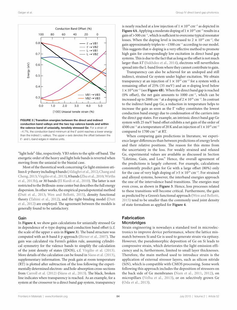
FiGURe 3 | Transition energies between the direct and indirect conduction band valleys and the two top valence bands and within the valence band of uniaxially, tensilely stressed Ge. For a strain of ~4.7%, the conduction band minimum at the Γ-point reaches a lower energy than the indirect L-valleys. The upper x-axis denotes the offset between the Γ- and L-band edges in relative units.
July 2015 | Volume 2 | Article 5284
Geiger et al. Group IV direct band gap photonics
Frontiers in Materials | www.frontiersin.org
“light hole”-like, respectively. VB3 refers to the split-off band. The energetic order of the heavy and light hole bands is reverted when moving from the uniaxial to the biaxial case.
Most of the theoretical work concerning Ge light emission uti-lizes k ·p theory including 6 bands (Aldaghri et al., 2012; Chang and Cheng, 2013; Virgilio et al., 2013), 8 bands (Zhu et al., 2010; Wirths et al., 2013b), or 30 bands (El Kurdi et al., 2010). The latter is not restricted to the Brillouin-zone center but describes the full energy dispersion. In other works, the empirical pseudopotential method (Dutt et al., 2013; Wen and Bellotti, 2015), density functional theory (Tahini et al., 2012), and the tight-binding model (Dutt et al., 2012) are employed. The agreement between the models is generally found to be satisfactory.
GainIn Figure 4, we show gain calculations for uniaxially stressed Ge in dependence of n-type doping and conduction band offset (c.f. the scale of the upper x-axis in Figure 3). The band structure was computed with an 8-band k·p approach (Birner et al., 2007). The gain was calculated via Fermi’s golden rule, assuming cylindri-cal symmetry for the valence bands to simplify the calculation of the joint density of states (JDOS), c.f. Virgilio et al. (2013). More details of the calculation can be found in Süess et al. (2013), supplementary information. The peak gain at room temperature (RT) is plotted after subtraction of the loss following the experi-mentally determined electron- and hole-absorption cross-sections from Carroll et al. (2012) (Süess et al., 2013). The black, broken line indicates when transparency is reached. As an example, for a system at the crossover to a direct band gap system, transparency
is nearly reached at a low injection of 1 × 1018 cm−3 as depicted in Figure 4A. Applying a moderate doping of 1 × 1019 cm−3 results in a gain of >500 cm−1, which is sufficient to overcome typical resonator losses. When the doping level is increased to 2 × 1019 cm−3, the gain approximately triples to ~1500 cm−1 according to our model. This suggests that n-doping is a very effective method to promote high gain for correspondingly low excitation in direct band gap systems. This is due to the fact that as long as the offset is not much larger than kT (Sukhdeo et al., 2014), electrons will nevertheless spread into the L-band from where they cannot contribute to gain.
Transparency can also be achieved for an undoped and still indirect, strained Ge system under higher excitation. We obtain transparency at an injection of 1 × 1019 cm−3 for a system with a remaining offset of 25% (35 meV) and an n-doping level below 1 × 1018cm−3 (see Figure 4B). When the direct band gap is reached (0% offset), the net gain amounts to 1000 cm−1, which can be increased up to 2000 cm−1 at a doping of 2 × 1019 cm−3. In contrast to the indirect band gap Ge, a reduction in temperature helps to increase the gain as soon as the Γ valley constitutes the lowest conduction band energy due to condensation of the carriers into the direct gap states. For example, an intrinsic direct band gap Ge system with 25 meV band offset exhibits a net gain of the order of 4500 cm−1 at a temperature of 20 K and an injection of 1 × 1019 cm−3 compared to 1700 cm−1 at RT.
When comparing gain predictions in literature, we experi-ence larger differences than between predictions of energy levels and their relative positions. The reason for this stems from the uncertainty in the loss. For weakly strained and relaxed Ge, experimental values are available as discussed in Section “Lifetime, Gain, and Loss.” Hence, the overall agreement of the predictions is largely coherent. For example, calculations consistently predict gain for Ge with a large offset (80%) only for the case of very high doping of >5 × 1019 cm−3. For strained and alloyed systems, however, the interband energies approach the one of the intervalence band transitions. The energies may even cross, as shown in Figure 3. Hence, loss processes related to these transitions will become critical. Furthermore, the gain as predicted by a Green’s functional approach (Wen and Bellotti, 2015) tend to be smaller than the commonly used joint density of state formalism as applied for Figure 4.
FabricationMicrobridgesStrain engineering is nowadays a standard tool in microelec-tronics to improve device performance, where the lattice mis-match between Si and Ge is used to generate strain via epitaxy. However, the pseudomorphic deposition of Ge on Si leads to compressive strain, which deteriorates the light emission effi-ciency and is, furthermore, limited to small layer thicknesses. Therefore, the main method used to introduce strain is the application of external stressor layers, such as silicon nitride (SiN), which is compatible with CMOS processing. Some work following this approach includes the deposition of stressors on the back side of Ge membranes (Nam et al., 2011, 2012), on micropillars (Velha et al., 2013), or on selectively grown Ge (Oda et al., 2013).
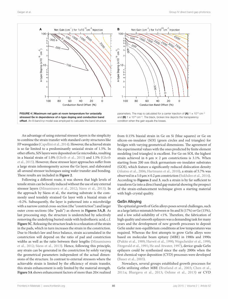
FiGURe 4 | Maximum net gain at room temperature for uniaxially stressed Ge in dependence of n-type doping and conduction band offset. An 8-band k·p model was employed to calculate the band structure
parameters. The map is calculated for a carrier injection of (A) 1 × 1018 cm−3 and (B) 1 × 1019 cm−3. The black, broken line depicts the transparency condition when the gain equals the losses.
July 2015 | Volume 2 | Article 5285
Geiger et al. Group IV direct band gap photonics
Frontiers in Materials | www.frontiersin.org
An advantage of using external stressor layers is the simplicity to combine the strain transfer with standard cavity structures like FP waveguides (Capellini et al., 2014). However, the achieved strain is so far limited to a predominantly uniaxial strain of 1.5%. In other efforts, SiN layers were deposited on Ge microdisks, resulting in a biaxial strain of 1.0% (Ghrib et al., 2013) and 1.5% (Ghrib et al., 2015). However, these stressor layer approaches suffer from a large strain inhomogeneity across the Ge layer, and elaborated all-around stressor techniques using wafer transfer and bonding. These results are included in Figure 2.
Following a different route, it was shown that high levels of tensile strain can be locally induced without the use of any external stressor layers (Minamisawa et al., 2012; Süess et al., 2013). In the approach by Süess et al., the starting substrate is the com-monly used tensilely strained Ge layer with a biaxial strain of ~0.2%. Subsequently, the layer is patterned into a microbridge with a narrow central cross-section (the “constriction”) and larger outer cross-sections (the “pads”) as shown in Figures 5A,B. As last processing step, the structure is underetched by selectively removing the underlying buried oxide with hydrofluoric acid, c.f. Figure 5C. Releasing the structure leads to a relaxation of the strain in the pads, which in turn increases the strain in the constriction. Due to Hooke’s law and force balance, strain accumulated in the constriction will depend on the ratio of pad and constriction widths as well as the ratio between their lengths (Minamisawa et al., 2012; Süess et al., 2013). Hence, following this principle, any strain can be generated in the constriction by solely varying the geometrical parameters independent of the actual dimen-sions of the structure. In contrast to external stressors where the achievable strain is limited by the efficiency of strain transfer, this strain enhancement is only limited by the material strength. Figure 5A shows enhancement factors of more than 20× realized
from 0.15% biaxial strain in Ge on Si (blue squares) or Ge on silicon-on-insulator (SOI) (green circles and red triangles) for bridges with varying geometrical dimensions. The agreement of the experimental values with the ones predicted by finite element modeling (red triangles) is excellent. For Ge on SOI, the highest strain achieved in 6 μm × 2 μm constrictions is 3.1%. When starting from 200 nm thick germanium-on-insulator substrates (GOI), which feature a significantly reduced dislocation density (Akatsu et al., 2006; Hartmann et al., 2010), a strain of 5.7% was observed in a 5.0 μm × 0.2 μm constriction (Sukhdeo et al., 2014). According to Figures 2 and 3, such a strain is by far sufficient to transform Ge into a direct band gap material showing the prospect of the strain-enhancement technique given a starting material with high-crystal quality.
GeSn AlloyingThe epitaxial growth of GeSn alloys poses several challenges, such as a large lattice mismatch between α-Sn and Si (17%) or Ge (15%), and a low solid-solubility of <1%. Therefore, the fabrication of high quality and smooth epilayers was a demanding task for many years and the development of new growth processes to deposit GeSn under non-equilibrium conditions at low temperatures was required. Whereas the first attempts to grow GeSn alloys were based on molecular beam epitaxy (MBE) in 1980s and 1990s (Pukite et al., 1989; Harwit et al., 1990; Wegscheider et al., 1990; Fitzgerald et al., 1991; He and Atwater, 1997), device-grade GeSn epilayers could be synthesized since the early 2000s when the first chemical vapor deposition (CVD) processes were developed (Bauer et al., 2003).
Nowadays, several groups established growth processes for GeSn utilizing either MBE (Bratland et al., 2003; Chen et al., 2011a; Bhargava et al., 2013; Oehme et al., 2013) or CVD

Electron-beam lithography
RIEetching
Wetetching
ε (%)
Mod
el e
nhan
cem
ent
Exp. strain (%)
Model strain (%
)
Exp. enhancement
Ge/Si: analyticalGe/SOI: analyticalGe/SOI: FEM
0 1 2 3 4
25
20
15
10
5
00 5 10 15 20 25
0
1
2
3
44
3.5
2.5
1.5
0.5
3
2
1
0
A B
C
FiGURe 5 | Suspended microbridges from thermally pre-strained Ge. (A) Experimental and modeled strain for Ge microbridges fabricated on Si and SOI. The analytical strain-enhancement model is given in Süess et al. (2013). The enhancement of 22× corresponds to 3.1% uniaxial strain (Süess et al., 2013).
(B) Strain profile of a suspended bridge structure as obtained by finite element modeling (FEM). Due to the relaxation in the pads, the strain in the central constriction is enhanced. (C) Process flow for the fabrication of suspended microbridges.
July 2015 | Volume 2 | Article 5286
Geiger et al. Group IV direct band gap photonics
Frontiers in Materials | www.frontiersin.org
(Vincent et al., 2011; Chen et al., 2013b; Wirths et al., 2013a; Xu et al., 2013; Du et al., 2014) for a variety of applications, e.g., photodiodes, photodetectors, or MOSFETs. Here, due to the reduced lattice mismatch compared to Si, Ge is preferred as virtual substrate (VS) in order to ensure layers of high monocrys-talline quality. Regarding the epitaxial growth of direct band gap GeSn alloys, nearly strain relaxed or even tensilely strained layers are highly desired, since for compressively strained GeSn layers, i.e., GeSn coherently grown on Ge VS, higher Sn contents are necessary for the indirect to direct transition (Gupta et al., 2013b). Owing to an advantageous relaxation mechanism for GeSn layers on Ge VS, dislocations seem to mostly protrude into the Ge VS rather than into the GeSn layer, which is beneficial for optical properties as the density of non-radiative recombina-tion centers is reduced (Takeuchi et al., 2006; Senaratne et al., 2014; Wirths et al., 2015). Although relaxation takes place, a certain level of compressive biaxial strain (typically between −0.6 to −0.8%) remains nevertheless, which, as already said in connection with Figure 2, shifts the indirect-to-direct band gap crossover to higher Sn concentrations with respect to fully relaxed GeSn. Therefore, several approaches are being followed to reduce the compressive strain, such as growth on lattice-matched InGaAs VS (Chen et al., 2011a), which is not acceptable within a CMOS processing line, or deposition of ever thicker layers to enforce further strain relaxation (Senaratne et al., 2014; Wirths et al., 2015). Gupta et al. (2013b) introduced a robust etching approach enabling to selectively dry etch the Ge VS underneath
the epitaxial GeSn layers. The authors envision their method to enable the fabrication of direct band gap GeSn micro disks.
Figures 6A–C show transmission electron microscopy images of a GeSn layer with 13% Sn grown via reduced pressure CVD on a Ge VS (Wirths et al., 2015). The advantageous relaxation mecha-nism mentioned above can be seen here with dislocation-loops (blue arrows) emitted into the Ge VS. Despite the high-Sn content, the thickness of the GeSn layer could be increased up to 560 nm without deteriorating the high-crystalline quality. Owing to the large thickness, a relaxation of 60% could be achieved such that only a mild compressive strain of −0.6% was present. As will be shown in Section “Photoluminescence – Direct Band Gap,” this epilayer was proven to be a direct band gap group IV semiconductor that provides net gain and, hence, shows lasing under optical pumping.
We conclude this section on the fabrication of GeSn alloys by summarizing the list of beneficial assets GeSn epitaxy brings to the current Si technology facilitating future developments and integra-tion. Apart from the prospect to fabricate a fundamental direct band gap group IV material, GeSn alloys are attractive because of (i) low-temperature deposition on Si(001) compatible with existing CMOS processes; (ii) strain relaxation with reasonably low thread-ing dislocation density; (iii) available option for selective growth on silicon, which is attractive for photonic integration; (iv) GeSn/SiGeSn heterojunction layers to generate carrier confinement in quantum wells; (v) and therefore, tunability of the lattice constant offering opportunities to combine the alloys with the strained membrane method.

FiGURe 6 | Cross-sectional transmission electron microscopy (TeM) image of a Ge0.87Sn0.13 alloy. (A) Expanded view showing the high-crystalline quality of the GeSn epilayer. The defects are located near the interface to the Ge virtual substrate. (B) Dislocation-loops (blue arrows) emitted below the
GeSn/Ge-interface (orange arrows) penetrating only into the Ge virtual substrate. (C) High-resolution TEM image of the interface used for Burgers vector calculations. Lomer dislocations with b = a/2[110] are observed (Wirths et al., 2015).
July 2015 | Volume 2 | Article 5287
Geiger et al. Group IV direct band gap photonics
Frontiers in Materials | www.frontiersin.org
Characterization Methods: Optical Properties
Lifetime, Gain, and LossWhen describing a material with regards to its suitability as an efficient laser source, key properties that decide upon adequacy are the gain and loss, i.e., the material’s ability to amplify light, as well as the non-radiative lifetime, which determines the internal quantum efficiency as well as the achievable steady-state carrier density. These characteristics can be extracted in a direct way using broadband, time-resolved pump–probe transmission, and reflection spectroscopy. Possible ways for performing such experi-ments could be via tunable lasers or supercontinuum sources. However, particularly synchrotron-based infrared pump–probe spectroscopy has been shown to offer advantageous conditions for measuring the carrier density, their lifetime as well as gain and loss due to its extended bandwidth and suitable pulse lengths (Carroll et al., 2012; Geiger et al., 2014a,b). At the infrared beamline of the SLS, 100 ps long pulses of infrared light are supplied from the synchrotron and serve as broadband probe pulses, whereas the excess charge carriers are optically excited by a 100 ps Nd:YAG laser at 1064 nm (Carroll et al., 2011). The delay time between pump and probe pulses can be varied electronically, which offers the possibility to follow the dynamics of a system over a long time period by probing at different times after excitation. In the follow-ing, we review some of the pump–probe measurements performed at the SLS and give the most important results that challenge the
interpretation of the Ge-lasing observations. We renarrate this discussion at the end of this chapter.
Figure 7A shows the mid-infrared reflection of a Ge layer grown on Si plotted as the ratio of pumped (RP) and unpumped (RU) reflection signal. The different colors depict different opti-cal excitation strengths between 1 and 160 MW cm−2. All of the spectra were taken for a pump–probe delay time of 250 ps. The distinct minimum observed in the spectra is attributed to the carriers’ plasma frequency. For an increasing excitation power, the minimum shifts to higher energy and becomes at the same time more pronounced. As the plasma frequency shifts in first order proportional to the square root of the total amount of charge carriers in the system, such reflection measurements facilitate a convenient method for the quantitative determination of the carrier density. Thus, the extracted carrier concentration in dependence of the optical pump power for delay times of 0 and 250 ps is shown in the inset of Figure 7A. Moreover, by analyzing the carrier density at a fixed pump power for varying delay times, the reflection spectra can be used to extract the carrier decay times. In the case shown here, the carrier density drops to ~4 × 1019 cm−3 within 250 ps for all generated carrier concentrations larger than 4 × 1019 cm−3. This behavior indicates an increasingly faster decay time at high-carrier concentrations, which is attributed to Auger recombination (Carroll et al., 2012).
While the analysis of mid-infrared reflection spectra enables to directly access charge carrier concentration and decay time, the latter can also be extracted from near-infrared transmission
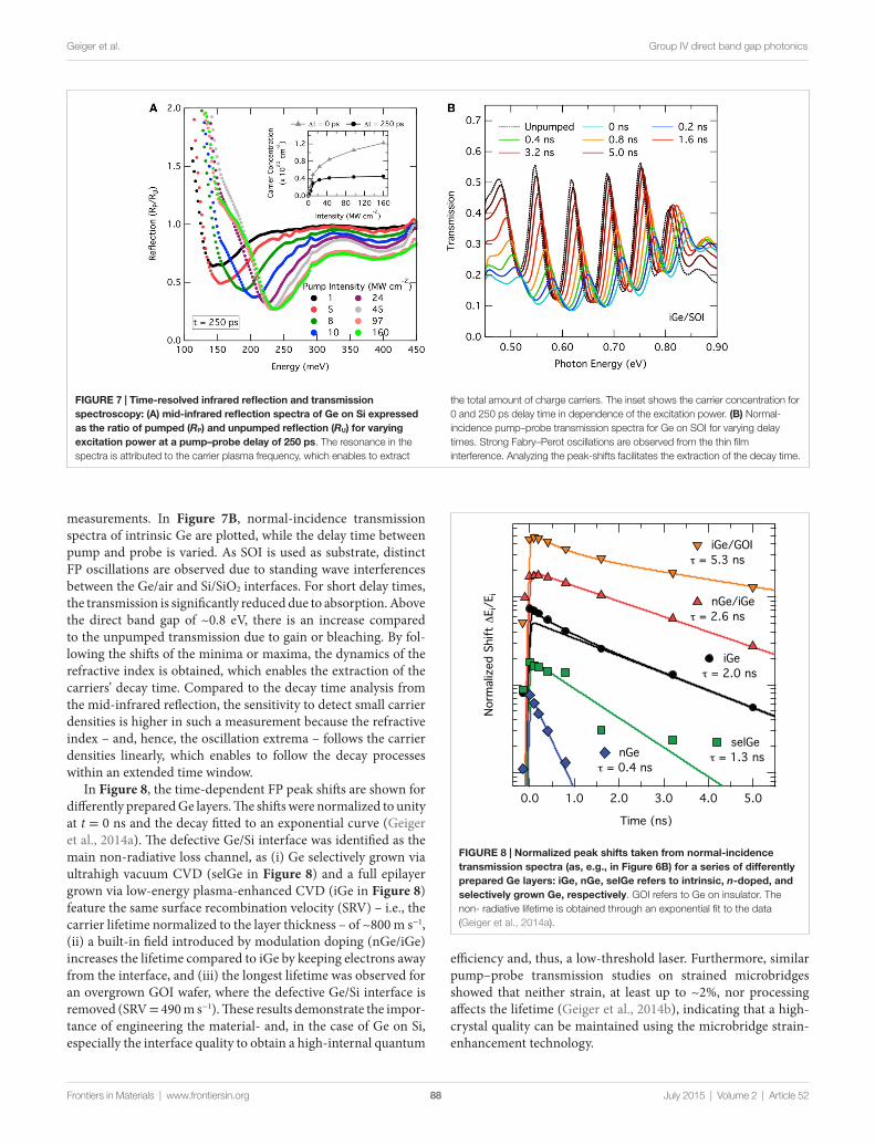
FiGURe 8 | Normalized peak shifts taken from normal-incidence transmission spectra (as, e.g., in Figure 6B) for a series of differently prepared Ge layers: iGe, nGe, selGe refers to intrinsic, n-doped, and selectively grown Ge, respectively. GOI refers to Ge on insulator. The non- radiative lifetime is obtained through an exponential fit to the data (Geiger et al., 2014a).
FiGURe 7 | Time-resolved infrared reflection and transmission spectroscopy: (A) mid-infrared reflection spectra of Ge on Si expressed as the ratio of pumped (RP) and unpumped reflection (RU) for varying excitation power at a pump–probe delay of 250 ps. The resonance in the spectra is attributed to the carrier plasma frequency, which enables to extract
the total amount of charge carriers. The inset shows the carrier concentration for 0 and 250 ps delay time in dependence of the excitation power. (B) Normal-incidence pump–probe transmission spectra for Ge on SOI for varying delay times. Strong Fabry–Perot oscillations are observed from the thin film interference. Analyzing the peak-shifts facilitates the extraction of the decay time.
July 2015 | Volume 2 | Article 5288
Geiger et al. Group IV direct band gap photonics
Frontiers in Materials | www.frontiersin.org
measurements. In Figure 7B, normal-incidence transmission spectra of intrinsic Ge are plotted, while the delay time between pump and probe is varied. As SOI is used as substrate, distinct FP oscillations are observed due to standing wave interferences between the Ge/air and Si/SiO2 interfaces. For short delay times, the transmission is significantly reduced due to absorption. Above the direct band gap of ~0.8 eV, there is an increase compared to the unpumped transmission due to gain or bleaching. By fol-lowing the shifts of the minima or maxima, the dynamics of the refractive index is obtained, which enables the extraction of the carriers’ decay time. Compared to the decay time analysis from the mid-infrared reflection, the sensitivity to detect small carrier densities is higher in such a measurement because the refractive index – and, hence, the oscillation extrema – follows the carrier densities linearly, which enables to follow the decay processes within an extended time window.
In Figure 8, the time-dependent FP peak shifts are shown for differently prepared Ge layers. The shifts were normalized to unity at t = 0 ns and the decay fitted to an exponential curve (Geiger et al., 2014a). The defective Ge/Si interface was identified as the main non-radiative loss channel, as (i) Ge selectively grown via ultrahigh vacuum CVD (selGe in Figure 8) and a full epilayer grown via low-energy plasma-enhanced CVD (iGe in Figure 8) feature the same surface recombination velocity (SRV) – i.e., the carrier lifetime normalized to the layer thickness – of ~800 m s−1, (ii) a built-in field introduced by modulation doping (nGe/iGe) increases the lifetime compared to iGe by keeping electrons away from the interface, and (iii) the longest lifetime was observed for an overgrown GOI wafer, where the defective Ge/Si interface is removed (SRV = 490 m s−1). These results demonstrate the impor-tance of engineering the material- and, in the case of Ge on Si, especially the interface quality to obtain a high-internal quantum
efficiency and, thus, a low-threshold laser. Furthermore, similar pump–probe transmission studies on strained microbridges showed that neither strain, at least up to ~2%, nor processing affects the lifetime (Geiger et al., 2014b), indicating that a high-crystal quality can be maintained using the microbridge strain-enhancement technology.

A B C
FiGURe 9 | Analysis of pump and probe measurements. (A) Transmission spectra for Ge on Si measured under Brewster angle for different delay times. (B) Modeled direct gap absorption unpumped (blue, thick line) and pumped (red, thick line) as well as pump-induced
absorption (red, thin line) obtained from the spectra in (A) at 0 time delay. (C) Similar extraction of direct gap gain and losses for undoped InGaAs showing light amplification, as the gain surpasses the pump-induced losses (Carroll et al., 2012).
July 2015 | Volume 2 | Article 5289
Geiger et al. Group IV direct band gap photonics
Frontiers in Materials | www.frontiersin.org
For the analysis of gain and loss, the transmission spectra should be recorded under the Brewster angle such that the obstructing FP resonances do not occur, c.f. Figure 9A for the case of unstrained Ge on Si for different pump–probe delay times. Δt = 0 ps refers to the maximum overlap between pump and probe and, hence, to the highest carrier density. The thick lines in blue and red show modeled transmission spectra for the unpumped and pumped case. Under excitation, a strong absorp-tion occurs with a linear dependence on energy. At the direct band gap, the absorption gets reduced due to gain, but the gain is too small to generate a negative absorption and, hence, light amplification. This situation holds true for all other delay times, i.e., carrier concentrations, as well.
In Figure 9B, the situation for Δt = 0 ps is shown again in terms of the absorption coefficient with the modeled functions being plotted separately for (i) direct gap absorption before pumping (blue, thick line), (ii) direct gap absorption under excitation (red, thick line), and (iii) the featureless pump-induced absorption decreasing linearly in energy (red, thin line). Even though a gain of ~850 cm−1 is observed as displayed by a negative absorption, the loss from that spectrally distributed absorption at the same energy is >6000 cm−1 making light amplification impossible. To show the contrast to an established laser material featuring a direct band gap, the same absorption properties are plotted in Figure 9C for the case of InGaAs. Here, the pump-induced losses are independent on energy and amount to ~1000 cm−1, which is compensated by a direct gap gain of ~1700 cm−1 such that a net gain of 700 cm−1 is revealed. We should mention here that the theoretical analysis of Carroll et al. (2012) has been questioned (Dutt et al., 2012) concerning the strength of the gain (red line, Figure 9B) but not the experiments, which clearly show that the loss is by far larger than the gain.
From the preceding analysis, it is clear that a solid understand-ing and consideration of the loss processes is required for an accurate description of gain in Ge. For illustration, the absorp-tion cross-sections for three Ge samples (Ge#1: Nd = 0, εxx = 0; Ge#2: Nd = 2.5 × 1019 cm−3, εxx = 0; Ge#3: Nd = 0, εxx = 0.25%) are plotted in Figure 10 in dependence of the total carrier density NT = Nd + NP, where Nd refers to the doping concentration and NP to the pump-induced carrier density. As a comparison, the cross-sections of three InGaAs layers (InGaAs#1: Nd = 0, InGaAs#2: Nd = 5.3 × 1018 cm−3; InGaAs#3: Nd = 2.1 × 1019 cm−3) are plotted as well. Therefore, Figure 10 reveals that the absorption scales pre-dominantly with NP indicating that the absorption cross-section from holes σh is much larger than the cross-section for electrons σe. Indeed, describing the absorption via a linearly dependent cross-section as α = σeNe + σhNh (where subscripts e and h refer to electrons and holes, respectively) offers a good representation of the experimental data with σh/σe > 10. The absorption cross-section for holes is significantly larger than for electrons, because in addition to the non-momentum conserving intraband or Drude-type free carrier absorption, the holes can undergo vertical intervalence band transitions (Newman and Tyler, 1957), which are hereby identified as the main loss channel in Ge. A similar conclusion concerning the cross-section ratio can be deduced from the InGaAs data shown in Figure 10 in agreement with common knowledge for direct band gap lasing materials (Adams et al., 1980; Childs et al., 1986). Furthermore, the absolute values of the hole cross-section are in a similar range but larger for InGaAs than for Ge, c.f. Figure 10. However, the absorption is much higher in Ge due to a much larger total carrier density needed to achieve a gain like in the InGaAs sample.
Finally, we would like to relate the above presented data of gain and loss as well as of lifetimes in Ge layers on Si to the observation

0.60.0
5000
4000
3000
2000
1000
0
mc(
noit
pros
bA
decudni-
pmuP
1-)
1.61.20.80.40.0
NT x 1020 ( cm )-3
Ge#1 Ge#2 Ge#3
InGaAs#1 InGaAs#2 InGaAs#3
Linear Fits
FiGURe 10 | Absorption coefficients for differently doped and strained Ge and inGaAs layers. The data are well described with a linear absorption cross-section model.
July 2015 | Volume 2 | Article 5290
Geiger et al. Group IV direct band gap photonics
Frontiers in Materials | www.frontiersin.org
of lasing in highly n-doped and weakly strained Ge (Liu et al., 2010; Camacho-Aguilera et al., 2012), which was recently repeated at the University of Stuttgart with an unstrained, highly n-doped light emitting diode (LED) (Koerner et al., 2015). First, as is shown above by the gain and loss experiment (Carroll et al., 2011), the loss in Ge layers strongly exceeds the gain at all the investigated carrier densities up to 1020 cm−3 and in all investigated cases, i.e., Ge with and without weak strain and/or n-doping. Hence, Carroll’s results are apparently in conflict with the observation of lasing (Liu et al., 2010) in similar but not identical material. Second, the non-radiative lifetimes, which have been determined for such Ge layers only recently by Geiger et al. (2014a), c.f Figure 8, shine a new light on previous and recent gain and threshold current density calculations (Dutt et al., 2012; Peschka et al., 2015). Using the obtained carrier lifetime of the order of 1–2 ns for thresh-old current estimates, the calculated threshold of the order of 100 kA cm−2 – obtained by assuming a lifetime of 100 ns – needs to be rescaled by a factor of 50–100. Surely, such a current density is above the material’s limit and also exceeds the observed threshold values by ~2 orders of magnitude. Therefore, not only the gain/loss experiments but also the theory (when fed with properly valued parameters) shows that more research is needed to understand the MIT results. The recent paper by the Stuttgart group (Koerner et al., 2015) may give the directions for further thinking: a “lasing” threshold was reached only shortly before their devices failed, hinting at a carrier breakthrough. The heat pulse related to the breakthrough may have caused the peaked emission signal.
Photoluminescence – Direct Band GapPhotoluminescence spectroscopy offers a convenient tool for prob-ing the changes of the electronic band structure induced via strain or Sn alloying. As shown in Figure 11A, the reduced offset between Γ- and L-valleys manifests in an increased emission intensity of the PL signal (Süess et al., 2013). A similar effect has also been observed by Chen et al. (2011a).
A quantitative analysis of the relative alignment between Γ- and L can be obtained from the temperature dependence of the
PL, as has been demonstrated recently in Wirths et al. (2015). In Figure 11B, the temperature-dependent PL intensity for a set of samples with Sn content from 8 to 13% is shown. The data have been normalized to unity at 300 K. For the sample with the lowest Sn content, a rapid drop in intensity on lowering the temperature is observed, whereas for the three other samples a steady increase in intensity can be seen with the intensity increase being dependent on the Sn concentration. Qualitatively, the increase from sample to sample can be explained by the reduced conduction band offset with increasing Sn, whereas cooling down leads to a condensation of the carriers into the lowest energy states such that the direct gap emission either vanishes for indirect band gap materials as sample Ge0.92Sn0.08 because the Γ valley is not populated anymore or increases strongly when the electrons condense at the minimum of the Γ valley. To quantify the band offsets for the set of GeSn samples, the emission efficiency is calculated via a similar JDOS model as the one used for calculating the gain in Figure 4. Therein, the offset ΔE between Γ- and L-valleys as well as the injected charge carrier density Ni represent the free fitting parameters. Furthermore, the temperature dependence of the lifetime is assumed to be identi-cal for all samples and follows the Shockley–Read–Hall (SRH) recombination characteristics (Shockley and Read, 1952; Schubert, 2006) that describes non-radiative recombination via trap states. Using this model, an excellent agreement with the experimental data is obtained (Wirths et al., 2015). The GeSn sample with 13% Sn content is, hence, identified as a true direct band gap group IV semiconductor with its Γ-valley being 25 meV below the indirect L-valleys. From the second fit parameter, a RT carrier density Ni of 4 × 1017 cm−3 is deduced consistent with a carrier lifetime of 0.35 ns, which corresponds to a SRV of 570 m s−1. This value is close to the ones reported for elemental Ge on Si (Geiger et al., 2014a), c.f. Figure 8, which is an indication of the high-crystalline quality of the investigated GeSn epilayers.
The temperature dependence of the non-radiative carrier lifetime is obtained as:
t t t t= + + − 1 1 1SRH Auger1( / / / )0 (1)
where τ0 describes the lifetime at low temperature, and τSRH describes the decay due to the capture of charge carriers by mid-gap states, i.e., τSRH = A × (1 + cosh(ET/kT)). τAuger describes the Auger recombination time, which can be neglected here due to the low-carrier densities. Furthermore, ET is the difference between the trap level energy and the intrinsic Fermi-level, k is the Boltzmann con-stant, and A is to normalize τ to 0.35 ns at 300 K as obtained from the temperature-dependent PL. For ΔE = 19 meV and τ0 = 2.1 ns, a good agreement between the extracted lifetimes and the lifetime model is obtained (Wirths et al., 2015). For temperatures >50 K, there is a drastic decrease in carrier lifetime from ~2 ns to 350 ps for higher temperatures. As the temperature dependence of this process is well described via the SRH model, the lifetime decay is attributed to the capture of carriers via mid-gap states originating from defects (Wirths et al., 2015). These defects could potentially be related to defects located at the GeSn/Ge-interface (Geiger et al., 2013; Wirths et al., 2015), but further studies are needed to unambiguously identify the origin of this deterioration and, subsequently, improve the material quality.

A B
FiGURe 11 | Photoluminescence investigation of strained Ge and GeSn alloys. (A) Room-temperature PL spectra for Ge samples with increasing uniaxial strain up to 3.1%. The inset shows the good agreement between the experimental and modeled band edges. (B) Temperature-dependent integrated PL intensity normalized to unity at 300 K for a series of GeSn layers with Sn-content ranging from 8 to 13%. An increase in
Sn-concentration leads to a more pronounced increase in intensity. The offset between Γ- and L-valleys is extracted from JDOS modeling (solid lines), which reveals Ge0.87Sn0.13 to have a fundamental, direct band gap. The inset shows the experimentally extracted non-radiative lifetime modeled with a Shockley–Read–Hall-like temperature dependence (red line).
July 2015 | Volume 2 | Article 5291
Geiger et al. Group IV direct band gap photonics
Frontiers in Materials | www.frontiersin.org
Optically Pumped LaserAccording to the modeling results shown in Section “Modeling,” a direct band gap Ge-based system should feature a net gain and, hence, enable light amplification at low excitation. In the previ-ous analysis of low-temperature PL on GeSn alloys in Section “Photoluminescence – Direct Band Gap,” a fundamental direct band gap could be identified for a Sn content of 13% in a strain-relaxed layer with 0.7% compressive biaxial strain. To show lasing, a 560-nm epilayer of such Ge0.87Sn0.13 material was grown providing an overlap of 60% for the fundamental transverse electric mode in a 5 μm wide FP cavity (Wirths et al., 2015). For this layer, modal gain could be observed at 20 K via the variable-stripe-length (VSL) method under pulsed optical excitation at 1064 nm with a dif-ferential gain of ≈0.4 cm kW−1 and a threshold excitation density of ≈325 kW cm−2 (c.f. Figure 12). Above threshold, the gain increases linearly with excitation and can easily pass 100 cm−1. The stripe length-dependent PL analysis is a widely applied technique to measure net modal gain, but it does not allow to resolve the gain and loss as by pump and probe spectroscopy. More evidentially, a gain statement, such as provided by Figure 12, becomes respected only after showing lasing.
Indeed, when pumping a FP cavity over its full length, a strongly enhanced emission and narrowing of the line spectra is observed as soon as the modal gain surpasses the cavity losses. This behavior is shown in Figure 13 where the edge-emission spectra from a 1-mm long FP cavity at 20 K are plotted for vary-ing optical excitation powers. The curves are offset for clarity. The threshold obtained from the lasing experiments matches well with the one obtained from the VSL method. For an excitation density of 1 MW cm−2, lasing could be observed up to 90 K. This
temperature is equivalent to the temperature range where the lifetime was found to drop substantially from ~2 ns to 350 ps. Hence, it is tempting to attribute the limitation of lasing to temperatures <100 K to the carrier capture by defect-induced mid-gap states, as has appealed from the analysis shown in Figure 11B, inset. However, carrier transfer to the L-valleys and carrier out diffusion into the Ge may be a determining factor, as well.
Despite the breakthrough of presenting for the first time a direct band gap group IV material that is lasing under optical pumping, there still remain open questions. For example, with an excitation power of 325 kW cm−2, a non-radiative lifetime of 2 ns, as shown in Figure 11, and a typical absorbance of 1 × 104 cm−1 at 1064 nm, a steady-state carrier density of ~3.5 × 1019 cm−3 is estimated. With this number, the gain at low temperature from our model is found to be >5000 cm−1. And, interpolating from Figure 4, at excitation density of 0.6 × 1018 cm−3 we would expect for a system with positive offset of about 15%, a material gain of ~300 cm−1 at RT. We assign this large discrepancy from what is observed at low temperature and what a RT calculation predicts to resonant intervalence band absorption. As mentioned above, due to the lack of experimental data for direct gap Ge or GeSn, the energy dependence of the loss as measured by pump–probe experiments for Ge (Carroll et al., 2012) has been used for Figure 4. Its proper inclusion possibly adds significant contribution to the loss (Wen and Bellotti, 2015).
In order to improve such gain calculations, which critically depend on the knowledge of the band structure, mappings of the entire valence, and conduction band in reciprocal space would cer-tainly be highly valuable. This could be possible via angle-resolved

FiGURe 13 | Lasing emission spectra measured from the facet of a 5-μm wide and 1 mm long FP waveguide cavity under optical pumping at 20 K. A clear threshold behavior can be observed in the spectra with respect to output intensity and linewidth, c.f. inset to the right and left hand side, respectively.
A B
FiGURe 12 | Gain extraction via the variable-stripe-length method (vSL). (A) Edge-emitted intensity of Ge0.87Sn0.13 at 20 K in dependence of the pumped waveguide length for varying excitation densities. The modal gain is
extracted by an exponential fit to the data. (B) Differential gain extracted from the spectra in (A) indicating a linear dependence on excitation density with a threshold at 325 kW cm−2.
July 2015 | Volume 2 | Article 5292
Geiger et al. Group IV direct band gap photonics
Frontiers in Materials | www.frontiersin.org
photoelectron spectroscopy (ARPES) at high energy (Gray et al., 2011) or the soft x-ray regime (Strocov et al., 2014). Other promis-ing experimental techniques not covered because of lack of space include lifetime measurements via time-resolved PL measure-ments (He and Atwater, 1997; Nam et al., 2014; Saito et al., 2014).
In fact, similar lifetimes for Ge as obtained from synchrotron measurements (Geiger et al., 2014a) were found (Nam et al., 2014).
Challenges
In the previous section, we reviewed experiments and results related to the dependence of the optical properties on strain and alloying of Ge with Sn. Furthermore, we summarized investiga-tions concerning the first lasing of a direct band gap group IV semiconductor and expounded on the temperature dependence of the PL as a powerful tool to determine the directness of a group IV material. We illustrated optical methods based on pump and probe spectroscopy using synchrotron light to determine the carrier lifetime, gain, and loss under optical pumping related to the injected carrier density.
Future experiments along these lines on both, the strained Ge system and GeSn alloys at various strain and Sn concentration, respectively, will allow to establish the fundamentals of lasing in direct band gap group IV systems. The impact of doping on gain, loss, and carrier lifetime should also be addressed in dependence of the directness of the respective system to verify the picture elucidated by Figure 4 of Section “Gain.”
As an example, intervalence band absorption, Auger recom-bination, and the electrical injection are some of the many fundamental aspects of group IV direct band gap lasing pending to be understood and quantified.
intervalence Band AbsorptionOne of the most essential parameters determining the efficiency of a laser is associated to the parasitic absorption due to the injected holes (Adams et al., 1980; Childs et al., 1986). As shown
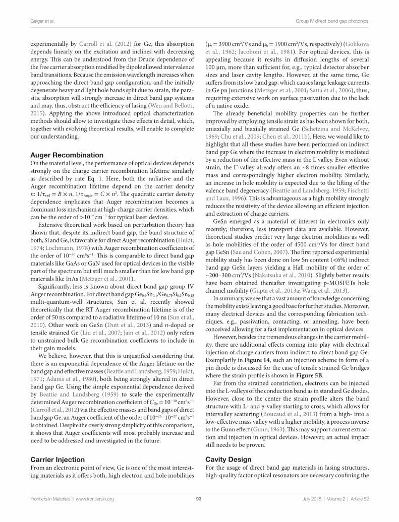
July 2015 | Volume 2 | Article 5293
Geiger et al. Group IV direct band gap photonics
Frontiers in Materials | www.frontiersin.org
experimentally by Carroll et al. (2012) for Ge, this absorption depends linearly on the excitation and inclines with decreasing energy. This can be understood from the Drude dependence of the free carrier absorption modified by dipole allowed intervalence band transitions. Because the emission wavelength increases when approaching the direct band gap configuration, and the initially degenerate heavy and light hole bands split due to strain, the para-sitic absorption will strongly increase in direct band gap systems and may, thus, obstruct the efficiency of lasing (Wen and Bellotti, 2015). Applying the above introduced optical characterization methods should allow to investigate these effects in detail, which, together with evolving theoretical results, will enable to complete our understanding.
Auger RecombinationOn the material level, the performance of optical devices depends strongly on the charge carrier recombination lifetime similarly as described by rate Eq. 1. Here, both the radiative and the Auger recombination lifetime depend on the carrier density n: 1/τrad = B × n, 1/τAuger = C × n2. The quadratic carrier density dependence implicates that Auger recombination becomes a dominant loss mechanism at high-charge carrier densities, which can be the order of >1019 cm−3 for typical laser devices.
Extensive theoretical work based on perturbation theory has shown that, despite its indirect band gap, the band structure of both, Si and Ge, is favorable for direct Auger recombination (Huldt, 1974; Lochmann, 1978) with Auger recombination coefficients of the order of 10−30 cm6s−1. This is comparable to direct band gap materials like GaAs or GaN used for optical devices in the visible part of the spectrum but still much smaller than for low band gap materials like InAs (Metzger et al., 2001).
Significantly, less is known about direct band gap group IV Auger recombination. For direct band gap Ge0.9Sn0.1/Ge0.75Si0.1Sn0.15 multi-quantum-well structures, Sun et al. recently showed theoretically that the RT Auger recombination lifetime is of the order of 50 ns compared to a radiative lifetime of 10 ns (Sun et al., 2010). Other work on GeSn (Dutt et al., 2013) and n-doped or tensile strained Ge (Liu et al., 2007; Jain et al., 2012) only refers to unstrained bulk Ge recombination coefficients to include in their gain models.
We believe, however, that this is unjustified considering that there is an exponential dependence of the Auger lifetime on the band gap and effective masses (Beattie and Landsberg, 1959; Huldt, 1971; Adams et al., 1980), both being strongly altered in direct band gap Ge. Using the simple exponential dependence derived by Beattie and Landsberg (1959) to scale the experimentally determined Auger recombination coefficient of CGe = 10−30 cm6s−1 (Carroll et al., 2012) via the effective masses and band gaps of direct band gap Ge, an Auger coefficient of the order of 10−26–10−27 cm6s−1 is obtained. Despite the overly strong simplicity of this comparison, it shows that Auger coefficients will most probably increase and need to be addressed and investigated in the future.
Carrier injectionFrom an electronic point of view, Ge is one of the most interest-ing materials as it offers both, high electron and hole mobilities
(μe = 3900 cm2/Vs and μh = 1900 cm2/Vs, respectively) (Golikova et al., 1962; Jacoboni et al., 1981). For optical devices, this is appealing because it results in diffusion lengths of several 100 μm, more than sufficient for, e.g., typical detector absorber sizes and laser cavity lengths. However, at the same time, Ge suffers from its low band gap, which causes large leakage currents in Ge pn junctions (Metzger et al., 2001; Satta et al., 2006), thus, requiring extensive work on surface passivation due to the lack of a native oxide.
The already beneficial mobility properties can be further improved by employing tensile strain as has been shown for both, uniaxially and biaxially strained Ge (Schetzina and McKelvey, 1969; Chu et al., 2009; Chen et al., 2011b). Here, we would like to highlight that all these studies have been performed on indirect band gap Ge where the increase in electron mobility is mediated by a reduction of the effective mass in the L valley. Even without strain, the Γ-valley already offers an ~8 times smaller effective mass and correspondingly higher electron mobility. Similarly, an increase in hole mobility is expected due to the lifting of the valence band degeneracy (Beattie and Landsberg, 1959; Fischetti and Laux, 1996). This is advantageous as a high mobility strongly reduces the resistivity of the device allowing an efficient injection and extraction of charge carriers.
GeSn emerged as a material of interest in electronics only recently; therefore, less transport data are available. However, theoretical studies predict very large electron mobilities as well as hole mobilities of the order of 4500 cm2/Vs for direct band gap GeSn (Sau and Cohen, 2007). The first reported experimental mobility study has been done on low Sn content (<6%) indirect band gap GeSn layers yielding a Hall mobility of the order of ~200–300 cm2/Vs (Nakatsuka et al., 2010). Slightly better results have been obtained thereafter investigating p-MOSFETs hole channel mobility (Gupta et al., 2013a; Wang et al., 2013).
In summary, we see that a vast amount of knowledge concerning the mobility exists leaving a good base for further studies. Moreover, many electrical devices and the corresponding fabrication tech-niques, e.g., passivation, contacting, or annealing, have been conceived allowing for a fast implementation in optical devices.
However, besides the tremendous changes in the carrier mobil-ity, there are additional effects coming into play with electrical injection of charge carriers from indirect to direct band gap Ge. Exemplarily in Figure 14, such an injection scheme in form of a pin diode is discussed for the case of tensile strained Ge bridges where the strain profile is shown in Figure 5B.
Far from the strained constriction, electrons can be injected into the L-valleys of the conduction band as in standard Ge diodes. However, close to the center the strain profile alters the band structure with L- and γ-valley starting to cross, which allows for intervalley scattering (Boucaud et al., 2013) from a high- into a low-effective mass valley with a higher mobility, a process inverse to the Gunn effect (Gunn, 1963). This may support current extrac-tion and injection in optical devices. However, an actual impact still needs to be proven.
Cavity DesignFor the usage of direct band gap materials in lasing structures, high-quality factor optical resonators are necessary confining the
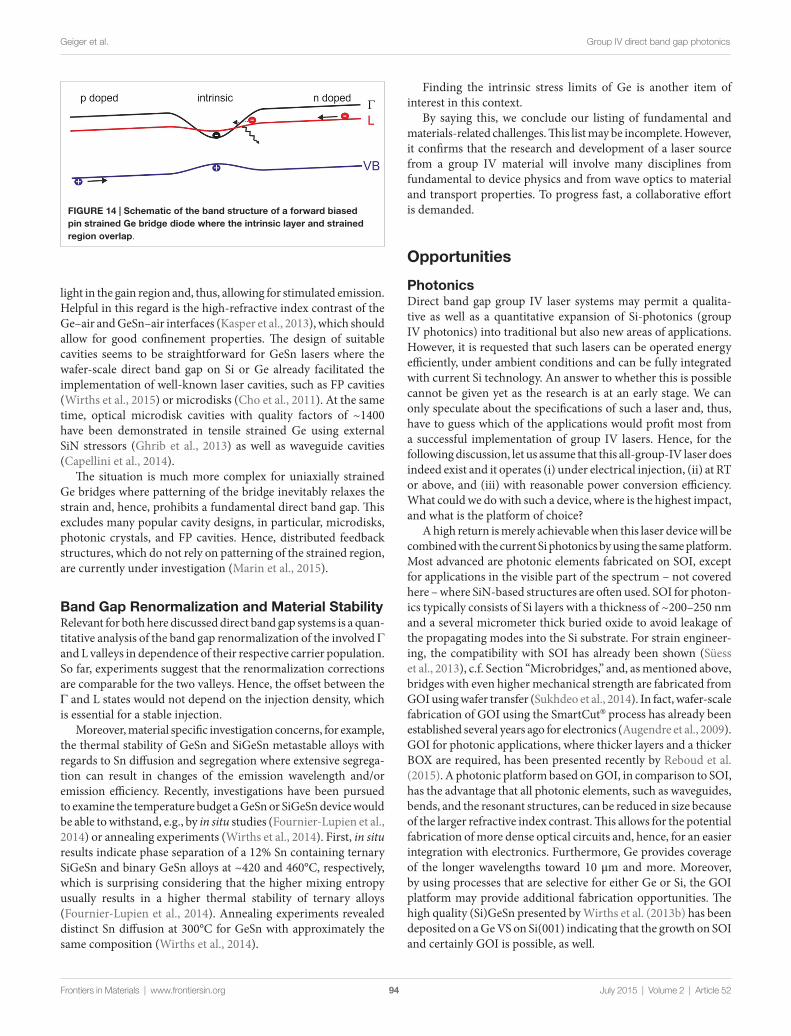
FiGURe 14 | Schematic of the band structure of a forward biased pin strained Ge bridge diode where the intrinsic layer and strained region overlap.
July 2015 | Volume 2 | Article 5294
Geiger et al. Group IV direct band gap photonics
Frontiers in Materials | www.frontiersin.org
light in the gain region and, thus, allowing for stimulated emission. Helpful in this regard is the high-refractive index contrast of the Ge–air and GeSn–air interfaces (Kasper et al., 2013), which should allow for good confinement properties. The design of suitable cavities seems to be straightforward for GeSn lasers where the wafer-scale direct band gap on Si or Ge already facilitated the implementation of well-known laser cavities, such as FP cavities (Wirths et al., 2015) or microdisks (Cho et al., 2011). At the same time, optical microdisk cavities with quality factors of ~1400 have been demonstrated in tensile strained Ge using external SiN stressors (Ghrib et al., 2013) as well as waveguide cavities (Capellini et al., 2014).
The situation is much more complex for uniaxially strained Ge bridges where patterning of the bridge inevitably relaxes the strain and, hence, prohibits a fundamental direct band gap. This excludes many popular cavity designs, in particular, microdisks, photonic crystals, and FP cavities. Hence, distributed feedback structures, which do not rely on patterning of the strained region, are currently under investigation (Marin et al., 2015).
Band Gap Renormalization and Material StabilityRelevant for both here discussed direct band gap systems is a quan-titative analysis of the band gap renormalization of the involved Γ and L valleys in dependence of their respective carrier population. So far, experiments suggest that the renormalization corrections are comparable for the two valleys. Hence, the offset between the Γ and L states would not depend on the injection density, which is essential for a stable injection.
Moreover, material specific investigation concerns, for example, the thermal stability of GeSn and SiGeSn metastable alloys with regards to Sn diffusion and segregation where extensive segrega-tion can result in changes of the emission wavelength and/or emission efficiency. Recently, investigations have been pursued to examine the temperature budget a GeSn or SiGeSn device would be able to withstand, e.g., by in situ studies (Fournier-Lupien et al., 2014) or annealing experiments (Wirths et al., 2014). First, in situ results indicate phase separation of a 12% Sn containing ternary SiGeSn and binary GeSn alloys at ~420 and 460°C, respectively, which is surprising considering that the higher mixing entropy usually results in a higher thermal stability of ternary alloys (Fournier-Lupien et al., 2014). Annealing experiments revealed distinct Sn diffusion at 300°C for GeSn with approximately the same composition (Wirths et al., 2014).
Finding the intrinsic stress limits of Ge is another item of interest in this context.
By saying this, we conclude our listing of fundamental and materials-related challenges. This list may be incomplete. However, it confirms that the research and development of a laser source from a group IV material will involve many disciplines from fundamental to device physics and from wave optics to material and transport properties. To progress fast, a collaborative effort is demanded.
Opportunities
PhotonicsDirect band gap group IV laser systems may permit a qualita-tive as well as a quantitative expansion of Si-photonics (group IV photonics) into traditional but also new areas of applications. However, it is requested that such lasers can be operated energy efficiently, under ambient conditions and can be fully integrated with current Si technology. An answer to whether this is possible cannot be given yet as the research is at an early stage. We can only speculate about the specifications of such a laser and, thus, have to guess which of the applications would profit most from a successful implementation of group IV lasers. Hence, for the following discussion, let us assume that this all-group-IV laser does indeed exist and it operates (i) under electrical injection, (ii) at RT or above, and (iii) with reasonable power conversion efficiency. What could we do with such a device, where is the highest impact, and what is the platform of choice?
A high return is merely achievable when this laser device will be combined with the current Si photonics by using the same platform. Most advanced are photonic elements fabricated on SOI, except for applications in the visible part of the spectrum – not covered here – where SiN-based structures are often used. SOI for photon-ics typically consists of Si layers with a thickness of ~200–250 nm and a several micrometer thick buried oxide to avoid leakage of the propagating modes into the Si substrate. For strain engineer-ing, the compatibility with SOI has already been shown (Süess et al., 2013), c.f. Section “Microbridges,” and, as mentioned above, bridges with even higher mechanical strength are fabricated from GOI using wafer transfer (Sukhdeo et al., 2014). In fact, wafer-scale fabrication of GOI using the SmartCut® process has already been established several years ago for electronics (Augendre et al., 2009). GOI for photonic applications, where thicker layers and a thicker BOX are required, has been presented recently by Reboud et al. (2015). A photonic platform based on GOI, in comparison to SOI, has the advantage that all photonic elements, such as waveguides, bends, and the resonant structures, can be reduced in size because of the larger refractive index contrast. This allows for the potential fabrication of more dense optical circuits and, hence, for an easier integration with electronics. Furthermore, Ge provides coverage of the longer wavelengths toward 10 μm and more. Moreover, by using processes that are selective for either Ge or Si, the GOI platform may provide additional fabrication opportunities. The high quality (Si)GeSn presented by Wirths et al. (2013b) has been deposited on a Ge VS on Si(001) indicating that the growth on SOI and certainly GOI is possible, as well.

July 2015 | Volume 2 | Article 5295
Geiger et al. Group IV direct band gap photonics
Frontiers in Materials | www.frontiersin.org
With a laser device implemented on the currently used SOI or similarly on GOI, various new applications will emerge. Before speculating, we may picture the many already existing photonic elements. To select a few: Low-loss (<1 dB cm−1) single mode waveguides in various designs, tapers to adiabatically match the waveguide modes to fibers, and low-loss grating couplers (<1 dB) in 1D or 2D providing polarization splitting. Other standard elements include directional couplers, Mach Zehnder interfer-ometers, ring resonators, and light modulators based on free carrier injections or quantum confined Stark effect. Detectors based on slightly tensile strained (0.2%) Ge provide more than 10 GHz speed for high-data rate transmission. Other device elements include add-drop filters, buffers, and switches, which can be integrated with fluidic channels for (bio-) sensing. The short wavelength infrared at which the here discussed group IV direct band gap lasers emit (see Figure 3) is certainly a clear asset for sensing applications (Soref, 2010; Nedeljkovic et al., 2013).
Silicon-on-insulator is (and GOI could become) a very conveni-ent platform to realize high-performing photonic crystal structures enabling unique photonic circuits, such as compact high-Q cavi-ties, which can operate stably at single and dual-wavelength, and as wavelength division multiplexer as desired for optical signal processing. This listing can be extended almost indefinitely, nam-ing, e.g., switching and steering of optical signals, slow light, pulse compression, customized reflectors, and filters. Together with the expectation that such photonic circuits will be very cost effective, compact, reliable, and efficient, a monolithically integrated laser source will certainly bring new functionality, in particular when optics can be merged with electronics.
CMOS integrationThe combination of optics with CMOS electronics to realize an on-chip data distribution network (Heck and Bowers, 2014) is – without any doubt – one of the most advanced and chal-lenging applications for direct band gap group IV lasers. The requirements are so complex (Miller, 2009) that before the start of such a development, many fundamental questions have to be answered, such as the efficiency issues among other challenges, which have been addresses in the previous section. However, once these hurdles are taken, we expect to arise a highly competi-tive and attractive platform solution for future data processing applications. In fact, the extension of CMOS by integration of Ge and (Si)GeSn may not just resolve the demands for a monolithic laser gain medium, but, as discussed widely elsewhere (Kao et al., 2014), (Si)GeSn would already advance the performance of the electronic circuits. This appealing double benefit, together with the potential compatibility to CMOS of such an all-group-IV solution, bears an essential advantage in comparison to other emerging technologies, such as spin- and/or valley-based elec-tronics, which rely in part on non-conform chemical elements and non-CMOS fabrication processes.
Hence, we expect that as soon as the fundamental lessons of direct band gap lasing are learnt and a gain medium well-qualified for injection pumping at RT is defined, research and development of a new opto-electronic platform will quickly advance. Experts in CMOS technology, group IV epitaxy, laser
physics, and Si electronics and photonics will cooperate and define the routes to opto-electronics for fast and energy-efficient data processing.
Conclusion and Outlook
We reviewed the methods for achieving a direct band gap in group IV semiconductors in the most promising material system for the prospect of a Si compatible laser, namely, Ge modified either via tensile strain or by alloying with Sn. We expanded on the methods to characterize these systems and gave examples on their optical properties. The recent advances in numerous approaches to achieve a direct band gap have finally concluded in the first demonstration of lasing in a direct band gap GeSn alloy (Wirths et al., 2015).
With this demonstration, we are at the beginning of an excit-ing journey in the field of silicon photonics. As shown in great detail, the many optical characterization tools at hand allow us to address a large amount of fundamental questions, including band gap renormalization, various recombination processes, and doping level-dependent lasing performance, but also material- and technology-related issues, such as high Q-factor cavity design, diffusive carrier transport, stress, and thermal diffusion limits.
We hope that with outlining these challenges, we can motivate a vast amount of new researchers from various backgrounds in optics, material science, and device physics to join this interesting research field. We believe that combined efforts will converge in a reasonable time to a demonstration of a practical laser source being electrically pumped, highly efficient, and fully integrated on an electro-optical CMOS platform. This building block will finally pave the way for true monolithic on-chip integration of photonics and CMOS electronics for new sensors in the long wavelength infrared, and will eventually enable to build an on-chip or off-chip electro-optical data distribution network for high-performance computing.
Acknowledgments
We would like to acknowledge the many scientific collaborators we were fortunate to work with over the last few years. They supported us in building up a strong portfolio in the investiga-tion and understanding of lasing in group IV systems, and the fabrication of direct band gap group IV materials. In particular, we thank our previous group members Gustav Schiefler, Martin J. Süess, and Renato Minamisawa for their contributions, which led to this appealing strain concept, and the group of Dan Buca (FZ Jülich), who contacted us for investigating their high quality material and thus gave us the opportunity to learn also about GeSn alloys. The tremendous progress achieved in a short time is a shining example of our good collaboration. We also thank Jérôme Faist and Ralph Spolenak (ETHZ) for their whole-hearted support to this subject and their many essential contributions. Finally, we acknowledge the Swiss Science Foundation (SNF) for supporting part of the here reviewed studies over several years.

July 2015 | Volume 2 | Article 5296
Geiger et al. Group IV direct band gap photonics
Frontiers in Materials | www.frontiersin.org
References
Adams, A. R., Asada, M., Suematsu, Y., and Arai, S. (1980). The temperature dependence of the efficiency and threshold current of In 1- xGa xAs yP 1- y lasers related to intervalence band absorption. Jpn. J. Appl. Phys. 19, L621–L624. doi:10.1143/JJAP.19.L621
Akatsu, T., Deguet, C., Sanchez, L., Allibert, F., Rouchon, D., Signamarcheix, T., et al. (2006). Germanium-on-insulator (GeOI) substrates – a novel engineered substrate for future high performance devices. Mater. Sci. Semicond. Process. 9, 444–448. doi:10.1016/j.mssp.2006.08.077
Aldaghri, O., Ikonic , Z., and Kelsall, R. W. (2012). Optimum strain configurations for carrier injection in near infrared Ge lasers. J. Appl. Phys. 111, 053106. doi:10.1063/1.3691790
Augendre, E., Sanchez, L., Benaissa, L., Signamarcheix, T., Hartmann, J.-M., Le Royer, C., et al. (2009). Challenges and progress in germanium-on-insulator materials and device development towards ULSI integration. ECS Trans. 25, 351–362. doi:10.1149/1.3203972
Bauer, M. R., Tolle, J., Bungay, C., Chizmeshya, A. V. G., Smith, D. J., Menéndez, J., et al. (2003). Tunable band structure in diamond-cubic tin-germanium alloys grown on silicon substrates. Solid State Commun. 127, 355–359. doi:10.1016/S0038-1098(03)00446-0
Beattie, A. R., and Landsberg, P. T. (1959). Auger effect in semiconductors. Proc. R. Soc. A Math. Phys. Eng. Sci. 249, 16–29. doi:10.1098/rspa.1959.0003
Bhargava, N., Coppinger, M., Gupta, J. P., Wielunski, L., and Kolodzey, J. (2013). Lattice constant and substitutional composition of GeSn alloys grown by molecular beam epitaxy. Appl. Phys. Lett. 103, 041908. doi:10.1063/1.4816660
Birner, S., Zibold, T., Andlauer, T., Kubis, T., Sabathil, M., Trellakis, A., et al. (2007). Nextnano: general purpose 3-D simulations. IEEE Trans. Electron Devices 54, 2137–2142. doi:10.1109/TED.2007.902871
Boucaud, P., Kurdi El, M., Ghrib, A., Prost, M., de Kersauson, M., Sauvage, S., et al. (2013). Recent advances in germanium emission. Photon. Res. 1, 102. doi:10.1364/PRJ.1.000102
Bratland, K., Foo, Y., Soares, J., Spila, T., Desjardins, P., and Greene, J. (2003). Mechanism for epitaxial breakdown during low-temperature Ge(001) molecular beam epitaxy. Phys. Rev. B 67, 125322. doi:10.1103/PhysRevB.67.125322
Camacho-Aguilera, R. E., Cai, Y., Patel, N., Bessette, J. T., Romagnoli, M., Kimerling, L. C., et al. (2012). An electrically pumped germanium laser. Opt. Express 20, 11316. doi:10.1364/OE.20.011316
Capellini, G., Kozlowski, G., Yamamoto, Y., Lisker, M., Wenger, C., Niu, G., et al. (2013). Strain analysis in SiN/Ge microstructures obtained via Si-complementary metal oxide semiconductor compatible approach. J. Appl. Phys. 113, 013513. doi:10.1063/1.4772781
Capellini, G., Reich, C., Guha, S., Yamamoto, Y., Lisker, M., Virgilio, M., et al. (2014). Tensile Ge microstructures for lasing fabricated by means of a silicon complemen-tary metal-oxide-semiconductor process. Opt. Express 22, 399–410. doi:10.1364/OE.22.000399
Carroll, L., Friedli, P., Lerch, P., Schneider, J., Treyer, D., Hunziker, S., et al. (2011). Ultra-broadband infrared pump-probe spectroscopy using synchrotron radiation and a tuneable pump. Rev. Sci. Instrum. 82, 063101–063101–9. doi:10.1063/1.3592332
Carroll, L., Friedli, P., Neuenschwander, S., Sigg, H., Cecchi, S., Isa, F., et al. (2012). Direct-gap gain and optical absorption in germanium correlated to the density of photoexcited carriers, doping, and strain. Phys. Rev. Lett. 109, 057402. doi:10.1103/PhysRevLett.109.057402
Chang, G.-E., and Cheng, H. H. (2013). Optical gain of germanium infrared lasers on different crystal orientations. J. Phys. D Appl. Phys. 46, 065103. doi:10.1088/0022-3727/46/6/065103
Chen, R., Gupta, S., Huang, Y.-C., Huo, Y., Rudy, C. W., Sanchez, E., et al. (2013a). Demonstration of a Ge/GeSn/Ge quantum-well microdisk resonator on silicon: enabling high-quality Ge(Sn) materials for micro- and nanophotonics. Nano Lett. 14, 37–43. doi:10.1021/nl402815v
Chen, R., Huang, Y.-C., Gupta, S., Lin, A. C., Sanchez, E., Kim, Y., et al. (2013b). Material characterization of high Sn-content, compressively-strained GeSn epitaxial films after rapid thermal processing. J. Cryst. Growth 365, 29–34. doi:10.1016/j.jcrysgro.2012.12.014
Chen, R., Lin, H., Huo, Y., Hitzman, C., Kamins, T. I., and Harris, J. S. (2011a). Increased photoluminescence of strain-reduced, high-Sn composition Ge1−xSnx alloys grown by molecular beam epitaxy. Appl. Phys. Lett. 99, 181125. doi:10.1063/1.3658632
Chen, Y. T., Lan, H. S., Hsu, W., Fu, Y. C., Lin, J. Y., and Liu, C. W. (2011b). Strain response of high mobility germanium n-channel metal-oxide-semiconductor field-effect transistors on (001) substrates. Appl. Phys. Lett. 99, 022106. doi:10.1063/1.3604417
Childs, G. N., Brand, S., and Abram, R. A. (1986). Intervalence band absorp-tion in semiconductor laser materials. Semicond. Sci. Technol. 1, 116–120. doi:10.1088/0268-1242/1/2/004
Cho, S., Chen, R., Koo, S., Shambat, G., Lin, H., Park, N., et al. (2011). Fabrication and analysis of epitaxially grown Ge1-xSnx microdisk resonator with 20-nm free-spectral range. IEEE Photon. Technol. Lett. 23, 1535–1537. doi:10.1109/LPT.2011.2163929
Chow, W. W. (2012). Model for direct-transition gain in a Ge-on-Si laser. Appl. Phys. Lett. 100, 191113. doi:10.1063/1.4714540
Chu, M., Sun, Y., Aghoram, U., and Thompson, S. E. (2009). Strain: a solution for higher carrier mobility in nanoscale MOSFETs. Annu. Rev. Mater. Res. 39, 203–229. doi:10.1146/annurev-matsci-082908-145312
Du, W., Ghetmiri, S. A., Conley, B. R., Mosleh, A., Nazzal, A., Soref, R. A., et al. (2014). Competition of optical transitions between direct and indirect bandgaps in Ge1−xSnx. Appl. Phys. Lett. 105, 051104. doi:10.1063/1.4892302
Dutt, B., Lin, H., Sukhdeo, D. S., Vulovic, B. M., Gupta, S., Nam, D., et al. (2013). Theoretical analysis of GeSn alloys as a gain medium for a Si-compatible laser. IEEE J. Sel. Top. Quantum Electron. 19, 1502706–1502706. doi:10.1109/JSTQE.2013.2241397
Dutt, B., Sukhdeo, D. S., Nam, D., Vulovic, B. M., Ze, Y., and Saraswat, K. C. (2012). Roadmap to an efficient germanium-on-silicon laser: strain vs. n-type doping. IEEE Photon. J. 4, 2002–2009. doi:10.1109/JPHOT.2012.2221692
El Kurdi, M., Fishman, G., Sauvage, S., and Boucaud, P. (2010). Band structure and optical gain of tensile-strained germanium based on a 30 band k·p formalism. J. Appl. Phys. 107, 013710. doi:10.1063/1.3279307
Fang, Z., Chen, Q. Y., and Zhao, C. Z. (2013). A review of recent progress in lasers on silicon. Opt. Laser Technol. 46, 103–110. doi:10.1088/0034-4885/76/3/034501
Fischetti, M. V., and Laux, S. E. (1996). Band structure, deformation potentials, and carrier mobility in strained Si, Ge, and SiGe alloys. J. Appl. Phys. 80, 2234–2252. doi:10.1063/1.363052
Fitzgerald, E. A., Xie, Y. H., Green, M. L., Brasen, D., Kortan, A. R., Michel, J., et al. (1991). Totally relaxed GexSi1−x layers with low threading dislocation densities grown on Si substrates. Appl. Phys. Lett. 59, 811. doi:10.1063/1.105351
Fournier-Lupien, J. H., Chagnon, D., Levesque, P., AlMutairi, A. A., Wirths, S., Pippel, E., et al. (2014). In situ studies of germanium-tin and silicon-germanium-tin thermal stability. ECS Trans. 64, 903–911. doi:10.1149/06406.0903ecst
Geiger, R., Frigerio, J., Süess, M. J., Chrastina, D., Isella, G., Spolenak, R., et al. (2014a). Excess carrier lifetimes in Ge layers on Si. Appl. Phys. Lett. 104, 062106–062106. doi:10.1063/1.4865237
Geiger, R., Süess, M. J., Bonzon, C., Frigerio, J., Chrastina, D., Isella, G., et al. (2014b). Carrier Lifetimes in Uniaxially Strained Ge Micro Bridges. IEEE, 227–228.
Geiger, R., Süess, M. J., Bonzon, C., Spolenak, R., Faist, J., and Sigg, H. (2014c). Strained Ge Microbridges to Obtain a Direct Bandgap Laser. IEEE, 7–8.
Geiger, R., Frigerio, J., Süess, M. J., Minamisawa, R. A., Chrastina, D., Isella, G., et al. (2013). Excess Carrier Lifetimes in Ge Layers on Si. IEEE, 103–104.
Ghrib, A., Kurdi El, M., de Kersauson, M., Prost, M., Sauvage, S., Checoury, X., et al. (2013). Tensile-strained germanium microdisks. Appl. Phys. Lett. 102, 221112. doi:10.1364/OE.23.006722
Ghrib, A., Kurdi El, M., Prost, M., Sauvage, S., Checoury, X., Beaudoin, G., et al. (2015). All-around SiN stressor for high and homogeneous tensile strain in germanium microdisk cavities. Adv. Opt. Mater. 3, 353–358. doi:10.1002/adom.201400369
Golikova, O. A., Moizhes, B. Y., and Stilbans, L. S. (1962). Hole mobility of germa-nium as a function of concentration and temperature. Sov. Phys. Solid State 3, 2259–2265.
Gray, A. X., Papp, C., Ueda, S., Balke, B., Yamashita, Y., Plucinski, L., et al. (2011). Probing bulk electronic structure with hard X-ray angle-resolved photoemission. Nat. Mater. 10, 759–764. doi:10.1038/nmat3089
Greil, J., Lugstein, A., Zeiner, C., Strasser, G., and Bertagnolli, E. (2012). Tuning the electro-optical properties of germanium nanowires by tensile strain. Nano Lett. 12, 6230–6234. doi:10.1021/nl303288g
Gunn, J. B. (1963). Microwave oscillations of current in III–V semiconductors. Solid State Commun. 1, 88–91. doi:10.1016/0038-1098(63)90041-3
Gupta, S., Chen, R., Vincent, B., Lin, D., Magyari-Kope, B., Caymax, M., et al. (2013a). (Invited) GeSn channel n and p MOSFETs. ECS Trans. 50, 937–941. doi:10.1149/05009.0937ecst

July 2015 | Volume 2 | Article 5297
Geiger et al. Group IV direct band gap photonics
Frontiers in Materials | www.frontiersin.org
Gupta, S., Magyari-Köpe, B., Nishi, Y., and Saraswat, K. C. (2013b). Achieving direct band gap in germanium through integration of Sn alloying and external strain. J. Appl. Phys. 113, 073707. doi:10.1063/1.4792649
Hartmann, J. M., Sanchez, L., Van Den Daele, W., Abbadie, A., Baud, L., Truche, R., et al. (2010). Fabrication, structural and electrical properties of compressively strained Ge-on-insulator substrates. Semicond. Sci. Technol. 25, 075010. doi:10.1088/0268-1242/25/7/075010
Harwit, A., Pukite, P. R., Angilello, J., and Iyer, S. S. (1990). Properties of diamond structure SnGe films grown by molecular beam epitaxy. Thin Solid Films 184, 395–401. doi:10.1016/0040-6090(90)90437-I
He, G., and Atwater, H. A. (1997). Interband transitions in SnxGe1−xAlloys. Phys. Rev. Lett. 79, 1937–1940. doi:10.1103/PhysRevLett.79.1937
Heck, M. J. R., and Bowers, J. E. (2014). Energy efficient and energy proportional optical interconnects for multi-core processors: driving the need for on-chip sources. IEEE J. Sel. Top. Quantum Electron. 20, 332–343. doi:10.1109/JSTQE.2013.2293271
Huldt, L. (1971). Band-to-band auger recombination in indirect gap semiconductors. Phys. Status Solidi A 8, 173–187. doi:10.1002/pssa.2210080118
Huldt, L. (1974). Auger recombination in germanium. Phys. Status Solidi A 24, 221–229. doi:10.1088/0957-4484/22/43/435401
Huo, Y., Lin, H., Chen, R., Makarova, M., Rong, Y., Li, M., et al. (2011). Strong enhance-ment of direct transition photoluminescence with highly tensile-strained Ge grown by molecular beam epitaxy. Appl. Phys. Lett. 98, 011111. doi:10.1063/1.3534785
Jacoboni, C., Nava, F., Canali, C., and Ottaviani, G. (1981). Electron drift velocity and diffusivity in germanium. Phys. Rev. B 24, 1014–1026. doi:10.1103/PhysRevB.24.1014
Jain, J. R., Hryciw, A., Baer, T. M., Miller, D. A. B., Brongersma, M. L., and Howe, R. T. (2012). A micromachining-based technology for enhancing germanium light emis-sion via tensile strain. Nat. Photonics 6, 398–405. doi:10.1038/nphoton.2012.111
Kao, K.-H., Verhulst, A. S., Rooyackers, R., Douhard, B., Delmotte, J., Bender, H., et al. (2014). Compressively strained SiGe band-to-band tunneling model calibration based on p-i-n diodes and prospect of strained SiGe tunneling field-effect tran-sistors. J. Appl. Phys. 116, 214506. doi:10.1063/1.4903288
Kasper, E., Kittler, M., Oehme, M., and Arguirov, T. (2013). Germanium tin: silicon photonics toward the mid-infrared [Invited]. Photon. Res. 1, 69. doi:10.1364/PRJ.1.000069
Koerner, R., Oehme, M., Gollhofer, M., Schmid, M., Kostecki, K., Bechler, S., et al. (2015). Electrically pumped lasing from Ge Fabry-Perot resonators on Si. Opt. Express 23, 14815–14822. doi:10.1364/OE.23.014815
Liu, J., Sun, X., Camacho-Aguilera, R., Kimerling, L. C., and Michel, J. (2010). Ge-on-Si laser operating at room temperature. Opt. Lett. 35, 679. doi:10.1364/OL.35.000679
Liu, J., Sun, X., Pan, D., Wang, X., Kimerling, L. C., Koch, T. L., et al. (2007). Tensile-strained, n-type Ge as a gain medium for monolithic laser integration on Si. Opt. Express 15, 11272. doi:10.1364/OE.15.011272
Lochmann, W. (1978). Phonon-assisted auger recombination in indirect gap semicon-ductors. Phys. Status Solidi A 45, 423–432. doi:10.1002/pssa.2210450208
Low, K. L., Yang, Y., Han, G., Fan, W., and Yeo, Y.-C. (2012). Electronic band structure and effective mass parameters of Ge1-xSnx alloys. J. Appl. Phys. 112, 103715. doi:10.1063/1.4767381
Marin, E., Bonzon, C., Geiger, R., Zabel, T., Sigg, H., and Faist, J. (2015). Proceedings CLEO-Europe 2015. (in print)
Metzger, W. K., Wanlass, M. W., Ellingson, R. J., Ahrenkiel, R. K., and Carapella, J. J. (2001). Auger recombination in low-band-gap n-type InGaAs. Appl. Phys. Lett. 79, 3272–3274. doi:10.1063/1.1418032
Michel, J., Liu, J., and Kimerling, L. C. (2010). High-performance Ge-on-Si photode-tectors. Nat. Photonics 4, 527–534. doi:10.1038/nphoton.2010.157
Miller, D. A. B. (2009). Device requirements for optical interconnects to silicon chips. Proc. IEEE 97, 1166–1185. doi:10.1109/JPROC.2009.2014298
Miller, D. A. B. (2010). Optical interconnects to electronic chips. Appl. Opt. 49, F59. doi:10.1364/AO.49.000F59
Minamisawa, R. A., Süess, M. J., Spolenak, R., Faist, J., David, C., Gobrecht, J., et al. (2012). Top-down fabricated silicon nanowires under tensile elastic strain up to 4.5%. Nat Commun 3, 1096. doi:10.1038/ncomms2102
Nakatsuka, O., Tsutsui, N., Shimura, Y., Takeuchi, S., Sakai, A., and Zaima, S. (2010). Mobility behavior of Ge1-xSnx layers grown on silicon-on-insulator substrates. Jpn. J. Appl. Phys. 49, 04DA10. doi:10.1143/JJAP.49.04DA10
Nam, D., Kang, J.-H., Brongersma, M. L., and Saraswat, K. C. (2014). Observation of improved minority carrier lifetimes in high-quality Ge-on-insulator using time-resolved photoluminescence. Opt. Lett. 39, 6205. doi:10.1364/OL.39.006205
Nam, D., Sukhdeo, D., Cheng, S.-L., Roy, A., Chih-Yao Huang, K., Brongersma, M., et al. (2012). Electroluminescence from strained germanium membranes and implications for an efficient Si-compatible laser. Appl. Phys. Lett. 100, 131112. doi:10.1063/1.3699224
Nam, D., Sukhdeo, D., Roy, A., Balram, K., Cheng, S.-L., Huang, K. C.-Y., et al. (2011). Strained germanium thin film membrane on silicon substrate for optoelectronics. Opt. Express 19, 25866–25872. doi:10.1364/OE.19.025866
Nam, D., Sukhdeo, D. S., Kang, J.-H., Petykiewicz, J., Lee, J. H., Jung, W. S., et al. (2013). Strain-induced pseudoheterostructure nanowires confining carriers at room temperature with nanoscale-tunable band profiles. Nano Lett. 13, 3118–3123. doi:10.1021/nl401042n
Nedeljkovic, M., Khokhar, A. Z., Hu, Y., Chen, X., Penades, J. S., Stankovic, S., et al. (2013). Silicon photonic devices and platforms for the mid-infrared. Opt. Mater. Express 3, 1205. doi:10.1364/OME.3.001205
Newman, R., and Tyler, W. (1957). Effect of impurities on free-hole infrared absorption in p-type germanium. Phys. Rev. 105, 885–886. doi:10.1103/PhysRev.105.885
Oda, K., Okumura, T., Tani, K., Saito, S.-I., and Ido, T. (2013). Improvement of photo-luminescence from Ge layer with patterned Si3N4 stressors. Thin Solid Films 557, 355–362. doi:10.1016/j.tsf.2013.08.117
Oehme, M., Buca, D., Kostecki, K., Wirths, S., Holländer, B., Kasper, E., et al. (2013). Epitaxial growth of highly compressively strained GeSn alloys up to 12.5% Sn. J. Cryst. Growth 384, 71–76. doi:10.1016/j.jcrysgro.2013.09.018
Passaro, V., Tullio, C., Troia, B., Notte, M., Giannoccaro, G., and Leonardis, F. (2012). Recent advances in integrated photonic sensors. Sensors 12, 15558–15598. doi:10.3390/s121115558
Peschka, D., Thomas, M., Glitzky, A., Nurnberg, R., Gartner, K., Virgilio, M., et al. (2015). Modeling of edge-emitting lasers based on tensile strained germanium microstrips. IEEE Photon. J. 7, 1–15. doi:10.1109/JPHOT.2015.2427093
Pukite, P. R., Harwit, A., and Iyer, S. S. (1989). Molecular beam epitaxy of meta-stable, diamond structure SnxGe1-x alloys. Appl. Phys. Lett. 54, 2142–2144. doi:10.1063/1.101152
Reboud, V., Widiez, J., Hartmann, J.-M., Dias, G. O., Fowler, D., Chelnokov, A., et al. (2015). Structural and optical properties of 200 mm germanium-on- insulator (GeOI) substrates for silicon photonics applications. Proc. SPIE 9367, Silicon Photonics X 2015. doi:10.1117/12.2079393
Saito, S., Gardes, F. Y., Al-Attili, A. Z., Tani, K., Oda, K., Suwa, Y., et al. (2014). Group IV light sources to enable the convergence of photonics and electronics. Front. Mater. 1:15. doi:10.3389/fmats.2014.00015
Sánchez-Pérez, J. R., Boztug, C., Chen, F., Sudradjat, F. F., Paskiewicz, D. M., Jacobson, R. B., et al. (2011). Direct-bandgap light-emitting germanium in tensilely strained nanomembranes. Proc. Natl. Acad. Sci. U.S.A. 108, 18893–18898. doi:10.1073/pnas.1107968108
Satta, A., Nicholas, G., Simoen, E., Houssa, M., Dimoulas, A., De Jaeger, B., et al. (2006). Impact of germanium surface passivation on the leakage current of shallow planar p-n junctions. Mater. Sci. Semicond. Process. 9, 716–720. doi:10.1016/j.mssp.2006.08.037
Sau, J., and Cohen, M. (2007). Possibility of increased mobility in Ge-Sn alloy system. Phys. Rev. B 75, 045208. doi:10.1103/PhysRevB.75.045208
Schetzina, J. F., and McKelvey, J. P. (1969). Strain dependence of the minority carrier mobility in p-type germanium. Phys. Rev. 181, 1191. doi:10.1103/PhysRev.181.1191
Schubert, E. F. (2006). Light-Emitting Diodes, 2nd Edn. Cambridge University Press.
Senaratne, C. L., Gallagher, J. D., Jiang, L., Aoki, T., Smith, D. J., Menendez, J., et al. (2014). Ge1-ySny (y = 0.01-0.10) alloys on Ge-buffered Si: synthesis, microstructure, and optical properties. J. Appl. Phys. 116, 133509. doi:10.1063/1.4896788
Shockley, W., and Read, W. (1952). Statistics of the recombinations of holes and electrons. Phys. Rev. 87, 835–842. doi:10.1103/PhysRev.87.835
Soref, R. (2010). Mid-infrared photonics in silicon and germanium. Nat. Photonics 4, 495–497. doi:10.1038/nphoton.2010.171
Strocov, V. N., Wang, X., Shi, M., Kobayashi, M., Krempasky, J., Hess, C., et al. (2014). Soft-X-ray ARPES facility at the ADRESS beamline of the SLS: concepts, technical realisation and scientific applications. J. Synchrotron. Radiat. 21, 32–44. doi:10.1107/S1600577513019085
Süess, M. J., Geiger, R., Minamisawa, R. A., Schiefler, G. L., Frigerio, J., Chrastina, D., et al. (2013). Analysis of enhanced light emission from highly strained germanium microbridges. Nat. Photonics 7, 466–472. doi:10.1038/nphoton.2013.67

July 2015 | Volume 2 | Article 5298
Geiger et al. Group IV direct band gap photonics
Frontiers in Materials | www.frontiersin.org
Sukhdeo, D. S., Nam, D., Kang, J.-H., Brongersma, M. L., and Saraswat, K. C. (2014). Direct bandgap germanium-on-silicon inferred from 5.7% ⟨100⟩ uniaxial tensile strain [Invited]. Photon. Res. 2, A8. doi:10.1364/PRJ.2.0000A8
Sun, G., Soref, R. A., and Cheng, H. H. (2010). Design of a Si-based lattice-matched room-temperature GeSn/GeSiSn multi-quantum-well mid-infrared laser diode. Opt. Express 18, 19957–19965. doi:10.1364/OE.18.019957
Tahini, H., Chroneos, A., Grimes, R. W., Schwingenschlögl, U., and Dimoulas, A. (2012). Strain-induced changes to the electronic structure of germanium. J. Phys. Condens. Matter 24, 195802. doi:10.1088/0953-8984/24/19/195802
Takeuchi, S., Sakai, A., Yamamoto, K., Nakatsuka, O., Ogawa, M., and Zaima, S. (2006). Growth and structure evaluation of strain-relaxed Ge 1− xSn xbuffer layers grown on various types of substrates. Semicond. Sci. Technol. 22, S231–S235. doi:10.1088/0268-1242/22/1/S54
Velha, P., Dumas, D. C., Gallacher, K., Millar, R., Myronov, M., Leadley, D. R., et al. (2013). Strained Germanium Nanostructures on Silicon Emitting at >2.2 µm Wavelength. IEEE, 142–143.
Vincent, B., Gencarelli, F., Bender, H., Merckling, C., Douhard, B., Petersen, D. H., et al. (2011). Undoped and in-situ B doped GeSn epitaxial growth on Ge by atmospheric pressure-chemical vapor deposition. Appl. Phys. Lett. 99, 152103. doi:10.1063/1.3645620
Virgilio, M., Manganelli, C. L., Grosso, G., Schroeder, T., and Capellini, G. (2013). Photoluminescence, recombination rate, and gain spectra in optically excited n-type and tensile strained germanium layers. J. Appl. Phys. 114, 243102. doi:10.1063/1.4849855
Wang, L., Su, S., Wang, W., Gong, X., Yang, Y., Guo, P., et al. (2013). Strained germa-nium-tin (GeSn) p-channel metal-oxide-semiconductor field-effect-transistors (p-MOSFETs) with ammonium sulfide passivation. Solid State Electron. 83, 66–70. doi:10.1016/j.sse.2013.01.031
Wegscheider, W., Eberl, K., Menczigar, U., and Abstreiter, G. (1990). Single-crystal Sn/Ge superlattices on Ge substrates: growth and structural properties. Appl. Phys. Lett. 57, 875. doi:10.1063/1.104264
Wen, H., and Bellotti, E. (2015). Rigorous theory of the radiative and gain characteristics of silicon and germanium lasing media. Phys. Rev. B 91, 035307. doi:10.1103/PhysRevB.91.035307
Wirths, S., Buca, D., Mussler, G., Tiedemann, A. T., Holländer, B., Bernardy, P., et al. (2013a). Reduced pressure CVD growth of Ge and Ge1-xSnx alloys. ECS J. Solid State Sci. Technol. 2, N99–N102. doi:10.1149/2.006305jss
Wirths, S., Ikonic , Z., Tiedemann, A. T., Holländer, B., Stoica, T., Mussler, G., et al. (2013b). Tensely strained GeSn alloys as optical gain media. Appl. Phys. Lett. 103, 192110. doi:10.1063/1.4829360
Wirths, S., Geiger, R., den Driesch von, N., Mussler, G., Stoica, T., Mantl, S., et al. (2015). Lasing in direct-bandgap GeSn alloy grown on Si. Nat. Photonics 9, 88–92. doi:10.1038/nphoton.2014.321
Wirths, S., Stange, D., Pampillón, M.-A., Tiedemann, A. T., Mussler, G., Fox, A., et al. (2014). High-k gate stacks on low bandgap tensile strained Ge and GeSn alloys for field-effect transistors. ACS Appl. Mater. Interfaces 7, 62–67. doi:10.1021/am5075248
Xiaochen, S., Jifeng, L., Kimerling, L. C., and Michel, J. (2010). Toward a germanium laser for integrated silicon photonics. IEEE J. Sel. Top. Quantum Electron. 16, 124–131. doi:10.1109/JSTQE.2009.2027445
Xu, C., Beeler, R. T., Jiang, L., Grzybowski, G., Chizmeshya, A. V. G., Menéndez, J., et al. (2013). New strategies for Ge-on-Si materials and devices using non-conventional hydride chemistries: the tetragermane case. Semicond. Sci. Technol. 28, 105001. doi:10.1088/0268-1242/28/10/105001
Zhu, Y.-H., Xu, Q., Fan, W.-J., and Wang, J.-W. (2010). Theoretical gain of strained GeSn0.02/Ge1−x−y′SixSny′ quantum well laser. J. Appl. Phys. 107, 073108. doi:10.1063/1.3329424
Conflict of Interest Statement: The authors declare that the research was conducted in the absence of any commercial or financial relationships that could be construed as a potential conflict of interest.
Copyright © 2015 Geiger, Zabel and Sigg. This is an open-access article distributed under the terms of the Creative Commons Attribution License (CC BY). The use, distribution or reproduction in other forums is permitted, provided the original author(s) or licensor are credited and that the original publication in this journal is cited, in accordance with accepted academic practice. No use, distribution or reproduction is permitted which does not comply with these terms.
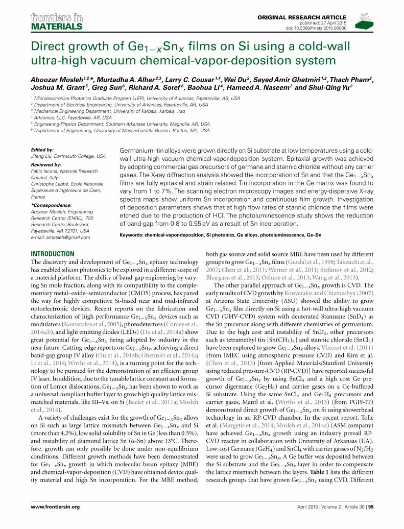
MATERIALSORIGINAL RESEARCH ARTICLE
published: 27 April 2015doi: 10.3389/fmats.2015.00030
Direct growth of Ge1−xSnx films on Si using a cold-wallultra-high vacuum chemical-vapor-deposition systemAboozar Mosleh1,2*, Murtadha A. Alher 2,3, Larry C. Cousar 1,4,Wei Du2, Seyed Amir Ghetmiri 1,2,Thach Pham2,Joshua M. Grant 5, Greg Sun6, Richard A. Soref 6, Baohua Li 4, Hameed A. Naseem2 and Shui-QingYu2
1 Microelectronics-Photonics Graduate Program (µEP), University of Arkansas, Fayetteville, AR, USA2 Department of Electrical Engineering, University of Arkansas, Fayetteville, AR, USA3 Mechanical Engineering Department, University of Karbala, Karbala, Iraq4 Arktonics, LLC, Fayetteville, AR, USA5 Engineering-Physics Department, Southern Arkansas University, Magnolia, AR, USA6 Department of Engineering, University of Massachusetts Boston, Boston, MA, USA
Edited by:Jifeng Liu, Dartmouth College, USA
Reviewed by:Fabio Iacona, National ResearchCouncil, ItalyChristophe Labbé, Ecole NationaleSupérieure d’Ingénieurs de Caen,France
*Correspondence:Aboozar Mosleh, EngineeringResearch Center (ENRC), 700Research Center Boulevard,Fayetteville, AR 72701, USAe-mail: [email protected]
Germanium–tin alloys were grown directly on Si substrate at low temperatures using a cold-wall ultra-high vacuum chemical-vapor-deposition system. Epitaxial growth was achievedby adopting commercial gas precursors of germane and stannic chloride without any carriergases.The X-ray diffraction analysis showed the incorporation of Sn and that the Ge1−xSnxfilms are fully epitaxial and strain relaxed. Tin incorporation in the Ge matrix was found tovary from 1 to 7%. The scanning electron microscopy images and energy-dispersive X-rayspectra maps show uniform Sn incorporation and continuous film growth. Investigationof deposition parameters shows that at high flow rates of stannic chloride the films wereetched due to the production of HCl. The photoluminescence study shows the reductionof band-gap from 0.8 to 0.55 eV as a result of Sn incorporation.
Keywords: chemical-vapor-deposition, Si photonics, Ge alloys, photoluminescence, Ge–Sn
INTRODUCTIONThe discovery and development of Ge1−xSnx epitaxy technologyhas enabled silicon photonics to be explored in a different scope ofa material platform. The ability of band-gap engineering by vary-ing Sn mole fraction, along with its compatibility to the comple-mentary metal–oxide–semiconductor (CMOS) process, has pavedthe way for highly competitive Si-based near and mid-infraredoptoelectronic devices. Recent reports on the fabrication andcharacterization of high performance Ge1−xSnx devices such asmodulators (Kouvetakis et al., 2005), photodetectors (Conley et al.,2014a,b), and light emitting diodes (LEDs) (Du et al., 2014a) showgreat potential for Ge1−xSnx being adopted by industry in thenear future. Cutting-edge reports on Ge1−xSnx, achieving a directband-gap group IV alloy (Du et al., 2014b; Ghetmiri et al., 2014a;Li et al., 2014; Wirths et al., 2014), is a turning point for the tech-nology to be pursued for the demonstration of an efficient groupIV laser. In addition, due to the tunable lattice constant and forma-tion of Lomer dislocations, Ge1−xSnx has been shown to work asa universal compliant buffer layer to grow high quality lattice mis-matched materials, like III–Vs, on Si (Beeler et al., 2011a; Moslehet al., 2014).
A variety of challenges exist for the growth of Ge1−xSnx alloyson Si such as large lattice mismatch between Ge1−xSnx and Si(more than 4.2%), low solid solubility of Sn in Ge (less than 0.5%),and instability of diamond lattice Sn (α-Sn) above 13°C. There-fore, growth can only possibly be done under non-equilibriumconditions. Different growth methods have been demonstratedfor Ge1−xSnx growth in which molecular beam epitaxy (MBE)and chemical-vapor-deposition (CVD) have obtained device qual-ity material and high Sn incorporation. For the MBE method,
both gas source and solid source MBE have been used by differentgroups to grow Ge1−xSnx films (Gurdal et al., 1998; Takeuchi et al.,2007; Chen et al., 2011; Werner et al., 2011; Stefanov et al., 2012;Bhargava et al., 2013; Oehme et al., 2013; Wang et al., 2013).
The other parallel approach of Ge1−xSnx growth is CVD. Theearly results of CVD growth by Kouvetakis and Chizmeshya (2007)at Arizona State University (ASU) showed the ability to growGe1−xSnx film directly on Si using a hot-wall ultra-high vacuumCVD (UHV-CVD) system with deuterated Stannane (SnD4) asthe Sn precursor along with different chemistries of germanium.Due to the high cost and instability of SnD4, other precursorssuch as tetramethyl tin [Sn(CH3)4] and stannic chloride (SnCl4)have been explored to grow Ge1−xSnx alloys. Vincent et al. (2011)(from IMEC using atmospheric pressure CVD) and Kim et al.(Chen et al., 2013) [from Applied Materials/Stanford Universityusing reduced pressure-CVD (RP-CVD)] have reported successfulgrowth of Ge1−xSnx by using SnCl4 and a high cost Ge pre-cursor digermane (Ge2H6) and carrier gases on a Ge-bufferedSi substrate. Using the same SnCl4 and Ge2H6 precursors andcarrier gases, Mantl et al. (Wirths et al., 2013) (from PGI9-IT)demonstrated direct growth of Ge1−xSnx on Si using showerheadtechnology in an RP-CVD chamber. In the recent report, Tolleet al. (Margetis et al., 2014; Mosleh et al., 2014a) (ASM company)have achieved Ge1−xSnx growth using an industry prevail RP-CVD reactor in collaboration with University of Arkansas (UA).Low-cost Germane (GeH4) and SnCl4 with carrier gasses of N2/H2
were used to grow Ge1−xSnx. A Ge buffer was deposited betweenthe Si substrate and the Ge1−xSnx layer in order to compensatethe lattice mismatch between the layers. Table 1 lists the differentresearch groups that have grown Ge1−xSnx using CVD. Different
www.frontiersin.org April 2015 | Volume 2 | Article 30 | 99

Mosleh et al. Direct Ge–Sn growth on Si using UHV-CVD
Table 1 | A summary of reports on Ge1−xSnx growth using CVD methods by different research groups.
Growth team Deposition system Deposition gas precursors Carrier gas Buffer layer
Ge Cost Sn Cost
ASU (Kouvetakis and Chizmeshya, 2007) UHV-CVD Different chemistries High SnD4 High Yes No
IMEC (Vincent et al., 2011) AP-CVD Ge2H6 High SnCl4 Low Yes Ge
Applied materials (Chen et al., 2013) RP-CVD Ge2H6 High SnCl4 Low Yes Ge
PGI9-IT (Wirths et al., 2013) RP-CVD Ge2H6 High SnCl4 Low Yes No
ASM/UA (Margetis et al., 2014; Mosleh et al., 2014a) RP-CVD GeH4 Low SnCl4 Low Yes Ge
UA (this work) UHV-CVD GeH4 Low SnCl4 Low No No
growth methods and the cost effectiveness of the gas precursorsare compared.
In this paper, we report direct growth of strain-relaxedGe1−xSnx films on Si substrates with Sn mole fractions up to 7%using a cold-wall UHV-CVD system. Stannic chloride and ger-mane were chosen as the precursors which are low-cost and com-mercially available. The growth of Ge1−xSnx films was achievedwithout using any carrier gases and buffer layers. In order toinvestigate the material quality, the X-ray diffraction (XRD),high-resolution transmission electron microscopy (TEM), energy-dispersive X-ray spectroscopy (EDX), Raman spectroscopy, andphotoluminescence (PL) measurements have been conducted.
EXPERIMENTGROWTH METHODA cold-wall UHV-CVD system was adopted to grow Ge1−xSnx
films (see Figure 1 for machine schematic). The system com-poses a load-lock chamber with a base pressure of 10−6 Pa anda process chamber whose base pressure reaches 10−8 Pa using theturbo-molecular and cryogenic pumps, respectively. Due to low-temperature growth of the films, removal of oxygen and watervapor is critical which was achieved by using a cryogenic pump.The turbo-molecular pumps are backed by mechanical pumps.The heating stage consisted of a pyrolytic graphite heater with athermocouple placed at the same distance away from the heateras the wafer. The sample holder rotates up to 80 rpm for uniformfilm growth. The gas flow is through a side entry port, controlledby mass flow controllers (MFCs). Stannic chloride is a volatile liq-uid with vapor pressure of 2.4 kPa at one atmospheric pressure.Therefore, the evaporation could produce enough pressure to bepassed through the MFC.
Germanium–tin films were grown on 4′′ (001) p-type Si sub-strates with 5–10 Ω cm resistivity. Prior to loading the samples,they were cleaned in a two-step process: (1) Piranha etch solution[H2SO4:H2O2 (1:1)], (2) oxide strip HF dipping [H2O:HF (10:1)using 48% pure HF] followed by nitrogen blow drying. The finaloxide strip step was not followed by a water rinse as it reduces thelife-time of hydrogen passivation and exposes the surface to ambi-ent oxygen (Mosleh et al., 2013, 2014b). The experiments werecarried out at reduced pressures of 13, 40, 65, 95, 130, 200, and260 Pa and at temperatures as low as 300°C. Germane (GeH4) andstannic chloride (SnCl4) were used as the precursors for Ge1−xSnx
growth. The gas flow ratio (GeH4/SnCl4) was set to 5, 3.3, 2.5,and 1.6. Depending on the growth parameters such as gas flow
ratio and deposition pressure, a growth rate of 20–3.3 nm/minwas achieved.
CHARACTERIZATION METHODAnalysis of Sn mole fraction, lattice constant, growth quality,and strain in the Ge1−xSnx films were conducted using a high-resolution X-ray diffractometer. High-resolution TEM (TITAN)with an accelerating voltage of 300 kV was used to investigatecrystal orientation and defects in the grown epi-layers as well asdetermining the thicknesses of the samples. Surface morphologyof the samples was investigated by a scanning electron micro-scope equipped with EDX. Room temperature PL measurementswere carried out using a 690-nm excitation laser. The PL signalwas collected by a grating-based spectrometer equipped with athermoelectric-cooled PbS detector (cut-off at 3 µm) for spectralanalysis.
RESULTS AND DISCUSSIONMATERIAL CHARACTERIZATIONThe 2θ-ω XRD scan was performed from the symmetric (004)plane to obtain the out-of-plane lattice constant of the Ge1−xSnx
films. Figure 2A shows the peak at 69° corresponding to a satisfac-tion of the Bragg condition by Si (001) substrate, and the peaks atlower angles of 66–65° due to larger lattice size of the Ge1−xSnx lay-ers. The difference in the position of Ge1−xSnx peaks is due to thedifference in the Sn mole fractions of Ge1−xSnx layers. Differentcompositions were achieved from 1 to 7% with desirable crystalquality. The Ge1−xSnx peaks are broadened for two reasons: (1)thin film thickness of the layers and (2) presence of mosaicity in theGe–Sn crystal and formation of defects as a result of strain relax-ation. The full width at half maximum (FWHM) of the Ge1−xSnx
peaks are between 0.28 for 1% Sn film and 0.36 for 7% Sn film. Thechange in FWHM depends on various factors such as film thick-ness, relaxation, and quality and there is no trend showing that theFWHM of the peaks change as the Sn composition increases.
In order to calculate the total lattice constant and the strainin the film, an asymmetric reciprocal space mapping (RSM)from (−2, −2, 4) plane was performed. The RSM scans providemeasurement of the in-plane (a‖) and out-of-plane (a⊥) latticeconstant of Ge1−xSnx alloys. The total lattice constant aGeSn
0 wascalculated by taking into account the elastic constants of Ge1−xSnx
(Beeler et al., 2011b). Knowing the total lattice constant, the Snmole fractions is calculated through Vegard’s law with the bow-ing factor of b= 0.0166 Å (Moontragoon et al., 2012). Figure 2B
Frontiers in Materials | Optics and Photonics April 2015 | Volume 2 | Article 30 | 100
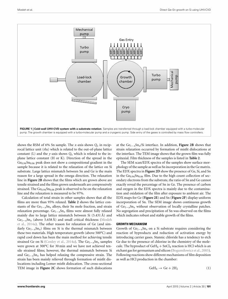
Mosleh et al. Direct Ge–Sn growth on Si using UHV-CVD
FIGURE 1 | Cold-wall UHV-CVD system with a substrate rotation. Samples are transferred through a load-lock chamber equipped with a turbo-molecularpump. The growth chamber is equipped with a turbo-molecular pump and a cryogenic pump. Side entry of the gases is controlled by mass flow controllers.
shows the RSM of 6% Sn sample. The x-axis shows Qz in recip-rocal lattice unit (rlu) which is related to the out-of-plane latticeconstant (L) and the y-axis shows Qx which is related to the in-plane lattice constant (H or K). Direction of the spread in theGe0.94Sn0.06 peak does not show a compositional gradient in thesample because it is related to the relaxation of the lattice on Sisubstrate. Large lattice mismatch between Sn and Ge is the mainreason for a large spread in the omega direction. The relaxationline in Figure 2B shows that the films which are grown above aretensile strained and the films grown underneath are compressivelystrained. The Ge0.94Sn0.06 peak is observed to be on the relaxationline and the relaxation is measured to be 97%.
Calculation of total strain in other samples shows that all thefilms are more than 95% relaxed. Table 2 shows the lattice con-stants of the Ge1−xSnx alloys, their Sn mole fraction, and strainrelaxation percentage. Ge1−xSnx films were almost fully relaxedmainly due to large lattice mismatch between Si (5.431 Å) andGe1−xSnx (above 5.658 Å) and small critical thickness (Moslehet al., 2014a). The other reason for relaxation of Ge (and sim-ilarly Ge1−xSnx) films on Si is the thermal mismatch betweenthese two materials. High temperature growth (above 500°C) andrapid cool down has been the main method for achieving tensilestrained Ge on Si (Conley et al., 2014a). The Ge1−xSnx sampleswere grown at 300°C for 30 min and we have not achieved ten-sile strained films; however, the thermal mismatch between Siand Ge1−xSnx has helped relaxing the compressive strain. Thestrain has been mainly relieved through formation of misfit dis-locations including Lomer misfit dislocation. The cross-sectionalTEM image in Figure 2C shows formation of such dislocations
at the Ge1−xSnx/Si interface. In addition, Figure 2B shows thatstrain relaxation occurred by formation of misfit dislocations atthe interface. The TEM image shows that the grown film was fullyepitaxial. Film thickness of the samples is listed in Table 2.
The SEM scan/EDX spectra of the samples show surface mor-phology of the sample as well as Sn incorporation in the Ge matrix.The EDX spectra in Figure 2D show the presence of Ge, Si, and Snin the Ge0.94Sn0.06 film. Due to the high count collection of sec-ondary electrons from the substrate, the ratio of Sn and Ge cannotexactly reveal the percentage of Sn in Ge. The presence of carbonand oxygen in the EDX spectra is mainly due to the contamina-tion and oxidation of the film after exposure to ambient air. TheEDX maps for Ge (Figure 2E) and Sn (Figure 2F) display uniformincorporation of Sn. The SEM image shows continuous growthof Ge1−xSnx without observation of locally crystalline patches.No segregation and precipitation of Sn was observed on the filmswhich indicates robust and stable growth of the films.
GROWTH MECHANISMGrowth of Ge1−xSnx on a Si substrate requires considering thereaction of byproducts and reduction of activation energy byintroducing carrier gases. Stannic chloride has a tendency to etchGe due to the presence of chlorine in the chemistry of the mole-cule. The byproduct of GeH4+ SnCl4 reaction is HCl which is anetchant gas for germanium and silicon (Bogumilowicz et al., 2005).Following reactions show different mechanisms of film depositionas well as HCl production in the chamber:
GeH4 → Ge+ 2H2 (1)
www.frontiersin.org April 2015 | Volume 2 | Article 30 | 101

Mosleh et al. Direct Ge–Sn growth on Si using UHV-CVD
FIGURE 2 | (A) Symmetric (004) 2θ-ω scan of Ge1−xSnx films which aregrown on a Si substrate. The peak at 69° shows the Si substrate peak andthe peaks between 66° and 65° belong to Ge1−xSnx films. (B) Reciprocalspace map from asymmetrical plane (−2, −2, 4) for Ge0.94Sn0.06 grown on aSi substrate. The x -coordinate shows out-of-plane lattice constant and they -coordinate shows in-plane lattice constant in units of reciprocal latticeunit. The relaxation line shows that the films grown above are tensilestrained and below are compressively strained. Presence of the
Ge0.94Sn0.06 on the relaxation line shows that the film is strain relaxed.(C) Transmission electron microscopy images of Ge0.94Sn0.06 film showsepitaxial growth of Ge–Sn on a Si substrate. Arrows show misfitdislocations formed at the Ge1−xSnx/Si interface. (D) The EDX spectrum ofSi/Ge0.94Sn0.06 film shows the presence of Si (substrate), Ge and Sn (film),O (native oxide), and C (carbon contamination from the ambient). (E) TheEDX surface maps of Ge and (F) Sn taken from scanning electronmicrographs for Ge0.94Sn0.06 film shows uniform growth of Ge1−xSnx alloy.
Table 2 |Tin mole fraction calculation, lattice constant, and relaxation
percentage of the grown samples.
Sample
no.
Sn (%) a‖Π (nm) a⊥ (nm) a (nm) Relaxation
(%)
Thickness
(nm)
1 1.2 5.666 5.671 5.668 98 615
2 2.1 5.673 5.679 5.676 98 423
3 2.9 5.678 5.687 5.682 97 295
4 4.2 5.689 5.695 5.692 98 207
5 5.8 5.699 5.712 5.706 97 108
6 7.0 5.715 5.719 5.717 99 532
2H2 + SnCl4 → Sn+ 4HCl (2)
GeH4 + SnCl4 → Ge+ Sn+ 4HCl (3)
Higher temperature of the substrate results in higher densityof depositing ad-atoms (Ge and Sn); however, it will result in pro-duction of HCl at a higher rate. In addition, higher flow rate ofSnCl4 increases the production rate of HCl as well. Controlling thetemperature and flow rate of the gases could control the process
so that growth is the dominant process in the chamber. The Ge/Snfilm will be etched by HCl through the following reactions:
4HCl + Ge→ GeH4 + 2Cl2 (4)
4HCl + Sn→ SnCl4+2H2 (5)
Domination of etching over growth is the main mechanismthat prevents direct growth of Ge1−xSnx on Si.
By controlling the flow through MFCs, we have grownGe1−xSnx films on Si at different pressures with a fixed flow ratioof GeH4/SnCl4= 1.6. Growth was observed at 13 Pa of depositionpressure and continued until the deposition pressure increased to130 Pa. Figure 3A shows the thickness of Ge1−xSnx films versusdeposition pressure of the chamber as well as Sn incorporationpercentage. Incorporation of Sn in the Ge lattice is increased byraising the pressure due to the higher residence time of the precur-sors in the chamber. The residence time of the gases has increasedfrom 2 s at 13 Pa to 19 s at 130 Pa. Meanwhile, HCl etched moreof the Ge1−xSnx films after deposition at higher pressures. Thistrend has continued to 130 Pa and no growth has been observedat 200 and 265 Pa. The increase in Sn composition from 1 to 6%
Frontiers in Materials | Optics and Photonics April 2015 | Volume 2 | Article 30 | 102

Mosleh et al. Direct Ge–Sn growth on Si using UHV-CVD
FIGURE 3 | (A) Variation of Sn incorporation percentage versus depositionpressure. Films were etched away for deposition pressures higher than130 Pa. The secondary axis on the right shows the reduction of film thickness
as a result of increase in the deposition pressure. (B) Tin incorporation andfilm thickness of the samples grown at 65 Pa growth pressure versusGeH4/SnCl4 flow ratios.
FIGURE 4 | (A) Raman spectra of the Ge1−xSnx film grown on a Sisubstrate. The shift in the Ge–Ge peak is due to the incorporation of Sn inGe lattice. The shoulder on the left side of the Ge–Ge peak is due to theGe–Sn peak at 285 cm−1. The Ge–Sn peak is shown at lowerwavenumber of 250–260 cm−1. (B) Ge–Ge and Ge–Sn peak shifts versus
Sn mole fraction. The solid symbols are experimental data and thecurves are theoretical predictions for relaxed films. The Ge–Ge peak isexpected to shift 0.8310 cm−1 for every 1% Sn incorporation in relaxedfilms. The expected shift (0.8311 cm−1) for Ge–Sn peak is very close tothat of Ge–Ge.
has been accompanied with reduction in the thickness from 615 to108 nm. Films that were expected to have higher than 6% Sn con-tent were totally etched off. Therefore, in order to grow higher Sncontent films, growth mechanism under fixed pressure and chang-ing the SnCl4 flow was studied. Higher film thickness and higherSn incorporation was achieved as a result of domination of growthover etching. Figure 3B shows Sn incorporation in Ge1−xSnx filmsversus SnCl4 flow rate at 95 Pa deposition pressure. The secondaryaxis of Figure 3B shows film thicknesses of the samples. Due to thedominance of etching for higher SnCl4 flow rate, the films weremostly etched and the film thickness was less than 100 nm.
Introduction of carrier gases has different effects on the growthof Ge1−xSnx films. Hydrogen changes the balance in the reaction toproduce more HCl. Consequently, the GeH4/SnCl4 ratio at whichthe Ge1−xSnx films were depositing will not result in growth whenhydrogen is introduced in the chamber. In addition, introductionof nitrogen and argon as carrier gases will reduce the activation
energy of the growth (Wirths et al., 2013). Although reductionof activation energy enables easier breakdown of the moleculeson the surface and enhances the growth quality and growth rate,it would prepare the conditions for easier etch due to the pres-ence of an etchant agent. Therefore, the presence of carrier gasespushes the competition between growth and etching toward etch-ing, resulting in film etching at even lower flow rates of carriergases when the flow rate of SnCl4 is of the same order of GeH4.
OPTICAL CHARACTERIZATIONRaman spectroscopyThe Ge1−xSnx films were further investigated by Raman spec-troscopy in order to analyze the crystal structure. Room tempera-ture Raman spectra of the grown samples as well as a Ge referencesample are plotted in Figure 4A. The Ge–Ge longitudinal optical(LO) peak was observed at 300 cm−1 for the Ge reference samplewhile the Ge–Ge peak in the Ge1−xSnx films was shifted to lower
www.frontiersin.org April 2015 | Volume 2 | Article 30 | 103

Mosleh et al. Direct Ge–Sn growth on Si using UHV-CVD
FIGURE 5 | (A) Photoluminescence spectra of the Ge1−xSnx filmswith 2, 4, 6, and 7% Sn mole fraction showing a red-shift in theband-gap of the films. Incorporation of Sn has shifted both directband-gap and indirect band-gap toward lower energies. (B) The
bowed Vegard’s law interpolation for the direct (solid line) andindirect band-gap (dash line) of Ge1−xSnx alloy is plotted for differentSn compositions and is overlaid with experimental data (solidsymbols).
wavenumbers due to the change in bonding energy of Ge–Ge byincorporation of Sn atoms. The intensity of the Ge–Ge LO peakat 300 cm−1 is normalized for all the samples for comparison ofthe peak positions. In addition to the main Ge–Ge peak, Ramanspectra of Ge1−xSnx films show other peaks that are induced asa result of Sn incorporation. The Ge–Sn LO peaks for differentSn mole fractions were observed at 250–260 cm−1 in the films. Asecond peak of Ge–Sn is observed at 285 cm−1, which can be seenas a shoulder of Ge–Ge main peak.
The peak positions are obtained by Lorentzian fitting to findthe exact position for further analysis. The shift in the Ge–GeLO peak depends on both strain and Sn composition of thefilms. Theoretical calculations for ∆ω are different for strain-relaxed films and strained films for different Sn (x) content[∆ωGe−Ge(x)= bx cm−1]. The Ge–Ge peak is expected to shiftby a factor of b=−30.30 for a strained alloy while this factorvaries to b=−83.10 for a strain-relaxed film (Cheng et al., 2013).Figure 4B shows the experimental data obtained for Ge–Ge andGe–Sn Raman shift from the sample compared with the theoret-ical calculations. The peak shifts match well with the theoreticalcalculations for strain-relaxed films.
PhotoluminescenceGermanium has an indirect band-gap in the L valley with theenergy of 0.644 eV and a direct band-gap at the γ point with 0.8 eVenergy at room temperature. Incorporation of Sn in Ge lattice low-ers the conduction band edge at the γ-point at a faster rate thanthat at the L-point. PL measurements on Ge1−xSnx samples allowdetermination of the band-gap edge for various Sn compositions.
Figure 5 depicts room temperature PL intensity spectra foras-grown Ge1−xSnx films with 2, 4, 6, and 7% Sn mole frac-tions. As indicated in Figure 5A, increase of the Sn mole fractionresults in a band-gap reduction. Both direct and indirect PL peaksexhibit red-shift with Sn compositions increase from 2 to 7%. AGaussian fitting function was employed to extract the PL peakpositions of both direct and indirect transitions as described in
Ghetmiri et al. (2014b). In Ge0.94Sn0.06 and Ge0.93Sn0.07 samples,the energies difference between direct and indirect transitions arevery small, therefore the PL emissions from these indirect anddirect transitions cannot be identified. A temperature-dependentstudy is needed to differentiate the direct and indirect peak posi-tions which will be reported in the future. The PL peaks fromthe samples with 2, 4, 6, and 7% Sn compositions are shown inFigure 5B as solid symbols. The solid and the dashed lines showthe direct and indirect band-gap energies based on bowed Veg-ard’s law for the relaxed Ge1−xSnx alloy (Ghetmiri et al., 2014b),respectively. Since the Ge1−xSnx films are almost strain-free, asconfirmed by XRD measurements, the experimental results closelyfollow the predicted values from Vegard’s law.
CONCLUSIONDirect growth of Ge1−xSnx layers on Si substrates was achievedusing a cold-wall UHV-CVD system. The films were grown byemploying low-cost commercial available GeH4 and SnCl4 precur-sors without using any carrier gases and buffer layers. Characteri-zations of the samples with XRD showed successful incorporationof Sn up to 7%. The TEM images show fully epitaxial growth of thesamples without any precipitation of Sn from the Ge lattice. TheRaman results verified the Sn incorporation and PL measurementsshowed reduction of the band-gap to 0.55 eV for 7% Sn sample.The low-cost and CMOS compatible growth method and the per-formance of the samples indicate a promising future for Ge1−xSnx
applications in Si photonics. Moreover, the samples were grownstrain-relaxed enabling this material to be a universal compliantbuffer layer which can be used in hybrid integration.
ACKNOWLEDGMENTSThe work at the UA was supported by NSF (EPS-1003970),the Arkansas Bioscience Institute, the Arktonics, LLC (Air ForceSBIR, FA9550-14-C-0044, Dr. Gernot Pomrenke, Program Man-ager), and DARPA (W911NF-13-1-0196, Dr. Dev Palmer, ProgramManager). Drs. RS and GS acknowledge support from AFOSR
Frontiers in Materials | Optics and Photonics April 2015 | Volume 2 | Article 30 | 104

Mosleh et al. Direct Ge–Sn growth on Si using UHV-CVD
(FA9550-14-1-0196, Dr. Gernot Pomrenke, Program Manager).JG acknowledges the support of NSF REU Program under Grantnumber EEC-1359306.
REFERENCESBeeler, R. T., Grzybowski, G. J., Roucka, R., Jiang, L., Mathews, J., Smith, D.
J., et al. (2011a). Synthesis and materials properties of Sn/P-doped Ge on Si(100): photoluminescence and prototype devices. Chem. Mater. 23, 4480–4486.doi:10.1021/cm201648x
Beeler, R., Roucka, R., Chizmeshya, A., Kouvetakis, J., and Menéndez, J. (2011b).Nonlinear structure-composition relationships in the Ge1-ySnySi (100) (y<0.15) system. Phys. Rev. B 84, 035204. doi:10.1103/PhysRevB.84.035204
Bhargava, N., Coppinger, M., Gupta, J. P., Wielunski, L., and Kolodzey, J. (2013). Lat-tice constant and substitutional composition of GeSn alloys grown by molecularbeam epitaxy. Appl. Phys. Lett. 103, 041908. doi:10.1063/1.4816660
Bogumilowicz, Y., Hartmann, J. M., Truche, R., Campidelli, Y., Rolland, G., and Bil-lon, T. (2005). Chemical vapour etching of Si, SiGe and Ge with HCl; applicationsto the formation of thin relaxed SiGe buffers and to the revelation of threadingdislocations. Semicond. Sci. Technol. 20, 127. doi:10.1088/0268-1242/20/2/004
Chen, R., Huang, Y., Gupta, S., Lin, A. C., Sanchez, E., Kim, Y., et al. (2013).Material characterization of high Sn-content, compressively-strained GeSnepitaxial films after rapid thermal processing. J. Cryst. Growth 365, 29–34.doi:10.1016/j.jcrysgro.2012.12.014
Chen, R., Lin, H., Huo, Y., Hitzman, C., Kamins, T. I., and Harris, J. S. (2011).Increased photoluminescence of strain-reduced, high-Sn composition Ge1-xSnx
alloys grown by molecular beam epitaxy. Appl. Phys. Lett. 99, 181125. doi:10.1063/1.3658632
Cheng, R., Wang, W., Gong, X., Sun, L., Guo, P., Hu, H., et al. (2013). Relaxed andstrained patterned germanium-tin structures: a Raman scattering study. ECS J.Solid State Sci. Technol. 2, 138–145. doi:10.1149/2.013304jss
Conley, B. R., Mosleh, A., Ghetmiri, S. A., Du, W., Soref, R. A., Sun, G., et al. (2014a).Temperature dependent spectral response and detectivity of GeSn photoconduc-tors on silicon for short wave infrared detection. Opt. Express 22, 15639–15652.doi:10.1364/OE.22.015639
Conley, B. R., Margetis, J., Du,W., Tran, H., Mosleh,A., Ghetmiri, S. A., et al. (2014b).Si based GeSn photoconductors with a 1.63 A/W peak responsivity and a 2.4 µmlong-wavelength cutoff. App. Phys. Lett. 105, 221117. doi:10.1063/1.4903540
Du, W., Zhou, Y., Ghetmiri, S. A., Mosleh, A., Conley, B. R., Nazzal, A., et al. (2014a).Room-temperature electroluminescence from Ge/Ge1-xSnx/Ge diodes on Si sub-strates. Appl. Phys. Lett. 104, 241110. doi:10.1063/1.4884380
Du, W., Ghetmiri, S. A., Conley, B. R., Mosleh, A., Nazzal, A., Soref, R. A.,et al. (2014b). Competition of optical transitions between direct and indirectbandgaps in Ge1-xSnx. Appl. Phys. Lett. 105, 051104. doi:10.1063/1.4892302
Ghetmiri, S. A., Du, W., Margetis, J., Mosleh, A., Cousar, L., Conley, B. R., et al.(2014a). Direct-bandgap GeSn grown on Silicon with 2230 nm photolumines-cence. Appl. Phys. Lett. 105, 151109. doi:10.1063/1.4898597
Ghetmiri, S. A., Du, W., Conley, B. R., Mosleh, A., Naseem, H. A., Yu, S., et al.(2014b). Shortwave-infrared photoluminescence from Ge1-xSnx thin films onsilicon. J. Vac. Sci. Technol. B 32, 060601. doi:10.1116/1.4897917
Gurdal, O., Desjardins, P., Carlsson, J., Taylor, N., Radamson, H., Sundgren, J.,et al. (1998). Low-temperature growth and critical epitaxial thicknesses of fullystrained metastable Ge1-xSnx (x.0.26) alloys on Ge (001) 2× 1. J. Appl. Phys.83, 162–170. doi:10.1063/1.366690
Kouvetakis, J., and Chizmeshya, A. V. G. (2007). New classes of Si-based photonicmaterials and device architectures via designer molecular routes. J. Mater. Chem.17, 1649–1655. doi:10.1039/b618416b
Kouvetakis, J., Menendez, J., and Soref, R.A. Strain-Engineered Direct-GapGe/SnxGe1-x Heterodiode and Multi-Quantum-Well Photodetectors, Laser, Emit-ters and Modulators Grown on SnySizGe1-y-z Buffered Silicon. United Statespatent US 6897471 B1 (2005).
Li, H., Brouillet, J., Salas, A., Chaffin, I., Wang, X., and Liu, J. (2014). Lowtemperature geometrically confined growth of pseudo single crystalline GeSnon amorphous layers for advanced optoelectronics. ECS Trans. 64, 819–827.doi:10.1149/06406.0819ecst
Margetis, J., Ghetmiri, S. A., Du, W., Conley, B. R., Mosleh, A., Soref, R., et al. (2014).Growth and characterization of epitaxial Ge1-XSnx alloys and heterostructures
using a commercial CVD system. ECS Trans. 64, 1830–1830. doi:10.1149/06406.0711ecst
Moontragoon, P., Soref, R., and Ikonic, Z. (2012). The direct and indirect bandgapsof unstrained Si x Ge1-xySny and their photonic device applications. J. Appl. Phys.112, 073106–073106–8. doi:10.1063/1.4757414
Mosleh, A., Benamara, M., Ghetmiri, S. A., Conley, B. R., Alher, M. A., Du, W., et al.(2014). Investigation on the formation and propagation of defects in GeSn thinfilms. ECS Trans. 64, 1845–1845. doi:10.1149/06406.0895ecst
Mosleh, A., Ghetmiri, S. A., Conley, B. R., Abu-Safe, H., Waqar, Z., Benamara,M., et al. (2013). “Nucleation-step study of silicon homoepitaxy for low-temperature fabrication of Si solar cells,” in Photovoltaic Specialists Conference(PVSC), IEEE 39th. Tampa, FL.
Mosleh, A., Ghetmiri, S. A., Conley, B. R., Hawkridge, M., Benamara, M., Nazzal, A.,et al. (2014a). Material characterization of Ge1-xSnx alloys grown by a commer-cial CVD system for optoelectronic device applications. J. Electron. Mater. 43,938–946. doi:10.1007/s11664-014-3089-2
Mosleh, A., Ghetmiri, S. A., Conley, B. R., Abu-Safe, H. H., Benamara, M., Waqar,Z., et al. (2014b). Investigation of growth mechanism and role of H2 in very lowtemperature Si epitaxy. ECS Trans. 64, 967–975. doi:10.1149/06406.0967ecst
Oehme, M., Buca, D., Kostecki, K., Wirths, S., Holländer, B., Kasper, E., et al. (2013).Epitaxial growth of highly compressively strained GeSn alloys up to 12.5% Sn. J.Cryst. Growth 384, 71–76. doi:10.1016/j.jcrysgro.2013.09.018
Stefanov, S., Conde, J., Benedetti, A., Serra, C., Werner, J., Oehme, M., et al. (2012).Laser synthesis of germanium tin alloys on virtual germanium. Appl. Phys. Lett.100, 104101. doi:10.1063/1.3692175
Takeuchi, S., Sakai, A., Yamamoto, K., Nakatsuka, O., Ogawa, M., and Zaima, S.(2007). Growth and structure evaluation of strain-relaxed Ge1-xSn buffer lay-ers grown on various types of substrates. Semicond. Sci. Technol. 22, S231.doi:10.1088/0268-1242/22/1/S54
Vincent, B., Gencarelli, F., Bender, H., Merckling, C., Douhard, B., Petersen, D.H., et al. (2011). Undoped and in-situ B doped GeSn epitaxial growth onGe by atmospheric pressure-chemical vapor deposition. Appl. Phys. Lett. 99,152103–152103–3. doi:10.1063/1.3645620
Wang, L., Su, S., Wang, W., Gong, X., Yang, Y., Guo, P., et al. (2013). Strainedgermanium–tin (GeSn) p-channel metal-oxide-semiconductor field-effect-transistors (p-MOSFETs) with ammonium sulfide passivation. Solid State Elec-tron. 83, 66–70. doi:10.1016/j.sse.2013.01.031
Werner, J.,Oehme,M.,Schmid,M.,Kaschel,M.,Schirmer,A.,Kasper,E., et al. (2011).Germanium-tin pin photodetectors integrated on silicon grown by molecularbeam epitaxy. Appl. Phys. Lett. 98, 061108–061108–3. doi:10.1063/1.3555439
Wirths, S., Buca, D., Mussler, G., Tiedemann, A., Holländer, B., Bernardy, P., et al.(2013). Reduced pressure CVD growth of Ge and Ge1-xSnx alloys. ECS J. SolidState Sci. Technol. 2, N99–N102. doi:10.1149/2.006305jss
Wirths, S., Geiger, R., Scherrer, P., Ikonic, Z., Tiedemann, A. T., Mussler, G., et al.(2014). “Epitaxy and photoluminescence studies of high quality GeSn het-erostructures with Sn concentrations up to 13 at.%,” in 11th International Con-ference on Group IV Photonics 27–29 August. Paris.
Conflict of Interest Statement: The authors declare that the research was conductedin the absence of any commercial or financial relationships that could be construedas a potential conflict of interest.
Received: 28 January 2015; accepted: 23 March 2015; published online: 27 April 2015.Citation: Mosleh A, Alher MA, Cousar LC, Du W, Ghetmiri SA, Pham T, Grant JM,Sun G, Soref RA, Li B, Naseem HA and Yu S-Q (2015) Direct growth of Ge1−xSnx filmson Si using a cold-wall ultra-high vacuum chemical-vapor-deposition system. Front.Mater. 2:30. doi: 10.3389/fmats.2015.00030This article was submitted to Optics and Photonics, a section of the journal Frontiersin Materials.Copyright © 2015 Mosleh, Alher, Cousar, Du, Ghetmiri, Pham, Grant , Sun, Soref,Li, Naseem and Yu. This is an open-access article distributed under the terms of theCreative Commons Attribution License (CC BY). The use, distribution or reproductionin other forums is permitted, provided the original author(s) or licensor are creditedand that the original publication in this journal is cited, in accordance with acceptedacademic practice. No use, distribution or reproduction is permitted which does notcomply with these terms.
www.frontiersin.org April 2015 | Volume 2 | Article 30 | 105

MATERIALSORIGINAL RESEARCH ARTICLE
published: 23 February 2015doi: 10.3389/fmats.2015.00008
Room-temperature near-infrared electroluminescencefrom boron-diffused silicon pn-junction diodesSi Li ,Yuhan Gao, Ruixin Fan, Dongsheng Li and DerenYang*
State Key Lab of Silicon Materials, Department of Materials Science and Engineering, Zhejiang University, Hangzhou, China
Edited by:Dan-Xia Xu, National ResearchCouncil Canada, Canada
Reviewed by:Jifeng Liu, Dartmouth College, USATatiana S. Perova, The University ofDublin, Ireland
*Correspondence:Deren Yang, State Key Lab of SiliconMaterials, Department of MaterialsScience and Engineering, ZhejiangUniversity, Zheda Road 38, Hangzhou310027, Chinae-mail: [email protected]
Silicon pn-junction diodes with different doping concentrations were prepared by borondiffusion into Czochralski n-type silicon substrate. Their room-temperature near-infraredelectroluminescence (EL) was measured. In the EL spectra of the heavily boron dopeddiode, a luminescence peak at ~1.6 µm (0.78 eV) was observed besides the band-to-bandline (~1.1 eV) under the condition of high current injection, while in that of the lightly borondoped diode only the band-to-band line was observed. The intensity of peak at 0.78 eVincreases exponentially with current injection with no observable saturation at room tem-perature. Furthermore, no dislocations were found in the cross-sectional transmissionelectron microscopy image, and no dislocation-related luminescence was observed inthe low-temperature photoluminescence spectra. We deduce that the 0.78 eV emissionoriginates from the irradiative recombination in the strain region of diodes caused by thediffusion of large number of the boron atoms into a silicon crystal lattice.
Keywords: boron diffusion, silicon pn-junction diode, near-infrared electroluminescence
INTRODUCTIONWith the development of integrated circuits (ICs), the disad-vantage of traditional metal interconnection structure, such asinterlayer interference, energy dissipation, and signal delay, hasbecome a bottleneck restricting the development of ultra-large-scale integration circuits (USLIs). Optical interconnection, whichuses photons to transform information, will be an ultimate solu-tion for future progress in USLIs. Because silicon is an indirect-band-gap semiconductor and fundamentally unable to emit lightefficiently, achieving efficient silicon-based light sources compati-ble with current IC manufacturing technology has become the keyissue of silicon optoelectronics. Many routes to fabricate efficientsilicon light emitters have been proposed: porous silicon (Can-ham, 1990; Qin et al., 1996; Bisi et al., 2000; Zhao et al., 2005a,b),Si nanoprecipitates in SiO2 (Pavesi et al., 2000; Wang et al., 2007),erbium-doped Si (Ennen et al., 1983; Zheng et al., 1994; Polmanet al., 1995), Si/SiO2 superlattice structures (Lu et al., 1995), andsilicon pn-junction diodes (Sveinbjörnsson, 1996; Martin et al.,2001; Ng et al., 2001; Sun et al., 2004; Lourenco et al., 2005). Amongthese ways, silicon pn-junction diodes have attracted much atten-tion. The most standout advantage of this kind of light-emitteris that the fabrication process is totally compatible with USLItechnology. Both ion-implantation (Sveinbjörnsson, 1996; Mar-tin et al., 2001; Ng et al., 2001; Sun et al., 2004; Lourenco et al.,2005; Sobolev, 2010) and thermal diffusion (Kveder et al., 2004;Hoang et al., 2006, 2007) have been used to manufacture siliconpn diodes. The past few years has seen great advances in the devel-opment of silicon pn-junction diodes. Electroluminescence (EL)efficiency of 0.1–1% has been achieved (Martin et al., 2001; Nget al., 2001). In addition to the band-to-band emission around1.1 µm, other near-infrared emissions have been found in boron-implanted and boron-diffused silicon pn diodes (Sveinbjörnsson,1996; Sun et al., 2004). Sveinbjörnsson (1996) reported strong
~1.6 µm (0.78 eV) EL emission related to dislocation-related cen-ter D1 at room temperature from dislocation-rich silicon diodes.Sun et al. (2004) reported two luminescence bands around 1.05and 0.95 eV related to doping spikes in boron-implanted silicon pndiodes. These emissions show great application potential in siliconoptoelectronics. But the mechanism is still in dispute.
In this paper, we fabricated silicon pn-junction diodes withdifferent boron doping concentrations. Their room-temperatureEL was measured and their cross-sectional transmission electronmicroscopy (TEM) images were studied. The result shows thatthe heavily boron doped silicon pn-junction diode without dis-location loops can emit strong 0.78 eV luminescence under thecondition of high current injection besides the band-to-bandemission. It is considered that the 0.78 eV emission originatesfrom the irradiative recombination in the strain regions caused bythe diffusion of large number of boron atoms into silicon crystallattice.
MATERIALS AND METHODSTwo kinds of boron diffusion sources were prepared by dissolv-ing B2O3 into SiO2 latex with B3+ concentration of 0.203 mol/L(marked as A) and 0.569 mol/L (marked as B), respectively. Boronsources were spin onto the surface of (100) oriented n-typeCzochralski-grown Si substrates (2 ~ 10 Ω cm, 500 µm in thick-ness) after the substrate wafer was cut into 15 mm× 15 mm slicesand carefully cleaned by standard RCA process. Rapid thermaltreating method was used to form shallow pn junction by borondiffusion at 1100°C for 5 min in the flowing high-purity N2 atmos-phere. After a pn junction was formed, an indium tin oxide (ITO)electrode with a thickness of 100 nm was deposited on the p-layerside by magnetron sputtering, and an Al electrode with a thicknessof 100 nm was evaporated on the n-layer side. Thus, a pn-junctiondiode was prepared.
Frontiers in Materials | Optics and Photonics February 2015 | Volume 2 | Article 8 | 106
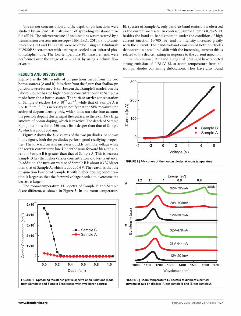
Li et al. Electroluminescence from silicon pn junction
The carrier concentration and the depth of pn junctions werestudied by an SSM350 instrument of spreading resistance pro-file (SRP). The microstructure of pn junctions was measured by atransmission electron microscope (TEM, JEOL 2010). Photolumi-nescence (PL) and EL signals were recorded using an EdinburghFLS920P Spectrometer with a nitrogen-cooled near-infrared pho-tomultiplier tube. The low-temperature PL measurements wereperformed over the range of 20 ~ 300 K by using a helium flowcryostat.
RESULTS AND DISCUSSIONFigure 1 is the SRP results of pn junctions made from the twoboron sources (A and B). It is clear from the figure that shallow pnjunctions were formed. It can be seen that Sample B made from theB boron source has the higher carrier concentration than Sample Amade from the A boron source. The surface carrier concentrationof Sample B reaches 4.6× 1017 cm−3, while that of Sample A is5× 1016 cm−3. It is necessary to notify that the SPR measures theactivated dopant density only, which does not take into accountthe possible dopant clustering at the surface, so there can be a largeamount of boron doping, which is inactive. The depth of SampleB pn junction is about 250 nm, a little deeper than that of SampleA, which is about 200 nm.
Figure 2 shows the I –V curves of the two pn diodes. As shownin the figure, both the pn diodes perform good rectifying proper-ties. The forward current increases quickly with the voltage whilethe reverse current stays low. Under the same forward bias, the cur-rent of Sample B is greater than that of Sample A. This is becauseSample B has the higher carrier concentration and less resistance.In addition, the turn-on voltage of Sample B is about 0.7 V, biggerthan that of Sample A, which is about 0.6 V. The reason is that thepn-junction barrier of Sample B with higher doping concentra-tion is larger, so that the forward voltage needed to overcome thebarrier is larger.
The room-temperature EL spectra of Sample B and SampleA are different, as shown in Figure 3. In the room-temperature
FIGURE 1 | Spreading resistance profile spectra of pn junctions madefrom Sample A and Sample B fabricated with two boron sources.
EL spectra of Sample A, only band-to-band emission is observedas the current increases. In contrast, Sample B emits 0.78 eV ELbesides the band-to-band emission under the condition of highcurrent injection (>705 mA) and its intensity increases greatlywith the current. The band-to-band emission of both pn diodesdemonstrates a small red shift with the increasing current; this isrelated to the device heating in response to the current injection.
Sveinbjörnsson (1996) and Xiang et al. (2012a,b) have reportedstrong emission of 0.78 eV EL at room temperature from sil-icon pn diodes containing dislocations. They have also found
FIGURE 2 | I–V curves of the two pn diodes at room temperature.
A
B
FIGURE 3 | Room-temperature EL spectra at different electricalcurrents of two pn diodes: (A) for sample B and (B) for sample A.
www.frontiersin.org February 2015 | Volume 2 | Article 8 | 107

Li et al. Electroluminescence from silicon pn junction
FIGURE 4 | (A) Photoluminescence spectra registered at different temperatures under laser excitation of 808 nm (500 mW) and (B) cross-sectional TEM imageof sample B.
FIGURE 5 |The dependence of peak intensity of EL band at 0.78 eV onthe input power of pn-junction diodes.
dislocation-related bands in the low-temperature PL spectra.They tended to regard the peak at 0.78 eV in PL spectrum atroom temperature as a red-shifted luminescence band D1. How-ever, for Sample B, no other luminescence band is found inthe low-temperature PL spectrum (the pump power intensity is0.22 W/cm2) except the band-to-band emission and no disloca-tions are observed in the cross-sectional TEM image as shownin Figure 4. It can be seen from Figure 4B that Sample B isfree from dislocations. Our work suggests that the 0.78 eV ELat room temperature has no direct connection with dislocationsor dislocation-related luminescence bands. In fact, lots of latticedamage regions can be seen near the surface of Sample B in theTEM image. As mentioned before, although the measured dopantconcentration by SPR is relatively low, a significant amount ofinactive boron doping may exist, so we think that the observed
lattice distortion is caused by large number of boron atoms dif-fusing into silicon lattice. Under the condition of high currentinjection, these regions can trap carriers and form effective irra-diative recombination centers, which are related to the 0.78 eVluminescence.
Figure 5 shows the dependence of peak intensity of 0.78 eVon the input power. When the input power is low, there is no0.78 eV EL emission. When the input power reaches ~15 W, Sam-ple B starts to emit 0.78 eV luminescence and its intensity increasesalmost exponentially with the input power with no observablesaturation. This means that if the turn-on power of the o.78 eVemission could be sufficiently decreased, a highly efficient lightsource would be achieved.
CONCLUSIONIn this paper, two silicon pn diodes with different boron dop-ing concentrations were fabricated by boron diffusion. We studiedtheir room-temperature near-infrared EL. The results show thatin the EL spectra of the heavily boron doped diode, a lumi-nescence peak at ~1.6 µm (0.78 eV) was observed besides theband-to-band line (~1.1 eV) under the condition of high currentinjection, while in that of the lightly boron doped diode, onlythe band-to-band line was observed. In addition, no dislocationswere found in the cross-sectional TEM image and no dislocation-related luminescence was observed in the low-temperature PLspectra. The 0.78 eV emission is proved to have no direct connec-tion with dislocations or dislocation-related luminescence bands.In fact, lots of lattice damage regions can be seen near the sur-face of the highly doped diode in the TEM image. We deduce thatthe 0.78 eV emission may originate from the irradiative recom-bination in these regions. What is more, the intensity of 0.78 eVemission increases exponentially with the input power withoutobservable saturation, which may be used as an efficient lightsource in future.
ACKNOWLEDGMENTSThis work is supported by the National Basic Research Programof China (973 Program) (No. 2013CB632102).
Frontiers in Materials | Optics and Photonics February 2015 | Volume 2 | Article 8 | 108

Li et al. Electroluminescence from silicon pn junction
REFERENCESBisi, O., Ossicini, S., and Pavesi, L. (2000). Surf. Sci. Rep. 38, 1–126. doi:10.1016/
S0167-5729(99)00012-6Canham, L. T. (1990). Silicon quantum wire array fabrication by electrochem-
ical and chemical dissolution of wafers. Appl. Phys. Lett. 57, 1046–1048.doi:10.1063/1.103561
Ennen, H., Schneider, J., Pomerenke, G., and Axmann, A. (1983). 1.54-µm Lumi-nescence of erbium implanted III–V? semiconductors and silicon. Appl. Phys.Lett. 43, 943–945. doi:10.1063/1.94190
Hoang, T., Holleman, J., LeMinh, P., Schmitz, J., Mchedlidze, T., Arguirov, T., et al.(2007). Influence of dislocation loops on the near-infrared light emission fromsilicon diodes. IEEE Trans. Electron Devices 54, 1860–1866. doi:10.1109/TED.2007.901072
Hoang, T., LeMinh, P., Holleman, J., and Schmitz, J. (2006). Strong efficiencyimprovement of SOI-LEDs through carrier confinement. IEEE Electron DeviceLett. 27, 383–385. doi:10.1109/LED.2007.895415
Kveder, V., Badylevich, M., Steinman, E., Lzotov, A., Seibt, M., and Schroter, W.(2004). Room-temperature silicon light-emitting diodes based on dislocationluminescence. Appl. Phys. Lett. 84, 2106–2108. doi:10.1063/1.1689402
Lourenco, M. A., Milosavljevic, M., Galata, S., Siddiqui, M. S. A., Shao, G., Gwilliam,R. M., et al. (2005). Silicon-based light-emitting devices. Vacuum 78, 551–556.doi:10.1016/j.vacuum.2005.01.085
Lu, Z. H., Lockwood, D. J., and Baribeau, J. M. (1995). Quantum confinementand light emission in SiO2/Si superlattices. Nature 378, 258–260. doi:10.1038/378258a0
Martin, A. G., Zhao, J., Wang, A., Peter, J. R., and Michal, G. (2001). Efficient siliconlight-emitting diodes. Nature 412, 805–808. doi:10.1038/35090539
Ng, W. L., Lourenco, M. A., Gwilliam, R. M., Ledain, S., Shao, G., and Hoomwood,K. P. (2001). An efficient room-temperature silicon-based light-emitting diode.Nature 410, 192–194. doi:10.1038/35069092
Pavesi, L., Dal, N. L., Mazzoleni, C., Franzo, G., and Priolo, F. (2000). Optical gainin silicon nanocrystals. Nature 408, 440–444. doi:10.1038/35044012
Polman, A., Van, D., Hoven, G. N., Custer, J. S., Shin, J. H., and Sema, R. (1995).Erbium in crystal silicon: optical activation, excitation, and concentration limits.J. Appl. Phys. 77, 1256–1262. doi:10.1063/1.358927
Qin, G. G., Song, H. Z., Zhang, B. R., Lin, J., Duan, J. Q., and Yao, G. Q. (1996).Experimental evidence for luminescence from silicon oxide layers in oxidizedporous silicon. Phys. Rev. B 54, 2548–2555. doi:10.1103/PhysRevB.54.2548
Sobolev, N. A. (2010). Defect engineering in implantation technology of siliconlight-emitting structures with dislocation-related luminescence. Semiconductors44, 1–23. doi:10.1134/S106378261001001X
Sun, J. M., Dekorsy, T., Skorupa, W., Schmdt, B., Mucklich, A., and Helm,M. (2004). Below-band-gap electroluminescence related to doping spikes in
boron-implanted silicon pn diodes. Phys. Rev. B 70, 1–11. doi:10.1103/PhysRevB.70.155316
Sveinbjörnsson, E. Ö, and Weber, J. (1996). Room temperature electroluminescencefrom dislocation-rich silicon. Appl. Phys. Lett. 69, 2686–2688. doi:10.1063/1.117678
Wang, M., Li, D., Yuan, Z., Yang, D., and Que, D. (2007). Photoluminescence ofSi-rich silicon nitride: defect-related states and silicon nanoclusters. Appl. Phys.Lett. 90, 1–3. doi:10.1063/1.2717014
Xiang, L., Li, D., Jin, L., and Yang, D. (2012a). Dislocation-related electrolumines-cence of silicon after electron irradiation. Solid State Commun. 152, 1956–1959.doi:10.1016/j.ssc.2012.08.011
Xiang, L., Li, D., Jin, L., Pivac, B., and Yang, D. (2012b). The origin of 0.78eVline of the dislocation related luminescence in silicon. J. Appl. Phys. 112, 1–4.doi:10.1063/1.4754825
Zhao, Y., Yang, D., Li, D., and Jiang, M. (2005a). Annealing and amorphous siliconpassivation of porous silicon with the blue light emission. Appl. Surf. Sci. 252,1065–1069. doi:10.1016/j.apsusc.2005.01.176
Zhao, Y., Yang, D., Li, D., and Jiang, M. (2005b). Photoluminescence of oxidizedporous silicon under UV-light illumination. Mater. Sci. Eng. B 116, 95–98.doi:10.1016/j.mseb.2004.08.014
Zheng, B., Michel, J., Ren, F. G., Kimerling, L. C., Jacobson, D. C., and Poate, J.M. (1994). Room-temperature sharp line electroluminescence at 1.54 µm froman erbium-doped silicon light-emitting diode. Appl. Phys. Lett. 64, 2842–2844.doi:10.1063/1.111977
Conflict of Interest Statement: The authors declare that the research was conductedin the absence of any commercial or financial relationships that could be construedas a potential conflict of interest.
Received: 17 August 2014; accepted: 20 January 2015; published online: 23 February2015.Citation: Li S, Gao Y, Fan R, Li D and Yang D (2015) Room-temperature near-infraredelectroluminescence from boron-diffused silicon pn-junction diodes. Front. Mater. 2:8.doi: 10.3389/fmats.2015.00008This article was submitted to Optics and Photonics, a section of the journal Frontiersin Materials.Copyright © 2015 Li, Gao, Fan, Li and Yang . This is an open-access article distributedunder the terms of the Creative Commons Attribution License (CC BY). The use, dis-tribution or reproduction in other forums is permitted, provided the original author(s)or licensor are credited and that the original publication in this journal is cited, inaccordance with accepted academic practice. No use, distribution or reproduction ispermitted which does not comply with these terms.
www.frontiersin.org February 2015 | Volume 2 | Article 8 | 109

EPFL Innovation Park · Building I · 1015 Lausanne · Switzerland
T +41 21 510 17 00 · [email protected] · frontiersin.org
ADVANTAGES OF PUBLISHING IN FRONTIERS
TRANSPARENT
Editors and reviewers acknowledged by name
on published articles
OPEN ACCESS
Articles are free to read, for greatest visibility
GLOBAL SPREAD
Six million monthly page views worldwide
SUPPORT
By our Swiss-based editorial team
COPYRIGHT TO AUTHORS
No limit to article distribution
and re-use
IMPACT METRICS
Advanced metrics track your
article’s impact
RESEARCH NETWORK
Our network increases readership
for your article
COLLABORATIVE PEER-REVIEW
Designed to be rigorous – yet also collaborative, fair and
constructive
FAST PUBLICATION
Average 90 days from submission
to publication