Introduction to Photonics: Principles and the Most Recent ...
25
micromachines Review Introduction to Photonics: Principles and the Most Recent Applications of Microstructures Iraj Sadegh Amiri 1 , Saaidal Razalli Bin Azzuhri 2 ID , Muhammad Arif Jalil 3 , Haryana Mohd Hairi 4 , Jalil Ali 5 , Montree Bunruangses 6 and Preecha Yupapin 7,8, * 1 Division of Materials Science and Engineering, Boston University, Boston, MA 02215, USA; [email protected] 2 Department of Computer System & Technology, Faculty of Computer Science & Information Technology, University of Malaya, 50603 Kuala Lumpur, Malaysia; [email protected] 3 Department of Physics, Faculty of Science, Universiti Teknologi Malaysia, 81300 Johor Bahru, Malaysia; [email protected] 4 Faculty of Applied Sciences, Universiti Teknologi Mara, Pasir Gudang Campus, 81750 Johor, Malaysia; [email protected] 5 Laser Centre, IBNU SINA ISIR, Universiti Teknologi Malaysia, 81310 Johor Bahru, Malaysia; [email protected] 6 Faculty of Industrial Education, Rajamangala University of Technology Phranakorn, Bangkok 10300, Thailand; [email protected] 7 Computational Optics Research Group, Advanced Institute of Materials Science, Ton Duc Thang University, District 7, Ho Chi Minh City, Vietnam 8 Faculty of Electrical & Electronics Engineering, Ton Duc Thang University, District 7, Ho Chi Minh City, Vietnam * Correspondence: [email protected] Received: 1 February 2018; Accepted: 4 April 2018; Published: 11 September 2018 Abstract: Light has found applications in data transmission, such as optical fibers and waveguides and in optoelectronics. It consists of a series of electromagnetic waves, with particle behavior. Photonics involves the proper use of light as a tool for the benefit of humans. It is derived from the root word “photon”, which connotes the tiniest entity of light analogous to an electron in electricity. Photonics have a broad range of scientific and technological applications that are practically limitless and include medical diagnostics, organic synthesis, communications, as well as fusion energy. This will enhance the quality of life in many areas such as communications and information technology, advanced manufacturing, defense, health, medicine, and energy. The signal transmission methods used in wireless photonic systems are digital baseband and RoF (Radio-over-Fiber) optical communication. Microwave photonics is considered to be one of the emerging research fields. The mid infrared (mid-IR) spectroscopy offers a principal means for biological structure analysis as well as nonintrusive measurements. There is a lower loss in the propagations involving waveguides. Waveguides have simple structures and are cost-efficient in comparison with optical fibers. These are important components due to their compactness, low profile, and many advantages over conventional metallic waveguides. Among the waveguides, optofluidic waveguides have been found to provide a very powerful foundation for building optofluidic sensors. These can be used to fabricate the biosensors based on fluorescence. In an optical fiber, the evanescent field excitation is employed to sense the environmental refractive index changes. Optical fibers as waveguides can be used as sensors to measure strain, temperature, pressure, displacements, vibrations, and other quantities by modifying a fiber. For some application areas, however, fiber-optic sensors are increasingly recognized as a technology with very interesting possibilities. In this review, we present the most common and recent applications of the optical fiber-based sensors. These kinds of sensors can be fabricated by a modification of the waveguide structures to enhance the evanescent field; therefore, direct interactions of the measurand with electromagnetic waves can be performed. In this research, the most recent applications of photonics components are studied and discussed. Micromachines 2018, 9, 452; doi:10.3390/mi9090452 www.mdpi.com/journal/micromachines
-
Upload
khangminh22 -
Category
Documents
-
view
3 -
download
0
Transcript of Introduction to Photonics: Principles and the Most Recent ...

micromachines
Review
Introduction to Photonics: Principles and the MostRecent Applications of Microstructures
Iraj Sadegh Amiri 1, Saaidal Razalli Bin Azzuhri 2 ID , Muhammad Arif Jalil 3,Haryana Mohd Hairi 4, Jalil Ali 5, Montree Bunruangses 6 and Preecha Yupapin 7,8,*
1 Division of Materials Science and Engineering, Boston University, Boston, MA 02215, USA; [email protected] Department of Computer System & Technology, Faculty of Computer Science & Information Technology,
University of Malaya, 50603 Kuala Lumpur, Malaysia; [email protected] Department of Physics, Faculty of Science, Universiti Teknologi Malaysia, 81300 Johor Bahru, Malaysia;
[email protected] Faculty of Applied Sciences, Universiti Teknologi Mara, Pasir Gudang Campus, 81750 Johor, Malaysia;
[email protected] Laser Centre, IBNU SINA ISIR, Universiti Teknologi Malaysia, 81310 Johor Bahru, Malaysia;
[email protected] Faculty of Industrial Education, Rajamangala University of Technology Phranakorn, Bangkok 10300,
Thailand; [email protected] Computational Optics Research Group, Advanced Institute of Materials Science, Ton Duc Thang University,
District 7, Ho Chi Minh City, Vietnam8 Faculty of Electrical & Electronics Engineering, Ton Duc Thang University, District 7,
Ho Chi Minh City, Vietnam* Correspondence: [email protected]
Received: 1 February 2018; Accepted: 4 April 2018; Published: 11 September 2018�����������������
Abstract: Light has found applications in data transmission, such as optical fibers and waveguidesand in optoelectronics. It consists of a series of electromagnetic waves, with particle behavior.Photonics involves the proper use of light as a tool for the benefit of humans. It is derived fromthe root word “photon”, which connotes the tiniest entity of light analogous to an electron inelectricity. Photonics have a broad range of scientific and technological applications that are practicallylimitless and include medical diagnostics, organic synthesis, communications, as well as fusionenergy. This will enhance the quality of life in many areas such as communications and informationtechnology, advanced manufacturing, defense, health, medicine, and energy. The signal transmissionmethods used in wireless photonic systems are digital baseband and RoF (Radio-over-Fiber) opticalcommunication. Microwave photonics is considered to be one of the emerging research fields.The mid infrared (mid-IR) spectroscopy offers a principal means for biological structure analysis aswell as nonintrusive measurements. There is a lower loss in the propagations involving waveguides.Waveguides have simple structures and are cost-efficient in comparison with optical fibers. These areimportant components due to their compactness, low profile, and many advantages over conventionalmetallic waveguides. Among the waveguides, optofluidic waveguides have been found to providea very powerful foundation for building optofluidic sensors. These can be used to fabricate thebiosensors based on fluorescence. In an optical fiber, the evanescent field excitation is employedto sense the environmental refractive index changes. Optical fibers as waveguides can be used assensors to measure strain, temperature, pressure, displacements, vibrations, and other quantitiesby modifying a fiber. For some application areas, however, fiber-optic sensors are increasinglyrecognized as a technology with very interesting possibilities. In this review, we present the mostcommon and recent applications of the optical fiber-based sensors. These kinds of sensors can befabricated by a modification of the waveguide structures to enhance the evanescent field; therefore,direct interactions of the measurand with electromagnetic waves can be performed. In this research,the most recent applications of photonics components are studied and discussed.
Micromachines 2018, 9, 452; doi:10.3390/mi9090452 www.mdpi.com/journal/micromachines
Micromachines 2018, 9, 452 2 of 25
Keywords: light; photon; communications; waveguides; fibers; biosensors
1. Introduction
The role of light is significant in our lives today. The importance of light cannot be taken forgranted because it is vital to most aspects of our contemporary society. It is used everywhere whetherit be building, telecommunication, transportation, entertainment, or clothing. Light has applicationsin data transmission, such as optical fibers and in optoelectronics. It is used in compact disc playerswhere a laser reflecting off of a CD transforms the returning signal into music. It is also used inlaser printing and digital photography. Connections between computers and telephone lines arepossible with the help of light (fiber-optic cables). It is used in optical fiber lasers, optical fiberinterferometers, optical fiber modulators, and sensors. Light is used in the medical field for imageproduction used in hospitals and in lasers that are used for optometric surgery [1]. Light consists of aseries of electromagnetic waves, with particle behavior under certain circumstances. Light is the rangeof wavelengths in the electromagnetic spectrum (Figure 1).
Micromachines 2018, 9, x FOR PEER REVIEW 2 of 25
Keywords: light; photon; communications; waveguides; fibers; biosensors
1. Introduction
The role of light is significant in our lives today. The importance of light cannot be taken for
granted because it is vital to most aspects of our contemporary society. It is used everywhere whether
it be building, telecommunication, transportation, entertainment, or clothing. Light has applications
in data transmission, such as optical fibers and in optoelectronics. It is used in compact disc players
where a laser reflecting off of a CD transforms the returning signal into music. It is also used in laser
printing and digital photography. Connections between computers and telephone lines are possible
with the help of light (fiber-optic cables). It is used in optical fiber lasers, optical fiber interferometers,
optical fiber modulators, and sensors. Light is used in the medical field for image production used in
hospitals and in lasers that are used for optometric surgery [1]. Light consists of a series of
electromagnetic waves, with particle behavior under certain circumstances. Light is the range of
wavelengths in the electromagnetic spectrum (Figure 1).
Figure 1. The electromagnetic spectrum.
Photonics is essentially the science that involves generation of a photon (light), its detection, as
well as manipulation via transmission, emission, signal processing, modulation, switching,
amplification, and sensing. Most importantly, photonics involves the proper use of light as a tool for
the benefit of humans [2,3]. Most photonics applications, even though they cover all technical
applications over the entire electromagnetic spectrum, range from near-infrared light to visible
region. The term “photonics” was derived from the root word “photon”, which connotes the tiniest
entity of light analogous to an electron in electricity. Just as the electronics revolutionized the 20th
century, photonics is doing the same in the 21st century. Photonics is made up of many different
technologies including optical fibers, lasers, detectors, quantum electronics, fibers, and materials [4].
The term photonics was first used to designate a field of research area responsible for utilizing
light to perform tasks that are conventionally related to the traditional sphere of electronics, like
telecommunications, information processing, and so on. Studies in the field of potonics began in 1960
after the discovery of lasers. Other progress followed including optical fibers for transmitting
information, the laser diode in the 1970s, as well as erbium fiber amplifiers. These developments
made the foundation for the industrial revolution in the telecommunications sector during the late
20th century and supplied the internet infrastructure. Although created before the 1980s, the word
photonics was used commonly for the first time in the 1980s as network operators of
Figure 1. The electromagnetic spectrum.
Photonics is essentially the science that involves generation of a photon (light), its detection, as wellas manipulation via transmission, emission, signal processing, modulation, switching, amplification,and sensing. Most importantly, photonics involves the proper use of light as a tool for the benefit ofhumans [2,3]. Most photonics applications, even though they cover all technical applications over theentire electromagnetic spectrum, range from near-infrared light to visible region. The term “photonics”was derived from the root word “photon”, which connotes the tiniest entity of light analogous to anelectron in electricity. Just as the electronics revolutionized the 20th century, photonics is doing thesame in the 21st century. Photonics is made up of many different technologies including optical fibers,lasers, detectors, quantum electronics, fibers, and materials [4].
The term photonics was first used to designate a field of research area responsible for utilizinglight to perform tasks that are conventionally related to the traditional sphere of electronics, liketelecommunications, information processing, and so on. Studies in the field of potonics began in1960 after the discovery of lasers. Other progress followed including optical fibers for transmittinginformation, the laser diode in the 1970s, as well as erbium fiber amplifiers. These developments madethe foundation for the industrial revolution in the telecommunications sector during the late 20th
Micromachines 2018, 9, 452 3 of 25
century and supplied the internet infrastructure. Although created before the 1980s, the word photonicswas used commonly for the first time in the 1980s as network operators of telecommunicationsembraced fiber-optic data transmission. Photonics came into being when the “IEEE Lasers andElectro-Optics Society” came up with a journal called “Photonics Technology Letters” towards theend of the 18th century. Through the years, until 2001 with the dot-com crash, research was primarilyfocused on optical fiber telecommunication. Nevertheless, the field of photonics has a broad rangeof scientific and technological applications. These include chemical and biological sensors, lasermanufacturing, medical therapy and medical diagnosis, optical computing and displaying technology.Advancement of photonics is possible due to the current success recorded concerning the developmentof silicon photonics. Photonics is related to opto-mechanics, electro-optics, quantum electronics andquantum optics. Nevertheless, these fields mean different things to both the scientific as well as thebusiness community. Quantum optics is often concerned with fundamental theoretical research areas.Photonics, on the other hand, deals with applied research and progress. Optoelectronics is used to referto the circuits or devices consisting of both electrical and optical components. The word “electro-optics”was utilized in the past to specifically relate to nonlinear interactions between electrical and opticaldevices. These devices include bulk crystal modulators and later include advanced imaging sensorsthat are typically employed by both government and private individuals in surveillance activities [5,6].
Photonics is said to be an “All-Pervasive” technology because it allows unlimited light totravel faster than the electrons that are used in electronic computer chips, which means that opticalcomputers will compute thousands of times faster than any electronic computers because of thephysical limitations of electronic conduction. More wavelengths can be packed into an optical fiber toallow an increase in the transmission bandwidth that can be in conventional copper wires. There is noelectromagnetic interference in light compared to electrons in copper wires [7,8].
2. Applications of Photonics
Photonics have uses in almost every aspect of our life, ranging from daily life to highly innovativescience. For instance, information processing, telecommunications, light detection, metrology, lighting,spectroscopy, photonic computing, holography, medical field (surgery, vision correction, healthmonitoring and endoscopy), fighting machinery, visual art, agriculture, laser material processing,robotics, and biophotonics. Similar to the way electronics have been used extensively since the creationof earlier transistors of 1948, the exceptional use of photonics continuously increases. Economicallysignificant uses of photonic devices include fiber optic telecommunications, optical data storage,displays, optical pumping of high-power lasers and laser printing. Prospective applications ofphotonics are practically limitless and include medical diagnostics, organic synthesis, information,and communication, as well as fusion energy [9,10]:
• Telecommunication: optical down-converter to microwave, and optical fiber communications.• Medical applications: laser surgery, poor eyesight correction, tattoo removal and surgical endoscopy.• Manufacturing processes in industries: involves the use of laser in welding, cutting, drilling, and
many surface modification techniques.• Building and construction: smart structures, laser range finding, and laser leveling.• Space exploration and aviation: including astronomical telescopes.• Military operations: command and control, IR sensors, navigation, mine laying, hunt and salvage,
and discovery.• Metrology: range finding, frequency and time measurements.• Photonic computing: printed circuit boards, and quantum computing.• Micro-photonics and nanophotonics.
These typically include solid-state devices and photonic crystals [11]. In simple terms, photonicsis currently solving and addressing the challenges of a modern world. Photonics enhances the qualityof life; it safeguards our health, security, and safety, it drives our economic growth, and it creates jobs

Micromachines 2018, 9, 452 4 of 25
as well as global effectiveness. Photonics technology enhances the quality of life in many areas. Specificareas are communications and information technology, advanced manufacturing, defense, health andmedicine, and energy [12,13]. Photodetectors are used to detect light. They can be very slow, as inthe case of solar cells that are used in harvesting sunlight energy, or very fast like photodiodes thatare very fast and are employed in communications in conjunction with digital cameras. Numerousothers centered on quantum, thermal, photoelectric and chemical areas also exist. Photonics likewiseinvolves research on photonic systems. The term photonics system has found its application in opticalcommunication systems [14].
3. Advances in Photonics
There has been an exponential growth in the research activities in the field of photonics and opticsover the years, as illustrated by the publication and citation trends from the Thomson Reuters web ofscience database (Figure 2).
Micromachines 2018, 9, x FOR PEER REVIEW 4 of 25
health and medicine, and energy [12,13]. Photodetectors are used to detect light. They can be very
slow, as in the case of solar cells that are used in harvesting sunlight energy, or very fast like
photodiodes that are very fast and are employed in communications in conjunction with digital
cameras. Numerous others centered on quantum, thermal, photoelectric and chemical areas also
exist. Photonics likewise involves research on photonic systems. The term photonics system has
found its application in optical communication systems [14].
3. Advances in Photonics
There has been an exponential growth in the research activities in the field of photonics and
optics over the years, as illustrated by the publication and citation trends from the Thomson Reuters
web of science database (Figure 2).
Figure 2. Publications and citation trends in Photonics (Source: Thomson Reuters Web of Science).
Photonic networks are the backbone of data dissemination, specifically in the modern and
upcoming wireless communication systems. Photonic networks continue to gain interest for
distribution of data from, say, central location to a remote antenna unit at base stations. While the
demand for wireless photonic systems continues to rise, there is a need for implementation of low-
cost systems [15]. Two of the most popular data transmission methods in wireless photonic systems
are digital baseband and RoF (Radio-over-Fiber) optical communication. In addition, further
emerging fields are opto-atomics, in which there is an integration of both atomic and photonic
devices. Opto-atomics applications include precise time-keeping. Opto-mechanics, metrology, and
navigation, as well as polaritonics, are different from photonics due to the presence of polarization
as the primary carrier of information. Microwave photonics is considered to be an emerging research
field. Microwave photonics is an enabling technology for the generation, control, distribution,
measurement, and detection of microwave signals. It also deals with the operation of new systems
and devices [16–19]. Part of the various functionalities facilitated by photonics, microwave
measurements centered on photonics can offer greater performance regarding broad frequency
coverage, significant direct bandwidth, high immunity to electromagnetic interference (EMI) and low
frequency-dependent loss. Photonic microwave measurements therefore have been widely
investigated in recent times. Moreover, several new methodologies have been offered to address the
challenges confronting electronic solutions [20]. Plasmon lasers are among the categories of optical
frequency amplifiers that send strong, penetrating, and guiding superficial plasmons underneath the
diffraction walls. The interactions between light energy and matter can be intensely improved by the
tightly held electric fields in plasmon lasers. This will also bring substantial innovative possibilities
to data storage, bio-sensing, optical communications and photolithography [21]. Because they can
generate high-intensity nano-scale electromagnetic radiation in a fraction of a second, the modern
development of plasmon lasers today has sparked the investigation of nanoscience and technology.
This would enable more feature sizes than the conventional lasers [22,23]. They could also be used to
Figure 2. Publications and citation trends in Photonics (Source: Thomson Reuters Web of Science).
Photonic networks are the backbone of data dissemination, specifically in the modern andupcoming wireless communication systems. Photonic networks continue to gain interest fordistribution of data from, say, central location to a remote antenna unit at base stations. Whilethe demand for wireless photonic systems continues to rise, there is a need for implementation oflow-cost systems [15]. Two of the most popular data transmission methods in wireless photonicsystems are digital baseband and RoF (Radio-over-Fiber) optical communication. In addition, furtheremerging fields are opto-atomics, in which there is an integration of both atomic and photonicdevices. Opto-atomics applications include precise time-keeping. Opto-mechanics, metrology, andnavigation, as well as polaritonics, are different from photonics due to the presence of polarization asthe primary carrier of information. Microwave photonics is considered to be an emerging research field.Microwave photonics is an enabling technology for the generation, control, distribution, measurement,and detection of microwave signals. It also deals with the operation of new systems and devices [16–19].Part of the various functionalities facilitated by photonics, microwave measurements centered onphotonics can offer greater performance regarding broad frequency coverage, significant directbandwidth, high immunity to electromagnetic interference (EMI) and low frequency-dependent loss.Photonic microwave measurements therefore have been widely investigated in recent times. Moreover,several new methodologies have been offered to address the challenges confronting electronicsolutions [20]. Plasmon lasers are among the categories of optical frequency amplifiers that send strong,penetrating, and guiding superficial plasmons underneath the diffraction walls. The interactionsbetween light energy and matter can be intensely improved by the tightly held electric fields in plasmon

Micromachines 2018, 9, 452 5 of 25
lasers. This will also bring substantial innovative possibilities to data storage, bio-sensing, opticalcommunications and photolithography [21]. Because they can generate high-intensity nano-scaleelectromagnetic radiation in a fraction of a second, the modern development of plasmon lasers todayhas sparked the investigation of nanoscience and technology. This would enable more feature sizesthan the conventional lasers [22,23]. They could also be used to package additional informationonto storage media such as hard disks or DVDs [24,25]. The mid-IR spectroscopy offers a principalmeans for biological structure analysis as well as nonintrusive measurements. For instance, the broadcross-section for absorption allows for the detection of traces of vapors at the order of parts-per-trillion(ppt) as well as parts per- billion (ppb).
4. Structure, Types, and Applications of Optical Fibers
Optical fibers are flexible filaments made of very clear glass and can carry information in theform of light from one point to another. They are hair-thin structures formed through the formation ofpreforms, which are glass rods made into fine threads of glass and secured by plastic coatings. Variousvapor deposition processes are employed by fiber manufacturers to draw the preform. The threaddrawn from this preform is then usually wrapped into a cable configuration, which is then placed intoan operative situation for years of dependable performance [26].
The two most important components of optical fibers are the core and the cladding. The “core”,which is the axial part of the optical fiber, is made up of silica glass. The optical fiber core is thatarea of the fiber where light is transmitted. Sometimes, doping elements are used to modify the fiberrefractive index, thereby changing the light velocity through the fiber. The “cladding”, on the otherhand, is the layer that surrounds the core completely. The cladding refractive index is less than thatof the core. This enables the light inside the core to strike the core-cladding interface at a “bouncingangle”, is confined inside the core by the total internal reflection, and keeps moving in the appropriatedirection along the fiber length to a certain point. The cladding is usually surrounded by anotherlayer known as “coating,” which normally is comprised of protective polymer films coated duringthe process of fiber drawing, before being in contact with any surface. Additional protective layers of“Buffers” are further applied on top of the polymer coatings as shown in Figure 3 [27].
Micromachines 2018, 9, x FOR PEER REVIEW 5 of 25
package additional information onto storage media such as hard disks or DVDs [24,25]. The mid-IR
spectroscopy offers a principal means for biological structure analysis as well as nonintrusive
measurements. For instance, the broad cross-section for absorption allows for the detection of traces
of vapors at the order of parts-per-trillion (ppt) as well as parts per- billion (ppb).
4. Structure, Types, and Applications of Optical Fibers
Optical fibers are flexible filaments made of very clear glass and can carry information in the
form of light from one point to another. They are hair-thin structures formed through the formation
of preforms, which are glass rods made into fine threads of glass and secured by plastic coatings.
Various vapor deposition processes are employed by fiber manufacturers to draw the preform. The
thread drawn from this preform is then usually wrapped into a cable configuration, which is then
placed into an operative situation for years of dependable performance [26].
The two most important components of optical fibers are the core and the cladding. The “core”,
which is the axial part of the optical fiber, is made up of silica glass. The optical fiber core is that area
of the fiber where light is transmitted. Sometimes, doping elements are used to modify the fiber
refractive index, thereby changing the light velocity through the fiber. The “cladding”, on the other
hand, is the layer that surrounds the core completely. The cladding refractive index is less than that
of the core. This enables the light inside the core to strike the core-cladding interface at a “bouncing
angle”, is confined inside the core by the total internal reflection, and keeps moving in the appropriate
direction along the fiber length to a certain point. The cladding is usually surrounded by another
layer known as “coating,” which normally is comprised of protective polymer films coated during
the process of fiber drawing, before being in contact with any surface. Additional protective layers of
“Buffers” are further applied on top of the polymer coatings as shown in Figure 3 [27].
Figure 3. Structure of optical fiber.
The mechanism of the modifications on the fiber surface can be characterized through the
transmission spectrum measurement of the fibers. There are so many different possible
configurations of fibers corresponding to different application purposes. The most important
classification considers fibers as either single-mode fibers and multimode fibers. The concept of
application-specific fibers was invented at Bell Laboratories in the mid-1990s, and this is followed by
an introduction of fibers designed for network applications. These next designs that are used mainly
for signal transmission in communications consist of 10-Gbps laser-optimized multimode fibers
(OM3), Zero Water Peak Fiber (ZWPF), Non-Zero Dispersion Fibers (NZDF), and fibers that are
specially designed for the marine application. Specially designed fibers, like erbium-doped fibers,
and dispersion compensating fibers perform tasks that supplement the transmission fibers. The
differences between the different transmission fibers are responsible for variations in the number and
range of different wavelengths or pathways via which the light is received or transmitted; this is the
Figure 3. Structure of optical fiber.
The mechanism of the modifications on the fiber surface can be characterized through thetransmission spectrum measurement of the fibers. There are so many different possible configurationsof fibers corresponding to different application purposes. The most important classification considersfibers as either single-mode fibers and multimode fibers. The concept of application-specific fiberswas invented at Bell Laboratories in the mid-1990s, and this is followed by an introduction of fibers

Micromachines 2018, 9, 452 6 of 25
designed for network applications. These next designs that are used mainly for signal transmissionin communications consist of 10-Gbps laser-optimized multimode fibers (OM3), Zero Water PeakFiber (ZWPF), Non-Zero Dispersion Fibers (NZDF), and fibers that are specially designed for themarine application. Specially designed fibers, like erbium-doped fibers, and dispersion compensatingfibers perform tasks that supplement the transmission fibers. The differences between the differenttransmission fibers are responsible for variations in the number and range of different wavelengths orpathways via which the light is received or transmitted; this is the distance at which a signal can travelwithout being amplified or regenerated, and the speed at which this signal can travel.
The silica fibers are the common type of fibers that can transmit light with wavelengths belowthe mid-infrared range [28]. The silica as an optical waveguide is a strongly absorbing material forwavelengths above 2 µm [29]. This is due to multiphoton absorption that causes vibrational resonance;however, there are different glass materials that can be used to fabricate the optical fibers in whichthese materials can transmit light at a longer wavelength [30]. The crystalline materials and hollowfiber waveguides are good candidates to perform these kinds of transmissions [31]. For instance,glasses such as the chalcogenides, which may have different compositions of sulfides, selenides ortellurides, have substantially lower vibration frequencies and therefore lower photon energy comparedto silica [32]. This is due to the higher mass of chalcogenide ions compared to oxygen ions. Examplesof these materials can be such as arsenic (As) or germanium (Ge), where the infrared absorptionof the materials starts at longer wavelengths. Hollow waveguide fibers, however, can be used forsingle-mode transmission, although fibers transmitting light of wavelengths larger than 2 µm can bemanufactured using either glass or crystalline materials [33]. The mid-infrared optical fibers havedisadvantages of high fabrication cost, less mechanical robustness, and higher propagation loss in theoptical communication wavelength range at 1.5 µm compared to silica fibers [34]. These are availableas bare fibers and fiber patch cable and are presenting additional protection and fiber connectors atthe end of their length. These fibers are mostly multimode waveguides and can be used for particularapplications; however, there are many challenges in the fabrication of mid-infrared optical fibers insingle-mode construction [35]. Recently, scientists are facing many technical challenges with fabricatingthe kind of fibers with air holes. For instance, omniguide fibers [36], hollow IR transmitting fibers [37]and holely fibers [38] can provide additional functionalities that are not available in other conventionalfibers such as solid core fibers. These have unusual guiding structures and can support new lightpropagation features applicable to novel photonic devices such as lasers and transmitters. Infraredfibers such as Chalcogenide (CIR) [39] and Polycrystalline (PIR) [40] can be made of two different corematerials. In CIR fibers, a high transmittance can be achieved in the wavelength range between 2to 6 µm, where these fibers exhibit very low optical loss and high flexibility. The PIR fibers show ahigh transmittance in the range between 4 to 18 µm. In these two types of fibers, the light leakage iseliminated by implementing a special design of the core and cladding, which allows for a high damagetolerance to withstand damages from other even more intense sources such as continuous-wave CO2
lasers. Infrared fibers have many applications in imaging devices, thermal imaging, evanescent wavesensors and chemical species analyzers [41,42].
Some critical parameters affect the performance of optical fibers transmission systems. Theseparameters and their specifications vary by fiber type and depend upon the intended use. Two of themore significant parameters of fibers are fiber dispersion and attenuation. Attenuation is the decreasein optical power when it propagates from one place to another. High attenuations affect the distance atwhich signals can be transmitted. Figure 4 shows the variation in attenuation with wavelengths for awide range of fiber optic cables.

Micromachines 2018, 9, 452 7 of 25Micromachines 2018, 9, x FOR PEER REVIEW 7 of 25
Figure 4. Attenuation against wavelength transmission windows.
Dispersion, on the other hand, is inversely related to the bandwidth and refers to the fiber to
carry information. Single-mode fibers are associated with a chromatic dispersion that causes pulse
spreading due to the various colors of light passing through the fiber at different speeds. Similarly,
multimode fibers are related to the modal dispersion that causes pulse spreading due to the geometry
of a multimode fiber core, which allows for the multiple modes lasers to simultaneously separate and
propagate at the fiber interface.
Multimode fibers are the first fibers to be produced on a commercial scale. They are called
multimode fibers just because they allow several modes or rays of light to propagate through the
waveguide simultaneously. These types of fibers have a much wider core diameter, when compared
to the single-mode fibers, and allow for the higher number of modes. Multimode fibers are easier to
couple than single-mode fibers. Multimode fibers can be classified into graded-index and step-index
fibers. Graded-index multimode fibers make use of the differences in compositions of the glass inside
the fiber core and recompense the different path lengths of the modes. They offer more bandwidth
than step index fibers. Step-index multimode fibers were the first cords designed but are too slow
regarding most applications because of the dispersion caused by the different path lengths of the
various modes. Step-index fibers are barely used in modern telecommunications. Multimode fibers
that are employed in communications possess the core size of 50 or 62.5 microns. The big core sizes
allow the fibers to support many diagonal electromagnetic modes for a given polarization and
frequency.
Single-mode fibers enjoy lower fiber attenuation than multimode fibers and retain better
reliability of each light pulse because they have no dispersion associated with multiple mode fibers.
Hence, data can be transferred over a longer distance. Similar to multimode fibers, the earlier single-
mode fibers were commonly characterized as step-index fibers (shown in Figure 5), which means the
refractive index of the fiber cladding is a step below that of the core rather than graduated as in the
case of graded-index fibers. Current single-mode fibers have grown into a more sophisticated design
like depressed clad, matched clad, or other mysterious structures.
Figure 4. Attenuation against wavelength transmission windows.
Dispersion, on the other hand, is inversely related to the bandwidth and refers to the fiber tocarry information. Single-mode fibers are associated with a chromatic dispersion that causes pulsespreading due to the various colors of light passing through the fiber at different speeds. Similarly,multimode fibers are related to the modal dispersion that causes pulse spreading due to the geometryof a multimode fiber core, which allows for the multiple modes lasers to simultaneously separate andpropagate at the fiber interface.
Multimode fibers are the first fibers to be produced on a commercial scale. They are calledmultimode fibers just because they allow several modes or rays of light to propagate through thewaveguide simultaneously. These types of fibers have a much wider core diameter, when comparedto the single-mode fibers, and allow for the higher number of modes. Multimode fibers are easier tocouple than single-mode fibers. Multimode fibers can be classified into graded-index and step-indexfibers. Graded-index multimode fibers make use of the differences in compositions of the glass insidethe fiber core and recompense the different path lengths of the modes. They offer more bandwidth thanstep index fibers. Step-index multimode fibers were the first cords designed but are too slow regardingmost applications because of the dispersion caused by the different path lengths of the various modes.Step-index fibers are barely used in modern telecommunications. Multimode fibers that are employedin communications possess the core size of 50 or 62.5 microns. The big core sizes allow the fibers tosupport many diagonal electromagnetic modes for a given polarization and frequency.
Single-mode fibers enjoy lower fiber attenuation than multimode fibers and retain better reliabilityof each light pulse because they have no dispersion associated with multiple mode fibers. Hence, datacan be transferred over a longer distance. Similar to multimode fibers, the earlier single-mode fiberswere commonly characterized as step-index fibers (shown in Figure 5), which means the refractiveindex of the fiber cladding is a step below that of the core rather than graduated as in the case ofgraded-index fibers. Current single-mode fibers have grown into a more sophisticated design likedepressed clad, matched clad, or other mysterious structures.

Micromachines 2018, 9, 452 8 of 25
Micromachines 2018, 9, x FOR PEER REVIEW 8 of 25
Figure 5. Multimode and single-mode fibers.
The core size of single-mode fibers usually is nine microns. Because only one mode can
propagate down the fiber length, the total internal reflection process does not occur; hence, the
concept of numerical aperture becomes similar to those of multimode fibers. The numerical aperture
of multimode fibers is usually larger than those of single-mode fibers. The most common lasers
appropriate for applications over single-mode fiber include distributed feedback (DFB) and
Fabry–Perot lasers. The attenuation of single-mode fibers is about 0.2 dB per km [43]. Optical fibers
operate based on the principle of total internal reflection. Imagine rays of light striking a distinct
boundary separating an optically less dense medium. A less dense medium is the one with a lower
reflection index. At an appropriate incidence angle, these rays rather than passing through will be
reflected fully. This phenomenon is referred to as the total internal reflection [44,45]. Prisms in
binoculars and camera viewfinders make use of total internal reflection. If the incidence angle is
represented by the symbol (α), and the angle of refraction as β (see Figure 6 at this boundary to the
less-dense medium, (nG > nA) assuming air and glass are being considered), the condition α < β holds.
However, the angle β cannot be greater than 90°. This is evident considering the Snell’s law of
refraction (Equation (1)):
sin
sin
A
G
n
n
(1)
Bearing in mind that (sin β) cannot be greater than one,
sin 1Acritical
G
n
n (2)
Figure 5. Multimode and single-mode fibers.
The core size of single-mode fibers usually is nine microns. Because only one mode can propagatedown the fiber length, the total internal reflection process does not occur; hence, the concept ofnumerical aperture becomes similar to those of multimode fibers. The numerical aperture of multimodefibers is usually larger than those of single-mode fibers. The most common lasers appropriatefor applications over single-mode fiber include distributed feedback (DFB) and Fabry–Perot lasers.The attenuation of single-mode fibers is about 0.2 dB per km [43]. Optical fibers operate based onthe principle of total internal reflection. Imagine rays of light striking a distinct boundary separatingan optically less dense medium. A less dense medium is the one with a lower reflection index.At an appropriate incidence angle, these rays rather than passing through will be reflected fully.This phenomenon is referred to as the total internal reflection [44,45]. Prisms in binoculars and cameraviewfinders make use of total internal reflection. If the incidence angle is represented by the symbol(α), and the angle of refraction as β (see Figure 6 at this boundary to the less-dense medium, (nG > nA)assuming air and glass are being considered), the condition α < β holds. However, the angle β cannotbe greater than 90◦. This is evident considering the Snell’s law of refraction (Equation (1)):
sin α
sin β=
nAnG
(1)
Bearing in mind that (sin β) cannot be greater than one,
sin αcritical =nAnG
< 1 (2)

Micromachines 2018, 9, 452 9 of 25Micromachines 2018, 9, x FOR PEER REVIEW 9 of 25
Figure 6. Total internal reflection phenomena
For even greater angles of incidence, the rays of light are entirely reflected back into the denser
medium almost without encountering any loss. It is the same principle that guides light around bends
as well as inside optical fibers [46].
Optical fibers have applications for assisting us in various aspects of our lives—for example, in
amplifiers [47], in telecommunications [48,49], in medicine [50], in aerospace and aviation technology
[51,52], in engineering [53,54], nanotechnology [55,56], and in sensing applications. Optical fiber
sensors have been studied for over 40 years. Several concepts have been suggested, and many
methods have been established for various parameters as well as for various uses. Commercialization
of optical fiber sensors has been carried out successfully. However, out of the many methods
investigated, only a small amount of applications and methodologies have been commercialized
successfully [57]. The optical fiber-based sensors possess many advantages over copper cables for
their high sensitivity, small size, large bandwidth, lightweight quality, as well as immunity towards
electromagnetic interferences [58–60]. Pressure, temperature, and strain are the extensively
investigated parameters, and, for the optical fiber sensors, the Bragg fiber grating sensors are the most
widely studied technologies. However, in various applications, optical fiber-based sensors are
expected to compete with other existing technologies like electronic-based systems. To get attention,
since customers are already familiar with the current technologies, there is a need to demonstrate the
superior qualities of optical fiber-based sensors over other contemporary methods. Usually,
customers are not interested in the procedures involved in the detection. However, these clients only
desire sensors with excellent performance at reasonable costs. Therefore, optical fiber-based sensors
should be obtainable in the form of a system that includes signal detection and signal processing.
5. Classification of Optical Fiber Sensors
There have been some approaches to the classification of optical fiber sensors. The increasing
complexity of several types of optical fiber sensors is what prompted the development of adequate
and appropriate classification systems. Factors such as physical quantity transduced by the sensors,
detection systems, as well as sensor type have been considered in so many classifications. To develop
the most suitable classification scheme for optical fiber sensors, an emphasis is given to the most
important aspects and, hence, a classification method is adopted. Previous work that attempted to
offer classification methods that cover the majority of the essential optical fiber sensors is cited in [61].
With the continuous increase in the development of optical fiber sensors, so many classification
systems that were adopted previously became unsuitable. Other classification systems were given
based on the modulation type chosen [62,63]. Hence, factors like wavelength, intensity, phase, and
polarization were regarded as the primary classification standards. The disadvantage of this type of
Figure 6. Total internal reflection phenomena
For even greater angles of incidence, the rays of light are entirely reflected back into the densermedium almost without encountering any loss. It is the same principle that guides light around bendsas well as inside optical fibers [46].
Optical fibers have applications for assisting us in various aspects of our lives—for example,in amplifiers [47], in telecommunications [48,49], in medicine [50], in aerospace and aviationtechnology [51,52], in engineering [53,54], nanotechnology [55,56], and in sensing applications. Opticalfiber sensors have been studied for over 40 years. Several concepts have been suggested, and manymethods have been established for various parameters as well as for various uses. Commercializationof optical fiber sensors has been carried out successfully. However, out of the many methodsinvestigated, only a small amount of applications and methodologies have been commercializedsuccessfully [57]. The optical fiber-based sensors possess many advantages over copper cablesfor their high sensitivity, small size, large bandwidth, lightweight quality, as well as immunitytowards electromagnetic interferences [58–60]. Pressure, temperature, and strain are the extensivelyinvestigated parameters, and, for the optical fiber sensors, the Bragg fiber grating sensors are themost widely studied technologies. However, in various applications, optical fiber-based sensors areexpected to compete with other existing technologies like electronic-based systems. To get attention,since customers are already familiar with the current technologies, there is a need to demonstrate thesuperior qualities of optical fiber-based sensors over other contemporary methods. Usually, customersare not interested in the procedures involved in the detection. However, these clients only desiresensors with excellent performance at reasonable costs. Therefore, optical fiber-based sensors shouldbe obtainable in the form of a system that includes signal detection and signal processing.
5. Classification of Optical Fiber Sensors
There have been some approaches to the classification of optical fiber sensors. The increasingcomplexity of several types of optical fiber sensors is what prompted the development of adequateand appropriate classification systems. Factors such as physical quantity transduced by the sensors,detection systems, as well as sensor type have been considered in so many classifications. To developthe most suitable classification scheme for optical fiber sensors, an emphasis is given to the mostimportant aspects and, hence, a classification method is adopted. Previous work that attemptedto offer classification methods that cover the majority of the essential optical fiber sensors is citedin [61]. With the continuous increase in the development of optical fiber sensors, so many classificationsystems that were adopted previously became unsuitable. Other classification systems were givenbased on the modulation type chosen [62,63]. Hence, factors like wavelength, intensity, phase,

Micromachines 2018, 9, 452 10 of 25
and polarization were regarded as the primary classification standards. The disadvantage of this typeof classification, however, is that the technique used is given emphasis rather than the sensor itself.This may be insignificant in applications where the most suitable technology is targeted for measuringa parameter of interest like pressure or temperature. This second method that considered variableslike temperature, pressure, magnetic field, electric field vibration and flows in classifying sensors hasalso been adopted [64]. However, this approach is also associated with some disadvantages whenapplied in a similar way to the other methods of measuring various parameters like displacement.Other factors such as novelty and geographical location were also considered in the classification ofsensors [65]. In the most extensively used system of classification, optical fiber sensors are classifiedas intrinsic or extrinsic sensors [66,67]. Extrinsic sensors are those in which the fiber guides the lightwave, and the interaction between the magnitude of the parameter measured and light occurs outsidethe fiber. These types of sensors have been used successfully for some applications. For intrinsicsensors, on the other hand, interactions between light and the measured parameter occur inside thefiber. Figure 7 shows a comparison between the intrinsic and the extrinsic optical fiber sensors [61].
Micromachines 2018, 9, x FOR PEER REVIEW 10 of 25
classification, however, is that the technique used is given emphasis rather than the sensor itself. This
may be insignificant in applications where the most suitable technology is targeted for measuring a
parameter of interest like pressure or temperature. This second method that considered variables like
temperature, pressure, magnetic field, electric field vibration and flows in classifying sensors has also
been adopted [64]. However, this approach is also associated with some disadvantages when applied
in a similar way to the other methods of measuring various parameters like displacement. Other
factors such as novelty and geographical location were also considered in the classification of sensors
[65]. In the most extensively used system of classification, optical fiber sensors are classified as
intrinsic or extrinsic sensors [66,67]. Extrinsic sensors are those in which the fiber guides the light
wave, and the interaction between the magnitude of the parameter measured and light occurs outside
the fiber. These types of sensors have been used successfully for some applications. For intrinsic
sensors, on the other hand, interactions between light and the measured parameter occur inside the
fiber. Figure 7 shows a comparison between the intrinsic and the extrinsic optical fiber sensors [61].
Figure 7. Schematic comparison between (a) extrinsic and (b) intrinsic sensors
An important parameter to be considered in intrinsic sensors is the nature of the optical guidance
of the fiber—that is, whether it is multimode, single, or otherwise. Another important sub-class of the
intrinsic sensors is interferometric sensors [61].
5.1. Intrinsic Optical Fiber Sensors
Optical fibers can be applied as sensors in measuring temperature, strain, pressure or other
parameters through fiber modification in such a way that the parameter of interest controls the
polarization, intensity, wavelength, phase, and the time in light passes through the cord. The simplest
sensors are those that vary the light intensity because they require only a simple detector and source
of light. Intrinsic sensors can offer distributed detection for comprehensive coverage. This broad
sensing ability associated with intrinsic sensors is very useful [68]. An optical fiber that has a
temporary loss, which depends on temperature, can be used to measure temperature. This
measurement can be possible by analyzing the Raman scattering of the optical fiber. Nonlinear optical
Figure 7. Schematic comparison between (a) extrinsic and (b) intrinsic sensors
An important parameter to be considered in intrinsic sensors is the nature of the optical guidanceof the fiber—that is, whether it is multimode, single, or otherwise. Another important sub-class of theintrinsic sensors is interferometric sensors [61].
5.1. Intrinsic Optical Fiber Sensors
Optical fibers can be applied as sensors in measuring temperature, strain, pressure or otherparameters through fiber modification in such a way that the parameter of interest controls thepolarization, intensity, wavelength, phase, and the time in light passes through the cord. The simplestsensors are those that vary the light intensity because they require only a simple detector and source oflight. Intrinsic sensors can offer distributed detection for comprehensive coverage. This broad sensingability associated with intrinsic sensors is very useful [68]. An optical fiber that has a temporaryloss, which depends on temperature, can be used to measure temperature. This measurement can

Micromachines 2018, 9, 452 11 of 25
be possible by analyzing the Raman scattering of the optical fiber. Nonlinear optical effects thatcan change the light polarization, which depends on electric field or voltage, can be used in sensingelectrical voltage. Other types of fibers are specially designed for special applications such as directionrecognition [69–71]. Other optical fibers have applications in sonar and seismic detection. Examplesof these types of fibers are hydrophones. Oil industries, as well as the navy in some countries, makeuse of the hydrophones systems. Microphone systems that involve the use of optical fibers havebeen developed by Sennheiser (Germany). In applications where high electric or magnetic fields arerequired, optical fiber based headphones and microphones are very useful. These applications includeteam communication among medics working on a patient in an MRI (Magnetic resonance imaging)system during surgeries that are MRI-guided [72]. In oil industries, optical fibers are used to measuretemperature and pressure in oil wells [73,74]. These types of applications very much require opticalfiber sensors since they can withstand very high temperatures compared to the semiconductor sensors.Optical fiber sensors can be used for interferometric sensings such as fiber optic gyroscopes, which areutilized for navigation in some cars and the Boeing 767 aircraft (USA). Optical fibers are used in makinghydrogen sensors. Some optical fiber sensors have been designed for simultaneous measurement ofcollocated temperature and strain with high precision using Fiber Bragg gratings [75]. This approach ispredominantly beneficial when obtaining data related to complex or small configurations [76]. Sensorsbased on Fiber Bragg grating are also very suitable for remote sensing. Detection of temperature and strainover considerable distances of up to 120 kilometers is also possible using “Brillouin scattering effects” [77].
Fiber-optic sensors have also found applications in electrical changeover gear for transmission oflight between an electrical arc-flash to a digitally protecting relay in order to allow fast falling off abreaker to decrease the arc blast energy [78]. Fiber optic sensors that are based on Fiber Bragg gratingimprove performance, productivity, and protection in some manufacturing processes. Integration ofFiber Bragg grating technology enables sensors to offer full investigation and complete informationon insights with precise resolution. These types of sensors are normally used in various industriessuch as aerospace, automotive, telecommunication, and energy. Fiber Bragg gratings are sensitiveto mechanical tension, static pressure, and compression and changes in fiber temperatures. Centralwavelength adjustment of light emitting source provides the effectiveness of Fiber Bragg grating opticalfiber sensors [79,80]. The structure of the side-polished fibers (SPFs) has a cladding section that is partiallyremoved on one side; therefore, by modification of the cladding, the evanescent field of the propagatinglight within the core can interact with surrounding materials that present different refractive indices.
Researchers have investigated many applications of the SPFs, especially in nonlinear opticsphotonics technologies [81,82]. We can illustrate the setup of the fiber modification as shown inFigure 3. In this case, a single mode fiber type that is known as SMF-28 is used for the fabrication,where it should be tightly suspended above the polishing wheel when the polishing process starts.The polishing section is only a few centimeters. Therefore, the SMF-28, which is striped, is suspendedover the polishing wheel as illustrated in Figure 8. The SMF-28 should be adjusted in such a way thatthe center of the stripping section should be placed at L0/2.
Micromachines 2018, 9, x FOR PEER REVIEW 11 of 25
effects that can change the light polarization, which depends on electric field or voltage, can be used
in sensing electrical voltage. Other types of fibers are specially designed for special applications such
as direction recognition [69–71]. Other optical fibers have applications in sonar and seismic detection.
Examples of these types of fibers are hydrophones. Oil industries, as well as the navy in some
countries, make use of the hydrophones systems. Microphone systems that involve the use of optical
fibers have been developed by Sennheiser (Germany). In applications where high electric or magnetic
fields are required, optical fiber based headphones and microphones are very useful. These
applications include team communication among medics working on a patient in an MRI (Magnetic
resonance imaging) system during surgeries that are MRI-guided [72]. In oil industries, optical fibers
are used to measure temperature and pressure in oil wells [73,74]. These types of applications very
much require optical fiber sensors since they can withstand very high temperatures compared to the
semiconductor sensors. Optical fiber sensors can be used for interferometric sensings such as fiber
optic gyroscopes, which are utilized for navigation in some cars and the Boeing 767 aircraft (USA).
Optical fibers are used in making hydrogen sensors. Some optical fiber sensors have been designed
for simultaneous measurement of collocated temperature and strain with high precision using Fiber
Bragg gratings [75]. This approach is predominantly beneficial when obtaining data related to
complex or small configurations [76]. Sensors based on Fiber Bragg grating are also very suitable for
remote sensing. Detection of temperature and strain over considerable distances of up to 120
kilometers is also possible using “Brillouin scattering effects” [77].
Fiber-optic sensors have also found applications in electrical changeover gear for transmission
of light between an electrical arc-flash to a digitally protecting relay in order to allow fast falling off
a breaker to decrease the arc blast energy [78]. Fiber optic sensors that are based on Fiber Bragg
grating improve performance, productivity, and protection in some manufacturing processes.
Integration of Fiber Bragg grating technology enables sensors to offer full investigation and complete
information on insights with precise resolution. These types of sensors are normally used in various
industries such as aerospace, automotive, telecommunication, and energy. Fiber Bragg gratings are
sensitive to mechanical tension, static pressure, and compression and changes in fiber temperatures.
Central wavelength adjustment of light emitting source provides the effectiveness of Fiber Bragg
grating optical fiber sensors [79,80]. The structure of the side-polished fibers (SPFs) has a cladding
section that is partially removed on one side; therefore, by modification of the cladding, the
evanescent field of the propagating light within the core can interact with surrounding materials that
present different refractive indices.
Researchers have investigated many applications of the SPFs, especially in nonlinear optics
photonics technologies [81,82]. We can illustrate the setup of the fiber modification as shown in
Figure 3. In this case, a single mode fiber type that is known as SMF-28 is used for the fabrication,
where it should be tightly suspended above the polishing wheel when the polishing process starts.
The polishing section is only a few centimeters. Therefore, the SMF-28, which is striped, is suspended
over the polishing wheel as illustrated in Figure 8. The SMF-28 should be adjusted in such a way that
the center of the stripping section should be placed at L0/2.
Figure 8. Polisher design setup. Figure 8. Polisher design setup.

Micromachines 2018, 9, 452 12 of 25
The double-sided scotch tape is wrapped around a shaft of the DC motor. Therefore, the siliconcarbide paper sticks to the double-sided scotch tape to create the uniform polishing wheel in such away that it is perpendicular to the suspended SMF-28 (Figure 9). The position of the polisher shouldbe adjusted to create the contact between the fiber and the wheel. Figure 9 shows the experimentalfabrication of the SPF.
Micromachines 2018, 9, x FOR PEER REVIEW 12 of 25
The double-sided scotch tape is wrapped around a shaft of the DC motor. Therefore, the silicon
carbide paper sticks to the double-sided scotch tape to create the uniform polishing wheel in such a
way that it is perpendicular to the suspended SMF-28 (Figure 9). The position of the polisher should
be adjusted to create the contact between the fiber and the wheel. Figure 9 shows the experimental
fabrication of the SPF.
Figure 9. Polisher design setup; (a) the stage used to hold the fiber; and (b) the polishing process,
where the light is figuring out from the fiber due to a removal of the cladding.
5.2. Extrinsic Optical Fiber Sensors
This type of fiber optic sensor makes use of optical fiber cables, usually the multimode type, to
pass controlled light from either an electronic sensor linked to an optical transmitter or a non-fiber
optical sensor. The advantage of extrinsic sensors is that they extend to places that cannot be
otherwise accessible—for example, measuring the inside of aircraft engines using fibers to pass
radiation to a radiation pyrometer that is situated on the exterior part of the machines. Similarly,
extrinsic fiber optic sensors can be utilized in measuring the internal temperature of electrical
transformers, in which the presence of a high electromagnetic field makes it impossible to measure
using other measurement techniques. Extrinsic fiber optic sensors offer an outstanding shield of the
frequency signal from being corrupted by noise. Regrettably, several traditional sensors release
electrical outputs that must be changed to optical signals for fiber use. Extrinsic sensors found
application in measuring temperature, rotation, acceleration, vibration, velocity, as well as
displacement [83].
Figure 9. Polisher design setup; (a) the stage used to hold the fiber; and (b) the polishing process,where the light is figuring out from the fiber due to a removal of the cladding.
5.2. Extrinsic Optical Fiber Sensors
This type of fiber optic sensor makes use of optical fiber cables, usually the multimode type,to pass controlled light from either an electronic sensor linked to an optical transmitter or a non-fiberoptical sensor. The advantage of extrinsic sensors is that they extend to places that cannot be otherwiseaccessible—for example, measuring the inside of aircraft engines using fibers to pass radiation to aradiation pyrometer that is situated on the exterior part of the machines. Similarly, extrinsic fiber opticsensors can be utilized in measuring the internal temperature of electrical transformers, in which thepresence of a high electromagnetic field makes it impossible to measure using other measurementtechniques. Extrinsic fiber optic sensors offer an outstanding shield of the frequency signal from beingcorrupted by noise. Regrettably, several traditional sensors release electrical outputs that must bechanged to optical signals for fiber use. Extrinsic sensors found application in measuring temperature,rotation, acceleration, vibration, velocity, as well as displacement [83].
Micromachines 2018, 9, 452 13 of 25
6. Fiber Bragg Grating and Applications
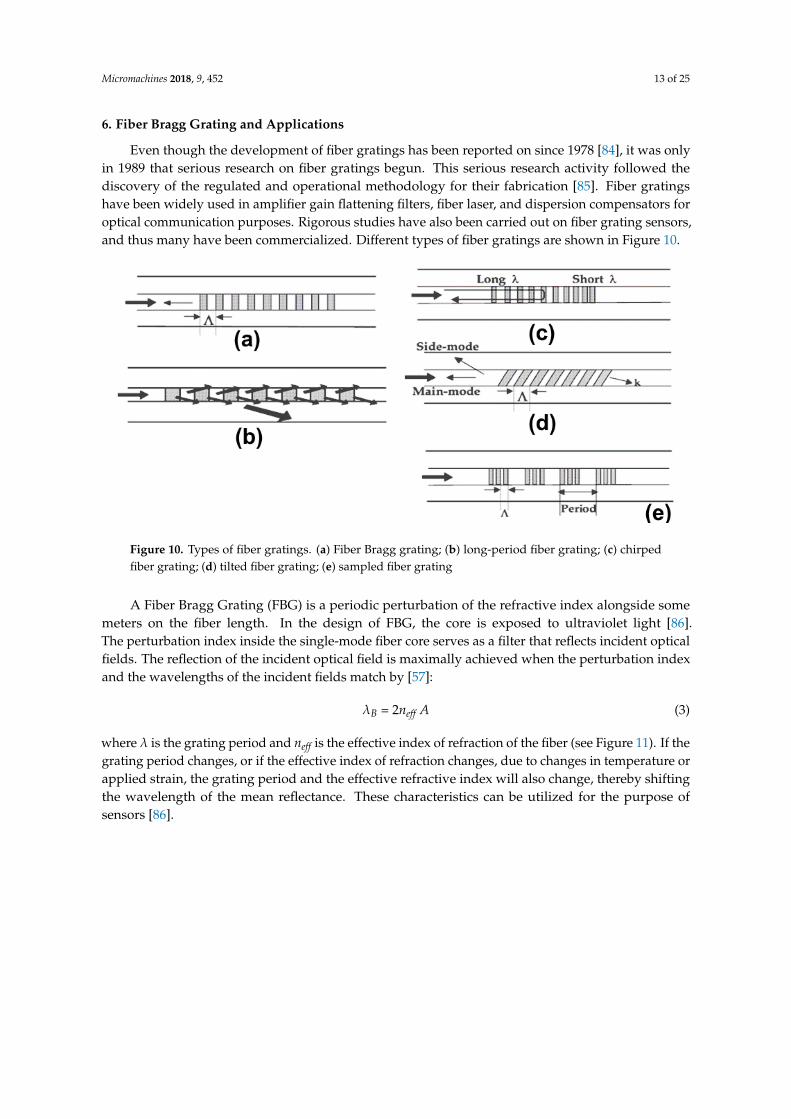
Even though the development of fiber gratings has been reported on since 1978 [84], it was onlyin 1989 that serious research on fiber gratings begun. This serious research activity followed thediscovery of the regulated and operational methodology for their fabrication [85]. Fiber gratingshave been widely used in amplifier gain flattening filters, fiber laser, and dispersion compensators foroptical communication purposes. Rigorous studies have also been carried out on fiber grating sensors,and thus many have been commercialized. Different types of fiber gratings are shown in Figure 10.
Micromachines 2018, 9, x FOR PEER REVIEW 13 of 25
6. Fiber Bragg Grating and Applications
Even though the development of fiber gratings has been reported on since 1978 [84], it was only
in 1989 that serious research on fiber gratings begun. This serious research activity followed the
discovery of the regulated and operational methodology for their fabrication [85]. Fiber gratings have
been widely used in amplifier gain flattening filters, fiber laser, and dispersion compensators for
optical communication purposes. Rigorous studies have also been carried out on fiber grating
sensors, and thus many have been commercialized. Different types of fiber gratings are shown in
Figure 10.
Figure 10. Types of fiber gratings. (a) Fiber Bragg grating; (b) long-period fiber grating; (c) chirped
fiber grating; (d) tilted fiber grating; (e) sampled fiber grating
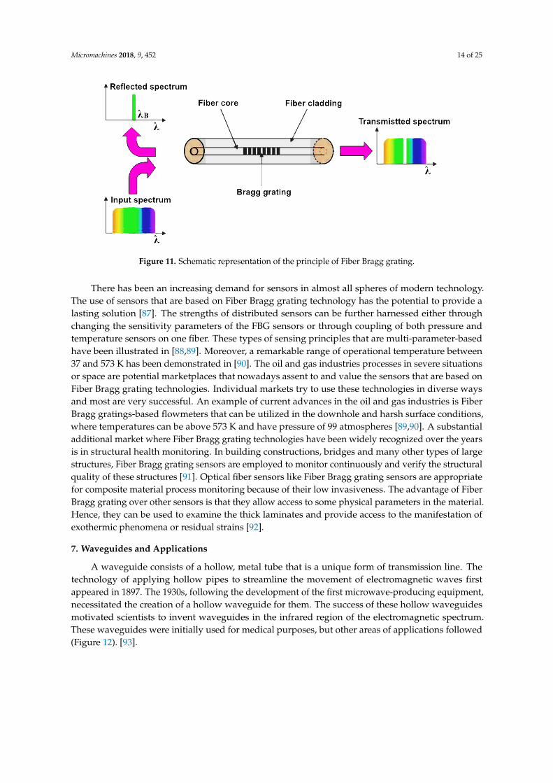
A Fiber Bragg Grating (FBG) is a periodic perturbation of the refractive index alongside some
meters on the fiber length. In the design of FBG, the core is exposed to ultraviolet light [86]. The
perturbation index inside the single-mode fiber core serves as a filter that reflects incident optical
fields. The reflection of the incident optical field is maximally achieved when the perturbation index
and the wavelengths of the incident fields match by [57]:
λB = 2neff A (3)
where λ is the grating period and neff is the effective index of refraction of the fiber (see Figure 11). If
the grating period changes, or if the effective index of refraction changes, due to changes in
temperature or applied strain, the grating period and the effective refractive index will also change,
thereby shifting the wavelength of the mean reflectance. These characteristics can be utilized for the
purpose of sensors [86].
Figure 10. Types of fiber gratings. (a) Fiber Bragg grating; (b) long-period fiber grating; (c) chirpedfiber grating; (d) tilted fiber grating; (e) sampled fiber grating
A Fiber Bragg Grating (FBG) is a periodic perturbation of the refractive index alongside somemeters on the fiber length. In the design of FBG, the core is exposed to ultraviolet light [86].The perturbation index inside the single-mode fiber core serves as a filter that reflects incident opticalfields. The reflection of the incident optical field is maximally achieved when the perturbation indexand the wavelengths of the incident fields match by [57]:
λB = 2neff A (3)
where λ is the grating period and neff is the effective index of refraction of the fiber (see Figure 11). If thegrating period changes, or if the effective index of refraction changes, due to changes in temperature orapplied strain, the grating period and the effective refractive index will also change, thereby shiftingthe wavelength of the mean reflectance. These characteristics can be utilized for the purpose ofsensors [86].
Micromachines 2018, 9, 452 14 of 25Micromachines 2018, 9, x FOR PEER REVIEW 14 of 25
Figure 11. Schematic representation of the principle of Fiber Bragg grating.
There has been an increasing demand for sensors in almost all spheres of modern technology.
The use of sensors that are based on Fiber Bragg grating technology has the potential to provide a
lasting solution [87]. The strengths of distributed sensors can be further harnessed either through
changing the sensitivity parameters of the FBG sensors or through coupling of both pressure and
temperature sensors on one fiber. These types of sensing principles that are multi-parameter-based
have been illustrated in [88,89]. Moreover, a remarkable range of operational temperature between
37 and 573 K has been demonstrated in [90]. The oil and gas industries processes in severe situations
or space are potential marketplaces that nowadays assent to and value the sensors that are based on
Fiber Bragg grating technologies. Individual markets try to use these technologies in diverse ways
and most are very successful. An example of current advances in the oil and gas industries is Fiber
Bragg gratings-based flowmeters that can be utilized in the downhole and harsh surface conditions,
where temperatures can be above 573 K and have pressure of 99 atmospheres [89,90]. A substantial
additional market where Fiber Bragg grating technologies have been widely recognized over the
years is in structural health monitoring. In building constructions, bridges and many other types of
large structures, Fiber Bragg grating sensors are employed to monitor continuously and verify the
structural quality of these structures [91]. Optical fiber sensors like Fiber Bragg grating sensors are
appropriate for composite material process monitoring because of their low invasiveness. The
advantage of Fiber Bragg grating over other sensors is that they allow access to some physical
parameters in the material. Hence, they can be used to examine the thick laminates and provide access
to the manifestation of exothermic phenomena or residual strains [92].
7. Waveguides and Applications
A waveguide consists of a hollow, metal tube that is a unique form of transmission line. The
technology of applying hollow pipes to streamline the movement of electromagnetic waves first
appeared in 1897. The 1930s, following the development of the first microwave-producing
equipment, necessitated the creation of a hollow waveguide for them. The success of these hollow
waveguides motivated scientists to invent waveguides in the infrared region of the electromagnetic
spectrum. These waveguides were initially used for medical purposes, but other areas of applications
followed (Figure 12). [93].
Figure 11. Schematic representation of the principle of Fiber Bragg grating.
There has been an increasing demand for sensors in almost all spheres of modern technology.The use of sensors that are based on Fiber Bragg grating technology has the potential to provide alasting solution [87]. The strengths of distributed sensors can be further harnessed either throughchanging the sensitivity parameters of the FBG sensors or through coupling of both pressure andtemperature sensors on one fiber. These types of sensing principles that are multi-parameter-basedhave been illustrated in [88,89]. Moreover, a remarkable range of operational temperature between37 and 573 K has been demonstrated in [90]. The oil and gas industries processes in severe situationsor space are potential marketplaces that nowadays assent to and value the sensors that are based onFiber Bragg grating technologies. Individual markets try to use these technologies in diverse waysand most are very successful. An example of current advances in the oil and gas industries is FiberBragg gratings-based flowmeters that can be utilized in the downhole and harsh surface conditions,where temperatures can be above 573 K and have pressure of 99 atmospheres [89,90]. A substantialadditional market where Fiber Bragg grating technologies have been widely recognized over the yearsis in structural health monitoring. In building constructions, bridges and many other types of largestructures, Fiber Bragg grating sensors are employed to monitor continuously and verify the structuralquality of these structures [91]. Optical fiber sensors like Fiber Bragg grating sensors are appropriatefor composite material process monitoring because of their low invasiveness. The advantage of FiberBragg grating over other sensors is that they allow access to some physical parameters in the material.Hence, they can be used to examine the thick laminates and provide access to the manifestation ofexothermic phenomena or residual strains [92].
7. Waveguides and Applications
A waveguide consists of a hollow, metal tube that is a unique form of transmission line. Thetechnology of applying hollow pipes to streamline the movement of electromagnetic waves firstappeared in 1897. The 1930s, following the development of the first microwave-producing equipment,necessitated the creation of a hollow waveguide for them. The success of these hollow waveguidesmotivated scientists to invent waveguides in the infrared region of the electromagnetic spectrum.These waveguides were initially used for medical purposes, but other areas of applications followed(Figure 12). [93].

Micromachines 2018, 9, 452 15 of 25Micromachines 2018, 9, x FOR PEER REVIEW 15 of 25
Figure 12. Rectangular and circular waveguides.
It directs the waves in a similar way river banks head a tidal wave [93]. Nevertheless, since
waveguides are regarded as single-conductor materials, there is a difference in the way electrical
energy is propagated down a waveguide as compared to the way in which it is propagated through
a two-conductor transmission system. Figure 13 shows the propagation of the TEM mode in the
waveguide.
Figure 13. Transverse electromagnetic (TEM) mode propagation of a waveguide.
Figure 12. Rectangular and circular waveguides.
It directs the waves in a similar way river banks head a tidal wave [93]. Nevertheless,since waveguides are regarded as single-conductor materials, there is a difference in the way electricalenergy is propagated down a waveguide as compared to the way in which it is propagated througha two-conductor transmission system. Figure 13 shows the propagation of the TEM mode inthe waveguide.
Micromachines 2018, 9, x FOR PEER REVIEW 15 of 25
Figure 12. Rectangular and circular waveguides.
It directs the waves in a similar way river banks head a tidal wave [93]. Nevertheless, since
waveguides are regarded as single-conductor materials, there is a difference in the way electrical
energy is propagated down a waveguide as compared to the way in which it is propagated through
a two-conductor transmission system. Figure 13 shows the propagation of the TEM mode in the
waveguide.
Figure 13. Transverse electromagnetic (TEM) mode propagation of a waveguide.
Figure 13. Transverse electromagnetic (TEM) mode propagation of a waveguide.
From Table 1, it could be concluded that a major improvement in waveguides is the decreasein propagation losses. The waveguide dimensions become impossibly large for lower frequencies,while, when the rate is higher, the dimensions become impracticably smaller. Waveguides presentnumerous advantages when compared to their optical fiber counterparts. Waveguides can transmitwavelengths above 20 µm. Their air core enables them to deliver high power lasers. Waveguides haverelatively simple structures and they are cheap compared to the existing optical fibers. These qualitiesallow their use in applications where transmission of electromagnetic radiation requires a materialof high mechanical, optical and thermal properties. Even though waveguides are associated with

Micromachines 2018, 9, 452 16 of 25
some setbacks such as losses upon bending as well as small numerical aperture, they appear to be thebest option for use in sensors. Waveguides can be classified into two classes based on the principleson which they operate. These are attenuated total internal reflection and leaky-type waveguides.In attenuated total internal reflection-based waveguides, hollow core substances are present, which areenclosed by a wall that has a refractive index lower than that of the wavelength of the transmittedlight. In the design of metallic waveguides, the inner wall is formed using a smooth metallic surfaceby depositing a metal film on the inner surface of plastic or a glass tube. Dielectric waveguides, on theother hand, are achieved by the formation of alternating high-low refractive index structure formed bythe addition of multiple dielectric layers onto the metal surface. There has been a dramatic increase inthe use of substrate integrated waveguides over the last decade due to their compact, low profile, andmany other advantages over the conventional metallic waveguides. They resemble the conventionalwaveguides in their performances and can be made with printed circuit boards [94].
Table 1. Rectangular waveguide sizes (source: https://www.everythingrf.com/tech-resources/waveguides-sizes).
Waveguide Name RecommendedFrequency
(GHz)
CutoffFrequency
Lowest OrderMode (GHz)
CutoffFrequencyNext Mode
(GHz)
Inner Dimensionsof Waveguide
Opening
EIA RCSC IEC A Inch B Inch
- WG9 - 2.20 to 3.30 1.686 3.372 3.5 1.75WR340 WG9A R26 2.20 to 3.30 1.736 3.471 3.4 1.7WR284 WG10 R32 2.60 to 3.95 2.078 4.156 2.84 1.34
- WG11 - 3.30 to 4.90 2.488 4.976 2.372 1.122WR229 WG11A R40 3.30 to 4.90 2.577 5.154 2.29 1.145WR187 WG12 R48 3.95 to 5.85 3.153 6.305 1.872 0.872WR159 WG13 R58 4.90 to 7.05 3.712 7.423 1.59 0.795WR137 WG14 R70 5.85 to 8.20 4.301 8.603 1.372 0.622WR112 WG15 R84 7.05 to 10 5.26 10.52 1.122 0.497WR102 - - 7.00 to 11 5.786 11.571 1.02 0.51WR90 WG16 R100 8.20 to 12.40 6.557 13.114 0.9 0.4WR75 WG17 R120 10.00 to 15 7.869 15.737 0.75 0.375WR62 WG18 R140 12.40 to 18 9.488 18.976 0.622 0.311WR51 WG19 R180 15.00 to 22 11.572 23.143 0.51 0.255WR42 WG20 R220 18.00 to 26.50 14.051 28.102 0.42 0.17WR34 WG21 R260 22.00 to 33 17.357 34.715 0.34 0.17WR28 WG22 R320 26.50 to 40 21.077 42.154 0.28 0.14WR22 WG23 R400 33.00 to 50 26.346 52.692 0.224 0.112WR19 WG24 R500 40.00 to 60 31.391 62.782 0.188 0.094WR15 WG25 R620 50.00 to 75 39.875 79.75 0.148 0.074WR12 WG26 R740 60 to 90 48.373 96.746 0.122 0.061WR10 WG27 R900 75 to 110 59.015 118.03 0.1 0.05WR8 WG28 R1200 90 to 140 73.768 147.536 0.08 0.04WR6 WG29 R1400 110 170 90.791 181.583 0.065 0.0325WR7 WG29 R1400 110 to 170 90.791 181.583 0.065 0.0325WR5 WG30 R1800 140 to 220 115.714 231.429 0.051 0.0255WR4 WG32 R2200 172 to 260 137.243 274.485 0.043 0.0215WR3 WG32 R2600 220 to 330 173.571 347.143 0.034 0.017
The need to explore waves at a millimeter scale for the subsequent generation of mobilecommunications has contributed significantly to the advancement of modern telecommunicationscomponents based on microwaves [95]. Substrate-integrated waveguides have found many potentialapplications outside the telecommunication industry. They are widely used in the automotive industry,as well as in biomedical devices for sensing applications. In terms of their dispersion and propagationcharacteristics, substrate integrated waveguides are similar to rectangular waveguides.
Another important emerging area is opted fluidics, which combines the benefits of opticsand microfluidics in order to achieve highly compact and highly functional materials. Specifically,

Micromachines 2018, 9, 452 17 of 25
fluidic elements are integrated into the photonics structure [96,97]. A lot of optofluidic sensors areproduced for healthcare and pharmaceutical researchers. Moreover, sensors are also available forbiochemical analyses, environmental monitoring as well as biomedical researchers [98]. Integrationof optical and fluidic structures can simply be achieved via optofluidic waveguides. Optofluidicwaveguides are found to provide a very powerful foundation for building optofluidic sensors.The liquid core serves as the medium through which the light is guided with the help of highlyreflective mirrors that are achieved by the sidewalls of the core. High sensitivity is usually achieved bytaking advantage of flow or guidance of the light and the fluid through the same medium or channel.This direct interaction provides high sensitivity due to the small volume of the liquid as well as strongoptical connections. Sensitivity can be achieved as low as the molecular level and this is the ultimatedesire for any given analytical procedure. Just like other waveguide systems such as slot waveguidesand photonic crystals, they have a high attractive capacity for optofluidic integrations with planarsystems [99,100]. These types of waveguides allow simultaneous confinement and propagation oflight because of the interference of light that occurs at the claddings that are made up of alternatingthin layers of low- and high-refractive index. The operating principle of these types of waveguides canbe understood easier when one considers the 1D structure as presented below in Figure 14. Assumingthat two layers of the cladding are considered, and their refractive indexes are respectively n1 and n2
(with n1 > n2), propagation of light through the core is achieved by Fresnel reflections at the claddinginterfaces. Repeated reflections at the interfaces cause the entrapped light to interfere. Interferencecladding is designed to certify certain conditions to strengthen the intensity of the reflected light [101].Micromachines 2018, 9, x FOR PEER REVIEW 18 of 25
Figure 14. 1D structure of narrow waveguide.
Presently, optical biosensors have emerged as the favorite choice to replace bulky laboratory
instruments for such applications where a bulky quantity of samples is required to be simultaneously
analyzed, like microplate array systems. Optical biosensors possess some desirable characteristics
like small size, low-cost and being easier to use. These pleasant characteristics allow them to be used
in online monitoring and sensing for the analysis of samples that are complex, and for real-time or
online monitoring of experimental procedures [102]. Therefore, optical bio-sensing is now an active
research field and commercialization of a number of platforms has already been realized. The
application areas include environmental monitoring, clinical application, and food safety and control
[103]. The most powerful and reliable biosensors are undoubtedly those based on fluorescence.
Fluorescence intensity, decay time, and emission anisotropy are among the parameters that could be
measured and used for sensing [104]. There is, therefore, a variety of options towards improving the
performance of biosensors. Optical waveguides are dielectric configurations having two extreme
wavelengths in the infrared and the ultraviolet regions of the electromagnetic spectrum and can be
used to transport energy between these two extreme wavelengths. Based on their geometrical shape,
they can be categorized into two main classes: planar and cylindrical. Optical waveguides are
contained within the first group and are comprised of a cylindrical central dielectric core-cladding
by an element characterized by a low refractive index (by z 1%). The planar waveguides are prepared
from a dielectric slab core enclosed between two layers of the cladding with slightly lower refractive
indices [105]. In both layers, propagation of light and streamlining along the direction of core depend
on the famous total internal reflection phenomenon. When light is propagated within a planar or
cylindrical waveguide, the light is reflected totally at the interface between two mediums in which
one is optically denser provided that the angle of refraction is greater than the critical angle. In
fluorescent biosensors that are based on evanescent field excitation, the geometry of the sensing
region must be properly designed in order to optimize the excitation ability along the probe length,
and also to prevent the coupling of the emitted fluorescence into guided modes that do not propagate
in the cladding. This is known as “V-number mismatch” [106,107].
Many industrial operations such as welding and cutting are achieved using carbon dioxide
lasers. However, bringing the laser beam from the source of flame to the desired area is a challenge
because other equipment may block the path. The only method to successfully deliver the beam is
using articulated arms; however, these colossal systems also require large spaces and mirrors
requiring regular maintenance and alignment. Attempts have been made to use solid core
waveguides to deliver high power carbon dioxide beams, but, due to thermal damage, particularly
at the high interface, they have not been successful. Short lifespan associated with some of the
promising solid core is also a disadvantage. Transmission of up to 3000 Watts of laser power is
required at the initial attempt using circular and rectangular metal-coated waveguides. However,
large core radii are needed to achieve the needed power levels and, when subjected to bends and
Figure 14. 1D structure of narrow waveguide.
Presently, optical biosensors have emerged as the favorite choice to replace bulky laboratoryinstruments for such applications where a bulky quantity of samples is required to be simultaneouslyanalyzed, like microplate array systems. Optical biosensors possess some desirable characteristics likesmall size, low-cost and being easier to use. These pleasant characteristics allow them to be used inonline monitoring and sensing for the analysis of samples that are complex, and for real-time or onlinemonitoring of experimental procedures [102]. Therefore, optical bio-sensing is now an active researchfield and commercialization of a number of platforms has already been realized. The application areasinclude environmental monitoring, clinical application, and food safety and control [103]. The mostpowerful and reliable biosensors are undoubtedly those based on fluorescence. Fluorescence intensity,decay time, and emission anisotropy are among the parameters that could be measured and used forsensing [104]. There is, therefore, a variety of options towards improving the performance of biosensors.Optical waveguides are dielectric configurations having two extreme wavelengths in the infrared

Micromachines 2018, 9, 452 18 of 25
and the ultraviolet regions of the electromagnetic spectrum and can be used to transport energybetween these two extreme wavelengths. Based on their geometrical shape, they can be categorizedinto two main classes: planar and cylindrical. Optical waveguides are contained within the first groupand are comprised of a cylindrical central dielectric core-cladding by an element characterized bya low refractive index (by z 1%). The planar waveguides are prepared from a dielectric slab coreenclosed between two layers of the cladding with slightly lower refractive indices [105]. In both layers,propagation of light and streamlining along the direction of core depend on the famous total internalreflection phenomenon. When light is propagated within a planar or cylindrical waveguide, the lightis reflected totally at the interface between two mediums in which one is optically denser providedthat the angle of refraction is greater than the critical angle. In fluorescent biosensors that are based onevanescent field excitation, the geometry of the sensing region must be properly designed in order tooptimize the excitation ability along the probe length, and also to prevent the coupling of the emittedfluorescence into guided modes that do not propagate in the cladding. This is known as “V-numbermismatch” [106,107].
Many industrial operations such as welding and cutting are achieved using carbon dioxide lasers.However, bringing the laser beam from the source of flame to the desired area is a challenge becauseother equipment may block the path. The only method to successfully deliver the beam is usingarticulated arms; however, these colossal systems also require large spaces and mirrors requiringregular maintenance and alignment. Attempts have been made to use solid core waveguides to deliverhigh power carbon dioxide beams, but, due to thermal damage, particularly at the high interface,they have not been successful. Short lifespan associated with some of the promising solid core is also adisadvantage. Transmission of up to 3000 Watts of laser power is required at the initial attempt usingcircular and rectangular metal-coated waveguides. However, large core radii are needed to achieve theneeded power levels and, when subjected to bends and other movements, these large radii waveguidesexhibit poor outputs. Moreover, most of the industrial operations require low order outputs to achievesharp and clean cuts. Therefore, to attain this type of quality with hollow waveguides, smaller sizecore is needed to filter and transmit the higher order mode in the desired fashion. It is a known factthat, as the size of the core decreases, the loss of the waveguide increases and this, in turn, decreasesthe power capacity. These setbacks reduce the use of hollow waveguides to industrial uses such asmarking cutting of plastic or paper, which requires lower power [108].
Controlling and streamlining the movement of light has been one of the main focus areas ofresearch in the last few decades. Materials such as optical fibers, which operate based on the principle oftotal internal reflection, have significantly transformed the communication industry [109]. The conceptof photonic crystals was proposed independently by John [110] and Yablonovitch [111] in 1987.They use the electronic band concept analogous to semiconductor crystals. Photonic crystals aredielectric materials that are periodic in 1D, 2D or 3D orthogonal directions. They can be fabricatedin a simple way and have unusual optical properties. Two-dimensional photonic crystals are themost interesting and can be categorized into two: dielectric materials in air, or air in the dielectricmaterial. The former is fabricated easily via periodic inscription of holes in materials of high dielectricproperties such as GaAs, Si, and Ge. Photonic bandgaps are characterized by photonic crystals becauseof the intermittent disparity in the refractive index. Photonic band gaps have a range of frequenciesthat cannot allow propagating inside the crystal. Because of this peculiar property, waveguides areformed through inducing of line imperfections in photonic crystal structures [112,113]. These linefaults are used to guide light from one place to another. The defects are guided inside the photonicband gap through the streamline via the total internal reflection principle. Because of the asymmetricalboundary, this streamlining creates backscattering, which causes slow light phenomena. Slow lightcauses optical signals to compress in space, and this enables interaction between light and matter andallows miniaturization. Presentation of photonic crystal waveguides is given in Figure 15a. A varietyof dielectric slab materials of the high refractive index can be used to produce photonic crystal slabs.A typical example of these photonic crystals is based on polymethyl methacrylate (PMMA) prepared

Micromachines 2018, 9, 452 19 of 25
by [114]. A photonic crystal slab based on Si3N4 has been demonstrated to work in the visible regionof the electromagnetic spectrum. Moreover, photonic crystals based on InP/InGaAsP structure havebeen prepared with a slight loss [115].
Micromachines 2018, 9, x FOR PEER REVIEW 19 of 25
other movements, these large radii waveguides exhibit poor outputs. Moreover, most of the
industrial operations require low order outputs to achieve sharp and clean cuts. Therefore, to attain
this type of quality with hollow waveguides, smaller size core is needed to filter and transmit the
higher order mode in the desired fashion. It is a known fact that, as the size of the core decreases, the
loss of the waveguide increases and this, in turn, decreases the power capacity. These setbacks reduce
the use of hollow waveguides to industrial uses such as marking cutting of plastic or paper, which
requires lower power [108].
Controlling and streamlining the movement of light has been one of the main focus areas of
research in the last few decades. Materials such as optical fibers, which operate based on the principle
of total internal reflection, have significantly transformed the communication industry [109]. The
concept of photonic crystals was proposed independently by John [110] and Yablonovitch [111] in
1987. They use the electronic band concept analogous to semiconductor crystals. Photonic crystals
are dielectric materials that are periodic in 1D, 2D or 3D orthogonal directions. They can be fabricated
in a simple way and have unusual optical properties. Two-dimensional photonic crystals are the most
interesting and can be categorized into two: dielectric materials in air, or air in the dielectric material.
The former is fabricated easily via periodic inscription of holes in materials of high dielectric
properties such as GaAs, Si, and Ge. Photonic bandgaps are characterized by photonic crystals
because of the intermittent disparity in the refractive index. Photonic band gaps have a range of
frequencies that cannot allow propagating inside the crystal. Because of this peculiar property,
waveguides are formed through inducing of line imperfections in photonic crystal structures
[112,113]. These line faults are used to guide light from one place to another. The defects are guided
inside the photonic band gap through the streamline via the total internal reflection principle.
Because of the asymmetrical boundary, this streamlining creates backscattering, which causes slow
light phenomena. Slow light causes optical signals to compress in space, and this enables interaction
between light and matter and allows miniaturization. Presentation of photonic crystal waveguides is
given in Figure 15a. A variety of dielectric slab materials of the high refractive index can be used to
produce photonic crystal slabs. A typical example of these photonic crystals is based on polymethyl
methacrylate (PMMA) prepared by [114]. A photonic crystal slab based on Si3N4 has been
demonstrated to work in the visible region of the electromagnetic spectrum. Moreover, photonic
crystals based on InP/InGaAsP structure have been prepared with a slight loss [115].
Figure 15. (a) Photonic crystal waveguide slab; (b) photonic band diagram Figure 15. (a) Photonic crystal waveguide slab; (b) photonic band diagram
Several types of research are on-going for the potential applications of photonic crystals.Most frequent among them are related to the photonic integrated circuits. The introduction of defectscan be achieved through the photonic band gap. Instead of guiding light through total internalreflection, it could be conducted using line defects in photonic crystals. The use of a photonic bandgapto guide light allows for small bending loss even when the bending angles are large. In the areaof sensors, photonic crystals have been widely used in the field of sensors. A photonic crystal slabprovides sensitivity to the photonic band gap. Some of these sensors can be designed to detect pressureusing a GaAs/AIGaAs slab [116].
8. Conclusions
Waveguides and optical fibers have applications for assisting us in various aspects of our lives.As anticipated, optical fiber-based sensors can be appropriate instruments for monitoring physicalparameters such as strain and temperature. A review of some of the recent advances related to thedesign and application of optical fiber sensors has been given. It has been established that opticalfiber grating sensors and side-polished fibers continue to play a significant role in the developmentof various sensors with the combination of new fiber materials and structures. These new classes ofFiber Bragg grating sensors have the potential for many industrial uses. Each market and applicationhas its separate advantages derived from Fiber Bragg grating based sensor applications. Nevertheless,optimization of the sensor systems is not restricted to the sensors only, but the entire system must beconsidered. To obtain an optimal Fiber Bragg grating sensors system for application, optimization ofthe interrogator with regard to wavelengths, resolutions, sweep frequencies as well as costs, amongother factors, must be considered.
Fiber optics sensors have been developing for many years but have not achieved great commercialsuccess yet due to the difficulties of introducing modern technologies that could replace current

Micromachines 2018, 9, 452 20 of 25
well-established technologies. However, for applications such as sensing in high-voltage andhigh-power machinery, or in microwave ovens, the fiber optics sensors are well recognized forpresenting many advantages. Fiber Bragg grating sensors have developed significantly, and thesecan now be used to monitor conditions within the wings of airplanes, in wind turbines, bridges,large dams, oil wells and pipelines. In smart structures, which are the main drivers for the furtherdevelopment of fiber-optic sensors, the fiber sensors can monitor and obtain essential informationabout the strain, vibrations, and other phenomena. Since the year 2000, fiber optics has provideda significant contribution in applications such as optical communications, transmission fibers usedunderwater, in terrestrial areas, metro and local area networks (LAN). Other special fibers have beenused in amplifiers, lasers, sensors and photonics devices. Further improvements of the fiber optics canbe done by providing higher bandwidth, transmissions capacities for longer distances, and introducingdevices with at a lower cost. For instance, in the LAN fiber world, the use of new wideband multimodefibers is recommended to improve the overall system efficiency. The wideband multimode fibers canbe used in wider frequency ranges from visible to infrared such as the short wavelength-divisionmultiplexing ranges 850 to 950 nm. Another rapidly growing technology is free-space communication,where the optical signals can be used for satellite–satellite communications. Recently, optical fibershave been used for transmission from light emitting sources such as high-power lasers, where thesudden changes in wavelength can be controlled easily in these devices.
Author Contributions: I.S.A. conceived and designed the experiments; S.R.B.A. performed the experiments;M.A.J. and J.A. analyzed the data; H.M.H. contributed reagents/materials/analysis tools; I.S.A. wrote the paper;M.B. and P.Y. have performed the revisions.
Acknowledgments: All sources of funding of the study should be disclosed. Please clearly indicate grants thatyou have received in support of your research work. Clearly state if you received funds for covering the costs topublish in open access.
Conflicts of Interest: The authors declare no conflict of interest.
References
1. Cavin, S.; Wang, X.; Zellweger, M.; Gonzalez, M.; Bensimon, M.; Wagnières, G.; Krueger, T.; Ris, H.;Gronchi, F.; Perentes, J.Y. Interstitial fluid pressure: A novel biomarker to monitor photo-induced druguptake in tumor and normal tissues. Lasers Surg. Med. 2017, 49, 773–780. [CrossRef] [PubMed]
2. Mignon, C.; Tobin, D.J.; Zeitouny, M.; Uzunbajakava, N.E. Shedding light on the variability of optical skinproperties: Finding a path towards more accurate prediction of light propagation in human cutaneouscompartments. Biomed. Opt. Express 2018, 9, 852–872. [CrossRef] [PubMed]
3. Sun, Q.; He, Y.; Liu, K.; Fan, S.; Parrott, E.P.J.; Pickwell-MacPherson, E. Recent advances in terahertztechnology for biomedical applications. Quant. Imaging Med. Surg. 2017, 7, 345–355. [CrossRef] [PubMed]
4. Gorin, A.; Jaouad, A.; Grondin, E.; Aimez, V.; Charette, P. Fabrication of silicon nitride waveguides forvisible-light using PECVD: A study of the effect of plasma frequency on optical properties. Opt. Express 2008,16, 13509–13516. [CrossRef] [PubMed]
5. Zheludev, N. The life and times of the LED—A 100-year history. Nat. Photonics 2007, 1, 189–192. [CrossRef]6. Gordon, R. Sensors: Single-ion detection. Nat. Photonics 2016, 10, 697–698. [CrossRef]7. Hochberg, M.; Baehr-Jones, T. Towards fabless silicon photonics. Nat. Photonics 2010, 4, 492–494. [CrossRef]8. Malka, D.; Peled, A. Power splitting of 1 × 16 in multicore photonic crystal fibers. Appl. Surf. Sci. 2017, 417,
34–39. [CrossRef]9. Dersch, R.; Steinhart, M.; Boudriot, U.; Greiner, A.; Wendorff, J.H. Nanoprocessing of polymers: Applications
in medicine, sensors, catalysis, photonics. Polym. Adv. Technol. 2005, 16, 276–282. [CrossRef]10. Weil, T.; Vosch, T.; Hofkens, J.; Peneva, K.; Müllen, K. The rylene colorant family—tailored nanoemitters for
photonics research and applications. Angew. Chem. Int. Ed. 2010, 49, 9068–9093. [CrossRef] [PubMed]11. Jariwala, D.; Marks, T.J.; Hersam, M.C. Mixed-dimensional van der Waals heterostructures. Nat. Mater. 2017,
16, 170–181. [CrossRef] [PubMed]12. Hedberg, T.; Feeney, A.B.; Helu, M.; Camelio, J.A. Toward a Lifecycle Information Framework and Technology
in Manufacturing. J. Comput. Inf. Sci. Eng. 2017, 17, 021010. [CrossRef] [PubMed]

Micromachines 2018, 9, 452 21 of 25
13. Sundaravadivel, P.; Kougianos, E.; Mohanty, S.P.; Ganapathiraju, M.K. Everything You Wanted to Knowabout Smart Health Care: Evaluating the Different Technologies and Components of the Internet of Thingsfor Better Health. IEEE Consum. Electron. Mag. 2018, 7, 18–28. [CrossRef]
14. Xu, T.; Shevchenko, N.A.; Lavery, D.; Semrau, D.; Liga, G.; Alvarado, A.; Killey, R.I.; Bayvel, P. Modulationformat dependence of digital nonlinearity compensation performance in optical fibre communicationsystems. Opt. Express 2017, 25, 3311–3326. [CrossRef] [PubMed]
15. Farsaei, A.; Wang, Y.; Molavi, R.; Jayatilleka, H.; Caverley, M.; Beikahmadi, M.; Shirazi, A.H.M.; Jaeger, N.;Chrostowski, L.; Mirabbasi, S. A review of wireless-photonic systems: Design methodologies and topologies,constraints, challenges, and innovations in electronics and photonics. Opt. Commun. 2016, 373, 16–34.[CrossRef]
16. Zou, X.; Lu, B.; Pan, W.; Yan, L.; Stöhr, A.; Yao, J. Photonics for microwave measurements. Laser Photonics Rev.2016, 10, 711–734. [CrossRef]
17. Marpaung, D.; Roeloffzen, C.; Heideman, R.; Leinse, A.; Sales, S.; Capmany, J. Integrated microwavephotonics. Laser Photonics Rev. 2013, 7, 506–538. [CrossRef]
18. Capmany, J.; Mora, J.; Pastor, D.; Ortega, B.; Sales, S. Microwave photonic signal processing.J. Lightwave Technol. 2013, 31, 571–586. [CrossRef]
19. Aulakh, S.K. Application of microwave photonics in electronic warfare. IJCST 2013, 4, 53–58.20. Liu, L.; Feng, F.; Hu, Q.; Paau, M.C.; Liu, Y.; Chen, Z.; Bai, Y.; Guo, F.; Choi, M.M.F. Capillary electrophoretic
study of green fluorescent hollow carbon nanoparticles. Electrophoresis 2015, 36, 2110–2119. [CrossRef][PubMed]
21. Ma, R.; Oulton, R.F.; Sorger, V.J.; Zhang, X. Plasmon lasers: Coherent light source at molecular scales.Laser Photonics Rev. 2013, 7, 1–21. [CrossRef]
22. Chen, B.; Yang, J.; Hu, C.; Wang, S.; Wen, Q.; Zhang, J. Plasmonic polarization nano-splitter based onasymmetric optical slot antenna pairs. Opt. Lett. 2016, 41, 4931–4934. [CrossRef] [PubMed]
23. Park, W.; Rhie, J.; Kim, N.Y.; Hong, S.; Kim, D. Sub-10 nm feature chromium photomasks for contactlithography patterning of square metal ring arrays. Sci. Rep. 2016, 6, 23823. [CrossRef] [PubMed]
24. El-Rabiaey, M.A.; Areed, N.F.F.; Obayya, S.S.A. Novel plasmonic data storage based on nematic liquid crystallayers. J. Lightwave Technol. 2016, 34, 3726–3732. [CrossRef]
25. Stipe, B.C.; Strand, T.C.; Poon, C.C.; Balamane, H.; Boone, T.D.; Katine, J.A.; Li, J.; Rawat, V.; Nemoto, H.;Hirotsune, A.; et al. Magnetic recording at 1.5 Pb m-2 using an integrated plasmonic antenna. Nat. Photonics2010, 4, 484–488. [CrossRef]
26. Petersen, M.R.; Yossef, M.; Chen, A. Gap between Code Requirements and Current State of Research onSafety Performance of Fiber-Reinforced Polymer for Nonstructural Building Components. Pract. Period.Struct. Des. Constr. 2017, 22, 04017005. [CrossRef]
27. Knight, J.C.; Birks, T.A.; Russell, P.S.J.; Atkin, D.M. All-silica single-mode optical fiber with photonic crystalcladding. Opt. Lett. 1996, 21, 1547–1549. [CrossRef] [PubMed]
28. Seddon, A.B.; Tang, Z.; Furniss, D.; Sujecki, S.; Benson, T.M. Progress in rare-earth-doped mid-infrared fiberlasers. Opt. Express 2010, 18, 26704–26719. [CrossRef] [PubMed]
29. Borshchevskaia, N.A.; Katamadze, K.G.; Kulik, S.P.; Klyamkin, S.N.; Chuvikov, S.V.; Sysolyatin, A.A.;Tsvetkov, S.V.; Fedorov, M.V. Luminescence in germania–silica fibers in a 1–2 µm region. Opt. Lett. 2017, 42,2874–2877. [CrossRef] [PubMed]
30. Hegedus, G.; Sarkadi, T.; Czigány, T. Analysis of the Light Transmission Ability of Reinforcing Glass FibersUsed in Polymer Composites. Materials 2017, 10, 637. [CrossRef] [PubMed]
31. Ertman, S.; Lesiak, P.; Wolinski, T.R. Optofluidic photonic crystal fiber-based sensors. J. Lightwave Technol.2017, 35, 3399–3405. [CrossRef]
32. Singh, E.; Kim, K.S.; Yeom, G.Y.; Nalwa, H.S. Atomically thin-layered molybdenum disulfide (MoS2) forbulk-heterojunction solar cells. ACS Appl. Mater. Interfaces 2017, 9, 3223–3245. [CrossRef] [PubMed]
33. Qiao, P.; Yang, W.; Chang-Hasnain, C.J. Recent advances in high-contrast metastructures, metasurfaces, andphotonic crystals. Adv. Opt. Photonics 2018, 10, 180–245. [CrossRef]
34. Tao, G.; Ebendorff-Heidepriem, H.; Stolyarov, A.M.; Danto, S.; Badding, J.V.; Fink, Y.; Ballato, J.;Abouraddy, A.F. Infrared fibers. Adv. Opt. Photonics 2015, 7, 379–458. [CrossRef]
35. Peacock, A.C.; Sparks, J.R.; Healy, N. Semiconductor optical fibres: Progress and opportunities.Laser Photonics Rev. 2014, 8, 53–72. [CrossRef]

Micromachines 2018, 9, 452 22 of 25
36. Wang, Z.; Guo, C.; Jiang, W. Large mode area OmniGuide fiber with superconductor-dielectric periodicmultilayers cladding. Opt. Int. J. Light Electron Opt. 2014, 125, 6789–6792. [CrossRef]
37. Hasan, M.I.; Akhmediev, N.; Chang, W. Mid-infrared supercontinuum generation in supercritical xenon-filledhollow-core negative curvature fibers. Opt. Lett. 2016, 41, 5122–5125. [CrossRef] [PubMed]
38. Bellanca, G.; Riesen, N.; Argyros, A.; Leon-Saval, S.G.; Lwin, R.; Parini, A.; Love, J.D.; Bassi, P. Holey fibermode-selective couplers. Opt. Express 2015, 23, 18888–18896. [CrossRef] [PubMed]
39. Hu, K.; Kabakova, I.V.; Büttner, T.F.; Lefrancois, S.; Hudson, D.D.; He, S.; Eggleton, B.J. Low-thresholdBrillouin laser at 2 µm based on suspended-core chalcogenide fiber. Opt. Lett. 2014, 39, 4651–4654. [CrossRef][PubMed]
40. Kim, R.; Park, C.H.; Lee, A.; Moon, J.H. Development of the noncontact temperature sensor using theinfrared optical fiber coated with antifog solution. Sci. Technol. Nucl. Install. 2015, 2015, 718592. [CrossRef]
41. Mishra, V. 16 Medical Applications of Fiber-Optic Sensors. Opt. Fiber Sens. Adv. Tech. Appl. 2015, 36, 455.42. Pospíšilová, M.; Kuncová, G.; Trögl, J. Fiber-optic chemical sensors and fiber-optic bio-sensors. Sensors 2015,
15, 25208–25259. [CrossRef] [PubMed]43. Liu, Y.; Zhang, M.; Zhang, J.; Wang, Y. Single-longitudinal-mode triple-ring Brillouin fiber laser with a
saturable absorber ring resonator. J. Lightwave Technol. 2017, 35, 1744–1749. [CrossRef]44. Axelrod, D.; Burghardt, T.P.; Thompson, N.L. Total internal reflection fluorescence. Annual review of
biophysics and bioengineering. Ann. Rev. Biophys. Bioeng. 1984, 13, 247–268. [CrossRef] [PubMed]45. Sönnichsen, C.; Geier, S.; Hecker, N.E.; von Plessen, G.; Feldmann, J.; Ditlbacher, H.; Lamprecht, B.;
Krenn, J.R.; Aussenegg, F.R.; Chan, V.Z.; et al. Spectroscopy of single metallic nanoparticles using totalinternal reflection microscopy. Appl. Phys. Lett. 2000, 77, 2949–2951. [CrossRef]
46. Mitschke, F. Fiber Optics: Physics and Technology; Springer Science & Business Media: New York, NY,USA, 2016.
47. Abedin, K.S.; Yan, M.F.; Taunay, T.F.; Zhu, B.; Monberg, E.M.; DiGiovanni, D.J. State-of-the-art multicorefiber amplifiers for space division multiplexing. Opt. Fiber Technol. 2017, 35, 64–71. [CrossRef]
48. Predehl, K.; Grosche, G.; Raupach, S.M.F.; Droste, S.; Terra, O.; Alnis, J.; Legero, T.; Hansch, T.W.; Udem, T.;Holzwarth, R.; et al. A 920-kilometer optical fiber link for frequency metrology at the 19th decimal place.Science 2012, 336, 441–444. [CrossRef] [PubMed]
49. Li, Z.; Heidt, A.M.; Daniel, J.M.O.; Jung, Y.; Alam, S.U.; Richardson, D.J. Thulium-doped fiber amplifier foroptical communications at 2 µm. Opt. Express 2013, 21, 9289–9297. [CrossRef] [PubMed]
50. Marhic, M.E.; Andrekson, P.A.; Petropoulos, P.; Radic, S.; Peucheret, C.; Jazayerifar, M. Fiber opticalparametric amplifiers in optical communication systems. Laser Photonics Rev. 2015, 9, 50–74. [CrossRef][PubMed]
51. Taffoni, F.; Formica, D.; Saccomandi, P.; Pino, G.; Schena, E. Optical fiber-based MR-compatible sensors formedical applications: An overview. Sensors 2013, 13, 14105–14120. [CrossRef] [PubMed]
52. Choi, Y.; Yoon, C.; Kim, M.; Yang, T.D.; Fang-Yen, C.; Dasari, R.R.; Lee, K.J.; Choi, W. Scanner-free andwide-field endoscopic imaging by using a single multimode optical fiber. Phys. Rev. Lett. 2012, 109, 203901.[CrossRef] [PubMed]
53. Woyessa, G.; Fasano, A.; Markos, C.; Stefani, A.; Rasmussen, H.K.; Bang, O. Zeonex microstructured polymeroptical fiber: Fabrication friendly fibers for high temperature and humidity insensitive Bragg grating sensing.Opt. Mater. Express 2017, 7, 286–295. [CrossRef]
54. Gu, F.; Xie, F.; Lin, X.; Linghu, S.; Fang, W.; Zeng, H.; Tong, L.; Zhuang, S. Single whispering-gallery modelasing in polymer bottle microresonators via spatial pump engineering. Light Sci. Appl. 2017, 6, e17061.[CrossRef]
55. Kostovski, G.; Stoddart, P.R.; Mitchell, A. The Optical Fiber Tip: An Inherently Light-Coupled MicroscopicPlatform for Micro-and Nanotechnologies. Adv. Mater. 2014, 26, 3798–3820. [CrossRef] [PubMed]
56. Lepinay, S.; Staff, A.; Ianoul, A.; Albert, J. Improved detection limits of protein optical fiber biosensors coatedwith gold nanoparticles. Biosens. Bioelectron. 2014, 52, 337–344. [CrossRef] [PubMed]
57. Lee, B. Review of the present status of optical fiber sensors. Opt. Fiber Technol. 2003, 9, 57–79. [CrossRef]58. Perrotton, C.; Westerwaal, R.J.; Javahiraly, N.; Slaman, M.; Schreuders, H.; Dam, B.; Meyrueis, P. A reliable,
sensitive and fast optical fiber hydrogen sensor based on surface plasmon resonance. Opt. Express 2013, 21,382–390. [CrossRef] [PubMed]

Micromachines 2018, 9, 452 23 of 25
59. Zeng, W.; Shu, L.; Li, Q.; Chen, S.; Wang, F.; Tao, X. Fiber-based wearable electronics: A review of materials,fabrication, devices, and applications. Adv. Mater. 2014, 26, 5310–5336. [CrossRef] [PubMed]
60. Zhang, H.; Healy, N.; Shen, L.; Huang, C.C.; Aspiotis, N.; Hewak, D.W.; Peacock, A.C. Graphene-based fiberpolarizer with PVB-enhanced light interaction. J. Lightwave Technol. 2016, 34, 3563–3567. [CrossRef]
61. Grattan, K.; Ning, Y. Optical Fiber Sensor Technology; Springer: Berlin/Heidelberg, Germany, 1998; pp. 1–35.62. Medlock, R.S. Fibre optic intensity modulation sensors. Appl. Sci. 1987, 132, 123–124.63. Spooncer, R. Fibre optics in instrumentation. Handb. Meas. Sci. 1992, 3, 1691–1720.64. Grattan, K.T.V. Fibre optic sensors—the way forward, measurement. J. Int. Meas. Confed. 1987, 5, 122.
[CrossRef]65. Grattan, K.T.V. New Developments in Sensor Technology—Fibre and Electro-Optics. Meas. Control 1989, 22,
165–175. [CrossRef]66. Barozzi, M.; Manicardi, A.; Vannucci, A.; Candiani, A.; Sozzi, M.; Konstantaki, M.; Pissadakis, S.;
Corradini, R.; Selleri, S.; Cucinotta, A. Optical fiber sensors for label-free DNA detection. J. Lightwave Technol.2017, 35, 3461–3472. [CrossRef]
67. Ferreira, M.F.S.; Castro-Camus, E.; Ottaway, D.J.; López-Higuera, J.M.; Feng, X.; Jin, W.; Jeong, Y.; Picqué, N.;Tong, L.; Reinhard, B.M.; et al. Roadmap on optical sensors. J. Opt. 2017, 19, 083001. [CrossRef] [PubMed]
68. Guan, B.; Jin, L.; Cheng, L.; Liang, Y. Acoustic and ultrasonic detection with radio-frequency encoded fiberlaser sensors. IEEE J. Sel. Top. Quantum Electron. 2017, 23, 302–313. [CrossRef]
69. Zhao, D.; Chen, X.; Zhou, K.; Zhang, L.; Bennion, I.; MacPherson, W.N.; Barton, J.S.; Jones, J.D.C. Bendsensors with direction recognition based on long-period gratings written in D-shaped fiber. Appl. Opt. 2004,43, 5425–5428. [CrossRef] [PubMed]
70. Zhao, D.; Zhou, K.; Chen, X.; Zhang, L.; Bennion, I.; Flockhart, G.; MacPherson, W.N.; Barton, J.S.; Jones, J.D.C.Implementation of vectorial bend sensors using long-period gratings UV-inscribed in special shape fibres.Meas. Sci. Technol. 2004, 15, 1647–1650. [CrossRef]
71. Shu, X.; Zhao, D.; Zhang, L.; Bennion, I. Use of dual-grating sensors formed by different types of fiber Bragggratings for simultaneous temperature and strain measurements. Appl. Opt. 2004, 43, 2006–2012. [CrossRef][PubMed]
72. Rapp, M.; Ley, C.J.; Hansson, K.; Sjöström, L. Postoperative computed tomography and low-field magneticresonance imaging findings in dogs with degenerative lumbosacral stenosis treated by dorsal laminectomy.Vet. Comp. Orthop. Traumatol. 2017, 30, 143–152. [CrossRef] [PubMed]
73. Yoon, S.; Ye, W.; Heidemann, J.; Littlefield, B.; Shahabi, C. SWATS: Wireless sensor networks for steamfloodand waterflood pipeline monitoring. IEEE Netw. 2011, 25, 50–56. [CrossRef]
74. Mishra, C.; Palai, G. Temperature and pressure effect on GaN waveguide at 428.71 terahertz frequency forsensing application. Opt. Int. J. Light Electron Opt. 2015, 126, 4685–4687. [CrossRef]
75. Trpkovski, S.; Wade, S.A.; Baxter, G.W.; Collins, S.F. Dual temperature and strain sensor using a combinedfiber Bragg grating and fluorescence intensity ratio technique in Er3+-doped fiber. Rev. Sci. Instrum. 2003, 74,2880–2885. [CrossRef]
76. Schultz, J.H. Protection of superconducting magnets. IEEE Trans. Appl. Supercond. 2002, 12, 1390–1395.[CrossRef]
77. Soto, M.A.; Angulo-Vinuesa, X.; Martin-Lopez, S.; Chin, S.; Ania-Castanon, J.D.; Corredera, P.; Rochat, E.;Gonzalez-Herraez, M.; Thevenaz, L. Extending the real remoteness of long-range Brillouin opticaltime-domain fiber analyzers. J. Lightwave Technol. 2014, 32, 152–162. [CrossRef]
78. Kramer, A.; Over, D.; Stoller, P.; Paul, T.A. Fiber-coupled LED gas sensor and its application to onlinemonitoring of ecoefficient dielectric insulation gases in high-voltage circuit breakers. Appl. Opt. 2017, 56,4505–4512. [CrossRef] [PubMed]
79. Oromiehie, E.; Prusty, B.G.; Compston, P.; Rajan, G. In-situ simultaneous measurement of strain andtemperature in automated fiber placement (AFP) using optical fiber Bragg grating (FBG) sensors. Adv. Manuf.Polym. Compos. Sci. 2017, 3, 52–61. [CrossRef]
80. Yang, S.; Homa, D.; Pickrell, G.; Wang, A. Fiber Bragg grating fabricated in micro-single-crystal sapphirefiber. Opt. Lett. 2018, 43, 62–65. [CrossRef] [PubMed]
81. Zhao, J.; Cao, S.; Liao, C.; Wang, Y.; Wang, G.; Xu, X.; Fu, C.; Xu, G.; Lian, J.; Wang, Y. Surface plasmonresonance refractive sensor based on silver-coated side-polished fiber. Sens. Actuators B Chem. 2016, 230,206–211. [CrossRef]

Micromachines 2018, 9, 452 24 of 25
82. Wang, G. Wavelength-switchable passively mode-locked fiber laser with mechanically exfoliatedmolybdenum ditelluride on side-polished fiber. Opt. Laser Technol. 2017, 96, 307–312. [CrossRef]
83. Roland, U.; Renschen, C.P.; Lippik, D.; Stallmach, F.; Holzer, F. A new fiber optical thermometer and itsapplication for process control in strong electric, magnetic, and electromagnetic fields. Sens. Lett. 2003, 1,93–98. [CrossRef]
84. Hill, K.O.; Malo, B.; Bilodeau, F.; Johnson, D.C.; Albert, J. Bragg gratings fabricated in monomodephotosensitive optical fiber by UV exposure through a phase mask. Appl. Phys. Lett. 1993, 62, 1035–1037.[CrossRef]
85. Meltz, G.; Morey, W.W.; Glenn, W.H. Formation of Bragg gratings in optical fibers by a transverse holographicmethod. Opt. Lett. 1989, 14, 823–825. [CrossRef] [PubMed]
86. Pospori, A.; Marques, C.A.F.; Bang, O.; Webb, D.J.; André, P. Polymer optical fiber Bragg grating inscriptionwith a single UV laser pulse. Opt. Express 2017, 25, 9028–9038. [CrossRef] [PubMed]
87. Zhang, A.P.; Gao, S.; Yan, G.; Bai, Y. Advances in optical fiber Bragg grating sensor technologies. Photonic Sens.2012, 2, 1–13. [CrossRef]
88. Tanaka, Y.; Miyazawa, H. Multipoint Fiber Bragg Grating Sensing Using Two-Photon Absorption Process inSilicon Avalanche Photodiode. J. Lightwave Technol. 2018, 36, 1032–1038. [CrossRef]
89. Li, T.; Shi, C.; Tan, Y.; Zhou, Z. Fiber Bragg grating sensing-based online torque detection on coupled bendingand torsional vibration of rotating shaft. IEEE Sens. J. 2017, 17, 1999–2007. [CrossRef]
90. Cheng, L.K.; Schiferli, W.; Nieuwland, R.A.; Franzen, A.; den Boer, J.J.; Jansen, T.H. Development of a FBGVortex Flow Sensor for High-Temperature Applications. In Proceedings of the 21st International Conferenceon Optical Fibre Sensors (OFS21), Ottawa, ON, Canada, 15–19 May 2011.
91. Zhang, F.; Zhou, Z.; Liu, Q.; Xu, W. An intelligent service matching method for mechanical equipmentcondition monitoring using the fibre Bragg grating sensor network. Enterp. Inf. Syst. 2017, 11, 284–309.[CrossRef]
92. Molimard, J.; Vacher, S.; Vautrin, A. Monitoring LCM process by FBG sensor under birefringence. Strain2011, 47, 364–373. [CrossRef]
93. Caloz, C.; Itoh, T. Electromagnetic Metamaterials: Transmission Line Theory and Microwave Applications;John Wiley & Sons: New York, NY, USA, 2005.
94. Lin, P.T.; Singh, V.; Kimerling, L.; Agarwal, A.M. Planar silicon nitride mid-infrared devices. Appl. Phys. Lett.2013, 102, 251121. [CrossRef]
95. Henry, M.; Free, C.E.; Izqueirdo, B.S.; Batchelor, J.; Young, P. Millimeter wave substrate integrated waveguideantennas: Design and fabrication analysis. IEEE Trans. Adv. Packag. 2009, 32, 93–100. [CrossRef]
96. Monat, C.; Domachuk, P.; Eggleton, B.J. Integrated optofluidics: A new river of light. Nat. Photonics 2007, 1,106–114. [CrossRef]
97. Psaltis, D.; Quake, S.R.; Yang, C. Developing optofluidic technology through the fusion of microfluidics andoptics. Nature 2006, 442, 381–386. [CrossRef] [PubMed]
98. Fan, X.; White, I.M. Optofluidic microsystems for chemical and biological analysis. Nat. Photonics 2011, 5,591–597. [CrossRef] [PubMed]
99. Schmidt, H.; Hawkins, A.R. The photonic integration of non-solid media using optofluidics. Nat. Photonics2011, 5, 598. [CrossRef]
100. Malik, A.; Muneeb, M.; Pathak, S.; Shimura, Y.; van Campenhout, J.; Loo, R.; Roelkens, G.Germanium-on-silicon mid-infrared arrayed waveguide grating multiplexers. IEEE Photonics Technol. Lett.2013, 25, 1805–1808. [CrossRef]
101. Bhardwaj, S.; Mittholiya, K.; Bhatnagar, A.; Bernard, R.; Dharmadhikari, J.A.; Mathur, D.;Dharmadhikari, A.K. Inscription of type I and depressed cladding waveguides in lithium niobate using afemtosecond laser. Appl. Opt. 2017, 56, 5692–5697. [CrossRef] [PubMed]
102. Taitt, C.; Anderson, G.P.; Ligler, F.S. Evanescent wave fluorescence biosensors: Advances of the last decade.Biosens. Bioelectron. 2016, 76, 103–112. [CrossRef] [PubMed]
103. Tompkin, R. Control of Listeria monocytogenes in the food-processing environment. J. Food Prot. 2002, 65,709–725. [CrossRef] [PubMed]
104. Peveler, W.J.; Algar, W.R. More Than a Light Switch: Engineering Unconventional Fluorescent Configurationsfor Biological Sensing. ACS Chem. Biol. 2018. [CrossRef] [PubMed]

Micromachines 2018, 9, 452 25 of 25
105. Liu, X.; Osgood, R.M.; Vlasov, Y.A.; Green, W.M.J. Mid-infrared optical parametric amplifier using siliconnanophotonic waveguides. Nat. Photonics 2010, 4, 557–560. [CrossRef]
106. Rijal, K.; Leung, A.; Shankar, P.M.; Mutharasan, R. Detection of pathogen Escherichia coli O157: H7 AT70cells/mL using antibody-immobilized biconical tapered fiber sensors. Biosens. Bioelectron. 2005, 21,871–880. [CrossRef] [PubMed]
107. Tao, S.; Gong, S.; Fanguy, J.C.; Hu, X. The application of a light guiding flexible tubular waveguide inevanescent wave absorption optical sensing. Sens. Actuators B Chem. 2007, 120, 724–731. [CrossRef]
108. Harrington, J.A. A review of IR transmitting, hollow waveguides. Fiber Integr. Opt. 2000, 19, 211–227.[CrossRef]
109. Dutta, H.S.; Goyal, A.K.; Srivastava, V.; Pal, S. Coupling light in photonic crystal waveguides: A review.Photonics Nan. Fundam. Appl. 2016, 20, 41–58. [CrossRef]
110. John, S. Strong localization of photons in certain disordered dielectric superlattices. Phys. Rev. Lett. 1987, 58,2486–2489. [CrossRef] [PubMed]
111. Yablonovitch, E. Inhibited spontaneous emission in solid-state physics and electronics. Phys. Rev. Lett. 1987,58, 2059. [CrossRef] [PubMed]
112. Xiao, T.; Zhao, Z.; Zhou, W.; Takenaka, M.; Tsang, H.K.; Cheng, Z.; Goda, K. Mid-infrared germaniumphotonic crystal cavity. Opt. Lett. 2017, 42, 2882–2885. [CrossRef] [PubMed]
113. Shankar, R.; Leijssen, R.; Bulu, I.; Loncar, M. Mid-infrared photonic crystal cavities in silicon. Opt. Express2011, 19, 5579–5586. [CrossRef] [PubMed]
114. Senn, T.; Bischoff, J.; Nüsse, N.; Schoengen, M.; Löchel, B. Fabrication of photonic crystals for applications inthe visible range by Nanoimprint Lithography. Photonics Nan. Fundam. Appl. 2011, 9, 248–254. [CrossRef]
115. Kappeler, R.; Kaspar, P.; Jäckel, H.; Hafner, C. Record-low propagation losses of 154 dB/cm for substrate-typeW1 photonic crystal waveguides by means of hole shape engineering. Appl. Phys. Lett. 2012, 101, 131108.[CrossRef]
116. Stomeo, T.; Grande, M.; Qualtieri, A.; Passaseo, A.; Salhi, A.; de Vittorio, M.; Biallo, D.; D’orazio, A.;de Sario, M.; Marrocco, V.; et al. Fabrication of force sensors based on two-dimensional photonic crystaltechnology. Microelectron. Eng. 2007, 84, 1450–1453. [CrossRef]
© 2018 by the authors. Licensee MDPI, Basel, Switzerland. This article is an open accessarticle distributed under the terms and conditions of the Creative Commons Attribution(CC BY) license (http://creativecommons.org/licenses/by/4.0/).