Raman-based silicon photonics
10
412 IEEE JOURNAL OF SELECTED TOPICS IN QUANTUM ELECTRONICS, VOL. 12, NO. 3, MAY/JUNE 2006 Raman-Based Silicon Photonics Bahram Jalali, Fellow, IEEE, Varun Raghunathan, Student Member, IEEE, Dimitri Dimitropoulos, and ¨ Ozdal Boyraz, Member, IEEE (Invited Paper) Abstract—This paper reviews recent progress in a new branch of silicon photonics that exploits Raman scattering as a practi- cal and elegant approach for realizing active photonic devices in pure silicon. The large Raman gain in the material, enhanced by the tight optical confinement in Si/SiO2 heterostructures, has en- abled the demonstration of the first optical amplifiers and lasers in silicon. Wavelength conversion, between the technologically impor- tant wavelength bands of 1300 and 1500 nm, has also been demon- strated through Raman four wave mixing. Since carrier generation through two photon absorption is omnipresent in semiconductors, carrier lifetime is the single most important parameter affecting the performance of silicon Raman devices. A desired reduction in lifetime is attained by reducing the lateral dimensions of the opti- cal waveguide, and by actively removing the carriers with a reverse biased diode. An integrated diode also offers the ability to electri- cally modulate the optical gain, a unique property not available in fiber Raman devices. Germanium-silicon alloys and superlattices offer the possibility of engineering the otherwise rigid spectrum of Raman in silicon. Index Terms—Nonlinear optics, Raman amplification, Raman laser, silicon, wavelength conversion. I. INTRODUCTION T HE recent wide-scale interest in silicon photonics can be identified with two motives. First, being able to tap into silicon’s vast manufacturing base will reduce the cost of pho- tonic devices which, in turn, will accelerate penetration of optics into communication at shorter distances than today’s fiber op- tic networks. Additionally, the technology can solve important problems in today’s computing systems, as well as spawn new industries of its own. For example, as the trend to reducing device dimensions continues, a significant bottleneck has ap- peared at the electronics interconnect level, where a large gap exists between individual device speeds and the speed of in- terconnects that link them [1], [2]. Optical interconnects can potentially solve this important problem. In the 1990s, a large number of passive silicon devices were developed [3] with a few reaching commercialization. However, due to unfavorable physical properties, such as the lack of efficient optical transitions due to the indirect band structure and the near-absence of Pockel’s effect caused by symmetric crystal structure, creation of active devices proved to be much more difficult. Manuscript received August 26, 2005. B. Jalali, V. Raghunathan, and D. Dimitropoulos are with the Department of Electrical Engineering, University of California, Los Angeles, CA 90095-1594 USA (e-mail: [email protected]; [email protected]; [email protected]). ¨ O. Boyraz is with the Department of Electrical Engineering and Com- puter Science, University of California, Irvine, CA 92697-2625 USA (e-mail: [email protected]). Digital Object Identifier 10.1109/JSTQE.2006.872708 The prospects for active optical functionality in silicon have drastically improved since the adoption of the Raman effect as a mechanism for producing amplifiers, lasers, and wavelength converters. Last year was witness to the demonstration of the first silicon laser [4]. The rapid pace of progress is continuing, and the first quarter of 2005 has already seen the demonstration of direct electrical modulation of the Raman laser [5] and report of the first continuous-wave (CW) silicon Raman laser [6]. Raman scattering was proposed and demonstrated in 2002 as a mean to bypass these limitations, and to create optical am- plifiers and lasers in silicon [7]. The approach was motivated by the fact that the stimulated Raman gain coefficient in silicon is 10 3 –10 4 times larger than that in fiber. The modal area in a silicon waveguide is roughly 100 times smaller than in fiber, resulting in a proportional increase in optical intensity. The com- bination makes it possible to realize chip-scale Raman devices that normally require kilometers of fiber to operate. The ini- tial demonstration of spontaneous Raman emission from silicon waveguides in 2002 was followed by the demonstration of stim- ulated Raman scattering [8] and parametric Raman wavelength conversion [9], both in 2003. Other merits of the Raman effect include the fact that it occurs in pure silicon and hence does not require rare earth dopants (such as Erbium), and that the spectrum is widely tunable through the pump laser wavelength. II. RAMAN SCATTERING IN SILICON Classical electrodynamics provides a simple and intuitive macroscopic description of the Raman scattering process [10]. In the spontaneous scattering, thermal vibrations of a lattice at frequency ω v (15.6 THz in silicon) produce a sinusoidal modulation of the susceptibility. The incident pump field in- duces an electric polarization that is given by the product of the susceptibility and the incident field. The beating of the inci- dent field oscillation ω p with oscillation of the susceptibility ω v produces induced polarizations at the sum frequency ω p + ω v , and at the difference frequency ω p − ω v . The radiation pro- duced by these two polarization components is referred to as anti-Stokes and Stokes waves, respectively. Quantum statistics dictates that the ratio of Stokes power to anti-Stokes power is given by (1 + N )/N , where N = [exp(¯ hω v /kT ) − 1] −1 is the Bose occupancy factor, and has a value of ∼0.1 for silicon at room temperature. The same model can be extended to describe stimulated Raman scattering [10]. Here, one assumes that pump and Stokes fields are present, with a frequency difference equal to the atomic vibrational frequency. The latter can be due to spontaneous emission, or in the case of a Raman amplifier, 1077-260X/$20.00 © 2006 IEEE
-
Upload
independent -
Category
Documents
-
view
1 -
download
0
Transcript of Raman-based silicon photonics

412 IEEE JOURNAL OF SELECTED TOPICS IN QUANTUM ELECTRONICS, VOL. 12, NO. 3, MAY/JUNE 2006
Raman-Based Silicon PhotonicsBahram Jalali, Fellow, IEEE, Varun Raghunathan, Student Member, IEEE, Dimitri Dimitropoulos,
and Ozdal Boyraz, Member, IEEE
(Invited Paper)
Abstract—This paper reviews recent progress in a new branchof silicon photonics that exploits Raman scattering as a practi-cal and elegant approach for realizing active photonic devices inpure silicon. The large Raman gain in the material, enhanced bythe tight optical confinement in Si/SiO2 heterostructures, has en-abled the demonstration of the first optical amplifiers and lasers insilicon. Wavelength conversion, between the technologically impor-tant wavelength bands of 1300 and 1500 nm, has also been demon-strated through Raman four wave mixing. Since carrier generationthrough two photon absorption is omnipresent in semiconductors,carrier lifetime is the single most important parameter affectingthe performance of silicon Raman devices. A desired reduction inlifetime is attained by reducing the lateral dimensions of the opti-cal waveguide, and by actively removing the carriers with a reversebiased diode. An integrated diode also offers the ability to electri-cally modulate the optical gain, a unique property not available infiber Raman devices. Germanium-silicon alloys and superlatticesoffer the possibility of engineering the otherwise rigid spectrum ofRaman in silicon.
Index Terms—Nonlinear optics, Raman amplification, Ramanlaser, silicon, wavelength conversion.
I. INTRODUCTION
THE recent wide-scale interest in silicon photonics can beidentified with two motives. First, being able to tap into
silicon’s vast manufacturing base will reduce the cost of pho-tonic devices which, in turn, will accelerate penetration of opticsinto communication at shorter distances than today’s fiber op-tic networks. Additionally, the technology can solve importantproblems in today’s computing systems, as well as spawn newindustries of its own. For example, as the trend to reducingdevice dimensions continues, a significant bottleneck has ap-peared at the electronics interconnect level, where a large gapexists between individual device speeds and the speed of in-terconnects that link them [1], [2]. Optical interconnects canpotentially solve this important problem.
In the 1990s, a large number of passive silicon deviceswere developed [3] with a few reaching commercialization.However, due to unfavorable physical properties, such as thelack of efficient optical transitions due to the indirect bandstructure and the near-absence of Pockel’s effect caused bysymmetric crystal structure, creation of active devices provedto be much more difficult.
Manuscript received August 26, 2005.B. Jalali, V. Raghunathan, and D. Dimitropoulos are with the Department of
Electrical Engineering, University of California, Los Angeles, CA 90095-1594USA (e-mail: [email protected]; [email protected]; [email protected]).
O. Boyraz is with the Department of Electrical Engineering and Com-puter Science, University of California, Irvine, CA 92697-2625 USA (e-mail:[email protected]).
Digital Object Identifier 10.1109/JSTQE.2006.872708
The prospects for active optical functionality in silicon havedrastically improved since the adoption of the Raman effect asa mechanism for producing amplifiers, lasers, and wavelengthconverters. Last year was witness to the demonstration of thefirst silicon laser [4]. The rapid pace of progress is continuing,and the first quarter of 2005 has already seen the demonstrationof direct electrical modulation of the Raman laser [5] and reportof the first continuous-wave (CW) silicon Raman laser [6].
Raman scattering was proposed and demonstrated in 2002 asa mean to bypass these limitations, and to create optical am-plifiers and lasers in silicon [7]. The approach was motivatedby the fact that the stimulated Raman gain coefficient in siliconis 103–104 times larger than that in fiber. The modal area ina silicon waveguide is roughly 100 times smaller than in fiber,resulting in a proportional increase in optical intensity. The com-bination makes it possible to realize chip-scale Raman devicesthat normally require kilometers of fiber to operate. The ini-tial demonstration of spontaneous Raman emission from siliconwaveguides in 2002 was followed by the demonstration of stim-ulated Raman scattering [8] and parametric Raman wavelengthconversion [9], both in 2003. Other merits of the Raman effectinclude the fact that it occurs in pure silicon and hence doesnot require rare earth dopants (such as Erbium), and that thespectrum is widely tunable through the pump laser wavelength.
II. RAMAN SCATTERING IN SILICON
Classical electrodynamics provides a simple and intuitivemacroscopic description of the Raman scattering process [10].In the spontaneous scattering, thermal vibrations of a latticeat frequency ωv (15.6 THz in silicon) produce a sinusoidalmodulation of the susceptibility. The incident pump field in-duces an electric polarization that is given by the product ofthe susceptibility and the incident field. The beating of the inci-dent field oscillation ωp with oscillation of the susceptibility ωv
produces induced polarizations at the sum frequency ωp + ωv,and at the difference frequency ωp − ωv. The radiation pro-duced by these two polarization components is referred to asanti-Stokes and Stokes waves, respectively. Quantum statisticsdictates that the ratio of Stokes power to anti-Stokes power isgiven by (1 + N)/N , where N = [exp(hωv/kT ) − 1]−1 is theBose occupancy factor, and has a value of ∼0.1 for silicon atroom temperature.
The same model can be extended to describe stimulatedRaman scattering [10]. Here, one assumes that pump andStokes fields are present, with a frequency difference equalto the atomic vibrational frequency. The latter can be due tospontaneous emission, or in the case of a Raman amplifier,
1077-260X/$20.00 © 2006 IEEE
JALALI et al.: RAMAN-BASED SILICON PHOTONICS 413
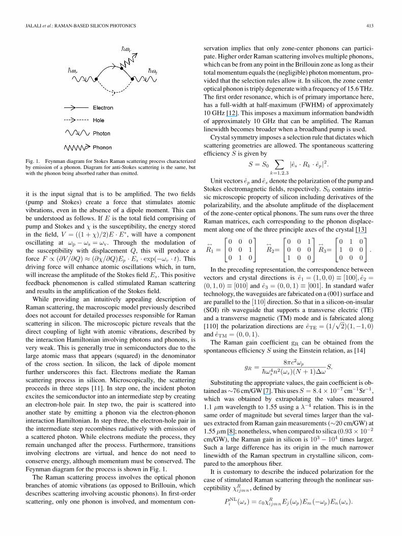
Fig. 1. Feynman diagram for Stokes Raman scattering process characterizedby emission of a phonon. Diagram for anti-Stokes scattering is the same, butwith the phonon being absorbed rather than emitted.
it is the input signal that is to be amplified. The two fields(pump and Stokes) create a force that stimulates atomicvibrations, even in the absence of a dipole moment. This canbe understood as follows. If E is the total field comprising ofpump and Stokes and χ is the susceptibility, the energy storedin the field, V = ((1 + χ)/2)E · E∗, will have a componentoscillating at ωp − ωs = ωv. Through the modulation ofthe susceptibility with displacement Q, this will produce aforce F ∝ (∂V/∂Q) ≈ (∂χ/∂Q)Ep · Es · exp(−ωv · t). Thisdriving force will enhance atomic oscillations which, in turn,will increase the amplitude of the Stokes field Es . This positivefeedback phenomenon is called stimulated Raman scatteringand results in the amplification of the Stokes field.
While providing an intuitively appealing description ofRaman scattering, the macroscopic model previously describeddoes not account for detailed processes responsible for Ramanscattering in silicon. The microscopic picture reveals that thedirect coupling of light with atomic vibrations, described bythe interaction Hamiltonian involving photons and phonons, isvery weak. This is generally true in semiconductors due to thelarge atomic mass that appears (squared) in the denominatorof the cross section. In silicon, the lack of dipole momentfurther underscores this fact. Electrons mediate the Ramanscattering process in silicon. Microscopically, the scatteringproceeds in three steps [11]. In step one, the incident photonexcites the semiconductor into an intermediate step by creatingan electron-hole pair. In step two, the pair is scattered intoanother state by emitting a phonon via the electron-phononinteraction Hamiltonian. In step three, the electron-hole pair inthe intermediate step recombines radiatively with emission ofa scattered photon. While electrons mediate the process, theyremain unchanged after the process. Furthermore, transitionsinvolving electrons are virtual, and hence do not need toconserve energy, although momentum must be conserved. TheFeynman diagram for the process is shown in Fig. 1.
The Raman scattering process involves the optical phononbranches of atomic vibrations (as opposed to Brillouin, whichdescribes scattering involving acoustic phonons). In first-orderscattering, only one phonon is involved, and momentum con-
servation implies that only zone-center phonons can partici-pate. Higher order Raman scattering involves multiple phonons,which can be from any point in the Brillouin zone as long as theirtotal momentum equals the (negligible) photon momentum, pro-vided that the selection rules allow it. In silicon, the zone centeroptical phonon is triply degenerate with a frequency of 15.6 THz.The first order resonance, which is of primary importance here,has a full-width at half-maximum (FWHM) of approximately10 GHz [12]. This imposes a maximum information bandwidthof approximately 10 GHz that can be amplified. The Ramanlinewidth becomes broader when a broadband pump is used.
Crystal symmetry imposes a selection rule that dictates whichscattering geometries are allowed. The spontaneous scatteringefficiency S is given by
S = S0
∑k=1,2,3
|es · Rk · ep |2.
Unit vectors ep and es denote the polarization of the pump andStokes electromagnetic fields, respectively. S0 contains intrin-sic microscopic property of silicon including derivatives of thepolarizability, and the absolute amplitude of the displacementof the zone-center optical phonons. The sum runs over the threeRaman matrices, each corresponding to the phonon displace-ment along one of the three principle axes of the crystal [13]
↔R1 =
0 0 0
0 0 10 1 0
↔
R2=
0 0 1
0 0 01 0 0
↔
R3=
0 1 0
1 0 00 0 0
.
In the preceding representation, the correspondence betweenvectors and crystal directions is e1 = (1, 0, 0) ≡ [100], e2 =(0, 1, 0) ≡ [010] and e3 = (0, 0, 1) ≡ [001]. In standard wafertechnology, the waveguides are fabricated on a (001) surface andare parallel to the [110] direction. So that in a silicon-on-insular(SOI) rib waveguide that supports a transverse electric (TE)and a transverse magnetic (TM) mode and is fabricated along[110] the polarization directions are eTE = (1/
√2)(1,−1, 0)
and eTM = (0, 0, 1).The Raman gain coefficient gR can be obtained from the
spontaneous efficiency S using the Einstein relation, as [14]
gR =8πc2ωp
hω4s n2(ωs)(N + 1)∆ω
S.
Substituting the appropriate values, the gain coefficient is ob-tained as∼76 cm/GW [7]. This uses S = 8.4 × 10⁻⁷ cm−1Sr−1,which was obtained by extrapolating the values measured1.1 µm wavelength to 1.55 using a λ−4 relation. This is in thesame order of magnitude but several times larger than the val-ues extracted from Raman gain measurements (∼20 cm/GW) at1.55 µm [8]; nonetheless, when compared to silica (0.93 × 10⁻²
cm/GW), the Raman gain in silicon is 103 − 104 times larger.Such a large difference has its origin in the much narrowerlinewidth of the Raman spectrum in crystalline silicon, com-pared to the amorphous fiber.
It is customary to describe the induced polarization for thecase of stimulated Raman scattering through the nonlinear sus-ceptibility χR
ijmn , defined by
PNLi (ωs) = ε0χ
RijmnEj (ωp)Em (−ωp)En (ωs).

414 IEEE JOURNAL OF SELECTED TOPICS IN QUANTUM ELECTRONICS, VOL. 12, NO. 3, MAY/JUNE 2006
On the other hand, the atomic displacement can be ob-tained using a classical harmonic oscillator model [10] with thedriving force described previously. By comparing the inducedpolarization suggested by the displacement with the precedingdefinition, one arrives at the following expression for the in-duced Raman susceptibility:
χRijmn
= 2Γωv2ncgR
ωs(µ0/ε0)1/2
∑k=1,2,3(Rij )k (Rmn )k
(ω2v − (ωp − ωs)2 − 2iΓ(ωp − ωs))
.
Where Γ is the dissipative term in the harmonic oscillatorequation, and n is the refractive index. Crystal symmetry con-sideration, described by the Raman tensor R, leads to a total of12 equal nonvanishing components that have the indexes of theform
1221 = 1212 = 2112 = 2121 = 1331 = 1313
= 3113 = 3131 = 2332 = 2323 = 3223 = 3232.
The induced susceptibility is related to the Raman gain coef-ficient as [13]
χR1221(ωp − ωs = Ω) =
i
(µ0/ε0)1/2
2ncgR
ωs
= 11.2 × 10⁻¹⁴icm2
V 2.
Two-photon-absorption (TPA) is another nonlinear opticaleffect that is particularly strong in semiconductors. This effectresults in pump depletion and generation of free carriers that,through the free carrier plasma effect, gives rise to a broad-band absorption spectrum. TPA has been shown to be neg-ligible from the point of view of pump depletion [8]. Thisis plausible since the TPA coefficient in silicon, β, is rela-tively small, ∼0.5 cm/GW. On the other hand, absorption byTPA-generated free carriers is a broadband process that com-petes with the Raman gain. The effect has been identified as alimiting factor in all-optical switching in III-V semiconductorwaveguides [15]–[19]. It has also been discussed as a poten-tial limit to achievable Raman gain in GaP waveguides [20],although a Raman gain of 24 dB was demonstrated in thesewaveguides [21]. More recently, TPA-induced FCA has beenmeasured in silicon waveguides in the context of the Ramanprocess [22], [23] and in the transmission of ultrashort pulses insilicon waveguides [24].
The magnitude of TPA-induced free carrier absorption de-pends on free carrier concentration through the relation:αFCA = 1.45 × 10⁻¹⁷(λ/1.55)2 · ∆N, where λ is the wave-length in microns, and ∆N is the density of electron-holepairs [25], [26]. The latter is related to the pump intensity Ip by
∆N = β · I2p · τeff/(2 · hν)
where hν is the pump photon energy and τeff is the effectiverecombination lifetime for free carriers. This equation neglectsthe contribution to free carrier generation due to pump-signal
Fig. 2. Impact of carrier lifetime on achievable CW Raman gain. Gain in-creases with intensity, while loss rises as intensity squared and dominates whenlifetime is long.
TPA, and hence is valid in the regime where Stokes intensity(Is)Is Ip .
The fundamental parameter that governs the TPA inducedloss, and hence the success of Raman-based devices, is therecombination lifetime τeff . It is well known that the recombi-nation lifetime in SOI is much shorter than that in a bulk siliconsample with comparable doping concentration. This lifetime re-duction is due to the presence of interface states at the boundarybetween the top silicon and the buried oxide layer. This effectdepends on the method used for preparation of the SOI waferand the film thickness, with measured and expected valuesranging between 10–200 ns [27]–[29]. In SOI waveguides, thelifetime is further reduced to a few nanoseconds, or even belowin the case of submicron waveguides, due to the recombinationat the etched waveguide facets and, in the case of rib waveg-uides, to diffusion into the slab regions [29]. The lifetime canbe further reduced by application of a reverse-bias p-n junc-tion [22], [23], [29], or by introduction of midgap states throughhigh energy irradiation, and gold or platinum doping. Modestamount of CW gain has been observed in deep submicrometerwaveguides [30] where the impact of surface and interfacerecombination plays a critical role in reducing the lifetime. CWgain has also been demonstrated by sweeping the free carriersusing a reverse-bias p-n junction [31]. This approach is furtherdiscussed in the context of Raman laser in the following.
The plot of the net Raman gain as a function of CW pumpintensity for a waveguide of length L = 1.9 cm and propagationloss 1 dB/cm is shown in Fig. 2 [23] for different free carrierlifetime values. The plot shows that more than 5 dB of gain canbe obtained with a pump intensity of less than 100 MW/cm2.Gain increases with intensity, while the loss rises as intensitysquared and dominates when the lifetime is long. The pump isassumed to be a monochromatic source. The finite linewidth ofthe pump laser will result in a lower gain than that predicted inFig. 2. It is clear that to create a successful amplifier, an effectivelifetime of ≤1 ns is required.
From the plot in Fig. 2, it is clear that the carrier lifetime isa critical parameter in the operation of a Raman amplifier. In arib SOI waveguide, its value is determined by the combination

JALALI et al.: RAMAN-BASED SILICON PHOTONICS 415
Fig. 3. Dependence of carrier lifetime on ratio h/H for waveguides with w = H = 0.25, 0.5, 1, and 5 µm (after [29]).
of carrier diffusion and carrier recombination in the bulk, on theSi surface, and the Si−SiO2 interface. An analytical expressiondescribing this process is [29]
1τeff
=1τb
+S
H+
w + 2(H − h)wH
S ′
+2 hH
√Dw2
(1τb
+ S+S ′
h
).
In this expression, τb is the carrier recombination lifetime inbulk silicon, S and S ′ are the interface and surface recombina-tion velocities, D is the ambipolar diffusion coefficient, w is thewaveguide rib width, h equals the slab height, and H is the totalrib height. The first term in the equation is the contribution ofthe bulk recombination, the second the contribution of interfacerecombination, the third the contribution of surface recombina-tion, and the last term is due to the diffusion of carriers out ofthe rib (and subsequent recombination outside of the waveguiderib). Because τb is on the order of 1–100 µs and the surface re-combination is often negligible (for passivated good quality sil-icon surfaces), the lifetime is often determined by the interfacerecombination. This is especially true for submicron waveg-uides, because the distance of the generated electrons from theinterface where they can recombine is small, and therefore theelectron recombination more effective.
As an example, we show in Fig. 3 the dependence of the carrierlifetime on waveguide dimensions [29]. The analytical expres-sion and simulation results for the carrier lifetime are shown forwaveguides with w = H , where H = 0.25, 0.5, 1, and 5 µm,where the ratio h/H is varied. The interface recombination ve-locity is taken to be 8000 cm/s and the surface recombinationis neglected. By varying the waveguide dimensions, variationin the carrier lifetime of about two orders of magnitude can beachieved in this example.
Besides engineering the waveguide dimensions to reduce thelifetime, the generated carriers can be swept out of the waveg-uide core by means of a p-n junction that can be formed bydoping regions adjacent to the waveguide core [6]. The use ofp-n junction for carrier sweep-out in the silicon waveguide is
Fig. 4. Carrier sweep-out using p-n junction (from [6]).
shown in Fig. 4. In the case of a strong reverse bias field, thecarrier lifetime is determined by the drift current that is due tothe applied electric field. The carrier lifetime is the mean tran-sit time of the carriers out of the rib, and equals τe = w/(2υe)for electrons and τh = w/(2υh) for holes, where υe, υh are theelectron and hole velocities, respectively. The velocities, in turn,are a nonlinear function of the applied electric field. When thefield is low enough, they are proportional to the electric field(the proportionality constant is the carrier mobility), but at veryhigh electric fields, the carrier velocities are independent of thefield. The preceding expression gives an estimate for the carrierlifetime in the case where the generation of electron-hole pairsis low. At very high generation rates, the junction might becomeineffective because, as the electrons and holes drift in oppositedirections, an opposing electric field is build up that is opposingthe applied reverse field. In very extreme cases, the junction canbe rendered completely ineffective so that the applied field haspractically no effect on the lifetime, and the lifetime then is thesame as the lifetime in a bare waveguide.
III. RAMAN WAVELENGTH CONVERSION
The nature of the Raman scattering process occurring inthe medium is determined by the phase mismatch between thepump, Stokes, and anti-Stokes fields. The total phase mismatch
416 IEEE JOURNAL OF SELECTED TOPICS IN QUANTUM ELECTRONICS, VOL. 12, NO. 3, MAY/JUNE 2006
Fig. 5. Energy-level representation of Raman wavelength conversion process.|1 > and |0 > are vibrational states, and arrow represent virtual transitions. Aphonon is created and annihilated, leaving the phonon population unchanged.
is defined as
∆β = 2βp − βs − βaS
where β is the wave-vector for the given wavelength, and thecorresponding mode of polarization should be taken into ac-count.
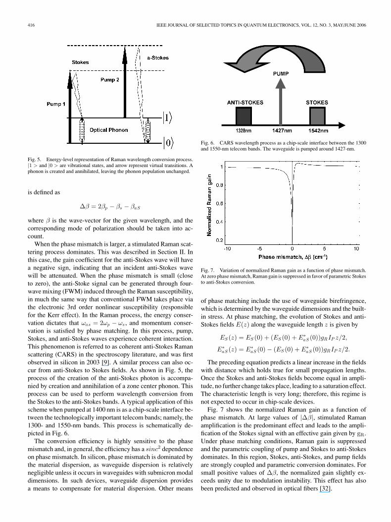
When the phase mismatch is larger, a stimulated Raman scat-tering process dominates. This was described in Section II. Inthis case, the gain coefficient for the anti-Stokes wave will havea negative sign, indicating that an incident anti-Stokes wavewill be attenuated. When the phase mismatch is small (closeto zero), the anti-Stoke signal can be generated through four-wave mixing (FWM) induced through the Raman susceptibility,in much the same way that conventional FWM takes place viathe electronic 3rd order nonlinear susceptibility (responsiblefor the Kerr effect). In the Raman process, the energy conser-vation dictates that ωas = 2ωp − ωs , and momentum conser-vation is satisfied by phase matching. In this process, pump,Stokes, and anti-Stokes waves experience coherent interaction.This phenomenon is referred to as coherent anti-Stokes Ramanscattering (CARS) in the spectroscopy literature, and was firstobserved in silicon in 2003 [9]. A similar process can also oc-cur from anti-Stokes to Stokes fields. As shown in Fig. 5, theprocess of the creation of the anti-Stokes photon is accompa-nied by creation and annihilation of a zone center phonon. Thisprocess can be used to perform wavelength conversion fromthe Stokes to the anti-Stokes bands. A typical application of thisscheme when pumped at 1400 nm is as a chip-scale interface be-tween the technologically important telecom bands; namely, the1300- and 1550-nm bands. This process is schematically de-picted in Fig. 6.
The conversion efficiency is highly sensitive to the phasemismatch and, in general, the efficiency has a sinc2 dependenceon phase mismatch. In silicon, phase mismatch is dominated bythe material dispersion, as waveguide dispersion is relativelynegligible unless it occurs in waveguides with submicron modaldimensions. In such devices, waveguide dispersion providesa means to compensate for material dispersion. Other means
Fig. 6. CARS wavelength process as a chip-scale interface between the 1300and 1550-nm telecom bands. The waveguide is pumped around 1427-nm.
Fig. 7. Variation of normalized Raman gain as a function of phase mismatch.At zero phase mismatch, Raman gain is suppressed in favor of parametric Stokesto anti-Stokes conversion.
of phase matching include the use of waveguide birefringence,which is determined by the waveguide dimensions and the built-in stress. At phase matching, the evolution of Stokes and anti-Stokes fields E(z) along the waveguide length z is given by
ES (z) = ES (0) + (ES (0) + E∗aS (0))gRIP z/2,
E∗aS (z) = E∗
aS (0) − (ES (0) + E∗aS (0))gRIP z/2.
The preceding equation predicts a linear increase in the fieldswith distance which holds true for small propagation lengths.Once the Stokes and anti-Stokes fields become equal in ampli-tude, no further change takes place, leading to a saturation effect.The characteristic length is very long; therefore, this regime isnot expected to occur in chip-scale devices.
Fig. 7 shows the normalized Raman gain as a function ofphase mismatch. At large values of |∆β|, stimulated Ramanamplification is the predominant effect and leads to the ampli-fication of the Stokes signal with an effective gain given by gR.Under phase matching conditions, Raman gain is suppressedand the parametric coupling of pump and Stokes to anti-Stokesdominates. In this region, Stokes, anti-Stokes, and pump fieldsare strongly coupled and parametric conversion dominates. Forsmall positive values of ∆β, the normalized gain slightly ex-ceeds unity due to modulation instability. This effect has alsobeen predicted and observed in optical fibers [32].

JALALI et al.: RAMAN-BASED SILICON PHOTONICS 417
Fig. 8. schematic showing pulsed pumping scheme. Repletion rate of laseris made longer than the carrier lifetime to prevent free-carrier accumulation.Pulsewidth of laser is also made longer than phonon response time.
Fig. 9. Experimental setup used to demonstrate pulse-pumped Raman ampli-fier.
IV. EXPERIMENTAL DEMONSTRATION OF RAMAN
DEVICES IN SILICON
Two schemes have been successfully employed to mitigatethe deleterious effects of free-carrier losses. One method foravoiding free carrier accumulation and the concomitant loss ispulsed pumping [34]–[37]. As long as the pump pulse period islonger than the free carrier lifetime, the free carrier accumulationcan be mostly eliminated. Fig. 8-shows a time-domain schematicof the pulsed pumping scheme. The decay of free-carriers at thetrailing edge of the pump pulse ensures that free-carriers donot accumulate, and hence do not contribute to excess nonlinearlosses. It should be noted that the pump pulsewidth is required tobe longer than the phonon response time to ensure that sufficientgain is achieved in the medium. This scheme was employed atUCLA to demonstrate the first silicon Raman laser [4]. Anothermethod to deal with free carriers is to employ reverse-biasedcarrier sweepout. This scheme was described in the context oflifetime reduction in the waveguides in Section II. Intel hasemployed this scheme to demonstrate a CW Raman laser [8].
Fig. 9 shows the schematic of the experimental setup used toobserve pulsed Raman amplification. The pump and Stokes sig-nal lasers with appropriate polarizations are combined into thewaveguide using WDMs. The measured change in CW signalbeam (tuned to the peak of Stokes resonance) due to the pumppulse is shown in Fig. 10. The pump source was a mode-lockedfiber laser with 25-MHz repetition rate and ∼1-ps output pulsewidth. Since phonon response time in silicon is more than 3 ps,the pulse width is broadened by using a spool of standard singlemode optical fiber. Maximum pump on-off gain of 20 dB hasbeen obtained. Taking into account the losses in the waveguide,we obtain a net waveguide gain of 13 dB [37]. This gain includeswaveguide propagation losses, but not the fiber-waveguide cou-pling loss. In separate devices that have adiabatic mode tapers,we have shown a net fiber-to-fiber gain of 11 dB under a similarpulse pumping scheme [33].
Fig. 10. Time-resolved Raman amplification with signal laser at 1673 nm. Apump on–off gain of 20 dB is obtained. Pump pulse wavelength is 1540 nm.
Fig. 11. Time-resolved signal loss with the signal laser at 1678 nm; i.e., outsideRaman resonance. Maximum loss of 4 dB and carrier lifetime of 4 ns is obtained.
Fig. 12. On–off optical gain as function of peak pump pulse power. Maximumgain of 20 dB is obtained.
The net free carrier loss and the free carrier lifetime can bemeasured by performing the same measurement with the signallaser tuned away from the Raman peak. This is shown in Fig. 11.Maximum loss due to the combined FCA loss was measured tobe 4 dB. Thus, the intrinsic Raman gain in the Silicon waveguideis 24 dB. By extrapolating the exponential decay of the carriers,we estimate a free carrier lifetime of ∼4 ns. The variation ofoptical gain as a function of peak pump power coupled into thewaveguide is shown in Fig. 12. Optical gain is found to saturatearound 37 W of peak pump power. This can be attributed to thepulse breakup and excessive spectral broadening of pump laserin the fiber pigtail preceding the waveguide [33].

418 IEEE JOURNAL OF SELECTED TOPICS IN QUANTUM ELECTRONICS, VOL. 12, NO. 3, MAY/JUNE 2006
Fig. 13. Measured anti-Stokes spectra versus Stokes signal wavelength. Thez-axis represents conversion efficiency, normalized to unity. CW pump laserwavelength is 1428 nm.
Fig. 14. (a) Anti-Stokes spectrum of converted signal at varying pump powers.(b) RF spectrum of wavelength converted analog data signal at 1.03 GHz. SNRof 47 dBe is obtained over 100-Hz bandwidth.
Fig. 13 shows the experimental verification of Raman wave-length conversion in Silicon. The pump laser (at 1427 nm) iscoupled to TE mode and the Stokes signal laser is coupled toTE mode. The Stokes signal laser is scanned in a range from1530 to 1560 nm. Fig. 13 shows the a-Stokes spectra measuredas a function of the Stokes signal wavelength. The CW pumppower in the waveguide was 0.7 W. There is a clear peak at1328.8 nm of anti-Stokes emission when the Stokes laser istuned to Stokes wavelength of 1542.3 nm. The nature of thesatellite peaks maybe due to the sinc2 dependence of the con-version efficiency with phase mismatch.
Fig. 14(a) shows the converted anti-Stokes signal spectrum[39]. The FWHM for wavelength conversion, which is ap-proximately 250 GHz, is determined solely by the pump laserlinewidth. The shift in the center wavelength in Fig. 14(a) is dueto the slight shift in the local maxima of conversion efficiency
Fig. 15. Measured laser output power with respect to peak pump power. Lasingthreshold is measured to be at 9-W peak power level. The slope efficiencyobtained by dividing the output peak pulse power by that of the input is ∼13%.
with increase in pump power. The CARS process is used toperform wavelength conversion from the Stokes to anti-Stokeswavelengths. Fig. 14(b) shows the conversion of 1.03-GHz RFmodulation from 1542 to 1328.5 nm [38]. The input RF signalpower applied to the Stokes wavelength is shown in the inset.The measured electrical signal to noise ratio (SNR) is 47 dBeover 100 Hz. We note that from the application point of view,the 1320- and 1550-nm bands are the two most important bandsin optical communication. The measured conversion efficiencywas approximately 10−5. As mentioned previously, a numberof design approaches are available for phase matching a siliconwaveguide and for realizing high conversion efficiency [39].
Fig. 15 shows the measured characteristics for the first siliconRaman laser [4]. The laser, demonstrated in 2004, operated inthe pulse mode and consisted of a 1.7-cm-long silicon waveg-uide gain medium with the experimental setup similar to Fig. 9and an external cavity form via a fiber loop. The laser has athreshold of 9 W peak pulse power (corresponding to a fewmilliwatts of average power), and was able to produce outputpulses with over 2.5-W peak power at a 25-MHz repetition rate.The demonstration was a major milestone, as it clearly showedthat silicon can indeed lase. The strong lasing characteristicsand high conversion efficiency (∼13%) of the prototype lasershowed that silicon Raman lasers must be considered as a prac-tical and compact alternative to fiber Raman lasers.
In 2005, Intel Corporation demonstrated the first CW siliconRaman laser [6]. The device was a 5-cm-long silicon waveg-uide with a cavity formed by high reflectivity (HR) coating thechip facets. CW operation was achieved by using a reverse biasp-n junction to sweep out the TPA generated free carriers, anapproach that was previously proposed in 2004 [22], [23], [29].Fig. 16 shows the laser input–output behavior at reverse biasvoltages of 5 and 25 V. The laser produced a maximum out-put power of ∼9 mW at 25-V reverse bias with 600 mW ofCW pump power inside the waveguide. The CW operation isan important step in the development of silicon Raman lasers.One drawback of the reverse bias carrier sweepout approach isthe electrical power dissipated on the chip. With a reverse cur-rent of approximately 50 mA expected for this device, the laserdissipates an on-chip electrical power of more than 1 W. Fromthis perspective, methods that can drastically reduce carrier life-time, and hence mitigate the need for active carrier removal, are

JALALI et al.: RAMAN-BASED SILICON PHOTONICS 419
Fig. 16. Threshold characteristics of CW silicon Raman laser demonstrated ina 5-cm silicon waveguide and with using reverse biased p-i-n diode for carriersweepout [6].
a desired. As a compromise, reduction of the required sweepoutvoltage will reduce the electrical power dissipation.
The ability to integrate a p-n junction along with the gainmedium offers the exciting possibility of intracavity gain switch-ing [5]. This feature was utilized recently to demonstrated elec-trical modulation using an integrated p-n junction diode. Opticalloss in silicon and hence the net optical gain in the laser cavityis proportional to the free carrier density in silicon, with a de-pendence that is described as ∆α = 1.7 × 10⁻¹⁷ · ∆N , where∆α is the change in loss caused by ∆N change in free carrierdensity [25], [26]. The linear dependence of free carrier densityon diode forward current provides direct electronic modulationof the intracavity gain. The laser will be turned off when theloss induced by diode current exceeds the gain per round trip inthe cavity. Hence, the device will function as a “normally on”switch that is turned off when forward bias is applied to the p-njunction diode. The turn-on and turn-off times are dependent ofthe photon build up in the resonator and the carrier injection timeof the diode, respectively. While the modulation speed is limitedin this experiment to 1 MHz, the result clearly demonstrates theswitching capability of the silicon Raman laser.
This idea, first demonstrated at UCLA, has been extended byIntel in a demonstration of an electrically switched Raman am-plifier, with the device representing a loss-less modulator [40].
V. GeSi RAMAN DEVICES
The introduction of germanium in the overall scheme of non-linear Raman processes in silicon offers new avenues for tai-loring the device characteristics. In particular are the follow-ing [41].
1) The strain caused by the difference in the lattice constantsof Si and Ge, along with the composition effect, providesmechanisms for tuning the Stokes shift associated withthe dominant Si-Si (500 cm−1) vibrational mode [42]. Inaddition, the presence of Si-Ge modes (400 cm−1) andGe-Ge modes (300 cm−1) provide flexibility in pump andsignal wavelengths.
Fig. 17. Stimulated Raman spectra of GeSi waveguides compared to that ofsilicon waveguide. A 37-GHz red shift in the Stokes wavelength is observed.Pump wavelength was 1539 nm.
2) Spectral broadening can be achieved by graded Ge com-position.
3) The growth of SimGen superlattices in Silicon can offerthe possibility of zone folding of acoustic phonon modes,and hence increase the number of Raman active modes, inthe medium.
4) When grown on an SOI substrate, the use of doublecladding in the vertical direction can improve fiber waveg-uide coupling efficiency.
5) The strain resulting in birefringence [43] can providean addition degree of freedom for phase matching inthe wavelength conversion process. Stress also results inbroadening of the gain spectrum via splitting of the de-generate optical phonon modes.
6) Higher carrier mobility, and hence diffusion constant, inSiGe reduces the effective lifetime in the waveguide. Thisreduces the losses associated with the free carriers that aregenerated by two-photon absorption (TPA). However, thisbenefit will be countered by the higher TPA coefficient inGeSi.
Recently, the first GeSi optical amplifier and laser was demon-strated [41]. A pulsed gain of 16 dB and lasing with sharpthreshold characteristics were observed for Ge0.08Si0.92 ribwaveguides. The Stokes spectrum, shown in Fig. 17, exhibits a37-GHz red shift which is in qualitative agreement with amodel that takes into account the effect of composition andstrain on the optical phonon frequency [41]. These resultssuggest that the spectrum of Raman scattering can be engi-neered using the GeSi material system. As a result, GeSi Ra-man devices represent an exciting topic for future research anddevelopment.
VI. CONCLUSION
This paper has reviewed recent results on light generation,amplification, and wavelength conversion in silicon and GeSiusing stimulated Raman processes. These effects are routinelyobserved in optical fiber; however, several kilometers of lengthare required to do so. What has enabled us to achieve these pro-cesses on millimeter length scales on a chip are two fundamentaldifferences between an optical fiber and a silicon microstructure.

420 IEEE JOURNAL OF SELECTED TOPICS IN QUANTUM ELECTRONICS, VOL. 12, NO. 3, MAY/JUNE 2006
The first is the difference in atomic structures. Vibrational modesin silica broaden into bands; hence, the Raman gain has a verylarge bandwidth and a low peak value, requiring long interactionlengths for the effect to be observed. In contrast, silicon is sin-gle crystal and supports only three degenerate optical vibrationmodes. The result is a much narrower gain bandwidth, but amuch higher gain peak (nearly 103–104 times higher). Second,consider the difference in modal areas. The large index-contrastin the silicon/SiO2 waveguides results in a mode area that is ap-proximately 100 times smaller (assuming 0.8 µm2 waveguides)than in a standard single mode fiber (mode area = 80µm2).The proportionally higher power density in the silicon waveg-uide lowers the threshold for nonlinear optical processes.
The intrinsic Raman bandwidth in silicon is 105 GHz, andit is broadened in the experiments by the pump laser linewidth(typically ∼2 nm). The resulting bandwidth is sufficient for am-plifying several WDM channels. The bandwidth can be broad-ened by broadening the pump linewidth even further (althoughthis reduces the peak gain), or by using multiple pump wave-lengths. The Raman phenomenon is fully tunable; the tuningrange is only limited by the available pump wavelengths. Thisis an advantage over the nanocrystal approach for light genera-tion and amplification. In addition, the Raman Effect can alsoperform wavelength conversion. Another important advantageof this approach is that it does not require rare-earth dopantsor nanostructures. Hence, it is truly compatible with silicon ICmanufacturing. A limitation of the Raman approach is the factthat it is optically pumped. However, it has been shown thatsilicon Raman lasers can be electronically switched or modu-lated using intracavity gain-loss modulation. Therefore, theselasers or similarly amplifiers can be interfaced with on-chipelectronic circuitry. Raman amplification and lasing in GeSiwaveguides has recently been demonstrated. The GeSi mate-rial system provides an opportunity to engineer the, otherwiserigid, Raman spectrum of silicon. Owing to the enhance carriermobility, GeSi is being pursued by the CMOS IC industry forfuture high speed circuits. This provides another impetus forinvestigating GeSi Raman devices.
Going forward, low loss waveguides with small cross sectionsare required for realizing high performance devices. Surfaceroughness produces strong scattering and high propagation lossdue to the high index contrast between the silicon waveguidecore and the cladding (air or SiO2). As such, the losses of sili-con waveguides tend to increase with reduction in cross section.Fortunately, new waveguide fabrication processes that are in de-velopment promise low-loss waveguides with submicron crosssections [44], [45]. Naturally, one must be able to efficientlycouple light into these structures. Several novel approaches forhigh efficiency coupling into submicron waveguides have alsobeen developed [45].
REFERENCES
[1] M. Paniccia, M. Morse, and M. Salib, “Integrated photonics,” in SiliconPhotonics, L. Pavesi and D. J. Lockwood, Eds. New York: Springer-Verlag,2004, p. 276.
[2] Z. Gaburro, “Optical interconnect,” in Silicon Photonics, L. Pavesi andD. J. Lockwood, Eds. New York: Springer-Verlag, 2004, ch. 4, pp. 121–176.
[3] B. Jalali, S. Yegnanarayanan, T. Yoon, T. Yoshimoto, I. Rendina, andF. Coppinger, “Advances in silicon-on-insulator optoelectronics,” IEEEJ. Sel. Topics Quantum Electron., vol. 4, no. 6, pp. 938–947, Nov.–Dec.1998.
[4] O. Boyraz and B. Jalali, “Demonstration of a silicon Raman laser,” Opt.Express, vol. 12, pp. 5269–5273, 2004.
[5] O. Boyraz and B. Jalali, “Demonstration of directly modulated siliconRaman laser,” Opt. Express, vol. 13, pp. 796–800, 2005.
[6] H. Rong, R. Jones, A. Liu, O. Cohen, D. Hak, A. Fang, and M. Pannicia,“A continuous-wave Raman silicon laser,” Nature, vol. 433, pp. 725–728,2005.
[7] R. Claps, D. Dimitropoulos, Y. Han, and B. Jalali, “Observation of Ramanemission in silicon waveguides at 1.54 µm,” Opt. Express, vol. 10,pp. 1305–1313, 2002.
[8] R. Claps, D. Dimitropoulos, V. Raghunathan, Y. Han, and B. Jalali, “Ob-servation of stimulated Raman scattering in silicon waveguides,” Opt.Express, vol. 11, pp. 1731–1739, 2003.
[9] R. Claps, V. Raghunathan, D. Dimitropoulos, and B. Jalali, “Anti-stokesRaman conversion in silicon waveguides,” Opt. Express, vol. 11, pp. 2862–2872, 2003.
[10] A. Yariv, Quantum Electronics, 3rd ed. New York: Wiley, 1988.[11] P. Y. Yu and M. Cardona, Fundamentals of Semiconductors, 3rd ed. New
York: Springer-Verlag, 1996.[12] P. A. Temple and C. E. Hathaway, “Multiphonon Raman spectrum of
silicon,” Phys. Rev. A, Gen. Phys., vol. 7, p. 3685, 1973.[13] D. Dimitropoulos, B. Houshmand, R. Claps, and B. Jalali, “Coupled-
mode theory of Raman effect in silicon-on-insulator waveguides,” Opt.Lett., vol. 28, pp. 1954–1956, 2003.
[14] J. M. Ralston and R. K. Chang, “Spontaneous-Raman-scattering efficiencyand stimulated scattering in silicon,” Phys. Rev. B, Condens, Matter, vol. 2,pp. 1858–1862, 1970.
[15] J. H. Yee and H. H. M. Chau, “Two-photon indirect transition in GaPcrystal,” Opt. Commun., vol. 10, pp. 56–58, 1974.
[16] K. W. DeLong and G. I. Stegeman, “Two-photon absorption as a limitationto all-optical waveguide switching in semiconductors,” Appl. Phys. Lett.,vol. 57, no. 20, pp. 2063–2064, 1990.
[17] A. Villeneuve, C. C. Yang, G. I. Stegeman, C. N. Ironside, G. Scelsi, andR. M. Osgood, “Nonlinear absorption in a GaAs waveguide just above halfthe band gap,” IEEE J. Quantum Electron., vol. 30, no. 5, pp. 1172–1175,May 1994.
[18] A. M. Darwish, E. P. Ippen, H. Q. Lee, J. P. Donnelly, and S. H. Groves,“Optimization of four-wave mixing conversion efficiency in the presenceof nonlinear loss,” Appl. Phys. Lett., vol. 69, pp. 737–739, 1996.
[19] Y.-H. Kao, T. J. Xia, and M. N. Islam, “Limitations on ultrafast opticalswitching in a semiconductor laser amplifier operating at transparencycurrent,” J. Appl. Phys., vol. 86, pp. 4740–4747, 1999.
[20] K. Suto, T. Kimura, T. Saito, and J. Nishizawa, “Raman amplifica-tion in GaP-AlxGa1-xP waveguides for light frequency discrimination,”Proc. Inst. Elect. Eng.-Optoelectron., vol. 145, no. 2, pp. 105–108, Apr.1998.
[21] S. Saito, K. Suto, T. Kimura, and J. I. Nishizawa, “80-ps and 4-ns pulse-pumped gains in a GaP-AlGaP semiconductor Raman amplifier,” IEEEPhoton. Technol. Lett., vol. 16, no. 2, pp. 395–397, Feb. 2004.
[22] T. K. Liang and H. K. Tsang, “Role of free carriers from two-photonabsorption in Raman amplification in silicon-on-insulator waveguides,”Appl. Phys. Lett., vol. 84, no. 15, pp. 2745–2747, 2004.
[23] R. Claps, V. Raghunathan, D. Dimitropoulos, and B. Jalali, “Influence ofnonlinear absorption on Raman amplification in silicon waveguides,” Opt.Express, vol. 12, pp. 2774–2780, 2004.
[24] A. R. Cowan, G. W. Rieger, and J. F. Young, “Nonlinear transmissionof 1.5 µm pulses through single-mode silicon-on-insulator waveguidestructures,” Opt. Express, vol. 12, pp. 1611–1621, 2004.
[25] R. A. Soref and B. R. Bennett, “Electrooptical effects in silicon,” IEEE J.Quantum Electron., vol. QE-23, no. 1, pp. 123–129, Jan. 1987.
[26] R. J. Bozeat, S. Day, F. Hopper, F. P. Payne, S. W. Roberts, and M. Asghari,“Silicon based waveguides,” in Silicon Photonics, L. Pavesi and D. J.Lockwood, Eds. New York: Springer-Verlag, 2004, ch. 8, pp. 269–294.
[27] M. A. Mendicino, “Comparison of properties of available SOI materials,”in Properties of Crystalline Silicon, R. Hull, Ed. London, U.K.: IEEINSPEC, 1998, pp. 992–1001.
[28] J. L. Freeouf and S. T. Liu, “Minority carrier lifetime results for SOIwafers,” in Proc. IEEE Int. SOI Conf., Tucson, AZ, Oct. 1995, pp. 74–75.
[29] D. Dimitropoulos, R. Jhaveri, R. Claps, J. C. S. Woo, and B. Jalali, “Life-time of photogenerated carriers in silicon-on-insulator rib waveguides,”Appl. Phys. Lett., vol. 86, p. 071115, 2005.

JALALI et al.: RAMAN-BASED SILICON PHOTONICS 421
[30] R. Espinola, J. Dadap, R. Osgood, S. J. McNab, and Y. A. Vlasov, “Ramanamplification in ultrasmall silicon-on-insulator wire waveguides,” Opt.Express, vol. 12, no. 16, pp. 3713–3718, 2004.
[31] R. Jones, H. Rong, A. Liu, A. W. Fang, M. J. Paniccia, D. Hak, andO. Cohen, “Net continuous wave optical gain in a low loss silicon-on-insulator waveguide by stimulated Raman scattering,” Opt. Express,vol. 13, pp. 519–525, 2005.
[32] E. Golovchenko, P. V. Mamyshev, A. N. Pilipetskii, and E. M. Dianov,“Mutual influence of the parametric effects and stimulated Raman scat-tering in optical fibers,” IEEE J. Quantum Electron., vol. 26, no. 10,pp. 1815–1820, Oct. 1990.
[33] O. Boyraz and B. Jalali, “Demonstration of 11dB fiber-to-fiber gain in asilicon Raman amplifier,” IEICE Electron. Express, vol. 1, no. 14, pp. 429–434, 2004.
[34] T. K. Liang and H. K. T sang, “Efficient Raman amplification in silicon-on-insulator waveguides,” Appl. Phys. Lett., vol. 85, pp. 3343–3345, 2004.
[35] Q. Xu, V. R. Almeida, and M. Lipson, “Time-resolved study of Ramangain in highly confined silicon-on-insulator waveguides,” Opt. Express,vol. 12, pp. 4437–4442, 2004.
[36] A. Liu, H. Rong, M. Paniccia, O. Cohen, and D. Hak, “Net optical gain in alow loss silicon-on-insulator waveguide by stimulated Raman scattering,”Opt. Express, vol. 12, no. 18, pp. 4261–4268, 2004.
[37] V. Raghunathan, O. Boyraz, and B. Jalali, “20 dB on-off Raman ampli-fication in silicon waveguides,” presented at the CLEO 2005, Baltimore,MD, May 2005, Paper CMU1.
[38] V. Raghunathan, R. Claps, D. Dimitropoulos, and B. Jalali, “ParametricRaman wavelength conversion in scaled silicon waveguides,” IEEE J.Lightw. Technol., vol. 23, no. 6, pp. 2094–2012, Jun. 2005.
[39] D. Dimitropoulos, V. Raghunathan, R. Claps, and B. Jalali, “Phase-matching and nonlinear optical processes in silicon waveguides,” Opt.Express, vol. 12, p. 2774, 2003.
[40] R. Jones, A. Liu, H. Rong, M. Paniccia, O. Cohen, and D. Hak, “Loss-less optical modulation in a silicon waveguide using stimulated Ramanscattering,” Opt. Express, vol. 13, no. 5, pp. 1716–1723, 2005.
[41] R. Claps, V. Raghunathan, O. Boyraz, P. Koonath, D. Dimitropoulos, andB. Jalali, “Raman amplification and lasing in SiGe waveguides,” Opt.Express, vol. 13, pp. 2459–2466, 2005.
[42] J. C. Tsang, P. M. Mooney, F. Dacol, and J. O. Chou, “Measurementsof alloy composition and strain in thin Gex Si1−x layers,” J. Appl. Phys.,vol. 75, pp. 8098–8108, 1994.
[43] D.-X. Xu, P. Cheben, D. Dalacu, A. Delage, S. Janz, B. Lamontagne,M.-J. Picard, and W. N. Ye, “Eliminating the birefringence in silicon-on-insulator ridge waveguides by use of ridge cladding stress,” Opt. Lett.,vol. 29, no. 20, pp. 2384–2386, 2004.
[44] P. Koonath, K. Kishima, T. Indukuri, and B. Jalali, “SIMOX sculpting of 3-D nano-optical structures,” in Proc. IEEE/LEOS Annu. Meeting, Tucson,AZ, 2003, vol. 2, pp. 558–559.
[45] T. Tsuchizawa, K. Yamada, H. Fukuda, T. Watanabe, J. Takahashi,M. Takahashi, T. Shoji, E. Tamechika, S. Itabashi, and H. Morita, “Mi-crophotonics devices based on silicon microfabrication technology,” IEEEJ. Sel. Topics Quantum Electron., vol. 11, no. 1, pp. 232–240, Jan.–Feb.2005.
Bahram Jalali (S’86–M’89–SM’97–F’04) is the Professor of Electrical Engi-neering, Director of the DARPA Center for Optical A/D Systems Technology(COAST), and Director of the Optoelectronic Circuits and Systems Laboratoryat the University of California, Los Angeles (UCLA). From 1988 to 1992, he wasa Member of the Technical Staff at the Physics Research Division, AT&T BellLaboratories, Murray Hill, NJ, where he conducted research on ultrafast elec-tronics and optoelectronics. While on sabbatical leave from UCLA from 1999to 2001, he founded Cognet Microsystems, a Los Angeles-based fiber-opticcomponent company. He served as the company’s CEO, President, and Chair,from the company’s inception through its acquisition by Intel Corporation inApril 2001. From 2001 to 2004, he served as a Consultant at Intel Corporation.His current research interests are in microwave photonics, integrated optics,and fiber-optic ICs. He has published over 200 scientific papers in internationalpeer-reviewed journals and conferences, and holds six U.S. patents with fivepatents pending.
Prof. Jalali is a Fellow of OSA and is a Full Member of the California NanoSystems Institute (CNSI). He was chosen by Scientific American as one of the50 Leaders Shaping the Future of Technology, in 2005. His work in demon-
strating the first silicon laser was cited by MIT Technology Review as one ofthe top 10 technology trends. He is a Chair of the Los Angeles Chapter of theIEEE Lasers and Electro-Optics Society. He was the General Chair for MWP2001, the IEEE International Conference on Microwave Photonics (MWP), andChair of its Steering Committee from 2001 to 2004. He was the recipient of theBridgeGate 20 Award for his contributions to the Southern California economy,and serves on the Board of Trustees of the California Science Center.
Varun Raghunathan (S’05) received the B.S. de-gree in electrical and electronics engineering fromthe Birla Institute of Technology and Science, Pilani,India, in 2002, and the M.S. degree in electrical en-gineering from the University of California, Los An-geles (UCLA), in 2005, where he is currently work-ing toward the Ph.D. degree in electrical engineer-ing.
His research concentrates on the experimentalstudy of stimulated Raman amplification wavelengthconversion using parametric Raman conversion pro-
cesses, and fabrication issues of silicon photonic structures. His research inter-ests include silicon photonics, nonlinear optics, solid state physics, and quantumelectronics.
Mr. Raghunathan was awarded a Fellowship by the California NanosystemsInstitute (CNSI) for his Master’s studies.
Dimitri Dimitropoulos received the B.S. degreefrom the National Technical University of Athens,Athens, Greece, in 2000, and the M.S. degree fromthe University of California, Los Angeles (UCLA), in2003, both in electrical engineering. He is currentlyworking toward the Ph.D. degree in electrical engi-neering at UCLA.
His research concentrates on silicon integrated op-tical devices, particularly silicon Raman lasers, am-plifiers, and wavelength converters. His research in-terests include quantum electronics and photonics;
noise in physical systems and information theory; and solid-state and plasmaphysics.
Ozdal Boyraz (M’05) received the B.S. degree fromHacettepe University, Ankara, Turkey, in 1993, andthe M.S. and Ph.D. degrees from the University ofMichigan, Ann Arbor, in 1997 and 2001, respectively,all in electrical engineering.
From 2001 to 2003, he was an R&D Engineer atXtera Communications. From 2003 to 2005, he wasa Postdoctoral Research Fellow in the Department ofElectrical Engineering, University of California, LosAngeles. In August 2005, he joined the Department ofElectrical Engineering and Computer Science, Uni-
versity of California, Irvine, as an Assistant Professor. He is the author orcoauthor of more than 60 scientific publications and holds three U.S. patents.
Dr. Boyraz is a member of the IEEE Lasers and Electro-Optics Society.