
Integrated Microwave Photonics for Radio Access Networks
13
JOURNAL OF LIGHTWAVE TECHNOLOGY, VOL. 32, NO. 16, AUGUST 15, 2014 2849 Integrated Microwave Photonics for Radio Access Networks Jos´ e Capmany,Fellow, IEEE, Fellow, OSA, and Pascual Mu ˜ noz, Senior Member, IEEE, Member, OSA (Invited Paper) Abstract—We explore the advantages that integrated microwave photonics (IMWP) can bring to access networks. We first of all review the most common architectures of radio access networks (RANs) to identify the segments where microwave photonic com- ponents and radio over fiber links are located. Then, we provide a short description of the basic principles of IMWP with the aim of illustrating the current state of the art of this technology and its potentials. We discuss the possibilities of incorporating IMWP technology into the RAN front-haul. In particular, we first of all identify the required MWP functionalities and then discuss the feasibility of implementing these in light of the current and near future state of the art. Index Terms—Access networks, integrated optics, microwave photonics. I. INTRODUCTION M ICROWAVE photonics (MWP) [1]–[3], a discipline that brings together the worlds of radiofrequency (RF) en- gineering and optoelectronics, has attracted great interest from both the research community and the commercial sector over the past 30 years. The added value that this area of research brings stems from the fact that, on the one hand, it enables the realization of key functionalities in microwave systems that ei- ther are complex or even not directly possible in the RF domain and, on the another hand, that it creates new opportunities for information and communication (ICT) systems and networks. While initially the research activity in this field was focused towards defense applications, MWP has expanded to address a considerable number of civil applications [3]–[5], including cellular, wireless, and satellite communications, cable televi- sion, distributed antenna systems, optical signal processing and medical imaging systems using terahertz (THz) waves. Many of these novel application areas demand ever-increasing values for speed, bandwidth and dynamic range while, at the same time, require devices that are small, lightweight and low-power, ex- hibiting large tunability and strong immunity to electromagnetic interference. Despite the fact that digital electronics is widely Manuscript received February 3, 2014; revised May 2, 2014 and May 26, 2014; accepted June 23, 2014. Date of publication June 26, 2014; date of current version July 25, 2014. This work was supported by the Generalitat Valenciana through the PROMETEO 2013/012 Research Excellency Award. This work was also supported by the Research Excellency Award Program GVA PROMETEO 2013/012. The authors are with the Optical and Quantum Communications Group, Institute of Telecommunications and Multimedia, Universitat Polit´ ecnica de Valencia, 46021 Valencia, Spain (e-mail: [email protected]; pmunoz@ iteam.upv.es). Color versions of one or more of the figures in this paper are available online at http://ieeexplore.ieee.org. Digital Object Identifier 10.1109/JLT.2014.2333369 Fig. 1. Concept of analog signal processing engine in the context of informa- tion and communications systems. used nowadays in these applications, the speed of digital sig- nal processors (DSPs) is normally less than several gigahertz (a limit established primarily by the electronic sampling rate) so, in order to preserve the flexibility brought by these devices and their limit constraints there is a need for equally flexible front-end analog solutions to precede the DSP. This situation is schematically depicted in Fig. 1, where the block that constitutes the analog signal processor engine is shown. One of the main driving forces for MWP in the middle term future is expected to come from converged broadband fiber- wireless access networks [3], where radio services are delivered as an overlay over existing passive optical network (PON) and local ring infrastructures. Fig. 2 shows a schematic configuration of this solution [6]. In this context wireless services can be efficiently delivered to a variety of end-users, including: shopping malls, airports, hospitals, stadiums, power plants and other large buildings. For instance, the IEEE standard WiMAX (the Worldwide Interoper- ability for Microwave Access) has recently upgraded to handle data rates of 1 Gbit/s, and it is envisaged that many small, WiMAX-based stations or pico-cells will soon start to spring up. To cope with this growth scenario, future networks will be expected to support wireless communications at data rates reach- ing multiple gigabits per second. In addition, the extremely low power consumption of an access network comprised of pico- or 0733-8724 © 2014 IEEE. Personal use is permitted, but republication/redistribution requires IEEE permission. See http://www.ieee.org/publications standards/publications/rights/index.html for more information.
Transcript of Integrated Microwave Photonics for Radio Access Networks

JOURNAL OF LIGHTWAVE TECHNOLOGY, VOL. 32, NO. 16, AUGUST 15, 2014 2849
Integrated Microwave Photonics for RadioAccess Networks
Jose Capmany, Fellow, IEEE, Fellow, OSA, and Pascual Munoz, Senior Member, IEEE, Member, OSA
(Invited Paper)
Abstract—We explore the advantages that integrated microwavephotonics (IMWP) can bring to access networks. We first of allreview the most common architectures of radio access networks(RANs) to identify the segments where microwave photonic com-ponents and radio over fiber links are located. Then, we providea short description of the basic principles of IMWP with the aimof illustrating the current state of the art of this technology andits potentials. We discuss the possibilities of incorporating IMWPtechnology into the RAN front-haul. In particular, we first of allidentify the required MWP functionalities and then discuss thefeasibility of implementing these in light of the current and nearfuture state of the art.
Index Terms—Access networks, integrated optics, microwavephotonics.
I. INTRODUCTION
M ICROWAVE photonics (MWP) [1]–[3], a discipline thatbrings together the worlds of radiofrequency (RF) en-
gineering and optoelectronics, has attracted great interest fromboth the research community and the commercial sector overthe past 30 years. The added value that this area of researchbrings stems from the fact that, on the one hand, it enables therealization of key functionalities in microwave systems that ei-ther are complex or even not directly possible in the RF domainand, on the another hand, that it creates new opportunities forinformation and communication (ICT) systems and networks.
While initially the research activity in this field was focusedtowards defense applications, MWP has expanded to addressa considerable number of civil applications [3]–[5], includingcellular, wireless, and satellite communications, cable televi-sion, distributed antenna systems, optical signal processing andmedical imaging systems using terahertz (THz) waves. Many ofthese novel application areas demand ever-increasing values forspeed, bandwidth and dynamic range while, at the same time,require devices that are small, lightweight and low-power, ex-hibiting large tunability and strong immunity to electromagneticinterference. Despite the fact that digital electronics is widely
Manuscript received February 3, 2014; revised May 2, 2014 and May 26,2014; accepted June 23, 2014. Date of publication June 26, 2014; date of currentversion July 25, 2014. This work was supported by the Generalitat Valencianathrough the PROMETEO 2013/012 Research Excellency Award. This work wasalso supported by the Research Excellency Award Program GVA PROMETEO2013/012.
The authors are with the Optical and Quantum Communications Group,Institute of Telecommunications and Multimedia, Universitat Politecnica deValencia, 46021 Valencia, Spain (e-mail: [email protected]; [email protected]).
Color versions of one or more of the figures in this paper are available onlineat http://ieeexplore.ieee.org.
Digital Object Identifier 10.1109/JLT.2014.2333369
Fig. 1. Concept of analog signal processing engine in the context of informa-tion and communications systems.
used nowadays in these applications, the speed of digital sig-nal processors (DSPs) is normally less than several gigahertz(a limit established primarily by the electronic sampling rate)so, in order to preserve the flexibility brought by these devicesand their limit constraints there is a need for equally flexiblefront-end analog solutions to precede the DSP. This situation isschematically depicted in Fig. 1, where the block that constitutesthe analog signal processor engine is shown.
One of the main driving forces for MWP in the middle termfuture is expected to come from converged broadband fiber-wireless access networks [3], where radio services are deliveredas an overlay over existing passive optical network (PON) andlocal ring infrastructures. Fig. 2 shows a schematic configurationof this solution [6].
In this context wireless services can be efficiently deliveredto a variety of end-users, including: shopping malls, airports,hospitals, stadiums, power plants and other large buildings. Forinstance, the IEEE standard WiMAX (the Worldwide Interoper-ability for Microwave Access) has recently upgraded to handledata rates of 1 Gbit/s, and it is envisaged that many small,WiMAX-based stations or pico-cells will soon start to springup.
To cope with this growth scenario, future networks will beexpected to support wireless communications at data rates reach-ing multiple gigabits per second. In addition, the extremely lowpower consumption of an access network comprised of pico- or
0733-8724 © 2014 IEEE. Personal use is permitted, but republication/redistribution requires IEEE permission.See http://www.ieee.org/publications standards/publications/rights/index.html for more information.

2850 JOURNAL OF LIGHTWAVE TECHNOLOGY, VOL. 32, NO. 16, AUGUST 15, 2014
Fig. 2. Converged broadband fiber-wireless access network, where radio ser-vices are delivered as an overlay over existing PON and local ring infrastructures.
femto-cells would make it much greener than current macro-cellnetworks, which require high-power base stations.
The purpose of this paper is to explore the advantages thatthat integrated microwave photonics (IMWP) can bring to accessnetworks. We first of all review, in Section II the most commonarchitectures of radio access networks (RANS) to identify thesegments where MWP components and radio over fiber (RoF)links are located We then provide a short review in Section IIIof the basic principles of IMWP with the aim of illustrating thecurrent state of the art of this technology and its potentials. InSection IV we discuss the possibilities of incorporating IMWPtechnology into the RAN front haul. In particular we first ofall identify the required MWP functionalities and then discusson the feasibility of implementing these in light of the currentand near future state of the art. Finally, we conclude the paperin Section V with a summary and some directions for futureresearch.
II. RADIO ACCESS NETWORKS
The typical configuration of a converged or fixed-wirelessmutualized access network shown in Fig. 2 includes both thewired baseband (BB) and the RAN segments that share a con-siderable part of common infrastructure [6]. In the context ofMWP and RoF applications we are mainly interested in theRAN segment [7]–[10].
A. Traditional RAN Architecture
Traditional RANs, are composed of many stand-alone, all inone, macro base stations (BTS). Fig. 3 shows a typical configu-ration of one of such BTS.
The structure of a macro BTS includes three different parts:the radiating element, usually composed of a three sector an-tenna site, a separate cell site cabinet (CSG) that hosts the mainequipment of the BS, including the remote radio units (RRU), thebaseband unit (BBU), a digital radio over fiber (DRoF) configu-ration connecting the RRUs to the BBU and the system module.Finally, the cell site gateway (CSG) interfaces the CSC to thebackhaul network. Most 1G and 2G BTS employed this all-in-one architecture, hosting both the analog, digital and power
Fig. 3. Basic layout of a traditional Macro Base Station (after [9]).
Fig. 4. Illustration of the coverage area of a Macro BTS and its backhaul link.
functions in a big CSC, usually placed in a dedicated equipmentroom with all necessary site supporting facilitates like power,backup battery, air condition, environment surveillance system,backhaul transmission equipment, etc.
In the BTS, the downstream signal received from the centraloffice through the backhaul network is in baseband format. Itis processed by the BBU, up-converted to radio and sent to thethree different RRU by means of three different DRoF links. Atthe RRUs, the signal is down-converted again to the RF domainand sent through pairs of RF coaxial cables to the antennas on theBTS tower where it is radiated. The same operations in reversedorder are performed for the received up-stream signal. Thisall-in-one base station architecture has been mostly employedin macro-cell deployment in 1G and 2G cellular networks, asshown in Fig. 4. A given BTS covers a small geographical area,while a group of BTS can provide extended coverage over acontinuous area.
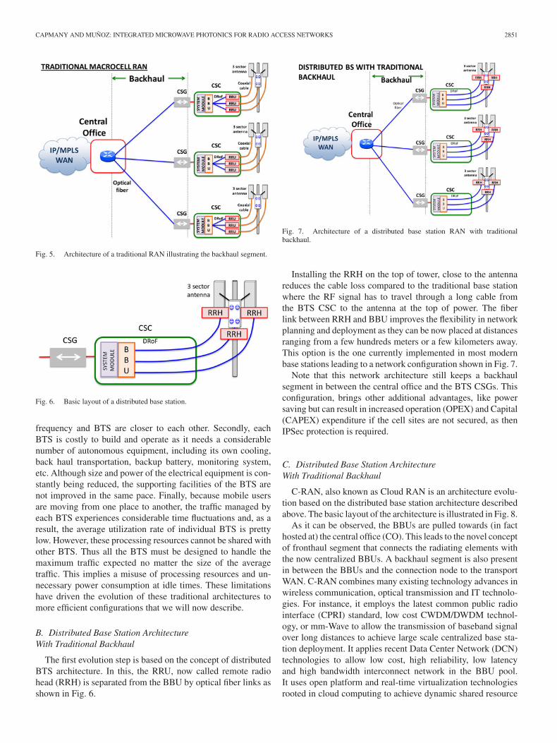
Because of the limited resource of spectrum, cellular net-works reuse the available frequencies among the different BTS.The consequence of this is that neighboring BTS that use thesame frequencies experience interference in both downlink anduplink transmission directions. Fig. 5 shows, as a summary, thetypical architecture of a traditional RAN where the backhaulpart and the connections to the central office and the transportnetwork are clearly indicated. Note that the backhaul network isusually composed of a set of point-to-point optical fiber links.
The traditional RANs architecture has some important draw-backs. First, when more BTS are added to the system to improvecapacity, if the same frequency resource is reused, the interfer-ence among BTS is severe as more BTS are using the same
CAPMANY AND MUNOZ: INTEGRATED MICROWAVE PHOTONICS FOR RADIO ACCESS NETWORKS 2851
Fig. 5. Architecture of a traditional RAN illustrating the backhaul segment.
Fig. 6. Basic layout of a distributed base station.
frequency and BTS are closer to each other. Secondly, eachBTS is costly to build and operate as it needs a considerablenumber of autonomous equipment, including its own cooling,back haul transportation, backup battery, monitoring system,etc. Although size and power of the electrical equipment is con-stantly being reduced, the supporting facilities of the BTS arenot improved in the same pace. Finally, because mobile usersare moving from one place to another, the traffic managed byeach BTS experiences considerable time fluctuations and, as aresult, the average utilization rate of individual BTS is prettylow. However, these processing resources cannot be shared withother BTS. Thus all the BTS must be designed to handle themaximum traffic expected no matter the size of the averagetraffic. This implies a misuse of processing resources and un-necessary power consumption at idle times. These limitationshave driven the evolution of these traditional architectures tomore efficient configurations that we will now describe.
B. Distributed Base Station ArchitectureWith Traditional Backhaul
The first evolution step is based on the concept of distributedBTS architecture. In this, the RRU, now called remote radiohead (RRH) is separated from the BBU by optical fiber links asshown in Fig. 6.
Fig. 7. Architecture of a distributed base station RAN with traditionalbackhaul.
Installing the RRH on the top of tower, close to the antennareduces the cable loss compared to the traditional base stationwhere the RF signal has to travel through a long cable fromthe BTS CSC to the antenna at the top of power. The fiberlink between RRH and BBU improves the flexibility in networkplanning and deployment as they can be now placed at distancesranging from a few hundreds meters or a few kilometers away.This option is the one currently implemented in most modernbase stations leading to a network configuration shown in Fig. 7.
Note that this network architecture still keeps a backhaulsegment in between the central office and the BTS CSGs. Thisconfiguration, brings other additional advantages, like powersaving but can result in increased operation (OPEX) and Capital(CAPEX) expenditure if the cell sites are not secured, as thenIPSec protection is required.
C. Distributed Base Station ArchitectureWith Traditional Backhaul
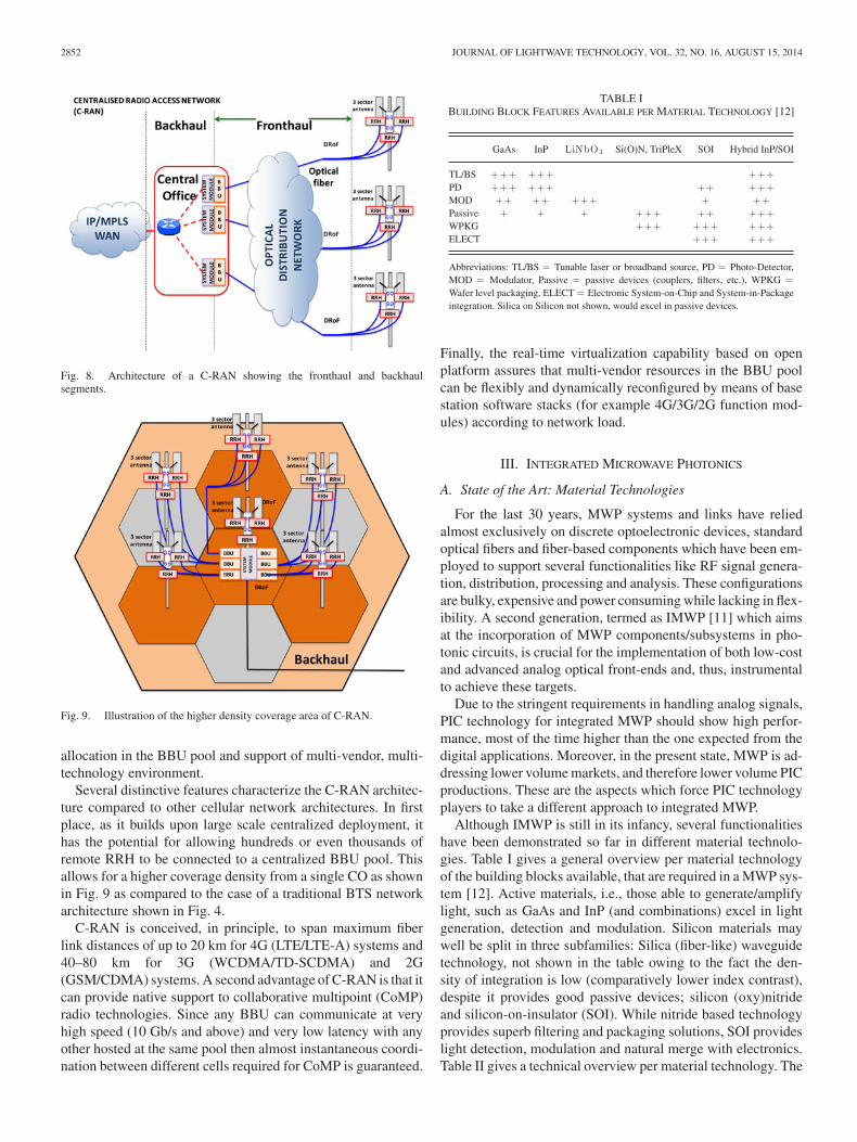
C-RAN, also known as Cloud RAN is an architecture evolu-tion based on the distributed base station architecture describedabove. The basic layout of the architecture is illustrated in Fig. 8.
As it can be observed, the BBUs are pulled towards (in facthosted at) the central office (CO). This leads to the novel conceptof fronthaul segment that connects the radiating elements withthe now centralized BBUs. A backhaul segment is also presentin between the BBUs and the connection node to the transportWAN. C-RAN combines many existing technology advances inwireless communication, optical transmission and IT technolo-gies. For instance, it employs the latest common public radiointerface (CPRI) standard, low cost CWDM/DWDM technol-ogy, or mm-Wave to allow the transmission of baseband signalover long distances to achieve large scale centralized base sta-tion deployment. It applies recent Data Center Network (DCN)technologies to allow low cost, high reliability, low latencyand high bandwidth interconnect network in the BBU pool.It uses open platform and real-time virtualization technologiesrooted in cloud computing to achieve dynamic shared resource
2852 JOURNAL OF LIGHTWAVE TECHNOLOGY, VOL. 32, NO. 16, AUGUST 15, 2014
Fig. 8. Architecture of a C-RAN showing the fronthaul and backhaulsegments.
Fig. 9. Illustration of the higher density coverage area of C-RAN.
allocation in the BBU pool and support of multi-vendor, multi-technology environment.
Several distinctive features characterize the C-RAN architec-ture compared to other cellular network architectures. In firstplace, as it builds upon large scale centralized deployment, ithas the potential for allowing hundreds or even thousands ofremote RRH to be connected to a centralized BBU pool. Thisallows for a higher coverage density from a single CO as shownin Fig. 9 as compared to the case of a traditional BTS networkarchitecture shown in Fig. 4.
C-RAN is conceived, in principle, to span maximum fiberlink distances of up to 20 km for 4G (LTE/LTE-A) systems and40–80 km for 3G (WCDMA/TD-SCDMA) and 2G(GSM/CDMA) systems. A second advantage of C-RAN is that itcan provide native support to collaborative multipoint (CoMP)radio technologies. Since any BBU can communicate at veryhigh speed (10 Gb/s and above) and very low latency with anyother hosted at the same pool then almost instantaneous coordi-nation between different cells required for CoMP is guaranteed.
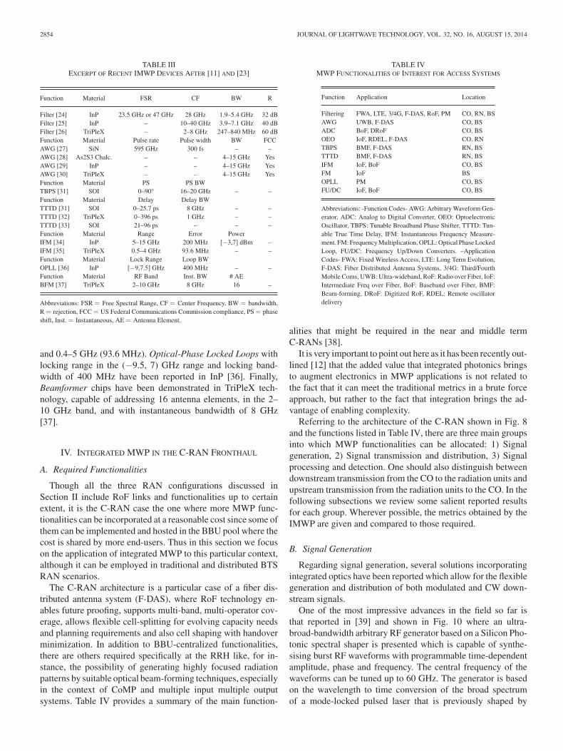
TABLE IBUILDING BLOCK FEATURES AVAILABLE PER MATERIAL TECHNOLOGY [12]
GaAs InP LiNbO3 Si(O)N, TriPleX SOI Hybrid InP/SOI
TL/BS +++ +++ +++PD +++ +++ ++ +++MOD ++ ++ +++ + ++Passive + + + +++ ++ +++WPKG +++ +++ +++ELECT +++ +++
Abbreviations: TL/BS = Tunable laser or broadband source, PD = Photo-Detector,MOD = Modulator, Passive = passive devices (couplers, filters, etc.), WPKG =Wafer level packaging, ELECT = Electronic System-on-Chip and System-in-Packageintegration. Silica on Silicon not shown, would excel in passive devices.
Finally, the real-time virtualization capability based on openplatform assures that multi-vendor resources in the BBU poolcan be flexibly and dynamically reconfigured by means of basestation software stacks (for example 4G/3G/2G function mod-ules) according to network load.
III. INTEGRATED MICROWAVE PHOTONICS
A. State of the Art: Material Technologies
For the last 30 years, MWP systems and links have reliedalmost exclusively on discrete optoelectronic devices, standardoptical fibers and fiber-based components which have been em-ployed to support several functionalities like RF signal genera-tion, distribution, processing and analysis. These configurationsare bulky, expensive and power consuming while lacking in flex-ibility. A second generation, termed as IMWP [11] which aimsat the incorporation of MWP components/subsystems in pho-tonic circuits, is crucial for the implementation of both low-costand advanced analog optical front-ends and, thus, instrumentalto achieve these targets.
Due to the stringent requirements in handling analog signals,PIC technology for integrated MWP should show high perfor-mance, most of the time higher than the one expected from thedigital applications. Moreover, in the present state, MWP is ad-dressing lower volume markets, and therefore lower volume PICproductions. These are the aspects which force PIC technologyplayers to take a different approach to integrated MWP.
Although IMWP is still in its infancy, several functionalitieshave been demonstrated so far in different material technolo-gies. Table I gives a general overview per material technologyof the building blocks available, that are required in a MWP sys-tem [12]. Active materials, i.e., those able to generate/amplifylight, such as GaAs and InP (and combinations) excel in lightgeneration, detection and modulation. Silicon materials maywell be split in three subfamilies: Silica (fiber-like) waveguidetechnology, not shown in the table owing to the fact the den-sity of integration is low (comparatively lower index contrast),despite it provides good passive devices; silicon (oxy)nitrideand silicon-on-insulator (SOI). While nitride based technologyprovides superb filtering and packaging solutions, SOI provideslight detection, modulation and natural merge with electronics.Table II gives a technical overview per material technology. The

CAPMANY AND MUNOZ: INTEGRATED MICROWAVE PHOTONICS FOR RADIO ACCESS NETWORKS 2853
TABLE IITECHNOLOGY FEATURES PER MATERIAL TECHNOLOGY [13]
GaAs/InP LiNbO3 Si(O)N TriPleX SOI
∆n [%] !10 !5 <5 >25 >100rb [mm] 0.1 0.2 0.2–0.8 0.05 0.05α [dB/cm] 2.5 0.2 0.05–0.3 0.01 <2Transparency NIR NIR VIS-NIR VIS-IR NIRFiber-chip coupling − + + +++ −Function integration ++++ +++ + +++ ++Fabrication cost −− −− ++ +++ ++
Abbreviations: ∆n = refractive index contrast, rb = bend radius (related to overallcircuit footprint), α = attenuation. IR = infrared, VIS = visible, NIR = near infrared.‘+’ good, positive, ‘−’ worse, negative. Note Table I includes a Hybrid InP/SOIcolumn not shown in this table, since the hybrid combination may benefit from thepositive aspects of both technologies, shown in separated columns.
first two rows, refractive index contrast and bend radius, arerelated to the circuit footprint. The third entry, attenuation coef-ficient, together with the two previous, is related to the qualityof optical filters.
Remarkable work by USCB and Aurrion resulted in the hy-brid integration of InP and Silicon material technologies [12].The last column in Table I (after [12]) remarks all the requiredbuilding blocks for MWP system can be built within this ma-terial technology, i.e., sources (DFB and Mode-locked lasers),amplifiers, electro-absorption modulators, all sort of passives(filters, couplers, polarization handling blocks, etc.) as well ashigh speed photo-detectors [14]. How this hybrid technologyis of application to MWP is reviewed in [12], where the fo-cus is not to beat traditional discrete component aggregation inMWP systems (on some aspects impossible, i.e., Watt operatingfiber lasers, see below), but rather on exploiting novel systemsconcepts enabled by this hybrid integration scheme. Apart fromthe works by [12], other groups are pursuing the integration ofgain media on Silicon technologies, and they have demonstratedamplifiers and lasers with Aluminium Oxide Erbium doped Sil-icon waveguides [15]–[17].
The active functions for the building blocks in Table I (laser,modulator and photo-detector) are subject to demanding re-quirements in a MWP system. The basic devices for signal gen-eration in MWP systems are high power, low relative intensityand phase noise optical sources, and broadband linear externalmodulators. On-chip semiconductor lasers provide lower powervalues (300 mW) compared to watt-class Er-doped fiber lasers(3 W) but can feature very competitive performance in terms ofRIN. For instance a InGaAlAs/InP quantum-well, high-power,low-noise packaged semiconductor external cavity laser oper-ating at 1550 nm has been recently reported [18] capable ofproviding 370 mW of fiber-coupled power with a linewidth of1 kHz, and relative intensity noise –160 dB/Hz from 200 kHzto 10 GHz.
High RF power handling broadband linear external modu-lators have been reported in III-V semiconductor technologies.For instance, both electro-absorption (EAM) and Mach-Zehnder(MZ) modulators coupler with low noise (RIN < −160 dB/Hz)tunable sampled grating DBR InP lasers have been reported.EAM based transmitters have been reported featuring a dy-
namic range of 126.3 dB ·Hz4/5, while figures in excess of115 dB ·Hz4/5 can be achieved for MZ transmitters. Both valuesare over the required with very low Vπ values. For instance, in[19] an advanced semiconductor design with transfer substratehas been reported featuring a 0.3 volt Vπ value, capable of han-dling a RF power of up to 200 mW and providing a modulationbandwidth in excess of 40 GHz.
Finally, photo-detectors delivering high RF power are re-quired in order to enhance the signal to noise ratio and dy-namic range. Among the possible photo-detector design, theuni-travelling carrier (UTC) configuration exhibits high satu-ration current at high frequencies [20], [21]. High power UTCdetectors delivering up to 31.7 dBm (1.5 W) at a 3 dB bandwidthof 8 GHz have been reported [20].
Higher operating frequency UTC detectors have been demon-strated with 3 dB bandwidths in excess of 65 GHz and 15.9 dBmRF output power [21].
B. State of the Art: Functional Devices
Regarding, functionalities that arise from the combination ofbuilding blocks, they may be classified resorting to a genericIMWP processor concept [22], [23] in the following:! Filtering.! Arbitrary waveform generator (AWG).! Analog digital converter (ADC).! Opto-electronic oscillator (OEO).! Tunable broadband phase shifter (TBPS).! Tunable true time delays (TTTD).! Instantaneous frequency measurement (IFM).! Frequency multiplication (FM).! Optical phase-locked loop (OPLL).! Frequency up/down converter (FU/DC).! Radio-frequency transceiver (RFTRX).! Beam-forming network (BFM).
For some of these functions, an excerpt of relevant works isprovided in the following paragraphs, and summarized in Ta-ble III. For further details refer to [11], [23]. Filters have beenproduced in all the cited material technologies. In InP, filtershave been reported with tunable central frequencies in the rangeof 10–40 GHz, and tunable bandwidths of 2–7 GHz, and at least30 dB of stop band rejection. For lower RF frequencies, imple-mentations have been reported in TriPleX technology, for the2–8 GHz band, with bandwidths in 300–800 MHz and 60 dBrejection. Arbitrary waveform generators have been reportedrecently, with significant efforts in ultra-wideband (UWB) gen-eration. Reported in several material technologies (SiN, chalco-genide waveguides, InP and TriPleX) all are capable of gener-ating FCC compliant signals for the 4–15 GHz band [27]–[30].Tunable broadband phase shifters and tunable true time delayshave been demonstrated mainly in Silicon technologies (SOIand TriPleX). TBPSs exhibit tunable phase shifts in the range of0–90° in a 16–20 GHz bandwidth [31]. TTTDs provide tun-able delays of up to 25 ps in 8 GHz [32] or up to 400 pslimited to 1 GHz bandwidth [33]. IFM chips are reported inInP [34] and TriPleX technologies [35], featuring RF frequencydetermination ranges (RMS error) of 5–15 GHz (200 MHz)
2854 JOURNAL OF LIGHTWAVE TECHNOLOGY, VOL. 32, NO. 16, AUGUST 15, 2014
TABLE IIIEXCERPT OF RECENT IMWP DEVICES AFTER [11] AND [23]
Function Material FSR CF BW R
Filter [24] InP 23.5 GHz or 47 GHz 28 GHz 1.9–5.4 GHz 32 dBFilter [25] InP – 10–40 GHz 3.9–7.1 GHz 40 dBFilter [26] TriPleX – 2–8 GHz 247–840 MHz 60 dBFunction Material Pulse rate Pulse width BW FCCAWG [27] SiN 595 GHz 300 fs – –AWG [28] As2S3 Chalc. – – 4–15 GHz YesAWG [29] InP – – 4–15 GHz YesAWG [30] TriPleX – – 4–15 GHz YesFunction Material PS PS BWTBPS [31] SOI 0–90° 16–20 GHz – –Function Material Delay Delay BWTTTD [31] SOI 0–25.7 ps 8 GHz – –TTTD [32] TriPleX 0–396 ps 1 GHz – –TTTD [33] SOI 21–96 ps – – –Function Material Range Error PowerIFM [34] InP 5–15 GHz 200 MHz [−3,7] dBm –IFM [35] TriPleX 0.5–4 GHz 93.6 MHz – –Function Material Lock Range Loop BWOPLL [36] InP [−9,7.5] GHz 400 MHz – –Function Material RF Band Inst. BW # AEBFM [37] TriPleX 2–10 GHz 8 GHz 16 –
Abbreviations: FSR = Free Spectral Range, CF = Center Frequency, BW = bandwidth,R = rejection, FCC = US Federal Communications Commission compliance, PS = phaseshift, Inst. = Instantaneous, AE = Antenna Element.
and 0.4–5 GHz (93.6 MHz). Optical-Phase Locked Loops withlocking range in the (−9.5, 7) GHz range and locking band-width of 400 MHz have been reported in InP [36]. Finally,Beamformer chips have been demonstrated in TriPleX tech-nology, capable of addressing 16 antenna elements, in the 2–10 GHz band, and with instantaneous bandwidth of 8 GHz[37].
IV. INTEGRATED MWP IN THE C-RAN FRONTHAUL
A. Required Functionalities
Though all the three RAN configurations discussed inSection II include RoF links and functionalities up to certainextent, it is the C-RAN case the one where more MWP func-tionalities can be incorporated at a reasonable cost since some ofthem can be implemented and hosted in the BBU pool where thecost is shared by more end-users. Thus in this section we focuson the application of integrated MWP to this particular context,although it can be employed in traditional and distributed BTSRAN scenarios.
The C-RAN architecture is a particular case of a fiber dis-tributed antenna system (F-DAS), where RoF technology en-ables future proofing, supports multi-band, multi-operator cov-erage, allows flexible cell-splitting for evolving capacity needsand planning requirements and also cell shaping with handoverminimization. In addition to BBU-centralized functionalities,there are others required specifically at the RRH like, for in-stance, the possibility of generating highly focused radiationpatterns by suitable optical beam-forming techniques, especiallyin the context of CoMP and multiple input multiple outputsystems. Table IV provides a summary of the main function-
TABLE IVMWP FUNCTIONALITIES OF INTEREST FOR ACCESS SYSTEMS
Function Application Location
Filtering FWA, LTE, 3/4G, F-DAS, RoF, PM CO, RN, BSAWG UWB, F-DAS CO, BSADC BoF, DRoF CO, BSOEO IoF, RDEL, F-DAS CO, RNTBPS BMF, F-DAS RN, BSTTTD BMF, F-DAS RN, BSIFM IoF, BoF CO, BSFM IoF BSOPLL PM CO, BSFU/DC IoF, BoF CO, BS
Abbreviations: -Function Codes- AWG: Arbitrary Waveform Gen-erator, ADC: Analog to Digital Converter, OEO: OptoelectronicOscillator, TBPS: Tunable Broadband Phase Shifter, TTTD: Tun-able True Time Delay, IFM: Instantaneous Frequency Measure-ment. FM: Frequency Multiplication, OPLL: Optical Phase LockedLoop, FU/DC: Frequency Up/Down Converters. –ApplicationCodes- FWA: Fixed Wireless Access, LTE: Long Term Evolution,F-DAS: Fiber Distributed Antenna Systems, 3/4G: Third/FourthMobile Coms, UWB: Ultra-wideband, RoF: Radio over Fiber, IoF:Intermediate Freq over Fiber, BoF: Baseband over Fiber, BMF:Beam-forming, DRoF: Digitized RoF, RDEL: Remote oscillatordelivery
alities that might be required in the near and middle termC-RANs [38].
It is very important to point out here as it has been recently out-lined [12] that the added value that integrated photonics bringsto augment electronics in MWP applications is not related tothe fact that it can meet the traditional metrics in a brute forceapproach, but rather to the fact that integration brings the ad-vantage of enabling complexity.
Referring to the architecture of the C-RAN shown in Fig. 8and the functions listed in Table IV, there are three main groupsinto which MWP functionalities can be allocated: 1) Signalgeneration, 2) Signal transmission and distribution, 3) Signalprocessing and detection. One should also distinguish betweendownstream transmission from the CO to the radiation units andupstream transmission from the radiation units to the CO. In thefollowing subsections we review some salient reported resultsfor each group. Wherever possible, the metrics obtained by theIMWP are given and compared to those required.
B. Signal Generation
Regarding signal generation, several solutions incorporatingintegrated optics have been reported which allow for the flexiblegeneration and distribution of both modulated and CW down-stream signals.
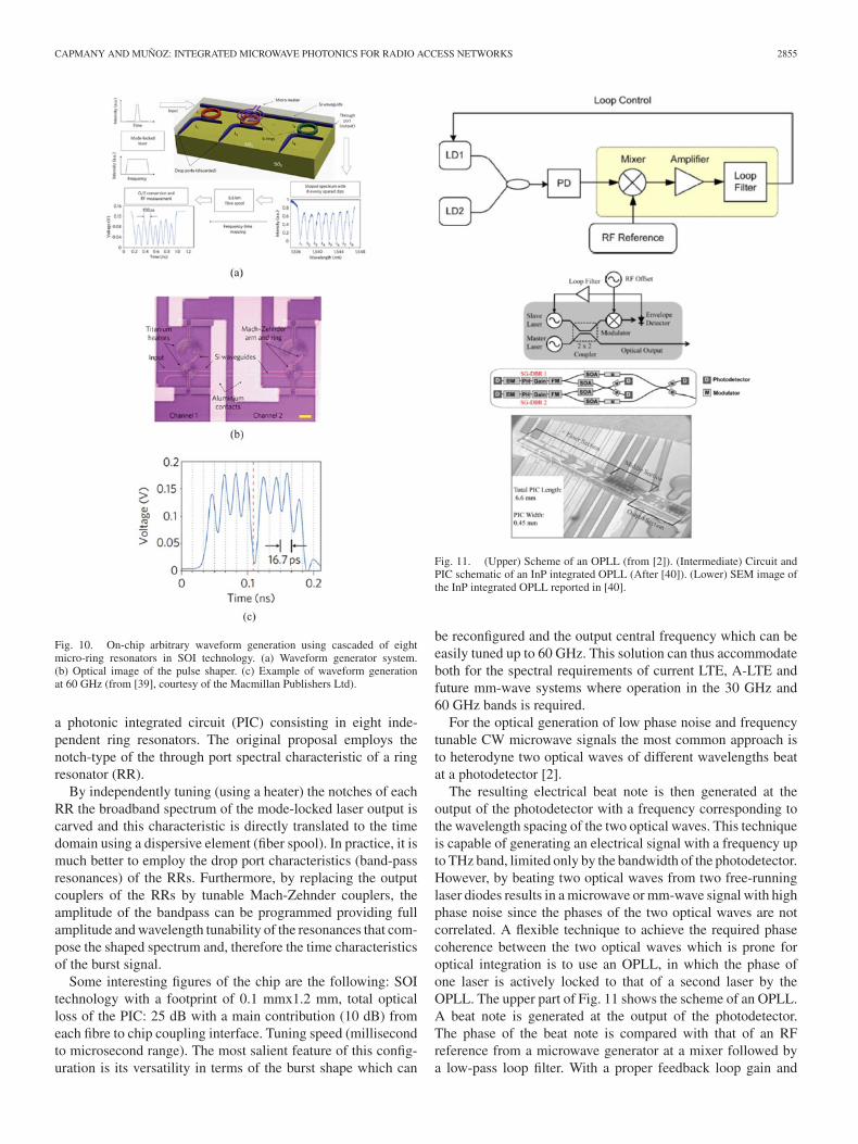
One of the most impressive advances in the field so far isthat reported in [39] and shown in Fig. 10 where an ultra-broad-bandwidth arbitrary RF generator based on a Silicon Pho-tonic spectral shaper is presented which is capable of synthe-sising burst RF waveforms with programmable time-dependentamplitude, phase and frequency. The central frequency of thewaveforms can be tuned up to 60 GHz. The generator is basedon the wavelength to time conversion of the broad spectrumof a mode-locked pulsed laser that is previously shaped by
CAPMANY AND MUNOZ: INTEGRATED MICROWAVE PHOTONICS FOR RADIO ACCESS NETWORKS 2855
Fig. 10. On-chip arbitrary waveform generation using cascaded of eightmicro-ring resonators in SOI technology. (a) Waveform generator system.(b) Optical image of the pulse shaper. (c) Example of waveform generationat 60 GHz (from [39], courtesy of the Macmillan Publishers Ltd).
a photonic integrated circuit (PIC) consisting in eight inde-pendent ring resonators. The original proposal employs thenotch-type of the through port spectral characteristic of a ringresonator (RR).
By independently tuning (using a heater) the notches of eachRR the broadband spectrum of the mode-locked laser output iscarved and this characteristic is directly translated to the timedomain using a dispersive element (fiber spool). In practice, it ismuch better to employ the drop port characteristics (band-passresonances) of the RRs. Furthermore, by replacing the outputcouplers of the RRs by tunable Mach-Zehnder couplers, theamplitude of the bandpass can be programmed providing fullamplitude and wavelength tunability of the resonances that com-pose the shaped spectrum and, therefore the time characteristicsof the burst signal.
Some interesting figures of the chip are the following: SOItechnology with a footprint of 0.1 mmx1.2 mm, total opticalloss of the PIC: 25 dB with a main contribution (10 dB) fromeach fibre to chip coupling interface. Tuning speed (millisecondto microsecond range). The most salient feature of this config-uration is its versatility in terms of the burst shape which can
Fig. 11. (Upper) Scheme of an OPLL (from [2]). (Intermediate) Circuit andPIC schematic of an InP integrated OPLL (After [40]). (Lower) SEM image ofthe InP integrated OPLL reported in [40].
be reconfigured and the output central frequency which can beeasily tuned up to 60 GHz. This solution can thus accommodateboth for the spectral requirements of current LTE, A-LTE andfuture mm-wave systems where operation in the 30 GHz and60 GHz bands is required.
For the optical generation of low phase noise and frequencytunable CW microwave signals the most common approach isto heterodyne two optical waves of different wavelengths beatat a photodetector [2].
The resulting electrical beat note is then generated at theoutput of the photodetector with a frequency corresponding tothe wavelength spacing of the two optical waves. This techniqueis capable of generating an electrical signal with a frequency upto THz band, limited only by the bandwidth of the photodetector.However, by beating two optical waves from two free-runninglaser diodes results in a microwave or mm-wave signal with highphase noise since the phases of the two optical waves are notcorrelated. A flexible technique to achieve the required phasecoherence between the two optical waves which is prone foroptical integration is to use an OPLL, in which the phase ofone laser is actively locked to that of a second laser by theOPLL. The upper part of Fig. 11 shows the scheme of an OPLL.A beat note is generated at the output of the photodetector.The phase of the beat note is compared with that of an RFreference from a microwave generator at a mixer followed bya low-pass loop filter. With a proper feedback loop gain and
2856 JOURNAL OF LIGHTWAVE TECHNOLOGY, VOL. 32, NO. 16, AUGUST 15, 2014
response time, the relative phase fluctuations between the twolasers are significantly reduced and the phase of the beat note islocked to the RF reference. Effective phase locking requires thetwo narrow linewidth lasers with phase fluctuations only at lowfrequencies.
An integrated OPLL in InP has been reported [40] formedfrom a pair of widely-tunable SGDBRs together with most ofthe required optical elements. The intermediate part of Fig. 11shows the circuit and the PIC schematic.
In the circuit schematic it can be appreciated that an inte-grated modulator is used to generate sidebands on the mixedsignal, so that the OPLL can lock on one of these. In [40] a5 GHz fundamental offset locking has been reported. It hasbeen anticipated that locking might be possible up to the THzrange without having to generate rf higher than 100 GHz bymeans of a deeper phase modulation of the on-chip modulatorto generate a higher number of modulation side bands. This fre-quency range is enough to cover the existing, and future LTE5G services. The lower part of Fig. 11 shows the SEM image ofthe whole OPLL-PIC. Very recently [41], a monolithically inte-grated InP dual OPLL subsystem has been reported that whensynchronized to an optical frequency comb generator withoutany prior filtering of the comb lines, enables the generation ofCW signals spanning from the microwave and millimetre-waveto the THz region of the spectrum.
CW signal generation with excellent frequency stability andphase noise characteristics can also be achieved by means ofOEOs. These reference signals are required in baseband andintermediate frequency MWP links as will be discussed below.Usually these solutions are not considered economically inter-esting, as they require a local oscillator at the radiating elements.However, in the C-RAN architecture the OEO can be hosted atthe CO and its RF signal distributed by optical means to theradiating elements, thus sharing its cost. A compact OEO hasbeen recently reported where the optical fiber loop is replacedby a high Q-factor cavity, implemented by means of a LiNbO3integrated whispering gallery mode resonator (WGMR) [42].WGMRs ranging in size from a few hundred micrometres to afew millimetres can be fabricated from a wide variety of op-tically transparent materials reaching Q-factors in the range of3 × 1011 . OEOs based on high-Q WGMRs made from electro-optic materials can provide high performance operating in fre-quency ranges from 10 to 40 GHz and featuring instantaneouslinewidths below 200 Hz.
In relation to upstream transmission, signal generation mustfollow a completely different philosophy, as allocating a highperformance photonic signal generator at each RRH is econom-ically unfeasible. In this case, it becomes more interesting touse a seed signal distributed from the CO as will be describedin the next section.
C. Signal Transmission and Distribution
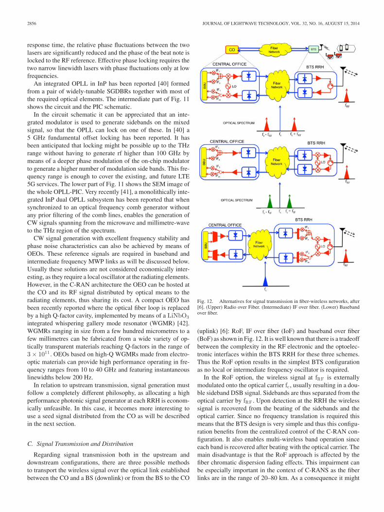
Regarding signal transmission both in the upstream anddownstream configurations, there are three possible methodsto transport the wireless signal over the optical link establishedbetween the CO and a BS (downlink) or from the BS to the CO
Fig. 12. Alternatives for signal transmission in fiber-wireless networks, after[6]. (Upper) Radio over Fiber. (Intermediate) IF over fiber. (Lower) Basebandover fiber.
(uplink) [6]: RoF, IF over fiber (IoF) and baseband over fiber(BoF) as shown in Fig. 12. It is well known that there is a tradeoffbetween the complexity in the RF electronic and the optoelec-tronic interfaces within the BTS RRH for these three schemes.Thus the RoF option results in the simplest BTS configurationas no local or intermediate frequency oscillator is required.
In the RoF option, the wireless signal at fRF is externallymodulated onto the optical carrier fc , usually resulting in a dou-ble sideband DSB signal. Sidebands are thus separated from theoptical carrier by fRF . Upon detection at the RRH the wirelesssignal is recovered from the beating of the sidebands and theoptical carrier. Since no frequency translation is required thismeans that the BTS design is very simple and thus this configu-ration benefits from the centralized control of the C-RAN con-figuration. It also enables multi-wireless band operation sinceeach band is recovered after beating with the optical carrier. Themain disadvantage is that the RoF approach is affected by thefiber chromatic dispersion fading effects. This impairment canbe especially important in the context of C-RANS as the fiberlinks are in the range of 20–80 km. As a consequence it might
CAPMANY AND MUNOZ: INTEGRATED MICROWAVE PHOTONICS FOR RADIO ACCESS NETWORKS 2857
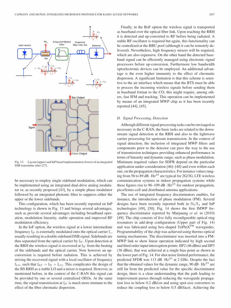
Fig. 13. Layout (upper) and InP based implementation (lower) of an integratedSSB transmitter after [27].
be necessary to employ single sideband modulation, which canbe implemented using an integrated dual-drive analog modula-tor or, as recently proposed [43], by a simple phase modulatorfollowed by an integrated photonic filter to suppress either theupper or the lower sidebands.
This configuration, which has been recently reported on InPtechnology is shown in Fig. 13 and brings several advantages,such as provide several advantages including broadband oper-ation, modulation linearity, stable operation and improved RFmodulation efficiency.
In the IoF option, the wireless signal at a lower intermediatefrequency fIF is externally modulated onto the optical carrier fc ,usually resulting in a double sideband DSB signal. Sidebands arethus separated from the optical carrier by fIF . Upon detection atthe RRH the wireless signal is recovered at fIF from the beatingof the sidebands and the optical carrier. Now however an up-conversion is required before radiation. This is achieved bymixing the recovered signal with a local oscillator of frequencyfLO , such that fRF = fIF + fLO . This complicates the design ofthe BS RRH as a stable LO and a mixer is required. However, asmentioned before, in the context of the C-RAN this signal canbe provided by one or several centralized OEOs. At the sametime, the signal transmission at fIF is much more immune to theeffect of the fiber chromatic dispersion.
Finally, in the BoF option the wireless signal is transportedas baseband over the optical fiber link. Upon reaching the RRHit is detected and up-converted to RF before being radiated. Astable RF oscillator is required but again, this functionality canbe centralized at the BBU pool (although it can be remotely de-livered). Nevertheless, high frequency mixers will be required,which are also expensive. On the other hand the detected base-band signal can be efficiently managed using electronic signalprocessors before up-conversion. Furthermore low bandwidthoptoelectronic devices can be employed. An additional advan-tage is the even higher immunity to the effect of chromaticdispersion. A significant limitation is that this scheme is sensi-tive to the air interface which means that the BTS must be ableto process the incoming wireless signals before sending themin baseband format to the CO, this might require, among oth-ers, fast IFM and tracking. This operation can be implementedby means of an integrated MWP chip as it has been recentlyreported [44], [45].
D. Signal Processing, Detection
Although different signal processing tasks can be envisaged asnecessary in the C-RAN, the basic tasks are related to the down-stream signal detection at the RRH and also to the lightwavecarrier processing for upstream transmission. In the context ofsignal detection, the inclusion of integrated MWP filters andcomponents prior to the detector can pave the way to the useof transmission techniques providing enhanced performance interms of linearity and dynamic range, such as phase modulation.Minimum required values for SDFR depend on the particularapplication under consideration [46]–[48] and even within eachone, on the propagation characteristics. For instance values rang-ing from 56 to 89 dB ·Hz2/3 are typical for 2G/3G, LTE wirelesscommunication systems in indoor propagation systems whilethese figures rise to 96–109 dB ·Hz2/3 for outdoor propagation,pico/femto-cell and distributed antenna applications.
The use of integrated frequency discriminators enables, forinstance, the introduction of phase modulation (PM). Severaldesigns have been recently reported both in Si3N4 and InPtechnologies [49], [50]. Fig. 14 shows the first IMWP fre-quency discriminator reported by Marpaung et al. in (2010)[49]. The chip consists of five fully reconfigurable optical ringresonators in add-drop configuration (Upper part of Fig. 14)and was fabricated using box-shaped TriPleXTM waveguides.Programmability of the chip was achieved using thermo-opticaltuning mechanisms. The discriminator was inserted into a PM-MWP link to show linear operation indicated by high secondand third order input interception points: IIP2 (46 dBm) and IIP3(36 dBm), that was achieved at a single bias point as shown inthe lower part of Fig. 14. For shot noise limited performance, thepredicted SFDR was 113 dB ·Hz2/3 at 2 GHz. Despite the factthat the obtained values for the dynamic range, 90 dB ·Hz2/3 arestill far from the predicted value for the specific discriminatordesign, there is a clear understanding that the path leading toimprovement passes through reducing the waveguide propaga-tion loss to below 0.2 dB/cm and using spot-size converters toreduce the coupling loss to below 0.5 dB/facet. Achieving the

2858 JOURNAL OF LIGHTWAVE TECHNOLOGY, VOL. 32, NO. 16, AUGUST 15, 2014
Fig. 14. (Upper) Layout of the Optical ring resonator frequency discrimi-nator based in TriPleX technology. (Lower) Characterization results of thefundamental RF signals and the IMDs, after [49].
low propagation loss is proven to be feasible since the value ofbelow 0.1 dB/cm has recently been demonstrated by the sameresearchers. An InP integrated discriminator that includes theoptical detectors has been reported in [50]. Designed as a linearfilter in intensity, featured SFDR values the range between 67and 79 dB ·Hz2/3 for signal frequencies in the range of 5–9 GHzlimited, in principle, by the high value of the optical losses aris-ing from the use of several free space coupling devices includedin the experimental setup. The above figures can be improvedfollowing two strategies. Firstly, losses can be readily reduced bythe use of integrated spot-size converters improving the SFDRby 17.3 dB to a range of 84–96 dB ·Hz2/3 and secondly, a fur-ther increase up to a range of 104–116 dB ·Hz2/3 is possible byreducing the system noise eliminating the EDFA employed inthe experimental setup and by using a commercially availablelaser source providing higher output power and lower relativeintensity noise.
The second approach to achieve linear phase demodulationis to use a coherent optical link and to detect the optical PMusing an optical phase locked loop (PM-CD-OPLL) [51]–[55].This alternative is complex, but offers potentially high perfor-mance. The interest for PM-CD-OPPL is justified as it opensthe possibility, as explained earlier, of realizing a phase track-ing receiver that can follow the linear phase modulation appliedat the transmitter providing, as a consequence, ultimately lineartransmission. As shown in the upper part of Fig. 15, the negativefeedback signal to the tracking modulator pair reduces the level
Fig. 15. (Upper) Layout Coherent receiver for phase-modulated input (after[54]). (Lower) Schematic of flip-chipping of electronic and photonic ICCs andlayout of the PIC (after [54]).
of the interference signal on the detectors so that the outputis reduced to the linear range. The differential pair also sup-presses even order distortions that may exist in the semiconduc-tor modulators as well as amplitude modulation. Furthermore,high modulation depth is enabled as the signals that output thedifferential tracking modulators are in phase. The price to bepaid is that the tracking phase modulators must provide an al-most instantaneous tracking of the phase deviation detected inthe photodiode pair. This imposes a very stringent requirementon the maximum feedback loop delay. In practice, the loopdelay must be a small fraction (e.g., 1/5) of the maximum RFfrequency and joint electronic and photonic integration becomesthen essential. The lower part of Fig. 15 a flip-chip bonded con-figuration of a PM-CD-OPLL implemented in InP to eliminateunnecessary delays and undesired signal paths. The chip pro-vided an RF gain of −2 dB and an SFDR of 122 dB ·Hz2/3 at300 MHz [54].
Regarding the lightwave carrier processing techniques forupstream transmission, there are three possible techniques bywhich a CW optical signal delivered from the BBU pool canbe reutilized. These are schematically shown in Fig. 16. A firstoption is to use an electro-absorption transceiver (EAT), this isan integrated device where an electro-absorption modulator isused as a detector (for the downlink carrier) and a modulator(for the uplink carrier). The un-modulated uplink carrier is re-motely delivered from the CO being transparent to detection atthe EAT. Several works [56], [57] have already experimentallydemonstrated the feasibility of this approach.
A second option shown in the intermediate part of Fig. 16is to employ a wavelength reuse technique, where a portion ofthe downlink carrier is extracted by means of a passive opticalfilter in this case a selective integrated-optic filter which needsto wipe out the signal sidebands. The resulting CW carrier canbe then and re-used for uplink transmission. Both the optical
CAPMANY AND MUNOZ: INTEGRATED MICROWAVE PHOTONICS FOR RADIO ACCESS NETWORKS 2859
Fig. 16. Three possible techniques by which a CW optical signal deliveredfrom the BBU pool can be reutilized in the RRH, after [6]. (Upper) Using anElectro-absorption transceiver. (Intermediate) Downstream carrier filtering anreutilization. (Lower) Remote CW carrier delivery.
filter and the upstream external modulator should be integratedon the same chip.
The last alternative, shown in the lower part of Fig. 15 knownas remote carrier delivery is based on remotely providing theuplink carrier from the CO. Hence, the optical source in the RRHis replaced by a filtering subsystem consisting of an integratedwavelength interleaver or narrowband optical filter to separatethe uplink carrier from the downlink signals [6]. Again, both thisoptical filtering element and the upstream external modulatorshould be integrated on the same chip.
V. SUMMARY, CONCLUSIONS AND CHALLENGES
We have explored the advantages that IMWP can bring toRANs. First we have reviewed the most common architecturesof RANS identifying the segments where MWP componentsand RoF links are located. We have then provided a short intro-duction to IMWP with the aim of illustrating the current stateof the art of this technology and its potentials. Finally, we haveprovided an overview of several salient results reported in the lit-erature where photonic integration is employed as a supportingtechnology in the context of the three main application groupsrequired for RAN fronthauls: Signal generation, transmissionand distribution and signal processing.
It is important to stress that besides meeting the traditionalspecifications and metrics required for MWP applications theIMWP approach must bring the added values of improving com-pactness, footprint and energy consumption, providing superiorstability and reducing coupling losses between devices whichis present in discrete component approaches (where devicesfrom different manufacturers and technologies are assembledtogether) and last, but not least enabling complexity by offeringthe possibility of rapid reconfiguration, tunability and adaptabil-ity in terms of offered functionalities.
Central to the success of incorporating integrated MWP chipsin the access networks is, as well, that the economic value de-rived from the integrated chip must outweigh the cost of theintegration itself [58]. This is especially true in a highly cost-sensitive application scenario such as RANs. Hence, several keyquestions need to be addressed when considering each one ofthe particular technology options previously discussed.
Firstly, is the technology flexible enough that it allows theimplementation of a fully functional MWP system with chips(i.e., not resorting to discrete component aggregation) with allor most of the required functions using the same technologyand leading to the possibility of a monolithic chip or on the con-trary a hybrid approach is required? The impact of this questionon the possibility of low-cost mass production and subsequentbenefit from economies of scale is evident. From Sections III-Aand III-B at the sight of Tables I–III, it is clear there is no win-ing technology, and different approaches exist to build a fullyintegrated MWP system on a chip: monolithic InP, and hybridInP/SOI [12] or InP/TriPleX [13]. For the cases in which inte-gration with demanding electronics and high RF frequencies arerequired, InP/SOI hybridization is a clear candidate. For thoseapplications where demanding requirements are posed to thefilters, InP/TriPleX combination seems the best option.
Secondly, does the technology support the required density ofintegration to allow for the incorporation of the required numberof functions on a chip of reasonable size? When hybridizationcomes into place, the answer is yes, being the wining optionin terms of footprint the hybrid InP/SOI technology. For thecurrently only available monolithic approach, InP, it may welldepend on the MWP system architecture that needs to be broughton-chip. Referring to the listed functional devices in Table IIIthe Filter, AWG, TBPS, TTTD, IFM and BFM devices only hada single function on chip, i.e., the photonic filter (in differentshapes). Considering approximately 5–7 photonic components,and 1–3 additional electronic components are required to inte-grate a fully functional MWP system on chips [23], the degreeof full integration (opto-electronic) is 1 out of 5 in the best case(20%) which is rather low. From those listed, only the OPLLof [36] had all the functions (laser, modulator, passives and de-tector) on an InP chip, achieving 100% photonic integration.Efforts are currently being carried out to bring the 100% build-ing blocks functions as IFM and BFM onto a chip (see [23]).
Third and final question: is the technology mature enough toprovide a good manufacturing reliability with a reasonable fab-rication yield?. For dedicated process and, in particular, for digi-tal communication applications this has certainly been achieved[58]. In the case of IMWP it might be of interest as well toconsider a generic chip fabrication process mimicking the elec-tronic industry, i.e., developing a platform that can serve to thefabrication of complex chips with very distinct functionalities.A detailed review of all the generic integration technologies andbuilding blocks available is given in [59]. The current focusof generic photonic chip manufacturing technologies is on in-corporating and demonstrating novel and/or enhanced features(i.e., higher RF operational speed) building blocks. Nonetheless,there is incipient interest on reproducibility and yield, as for in-stance on SOI technology [60]. Despite this, the main efforts in
2860 JOURNAL OF LIGHTWAVE TECHNOLOGY, VOL. 32, NO. 16, AUGUST 15, 2014
generic integration are still some steps before the concerns onyield and reproducibility, i.e., on demonstrating and starting-upthe generic processes.
REFERENCES
[1] J. Capmany and D. Novak, “Microwave photonics combines two worlds,”Nature Photon., vol. 1, pp. 316–330, 2007.
[2] J. Yao, “Microwave photonics,” J. Lightw. Technol., vol. 27, no. 12,pp. 314–335, Dec. 2009.
[3] “Technology focus on microwave photonics,” Nature Photon., vol. 5,pp.723–736, 2011.
[4] H. Al-Raweshidi and S. Komaki Eds., Radio Over Fiber Technologiesfor Mobile Communications Networks. Boston, MA, USA: Artech House,2002.
[5] J. Capmany, B. Ortega, and D. Pastor, “A tutorial on microwave photonicfilters,” J. Lightw. Technol., vol. 24, no. 1, pp. 201–229, Jan. 2006.
[6] C. Lim, A. Nirmalathas, M. Bakaul, P. Gamage, K.-L. Lee, Y. Yang,D. Novak, and R. Waterhouse, “Fiber-wireless networks and subsystemtechnologies,” J. Lightw. Technol., vol. 28, no. 4, pp. 390–405, Feb. 15,2010.
[7] P. Chanclou et al., “Optical access evolutions and their impact on themetropolitan and home networks” presented at the ECOC, Brussels, Bel-gium, 2008, Paper We.3.F.1.
[8] P. Chanclou et al., “Optical fiber solution for mobile fronthaul to achievecloud radio access network,” in Proc. Future Netw. MobileSummit Conf.,2013.
[9] A. Pizzinat, P. Chanclou, F. Le Clech, and B. Landousies, “FTTx wherex stays for antenna: Requirements on optical access/distribution networkfor new mobile backhaul architectures,” presented at the FTTx SUMMITEur., London, U.K., Apr. 25, 2012.
[10] A. Pizzinat, P. Chanclou, F. Frank, B. Charbonnier, P. Niger,B. Landousies, P. Herbelin, J. M. Picard, and J.-P. Charles, “Infrastructureconvergence for fixed and mobile access networks,” presented at the OFCWorkshop, San Diego, CA, USA, Mar. 22, 2009.
[11] D. Marpaung, C. Roeloffzen, R. Heideman, A. Leinse, S. Sales, andJ. Capmany, “Integrated microwave photonics,” Lasers Photon. Rev.,vol. 7, pp. 506–538, 2013.
[12] H.-W. Chen, A. W. Fang, J. D. Peters, Z. Wang, J. Bovington, D. Liang,and J. E. Bowers, “Integrated microwave photonic filteron a hybrid siliconplatform,” IEEE Trans. Microw. Theory Tech., vol. 58, no. 11, pp. 3213–3219, Nov. 2010.
[13] C. G. H. Roeloffzen, L. Zhuang, C. Taddei, A. Leinse, R. G. Heideman,P. W. L. van Dijk, R. M. Oldenbeuving, D. A. I. Marpaung, M. Burla,and K.-J. Boller, “Silicon nitride microwave photonic circuits,” Opt. Exp.,vol. 21, pp. 22937–22961, 2013.
[14] M. J. R Heck, J. F. Bauters, M. L. Davenport, J. K. Doylend, S. Jain,G. Kurczveil, S. Srinivasan, Y. Tang, and J. E. Bowers, “Hybrid siliconphotonic integrated circuit technology,” IEEE J. Sel. Topics QuantumElectron., vol. 19, no. 4, p. 6100117, Jul.-Aug. 2013.
[15] J. Bradley, Purnawirman, E. Hosseini, J. Sun, T. Adam, G. Leake,D. Coolbaugh, and M. Watts, “C- and L-band erbium-doped aluminumoxide lasers with silicon nitride distributed Bragg reflector cavities,” pre-sented at the CLEO: 2013, OSA Tech. Dig., San Jose, CA, USA, 2013,Paper CF1I.4.
[16] M. Belt, T. Huffman, M. Davenport, W. Li, J. Barton, and D. Blumenthal,“Arrayed narrow linewidth erbium-doped waveguide-distributed feedbacklasers on an ultra-low-loss silicon-nitride platform,” Opt. Lett., vol. 38,pp. 4825–4828, 2013.
[17] J. D. Bradley and M. Pollnau, “Erbium-doped integrated waveguide am-plifiers and lasers”, Laser Photon. Rev., vol. 5, no. 3, pp. 368–403, 2011.
[18] W. Loh, F. J. O’Donnell, J. J. Plant, M. A. Brattain, L. J. Missaggia,and P. W. Juodawlkis, “ Packaged, high-power, narrow-linewidth slab-coupled optical waveguide external cavity laser (SCOWECL),” IEEE Pho-ton. Technol. Lett., vol. 23, no. 14, pp. 974–977, Jul. 2011.
[19] J. H. Shin, Y.-C. Chang, and N. Dagli, “0.3 V drive voltage GaAs/AlGaAssubstrate removed Mach–Zehnder intensity modulators,” Appl. Phys. Lett.,vol. 92, p. 201103, 2008.
[20] Q. Zhou, A. S. Cross, Y. Fu, A. Beling, B. M. Foley, P. E. Hopkins, andJ. C. Campbell, “Balanced InP/InGaAs photodiodes with 1.5-W outputpower,” IEEE Photon. J., vol. 5, no. 3, p. 6800307, Jun. 2013.
[21] Q. Zhou, A. S. Cross, A. Beling, Y. Fu, Z. Lu, and J. C. Campbell, “High-power V-band InGaAs/InP photodiodes,” IEEE Photon. Technol. Lett.,vol. 25, no. 10, pp. 907–909, May 15, 2013.
[22] J. Capmany, S. Sales, I. Gasulla, J. Mora, J. Lloret, and J. Sancho, “In-novative concepts in microwave photonics,” Waves, vol. 4, pp. 43–58,2012.
[23] P. Munoz, J. Capmany, D. Perez, J. H. den Besten, J. S. Fandino, and J. D.Domenech, “Integrated microwave photonics: State of the art and futuretrends,” presented at the Int. Conf. Transparent Opt. Netw., Graz, Austria,Jul. 6–10, 2014.
[24] E. J. Norberg, R. S. Guzzon, J. S. Parker, L. A. Johansson, and L. A.Coldren, “Programmable photonic microwave filters monolithically inte-grated in InP–InGaAsP,” J. Lightw. Technol., vol. 29, no. 11, pp. 1611–1619, Jun. 2011.
[25] R. S. Guzzon, E. J. Norberg, J. S. Parker, L. A. Johansson, and L. A.Coldren, “Integrated InP-InGaAsP tunable coupled ring optical bandpassfilters with zero insertion loss,” Opt. Exp., vol. 19, no. 8, pp. 7816–7826,2011.
[26] D. Marpaung, B. Morrison, R. Pant, C. Roeloffzen, A. Leinse,M. Hoekman, R. Heideman, and B. J. Eggleton, “Si3 N4 ring resonator-based microwave photonic notch filter with an ultrahigh peak rejection,”Opt. Exp., vol. 21, no. 20, pp. 23286–23294, 2013.
[27] F. Ferdous, H. Miao, D. E. Leaird, K. Srinivasan, J. Wang, L. Chen,L. T. Varghese, and A. M. Weiner, “Spectral line-by-line pulse shaping ofon-chip microresonator frequency combs,” Nature Photon., vol. 5, no. 12,pp. 770–776, 2011.
[28] K. Tan, D. Marpaung, R. Pant, F. Gao, E. Li, J. Wang, D.-Y. Choi,S. Madden, B. Luther-Davies, J. Sun, et al., “Photonic-chip-based alloptical ultra-wideband pulse generation via XPM and birefringence in achalcogenide waveguide,” Opt. Exp., vol. 21, no. 2, pp. 2003–2011, 2013.
[29] V. Moreno, M. Rius, J. Mora, M. A. Muriel, and J. Capmany, “Integrablehigh order UWB pulse photonic generator based on cross phase mod-ulation in a SOA-MZI,” Opt. Exp., vol. 21, no. 19, pp. 22911–22917,2013.
[30] D. Marpaung, L. Chevalier, M. Burla, and C. Roeloffzen, “Impulse ra-dio ultrawideband pulse shaper based on a programmable photonic chipfrequency discriminator,” Opt. Exp., vol. 19, no. 25, pp. 24838–24848,2011.
[31] M. Burla, L. R. Cortes, M. Li, X. Wang, L. Chrostowski, and J. Azana,“On-chip ultra-wideband microwave photonic phase shifter and true timedelay line based on a single phase-shifted waveguide Bragg grating,” inProc. IEEE Microw. Photon. Conf., 2013, pp. 92–95.
[32] M. Burla, D. Marpaung, L. Zhuang, C. Roeloffzen, M. R. Khan, A. Leinse,M. Hoekman, and R. Heideman, “On-chip CMOS compatible reconfig-urable optical delay line with separate carrier tuning for microwave pho-tonic signal processing,” Opt. Exp., vol. 19, pp. 21475–21484, Oct. 2011.
[33] W. Shi, V. Veerasubramanian, D. Patel, and D. V. Plant, “Tunable nanopho-tonic delay lines using linearly chirped contradirectional couplers withuniform Bragg gratings,” Opt. Lett., vol. 39, no. 3, pp. 701–703, 2014.
[34] J. S. Fandino and P. Munoz, “Photonics-based microwave frequency mea-surement using a double-sideband suppressed-carrier modulation and anInP integrated ring-assisted Mach-Zehnder interferometer filter,” Opt.Lett., vol. 38, pp. 4316–4319, Nov. 2013.
[35] D. Marpaung, “On-chip photonic-assisted instantaneous microwave fre-quency measurement system,” IEEE Photon. Technol. Lett., vol. 25,no. 9, pp. 837–840, May 1, 2013.
[36] M. Lu, H. Park, E. Bloch, A. Sivananthan, A. Bhardwaj, Z. Griffith, L. A.Johansson, M. J. Rodwell, and L. A. Coldren, “Highly integrated opticalheterodyne phase-locked loop with phase/frequency detection,” Opt. Exp.,vol. 20, no. 9, pp. 9736–9741, 2012.
[37] M. Burla, D. Marpaung, L. Zhuang, C. Roeloffzen, M. R. Khan, A. Leinse,M. Hoekman, and R. Heideman, “On-chip CMOS compatible reconfig-urable optical delay line with separate carrier tuning for microwave pho-tonic signal processing,” Opt. Exp., vol. 19, no. 22, pp. 21475–21484,2011.
[38] J. Capmany and P. Munoz, “Integrated microwave photonics for accesssystems,” presented at the Eur. Conf. Exhib. Opt. Commun., London, U.K.,2013.
[39] M. Kahn, H. Shen, Y. Xuan, L. Zhao, S. Xiao, D. Leaird, A. Weiner andM. Qi, “Ultrabroad-bandwidth arbitrary radiofrequency waveform gener-ation with a silicon photonic chip-based spectral shaper,” Nature Photon.,vol. 4, pp. 117–122, 2009.
[40] S. Ristic, A. Bhardwaj, M. J. Rodwell, L. A. Coldren, and L. A. Johansson,“An optical phase-locked loop photonic integrated circuit,” J. Lightw.Technol., vol. 28, no. 4, pp. 526–538, Feb. 2010.
[41] K. Balakier, M. J. Fice, L. Ponnampalam, A. J. Seeds and C. C.Renaud, “Monolithically integrated optical phase lock loop for microwavephotonics,” J. Lightw. Technol., 2014, to be published.
CAPMANY AND MUNOZ: INTEGRATED MICROWAVE PHOTONICS FOR RADIO ACCESS NETWORKS 2861
[42] L. Maleki, “The optoelectronic oscillator”, Nat. Photonics, vol. 5, no. 12,pp. 728–730, 2011.
[43] J. S. Fandino, M. Rius, J. Mora, P. Munoz, and J. Capmany, “Optical singlesideband transmitter using phase modulation and a photonic integratedfilter,” presented at the IEEE Int. Top. Meet. Microw. Photon., Alexandria,VA, USA, 2013.
[44] D. Marpaung, “On-chip photonic-assisted instantaneous microwave fre-quency measurement system,” IEEE Photon. Technol. Lett., vol. 25,no. 9, pp. 837–840, May 2013.
[45] J. S. Fandino and P. Munoz, “Photonics-based microwave frequency mea-surement using a double-sideband suppressed-carrier modulation and anInP integrated ring-assisted Mach–Zehnder interferometer filter,” Opt.Lett., vol. 38, pp. 4316–4319, 2013.
[46] W. I. Way, Broadband Hybrid Fiber/Coax Access System Technologies.San Diego, CA, USA: Academic, 1998.
[47] H. Al-Raweshidi and S. Komaki, Radio Over Fiber Technologies for Mo-bile Communications Networks. Boston, MA, USA: Artech House, 2002.
[48] S. Iezekiel Ed., Microwave Photonics: Devices and Applications.New York, NY, USA: Wiley-IEEE, 2009.
[49] D. Marpaung, C. Roeloffzen, A. Leinse, and M. Hoekman,“A photonicchip based frequency discriminator for a high performance microwavephotonic link,” Opt. Exp., vol. 18, no. 26, pp. 27359–27370, 2010.
[50] J. S. Fandino, J. D. Domenech, P. Munoz, and J. Capmany, “Integrated InPfrequency discriminator for phase-modulated microwave photonic links,”Opt. Exp., vol. 21, pp. 3726–3736, 2013.
[51] A. Ramaswamy, L. Johansson, U. Krishnamachari, S. Ristic, C. Chen,M. Piels, A. Bhardwaj, L. Coldren, M. Rodwell, J. Bowers, R. Yoshimitsu,D. Scott, and R. Davis, “Demonstration of a linear ultra-compact integratedcoherent receiver,” in Proc. Int. Top. Meet. Microw. Photon., Oct. 2010,pp. 31–34.
[52] J. Klamkin, L. A. Johansson, A. Ramaswamy, N. Nunoya, S. Ris-tic, U. Krishnamachari, J. Chen, J. E. Bowers, S. P. DenBaars, L. A.Coldren, “Highly linear integrated coherent receivers for microwave pho-tonic links,” in Proc. Opt. Fiber Commun. Conf., 2009.
[53] T. Clark and M. Dennis, “Coherent optical phase-modulation link,” IEEEPhoton. Technol. Lett., vol. 19, no. 16, pp. 1206–1208, Aug. 15, 2007.
[54] H. F. Chou, A. Ramaswamy, D. Zibar, L. A. Johansson, J. E. Bowers,M. Rodwell, and L. A. Coldren, “High-linearity coherent receiver withfeedback,” IEEE Photon. Technol. Lett., vol. 19, no. 12, pp. 940–942,Jun. 2007.
[55] L. A. Coldren, S. Nicholes, L. Johansson, S. Ristic, R. S. Guzzon, E. J.Norberg, and U. Krishnamachari, “High performance InP- based photonicICs-A Tutorial,” J. Lightw. Technol., vol. 29, pp. 554–570, 2011.
[56] A. Stohr, K. Kitayama, and D. Jager, “Full-duplex fiber-optic RF sub-carrier transmission using a dual-function modulator/photodetector,”IEEE Trans. Microw. Theory Tech., vol. 47, no. 7, pp. 1338–1341,Jul. 1999.
[57] K. Kitayama, A. Stohr, T. Kuri, R. Heinzelmann, D. Jager, and Y.Takahashi, “An approach to single optical component antenna base stationfor broad-band millimeter-wave fiber-radio access systems,” IEEE Trans.Microw. Theory Tech., vol. 48, no. 12, pp. 2588–2595, Dec. 2000.
[58] F. Kish, R. Nagarajan, D. Welch, P. Evans, J. Rossi, J. Pleumeekers,A. Dentai, M. Kato, S. Corzine, R. Muthiah, M. Ziari, R. Schneider, M.Reffle, T. Butrie, D. Lambert, M. Missey, V. Lal, M. Fisher, S. Murthy,R. Salvatore, S. Demars, A. James, and C. Joyner, “From visible light-emitting diodes to large-scale III–V photonic integrated circuits,” Proc.IEEE, vol. 101, no. 10, pp. 2255–2270, Oct. 2013.
[59] P. Munoz, J. Domenech, I. Artundo, J. den Bested, and J. Capmany,“Evolution of fabless generic photonic integration,” in Proc. 15th Int.Conf. Transparent Opt. Netw., Cartagena, Spain, Jun. 2013, pp. 1–3.
[60] W. Bogaerts, M. Fiers, and M. P. Dumon, “Design challenges in siliconphotonics,” IEEE J. Sel. Topics Quantum Electron., vol. 20, no. 4, pp. 1–8,Jul./Aug. 2014.
Jose Capmany was born in Madrid, Spain, on December 15, 1962. He receivedthe Ingeniero de Telecomunicacion degree from the Universidad Politecnica deMadrid (UPM) in 1987 and the Licenciado en Ciencias Fısicas in 2009 fromUNED. He received the Ph.D. degrees in electrical engineering from UPM andin quantum physics from the Universidad de Vigo.
Since 1991, he has been with the Departamento de Comunicaciones, Uni-versidad Politecnica de Valencia, where he started the activities on opticalcommunications and photonics, founding the Optical Communications Group(www.gco.upv.es). He was an Associate Professor from 1992 to 1996, andhas been a Full Professor of optical communications, systems, and networkssince 1996. In parallel, he was the Telecommunications Engineering FacultyVice-Dean from 1991 to 1996, and has been the Deputy Head of the Commu-nications Department since 1996. Since 2002, he has been the Director of theITEAM Research Institute, Universidad Politecnica de Valencia. His researchactivities and interests cover a wide range of subjects related to optical commu-nications including optical signal processing, ring resonators, fiber gratings, RFfilters, SCM, WDM, and CDMA transmission, wavelength conversion, opticalbistability, and more recently quantum cryptography and quantum informationprocessing using photonics. He has published more than 450 papers in interna-tional refereed journals and conferences and has been a member of the TechnicalProgram Committees of the European Conference on Optical Communications,the Optical Fiber Conference.
Prof. Capmany also carried out activities related to professional bodies and isthe Founder and current Chairman of the PS Spanish Chapter, member of IEEEPS BoG (2010–2012), and a Fellow of the Optical Society of America. He is therecipient of King James I Prize on Novel Technologies, the highest scientificdistinction in Spain, in recognition to his outstanding contributions to the fieldof microwave photonics, the Extraordinary Engineering Doctorate Prize of theUniversidad Politecnica de Madrid and the Extraordinary Physics Laurea Prizefrom UNED. He is an Associate Editor of IEEE PHOTONICS TECHNOLOGY LET-TERS.
Pascual Munoz was born in Valencia, Spain, on February 7, 1975. He receivedthe Ingeniero de Telecomunicacion degree from the Universitat Politecnica deValencia (UPV) in 1998. In 1999, he served as first Lieutenant in the SpanishAirforce, while working as IT consultant for AIME Instituto Tecnologico. Hereceived the Ph.D. degree in photonics from UPV in 2003. He is currently anAssociate Professor at the Departamento de Comunicaciones, and a Researcherat the Institute for Telecommunications and Multimedia Applications (ITEAM),both at UPV.
He runs a consolidated research line, started in 2005, on prototyping PhotonicIntegrated Circuits (PICs) in a technology agnostic fashion, where PICs are de-signed in the best suited technology (silicon-on-insulator, indium phosphide,silica on silicon, silicon nitride among others) for each application. He has beeninvolved in several European Commission funded projects, being coordinatorfor integration on InP within the NoE IST-EPIXNET. He has published morethan 25 papers in international refereed journals and more than 40 conferencecontributions. He is a member of the Technical Programme Committees of theEuropean Conference on Optical Communications and the European Confer-ence on Integrated Optics.
Dr. Munoz received the VPI Speed Up Photonics Award in 2002 for innova-tive Fourier optics AWG with multimode interference (MMI) couplers model-ing, by Virtual Photonics Incorporated and IEEE Communications Magazine.He was also granted the IEEE/LEOS Graduate Student Fellowship Program in2002. He received the extraordinary doctorate prize from UPV in 2006. Fromhis research line, he co-founded the UPV spin-off company VLC Photonics in2011, where the PIC design know-how, expertise and tools have been trans-ferred, and he served as CEO from 2011 to 2013. He is a Senior Member of theOptical Society of America.