MICROWAVE OVEN CONTROLLER DESIGN
95
MICROWAVE OVEN CONTROLLER DESIGN A THESIS SUBMITTED IN PARTIAL FULFILLMENT OF THE REQUIREMENT FOR BACHELOR OF SCIENCE IN ELECTRICAL AND ELECTRONICS ENGINEERING SUPERVISED BY: PROF.DR.MD.ASHRAFUL HOQUE PREPARED BY: MOHAMMAD NASER (123427) NAJIBULLAH (123429) SIKANDAR ABBAS (123434) Department of Electrical and Electronic Engineering Islamic University of Technology (IUT) Organization of Islamic Cooperation Gazipur-1704, Bangladesh September 2013
-
Upload
khangminh22 -
Category
Documents
-
view
0 -
download
0
Transcript of MICROWAVE OVEN CONTROLLER DESIGN

MICROWAVE OVEN CONTROLLER DESIGN
A THESIS SUBMITTED IN PARTIAL FULFILLMENT OF THE
REQUIREMENT FOR BACHELOR OF SCIENCE IN ELECTRICAL AND
ELECTRONICS ENGINEERING
SUPERVISED BY:
PROF.DR.MD.ASHRAFUL HOQUE
PREPARED BY:
MOHAMMAD NASER (123427)
NAJIBULLAH (123429)
SIKANDAR ABBAS (123434)
Department of Electrical and Electronic Engineering
Islamic University of Technology (IUT)
Organization of Islamic Cooperation
Gazipur-1704, Bangladesh
September 2013

MICROWAVE OVEN CONTROLLER DESIGN
APROVED BY
This is to certify that the work presented in this thesis is an outcome of the
investigation carried out by the authors under the supervision of
prof.Dr.Md.Ashraful Hoque, Department of Electrical and Electronics
Engineering, Islamic University of Technology (Bangladesh).
Pro.Dr.MD.Ashraful Hoque
Department of Electrical and
Electronics Engineering
AUTHORS:
Mohammad Naser Najibullah Sikandar Abbas
A B S T R A C T
Micro controller plays an important role in industries as well as in our day-to-day life.
They are programmable devices which are used to control working principles of technologies or
functionalities of different application that has been designed based on each and every single
instruction that has been given to the Micro controller using assembly language
(MPLAB/simulation and Proteus in our project, to design control unit if Microwave oven using
micro controller PIC16F872A), and provides desired functions and proper directions in
industries.
They are also an indispensable part of our daily lives. An average home in Australia, Asia,
Europe, Africa and America using these technology.
Microcontroller is considered as a basic device or equipment in software engineering and
programming.
The aim of this thesis is to introduce students to the modeling and designing instructions of
control unit of micro wave oven using micro controller for different operation on different
components, based on MPLAB and PROTEUS and to use computer simulation as a tool for
conducting procedures and control studies.
From reading theory the dynamic behavior and interactions that are often not readily apparent
and feasible that is why simulation can be very helpful in gaining insights to the different
behaviors.
Next to having an actual system to experiment on, simulation is often chosen by engineers to
study transient and control performance or to test conceptual designs.
MPLAB is used because of the short learning instruction that most students require to start using
it, its wide distribution, and its general-purpose nature. This will demonstrate the advantages of
using MPLAB for analyzing micro controller instructions power system steady state behavior
and its capabilities for simulating transients in power systems and power electronics, including
control system dynamic behavior.
I

A C K N O W L E D G E M E N T
We would like to extend our sincere gratitude to our supervisor, Prof.Dr.Mohammad Ashraful
Hoque, for their assistance and guidance towards the progress of this thesis project.
Throughout the year, Prof.Dr.Mohammad Ashraful Hoque has been patiently monitoring our
progress and guided us in the right direction and offering encouragement. Obviously the progress
we had now will be uncertain without their assistance.
Special thanks must also go to the laboratory supervisor, Mr Massaod and Mr Ghulam Mostafa
for their advices and helps on the thesis project.
My special appreciation and thanks to our fellow classmates for their invaluable assistances
towards this thesis project.
Most of all, we are highly grateful to our family for their unfailing encouragement and financial
support that willingly they have given us over the years.
And also special thanks from our group mates for helping to finish successfully this thesis.
I I
T A B L E O F T H E C O N T E N T S
A b s t r a c t I
A c k n o w l e d g e m e n t I I
C h a p t e r 1 Introduction 1
1.1 Construction of microwave oven 2
1.1.1 Cavity 3
1.1.2 Door 4
1.1.3 Cooling fans 4
1.2 controller 5
1.3 sensors 5
1.4 How a microwave oven works? 5
1.5 Microwave generator 6
1.6 High voltage transformer 7
1.7 Magnetron 9
1.7.1 Magnetron construction and operation 9
1.7.2 Magnetron construction 9
1.7.3 Magnetron construction - modern microwave oven 10
1.7.4 Magnetron construction - common features 11
1.8 Interlock switches 12
1.9 Objective 13
III

C h a p t e r 2 A s s e m b l y La n g u a g e 1 4
2 . 1 I n t r o d u c t i o n 1 4
2 . 1 . 1 T h e b a s i c 1 4
2 . 1 . 2 A s s e m b l y l a n g u a g e 1 4
2 . 1 . 3 R u n n i n g t h e p r o g r a m 1 5
2 . 2 A s s e m b l y l a n g u a g e e l e m e n t s 1 6 2 . 2 . 1 L a b e l s 1 7
2 . 2 . 2 I n s t r u c t i o n s 1 7
2 . 2 . 3 O p e r a n d 1 8
2 . 2 . 4 C o m m e n t s 1 8
2 . 2 . 5 D i r e c t i v e s 1 8
2 . 3 B a s i c p r o g r a m i n M P L A B 1 9
2 . 4 A d d r e s s i n g M o d e s 2 0
2 . 4 . 1 D i r e c t A d d r e s s i n g 2 0
2 . 4 . 2 I n d i r e c t A d d r e s s i n g 2 1
2 . 5 W r i t i n g t o E E P R O M M e m o r y 2 2
2 . 6 C b l o c k 2 3
2 . 7 T h e C o d e 2 4
2 . 8 L o o p i n g 2 4
2 . 9 S e t s o f i n s t r u c t i o n 2 5
Chapter 3 Controller Design 39
3.1 Introduction 39
3.2 PIC16f876a/PIC18f252 39
3.3 TEMPERATURE SENSOR (DS18b20) 44
3.3.1 Operation – Measuring Temperature 44
3.4 Voltage Regulator (LM 7805) 47
3.5 LCD HD-44780 48
IV

Chapter 4 IR (Infrared) Receiver 51
4.1 IR data communication protocol 51
4.2 IR transmitters 52
4.3 IR receivers 53
4.4 Frame Timing 53
4.5 IR or Infrared Interface 54
Chapter 5 Outcomes 57
5.1 features 57
5.2 Design snap-shot 58
Chapter 6 Conclusion 59
6.1 Advantages 60
6.2 Disadvantages 61
Appendix 61
References 87
V

Chapter 1
Introduction
The microwave oven is one of the great invention of the 20th
century- millions of homes in world
have one. A typical microwave oven uses between 500 and 1000 W of microwave energy at 2.45
GHz to heat the food. This heating is caused mainly by the vibration of the water molecules.
Thus plastic, glass, or even paper containers will heat only through conduction from the hot food.
There is little transfer of energy directly to these materials. This also means that the food does
not need to be a conductor of electricity (try heating a cup of distilled water) and that
electromagnetic induction (used elsewhere for high frequency non-contact heating) is not
involved.
What is significant about 2.45 GHz? Not that much. Water molecules are not resonant at this
frequency. A wide range of frequencies will work to heat water efficiently. 2.45 GHz was
probably chosen for a number of other reasons including not interfering with existing EM
spectrum assignments and convenience in implementation. In addition, the wavelength (about 5
inches) results in reasonable penetration of the microwave energy into the food. The 3 dB (half
power) point is about 1 inch for liquid water - half the power is absorbed in the outer 1 inch of
depth, another 1/4 of the power in the next inch, and so forth.
"Industrial ovens still often operate at 915 MHz and other frequencies near 6 GHz are also used.
Water has numerous resonances over the entire spectra range, but the lowest frequency
resonance is the rotational resonance is around 24 GHz. Other resonances occur in the millimeter
wave range through the infrared.
Since the oven chamber cavity is a good reflector of microwaves, nearly all the energy generated
by the oven is available to heat the food and heating speed is thus only dependent on the
available power and how much food is being cooked. Ignoring losses through convection, the
time to heat food is roughly proportional to its weight. Thus two cups of water will take around
twice as long to bring to a boil as one.
Heating is not (as popularly assumed) from the inside out. The penetration depth of the
microwave energy is a few cm so that the outside is cooked faster than the inside. However,
unlike a conventional oven, the microwave energy does penetrate these few cm rather than being
totally applied to the exterior of the food. The misconception may arise when sampling
something like a pie filling just out of the microwave (or conventional oven for that matter).
Since the pie can only cool from the outside, the interior filling will appear to be much hotter
than the crust and will remain that way for a long time.
1

One very real effect that may occur with liquids is superheating. It is possible to heat a pure
liquid like water to above its boiling point if there are no centers for bubbles to form such as dust
specks or container imperfections. Such a superheated liquid may boil suddenly and violently
upon removal from the oven with dangerous consequences. This can take place in a microwave
since the heating is relatively uniform throughout the liquid. With a stovetop, heating is via
conduction from the burner or coil and there will be ample opportunity for small bubbles to form
on the bottom long before the entire volume has reached the boiling point.
Most metal objects should be excluded from a microwave oven as any sharp edges (areas of high
electric field gradient) may create sparking or arcing which at the very least is a fire hazard.
Microwave safe metal shelves will have nicely rounded corners.
A microwave oven should never be operated without anything inside as the microwave generator
then has no load - all the energy bounces around inside an a great deal is reflected back to the
source. This may cause expensive damage to the magnetron and other components.
1.1 Construction of microwave oven
Figure (1.1)
2

1.1.1 Cavity
All cavity magnetrons consist of a hot cathode with a high (continuous or pulsed) negative
potential created by a high-voltage, direct-current power supply. The cathode is built into the
center of an evacuated, lobed, circular chamber. A magnetic field parallel to the filament is
imposed by a permanent magnet. The magnetic field causes the electrons, attracted to the
(relatively) positive outer part of the chamber, to spiral outward in a circular path, a consequence
of the Lorentz force. Spaced around the rim of the chamber are cylindrical cavities. The cavities
are open along their length and connect the common cavity space. As electrons sweep past these
openings, they induce a resonant, high-frequency radio field in the cavity, which in turn causes
the electrons to bunch into groups. (This principle of cavity resonator is very similar to blowing a
stream of air across the open top of a glass pop bottle.) A portion of the field is extracted with a
short antenna that is connected to a waveguide (a metal tube usually of rectangular cross
section). The waveguide directs the extracted RF energy to the load, which may be a cooking
chamber in a microwave oven or a high-gain antenna in the case of radar.
A cross-sectional diagram of a resonant cavity magnetron. Magnetic lines of force are parallel to
the geometric axis of this structure.
The sizes of the cavities determine the resonant frequency, and thereby the frequency of emitted
microwaves. However, the frequency is not precisely controllable. The operating frequency
varies with changes in load impedance, with changes in the supply current, and with the
temperature of the tube. This is not a problem in uses such as heating, or in some forms
of radar where the receiver can be synchronized with an imprecise magnetron frequency. Where
precise frequencies are needed, other devices such as the klystron are used.
The magnetron is a self-oscillating device requiring no external elements other than a power
supply. A well-defined threshold anode voltage must be applied before oscillation will build up;
this voltage is a function of the dimensions of the resonant cavity, and the applied magnetic field.
In pulsed applications there is a delay of several cycles before the oscillator achieves full peak
power, and the build-up of anode voltage must be coordinated with the build-up of oscillator
output.
Where there are an even number of cavities, two concentric rings can connect alternate cavity
walls to prevent inefficient modes of oscillation. This is called Pi strapping because the two
straps lock the phase difference between adjacent cavities at Pi radians (180°).
The magnetron is a fairly efficient device. In a microwave oven, for instance, a 1.1 kilowatt input
will generally create about 700 watts of microwave power, an efficiency of around 65%. (The
high-voltage and the properties of the cathode determine the power of a magnetron.) Large S
band magnetrons can produce up to 2.5 megawatts peak power with an average power of
3.75 kW. Large magnetrons can be water cooled. The magnetron remains in widespread use in
roles which require high power, but where precise frequency control is unimportant
3
1.1.2 Door
The door of a microwave oven is carefully designed to reflect microwaves so that they can't
escape from the oven. That mesh that you see in the door isn't plastic, it's metal. Metal surfaces
reflect microwaves and, even though the mesh has holes in it to allow you to observe the food, it
acts as a perfect mirror for the microwaves. Basically, the holes are so much smaller than the
12.2-cm wavelength of the 2.45-GHz microwave that the microwave cannot propagate through
the holes. Electric currents flow through the metal mesh as the microwave hits it and those
currents re-radiate the microwave in the reflected direction. Since the holes aren't big enough to
disrupt that current flow, the mesh reflects the microwaves as effectively as a solid metal surface
would.
After plugging your oven into a standard housing socket, press start button or turn the timer. And
then switches (primary, secondary, timer) close the circuit..
Eventually the input power will be applied to turntable motor timer motor, fan motor, oven lamp
a high voltage transformer.
A high voltage of 2100 volts AC is generated in the second winging of H.V transformer. And the
voltage is doubled by H.V Capacitor & H.V Diode. The 4Kv DC voltage is applied to filament of
magnetron, then magnetron start to produce microwave.
This microwave is injected to cavity.
1.1.3 Cooling fans
Since 30 to 50 percent of the power into a microwave oven is dissipated as heat in the
Magnetron, cooling is extremely important. Always inspect the cooling fan/motor for dust and
dirt and lubricate if necessary. A couple of drops of electric motor oil or 3-in-One will go a long
way. If there are any belts, inspect for deterioration and replace if necessary.
An oven that shuts off after a few minutes of operation could have a cooling problem, a defective
over temperature thermostat, a bad magnetron, or is being operated from very high AC line
voltage increasing power to the oven.
One interesting note: Since 30 to 50 percent of the power goes out the vents in the back as heat, a
microwave oven is really only more efficient than conventional means such as a stovetop or gas
or electric oven for heating small quantities of anything. With a normal oven or stovetop, wasted
energy goes into heating the pot or oven, the air, and so on. However, this is relatively
independent of the quantity of food and may be considered to be a fixed overhead. Therefore,
there is a crossover point beyond which it is more efficient to use conventional heat than high
tech microwaves.
4
1.2 Controller
The controller usually includes a microcomputer, though very inexpensive units may simply
have a mechanical timer (which ironically, is probably more expensive to manufacture!). The
controller runs the digital clock and cook timer; sets microwave power levels; runs the display;
and in high performance ovens, monitors the moisture or temperature sensors.
Power level in most microwave ovens is set by pulse width control of the microwave generator
usually with a cycle that lasts 10-30 seconds. For example, HIGH will be continuous on,
MEDIUM may be 10 seconds on, 10 seconds off, and LOW may be 5 seconds on, 15 seconds
off. The power ratios are not quite linear as there is a 1 to 3 second warm up period after
microwave power is switched on.
However, some models use finer control, even to the point of a continuous range of power.
These are typically "inverter" models which use a more sophisticated type of power supply than
the simple high voltage transformer, capacitor, rectifier, system described below. However, there
have been some back in the 1970s that did this with a 1 second or so pulse width modulated
cycle, fast enough to have the same effect as continuous control for all practical purposes.
The operating voltages for the controller usually are derived from a step down transformer. The
controller activates the microwave generating circuitry using either a relay or triac.
1.3 Sensors
More sophisticated ovens may include various sensors. Most common are probes for temperature
and moisture. A convection oven will include a temperature sensor above the oven chamber.
Since these sensors are exposed to the food or its vapors, failures of the sensor probes themselves
are common.
1.4 How a microwave oven works?
The operation of a microwave oven is really very simple. It consists of two parts: the controller
and the microwave generator.
The controller is what times the cooking by turning the microwave energy on and off. Power
level is determined by the ratio of on time to off time in a 10-30 second cycle.
The microwave generator takes AC line power. Steps it up to a high voltage, and applies this to a
special type of vacuum tube called a magnetron - little changed from its invention during World
War II (for Radar).
5

Figure (1.2)
1.5 Microwave generator
This is the subsystem that converts AC line power into microwave energy. The majority of
microwave ovens use a brute force approach which consists of 5 parts: high voltage (HV)
transformer running off the AC line, HV rectifier diode, HV capacitor, magnetron, and
waveguide to oven chamber. (A few employ solid state inverter in place of the simple HV
transformer. These will be discussed later.)
The most common microwave generator consists of the following:
High Voltage Transformer. Typically has a secondary of around 2,000 VRMS at 0.5 to 1
amp - more or less depending on the power rating of the oven. There will also be a low
voltage winding for the Magnetron filament (3.3 V at 10 A is typical).
You cannot miss this as it is the largest and heaviest component visible once the cover is
removed. There will be a pair of quick-connect terminals for the AC input, a pair of leads
for the Magnetron filament. And a single connection for the HV output. The HV return
will be fastened directly to the transformer frame and thus the chassis.
6

These transformers are designed with as little copper as possible. The primary for 115
VAC is typically only 120 turns of thick wire - thus about 1 turn per volt input and output
(this is about 1/4th as many turns as in a "normal" power transformer. (It's usually
possible to count the primary turns by examining how it is wound - no disassembly
required!) So there would be about 3 turns for the magnetron filament and 2080 turns for
the high voltage winding for the transformer mentioned above. The reason they can get
away with so few turns is that it operates fully loaded about 90 percent of the time but is
still on the hairy edge of core saturation. The HV components are actually matched to the
HV transformer characteristics. Performance will suffer if the uF value of a replacement
HV capacitor is not close to that of the original.
There is also generally a "magnetic shunt" in the core of the transformer. This provides
some current limiting, possibly to compensate for various magnetron load conditions.
However, it's not enough to provide any reduction in the likelihood of electrocution
should you come in contact with the HV winding!
Rectifier - usually rated 12,000 to 15,000 PRV at around 0.5 amp. Most commonly, this
will be rectangular or cylindrical, about 0.5 inch long with wire leads. Sometimes, it is a
box bolted to the chassis. One end will be electrically connected to the chassis.
Capacitor - 0.65 to 1.2 uF at a working voltage of around 2,000 VAC. Note that this use
of 'working voltage' may be deceiving as the actual voltage on the capacitor may exceed
this value during operation. The capacitor is metal cased with quick-connect terminals on
top (one end). Always discharge the capacitor as described below before touching
anything inside once the cover is removed.
Magnetron - the microwave producing tube includes a heated filament cathode, multiple
resonant cavities with a pair of permanent ceramic ring magnets to force the electron
beams into helical orbits, and output antenna. The magnetron is most often box shaped
with cooling fins in its midsection, the filament/HV connections on the bottom section,
and the antenna (hidden by the waveguide) on top. Sometimes, it is cylindrical in shape
but this is less common. The frequency of the microwaves is usually 2.45 GHz.
When salvaging parts from dead microwave ovens, save the HV components (transformer,
capacitor, and diode) as a group (assuming all are still good). Then, if a repair is needed to
another oven it may be better to replace all 3 both because this eliminates uncertainty if more
than 1 part failed or is marginal, and they will have been designed to have the best compatibility.
1.6 High voltage transformer
The transformer goes by several names, depending on where you are. Variable reluctance,
leakage flux, stray flux, etc. It is exactly the same construction and operating principle as a neon
transformer, some kinds of HID light ballasts and some series streetlight constant current
7
transformers.
The core is an almost standard "E" core (or "H" core if you prefer) with one exception. The
center leg has an air gap. The windings are on the end legs of the "E" instead of the center leg.
There are two magnetic paths around the core for the field set up by the primary to travel.
Around the periphery and across the secondary and around the center leg and across the air gap.
The field that travels along the center leg does not cross the secondary and induces no voltage.
With no load applied, the bulk of the field travels the peripheral, very much lower reluctance
solid iron path, inducing full secondary voltage proportional to the turns ratio. As current flows
in the secondary, counter-MMF raises the reluctance of the peripheral path so that some of the
flux travels through the center leg. With less flux traveling around the periphery and cutting
across the secondary, the secondary voltage drops as the current remains about the same. At the
0++limit, if the secondary is shorted, the peripheral path has so much reluctance that most of the
flux travels the center leg and across the air gap. The same current as before flows through the
secondary but at zero volts.
When the dimensions of the core and gap are set up correctly, the transformer behaves as an
almost perfect constant current device. That is, the secondary voltage varies as necessary to keep
the same current flowing through a varying load. Just what the doctor ordered to keep the
magnetron happy.
The secondary current can be increased by opening up the air gap. This raises the reluctance of
that path and forces more field through the secondary leg. Closing the gap has the opposite
effect.
The center leg is often called the magnetic shunt and frequently it is a separate piece of
laminated iron stuck between the coils and TIG welded in place. It is a common trick for Tesla
Coilers to open up a neon transformer and either knock out the shunt entirely or grind it down to
open the air gap. This modification causes the transformer to output much more current than it is
designed for - for a little while, at least, The same thing works with microwave oven
transformers (MOT).
This design in a microwave oven is a vital part of keeping the magnetron anode current within
spec. The magnetron is electrically a diode. A diode that isn't emission-limited would draw
destructive current if not externally limited. With this design, the filament can be heated good
and hot for long life and not have the tube run away. The design also is vital for protecting the
magnetron from potentially damaging conditions such as operating the oven empty, arcing, etc.
It's popular to use several MOTs to build an arc welder. This works quite well specifically
because these transformers are constant-current devices - exactly the characteristic stick welding
needs. If they were conventional transformers, the first time the rod touched the work and
shorted the secondary, fault current would flow and the breaker would trip or blue smoke would
leak out. 8
Along similar lines, one can cut off the high voltage secondary and replace it with a suitable
number of turns of heavy wire, connect a bridge rectifier and have a nice constant current battery
charger. Select the turns carefully and it'll do the bulk/absorption stages of the smart 3 stage
charging algorithm.
1.7 Magnetron
1.7.1 Magnetron construction and operation
The cavity magnetron was invented by the British before World War II. It is considered by many
to be the invention most critical to the Allied victory in Europe.
The story goes that shortly after the War, a researcher at the Raytheon Corporation, Dr. Percy
Spencer, was standing near one of the high power radar units and noticed that a candy bar in his
shirt pocket had softened. In the typical 'I have to know why this happened' mentality of a true
scientist, he decided to investigate further. The Amana Radarange and the entire future
microwave oven industry were the result.
1.7.2 Magnetron construction
This is the description you will find in any textbook on radar or microwave engineering. The
original Amana Radarange and other early microwave ovens likely used this design as well.
1. A centrally located cylindrical electron emitting cathode. This is supplied with pulsed or
continuous power of many thousands of volts (negative with respect to the anode.
2. A cylindrical anode block surrounding but separate and well insulated from the cathode.
3. Multiple cylindrical resonator cavities at a fixed radius from the cathode bored in the
anode block. Channels link the cavities to the central area in which the cathode is located.
The wavelength of the microwave energy is approximately 7.94 times the diameter of the
cavities. (For the frequency of 2.45 GHz (12.4 cm) used in a microwave oven this would
result in a cavity diameter of approximately .62" (15.7 mm).
4. An antenna pickup in one of the cylindrical cavities which couples the microwave energy
to the waveguide.
5. The entire assembly is placed in a powerful magnetic field (several thousand Gauss
compared to the Earth's magnetic field of about .5 Gauss). This is usually supplied by a
permanent magnet though electromagnets have been also used. The original designs used
huge somewhat horseshoe shaped permanent magnets which were among the most
powerful of the day.
6. Cooling of the anode block must be provided by forced air, water, or oil since the
microwave generation process is only about 60 to 75 percent efficient and these are often
high power tubes (many kilowatts).
9
1.7.3 Magnetron construction - modern microwave oven
This description is specifically for the 2M214 (which I disassembled) or similar types used in the
majority of medium-to-high power units. However, nearly all other magnetrons used in modern
domestic microwave ovens should be very similar.
The item numbers are referenced to the diagram in the section: Cross section diagram of typical
magnetron.
This is a view looking up through the anode cylinder from the filament end of the tube. See the
text below for parts names and dimensions.
1. The filament and cathode are one in the same and made of solid tungsten wire, about
.020" (.5 mm) diameter, formed in a helix with about 8 to 12 turns, 5/32" (4 mm)
diameter and just over 3/8" (9.5 mm) in length. The cathode is coated with a material
which is good for electron emission.
Note: this coating is the only material contained in the microwave oven magnetron that
might be at all hazardous. Beryllium, a toxic metal, may be used in the form of a ceramic
of beryllium oxide (BeO) in large radar magnetrons due to its excellent heat conductivity.
But should not be present in modern domestic microwave ovens. However, see the
section: SAFETY.
The filament gets its power via a pair of high current RF chokes - a dozen or so turns of
heavy wire on a ferrite core - to prevent microwave leakage back into the filament circuit
and electronics bay of the oven. Typical filament power is 3.3 VAC at 10 A.
The cathode is supplied with a pulsating negative voltage with a peak value of up to
5,000 V.
2. The anode is a cylinder made from .062" (1.5 mm) thick copper with an inside diameter
of 1-3/8" (35 mm) and a length of about 1" (25.4 mm).
Steel plates (which probably help to shape the magnetic field, see below) and thin steel
covers (to which the filament and antenna insulators are sealed) are welded to the ends of
the cylinder.
The filament leads/supports enter through a cylindrical ceramic insulator sealed to the
bottom cover and then pass through a hole in the bottom end plate.
10
3. Rather than cylindrical cavities (as you would find in most descriptions of radar
magnetrons), there are a set of 10 copper vanes .062" (1.5 mm) thick and approximately
1/2" (12.7 mm) long by 3/8" (9.5 mm) wide. These are brazed or silver soldered to the
inside wall of the cylinder facing inward leaving a 5/16" (8 mm) central area clear for the
filament/cathode.
Surrounding this space are the .062" (1.5 mm) thick edges of the 10 vanes with gaps of
approximately .04" (1 mm) between them.
Copper shorting rings at both ends near the center join alternating vanes. Thus, all the
even numbered vanes are shorted to each other and all the odd numbered vanes are
shorted to each other. Of course, all the rings are also all shorted at the outside where
they are joined to the inner wall of the cylinder.
This structure results in multiple resonant cavities which behave like sets of very high
quality low loss L-C tuned circuits with a sharp peak at 2.45 GHz. At this high frequency,
individual inductors and capacitors are not used. The inductance and capacitance are
provided by the precise configuration and spacing of the copper vanes, shorting rings,
and anode cylinder.
4. A connection is made near the middle of a single vane to act as the output power takeoff.
It passes through a hole in the top end plate, exits the tube via a cylindrical ceramic
insulator sealed to the top cover, and attaches to the pressed-on bullnose antenna cap.
5. The entire assembly is placed in a powerful magnetic field (several thousand Gauss
compared to the Earth's magnetic field of about .5 Gauss). This is provided by a pair of
ceramic ring magnets placed against the top and bottom covers of the anode cylinder. For
the 2M214, these are about 2-1/8" (54 mm) OD, 1-13/16" (46 mm) ID, 1/2" (12.7 mm)
thick.
6. A set of thin aluminum fins act as a heat sink for removing the significant amount of
wasted heat produced by the microwave generation process since it is only about 60 to 75
percent efficient. These are press fit on the magnetron anode and also in contact with the
magnetron case. There will always be a cooling fan to blow air through this assembly.
The anode and magnetron case are at ground potential and connected to the chassis.
1.7.4 Magnetron construction - common features
The following items apply to all types of magnetrons.
7. The gap between the cathode and anode, and the resonant cavities, are all in a vacuum. 8. When powered, electrons stream from the cathode to the anode. The magnetic field forces
them to travel in curved paths in bunches like the spokes of a wheel. The simplest way to
describe what happens is that the electron bunches brush against the openings of the
resonating cavities in the anode and excite microwave production in a way analogous to what
happens when you blow across the top of a Coke bottle or through a whistle.
11

9. The frequency/wavelength of the microwaves is mostly determined by the size and shape
of the resonating cavities - not by the magnetic field as is popularly thought. However,
the strength of the magnetic field does affect the threshold voltage (the minimum anode
voltage required for the magnetron to generate any microwaves), power output, and
efficiency.
WARNING: What this implies is that if the magnetron is not present or is not drawing power for
some reason - like an open filament - up to V (peak) will still be present across the capacitor
when power is removed. At the end of normal operation, some of this will likely be discharged
immediately but will not likely go below about 2,000 V due to the load since the magnetron does
not conduct at low voltages.
Other types of power supplies have been used in a few models - including high frequency
inverters - but it is hard to beat the simplicity, low cost, and reliability of the half wave doubler
configuration. See the section: High frequency inverter type HV power supplies.
There is also usually a bleeder resistor as part of the capacitor, not shown. However: do not
assume that this is sufficient to discharge the capacitor - always do this if you need to touch
anything in the microwave generator after the oven has been powered. The bleeder may be
defective and open as this does not effect operation of oven and/or the time constant may be long
- minutes. Some ovens may not have a bleeder at all.
In addition, there will likely be an over-temperature thermostat - thermal protector - somewhere
in the primary circuit, often bolted to the magnetron case. There may also be a thermal fuse or
other protector physically elsewhere but in series with the primary to the high voltage
transformer.
Other parts of the switched primary circuit include the oven interlock switches, cooling fan,
turntable motor (if any), oven light, etc.
1.8 Interlock switches
Various door interlock switches prevent inadvertent generation of microwaves unless the door is
closed completely. At least one of these will be directly in series with the transformer primary so
that a short in the relay or triac cannot accidentally turn on the microwaves with the door open.
The interlocks must be activated in the correct sequence when the door is closed or opened.
Interestingly, another interlock is set up to directly short the power line if it is activated in an
incorrect sequence. The interlocks are designed so that if the door is correctly aligned, they will
sequence correctly. Otherwise, a short will be put across the power line causing the fuse to blow
forcing the oven to be serviced. This makes it more difficult for an ignorant consumer to just
bypass the door interlocks should they fail or to run the oven with an open door as a room heater
- and protects the manufacturer from lawsuits. (That interlock may be known as a "dummy
12

switch" for obvious reasons and is often not even mentioned in the schematic/parts manifest.) Of
course, should that switch ever actually be used, not only will the fuse blow, but the switch
contacts will likely be damaged by the high initial current! This also means it probably wouldn't
be a bad idea to replace the interlock switch which might have been affected if your oven fails
with a blown fuse due to a door problem.
Failed door interlocks account for the majority of microwave oven problems - perhaps as high as
75 percent. This is not surprising considering that two of the three switches carry the full oven
current - any deterioration of the contacts results in increased resistance leading to their heating
and further deterioration. And, opening the door to interrupt a cook cycle results in arcing at the
contacts. Complete meltdowns are not unusual! If any defective door switches are found, it is
probably a good idea to replace all of them as long as the oven is already apart.
The typical door switches and their function:
Door Sensing: Input to the microcontroller to indicate the state of the door.
Interlock Monitor: Shorts out the AC line (and blows the main fuse) should the Primary
Interlock not open due to incorrect sequencing of the door switches or a failed switch.
Primary Interlock: In series with the high voltage (magnetron) power supply so cuts
power when the door is open.
Note that if the Door Sensing switch should malfunction, peculiar behavior may occur (like the
fan or turntable operating at the wrong time) but should never result in microwaves being
generated with the door open.
1.9 Objective
Controller unit is an important part of the each system, to design a universal controller for microwave oven we need to program accordingly either using assembly or C languages. The following chapter is based on assembly programming using MPLAB.
13

Chapter2
A s s e m b l y L a n g u a g e
2 . 1 I n t r o d u c t i o n
This is a brief introduction to assembly language. Assembly language is the most basic
programming language available for any processor. With assembly language, a programmer
works only with operations implemented directly on the physical CPU. Assembly language lacks
high-level conveniences such as variables and functions, and it is not portable between various
families of processors. Nevertheless, assembly language is the most powerful computer
programming language available, and it gives programmers the insight required to write effective
code in high-level languages. Learning assembly language is well worth the time and effort of
every serious programmer.
2 . 1 . 1 T h e B a s i c s
Before we can explore the process of writing computer programs, we have to go back to the
basics and learn exactly what a computer is and how it works. Every computer, no matter how
simple or complex, has at its heart exactly two things: a CPU and some memory. Together, these
two things are what make it possible for your computer to run programs.
On the most basic level, a computer program is nothing more than a collection of numbers stored
in memory. Different numbers tell the CPU to do different things. The CPU reads the numbers
one at a time, decodes them, and does what the numbers say. For example, if the CPU reads the
number 64 as part of a program, it will add 1 to the number stored in a special location called
AX. If the CPU reads the number 146, it will swap the number stored in AX with the number
stored in another location called BX. By combining many simple operations such these into a
program, a programmer can make the computer perform many incredible things.
As an example, here are the numbers of a simple computer program: 184, 0, 184, 142, 216, 198,
6, 158, 15, 36, 205, and 32. If you were to enter these numbers into your computer's memory and
run them under MS-DOS, you would see a dollar sign placed in the lower right hand corner of
your screen, since that is what these numbers tell the computer to do.
2 . 1 . 2 A s s e m b l y L a n g u a g e
Although the numbers of the above program make perfect sense to a computer, they are about as
clear as mud to a human. Who would have guessed that they put a dollar sign on the screen?
Clearly, entering numbers by hand is a lousy way to write a program.
14

It doesn't have to be this way, though. A long time ago, someone came up with the idea that
computer programs could be written using words instead of numbers. A special program called
an assembler would then take the programmer's words and convert them to numbers that the
computer could understand. This new method, called writing a program in assembly language,
saved programmers thousands of hours, since they no longer had to look up hard-to-remember
numbers in the backs of programming books, but could use simple words instead.
The program above, written in assembly language, looks like this:
MOV AX, 47104 MOV DS, AX MOV [3998], 36 INT 32
When an assembler reads this sample program, it converts each line of code into one CPU-level
instruction. This program uses two types of instructions, MOV and INT. On Intel processors,
the MOV instruction moves data around, while the INT instruction transfers processor control to
the device drivers or operating system.
The program still isn't quite clear, but it is much easier to understand than it was before. The first
instruction, MOV AX, 47104, tells the computer to copy the number 47104 into the location AX.
The next instruction, MOV DS, AX, tells the computer to copy the number in AX into the
location DS. The next instruction, MOV [3998], 36 tells the computer to put the number 36 into
memory location 3998. Finally, INT 32 exits the program by returning to the operating system.
Before we go on, I would like to explain just how this program works. Inside the CPU are a
number of locations, called registers, which can store a number. Some registers, such as AX, are
general purpose, and don't do anything special. Other registers, such as DS, control the way the
CPU works. DS just happens to be a segment register, and is used to pick which area of memory
the CPU can write to. In our program, we put the number 47104 into DS, which tells the CPU to
access the memory on the video card. The next thing our program does is to put the number 36
into location 3998 of the video card's memory. Since 36 is the code for the dollar sign, and 3998
is the memory location of the bottom right hand corner of the screen, a dollar sign shows up on
the screen a few microseconds later. Finally, our program tells the CPU to perform what is called
an interrupt. An interrupt is used to stop one program and execute another in its place. In our
case, we want interrupt 32, which ends our program and goes back to MS-DOS, or whatever
other program was used to start our program.
2 . 1 . 3 R u n n i n g t h e P r o g r a m
Let's go ahead and run this program. First, be sure to print these instructions out, since you will
need to refer to them as we go on. Next, click on your start menu, and run the program
called MS-DOS Prompt. A black screen with white text should appear. We are now in MS-DOS,
the way computers used to be 20 years ago. MS-DOS was before the days of the mouse, so you
15

must type commands on the keyboard to make the computer do things.
First, I want you to type the word debug, and press enter. The cursor should move down a line,
and you should see the Debug prompt, which is a simple dash. We are now in a program
called Debug. Debug is a powerful utility that lets you directly access the registers and memory
of your computer for various purposes. In our case, we want to enter our program into memory
and run it, so we'll use Debug's a command, for assemble. Go ahead and type a100 now. The
cursor will move down another line, and you will see something like 1073:0100. This is the
memory location we are going to enter assembly language instructions at. The first number is the
segment, and the second number is the memory location within the segment. Your Debug
program will probably pick a different segment for your program than mine did, so don't worry if
it's different. Another thing to note is that Debug only understands hexadecimal numbers, which
are a sort of computer shorthand. Hexadecimal numbers sometimes contain letters as well as well
as digits, so if you see something like 63AF, don't worry.
Let's go ahead and enter our program now. Type each of the instructions below into Debug
exactly as they appear, and press enter after each one. When you finish entering the last
instruction, press enter twice to tell Debug that we are done entering instructions.
mov ax,B800 mov ds,ax mov byte[0F9E],24 int 20
As you can see, I've converted all the numbers into hexadecimal, and have made a few other
changes so Debug can understand what's going on. If you make a mistake while entering the
above program, press enter twice, type a100, and start entering instructions again at the
beginning of the program.
Once you have entered the program, you can go ahead and run it. Simply type g for go and press
enter when you are ready to start the program. You should see a dollar sign in the lower right
hand corner of your screen and the words Program terminated normally. These words are put out
by Debug to let you know that the program ended normally. Congratulations! You've just entered
and run your first assembly language program!
2.2 Assembly language elements
Basic elements of assembly language are:
Labels Instructions Operands Directives Comments
16

2.2.1 Labels
A Label is a textual designation (generally an easy-to-read word) for a line in a program, or section of a
program where the micro can jump to - or even the beginning of set of lines of a program. It can also be
used to execute program branching (such as Goto) and the program can even have a condition that
must be met for the Goto instruction to be executed. It is important for a label to start with a letter of
the alphabet or with an underline "_". The length of the label can be up to 32 characters. It is also
important that a label starts in the first column.
2.2.2 Instructions
Instructions are already defined by the use of a specific microcontroller, so it only remains for us to
follow the instructions for their use in assembly language. The way we write an instruction is also called
instruction "syntax". In the following example, we can recognize a mistake in writing because
instructions movlp and gotto do not exist for the PIC16F84
microcontroller.
17
2.2.3 Operand
Operand is the instruction elements for the instruction are being executed. They are usually registers or
variables or constants.
2.2.4 Comments
Comment is a series of words that a programmer writes to make the program more clear and legible. It
is placed after an instruction, and must start with a semicolon ";".
2.2.5 Directives
A directive is similar to an instruction, but unlike an instruction it is independent on the microcontroller
model, and represents a characteristic of the assembly language itself. Directives are usually given
purposeful meanings via variables or registers. For example, LEVEL can be a designation for a variable in
RAM memory at address 0Dh. In this way, the variable at that address can be accessed via LEVEL
designation. This is far easier for a programmer to understand than for him to try to remember address
0Dh contains information about LEVEL.
18
2.3 Basic program is MPLAB
There are a few things you need in every program. Might as well get them in the file now.
When entering data in the MPLAB assembler, there are three columns of interest. The columns
are separated by whitespace (tabs and space). How much whitespace is entirely up to us? We can
use a single space, or 10 tabs, really doesn‟t matter to the assembler. Personally, I like to use two
tabs. This makes the column line up without thinking much about it, and it allows a reasonable
length for identifiers.
The first column is anything that starts in column 1. The assembler assumes that this is a label
that we will reference somewhere in our program.
The second column contains the opcode. This is the thing we want the PIC to do dome thing to.
Besides instructions, there can be assembler directives. These don‟t end up as instructions in the
PIC, instead, they tell the assembler things we want it to know.
We need three directives in any program:
LIST P=16F877A
#INCLUDE <P16F877A.INC>
END
It‟s also a good idea to include the configuration word. We will talk about this one in more
detail, but for now, type in the following:
<tab><tab>processor<16f876A>
<tab><tab>include<tab><tab><16f876A.inc><enter>
<tab><tab>__config<tab>_HS_OSC & _WDT_OFF & _PWRTE_ON <enter>
<tab><tab>end<enter>
The processor directive tells the assembler which type of PIC we are using. The include directive
tells the assembler to include a file which contains definitions for a number of symbols relevant
to that processor. The __config tells the processor that we will be using a crystal (_HS_OSC),
we want the watchdog timer turned off (_WDT_OFF) and we want the power-up timer
enabled (_PWRTE_ON).
Select „file->save‟ to save your work, than select to build all
„Project->Bulk All‟
We will get a new window with a bunch of junk, but the last line should say:
19

BUILD SUCCEEDED
2.4 Addressing modes
RAM memory locations can be accessed directly or indirectly.
2.4.1 Direct Addressing
Direct Addressing is done through a 9-bit address. This address is obtained by connecting 7th bit
of direct address of an instruction with two bits (RP1, RP0) from STATUS register as is shown
on the following picture. Any access to SFR registers is an example of direct addressing.
1.
2.
3. Bsf STATUS, RP0 ;Bankl
4. movlw 0xFF ;w=0xFF
5. movwf TRISA ;address of TRISA register is taken from
6. ;instruction movwf
Figure (2.1)
20

2.4.2 Indirect Addressing
Indirect unlike direct addressing does not take an address from an instruction but derives it from
IRP bit of STATUS and FSR registers. Addressed location is accessed via INDF register which
in fact holds the address indicated by a FSR. In other words, any instruction which uses INDF as
its register in reality accesses data indicated by a FSR register. Let's say, for instance, that one
general purpose register (GPR) at address 0Fh contains a value of 20. By writing a value of 0Fh
in FSR register we will get a register indicator at address 0Fh, and by reading from INDF
register, we will get a value of 20, which means that we have read from the first register its value
without accessing it directly (but via FSR and INDF). It appears that this type of addressing does
not have any advantages over direct addressing, but certain needs do exist during programming
which can be solved smoothly only through indirect addressing.
Figure (2.2)
Such examples include sending a set of data via serial communication, working with buffers and
indicators (which will be discussed further in a chapter with examples), or erasing a part of RAM
memory (16 locations) as in the following instance.
21

Reading data from INDF register when the contents of FSR register is equal to zero returns the
value of zero, and writing to it results in NOP operation (no operation).
2.5 Writing to EEPROM Memory
In order to write data to EEPROM location, programmer must first write address to EEADR
register and data to EEDATA register. Only then is it useful to set WR bit which sets the whole
action in motion. WR bit will be reset, and EEIF bit set following a writing what may be used in
processing interrupts. Values 55h and AAh are the first and the second key whose disallow for
accidental writing to EEPROM to occur. These two values are written to EECON2 which serves
only that purpose, to receive these two values and thus prevent any accidental writing to
EEPROM memory. Program lines marked as 1, 2, 3, and 4 must be executed in that order in even
time intervals. Therefore, it is very important to turn off interrupts which could change the
timing needed for executing instructions. After writing, interrupts can be enabled again.
Example of the part of a program which writes data 0xEE to first location in EEPROM memory
could look something like the following:
22

NOTE: It is recommended that WREN be turned off the whole time except when writing data to
EEPROM, so that possibility of accidental writing would be minimal. All writing to EEPROM
will automatically clear a location prior to writing a new.
2.6 Cblock
If you recall, in earlier lessons, we allocated locations in the file register for our
Various memory needs, and we assigned names to their locations with equ
statements. There‟s nothing wrong with this. But the cblock directive has a
number of advantages.
The sequence
Cblock H'20'
Spot1 ; First program variable
Spot2 ; Second program variable
endc
Is exactly the same as
Spot1 equ H'20' ; First program variable
Spot2 equ H'21' ; Second program variable
But has the advantage that the assembler keeps track of adding one each time we use another
location. Obviously, this isn‟t a big win for only 2 locations. But as our programs get longer,
it‟s a bigger help.
There‟s another reason we want to use this construct for allocating file register memory. If we
later decide we want to use a different PIC model, this can save us some work in modifying the
code for the new processor. For example, the PIC16F84A has file register memory starting at
H‟0C‟. If we run out of program memory and decide to move to a PIC16F628, we have more
program memory as well as file register memory, but the file register starts at H‟20‟. We may
have dozens of lines to edit if we used the equ form, and plenty of opportunity for errors. With
the cblock, we have only one directive to change.
We will continue to use equ to define manifest constants, and this convention has the additional
advantage of making our memory allocation definitions stand out from constant declarations.
23
2.7 The code
To do a subtraction, we want to initially set the C bit, so it is available to borrow from. Before
all done, set up the following code:
; set up a subtraction
movlw H‟03‟
bsf STATUS,C
subwf Spot2,F
movlw H‟0f‟
subwf Spot2,F
2.8 Looping
There is another pair of increment/decrement instructions. They are incfsz and decfsz (increment
F and skip if zero, likewise for decrement). Try this (again, before alldone):
; Lets do a counter
clrf Spot1
loop
incfsz Spot1,F
goto loop
Now, when we run this, watch what happens to the file register location Spot1. Notice that the
first time the incfsz is executed, the file register gets bumped up to one. Two more clicks of the
Step Into button and it becomes two. Now select Debugger->Animate and watch the file register.
The program runs freely, but the screen is updated after each instruction so we can watch the file
register location increment. When it wraps around to zero, the program leaves the loop (because
the incfsz instruction finally skipped the goto) and reaches our alldone loop.
24

The incfsz instruction changes none of the status bits, but it does take action (skipping the next
instruction) when the result is zero.
2.9 SETS OF INSTRUCTION
The RISC Stands for "Reduced Instruction Set Computing, “and is pronounced "risk." It is
arguably the fastest and most efficient microprocessor technology available today. The RISC
architecture is an improvement upon the CISC (Complex Instruction Set Computing)
architecture used in the original Intel Pentium chips. In 1974, John Cocked of IBM Research was
working on making a faster version of the CISC chip and came up with a design that
significantly reduced the number of instructions need for performing computations. The new
design was not only faster than the CISC architecture, but the chips were also smaller and less
expensive to manufacture. Motorola's PowerPC chips (such as the G4 in Power Macs) are the
most widely used RISC-based chips. Intel has slowly been integrating RISC technology into its
chips, but they still are mostly CISC-based.
ADDLW K
o Add the literal value K to register WREG and put the result back in the WREG register
o (W) + k (W) o K is an 8-bit value: 0-255 (decimal), 00-FF (hex)
o L: literal (actual value)
Affect STATUS bits: C, DC, Z
Instruction: ADDLW 15
Before After
W=10 W=25
ADDWF f, d
o Add together contents of WREG and a file register location (SFR @ GPR).
o Put the result in the register WREG if d = 0 otherwise it is stored back in register f.
o (W) + (f) (d)
o 0 f 127, d [0, 1]
o Affect STATUS bits: C, DC, Z
25

Instruction: MOVLW 17H
ADDWF 5H,0
Before After
W=0H W=17H
5H=0H 5H=0H
MOVF f, d
o Move the content of f register upon the status of d
o (f) (d)
o Affect bit‟Z‟ of Status register
o Instruction: MOVF FSR, 0
Before After
W=09AH W=value in FSR register
FSR=0H Z=1
ANDLW k
o Logical AND k literal with the content of WREG register & the result is placed in the
WREG register
o (W) AND k (W)
o Affect Z bit of STATUS register
Instruction: ANDLW 5FH
Before After
W=A3H W=03H
ANDWF f, d
o AND the WREG register with f register
o (W) + (f) (d)
o Affect Z bit of STATUS register
26

Instruction: ANDWF FSR, 1
Before After
W=17H
FSR=0C2H
W=17H
FSR=02H
BCF f, b
o Clear bit „b‟ in file register
o 0 (f<b>)
o Not affect on STATUS register
Instruction: BCF STATUS, 5
Before After
STATUS=0A7H STATUS=087H
BSF f, b
o Set bit „b‟ in f register
o 1 (f<b>)
o Not affect on STATUS register
Instruction: BSF INTCON, 7
Before After
INTCON=0BH INTCON=08BH
BTFSS f, b
o Execute the next instruction if bit „b‟ in file register „f‟ is „0‟, otherwise discard executing
next instruction
o 2-cycle instruction
o Not affect on STATUS register
27
Instruction: H BTFSS STATUS, 2
I GOTO LOOP
J ………
………
Before After
PC=address H PC=Add.j if STATUS<2>=1,
PC=Add.I if STATUS<2>=0
BTFSC f, b
o Execute the next instruction if bit „b‟ in file register „f‟ is „1‟, otherwise discard executing
next instruction
o 2-cycle instruction
o Not affect on STATUS register
Instruction: H BTFSC PORTA, 3
I GOTO LOOP
J ………
………
Before After
INTCON=0BH INTCON=08BH
CALL k
o Call subroutine
o (PC) + 1 TOS (top of stack)
o k PC<10:0>
o (PCLATCH<4:3>) PC<12:11>
o 2-cycle instruction
28

o Not affect on STATUS register
Instruction: SO CALL THEN
………
………
Before After
PC=add.SO PC=ADD.THEN;
TOS=add.SO+1
CLRF f
o Clear the content of „f‟ register
o 00h (f)
o 1 Z
Instruction: CLRF PORTA
Before After
PORTA=5AH PORTA=00H
Z=1
CLRW
o Clear the content WREG register
o 00h (W)
o 1 Z
Instruction: CLRW
o Clear the content WREG register
o 00h (W)
o 1 Z
29
Instruction: CLRW
Before After
W=5AH W=00H
Z=1
COMP f, d
o Complement the content of „f‟ register
o (f) (d)
Instruction: COMP ONE, 0
Before After
ONE=13H
W=02H
ONE=13H
W=0ECH
DECF f, d
o Decrease „f‟ register
o (f) – 1 (d)
Instruction: DECF CNT, 1
Before After
CNT=01H
Z=0
CNT=00H
Z=1
DECFSZ f, d
o Decrease „f‟ register and skip the next instruction if the result is 0; otherwise execute the
next instruction
o (f) – 1 (d), skip if result = 0
o 2-cycle instruction
30

Instruction: HERE DECFSZ CNT, 1
GOTO HERE
CONT ………
Before After
PC=add.HERE CNT=CNT-1
PC=add.CONT if CNT =0;
PC= add.HERE+1 if CNT0
GOTO k
o Unconditional branch
o k PC<10:0>
o (PCLATCH<4:3>) PC<12:11>
o 2-cycle instruction
Instruction: HERE GOTO THERE
………
THERE ………
Before After
PC.add.
HERE
PC=add.THERE
INCF f, d
o Increase the content of „f‟ register
o (f) + 1 (d)
o d is destination
31

Instruction: INCF SATU, 1
Before After
SATU SATU=00H
Z=1
INCFSZ f, d
o Increase the content of „f‟ register and skip the next instruction if the result is 0;
otherwise execute the next instruction
o (f) + 1 (d), skip if result = 0
o 2-cycle instruction
Instruction: HERE INCFSZ CNT, 1
GOTO loop
CONT ………
……..
Before After
PC=add.HERE CNT=CNT+1
PC=add.CONT if CNT=0;
Else add.HERE
32

IORLW k
o Inclusive OR literal „k‟ with the content of WREG register
o (W) OR k (W)
o Affect bit „Z‟ of STATUS register
Instruction: IORLW 35H
Before After
W=09AH
Z=?
W=0BFH
Z=0
IORWF f, d
o Inclusive OR the content of WREG register with f register
o (W) OR (f) (d)
o Affect bit „Z‟ of STATUS register
Instruction: IORWF RESULT, 0
Before After
RESULT=13H
W=91H
RESULT=13H
W=93H
Z=0
NOP
o No operation
Instruction: NOP
33

RETFIE
o Return from interrupt
o TOS PC
o 1 GIE (Global Interrupt Enable)
o Not affect bit of STATUS register
Instruction: RETFIE
Before After
PC=TOS, GTE=1
RETLW k
o Return with loading literal „k‟ onto WREG register, k (W)
o TOS PC
o Not affect on STATUS register
Instruction: RETLW 088H
Before After
W=09AH W=088H
RETURN
o Return from subroutine
o POP the TOS and load into the PC
o 2-cycle instruction
Instruction: RETURN
Before After
PC=TOS
34
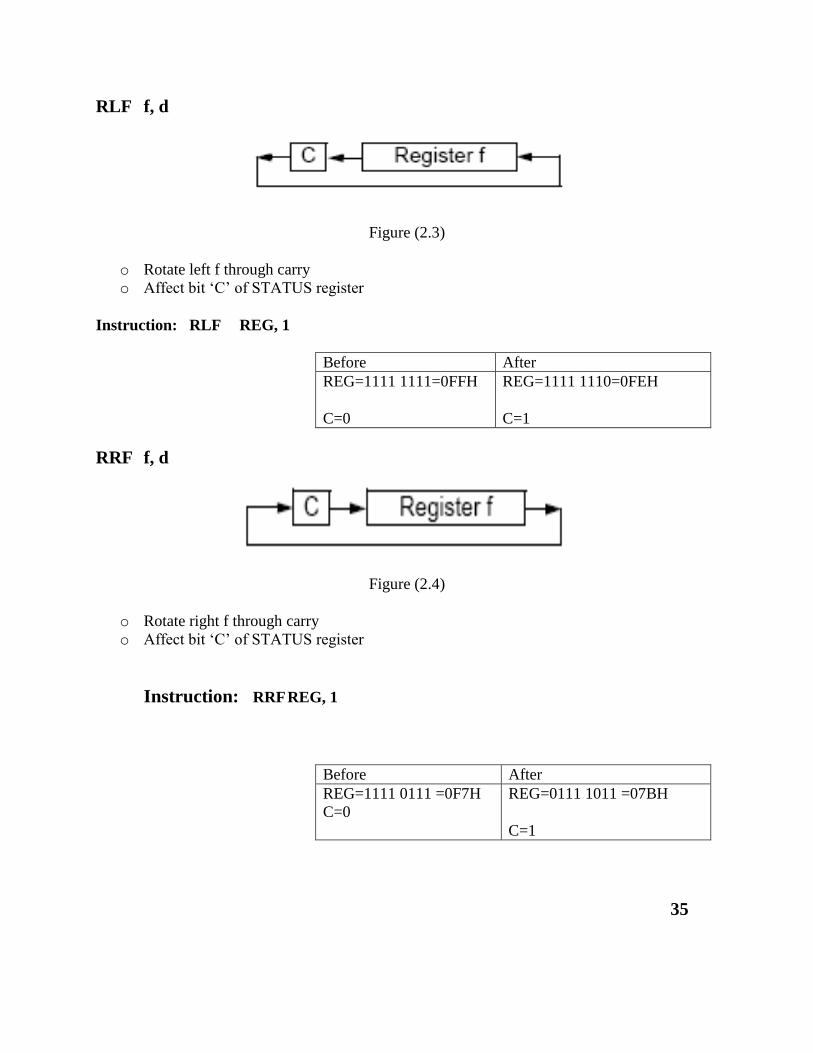
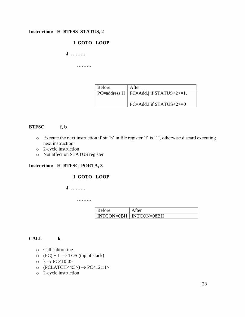
RLF f, d
Figure (2.3)
o Rotate left f through carry
o Affect bit „C‟ of STATUS register
Instruction: RLF REG, 1
Before After
REG=1111 1111=0FFH
C=0
REG=1111 1110=0FEH
C=1
RRF f, d
Figure (2.4)
o Rotate right f through carry
o Affect bit „C‟ of STATUS register
Instruction: RRF REG, 1
Before After
REG=1111 0111 =0F7H
C=0
REG=0111 1011 =07BH
C=1
35

SLEEP
o 00h WDT
o 0 WDT pre-scalar
o 1 TO
o 0 PD
o Affect TO & PD bits of STATUS register
Instruction: SLEEP
SUBLW k
o Subtract WREG register (2‟s complement) from literal „k‟ and put the result onto WREG
register
o k – (W) (W)
o Affect C, DC & Z bits of STATUS register
Instruction: SUBLW 02H
Before After
W=01H
C=?
Z=?
W=01H
C=1
Z=0
SUBWF f, d
o Subtract WREG register (2‟s complement) from f register
o (f) – (W) (d)
o Affect C, DC & Z bits of STATUS register
36

Instruction: SUBWF 02H, 0
Before After
W=01H
F=05H
C=?
Z=?
W=04H
F=05H
C=1
Z=0
SWAPF f, d
o Exchange the upper & lower nibbles off register
o (f<3:0) (d<7:4>), (f<7:4) (d<3:0>)
o Not affect STATUS register
Instruction: SWAPF ON, 1
Before After
ON=0F4H
W=09AH
ON=04FH
W=09AH
XORLW k
o Exclusive OR (XOR) the content of WREG register with k literal
o (W) XOR k (W)
o Store the result in WREG register
o Affect bit „Z‟ of STATUS register
Instruction: XORLW 0AFH
Before After
W=0B5H W=01AH
37

XORWF f, d
o Exclusive OR (XOR) the content of WREG register with f register
o (W) XOR (f) (d)
o Affect bit „Z‟ of STATUS register
Instruction: XORWF REG, 1
Before After
REG=0AFH
W=0B5H
REG=01AH
W=0B5H
These instructions can help us to write code in assembly language (MPLAB) for PIC
microcontrollers. Where design a universal controller we need to use PIC 16F876A
microcontroller as a main part of control unit.
The following chapter is based on controller design for microwave oven.
38

Chapter 3
CONTROLLER DESIGN
3.1 Introduction
The heart of the each system is control system, the control system means a system the operation
of the another system or control systems, combination of components (electrical, mechanical,
thermal or hydraulic) that act to gather to maintain actual system performance close to desired
set of performance.
Now a days technologies are advance so in place of relay or circuit breaker mostly using
microcontroller to control the operation of a system.
Our objective in this chapter is to design a control unit that can control the operation of oven
with keypad, trough out the chapter we will get some idea of main unit (microcontroller, LCD,
voltage regulator, and temperature sensor).
In the next chapter we will go through operation by IR Receiver (Remote control)
3.2 PIC16f876A/PIC18f252
The PIC16F876A/PIC18f252 is the latest products from Microchip. It features all the
components which modern microcontrollers normally have. For its low price, wide range of
application, high quality and easy availability, it is an ideal solution in applications such as: the
control of different processes in industry, machine control devices, measurement of different
values etc. Some of its main features are listed below.
39

Figure (3.1)
40
Key features PIC 16f876A PIC 18f252
Operating frequency DC-20MHz DC-40MHz
Resets (and delays) POR,BOR(PWRT, OST) POR, BOR , RESET INSTRUCTIONS,
STACK FULL(PWRT)OST
Flash program memory (14-
bit words)
8K 32K
Data memory(bytes) 368 1536
EEPROM data memory
(bytes)
256 256
Interrupts 15 17
I/O ports PIN (A,B,C,D,E) PIN(A,B,C,D,E)
Timers 3 4
Capture/ compare/pwm
modules
2 2
Serial communications MSSP, USART MSSP, ADDRESSABLE USART
Parallel communication PSP PSP
10-bit analog-to- digital
modules
8 INPUT CHANNELS 8 INPUT CHANNELS
Analog comparators 2 -
instruction set 35 75
Packages 40-PIN PIDP
44-PIN PLCC
44-PIN TQFP
44-PIN QFN
28-PIN DIP
28-PIN SOCC
41

11
10
3
4
8
9
1 2 13 14 15 16
1213141516
11
10
9
8
4
3
TTR 01 B
1221 - XW
6
7
5
+3Vdc
1
7
4 2 35 6
8 90
Infrared
(TX)
47mfd
16VSTAR
T
STOP
pOW
ER
CLEAR
EZ ON
TIME
MO
RE
UP(+)
LESS
DO
WN(-)
AUTO
DEFO
RST
CUSTO
M
CO
OK
CUSTO
M
SET
CO
SSERO
LE
FOO
D
PLATE
BAKED
GO
ODS
FRESH
VEGETABLE
FRO
ZEN
ENTR
EE
PIZZA
BEVERAG
E
POTATO
POPC
ORN
CLO
CK
Timer
Enter
Figure (3.2)
We have got in here 35 keys which make it possible to do different functions by
keypad, this is attached to the microwave oven and by pressing the key we can get the
appropriate operation.
1. DISPLAY WINDOW.
2. ONE TOUCH CONTROL: This menu has been preprogrammed to cook
food automatically by one touch.
3. AUTO DEFROST: This feature provides you with the best defrosting
method for frozen foods.
4. CUSTOM COOK: This feature allows you to set and execute a frequently
used single stage program.
5. NUMBER: These used to set for time of day, cooking time, power level,
or defrost weight.
6. MORE / LESS: All pf the one touch cook and TIMED COOK can be
adjusted to cook food for a longer or shorter time.
MORE pressing MORE will add 10 seconds to the cooking time.
LESS pressing LESS will subtract 10 seconds of cooking time.
7. STOP/ CLEAR: it used to stop oven and clear all entries except time of
day. 42

8. CUSTOM SET: You can select sound on/off, clock on/off, scroll speed,
lbs/kg choice, language choice, demo on / off mode.
9. TIME: You can set the desired cooking time.
10. POWER: You can select the desired power level for cooking.
11. TIMER: You can use the timer function of your oven for purpose other
than coking.
12. CLOCK: It is used to set the time of day.
13. EZ ON: You can extend cooking time in multiplies of 1 minute by
repeatedly touching this pad during cooking.
14. START: This feature allows oven to begin functioning.
By pressing any key a signal is going to microcontroller which cases the operation microwave
oven through magnetron.
Figure (3.3)
43

The above a part of the controller circuit is given which shows the microcontroller with LCD for
keypad operation of microwave oven .
3.3 TEMPERATURE SENSOR (DS1820)
The DS1820 Digital Thermometer provides 9–bit temperature
readings which indicate the temperature of the device.
Information is sent to/from the DS1820 over a 1–Wire
interface, so that only one wire (and ground) needs to be
connected from a central microprocessor to a DS1820.
Power for reading, writing, and performing temperature
conversions can be derived from the data line itself with no
need for an external power source.
Figure (3.4)
Because each DS1820 contains a unique silicon serial number, multiple DS1820s can exist on
the same 1–Wire bus. This allows for placing temperature sensors in many different places.
Applications where this feature is useful include HVAC environmental controls, sensing
temperatures inside buildings, equipment or machinery, and in process monitoring and control.
Table Detailed pin Description
Pin 16-pin SSOP Pin PR35 SYMBOLS Description
9 1 GND Ground
8 2 DQ Data input/output pin for 1-wire: open drain
7 3 VDD Optional VDD pin
Using VDD to supply temperature conversion current
44

Figure(3.5)
3.3.1 Operation – Measuring Temperature
The DS1820 measures temperature through the use of an on–board proprietary temperature
measurement technique.
The DS1820 measures temperature by counting the number of clock cycles that an oscillator
with a low temperature coefficient goes through during a gate period determined by a high
temperature coefficient oscillator.
The counter is preset with a base count that corresponds to –55°C. If the counter reaches zero
before the gate period is over, the temperature register, which is also preset to the –55°C value, is
incremented, indicating that the temperature is higher than –55°C.
At the same time, the counter is then preset with a value determined by the slope accumulator
circuitry. This circuitry is needed to compensate for the parabolic behavior of the oscillators over
temperature. The counter is then clocked again until it reaches zero. If the gate period is still not
finished, then this process repeats. The slope accumulator is used to compensate for the non–
linear behavior of the oscillators over temperature, yielding a high resolution temperature
measurement.
This is done by changing the number of counts necessary for the counter to go through for each
incremental degree in temperature. To obtain the desired resolution, therefore, both the value of
the counter and the number of counts per degree C (the value of the slope accumulator) at a
given temperature must be known. Internally, this calculation is done inside the DS1820 to
provide 0.5°C resolution. The temperature reading is provided in a 16–bit, sign–extended two‟s
complement reading. Table 1 describes the exact relationship of output data to measured
temperature. The data is transmitted serially over the 1–Wire interface. The DS1820 can measure
temperature over the range of –55°C to +125°C in 0.5°C increments. For Fahrenheit usage, a
lookup table or conversion factor must be used.
45
Note that temperature is represented in the DS1820 in terms of a 1/2°C LSB, yielding the
following 9–bit format:
MSB LSB
1 1 1 0 0 1 1 1 0
= –25°C
The most significant (sign) bit is duplicated into all of the bits in the upper MSB of the two–byte
temperature register in memory. This “sign–extension” yields the 16–bit temperature readings as
shown in Table 1.
Higher resolutions may be obtained by the following procedure. First, read the temperature, and
truncate the 0.5°C bit (the LSB) from the read value. This value is TEMP_READ. The value left
in the counter may then be read. This value is the count remaining (COUNT_REMAIN) after the
gate period has ceased.
The last value needed is the number of counts per degree C (COUNT_PER_C) at that
temperature. The actual temperature may be then be calculated by the user using the following:
TEMPERATURE = TEMP_READ – 0.25 +
TEMPERATURE/DATA RELATIONSHIPS Table (3.1)
TEMPERATURE DIGITAL OUTPUT
(binary)
DIGITAL OUTPUT
(Hex)
+125°C 00000000 11111010 00FA
+25°C 00000000 00110010 0032h
+1/2°C 00000000 00000001 0001h
+0°C 00000000 00000000 0000h
–1/2°C 11111111 11111111 FFFFh
–25°C 11111111 11001110 FFCEh
–55°C 11111111 10010010 FF92h
46
3.4 Voltage Regulator (LM7805)
The MC7805 of three terminal positive regulator are
available in the TO-220/D-PAK package and with
several fixed
output voltages, making them useful in a wide range
of applications. Each type employs internal
current limiting, thermal shut down and safe
figure(3.6)
operating area protection, making it essentially indestructible. If adequate heat sinking is
provided, they can deliver over 1A output current. Although designed primarily as fixed voltage
regulators, these devices can be used with external components to obtain adjustable voltages and
currents.
Absolute maximum Ratings
Electrical Characteristics (MC7805/LM7805)
(Refer to test circuit ,0°C < TJ < 125°C, IO = 500mA, VI = 10V, CI= 0.33µF, CO= 0.1µF,
unless otherwise specified)
Parameter Symbol Conditions MC7805/LM7805 unit
Min. Type Max.
Output Voltage Vo TJ =+25 oC 4.8 5.0 5.2 V
5.0mA ≤ Io ≤ 1.0A, PO ≤ 15W VI = 7V to 20V
4.75 5.0 5.25
Line Regulation (Note1)
Load Regulation
(Note1)
Regline
Regload
TJ=+25 oC VO = 7V to 25V
- 4.0 100 mV
VI = 8V to 12V
- 1.6 50
TJ=+25 oC O = 5.0mA to1.5A
- 9 100 mV
O =250mA to
750mA
- 4 50
47
Parameter Symbol Value Unit
input Voltage (for VO = 5V to 18V) (for VO = 24V)
VI VI
35 40
V V
Thermal Resistance Junction-Cases (TO-220) RθJC 5 °C/W
Thermal Resistance Junction-Air (TO-220) RθJA 65 °C/W Operating Temperature Range TOPR 0 ~ +125 °C
Storage Temperature Range TSTG -65 ~ +150 °C

3.5 LCD HD-44780
The HD44780U dot-matrix liquid crystal display
controller and driver LSI displays alphanumeric,
Japanese kana characters, and symbols. It can be
configured to drive a dot-matrix liquid crystal display
under the control of a 4- or 8-bit microprocessor. Since
all the functions such as display RAM, character
generator, and liquid crystal driver, required for driving
a dot-matrix liquid crystal display are internally
provided on one chip, a minimal system can be
interfaced with this controller/driver. A single HD44780U figure (3.7)
can display up to one 8-character line or two 8-character
lines.
The HD44780U has pin function compatibility with the
HD44780S which allows the user to easily replace an
LCD-II with an HD44780U. The HD44780U character
generator ROM is extended to generate 208 5 × 8 dot
character fonts and 32 5 × 10 dot character fonts for a
total of 240 different character fonts. The low power figure (3.8)
supply (2.7V to 5.5V) of the HD44780U is suitable for any portable battery-driven product
requiring low power dissipation.
48

Block diagram with Temperature sensor is shown below
Figure (3.9)
The above show a part of the microwave oven circuit which consist of microcontroller, LCD,
temperature sensor, number of relays.
In the next chapter I am going to talk about IR Receiver (Remote control) design for
operation of microwave oven
49

Chapter 4
IR (Infrared) Receiver
IR receiver is one of the latest technologies where we are using it to control the operation of TV,
Multimedia etc. IR stands for Infra-Red, and IR are part of the light spectrum beyond human
eyesight capability. So far we know that there are many different types of light spectrum around
any object in the world, physically, chemically, and among all these lights spectrum some of
them are visible and some of them are invisible and X-Ray. We will see how IR acts in light
spectrum in terms of frame timing later on.
The mediums in the wireless communication are many, but the two most popular mediums in the
wireless communication are:
1- Infrared (IR)
2- Radio Frequency (RF).
Later models have incorporated the IR receiver as an integral part of the laptop. Most modern
models no longer uses IR as this has been replace by the Bluetooth technology and then WiFi
(wireless networking). There are some laptop models that have all 3.
IR technologies are better suited for short distance, low-to-medium data throughput, and wireless
communication channels,
IR receiver has defined the standard as a wireless communication link between two devices in
which the information is transmitted using infrared light.
Where to control the operation of microwave oven by IR receiver is a new idea that developed
by our group.
4.1 IR data communication protocol
Communication is one of the great fundamental factors of today’s technologies in the world, it
plays an important role in the industries and as well as in day-to-day of human’s life, and has
direct effect in today’s technologies. Communication is dealing to a condition to provide
facilities and the way of interaction between humans and different technologies in the world.
So far we know that, technologies have been developing, we can see a huge differences in
today’s technologies and the ones as it was at the beginning, many change has became in the
size, model, and effectiveness of usage in different areas and so on.
So, in order to use the new technologies effectively and to have a resized model, proper
direction and communication with technologies we have tried to replace the microwave oven’s
51

keypad with IR remote for parallel operations.
There are two most important standard electronics devices in terms of communications, these
two are:
1- IR transmitters and
2- IR receivers.
In the main time IR transmitters and IR receivers are based on different types, models and
different companies.
Initially, Sony Infrared Receiver PCVA-IR6U would be as it implies; it is an add-on device to a
laptop/computer to enable said laptop/computer to be able to receive IR (infrared) signals from
external sources such as a cell phone, another laptop or any other electronic product that has a
built-in IR transmitter.
4.2 IR transmitters
IR Transmitter is a breakout for a simple and clear infrared LED on it. These Infrared LED operates around 940nm and work well for generic IR systems including remote control and touch-less object sensing. Pair them with any of our IR receivers
Figure (4.1)
Figure (4.2) figure (4.3)
52

4.3 IR receivers
IR receiver is a breakout board with IR detector mounting on it.IR detector is little microchips
with a photocell that are tuned to listen to infrared light at 38KHz. They are almost always used
for remote control detection – every TV and DVD player has one of these in the front to listen
for the IR signal from the clicker.
Figure (4.4)
4.4 Frame timing
In order to communicate or we can say to
receive IR or infrared signals form a certain
sources for this case we have used IR
TOSP1738
Command and Address bits are encoded as a
600us “low” pulse followed by:
600us “high” pulse for a logical bit zero
1200us “high” pulse for a logical bit one
Please note that the output (“low” and “high”
levels) of a TSOP1738 is inverted in relation to
this picture.
This decoder is implemented as an “interrupt
on change” service routine running on the pin
where the TSOP1738 is connected. A hardware
timer is used as a counter to measure the time
between transitions, allowing the ISR to run for a Figure (4.5)
very short time to manipulate the timer and change
its internal state, leaving immediately to the main loop.
53

Every time the TSOP1738 pin changes the ISR changes its internal state according to the next
diagram:
In short, and after running several times for very
short periods, once for every time the TSOP1738 pin
flips, the SIRC ISR does the following: It waits for a
start bit and when it finds one, it goes on to decode
the Command and Address bits, by validating both
halves of the bits. The first half of each data bit is
always 600us long and the second half may be
600us is the bit is a logical 0 or 1200us if the bit is a
logical 1. After decoding all 12 Command and
Address bits, the decoder rests at the “Wait start bit”
state.
Every time an error happens, because a bit length is
out of the permitted values, the decoder aborts and
goes to the “Wait start bit” state, where it waits for
the next frame. These errors are shown in the diagram using red arrows. Figure (4.6)
4.5 IR or Infrared Interface
The two most popular mediums in the wireless arena are Infrared (IR) and Radio Frequency
(RF). IR technologies are better suited for short distance, low-to-medium data throughput, and
wireless communication channels. Two common types of IR technologies are currently in use.
These are:
1. TV Remote (TVR) and
2. IrDC (Infrared Data communication) standard protocol.
The IrDC (Infrared Data communication) has defined the standard as a wireless communication
link between two devices in which the information is transmitted using infrared light.
The IrDC standard is a set of specifications for providing a universal two-way wireless infrared
data communications, based on a practical cost, short-range point-to-point user model. The
standard defines the physical characteristics of the interface, the communications protocols that
provide for different needs, and the transmission speeds at which the infrared device
communicates. 54
The two basics of the infrared communication standards are IrDC-Data and IrDC-Control.
IrDC-Data defines the standard for the wireless, two-way infrared data transmission between
two devices and consists of a set of mandatory protocols: IrPHY (Physical), IrLAP (Link
Access), and IrLMP (Link Management).
IrDC-Control is the infrared standard that allows wireless peripherals such as keyboards,
mouse, game pads, joysticks, and other pointing devices to interact with many types of host
devices. Host devices include PCs, home appliances, game consoles, and TV/ audio devices/
Web set top boxes.
IrDC-Control is not the same as the standard TV Remote Control. IrDC-Control has its own set
of mandatory protocols: PHY (Physical), MAC (Media Access Control), and LLC (Logical Link
Control).
IrDA technology has emerged as one of the most promising wireless solutions because it offers
several compelling advantages over other types of wireless communication interfaces.
Although infrared is only applicable between two devices at a time and cannot transmit through
walls, the positive aspects of this technology are many.
Because infrared can only communicate from one device to another and because this
communication must be line-of-sight, there is no risk that someone may intentionally or
unintentionally obtain your information as it is being transferred.
IrDC infrared port module is the most mature of the wireless communications standards. These
devices include cell phones, pagers, laptops, PDAs, digital cameras, handheld scanners, and laser
printers. The IrDA standard has both support and user applications in all major operating systems
including all recent versions of Windows, Windows CE, Linux, as well as the Palm operating
systems.
55
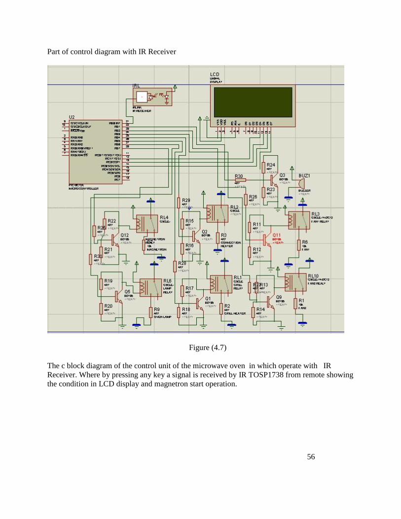
Part of control diagram with IR Receiver
Figure (4.7)
The c block diagram of the control unit of the microwave oven in which operate with IR
Receiver. Where by pressing any key a signal is received by IR TOSP1738 from remote showing
the condition in LCD display and magnetron start operation.
56

Chapter 5
Outcomes
As we thought through out the chapters now we are here to get the result of our work.
Where design of universal controller for microwave oven to satisfy the every one‟s need. Where
everyone have a microwave oven in their homes. So by facing problems where the keypad not
working or some other problems inside you don‟t need to through it out you can place this design
as a control unit for your oven.
Complete block diagram
Figure (5.1)
5.1 Features
Use of IR Receiver is a new idea for microwave oven.
Where before never used this for microwave oven.
Possibility to except both PIC 16 & PIC 18 microcontrollers.
We can have large program which need more than 8k byte so for that we can use 32 k
Byte as well.
Use of temperature sensor instead of RTD. 57

Standard protocol SIRC for IR Receiver.
Use of Optocoupler to handle large current
Use of 2N-2222 (NPN)Transistor this can be used for back light of LCD.
A diode is used for safety purpose form high current
The result of out work is given below
5.2 Design snap- shot
Figure (5.2) Figure (5.3)
Figure (5.4)
58

Chapter 6
Conclusion
Finally we are coming across a research that we have done on our goals and project that have
been expected from concept and ideas based on Microwave Oven controller design which this
ideas and researches caused to control any kinds of functionalities or working principles that are
used in a Microwave oven to lead its different applications and purposes.
In order to do this or to control the functionalities or working principles of microwave oven we
use Microcontroller, which is a programmable device (PIC16F877A) used to be programmed
and execute the instructions that have been given or programmed by programming language such
as MPLAB which we have mentioned earlier in case of controller design in detailed form.
As it is so, thus it is applicable for any kinds of Microwave oven and so we can design a
universal keypad as well.
The study was set out to explore the concept of Microwave oven controller design and has
identified the natures, forms, principle of operations, types of Microwave ovens, according to the
reasons and diversification advantages, the type, the extent, resources required for diversification
and the role and impact of intervention on the Microwave oven economy and well-being.
The study has also thought to know whether this design towards its diversification advantages
can result in effective cost reduction or being cost effect, particularly within different kinds of
Microwave oven.
In this aims the theoretical cases for diversification therefore needs to be revisited in order
further understand the controller and designing dynamics of the designing a controller and how it
can be made more sustainable.
The sustainable framework suggests the achievement of accumulation from diversification
within the rural economy or being cost effect It is however, noted from this study that such a
benefit is not likely for most rural microwave oven with the obvious alternative of survival being
the more probable outcome of diversification.
The scale of our thesis and project is therefore extensive and multifaceted even at the local level.
To generate achievable policy, strategies and development targets with regards to diversification,
being well outcome there is need for more case studies at the local level to allow further
assessment of local dimensions of the subject. Exploring the following as future research
Strategies can facilitate the attainment of this goal.
The study has offered an evaluative perspective on an important development due to our certain
goal and the concepts of project, policy program, and was conducted by microcontroller for
controlling the designing the Microwave oven and its application through sampling farm
59
Controller design and finally results in a universal keypad as well.
As a direct consequence of this methodology, the study encountered a number of limitations,
which need to be considered.
In order to reach to achievable results and to have outcomes that are resulted from this study or
our project and thesis and have been identified towards its different application, there were two
or more important factors or standard topics were necessary to be discussed and needed to be
considered as essential and major parts in overall the project they are such as assembly language
microcontroller, IR receiver or Infra Red receiver and its data communication protocol and some
other parameters that have been considered in this study which they are related to the ideas or
our research that we have been dealing with it(Microwave oven controller design).
Each and every one of these topics has been discussed in detail specially the things which were
important to our goal in order to lead us to our desired objectives with real and applicable
outcomes.
In case of controller, in order to control the operation of microwave oven or its functionalities we
have used microcontroller PIC16F877A / PIC16F876A, obviously we know that microcontroller
have different type, size, forms and numbers, it varies according to its applications, functions,
number of instructions and so on. Therefore we have used microcontroller PIC16F877A /
PIC16F876A, because it matches to application of our project (microwave oven controller design
universal keypad).
In this study we have discussed microcontroller in detail in the previous chapter.
In case of programming ,so far we know that microcontrollers are programmable device used to
in programming to execute different instructions ,this instructions that have been given to the
microcontroller by programmable language ,although there are different programmable
languages like high level language such us java ,PHP , C , C++ and so on, we have used
assembly language because it‟s easy to write different instructions easily ,in this issues assembly
language has been instructed and written in MPLAB according to the characteristics of
microcontroller which has different ports ,addresses ,memories and so on .
And finally basically the main focus was on the change (objective, goals resulted from our
project the concept of microwave oven controller design) which have been developed in our
project (the change or objective is to replace microwave ovens keypad and use remote controller
instead of keypad), due to this issue the changes or objectives is towards the following
advantages:
6.1 Advantages: Remote controller 1-cost effect (economy)
2-tacking less space rather than microwave oven keypad
3-ease of installation rather than microwave oven keypad
60
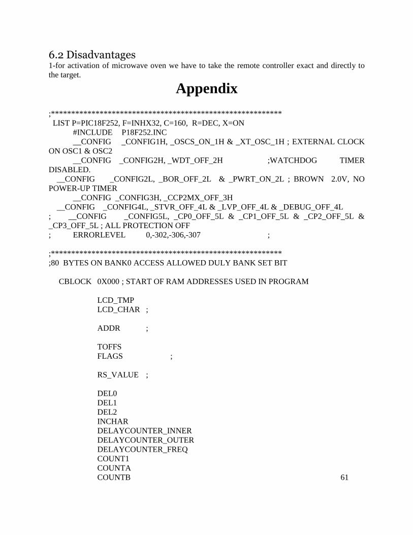
6.2 Disadvantages 1-for activation of microwave oven we have to take the remote controller exact and directly to
the target.
Appendix ;*********************************************************
LIST P=PIC18F252, F=INHX32, C=160, R=DEC, X=ON
#INCLUDE P18F252.INC
__CONFIG _CONFIG1H, _OSCS_ON_1H & _XT_OSC_1H ; EXTERNAL CLOCK
ON OSC1 & OSC2
__CONFIG _CONFIG2H, _WDT_OFF_2H ;WATCHDOG TIMER
DISABLED.
__CONFIG _CONFIG2L, _BOR_OFF_2L & _PWRT_ON_2L ; BROWN 2.0V, NO
POWER-UP TIMER
__CONFIG _CONFIG3H, _CCP2MX_OFF_3H
__CONFIG _CONFIG4L, _STVR_OFF_4L & _LVP_OFF_4L & _DEBUG_OFF_4L
; __CONFIG _CONFIG5L, _CP0_OFF_5L & _CP1_OFF_5L & _CP2_OFF_5L &
_CP3_OFF_5L ; ALL PROTECTION OFF
; ERRORLEVEL 0,-302,-306,-307 ;
;*********************************************************
;80 BYTES ON BANK0 ACCESS ALLOWED DULY BANK SET BIT
CBLOCK 0X000 ; START OF RAM ADDRESSES USED IN PROGRAM
LCD_TMP
LCD_CHAR ;
ADDR ;
TOFFS
FLAGS ;
RS_VALUE ;
DEL0
DEL1
DEL2
INCHAR
DELAYCOUNTER_INNER
DELAYCOUNTER_OUTER
DELAYCOUNTER_FREQ
COUNT1
COUNTA
COUNTB 61

TMP0
DUMMY1
DUMMY2
R0
R1
R2
L_BYTE
H_BYTE
TEMP1
TEMP2
TEMP3
H
L
TEMP
RD_TEMP_LSB
RD_TEMP_MSB
RES_BIT
;-----------------------------------------------------------------------------------
WREG_TEMP ;to save WREG during interrupt
STATUS_TEMP ;to save STATUS during interrupt
BSR_TEMP ;to save BSR during interrupt
FSR1H_TEMP ;to save FSR0H during interrupt
FSR1L_TEMP ;to save FSR0L during interrupt
FSR0H_TEMP ;to save FSR0H during interrupt
FSR0L_TEMP ;to save FSR0L during interrupt
BCD
DT_POINTER
LSB_RELD_ON
MODE_FLAG
RMT_CODE
RMT_CMND
RMT_ADDR
RMT_CMND_N
RMT_ADDR_N
IR_TIMER
IR_BIT_CNTR
IR_FLAGS
;XXXXXXXXXXXXXXXXXXXXXXXXXXXXXXXXXXXXXXXX
ENDC
;*********************************************************
DS_TRIS EQU TRISB ;
DS_PORT EQU PORTB ;
62

DS_BIT EQU .0 ;
;*********************************************************
#DEFINE E PORTC,3 ;
#DEFINE RS PORTC,0 ;
#DEFINE BEEP PORTA,2 ; DS 1820 ATTACHED HERE
#DEFINE REMOTE PORTB,1 ;10h is the family
code of d
;*********************************************************
CLK = .4 ;
SCRFLAFMASK = B'11111100' ;
;*****************************************************************************
; =================LCD
EQUATES======================================================
;*****************************************************************************
******
SET_8B EQU 0X30 ; SET 8 BIT DATA (FOR INITIALISATION)
SET_4B_1L EQU 0X20 ; SET 4 BIT DATA, 1 LINES
SET_4B_2L EQU 0X28 ; SET 4 BIT DATA, 2 LINES
DISP_ON EQU 0X0C ; DISPLAY ON, CURSOR OFF, BLINK OFF
CLR_DISP EQU 0X01 ; CLEAR DISPLAY
ENTRY_INC EQU 0X06 ; ENTRY MODE INCREMENT, NO SHIFT
DD_RAM_ADDR EQU 0X80 ; LEAST SIGNIFICANT 7 BITS ARE FOR ADDRESS
;;==================================================
; =================0NE WIRE COMMANDS AND
EQUATES====================================
;*****************************************************************************
******
START_CONV EQU 0X44 ; SET 8 BIT DATA (FOR INITIALISATION)
COPY_SCRATCH EQU 0X48 ; SET 4 BIT DATA, 1 LINES
READ_SCRATCH EQU 0XBE ; SET 4 BIT DATA, 1 LINES
WRITE_SCRATCH EQU 0X4E ; SET 4 BIT DATA, 2 LINES
RECALL_PSUPPLY EQU 0XB4 ; SET 4 BIT DATA, 1 LINES
RECALL_SCRATCH EQU 0XB8 ; SET 4 BIT DATA, 1 LINES
63
ALARM_SEARCH EQU 0XEC ; SET 4 BIT DATA, 1 LINES
READ_ROM EQU 0X33 ; CLEAR DISPLAY
MATCH_ROM EQU 0X55 ; ENTRY MODE INCREMENT, NO SHIFT
SKIP_ROM EQU 0XCC ; LEAST SIGNIFICANT 7 BITS ARE FOR ADDRESS
SEARCH_ROM EQU 0XF0 ; DISPLAY ON, CURSOR OFF, BLINK OFF
;===================================================
;************USED SONY IR DECODER ROUTINE**************;
;XXXXXXXXXXXXXXXXXXXXXXXXXXXXXXXXXXXXXXXXXXXXXXXXXXXXX
CONSTANT SIRC_ON_T = .183 ; 182 ALSO TWNK MODE(D)
CONSTANT SIRC_OFF_T = .195 ; 182 ALSO TWNK MODE(D)
CONSTANT IR_SPACE = .220 ; FOR DIS BANK IN SOLID MODE
CONSTANT HI_P_T = .2 ; FOR DIS BANK IN SOLID
MODE
;XXXXXXXXXXXXXXXXXXXXXXXXXXXXXXXXXXXXXXXX
BLNK MODE(D)
CONSTANT IR_RD_ON = .1 ; FOR DIS BANK IN SOLID MODE
CONSTANT IR_REPEAT = .2 ; FOR DIS BANK IN SOLID MODE
CONSTANT NEW_BYTE = .3 ; FOR DIS BANK IN SOLID MODE
CONSTANT IR_ERROR = .4 ; FOR DIS BANK IN SOLID MODE
;XXXXXXXXXXXXXXXXXXXXXXXXXXXXXXXXXXXXXXXXXXXXXXXXX
PAUSE MACRO DLYF ;
MOVLW (DLYF / 5) - 1 ;
MOVWF TMP0 ;
CALL DLY5N ;
ENDM ;
;===================================================
; MACRO FOR DS1820
;===================================================
DQLOW MACRO ;
BCF DS_PORT,DS_BIT ; DQ BIT READY
BCF DS_TRIS,DS_BIT ; SET DQ TO OUTPUT
64

ENDM ;
;===================================================
DQHIZ MACRO ;
BSF DS_TRIS,DS_BIT ; SET DQ TO INPUT
ENDM ;
;===================================================
;*************MACRO TO MOVE A LITTERAL BYTE TO A FILE REG**********;
;XXXXXXXXXXXXXXXXXXXXXXXXXXXXXXXXXXXXXXXX
MOVLF MACRO LITERAL,DEST ;MACRO STATEMENT AND EXPRESSION
;
MOVLW LITERAL ;MOVE THE VALUE IN W FIRST ;
MOVWF DEST ;PLACE THE VALUE IN DESTINATION FILE ;
ENDM ;END OF MACRO ---------------------------------;
;===================================================
ORG 0X000 ;START VECTOR
; CLRF STATUS ; ENSURE WE ARE AT BANK 0
; CLRF PCLATH ; ENSURE PAGE BITS ARE CLEARED (BEFORE
GOTO XX)
NOP
GOTO MAIN_PROG ;GOTO INITIALIZATION OF PROGRAM
;===================================================
ORG 0X008 ;HIGH PRIORITY INTERRUPT VECTOR
GOTO PULL_RAM ;HIGH PRIORITY INTERRUPT VECTOR
;===================================================================
ORG 0X018 ;LOW PRIORITY INTERRUPT VECTOR
;XXXXXXXXXXXXXXXXXXXXXXXXXXXXXXXXXXXXXXXX
PULL_RAM
MOVFF STATUS,STATUS_TEMP ;SAVE STATUS REGISTER
MOVFF WREG,WREG_TEMP ;SAVE WORKING
REGISTER
MOVFF BSR,BSR_TEMP ;SAVE BSR REGISTER
MOVFF FSR0H,FSR0H_TEMP ;SAVE FSR0H REGISTER
MOVFF FSR0L,FSR0L_TEMP ;SAVE FSR0L REGISTER
65

MOVFF FSR1H,FSR1H_TEMP ;SAVE FSR0H REGISTER
MOVFF FSR1L,FSR1L_TEMP ;SAVE FSR0L REGISTER
;===================================================
BTFSC INTCON,TMR0IF ; CHECKING TMR0 OVER FLOW
INT
GOTO TIME_JUKAR ; IF YES GOTO TIME COUNTER
SER
BTFSC INTCON3,INT1IF
GOTO UPDT_RMT_CODE
GOTO POINT_RETURN
;XXXXXXXXXXXXXXXXXXXXXXXXXXXXXXXXXXXXXXXX
;THE SUBROUTINE TO COUNT THE DOWN TIMER DEFINED BY THE USER
INTERFAC
; THE CLOCK FREQUENCY IS 4.00 MHZ AND PRESCALER IS DEFINED FOR 1:2 F
;XXXXXXXXXXXXXXXXXXXXXXXXXXXXXXXXXXXXXXXX
TIME_JUKAR ; CALLING LINE FOR THE TIMER ROUTINE
GOTO POINT_RETURN ; RETURN FROM INTERRUPT
;****************************SIRC REMOTE CODE**********************;
;XXXXXXXXXXXXXXXXXXXXXXXXXXXXXXXXXXXXXXXX
UPDT_RMT_CODE
BTFSC REMOTE
GOTO ERR_RMT_CODE
CALL ACQR_LO_T
BTFSC IR_FLAGS,IR_ERROR
GOTO ERR_RMT_CODE ;ERR_RMT_CODE
;*********************************************************
VALIDATE_START
MOVLW .4
SUBWF IR_TIMER,W
BTFSS STATUS,C
GOTO INVALID_START ;ERR_RMT_CODE
; MOVLW .5
; SUBWF IR_TIMER,W
; BTFSC STATUS,C
; GOTO INVALID_START ;ERR_RMT_CODE
;*********************************************************
66

VALID_START
CALL ACQR_HI_T
BTFSC IR_FLAGS,IR_ERROR
GOTO ERR_RMT_CODE ;ERR_RMT_CODE
BSF IR_FLAGS,STRT_PASS
CLRF RMT_CMND_N
CLRF RMT_ADDR_N
;XXXXXXXXXXXXXXXXXXXXXXXXXXXXXXXXXXXXXXXX
;****************************SIRC REMOTE CODE**********************;
;XXXXXXXXXXXXXXXXXXXXXXXXXXXXXXXXXXXXXXXX
INIT_IR_CMD_READ
MOVLF .7,IR_BIT_CNTR
;*********************************************************
READ_CMND_BITS
CALL ACQR_LO_T
BTFSC IR_FLAGS,IR_ERROR
GOTO ERR_RMT_CODE
CALL ACQR_HI_T
BTFSC IR_FLAGS,IR_ERROR
GOTO ERR_RMT_CODE
CMND_BIT_OK
MOVF IR_TIMER,W
ANDLW 0X02
ADDLW 0XFF
RRCF RMT_CMND_N,F
DECFSZ IR_BIT_CNTR,F
GOTO READ_CMND_BITS
RRNCF RMT_CMND_N,F
;*********************************************************
READ_IR_ADDR_BYTE
MOVLF .5,IR_BIT_CNTR
;*********************************************************
READ_ADDR_BITS
CALL ACQR_LO_T
BTFSC IR_FLAGS,IR_ERROR
GOTO ERR_RMT_CODE
MOVF IR_BIT_CNTR,W
XORLW 0X01
BTFSC STATUS,Z
GOTO JUMP_HI_TEST
CALL ACQR_HI_T
BTFSC IR_FLAGS,IR_ERROR
GOTO ERR_RMT_CODE
JUMP_HI_TEST
67
MOVF IR_TIMER,W
ANDLW 0X02
ADDLW 0XFF
RRCF RMT_ADDR_N,F
DECFSZ IR_BIT_CNTR,F
GOTO READ_ADDR_BITS
;*********************************************************
FOUND_FRESH_BYTE
RRNCF RMT_ADDR_N,F
RRNCF RMT_ADDR_N,F
RRNCF RMT_ADDR_N,F
;*********************************************************
MOVFF RMT_ADDR_N,RMT_ADDR
MOVFF RMT_CMND_N,RMT_CMND
BSF IR_FLAGS,NEW_BYTE
GOTO POINT_RETURN
;*********************************************************
INVALID_START
BCF IR_FLAGS,STRT_PASS
;*********************************************************
ERR_RMT_CODE
BSF IR_FLAGS,IR_ERROR
BCF IR_FLAGS,NEW_BYTE
;*********************************************************
POINT_RETURN
CLRF T1CON
BCF INTCON3,INT1IF
MOVFF FSR1L_TEMP,FSR1L ;RESTORE FSR0L REGISTER
MOVFF FSR1H_TEMP,FSR1H ;RESTORE FSR0H REGISTER
MOVFF FSR0L_TEMP,FSR0L ;RESTORE FSR0L REGISTER
MOVFF FSR0H_TEMP,FSR0H ;RESTORE FSR0H REGISTER
MOVFF BSR_TEMP,BSR ;RESTORE BSR REGISTER
MOVFF WREG_TEMP,WREG ;RESTORE WORKING
REGISTER
MOVFF STATUS_TEMP,STATUS ;RESTORE STATUS REGISTER
RETFIE ; ENSURE WE ARE AT BANK 0
68

;XXXXXXXXXXXXXXXXXXXXXXXXXXXXXXXXXXXXXXXX
MAIN_PROG
;XXXXXXXXXXXXXXXXXXXXXXXXXXXXXXXXXXXXX
CALL INIT_PORT ;INITIALIZING I/O PORTS
CALL INIT_LCD ; INITIAL LCD
CALL LCD_CLR ;
;===================================================
LCD_DIAGNOSTIC
; CALL LCD_CLR ;
; MOVLW .5
CALL LCD_LINE1
MOVLW 'W'
CALL DATA2LCD
MOVLW 'E'
CALL DATA2LCD
MOVLW 'L'
CALL DATA2LCD
MOVLW 'C'
CALL DATA2LCD
MOVLW 'O'
CALL DATA2LCD
MOVLW 'M'
CALL DATA2LCD
MOVLW 'E'
CALL DATA2LCD
;*********************************************************
INIT_DS18B20_TMP1
CALL DS_RESET ; CALLING DS_18B20 BUS RESET TO INIT NEW ROM
CMN
;...........................................................................
MOVLW SKIP_ROM ; MATCH ROM COMMAND TO DS
CALL DS_WRITE_BYTE ; MEM. FUNC. CMND TO WRITE A SINGLE BYTE
;...........................................................................
MOVLW START_CONV ; ROM COMMAND TO START
TEMPCONVERTION
CALL DS_WRITE_BYTE ; MEM. FUNC. CMND TO WRITE A SINGLE BYTE
69
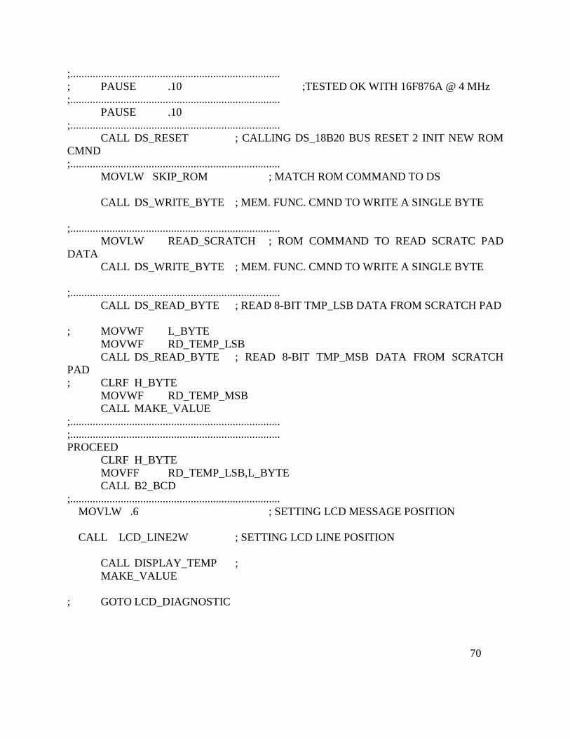
;...........................................................................
; PAUSE .10 ;TESTED OK WITH 16F876A @ 4 MHz
;...........................................................................
PAUSE .10
;...........................................................................
CALL DS_RESET ; CALLING DS_18B20 BUS RESET 2 INIT NEW ROM
CMND
;...........................................................................
MOVLW SKIP_ROM ; MATCH ROM COMMAND TO DS
CALL DS_WRITE_BYTE ; MEM. FUNC. CMND TO WRITE A SINGLE BYTE
;...........................................................................
MOVLW READ_SCRATCH ; ROM COMMAND TO READ SCRATC PAD
DATA
CALL DS_WRITE_BYTE ; MEM. FUNC. CMND TO WRITE A SINGLE BYTE
;...........................................................................
CALL DS_READ_BYTE ; READ 8-BIT TMP_LSB DATA FROM SCRATCH PAD
; MOVWF L_BYTE
MOVWF RD_TEMP_LSB
CALL DS_READ_BYTE ; READ 8-BIT TMP_MSB DATA FROM SCRATCH
PAD
; CLRF H_BYTE
MOVWF RD_TEMP_MSB
CALL MAKE_VALUE
;...........................................................................
;...........................................................................
PROCEED
CLRF H_BYTE
MOVFF RD_TEMP_LSB,L_BYTE
CALL B2_BCD
;...........................................................................
MOVLW .6 ; SETTING LCD MESSAGE POSITION
CALL LCD_LINE2W ; SETTING LCD LINE POSITION
CALL DISPLAY_TEMP ;
MAKE_VALUE
; GOTO LCD_DIAGNOSTIC
70

CLRF IR_FLAGS
CLRF RMT_CMND
CLRF RMT_ADDR
CLRF IR_TIMER
CLRF RMT_CMND_N
CLRF RMT_ADDR_N
CLRF INTCON1
CLRF INTCON2
CLRF INTCON3
CHK_MIN_HI
BSF IR_FLAGS,NEW_BYTE
BSF INTCON3,INT1IE
BSF INTCON,GIE
;#########################################################
CALL LCD_CLR ;
;XXXXXXXXXXXXXXXXXXXXXXXXXXXXXXXXXXXXXXXXXXXXXXXXXXXXX
STNBY_LOOP
; MOVLW .5
CALL LCD_LINE1
BTFSC IR_FLAGS,STRT_PASS
GOTO START_VALID
;*********************************************************
START_IN_VALID
MOVLW '0'
CALL DATA2LCD
GOTO PRODUCE_BIT11
;*********************************************************
START_VALID
MOVLW '1'
CALL DATA2LCD
;*********************************************************
;!!!!!!!!!!!!!!!!!!!!!!!!!!!!!!!!!!!!!!!!!!!!!!!!!!!!!!!!!!!!!!!!!!!
PRODUCE_BIT11
CLRF TEMP3
MOVF RMT_ADDR,W
ANDLW B'00010000'
ADDLW 0XFF
RLCF TEMP3,F
MOVF TEMP3,W
71

ADDLW 0X30
CALL DATA2LCD
;*********************************************************
;!!!!!!!!!!!!!!!!!!!!!!!!!!!!!!!!!!!!!!!!!!!!!!!!!!!!!!!!!!!!!!!!!!!
PRODUCE_BIT10
CLRF TEMP3
MOVF RMT_ADDR,W
ANDLW B'00001000'
ADDLW 0XFF
RLCF TEMP3,F
MOVF TEMP3,W
ADDLW 0X30
CALL DATA2LCD
;*********************************************************
;!!!!!!!!!!!!!!!!!!!!!!!!!!!!!!!!!!!!!!!!!!!!!!!!!!!!!!!!!!!!!!!!!!!
PRODUCE_BIT9
CLRF TEMP3
MOVF RMT_ADDR,W
ANDLW B'00000100'
ADDLW 0XFF
RLCF TEMP3,F
MOVF TEMP3,W
ADDLW 0X30
CALL DATA2LCD
;*********************************************************
;!!!!!!!!!!!!!!!!!!!!!!!!!!!!!!!!!!!!!!!!!!!!!!!!!!!!!!!!!!!!!!!!!!!
PRODUCE_BIT8
CLRF TEMP3
MOVF RMT_ADDR,W
ANDLW B'00000010'
ADDLW 0XFF
RLCF TEMP3,F
MOVF TEMP3,W
ADDLW 0X30
CALL DATA2LCD
;*********************************************************
;!!!!!!!!!!!!!!!!!!!!!!!!!!!!!!!!!!!!!!!!!!!!!!!!!!!!!!!!!!!!!!!!!!!
PRODUCE_BIT7
CLRF TEMP3
MOVF RMT_ADDR,W
ANDLW B'00000001'
ADDLW 0XFF
RLCF TEMP3,F
MOVF TEMP3,W
72

ADDLW 0X30
CALL DATA2LCD
;*********************************************************
;!!!!!!!!!!!!!!!!!!!!!!!!!!!!!!!!!!!!!!!!!!!!!!!!!!!!!!!!!!!!!!!!!!!
PRODUCE_BIT6
CLRF TEMP3
MOVF RMT_CMND,W
ANDLW B'01000000'
ADDLW 0XFF
RLCF TEMP3,F
MOVF TEMP3,W
ADDLW 0X30
CALL DATA2LCD
;*********************************************************
;!!!!!!!!!!!!!!!!!!!!!!!!!!!!!!!!!!!!!!!!!!!!!!!!!!!!!!!!!!!!!!!!!!!
PRODUCE_BIT5
CLRF TEMP3
MOVF RMT_CMND,W
ANDLW B'00100000'
ADDLW 0XFF
RLCF TEMP3,F
MOVF TEMP3,W
ADDLW 0X30
CALL DATA2LCD
;*********************************************************
;!!!!!!!!!!!!!!!!!!!!!!!!!!!!!!!!!!!!!!!!!!!!!!!!!!!!!!!!!!!!!!!!!!!
PRODUCE_BIT4
CLRF TEMP3
MOVF RMT_CMND,W
ANDLW B'00010000'
ADDLW 0XFF
RLCF TEMP3,F
MOVF TEMP3,W
ADDLW 0X30
CALL DATA2LCD
;*********************************************************
;!!!!!!!!!!!!!!!!!!!!!!!!!!!!!!!!!!!!!!!!!!!!!!!!!!!!!!!!!!!!!!!!!!!
PRODUCE_BIT3
CLRF TEMP3
MOVF RMT_CMND,W
ANDLW B'00001000'
ADDLW 0XFF
RLCF TEMP3,F
MOVF TEMP3,W
73

ADDLW 0X30
CALL DATA2LCD
;*********************************************************
;!!!!!!!!!!!!!!!!!!!!!!!!!!!!!!!!!!!!!!!!!!!!!!!!!!!!!!!!!!!!!!!!!!!
PRODUCE_BIT2
CLRF TEMP3
MOVF RMT_CMND,W
ANDLW B'00000100'
ADDLW 0XFF
RLCF TEMP3,F
MOVF TEMP3,W
ADDLW 0X30
CALL DATA2LCD
;*********************************************************
;!!!!!!!!!!!!!!!!!!!!!!!!!!!!!!!!!!!!!!!!!!!!!!!!!!!!!!!!!!!!!!!!!!!
PRODUCE_BIT1
CLRF TEMP3
MOVF RMT_CMND,W
ANDLW B'00000010'
ADDLW 0XFF
RLCF TEMP3,F
MOVF TEMP3,W
ADDLW 0X30
CALL DATA2LCD
;*********************************************************
;!!!!!!!!!!!!!!!!!!!!!!!!!!!!!!!!!!!!!!!!!!!!!!!!!!!!!!!!!!!!!!!!!!!
PRODUCE_BIT0
CLRF TEMP3
MOVF RMT_CMND,W
ANDLW B'00000001'
ADDLW 0XFF
RLCF TEMP3,F
MOVF TEMP3,W
ADDLW 0X30
CALL DATA2LCD
;********************************************************
;!!!!!!!!!!!!!!!!!!!!!!!!!!!!!!!!!!!!!!!!!!!!!!!!!!!!!!!!!!!!!!!!!!!
OUT_PUT
BTFSS IR_FLAGS,NEW_BYTE
GOTO OUT_PUT
GOTO STNBY_LOOP
;XXXXXXXXXXXXXXXXXXXXXXXXXXXXXXXXXXXXXXXX
; LCD ROUTINE TUNED FOR OSC @ 04 XT CONFIG : OSC_XT
;****************** RUTINES USED BY LCD
74

FACTIONS***************************
;===================================================
LCD_LINE1 ;CAALING LINE OF LCD LINE1
MOVLW 0X80 ;MOVE TO 1ST ROW, FIRST COLUMN
MOVWF ADDR ;SEETING ADDRESS
CALL SET_ADDR ;SEETING ADDRESS
RETLW 0X00 ;END OF LCD LINE 1 ROUTINE
;===================================================
LCD_LINE2 ;CAALING LINE OF LCD LINE2
MOVLW 0XC0 ;MOVE TO 1ST ROW, FIRST COLUMN
MOVWF ADDR ;SEETING ADDRESS
CALL SET_ADDR ;SEETING ADDRESS
RETLW 0X00 ;END OF LCD LINE 2 ROUTINE
;===================================================
LCD_LINE3 ;CAALING LINE OF LCD LINE1
MOVLW 0X94 ;MOVE TO 1ST ROW, FIRST COLUMN
MOVWF ADDR ;SEETING ADDRESS
CALL SET_ADDR ;SEETING ADDRESS
RETLW 0X00 ;END OF LCD LINE 1 ROUTINE
;===================================================
LCD_LINE4 ;CAALING LINE OF LCD LINE2
MOVLW 0XD4 ;MOVE TO 1ST ROW, FIRST COLUMN
MOVWF ADDR ;SEETING ADDRESS
CALL SET_ADDR ;SEETING ADDRESS
RETLW 0X00 ;END OF LCD LINE 2 ROUTINE
;====================================================================
LCD_CLR ;CAALING LINE OF LCD CLR
MOVLW 0X01 ;CLEAR DISPLAY
MOVWF ADDR ;SEETING ADDRESS
CALL SET_ADDR ;SEETING ADDRESS
RETLW 0X00 ;END OF LCD CLR ROUTINE
;===================================================
LCD_LINE1W ;CAALING LINE OF LCD LINE1W
ADDLW 0X80 ;MOVE TO 1ST ROW, COLUMN W
MOVWF ADDR ;SEETING ADDRESS
CALL SET_ADDR ;SEETING ADDRESS
RETLW 0X00 ;END OF LCD LINE1 W ROUTINE
;===================================================
LCD_LINE2W ;CAALING LINE OF LCD LINE2W
ADDLW 0XC0 ;MOVE TO 2ND ROW, COLUMN W
MOVWF ADDR ;SEETING ADDRESS
CALL SET_ADDR ;SEETING ADDRESS
RETLW 0X00 ;END OF LCD LINE2 W ROUTINE
;===================================================
75

LCD_LINE3W ;CAALING LINE OF LCD LINE1W
ADDLW 0X94 ;MOVE TO 1ST ROW, COLUMN W
MOVWF ADDR ;SEETING ADDRESS
CALL SET_ADDR ;SEETING ADDRESS
RETLW 0X00 ;END OF LCD LINE1 W ROUTINE
;===================================================
LCD_LINE4W ;CAALING LINE OF LCD LINE1W
ADDLW 0XD4 ;MOVE TO 1ST ROW, COLUMN W
MOVWF ADDR ;SEETING ADDRESS
CALL SET_ADDR ;SEENG ADDRESS
RETLW 0X00 ;END OF LCD LINE1 W ROUTINE
;===================================================
_RESET ;CAALING LINE OF LCD RESET
MOVLW SET_8B ; LCD INIT INSTRUCTION (FIRST)
MOVWF PORTC ; SEND TO LCD VIA RB7..RB0
BSF E ; SET THE LCD E LINE HIGH,
CALL DEL05
BCF E ;
RETURN ; END OF RESET ROUTINE
;===================================================
;********************** LCD INITIALIZATION ROUTINE ***********************
;===================================================
INIT_LCD ;CALLING LINE OF LCD INITIALIZATION
CLRF PORTC ;CLEARING PORT VALUES IF ANY
CALL _RESET ; RESET LCD
CALL _RESET ; RESET LCD
CALL _RESET ; RESET LCD
MOVLW SET_4B_1L ; 4-BIT MODE INSTRUCTION
MOVWF PORTC ; SEND TO LCD VIA RB7..RB0
BSF E ; SET E HIGH,
CALL D160US
BCF E ; AND THEN CLEAR E
MOVLW SET_4B_2L ; 1/16 DUTY CYCLE, 5X8 MATRIX
CALL CMND2LCD ; SEND COMMAND IN W TO LCD
MOVLW CLR_DISP ; CLEAR AND RESET CURSOR
CALL CMND2LCD ; SEND COMMAND IN W TO LCD
MOVLW DISP_ON ; DISPLAY ON, CURSOR AND BLINK OFF
CALL CMND2LCD ; SEND COMMAND IN W TO LCD
MOVLW ENTRY_INC ; SET CURSOR TO MOVE RIGHT, NO SHIFT
CALL CMND2LCD ; SEND COMMAND IN W TO LCD
MOVLW DD_RAM_ADDR ; CLEAR AND RESET CURSOR
76

CALL CMND2LCD ; SEND COMMAND IN W TO LCD
RETURN ;END OF INITIALIZATION
;===================================================
SET_ADDR ; CALLING LINE TO SET APPROPRIATE LCD DATA ADDRESS
BCF E ; FIX POSITION ON LCD
BCF RS ; SEND COMMAND
MOVF ADDR,W ; SELECT ADDRESS FOR SENDING DATA TO
LCD
CALL CMND2LCD ;
BSF RS ;
RETURN ;
;===================================================
CMND2LCD ; CALLING LINE OF COMMAND 2 LCD
MOVWF LCD_CHAR ; SAVE BYTE TO WRITE TO LCD
CLRF RS_VALUE ; REMEMBER TO CLEAR RS (CLEAR RS_VALUE)
BCF RS ;
NOP ; VERY SHORT DELAY
GOTO WRITE2LCD ; GO TO COMMON CODE
;=================================================== DATA2LCD
;CALLING LINE OF DATA 2 LCD
MOVWF LCD_CHAR ; SAVE BYTE TO WRITE TO LCD
BSF RS_VALUE,0 ; REMEMBER TO SET RS (SET BIT 0 OF RS_VALUE)
BSF RS ;
NOP ; VERY SHORT DELAY
NOP ; VERY SHORT DELAY
;=================================================== WRITE2LCD ;
CALLING LINE FOR WRITE ON LCD
CALL DEL50
CLRF PORTC ; CLEAR ALL OF PORT B (INPUTS AND OUTPUTS)
MOVLW 0X00 ; SET UP TO ENABLE PORTB DATA PINS
MOVWF TRISC ; ALL PINS (RB7..RB0) ARE BACK TO OUTPUTS
BCF RS ; GUESS RS SHOULD BE CLEAR
77

BTFSC RS_VALUE,0 ; SHOULD RS BE CLEAR? (IS BIT 0 == 0?)
BSF RS ; NO, SET RS
NOP ; VERY SHORT DELAY
NOP ; VERY SHORT DELAY
; TRANSFER MOST SIGNIFICANT NIBBLE (XXXX PORTION OF XXXXYYYY)
MOVLW 0X0F ; SET UP MASK
ANDWF PORTC,F ; CLEAR OLD RB7..RB4
MOVF LCD_CHAR,W ; PUT BYTE OF DATA INTO W
ANDLW 0XF0 ; MASK TO GIVE XXXX0000 IN W
IORWF PORTC,F ; SEND TO RB7..RB4 WITHOUT CHANGING RB3..RB0
BSF E ; PULSE THE E LINE HIGH,
NOP ; VERY SHORT DELAY
NOP ; VERY SHORT DELAY
BCF E ; AND DROP IT AGAIN
; TRANSFER LEAST SIGNIFICANT NIBBLE (YYYY PORTION OF XXXXYYYY)
MOVLW 0X0F ; SET UP MASK
ANDWF PORTC,F ; CLEAR OLD RB7..RB4
SWAPF LCD_CHAR,W ; MOVE LS NIBBLE OF DATA TO MS POSITION IN W
ANDLW 0XF0 ; MASK TO GIVE YYYY0000 IN W
IORWF PORTC,F ; SEND TO RB7..RB4 WITHOUT CHANGING RB3..RB0
BSF E ; PULSE THE E LINE HIGH,
NOP ; VERY SHORT DELAY
NOP ; VERY SHORT DELAY
BCF E ; AND DROP IT AGAIN
NOP ; VERY SHORT DELAY
NOP ; VERY SHORT DELAY
RETURN ;
;===================================================
;**************SETPORT I/O OF PIC16F876A****************************
;XXXXXXXXXXXXXXXXXXXXXXXXXXXXXXXXXXXXXXXXXXXXXXXXXXXXX
XXXXXXXXXXXXXX
;********** ALL THROUGH INDIRECT ADDRESSING ARE USED
;*********************************************************
INIT_PORT ; INITIALIZING CALLING LINE FOR 16F877A
;*********************************************************
78
;SETTING ADC (ADCON1)===============================================
PORT_DIGITAL ;SETTING UP ADC PORT CONFIGURATIONS
; MOVLW B'00000110' ;
(1<<PCFG
; MOVWF ADCON1 ;DIRECTING ADCON1 REG,
;*********************************************************
SETTING_PORTA ;===================================================
MOVLW B'00000000' ;RA0 , RA1 OPTIONAL ANALOG ALL OTHER
D
MOVWF TRISA ;
;*********************************************************
SETTING_PORTB ;===================================================
MOVLW B'00000000' ;RB0 , RA1 OPTIONAL ANALOG ALL OTHER
D
MOVWF TRISB ;
;*********************************************************
SETTING_PORTC ;===================================================
MOVLW B'00000000' ;RB0 , RA1 OPTIONAL ANALOG ALL OTHER
D
MOVWF TRISC ;
;*********************************************************
RETURN ;
;XXXXXXXXXXXXXXXXXXXXXXXXXXXXXXXXXXXXXXXX
DLY5N:
NOP
; NOP
DECFSZ TMP0,F
GOTO DLY5N
RETURN
;XXXXXXXXXXXXXXXXXXXXXXXXXXXXXXXXXXXXXXXX
; DELAY ROUTINES...
D160US ;
CLRF COUNT1 ;
BSF COUNT1, 5 ; DELAY 160 USECS
79
BSF COUNT1, 4 ;
DLOOP
DECFSZ COUNT1, F ;
GOTO DLOOP ;
RETURN ;
DEL255
MOVLW 0XFF ; DELAY 255 MS
GOTO D0 ;
DEL200
MOVLW D'255' ; DELAY 200MS
GOTO D0 ;
DEL100
MOVLW D'200' ; DELAY 100MS
GOTO D0 ;
DEL50
MOVLW D'100' ; DELAY 50MS
GOTO D0 ;
DEL20
MOVLW D'40' ; DELAY 20MS
GOTO D0 ;
DEL05
MOVLW 0X10 ; DELAY 5.000 MS (4 MHZ CLOCK)
GOTO D0 ;
DEL01
MOVLW 0X05 ; DELAY 1.000 MS (4 MHZ CLOCK)
D0
MOVWF COUNT1 ;
D1
MOVLW 0XC7 ; DELAY 1MS
MOVWF COUNTA ;
MOVLW 0X04 ;
MOVWF COUNTB ;
DEL_0
DECFSZ COUNTA,F ;
GOTO $+2 ;
DECFSZ COUNTB,F ;
GOTO DEL_0 ;
DECFSZ COUNT1,F ;
GOTO D1 ;
RETLW 0X00 ;
80

;XXXXXXXXXXXXXXXXXXXXXXXXXXXXXXXXXXXXXXXX
; RESET DS1820 *
;*********************************************************
DS_RESET
DQLOW
;*********************************************************
; PAUSE .250 ;TESTED OK WITH 16F876A @ 4 MHz
;*********************************************************
PAUSE .480
DQHIZ
;*********************************************************
; PAUSE .20 ;TESTED OK WITH 16F876A @ 4 MHz
;*********************************************************
PAUSE .60 ;TESTED OK WITH 16F876A @ 4 MHz
MOVFF DS_PORT,W
ANDLW 0X01 ; USE RA0 ONLY
BANKSEL DUMMY1
MOVWF DUMMY1
;*********************************************************
; PAUSE .20 ;TESTED OK WITH 16F876A @ 4 MHz
;*********************************************************
PAUSE .80 ;TESTED OK WITH 16F876A @ 4 MHz
MOVFF DUMMY1,W ; RESPONSE IN W REGISTER
RETURN
;*********************************************************
; SEND DATA TO DS1820 (8 BIT) *
;*********************************************************
DS_WRITE_BYTE
BANKSEL DUMMY1
MOVWF DUMMY2 ; TRANSMISSION DATA
MOVLW 0X08 ; PREPARE 8-BIT COUNTER FOR
SENDING DATA
MOVWF DUMMY1
DS_WRITE_BIT
DQLOW
NOP ;
RRCF DUMMY2,F ; ROTATE DATA TO CARRY FLAG
BTFSC STATUS,C ; TEST CARRY FLAG
BSF DS_PORT,DS_BIT ; IF CARRY FLAG = "1" , SET DQ TO
HIGH
;*********************************************************; PAUSE
.10 ;TESTED OK WITH 16F876A @ 4 MHz
;*********************************************************
81

PAUSE .80 ;TESTED OK WITH 16F876A @ 4 MHz
DQHIZ
DECFSZ DUMMY1,F ; 8 TIMES ?
GOTO DS_WRITE_BIT ; NO, SEND AGAIN
RETURN
;*********************************************************
; RECIEVE DATA FROM DS1820 (11 BIT TO IGNORE RESOLUTION BIT*
;*********************************************************
DS_READ_BYTE
MOVLF 0X08,DUMMY1 ; RECIEVE 8-BIT DATA
DS_READ_BIT
DQLOW ; MACRO OF DQ PIN TO LOW,
THIS IS START BIT
NOP ; 10 MICROSECOND DELAY
NOP
DQHIZ ; BACK TO HIGH FOR
RECEIVING
NOP
MOVF DS_PORT,W ; READ DATA
ANDLW 0X01 ; GET DATA BIT 0 ONLY
ADDLW 0XFF ; MOVE DATA BIT 0 2 CARRY FLAG
WITH ADD METHOD
BANKSEL DUMMY1
RRCF DUMMY2,F ; MOVE DATA BIT 0 TO DUMMY BIT 7
;*********************************************************
; PAUSE .5 ;TESTED OK WITH 16F876A @ 4 MHz
;***********************************************************************
PAUSE .65 ;TESTED OK WITH 16F876A @ 4
MHz
DECFSZ DUMMY1,F ; LOOP 8 TIMES
GOTO DS_READ_BIT ; READ AGAIN
MOVF DUMMY2,W ; SAVE DATA TO W REGISTER
RETURN
;*********************************************************
DISPLAY_TEMP
MOVF R1,W
CALL CONV_BCD_ASCII
MOVF H,W
CALL DATA2LCD
MOVF L,W
CALL DATA2LCD
MOVF R2,W
CALL CONV_BCD_ASCII
MOVF H,W
82

CALL DATA2LCD
MOVF L,W
CALL DATA2LCD
MOVLW '.' ;
CALL DATA2LCD
MOVF RES_BIT,W
CLRF H_BYTE
MOVFF RES_BIT,L_BYTE
CALL B2_BCD
MOVF R2,W
CALL CONV_BCD_ASCII
MOVF H,W
CALL DATA2LCD
MOVF L,W
CALL DATA2LCD
MOVLW 0XDF
CALL DATA2LCD
RETURN
;XXXXXXXXXXXXXXXXXXXXXXXXXXXXXXXXXXXXXXXX
;******************16 BIT BINARY TO 5 DIGIT BCD********************;
;XXXXXXXXXXXXXXXXXXXXXXXXXXXXXXXXXXXXXXXX
B2_BCD
BCF STATUS,C ; CLEAR THE CARRY BIT
MOVLW .16
MOVWF COUNT1
CLRF R0
CLRF R1
CLRF R2
;*********************************************************
LOOP16
RLCF L_BYTE, F
RLCF H_BYTE, F
RLCF R2, F
RLCF R1, F
RLCF R0, F
DECFSZ COUNT1, F
83

GOTO ADJDEC
RETLW 0
;*********************************************************
ADJDEC
MOVLW R2
MOVWF FSR1L
CALL ADJBCD
MOVLW R1
MOVWF FSR1L
CALL ADJBCD
MOVLW R0
MOVWF FSR1L
CALL ADJBCD
GOTO LOOP16
;*********************************************************
ADJBCD
MOVF INDF1,W
ADDLW 0X03
MOVWF TEMP1
BTFSC TEMP1,3 ; TEST IF RESULT > 7
MOVWF INDF1
MOVF INDF1,W
ADDLW 0X30
MOVWF TEMP1
BTFSC TEMP1,7 ; TEST IF RESULT > 7
MOVWF INDF1 ; SAVE AS MSD
RETLW 0
;XXXXXXXXXXXXXXXXXXXXXXXXXXXXXXXXXXXXXXXX
;**************MATH ROUTINE BCD TO ASCII CONVERSION*****************
;XXXXXXXXXXXXXXXXXXXXXXXXXXXXXXXXXXXXXXXX
CONV_BCD_ASCII ;CALLING LINE OF BCD TO ASCII
MOVWF TEMP ;GETTING BCD NUMBER IN TEMP REGISTER
SWAPF TEMP,W ;SWAPPING NIBBLES OF TEMP BYTE
ANDLW B'00001111' ;MASKING HIGH NIBLE ONLY
ADDLW 0X30 ;MAKING THE VALUE 2 ASCII BY ADDING
0X30
MOVWF H ;STORING HIGH NIBLE ASCII VALUE
MOVF TEMP,W ;TAKING LOWER NIBBLE
84

ANDLW B'00001111' ;MASKING LOWER NIBBLE ONLY
ADDLW 0X30 ;MAKING THE VALUE 2 ASCII BY ADDING
0X30
MOVWF L ;STORING LOW NIBLE ASCII VALUE
RETURN ;RETURN LINE FOR BCD 2 ASCII SUBROUTINE
;XXXXXXXXXXXXXXXXXXXXXXXXXXXXXXXXXXXXXXXX
MAKE_VALUE
CLRF RES_BIT
MOVF RD_TEMP_LSB,W
ANDLW B'00001111'
MOVWF RES_BIT
RRCF RD_TEMP_MSB,F
RRCF RD_TEMP_LSB,F
RRCF RD_TEMP_MSB,F
RRCF RD_TEMP_LSB,F
RRCF RD_TEMP_MSB,F
RRCF RD_TEMP_LSB,F
RRCF RD_TEMP_MSB,F
RRCF RD_TEMP_LSB,F
RESU_
MOVLW 0X7F
ANDWF RD_TEMP_LSB,F
RETURN
RES_TABLE
ADDWF PCL,F
RETLW '0'
RETLW '1'
RETLW '1'
RETLW '2'
RETLW '2'
RETLW '3'
RETLW '3'
RETLW '4'
RETLW '5'
RETLW '6'
RETLW '6'
RETLW '7'
RETLW '8'
84
RETLW '8'
RETLW '9'
RETLW '9'
;*********************************************************
ACQR_LO_T
;*********************************************************
CLRF IR_TIMER
BCF PIR1,TMR1IF
BSF IR_FLAGS,IR_ERROR
MOVLW B'00111000'
MOVWF T1CON
BSF T1CON,0
INIT_LENGTH_LO
;!!!!!!!!!!!!!!!!!!!!!!!!!!!!!!!!!!!!!!!!!!!!!!!!!!!!!!!!!!!!!!!!!!!
SETF TMR1H ;ADJUSTING VALUUE FOR T=600 MICRO
SECS ;
MOVLF SIRC_ON_T,TMR1L ;ADJUSTING VALUUE FOR T=600 MICRO
SECS ;
;!!!!!!!!!!!!!!!!!!!!!!!!!!!!!!!!!!!!!!!!!!!!!!!!!!!!!!!!!!!!!!!!!!!
IR_STIL_LO
BTFSC PIR1,TMR1IF
GOTO UPDT_IR_LEN_LO
BTFSS REMOTE
GOTO IR_STIL_LO
;******************************************************************;
IR_RTN_LO_2_HI
BCF T1CON,0
BCF PIR1,TMR1IF
MOVF IR_TIMER,W
BTFSC STATUS,Z
RETURN
BCF IR_FLAGS,IR_ERROR
RETURN
;*********************************************************
UPDT_IR_LEN_LO
INCF IR_TIMER,F
BCF PIR1,TMR1IF
GOTO INIT_LENGTH_LO
;*********************************************************
;******************************************************************;
;*********************************************************
85
ACQR_HI_T
;*********************************************************
CLRF TEMP2
BCF PIR1,TMR1IF
BSF IR_FLAGS,IR_ERROR
MOVLW B'00111000'
MOVWF T1CON
BSF T1CON,0
INIT_LENGTH_HI
;!!!!!!!!!!!!!!!!!!!!!!!!!!!!!!!!!!!!!!!!!!!!!!!!!!!!!!!!!!!!!!!!!!!
SETF TMR1H ;ADJUSTING VALUUE FOR T=600 MICRO
SECS ;
MOVLF SIRC_OFF_T,TMR1L;ADJUSTING VALUUE FOR T=600 MICRO
SECS ;
;!!!!!!!!!!!!!!!!!!!!!!!!!!!!!!!!!!!!!!!!!!!!!!!!!!!!!!!!!!!!!!!!!!!
IR_STIL_HI
BTFSC PIR1,TMR1IF
GOTO UPDT_IR_LEN_HI
BTFSC REMOTE
GOTO IR_STIL_HI
;*********************************************************
IR_RTN_HI_2_LO
BCF T1CON,0
BCF PIR1,TMR1IF
MOVF TEMP2,W
BTFSC STATUS,Z
RETURN
BCF IR_FLAGS,IR_ERROR
RETURN
;*********************************************************
UPDT_IR_LEN_HI
INCF TEMP2,F
BCF PIR1,TMR1IF
GOTO INIT_LENGTH_HI
;********************************************************
END
86

References
1. Microwave oven service manual “Gold star” 2. http://hyperphysics.phy-astr.gsu.edu/hbase/waves/magnetron.html
3. http://en.wikipedia.org/wiki/Cavity_magnetron
4. http://www.howeverythingworks.org/page1.php?QNum=1579
5. http://www.microtechfactoryservice.com/mag_test.html
6. http://scripts.mit.edu/~zong/wpress/?p=231
7. http://www.circuitstoday.com/pn-junction-diode-characteristics
8. https://www.google.com.bd/search?q=lm7805&biw=1366&bih=681&tbm=isch&tbo=u&
source=univ&sa=X&ei=pBsyUpbRMcfjrAfGp4DgCg&sqi=2&ved=0CDcQsAQ
9. http://www.acsu.buffalo.edu/~wie/applet/students/jiawang/pn.html
10. http://www.thefreedictionary.com/control+system
11. http://encyclopedia2.thefreedictionary.com/Control+systems
12. http://www.toolingu.com/definition-450260-75024-timer-timing-bit.html
13. http://www.softpedia.com/progScreenshots/Proteus-PCB-Design-Screenshot-
216146.html
14. http://www.swansontec.com/sprogram.html
15. http://www.islavici.ro/cursuri/conducere%20sist%20cu%20calculatorul/PICbook/3_chapt
er.htm
87