LAB ELECTRONICS
84
LAB ELECTRONICS NEW#5, OLD#27, II FLOOR, 10 TH AVENUE, ASHOK NAGAR, CHENNAI-83. DIGITAL COMMUNICATION TRAINER MODEL - X15B FEATURES: Lab Digital Communication Trainer is a versatile instrument which includes all principles of modulation & demodulation techniques. List of experiments that can be conducted using this trainer are as follows, 1) Time Division Multiplexer. 2) PPM/PWM modulation/demodulation 3) FSK transmitter. 4) FSK receiver. 5) PCM modulation/demodulation. 6) Transmission impairments This unit consists of the signal source on the top panel of the trainer as mentioned below. AF OSCILLATOR: OUTPUT : SINE /SQUARE FREQUENCY : X1 : 200 Hz TO 2 KHz X10 : 2 KHz to 20 KHz AMPLITUDE : 0 - 10V (P-P) LAB ELECTRONICS
-
Upload
khangminh22 -
Category
Documents
-
view
1 -
download
0
Transcript of LAB ELECTRONICS

LAB ELECTRONICS
NEW#5, OLD#27, II FLOOR, 10THAVENUE, ASHOK NAGAR, CHENNAI-83.
DIGITAL COMMUNICATION TRAINER
MODEL - X15B
FEATURES:
Lab Digital Communication Trainer is a versatile instrument which includes all
principles of modulation & demodulation techniques.
List of experiments that can be conducted using this trainer are as follows,
1) Time Division Multiplexer.
2) PPM/PWM modulation/demodulation
3) FSK transmitter.
4) FSK receiver.
5) PCM modulation/demodulation.
6) Transmission impairments
This unit consists of the signal source on the top panel of the trainer as mentioned
below.
AF OSCILLATOR:
OUTPUT : SINE /SQUARE
FREQUENCY :
X1 : 200 Hz TO 2 KHz
X10 : 2 KHz to 20 KHz
AMPLITUDE : 0 - 10V (P-P)
LAB ELECTRONICS

X-15B PAGE: 2
LAB ELECTRONICS
NEW#5, OLD#27, II FLOOR, 10THAVENUE, ASHOK NAGAR, CHENNAI-83
LAB ELECTRONICS
CLOCK GENERATOR:
OUTPUT:
1. CLOCK: Clock Frequency varies with frequency control Potentiometer.
2. PULSE: Clock Pulse width varies with Pulse width Control potentiometer.
1.5 MHz SYNC PULSE O/P: Varies from 0.9 MHz to 1.5 MHz (Frequency
control potentiometer provided for fine frequency adjustment)
NOISE INJECTOR: 15V AC varies with 1K trimmer provided on the top panel of
the trainer using as a noise source.
FREQUENCY
RANGE
FREQUENCY
VARIATION
X 0.1 0.7Hz - 10Hz
X 1 7Hz - 100Hz
X 10 70Hz - 1 KHz
X 100 700Hz - 10 KHz
X 1K 7 KHz - 100 KHz

X-15B PAGE: 3
LAB ELECTRONICS
NEW#5, OLD#27, II FLOOR, 10THAVENUE, ASHOK NAGAR, CHENNAI-83
LAB ELECTRONICS
EXPERIMENT - 1
TIME DIVISION MULTIPLEXER
OBJECTIVES:
1. To construct a pulse duration modulator.
2. To construct a 3-channel Time-Division multiplexed generator which uses pulse
duration modulation (PDM).
3. To study and observe the characteristics of Time Division Multiplexed generator
and verify its operation.
MATERIALS REQUIRED:
1. LAB digital communication trainer.
2. Dual Trace Oscilloscope.
3. Set of patching wires.
INTRODUCTION:
In modern measurement systems, the various components comprising the
system are usually located at a distance from each other. It therefore becomes
necessary to transmit data between them through some form of communication
channels. The term data transmission refers to the process by which the information
regarding the quantity being measured is transmitted to a location for applications
like data processing, recording or displaying.
MULTIPLEXING:
Multiplexing is the process of transmitting several separate information
channels over the same communication circuit simultaneously without interference.
There are two basic types of multiplexing: time division multiplexing (TDM) and
frequency division multiplexing (FDM).
THEORY:

X-15B PAGE: 4
LAB ELECTRONICS
NEW#5, OLD#27, II FLOOR, 10THAVENUE, ASHOK NAGAR, CHENNAI-83
LAB ELECTRONICS
TIME DIVISION MULTIPLEXER:
In TDM, several information channels are transmitted over the same
communication circuit simultaneously using a time-sharing technique. As an
example, PAM waveforms can be generated that have a very low duty cycle. This
means that if a single channel is transmitted, most of the transmission time would be
wasted. Instead, this time is fully utilized by transmitting pulses from other PAM
channels during the intervals. A PAM-TDM waveform for three channels is shown in
figure 1.
The first pulse is a synchronizing pulse, which is used at the receiver in
demultiplexing. The second pulse is amplitude modulated by channel 1, the third by
channel 2 and the fourth by channel 3. This set of pulses is called a frame. Four
complete frames as shown in figure 1.
FIGURE: 1 - THREE CHANNEL TIME DIVISION MULTIPLEX USING SINGLE POLARITY
PAM
The primary advantage of TDM is that several channels of information can be
transmitted simultaneously over a single cable, a single radio transmitter or any other
communications circuit. Also, any type of pulse modulation may be used in TDM. In
fact, many telephone systems use PCM -TDM.

X-15B PAGE: 5
LAB ELECTRONICS
NEW#5, OLD#27, II FLOOR, 10THAVENUE, ASHOK NAGAR, CHENNAI-83
LAB ELECTRONICS
STEP-BY-STEP PROCEDURE:
1. Study the Time Division Multiplexer circuit configuration given on the front panel
of the trainer.
2. Referring to the same circuit as given below, set R1, R2 & R3 to midrange.
FIGURE - 2: CIRCUIT DIAGRAM
3. Turn ON the trainer.
4. Connect your oscilloscope to pin 3 of the 555 IC. Adjust the triggering controls to
obtain a stable display. If you cannot stabilize the display, connect the
oscilloscope's external trigger input to pin 3 of the 4017 IC. Now switch your
oscilloscope to External Triggering. This should trigger the oscilloscope on the
TDM waveform's sync pulse.
+5V +5V +5V
+5V

X-15B PAGE: 6
LAB ELECTRONICS
NEW#5, OLD#27, II FLOOR, 10THAVENUE, ASHOK NAGAR, CHENNAI-83
LAB ELECTRONICS
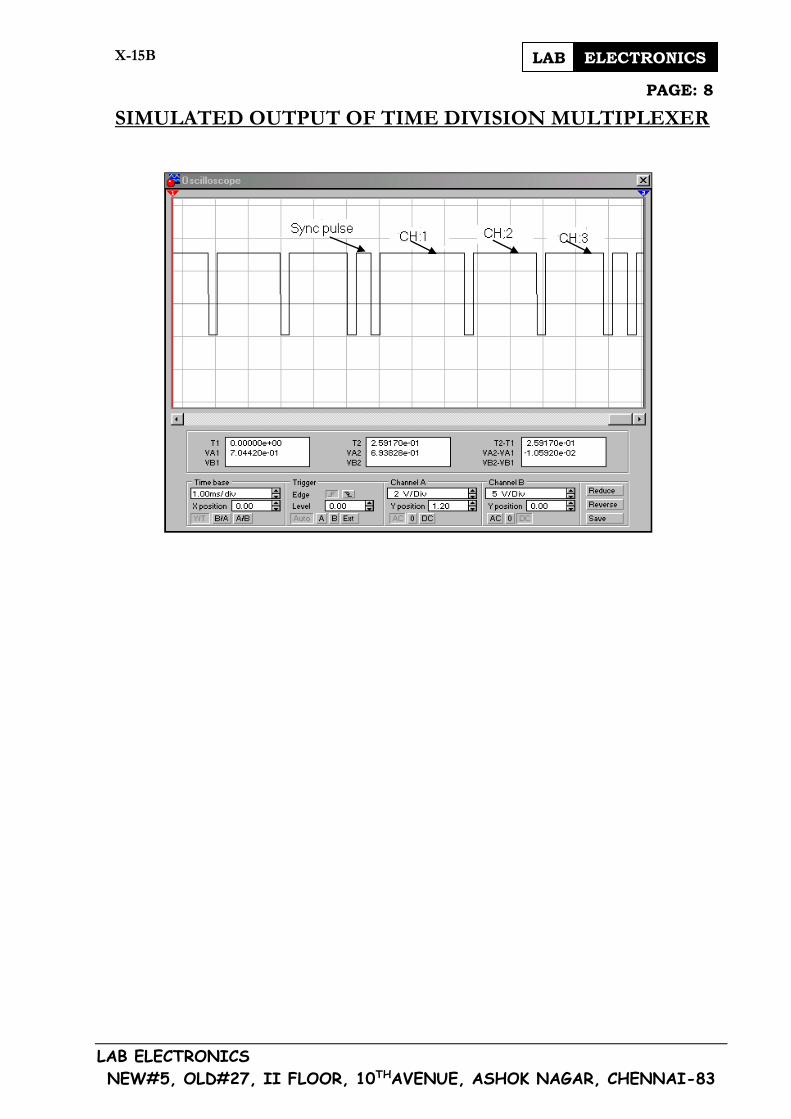
5. The output waveform should appear as shown in figure 3. Note that the sync
pulse is a relatively short duration pulse while channels 1, 2 and 3 are
approximately equal. Turn trimmer R1, fully clockwise.
FIGURE: 3 - OUTPUT WAVEFORM
6. Return R1 to midrange. Now adjust R2 alternatetively clockwise and
counterclockwise. What happens to the output wave?
7. Return R2 to midrange. Adjust R3 fully clockwise and then fully counterclockwise.
What happens to the output wave when R3 is adjusted?
8. Turn off your trainer and read the following discussion.
DISCUSSION:
The circuit of figure 2 is a Time Division Multiplex Generator. The output wave
is as shown in figure 3 with pulse duration modulation used for channels 1, 2 and 3.
The 4017-decade counter alternately connects different timing resistors to the 555
IC. It first connects R4 which determines the sync pulse duration. When the 555 IC
output goes low, pin13 on the 4017 steps the counter to the next pulse. In this case,
R1 becomes the timing resistor. Therefore, when R1 is adjusted, the first pulse's
duration is changed.
CHANNELS 1,2,3 &TDM
OUTPUT
CRO ADJUSTMENT
TIME/DIV VOLT/DIV
1ms 2V

X-15B PAGE: 7
LAB ELECTRONICS
NEW#5, OLD#27, II FLOOR, 10THAVENUE, ASHOK NAGAR, CHENNAI-83
LAB ELECTRONICS
This is channel 1. Also, when R2 is adjusted, channel - 2's pulse duration changes.
The same is true for R3 and channel-3. Thus, this circuit is a time division multiplex
generator with the input signals being the position of R1, R2 and R3.
FIGURE: 4 - PIN DIAGRAM OF 4017
SIMULATED OUTPUTS
TIME DIVISION MULTIPLEXER
X-15B PAGE: 8
LAB ELECTRONICS
NEW#5, OLD#27, II FLOOR, 10THAVENUE, ASHOK NAGAR, CHENNAI-83
LAB ELECTRONICS
SIMULATED OUTPUT OF TIME DIVISION MULTIPLEXER

X-15B PAGE: 9
LAB ELECTRONICS
NEW#5, OLD#27, II FLOOR, 10THAVENUE, ASHOK NAGAR, CHENNAI-83
LAB ELECTRONICS
Channel -1
C1 C1
Channel-2
C2
Channel-3
C1 C2 C3 Sync C1 C2 C3
Note: Here C1, C2 and C3 are of same frequencies.
TDM OUTPUT
Sync Pulse

X-15B PAGE: 10
LAB ELECTRONICS
NEW#5, OLD#27, II FLOOR, 10THAVENUE, ASHOK NAGAR, CHENNAI-83
LAB ELECTRONICS
WIRING DIAGRAM

X-15B PAGE: 11
LAB ELECTRONICS
NEW#5, OLD#27, II FLOOR, 10THAVENUE, ASHOK NAGAR, CHENNAI-83
LAB ELECTRONICS
EXPERIMENT - 2
PULSE CODE MODULATION & DEMODULATION
OBJECTIVE:
1. To construct and study the Pulse Code Modulator and observe its waveform
2. To observe the pulse decoded waveform.
MATERIALS REQUIRED:
1. LAB digital communication trainer.
2. Dual Trace Oscilloscope.
3. Set of patching Cords.
THEORY OF PULSE CODE MODULATION:
Pulse code modulation or PCM is the major form of digital pulse modulation.
In PCM, the modulating signal is sampled, just as in other forms of pulse modulation.
The sample amplitude is then converted into a binary code and transmitted as a
stream of pulses.
In the other forms of pulse modulation, the sample amplitude is converted
directly into pulse amplitude, duration or position. However, in PCM, since the
amplitude must be transmitted as a specific number out of a limited range of
numbers, the sample amplitude must first be quantized. That is, each sample
amplitude must be converted to the nearest standard amplitude or quantum. For
example, suppose the PCM system has a total signal amplitude range of 7V and
each 1V level corresponds to a specific binary code. Therefore, for this system each
quantum or standard level is 1V. This is shown in figure 1 for a sine wave signal with
8 quantum steps from 0V to 7V. Note that the quantizing waveform is actually a form
of PAM, although it is limited to the quantum steps and is not continuously variable.
You'll notice that the first sampling point in figure 1 is approximately 3.3V.
Since there is no quantum level at this voltage; it is represented by the nearest level,
which is 3V. This occurs at many places on the waveform. This error or distortion is
called quantizing noise.

X-15B PAGE: 12
LAB ELECTRONICS
NEW#5, OLD#27, II FLOOR, 10THAVENUE, ASHOK NAGAR, CHENNAI-83
LAB ELECTRONICS
FIGURE - 1: A QUANTIZED SINE WAVE
It is noise because the errors are random. This is because the difference between
the quantum level and the actual signal at any instant is completely unpredictable.
The obvious method of reducing quantizing noise is to increase the number of
quantum levels until the noise level is acceptable. However, increasing the number
of levels increases the transmission bandwidth, so a compromise must be made
between acceptable quantizing noise and bandwidth.
FIGURE - 2: CODING THE QUANTIZED WAVE
After quantization has occurred, each sample must be coded as a binary
number before it can be transmitted as PCM. Figure 2 shows the results of coding
the quantized waveform from figure 1. Since there are only 8 quantum levels, they
can be represented by a 3-bit binary word, with 000 representing 0V and 111
representing 7V.
QUANTIZATION
LEVELS
SAMPLING PULSES
SAMPLING POINT
QUANTIZING
WAVEFORM

X-15B PAGE: 13
LAB ELECTRONICS
NEW#5, OLD#27, II FLOOR, 10THAVENUE, ASHOK NAGAR, CHENNAI-83
LAB ELECTRONICS
Once the quantizing waveform is coded, each sequential sample is transmitted as a
pulse code. A table comparing the quantizing level, binary number and pulse code is
shown in figure 3.
FIGURE - 3: THREE BIT PCM
A PCM receiver is shown in figure 4. It is made up of a PCM-to-PAM
converter and a low-pass filter to convert that PAM back to the original modulating
signal. It is, in essence, a digital-to-analog converter.
As mentioned earlier, the primary advantage of PCM is its much better
immunity to noise and interference. For example, a typical PCM transmission can be
sent over a communication channel having a signal-to-noise ratio of 21 dB with
minimal error. In fact, the error would be just one pulse missed or decoded
improperly every 17 minutes. If the signal-to-noise ratio is improved to 23 dB, the
error rate drops to one error every four months. To achieve this; low error rate in an
AM system would require a signal-to-noise ratio of 60 to 70 dB.
QUANTIZING LEVEL
BINARY NUMBER
PULSE CODE

X-15B PAGE: 14
LAB ELECTRONICS
NEW#5, OLD#27, II FLOOR, 10THAVENUE, ASHOK NAGAR, CHENNAI-83
LAB ELECTRONICS
INPUT PCM
TO PAM
LOW PASS
FILTER OUTPUT
DIGITAL TO ANALOG
CONVERSION
FIGURE - 4: PCM RECEIVER
INTRODUCTION:
The purpose of a communication system is to transmit information bearing
signals from a source, located at one point in space, to a user destination, located at
another point. As a rule, the message produced by the source is not electrical in
nature. Accordingly, an input transducer is used to convert the message generated
by the source into a time-varying electrical signal called the message signal. By
using another transducer at the receiver the original message is recreated at the
user destination. Figure-5 shows the block diagram of a communication system. The
system consists of three major parts: 1) transmitter, 2) communication channel, and
3) receiver.
FIGURE - 5: COMMUNICATION SYSTEM
The main purpose of the transmitter is to modify the message signal and to
make suitable for transmission over the channel. This modification is achieved by
means of a process known as modulation, which involves varying some parameter of
a carrier wave (e.g., the amplitude, frequency or phase of a sinusoidal wave) in
accordance with the message signal.

X-15B PAGE: 15
LAB ELECTRONICS
NEW#5, OLD#27, II FLOOR, 10THAVENUE, ASHOK NAGAR, CHENNAI-83
LAB ELECTRONICS
The communication channel may be a transmission line (as in telephony and
telegraphy), an optical fiber (as in optical communication), or merely free space in
which the signal is radiated as an electromagnetic wave (as in radio and television
broadcasting). In propagating through the channel, the transmitted signal is distorted
due to non-linearity and/or imperfections in the frequency response of the channel.
Other sources of degradation are noise and interference picked up by the signal
during the course of transmission through the channel. Noise and distortion
constitute two basic problems in the design of communication systems.
Usually, the transmitter and receiver are carefully designed so as to minimize
the effects of noise and distortion on the quality of reception. The main purpose of
the receiver is to recreate the original message signal from the degraded version of
the transmitted signal after propagation through the channel. This recreation is
accomplished by using a process used in the transmitter. An analog signal is a
continuous function of time, with the amplitude being continuous as well. Analog
signals arise when a physical waveform such as an acoustic or a light wave is
converted into an electrical signal. The conversion is effected by means of a
transducer; examples include the microphone, which converts sound pressure
variations into corresponding Voltage or current variations, and the photoelectric cell,
which does the same for light intensity variations. On the other hand, a discrete-time
signal is defined only at discrete times. Thus, in this case the independent variable
takes on only discrete values, which are usually uniformly spaced. Consequently,
discrete time signals are described as sequences of samples whose amplitudes may
take on continuous values.
When each samples of discrete time signal is quantized (i.e., its amplitude is
only allowed to take on a finite set of discrete values) and then coded, the resulting
signal is referred to as a digital signal. The output of a digital computer is an example
of a digital signal. Naturally, an analog signal may be converted into digital form by
sampling it in time, then quantizing and coding it.
In pulse-code modulation (PCM) the message signal is sampled and the
amplitude of each sample is rounded off to the nearest one of a finite set of allowable
values, so that both time and amplitude are in discrete form. This allows the
message to be transmitted by means of coded electrical signals thereby
distinguishing PCM from all other methods of modulation.

X-15B PAGE: 16
LAB ELECTRONICS
NEW#5, OLD#27, II FLOOR, 10THAVENUE, ASHOK NAGAR, CHENNAI-83
LAB ELECTRONICS
The use of digital representation of analog signals (e.g. voice, video) offers
the following advantages: 1) Ruggedness to transmission noise and interference, 2)
Efficient regeneration of the coded signal along the transmission path and 3) The
possibility of a uniform format for different kinds of base-band signals. These
requirement and increased system complexity are in increase. These advantages,
however, are attained at the cost of increased transmission bandwidth requirement
and increased system complexity.
With the increasing availability of wide-band communication channels,
coupled with the emergence of the requisite device technology, the use of PCM has
become a practical reality. In pulse-duration modulation (PDM) and pulse-position
modulation (PPM) only time is expressed in discrete form, whereas the respective
modulation parameters (namely, pulse amplitude, duration, and position) are varied
in a continuous manner in accordance with the message. Thus, in these modulation
systems, information transmission is accomplished in analog form at discrete times.
ELEMENTS OF PULSE-CODE MODULATION (PCM):
Pulse-code modulation systems are considerably more complex than PAM,
PDM, and PPM systems, in that the message signal is subjected to a greater
number of operations. The essential operations in the transmitter of a PCM system
are sampling, quantizing, and encoding, as shown in figure-6 (a). The quantizing and
encoding operations are usually performed in the same circuit, which is called an
analog-digital converter. The essential operations in the receiver are regeneration of
impaired signals, decoding, and demodulation of the train of quantized samples.
Regeneration usually occurs at intermediate points along the transmission route as
necessary. When time-division multiplexing is used, it becomes necessary to
synchronize the receiver to the transmitter for the overall system to operate
satisfactorily.

X-15B PAGE: 17
LAB ELECTRONICS
NEW#5, OLD#27, II FLOOR, 10THAVENUE, ASHOK NAGAR, CHENNAI-83
LAB ELECTRONICS
FIGURE- 6 (B): BLOCK DIAGRAM OF A PULSE CODER & DECODER IC
SAMPLING:
The incoming message wave is sampled with a train of narrow rectangular
pulses so as to closely approximate the instantaneous sampling process. In order to
ensure perfect reconstruction of the message at the receiver, the sampling rate must
be greater than twice the highest frequency component of the message wave in
accordance with the sampling theorem. In practice, a low-pass filter is used at the
front end of the sampler in order to exclude frequencies greater than before
sampling. Thus, the application of sampling permits the reduction of the continuously
varying message wave to a limited number of discrete values per second.
AUTO
ZERO
5-V
REFERENCE
SUCCESSIVE APPROXIMATION
REGISTER
OUTPUT PCM
BUFFER
CONTROL
LOGIC
INPUT PCM
BUFFER
ANALOG
IN
ANALOG
OUT
INPUT SAMPLE &
HOLD
OUTPUT SAMPLE &
HOLD
PCM OUT
PCM IN
COMPARATOR
NON- LINEAR D/A
CONVERTER
FIGURE- 6 (A): BLOCK DIAGRAM OF PULSE CODER & DECODER

X-15B PAGE: 18
LAB ELECTRONICS
NEW#5, OLD#27, II FLOOR, 10THAVENUE, ASHOK NAGAR, CHENNAI-83
LAB ELECTRONICS
QUANTIZING:
A continuous signal, such as voice, has a continuous range of amplitudes and
therefore its samples have a continuous amplitude range. In other words, within the
finite amplitude range of the signal we find an infinite number of amplitude levels. It is
not necessary in fact to transmit the exact amplitudes of the samples. Any human
sense (the ear or the eye), as ultimate receiver, can only detect finite intensity
differences. This means that the original continuous signal may be approximated by
a signal constructed of discrete amplitude selected on a minimum error basis from
an available set. The existence of a finite number of discrete amplitude levels is a
basic condition of PCM. Clearly, if we assign the discrete amplitude levels with
sufficiently close spacing, we may make the approximated signal practically
indistinguishable from the original continuous signal.
FIGURE - 7: ILLUSTRATION OF THE QUANTIZING PRINCIPLE A) QUANTIZING
CHARACTERISTIC, B) CHARACTERISTIC OF ERRORS IN QUANTIZING,
C) A QUANTIZED SIGNAL WAVE.
The conversion of an analog (continuous) sample of the signal into a digital
(discrete) form is called the quantizing process. Graphically, the quantizing process
means that a straight line representing the relation between the input and output of
linear continuous system is replaced by a staircase characteristic, as in figure-7 (a).
INPUT WAVE
QUANTIZED OUPTUT
DIFFERENCE BETWEEN CURVES
1 & 2
MAGNITUDE
TIME
(a)
(b)

X-15B PAGE: 19
LAB ELECTRONICS
NEW#5, OLD#27, II FLOOR, 10THAVENUE, ASHOK NAGAR, CHENNAI-83
LAB ELECTRONICS
The difference between adjacent discrete values is called a quantum or step
size. Signals applied to a quantizer, with the input-output characteristic of figure-7
(a) are sorted into amplitude slices (the threads of the staircase), and all input
signals within plus or minus half a quantum step of the mid-value of a slice are
replaced in the output by the mid value in question.
The quantizing error consists of the difference between the input and output
signals of the quantizer. It is apparent that the maximum instantaneous value of this
error is half of one quantum step and the total range of variation is from minus half a
step to plus half a step. In part (b) figure-7 the error is shown plotted as a function of
the input signal, and in part (c) of the figure a typical variation of the error as a
function of time is indicated.

X-15B PAGE: 20
LAB ELECTRONICS
NEW#5, OLD#27, II FLOOR, 10THAVENUE, ASHOK NAGAR, CHENNAI-83
LAB ELECTRONICS
BASICS PCM WAVEFORMS WITH BINARY CODE:
FIGURE- 8: PARALLEL PCM WAVEFORMS WITH QUANTIZED LEVEL
(A)
(B)

X-15B PAGE: 21
LAB ELECTRONICS
NEW#5, OLD#27, II FLOOR, 10THAVENUE, ASHOK NAGAR, CHENNAI-83
LAB ELECTRONICS
ENCODING:
In combining the processes of sampling and quantizing, the specification of a
continuous base-band signal becomes limited to a discrete set of values, but not in
the form best suited to transmission over a line or radio path. To exploit the
advantages of sampling and quantizing, we require the use of an encoding process
to translate the discrete set of sample values to a more appropriate form of signal.
Any plan for representing each of this discrete set of values as particular
arrangement of discrete events is called a code. One of the discrete events in a code
is called a code element or symbol. For example, the presence or absence of a
pulse is a symbol. A particular arrangement of symbols used in a code to represent a
single value of the discrete set is called a code word or character.
REGENERATION:
The most important feature of PCM systems lies in the ability to control the
effects of distortion and noise produced by transmitting a PCM wave through a
channel.
This capability is accomplished by reconstructing the PCM wave by means of
a chain of regenerative repeaters located at sufficiently close spacing along the
transmission route.
As in figure-9 a regenerative repeater, namely, equalization, timing, and
decision-making, performs three basic functions. The equalizer shapes the received
pulses so as to compensate for the effects of amplitude and phase distortions
produced by the transmission characteristics of the channel.
FIGURE: 9 - BLOCK DIAGRAM OF A REGENERATIVE REPEATER
Decision
Making
Device
Amplifier
Equalizer
Timing
Circuit
Distorted
PCM Wave
Regenerated
PCM Wave

X-15B PAGE: 22
LAB ELECTRONICS
NEW#5, OLD#27, II FLOOR, 10THAVENUE, ASHOK NAGAR, CHENNAI-83
LAB ELECTRONICS
The timing circuitry provides a periodic pulse train, derived from the received
pulses, for sampling the equalized pulses at the instants of time where the signal-to-
noise ratio is a maximum. The decision device is enabled, when at the sampling time
determined by the timing circuitry, the amplitude of the equalized pulse plus noise
exceeds a predetermined voltage level. Thus, for example, in a PCM system with on-
off signaling, the repeater makes a decision in each bit interval as to whether or not a
pulse is present.
If the decision is "yes", a clean new pulse is transmitted to the next repeater.
If, on the other hand, the decision is "no", a clean base line is transmitted. In this
way, the accumulation of distortion and noise in a repeater span is completely
removed, provided, that the disturbance is not too large to cause an error in the
decision making process. Ideally, except for delay, the regenerated signal is exactly,
the same as the signal originally transmitted.
DECODING:
The first operation in the receiver is to regenerate (i.e., reshape and clean up)
the received pulses. These clean pulses are then regrouped into code words and
decoded (i.e., mapped back) into a quantized PAM signal. The decoding process
involves generating a pulse amplitude of which is the linear sum of all the pulses in
the code word, with each pulse weighted by its place-value (20, 21, 22, 23...) in the
code.
FILTERING:
The final operation in the receiver is to recover the signal wave by passing the
decoder output through a low-pass reconstruction filter whose cutoff frequency is
equal to the message bandwidth . Assuming that the transmission path is error-
free, the recovered signal includes no noise with the exception of the initial distortion
introduced by the quantization process.
MULTIPLEXING:
In applications using PCM, it is natural to multiplex different message sources
by time-division, where by each source keeps its individuality throughout the journey
from the transmitter to the receiver. This individuality accounts for the comparative
ease with which message sources may be dropped or reinserted in a time-division
multiplex system.

X-15B PAGE: 23
LAB ELECTRONICS
NEW#5, OLD#27, II FLOOR, 10THAVENUE, ASHOK NAGAR, CHENNAI-83
LAB ELECTRONICS
As the number of independent message sources is increased, the time
interval that may be allotted to each source has to be reduced, since all of them must
be accommodated into a time interval equal to the reciprocal of the sampling rate.
This in turn means that the allowable duration of a code word representing a single
sample is reduced. However, pulses tend to become more difficult to generate and to
transmit as their duration is reduced. Furthermore, if the pulses become too short,
impairments in the transmission medium begin to interfere with the proper operation
of the system. Accordingly, in practice, it is necessary to restrict the number of
independent message sources that can be included within a time-division group.
SYNCHRONIZATION:
For a PCM system with time-division multiplexing to operate satisfactorily, it is
necessary that the timing operations at the receiver, except for the time lost in
transmission and regenerative repeating, follow closely the corresponding operations
at the transmitter. In a general way, this amounts to requiring a local clock at the
receiver keep the same time as a distant standard clock at the transmitter, except
that the local clock is somewhat slower by an amount corresponding to the time
required to transport the message signals from the transmitter to the receiver.
One possible procedure to synchronize the transmitter and receiver clocks is
to set aside a code element or pulse at the end of a frame (consisting of a code word
derived from each of the independent message sources in succession) and to
transmit this pulse every other frame only. In such a case, the receiver includes a
circuit that would search for the pattern of 1's and 0's alternating at half the frame
rate, and thereby establish synchronization between the transmitter and receiver.
When the transmission is interrupted, it is highly unlikely that the transmitter and
receiver clocks will continue to indicate the same time for long.
Accordingly, in carrying out a synchronization process, we must set up an
orderly procedure for detecting the synchronizing pulse. The procedure consists of
observing the code elements one by one until the synchronizing pulse is detected.
That is, after observing a particular code element long enough to establish the
absence of the synchronizing pulse, the receiver clock is set back by one code
element and the next code element is observed.

X-15B PAGE: 24
LAB ELECTRONICS
NEW#5, OLD#27, II FLOOR, 10THAVENUE, ASHOK NAGAR, CHENNAI-83
LAB ELECTRONICS
This searching process is repeated until the synchronizing pulse is detected.
Clearly, the time required for synchronization depends on the epoch at which proper
transmission is reestablished.
DEFINITION & APPLICATION OF PULSE CODE
MODULATION
Pulse code modulation (PCM) may be chosen as an example of technologies
for A/D conversion. PCM was invented as early as the 1930s, but did not start to
predominate until the 1960s when integrated transistor circuits became available.
PCM is a type of waveform coding and is standard for voice coding in the telephone
network. The bit rate generated per call - 64 K bits/s - has been a decisive factor in
switching and transmission design.
FIGURE 10: THE VOICE CURVE IS TIME DIVIDED INTO AMPLITUDE VALUES
Sound - movement of particles in an elastic medium, as the definition goes - is
intrinsically analog. This may be illustrated with a curve that shows how the
amplitude (sound level) varies over time. Figure-10 (considerably simplified) shows
such a voice curve. Let us imagine that we measure the amplitude at regular
intervals and jot down the values in a table. Since there are no values between the
readings, the table does not give us the whole truth. But it is quite clear that the
shorter the period of time between the readings, the better the description of the
voice curve.
SAMPLING:
Reading the amplitude at regular intervals is called sampling. It is important to
take the samples on the voice curve at suitable intervals, which means that the
quality obtained should allow us to clearly recognize each other's voices.

X-15B PAGE: 25
LAB ELECTRONICS
NEW#5, OLD#27, II FLOOR, 10THAVENUE, ASHOK NAGAR, CHENNAI-83
LAB ELECTRONICS
Taking too many samples is uneconomical; a suitable sampling frequency is
8,000 samples per second. The result will be a pulse amplitude-modulated (PAM)
signal where each pulse directly corresponds to the amplitude of the voice curve.
See figure-11.
FIGURE 11: PULSE AMPLITUDE-MODULATED SIGNAL
The sampling theorem;
Now, how have we reached the conclusion that a frequency of 8,000 samples
per second is sufficiently close between readings? The answer lies in the sampling
theorem, which states that:
"All the information in the original signal will be present in the signal described by the
samples”, if:
1. The original signal has a limited bandwidth, that is, it does not contain any
component with a frequency exceeding a given value, B
2. The sampling frequency is greater than twice the highest frequency in the original
signal; that is, >2 x B.
Since telephone connections operate in the 300 - 3,400 Hz band, 8,000 Hz is
a sampling frequency that meets the primary requirement for transmission quality: no
information should be lost. The sampling frequency is twice the maximum frequency,
which is significantly lower than 8 KHz.
QUANTIZATION:
Quantization means that we measure the amplitude of the pulses in the PAM
curve and assign a numerical value to each pulse. To avoid having to handle an
infinite number of numerical values, we divide the amplitude levels into intervals and
assign the same value to all samples within a given interval.

X-15B PAGE: 26
LAB ELECTRONICS
NEW#5, OLD#27, II FLOOR, 10THAVENUE, ASHOK NAGAR, CHENNAI-83
LAB ELECTRONICS
See figure-12, in principle, this is analogous with the way in which a person's age
may be viewed. A 25-year-old belongs to the "quantization interval" twenty-five years
for no less than 365 days.
FIGURE 12: SAMPLES WITH THE CORRESPONDING QUANTISED VALUES
Quantization also means that we forgo accuracy: the series of digits is not
really the whole truth about the voice curve. We call this deviation quantizing
distortion. See figure-12. But we will have a limited number of numerical values to
transmit, the equipment can be made less complex, and the risk of transmission
errors is reduced. In telephony, 256 quantizing intervals are used. Consequently,
there are 256 values to be transmitted.
Figure-12 shows that there are also other problems. In the figure-13, the
quantizing intervals are equally large and we will have the same quantizing distortion
regardless of the amplitude. But if we set distortion in relation to the amplitude, the
relationship will vary. A low distortion-to-volume ratio is crucial to audibility. This
means that a weak voice will be significantly disturbed if equally large quantizing
intervals are used.
One way of solving this problem is to make the quantizing intervals small
enough, so that even low amplitude deviations can be transferred with sufficiently
good audibility. Then again, we will have unnecessarily small intervals for the high
amplitudes, which also mean that there will be an unnecessary amount of numerical
values to be transferred.

X-15B PAGE: 27
LAB ELECTRONICS
NEW#5, OLD#27, II FLOOR, 10THAVENUE, ASHOK NAGAR, CHENNAI-83
LAB ELECTRONICS
FIGURE 13: QUANTIZING DISTORTION
The ideal thing must be to allow the quantizing intervals to increase with amplitude.
The amplitude/distortion relationship should preferably be constant. In addition, it is
important to find the right relationship between the number of quantizing intervals
and the desired transmission quality. Here, too, we can refer to the common way of
saying or writing a person's age. At the beginning of our lives, we specify age in days
- then in weeks and months. Not until a child is two years of age do we start to use
"full-year quantizing intervals".
Two models are available. One of them, the A-law, is illustrated in figure-14
The other one, the µ-law, follows the same principle but has fifteen segments instead
of thirteen. The A-law is used in Europe, and the µ-law is used in the US.

X-15B PAGE: 28
LAB ELECTRONICS
NEW#5, OLD#27, II FLOOR, 10THAVENUE, ASHOK NAGAR, CHENNAI-83
LAB ELECTRONICS
FIGURE 14: THE A-LAW
CODING:
Now it remains for us to give our 256 possible values a suitable layout for
transmission. Let us use binary pulses; that is, pulses with only two levels. Eight
such pulses, or bits, will suffice to form a unique code for each interval value (28 =
256). The equipment need only be capable of distinguishing between two pulse
levels, and of counting to eight. This technique-the elements of computer technology
is ideally suited for telephony applications.
FIGURE 15: BINARY PULSES

X-15B PAGE: 29
LAB ELECTRONICS
NEW#5, OLD#27, II FLOOR, 10THAVENUE, ASHOK NAGAR, CHENNAI-83
LAB ELECTRONICS
FIGURE 16: QUANTISED VALUES WITH THE CORRESPONDING BINARY CODE
Three processing steps;
To sum up, there are three steps between the analog voice and the
digital transmission link.
1. Sampling, where we measure the amplitude 8,000 times per second.
2. Quantizing, where we assign one out of 256 values to each sample.
3. Coding, where each quantised value is expressed as a binary code of eight bits.
FIGURE 17: PCM WORD, EIGHT BITS
The result of this pulse code modulation process - the eight-bit binary code -
is called a PCM word. See figure-17. One PCM word corresponds to one sample.
8,000 PCM words are generated per second, and for each call we will have a bit
stream of 8 x 8,000 = 64,000 K bits/s in the digital link. The ITU-T calls this type of
voice coding "64 K bits/s PCM".
\

X-15B PAGE: 30
LAB ELECTRONICS
NEW#5, OLD#27, II FLOOR, 10THAVENUE, ASHOK NAGAR, CHENNAI-83
LAB ELECTRONICS
FROM DIGITAL TO ANALOG:
In the receiving equipment, the pulse train is received and converted into
analog form; that is, the sound curve is reproduced. This, too, is a process in three
steps.
FIGURE 18: A/D CONVERSION, TRANSMISSION AND D/A CONVERSION
Firstly, regeneration: the binary pulse train is received and the PCM words are
reproduced. Secondly, the PCM words are interpreted in a decoder and translated
into quantised amplitude values. Thirdly, the voice curve itself is reconstructed, and
we will again have an analog signal that can be made audible at the receiving end.
See figure-18.
Today, the PCM technique is also used to record music on compact discs
(CD) but in this application, the sampling frequency is higher: 44.1 KHz in contrast
with 8 KHz for telephony.
1. SYNCHRONOUS PULSE GENERATOR: (SYNC PULSE):
This part of the circuit generates a MHz SYNC Pulse signal using a transistor,
Schmitt trigger and a -flip flop. The frequency of this SYNC Pulse can be varied
using the 5K potentiometer (10K potentiometer).
2. PULSE CODER & DECODER:
a) ANALOG TO PCM (TRANSMIT SECTION):
The analog input signal is placed on the uncommitted op-amp’s terminals.
The op-amp allows for input gain adjustment if necessary to either 0 dB or the
system’s 0 levels.

X-15B PAGE: 31
LAB ELECTRONICS
NEW#5, OLD#27, II FLOOR, 10THAVENUE, ASHOK NAGAR, CHENNAI-83
LAB ELECTRONICS
The op-amp also acts as a 2nd order analog anti-aliasing filter by band-limiting
the input to less than half of the sampling frequency as per the Nyquist Rate
Theorem. The analog signal is filtered by a cosine filter, a 6th order low-pass filter,
and the high-pass filter before being sampled. The sampling is performed by a
capacitor array at a rate of 8 KHz and the value fed into the encoder.
From the encoder the 8 bit PCM data is clocked out by the shift clock. Lastly,
an auto-zero loop (without any external capacitor provides cancellation of any DC
offset by integrating the single bit of the PCM data and feeding it back to the non-
inverting input of the comparator, and a sign bit - fixation circuitry reduces idle
channel noise during quiet periods).
b) PCM TO ANALOG (RECEIVE SECTION):
The PCM data is shifted into the decoder's input buffer register once every
sampling period. Once the PCM data has been shifted into the decoder register a
charge proportional to the received PCM data work value appears on the decoder's
capacitor array. A sample and hold circuit integrates to the charge value and holds
that value for the rest of the sampling period. Then low-pass switched capacitor filter
smoothes the signal and performs loss equalization to compensate for the (SIN X)/X
distortion due to sample and hold operation. The low pass filter's output is then
buffered and available for driving electronic hybrids directly.
c) TIMING REQUIREMENTS:
The 8 KHz transmit and receive sampling strobes need not be exactly 8 bit
periods wide. The codec has an internal bit counter that counts the number of data
bits shifted and forces the PCM output into a high-impedance state after the 8th bit-
has been shifted out. This allow the strobe signal to have any duty cycle as long as
its repetition rate is 8KHz and the shift clock is synchronized to it and the clock rate
is either 1.537MHz, 1.544MHz, or 2.048MHz. Note that all internal clocks for the
switched capacitor filters and timing conversions are automatically derived; no
external control signal for clock selection is required.
d) POWER DOWN CIRCUITRY:
The codec can be powered down in two ways. The most direct power down
command is to force the PD (Pin 14) mode select low. This will shut down the chip
regardless of the strobes. The second method is to stop strobing with the clock (Pin
11) input.

X-15B PAGE: 32
LAB ELECTRONICS
NEW#5, OLD#27, II FLOOR, 10THAVENUE, ASHOK NAGAR, CHENNAI-83
LAB ELECTRONICS
The clock can be held high, low or floating just so long as its state is not
changed. After the chip has been shut down the PCM is locked into a high
impedance state and the AOUT is connected to AGND for about 1ms to avoid output
noise to the system.
e) A-LAW CHARACTERISTICS:
Compression (refer to figure-19 (a)) allows more channels to be multiplexed
on a given transmission media by reducing the bandwidth of each individual channel.
Figure-19 (b) shows the A-LAW companding transfer functions used in telephony to
convert the speaker's analog voice signal into PCM. Figure-19(c) shown the
expansion transfer function used to convert the digital PCM signal back into an
analog signal for the end telephone user to hear.
FIGURE - 19A
QUANTIZING LEVEL
STRONG SIGNAL
WEAK SIGNAL
1 WITHOUT A COMPANDER 2 WITH A COMPANDER

X-15B PAGE: 33
LAB ELECTRONICS
NEW#5, OLD#27, II FLOOR, 10THAVENUE, ASHOK NAGAR, CHENNAI-83
LAB ELECTRONICS
FIGURE - 19B: THE A-LAW A/D COMPANDING TRANSFER FUNCTION
FIGURE - 19C: THE A- LAW D/A COMPANDING TRANSFER FUNCTION
10100101
10110101
10000101
10010101
11100101
11110101
01110101
01100101
00010101
00000101
00110101
00100101
11000101
01000101
11010101
01111111 01010101
11111111
DIGITAL
OUTPUTS
ANALOG INPUT
-3 -2 -1 0 1 2 3
01010101
01111111
11111111
11010101
DIGITAL INPUTS BY DECODER
3 2 1 0 -1 -2
-3
ANALOG
INPUTS

X-15B PAGE: 34
LAB ELECTRONICS
NEW#5, OLD#27, II FLOOR, 10THAVENUE, ASHOK NAGAR, CHENNAI-83
LAB ELECTRONICS
EXPERIMENTAL STEP-BY-STEP PROCEDURE:
1. Study the PCM & Demodulation Circuit configurations given on the front panel of
the trainer.
2. Connect the Patch Cords as shown in wiring diagram.
3. Switch ON the trainer.
a. Connect Oscilloscope across SYNC pulse output terminal (adjusted to 700KHz)
and ground. Observe the SYNC pulse output of frequency to be approx 0.05 MHz
to1.5 MHz & Amplitude will be approx 4V(P-P).
OSCILLOSCOPE SETTINGS: (For SYNC pulse)
Time / Div = 0.5μs to 1μs
V / Div = 2V.
SIMULATED OUTPUT OF SYNC PULSE GENERATOR O/P
b. Connect oscilloscope across clock output and Gnd. Observe the clock output.
Select frequency selector switch to x 100 and adjust the frequency to be 3.5 KHz
by adjusting frequency control knob amplitude will be approx 4V (p-p).
OSCILLOSCOPE SETTINGS: (For CLOCK)
Time / Div = 0.1ms to 50s
V / Div = 2V

X-15B PAGE: 35
LAB ELECTRONICS
NEW#5, OLD#27, II FLOOR, 10THAVENUE, ASHOK NAGAR, CHENNAI-83
LAB ELECTRONICS
C. Connect Oscilloscope across the AF output terminal and ground in the AF
oscillator section. Select function selector switch to SINE (on the front panel AF
Oscillator). You can observe sine output on CRO at this terminal. By varying the
frequency control and amplitude control potentiometers adjust frequency to be 1
KHz and amplitude to be 4V (P-P).
OSCILLOSCOPE SETTINGS: (For sine output)
Time / Div = 0.2ms
V / Div = 2V
4. Switch OFF the trainer and patch the circuit as shown in the wiring diagram.
You will observe that sync pulse output, clock and AF output are connected from
the top panel trainer to PCM and demodulation section.
5. Switch ON the trainer.
6. Connect CRO across the PCM output and ground at pin 15 of IC44233. For
observing PCM output;
Verify that AF (SINE output) frequency to be approx 1KHZ and amplitude to be
4V (P-P).
Verify that clock generator output frequency range to be approx 7KHz and
amplitude to be 4V (P-P). Slightly adjust the frequency control Knob to observe
the PCM output.
Verify that SYNC pulse output frequency range to be approx 1.5MHz and
amplitude to be 4V (P-P). Keep pulse width control to maximum position
PCM OUTPUT:
7. Note: 60MHz dual trace oscilloscope can be used for better clarity while
observing PCM output
Time / Div = 0.1ms to 0.2ms
V / Div = 2V

X-15B PAGE: 36
LAB ELECTRONICS
NEW#5, OLD#27, II FLOOR, 10THAVENUE, ASHOK NAGAR, CHENNAI-83
LAB ELECTRONICS
WIRING DIAGRAM
INDICATES PATCHING CONNECTIONS

X-15B PAGE: 37
LAB ELECTRONICS
NEW#5, OLD#27, II FLOOR, 10THAVENUE, ASHOK NAGAR, CHENNAI-83
LAB ELECTRONICS
SIMULATED OUTPUT OF PCM
AUDIO INPUT SETTING‘S
SIMULATED OUTPUT OF PCM
7. It is a very precise adjustment to obtain the PCM output. If you are not getting
the PCM output slightly adjust clock generator frequency control.
8. Ignore the Harmonic Distortion if any in the PCM output, as it is an educational
trainer only.
2
INPUT PCM O/P

X-15B PAGE: 38
LAB ELECTRONICS
NEW#5, OLD#27, II FLOOR, 10THAVENUE, ASHOK NAGAR, CHENNAI-83
LAB ELECTRONICS
9. Finally observe the audio output at pin 5 of IC44233, which is same as the audio
input. Vary the Gain potentiometer for amplitude variation. You can observe
some weak signals as shown in the figure -19(A). If required slightly adjust clock
generator frequency control and audio amplitude control.
IC 44233 TIMING DIAGRAM:
This is a LS-TTL compatible open drain output. It is active only during
transmission of digital PCs output for 8 bit periods of the transmit clock signal
following a positive edge on the transmit SYNC input data is clocked out by the
positive edge of 470 ohms, although only one 470 ohm resistor is required for eight
codes.
The timing chart of IC44233 is as given below.
FIGURE- 44233 TIMING CHART

X-15B PAGE: 39
LAB ELECTRONICS
NEW#5, OLD#27, II FLOOR, 10THAVENUE, ASHOK NAGAR, CHENNAI-83
LAB ELECTRONICS
EXPERIMENT - 3
PULSE POSITION AND PULSE WIDTH
MODULATION
OBJECTIVE:
1. To construct a pulse position carrier generator.
2. To show how this Pulse Position Modulation (PPM) and Pulse Width Modulation
(PWM) is modulated by any external AF modulating frequency.
MATERIALS REQUIRED:
1. LAB digital communication trainer.
2. Dual Trace Oscilloscope.
3. Set of patching wires.
INTRODUCTION:
In amplitude and angle modulation, some characteristics of the carrier
amplitude, frequency, or phase is continuously varied in accordance with the
modulating information. However, in pulse modulation, a small sample is made of the
modulating signal and then a pulse is transmitted. In this case, some characteristics
of the pulse is varied in accordance with the sample of the modulating signal. The
sample is actually a measure of the modulating signal at a specific time.
There are several types of pulse modulating systems. Three of the more
common types are pulse amplitude modulation (PAM). Pulse duration modulation
(PDM), and pulse position modulation (PPM). In each of these systems, a
characteristic of the pulse - such as amplitude, duration, or position is continuously
varied in accordance with the modulating signal. This type of pulse modulation,
where a pulse characteristic is continuously varied, is called analog pulse
modulation.
Another type of pulse modulation is pulse code modulation (PCM), which is
digital pulse modulation. With PCM, the modulating signal is sampled and then
quantized. In quantization, each sample is assigned a specific numerical value
according to its amplitude.

X-15B PAGE: 40
LAB ELECTRONICS
NEW#5, OLD#27, II FLOOR, 10THAVENUE, ASHOK NAGAR, CHENNAI-83
LAB ELECTRONICS
This numerical value is then represented by a group of pulses, which represent the
modulating signals value in the binary number system. This system has many
advantages and, therefore, has many applications in modern communications.
THEORY:
In pulse time modulation (PTM), the modulating signal is sampled, just as it is
in PAM. However, in PTM, the amplitude of the sample is indicated by a timing
variation of the modulated pulse rather than an amplitude variation. The variable
timing characteristics may be the duration, position, or frequency of the pulses.
Therefore, there are three basic types of PTM: pulse duration modulation, pulse
position modulation, and pulse frequency modulation.
This type of PTM is also called pulse width or pulse length modulation,
however, pulse duration modulation (PDM) is the preferred term. There are three
different classifications of PDM: symmetrical PDM, leading edge PDM and trailing
edge PDM. These are shown in figure 1 along with the sine wave modulating signal.
Figure 1 (a) shows a symmetrical PDM waveform. Here, the modulating signal is
sampled and both the leading and trailing edges of the pulse are varied in
accordance with the sample amplitude. When the sample is high, the negative
reference duration, the spacing between the centers of the pulses remains constant.
Leading edge PDM is shown in figure 1 (b). In this type of PDM, the sample
amplitude varies the leading edge of the pulse. The trailing edge of each pulse is
fixed and, therefore, the spacing or timing between each pulses trailing edge is
constant. Figure 1 (c) shows trailing edge PDM. Here, the sample amplitude varies
the trailing edge of the pulse, with the leading edge remaining fixed.
PULSE POSITION MODULATION:
The next form of PTM is known as pulse position modulation (PPM). With this
form of PTM, both pulse amplitude and duration remain constant while the position of
the pulse, relative to a reference pulse, is varied in accordance with the modulating
signal. Figure 2 (b) shows a typical PPM waveform. The modulating signal and the
reference pulses are shown in figure 2 (a). Note that when the modulating signal
goes negative, the output pulse now leads the reference pulse by a proportional
amount.

X-15B PAGE: 41
LAB ELECTRONICS
NEW#5, OLD#27, II FLOOR, 10THAVENUE, ASHOK NAGAR, CHENNAI-83
LAB ELECTRONICS
FIGURE - 1
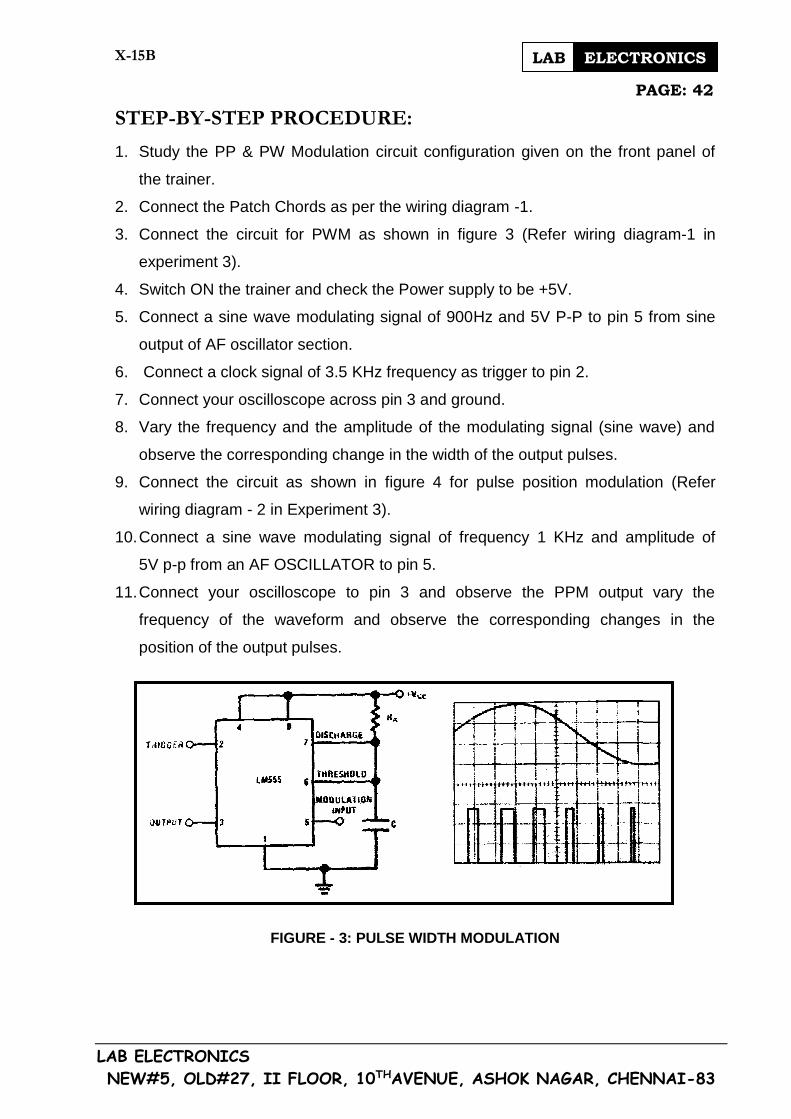
A typical PWM waveform can be generated using a 555 timer. When the timer is
connected in the monostable mode and triggered with a continuous pulse train, the
output pulse width can be modulated by a signal applied to pin 5. Figure 3 shows the
circuit and the waveform for pulse width modulation. A typical PPM waveform can be
generated by connecting the timer in a stable mode with a modulating signal applied
to the control voltage terminal. The pulse position varies with modulating signal since
the threshold voltage and hence the time delay is varied. Figure 4 shows the circuit
and the waveform for a triangle wave modulating signal.
FIGURE - 2
X-15B PAGE: 42
LAB ELECTRONICS
NEW#5, OLD#27, II FLOOR, 10THAVENUE, ASHOK NAGAR, CHENNAI-83
LAB ELECTRONICS
STEP-BY-STEP PROCEDURE:
1. Study the PP & PW Modulation circuit configuration given on the front panel of
the trainer.
2. Connect the Patch Chords as per the wiring diagram -1.
3. Connect the circuit for PWM as shown in figure 3 (Refer wiring diagram-1 in
experiment 3).
4. Switch ON the trainer and check the Power supply to be +5V.
5. Connect a sine wave modulating signal of 900Hz and 5V P-P to pin 5 from sine
output of AF oscillator section.
6. Connect a clock signal of 3.5 KHz frequency as trigger to pin 2.
7. Connect your oscilloscope across pin 3 and ground.
8. Vary the frequency and the amplitude of the modulating signal (sine wave) and
observe the corresponding change in the width of the output pulses.
9. Connect the circuit as shown in figure 4 for pulse position modulation (Refer
wiring diagram - 2 in Experiment 3).
10. Connect a sine wave modulating signal of frequency 1 KHz and amplitude of
5V p-p from an AF OSCILLATOR to pin 5.
11. Connect your oscilloscope to pin 3 and observe the PPM output vary the
frequency of the waveform and observe the corresponding changes in the
position of the output pulses.
FIGURE - 3: PULSE WIDTH MODULATION

X-15B PAGE: 43
LAB ELECTRONICS
NEW#5, OLD#27, II FLOOR, 10THAVENUE, ASHOK NAGAR, CHENNAI-83
LAB ELECTRONICS
CRO OBSERVATION PWM:
Time = 2ms/DIV
Top Trace Modulation I/P = 1V/DIV
Bottom Trace O/P = 2V/DIV
FIGURE - 4: PULSE POSITION MODULATION
CRO OBSERVATION (PPM):
Time = 50s/DIV
Top Trace Modulation Input = 1V/DIV
Bottom Trace Output = 2V/DIV

X-15B PAGE: 44
LAB ELECTRONICS
NEW#5, OLD#27, II FLOOR, 10THAVENUE, ASHOK NAGAR, CHENNAI-83
LAB ELECTRONICS
WIRING DIAGRAM-1
PULSE WIDTH MODULATION
INDICATES THE PATCHING CONNECTIONS
FSK RECEIVER
PP/PW MODULATION
5
4 8
21
37
6
+5V
I/PTRIG
9K1
3K9
PP/PWMO/P
0.01F
1K
NE555
10K

X-15B PAGE: 45
LAB ELECTRONICS
NEW#5, OLD#27, II FLOOR, 10THAVENUE, ASHOK NAGAR, CHENNAI-83
LAB ELECTRONICS
WIRING DIAGRAM-2
PULSE POSITION MODULATION
INDICATES THE PATCHING CONNECTIONS

X-15B PAGE: 46
LAB ELECTRONICS
NEW#5, OLD#27, II FLOOR, 10THAVENUE, ASHOK NAGAR, CHENNAI-83
LAB ELECTRONICS
EXPERIMENT - 4
PULSE POSITION & PULSE WIDTH
DEMODULATION
OBJECTIVES:
1. To construct the pulse position and pulse width demodulation circuit.
2. To show that the pulse width and pulse position modulation signal is
demodulated.
3. To show that the P.W.M demodulation output is nearly the same as the
modulating frequency by using phase locked loop demodulator.
MATERIALS REQUIRED:
1. LAB digital communication trainer.
2. Dual Trace Oscilloscope.
3. Set of patching wires.
INTRODUCTION:
In pulse modulation, some parameter of a pulse train is varied in accordance
with the message. In pulse analog modulation systems, a periodic pulse train is used
as the carrier wave and some characteristic feature of each pulse (amplitude,
duration or position) is varied in a continuous manner in accordance with the
pertinent sample value of the message.
The phase locked loop is an excellent detector and gives an acceptable signal
to noise ratio from weak and noise-invested signals.
THEORY:
Referring to the circuit diagram is connected as an inverting amplifier with a
voltage gain of 20dB & this provides the necessary amplification of the pulse width
modulated signal. The clipped signal at the output of the op-amp is compatible with
the input of the PLL.

X-15B PAGE: 47
LAB ELECTRONICS
NEW#5, OLD#27, II FLOOR, 10THAVENUE, ASHOK NAGAR, CHENNAI-83
LAB ELECTRONICS
STEP-BY-STEP PROCEDURE:
1. Study the circuit diagram for PW/PP demodulation given on the front panel of the
trainer.
2. Ensure that PW modulation circuit is connected as in Experiment - 3
3. Switch on the TRAINER.
4. Connect the pulse width modulated signal from the PWM OUTPUT to the input
terminal at the demodulated o/p section.
5. Connect the oscilloscope at DEMODULATED O/P and observe the modulating
signal waveform (SINE WAVE).
6. You will observe the amplified O/P on the CRO.
7. Compare this demodulated output to the original modulating signal of the pulse-
width modulation on a dual trace oscilloscope. You will find that the demodulated
output is in phase with the original signal.
8. Similarly connect the pulse position modulated (PPM) signal to I/P of
demodulator and repeat the steps from 2 to 7.

X-15B PAGE: 48
LAB ELECTRONICS
NEW#5, OLD#27, II FLOOR, 10THAVENUE, ASHOK NAGAR, CHENNAI-83
LAB ELECTRONICS
WIRING DIAGRAM
PULSE WIDTH/POSITION DEMODULATION
INDICATES THE PATCHING CONNECTIONS

X-15B PAGE: 49
LAB ELECTRONICS
NEW#5, OLD#27, II FLOOR, 10THAVENUE, ASHOK NAGAR, CHENNAI-83
LAB ELECTRONICS
EXPERIMENT - 5
FSK TRANSMITTER
OBJECTIVE:
1. To design a FSK transmitter, similar to those used in data communication
systems in simplex mode of operation.
2. To measure its "LOW" output frequency (800 Hz to 1000 Hz) when its data input
terminal is grounded and "HIGH" output frequency (1100 Hz to 1300 Hz) when its
data input terminal is connected to VCC.
3. To connect the data input terminal to the pulse train that creates frequency shift
at the output signal in response to the pulse input.
MATERIALS REQUIRED:
1. LAB digital communication trainer.
2. Dual Trace Oscilloscope.
3. Set of patching Chords.
INTRODUCTION:
Generated waveforms can be modulated in a variety of ways in order to
convey information or to produce special sound effects. The three best known forms
of modulation are, of course, Amplitude Modulation (AM), Frequency Modulation
(FM), and Frequency-Shift Keying (FSK), but a variety of other forms of modulation,
such as Phase-Shift Keying (PSK), Sweep Modulation and Carrier Keying are also
used. When it is required to transmit digital data over a band pass channel, it is
necessary to modulate the incoming data on to a carrier wave (usually sinusoidal)
with fixed frequency limits imposed by the channel.
The data may represent digital computer outputs, or PCM waves generated
by digitizing voice or video signals, etc. The channel may be a microwave radio link,
or satellite channel, etc. In any event, the modulation process involves switching or
keying the amplitude, frequency, or phase of the carrier in accordance with the
incoming data.

X-15B PAGE: 50
LAB ELECTRONICS
NEW#5, OLD#27, II FLOOR, 10THAVENUE, ASHOK NAGAR, CHENNAI-83
LAB ELECTRONICS
AM INPUT
OR
OUTPUT
MULT. OUT
+VCC
TIMING
CAPACITOR
TIMING
RESISTORS
MULTIPLIER & SINE
SHAPER
CURRENT
SWITCHES
SYMETRY
ADJ
WAVEFORM
ADJ
GROUND
SYNC
OUTPUT
BYPASS
FSK
INPUT
XR - 2206
Thus there are three basic signaling techniques known as amplitude shift
keying (ASK) frequency shift keying (FSK) and phase shift keying (PSK) which may
be viewed as special cases of amplitude modulation, frequency modulation, and
phase modulation respectively.
Ideally, FSK & PSK signals have a constant envelope. The feature makes
them impervious to amplitude non-linearities as encountered in microwave radio
links and satellite channels. Accordingly, we find that, in practice, FSK & PSK signals
are much more widely used than ASK signals.
THEORY:
Frequency-shift keying is a form of frequency modulation in which the 'carrier'
switches abruptly from one frequency to another on receipt of a command or keying
signal. Most oscillator circuits can be subjected to FSK by simply designing them so
that an alternative frequency determining component or parameter is selected on
receipt of the 'key' signal. The 'key' signal may be delivered electro-mechanically via
a switch, or electronically via a transistor gate, etc.
The XR-2206 waveform generator has a terminal that is specifically allocated
for FSK use. Figure 1 shows the practical connections for making a split-supply
sine-wave generating FSK or ‘Warble-Tone’ XR-2206 oscillator.
FIGURE: 1 - XR-2206 SPLIT-SUPPLY F.S.K. SINE-WAVE GENERATOR

X-15B PAGE: 51
LAB ELECTRONICS
NEW#5, OLD#27, II FLOOR, 10THAVENUE, ASHOK NAGAR, CHENNAI-83
LAB ELECTRONICS
This IC has two alternative timing resistor pins (pins 7 and 8) and either pin
can be selected by applying a suitable bias signal to pin 9 of the IC. When the pin 9
FSK input terminal is open circuit or externally biased above 2V with respect to the
negative supply rail, the pin 7 timing resistor is automatically selected and the circuit
operates at a frequency determined by R1 and C1.
When pin 9 is shorted to the negative supply rail or biased below 1V with
reference to the negative supply rail, the pin 8 timing resistor is selected and the
circuit operates at a frequency determined by R2 and C1. The XR-2206 IC can thus
be frequency-shift keyed by simply applying a suitable keying or pulsing signal
between pin 9 and the negative supply rail.
STEP-BY-STEP PROCEDURE:
1. Study the FSK transmitter circuit as shown in the front panel of the trainer.
2. Switch on the trainer.
3. In this circuit, the capacitor connected between pins 5 & 6 is C1. The value of C1
is .022F. Initially set R1 to 39 K, R2 to 47K and C1 to 0.022F (Connect digital
Multimeter across the two terminals of 50K trim pots and slowly adjust the value).
4. Connect data input to the GND through a patching wire so that data input is in
“LO” mode. Connect an oscilloscope across the FSK output, pin 2 and GND.
Switch ON the trainer and adjust the oscilloscope for a stable display. What is the
output frequency with the data input at “LO”__________Hz.
5. Now remove the data input from GND so that data input is in “HI” mode. What is
the output frequency now? ____________Hz. What is the frequency shift
_______Hz.
6. Connect the data input, pin 9, to the CLOCK generator output. What do you
observe on the oscilloscope? _______________________
7. Connect channel A to the input wave form and connect channel B to the FSK
output. Observe the frequency shifting in the waveform (Refer simulated
diagram).

X-15B PAGE: 52
LAB ELECTRONICS
NEW#5, OLD#27, II FLOOR, 10THAVENUE, ASHOK NAGAR, CHENNAI-83
LAB ELECTRONICS
DISCUSSION:
In this part of the experiment, you studied about the FSK transmitter. In step
5, you measured its ‘low' output frequency, which should have been between 800
and 1000 Hz. In step 6, you measured its "high" frequency, which should have been
between 1100 and 1300 Hz. The frequency shift should be between 200Hz to 350Hz
(approx). In Step 7, you have connected the data input to a CLOCK source which
simulates a data pulse train. There will be a shift in frequency of the output signal in
response to the data input.
STEP-BY-STEP PROCEDURE (CONT’D):
8. Vary R1 and R2 in accordance with the values given in the Tabular column and
note the high and low frequencies.
9. A high level signal selects the frequency fH = 1/R1C1 and a low level signal
selects the frequency fL = 1/R2C1.
TABULAR COLUMN
R1 R2 fL fH
28K 30K
26K 28K
26K 50K
DISCUSSION:
You have changed the resistances to exaggerate the frequency shift. In this
way you could easily see the FSK signal on your oscilloscope screen.
50K 50K 10f
2 SQUARE DATA
INPUT
150 0.02F
FSK OUTPUT
1F
4.7K
4.7K
XR - 2206
+15V
FIGURE: 2 - PIN OUT DIAGRAM OF XR - 2206 IC

X-15B PAGE: 53
LAB ELECTRONICS
NEW#5, OLD#27, II FLOOR, 10THAVENUE, ASHOK NAGAR, CHENNAI-83
LAB ELECTRONICS
SIMULATED OUTPUT SETTINGS FOR FSK TRANSMITTER
WIRING DIAGRAM
INDICATES THE PATCHING CONNECTIONS
INPUT FSK O/P

X-15B PAGE: 54
LAB ELECTRONICS
NEW#5, OLD#27, II FLOOR, 10THAVENUE, ASHOK NAGAR, CHENNAI-83
LAB ELECTRONICS
EXPERIMENT - 6
FSK RECEIVER
OBJECTIVES:
1. To construct an FSK receiver using a phase locked loop and an operational
amplifier to demodulate the FSK signal, by adjusting the PLL to the center of the
FSK signal.
2. To prove the fact that the PLL output follows the input level exactly by comparing
the steady state input and output levels.
MATERIALS REQUIRED:
1. LAB digital communication trainer.
2. Dual Trace Oscilloscope.
3. Set of patching wires.
INTRODUCTION:
In computer peripheral and radio (wireless) communications, the binary data
or code is transmitted by means of a carrier frequency that is shifted between two
preset frequencies. Since a carrier frequency is shifted between two preset
frequencies, the data transmission is said to use a frequency shift keying (FSK)
technique.
A very useful application of the 565 PLL is a FSK demodulator. In the 565 PLL
the frequency shift is usually accomplished by driving a VCO with the binary data
signal so that the two resulting frequencies correspond to the logic 0 and logic 1
states of the binary data signal. The frequencies corresponding to logic 1 and logic 0
states are commonly called the mark and space frequencies. Several standards are
used to set the mark and space frequencies.

X-15B PAGE: 55
LAB ELECTRONICS
NEW#5, OLD#27, II FLOOR, 10THAVENUE, ASHOK NAGAR, CHENNAI-83
LAB ELECTRONICS
THEORY:
Figure 1 shows IC 565 configured for FSK. The input frequencies are applied
to pin 2, and the output is taken from pin 7. In addition to the low pass filter, a three-
stage RC filter is connected to pin 7 to remove the carrier from the output. The
output (pin 7) and the reference output (pin 6) are connected to a comparator, which
provides the output pulses. When the input is high, pin 7 goes to a lower DC level,
which produces a pulse at the output of the comparator. The free-running frequency
of the VCO is adjusted by R1 to give a slightly positive voltage at the output when the
input is low.
FIGURE: 1 - CIRCUIT DIAGRAM OF FSK RECEIVER
The IC 565 Phase Locked Loop is a general purpose circuit designed for
highly linear FM demodulation. During lock, the average DC level of the phase
comparator output signal is directly proportional to the frequency of the input signal.
As the input frequency shifts, it is this output signal which causes the VCO to shift its
frequency to match that of the input. Consequently, the linearity of the phase
comparator output with frequency is determined by the voltage-to-frequency transfer
function of the VCO.
+5V
-5V
F
S
K
I
N
P
U
T
X
R
-
2
2
0
6
DATA OUTPUT
5
6
5
565 FSK INPUT

X-15B PAGE: 56
LAB ELECTRONICS
NEW#5, OLD#27, II FLOOR, 10THAVENUE, ASHOK NAGAR, CHENNAI-83
LAB ELECTRONICS
Because of its unique and highly linear VCO, the 565 PLL can lock to and
track an input signal over a very wide range (typically 60%) with very high linearity
(typically, within 0.5%). A typical connection diagram is shown on the front panel of
the trainer.
The source can be direct coupled if the DC resistances seen from pins 2 and
3 are equal and there is no DC voltage difference between the pins. A short between
pins 4 and 5 connects the VCO to the phase comparator. Pin 6 provides a DC
reference voltage that is close to the DC potential of the demodulated output (pin 7).
Thus, if a resistance R2 is connected between pins 6 and 7, the gain of the output
stage can be reduced with little change in the DC voltage level at the output. This
allows the lock range to be decreased with little change in the free-running frequency
(f0). In this manner the lock range can be decreased from +60% of f0 to
approximately 20% of f0 (at +6V).
A small capacitor (typically 0.0011 F) should be connected between pins 7
and 8 to eliminate possible oscillation in the control current source. A single-pole
loop filter is formed by the capacitor C2, connected between pin 7 and positive
supply, and an internal resistance of approximately 3600. FSK refers to data
transmission by means of carrier which is shifted is usually accomplished by driving
a VCO with the binary data signal so that the two resulting frequencies correspond to
the "0" and “1” states (commonly called space and mark) of the binary data signal.
As the signal appears at the input, the loop locks to the input frequency and
tracks it between the two frequencies with a corresponding DC shift at the output.
The loop filter capacitor C2 is chosen smaller than usual to eliminate overshoot on
the output pulse, and a three-stage RC ladder filter is used to remove the carrier
component from the output. The band edge of the ladder filter is chosen to be
approximately half way between the maximum keying rate. The output signal can
now be made logic compatible by connecting a voltage comparator between the
output and pin 6 of the loop. The free-running frequency is adjusted with R1 so as to
result in a slightly positive voltage at the output at fin = 200Hz.

X-15B PAGE: 57
LAB ELECTRONICS
NEW#5, OLD#27, II FLOOR, 10THAVENUE, ASHOK NAGAR, CHENNAI-83
LAB ELECTRONICS
STEP-BY-STEP PROCEDURE:
1. Study the circuit diagram in the front panel on the trainer.
2. Switch ON the trainer.
3. Feed the FSK transmitter output to the input (pin 2) of the receiver section. Set
the oscilloscope to DC coupling, internal triggering. Now connect CRO across pin
6 of the IC 741 i.e SQUARE output (Refer wiring Diagram) and GND.
4. Set the 10K trimmer in FSK receiver section to mid range, now adjust the 10 K
TRIMMERS until you obtain a square wave output on the oscilloscope display.
This is a very precise adjustment; on one-side of the correct position, the output
will be negative, on the other side, it will be positive. Adjust it to the exact center
of these two indications, which should result in a symmetrical square wave
output.
5. Disconnect the data input pin 9 of the XR-2206 of FSK transmitter from the
clock generator and connect it to data input to GND. What is the data output
level? ___________________.
6. Remove the data from Gnd terminal i.e it will be in “HI” mode. What is the data
output level? _________
7. What mode of operation is the data communications system on your trainer
using? __________________________________
8. Switch OFF your trainer and disconnect the circuit. Read the following
discussion.
DISCUSSION:
In this part of the experiment, you have studied the FSK receiver using 565
PLL (Phase-Lock-Loop) and a 741 op-amp to demodulate the FSK signal. In step 4,
you adjusted the PLL to the center of the FSK signal. Therefore, PLL demodulates
the FSK signal. In steps 5 and 6, you have proved this by comparing steady input
and output levels; the PLL output followed by the input level is exact. The data
communication system on the experimenter is an example of the simplex mode of
operation.

X-15B PAGE: 58
LAB ELECTRONICS
NEW#5, OLD#27, II FLOOR, 10THAVENUE, ASHOK NAGAR, CHENNAI-83
LAB ELECTRONICS
SIMULATED OUTPUT OF FSK RECIVER
WIRING DIAGRAM
INDICATES THE PATCHING CONNECTIONS
I
FSK INPUT
DE MOD O/P

X-15B PAGE: 59
LAB ELECTRONICS
NEW#5, OLD#27, II FLOOR, 10THAVENUE, ASHOK NAGAR, CHENNAI-83
LAB ELECTRONICS
EXPERIMENT - 7
DIGITAL CODING SYSTEM
OBJECTIVE:
To demonstrate how signals obtained from physical inputs such as switches
and keyboard contacts can be decoded into unique digital base band signals that
can be transmitted over parallel data lines.
MATERIALS REQUIRED:
1. LAB digital communication trainer.
2. Dual Trace Oscilloscope.
3. Set of patching wires.
INTRODUCTION:
In this trainer, you will build a digital coding circuit that will produce a
distinctive output for each possible input. You will first need a digital input, obtained
from the logic switches on the trainer. You will then use the LEDs on the trainer to
observe the operation of the circuit.
Using the circuit shown in trainer, you will generate a distinct fixed length code
for each possible combination of input signals. This type of coding is widely used in
communication systems.
STEP-BY-STEP PROCEDURE:
1. In this experiment, you will use both the IC 74LS02 NOR gate and IC 74LS04 hex
inverter. Pin-out for the 74LS02 are shown in figure 1.
2. Examine figure 2. Analyze its operation carefully. (Remember that the IC 74LS02
is a NOR gate).
3. Study the digital coding system section in the front panel of the trainer. Switch
ON the TRAINER. Use the binary data switches provided on trainer the S1 and S2
as inputs. Observe the outputs of 74LS02 through the LEDs indicated.

X-15B PAGE: 60
LAB ELECTRONICS
NEW#5, OLD#27, II FLOOR, 10THAVENUE, ASHOK NAGAR, CHENNAI-83
LAB ELECTRONICS
FIGURE 1: PIN OUT OF 7404 AND 7402
FIGURE 2: CIRCUIT TO ENCODE INPUTS
4. Set S1 and S2 to 0. Note the output LEDs. Does the LED turns ON, when the
output of the 74LS02 is HIGH or when it is LOW?
5. Turn OFF the trainer.
DISCUSSION:
Your analysis of the circuit in figure 2 revealed that it is wired so that each of
the NOR gates receives a different pair of signals from the input lines because of the
inverters. No NOR gate has the same inputs at the same time.
The truth table of a NOR gate shows that the output is 1 only when both
inputs are 0. When switch S2 and S1 is both neither set to 0, only the first NOR gate
(the one connected to LED 0 -"LO") detects 0 at both its inputs.
7404 7402

X-15B PAGE: 61
LAB ELECTRONICS
NEW#5, OLD#27, II FLOOR, 10THAVENUE, ASHOK NAGAR, CHENNAI-83
LAB ELECTRONICS
Because of the inverters, at least one of the inputs to each of the other gates
is 1, and so the output of each of the other gates is 0. You will find that the LEDS
glow when the signal to the LED is high, or 1. So you know that when an LED glows
it indicates 1 at the output from the NOR gate connected to it. You also know that the
output of the NOR gates associated with the LEDs that do not glow are 0.
STEP-BY-STEP PROCEDURE (CON'T):
6. Now set the logic switches to all possible combinations. Complete the following
chart by filling in which LED glows for each switch combination (1 = LED on, 0 =
LED off).
7.
S2 S1 L0 L1 L2 L3
0 0
0 1
1 0
1 1
8. Examine the chart that you have filled. What does this circuit accomplish?
______________________________________________________________ if
you wanted to transmit the outputs of this circuit to some other location, how
many wires would be needed? ___________________________.
9. This circuit will be used in the next experiment. Turn OFF the trainer.

X-15B PAGE: 62
LAB ELECTRONICS
NEW#5, OLD#27, II FLOOR, 10THAVENUE, ASHOK NAGAR, CHENNAI-83
LAB ELECTRONICS
DISCUSSION:
You should have obtained a truth table like that shown below for the LEDs
associated with this circuit:
S2 S1 L0 L1 L2 L3
0 0 1 0 0 0
0 1 0 1 0 0
1 0 0 0 1 0
1 1 0 0 0 1
This circuit is a 1-of-4 coder. For each possible input, a unique output is
produced in which one bit of the four in the code is a one. You don't see four bits?
Each LED represents a bit of the code; a lighted LED is a 1 bit, an unlit LED is a 0. In
no case, more than one LED is lit for any input condition. To send the electrical
signals that cause the LEDs to light from one place to another would require five
wires: one for each LED signal, and one to serve as a common ground. If there were
8 possible outputs, then nine wires would be needed: one per LED and a ground.
This is an example of parallel data transmission. You can see that the number of
physical wires needed increases dramatically as the number of bits in the code
increases.
SUMMARY:
In step 2, you analyzed the outputs from the circuit shown in figure 2. You
discovered that a separate HIGH (1) output was to be expected from the 74LS02 for
each possible input switch combination. A separate output of "1" occurred when
SW0 and SW1 were switched from 00 to 01 to 10 to 11.
In steps 3 through 6, you verified the accuracy of your analysis and examined
the operation of this circuit. You saw that it did truly function as you expected it to,
with only one LED lighting for each input switch setting combination. You also saw
how parallel data transmission could be applied to send the coded data in parallel.
One wire is needed for each possible code level, plus one wire to serve as a
common ground.

X-15B PAGE: 63
LAB ELECTRONICS
NEW#5, OLD#27, II FLOOR, 10THAVENUE, ASHOK NAGAR, CHENNAI-83
LAB ELECTRONICS
The circuit you built and analyzed is called a one-out-of-four decoder. It
produces a single distinct output for each of four possible unique input conditions.
By extension, you can build "m-out-of-n" decoders to provide unique combinations of
outputs for each input condition.
WIRING DIAGRAM
DIGITAL CODING SYSTEM

X-15B PAGE: 64
LAB ELECTRONICS
NEW#5, OLD#27, II FLOOR, 10THAVENUE, ASHOK NAGAR, CHENNAI-83
LAB ELECTRONICS
EXPERIMENT - 8
EFFECT OF NOISE & OTHER IMPAIRMENTS
ON DATA TRANSMISSION
OBJECTIVE:
To demonstrate how noise and line imperfections affect the received data
signal on a typical data transmission line, and how these imperfections can be
compensated.
MATERIALS REQUIRED:
1. LAB digital communication trainer.
2. Dual Trace Oscilloscope.
3. Set of patching wires.
INTRODUCTION:
In this trainer, you will study a simulated transmission line using Multiplexer,
Demultiplexer circuit to examine how noise and line distortion affect received data
signal. You will also build a noise generator, and then inject variable noise levels into
the multiplexed signal to observe the effect on outputs. In this way, you will study
how transmission line characteristics affect data transmissions.
STEP-BY-STEP PROCEDURE:
1. Study the circuit shown in figure 1.
2. This section consists of the following features;
a. Time generator using IC 74112 J-K flip-flop.
b. Multiplexer using IC 7400 NAND Gates and 7404 Inverter.
c. Demultiplexer using IC 7400.
d. Simulated transmission line using R & C.
e. 74121 Monostable Multivibrator.

X-15B PAGE: 65
LAB ELECTRONICS
NEW#5, OLD#27, II FLOOR, 10THAVENUE, ASHOK NAGAR, CHENNAI-83
LAB ELECTRONICS
FIGURE- 1: MULTIPLEXER WITH SIMULATED TRANSMISSION LINE
3. Patch the circuit as shown in wiring diagram for figure -1.
4. Turn ON the TRAINER and set the clock generator for either 2000 s or 2ms
pulses at a 300 Hz frequency. Adjust the sweep controls to show at least two
repetitions of the pulses on the upper trace. Sketch the upper and lower traces
on the scope graticule provided in figure 2.
How does the introduction of line resistance and capacitance influence the
demultiplexed signal?

X-15B PAGE: 66
LAB ELECTRONICS
NEW#5, OLD#27, II FLOOR, 10THAVENUE, ASHOK NAGAR, CHENNAI-83
LAB ELECTRONICS
FIGURE: 2 - EMPTY GRATICULE FOR SKETCHING SIGNALS AT PIN 8 AND PIN 11
5. Now connect the lower trace to pin 6 of the IC 74LS04 and then to pin 8 of the
74LS00 in the space provided, sketch the signals you find at these two pins.
Pin 6, 74LS04: ____________________________
Pin 8, 74LS00: ____________________________
How does the introduction of line resistance and capacitance influence these
demultiplexed signals?
________________________________________________________________
___________________
6. Connect the lower trace to the top of the 1K emitter resistors of Q1 and Q2.
Observe the effect on the multiplexed signal of the line resistance and
capacitance. While observing the multiplexed signal, vary the amplitude of the
sine wave to observe what effect, changing pulse widths and shapes have. What
are these effects?
________________________________________________________________
________________________________________________________________
______________________________

X-15B PAGE: 67
LAB ELECTRONICS
NEW#5, OLD#27, II FLOOR, 10THAVENUE, ASHOK NAGAR, CHENNAI-83
LAB ELECTRONICS
Vary the frequency generated by the Clock by using the PULSE WIDTH, FREQ., and
FREQ. MULTIPLIER controls. What effect does this have on the distortion?
7. Turn off the TRAINER.
DISCUSSION:
The sketches that you made in figure 2 should approximately resemble to
those shown in figure 4. If your results do not look like these, go back and try again.
Figure 4 shows the signals that you should have found at pin 6 (74LS04) and pin 8
(74LS00). If your results do not match the ones shown in figure 4; recheck your
circuit and repeat that portion of the experiment.
FIGURE - 3: SIGNALS AT PIN 8 (741S04) AND PIN 11 (741S00)
FIGURE - 4: SIGNALS AT PIN 6 (74LS04) AND PIN 8 (74LS00)

X-15B PAGE: 68
LAB ELECTRONICS
NEW#5, OLD#27, II FLOOR, 10THAVENUE, ASHOK NAGAR, CHENNAI-83
LAB ELECTRONICS
As you examined the outputs of both multiplex channels in the presence of a
simulated coaxial cable transmission line, you observed that the received pulses
become rounded and more difficult to pick out as you increase the pulse frequency
and/or decrease the pulse width.
From these results, you probably guessed that there are optimum pulse
widths and speeds for signaling over a given cable. That is true in the general sense.
However, one rarely gets to design terminal equipment for only one configuration of
cabling, so it is generally the cable characteristics that must be changed to
accommodate distortion, and not the characteristics of the terminal equipment.
Once your circuit is functioning, you may want to vary the pulse - width, signal
amplitude, and generator frequency. As you vary these, watch your oscilloscope for
changes. You may also see some interesting results by changing the input signals
from sine wave to square wave. When you are through experimenting, return your
input signal and control switches to their original positions.
STEP-BY-STEP PROCEDURE (CON’T):
8. Modify your circuit as shown in figure 5. This circuit simulates the introduction of
noise at the power frequency onto a real transmission line.
FIGURE: 5 - MULTIPLEXER WITH “NOISE
INJECTOR”

X-15B PAGE: 69
LAB ELECTRONICS
NEW#5, OLD#27, II FLOOR, 10THAVENUE, ASHOK NAGAR, CHENNAI-83
LAB ELECTRONICS
9. Turn on the TRAINER and oscilloscope. Vary the setting of the 1K TRIMMER
and observe the effect of this noise on the pulses at the output (pins 8 and 11 of
the 74LS00) of the demultiplexer and on the multiplex line. What effect does the
noise have?
________________________________________________________________
What is the effect of increase in pulse frequency (vary using the FREQ. selector
and FREQ. MULTIPLIER CONTROLS in the CLOCK GENERATOR)
________________________________________________________________
_________________________of lower pulse repetition frequency?
_______________________________________________________________
10. Turn off the TRAINER.
DISCUSSION:
As you saw, adding noise to the transmission line makes the reception of
good signals more difficult. In fact, as you increased the amplitude of the noise
coupled in by adjusting the 1K-ohm trimmer you noticed the synchronization of the
multiplexer could be destroyed. When that synchronization is lost nothing meaningful
can be detected at the receiver.
As you noted, decreasing the signaling speed and increasing the pulse width
made it easier to extract the signal from the noise. Conversely, with narrow pulses
and fast signaling, detection became more and more difficult. Often the second pulse
in a series simply disappeared from the demultiplexed out.
Clearly, the mixture of noise and transmission line effects causes major
problems for data transmissions. Real lines do have noise and distortion, so this is
not merely a laboratory problem. Methods of dealing with this noise and distortion
effectively and inexpensively (naturally the ideal case) are still being developed.
Let's consider one possibility in the next step.

X-15B PAGE: 70
LAB ELECTRONICS
NEW#5, OLD#27, II FLOOR, 10THAVENUE, ASHOK NAGAR, CHENNAI-83
LAB ELECTRONICS
STEP-BY-STEP PROCEDURE:
11. It might be possible to improve the reception of pulses in noise by passing the
received pulse through a one-shot multivibrator circuit. Let's see if this helps.
Look at the IC shown in figure 6. This IC includes not only a one-shot, but also a
Schmitt trigger. As you see, this chip can be used to clean up the effects of
distortion on a data transmission line.
FIGURE: 6 - PIN OUT FOR 74121 IC
12. Connect the 74121 IC into the circuit as shown in figure-7. You should have the
circuit as shown in figure-8. Connect pin 11 of the IC 74LS00 to the one-shot
input at pin 5 of the IC 74121. Set the oscilloscope controls. Connect the
oscilloscope upper trace to pin 11 of the 74LS00, and the lower trace to the
output at pin 6 of the IC 74121.
13. Turn ON the TRAINER and the oscilloscope. Turn the 1K trimmer fully counter
clockwise, so no AC noise is coupled onto the line. Adjust the 100K trimmer in
the pulse squarer section until the lower scope signal looks similar to the upper
trace drawing in figure 3. Compare the input to the one-shot with the "cleaned up"
output at pin 6 of the IC 74121. Does the one-shot help to detect the pulses
accurately? _________________ Is it a major improvement, or a minor one?
_________________. Why do you think it behaves as it does?

X-15B PAGE: 71
LAB ELECTRONICS
NEW#5, OLD#27, II FLOOR, 10THAVENUE, ASHOK NAGAR, CHENNAI-83
LAB ELECTRONICS
FIGURE - 7: 74121 IC IN A CIRCUIT
14. Repeat step 12 by varying the 100K-ohm TRIMMER to add AC noise to the
multiplexed signal.
15. In steps 12 and 13, you observed signals like those shown in figure 9. If you did
not, recheck your circuit and repeat these steps
16. As you discovered in step 13, if you inject enough noise, you lose the
synchronization of the signal coming from the one-shot. The Schmitt trigger
allows the one-shot to cycle dependably - once a given input signal is reached.
The width of the one-shot output pulses depends on the 0.47μF capacitor and the
100K-ohm trimmer. Experiment with different settings of the 1K and 100K-ohm
trimmers to observe the effect of noise and one-shot pulse width on the
recovered signal.
17. Turn OFF the trainer.

X-15B PAGE: 72
LAB ELECTRONICS
NEW#5, OLD#27, II FLOOR, 10THAVENUE, ASHOK NAGAR, CHENNAI-83
LAB ELECTRONICS
FIGURE - 8
NOTES:
PIN 11 signals are badly distorted by line capacitance and resistance. The
width of pulses at pin 6 can be varied with the 100K trimmer.
FIGURE: 9

X-15B PAGE: 73
LAB ELECTRONICS
NEW#5, OLD#27, II FLOOR, 10THAVENUE, ASHOK NAGAR, CHENNAI-83
LAB ELECTRONICS
DISCUSSION:
In comparing the one-shot inputs to the outputs, you should have noticed an
improvement in the performance of the circuit in the presence of noise. This is due to
the fact that, once triggered, the one-shot will cycle and produce a pulse regardless
of what happens on the line while it is cycling. The pulse width is determined-by the
setting of the 100K ohm pot.
In the absence of any noise, you have observed that the one-shot allowed you
to recover clear pulses from a distorted input signal. Remember that the width of
these pulses is fixed by the one-shot circuitry. If pulse width modulation were used,
this approach would be limited.
A one-shot alone does not provide more noise immunity because it is
triggered by the same pulse that you are trying to detect. If the leading edge of that
pulse is distorted, the one-shot's triggering will also suffer. Further improvement
could be achieved in many applications by preceding the one-shot with a Schmitt
trigger, which produces an output pulse only when the input exceeds a specified
threshold value. You saw in step 13 that the Schmitt trigger/one-shot combination
provided a small amount of noise immunity.
Although distortion can make the job more difficult, the nature of digital signals
makes possible their recovery even when they are buried deep in noise. In steps 12
and 13, you saw how the received signal could be cleaned up by applying advanced
detection techniques. That is probably the single most important advantage of digital
signals over analog signals, and it is the reason why digital communication continues
to expand at an increasing rate.
SUMMARY:
In this experiment, you observed how line resistance and capacitance affect
the signals received over a data transmission link. As you varied the speed, width,
and shape of the transmitted pulses, you could see the effect on the fidelity of the
received signals.
You also verified that wide pulses sent at a slow rate are much easier to
detect in the presence of distortion and noise than the narrow pulses sent at a high
rate.

X-15B PAGE: 74
LAB ELECTRONICS
NEW#5, OLD#27, II FLOOR, 10THAVENUE, ASHOK NAGAR, CHENNAI-83
LAB ELECTRONICS
While it appears obviously, this fact runs the counter to what we want to do with data
circuits, namely make them operate fast. For that reason, this "feature" of data
communications is often overlooked.
In step 9, you injected line noise into the transmission path. As you have seen
in previous experiments, this is a common type of noise found on transmission lines.
By changing the signal parameters and the magnitude of the noise, you gained an
understanding of just how noise affects the ability of a receiver to detect a data
signal. You found that these effects can range from the merely bothersome to the
truly destructive.
In steps 11 through 13, you evaluated the usefulness of a one-shot, which
compensates for noise coming from the detected pulses.
As a result of this experiment, you should have gained a better understanding
of how line imperfections and noise affect data signals. You should have become
sufficiently familiar with this subject that you can make basic measurements to
observe qualitatively the fidelity of received base band data signals. You should also
be able to discuss the performance of circuits and equipment in the presence of
noise and distortion, and form preliminary judgments about the suitability of various
equipment interconnections for data communication use.

X-15B PAGE: 75
LAB ELECTRONICS
NEW#5, OLD#27, II FLOOR, 10THAVENUE, ASHOK NAGAR, CHENNAI-83
LAB ELECTRONICS
WIRING DIAGRAM
FOR FIGURE -1
EFFECT OF NOISE & OTHER IMPAIRMENTS ON
DATA TRANSMISSION
INDICATES THE PATCHING CONNECTIONS
TO CRO

X-15B PAGE: 76
LAB ELECTRONICS
NEW#5, OLD#27, II FLOOR, 10THAVENUE, ASHOK NAGAR, CHENNAI-83
LAB ELECTRONICS
EXPERIMENT - 9
ACTIVE BAND PASS FILTER
OBJECTIVES:
To observe the frequency response of Band pass filter that permits a range of
medium frequencies to pass through while rejecting frequencies above & below this
medium. To Calculate "Q" of this band pass filter.
MATERIALS REQUIRED:
1. LAB digital communication trainer.
2. Dual Trace Oscilloscope.
3. Set of patching wires.
INTRODUCTION:
An electric filter is often a frequency-selective circuit that passes a specified
band of frequencies and blocks or attenuates signals of frequencies outside these
band-Filters may be classified in a number of ways:
1. Analogue or digital.
2. Passive or active.
3. Audio (AF) or Radio frequency (RF).
Analogue filters are designed to process Analogue signals. While digital
filters, process analog signals using digital techniques. Depending on the type of
elements used in their construction, filters may be classified as passive or active.
Elements used in passive filters are resistors, capacitors, and inductors. Active
filters, on the other hand, employ transistors or op-amps in addition to the resistors
and capacitors. The type of element used dictates the operating frequency range of
the filter. For example, RC filters are commonly used for audio or low frequency
operation, whereas LC or crystal filters are employed at RF or high frequencies.
Especially because of their high Q value (figure of merit), the crystals provide more
stable operation at higher frequencies.

X-15B PAGE: 77
LAB ELECTRONICS
NEW#5, OLD#27, II FLOOR, 10THAVENUE, ASHOK NAGAR, CHENNAI-83
LAB ELECTRONICS
THEORY:
First, this presents the analysis and design of analog active-RC (audio
frequency) filters using op-amps. In the audio frequencies, inductors are often not
used because they are very large, costly and may dissipate more poor. Inductors
also eliminate magnetic fields. An active filter offers the following advantages over a
passive filter.
1. Gain and frequency adjustment flexibility. Since the op-amp is capable of
providing a gain, the input signal is not attenuated as it is in a passive filter.
Besides that, the active filter is easier to tune to adjust.
2. No loading problem, because of the high input resistance and low output
resistance of the op-amp, the active filter does not cause loading of the source or
load.
3. Cost effectively, active filters are more economical than passive filters. This is
because of the variety of cheaper op-amps and the absence of inductors.
Although active filters are most extensively used in the field of
communications and signal processing, they are employed in one form or another in
almost all sophisticated electronic systems. Radio, television, telephone, radar,
space satellites, and biomedical equipment are but a few systems that employ active
filters.
The most commonly used filters are these:
1. Low-pass filter
2. High-pass filter
3. Band-pass filter
4. Band-reject filter
5. All-pass filter
Each of these filters uses an op-amp as the active element and resistors and
capacitors as the passive elements. Although the IC 741-type op amp works
satisfactorily in these filter circuits, high-speed op-amps such as the IC LM318 or the
ICL8017 improve the filter's performance through their increased slew rate and
higher unity gain bandwidth.

X-15B PAGE: 78
LAB ELECTRONICS
NEW#5, OLD#27, II FLOOR, 10THAVENUE, ASHOK NAGAR, CHENNAI-83
LAB ELECTRONICS
Figure 1(a) shows the frequency response characteristics of five types of
filters. The ideal response is shown by dashed curves, while the solid lines indicate
the practical filter response. A low pass filter has a constant gain from 0 Hz to a high
cutoff frequency fH.
Therefore, the bandwidth is also fH. At fH the gain is down by 3 dB; after that (f
> fH). It decreases with the increase in input frequency. The frequencies between 0
Hz and fH are known as the pass band frequencies, whereas the range of
frequencies, those beyond fH that are attenuated includes the stop band frequencies.
FIGURE -1: FREQUENCY RESPONSE OF THE MAJOR ACTIVE FILTERS.
(A) LOW PASS; (B) HIGH PASS; (C) BAND PASS; (D) BAND REJECT; (E) PHASE
SHIFT BETWEEN INPUT AND OUTPUT VOLTAGE OF AN ALL-PASS FILTER

X-15B PAGE: 79
LAB ELECTRONICS
NEW#5, OLD#27, II FLOOR, 10THAVENUE, ASHOK NAGAR, CHENNAI-83
LAB ELECTRONICS
Figure 1(a) shows the frequency response of the low-pass filter. As indicated
by the dashed line, an ideal filter has a zero loss in its pass band and infinite loss in
its stop band. Unfortunately, ideal filter response is not practical because linear
networks cannot produce the discontinuities. However, it is possible to obtain a
practical response that approximates the ideal response by using special design
techniques as well as precision component values and high-speed op-amps.
Butter worth, Chebyshev, and Cauer filters are some of the most commonly
used practical filters that approximate the ideal response. The key characteristic of
the Butterworth filter is that it has a flat pass band as well as stop band. For this
reason, it is sometimes called a flat-flat filter. The Chebyshev filter has a ripple pass
band and flat stop band, while the Cauer filter has a ripple pass band and a ripple
stop band. Generally, the Cauer filter gives the best stop band response among the
three. Because of their simplicity of design, the low-pass and high-pass Butter worth
filters are discussed.
Figure 1 (b) shows a high-pass filter with a stop band 0 < f < fL and a pass
band f > fL. fL is the low cutoff frequency and f is the operating frequency. A band-
pass filter has a pass band between two cutoff frequencies fH and fL, where fH > fL,
and two stop bands: 0 < f < fL and f > fH. The bandwidth of the band-pass filter,
therefore, is equal to (fH - fL). The band-reject filter performs exactly opposite to the
band-pass- that is it has a band stop between two cutoff frequencies fH and fL and
two pass bands: 0 < f < fL and f > fH. The band-reject is also called a band-stop or
band-elimination filter. The frequency response of band-pass and band-reject filters
is shown in figure 1(c) and (d). In these figures, fC is called the center frequency
since it is approximately at the center of the pass band or stop band.
Figure 1(e) shows the phase shift between input and output voltages of an all-
pass filter. This filter passes all frequencies equally well: that is, output and input
voltages are equal in amplitude for all frequencies; with the phase shift between the
two as a function of frequency.
The highest frequency up to which the input and output amplitudes remain
equal is dependent on the unit gain bandwidth of the op-amp. At this frequency,
however, the phase shift between the input and output is maximum.

X-15B PAGE: 80
LAB ELECTRONICS
NEW#5, OLD#27, II FLOOR, 10THAVENUE, ASHOK NAGAR, CHENNAI-83
LAB ELECTRONICS
THE MULTIPLE-FEEDBACK BAND PASS FILTER:
FIGURE: 2 - BASIC MULTIPLE-FEEDBACK BAND PASS FILTER
As shown in figure 2, the basic multiple-feedback band pass filter is useful for Q's up
to approximately 15-20 with "moderate" gains. For this circuit, the center frequency is
determined from the relation
As a function of the filter's pass band gain G, and Q, the five components are found
from the equations.
and
The filter pass band gain, i.e. the gain at the filter's center frequency is the selection
of the five component values eased by making C2 and C4 equal.
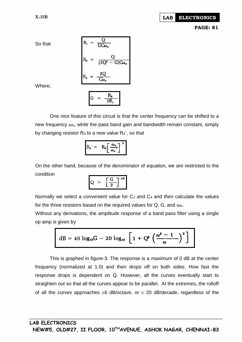
X-15B PAGE: 81
LAB ELECTRONICS
NEW#5, OLD#27, II FLOOR, 10THAVENUE, ASHOK NAGAR, CHENNAI-83
LAB ELECTRONICS
So that
Where,
One nice feature of this circuit is that the center frequency can be shifted to a
new frequency ωo, while the pass band gain and bandwidth remain constant, simply
by changing resistor R3 to a new value R3΄, so that
On the other hand, because of the denominator of equation, we are restricted to the
condition
Normally we select a convenient value for C2 and C4 and then calculate the values
for the three resistors based on the required values for Q, G, and ωo.
Without any derivations, the amplitude response of a band pass filter using a single
op amp is given by
This is graphed in figure-3. The response is a maximum of 0 dB at the center
frequency (normalized at 1.0) and then drops off on both sides. How fast the
response drops is dependent on Q. However, all the curves eventually start to
straighten out so that all the curves appear to be parallel. At the extremes, the rolloff
of all the curves approaches 6 dB/octave, or 20 dB/decade, regardless of the

X-15B PAGE: 82
LAB ELECTRONICS
NEW#5, OLD#27, II FLOOR, 10THAVENUE, ASHOK NAGAR, CHENNAI-83
LAB ELECTRONICS
filter's Q. When the response of band pass filter approaches a rolled of 6 dB/octave,
it is termed a second order 1 pole band pass filter.
The sharpness of the band pass filter's response in the vicinity of its center
frequency depends on its Q, which in turn depends on its 3-dB bandwidth.
The 3-dB bandwidth is the difference between the upper and lower frequencies
where the amplitude response is 3 dB less than the response at the center
frequency, equation becomes
FIGURE - 3: AMPLITUDE RESPONSE OF BAND PASS FILTER USING A SINGLE OP
AMP
X-15B PAGE: 83
LAB ELECTRONICS
NEW#5, OLD#27, II FLOOR, 10THAVENUE, ASHOK NAGAR, CHENNAI-83
LAB ELECTRONICS
STEP-BY-STEP PROCEDURE:
1. Study the circuit diagram given for band pass filter on the front panel of the
trainer.
2. Switch on the trainer.
3. Connect a sine wave oscillator from the AF sine output at the input and adjust the
amplitude to 2V p-p and frequency to 200 Hz.
4. Measure the output voltage (v0).
5. Vary the frequency of the generator in steps of 100Hz and note the output
voltage at each step.
6. Measure the frequency (fC) at which the amplitude is maximum. Now determine
the upper and lower 3dB frequencies (fH & fL) by measuring the frequencies at
which the amplitude response drops by 0.707 times the maximum voltage gain
which is the 3dB decrease.
7. Calculate the following factors - Frequency Gain, Upper 3dB Frequency, Lower
3dB Frequency, Bandwidth, Center Frequency
fO
Quality Factor (Q) = ----------
fH - fL
8. Plot the graph between output voltage versus frequency.

X-15B PAGE: 84
LAB ELECTRONICS
NEW#5, OLD#27, II FLOOR, 10THAVENUE, ASHOK NAGAR, CHENNAI-83
LAB ELECTRONICS
WIRING DIAGRAM
ACTIVE BAND PASS FILTER
INDICATES THE PATCHING CONNECTIONS