
Assad_thesis.pdf - nanoHUB
174
COMPUTATIONAL AND EXPERIMENTAL STUDY OF TRANSPORT IN ADVANCED SILICON DEVICES A Thesis Submitted to the Faculty of Purdue University by Farzin Assad In Partial Fulfillment of the Requirements for the Degree of Doctor of Philosophy December 1999
-
Upload
khangminh22 -
Category
Documents
-
view
2 -
download
0
Transcript of Assad_thesis.pdf - nanoHUB
COMPUTATIONAL AND EXPERIMENTAL STUDY OF TRANSPORT
IN ADVANCED SILICON DEVICES
A Thesis
Submitted to the Faculty
of
Purdue University
by
Farzin Assad
In Partial Fulfillment of the
Requirements for the Degree
of
Doctor of Philosophy
December 1999
ii
ACKNOWLEDGMENTS
This thesis would not have materialized, if it had not been for the contribution of
the following individuals. Professor Mark Lundstrom supervised this project from start
to finish, actively lending out his expertise on its direction. In addition, he was never
hesitant to get involved with the "details" as well as the big issues and I am grateful for
that. Professor Supriyo Datta's willingness to share his knowledge as well as his ability
to resolve the conceptual issues into simple logic, has benefited this work in a visible
way. I would like to thank Professors Mike Melloch and David Nolte not just for
agreeing to be on my committee, but for expressing their insightful critique at the
Preliminary Review of this undertaking. Mr. Zhibin Ren's hard work and intelligence
during the last phases of this project was instrumental to its fruition. A special note of
thanks goes to Dr. Peter Bendix of LSI Logic Inc. who willingly shared his expertise on
device characterization as well as providing devices for taking experimental data. There
were many other individuals who have influenced me over the years, and I thank them for
their contribution, however indirect, to this thesis.
iii
TABLE OF CONTENTS
Page
LIST OF TABLES............................................................................................................. vi
LIST OF FIGURES .......................................................................................................... vii
ABSTRACT..................................................................................................................... xiii
CHAPTER 1. INTRODUCTION
1.0 Motivation............................................................................................................ 11.1 Thesis Objectives ................................................................................................. 21.2 Review of Transport Models ............................................................................... 21.3 A generic transport model for transistors............................................................. 61.4 Thesis Overview .................................................................................................. 9
CHAPTER 2. AN ACCELERATION SCHEME TO THE SOLUTION OF THEBOLTZMANN TRANSPORT EQUATION IN ONE DIMENSION
2.0 Chapter in Brief.................................................................................................. 112.1 Introduction........................................................................................................ 112.2 One-Flux Treatment of Carrier Transport.......................................................... 122.3 M-flux Treatment of Carrier Transport............................................................. 192.4 Acceleration of M-flux Solution....................................................................... 21
2.4.1 Extracting the one-flux scattering matrix ....................................................... 242.4.2 Acceleration algorithm.................................................................................... 25
2.5 Discussion and Results ..................................................................................... 262.6 Conclusions........................................................................................................ 31
CHAPTER 3. AN ASSESSMENT OF SIMULATION APPROACHES FOR SILICONBIPOLAR TRANSISTORS: DRIFT-DIFFUSION AND BEYOND
3.0 Chapter in Brief.................................................................................................. 313.1 Introduction........................................................................................................ 31
iv
3.2 Methodology ...................................................................................................... 34Page
3.2.1. Quantities Compared..................................................................................... 343.2.2. Devices Compared ........................................................................................ 353.2.3. Simulation Approaches Compared................................................................ 373.2.4 Physical Parameters....................................................................................... 38
3.3 Results............................................................................................................... 403.3.1 Device (a): ∪peakTf , 25 Ghz........................................................................... 403.3.2 Device (b): ∪peakTf , 55 Ghz.......................................................................... 41
3.4 Discussion .......................................................................................................... 423.5 Conclusions........................................................................................................ 46
CHAPTER 4. THE DRIFT-DIFFUSION EQIUATION REVISITED
4.0 Chapter in Brief.................................................................................................. 474.1 Introduction....................................................................................................... 474.2 Scattering Theory............................................................................................... 504.3 One-Flux Theory and the Drift-Diffusion Equation .......................................... 554.4 M-Flux Theory and the Drift-Diffusion Equation ............................................. 584.5 Applications ....................................................................................................... 59
4.5.1 Low-Field Transport in Bulk Si...................................................................... 604.5.2 Thin Base Transport in Si ............................................................................... 614.5.3 Transport Over a Barrier................................................................................. 644.5.4 High-field and Off-Equilibrium Transport ..................................................... 73
4.6 Discussion .......................................................................................................... 764.7 Summary and Conclusions ................................................................................ 79
CHAPTER 5. ON THE PERFORMANCE LIMITS FOR SI MOSFETS: ATHEORETICAL STUDY
5.0 Chapter in brief .................................................................................................. 815.1. Introduction........................................................................................................ 815.2. Theory ................................................................................................................ 835.3. Results................................................................................................................ 875.4. Discussion ........................................................................................................ 1045.5. Summary .......................................................................................................... 107
CHAPTER 6. A STUDY OF THE PERFORMANCE LIMITS OF CMOSTECHNOLOGY BASED ON SIMULATION AND EXPERIMENT
6.1 Introduction...................................................................................................... 1096.2 Review of Scattering Theory of the MOSFET ................................................ 110
v
6.3 Results.............................................................................................................. 1156.3.1 Injection Velocity.......................................................................................... 115
Page
6.3.2 Electrical Characterization of a 0.35 µm Technology .................................. 1196.4 Discussion ........................................................................................................ 1226.4.1 Scattering theory vs. measurements................................................................. 1226.4.2 Implications for the ITRS ................................................................................ 1236.4.3 P-channel vs. N-channel MOSFET.................................................................. 1296.5 Summary .......................................................................................................... 129
CHAPTER 7. SUMMARY AND FUTRE WORK
7.1 Summary .......................................................................................................... 1317.2 Future work...................................................................................................... 133
REFERENCES ............................................................................................................... 135
APPENDIX A................................................................................................................. 145
APPENDIX B ................................................................................................................. 147
APPENDIX C ................................................................................................................. 151
APPENDIX D................................................................................................................. 157
vi
LIST OF TABLES
Table Page
Table 3.1 Examined terminal characteristics along with a list ofextracted parameters 35
Table 3.2 Caughey-Thomas mobility parameters for electrons. Theseparameters reproduce the results obtained for scatteringmatrix simulations of electron transport in bulk silicon. 39
Table 3.3 Summary of results for device (a). A 1 µm ↔1µm emitterarea is assumed. 40
Table 3.4 Summary of results for device (b). A 1 µm ↔1µm emitterarea is assumed. 42
Table 5.1 Computed performance of the model ballistic device at300K. The threshold voltage was ∪0.4 V, the gate overdrivewas VGS − VT( ) ≈ 0.8 V and the drain voltage was 1.0V. 99
Table 5.2 Computed performance of the model ballistic device at 77K.The threshold voltage was ∪0.5 V and the gate overdrivewas VGS − VT( ) ≈ 0.8 . 104
Table 6.1 Effective mass values used in the self-consistent SchrödingerPoisson calculations 116
vii
LIST OF FIGURES
Figure Page
Figure 1.1. A simple, generic model for a transistor showing a source ofcarriers, a collector of carriers, and a control point in between. Thevertical axis is the conduction band energy. 7
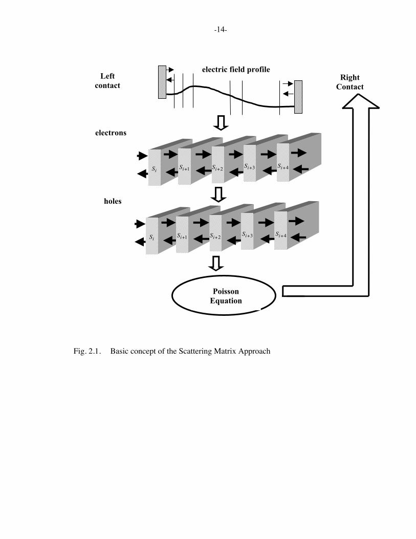
Figure 2.1. Basic concept of the Scattering Matrix Approach 14
Figure 2.2. Labeling of slabs and fluxes in one dimension 15
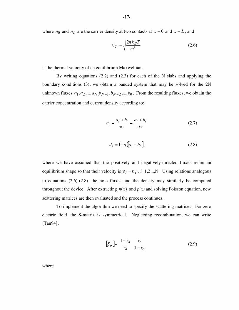
Figure 2.3. Concept of splitting 15
Figure 2.4. Doping profile for the bipolar transistor as a function of distance.Also shown is the electric field profile obtained at a bias ofVBE=VCE=0.8 (V). 21
Figure 2.5. L1 norm of the change in carrier concentration Δn/n and carrierenergy Δu/u (normalized) as a function of iteration. 22
Figure 2.6. Residual as a function of iteration for the bipolar transistor ofFigure 2.4. 28
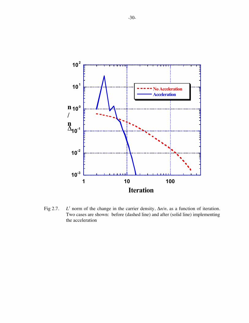
Fig 2.7. L1 norm of the change in carrier density, Δn/n, as a function ofiteration. Two cases are shown: before (dashed line) and after(solid line) implementing the acceleration 29
Figure 3.1 Doping profile for the ∪peakTf , 55 Ghz device vs. depth. 36
Figure 3.2 Gain-bandwidth product vs. collector current for the ∪Tf 55 Ghzdevice. The solid black lines correspond to Drift-Diffusion, whilethe gray dashed lines correspond to Energy Transport. The
viii
symbols refer to Scattering Matrix simulations. Both β and Tfare shown in the figure. 44
Figure Page
Figure 3.3 Velocity vs. position with the electric field superposed throughoutthe device and (inset) in the base region. The solid black linescorrespond to Drift-Diffusion, while the long-dashed gray linescorrespond to Energy Transport. The symbols refer to ScatteringMatrix simulations. In addition, the electric field is shown usingshort dashed lines, corresponding to 80.VV CEBE == (V). 45
Figure 4.1 Resolution of carriers into right- and left-directed fluxes andillustration of back-scattering from a region of thickness, dz. 52
Figure 4.2 Illustration of how the carrier distribution is divided into positiveand negative halves. (a) the one-flux approach with an assumedMaxwellian for each half and (b) the M-flux approach whichrepresents each half of the distribution by M bins in momentumspace. For the positive flux, a bin is a region located around (px,py, +pz) and for the negative flux, around (px, py, -pz) 54
Figure 4.3 A plot of the average velocities for the positively- and negatively-directed electron velocities vs. electric field for electron transportin bulk Si. Also shown is the overall average carrier velocity. 61
Figure 4.5 Average electron velocity vs. position across a thin, field-freeregion as computed by M-flux scattering matrix simulations. Alsoplotted are the average velocities for the positively- andnegatively-directed electron velocities. (a) W = 1000 Å and (b) W= 250 Å. (At z/W=1.0, υ- is undefined because the absorbingcontact makes n- zero there. 63
Figure 4.6 The carrier density profiles, n(z) vs. z and the fraction of carriers inthe positive half of the distribution, n+(z)/n(z) vs. z. (a) W = 1000Å and (b) W = 250 Å. 65
Figure 4.7 The rigorous mobility as defined in eqn. (4.7) vs. position. Thecorresponding low-field mobility for bulk Si doped at 1018 cm-3
as determined by similar M-flux simulations is 427 cm2/Vs. (a) W= 1000 Å and (b) W = 250 Å. 66
ix
Figure Page
Figure 4.8 Sketch of the energy band diagram for a simple forward biasedmetal/n-Si junction. The Si is doped at 1↔1016 cm-3, the barrierheight is ϕBn = 0.70 V, Vbi = 0.492 , and the applied bias is 0.40V.Under these conditions, the band bending in the semiconductor is ≈4 kBT/q. The metal-semiconductor interface is taken to beabsorbing. 68
Figure 4.9 Average electron velocity vs. position across the forward-biasedbarrier as computed by M-flux scattering matrix simulations. Alsoplotted are the average velocities for the positively- andnegatively-directed electron velocities. The metal-semiconductorcontact is at the right, as in Figure 4.8. 68
Figure 4.10 The carrier density profiles, n(z) vs. z and the fraction of carriers inthe positive half of the distribution, n+(z)/n(z) vs. z for theforward-biased barrier. 71
Figure 4.11 The electric field vs. position and the effective (thermoelectric)field as defined by eqn. (4.33) for the forward-biased barrier. 71
Figure 4.12 The back-scattering parameters (r ∪ξ Δz and ʹ′ r ∪ ʹ′ ξ Δz ) vs.position for the forward-biased barrier. The parameters, r and r',are evaluated rigorously from M-flux simulations. Also shown arethe analytical expressions for r and r' as suggested by Lundstromand Tanaka [Lun95]. 72
Figure 4.13 The rigorous mobility vs. position and the Einstein relation (D/µ)vs. position within the forward-biased barrier. The mobility anddiffusion coefficient were obtained from M-flux scattering matrixsimulations. Also shown is the field-dependent mobilitydeveloped in [Lun95]. 72
Figure 4.14 Average electron velocity vs. position across a low-high-low fieldstructure as computed by non-self-consistent M-flux scatteringmatrix simulations. Also plotted are the average velocities for thepositively- and negatively-directed electron velocities. Thestructure consists of a 0.2 µm region with E = 103 V/cm followedby a 0.4 µm region with E = 105 V/cm then by another 0.2 µmregion with E = 103 V/cm. 74
x
Figure Page
Figure 4.15 The fraction of carriers in the positive half of the distribution,n+(z)/n(z) vs. z for the low-high-low field structure. 74
Figure 4.16 The rigorous mobility vs. position and the Einstein relation (D/µ)vs. position within the low-high-low field structure. The mobilityand diffusion coefficient were obtained from M-flux scatteringmatrix simulations using eqn. (4.8). 75
Figure 4.17 The energy gradient field vs. position and the within the low-high-low field structure. Also shown is the actual electric field vs.position. 75
Figure 4.18 An energy band diagram for a bipolar transistor with the current-limiting region, the base, indicated. The diagram can also beviewed as the energy band diagram from the source to drain alongthe top surface of a MOSFET. In this case, the current-limitingregion is the low-field region near the beginning of the channel. 77
Figure 5.1 The assumed geometry of the ballistic MOSFET. Current flow isalong the x-direction, the confinement potential varies in the y-direction, and the width of the device is along the z-direction. 84
Figure 5.2 The inversion layer density vs. the gate voltage as obtained by aself-consistent solution to the Schrödinger and Poisson equations.Two cases are shown: (i) the equilibrium solution when both +kxand –kx states occupied, solid lines and (ii) the ballistic solution forwhich only the +kx states are occupied, dashed lines. Solutions forboth a metal gate and for a polysilicon gate are shown. Forcomparison, a classical calculation for a metal gate transistor withboth +kx and –kx states occupied is also shown (dotted line). 88
Figure 5.3 The common source characteristics of metal gate (dotted lines) andpolysilicon gate (dashed lines) ballistic MOSFETs. 89
Figure 5.4 The common source characteristics of a metal gate ballisticMOSFET showing the effect of DIBL. Without DIBL (solid line)and with an assumed DIBL of 100 mV/V (dashed line). 90
Figure 5.5 ID vs. VGS for the ballistic MOSFET at a drain voltage of 1.0 V. 93
xi
Figure 5.6 The ratios, nS1 nS and ID1 ID vs. VGS for the metal gate, ballisticMOSFET. 94
Figure Page
Figure 5.7 The ballistic injection velocity at the source vs. gate voltage, VGS,for the metal gate, ballistic MOSFET. Also shown is the injectionvelocity for the first sub-band alone. 95
Figure 5.8 The ratio of the degenerate limit velocity to the actual injectionvelocity for electrons in the lowest sub-band vs. VGS. 96
Figure 5.9 The transconductance vs. VGS for the ballistic MOSFETs (solidlines). Also shown, is the product of Ceff υinj (dashed lines). Thetransconductance is seen to be higher than Ceff υinj for VGS > 0.6V. 98
Figure 5.10 The ratio of transconductance divided by drain current, vs. VGS forthe metal gate, ballistic MOSFET 101
Figure 5.11 The ratio of the intrinsic transconductance, ˆ g m , to the drain currentvs. surface potential. 102
Figure 5.12 The intrinsic drain to source resistance, Ri, vs. VGS for the metalgate, ballistic MOSFET. 103
Figure 5.13 The injection velocity vs. gate voltage for the model device. Solidline, T = 300K. Dashed line, T = 77K. 106
Figure 6.1. Illustration of a one-dimensional band diagram for a MOSFETbiased in saturation 111
Figure 6.2. Simulated lateral field as a function of lateral distance along ahorizontal cut through the depletion layer for (a) long- and short-channel devices and (b) for low and high drain bias [Ngu84]. 113
Figure 6.3. The computed channel injection velocity vs. inversion layerdensity. Two kinds of channel profiles are examined: a uniformchannel profile (solid lines) and a retrograde profile (circles),shown for 250 nm and 50 nm generation technologies. Results fora uniform profile p-channel 50nm technology are also shown. 117
Figure 6.4 The measured IDS vs. VDS characteristic of an Lpoly = 0.30 µm n-MOSFET at VGS = 3.0V (solid line). Also shown is the upper-limit
xii
characteristic for this device with (dotted line) and without (dashedline) the measured series resistance included. 118
Figure Page
Figure 6.5. The extracted channel back-scattering coefficient for the 0.30micron n-MOSFET vs. gate voltage for low VDS (dashed line) andfor high VDS (solid line). 121
xiii
Figure 6.6. The measured channel resistance vs. gate voltage for the 0.30micron n-MOSFET with series resistance effects removed (solidline). Also shown is the fundamental channel resistance (dashedline) 125
Figure 6.7 Comparison of the scattering model (solid line) with IDS vs. VDS
characteristics of the n-MOSFET reported in [Tau98] as obtainedby Monte Carlo at VGS=1.1 (V). 126
Fig 6.8. Projected ballistic current vs. time for several future technologiesas obtained from the NTRS-97. The circles are the calculated on-current with no parasitic resistance and the triangles include aparasitic resistance equal to 10% VDD/Ion. Also shown (dashed line)is the target on-current. 127
Figure 6.9. Comparison of the calculated ballistic current for a n-channel(dashed line) and p-channel (solid line) device at the 50 nm nodeof the NTRS-97. 128
Figure 6.10. Inversion density and injection velocity as computed for the n-channel (solid line), and p-channel (dashed line) device at the 50nm node of the NTRS. 128
Figure D.1. Estimated mean-free path (solid line) vs. gate voltage. Thisestimate was obtained using mobility data (dotted line) measuredon large area MOSFETs. 159
xiii
ABSTRACT
Assad, Farzin. Ph. D., Purdue University, May 2000. Computational and ExperimentalStudy of Transport in Advanced Silicon Devices. Major Professor: Mark S. Lundstrom.
In this thesis, we study electron transport in advanced silicon devices by focusing
on the two most important classes of devices: the bipolar junction transistor (BJT) and the
MOSFET. In regards to the BJT, we will compare and assess the solutions of a
physically detailed microscopic model to standard models. In so doing, we will explain
why the standard Drift-Diffusion model has been so prevalent and speculate about its
prospect in the future. The physically detailed solutions were obtained using a
deterministic Boltzmann solver which incorporates an effective acceleration technique, in
order to speed up the solution time.
In connection with the MOSFET, we present a new theory, which calculates the
upper-limit performance for a given CMOS technology. Using this theory, we assess the
performance of a present technology by using experimental data and make predictions
about the performance of future technologies. Finally, we will speculate on whether or
not CMOS technology will be viable in the future.
-1-
1. INTRODUCTION
1.0 Motivation
By the year 2012, the number of transistors on a chip is expected to be around 180
million, requiring that the feature size of an individual transistor to be shrunk down to 50
nm [SIA97]. As the number of transistors grows, the supply voltages must be reduced to
maintain acceptable powers, but the power dissipation will substantially increase,
nonetheless. For instance, according to the National Technology Roadmap for
Semiconductors, a report published by a leading industry group [SIA97], power
dissipation is going to show over a four-fold increase, while the individual transistors
have to be made more than three times smaller. By way of scaling the transistor, CMOS
technology has been able to meet these stringent power-density requirements, but it
remains to be seen whether the scaling of CMOS could continue to be viable in the
future.
To be sure, there are many obstacles related to not only the design but also the
processing of the “nanoscaled” devices of the future. A nanoscale MOSFET, among
other things, incorporates an ultra thin gate oxide, shallow junctions (extensions) at the
source and drain sides, and finally good ohmic contacts to source and drain. It is well
known that the gate oxide could not be scaled below a critical thickness (~ 2.0 nm)
without the tunneling current becoming excessive [Ran96]. The junctions at the source
and drain would have to be extremely abrupt and at the same time heavily doped, and it is
not clear whether or not such abrupt profiles could at all be fabricated [Won99]. In
addition, the parasitic resistance associated with ohmic contacts, which does not scale
relative to the actual device resistance, may eventually limit the on-current performance
[Tho98]. Some of the device-related issues relevant to the nanoscale MOSFET include
-2-
the random fluctuation of device parameters (such as the threshold voltage) due to small-
size effects [Ase99], controlling tunneling current through the gate oxide [Ran96], and
finally maintaining acceptable on-current levels [Asa99].
Tackling these issues requires a thorough understanding of the device physics and
many of these issues are still being hotly debated in the device engineering community.
In particular, modeling of the on-current is a key problem and, indeed, it has attracted a
lot of attention in the past few years [Aro93]. Modeling the response of carriers confined
in a channel with nanoscale dimensions while responding to a rapidly changing electric
field has pushed transport models to their limits. Many alternative models have been
offered, ranging from simple classical to more sophisticated solutions incorporating off-
equilibrium transport, all the way to ballistic and even quantum transport. Modeling
transport in advanced devices is a problem that, in view of its practical importance,
deserves a lot of attention.
1.1 Thesis Objectives
My objectives in this thesis are to: (i) develop a clear physical understanding of
carrier transport in nanoscale transistors, (ii) establish the upper performance limits of the
MOSFET and (iii) to assess the performance of present day devices against their upper
limits.
The first objective involved extending and enhancing the capabilities of a
Boltzmann solver in 1D for silicon devices. The second, involved developing a new
theory for the ballistic MOSFET, and the third objective, called for electrical
characterization of n-channel MOSFET technologies.
1.2 Review of Transport Models
Electron transport in semiconductors can be modeled at various levels of
sophistication ranging from purely classical treatments, appropriate for devices with large
feature lengths, all the way down to quantum treatments appropriate for ultra-small
devices [Lun90]. Semi-classical transport theory has served device physicists for almost
half a century, providing the conceptual framework with which everyday integrated
-3-
circuit (IC) design is guided. In this section, we will briefly discuss the three modeling
paradigms of semi-classical transport that are in popular use.
Boltzmann Transport Equation:
The Boltzmann Transport Equation (BTE) provides the most detailed description
of transport in semi-classical theory [Lun90]. According to this description, electrons are
treated as classical particles, which unlike quantum particles, do not obey the uncertainty
principle and are allowed to have a definite momentum and a definite position at the
same time. On the other hand, their interaction with the scatterers, such as phonons or
impurity ions, is accounted for quantum mechanically by a simple application of Fermi’s
golden rule. Accordingly, the BTE is valid as long as the device dimension exceeds the
DeBroglie wavelength given by
Tkmh B/2/ *=λ , (1.1)
where *m is the effective mass for electrons (or holes). The primary unknown in the
BTE is the electron distribution function ( )tprf ,, which is taken to be a function of
position rr as well as momentum pr obeying
.colpr t
ffFftf
ƒ
ƒ= 〈+ 〈+
ƒ
ƒυ (1.2)
In equation (1.2), υ is the group velocity and F is the force due to the electric field.
Being an integro-differential equation in six-dimensions, three corresponding to position
and three to momentum in steady state, the BTE is an exceedingly difficult equation to
solve. The voluminous effort made to solve the BTE in the past has concentrated on
approximate/analytical treatments as well as numerical approaches [McK66, Jac83]. To
solve the BTE analytically, certain simplifying assumptions are typically introduced (e.g.,
relaxation time approximation), however, even in the simplest of the cases, it is still
difficult to solve. On the other hand, a handful of numerical techniques are available, the
-4-
most popular of which is the Monte-Carlo method [Jac83] providing a stochastic solution
to the BTE. Among the deterministic methods is the scattering matrix approach (SMA)
[Ala93-1, Das90], which is routinely used in this work.
Drift-Diffusion:
The Drift-Diffusion (DD) model is still the most prevalent transport model.
Because of its simplicity and robustness, it has been the backbone of device modeling for
over forty years. In the DD model, the carriers are thought of as classical particles
capable of drifting in an electric field and diffusing in a concentration gradient according
to:
nqDFnqJ rnnn +=rr
µ (1.3)
where nD is the diffusion coefficient and nµ is the carrier mobility. Furthermore, the
mobility may be written in terms of the momentum relation time mτ as:
*mq m
nτ
µ = . (1.4)
Mobility is a key parameter in this model: once it is known the well known
Einstein's relation may be used to specify the diffusion coefficient, but before doing so,
we must specify the momentum relaxation time. In theory, in order to specify mτ , one
needs to solve for the distribution function, which would require solving the BTE.
Alternatively, one may circumvent solving the BTE and treat mobility as a material
parameter which depends on the local doping density and local electric field. This
assumption is quite reasonable as long as the electric field changes slowly in the active
region of the device. In small devices, more often than not, the electric field changes
very rapidly and therefore nµ and nD may not be treated as local functions of the
electric field, as they are in large devices. Often times a given mobility model which

-5-
produces reasonable results for one technology, needs to be adjusted in order to match the
measured characteristics of another technology.
Hydrodynamic Model:
In the Drift-Diffusion model one treats mobility as a device parameter, which is
determined by the local electric field, but the dependence of this parameter on the local
electric field could vary from one device to another. Another important assumption in
the DD model, is that the carrier energy is assumed not to exceed the thermal energy (i.e.,
LBTk2/3 ). The Hydrodynamic model (HD) attempts to remove these assumptions by
allowing the carrier energy to exceed the thermal energy in the “hot” regions of the
device [Che92], while in the equations for total current the energy flow is accounted for
as well.
Energy flow in semiconductors may be modeled by the same means as the
particle flow in the DD model. One possibility, among many other implementations in
common use, is to write the energy flow WFr
as [Lun90]
)(2 nRFF EEW −−= µµrr
(1.4)
where R is a tensor quantity related to the fourth moment of the BTE, and Eµ is the
energy mobility which, much like nµ in equation (1.3), may be written in terms of the
energy relaxation time. In most implementations of the Hydrodynamic model, these
parameters are again device dependent parameters that need to be derived from external
means. In this respect, the HD model is very similar to DD, as certain model parameters
need to be specified at the outset, which in practice depends on the technology at hand
[Cho95]. One advantage of the HD over the DD model has been its application to the hot
electron effect, where the heating of the electrons degrades the device performance.

-6-
1.3 A generic transport model for transistors
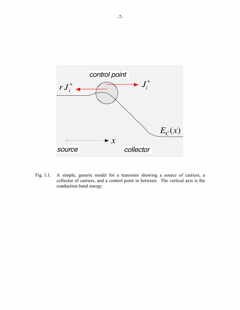
Fig. 1.1 shows a simple conceptual model which captures the essentials of
transport occurring in a transistor. Carriers are injected into the device from the left
contact, and after traversing the channel region, are collected at the right contact.
Interestingly, the simple model shown in Fig. 1.1 is applicable to a bipolar transistor as
well as a MOSFET. In case of a bipolar transistor, the left and right contacts are the
emitter and the collector, but in case of a MOSFET, they are the source and drain
respectively. The magnitude of the current through the device depends on the voltage
difference between the right and left contacts. The carriers injected from the source, first
drift and diffuse against a barrier, which separates the source (emitter) contact from the
channel region. The height of the barrier controls the carrier flux entering the channel in
both cases, but the mechanism to control the height is different: in a bipolar transistor, the
height is controlled by the base-emitter voltage, while in a MOSFET the height is
controlled by the gate voltage. Once the carriers overcome the barrier, they traverse a
low field region adjacent to the barrier at the beginning of the channel (the shaded circle
in the figure). In a bipolar transistor, this low field region consists of the quasi-neutral
base, but in a MOSFET this is the critical region that controls the slope of the energy
band at the very beginning of the channel and consequently the on-current [Lun97].
Once the carriers have traversed this critical region, they enter a high field region where
they are accelerated at a large rate and get swept away towards the drain and are
collected. As the critical dimension of devices are shrunk, carrier transport begins to be
complicated by the complex effects occurring in different regions of the device. In the
remainder of this section, we will examine how electron transport is modeled in each of
these regions using the conventional approach.
The modeling of transport in a barrier has historically posed as one of the more
challenging problems, but in light of the scaling of devices, this problem takes on a more
important role. As the intrinsic region of the device is scaled to smaller dimensions, the
length of the barrier becomes a larger fraction of the total length of the active region, and
therefore, the barrier plays a more visible role in controlling the current.
-7-
Ji+
r Ji+
source collector
control point
EC(x)x
Fig. 1.1. A simple, generic model for a transistor showing a source of carriers, acollector of carriers, and a control point in between. The vertical axis is theconduction band energy.
-8-
Transport in a barrier is conventionally treated using the drift-diffusion equation,
but there remain questionable assumptions when the standard theory is applied to a
barrier [Sze81]. In a barrier, carriers have to diffuse through large concentration
gradients, typically on the order of ~1018 cm-3, which makes the use of the simple drift-
diffusion theory questionable. As the carriers diffuse through such large gradients, they
may have to acquire an exceedingly large velocity, well in excess of the thermal velocity,
but the conventional theory does not allow any limits on the maximum velocity attained
by the carriers. In addition, the use of the low field as opposed to the high field mobility
is another issue that requires a closer examination.
Transport through a thin low field region may be regarded as a diffusion problem
so long as the width of the low field region is larger than the mean-free-path for
electrons. In modern bipolar transistors, the width of the low-field base region may
become very small, small enough to be comparable to a mean-free-path, and therefore the
carriers may traverse the base without substantial scattering (i.e., quasi-ballistic). In this
situation, the use of a simple diffusive transport law, which is the common practice in
modeling diffusion in the base, should be reexamined.
In the transistor model of Fig. 1.1, following the low field region, carriers are
collected through a high field region, where the electric field rapidly increases on a short
length. Modeling transport through rapidly changing electric field profiles is a difficult
problem, as the so-called off-equilibrium effects should be accounted for. Excellent
articles are available [Con85] in which this complicated effect, precipitated by abrupt
changes in electric field both in time and/or space, is studied in painstaking detail.
However, as far as the I-V characteristics of the device is concerned, it is the first few
qTkB / of voltage drop right at the beginning of this high field region that determines the
current [Lun97]. This provides an immense simplification for modeling the on-current
which we will exploit later.
So far we have attempted to present a unifying picture of transport which is valid
for both bipolar and MOS devices. The MOS devices, however, are specially important,
not only from technological but also from a commercial view point. More than 80% of
revenues of the semiconductor electronics is generated by MOS devices and this trend is
expected to continue or even accelerate in the next century [Won99]. The MOS devices
-9-
of the new millennium are expected to have active channel lengths on the order of, or
smaller, than a mean-free path. The dominant mode of transport in the nano-scale
devices of the future is ballistic transport, whereby the carriers will undergo little
scattering if any as they cross the channel. Ballistic transport is a subject that has
received a lot of attention in the past, but not in the context of MOS devices.
1.4 Thesis Overview
In the foregoing discussion we identified key issues that are relevant to the
operation of a modern transistor and briefly discussed the standard methods used in
analyzing them. Our goal in this thesis is to reexamine these issues, but instead of taking
the conventional approach, we will take a more microscopic approach, appealing to the
solutions of the Boltzmann Transport Equation. The method we use to solve the BTE in
this work is the scattering matrix approach [Ala93-1, Das90], which is a deterministic
way to solve this complicated differential equation. We will begin this thesis in Chapter
2 with an overview of the method and in so doing we will present a useful acceleration
technique which speeds up the convergence by more than a factor of ten!
Following the discussion of the method of simulating carrier transport, in Chapter
3 we will delve into the physics of transport in sub-micron bipolar devices and show how
the software tool developed in Chapter 2 is applied to analyzing bipolar transistors. We
will have an opportunity to revisit the transport problem across a low-field base region in
the context of bipolar transistors and also will examine whether or not current approaches
used for simulating bipolar transistors are accurate. We will use SMA simulations to
establish the accuracy of one model vs. another.
In Chapter 4 we will take a look at other transport problems, but instead of
simulating devices, we will choose model problems and examine them starting from the
BTE. In particular, we will discuss the transport issues arising in a barrier as well as high
field regions that exist in the collectors (drains) of transistors. The Drift-Diffusion model
has been a dominant force in predicting the behavior of devices for the past four decades.
We will explain why it has been successful and under what conditions it will fail.
-10-
We will devote the last two chapters to the transport in bulk MOSFETs. In
Chapter 5, we present a theory which determines the ballistic current in a MOS device,
considered to be the maximum on-current obtainable from a given technology. As one
technology is supplanted by a more advanced one having a smaller feature length, the on-
current performance improves but there is a finite limit to the benefits reaped from these
scaling efforts. This theory reveals, in a simple way, the best performance, (i.e.,
maximum on-current) that may be obtained from a given technology. Another important
revelation of the theory is that, in addition to a maximum limit to the on-current, there is
similarly a minimum limit to the resistance of the channel, which may not be surpassed.
Conventional theory assumes that the channel resistance will shrink to zero, however in
the limit of L0, there is finite resistance, identifiable as the fundamental limit for
channel resistance.
In Chapter 6 we will apply the ballistic MOS theory developed in Chapter 5 to
experimental data, in order to show how to assess the performance of a given technology
and indicate how close a given technology operates to its upper limit performance.
Having assessed a current technology, we will then look ahead down the roadmap and
based on the current performance, will project how close future technologies will
compare against their best performance.
Finally, we will summarize the key results of this investigation and will identify
issues for future investigation.

-11-
2. AN ACCELERATION SCHEME FOR THE SOLUTION OFTHE BOLTZMANN TRANSPORT EQUATION IN ONE-
DIMENSION
2.0 Chapter in Brief
In the first part of this chapter, we describe a method to solve the Boltzmann
Transport Equation (BTE) in one-dimension. The solution method is based on the
scattering matrix approach, which unlike the stochastical methods such as Monte Carlo,
provides a deterministic solution, free from the statistical noise associated with the
stochastic techniques. The main drawback of the method, however, is that it takes a long
time for the solution to converge. To remedy this problem, we propose and demonstrate
an acceleration algorithm which significantly reduces the convergence time. The
acceleration algorithm discussed plays a central role in the following chapter, where we
will extensively use the software tool developed in this chapter to explore transport in
sub-micron transistors.
2.1 Introduction
With the continuing advances in silicon device technology, physically detailed
simulation approaches such as Monte Carlo and deterministic solutions of the Boltzmann
equation [Fis88, Bud94, Lin92, Gnu93, Das90] are finding increasing applications. As a
deterministic method, the scattering matrix approach (SMA) makes use of pre-computed
Monte-Carlo simulations to provide either stochastic or deterministic solutions [Hus94].
The SMA solves for a very large number of fluxes in a discretized position-momentum
space. For one dimension, in space using simple spherical non-parabolic energy bands,
the fluxes are typically discretized into 200-400 bins in momentum space and perhaps
-12-
100 slabs in position space. The resulting number of fluxes is between 40,000 and
120,000. Full band scattering matrix simulations have also been demonstrated [Hus94].
For the simple, rectangular bin discretization of momentum space, the number of bins is
44,478 resulting in almost nine million unknown fluxes for a typical 1D device. Because
of the large number of unknown fluxes, iterative techniques are typically employed to
solve for the unknowns. To date, reported scattering matrix simulation have used a
simple Gauss-Seidal iteration which has well known convergence problems. In this
chapter, we introduce an effective acceleration scheme which is analogous to synthetic
diffusion acceleration[Mor93].
This chapter is organized as follows. In Section 2.2 we describe a one-flux
approach for which a direct solution of the unknown fluxes is easily accomplished.
Approximate one-flux S-matrices can be obtained analytically, but in this work we
extract one-flux S-matrices from physically-detailed M-flux solutions, which is the
generalization of the one-flux approach in the momentum space. The M-flux approach
and its solution by Gauss-Seidal iteration are described in Section 2.3. In Section 2.4 we
introduce the acceleration scheme which consists of extracting one-flux S-matrices from
the M-flux simulation, solving the system directly, and using the results to re-scale the
M-flux solution. Results are presented in section 2.5, and the work is summarized in
Section 2.6.
2.2 One-Flux Treatment of Carrier Transport
The one-flux approach to semiconductor transport dates back to 1957 [McK57]
and was later systematized by McKelvey, Longini, and Brodley in 1961 [McK61]. More
recently, the technique has been recast into a scattering matrix format [Tan94]. As shown
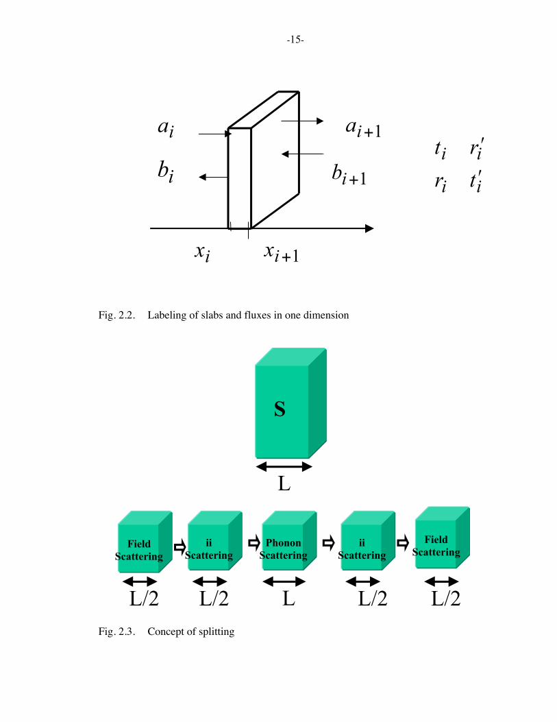
in Fig. 1, one-dimensional devices are first divided into a number of slabs thin enough so
that the electric field and doping density may be assumed constant within each slab.
Transport across individual slabs is described by a scattering matrix which relates the
incident fluxes to the emerging fluxes according to
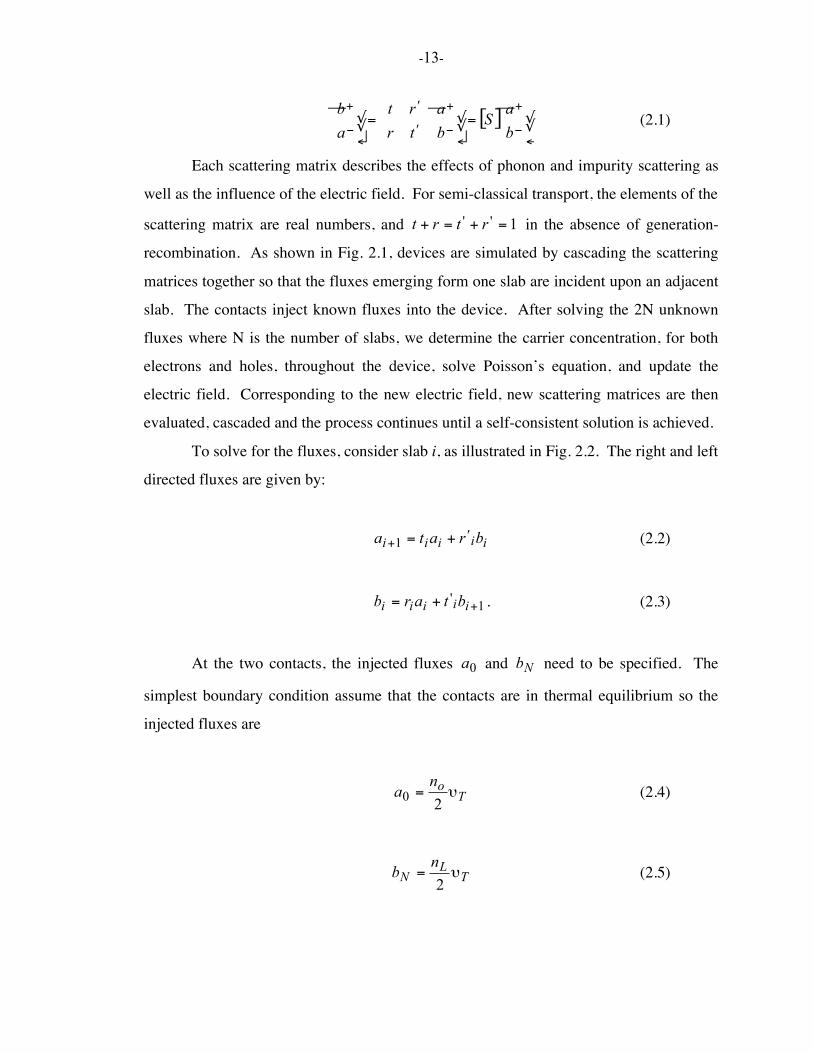
-13-
[ ] √√↵
⎯=√√
↵
⎯
=√√
↵
⎯−
+
−
+
−
+
ba
Sba
trrt
ab
'
'(2.1)
Each scattering matrix describes the effects of phonon and impurity scattering as
well as the influence of the electric field. For semi-classical transport, the elements of the
scattering matrix are real numbers, and 1'' =+=+ rtrt in the absence of generation-
recombination. As shown in Fig. 2.1, devices are simulated by cascading the scattering
matrices together so that the fluxes emerging form one slab are incident upon an adjacent
slab. The contacts inject known fluxes into the device. After solving the 2N unknown
fluxes where N is the number of slabs, we determine the carrier concentration, for both
electrons and holes, throughout the device, solve Poisson’s equation, and update the
electric field. Corresponding to the new electric field, new scattering matrices are then
evaluated, cascaded and the process continues until a self-consistent solution is achieved.
To solve for the fluxes, consider slab i, as illustrated in Fig. 2.2. The right and left
directed fluxes are given by:
ii'iii brata +=+1 (2.2)
1'++= iiiii btarb . (2.3)
At the two contacts, the injected fluxes 0a and Nb need to be specified. The
simplest boundary condition assume that the contacts are in thermal equilibrium so the
injected fluxes are
Ton
a υ20 = (2.4)
TL
Nnb υ2
= (2.5)
-14-
Fig. 2.1. Basic concept of the Scattering Matrix Approach
Leftcontact
1+iS 4+iS3+iS2+iSiS
RightContact
electric field profile
electrons
1+iS 4+iS3+iS2+iSiS
holes
PoissonEquation
-15-
Fig. 2.2. Labeling of slabs and fluxes in one dimension
Fig. 2.3. Concept of splitting
1+ib
ia
ib
1+ia
1+ix
ʹ′
ʹ′
ii
iitrrt
ix
PhononScattering
FieldScattering
iiScattering
iiScattering
FieldScattering
L/2 L/2L/2 L/2L
S
L

-16-
-17-
where 0n and Ln are the carrier density at two contacts at 0=x and Lx = , and
*B
T mTkπ
υ2
= (2.6)
is the thermal velocity of an equilibrium Maxwellian.
By writing equations (2.2) and (2.3) for each of the N slabs and applying the
boundary conditions (3), we obtain a banded system that may be solved for the 2N
unknown fluxes 021,21 ,...,,,...,, bbbaaa NNN −− . From the resulting fluxes, we obtain the
carrier concentration and current density according to:
T
ii
i
iii
baban
υυ
+=
+= (2.7)
( )[ ]iii baqJ −−= , (2.8)
where we have assumed that the positively and negatively-directed fluxes retain an
equilibrium shape so that their velocity is Ti υυ = , i=1,2,..,N. Using relations analogous
to equations (2.6)-(2.8), the hole fluxes and the density may similarly be computed
throughout the device. After extracting )(xn and p(x) and solving Poisson equation, new
scattering matrices are then evaluated and the process continues.
To implement the algorithm we need to specify the scattering matrices. For zero
electric field, the S-matrix is symmetrical. Neglecting recombination, we can write
[Tan94],
[ ]
−
−=
oo
ooo rr
rrS
11
(2.9)
where
-18-
hDr
Tno υ/21
1+
= (2.10)
with h being the thickness of the slab and nD the carrier diffusion coefficient in the bulk.
Similarly, if we neglect scattering, we can obtain an S-matrix for the electric field.
Assuming that the potential decreases across the slab, we find
[ ]
−=
Δ−
Δ−Δ 11
0/
/
TkVq
TkVqV
B
B
eeS . (2.11)
In general, we have both scattering and electric field present. To develop the S-
matrix, we split the effect of the potential drop and scattering as illustrated in Fig. 2.3.
Carriers first experience one-half of the potential drop, then traverse a field free region
where they scatter, and then they experience the effect of the second–half of the potential
drop. The corresponding S-matrix is obtained by cascading the scattering matrices,
[ ] [ ] [ ] [ ]2/2/ VoV SSSS ΔΔ = (2.12)
where stands for the scattering matrix cascading operation [Gup81]. Using (7) and (9)
in (10) we obtain:
[ ] ( )↔−−=
− Tk/Vqo BerS
2111Δ
( )
−−−−
−−−
−−
)r(e)r(ererer
oTk/VqoTk/Vqo
Tk/VqoTk/VqoBB
BB
1111
2
2
ΔΔ
ΔΔ.(2.13)
We have described the one-flux approach because it readily generalizes to M-
fluxes, which provides a solution to the Boltzmann transport equation, and because the
-19-
one-flux approach will be used to accelerate the M-flux approach. As presented above,
the one-flux approach makes a key simplifying assumption. It assume that each flux
retain an equilibrium shape. As a result, the average velocity associated with each flux is
simply Tυ , and the elements of the S-matrix, which are the average probability of their
reflection and transmission, are readily evaluated. To treat high-field and off-equilibrium
effects, we need to solve for the shape of the carrier distribution.
2.3 M-flux Treatment of Carrier Transport
The M-flux approach can be viewed as a direct generalization of the 1-flux
approach which removes the simplifying assumption about the shape of the incident flux
distributions. Each incident flux (a and b) is discretized into M bins in momentum space,
and the 2M incident and 2M emerging fluxes are related by a 2M by 2M scattering matrix
(S-matrix) with M by M sub-matrices, [ ]t , [ ]r , [ ]'t , and [ ]'r . For example, tij, is the
fraction of the flux incident in bin j which transmits across the slab and exits in bin i. The
scattering matrices could be evaluated by analytically integrating the Boltzmann equation
but in practice, we have found it more convenient to evaluate them by Monte-Carlo
simulations. To evaluate column j of the S-matrix, we inject a large number of electrons
in bin j, record the bins in which they exit, and evaluate the elements of the S-matrix by
taking the ratios of the exiting to injected particles. The M-flux approach can be shown
to provide a numerical solution to the Boltzmann equation. [Ala93-1].
Because of the large number of unknown fluxes, iterative techniques are used to
solve the M-flux equations. To date, a simple Gauss-Seidal iteration has been used. An
iteration consists of two sweeps. First, beginning at the left contact, the right-directed
fluxes are updated according to
1'11
−−− += l
iilii
li brata (2.14)

-20-
where i=1,2,…, N indexes the N-slabs and l is the iteration counter. After updating the
right-directed fluxes, we begin at the right contact and update the left-directed fluxes
according to
1'11
−−− += l
iilii
li btarb (2.15)
where i=N,N-1,…,1. Recall that in this case, the fluxes a and b are M by 1 vectors and
the transmission and reflection coefficients are M by M matrices. The process continues
until the fluxes converge.
We may illustrate these ideas by showing an example M-flux simulation. In Fig.
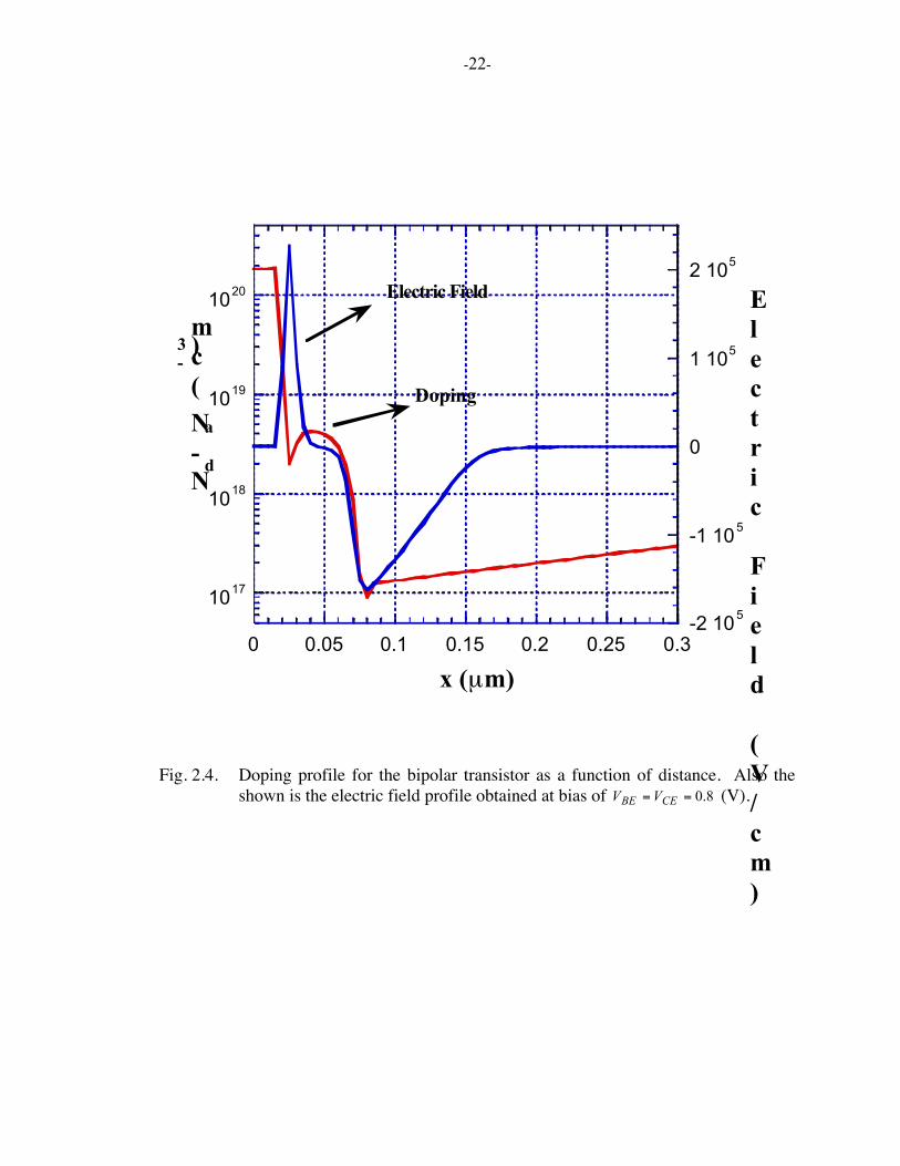
2.4 we show the doping profile of the bipolar transistor that we simulate for this work.
The device has a nominal base-width of ~500Å and is suitable for use in high speed
applications such as a microwave amplifier. Also shown in the figure is the electric field
profile obtained at a bias of 8.0== CEBE VV (V). The electric field profile would, in
general, have to be computed self-consistently but in order to make the discussion
concrete we will first discuss the non self-consistent solution. The sub-matrices [ ]t ,
[ ]r ,… necessary for the M-flux solution were evaluated using a Monte Carlo program as
described by [Jac88], where in evaluating them, the momentum space was divided into
400 modes, uniformly spaced in energy. A slab thickness of 50 Å was used.
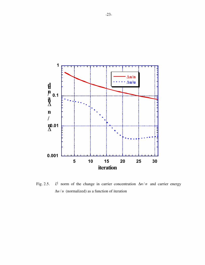
In Fig. 2.5, we show the change in the carrier density, nn /Δ , as a function of
iteration as obtained from the M-flux solution. In addition, we show the change in the
average energy, uu /Δ , where for each quantity where we plot the 1L norm as a function
of iteration. Fig. 2.5 shows that the normalized carrier density converges slowly but, in
contrast, the normalized energy converges quickly. The average carrier density and
energy are important quantities in physical device simulation and their importance in this
context could be easily understood in terms of the flux distribution in momentum space:
while the carrier density is associated with the area under the fluxes, the average energy
is associated with the shape of the fluxes. Fig. 2.5 suggests that although the area under
-21-
the distribution converges slowly, the shape of the flux distribution converges quickly.
We will use this observation to prescribe an acceleration technique in the next section.
2.4 Acceleration of M-flux Solution
In Section 2.2, we presented an analytical expression for the one-flux S-matrix,
where we assumed that the shape of the fluxes does not deviate from equilibrium. In
advanced devices, often times non-local effects become dominant, which would easily
invalidate this assumption. For instance, in a thin base transistor when the base width
becomes comparable to a mean-free path, the electrons crossing the quasi-neutral base
region may suffer very little scattering. Under such conditions, we expect the distribution
function at the top of the emitter-base barrier (i.e., at the point of injection to the base)
deviate significantly from a equilibrium. In this section, we present a prescription to
compute the one-flux S-matrix without being confined to making similar assumptions.
Using the one-flux parameters whence obtained, we propose an acceleration algorithm,
which as we will show later, would significantly enhance the convergence of the M-flux
solution itself.
-22-
Fig. 2.4. Doping profile for the bipolar transistor as a function of distance. Also theshown is the electric field profile obtained at bias of 8.0== CEBE VV (V).
1017
1018
1019
1020
-2 105
-1 105
0
1 105
2 105
0 0.05 0.1 0.15 0.2 0.25 0.3
Nd-
Na (cm
-3 )
Electric Field (V/cm)
x (µm)
Electric Field
Doping
-23-
Fig. 2.5. 1L norm of the change in carrier concentration nn /Δ and carrier energy
uu /Δ (normalized) as a function of iteration
0.001
0.01
0.1
1
5 10 15 20 25 30
Δn/nΔu/u
Δn/n and
Δu/u
iteration
-24-
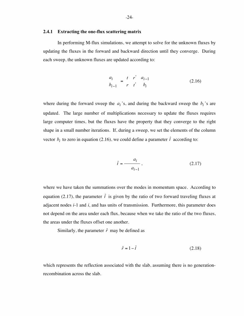
2.4.1 Extracting the one-flux scattering matrix
In performing M-flux simulations, we attempt to solve for the unknown fluxes by
updating the fluxes in the forward and backward direction until they converge. During
each sweep, the unknown fluxes are updated according to:
=
−
− i
i
i
ib
atrrt
ba 1
'
'
1(2.16)
where during the forward sweep the ia ’s, and during the backward sweep the ib ’s are
updated. The large number of multiplications necessary to update the fluxes requires
large computer times, but the fluxes have the property that they converge to the right
shape in a small number iterations. If, during a sweep, we set the elements of the column
vector ib to zero in equation (2.16), we could define a parameter t̂ according to:
−=
1ˆ
i
i
a
at , (2.17)
where we have taken the summations over the modes in momentum space. According to
equation (2.17), the parameter t̂ is given by the ratio of two forward traveling fluxes at
adjacent nodes i-1 and i, and has units of transmission. Furthermore, this parameter does
not depend on the area under each flux, because when we take the ratio of the two fluxes,
the areas under the fluxes offset one another.
Similarly, the parameter r̂ may be defined as
tr ˆ1ˆ −= (2.18)
which represents the reflection associated with the slab, assuming there is no generation-
recombination across the slab.
-25-
The same argument leading to equation (2.17) and (2.18) may readily be
generalized, in order to extract the “reverse” coefficients '~t and '~r as follows:
−
=i
i
b
bt 1'ˆ (2.19)
and
'' ˆ1ˆ tr −= . (2.20)
Equations (2.17-2.20) present the prescription for extracting the one-flux
parameters from an M-flux simulation. In deriving these equations, we made no special
assumptions regarding the shape of the fluxes and hence they are valid for off-
equilibrium as well as near-equilibrium transport.
2.4.2 Acceleration algorithm
Using the prescription for extracting the one-flux S-matrix, we present an
algorithm to accelerate the convergence of the M-flux solution. The procedure begins
with an initial guess for the electric field, which may be obtained from an analytical or
numerical solution. Given an electric field, the procedure would proceed as follows:
1. Beginning from the left contact, start sweeping to the right, updating the right-
directed fluxes ia , Ni ,...,2,1= . Once the right contact is reached, start sweeping
back towards the left contact, updating the left-directed fluxes ib ,
0,...,2,1 −−= NNi .
2. Having computed the fluxes, evaluate the macroscopic quantities such as carrier
density in , average velocity iυ , and average energy iu at each node i.
3. Extract the one-flux scattering parameters for each slab using the prescription
given by equations (2.17)-(2.20).

-26-
4. Using the one-flux parameters extracted and the average velocity iυ evaluated at
each node, solve equation (2.7) to update the carrier density in . Note the velocity
iυ may significantly differ from the thermal Maxwellian velocity Tυ .
5. Use the updated carrier density to re-scale the fluxes. Re-scaling the fluxes would
ensure that the fluxes have an area consistent with the updated the carrier density
in .
6. For self-consistent simulations, solve the Poisson equation and obtain a new
electric field.
7. Go back to step 1, and repeat until convergence is achieved.
The efficacy of this algorithm depends on how fast the shape of the flux
distributions converge, but as illustrated in Fig. 2.5, it typically takes a small number of
iterations for the fluxes to converge in shape. This is the reason why this algorithm is so
effective, which we discuss next.
2.5 Discussion and Results
In order to analyze the convergence properties of the iterative solution, we
evaluate the successive error estimate [Mor94] by subtracting equation (2.14) from (2.2)
and equation (2.15) from (2.3) to find
lii
lii
li rt )(1)(
11)( −++
−++ += εεε (2.21)
and 1)(1
1)(1)( +−+
+++− += lii
lii
li tr εεε (2.22)
where
11)( +++ −= lii
li aaε (2.23)
-27-
and 11)1( ++− −= lii
li bbε (2.24)
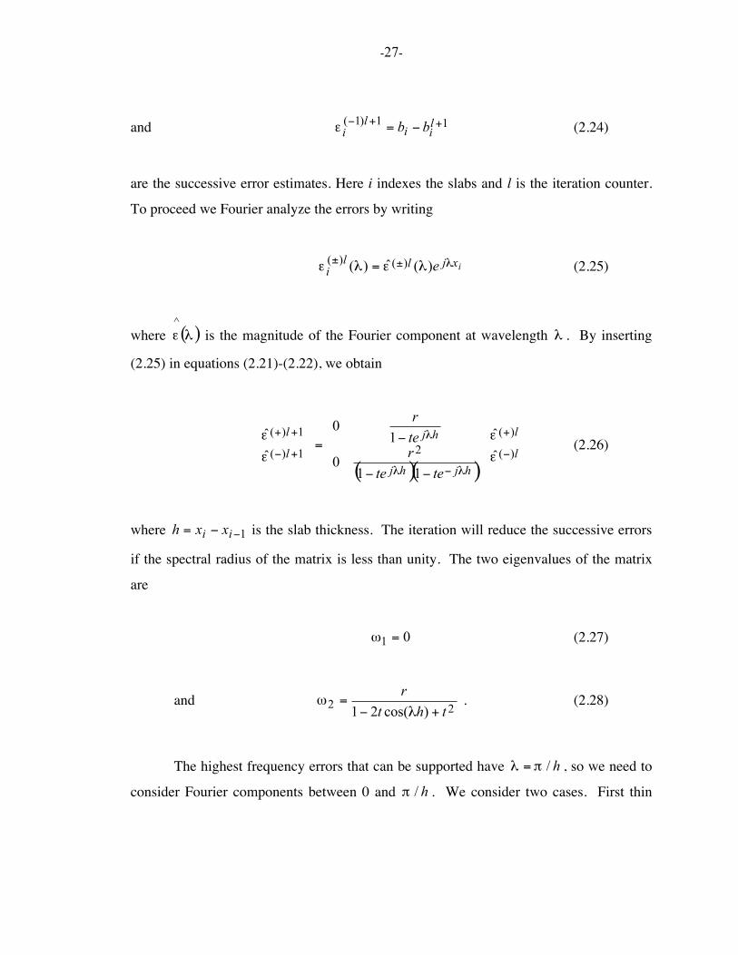
are the successive error estimates. Here i indexes the slabs and l is the iteration counter.
To proceed we Fourier analyze the errors by writing
ixjlli e λλελε )(ˆ)( )()( ±± = (2.25)
where ( )λε^
is the magnitude of the Fourier component at wavelength λ . By inserting
(2.25) in equations (2.21)-(2.22), we obtain
( )( )
−−
−=
−
+
−+−
++
l
l
hjhj
hjl
l
teterter
)(
)(21)(
1)(
ˆˆ
110
10
ˆˆ
ε
ε
ε
ε
λλ
λ(2.26)
where 1−−= ii xxh is the slab thickness. The iteration will reduce the successive errors
if the spectral radius of the matrix is less than unity. The two eigenvalues of the matrix
are
01 =ω (2.27)
and 22 )cos(21 thtr
+−=
λω . (2.28)
The highest frequency errors that can be supported have h/πλ = , so we need to
consider Fourier components between 0 and h/π . We consider two cases. First thin
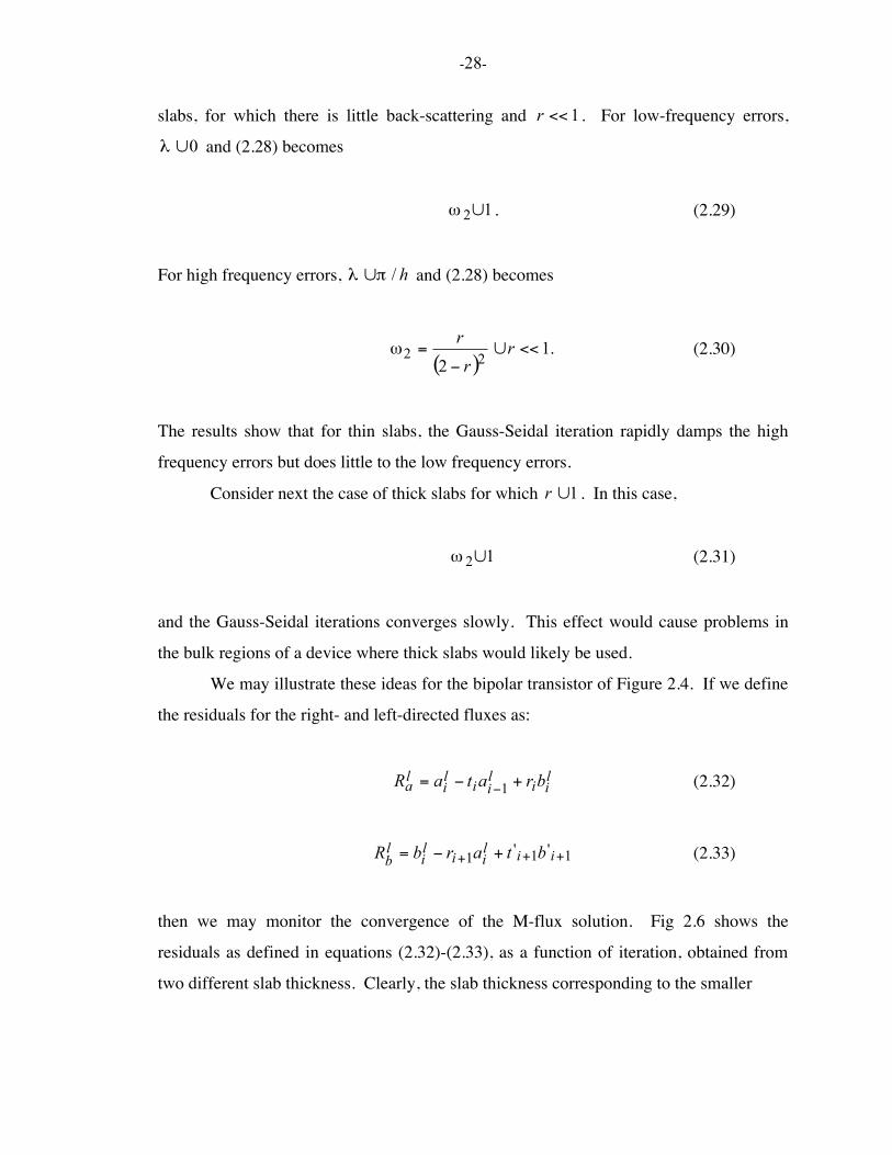
-28-
slabs, for which there is little back-scattering and 1<<r . For low-frequency errors,
0∪λ and (2.28) becomes
12∪ω . (2.29)
For high frequency errors, h/πλ ∪ and (2.28) becomes
( ).1
2 22 <<∪−
= rr
rω (2.30)
The results show that for thin slabs, the Gauss-Seidal iteration rapidly damps the high
frequency errors but does little to the low frequency errors.
Consider next the case of thick slabs for which 1∪r . In this case,
12∪ω (2.31)
and the Gauss-Seidal iterations converges slowly. This effect would cause problems in
the bulk regions of a device where thick slabs would likely be used.
We may illustrate these ideas for the bipolar transistor of Figure 2.4. If we define
the residuals for the right- and left-directed fluxes as:
lii
lii
li
la brataR +−= −1 (2.32)
1'1'1 +++ +−= iilii
li
lb btarbR (2.33)
then we may monitor the convergence of the M-flux solution. Fig 2.6 shows the
residuals as defined in equations (2.32)-(2.33), as a function of iteration, obtained from
two different slab thickness. Clearly, the slab thickness corresponding to the smaller
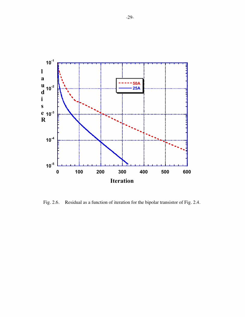
-29-
Fig. 2.6. Residual as a function of iteration for the bipolar transistor of Fig. 2.4.
10-5
10-4
10-3
10-2
10-1
0 100 200 300 400 500 600
50A25A
Residual
Iteration
-30-
Fig 2.7. L1 norm of the change in the carrier density, Δn/n, as a function of iteration.Two cases are shown: before (dashed line) and after (solid line) implementingthe acceleration
10-3
10-2
10-1
100
101
102
1 10 100
No AccelerationAcceleration
Δn/n
Iteration
-31-
channel back-scattering converges faster as was discussed above. Nevertheless, both
solutions have well behaved convergence, proving that the convergence radius
corresponding to a slab thickness of 25Å and 50Å is less than unity.
Finally, in Fig. 2.7, we demonstrate the improvement provided by the acceleration
algorithm where we show the convergence of nn /Δ with and without implementing the
acceleration algorithm. As demonstrated in Fig. 2.7, for a convergence criterion of 10-3,
the acceleration algorithm shaves off the number of necessary iterations by a factor of
~10. Clearly, the number of iterations saved would be larger if we select the convergence
criterion to be tighter, which we chose to be 10-3 for this example. The convergence
criterion is an important parameter that affects the computation time, particularly in self-
consistent simulations, where it is usually specified in terms of the change in the
potential. Typically, in a self-consistent simulation, the M-flux solution and the Poisson
equation are solved sequentially and the sequence is repeated until the desired
convergence is obtained. The acceleration algorithm reduces the number of iterations
each time the M-flux solution is obtained, therefore the total number of iterations will be
reduced by a factor 10 in a self-consistent simulation. The real benefit, nevertheless,
should not only be stated in terms of the total number of iterations, but also in terms of
the CPU time. Since it typically takes hours to obtain a self-consistent solution, the
acceleration algorithm would cut down the computer time to a remarkably low few
minutes.
2.6 Conclusions
In this chapter, we presented a highly effective acceleration algorithm which
speeds up the solution to the Boltzmann equation by a factor of ~10. We discussed the
convergence properties of the solution method and identified conditions under which the
iterative solution method may not converge. We demonstrated the acceleration algorithm
in one-dimension for a 1D transistor profile, but the benefit of this technique in two
dimensions, would even be greater.
-31-
3. AN ASSESSMENT OF SIMULATION APPROACHES FORSILICON BIPOLAR TRANSISTORS: DRIFT-DIFFUSION AND
BEYOND
3.0 Chapter in BriefIn Chapter 2, we presented an acceleration scheme which helped to make the
Boltzmann solver significantly more efficient. Our goal in this chapter is to apply theBoltzmann solver to study transport in advanced (i.e., thin base) bipolar devices. We willuse the solutions provided by the Boltzmann solver as a benchmark in this chapter, andcompare and assess the solutions provided by simpler approaches.
3.1 IntroductionThe semiconductor industry relies on computer simulation programs to develop
new technologies, and as such, the accuracy of these models has great economicimportance. There is currently a very large number of simulation programs in use whichimplement a multitude of approaches; we have a clear understanding of how theseapproaches are derived, and under what general conditions they are valid [Lau95].However, there is little specific understanding of how various approaches compare to eachother when applied to a given technology (or even of how they should be compared). Ourobjective in this chapter is to address these questions in a specific context, computersimulation tools for silicon bipolar transistors. This chapter presents a methodology forcomparing simulation programs and applies the methodology to simulation tools for siliconbipolar technology. The results show some surprises and underscore the on-going need tobenchmark and assess device simulation programs.
The use of drift-diffusion transport equations, the most popular simulation methodfor semiconductor devices, must be questioned for small devices because it relies on thelocality assumption (i.e., electric field does not vary abruptly within the device) which mayeasily break down in modern devices [Lun90]. Non-local transport models, such as theenergy transport, do not suffer from this limitation and have been implemented in

-32-
commercial packages [Tma94, Sil94]. Despite the increasing use of such models forMOSFET simulation, they have not yet been carefully compared and assessed for bipolardevices. Although the models are usually “tuned” to produce agreement with Monte Carlosimulations in specific cases, they are known to contain nonphysical artifacts [Ste93].Because these models have been developed for MOSFET's, but are also used for bipolartransistors, such an assessment is even more important for bipolar technology. The MonteCarlo technique, which is often used as the standard against which derived transportmodels such as energy transport are gauged, is not well-suited to this task for bipolartransistors. The large emitter-base energy barrier and the stochastic noise associated withthe technique make it difficult to compare predictions quantitatively over a wide range ofbiases.
This chapter presents a comparative study of drift-diffusion (DD) vs. energytransport (ET) models for sub-micron bipolar devices. To achieve this end, we havedeveloped a methodology (described in Section 3.2) which involves using realistic dopingprofiles and not abrupt ones, and examining terminal characteristics and not internalcharacteristics. A key element of the methodology is the use of a “computationalbenchmark” against which the validity of the derived transport models (DD and ET) isassessed. Our computational benchmark is a solution to the Boltzmann transport equationprovided by the scattering matrix approach [Ala93]. The methodology spans a two stepprocess consisting of calibrating the simulation programs to the same physical models andsubsequently comparing terminal characteristics. Two representative technologies are
examined: a current generation device with a nominal 25∪Tf Ghz, and a higher speed
generation with a nominal ∪Tf 55 Ghz. A comparison of the terminal characteristics ispresented in Section 3.3. In Section 3.4, internal characteristics are examined to explaindifferences observed in terminal characteristics. Finally, we close the discussion with asummary and conclusions in Sec. 3.5.
-33-
3.2 MethodologyThe methodology consists of three different aspects. The first is to select what
quantities to compare. While it is common to compare internal quantities (e.g. averagevelocity vs. position), it is the terminal characteristics that matter to circuit designers. Wefocus, therefore, on comparing a selected set of terminal parameters. Second is to selectwhat device profiles to compare. While it is common to compare model devices, it is morerelevant to compare realistic doping profiles that are being manufactured or explored inresearch laboratories. The final consideration is to select what simulation approaches tocompare. For this study we selected drift-diffusion, because it is still the standardtechnique in use, and the so-called energy transport model [Che92] because of itsincreasing use. As a standard of comparison, or computational benchmark, we usedscattering matrix solutions to the Boltzmann transport equation. It has been common tocompare simpler, derived transport models to more accurate techniques such as MonteCarlo simulation, but it is critical to ensure that each approach is modeling the samephysical problem. For example, the bulk velocity vs. electric field characteristic used in theDD model should be the bulk velocity vs. electric field characteristic computed by theBoltzmann solver, not a measured characteristic which may be different. In the remainderof this section, we address each of these three issues in more detail.
3 .2 .1 . Quantities ComparedThe objective of technology development is to provide devices to the circuit
designer. As such, the relevant parameters for comparison are the terminal characteristicsdeemed important by the designer. While the particular suite of electrical tests will varyfrom application to application, we chose the specific set listed in Table 3.1 which are themost relevant parameters for RF circuit design. In the first column , we list the terminalcharacteristics which typically involves the simulation of a current or a parameter vs.applied voltage, or DC collector current. Circuit designers are interested in parameterswhich capture the essence of the model. Since these characteristics consist of a largeamount of data, we also extracted key parameters to capture this information. Specifically,IS is the saturation current for the collector current, _o the common emitter (CE) current
gain in the constant gain region. The parameter peakTf , is the frequency at which the cut-
off frequency is a maximum, and IHL is a measure of the on-set of high current effect,which is defined to be the collector current at which the forward transit time is five times itslow-current value. Note that while these extracted parameters sometimes have the same
-34-
name as common circuit model parameters (e.g. a Spice model parameter), they are simplydefined here for our own purposes in order to capture aspects of the terminal characteristicdata in a single number.
Table 3.1Examined terminal characteristics along with a list of extracted parameters
Terminal Characteristics Extracted Parameters
IC(VBE), IB(VBE) [Gummel plot] IS , saturation current
β(IC) [common emitter gain vs. IC] βo, maximum CE current gain
Breakdown voltage BVCEO
fT(IC) [gain-bandwidth product] fT(peak), maximum fT
τF(IC) [forward transit time] τFo, low current forward transit time
IHL , high current roll-off current
3 .2 .2 . Devices ComparedThe second part of the methodology consists of selecting a set of devices for the
simulations. We selected polysilicon emitter, npn transistors with metallurgical base
widths of 0.1 µm and 0.05 µm, representing two generations of high speed bipolar
transistors. The first device, which has metallurgical base width of ∪ 0.1 µm, is a
production transistor with an estimated peakTf , of ∪ 25 Ghz [Klo93]. The second
device, which has a metallurgical base width of ∪ 0.05 µm, has an estimated peakTf , of
∪ 55 Ghz. Fig. 3.1 displays the vertical doping profile, AD NN − , for the secondtransistor as a function of vertical distance.
10202 105
Electric Field
-35-
Fig. 3.1 Doping profile for the ∪peakTf , 55 Ghz device vs. depth.
-36-
3 .2 .3 . Simulation Approaches ComparedFor this study, we examined three different approaches for simulating bipolar
devices:
1) Drift-Diffusion (DD)2) Energy Transport (ET)3) Scattering Matrix Approach (SMA)
The first approach (DD) is based on the conventional drift-diffusion equations,while the second one (ET) additionally accounts for energy balance in the current equations[Che92]. The third approach (SMA), solves for the carrier distribution function throughoutthe device by directly solving the Boltzmann equation [Ala93] and therefore is the mostrigorous of the three. The DD and ET approaches have both been implemented in thecommercial package, Medici [Tma94], which was used for this study. For drift-diffusionsimulations, we also used Device [Sch91]. The significant difference between Device andMedici was that Device uses the gradient of the quasi-Fermi level as the field in the field-dependent mobility while Medici uses the electric field. The ET simulations used anuncoupled solution approach, which provided more reliable convergence that the coupledsolution approach. We also note that the ET simulations reverted to DD for the ACanalysis; a small-signal DD AC analysis was performed about the DC ET solution.
The SMA program is a university research tool whose performance has beendemonstrated and refined in various bipolar studies over the past few years [Ste94]. Thescattering matrix simulation program, SMASH, resolves the electron distribution functionin detail but uses a simplified, one-flux approach (analogous to drift-diffusion) for holes.It treats effective bandgap narrowing and recombination at the emitter contact. Theprogram uses a spherical, non-parabolic energy band and uses scattering matrices evaluatedfrom a Monte Carlo program based on the work of Jacoboni and Reggiani [Jac83]. Otherdetails of the implementation are described in references [Ste1-94, Ste2-94]. Because itrepresents the most rigorous solution we have available, the SMA Boltzmann solver servesas the computational benchmark against which the DD and ET programs are compared.Since our focus was on the intrinsic device, where off-equilibrium transport is expected tomatter and not on the parasitics, one-dimensional simulations were deemed adequate.
-37-
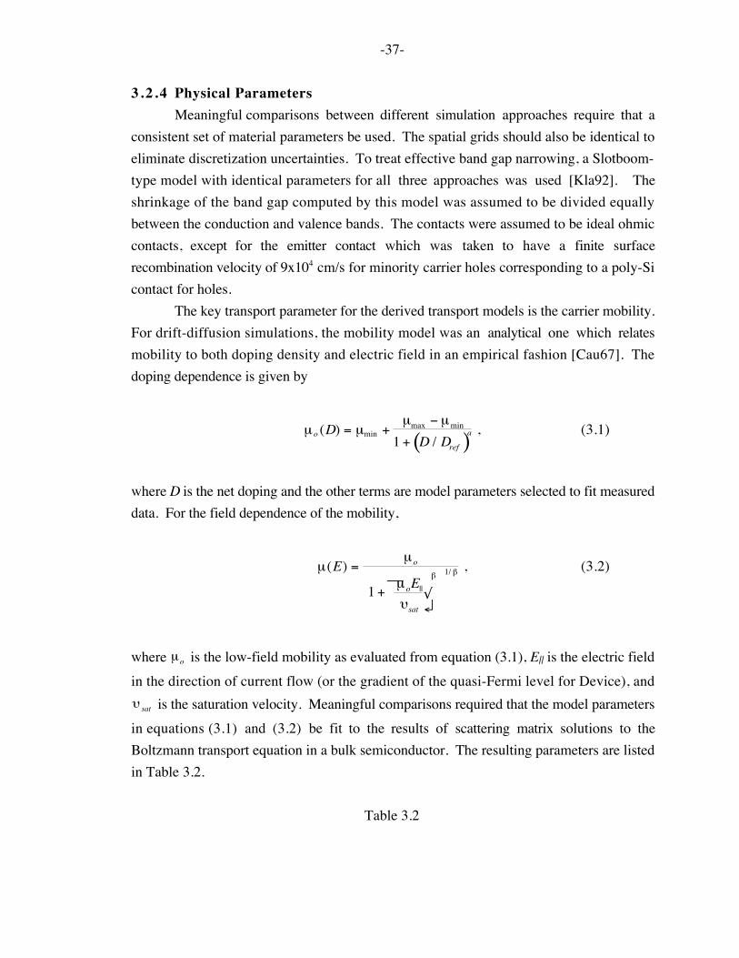
3 .2 .4 Physical ParametersMeaningful comparisons between different simulation approaches require that a
consistent set of material parameters be used. The spatial grids should also be identical toeliminate discretization uncertainties. To treat effective band gap narrowing, a Slotboom-type model with identical parameters for all three approaches was used [Kla92]. Theshrinkage of the band gap computed by this model was assumed to be divided equallybetween the conduction and valence bands. The contacts were assumed to be ideal ohmiccontacts, except for the emitter contact which was taken to have a finite surfacerecombination velocity of 9x104 cm/s for minority carrier holes corresponding to a poly-Sicontact for holes.
The key transport parameter for the derived transport models is the carrier mobility.For drift-diffusion simulations, the mobility model was an analytical one which relatesmobility to both doping density and electric field in an empirical fashion [Cau67]. Thedoping dependence is given by
µ o (D) = µmin +µmax − µmin
1 + D / Dref( )a , (3.1)
where D is the net doping and the other terms are model parameters selected to fit measureddata. For the field dependence of the mobility,
µ(E) =µ o
1 +µ oE||
υsat
⎯
↵ √
β
1/ β , (3.2)
where µ o is the low-field mobility as evaluated from equation (3.1), E|| is the electric fieldin the direction of current flow (or the gradient of the quasi-Fermi level for Device), andυ sat is the saturation velocity. Meaningful comparisons required that the model parametersin equations (3.1) and (3.2) be fit to the results of scattering matrix solutions to theBoltzmann transport equation in a bulk semiconductor. The resulting parameters are listedin Table 3.2.
Table 3.2
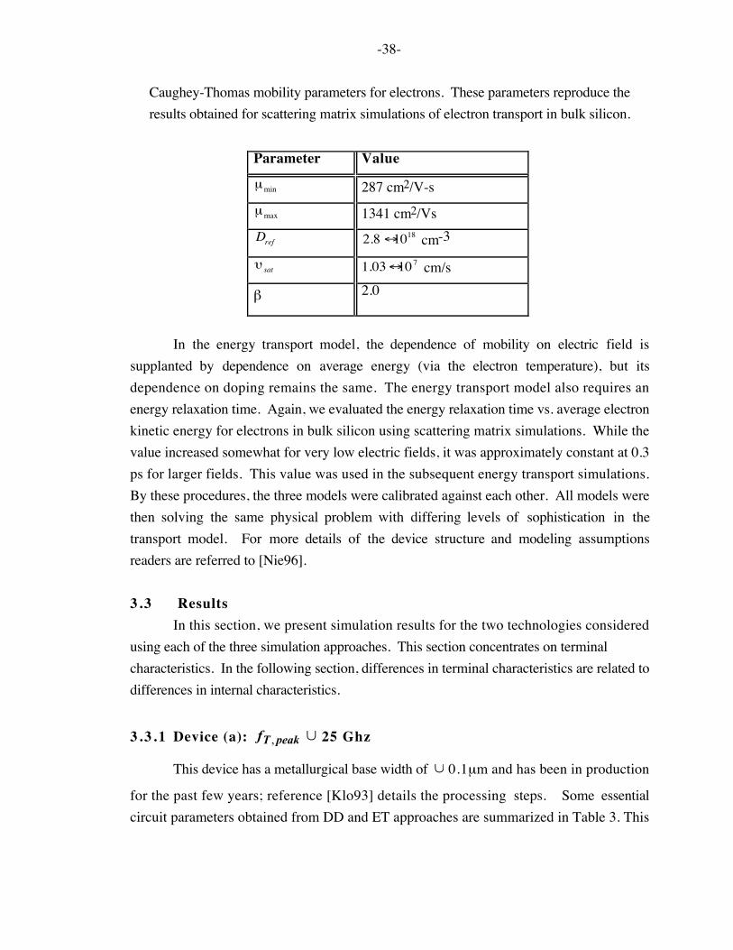
-38-
Caughey-Thomas mobility parameters for electrons. These parameters reproduce theresults obtained for scattering matrix simulations of electron transport in bulk silicon.
Parameter Value
µmin 287 cm2/V-sµmax 1341 cm2/VsDref 2.8 ↔1018 cm-3
υ sat 1.03↔107 cm/s
β 2.0
In the energy transport model, the dependence of mobility on electric field issupplanted by dependence on average energy (via the electron temperature), but itsdependence on doping remains the same. The energy transport model also requires anenergy relaxation time. Again, we evaluated the energy relaxation time vs. average electronkinetic energy for electrons in bulk silicon using scattering matrix simulations. While thevalue increased somewhat for very low electric fields, it was approximately constant at 0.3ps for larger fields. This value was used in the subsequent energy transport simulations.By these procedures, the three models were calibrated against each other. All models werethen solving the same physical problem with differing levels of sophistication in thetransport model. For more details of the device structure and modeling assumptionsreaders are referred to [Nie96].
3.3 ResultsIn this section, we present simulation results for the two technologies considered
using each of the three simulation approaches. This section concentrates on terminalcharacteristics. In the following section, differences in terminal characteristics are related todifferences in internal characteristics.
3 .3 .1 Device (a): ∪peakTf , 25 Ghz
This device has a metallurgical base width of ∪ 0.1µm and has been in production
for the past few years; reference [Klo93] details the processing steps. Some essentialcircuit parameters obtained from DD and ET approaches are summarized in Table 3. This
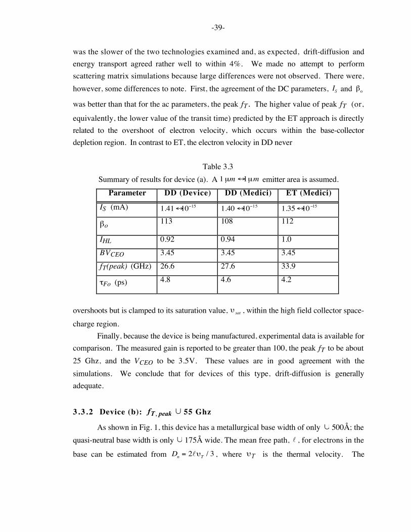
-39-
was the slower of the two technologies examined and, as expected, drift-diffusion andenergy transport agreed rather well to within 4%. We made no attempt to performscattering matrix simulations because large differences were not observed. There were,however, some differences to note. First, the agreement of the DC parameters, IS and βo
was better than that for the ac parameters, the peak fT. The higher value of peak fT (or,
equivalently, the lower value of the transit time) predicted by the ET approach is directlyrelated to the overshoot of electron velocity, which occurs within the base-collectordepletion region. In contrast to ET, the electron velocity in DD never
Table 3.3Summary of results for device (a). A 1 µm ↔1µm emitter area is assumed.
Parameter DD (Device) DD (Medici) ET (Medici)
IS (mA) 1.41↔10−15 1.40 ↔10−15 1.35↔10−15
βo 113 108 112
IHL 0.92 0.94 1.0BVCEO 3.45 3.45 3.45fT(peak) (GHz) 26.6 27.6 33.9
τFo (ps) 4.8 4.6 4.2
overshoots but is clamped to its saturation value, υ sat , within the high field collector space-charge region.
Finally, because the device is being manufactured, experimental data is available forcomparison. The measured gain is reported to be greater than 100, the peak fT to be about25 Ghz, and the VCEO to be 3.5V. These values are in good agreement with thesimulations. We conclude that for devices of this type, drift-diffusion is generallyadequate.
3 .3 .2 Device (b): ∪peakTf , 55 Ghz
As shown in Fig. 1, this device has a metallurgical base width of only ∪ 500Å; thequasi-neutral base width is only ∪ 175Å wide. The mean free path, l , for electrons in the
base can be estimated from Dn = 2lυT / 3 , where Tυ is the thermal velocity. The
-40-
estimated mean free path is ∪ 150Å, so this device has a quasi-neutral base width of aboutone mean free path. The simulated parameters for this device are shown in Table 3.4. Insharp contrast to the previous device, we found substantial discrepancies in the parameter
values computed by the various approaches. Of particular interest are IS , βo , and peakTf ,
which are seen to be ∪ 20% higher in the ET approach as compared to DD. The increasedbreakdown voltage in the ET model is expected because of the breakdown of the local fieldassumption in the DD model. The key question, then, is to determine which simulation ismore reliable.
We also performed scattering matrix simulations for this device which resolved theposition-dependent electron distribution function within the transistor. From the carrierdistribution function, we evaluated internal parameters such as carrier density, velocity, and
energy within the device as well as terminal characteristics. To obtain the peak Tf , weused a quasi-static treatment. Since the scattering matrix program used a spherical, non-parabolic energy band description, breakdown was not treated. The expected differences inthe DD and ET breakdown voltages could not, therefore, be examined, but the unexpecteddifferences in the other parameters could.
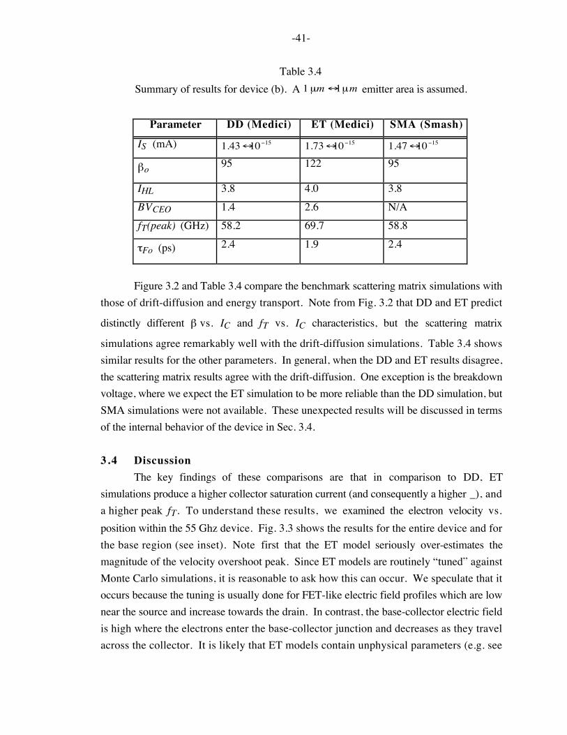
-41-
Table 3.4Summary of results for device (b). A 1 µm ↔1µm emitter area is assumed.
Parameter DD (Medici) ET (Medici) SMA (Smash)
IS (mA) 1.43↔10−15 1.73↔10−15 1.47↔10−15
βo 95 122 95
IHL 3.8 4.0 3.8BVCEO 1.4 2.6 N/AfT(peak) (GHz) 58.2 69.7 58.8
τFo (ps) 2.4 1.9 2.4
Figure 3.2 and Table 3.4 compare the benchmark scattering matrix simulations withthose of drift-diffusion and energy transport. Note from Fig. 3.2 that DD and ET predict
distinctly different β vs. IC and fT vs. IC characteristics, but the scattering matrix
simulations agree remarkably well with the drift-diffusion simulations. Table 3.4 showssimilar results for the other parameters. In general, when the DD and ET results disagree,the scattering matrix results agree with the drift-diffusion. One exception is the breakdownvoltage, where we expect the ET simulation to be more reliable than the DD simulation, butSMA simulations were not available. These unexpected results will be discussed in termsof the internal behavior of the device in Sec. 3.4.
3.4 DiscussionThe key findings of these comparisons are that in comparison to DD, ET
simulations produce a higher collector saturation current (and consequently a higher _), anda higher peak fT. To understand these results, we examined the electron velocity vs.position within the 55 Ghz device. Fig. 3.3 shows the results for the entire device and forthe base region (see inset). Note first that the ET model seriously over-estimates themagnitude of the velocity overshoot peak. Since ET models are routinely “tuned” againstMonte Carlo simulations, it is reasonable to ask how this can occur. We speculate that itoccurs because the tuning is usually done for FET-like electric field profiles which are lownear the source and increase towards the drain. In contrast, the base-collector electric fieldis high where the electrons enter the base-collector junction and decreases as they travelacross the collector. It is likely that ET models contain unphysical parameters (e.g. see

-42-
[Ste93]) which can be tuned with success for specific profiles. When applied to deviceswith much different electric field profiles, errors can occur. The excessive velocityovershoot could simply be assumed to reduce the collector transit time, which consequentlyincreases fT, but as discussed by [Das91], delay across the base-collector junction does notdominate the total delay time, not as much as the neutral base region.
Fig. 3.3 shows the average velocity vs. position within the base region of thetransistor (the inset). Once again we noticed an unusually close agreement in the velocitiesobtained by DD and SMA spanning the edges of the emitter-base (EB) to base-collector(BC) depletion regions. Recall that the quasi-neutral base width for this device is about onemean free path. It is commonly assumed that the drift-diffusion approach will lose validityonce the base width approaches a mean free path and that ballistic transport will dominate.It has been shown in the old [Sho62] and recent [Han94] literature, however, that Fick'sLaw can describe transport in a thin base if the physically correct boundary conditions areapplied. Carriers are injected from a thermal source, the emitter, and can exit a field-freebase, at most, at the thermal velocity of an equilibrium hemi-Maxwellian distribution,
υT =2kTπm* . (3.3)
(Moderate corrections of ∪ 18% can occur because of the anisotropic nature of ionizedimpurity scattering [Ber74], but they do not alter the general argument.) The key issue,then, is the boundary condition at the base-collector junction. In a drift-diffusion model,the velocity is clamped at υ sat , which, for silicon, just happens to be very close to thethermal velocity. Because of this fortunate occurrence, DD models accurately describe
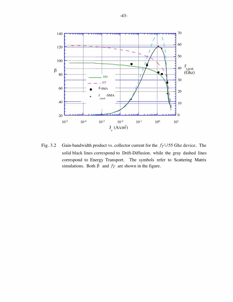
-43-
20
40
60
80
100
120
140
0
10
20
30
40
50
60
70
10-5 10-4 10-3 10-2 10-1 100 101
β-SMA
DD
ET
ft,peak
-SMA
Jc (A/cm2)
ft,peak
(Ghz)β
Fig. 3.2 Gain-bandwidth product vs. collector current for the ∪Tf 55 Ghz device. Thesolid black lines correspond to Drift-Diffusion, while the gray dashed linescorrespond to Energy Transport. The symbols refer to Scattering Matrixsimulations. Both β and Tf are shown in the figure.
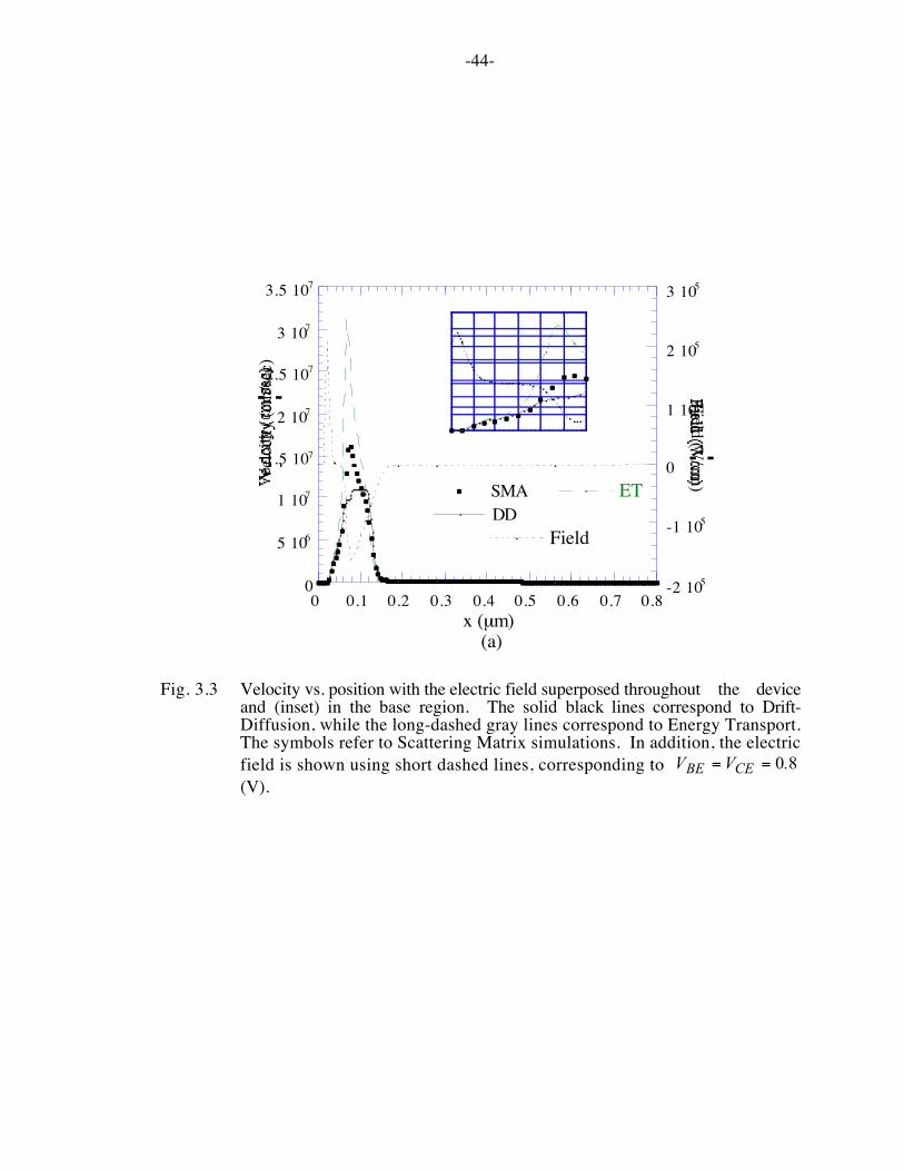
-44-
0
5 106
1 107
1.5 107
2 107
2.5 107
3 107
3.5 107
-2 105
-1 105
0
1 105
2 105
3 105
0 0.1 0.2 0.3 0.4 0.5 0.6 0.7 0.8
SMADD
ET
Field
Vel
ocity
(cm
/sec)
Field (V/cm
)
x (µm) (a)
Fig. 3.3 Velocity vs. position with the electric field superposed throughout the deviceand (inset) in the base region. The solid black lines correspond to Drift-Diffusion, while the long-dashed gray lines correspond to Energy Transport.The symbols refer to Scattering Matrix simulations. In addition, the electricfield is shown using short dashed lines, corresponding to 80.VV CEBE ==(V).
-45-
devices with base widths on the order of a mean free path. In an ET model, however, thevelocity at the base-collector junction rises because of velocity overshoot. This isphysically correct, but unless there is a mechanism to limit the carrier velocity as they exitthe base to the thermal velocity, the diffusion velocity can be unphysically high. Theappropriate mechanism is the carrier drift energy [Bac85], but this term is missing in manyET implementations. We speculate that this is the source of the unphysically high electronvelocities in the base predicted by the ET simulation. The large magnitude of the velocitiesin the base do not effect the device characteristics directly, instead they effect the devicecharacteristics by allowing too much diffusion through the quasi-neutral base region.
3.5 ConclusionsDrift-diffusion, energy transport, and full Boltzmann simulations of silicon bipolar
transistors of two different technologies were compared and analyzed. When applied tobipolar transistors, we found that energy transport simulators which have been developedand tuned for MOSFETs can produce serious errors. They are certainly needed to predictbreakdown voltages, but they can introduce errors in modeling the transport. A surprisingresults was the remarkable accuracy of the drift-diffusion simulations, well beyond thecommonly assumed limits of validity. We explained these results by examining internalquantities which showed that for silicon devices, drift-diffusion simulations can be used towell within the quasi-ballistic regime.
It is also worth making clear what we have not established. Energy transportmodels are not in principle inferior to drift-diffusion models, they include more physics andtherefore entail more assumptions. They seem to treat first order hot carrier effects well(e.g. the increased breakdown voltage), but errors can be introduced into the transportmodel. The point is not that an ET model cannot work reliably for advanced bipolartransistors, but rather, models developed and tuned for MOSFETs should not beuncritically accepted when applied to much different devices. This work identifies the twoareas of focus for ET models in bipolar applications as: 1) a correct treatment of quasi-ballistic transport in the base, and 2) a correct prediction of velocity overshoot in thecollector.
Finally, we consider the most important contribution of this work to be moregeneral. The point is that the large number of simulation programs available today need tobe assessed against a computational benchmark as well as against experiments. It iscommon nowadays to compare derived transport models to Monte Carlo simulations, butwhat is compared is usually the shape of the velocity or energy vs. position profile. To
-46-
fully assess a derived transport model, it is necessary to compare simulated terminalcharacteristics with those obtained from more accurate transport models. It should be notedthat when a model includes more physics, it is not guaranteed that it is always moreaccurate. More physics in the model means that there are more assumptions involved inimplementing it. The methodology developed here, which consists of examining terminalcharacteristic important to the designer, using structures being manufactured or explored inthe lab, and calibrating all simulators to a common computational benchmark should proveuseful in similar assessments of other simulators and devices.
-47-
4. THE DRIFT-DIFFUSION EQUATION REVISITED
4.0 Chapter in BriefIn Chapter 3, we discussed the Drift-Diffusion equation in the context of bipolar
transistors and showed that it continues to work well even for devices in which transport isquasi-ballistic. Our goal in this chapter is to expand on the discussion in Chapter 3, butinstead of focusing on a particular technology we will take a more systematic approach,starting from the BTE. In doing so, we will discuss the reason for the Drift-Diffusion’scontinued success from the perspective of scattering theory, and discuss the conditionsunder which it breaks down. Finally, we speculate on its continued success for sub-micron technologies of the future.
4.1 IntroductionSince 1950 when van Roosbroeck presented the drift-diffusion formulation of the
semiconductor equations [Roo50], the critical dimensions of transistors have shrunkconsiderably. Rapidly varying electric fields in modern devices would seem to invalidatethe drift-diffusion equation, yet it continues to be used successfully [Han91]. It not onlyforms the basis for numerical simulations, but it also provides the conceptual framework
most often used to think about devices. As silicon technology approaches 0.1 µm channel
lengths, it is important to have a clear understanding of the capabilities and limitations ofthe drift-diffusion equation. Our purpose in this chapter is to reconsider the drift-diffusionequation from a non-traditional perspective — scattering theory. In the process we hope toexplain the continued success of the drift-diffusion equation and to speculate about itscontinued application.
We begin with a conventional derivation of the drift-diffusion equation. Thesteady-state Boltzmann Transport Equation (BTE),
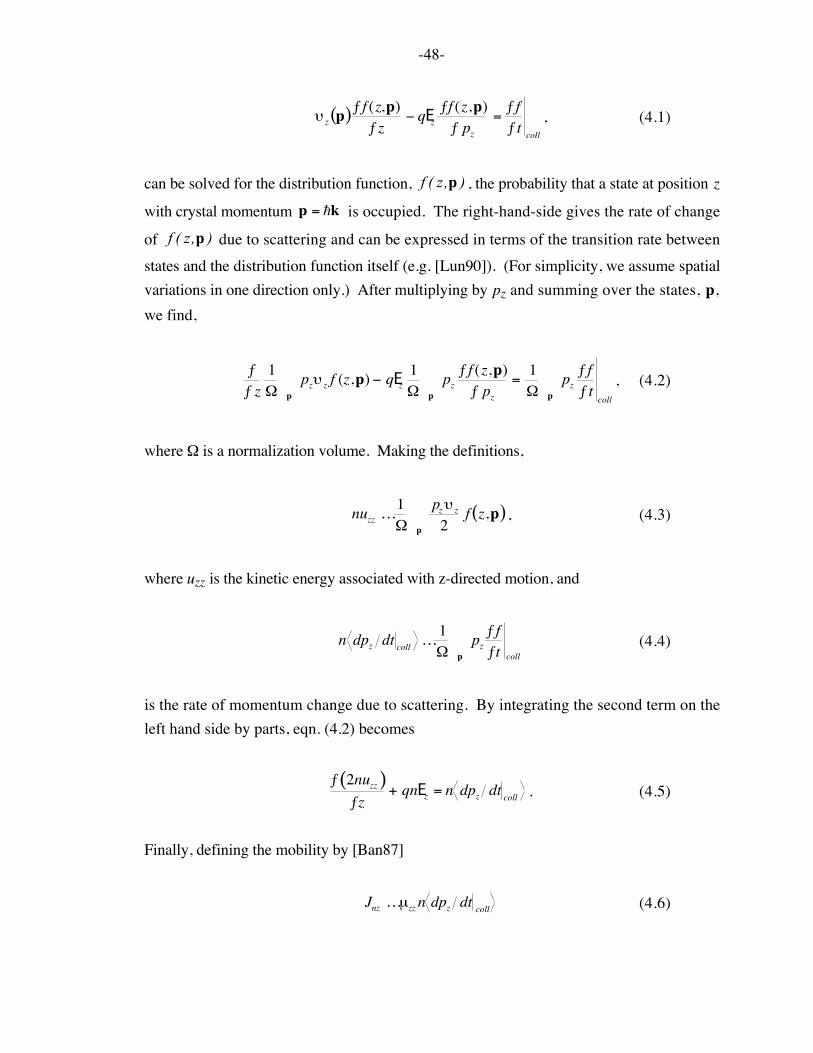
-48-
υ z p( )ƒf (z,p)
ƒz− qEz
ƒf (z,p)ƒ pz
=ƒfƒt coll
, (4.1)
can be solved for the distribution function, ),z(f p , the probability that a state at position z
with crystal momentum p = hk is occupied. The right-hand-side gives the rate of change
of ),z(f p due to scattering and can be expressed in terms of the transition rate betweenstates and the distribution function itself (e.g. [Lun90]). (For simplicity, we assume spatialvariations in one direction only.) After multiplying by pz and summing over the states, p,we find,
ƒƒ z
1Ω
pzυ z f (z,p)p − qEz
1Ω
pzp ƒf (z,p)
ƒ pz
=1Ω
pzp
ƒfƒt
coll
, (4.2)
where Ω is a normalization volume. Making the definitions,
nuzz …1Ω
pzυ z
2f z,p( )
p , (4.3)
where uzz is the kinetic energy associated with z-directed motion, and
n dpz dt coll …1Ω
pzƒfƒt collp
(4.4)
is the rate of momentum change due to scattering. By integrating the second term on theleft hand side by parts, eqn. (4.2) becomes
ƒ 2nuzz( )
ƒz+ qnEz = n dpz dt coll . (4.5)
Finally, defining the mobility by [Ban87]
Jnz …µzz n dpz dt coll (4.6)
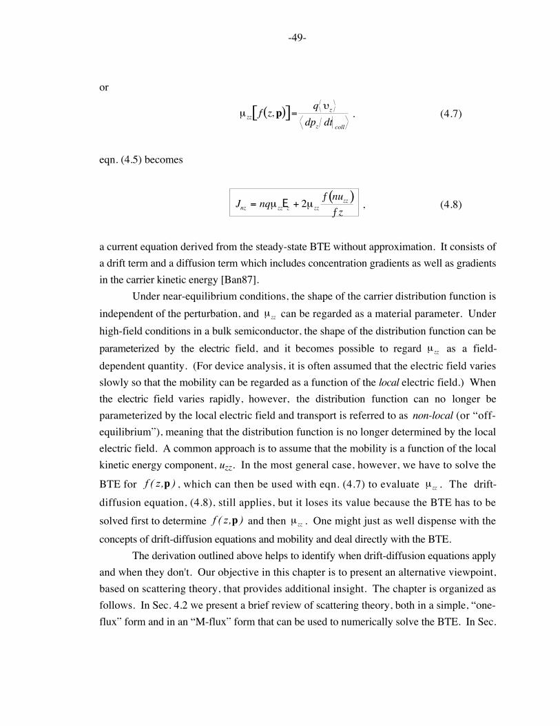
-49-
or
µ zz f z, p( )[ ]=q υz
dpz dt coll
. (4.7)
eqn. (4.5) becomes
Jnz = nqµ zzEz + 2µ zz
ƒ nuzz( )ƒz
, (4.8)
a current equation derived from the steady-state BTE without approximation. It consists ofa drift term and a diffusion term which includes concentration gradients as well as gradientsin the carrier kinetic energy [Ban87].
Under near-equilibrium conditions, the shape of the carrier distribution function isindependent of the perturbation, and µ zz can be regarded as a material parameter. Underhigh-field conditions in a bulk semiconductor, the shape of the distribution function can beparameterized by the electric field, and it becomes possible to regard µ zz as a field-dependent quantity. (For device analysis, it is often assumed that the electric field variesslowly so that the mobility can be regarded as a function of the local electric field.) Whenthe electric field varies rapidly, however, the distribution function can no longer beparameterized by the local electric field and transport is referred to as non-local (or “off-equilibrium”), meaning that the distribution function is no longer determined by the localelectric field. A common approach is to assume that the mobility is a function of the localkinetic energy component, uzz. In the most general case, however, we have to solve the
BTE for ),z(f p , which can then be used with eqn. (4.7) to evaluate µ zz . The drift-diffusion equation, (4.8), still applies, but it loses its value because the BTE has to besolved first to determine ),z(f p and then µ zz . One might just as well dispense with theconcepts of drift-diffusion equations and mobility and deal directly with the BTE.
The derivation outlined above helps to identify when drift-diffusion equations applyand when they don't. Our objective in this chapter is to present an alternative viewpoint,based on scattering theory, that provides additional insight. The chapter is organized asfollows. In Sec. 4.2 we present a brief review of scattering theory, both in a simple, “one-flux” form and in an “M-flux” form that can be used to numerically solve the BTE. In Sec.
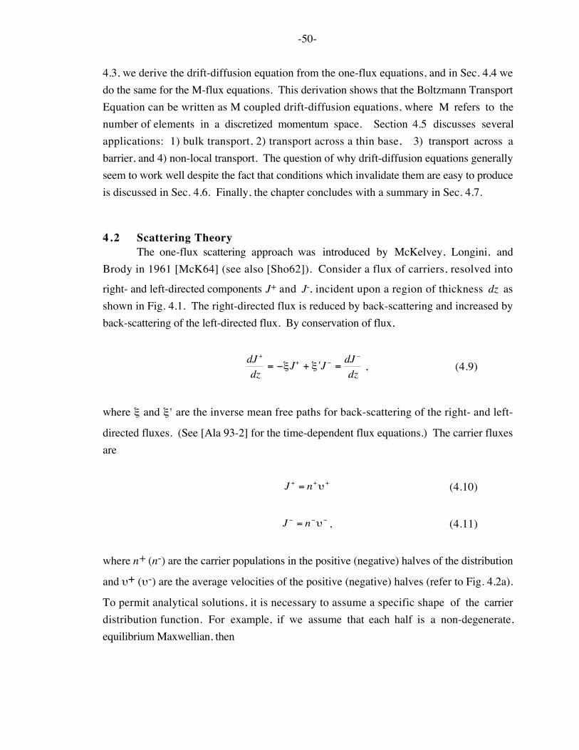
-50-
4.3, we derive the drift-diffusion equation from the one-flux equations, and in Sec. 4.4 wedo the same for the M-flux equations. This derivation shows that the Boltzmann TransportEquation can be written as M coupled drift-diffusion equations, where M refers to thenumber of elements in a discretized momentum space. Section 4.5 discusses severalapplications: 1) bulk transport, 2) transport across a thin base, 3) transport across abarrier, and 4) non-local transport. The question of why drift-diffusion equations generallyseem to work well despite the fact that conditions which invalidate them are easy to produceis discussed in Sec. 4.6. Finally, the chapter concludes with a summary in Sec. 4.7.
4.2 Scattering TheoryThe one-flux scattering approach was introduced by McKelvey, Longini, and
Brody in 1961 [McK64] (see also [Sho62]). Consider a flux of carriers, resolved into
right- and left-directed components J+ and J-, incident upon a region of thickness dz asshown in Fig. 4.1. The right-directed flux is reduced by back-scattering and increased byback-scattering of the left-directed flux. By conservation of flux,
dJ +
dz= −ξJ+ + ʹ′ ξ J − =
dJ −
dz, (4.9)
where ξ and ξ' are the inverse mean free paths for back-scattering of the right- and left-
directed fluxes. (See [Ala 93-2] for the time-dependent flux equations.) The carrier fluxesare
J + = n+υ+ (4.10)
J − = n−υ− , (4.11)
where n+ (n-) are the carrier populations in the positive (negative) halves of the distribution
and υ+ (υ-) are the average velocities of the positive (negative) halves (refer to Fig. 4.2a).
To permit analytical solutions, it is necessary to assume a specific shape of the carrierdistribution function. For example, if we assume that each half is a non-degenerate,equilibrium Maxwellian, then

-51-
υ + = υ− = υT =2kBTπm* , (4.12)
which is twice the so-called Richardson velocity. More familiar quantities such as thecarrier density and electron current are obtained from the fluxes by
n =J +
υ+ +J −
υ− (4.13)
and
Jn = −q J + − J −( ) . (4.14)
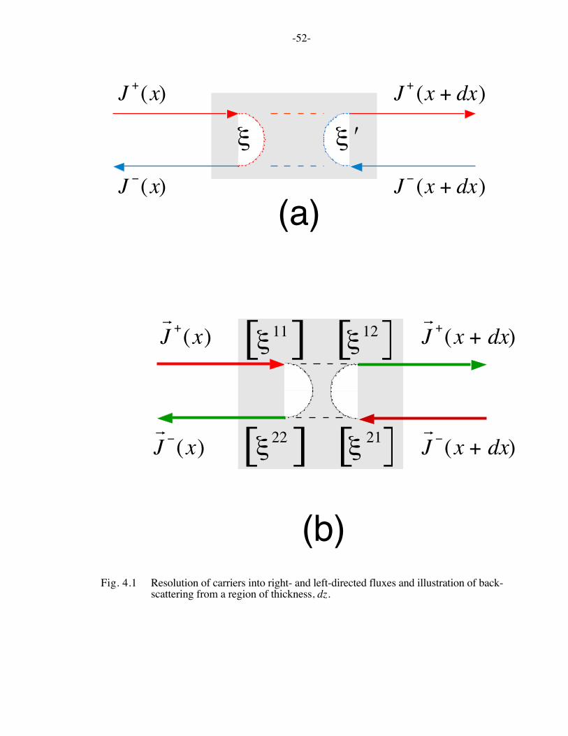
-52-
ξ ʹ′ ξ
(a)
J +(x) J + (x + dx)
J − (x + dx)J −(x)
ξ 11[ ] ξ 12[ ]
ξ 22[ ] ξ 21[ ]
(b)
r
J −(x)
r
J +(x)
r
J +(x + dx)
r
J −(x + dx)
Fig. 4.1 Resolution of carriers into right- and left-directed fluxes and illustration of back-scattering from a region of thickness, dz.
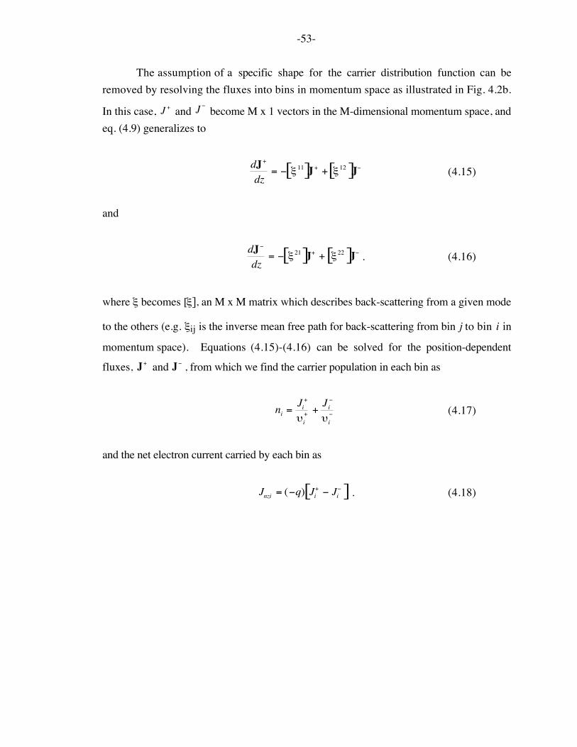
-53-
The assumption of a specific shape for the carrier distribution function can beremoved by resolving the fluxes into bins in momentum space as illustrated in Fig. 4.2b.
In this case, J + and J − become M x 1 vectors in the M-dimensional momentum space, andeq. (4.9) generalizes to
dJ+
dz= − ξ 11[ ]J+ + ξ 12[ ]J− (4.15)
and
dJ−
dz= − ξ 21[ ]J+ + ξ 22[ ]J− . (4.16)
where ξ becomes [ξ], an M x M matrix which describes back-scattering from a given mode
to the others (e.g. ξij is the inverse mean free path for back-scattering from bin j to bin i in
momentum space). Equations (4.15)-(4.16) can be solved for the position-dependent
fluxes, J+ and J− , from which we find the carrier population in each bin as
ni =Ji
+
υi+ +
Ji−
υi− (4.17)
and the net electron current carried by each bin as
Jnzi = (−q) Ji+ − Ji
−[ ] . (4.18)

-54-
v
f(v)
(a)
J − = n−υth J + = n+υth
v
f(v)
(b)
J +J −
Fig. 4.2 Illustration of how the carrier distribution is divided into positive and negativehalves. (a) the one-flux approach with an assumed Maxwellian for each halfand (b) the M-flux approach which represents each half of the distribution by Mbins in momentum space. For the positive flux, a bin is a region located around(px, py, +pz) and for the negative flux, around (px, py, -pz)
where i = 1, 2, 3, ... M, and υ i+ and υ i
− are the z-directed velocities of the positive andnegatively-directed fluxes in bin i. The total carrier density and electron current areobtained by summing the contributions from each bin.

-55-
We have presented eqs. (4.15)-(4.16) as a simple generalization of eqn. (4.9), butthey can also be derived rigorously from a path integral solution to the BTE [Ala93-1]. Theflux equations have been presented in differential form, but they can be integrated across aslab of finite thickness and the results expressed in terms of a scattering matrix. For theone-flux case, the result is the one-flux scattering matrix approach that has recently beenapplied to bipolar transistors [Tan94, Tan95] and MOSFETs [Lun96, Lun97]. (A similarapproach, the transmission line equivalent circuit model of minority carrier transport, hasalso been introduced [Kar95].) For the M-flux case, we have M incident fluxes from eachside of the slab so the scattering matrix becomes a 2M x 2M matrix. This “scattering matrixapproach” provides numerical solutions to the BTE [Ala93-1, Das90]. After solving theM-flux equations, however, one can sum over the bins to express the result in an exact,one-flux form (see Appendix A).
The flux method, in either the differential or discrete form in space, provides amethod for simulating transport in devices. In the differential form, the flux equations areintegrated across a device, and in the discrete form, scattering matrices are cascaded. Theone-flux version provides analytical solutions, and the M-flux version provides numericalsolutions to the BTE. Our intent in this chapter, however, is to show that there is a closeconnection between the drift-diffusion equation and scattering theory and that deriving thedrift-diffusion equation from scattering theory provides useful insights.
4.3 One-Flux Theory and the Drift-Diffusion EquationThe one-flux equations are easily manipulated into a more familiar form. By adding
the equations for J+ and J-, we obtain
dJdz
= 0 , (4.19)
which is simply the electron continuity equation. (Flux is conserved because we have notincluded particle recombination-generation terms, but they are readily treated [Sho62].)
Similarly, by subtracting the equations for J+ and J- and rearranging the result, we find
J = −ξ − ʹ′ ξ ξ + ʹ′ ξ
⎯
↵ √ υT n − υT
ξ + ʹ′ ξ
⎯
↵ √
dndz
, (4.20)

-56-
where we have made a near-equilibrium assumption so that υ + = υ− = υT as given by eqn.(4.12). Equation (4.20) is in drift-diffusion form, so it is convenient to define thediffusion coefficient as
D =υT
ξ + ʹ′ ξ . (4.21)
Under the assumed near-equilibrium conditions, ξ − ʹ′ ξ ( ) should be proportional to the
electric field and ξ + ʹ′ ξ ( ) should be independent of the field. Writing [McK61]
ξ = ξ o +Δξ 2 (4.22)and
ʹ′ ξ = ξ o − Δξ 2 , (4.23)
we find a simple relation between the measured diffusion coefficient and the inverse meanfree path for back-scattering under field-free conditions as
ξ o =υT
2D. (4.24)
The first term in eqn. (4.20) can be identified as a drift term, and a mobility can bedefined as
µEz =
ξ − ʹ′ ξ ξ + ʹ′ ξ
⎯
↵ υT (4.25)
or
µ =
ξ − ʹ′ ξ Ez
⎯
↵ √ D = E−1D , (4.26)
where E-1 is an inverse Einstein factor. From the near-equilibrium assumption, we expect
that E-1 = q/kBT. With this assumption and eqns. (4.22)-(4.23), we find
-57-
Δξ = ξ − ʹ′ ξ ( )= Ez kBT / q( ). (4.27)
These results demonstrate that the near-equilibrium one-flux equations areequivalent to a near-equilibrium drift-diffusion equation,
Jnz = nqµnEz + qDn
dndz
. (4.28)
The thermoelectric component in eqn. (4.8) is missing in eqn. (4.33) because of theassumed near-equilibrium conditions. The mobility and diffusion coefficient can be
obtained from the back-scattering parameters, ξ and ξ' , or the back-scattering parameters
can be deduced from the measured mobility and diffusion coefficient. The result, eqn.(4.28), is somewhat surprising. For example, it is clear that the one-flux equations retaintheir validity in a region that is short compared to a mean-free path. The implication is thatat least for some conditions (i.e. field-free transport with a near-equilibrium injected flux) itis possible to employ drift-diffusion equations to describe quasi-ballistic transport. Thisresult, discovered by Shockley in 1962 [Sho62], will be discussed in Sec. 4.5, where thevalidity of the assumptions used to derive the one-flux equations is examined.
-58-
4.4 M-Flux Theory and the Drift-Diffusion EquationFollowing a series of steps similar to those that led from the one-flux equations,
(9), to the continuity and drift-diffusions equations, eqs. (15) and (16), we can transformthe M-flux equations, eqs. (4.15) and (4.16) to an M-flux continuity and drift-diffusionequation. The result is an M-flux continuity equation,
dJnz
dz= [α ]Jnz + [β ]n , (4.29)
(recall that Jnz and n are M x 1 vectors corresponding to M fluxes in discretized momentumspace). In deriving eqn. (4.29), the bins representing +pz and -pz for the same (px, py)have been summer. The non-zero “recombination-generation” terms on the RHS of eqn.(4.29) do not refer to the explicit recombination and generation of carriers but, rather, to theshuffling of carriers between momentum states caused by scattering and the electric field.
Similarly, we find the current equation as
Jnz = q µ zz[ ]nEz + q Dzz[ ]dn
dz, (4.30)
which gives the electron current carried by each bin in momentum space. The mobility anddiffusion matrices (M x M) are defined in terms of the differential back-scattering matrices,
[ξij], as are the generation-recombination matrices, [α] and [β ] (see appendix B for the
expressions). These matrices turn out to be sparse and to have a simple structure (see[Ban97] for some examples).
Equations (4.29) and (4.30) reformulate the BTE as M coupled continuity and drift-diffusion equation in discretized momentum space. When eqn. (4.30) is inserted into eqn.(4.29), a second order partial differential equation for n(z), the position-dependent carrierdistribution function, results. (The approach here is similar to the well-known even- andodd- parity forms of the transport equation [Lew93].) Numerical solutions for electrontransport in bulk Si have been presented in [Ban97], but whether this approach proves tobe a practical technique for solving the BTE remains to be seen. It does, however, havepedagogical value. It shows that solving the BTE is equivalent to solving M coupled drift-diffusion equations.

-59-
Formulation of the BTE as M coupled drift-diffusion equations also helps clarifythe connection between the drift diffusion equation and a full solution to the BTE. If onesums over all the bins in momentum space, an equation for the macroscopic current,
Jnz = Jnzii =1
M
, (4.31)
results. After performing this sum on eqn. (4.29), the macroscopic current can beexpressed as in the form of eqn. (4.8) (see Appendix B). The macroscopic mobility isdetermined from the mobility matrix and the computed carrier distribution function as
µ zz =µijn j
i =1
M
n
. (4.32)
The mobility matrix is nearly field-independent; the field dependence of the macroscopicmobility comes from the field dependence of the distribution function, not from themobility matrix itself.
4.5 ApplicationsIn this section we examine transport in four different situations. In doing so, we
relate the results to drift-diffusion equations and to the underlying flux equations. Ourapproach uses the M-flux, scattering matrix approach to solve the BTE then expresses theresults in exact one-flux terms as discussed in Appendix A. We treat electron transport inSi at room temperature with an electric field oriented along <111>. The Si band structureand electron scattering are treated as described Jacoboni and Reggiani [Jac83].
4 .5 .1 Low-Field Transport in Bulk SiWe begin by examining transport in intrinsic, bulk Si. “Exact” results are obtained
from scattering matrix simulations which resolve the carrier distribution in momentumspace. From the results we can extract the average velocities of the positively- andnegatively-directed carrier fluxes, and the results are presented in Fig. 4.3. As expected,
under low field conditions, υ + ≅ υ− ≅ υT = 2kBT πm* . (The appropriate effective mass
-60-
to use is the conductivity effective mass, 0.26m0 for Si, which gives υT ≅ 1.06↔107 cm/s,in good agreement with the numerical calculations displayed in Fig. 4.3.) The range of
electric fields over which υ + ≅ υ− ≅ υT defines the range over which a near-equilibriumone-flux or drift-diffusion treatment can be expected to be valid. From Fig. 4.3, weobserve that for electric fields less than about 1 kV/cm, the near-equilibrium assumption iswell-satisfied, but for fields greater than a few kV/cm the near-equilibrium assumptionclearly breaks down for electron transport in Si.
It also interesting to examine the equivalent one-flux back-scattering coefficients inbulk Si. Equations (A2) relates the M-flux back-scattering matrix to the equivalent one-fluxparameters. For the scattering matrix simulations, however, slabs with a finite thickness(50 Å in this case) were used. We therefore extract from the scattering matrix simulation,the parameters, r and r', which refer to back-scattering from a 50 Å Si slab. Assuming that
these slabs are thin, we then estimate the differential back-scattering parameters, ξ and ξ' ,
from ξ ∪r dx and ʹ′ ξ ∪ ʹ′ r dx . In Fig. 4.4 we plot (ξ - ξ') vs. Ez; as expected, (ξ - ξ')
varies linearly with electric field for small electric fields. According to eqn. (4.27), the
slope of the line, d ξ − ʹ′ ξ ( ) dE , is 40 V-1, which is in excellent agreement with the exact
values at low electric fields. Under high electric fields, however, (ξ - ξ') saturates. These
results confirm the simple estimates for the near-equilibrium one-flux parameters aspresented in Sec. 4.3.
4 .5 .2 Thin Base Transport in SiNext, we consider the transport of electrons across a thin, field-free region in which
thermal carriers are injected at the left, and the right contact is taken to be absorbing. (Thismodel problem might represent the base of a bipolar transistor.)
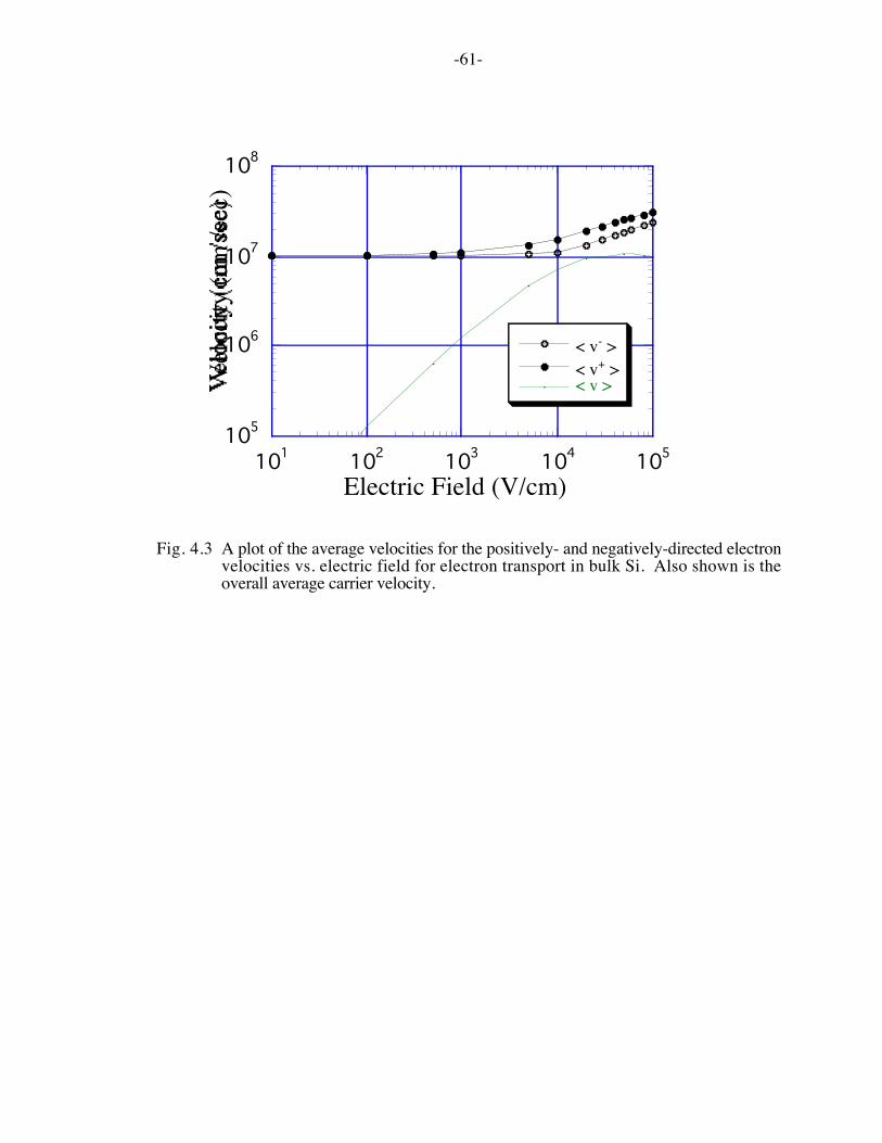
-61-
105
106
107
108
101 102 103 104 105
< v- >< v+ >< v >V
eloc
ity (c
m /s
ec)
Electric Field (V/cm)
Fig. 4.3 A plot of the average velocities for the positively- and negatively-directed electronvelocities vs. electric field for electron transport in bulk Si. Also shown is theoverall average carrier velocity.
-62-
Scattering matrix simulations were performed for two different widths, a fairly thick base
of W = 1000 Å and a fairly thin base of W = 250 Å. A doping density of 1018 cm-3 was
assumed. The bulk mobility for this case is about 427 cm2/V-s. From eqn. (4.24), we
estimate the mean-free-path for carrier back-scattering l = ξ o
−1 = 2D υT as ∪ 200 Å, so thefirst sample is about five mean-free-paths thick and the second about one. In Fig. 4.5, weplot the average electron velocity vs. position for both cases. Also plotted are the averagepositively- and negatively-directed velocities vs. position. In Fig. 4.6, we plot the carrier
density, n(z), and the fraction of carriers in the positive half of the distribution, n+/n vs.position. Finally, in Fig. 4.7 we plot the rigorous mobility vs. position. Since eqn. (4.8)relates the mobility to the computed current, carrier density, and kinetic energy component,
uzz, we can extract µzz from the known M-flux solutions for Jnz(z), n(z), and uzz(z)
[Ste93]. An effective electric field,
Ezʹ′ =
d uzz / q( )dz
, (4.33)
which comes from the thermoelectric current component, can also be extracted.The results displayed in Figs. 4.5-4.7 suggest that the carrier distribution function
consists of two halves each of which is roughly a thermal equilibrium hemi-Maxwellian.
The positive and negative velocities are roughly υT. The deviation from υT is more
pronounced in the thinner sample and near the absorbing contact in both samples. (Carrierswith velocities normal to the slab penetrate more deeply, and near the absorbing contact theresult is a distortion of the carrier distribution that increases the average velocity [Ste94-2,Ber74].) Figure 4.6 shows that the carrier profile across the base is nearly linear, just asFick's Law for diffusive transport would predict. It also shows, however, that the overallshape of the distribution is nearly Maxwellian at the left boundary (especially for the 1000Å thick base) but that it approaches a hemi-Maxwellian at the right contact. Finally, Fig.4.7 shows that the rigorous mobility is very close to the bulk mobility, even for a thin base.Comparing the effective field due to energy gradients to the “effective field for diffusion,”
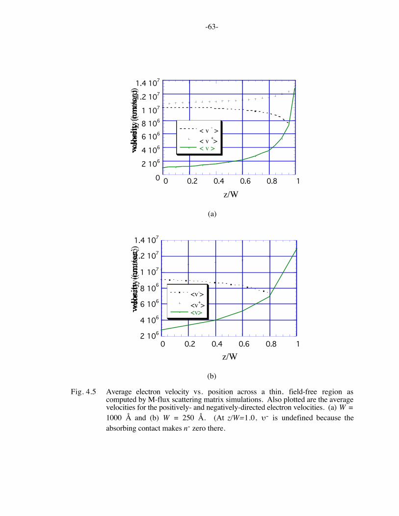
-63-
0
2 106
4 106
6 106
8 106
1 107
1.2 107
1.4 107
0 0.2 0.4 0.6 0.8 1
< v - > < v +>< v >ve
loci
ty (c
m/se
c)
z/W
(a)
2 106
4 106
6 106
8 106
1 107
1.2 107
1.4 107
0 0.2 0.4 0.6 0.8 1
<v-><v+><v>
velo
city
(cm
/sec)
z/W
(b)
Fig. 4.5 Average electron velocity vs. position across a thin, field-free region ascomputed by M-flux scattering matrix simulations. Also plotted are the averagevelocities for the positively- and negatively-directed electron velocities. (a) W =1000 Å and (b) W = 250 Å. (At z/W=1.0, υ- is undefined because theabsorbing contact makes n- zero there.

-64-
Ediff =
kTq
1n
dndz
, (4.34)
shows that energy gradient effects are negligible. These results confirm Shockley'sobservation in 1962; diffusion across a field-free region can be described by Fick's Law,even if the region is thin compared to a mean-free-path and that the appropriate diffusionconstant is that of the corresponding bulk semiconductor. (it is, of course, essential to becareful about the boundary conditions [Han94].) We find that a Fick's Law treatmentagrees with the results displayed in Figs. 4.5-4.7 to within about 5-10%.
The description of transport across thin bases by an effective diffusion coefficientwhich is smaller than the corresponding value in the bulk has been a common practice (e.g.[Har94], [StD95]). The effective diffusion coefficient is needed when an unphysicalboundary condition, n(W) = 0 is employed. This results in an unphysically highconcentration gradient, and to produce the correct current, an unphysical, effectivediffusion coefficient has to be introduced. In reality, the concentration gradient approacheszero in the ballistic limit, and there is no need to reduce the diffusion coefficient. Intransport across a barrier, however, strong concentration gradients do occur and thediffusion coefficient is reduced from its bulk value.
4 .5 .3 Transport Over a BarrierNext, we consider transport of electrons across a forward biased barrier. The
standard treatments of this problem are the diffusion theory, which integrates a drift-diffusion equation across the barrier, and thermionic emission theory [Sze81]. When usinga drift-diffusion equation in a barrier, the mobility is usually taken to be the low-field, near-equilibrium value, because carriers diffuse against the built-in field and are not heated by it[Gok70] (but see [Gun68] for an alternative view). The question of whether a drift-diffusion equation is valid within a barrier, has still not been settled. For example, in ametal-semiconductor junction, the distribution function is strongly distorted from itsequilibrium shape in the so-called kBT layer, and drift-diffusion equations are not thought
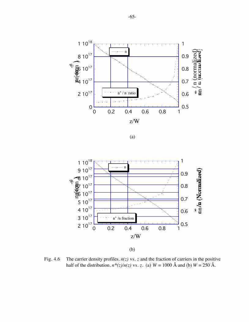
-65-
0
2 1017
4 1017
6 1017
8 1017
1 1018
0.5
0.6
0.7
0.8
0.9
1
0 0.2 0.4 0.6 0.8 1
n
n+ / n ratio
n (c
m -3)
n+ /
n (n
orm
aliz
ed)
z/W
(a)
2 10173 10174 10175 10176 10177 10178 10179 10171 1018
0.5
0.6
0.7
0.8
0.9
1
0 0.2 0.4 0.6 0.8 1
n
n+ /n fraction
n (c
m -3)
n+ /n
(Nor
mal
ized
)
z/W
(b)
Fig. 4.6 The carrier density profiles, n(z) vs. z and the fraction of carriers in the positivehalf of the distribution, n+(z)/n(z) vs. z. (a) W = 1000 Å and (b) W = 250 Å.
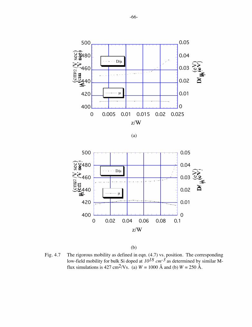
-66-
400
420
440
460
480
500
0
0.01
0.02
0.03
0.04
0.05
0 0.005 0.01 0.015 0.02 0.025
µ
D/µ
µ (cm
2 /V
sec)
D/ µ (e
V)
z/W
(a)
400
420
440
460
480
500
0
0.01
0.02
0.03
0.04
0.05
0 0.02 0.04 0.06 0.08 0.1
µ
D/µ
µ (cm
2 /V
sec)
D/ µ (e
V)
z/W
(b)Fig. 4.7 The rigorous mobility as defined in eqn. (4.7) vs. position. The corresponding
low-field mobility for bulk Si doped at 1018 cm-3 as determined by similar M-flux simulations is 427 cm2/Vs. (a) W = 1000 Å and (b) W = 250 Å.
-67-
to be valid [Ber85]. Here, we consider the metal-semiconductor barrier problem usingscattering theory.
Figure 4.8 shows the energy band diagram for a simple metal/n-Si junction. Wetake the interface to be an ideal, absorbing contact for electrons incident from thesemiconductor. Since the net current under forward-biased conditions is a delicate balancebetween drift and diffusion, it was important to perform the simulations self-consistently
(we iterated until the electrostatic potential converged to < 10-8 kBT/q, and the relative
variation in carrier flux was < 10-12). Figure 4.9 shows a plot of υ + z( ) , υ − z( ) , and
υ z( ) under forward biased conditions. Since carrier transport under forward bias isdominated by diffusion, it is not surprising that the velocity profiles are similar to those
observed in the base transport examples. Note that υ + ≅ υT throughout most of thebarrier, suggesting that a near-equilibrium, one-flux treatment (or a near-equilibrium drift-diffusion treatment) might adequately describe electron transport across the forward-biased
barrier. (Although υ- is not as close to υT, the consequences are limited because the
approximation υ − ≅ υT is least well satisfied near the interface, where the negative halfpopulation is small.) Figure 4.10 shows the carrier density profile, n(z), and the positive-
half fraction, n+(z)/n(z) vs. position. The electric field profile is compared to the energygradient field defined by eqn. (4.33) in Fig. 4.11. The energy gradient field is extremelysmall compared to the electric field; only near the interface does its magnitude rise to asmuch as 10% of the actual electric field. If the energy gradient field can be neglected, thenelectron current flow in the forward biased barrier should be describable by a drift-diffusion equation (with an appropriate mobility and diffusion coefficient).
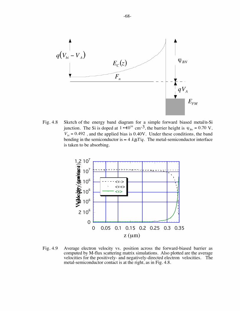
-68-
ϕBNq Vbi − V A( )
EC z( )
Fn
EFM
qVA
Fig. 4.8 Sketch of the energy band diagram for a simple forward biased metal/n-Sijunction. The Si is doped at 1↔1016 cm-3, the barrier height is ϕBn = 0.70 V,Vbi = 0.492 , and the applied bias is 0.40V. Under these conditions, the bandbending in the semiconductor is ≈ 4 kBT/q. The metal-semiconductor interfaceis taken to be absorbing.
0
2 106
4 106
6 106
8 106
1 107
1.2 107
0 0.05 0.1 0.15 0.2 0.25 0.3 0.35
<v-><v+><v>
Vel
ocity
(cm
/sec)
z (µm)
Fig. 4.9 Average electron velocity vs. position across the forward-biased barrier ascomputed by M-flux scattering matrix simulations. Also plotted are the averagevelocities for the positively- and negatively-directed electron velocities. Themetal-semiconductor contact is at the right, as in Fig. 4.8.
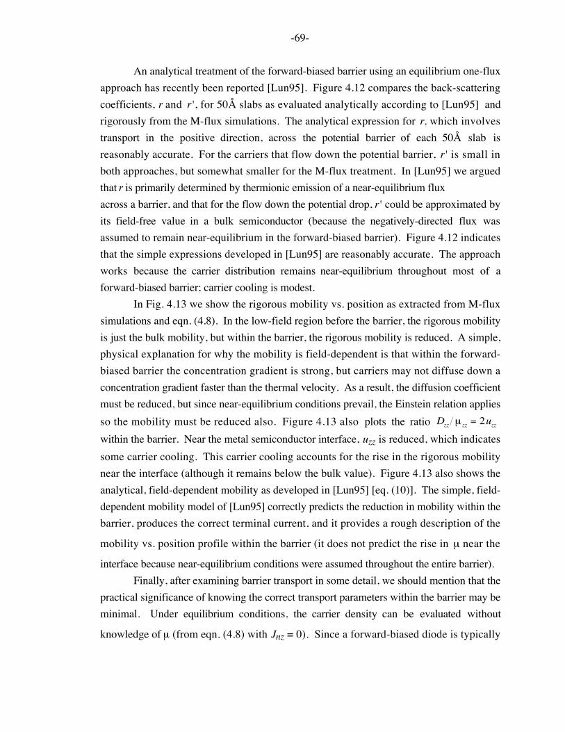
-69-
An analytical treatment of the forward-biased barrier using an equilibrium one-fluxapproach has recently been reported [Lun95]. Figure 4.12 compares the back-scatteringcoefficients, r and r', for 50Å slabs as evaluated analytically according to [Lun95] andrigorously from the M-flux simulations. The analytical expression for r, which involvestransport in the positive direction, across the potential barrier of each 50Å slab isreasonably accurate. For the carriers that flow down the potential barrier, r' is small inboth approaches, but somewhat smaller for the M-flux treatment. In [Lun95] we arguedthat r is primarily determined by thermionic emission of a near-equilibrium fluxacross a barrier, and that for the flow down the potential drop, r' could be approximated byits field-free value in a bulk semiconductor (because the negatively-directed flux wasassumed to remain near-equilibrium in the forward-biased barrier). Figure 4.12 indicatesthat the simple expressions developed in [Lun95] are reasonably accurate. The approachworks because the carrier distribution remains near-equilibrium throughout most of aforward-biased barrier; carrier cooling is modest.
In Fig. 4.13 we show the rigorous mobility vs. position as extracted from M-fluxsimulations and eqn. (4.8). In the low-field region before the barrier, the rigorous mobilityis just the bulk mobility, but within the barrier, the rigorous mobility is reduced. A simple,physical explanation for why the mobility is field-dependent is that within the forward-biased barrier the concentration gradient is strong, but carriers may not diffuse down aconcentration gradient faster than the thermal velocity. As a result, the diffusion coefficientmust be reduced, but since near-equilibrium conditions prevail, the Einstein relation appliesso the mobility must be reduced also. Figure 4.13 also plots the ratio Dzz µ zz = 2uzz
within the barrier. Near the metal semiconductor interface, uzz is reduced, which indicatessome carrier cooling. This carrier cooling accounts for the rise in the rigorous mobilitynear the interface (although it remains below the bulk value). Figure 4.13 also shows theanalytical, field-dependent mobility as developed in [Lun95] [eq. (10)]. The simple, field-dependent mobility model of [Lun95] correctly predicts the reduction in mobility within thebarrier, produces the correct terminal current, and it provides a rough description of the
mobility vs. position profile within the barrier (it does not predict the rise in µ near the
interface because near-equilibrium conditions were assumed throughout the entire barrier).Finally, after examining barrier transport in some detail, we should mention that the
practical significance of knowing the correct transport parameters within the barrier may beminimal. Under equilibrium conditions, the carrier density can be evaluated without
knowledge of µ (from eqn. (4.8) with Jnz = 0). Since a forward-biased diode is typically

-70-
in a near-equilibrium condition, the use of a drift-diffusion equation with any reasonablemobility along with the proper boundary conditions at the contacts (as in the thermionicemission-diffusion treatment) is likely to produce reasonable results. The use of a drift-diffusion equation within the forward biased barrier, even a conventional one, is not likelyto produce serious errors.
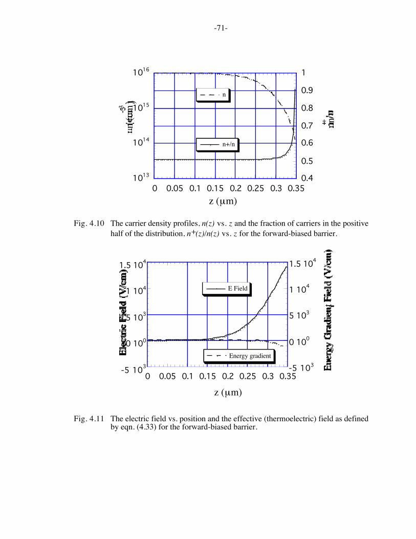
-71-
1013
1014
1015
1016
0.4
0.5
0.6
0.7
0.8
0.9
1
0 0.05 0.1 0.15 0.2 0.25 0.3 0.35
n
n+/n
n (c
m-3)
n+/n
z (µm)
Fig. 4.10 The carrier density profiles, n(z) vs. z and the fraction of carriers in the positivehalf of the distribution, n+(z)/n(z) vs. z for the forward-biased barrier.
-5 103
0 100
5 103
1 104
1.5 104
-5 103
0 100
5 103
1 104
1.5 104
0 0.05 0.1 0.15 0.2 0.25 0.3 0.35
E Field
Energy gradientElec
tric
Fiel
d (V
/cm
)
Ener
gy G
radi
ent F
ield
(V/c
m)
z (µm)
Fig. 4.11 The electric field vs. position and the effective (thermoelectric) field as definedby eqn. (4.33) for the forward-biased barrier.
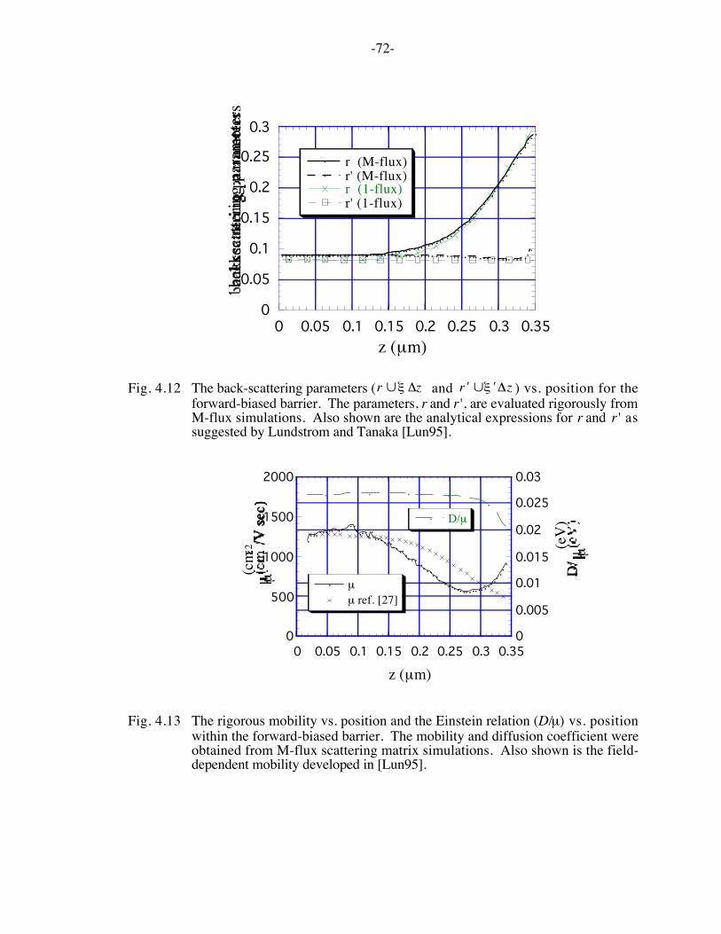
-72-
0
0.05
0.1
0.15
0.2
0.25
0.3
0 0.05 0.1 0.15 0.2 0.25 0.3 0.35
r (M-flux)r' (M-flux)r (1-flux)r' (1-flux)
back
scat
terin
g pa
ram
eter
s
z (µm)
Fig. 4.12 The back-scattering parameters (r ∪ξ Δz and ʹ′ r ∪ ʹ′ ξ Δz ) vs. position for theforward-biased barrier. The parameters, r and r', are evaluated rigorously fromM-flux simulations. Also shown are the analytical expressions for r and r' assuggested by Lundstrom and Tanaka [Lun95].
0
500
1000
1500
2000
0
0.005
0.01
0.015
0.02
0.025
0.03
0 0.05 0.1 0.15 0.2 0.25 0.3 0.35
µµ ref. [27]
D/µ
µ (cm
2 /V se
c)
D/ µ (e
V)
z (µm)
Fig. 4.13 The rigorous mobility vs. position and the Einstein relation (D/µ) vs. positionwithin the forward-biased barrier. The mobility and diffusion coefficient wereobtained from M-flux scattering matrix simulations. Also shown is the field-dependent mobility developed in [Lun95].
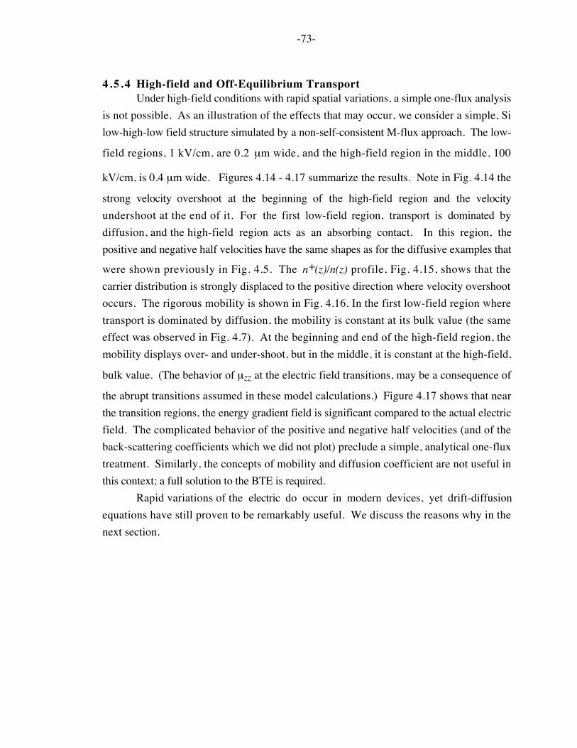
-73-
4 .5 .4 High-field and Off-Equilibrium TransportUnder high-field conditions with rapid spatial variations, a simple one-flux analysis
is not possible. As an illustration of the effects that may occur, we consider a simple, Silow-high-low field structure simulated by a non-self-consistent M-flux approach. The low-
field regions, 1 kV/cm, are 0.2 µm wide, and the high-field region in the middle, 100
kV/cm, is 0.4 µm wide. Figures 4.14 - 4.17 summarize the results. Note in Fig. 4.14 the
strong velocity overshoot at the beginning of the high-field region and the velocityundershoot at the end of it. For the first low-field region, transport is dominated bydiffusion, and the high-field region acts as an absorbing contact. In this region, thepositive and negative half velocities have the same shapes as for the diffusive examples that
were shown previously in Fig. 4.5. The n+(z)/n(z) profile, Fig. 4.15, shows that thecarrier distribution is strongly displaced to the positive direction where velocity overshootoccurs. The rigorous mobility is shown in Fig. 4.16. In the first low-field region wheretransport is dominated by diffusion, the mobility is constant at its bulk value (the sameeffect was observed in Fig. 4.7). At the beginning and end of the high-field region, themobility displays over- and under-shoot, but in the middle, it is constant at the high-field,
bulk value. (The behavior of µzz at the electric field transitions, may be a consequence of
the abrupt transitions assumed in these model calculations.) Figure 4.17 shows that nearthe transition regions, the energy gradient field is significant compared to the actual electricfield. The complicated behavior of the positive and negative half velocities (and of theback-scattering coefficients which we did not plot) preclude a simple, analytical one-fluxtreatment. Similarly, the concepts of mobility and diffusion coefficient are not useful inthis context; a full solution to the BTE is required.
Rapid variations of the electric do occur in modern devices, yet drift-diffusionequations have still proven to be remarkably useful. We discuss the reasons why in thenext section.
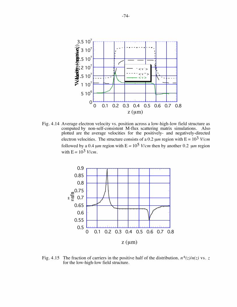
-74-
0
5 106
1 107
1.5 107
2 107
2.5 107
3 107
3.5 107
0 0.1 0.2 0.3 0.4 0.5 0.6 0.7 0.8
< v - >< v + >< v >
Vel
ocity
(cm
/sec)
z (µm)
Fig. 4.14 Average electron velocity vs. position across a low-high-low field structure ascomputed by non-self-consistent M-flux scattering matrix simulations. Alsoplotted are the average velocities for the positively- and negatively-directedelectron velocities. The structure consists of a 0.2 µm region with E = 103 V/cmfollowed by a 0.4 µm region with E = 105 V/cm then by another 0.2 µm regionwith E = 103 V/cm.
0.50.550.6
0.650.7
0.750.8
0.850.9
0 0.1 0.2 0.3 0.4 0.5 0.6 0.7 0.8
n+/n
z (µm)
Fig. 4.15 The fraction of carriers in the positive half of the distribution, n+(z)/n(z) vs. zfor the low-high-low field structure.

-75-
0
500
1000
1500
2000
2500
0
0.05
0.1
0.15
0.2
0.25
0.3
0 0.1 0.2 0.3 0.4 0.5 0.6 0.7 0.8
µ
D/µ
µ (cm
2 /V se
c)
D/ µ (e
V)
z (µm)
Fig. 4.16 The rigorous mobility vs. position and the Einstein relation (D/µ) vs. positionwithin the low-high-low field structure. The mobility and diffusion coefficientwere obtained from M-flux scattering matrix simulations using eqn. (4.8).
-1.5 105
-1 105
-5 104
0
5 104
0 0.1 0.2 0.3 0.4 0.5 0.6 0.7 0.8
EE'
E an
d E'
(V/c
m)
z (µm)
Fig. 4.17 The energy gradient field vs. position and the within the low-high-low fieldstructure. Also shown is the actual electric field vs. position.

-76-
4.6 DiscussionIt is relatively easy to state the general conditions under which the drift-diffusion
equation applies and when it does not, but it is another matter to determine whether itprovides an adequate description of a given device. Drift-diffusion transport continues tobe the basis for numerical simulations and compact circuit models of Si transistors. Giventhe high, rapidly varying electric fields in modern devices, it is not obvious why drift-diffusion based approaches continue to work. A simple answer is that the drift-diffusionmodel is not valid, but the “tuning” of parameters to match experimental data simply fits themodel to measured results. But there seems to be more to it than that. Drift-diffusionmodels invariably provide a good description of the transistor's current-voltagecharacteristics, and parameter tuning is relatively minor and still results in physicallyreasonable parameter values. Moreover, when drift-diffusion simulations are used toproject the performance of new technologies, the results usually provide good guidance forexperimental work. There must be a deeper reason for the continued success of the drift-diffusion equation.
Figure 4.18 is an energy band diagram for a bipolar transistor. The emitter is athermal source of electrons that are injected into the base across which they drift and diffuseuntil they enter the collector and are swept out. The steady-state current in a Si bipolartransistor is set by the emitter-base barrier and by transport across the base. Formoderately thick base widths, base transport is well-described by drift-diffusion. Asdiscussed in Sec. 4.5, however, a drift-diffusion treatment may still work when the base isnot thick compared to a mean-free-path. For drift-diffusion to apply, electrons must beinjected from a thermal source (and not, for example, from a heterojunction launchingramp), and the correct boundary conditions must also be applied at the end of the base.The average velocity there should not exceed the thermal injection velocity (we are, ofcourse, ignoring the ∪ 20% enhancement due to the increased transmission probability ofnear-normal electrons as illustrated in Fig. 4.5). Because the saturated drift velocity in the
high-field collector is approximately υT, the appropriate boundary occurs. (albeit in an
unphysical manner!) Of course, for a thin base transistor, the collector delay will alsobecome important, and the transient response (i.e. fT) may be influenced by off-equilibriumtransport. Drift-diffusion based approaches tend to work for Si transistors
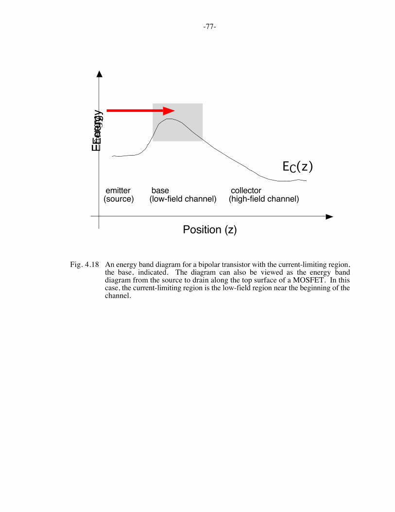
-77-
EC(z)
Position (z)
Ener
gy
emitter (source)
collector (high-field channel)
base (low-field channel)
Fig. 4.18 An energy band diagram for a bipolar transistor with the current-limiting region,the base, indicated. The diagram can also be viewed as the energy banddiagram from the source to drain along the top surface of a MOSFET. In thiscase, the current-limiting region is the low-field region near the beginning of thechannel.
-78-
because transport across the steady-state current-limiting region of the transistor, the quasi-neutral base, can be described by a drift-diffusion equation.
The operating principles of MOSFETs and bipolar transistors are usually thought tobe different, the first being a “field-effect transistor” and the second being a “potential effecttransistor” [Ng96]. At a deeper level, however, the two devices are quite similar [Joh73].Figure 4.18 can also be regarded as the energy band diagram along the channel of aMOSFET. Thermal electrons are injected from the source over a small potential barrierbetween the source and channel. After drifting and diffusing across the low-field regionnear the source end of the channel, they enter a high-field region which collects them andsends them to the drain. This analogy between the MOSFET and bipolar transistor hasbeen known for some time [Joh73], but for long-channel transistors, the first part, injectionof carriers from the thermal source across the source-channel potential barrier, is rapid, sochannel transport is the rate-limiting process and the current is controlled by theconductance of the channel. (As channel lengths decrease, however, the injection processwill increase in importance [Lun97].) Monte Carlo simulations show that once a carrier hastraveled a small distance down the channel potential drop (roughly kBT/q in potential drop),then even if it back-scatters, it cannot surmount the potential barrier and return to the source[Lun97]. The steady-state current-limiting region of a MOSFET, therefore, is a small,low-field portion of the channel near the source. Just as for the base of a bipolar transistor,this region can be approximately described by drift-diffusion transport.
This discussion shows that in Si transistors, both bipolar and field-effect, have acurrent-limiting region that tends to be adequately described by drift-diffusion transport.Moreover, as devices are scaled down in size, doping levels are increased and supplyvoltages reduced in order to preserve this low-field, current limiting region. This isnecessary to preserve the ability to turn a transistor off and to minimize the outputconductance. One could say that a good Si transistor is one that is designed to bedescribable by drift-diffusion equations. Drift-diffusion treatments will not work as wellfor III-V transistors where heterojunctions can produce non-equilibrium injection andwhere the high-field saturated velocity tends to be lower than _T.
In this chapter we have been concerned with the drift-diffusion equation and itsrelation to the scattering theory of transport. Vaidyanathan and Pulfrey [Vai96] recentlyaddressed similar issues and concluded that: 1) under near-equilibrium conditions, thedrift-diffusion and one-flux equations are identical, 2) for thin-base transport, the one-fluxmethod is equivalent to the use of a diffusion equation with appropriate boundaryconditions, and 3) the one-flux theory of barrier transport, as described by Lundstrom and

-79-
Tanaka [Lun95] has no obvious physical basis [Vai96]. Conclusions 1) and 2) areconsistent with the results presented here, as well as with earlier work [Tan94], includingShockley's [Sho62]. With regard to Conclusion 3, the M-flux barrier transport simulationspresented in Sec. 4.5 seem to generally bear out the physical basis for the analyticaltreatment in [Lun95] as well as the major conclusion that the mobility is reduced in aforward-biased barrier. The details of barrier transport are, however, complex, and asimple, analytical treatment should only be used as a rough approximation. Finally, notethat our focus has been on steady-state transport where the flux equations can be re-castinto a standard drift-diffusion form. Vaidyanathan and Pulfrey [Vai96] showed that thetime-dependent flux equations lead to a current equation that contains an additional term dueto momentum relaxation.
4.7 Summary and ConclusionsIn this chapter we revisited the drift-diffusion equation by viewing it from the
perspective of scattering theory. The drift-diffusion equation is formally identical to asimple, near-equilibrium one-flux version of the Boltzmann Transport Equation. Thisderivation showed that the drift-diffusion equation can be applied to quasi-ballistic transportunder conditions that tend to occur in the current-limiting region of a transistor. Moreover,the problem of transport across a barrier can be treated by a drift-diffusion equation, but themobility and diffusion coefficient should be regarded as field-dependent quantities, incontrast to conventional practice. (Barrier transport is increasing in importance as devicedimensions shrink and barrier transport becomes the limiting process.) Finally, weshowed that when it is necessary to resolve the carrier distribution function, the BTE can berecast into a drift-diffusion formulation by discretizing momentum space into M fluxes.Solving the BTE then reduces to solving M coupled drift-diffusion/continuity equations.
The drift-diffusion equation has been successfully applied to transistors for almost50 years. It works because transistors are designed to have a current limiting region thatcan be controlled by a gate (or base), and this region tends to be adequately described bydrift-diffusion transport. It seems likely that the drift-diffusion equation will continue tofind wide application, even as Si technology enters the nanometer regime.
-81-
5. ON THE PERFORMANCE LIMITS FOR SI MOSFETS: ATHEORETICAL STUDY
5.0 Chapter in briefIn this chapter, we present a theory to compute the performance limit of silicon MOSFETs.
This theory incorporates a simple analytical treatment, but is augmented by self-consistentSchrödinger-Poisson simulations. The on-current, transconductance, and drain-to-sourceresistance in the ballistic limit (which corresponds to the channel length approaching zero) areexamined. The ballistic transconductance in the limit that the oxide thickness approaches zero isalso examined.
5 .1 . IntroductionAs silicon technology advances, questions about ultimate performance limits arise. Toriumi
et al. estimated performance limits by extrapolating measured results to the limits of zero channellength and zero oxide thickness [Tor88]. Their results suggested that the electron saturationvelocity and finite inversion layer capacitance set a limiting transconductance of about 3000mS/mm. In this chapter, we re-examine MOSFET limits by calculating the theoretical performancelimits for an idealized, ballistic MOSFET using an approach similar to that of Natori [Nat94] andour own recent work [3,4]. For this study, we make use of self-consistent Schrödinger-Poissonsimulations [Vas97] to examine the validity of several simplifying assumptions made in earlierwork. The results should be useful for assessing the performance potential of different transistorsdesigns, for comparing measured device characteristics against ultimate limits, and for identifyingimportant technological and theoretical issues for silicon transistors at the end of the roadmap[SIA97].
Before we begin, we should ask whether the ballistic limits discussed here are of concernfor present-day devices. Hot electrons near the drain have a mean-free-path of only a fewAngstroms, much shorter than the channel length of present-day MOSFETs. But when theperformance of present-day MOSFETs is compared to the corresponding ballistic limits presentedin this chapter, we find that they operate at roughly 30-40% of the ballistic limit. The reason is thatthe steady-state on-current is controlled by a very short region near the source [Lun97]. Once themean-free-path (which is longer near the source) is comparable to the length of this critical region,quasi-ballistic transport occurs. This is analogous to transport in metal-semiconductor diodes,

-82-
where the thermionic emission (ballistic) theory applies if the mean-free-path is longer than thedistance over which the first kBT/q of potential drop occurs (the so-called Bethe condition).Current levels that approach the ballistic limit occur when the mean-free-path is comparable to thelength of the critical region of the device; it does not have to be longer than the channel lengthitself.
In this chapter, we examine the limiting performance of a device corresponding to the L =100 nm node in the 1997 National Technology Roadmap for Semiconductors (NTRS) [SIA97].The device on-current, transconductance, and source-to-drain resistance will be examined in twolimits, the ballistic limit (corresponding to the channel length approaching zero or the mean-free-path approaching infinity) and the zero oxide thickness limit. Although there are simplifyingassumptions in the theoretical model, the results will indicate that the ultimate MOSFET limits areconsiderably higher than previously estimated and well above those currently achieved. On theother hand, the transconductance limit is well below that projected by Johnson, who argued that asthe channel length and oxide thickness approach zero, the transconductance of a MOSFET shouldapproach that of a bipolar transistor [Joh73]. If projections like those to be described in thischapter are done for devices at the end of the NTRS, they show that to achieve the performancetargets called for, devices will have to operate significantly closer to their ultimate limits thantoday’s devices. Parasitic resistances and scattering at the oxide-silicon interface tend to increaseas devices are scaled and will make it difficult to operate closer to the ballistic limits. New devicedesigns are likely to be necessary to achieve device performance targets at the end of the NTRS.
5 .2 . TheoryThe ballistic current for a MOSFET is readily evaluated as described by Natori [Nat94] and
Datta [Dat97]. A sketch of the derivation is presented in the appendix; the important results aresummarized here. Fig. 5.1 shows the geometry. Current flow is in the x-direction, the confiningpotential is in the y-direction, and the width of the transistor is in the z-direction. The drain currentis sum of the contributions from each subband. The positive kx states are populated by injectionfrom the source, and the negative kx states by injection from the drain. The drain currentcontributed by subband, i, is
IDi
W=
qh
2mCi
2kBTπ
⎛ ⎝
⎞ ⎠
3/2⎡
⎣ ⎢ ⎤
⎦ ⎥ F1/2 (EF − εi)/ kBT[ ] −F1/2 (EF − εi − qVD)/ kBT[ ]{ } , (5.1)

-83-
where mCi is the conductivity effective mass of subband, i, and ε i is the subband energy and
F1/2 η[ ] is the Fermi-Dirac integral of order one-half as defined by Blakemore [Bla82]. Similarly,the electron density in subband, i, is
nSi =mDi
π h2
kBT2
⎡
⎣ ⎢ ⎤
⎦ ⎥ ln 1+ e ( EF−ε i) / kBT( ) + ln 1 + e ( EF− εi −qVD )/ kBT( ){ }, (5.2)
where mDi is the density of states effective mass for the subband. Under high drain bias, injectionfrom the drain is suppressed, and the on-current can be written as
IDi(on)/ W = qnSiυinji , (5.3)
where
υinj
i =2kBTmCi
πmDi2
F1 / 2[(EF − ε i)/ kBT]ln 1 + e(E F−εi ) / kBT ]( )
⎛
⎝ ⎜ ⎜
⎞
⎠ ⎟ ⎟ , (5.4)
is the product of the non-degenerate thermal velocity, υTi = 2kBT mCi π mDi
2 , and a correction
factor for Fermi-Dirac statistics. For small drain biases, we find the drain-to-source conductanceas
GDi
W=
q2
π3 / 2h
2mCikBT
2⎡
⎣ ⎢
⎤
⎦ ⎥ F−1/2 (EF − ε i )/ kBT[ ]. (5.5)
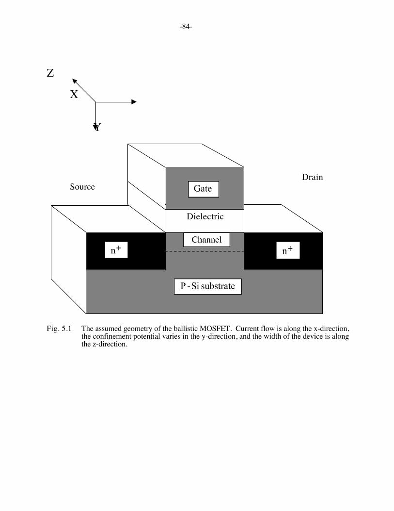
-84-
Z
X
Y
DrainSource
Fig. 5.1 The assumed geometry of the ballistic MOSFET. Current flow is along the x-direction,the confinement potential varies in the y-direction, and the width of the device is alongthe z-direction.
+n+
+nChannel
substrate Si-P
Gate
Dielectric
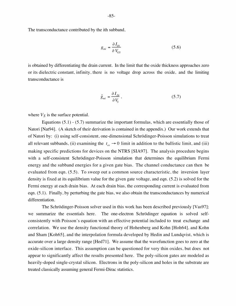
-85-
The transconductance contributed by the ith subband,
gmi =∂ IDi
∂VGS
(5.6)
is obtained by differentiating the drain current. In the limit that the oxide thickness approaches zeroor its dielectric constant, infinity, there is no voltage drop across the oxide, and the limitingtransconductance is
ˆ g mi =∂ IDi
∂VS
, (5.7)
where VS is the surface potential.Equations (5.1) - (5.7) summarize the important formulas, which are essentially those of
Natori [Nat94]. (A sketch of their derivation is contained in the appendix.) Our work extends thatof Natori by: (i) using self-consistent, one-dimensional Schrödinger-Poisson simulations to treatall relevant subbands, (ii) examining the tox → 0 limit in addition to the ballistic limit, and (iii)making specific predictions for devices on the NTRS [SIA97]. The analysis procedure beginswith a self-consistent Schrödinger-Poisson simulation that determines the equilibrium Fermienergy and the subband energies for a given gate bias. The channel conductance can then beevaluated from eqn. (5.5). To sweep out a common source characteristic, the inversion layerdensity is fixed at its equilibrium value for the given gate voltage, and eqn. (5.2) is solved for theFermi energy at each drain bias. At each drain bias, the corresponding current is evaluated fromeqn. (5.1). Finally, by perturbing the gate bias, we also obtain the transconductances by numericaldifferentiation.
The Schrödinger-Poisson solver used in this work has been described previously [Vas97];we summarize the essentials here. The one-electron Schrödinger equation is solved self-consistently with Poisson’s equation with an effective potential included to treat exchange andcorrelation. We use the density functional theory of Hohenberg and Kohn [Hoh64], and Kohnand Sham [Koh65], and the interpolation formula developed by Hedin and Lundqvist, which isaccurate over a large density range [Hed71]. We assume that the wavefunction goes to zero at theoxide-silicon interface. This assumption can be questioned for very thin oxides, but does notappear to significantly affect the results presented here. The poly-silicon gates are modeled asheavily-doped single-crystal silicon. Electrons in the poly-silicon and holes in the substrate aretreated classically assuming general Fermi-Dirac statistics.
-86-
Our one-dimensional treatment of MOS electrostatics implies a gradual channelapproximation at the source and drain ends of the channel. The source end is at the top of apotential energy barrier, so the lateral electric field is zero and a one-dimensional treatment isreasonable. (The second derivative is non-zero, however, so two-dimensional effects such asdrain-induced barrier lowering (DIBL) need to be accounted for separately.) At the drain end, theone-dimensional treatment can only be justified at low drain voltages, but when the voltage exceedsa few kBT/q, carrier injection from the drain is small, so the assumption has little effect on the draincurrent.
5 .3 . ResultsThe device examined was taken from the L = 100 nm node of the National Technology
Roadmap for Semiconductors [SIA97]. The oxide thickness is 1.5 nm, and the substrate is
uniformly doped at NA = 2.0 × 1018 cm-3. This substrate doping results in a threshold voltage ofabout 0.4 V, which is much too high for the assumed 1.0 V power supply. In practice, however,this value would be lowered by two-dimensional, short channel effects which are not consideredhere. Results are quoted, therefore, at a gate overdrive of VGS − VT = 0.8V , which would resultfor a more appropriate VT of ≈ 0.2 V. (Note that the uniform channel doping was assumed only toprovide a baseline against which more sophisticated channel doping profiles can be compared. Forexample, it would be interesting to compare the ultimate performance of a super steep retrograde(SSR) channel profile [Sha93] against a uniform profile.) Unless otherwise stated, all simulationsare for T = 300K. In the remainder of this section, we present several results and discuss someissues. At the end of the section, we summarize the ultimate performance parameters for thismodel device.
In equilibrium, the positive and negative kx states in the carrier distribution function areboth occupied. In a ballistic MOSFET, however, positive kx states are populated by injection fromthe source, and the negative kx states by injection from the drain. If the drain bias exceeds severalkBT/q, therefore, the carrier distribution function at the source will consist of only positive kx
states. The effects of this strongly off-equilibrium distribution on MOS electrostatics will beexamined next.
Fig. 5.2 shows the computed inversion layer density vs. gate voltage as obtained by self-consistent, Schrödinger-Poisson simulations [Vas97]. Results for both a metal gate and apolysilicon gate are shown. The metal gate is taken to be aluminum (with a workfunction
difference of χSi −Φ M = 0.05 eV) while the polysilicon gate is doped to 1 x 1020 cm-3. As
expected, the equilibrium nS vs. VGS characteristics (solid lines) are well fit by
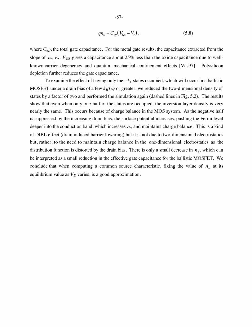
-87-
qnS = Ceff VGS −VT( ) , (5.8)
where Ceff, the total gate capacitance. For the metal gate results, the capacitance extracted from theslope of nS vs. VGS gives a capacitance about 25% less than the oxide capacitance due to well-known carrier degeneracy and quantum mechanical confinement effects [Vas97]. Polysilicondepletion further reduces the gate capacitance.
To examine the effect of having only the +kx states occupied, which will occur in a ballisticMOSFET under a drain bias of a few kBT/q or greater, we reduced the two-dimensional density ofstates by a factor of two and performed the simulation again (dashed lines in Fig. 5.2). The resultsshow that even when only one-half of the states are occupied, the inversion layer density is verynearly the same. This occurs because of charge balance in the MOS system. As the negative halfis suppressed by the increasing drain bias, the surface potential increases, pushing the Fermi leveldeeper into the conduction band, which increases nS and maintains charge balance. This is a kindof DIBL effect (drain induced barrier lowering) but it is not due to two-dimensional electrostaticsbut, rather, to the need to maintain charge balance in the one-dimensional electrostatics as thedistribution function is distorted by the drain bias. There is only a small decrease in nS , which canbe interpreted as a small reduction in the effective gate capacitance for the ballistic MOSFET. Weconclude that when computing a common source characteristic, fixing the value of nS at itsequilibrium value as VD varies, is a good approximation.
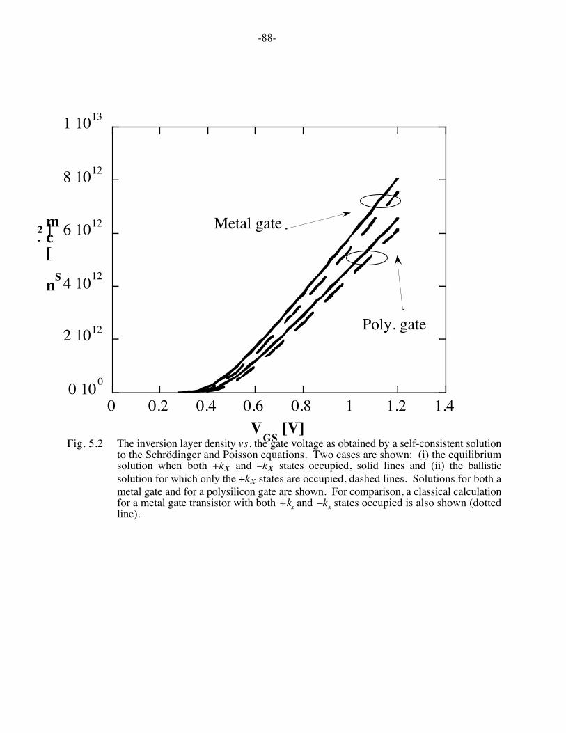
-88-
Fig. 5.2 The inversion layer density vs. the gate voltage as obtained by a self-consistent solutionto the Schrödinger and Poisson equations. Two cases are shown: (i) the equilibriumsolution when both +kx and –kx states occupied, solid lines and (ii) the ballisticsolution for which only the +kx states are occupied, dashed lines. Solutions for both ametal gate and for a polysilicon gate are shown. For comparison, a classical calculationfor a metal gate transistor with both +kx and –kx states occupied is also shown (dottedline).
0 100
2 1012
4 1012
6 1012
8 1012
1 1013
0 0.2 0.4 0.6 0.8 1 1.2 1.4
nS [cm
-2 ]
VGS
[V]
Poly. gate
Metal gate
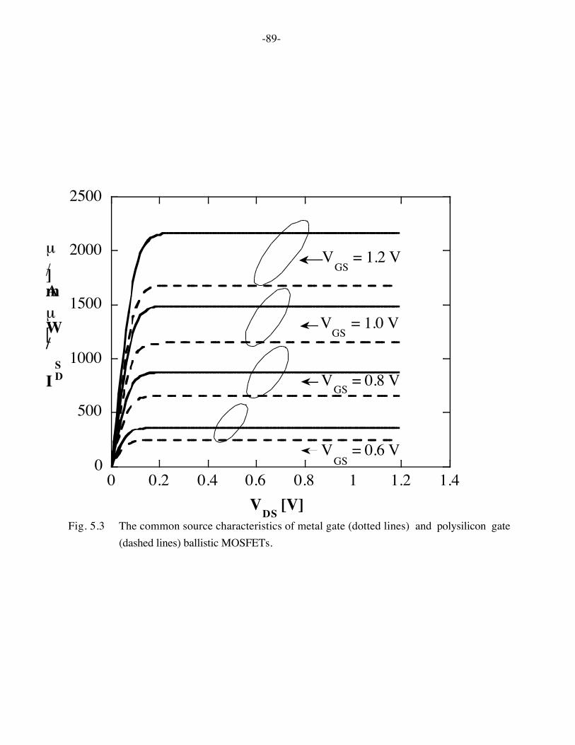
-89-
Fig. 5.3 The common source characteristics of metal gate (dotted lines) and polysilicon gate(dashed lines) ballistic MOSFETs.
0
500
1000
1500
2000
2500
0 0.2 0.4 0.6 0.8 1 1.2 1.4
I DS
/W[µΑ/µ
m]
VDS
[V]
VGS
= 1.0 V
VGS
= 0.6 V
VGS
= 1.2 V
VGS
= 0.8 V
-90-
Fig. 5.4 The common source characteristics of a metal gate ballistic MOSFET showing the effectof DIBL. Without DIBL (solid line) and with an assumed DIBL of 100 mV/V (dashedline).
0
500
1000
1500
2000
2500
3000
0 0.2 0.4 0.6 0.8 1 1.2 1.4
I DS/
W [µA/µm]
VDS
[V]
VGS
= 1.2 V
VGS
= 1.0 V
VGS
= 0.6 V
VGS
= 0.8 V
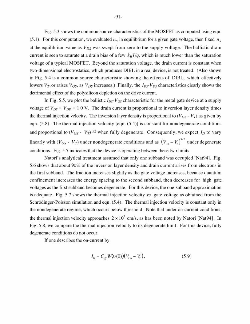
-91-
Fig. 5.3 shows the common source characteristics of the MOSFET as computed using eqn.(5.1). For this computation, we evaluated nS in equilibrium for a given gate voltage, then fixed nS
at the equilibrium value as VDS was swept from zero to the supply voltage. The ballistic draincurrent is seen to saturate at a drain bias of a few kBT/q, which is much lower than the saturationvoltage of a typical MOSFET. Beyond the saturation voltage, the drain current is constant whentwo-dimensional electrostatics, which produces DIBL in a real device, is not treated. (Also shownin Fig. 5.4 is a common source characteristic showing the effects of DIBL, which effectivelylowers VT, or raises VGS, as VDS increases.) Finally, the IDS-VDS characteristics clearly shows thedetrimental effect of the polysilicon depletion on the drive current.
In Fig. 5.5, we plot the ballistic IDS-VGS characteristic for the metal gate device at a supplyvoltage of VDS = VDD = 1.0 V. The drain current is proportional to inversion layer density timesthe thermal injection velocity. The inversion layer density is proportional to (VGS - VT) as given byeqn. (5.8). The thermal injection velocity [eqn. (5.4)] is constant for nondegenerate conditions
and proportional to (VGS - VT)1/2 when fully degenerate. Consequently, we expect ID to vary
linearly with (VGS - VT) under nondegenerate conditions and as VGS − VT( )3 / 2 under degenerate
conditions. Fig. 5.5 indicates that the device is operating between these two limits.Natori’s analytical treatment assumed that only one subband was occupied [Nat94]. Fig.
5.6 shows that about 90% of the inversion layer density and drain current arises from electrons inthe first subband. The fraction increases slightly as the gate voltage increases, because quantumconfinement increases the energy spacing to the second subband, then decreases for high gatevoltages as the first subband becomes degenerate. For this device, the one-subband approximationis adequate. Fig. 5.7 shows the thermal injection velocity vs. gate voltage as obtained from theSchrödinger-Poisson simulation and eqn. (5.4). The thermal injection velocity is constant only inthe nondegenerate regime, which occurs below threshold. Note that under on-current conditions,
the thermal injection velocity approaches 2 ×107 cm/s, as has been noted by Natori [Nat94]. InFig. 5.8, we compare the thermal injection velocity to its degenerate limit. For this device, fullydegenerate conditions do not occur.
If one describes the on-current by
ID = Ceff W υ(0) VGS − VT( ) , (5.9)
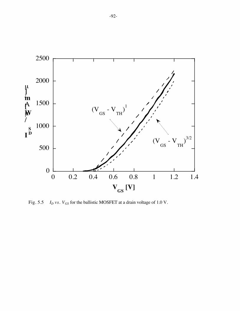
-92-
Fig. 5.5 ID vs. VGS for the ballistic MOSFET at a drain voltage of 1.0 V.
0
500
1000
1500
2000
2500
0 0.2 0.4 0.6 0.8 1 1.2 1.4
I DS
/W[µΑ/µ
m]
VGS
[V]
(VGS
- VTH
)1
(VGS
- VTH
)3/2
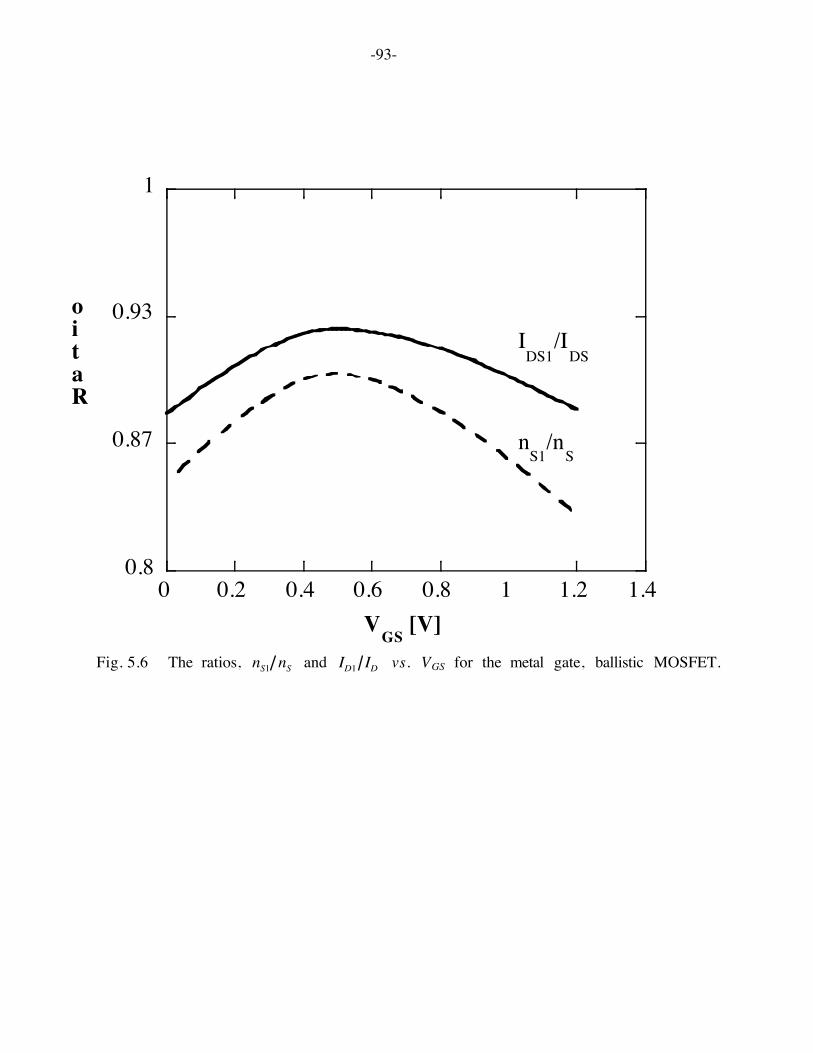
-93-
Fig. 5.6 The ratios, nS1 nS and ID1 ID vs. VGS for the metal gate, ballistic MOSFET.
0.8
0.87
0.93
1
0 0.2 0.4 0.6 0.8 1 1.2 1.4
Ratio
VGS
[V]
IDS1
/IDS
nS1
/nS
-94-
Fig. 5.7 The ballistic injection velocity at the source vs. gate voltage, VGS, for the metal gate,ballistic MOSFET. Also shown is the injection velocity for the first subband alone.
1.0 10 7
1.2 10 7
1.4 10 7
1.6 10 7
1.8 10 7
2.0 10 7
0 0.2 0.4 0.6 0.8 1 1.2 1.4
υinj[
cm/sec]
VGS
[V]
Total carrier
First subband carrier
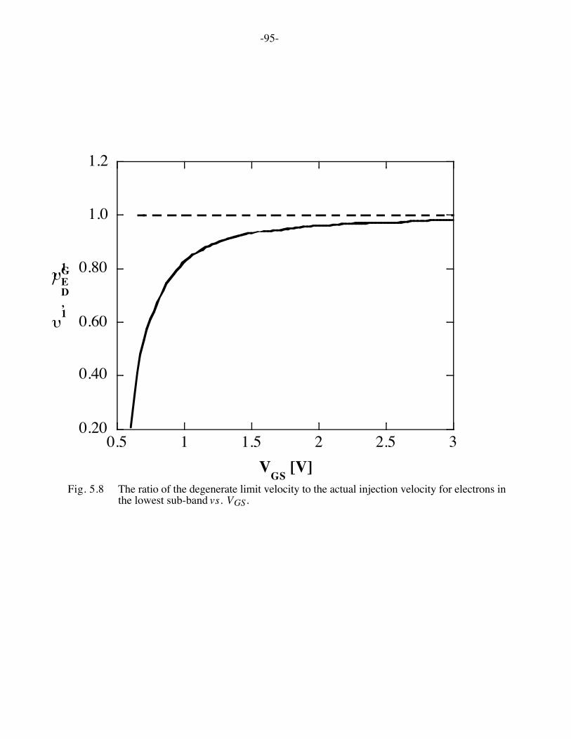
-95-
Fig. 5.8 The ratio of the degenerate limit velocity to the actual injection velocity for electrons inthe lowest sub-band vs. VGS.
0.20
0.40
0.60
0.80
1.0
1.2
0.5 1 1.5 2 2.5 3
υ1,DEG/υ1
VGS
[V]
-96-
then the upper limit for the average velocity at the source, υ(0) , is the thermal injection velocity.
In practice, scattering will reduce υ(0) below the thermal injection velocity [Lun97]. In smalltransistors, strong velocity overshoot occurs within the channel. Through its influence on the self-consistent channel potential, velocity overshoot affects the electric field at the source, and thereforecarrier backscattering and consequently υ(0) [Lun97]. But velocity overshoot does not change
the upper limit for υ(0) . The transconductance of the ballistic MOSFET is
gm / W =∂ ID / W( )∂VGS
= Ceffυ inj + Ceff VGS −VT( ) ∂υinj
∂VGS
. (5.10)
If the second term is small, then the transconductance is a measure of the thermal injection velocity.Fig. 5.9 compares the computed transconductance with that obtained from the first term on theright hand side of eqn. (5.10). In the subthreshold region, where the thermal injection velocity isconstant, the second term in eqn. (5.10) is negligible, but above threshold it is not. If one were todeduce a velocity from the transconductance by ignoring the second term, as is common practice,the result would be higher than the actual thermal injection velocity.
A useful way to assess the transconductance is to examine the ratio, gm / ID. For a bipolar
transistor, this ratio is q kBT ≈ 40 . It has been argued that for a MOSFET with the oxidethickness approaching zero, gm / ID should approach the bipolar limit [Joh73]. Fig. 5.10 plots
gm / ID vs. VGS for the model transistor. Below threshold, the transconductance does approachthe bipolar limit. (It is a little lower than the bipolar limit because the subthreshold slope of theMOSFET is higher than the theoretical minimum of 60 mV/decade.) Above threshold, however,gm / ID is only about 5% of the bipolar limit - even for the assumed oxide thickness of 1.5 nm. In
the limit that tox approaches zero, we can evaluate the limiting transconductance, ˆ g m from eqn.
(5.7). The result is shown in Fig. 5.11. Below threshold, ˆ g m / ID is even closer to the bipolarlimit. (It is a little lower because of the finite inversion layer thickness.) Above threshold, the ratiodrops, but it is a sizable fraction of the bipolar limit. The limiting transconductance increases withsurface potential; its maximum value will be set by the maximum surface potential that can beachieved. Finally, note that these results show that a hypothetical MOSFET with a gate insulatorhaving an infinite dielectric constant (so that its electrical thickness is zero)
-97-
Fig. 5.9 The transconductance vs. VGS for the ballistic MOSFETs (solid lines). Also shown, isthe product of Ceff υinj (dashed lines). The transconductance is seen to be higher thanCeff υinj for VGS > 0.6V.
-98-
and an infinite bandgap (so that there is no penetration of the wavefunction into the insulator), stilldelivers a lower transconductance than a corresponding bipolar transistor. In practice, tunnelingthrough the gate insulator would further reduce performance, so that MOSFETs will always deliverconsiderably lower transconductance that bipolar transistors.
Fin a lly , we e xa m in e t h e in t r in sic d r a in t o so u r ce r e sis t a n ce o f t h e
b a llis t ic MOSFET. Con ven t ion a l MOSFET t h e o r y p r e d ict s a ch a n n el
r e s is t a n ce t h a t go e s a s t h e le n g t h o f t h e ch a n n e l, so in t h e b a llis t ic lim it ,
wh e r e L a p p r o a ch e s ze r o , t h e r e sh o u ld b e n o ch a n n e l r e sist a n ce . Eq u a t io n
(5 .5 ), h o we ve r , sh o ws t h a t t h e b a llis t ic MOSFET h a s a fin it e r e sis t a n ce .
Th is r e s is t a n ce , d u e t o t h e fin it e n u m b e r o f t r a n sve r se m o d e s a va ila b le t o
co n d u ct cu r r en t , is a n a lo go u s t o t h e h / 2 e 2 q u a n t u m co n t a ct r e sis t a n ce o f a
m e so sco p ic d e v ice [Da t 9 5 ] . It s e t s a lo w e r lim it fo r t h e r e sis t a n ce o f a
MOSFET, in d ep en d en t o f con ta ct t ech n o logy . Fig . 5 .1 2 is a p lo t o f t h e
in t r in s ic r e s is t a n ce o f t h e b a llis t ic MOSFET. Th is ga t e -v o lt a ge d ep en d en t
in t r in sic r e sis t a n ce is la r ge e n o u gh t h a t it m a y h a ve t o b e a cco u n t e d fo r in
a n a lyzin g e xp e r im e n t s . A sim p le p h y sica l exp la n a t ion fo r t h e fin it e
r e sis t a n ce o f t h e b a llis t ic ch a n n e l is t h a t t h e n e t d r a in t o so u r ce cu r r e n t is
t h e d iffe r e n ce b e t we e n t h e cu r r e n t t h e r m io n ica lly in je ct e d fr o m t h e so u r ce
a n d t h a t t h e r m io n ica lly in ject ed fr o m t h e d r a in . Th e cu r r en t in ject ed fr o m
t h e d r a in is lo we r b y a fa ct o r o f exp[−qVDS / kBT] in t h e n o n -d e ge n e r a t e lim it .
At sm a ll d r a in b ia se s , t h e e xp o n e n t ia l ca n b e e xp a n d e d , a n d we fin d t h a t
t h e n e t cu r r e n t is p r o p o r t io n a l t o t h e d r a in v o lt a ge , wh ich g iv e s a fin it e
r e sist a n ce . Th e co m p u t e d p e r fo r m a n ce lim it s fo r t h e L = 1 0 0 n m b a llis t ic
MOSFET a r e su m m a r ized b e lo w:
Table 5.1Computed performance of the model ballistic device at 300K. The threshold voltage was ≈ 0.4 V
and the gate overdrive was VGS − VT( ) ≈ 0.8 V and the drain voltage was 1.0V.
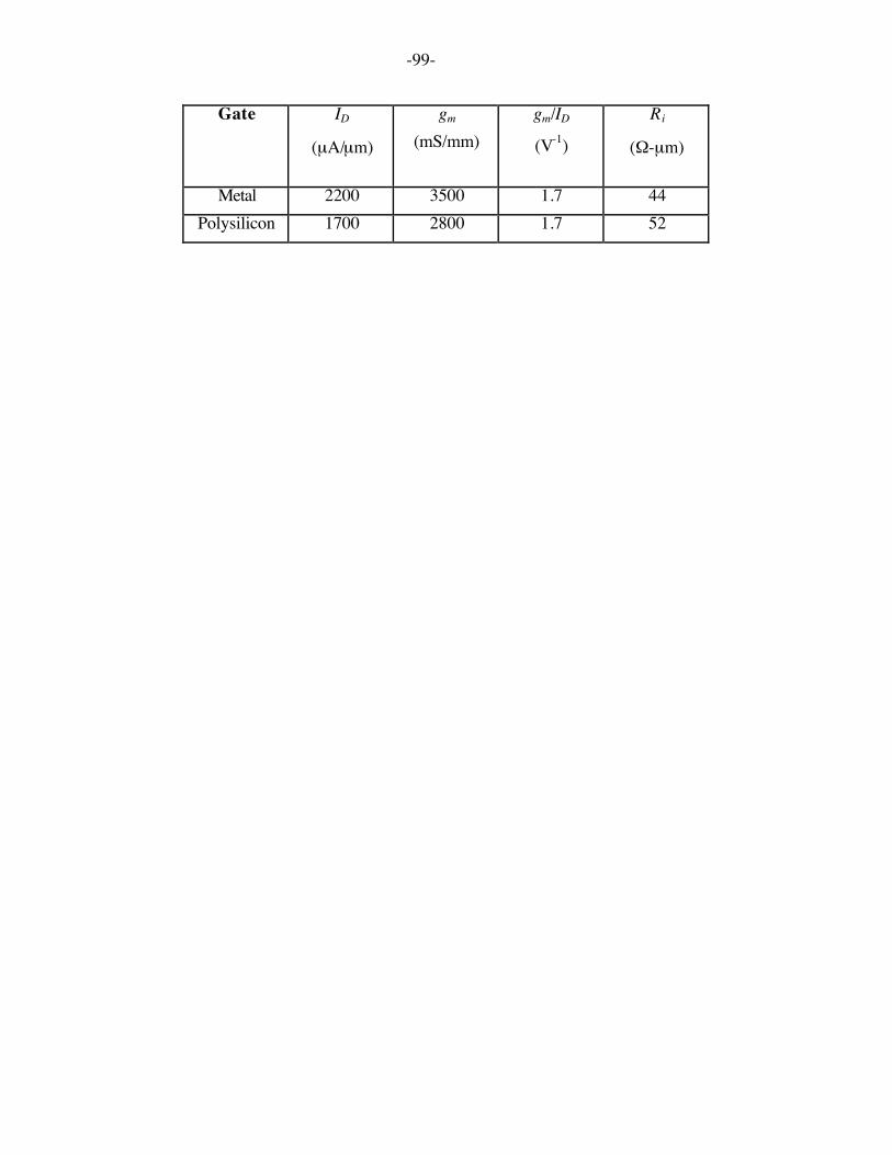
-99-
Gate ID
(µA/µm)
gm
(mS/mm)gm/ID
(V-1)
Ri
(Ω-µm)
Metal 2200 3500 1.7 44Polysilicon 1700 2800 1.7 52
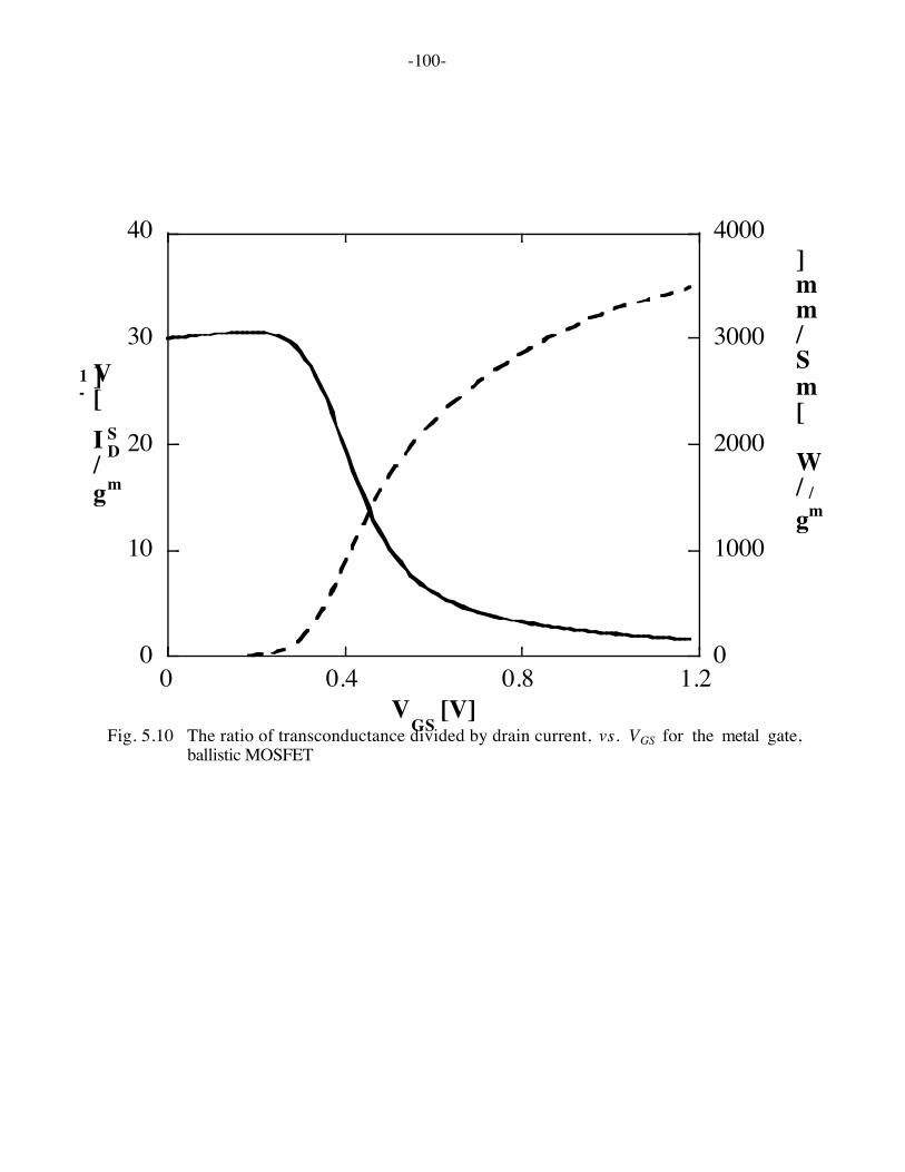
-100-
Fig. 5.10 The ratio of transconductance divided by drain current, vs. VGS for the metal gate,ballistic MOSFET
0
10
20
30
40
0
1000
2000
3000
4000
0 0.4 0.8 1.2
gm/I D
S [V
-1 ]
gm//
W [mS/mm]
VGS
[V]
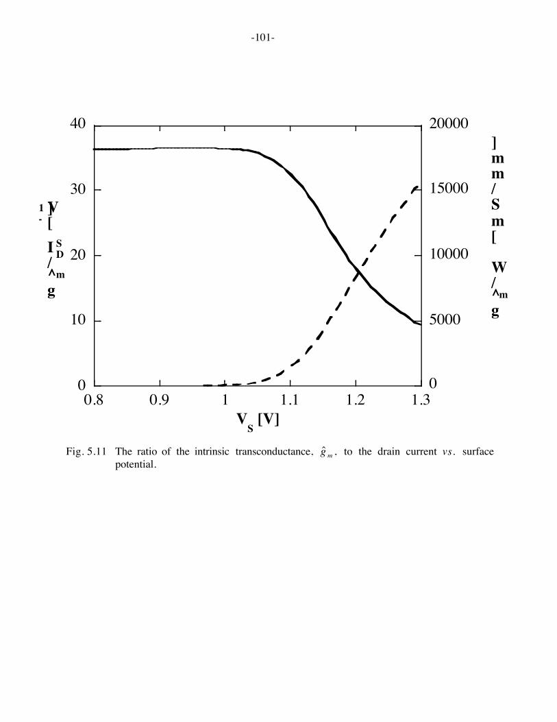
-101-
Fig. 5.11 The ratio of the intrinsic transconductance, ˆ g m , to the drain current vs. surfacepotential.
0
10
20
30
40
0
5000
10000
15000
20000
0.8 0.9 1 1.1 1.2 1.3
g^m/I D
S [V
-1 ]
g^m/W [mS/mm]
VS [V]
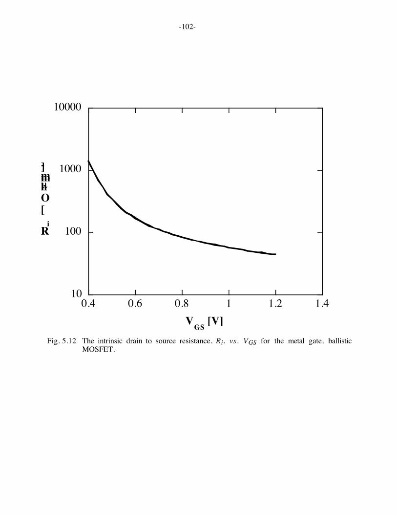
-102-
Fig. 5.12 The intrinsic drain to source resistance, Ri, vs. VGS for the metal gate, ballisticMOSFET.
10
100
1000
10000
0.4 0.6 0.8 1 1.2 1.4
Ri
[Ohm-
µm]
VGS
[V]
-103-
5 .4 . DiscussionThe performance limits for the ballistic MOSFET presented in Table 5.1 are comfortably
above the performance targets in the NTRS [SIA97]. For example, the ballistic on-current isalmost four times higher than the on-current target. Current-day devices operate at about the samepercentage of the ballistic limit, so it appears that scaling current devices to the 100 nm node shouldbe capable of producing the required on-current. If one looks further ahead, however, the gapbetween the ballistic limit and the performance target narrows. For example, for a model L = 50nm devices with a 1.0 nm gate oxide and a power supply of 0.6V, the ballistic current is only 1.5times the target on-current. This suggests that to meet the on-current targets with low powersupply voltages, new device architechtures might be needed.
Operation at liquid nitrogen temperatures improves the performance of MOSFETs;typically, the on-current increases by about 30% [Sai87]. In the ballistic MOSFET, the on-currentis determined by the thermal injection velocity, which may be expected to decrease at lowtemperatures. Table 5.2 shows the computed device performance parameters at T = 77K. Notethat the on-current improves at low temperatures. The reason may be seen from Fig. 5.13, whichcompares the thermal injection velocity vs. gate voltage at T = 300K and 77K. At low gatevoltages, the inversion layer is nondegenerate, and the carrier velocity is considerably lower at77K. Above threshold, however, carrier degeneracy, which raises υinj , is stronger at low
temperatures, so the injection velocity under maximum gate bias is actually higher at 77K than at300K. Real devices don’t operate at the ballistic limit, so the reduction in scattering at lowtemperatures further boosts the on-current. A quantitative analysis of the magnitude of the effectwould also have to consider possible changes in the saturation drain voltage and in the parasiticresistances.
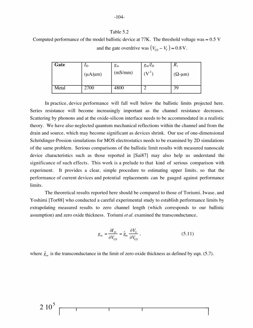
-104-
Table 5.2Computed performance of the model ballistic device at 77K. The threshold voltage was ≈ 0.5 V
and the gate overdrive was VGS − VT( ) ≈ 0.8 V.
Gate ID
(µA/µm)
gm
(mS/mm)gm/ID
(V-1)
Ri
(Ω-µm)
Metal 2700 4800 2 39
In practice, device performance will fall well below the ballistic limits projected here.Series resistance will become increasingly important as the channel resistance decreases.Scattering by phonons and at the oxide-silicon interface needs to be accommodated in a realistictheory. We have also neglected quantum mechanical reflections within the channel and from thedrain and source, which may become significant as devices shrink. Our use of one-dimensionalSchrödinger-Possion simulations for MOS electrostatics needs to be examined by 2D simulationsof the same problem. Serious comparisons of the ballistic limit results with measured nanoscaledevice characteristics such as those reported in [Sai87] may also help us understand thesignificance of such effects. This work is a prelude to that kind of serious comparison withexperiment. It provides a clear, simple procedure to estimating upper limits, so that theperformance of current devices and potential replacements can be gauged against performancelimits.
The theoretical results reported here should be compared to those of Toriumi, Iwase, andYoshimi [Tor88] who conducted a careful experimental study to establish performance limits byextrapolating measured results to zero channel length (which corresponds to our ballisticassumption) and zero oxide thickness. Toriumi et al. examined the transconductance,
gm =∂ID
∂VGS
= ˆ g m∂VS
∂VGS
, (5.11)
where ˆ g m is the transconductance in the limit of zero oxide thickness as defined by eqn. (5.7).
2 105
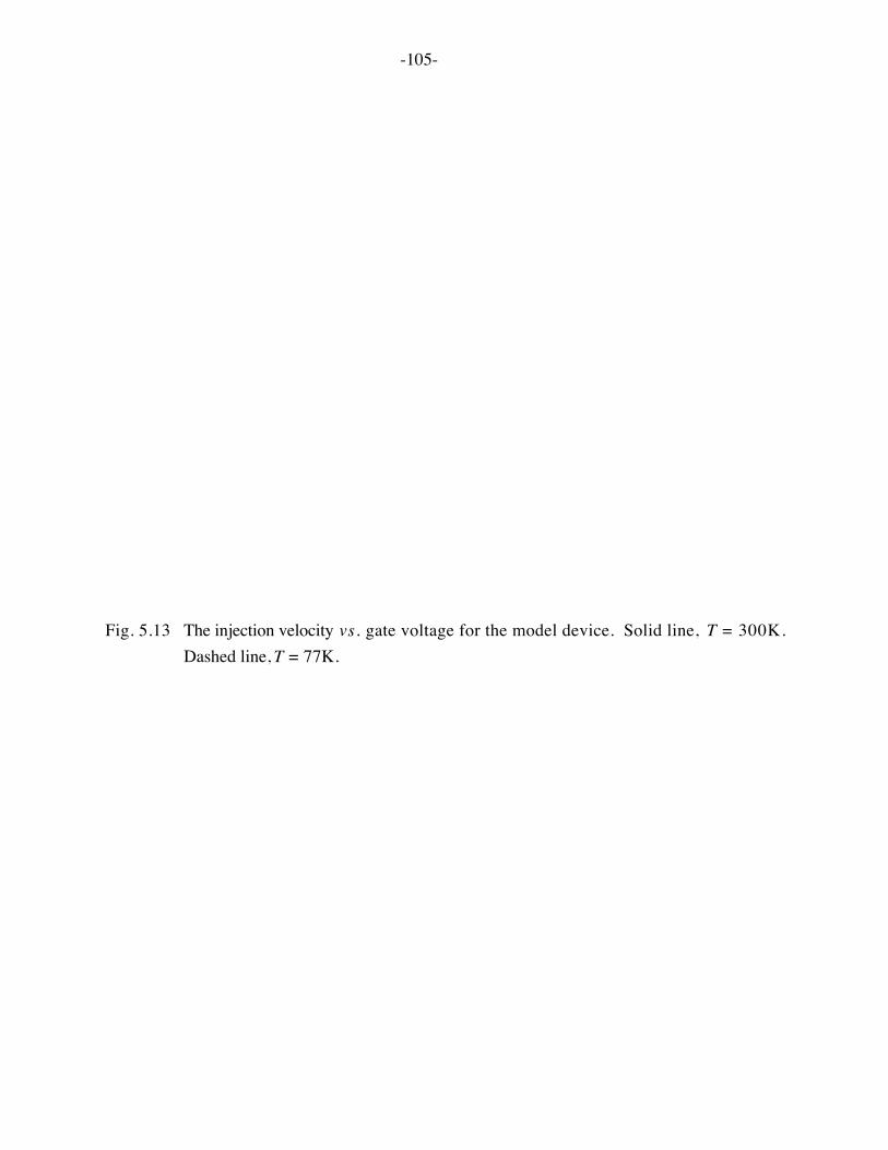
-105-
Fig. 5.13 The injection velocity vs. gate voltage for the model device. Solid line, T = 300K.Dashed line, T = 77K.
-106-
Using
∂VGS
∂VS
= 1+CS
Cox
, (5.12)
where CS is the semiconductor capacitance, eqn. (5.11) can be expressed as
1gm
=1ˆ g m
1 +κ S tox
κ oδ
⎛
⎝ ⎜ ⎞
⎠ ⎟ . (5.13)
We have defined the effective thickness of the inversion layer by CS = κSε0 δ . Accordingto eqn. (5.13), a plot of inverse transconductance vs. oxide thickness is linear if the effectivethickness of the inversion layer is constant. Toriumi et al. observed this linear dependenceexperimentally [Tor88]. They found a limiting transconductance of ≈ 3000 mS/mm, which issignificantly lower than the value we obtained. From the intercept of their plot, an effectiveinversion layer thickness of δ ≈ 3.6 nm can also be inferred. The effective inversion layerthickness obtained from our self-consistent, Schrödinger-Poisson simulation was much smaller,about 1.1nm. Note that the limiting transconductance, ˆ g m , and the effective inversion layer
thickness, δ, both depend on the surface potential. The lower ˆ g m and larger δ observed by
Toriumi et al. suggest that the experimental data were taken at lower surface potentials thanassumed in the theoretical calculations. Series resistance causes the transconductance to peak atlower surface potentials and may explain the discrepancy between the theory and experiment.
5 .5 . SummaryWe presented a simple procedure for estimating the performance limits of silicon
MOSFETs as channel lengths and oxide thicknesses approach zero. In addition to the ballistic limitcurrent, the procedure also gives the ballistic limit transconductance and the channel resistance.The procedure assumed a gradual channel approximation at the source end of the channel and thenmade use of one-dimensional Schrödinger-Poisson simulations of the MOS problem. (Thisapproach misses important two-dimensional effects such as DIBL, which have to be added inseparately.) We also treated the channel and drain as perfect absorbers for electrons injected fromthe source, which neglects quantum mechanical reflections that might occur in very smalltransistors. These issues should be addressed by more sophisticated simulations, but the approachpresented here provides a clear conceptual way to think about transistor limits, and the simplifying
-107-
assumptions are physically based and will provide, we believe, reasonable upper limits for deviceperformance.
In agreement with a previous experimental study, we found that as the channel lengthapproaches zero (or as the device becomes ballistic) the drain current and transconductance have afinite limit. We also found a finite channel resistance, even when the channel is ballistic. Wefound that the carrier velocity at the source end of the channel [ υ(0) in eqn. (5.9)] can be as high
as ≈ 1.5 × 107 cm/s in the ballistic limit. The MOSFET performance limits established here arewell above those of current day devices and considerably higher than those deduced by Toriumi etal. [Tor88]. For example, the drive current targeted for the L = 100 nm node of the NTRS is onlyabout one fourth of the ballistic limit current. Even for a 1.5 nm thin oxide, however, thetransconductance to current ratio is only about 5% of the value for a bipolar transistor. As onelooks further ahead, however, it appears that devices will have to operate significantly closer to theballistic limit if the NTRS targets are to be met. The approach presented here should be useful inassessing new device designs as well as in understanding the performance limiting factors ofpresent-day devices.

-108-
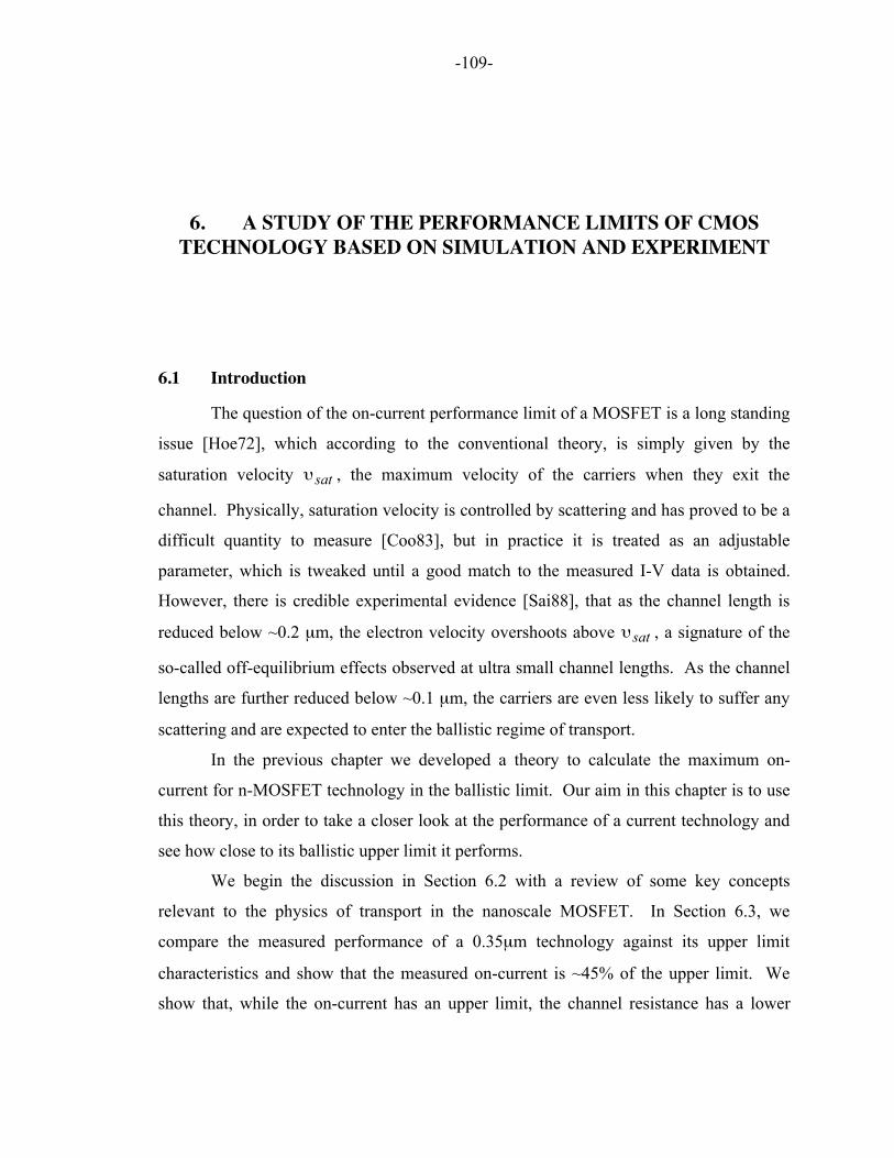
-109-
6. A STUDY OF THE PERFORMANCE LIMITS OF CMOSTECHNOLOGY BASED ON SIMULATION AND EXPERIMENT
6.1 Introduction
The question of the on-current performance limit of a MOSFET is a long standing
issue [Hoe72], which according to the conventional theory, is simply given by the
saturation velocity satυ , the maximum velocity of the carriers when they exit the
channel. Physically, saturation velocity is controlled by scattering and has proved to be a
difficult quantity to measure [Coo83], but in practice it is treated as an adjustable
parameter, which is tweaked until a good match to the measured I-V data is obtained.
However, there is credible experimental evidence [Sai88], that as the channel length is
reduced below ~0.2 µm, the electron velocity overshoots above satυ , a signature of the
so-called off-equilibrium effects observed at ultra small channel lengths. As the channel
lengths are further reduced below ~0.1 µm, the carriers are even less likely to suffer any
scattering and are expected to enter the ballistic regime of transport.
In the previous chapter we developed a theory to calculate the maximum on-
current for n-MOSFET technology in the ballistic limit. Our aim in this chapter is to use
this theory, in order to take a closer look at the performance of a current technology and
see how close to its ballistic upper limit it performs.
We begin the discussion in Section 6.2 with a review of some key concepts
relevant to the physics of transport in the nanoscale MOSFET. In Section 6.3, we
compare the measured performance of a 0.35µm technology against its upper limit
characteristics and show that the measured on-current is ~45% of the upper limit. We
show that, while the on-current has an upper limit, the channel resistance has a lower

-110-
limit, regard less of how short the channel is and that the magnitude of this fundamental
channel resistance may be large enough to influence device design for future
technologies.
Real devices operate below their fundamental limit because of channel back-
scattering [Lun97]. We present a procedure for extracting the channel back-scattering
coefficient, r, as a function of gate and drain bias and show that the values extracted from
these measurements are consistent with simple estimates.
Each new technology strives to reduce power dissipation and increase switching
speed, and device scaling has provided the conceptual framework to meet these demands
simultaneously. In Section 6.4, we discuss why the constant field scaling results in the
same channel back-scattering, and discuss whether or not the targets in the International
Technology Roadmap for Semiconductors (ITRS) may be achieved if this same trend
continues. Furthermore, we compare the on-current performance of the p-MOSFET with
the performance of the n-MOSFET at the end-of-the-roadmap. In Section 6.5, we
summarize the main results of this chapter.
6.2 Review of Scattering Theory of the MOSFET
Carrier transport in nanoscale MOSFET is an inherently two dimensional problem
which involves the so called off-equilibrium effects, but the essential features may be
understood using the simplified band diagram shown in Fig. 6.1.
The beginning of the channel, as identified by the top of the barrier in Fig. 6.1, is a
quasi-equilibrium point populated by thermal equilibrium electrons injected from the
source. The total inversion density at this point is controlled by the gate voltage
according to the relation
( ) ( )TGSTGSeffinv VV,VVCQ >−= (6.1)
where TV is the threshold voltage and effC is the effective gate to channel capacitance
given by the series combination of the oxide and inversion layer capacitance. The
-111-
Fig. 6.1. Illustration of a one-dimensional band diagram for a MOSFET biased in
saturation
Drain
Beginning of Channel
Source
VGS
VDS

-112-
validity of this relation is well known for the long channel transistor where the drain bias
has little, if any, influence on the electrostatics at the beginning of the channel. For the
short channel MOSFET, on the other hand, the electric field associated with the drain
junction has considerable influence on the electrostatics at the beginning of the channel,
which brings the validity of equation (6.1) under question.
Electrostatically, the charges must obey Poisson equation
,y
Ex
E ySi
xSi ρεε =
ƒ
ƒ+
ƒ
ƒ(6.2)
where Ex and Ey are the lateral and vertical electric field and ρ is the total charge density
at the point of injection. In Fig. 6.2, we illustrate the lateral electric field as obtained
from simulations for two cases corresponding to a low drain bias and high drain bias
[Ngu84]. When the drain bias is low, the electric field associated with the junctions at the
source and drain penetrate symmetrically into the channel, and at one point, right in the
middle of the channel the two cancel each other and the net electric field becomes a
minimum. When the drain bias is high, on the other hand, the field associated with the
drain junction becomes much stronger and pushes the location of this minimum away
from the middle, closer to the left of the channel near the source junction. Note, the
minimum electric field point corresponds to the point where the surface potential is a
minimum, which is the location of the injection point (i.e., top of the barrier) that we
illustrated in Fig. 6.1. In a long channel transistor the lateral field is negligible:
xE
yE xy
ƒ
ƒ>>
ƒ
ƒ(6.3)
and hence the charge density is completely controlled by the vertical electric field Ey. In
a short channel device, on the other hand, the lateral electric field diminishes the control
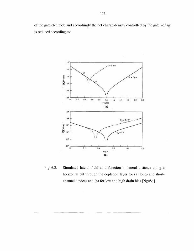
-113-
of the gate electrode and accordingly the net charge density controlled by the gate voltage
is reduced according to:
Fig. 6.2. Simulated lateral field as a function of lateral distance along a
horizontal cut through the depletion layer for (a) long- and short-
channel devices and (b) for low and high drain bias [Ngu84].
-114-
xE
yE x
siy
si ƒ
ƒ−=
ƒ
ƒερε (6.4)
which explains the lowering of the threshold voltage in a short channel device (DIBL) as
discussed in [Ngu81]. Equation (6.4) emphasizes that the charge density at the point of
injection continues to be modulated by the vertical field, except that the vertical field’s
influence is diminished by the lateral field’s penetration into the channel. This
diminished influence is indeed the mechanism responsible for DIBL, but the presence of
DIBL does not invalidate the general validity of equation (6.1).
So far we have discussed the inversion charge at the point of injection, but current
is given by the product of inversion charge and carrier velocity, which in a ballistic
device is the so-called thermal injection velocity. Just as the amount of inversion charge
is controlled by the gate bias, so is the thermal velocity, which depends on the details of
how the sub-bands are occupied and is analytically given by
( )( )√√↵
⎯
+
⎜=
η
η
πυ
emTk /*
LBT 1
2 21 (6.5)
(For exact derivation consult Chapter 5 and [Asa00]).
Real devices operate below the ballistic limit because of carrier back-scattering,
which leads to
( )DSTGS
BToxDS V)VV(
q/TkrCW/I −
−=
21
υ (6.6)
for qTkV BDS /<< and [Lun97]
)(11/ TGSToxDS VV
rrCWI −√↵
⎯+
−= υ (6.7)

-115-
for qTkV BDS />> . Equations (6.6) and (6.7) explain how much channel back-
scattering lowers the maximum on-current and at the same time increases channel
resistance from their fundamental limits. In the following section we will use these
equations to deduce channel back-scattering as a function of drain and gate bias, using
experimental data, and investigate how the extracted values are related to physics of
transport.
6.3 Results
In this section, we compare the results obtained from simulations with
experimental data obtained from a 0.35 µm bulk CMOS technology.
6.3.1 Injection Velocity
The channel injection velocity, Tυ , is a critical parameter in the theory because it
is the maximum velocity achievable at the source end of the channel and consequently it
limits the maximum current that can be delivered. Microscopically, this parameter is
related to the shape of the distribution function, which for instance, for a Maxwellian
distribution, is mainly a function of the lattice temperature TL and is given by :
*LB
T mTk
πυ
2= . (6.8)
According to equation (6.8), at room temperature, the thermal injection velocity is
equal to 710061 ↔. (cm/sec) if a conductivity effective mass of o* m.m 260= ,
corresponding to 3D bulk carriers in silicon is used. In a deep sub-micron MOSFET, in
contrast to the 3D carriers in the bulk, the carriers are confined to 2D sub-bands in the
channel and are more likely to be degenerate (i.e., obey Fermi-Dirac and not Maxwell-
Boltzmann statistics as assumed in equation (6.8)). In this case, Tυ is not a constant
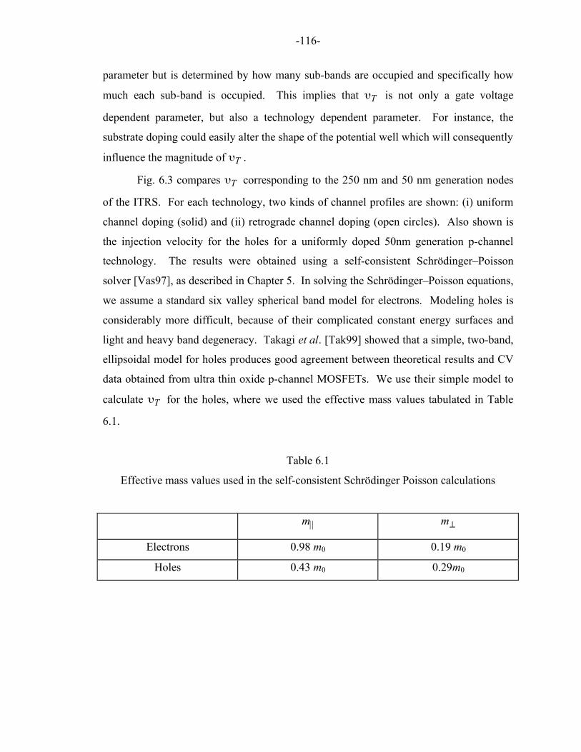
-116-
parameter but is determined by how many sub-bands are occupied and specifically how
much each sub-band is occupied. This implies that Tυ is not only a gate voltage
dependent parameter, but also a technology dependent parameter. For instance, the
substrate doping could easily alter the shape of the potential well which will consequently
influence the magnitude of Tυ .
Fig. 6.3 compares Tυ corresponding to the 250 nm and 50 nm generation nodes
of the ITRS. For each technology, two kinds of channel profiles are shown: (i) uniform
channel doping (solid) and (ii) retrograde channel doping (open circles). Also shown is
the injection velocity for the holes for a uniformly doped 50nm generation p-channel
technology. The results were obtained using a self-consistent Schrödinger–Poisson
solver [Vas97], as described in Chapter 5. In solving the Schrödinger–Poisson equations,
we assume a standard six valley spherical band model for electrons. Modeling holes is
considerably more difficult, because of their complicated constant energy surfaces and
light and heavy band degeneracy. Takagi et al. [Tak99] showed that a simple, two-band,
ellipsoidal model for holes produces good agreement between theoretical results and CV
data obtained from ultra thin oxide p-channel MOSFETs. We use their simple model to
calculate Tυ for the holes, where we used the effective mass values tabulated in Table
6.1.
Table 6.1
Effective mass values used in the self-consistent Schrödinger Poisson calculations
||m ⊥m
Electrons 0.98 m0 0.19 m0
Holes 0.43 m0 0.29m0
-117-
Fig. 6.3 reveals that Tυ for the 50 nm device is higher than the 250 nm device,
but there is virtually no difference between the uniform and retrograde channel doping.
The injection velocity depends on the total inversion layer density, sn , but also on how
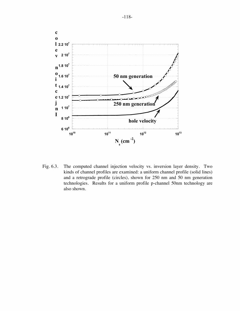
-118-
6 106
8 106
1 107
1.2 107
1.4 107
1.6 107
1.8 107
2 107
2.2 107
1010 1011 1012 1013
Injection veloci
Ns (cm -2)
250 nm generation
50 nm generation
hole velocity
Fig. 6.3. The computed channel injection velocity vs. inversion layer density. Twokinds of channel profiles are examined: a uniform channel profile (solid lines)and a retrograde profile (circles), shown for 250 nm and 50 nm generationtechnologies. Results for a uniform profile p-channel 50nm technology arealso shown.
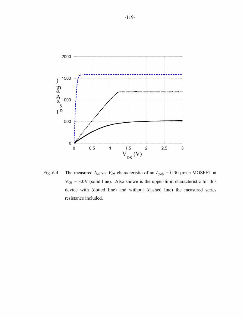
-119-
0
500
1000
1500
2000
0 0.5 1 1.5 2 2.5 3
I DS
(µA/µm)
VDS
(V)
Fig. 6.4 The measured IDS vs. VDS characteristic of an Lpoly = 0.30 µm n-MOSFET at
VGS = 3.0V (solid line). Also shown is the upper-limit characteristic for this
device with (dotted line) and without (dashed line) the measured series
resistance included.
-120-
the inversion layer is distributed among the different sub-bands. A higher substrate
doping tends to increase the well confinement causing the higher lying energy levels,
with their heavier masses, to be populated more sparsely. For the 50nm device the
substrate doping is higher, therefore the carriers would exclude occupying the higher sub-
bands and would instead occupy the first sub-band which has a lighter effective-mass and
hence higher injection velocity. For the polyL = 0.30 µm n-MOSFET examined next,
Tυ ~ 1.4 x 107 cm/s at a GSV =3.0 (V).
6.3.2 Electrical Characterization of a 0.35 µm Technology
In order to assess the performance of a 0.35 micron bulk CMOS technology, we
show the measured DSDS VI − characteristics for an polyL =0.3 µm device in Fig. 6.4,
taken at GSV =3.0 (V). The devices used for this study were provided by LSI Logic
Corporation, and in addition to the 0.35 µm included a 0.25 and 0.18 µm technology. We
have selected to display the results from the 0.35 µm technology, but the general
conclusions made in this chapter equally apply to the two other technologies. In order to
parameterize the technology, we used large area (300x500 µm2) capacitors and from the
quasi-static CV characteristics deduced the oxide thickness, gate polysilicon doping, and
the substrate doping. The technology used to make this device utilizes a physical oxide
thickness oxt =6.5 (nm), polysilicon doping of polyN = 191005 ↔. (cm-3), and a substrate
doping subN = 171053 ↔. (cm-3). The substrate doping in the channel was designed to
correspond to a nominal threshold voltage of 0.60-0.65 (V) for this technology. For this
particular device, however, we used the mobility degradation method [Sch90] to measure
a threshold voltage of TV =0.62 (V), but the linear extrapolation method [Sch90], the
industry standard to measure the threshold voltage, yielded a TV =0.60 (V) in very good
agreement with the mobility degradation method.
Also shown in Fig. 6.4, is the calculated ballistic current for an ideal device (long
dashes) excluding parasitic resistance and the ballistic current for a non-ideal device

-121-
(short dashes) including parasitic resistance for the device. The parasitic resistance used
in these calculation was parR =500 (Ω.µm) and was obtained from the measured
characteristics, using the paired VG method proposed in [Hu87]. As is well known, the
parasitic resistance in a MOSFET, sustains a small but finite voltage drop across the gate-
source and drain-source terminals and thereby lowers the “effective” bias voltages.
However, its impact on the ballistic device is much more pronounced than it is on the
long channel device. The visible effect of parR for the ballistic device is clear in Fig.
6.4, where we show that the ballistic current saturates at a higher drain voltage, but more
importantly, the on-current is degraded by a significant amount (~30%).
Equation (6.7) shows that to maximize the on-current, we need to minimize the
channel back-scattering coefficient, r. In Fig. 6.5 we show r extracted for the 0.3 µm
device as a function of gate voltage, where equations (6.6) and (6.7) were used to extract
r for the DSV low (linear regime) and DSV high (saturation regime) biases. The back-
scattering coefficient is determined by the electric field near the source. Under low DSV ,
the field is low and r ~0.9; for high DSV the field increase and r ~0.4.
Finally, in Fig. 6.6 we show the active channel resistance (solid line), defined as
the total measured resistance minus the parasitic resistance, plotted as a function of gate
voltage. Alongside the active channel resistance, we show the theoretically calculated
ballistic resistance (dashed line) as evaluated from equation (6.6). The ballistic resistance
is not expected to be important for the longer channel technologies such as the one
considered here. However, in defiance of our expectation, for the 0.35 µm technology
studied here, it is already a noticeable fraction of the total resistance.
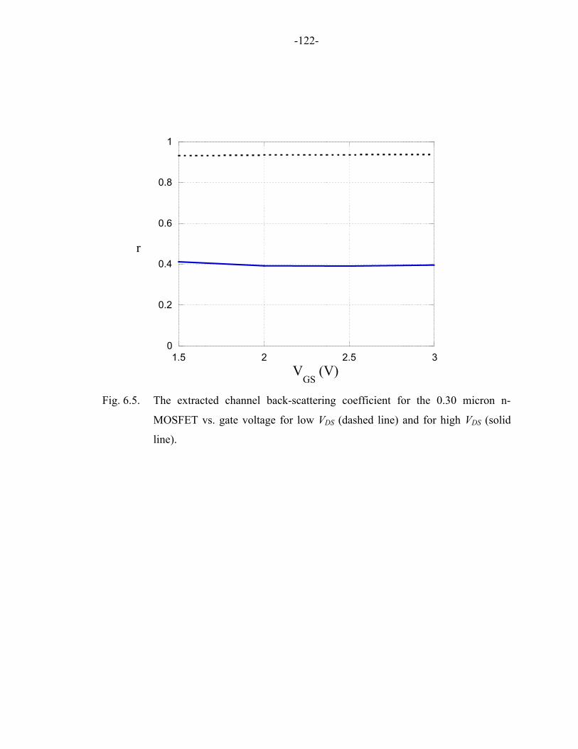
-122-
0
0.2
0.4
0.6
0.8
1
1.5 2 2.5 3V
GS (V)
r
Fig. 6.5. The extracted channel back-scattering coefficient for the 0.30 micron n-
MOSFET vs. gate voltage for low VDS (dashed line) and for high VDS (solid
line).
-123-
6.4 Discussion
In this section, we discuss the implications of the parameters obtained from the
measurements in the previous section and put them in perspective with the theory.
6.4.1 Scattering theory vs. measurements
According to scattering theory, the ratio of the two resistances plotted in Fig. 4 is given
by effL+λ
λ , where λ is the mean-free-path (MFP) [Dat95]. Assuming a polyeff LL ≅ =
0.3 µm, the ratio provides an estimate of λ ~18 (nm) which is consistent with λ ~21
(nm), deduced from the measured mobility data obtained at GSV =3.0 (V), but this
agreement should be regarded with caution (see Appendix D on how the MFP is
estimated). The device examined here is much longer (~15 times) than the expected
MFP, which makes the estimate susceptible to measurement errors. For the nanoscale
MOSFET, however, we expect the fundamental resistance to be a more sizable fraction
of the total measured resistance.
We have shown that for the 0.3 µm device, the channel back-scattering for
DDD VV = is ~0.4 independent of the gate bias, but we can readily explain this using
scattering theory. When the drain bias is high, the energy bands have large gradients near
the drain end and therefore the non-local effects are important. But for a well–designed
MOSFET the energy bands near the source end, despite the large field gradients near the
drain, bend gently and, indeed, we can show that transport is controlled by a small region
near the source end. To be specific, we can show that r is given by:
ll
l
/r
λλ +=
+=
11 (6.9)
where l is the length of this critical region near the source, and is equal to the distance it
takes for the electrons to drift ~ q/TkB down the channel from the top of the barrier
-124-
[Lun97]. As the gate voltage increases, λ decreases but the electric field near the source
barrier will also increase. This causes the characteristic distance l to proportionately
decrease causing r to be fixed to ~0.4. The critical distance l is not a directly
measurable quantity and may only be obtained from simulations, nevertheless, a first
order estimate of l may be given by
sat,D
effBV
Lq/Tk ↔, (6.10)
where sat,DV is the saturation voltage. Our estimate of equation (6.10), using saturation
voltage extracted from the measured device characteristics, shows that the channel back-
scattering of r ~0.4 is reasonable.
According to equation (6.7), the measured on-current is a fraction β of the ballistic
limit where β=rr
+
−
11 . For this device r =0.4, which yields a β=0.45. It is somewhat
surprising that such a long channel device (~15 MFP’s) operates so close to its upper
limit but the reason can be explained by using equation (6.9): once the carriers injected
into the channel pass beyond the length l , they are unlikely to reemerge even when they
back-reflect and hence it is the length l that determines the on-current and not the entire
channel length. Increasing the on-current, according to the conventional theory, would
require scaling the entire channel length, however we have shown that the on-current is
determined by only the first ~ q/TkB drop right at the beginning of the channel. To
extract a larger on-current, then, we would need to minimize the ratio λ/l but at the
same time we need to maintain the off-current correspondingly low.
6.4.2 Implications for the ITRS
Conventional scaling strives to maintain the same on-current while maintaining a
low off-current. Our analysis of the 0.35 µm technology shows that this technology is
-125-
characterized by a channel back-scattering of ~0.4 but our analysis of other devices
[Asa99] indicates that for more aggressively scaled technologies, the back-scattering
coefficient continues to be close to 0.4 – independent of technology generation. In Fig.
6.7 we show the simulated DSDS VI − characteristics of a hypothetical 25 nm device,
obtained using a Monte Carlo program [Tau98] and compare it with the current calculated
using the scattering theory, where a channel back-scattering of r=0.4 was assumed. The
device examined uses a so-called “super-halo” [Tau98] design whereby the doping in the
channel has been engineered in both the vertical and horizontal directions, in order to
control the short channel effects. The good agreement shown indicates that
conventionally scaled devices will continue to be characterized by r ~0.4. Constant field
scaling maintains the overall electrostatic profile from one generation to another, and in
particular, it retains the electrostatic profile at the beginning of the channel, which
controls the on-current.
Looking ahead towards the end of the roadmap, it is not at all clear whether or not
the on-current targets in the ITRS may be met. In Fig. 6.8 we show the projected on-
current performance at various nodes of the ITRS-97, where we have obtained the device
parameters oxt (oxide thickness), subN (substrate doping), and DDV (supply voltage)
straight from the ITRS-97, but for the threshold voltage, we used the commonly accepted
thumb rule of 0.5/DDT VV = . Since the threshold voltage may not be scaled below a
minimum value, which is set by the off-current requirement (~0.2 V ), we took TV =0.2
(V) for the last two nodes of the ITRS-97. In Fig. 6.8, we also show the target on-current
of 600 µA/µm (the horizontal dashed line) as required by the ITRS. Comparing against
the roadmap target of 600 µA/µm, it is apparent from Fig. 6.8 that future technologies
will have to operate much closer to the upper limit in order to achieve the targets. The
bulk CMOS technology has been the workhorse of the industry for more than thirty years,
but as this result indicates, this technology will cease to stand up to expectations at the
end-of-the-roadmap. This observation underscores the importance of other variants of the
bulk CMOS technology (i.e., the double gate SOI technology), which are currently being
explored experimentally [Won99], as a viable alternative at the end-of-the-roadmap.

-126-
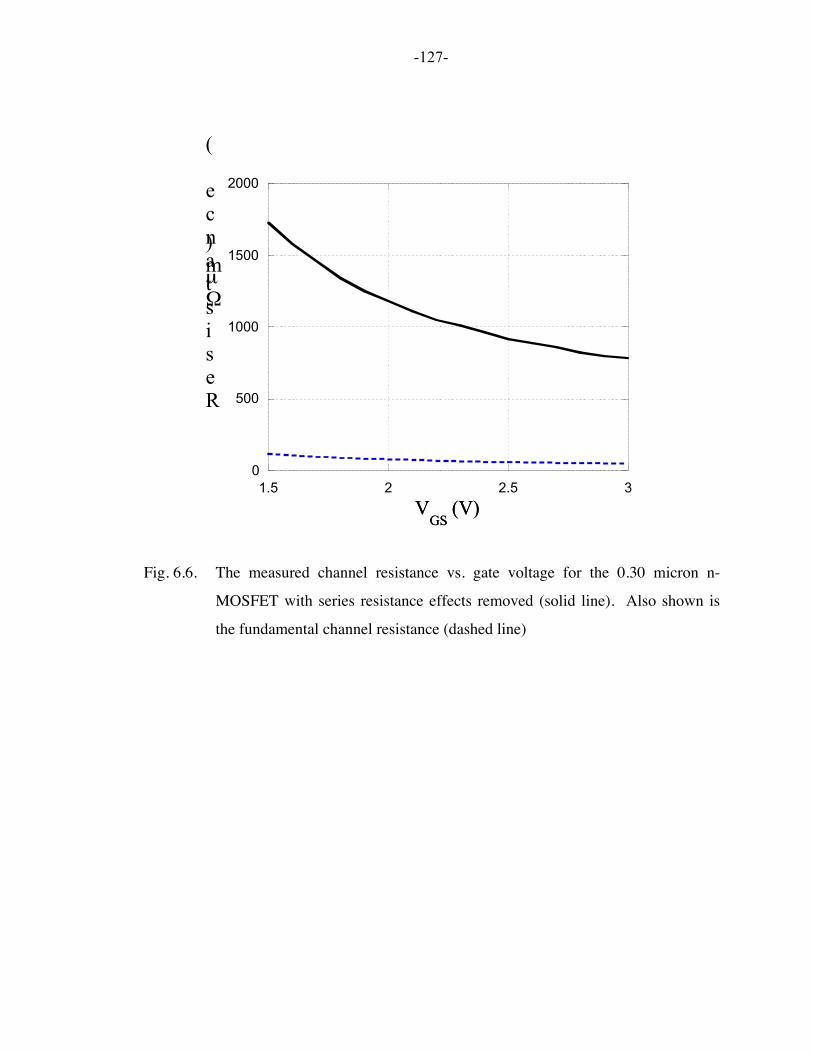
-127-
0
500
1000
1500
2000
1.5 2 2.5 3V
GS (V)V
GS (V)
Resistance (
Ω µm)
Fig. 6.6. The measured channel resistance vs. gate voltage for the 0.30 micron n-
MOSFET with series resistance effects removed (solid line). Also shown is
the fundamental channel resistance (dashed line)
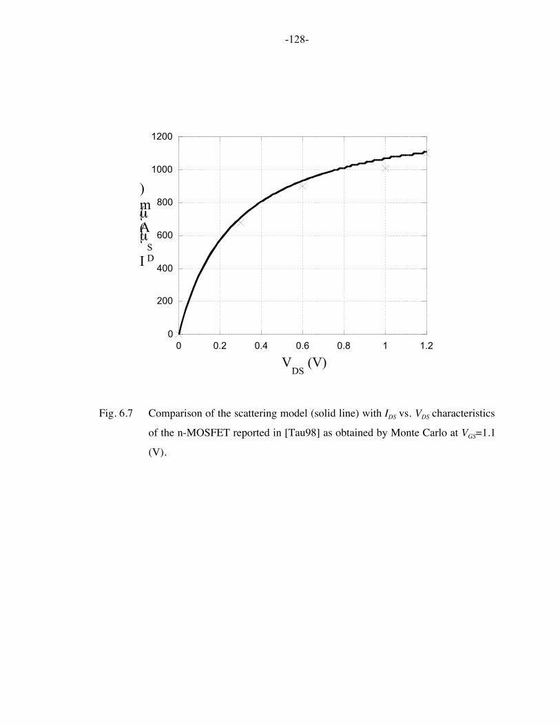
-128-
0
200
400
600
800
1000
1200
0 0.2 0.4 0.6 0.8 1 1.2
VDS
(V)
I DS
(µA/µm)
Fig. 6.7 Comparison of the scattering model (solid line) with IDS vs. VDS characteristics
of the n-MOSFET reported in [Tau98] as obtained by Monte Carlo at VGS=1.1
(V).
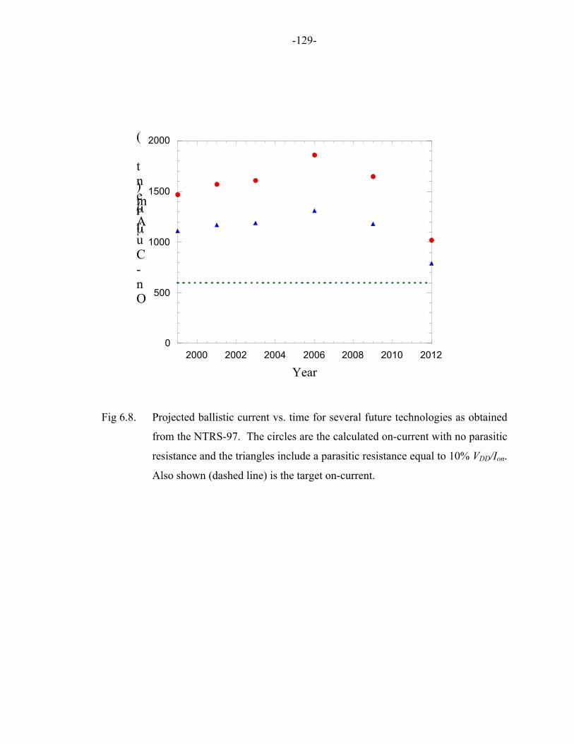
-129-
0
500
1000
1500
2000
2000 2002 2004 2006 2008 2010 2012
On-Current (
µA/µm)
Year
Fig 6.8. Projected ballistic current vs. time for several future technologies as obtained
from the NTRS-97. The circles are the calculated on-current with no parasitic
resistance and the triangles include a parasitic resistance equal to 10% VDD/Ion.
Also shown (dashed line) is the target on-current.
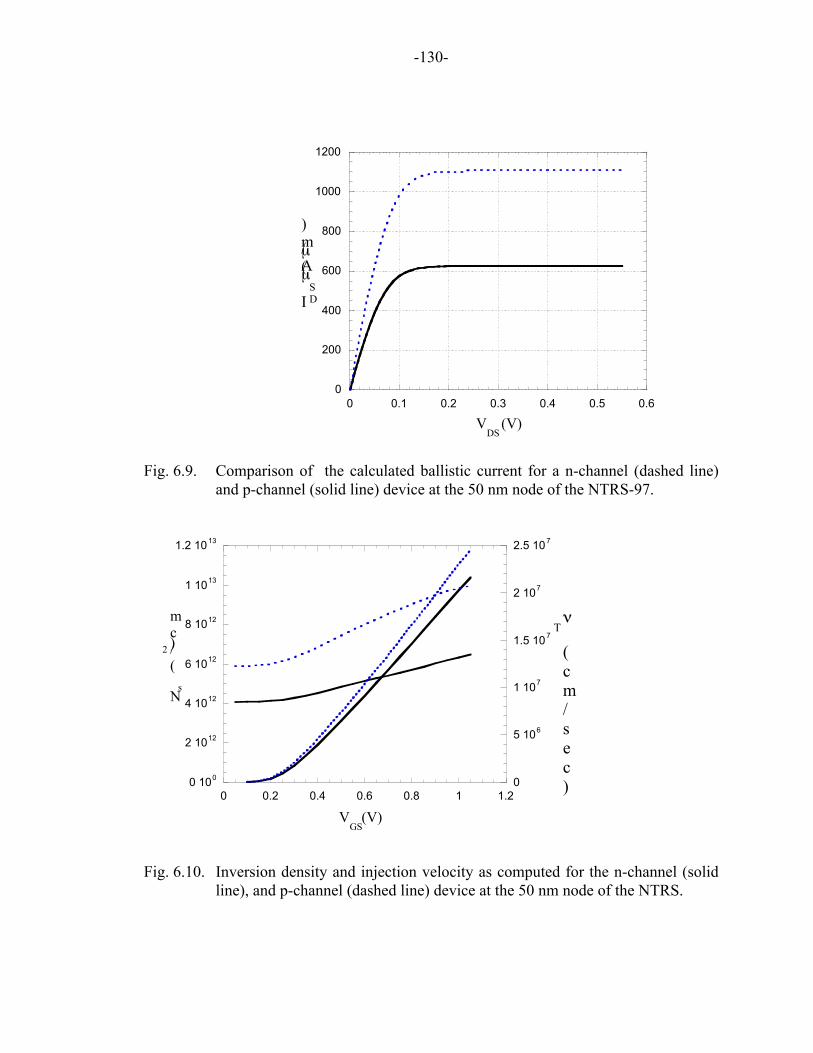
-130-
0
200
400
600
800
1000
1200
0 0.1 0.2 0.3 0.4 0.5 0.6
I DS
(µA/µm)
VDS
(V)
Fig. 6.9. Comparison of the calculated ballistic current for a n-channel (dashed line)and p-channel (solid line) device at the 50 nm node of the NTRS-97.
0 100
2 1012
4 1012
6 1012
8 1012
1 1013
1.2 1013
0
5 106
1 107
1.5 107
2 107
2.5 107
0 0.2 0.4 0.6 0.8 1 1.2
Ns
(/cm
2 )
νT
(cm/sec)
VGS
(V)
Fig. 6.10. Inversion density and injection velocity as computed for the n-channel (solidline), and p-channel (dashed line) device at the 50 nm node of the NTRS.
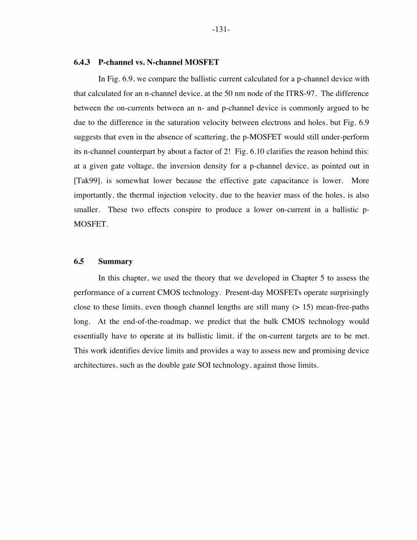
-131-
6.4.3 P-channel vs. N-channel MOSFET
In Fig. 6.9, we compare the ballistic current calculated for a p-channel device with
that calculated for an n-channel device, at the 50 nm node of the ITRS-97. The difference
between the on-currents between an n- and p-channel device is commonly argued to be
due to the difference in the saturation velocity between electrons and holes, but Fig. 6.9
suggests that even in the absence of scattering, the p-MOSFET would still under-perform
its n-channel counterpart by about a factor of 2! Fig. 6.10 clarifies the reason behind this:
at a given gate voltage, the inversion density for a p-channel device, as pointed out in
[Tak99], is somewhat lower because the effective gate capacitance is lower. More
importantly, the thermal injection velocity, due to the heavier mass of the holes, is also
smaller. These two effects conspire to produce a lower on-current in a ballistic p-
MOSFET.
6.5 Summary
In this chapter, we used the theory that we developed in Chapter 5 to assess the
performance of a current CMOS technology. Present-day MOSFETs operate surprisingly
close to these limits, even though channel lengths are still many (> 15) mean-free-paths
long. At the end-of-the-roadmap, we predict that the bulk CMOS technology would
essentially have to operate at its ballistic limit, if the on-current targets are to be met.
This work identifies device limits and provides a way to assess new and promising device
architectures, such as the double gate SOI technology, against those limits.

-130-
-131-
7. SUMMARY AND FUTURE WORK
As the writing of this thesis comes to its finish, silicon device technology is about
to embark upon the so-called "nanoscale" realm, with device sizes approaching the
100nm landmark and below. Accordingly, many of the oldest and most trusted models in
existence, mostly founded upon the classic Drift-Diffusion model of transport, are
beginning to lose validity. Our goal in this thesis, rather than developing new models,
has been to focus on the physical mechanisms which are of importance in modern
devices. Understanding these issues will undoubtedly pave the way for better models,
but more importantly, for fresh device design concepts. We hope that the following
summary will reflect the effort made towards that end.
7.1 Summary
After a brief introduction in Chapter 1, we began the discussion in Chapter 2
where we presented an acceleration scheme to speed up the Boltzmann solver developed
for this work. We demonstrated that this scheme, which was originally devised for the
simulation of neutron transport, is extremely effective when applied to electron transport,
speeding up the solution time by more than a factor of ten! The BTE is the most rigorous
model of transport among semi-classical paradigms, but it requires exceedingly large
computer times. The acceleration scheme we implemented facilitates the finding of a
solution in 1D and was instrumental for the work done in the following chapter.
In Chapter 3, we looked at transport in sub-micron bipolar junction transistors, but
unlike previous works, we used realistic doping profiles in order to reflect the complexity
of a modern transistor. We compared BTE solutions against simpler but popular
approaches by comparing the resultant I-V characteristics. In the computer-aided design
-132-
of devices, engineers use models of varying sophistication, and these models inevitably
give different results. Given the vast difference among the physics underlying these
models, it is not straightforward how to assess the validity of one against another. In
Chapter 3, we emphasized how such comparison must be conducted, even when the
principal equations in the models have little in common. The main conclusion is that a
more complex model doesn't necessarily imply more accuracy, but such comparative
studies should instead focus on whether or not the model assumptions are applicable to
the device under investigation.
In Chapter 4, we applied our Boltzmann solver to model problems in order to
investigate transport in three simple, yet important, profiles that correspond to current-
controlling regions in devices. Drift-Diffusion (DD) has been the dominant force in
device design for decades and in this chapter we explained how DD has succeeded, by
correctly modeling the current-controlling regions in the device.
In Chapter 5, we presented a new theory to calculate the upper limit performance
of a CMOS technology. Continuous scaling of CMOS technology has resulted in more
density and speed for twenty years, but as CMOS enters its third decade, there are serious
questions as to how much more performance one may squeeze out of this technology.
Alternative technologies may have to fulfill CMOS's shortcomings and the theory in
Chapter 5 allows one to assess the relative advantages of such alternative technologies.
Finally in Chapter 6, we applied the theory developed in Chapter 5 to a current
technology in order to assess its performance using experimental data. The results
included some surprises. For example, the technology examined operated unusually
close to its upper limit, but the larger outgrowth of this chapter is the suggested
methodology, which is useful to technologist who often have to grapple with gauging the
performance of a developing technology. As for the future of CMOS technology, we
projected that at the end-of-the-roadmap the devices will essentially have to operate at
their ballistic limit. This implies that variants of bulk CMOS technology, such as SOI
technology, which are currently at the experimental stage need to be engineered into a
manufacturable process.
-133-
7.2 Future work
In this section we identify three promising areas, which based on the
accomplishments to date, deserve further attention. Some of the ongoing efforts of our
group is already focused on these issues.
1) Extend the ballistic approach to 2D
The ballistic theory presented in this thesis predicts the maximum on-current by
focusing at the point of injection in the channel. This theory is essentially a thermionic
injection theory but at the same time accounts for multiple sub-bands and degeneracy that
do occur in a deep sub-micron MOSFET. While it embodies the main physical effects of
interest, it is incapable of accounting for the important 2D effects in a MOSFET (for
example, DIBL was accounted for by reducing the threshold voltage by the amount
measured for the device). It is of interest to develop this theory to 2D so that such
electrostatics effects may be accounted for explicitly.
2) Develop a complete scattering-based compact model
In this thesis, we have shown the manner by which scattering lowers the on-
current, both in the linear and saturation regimes of operation. Based on the observed
trends, we made extrapolations about the magnitude of channel back-scattering, and we
demonstrated a simple model which works well in these regimes of operation, albeit a
separate expression was used for each regime. One advantage of the scattering model is
its stark simplicity. On comparison, the existing models developed for the deep sub-
micron MOSFET require a very large number of parameters that are essentially obtained
from fitting to experiments and sometimes have no physical justification. It would serve
us well, if the scattering based model were developed into a complete model that could
account for all regimes of operation equally. The present model works either in the linear
or saturation regimes, but can not model the transition between the two.
3) Quantum Simulation of a MOSFET
One of the assumptions made in calculating the maximum on-current is that, the
electrons are assumed to behave semi-classically in the transport direction, but at very
-134-
small dimensions, below ~50 (nm), we expect the wave nature of the electrons to become
important. The role of quantum reflection within the channel, in addition to tunneling
through the source barrier may indeed become important at ultra small length scales.
Understanding these quantum effects may be provided by a promising method called
Non-Equilibrium Green's Function (NGEF) developed by Prof. Datta's group at Purdue
University. This method is a rigorous method of solving the "wave" equations of
transport, but at the same time accommodates for such important effects as the many-
body effects and scattering within the channel. Some preliminary results were published
in conjunction with this thesis, where we used simplified 1D energy band diagrams and
compared the NGEF against Boltzmann solutions. On the downside, this is a
computationally very intensive method, but battling out such numerical issues continues
to be one of the ongoing tasks of the device simulation group.
-135-
135
REFERENCES
[Ala93-1] M. A. Alam, M. A. Stettler, and M. S. Lundstrom, “Formulation of theBoltzmann equation in terms of scattering matrices,” Solid-State Electron.,vol. 36, pp. 263-271, 1993.
[Ala93-2] M. A. Alam, S.-I. Tanaka, and M. S. Lundstrom, “A small-signal, one-fluxanalysis of short base transport,” Solid-State Electron., 38, pp. 177-182, 1993.
[Aro93] N. Arora, MOSFET Models for VLSI Circuit simulation, Springer-Verlag,New York, 1993.
[Asa96] F. Assad, C. A. Niemiec, and M. S. Lundstrom, "Benchmarking and assessingdevice simulation tools for advanced bipolar applications," presented atTECHCON-96, Phoenix AZ,1996.
[Asa98] F. Assad, K. Banoo and M. Lundstrom, "The Drift-Diffusion equationrevisited," Solid-State Electron., vol. 42, pp. 283-295,1998.
[Asa99] F. Assad, Z. Ren, D. Vasileska, S. Datta, and M. S. Lundstrom, Tech. Proc.MSM ’99, pp. 100-102, 1999.
[Asa99] F. Assad, Z. Ren, S. Datta, M. Lundstrom, and P. Bendix, "Performance limits ofsilicon MOSFETs," Intern. Electron Dev. Meeting, vol. IEDM-99, pp 547-550,1999.
[Asa00] F. Assad, Z. Ren, D. Vasileska, S. Datta, and M. S. Lundstrom, “On theperformance limits of Si MOSFET’s: a theoretical study,” to appear in IEEETrans. Electron Dev., Jan 2000.
[Ase99] A. Asenov, G. Slavcheva, A. R. Brown, J, H. Davies, and S. Saini, "Quantummechanical enhancement of the random dopant induces threshold voltagefluctuations and lowering in sub 0.1 micron MOSFETs," Intern. Electron Dev.Meeting, vol. IEDM-99, pp. 535-538, 1999.
[Ber74] F. Berz, “Diffusion near an absorbing boundary,” Solid-State Electron., vol.15, pp. 1245-1255, 1974.
[Ber85] F. Berz, “The Bethe condition for thermionic emission near an absorbingboundary,” Solid-State Electron., 28, pp. 1007-1013, 1985.
[Bac85] G. Baccarani and M. R. Wordeman, “An investigation of steady-state velocityovershoot in silicon,” Solid-State Electron., vol. 28, pp. 407-416, 1985.
[Ban87] S. Bandyopadhyay, M. E. Klausmeier-Brown, C. M. Maziar, S. Datta, and M. S.Lundstrom, “A rigorous technique to couple Monte Carlo and drift-diffusion

-136-
136
models for computationally efficient device simulation,” IEEE Trans. ElectronDev., vol. TED-34, pp. 392-399, 1987.
[Ban97] K. Banoo, F. Assad, and M. S. Lundstrom, “Formulation of the Boltzmannequation as a multi-mode drift-diffusion equation,” presented at theInternational Workshop on Computational Electronics, Notre Dame Indiana,May 27-29, 1997.
[Bla82] J. S. Blakemore, “Approximations for the Fermi-Dirac Integrals, Especiallythe Function, F1 / 2η[ ], Used to Describe Electron Density in aSemiconductor,” Solid-State Electron., Vol. 25, pp. 1067-1076, 1982.
[Bud94] J. Bude and R. K. Smith, “Phase-space simplex Monte carlo forsemiconductor transport,” Semiconductor Sci. and Technol., vol. 9, pp. 840-843, 1994.
[Cau67] D. M. Caughy and R. F. Thomas, “Carrier mobilities in silicon empiricallyrelated to doping and field,” Proc. IEEE, vol. 55, pp. 2192-2193, 1967.
[Che80] J. G. J. Chern, P. Chang, R. F. Motta, and N. Godinho, “A new method todetermine MOSFET channel length,” IEEE Electron Device Lett., vol. EDL-1,pp.170-173, 1980.
[Che92] D. Chen, E. C. Kan, U. Ravaioli, C.-W. Shu, and R. W. Dutton, “An improvedenergy transport model including nonparabolicity and non-Maxwelliandistribution effects,” IEEE Electron Dev. Lett., vol 13, pp. 26-28, 1992.
[Chi95] W. S. Choi, F. Assaderaghi, Y. J. Park, H. S. Min, C. Hu, and R. W. Dutton,“Simualtion of deep submicron SOI N-MOSFET considering the velocityovershoot effect,” IEEE Electron Device Lett., vol. 7, pp. 333-335, 1995.
[Cho85] S. Y. Chou, A. Antoniadis, and H. I. Smith, “Observation of electron velocityovershoot in sub-100-nm-channel MOSFET’s in Si,” IEEE Electron DeviceLett., vol. EDL-6, pp. 665-667, 1985.
[Cho87] S. Y. Chou, D. A. Antoniadis, “Relationship between measured and intrinsictransconductance of FET’s,” IEEE Transactions on Electron Devices, vol.TED-34, pp.448-450, 1987.
[Cho95] W-S. Choi, F. Assaderaghi, Y.J. Park, H-S. Min, C. Hu, and R. W. Dutton,“Simulation of deep submicron SOI N-MOSFET considering the velocityovershoot effect,” IEEE Electron Device Lett., vol. EDL-17, pp.333-335,1995.
-137-
137
[Coo83] J. A. Cooper and D. F. Nelson, "Measurement of the high-field drift velocityof electrons in inversion layer in silicon," IEEE Transactions on ElectronDevices, vol. TED-7, pp.169-173, 1983.
[Con85] E. Constant, “Non-steady carrier transport in semiconductors in perspectivewith semiconductor devices,” Chapter 7 in Hot-Electron Transport inSemiconductors, Edited by L. Reggiani, vol. 58 of Topics in Applied Physics,Spring-Verlag, New York, 1985.
[Dat95] S. Datta, Electronic Transport in Mescopic Systems, Cambridge UniversityPress, Cambridge, UK, 1995.
[Das90] A. Das and M. S. Lundstrom., “A scattering matrix approach to devicesimulation," Solid-State Electron., 1990, 33, pp. 1299-1307.
[Das91] A. Das and M. Lundstrom, "Does velocity overshoot reduce collector delaytime in AlGaAs/GaAs HBTs?," IEEE Electron Device Lett., Vol. EDL-12, pp.335-337, 1991.
[Fis88] M. V. Fischetti and S. E. Laux, “Monte Carlo analysis of electron transport insmall semiconductor devices including band-structure and space-chargeeffects,” Phys. Rev. B, vol. 38, pp. 9721-9745, 1988.
[Gok70] K. Gokhale, Numerical solutions for a one-dimensional Si n-p-n transistor,” IEEETrans. Electron Dev., vol. 17, pp. 594-602, 1970.
[Gnu93] A. Gnudi, D. Ventura, G. Baccarani, and F. Odeh, “Two-dimensionalMOSFET simulation by means of a multi-dimensional spherical harmonicsexpansion of the Boltzmann transport equation,” Solid-State Electron., vol.36, pp. 575-581, 1993.
[Gun68] J.B. Gunn, “Transport of electrons in a strong built-in electric field, J. Appl.Phys., 39, pp. 4602-4604, 1968.
[Gup81] K. C. Gupta, R. Garg, and R. Chadha, Computer-Aided Design of MicrowaveCircuits, Artech, Dedham, Mass., 1981.
[Han91] W. Hänsch, The Drift-Diffusion Equation and Its Applications in MOSFETModeling, Springer-Verlag, New York, 1991.
[Han94] O. Hansen, “Diffusion in a thin base,” Solid-State Electron.., vol. 37, pp.1663-1669, 1994.
[Har94] E. S. Harmon, M. R. Melloch, M. S. Lundstrom, and F. Cardone, “Thermalvelocity limits to diffusive electron transport in thin-base np+n GaAs bipolartransistors,” Appl. Phys. Lett., 64, pp. 205-207, 1994.
-138-
138
[Hae95] S. A. Hareland, S. Krishnamurthy, S. Jallepalli, C. F. Yeap, K. Hasnat, A. F.Tasch, and C. M. Maziar, “A computationally efficient model for inversionlayer quantization effects in deep submicrom N-channel MOSFETs,” IEDM1995, pp.933-936, 1995.
[Har95] D. Hareme, L. Larson, M. Case, S. Kovacic, S. Voinigescu, T. Tewksbury, D.Nguyen-Ngoc, K. Stein, J. Cressler, S-J., Jeng, J. Malinowski, R. Groves, E.Eld, D. Sunderland, and D. Rensch, “SiGe HBT Technology: Device andApplication Issues,” IEDM, pp. 731-734, 1995.
[Hed71] L. Hedin and B. I. Lundqvist, “Explicit Local Exchange-CorrelationPotentials,” J. Phys. C: Solid St. Phys., vol. 4, pp. 2064-2083, 1971.
[Hoe72] B. Hoeneisen and C. A. Mead, “Fundamental limitation in microelectronics-I.MOS technology,” Solid-State Electron., pp.819-829, 1972.
[Hoh64] P. Hohenberg and W. Kohn, "Inhomogeneous Electron Gas," Phys. Rev., vol.136, pp. B864-B871, 1964.
[Hu87] G. J. Hu, C. Chang, and Y. T. Chia, “Gate-voltage-dependent effectivechannel length and series resistance of LDD MOSFETs,” IEEE Trans.Electron Devices, vol. TED-34, pp.2469-2475, 1987.
[Hua90] C. L. Huang, and G. S. Gildenblat, “Measurement and modeling of the n-channel MOSFET Inversion Layer mobility and device characteristics in thetemperature range 60-300K,” IEEE Transactions on Electron Devices, vol.TED-37, pp.1289-1300, 1990.
[Hus94] C. R. Huster and M. S. Lundstrom, “Full band S-Matrix simulation of electrontransport in Si,” presented at the IWCE, May 1994.
[Jac83] C. Jacoboni and L. Reggiani, “The Monte Carlo method for the solution ofcharge transport in semiconductors with application to covalent materials,”Rev. Mod. Phys., vol. 55, pp. 645-705, 1983.
[Joh73] E. O. Johnson, “The insulated-gate field-effect transistor - a bipolartransistor in disguise,” RCA Review, 34, pp. 80-94, 1973.
[Kar95] J. P. Karamarkovic , N. D. Janovic, and D. B. Glozic, “Transmission lineequivalent circuit model of minority carrier transient current in quasi-neutralsilicon layers including inductive effects,” Intern. J. of Numerical Modelling -Electrical Networks, Devices, and Fields, 8, pp. 341-356, 1995.
[Kit80] C. Kittel and H. Kroemer, Thermal Physics, 2nd ed., W. H. Freeman andCompany, New York, 1980.
-139-
139
[Kla92] D. B. M. Klaassen, J. W. Slotboom, and H. C. De Graaf, “Unified apparentbandgap narrowing in n- and p-type silicon,” Solid-State Electron., vol. 35,pp. 125-129, 1992.
[Klo93] H. Klose, R. Lachner, K.R. Schon, R. Mahnkopf, K.H. Malek, M. Kerber, H.Braun, A.v. Felde, J. Popp, O. Cohrs, E. Bertagnolli, and P. Sehrig, “B6HF- A0.8 micron 25 Ghz/25 ps bipolar technology for mobile radio and ultra fastdata link IC products,” Proc. BCTM, pp. 125-127, 1993.
[Ko89] P. K. Ko, “Approaches to scaling,” in VLSI Electronics MicrostructureScience, eds. N. G. Einspruch and G. S. Gildenblath, Academic Press, 1989.
[Koh65] W. Kohn and L. J. Sham, “Self-Consistent Equations Including Exchange andCorrelation Effects,” Phys. Rev., vol. 140, pp. A1133-A1140, 1965.
[Lan85] R. Landauer, “Transport as a consequence of incident flux,” in Localization,Interaction, and Transport Phenomena in Impure Metals, eds. G. Bergmann,Y. Bruynseraede, and B. Kramer, Spring Heidleberg, 1985.
[Lau88] S. E. Laux, M. V. Fischetti, “Monte-Carlo simulation of submicrometer Si n-MOSFET at 77K and 300K,” IEEE Electron Device Lett., vol. 9, pp. 467-469,1988.
[Lau95] S. E. Laux and M. V. Fischetti, “Transport models for advanced devicesimulation - truth or consequences?” Proc. of the Bipolar Circuits andTechnol. Mtg., Minneapolis, MN, 1995.
[Lew93] E. E. Lewis and W. F. Miller, Computational Methods of Neutron Transport,American Nuclear Society, Inc., Lagrange Park, IL, 1993.
[Lin92] H. Lin, N. Goldsman, and I. D. Mayergoyz, “Device modeling bydeterministic self-consistent solution of Poisson and Boltzmann transportequation,” Solid-Sate Electron., pp.769, vol. 35, 1992.
[Lun90] M. S. Lundstrom, Fundamentals of Carrier Transport, Addison-Wesley,Reading, Massachusetts, 1990.
[Lun95] M. S. Lundstrom and S.-I Tanaka, “On the carrier mobility in a forward-biasedbarrier,” Appl. Phys. Lett., 66, pp. 962-964, 1995.
[Lun96] M. S. Lundstrom, “Scattering Theory of the short channel MOSFET,” Tech.Digest, pp. 387-390, Intern. Electron Dev. Meeting, 1996.
[Lun97] M. Lundstrom, “Elementary Scattering theory of the MOSFET,” IEEEElectron Device Lett., vol. 18, pp. 361-363, 1997.
-140-
140
[McK57] J. P. McKelvey, Phys. Rev., pp.910-917, vol. 196, 1957.
[McK61] J. P. McKelvey, R. L. Longini, and T. P. Brody, “Alternative approach to thesolution of added carrier transport problems in semiconductors, ”Phys. Rev.,123, 51-57, 1961.
[McK66] J. P. McKelvey, Solid State and Semiconductor Physics, Harper and Row,New York, 1966.
[Mor93] J. E. Morel, J. E. Dendy, Jr., and T. A. Wareing, “Diffusion-Acceleratedsolution of the two-dimensional Sn equations with bilinear-discontinuousdifferencing,” Nuc. Sci. and Eng., Dec., 1993.
[Mor94] J. E. Morel, Private communications.
[Nat94] K. Natori, “Ballistic meat-oxide-semiconductor field effect transistor,” J.Appl. Phys., vol. 76, pp.4879-4890, 1994.
[Ng86] K. K. Ng, W. T. Lynch, “Analysis of the gate-voltage-dependent seriesresistance of MOSFET’s,” IEEE Trans. Electron Dev., vol. ED-33, pp.965-972, 1986.
[Ng96] K. K. Ng, “A survey of semiconductor devices,” IEEE Trans. Electron. Dev.,vol. TED-43, pp. 1760-1766, 1996.
[Ngu81] T. N. Nguyen, J. D. Plummer, “Physical mechanisms responsible for short-channel effects in MOS devices,” Intern. Electron Dev. Meeting, pp.596-5999, 1981.
[Ngu84] T. N. Nguyen, “Small geometry MOS transistors: physics and modeling ofsurface- and buried-channel MOSFETs,” Ph.D. Thesis, Stanford University1984.
[Nie96] C. A. Niemiec, “Benchmarking and verification of bipolar junction transistorTCAD simulation programs,” M.S.E.E. thesis, Purdue University, 1996.
[Pin93] M. R. Pinto, E. Sangiorgi, and J. Bude, “Silicon MOS transconductancescaling into the velocity overshoot regime,” IEEE Electron Device Lett., vol.EDL-14, pp. 375-378, 1993.
[Ran96] F. Rana, S. Tiwari, and D. Buchanan, "Self-consistent modeling ofaccumulation layers and tunneling current through very thin oxides," Appl.Phys. Lett., vol. 69, p.1104, 1996.
[Sai87] G. A. Sai-Halasz, M. R. Wordeman, D. P. Kern, E. Ganin, S. Kishton, D. S.Zicherman, H. Schmid, M. R. Polcari, H. Y. Ng, P. J. Restle, T. H. P. Chang,
-141-
141
and R. H. Dennard, “Design and Experimental Technology for 0.1 µm gatelength, low-temperature operation FET’s,” IEEE Electron Dev. Lett., vol.EDL-8, pp. 463-467, 1987.
[Sai88] G. A. Sai-Halasz, M. R. Wordeman, D. P. Kern, S. Rishton, and E. Ganin,“High transconductance and velocity overshoot in NMOS at the 0.1-mm gate-length level,” IEEE Electron Device Lett., vol. EDL-8, pp. 464-466, 1988.
[Sch90] D. K. Schroder, Semiconductor Device and Material Characterization, JohnWiley and Sons, 1990.
[Sch91] M. Schröter, “Transient and small-signal high-frequency simulation ofnumerical device models embedded in an external circuit,” COMPEL, vol. 10,pp. 377-387, 1991.
[Sha93] G. G. Shahidi, B. Davari, T. J. Bucelot, P. A. Ronsheim, P. J. Coane, S.Pollack, C. R. Blair, B. Clark, and H. H. Hansen, “Indium Channel Implantfor Improved Short-Channel Behavior of Submicrometer NMOSFETs,” IEEEElectron Dev. Lett., vol. EDL-14, pp. 409-411, 1993.
[Sho62] W. Shockley, “Diffusion and Drift of Minority Carriers in Semiconductors forComparable Capture and Scattering Mean Free Paths,” Phys. Rev., vol. 125,pp. 157-1576, 1962.
[SIA97] National Technology Roadmap for Semiconductors, Semiconductor IndustryAssociation, 1997.
[Sil94] SILVACO International, ATLAS: 2D Device Simulation Framework Edition2, Santa Clara, CA: SILVACO international, 1994.
[Sod82] C. G. Sodini, T. W. Ekstedt, and J. L. Moll, “Charge Accumulation andMobility in thin dielectric MOS transistors,” Solid-State Electron., vol. 25, pp.833-841, 1982.
[Son96] J. H. Song, Y. J. Park, and H. S. Min, “Drain current enhancements due tovelocity overshoot effects and its analytic modeling,” IEEE Transactions onElectron Devices, vol. 43, pp.1870-1875, 1996.
[StD95] A. St. Denis and D. L. Pulfrey, “An analytical expression for the current inshort-base transistors,” Solid-State Electron., vol. 38, pp. 1431-1436, 1995.
[Ste93] M. A. Stettler, M. A. Alam, and M. S. Lundstrom, “A critical examination ofthe assumptions underlying macroscopic transport equations for silicondevices”, IEEE Trans. Electron Devices, vol. 40, 1993.
-142-
142
[Ste94-1] M. A. Stettler and M. S. Lundstrom, “A Microscopic study of transport in thinbase silicon bipolar transistors,” IEEE Trans. Electron Devices, vol. 41, pp.1027-1033, 1994.
[Ste94-2] M. A. Stettler and M. S. Lundstrom, “A detailed investigation ofheterojunction transport using a rigorous solution to the Boltzmann equation,”IEEE Trans. Electron Devices, vol. 41, pp. 592-600, 1994.
[Sze81] S. M. Sze, Physics of Semiconductor Devices, 2nd Ed., John Wiley and Sons,New York, 1981.
[Tak99] S. Takagi, M. Takayanagi, and A. Toriumi, “Characterization of inversion-layer capacitance holes in Si MOSFET’s,” IEEE Trans. Electron Devices, vol.TED-46, pp. 1446-1450, 1999.
[Tan94] S.-I. Tanaka and M. S. Lundstrom, “A Compact Model HBT Device ModelBased on a One-Flux Treatment of Carrier Transport,” Solid-State Electron.,vol. 37, 401-410, 1994.
[Tan95] S.-I. Tanaka and M. S. Lundstrom, “A flux-based study of carrier transport inthin-base diodes and transistors,” IEEE Trans. Electron Dev., vol. TED-42,pp. 1806-1815, 1995.
[Tau98] Y. Taur, C. H. Wann, and D.J. Frank, “25 nm CMOS design considerations,”Intern. Electron Dev. Meeting, pp. 789-792, 1998.
[Ter79] K. Terada and H. Muta, “A new method to determine effective MOSFETchannel length,” Japanese J. Appl. Phys., 953-959, 1979.
[Tho98] S. Thompson, P. Packan, and M. Bohr, "MOS scaling: transistor challengesfor the 21st century," Intel Quarterly Journal, vol. Q398, pp.1-19, 1998.
[Tim97] G. Timp, “Low leakage, ultra thin oxides for extremely high performance sub-100nm nMOSFET,” Intern. Electron Dev. Meeting, pp. 930-932, 1997.
[Tma94] Technology Modeling Associates, Inc., TMA Medici: Two DimensionalDevice Simulation, Program Version 2.0, Palo Alto, CA: TechnologyModeling Associates, 1994.
[Tor88] A. Toriumi, M. Iwase, and M. Yoshimi, “On the performance limit for SiMOSFET: experimental study,” IEEE Electron Dev., vol. TED-35, pp. 999-1003, 1988.
[Vai96] M. Vaidyanathan and D. L. Pulfrey, “An appraisal of the one-flux method fortreating carrier transport in modern semiconductor devices,” Solid-State Electron.,vol. 39, pp. 827-832, 1996.
-143-
143
[Vas97] D. Vasileska, D. K. Schroder, and D. K. Ferry, “Scaled silicon MOSFET’s:degradation of the total gate capacitance,” IEEE Trans. Electron Dev., vol.TED-44, pp. 584-587, 1997.
[Wan 94] “A single poly BiCMOS technology with 30Ghz fT,” Proc. BCTM, pp.234-237,1994.
[Won99] H-S. P. Wong, D. J. Frank, P. M. Solomon, C. H. J. Wann, and J. J. Welser,“Nanoscale CMOS,” Proc. IEEE, vol. 87, No. 4, pp.537-570, 1999.

-144-
144

-145-
APPENDIX A
The M-flux equations can be summed over the M bins to write exact one-flux
equations that make no simplifying assumptions about the directed velocities or
backscattering parameters. Beginning with
J + = Ji+
i =1
M
J − = Ji−
i =1
M
(A1)
we can sum eqs. (4.15)-(4.16) over M and write the result in the one-flux form, eqs. (4.9).
We find
ξ =ξ ij
11Jj+
i=1
M
J + =
ξij21Jj
+
i =1
M
J+ (A2a)
and
ʹ′ ξ =ξij
12Jj−
i =1
M
J−
=ξij
22J j−
i =1
M
J−
(A2b)
(an implied sum over repeated indices is assumed).
We also find the directed velocities in a one-flux model to be
υ + =ni
+υi+
i =1
M
n
(A3a)
and
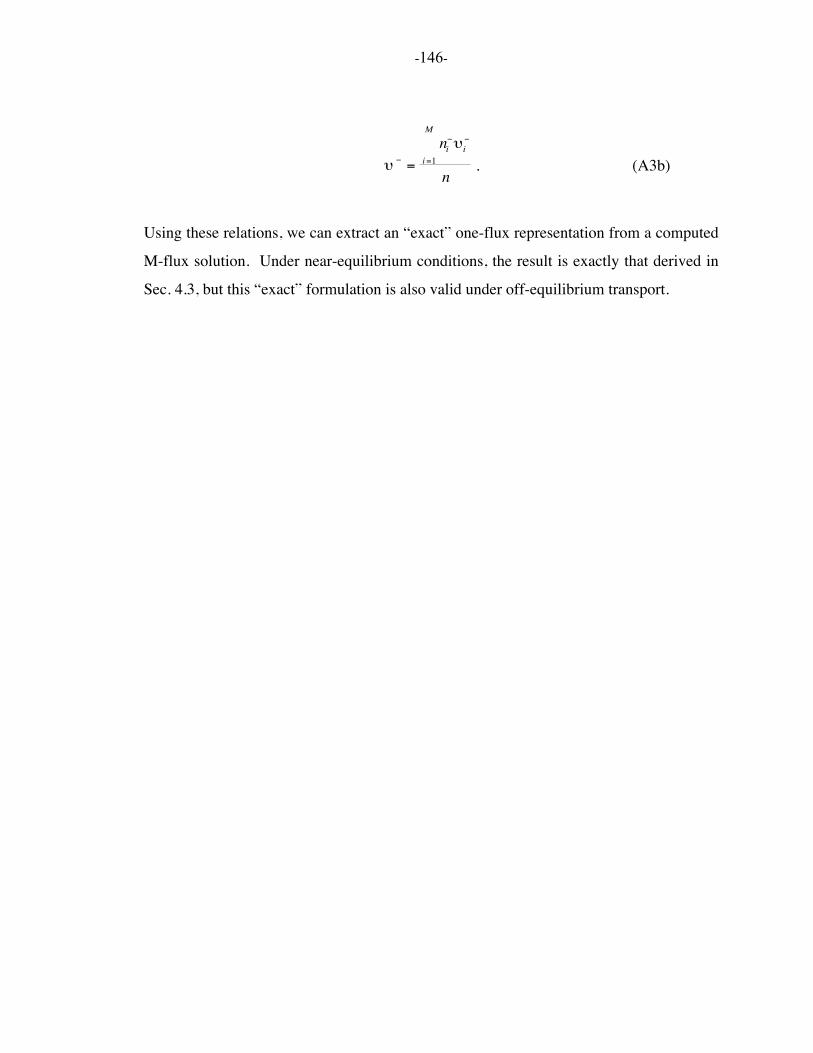
-146-
υ − =ni−υi
−
i =1
M
n
. (A3b)
Using these relations, we can extract an “exact” one-flux representation from a computed
M-flux solution. Under near-equilibrium conditions, the result is exactly that derived in
Sec. 4.3, but this “exact” formulation is also valid under off-equilibrium transport.

-147-
APPENDIX B
The multimode drift-diffusion equation is derived by a procedure similar to that
which led from the one-flux equations, eqs. (4.9), to the continuity and drift-diffusions
equations, eqs. (4.19) and (4.20). The result is that the M-flux equations, eqs. (4.15) and
(4.16), are transformed to an M-flux continuity and drift-diffusion equation (see [Ban97]
for details). The parameters in these equations are M x M matrices related to the M x M
backscattering matrices in the M-flux equations. The “generation-recombination”
matrices in the M-flux continuity equation are
[α] = −12
⎯
↵ ξ
11[ ]+ ξ 12[ ]− ξ 22[ ]− ξ 21[ ]{ } (B1a)
and
β[ ]=q2⎯
↵ υ[ ] ξ 11[ ]− ξ 12[ ]+ ξ 22[ ]− ξ 21[ ]{ }. (B1b)
Similarly, the M x M diffusion matrix is
D[ ]= 2 ξ 11[ ]+ ξ 12[ ]+ ξ 21[ ]+ ξ 22[ ]{ }−1υ[ ] , (B2a)
and the mobility matrix is
µ zz[ ]= Dzz[ ]E[ ]−1 , (B2b)
where
E[ ]−1
=1
2Ez
υ[ ]−1ξ 11[ ]− ξ 22[ ]+ ξ 21[ ]− ξ 12[ ]{ }υ[ ] (B2c)
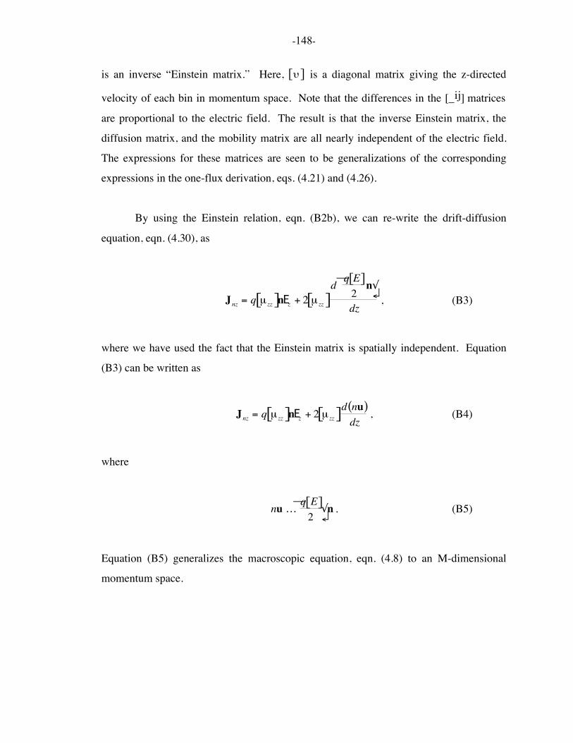
-148-
is an inverse “Einstein matrix.” Here, υ[ ] is a diagonal matrix giving the z-directed
velocity of each bin in momentum space. Note that the differences in the [_ij] matrices
are proportional to the electric field. The result is that the inverse Einstein matrix, the
diffusion matrix, and the mobility matrix are all nearly independent of the electric field.
The expressions for these matrices are seen to be generalizations of the corresponding
expressions in the one-flux derivation, eqs. (4.21) and (4.26).
By using the Einstein relation, eqn. (B2b), we can re-write the drift-diffusion
equation, eqn. (4.30), as
Jnz = q µ zz[ ]nEz + 2 µ zz[ ]
d q E[ ]2
n⎯
↵ √
dz, (B3)
where we have used the fact that the Einstein matrix is spatially independent. Equation
(B3) can be written as
Jnz = q µ zz[ ]nEz + 2 µ zz[ ]d nu( )
dz, (B4)
where
nu …q E[ ]
2⎯
↵ √ n . (B5)
Equation (B5) generalizes the macroscopic equation, eqn. (4.8) to an M-dimensional
momentum space.
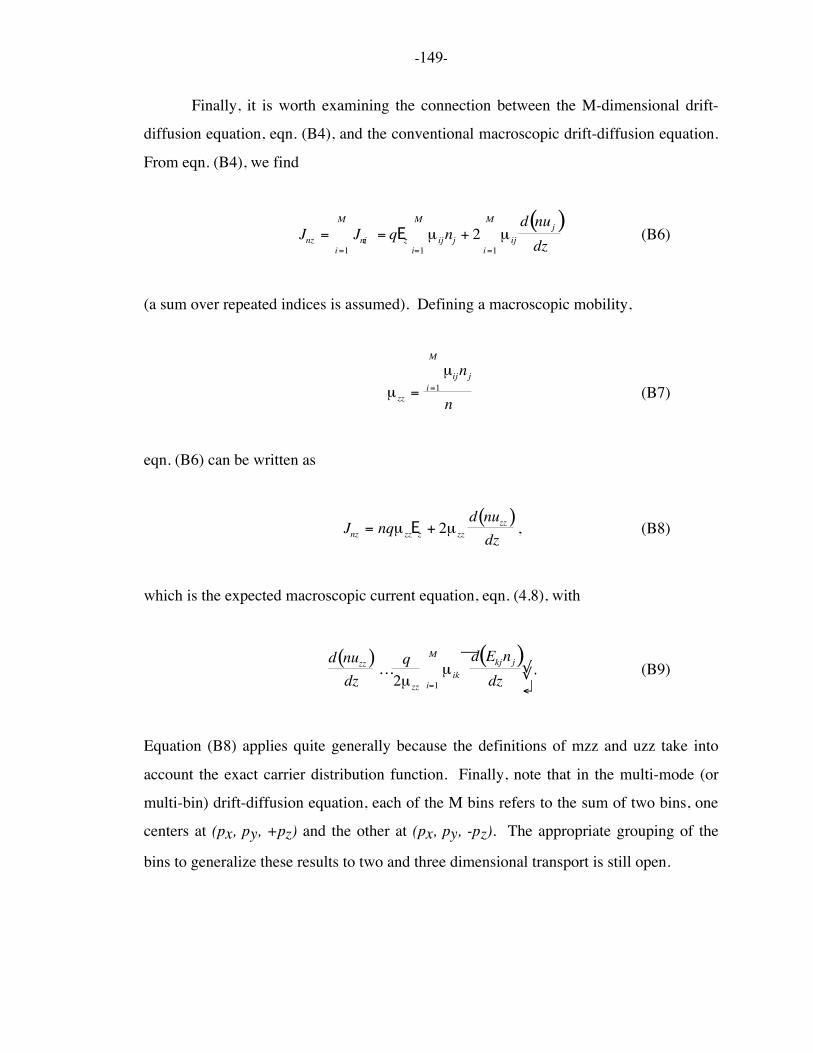
-149-
Finally, it is worth examining the connection between the M-dimensional drift-
diffusion equation, eqn. (B4), and the conventional macroscopic drift-diffusion equation.
From eqn. (B4), we find
Jnz = Jnzi
i =1
M
= qEz µ ijnji=1
M
+ 2 µ ij
d nuj( )dzi =1
M
(B6)
(a sum over repeated indices is assumed). Defining a macroscopic mobility,
µ zz =µijn j
i =1
M
n
(B7)
eqn. (B6) can be written as
Jnz = nqµ zzEz + 2µ zz
d nuzz( )dz
, (B8)
which is the expected macroscopic current equation, eqn. (4.8), with
d nuzz( )dz
…q
2µ zz
µ ik
d Ekjn j( )dz
⎯
↵ √ √
i=1
M
. (B9)
Equation (B8) applies quite generally because the definitions of mzz and uzz take into
account the exact carrier distribution function. Finally, note that in the multi-mode (or
multi-bin) drift-diffusion equation, each of the M bins refers to the sum of two bins, one
centers at (px, py, +pz) and the other at (px, py, -pz). The appropriate grouping of the
bins to generalize these results to two and three dimensional transport is still open.

-150-
-151-
APPENDIX C
When the SiO Si2 / interface is parallel to the [100] plane, the six equivalent minima of
the bulk silicon conduction band split into two sets of sub-bands [16]. The first set consists of
the two equivalent valleys with in-plane effective density-of-states mass mD = 2mt (where a
factor of 2 accounts for the valley degeneracy) and perpendicular effective mass of m
l. The
second set (Δ4-band) consists of the four equivalent valleys with mD = 4 m
lmt (again, factor of
4 accounts for valley degeneracy) and the perpendicular effective mass ismt . The energy levels
associated with the first set comprise the so-called unprimed ladder of sub-bands, whereas those
associated with the second set comprise the primed ladder of sub-bands.
The drain current of a MOSFET is the sum of the contributions from the unprimed and
primed sub-bands. The ballistic limit current contribution from each sub-band is computed from
IDi W =
qA
υ xkx >0,kz
∑ fL −qA
υ xkx <0,kz
∑ fR, (C1)
where A is a normalization area,
fL =1
1+ e E−EF( ) kBT (C2)
the Fermi function for electrons injected from the left contact, and
fR =1
1+ e E−EF +qVD( ) / k BT (C3)
for electrons injected from the right contact. Parabolic energy bands were assumed, and we
assumed that the MOSFET width, W, was large so that the sum over kz could be replaced by an
integral (see Secs. 1.2.3 and 3.1 of ref. [17] for a discussion of how such integrals are worked

-152-
out). The result of evaluating eqn. (C1) in this manner gives the drain current carried by each
sub-band, eqn. (1).
In the drain current expressions, one must use the proper density of states and conductivity
effective masses. For the unprimed ladder,
mCi = 4mt (C4)
and for the primed ladder
mCi = 4 mt + ml( )2. (C5)
Also,
mDi = 2mt (C6)
for the unprimed ladder and
mDi = 4 mt ml (C7)
for the primed ladder. The carrier density for each sub-band is given by eqn. (2), and the total
inversion layer density per unit area is the sum of the carrier densities of each sub-band. Note
that the factor of two in the denominator of eqn. (2) arises because in the ballistic limit, only the
+kx states are occupied when VD is greater than a few kBT/q.
To evaluate the source to drain resistance in the ballistic limit, note that for small drain-to-source
voltages,
fL − fR ≅∂fL
∂E⎛ ⎝ ⎜
⎞ ⎠ ⎟ −qVD( ) , (C8)
-153-
and the source to drain channel conductance becomes
GDSi
W=
q2
Aυx
kx >0, kz
∑ −∂ fL
∂E⎛
⎝ ⎜ ⎞
⎠ , (C9)
which can be evaluated to find eqn. (5).
A common assumption in the analysis of MOS problems is to assume that only a single
sub-band is occupied (e.g. Natori [2]). The results of our study show that this assumption is, for
the most part acceptable. In this case, the total carrier concentration is the first sub-band
population, so
qnS1 = Ceff VGS − VT( ), (C10)
and we may, therefore, solve eqn. (2) for EF − ε1( ) and, therefore perform the entire analysis
analytically. A Schrödinger-Poisson simulation may be needed to specify Ceff and VT.
It is useful to examine the one sub-band analytical results in the degenerate limit. In this
case,
nS1 =mt
πh2 EF − ε1( ) =
kF2
2π. (C11)
Notice that eqn. (C11) is the standard, equilibrium result for single spherical valley; it is actually
a factor of two smaller because only +kx states are occupied, but then it is multiplied by two to
account for valley degeneracy. Using the degenerate limit of the Fermi-Dirac integral,
limηF→∞
F1/2 (ηF ) =4ηF
3/ 2
3π1 / 2, (C12)
-154-
the degenerate thermal injection velocity becomes,
υinj =4
3πhkF
mt
=4h
3mt
2Ceff VGS − VT( )/ qπ . (C13)
Note that in the one-sub-band approximation, the thermal injection velocity is independent of
temperature, if a fixed gate overdrive is maintained. Figure 10 shows that the injection velocity
at high gate voltages is higher at 77K than at 300K. This occurs because at 300K, upper sub-
bands are partially occupied, which lowers the average injection velocity somewhat.
The on-current is now readily evaluated from the product of nS and υinj to find
ID(on) /W =2q3π2
hkF3
mt
=2qh
3π 2mt
2πCeff VGS −VT( ) / q[ ]3 / 2. (C14)
Finally, we can find the one sub-band, channel conductance in the degenerate limit as
GD / W =2q2
π2h
kF =2q3 / 2
π3 / 2h
Ceff VGS − VT( ) . (C15)
Equation (C15) can be expressed in a more familiar form if we write it in terms of the number of
transverse modes at the Fermi energy,
M = 2 × 2kF
2π W. (C16)
In eqn. (C16), the factor of two comes from valley degeneracy. Using eqn. (C16) in eqn. (C15),
we find
GD =2q2
hM , (C17)
-155-
where M = 0, 2, 4, 6, etc. because of the valley degeneracy. Equation (C17) is a familiar result in
mesoscopic physics [9]. In the degenerate limit, each transverse mode contributes 2q2/h to the
ballistic conductance.

-156-
-157-
APPENDIX D
In this appendix, we outline how the mean-free-path may be estimated from the
MOS device parameters. In the kinetic theory of gases, the mean-free-path (MFP) is
usually written in terms of the diffusion coefficient as
zzD λυ= (D1)
where zλ and zυ are the z-directed (i.e., along the direction of current) components of
the MFP and velocity, respectively. In order to obtain an average of zzλυ in three
dimensions, we may define a hemisphere and, since all directions are equally likely, we
perform an average over the whole sphere to show that [Kit80]:
υλ31
=D (D2)
For the two-dimensional carriers confined to channel sub-bands in a MOSFET,
we may similarly define a semicircle and perform a similar average. The result is:
υλθθυλυλπ
41
21
0
2 =
== dCosD (D3)
Note, the velocity term υ that appears in equation (D3) is not the thermal
injection velocity, as given by equation 6.5, but is the average velocity that the carriers
acquire in between the randomizing collisions. Clearly, this velocity depends on the
average energy of the carriers, which at beginning of the channel is simply given by
thermal equilibrium energy for a 2DEG, TkB . Consequently, velocity may be written in
terms of the thermal energy as :
-158-
*B
mTk2
=υ (D4)
where *m is the effective mass for a given sub-band. The diffusion coefficient may now
simply be written in terms of the mean-free-path if we use the Einstein relation:
( )( )η
ηηµ
eeelog
qTkD B ++
=11 (D5)
Inserting equation (C.5) in equation (C.3), the mean-free-path may be expressed in terms
of mobility µ as:
( )( )η
ηη
υλ
eeelog
qTkB ++
=1114 . (D6)
In Fig. D.1 we plot the mean-free-path as obtained using equation (D6), and the mobility
as a function of gate voltage. The mobility shown in this figure was measured using the
conductivity method [Sch90] on large area MOSFETs (W=L=20µm). The measured
mobility shows a slight rise at low gate voltages but subsequently drops at higher gate
voltages, remnant of the dopant-scattering and surface-scattering regimes, respectively.
The estimates quoted in Chapter 6 are taken from Fig. D.1.