S-PARAMETERS - nanoHUB
107
S-PARAMETERS An Introduction
-
Upload
khangminh22 -
Category
Documents
-
view
3 -
download
0
Transcript of S-PARAMETERS - nanoHUB

S-PARAMETERS
An Introduction

S-parameters are a useful method for representing a circuit as a “black box”

S-parameters are a useful method for representing a circuit as a “black box”
The external behaviour of thisblack box can be predicted without any regard for the contents of the black box.

The external behaviour of thisblack box can be predicted without any regard for the contents of the black box.
This black box could contain anything:a resistor, a transmission line or an integrated circuit.
S-parameters are a useful method for representing a circuit as a “black box”

A “black box” or network may have any number of ports.
This diagram shows a simple
network with just 2 ports.

A “black box” or network may have any number of ports.
This diagram shows a simple
network with just 2 ports.
Note :
A port is a terminal pair of lines.
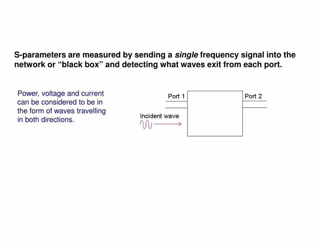
S-parameters are measured by sending a single frequency signal into the network or “black box” and detecting what waves exit from each port.
Power, voltage and current
can be considered to be in
the form of waves travelling
in both directions.

Power, voltage and current
can be considered to be in
the form of waves travelling
in both directions.
For a wave incident on Port 1,
some part of this signal
reflects back out of that port
and some portion of the signal
exits other ports.
S-parameters are measured by sending a single frequency signal into the network or “black box” and detecting what waves exit from each port.

I have seen S-parameters described as S11, S21, etc. Can you explain?
First lets look at S11.
S11 refers to the signal
reflected at Port 1 for the
signal incident at Port 1.

First lets look at S11.
S11 refers to the signal
reflected at Port 1 for the
signal incident at Port 1.
Scattering parameter S11is the ratio of the two waves b1/a1.
I have seen S-parameters described as S11, S21, etc. Can you explain?

Now lets look at S21.
S21 refers to the signal
exiting at Port 2 for the
signal incident at Port 1.
Scattering parameter S21is the ratio of the two waves b2/a1.
I have seen S-parameters described as S11, S21, etc. Can you explain?

Now lets look at S21.
S21 refers to the signal
exiting at Port 2 for the
signal incident at Port 1.
Scattering parameter S21is the ratio of the two waves b2/a1.
I have seen S-parameters described as S11, S21, etc. Can you explain?

Now lets look at S21.
S21 refers to the signal
exiting at Port 2 for the
signal incident at Port 1.
Scattering parameter S21is the ratio of the two waves b2/a1.
I have seen S-parameters described as S11, S21, etc. Can you explain?


A linear network can be characterised by a set of simultaneous equations
describing the exiting waves from each port in terms of incident waves.
S11 = b1 / a1
S12 = b1 / a2
S21 = b2 / a1
S22 = b2 / a2
Note again how the subscript follows the parameters in the ratio (S11=b1/a1, etc...)
I have seen S-parameters described as S11, S21, etc. Can you explain?

S-parameters are complex (i.e. they have magnitude and angle)
because both the magnitude and phase of the input signal are
changed by the network.
(This is why they are sometimes referred to as complex scattering parameters).
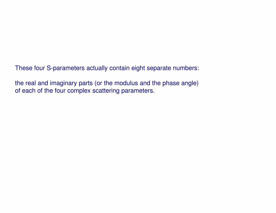
These four S-parameters actually contain eight separate numbers:
the real and imaginary parts (or the modulus and the phase angle)
of each of the four complex scattering parameters.

Quite often we refer to the magnitude only as it is of the most interest.
How much gain (or loss) you get is usually more important than how much
the signal has been phase shifted.

S-parameters depend upon the network
and the characteristic impedances of the
source and load used to measure it, and
the frequency measured at.
i.e.
if the network is changed, the S-parameters change.
if the frequency is changed, the S-parameters change.
if the load impedance is changed, the S-parameters change.
if the source impedance is changed, the S-parameters change.
What do S-parameters depend on?

What do S-parameters depend on?
S-parameters depend upon the network
and the characteristic impedances of the
source and load used to measure it, and
the frequency measured at.
i.e.
if the network is changed, the S-parameters change.
if the frequency is changed, the S-parameters change.
if the load impedance is changed, the S-parameters change.
if the source impedance is changed, the S-parameters change.
In the Si9000e S-parameters are
quoted with source and load
impedances of 50 Ohms

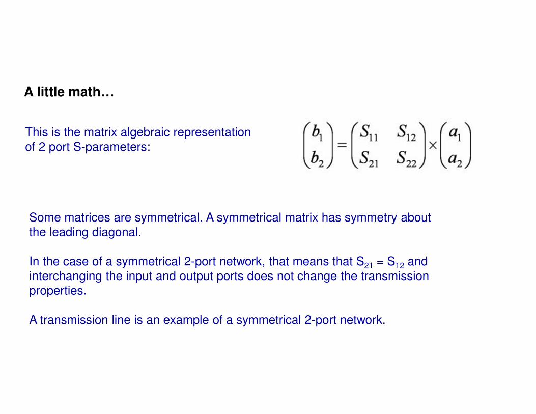
A little math…
This is the matrix algebraic representation
of 2 port S-parameters:
Some matrices are symmetrical. A symmetrical matrix has symmetry about
the leading diagonal.

A little math…
This is the matrix algebraic representation
of 2 port S-parameters:
Some matrices are symmetrical. A symmetrical matrix has symmetry about
the leading diagonal.
In the case of a 2-port network, that means that S21 = S12 and interchanging
the input and output ports does not change the transmission properties.
A little math…
This is the matrix algebraic representation
of 2 port S-parameters:
Some matrices are symmetrical. A symmetrical matrix has symmetry about
the leading diagonal.
In the case of a symmetrical 2-port network, that means that S21 = S12 and
interchanging the input and output ports does not change the transmission
properties.
A transmission line is an example of a symmetrical 2-port network.

A little math…
Parameters along the leading diagonal,
S11 & S22, of the S-matrix are referred to as
reflection coefficients because they refer to
the reflection occurring at one port only.

A little math…
Parameters along the leading diagonal,
S11 & S22, of the S-matrix are referred to as
reflection coefficients because they refer to
the reflection occurring at one port only.
Off-diagonal S-parameters, S12, S21, are referred to as transmission coefficients
because they refer to what happens from one port to another.

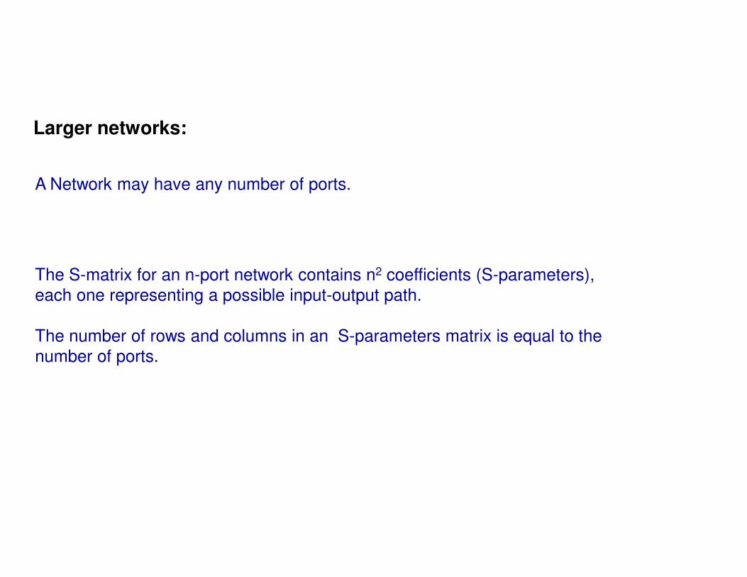
Larger networks:
A Network may have any number of ports.

Larger networks:
A Network may have any number of ports.
The S-matrix for an n-port network contains n2 coefficients (S-parameters),
each one representing a possible input-output path.
Larger networks:
A Network may have any number of ports.
The S-matrix for an n-port network contains n2 coefficients (S-parameters),
each one representing a possible input-output path.
The number of rows and columns in an S-parameters matrix is equal to the
number of ports.

Larger networks:
A Network may have any number of ports.
The S-matrix for an n-port network contains n2 coefficients (S-parameters),
each one representing a possible input-output path.
The number of rows and columns in an S-parameters matrix is equal to the
number of ports.
For the S-parameter subscripts “ij”, “j” is the port that is excited (the input port)
and “i” is the output port.


Sum up…
• S-parameters are a powerful way to describe an electrical network
• S-parameters change with frequency / load impedance / source impedance / network
• S11 is the reflection coefficient
• S21 describes the forward transmission coefficient (responding port 1st!)
• S-parameters have both magnitude and phase information
• Sometimes the gain (or loss) is more important than the phase shift and the phase
information may be ignored
• S-parameters may describe large and complex networks
• If you would like to learn more please see next slide:

Further reading:
Agilent papershttp://www.sss-mag.com/pdf/an-95-1.pdfhttp://www.sss-mag.com/pdf/AN154.pdfNational Instruments paperhttp://zone.ni.com/devzone/nidzgloss.nsf/webmain/D2C4FA88321195FE8625686B00542EDB?OpenDocumentOther links:http://www.sss-mag.comhttp://www.microwaves101.com/index.cfmhttp://www.reed-electronics.com/tmworld/article/CA187307.htmlhttp://en.wikipedia.org/wiki/S-parametersOnline lecture OLL-140 Intro to S-parameters - Eric BogatinOnline lecture OLL-141 S11 & Smith charts - Eric Bogatin
www.bethesignal.com

TRANSMISSION LINES
Description

Terminology and Conventions
36
( ) ( )φ+ω= tcosVtV o
( ) ( ) tjjo
tjo eeVReeVRetV ωφφ+ω ==
1j −=
Sinusoidal Source
φjoeV is a complex phasor

Phasors
• In these notes, all sources are sine waves
• Circuits are described by complex phasors
• The time varying answer is found by multiplying phasors by and taking the real part
37
oV
( )φcosVo
( )φsinVo
φω
Re
Im
( ) ( )φ+φ=φ sinjVcosVeV ooj
o
tje
ω

TEM Transmission Line Theory
38
Charge on the inner conductor:
xVCq l∆=∆
where Cl is the capacitance per unit length
Azimuthal magnetic flux:
xIL l∆=∆Φ
where Ll is the inductance per unit length

Electrical Model of a Transmission Line
39
i ii ∆+
v vv ∆+
xL l ∆
xC l ∆
Voltage drop along the inductor:
( )dt
dixLvvv l∆=∆+−
Current flowing through the capacitor:
dt
dvxCiii l∆−=∆+

Transmission Line Waves
40
Limit as ∆x->0
t
iL
x
vl
∂
∂−=
∂
∂
t
BE
∂
∂−=×∇
t
vC
x
il
∂
∂−=
∂
∂
t
DH
∂
∂=×∇
Solutions are traveling waves
( )
++
−= −+
vel
xtv
vel
xtvx,tv
( )
+−
−=
−+
vel
xt
Z
v
vel
xt
Z
vx,ti
oo
v+ indicates a wave traveling in the +x directionv- indicates a wave traveling in the -x direction

Phase Velocity and Characteristic
Impedance
41
vel is the phase velocity of the wave
llCL
1vel =
For a transverse electromagnetic wave (TEM), the phase velocity is only a property of the material the wave travels through
µε=
1
CL
1
ll
The characteristic impedance Zo
l
lo
C
LZ =
has units of Ohms and is a function of the material AND the geometry

Pulses on a Transmission Line
42
Pulse travels down the transmission line as a forward going wave only (v+). However, when the pulse reaches the load resistor:
oo
L
Z
v
Z
v
vvR
i
v
−+
−+
−
+==
LR+v
so a reverse wave v- and i- must be created to satisfy the boundary condition imposed by the load resistor

Reflection Coefficient
43
The reverse wave can be thought of as the incident wave reflected from the load
Γ=+
−=
+
−
oL
oL
ZR
ZR
v
v Reflection coefficient
Three special cases:
RL = ∞ (open) Γ = +1
RL = 0 (short) Γ = -1
RL = Zo Γ = 0
A transmission line terminated with a resistor equal in value to the characteristic impedance of the transmission line looks the same to
the source as an infinitely long transmission line

Sinusoidal Waves
44
( ) tjxj eeVRextcosVv ωβ−+++ =β−ω=
vel=β
ωphase velocity
λ
π=
π=β
2
vel
f2wave number
By using a single frequency sine wave we can now define complex impedances such as:
LIjV ω=dt
diLv =
dt
dvCi =
Cj
1Zcap
ω=
LjZind ω=
CVjI ω=
Experiment: Send a SINGLE frequency (ω) sine wave into a transmission line and measure how the line responds

Standing Waves
45
LZoZ
0x =
x
d
At x=0
oL
oL
ZZ
ZZVV
+
−=Γ= +−
Along the transmission line:
( ) ( )xcosV2e1VV
eVeVV
xj
xjxj
βΓ+Γ−=
Γ+=
+β−+
β++β−+
traveling wave standing wave

Voltage Standing Wave Ratio (VSWR)
46
0 0.1 0.2 0.3 0.4 0.5 0.6 0.7 0.8 0.9 11.5
1
0.5
0
0.5
1
1.5
Position
( )( )
( )( )
VSWR
1
1
1V
1V
V
V
min
max
=
Γ−
Γ+=
Γ−
Γ+=
+
+
The VSWR is always greater than 1
2
1=Γ
Large voltage
Large current

Voltage Standing Wave Ratio (VSWR)
47
( )( )
( )( )
VSWR
1
1
1V
1V
V
V
min
max
=
Γ−
Γ+=
Γ−
Γ+=
+
+
The VSWR is always greater than 1
2
1=Γ
Incident wave
Reflected wave
Standing wave

Reflection Coefficient Along a
Transmission Line
48
LZoZ
0x =
x
d
oL
oLL
ZZ
ZZ
+
−=ΓGΓ
towards load
towards generator
xjL
xj eVeVV β++β−+ Γ+=
d2jL)d(j
)d(j
L
genreverse
forwardG e
eV
eV
V
V β−−β−+
−β++
Γ=Γ==Γ
Wave has to travel down and back
Impedance and Reflection
49
GΓ
LΓ
ΓRe
ΓIm
d2β−=θ
There is a one-to-one correspondence between ΓG and
ZL
oG
oGG
ZZ
ZZ
+
−=Γ
G
GoG
1
1ZZ
Γ−
Γ+=
d2jL
d2jL
oGe1
e1ZZ
β−
β−
Γ−
Γ+=

Impedance and Reflection: Open Circuits
50
For an open circuit ZL= ∞ so ΓL = +1
Impedance at the generator:
( )dtan
jZZ o
Gβ
−=
For βd<<1
dCj
1
d
jZZ
l
oG
ω=
β
−≈ looks capacitive
For βd = π/2 or d=λ/4
0ZG =
An open circuit at the load looks like a short circuit at the generator if the generator is a quarter wavelength away from the load

Impedance and Reflection: Short Circuits
51
For a short circuit ZL= 0 so ΓL = -1
Impedance at the generator:
( )dtanjZZ oG β=
For βd<<1
dLjdjZZ loG ω=β≈ looks inductive
For βd = π/2 or d=λ/4
∞→GZ
A short circuit at the load looks like an open circuit at the generator if the generator is a quarter wavelength away from the load

Incident and Reflected Power
52
LZoZ
0x =
x
d
sP
dx −=
dj
oL
dj
oG
djL
djG
eZ
Ve
Z
V)d(II
eVeV)d(VV
β−+
β++
β−+β++
Γ−=−=
Γ+=−=
Voltage and Current at the generator (x=-d)
The rate of energy flowing through the plane at x=-d
o
22
Lo
2
*GG
Z
V
2
1
Z
V
2
1P
IVRe2
1P
++
Γ−=
=
forward powerreflected power

Incident and Reflected Power
• Power does not flow! Energy flows.
– The forward and reflected traveling waves are power orthogonal
• Cross terms cancel
– The net rate of energy transfer is equal to the difference in power of the
individual waves
• To maximize the power transferred to the load we want:
53
0L =Γ
which implies:
oL ZZ =
When ZL = Zo, the load is matched to the transmission line

Load Matching
54
What if the load cannot be made equal to Zo for some other reasons?Then, we need to build a matching network so that the sourceeffectively sees a match load.
0=Γ
LZsP 0Z M
Typically we only want to use lossless devices such as capacitors,inductors, transmission lines, in our matching network so that we donot dissipate any power in the network and deliver all the availablepower to the load.

Normalized Impedance
55
jxrZ
Zz
o
+==
It will be easier if we normalize the load impedance to thecharacteristic impedance of the transmission line attached to theload.
Γ−
Γ+=
1
1z
Since the impedance is a complex number, the reflection coefficientwill be a complex number
jvu +=Γ
( ) 22
22
vu1
vu1r
+−
−−= ( ) 22
vu1
v2x
+−=

dB and dBm
56
A dB is defined as a POWER ratio. For example:
( )Γ=
Γ=
=Γ
log20
log10
P
Plog10
2
for
revdB
A dBm is defined as log unit of power referenced to 1mW:
=
mW1
Plog10PdBm

Z AND S PARAMETERS
Description

Two Port Z Parameters
58
We have only discussed reflection so far. What about transmission? Consider a device that has two ports:
1V 2V
2I1I
[ ] [ ][ ]IZV
IZIZV
IZIZV
2221212
2121111
=
+=
+=
The device can be characterized by a 2x2 matrix:

Scattering (S) Parameters
59
−+
−+
−=
+=
iiio
iii
VVIZ
VVV
Since the voltage and current at each port (i) can be broken down into forward and reverse waves:
We can characterize the circuit with forward and reverse waves:
[ ] [ ][ ]+−
++−
++−
=
+=
+=
VSV
VSVSV
VSVSV
2221212
2121111

Z and S Parameters
60
[ ] [ ] [ ]( ) [ ] [ ]( )
[ ] [ ] [ ]( ) [ ] [ ]( ) 1o
o1
o
S1S1ZZ
1ZZ1ZZS
−
−
−+=
−+=
Similar to the reflection coefficient, there is a one-to-one correspondence between the impedance matrix and the scattering
matrix:

Normalized Scattering (S) Parameters
61
The S matrix defined previously is called the un-normalizedscattering matrix. For convenience, define normalized waves:
io
ii
io
ii
Z2
Vb
Z2
Va
−
+
=
=
Where Zoi is the characteristic impedance of the transmission line connecting port (i)
|ai|2 is the forward power into port (i)
|bi|2 is the reverse power from port (i)

Normalized Scattering (S) Parameters
62
The normalized scattering matrix is:
Where:
[ ] [ ][ ]asb
asasb
asasb
2221212
2121111
=
+=
+=
j,i
io
jo
j,i SZ
Zs =
If the characteristic impedance on both ports is the same then the normalized and un-normalized S parameters are the same.
Normalized S parameters are the most commonly used.

Normalized S Parameters
63
The s parameters can be drawn pictorially
s11 and s22 can be thought of as reflection coefficients
s21 and s12 can be thought of as transmission coefficients
s parameters are complex numbers where the angle corresponds to a phase shift between the forward and reverse waves
s11 s22
s21
s12
a1
a2b1
b2

Examples of S parameters
64
τ
Zo1 2
[ ]
=
ωτ−
ωτ−
0e
e0s
j
j
21 [ ]
−
−=
10
01s
1 2
[ ]
=
0G
00s
G
Transmission Line
Short
Amplifier

Examples of S parameters
65
[ ]
=
010
001
100
s
1
2
[ ]
=
01
00s
Zo
Isolator
1 2
3
Circulator

Lorentz Reciprocity
66
If the device is made out of linear isotropic materials (resistors, capacitors, inductors, metal, etc..) then:
[ ] [ ]ssT =
j,ii,j ss = ji ≠
or
for
This is equivalent to saying that the transmitting pattern of an antenna is the same as the receiving pattern
reciprocal devices: transmission line
short
directional coupler
non-reciprocal devices: amplifier
isolator
circulator

Lossless Devices
67
The s matrix of a lossless device is unitary:
[ ] [ ] [ ]1ssT* =
∑
∑
=
=
j
2
j,i
i
2
j,i
s1
s1for all j
for all i
Lossless devices: transmission line
short
circulator
Non-lossless devices: amplifier
isolator

Network Analyzers
68
Network analyzers measure S parameters as a function of
frequency
At a single frequency, network analyzers send out forward waves a1and a2 and measure the phase and amplitude of the reflected waves b1and b2 with respect to the forward
waves.
a1 a2
b1 b2
02a1
111
a
bs
=
=
02a1
221
a
bs
=
=
01a2
112
a
bs
=
=
01a2
222
a
bs
=
=

Network Analyzer Calibration
69
To measure the pure S parameters of a device, we need to eliminate the effects of cables, connectors, etc. attaching the device to the
network analyzer
s11 s22
s21
s12
x11 x22
x21
x12
y11 y22
y21
y12
yx21
yx12
Connector Y Connector X
We want to know the S parameters at these reference planes
We measure the S parameters at these reference planes

Network Analyzer Calibration
• There are 10 unknowns in the connectors
• We need 10 independent measurements to eliminate these unknowns
– Develop calibration standards
– Place the standards in place of the Device Under Test (DUT) and measure the S- parameters of the standards and the connectors
– Because the S parameters of the calibration standards are known (theoretically), the S parameters of the connectors can be determined and can be mathematically eliminated once the DUT is placed back in the measuring fixtures.
70

Network Analyzer Calibration• Since we measure four S parameters for each
calibration standard, we need at least three independent standards.
• One possible set is:
71
[ ]
−
−=
10
01s
[ ]
=
ωτ−
ωτ−
0e
e0s
j
j
τ
[ ]
=
01
10sThru
Short
Delay**ωτ~90degrees

Phase Delay
72
A pure sine wave can be written as:
( )ztjoeVV β−ω=
The phase shift due to a length of cable is:
ph
ph
dv
d
ωτ=
ω=
β=θ
The phase delay of a device is defined as:
( )ω
−=τ 21ph
Sarg
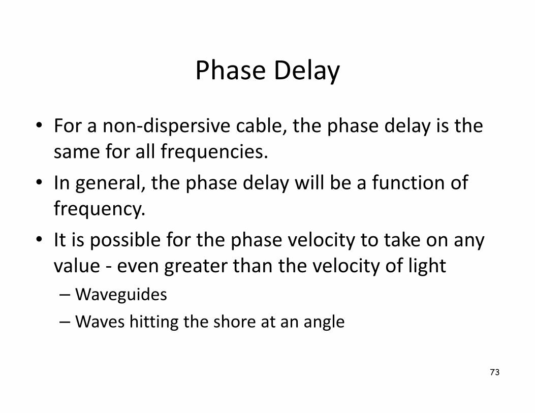
Phase Delay
• For a non-dispersive cable, the phase delay is the
same for all frequencies.
• In general, the phase delay will be a function of
frequency.
• It is possible for the phase velocity to take on any
value - even greater than the velocity of light
– Waveguides
– Waves hitting the shore at an angle
73

Group Delay• A pure sine wave has no information content
– There is nothing changing in a pure sine wave
– Information is equivalent to something changing
• To send information there must be some
modulation of the sine wave at the source
74
( )( ) ( )tcostcosm1VV o ωω∆+=
( ) ( )( ) ( )( )[ ]tcostcos2
mVtcosVV oo ω∆−ω+ω∆+ω+ω=
The modulation can be de-composed into different frequency components

Group Delay
75
( )
( ) ( )( )
( ) ( )( )ztcos2
mV
ztcos2
mV
ztcosVV
o
o
o
β∆−β−ω∆−ω+
β∆+β−ω∆+ω+
β−ω=
The waves emanating from the source will look like
Which can be re-written as:
( )( ) ( )ztcosztcosm1VV o β−ωβ∆−ω∆+=

Group Delay
76
The information travels at a velocity
ω∂
β∂⇒
ω∆
β∆= 11vgr
The group delay is defined as:
( )( )ω∂
∂−=
ω∂
β∂=
=τ
21
grgr
Sarg
d
v
d

Phase Delay and Group Delay
77
Phase Delay:
( )ω
−=τ 21ph
Sarg
Group Delay:
( )( )ω∂
∂−=τ 21
grSarg

SMITH CHART
Description

Smith Chart
• Impedances, voltages, currents, etc. all repeat every half wavelength
• The magnitude of the reflection coefficient, the standing wave ratio (SWR) do not change, so they characterize the voltage & current patterns on the line
• If the load impedance is normalized by the characteristic impedance of the line, the voltages, currents, impedances, etc. all still have the same properties, but the results can be generalized to any line with the same normalized impedances 79

Smith Chart
• The Smith Chart is a clever tool for analyzing
transmission lines
• The outside of the chart shows location on the line
in wavelengths
• The combination of intersecting circles inside the
chart allow us to locate the normalized impedance
and then to find the impedance anywhere on the
line
80

Smith Chart
• Thus, the first step in analyzing a transmission line is to
locate the normalized load impedance on the chart
• Next, a circle is drawn that represents the reflection
coefficient or SWR. The center of the circle is the center
of the chart. The circle passes through the normalized
load impedance
• Any point on the line is found on this circle. Rotate
clockwise to move toward the generator (away from the
load)
• The distance moved on the line is indicated on the
outside of the chart in wavelengths81

Smith Charts
82
The impedance as a function of reflection coefficient can be re-written in the form:
( ) 22
22
vu1
vu1r
+−
−−=
( ) 22vu1
v2x
+−=
( )22
2
r1
1v
r1
ru
+=+
+−
( )2
22
x
1
x
1v1u =
−+−
These are equations forcircles on the (u,v) plane

Smith Chart – Real Circles
83
1 0.5 0 0.5 1
1
0.5
0.5
1
ΓRe
ΓIm
r=0r=1/3
r=1r=2.5

Smith Chart – Imaginary Circles
84
1 0.5 0 0.5 1
1
0.5
0.5
1
ΓRe
ΓIm
x=1/3 x=1 x=2.5
x=-1/3 x=-1 x=-2.5

Smith Chart
85

Smith Chart Example 1
86
Given:
Ω= 50Zo
°∠=Γ 455.0L
What is ZL?
( )Ω+Ω=
+Ω=
5.67j5.67
35.1j35.150ZL

Smith Chart Example 2
87
Given:
Ω= 50Zo
Ω−Ω= 25j15ZL
What is ΓL?
5.0j3.0
50
25j15zL
−=
Ω
Ω−Ω=
°−∠=Γ 124618.0L

Smith Chart Example 3
88
Given:
Ω= 50Zo
Ω+Ω= 50j50ZL
What is Zin at 50 MHz?
0.1j0.1
50
50j50zL
+=
Ω
Ω+Ω=
°∠=Γ 64445.0L
nS78.6=τ
?Zin =
ωτ−β− Γ=Γ=Γ 2jL
d2jLin ee
°=ωτ 2442
°∠=Γ 180445.0in
( ) Ω=+Ω= 190.0j38.050ZL
°=ωτ 2442

Admittance
89
A matching network is going to be a combination of elements connected in series AND parallel.
Impedance is NOT well suited when working with parallel configurations.
21L ZZZ +=
2Z1Z
2Z
1Z
21
21L
ZZ
ZZZ
+=
ZIV =
For parallel loads it is better to work with admittance.
YVI =
2Y1Y
21L YYY +=1
1Z
1Y =
Impedance is well suited when working with series configurations. For example:

Normalized Admittance
90
jbgYZY
Yy o
o
+===
Γ+
Γ−=
1
1y
( ) 22
22
vu1
vu1g
++
−−=
( ) 22vu1
v2b
++
−=
( )22
2
g1
1v
g1
gu
+=+
++
( )2
22
b
1
b
1v1u =
+++
These are equations forcircles on the (u,v) plane

Admittance Smith Chart
91
1 0.5 0 0.5 1
1
0.5
0.5
1
1 0.5 0 0.5 1
1
0.5
0.5
1
ΓRe
ΓIm
g=1/3
b=-1 b=-1/3
g=1g=2.5 g=0
b=2.5 b=1/3
b=1
b=-2.5
ΓIm
ΓRe

Impedance and Admittance Smith
Charts• For a matching network that contains elements
connected in series and parallel, we will need two
types of Smith charts
– impedance Smith chart
– admittance Smith Chart
• The admittance Smith chart is the impedance Smith
chart rotated 180 degrees.
– We could use one Smith chart and flip the
reflection coefficient vector 180 degrees when
switching between a series configuration to a
parallel configuration. 92

Admittance Smith Chart Example 1
93
• Procedure:
• Plot 1+j1 on chart
• vector =
• Flip vector 180 degrees
Given:
°∠64445.0
What is Γ?
1j1y +=
°−∠=Γ 116445.0
Plot y
Flip 180degrees
Read Γ

Admittance Smith Chart Example 2
94
• Procedure:
• Plot Γ
• Flip vector by 180 degrees
• Read coordinate
Given:
What is Y?
°+∠=Γ 455.0 Ω= 50Zo
Plot Γ
Flip 180degrees
Read y
36.0j38.0y −=
( )
( ) mhos10x2.7j6.7Y
36.0j38.050
1Y
3−−=
−Ω
=

Smith Chart
95
Constant Imaginary
Impedance Lines
Constant Real
Impedance Circles
Impedance
Z=R+jX
=100+j50
Normalized
z=2+j for
Zo=50

Smith Chart •Impedance divided by line impedance (50 Ohms)
– Z1 = 100 + j50
– Z2 = 75 -j100
– Z3 = j200
– Z4 = 150
– Z5 = infinity (an open circuit)
– Z6 = 0 (a short circuit)
– Z7 = 50
– Z8 = 184 -j900
•Then, normalize and plot. The points are plotted as follows:
– z1 = 2 + j
– z2 = 1.5 -j2
– z3 = j4
– z4 = 3
– z5 = infinity
– z6 = 0
– z7 = 1
– z8 = 3.68 -j18S96

97
Toward
Generator
Away From
Generator
Constant
Reflection
Coefficient Circle
Scale in
Wavelengths
Full Circle is One Half
Wavelength Since
Everything Repeats

Smith Chart Example
• First, locate the normalized impedance on the chart for ZL
= 50 + j100
• Then draw the circle through the point
• The circle gives us the reflection coefficient (the radius of
the circle) which can be read from the scale at the bottom
of most charts
• Also note that exactly opposite to the normalized load is
its admittance. Thus, the chart can also be used to find
the admittance. We use this fact in stub matching
98

Matching Example
99
0=Γ
Ω100sP Ω= 50Z0 M
Match 100Ω load to a 50Ω system at 100MHz
A 100Ω resistor in parallel would do the trick but ½ of thepower would be dissipated in the matching network. We wantto use only lossless elements such as inductors and capacitorsso we don’t dissipate any power in the matching network
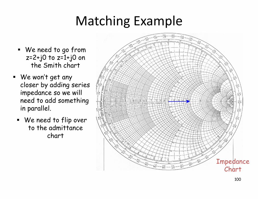
Matching Example
100
We need to go from z=2+j0 to z=1+j0 on the Smith chart
We won’t get any closer by adding series impedance so we will need to add something in parallel.
We need to flip over to the admittance
chart
Impedance Chart
Matching Example
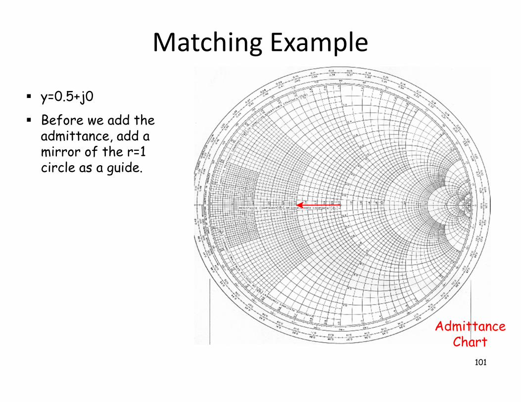
101
y=0.5+j0
Before we add the admittance, add a mirror of the r=1 circle as a guide.
Admittance Chart

Matching Example
102
y=0.5+j0
Before we add the admittance, add a mirror of the r=1 circle as a guide
Now add positive imaginary admittance.
Admittance Chart

Matching Example
103
y=0.5+j0
Before we add the admittance, add a mirror of the r=1 circle as a guide
Now add positive imaginary admittance jb = j0.5
Admittance Chart
( )
pF16C
CMHz1002j50
5.0j
5.0jjb
=
π=Ω
=
pF16 Ω100

Matching Example
104
We will now add series impedance
Flip to the impedance Smith Chart
We land at on the r=1 circle at x=-1
Impedance Chart

Matching Example
105
Add positive imaginary admittance to get to
z=1+j0
Impedance Chart
pF16
Ω100
( ) ( )nH80L
LMHz1002j500.1j
0.1jjx
=
π=Ω
=
nH80

Matching Example
106
This solution would have also worked
Impedance Chart
pF32
Ω100nH160
Matching Bandwidth
107
50 60 70 80 90 100 110 120 130 140 15040
35
30
25
20
15
10
5
0
Frequency (MHz)
Re
fle
ctio
n C
oe
ffic
ien
t (d
B)
50 MHz
100 MHz
Because the inductor and capacitor impedances change with frequency, the
match works over a narrow frequency range
pF16Ω100
nH80
Impedance Chart