SOLUTIONS: ECE 656 Homework (Week 6) - nanoHUB
13
Mark Lundstrom ECE656 Fall 2015 1 SOLUTIONS: ECE 656 Homework (Week 6) Mark Lundstrom Purdue University 1) We have discussed ME ( ) for a 3D semiconductor with parabolic energy bands. Answer the following two questions about a 3D semiconductor with nonparabolic energy bands. a) Assume that the nonparabolicity can be described by E 1 + ! E ( ) = ! 2 k 2 2m * 0 () . Derive an expression for the corresponding ME ( ) . b) Using the following numbers for GaAs, m * 0 () = 0.067 m 0 ! = 0.64 , plot ME ( ) from the bottom of the ! valley to E = 0.3 eV comparing results from the nonparabolic expression derived in part a) to the parabolic expression. Solutions: We know that nonparabolicity flattens the bands – it increases the DOS and lowers the velocity, so it is not obvious whether M(E) will be larger or smaller, since M(E) is the product of the DOS and velocity. Let’s work it out and see what the answer is. 1a) Begin with the definition: M 3D E ( ) = h 4 ! x + D 3D E ( ) (1) ! x + = 12 ( ) ! E ( ) (2) Step 1: compute D 3D E ( ) for nonparabolic bands Step 2: compute ! E ( ) for nonparabolic bands Step 3: multiply the two to get the answer
-
Upload
khangminh22 -
Category
Documents
-
view
6 -
download
0
Transcript of SOLUTIONS: ECE 656 Homework (Week 6) - nanoHUB

Mark Lundstrom
ECE-‐656 Fall 2015 1
SOLUTIONS: ECE 656 Homework (Week 6) Mark Lundstrom Purdue University
1) We have discussed M E( ) for a 3D semiconductor with parabolic energy bands.
Answer the following two questions about a 3D semiconductor with non-‐parabolic energy bands.
a) Assume that the non-‐parabolicity can be described by
E 1+!E( ) = !2k 2
2m* 0( ) . Derive an expression for the corresponding M E( ) .
b) Using the following numbers for GaAs,
m* 0( ) = 0.067 m0
! = 0.64 , plot M E( ) from the bottom of the ! valley to E = 0.3 eV comparing results from the non-‐parabolic expression derived in part a) to the parabolic expression.
Solutions:
We know that non-‐parabolicity flattens the bands – it increases the DOS and lowers the velocity, so it is not obvious whether M(E) will be larger or smaller, since M(E) is the product of the DOS and velocity. Let’s work it out and see what the answer is.
1a) Begin with the definition:
M 3D E( ) = h4
!x+ D3D E( ) (1)
!x+ = 1 2( )! E( ) (2)
Step 1: compute D3D E( ) for non-‐parabolic bands Step 2: compute ! E( ) for non-‐parabolic bands Step 3: multiply the two to get the answer

Mark Lundstrom
ECE-‐656 Fall 2015 2
ECE 656 Homework (Week 6) Solutions (continued) Step 1:
D3D (E)dE =
N3D k( )!
4" k 2dk = 14" 3 4" k 2dk = 1
" 2 k 2dk (3)
E 1+!E( ) = !2k 2
2m* 0( ) (4)
Solve for k:
k =
2m* 0( )E 1+!E( )!
(5)
differentiate to find:
kdk =
m* 0( )!2 1+ 2!E( )dE (6)
put the two together:
k 2dk =
m* 0( )!3 2m* 0( )E 1+!E( ) 1+ 2!E( )dE
Insert in (3)
D3D (E)dE = 1
! 2 k 2dk =m* 0( )! 2!3 2m* 0( )E 1+"E( ) 1+ 2"E( )dE
D3D (E) = 1
! 2 k 2dk =m* 0( )! 2!3 2m* 0( )E 1+"E( ) 1+ 2"E( ) (7)
Step 2: From (6)
dEdk
= !2k
m* 0( )1
1+ 2!E( )"1!
dEdk
=# = !km* 0( )
11+ 2!E( )
Now use (5)
! E( ) = !k
m* 0( )1
1+ 2"E( ) =2E 1+"E( )
m* 0( )1
1+ 2"E( ) (8)

Mark Lundstrom
ECE-‐656 Fall 2015 3
ECE 656 Homework (Week 6) Solutions (continued)
Step 3: Now use (1), (2), (7), and (8)
M 3D E( ) = h4
! E( )2
"#$
%&'D3D E( ) = h
4! E( )2
"#$
%&'D3D E( ) = h
4E 1+(E( )2m* 0( )
11+ 2(E( )D3D E( )
M 3D E( ) = h
4E 1+!E( )2m* 0( )
11+ 2!E( )
m* 0( )" 2!3
2m* 0( )E 1+!E( ) 1+ 2!E( )#$%
&'(
M 3D E( ) = m
* 0( )2!!2
E 1+"E( ) We have been assuming that the bottom of the conduction band is at EC = 0 . Let’s put EC back in explicitly.
M 3D E( ) = m
* 0( )2!!2
E " EC( ) 1+# E " EC( )$% &'
So we see that the M(E) increases when the bands are nonparabolic. 1b) The following Matlab script is used to produce the plot below.
2
set(get(gca,'ylabel'),'FontSize',font_size);
Published with MATLAB® R2013a

Mark Lundstrom
ECE-‐656 Fall 2015 4
ECE 656 Homework (Week 6) Solutions (continued)
1
Table of Contents....................................................................................................................................... 1Parameters ......................................................................................................................... 1Calculation of Modes .......................................................................................................... 1Plots ................................................................................................................................. 1
function ece656_hw6_1b()
% ECE 656 (Fall 2013) HW#6, 1b% This script plots and compares the density of modes for GaAs assuming parabolic and% non-parabolic energy bands
Parametersm_star = 0.067; % (1) effective mass coefficientalpha = 0.64; % (/eV) non-parabolicty factor
m_o = 0.511e6; % (eV/c^2) electron rest masshbar = 6.582e-16; % (eV-s)m = m_star*m_o; % (eV/c^2) electron effective mass
E = linspace(0,0.3,100); % (eV) range of energy
Calculation of ModesM_3D_nonp = m./(2*pi*hbar^2).*E.*(1+alpha.*E).*1e-4; % (/cm^2)M_3D_p = m./(2*pi*hbar^2).*E.*1e-4; % (/cm^2)
Plotsfigure(1)
plot(E, M_3D_nonp,'LineWidth',2)hold onplot(E, M_3D_p,'--','LineWidth',2)
xlabel('Energy (eV)');ylabel('M(E) (/cm^2)');legend('Non-parabolic', 'Parabolic','Location','NorthWest');
xlim([0 max(E)])
font_size = 12;
set(gcf, 'color', 'white');set(gca, 'FontSize', font_size);set(get(gca,'title'), 'FontSize',font_size);set(get(gca,'xlabel'),'FontSize',font_size);
Mark Lundstrom
ECE-‐656 Fall 2015 5
ECE 656 Homework (Week 6) Solutions (continued)
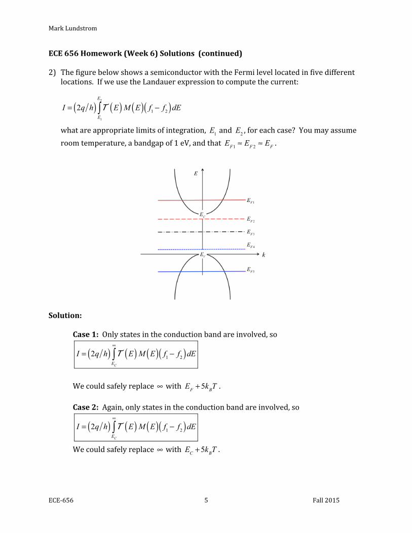
2) The figure below shows a semiconductor with the Fermi level located in five different locations. If we use the Landauer expression to compute the current:
what are appropriate limits of integration, E1 and E2 , for each case? You may assume room temperature, a bandgap of 1 eV, and that EF1 ! EF 2 ! EF .
Solution:
Case 1: Only states in the conduction band are involved, so
I = 2q h( ) T E( )M E( ) f1 ! f2( )dEEC
"
#
We could safely replace ! with EF +5kBT . Case 2: Again, only states in the conduction band are involved, so
I = 2q h( ) T E( )M E( ) f1 ! f2( )dEEC
"
#
We could safely replace ! with EC +5kBT .
I = 2q h( ) T E( )M E( ) f1 ! f2( )dE
E1
E2
"

Mark Lundstrom
ECE-‐656 Fall 2015 6
ECE 656 Homework (Week 6) Solutions (continued)
Case 3: There are not many electrons or holes involved, but we need to include both bands.
I = 2q h( ) T E( )M E( ) f1 ! f2( )dE
!"
+"
#
We could safely replace +! with EC +5kBT and !" with EV !5kBT . Case 4: Only states in the valence band are involved, so
I = 2q h( ) T E( )M E( ) f1 ! f2( )dE
!"
EV
#
We could safely replace !" with EV !5kBT . Case 5: Again, only states in the valence band are involved, so
I = 2q h( ) T E( )M E( ) f1 ! f2( )dE
!"
EV
#
We could safely replace !" with EF !5kBT . 3) Determine the limits of integration, E1 and E2 , for the integral in the Landauer
expression:
I = 2q h( ) T E( )M E( ) f1 ! f2( )dE
E1
E2
"
for the case of T = 0 K. Assume that contact one is grounded and that a positive voltage (not necessarily small) has been applied to contact 2.
Solution:
In the left contact, states below EF1 are occupied, and in the right contact, states below EF 2 = EF1 ! qV are occupied. The only ranges where f1 ! f2( ) is EF 2 < E < EF1 , so
I = 2q h( ) T E( )M E( ) f1 ! f2( )dEEF 1!qV
EF 1
"

Mark Lundstrom
ECE-‐656 Fall 2015 7
ECE 656 Homework (Week 6) Solutions (continued) 4) The ballistic conductance is often derived from a k-‐space treatment, which writes the
current from left to right as
I + = 1L
q!xk>0" f0 EF1( )
and the current from right to left as
I ! = 1L
q"xk<0# f0 EF2( )
The net current is the difference between the two. In the ballistic limit, the Landauer expression for the current is
I = 2q h( ) M E( ) f1 ! f2( )dE
E1
E2
"
4a) Assume parabolic energy bands, evaluate the net current from the k-‐space
approach, and show that it is the same as the Landauer expression.
Solution:
I + = 1L
q!xk>0" f0 EF1( ) = 1
LL2#
$ 2 q f0 EF1( )dk0
+%
&
I + = q!" f0 EF1( )dk
0
+#
$ = q!
f0 EF1( ) dkdE0
+#
$ dE
E = !
2k 2
2m* dE = !
2kdkm*
dk = m*dE!2k
k = 2m*E!
dkdE
= m*
! 2m*E= 1!
m*
2E
I + = q ! 1
"!m*
2E#
$%
&
'( f0 EF1( )
0
+)
* dE
I + = 2q
hh4! 2
"!m*
2E#
$%
&
'( f0 EF1( )
0
+)
* dE = 2qh
h4!D1D E( )+
,-
./0f0 EF1( )
0
+)
* dE
I + = 2qh
M E( ) f0 EF1( )0
+!
" dE
where
M E( ) ≡ h4
υx+ D1D E( )
υx
+ = υ

Mark Lundstrom
ECE-‐656 Fall 2015 8
ECE 656 Homework (Week 6) Solutions (continued)
Similarly, we can show:
I ! = 2qh
M E( ) f0 EF2( )0
+"
# dE
The net current is
I = I + ! I ! = 2qh
M E( ) f0 EF1( )! f0 EF2( )"# $%0
+&
' dE
I = 2qh
M E( ) f1 ! f2( )0
+"
# dE
Note that in solving this problem, we have also defined M E( ) and !x+ in 1D with
parabolic energy bands.
4b) Assume parabolic energy bands, but now assume 2D electrons. Evaluate the net current from the k-‐space approach, and show that it is the same as the Landauer expression.
Solution:
I + = 1A
q!xkx>0" f0 EF1( ) = 1
AA2#( )2
$ 2 q! cos% f0 EF1( )k dk d%&# 2
+# 2
'0
+(
'
cos! d!"# 2
+# 2
$ = 2
I + = q2! 2 2" f0 EF1( )k dk
0
+#
$ = q2! 2 2" f0 EF1( ) kdk
dE0
+#
$ dE
E = !
2k 2
2m* dE = !
2kdkm*
kdk = m*dE!2
kdkdE
= m*
!2
I + = q
22!"
f0 EF1( ) m*
"!2#$%
&'(0
+)
* dE = q2
!x+ f0 EF1( )D2D
0
+)
* dE
where
!x+ = 2
"!

Mark Lundstrom
ECE-‐656 Fall 2015 9
ECE 656 Homework (Week 6) Solutions (continued)
I + = q2
!x+ D2D f0 EF1( )
0
+"
# dE = I + = 2qh
h4
!x+ D2D
$%&
'()f0 EF1( )
0
+"
# dE
I + = 2qh
M E( ) f0 (EF1)0
+!
" dE
where
M E( ) ! h4
"x+ D2D E( )
Similarly, we can show:
I ! = 2qh
M E( ) f0 EF2( )0
+"
# dE
The net current is
I = I + ! I ! = 2qh
M E( ) f0 EF1( )! f0 EF2( )"# $%0
+&
' dE
I = 2qh
M E( ) f1 ! f2( )0
+"
# dE
Note that in solving this problem, we have also defined M E( ) and !x+ in 2D with
parabolic energy bands. 4c) Assume parabolic energy bands, but now assume 3D electrons. Evaluate the net
current from the k-‐space approach, and show that it is the same as the Landauer expression.
Solution:
I + = 1!
q"xkx>0# f0 EF1( ) = 1
!!2$( )3
% 2 q" sin& cos' f0 EF1( )k2 sin& d& d' dk($ 2
+$ 2
)0
$
)0
+*
)
I + = q4! 3 " sin# cos$ f0 EF1( )k2 sin# d# d$ dk
%! 2
+! 2
&0
!
&0
+'
&
cos! d! = 2"# 2
+# 2
$

Mark Lundstrom
ECE-‐656 Fall 2015 10
ECE 656 Homework (Week 6) Solutions (continued)
I + = q2! 3 " sin# f0 EF1( )k2 sin# d# dk
0
!
$0
+%
$
sin2! d!0
"
# = "2
I + = q4! 2 " f0 EF1( )k2 dk
0
+#
$ = q4! 2 " f0 EF1( )k2 dk
dE0
+#
$ dE
E = !
2k 2
2m* dE = !
2kdkm*
kdk = m*dE!2
k = 2m*E!
k 2dk = 2m*E
!m*dE!2 = m* 2m*E
!3 dE
I + = q
4! 2 " f0 EF1( )k2 dkdE0
+#
$ dE = q4! 2 " f0 EF1( )m
* 2m*E!3
dE0
+#
$
I + = q
4! m* 2m*E
" 2!3#$%
&%
'(%
)%f0 =
q4"
!D3D E( ) f0 EF1( )dE0
+*
+0
+*
+
I + = q2
!2
"#$
%&' D3D E( ) f0 EF1( )dE
0
+(
) = q2*
!x+ D3D E( ) f0 EF1( )dE
0
+(
)
where
υx+ = υ
2
I + = 2qh
h4
!x+ D3D E( )"
#$
%&'f0 EF1( )dE
0
+(
)
I + = 2qh
M E( ) f0 (EF1)0
+!
" dE
where
M E( ) ! h4
"x+ D3D E( )

Mark Lundstrom
ECE-‐656 Fall 2015 11
ECE 656 Homework (Week 6) Solutions (continued)
Similarly, we can show:
I ! = 2qh
M E( ) f0 EF2( )0
+"
# dE
The net current is
I = I + ! I ! = 2qh
M E( ) f0 EF1( )! f0 EF2( )"# $%0
+&
' dE
I = 2qh
M E( ) f1 ! f2( )0
+"
# dE
Note that in solving this problem, we have also defined M E( ) and !x
+ in 3D with parabolic energy bands.
5) The quantity,
M = M E( ) !
" f0
"E#$%
&'(
dEEC
)
*
is the number of conduction band channels in the Fermi-‐Window. Answer the following questions.
5a) Evaluate M for an arbitrary temperature and location of the Fermi level assuming a 2D semiconductor with parabolic energy bands.
Solution:
M = M E( ) !
" f0
"E#$%
&'(
dEEC
)
* = ""EF
M E( ) f0 E( )dEEC
)
*
M E( ) =W M2D E( ) =W
2m* E ! EC( )"!

Mark Lundstrom
ECE-‐656 Fall 2015 12
ECE 656 Homework (Week 6) Solutions (continued)
M = !
!EF
W2m* E " EC( )
#!1
1+ e E"EF( ) kBTdE
EC
$
%
M =W 2m*
!!"
"EF
E # EC( )1+ e E#EC+EC#EF( ) kBT
dEEC
$
%
M =W 2m*
!!kBT( )3/2 "
"EF
#1+ e#$#F
d#0
%
&
where
! = E " EC( ) kB T and !F = EF " EC( ) kB T
M =W 2m*
!!kBT( )1/2 "
"#F
!2
F 1/2 #F( )$%&
'&
()&
*&=W m*
2!1!
kBT( )1/2F +1/2 #F( )
M =W m*
2!1!
kBT( )1/2F "1/2 #F( )
5b) Evaluate M for an arbitrary temperature and location of the Fermi level above the Dirac point, ED , assuming graphene.
Solution: The DOS is:
D2 D E( ) = 2 E ! ED( )
"!2#F2
M E( ) =W
h4!x
+ D2 D E( ) =Wh4
2"!F
#$%
&'(
2 E ) ED( )"!2!F
2 =W4
!F hE ) ED( )
M = M E( ) !
" f0
"E#$%
&'(
dEED
)
* = ""EF
M E( ) f0 E( )dEED
)
*
M =W 4
!F h"
"EF
E # ED( ) 11+ e E#EF( ) kBT
dEED
$
%
M =W 4
!F hkBT( )2 "
"EF
#1+ e#$#F
d#0
%
&
M =W 4
!F hkBT( ) "
"#F
F 1 #F( )

Mark Lundstrom
ECE-‐656 Fall 2015 13
ECE 656 Homework (Week 6) Solutions (continued)
M =W 4
!F hkBT( )F 0 "F( )
5c) Assume that EF = EC + 0.1eV = ED + 0.1eV . For 5a), assume Si with m
* = 0.19m0 and a valley degeneracy of 2. For 5b), assume graphene parameters, !F = 108 cm/s and a valley degeneracy of 2. Compare the numerical values of M for these two cases assuming T = 300 K.
Solution:
MSi
Mgraphene
=gVW m*
2!1!
kBT( )1/2F "1/2 #F( )
gvW4
$F hkBT( )F 0 #F( )
MSi
Mgraphene
=!F
2"m*
2kBTF #1/2 $F( )F 0 $F( )
%
&'
(
)*
MSi
Mgraphene
=!F
2!T
F "1/2 #F( )F 0 #F( )
$
%&
'
()
where
!T =
2kBT"m* = 1.23#107 cm/s
MSi
Mgraphene
= 108
2.47 !107
F "1/2 #F( )F 0 #F( )
$
%&
'
() = 4.05!
F "1/2 #F( )F 0 #F( )
$
%&
'
()
!F = 0.1/ 0.026 = 3.85
MSi
Mgraphene
= 4.05!F "1/2 3.85( )F 0 3.85( )
#
$%
&
'( = 4.05! 2.1392
3.821#$%
&'(= 2.27
MSi
Mgraphene
= 2.27