Green-tape ceramics. New technological approach for integrating electronics and fluidics in...
10
Green-tape ceramics. New technological approach for integrating electronics and fluidics in microsystems Nu ´ria Iba ´n ˜ez-Garcı ´a, Cynthia S. Martı ´nez-Cisneros, Francisco Valde ´s, Julia ´n Alonso The miniaturization of analytical systems for different applications is curre- ntly a very active field of research. The inherent advantages of micro total analysis systems (lTASs) are well known. Although the fluidic platforms and the development of suitable miniaturized detection systems have been stu- died extensively, the integration in a single substrate of the electronics that is needed to manage the whole system using a single technology is still a siz- eable challenge. In this overview, we discuss the role of the low-temperature co-fired ceramics (LTCC) as a potential alternative for miniaturizing analytical syst- ems, since a single technology can easily combine fluidics and electronics to produce a number of novel chemical microanalyzers. ª 2007 Elsevier Ltd. All rights reserved. Keywords: Electronics; Fluidics; Integration; Low-temperature co-fired ceramics; LTCC; Miniaturization 1. Introduction The miniaturization of total analysis sys- tems (TASs) in analytical chemistry aims to solve some common drawbacks found in macro analyzers, which, although they provide sensitive, accurate and traceable results, require a relatively high volume of reagents and sample and the operation by highly skilled staff. Additionally, since they are not portable, there is a delay bet- ween taking the sample and reporting the results, and this delay can be unacceptable in some applications. The micro TAS (lTAS) concept began to emerge not only to address these problems but also to provide analysis with temporal and spatial resolution, in line with current trends in several research fields, especially in chemistry, environmental monitoring and medicine [1]. The advantages of lTAS are well known: low production costs; small sample volumes; low consumption of reagents; and, portability. lTASs comprise miniaturized devices able to integrate most of the stages involved in an analytical process [2,3]. The wide variety of key components nee- ded to design lTASs has hindered their full development. Among the functional ele- ments needed are microfluidic structures and their connections [4], pumps [5,6], valves [7,8], injection elements [9,10], reactors [11,12], filters [13], separation and/or preconcentration devices [14], microsensors (physical and chemical) [15,16]. Most of the work in the literature has focused on microfluidics, as it is the basic platform needed for lTAS development. Glass and silicon have been the most widely used materials for this purpose, in part because they are versatile and chem- ically robust, with relatively straightfor- ward fabrication and the easy integration to optical detection systems [17,18]. Re- cently, plastic devices have shown a large number of advantages over those manu- factured in glass or silicon, including speed of manufacture, the multilayer approach and lower cost of fabrication [19]. However, the procurement of a real, com- plete lTAS is limited by a number of factors: the limited research on miniaturized key elements for fluid handling (e.g., micropumps, microvalves and other microactuators); Nu ´ria Iba ´n ˜ ez-Garcı ´a, Julia ´n Alonso* Grup de Sensors i Biosensors, Departament de Quı ´mica Analı ´tica, Universitat Auto `noma de Barcelona, Spain Cynthia S. Martı ´nez-Cisneros, Francisco Valde ´s Instituto Tecnolo ´gico de La Laguna, Torreo ´n, Me ´xico * Corresponding author. Tel.: +34 935 812 149; Fax: +34 935 812 379; E-mail: [email protected] Trends Trends in Analytical Chemistry, Vol. 27, No. 1, 2008 24 0165-9936/$ - see front matter ª 2007 Elsevier Ltd. All rights reserved. doi:10.1016/j.trac.2007.11.002
-
Upload
itlalaguna -
Category
Documents
-
view
3 -
download
0
Transcript of Green-tape ceramics. New technological approach for integrating electronics and fluidics in...

Trends Trends in Analytical Chemistry, Vol. 27, No. 1, 2008
Green-tape ceramics. Newtechnological approach forintegrating electronics andfluidics in microsystemsNuria Ibanez-Garcıa, Cynthia S. Martınez-Cisneros, Francisco Valdes,
Julian Alonso
The miniaturization of analytical systems for different applications is curre-
ntly a very active field of research. The inherent advantages of micro total
analysis systems (lTASs) are well known. Although the fluidic platforms and
the development of suitable miniaturized detection systems have been stu-
died extensively, the integration in a single substrate of the electronics that is
needed to manage the whole system using a single technology is still a siz-
eable challenge.
In this overview, we discuss the role of the low-temperature co-fired
ceramics (LTCC) as a potential alternative for miniaturizing analytical syst-
ems, since a single technology can easily combine fluidics and electronics to
produce a number of novel chemical microanalyzers.
ª 2007 Elsevier Ltd. All rights reserved.
Keywords: Electronics; Fluidics; Integration; Low-temperature co-fired ceramics; LTCC;
Miniaturization
Nuria Ibanez-Garcıa,
Julian Alonso*
Grup de Sensors i Biosensors,
Departament de Quımica
Analıtica,
Universitat Autonoma de
Barcelona,
Spain
Cynthia S. Martınez-Cisneros,
Francisco Valdes
Instituto Tecnologico de La
Laguna,
Torreon, Mexico
*Corresponding author.
Tel.: +34 935 812 149;
Fax: +34 935 812 379;
E-mail: [email protected]
24
1. Introduction
The miniaturization of total analysis sys-tems (TASs) in analytical chemistry aimsto solve some common drawbacks foundin macro analyzers, which, although theyprovide sensitive, accurate and traceableresults, require a relatively high volume ofreagents and sample and the operation byhighly skilled staff. Additionally, sincethey are not portable, there is a delay bet-ween taking the sample and reporting theresults, and this delay can be unacceptablein some applications.
The micro TAS (lTAS) concept began toemerge not only to address these problemsbut also to provide analysis with temporaland spatial resolution, in line with currenttrends in several research fields, especiallyin chemistry, environmental monitoringand medicine [1].
0165-9936/$ - see front matter ª 2007 El
The advantages of lTAS are wellknown: low production costs; small samplevolumes; low consumption of reagents; and,portability. lTASs comprise miniaturizeddevices able to integrate most of the stagesinvolved in an analytical process [2,3].The wide variety of key components nee-ded to design lTASs has hindered their fulldevelopment. Among the functional ele-ments needed are microfluidic structuresand their connections [4], pumps [5,6],valves [7,8], injection elements [9,10],reactors [11,12], filters [13], separationand/or preconcentration devices [14],microsensors (physical and chemical)[15,16].
Most of the work in the literature hasfocused on microfluidics, as it is the basicplatform needed for lTAS development.Glass and silicon have been the mostwidely used materials for this purpose, inpart because they are versatile and chem-ically robust, with relatively straightfor-ward fabrication and the easy integrationto optical detection systems [17,18]. Re-cently, plastic devices have shown a largenumber of advantages over those manu-factured in glass or silicon, including speedof manufacture, the multilayer approachand lower cost of fabrication [19].
However, the procurement of a real, com-plete lTAS is limited by a number of factors:� the limited research on miniaturized
key elements for fluid handling (e.g.,micropumps, microvalves and othermicroactuators);
sevier Ltd. All rights reserved. doi:10.1016/j.trac.2007.11.002

Table 1. Physical and electrical properties of DuPont 951AX andHeraeus HL2000 green tapes
Dupont951AX
HeraeusHL2000 5.3
Physical propertiesThickness (green state) (lm) 254 ± 13 133 ± 5.1Shrinkage x-y plane (%) 12.7 ± 0.3 0.2 ± 0.04Shrinkage z axis 15 ± 0.5 32TCE (20–300�C), ppm/�C 5.8 6.1Density (g/cm3) 3.1 2.9Thermal conductivity (W/mK) 3.3 –Roughness (lm) <0.34 0.7
Electrical propertiesDielectric constant @ 3 GHz 7.8 7.4Isolation resistance @ 100VDC, X >1012 1013
Breakdown potential, V/lm >1000/25 3000/thicknesslayer
Trends in Analytical Chemistry, Vol. 27, No. 1, 2008 Trends
� there are no complete solutions to packagingproblems at the interface of the device and itsenvironment and the issues of implementation inthree-dimensional (3-D) are also still partly unsolved[20–22]; and,
� miniaturization and integration of the electronicsneeded to control the actuators and the detectionsystem should also be considered, as many of the cur-rent microfabrication techniques and materials haveproved incapable of easy, fast and low-cost implemen-tation.In this review, we present low-temperature co-fired
ceramics (LTCC) technology as an alternative for thefabrication of lTASs. Using a multilayer approach, thefast prototyping of complex 3-D structures without liquidleakage can be easily attained using a relatively simpleinfrastructure. Moreover, since this material has beencommonly used as an electronic substrate, it is perfectlycompatible with screen-printing techniques, allowingthe integration of electronic circuits, along with surface-mounted devices (SMDs). Hence, by using a singletechnology, fluidics and electronics can be integrated toachieve a total miniaturized system.
2. LTCC technology
The ceramic tape in a green state mainly comprises45% filler (mainly Al2O3), 40% glass and 15% organiccomponents (solvent, plasticizer and binder). They areknown as ‘‘green’’ tapes because they are mechanizedin the ‘‘green stage’’, when they are still soft andmalleable, as opposed to hard and cured. Gongora-Rubio et al. gave details about the most remarkablecharacteristics of LTCC, their common fabricationtechniques and some applications, mostly focused onphysical sensors [23].
When compared to conventional microfabricationtechniques (e.g., using glass, silicon or polymers), LTCCtechnology shows some additional advantages, includ-ing:
(i) rapid prototyping, which allows quick modifica-tions;
(ii) low costs of fabrication;(iii) no need for special and expensive fabrication facil-
ities, such as clean rooms; and,(iv) sealing elements, such as epoxies, are not needed,
since, after the sintering process, the ceramiclayers fuse solidly.
Nowadays, the study of different green-tape composi-tions to meet several needs is an active field of researchfor many ceramic manufacturers. Table 1 summarizessome of the most remarkable features of two types ofgreen-tape ceramics.
Once fired, LTCC tapes have a chemical behaviorsimilar to that shown by other common glasses when
exposed to harsh conditions (e.g., concentrated NaOHsolutions, HF).
Not only the great variety of tailored-made ceramics,but also their compatibility with other materials makesthe ceramics suitable substrates for several applications.Some groups have focused their research on the com-patibility of LTCC and piezoelectric thick-film layers toobtain sensors and actuators [24–26]. Hydrogenatedamorphous silicon carbide (a-SiC:H) thin films have alsobeen deposited onto LTCC ceramics, due to their excel-lent properties as passivation layers for microsensors andmicroactuators operating in harsh environmentalapplications [27]. The excellent compatibility betweengreen tapes and thick-film technology has also beendemonstrated by integrating other useful elements inmicrosystems (e.g., thermistors for temperature sensing[28]). Aerosol-deposition techniques can also be used toembed electric components to reduce the final size of theminiaturized device [29].
Fig. 1 shows the general fabrication procedure of anLTCC device.
Since this technology is based on a multilayerapproach, the desired design must be decomposed inseparate layers. Each of these layers contains a certaingeometrical pattern. Because the entire layers overlap, athree-dimensional structure is achieved.
The layers are designed using computer-assisteddesign (CAD) software. After that, they can be mecha-nized using different methodologies (e.g., drilling, laser,jet-vapor etching or computer numerically controlled(CNC) machining). Due to their affordability, CNCmachines have been widely used (Fig. 2). However, toattain smaller features in shorter times, an IR laser canbe a better alternative.
The screen-printing stage (Fig. 3), used to integratethe conductive tracks and planar passive electroniccomponents normally needed in detection and signal-
http://www.elsevier.com/locate/trac 25
1
2
1’1 2 1’
Figure 2. Ceramic layer mechanized by a CNC machine. (A) Mechanization of three laminated layers with two approaches: total removal (1 and1 0) and bass relief (2). (B) Cross-sectional view of the three laminated layers.
12
3
5
4
Figure 3. (A) Screen-printing process for three laminated LTCC. 1: Screen-printing conductive paste; 2: Metallic or polymeric mesh; 3: Emulsionover the mesh delimiting the areas to be screen-printed; 4: Squeegee; 5: Laminated ceramics. (B) Part of a screen-printed circuit on LTCC.
CNCLaser
3000 psi, 100
Tem
pera
ture
(ºC
)
Time20
P,T
1.CAD DESIGN 2. MECHANIZATION
LTCC LAYERS
3. SCREEN - PRINTING
4. LAMINATION5. SINTERINGFINAL DEVICE
CNCLaser
3000 psi, 100 ºC
Tem
p
Time
10 ºC / min
20
P,TP,T
1.CAD DESIGN 2. MECHANIZATION
LTCC LAYERS
3. SCREEN - PRINTING
4. LAMINATION5. SINTERINGFINAL DEVICE
850 ºC 30 min
350 ºC 45 min
10 ºC / min
Figure 1. General fabrication procedure for a miniaturized LTCC device.
Trends Trends in Analytical Chemistry, Vol. 27, No. 1, 2008
processing systems, is usually done in more than onelayer. Conducting tracks on each layer are connected bymeans of vials filled with conductive screen-printingpaste. In this fashion, multilayer circuits are obtained in
26 http://www.elsevier.com/locate/trac
a more compact way, reducing their size, a desirablefeature in miniaturized systems.
Once all the layers have been mechanized and screen-printed, and before they undergo the sintering process in
Trends in Analytical Chemistry, Vol. 27, No. 1, 2008 Trends
a programmable box furnace, a lamination stage isrequired. A classical lamination procedure, used to bindthe layers partly, involves applying temperature (100�C)and pressure (3000–5000 psi) for short times (3–5 min)[23].
Recent research has shown an alternative method thatrequires a lower pressure, so that deformations usuallyfound in the patterns made are avoided. This process,known as cold and low-pressure lamination (CLPL), isbased on the use of adhesives or organic fluids betweenlayers [30]. These components provide a temporal bind-ing between the ceramic layers that is strong enough andfacilitates interpenetration of Al2O3 particles. The com-bination of both lamination methodologies can be a goodoption in order to avoid deformations arising fromexcessive pressure in complex ceramic structures.
The final stage is sintering the laminated ceramics.This step can be performed in air or a nitrogen atmo-sphere. The temperature profile depends on the specifi-cations of each manufacturer. It normally involves twotemperature plateaus. In the first (200–400�C), all theorganic components burn out. The second (600–900�C)is the temperature at which most glasses have theirvitreous transition temperature. At this point, the alu-mina particles can interpenetrate the original ceramiclayers so that, at the end of the sintering process, nodifference between those layers can be observed [31].One of the most important characteristics of green-tapeceramics is the shrinkage suffered by the layers due tothe volatilization of the organic components in the sin-tering step. Some manufacturers (e.g., Heraeus) havedeveloped zero-shrinkage ceramics. Furthermore, thereare also some techniques to avoid this phenomenon, thatinclude the use of modified ceramics (containing ahigher amount of Al2O3 and BeO) [32,33], or sinteringunder pressure conditions or using sacrificial layers [34].
3. LTCC applications
Most LTCC applications found in the literature refer tothe use of ceramics as substrates for electronic circuits(e.g., microwave and radiofrequency circuits, andphysical sensors). Although information on the use ofceramics for fabrication of fluidic devices or miniaturi-zation of whole measurement systems is scarce in liter-ature [35,36], recent work, reviewed in this article,shows the versatility of this novel technology. For thatpurpose, in this section, we discuss LTCC applications inelectronics and fluidics.
3.1. Sensing and microfluidic platforms formicroanalytical systemsSensing with LTCC devices has mostly been accom-plished for physical parameters. Due to the high thermaland pressure resistivity of the ceramics, there are someexamples of applications in the automotive field (e.g.,
Schmid designed a mass-flow sensor to control the fuelinjection in an engine-control module (ECM) [37]).Wilde et al. [38] and Fonseca et al. [39] fabricated apressure sensor capable of working at high temperaturesin turbine engines. LTCC-based eddy-proximity sensorshave also been used in the automotive industry to po-sition metallic objects in anti-blocking systems (ABSs)and engines [38].
From a chemical point of view, there are also somepapers about sensors that can be used in or that havebeen integrated into a miniaturized system. Teteryczet al. [40] and Pisarkiewicz et al. developed gas sensorsto detect carbon monoxide, ethanol and ozone in air orhydrogen [36]. Hot-layer electrochemical sensors havebeen constructed to study the denaturalization of pro-teins [41].
Recent research has focused on the development ofceramic-based miniaturized analyzers aimed at thedetection of environmental pollutants. All of themdemonstrate two fundamental concepts:� scaling down conventional continuous-flow analyti-
cal techniques, exploiting the advantages of the LTCCtechnology; and,
� the simplicity and the speed of prototyping using thistechnology, compared to silicon-based or polymer-based microdevices.The time-consuming design and fabrication processes
inherent in silicon-based devices have deterred wide-spread application of continuous-flow analytical systemsusing microelectronic materials and fabrication methods.The main advantages of silicon/glass or polymer tech-nologies are that they are amenable to mass fabrication.However, their use for the production of a small numberof tailor-made instruments with short production seriesis economically unfeasible. Using LTCC technology, al-most all the practical scientific knowledge of continuous-flow systems can be deployed in a ceramic microsystemtaking advantage of miniaturization. Using a multilayerapproach, complex or multi-parametric continuous-flowmicrosystems can be easily designed. Fig. 4 shows thatindependent microfluidic platforms for specific analytescan be monolithically integrated in the same device. Inaddition, complex analytical procedures can be inte-grated into the same device by distributing the elementsrequired (e.g., pretreatment steps, reagent mixers,detectors) throughout different ceramic layers.
Some of the examples found in literature include fab-rication of a heavy-metal sensor using amperometricdetection [35]. Although this particular system was notintegrated into a fluidic platform, there are some examplesof the combination of microfluidics (complex 3-D chan-nels) with one or more detection systems. Most of theanalytical methodologies used in routine determinationsare based on optical detection, mainly absorption mea-surements. Scaling down this detection system wouldbe of great interest. However, miniaturization of these
http://www.elsevier.com/locate/trac 27
Figure 4. Multilayer microfluidic system with complex analytical procedures defined inside the same substrate.
Trends Trends in Analytical Chemistry, Vol. 27, No. 1, 2008
systems involves scaling down the detection cell, whichmeans a dramatic decrease in sensitivity. Despite thisdrawback, there are several reports regarding fabricationof LTCC microsystems with optical detection. Golonkaet al. presented microsystems that included optical fibers[42,43]. Ibanez-Garcia et al. proposed a compact LTCCmicrosystem incorporating a monolithic integrated flowcell to carry out spectrophotometric detection [44].Fig. 5A shows the design and the construction of all thelayers that, after lamination and sintering, form the finaldevice (Fig. 5B).
A specially designed flow cell with a vortex configu-ration, which allows optimized measurements of chem-iluminiscence reactions, has been also proposed. This
a b
c d
Figure 5. LTCC device to carry out spectrophotometric measurement. (A)inner channels. (B) Final device. The optical window can also be observe
28 http://www.elsevier.com/locate/trac
microsystem has been applied to determine severalanalytes, including cobalt and paracetamol [45].
Other detection techniques commonly used in micro-systems include electroanalytical procedures, especiallypotentiometry and amperometry. Detection based onthese techniques is simple, easy to miniaturize andhighly sensitive, especially amperometric systems. Anexample of a potentiometric LTCC microsystem com-prises a miniaturized analyzer to determine chloride ionsin natural waters. This device integrates a potentiomet-ric sensor, based on a solid Ag2S/AgCl disk and a 3-Dmixer to enhance mixing between reagents [40]. Takingthis further, Ibanez-Garcıa et al. constructed an analyzerthat integrated not only the potentiometric sensor (in
Compounding layers from top (a) to bottom (d). Layer (c) shows thed.
Trends in Analytical Chemistry, Vol. 27, No. 1, 2008 Trends
this case, based on a polymeric ion-selective membrane)but also the reference electrode and the fluidic system ina single substrate. The analyzer was used to determineammonium and nitrate ions [47].
Llopis et al. designed and developed a complex min-iaturized system to determine a pesticide (carbofuran)using amperometric detection and enzyme inhibition.The detection system comprised two platinum sheets(acting as counter and working electrodes) and anintegrated reference electrode (based on the Ag/AgClpair) [48].
The integration of chemical separation techniquesexploiting electroosmotic flow phenomena in microflu-idic LTCC structures was proposed and realized by Henryet al. [49]. They demonstrated the capability of thismethodology in designing lab-on-a-chip devices.
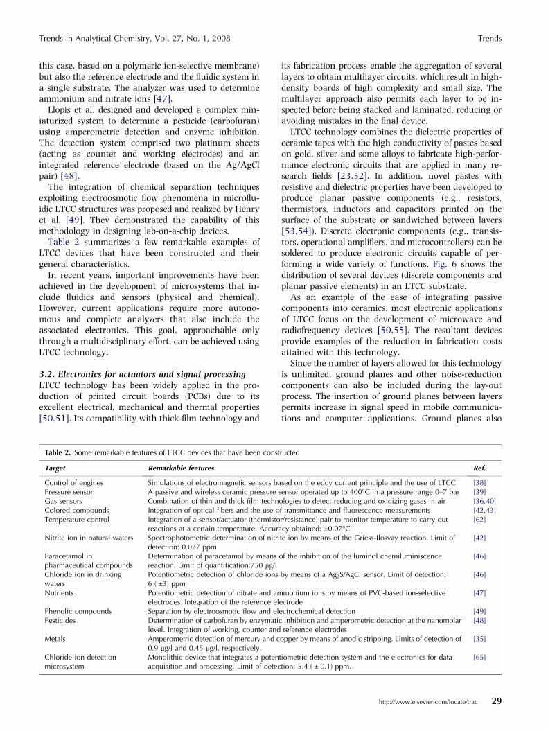
Table 2 summarizes a few remarkable examples ofLTCC devices that have been constructed and theirgeneral characteristics.
In recent years, important improvements have beenachieved in the development of microsystems that in-clude fluidics and sensors (physical and chemical).However, current applications require more autono-mous and complete analyzers that also include theassociated electronics. This goal, approachable onlythrough a multidisciplinary effort, can be achieved usingLTCC technology.
3.2. Electronics for actuators and signal processingLTCC technology has been widely applied in the pro-duction of printed circuit boards (PCBs) due to itsexcellent electrical, mechanical and thermal properties[50,51]. Its compatibility with thick-film technology and
Table 2. Some remarkable features of LTCC devices that have been const
Target Remarkable features
Control of engines Simulations of electromagnetic sensors baPressure sensor A passive and wireless ceramic pressure sGas sensors Combination of thin and thick film technoColored compounds Integration of optical fibers and the use oTemperature control Integration of a sensor/actuator (thermisto
reactions at a certain temperature. AccuraNitrite ion in natural waters Spectrophotometric determination of nitri
detection: 0.027 ppmParacetamol inpharmaceutical compounds
Determination of paracetamol by means oreaction. Limit of quantification:750 lg/l
Chloride ion in drinkingwaters
Potentiometric detection of chloride ions6 ( ±3) ppm
Nutrients Potentiometric detection of nitrate and amelectrodes. Integration of the reference ele
Phenolic compounds Separation by electroosmotic flow and elePesticides Determination of carbofuran by enzymatic
level. Integration of working, counter andMetals Amperometric detection of mercury and c
0.9 lg/l and 0.45 lg/l, respectively.Chloride-ion-detectionmicrosystem
Monolithic device that integrates a potentacquisition and processing. Limit of detec
its fabrication process enable the aggregation of severallayers to obtain multilayer circuits, which result in high-density boards of high complexity and small size. Themultilayer approach also permits each layer to be in-spected before being stacked and laminated, reducing oravoiding mistakes in the final device.
LTCC technology combines the dielectric properties ofceramic tapes with the high conductivity of pastes basedon gold, silver and some alloys to fabricate high-perfor-mance electronic circuits that are applied in many re-search fields [23,52]. In addition, novel pastes withresistive and dielectric properties have been developed toproduce planar passive components (e.g., resistors,thermistors, inductors and capacitors printed on thesurface of the substrate or sandwiched between layers[53,54]). Discrete electronic components (e.g., transis-tors, operational amplifiers, and microcontrollers) can besoldered to produce electronic circuits capable of per-forming a wide variety of functions. Fig. 6 shows thedistribution of several devices (discrete components andplanar passive elements) in an LTCC substrate.
As an example of the ease of integrating passivecomponents into ceramics, most electronic applicationsof LTCC focus on the development of microwave andradiofrequency devices [50,55]. The resultant devicesprovide examples of the reduction in fabrication costsattained with this technology.
Since the number of layers allowed for this technologyis unlimited, ground planes and other noise-reductioncomponents can also be included during the lay-outprocess. The insertion of ground planes between layerspermits increase in signal speed in mobile communica-tions and computer applications. Ground planes also
ructed
Ref.
sed on the eddy current principle and the use of LTCC [38]ensor operated up to 400�C in a pressure range 0–7 bar [39]logies to detect reducing and oxidizing gases in air [36,40]
f transmittance and fluorescence measurements [42,43]r/resistance) pair to monitor temperature to carry outcy obtained: ±0.07�C
[62]
te ion by means of the Griess-Ilosvay reaction. Limit of [42]
f the inhibition of the luminol chemiluminiscence [46]
by means of a Ag2S/AgCl sensor. Limit of detection: [46]
monium ions by means of PVC-based ion-selectivectrode
[47]
ctrochemical detection [49]inhibition and amperometric detection at the nanomolarreference electrodes
[48]
opper by means of anodic stripping. Limits of detection of [35]
iometric detection system and the electronics for datation: 5.4 ( ± 0.1) ppm.
[65]
http://www.elsevier.com/locate/trac 29

Surface Mount Devices
Electrical vias
Embedded capacitor
Surface Mount Devices
Electrical tracks
Electrical vias
Embedded capacitor
Ground plane
Embedded resistor
Figure 6. LTCC substrate with embedded passive components and discrete electronic elements mounted on its surface.
Trends Trends in Analytical Chemistry, Vol. 27, No. 1, 2008
serve as electromagnetic isolators needed in highly sen-sitive electronic circuits. The LTCC-fabrication processonly allows half or less of the surface to be metallized, sothat tape-to-tape contact is not compromised, so groundgrids, rather than ground planes, are used for this pur-pose.
Taking advantage of the versatility of this technology,some authors have also used green tapes as a substrateto fabricate actuators. Bau et al. [56] and Zhong et al.[57] constructed an electromagnetically driven micro-pump. Li et al. [58] fabricated omnidirectional wheelsthat can be used as actuators for vision cameras or ro-bots.
Other interesting types of actuators are those aimed attemperature control: passive heating and coolingsystems. The generation of perfectly controlled temper-ature gradients can be very helpful in polymerase chainreaction (PCR), as temperature needs to be controlled indifferent zones to ±1�C [59,60]. Moreover, a largenumber of enzyme reactions increase their reaction ratesat 37 �C. Since temperatures higher than 45–50�C caninhibit the catalytic properties of proteins, accuratetemperature control is essential in these cases (e.g.,Bischoff et al. embedded metal sheets within the ceramicbody so that heat could be spread across certain regionsof the ceramic device [61]). Chou et al. fabricated a PCRsystem with air gaps that provided thermal insulationbetween the three reaction zones [59]. Martınez-Cisneroset al. studied different insulation geometries so that thegood thermal conductivity of LTCC did not constitute anobstacle for precise attainment of the desired tempera-ture [62].
The low dielectric losses in green-tape ceramics(dielectric constant at 3 GHz = 7.8), their hermeticsealing after the sintering process and the possibility ofconstructing complex 3-D structures enable their use as
30 http://www.elsevier.com/locate/trac
packaging materials for MEMS (micro-electro-mechani-cal systems) as well as assembly for flip-chip and ball-grid array (BGA) devices [63]. Ruso et al. presented astudy about the hybrid integration of LTCC and silicon,where LTCC played the main role as substrate, fluidiccircuit board, electrical interconnection and packaging[64].
3.3. Integration of electronics and fluidicsNew demands often lead research towards the design ofcomplete analytical devices that integrate all the ele-ments required for specific applications. However, thisgoal can be reached only through the harmonic com-bination of several scientific disciplines as well as novelmaterials and new fabrication technologies.
Silicon and glass technologies are the most widelyused microfabrication techniques. They permit the pro-duction of electronics, fluidics, sensors and actuators onmicro and nano scales. However, as previously men-tioned, they require complex, time-consuming fabrica-tion processes. Also, they do not permit integration ofdiscrete electronic components into the same substrateand complete electronic systems needed for a totalanalysis system cannot always be included in the samechip. As with silicon, polymers allow fabrication ofmicrofluidic channels, and incorporation of electroniccomponents in the same substrate can be achievedthrough relatively complex processes. However, they donot always require complex facilities, such as cleanrooms. But, there are reports in the literature aboutsealing problems leading to leakage between layers andmaking it difficult to integrate electronic circuits.
In this review, we have focused on electronics,microfluidics and their integration using LTCC technol-ogy to obtain complete miniaturized analyzers. Thesuitability of this novel technology arises from its easy

Trends in Analytical Chemistry, Vol. 27, No. 1, 2008 Trends
implementation and low costs (capital and operational),leading to a flexible, cheap prototyping process, and alsofrom the versatility of the ceramics themselves that allowoperation of the resulting systems in a wide range ofconditions. The integration of these two technologicalplatforms (microfluidics and electronics) can be attainedusing a modular or a monolithic approach, dependingon the final application and the functionality required byeach microanalyzer [65]. Fig. 7 presents a monolithicchloride-ion microanalyzer, smaller than a credit card,integrating fluidics, detection and electronics for dataacquisition and digital signal processing in a singlesubstrate.
The rapid prototyping offered by LTCC technologypermits fabrication of specific and dedicated microfluidicmanifolds accurately adapted to each analytical prob-lem. In this way, the modular approach is based on theuse of a unique electronic module adapted to a specificdetection system (e.g., potentiometry, amperometry orcolorimetry) and a dedicated chemical module that caninclude all the stages involved in a classical analyticalprocess (e.g., microfluidics, pretreatment steps, anddetection system). The modular approach is a very ver-satile tool, as the same electronic platform can be at-tached to a wide variety of fluidic platforms (based on thesame detection principle) to determine several analytes.
Figure 7. Chloride-ion microanalyzer developed with the ‘‘lab-on-a-credit-card’’ concept for integration using LTCC technology.
Following this modular concept, some miniaturizedinstruments with applications in areas such as potenti-ometry [65,66], amperometry [67,68] and colorimetry[69,70] have been developed using conventional mate-rials and technologies, such as PCBs). However, thesetypes of miniaturized instruments do not permit con-struction of monolithic devices (integrating electronicsand fluidics in a single substrate). Until now, only a fewauthors have profited from LTCC properties to integrateboth concepts. Moilanen et al. [71] reported multiplexedread-out electronics modules implemented in a LTCCsubstrate for a PbS detector array.
The intrinsic advantages of LTCC technology permitthe monolithic integration of microfluidics, detectionsystems and electronics, as all of them can share thesame substrate and the same fabrication methodology.In this sense, construction of compact, robust and por-table microanalyzers with more autonomy can be easilyattained.
The potential of LTCC technology to integrate fluidicsand electronics monolithically has already been dem-onstrated [65]. However, the monolithic approach pre-sents a limitation that needs to be considered; unlike themodular system, once the LTCC system has been builtmonolithically, its analytical application in terms ofanalyte and type of sample is fixed and it cannot bemodified easily, so the monolithic approach can be se-lected only when microanalyzers are needed for a specificapplication. In this case, compactness, robustness, lowpower consumption and total portability, but not ver-satility, would be the features of interest.
Regardless of how compact the ceramic microsystemis, its robustness will depend on different factors thatshould be taken into account, e.g.:� type of sample (e.g., suspended particles should be fil-
tered in order to avoid occlusion of the microchan-nels);
� a harsh environment that could cause the micro-system to deteriorate;
� frequency of analysis that could shorten the lifetime ofsome fluidic or electronics components;
� type of detection system (e.g., optical systems shouldbe more robust than PVC-based ion-selective mem-branes).However, most of these requirements are not specific
to LTCC microsystems, but apply to most equipmentaimed at the analysis of real samples and naturally theyare solved.
4. Future prospects
We have demonstrated that LTCC technology is anexcellent alternative for combining microfluidics andelectronics in a single substrate using one fabricationmethodology. However, there are still a number of issues
http://www.elsevier.com/locate/trac 31

Trends Trends in Analytical Chemistry, Vol. 27, No. 1, 2008
to be tackled to fulfill the potential of LTCC technology.The miniaturization of actuators (pumps and valves) forhandling fluids remains one of the most challengingfields of research, for not only LTCC but also othertechnologies based on other materials.
When considering the great complexity of somesample matrices and analytes, it would be very inter-esting to investigate further the integration of chro-matographic (i.e. electrophoresis techniques), non-chromatographic pretreatment steps and new detectionprinciples to address as many analytical applications aspossible. The study of the compatibility between mate-rials, (e.g., silicon and LTCC) would also greatly increasethe possibilities for novel miniaturized analyzers.
Acknowledgements
The authors would like to thank the Spanish MEC for itsfinancial support through: Consolider-Ingenio 2010(CSD2006-00012), TEC2006-13907-C04-04/MIC andCIT-310200-2007-29.
References
[1] A. Manz, N. Graber, H.M. Widmer, Sens. Actuators, B 1 (1990)
244.
[2] D.R. Reyes, D. Iossifidis, P.A. Auroux, A. Manz, Anal. Chem. 74
(2002) 2623.
[3] P.A. Auroux, D. Iossifidis, D.R. Reyes, A. Manz, Anal. Chem. 74
(2002) 2637.
[4] C. Gonzalez, S.D. Collins, R.L. Smith, Sens. Actuators, B 49 (1998)
40.
[5] S. Santra, P. Holloway, C.D. Batich, Sens. Actuators, B 87 (2002)
358.
[6] N.T. Nguyen, X.Y. Huang, Sens. Actuators, A 88 (2001) 104.
[7] T. Ohori, S. Shoji, K. Miura, A. Yotsumoto, Sens. Actuators, A 64
(1998) 57.
[8] N.L. Jeon, D.T. Chiu, C.J. Wargo, H.K. Wu, I.S. Choi, J.R.
Anderson, G.M. Whitesides, Biomed. Microdevices 4 (2002) 117.
[9] C.X. Zhang, A. Manz, Anal. Chem. 73 (2001) 2656.
[10] G.M. Greenway, S.J. Haswell, P.H. Petsul, Anal. Chim. Acta 387
(1999) 1.
[11] A. Bertsch, S. Heimgartner, P. Cousseau, P. Renaud, Lab Chip 1
(2001) 56.
[12] A.T. Woolley, D. Hadley, P. Landre, A.J. de Mello, R.A. Mathies,
M.A. Northrup, Anal. Chem. 68 (1996) 4081.
[13] H. Andersson, W. van der Wijngaart, P. Enoksson, G. Stemme,
Sens. Actuators, B 67 (2000) 203.
[14] Y. Fintschenko, A. van den Berg, J. Chromatogr., A 819 (1998) 3.
[15] J. Wang, Trends Anal. Chem. 21 (2002) 226.
[16] M. Puyol, M. del Valle, I. Garces, F. Villuendas, C. Dominguez, J.
Alonso, Anal. Chem. 71 (1999) 5037.
[17] K.E. Petersen, Proc. IEEE 70 (1982) 420.
[18] G. Thornell, S. Johansson, J. Micromech. Microeng. 8 (1998) 251.
[19] H. Becker, L.E. Locascio, Talanta 56 (2002) 267.
[20] S. Lai, X. Cao, L.J. Lee, Anal. Chem. 76 (2004) 1175.
[21] D.M. Leatzow, J.M. Dodson, J.P. Golden, F.S. Ligler, Biosens.
Bioelectron. 17 (2002) 105.
[22] H.Y. Wang, R.S. Foote, S.C. Jacobson, J.H. Schneibel, J.M. Ramsey,
Sens. Actuators, B 45 (1997) 199.
32 http://www.elsevier.com/locate/trac
[23] M. Gongora-Rubio, L.M. Sola-Laguna, P.J. Moffett, J.J. Santiago-
Aviles, Sens. Actuators, A 73 (1999) 215.
[24] M. Hrovat, J. Holc, S. Drnovsek, D. Belavic, J. Bernard, M. Kosec,
L. Golonka, A. Dziedzic, J. Kita, J. Mater. Sci. 22 (2003) 1193.
[25] L.J. Golonka, M. Buczek, M. Hrovat, D. Belavic, A. Dziedzic, H.
Roguszczak, T. Zawada, Microelectron. Int. 22 (2005) 13.
[26] S. Gebhardt, L. Seffner, F. Schlenkrich, A. Schonecker, J. Eur.
Ceram. Soc. 27 (2007) 4177.
[27] U. Schmid, H. Seidel, Sens. Actuators, A 130 (2006) 194.
[28] M. Hrovat, D. Belavic, J. Kita, J. Cilensek, L. Golonka, A. Dziedzic,
J. Eur. Ceram. Soc. 25 (2005) 3443.
[29] Y. Imanaka, N. Hayashi, M. Takenouchi, J. Akedo, J. Eur. Ceram.
Soc. 27 (2007) 2789.
[30] A. Roosen, J. Eur. Ceram. Soc. 21 (2001) 1993.
[31] DuPont Green Tape Material System Design and Layout Guide-
lines [Please give full reference].
[32] C. Scranton, J. Lawson, in: Proc. Radio and Wireless Conference
(RAWCON), 1999, 194.
[33] F.K. Patterson, J.E. Gantzhorn, T.P. Daly, J.R. Rellick, M.
Iwabuchi, S. Kawasaki, in: IEMT Symposium, 1989, 147.
[34] A. Mohanram, S.H. Lee, G.L. Messing, D.J. Green, J. Am. Ceram.
Soc. 89 (2006) 1923.
[35] M.R. Gongora-Rubio, M.B.A. Fontes, Z.M. da Rocha, E.M. Richter,
L. Angnes, Sens. Actuators, B 103 (2004) 468.
[36] T. Pisarkiewicz, A. Sutor, P. Potempa, W. Maziarz, H. Thust, T.
Thelemann, Thin Solid Films 436 (2003) 84.
[37] U. Schmid, Sens. Actuators, A 97 (2002) 253.
[38] J. Wilde, Y.Q. Lai, Microelectron. Reliab. 43 (2003) 345.
[39] M.A. Fonseca, J.M. English, M. von Arx, M.G. Allen, J. Microelec-
tromech. Syst. 11 (2002) 337.
[40] H. Teterycz, J. Kita, R. Bauer, L.J. Golonka, B.W. Licznerski, K.
Nitsch, K. Wisniewski, Sens. Actuators, B 47 (1998) 100.
[41] T. Voß, P. Grundler, A. Kirbs, G.U. Flechsig, Electrochem.
Commun. 1 (1999) 383.
[42] L.J. Golonka, T. Zawada, J. Radojewski, H. Roguszczak, M.
Stefanow, Int. J. Appl. Ceram. Technol. 3 (2006) 150.
[43] L.J. Golonka, H. Roguszczak, T. Zawada, J. Radojewski, I.
Grabowska, M. Chudy, A. Dybko, Z. Brzozka, D. Stadnik, Sens.
Actuators, B 111 (2005) 396.
[44] N. Ibanez-Garcıa, J.A. Chamarro, Z.M. da Rocha, M.R.G. Rubio,
in: IMAPS/ACERS 1st Int. Conf. Exhibit. Ceramic Interconnect
Ceramic Microsyst. Technol. (CICMT), Baltimore, MD, USA,
2005.
[45] N. Ibanez-Garcıa, C.M. Azevedo, M. Puyol, F. Villuendas, J.A.
Chamarro, in: 10th Int. Conf. Flow Anal., 2006, Portugal, 2006.
[46] N. Ibanez-Garcia, R.D. Machado Goncalves, Z. Mendes da Rocha,
M.R. Gongora-Rubio, A.C. Seabra, J.A. Chamarro, Sens. Actua-
tors, B 118 (2006) 67.
[47] N. Ibanez-Garcia, M.B. Mercader, Z.M. da Rocha, C.A. Seabra,
M.R. Gongora-Rubio, J.A. Chamarro, Anal. Chem. 78 (2006)
2985.
[48] X. Llopis, N. Ibanez-Garcia, S. Alegret, J. Alonso, Anal. Chem. 79
(2007) 3662.
[49] C.S. Henry, M. Zhong, S.M. Lunte, M. Kim, H. Bau, J.J. Santiago,
Anal. Commun. 36 (1999) 305.
[50] O. Dernovsek, A. Naeini, G. Preu, W. Wersing, M. Eberstein, W.A.
Schiller, J. Eur. Ceram. Soc. 21 (2001) 1693.
[51] Y. Wang, G. Zhang, J. Ma, Mater. Sci. Eng., B 94 (2002) 48.
[52] M.R. Gongora-Rubio, P. Espinoza-Vallejos, L. Sola-Laguna, J.J.
Santiago-Aviles, Sens. Actuators, A 89 (2001) 222.
[53] M. Hrovat, D. Belavic, J. Kita, J. Holc, S. Drnovsek, J. Cilensek, L.
Golonka, A. Dziedzic, Microelectron. Int. 23 (2006) 33.
[54] R.B. Tait, R. Humphries, J. Lorenz, IEEE Trans. Ind. Appl. 30
(1994) 573.
[55] H. Jantunen, T. Kangasvieri, J. Vahakangas, S. Leppavuori, J. Eur.
Ceram. Soc. 23 (2003) 2541.
[56] H.H.Bau, J. Zhu, S. Qian,Y. Xiang, Sens. Actuators, B 88(2003)205.
Trends in Analytical Chemistry, Vol. 27, No. 1, 2008 Trends
[57] J. Zhong, M. Yi, H.H. Bau, Sens. Actuators, A 96 (2002) 59.
[58] J. Li, G.K. Ananthasuresh, J. Micromech. Microeng. 12 (2002)
198.
[59] C.F. Chou, R. Changrani, P. Roberts, D. Sadler, J. Burdon, F.
Zenhausern, S. Lin, A. Mulholland, N. Swami, R. Terbrueggen,
Microelectron. Eng. 921 (2002) 61.
[60] J. Chiou, P. Matsudaira, A. Sonin, D. Ehrlich, Anal. Chem. 73
(2001) 2018.
[61] G. Bischoff, H. Thust, T. Thelemann, T. Kirchner, in: Int. Symp.
Microelectron. (1999) 636.
[62] C.S. Martınez-Cisneros, N. Ibanez-Garcıa, F. Valdes, J. Alonso,
Sens. Actuators, A 138 (2007) 63.
[63] K.I. Kim, J.M. Kim, G.C. Hwang, C.W. Baek, Y.K. Kim, J.
Micromech. Microeng. 16 (2006) 150.
[64] C. Rusu, K. Persson, B. Ottosson, D. Billger, J. Micromech.
Microeng. 16 (2006) 13.
[65] C.S. Martınez-Cisneros, N. Ibanez-Garcıa, F. Valdes, J. Alonso,
Anal. Chem. 79 (2007) 8376.
[66] J.J.R. Rohwedder, C. Pasquini, I.M. Raimundo Jr., M. Conceicao,
B.S.M. Montenegro, A.N. Araujo, C.M.C.M. Couto, J. Autom.
Methods Manag. Chem. 24 (2002) 105.
[67] E.M. Avdikos, M.I. Prodromidis, C.E. Efstathiou, Sens. Actuators, B
107 (2002) 372.
[68] M.D. Steinberg, C.R. Lowe, Sens. Actuators, B 97 (2004)
284.
[69] K.T. Lau, S. Baldwin, M. O�Toole, R. Shepherd, W.J. Yerazunis,
S. Izuo, S. Ueyama, D. Diamond, Anal. Chim. Acta 557 (2006)
111.
[70] L. Yang, M. Egawa, M. Akimoto, M. Miyakawa, Opt. Rev. 10
(2003) 554.
[71] V. Moilanen, A. Kemppainen, J. Malinen, M. Kansakoski, R.
Marbach, Meas. Sci. Technol. 15 (2004) 2188.
http://www.elsevier.com/locate/trac 33