Extended Vapor–Liquid–Solid Growth of Silicon Carbide Nanowires
11
RESEARCH ARTICLE Copyright © 2013 American Scientific Publishers All rights reserved Printed in the United States of America Journal of Nanoscience and Nanotechnology Vol. 13, 1–11, 2013 Extended Vapor–Liquid–Solid Growth of Silicon Carbide Nanowires John Anthuvan Rajesh and Arumugam Pandurangan ∗ Department of Chemistry, Institute of Catalysis and Petroleum Technology Anna University, Chennai 600025, Tamilnadu, India We developed an alloy catalytic method to explain extended vapor–liquid–solid (VLS) growth of silicon carbide nanowires (SiC NWs) by a simple thermal evaporation of silicon and activated carbon mixture using lanthanum nickel (LaNi 5 ) alloy as catalyst in a chemical vapor deposition process. The LaNi 5 alloy binary phase diagram and the phase relationships in the La–Ni–Si ternary system were play a key role to determine the growth parameters in this VLS mechanism. Different reaction temperatures (1300, 1350 and 1400 C) were applied to prove the established growth process by experimentally. Scanning electron microscopy and transmission electron microscopy studies show that the crystalline quality of the SiC NWs increases with the temperature at which they have been synthesized. La–Ni alloyed catalyst particles observed on the top of the SiC NWs confirms that the growth process follows this extended VLS mechanism. The X-ray diffraction and confocal Raman spectroscopy analyses demonstrate that the crystalline structure of the SiC NWs was zinc blende 3C–SiC. Optical property of the SiC NWs was investigated by photoluminescence technique at room temperature. Such a new alloy catalytic method may be extended to synthesis other one- dimensional nanostructures. Keywords: SiC NWs, LaNi 5 Alloy Catalyst, Chemical Vapor Deposition, VLS Mechanism. 1. INTRODUCTION Rapid developments of nanostructured materials such as nanotubes, 1 2 nanoparticles, 3 4 nanowires, 5 6 nanofilms, 7 8 and nanoporous materials 9 10 enable us to prepare impor- tant materials with well defined structures. Especially, preparation of nanostructures of functional semiconduc- tive materials is highly useful for device construction. For example, silicon carbide (SiC) is one of the most important wide band gap semiconductors and employed as a high- temperature electric material in high-temperature engineer- ing applications due to their chemical stability, thermal shock resistance and excellent creep resistance. 11 12 These improved properties make SiC a promising material for using in high-temperature circuit operation (from 350 C to 600 C) in aerospace applications (turbine engines and more electric aircraft initiative), nuclear power instrumen- tation, satellites, space exploration, geothermal wells and it has been considered as a potential sensor material that may be used in high-temperature hazardous environments. 13–16 The discovery of SiC nanorods in 1995 by Dai et al. 17 the synthesis, characterization and studies of the structures ∗ Author to whom correspondence should be addressed. and properties of this unique material have generated great interest. One-dimensional (1-D) SiC nanostructures such as nanowires (NWs), nanospheres, nanorods, nanowebs, nanocables and nanoflowers are very much ignited inter- est due to special properties and potential applications. 18–22 Among the 1-D SiC nanostructures, SiC NWs would be favorable for applications in high-temperature, high-power and high-frequency nanoelectronic devices because of their longer aspect ratio, better elasticity and strength. 23–26 Dur- ing the past several years, a great deal of effort has been devoted to obtaining SiC NWs and a lot of meth- ods such as carbothermal reduction, 27 arc discharge, 28 laser ablation, 29 chemical vapor deposition (CVD), 30 met- alorganic CVD, 31 microwave heating-assisted physical vapor transport, 32 catalytic pyrolysis of organic precur- sors includes diethylmethylsilane, dichloromethylvinylsi- lane and polyureasilazane 26 31 33 have been successfully employed. Amongst catalyst assisted growth by CVD method (CCVD) is a simple and efficient method for syn- thesizing SiC NWs. CCVD method is based on metal catalyzed vapor– liquid–solid (VLS) growth mechanism. The VLS growth method was first developed by Wagner and Ellis for whiskers growth is often used to synthesis a variety of J. Nanosci. Nanotechnol. 2013, Vol. 13, No. xx 1533-4880/2013/13/001/011 doi:10.1166/jnn.2013.8569 1
Transcript of Extended Vapor–Liquid–Solid Growth of Silicon Carbide Nanowires

RESEARCH
ARTIC
LE
Copyright © 2013 American Scientific PublishersAll rights reservedPrinted in the United States of America
Journal ofNanoscience and Nanotechnology
Vol. 13, 1–11, 2013
Extended Vapor–Liquid–Solid Growth ofSilicon Carbide Nanowires
John Anthuvan Rajesh and Arumugam Pandurangan∗
Department of Chemistry, Institute of Catalysis and Petroleum Technology Anna University,Chennai 600025, Tamilnadu, India
We developed an alloy catalytic method to explain extended vapor–liquid–solid (VLS) growth ofsilicon carbide nanowires (SiC NWs) by a simple thermal evaporation of silicon and activated carbonmixture using lanthanum nickel (LaNi5) alloy as catalyst in a chemical vapor deposition process.The LaNi5 alloy binary phase diagram and the phase relationships in the La–Ni–Si ternary systemwere play a key role to determine the growth parameters in this VLS mechanism. Different reactiontemperatures (1300, 1350 and 1400 �C) were applied to prove the established growth process byexperimentally. Scanning electron microscopy and transmission electron microscopy studies showthat the crystalline quality of the SiC NWs increases with the temperature at which they have beensynthesized. La–Ni alloyed catalyst particles observed on the top of the SiC NWs confirms that thegrowth process follows this extended VLS mechanism. The X-ray diffraction and confocal Ramanspectroscopy analyses demonstrate that the crystalline structure of the SiC NWs was zinc blende3C–SiC. Optical property of the SiC NWs was investigated by photoluminescence technique atroom temperature. Such a new alloy catalytic method may be extended to synthesis other one-dimensional nanostructures.
Keywords: SiC NWs, LaNi5 Alloy Catalyst, Chemical Vapor Deposition, VLS Mechanism.
1. INTRODUCTION
Rapid developments of nanostructured materials such asnanotubes,1�2 nanoparticles,3�4 nanowires,5�6 nanofilms,7�8
and nanoporous materials9�10 enable us to prepare impor-tant materials with well defined structures. Especially,preparation of nanostructures of functional semiconduc-tive materials is highly useful for device construction. Forexample, silicon carbide (SiC) is one of the most importantwide band gap semiconductors and employed as a high-temperature electric material in high-temperature engineer-ing applications due to their chemical stability, thermalshock resistance and excellent creep resistance.11�12 Theseimproved properties make SiC a promising material forusing in high-temperature circuit operation (from 350 �Cto 600 �C) in aerospace applications (turbine engines andmore electric aircraft initiative), nuclear power instrumen-tation, satellites, space exploration, geothermal wells and ithas been considered as a potential sensor material that maybe used in high-temperature hazardous environments.13–16
The discovery of SiC nanorods in 1995 by Dai et al.17
the synthesis, characterization and studies of the structures
∗Author to whom correspondence should be addressed.
and properties of this unique material have generated greatinterest. One-dimensional (1-D) SiC nanostructures suchas nanowires (NWs), nanospheres, nanorods, nanowebs,nanocables and nanoflowers are very much ignited inter-est due to special properties and potential applications.18–22
Among the 1-D SiC nanostructures, SiC NWs would befavorable for applications in high-temperature, high-powerand high-frequency nanoelectronic devices because of theirlonger aspect ratio, better elasticity and strength.23–26 Dur-ing the past several years, a great deal of effort hasbeen devoted to obtaining SiC NWs and a lot of meth-ods such as carbothermal reduction,27 arc discharge,28
laser ablation,29 chemical vapor deposition (CVD),30 met-alorganic CVD,31 microwave heating-assisted physicalvapor transport,32 catalytic pyrolysis of organic precur-sors includes diethylmethylsilane, dichloromethylvinylsi-lane and polyureasilazane26�31�33 have been successfullyemployed. Amongst catalyst assisted growth by CVDmethod (CCVD) is a simple and efficient method for syn-thesizing SiC NWs.CCVD method is based on metal catalyzed vapor–
liquid–solid (VLS) growth mechanism. The VLS growthmethod was first developed by Wagner and Ellis forwhiskers growth is often used to synthesis a variety of
J. Nanosci. Nanotechnol. 2013, Vol. 13, No. xx 1533-4880/2013/13/001/011 doi:10.1166/jnn.2013.8569 1

RESEARCH
ARTIC
LE
Extended Vapor–Liquid–Solid Growth of Silicon Carbide Nanowires Rajesh and Pandurangan
1-D nanomaterials.34 This mechanism occurs at the melt-ing temperatures of the catalyst at which the catalyst existsin the liquid form and is characterized by a catalyticdroplet on the top of the synthesized nanostructures. Phasediagram approach plays a main roll to explain the VLSgrowth principles for developing catalyst. A large num-ber of reports on the synthesis of SiC NWs using solemetal catalyst such as Fe, Co, Ni, Pd, Pt and so on.30–33�35
Various studies indicated that the catalytic growth of SiCNWs obtained at high temperatures ranging between at1000–1750 �C.19�23�27�31–33�35 An important factor in theCCVD process is the control of the size of the metal-lic catalyst, which is tends to aggregate to form largerparticles with increasing the reaction temperature. Theintroduction of other metals such as La, Mo or Mg tothe catalysts can avoid the aggregation of the catalyst aswell as reduces the melting temperature of the active cat-alyst. The addition of La or Mg into the catalysts canform an alloy structure possessing a lower melting pointthan the highest melting temperature of its constituents,which is able to reduce the melting temperature of cata-lyst and promotes solid-state reactions by forming ternaryphases. For example, the intermetallic alloys lanthanum–nickel (LaNi5), magnesium–nickel has been used as hydro-gen storage materials and also used as effective catalyststo produce carbon nanotubes (CNTs).36�37 Very recently,Al69Ni31 alloyed particles used as catalysts for synthesis ofAlN NWs by nitridation reaction in N2–NH3 atmosphereat different temperatures.38 As a result, there has been arenovated interest to extend the traditional VLS growthmethod for synthesizing nanowires via introducing alloycatalyst.LaNi5 alloy was demonstrated to be an efficient hydro-
gen storage alloy and it used as catalyst for the synthesisCNTs, carbon nanofibers and boron nitride nanotubes(BNNTs).36�39�40 Interestingly, the melting point of theembedded alloy (LaNi5) was found to be ∼1623 K (datafrom BINARY (SGTE) alloy databases), which is lowerthan that of the sole Ni catalyst. Since the synthesis of SiCNWs has not achieved with an alloy catalyst so far. There-fore, the utilization of LaNi5 alloy as catalyst would bereasonable and efficient way to produce SiC NWs. In thepresent work, we developed an extended VLS growth ofSiC NWs via introducing LaNi5 alloy as catalyst by CVDmethod. By applying the different reaction temperatures(1300, 1350 and 1400 �C), we proved the establishedgrowth process by experimentally.
2. EXPERIMENTAL DETAILS
2.1. Preparation of Precursor Material
Commercial powders of silicon (Si, 99%, −325 mesh,Sigma-Aldrich), activated carbon (−20+50 mesh, AlfaAesar) and LaNi5 alloy (99.5%, metal basis, Alfa Aesar)were used for the synthesis of SiC NWs. In a typical
procedure, the LaNi5 alloy catalyst and silicon powderwere mixed by ball-milling for 24 h with the mass ratioof 1:3. The activated carbon (with a BET surface area of390 m2/g) used in this reaction was ground to a fine pow-der, ultrasonically washed with distilled water and dried ina muffle furnace (150 �C) for 2 hr. The ball milled LaNi5–Si mixture and as cleaned activated carbon was mixedhomogeneously in an appropriate amount by an agate pes-tle and mortar and it was used as precursor material forthe synthesis of SiC NWs.
2.2. Synthesis of SiC NWs
The hot filament CVD utilized for the growth of SiC NWs.The well homogeneous as prepared precursor material wasplaced in an alumina boat, which was transferred into thecentre of the alumina tube of a furnace equipped with twowater-cooled zones at each end. The chamber was firstflushed with argon gas (Ar) at a flow rate of 200 ml/minto remove the oxygen and/or moisture. Then the furnacewas heated from room temperature to 700 �C at a rate of5 �C/min with a flow of Ar at a rate of 100 ml/min. Whenthe furnace temperature was raised to 700 �C, hydrogengas was introduced with a flow rate of 100 ml/min intothe reactor to reduce the LaNi5 alloy catalyst. After reduc-tion, furnace was heated to desired reaction temperatures(1300, 1350 and 1400 �C) at a rate of 5 �C in Ar at a flowrate of 100 ml/min. The pyrolysis was carried out for 2 hto facilitate the reaction completion followed by furnacecooling at a rate of 5 �C/min in Ar atmosphere. Whenthe temperature cooled down to the room temperature, thegreen color products were taken out. The lower part of thegreenish product in the alumina boat was collected, whichmainly contains SiC NWs (The upper part of the spongylike product was removed because it had a residual cat-alyst). The as-synthesized samples were heated in air at700 �C for removal of the residual carbon and treated bysulfuric acid and nitric acid (1:3) for elimination of LaNi5alloy catalyst.
2.3. Characterizations
The average particle size of the LaNi5 alloy catalyst wasobtained by laser scattering particle size distribution ana-lyzer (Zetasizer Ver. 6.20). The thermal stability of LaNi5alloy catalyst was carried out on a STA-449F3 thermalanalyzer, Netzsch in a flowing Ar gas and heated fromroom temperature to 1500 �C with a rate of 10 �C/min.The morphology of the precursor material (ball milled Si–LaNi5 alloy powder mixture) prior to growth was charac-terized by transmission electron microscopy (TEM). Thepurified samples (SiC NWs) were analyzed by the fol-lowing techniques. Scanning electron microscopy (SEM)equipped with energy dispersive X-ray analysis (EDAX)(Oxford Instruments) was carried out using an ESEMQuanta 200, FEI scanning microscope operated at 20 kV
2 J. Nanosci. Nanotechnol. 13, 1–11, 2013

RESEARCH
ARTIC
LE
Rajesh and Pandurangan Extended Vapor–Liquid–Solid Growth of Silicon Carbide Nanowires
to study the morphology of the samples. TEM and high-resolution TEM (HRTEM) (JEOL 3010) equipped withEDAX (Oxford Instruments) operated at 200 kV was usedto study the nanostructure and compositional analysis ofthe SiC NWs. The XRD pattern was obtained with a PAN-alytical X’Pert using Ni-filtered Cu K� radiation and a liq-uid N2 cooled germanium solid-state detector. The diffrac-togram was recorded in the 2� range of 10�–80�, and inthe scanning rate of 0.02� with the counting time of 5 sat each point. Confocal Raman spectrum of purified sam-ple was done with a WiTec GmbH, Alpha-SNOM CRM200 confocal Raman microscope having a 514 nm laseras the excitation source. A Photoluminescence (PL) spec-trum was measured on a Horiba Jobin Yuon fluorescencephotometer at room temperature using a 325 nm excitationwavelength from a He–Cd laser excitation source.
3. RESULTS AND DISCUSSION
3.1. Studies on LaNi5 Alloy Catalyst andLaNi5–Si Precursor Material
A systematic study on the LaNi5 alloy binary phase dia-gram and the phase relationships in the La–Ni–Si ternarysystem were used to determine the growth parameters andthe role of alloy catalyst in the effective synthesis process.There are certain parameters such as the critical catalyst,Si:catalyst composition and melting point of the catalystwere important for the growth of SiC NWs. In our experi-ments the critical catalyst LaNi5 alloy melting point (reac-tion temperature) Si:LaNi5 composition and Si solubilityin LaNi5 can be determined by examining the binary phasediagram of the LaNi5 alloy and the phase relationships inthe La–Ni–Si ternary system. Zhang et al.36 found that theLaNi5 alloy catalyst cannot decomposed into La and Niat low temperature (700 �C) but it act as a intermetalliccompound of La and Ni. At higher temperature (1350 �C)LaNi5 alloy changed into liquid droplets. It is confirmedfrom the binary phase diagram of the La–Ni alloy sys-tem, a typical La–Ni binary alloy phase diagram shownin Figure 1 (data from BINARY (SGTE) alloy databases),which shows the melting point of embedded alloy (LaNi5)was found to be ∼1623 K. These liquid alloy dropletsserve as a preferential site for adsorption of reactants.Si:LaNi5 composition and the maximum solubility of Si inLaNi5 alloy were determined from the La–Ni–Si ternarysystem. Zhou et al.41 studied the La–Ni–Si ternary systemand reported the 14 possible ternary systems and the max-imum solubility of Si in LaNi5 alloy was about 8.33 at.%at 673 K and the solubility increases significantly withincreasing temperature.The average particle size of the LaNi5 alloy catalyst
was determined from particle size distribution analyzerand found to be 2–6 �m, which is shown in Figure 2(a).Thermal stability of LaNi5 catalyst was determined byDSC from room temperature to 1500 �C in flowing Ar
Fig. 1. La–Ni binary alloy phase diagram (data from BINARY (SGTE)alloy databases).
atmosphere at a heating rate of 10 �C/min. Figure 2(b)shows the DSC profile of LaNi5 catalyst. DSC curve showsonly one exothermic peak at 1448.1 �C. The onset ini-tiates at 1442.6 �C, and it is completed at 1456.1 �C.So the exothermic peak in the DSC curve in Ar atmo-sphere is attributed to the complete melting temperature ofLaNi5 alloy catalyst. This result indicated that the catalystwas stable up to 1440 �C and there is no phase changeappeared.The morphology of the precursor material prior to
growth was characterized by TEM. Figure 3 shows theTEM and HRTEM images of the ball milled and H2 treatedSi–LaNi5 alloy powder mixture at 700 �C for 20 min. Fromthe low magnification TEM images (Figs. 3(a)–(c)), wecan see that the homogenous mixture of precursor mate-rial contains more number of well-dispersed catalyst par-ticles (active sites) formed after hydrogen treatment. Theactive catalyst particles were indicated by white arrows inFigure 3(a). HRTEM image in Figure 3(d) indicates thecrystalline structure of the catalyst particle through lat-tice fringes. Also it can be noted that the particles sizeof the active catalysts in the ball milled and H2 treatedprecursors show below 50 nm, but the average startingLaNi5 alloy catalyst particle size was 6 �m. This resultsuggests that particles size reduction should from the bothball milling and H2 treatment processes. Therefore, TEMresults demonstrate that the precursor material containingnecessary active sites were important to direct the catalyticgrowth of SiC NWs in the synthesis process.
3.2. Scanning Electron Microscopy withEnergy Dispersive X-Ray Analysis
Microscopy analysis play a key role to understand theVLS growth of SiC NWs from the ball milled and hydro-gen reduced LaNi5–Si precursor material and explainingthe correlation between phase diagram of the LaNi5 alloycatalyst and VLS mechanism. The growth temperatures
J. Nanosci. Nanotechnol. 13, 1–11, 2013 3

RESEARCH
ARTIC
LE
Extended Vapor–Liquid–Solid Growth of Silicon Carbide Nanowires Rajesh and Pandurangan
2000 2500 3000 3500 4000 4500 5000 5500 60000
2
4
6
8
10
12
14
16
18
20(a)In
tens
ity (
%)
Size (d.nm)
0 200 400 600 800 1000 1200 1400
–6
–4
–2
0
2
4
6
8
10
12(b)
Complex Peak
End: 1456.1 ºC
Onset: 1442.6 ºC
Peak: 1448.1 ºC
exo
Temperature ºC
DSC
(m
W/m
g)
Fig. 2. (a) and (b) average particle size distribution and DSC profile ofLaNi5 alloy catalyst, respectively.
during the reactions were found to have a significant effecton the morphology and yield of the product. The growthruns were realized at three different reaction temperatures,such as below the LaNi5 catalyst liquidized temperature(1300 �C), exact liquidized temperature (1350 �C) andabove the liquidized temperature (1400 �C). From theseresults we found that the optimum temperature for the for-mation of SiC NWs was 1400 �C. This is well agreementwith SEM and TEM studies of the products obtained at1300, 1350 and 1400 �C.The typical SEM morphologies and the correspond-
ing EDAX spectra of the products synthesized at 1300,1350 and 1400 �C were shown in Figure 4. Figures 4(a)and (b) show that SiC NWs were first nucleated as pri-marily wire-like structure at 1300 �C, while some NWsformed when the temperature was increased to 1350 �C(Figs. 4(c) and (d)). When the temperature was raised to1400 �C, more NWs grew out from the LaNi5–Si reactionmixture (Figs. 4(e) and (f)). From SEM results we foundthat the yield and crystalline quality of the NWs increases
Fig. 3. TEM images of precursor material: Ball milled and hydrogentreated LaNi5–Si powder mixture at 700 �C for 20 min (a)–(c) at lowmagnifications and (d) at high magnification.
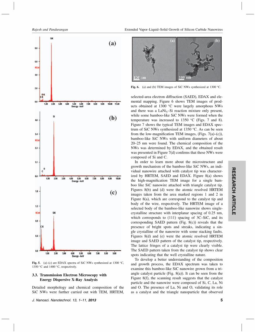
with the temperature at which they have been synthesized.Elemental composition of synthesized samples was ana-lyzed by EDAX. Figures 5(a)–(c) show the EDAX spectraof NWs prepared at 1300, 1350, and 1400 �C, respectively.It revealed that these NWs were mainly composed of Siand C only.
Fig. 4. SEM images of SiC NWs synthesized at (a)–(b) 1300 �C, (c)–(d) 1350 �C and (e)–(f) 1400 �C.
4 J. Nanosci. Nanotechnol. 13, 1–11, 2013
RESEARCH
ARTIC
LE
Rajesh and Pandurangan Extended Vapor–Liquid–Solid Growth of Silicon Carbide Nanowires
Fig. 5. (a)–(c) are EDAX spectra of SiC NWs synthesized at 1300 �C,1350 �C and 1400 �C, respectively.
3.3. Transmission Electron Microscopy withEnergy Dispersive X-Ray Analysis
Detailed morphology and chemical composition of theSiC NWs were further carried out with TEM, HRTEM,
Fig. 6. (a) and (b) TEM images of SiC NWs synthesized at 1300 �C.
selected-area electron diffraction (SAED), EDAX and ele-mental mapping. Figure 6 shows TEM images of prod-ucts obtained at 1300 �C were largely amorphous NWsand there was a LaNi5–Si reaction mixture only present,while some bamboo-like SiC NWs were formed when thetemperature was increased to 1350 �C (Figs. 7 and 8).Figure 7 shows the typical TEM images and EDAX spec-trum of SiC NWs synthesized at 1350 �C. As can be seenfrom the low-magnification TEM images, (Figs. 7(a)–(c)),bamboo-like SiC NWs with uniform diameters of about20–25 nm were found. The chemical composition of theNWs was determined by EDAX, and the obtained resultwas presented in Figure 7(d) confirms that these NWs werecomposed of Si and C.In order to learn more about the microstructure and
growth mechanism of the bamboo-like SiC NWs, an indi-vidual nanowire attached with catalyst tip was character-ized by HRTEM, SAED and EDAX. Figure 8(a) showsthe high-magnification TEM image for a single bam-boo like SiC nanowire attached with triangle catalyst tip.Figures 8(b) and (d) were the atomic resolved HRTEMimages taken from the area marked regions 1 and 2 inFigure 8(a), which are correspond to the catalyst tip andbody of the wire, respectively. The HRTEM image of aselected body of the bamboo-like nanowire shows single-crystalline structure with interplanar spacing of 0.25 nm,which corresponds to (111) spacing of 3C–SiC, and itscorresponding SAED pattern (Fig. 8(c)) reveals that thepresence of bright spots and streaks, indicating a sin-gle crystalline of the nanowire with some stacking faults.Figures 8(d) and (e) were the atomic resolved HRTEMimage and SAED pattern of the catalyst tip, respectively.The lattice fringes of a catalyst tip were clearly visible.The SAED pattern taken from the catalyst tip shows clearspots indicating that the well crystalline nature.To develop a better understanding of the composition
and growth process, the EDAX spectrum was taken toexamine this bamboo-like SiC nanowire grown from a tri-angle catalyst particle (Fig. 8(a)). It can be seen from theFigure 8(f), the scanning result suggests that the catalystparticle and the nanowire were composed of Si, C, La, Niand O. The presence of La, Ni and O, validating its roleas a catalyst and the triangle nanoparticle that observed
J. Nanosci. Nanotechnol. 13, 1–11, 2013 5

RESEARCH
ARTIC
LE
Extended Vapor–Liquid–Solid Growth of Silicon Carbide Nanowires Rajesh and Pandurangan
Fig. 7. (a)–(c) typical TEM images of bamboo-like SiC NWs synthesized at 1350 �C, and (d) is the corresponding EDAX spectrum of SiC nanowire.
Fig. 8. (a) A high magnification TEM image of an individual SiC nanowire attached with triangle catalyst particle. (b), (d) are the atomic resolvedHRTEM images taken from the area marked with circles in (a). (c), (e) SAED patterns of SiC nanowire body and catalyst tip (f) is the EDAX spectrumtaken from the SiC nanowire with catalyst tip.
6 J. Nanosci. Nanotechnol. 13, 1–11, 2013
RESEARCH
ARTIC
LE
Rajesh and Pandurangan Extended Vapor–Liquid–Solid Growth of Silicon Carbide Nanowires
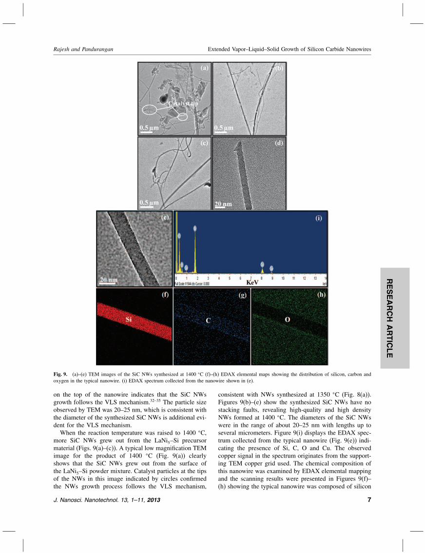
Fig. 9. (a)–(e) TEM images of the SiC NWs synthesized at 1400 �C (f)–(h) EDAX elemental maps showing the distribution of silicon, carbon andoxygen in the typical nanowire. (i) EDAX spectrum collected from the nanowire shown in (e).
on the top of the nanowire indicates that the SiC NWsgrowth follows the VLS mechanism.32–35 The particle sizeobserved by TEM was 20–25 nm, which is consistent withthe diameter of the synthesized SiC NWs is additional evi-dent for the VLS mechanism.When the reaction temperature was raised to 1400 �C,
more SiC NWs grew out from the LaNi5–Si precursormaterial (Figs. 9(a)–(c)). A typical low magnification TEMimage for the product of 1400 �C (Fig. 9(a)) clearlyshows that the SiC NWs grew out from the surface ofthe LaNi5–Si powder mixture. Catalyst particles at the tipsof the NWs in this image indicated by circles confirmedthe NWs growth process follows the VLS mechanism,
consistent with NWs synthesized at 1350 �C (Fig. 8(a)).Figures 9(b)–(e) show the synthesized SiC NWs have nostacking faults, revealing high-quality and high densityNWs formed at 1400 �C. The diameters of the SiC NWswere in the range of about 20–25 nm with lengths up toseveral micrometers. Figure 9(i) displays the EDAX spec-trum collected from the typical nanowire (Fig. 9(e)) indi-cating the presence of Si, C, O and Cu. The observedcopper signal in the spectrum originates from the support-ing TEM copper grid used. The chemical composition ofthis nanowire was examined by EDAX elemental mappingand the scanning results were presented in Figures 9(f)–(h) showing the typical nanowire was composed of silicon
J. Nanosci. Nanotechnol. 13, 1–11, 2013 7

RESEARCH
ARTIC
LE
Extended Vapor–Liquid–Solid Growth of Silicon Carbide Nanowires Rajesh and Pandurangan
(red), carbon (blue) and oxygen (green). Elemental map-ping confirmed that the nanowire distribution containssilicon and carbon only.
3.4. The Extended VLS Growth Mechanism
CCVD is a general technique to produce SiC NWsusing various metal catalysts via VLS growth mechanism.In general the formation of SiC NWs on sole metal cat-alysts follows the traditional VLS mechanism and it hassome common steps. The most important are:(1) the formation of metal catalytic liquid droplets over-saturated with silicon and carbon vapors(2) supersaturation and(3) nucleation of NWs from the liquid/solid interface.
Previous studies on traditional VLS growth of SiC NWsby sole metal catalysts were primarily focused on theirconstant diameters by controlling the size of catalyticdroplets. Unfortunately, various drawbacks were found inthe literatures such as non-uniform diameters, larger diam-eters, uncontrolled shape (mostly cone-like and needle-likeSiC NWs) and high temperature processes.32�33�35 Alter-natively, in our experiments we used LaNi5 alloy catalystto extend the traditional VLS growth of SiC NWs. GroupVIII transition metal Ni has shown excellent catalyticproperty for producing SiC NWs, which enhances the sol-ubility of carbon in a silicon-metal eutectic solution.31�32�42
Rare earth metal La has been reported to show cat-alytic effect for synthesizing 1D materials such as CNTs,BNNTs and SiC nanochains and nanofibers.43–46 In addi-tion, La might take part in controlling the size of theactive metal particles (Ni) along with improves the cat-alyst lifetime.47�48 In a word, La might enhance the Siand C solubility via synergic or dual metal effect. Hence,La containing intermetallic alloy LaNi5 was selected totake advantages of the excellent catalytic effect to producehigh-quality SiC NWs.Schematic illustration of the traditional and extended
VLS growth of SiC NWs is depicted in Figure 10, whichare deduced from the Ni and LaNi5 alloy catalyst parti-cles. According to VLS growth mechanism Si vapors reactwith the LaNi5 liquid droplets to form LaNi5–Si eutec-tic solution at higher temperatures (1350 and 1400 �C),then the carbon vapors diffused on the eutectic solution.The presence of Si and C atoms in the solution madethe supersaturated state, from that the SiC NWs segre-gate with crystalline structure. It was systematically exam-ined by microscopy analysis discussed above (Figs. 4,6–9), confirmed that the crystalline quality of SiC NWsincreased with increased reaction temperatures. It demon-strates that the absorption rates and solubility of Si andC species enhanced by increasing the reaction temperaturefrom 1300 to 1400 �C. The uniform and smaller diametersof SiC NWs (20–25 nm) growth happened by the smallercatalytic droplets formed on the top of the NWs (Figs. 8(a)and 9(a)), indicating that the La should involved in the
Fig. 10. Schematic illustration of traditional and extended VLS growthof SiC nanowires.
controlling the size of the catalyst particles in terms of par-ticle agglomeration controlling phenomena. The catalyticlifetime has an effective influence on the NWs length; thepresence of La improves the catalyst lifetime for a longduration (2 hr) at the reaction temperature (1400 �C), asthe Si and C species were absorbed continuously for awhole reaction time and it makes longer growth of theNWs. This is well agreement with SEM and TEM resultsas shown in Figures 4 and 9. Finally, the SEM and TEMstudies were therefore in good agreement with the estab-lished VLS growth process from the LaNi5 alloy binaryphase diagram and the phase relationships in the La–Ni–Siternary system.
3.5. X-Ray Diffraction Analysis
The catalytic behavior of LaNi5 alloy in the SiC NWssynthesis process was studied by XRD. Figure 11 shows
10 20 30 40 50 60 70 80
LaNiOLa2O3
*
****
(c) 3C-SiC - JCPDS No: 29-1129(a) LaNi5 - JCPDS No: 42-1191
**** ****
**
*
***
(222
)(311
)
(220
)
(200
)
Inte
nsity
(a.
u.)
(111
)
(c)
(b)
(a) (220
)(1
03)
(301
)
2θ (degree)
(300
)(2
02)
(211
)(1
12)
(201
)(0
02)(1
11)
(200
)
(110
)
(101
)
(001
)(1
00)
Fig. 11. XRD patterns of purified SiC NWs synthesized at 1400 �C.
8 J. Nanosci. Nanotechnol. 13, 1–11, 2013

RESEARCH
ARTIC
LE
Rajesh and Pandurangan Extended Vapor–Liquid–Solid Growth of Silicon Carbide Nanowires
XRD patterns of commercially purchased LaNi5 alloy cat-alyst, as-synthesized SiC NWs and purified SiC NWs.Figure 11(a) shows XRD pattern of LaNi5 alloy catalystdemonstrates that all of the peaks could be indexed tothe hexagonal CaCu5-type structure (JCPDS No: 42-1191).The XRD pattern of the as-synthesized SiC NWs inFigure 11(b) shows the major diffraction peaks of 3C–SiCtogether with minor peaks of lanthanum nickel oxide (∗)and lanthanum oxide (•) peaks. It can be understood from
200 400 600 800 1000 1200300
350
400
450
500(b)
795.37
Inte
nsity
Raman shift (cm–1)
Fig. 12. (a) 2-D confocal Raman microscopy image of individual SiC nanowires and its corresponding Raman spectra collected from the pointsmarked in the image 1, 2 and 3 and (b) Raman spectrum of bulk SiC NWs synthesized at 1400 �C.
that the peaks associated with the LaNi5 phase vanish;indicating that the CaCu5-type structure of LaNi5 disap-peared and it changed into their La–Ni–O compound (per-ovskite type crystal structure) and La2O3 after synthesis.The diffraction patterns were indexed by comparison withXRD and JCPDS database. The formation of La–Ni–Oand La2O3 under high temperature process of SiC NWssynthesis in Ar atmosphere is might come from the oxi-dation due to the unavoidable existence of trace oxygen
J. Nanosci. Nanotechnol. 13, 1–11, 2013 9

RESEARCH
ARTIC
LE
Extended Vapor–Liquid–Solid Growth of Silicon Carbide Nanowires Rajesh and Pandurangan
in Ar. The XRD pattern of purified SiC NWs is shownin Figure 11(c). All of the strong intensive peaks locatedat 2� = 35�79�, 42�55�, 60.05�, 71.98� and 75.74� couldbe indexed as the planes of (111), (200), (220), (311)and (222) of 3C–SiC (JCPDS file no. 29-1129) phase.The strong and sharp peaks indicated that the sampleswere well-crystallized. There are no impurities that can bedetected from the XRD pattern, indicating that all of theprecursor material can be removed during the purification.No obvious weak diffraction peak at 2� = 35�5� indicatesthat no stacking faults in the SiC NWs, which is in goodaccordance with TEM results of SiC NWs synthesized at1400 �C.
3.6. Confocal Raman Spectroscopy Analysis
We used scanning confocal Raman microscopy for thefirst time to study the size confinement and stackingfaults of individual SiC NWs. Figure 12(a) shows thespatially resolved 2D-Raman image of purified singleSiC NWs and its corresponding Raman spectra collectedfrom the marked regions 1, 2 and 3. These spectra wereclearly indicated that Raman peak appeared at 795 cm−1,demonstrates that the presence of the crystalline SiC andwhich are corresponds to the transverse optical (TO) modephonon of 3C–SiC.49 An interesting observation from theall Raman spectra is the absence of LO phonon mode.According to the Raman selection rules for zinc–blendeSiC structure, the TO phonon is allowed while the LOphonon is forbidden.50 This is the possible reason for theabsence of the LO phonon mode in our Raman spectra.Similar kind of results is observed in previous reportson 3C–SiC NWs.32�51 Also we can find the broad line athigher wave number of the TO phonon mode in the Ramanspectrum 2, which could be attributed to the size confine-ment effect of SiC NWs. For comparison we have doneRaman analysis on the bulk SiC NWs and the obtainedresult is presented in Figure 12(b). We noted that onlyTO phonon mode at 795 cm−1 present and no LO phononmode was recorded, which is consistent with Raman fea-tures of individual SiC NWs and are strikingly differentfrom others reported in the literature.18�22�29�42
3.7. Photoluminescence Analysis
Figure 13 displays a room-temperature photoluminescencespectrum of SiC NWs synthesized at 1400 �C. Whenexcited with light from xenon source (excitation wave-length 425 nm), the SiC NWs show a strong intense emis-sion peak at 440 nm (2.82 eV). It is compared with thepreviously reported luminescence from the SiC NWs,52�53
which is in good agreement with our result. Still it is dif-ficult to identify the origin of the other three week emis-sion peaks located at 461 (2.69 eV), 466 (2.66 eV) and473 (2.62 eV) nm and it has never been observed in SiCNWs previously. Compared with the photoluminescence
350 400 450 500 550 600 650 700
456 460 464 468 472 47654
55
56
57
58
59
473
466
461
Inte
nsity
(a.
u)
Wavelength (nm)
440
PL I
nten
sity
(a.
u)
Wavelength (nm)
Fig. 13. Room temperature photoluminescence spectrum of purifiedSiC NWs synthesized at 1400 �C.
spectra of SiC nanoparticles,54 zigzag nanoneedles55 andnanobelts,56 the present emission peaks of SiC NWs wereobviously blue-shifted. We believed and concluded thatthese luminescence characteristics are related to the sizeconfinement effect of the material.57
4. CONCLUSIONS
We have developed a LaNi5 alloy catalytic method to syn-thesis and study the morphology of extended VLS grownSiC NWs by varying the reaction temperatures. Growthtemperature and the effect of LaNi5–Si precursor materialwere studied from the LaNi5 alloy binary phase diagramand La–Ni–Si ternary system, respectively. SEM and TEMresults confirmed the correlation between the phase dia-gram of LaNi5 alloy catalyst and VLS grown SiC NWs.The high crystalline quality of the SiC NWs was obtainedabove the liquidized temperature 1350 �C. The emergenceof La–Ni alloyed catalyst droplet nucleates the SiC NWsvia extended VLS mechanism. Finally, this LaNi5 alloycatalytic method gives a new representation to prove theextended VLS growth of SiC NWs by experimentally andcan be used to synthesis other nanomaterials.
Acknowledgments: One of the authors J. AnthuvanRajesh is thankful to UGC for providing the ResearchFellowship in Sciences for meritorious students. Instru-mentation facility provided under FIST-DST and DRS-UGC to Department of Chemistry, Anna Universityare sincerely acknowledged. The authors wish to thankProfessor T. Pradeep of the DST unit of NanoscienceIndian Institute of Technology Madras for the HRTEMwith EDAX analysis and Dr. Dinesh Deva research sci-entist of the DST unit of Nanoscience Indian Institute ofTechnology Kanpur for the confocal Raman microscopyanalysis.
10 J. Nanosci. Nanotechnol. 13, 1–11, 2013

RESEARCH
ARTIC
LE
Rajesh and Pandurangan Extended Vapor–Liquid–Solid Growth of Silicon Carbide Nanowires
References and Notes
1. G. Hong, Y. Chen, P. Li, and J. Zhang, Carbon 50, 2067 (2012).2. N. Neskovic and S. Petrovic, Nanosci. Nanotechnol. Lett. 4, 1033
(2012).3. L. Dykman and N. Khlebtsov, Chem. Soc. Rev. 41, 2256 (2012).4. W. Su, J. Liu, W. Li, S. Hu, and J. Tang, Nanosci. Nanotechnol. Lett.
4, 1023 (2012).5. X. Liu, Y. Z. Long, L. Liao, X. Duan, and Z. Fan, ACS Nano 6, 1888
(2012).6. C. T. G. Petit, M. S. A. Alsulaiman, R. Lan, and S. Tao, Nanosci.
Nanotechnol. Lett. 4, 136 (2012).7. K. Ariga, Q. Ji, J. P. Hill, Y. Bando, and M. Aono, NPG Asia Mater.
4, e17 (2012).8. G. Bussetti, M. Riva, A. Picone, A. Brambilla, L. Duo, F. Ciccacci,
and M. Finazzi, Nanosci. Nanotechnol. Lett. 4, 1092 (2012).9. K. Ariga, A. Vinu, Y. Yamauchi, Q. Ji, and J. P. Hill, Bull. Chem.
Soc. Jpn. 85, 1 (2012).10. Y. Yu, A. Dhanabalan, L. Gu, and C. Wang, Nanosci. Nanotechnol.
Lett. 4, 983 (2012).11. J. B. Casady and R. W. Johnson, Solid-State Electron. 39, 1409
(1996).12. R. R. Siergiej, R. C. Clarke, S. Sriram, A. K. Agarwal, R. J. Bojko,
A. W. Morse, V. Balakrishna, M. F. MacMillan, A. A Burk, andC. D. Brandt, Mater. Sci. Eng. B B61–62, 9 (1999).
13. M. Mehregany and C. A. Zorman, Thin Solid Films 355–356, 518(1999).
14. G. Krotz, H. Moller, M. Eickhoff, S. Zappe, R. Ziermann,E. Obermeier, and J. Stoemenos, Mater. Sci. Eng. B B61–62, 516(1999).
15. N. G. Wright, A. B. Horsfall, and K. Vassilevski,Mater. Today 11, 16(2008).
16. G. Muller, G. Krotz, and E. Niemann, Sens. Actuators A 43, 259(1994).
17. H. Dai, E. W. Wong, Y. Z. Lu, S. Fan, and C. M. Lieber, Nature375, 769 (1995).
18. P. Li, L. Xu, and Y. Qian, Cryst. Growth Des. 8, 2431 (2008).19. R. Wu, B. Li, M. Gao, J. Chen, Q. Zhu, and Y. Pan, Nanotechnology
19, 335602 (2008).20. X. T. Zhou, N. Wang, F. C. K. Au, H. L. Lai, H. Y. Peng, I. Bello,
C. S. Lee, and S. T. Lee, Mater. Sci. Eng. A A286, 119 (2000).21. H. W. Shim and H. Huang, Nanotechnology 18, 335607 (2007).22. G. W. Ho, A. S. W. Wong, D. J. Kang, and M. E. Welland, Nano-
technology 15, 996 (2004).23. Y. Yang, G. Meng, X. Liu, L. Zhang, Z. Hu, C. He, and Y. Hu,
J. Phys. Chem. C 112, 20126 (2008).24. H. W. Shim, J. D. Kuppers, and H. Huang, Nanotechnology
20, 025704 (2009).25. H. W. Shim, J. D. Kuppers, and H. Huang, J. Nanosci. Nanotechnol.
8, 3999 (2008).26. J. S. Hyun, S. H. Nam, B. C. Kang, J. H. Park, and J. H. Boo,
J. Nanosci. Nanotechnol. 8, 5581 (2008).27. J. Li, Y. Zhang, X. Zhong, K. Yang, J. Meng, and X. Cao, Nano-
technology 18, 245606 (2007).28. S. C. Chiu, C. W. Huang, and Y. Y. Li, J. Phys. Chem. C 111, 10294
(2007).
29. W. Shi, Y. Zheng, H. Peng, N. Wang, C. S. Lee, and S. T. Lee,J. Am. Ceram. Soc. 83, 3228 (2000).
30. N. Jie, L. Zhengcao, and Z. Zhengjun, Front Mater. Sci. China 1, 304(2007).
31. B. C. Kang, S. B. Lee, and J. H. Boo, Thin Solid Films 464–465,215 (2004).
32. S. G. Sundaresan, A. V. Davydov, M. D. Vaudin, I. Levin, J. E.Maslar, Y. L. Tian, and M. V. Rao, Chem. Mater. 19, 5531 (2007).
33. W. Feng, J. Ma, and W. Yang, Cryst. Eng. Comm. 14, 1210 (2012).34. R. S. Wagner and W. C. Ellis, Appl. Phys. Lett. 4, 89 (1964).35. H. Wang, Z. Xie, W. Yang, J. Fang, and L. An, Cryst. Growth Des.
8, 3893 (2008).36. H. Zhang, Y. Chen, S. Li, X. Fu, Y. Zhu, S. Yi, X. Xue, Y. He, and
Y. Chen, J. Appl. Phys. 94, 6417 (2003).37. C. M. Chen, Y. M. Dai, J. G. Huang, and J. M. Jehng, Carbon
44, 1808 (2006).38. C. He, X. Wang, Q. Wu, Z. Hu, Y. Ma, J. Fu, and Y. Chen, J. Am.
Chem. Soc. 132, 4843 (2010).39. H. Raghubanshi, M. S. L. Hudson, and O. N. Srivastava, Int. J.
Hydrogen Energy 36, 4482 (2011).40. X. Chen, X. P. Gao, H. Zhang, Z. Zhou, W. K. Hu, G. L. Pan,
H. Y. Zhu, T. Y. Yan, and D. Y. Song, J. Phys. Chem. B 109, 11525(2005).
41. H. Zhou, Q. Yao, S. Yuan, J. Liu, and H. Deng, J. Alloys Compd.366, 161 (2004).
42. R. Wu, G. Yang, M. Gao, B. Li, J. Chen, R. Zhai, and Y. Pan, Cryst.Growth Des. 9, 100 (2009).
43. Y. Saito, M. Okuda, M. Tomita, and T. Hayashi, Chem. Phys. Lett.236, 419 (1995).
44. T. Oku, Physica B 323, 357 (2002).45. Y.-J. Hao, J. B. Wagner, D. S. Su, G.-Q. Jin, and X.-Y. Guo, Nano-
technology 17, 2870 (2006).46. Y.-J. Hao, G.-Q. Jin, X.-D. Han, and X.-Y. Guo,Mater. Lett. 60, 1334
(2006).47. Q. Jiang, L. J. Song, Y. Zhao, X. Y. Lu, X. T. Zhu, L. Qian, X. M.
Ren, and Y. D. Cai, Mater. Lett. 61, 2749 (2007).48. A. Yuliang, H. Qingyi, W. Jun, Z. Zhaohui, Z. Hui, and Z. Gang,
J. Rare. Earths 28, 717 (2010).49. H. Okumura, E. Sakuma, J. H. Lee, H. Mukaida, S. Misawa,
K. Endo, and S. Yoshida, J. Appl. Phys. 61, 1134 (1986).50. P. Y. Yu and M. Cardona, Fundamentals of Semiconductors,
Springer-Verlag, Berlin (1996), p. 36651. G. Gundiah, G. V. Madhav, A. Govindaraj, Md. Motin Seikh, and
C. N. R. Rao, J. Mater. Chem. 12, 1606 (2002).52. H. K. Seong, H. J. Choi, S. K. Lee, J. I. Lee, and D. J. Choi, Appl.
Phys. Lett. 85, 1256 (2004).53. J. Q. Hu, Q. Y. Lu, K. B. Tang, B. Deng, R. R. Jiang, Y. T. Qian,
W. C. Yu, G. E. Zhou, X. M. Liu, and J. X. Wu, J. Phys. Chem. B104, 5251 (2000).
54. G. Xi, S. Yu, R. Zhang, M. Zhang, D. Ma, and Y. Qian, J. Phys.Chem. B 109, 13200 (2005).
55. R. Wu, Y. Pan, G. Yang, M. Gao, L. Wu, J. Chen, R. Zhai, andJ. Lin, J. Phys. Chem. C 111, 6233 (2007).
56. G. Xi, Y. Peng, S. Wan, T. Li, W. Yu, and Y. Qian, J. Phys. Chem.B 108, 20102 (2004).
57. G. Xi, Y. Liu, X. Liu, X. Wang, and Y. Qian, J. Phys. Chem. B 110,14172 (2006).
Received: 14 February 2013. Accepted: 20 April 2013.
J. Nanosci. Nanotechnol. 13, 1–11, 2013 11