Silicon carbide high-power devices
10
1732 IEEE TRANSACTIONS ON ELECTRON DEVICES, VOL. 43, NO. 10, OCTOBER 1996 ilicon Carbide High-Power Devices Charles E. Weitzel, Senior Member, IEEE, John W. Palmour, Member, IEEE, Calvin H. Carter, Jr., Karen Moore, Member, IEEE, Kevin J. Nordquist, Scott Allen, Christine Thero, Member, IEEE, and Mohit Bhatnagar Abstruct- In recent years, silicon carbide has received in- creased attention because of its potential for high-power devices. The unique material properties of S i c , high electric breakdown field, high saturated electron drift velocity, and high thermal con- ductivity are what give this material its tremendous potential in the power device arena. 4H-Sic Schottky barrier diodes (1400 V) with forward current densities over 700 A/cm2 at 2 V have been demonstrated. Packaged SIT’S have produced 57 W of output power at 500 MMz. S i c UMOSFET’s (1200 V) are projected to have 15 times the current density of Si IGBT’s (1200 V). Submicron gate length 4H-Sic MESFET’s have achieved fmax = 32 GHz, f~ = 14.0 GHz, and power density = 2.8 W/mm @ 1.8 GHz. The performance of a wide variety of S i c devices will be compared to that of similar Si and GaAs devices and to theoretically expected results. I. INTRODUCTION N recent years, silicon carbide has received increased I attention because of its potential for a wide variety of high- power devices [ 11-[3]. The unique material properties of Sic, high electric breakdown field of 4 x lo6 V/cm, high saturated electron drift velocity of 2 x lo7 cm/s, and high thermal conductivity of 4.9 Wkm-”K are what give this material its tremendous potential in the power device arena. The data in Table I allows a comparison of the basic material properties of silicon, gallium arsenide, and silicon carbide. The two S i c polytypes that are having the biggest impact on power devices, 6H and 4H, are both listed in Table I. The most significant difference between 6H and 4H is that the electron mobility in 4H-Sic is two times that of 6H-SIC perpendicular to the e-axis and almost 10 times that of 6H-SIC parallel to the c- axis [4]. This fact alone explains the increased importance of 4H-Sic. S i c devices will have better performance compared to Si and GaAs devices for high voltage applications because of Sic’s higher breakdown field, saturated drift velocity, and thermal conductivity even though the electron mobility is lower. Some insight into how these material parameters affect device performance can be seen by studying the various device figures of merit that have been proposed over the last 30 years CS1-[91. Manuscript received October 31, 1995, revised April 30, 1996 This work was supported in part by the Office of Naval Research, Department of the Air Force, Wright Laboratones, and, NASA Lewis Research Center C E Weitzel, K Moore, K J Nordquist, C Thero, and M Bhatnagar are with the Phoenix Coiporate Research Laboratories, Motorola, Inc , Tempe, AZ 85284 USA J. W Palmour, C. H Carter, Jr., and S Allen are with Cree Research, Durham, NC 27713 USA Publisher Item Identifier S 00 18-9383(96)07217-6 0018-9383/96$05 High Resistivity r Schottky Contact Epitaxial Drift Layer (t = 10 p) Nd ii: 1 X Cm-’ Substrate (t = 11 mils) Ohmic Contact Fig 1 edge termination Cross sectional view of a S i c Schottky diode with high-resistivity In this paper, a wide variety of Sic power devices-Schottky and p-n junction diodes, thyristors, UMOSFET’s, SIT’S, RF MESFET’s, and RF JFET’s-will be discussed in terms of fabrication, simulated performance, and state-of-the-art experimental performance. Where possible, the simulated and experimental results will be compared with those of comparable Si and GaAs devices. 11. SCHOTTKY AND p-n JUNCTION DIODES The least complex S i c power device is the Schottky rectifier (Fig. l), which consists of an N+ doped substrate (thickness % 11 mil) with backside ohmic contact, a lightly doped (1 x 10l6 ~m-~) epitaxial drift layer (thickness M 10 um), and a topside Schottky contact with a high-resistivity edge termination. The Schottky diode is fabricated by evaporating a high work function metal, such as titanium, nickel, or gold, onto the epitaxial layer to form the Schottky contact and by depositing an ohmic contact metal onto the back of the N+ substrate [lo]. The order of these depositions may be reversed to accommodate annealing of the ohmic contact. The high resistivity edge termination is achieved by implanting an inert species, such as argon, which damages the exposed semiconductor causing a high resistivity region. The process is self-aligned to the Schottky contact because the Schottky metal acts as a mask preventing damage under the contact [ 111. The most important device properties are high reverse breakdown voltage and low forward resistance which, in tum, produces a high forward current density. By calculating the specific Ron of Si, GaAs, and 4H-SiC Schottky diodes at various breakdown voltages, the lower resistance of 4H-Sic .OO 0 1996 IEEE
-
Upload
independent -
Category
Documents
-
view
1 -
download
0
Transcript of Silicon carbide high-power devices

1732 IEEE TRANSACTIONS ON ELECTRON DEVICES, VOL. 43, NO. 10, OCTOBER 1996
ilicon Carbide High-Power Devices Charles E. Weitzel, Senior Member, IEEE, John W . Palmour, Member, IEEE, Calvin H. Carter, Jr.,
Karen Moore, Member, IEEE, Kevin J. Nordquist, Scott Allen, Christine Thero, Member, IEEE, and Mohit Bhatnagar
Abstruct- In recent years, silicon carbide has received in- creased attention because of its potential for high-power devices. The unique material properties of Sic , high electric breakdown field, high saturated electron drift velocity, and high thermal con- ductivity are what give this material its tremendous potential in the power device arena. 4H-Sic Schottky barrier diodes (1400 V) with forward current densities over 700 A/cm2 at 2 V have been demonstrated. Packaged SIT’S have produced 57 W of output power at 500 MMz. S i c UMOSFET’s (1200 V) are projected to have 15 times the current density of Si IGBT’s (1200 V). Submicron gate length 4H-Sic MESFET’s have achieved fmax = 32 GHz, f~ = 14.0 GHz, and power density = 2.8 W/mm @ 1.8 GHz. The performance of a wide variety of S i c devices will be compared to that of similar Si and GaAs devices and to theoretically expected results.
I. INTRODUCTION N recent years, silicon carbide has received increased I attention because of its potential for a wide variety of high-
power devices [ 11-[3]. The unique material properties of Sic , high electric breakdown field of 4 x lo6 V/cm, high saturated electron drift velocity of 2 x lo7 cm/s, and high thermal conductivity of 4.9 Wkm-”K are what give this material its tremendous potential in the power device arena. The data in Table I allows a comparison of the basic material properties of silicon, gallium arsenide, and silicon carbide. The two S i c polytypes that are having the biggest impact on power devices, 6H and 4H, are both listed in Table I. The most significant difference between 6H and 4H is that the electron mobility in 4H-Sic is two times that of 6H-SIC perpendicular to the e-axis and almost 10 times that of 6H-SIC parallel to the c- axis [4]. This fact alone explains the increased importance of 4H-Sic. S i c devices will have better performance compared to Si and GaAs devices for high voltage applications because of Sic’s higher breakdown field, saturated drift velocity, and thermal conductivity even though the electron mobility is lower. Some insight into how these material parameters affect device performance can be seen by studying the various device figures of merit that have been proposed over the last 30 years CS1-[91.
Manuscript received October 31, 1995, revised April 30, 1996 This work was supported in part by the Office of Naval Research, Department of the Air Force, Wright Laboratones, and, NASA Lewis Research Center
C E Weitzel, K Moore, K J Nordquist, C Thero, and M Bhatnagar are with the Phoenix Coiporate Research Laboratories, Motorola, Inc , Tempe, AZ 85284 USA
J. W Palmour, C. H Carter, Jr., and S Allen are with Cree Research, Durham, NC 27713 USA
Publisher Item Identifier S 00 18-9383(96)07217-6
0018-9383/96$05
High Resistivity r Schottky Contact
Epitaxial Drift Layer (t = 10 p) Nd ii: 1 X Cm-’
Substrate (t = 11 mils)
Ohmic Contact
Fig 1 edge termination
Cross sectional view of a Sic Schottky diode with high-resistivity
In this paper, a wide variety of S i c power devices-Schottky and p-n junction diodes, thyristors, UMOSFET’s, SIT’S, RF MESFET’s, and RF JFET’s-will be discussed in terms of fabrication, simulated performance, and state-of-the-art experimental performance. Where possible, the simulated and experimental results will be compared with those of comparable Si and GaAs devices.
11. SCHOTTKY AND p-n JUNCTION DIODES
The least complex S i c power device is the Schottky rectifier (Fig. l), which consists of an N+ doped substrate (thickness % 11 mil) with backside ohmic contact, a lightly doped (1 x 10l6 ~ m - ~ ) epitaxial drift layer (thickness M 10 um), and a topside Schottky contact with a high-resistivity edge termination. The Schottky diode is fabricated by evaporating a high work function metal, such as titanium, nickel, or gold, onto the epitaxial layer to form the Schottky contact and by depositing an ohmic contact metal onto the back of the N+ substrate [lo]. The order of these depositions may be reversed to accommodate annealing of the ohmic contact. The high resistivity edge termination is achieved by implanting an inert species, such as argon, which damages the exposed semiconductor causing a high resistivity region. The process is self-aligned to the Schottky contact because the Schottky metal acts as a mask preventing damage under the contact [ 111.
The most important device properties are high reverse breakdown voltage and low forward resistance which, in tum, produces a high forward current density. By calculating the specific Ron of Si, GaAs, and 4H-SiC Schottky diodes at various breakdown voltages, the lower resistance of 4H-Sic
.OO 0 1996 IEEE

WEITZEL et al.: SILICON CARBIDE HIGH-POWER DEVICES 1733
1
"E - 0.01
c K U =
- : .- % 1 0 ' 4 . ::
TABLE I MATERIAL PROPERTIES OF SILICON, GALLIUM ARSENIDE, AND SILICON CARBIDE (6H AND 4H)
Fotward Voltage (V) 0 2 4 6 8 10
. . . . . . . . , . . . . . . . . , . . . . . . . . , , . . . . . - Analytical Results
GaAs - - 4H-Sic-
: S i - - - Si ,' 4H-SICi
. : GaAs 4H-Sic Experimental H 0,0,0 0 A/- Data
:
Forward Current
/.,e ..U
: / .: / / 1 .__-- -
/ 4 0
Schottky diodes at high voltages can be easily quantified. The Schottky diode specific R o n is the sum of the epitaxial breakdown field of 4H-Sic becomes the dominant parameter drift layer and the N+ substrate resistances both of which are and the 4H-SiC Schottky has the lowest specific Ron. These calculated using (1) where w is layer thickness, Nd is layer analytical results show that the specific Ron of a 1000 V 4H- doping, and pUn is electron mobility [12]. S i c Schottky is 15 times lower than that of a 1000 V GaAs
Ron,sp = w / ( q N d h ) . (1)
The drift layer doping density determines the breakdown voltage and drift layer thickness is chosen so that deple- tion layer punch-through occurs at the same voltage as the avalanche breakdown. For these calculations, the substrate is assumed to be 5 mil thick and doped 1 x 1020cm-3. The substrate ohmic contact resistance is assumed to be zero for all three materials. Using readily available [4], [13], [14] doping dependent material parameters, the analytical results (solid and dashed lines) are shown in Fig. 2 where specific Ron for Si, GaAs, and 4H-Sic is plotted versus breakdown voltage. At low-breakdown-voltages, the specific Ron for each material is dominated by the specific substrate resistance. For higher breakdown voltages, the drift layer must be thicker and have a lower doping density both of which increase the specific Ron. At low voltages, GaAs Schottky diodes have the lowest specific Ron, but at sufficiently high voltage 2200 V the higher
Schottky and over 200 times lower than that of a 1000 V Si Schottky.
Experimental results for GaAs and 4H-Sic Schottky diodes are included to help validate the modeled results. GaAs diodes (open and solid squares) with 200 V and 610 V breakdown voltages have 682 A/cm2 and 500 A/cm2 forward current densities at 2 V, and 1.43 mO-cm2 and 2.04 mR- cm2 specific Ron's, respectively [15], [16] The specific Ron's were measured at large forward voltages (1.5-2.5 V) where the forward current density saturates and series resistance limits conduction. The 200 V GaAs diode is a Schottky diode and the 610 V GaAs diode is a merged p-i-n Schottky (MPS) which includes a p-i-n diode in parallel with the Schottky diode [16], [ 171. Forward biasing2 p-i-n diode causes minority carrier injection which significantly reduces the specific R,,, and therefore the specific Ron for the GaAs MPS diode is below the modeled Schottky diode curve. The forward and reverse I-V curves for a 4H-Sic Schottky diode (solid ellipse)

1734 IEEE TRANSACTIONS ON ELECTRON DEVICE$, VOL. 43, NO. 10, OCTOBER 1996
Anode! Ohmic Contacts 1
I N-type I I
P' Epitaxy
Cathode Ohmic Contact
Fig. 4. Cross sectional view of mesa isolated, n-p-n-p S ic thyristor.
are plotted in Fig. 3. This diode has 732 A/cm2 forward current density at 2 V, 1.5 mR-cm2 specific Ron, and 1400 V breakdown voltage which were achieved with a 10-pm-thick epitaxial drift layer doped 7.5 x lOI5 cmP3 and argon implant damage termination [ l l ] . The argon implant dose was 1 x
cm-' at an energy of 30 keV. This particular diode has higher than desired reverse leakage current. Recently, other workers have reported 4H-Sic Schottky diodes (solid and open circles) with 2 m0-cm2 and 1.4 mR-cm2 specific Ron and 1000 V and 800 V breakdown voltages, respectively [18], [19].
A somewhat more complex device is the p-i-n diode which substitutes a P+ epitaxial layer and a p-type ohmic contact for the Schottky contact. A 21000 V p-n diode which incorporates a mesa edge termination lhas been demonstrated with 6H-Sic [20]. An RIE defined 6H-Sic mesa p-i-n diode with a 4.5 kV blocking voltage has also1 been demonstrated using a 45 pm thick N- drift layer (1 x ~ m - ~ ) and a 1.5 pm thick P+ contact layer [21].
111. THYRISTORS For very high-voltage l(5 kV-10 kV) applications, such as
traction control and high-voltage DC transmission, Si bipolar devices have much lower on-resistances than unipolar devices, such as MOSFET's. The same is expected to be true for S i c bipolar devices. At these very high voltages a single S i c thyristor could replace a stack of several Si thyristors and thereby achieve a lower forward voltage drop. In addition it is expected that properly designed S i c bipolar devices, which take advantage of the high-breakdown electric field of Sic, will have lower voltage drops than corresponding Si bipolar devices. This is expected to be the case in spite of the higher built-in voltage for S i c junctions. The most promising S i c thyristor structure to date has been an n-p-n-p de;ice (Fig. 4) in 4H-SiC, the design of which has been reported previously [22], because it allows the use of a low-resistivity n-type substrate. The mesa structure was utilized with all the doping being done in situ during epitaxial growth [23]. The device periphery was terminated using a reactive ion etched mesa. Early 4H devices showed a forward blockiiig voltage of -375 V with
A = 3 .21~10-~ cm2 1.5
3 1.0
-0.5
-1.0
-2.0 -1.5 L
I
4H-Sic npnp Thyristor
-2 5 -1000 -800 -600 -400 -200 0 200 400 600 800 1000
CATHODE VOLTAGE (V)
Forward and reverse bias I-V characteristics of a 600 V 4H-Sic cm2 I f = 1 8 A at
Fig. 5 n-p-n-p thyristor at 27 OC The area is 3 .2 x 3 7 v
no gate current. The voltage drop for a current of -1 A (1000 A/cm') was -4.0 V. The low on-resistance of the 4H devices resulted in a lower voltage drop for a current density of 500-1000 A/cm2 than for 6H devices, despite the higher built-in potential of 2.85 V for 4H as compared with 2.6 V for 6H. High-temperature measurements on these earlier 4H thyristors confirmed their capability to successfully operate at 500 "C with a cathode voltage of -200 V. At 500 "C, the forward breakover voltage with no gate current was still above -200 V and the leakage current at -160 V was only 5 pA (4.8 x A/cm2). This yields a high "on-off' current ratio of lo5 at 500 "C which is adeptable for a power switch.
More recently, n-p-n-p 4H-Sic thyristors have achieved blocking voltages of 600 V in both forward and reverse bias, as shown in Fig. 5. The forward characteristic for this thyristor is in the third quadrant because the gate electrode is made to n-type material and the P- epitaxial layer supports the reverse breakdown voltage. The forward breakover voltage could be reduced to less than 30 V with a gate current of -2.5 mA (0.77 A/cm2). After the forward current snaps back at a holding current of 2.3 mA, the device has a rated forward current of 1.8 A (563 A/cm2) with a voltage drop of 3.7 V. The cathode leakage current at a forward bias of -500 V was only 3.7 nA at 27 "C, yielding an on-off ratio of 5 x lo8. A larger area thyristor (1.61 x lo-' cm2) had a 10 A rated on-current and blocked 200 V in both directions. Initial measurements of lower voltage thyristors indicate that 4H-SIC thyristors have turn-off times ranging from 360 ns to 640 ns. Fast turn-off times indicate that these devices can operate at much higher frequencies (> 150 kHz) than typical silicon thyristors [23].
IV. UMOSFET'S
The S i c UMOSFET (Fig. 6) has a backside drain ohmic contact, N+ doped substrate (thickness NN 11 mil), and epitaxial

WEITZEL et al.: SILICON CARBlDE HIGH-POWER DEVICES
Source Ohmic Contact \ Oxide
Drain Ohmic Contact
Fig. 6. inversion layers formed at the p-type layer-oxide interfaces.
Cross section of a S ic UMOSFET. Source to drain current flows in
drift layer similar to that of the Schottky diode. The upper portion of the UMOSFET contains an epitaxial p-type layer, ion implanted N+ source contact regions, and a source ohmic contact. The upper portion of the UMOSFET is enclosed by trenches which contain metal or polysilicon gate electrodes which are spaced from the p-type layer and n-type drift region by the gate oxide Si02 [22], [24]. The device fabrication starts with an N+ S i c substrate on which is grown in succession the n-type drift layer and the p-type layer. The N+ source contact regions are typically implanted at an elevated temperature and activated at an even higher temperature [25]. RIE is used to form the trenches on either side of the p-type layer [26], [27]. After the gate oxide (Si02) is grown and annealed [28], ohmic contacts are formed on the source and drain areas [29]. Finally the gate metal and interconnect metal is defined. During device operation current flows from the N+ source contacts through an inversion layer (minority carriers) at both vertical surfaces of the p-type layer across the n-type drift layer (majority carriers) to the N+ substrate. The current flow from source to drain is controlled by the potential on the gate electrode.
The higher forward current density of an ideal 1200 V 4H-SIC UMOSFET compared to those of a 1200 V vertical silicon MOSFET and a 1200 V Si IGBT is shown by the analytical and experimental results in Fig. 7. The Si and 4H- S i c MOSFET’s analytical results (solid lines) were calculated based on a design approach that minimizes R,, for a given breakdown voltage [30]. Inversion layer electron mob 1000 cm2/V-s and 20 cm2/V-s were assumed for the Si and 4H-Sic UMOSFET’s, respectively. In spite of the extremely low 4H-SIC inversion layer mobility, the ideal current density of the 4H-Sic UMOSFET is 100 timeshigher than that of a Si MOSFET primarily because of the much lower specific R,, of the 4H-Sic drift layer. An experimental data point for a typical 1200 V, 10 A Si IGBT is also included in Fig. 7 for comparison. This device has a 2.5 V forward voltage drop at an operating current density of 75 A/cm2 [31]. The analytically expected current density of the ideal 4H-Sic UMOSFET is 15 times higher than that of a present day, state-of-the-art typical Si IGBT.
At present S i c UMOSFET’s are in an early stage of development and must be impro.4 significantly to reach the potential illustrated by the ia+I analytical data shown
.
- / -
R E
3
1735
loooo
r U) C
c .-
: CI e f a
1000
100
10
1
1 4H, Ma ‘del
4H-Sic UMOSFET (260V) Experimental
Experimental
0 0.5 1 1.5 2 2.5 3 3.5 4 Forward Voltage (V)
Fig. 7. Current density versus forward voltage of ideal 1200 V Si and 1200 V 4H-Sic UMOSFET’s (modeled), a typical 1200 V Si IGBT (experi- mental), and a 260 V 4H-Sic UMOSFET (experimental).
I I I I I I -
T = 3 0 0 K 1.6
1.2
0.8
0.4
0 0 2.0 4.0 6.0 8.0 10
DRAIN VOLTAGE (V)
Fig. 8. I-V curves of a large area (0.01 cm’), 2 A 4H-Sic vertical UMOS power FET showing the low-voltage, high-current characteristics. Specific R,, = 13.2mQ-cm’.
in Fig. 7. Experimentally, the first vertical UMOS power FET’s in 4H-Sic were capable of blocking 150 V and had a current rating of 67 mA (100 A/cm2) at V d = 3.3 V which corresponds to a specific R,, of 33 mR-cm2 [14]. The I-V characteristic of the largest (1 x cm2) and highest current 4H-Sic UMOSFET achieved to date is shown in Fig. 8. This device has a blocking voltage of 175 V, a drain current of 2 A (200 A/cm2) at v d = 2.65 V, a transconductance of 454 mS (5.3 mS/mm), and a specific R,, of 13.2 mR-cm2 at a gate bias of f20 V. On the other hand, the highest voltage 4H-Sic UMOSFET has a 260 V blocking voltage, a current rating of 100 mA (100 A/cm2) at V d = 1.8 V, and a specific R,, of 18 mR-cm2 [23].

1736 IEEE TRANSACTIONS ON ELECTRON DEVICES, VOL. 43, NO. 10, OCTOBER 1996
Source Ohmic Contact \
Drain Ohmic Contact
Fig 9 Cross sectional view of a S ic static induction transistor (SIT) Current flows vertically from source to drain subject to Schottky gate control.
-
Experimental data from the highest blocking voltage (260 V) 4H-Sic UMOSFET is also included in Fig. 7. The current density of the 260 V 4H-Sic UMOSFET is approximately one order of magnitude below that of the ideal 1200 V 4H- S i c UMOSFET. The lower than expected current density of the present 4H-Sic UMOSFET’s is most likely a result of its very low inversion channel mobility (7-12 cm2/V-s) [32]. Higher inversion channel mobilities are expected from improvements in S i c oxidation technology. It is expected that with improvements in SIC material quality, fabrication processes, and device design additional increases in breakdown voltage will be realized. The reader is cautioned not to draw any conclusions about the relative merits of the 260 V S i c UMOSFET and the 1200 V Si devices because these devices have significantly different breakdown voltages. The 4H-Sic experimental data is plotted in Fig. 7 to show the, as yet, unrealized potential of 4H-Sic UMOSFET’s.
V. SIT’s (STATIC INDUCTION TRANSISTORS)
The cross section (Fig. 9) of a S i c SIT bears a resemblance to that of the UMOSFET (Fig. 6), but the details of its structure and method of operation are significantly different. Like all of the previously discussed devices, the SIT is a vertical device with an ohmic source contact on the top and an ohmic drain contact on the back of the wafer. Between these two N+ regions is an N- epitaxial drift layer whose doping is one of the factors that determines the device breakdown voltage and pinch-off voltage. Trenches are etched to define the channel region and Schottky gate contacts are formed in the bottom and along the sidewalls of the trench. Majority carriers flow from the source contact to the drain contact through an accumulation layer in the n-type channel region. By applying a negative voltage to the gate contact the current flow can be modulated and even decreased to zero when depletion regions under each gate contact meet in the middle of the channel. In DC operation the drain current does not saturate, but resembles that of a vacuum triode [33]. 6H-Sic SIT’s have achieved a blocking voltage of 120 V, a channel current of 350 mA/cm, and a transconductance of 4.0 mS/mm. A single 1 cm periphery 6H device delivered 0.35 W/mm power density and 10 combined chips delivered 38 W pulsed power at 175 MHz [34]. Using
-
Ohmic Schottky
P- Buffer
N-type Substrate
Fig 10 Cross section of an RF SIC MESFET Current flows laterally from source to drain confined to the n-type channel by the P- buffer layer and controlled by the Schottky gate electrode.
0.5 pm lithography, 4H-Sic SIT’s achieved a current density of 100 mA/mm of source periphery, a voltage gain of 15, a transconductance of 7.5 mS/mm, a blocking voltage of 200 V, and a cut-off frequency fmax of 4 GHz. Packaged transistors (4.75 cm periphery) delivered 57 W pulsed output power with 43% power added efficiency at 12 dB gain at 500 MHz [35]. Packaged transistors with combined 16.5 cm periphery delivered 225 W output power with an associated gain of 8.7 dB at 600 MHz [36]. This power density (1.36 W/mm) at 600 MHz is significantly higher than the 0.76 W/mm at 225 MHz and 0.52 W/mm at 900 MHz achieved with Si SIT’s [37].
VI. RF MESFET’s
Unlike the preceding devices, S i c RF FET’s are lateral devices with both source and drain contacts on the top surface of the wafer (Fig. 10). Source and drain ohmic mntacts are typically placed on top of an N+ epitaxial-layer and are separated by a more lightly doped (1 x n-type channel region. The majority carriers flow in the channel from source to drain and are controlled by a Schottky gate contact. Typically device isolation was achieved with a P- buffer layer on a conducting substrate. More recently h&- resistivity substrates have been used in place of the P- buffer layer to achieve higher cut-off frequency devices 7381. The superior power density capability of 4H-Sic RF MESFET’s is demonstrated by the analytical and experimental results shown in Fig. 11 [39]. The device parameters which were important in differentiating the power density of the Si, GaAs, and 4H- S i c MESFET’s were low field electron mobility, breakdown field, and electron saturation velocity. At a doping density of 1 x 1017 cm-3 the electron mobility of 4H-Sic is 560 cm2/V-s which is slightly lower than that of Si (800 cm2/V-s) and significantly lower than that of GaAs (4900 cm2/V-s). On the other hand, the breakdown field of 4H-Sic is 10 times that of Si and GaAs, and the saturated drift velocity is 2 times that of Si and GaAs. The experimental data give added credibility to the analytical results. Si LDMOS data was substituted because of the unavailability of Si MESFET data [39]. At low voltages, GaAs MESFET’s, which have higher electron mobility, have the highest power density [40]. The higher power density of S i c MESFET’s is only achieved at drain voltages higher than those normally used with either Si or GaAs devices. It is
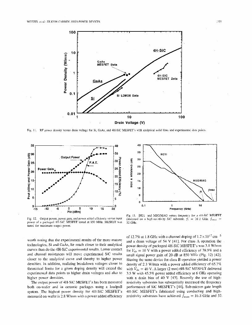
WEITZEL et al.: SILICON CARBIDE HIGH-POWER DEVICES 1737
Fig. 11. RF power density
35 -40
,35
: 4
Y - - a -30 2 -25 2
B
. P
;20 - - * -15 g.
0 Y :lo-
8 v
-5
0 -15 -10 -5 O 5 10 15 20
Pin (dBm)
Fig 12 Output power, power gain, and power added efficiency versus input power of a packaged 4H-SIC MESFET te5ted at 850 MHz MESFET was tuned for maximum output power
worth noting that the experimental results of the more mature technologies, Si and GaAs, lie much closer to their analytical curves than do the 4H-Sic experimental results. Lower contact and channel resistances will move experimental SIC results closer to the analytical curve and thereby to higher power densities. In addition, realizing breakdown voltages closer to theoretical limits for a given doping density will extend the experimental data points to higher drain voltages and also to higher power densities.
The output power of 4H-Sic MESFET’s has been measured both on-wafer and in ceramic packages using a loadpull system. The highest power density for 4H-Sic MESFET’s measured on-wafer is 2.8 W/mm with a power added efficiency
data points.
40 .
35 : IH211
30
25
20
15
10
5
0 0.1 I 10
Frequency (GHz)
Fig. 13. IH211 and MSG/MAG versus frequency for a 4H-Sic MESFET fabricated on a high-resistivity Sic substrate. f t = 16.2 GHz. fr,,, = 32 GHz.
of 12.7% at 1.8 GHz with a channel doping of 1 . 7 ~ cmP3 and a drain voltage of 54 V [41]. For class A operation the power density of packaged 4H-Sic MESFET’s was 3.1 W/mm for v d s = 50 V with a power added efficiency of 38.9% and a small signal power gain of 20 dB at 850 MHz (Fig. 12) [42]. Biasing the same device for class B operation yielded a power density of 2.3 W/mm with a power added efficiency of 65.7% with v d s = 40 V. A larger (2 mm) 6H-Sic MESFET delivered 3.5 W with 45.5% power added efficiency at 6 GHz operating with a drain bias of 40 V [43]. Recently the use of high- resistivity substrates has substantially increased the frequency performance of S i c MESFET’s [44]. Sub-micron gate length 4H-Sic MESFET’s fabricated using conducting and high- resistivity substrates have achieved frIlax = 16.3 GHz and 32

1738 IEEE TRANSACTIONS ON ELECTRON DEVICES, VOL 43, NO 10, OCTOBER 1996
Ohmic ,Metal
I P- Buffer I N-type Substrate
Fig. 14. epitaxial gate and ion implanted source and drain regions.
Cross sectional view of a lateral RF 6H-Sic JFET showing the P+
GHz and f~ = 8.0 GHz and 14.0 GHz, respectively (Fig. 13) [45]. Device parameters for the data in Fig. 13 are 2 x loi7 cmP3 channel doping, 0.45 pm gate length, v& = 50 V, Ids = 36 mA, and V,, = -6 V. A recently reported 4H-Sic MESFET on a high-resistivity substrate achieved a 42 GHz fmax [431, [46l.
VII. 6H-Sic JFET’s
High-frequency S i c JFET’s are of interest for high- temperature RF applications because much lower gate leakage should be obtained with a p-n junction at high temperature than with a Schottky gate. The cross section of a SIC RF JFET (Fig. 14) is similar to that of the RF MESFET (Fig. 10) except a P+ 6H-SIC epitaxial region with an ohmic contact on top is used in place of a Schottky contact [47]. Ion implanted N+ source and drain contact regions are used in place of the N+ 6H-Sic epitaxial region. The highest frequency performance achieved with a 6H-Sic JFET is fmax = 9.2 GHz and f~ = 7.3 GHz (Fig. 15). The best power performance is 1.3 W/mm with 40 V drain voltage at 850 MHz. Device parameters for these results are 2.4 x 1017cm-3 channel doping, 0.3 pm gate length, 24 mS/mm transconductance, and I d s , = 165 mA/mm [48]. SIC JFET performance can be improved significantly by replacing 6H-SIC with higher mobility 4H-Sic and by replacing the conducting substrate with a high-resistivity substrate,
I I
25 h
2 0 <[
$ 15 z z d
5
0 0.1 1 10
Frequency (GHz)
Fig 15 cated on a conducting SIC substrate f t = 7 3 GHz fmax = 9 2 GHz
IH211 and MSGMAG versus frequency for a 6H-SIC JFET fabri-
reduction of micropipe defects has resulted in densities as low as 3.5 cm-’, which is about 1/100th that of several years ago [SO]. While this defect density is low enough for microwave applications, even lower total defect densities are needed if S i c is to reach its full potential in the power switching semiconductor market. The present high substrate cost will initially limit commercialization to those applications where S i c devices would offer significant performance advantages or would lead to an overall reduction in system cost. The first de- vices to be commercialized will be those whose demonstrated performance clearly takes advantage of the unique materials properties of Sic . At this time these would include Schottky diodes, RF SIT’S, RF MESFET’s, and possibly p-i-n diodes.
ACKNOWLEDGMENT
The authors would like to acknowledge the help of R. Singh and C. Capell, Cree Research, processing and test engineers and technicians at both Motorola and Cree Research, and the management support at both companies.
VIII. CONCLUSIONS REFERENCES
The analytical and experimental performance of a wide variety of S i c devices clearly show the significant technical advantage that S i c high voltage, high-power devices have over similar devices fabricated with Si and GaAs technologies. The major impediments to rapid commercialization of S i c technology are the size, defect density, and cost of S i c substrates. In the near term, 2” diameter S i c substrates will become commercially available and 3” diameter wafers are on the horizon. This progression to larger and larger substrates is absolutely essential if S i c is to have a large impact on the commercial semiconductor market. Substrate defect densities will also have to be reduced. One of the most important defects determined to be fatal to the operation of S i c high voltage devices is the “micropipe” defect, which causes device failures at high fields [49]. However, recent advances in the
[1] K. Shenai, R. S. Scott, and B. J. Baliga, “Optimum semiconductors for high-power electronics,” IEEE Trans. Electron Devices, vol. 36, no. 9, pp. 1811-1823, 1989.
[2] R. J. Trew, J. Yan, and P. M. Mock, “The potential of diamond and Sic electronic devices for microwave and millimeter-wave power applications,” Proc. IEEE, vol. 79, no. 5, pp. 598-620, 1991.
[3] H. Morkoc, S . Strite, G. B. Gao, M. E. Lin, B. Sverdlov, and M. Burns, “Large bandgap Sic, 111-V nitride, and 11-VI ZnSe-based semiconductor device technologies,” J. Appl. Phys., vol. 76, no. 3, pp. 1363-1398, 1994.
[4] W. J. Schaffer, G. H. Negley, K. G. Irvine, and J. W. Palmour, “Conductivity anisotropy in epitaxial 6H and 4H Sic,” in Diamond, Sic, and Nitride Wide Bandgap Semiconductors, C.H. Carter, Jr., G. Gildenblatt, S. Nakamura, and R.J. Nemanich, Eds., Material Research Society Proc., vol. 339. Pittsburgh, PA: MRS, 1994, pp. 595-600.
151 E. 0. Johnson, “Physical limitations on frequency and power parameters of transistors,” RCA Rev., vol. 26, pp. 163-177, 1963.
161 R. W. Keyes, “Figure of merit for semiconductors for high-speed switches,” Proc. IEEE, vol. 60, pp. 225-232, 1972.
171 B. J. Baliga, “Semiconductors for high-voltage, vertical channel FET’s,” J. Appl. Phys., vol. 53, no. 3, pp. 1759-1764, 1982.
WEITZEL et al.: SILICON CARBIDE HIGH-POWER DEVICES 1739
-, “Power semiconductor device figure of merit for high-frequency applications,” IEEE Electron Device Lett., vol. 10, no. 10, pp. 455457, 1989. T. P. Chow and R. Tyagi, “Wide bandgap compound semiconductors for superior high-voltage unipolar power devices,” IEEE Trans. Electron Devices, vol. 41, no. 8, pp. 1481-1483, 1994. M. Bhatnagar, P. McLarty, and B. J . Baliga, “Silicon-carbide high- voltage (400 V) Schottky barrier diodes,” IEEE Electron Device Lett., vol. 13, no. 10, pp. 501-503, 1992. D. Alok, B. J. Baliga, and P. K. McLarty, “A simple edge termination for silicon carbide devices with nearly ideal breakdown voltage,” IEEE Electron Device Lett., vol. 1.5, no. 10, p. 394-395, 1994. M. Bhatnagar and B. J. Baliga, “Comparison of 6H-SiC, 3C-Sic and Si for power devices,” IEEE Trans. Electron Devices, vol. 40, no. 3, pp. 645-655, 1993. S.M. Sze, Physics of Semiconductor Devices. New York: Wiley, 1981. J. W. Palmour, J. A. Edmond, H. S. Kong, and C. H. Carter, Jr., “Vertical power devices in silicon carbide” in Silicon Carbide and Related Materials, M.G. Spencer, R.P. Devaty, J.A. Edmond, M. Asif Khan, R. Kaplan, and M. Rahman, Eds. Bristol: Inst. Phys. Pub., 1994, no. 137, pp, 499-502. A. S. M. Salih, R. W. Slocumb, J. Ommen, and C. Thero, “High voltage GaAs power rectifiers with low switching and conduction losses,” in IEEE PEDS 1995 Conf Proc., Singapore, Feb. 1995. A. S. M. Salih, R. W. Slocumb, P. Hadizad, and C. Thero, “GaAs rectifiers for power supply and motor control applications,” in IEEE APEC 2995 Conf Proc., Dallas, TX, Mar. 1995, p 743-745. L. Tu and B. J. Baliga, “Controlling the characteristics of MPS rectifier by variation of area of Schottky region,” IEEE Trans. Electron Devices, vol. 40, no. 7, p. 1307-1315, 1993. R. Raghunathan, D. Alok, and B. J. Baliga, “High voltage 4H-Sic Schottkv barrier diodes,” IEEE Electron Device Lett., vol. 16, no. 6, pp. 228-227, 1995. A. Itoh, T. Kimoto, and H. Matsunami, “High performance high-voltage 4H-Sic Schottky barrier diodes,” IEEE Electron Device Let;, vol. 16, no. 6, pp. 280-282, 1995. P. G. Neudeck, D. J. Larkin, J. A. Powell, and L. G. Matus, “2000 V 6H-Sic p-n junction diodes grown by chemical vapor deposition,” Appl. Phys. Lett., vol. 64, no. 11, p. 1386-1388, Mar. 1994 . 0. Kordina, J. P. Bergman, A. Henry, E. Janzen, S. Savage, J. Andre, L. P. Ramberg, U. Lindefelt, W. Hermansson, and K. Bergman, “A 4.5 kV 6H silicon carbide rectifier,” Appl. Phys. Lett., vol. 67, no. 11, pp. 1561-1563, Sept. 1995. J. W. Palmour, V. F. Tsvetkov, L. A. Lipkin, and C. H. Carter, Jr., “Silicon carbide substrates and power devices,” in Compound Scmiconductors 1994, H. Goronkin and U. Mishra, Eds. Bristol: Inst. Phys. Pub., 1994, no. 141, pp. 377-382. J. W. Palmour, S. T. Allen, R. Singh, L. A. Lipkin, and D. G. Waltz, “4H-silicon carbide power switching devices,” in Int. Conf Silicon Carbide and Related Materials, 1995, Tech. Dig., Kyoto, Japan, Sept. 18-21, 1995, pp. 319-320. D. Ueda, H. Takagi, and G. Kano, “An ultra-low on-resistance power MOSFET fabricated by using a fully self-aligned process,” IEEE Trans. Electron Devices, vol. 34, p. 926, 1987. N. Inoue, A. Itoh, T. Kimoto, H. Matsunami, T. Kakata, and M. Watanabe, “Hot implantation of Nf into a -S ic epilayers,” Int. Con$ Silicon Carbide and Related Materials, 1995, Tech. Dig., Kyoto, Japan, Sept. 18-21, 1995, pp. 408409. J. W. Palmour, R. F. Davis. P. Astell-Burt, and P. Blackborow, “Effects of cathode materials and gas species on the surface characteristics of dry etched monocrystalline beta-Sic thin films,” Ceramic Trans., vol. 2, pp. 491-500, 1989. P. H. Yih and A. J. Steckl, “Residue-free reactive ion etching of silicon carbide in fluorinated plasmas,” J. Electrochem. Soc., vol. 142, no. 1, pp. 312-319, Jan. 1995. J. N. Shenoy, L. A. Lipkin, G. L. Chindalore, J. Pan, J. A. Cooper, J. W. Palmour, and M. R. Melloch, “Electrical characterization of the thermally oxidized SiOz/SiC Interface,” in Compound Semiconductors 1994. H. Goronkin and U. Mishra, Eds. Bristol: Inst. Phys. Pub., 1994, no. 141, pp. 449454. J. Crofton. P. G. McMullin, J. R. Williams, and M. J. Bozack, “A high- temperature ohmic contact to n-type 6H-Sic using Ni,” in Trans. 2nd Int. High Temperature Electronics Conf, D. B. King and F. V. Thome, Eds., Sandia National Laboratories, June 5-10, 1994, pp. XIII-15-XIII-25. M. Bhatnagar, D. Alok, and B. J. Baliga, “Sic power UMOSFET : Design, analysis and technological feasibility,” in Silicon Carbide and Related Materials, M. G. Spencer, R. P. Devaty, J. A. Edmond, M. Asif Khan, R. Kaplan, and M. Rahman, Eds. Bristol: Inst. Phys. Pub.,
1993, no. 137, pp. 703-706. [31] B. Fragale, Motorola Semiconductor Product Sector, private communi-
cation. [32] J. W. Palmour and L. A. Lipkin, “High temperature devices in silicon
carbide,” in Trans. 2nd h t . High Temperature Electronics Conf, D. B. King and F. V. Thome, Eds., Sandia National Laboratories, June 5-10,
[33] J. Nishizawa, T. Terasaki, and J. Shibata, “Field-effect transistor versus analog transistor (static induction transistor),” IEEE Trans. Electron Devices, vol. ED-22, pp. 185, 1975.
1341 R. C. Clarke, R. R. Siergiej, A. K. Agarwal, C. D. Brandt, A. A. Burk, Jr., A. Morse, and P. A. Orphanos, “30W VHF 6H-Sic power static induction transistor,” 15th Biennial IEEELornell Univ. Con5 Advanced Concepts in High Speed Semiconductor Devices and Circuits Dig. Abstracts, Aug. 7-9, 1995, pp. 14.
1351 R. R. Siergiej, S. Sriram, R. C. Clarke, A. K. Agarwal, C. D. Brandt, A. A. Burk, Jr., T. J. Smith, A. Morse, and P. A. Orphanos, “Sic microwave power transistors,” Int. Conf Silicon Carbide and Related Materials, 1995, Tech. Dig., Kyoto, Japan, Sept. 18-21, 1995, p. 321.
[36] R. R. Siergiej, R. C. Clarke, A. K. Agarwal, C. D. Brandt, A. A. Burk, Jr., T. J. Smith, and P. A. Orphanos, “High power 4H-Sic static induction transistors,” in IEDM Tech. Dig., 1995, pp. 353-356.
[37] I. Bencuya, A. I. Cogan, S. J. Scott, and R. J. Regan, “Static induction transistors optimized for high-voltage operation and high microwave power output,” IEEE Trans. Electron Devices, vol. ED-32, pp. 1321, 1975.
1381 H. M. Hobgood, R. C. Glass, G. Augustine, R.H. Hopkins, J. Jenny, M. Skowronski, W.C. Mitchel, and M. Roth, “Semi-insulating 6H-Sic Grown by physical vapor deposition,” Appl. Phys. Lett., vol. 66, no. 11,
1994, pp. XI-3-XI-8.
~~
pp. 136Li366, Mar. -1995.- 1391 C. E. Weitzel, “Comparison of Si. GaAs, and Sic RF MESFET power ~~
densities,” IEEE Electron Device Lett., vol. 16, no. 10, pp. 45i4.53, 1995.
[40] H. M. Macksey, “GaAs power FET design,” in GaAs FET Principles and Technology, J. V. Dilorenzo and D. D. Khandelwal, Eds. Dedham, MA: Artech House, 1982, pp, 257-275.
[41] C. E. Weitzel, J. W. Palmour, C. H. Carter, Jr., and K. Nordquist, “4H- Sic MESFET with 2.8 W/mm power density at 1.8 GHz,” IEEE Electron Device Lett., vol. 15, no. 10, pp. 406408, 1994.
[42] K. Moore, C. Weitzel, K. Nordquist, L. Pond 111, J. Palmour, S. Allen, V. F. Tsvetkov, S. Macko, and C. Carter Jr., “Bias dependence of RF power characteristics of 4H-Sic MESFET’s,” in 15th Biennial IEEEKornell Univ. Conf: Advanced Concepts in High Speed Semiconductor Devices and Circuits Dig. Abstracts, Aug. 7-9, 1995, pp. 12-13.
[43] S. Sriram, R. Barron, A. W. Morse, T. J. Smith, G. Augustine, A. A. Burk, Jr., R. C. Clarke, R. C. Glass, H. M. Hobgood, P. A. Orphanos, R. R. Siergiej, C. D. Brandt, M. C. Driver, and R. H. Hopkins, “High efficiency operation of 6H-Sic MESFET’s at 6 GHz,” in 1995 53rd Annual Device Research Conf Dig., Charlottesville, Va, June 19-21, 1995, pp. 104-105.
1441 S. Sriram, R. C. Clarke, A. A. Burk, Jr., H. M. Hobgood, P. G. McMullin, P. A. Orphanos, R. R. Siergiej, T. J. Smith, C. D. Brandt, M. C. Driver, and R. H. Hopkins, “RF performance of SIC MESFET’s on high resistivity substrates,” IEEE Electron Device Lett., vol. 15, no. 11, pp. 458459, 1994.
[45] S. T. Allen, J. W. Palmour, V. F. Tsvetkov, S. J. Macko, C. H. Carter, Jr., C. E. Weitzel, K. E. Moore, K. J. Nordquist, and L. L. Pond, 111, “Frequency and power performance of microwave Sic FET’s,” in Int. Conf Silicon Carbide and Related Materials, 1995, Tech. Dig., Kyoto, Japan, Sept. 18-21, 1995, p. 599-600.
1461 C. D. Brandt, A. K. Agarwal, G. Augustine, R. R. Barron, A. A. Burk, Jr., R. C. Clarke, R. C. Glass, H. M. Hobgood, A. W. Morse, L. B. Rowland, S. Seshadri, R. R. Siergiej, T. J. Smith, S. Sriram, M. C. Driver, and R. H. Hopkins, “Advances in Sic materials, and devices for high frequency applications,” h t . Conf Silicon Carbide and Related Materials, 1995, Tech. Dig., Kyoto, Japan, Sept. 18-21, 199.5, p. 587.
[47] C. E. Weitzel, J. W. Palmour, C. H. Carter, Jr., K. J. Nordquist, K. Moore, and S. Allen, “Sic microwave power MESFET’s and JFET’s,” in Comuound Semiconductors 1994, H. Goronkin and U. Mishra, Eds. Bristo1:’Inst. Phys. Pub., 1994, no. 141, pp. 389-394.
1481 K. Moore, “DC, RF, and power performance of 6H-SIC JFET’s,” - - presented at WOCSEMMAD ’95, New Orleans, Feb., 1995.
[49] P. G. Neudeck and J. A. Powell, “Performance limiting micropipe defects in silicon carbide wafers,” IEEE Electron Device Left., vol. 15, no. 2, pp. 63-65, 1994.
1501 V. F. Tsvetkov, S. T. Allen, H. S. Kong, and C. H. Carter, Jr., “Recent progress in Sic boule growth,” in Int. Con$ Silicon Carbide and Reluted Materials, 1995, Tech. Dig., Kyoto, Japan, Sept. 18-21, 1995, p. 11-12.
1740 IEEE TRANSACTIONS ON ELECTRON DEVICES, VOL. 43, NO. 10, OCTOBER 1996
John W. Palmour (M’95) received both the B S and the PhD degrees in materials science and engineering (with a minor in electrical engineering) from North Carolina State University, Raleigh, in 1982 and 1988, respectively. His doctoral research concentrated on processing techniques and transistor development in Sic devices, and he demonstrated a Sic MOSFET operating at 650 O C .
After graduating, he became a co-founder of Cree Research, Inc., Durham, NC, where he has been Senior Scientist since its formation, concentrating
on device processing techniques and transistor development in S ic He has been responsible for the development of high-voltage, high-temperature 4H- SIC power MOSFET’s and thyristors, as well as high-frequency MESFET’s and planar n-channel and p-channel 6H-SIC MOSFET’s He has co-authored over 80 publications in various conference proceedings and refereed journals and is an inventor on 13 issued U S patents and seven foreign patents concerning semiconducting Sic
Dr Palmour serves on the Board of Directors for Cree Research, Inc.
Kevin J. Nordquist received the B S E E degree from DeVry Institute of Technology, Phoenix, AZ, in 1983
Upon graduahon, he joined the Photomask Op- eration, General Instruments, Chandler, AZ, and contributed to research of electron beam lithography photomask manufacturing In 1984, he joined the Bipolar Technology Center, Photomask Operations, Motorola, Phoenix, where, for seven years, he was a key contributor in both engineering and manage- ment capacities to the successful implementation of
the electron beam lithography photomask manufacturing In 1991, he joined Motorola’s Phoenix Corporate Research Laboratories, Tempe, AZ, to advance the optical and electron beam lithography programs His high-resolution lithography work has been instrumental in the development of S i c power devices for switching and RF applications His most recent work is focused on characterizing experimental deep ultraviolet (193-248 nm) resists for sub-0 35 p m IC manufacturing
Calvin H. Carter, Jr., received the B S , M S and PhD degrees in materials science and engineer- ing from North Carolina State university, Raleigh, (NCSU) in 1977, 1980, and 1983, respectively His doctoral research was focused on the study of high- temperature creep on various forms of SIC
After his graduate research, he remained at NCSU as a Research Assistant Professor, where he con- ducted research on the development of S i c as a semiconductor As a result of this effort, he develooed a method of reoeatablv growing large
area 6H-SIC single crystals He ais0 performed research on the GBE growth of gallium nitride while at NCSU through 1987 In 1987, he became a co-founder of Cree Research, Inc , Durham, NC, where he has been Vice President, New Product Development, since its formation He directs all internal research and development and also oversees the externally funded research contracts His primary technical expertise is in bulk crystal growth and epitaxial deposition of Sic, and he has been primarily responsible for the development of large, low-defect density bulk Sic crystals He has co-authored over 60 publications, is co-inventor on eight U S and four foreign patents
Dr Carter is a member of American Vacuum Society and the Materials Research Society He also serves on the Board of Directors for Cree Research Inc
Scott Allen received the B S degree from Cornel1 University, Ithaca, NY, in 1987 and, in 1989, the M.S degree from the University of Massachusetts, Amherst, where he specialized in mcrowave technology In 1994, he received the Ph D degree in electrical engineering from the University of California, Santa Barbara, where his research focused on. GaAs devices and circuits for sub- millimeter-wave applications
He spent three years at Lockheed Martin’s Electronics Laboratory (formerly General Electric),
Syracuse, NY, working as a Device Engineer on the development of HEMT technology. His work there included extensive device modeling of both GaAs PHEMT’s and InP HEMT’s, and the design of low-noise MMIC amplifiers. In 1994 he joined the research and development group at Cree Research, Inc , to work on silicon carbide MESFET’s for microwave power applications. He is the principal investigator on several microwave contracts at Cree and is the primary technical liaison for Cree’s collaboration with Motorola on Sic MESFET development. He has authored or co-authored 38 papers published in various conference proceedings and refereed journals He has also been cited as a co-inventor on three patent applications pertaining to silicon carbide microwave technology
WEITZEL et al.: SILICON CARBIDE HIGH-POWER DEVICES 1741
Christine Thero (M’88) received the B.S.E.E. and M.S.E.E. degrees from Villanova University, Vil- lanova, PA, in 1990 and 1992, respectively. Her graduate work focused on electrodeposition of thin films for low-cost solar cells.
In 1992, she joined Motorola’s Phoenix Corporate Research Laboratories, Tempe, AZ, and worked in the area of bulk acoustic wave filters. In 1993, she began working on power devices and was a key contributor to the commercialization of Motorola’s first GaAs Schottky rectifier by the Power Products
Division. Presently, her work is focused bn silicon carbide high-voltage Schottky diodes and gallium arsenide power devices.
Ms. Thero is a member of the Sigma Xi Research Society and the Society of Women Engineers.
Mohit Bhatnagar, 1996 issue of this
for a photograph and biography, TRANSACTIONS.
see p. 156 of the January