Formation of Wigner crystals in conducting polymer nanowires
17
arXiv:cond-mat/0702009v1 [cond-mat.mes-hall] 1 Feb 2007 Formation of Wigner crystals in conducting polymer nanowires Atikur Rahman and Milan K. Sanyal Surface Physics Division, Saha Institute of Nuclear Physics, 1/AF Bidhannagar, Kolkata 700 064, India. (Dated: February 5, 2008) Abstract The search for theoretically predicted Wigner crystal in one-dimensional (1D) wires of struc- turally disordered materials exhibiting properties of charge-density-waves have remained unsuc- cessful. Based on the results of a low temperature conductivity study we report here formation of such 1D Wigner crystal (1DWC) in polypyrrole nanowires having low electron densities. The current-voltage characteristics of all the nanowires show a ’gap’ that decreases rapidly as the tem- perature is increased - confirming the existence of long-range electron-electron interaction in the nanowires. The measured current show power-law dependence on voltage and temperature as ex- pected in 1DWC. A switching transition to highly conducting state has been observed above a threshold voltage, which can be tuned by changing the diameters of the nanowires and the tem- perature. Negative differential resistance and enhancement of noise has been observed above the threshold as expected. PACS numbers: 73.20.Mf, 73.20.Qt, 73.61.Ph, 73.63.-b 1
Transcript of Formation of Wigner crystals in conducting polymer nanowires

arX
iv:c
ond-
mat
/070
2009
v1 [
cond
-mat
.mes
-hal
l] 1
Feb
200
7
Formation of Wigner crystals in conducting polymer nanowires
Atikur Rahman and Milan K. Sanyal
Surface Physics Division, Saha Institute of Nuclear Physics,
1/AF Bidhannagar, Kolkata 700 064, India.
(Dated: February 5, 2008)
Abstract
The search for theoretically predicted Wigner crystal in one-dimensional (1D) wires of struc-
turally disordered materials exhibiting properties of charge-density-waves have remained unsuc-
cessful. Based on the results of a low temperature conductivity study we report here formation
of such 1D Wigner crystal (1DWC) in polypyrrole nanowires having low electron densities. The
current-voltage characteristics of all the nanowires show a ’gap’ that decreases rapidly as the tem-
perature is increased - confirming the existence of long-range electron-electron interaction in the
nanowires. The measured current show power-law dependence on voltage and temperature as ex-
pected in 1DWC. A switching transition to highly conducting state has been observed above a
threshold voltage, which can be tuned by changing the diameters of the nanowires and the tem-
perature. Negative differential resistance and enhancement of noise has been observed above the
threshold as expected.
PACS numbers: 73.20.Mf, 73.20.Qt, 73.61.Ph, 73.63.-b
1

Possibilities of applications in nanotechnology has triggered extensive research activi-
ties to understand charge-conduction in quasi-1D conductors like nanowires and nanotubes
where electron-electron interaction (EEI) plays a dominant role. In 1934 Eugene Wigner
considered the effect of long-range EEI in metals and predicted in a seminal paper [1] pos-
sibility of formation of periodic spatial structures of electrons for very low electron density
materials. It has been predicted theoretically that one dimensional Wigner crystal (1DWC)
[2] formation exhibiting the characteristic of a charge density wave (CDW) may occur in
nanowires of even structurally disordered materials [3]. Wigner crystal (WC) phase has
been observed experimentally in two-dimensional electron system under intense magnetic
field [4, 5], in surface-state electrons of superfluid helium [6], in quasi-1D organic charge
transfer salt [7] and recently in inorganic chain compounds [8]. Although interesting phases
like Luttinger liquid (LL) [9], which arise due to short-range EEI, has been observed in
several one dimensional (1D) systems [10, 11, 12, 13], predicted formation of 1DWC in
structurally disordered materials [3] has not been observed experimentally, to the best of
our knowledge. Among various low-dimensional systems conducting polymer nanowires are
easy-to-form quasi-1D systems to study EEI as one can tune the carrier concentration of
a polymer over several orders of magnitudes by controlling doping concentration and WC
formation has been predicted in conducting polymers [3, 14].
Here we report results of low temperature study of polypyrrole nanowires having diam-
eters from 30 to 450 nm. Highly non-linear current-voltage (I-V) characteristics having
I ∝ V 1+β at high V and I ∝ T αV at low V was observed. The exponent β reduces from
high value (∼5 -7) with increasing temperature and does not take equal value to α, in
general. A large ’gap’ voltage (VG), above which the conductance increase substantially,
was observed in the low temperature I-V characteristics. The gap was found to decrease
rapidly with increasing temperature and with increasing diameter. The I-V characteris-
tics also show a switching transition to a highly conducting state above a certain threshold
voltage VTh(> VG). The threshold field (ETh) corresponding to VTh was found to depend
on the diameter (d) as ETh ∝ d−4/3. Current-driven I-V characteristics show negative dif-
ferential resistance (NDR) at low temperature. An increase in ’noise’ has been observed
in the switched (highly conducting) state. All these experimental results give evidence in
favor of pinned Wigner crystal formation in conducting polymer nanowires, as predicted
theoretically [3].
2

Conducting polymer nanowires are quasi-1D systems composed of aligned polymer chains
where charge carriers are created by doping. We used membrane based synthesis technique
for growing polymer nanowires following same preparation technique describe earlier [15].
The average doping concentration (obtained after initial doping gradient within few hundred
nanometer) can be systematically reduced by lowering the diameters of the nanowires [15].
The actual diameter of nanowires were characterized from SEM micrograph and were found
to have an average diameter of 30, 50, 70, 110, 350 and 450 nm. Gold electrodes (2mm
diameter) were sputter-deposited on both sides of the membrane to establish parallel con-
nection with ∼ 107 nanowires (pore density of the membrane ∼ 109/ cm2). The electrical
measurements were carried out in a Oxford cryostat under liquid Helium environment using
Keithley 2400 source-meter and 6517A electro-meter in two probe configuration (refer inset
of Fig. 1(a)) over the temperature range of 1.7 to 300 K. The consistency of the results were
checked by changing the contact material, scan-speed of the bias voltage (current). Differ-
ential conductance (dI/dV ) were obtained by numerically differentiating the I-V curves and
verified by Lock-in measurements. In Fig. 1(a) we have shown dI/dV vs. V plots for 30 nm
nanowires taken at various temperatures.
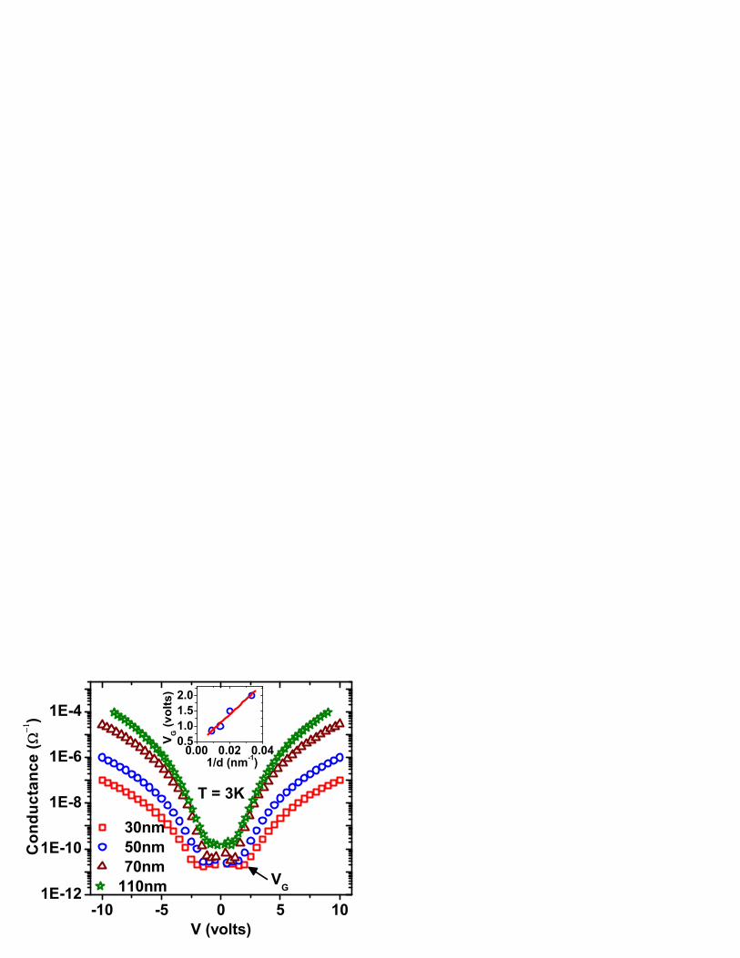
The conductance vs. voltage and dI/dV vs. voltage data of various nanowires (refer
Fig. 1(a) and (b)) show existence of ’gap’ voltage (VG). We have measured the value of VG
by noting the change of slope from the conductance vs. voltage data for different diameter
nanowires as shown in Fig. 1(b). VG was found to be inversely proportional to the diameter
(d) of the nanowires (refer inset of Fig. 1(b)). It is to be noted that zero-bias current and
hence the conductance below the VG increases with temperature and diameter of nanowires.
The ’gap’ was found to reduce rapidly with increase in temperature and vanishes at relatively
high temperature that depends on the wire diameter.
Strong temperature dependence of ’gap’ is a signature of electron-electron interaction
[16, 17], and has been observed earlier in chains of graphitized carbon nanoparticle [18].
Temperature and diameter dependence of ’gap’ in our nanowires can only be explained
by considering ’pinned’ collective state [3] where pining strength increases with decreasing
diameter. This is consistent with the fact that observed voltage required for switching
transition also increases with decreasing diameter. In a previous study existence of collective
behavior has been predicted in these nanowires as a non-Curie type temperature dependence
of static dielectric constant [15] was observed. Here dipoles (formed by dopant counter ion)
3

interact among each other via Coulomb interaction and produce a collective pinning [3].
The observed characteristics of VG here is consistent with Wigner crystal formation which
is pinned by the impurity [3, 5, 6].
Above the voltage VG, I-V characteristics of all nanowires show power law behavior -
a known characteristics of 1D conductors. In contrast to conventional three-dimensional
(3D) materials, 1D conductors exhibit fascinating transport properties due to the power law
dependence of tunneling density of states, which can be parameterized as dI/dV ∝ T α and
∝ Vβ for low bias (V ≪ kBT/e) and high bias (V ≫ kBT/e) conditions respectively [9]. In
Fig. 2(a) we have shown a representative data that show R ∝ T−α behavior. In this figure
we have also plotted the same data as log(R) vs. T−1/4 to show that variable range hopping
(VRH) can also give reasonable fit. We found that for low bias data VRH give better fit
[15] but power law gives better fit for the data taken with higher bias, as discussed earlier
[19]. In the inset of Fig. 2(a) we have plotted resistivity data (taken with bias 1V) against
temperature in log-log scale for 30nm diameter nanowire and fitted it to show that power
law dependence (R ∝ T−α, with α = 5.2) remains above 30K. Due to the presence of VG,
below 30K the resistance for this bias becomes nearly temperature independent as observed
in other polymer nanowires [20]. For 30 nm diameter nanowire taking α = 5.2 and plotting
I/T 1+α versus eV/(kBT ), various I-V curves of different temperatures collapse on a master
curve (Fig. 2(b)). Clean LL state predicts α = β and scaling of I-V curves of different
temperatures to such a master curve [10, 11, 21]. But for the higher diameter nanowires the
I-V characteristics of different temperatures could not be collapsed to a single master curve.
Presence of VG, absence of single master curve and unequal exponents (discussed below) α
and β in these wires show that LL theory is not applicable.
The power law behavior is a characteristic feature of 1D transport [2, 9, 10, 11, 12, 13,
22, 23] and has also been observed in nanowires of conventional CDW materials [24]. From
the I-V data we get β = 5.6 at T = 3 K for 30 nm diameter nanowire (refer upper inset
of Fig. 2(b)) and for other diameter nanowires this value goes up to 7.2 at 3K (refer lower
inset of Fig. 2(b)). Similar power law behavior have been observed in other 1D systems
like carbon nanotubes (α, β ∼ 0.36) [10] and nanowires of InSb (α ∼ 2 − 7, β ∼ 2 − 6) [13],
polymer (α ∼ 2.2 − 7.2, β ∼ 2 − 5.7) [20], NbSe3 (α ∼ 1 − 3, β ∼ 1.7 − 2.7) [24] and MoSe
(α ∼ 0.6− 6.6, β ∼ 0.32− 4.9) [25] . Although we obtained α ≃ β for most of the nanowires
at low temperature but the β values were found to decrease with increasing temperature
4

and with decreasing diameter (refer lower inset of Fig. 2(b)) - as a result α remains unequal
to β, in general for our wires.
For a quasi-1D system strength of Coulomb correlation is defined as rs = a/(2aB), where
a is the average distance between electrons and aB is the effective Bohr radius. Low doped
Polymer nanowires with quasi-1D nature and low electron density (rs ≫ 1) are a potential
candidate to form Wigner crystal that can exhibit characteristics of a charge density wave
state [2, 3, 14, 20, 26]. For weakly pinned Wigner crystals tunneling density of states show
a power law behavior with the applied bias [22] and the exponent ranges from ∼ 3 to 6
[23, 27]. It has been shown [23] that for 1DWC with increasing pinning strength β should
decrease. The variation of VG with d (refer inset of 1(b)) clearly indicates that pinning
strength increases [17] with decreasing diameter. Hence our observation of reduction in β
value with decreasing diameter of nanowires is consistent with 1DWC model. Moreover
higher values of the exponents observed here also indicate that 1DWC has formed in our
nanowires.
At low temperature all the nanowires show a switching transition to a highly conducting
state above a certain threshold voltage VTh(> VG). We did not observe any switching
transition when the bias voltage is kept ∼ 1 mV below VTh for long time. The sharp
threshold indicates a collective phenomena [28, 29, 30] and the transition is not due to field
heating. In Fig. 3(a) and in its inset we have shown representative switching transitions
for the nanowires measured at 2.5 K. All the nanowires showed hysteresis in the switching
transition which is independent of the bias scan speed (thus removes any possibility of
capacitive effect). The nanowires could switch back to the low conducting state only when
the applied voltage is reduced to a value VRe (|VTh| > |VRe| > |VG|). With decreasing
temperature the hysteresis, defined as (ETh − ERe)/ERe ( ERe is the field corresponding to
VRe), increases (refer Fig.3(b))- this behavior is consistent with that observed in switching
CDW [28, 29, 30, 31]. It has been shown theoretically that formation of 1DWC is equivalent
to have 4kF CDW in a system [2, 3]. The sliding state of this pinned CDW can explain the
field induced switching transition observed here. Presence of VG and VTh is also consistent
with two threshold observed in semiconducting CDW systems [31].
Depending upon the pinning strength a pinned CDW become non-conducting below a
certain threshold field. When an applied DC field is strong enough to overcome the pinning
energy the CDW depins and sliding motion starts giving rise to a switching transition [28,
5

29, 30, 31]. When CDW is confined in two direction as in the nanowires, phase deformations
occur along the length of the nanowires. In this situation pinning of CDW is one dimensional
and the threshold field is expected to be proportional to d−4/3 [32]. The plot of ETh vs. d
shown in Fig. 3(c) confirms this dependence in our nanowires. The change in ETh with
d is obviously not due to surface pinning as that would have given us ETh ∝ d−1. It has
been also observed previously in a study of NbSe3 samples that surface pinning can be
excluded for highly resistive samples (R/L > 1Ω/µm) [32]. We measured current-driven
I-V characteristics to investigate the nature of switched state in these nanowires. The
measurements (Fig. 3(d) and its upper inset ) exhibit negative differential resistance (NDR).
This type of behavior has been observed in sliding CDW state [31, 33] and is expected in
1DWC. The comparison between voltage driven and current driven I-V characteristics has
been shown in Fig. 3(d) and this shows the uniqueness of threshold field for both type of
measurements. We have also observed a large fluctuation in the measured voltage in the
switched state (refer lower inset of Fig. 3(d)), which gives strong evidence of sliding motion
above ETh [31], similar increase in ’noise’ has been observed previously in two dimensional
Wigner crystal [4].
The results presented here show that the I-V characteristics of all the nanowires have
three distinct regions (refer Fig. 3(a)). Below VG current is very small and that increases
with temperature and diameter. Between VG and VTh power-law characteristics of 1D trans-
port is observed. Above VTh switching transition is observed that exhibit hysteresis, d−4/3
scaling, NDR and ’noise’ enhancement. All these findings confirm the formation of 1DWC
which is expected to exhibit characteristics of CDW, in our nanowire. Although power law
dependent I-V characteristics can be explained by other models like Luttinger liquid [9] and
environmental Coulomb blockade (ECB) [34], these theories cannot explain the observed
switching transition and related phenomena reported here. Moreover, LL theory is clearly
inconsistent with observed VG and reduction of β with decreasing diameter (refer inset of
Fig. 2(b)). In addition we could not get expected collapse to a master curve [21] for higher
diameter nanowires as observed in 30nm wires (refer Fig. 2(b)). ECB theory can account
for VG but it predicts an increase in β with increasing environmental impedance but in our
case though resistance of the nanowires decreases with increasing diameter - β increases. In
conclusion all our experimental findings show that one dimensional Wigner crystal has been
formed in nanowires of a structurally disordered material like conducting polymer.
6

Authors are grateful to R. Gangopadhayy and A. De for their help in sample preparation.
[1] E. Wigner, Phys. Rev. 46, 1002 (1934).
[2] H. J. Schulz, Phys. Rev. Lett. 71, 1864 (1993).
[3] M. M. Fogler, S. Teber and B. I. Shklovskii, Phys. Rev. B, 69, 035413 (2004).
[4] V. J. Goldman, M. Santos, M. Shayegan and J. E. Cunningham, Phys. Rev. Lett. 65, 2189
(1990).
[5] E. Y. Andrei et al., Phys. Rev. Lett. 60, 2765 (1988).F. I. B. Williams et al., Phys. Rev. Lett.
66 3285 (1991).
[6] H. W. Jinag and A. J. Dahm, Phys. Rev. Lett. 62, 1396 (1989). P. Glasson et al., Phys. Rev.
Lett. 87, 176802 (2001).
[7] K. Hiraki and K. Kanoda, Phys. Rev. Lett. 80, 4737 (1998).
[8] P. Horsch, M. Sofin, M. Mayr and M. Jansen, Phys. Rev. Lett. 94, 076403 (2005).
[9] J. Voit, Rep. Prog. Phys. 58, 977 (1995).
[10] M. Bockrath et al., Nature (London), 397, 598 (1999).
[11] Z. Yao et al., Nature (London), 402, 273 (1999).
[12] A. Bachtold et al., Phys. Rev. Lett. 87, 166801 (2001).
[13] S. V. Zaitsev-Zotov et al., J. Phys. Condens. Matter 12, L303 (2000).
[14] A. J. Heeger. S. A. Kivelson, J. R. Schrieffer, and W. P. Su, Rev. Mod. Phys. 60, 781 (1988).
[15] A. Rahman, M. K. Sanyal, R. Gangopadhayy, A. De, I. Das, Phys. Rev. B 73, 125313 (2006).
[16] B. I. Shklovskii and A. L. Efros, Electronic Properties of Doped Semiconductor (Springer-
Verlag, Berlin, 1984).
[17] A. Alan Middleton and Ned S. Wingreen, Phys. Rev. Lett. 71, 3198 (1993).
[18] A. Bezryadin, R. M. Westervelt, and M. Tinkham, Appl. Phys. Lett. 74, 2699 (1999).
[19] S. N. Artemenko and S. V. Remizov, Phys. Rev. B 72, 125118 (2005).
[20] A. N. Aleshin, H. J. Lee, Y. W. Park, and K. Akagi, Phys. Rev. Lett. 93, 196601 (2004).
[21] L. Balents, cond-mat/9906032.
[22] H. Maurey and T. Giamarchi, Phys. Rev. B, 51, 10833 (1995). L. I. Glazman, I. M. Ruzin,
and B. I. Shklovskii, Phys. Rev. B 45, 8454 (1992).
[23] Gun Sang Jeon, M. Y. Choi, and S. -R. Eric Yang, Phys. Rev. B, 54, R8341 (1996).
7

[24] E. Slot, M. A. Holst, H. S. J. van der Zant and S. V. Zaitsev-Zotov, Phys. Rev. Lett. 93,
176602 (2004).
[25] L. Venkataraman, Y. S. Hong and P. Kim, Phys. Rev. Lett. 96, 076601(2006).
[26] K. Lee, R. Menon, A. J. Heeger, K. H. Kim, Y. H. Kim, A. Schwartz, M. Dressel and G.
Gruner, Phys. Rev. B, 61, 1635 (2000).
[27] Hyun C. Lee, Phys. Rev. B 66, 052202 (2002).
[28] A. Zettl and G. Gruner, Phys. Rev. B 26, 2298 (1982).
[29] G. Gruner, Rev. Mod. Phys. 60, 1129 (1988).
[30] J. Levy, M. S. Sherwin, F. F. Abraham and K. Wiesenfeld, Phys. Rev. Lett. 68, 2968 (1992).
[31] A. Maeda, M. Notomi and K. Uchinokura, Phys. Rev. B 42, 3290 (1990). R.V. Coleman, M.P.
Everson, G. Eiserman, A. Johnson and Hao-an Lu, Synth. Met. 19, 795 (1987).
[32] E. Slot, H. S. J. van der Zant, K. O’Neill and R. E. Thorne, Phys. Rev. B, 69, 073105 (2004).
[33] R. P. Hall, M. Sherwin and A. Zettl, Phys. Rev. Lett. 52, 2293 (1984).
[34] K. A. Matveev and L. I. Glazman, Phys. Rev. Lett. 70, 990 (1993).
Figure Capsions
Fig.1.(a) Differential conductance (dI/dV) is plotted as a function of bias voltage (V) for 30
nm diameter nanowire at various temperatures. Schematic diagram of the two-probe measure-
ment configuration is shown in the inset. (b) Conductance vs. voltage plot for four different
diameter nanowires at T=3K. Gap voltage (VG) for 30nm diameter nanowire has been indi-
cated by an arrow. VG has been poltted as a function of inverse diameter (d) in the inset.
Fig.2.(a) Resistance (R) vs. temperature (T) data for 50 nm diameter nanowire. Upper
arrow indicates plot of log10 R as a function of T−1/4 and its linear fit. Lower arrow indicates
a double-logarithmic plot of R as a function of T and its fit by a power law R(T ) ∝ T−5.
Power law dependence of R − T data for 30nm diameter nanowire has been shown in the
inset. (b) I/T 1+α is plotted against eV/kBT , where α = 5.2 for 30 nm nanowire for four
different temperatures. I-V data for 30 nm diameter nanowire at T=3K is plotted in a double
logarithmic scale in the upper inset. The data is fitted (solid line) by the power law I ∝ V 1+β
with β = 5.6. Plot of β determined at T=3K is shown as a function of diameter d in lower
inset (continuous lines are guide to eye).
Fig.3.(a) Voltage biased I-V characteristics of 110nm diameter nanowire at T=2.5K showing
the gap and switching transition, same for various diameter nanowires are shown in the inset.
8

(b) Hysteresis (ETh−ERe)/ERe is plotted against temperature for 70 nm diameter nanowire.
Upper and lower inset shows voltage driven I-V characteristics of 110 and 350 nm diameter
nanowires respectively at 2.5K, arrows indicates direction of voltage scan. (c) Threshold field
(ETh) is plotted as a function of diameter (symbol) for various nanowires at 2.5 K. The data is
fitted (solid line) by the power law ETh ∝ d−δ with δ ∼ 4/3. (d) Comparison between voltage
biased (square) and current biased (circle) I-V measurements of 450nm diameter nanowire
at 1.7K (arrows indicate the direction of scan). In lower inset fluctuations in the voltage has
been shown for 3mA (upper curve) and 4mA (lower curve) bias current respectively (note the
different scales used). Upper inset shows NDR in the switched state (indicated by (b)).
9

-10 -5 0 5 101E-6
1E-4
0.01
1
100
dI/d
V (
S)
V(volts)
2K 3K 12K 40K
-10 -5 0 5 101E-12
1E-10
1E-8
1E-6
1E-4
0.00 0.02 0.040.51.01.52.0
V G (v
olts
)
1/d (nm-1)
T = 3K
30nm 50nm 70nm110nm
Con
duct
ance
()
V (volts)
VG

1.5 2.0 2.53
6
9
3
6
9
Log 1
0(R())
Log10(T(K))
0.2 0.3 0.4 0.5
1 24
8
12
T=30K
Log 1
0(R())
Log10(T(K))
=5.2
T-1/4 (K-1/4)

102 103 104
1E-20
1E-18
1E-16
1E-14
1E-12
40 80 1205.66.47.2
d (nm)
2 5 10
10-9
10-7
I (Am
p)
V (volts)
I/T (a
rb. u
nits
)
eV/kBT
12K 20K 40K 50k

0.1 1 101E-11
1E-9
1E-7
1E-5
1E-3
0.1
VRe
0.1 1 10
0
5
10
I (m
A)
V (volts)
50nm 70nm 110nm 350nm 450nm
T = 2.5K
T = 2.5K
VTh
I (A
mp)
V (volts)
VG

0 20 40 60 80
0.00
0.08
0.16
0.24
-10 0 10-10
0
10
I (m
A)
V (volts)
-14 0 14-10
0
10
I (m
A)
V (volts)
(ETh
- ER
e)/ER
e
T (K)

10 100 5000.1
1
10
ETh d- with ~ 4/3
E Th (V
/m
)
d (nm)
ETh
Linear Fit
T = 2.5K

-10 -5 0 5 10
-16
-8
0
8
16
1 2 3-2000
0
2000
dV
/dI (
)
I (mA)b
0 30 603.563.58
11.488211.4883
V(v
olt
s)
t (sec)
V(vo
lts)
I(mA)
a
b a