Piezoresistivity characterization of silicon nanowires using a MEMS device
9
JOURNAL OF MICROELECTROMECHANICAL SYSTEMS, VOL. 20, NO. 4, AUGUST 2011 959 Piezoresistivity Characterization of Synthetic Silicon Nanowires Using a MEMS Device Yong Zhang, Student Member, IEEE, Xinyu Liu, Member, IEEE, Changhai Ru, Member, IEEE, Yan Liang Zhang, Member, IEEE, Lixin Dong, Senior Member, IEEE, and Yu Sun, Senior Member, IEEE Abstract—This paper presents a microelectromechanical sys- tems (MEMS) device for simultaneous electrical and mechanical characterization of individual nanowires. The device consists of an electrostatic actuator and two capacitive sensors, capable of acquiring all measurement data (force and displacement) elec- tronically without relying on electron microscopy imaging. This capability avoids the effect of electron beam (e-beam) irradiation during nanomaterial testing. The bulk-microfabricated devices perform electrical characterization at different mechanical strain levels. To integrate individual nanowires to the MEMS device for testing, a nanomanipulation procedure is developed to transfer individual nanowires from their growth substrate to the device inside a scanning electron microscope. Silicon nanowires are char- acterized using the MEMS device for their piezoresistive as well as mechanical properties. It is also experimentally verified that e-beam irradiation can significantly alter the characterization results and must be avoided during testing. [2011-0031] Index Terms—Electrical characterization, mechanical charac- terization, microelectromechanical systems (MEMS) tensile test- ing, nanomanipulation, piezoresistivity characterization, scanning electron microscope (SEM), silicon nanowires. I. I NTRODUCTION C HARACTERIZATION of nanomaterials is important for understanding their properties and exploring their appli- cations. Among a range of properties of nanomaterials, the piezoresistive effect is of interest because of its potential uti- lization in electromechanical sensors and strain engineering Manuscript received February 3, 2011; revised April 1, 2011; accepted April 26, 2011. Date of publication June 9, 2011; date of current version August 3, 2011. This work was supported by Hitachi High-Technologies Canada Inc., by the Natural Sciences and Engineering Research Council of Canada under a Collaborative Research and Development Grant, by the Ontario Centers of Excellence under a Collaborative Research Grant, by the Canada Research Chairs Program, and by Canadian Microelectronics Corporation under a Financial Assistance Program for Microfabrication. Subject Editor Y. Zohar. Y. Zhang and Y. L. Zhang are with the Advanced Micro and Nanosystems Laboratory, University of Toronto, Toronto, ON M5S 3G8, Canada (e-mail: [email protected]; [email protected]). X. Liu is with the Department of Mechanical Engineering, McGill Univer- sity, Montreal, QC H3A 2K6, Canada (e-mail: [email protected]). C. Ru is with Robotics and Microsystems Center, Soochow University, Suzhou 215021, China (e-mail: [email protected]). L. Dong is with the Department of Electrical and Computer Engineering, Michigan State University, East Lansing, MI 48824, USA (e-mail: ldong@egr. msu.edu). Y. Sun is with the Advanced Micro and Nanosystems Laboratory, University of Toronto, Toronto, ON M5S 3G8, Canada, and also with the Robotics and Microsystems Center, Soochow University, Suzhou 215021, China (e-mail: [email protected]). Color versions of one or more of the figures in this paper are available online at http://ieeexplore.ieee.org. Digital Object Identifier 10.1109/JMEMS.2011.2153825 for nanoelectronic applications. For instance, individual single- walled carbon nanotubes were used as active transducer ele- ments in a pressure sensor [1] and a displacement sensor [2]. To quantify the piezoresistivity of individual nanomaterials, a number of experimental techniques have been reported. The ex- periments in common require simultaneous mechanical loading and electrical measurement of a nanomaterial. For example, the cantilever tip of an atomic force microscope (AFM) was used to laterally push a single-walled carbon nanotube suspended over a trench between two solid electrodes [3], which results in large local deformation of the nanotube at the tube–tip contact point. To achieve more uniform tensile stretching, carbon nanotubes were suspended between a solid terrace and a suspended beam, which was pushed downward by an AFM cantilever [4]. This scheme also results in large local deformation of carbon nano- tubes at the edges of the terrace and suspended beam, which undesirably contributes to the characterization results. Uniaxial or almost uniaxial tensile strains were also pro- duced. The four-point bending method was used to deform silicon nanowires that were epitaxially grown across a trench, producing low-level uniform strains on the order of 10 −4 [5]. To produce severe strains, silicon nanowires were grown between a silicon pad and a cantilever beam, which was pushed by a probe along the longitudinal direction of the nanowire [6]. A single-walled carbon nanotube was adsorbed on top of a membrane and was electromechanically characterized through bulge testing [1]. A silicon nanowire was embedded close to the anchor of a cantilever, which was pushed down by a stylus [7]. Individual InGaAs/GaAs nanosprings were stretched by two nanomanipulators inside a scanning electron microscope (SEM) for piezoresistivity characterization [8]. In addition to the aforementioned methods, since micro- electromechanical systems (MEMS) actuators are capable of delivering adequate motion resolutions and ranges for deform- ing nanomaterials, a number of MEMS devices were developed for mechanical characterization of nanomaterials [9]–[24]. For example, electrostatic actuators [10], [13], [20] and electrother- mal actuators [13], [22] were utilized to stretch nanomaterial specimens. MEMS capacitive sensors were incorporated into some of the MEMS devices [11], [20] to measure tensile forces of the specimen. The elongation measurements of the nanomaterial were obtained via SEM imaging. While most of existing MEMS devices are only capable of mechanical characterization of nanomaterials, two of them have electrical testing capabilities [16], [17]. However, the device reported in [16] can only characterize a pair of nanowires in conjunction, rather than individual nanowires, because the 1057-7157/$26.00 © 2011 IEEE
Transcript of Piezoresistivity characterization of silicon nanowires using a MEMS device

JOURNAL OF MICROELECTROMECHANICAL SYSTEMS, VOL. 20, NO. 4, AUGUST 2011 959
Piezoresistivity Characterization of Synthetic SiliconNanowires Using a MEMS Device
Yong Zhang, Student Member, IEEE, Xinyu Liu, Member, IEEE, Changhai Ru, Member, IEEE,Yan Liang Zhang, Member, IEEE, Lixin Dong, Senior Member, IEEE, and Yu Sun, Senior Member, IEEE
Abstract—This paper presents a microelectromechanical sys-tems (MEMS) device for simultaneous electrical and mechanicalcharacterization of individual nanowires. The device consists ofan electrostatic actuator and two capacitive sensors, capable ofacquiring all measurement data (force and displacement) elec-tronically without relying on electron microscopy imaging. Thiscapability avoids the effect of electron beam (e-beam) irradiationduring nanomaterial testing. The bulk-microfabricated devicesperform electrical characterization at different mechanical strainlevels. To integrate individual nanowires to the MEMS device fortesting, a nanomanipulation procedure is developed to transferindividual nanowires from their growth substrate to the deviceinside a scanning electron microscope. Silicon nanowires are char-acterized using the MEMS device for their piezoresistive as wellas mechanical properties. It is also experimentally verified thate-beam irradiation can significantly alter the characterizationresults and must be avoided during testing. [2011-0031]
Index Terms—Electrical characterization, mechanical charac-terization, microelectromechanical systems (MEMS) tensile test-ing, nanomanipulation, piezoresistivity characterization, scanningelectron microscope (SEM), silicon nanowires.
I. INTRODUCTION
CHARACTERIZATION of nanomaterials is important forunderstanding their properties and exploring their appli-
cations. Among a range of properties of nanomaterials, thepiezoresistive effect is of interest because of its potential uti-lization in electromechanical sensors and strain engineering
Manuscript received February 3, 2011; revised April 1, 2011; acceptedApril 26, 2011. Date of publication June 9, 2011; date of current versionAugust 3, 2011. This work was supported by Hitachi High-TechnologiesCanada Inc., by the Natural Sciences and Engineering Research Councilof Canada under a Collaborative Research and Development Grant, by theOntario Centers of Excellence under a Collaborative Research Grant, bythe Canada Research Chairs Program, and by Canadian MicroelectronicsCorporation under a Financial Assistance Program for Microfabrication.Subject Editor Y. Zohar.
Y. Zhang and Y. L. Zhang are with the Advanced Micro and NanosystemsLaboratory, University of Toronto, Toronto, ON M5S 3G8, Canada (e-mail:[email protected]; [email protected]).
X. Liu is with the Department of Mechanical Engineering, McGill Univer-sity, Montreal, QC H3A 2K6, Canada (e-mail: [email protected]).
C. Ru is with Robotics and Microsystems Center, Soochow University,Suzhou 215021, China (e-mail: [email protected]).
L. Dong is with the Department of Electrical and Computer Engineering,Michigan State University, East Lansing, MI 48824, USA (e-mail: [email protected]).
Y. Sun is with the Advanced Micro and Nanosystems Laboratory, Universityof Toronto, Toronto, ON M5S 3G8, Canada, and also with the Robotics andMicrosystems Center, Soochow University, Suzhou 215021, China (e-mail:[email protected]).
Color versions of one or more of the figures in this paper are available onlineat http://ieeexplore.ieee.org.
Digital Object Identifier 10.1109/JMEMS.2011.2153825
for nanoelectronic applications. For instance, individual single-walled carbon nanotubes were used as active transducer ele-ments in a pressure sensor [1] and a displacement sensor [2].
To quantify the piezoresistivity of individual nanomaterials, anumber of experimental techniques have been reported. The ex-periments in common require simultaneous mechanical loadingand electrical measurement of a nanomaterial. For example, thecantilever tip of an atomic force microscope (AFM) was used tolaterally push a single-walled carbon nanotube suspended overa trench between two solid electrodes [3], which results in largelocal deformation of the nanotube at the tube–tip contact point.To achieve more uniform tensile stretching, carbon nanotubeswere suspended between a solid terrace and a suspended beam,which was pushed downward by an AFM cantilever [4]. Thisscheme also results in large local deformation of carbon nano-tubes at the edges of the terrace and suspended beam, whichundesirably contributes to the characterization results.
Uniaxial or almost uniaxial tensile strains were also pro-duced. The four-point bending method was used to deformsilicon nanowires that were epitaxially grown across a trench,producing low-level uniform strains on the order of 10−4 [5]. Toproduce severe strains, silicon nanowires were grown betweena silicon pad and a cantilever beam, which was pushed bya probe along the longitudinal direction of the nanowire [6].A single-walled carbon nanotube was adsorbed on top of amembrane and was electromechanically characterized throughbulge testing [1]. A silicon nanowire was embedded close tothe anchor of a cantilever, which was pushed down by a stylus[7]. Individual InGaAs/GaAs nanosprings were stretched bytwo nanomanipulators inside a scanning electron microscope(SEM) for piezoresistivity characterization [8].
In addition to the aforementioned methods, since micro-electromechanical systems (MEMS) actuators are capable ofdelivering adequate motion resolutions and ranges for deform-ing nanomaterials, a number of MEMS devices were developedfor mechanical characterization of nanomaterials [9]–[24]. Forexample, electrostatic actuators [10], [13], [20] and electrother-mal actuators [13], [22] were utilized to stretch nanomaterialspecimens. MEMS capacitive sensors were incorporated intosome of the MEMS devices [11], [20] to measure tensileforces of the specimen. The elongation measurements of thenanomaterial were obtained via SEM imaging.
While most of existing MEMS devices are only capable ofmechanical characterization of nanomaterials, two of them haveelectrical testing capabilities [16], [17]. However, the devicereported in [16] can only characterize a pair of nanowiresin conjunction, rather than individual nanowires, because the
1057-7157/$26.00 © 2011 IEEE

960 JOURNAL OF MICROELECTROMECHANICAL SYSTEMS, VOL. 20, NO. 4, AUGUST 2011
two electrical terminals are both on the stationary portion of thedevice. The device reported in [17] contains an electrothermalactuator, which causes temperature increase in the specimenand affects nanomaterial characterization results. Additionally,force sensing mechanisms of both devices [16], [17] are cou-pled with actuators, which can introduce large errors in com-parison with the use of an independent force sensor.
This paper reports on a MEMS device and experimentaltechniques for the electrical and mechanical characterization ofindividual 1-D nanomaterials. Different from previous MEMStensile-testing devices, this device is capable of acquiringboth force and elongation data of a nanomaterial specimenelectronically without relying on SEM imaging. In addition,since this MEMS device is capable of performing electricalmeasurements on a nanomaterial under controllable mechanicalstrains, the piezoresistive property of the nanomaterial is able tobe characterized. The effect of electron beam (e-beam) irradia-tion on the characterization results is also presented. Electricalinsulation on the suspended structures was created through amicrofabrication process, enabling the electrical measurementof a nanomaterial. Individual silicon nanowires were integratedto the MEMS device via pick-and-place nanomanipulationinside a SEM and characterized for their mechanical and piezo-resistive properties.
II. DEVICE DESIGN AND ANALYSIS
A. Device Design
As schematically illustrated in Fig. 1(a) and (b), the device iscomposed of two suspended shuttles, namely, the actuator shut-tle (on the left) and the force sensor shuttle (on the right), with asmall gap in between to be bridged by a nanomaterial specimen.The actuator shuttle includes an electrostatic actuator and a ca-pacitive displacement sensor (lateral comb-drive configuration)that measures displacements of the actuator. The force sensorshuttle contains a capacitive force sensor (transverse-combconfiguration), which measures tensile forces of the specimenas well as its own displacement. When the actuator shuttlemoves leftward, the specimen is stretched and the force sensorshuttle is also pulled leftward. Thus, the amount of specimenelongation is the displacement of the actuator subtracted by thatof the force sensor.
This electronic method of elongation measurement has ad-vantages over electron microscopy (EM) imaging as used inprevious MEMS-based nanomaterial testing devices. First, itoffers a higher sampling rate than EM imaging (EM typicallyhas a rate of 13 frames/s in fast scanning mode). Thus, datapoints during rapidly developing events (e.g., plastic deforma-tion and failure) can possibly be captured. Second, EM imagingcan be relieved from observing the entire nanomaterial and,hence, can be used to focus on a section of the nanomaterialwith a higher magnification (e.g., for in situ study of deforma-tion mechanisms). Third, EM imaging affects electromechan-ical characterization, owing to e-beam irradiation. We experi-mentally verified the e-beam irradiation effect, which will bediscussed quantitatively in Section IV-D. Fourth, the specimencan be characterized outside the EM vacuum chamber, making
Fig. 1. Schematics of the MEMS device for electromechanical characteri-zation. Force and displacement data of the nanomaterial are both acquiredelectronically, obviating the reliance on electron microscopy imaging. Elec-trical insulation within suspended structures enables simultaneous electricalcharacterization during tensile testing. (a) Planar schematic showing devicecompositions. (b) Three-dimensional model of the device.
it easier to study the effect of environmental factors, such asgas, light, or temperature, on nanomaterial properties.
The probe (Fig. 1) protruding out from the device frame is forthe stiffness calibration of the force sensor. Electrostatic actua-tor was chosen over electrothermal actuator to avoid unwantedtemperature increase of the specimen owing to heat conduction,which can alter material properties. The lateral-comb configura-tion was used for displacement sensing, since the displacementsensor should have a larger linear displacement sensing rangethan the force sensor. Additionally, there is an open windowbelow the suspended structures in the area surrounding the gapin order to achieve electron transparency, so that transmissionelectron microscopy can be used to observe the nanomaterialspecimen, if desired.
Fig. 1(a) and (b) also shows four electrical insulation cutson the actuator shuttle and the force sensor shuttle. These cutselectrically separate structures of different electrical functions.Meanwhile, mechanical connection is maintained by usingthe insulation layer material below the device silicon layerof the silicon-on-insulator wafer, as shown in Fig. 1(b). Thespecific functions of these insulation cuts are as follows. First,the insulation cut between the displacement sensor and theactuator ensures that capacitance sensing is decoupled fromthe actuation voltage. Second, the two electrodes at the gapare, respectively, insulated from the actuator and the forcesensor, in order to provide independent electrical connectionsto the specimen for two-point electrical measurement. Duringthe electrical characterization, an electric current flows in series

ZHANG et al.: CHARACTERIZATION OF SYNTHETIC SILICON NANOWIRES USING MEMS DEVICE 961
Fig. 2. Mechanical model of the device during mechanical characterization ofa specimen. The characteristics (motion range and stiffness) of the actuator andthe two sensors must be compatible with that of the target specimen, in order toachieve desired testing conditions.
through beam “b,” the specimen, and beam “a” [Fig. 1(a)].Third, the calibration probe is insulated from the force sensorfor valid calibration.
B. Mechanical Analysis
Since a nanomaterial specimen becomes part of the mechan-ical system of the device during testing, the motion ranges andstiffness values of the actuator and sensors must be compatiblewith the mechanical properties of the specimen. Fig. 2 showsa spring diagram for analyzing deformation compatibility andforce equilibrium
da = ds + df (1a)
ksds = kfdf (1b)
Fa = kada + ksds (1c)
where da is the displacement of the actuator shuttle; ds isthe elongation of the specimen; df is the displacement of theforce sensor shuttle; ka, ks, and kf are the stiffness valuesof the actuator shuttle, the specimen, and the force sensorshuttle, respectively; and Fa is the output force generated bythe actuator.
The equations were used for parameter design of the device,in consideration of the requirement to produce tensile failure ofthe specimen. The specimen elongation at the failure point canbe estimated using
dso = wgεo (2)
where wg is the gap width of the device (original specimenlength) and εo is the approximate failure strain according tothe reported data in the literature. df at specimen failure is setto be the largest displacement of the force sensor in its linearsensing range. Then, ks and kf can be selected according to(1b). A slightly larger kf can be chosen to ensure specimenfailure. Subsequently, (1a) is used to select da at specimenfailure, which is the largest displacement required for theactuator shuttle. Finally, (1c) is used to determine the largestFa required, for the actuator parameter design (e.g., number ofcomb pairs).
C. Electrical Analysis
Within the circuit for electrical characterization, the speci-men is connected in series with beam a and beam b [thesebeams are labeled in Fig. 1(a)]. Additionally, contact resistancesexist between the specimen and the two electrodes (Fig. 3).
Fig. 3. Circuit diagram of the testing setup during electrical characterizationof a nanomaterial specimen. In order to extract the intrinsic electrical charac-teristics of a specimen, contact resistances as well as the resistances of the twobeams are considered.
Thus, the measured current–voltage (I–V ) characteristics arenot from the specimen alone. The contact can be either anohmic contact or a Schottky barrier. Since an ohmic contactcan also be regarded as a Schottky barrier with a low barrierheight close to zero [25], Schottky diodes are used in Fig. 3 torepresent contacts. It can be seen that, at a given voltage, oneSchottky barrier is forward biased, whereas the other is reversebiased, playing an important role in the measured I–V data.This contact effect must be considered and is discussed in detailin Section IV-C.
The resistances of beam a and beam b can be well calculated,given that beam dimensions and the resistivity of the silicon de-vice layer are known. They can also be experimentally verifiedby fabricating and testing a device with the actuator shuttle andthe force sensor shuttle connected. Additionally, if the devicelayer silicon is not heavily doped, the piezoresistive effect ofbeam a and beam b should also be taken into account.
It should be noted that four-point probe measurement iscapable of eliminating/minimizing the contact resistance effect[26]–[28] and can also be realized herein by modifying thedevice design. However, such modification would require alonger specimen to span four suspended electrodes.
III. DEVICE FABRICATION AND CALIBRATION
A. Microfabrication
A deep reactive-ion etching (DRIE) on SOI process, modi-fied from [29], was used for device construction (Fig. 4). Thestarting SOI wafer has a 25-μm-thick silicon device layer thatwas heavily doped with boron (resistivity: 1.7−1.9 × 10⁻⁵ Ω ·m). The low-resistivity device layer reduces the resistivity ofbeam a and beam b [Figs. 1(a) and 3] as well as their piezore-sistive effect.
Briefly, thermal oxidation is used to grow 1-μm-thick oxidelayers on the top and bottom surfaces of the wafer, and then,the top oxide layer is stripped with buffered oxide etch (BOE)[Fig. 4(a)]. The bottom thermal oxide layer is then patternedusing reactive-ion etching (RIE) [Fig. 4(b)]. A thick layer ofphotoresist is patterned on the bottom side, which is used inconjunction with the thermal oxide layer as an etch mask forthe DRIE of the handle layer to create steps of a certain height(e.g., 100 μm) [Fig. 4(c)]. The thermal oxide not covered by thephotoresist is etched using RIE [Fig. 4(d)]. Using the remainedphotoresist as an etch mask, the silicon handle layer is etcheduntil the buried oxide layer by DRIE [Fig. 4(e)]. The buried

962 JOURNAL OF MICROELECTROMECHANICAL SYSTEMS, VOL. 20, NO. 4, AUGUST 2011
Fig. 4. Microfabrication process flow. (a) Grow thermal oxide on the backsideof the SOI wafer. (b) Pattern the thermal oxide layer by RIE. (c) DRIE-etchthe handle layer Si. (d) RIE-etch the thermal oxide layer. (e) DRIE-etch thehandle layer Si. (f) BOE-etch the buried oxide layer and thermal oxide layer.(g) E-beam-evaporate the Al and lift off. (h) DRIE-etch the device layer Si andrelease devices.
Fig. 5. MEMS device wire bonded to a circuit board with a capacitive readoutIC for sampling capacitance data from the displacement sensor and the forcesensor.
oxide layer as well as the remained bottom oxide layer is etchedusing BOE [Fig. 4(f)]. Aluminum electrodes are patterned onthe top side by e-beam evaporation and lift off [Fig. 4(g)].Finally, the device layer is patterned using DRIE to form activestructures [Fig. 4(h)].
For mechanically connecting suspended structures with elec-trical insulation, the two-step DRIE process of the handle layer[Fig. 4(c) and (e)] creates a step difference between the centralsuspended structure and the device frame, which significantlyreduces the risk of device breakage during device handling andoperation. The released devices are glued and wire bonded tocustom-made printed circuit boards (Fig. 5) with a two-channelcapacitive-to-digital converter (AD7746, Analog Devices Inc.)for sampling data from the two capacitive sensors on thedevice. Since the remained flux on the circuit boards can outgasin SEM, it was removed using an ultrasonic cleaner and anaqueous flux remover, prior to the wire bonding. The glue andsolder used in this work are vacuum compatible.
A few devices whose actuator shuttle and force sensor shuttleare connected by design were also included on the same wafer,for device characterization. The equivalent resistance of beama and beam b was measured to be 81 Ω, which is negligi-ble in comparison with the nanowire resistances obtained inSection IV-C. Furthermore, the deformation of the two beamsby the actuator did not result in resistance change. Therefore,beam a and beam b can be safely ignored in the circuit shownin Fig. 3.
B. Sensor Calibration
The displacement sensing functions of both the displacementsensor and the force sensor were calibrated. The force sensingfunction of the force sensor was also calibrated. A data sam-pling rate of 45 Hz was used during device calibration.
The displacement sensor was deformed by driving the ac-tuator [Fig. 1(a)], with the displacements measured from mi-croscopy imaging and correlated to the output voltage of thereadout circuit [Fig. 6(a)]. Determined from the noise level ofthe output voltage, the displacement sensor exhibits a resolutionof 1.7 nm at 45 Hz. The force sensor was deformed by using amicroprobe under a probe station to push the calibration probeof the device, with the displacements also measured from bothimaging and the readout circuit. The calibration results areshown in Fig. 6(b). The displacement sensing resolution of theforce sensor was determined to be 1.5 nm at 45 Hz.
A precision microbalance (XS105DU, Mettler-Toledo Inc.)with a resolution of 0.1 μN was used to calibrate the forcesensor. Fig. 6(c) shows the calibration results. The force sensorexhibits a resolution of 26.8 nN at 45 Hz. Additionally, thestiffness of the force sensor can be obtained by calculating theratio of the slope of the regression line in Fig. 6(b) to that inFig. 6(c), resulting in 18.2 N/m.
IV. EXPERIMENTAL RESULTS AND DISCUSSIONS
A. Synthesis of Silicon Nanowires
As a type of piezoresistive nanomaterial, silicon nanowireswere chosen for characterization by the MEMS device inthis paper. Silicon nanowires used in this paper were vapor–liquid–solid (VLS) synthesized using low-pressure chemicalvapor deposition. A gold thin film was thermally evaporatedonto a silicon (111) substrate, which was subsequently annealedto form a discontinuous film consisting of 50–100-nm-diametergold islands. The substrate was then introduced into a reactorand brought to a temperature above the Au–Si eutectic pointof 363 ◦C in a H2 atmosphere. The deposition occurred atapproximately 550 ◦C using a 10% SiH4/H2 as the siliconsource with trace levels of phosphine (PH3) as the n-typedopant source at a total pressure between 10 and 50 torr.Lengths of the synthesized nanowires were 10–30 μm.
B. Transfer of Nanowire Onto MEMS Device
A few methods have been reported for the integration ofa nanomaterial to a MEMS device. Nanomaterials can befabricated directly on MEMS devices [9], [30]. Presynthesized

ZHANG et al.: CHARACTERIZATION OF SYNTHETIC SILICON NANOWIRES USING MEMS DEVICE 963
Fig. 6. Calibration results of (a) the displacement sensor and (b) and (c) theforce sensor. The displacement sensor exhibits a resolution of 1.7 nm at 45 Hz.The force sensor exhibits a displacement sensing resolution of 1.5 nm and aforce sensing resolution of 26.8 nN at 45 Hz.
nanomaterials were also transferred onto MEMS devices viadielectrophoresis trapping [12], [22], [31], focused-ion-beamdeposition [14], and direct pick and place [11], [13], [17], [20],[32]–[35]. Due to the flexibility of pick-and-place nanomanipu-lation inside SEM and no need for nanomaterial preprocessing(e.g., sonication), we transferred individual silicon nanowiresfrom growth substrates onto MEMS devices via direct pick andplace.
For the experimental setup, a silicon nanowire substrateand a circuit board with a wire-bonded MEMS device wereplaced on the specimen stage of a SEM (S-4000, Hitachi, Ltd.),where a nanomanipulation system (S100, Zyvex Instruments)was mounted, as illustrated in Fig. 7(a). A tungsten probe (tipdiameter: 200 nm) was installed to one of the nanomanipulators
Fig. 7. Nanowire transfer. (a) Experimental setup: The MEMS device andthe nanowire sample are installed to the specimen stage of a SEM integratedwith a nanomanipulation system. (1) Nanomanipulator, (2) tungsten nanoprobe,(3) silicon nanowire substrate, and (4) MEMS device. (b) Transfer procedure:A silicon nanowire is transferred from its growth substrate to the testingdevice via nanomanipulation inside a SEM, followed by electromechanicalcharacterization. (b1) Probe picks up a nanowire by soldering it to the probe tipusing EBID and detaching it from the growth substrate. (b2) Nanomanipulatortransfers the nanowire to above the device. (b3) Nanomanipulator places thenanowire across the gap of the device, and the nanowire is EBID solderedto the two edges of the gap. (b4) Device electromechanically interrogates thenanowire until its tensile failure.
and used to transfer individual nanowires [Fig. 7(b1)–(b3)].Throughout the manipulation process, an acceleration voltageof 2 kV in SEM imaging was typically used.
Briefly, the nanomanipulator first approaches an edge ofthe nanowire substrate and establishes contact with a singlenanowire near its root. Following the contact, the nanowire is“soldered” to the probe tip using e-beam induced deposition(EBID). The deposited material from EBID without injectingprecursors is carbonaceous material, which is from the decom-position of contaminants inside the SEM chamber [36]–[38].The probe then retracts and pulls the nanowire off from thegrowth substrate, as shown in Fig. 7(b1). A detached nanowiretypically fractures near its root, so the upper section of thenanowire to be used for testing does not experience tension andremains intact.

964 JOURNAL OF MICROELECTROMECHANICAL SYSTEMS, VOL. 20, NO. 4, AUGUST 2011
Fig. 8. Mechanical and electrical characterization results. (a) Stress–straincurve. The nanowire exhibits a Young’s modulus of 165.3 GPa and a failurestrength of 5.67 GPa. (b) I–V characteristics of the nanowire under differentstrain levels.
The nanomanipulator subsequently transfers the nanowire toabove the MEMS device [Fig. 7(b2)] and lowers the nanowireto place it across the gap of the device. The first bond betweenthe nanowire and one edge of the gap is formed again viaEBID. The nanomanipulator then orients the nanowire to makeit perpendicular to the gap, followed by EBID soldering thenanowire to the second gap edge [Fig. 7(b3)]. The purpose offixing the nanowire to the very edges of the gap, rather thansome distance away from the edges, is to prevent static frictionbetween the nanowire and the device surface when the nanowireis stretched.
Finally, the probe is retracted from the MEMS device, duringwhich the nanowire breaks between the second EBID bond onthe device and the EBID bond on the probe. Prior to stretchingthe nanowire, the two bonds are strengthened using EBID onceagain, until the I–V characteristics of the nanowire do notchange anymore. This step was also performed to ensure thatthe EBID bonds are secure during nanowire stretching and donot break before the tensile failure of the nanowire.
C. Nanowire Characterization
The nanowire specimen was tensile stretched until its frac-ture [Fig. 7(b4)], with the force–elongation data recorded, dur-ing which its I–V data curves were also obtained using a sourcemeasurement unit (SourceMeter 2602, Keithley InstrumentsInc.) at a number of strain levels. A representative stress–straincurve from a nanowire specimen is shown in Fig. 8(a), from
which the Young’s modulus (165.3 GPa) and failure strength(5.67 GPa) were determined. It can also be observed from thecurve that the nanowire specimen did not experience the phaseof plastic deformation before fracture, proving to be brittle.
The Young’s modulus derived from five silicon nanowireswas 165.4 ± 3.9 GPa (n = 5), which is in agreement with thefindings for VLS-grown [111] silicon nanowires as reported in[20] and [39]. In all experiments, the nanowire misalignmentwas less than 5◦ between the axial direction of the nanowirespecimen and the stretching direction, resulting in an error ofless than 1% in the measured Young’s modulus [11]. The failurestrengths of the nanowires were determined to be 5.3 ± 0.6 GPa(n = 5). The tested nanowires had diameters of 72–97 nm andlengths of 6.7–8.2 μm between the two EBID bonds.
For coupled electrical characterization at each strain level,a voltage sweep (e.g., from −20 to +20 V) was applied toa nanowire specimen, and the current flow was measured.Fig. 8(b) shows the I–V characteristics of a silicon nanowire atdifferent strain levels. It can be seen that straining the nanowireresulted in I–V changes.
Fig. 8(b) also shows that the I–V curves are not symmetricalwith regard to the origin, indicating the existence of Schottkycontacts. When the applied voltage is low (< 0.5 V), the voltageis mainly distributed on the two Schottky barriers (Fig. 3),rather than on the specimen. As the applied voltage increases,the specimen starts to contribute more to the I–V characteris-tics. At a high voltage (> 5 V), while the voltage drop acrossthe forward-biased Schottky barrier remains small, the voltagedrop across the reverse-biased Schottky barrier becomes sat-urated. Thus, the slope of the linear section of an I–V curveat high voltages approximates the conductance of the speci-men [25], [40]–[42]. When the applied voltage is even higher(e.g., > 15 V), the I–V curves become more nonlinear sincethe electrical transport through the nanowire is space-chargelimited [6], [43].
Therefore, the voltage range of 5–9 V in Fig. 8(b) wasused to determine the intrinsic resistance of the nanowire atdifferent strain levels. The resistance and resistivity under theunstrained condition were determined to be 5.9 × 10¹¹ Ω and406 Ω · m. At 3.0% strain, the resistance was determined to be2.2 × 1010 Ω, reduced by a factor of 26.8 from the resistance atzero strain. This significant change in the resistance indicatesthe piezoresistive effect of the silicon nanowire. As anothermeasure to quantify this effect, the gauge factor (ratio of relativeresistance change to strain) of the nanowire was determinedto be 67.1 at 1.3% strain. The characterization of the piezore-sistivity of silicon nanowire was enabled by the capability ofthe MEMS device for simultaneous electrical and mechanicalcharacterization.
D. Effect of E-Beam Irradiation
Repeated tensile tests were performed on silicon nanowires,under the conditions of e-beam on and off. The experimental re-sults indicate that e-beam irradiation did not affect the measuredmechanical properties. However, e-beam irradiation producessignificant effect on the I–V characteristics of nanowires. Inour study, I–V characteristics of the nanowires were quantified
ZHANG et al.: CHARACTERIZATION OF SYNTHETIC SILICON NANOWIRES USING MEMS DEVICE 965
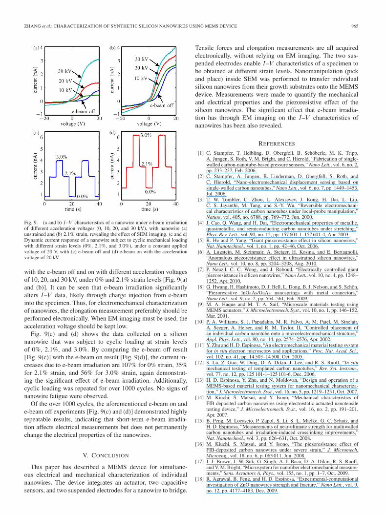
Fig. 9. (a and b) I–V characteristics of a nanowire under e-beam irradiationof different acceleration voltages (0, 10, 20, and 30 kV), with nanowire (a)unstrained and (b) 2.1% strain, revealing the effect of SEM imaging. (c and d)Dynamic current response of a nanowire subject to cyclic mechanical loadingwith different strain levels (0%, 2.1%, and 3.0%), under a constant appliedvoltage of 20 V, with (c) e-beam off and (d) e-beam on with the accelerationvoltage of 20 kV.
with the e-beam off and on with different acceleration voltagesof 10, 20, and 30 kV, under 0% and 2.1% strain levels [Fig. 9(a)and (b)]. It can be seen that e-beam irradiation significantlyalters I–V data, likely through charge injection from e-beaminto the specimen. Thus, for electromechanical characterizationof nanowires, the elongation measurement preferably should beperformed electronically. When EM imaging must be used, theacceleration voltage should be kept low.
Fig. 9(c) and (d) shows the data collected on a siliconnanowire that was subject to cyclic loading at strain levelsof 0%, 2.1%, and 3.0%. By comparing the e-beam off result[Fig. 9(c)] with the e-beam on result [Fig. 9(d)], the current in-creases due to e-beam irradiation are 107% for 0% strain, 35%for 2.1% strain, and 56% for 3.0% strain, again demonstrat-ing the significant effect of e-beam irradiation. Additionally,cyclic loading was repeated for over 1000 cycles. No signs ofnanowire fatigue were observed.
Of the over 1000 cycles, the aforementioned e-beam on ande-beam off experiments [Fig. 9(c) and (d)] demonstrated highlyrepeatable results, indicating that short-term e-beam irradia-tion affects electrical measurements but does not permanentlychange the electrical properties of the nanowires.
V. CONCLUSION
This paper has described a MEMS device for simultane-ous electrical and mechanical characterization of individualnanowires. The device integrates an actuator, two capacitivesensors, and two suspended electrodes for a nanowire to bridge.
Tensile forces and elongation measurements are all acquiredelectronically, without relying on EM imaging. The two sus-pended electrodes enable I–V characteristics of a specimen tobe obtained at different strain levels. Nanomanipulation (pickand place) inside SEM was performed to transfer individualsilicon nanowires from their growth substrates onto the MEMSdevice. Measurements were made to quantify the mechanicaland electrical properties and the piezoresistive effect of thesilicon nanowires. The significant effect that e-beam irradia-tion has through EM imaging on the I–V characteristics ofnanowires has been also revealed.
REFERENCES
[1] C. Stampfer, T. Helbling, D. Obergfell, B. Schöberle, M. K. Tripp,A. Jungen, S. Roth, V. M. Bright, and C. Hierold, “Fabrication of single-walled carbon-nanotube-based pressure sensors,” Nano Lett., vol. 6, no. 2,pp. 233–237, Feb. 2006.
[2] C. Stampfer, A. Jungen, R. Linderman, D. Obergfell, S. Roth, andC. Hierold, “Nano-electromechanical displacement sensing based onsingle-walled carbon nanotubes,” Nano Lett., vol. 6, no. 7, pp. 1449–1453,Jul. 2006.
[3] T. W. Tombler, C. Zhou, L. Alexseyev, J. Kong, H. Dai, L. Liu,C. S. Jayanthi, M. Tang, and S.-Y. Wu, “Reversible electromechani-cal characteristics of carbon nanotubes under local-probe manipulation,”Nature, vol. 405, no. 6788, pp. 769–772, Jun. 2000.
[4] J. Cao, Q. Wang, and H. Dai, “Electromechanical properties of metallic,quasimetallic, and semiconducting carbon nanotubes under stretching,”Phys. Rev. Lett., vol. 90, no. 15, pp. 157 601-1–157 601-4, Apr. 2003.
[5] R. He and P. Yang, “Giant piezoresistance effect in silicon nanowires,”Nat. Nanotechnol., vol. 1, no. 1, pp. 42–46, Oct. 2006.
[6] A. Lugstein, M. Steinmair, A. Steiger, H. Kosina, and E. Bertagnolli,“Anomalous piezoresistance effect in ultrastrained silicon nanowires,”Nano Lett., vol. 10, no. 8, pp. 3204–3208, Aug. 2010.
[7] P. Neuzil, C. C. Wong, and J. Reboud, “Electrically controlled giantpiezoresistance in silicon nanowires,” Nano Lett., vol. 10, no. 4, pp. 1248–1252, Apr. 2010.
[8] G. Hwang, H. Hashimoto, D. J. Bell, L. Dong, B. J. Nelson, and S. Schön,“Piezoresistive InGaAs/GaAs nanosprings with metal connectors,”Nano Lett., vol. 9, no. 2, pp. 554–561, Feb. 2009.
[9] M. A. Haque and M. T. A. Saif, “Microscale materials testing usingMEMS actuators,” J. Microelectromech. Syst., vol. 10, no. 1, pp. 146–152,Mar. 2001.
[10] P. A. Williams, S. J. Papadakis, M. R. Falvo, A. M. Patel, M. Sinclair,A. Seeger, A. Helser, and R. M. Taylor, II, “Controlled placement ofan individual carbon nanotube onto a microelectromechanical structure,”Appl. Phys. Lett., vol. 80, no. 14, pp. 2574–2576, Apr. 2002.
[11] Y. Zhu and H. D. Espinosa, “An electromechanical material testing systemfor in situ electron microscopy and applications,” Proc. Nat. Acad. Sci.,vol. 102, no. 41, pp. 14 503–14 508, Oct. 2005.
[12] S. Lu, Z. Guo, W. Ding, D. A. Dikin, J. Lee, and R. S. Ruoff, “In situmechanical testing of templated carbon nanotubes,” Rev. Sci. Instrum.,vol. 77, no. 12, pp. 125 101-1–125 101-6, Dec. 2006.
[13] H. D. Espinosa, Y. Zhu, and N. Moldovan, “Design and operation of aMEMS-based material testing system for nanomechanical characteriza-tion,” J. Microelectromech. Syst., vol. 16, no. 5, pp. 1219–1231, Oct. 2007.
[14] M. Kiuchi, S. Matsui, and Y. Isono, “Mechanical characteristics ofFIB deposited carbon nanowires using electrostatic actuated nanotensiletesting device,” J. Microelectromech. Syst., vol. 16, no. 2, pp. 191–201,Apr. 2007.
[15] B. Peng, M. Locascio, P. Zapol, S. Li, S. L. Mielke, G. C. Schatz, andH. D. Espinosa, “Measurements of near-ultimate strength for multiwalledcarbon nanotubes and irradiation-induced crosslinking improvements,”Nat. Nanotechnol., vol. 3, pp. 626–631, Oct. 2008.
[16] M. Kiuchi, S. Matsui, and Y. Isono, “The piezoresistance effect ofFIB-deposited carbon nanowires under severe strain,” J. Micromech.Microeng., vol. 18, no. 6, p. 065 011, Jun. 2008.
[17] J. J. Brown, J. W. Suk, G. Singh, A. I. Baca, D. A. Dikin, R. S. Ruoff,and V. M. Bright, “Microsystem for nanofiber electromechanical measure-ments,” Sens. Actuators A, Phys., vol. 155, no. 1, pp. 1–7, Oct. 2009.
[18] R. Agrawal, B. Peng, and H. D. Espinosa, “Experimental-computationalinvestigation of ZnO nanowires strength and fracture,” Nano Lett., vol. 9,no. 12, pp. 4177–4183, Dec. 2009.
966 JOURNAL OF MICROELECTROMECHANICAL SYSTEMS, VOL. 20, NO. 4, AUGUST 2011
[19] D. Zhang, J.-M. Breguet, R. Clavel, L. Phillippe, I. Utke, andJ. Michler, “In situ tensile testing of individual Co nanowires insidea scanning electron microscope,” Nanotechnology, vol. 20, no. 36,p. 365 706, Sep. 2009.
[20] D. Zhang, J.-M. Breguet, R. Clavel, V. Sivakov, S. Christiansen, andJ. Michler, “In situ electron microscopy mechanical testing of siliconnanowires using electrostatically actuated tensile stages,” J. Microelectro-mech. Syst., vol. 19, no. 3, pp. 663–674, Jun. 2010.
[21] M. A. Haque, H. D. Espinosa, and H. J. Lee, “MEMS for in situtesting—Handling, actuation, loading, and displacement measurements,”MRS Bull., vol. 35, pp. 375–381, May 2010.
[22] J. Brown, A. Baca, K. Bertness, D. Dikin, R. Ruoff, and V. Bright, “Tensilemeasurement of single crystal gallium nitride nanowires on MEMS teststages,” Sens. Actuators A, Phys., vol. 166, no. 2, pp. 177–186, Apr. 2011.DOI:10.1016/j.sna.2010.04.002.
[23] W. Kang, J. H. Han, and M. T. A. Saif, “A novel method for in situ uniaxialtests at the micro/nano scale—Part II: Experiment,” J. Microelectromech.Syst., vol. 19, no. 6, pp. 1322–1330, Dec. 2010.
[24] R. A. Bernal, R. Agrawal, B. Peng, K. A. Bertness, N. A. Sanford,A. V. Davydov, and H. D. Espinosa, “Effect of growth orientation anddiameter on the elasticity of GaN nanowires. A combined in situ TEM andatomistic modeling investigation,” Nano Lett., vol. 11, no. 2, pp. 548–555,Feb. 2011. dx.doi.org/10.1021/nl103450e.
[25] Z. Zhang, K. Yao, Y. Liu, C. Jin, X. Liang, Q. Chen, and L.-M. Peng,“Quantitative analysis of current–voltage characteristics of semiconduct-ing nanowires: Decoupling of contact effects,” Adv. Funct. Mater., vol. 17,no. 14, pp. 2478–2489, Sep. 2007.
[26] S. Yoshimoto, Y. Murata, K. Kubo, K. Tomita, K. Motoyoshi, T. Kimura,H. Okino, R. Hobara, I. Matsuda, S. Honda, M. Katayama, andS. Hasegawa, “Four-point probe resistance measurements usingPtIr-coated carbon nanotube tips,” Nano Lett., vol. 7, no. 4, pp. 956–959,Apr. 2007.
[27] C. Ru, Y. Zhang, Y. Sun, Y. Zhong, X. Sun, D. Hoyle, and I. Cotton,“Automated four-point probe measurement of nanowires inside a scanningelectron microscope,” IEEE Trans. Nanotechnol., vol. 10, no. 4, pp. 674–681, Jul. 2011
[28] T.-H. Kim, X.-G. Zhang, D. M. Nicholson, B. M. Evans, N. S. Kulkarni,B. Radhakrishnan, E. A. Kenik, and A.-P. Li, “Large discrete resistancejump at grain boundary in copper nanowire,” Nano Lett., vol. 10, no. 8,pp. 3096–3100, Aug. 2010.
[29] Y. Zhang, B. K. Chen, X. Liu, and Y. Sun, “Autonomous robotic pick-and-place of microobjects,” IEEE Trans. Robot., vol. 26, no. 1, pp. 200–207,Feb. 2010.
[30] M. A. Haque and M. T. A. Saif, “Deformation mechanisms in free-standing nanoscale thin films: A quantitative in situ transmission electronmicroscope study,” Proc. Nat. Acad. Sci., vol. 101, no. 17, pp. 6335–6340,Apr. 2004.
[31] S. Lu, J. Chung, and R. S. Ruoff, “Controlled deposition of nanotubeson opposing electrodes,” Nanotechnology, vol. 16, no. 9, pp. 1765–1770,Sep. 2005.
[32] B. D. Sosnowchik, J. Chang, and L. Lin, “Pick, break, and place-ment of one-dimensional nanostructures for direct assembly and inte-gration,” Appl. Phys. Lett., vol. 96, no. 15, pp. 153 101-1–153 101-3,Apr. 2010.
[33] Y. Ganesan, Y. Lu, C. Peng, H. Lu, R. Ballarini, and J. Lou, “Developmentand application of a novel microfabricated device for the in situ tensiletesting of 1-D nanomaterials,” J. Microelectromech. Syst., vol. 19, no. 3,pp. 675–682, Jun. 2010.
[34] Y. Ganesan, C. Peng, Y. Lu, L. Ci, A. Srivastava, P. M. Ajayan, andJ. Lou, “Effect of nitrogen doping on the mechanical properties of carbonnanotubes,” ACS Nano, vol. 4, no. 12, pp. 7637–7643, Dec. 2010.
[35] Y. Hu, J. Zhou, P.-H. Yeh, Z. Li, T.-Y. Wei, and Z. L. Wang, “Super-sensitive, fast-response nanowire sensors by using Schottky contacts,”Adv. Mater., vol. 22, no. 30, pp. 3327–3332, Aug. 2010.
[36] M.-F. Yu, O. Lourie, O. Lourie, K. Moloni, T. F. Kelly, andR. S. Ruoff, “Strength and breaking mechanism of multiwalled carbonnanotubes under tensile load,” Science, vol. 287, no. 5453, pp. 637–640,Jan. 2000.
[37] T. Fukuda, F. Arai, and L. Dong, “Assembly of nanodevices with car-bon nanotubes through nanorobotic manipulations,” Proc. IEEE, vol. 91,no. 11, pp. 1803–1818, Nov. 2003.
[38] T. Fukuda, M. Nakajima, P. Liu, and H. ElShimy, “Nanofabrication,nanoinstrumentation and nanoassembly by nanorobotic manipulation,”Int. J. Robot. Res., vol. 28, no. 4, pp. 537–547, Apr. 2009.
[39] M. J. Gordon, T. Baron, F. Dhalluin, P. Gentile, and P. Ferret, “Sizeeffects in mechanical deformation and fracture of cantilevered siliconnanowires,” Nano Lett., vol. 9, no. 2, pp. 525–529, Feb. 2009.
[40] Z. Y. Zhang, C. H. Jin, X. L. Liang, Q. Chen, and L.-M. Peng,“Current–voltage characteristics and parameter retrieval of semiconduct-ing nanowires,” Appl. Phys. Lett, vol. 88, no. 7, pp. 073 102-1–073 102-3,Feb. 2006.
[41] Y.-F. Lin and W.-B. Jian, “The impact of nanocontact on nanowire basednanoelectronics,” Nano Lett., vol. 8, no. 10, pp. 3146–3150, Oct. 2008.
[42] A. Asthana, T. Shokuhfar, Q. Gao, P. Heiden, C. Friedrich, andR. S. Yassar, “A study on the modulation of the electrical transport by me-chanical straining of individual titanium dioxide nanotube,” Appl. Phys.Lett, vol. 97, no. 7, pp. 072 107-1–072 107-3, Aug. 2010.
[43] A. A. Grinberg, S. Luryi, M. R. Pinto, and N. L. Schryer, “Space-charge-limited current in a film,” IEEE Trans. Electron Devices, vol. 36, no. 6,pp. 1162–1170, Jun. 1989.
Yong Zhang (S’09) received the B.S. and M.S.degrees in mechatronics engineering from HarbinInstitute of Technology, Harbin, China, in 2005 and2007, respectively. He is currently working towardthe Ph.D. degree in the Department of Electricaland Computer Engineering, University of Toronto,Toronto, ON, Canada.
His research interests include manipulation andcharacterization of micrometer- and nanometer-sizedmaterials using microelectromechanical systems androbotics.
Xinyu Liu (S’06–M’10) received the B.Eng. andM.Eng. degrees in mechanical engineering fromHarbin Institute of Technology, Harbin, China, in2002 and 2004, respectively, and the Ph.D. degreein mechanical engineering from the University ofToronto, Toronto, ON, Canada, in 2009.
He was a Postdoctoral Fellow in the Departmentof Chemistry and Chemical Biology, Harvard Uni-versity, Cambridge, MA. He is currently an AssistantProfessor in the Department of Mechanical Engi-neering, McGill University, Montreal, QC, Canada.
His research interests are design and fabrication of microelectromechanical sys-tems devices, micro- and nanorobotic manipulation of bio- and nanomaterials,low-cost diagnostic technologies for the developing world, and microfluidicsfor bioapplications.
Changhai Ru (M’07) received the Ph.D. degree inmechatronics engineering from Harbin Institute ofTechnology, Harbin, China, in 2005.
He was a Postdoctoral Fellow in the Department ofMechanical and Industrial Engineering, Universityof Toronto, Toronto, ON, Canada. He is currently aProfessor at the Robotics and Microsystems Center,Soochow University, Suzhou, China. His research in-terests include micro-/nanomanipulation, nanoposi-tioning technology, and solid-state actuators’ drivingand control methods.
Yan Liang Zhang (M’10) received the B.Eng.degree in computer engineering and the Ph.D. de-gree in mechanical and aerospace engineering fromNanyang Technological University, Singapore, in2006 and 2010, respectively.
He is currently a Postdoctoral Fellow in the De-partment of Mechanical and Industrial Engineering,University of Toronto, Toronto, ON, Canada. Hisresearch interests include cell mechanobiology, ro-botics automation under optical and electron micro-scopes for micro-/nanomanipulation, and fabrication
and characterization of nanodevices.
ZHANG et al.: CHARACTERIZATION OF SYNTHETIC SILICON NANOWIRES USING MEMS DEVICE 967
Lixin Dong (S’01–M’03–SM’10) received the B.S.and M.S. degrees in mechanical engineering fromXi’an University of Technology (XUT), Xi’an,China, in 1989 and 1992, respectively, and the Ph.D.degree in microsystems engineering from NagoyaUniversity, Nagoya, Japan, in 2003.
He was with XUT, where he became a ResearchAssociate in 1992, a Lecturer in 1995, and an As-sociate Professor in 1998. In 2003, he became anAssistant Professor at Nagoya University. In 2004,he joined the Swiss Federal Institute of Technology
Zürich (ETH Zürich), Zürich, Switzerland, as a Research Scientist, wherehe became a Senior Research Scientist in 2005 and led the NanoRoboticsGroup, Institute of Robotics and Intelligent Systems. Since December 2008,he has been an Assistant Professor at Michigan State University, East Lansing.His current research interests include nanorobotics, nanoelectromechanicalsystems, mechatronics, mechanochemistry, and nanobiomedical devices.
Yu Sun (S’01–M’03–SM’07) received the B.S.degree in electrical engineering from Dalian Uni-versity of Technology, Dalian, China, in 1996,the M.S. degree from Institute of Automation,Chinese Academy of Sciences, Beijing, China, in1999, and the M.S. degree in electrical engineeringand the Ph.D. degree in mechanical engineering fromthe University of Minnesota, Minneapolis, in 2001and 2003, respectively.
He is currently an Associate Professor in the De-partment of Mechanical and Industrial Engineering
and is jointly appointed in the Institute of Biomaterials and BiomedicalEngineering and the Department of Electrical and Computer Engineering,University of Toronto, Toronto, ON, Canada. His research areas include thedesign and fabrication of micro- and nanoelectromechanical systems devices,micro-/nanorobotic manipulation, and the manipulation and characterization ofbiological cells, biomolecules, and nanomaterials. He was a Research Scientistat the Swiss Federal Institute of Technology Zürich (ETH Zürich), Zürich,Switzerland, before joining the faculty of the University of Toronto in July2004. He is the Canada Research Chair in micro- and nanoengineering systemsand a Guest Chair Professor at Soochow University, Suzhou, China.