Increased Graphitization in Electrospun Single Suspended Carbon Nanowires Integrated with...
6
Increased Graphitization in Electrospun Single Suspended Carbon Nanowires Integrated with Carbon-MEMS and Carbon-NEMS Platforms Swati Sharma, † Ashutosh Sharma,* ,‡ Yoon-Kyoung Cho, † and Marc Madou* ,§ † School of Nano-Bioscience and Chemical Engineering, Ulsan National Institute of Science and Technology, Ulsan 689-798, South Korea ‡ Department of Chemical Engineering, Indian Institute of Technology, Kanpur 208016, U.P., India § Department of Mechanical & Aerospace Engineering, University of California, Irvine, California, United States 92697-3975 ABSTRACT: Single suspended carbon nanowires (CNWs) integrated on carbon-MEMS (CMEMS) structures are fabricated by electrospinning of SU-8 photoresist followed by pyrolysis. These monolithic CNW-CMEMS structures enable fabrication of very high aspect ratio CNWs of predefined length. The CNWs thus fabricated display core− shell structures having a graphitic shell with a glassy carbon core. The electrical conductivity of these CNWs is increased by about 100% compared to glassy carbon as a result of enhanced graphitization. We suggest some tunable fabrication and pyrolysis parameters that may improve graphitization in the resulting CNWs, making them a good replacement for several carbon nanostructure-based devices. KEYWORDS: carbon nanowire, carbon-MEMS, photolithography, electrospinning, graphitization I n the past two decades, carbon has received much attention as a material to possibly compete with silicon for the construction of miniaturized devices such as ICs and micro- and nano-electromechanical systems (MEMS and NEMS). 1−6 Carbon occupies a very special place both in nature and technology because of the widely different structures and properties of its various forms. 7−9 Glassy carbon electrodes offer a wide electrochemical stability window, low-background currents, and low cost. 1,10,11 Graphitic and hard carbons in battery applications are well suited because of their reversible Li intercalation/deintercalation capacity. 12 Further, carbon nano- tubes (CNTs), graphene and carbons with higher graphitic content are of tremendous current interest in both fundamental research and for nanoelectronics applications. 13−17 Here we introduce CMEMS and CNEMS platforms as a means of fabrication, positioning, and integration of single suspended carbon nanowires (CNWs) with good and reproducible ohmic contacts. The main challenges in the fabrication of single CNW or CNT based devices are their positioning and integration with the underlying platforms and in establishing a reliable ohmic contact. In most cases, the nanowires are first synthesized and isolated, and then carefully nanopositioned and integrated, e.g., by placing on a flat substrate followed by deposition of metal electrodes over their ends. 18−20 These are cumbersome and low-throughput techniques that are not suitable for manufactur- ing of solid-state devices. Also, the contact resistance varies from sample to sample and the contact with the substrate can interfere with the properties of the nanowires. Here we present a simple and scalable fabrication technique for positioning and integration of suspended CNWs with good ohmic contacts. This technique enables fabrication of single, well separated CNWs that are pulled in tension on the CMEMS, and isolation of a single CNW from bulk is not required. This is achieved by electrospining of polymer nanowires on an underlying polymeric MEMS platform fixed on a rotating drum, followed by pyrolysis of the suspended nanowires plus their platform to produce a carbon monolith. The current technique enables the fabrication of CNWs of predefined lengths at preselected locations of interest, which are difficult to achieve with other methods. Further, we show that this method produces CNWs of higher graphitic content and electrical conductivity than glassy carbon and the extent of graphitization can be tuned by controlling the fabrication parameters. It is known that in the pyrolysis process, polymer precursors retain their original morphology and chain configurations. 21 Therefore, it is extremely important to first obtain polymer nanofibers with maximized chain disentanglements in order to get more graphitic resulting CNWs. Tangled polymer chains yield glassy carbons that cannot be reverted back to graphite even at very high temperatures, 21−23 because it is not possible to unwind the polymer chains once converted to carbon. The parameters that may influence the extent of disen- tanglement of polymer chains, and in turn, the extent of Received: October 18, 2011 Accepted: January 3, 2012 Published: January 3, 2012 Letter www.acsami.org © 2012 American Chemical Society 34 dx.doi.org/10.1021/am2014376 | ACS Appl. Mater. Interfaces 2012, 4, 34−39
Transcript of Increased Graphitization in Electrospun Single Suspended Carbon Nanowires Integrated with...
Increased Graphitization in Electrospun Single Suspended CarbonNanowires Integrated with Carbon-MEMS and Carbon-NEMSPlatformsSwati Sharma,† Ashutosh Sharma,*,‡ Yoon-Kyoung Cho,† and Marc Madou*,§
†School of Nano-Bioscience and Chemical Engineering, Ulsan National Institute of Science and Technology, Ulsan 689-798, SouthKorea‡Department of Chemical Engineering, Indian Institute of Technology, Kanpur 208016, U.P., India§Department of Mechanical & Aerospace Engineering, University of California, Irvine, California, United States 92697-3975
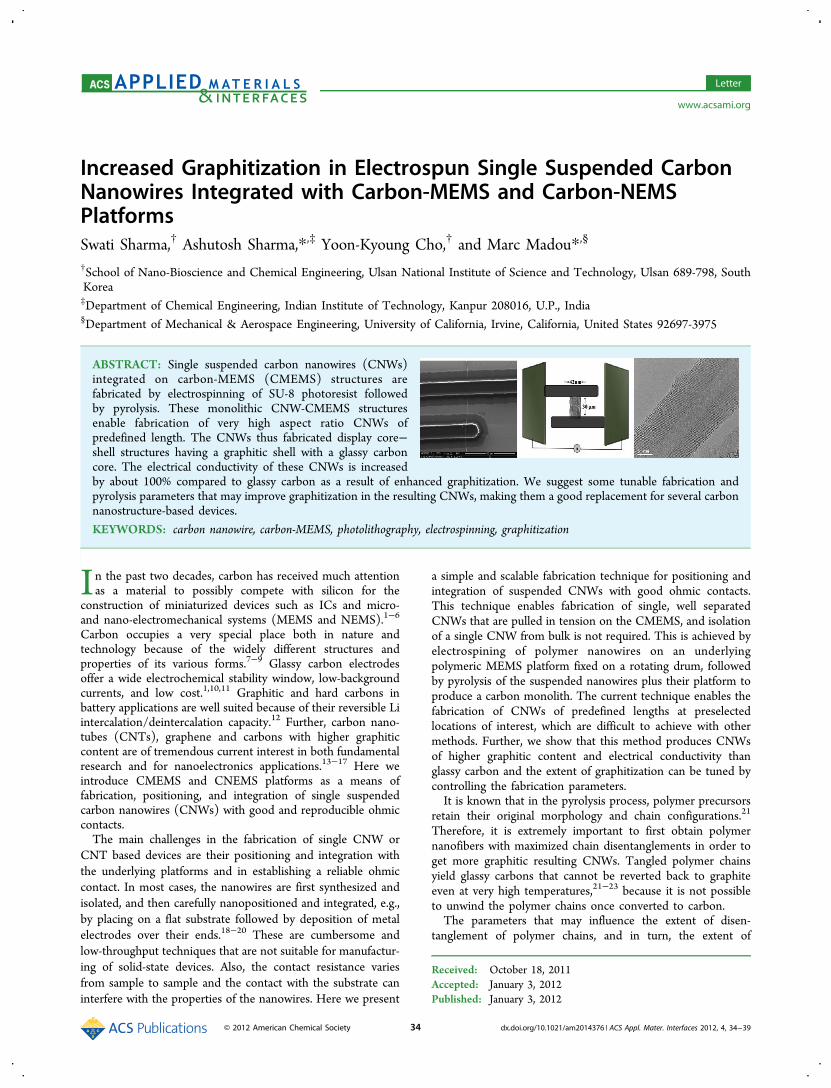
ABSTRACT: Single suspended carbon nanowires (CNWs)integrated on carbon-MEMS (CMEMS) structures arefabricated by electrospinning of SU-8 photoresist followedby pyrolysis. These monolithic CNW-CMEMS structuresenable fabrication of very high aspect ratio CNWs ofpredefined length. The CNWs thus fabricated display core−shell structures having a graphitic shell with a glassy carboncore. The electrical conductivity of these CNWs is increasedby about 100% compared to glassy carbon as a result of enhanced graphitization. We suggest some tunable fabrication andpyrolysis parameters that may improve graphitization in the resulting CNWs, making them a good replacement for several carbonnanostructure-based devices.
KEYWORDS: carbon nanowire, carbon-MEMS, photolithography, electrospinning, graphitization
In the past two decades, carbon has received much attentionas a material to possibly compete with silicon for the
construction of miniaturized devices such as ICs and micro-and nano-electromechanical systems (MEMS and NEMS).1−6
Carbon occupies a very special place both in nature andtechnology because of the widely different structures andproperties of its various forms.7−9 Glassy carbon electrodesoffer a wide electrochemical stability window, low-backgroundcurrents, and low cost.1,10,11 Graphitic and hard carbons inbattery applications are well suited because of their reversible Liintercalation/deintercalation capacity.12 Further, carbon nano-tubes (CNTs), graphene and carbons with higher graphiticcontent are of tremendous current interest in both fundamentalresearch and for nanoelectronics applications.13−17 Here weintroduce CMEMS and CNEMS platforms as a means offabrication, positioning, and integration of single suspendedcarbon nanowires (CNWs) with good and reproducible ohmiccontacts.The main challenges in the fabrication of single CNW or
CNT based devices are their positioning and integration withthe underlying platforms and in establishing a reliable ohmiccontact. In most cases, the nanowires are first synthesized andisolated, and then carefully nanopositioned and integrated, e.g.,by placing on a flat substrate followed by deposition of metalelectrodes over their ends.18−20 These are cumbersome andlow-throughput techniques that are not suitable for manufactur-ing of solid-state devices. Also, the contact resistance variesfrom sample to sample and the contact with the substrate caninterfere with the properties of the nanowires. Here we present
a simple and scalable fabrication technique for positioning andintegration of suspended CNWs with good ohmic contacts.This technique enables fabrication of single, well separatedCNWs that are pulled in tension on the CMEMS, and isolationof a single CNW from bulk is not required. This is achieved byelectrospining of polymer nanowires on an underlyingpolymeric MEMS platform fixed on a rotating drum, followedby pyrolysis of the suspended nanowires plus their platform toproduce a carbon monolith. The current technique enables thefabrication of CNWs of predefined lengths at preselectedlocations of interest, which are difficult to achieve with othermethods. Further, we show that this method produces CNWsof higher graphitic content and electrical conductivity thanglassy carbon and the extent of graphitization can be tuned bycontrolling the fabrication parameters.It is known that in the pyrolysis process, polymer precursors
retain their original morphology and chain configurations.21
Therefore, it is extremely important to first obtain polymernanofibers with maximized chain disentanglements in order toget more graphitic resulting CNWs. Tangled polymer chainsyield glassy carbons that cannot be reverted back to graphiteeven at very high temperatures,21−23 because it is not possibleto unwind the polymer chains once converted to carbon.The parameters that may influence the extent of disen-
tanglement of polymer chains, and in turn, the extent of
Received: October 18, 2011Accepted: January 3, 2012Published: January 3, 2012
Letter
www.acsami.org
© 2012 American Chemical Society 34 dx.doi.org/10.1021/am2014376 | ACS Appl. Mater. Interfaces 2012, 4, 34−39

graphitization in the CNWs include (1) nature of the precursorpolymer (e.g., its chemical composition and viscoelasticity),24
(2) thickness of the polymer wires,25 (3) carbonizationtemperature,22 (4) alignment of polymer molecules by theflow pattern of the polymer and nozzle size,25,26 (5) mechanicalpulling of the polymer molecules,27,28 (6) alignment ofpolymers chains caused by high electric fields,29 (7) catalystsin the precursor polymer,30 and (8) templating.31,32
In addition to these reported parameters, we believe thatmechanical pulling of the suspended polymer nanofiber is alsoaffected in other ways. For example, during the carbonizationprocess itself, say when employing SU-8 walls to hold the fiber,the shrinkage of these walls to almost one forth their originalsize (horizontally) gives an extra pull to the suspended fibers.We chose to work further with SU-8 derived nanowires becauseit is the material of choice for MEMS fabrication, allowing awider range of MEMS structures with tunable designs due to itscompatibility with conventional photolithography. Further, SU-8 fibers should display better adhesion and integration with SU-8 MEMS structures because of the same glass transitiontemperature of both. Also, because of the very low electricalconductivity of SU-8 fibers, the high voltages applied duringelectrospinning exert an extra mechanical force on the polymernanofibers during their formation, stretching and disentanglingthe polymer chains. Moreover, carbonization of one-dimen-sional, suspended polymer structures, with all surfaces exposedduring pyrolysis, is bound to give a different morphology thansurface attached structures. Finally, making the wires shortergives one a higher probability of obtaining CNWs that containcontinuous graphite sheets without defects or bending ofgraphitic planes from contact to contact (explained in detailwith HR-TEM pictures, Figure 3). Figure 3A−D illustrates fourdifferent types of CNWs that can be observed in the samebatch of fibers. Most CNWs have core−shell geometry.However, the thickness of graphitic shell may slightly varybecause the distribution of polymer chains may not be uniformat nanoscale in the polymer solution itself. Images E and F inFigure 3 display HR-TEM images of pure graphite and glassycarbon, and it can be clearly observed that carbon chains formloops in polymer derived glassy carbons and it is almostimpossible to disentangle them after carbonization.These parameters are not necessarily independent; nor are
their relative importance in enhancing the graphitic content ofthe wires known. Our group has started to address the relativeinfluence of these different parameters on the extent ofgraphitization. In a previous work, we discussed the results ofconductivity measurements on single suspended CNWs derivedfrom two different polymers (parameter 1).24 The carbon fibersstudied were only moderately stretched with diameters ∼200nm (parameter 6), and no additional mechanical stretching(parameter 5) was employed during fabrication. The relativelylarge diameters also did not allow elucidation of nanoconfine-ment or surface effects.In the current paper we emphasize fabrication of structures
for use in evaluating the influence of parameters 4, 5, and 6 andthe additional plausible parameters listed above by monitoringthe change in resistance and structural changes in the fabricatedCNWs. Besides impedance measurements, high-resolutiontransmission electron microscopy (HR-TEM), Raman spec-troscopy, X-ray diffraction (XRD), and scanning electronmicroscopy (SEM) were carried out to correlate nanowirestructure with resistance data.
A typical MEMS structure featuring SU-8 walls that was usedto anchor electrospun suspended nanowires is schematicallyshown in Figure 1A. In this design, two SU-8 contact pads (5.0
mm × 5.0 mm) are connected to two SU-8 walls 20 μm widewith a 20 μm gap in between. The SU-8 posts are about 10 μmhigh, which shrink to ∼2 μm height after pyrolysis. In Figure1B, we schematically illustrate photoelectrospinning of SU-8 onan SU-8 MEMS structure employing a rotating drum collector,whereas in Figure 1C we display a Si chip (2 cm × 1 cm)patterned with a CNW-CMEMS structure that is obtained bythe pyrolysis of the polymer precursor structures. The rotatingdrum forces the fibers to follow a straight pattern that we orientperpendicularly to the electrodes, and because of the drum’srotation, the fibers remain taut without touching the substrate.Flow and electrical field are both expected to facilitate
molecular disentanglement (parameters 4 and 5). And as wealso speculate here the rotating drum introduces a considerableadditional mechanical pull on the nanowires that may furtherenhance graphitization by molecular combing (parameter 6).In case more than one carbon nanofiber linked the walls, the
extra fibers were cut using a gallium ion beam dual focused ionbeam (FIB) system. The MEMS design employed in ourfabrication has 2 mm long overlapping electrodes. The numberof fibers linking these electrodes can be controlled by reducingthe time of electrospinning and the overlapping area of theelectrodes. In this study we perform electrospinning for 3−5seconds, which yields a single CNW in most cases. However, iftwo fibers fallen at the same time connect the electrodes, theundesired extra fiber can be cut using FIB.The FIB wire cutting is illustrated in Figure 2A. After
confirming that only one suspended carbon wire remained, the
Figure 1. (A) 2D representation of SU-8 MEMS structure used asbase structure for electrospinning nanofibers. Both thickness and thegap between two stripes are 20 μm. (B) Use of rotating drum ascollector for electrospinning SU-8 nanofibers on SU-8 MEMS chip.(C) Final chip-based CMEMS-CNW design on a Si chip fabricated asdescribed in A and B and pyrolyzed at 900 °C (electrical connectionswere made only after pyrolysis).
ACS Applied Materials & Interfaces Letter
dx.doi.org/10.1021/am2014376 | ACS Appl. Mater. Interfaces 2012, 4, 34−3935

carbon electrode pads were connected to Cu wires with silverpaste that then were connected to an impedance analyzer(Figure 1C). Figure 2B shows a typical I−V curve for a 42.2 nmthick and ∼29 μm long single suspended CNW obtained usingthe impedance analyzer connected to the measuring chip(illustrated in Figure 1C). The structures of these CNWs werefurther characterized with SEM, Raman spectroscopy, XRD,and HR-TEM imaging.Typical SEM images of single suspended CNWs are shown
in Figure 2C−E. In Figure 2C, D, a 42.22 nm thick nanowirewith a length of ∼29 μm is shown. It can be observed in Figure3D that the CNWs have a very uniform geometry. However, toaccount for any experimental or imaging error in determiningthe diameter of CNWs, we took SEM pictures at 3−4 differentpoints along the length of the wire. Uniformity of the wires towithin 10% was observed. In Figure 2E, a lower-magnificationSEM image illustrates the adhesion of a typical CNW onto thecarbon walls. As the SU-8 MEMS structure and suspended SU-8 nanowire are pyrolyzed together, this technique yields CNWswith very good adhesion to the walls. Also, the electricalmeasurements confirm that an ohmic contact between wire andwalls is realized automatically without the need for any othercontacting metal or further sintering.The linearity of all I−V curves thus obtained is evidence for
the ohmicity of the carbon-to-carbon contacts. In Table 1 wecompare the electrical conductivity values of five different
diameter wires as obtained from the slope of I−V curves. Whilecalculating the conductivity values, length, and diameters ofCNWs were accounted for. We observe that for the CNWs indiameter range 42−113, the conductivity is a materials propertyand thus remains constant.The average value for the electrical conductivity of the
CNWs was found to be 6.13 × 10⁴, which is almost twice thatof glassy carbon (2.8 × 10⁴).33 The reported electricalconductivity values for graphite range from 2.4 × 10⁴ to 1.02× 10⁵ observed parallel and perpendicular to the C-axis,respectively.34 Our experimental conductivity values are lowerthan graphite but higher than glassy carbon. These resultsindicated that electrospun SU-8 derived CNWs fabricated withadditional mechanical pulling are not composed entirely ofglassy carbon. On the basis of previous CMEMS work2 withcarbonization of SU-8, one expects that the resulting carbonwould be completely glassy in nature and that the suspendedcarbon wires would shrink by approximately 80−90% of theoriginal polymer wire diameter. However, these wires shrunkonly by approximately 30% of the original wire diameter asconfirmed by SEM images. These unexpected observations onelectrical conductivity and shrinkage during pyrolysis led us toinvestigate the structure and composition of the CNWs. Anearlier study24 reported a lower value for the SU-8 derivedcarbon wires of ∼200 nm diameter, which was most likely dueto their higher contact resistance as they could not be spun and
Figure 2. (A) FIB cutting for extra CNWs. (B) Typical I−V curve for a single suspended CNW. (C, D) SEM images displaying (C) the diameterand (D) length of a single suspended CNW. (E) Low-magnification SEM image displaying the adhesion of CNW on to CMEMS electrode walls.
ACS Applied Materials & Interfaces Letter
dx.doi.org/10.1021/am2014376 | ACS Appl. Mater. Interfaces 2012, 4, 34−3936

integrated tightly on to the posts without mechanical action ofpulling on a rotating drum as used here.The HR-TEM images in Figure 3A−D indicate formation of
ordered surface domains with a more disordered glassy core.The presence of a graphitic skin layer could explain the higherconductivity and a lack of greater shrinkage associated with theproduction of glassy carbon. Such structures support thetheoretical model of polymer chain orientation suggested by Ji
Figure 3. (A−D) HR-TEM images of SU-8 derived CNWs: (A) Tubelike graphitic CNW with glassy carbon core and graphite shell. (B) Glassycarbon trapped between graphitic walls in a CNW. (C) Graphite layers bending inward at various segments of a CNW. (D) Tubelike graphitic CNWwith graphite shell not well-formed. (E) Pure graphite obtained from pencil flakes. (F) Pure glassy carbon obtained from a pyrolyzed thick SU-8structure.
Table 1. Comparison of the Conductivity of SU-8 DerivedSingle Suspended CNWs of Different Diameters
diameter of nanowire (nm) observed value of conductivity (S/m)
42.22 6.16 (± 0.23) × 104
71.16 6.96 (± 0.17) × 104
107.0 5.33 (± 0.21) × 104
113.0 6.07 (± 0.19) × 104
ACS Applied Materials & Interfaces Letter
dx.doi.org/10.1021/am2014376 | ACS Appl. Mater. Interfaces 2012, 4, 34−3937

et al.25 With repeated HR-TEM experiments, we also observedbending of graphitic planes (Figure 3C), something that shouldalso influence the conductivity.35
Figure 4A displays the Raman spectra for SU-8 derivedCNWs. The fraction of disordered carbon in these wires
(calculated as the area fraction of the first peak, Id)36 is lower
than the fraction of graphitic carbon (area fraction of thesecond peak, Ig); however, we can observe the presence of bothamorphous and crystalline carbon. The fraction of graphite inthe resulting carbon is 0.61 which indicates that a slightlyhigher amount of graphitic carbon than amorphous is presentin the wires.The results of XRD are represented in Figure 4B. We can
clearly observe the characteristic sharp peak for graphite at 2θvalue 28.37 The diffused peaks appearing at 2θ values 10−23confirm the presence of amorphous or glassy carbon with somedegree of crystallinity.38 These results again confirm thepartially graphitic nature of CNWs.According to Harris,22 carbons obtained from the pyrolysis of
polymers contain six, five and seven membered rings, the lattertwo cause the bending of graphitic planes. This bending effectcan be observed in our HR-TEM pictures (Figure 3C). Itappears that the stretching action of the combined mechanicaland electrostatic forces during electrospinning on a drumgreatly reduces the polymer chain entanglement leading to theiralignment and to more graphitic CNWs. SU-8 has very lowelectrical conductivity and therefore very high voltages areapplied during electrospinning. The charged SU-8 fibers arepulled from both ends by electrical force and this leads to betterelectrical combing leading to chain disentanglements. Incontrast, carbonization of the underlying photolitographicallydefined SU-8 (as in the contacting walls) continues to yieldcompletely glassy carbon as expected. This supports the ideathat the enhanced graphitization of SU-8 derived CNWs is
affected by the fabrication technique used. The improvedgraphitization of the CNWs fabricated here by electrospinningis thus engendered by one or more of the following factors: (1)flow of the polymer/solvent jet with a diameter similar to thatof the gyration radius of the constituent polymer molecules,25
(2) mechanical pulling of fibers during the electrospinning on adrum, (3) high electrical forces employed in electrospinningacting on the charged SU-8 polymer (electrical moleculecombing) and, (4) pyrolysis of a free-standing one- dimensionalstructure instead of an anchored three-dimensional largepolymer structure.In summary, we have demonstrated a method for the
fabrication of sub-50 nm diameter suspended carbon wires ofpredefined length and position by controlled electrospinning.These wires are monolithically integrated with an underlyingCMEMS structure. The method is compatible with standardphotolithography and electrospinning techniques and materials(SU-8 photoresist) allowing for easy integration with massmanufacturing. The most important advantage of ourfabrication methodology is that we obtain a monolithic devicewith no glue or clips required to hold the nanowire in place.This technique is a very simple and inexpensive way forfabricating carbon nanowires with very high aspect ratios. Also,no effort is required for isolation and positioning of a singleCNW from a collection of wires. The wires are free-standingand they are pulled in tension due to the mechanical stretchingcaused by the rotating drum. The stretching of the polymerchains and surface confinement in these CNWs produce agraphitic skin and an amorphous core, thus enhancing theCNW electrical conductivity compared to pure glassy carbon.We also analyzed all the parameters that may improve chaindisentanglements in polymer nanofibers that subsequently leadto more graphitic CNWs. A complete understanding andcontrol over these parameters will enable the production of allgraphite nanowires from contact to contact, i.e., nanocables thatexhibit a band gap equivalent to de Heer et al.’s grapheneribbons.39
■ EXPERIMENTAL SECTIONHigh-resistivity Si wafers (25−40 kΩ) coated with an 800 nmthick layer of thermal SiO2 were utilized as substrates to ensurea completely insulated surface for electrical characterization ofthe carbonized fibers and CMEMS structure. Epoxy-basednegative photoresist, SU-8 2010 (2000 series cyclopentanone-based formulation obtained from Micro Chem, MA) withoutany additional solvents was electrospun to produce SU-8nanofibers on the SU-8 walls. We employed standardphotolithography to fabricate the SU-8 MEMS contactstructures that predefine the length of the electrospun SU-8fibers.2,24 Electrospinning was carried out on a electrospinner(NF Series, MECC, Japan) with a rotating drum collector. Therotating drum collector‘s speed during electrospinning was2000 rpm and MEMS chips were fixed onto the drum withscotch tape. The flow rate of the SU-8 photoresist was 1 mL/hthroughout the short 3−5 s electrospinning process. Thedistance between the polymer jet’s point of initiation and therotating collector was 10 cm. The applied voltage was 22−24kV. In 3−5 s of electrospinning, we typically obtained between1 to 5 nanofibers suspended between the SU-8 walls. The fiberswere exposed to UV light to initiate cross-linking. Pyrolysis ofthese SU-8 nanofibers and SU-8 walls was carried out at 900 °Cfor 1 h in a vacuum furnace (R. D. WEBB 2704, USA); thetemperature ramp up was 1 °C/min.
Figure 4. (A) Raman spectra of SU-8 derived CNWs. (B) XRD datafor SU-8 derived CNWs (Y axis, intensity in a.u.; X axis, 2θ in deg).
ACS Applied Materials & Interfaces Letter
dx.doi.org/10.1021/am2014376 | ACS Appl. Mater. Interfaces 2012, 4, 34−3938
Impedance measurements on the suspended single CNWsranging from 42.2- 113.0 nm in diameter were carried out usinga VSP impedance analyzer (BioLogic, S.Korea). For HR-TEM,Raman spectra, and X- ray diffraction, the samples wereprepared as nanowire mats rather than individual fibers. Anaverage value of graphitization of nanowires in the laser/X-raybeam was calculated. HR-TEM imaging was carried out on aJEM-2100F (Cs) machine (JEOL, Japan), Raman spectra andX- Ray Diffraction patters were obtained on a WITecalpha300R Micro Raman instrument (532 nm) and X’ PertPRO, (PANanalytical, Netherlands) using Cu Kα radiationrespectively. SEM and FIB imaging were carried out on a dualbeam FIB system (Quanta 3D FEG, FEI, USA).There is a major difference in the fabrication method
employed here compared to our earlier work.24 Earlier,electrospinning was done on electrically conducting postswithout a rotating drum.24 The electrospun nanofibers did notconnect to the posts if the posts were not conducting. In thepresent technique, nanowire connections can be formeddirectly on nonconducting SU-8 walls by mechanical means,i.e., action of the rotating collector. The whole structure(underlying SU-8 MEMS platform plus wires) is pyrolyzed afterthe formation of nanowires. The earlier technique24 is thusmore suitable for the formation of large area networks in whichan array of microposts are to be connected by self-assemblyengendered by electrically conducting posts. The currenttechnique, however, appears to be more attractive for a tighterintegration of the nanowires with the underlying microstructureand thus for a more accurate testing of the electrical propertiesof single wires.
■ AUTHOR INFORMATIONCorresponding Author*E-mail: [email protected] (M.M.); [email protected] (A.S.).Tel.: +1-9499815672 (M. M.); +91 512 2597026 (A.S.).
■ ACKNOWLEDGMENTSThis work was supported by World Class University (WCU)program R32-2008-000-20054-0 at UNIST, South Korea; UCLab Fees Award 09-LR-09-117362 at UC, Irvine, CA, USA, andthe Unit on Soft Nanofabrication and IRHPA research grantsfrom the Department of Science and Technology, New Delhi atIIT, Kanpur, India. A.S. and M.M. also acknowledge supportfrom the Indo-US Science and Technology Forum, New Delhi.
■ REFERENCES(1) Kinoshita, K. Carbon: Electrochemical and PhysicochemicalProperties; Wiley: New York, 1988.(2) Wang, C.; Zaouk, R.; Park, B. Y.; Madou, M. J. J. Manuf. Technol.Manage. 2008, 13, 360−375.(3) Gates, B. D.; Xu, Q.; Stewart, M.; Ryan, D.; Willson, C. G.;Whitesides, G. M. Chem. Rev. 2005, 105, 1171−1196.(4) Madou, M. J. Fundamentals of Microfabrication, 1st ed.; CRCPress: Boca Raton, FL, 1997.(5) McCreery, R. Special Issue: Molecular Electronics Interface (TheElectrochem. Soc.) 2004, 13 (1), 46−51.(6) Schueller, O. J. A.; Brittain, S. T.; Whitesides, G. M. Adv. Mater.1997, 9, 477−480.(7) Baughman, R. H.; Zakhidov, A. A.; DeHeer, W. A. Science 2002,297, 787−792.(8) McCreery, R. L. Chem. Rev. 2008, 108, 2646−2687.(9) Dresselhaus, M. S.; Dresselhaus, G.; Avouris, Ph., Eds. CarbonNanotubes; Springer: New York, 2001.(10) Chen, P.; McCreery, R. L. Anal. Chem. 1996, 68, 3958−3965.
(11) Marsh, H.; Heintz, E. A.; Rodrigues-Peinoso, F., Eds.Introduction to Carbon Technologies; University of Alicante: SanVicente del Raspeig, Spain, 1997.(12) Kinoshita, K. New Trends in Electrochemical Technology, Vol. 1:Energy Storage Systems for Electronics; Osaka, T., Datta, M., Eds.;Gordon and Breach, Reading, U.K., 1999; p 193.(13) Bosnick, K.; Gabor, N.; McEuen, P. L. Appl. Phys. Lett. 2006, 89(163121), 1−3.(14) Ilani, S.; Donev, L. A. K.; Kindermann, M.; McEuen, P. L. Nat.Phys. 2006, 2, 687−691.(15) Sazonova, V.; Yaish, Y.; Ustunel, H.; Roundy, D.; Arias, T. A.;McEuen, P. L. Nature 2004, 431, 284−287.(16) DeVolder, M. F. L.; Vansweevelt, R.; Wagner, P.; Reynaerts, D.;Van Hoof, C.; Hart, A. J. ACS Nano 2011, 5 (8), 6593−6600.(17) Chen, W.; Beidaghi, M.; Penmatsa, V.; Bechtold, K.; Kumari, L.;Li, W. Z.; Wang, C. IEEE Trans. Nanotechnol. 2010, 9 (6), 734−740.(18) Chai, Y.; Wu, Y.; Takei, K.; Chen, H. Y.; Yu, S.; Chan, P. C. H.;Javey, A.; Wong, H. S. P. 2010 IEEE International Electron DevicesMeeting (IEDM); San Francisco, Dec 6−8, 2010 ; IEEE: Piscataway,NJ, 2010; pp 214−217.(19) Huang, J; Wan, Q. Sensors 2009, 9, 9903−9924.(20) Bibekananda, S.; Babu, V. J.; Subramanian, V.; Natarajan, T. S. J.Eng. Fibers Fabr. 2008, 3 (4), 39−45.(21) Jenkins, G. M.; Kawamura, K. Nature 1971, 231, 175−176.(22) Harris, P. J. F. Philos. Mag. 2004, 84 (29), 3159−3167.(23) Franklin, R. E. Proc. R. Soc. London, Ser. A 1951, 209, 196−218.(24) Sharma, C. S.; Katepalli, H.; Sharma, A.; Madou, M. J. Carbon2011, 49, 1727−1732.(25) Ji, Y.; Li, C.; Wang, G.; Koo, J.; Ge, S.; Li, B.; Jiang, J.; Herzberg,B.; Klein, T.; Chen, S.; et al. EPL 2008, 84 (56002), 1−6.(26) Ehrenstein, G. W.; Theriault, R. P. Polymeric Materials: Structure,Properties, Applications; Carl Hanser Verlag: Munich, Germany, ; p 67.(27) Ko, F.; Gogotsi, Y.; Ali, A.; Naguib, N.; Ye, H.; Li, C.; Willis, P.Adv. Mater. 2003, 15 (14), 1161−1165.(28) Lozano, K.; Sarkar, K. U.S. Patent 0 280 325 A1 2009.(29) Kim, J. M.; Ohtani, T.; Park, J. Y.; Chang, S. M.; Muramatsu, H.Ultramicroscopy 2002, 91 (1−4), 139−149.(30) Oya, A.; Marsh, H. J. Mater. Sci. 1982, 17, 309−322.(31) Du, R.; Ssenyange, S.; Aktary, M.; McDermott, M. T. Small2009, 5 (10), 1162−1168.(32) Sevilla, M.; Fuertes, A. B. Carbon 2006, 44, 468−474.(33) Serway, R. A.; Faughn, J. S. College Physics, 6th ed.; Thomson:Belmont, CA, 2003.(34) Powell, R. L.; Childs, G. E. American Institute of PhysicsHandbook; McGraw-Hill, New York, 1972; pp 4−142.(35) Dutta, A. K. Phys. Rev. 1953, 90 (2), 187−192.(36) Ra, E. J.; An, K. H.; Kim, K. K.; Jeong, S. Y.; Lee, Y. H. Chem.Phys. Lett. 2005, 413 (1−3), 188−193.(37) Saenger, K. L.; Tsang, J. C.; Bol, A. A.; Chu, J. O.; Grill, A.;Lavoie, C. Appl. Phy. Lett. 2010, 96 (153105), 1−3.(38) Hussain, R.; Qadeer, R.; Ahmad, M.; Saleem, M. Turk. J. Chem.2000, 24, 177−183.(39) DeHeer, W. A.; Berger, C.; First, P. N. U.S. Patent 7 015 142,2006.
ACS Applied Materials & Interfaces Letter
dx.doi.org/10.1021/am2014376 | ACS Appl. Mater. Interfaces 2012, 4, 34−3939