Cyclone III Device Handbook, Volume 1, Section 1. Device Core
86
© December 2009 Altera Corporation Cyclone III Device Handbook, Volume 1 Section 1. Device Core This section provides a complete overview of all features relating to the Cyclone ® III device family, which is the most architecturally advanced, high-performance, low-power FPGA in the market place. This section includes the following chapters: ■ Chapter 1, Cyclone III Device Family Overview ■ Chapter 2, Logic Elements and Logic Array Blocks in the Cyclone III Device Family ■ Chapter 3, Memory Blocks in the Cyclone III Device Family ■ Chapter 4, Embedded Multipliers in the Cyclone III Device Family ■ Chapter 5, Clock Networks and PLLs in the Cyclone III Device Family Revision History Refer to each chapter for its own specific revision history. For information about when each chapter was updated, refer to the Chapter Revision Dates section, which appears in the complete handbook.
-
Upload
khangminh22 -
Category
Documents
-
view
1 -
download
0
Transcript of Cyclone III Device Handbook, Volume 1, Section 1. Device Core

© December 2009 Altera Corporation Cyclone III Device Handbook, Volume 1
Section 1. Device Core
This section provides a complete overview of all features relating to the Cyclone® III device family, which is the most architecturally advanced, high-performance, low-power FPGA in the market place. This section includes the following chapters:
■ Chapter 1, Cyclone III Device Family Overview
■ Chapter 2, Logic Elements and Logic Array Blocks in the Cyclone III Device Family
■ Chapter 3, Memory Blocks in the Cyclone III Device Family
■ Chapter 4, Embedded Multipliers in the Cyclone III Device Family
■ Chapter 5, Clock Networks and PLLs in the Cyclone III Device Family
Revision HistoryRefer to each chapter for its own specific revision history. For information about when each chapter was updated, refer to the Chapter Revision Dates section, which appears in the complete handbook.


© December 2009 Altera Corporation Cyclone III Device Handbook, Volume 1
1. Cyclone III Device Family Overview
Cyclone® III device family offers a unique combination of high functionality, low power and low cost. Based on Taiwan Semiconductor Manufacturing Company (TSMC) low-power (LP) process technology, silicon optimizations and software features to minimize power consumption, Cyclone III device family provides the ideal solution for your high-volume, low-power, and cost-sensitive applications. To address the unique design needs, Cyclone III device family offers the following two variants:
■ Cyclone III: lowest power, high functionality with the lowest cost
■ Cyclone III LS: lowest power FPGAs with security
With densities ranging from 5K to 200K logic elements (LEs) and 0.5 Mbits to 8 Mbits of memory for less than ¼ watt of static power consumption, Cyclone III device family makes it easier for you to meet your power budget. Cyclone III LS devices are the first to implement a suite of security features at the silicon, software, and intellectual property (IP) level on a low-power and high-functionality FPGA platform. This suite of security features protects the IP from tampering, reverse engineering and cloning. In addition, Cyclone III LS devices support design separation which enables you to introduce redundancy in a single chip to reduce size, weight, and power of your application.
This chapter contains the following sections:
■ “Cyclone III Device Family Features” on page 1–1
■ “Cyclone III Device Family Architecture” on page 1–6
■ “Reference and Ordering Information” on page 1–12
Cyclone III Device Family FeaturesCyclone III device family offers the following features:
Lowest Power FPGAs■ Lowest power consumption due to:
■ TSMC low-power process technology
■ Altera® power-aware design flow
■ Low-power operation offers the following benefits:
■ Extended battery life for portable and handheld applications
■ Reduced or eliminated cooling system costs
■ Operation in thermally-challenged environments
■ Hot-socketing operation support
CIII51001-2.2

1–2 Chapter 1: Cyclone III Device Family OverviewCyclone III Device Family Features
Cyclone III Device Handbook, Volume 1 © December 2009 Altera Corporation
Design Security FeatureCyclone III LS devices offer the following design security features:
■ Configuration security using advanced encryption standard (AES) with 256-bit volatile key
■ Routing architecture optimized for design separation flow with the Quartus® II software
■ Design separation flow achieves both physical and functional isolation between design partitions
■ Ability to disable external JTAG port
■ Error Detection (ED) Cycle Indicator to core
■ Provides a pass or fail indicator at every ED cycle
■ Provides visibility over intentional or unintentional change of configuration random access memory (CRAM) bits
■ Ability to clear contents of the FPGA logic, CRAM, embedded memory, and AES key
■ Internal oscillator enables system monitor and health check capabilities
Increased System Integration ■ High memory-to-logic and multiplier-to-logic ratio
■ High I/O count, low-and mid-range density devices for user I/O constrained applications
■ Adjustable I/O slew rates to improve signal integrity
■ Supports I/O standards such as LVTTL, LVCMOS, SSTL, HSTL, PCI, PCI-X, LVPECL, bus LVDS (BLVDS), LVDS, mini-LVDS, RSDS, and PPDS
■ Supports the multi-value on-chip termination (OCT) calibration feature to eliminate variations over process, voltage, and temperature (PVT)
■ Four phase-locked loops (PLLs) per device provide robust clock management and synthesis for device clock management, external system clock management, and I/O interfaces
■ Five outputs per PLL
■ Cascadable to save I/Os, ease PCB routing, and reduce jitter
■ Dynamically reconfigurable to change phase shift, frequency multiplication or division, or both, and input frequency in the system without reconfiguring the device
■ Remote system upgrade without the aid of an external controller
■ Dedicated cyclical redundancy code checker circuitry to detect single-event upset (SEU) issues
■ Nios® II embedded processor for Cyclone III device family, offering low cost and custom-fit embedded processing solutions

Chapter 1: Cyclone III Device Family Overview 1–3Cyclone III Device Family Features
© December 2009 Altera Corporation Cyclone III Device Handbook, Volume 1
■ Wide collection of pre-built and verified IP cores from Altera and Altera Megafunction Partners Program (AMPP) partners
■ Supports high-speed external memory interfaces such as DDR, DDR2, SDR SDRAM, and QDRII SRAM
■ Auto-calibrating PHY feature eases the timing closure process and eliminates variations with PVT for DDR, DDR2, and QDRII SRAM interfaces
Cyclone III device family supports vertical migration that allows you to migrate your device to other devices with the same dedicated pins, configuration pins, and power pins for a given package-across device densities. This allows you to optimize device density and cost as your design evolves.
Table 1–1 lists Cyclone III device family features.
Table 1–1. Cyclone III Device Family Features
Family Device Logic Elements
Number of M9K Blocks
Total RAM Bits
18 x 18 Multipliers PLLs Global Clock
NetworksMaximum User I/Os
Cyclone III
EP3C5 5,136 46 423,936 23 2 10 182
EP3C10 10,320 46 423,936 23 2 10 182
EP3C16 15,408 56 516,096 56 4 20 346
EP3C25 24,624 66 608,256 66 4 20 215
EP3C40 39,600 126 1,161,216 126 4 20 535
EP3C55 55,856 260 2,396,160 156 4 20 377
EP3C80 81,264 305 2,810,880 244 4 20 429
EP3C120 119,088 432 3,981,312 288 4 20 531
Cyclone III LS
EP3CLS70 70,208 333 3,068,928 200 4 20 413
EP3CLS100 100,448 483 4,451,328 276 4 20 413
EP3CLS150 150,848 666 6,137,856 320 4 20 413
EP3CLS200 198,464 891 8,211,456 396 4 20 413

1–4 Chapter 1: Cyclone III Device Family OverviewCyclone III Device Family Features
Cyclone III Device Handbook, Volume 1 © December 2009 Altera Corporation
Table 1–2 lists Cyclone III device family package options, I/O pins, and differential channel counts.
Table 1–2. Cyclone III Device Family Package Options, I/O pin and Differential Channel Counts (Note 1), (2), (3), (4), (5)
Family Package E144 (7) M164 P240 F256 U256 F324 F484 U484 F780
Cyclone III (8)
EP3C5 94, 22 106, 28 — 182, 68 182, 68 — — — —
EP3C10 94, 22 106, 28 — 182, 68 182, 68 — — — —
EP3C16 84, 19 92, 23 160, 47 168, 55 168, 55 — 346, 140 346, 140 —
EP3C25 82, 18 — 148, 43 156, 54 156, 54 215, 83 — — —
EP3C40 — — 128, 26 — — 195, 61 331, 127 331, 127 535, 227 (6)
EP3C55 — — — — — — 327, 135 327, 135 377, 163
EP3C80 — — — — — — 295, 113 295, 113 429, 181
EP3C120 — — — — — — 283, 106 — 531, 233
Cyclone III LS
EP3CLS70 — — — — — — 278, 113 278, 113 413, 181
EP3CLS100 — — — — — — 278, 113 278, 113 413, 181
EP3CLS150 — — — — — — 210, 87 — 413, 181
EP3CLS200 — — — — — — 210, 87 — 413, 181
Notes to Table 1–2:
(1) For each device package, the first number indicates the number of the I/O pin; the second number indicates the differential channel count.(2) For more information about device packaging specifications, refer to the Altera Device Package Information Data Sheet.(3) The I/O pin numbers are the maximum I/O counts (including clock input pins) supported by the device package combination and can be affected
by the configuration scheme selected for the device.(4) All packages are available in lead-free and leaded options.(5) Vertical migration is not supported between Cyclone III and Cyclone III LS devices.(6) The EP3C40 device in the F780 package supports restricted vertical migration. Maximum user I/Os are restricted to 510 I/Os if you enable
migration to the EP3C120 and are using voltage referenced I/O standards. If you are not using voltage referenced I/O standards, you can increase the maximum number of I/Os.
(7) The E144 package has an exposed pad at the bottom of the package. This exposed pad is a ground pad that must be connected to the ground plane on your PCB. Use this exposed pad for electrical connectivity and not for thermal purposes.
(8) All Cyclone III device UBGA packages are supported by the Quartus II software version 7.1 SP1 and later, with the exception of the UBGA packages of EP3C16, which are supported by the Quartus II software version 7.2.
Chapter 1: Cyclone III Device Family Overview 1–5Cyclone III Device Family Features
© December 2009 Altera Corporation Cyclone III Device Handbook, Volume 1
Table 1–3 lists Cyclone III device family package sizes.
Table 1–4 lists Cyclone III device family speed grades.
Table 1–3. Cyclone III Device Family Package Sizes
Family Package Pitch (mm) Nominal Area (mm2) Length x Width (mm mm) Height (mm)
Cyclone III
E144 0.5 484 22 22 1.60
M164 0.5 64 8 8 1.40
P240 0.5 1197 34.6 34.6 4.10
F256 1.0 289 17 17 1.55
U256 0.8 196 14 14 2.20
F324 1.0 361 19 19 2.20
F484 1.0 529 23 23 2.60
U484 0.8 361 19 19 2.20
F780 1.0 841 29 29 2.60
Cyclone III LS
F484 1.0 529 23 23 2.60
U484 0.8 361 19 19 2.20
F780 1.0 841 29 29 2.60
Table 1–4. Cyclone III Device Family Speed Grades
Family Device E144 M164 P240 F256 U256 F324 F484 U484 F780
Cyclone III
EP3C5C7,C8,I7,
A7C7,C8,I7 —
C6,C7,C8,I7,A7
C6,C7,C8,I7,A7
— — — —
EP3C10C7,C8,I7,
A7C7,C8,I7 —
C6,C7,C8,I7,A7
C6,C7,C8,I7,A7
— — — —
EP3C16C7,C8,I7,
A7C7,C8,I7 C8
C6,C7,C8,I7,A7
C6,C7,C8,I7,A7
—C6,C7,C8,
I7,A7C6,C7,C8,
I7,A7—
EP3C25C7,C8,I7,
A7— C8
C6,C7,C8,I7,A7
C6,C7,C8,I7,A7
C6,C7,C8,I7,A7
— — —
EP3C40 — — C8 — —C6,C7,C8,
I7,A7C6,C7,C8,
I7,A7C6,C7,C8,
I7,A7C6,C7,C8,
I7
EP3C55 — — — — — —C6,C7,C8,
I7C6,C7,C8,
I7C6,C7,C8,
I7
EP3C80 — — — — — —C6,C7,C8,
I7C6,C7,C8,
I7C6,C7,C8,
I7
EP3C120 — — — — — — C7,C8,I7 — C7,C8,I7
Cyclone III LS
EP3CLS70 — — — — — — C7,C8,I7 C7,C8,I7 C7,C8,I7
EP3CLS100 — — — — — — C7,C8,I7 C7,C8,I7 C7,C8,I7
EP3CLS150 — — — — — — C7,C8,I7 — C7,C8,I7
EP3CLS200 — — — — — — C7,C8,I7 — C7,C8,I7

1–6 Chapter 1: Cyclone III Device Family OverviewCyclone III Device Family Architecture
Cyclone III Device Handbook, Volume 1 © December 2009 Altera Corporation
Table 1–5 lists Cyclone III device family configuration schemes.
Cyclone III Device Family ArchitectureCyclone III device family includes a customer-defined feature set that is optimized for portable applications and offers a wide range of density, memory, embedded multiplier, and I/O options. Cyclone III device family supports numerous external memory interfaces and I/O protocols that are common in high-volume applications. The Quartus II software features and parameterizable IP cores make it easier for you to use the Cyclone III device family interfaces and protocols.
The following sections provide an overview of the Cyclone III device family features.
Logic Elements and Logic Array BlocksThe logic array block (LAB) consists of 16 logic elements and a LAB-wide control block. An LE is the smallest unit of logic in the Cyclone III device family architecture. Each LE has four inputs, a four-input look-up table (LUT), a register, and output logic. The four-input LUT is a function generator that can implement any function with four variables.
f For more information about LEs and LABs, refer to the Logic Elements and Logic Array Blocks in Cyclone III Devices chapter.
Memory Blocks Each M9K memory block of the Cyclone III device family provides nine Kbits of on-chip memory capable of operating at up to 315 MHz for Cyclone III devices and up to 274 MHz for Cyclone III LS devices. The embedded memory structure consists of M9K memory blocks columns that you can configure as RAM, first-in first-out (FIFO) buffers, or ROM. The Cyclone III device family memory blocks are optimized for applications such as high throughout packet processing, embedded processor program, and embedded data storage.
The Quartus II software allows you to take advantage of the M9K memory blocks by instantiating memory using a dedicated megafunction wizard or by inferring memory directly from the VHDL or Verilog source code.
M9K memory blocks support single-port, simple dual-port, and true dual-port operation modes. Single-port mode and simple dual-port mode are supported for all port widths with a configuration of ×1, ×2, ×4, ×8, ×9, ×16, ×18, ×32, and ×36. True dual-port is supported in port widths with a configuration of ×1, ×2, ×4, ×8, ×9, ×16, and ×18.
Table 1–5. Cyclone III Device Family Configuration Schemes
Configuration Scheme Cyclone III Cyclone III LS
Active serial (AS) v v
Active parallel (AP) v —
Passive serial (PS) v v
Fast passive parallel (FPP) v v
Joint Test Action Group (JTAG) v v

Chapter 1: Cyclone III Device Family Overview 1–7Cyclone III Device Family Architecture
© December 2009 Altera Corporation Cyclone III Device Handbook, Volume 1
f For more information about memory blocks, refer to the Memory Blocks in Cyclone III Devices chapter.
Embedded Multipliers and Digital Signal Processing Support Cyclone III devices support up to 288 embedded multiplier blocks and Cyclone III LS devices support up to 396 embedded multiplier blocks. Each block supports one individual 18 × 18-bit multiplier or two individual 9 × 9-bit multipliers.
The Quartus II software includes megafunctions that are used to control the operation mode of the embedded multiplier blocks based on user parameter settings. Multipliers can also be inferred directly from the VHDL or Verilog source code. In addition to embedded multipliers, Cyclone III device family includes a combination of on-chip resources and external interfaces, making them ideal for increasing performance, reducing system cost, and lowering the power consumption of digital signal processing (DSP) systems. You can use Cyclone III device family alone or as DSP device co-processors to improve price-to-performance ratios of DSP systems.
The Cyclone III device family DSP system design support includes the following features:
■ DSP IP cores:
■ Common DSP processing functions such as finite impulse response (FIR), fast Fourier transform (FFT), and numerically controlled oscillator (NCO) functions
■ Suites of common video and image processing functions
■ Complete reference designs for end-market applications
■ DSP Builder interface tool between the Quartus II software and the MathWorks Simulink and MATLAB design environments
■ DSP development kits
f For more information about embedded multipliers and digital signal processing support, refer to the Embedded Multipliers in Cyclone III Devices chapter.
Clock Networks and PLLs Cyclone III device family includes 20 global clock networks. You can drive global clock signals from dedicated clock pins, dual-purpose clock pins, user logic, and PLLs. Cyclone III device family includes up to four PLLs with five outputs per PLL to provide robust clock management and synthesis. You can use PLLs for device clock management, external system clock management, and I/O interfaces.
You can dynamically reconfigure the Cyclone III device family PLLs to enable auto-calibration of external memory interfaces while the device is in operation. This feature enables the support of multiple input source frequencies and corresponding multiplication, division, and phase shift requirements. PLLs in Cyclone III device family may be cascaded to generate up to ten internal clocks and two external clocks on output pins from a single external clock source.
f For more PLL specifications and information, refer to the Cyclone III Device Data Sheet, Cyclone III LS Device Data Sheet, and Clock Networks and PLLs in Cyclone III Devices chapters.

1–8 Chapter 1: Cyclone III Device Family OverviewCyclone III Device Family Architecture
Cyclone III Device Handbook, Volume 1 © December 2009 Altera Corporation
I/O Features Cyclone III device family has eight I/O banks. All I/O banks support single-ended and differential I/O standards listed in Table 1–6.
The Cyclone III device family I/O also supports programmable bus hold, programmable pull-up resistors, programmable delay, programmable drive strength, programmable slew-rate control to optimize signal integrity, and hot socketing. Cyclone III device family supports calibrated on-chip series termination (RS OCT) or driver impedance matching (Rs) for single-ended I/O standards, with one OCT calibration block per side.
f For more information, refer to the Cyclone III Device I/O Features chapter.
High-Speed Differential Interfaces Cyclone III device family supports high-speed differential interfaces such as BLVDS, LVDS, mini-LVDS, RSDS, and PPDS. These high-speed I/O standards in Cyclone III device family provide high data throughput using a relatively small number of I/O pins and are ideal for low-cost applications. Dedicated differential output drivers on the left and right I/O banks can send data rates at up to 875 Mbps for Cyclone III devices and up to 740 Mbps for Cyclone III LS devices, without the need for external resistors. This saves board space or simplifies PCB routing. Top and bottom I/O banks support differential transmission (with the addition of an external resistor network) data rates at up to 640 Mbps for both Cyclone III and Cyclone III LS devices.
f For more information, refer to the High-Speed Differential Interfaces in Cyclone III Devices chapter.
Auto-Calibrating External Memory Interfaces Cyclone III device family supports common memory types such as DDR, DDR2, SDR SDRAM, and QDRII SRAM. DDR2 SDRAM memory interfaces support data rates up to 400 Mbps for Cyclone III devices and 333 Mbps for Cyclone III LS devices. Memory interfaces are supported on all sides of Cyclone III device family. Cyclone III device family has the OCT, DDR output registers, and 8-to-36-bit programmable DQ group widths features to enable rapid and robust implementation of different memory standards.
An auto-calibrating megafunction is available in the Quartus II software for DDR and QDR memory interface PHYs. This megafunction is optimized to take advantage of the Cyclone III device family I/O structure, simplify timing closure requirements, and take advantage of the Cyclone III device family PLL dynamic reconfiguration feature to calibrate PVT changes.
f For more information, refer to the External Memory Interfaces in Cyclone III Devices chapter.
Table 1–6. Cyclone III Device Family I/O Standards Support
Type I/O Standard
Single-Ended I/O LVTTL, LVCMOS, SSTL, HSTL, PCI, and PCI-X
Differential I/O SSTL, HSTL, LVPECL, BLVDS, LVDS, mini-LVDS, RSDS, and PPDS

Chapter 1: Cyclone III Device Family Overview 1–9Cyclone III Device Family Architecture
© December 2009 Altera Corporation Cyclone III Device Handbook, Volume 1
Support for Industry-Standard Embedded ProcessorsTo quickly and easily create system-level designs using Cyclone III device family, you can select among the ×32-bit soft processor cores: Freescale®V1 Coldfire, ARM® Cortex M1, or Altera Nios® II, along with a library of 50 other IP blocks when using the system-on-a-programmable-chip (SOPC) Builder tool. SOPC Builder is an Altera Quartus II design tool that facilitates system-integration of IP blocks in an FPGA design. The SOPC Builder automatically generates interconnect logic and creates a testbench to verify functionality, saving valuable design time.
Cyclone III device family expands the peripheral set, memory, I/O, or performance of legacy embedded processors. Single or multiple Nios II embedded processors are designed into Cyclone III device family to provide additional co-processing power, or even replace legacy embedded processors in your system. Using the Cyclone III device family and Nios II together provide low-cost, high-performance embedded processing solutions, which in turn allow you to extend the life cycle of your product and improve time-to-market over standard product solutions.
1 Separate licensing of the Freescale and ARM embedded processors are required.
Hot Socketing and Power-On-Reset Cyclone III device family features hot socketing (also known as hot plug-in or hot swap) and power sequencing support without the use of external devices. You can insert or remove a board populated with one or more Cyclone III device family during a system operation without causing undesirable effects to the running system bus or the board that was inserted into the system.
The hot socketing feature allows you to use FPGAs on PCBs that also contain a mixture of 3.3-V, 2.5-V, 1.8-V, 1.5-V, and 1.2-V devices. The Cyclone III device family hot socketing feature eliminates power-up sequence requirements for other devices on the board for proper FPGA operation.
f For more information about hot socketing and power-on-reset, refer to the Hot-Socketing and Power-on-Reset in Cyclone III Devices chapter.
SEU Mitigation Cyclone III LS devices offer built-in error detection circuitry to detect data corruption due to soft errors in the CRAM cells. This feature allows CRAM contents to be read and verified to match a configuration-computed CRC value. The Quartus II software activates the built-in 32-bit CRC checker, which is part of the Cyclone III LS device.
f For more information about SEU mitigation, refer to the SEU Mitigation in Cyclone III Devices chapter.

1–10 Chapter 1: Cyclone III Device Family OverviewCyclone III Device Family Architecture
Cyclone III Device Handbook, Volume 1 © December 2009 Altera Corporation
JTAG Boundary Scan Testing Cyclone III device family supports the JTAG IEEE Std. 1149.1 specification. The boundary-scan test (BST) architecture offers the capability to test pin connections without using physical test probes and captures functional data while a device is operating normally. Boundary-scan cells in the Cyclone III device family can force signals onto pins or capture data from pins or from logic array signals. Forced test data is serially shifted into the boundary-scan cells. Captured data is serially shifted out and externally compared to expected results. In addition to BST, you can use the IEEE Std. 1149.1 controller for the Cyclone III LS device in-circuit reconfiguration (ICR).
f For more information about JTAG boundary scan testing, refer to the IEEE 1149.1 (JTAG) Boundary Scan Testing for Cyclone III Devices chapter.
Quartus II Software SupportThe Quartus II software is the leading design software for performance and productivity. It is the only complete design solution for CPLDs, FPGAs, and ASICs in the industry. The Quartus II software includes an integrated development environment to accelerate system-level design and seamless integration with leading third-party software tools and flows.
The Cyclone III LS devices provide both physical and functional separation between security critical design partitions. Cyclone III LS devices offer isolation between design partitions. This ensures that device errors do not propagate from one partition to another, whether unintentional or intentional. The Quartus II software design separation flow facilitates the creation of separation regions in Cyclone III LS devices by tightly controlling the routing in and between the LogicLock regions. For ease of use, the separation flow integrates in the existing incremental compilation flow.
f For more information about the Quartus II software features, refer to the Quartus II Handbook.
Configuration Cyclone III device family uses SRAM cells to store configuration data. Configuration data is downloaded to Cyclone III device family each time the device powers up. Low-cost configuration options include the Altera EPCS family serial flash devices as well as commodity parallel flash configuration options. These options provide the flexibility for general-purpose applications and the ability to meet specific configuration and wake-up time requirements of the applications. Cyclone III device family supports the AS, PS, FPP, and JTAG configuration schemes. The AP configuration scheme is only supported in Cyclone III devices.
f For more information about configuration, refer to the Configuration, Design Security, and Remote System Upgrades in Cyclone III Devices chapter.
Chapter 1: Cyclone III Device Family Overview 1–11Cyclone III Device Family Architecture
© December 2009 Altera Corporation Cyclone III Device Handbook, Volume 1
Remote System Upgrades Cyclone III device family offers remote system upgrade without an external controller. The remote system upgrade capability in Cyclone III device family allows system upgrades from a remote location. Soft logic (either the Nios II embedded processor or user logic) implemented in Cyclone III device family can download a new configuration image from a remote location, store it in configuration memory, and direct the dedicated remote system upgrade circuitry to start a reconfiguration cycle. The dedicated circuitry performs error detection during and after the configuration process, and can recover from an error condition by reverting to a safe configuration image. The dedicated circuitry also provides error status information. Cyclone III devices support remote system upgrade in the AS and AP configuration scheme. Cyclone III LS devices support remote system upgrade in the AS configuration scheme only.
f For more information, refer to the Configuration, Design Security, and Remote System Upgrades in Cyclone III Devices chapter.
Design Security (Cyclone III LS Devices Only)Cyclone III LS devices offer design security features which play a vital role in the large and critical designs in the competitive military and commercial environments. Equipped with the configuration bit stream encryption and anti-tamper features, Cyclone III LS devices protect your designs from copying, reverse engineering and tampering. The configuration security of Cyclone III LS devices uses AES with 256-bit security key.
f For more information, refer to the Configuration, Design Security, and Remote System Upgrades in Cyclone III Devices chapter.
1–12 Chapter 1: Cyclone III Device Family OverviewReference and Ordering Information
Cyclone III Device Handbook, Volume 1 © December 2009 Altera Corporation
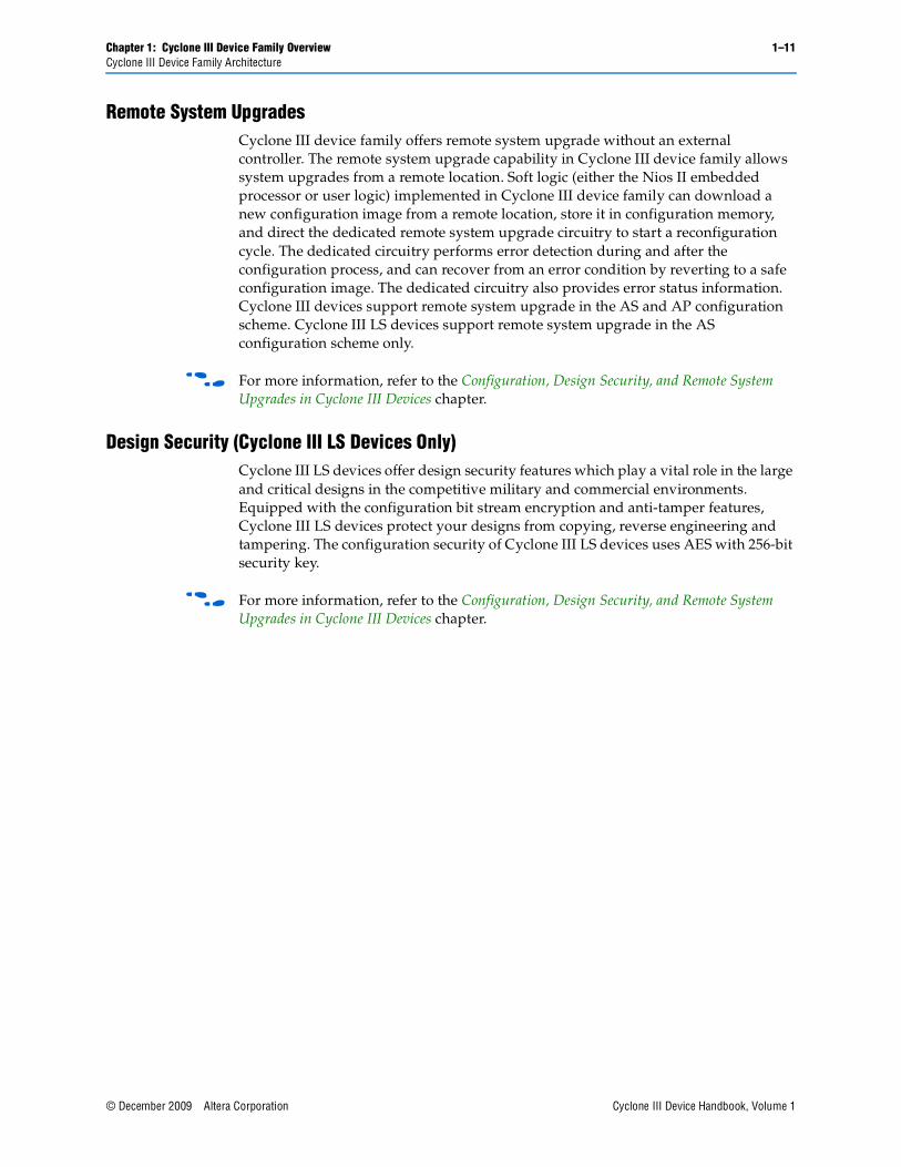
Reference and Ordering InformationFigure 1–1 and Figure 1–2 show the ordering codes for Cyclone III and Cyclone III LS devices.
Figure 1–1. Cyclone III Device Packaging Ordering Information
Figure 1–2. Cyclone III LS Device Packaging Ordering Information
Device Type
Package Type
6 (fastest)78
Number of pins for a particular package:144164240256324484780
E: Plastic Enhanced Quad Flat Pack (EQFP)Q: Plastic Quad Flat Pack (PQFP)F: FineLine Ball-Grid Array (FBGA)U: Ultra FineLine Ball-Grid Array (UBGA)M: Micro FineLine Ball-Grid Array (MBGA)
EP3C: Cyclone III
510162525E405580120 C: Commercial temperature (TJ = 0°C to 85°C)
I: Industrial temperature (TJ = -40°C to 100°C)A: Automotive temperature (TJ = -40°C to 125°C)
Optional SuffixFamily Signature
Operating Temperature
Speed Grade
Pin Count
ES: Engineering sampleN: Lead-free devices
7EP3C 25 C324F N
Indicates specific device options or shipment method.
Device Type
Package Type
7 (fastest)8
Number of pins for a particular package:484780
F: FineLine Ball-Grid Array (FBGA)U: Ultra FineLine Ball-Grid Array (UBGA)
EP3CLS: Cyclone III LS
70100150200
C: Commercial temperature (TJ = 0°C to 85°C)I: Industrial temperature (TJ = -40°C to 100°C)
Optional SuffixFamily Signature
Operating Temperature
Speed Grade
Pin Count
ES: Engineering sampleN: Lead-free devices
7EP3CLS 70 C484F N
Indicates specific device options or shipment method.

Chapter 1: Cyclone III Device Family Overview 1–13Chapter Revision History
© December 2009 Altera Corporation Cyclone III Device Handbook, Volume 1
Chapter Revision HistoryTable 1–7 lists the revision history for this chapter.
Table 1–7. Chapter Revision History
Date Version Changes Made
December 2009 2.2 Minor text edits.
July 2009 2.1 Minor edit to the hyperlinks.
June 2009 2.0
■ Added Table 1–5.
■ Updated Table 1–1, Table 1–2, Table 1–3, and Table 1–4.
■ Updated “Introduction”, “Cyclone III Device Family Architecture”, “Embedded Multipliers and Digital Signal Processing Support ”, “Clock Networks and PLLs ”, “I/O Features ”, “High-Speed Differential Interfaces ”, “Auto-Calibrating External Memory Interfaces ”, “Quartus II Software Support”, “Configuration ”, and “Design Security (Cyclone III LS Devices Only)”.
■ Removed “Referenced Document” section.
October 2008 1.3
■ Updated “Increased System Integration” section.
■ Updated “Memory Blocks” section.
■ Updated chapter to new template.
May 2008 1.2
■ Added 164-pin Micro FineLine Ball-Grid Array (MBGA) details to Table 1–2, Table 1–3 and Table 1–4.
■ Updated Figure 1–2 with automotive temperature information.
■ Updated “Increased System Integration” section, Table 1–6, and “High-Speed Differential Interfaces” section with BLVDS information.
July 2007 1.1
■ Removed the text “Spansion” in “Increased System.
■ Integration” and “Configuration” sections.
■ Removed trademark symbol from “MultiTrack” in “MultiTrack Interconnect”.
■ Removed registered trademark symbol from “Simulink” and “MATLAB” from “Embedded Multipliers and Digital.
■ Signal Processing Support” section.
■ Added chapter TOC and “Referenced Documents” section.
March 2007 1.0 Initial release.

1–14 Chapter 1: Cyclone III Device Family OverviewChapter Revision History
Cyclone III Device Handbook, Volume 1 © December 2009 Altera Corporation

© December 2009 Altera Corporation Cyclone III Device Handbook, Volume 1
2. Logic Elements and Logic Array Blocksin the Cyclone III Device Family
This chapter contains feature definitions for logic elements (LEs) and logic array blocks (LABs). Details are provided on how LEs work, how LABs contain groups of LEs, and how LABs interface with the other blocks in the Cyclone® III device family (Cyclone III and Cyclone III LS devices).
Logic ElementsLogic elements (LEs) are the smallest units of logic in the Cyclone III device family architecture. LEs are compact and provide advanced features with efficient logic usage. Each LE has the following features:
■ A four-input look-up table (LUT), which can implement any function of four variables
■ A programmable register
■ A carry chain connection
■ A register chain connection
■ The ability to drive the following interconnects:
■ Local
■ Row
■ Column
■ Register chain
■ Direct link
■ Register packing support
■ Register feedback support
CIII51002-2.2

2–2 Chapter 2: Logic Elements and Logic Array Blocks in the Cyclone III Device FamilyLogic Elements
Cyclone III Device Handbook, Volume 1 © December 2009 Altera Corporation
Figure 2–1 shows the LEs for the Cyclone III device family.
LE FeaturesYou can configure the programmable register of each LE for D, T, JK, or SR flipflop operation. Each register has data, clock, clock enable, and clear inputs. Signals that use the global clock network, general-purpose I/O pins, or any internal logic can drive the clock and clear control signals of the register. Either general-purpose I/O pins or the internal logic can drive the clock enable. For combinational functions, the LUT output bypasses the register and drives directly to the LE outputs.
Each LE has three outputs that drive the local, row, and column routing resources. The LUT or register output independently drives these three outputs. Two LE outputs drive the column or row and direct link routing connections, while one LE drives the local interconnect resources. This allows the LUT to drive one output while the register drives another output. This feature, called register packing, improves device utilization because the device can use the register and the LUT for unrelated functions. The LAB-wide synchronous load control signal is not available when using register packing. For more information on the synchronous load control signal, refer to “LAB Control Signals” on page 2–6.
The register feedback mode allows the register output to feed back into the LUT of the same LE to ensure that the register is packed with its own fan-out LUT, providing another mechanism for improved fitting. The LE can also drive out registered and unregistered versions of the LUT output.
Figure 2–1. Cyclone III Device Family LEs
Row, Column,And Direct Link Routing
data 1data 2data 3
data 4
labclr1labclr2
Chip-WideReset
(DEV_CLRn)
labclk1
labclk2
labclkena1
labclkena2
LE Carry-In
LAB-WideSynchronous
LoadLAB-Wide
Synchronous Clear
Row, Column,And Direct Link Routing
Local Routing
Register ChainOutput
Register Bypass
ProgrammableRegister
Register ChainRouting from previous LE
LE Carry-Out
Register Feedback
SynchronousLoad and
Clear Logic
CarryChain
Look-Up Table(LUT)
Asynchronous Clear Logic
Clock &Clock Enable
Select
D Q
ENACLRN

Chapter 2: Logic Elements and Logic Array Blocks in the Cyclone III Device Family 2–3LE Operating Modes
© December 2009 Altera Corporation Cyclone III Device Handbook, Volume 1
In addition to the three general routing outputs, LEs in a LAB have register chain outputs, which allows registers in the same LAB to cascade together. The register chain output allows the LUTs to be used for combinational functions and the registers to be used for an unrelated shift register implementation. These resources speed up connections between LABs while saving local interconnect resources.
LE Operating ModesCyclone III device family LEs operate in the following modes:
■ Normal mode
■ Arithmetic mode
LE operating modes use LE resources differently. In each mode, there are six available inputs to the LE. These inputs include the four data inputs from the LAB local interconnect, the LE carry-in from the previous LE carry-chain, and the register chain connection. Each input is directed to different destinations to implement the desired logic function. LAB-wide signals provide clock, asynchronous clear, synchronous clear, synchronous load, and clock enable control for the register. These LAB-wide signals are available in all LE modes.
The Quartus® II software automatically chooses the appropriate mode for common functions, such as counters, adders, subtractors, and arithmetic functions, in conjunction with parameterized functions such as the library of parameterized modules (LPM) functions. You can also create special-purpose functions that specify which LE operating mode to use for optimal performance, if required.
Normal ModeNormal mode is suitable for general logic applications and combinational functions. In normal mode, four data inputs from the LAB local interconnect are inputs to a four-input LUT (Figure 2–2). The Quartus II Compiler automatically selects the carry-in (cin) or the data3 signal as one of the inputs to the LUT. LEs in normal mode support packed registers and register feedback.
Figure 2–2 shows LEs in normal mode.
Figure 2–2. Cyclone III Device Family LEs in Normal Mode
data1
Four-InputLUT
data2
data3cin (from cout of previous LE)
data4
clock (LAB Wide)
ena (LAB Wide)
aclr (LAB Wide)
CLRN
DQ
ENA
sclear(LAB Wide)
sload(LAB Wide)
Register ChainConnection
RegisterChain Output
Row, Column, andDirect Link Routing
Row, Column, andDirect Link Routing
Local Routing
Register Bypass
Packed Register Input
Register Feedback

2–4 Chapter 2: Logic Elements and Logic Array Blocks in the Cyclone III Device FamilyLE Operating Modes
Cyclone III Device Handbook, Volume 1 © December 2009 Altera Corporation
Arithmetic ModeArithmetic mode is ideal for implementing adders, counters, accumulators, and comparators. An LE in arithmetic mode implements a 2-bit full adder and basic carry chain (Figure 2–3). LEs in arithmetic mode can drive out registered and unregistered versions of the LUT output. Register feedback and register packing are supported when LEs are used in arithmetic mode.
Figure 2–3 shows LEs in arithmetic mode.
The Quartus II Compiler automatically creates carry chain logic during design processing. You can also manually create the carry chain logic during design entry. Parameterized functions, such as LPM functions, automatically take advantage of carry chains for the appropriate functions.
The Quartus II Compiler creates carry chains longer than 16 LEs by automatically linking LABs in the same column. For enhanced fitting, a long carry chain runs vertically, which allows fast horizontal connections to M9K memory blocks or embedded multipliers through direct link interconnects. For example, if a design has a long carry chain in a LAB column next to a column of M9K memory blocks, any LE output can feed an adjacent M9K memory block through the direct link interconnect. If the carry chains run horizontally, any LAB which is not next to the column of M9K memory blocks uses other row or column interconnects to drive a M9K memory block. A carry chain continues as far as a full column.
Figure 2–3. Cyclone III Device Family LEs in Arithmetic Mode
clock (LAB Wide)
ena (LAB Wide)
aclr (LAB Wide)
CLRN
DQ
ENA
sclear(LAB Wide)
sload(LAB Wide)
RegisterChain Output
Row, Column, andDirect link routing
Row, Column, andDirect link routing
Local Routing
Register Feedback
Three-InputLUT
Three-InputLUTcin (from cout
of previous LE)
data2data1
cout
Register Bypass
data4
data3
Register ChainConnection
Packed Register Input

Chapter 2: Logic Elements and Logic Array Blocks in the Cyclone III Device Family 2–5Logic Array Blocks
© December 2009 Altera Corporation Cyclone III Device Handbook, Volume 1
Logic Array BlocksLogic array blocks (LABs) contain groups of LEs.
TopologyEach LAB consists of the following features:
■ 16 LEs
■ LAB control signals
■ LE carry chains
■ Register chains
■ Local interconnect
The local interconnect transfers signals between LEs in the same LAB. Register chain connections transfer the output of one LE register to the adjacent LE register in a LAB. The Quartus II Compiler places associated logic in a LAB or adjacent LABs, allowing the use of local and register chain connections for performance and area efficiency.
Figure 2–4 shows the LAB structure for the Cyclone III device family.
Figure 2–4. Cyclone III Device Family LAB Structure
Direct linkinterconnectfrom adjacentblock
Direct linkinterconnectto adjacentblock
Row Interconnect
Column Interconnect
Local InterconnectLAB
Direct linkinterconnectfrom adjacentblock
Direct linkinterconnectto adjacentblock

2–6 Chapter 2: Logic Elements and Logic Array Blocks in the Cyclone III Device FamilyLAB Control Signals
Cyclone III Device Handbook, Volume 1 © December 2009 Altera Corporation
LAB InterconnectsThe LAB local interconnect is driven by column and row interconnects and LE outputs in the same LAB. Neighboring LABs, phase-locked loops (PLLs), M9K RAM blocks, and embedded multipliers from the left and right can also drive the local interconnect of a LAB through the direct link connection. The direct link connection feature minimizes the use of row and column interconnects, providing higher performance and flexibility. Each LE can drive up to 48 LEs through fast local and direct link interconnects.
Figure 2–5 shows the direct link connection.
LAB Control SignalsEach LAB contains dedicated logic for driving control signals to its LEs. The control signals include:
■ Two clocks
■ Two clock enables
■ Two asynchronous clears
■ One synchronous clear
■ One synchronous load
You can use up to eight control signals at a time. Register packing and synchronous load cannot be used simultaneously.
Each LAB can have up to four non-global control signals. You can use additional LAB control signals as long as they are global signals.
Synchronous clear and load signals are useful for implementing counters and other functions. The synchronous clear and synchronous load signals are LAB-wide signals that affect all registers in the LAB.
Figure 2–5. Cyclone III Device Family Direct Link Connection
LAB
Direct linkinterconnectto right
Direct link interconnect fromright LAB, M9K memoryblock, embedded multiplier,PLL, or IOE output
Direct link interconnect fromleft LAB, M9K memory
block, embedded multiplier,PLL, or IOE output
LocalInterconnect
Direct linkinterconnect
to left
Chapter 2: Logic Elements and Logic Array Blocks in the Cyclone III Device Family 2–7LAB Control Signals
© December 2009 Altera Corporation Cyclone III Device Handbook, Volume 1
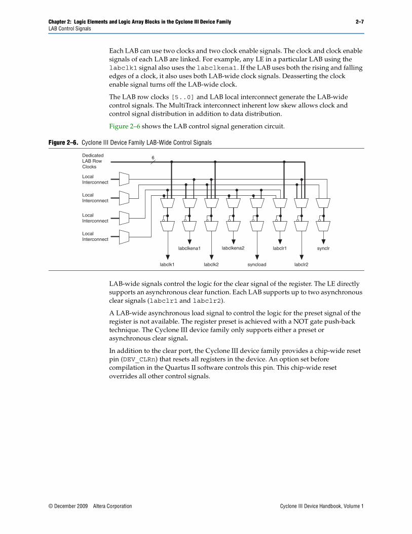
Each LAB can use two clocks and two clock enable signals. The clock and clock enable signals of each LAB are linked. For example, any LE in a particular LAB using the labclk1 signal also uses the labclkena1. If the LAB uses both the rising and falling edges of a clock, it also uses both LAB-wide clock signals. Deasserting the clock enable signal turns off the LAB-wide clock.
The LAB row clocks [5..0] and LAB local interconnect generate the LAB-wide control signals. The MultiTrack interconnect inherent low skew allows clock and control signal distribution in addition to data distribution.
Figure 2–6 shows the LAB control signal generation circuit.
LAB-wide signals control the logic for the clear signal of the register. The LE directly supports an asynchronous clear function. Each LAB supports up to two asynchronous clear signals (labclr1 and labclr2).
A LAB-wide asynchronous load signal to control the logic for the preset signal of the register is not available. The register preset is achieved with a NOT gate push-back technique. The Cyclone III device family only supports either a preset or asynchronous clear signal.
In addition to the clear port, the Cyclone III device family provides a chip-wide reset pin (DEV_CLRn) that resets all registers in the device. An option set before compilation in the Quartus II software controls this pin. This chip-wide reset overrides all other control signals.
Figure 2–6. Cyclone III Device Family LAB-Wide Control Signals
labclkena1
labclk2labclk1
labclkena2 labclr1
DedicatedLAB RowClocks
LocalInterconnect
LocalInterconnect
LocalInterconnect
LocalInterconnect
syncload
synclr
labclr2
6

2–8 Chapter 2: Logic Elements and Logic Array Blocks in the Cyclone III Device FamilyChapter Revision History
Cyclone III Device Handbook, Volume 1 © December 2009 Altera Corporation
Chapter Revision HistoryTable 2–1 lists the revision history for this chapter.
Table 2–1. Chapter Revision History
Date Version Changes Made
December 2009 2.2 Minor changes to the text.
July 2009 2.1 Minor edit to the hyperlinks.
June 2009 2.0
Updated to include Cyclone III LS information
■ Updated chapter part number.
■ Updated “Introduction” on page 2–1.
■ Updated Figure 2–1 on page 2–2 and Figure 2–4 on page 2–5.
■ Updated “LAB Control Signals” on page 2–6.
October 2008 1.2 Updated chapter to new template.
July 2007 1.1 Removed trademark symbol from “MultiTrack” in “LAB Control Signals” section.
March 2007 1.0 Initial release.
© December 2009 Altera Corporation Cyclone III Device Handbook, Volume 1
3. Memory Blocks in the Cyclone IIIDevice Family
The Cyclone® III device family (Cyclone III and Cyclone III LS devices) features embedded memory structures to address the on-chip memory needs of Altera® Cyclone III device family designs. The embedded memory structure consists of columns of M9K memory blocks that you can configure to provide various memory functions, such as RAM, shift registers, ROM, and FIFO buffers.
This chapter contains the following sections:
■ “Memory Modes” on page 3–8
■ “Clocking Modes” on page 3–15
■ “Design Considerations” on page 3–16
OverviewM9K blocks support the following features:
■ 8,192 memory bits per block (9,216 bits per block including parity)
■ Independent read-enable (rden) and write-enable (wren) signals for each port
■ Packed mode in which the M9K memory block is split into two 4.5 K single-port RAMs
■ Variable port configurations
■ Single-port and simple dual-port modes support for all port widths
■ True dual-port (one read and one write, two reads, or two writes) operation
■ Byte enables for data input masking during writes
■ Two clock-enable control signals for each port (port A and port B)
■ Initialization file to pre-load memory content in RAM and ROM modes
CIII51004-2.2

3–2 Chapter 3: Memory Blocks in the Cyclone III Device FamilyOverview
Cyclone III Device Handbook, Volume 1 © December 2009 Altera Corporation
Table 3–1 lists the features supported by the M9K memory
f For information about the number of M9K memory blocks for the Cyclone III device family, refer to the Cyclone III Device Family Overview chapter.
Table 3–1. Summary of M9K Memory Features
Feature M9K Blocks
Configurations (depth × width)
8192 × 1
4096 × 2
2048 × 4
1024 × 8
1024 × 9
512 × 16
512 × 18
256 × 32
256 × 36
Parity bits v
Byte enable v
Packed mode v
Address clock enable v
Single-port mode v
Simple dual-port mode v
True dual-port mode v
Embedded shift register mode (1) v
ROM mode v
FIFO buffer (1) v
Simple dual-port mixed width support v
True dual-port mixed width support (2) v
Memory initialization file (.mif) v
Mixed-clock mode v
Power-up condition Outputs cleared
Register asynchronous clears Read address registers and output registers only
Latch asynchronous clears Output latches only
Write or read operation triggering Write and read: Rising clock edges
Same-port read-during-write Outputs set to Old Data or New Data
Mixed-port read-during-write Outputs set to Old Data or Don’t Care
Notes to Table 3–1:(1) FIFO buffers and embedded shift registers that require external logic elements (LEs) for implementing control
logic.(2) Width modes of ×32 and ×36 are not available.

Chapter 3: Memory Blocks in the Cyclone III Device Family 3–3Overview
© December 2009 Altera Corporation Cyclone III Device Handbook, Volume 1
Control SignalsThe clock-enable control signal controls the clock entering the input and output registers and the entire M9K memory block. This signal disables the clock so that the M9K memory block does not see any clock edges and does not perform any operations.
The rden and wren control signals control the read and write operations for each port of M9K memory blocks. You can disable the rden or wren signals independently to save power whenever the operation is not required.
Figure 3–1 shows how the register clock, clear, and control signals are implemented in the Cyclone III device family M9K memory block.
Parity Bit SupportParity checking for error detection is possible with the parity bit along with internal logic resources. The Cyclone III device family M9K memory blocks support a parity bit for each storage byte. You can use this bit as either a parity bit or as an additional data bit. No parity function is actually performed on this bit.
Figure 3–1. M9K Control Signal Selection
clock_b
clocken_aclock_a
clocken_b aclr_b
aclr_a
DedicatedRow LABClocks
rden_b
rden_a
6
LocalInterconnect
byteena_b
byteena_a
addressstall_b
addressstall_awren_a
wren_b

3–4 Chapter 3: Memory Blocks in the Cyclone III Device FamilyOverview
Cyclone III Device Handbook, Volume 1 © December 2009 Altera Corporation
Byte Enable SupportThe Cyclone III device family M9K memory blocks support byte enables that mask the input data so that only specific bytes of data are written. The unwritten bytes retain the previous written value. The wren signals, along with the byte-enable (byteena) signals, control the write operations of the RAM block. The default value of the byteena signals is high (enabled), in which case writing is controlled only by the wren signals. There is no clear port to the byteena registers. M9K blocks support byte enables when the write port has a data width of ×16, ×18, ×32, or ×36 bits.
Byte enables operate in one-hot manner, with the LSB of the byteena signal corresponding to the least significant byte of the data bus. For example, if byteena = 01 and you are using a RAM block in ×18 mode, data[8..0] is enabled and data[17..9] is disabled. Similarly, if byteena = 11, both data[8..0] and data[17..9] are enabled. Byte enables are active high.
Table 3–2 lists the byte selection.
Table 3–2. byteena for Cyclone III Device Family M9K Blocks (Note 1)
byteena[3..0]Affected Bytes
datain × 16 datain × 18 datain × 32 datain × 36
[0] = 1 [7..0] [8..0] [7..0] [8..0]
[1] = 1 [15..8] [17..9] [15..8] [17..9]
[2] = 1 — — [23..16] [26..18]
[3] = 1 — — [31..24] [35..27]
Note to Table 3–2:(1) Any combination of byte enables is possible.

Chapter 3: Memory Blocks in the Cyclone III Device Family 3–5Overview
© December 2009 Altera Corporation Cyclone III Device Handbook, Volume 1
Figure 3–2 shows how the wren and byteena signals control the RAM operations.
When a byteena bit is deasserted during a write cycle, the old data in the memory appears in the corresponding data-byte output. When a byteena bit is asserted during a write cycle, the corresponding data-byte output depends on the setting chosen in the Quartus® II software. The setting can either be the newly written data or the old data at that location.
Packed Mode SupportCyclone III device family M9K memory blocks support packed mode. You can implement two single-port memory blocks in a single block under the following conditions:
■ Each of the two independent block sizes is less than or equal to half of the M9K block size. The maximum data width for each independent block is 18 bits wide.
■ Each of the single-port memory blocks is configured in single-clock mode. For more information about packed mode support, refer to “Single-Port Mode” on page 3–8 and “Single-Clock Mode” on page 3–16.
Address Clock Enable SupportCyclone III device family M9K memory blocks support an active-low address clock enable, which holds the previous address value for as long as the addressstall signal is high (addressstall = '1'). When you configure M9K memory blocks in dual-port mode, each port has its own independent address clock enable.
Figure 3–2. Cyclone III Device Family byteena Functional Waveform (Note 1)
Note to Figure 3–2:
(1) For this functional waveform, New Data mode is selected.
inclock
wren
address
data
q (asynch)
an
XXXX
a0 a1 a2 a0 a1 a2
doutn ABFF FFCD ABCD ABFF FFCD
ABCD
byteena XX 10 01 11
XXXX
XX
ABCD
ABCDFFFF
FFFF
FFFF
ABFF
FFCD
contents at a0
contents at a1
contents at a2
rden
3–6 Chapter 3: Memory Blocks in the Cyclone III Device FamilyOverview
Cyclone III Device Handbook, Volume 1 © December 2009 Altera Corporation
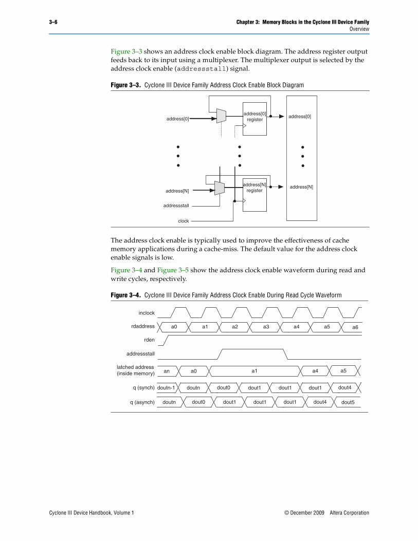
Figure 3–3 shows an address clock enable block diagram. The address register output feeds back to its input using a multiplexer. The multiplexer output is selected by the address clock enable (addressstall) signal.
The address clock enable is typically used to improve the effectiveness of cache memory applications during a cache-miss. The default value for the address clock enable signals is low.
Figure 3–4 and Figure 3–5 show the address clock enable waveform during read and write cycles, respectively.
Figure 3–3. Cyclone III Device Family Address Clock Enable Block Diagram
Figure 3–4. Cyclone III Device Family Address Clock Enable During Read Cycle Waveform
address[0]
address[N]
addressstall
clock
address[0]register
address[N]register
address[N]
address[0]
inclock
rden
rdaddress
q (synch)
a0 a1 a2 a3 a4 a5 a6
q (asynch)
an a0 a4 a5latched address(inside memory)
dout0 dout1 dout1 dout4
dout1 dout4 dout5
addressstall
a1
doutn-1 dout1doutn
doutn dout1dout0 dout1

Chapter 3: Memory Blocks in the Cyclone III Device Family 3–7Overview
© December 2009 Altera Corporation Cyclone III Device Handbook, Volume 1
Mixed-Width SupportM9K memory blocks support mixed data widths. When using simple dual-port, true dual-port, or FIFO modes, mixed width support allows you to read and write different data widths to an M9K memory block. For more information about the different widths supported per memory mode, refer to “Memory Modes” on page 3–8.
Asynchronous ClearThe Cyclone III device family supports asynchronous clears for read address registers, output registers, and output latches only. Input registers other than read address registers are not supported. When applied to output registers, the asynchronous clear signal clears the output registers and the effects are immediately seen. If your RAM does not use output registers, you can still clear the RAM outputs using the output latch asynchronous clear feature.
1 Asserting asynchronous clear to the read address register during a read operation might corrupt the memory content.
Figure 3–6 shows the functional waveform for the asynchronous clear feature.
Figure 3–5. Cyclone III Device Family Address Clock Enable During Write Cycle Waveform
inclock
wren
wraddress a0 a1 a2 a3 a4 a5 a6
an a0 a4 a5latched address(inside memory)
addressstall
a1
data 00 01 02 03 04 05 06
contents at a0
contents at a1
contents at a2
contents at a3
contents at a4
contents at a5
XX
04XX
00
0301XX 02
XX
XX
XX 05
Figure 3–6. Output Latch Asynchronous Clear Waveform
aclr
aclr at latch
clk
q a1 a0 a1a2
3–8 Chapter 3: Memory Blocks in the Cyclone III Device FamilyMemory Modes
Cyclone III Device Handbook, Volume 1 © December 2009 Altera Corporation
1 You can selectively enable asynchronous clears per logical memory using the Quartus II RAM MegaWizard™ Plug-In Manager.
f For more information, refer to the RAM Megafunction User Guide.
There are three ways to reset registers in the M9K blocks:
■ Power up the device
■ Use the aclr signal for output register only
■ Assert the device-wide reset signal using the DEV_CLRn option
Memory ModesCyclone III device family M9K memory blocks allow you to implement fully-synchronous SRAM memory in multiple modes of operation. Cyclone III device family M9K memory blocks do not support asynchronous (unregistered) memory inputs.
M9K memory blocks support the following modes:
■ Single-port
■ Simple dual-port
■ True dual-port
■ Shift-register
■ ROM
■ FIFO
1 Violating the setup or hold time on the M9K memory block input registers may corrupt memory contents. This applies to both read and write operations.
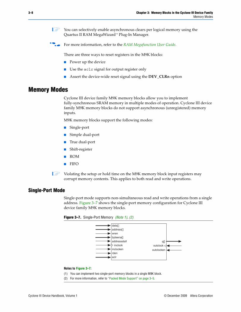
Single-Port ModeSingle-port mode supports non-simultaneous read and write operations from a single address. Figure 3–7 shows the single-port memory configuration for Cyclone III device family M9K memory blocks.
Figure 3–7. Single-Port Memory (Note 1), (2)
Notes to Figure 3–7:
(1) You can implement two single-port memory blocks in a single M9K block.(2) For more information, refer to “Packed Mode Support” on page 3–5.
data[ ]address[ ]wrenbyteena[]addressstall inclockinclockenrdenaclr
outclock
q[]
outclocken

Chapter 3: Memory Blocks in the Cyclone III Device Family 3–9Memory Modes
© December 2009 Altera Corporation Cyclone III Device Handbook, Volume 1
During a write operation, the behavior of the RAM outputs is configurable. If you activate rden during a write operation, the RAM outputs show either the new data being written or the old data at that address. If you perform a write operation with rden deactivated, the RAM outputs retain the values they held during the most recent active rden signal.
To choose the desired behavior, set the Read-During-Write option to either New Data or Old Data in the RAM MegaWizard Plug-In Manager in the Quartus II software. For more information about read-during-write mode, refer to “Read-During-Write Operations” on page 3–16.
The port width configurations for M9K blocks in single-port mode are as follow:
■ 8192 × 1
■ 4096 × 2
■ 2048 × 4
■ 1024 × 8
■ 1024 × 9
■ 512 × 16
■ 512 × 18
■ 256 × 32
■ 256 × 36
Figure 3–8 shows timing waveforms for read and write operations in single-port mode with unregistered outputs. Registering the outputs of the RAM simply delays the q output by one clock cycle.
Figure 3–8. Cyclone III Device Family Single-Port Mode Timing Waveforms
clk_a
wren_a
address_a
data_a
rden_a
q_a (old data)
a0 a1
A B C D E F
a0(old data) a1(old data)A B D E
q_a (new data) A DB C E F

3–10 Chapter 3: Memory Blocks in the Cyclone III Device FamilyMemory Modes
Cyclone III Device Handbook, Volume 1 © December 2009 Altera Corporation
Simple Dual-Port ModeSimple dual-port mode supports simultaneous read and write operations to different locations. Figure 3–9 shows the simple dual-port memory configuration.
Cyclone III device family M9K memory blocks support mixed-width configurations, allowing different read and write port widths.
Table 3–3 lists mixed-width configurations.
In simple dual-port mode, M9K memory blocks support separate wren and rden signals. You can save power by keeping the rden signal low (inactive) when not reading. Read-during-write operations to the same address can either output “Don’t Care” data at that location or output “Old Data”. To choose the desired behavior, set the Read-During-Write option to either Don’t Care or Old Data in the RAM MegaWizard Plug-In Manager in the Quartus II software. For more information about this behavior, refer to “Read-During-Write Operations” on page 3–16.
Figure 3–9. Cyclone III Device Family Simple Dual-Port Memory (Note 1)
Note to Figure 3–9:
(1) Simple dual-port RAM supports input or output clock mode in addition to the read or write clock mode shown.
data[ ]wraddress[ ]wrenbyteena[]wr_addressstallwrclockwrclockenaclr
rdaddress[ ]rden
q[ ]rd_addressstall
rdclockrdclocken
Table 3–3. Cyclone III Device Family M9K Block Mixed-Width Configurations (Simple Dual-Port Mode)
Read PortWrite Port
8192 × 1 4096 × 2 2048 × 4 1024 × 8 512 × 16 256 × 32 1024 × 9 512 × 18 256 × 36
8192 × 1 v v v v v v — — —
4096 × 2 v v v v v v — — —
2048 × 4 v v v v v v — — —
1024 × 8 v v v v v v — — —
512 × 16 v v v v v v — — —
256 × 32 v v v v v v — — —
1024 × 9 — — — — — — v v v
512 × 18 — — — — — — v v v
256 × 36 — — — — — — v v v

Chapter 3: Memory Blocks in the Cyclone III Device Family 3–11Memory Modes
© December 2009 Altera Corporation Cyclone III Device Handbook, Volume 1
Figure 3–10 shows the timing waveforms for read and write operations in simple dual-port mode with unregistered outputs. Registering the outputs of the RAM simply delays the q output by one clock cycle.
True Dual-Port ModeTrue dual-port mode supports any combination of two-port operations: two reads, two writes, or one read and one write, at two different clock frequencies. Figure 3–11 shows the Cyclone III device family true dual-port memory configuration.
1 The widest bit configuration of the M9K blocks in true dual-port mode is 512 × 16-bit (18-bit with parity).
Figure 3–10. Cyclone III Device Family Simple Dual-Port Timing Waveforms
wrclock
wren
wraddress
rdclock
an-1 an a0 a1 a2 a3 a4 a5 a6
q (asynch)
rden
rdaddress bn b0 b1 b2 b3
doutn-1 doutn dout0
din-1 din din4 din5 din6data
Figure 3–11. Cyclone III Device Family True Dual-Port Memory (Note 1)
Note to Figure 3–11:
(1) True dual-port memory supports input or output clock mode in addition to the independent clock mode shown.
data_a[ ]address_a[ ]wren_abyteena_a[]addressstall_a clock_aclocken_arden_aaclr_aq_a[]
data_b[ ]address_b[]
wren_bbyteena_b[]
addressstall_bclock_b
clocken_brden_baclr_bq_b[]

3–12 Chapter 3: Memory Blocks in the Cyclone III Device FamilyMemory Modes
Cyclone III Device Handbook, Volume 1 © December 2009 Altera Corporation
Table 3–4 lists the possible M9K block mixed-port width configurations.
In true dual-port mode, M9K memory blocks support separate wren and rden signals. You can save power by keeping the rden signal low (inactive) when not reading. Read-during-write operations to the same address can either output “New Data” at that location or “Old Data”. To choose the desired behavior, set the Read-During-Write option to either New Data or Old Data in the RAM MegaWizard Plug-In Manager in the Quartus II software. For more information about this behavior, refer to “Read-During-Write Operations” on page 3–16.
In true dual-port mode, you can access any memory location at any time from either port A or port B. However, when accessing the same memory location from both ports, you must avoid possible write conflicts. When you attempt to write to the same address location from both ports at the same time, a write conflict happens. This results in unknown data being stored to that address location. There is no conflict resolution circuitry built into the Cyclone III device family M9K memory blocks. You must handle address conflicts external to the RAM block.
Table 3–4. Cyclone III Device Family M9K Block Mixed-Width Configurations (True Dual-Port Mode)
Read PortWrite Port
8192 × 1 4096 × 2 2048 × 4 1024 × 8 512 × 16 1024 × 9 512 × 18
8192 × 1 v v v v v — —
4096 × 2 v v v v v — —
2048 × 4 v v v v v — —
1024 × 8 v v v v v — —
512 × 16 v v v v v — —
1024 × 9 — — — — — v v
512 × 18 — — — — — v v

Chapter 3: Memory Blocks in the Cyclone III Device Family 3–13Memory Modes
© December 2009 Altera Corporation Cyclone III Device Handbook, Volume 1
Figure 3–12 shows true dual-port timing waveforms for the write operation at port A and read operation at port B. Registering the outputs of the RAM simply delays the q outputs by one clock cycle.
Shift Register ModeCyclone III device family M9K memory blocks can implement shift registers for digital signal processing (DSP) applications, such as finite impulse response (FIR) filters, pseudo-random number generators, multi-channel filtering, and auto-correlation and cross-correlation functions. These and other DSP applications require local data storage, traditionally implemented with standard flipflops that quickly exhaust many logic cells for large shift registers. A more efficient alternative is to use embedded memory as a shift register block, which saves logic cell and routing resources.
The size of a (w × m × n) shift register is determined by the input data width (w), the length of the taps (m), and the number of taps (n), and must be less than or equal to the maximum number of memory bits, which is 9,216 bits. In addition, the size of (w × n) must be less than or equal to the maximum width of the block, which is 36 bits. If you need a larger shift register, you can cascade the M9K memory blocks.
Figure 3–12. Cyclone III Device Family True Dual-Port Timing Waveforms
clk_a
wren_a
address_a
clk_b
an-1 an a0 a1 a2 a3 a4 a5 a6
q_b (asynch)
wren_b
address_b bn b0 b1 b2 b3
doutn-1 doutn dout0
q_a (asynch)
din-1 din din4 din5 din6data_a
din-1 din dout0 dout1 dout2 dout3 din4 din5
dout2dout1
rden_a
rden_b

3–14 Chapter 3: Memory Blocks in the Cyclone III Device FamilyMemory Modes
Cyclone III Device Handbook, Volume 1 © December 2009 Altera Corporation
Figure 3–13 shows the Cyclone III device family M9K memory block in the shift register mode.
ROM ModeCyclone III device family M9K memory blocks support ROM mode. A .mif initializes the ROM contents of these blocks. The address lines of the ROM are registered. The outputs can be registered or unregistered. The ROM read operation is identical to the read operation in the single-port RAM configuration.
FIFO Buffer ModeCyclone III device family M9K memory blocks support single-clock or dual-clock FIFO buffers. Dual clock FIFO buffers are useful when transferring data from one clock domain to another clock domain. Cyclone III device family M9K memory blocks do not support simultaneous read and write from an empty FIFO buffer.
f For more information about FIFO buffers, refer to the Single- and Dual-Clock FIFO Megafunction User Guide.
Figure 3–13. Cyclone III Device Family Shift Register Mode Configuration
W
w × m × n Shift Register
m-Bit Shift Register
m-Bit Shift Register
m-Bit Shift Register
m-Bit Shift Register
W
W
W
W
W
W
W
n Number of Taps
Chapter 3: Memory Blocks in the Cyclone III Device Family 3–15Clocking Modes
© December 2009 Altera Corporation Cyclone III Device Handbook, Volume 1
Clocking ModesCyclone III device family M9K memory blocks support the following clocking modes:
■ Independent
■ Input or output
■ Read or write
■ Single-clock
When using read or write clock mode, if you perform a simultaneous read or write to the same address location, the output read data is unknown. If you require the output data to be a known value, use either single-clock mode or I/O clock mode and choose the appropriate read-during-write behavior in the MegaWizard Plug-In Manager.
1 Violating the setup or hold time on the memory block input registers might corrupt the memory contents. This applies to both read and write operations.
1 Asynchronous clears are available on read address registers, output registers, and output latches only.
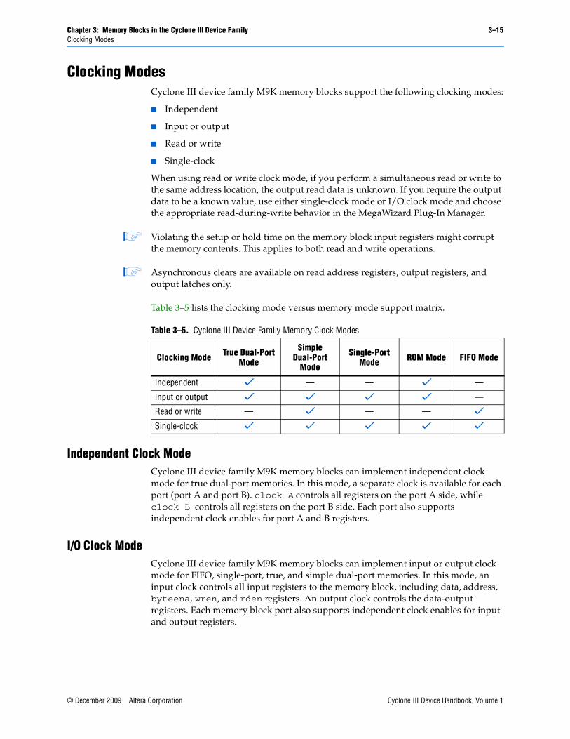
Table 3–5 lists the clocking mode versus memory mode support matrix.
Independent Clock ModeCyclone III device family M9K memory blocks can implement independent clock mode for true dual-port memories. In this mode, a separate clock is available for each port (port A and port B). clock A controls all registers on the port A side, while clock B controls all registers on the port B side. Each port also supports independent clock enables for port A and B registers.
I/O Clock ModeCyclone III device family M9K memory blocks can implement input or output clock mode for FIFO, single-port, true, and simple dual-port memories. In this mode, an input clock controls all input registers to the memory block, including data, address, byteena, wren, and rden registers. An output clock controls the data-output registers. Each memory block port also supports independent clock enables for input and output registers.
Table 3–5. Cyclone III Device Family Memory Clock Modes
Clocking Mode True Dual-Port Mode
Simple Dual-Port
Mode
Single-Port Mode ROM Mode FIFO Mode
Independent v — — v —
Input or output v v v v —
Read or write — v — — v
Single-clock v v v v v

3–16 Chapter 3: Memory Blocks in the Cyclone III Device FamilyDesign Considerations
Cyclone III Device Handbook, Volume 1 © December 2009 Altera Corporation
Read or Write Clock ModeCyclone III device family M9K memory blocks can implement read or write clock mode for FIFO and simple dual-port memories. In this mode, a write clock controls the data inputs, write address, and wren registers. Similarly, a read clock controls the data outputs, read address, and rden registers. M9K memory blocks support independent clock enables for both the read and write clocks.
When using read or write mode, if you perform a simultaneous read or write to the same address location, the output read data is unknown. If you require the output data to be a known value, use either single-clock mode, input clock mode, or output clock mode and choose the appropriate read-during-write behavior in the MegaWizard Plug-In Manager.
Single-Clock ModeCyclone III device family M9K memory blocks can implement single-clock mode for FIFO, ROM, true dual-port, simple dual-port, and single-port memories. In this mode, you can control all registers of the M9K memory block with a single clock together with clock enable.
Design ConsiderationsThis section describes designing with M9K memory blocks.
Read-During-Write Operations“Same-Port Read-During-Write Mode” on page 3–17 and “Mixed-Port Read-During-Write Mode” on page 3–18 describe the functionality of the various RAM configurations when reading from an address during a write operation at that same address.
There are two read-during-write data flows: same-port and mixed-port. Figure 3–14 shows the difference between these flows.
Figure 3–14. Cyclone III Device Family Read-During-Write Data Flow
Port Adata in
Port Bdata in
Port Adata out
Port Bdata out
Mixed-portdata flow
Same-portdata flow
write_a
read_aread_b
write_b

Chapter 3: Memory Blocks in the Cyclone III Device Family 3–17Design Considerations
© December 2009 Altera Corporation Cyclone III Device Handbook, Volume 1
Same-Port Read-During-Write ModeThis mode applies to a single-port RAM or the same port of a true dual-port RAM. In the same port read-during-write mode, there are two output choices: New Data mode (or flow-through) and Old Data mode. In New Data mode, new data is available on the rising edge of the same clock cycle on which it was written. In Old Data mode, the RAM outputs reflect the old data at that address before the write operation proceeds.
When using New Data mode together with byteena, you can control the output of the RAM. When byteena is high, the data written into the memory passes to the output (flow-through). When byteena is low, the masked-off data is not written into the memory and the old data in the memory appears on the outputs. Therefore, the output can be a combination of new and old data determined by byteena.
Figure 3–15 and Figure 3–16 show sample functional waveforms of same port read-during-write behavior with both New Data and Old Data modes, respectively.
Figure 3–15. Same Port Read-During Write: New Data Mode
Figure 3–16. Same Port Read-During-Write: Old Data Mode
clk_a
wren_a
address_a
data_a
rden_a
q_a (asynch)
a0 a1
A B C D E F
A B C D E F
clk_a
wren_a
address_a
data_a
rden_a
q_a (asynch)
a0 a1
A B C D E F
a0(old data) a1(old data)A B D E

3–18 Chapter 3: Memory Blocks in the Cyclone III Device FamilyDesign Considerations
Cyclone III Device Handbook, Volume 1 © December 2009 Altera Corporation
Mixed-Port Read-During-Write ModeThis mode applies to a RAM in simple or true dual-port mode, which has one port reading and the other port writing to the same address location with the same clock.
In this mode, you also have two output choices: Old Data mode or Don't Care mode. In Old Data mode, a read-during-write operation to different ports causes the RAM outputs to reflect the old data at that address location. In Don't Care mode, the same operation results in a “Don't Care” or unknown value on the RAM outputs.
f For more information about how to implement the desired behavior, refer to the RAM Megafunction User Guide.
Figure 3–17 shows a sample functional waveform of mixed port read-during-write behavior for the Old Data mode. In Don't Care mode, the old data is replaced with “Don't Care”.
1 For mixed-port read-during-write operation with dual clocks, the relationship between the clocks determines the output behavior of the memory. If you use the same clock for the two clocks, the output is the old data from the address location. However, if you use different clocks, the output is unknown during the mixed-port read-during-write operation. This unknown value may be the old or new data at the address location, depending on whether the read happens before or after the write.
Conflict ResolutionWhen you are using M9K memory blocks in true dual-port mode, it is possible to attempt two write operations to the same memory location (address). Because there is no conflict resolution circuitry built into M9K memory blocks, this results in unknown data being written to that location. Therefore, you must implement conflict-resolution logic external to the M9K memory block.
Figure 3–17. Mixed Port Read-During-Write: Old Data Mode
a b
a (old data) b (old data)
clk_a&b
wren_a
address_a
q_b (asynch)
rden_b
a baddress_b
data_a A B C D E F
A B D E

Chapter 3: Memory Blocks in the Cyclone III Device Family 3–19Chapter Revision History
© December 2009 Altera Corporation Cyclone III Device Handbook, Volume 1
Power-Up Conditions and Memory InitializationThe M9K memory block outputs of the Cyclone III device family power up to zero (cleared) regardless of whether the output registers are used or bypassed. All M9K memory blocks support initialization using a .mif. You can create .mifs in the Quartus II software and specify their use using the RAM MegaWizard Plug-In Manager when instantiating memory in your design. Even if memory is pre-initialized (for example, using a .mif), it still powers up with its outputs cleared. Only the subsequent read after power up outputs the pre-initialized values.
f For more information about .mifs, refer to the RAM Megafunction User Guide and the Quartus II Handbook.
Power ManagementThe M9K memory block clock enables of the Cyclone III device family allow you to control clocking of each M9K memory block to reduce AC power consumption. Use the rden signal to ensure that read operations only occur when necessary. If your design does not require read-during-write, reduce power consumption by deasserting the rden signal during write operations, or any period when there are no memory operations. The Quartus II software automatically powers down any unused M9K memory blocks to save static power.
Chapter Revision HistoryTable 3–6 lists the revision history for this chapter.
Table 3–6. Chapter Revision History
Date Version Changes Made
December 2009 2.2 Minor changes to the text.
July 2009 2.1 Made minor correction to the part number.
June 2009 2.0
Updated to include Cyclone III LS information
■ Updated chapter part number.
■ Updated “Introduction” on page 3–1.
■ Updated “Overview” on page 3–1.
■ Updated Table 3–1 on page 3–2.
■ Updated “Control Signals” on page 3–3.
■ Updated “Memory Modes” on page 3–8.
■ Updated “Simple Dual-Port Mode” on page 3–10.
■ Updated “Read or Write Clock Mode” on page 3–16.
October 2008 1.3 Updated chapter to new template.
May 2008 1.2■ Revised the maximum performance of the M9K blocks to 315 MHz in
“Introduction” and “Overview” sections, and in Table 3-1.
■ Updated “Address Clock Enable Support” section.
July 2007 1.1 Added chapter TOC and “Referenced Documents” section.
March 2007 1.0 Initial release.

3–20 Chapter 3: Memory Blocks in the Cyclone III Device FamilyChapter Revision History
Cyclone III Device Handbook, Volume 1 © December 2009 Altera Corporation

© December 2009 Altera Corporation Cyclone III Device Handbook, Volume 1
4. Embedded Multipliers in theCyclone III Device Family
The Cyclone® III device family (Cyclone III and Cyclone III LS devices) includes a combination of on-chip resources and external interfaces that help to increase performance, reduce system cost, and lower the power consumption of digital signal processing (DSP) systems. The Cyclone III device family, either alone or as DSP device co-processors, are used to improve price-to-performance ratios of DSP systems. Particular focus is placed on optimizing Cyclone III and Cyclone III LS devices for applications that benefit from an abundance of parallel processing resources, which include video and image processing, intermediate frequency (IF) modems used in wireless communications systems, and multi-channel communications and video systems.
This chapter contains the following sections:
■ “Embedded Multiplier Block Overview” on page 4–1
■ “Architecture” on page 4–3
■ “Operational Modes” on page 4–5
Embedded Multiplier Block OverviewFigure 4–1 shows one of the embedded multiplier columns with the surrounding logic array blocks (LABs). The embedded multiplier is configured as either one 18 × 18 multiplier or two 9 × 9 multipliers. For multiplications greater than 18 × 18, the Quartus® II software cascades multiple embedded multiplier blocks together. There are no restrictions on the data width of the multiplier, but the greater the data width, the slower the multiplication process.
Figure 4–1. Embedded Multipliers Arranged in Columns with Adjacent LABs
EmbeddedMultiplier
EmbeddedMultiplierColumn
1 LABRow
CIII51005-2.2

4–2 Chapter 4: Embedded Multipliers in the Cyclone III Device FamilyEmbedded Multiplier Block Overview
Cyclone III Device Handbook, Volume 1 © December 2009 Altera Corporation
Table 4–1 lists the number of embedded multipliers and the multiplier modes that can be implemented in the Cyclone III device family.
In addition to the embedded multipliers in the Cyclone III device family, you can implement soft multipliers by using the M9K memory blocks as look-up tables (LUTs). The LUTs contain partial results from the multiplication of input data with coefficients that implement variable depth and width high-performance soft multipliers for low-cost, high-volume DSP applications. The availability of soft multipliers increases the number of available multipliers in the device.
Table 4–2 lists the total number of multipliers available in the Cyclone III device family using embedded multipliers and soft multipliers.
Table 4–1. Number of Embedded Multipliers in the Cyclone III Device Family
Device Family Device Embedded Multipliers 9 × 9 Multipliers (1) 18 × 18 Multipliers (1)
Cyclone III
EP3C5 23 46 23
EP3C10 23 46 23
EP3C16 56 112 56
EP3C25 66 132 66
EP3C40 126 252 126
EP3C55 156 312 156
EP3C80 244 488 244
EP3C120 288 576 288
Cyclone III LS
EP3CLS70 200 400 200
EP3CLS100 276 552 276
EP3CLS150 320 640 320
EP3CLS200 396 792 396
Note to Table 4–1:
(1) These columns show the number of 9 × 9 or 18 × 18 multipliers for each device. The total number of multipliers for each device is not the sum of all the multipliers.
Table 4–2. Number of Multipliers in the Cyclone III Device Family (Part 1 of 2)
Device Family Device Embedded Multipliers Soft Multipliers (16 × 16) (1) Total Multipliers (2)
Cyclone III
EP3C5 23 — 23
EP3C10 23 46 69
EP3C16 56 56 112
EP3C25 66 66 132
EP3C40 126 126 252
EP3C55 156 260 416
EP3C80 244 305 549
EP3C120 288 432 720

Chapter 4: Embedded Multipliers in the Cyclone III Device Family 4–3Architecture
© December 2009 Altera Corporation Cyclone III Device Handbook, Volume 1
f For more information about M9K memory blocks of the Cyclone III device family, refer to the Memory Blocks in Cyclone III Devices chapter.
f For more information about soft multipliers, refer to AN 306: Implementing Multipliers in FPGA Devices.
ArchitectureEach embedded multiplier consists of the following elements:
■ Multiplier stage
■ Input and output registers
■ Input and output interfaces
Figure 4–2 shows the multiplier block architecture.
Cyclone III LS
EP3CLS70 200 333 533
EP3CLS100 276 483 759
EP3CLS150 320 666 986
EP3CLS200 396 891 1287
Notes to Table 4–2:
(1) Soft multipliers are implemented in sum of multiplication mode. M9K memory blocks are configured with 18-bit data widths to support 16-bit coefficients. The sum of the coefficients requires 18-bits of resolution to account for overflow.
(2) The total number of multipliers may vary, depending on the multiplier mode you use.
Table 4–2. Number of Multipliers in the Cyclone III Device Family (Part 2 of 2)
Device Family Device Embedded Multipliers Soft Multipliers (16 × 16) (1) Total Multipliers (2)
Figure 4–2. Multiplier Block Architecture
CLRN
D Q
ENA
Data A
Data B
aclrclock
ena
signasignb
CLRN
D Q
ENA
CLRN
D Q
ENAData Out
Embedded Multiplier Block
OutputRegisterInput
Register

4–4 Chapter 4: Embedded Multipliers in the Cyclone III Device FamilyArchitecture
Cyclone III Device Handbook, Volume 1 © December 2009 Altera Corporation
Input RegistersYou can send each multiplier input signal into an input register or directly into the multiplier in 9- or 18-bit sections, depending on the operational mode of the multiplier. Each multiplier input signal can be sent through a register independently of other input signals. For example, you can send the multiplier Data A signal through a register and send the Data B signal directly to the multiplier.
The following control signals are available to each input register in the embedded multiplier:
■ clock
■ clock enable
■ asynchronous clear
All input and output registers in a single embedded multiplier are fed by the same clock, clock enable, and asynchronous clear signals.
Multiplier StageThe multiplier stage of an embedded multiplier block supports 9 × 9 or 18 × 18 multipliers as well as other multipliers in between these configurations. Depending on the data width or operational mode of the multiplier, a single embedded multiplier can perform one or two multiplications in parallel. For multiplier information, refer to “Operational Modes” on page 4–5.
Each multiplier operand is a unique signed or unsigned number. Two signals, signa and signb, control an input of a multiplier and determine if the value is signed or unsigned. If the signa signal is high, the Data A operand is a signed number. If the signa signal is low, the Data A operand is an unsigned number.
Table 4–3 lists the sign of the multiplication results for the various operand sign representations. The results of the multiplication are signed if any one of the operands is a signed value.
Each embedded multiplier block has only one signa and one signb signal to control the sign representation of the input data to the block. If the embedded multiplier block has two 9 × 9 multipliers, the Data A input of both multipliers share the same signa signal, and the Data B input of both multipliers share the same signb signal. You can dynamically change the signa and signb signals to modify the sign representation of the input operands at run time. You can send the signa and signb signals through a dedicated input register. The multiplier offers full precision, regardless of the sign representation.
Table 4–3. Multiplier Sign Representation
Data A Data BResult
signa Value Logic Level signb Value Logic Level
Unsigned Low Unsigned Low Unsigned
Unsigned Low Signed High Signed
Signed High Unsigned Low Signed
Signed High Signed High Signed

Chapter 4: Embedded Multipliers in the Cyclone III Device Family 4–5Operational Modes
© December 2009 Altera Corporation Cyclone III Device Handbook, Volume 1
1 When the signa and signb signals are unused, the Quartus II software sets the multiplier to perform unsigned multiplication by default.
Output RegistersYou can register the embedded multiplier output using output registers in either 18- or 36-bit sections, depending on the operational mode of the multiplier. The following control signals are available for each output register in the embedded multiplier:
■ clock
■ clock enable
■ asynchronous clear
All input and output registers in a single embedded multiplier are fed by the same clock, clock enable, and asynchronous clear signals.
Operational ModesYou can use an embedded multiplier block in one of two operational modes, depending on the application needs:
■ One 18-bit × 18-bit multiplier
■ Up to two 9-bit × 9-bit independent multipliers
1 You can also use embedded multipliers of the Cyclone III device family to implement multiplier adder and multiplier accumulator functions, in which the multiplier portion of the function is implemented using embedded multipliers, and the adder or accumulator function is implemented in logic elements (LEs).
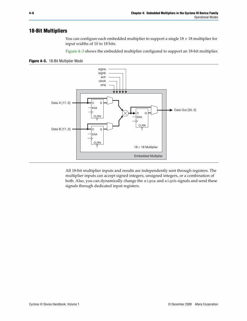
4–6 Chapter 4: Embedded Multipliers in the Cyclone III Device FamilyOperational Modes
Cyclone III Device Handbook, Volume 1 © December 2009 Altera Corporation
18-Bit MultipliersYou can configure each embedded multiplier to support a single 18 × 18 multiplier for input widths of 10 to 18 bits.
Figure 4–3 shows the embedded multiplier configured to support an 18-bit multiplier.
All 18-bit multiplier inputs and results are independently sent through registers. The multiplier inputs can accept signed integers, unsigned integers, or a combination of both. Also, you can dynamically change the signa and signb signals and send these signals through dedicated input registers.
Figure 4–3. 18-Bit Multiplier Mode
CLRN
D Q
ENA
Data A [17..0]
Data B [17..0]
aclrclock
ena
signasignb
CLRN
D Q
ENA
CLRN
D Q
ENAData Out [35..0]
18 × 18 Multiplier
Embedded Multiplier

Chapter 4: Embedded Multipliers in the Cyclone III Device Family 4–7Operational Modes
© December 2009 Altera Corporation Cyclone III Device Handbook, Volume 1
9-Bit MultipliersYou can configure each embedded multiplier to support two 9 × 9 independent multipliers for input widths of up to 9 bits.
Figure 4–4 shows the embedded multiplier configured to support two 9-bit multipliers.
All 9-bit multiplier inputs and results are independently sent through registers. The multiplier inputs can accept signed integers, unsigned integers, or a combination of both. Two 9 × 9 multipliers in the same embedded multiplier block share the same signa and signb signal. Therefore, all the Data A inputs feeding the same embedded multiplier must have the same sign representation. Similarly, all the Data B inputs feeding the same embedded multiplier must have the same sign representation.
Figure 4–4. 9-Bit Multiplier Mode
CLRN
D Q
ENA
Data A 0 [8..0]
Data B 0 [8..0]
aclrclock
ena
signasignb
CLRN
D Q
ENA
CLRN
D Q
ENAData Out 0 [17..0]
9 × 9 Multiplier
Embedded Multiplier
CLRN
D Q
ENA
Data A 1 [8..0]
Data B 1 [8..0]
CLRN
D Q
ENA
CLRN
D Q
ENAData Out 1 [17..0]
9 × 9 Multiplier

4–8 Chapter 4: Embedded Multipliers in the Cyclone III Device FamilyChapter Revision History
Cyclone III Device Handbook, Volume 1 © December 2009 Altera Corporation
Chapter Revision HistoryTable 4–4 lists the revision history for this chapter.
Table 4–4. Chapter Revision History
Date Version Changes Made
December 2009 2.2 Minor changes to the text.
July 2009 2.1 Made minor correction to the part number.
June 2009 2.0
Updated to include Cyclone III LS information
■ Updated chapter part number.
■ Updated “Introduction” on page 4–1.
■ Updated “Embedded Multiplier Block Overview” on page 4–1.
■ Updated Table 4–1 on page 4–2 and Table 4–2 on page 4–2.
■ Updated “Input Registers” on page 4–4.
October 2008 1.2 Updated chapter to new template.
July 2007 1.1
Added EP3C120 information.
■ Updated “Introduction” section.
■ Updated Table 4–1 and Table 4–2.
■ Added chapter TOC and “Referenced Documents” section.
March 2007 1.0 Initial release.

© December 2009 Altera Corporation Cyclone III Device Handbook, Volume 1
5. Clock Networks and PLLs in theCyclone III Device Family
This chapter describes the hierarchical clock networks and phase-locked loops (PLLs) with advanced features in the Cyclone® III device family (Cyclone III and Cyclone III LS devices).
This chapter includes the following sections:
■ “Clock Networks” on page 5–1
■ “PLLs in the Cyclone III Device Family” on page 5–9
■ “Cyclone III Device Family PLL Hardware Overview” on page 5–10
■ “Clock Feedback Modes” on page 5–12
■ “Hardware Features” on page 5–15
■ “Programmable Bandwidth” on page 5–22
■ “Phase Shift Implementation” on page 5–22
■ “PLL Cascading” on page 5–24
■ “PLL Reconfiguration” on page 5–24
■ “Spread-Spectrum Clocking” on page 5–32
■ “PLL Specifications” on page 5–32
Clock NetworksThe Cyclone III device family provides up to 16 dedicated clock pins (CLK[15..0]) that can drive the global clocks (GCLKs). The Cyclone III device family supports four dedicated clock pins on each side of the device except EP3C5 and EP3C10 devices. EP3C5 and EP3C10 devices only support four dedicated clock pins on the left and right sides of the device.
f For more information about the number of GCLK networks in each device density, refer to the Cyclone III Device Family Overview chapter.
GCLK NetworkGCLKs drive throughout the entire device, feeding all device quadrants. All resources in the device (I/O elements, logic array blocks (LABs), dedicated multiplier blocks, and M9K memory blocks) can use GCLKs as clock sources. Use these clock network resources for control signals, such as clock enables and clears fed by an external pin. Internal logic can also drive GCLKs for internally generated GCLKs and asynchronous clears, clock enables, or other control signals with high fan-out.
CIII51006-3.2

5–2 Chapter 5: Clock Networks and PLLs in the Cyclone III Device FamilyClock Networks
Cyclone III Device Handbook, Volume 1 © December 2009 Altera Corporation
Table 5–1 lists the connectivity of the clock sources to the GCLK networks.
Table 5–1. Cyclone III Device Family GCLK Network Connections (Part 1 of 2)
GCLK Network Clock Sources
GCLK Networks (Note 1)
0 1 2 3 4 5 6 7 8 9 10 11 12 13 14 15 16 17 18 19
CLK0/DIFFCLK_0p v — v — v — — — — — — — — — — — — — — —
CLK1/DIFFCLK_0n — v v — — — — — — — — — — — — — — — — —
CLK2/DIFFCLK_1p — v — v v — — — — — — — — — — — — — — —
CLK3/DIFFCLK_1n v — — v — — — — — — — — — — — — — — — —
CLK4/DIFFCLK_2p — — — — — v — v — v — — — — — — — — — —
CLK5/DIFFCLK_2n — — — — — — v v — — — — — — — — — — — —
CLK6/DIFFCLK_3p — — — — — — v — v v — — — — — — — — — —
CLK7/DIFFCLK_3n — — — — — v — — v — — — — — — — — — — —
CLK8/DIFFCLK_5n (2) — — — — — — — — — — v — v — v — — — — —
CLK9/DIFFCLK_5p (2) — — — — — — — — — — — v v — — — — — — —
CLK10/DIFFCLK_4n (2) — — — — — — — — — — — v — v v — — — — —
CLK11/DIFFCLK_4p (2) — — — — — — — — — — v — — v — — — — — —
CLK12/DIFFCLK_7n (2) — — — — — — — — — — — — — — — v — v — v
CLK13/DIFFCLK_7p (2) — — — — — — — — — — — — — — — — v v — —
CLK14/DIFFCLK_6n (2) — — — — — — — — — — — — — — — — v — v v
CLK15/DIFFCLK_6p (2) — — — — — — — — — — — — — — — v — — v —
PLL1_C0 (3) v — — v — — — — — — — — — — — — — — — —
PLL1_C1 (3) — v — — v — — — — — — — — — — — — — — —
PLL1_C2 (3) v — v — — — — — — — — — — — — — — — — —
PLL1_C3 (3) — v — v — — — — — — — — — — — — — — — —
PLL1_C4 (3) — — v — v — — — — — — — — — — — — — — —
PLL2_C0 (3) — — — — — v — — v — — — — — — — — — — —
PLL2_C1 (3) — — — — — — v — — v — — — — — — — — — —
PLL2_C2 (3) — — — — — v — v — — — — — — — — — — — —
PLL2_C3 (3) — — — — — — v — v — — — — — — — — — — —
PLL2_C4 (3) — — — — — — — v — v — — — — — — — — — —
PLL3_C0 — — — — — — — — — — v — — v — — — — — —
PLL3_C1 — — — — — — — — — — — v — — v — — — — —
PLL3_C2 — — — — — — — — — — v — v — — — — — — —
PLL3_C3 — — — — — — — — — — — v — v — — — — — —
PLL3_C4 — — — — — — — — — — — — v — v — — — — —
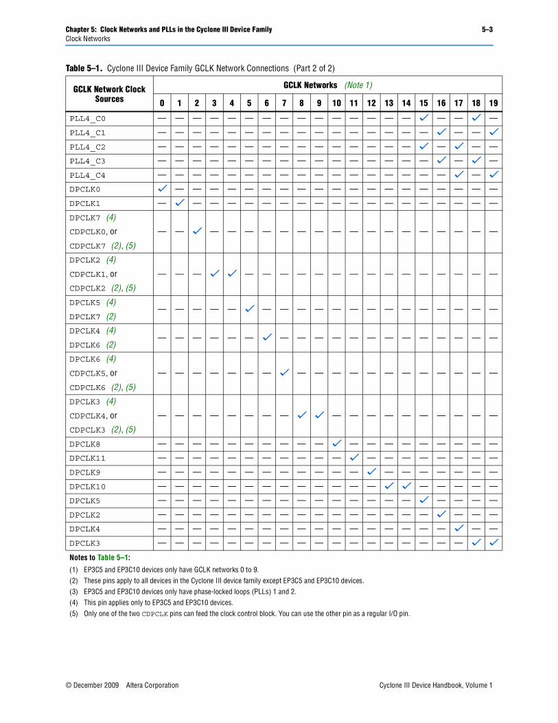
Chapter 5: Clock Networks and PLLs in the Cyclone III Device Family 5–3Clock Networks
© December 2009 Altera Corporation Cyclone III Device Handbook, Volume 1
PLL4_C0 — — — — — — — — — — — — — — — v — — v —
PLL4_C1 — — — — — — — — — — — — — — — — v — — v
PLL4_C2 — — — — — — — — — — — — — — — v — v — —
PLL4_C3 — — — — — — — — — — — — — — — — v — v —
PLL4_C4 — — — — — — — — — — — — — — — — — v — v
DPCLK0 v — — — — — — — — — — — — — — — — — — —
DPCLK1 — v — — — — — — — — — — — — — — — — — —
DPCLK7 (4)
CDPCLK0, or
CDPCLK7 (2), (5)
— — v — — — — — — — — — — — — — — — — —
DPCLK2 (4)
CDPCLK1, or
CDPCLK2 (2), (5)
— — — v v — — — — — — — — — — — — — — —
DPCLK5 (4)
DPCLK7 (2)— — — — — v — — — — — — — — — — — — — —
DPCLK4 (4)
DPCLK6 (2)— — — — — — v — — — — — — — — — — — — —
DPCLK6 (4)
CDPCLK5, or
CDPCLK6 (2), (5)
— — — — — — — v — — — — — — — — — — — —
DPCLK3 (4)
CDPCLK4, or
CDPCLK3 (2), (5)
— — — — — — — — v v — — — — — — — — — —
DPCLK8 — — — — — — — — — — v — — — — — — — — —
DPCLK11 — — — — — — — — — — — v — — — — — — — —
DPCLK9 — — — — — — — — — — — — v — — — — — — —
DPCLK10 — — — — — — — — — — — — — v v — — — — —
DPCLK5 — — — — — — — — — — — — — — — v — — — —
DPCLK2 — — — — — — — — — — — — — — — — v — — —
DPCLK4 — — — — — — — — — — — — — — — — — v — —
DPCLK3 — — — — — — — — — — — — — — — — — — v v
Notes to Table 5–1:
(1) EP3C5 and EP3C10 devices only have GCLK networks 0 to 9.(2) These pins apply to all devices in the Cyclone III device family except EP3C5 and EP3C10 devices.(3) EP3C5 and EP3C10 devices only have phase-locked loops (PLLs) 1 and 2.(4) This pin applies only to EP3C5 and EP3C10 devices.(5) Only one of the two CDPCLK pins can feed the clock control block. You can use the other pin as a regular I/O pin.
Table 5–1. Cyclone III Device Family GCLK Network Connections (Part 2 of 2)
GCLK Network Clock Sources
GCLK Networks (Note 1)
0 1 2 3 4 5 6 7 8 9 10 11 12 13 14 15 16 17 18 19

5–4 Chapter 5: Clock Networks and PLLs in the Cyclone III Device FamilyClock Networks
Cyclone III Device Handbook, Volume 1 © December 2009 Altera Corporation
If you do not use dedicated clock pins to feed the GCLKs, you can use them as general-purpose input pins to feed the logic array. However, when using them as general-purpose input pins, they do not have support for an I/O register and must use LE-based registers in place of an I/O register.
f For more information about how to connect the clock and PLL pins, refer to the Cyclone III Device Family Pin Connection Guidelines on the Altera® website.
Clock Control BlockThe clock control block drives GCLKs. Clock control blocks are located on each side of the device, close to the dedicated clock input pins. GCLKs are optimized for minimum clock skew and delay.
Table 5–2 lists the sources that can feed the clock control block, which in turn feeds the GCLKs.
In the Cyclone III device family, dedicated clock input pins, PLL counter outputs, dual-purpose clock I/O inputs, and internal logic can all feed the clock control block for each GCLK. The output from the clock control block in turn feeds the corresponding GCLK. The GCLK can drive the PLL input if the clock control block inputs are outputs of another PLL or dedicated clock input pins. The clock control blocks are at the device periphery; there are a maximum of 20 clock control blocks available per Cyclone III device family.
The control block has two functions:
■ Dynamic GCLK clock source selection (not applicable for DPCLK or CDPCLK and internal logic input)
■ GCLK network power down (dynamic enable and disable)
Table 5–2. Clock Control Block Inputs
Input Description
Dedicated clock inputsDedicated clock input pins can drive clocks or global signals, such as synchronous and asynchronous clears, presets, or clock enables onto given GCLKs.
Dual-purpose clock (DPCLK and CDPCLK) I/O input
DPCLK and CDPCLK I/O pins are bidirectional dual function pins that are used for high fan-out control signals, such as protocol signals, TRDY and IRDY signals for PCI, via the GCLK. Clock control blocks that have inputs driven by dual-purpose clock I/O pins are not able to drive PLL inputs.
PLL outputs PLL counter outputs can drive the GCLK.
Internal logic
You can drive the GCLK through logic array routing to enable internal logic elements (LEs) to drive a high fan-out, low-skew signal path. Clock control blocks that have inputs driven by internal logic are not able to drive PLL inputs.

Chapter 5: Clock Networks and PLLs in the Cyclone III Device Family 5–5Clock Networks
© December 2009 Altera Corporation Cyclone III Device Handbook, Volume 1
Figure 5–1 shows the clock control block.
Each PLL generates five clock outputs through the c[4..0] counters. Two of these clocks can drive the GCLK through a clock control block, as shown in Figure 5–1.
f For more information about how to use the clock control block in the Quartus® II software, refer to the ALTCLKCTRL Megafunction User Guide.
Figure 5–1. Clock Control Block
Notes to Figure 5–1:
(1) The clkswitch signal can either be set through the configuration file or dynamically set when using the manual PLL switchover feature. The output of the multiplexer is the input clock (fIN) for the PLL.
(2) The clkselect[1..0] signals are fed by internal logic and is used to dynamically select the clock source for the GCLK when the device is in user mode.
(3) The static clock select signals are set in the configuration file. Therefore, dynamic control when the device is in user mode is not feasible.(4) You can use internal logic to enable or disable the GCLK in user mode.
CLKSWITCH (1)
Static Clock Select (3)
Static ClockSelect (3)
Internal Logic
Clock Control Block
DPCLK or CDPCLK
CLKSELECT[1..0] (2) Internal Logic (4)
inclk1inclk0
CLK[n + 3]CLK[n + 2]CLK[n + 1]
CLK[n]
fIN
C0C1
C2PLL
GlobalClock
Enable/Disable
C3C4
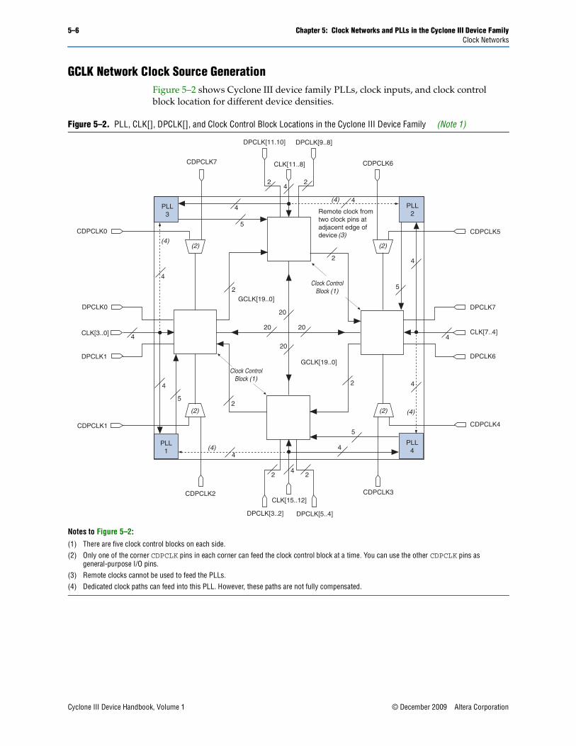
5–6 Chapter 5: Clock Networks and PLLs in the Cyclone III Device FamilyClock Networks
Cyclone III Device Handbook, Volume 1 © December 2009 Altera Corporation
GCLK Network Clock Source GenerationFigure 5–2 shows Cyclone III device family PLLs, clock inputs, and clock control block location for different device densities.
Figure 5–2. PLL, CLK[], DPCLK[], and Clock Control Block Locations in the Cyclone III Device Family (Note 1)
Notes to Figure 5–2:(1) There are five clock control blocks on each side.(2) Only one of the corner CDPCLK pins in each corner can feed the clock control block at a time. You can use the other CDPCLK pins as
general-purpose I/O pins.
(3) Remote clocks cannot be used to feed the PLLs.(4) Dedicated clock paths can feed into this PLL. However, these paths are not fully compensated.
PLL1
PLL4
PLL2
PLL3
20
20
20
20
4
4
4
44
4
4
4
2
2
2
2
2 2
2 2
5
5
5
5
(2)(2)
(2) (2)
CDPCLK7
CDPCLK0
CDPCLK1
DPCLK1
DPCLK[11.10] DPCLK[9..8]
CLK[11..8] CDPCLK6
DPCLK0
CLK[3..0]
Clock ControlBlock (1)
GCLK[19..0]
GCLK[19..0]
CDPCLK5
DPCLK7
CLK[7..4]
DPCLK6
CDPCLK4
CDPCLK2
DPCLK[3..2]
CLK[15..12]
DPCLK[5..4]
CDPCLK3
Remote clock fromtwo clock pins at adjacent edge of device
Clock ControlBlock (1)
(3)
4
4
4
4
(4)
(4)
(4)
(4)

Chapter 5: Clock Networks and PLLs in the Cyclone III Device Family 5–7Clock Networks
© December 2009 Altera Corporation Cyclone III Device Handbook, Volume 1
The inputs to the five clock control blocks on each side must be chosen from among the following clock sources:
■ Four clock input pins
■ Five PLL counter outputs
■ Two DPCLK pins and two CDPCLK pins from both the left and right sides, and four DPCLK pins and two CDPCLK pins from both the top and bottom
■ Five signals from internal logic
From the clock sources listed above, only two clock input pins, two PLL clock outputs, one DPCLK or CDPCLK pin, and one source from internal logic can drive into any given clock control block, as shown in Figure 5–1 on page 5–5.
Out of these five inputs to any clock control block, the two clock input pins and two PLL outputs are dynamically selected to feed a GCLK. The clock control block supports static selection of the signal from internal logic.
Figure 5–3 shows a simplified version of the five clock control blocks on each side of the Cyclone III device family periphery.
GCLK Network Power DownYou can disable the Cyclone III device family GCLK (power down) by using both static and dynamic approaches. In the static approach, configuration bits are set in the configuration file generated by the Quartus II software, which automatically disables unused GCLKs. The dynamic clock enable or disable feature allows internal logic to control clock enable or disable of the GCLKs in the Cyclone III device family.
When a clock network is disabled, all the logic fed by the clock network is in an off-state, thereby reducing the overall power consumption of the device. This function is independent of the PLL and is applied directly on the clock network, as shown in Figure 5–1 on page 5–5.
You can set the input clock sources and the clkena signals for the GCLK multiplexers through the Quartus II software using the ALTCLKCTRL megafunction.
f For more information, refer to the ALTCLKCTRL Megafunction User Guide.
Figure 5–3. Clock Control Blocks on Each Side of the Cyclone III Device Family (Note 1)
Note to Figure 5–3:
(1) The left and right sides of the device have two DPCLK pins; the top and bottom of the device have four DPCLK pins.
5GCLK
Clock Input Pins4
DPCLK
Internal Logic
ClockControlBlock
5PLL Outputs
5
2 or 4
CDPCLK2
Five Clock ControlBlocks on Each Side
of the Device

5–8 Chapter 5: Clock Networks and PLLs in the Cyclone III Device FamilyClock Networks
Cyclone III Device Handbook, Volume 1 © December 2009 Altera Corporation
clkena SignalsThe Cyclone III device family supports clkena signals at the GCLK network level. This allows you to gate-off the clock even when a PLL is used. Upon re-enabling the output clock, the PLL does not need a resynchronization or re-lock period because the circuit gates off the clock at the clock network level. In addition, the PLL can remain locked independent of the clkena signals because the loop-related counters are not affected.
Figure 5–4 shows how to implement the clkena signal.
1 The clkena circuitry controlling the output C0 of the PLL to an output pin is implemented with two registers instead of a single register, as shown in Figure 5–4.
Figure 5–5 shows the waveform example for a clock output enable. The clkena signal is sampled on the falling edge of the clock (clkin).
1 This feature is useful for applications that require low power or sleep mode.
The clkena signal can also disable clock outputs if the system is not tolerant to frequency overshoot during PLL resynchronization.
Figure 5–4. clkena Implementation
D Qclkena clkena_out
clk_out
clkin
Figure 5–5. clkena Implementation: Output Enable
clkin
clkena
clk_out

Chapter 5: Clock Networks and PLLs in the Cyclone III Device Family 5–9PLLs in the Cyclone III Device Family
© December 2009 Altera Corporation Cyclone III Device Handbook, Volume 1
Altera recommends using the clkena signals when switching the clock source to the PLLs or the GCLK. The recommended sequence is:
1. Disable the primary output clock by deasserting the clkena signal.
2. Switch to the secondary clock using the dynamic select signals of the clock control block.
3. Allow some clock cycles of the secondary clock to pass before reasserting the clkena signal. The exact number of clock cycles you must wait before enabling the secondary clock is design-dependent. You can build custom logic to ensure glitch-free transition when switching between different clock sources.
PLLs in the Cyclone III Device FamilyThe Cyclone III device family offers up to four PLLs that provide robust clock management and synthesis for device clock management, external system clock management, and high-speed I/O interfaces.
f For more information about the number of PLLs in each device density, refer to the Cyclone III Device Family Overview chapter.
The Cyclone III device family PLLs have the same core analog structure.
Table 5–3 lists the features available in the Cyclone III device family PLLs.
Table 5–3. Cyclone III Device Family PLL Hardware Features
Hardware Features Availability
C (output counters) 5
M, N, C counter sizes 1 to 512 (1)
Dedicated clock outputs 1 single-ended or 1 differential pair
Clock input pins 4 single-ended or 2 differential pairs
Spread-spectrum input clock tracking v (2)
PLL cascading Through GCLK
Compensation modes Source-Synchronous Mode, No Compensation Mode, Normal Mode, and Zero Delay Buffer Mode
Phase shift resolution Down to 96-ps increments (3)
Programmable duty cycle v
Output counter cascading v
Input clock switchover v
User mode reconfiguration v
Loss of lock detection v
Notes to Table 5–3:
(1) C counters range from 1 through 512 if the output clock uses a 50% duty cycle. For any output clocks using a non-50% duty cycle, the post-scale counters range from 1 through 256.
(2) Only applicable if the input clock jitter is in the input jitter tolerance specifications.(3) The smallest phase shift is determined by the voltage-controlled oscillator (VCO) period divided by eight. For
degree increments, the Cyclone III device family can shift all output frequencies in increments of at least 45°. Smaller degree increments are possible depending on the frequency and divide parameters.

5–10 Chapter 5: Clock Networks and PLLs in the Cyclone III Device FamilyCyclone III Device Family PLL Hardware Overview
Cyclone III Device Handbook, Volume 1 © December 2009 Altera Corporation
Cyclone III Device Family PLL Hardware Overview This section gives a hardware overview of the Cyclone III device family PLL.
Figure 5–6 shows a simplified block diagram of the major components of the PLL of the Cyclone III device family.
1 The VCO post-scale counter K is used to divide the supported VCO range by two. The VCO frequency reported by the Quartus II software in the PLL summary section of the compilation report takes into consideration the VCO post-scale counter value. Therefore, if the VCO post-scale counter has a value of 2, the frequency reported is lower than the fVCO specification specified in the Cyclone III Device Data Sheet and Cyclone III LS Device Data Sheet chapters.
External Clock OutputsEach PLL of the Cyclone III device family supports one single-ended clock output or one differential clock output. Only the C0 output counter can feed the dedicated external clock outputs, as shown in Figure 5–7, without going through the GCLK. Other output counters can feed other I/O pins through the GCLK.
Figure 5–6. Cyclone III Device Family PLL Block Diagram (Note 1)
Notes to Figure 5–6:
(1) Each clock source can come from any of the four clock pins located on the same side of the device as the PLL.(2) This is the VCO post-scale counter K.(3) This input port is fed by a pin-driven dedicated GCLK, or through a clock control block if the clock control block is fed by an output from another
PLL or a pin-driven dedicated GCLK. An internally generated global signal cannot drive the PLL.
ClockSwitchover
Block
inclk0
inclk1
Clock inputsfrom pins
GCLK
pfdena
clkswitch
clkbad0clkbad1
activeclock
PFD
LOCKcircuit
lock
÷n CP LF VCO ÷2 (2)
÷C0
÷C1
÷C2
÷C3
÷C4
÷M
PLLoutputmux
GCLKs
External clockoutput
8 84
GCLKnetworks
no compensation; ZDB mode
source-synchronous;normal mode
VCO Range
Detector
VCOOVRR
VCOUNDR
(3)

Chapter 5: Clock Networks and PLLs in the Cyclone III Device Family 5–11Cyclone III Device Family PLL Hardware Overview
© December 2009 Altera Corporation Cyclone III Device Handbook, Volume 1
Figure 5–7 shows the external clock outputs for PLLs.
Each pin of a differential output pair is 180° out of phase. The Quartus II software places the NOT gate in your design into the I/O element to implement 180° phase with respect to the other pin in the pair. The clock output pin pairs support the same I/O standards as standard output pins (in the top and bottom banks) as well as LVDS, LVPECL, differential HSTL, and differential SSTL.
f To determine which I/O standards are supported by the PLL clock input and output pins, refer to the Cyclone III Device I/O Features chapter.
Cyclone III device family PLLs can drive out to any regular I/O pin through the GCLK. You can also use the external clock output pins as general purpose I/O pins if external PLL clocking is not required.
Figure 5–7. External Clock Outputs for PLLs
Notes to Figure 5–7:
(1) These external clock enable signals are available only when using the ALTCLKCTRL megafunction. (2) PLL#_CLKOUTp and PLL#_CLKOUTn pins are dual-purpose I/O pins that you can use as one single-ended or
one differential clock output.
C0
C1
C2
C4
C3PLL #
clkena 1 (1)
clkena 0 (1)
PLL #_CLKOUTp (2)
PLL #_CLKOUTn (2)
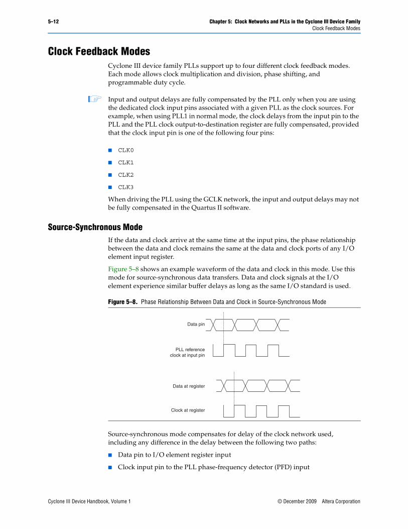
5–12 Chapter 5: Clock Networks and PLLs in the Cyclone III Device FamilyClock Feedback Modes
Cyclone III Device Handbook, Volume 1 © December 2009 Altera Corporation
Clock Feedback ModesCyclone III device family PLLs support up to four different clock feedback modes. Each mode allows clock multiplication and division, phase shifting, and programmable duty cycle.
1 Input and output delays are fully compensated by the PLL only when you are using the dedicated clock input pins associated with a given PLL as the clock sources. For example, when using PLL1 in normal mode, the clock delays from the input pin to the PLL and the PLL clock output-to-destination register are fully compensated, provided that the clock input pin is one of the following four pins:
■ CLK0
■ CLK1
■ CLK2
■ CLK3
When driving the PLL using the GCLK network, the input and output delays may not be fully compensated in the Quartus II software.
Source-Synchronous ModeIf the data and clock arrive at the same time at the input pins, the phase relationship between the data and clock remains the same at the data and clock ports of any I/O element input register.
Figure 5–8 shows an example waveform of the data and clock in this mode. Use this mode for source-synchronous data transfers. Data and clock signals at the I/O element experience similar buffer delays as long as the same I/O standard is used.
Source-synchronous mode compensates for delay of the clock network used, including any difference in the delay between the following two paths:
■ Data pin to I/O element register input
■ Clock input pin to the PLL phase-frequency detector (PFD) input
Figure 5–8. Phase Relationship Between Data and Clock in Source-Synchronous Mode
Data pin
PLL referenceclock at input pin
Data at register
Clock at register
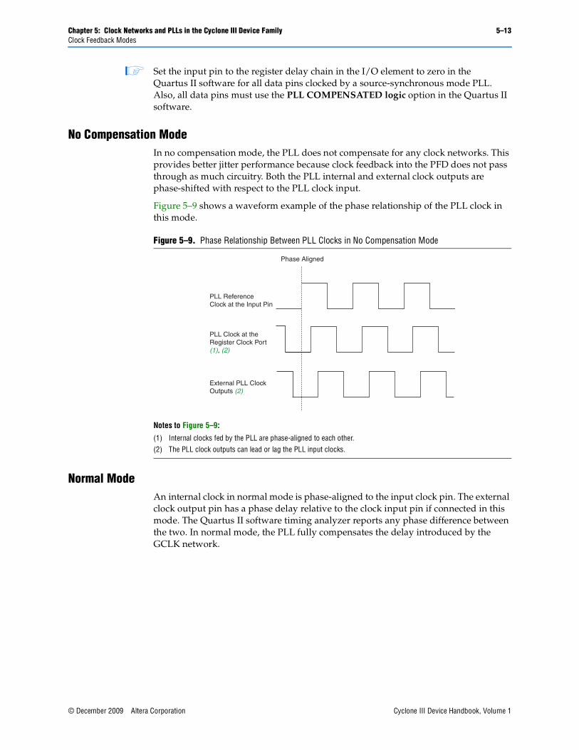
Chapter 5: Clock Networks and PLLs in the Cyclone III Device Family 5–13Clock Feedback Modes
© December 2009 Altera Corporation Cyclone III Device Handbook, Volume 1
1 Set the input pin to the register delay chain in the I/O element to zero in the Quartus II software for all data pins clocked by a source-synchronous mode PLL. Also, all data pins must use the PLL COMPENSATED logic option in the Quartus II software.
No Compensation ModeIn no compensation mode, the PLL does not compensate for any clock networks. This provides better jitter performance because clock feedback into the PFD does not pass through as much circuitry. Both the PLL internal and external clock outputs are phase-shifted with respect to the PLL clock input.
Figure 5–9 shows a waveform example of the phase relationship of the PLL clock in this mode.
Normal ModeAn internal clock in normal mode is phase-aligned to the input clock pin. The external clock output pin has a phase delay relative to the clock input pin if connected in this mode. The Quartus II software timing analyzer reports any phase difference between the two. In normal mode, the PLL fully compensates the delay introduced by the GCLK network.
Figure 5–9. Phase Relationship Between PLL Clocks in No Compensation Mode
Notes to Figure 5–9:
(1) Internal clocks fed by the PLL are phase-aligned to each other.(2) The PLL clock outputs can lead or lag the PLL input clocks.
PLL ReferenceClock at the Input Pin
PLL Clock at theRegister Clock Port(1), (2)
External PLL ClockOutputs (2)
Phase Aligned
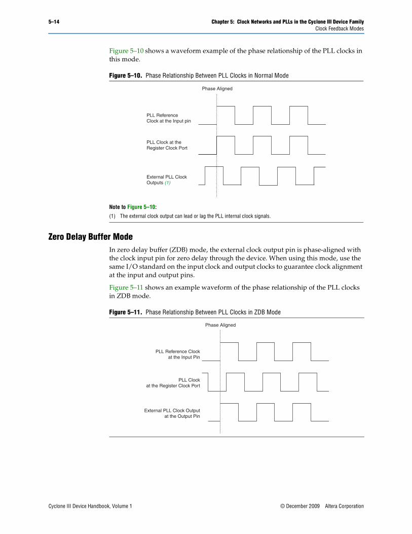
5–14 Chapter 5: Clock Networks and PLLs in the Cyclone III Device FamilyClock Feedback Modes
Cyclone III Device Handbook, Volume 1 © December 2009 Altera Corporation
Figure 5–10 shows a waveform example of the phase relationship of the PLL clocks in this mode.
Zero Delay Buffer ModeIn zero delay buffer (ZDB) mode, the external clock output pin is phase-aligned with the clock input pin for zero delay through the device. When using this mode, use the same I/O standard on the input clock and output clocks to guarantee clock alignment at the input and output pins.
Figure 5–11 shows an example waveform of the phase relationship of the PLL clocks in ZDB mode.
Figure 5–10. Phase Relationship Between PLL Clocks in Normal Mode
Note to Figure 5–10:
(1) The external clock output can lead or lag the PLL internal clock signals.
PLL ReferenceClock at the Input pin
PLL Clock at theRegister Clock Port
External PLL ClockOutputs (1)
Phase Aligned
Figure 5–11. Phase Relationship Between PLL Clocks in ZDB Mode
PLL Reference Clock at the Input Pin
PLL Clockat the Register Clock Port
External PLL Clock Outputat the Output Pin
Phase Aligned
Chapter 5: Clock Networks and PLLs in the Cyclone III Device Family 5–15Hardware Features
© December 2009 Altera Corporation Cyclone III Device Handbook, Volume 1
Hardware FeaturesCyclone III device family PLLs support several features for general-purpose clock management. This section discusses clock multiplication and division implementation, phase shifting implementations, and programmable duty cycles.
Clock Multiplication and DivisionEach Cyclone III device family PLL provides clock synthesis for PLL output ports using M/(N*post-scale counter) scaling factors. The input clock is divided by a pre-scale factor, N, and is then multiplied by the M feedback factor. The control loop drives the VCO to match fIN (M/N). Each output port has a unique post-scale counter that divides down the high-frequency VCO. For multiple PLL outputs with different frequencies, the VCO value is the least common multiple of the output frequencies that meets its frequency specifications. For example, if output frequencies required from one PLL are 33 and 66 MHz, the Quartus II software sets the VCO to 660 MHz (the least common multiple of 33 and 66 MHz in the VCO range). Then, the post-scale counters scale down the VCO frequency for each output port.
There is one pre-scale counter, N, and one multiply counter, M, per PLL, with a range of 1 to 512 for both M and N. The N counter does not use duty cycle control because the purpose of this counter is only to calculate frequency division. There are five generic post-scale counters per PLL that can feed GCLKs or external clock outputs. These post-scale counters range from 1 to 512 with a 50% duty cycle setting. The post-scale counters range from 1 to 256 with any non-50% duty cycle setting. The sum of the high/low count values chosen for a design selects the divide value for a given counter.
The Quartus II software automatically chooses the appropriate scaling factors according to the input frequency, multiplication, and division values entered into the ALTPLL megafunction.
1 Phase alignment between output counters are determined using the tPLL_PSERR specification.

5–16 Chapter 5: Clock Networks and PLLs in the Cyclone III Device FamilyHardware Features
Cyclone III Device Handbook, Volume 1 © December 2009 Altera Corporation
Post-Scale Counter CascadingCyclone III device family PLLs support post-scale counter cascading to create counters larger than 512. This is implemented by feeding the output of one C counter into the input of the next C counter, as shown in Figure 5–12.
When cascading counters to implement a larger division of the high-frequency VCO clock, the cascaded counters behave as one counter with the product of the individual counter settings.
For example, if C0 = 4 and C1 = 2, the cascaded value is C0 × C1 = 8.
1 Post-scale counter cascading is automatically set by the Quartus II software in the configuration file. Post-scale counter cascading cannot be performed using the PLL reconfiguration.
Programmable Duty CycleThe programmable duty cycle allows PLLs to generate clock outputs with a variable duty cycle. This feature is supported on the PLL post-scale counters. You can achieve the duty cycle setting by a low and high time count setting for the post-scale counters. The Quartus II software uses the frequency input and the required multiply or divide rate to determine the duty cycle choices. The post-scale counter value determines the precision of the duty cycle. The precision is defined by 50% divided by the post-scale counter value. For example, if the C0 counter is 10, steps of 5% are possible for duty cycle choices between 5 to 90%.
Combining the programmable duty cycle with programmable phase shift allows the generation of precise non-overlapping clocks.
Figure 5–12. Counter Cascading
C0
C1
C2
C3
C4
VCO Output
VCO Output
VCO Output
VCO Output
VCO Output
VCO Output
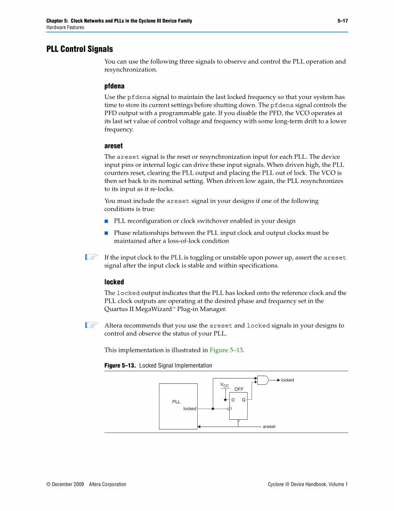
Chapter 5: Clock Networks and PLLs in the Cyclone III Device Family 5–17Hardware Features
© December 2009 Altera Corporation Cyclone III Device Handbook, Volume 1
PLL Control SignalsYou can use the following three signals to observe and control the PLL operation and resynchronization.
pfdenaUse the pfdena signal to maintain the last locked frequency so that your system has time to store its current settings before shutting down. The pfdena signal controls the PFD output with a programmable gate. If you disable the PFD, the VCO operates at its last set value of control voltage and frequency with some long-term drift to a lower frequency.
aresetThe areset signal is the reset or resynchronization input for each PLL. The device input pins or internal logic can drive these input signals. When driven high, the PLL counters reset, clearing the PLL output and placing the PLL out of lock. The VCO is then set back to its nominal setting. When driven low again, the PLL resynchronizes to its input as it re-locks.
You must include the areset signal in your designs if one of the following conditions is true:
■ PLL reconfiguration or clock switchover enabled in your design
■ Phase relationships between the PLL input clock and output clocks must be maintained after a loss-of-lock condition
1 If the input clock to the PLL is toggling or unstable upon power up, assert the areset signal after the input clock is stable and within specifications.
lockedThe locked output indicates that the PLL has locked onto the reference clock and the PLL clock outputs are operating at the desired phase and frequency set in the Quartus II MegaWizard™ Plug-in Manager.
1 Altera recommends that you use the areset and locked signals in your designs to control and observe the status of your PLL.
This implementation is illustrated in Figure 5–13.
Figure 5–13. Locked Signal Implementation
OFF
D QPLL
locked
locked
areset
VCC

5–18 Chapter 5: Clock Networks and PLLs in the Cyclone III Device FamilyHardware Features
Cyclone III Device Handbook, Volume 1 © December 2009 Altera Corporation
If you use the SignalTap® II tool to probe the locked signal before the D flip-flop, the locked signal goes low only when areset is deasserted. If the areset signal is not enabled, the extra logic is not implemented in the ALTPLL megafunction.
f For more information about the PLL control signals, refer to the ALTPLL Megafunction User Guide.
Clock SwitchoverThe clock switchover feature allows the PLL to switch between two reference input clocks. Use this feature for clock redundancy or for a dual-clock domain application, such as a system that turns on the redundant clock if the previous clock stops running. Your design can automatically perform clock switchover when the clock is no longer toggling, or based on the user control signal, clkswitch.
Automatic Clock SwitchoverCyclone III device family PLLs support a fully configurable clock switchover capability.
When the current reference clock is not present, the clock-sense block automatically switches to the backup clock for PLL reference. The clock switchover circuit also sends out three status signals—clkbad[0], clkbad[1], and activeclock—from the PLL to implement a custom switchover circuit. You can select a clock source at the backup clock by connecting it to the inclk1 port of the PLL in your design.
Figure 5–14 shows the block diagram of the switchover circuit built into the PLL.
Figure 5–14. Automatic Clock Switchover Circuit
SwitchoverState
Machine
ClockSense
n Counter PFD
clkswitch (provides manual switchover support)
Activeclock
clkbad1
clkbad0
muxout
inclk0
inclk1
refclk
fbclk
clksw
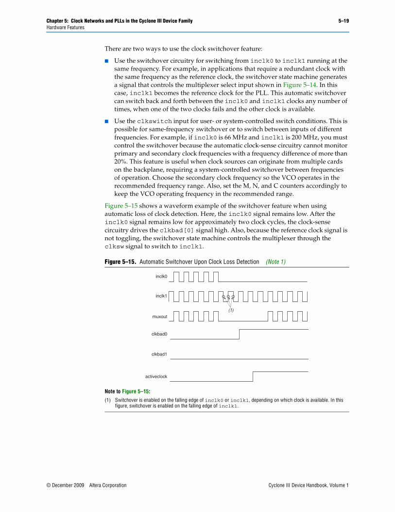
Chapter 5: Clock Networks and PLLs in the Cyclone III Device Family 5–19Hardware Features
© December 2009 Altera Corporation Cyclone III Device Handbook, Volume 1
There are two ways to use the clock switchover feature:
■ Use the switchover circuitry for switching from inclk0 to inclk1 running at the same frequency. For example, in applications that require a redundant clock with the same frequency as the reference clock, the switchover state machine generates a signal that controls the multiplexer select input shown in Figure 5–14. In this case, inclk1 becomes the reference clock for the PLL. This automatic switchover can switch back and forth between the inclk0 and inclk1 clocks any number of times, when one of the two clocks fails and the other clock is available.
■ Use the clkswitch input for user- or system-controlled switch conditions. This is possible for same-frequency switchover or to switch between inputs of different frequencies. For example, if inclk0 is 66 MHz and inclk1 is 200 MHz, you must control the switchover because the automatic clock-sense circuitry cannot monitor primary and secondary clock frequencies with a frequency difference of more than 20%. This feature is useful when clock sources can originate from multiple cards on the backplane, requiring a system-controlled switchover between frequencies of operation. Choose the secondary clock frequency so the VCO operates in the recommended frequency range. Also, set the M, N, and C counters accordingly to keep the VCO operating frequency in the recommended range.
Figure 5–15 shows a waveform example of the switchover feature when using automatic loss of clock detection. Here, the inclk0 signal remains low. After the inclk0 signal remains low for approximately two clock cycles, the clock-sense circuitry drives the clkbad[0] signal high. Also, because the reference clock signal is not toggling, the switchover state machine controls the multiplexer through the clksw signal to switch to inclk1.
Figure 5–15. Automatic Switchover Upon Clock Loss Detection (Note 1)
Note to Figure 5–15:
(1) Switchover is enabled on the falling edge of inclk0 or inclk1, depending on which clock is available. In this figure, switchover is enabled on the falling edge of inclk1.
inclk0
inclk1
muxout
clkbad0
clkbad1
(1)
activeclock
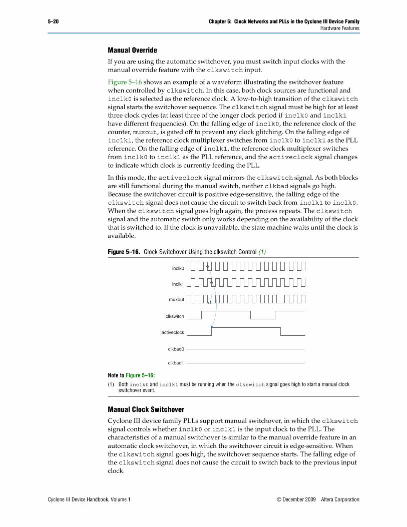
5–20 Chapter 5: Clock Networks and PLLs in the Cyclone III Device FamilyHardware Features
Cyclone III Device Handbook, Volume 1 © December 2009 Altera Corporation
Manual Override If you are using the automatic switchover, you must switch input clocks with the manual override feature with the clkswitch input.
Figure 5–16 shows an example of a waveform illustrating the switchover feature when controlled by clkswitch. In this case, both clock sources are functional and inclk0 is selected as the reference clock. A low-to-high transition of the clkswitch signal starts the switchover sequence. The clkswitch signal must be high for at least three clock cycles (at least three of the longer clock period if inclk0 and inclk1 have different frequencies). On the falling edge of inclk0, the reference clock of the counter, muxout, is gated off to prevent any clock glitching. On the falling edge of inclk1, the reference clock multiplexer switches from inclk0 to inclk1 as the PLL reference. On the falling edge of inclk1, the reference clock multiplexer switches from inclk0 to inclk1 as the PLL reference, and the activeclock signal changes to indicate which clock is currently feeding the PLL.
In this mode, the activeclock signal mirrors the clkswitch signal. As both blocks are still functional during the manual switch, neither clkbad signals go high. Because the switchover circuit is positive edge-sensitive, the falling edge of the clkswitch signal does not cause the circuit to switch back from inclk1 to inclk0. When the clkswitch signal goes high again, the process repeats. The clkswitch signal and the automatic switch only works depending on the availability of the clock that is switched to. If the clock is unavailable, the state machine waits until the clock is available.
Manual Clock SwitchoverCyclone III device family PLLs support manual switchover, in which the clkswitch signal controls whether inclk0 or inclk1 is the input clock to the PLL. The characteristics of a manual switchover is similar to the manual override feature in an automatic clock switchover, in which the switchover circuit is edge-sensitive. When the clkswitch signal goes high, the switchover sequence starts. The falling edge of the clkswitch signal does not cause the circuit to switch back to the previous input clock.
Figure 5–16. Clock Switchover Using the clkswitch Control (1)
Note to Figure 5–16:
(1) Both inclk0 and inclk1 must be running when the clkswitch signal goes high to start a manual clock switchover event.
inclk0
inclk1
muxout
clkswitch
activeclock
clkbad0
clkbad1

Chapter 5: Clock Networks and PLLs in the Cyclone III Device Family 5–21Hardware Features
© December 2009 Altera Corporation Cyclone III Device Handbook, Volume 1
f For more information about PLL software support in the Quartus II software, refer to the ALTPLL Megafunction User Guide.
GuidelinesUse the following guidelines to design with clock switchover in PLLs:
■ Clock loss detection and automatic clock switchover requires that the inclk0 and inclk1 frequencies be within 20% of each other. Failing to meet this requirement causes the clkbad[0] and clkbad[1] signals to function improperly.
■ When using manual clock switchover, the difference between inclk0 and inclk1 can be more than 20%. However, differences between the two clock sources (frequency, phase, or both) can cause the PLL to lose lock. Resetting the PLL ensures that the correct phase relationships are maintained between the input and output clocks.
1 Both inclk0 and inclk1 must be running when the clkswitch signal goes high to start the manual clock switchover event. Failing to meet this requirement causes the clock switchover to malfunction.
■ Applications that require a clock switchover feature and a small frequency drift must use a low-bandwidth PLL. When referencing input clock changes, the low-bandwidth PLL reacts slower than a high-bandwidth PLL. When the switchover happens, the low-bandwidth PLL propagates the stopping of the clock to the output slower than the high-bandwidth PLL. The low-bandwidth PLL filters out jitter on the reference clock. However, you must be aware that the low-bandwidth PLL also increases lock time.
■ After a switchover occurs, there may be a finite resynchronization period for the PLL to lock onto a new clock. The exact amount of time it takes for the PLL to re-lock is dependent on the PLL configuration.
■ If the phase relationship between the input clock to the PLL and output clock from the PLL is important in your design, assert areset for 10 ns after performing a clock switchover. Wait for the locked signal (or gated lock) to go high before re-enabling the output clocks from the PLL.
■ Figure 5–17 shows how the VCO frequency gradually decreases when the primary clock is lost and then increases as the VCO locks on to the secondary clock. After the VCO locks on to the secondary clock, some overshoot can occur (an over-frequency condition) in the VCO frequency.
Figure 5–17. VCO Switchover Operating Frequency
ΔFvco
Primary Clock Stops Running
Switchover Occurs
VCO Tracks Secondary Clock
Frequency Overshoot

5–22 Chapter 5: Clock Networks and PLLs in the Cyclone III Device FamilyProgrammable Bandwidth
Cyclone III Device Handbook, Volume 1 © December 2009 Altera Corporation
■ Disable the system during switchover if the system is not tolerant to frequency variations during the PLL resynchronization period. You can use the clkbad[0] and clkbad[1] status signals to turn off the PFD (pfdena = 0) so the VCO maintains its last frequency. You can also use the switchover state machine to switch over to the secondary clock. Upon enabling the PFD, output clock enable signals (clkena) can disable clock outputs during the switchover and resynchronization period. After the lock indication is stable, the system can re-enable the output clock or clocks.
Programmable BandwidthThe PLL bandwidth is the measure of the PLL’s ability to track the input clock and its associated jitter. Cyclone III device family PLLs provide advanced control of the PLL bandwidth using the programmable characteristics of the PLL loop, including loop filter and charge pump. The closed-loop gain 3-dB frequency in the PLL determines the PLL bandwidth. The bandwidth is approximately the unity gain point for open loop PLL response.
Phase Shift ImplementationPhase shift is used to implement a robust solution for clock delays in the Cyclone III device family. Phase shift is implemented with a combination of the VCO phase output and the counter starting time. The VCO phase output and counter starting time are the most accurate methods of inserting delays, because they are purely based on counter settings, which are independent of process, voltage, and temperature.
You can phase shift the output clocks from the Cyclone III device family PLLs in either:
■ Fine resolution using VCO phase taps, or
■ Coarse resolution using counter starting time
Fine resolution phase shifts are implemented by allowing any of the output counters (C[4..0]) or the M counter to use any of the eight phases of the VCO as the reference clock. This allows you to adjust the delay time with a fine resolution. Equation 5–1 shows the minimum delay time that you can insert using this method.
in which fREF is the input reference clock frequency.
For example, if fREF is 100 MHz, N = 1, and M = 8, then fVCO = 800 MHz, and fine = 156.25 ps. The PLL operating frequency defines this phase shift, a value that depends on reference clock frequency and counter settings.
Equation 5–1. Fine Resolution Phase Shift
fineTVCO
8----------- 1
8fVCO-------------- N
8MfREF------------------= = =

Chapter 5: Clock Networks and PLLs in the Cyclone III Device Family 5–23Phase Shift Implementation
© December 2009 Altera Corporation Cyclone III Device Handbook, Volume 1
Coarse resolution phase shifts are implemented by delaying the start of the counters for a predetermined number of counter clocks. Equation 5–2 shows the coarse phase shift.
C is the count value set for the counter delay time (this is the initial setting in the PLL usage section of the compilation report in the Quartus II software). If the initial value is 1, C – 1 = 0° phase shift.
Figure 5–18 shows an example of phase shift insertion using fine resolution through VCO phase taps method. The eight phases from the VCO are shown and labeled for reference. In this example, CLK0 is based on 0° phase from the VCO and has the C value for the counter set to one. The CLK1 signal is divided by four, two VCO clocks for high time and two VCO clocks for low time. CLK1 is based on the 135° phase tap from the VCO and has the C value for the counter set to one. The CLK1 signal is also divided by four. In this case, the two clocks are offset by 3 fine. CLK2 is based on the 0° phase from the VCO but has the C value for the counter set to three. This creates a delay of two coarse (two complete VCO periods).
You can use the coarse and fine phase shifts to implement clock delays in the Cyclone III device family.
The Cyclone III device family supports dynamic phase shifting of VCO phase taps only. The phase shift is configurable for any number of times. Each phase shift takes about one scanclk cycle, allowing you to implement large phase shifts quickly.
Equation 5–2. Coarse Resolution Phase Shift
coarseC 1–fVCO------------ C 1– N
MfREF---------------------= =
Figure 5–18. Delay Insertion Using VCO Phase Output and Counter Delay Time
td0-1
td0-2
1/8 tVCO tVCO
0
90
135
180
225
270
315
CLK0
CLK1
CLK2
45

5–24 Chapter 5: Clock Networks and PLLs in the Cyclone III Device FamilyPLL Cascading
Cyclone III Device Handbook, Volume 1 © December 2009 Altera Corporation
PLL CascadingTwo PLLs are cascaded to each other through the clock network. If your design cascades PLLs, the source (upstream) PLL must have a low-bandwidth setting, while the destination (downstream) PLL must have a high-bandwidth setting.
Figure 5–19 shows using GCLK while cascading PLLs.
PLL ReconfigurationPLLs use several divide counters and different VCO phase taps to perform frequency synthesis and phase shifts. In Cyclone III device family PLLs, you can reconfigure both counter settings and phase shift the PLL output clock in real time. You can also change the charge pump and loop filter components, which dynamically affects PLL bandwidth. You can use these PLL components to update the output clock frequency, PLL bandwidth, and phase shift in real time, without reconfiguring the entire FPGA.
Figure 5–19. PLL Cascading Using GCLK
CLK[0..3]
CLK[8..11]
GCLK[0..4]
GCLK[5..9]
GCLK[15..19]
GCLK[10..14]
CLK[12..15]
CLK[4..7]
Output from PLL
Output from PLL
Input to PLL
Output from PLL
Output from PLL
Five Clock Control Blocks
Five ClockControl Blocks
Five ClockControl Blocks
Five ClockControl Blocks
PLL1
PLL4
PLL2
PLL3
5
5
5
5
Remote clock from two Clock pins at adjacentedge of device
2
2
2
2
2
4
2
4
4
2
2
4
120
GCLK[0:19]
20 1
20
1
GCLK[0:19]
20
1
GCLK[0:19]
GCLK[0:19]

Chapter 5: Clock Networks and PLLs in the Cyclone III Device Family 5–25PLL Reconfiguration
© December 2009 Altera Corporation Cyclone III Device Handbook, Volume 1
The ability to reconfigure the PLL in real time is useful in applications that might operate at multiple frequencies. It is also useful in prototyping environments, allowing you to sweep PLL output frequencies and adjust the output clock phase dynamically. For instance, a system generating test patterns is required to generate and send patterns at 75 or 150 MHz, depending on the requirements of the device under test. Reconfiguring PLL components in real time allows you to switch between two such output frequencies in a few microseconds.
You can also use this feature to adjust clock-to-out (tCO) delays in real time by changing the PLL output clock phase shift. This approach eliminates the need to regenerate a configuration file with the new PLL settings.
PLL Reconfiguration Hardware ImplementationThe following PLL components are configurable in real time:
■ Pre-scale counter (N)
■ Feedback counter (M)
■ Post-scale output counters (C0-C4)
■ Dynamically adjust the charge pump current (ICP) and loop filter components (R, C) to facilitate on-the-fly reconfiguration of the PLL bandwidth
Figure 5–20 shows how to adjust PLL counter settings dynamically by shifting their new settings into a serial shift register chain or scan chain. Serial data shifts to the scan chain via the scandataport, and shift registers are clocked by scanclk. The maximum scanclk frequency is 100 MHz. After shifting the last bit of data, asserting the configupdate signal for at least one scanclk clock cycle synchronously updates the PLL configuration bits with the data in the scan registers.
Figure 5–20. PLL Reconfiguration Scan Chain
/C4 /C3 /C2 /C1 /C0 /M /N
scanclk
scandone
scandata
LF/K/CP
configupdate
inclk
PFD VCO
FVCO
scanclkena
scandataout
from M counterfrom N counter
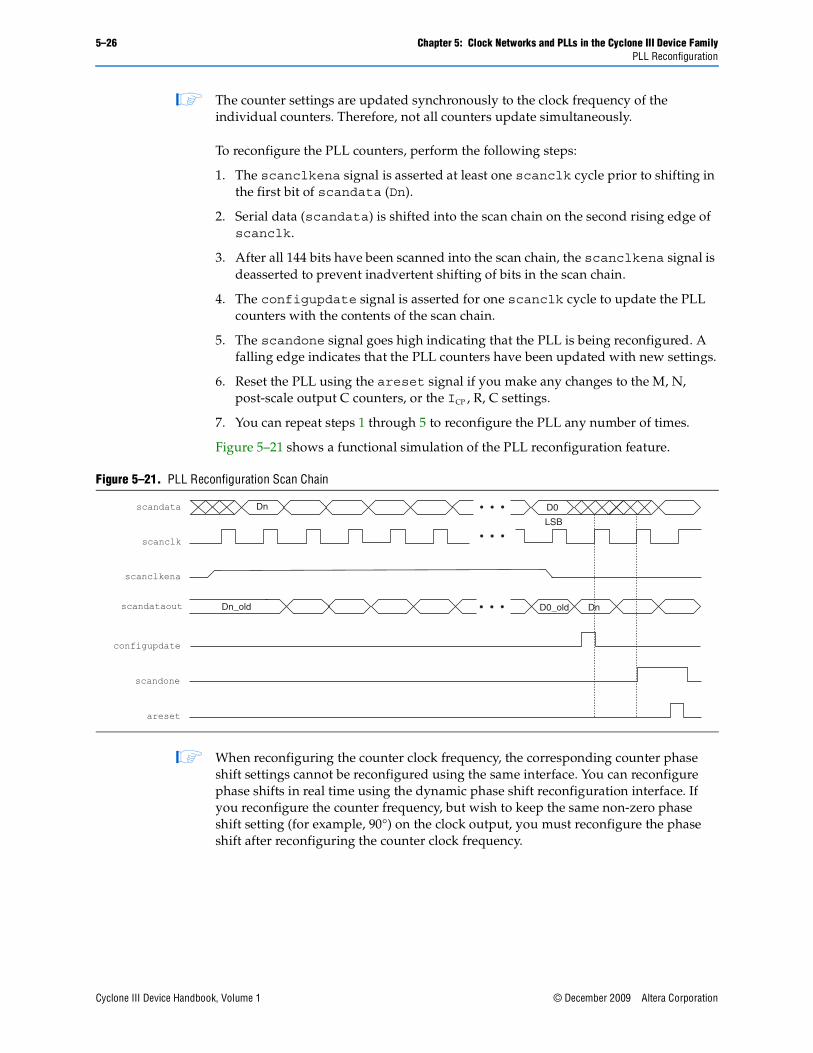
5–26 Chapter 5: Clock Networks and PLLs in the Cyclone III Device FamilyPLL Reconfiguration
Cyclone III Device Handbook, Volume 1 © December 2009 Altera Corporation
1 The counter settings are updated synchronously to the clock frequency of the individual counters. Therefore, not all counters update simultaneously.
To reconfigure the PLL counters, perform the following steps:
1. The scanclkena signal is asserted at least one scanclk cycle prior to shifting in the first bit of scandata (Dn).
2. Serial data (scandata) is shifted into the scan chain on the second rising edge of scanclk.
3. After all 144 bits have been scanned into the scan chain, the scanclkena signal is deasserted to prevent inadvertent shifting of bits in the scan chain.
4. The configupdate signal is asserted for one scanclk cycle to update the PLL counters with the contents of the scan chain.
5. The scandone signal goes high indicating that the PLL is being reconfigured. A falling edge indicates that the PLL counters have been updated with new settings.
6. Reset the PLL using the areset signal if you make any changes to the M, N, post-scale output C counters, or the ICP , R, C settings.
7. You can repeat steps 1 through 5 to reconfigure the PLL any number of times.
Figure 5–21 shows a functional simulation of the PLL reconfiguration feature.
1 When reconfiguring the counter clock frequency, the corresponding counter phase shift settings cannot be reconfigured using the same interface. You can reconfigure phase shifts in real time using the dynamic phase shift reconfiguration interface. If you reconfigure the counter frequency, but wish to keep the same non-zero phase shift setting (for example, 90°) on the clock output, you must reconfigure the phase shift after reconfiguring the counter clock frequency.
Figure 5–21. PLL Reconfiguration Scan Chain
scandata
scanclk
scanclkena
scandataout
configupdate
scandone
areset
Dn_old D0_old Dn
D0Dn
LSB
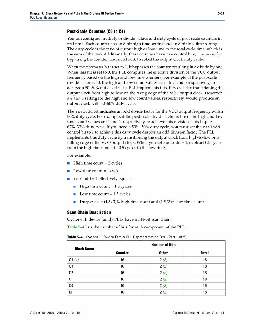
Chapter 5: Clock Networks and PLLs in the Cyclone III Device Family 5–27PLL Reconfiguration
© December 2009 Altera Corporation Cyclone III Device Handbook, Volume 1
Post-Scale Counters (C0 to C4)You can configure multiply or divide values and duty cycle of post-scale counters in real time. Each counter has an 8-bit high time setting and an 8-bit low time setting. The duty cycle is the ratio of output high or low time to the total cycle time, which is the sum of the two. Additionally, these counters have two control bits, rbypass, for bypassing the counter, and rselodd, to select the output clock duty cycle.
When the rbypass bit is set to 1, it bypasses the counter, resulting in a divide by one. When this bit is set to 0, the PLL computes the effective division of the VCO output frequency based on the high and low time counters. For example, if the post-scale divide factor is 10, the high and low count values is set to 5 and 5 respectively, to achieve a 50–50% duty cycle. The PLL implements this duty cycle by transitioning the output clock from high-to-low on the rising edge of the VCO output clock. However, a 4 and 6 setting for the high and low count values, respectively, would produce an output clock with 40–60% duty cycle.
The rselodd bit indicates an odd divide factor for the VCO output frequency with a 50% duty cycle. For example, if the post-scale divide factor is three, the high and low time count values are 2 and 1, respectively, to achieve this division. This implies a 67%–33% duty cycle. If you need a 50%–50% duty cycle, you must set the rselodd control bit to 1 to achieve this duty cycle despite an odd division factor. The PLL implements this duty cycle by transitioning the output clock from high-to-low on a falling edge of the VCO output clock. When you set rselodd = 1, subtract 0.5 cycles from the high time and add 0.5 cycles to the low time.
For example:
■ High time count = 2 cycles
■ Low time count = 1 cycle
■ rselodd = 1 effectively equals:
■ High time count = 1.5 cycles
■ Low time count = 1.5 cycles
■ Duty cycle = (1.5/3)% high time count and (1.5/3)% low time count
Scan Chain Description Cyclone III device family PLLs have a 144-bit scan chain.
Table 5–4 lists the number of bits for each component of the PLL.
Table 5–4. Cyclone III Device Family PLL Reprogramming Bits (Part 1 of 2)
Block Name Number of Bits
Counter Other Total
C4 (1) 16 2 (2) 18
C3 16 2 (2) 18
C2 16 2 (2) 18
C1 16 2 (2) 18
C0 16 2 (2) 18
M 16 2 (2) 18

5–28 Chapter 5: Clock Networks and PLLs in the Cyclone III Device FamilyPLL Reconfiguration
Cyclone III Device Handbook, Volume 1 © December 2009 Altera Corporation
Figure 5–22 shows the scan chain order of the PLL components.
Figure 5–23 shows the scan chain bit order sequence for one PLL post-scale counter in Cyclone III device family PLLs.
N 16 2 (2) 18
Charge Pump 9 0 9
Loop Filter (3) 9 0 9
Total number of bits: 144
Notes to Table 5–4:
(1) LSB bit for C4 low-count value is the first bit shifted into the scan chain.(2) These two control bits include rbypass, for bypassing the counter, and rselodd, to select the output clock
duty cycle.(3) MSB bit for loop filter is the last bit shifted into the scan chain.
Figure 5–22. PLL Component Scan Chain Order
Table 5–4. Cyclone III Device Family PLL Reprogramming Bits (Part 2 of 2)
Block Name Number of Bits
Counter Other Total
DATAIN
C1C2C3C4DATAOUT
MSBLF CP
LSBN M C0
Figure 5–23. Scan Chain Bit Order
DATAINrbypass
HB
7
HB
6
HB
5
HB
4
HB
3
HB
2
HB
1
HB
0
rselodd
LB
7
LB
6
LB
5
LB
4
LB
3
LB
2
LB
1
LB
0DATAOUT
HB
9
HB
8
LB
9
LB
8
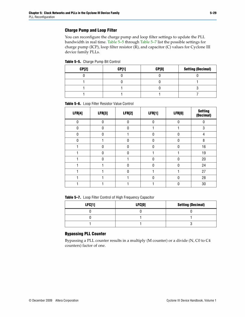
Chapter 5: Clock Networks and PLLs in the Cyclone III Device Family 5–29PLL Reconfiguration
© December 2009 Altera Corporation Cyclone III Device Handbook, Volume 1
Charge Pump and Loop FilterYou can reconfigure the charge pump and loop filter settings to update the PLL bandwidth in real time. Table 5–5 through Table 5–7 list the possible settings for charge pump (ICP), loop filter resistor (R), and capacitor (C) values for Cyclone III device family PLLs.
Bypassing PLL CounterBypassing a PLL counter results in a multiply (M counter) or a divide (N, C0 to C4 counters) factor of one.
Table 5–5. Charge Pump Bit Control
CP[2] CP[1] CP[0] Setting (Decimal)
0 0 0 0
1 0 0 1
1 1 0 3
1 1 1 7
Table 5–6. Loop Filter Resistor Value Control
LFR[4] LFR[3] LFR[2] LFR[1] LFR[0] Setting (Decimal)
0 0 0 0 0 0
0 0 0 1 1 3
0 0 1 0 0 4
0 1 0 0 0 8
1 0 0 0 0 16
1 0 0 1 1 19
1 0 1 0 0 20
1 1 0 0 0 24
1 1 0 1 1 27
1 1 1 0 0 28
1 1 1 1 0 30
Table 5–7. Loop Filter Control of High Frequency Capacitor
LFC[1] LFC[0] Setting (Decimal)
0 0 0
0 1 1
1 1 3

5–30 Chapter 5: Clock Networks and PLLs in the Cyclone III Device FamilyPLL Reconfiguration
Cyclone III Device Handbook, Volume 1 © December 2009 Altera Corporation
Table 5–8 lists the settings for bypassing the counters in Cyclone III device family PLLs.
To bypass any of the PLL counters, set the bypass bit to 1. The values on the other bits are then ignored.
Dynamic Phase ShiftingThe dynamic phase shifting feature allows the output phase of individual PLL outputs to be dynamically adjusted relative to each other and the reference clock without sending serial data through the scan chain of the corresponding PLL. This feature simplifies the interface and allows you to quickly adjust tCO delays by changing output clock phase shift in real time. This is achieved by incrementing or decrementing the VCO phase-tap selection to a given C counter or to the M counter. The phase is shifted by 1/8 the VCO frequency at a time. The output clocks are active during this phase reconfiguration process.
Table 5–9 lists the control signals that are used for dynamic phase shifting.
Table 5–8. PLL Counter Settings
PLL Scan Chain Bits [0..8] Settings Description
LSB MSB
X X X X X X X X 1 (1) PLL counter bypassed
X X X X X X X X 0 (1) PLL counter not bypassed
Note to Table 5–8:
(1) Bypass bit.
Table 5–9. Dynamic Phase Shifting Control Signals
Signal Name Description Source Destination
PHASECOUNTERSELECT[2:0]
Counter Select. Three bits decoded to select either the M or one of the C counters for phase adjustment. One address map to select all C counters. This signal is registered in the PLL on the rising edge of SCANCLK.
Logic array or I/O pins
PLL reconfiguration circuit
PHASEUPDOWNSelects dynamic phase shift direction; 1= UP, 0 = DOWN. Signal is registered in the PLL on the rising edge of SCANCLK.
Logic array or I/O pins
PLL reconfiguration circuit
PHASESTEP Logic high enables dynamic phase shifting. Logic array or I/O pins
PLL reconfiguration circuit
SCANCLK
Free running clock from core used in combination with PHASESTEP to enable or disable dynamic phase shifting. Shared with SCANCLK for dynamic reconfiguration.
GCLK or I/O pins PLL reconfiguration circuit
PHASEDONE
When asserted, it indicates to core logic that the phase adjustment is complete and PLL is ready to act on a possible second adjustment pulse. Asserts based on internal PLL timing. Deasserts on rising edge of SCANCLK.
PLL reconfiguration circuit
Logic array or I/O pins

Chapter 5: Clock Networks and PLLs in the Cyclone III Device Family 5–31PLL Reconfiguration
© December 2009 Altera Corporation Cyclone III Device Handbook, Volume 1
Table 5–10 lists the PLL counter selection based on the corresponding PHASECOUNTERSELECT setting.
To perform one dynamic phase shift step, you must perform the following procedures:
1. Set phaseupdown and phasecounterselect as required.
2. Assert phasestep for at least two scanclk cycles. Each phasestep pulse enables one phase shift.
3. Deassert phasestep.
4. Wait for phasedone to go high.
5. You can repeat steps 1 through 4 as many times as required to get multiple phase shifts.
All signals are synchronous to scanclk, so they are latched on the scanclk edges and must meet tSU or tH requirements (with respect to the scanclk edges).
Dynamic phase shifting can be repeated indefinitely. All signals are synchronous to scanclk, so they must meet tSU or tH requirements (with respect to scanclk edges).
Table 5–10. Phase Counter Select Mapping
PHASECOUNTERSELECT [2] [1] [0] Selects
0 0 0 All Output Counters
0 0 1 M Counter
0 1 0 C0 Counter
0 1 1 C1 Counter
1 0 0 C2 Counter
1 0 1 C3 Counter
1 1 0 C4 Counter
Figure 5–24. PLL Dynamic Phase Shift
phaseupdown
phasecounterselect
scanclk
phasestep
phasedone

5–32 Chapter 5: Clock Networks and PLLs in the Cyclone III Device FamilySpread-Spectrum Clocking
Cyclone III Device Handbook, Volume 1 © December 2009 Altera Corporation
The phasestep signal is latched on the negative edge of scanclk. In Figure 5–24, this is shown by the second scanclk falling edge. phasestep must stay high for at least two scanclk cycles. On the second scanclk rising edge after phasestep is latched (indicated by the fourth rising edge), the values of phaseupdown and phasecounterselect are latched and the PLL starts dynamic phase shifting for the specified counter or counters and in the indicated direction. On the fourth scanclk rising edge, phasedone goes high to low and remains low until the PLL finishes dynamic phase shifting. You can perform another dynamic phase shift after the phasedone signal goes from low to high.
Depending on the VCO and scanclk frequencies, phasedone low time may be greater than or less than one scanclk cycle. The maximum time for reconfiguring phase shift dynamically is to be determined (TBD) based on device characterization.
After phasedone goes from low to high, you can perform another dynamic phase shift. phasestep pulses must be at least one scanclk cycle apart.
f For information about the ALTPLL_RECONFIG MegaWizard Plug-In Manager, refer to the ALTPLL_RECONFIG Megafunction User Guide.
Spread-Spectrum ClockingThe Cyclone III device family can accept a spread-spectrum input with typical modulation frequencies. However, the device cannot automatically detect that the input is a spread-spectrum signal. Instead, the input signal looks like deterministic jitter at the input of the PLL. Cyclone III device family PLLs can track a spread-spectrum input clock as long as it is in the input jitter tolerance specifications and the modulation frequency of the input clock is below the PLL bandwidth, which is specified in the fitter report. The Cyclone III device family cannot generate spread-spectrum signals internally.
PLL Specifications
f For information about PLL specifications, refer to the Cyclone III Device Data Sheet and Cyclone III LS Device Data Sheet chapters.

Chapter 5: Clock Networks and PLLs in the Cyclone III Device Family 5–33Chapter Revision History
© December 2009 Altera Corporation Cyclone III Device Handbook, Volume 1
Chapter Revision HistoryTable 5–11 lists the revision history for this chapter.
Table 5–11. Chapter Revision History (Part 1 of 2)
Date Version Changes Made
December 2009 3.2 Minor changes to the text.
July 2009 3.1 Made minor correction to the part number.
June 2009 3.0
Updated to include Cyclone III LS information
■ Updated chapter part number.
■ Updated “Clock Networks” on page 5–1.
■ Updated Table 5–1 on page 5–2, Table 5–3 on page 5–9.
■ Updated “PLLs in the Cyclone III Device Family” on page 5–9.
■ Updated “PLL Reconfiguration Hardware Implementation” on page 5–25.
■ Updated “Spread-Spectrum Clocking” on page 5–32.
October 2008 2.1
■ Updated the “Dynamic Phase Shifting” and “Introduction” sections.
■ Updated Figure 5–2, Figure 5–8, and Figure 5–24.
■ Updated chapter to new template.
May 2008 2.0
■ Updated Figure 5–2 and added (Note 3).
■ Updated “clkena Signals” section.
■ Updated Figure 5–8 and added (Note 3).
■ Updated “PLL Control Signals” section.
■ Updated “PLL Cascading” section.
■ Updated “Cyclone III PLL Hardware Overview” section.
■ Updated Table 5–6, Table 5–3, Table 5–7.
■ Updated Figure 5–14.
■ Updated “PLL Cascading” section.
■ Updated “Clock Multiplication and Division” section.
■ Updated Step 6–32 in “PLL Reconfiguration Hardware Implementation” section.
■ Updated “Spread-Spectrum Clocking” section.
■ Updated Figure 5–29.
■ Updated “VCCD and GND” section.
■ Added “Power Consumption” section.
September 2007 1.2 ■ Updated “Board Layout” section and removed Figure 5-30.

5–34 Chapter 5: Clock Networks and PLLs in the Cyclone III Device FamilyChapter Revision History
Cyclone III Device Handbook, Volume 1 © December 2009 Altera Corporation
July 2007 1.1
Updated document with EP3C120 information.
■ Updated Table 5–1 and Table 5–4 with EP3C120 information.
■ Updated “Clock Control Block” section.
■ Updated locked signal information in “PLL Control Signals” section and added Figure 5–16.
■ Updated “Manual Override” section, updated “Manual Clock Switchover” section.
■ Added new “Programmable Bandwidth” section with Figure 5–21 and Figure 5–22.
■ Replaced Figure 5-30 with correct diagram.
■ Added chapter TOC and “Referenced Documents” section.
March 2007 1.0 Initial release.
Table 5–11. Chapter Revision History (Part 2 of 2)
Date Version Changes Made