
Photon-induced tunable and reversible wettability of pulsed laser deposited W-doped ZnO nanorods
Upload
independentCategory
view
4download
0
Superlattices and Microstructures 39 (2006) 358–365
www.elsevier.com/locate/superlattices
Optical properties of ZnO nanorods and nanowires
A. Mézya,b, S. Anceaua, T. Bretagnona,∗, P. Lefebvrea,T. Taliercioa, Gyu-Chul Yic, Jinkyoung Yooc
aGroupe d’Etudes des Semiconducteurs (GES-UMR 5650) - CNRS- Université Montpellier II,34095 Montpellier, France
bLaboratoire de Physico-Chimie de la Matière Condensée LPMC-UMR 5617 Université Montpellier II,34095 Montpellier, France
cDepartment of Materials Science and Engineering, Pohang University of Science and Technology (POSTECH),Pohang, Kyoungbuk 790-784, Republic of Korea
Available online 19 September 2005
Abstract
We report continuous-wave and time-resolved optical spectroscopy of ZnO nanorods andnanowires of varying diameters grown by MOVPE, under varying thermo-dynamical conditions.We discuss the influence of these conditions on the different spectral components. Two families ofphotoluminescence lines are identified. The first one is related to defect-bound excitons and to theirtwo-electron replica. The second one is correlated to near surface states. The relative intensities ofvarious contributions appear to be strongly dependent on the growth conditions and of the diameterof the nanostructures. Photoluminescence decay time of the different lines has been measured on oneof the samples.© 2005 Elsevier Ltd. All rights reserved.
1. Introduction
One-dimensional semiconductor nanowires and nanorods have attracted increasinginterest due to their physical properties and diversity of potential electronic and photonicdevice applications [1,2]. Among the wide variety of 1D semiconductor nanostructures
∗ Corresponding author.E-mail address: [email protected] (T. Bretagnon).
0749-6036/$ - see front matter © 2005 Elsevier Ltd. All rights reserved.doi:10.1016/j.spmi.2005.08.079

A. Mézy et al. / Superlattices and Microstructures 39 (2006) 358–365 359
Table 1Growth conditions and morphology of the samples
Sample Growth temperature(◦C) Growth time (h) Morphology Encapsulation
1 500 2 Nanorod2 500 1 Nanorod3 800 2 Nanowire4 800 1 Nanowire5 500 1 Nanorod (Zn, Mg)O—5 mn6 500 1 Nanorod (Zn, Mg)O—10 mn
ZnO nanorods and nanowires attract special interest for high efficiency short wavelengthoptoelectronic nanodevices, due to their large excitonic binding energy of∼60 meV [3]and high mechanical and thermal stabilities.
The optical characteristics of ZnO nanorods and nanowires by continuous wavephotoluminescence (CW-PL), at room temperature [4] and low temperature [5–7] andcathodoluminescence [8] have already been reported. Nevertheless low temperature timeresolved photoluminescence (TR-PL) spectroscopy of semiconductor nanorods has notbeen extensively investigated. In this paper we present on one hand the results of lowtemperature CW-PL on a series of samples grown with different conditions. The aim ofthis study is to correlate the different types of recombination process with the temperatureand duration of the growth and finally to interpret the effect of ZnMgO coating layer onPL recombination. On the other hand we report on preliminary low temperature TR-PL onone of these samples.
2. Experimental details
The samples have been grown by metal–organic vapor phase epitaxy (MOVPE) withoutthe metal catalyst usually required in other methods [9,10] on silicon substrate. Detailson the growth conditions can be found in Refs. [9,10]. There are two typical growthtemperatures (Table 1), which are 500 and 800◦C. Electron microscopy revealed two typesof morphology depending on the temperature condition. Nanorods (vertically oriented),and nanowires (random orientations) are obtained respectively at 500 and 800◦C. TheZnO diameter is correlated to the growth time. For example, a diameter of∼35 nm and∼55 nm is obtained at respectively one hour and two hours growth time at 500◦C. (Zn,Mg)O coating layers have been grown on 500◦C (1 h) nanorods with two different deposittimes. The addition of a (Zn, Mg)O coating layer tilts the well aligned nanorods.
Low temperature (2 K) continuous wave photoluminescence (CW-PL) has beenperformed using the 325 nm line He–Cd laser as the excitation source. The time-resolvedPL (TRPL) set-up uses the frequency-tripled radiation (266 nm) from a pulsed Ti-sapphiremode-locked laser cavity, with a typical pulse width of 2 ps, to excite the PL of thesample. We used an acousto-optic modulator (pulse picker) to adjust the repetition rateof the system between 82 MHz and 800 Hz. The sample is placed in a closed-cyclerefrigerator yielding a control of the temperature between 8 and 300 K. The PL is collectedand focussed by two parabolic mirrors onto the entrance slit of a 0.5 m focal lengthspectrometer, then dispersed and detected using a Hamamatsu Synchroscan streak camera.

360 A. Mézy et al. / Superlattices and Microstructures 39 (2006) 358–365
Fig. 1. Continuous wave photoluminescence spectra of samples with different time of grown: sample 1 (2 h) andsample 2 (1 h).
3. Results and discussion
Continuous wave optical spectroscopy has been done on the different samples at 2 K, atypical result is presentedFig. 1. At a temperature of 2 K, the spectrum of sample 1 (Fig. 1)is dominated by two neutral donor bound excitons, respectively at 3.361 eV(D0X1)
and 3.354 eV(D0X2) [3,5]. The 3.208 eV line is attributed [3] to donor–acceptor pair(DAP) recombination. Two-electron replicas of bound exciton lines (TES) are commonlyobserved in PL spectra of high quality ZnO. The difference in energy between the lineand its replica is 3/4 of the binding energy of the donor. We attributed the 3.327 eVline to a replica of the D0X1 line. The distance in energy between the two lines gives adonor binding energy of 45.3 meV, which is close to the one reported [3] 46.1 meV for thehydrogen in ZnO. Based on the following investigation, we have attributed the 3.305 eV(S1) and 3.332 eV(S2) lines to near surface states.
When the growth time is increased from one hour (sample 2) to two hours (sample 1),the relative intensities of the S1 and S2 lines (Fig. 1), which are dominant in the one-hourgrown sample, collapse. A continuum of states, characteristic of surface states, contributesalso to the PL spectra of sample 2. This indicates a decreased contribution of surface statesto the spectra when the grown time increases. In other words, the diameter of the nanorodsincreases with the growth time, consequently the volume to surface ratio increases. Shalishet al. [11] have reported similar observations on nanorods with diameter ranged from 50to 250 nm. These observations confirm our identification of S1 and S2, according to whichS1 and S2 lines are coming from the near surface state recombination. Moreover, in thespectra of sample 2 (Fig. 1), the relative intensities of the S1 and S2 lines compared to theDX line, prohibits their identification as TES transition or phonon replica.
Dramatic changes in PL spectra occur when the growth temperature increases from500 to 800◦C (Fig. 2). The D0X1 line becomes dominant in the PL spectra of sample 3,

A. Mézy et al. / Superlattices and Microstructures 39 (2006) 358–365 361
Fig. 2. Comparison of continuous wave photoluminescence spectra of samples with different growth temperature:sample 1(500◦C) and sample 3(800◦C).
Fig. 3. Continuous wave photoluminescence spectra of samples without (sample 2) and with (Zn, Mg)Oencapsulation (sample 5).
indicating a change in donor impurities incorporation. The intensity of the S2 lineincreases, whereas the S1 one collapses with the growth temperature. For high temperaturegrowth, the TES line is well resolved.
The addition of the (Zn, Mg)O coating layer around the ZnO nanorod grown at 500◦Cleads to an important decrease of both S1 and S2 lines (Fig. 3). The reduction can beexplained in several ways. The potential barrier, introduced by the coating layer, keepsthe photo-injected carriers in the core of the nanorods. On the other hand, the (Zn, Mg)O

362 A. Mézy et al. / Superlattices and Microstructures 39 (2006) 358–365
Fig. 4. Comparison of continuous wave photoluminescence spectra of samples with different (Zn, Mg)Oencapsulation thickness.
Fig. 5. Time integrated photoluminescence spectra of sample 1 taken at 10 K.
coating layer could reduce the near surface state density. The (Zn, Mg)O coating can bean interesting method for decreasing the localisation of the careers into the surface state ofthe ZnO nanorods.
Relative reductions (Fig. 4) of the near surface state intensities to the benefit of theZnO core state recombination related to the increasing of the (Zn, Mg)O layer thicknesshave been observed. Furthermore, a progressive compressive strain in the ZnO nanorodsis applied when the deposit time increases, which yields a blue shift (Fig. 4) of the entirephotoluminescence spectrum.
A. Mézy et al. / Superlattices and Microstructures 39 (2006) 358–365 363
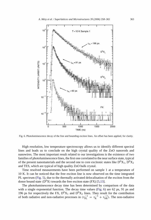
Fig. 6. Photoluminescence decay of the free and bounding exciton lines. An offset has been applied, for clarity.
High resolution, low temperature spectroscopy allows us to identify different spectrallines and leads us to conclude on the high crystal quality of the ZnO nanorods andnanowires. The most important result related to our investigations is the existence of twofamilies of photoluminescence lines, the first one correlated to the near surface state, typicalof the present nanomaterials and the second one to core excitonic states like D0X1, D0X2and TES, which are typical of high quality ZnO bulk crystal.
Time resolved measurements have been performed on sample 1 at a temperature of10 K. It can be noticed that the free exciton line is now observed on the time integratedPL spectrum (Fig. 5), due to the thermally activated delocalisation of the exciton from thedonor bound state(D0X) towards the free exciton state (FX) [5,13].
The photoluminescence decay time has been determined by comparison of the datawith a single exponential function. The decay time values (Fig. 6) are 62 ps, 91 ps and196 ps for respectively the FX, D0X1 and D0X2 lines. They result for the contributionof both radiative and non-radiative processes in(τ−1
PL = τ−1R + τ−1
NR). The non-radiative

364 A. Mézy et al. / Superlattices and Microstructures 39 (2006) 358–365
Fig. 7. Photoluminescence decay of the S1, TES and S2 lines. An offset has been applied, for clarity.
contribution corresponds in the case of the bound excitons to the delocalisation process.The S1 and S2 possess similar photoluminescence dynamics (Fig. 7), with a PL lifetimein the range of few ns. The TES line is not well resolved from the S1 lines. However, twocomponents can be distinguished (Fig. 7) on the PL decay at 3.327 eV. The fastest onecorresponds to the contribution of S1 lines with a lifetime of∼1 ns. And we attribute theslowest part to the TES recombination. The TES decay time is determined to be 27 ns.This fact confirms once again the identification of this line with the two electrons replicaof the donor bound exciton line. The donor–acceptor pairs show a non-exponential decayas expected [12].
4. Conclusion
We reported on low temperature (2 K) CW-PL and TR-PL (10 K) investigation of avariety of nanorods and nanowires. The change of CW-PL spectra with the different growth

A. Mézy et al. / Superlattices and Microstructures 39 (2006) 358–365 365
conditions allowed us to identify PL lines that are related to surface states. These linescome in addition to the transition lines(D0X1, D0X2, TES, DAP,. . .) that are well knownin high-quality ZnO. The (Zn, Mg)O encapsulation reduces the influence of near surfacestates on emission spectra and favours the contributions from core states. Decay times ofthe different lines have been measured. As a final remark, we notice that we measured alifetime of 27 ns for the decay dynamics of two electrons replica (TES) of donor-boundexcitons, for which there is, to the best of our knowledge, no equivalent in the literature,for ZnO single crystals or epilayers.
Acknowledgement
We acknowledge support from the French Ministry of Education, Research andTechnology within the “NANOZINOX” Research Programs.
References
[1] X. Duan, Y. Huang, Y. Cui, J. Wang, C.M. Lieber, Nature 409 (2001) 66.[2] M.H. Huang, S. Mao, H. Feick, H. Yan, Y. Wu, H. Kind, E. Weber, R. Russo, P. Yang, Science 292 (2001)
1897.[3] B.K. Meyer, H. Alves, D.M. Hofmann, W. Kriegseis, D. Forster, F. Bertram, J. Christen, A. Hoffmann,
M. Straßburg, M. Dworzak, U. Haboeck, A.V. Rodina, Phys. Status Solidi b 241 (2004) 231.[4] W.I. Park, D.H. Kim, S.-W. Jung, G.-C. Yi, Appl. Phys. Lett. 80 (2002) 4232.[5] W.I. Park, Y.H. Jun, S.W. Jung, G.-C. Yi, Appl. Phys. Lett. 82 (2003) 964.[6] J. Jie, G. Wang, Y. Chen, X. Han, Q. Wang, B. Xu, J.G. Hou, Appl. Phys. Lett. 86 (2005) 031909.[7] W. Lee, M.-C. Jeong, J.-M. Myoung, Appl. Phys. Lett. 85 (2004) 6167.[8] H.J. Fan, R. Scholz, M. Zacharias, U. Gösele, F. Bertram, D. Forster, J. Christen, Appl. Phys. Lett. 86 (2005)
023113.[9] W.I. Park, D.H. Kim, S.-W. Jung, G.-C. Yi, Appl. Phys. Lett. 80 (2002) 4232.
[10] G.-C. Yi, C. Wang, W.I. Park, Semicond. Sci. Technol. 20 (2005) 522.[11] I. Shalish, H. Tempkin, V. Narayanamurti, Phys. Rev. B 69 (2004) 245401.[12] D.G. Thomas, J. Phys. Chem. Solids 15 (1960) 86.[13] A.A. Toropov, O.V. Nekrutkina, T.V. Shubina, T. Gruber, C. Kirchner, A. Waag, K.F. Karlsson, P.O. Holtz,
B. Monemar, Phys. Rev. B 69 (2004) 165205.
Copyright © 2022 FDOKUMEN