
Urchin-inspired ZnO-TiO 2 core-shell as building blocks for ...
Upload
khangminh22Category
view
3download
0
Institut de Physique de l’Universite de Neuchatel (Suisse)
- Advanced LPCVD ZnO -Challenges in Application for Thin Film
Solar Cells and Modules
These
presentee a la Faculte des Sciences
de l’Universite de Neuchatel
pour l’obtention du grade de doctuer es sciences
Par
Daniel Messerschmidt
Soutenue le 23 juillet 2014
En presence du directeur de these:Prof . Philipp Aebi
Et des rapporteurs:Prof. Christophe BallifProf. Thomas SudmeyerProf. Edda RadleinDr. Jens Eberhardt
Neuchatel 2014

Faculté des sciences
Secrétariat-décanat de Faculté Rue Emile-Argand 11
2000 Neuchâtel - Suisse Tél: + 41 (0)32 718 2100
E-mail: [email protected]
IMPRIMATUR POUR THESE DE DOCTORAT
La Faculté des sciences de l'Université de Neuchâtel
autorise l'impression de la présente thèse soutenue par
Monsieur Daniel MESSERSCHMIDT
Titre:
Advanced LPCVD ZnO – Challenges in Application for Thin
Film Solar Cells and Modules
sur le rapport des membres du jury composé comme suit :
• Prof. Philipp Aebi, Université de Fribourg, directeur de thèse • Prof. Thomas Südmeyer, Université de Neuchâtel • Prof. Christophe Ballif, EPF Lausanne • Prof. Edda Rädlein, Technische Universität Ilmenau, D • Dr. Jens Eberhardt, Bosch Solar Energy AG, D
Neuchâtel, le 12 août 2014 Le Doyen, Prof. P. Kropf
Imprimatur pour thèse de doctorat www.unine.ch/sciences

Abstract
Ethanol is used as a precursor during the growth of zinc oxide (ZnO) by low-pressure
chemical vapor deposition (LPCVD). By adding ethanol, the surface of the deposited
ZnO layer is flattened and its roughness is decreased about sevenfold. The layers be-
come increasingly stressed and their resistivity grows significantly. The present work
proposes an explanation for the observed behavior based on the catalytic decomposi-
tion of ethanol at the ZnO surface and on the growth of selected crystal planes. By
using ethanol for the last 10 % of the total ZnO layer growth only, sheet resistance is
maintained and roughness is slightly decreased. The results indicate that such LPCVD
ZnO bilayers could be a promising method to modify the ZnO surface morphology be-
fore cell deposition, thus providing an alternative to argon plasma treatment, which is
typically reported to improve solar cell parameters such as open-circuit voltage and fill
factor.
The introduction of an advanced LPCVD boron-doped ZnO (ZnO:B) into the pro-
duction line at Bosch Solar Thin Film in Erfurt, Germany, is presented. Here the ZnO:B
is deposited with a LPCVD production tool on 1.1 × 1.3m2 glass substrates. Early
results on a laboratory scale of this advanced transparent conductive oxide (ATCO)
type were published by Ding et al. [1,2]. For an ATCO, they combined a highly doped
ZnO:B seed layer with a low-doped ZnO:B bulk layer. Compared to a standard ZnO:B
(Std-TCO), which is homogeneously doped across the total layer thickness, the ATCO
possesses enhanced optical and electrical properties. Comparing the ATCO with the
Std-TCO, equal in layer thickness (1800nm) and sheet resistance (16 to 17Ω), the
ATCO possesses slightly better transmittance. Furthermore, the ATCO showed 37 %
haze, which is 3 to 5 % absolute more haze compared to the Std-TCO. After ATCO
optimization, a complete micromorph solar module was fabricated, incorporating this
new advanced LPCVD ZnO:B layer as the front electrode. An initial module power of
153.7Wp was achieved. Here the unit Wp indicates that the module was tested under
standardized test conditions. The power output was determined at 25 with a light
illumination power of 1000W/m2. The light spectrum was adjust to be equivalent to
an terrestrial solar spectrum with an air mass 1.5 characteristic.
For the first time the present work introduces a novel degradation effect of the ZnO,
which is observed for ZnO layers deposited on commercially available soda-lime glass.
When an electric field is applied, the potential induced anodic degradation causes a
5

massive sheet resistance increase of the ZnO. The present work shows that the increase
in resistance strongly affects the power output of small non-encapsulated and large en-
capsulated micromorph thin-film photovoltaic modules, in which ZnO was used as the
front electrode. The present work proposes that the evolution of gaseous oxygen at the
anode (ZnO) may be responsible for the increased resistance of the ZnO. A model that
describes this observation is presented and solutions to suppress the effect are proposed.
The optical properties of non-degraded and anodically degraded ZnO:B are presented.
The optical model used to simulate the infrared reflectance in the wavelength range
between 1.2 and 25µm is based on the Maxwell-Garnett effective-medium theory. The
model is sensitive to the conditions at the grain boundaries of the investigated poly-
crystalline ZnO:B films. The yielded results confirm the presence of defect-rich grain
boundaries, especially after degradation. Furthermore, indications of a degraded ZnO
layer next to the ZnO:B/glass interface with a different refractive index are found.
Furthermore, based on Raman investigations, evidence for the creation of oxygen va-
cancies, which correlate with a shift of the optical absorption edge of the ZnO:B, is
presented. Investigations with scanning and transmission electron microscopy show
microvoids at the grain boundaries after anodic degradation. This indicates that the
grain/grain interfaces are the principle location of defects after degradation.
Contents
Contents i
List of Figures iii
List of Tables vii
1 Introduction 11.1 Contribution to the Field of Research . . . . . . . . . . . . . . . . . . . 3
2 Principles of Thin-Film Silicon PV 52.1 Zinc Oxide -
Deposition and Material Properties . . . . . . . . . . . . . . . . . . . . 52.1.1 Deposition of Zinc Oxide by LPCVD . . . . . . . . . . . . . . . 62.1.2 Structural Properties . . . . . . . . . . . . . . . . . . . . . . . . 112.1.3 Electrical Properties . . . . . . . . . . . . . . . . . . . . . . . . 122.1.4 Optical Properties . . . . . . . . . . . . . . . . . . . . . . . . . 142.1.5 Dielectric Function of Polycrystalline LPCVD ZnO:B . . . . . . 16
2.2 Silicon Thin Films -Deposition and Material Properties . . . . . . . . . . . . . . . . . . . . 182.2.1 Deposition of Silicon Thin Films by Plasma-Enhanced Chemical
Vapor Deposition . . . . . . . . . . . . . . . . . . . . . . . . . . 182.2.2 Amorphous Silicon . . . . . . . . . . . . . . . . . . . . . . . . . 202.2.3 Microcrystalline Silicon . . . . . . . . . . . . . . . . . . . . . . . 21
2.3 Micromorph Solar Cells and Modules . . . . . . . . . . . . . . . . . . . 222.3.1 Concept of a micromorph solar cell . . . . . . . . . . . . . . . . 232.3.2 Working principles of a solar cell and characteristic I(V) parameters 242.3.3 Module Fabrication . . . . . . . . . . . . . . . . . . . . . . . . . 28
3 Techniques of Characterization 313.1 Optical Characterization . . . . . . . . . . . . . . . . . . . . . . . . . . 31
3.1.1 Ultraviolet-Visible Spectroscopy . . . . . . . . . . . . . . . . . . 313.1.2 Fourier Transform Infrared Spectroscopy . . . . . . . . . . . . . 323.1.3 Raman Spectroscopy . . . . . . . . . . . . . . . . . . . . . . . . 34
3.2 Electrical Characterization . . . . . . . . . . . . . . . . . . . . . . . . . 343.2.1 Four-Point Probe Resistance Measurement . . . . . . . . . . . . 343.2.2 Hall Effect Measurement . . . . . . . . . . . . . . . . . . . . . . 34
3.3 Structural Characterization . . . . . . . . . . . . . . . . . . . . . . . . 363.3.1 Atomic Force Microscopy . . . . . . . . . . . . . . . . . . . . . . 363.3.2 X-Ray Diffraction Analysis (XRD) . . . . . . . . . . . . . . . . 373.3.3 Secondary Ion Mass Spectroscopy (SIMS) . . . . . . . . . . . . 37
i
ii Contents
3.4 Characterization of Solar Cells and Modules . . . . . . . . . . . . . . . 383.4.1 Current-Voltage Characterization of Solar Cells and
Modules . . . . . . . . . . . . . . . . . . . . . . . . . . . . . . . 383.4.2 External Quantum Efficiency (EQE) . . . . . . . . . . . . . . . 39
4 Ethanol-enriched LPCVD ZnO bilayers: Properties and Growth – APotential Electrode for Thin Film Solar Cells 414.1 Background . . . . . . . . . . . . . . . . . . . . . . . . . . . . . . . . . 414.2 Experimental . . . . . . . . . . . . . . . . . . . . . . . . . . . . . . . . 434.3 Results . . . . . . . . . . . . . . . . . . . . . . . . . . . . . . . . . . . . 43
4.3.1 ZnO single layers deposited using a mixture of ethanol, waterand DEZ . . . . . . . . . . . . . . . . . . . . . . . . . . . . . . . 43
4.3.2 Ethanol-enriched bilayers . . . . . . . . . . . . . . . . . . . . . . 514.4 Conclusion . . . . . . . . . . . . . . . . . . . . . . . . . . . . . . . . . . 54
5 Integration of Advanced-TCO into the Production Line at Bosch 575.1 Experimental . . . . . . . . . . . . . . . . . . . . . . . . . . . . . . . . 585.2 Results . . . . . . . . . . . . . . . . . . . . . . . . . . . . . . . . . . . . 59
5.2.1 Variation of process temperature . . . . . . . . . . . . . . . . . 605.2.2 Variation of water-diethylzinc ratio . . . . . . . . . . . . . . . . 625.2.3 Variation of process pressure . . . . . . . . . . . . . . . . . . . . 635.2.4 Variation of seed layers deposition time / thickness . . . . . . . 645.2.5 Variation of bulk layer doping . . . . . . . . . . . . . . . . . . . 655.2.6 Comparison of ATCO vs. Std-TCO . . . . . . . . . . . . . . . . 675.2.7 Result on module power using ATCO . . . . . . . . . . . . . . . 69
5.3 Conclusion . . . . . . . . . . . . . . . . . . . . . . . . . . . . . . . . . . 70
6 Anodic degradation of ZnO:B on soda-lime glass 716.1 Background . . . . . . . . . . . . . . . . . . . . . . . . . . . . . . . . . 716.2 Experimental . . . . . . . . . . . . . . . . . . . . . . . . . . . . . . . . 736.3 Anodic degradation of a large size module in the climate chamber . . . 756.4 Anodic degradation of a unencapsulated mini module on the hot plate . 776.5 Degradation of samples with ZnO:B on glass only . . . . . . . . . . . . 79
6.5.1 Electrical changes of glass/ZnO:B samples . . . . . . . . . . . . 796.5.2 Optical changes of glass/ZnO:B samples . . . . . . . . . . . . . 81
6.6 The glass substrate as a source of oxygen during degradation treatment 926.7 Model of anodic degradation of ZnO:B at the glass/ZnO:B interface . . 936.8 Improvements . . . . . . . . . . . . . . . . . . . . . . . . . . . . . . . . 976.9 Conclusion . . . . . . . . . . . . . . . . . . . . . . . . . . . . . . . . . . 100
7 Summary 103
References 105
A IR spectral reflectivity response of low-iron soda-lime glass ix
Publications xiii
Acknowledgment xv
Curriculum Vitae xvii
List of Figures
1.1 Net price reduction of solar modules based on micromorph technology. 2
2.1 Demonstration of high reactivity between DEZ and water at atmosphericpressure. . . . . . . . . . . . . . . . . . . . . . . . . . . . . . . . . . . . 7
2.2 Small LPCVD system. . . . . . . . . . . . . . . . . . . . . . . . . . . . 82.3 Large size LPCVD TCO1200 deposition system. . . . . . . . . . . . . . 102.4 Crystallographic structure of ZnO. . . . . . . . . . . . . . . . . . . . . 112.5 SEM imageas of a standard ZnO layer. Morphology and cross section . 122.6 Barrier model of ZnO grain boundaries. . . . . . . . . . . . . . . . . . . 142.7 Transmittance and reflectance of LPVCD ZnO deposited on a glass sub-
strate. . . . . . . . . . . . . . . . . . . . . . . . . . . . . . . . . . . . . 152.8 PECVD deposition system for Si thin-film fabrication. . . . . . . . . . 192.9 Classification of energy states into non-localized and localized band
stands in amorphous silicon. . . . . . . . . . . . . . . . . . . . . . . . . 202.10 Illustration of the microstructural characteristics of µc-Si:H. . . . . . . 222.11 Comparison of absorption coefficients for amorphous, microcrystalline
and crystalline silicon material as a function of photon energy and wave-length. . . . . . . . . . . . . . . . . . . . . . . . . . . . . . . . . . . . . 22
2.12 Layer configuration of a micromorph solar cell. . . . . . . . . . . . . . . 232.13 Sketch of a band diagram of a solar cell with p-i-n structure under short-
circuit conditions. . . . . . . . . . . . . . . . . . . . . . . . . . . . . . . 252.14 Current-voltage characteristic of a solar cell, showing important electric
parameters. . . . . . . . . . . . . . . . . . . . . . . . . . . . . . . . . . 272.15 Electric equivalent circuit of a single-junction solar cell. . . . . . . . . . 282.16 Illustration of the process to produce a monolithic interconnection of
single solar cells on the glass substrate. . . . . . . . . . . . . . . . . . . 292.17 Thin-film silicon solar module. . . . . . . . . . . . . . . . . . . . . . . . 30
3.1 Principle setup of an integrating sphere. . . . . . . . . . . . . . . . . . 323.2 Schematic of Michelson interferometer. . . . . . . . . . . . . . . . . . . 323.3 Schematic of collinear probe arrangement for four-point probe measure-
ment. . . . . . . . . . . . . . . . . . . . . . . . . . . . . . . . . . . . . . 343.4 Schematic of Hall effect. . . . . . . . . . . . . . . . . . . . . . . . . . . 353.5 Schematic of x-ray diffraction geometry (Bragg-Brentano). . . . . . . . 373.6 Comparison of light spectra of solar simulator and terrestrial solar spec-
trum AM1.5. . . . . . . . . . . . . . . . . . . . . . . . . . . . . . . . . 38
4.1 Deposition rate – ethanol enriched LPCVD ZnO . . . . . . . . . . . . . 444.2 SEM images of surface - ethanol enriched LPCVD ZnO . . . . . . . . . 454.3 XRD data - ethanol enriched LPCVD ZnO. . . . . . . . . . . . . . . . 46
iii
iv LIST OF FIGURES
4.4 Resistivity of ZnO films versus ethanol flow rate during deposition. . . 47
4.5 IR reflection spectra of ZnO films deposited with and without ethanol. 49
4.6 Optical transmission next to the optical absorption edge of glass samplescovered with ZnO, deposited with and without ethanol. . . . . . . . . . 50
4.7 Evolution of haze at 600 nm as a function of ethanol mass flow rateduring the deposition of ZnO. . . . . . . . . . . . . . . . . . . . . . . . 51
4.8 Sketch of layer stack, RMS surface roughness and simplified bilayerequivalent circuit. . . . . . . . . . . . . . . . . . . . . . . . . . . . . . . 52
4.9 Sheet resistance of ethanol-enriched bilayers as a function of cap-layerthickness. . . . . . . . . . . . . . . . . . . . . . . . . . . . . . . . . . . 53
4.10 SEM image of an ethanol-enriched bilayer in comparison to a standardZnO layer. . . . . . . . . . . . . . . . . . . . . . . . . . . . . . . . . . . 54
5.1 Schematic of the deposition tool TCO1200. . . . . . . . . . . . . . . . . 58
5.2 Distribution of layer properties after the retrofit of TCO1200. . . . . . 59
5.3 Comparison of ATCO and Std-TCO before optimization. . . . . . . . . 60
5.4 Variation of process temperature. . . . . . . . . . . . . . . . . . . . . . 61
5.5 Variation of the water/DEZ ratio. . . . . . . . . . . . . . . . . . . . . . 62
5.6 Variation of process pressure. . . . . . . . . . . . . . . . . . . . . . . . 64
5.7 Variation of seed layer thickness. . . . . . . . . . . . . . . . . . . . . . 65
5.8 Variation in bulk layer doping. . . . . . . . . . . . . . . . . . . . . . . . 66
5.9 Comparison of ATCO and Std-TCO for the optimized deposition pa-rameters. . . . . . . . . . . . . . . . . . . . . . . . . . . . . . . . . . . . 68
5.10 Comparison of transmission measured index matched for ATCO andStd-TCO. . . . . . . . . . . . . . . . . . . . . . . . . . . . . . . . . . . 69
5.11 Best results achieved on ATCO with non-retrofitted PECVD equipment. 69
6.1 Equipment for biased damp heat experiments in the climate chamber. . 73
6.2 Experimental setup for TCO degradation tests. . . . . . . . . . . . . . 74
6.3 Comparison of thin-film silicon solar module performances in the climatechamber, with and without biasing. . . . . . . . . . . . . . . . . . . . . 76
6.4 Solar Module’s fill factor (FF) and series resistance (Rs) as a functionof time in the climate chamber. . . . . . . . . . . . . . . . . . . . . . . 76
6.5 I(V) characteristics of a small module based on an a-Si:H and µc-Si:Hsilicon tandem solar cell structure before and after degradation treatment. 77
6.6 External quantum efficiency of a small module measured at differentspots on the active module area before and after degradation treatment. 78
6.7 Evolution of the resistance of the ZnO:B covered glass samples duringhot plate treatment. . . . . . . . . . . . . . . . . . . . . . . . . . . . . 80
6.8 Scanning electron microscopy (SEM) images of a ZnO:B surface afteran anodic degradation treatment. . . . . . . . . . . . . . . . . . . . . . 82
6.9 Transmittance spectra of a 3.2-mm-thick soda-lime glass substrate cov-ered with ZnO:B before and after degradation treatment. . . . . . . . . 82
6.10 IR reflectance of non-degraded and degraded ZnO:B deposited on glass. 84
6.11 Modeled layer stacks used for simulating the IR reflectance spectra ofthe non-degraded and degraded sample. . . . . . . . . . . . . . . . . . . 85
6.12 Refractive index (n) and extinction coefficient (k) for non-degraded, de-graded ZnO materials. . . . . . . . . . . . . . . . . . . . . . . . . . . . 88
LIST OF FIGURES v
6.13 Transmission electron (TEM) and scanning electron (SEM) microscopyimages of a non-degraded and degraded ZnO film deposited on soda-limeglass. . . . . . . . . . . . . . . . . . . . . . . . . . . . . . . . . . . . . . 90
6.14 The change between the degraded sample and the non-degraded one inthe Raman signal is presented. . . . . . . . . . . . . . . . . . . . . . . . 91
6.15 SIMS intensity of the ratio m/e=60. . . . . . . . . . . . . . . . . . . . . 936.16 A SEM cross section illustrates the conditions under the anode (ZnO:B)
– The model of the anodic degradation of ZnO on soda-lime glass . . . 956.17 Different approaches of LPCVD ZnO:B in order to reduce the sensitivity
to the the hot plate and climate chamber treatment. . . . . . . . . . . . 986.18 Optical and electrical properties of different homogeneously doped Std-
TCOs, Lasagne-TCO and ATCO. . . . . . . . . . . . . . . . . . . . . . 986.19 Comparison of different types of LPCVD ZnO:B treated on the hot plate. 996.20 Modules under test in the climate chamber. Different configurations
have been studied to stabilize the power loss. . . . . . . . . . . . . . . . 100
A.1 Experimental and simulated IR reflectance data of a 3.2-mm-thick low-iron soda-lime glass sample. . . . . . . . . . . . . . . . . . . . . . . . . x
A.2 Dielectric function of glass in the IR spectral range. . . . . . . . . . . . xi

vi LIST OF FIGURES
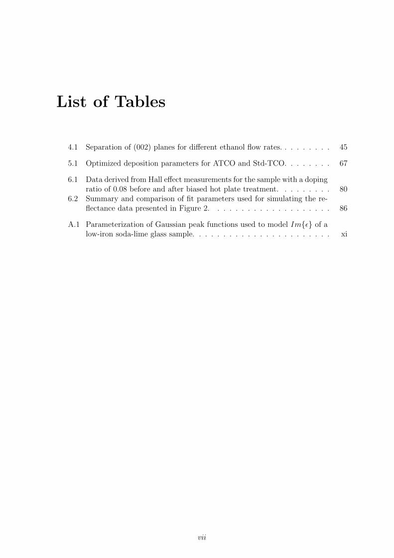
List of Tables
4.1 Separation of (002) planes for different ethanol flow rates. . . . . . . . . 45
5.1 Optimized deposition parameters for ATCO and Std-TCO. . . . . . . . 67
6.1 Data derived from Hall effect measurements for the sample with a dopingratio of 0.08 before and after biased hot plate treatment. . . . . . . . . 80
6.2 Summary and comparison of fit parameters used for simulating the re-flectance data presented in Figure 2. . . . . . . . . . . . . . . . . . . . 86
A.1 Parameterization of Gaussian peak functions used to model Imε of alow-iron soda-lime glass sample. . . . . . . . . . . . . . . . . . . . . . . xi
vii

viii LIST OF TABLES

Chapter 1
Introduction
For decades the global annual consumption of primary energy has been rising [3].
Primary energy includes both non-renewable and renewable forms of energy. Whereas
uranium and fossil fuels like coal, oil, and gas are assigned to the non-renewable forms,
energy provided by wind, water and the sun are typically assigned to the renewable
forms. In 2012 the global primary energy consumption was about 1.49 · 1017Wh [4].
Ninety-one percent of this energy demand was covered by non-renewable fuels and nine
percent by renewable forms of energy. It is well known that fossil fuels are limited and
that their combustion leads to climate-damaging emissions. It is highly probable that
these emissions are linked to global warming [5]. It is the opinion of the author that the
use of 100 % renewable forms of energy is the only way to circumvent the limitations
of the current global energy system.
For billions of years the sun has provided energy to our earth. This energy is partially
stored in wind, ocean waves, and electromagnetic waves (light). Estimated from the
solar constant, which has a value of 1367W/m2, and the earth’s cross-sectional area,
the total power reaching earth is about 1.74·1017W . One year’s total energy amounts to
1.52 · 1021Wh. Considering the global radiation balance, about one-half of this energy
reaches the earth’s surface, whereas the other half is absorbed, reflected or scattered by
the earth’s atmosphere [5]. Compared to the annual demand of primary energy in 2012
these numbers illustrate the potential of using the sunlight that reaches the surface as
one source of renewable energy. Furthermore, sunlight is available everywhere on earth
for free and represents an inexhaustible source of energy for mankind.
Photovoltaic technologies represent a possibility to access this energy source. With
photovoltaics, sunlight is converted directly into electricity. There are different tech-
nologies available on the market, based on crystalline wafers or on thin films. In the
present work the focus is on the micromorph thin-film silicon technology. This tech-
nology combines an amorphous top cell with a microcrystalline silicon bottom cell in
a tandem configuration. Furthermore, the transparent conductive oxide zinc oxide
(boron doped, ZnO:B) is used as the front and back electrodes. Small quantities of
1
2 Introduction
abundant and non-toxic materials (silicon, zinc) are used. As a result this technology
holds the potential for low production costs at a minimum risk of material shortage.
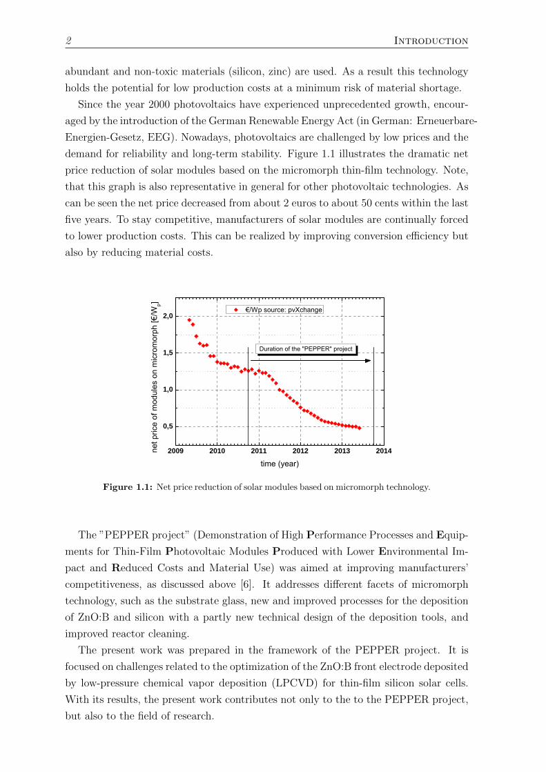
Since the year 2000 photovoltaics have experienced unprecedented growth, encour-
aged by the introduction of the German Renewable Energy Act (in German: Erneuerbare-
Energien-Gesetz, EEG). Nowadays, photovoltaics are challenged by low prices and the
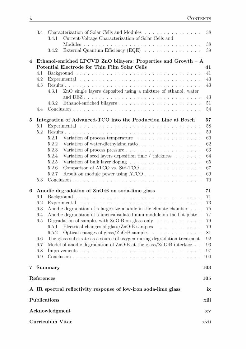
demand for reliability and long-term stability. Figure 1.1 illustrates the dramatic net
price reduction of solar modules based on the micromorph thin-film technology. Note,
that this graph is also representative in general for other photovoltaic technologies. As
can be seen the net price decreased from about 2 euros to about 50 cents within the last
five years. To stay competitive, manufacturers of solar modules are continually forced
to lower production costs. This can be realized by improving conversion efficiency but
also by reducing material costs.
2 0 0 9 2 0 1 0 2 0 1 1 2 0 1 2 2 0 1 3 2 0 1 4
0 , 5
1 , 0
1 , 5
2 , 0
Figure 1.1: Net price reduction of solar modules based on micromorph technology.
The ”PEPPER project” (Demonstration of High Performance Processes and Equip-
ments for Thin-Film Photovoltaic Modules Produced with Lower Environmental Im-
pact and Reduced Costs and Material Use) was aimed at improving manufacturers’
competitiveness, as discussed above [6]. It addresses different facets of micromorph
technology, such as the substrate glass, new and improved processes for the deposition
of ZnO:B and silicon with a partly new technical design of the deposition tools, and
improved reactor cleaning.
The present work was prepared in the framework of the PEPPER project. It is
focused on challenges related to the optimization of the ZnO:B front electrode deposited
by low-pressure chemical vapor deposition (LPCVD) for thin-film silicon solar cells.
With its results, the present work contributes not only to the to the PEPPER project,
but also to the field of research.
Introduction 3
1.1 Contribution to the Field of Research
The morphology of the ZnO:B front electrode is of importance not only for light scat-
tering, but also for the quality of the subsequently deposited silicon material. It is
therefore of importance for the solar cell and module efficiency. The effect of using
ethanol as an additional precursor during the ZnO:B layer deposition on the as-grown
surface morphology is investigated. The related results are presented in Chapter 4.The
present work proposes a growth model in which ethanol mediates the incorporation
of oxygen at oxygen vacancy sites at the surface of the growing ZnO grains. Further-
more, the ethanol changes the reaction kinetics at the surface of the ZnO and therefore
impacts the final layer morphology [7].
As a practical application, the introduction of an advanced LPCVD ZnO:B (ATCO)
into the production line of Bosch Solar Thin Film GmbH is presented. The approach
depicts a LPCVD ZnO:B with improved optical and electrical parameters. Here, the
ZnO:B film is composed of a highly doped thin seed layer and a low-doped thicker bulk
layer [1]. The corresponding results are presented in Chapter 5 and document the first
results with ATCO in a commercial production line.
When new processes and functional layers are introduced, the final product (the
improved solar module) has to be qualified. Beyond standardized lifetime test condi-
tions a novel degradation phenomenon of LPCVD ZnO:B was encountered. According
to IEC61646(10.13) the modules are tested in a climate chamber for 1000 hours at
85 and 85 % relative humidity. These test conditions neglect the functioning of the
module under certain bias voltage conditions in the field. In addition to these test
conditions, the modules were biased with 600V against the grounded module frame
(mounting system). The anodic degradation of LPCVD ZnO:B deposited on soda-lime
glass was reported for the first time; the resistivity of the ZnO:B was found to strongly
increase, due to an increase of defect concentration at ZnO:B grain boundaries. The
resulting resistance increase of the ZnO:B is responsible for a dramatic efficiency loss
in tested solar modules. Oxygen generation at the ZnO:B/glass interface during the
degradation procedure will be discussed as a root cause for the increase of the defect
density at ZnO grain boundaries. The corresponding results are presented in Chapter
6. Furthermore, solutions to minimize the degradation, minimizing the degradation
are proposed and discussed [8, 9].
The present work is structured as follows:
In Chapter 2 the principles of thin-film silicon photovoltaics are introduced. The
material properties and the deposition processes of zinc oxide and amorphous and
microcrystalline silicon are presented. Micromorph solar cells and modules and their
working principles are introduced.
Chapter 3 presents the main characterization techniques used for the investigations
in the present work. It is separated into four sections. The first three summarize

4 Introduction
the optical, electrical and structural techniques related to layer characterization. The
fourth covers the characterization of solar cells and modules.
In Chapter 4 results of the investigations using ethanol as an additional precursor
to modify the ZnO:B surface morphology are presented.
Chapter 5 presents the introduction of an advanced transparent conductive oxide
(ATCO, based on ZnO:B) into the production line at Bosch Solar Thin Film GmbH in
Erfurt, Germany.
In Chapter 6 the anodic degradation of ZnO:B on soda lime glass is discussed.
Finally, in Chapter 7 the results are summarized.
Chapter 2
Principles of Thin-Film Silicon PV
It is the goal of this chapter to present a brief introduction to the main technology used
for preparing micromorph solar cells and modules. Furthermore, for a better under-
standing of results presented later, important material properties will be discussed and
summarized. The cells and modules investigated were prepared in the so-called super-
strate configuration [10]. That means that the glass substrate used for the deposition
of the required layer stack not only acts as a pure substrate but also as the entrance
window for the light to be converted into photocurrent. In our case, the first layer to
be deposited on the glass substrate is zinc oxide (ZnO) a transparent conductive oxide
(TCO). Details on deposition and material properties will be discussed in Section 2.1.
After the ZnO layer is processed, the silicon cell structure is deposited. The material
properties and deposition process will be introduced in Section 2.2. Finally, the concept
of micromorph solar cells and modules will be presented in Section 2.3.
2.1 Zinc Oxide -
Deposition and Material Properties
ZnO possesses unique properties, which make it suitable not only for photovoltaic ap-
plications, but also for devices such as gas sensors, light-emitting diodes, varistors or
sound acoustic wave applications [11]. It possesses high transparency in the visible
and near-infrared spectral region. In most cases ZnO is a semiconductor of n-type
conductivity. Due to intrinsic defects such as zinc interstitials or oxygen vacancies
and extrinsic doping elements such as aluminum (Al) or boron (B), the free-electron
concentration can typically be adjusted in a range between 1019 and 1021 1/cm3. This
yields resistivity values lower than 10−3Ωcm. For industrial photovoltaic applications
it is necessary to deposit ZnO on large substrates. In the case of micromorph module
fabrication, substrate sizes of 1.4m2 are used. In addition to the already mentioned
high transparency, ZnO’s light-scattering ability is important for yielding highly effi-
cient thin-film solar cells. The production process technology based on chemical vapor
5
6 Principles of Thin-Film Silicon PV
deposition at low pressures (LPCVD) meets all the requirements of the micromorph
modules concept.
2.1.1 Deposition of Zinc Oxide by LPCVD
Due to the complexity of the process of ZnO deposition using chemical vapor deposition
(CVD) [12–16], only an introduction is presented here in order to show the reader the
principles of this technology and the growth regime used for sample fabrication in
the present work. Metal-organic compounds such as diethylzinc (DEZ, (C2H5)2Zn) or
dimethylzinc (DMZ, (CH3)2Zn) as a source of zinc (Zn) and molecular oxygen (O2)
or water (H2O) as a source of oxygen are typically utilized as precursors for ZnO film
deposition, by means of CVD. Also other precursors are possible, e.g. zinc acetyl-
acetonate [17], alcohols [7, 18–24] or nitrogen oxygen compounds [25, 26]. The present
work will focus on DEZ and water only.
The deposition of ZnO, using a CVD process, is a result of sophisticated chemical
vapor phase reactions followed by the nucleation of reaction intermediates and finally of
the adsorption of reaction products on the substrate surface [12–14]. At the surface of
the substrate the cluster formation and growth of single ZnO grains strongly depend on
the growth conditions which are mainly determined by substrate temperature, process
pressure and precursor flow rates. Here, the mobility of adatoms or clusters, which is
of importance during layer growth, significantly influences the final layer properties, as
e.g. morphology [15, 16, 27]. The morphology is of major importance for photovoltaic
applications, as will be discussed later.
In comparison to other oxygen precursors mentioned above, water possesses a high
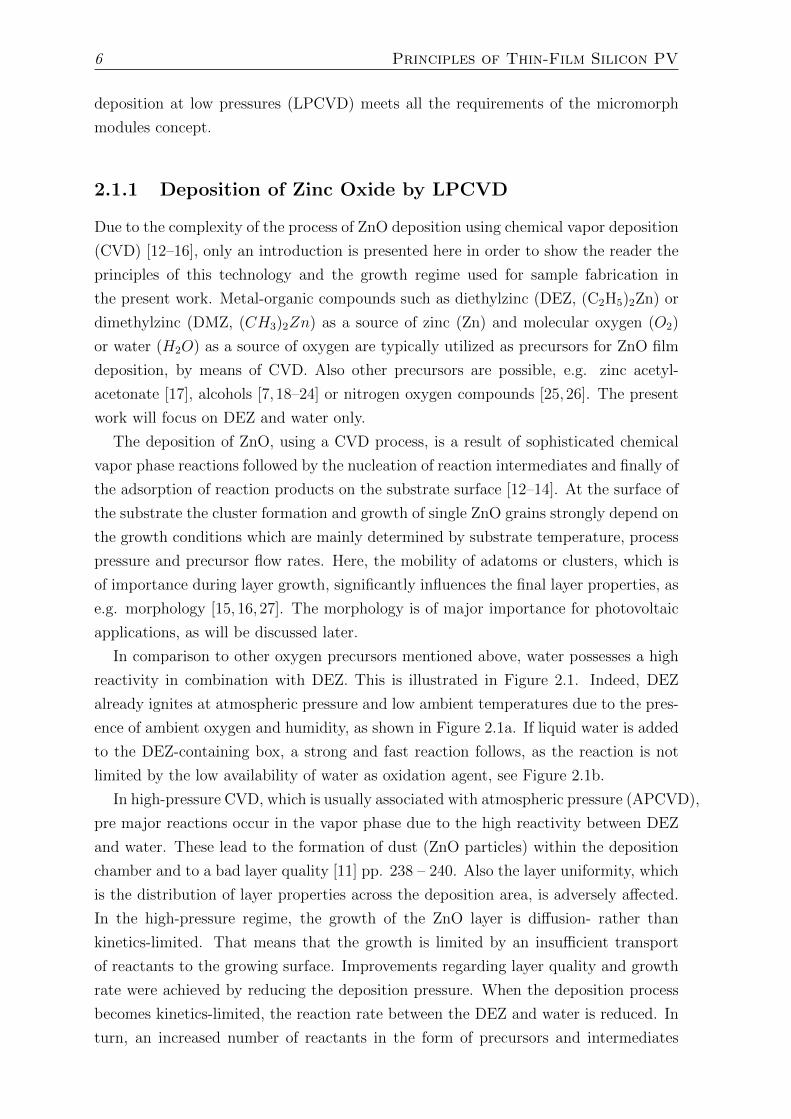
reactivity in combination with DEZ. This is illustrated in Figure 2.1. Indeed, DEZ
already ignites at atmospheric pressure and low ambient temperatures due to the pres-
ence of ambient oxygen and humidity, as shown in Figure 2.1a. If liquid water is added
to the DEZ-containing box, a strong and fast reaction follows, as the reaction is not
limited by the low availability of water as oxidation agent, see Figure 2.1b.
In high-pressure CVD, which is usually associated with atmospheric pressure (APCVD),
pre major reactions occur in the vapor phase due to the high reactivity between DEZ
and water. These lead to the formation of dust (ZnO particles) within the deposition
chamber and to a bad layer quality [11] pp. 238 – 240. Also the layer uniformity, which
is the distribution of layer properties across the deposition area, is adversely affected.
In the high-pressure regime, the growth of the ZnO layer is diffusion- rather than
kinetics-limited. That means that the growth is limited by an insufficient transport
of reactants to the growing surface. Improvements regarding layer quality and growth
rate were achieved by reducing the deposition pressure. When the deposition process
becomes kinetics-limited, the reaction rate between the DEZ and water is reduced. In
turn, an increased number of reactants in the form of precursors and intermediates
Principles of Thin-Film Silicon PV 7
a) b)
Figure 2.1: Demonstration of high reactivity between DEZ and water at atmo-spheric pressure and at an ambient temperature of about 15 . (a)DEZ ignites already due to the presence of ambient oxygen and hu-midity. (b) Adding liquid water to the DEZ-containing box leads toa strong and fast reaction.
reach the substrate surface. Due to the reduced process pressure the probability of
vapor phase reactions is reduced caused by the lower density of reactants. One can
think also of an increased length of mean free path before a water molecule meets a
DEZ molecule in order to react. In fact, the process of deposition became easier to be
controlled. The low-pressure CVD (LPCVD) process, which is associated with pres-
sures below 10 mbar and which is similar to the process used in the present work, was
intensively studied by Fay et al. [15, 27–30]. The reader is referred to these references
to get more information about the impact of the precursor flow ratio, deposition tem-
perature and pressure on final ZnO layer properties. Nowadays a pressure of about
0.5mbar has been found to be suitable for LPCVD ZnO layer deposition not only for
laboratory but also for industrial application.
Smith et al. [13] and Kim et al. [14] made theoretical calculations to find the paths
of reactions that are likely to occur between DEZ and water. Besides other possible
reaction paths and emerging intermediates they identified the reaction paths shown in
Equation 2.1 and 2.2 to be highly likely in the vapor phase:
(C2H5)2Zn+H2O ⇒ (C2H5)ZnOH + C2H6,and (2.1)
(C2H5)ZnOH +H2O ⇒ Zn(OH)2 + C2H6. (2.2)
Zinc hydroxide (Zn(OH)2) is assumed to play a key role for the formation of ZnO.
Here, due to oligomerization of zinc hydroxide and the elimination of hydrogen, nuclides
or clusters emerge. Adsorbed on the substrate surface they are responsible for ZnO
layer growth during the CVD process. In the following section, the deposition tools
used in the present work are introduced. After that, the general material properties of
LPCVD ZnO will be presented.
8 Principles of Thin-Film Silicon PV
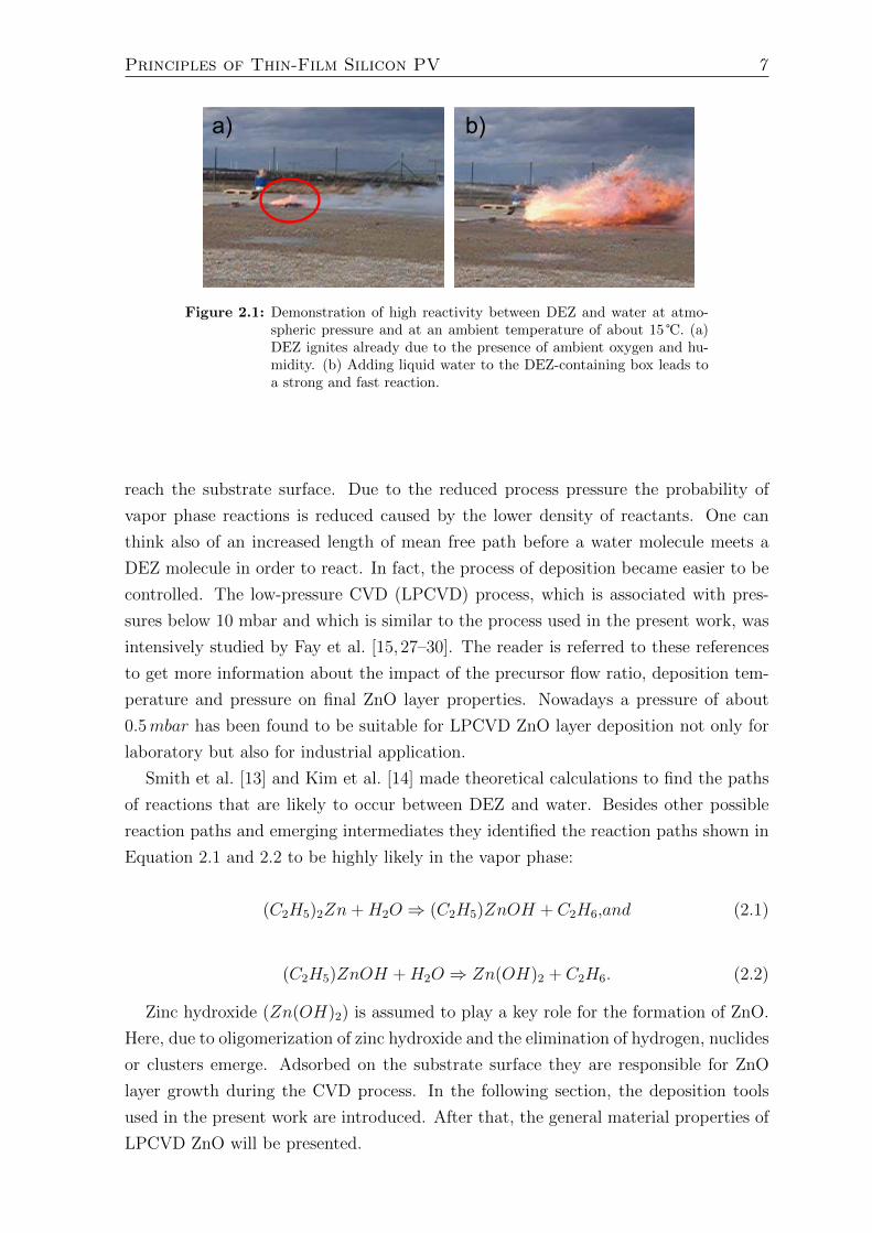
2.1.1.1 Small Single-Chamber Deposition System
In Figure 2.2 a single-chamber LPCVD deposition tool is presented. The small system
is located at the Institute of Microengineering (IMT) in Neuchatel, Switzerland. In
the present work the system was used for all preparations for the investigations of the
suitability of ethanol to modify the surface morphology of the final LPCVD ZnO layer
during the deposition. Results on that are presented in Section 4.
IIIII
I
I. control paneltemperature, pressure,
precursor flow rates
II. LPCVD reactordeposition of ZnO:B layer
III. exhaust to pumps
II
Inside the reactor:
DEZ
B2H6
H2O
C2H5OH
exhaust pumps
hot plate (~ RT – 400°C)
substratewater cooled shower head
vapor of precursor mixture
Figure 2.2: Small LPCVD system in the PV-Lab at the Institute of Microengi-neering in Neuchatel (IMT) used for investigation of the suitability ofprecursor ethanol during the deposition of ZnO from DEZ and water,see Section 4.
The deposition system is composed of three major components: the control panel (I),
the reactor (II) and the exhaust (III), which connects the reactor and system vacuum
pumps. A schematic view into the LPCVD reactor (II) is shown at the bottom of Figure
2.2. The reactor is about 50 cm in diameter and about 25 cm in height. As shown,
the shower head, responsible for mixing the precursors before entering the reactor zone
between the shower head and the substrate, is located at the bottom of the reactor.
The hot plate, on which the substrate is fixed, is located at the top of the reactor.
The deposition system is suitable for substrates with a size of about 5 × 5 cm2. Note
that the substrates used here are borosilicate glass slices (0.5mm thick). They were
cleaned in a bath of an acidic solution followed by one in an alkaline solution. The
baths were enhanced by ultrasonic treatment. Afterward, the substrates were rinsed
with deionized water and dried in air.
The temperature of the hot plate can be varied between room temperature (RT)
Principles of Thin-Film Silicon PV 9
and 400 . In the present case the temperature was set to 175 , unless indicated
otherwise. DEZ, water and ethanol (C2H5OH) were used as precursors. The doping
gas source used was diborane (B2H6) diluted at 1 % in argon. Argon was used not
only for dilution but also as a carrier gas. It is assumed to have a negligible impact on
the deposition process. The deposition pressure can be regulated in a range between
0.1 and 1mbar with a butterfly valve. For the deposition of LPCVD ZnO:B, which is
suitable for thin-film silicon solar cells, a pressure of 0.5mbar was set. Without using
ethanol, typical deposition rates between 2.5 and 3nm/s were achieved. For more
process details regarding the small deposition system presented here, see Section 4.
2.1.1.2 Large Deposition System (TCO1200)
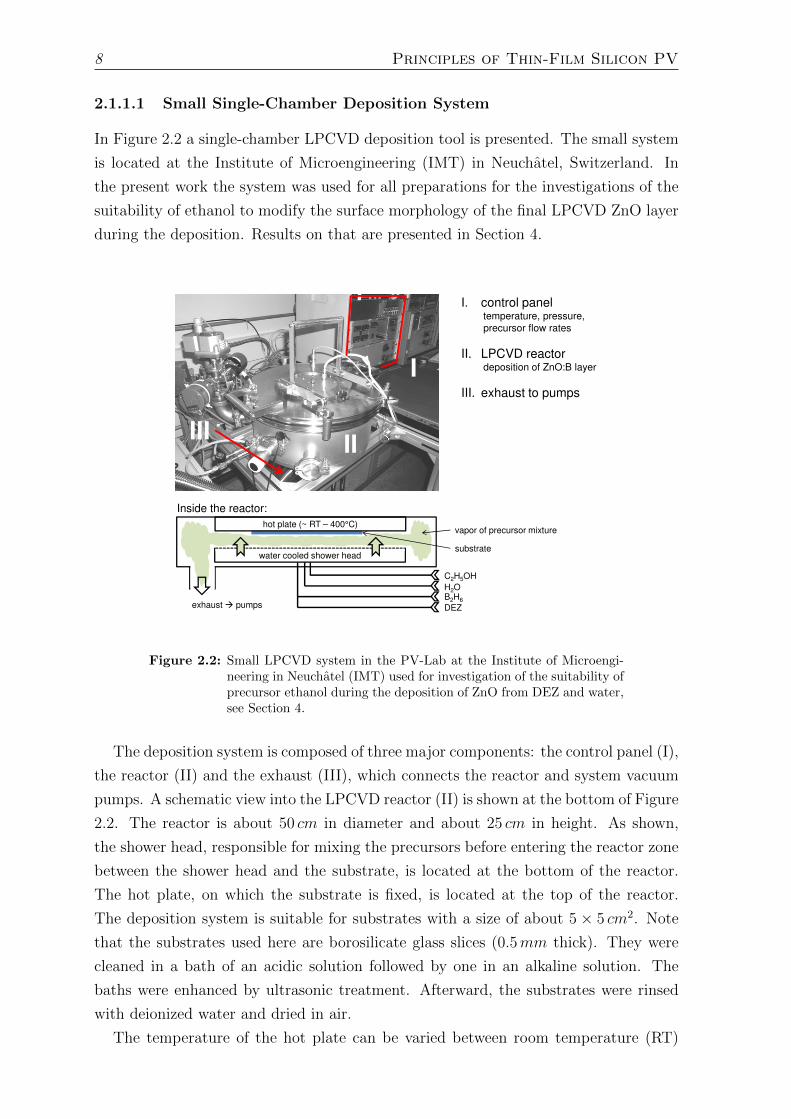
The TCO1200 deposition tool, which is used for the large-size industrial photovoltaic
application at Bosch Solar Thin Film GmbH (BSTF), is shown in Figure 2.3. In the
present work the tool is used for the introduction of an advanced LPCVD ZnO:B
into the production line at BSTF. Results will be presented in Section 5. The tool is
also used for solar module and sample fabrication during the investigation of anodic
degradation of ZnO:B on soda-lime glass. For results see Section 6. The TCO1200 tool
enables us to deposit LPCVD ZnO:B on glass substrates with a size of 1.1 × 1.3m2.
Note that the substrate used for solar module and sample fabrication is a low-iron
soda-lime glass with a thickness of 3 to 3.2mm. Before front contact layer deposition,
the substrates were cleaned in a bath of an alkaline solution. The cleaning process
was enhanced by ultrasonic treatment. Afterward, the substrates were rinsed with
deionized water and dried with a clean air flow.
The TCO1200 deposition system is about 15m long and a weights about 40 tons.
The main components are the load lock followed by four process modules (PM1–4)
and the unload lock. Leaving the unload lock the ZnO:B-covered substrates cool down
at atmospheric ambient conditions. Below the deposition tool, a transfer back to
the starting point is realized. Afterward, the substrates are handled further by an
automated production line control system.
In order to cycle through the deposition process, a cleaned substrate, provided by the
automated production line control system, is transferred into the load lock at ambient
pressure. After the transfer is completed, the pressure is reduced down to regime of
deposition, which is around 0.5mbar. At the same time an infrared radiation heater
increases the substrate temperature from ambient temperature to 170 to 180 . This
step is realized within less than 2 minutes. Now the pre-heated substrate is transferred
into PM1 and another substrate enters the load lock immediately after the transfer has
completed. Contrary to the reactor geometry of the small deposition system described
in Section 2.1.1.1, in the process modules of the LPCVD tool TCO1200 the hot plate is
placed at the bottom and the shower head is placed at the top of the process module.
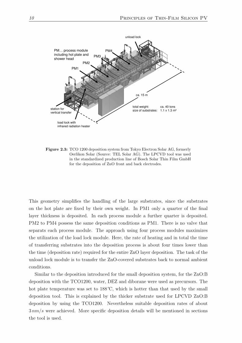
10 Principles of Thin-Film Silicon PV
unload lock
PM1
PM2
PM3
PM4PM… process module
including hot plate and
shower head
station for
vertical transfer
load lock with
infrared radiation heater
ca. 15 m
total weight: ca. 40 tons
size of substrates: 1.1 x 1.3 m²
Figure 2.3: TCO 1200 deposition system from Tokyo Electron Solar AG, formerlyOerlikon Solar (Source: TEL Solar AG). The LPCVD tool was usedin the standardized production line of Bosch Solar Thin Film GmbHfor the deposition of ZnO front and back electrodes.
This geometry simplifies the handling of the large substrates, since the substrates
on the hot plate are fixed by their own weight. In PM1 only a quarter of the final
layer thickness is deposited. In each process module a further quarter is deposited.
PM2 to PM4 possess the same deposition conditions as PM1. There is no valve that
separats each process module. The approach using four process modules maximizes
the utilization of the load lock module. Here, the rate of heating and in total the time
of transferring substrates into the deposition process is about four times lower than
the time (deposition rate) required for the entire ZnO layer deposition. The task of the
unload lock module is to transfer the ZnO-covered substrates back to normal ambient
conditions.
Similar to the deposition introduced for the small deposition system, for the ZnO:B
deposition with the TCO1200, water, DEZ and diborane were used as precursors. The
hot plate temperature was set to 188 , which is hotter than that used by the small
deposition tool. This is explained by the thicker substrate used for LPCVD ZnO:B
deposition by using the TCO1200. Nevertheless suitable deposition rates of about
3nm/s were achieved. More specific deposition details will be mentioned in sections
the tool is used.
Principles of Thin-Film Silicon PV 11
2.1.2 Structural Properties
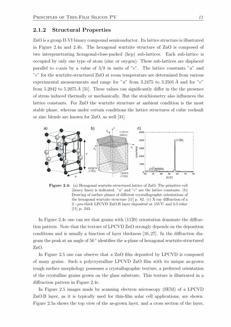
ZnO is a group II-VI binary compound semiconductor. Its lattice structure is illustrated
in Figure 2.4a and 2.4b. The hexagonal wurtzite structure of ZnO is composed of
two interpenetrating hexagonal-close-packed (hcp) sub-lattices. Each sub-lattice is
occupied by only one type of atom (zinc or oxygen). These sub-lattices are displaced
parallel to c-axis by a value of 3/8 in units of ”c”. The lattice constants ”a” and
”c” for the wurtzite-structured ZnO at room temperature are determined from various
experimental measurements and range for ”a” from 3.2475 to 3.2501 A and for ”c”
from 5.2042 to 5.2075 A [31]. These values can significantly differ in the the presence
of stress induced thermally or mechanically. But the stoichiometry also influences the
lattice constants. For ZnO the wurtzite structure at ambient condition is the most
stable phase, whereas under certain conditions the lattice structures of cubic rocksalt
or zinc blende are known for ZnO, as well [31].
c)a) b)
Figure 2.4: (a) Hexagonal wurtzite-structured lattice of ZnO. The primitive cell(heavy lines) is indicated. ”a” and ”c” are the lattice constants. (b)Drawing of surface planes of different crystallographic orientations ofthe hexagonal wurtzite structure [11] p. 82. (c) X-ray diffraction of a2−µm-thick LPCVD ZnO:B layer deposited at 155 and 0.5mbar[11] p. 243.
In Figure 2.4c one can see that grains with (1120) orientation dominate the diffrac-
tion pattern. Note that the texture of LPCVD ZnO strongly depends on the deposition
conditions and is usually a function of layer thickness [16, 27]. In the diffraction dia-
gram the peak at an angle of 56 identifies the a-plane of hexagonal wurtzite-structured
ZnO.
In Figure 2.5 one can observe that a ZnO film deposited by LPCVD is composed
of many grains. Such a polycrystalline LPCVD ZnO film with its unique as-grown
rough surface morphology possesses a crystallographic texture, a preferred orientation
of the crystalline grains grown on the glass substrate. This texture is illustrated in a
diffraction pattern in Figure 2.4c.
In Figure 2.5 images made by scanning electron microscopy (SEM) of a LPCVD
ZnO:B layer, as it is typically used for thin-film solar cell applications, are shown.
Figure 2.5a shows the top view of the as-grown layer, and a cross section of the layer,
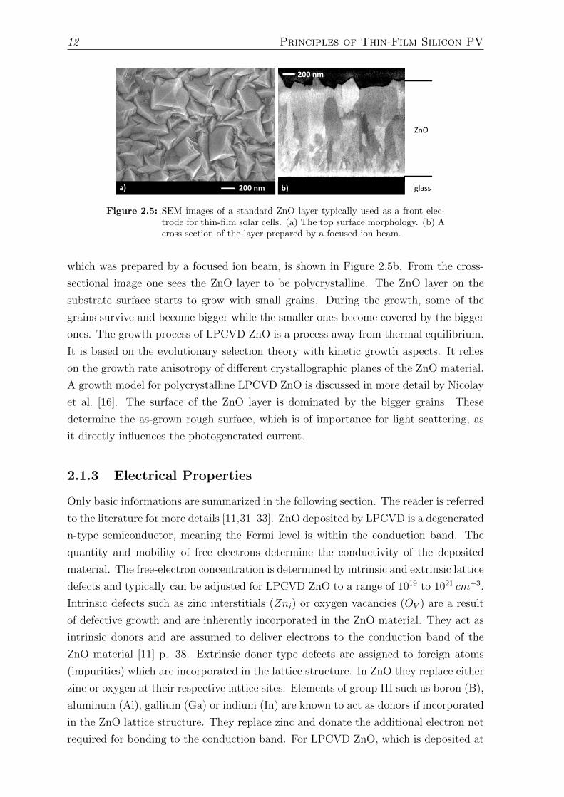
12 Principles of Thin-Film Silicon PV
200 nm
ZnO
glass200 nma) b)
Figure 2.5: SEM images of a standard ZnO layer typically used as a front elec-trode for thin-film solar cells. (a) The top surface morphology. (b) Across section of the layer prepared by a focused ion beam.
which was prepared by a focused ion beam, is shown in Figure 2.5b. From the cross-
sectional image one sees the ZnO layer to be polycrystalline. The ZnO layer on the
substrate surface starts to grow with small grains. During the growth, some of the
grains survive and become bigger while the smaller ones become covered by the bigger
ones. The growth process of LPCVD ZnO is a process away from thermal equilibrium.
It is based on the evolutionary selection theory with kinetic growth aspects. It relies
on the growth rate anisotropy of different crystallographic planes of the ZnO material.
A growth model for polycrystalline LPCVD ZnO is discussed in more detail by Nicolay
et al. [16]. The surface of the ZnO layer is dominated by the bigger grains. These
determine the as-grown rough surface, which is of importance for light scattering, as
it directly influences the photogenerated current.
2.1.3 Electrical Properties
Only basic informations are summarized in the following section. The reader is referred
to the literature for more details [11,31–33]. ZnO deposited by LPCVD is a degenerated
n-type semiconductor, meaning the Fermi level is within the conduction band. The
quantity and mobility of free electrons determine the conductivity of the deposited
material. The free-electron concentration is determined by intrinsic and extrinsic lattice
defects and typically can be adjusted for LPCVD ZnO to a range of 1019 to 1021 cm−3.
Intrinsic defects such as zinc interstitials (Zni) or oxygen vacancies (OV ) are a result
of defective growth and are inherently incorporated in the ZnO material. They act as
intrinsic donors and are assumed to deliver electrons to the conduction band of the
ZnO material [11] p. 38. Extrinsic donor type defects are assigned to foreign atoms
(impurities) which are incorporated in the lattice structure. In ZnO they replace either
zinc or oxygen at their respective lattice sites. Elements of group III such as boron (B),
aluminum (Al), gallium (Ga) or indium (In) are known to act as donors if incorporated
in the ZnO lattice structure. They replace zinc and donate the additional electron not
required for bonding to the conduction band. For LPCVD ZnO, which is deposited at

Principles of Thin-Film Silicon PV 13
temperatures below 200 , diborane (B2H6) was found to be a suitable extrinsic doping
source. When diborane is used as an additional precursor, the electron concentration
and as a result the resistivity can easily be tuned.
The mobility of electrons is of major importance to achieve suitable resistivity values.
For LPCVD ZnO:B used in photovoltaic applications and in the present work, typical
mobility values are around 30 cm2/V s. The mobility of electrons is a measure of
their scattering probability while moving through the material. There are several
scattering mechanisms known to reduce the electron mobility [11, 31]. For example,
ionized impurity scattering occurs due to the deflection of electrons by long-range
coulomb potentials. These are induced by charged defect centers or intentionally doped
impurities, e.g. ionized boron atoms within the lattice structure of ZnO. Another
form of scattering is induced by electron phonon interaction. Here, one distinguishes
between optical and acoustical phonon scattering. While for optical phonon scattering
the electron interacts with the electrical field induced by the lattice vibration, for
acoustical phonon scattering the electrons are scattered by the lattice deformation,
which induces a local energetic shift of the band edge. Other scattering mechanisms
are piezoelectric scattering and the scattering induced by lattice dislocations (crystal
defects). Piezoelectric scattering occurs due to the interaction of electrons with an
electric field that is induced by the presence of stress in the material.
In polycrystalline materials such as in LPCVD ZnO thin films, a vast number of
grains and as a result of grain boundaries is present. Here, the consideration of scat-
tering of free charge carriers (electrons) at grain boundaries is of importance if one
discusses electrical properties. According to the model of Seto [34] trap states at the
grain boundaries are responsible for trapping free electrons from the near grain bulk
material. These cause the creation of a negatively charged interface layer and the
formation of a back-to-back Schottky potential barrier. Figure 2.6 shows a schematic
band diagram illustrating a one-dimensional grain model and the idealized situation
at the grain boundaries. Electrons crossing the grain/grain interface have to overcome
the barrier by thermionic emission or by tunneling.
The barrier is characterized by its height (ΦB) and width (W). An expression for
both is given in Equation 2.3 and 2.4 [34]:
ΦB =e2Nt
2
8εε0Ne
,and (2.3)
W =Nt
Ne
. (2.4)
where e is the elementary charge of electrons, Nt the trap density at the grain bound-
aries, ε the dielectric permittivity of the material, ε0 the dielectric permittivity of free
space and Ne the free-electron concentration. One can see that ΦB and W are propor-
tional to the density of traps, whereas they are inverse proportional to the free-electron
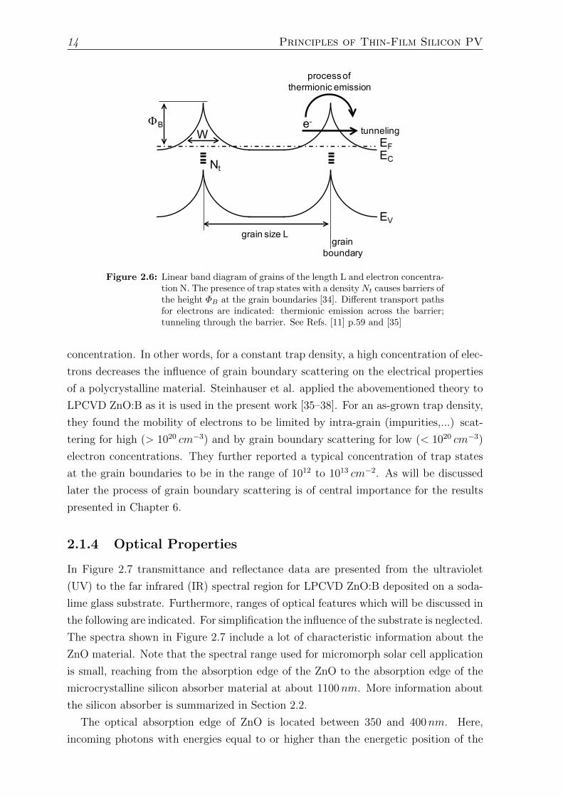
14 Principles of Thin-Film Silicon PV
ΦBW
Nt
e-
process of thermionic emission
tunneling
EC
EV
EF
grain size Lgrain
boundary
Figure 2.6: Linear band diagram of grains of the length L and electron concentra-tion N. The presence of trap states with a density Nt causes barriers ofthe height ΦB at the grain boundaries [34]. Different transport pathsfor electrons are indicated: thermionic emission across the barrier;tunneling through the barrier. See Refs. [11] p.59 and [35]
concentration. In other words, for a constant trap density, a high concentration of elec-
trons decreases the influence of grain boundary scattering on the electrical properties
of a polycrystalline material. Steinhauser et al. applied the abovementioned theory to
LPCVD ZnO:B as it is used in the present work [35–38]. For an as-grown trap density,
they found the mobility of electrons to be limited by intra-grain (impurities,...) scat-
tering for high (> 1020 cm−3) and by grain boundary scattering for low (< 1020 cm−3)
electron concentrations. They further reported a typical concentration of trap states
at the grain boundaries to be in the range of 1012 to 1013 cm−2. As will be discussed
later the process of grain boundary scattering is of central importance for the results
presented in Chapter 6.
2.1.4 Optical Properties
In Figure 2.7 transmittance and reflectance data are presented from the ultraviolet
(UV) to the far infrared (IR) spectral region for LPCVD ZnO:B deposited on a soda-
lime glass substrate. Furthermore, ranges of optical features which will be discussed in
the following are indicated. For simplification the influence of the substrate is neglected.
The spectra shown in Figure 2.7 include a lot of characteristic information about the
ZnO material. Note that the spectral range used for micromorph solar cell application
is small, reaching from the absorption edge of the ZnO to the absorption edge of the
microcrystalline silicon absorber material at about 1100nm. More information about
the silicon absorber is summarized in Section 2.2.
The optical absorption edge of ZnO is located between 350 and 400nm. Here,
incoming photons with energies equal to or higher than the energetic position of the
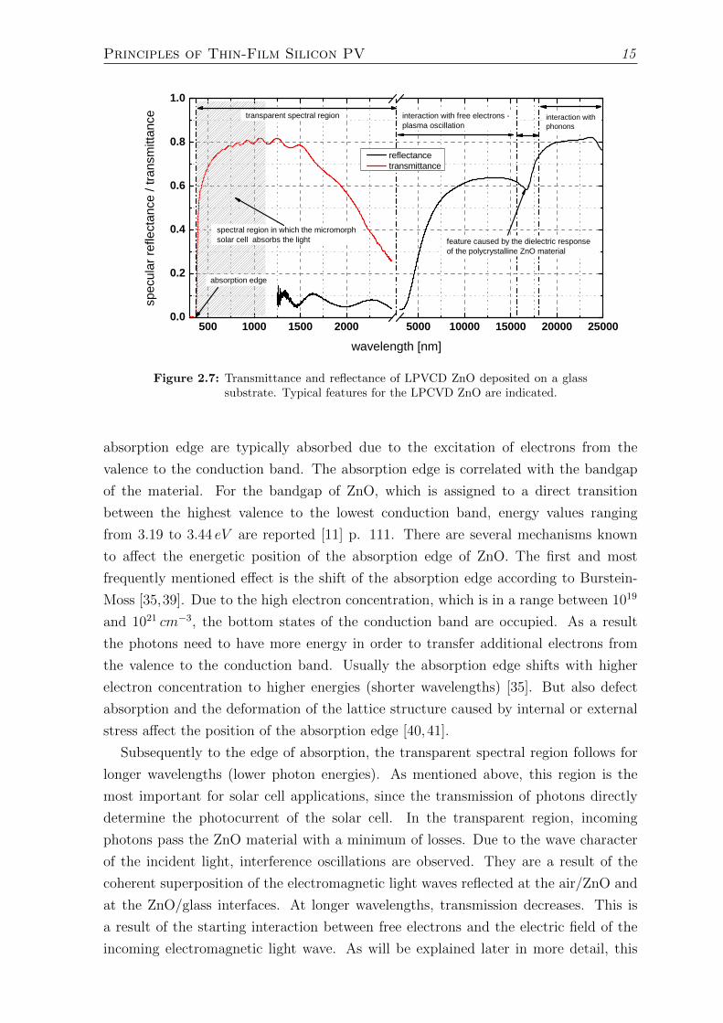
Principles of Thin-Film Silicon PV 15
5 0 0 1 0 0 0 1 5 0 0 2 0 0 0 5 0 0 0 1 0 0 0 0 1 5 0 0 0 2 0 0 0 0 2 5 0 0 00 . 0
0 . 2
0 . 4
0 . 6
0 . 8
1 . 0i n t e r a c t i o n w i t h p h o n o n s
i n t e r a c t i o n w i t h f r e e e l e c t r o n s - p l a s m a o s c i l l a t i o n
t r a n s p a r e n t s p e c t r a l r e g i o n
spec
ular re
flecta
nce /
trans
mitta
nce
w a v e l e n g t h [ n m ]
r e f l e c t a n c e t r a n s m i t t a n c e
a b s o r p t i o n e d g e
s p e c t r a l r e g i o n i n w h i c h t h e m i c r o m o r p h s o l a r c e l l a b s o r b s t h e l i g h t f e a t u r e c a u s e d b y t h e d i e l e c t r i c r e s p o n s e
o f t h e p o l y c r y s t a l l i n e Z n O m a t e r i a l
Figure 2.7: Transmittance and reflectance of LPVCD ZnO deposited on a glasssubstrate. Typical features for the LPCVD ZnO are indicated.
absorption edge are typically absorbed due to the excitation of electrons from the
valence to the conduction band. The absorption edge is correlated with the bandgap
of the material. For the bandgap of ZnO, which is assigned to a direct transition
between the highest valence to the lowest conduction band, energy values ranging
from 3.19 to 3.44 eV are reported [11] p. 111. There are several mechanisms known
to affect the energetic position of the absorption edge of ZnO. The first and most
frequently mentioned effect is the shift of the absorption edge according to Burstein-
Moss [35,39]. Due to the high electron concentration, which is in a range between 1019
and 1021 cm−3, the bottom states of the conduction band are occupied. As a result
the photons need to have more energy in order to transfer additional electrons from
the valence to the conduction band. Usually the absorption edge shifts with higher
electron concentration to higher energies (shorter wavelengths) [35]. But also defect
absorption and the deformation of the lattice structure caused by internal or external
stress affect the position of the absorption edge [40,41].
Subsequently to the edge of absorption, the transparent spectral region follows for
longer wavelengths (lower photon energies). As mentioned above, this region is the
most important for solar cell applications, since the transmission of photons directly
determine the photocurrent of the solar cell. In the transparent region, incoming
photons pass the ZnO material with a minimum of losses. Due to the wave character
of the incident light, interference oscillations are observed. They are a result of the
coherent superposition of the electromagnetic light waves reflected at the air/ZnO and
at the ZnO/glass interfaces. At longer wavelengths, transmission decreases. This is
a result of the starting interaction between free electrons and the electric field of the
incoming electromagnetic light wave. As will be explained later in more detail, this
16 Principles of Thin-Film Silicon PV
phenomenon can be treated by the well-known Drude Theory [35,42–45].
Between 2.5 and about 15µm, a strong increase of reflection can be observed. Here,
for frequencies between 20 and 120THz the free electrons are able to follow the oscillat-
ing electric field of the light waves. With the onset of strong reflection the penetration
depth of the electromagnetic waves is drastically reduced. No electromagnetic waves
if still reflected at the ZnO/glass interface contribute to the formation of interference
fringes. This is indicated by the disappearance of the interference fringes, which are
observed only in the transparent spectral region. The position of the reflection edge
and its shape depends on the concentration and on the mobility of electrons, respec-
tively. Whereas with a higher concentration of electrons the reflection edge shifts to
shorter wavelengths and vice versa, the slope of the reflection edge increases the higher
the mobility of the interacting free electrons and vice versa.
The second reflection edge above 17µm marks the interaction of optical phonons
with electric field oscillations of electromagnetic waves. This band of high reflection is
known as Reststrahlen (residual rays) band reflection [42,46].
A last feature which was found to be of interest during the course of the present
work was the dip in the reflection spectrum located at about 17µm. Recently, Prunici
et al. explained that the dip is due to the dielectric response of the polycrystalline
ZnO:B material [46]. Prunici’s approach will be introduced in Section 2.1.5. As a
result one obtains a dielectric response function which includes the features mentioned
above and enables the simulation of the reflection spectra shown in Figure 2.7. The fit
parameters extracted and their interpretation are in agreement with electron transport
theory introduced by Seto [34] and discussed in Section 2.1.3.
2.1.5 Dielectric Function of Polycrystalline LPCVD ZnO:B
The dielectric function (DF), ε(ω), of any material is known to be a complex function
describing the interaction between an incoming electromagnetic wave and the interact-
ing material. According to the relation n =√ε = n + ik the refractive index (n) and
the extinction coefficient (k) can be calculated. If the DF of the material is known, in
combination with Fresnel’s equations, one is able to calculate transmission, absorption
and reflection of an incoming electromagnetic wave. The reader is referred to related
textbooks for more details [42, 47, 48]. Note that it is necessary to know the DF of
each layer including the substrate and the surrounding medium, if for example the
transmission or reflection of a stack of layers has to be calculated. The DF of our glass
substrate was determined separately and will not be discussed further, since the focus
of the present work is on the ZnO material. For more information on the DF of the
glass the reader is referred to the Appendix A. For ZnO in the IR spectral range to
25µm one has to consider three major dielectric contributions. These are summed up
in Equation 2.5:
Principles of Thin-Film Silicon PV 17
ε(ω) = ε∞ + εpl + εph. (2.5)
ε∞ is the high-frequency dielectric constant and is associated with oscillators in the
high-frequency range, which do not directly influence the optical spectral range inves-
tigated. εpl and εph are the dielectric contributions of the free electrons and phonons,
respectively. These are defined in Equation 2.6 and 2.7:
εpl = −ω2pl
ω2 + iΓplω, and (2.6)
εph =ω2LO − ω2
TO
ω2TO − ω2 + iΓphω
. (2.7)
Here, ωpl is the plasma mode frequency and Γpl is the corresponding damping constant.
ωTO and ωLO are the resonance frequencies of the transversal and longitudinal optical
phonon modes, respectively. Γph is the damping constant of the phonon dielectric
contribution.
The proposed DF would be sufficient to describe an isotropic, monocrystalline ZnO.
However, it fails when describing a polycrystalline ZnO possessing a free-electron con-
centration on the order of 1019 cm−3. In order to overcome these limitations and to
model IR reflectance of ZnO:B deposited by LPCVD, Prunici et. al. [46] proposed to
describe the DF of a polycrystalline ZnO layer as an effective medium according to
the theory of Maxwell-Garnett [49, 50]. It is assumed that the ZnO grain bulk/core
material (as spherical inclusions) is embedded in a ZnO host material, namely the ZnO
grain boundary material. Both the grain bulk and boundary material are modeled
by their respective DF, according to Equation 2.5. The resulting DF according to
Maxwell-Garnett is calculated from Equation 2.8:
ε(ω) = εbndεblk + 2εbnd + 2fblk(εblk − εbnd)εblk + 2εbnd − fblk(εblk − εbnd)
, (2.8)
where εblk and εbnd are assigned to the individual DFs of the ZnO grain bulk and
boundary material, respectively. fblk is the volume fraction of the ZnO grain bulk ma-
terial. fbnd, the volume fraction of the ZnO grain boundary material, can be calculated
according to Equation 2.9:
fbnd = 1− fblk (2.9)
Again, εblk and εbnd are independently determined according to Equations 2.5 to 2.7.
From the fitting process of simulated and measured optical spectra, important pa-
rameters such as the plasma mode frequency (ωpl) and the damping constant (Γpl) can
be derived. As can be seen from Equation 2.10 and 2.11, these parameters allow us to
determine the free-electron concentration (Ne) and electron optical mobility (µopt):
18 Principles of Thin-Film Silicon PV
Ne =ω2Nε0ε∞m
∗
e2=ω2plε0m
∗
e2, ω2
N =ω2pl
ε∞,and (2.10)
µopt =m∗
eΓpl, (2.11)
where e, ε0 and m∗ are the elementary electron charge, the permittivity of the vacuum
and the effective electron mass, respectively. ωN is the plasma mode frequency, as well.
It results from putting ε∞ in Equation 2.5 out of the brackets.
2.2 Silicon Thin Films -
Deposition and Material Properties
On the following pages a brief introduction into thin-film silicon technology will be
given. The deposition process is introduced in Section 2.2.1. Afterward, the material
properties of amorphous and microcrystalline silicon will be briefly summarized in
Sections 2.2.2 and 2.2.3, respectively.
2.2.1 Deposition of Silicon Thin Films by Plasma-Enhanced
Chemical Vapor Deposition
For the industrial fabrication of silicon thin films on large substrates (1.1× 1.3m2, in
our case), the technology of plasma-enhanced chemical vapor deposition (PECVD) is
utilized. In the present case the main precursors required for the deposition of silicon
are silane (SiH4) and hydrogen (H2). Other precursors such as silicon tetrachloride
(SiCl4), dichlorosilane (SiH2Cl2) or silicon tetrafluoride (SiF4) are also reported for
thin-film silicon deposition [51–54].
Silane usually dissociates at temperatures above 450 . Thus, only substrates re-
sisting high temperature are suited for the deposition of silicon thin films. During the
PECVD process a continuous flow of precursors is forced to dissociate before reach-
ing the substrate surface. In the gas phase a plasma is generated [55]. The plasma
is powered by an external power source. This approach has an advantage, since the
temperature of the substrate can be chosen independently from the dissociation tem-
perature of the precursors. The substrate temperature for the deposition of silicon thin
films by PECVD is typically adjusted to a range between 150 and 200 . The plasma
required for the dissociation is generated between coplanar-arranged electrodes. The
deposition setup is shown in Figure 2.8. Utilizing an alternating electric field with a
frequency of 40MHz applied to the electrodes, enables the deposition of thin films on
isolating substrates. Whereas the upper electrode in Figure 2.8 is used as the input
electrode, the bottom electrode, as well as the rest of the reactor, is grounded. The
Principles of Thin-Film Silicon PV 19
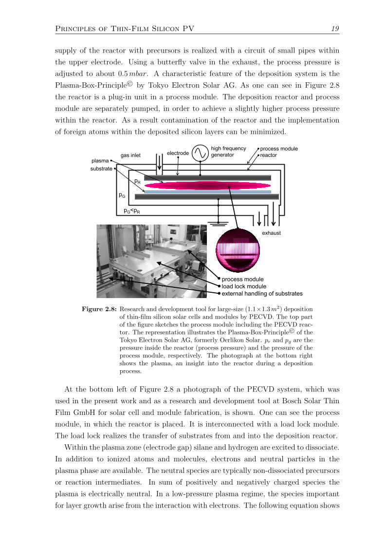
supply of the reactor with precursors is realized with a circuit of small pipes within
the upper electrode. Using a butterfly valve in the exhaust, the process pressure is
adjusted to about 0.5mbar. A characteristic feature of the deposition system is the
Plasma-Box-Principle© by Tokyo Electron Solar AG. As one can see in Figure 2.8
the reactor is a plug-in unit in a process module. The deposition reactor and process
module are separately pumped, in order to achieve a slightly higher process pressure
within the reactor. As a result contamination of the reactor and the implementation
of foreign atoms within the deposited silicon layers can be minimized.
high frequency generatorelectrode
plasmasubstrate
process moduleload lock moduleexternal handling of substrates
exhaust
gas inlet
pR
pG
pG<pR
process modulereactor
Figure 2.8: Research and development tool for large-size (1.1×1.3m2) depositionof thin-film silicon solar cells and modules by PECVD. The top partof the figure sketches the process module including the PECVD reac-tor. The representation illustrates the Plasma-Box-Principle© of theTokyo Electron Solar AG, formerly Oerlikon Solar. pr and pg are thepressure inside the reactor (process pressure) and the pressure of theprocess module, respectively. The photograph at the bottom rightshows the plasma, an insight into the reactor during a depositionprocess.
At the bottom left of Figure 2.8 a photograph of the PECVD system, which was
used in the present work and as a research and development tool at Bosch Solar Thin
Film GmbH for solar cell and module fabrication, is shown. One can see the process
module, in which the reactor is placed. It is interconnected with a load lock module.
The load lock realizes the transfer of substrates from and into the deposition reactor.
Within the plasma zone (electrode gap) silane and hydrogen are excited to dissociate.
In addition to ionized atoms and molecules, electrons and neutral particles in the
plasma phase are available. The neutral species are typically non-dissociated precursors
or reaction intermediates. In sum of positively and negatively charged species the
plasma is electrically neutral. In a low-pressure plasma regime, the species important
for layer growth arise from the interaction with electrons. The following equation shows
20 Principles of Thin-Film Silicon PV
only one possible reaction path [55]:
2SiH4 + 2e− ⇒ 2SiH3 + 2H + 2e− ⇒ 2SiH3 +H2 + 2e−. (2.12)
SiH3 as a reaction intermediate is assumed to play a major role in the deposition of
silicon. On their way to the surface of the growing silicon layer, reaction intermediates
are influenced by many interactions. Here, secondary reactions might occur that lead
to the formation of further intermediates. On the one hand some of them will support
layer growth, but on the other hand some of them will cause the formation of dust
(silicon dust) influencing the final layer quality [55]. Nevertheless, due to a certain
set of deposition parameters, the fabrication of amorphous and microcrystalline silicon
films and their photovoltaic application are possible [10,56,57].
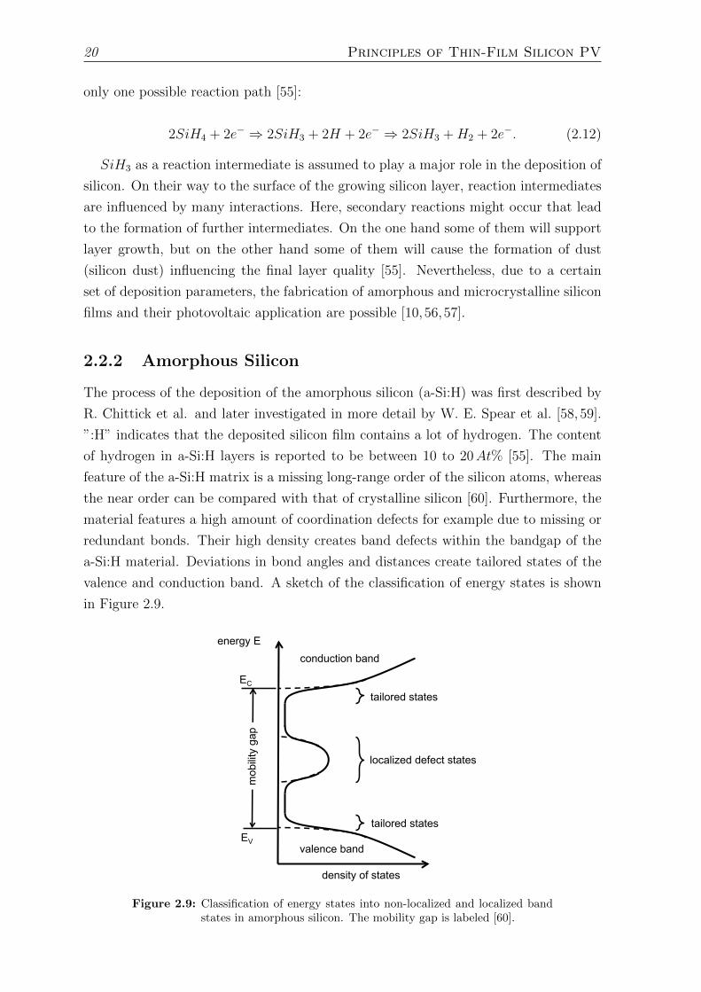
2.2.2 Amorphous Silicon
The process of the deposition of the amorphous silicon (a-Si:H) was first described by
R. Chittick et al. and later investigated in more detail by W. E. Spear et al. [58, 59].
”:H” indicates that the deposited silicon film contains a lot of hydrogen. The content
of hydrogen in a-Si:H layers is reported to be between 10 to 20At% [55]. The main
feature of the a-Si:H matrix is a missing long-range order of the silicon atoms, whereas
the near order can be compared with that of crystalline silicon [60]. Furthermore, the
material features a high amount of coordination defects for example due to missing or
redundant bonds. Their high density creates band defects within the bandgap of the
a-Si:H material. Deviations in bond angles and distances create tailored states of the
valence and conduction band. A sketch of the classification of energy states is shown
in Figure 2.9.
energy E
density of states
conduction band
valence band
mob
ility
gap
tailored states
tailored states
localized defect states
EC
EV
Figure 2.9: Classification of energy states into non-localized and localized bandstates in amorphous silicon. The mobility gap is labeled [60].
Principles of Thin-Film Silicon PV 21
The mobility of charge carriers that occupy the tailored states of the valence and
conduction bands is reduced, but increases significantly towards the bands. This is
the reason one defines a mobility gap rather than a bandgap for a-Si:H. The mobility
gap for a-Si:H is reported to be 1.65 eV [60]. That energy is required for electron
excitation in order to overcome the mobility gap, so that a significant increase of
layer conductivity becomes measureable. Unlike crystalline silicon, a-Si:H is a direct
semiconductor [55, 60]. This leads to stronger absorption, which will be discussed for
Figure 2.11 in the following section.
2.2.3 Microcrystalline Silicon
Microcrystalline silicon (µc-Si:H) is known to be a crystalline silicon material which is
embedded in a matrix of a-Si:H [61]. The material quality is of major importance for
the application in a µc-Si:H solar cell. In Figure 2.10 the microstructure of µc-Si:H
is sketched for different deposition regimes. Typically, the growth of the crystalline
material occurs due to the presence of nuclei next to the substrate surface. Their
presence and survival depend on the deposition conditions. After the survival of nu-
merous nuclei they increase quickly in size before the growth of the crystallites becomes
columnar. The space in between the crystallites is associated with voids or is filled with
a-Si:H. Unlike for the amorphous deposition regime, for the microcrystalline deposition
regime, the precursor silane is strongly diluted with hydrogen. With reference to the
total mass flow rate of precursors, the dilution usually lies in the range between 6 and
7 %. This range of dilution is reported to be suitable for solar cell fabrication, but
depends on other deposition parameters, such as on the electrical power the plasma is
loaded with [10, 51, 62]. For higher dilutions (< 6 %) the crystallites are larger in size.
This is illustrated by the left side of Figure 2.10. Here, the µc-Si:H material is more
porous and more sensitive to contamination, especially at the grain boundaries. Solar
cells prepared with that kind of material possess low efficiencies [63].
When a lower dilution of silane (> 7 %) is used, the material properties become
amorphous. Such material is illustrated on the right side of Figure 2.10. Note that due
to the addition of hydrogen the quality of the amorphous material can be improved.
One assumes the hydrogen quenches non-quenched silicon bonds [55].
Optically, µc-Si:H possesses properties similar to crystalline silicon. As well as crys-
talline silicon, µc-Si:H is an indirect semiconductor and has a bandgap of 1.12 eV . The
absorption coefficient for photons with energies above 1.12 eV is usually smaller in
comparison to a direct semiconductor [10]. A comparison of the absorption coefficients
of amorphous, microcrystalline and crystalline silicon is shown in Figure 2.11. One can
see the absorption coefficient of a-Si:H for photon energies above 1.65 eV is one order
of magnitude larger than the one for the crystalline material. The absorption coeffi-
cient of µc-Si:H material lies in between. Note that the µc-Si:H material is embedded

22 Principles of Thin-Film Silicon PV
Figure 2.10: Illustration of the microstructural characteristics of µc-Si:H [64].The marked range indicates the material suitable for solar cell ap-plication.
in an a-Si:H matrix, which might explain the higher absorption compared to the pure
crystalline material. Between 1.12 and 1.65 eV the absorption coefficient of the µc-Si:H
material is dominated by its crystalline volume fraction. Here, the µc-Si:H is similar to
the one of the pure crystalline material. Below 1.12 eV defect absorption determines
the absorption of the µc-Si:H material.
Figure 2.11: Comparison of absorption coefficients for amorphous, microcrys-talline and crystalline silicon material as a function of photon energyand wavelength [10].
2.3 Micromorph Solar Cells and Modules
In the following a brief introduction into the concept of a micromorph solar cell will
be given. Furthermore, the working principle of a solar cell and its characterizing pa-
rameters derived from current-voltage measurements will be discussed. Finally, the
fabrication of a micromorph module is briefly summarized. For a more detailed discus-
sion the reader is referred to the literature and references therein [60,65,66].
Principles of Thin-Film Silicon PV 23
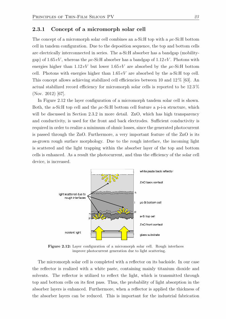
2.3.1 Concept of a micromorph solar cell
The concept of a micromorph solar cell combines an a-Si:H top with a µc-Si:H bottom
cell in tandem configuration. Due to the deposition sequence, the top and bottom cells
are electrically interconnected in series. The a-Si:H absorber has a bandgap (mobility-
gap) of 1.65 eV , whereas the µc-Si:H absorber has a bandgap of 1.12 eV . Photons with
energies higher than 1.12 eV but lower 1.65 eV are absorbed by the µc-Si:H bottom
cell. Photons with energies higher than 1.65 eV are absorbed by the a-Si:H top cell.
This concept allows achieving stabilized cell efficiencies between 10 and 12 % [63]. An
actual stabilized record efficiency for micromorph solar cells is reported to be 12.3 %
(Nov. 2012) [67].
In Figure 2.12 the layer configuration of a micromorph tandem solar cell is shown.
Both, the a-Si:H top cell and the µc-Si:H bottom cell feature a p-i-n structure, which
will be discussed in Section 2.3.2 in more detail. ZnO, which has high transparency
and conductivity, is used for the front and back electrodes. Sufficient conductivity is
required in order to realize a minimum of ohmic losses, since the generated photocurrent
is passed through the ZnO. Furthermore, a very important feature of the ZnO is its
as-grown rough surface morphology. Due to the rough interface, the incoming light
is scattered and the light trapping within the absorber layer of the top and bottom
cells is enhanced. As a result the photocurrent, and thus the efficiency of the solar cell
device, is increased.
Figure 2.12: Layer configuration of a micromorph solar cell. Rough interfacesimprove photocurrent generation due to light scattering.
The micromorph solar cell is completed with a reflector on its backside. In our case
the reflector is realized with a white paste, containing mainly titanium dioxide and
solvents. The reflector is utilized to reflect the light, which is transmitted through
top and bottom cells on its first pass. Thus, the probability of light absorption in the
absorber layers is enhanced. Furthermore, when a reflector is applied the thickness of
the absorber layers can be reduced. This is important for the industrial fabrication
24 Principles of Thin-Film Silicon PV
of solar cells and modules, since the deposition time of the absorber material can be
reduced and thus the throughput can be increased.
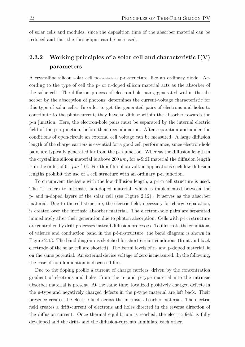
2.3.2 Working principles of a solar cell and characteristic I(V)
parameters
A crystalline silicon solar cell possesses a p-n-structure, like an ordinary diode. Ac-
cording to the type of cell the p- or n-doped silicon material acts as the absorber of
the solar cell. The diffusion process of electron-hole pairs, generated within the ab-
sorber by the absorption of photons, determines the current-voltage characteristic for
this type of solar cells. In order to get the generated pairs of electrons and holes to
contribute to the photocurrent, they have to diffuse within the absorber towards the
p-n junction. Here, the electron-hole pairs must be separated by the internal electric
field of the p-n junction, before their recombination. After separation and under the
conditions of open-circuit an external cell voltage can be measured. A large diffusion
length of the charge carriers is essential for a good cell performance, since electron-hole
pairs are typically generated far from the p-n junction. Whereas the diffusion length in
the crystalline silicon material is above 200µm, for a-Si:H material the diffusion length
is in the order of 0.1µm [10]. For thin-film photovoltaic applications such low diffusion
lengths prohibit the use of a cell structure with an ordinary p-n junction.
To circumvent the issue with the low diffusion length, a p-i-n cell structure is used.
The ”i” refers to intrinsic, non-doped material, which is implemented between the
p- and n-doped layers of the solar cell (see Figure 2.12). It serves as the absorber
material. Due to the cell structure, the electric field, necessary for charge separation,
is created over the intrinsic absorber material. The electron-hole pairs are separated
immediately after their generation due to photon absorption. Cells with p-i-n structure
are controlled by drift processes instead diffusion processes. To illustrate the conditions
of valence and conduction band in the p-i-n-structure, the band diagram is shown in
Figure 2.13. The band diagram is sketched for short-circuit conditions (front and back
electrode of the solar cell are shorted). The Fermi levels of n- and p-doped material lie
on the same potential. An external device voltage of zero is measured. In the following,
the case of no illumination is discussed first.
Due to the doping profile a current of charge carriers, driven by the concentration
gradient of electrons and holes, from the n- and p-type material into the intrinsic
absorber material is present. At the same time, localized positively charged defects in
the n-type and negatively charged defects in the p-type material are left back. Their
presence creates the electric field across the intrinsic absorber material. The electric
field creates a drift-current of electrons and holes directed in the reverse direction of
the diffusion-current. Once thermal equilibrium is reached, the electric field is fully
developed and the drift- and the diffusion-currents annihilate each other.
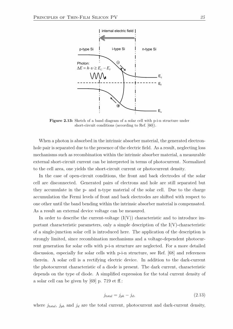
Principles of Thin-Film Silicon PV 25
Ec
Ef
Ev
p-type Si n-type Si
Photon:
internal electric field
-
+
VC EEhE −≥⋅=∆ υ
i-type Si
Figure 2.13: Sketch of a band diagram of a solar cell with p-i-n structure undershort-circuit conditions (according to Ref. [60]).
When a photon is absorbed in the intrinsic absorber material, the generated electron-
hole pair is separated due to the presence of the electric field. As a result, neglecting loss
mechanisms such as recombination within the intrinsic absorber material, a measurable
external short-circuit current can be interpreted in terms of photocurrent. Normalized
to the cell area, one yields the short-circuit current or photocurrent density.
In the case of open-circuit conditions, the front and back electrodes of the solar
cell are disconnected. Generated pairs of electrons and hole are still separated but
they accumulate in the p- and n-type material of the solar cell. Due to the charge
accumulation the Fermi levels of front and back electrodes are shifted with respect to
one other until the band bending within the intrinsic absorber material is compensated.
As a result an external device voltage can be measured.
In order to describe the current-voltage (I(V)) characteristic and to introduce im-
portant characteristic parameters, only a simple description of the I(V)-characteristic
of a single-junction solar cell is introduced here. The application of the description is
strongly limited, since recombination mechanisms and a voltage-dependent photocur-
rent generation for solar cells with p-i-n structure are neglected. For a more detailed
discussion, especially for solar cells with p-i-n structure, see Ref. [68] and references
therein. A solar cell is a rectifying electric device. In addition to the dark-current
the photocurrent characteristic of a diode is present. The dark current, characteristic
depends on the type of diode. A simplified expression for the total current density of
a solar cell can be given by [69] p. 719 et ff.:
jtotal = jph − jd, (2.13)
where jtotal, jph and jd are the total current, photocurrent and dark-current density,
26 Principles of Thin-Film Silicon PV
respectively, where
jd = j0 ·(
exp
(eV
nkBT
)− 1
). (2.14)
Here, j0, n, kB, T, e and V are the saturation-current density, diode quality factor,
Boltzmann constant, temperature, elementary electron charge and applied voltage,
respectively. In general, the photocurrent density depends on the amount of absorbed
photons. Assuming short-circuit (sc) conditions (V=0) jd is zero and jtotal is equal to
the short-circuit current density (jsc) and thus equal to jph:
jtotal = jph = jsc. (2.15)
In open-circuit (oc) conditions, jtotal = 0. Equation 2.13 in combination with Equation
2.14 can be rewritten as:
0 = jph − j0 ·(
exp
(eVocnkBT
)− 1
). (2.16)
Furthermore, the last equation can be solved for the open-circuit voltage (Voc). As one
can see from equation 2.17, Voc is a function of photocurrent and saturation-current
density.
Voc =nkBT
e· ln(jphj0
+ 1
). (2.17)
The higher the jph – or the lower j0 – the higher the Voc. Among other dependencies,
j0 scales with the bandgap of the absorber material. It generally applies that the larger
the bandgap of the absorber material the higher the Voc [69] p. 723. The temperature
dependence of a solar cell is not obvious from Equation 2.17, since the parameters
jph and j0 in general are a function of temperature, as well. As a rule of thumb for
crystalline silicon solar cells it is [70] p. 231 ff.:
dVocdT
=1
T
(Voc −
Ege
), (2.18)
where Eg is the bandgap of the absorber material. Usually dVoc/dT < 0 is observed.
The higher the temperature, the lower Voc.
In Figure 2.14 the current-voltage characteristic of a solar cell is shown for the dark
case and the illuminated case. The power output density of a solar cell depends on the
voltage the solar cell is working at. It is
p(V ) = jtotal(V ) · V. (2.19)
For jtotal = 0 (external resistor is equal to infinity) and V = 0 (external resistor is
equal to zero) the power output of the solar cell is zero. Its maximum power point is
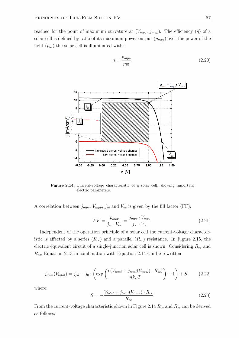
Principles of Thin-Film Silicon PV 27
reached for the point of maximum curvature at (Vmpp, jmpp). The efficiency (η) of a
solar cell is defined by ratio of its maximum power output (pmpp) over the power of the
light (pill) the solar cell is illuminated with:
η =pmpppill
. (2.20)
Figure 2.14: Current-voltage characteristic of a solar cell, showing importantelectric parameters.
A correlation between jmpp, Vmpp, jsc and Voc is given by the fill factor (FF):
FF =pmppjsc · Voc
=jmpp · Vmppjsc · Voc
. (2.21)
Independent of the operation principle of a solar cell the current-voltage character-
istic is affected by a series (Roc) and a parallel (Rsc) resistance. In Figure 2.15, the
electric equivalent circuit of a single-junction solar cell is shown. Considering Roc and
Rsc, Equation 2.13 in combination with Equation 2.14 can be rewritten
jtotal(Vtotal) = jph − j0 ·(
exp
(e(Vtotal + jtotal(Vtotal) ·Roc)
nkBT
)− 1
)+ S, (2.22)
where:
S = −Vtotal + jtotal(Vtotal) ·Roc
Rsc
. (2.23)
From the current-voltage characteristic shown in Figure 2.14 Roc and Rsc can be derived
as follows:
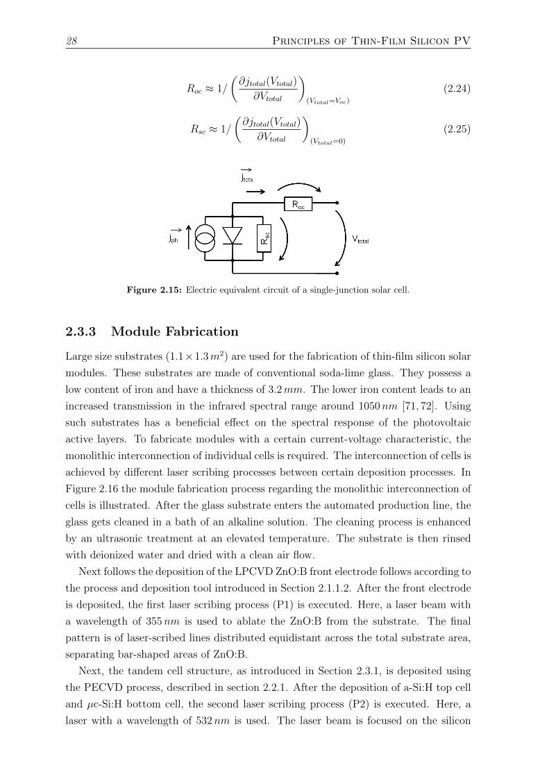
28 Principles of Thin-Film Silicon PV
Roc ≈ 1/
(∂jtotal(Vtotal)
∂Vtotal
)(Vtotal=Voc)
(2.24)
Rsc ≈ 1/
(∂jtotal(Vtotal)
∂Vtotal
)(Vtotal=0)
(2.25)
Figure 2.15: Electric equivalent circuit of a single-junction solar cell.
2.3.3 Module Fabrication
Large size substrates (1.1×1.3m2) are used for the fabrication of thin-film silicon solar
modules. These substrates are made of conventional soda-lime glass. They possess a
low content of iron and have a thickness of 3.2mm. The lower iron content leads to an
increased transmission in the infrared spectral range around 1050nm [71, 72]. Using
such substrates has a beneficial effect on the spectral response of the photovoltaic
active layers. To fabricate modules with a certain current-voltage characteristic, the
monolithic interconnection of individual cells is required. The interconnection of cells is
achieved by different laser scribing processes between certain deposition processes. In
Figure 2.16 the module fabrication process regarding the monolithic interconnection of
cells is illustrated. After the glass substrate enters the automated production line, the
glass gets cleaned in a bath of an alkaline solution. The cleaning process is enhanced
by an ultrasonic treatment at an elevated temperature. The substrate is then rinsed
with deionized water and dried with a clean air flow.
Next follows the deposition of the LPCVD ZnO:B front electrode follows according to
the process and deposition tool introduced in Section 2.1.1.2. After the front electrode
is deposited, the first laser scribing process (P1) is executed. Here, a laser beam with
a wavelength of 355nm is used to ablate the ZnO:B from the substrate. The final
pattern is of laser-scribed lines distributed equidistant across the total substrate area,
separating bar-shaped areas of ZnO:B.
Next, the tandem cell structure, as introduced in Section 2.3.1, is deposited using
the PECVD process, described in section 2.2.1. After the deposition of a-Si:H top cell
and µc-Si:H bottom cell, the second laser scribing process (P2) is executed. Here, a
laser with a wavelength of 532nm is used. The laser beam is focused on the silicon

Principles of Thin-Film Silicon PV 29
material through the glass and ZnO:B next to the P1 scribe. Glass and ZnO:B are
transparent to the used laser wavelength. As a result only the silicon is ablated.
substrate cleaning
deposition front contactLPCVD ZnO
laser scribingP1
deposition tandem cell structurePECVD a-Si/µc-Si
deposition back contactLPCVD ZnO
laser scribingP2
final structure after laser scribingP3
Figure 2.16: Illustration of the process to produce a monolithic interconnectionof single solar cells on the substrate.
In a next fabrication step, the LPCVD ZnO:B back electrode is deposited on the
laser-scribed (P1, P2) tandem cell structure. The final laser-scribing process (P3)
completes the monolithic interconnection of individual cells fabricated on the glass
substrate. For the P3 process, the same laser used for the P2-process is focused on
the silicon material through the glass and the ZnO:B front electrode next to the P2
laser-scribe. As indicated in Figure 2.16 the cells are now interconnected in series. The
gap between P1 and P3 is a non-photoactive module area (area loss). This gap has to
be minimized in order to maximize the photoactive module area. Depending on the
positioning accuracy of the used scribing system, typical gap distances are between 150
and 250µm. The photoactive cell area is determined by the cell width, the distance
between P3n−1 and P1n. Due to the limited substrate area, the number of cells and
therefore the open-circuit voltage of the module decreases with increasing cell width.
In turn the short-circuit current of the module is enhanced, which usually coincides
with an increase of ohmic power-losses (I2R) due to the contributions of front and back
electrodes to the series resistance. A balance has to be found between area losses (gap
between P1 and P3) and ohmic losses [11] p. 373.
In order to complete the internal electric circuit of the module, electric leads are
glued onto the outer cells of the monolithically interconnected cell string. Cross con-
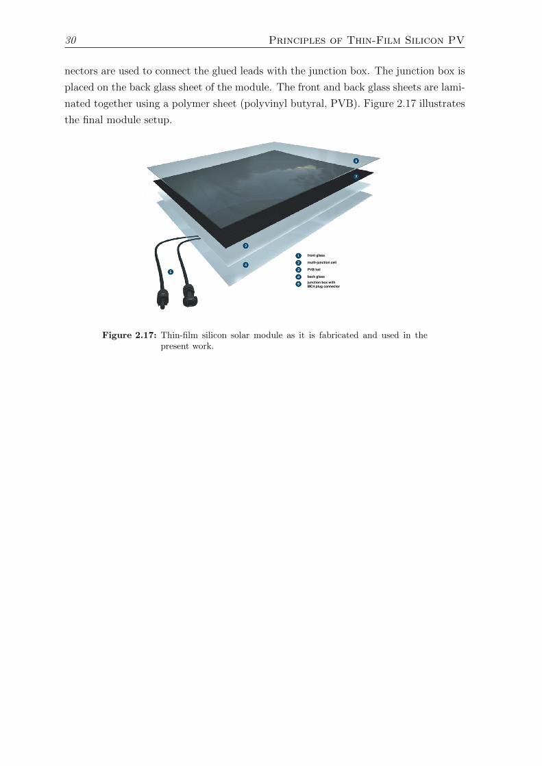
30 Principles of Thin-Film Silicon PV
nectors are used to connect the glued leads with the junction box. The junction box is
placed on the back glass sheet of the module. The front and back glass sheets are lami-
nated together using a polymer sheet (polyvinyl butyral, PVB). Figure 2.17 illustrates
the final module setup.
front glass
multi-junction cell
PVB foil
back glass
junction box with MC4 plug connector
Figure 2.17: Thin-film silicon solar module as it is fabricated and used in thepresent work.
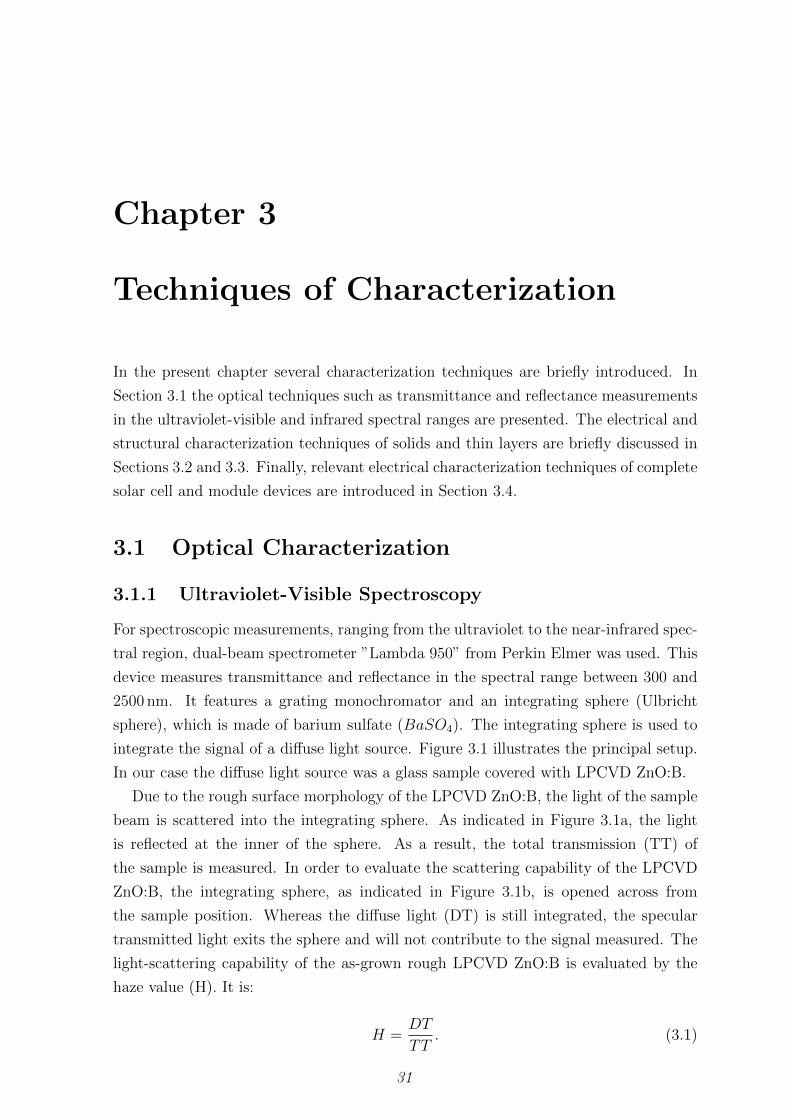
Chapter 3
Techniques of Characterization
In the present chapter several characterization techniques are briefly introduced. In
Section 3.1 the optical techniques such as transmittance and reflectance measurements
in the ultraviolet-visible and infrared spectral ranges are presented. The electrical and
structural characterization techniques of solids and thin layers are briefly discussed in
Sections 3.2 and 3.3. Finally, relevant electrical characterization techniques of complete
solar cell and module devices are introduced in Section 3.4.
3.1 Optical Characterization
3.1.1 Ultraviolet-Visible Spectroscopy
For spectroscopic measurements, ranging from the ultraviolet to the near-infrared spec-
tral region, dual-beam spectrometer ”Lambda 950” from Perkin Elmer was used. This
device measures transmittance and reflectance in the spectral range between 300 and
2500 nm. It features a grating monochromator and an integrating sphere (Ulbricht
sphere), which is made of barium sulfate (BaSO4). The integrating sphere is used to
integrate the signal of a diffuse light source. Figure 3.1 illustrates the principal setup.
In our case the diffuse light source was a glass sample covered with LPCVD ZnO:B.
Due to the rough surface morphology of the LPCVD ZnO:B, the light of the sample
beam is scattered into the integrating sphere. As indicated in Figure 3.1a, the light
is reflected at the inner of the sphere. As a result, the total transmission (TT) of
the sample is measured. In order to evaluate the scattering capability of the LPCVD
ZnO:B, the integrating sphere, as indicated in Figure 3.1b, is opened across from
the sample position. Whereas the diffuse light (DT) is still integrated, the specular
transmitted light exits the sphere and will not contribute to the signal measured. The
light-scattering capability of the as-grown rough LPCVD ZnO:B is evaluated by the
haze value (H). It is:
H =DT
TT. (3.1)
31
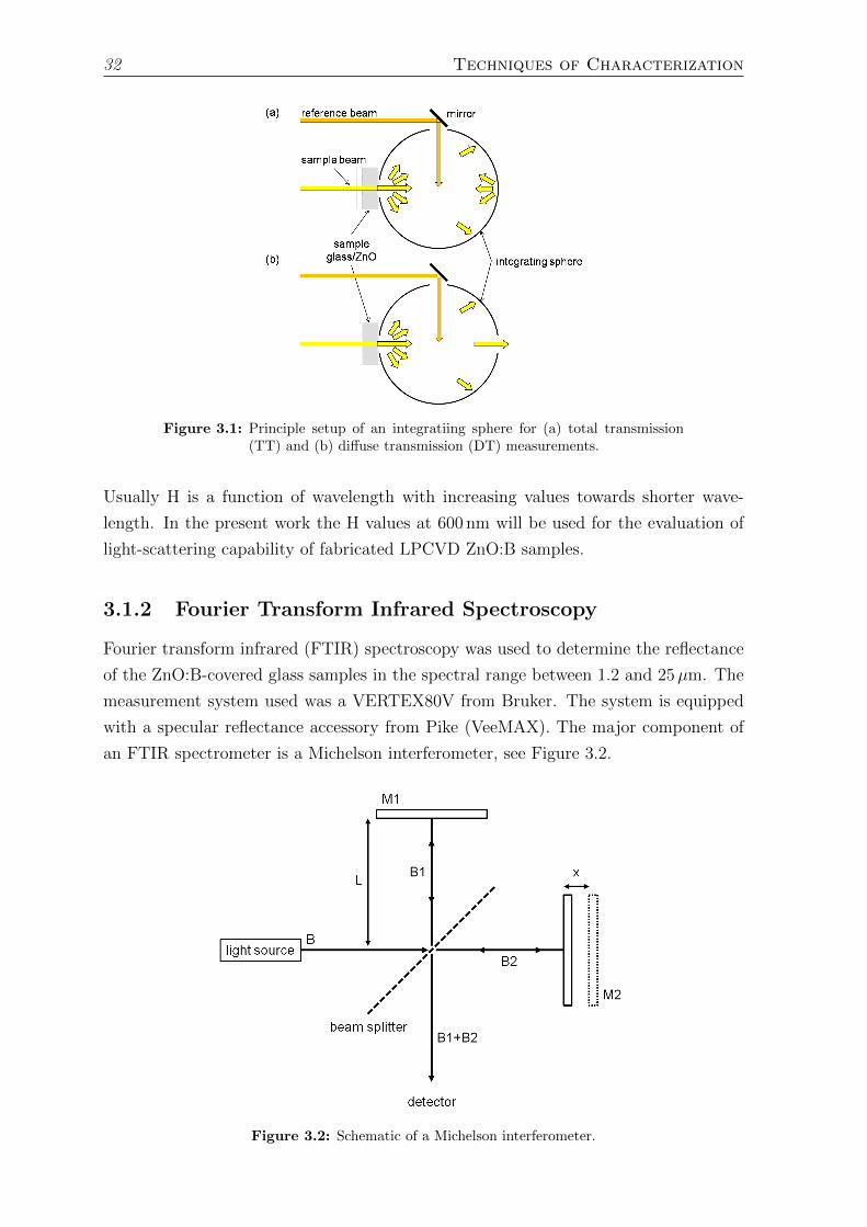
32 Techniques of Characterization
Figure 3.1: Principle setup of an integratiing sphere for (a) total transmission(TT) and (b) diffuse transmission (DT) measurements.
Usually H is a function of wavelength with increasing values towards shorter wave-
length. In the present work the H values at 600 nm will be used for the evaluation of
light-scattering capability of fabricated LPCVD ZnO:B samples.
3.1.2 Fourier Transform Infrared Spectroscopy
Fourier transform infrared (FTIR) spectroscopy was used to determine the reflectance
of the ZnO:B-covered glass samples in the spectral range between 1.2 and 25µm. The
measurement system used was a VERTEX80V from Bruker. The system is equipped
with a specular reflectance accessory from Pike (VeeMAX). The major component of
an FTIR spectrometer is a Michelson interferometer, see Figure 3.2.
Figure 3.2: Schematic of a Michelson interferometer.
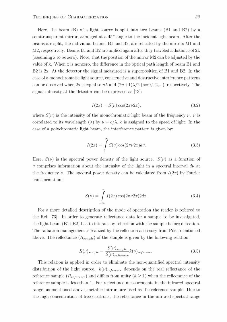
Techniques of Characterization 33
Here, the beam (B) of a light source is split into two beams (B1 and B2) by a
semitransparent mirror, arranged at a 45 angle to the incident light beam. After the
beams are split, the individual beams, B1 and B2, are reflected by the mirrors M1 and
M2, respectively. Beams B1 and B2 are unified again after they traveled a distance of 2L
(assuming x to be zero). Note, that the position of the mirror M2 can be adjusted by the
value of x. When x is nonzero, the difference in the optical path length of beam B1 and
B2 is 2x. At the detector the signal measured is a superposition of B1 and B2. In the
case of a monochromatic light source, constructive and destructive interference patterns
can be observed when 2x is equal to nλ and (2n+1)λ/2 (n=0,1,2,...), respectively. The
signal intensity at the detector can be expressed as [73]:
I(2x) = S(ν) cos(2πν2x), (3.2)
where S(ν) is the intensity of the monochromatic light beam of the frequency ν. ν is
correlated to its wavelength (λ) by ν = c/λ. c is assigned to the speed of light. In the
case of a polychromatic light beam, the interference pattern is given by:
I(2x) =
∞∫0
S(ν) cos(2πν2x)dν. (3.3)
Here, S(ν) is the spectral power density of the light source. S(ν) as a function of
ν comprises information about the intensity of the light in a spectral interval dν at
the frequency ν. The spectral power density can be calculated from I(2x) by Fourier
transformation:
S(ν) =
∞∫−∞
I(2x) cos(2πν2x)2dx. (3.4)
For a more detailed description of the mode of operation the reader is referred to
the Ref. [73]. In order to generate reflectance data for a sample to be investigated,
the light beam (B1+B2) has to interact by reflection with the sample before detection.
The radiation management is realized by the reflection accessory from Pike, mentioned
above. The reflectance (Rsample) of the sample is given by the following relation:
R(ν)sample =S(ν)sampleS(ν)reference
k(ν)reference. (3.5)
This relation is applied in order to eliminate the non-quantified spectral intensity
distribution of the light source. k(ν)reference depends on the real reflectance of the
reference sample (Rreference) and differs from unity (k ≥ 1) when the reflectance of the
reference sample is less than 1. For reflectance measurements in the infrared spectral
range, as mentioned above, metallic mirrors are used as the reference sample. Due to
the high concentration of free electrons, the reflectance in the infrared spectral range
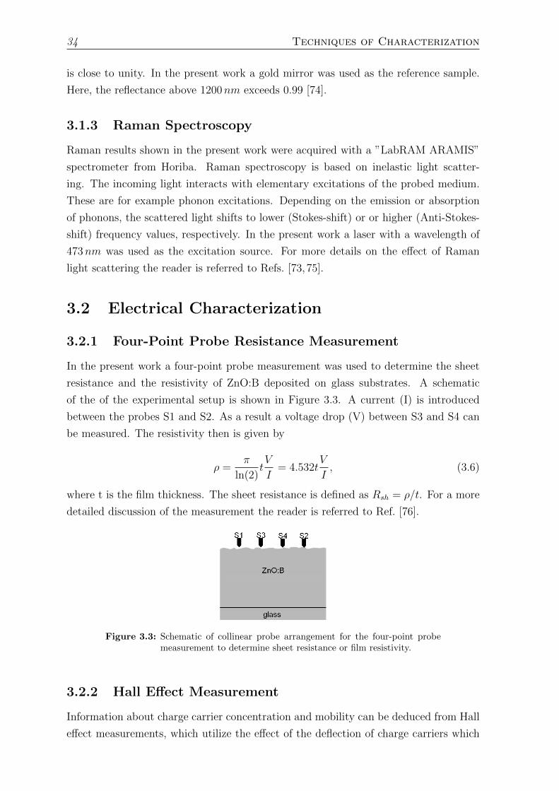
34 Techniques of Characterization
is close to unity. In the present work a gold mirror was used as the reference sample.
Here, the reflectance above 1200nm exceeds 0.99 [74].
3.1.3 Raman Spectroscopy
Raman results shown in the present work were acquired with a ”LabRAM ARAMIS”
spectrometer from Horiba. Raman spectroscopy is based on inelastic light scatter-
ing. The incoming light interacts with elementary excitations of the probed medium.
These are for example phonon excitations. Depending on the emission or absorption
of phonons, the scattered light shifts to lower (Stokes-shift) or or higher (Anti-Stokes-
shift) frequency values, respectively. In the present work a laser with a wavelength of
473nm was used as the excitation source. For more details on the effect of Raman
light scattering the reader is referred to Refs. [73,75].
3.2 Electrical Characterization
3.2.1 Four-Point Probe Resistance Measurement
In the present work a four-point probe measurement was used to determine the sheet
resistance and the resistivity of ZnO:B deposited on glass substrates. A schematic
of the of the experimental setup is shown in Figure 3.3. A current (I) is introduced
between the probes S1 and S2. As a result a voltage drop (V) between S3 and S4 can
be measured. The resistivity then is given by
ρ =π
ln(2)tV
I= 4.532t
V
I, (3.6)
where t is the film thickness. The sheet resistance is defined as Rsh = ρ/t. For a more
detailed discussion of the measurement the reader is referred to Ref. [76].
Figure 3.3: Schematic of collinear probe arrangement for the four-point probemeasurement to determine sheet resistance or film resistivity.
3.2.2 Hall Effect Measurement
Information about charge carrier concentration and mobility can be deduced from Hall
effect measurements, which utilize the effect of the deflection of charge carriers which
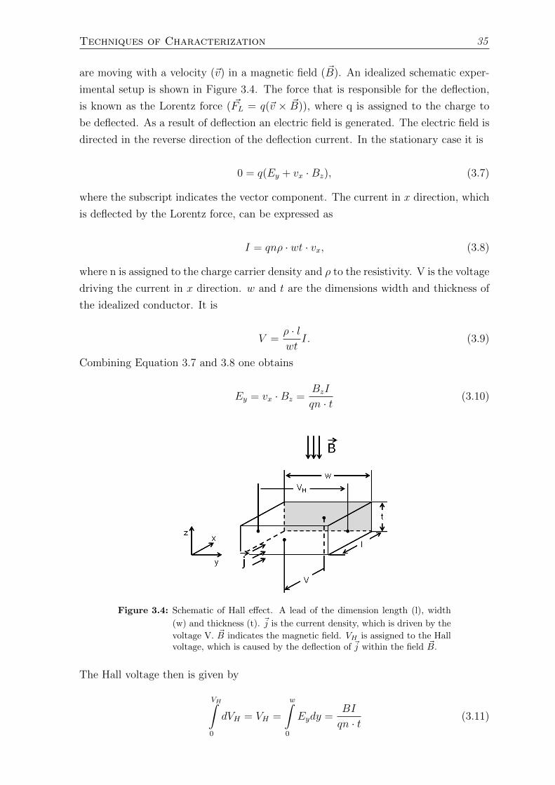
Techniques of Characterization 35
are moving with a velocity (~v) in a magnetic field ( ~B). An idealized schematic exper-
imental setup is shown in Figure 3.4. The force that is responsible for the deflection,
is known as the Lorentz force ( ~FL = q(~v × ~B)), where q is assigned to the charge to
be deflected. As a result of deflection an electric field is generated. The electric field is
directed in the reverse direction of the deflection current. In the stationary case it is
0 = q(Ey + vx ·Bz), (3.7)
where the subscript indicates the vector component. The current in x direction, which
is deflected by the Lorentz force, can be expressed as
I = qnρ · wt · vx, (3.8)
where n is assigned to the charge carrier density and ρ to the resistivity. V is the voltage
driving the current in x direction. w and t are the dimensions width and thickness of
the idealized conductor. It is
V =ρ · lwt
I. (3.9)
Combining Equation 3.7 and 3.8 one obtains
Ey = vx ·Bz =BzI
qn · t(3.10)
Figure 3.4: Schematic of Hall effect. A lead of the dimension length (l), width
(w) and thickness (t). ~j is the current density, which is driven by the
voltage V. ~B indicates the magnetic field. VH is assigned to the Hallvoltage, which is caused by the deflection of ~j within the field ~B.
The Hall voltage then is given by
VH∫0
dVH = VH =
w∫0
Eydy =BI
qn · t(3.11)
36 Techniques of Characterization
By rewriting Equation 3.11 the Hall coefficient (RH) is defined as
RH =1
qn=VHt
BI. (3.12)
From Equation 3.12 charge carrier density (nH) and mobility (µH) can be derived from
the following relations
nH =1
qRH
, µH =RH
ρ(3.13)
A more detailed discussion of the Hall effect measurement is given in Ref. [76]. Note,
that the above model to determine nH and µH is valid for thin films possessing a ho-
mogeneous structure. Other more sophisticated models may also apply. For simplicity
the above model is assumed to be valid in the first approximation.
3.3 Structural Characterization
3.3.1 Atomic Force Microscopy
Atomic force microscopy (AFM) was used to characterize the morphology of the top
surface of the rough ZnO:B front electrode. AFM is a scanning probe technique. It is
realized with a cantilever, which is equipped with sharp tip. The tip interacts with the
atomic surface structure of the sample, yielding a height profile. In general the height
profile can be obtained with two different modes of the measurement. The first mode
is the contact mode. Here, the tip is in contact with the surface. While scanning, the
deflection of the tip is adjusted to be constant. For the second, the non-contact mode,
the tip oscillates with its natural frequency. When it nears the surface a phase shift in
its oscillation can be observed. While scanning, the approach is adjusted in order to
fix the observed phase shift. In the present work the non-contact mode was used for
surface analysis. For more details the reader is referred to Refs. [76–78].
In the present work AFM images were acquired with a system from Nanotec Elec-
tronica. The images were 10 × 10µm2 and were further analyzed by determining the
root mean square roughness (σRMS) as follows:
σRMS =
√√√√ 1
MN
M∑m=1
N∑n=1
(z(xm,yn)− < z >)2, (3.14)
where z(xm,yn) is the measured height value at the position (xm,yn) and < z > is
defined as the average deflection of the cantilever:
< z >=1
MN
M∑m=1
N∑n=1
z(xm,yn). (3.15)
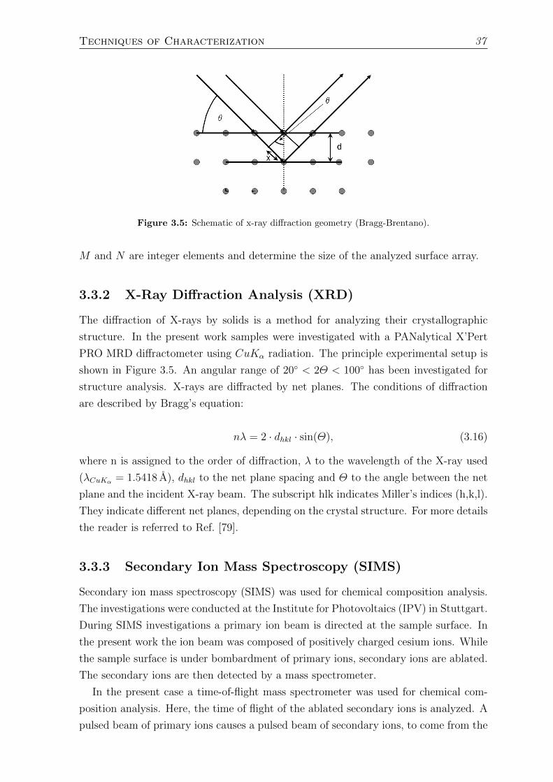
Techniques of Characterization 37
Figure 3.5: Schematic of x-ray diffraction geometry (Bragg-Brentano).
M and N are integer elements and determine the size of the analyzed surface array.
3.3.2 X-Ray Diffraction Analysis (XRD)
The diffraction of X-rays by solids is a method for analyzing their crystallographic
structure. In the present work samples were investigated with a PANalytical X’Pert
PRO MRD diffractometer using CuKα radiation. The principle experimental setup is
shown in Figure 3.5. An angular range of 20 < 2Θ < 100 has been investigated for
structure analysis. X-rays are diffracted by net planes. The conditions of diffraction
are described by Bragg’s equation:
nλ = 2 · dhkl · sin(Θ), (3.16)
where n is assigned to the order of diffraction, λ to the wavelength of the X-ray used
(λCuKα = 1.5418 A), dhkl to the net plane spacing and Θ to the angle between the net
plane and the incident X-ray beam. The subscript hlk indicates Miller’s indices (h,k,l).
They indicate different net planes, depending on the crystal structure. For more details
the reader is referred to Ref. [79].
3.3.3 Secondary Ion Mass Spectroscopy (SIMS)
Secondary ion mass spectroscopy (SIMS) was used for chemical composition analysis.
The investigations were conducted at the Institute for Photovoltaics (IPV) in Stuttgart.
During SIMS investigations a primary ion beam is directed at the sample surface. In
the present work the ion beam was composed of positively charged cesium ions. While
the sample surface is under bombardment of primary ions, secondary ions are ablated.
The secondary ions are then detected by a mass spectrometer.
In the present case a time-of-flight mass spectrometer was used for chemical com-
position analysis. Here, the time of flight of the ablated secondary ions is analyzed. A
pulsed beam of primary ions causes a pulsed beam of secondary ions, to come from the
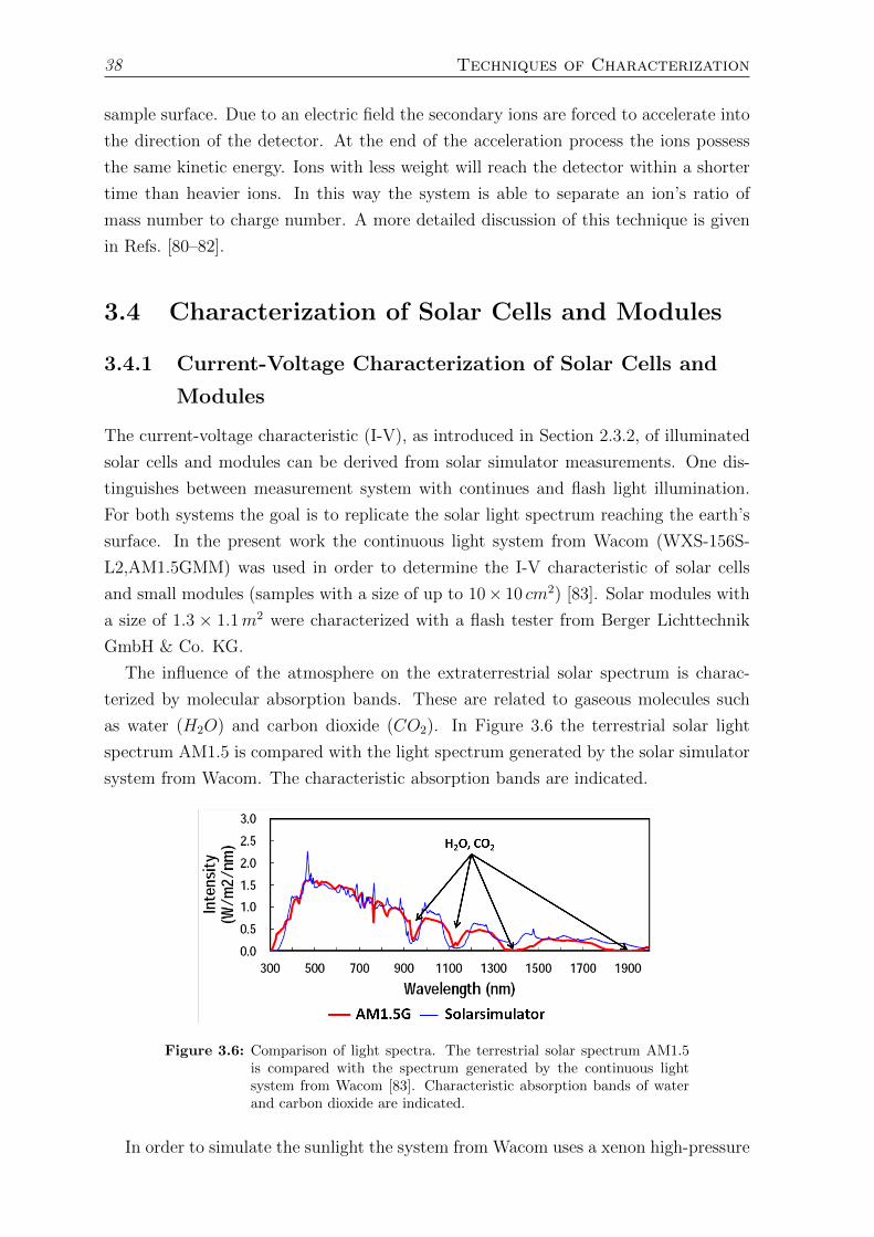
38 Techniques of Characterization
sample surface. Due to an electric field the secondary ions are forced to accelerate into
the direction of the detector. At the end of the acceleration process the ions possess
the same kinetic energy. Ions with less weight will reach the detector within a shorter
time than heavier ions. In this way the system is able to separate an ion’s ratio of
mass number to charge number. A more detailed discussion of this technique is given
in Refs. [80–82].
3.4 Characterization of Solar Cells and Modules
3.4.1 Current-Voltage Characterization of Solar Cells and
Modules
The current-voltage characteristic (I-V), as introduced in Section 2.3.2, of illuminated
solar cells and modules can be derived from solar simulator measurements. One dis-
tinguishes between measurement system with continues and flash light illumination.
For both systems the goal is to replicate the solar light spectrum reaching the earth’s
surface. In the present work the continuous light system from Wacom (WXS-156S-
L2,AM1.5GMM) was used in order to determine the I-V characteristic of solar cells
and small modules (samples with a size of up to 10× 10 cm2) [83]. Solar modules with
a size of 1.3 × 1.1m2 were characterized with a flash tester from Berger Lichttechnik
GmbH & Co. KG.
The influence of the atmosphere on the extraterrestrial solar spectrum is charac-
terized by molecular absorption bands. These are related to gaseous molecules such
as water (H2O) and carbon dioxide (CO2). In Figure 3.6 the terrestrial solar light
spectrum AM1.5 is compared with the light spectrum generated by the solar simulator
system from Wacom. The characteristic absorption bands are indicated.
Figure 3.6: Comparison of light spectra. The terrestrial solar spectrum AM1.5is compared with the spectrum generated by the continuous lightsystem from Wacom [83]. Characteristic absorption bands of waterand carbon dioxide are indicated.
In order to simulate the sunlight the system from Wacom uses a xenon high-pressure
Techniques of Characterization 39
lamp and a halogen lamp. With additional filters the spectra are further adjusted. In
the term AM1.5, AM refers air mass, ans 1.5 indicates the path length the extrater-
restrial light passed through the atmosphere. Here, one atmosphere (AM1) scales with
the height h where the pressure measured at the earth’s surface (pnorm) decreased by
ph = 1/e·pnorm in accordance with the barometric formula [60]. As in the present work,
solar cells and modules are generally rated with standardized test conditions. These
conditions are given in detail in IEC60904. In general the ratings were done with a
terrestrial solar radiation spectrum of AM1.5 at 1000W/m2. The device temperature
during measurement was set to 25 .
3.4.2 External Quantum Efficiency (EQE)
The spectral response of a solar cell includes both optical information and information
regarding charge carrier collection. The spectral response (S) of a solar cell is defined as
ratio of the short-circuit current density (jsc [A/m2]) and the monochromatic irradiation
power (E [W/m2]). It is [60]:
S(λ) =jsc(λ)
E(λ), (3.17)
where λ is assigned to the incident wavelength. If one normalizes the current density in
Equation 3.17 to the electron charge (e) and the irradiation power to the energy of an
single incident photon (hc/λ), one obtains the external quantum efficiency (EQE) [60]:
EQE(λ) =jsc(λ)
e· hc
λE(λ)=hc
eλS(λ), (3.18)
where c is assigned to the speed of light and h to Planck’s constant. One distinguishes
between the external and internal quantum efficiency, because only a certain amount
of photons penetrate the absorber material of the solar cell. Some of the photons
are reflected at interfaces before they reach the absorber material. For the internal
quantum efficiency (IQE) it is:
IQE(λ) =EQE(λ)
1−R(λ), (3.19)
where R is assigned to the reflectance, the reflected part of the incoming photons.

40 Techniques of Characterization
Chapter 4
Ethanol-enriched LPCVD ZnO
bilayers: Properties and Growth –
A Potential Electrode for Thin
Film Solar Cells
The present chapter investigates ethanol as additional precursor to water and diethylz-
inc in order to deposit ZnO by low pressure chemical vapor deposition. Here, the
addition of ethanol is intended to modify the as grown surface morphology of the de-
posited ZnO film. The application of such layers to micromorph solar cells will be
discussed. In Section 4.1 more introductive information will be given. After, experi-
mental details are presented in Section 4.2. Section 4.3 is divited into two parts. In the
first one, results of ZnO single layers deposited using a mixture of ethanol, water and
diethylzinc are presented. In the second part the approach of ethanol enriched bilayers
is discussed. Finally, in the Section 4.4 the main results of the chapter are summarized.
4.1 Background
Zinc oxide (ZnO) deposited by low-pressure chemical vapor deposition (LPCVD) is a
widely used transparent conductive oxide (TCO) in thin-film photovoltaics and other
applications like low-emission coatings and gas sensor devices. In photovoltaics ZnO:B
layers are used as front and back electrodes to electrically contact thin-film solar cells.
One of the advantages of LPCVD ZnO:B as a front electrode is that it possesses an
as-grown roughness, unlike sputtered ZnO which needs an additional etching step to
texture the surface [84]. Surface roughness is directly related to a film’s light scattering
properties. Indeed, efficient light scattering allows the use of thinner absorber layers in
thin-film silicon solar cells without compromising photocurrent generation [57]. This
in turn can be translated into reduced takt time and increased throughput. Also,
41
42Ethanol-enriched LPCVD ZnO bilayers: Properties and Growth – A
Potential Electrode for Thin Film Solar Cells
regarding cell stability, thinner absorber layers are preferred in thin-film silicon tandem
cells, as light-induced degradation of hydrogenated amorphous silicon (a-Si:H) can be
reduced [85]. For a given growth regime, the roughness of LPCVD ZnO:B is controlled
primarily by adjusting the thickness of the layer: The thicker the layer, the rougher
the ZnO surface tends to be. Therefore, the amount of light scattering can easily be
tuned.
The present section discusses the use of LPCVD ZnO:B for front and back electrodes
for micromorph silicon solar cells as introduced in Section 2.3.1. These devices combine
an a-Si:H top cell with a hydrogenated microcrystalline silicon (µc-Si:H) bottom cell
in a tandem configuration [10, 56]. It is well established that the quality of µc-Si:H is
sensitive to the morphology of the surface on which it is deposited [86], as well as to its
crystallinity [87]. Therefore, one has to pay special attention to the quality of the front
TCO surface, even the µc-Si:H absorber is deposited on top of the a-Si:H absorber.
Optimized as-grown LPCVD ZnO:B has very good electrical and optical properties
that result from large grains [27]. However, the sharp pyramidal features of its surface
are known to deteriorate the quality of subsequently deposited µc-Si:H absorber layers,
which are characterized by porous regions, also called cracks [88]. In fact, it has been
shown that the crack density in the µc-Si:H absorber material is directly related to
the roughness and V-shaped features of the ZnO:B layer [86]. Usually, a high density
of cracks is correlated with losses in fill factor and open-circuit voltage and, as a
result, in conversion efficiency. High densities of cracks are avoided by using ZnO:B
layers of reduced thickness and scattering ability (roughness). Another approach is
to introduce optimized p- and n-type silicon oxide layers deposited before and after
the µc-Si:H absorber material [89]. To obtain a surface morphology suitable for both
the deposition of high-quality µc-Si:H and high-angle light scattering, an argon-based
plasma treatment on as-grown LPCVD ZnO:B layers is typically used [90]. The aim of
the treatment is to change the surface grooves from V-shaped to U-shaped. However,
this approach is not cost-efficient for industrial production. Another possible approach
to achieve good optical and electrical properties is to use sputtered ZnO, which features
a U-shaped morphology after hydrochloric acid etching [84,91]. However, this approach
requires two different processes in order to create front electrodes suitable for thin-film
silicon devices, and free carrier absorption is usually higher than in LPCVD ZnO:B
films.
In the following a technique to modify the surface morphology of LPCVD ZnO:B
without additional plasma treatment or etching is proposed. Ethanol is added to the
water and diethylzinc mixture during deposition to change the surface morphology of
the ZnO:B layer. In fact, it has already been reported that ethanol and other alcohols
like methanol or butanol can be used as an oxygen source together with diethylzinc to
deposit ZnO layers [18,23,92], and that they can prompt morphological changes. Here
the results of Wenas et al, [92] will be confirmed. Furthermore, a growth mechanism
Ethanol-enriched LPCVD ZnO bilayers: Properties and Growth – APotential Electrode for Thin Film Solar Cells 43
is proposed which is able to explain the observations in the regard of electrical, optical
and morphological changes.
4.2 Experimental
ZnO layers were deposited on 0.5mm thick AF45 glass substrates from SCHOTT,
using the deposition tool introduced in Section 2.1.1.1. The films were grown with
an LPCVD reactor at a pressure of 0.5 mbar and a substrate temperature of 175 ,
unless otherwise indicated. Diethylzinc (DEZ, [C2H5]2Zn) and water (H2O) were used
as the main precursors to form the ZnO. Ethanol (C2H5OH) was added during ZnO
deposition to change the film surface morphology.
Both, scanning electron microscopy (SEM) and atomic force microscopy (AFM)
were used to analyse the surface roughness of the samples. The optical properties were
investigated with a photospectrometer featuring an integrating sphere to measure the
total and diffuse transmittance, from which haze was calculated. The haze value given
is for a wavelength of 600nm. FITR-reflectance measurements have been utilized to
investigate samples properties in the infrared spectral range. Electrical properties were
measured with a four-point probe to determine the sheet resistance and resistivity of
the films. Film crystallography was investigated by X-ray diffraction (XRD) analysis
in the θ − 2θ mode.
4.3 Results
The following section is divided into two parts. The first part deals with single ZnO
layers for which ethanol was used for the whole layer deposition, and we discuss the role
of ethanol during deposition. The second part follows the work of Wenas et al. [92]. A
standard layer deposited without ethanol is capped by a thin ZnO film deposited with
a mixture of ethanol, water and DEZ.
4.3.1 ZnO single layers deposited using a mixture of ethanol,
water and DEZ
Structural and electrical properties
Different agents can be used to oxidize DEZ in order to deposit ZnO [16, 18, 23, 93].
Grain growth, deposition rate, optical and electrical properties are expected to vary
when different agents are used as precursors, as each oxidation agent is characterized
by its respective kinetics. Figure 4.1 shows the ZnO growth rate as a function of
ethanol mass flow rate. For the present investigations, the flow was varied between
0 and 20 sccm. The flow ratio of DEZ to water was kept constant at 2.5, and a value
44Ethanol-enriched LPCVD ZnO bilayers: Properties and Growth – A
Potential Electrode for Thin Film Solar Cells
of 50 sccm of DEZ was used. In every case the deposition time was adjusted to achieve
films with thicknesses of about 2µm. As can be seen from Figure 4.1, the deposition
rate decreases from approximately 25 to 15 A/s as the ethanol flow rate increases.
A possible explanation for this behaviour is a reduction of the adatom residence time
induced by the rise of the total gas flow rate. Ethanol might also influence the formation
of intermediates (ZnxOy) in the gas phase and on the sample surface. It is well known
that these intermediates are important for cluster formation and thus for the deposition
and growth of a ZnO film [12,94]. As will be discussed later, ethanol plays an important
role, especially at the surface of ZnO.
0 5 1 0 1 5 2 01 0
1 5
2 0
2 5
3 0
depo
sition
rate
[A/s]
e t h a n o l m a s s f l o w r a t e [ s c c m ]
Figure 4.1: Deposition rate of LPCVD ZnO deposited at 175 and 0.5mbar asa function of ethanol mass flow rate.
In Figure 4.2a, a standard, ethanol-free ZnO film, 2µm thick, is shown as a refer-
ence, with its typical pyramidal-like surface features. For the results shown in Figure
4.2b, c and d the ethanol flow rate was increased from 2 to 10 sccm. Figure 4.2 demon-
strates the evolution of ZnO surface morphology with increasing ethanol flow rate.
One observes that the surface features become smaller and the morphology becomes
smoother with rising ethanol concentration. Furthermore, the occurrence of cracks can
be observed for higher ethanol flow rates, as can be seen in Figure 4.2c and d.
In the ethanol-free case, the ZnO grows with a (110) preferential crystallographic
orientation, corresponding to the a-axis of the wurtzite structure, as shown by XRD
in Figure 4.3. Furthermore, Figure 4.3 shows XRD spectra of films grown with 0 to
10 sccm of ethanol. As expected ethanol has a major impact, not only on the morphol-
ogy, but also on the preferential crystallographic orientation.
As seen in Figure 4.3b, an increase in the ethanol mass flow rate leads to a decrease in
the (110) peak signal until it vanishes for the film deposited with 10 sccm. In contrast,
the (100) peak intensity increases for films with up to 5 sccm. For higher mass flow
rate, the (100) peak signal decreases again while the (101) slightly increases. Figure
4.3a shows a detail of the XRD spectra for 2θ from 30 to 40 degrees. The measured
Ethanol-enriched LPCVD ZnO bilayers: Properties and Growth – APotential Electrode for Thin Film Solar Cells 45
Figure 4.2: SEM images of 2µm thick ZnO films deposited a) without ethanoland with b) 2 sccm, c) 7 sccm, and d) 10 sccm of ethanol during layergrowth.
peaks are slightly shifted towards lower diffraction angles compared to unstrained ZnO
powder, indicating residual stress in the deposited films. In Table 4.1, the distances
between planes with (002) orientation - also known as the lattice constant, c - are
shown for different ethanol flow rates.
Table 4.1: Separation of (002) planes for different ethanol flow rates.
conditions 2θ [] c [nm] ∆c [nm]ZnO powder 34.449 5.2013ZnO with 0 sccm ethanol 34.389 5.2101 0.0087ZnO with 3 sccm ethanol 34.343 5.2169 0.0156ZnO with 5 sccm ethanol 34.324 5.2197 0.0184ZnO with 10 sccm ethanol 34.328 5.2192 0.0178
One can see from the calculated values that grains oriented normal (perpendicular)
to the surface with their c-axes (002) are stretched along the c-axis. Furthermore, the
higher the ethanol concentration, the more the films tend to be strained, as can be
seen when comparing the c values of ZnO films deposited with and without ethanol.
Here, the amplitude of elongation, ∆c, is only on the order of one half of the maximum
change observed for 5 sccm. For 10 sccm, c is reduced again, indicating a relaxation
of the tensile strain along the c-axis, probably related to the occurrence of undesired
cracks, as observed in Figure 4.2c and d, upper left corner.
The resistivity, which was deduced from the measured sheet resistance and the film
thickness, is shown in Figure 4.4. An increase of about 5 orders of magnitude is
observed between the minimum and maximum values. The resistivity increase is more
pronounced for ethanol flow rates above 5 sccm. It is interesting to note that the onset
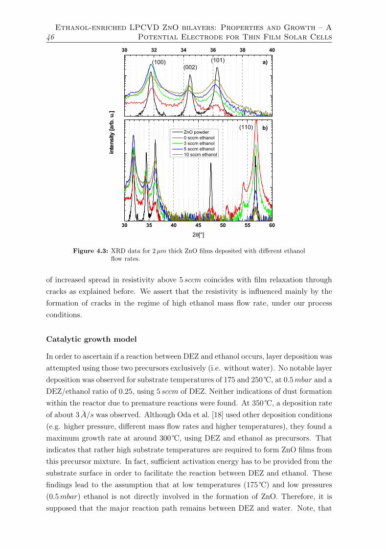
46Ethanol-enriched LPCVD ZnO bilayers: Properties and Growth – A
Potential Electrode for Thin Film Solar Cells
3 0 3 5 4 0 4 5 5 0 5 5 6 0
θ
3 0 3 2 3 4 3 6 3 8 4 0
b )
inten
sity [a
rb. u.
]
a )
Figure 4.3: XRD data for 2µm thick ZnO films deposited with different ethanolflow rates.
of increased spread in resistivity above 5 sccm coincides with film relaxation through
cracks as explained before. We assert that the resistivity is influenced mainly by the
formation of cracks in the regime of high ethanol mass flow rate, under our process
conditions.
Catalytic growth model
In order to ascertain if a reaction between DEZ and ethanol occurs, layer deposition was
attempted using those two precursors exclusively (i.e. without water). No notable layer
deposition was observed for substrate temperatures of 175 and 250 , at 0.5mbar and a
DEZ/ethanol ratio of 0.25, using 5 sccm of DEZ. Neither indications of dust formation
within the reactor due to premature reactions were found. At 350 , a deposition rate
of about 3 A/s was observed. Although Oda et al. [18] used other deposition conditions
(e.g. higher pressure, different mass flow rates and higher temperatures), they found a
maximum growth rate at around 300 , using DEZ and ethanol as precursors. That
indicates that rather high substrate temperatures are required to form ZnO films from
this precursor mixture. In fact, sufficient activation energy has to be provided from the
substrate surface in order to facilitate the reaction between DEZ and ethanol. These
findings lead to the assumption that at low temperatures (175 ) and low pressures
(0.5mbar) ethanol is not directly involved in the formation of ZnO. Therefore, it is
supposed that the major reaction path remains between DEZ and water. Note, that
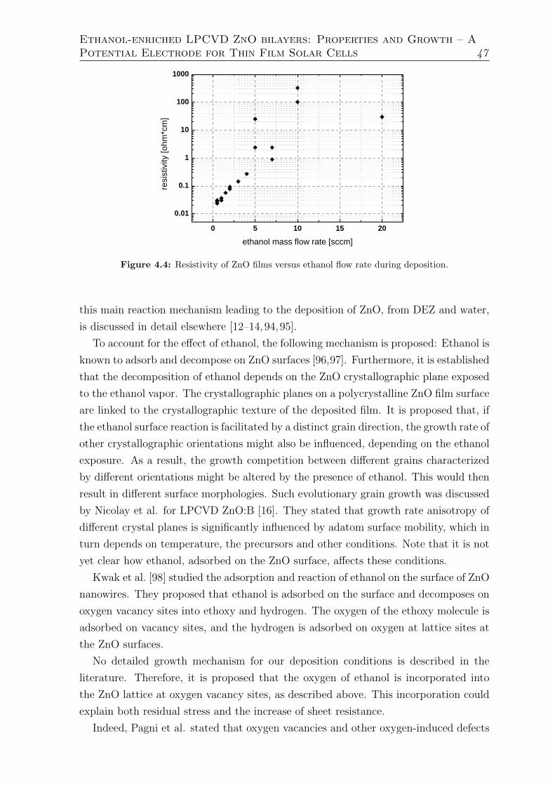
Ethanol-enriched LPCVD ZnO bilayers: Properties and Growth – APotential Electrode for Thin Film Solar Cells 47
0 5 1 0 1 5 2 00 . 0 1
0 . 1
1
1 0
1 0 0
1 0 0 0
resisti
vity [o
hm*cm
]
e t h a n o l m a s s f l o w r a t e [ s c c m ]
Figure 4.4: Resistivity of ZnO films versus ethanol flow rate during deposition.
this main reaction mechanism leading to the deposition of ZnO, from DEZ and water,
is discussed in detail elsewhere [12–14,94,95].
To account for the effect of ethanol, the following mechanism is proposed: Ethanol is
known to adsorb and decompose on ZnO surfaces [96,97]. Furthermore, it is established
that the decomposition of ethanol depends on the ZnO crystallographic plane exposed
to the ethanol vapor. The crystallographic planes on a polycrystalline ZnO film surface
are linked to the crystallographic texture of the deposited film. It is proposed that, if
the ethanol surface reaction is facilitated by a distinct grain direction, the growth rate of
other crystallographic orientations might also be influenced, depending on the ethanol
exposure. As a result, the growth competition between different grains characterized
by different orientations might be altered by the presence of ethanol. This would then
result in different surface morphologies. Such evolutionary grain growth was discussed
by Nicolay et al. for LPCVD ZnO:B [16]. They stated that growth rate anisotropy of
different crystal planes is significantly influenced by adatom surface mobility, which in
turn depends on temperature, the precursors and other conditions. Note that it is not
yet clear how ethanol, adsorbed on the ZnO surface, affects these conditions.
Kwak et al. [98] studied the adsorption and reaction of ethanol on the surface of ZnO
nanowires. They proposed that ethanol is adsorbed on the surface and decomposes on
oxygen vacancy sites into ethoxy and hydrogen. The oxygen of the ethoxy molecule is
adsorbed on vacancy sites, and the hydrogen is adsorbed on oxygen at lattice sites at
the ZnO surfaces.
No detailed growth mechanism for our deposition conditions is described in the
literature. Therefore, it is proposed that the oxygen of ethanol is incorporated into
the ZnO lattice at oxygen vacancy sites, as described above. This incorporation could
explain both residual stress and the increase of sheet resistance.
Indeed, Pagni et al. stated that oxygen vacancies and other oxygen-induced defects
48Ethanol-enriched LPCVD ZnO bilayers: Properties and Growth – A
Potential Electrode for Thin Film Solar Cells
affect the tensile strain and the grain size of ZnO [99]. They deposited ZnO films on
glass slides by metal organic CVD, using DEZ and tert-butanol as precursors. They
claimed that residual strain was higher for films with fewer oxygen defects (vacancies)
present in the lattice structure. They linked their results to annealing studies, where the
generation of oxygen vacancies was investigated and a correlation between luminescence
and diffraction studies was made [100, 101]. With regard to the present study, it is
proposed that increased ethanol flow rate during deposition results in fewer oxygen
vacancies, leading to increased residual stress in the films.
The conduction mechanism of ZnO is still debated in the literature. As-grown
ZnO exhibits n-type behaviour. This is ascribed mainly to defects in the ZnO lattice
structure. Intrinsic defects like oxygen vacancies or zinc interstitials, as well as extrinsic
defects due to additional doping (e.g. with aluminium, boron, or gallium), act as
donors and determine the amount of free carriers in the conduction band of ZnO
and its n-type conductivity. A recent review about defects in ZnO was published
by McCluskey et al. [32]. As the ZnO films discussed above were deposited without
extrinsic doping, it is proposed that the changes in resistivity in Figure 4.4 originate
in part from changes in the intrinsic defect density, where the defects act as donors.
Lany et al. [102] suspected metastable vacancies behaving as shallow donor states to
be responsible for the n-type conductivity of ZnO. However, oxygen vacancies alone,
without other native point defects, are not believed to be the predominant cause of the
n-type conductivity [32]. With a calculated energetic position within the band gap of
0.5 to 0.8 eV above the valance band maximum, an oxygen vacancy is a deep rather than
a shallow donor [32]. More recently, Janotti et al. [33] showed that hydrogen can occupy
an oxygen substitutional site, which can be interpreted as an oxygen vacancy with a
single hydrogen atom in the centre. This defect is assumed to act as a shallow donor
in as-grown ZnO [103]. This implies that fewer oxygen vacancies in ZnO mean fewer
available sites for substitutional hydrogen acting as a shallow donor. As a consequence,
the electron concentration decreases, thus increasing the resistivity of the ZnO, as
observed in Figure 4.4. Following this line of reasoning again confirms the claim that
increasing ethanol concentration during film deposition facilitates the incorporation of
oxygen at oxygen vacancies at the ZnO surface during layer growth. Apart from crack
formation at high ethanol concentrations, grain boundaries may influence conductivity
as well [37].
Evidence of decreased electron concentration inside the ZnO grains is found in the
infrared (IR) reflection spectra, shown in Figure 4.5. Steinhauser et al. [37] showed
that the IR reflection signal of LPCVD ZnO:B is significantly influenced by the con-
centration of free carriers, which depends on the doping level. The sudden increase in
reflection can be explained by Drude’s theory and is directly correlated to the electron
plasma mode frequency, ωp [37, 104]:
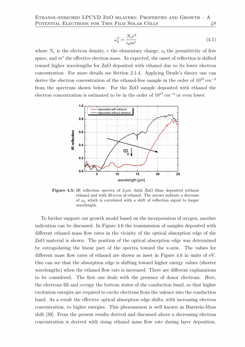
Ethanol-enriched LPCVD ZnO bilayers: Properties and Growth – APotential Electrode for Thin Film Solar Cells 49
ω2p =
Nee2
ε0m∗(4.1)
where Ne is the electron density, e the elementary charge, ε0 the permittivity of free
space, and m∗ the effective electron mass. As expected, the onset of reflection is shifted
toward higher wavelengths for ZnO deposited with ethanol due to its lower electron
concentration. For more details see Section 2.1.4. Applying Drude’s theory one can
derive the electron concentration of the ethanol-free sample in the order of 1019 cm−3
from the spectrum shown below. For the ZnO sample deposited with ethanol the
electron concentration is estimated to be in the order of 1017 cm−3 or even lower.
5 1 0 1 5 2 0 2 50 . 0
0 . 2
0 . 4
0 . 6
0 . 8
1 . 0
IR ref
lectio
n
ω
Figure 4.5: IR reflection spectra of 2µm thick ZnO films deposited withoutethanol and with 20 sccm of ethanol. The arrows indicate a decreaseof ωp which is correlated with a shift of reflection signal to longerwavelength.
To further support our growth model based on the incorporation of oxygen, another
indication can be discussed. In Figure 4.6 the transmission of samples deposited with
different ethanol mass flow rates in the vicinity of the optical absorption edge of the
ZnO material is shown. The position of the optical absorption edge was determined
by extrapolating the linear part of the spectra toward the x-axis. The values for
different mass flow rates of ethanol are shown as inset in Figure 4.6 in units of eV.
One can see that the absorption edge is shifting toward higher energy values (shorter
wavelengths) when the ethanol flow rate is increased. There are different explanations
to be considered. The first one deals with the presence of donor electrons. Here,
the electrons fill and occupy the bottom states of the conduction band, so that higher
excitation energies are required to excite electrons from the valence into the conduction
band. As a result the effective optical absorption edge shifts, with increasing electron
concentration, to higher energies. This phenomenon is well known as Burstein-Moss
shift [39]. From the present results derived and discussed above a decreasing electron
concentration is derived with rising ethanol mass flow rate during layer deposition.
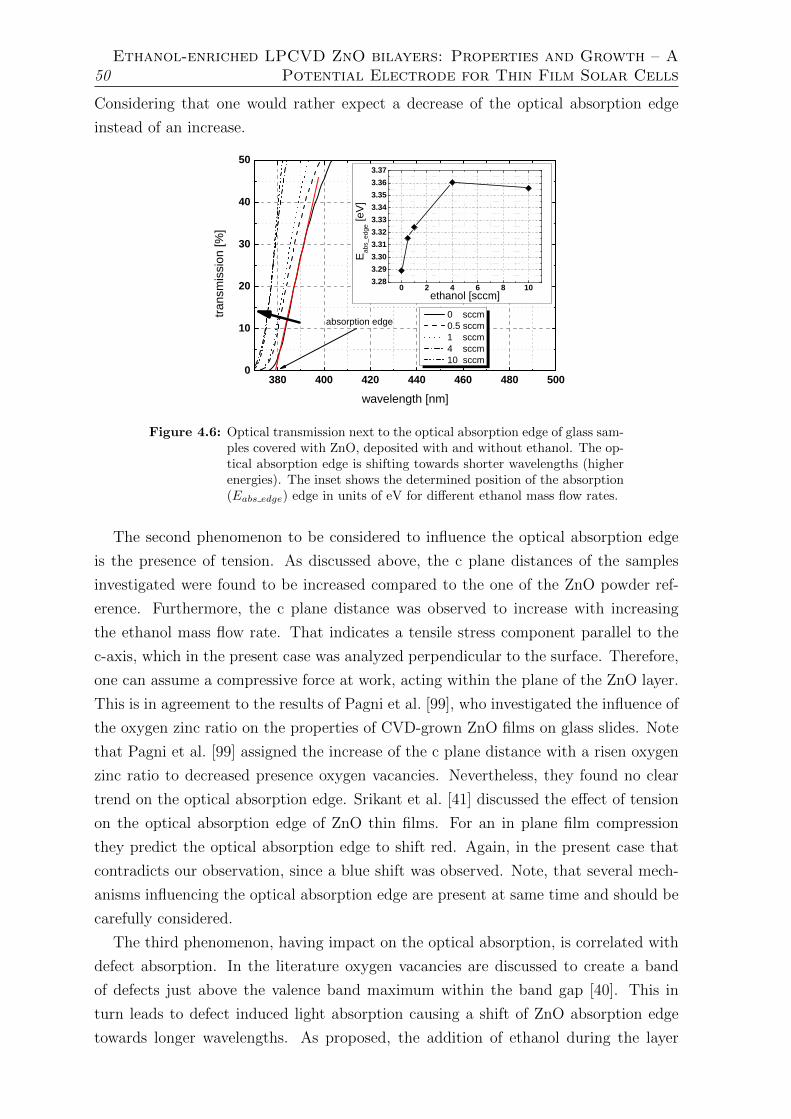
50Ethanol-enriched LPCVD ZnO bilayers: Properties and Growth – A
Potential Electrode for Thin Film Solar Cells
Considering that one would rather expect a decrease of the optical absorption edge
instead of an increase.
3 8 0 4 0 0 4 2 0 4 4 0 4 6 0 4 8 0 5 0 00
1 0
2 0
3 0
4 0
5 0
trans
missi
on [%
]
w a v e l e n g t h [ n m ]
0 s c c m 0 . 5 s c c m 1 s c c m 4 s c c m 1 0 s c c m
a b s o r p t i o n e d g e
0 2 4 6 8 1 03 . 2 83 . 2 93 . 3 03 . 3 13 . 3 23 . 3 33 . 3 43 . 3 53 . 3 63 . 3 7
E abs_
edge
[eV]
e t h a n o l [ s c c m ]
Figure 4.6: Optical transmission next to the optical absorption edge of glass sam-ples covered with ZnO, deposited with and without ethanol. The op-tical absorption edge is shifting towards shorter wavelengths (higherenergies). The inset shows the determined position of the absorption(Eabs edge) edge in units of eV for different ethanol mass flow rates.
The second phenomenon to be considered to influence the optical absorption edge
is the presence of tension. As discussed above, the c plane distances of the samples
investigated were found to be increased compared to the one of the ZnO powder ref-
erence. Furthermore, the c plane distance was observed to increase with increasing
the ethanol mass flow rate. That indicates a tensile stress component parallel to the
c-axis, which in the present case was analyzed perpendicular to the surface. Therefore,
one can assume a compressive force at work, acting within the plane of the ZnO layer.
This is in agreement to the results of Pagni et al. [99], who investigated the influence of
the oxygen zinc ratio on the properties of CVD-grown ZnO films on glass slides. Note
that Pagni et al. [99] assigned the increase of the c plane distance with a risen oxygen
zinc ratio to decreased presence oxygen vacancies. Nevertheless, they found no clear
trend on the optical absorption edge. Srikant et al. [41] discussed the effect of tension
on the optical absorption edge of ZnO thin films. For an in plane film compression
they predict the optical absorption edge to shift red. Again, in the present case that
contradicts our observation, since a blue shift was observed. Note, that several mech-
anisms influencing the optical absorption edge are present at same time and should be
carefully considered.
The third phenomenon, having impact on the optical absorption, is correlated with
defect absorption. In the literature oxygen vacancies are discussed to create a band
of defects just above the valence band maximum within the band gap [40]. This in
turn leads to defect induced light absorption causing a shift of ZnO absorption edge
towards longer wavelengths. As proposed, the addition of ethanol during the layer
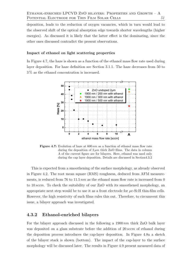
Ethanol-enriched LPCVD ZnO bilayers: Properties and Growth – APotential Electrode for Thin Film Solar Cells 51
deposition, leads to the reduction of oxygen vacancies, which in turn would lead to
the observed shift of the optical absorption edge towards shorter wavelengths (higher
energies). As discussed it is likely that the latter effect is the dominating, since the
other ones discussed contradict the present observations.
Impact of ethanol on light scattering properties
In Figure 4.7, the haze is shown as a function of the ethanol mass flow rate used during
layer deposition. For haze definition see Section 3.1.1. The haze decreases from 50 to
3 % as the ethanol concentration is increased.
0 2 4 6 8 1 0 2 00
1 0
2 0
3 0
4 0
5 0
Haze
[%]
A
Figure 4.7: Evolution of haze at 600nm as a function of ethanol mass flow rateduring the deposition of 2µm thick ZnO films. The data in columnA of the current figure are for bilayers. Here, ethanol was used onlyduring the cap layer deposition. Details are discussed in Section4.3.2
This is expected from a smoothening of the surface morphology, as already observed
in Figure 4.2. The root mean square (RMS) roughness, deduced from AFM measure-
ments, is reduced from 76 to 11.5nm as the ethanol mass flow rate is increased from 0
to 10 sccm. To check the suitability of our ZnO with its smoothened morphology, an
appropriate next step would be to use it as a front electrode for µc-Si:H thin-film cells.
However, the high resistivity of such films rules this out. Therefore, to circumvent this
issue, a bilayer approach was investigated.
4.3.2 Ethanol-enriched bilayers
For the bilayer approach discussed in the following a 1900nm thick ZnO bulk layer
was deposited on a glass substrate before the addition of 20 sccm of ethanol during
the deposition process introduces the cap-layer deposition. In Figure 4.8a a sketch
of the bilayer stack is shown (bottom). The impact of the cap-layer to the surface
morphology will be discussed later. The results in Figure 4.9 present measured data of
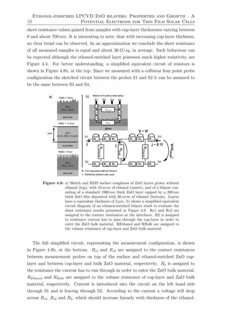
52Ethanol-enriched LPCVD ZnO bilayers: Properties and Growth – A
Potential Electrode for Thin Film Solar Cells
sheet resistance values gained from samples with cap-layer thicknesses varying between
0 and about 700nm. It is interesting to note, that with increasing cap-layer thickness,
no clear trend can be observed. In an approximation we conclude the sheet resistance
of all measured samples is equal and about 36Ω/sq, in average. Such behaviour can
be expected although the ethanol-enriched layer possesses much higher resistivity, see
Figure 4.4. For better understanding, a simplified equivalent circuit of resistors is
shown in Figure 4.8b, at the top. Since we measured with a collinear four point probe
configuration the sketched circuit between the probes S1 and S2 it can be assumed to
be the same between S3 and S4.
Figure 4.8: a) Sketch and RMS surface roughness of ZnO layers grown withoutethanol (top), with 10 sccm of ethanol (center), and of a bilayer con-sisting of a standard 1900nm thick ZnO layer capped by a 200nmthick ZnO film deposited with 20 sccm of ethanol (bottom). Layershave a equivalent thickness of 2µm. b) shows a simplified equivalentcircuit diagram of an ethanol-enriched bilayer stack to evaluate thesheet resistance results presented in Figure 4.9. Rc1 and Rc2 areassigned to the contact resistances at the interfaces. R2 is assignedto resistance current has to pass through the cap-layer in order toenter the ZnO bulk material. REthanol and RBulk are assigned tothe volume resistance of cap-layer and ZnO bulk material.
The full simplified circuit, representing the measurement configuration, is shown
in Figure 4.8b, at the bottom. Rc1 and Rc2 are assigned to the contact resistances
between measurement probes on top of the surface and ethanol-enriched ZnO cap-
layer and between cap-layer and bulk ZnO material, respectively. R2 is assigned to
the resistance the current has to run through in order to enter the ZnO bulk material.
REthanol and RBulk are assigned to the volume resistance of cap-layer and ZnO bulk
material, respectively. Current is introduced into the circuit on the left hand side
through S1 and is leaving through S2. According to the current a voltage will drop
across Rc1, Rc2 and R2, which should increase linearly with thickness of the ethanol-
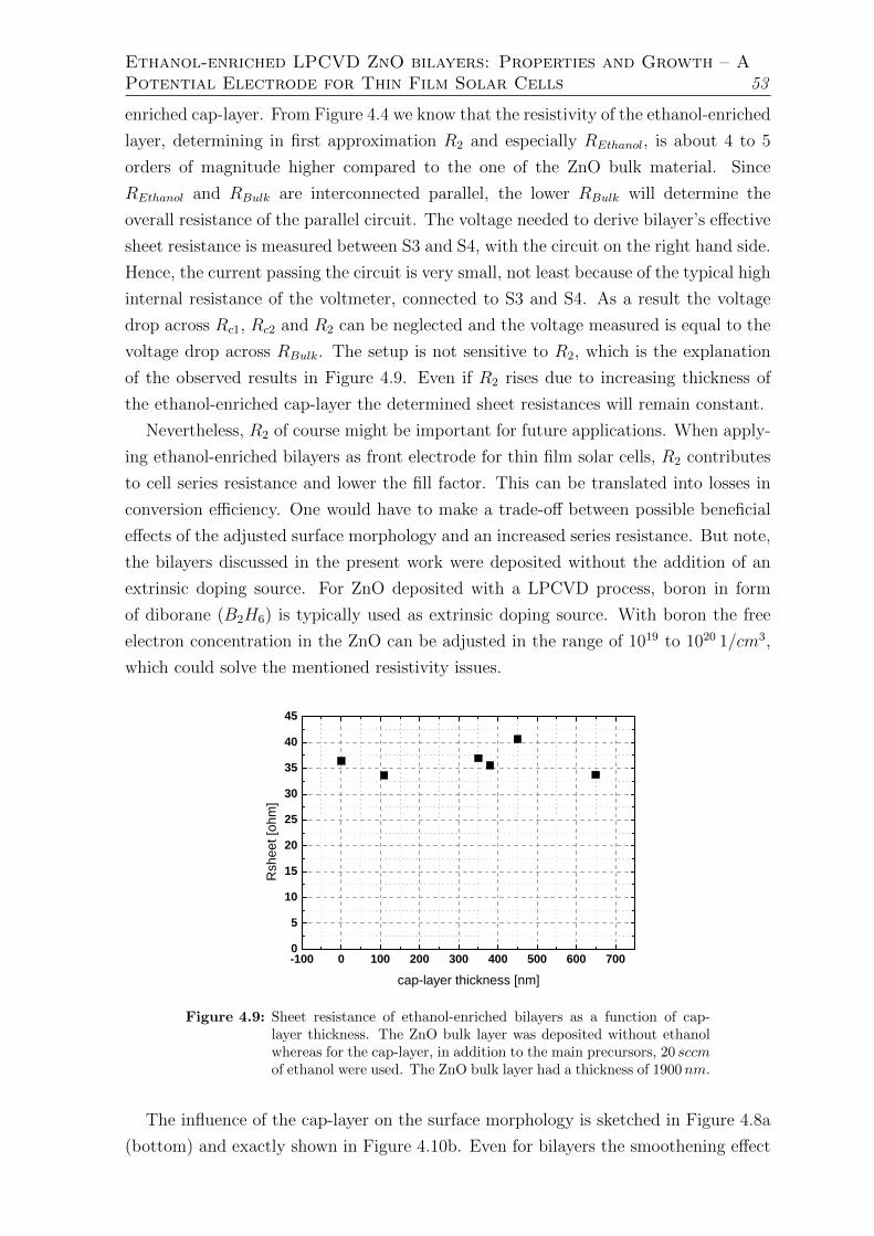
Ethanol-enriched LPCVD ZnO bilayers: Properties and Growth – APotential Electrode for Thin Film Solar Cells 53
enriched cap-layer. From Figure 4.4 we know that the resistivity of the ethanol-enriched
layer, determining in first approximation R2 and especially REthanol, is about 4 to 5
orders of magnitude higher compared to the one of the ZnO bulk material. Since
REthanol and RBulk are interconnected parallel, the lower RBulk will determine the
overall resistance of the parallel circuit. The voltage needed to derive bilayer’s effective
sheet resistance is measured between S3 and S4, with the circuit on the right hand side.
Hence, the current passing the circuit is very small, not least because of the typical high
internal resistance of the voltmeter, connected to S3 and S4. As a result the voltage
drop across Rc1, Rc2 and R2 can be neglected and the voltage measured is equal to the
voltage drop across RBulk. The setup is not sensitive to R2, which is the explanation
of the observed results in Figure 4.9. Even if R2 rises due to increasing thickness of
the ethanol-enriched cap-layer the determined sheet resistances will remain constant.
Nevertheless, R2 of course might be important for future applications. When apply-
ing ethanol-enriched bilayers as front electrode for thin film solar cells, R2 contributes
to cell series resistance and lower the fill factor. This can be translated into losses in
conversion efficiency. One would have to make a trade-off between possible beneficial
effects of the adjusted surface morphology and an increased series resistance. But note,
the bilayers discussed in the present work were deposited without the addition of an
extrinsic doping source. For ZnO deposited with a LPCVD process, boron in form
of diborane (B2H6) is typically used as extrinsic doping source. With boron the free
electron concentration in the ZnO can be adjusted in the range of 1019 to 1020 1/cm3,
which could solve the mentioned resistivity issues.
- 1 0 0 0 1 0 0 2 0 0 3 0 0 4 0 0 5 0 0 6 0 0 7 0 005
1 01 52 02 53 03 54 04 5
Rshe
et [oh
m]
c a p - l a y e r t h i c k n e s s [ n m ]
Figure 4.9: Sheet resistance of ethanol-enriched bilayers as a function of cap-layer thickness. The ZnO bulk layer was deposited without ethanolwhereas for the cap-layer, in addition to the main precursors, 20 sccmof ethanol were used. The ZnO bulk layer had a thickness of 1900nm.
The influence of the cap-layer on the surface morphology is sketched in Figure 4.8a
(bottom) and exactly shown in Figure 4.10b. Even for bilayers the smoothening effect
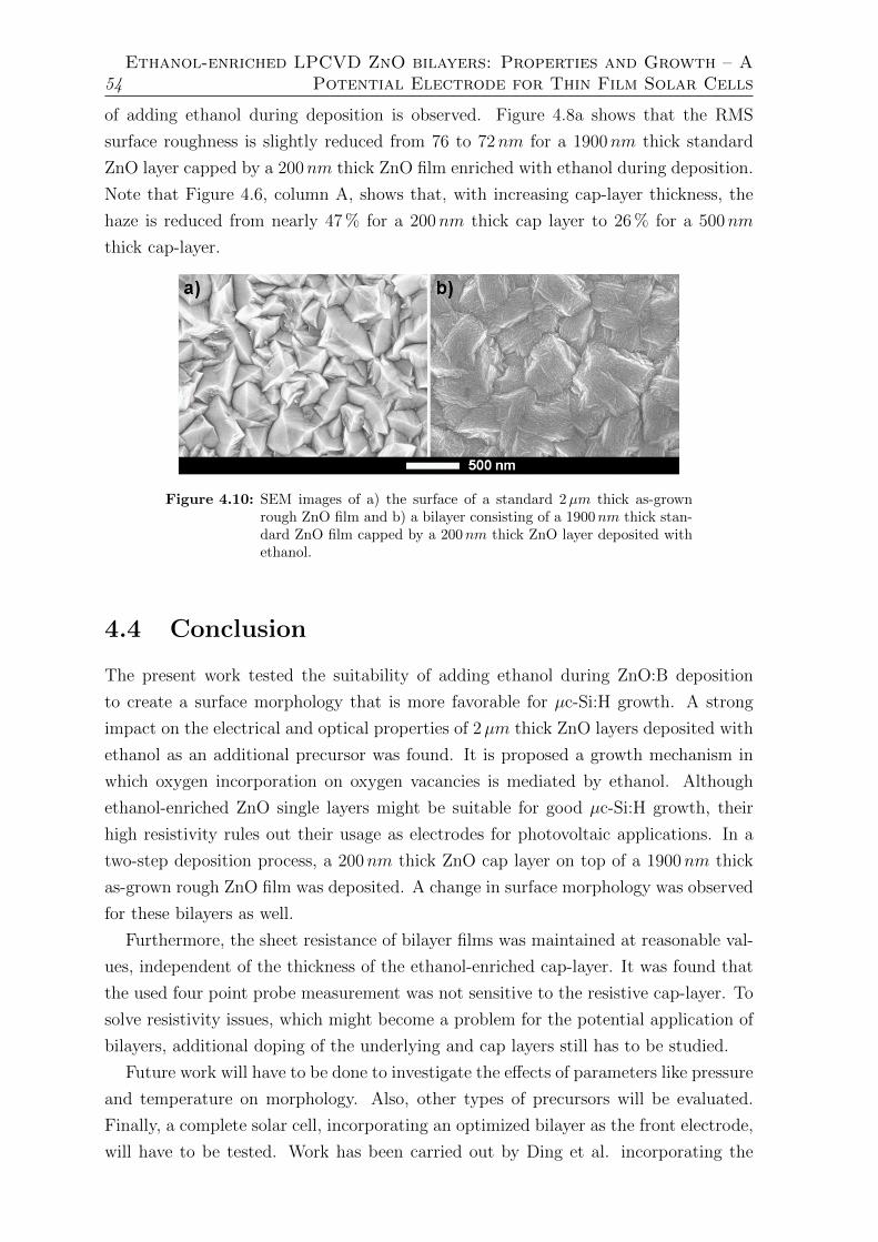
54Ethanol-enriched LPCVD ZnO bilayers: Properties and Growth – A
Potential Electrode for Thin Film Solar Cells
of adding ethanol during deposition is observed. Figure 4.8a shows that the RMS
surface roughness is slightly reduced from 76 to 72nm for a 1900nm thick standard
ZnO layer capped by a 200nm thick ZnO film enriched with ethanol during deposition.
Note that Figure 4.6, column A, shows that, with increasing cap-layer thickness, the
haze is reduced from nearly 47 % for a 200nm thick cap layer to 26 % for a 500nm
thick cap-layer.
Figure 4.10: SEM images of a) the surface of a standard 2µm thick as-grownrough ZnO film and b) a bilayer consisting of a 1900nm thick stan-dard ZnO film capped by a 200nm thick ZnO layer deposited withethanol.
4.4 Conclusion
The present work tested the suitability of adding ethanol during ZnO:B deposition
to create a surface morphology that is more favorable for µc-Si:H growth. A strong
impact on the electrical and optical properties of 2µm thick ZnO layers deposited with
ethanol as an additional precursor was found. It is proposed a growth mechanism in
which oxygen incorporation on oxygen vacancies is mediated by ethanol. Although
ethanol-enriched ZnO single layers might be suitable for good µc-Si:H growth, their
high resistivity rules out their usage as electrodes for photovoltaic applications. In a
two-step deposition process, a 200nm thick ZnO cap layer on top of a 1900nm thick
as-grown rough ZnO film was deposited. A change in surface morphology was observed
for these bilayers as well.
Furthermore, the sheet resistance of bilayer films was maintained at reasonable val-
ues, independent of the thickness of the ethanol-enriched cap-layer. It was found that
the used four point probe measurement was not sensitive to the resistive cap-layer. To
solve resistivity issues, which might become a problem for the potential application of
bilayers, additional doping of the underlying and cap layers still has to be studied.
Future work will have to be done to investigate the effects of parameters like pressure
and temperature on morphology. Also, other types of precursors will be evaluated.
Finally, a complete solar cell, incorporating an optimized bilayer as the front electrode,
will have to be tested. Work has been carried out by Ding et al. incorporating the

Ethanol-enriched LPCVD ZnO bilayers: Properties and Growth – APotential Electrode for Thin Film Solar Cells 55
above presented approach into a micromorph solar cell [105]. Cell efficiencies above
12.2 % were achieved.

56Ethanol-enriched LPCVD ZnO bilayers: Properties and Growth – A
Potential Electrode for Thin Film Solar Cells
Chapter 5
Integration of Advanced-TCO into
the Production Line at Bosch
By using the LPCVD process, Ding et al. [1,2] introduced a novel and advanced LPCVD
ZnO:B. In this Chapter, this type of TCO will be called ATCO. The ATCO approach
combines a highly doped ZnO:B seed layer with a low-doped bulk layer above. ATCO,
in opposition to standard TCO (Std-TCO, which is uniformly doped throughout the
whole layer cross section), possesses both higher transparency due to less free-carrier
light absorption in the infrared spectral range and higher haze, while maintaining the
level of conductivity. The haze parameter is correlated to the film’s light-scattering
ability and influences the absorption of light in the absorber material of the top (a-Si:H)
and bottom (µc-Si:H) cells that are combined to form a micromorph tandem solar cell
device.
For more details the reader is referred to the Refs. [1, 2] and to the project results
reported in Ref. [6]. Whereas the deposition process was invented by Ding et al. on
the same small deposition system shown in Figure 2.2, within the framework of the
PEPPER project, the deposition process was scaled up (to substrate sizes of 1.1 ×1.3m2) by Tokyo Electron Solar AG (TEL Solar, formerly Oerlikon Solar). For this,
the TCO1200 deposition system, as shown in Figure 2.3, was retrofitted. With the
retrofit of the deposition system TCO1200 it became possible to deposit ATCO on a
commercially available production line tool.
In this Chapter the introduction of ATCO into the production line at Bosch Solar
Thin Film (BSTF) is presented. First, brief comments on the retrofitted deposition tool
TCO1200 are given. Then results on the process optimization done at the production
site at BSTF in Erfurt (Germany) are shown. A comparison of the electrical and
optical properties of ATCO and Std-TCO is presented. Finally the module performance
achieved so far using ATCO as the new front electrode is reported.
57
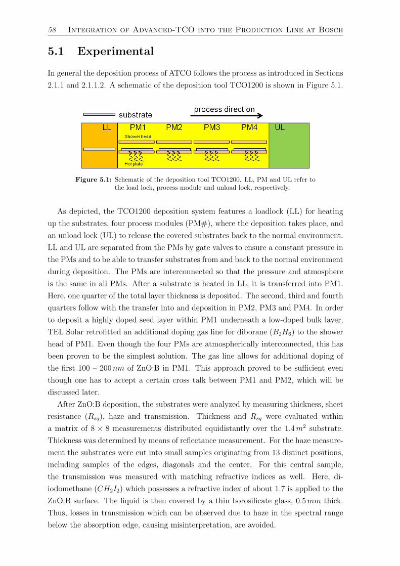
58 Integration of Advanced-TCO into the Production Line at Bosch
5.1 Experimental
In general the deposition process of ATCO follows the process as introduced in Sections
2.1.1 and 2.1.1.2. A schematic of the deposition tool TCO1200 is shown in Figure 5.1.
Figure 5.1: Schematic of the deposition tool TCO1200. LL, PM and UL refer tothe load lock, process module and unload lock, respectively.
As depicted, the TCO1200 deposition system features a loadlock (LL) for heating
up the substrates, four process modules (PM#), where the deposition takes place, and
an unload lock (UL) to release the covered substrates back to the normal environment.
LL and UL are separated from the PMs by gate valves to ensure a constant pressure in
the PMs and to be able to transfer substrates from and back to the normal environment
during deposition. The PMs are interconnected so that the pressure and atmosphere
is the same in all PMs. After a substrate is heated in LL, it is transferred into PM1.
Here, one quarter of the total layer thickness is deposited. The second, third and fourth
quarters follow with the transfer into and deposition in PM2, PM3 and PM4. In order
to deposit a highly doped seed layer within PM1 underneath a low-doped bulk layer,
TEL Solar retrofitted an additional doping gas line for diborane (B2H6) to the shower
head of PM1. Even though the four PMs are atmospherically interconnected, this has
been proven to be the simplest solution. The gas line allows for additional doping of
the first 100 – 200nm of ZnO:B in PM1. This approach proved to be sufficient even
though one has to accept a certain cross talk between PM1 and PM2, which will be
discussed later.
After ZnO:B deposition, the substrates were analyzed by measuring thickness, sheet
resistance (Rsq), haze and transmission. Thickness and Rsq were evaluated within
a matrix of 8 × 8 measurements distributed equidistantly over the 1.4m2 substrate.
Thickness was determined by means of reflectance measurement. For the haze measure-
ment the substrates were cut into small samples originating from 13 distinct positions,
including samples of the edges, diagonals and the center. For this central sample,
the transmission was measured with matching refractive indices as well. Here, di-
iodomethane (CH2I2) which possesses a refractive index of about 1.7 is applied to the
ZnO:B surface. The liquid is then covered by a thin borosilicate glass, 0.5mm thick.
Thus, losses in transmission which can be observed due to haze in the spectral range
below the absorption edge, causing misinterpretation, are avoided.

Integration of Advanced-TCO into the Production Line at Bosch 59
5.2 Results
As mentioned in Section 5.1, the upgrade of the TCO1200 deposition system gives
rise to a certain cross talk between PM1 and the other process chambers. In order
to study this effect, four substrates were loaded into PM1 to PM4. After reaching
thermal equilibrium a ZnO:B film with a nominal thickness of 1700nm was deposited
in 514 seconds in PM1 to PM4. For the deposition, the ratio of mass flow rates of
[H2O]/[DEZ] and [B2H6]/[DEZ] was adjusted to 1.28 and 0.04, respectively. Due to
the additional mass flow rate of diborane in PM1 the resulting ratio of [B2H6]/[DEZ]
in PM1 was set to be 0.84. In Figure 5.2, results of sheet resistance and thickness are
shown for all PMs.
200 400 600 800 1000 1200
200
400
600
800
1000 Layer-1
y [m
m]
x [mm]
14001460152015801640170017601820188019402000
200 400 600 800 1000 1200
200
400
600
800
1000 Layer-1
y
[mm
]
x [mm]
14001460152015801640170017601820188019402000
200 400 600 800 1000 1200
200
400
600
800
1000 Layer-1
y [m
m]
x [mm]
14001460152015801640170017601820188019402000
200 400 600 800 1000 1200
200
400
600
800
1000 Layer-1
y [m
m]
x [mm]
14001460152015801640170017601820188019402000
PM1 PM2 PM3 PM4
thickness
200 400 600 800 1000 1200
200
400
600
800
1000 Resistance value
y [m
m]
x [mm]
5.08.0111417202326293235
200 400 600 800 1000 1200
200
400
600
800
1000 Resistance value
y [m
m]
x [mm]
5.08.0111417202326293235
200 400 600 800 1000 1200
200
400
600
800
1000 Resistance value
y [m
m]
x [mm]
5.08.0111417202326293235
200 400 600 800 1000 1200
200
400
600
800
1000 Resistance value
y [m
m]
x [mm]
5.08.0111417202326293235
RSq
Figure 5.2: Distribution of layer properties after the retrofit of TCO1200, doing asingle-chamber deposition with an additional mass flow rate of B2H6
of 500 sccm in PM1.
Due to higher doping ratio in PM1 the average sheet resistance results in a lower
average value of 8Ω compared to the values reached in PM3 and PM4 of about 20Ω.
On the left side in PM2 one can clearly see the cross talk. Here, diborane spread
into PM2 due to higher partial pressure of diborane in PM1 causing a lower sheet
resistance. The average thickness in PM1 is obviously reduced in comparison to those
of PM3 and PM4. In PM2 an area of minimal deposition rate was found. This feature
is attributed rather to an undesired particle placed between the hot plate and the
substrate – presumably ZnO – and therefore a locally lower substrate temperature,
than to the higher flow rate of diborane in PM1. The lower thickness / deposition rate
in PM1 seems to result from a thermal cooling effect (high flow regime) or a reduced
adatom residence time induced by a higher total mass flow rate.
The TCO1200 deposition system runs in normal mode during production. Sub-
strates are transferred from the normal environment to LL, from LL through the four
PMs into UL, and from UL back to the normal environment every two minutes. The
first results of layer properties of ATCO and Std-TCO are compared in Figure 5.3.
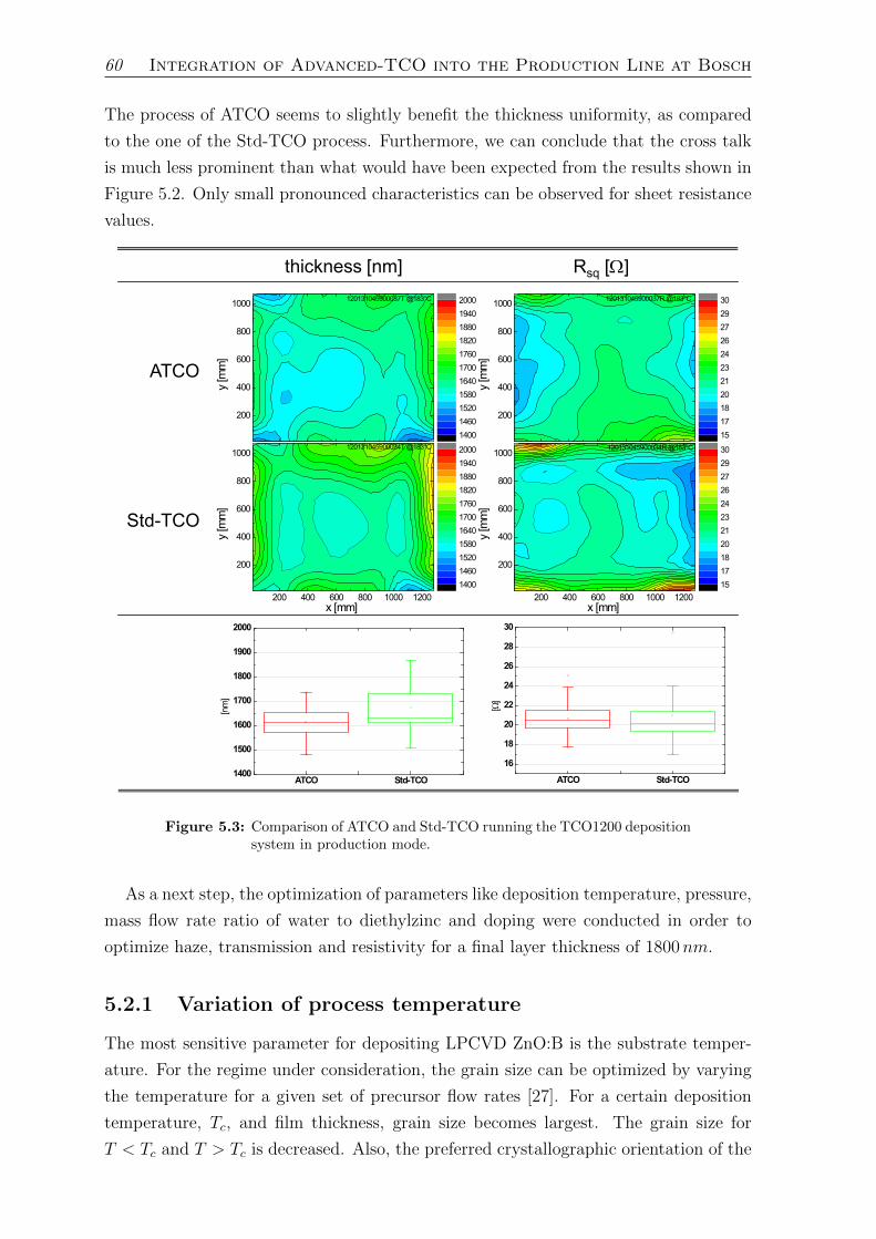
60 Integration of Advanced-TCO into the Production Line at Bosch
The process of ATCO seems to slightly benefit the thickness uniformity, as compared
to the one of the Std-TCO process. Furthermore, we can conclude that the cross talk
is much less prominent than what would have been expected from the results shown in
Figure 5.2. Only small pronounced characteristics can be observed for sheet resistance
values.
200 400 600 800 1000 1200
200
400
600
800
1000 120131045900037T @183°C
y [m
m]
x [mm]
14001460152015801640170017601820188019402000
200 400 600 800 1000 1200
200
400
600
800
1000 120131045900037R @183°C
y [m
m]
x [mm]
1517182021232426272930
200 400 600 800 1000 1200
200
400
600
800
1000 120131045900034T @183°C
y [m
m]
x [mm]
14001460152015801640170017601820188019402000
200 400 600 800 1000 1200
200
400
600
800
1000 120131045900034R @183°C
y [m
m]
x [mm]
1517182021232426272930
ATCO Std-TCO1400
1500
1600
1700
1800
1900
2000
[nm
]
ATCO Std-TCO
16
18
20
22
24
26
28
30
[Ω]
Std-TCO
ATCO
thickness [nm] Rsq [Ω]
Figure 5.3: Comparison of ATCO and Std-TCO running the TCO1200 depositionsystem in production mode.
As a next step, the optimization of parameters like deposition temperature, pressure,
mass flow rate ratio of water to diethylzinc and doping were conducted in order to
optimize haze, transmission and resistivity for a final layer thickness of 1800nm.
5.2.1 Variation of process temperature
The most sensitive parameter for depositing LPCVD ZnO:B is the substrate temper-
ature. For the regime under consideration, the grain size can be optimized by varying
the temperature for a given set of precursor flow rates [27]. For a certain deposition
temperature, Tc, and film thickness, grain size becomes largest. The grain size for
T < Tc and T > Tc is decreased. Also, the preferred crystallographic orientation of the
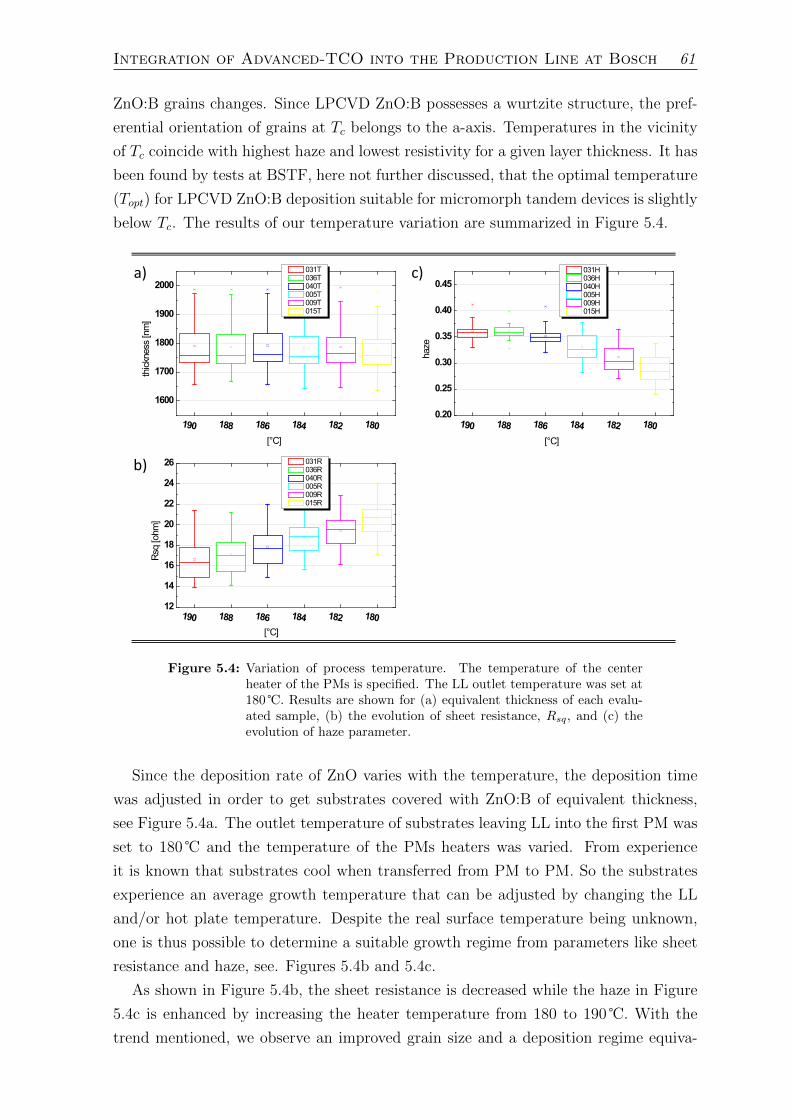
Integration of Advanced-TCO into the Production Line at Bosch 61
ZnO:B grains changes. Since LPCVD ZnO:B possesses a wurtzite structure, the pref-
erential orientation of grains at Tc belongs to the a-axis. Temperatures in the vicinity
of Tc coincide with highest haze and lowest resistivity for a given layer thickness. It has
been found by tests at BSTF, here not further discussed, that the optimal temperature
(Topt) for LPCVD ZnO:B deposition suitable for micromorph tandem devices is slightly
below Tc. The results of our temperature variation are summarized in Figure 5.4.
190 188 186 184 182 1800.20
0.25
0.30
0.35
0.40
0.45
[°C]
haze
031H 036H 040H 005H 009H 015H
190 188 186 184 182 180
1600
1700
1800
1900
2000
thick
ness
[nm
]
031T 036T 040T 005T 009T 015T
[°C]
190 188 186 184 182 18012
14
16
18
20
22
24
26
[°C]
Rsq
[ohm
]
031R 036R 040R 005R 009R 015R
a) c)
b)
Figure 5.4: Variation of process temperature. The temperature of the centerheater of the PMs is specified. The LL outlet temperature was set at180 . Results are shown for (a) equivalent thickness of each evalu-ated sample, (b) the evolution of sheet resistance, Rsq, and (c) theevolution of haze parameter.
Since the deposition rate of ZnO varies with the temperature, the deposition time
was adjusted in order to get substrates covered with ZnO:B of equivalent thickness,
see Figure 5.4a. The outlet temperature of substrates leaving LL into the first PM was
set to 180 and the temperature of the PMs heaters was varied. From experience
it is known that substrates cool when transferred from PM to PM. So the substrates
experience an average growth temperature that can be adjusted by changing the LL
and/or hot plate temperature. Despite the real surface temperature being unknown,
one is thus possible to determine a suitable growth regime from parameters like sheet
resistance and haze, see. Figures 5.4b and 5.4c.
As shown in Figure 5.4b, the sheet resistance is decreased while the haze in Figure
5.4c is enhanced by increasing the heater temperature from 180 to 190 . With the
trend mentioned, we observe an improved grain size and a deposition regime equiva-
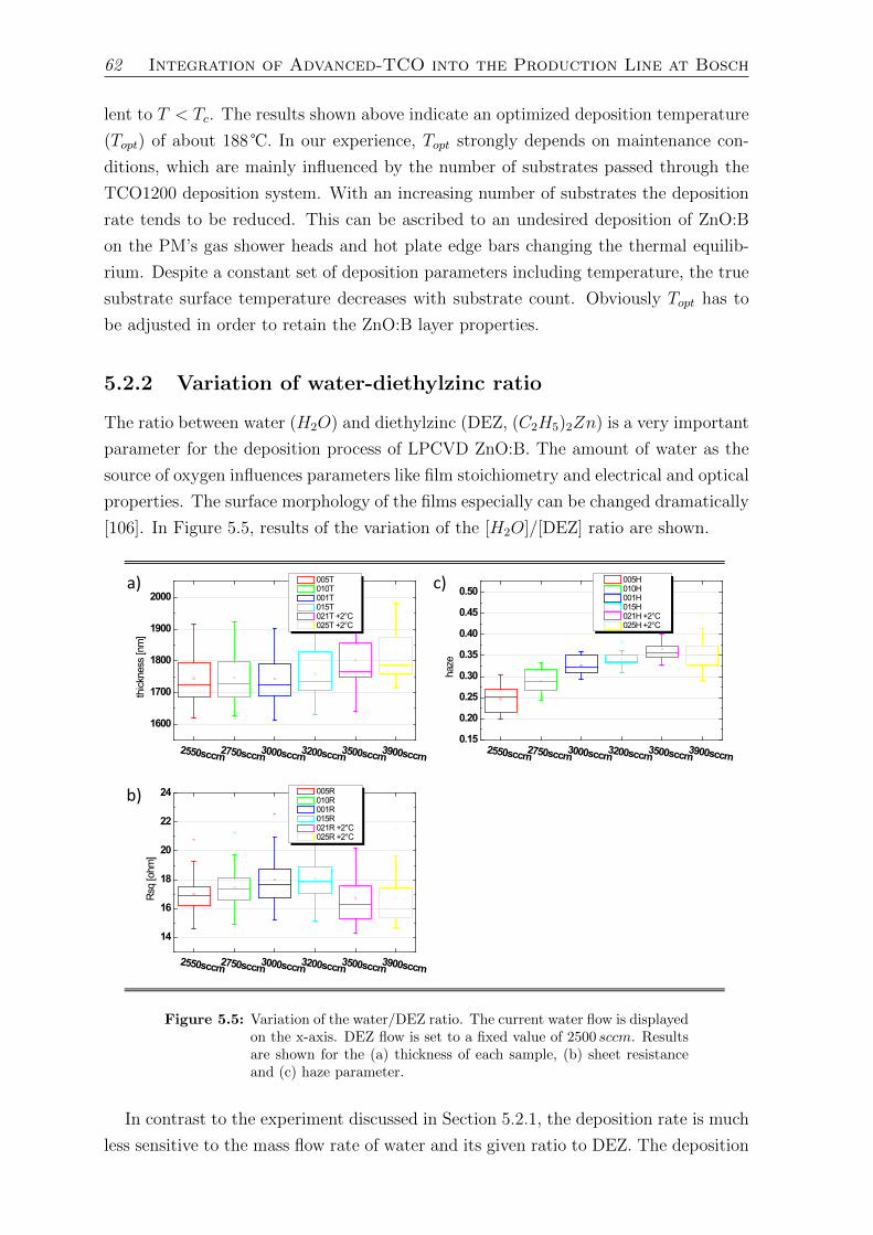
62 Integration of Advanced-TCO into the Production Line at Bosch
lent to T < Tc. The results shown above indicate an optimized deposition temperature
(Topt) of about 188 . In our experience, Topt strongly depends on maintenance con-
ditions, which are mainly influenced by the number of substrates passed through the
TCO1200 deposition system. With an increasing number of substrates the deposition
rate tends to be reduced. This can be ascribed to an undesired deposition of ZnO:B
on the PM’s gas shower heads and hot plate edge bars changing the thermal equilib-
rium. Despite a constant set of deposition parameters including temperature, the true
substrate surface temperature decreases with substrate count. Obviously Topt has to
be adjusted in order to retain the ZnO:B layer properties.
5.2.2 Variation of water-diethylzinc ratio
The ratio between water (H2O) and diethylzinc (DEZ, (C2H5)2Zn) is a very important
parameter for the deposition process of LPCVD ZnO:B. The amount of water as the
source of oxygen influences parameters like film stoichiometry and electrical and optical
properties. The surface morphology of the films especially can be changed dramatically
[106]. In Figure 5.5, results of the variation of the [H2O]/[DEZ] ratio are shown.
2550sccm2750sccm3000sccm3200sccm3500sccm3900sccm0.15
0.20
0.25
0.30
0.35
0.40
0.45
0.50
haze
005H 010H 001H 015H 021H +2°C 025H +2°C
2550sccm2750sccm3000sccm3200sccm3500sccm3900sccm
14
16
18
20
22
24
Rsq
[ohm
]
005R 010R 001R 015R 021R +2°C 025R +2°C
2550sccm2750sccm3000sccm3200sccm3500sccm3900sccm
1600
1700
1800
1900
2000
thick
ness
[nm
]
005T 010T 001T 015T 021T +2°C 025T +2°C
a) c)
b)
Figure 5.5: Variation of the water/DEZ ratio. The current water flow is displayedon the x-axis. DEZ flow is set to a fixed value of 2500 sccm. Resultsare shown for the (a) thickness of each sample, (b) sheet resistanceand (c) haze parameter.
In contrast to the experiment discussed in Section 5.2.1, the deposition rate is much
less sensitive to the mass flow rate of water and its given ratio to DEZ. The deposition
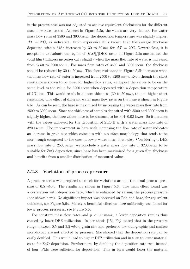
Integration of Advanced-TCO into the Production Line at Bosch 63
in the present case was not adjusted to achieve equivalent thicknesses for the different
mass flow rates tested. As seen in Figure 5.5a, the values are very similar. For water
mass flow rates of 3500 and 3900 sccm the deposition temperature was slightly higher,
∆T = 2 , as indicated. From experience it is known that the average thickness
deposited within 548 s increases by 30 to 50nm for ∆T = 2 . Nevertheless, it is
acceptable to evaluate the regime of [H2O]/[DEZ] ratio. In Figure 5.5a one can see the
total film thickness increases only slightly when the mass flow rate of water is increased
from 2550 to 3900 sccm. For mass flow rates of 3500 and 3900 sccm, the thickness
should be reduced by 30 to 50nm. The sheet resistance in Figure 5.5b increases when
the mass flow rate of water is increased from 2500 to 3200 sccm. Even though the sheet
resistance is shown to be lower for higher flow rates, we expect the values to be on the
same level as the value for 3200 sccm when deposited with a deposition temperature
of 2 less. This would result in a lower thickness (30 to 50nm), thus in higher sheet
resistance. The effect of different water mass flow rates on the haze is shown in Figure
5.5c. As can be seen, the haze is maximized by increasing the water mass flow rate from
2500 to 3900 sccm. Since the thickness of samples deposited with 3500 and 3900 sccm is
slightly higher, the haze values have to be assumed to be 0.01–0.02 lower. So it matches
with the values achieved for the deposition of ZnO:B with a water mass flow rate of
3200 sccm. The improvement in haze with increasing the flow rate of water indicates
an increase in grain size which coincides with a surface morphology that tends to be
more rough compared to the ones at lower water mass flow rates. Considering a DEZ
mass flow rate of 2500 sccm, we conclude a water mass flow rate of 3200 sccm to be
suitable for ZnO deposition, since haze has been maximized for a given film thickness
and benefits from a smaller distribution of measured values.
5.2.3 Variation of process pressure
A pressure series was prepared to check for variations around the usual process pres-
sure of 0.5mbar. The results are shown in Figure 5.6. The main effect found was
a correlation with deposition rate, which is enhanced by raising the process pressure
(not shown here). No significant impact was observed on Rsq and haze, for equivalent
thickness, see Figure 5.6a. Merely a beneficial effect on haze uniformity was found for
lower process pressures, see Figure 5.6c.
For constant mass flow rates and p < 0.5mbar, a lower deposition rate is thus
caused by lower DEZ utilization. In her thesis [15], Fay stated that in the pressure
range between 0.5 and 3.5mbar, grain size and preferred crystallographic and surface
morphology are not affected by pressure. She showed that the deposition rate can be
easily doubled. This would lead to higher DEZ utilization and in turn to lower material
costs for ZnO deposition. Furthermore, by doubling the deposition rate two, instead
of four, PMs were sufficient for deposition. This in turn would lower the material
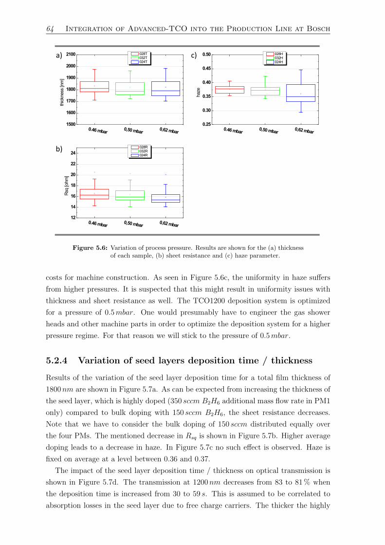
64 Integration of Advanced-TCO into the Production Line at Bosch
0.46 mbar 0,50 mbar 0,62 mbar0.25
0.30
0.35
0.40
0.45
0.50
haze
028H 032H 024H
0.46 mbar 0,50 mbar 0,62 mbar12
14
16
18
20
22
24
Rsq
[ohm
]
028R 032R 024R
0.46 mbar 0,50 mbar 0,62 mbar1500
1600
1700
1800
1900
2000
2100
thick
ness
[nm
] 028T 032T 024T
a) c)
b)
Figure 5.6: Variation of process pressure. Results are shown for the (a) thicknessof each sample, (b) sheet resistance and (c) haze parameter.
costs for machine construction. As seen in Figure 5.6c, the uniformity in haze suffers
from higher pressures. It is suspected that this might result in uniformity issues with
thickness and sheet resistance as well. The TCO1200 deposition system is optimized
for a pressure of 0.5mbar. One would presumably have to engineer the gas shower
heads and other machine parts in order to optimize the deposition system for a higher
pressure regime. For that reason we will stick to the pressure of 0.5mbar.
5.2.4 Variation of seed layers deposition time / thickness
Results of the variation of the seed layer deposition time for a total film thickness of
1800nm are shown in Figure 5.7a. As can be expected from increasing the thickness of
the seed layer, which is highly doped (350 sccm B2H6 additional mass flow rate in PM1
only) compared to bulk doping with 150 sccm B2H6, the sheet resistance decreases.
Note that we have to consider the bulk doping of 150 sccm distributed equally over
the four PMs. The mentioned decrease in Rsq is shown in Figure 5.7b. Higher average
doping leads to a decrease in haze. In Figure 5.7c no such effect is observed. Haze is
fixed on average at a level between 0.36 and 0.37.
The impact of the seed layer deposition time / thickness on optical transmission is
shown in Figure 5.7d. The transmission at 1200nm decreases from 83 to 81 % when
the deposition time is increased from 30 to 59 s. This is assumed to be correlated to
absorption losses in the seed layer due to free charge carriers. The thicker the highly
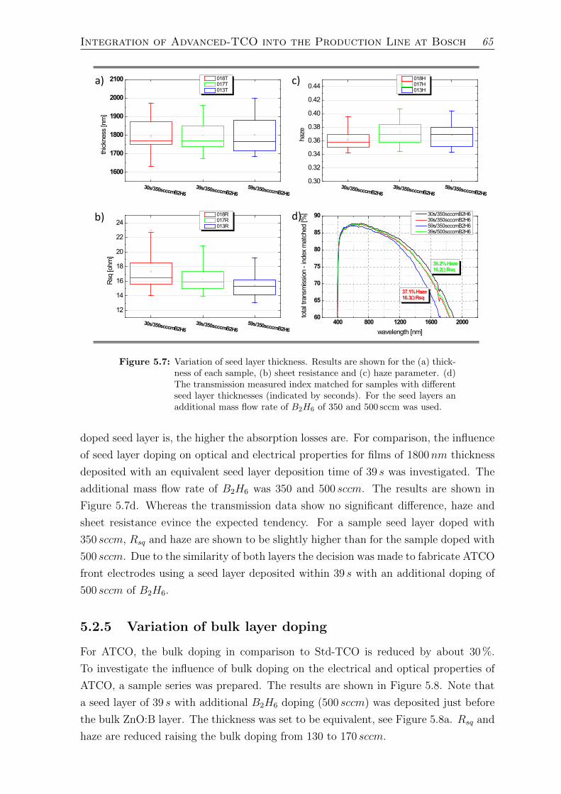
Integration of Advanced-TCO into the Production Line at Bosch 65
30s/350scccmB2H639s/350scccmB2H6
59s/350scccmB2H6
0.30
0.32
0.34
0.36
0.38
0.40
0.42
0.44
haze
018H 017H 013H
30s/350scccmB2H639s/350scccmB2H6
59s/350scccmB2H6
12
14
16
18
20
22
24
Rsq
[ohm
]
018R 017R 013R
30s/350scccmB2H639s/350scccmB2H6
59s/350scccmB2H6
1600
1700
1800
1900
2000
2100
thick
ness
[nm
]
018T 017T 013T
a) c)
b)
400 800 1200 1600 200060
65
70
75
80
85
90
37.1% Haze16.3Ω Rsq
tota
l tra
nsm
issio
n - i
ndex
mat
ched
[%]
wavelength [nm]
30s/350scccmB2H6 39s/350scccmB2H6 59s/350scccmB2H6 39s/500scccmB2H6
36.2% Haze16.2Ω Rsq
d)
Figure 5.7: Variation of seed layer thickness. Results are shown for the (a) thick-ness of each sample, (b) sheet resistance and (c) haze parameter. (d)The transmission measured index matched for samples with differentseed layer thicknesses (indicated by seconds). For the seed layers anadditional mass flow rate of B2H6 of 350 and 500 sccm was used.
doped seed layer is, the higher the absorption losses are. For comparison, the influence
of seed layer doping on optical and electrical properties for films of 1800nm thickness
deposited with an equivalent seed layer deposition time of 39 s was investigated. The
additional mass flow rate of B2H6 was 350 and 500 sccm. The results are shown in
Figure 5.7d. Whereas the transmission data show no significant difference, haze and
sheet resistance evince the expected tendency. For a sample seed layer doped with
350 sccm, Rsq and haze are shown to be slightly higher than for the sample doped with
500 sccm. Due to the similarity of both layers the decision was made to fabricate ATCO
front electrodes using a seed layer deposited within 39 s with an additional doping of
500 sccm of B2H6.
5.2.5 Variation of bulk layer doping
For ATCO, the bulk doping in comparison to Std-TCO is reduced by about 30 %.
To investigate the influence of bulk doping on the electrical and optical properties of
ATCO, a sample series was prepared. The results are shown in Figure 5.8. Note that
a seed layer of 39 s with additional B2H6 doping (500 sccm) was deposited just before
the bulk ZnO:B layer. The thickness was set to be equivalent, see Figure 5.8a. Rsq and
haze are reduced raising the bulk doping from 130 to 170 sccm.
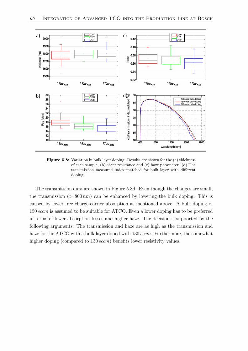
66 Integration of Advanced-TCO into the Production Line at Bosch
130sccm 150sccm 170sccm0.32
0.34
0.36
0.38
0.40
0.42
haze
039H 017H 013H
400 800 1200 1600 200060
65
70
75
80
85
90
tota
l tra
nsm
issio
n - i
ndex
mat
ched
[%]
wavelength [nm]
130sccm bulk doping 150sccm bulk doping 170sccm bulk doping
130sccm 150sccm 170sccm1012141618202224262830
Rsq
[ohm
]
039R 017R 013R
130sccm 150sccm 170sccm
1500
1600
1700
1800
1900
2000
thick
ness
[nm
] 039T 017T 013T
a) c)
b) d)
Figure 5.8: Variation in bulk layer doping. Results are shown for the (a) thicknessof each sample, (b) sheet resistance and (c) haze parameter. (d) Thetransmission measured index matched for bulk layer with differentdoping.
The transmission data are shown in Figure 5.8d. Even though the changes are small,
the transmission (> 800nm) can be enhanced by lowering the bulk doping. This is
caused by lower free charge-carrier absorption as mentioned above. A bulk doping of
150 sccm is assumed to be suitable for ATCO. Even a lower doping has to be preferred
in terms of lower absorption losses and higher haze. The decision is supported by the
following arguments: The transmission and haze are as high as the transmission and
haze for the ATCO with a bulk layer doped with 130 sccm. Furthermore, the somewhat
higher doping (compared to 130 sccm) benefits lower resistivity values.
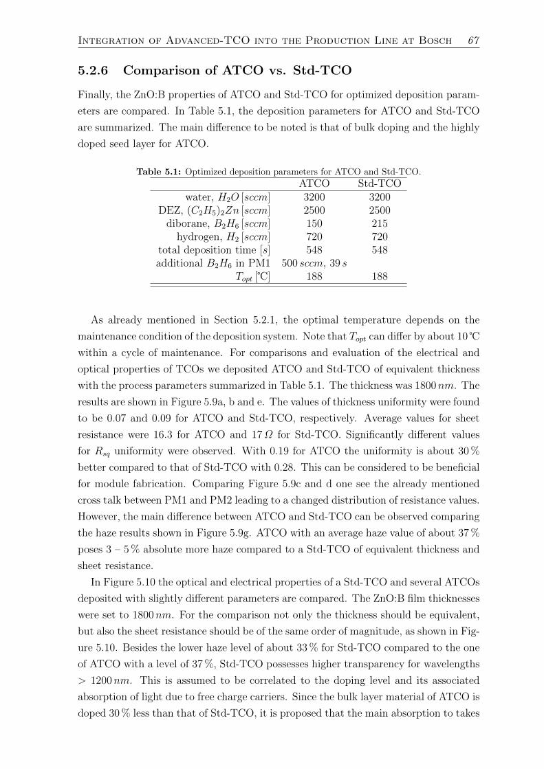
Integration of Advanced-TCO into the Production Line at Bosch 67
5.2.6 Comparison of ATCO vs. Std-TCO
Finally, the ZnO:B properties of ATCO and Std-TCO for optimized deposition param-
eters are compared. In Table 5.1, the deposition parameters for ATCO and Std-TCO
are summarized. The main difference to be noted is that of bulk doping and the highly
doped seed layer for ATCO.
Table 5.1: Optimized deposition parameters for ATCO and Std-TCO.
ATCO Std-TCOwater, H2O [sccm] 3200 3200
DEZ, (C2H5)2Zn [sccm] 2500 2500diborane, B2H6 [sccm] 150 215
hydrogen, H2 [sccm] 720 720total deposition time [s] 548 548additional B2H6 in PM1 500 sccm, 39 s
Topt [] 188 188
As already mentioned in Section 5.2.1, the optimal temperature depends on the
maintenance condition of the deposition system. Note that Topt can differ by about 10 within a cycle of maintenance. For comparisons and evaluation of the electrical and
optical properties of TCOs we deposited ATCO and Std-TCO of equivalent thickness
with the process parameters summarized in Table 5.1. The thickness was 1800nm. The
results are shown in Figure 5.9a, b and e. The values of thickness uniformity were found
to be 0.07 and 0.09 for ATCO and Std-TCO, respectively. Average values for sheet
resistance were 16.3 for ATCO and 17Ω for Std-TCO. Significantly different values
for Rsq uniformity were observed. With 0.19 for ATCO the uniformity is about 30 %
better compared to that of Std-TCO with 0.28. This can be considered to be beneficial
for module fabrication. Comparing Figure 5.9c and d one see the already mentioned
cross talk between PM1 and PM2 leading to a changed distribution of resistance values.
However, the main difference between ATCO and Std-TCO can be observed comparing
the haze results shown in Figure 5.9g. ATCO with an average haze value of about 37 %
poses 3 – 5 % absolute more haze compared to a Std-TCO of equivalent thickness and
sheet resistance.
In Figure 5.10 the optical and electrical properties of a Std-TCO and several ATCOs
deposited with slightly different parameters are compared. The ZnO:B film thicknesses
were set to 1800nm. For the comparison not only the thickness should be equivalent,
but also the sheet resistance should be of the same order of magnitude, as shown in Fig-
ure 5.10. Besides the lower haze level of about 33 % for Std-TCO compared to the one
of ATCO with a level of 37 %, Std-TCO possesses higher transparency for wavelengths
> 1200nm. This is assumed to be correlated to the doping level and its associated
absorption of light due to free charge carriers. Since the bulk layer material of ATCO is
doped 30 % less than that of Std-TCO, it is proposed that the main absorption to takes
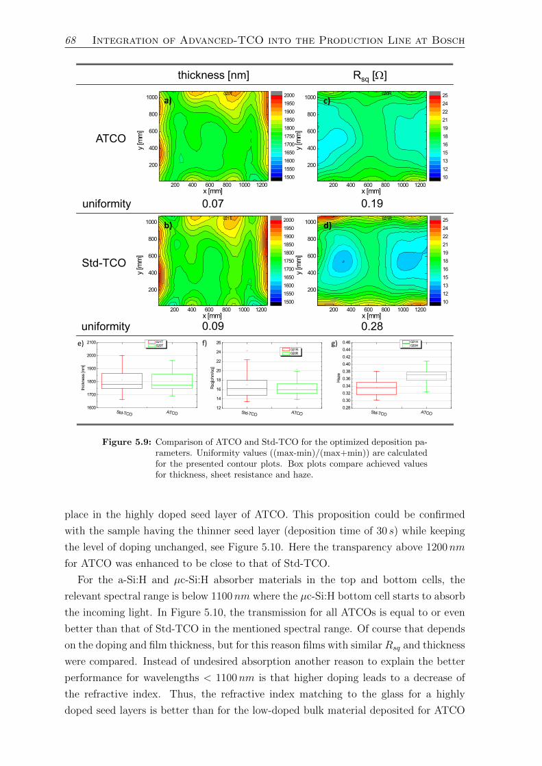
68 Integration of Advanced-TCO into the Production Line at Bosch
Std-TCO ATCO0.280.300.320.340.360.380.400.420.440.46
Haze
021H 020H
200 400 600 800 1000 1200
200
400
600
800
1000 021T
y [m
m]
x [mm]
15001550160016501700175018001850190019502000
200 400 600 800 1000 1200
200
400
600
800
1000 021R
y [m
m]
x [mm]
1012131516181921222425
200 400 600 800 1000 1200
200
400
600
800
1000 020R
y [m
m]
x [mm]
1012131516181921222425
200 400 600 800 1000 1200
200
400
600
800
1000 020T
y [m
m]
x [mm]
15001550160016501700175018001850190019502000
Std-TCO
ATCO
thickness [nm] Rsq [Ω]
Std-TCO ATCO1600
1700
1800
1900
2000
2100
thick
ness
[nm
]
021T 020T
Std-TCO ATCO12
14
16
18
20
22
24
26
Rsq[
ohm
/sq]
021R 020R
a)
b)
c)
d)
e) f) g)
uniformity
uniformity
0.07 0.19
0.09 0.28
Figure 5.9: Comparison of ATCO and Std-TCO for the optimized deposition pa-rameters. Uniformity values ((max-min)/(max+min)) are calculatedfor the presented contour plots. Box plots compare achieved valuesfor thickness, sheet resistance and haze.
place in the highly doped seed layer of ATCO. This proposition could be confirmed
with the sample having the thinner seed layer (deposition time of 30 s) while keeping
the level of doping unchanged, see Figure 5.10. Here the transparency above 1200nm
for ATCO was enhanced to be close to that of Std-TCO.
For the a-Si:H and µc-Si:H absorber materials in the top and bottom cells, the
relevant spectral range is below 1100nm where the µc-Si:H bottom cell starts to absorb
the incoming light. In Figure 5.10, the transmission for all ATCOs is equal to or even
better than that of Std-TCO in the mentioned spectral range. Of course that depends
on the doping and film thickness, but for this reason films with similar Rsq and thickness
were compared. Instead of undesired absorption another reason to explain the better
performance for wavelengths < 1100nm is that higher doping leads to a decrease of
the refractive index. Thus, the refractive index matching to the glass for a highly
doped seed layers is better than for the low-doped bulk material deposited for ATCO

Integration of Advanced-TCO into the Production Line at Bosch 69
4 0 0 8 0 0 1 2 0 0 1 6 0 0 2 0 0 06 0
6 5
7 0
7 5
8 0
8 5
9 0
3 7 . 1 % H a z e1 6 . 3 W R s q
3 7 . 5 % H a z e1 6 . 3 W R s q
3 3 . 6 % H a z e1 7 . 0 W R s q
3 6 . 2 % H a z e1 7 . 3 W R s q
total
trans
missi
on - i
ndex
matc
hed [
%]
w a v e l e n g t h [ n m ]
S t d - T C O 1 8 0 0 n m , b u l k 2 1 5 s c c m B 2 H 6 A T C O 1 8 0 0 n m , b u l k 1 5 0 s c c m B 2 H 6 , s e e d l a y e r 3 9 s 5 0 0 s c c m B 2 H 6 A T C O 1 8 0 0 n m , b u l k 1 5 0 s c c m B 2 H 6 , s e e d l a y e r 3 0 s 3 5 0 s c c m B 2 H 6 A T C O 1 8 0 0 n m , b u l k 1 5 0 s c c m B 2 H 6 , s e e d l a y e r 3 9 s 3 5 0 s c c m B 2 H 6
Figure 5.10: Comparison of transmission measured index matched for ATCO andStd-TCO.
and Std-TCO. This leads to fewer losses due to reflection at the glass-TCO interface.
Furthermore, the seed layer may also act as a kind of antireflective layer.
5.2.7 Result on module power using ATCO
Using ATCO a maximum initial module power of 153.7Wp was achieved, see Figure
5.11. The critical point is to adjust the PECVD deposition parameters to adapt for
the high haze of ZnO:B. Here, the contact layer between the ZnO and the a-Si:H top
cell and the crystallinity of the µc-Si:H bottom cell plays a major roll.
0 20 40 60 80 1000,0
0,5
1,0
1,5
2,0
2,5
I [A]
V [V]
Voc/cell [V] 1.36Isc [A] 2.43FF [%] 70.2Pmpp [W] 153.7
Figure 5.11: Best results achieved on ATCO with non-retrofitted PECVD equip-ment. The amorphous top and microcrystalline bottom cells havehave thicknesses of 250 and 1300nm, respectively.
With the current PECVD equipment, as introduced in Section 2.2.1, the cell depo-
sition parameters still can be fine tuned to further raise module power. For module
70 Integration of Advanced-TCO into the Production Line at Bosch
power above 160Wp a new, retrofitted PECVD reactor with a lower electrode gap is
required, especially for µc-Si:H material deposition. For more details see reports in
reference [6].
5.3 Conclusion
The introduction of ATCO into the production line at Bosch Solar Thin Film in Erfurt
(Germany) was presented. It was shown that the retrofitted TCO1200 deposition tool
is suitable for ATCO deposition. After presenting the results on process optimization,
the optical and electrical properties ATCO and Std-TCO were compared. It was found
that ATCO possesses better uniformity of thickness and Rsq values. Furthermore,
ATCO possesses slightly better transmittance in the relevant spectral range of the
absorber materials of the top and bottom cells. The major difference was found in the
haze parameter. Whereas a 1800−nm-thick ATCO shows a haze of 37 %, a Std-TCO
of equal thickness and sheet resistance possesses 3 – 5 % absolute less haze. Finally, the
parameters for PECVD deposition for the top and bottom cells were adjusted to the
more rough ATCO. Here the major adjustments have to be done on the contact layer
facilitating the interface between the top cell and the TCO, and on the crystallinity of
the µc-Si:H absorber of the bottom cell. Using ATCO as the front electrode, an initial
module power of 153.7Wp was achieved.
Chapter 6
Anodic degradation of ZnO:B on
soda-lime glass
In the present chapter the anodic degradation of ZnO:B and its influence on thin-film
silicon solar cells and modules will be discussed. In Section 6.1 introductory background
informations are given. Furthermore, the cathodic degradation (the well known TCO
corrosion) is summarized. Experimental details are presented in Section 6.2. General
observations made for large size modules will be shown in Section 6.3. Enclosed to
these results the focus of the investigation is directed to the microscopic mechanism
responsible for the observed degradation phenomenon in Sections 6.4, 6.5, 6.6 and
6.7. Finally, solutions are presented in Section 6.8 which minimize the phenomenon
of anodic degradation. Note that the findings presented in the following were gener-
ated under harsh conditions (contacting and/or applied voltage) derived in parts from
IEC61646 10.13. Since there is a certain scarcity of information about the relation
between these accelerated test conditions and the long term performance of modules
in the field, the results should just be considered merely as an indicator for the module
long term performance.
6.1 Background
Thin-film modules have to pass many durability tests, including several accelerated
lifetime tests, such as damp heat exposure in a climate chamber (IEC61646, 10.13).
For this test, modules are exposed to 85 and 85 % relative humidity (r.h.) for
1000 hours. However, this test does not adequately describe the performance of a mod-
ule wired in a string with other modules. In such a setup the cells in a module may be
biased with several hundred volts with respect to ground (module frame or mounting
system). This voltage is isolated by highly resistive module components, the front
or back glass, for example. Leakage current through these resistive components may
cause degradation not only in thin-film modules but also in modules based on inter-
71
72 Anodic degradation of ZnO:B on soda-lime glass
connected crystalline silicon wafer solar cells [107, 108]. This leakage current strongly
depends on the temperature of the module and the humidity of its environment. To
date, in thin-film photovoltaics, especially in technologies based on the superstrate
configuration, the most apparent potential-induced degradation effect is correlated to
corrosion of the transparent conductive oxide (TCO), typically used as the front or
back electrode [10, 109–112]. Here, the front contact (TCO) is typically deposited on
commercially available soda-lime glass, followed by the deposition of the absorber ma-
terial and the back contact. To protect this sensitive layer stack against environmental
impact, it is laminated together with an aluminium-foil-enhanced polymer sheet or
glass. According to the standard VDI2578, the main chemical components of soda-
lime silicate glass are as follows by mass percentage: 73 % of silicon oxide (SiO2), 13 %
sodium oxide (Na2O), 9 % calcium oxide (CaO) and other metal oxides which mainly
influence optical properties [71]. The sodium concentration and its mobility in such
glass are the root cause of the TCO corrosion mentioned above.
Due to the electric field caused by the potential difference between the front TCO
and the mounting system, positively charged sodium ions in soda-lime glass migrate
towards the glass/TCO interface. The cathode (TCO) reduces the positively charged
sodium ions accumulated at this interface to elementary sodium according to chemical
reaction 6.1 [111]:
Na+ + e− ⇒ Na (6.1)
Water is believed to play a major role in the second step of the corrosion mechanism,
since moisture accelerates this kind of corrosion. Water oxidizes the elementary sodium
to Na+ and produces OH− (at the glass/TCO interface), as proposed in reaction
Equation 6.2.
2Na+ 2H2O ⇒ 2Na+ + 2OH− +H2 (6.2)
The elementary or molecular hydrogen remaining from the reaction between water
and sodium is assumed to reduce the TCO at the glass interface, causing an observable
delamination. This has been observed for both fluorine doped tin oxide (SnO2 : F ) and
aluminium doped zinc oxide (ZnO:Al) – common TCO materials – but ZnO:Al seems to
be less sensitive than SnO2 : F to this kind of corrosion [111]. Another explanation for
the delamination is the destruction of the sub-interface glass matrix due to the presence
of a strong basic solution (pH > 9), as might be indicated by the presence of Na+
and OH− [113, 114]. Furthermore it was found that before irreversible delamination
occurred, the accumulation of sodium could be reduced by applying a reverse bias [111].
In this case the resulting electric field forces the sodium accumulated at the glass/TCO
interface to migrate back into the glass. After such a treatment no delamination was
observed, even in a humid environment.
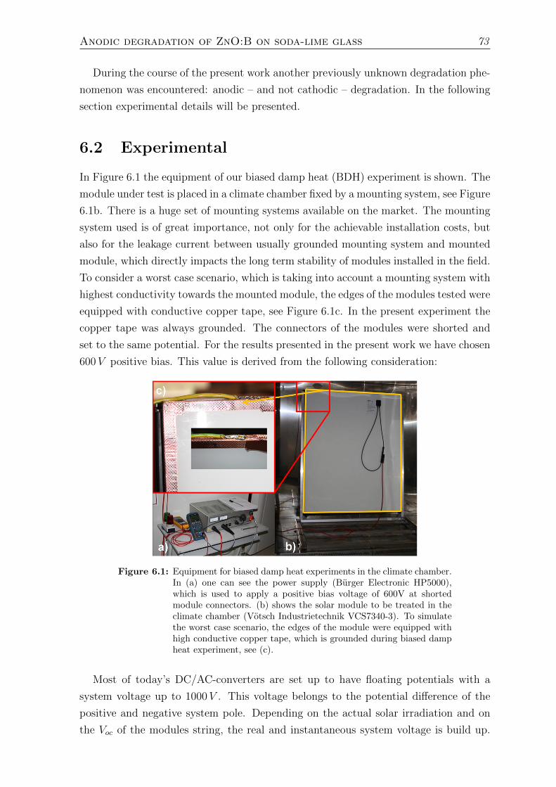
Anodic degradation of ZnO:B on soda-lime glass 73
During the course of the present work another previously unknown degradation phe-
nomenon was encountered: anodic – and not cathodic – degradation. In the following
section experimental details will be presented.
6.2 Experimental
In Figure 6.1 the equipment of our biased damp heat (BDH) experiment is shown. The
module under test is placed in a climate chamber fixed by a mounting system, see Figure
6.1b. There is a huge set of mounting systems available on the market. The mounting
system used is of great importance, not only for the achievable installation costs, but
also for the leakage current between usually grounded mounting system and mounted
module, which directly impacts the long term stability of modules installed in the field.
To consider a worst case scenario, which is taking into account a mounting system with
highest conductivity towards the mounted module, the edges of the modules tested were
equipped with conductive copper tape, see Figure 6.1c. In the present experiment the
copper tape was always grounded. The connectors of the modules were shorted and
set to the same potential. For the results presented in the present work we have chosen
600V positive bias. This value is derived from the following consideration:
Figure 6.1: Equipment for biased damp heat experiments in the climate chamber.In (a) one can see the power supply (Burger Electronic HP5000),which is used to apply a positive bias voltage of 600V at shortedmodule connectors. (b) shows the solar module to be treated in theclimate chamber (Votsch Industrietechnik VCS7340-3). To simulatethe worst case scenario, the edges of the module were equipped withhigh conductive copper tape, which is grounded during biased dampheat experiment, see (c).
Most of today’s DC/AC-converters are set up to have floating potentials with a
system voltage up to 1000V . This voltage belongs to the potential difference of the
positive and negative system pole. Depending on the actual solar irradiation and on
the Voc of the modules string, the real and instantaneous system voltage is build up.
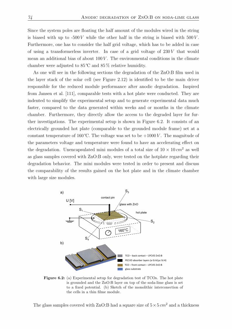
74 Anodic degradation of ZnO:B on soda-lime glass
Since the system poles are floating the half amount of the modules wired in the string
is biased with up to -500V while the other half in the string is biased with 500V .
Furthermore, one has to consider the half grid voltage, which has to be added in case
of using a transformerless inverter. In case of a grid voltage of 230V that would
mean an additional bias of about 100V . The environmental conditions in the climate
chamber were adjusted to 85 and 85 % relative humidity.
As one will see in the following sections the degradation of the ZnO:B film used in
the layer stack of the solar cell (see Figure 2.12) is identified to be the main driver
responsible for the reduced module performance after anodic degradation. Inspired
from Jansen et al. [111], comparable tests with a hot plate were conducted. They are
indented to simplify the experimental setup and to generate experimental data much
faster, compared to the data generated within weeks and or months in the climate
chamber. Furthermore, they directly allow the access to the degraded layer for fur-
ther investigations. The experimental setup is shown in Figure 6.2. It consists of an
electrically grounded hot plate (comparable to the grounded module frame) set at a
constant temperature of 160 . The voltage was set to be +1000V . The magnitude of
the parameters voltage and temperature were found to have an accelerating effect on
the degradation. Unencapsulated mini modules of a total size of 10 × 10 cm2 as well
as glass samples covered with ZnO:B only, were tested on the hotplate regarding their
degradation behavior. The mini modules were tested in order to present and discuss
the comparability of the results gained on the hot plate and in the climate chamber
with large size modules.
PECVD absorber layers (a-Si:H/µc-Si:H)
glass substrate
TCO – front contact – LPCVD ZnO:B
TCO – back contact – LPCVD ZnO:B
U [V]contact pin
glass with ZnO
hot plateS1
S2
S3
S4
a)
b)
Figure 6.2: (a) Experimental setup for degradation test of TCOs. The hot plateis grounded and the ZnO:B layer on top of the soda-lime glass is setto a fixed potential. (b) Sketch of the monolithic interconection ofthe cells in a thin filme module.
The glass samples covered with ZnO:B had a square size of 5×5 cm2 and a thickness
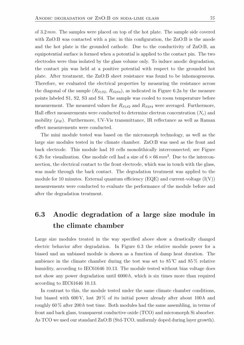
Anodic degradation of ZnO:B on soda-lime glass 75
of 3.2mm. The samples were placed on top of the hot plate. The sample side covered
with ZnO:B was contacted with a pin; in this configuration, the ZnO:B is the anode
and the hot plate is the grounded cathode. Due to the conductivity of ZnO:B, an
equipotential surface is formed when a potential is applied to the contact pin. The two
electrodes were thus isolated by the glass volume only. To induce anodic degradation,
the contact pin was held at a positive potential with respect to the grounded hot
plate. After treatment, the ZnO:B sheet resistance was found to be inhomogeneous.
Therefore, we evaluated the electrical properties by measuring the resistance across
the diagonal of the sample (RS1S2, RS2S4), as indicated in Figure 6.2a by the measure
points labeled S1, S2, S3 and S4. The sample was cooled to room temperature before
measurement. The measured values for RS1S2 and RS2S4 were averaged. Furthermore,
Hall effect measurements were conducted to determine electron concentration (Ne) and
mobility (µH). Furthermore, UV-Vis transmittance, IR reflectance as well as Raman
effect measurements were conducted.
The mini module tested was based on the micromorph technology, as well as the
large size modules tested in the climate chamber. ZnO:B was used as the front and
back electrode. This module had 10 cells monolithically interconnected; see Figure
6.2b for visualization. One module cell had a size of 6× 66mm2. Due to the intercon-
nection, the electrical contact to the front electrode, which was in touch with the glass,
was made through the back contact. The degradation treatment was applied to the
module for 10 minutes. External quantum efficiency (EQE) and current-voltage (I(V))
measurements were conducted to evaluate the performance of the module before and
after the degradation treatment.
6.3 Anodic degradation of a large size module in
the climate chamber
Large size modules treated in the way specified above show a drastically changed
electric behavior after degradation. In Figure 6.3 the relative module power for a
biased und an unbiased module is shown as a function of damp heat duration. The
ambience in the climate chamber during the test was set to 85 and 85 % relative
humidity, according to IEC61646 10.13. The module tested without bias voltage does
not show any power degradation until 6000h, which is six times more than required
according to IEC61646 10.13.
In contrast to this, the module tested under the same climate chamber conditions,
but biased with 600 V, lost 20 % of its initial power already after about 100h and
roughly 60 % after 200h test time. Both modules had the same assembling, in terms of
front and back glass, transparent conductive oxide (TCO) and micromorph Si absorber.
As TCO we used our standard ZnO:B (Std-TCO, uniformly doped during layer growth).
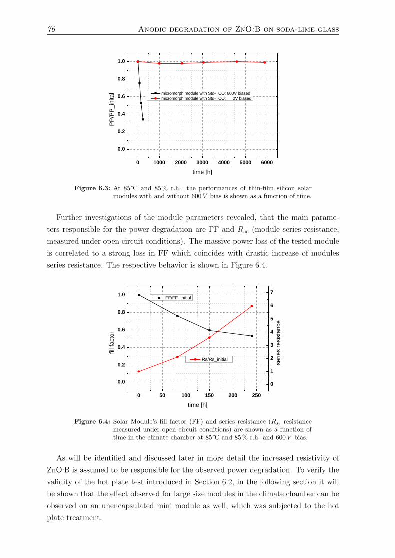
76 Anodic degradation of ZnO:B on soda-lime glass
0 1 0 0 0 2 0 0 0 3 0 0 0 4 0 0 0 5 0 0 0 6 0 0 00 . 0
0 . 2
0 . 4
0 . 6
0 . 8
1 . 0
PP/PP
_inita
l
t i m e [ h ]
m i c r o m o r p h m o d u l e w i t h S t d - T C O ; 6 0 0 V b i a s e d m i c r o m o r p h m o d u l e w i t h S t d - T C O ; 0 V b i a s e d
Figure 6.3: At 85 and 85 % r.h. the performances of thin-film silicon solarmodules with and without 600V bias is shown as a function of time.
Further investigations of the module parameters revealed, that the main parame-
ters responsible for the power degradation are FF and Roc (module series resistance,
measured under open circuit conditions). The massive power loss of the tested module
is correlated to a strong loss in FF which coincides with drastic increase of modules
series resistance. The respective behavior is shown in Figure 6.4.
0 5 0 1 0 0 1 5 0 2 0 0 2 5 00 . 0
0 . 2
0 . 4
0 . 6
0 . 8
1 . 0
fill fac
tor
t i m e [ h ]
F F / F F _ i n i t i a l
01234567
R s / R s _ i n i t i a l serie
s res
istanc
e
Figure 6.4: Solar Module’s fill factor (FF) and series resistance (Rs, resistancemeasured under open circuit conditions) are shown as a function oftime in the climate chamber at 85 and 85 % r.h. and 600V bias.
As will be identified and discussed later in more detail the increased resistivity of
ZnO:B is assumed to be responsible for the observed power degradation. To verify the
validity of the hot plate test introduced in Section 6.2, in the following section it will
be shown that the effect observed for large size modules in the climate chamber can be
observed on an unencapsulated mini module as well, which was subjected to the hot
plate treatment.
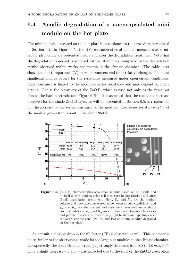
Anodic degradation of ZnO:B on soda-lime glass 77
6.4 Anodic degradation of a unencapsulated mini
module on the hot plate
The mini module is treated on the hot plate in accordance to the procedure introduced
in Section 6.2. In Figure 6.5a the I(V) characteristics of a small unencapsulated mi-
cromorph module are presented before and after the degradation treatment. Note that
the degradation observed is achieved within 10 minutes, compared to the degradation
results observed within weeks and month in the climate chamber. The table inset
shows the most important I(V) curve parameters and their relative changes. The most
significant change occurs for the resistance measured under open-circuit conditions.
This resistance is linked to the module’s series resistance and may depend on many
details. One is the resistivity of the ZnO:B, which is used not only as the front but
also as the back electrode (see Figure 6.2b). It is assumed that the resistance increase
observed for the single ZnO:B layer, as will be presented in Section 6.5, is responsible
for the increase of the series resistance of the module. The series resistance (Roc) of
the module grows from about 50 to about 960Ω.
0 2 4 6 8 10 120
5
10
15
20
25
30
35
I [m
A]
V [V]
initial final
Voc [V] Jsc [mA/cm²] FF [%] Roc [Ohm] Rsc [Ohm]initial 12.49 8.8 67.2 50 2077
final 12.93 1.63 34.4 964 3539-- -- -- -- -- --
final/initial [%] 4% -81% -49% 1801% 70%
P1P2P3
a) b)
blisters and spallingscaused by the degradation treatment
Figure 6.5: (a) I(V) characteristics of a small module based on an a-Si:H andµc-Si:H silicon tandem solar cell structure before (initial) and after(final) degradation treatment. Here, Voc and Roc are the modulevoltage and resistance measured under open-circuit conditions, andjsc and Rsc are the current and resistance measured under short-circuit conditions. Roc and Rsc are correlated with the module’s seriesand parallel resistances, respectively. (b) bilsters and spallings nearthe laser scribing zone (P1, P2 and P3) on a mini module degradedon the hot plate.
As a result a massive drop in the fill factor (FF) is observed as well. This behavior is
quite similar to the observations made for the large size modules in the climate chamber.
Unexpectedly, the short-circuit current (jsc) strongly decreases from 8.8 to 1.6mA/cm2.
Only a slight decrease – if any – was expected due to the shift of the ZnO:B absorption
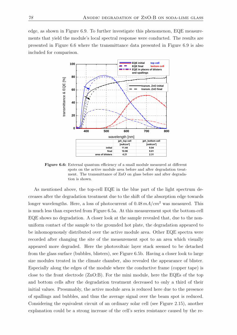
78 Anodic degradation of ZnO:B on soda-lime glass
edge, as shown in Figure 6.9. To further investigate this phenomenon, EQE measure-
ments that yield the module’s local spectral response were conducted. The results are
presented in Figure 6.6 where the transmittance data presented in Figure 6.9 is also
included for comparison.
4 0 0 5 0 0 6 0 0 7 0 0 8 0 00
2 0
4 0
6 0
8 0
1 0 0 E Q E i n i t i a l t o p c e l lE Q E f i n a l b o t t o m c e l lE Q E i n p l a c e s o f b l i s t e r s a n d s p a l l i n g s
tra
nsmi
ttanc
e & EQ
E [%]
w a v e l e n g t h [ n m ]
t r a n s m . Z n O i n i t i a lt r a n s m . Z n O f i n a l
Figure 6.6: External quantum efficiency of a small module measured at differentspots on the active module area before and after degradation treat-ment. The transmittance of ZnO on glass before and after degrada-tion is shown.
As mentioned above, the top-cell EQE in the blue part of the light spectrum de-
creases after the degradation treatment due to the shift of the absorption edge towards
longer wavelengths. Here, a loss of photocurrent of 0.48mA/cm2 was measured. This
is much less than expected from Figure 6.5a. At this measurement spot the bottom-cell
EQE shows no degradation. A closer look at the sample revealed that, due to the non-
uniform contact of the sample to the grounded hot plate, the degradation appeared to
be inhomogenously distributed over the active module area. Other EQE spectra were
recorded after changing the site of the measurement spot to an area which visually
appeared more degraded. Here the photovoltaic layer stack seemed to be detached
from the glass surface (bubbles, blisters), see Figure 6.5b. Having a closer look to large
size modules treated in the climate chamber, also revealed the appearance of blister.
Especially along the edges of the module where the conductive frame (copper tape) is
close to the front electrode (ZnO:B). For the mini module, here the EQEs of the top
and bottom cells after the degradation treatment decreased to only a third of their
initial values. Presumably, the active module area is reduced here due to the presence
of spallings and bubbles, and thus the average signal over the beam spot is reduced.
Considering the equivalent circuit of an ordinary solar cell (see Figure 2.15), another
explanation could be a strong increase of the cell’s series resistance caused by the re-
Anodic degradation of ZnO:B on soda-lime glass 79
sistivity increase of the ZnO:B front electrode. Due to the locally strongly increased
series resistance, the photocurrent is not able to follow the external circuit. The pho-
tocurrent is forced to drain off through the local parallel resistance. As a result the
low EQE signal shown in Figure 6.6 is measured. As already mentioned in the experi-
mental section that the ZnO:B resistance was found to have a certain inhomogeneity.
Together with the explanation given above, the averaging of unaffected module areas
with areas of significantly increased series resistance could explain the observed drop
of jsc in Figure 6.5a.
6.5 Degradation of samples with ZnO:B on glass
only
As one has seen from Section 6.4 the hot plate setup is adequate to achieve similar
degradation results for mini modules compared to results gained for large size modules
degraded in the climate chamber. In the following it will be further proven that the
ZnO:B deposited on the glass and used as front contact is the layer driving the power
degradation of the solar module. Electrical and optical properties of glass samples
(5 × 5 cm2) covered with ZnO:B only will be discussed before and after degradation
treatment on the hot plate.
6.5.1 Electrical changes of glass/ZnO:B samples
The average resistance across the diagonal of the treated samples is shown in Figure
6.7. The ZnO:B was deposited with a constant mass flow rate of DEZ and a varying
B2H6 rate for different samples. As indicated, the doping ratio (B2H6/DEZ) was
varied between 0.08 and 0.18. For 10 minutes time a voltage of +1000V was applied
to each sample, as described in Section 6.2. A strong increase of resistance of about
4 orders of magnitude was observed for the sample with a doping ratio of 0.08. The
resistance increase is reduced for higher doping ratios. Note that the applied voltage
and temperature mainly affects the rate of the degradation process. If no voltage is
applied, no reasonable degradation is observed, despite the sample is subjected to the
hot plate at 160 . Details on voltage and temperature variations will not be discussed
further in the present work. To the author’s knowledge, this phenomenon is previously
unrecorded in the literature, even though it is obviously of practical importance for
photovoltaic applications.
The resistivity of a polycrystalline semiconductor thin film on top of an isolating
substrate is determined by its thickness, density of free charge carriers and their corre-
sponding mobility [69,115]. In order to discover the reason for the resistance increase,
the free charge carrier density and mobility in the ZnO:B film were determined by Hall
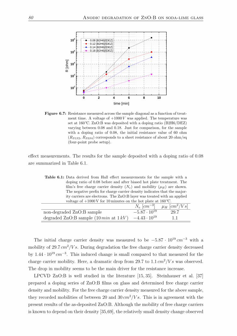
80 Anodic degradation of ZnO:B on soda-lime glass
0 2 4 6 8 1 0
1 0 2
1 0 3
1 0 4
1 0 5
1 0 6
R [oh
m]
t i m e [ m i n ]
0 . 0 8 [ B 2 H 6 ] / [ D E Z ] 0 . 1 2 [ B 2 H 6 ] / [ D E Z ] 0 . 1 4 [ B 2 H 6 ] / [ D E Z ] 0 . 1 8 [ B 2 H 6 ] / [ D E Z ]
Figure 6.7: Resistance measured across the sample diagonal as a function of treat-ment time. A voltage of +1000V was applied. The temperature wasset at 160 . ZnO:B was deposited with a doping ratio (B2H6/DEZ)varying between 0.08 and 0.18. Just for comparison, for the samplewith a doping ratio of 0.08, the initial resistance value of 60 ohm(RS1S2, RS3S4) corresponds to a sheet resistance of about 20 ohm/sq(four-point probe setup).
effect measurements. The results for the sample deposited with a doping ratio of 0.08
are summarized in Table 6.1.
Table 6.1: Data derived from Hall effect measurements for the sample with adoping ratio of 0.08 before and after biased hot plate treatment. Thefilm’s free charge carrier density (Ne) and mobility (µH) are shown.The negative prefix for charge carrier density indicates that the major-ity carriers are electrons. The ZnO:B layer was treated with an appliedvoltage of +1000 V for 10 minutes on the hot plate at 160 .
Ne [cm−3] µH [cm2/V s]non-degraded ZnO:B sample −5.87 · 1019 29.7degraded ZnO:B sample (10min at 1 kV ) −4.43 · 1019 1.1
The initial charge carrier density was measured to be −5.87 · 1019 cm−3 with a
mobility of 29.7 cm2/V s. During degradation the free charge carrier density decreased
by 1.44 · 1019 cm−3. This induced change is small compared to that measured for the
charge carrier mobility. Here, a dramatic drop from 29.7 to 1.1 cm2/V s was observed.
The drop in mobility seems to be the main driver for the resistance increase.
LPCVD ZnO:B is well studied in the literature [15, 35]. Steinhauser et al. [37]
prepared a doping series of ZnO:B films on glass and determined free charge carrier
density and mobility. For the free charge carrier density measured for the above sample,
they recorded mobilities of between 20 and 30 cm2/V s. This is in agreement with the
present results of the as-deposited ZnO:B. Although the mobility of free charge carriers
is known to depend on their density [35,69], the relatively small density change observed
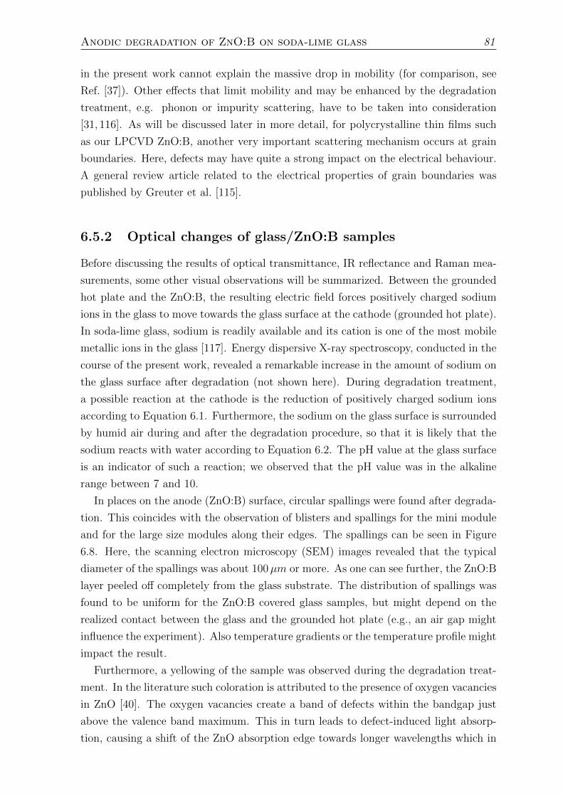
Anodic degradation of ZnO:B on soda-lime glass 81
in the present work cannot explain the massive drop in mobility (for comparison, see
Ref. [37]). Other effects that limit mobility and may be enhanced by the degradation
treatment, e.g. phonon or impurity scattering, have to be taken into consideration
[31, 116]. As will be discussed later in more detail, for polycrystalline thin films such
as our LPCVD ZnO:B, another very important scattering mechanism occurs at grain
boundaries. Here, defects may have quite a strong impact on the electrical behaviour.
A general review article related to the electrical properties of grain boundaries was
published by Greuter et al. [115].
6.5.2 Optical changes of glass/ZnO:B samples
Before discussing the results of optical transmittance, IR reflectance and Raman mea-
surements, some other visual observations will be summarized. Between the grounded
hot plate and the ZnO:B, the resulting electric field forces positively charged sodium
ions in the glass to move towards the glass surface at the cathode (grounded hot plate).
In soda-lime glass, sodium is readily available and its cation is one of the most mobile
metallic ions in the glass [117]. Energy dispersive X-ray spectroscopy, conducted in the
course of the present work, revealed a remarkable increase in the amount of sodium on
the glass surface after degradation (not shown here). During degradation treatment,
a possible reaction at the cathode is the reduction of positively charged sodium ions
according to Equation 6.1. Furthermore, the sodium on the glass surface is surrounded
by humid air during and after the degradation procedure, so that it is likely that the
sodium reacts with water according to Equation 6.2. The pH value at the glass surface
is an indicator of such a reaction; we observed that the pH value was in the alkaline
range between 7 and 10.
In places on the anode (ZnO:B) surface, circular spallings were found after degrada-
tion. This coincides with the observation of blisters and spallings for the mini module
and for the large size modules along their edges. The spallings can be seen in Figure
6.8. Here, the scanning electron microscopy (SEM) images revealed that the typical
diameter of the spallings was about 100µm or more. As one can see further, the ZnO:B
layer peeled off completely from the glass substrate. The distribution of spallings was
found to be uniform for the ZnO:B covered glass samples, but might depend on the
realized contact between the glass and the grounded hot plate (e.g., an air gap might
influence the experiment). Also temperature gradients or the temperature profile might
impact the result.
Furthermore, a yellowing of the sample was observed during the degradation treat-
ment. In the literature such coloration is attributed to the presence of oxygen vacancies
in ZnO [40]. The oxygen vacancies create a band of defects within the bandgap just
above the valence band maximum. This in turn leads to defect-induced light absorp-
tion, causing a shift of the ZnO absorption edge towards longer wavelengths which in
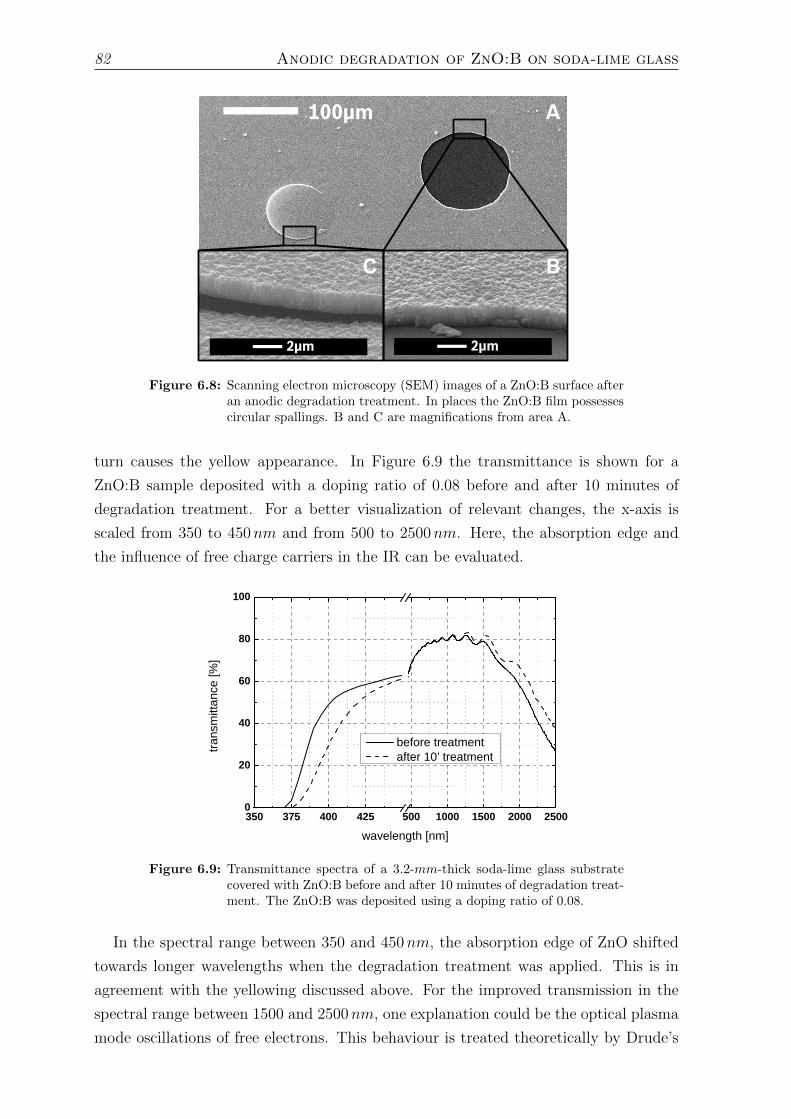
82 Anodic degradation of ZnO:B on soda-lime glass
100µm
2µm 2µm
A
BC
Figure 6.8: Scanning electron microscopy (SEM) images of a ZnO:B surface afteran anodic degradation treatment. In places the ZnO:B film possessescircular spallings. B and C are magnifications from area A.
turn causes the yellow appearance. In Figure 6.9 the transmittance is shown for a
ZnO:B sample deposited with a doping ratio of 0.08 before and after 10 minutes of
degradation treatment. For a better visualization of relevant changes, the x-axis is
scaled from 350 to 450nm and from 500 to 2500nm. Here, the absorption edge and
the influence of free charge carriers in the IR can be evaluated.
3 5 0 3 7 5 4 0 0 4 2 5 5 0 0 1 0 0 0 1 5 0 0 2 0 0 0 2 5 0 00
2 0
4 0
6 0
8 0
1 0 0
trans
mitta
nce [
%]
w a v e l e n g t h [ n m ]
b e f o r e t r e a t m e n t a f t e r 1 0 ’ t r e a t m e n t
Figure 6.9: Transmittance spectra of a 3.2-mm-thick soda-lime glass substratecovered with ZnO:B before and after 10 minutes of degradation treat-ment. The ZnO:B was deposited using a doping ratio of 0.08.
In the spectral range between 350 and 450nm, the absorption edge of ZnO shifted
towards longer wavelengths when the degradation treatment was applied. This is in
agreement with the yellowing discussed above. For the improved transmission in the
spectral range between 1500 and 2500nm, one explanation could be the optical plasma
mode oscillations of free electrons. This behaviour is treated theoretically by Drude’s
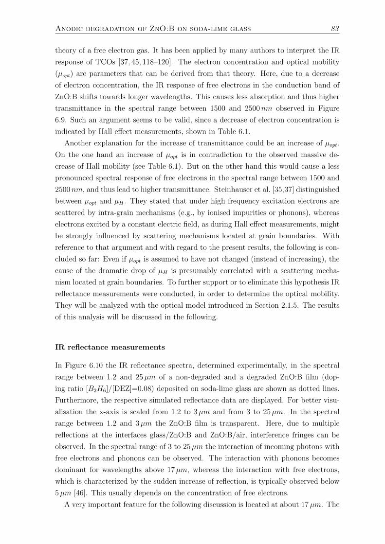
Anodic degradation of ZnO:B on soda-lime glass 83
theory of a free electron gas. It has been applied by many authors to interpret the IR
response of TCOs [37, 45, 118–120]. The electron concentration and optical mobility
(µopt) are parameters that can be derived from that theory. Here, due to a decrease
of electron concentration, the IR response of free electrons in the conduction band of
ZnO:B shifts towards longer wavelengths. This causes less absorption and thus higher
transmittance in the spectral range between 1500 and 2500nm observed in Figure
6.9. Such an argument seems to be valid, since a decrease of electron concentration is
indicated by Hall effect measurements, shown in Table 6.1.
Another explanation for the increase of transmittance could be an increase of µopt.
On the one hand an increase of µopt is in contradiction to the observed massive de-
crease of Hall mobility (see Table 6.1). But on the other hand this would cause a less
pronounced spectral response of free electrons in the spectral range between 1500 and
2500nm, and thus lead to higher transmittance. Steinhauser et al. [35,37] distinguished
between µopt and µH . They stated that under high frequency excitation electrons are
scattered by intra-grain mechanisms (e.g., by ionised impurities or phonons), whereas
electrons excited by a constant electric field, as during Hall effect measurements, might
be strongly influenced by scattering mechanisms located at grain boundaries. With
reference to that argument and with regard to the present results, the following is con-
cluded so far: Even if µopt is assumed to have not changed (instead of increasing), the
cause of the dramatic drop of µH is presumably correlated with a scattering mecha-
nism located at grain boundaries. To further support or to eliminate this hypothesis IR
reflectance measurements were conducted, in order to determine the optical mobility.
They will be analyzed with the optical model introduced in Section 2.1.5. The results
of this analysis will be discussed in the following.
IR reflectance measurements
In Figure 6.10 the IR reflectance spectra, determined experimentally, in the spectral
range between 1.2 and 25µm of a non-degraded and a degraded ZnO:B film (dop-
ing ratio [B2H6]/[DEZ]=0.08) deposited on soda-lime glass are shown as dotted lines.
Furthermore, the respective simulated reflectance data are displayed. For better visu-
alisation the x-axis is scaled from 1.2 to 3µm and from 3 to 25µm. In the spectral
range between 1.2 and 3µm the ZnO:B film is transparent. Here, due to multiple
reflections at the interfaces glass/ZnO:B and ZnO:B/air, interference fringes can be
observed. In the spectral range of 3 to 25µm the interaction of incoming photons with
free electrons and phonons can be observed. The interaction with phonons becomes
dominant for wavelengths above 17µm, whereas the interaction with free electrons,
which is characterized by the sudden increase of reflection, is typically observed below
5µm [46]. This usually depends on the concentration of free electrons.
A very important feature for the following discussion is located at about 17µm. The
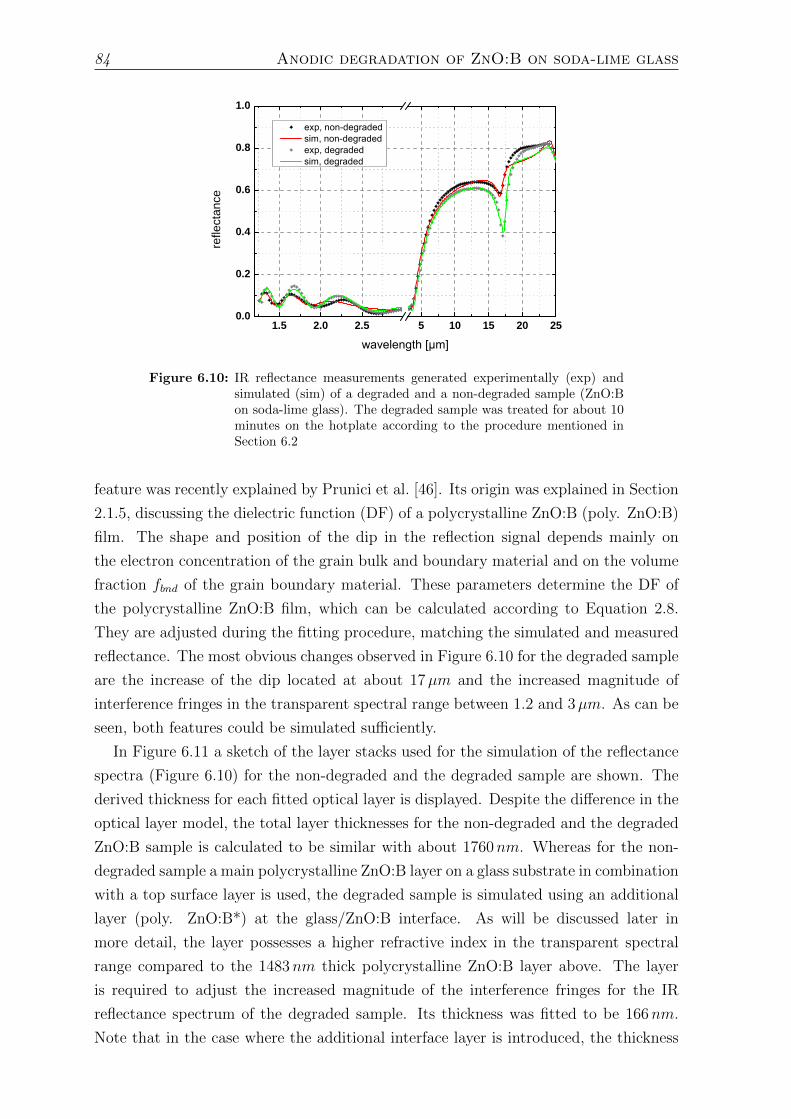
84 Anodic degradation of ZnO:B on soda-lime glass
1 . 5 2 . 0 2 . 5 5 1 0 1 5 2 0 2 50 . 0
0 . 2
0 . 4
0 . 6
0 . 8
1 . 0
reflec
tance
Figure 6.10: IR reflectance measurements generated experimentally (exp) andsimulated (sim) of a degraded and a non-degraded sample (ZnO:Bon soda-lime glass). The degraded sample was treated for about 10minutes on the hotplate according to the procedure mentioned inSection 6.2
feature was recently explained by Prunici et al. [46]. Its origin was explained in Section
2.1.5, discussing the dielectric function (DF) of a polycrystalline ZnO:B (poly. ZnO:B)
film. The shape and position of the dip in the reflection signal depends mainly on
the electron concentration of the grain bulk and boundary material and on the volume
fraction fbnd of the grain boundary material. These parameters determine the DF of
the polycrystalline ZnO:B film, which can be calculated according to Equation 2.8.
They are adjusted during the fitting procedure, matching the simulated and measured
reflectance. The most obvious changes observed in Figure 6.10 for the degraded sample
are the increase of the dip located at about 17µm and the increased magnitude of
interference fringes in the transparent spectral range between 1.2 and 3µm. As can be
seen, both features could be simulated sufficiently.
In Figure 6.11 a sketch of the layer stacks used for the simulation of the reflectance
spectra (Figure 6.10) for the non-degraded and the degraded sample are shown. The
derived thickness for each fitted optical layer is displayed. Despite the difference in the
optical layer model, the total layer thicknesses for the non-degraded and the degraded
ZnO:B sample is calculated to be similar with about 1760nm. Whereas for the non-
degraded sample a main polycrystalline ZnO:B layer on a glass substrate in combination
with a top surface layer is used, the degraded sample is simulated using an additional
layer (poly. ZnO:B*) at the glass/ZnO:B interface. As will be discussed later in
more detail, the layer possesses a higher refractive index in the transparent spectral
range compared to the 1483nm thick polycrystalline ZnO:B layer above. The layer
is required to adjust the increased magnitude of the interference fringes for the IR
reflectance spectrum of the degraded sample. Its thickness was fitted to be 166nm.
Note that in the case where the additional interface layer is introduced, the thickness
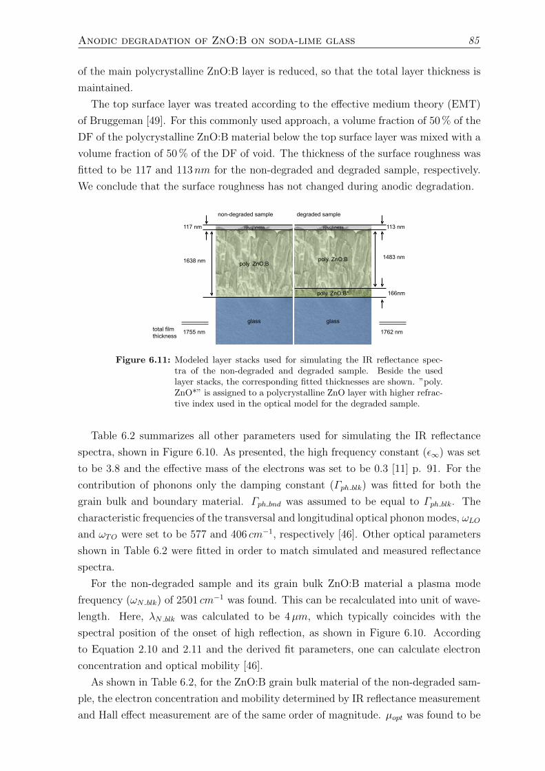
Anodic degradation of ZnO:B on soda-lime glass 85
of the main polycrystalline ZnO:B layer is reduced, so that the total layer thickness is
maintained.
The top surface layer was treated according to the effective medium theory (EMT)
of Bruggeman [49]. For this commonly used approach, a volume fraction of 50 % of the
DF of the polycrystalline ZnO:B material below the top surface layer was mixed with a
volume fraction of 50 % of the DF of void. The thickness of the surface roughness was
fitted to be 117 and 113nm for the non-degraded and degraded sample, respectively.
We conclude that the surface roughness has not changed during anodic degradation.
glass
poly. ZnO:B
poly. ZnO:B*
glass
poly. ZnO:B
degraded samplenon-degraded sample
117 nm 113 nm
1638 nm 1483 nm
166nm
roughnessroughness
total filmthickness
1755 nm 1762 nm
Figure 6.11: Modeled layer stacks used for simulating the IR reflectance spec-tra of the non-degraded and degraded sample. Beside the usedlayer stacks, the corresponding fitted thicknesses are shown. ”poly.ZnO*” is assigned to a polycrystalline ZnO layer with higher refrac-tive index used in the optical model for the degraded sample.
Table 6.2 summarizes all other parameters used for simulating the IR reflectance
spectra, shown in Figure 6.10. As presented, the high frequency constant (ε∞) was set
to be 3.8 and the effective mass of the electrons was set to be 0.3 [11] p. 91. For the
contribution of phonons only the damping constant (Γph blk) was fitted for both the
grain bulk and boundary material. Γph bnd was assumed to be equal to Γph blk. The
characteristic frequencies of the transversal and longitudinal optical phonon modes, ωLO
and ωTO were set to be 577 and 406 cm−1, respectively [46]. Other optical parameters
shown in Table 6.2 were fitted in order to match simulated and measured reflectance
spectra.
For the non-degraded sample and its grain bulk ZnO:B material a plasma mode
frequency (ωN blk) of 2501 cm−1 was found. This can be recalculated into unit of wave-
length. Here, λN blk was calculated to be 4µm, which typically coincides with the
spectral position of the onset of high reflection, as shown in Figure 6.10. According
to Equation 2.10 and 2.11 and the derived fit parameters, one can calculate electron
concentration and optical mobility [46].
As shown in Table 6.2, for the ZnO:B grain bulk material of the non-degraded sam-
ple, the electron concentration and mobility determined by IR reflectance measurement
and Hall effect measurement are of the same order of magnitude. µopt was found to be
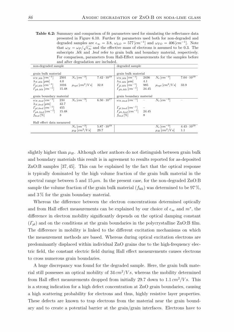
86 Anodic degradation of ZnO:B on soda-lime glass
Table 6.2: Summary and comparison of fit parameters used for simulating the reflectance datapresented in Figure 6.10. Further fit parameters used both for non-degraded anddegraded samples are ε∞ = 3.8, ωLO = 577 [cm−1] and ωTO = 406 [cm−1]. Notethat ωN = ωP /
√ε∞ and the effective mass of electrons is assumed to be 0.3. The
subscripts blk and bnd refer to grain bulk and boundary material, respectively.For comparison, parameters from Hall-Effect measurements for the samples beforeand after degradation are included.
non-degraded sample degraded sample
grain bulk material grain bulk materialωN blk [cm−1] 2501 Ne [cm−3] 7.42 · 1019 ωN blk [cm−1] 2436 Ne [cm−3] 7.04 · 1019
λN blk [µm] 4.0 λN blk [µm] 4.1Γpl blk [cm−1] 1016 µopt [cm2/V s] 32.8 Γpl blk [cm−1] 985 µopt [cm2/V s] 33.9Γph blk [cm−1] 15.48 Γph blk [cm−1] 24.45
grain boundary material grain boundary materialωN bnd [cm−1] 234 Ne [cm−3] 6.50 · 1017 ωN bnd [cm−1] – Ne [cm−3] –λN bnd [µm] 42.7Γpl bnd [cm−1] 455 Γpl bnd [cm−1] –Γph bnd [cm−1] 15.48 Γph bnd [cm−1] 24.45fbnd [%] 3 fbnd [%] 8
Hall effect data measuredNe [cm−3] 5.87 · 1019 Ne [cm−3] 4.43 · 1019
µH [cm2/V s] 29.7 µH [cm2/V s] 1.1
slightly higher than µH . Although other authors do not distinguish between grain bulk
and boundary materials this result is in agreement to results reported for as-deposited
ZnO:B samples [37, 45]. This can be explained by the fact that the optical response
is typically dominated by the high volume fraction of the grain bulk material in the
spectral range between 5 and 15µm. In the present case, for the non-degraded ZnO:B
sample the volume fraction of the grain bulk material (fblk) was determined to be 97 %,
and 3 % for the grain boundary material.
Whereas the difference between the electron concentrations determined optically
and from Hall effect measurements can be explained by our choice of ε∞ and m∗, the
difference in electron mobility significantly depends on the optical damping constant
(Γpl) and on the conditions at the grain boundaries in the polycrystalline ZnO:B film.
The difference in mobility is linked to the different excitation mechanisms on which
the measurement methods are based. Whereas during optical excitation electrons are
predominantly displaced within individual ZnO grains due to the high-frequency elec-
tric field, the constant electric field during Hall effect measurements causes electrons
to cross numerous grain boundaries.
A huge discrepancy was found for the degraded sample. Here, the grain bulk mate-
rial still possesses an optical mobility of 34 cm2/V s, whereas the mobility determined
from Hall effect measurements dropped from initially 29.7 down to 1.1 cm2/V s. This
is a strong indication for a high defect concentration at ZnO grain boundaries, causing
a high scattering probability for electrons and thus, highly resistive layer properties.
These defects are known to trap electrons from the material near the grain bound-
ary and to create a potential barrier at the grain/grain interfaces. Electrons have to
Anodic degradation of ZnO:B on soda-lime glass 87
overcome the potential or to tunnel through this interface in order to contribute to a
DC current. As a result µH is reduced whereas µopt is maintained, since the majority
of electrons optically excited are within grains and not scattered by defect-rich grain
boundaries.
Evidence for trapped electrons can be found in the DF fitting parameters of the grain
boundary material. Here, the electron concentration was found to be 6.5 ·1017 cm−3 for
the non-degraded ZnO:B sample, much less than the value of 7.49 ·1019 cm−3 found for
the grain bulk material. Note that the accuracy of the electron concentration deter-
mined for the grain boundary material presumably is limited. The value was derived
from the fitted plasma mode frequency ωN bnd =234 cm−1 (approximately 42µm) given
in Table 6.2. This is beyond the spectral range investigated but better fit results were
obtained, considering a small amount of electrons than neglecting them. Furthermore,
because the plasma mode frequency for the grain boundary material is close to the
phonon resonances (ωLO, ωTO), the plasma mode oscillation in the grain boundary ma-
terial might interfere with the phonon resonance. As a result the fitted parameters for
the grain boundary material may be inaccurate, and we thus abstained from further
interpretation of the damping constant related to the optical mobility.
For the degraded sample, the best fit results were obtained by neglecting free elec-
trons in the grain boundary material. Such an approach may be valid since a higher
defect concentration at the grain boundaries for the degraded than for the non-degraded
sample is assumed, thus causing a higher number of trapped electrons at the ZnO grain
interfaces. This in turn would cause a decrease in electron concentration in the ZnO
grain boundary material and a further decrease of ωN bnd. Furthermore, a decrease in
electron concentration in the grain bulk material from 7.42·1019 cm−3 to 7.04·1019 cm−3
was determined optically for the degraded ZnO:B film. This decrease was confirmed
by Hall effect measurements and further confirms an increased electron trap density at
ZnO:B grain boundaries.
In Figure 6.12 the modelled refractive indices and extinction coefficients, which were
derived from the EMT approach, are shown for non-degraded and degraded polycrys-
talline ZnO:B layers. Furthermore, the optical constants for the grain bulk and bound-
ary material used in the EMT approach for the non-degraded sample are presented.
The optical constants for the degraded grain bulk and boundary materials are omitted
for clarity. They are visually similar to the optical constants of the non-degraded ZnO
grain bulk and boundary materials. For the grain bulk and boundary materials, the
major difference in n and k is caused by the low electron concentration of the grain
boundary material compared to the grain bulk material. Due to the low electron con-
centration the plasma mode frequency (ωN bnd) is in far IR spectral range. As a result,
the onset of increased k values in the IR spectral range is correlated with the phonon
resonance for wavelengths above 15µm. For comparison see the extinction coefficients
in Figure 6.12 (dashed-dotted and dashed lines).
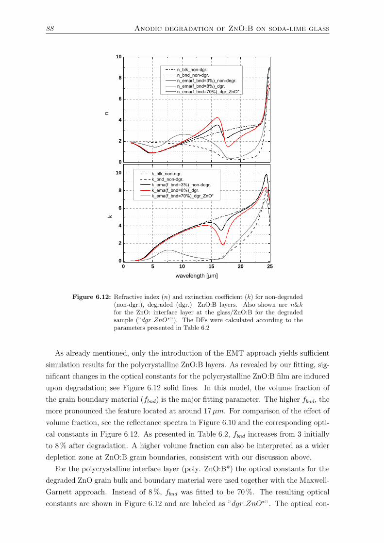
88 Anodic degradation of ZnO:B on soda-lime glass
0
2
4
6
8
1 0
n
0 5 1 0 1 5 2 0 2 50
2
4
6
8
1 0
k
! "
Figure 6.12: Refractive index (n) and extinction coefficient (k) for non-degraded(non-dgr.), degraded (dgr.) ZnO:B layers. Also shown are n&kfor the ZnO: interface layer at the glass/ZnO:B for the degradedsample (”dgr ZnO∗”). The DFs were calculated according to theparameters presented in Table 6.2
As already mentioned, only the introduction of the EMT approach yields sufficient
simulation results for the polycrystalline ZnO:B layers. As revealed by our fitting, sig-
nificant changes in the optical constants for the polycrystalline ZnO:B film are induced
upon degradation; see Figure 6.12 solid lines. In this model, the volume fraction of
the grain boundary material (fbnd) is the major fitting parameter. The higher fbnd, the
more pronounced the feature located at around 17µm. For comparison of the effect of
volume fraction, see the reflectance spectra in Figure 6.10 and the corresponding opti-
cal constants in Figure 6.12. As presented in Table 6.2, fbnd increases from 3 initially
to 8 % after degradation. A higher volume fraction can also be interpreted as a wider
depletion zone at ZnO:B grain boundaries, consistent with our discussion above.
For the polycrystalline interface layer (poly. ZnO:B*) the optical constants for the
degraded ZnO grain bulk and boundary material were used together with the Maxwell-
Garnett approach. Instead of 8 %, fbnd was fitted to be 70 %. The resulting optical
constants are shown in Figure 6.12 and are labeled as ”dgr ZnO∗”. The optical con-
Anodic degradation of ZnO:B on soda-lime glass 89
stants show a marked difference compared to those of the non-degraded and degraded
ZnO:B material, which is caused by the high volume fraction (fbnd). Note that an indi-
vidual parameterization of the interface layer is challenging. The reflectance spectrum
in Figure 6.10 is sensitive to the interface layer only at short wavelengths, for which the
ZnO:B is transparent. From the extinction coefficient presented in Figure 6.12, one can
estimate the wavelength-dependent optical penetration depth for the polycrystalline
ZnO:B layer above the interface layer. Whereas the penetration depth for wavelengths
above 5µm is estimated to be below 500nm, the penetration depth for wavelengths
below 5µm exceeds 3µm, so that the ZnO:B becomes optically transparent for shorter
wavelengths. Thus, the optical constants for the interface layer (dgr ZnO : B∗) are
valid only for wavelengths below 5µm. For wavelengths above 5µm, the glass/ZnO
interface is not sensed, due to the reduced penetration depth of the light. However
for the optical model of the degraded ZnO:B sample the interface layer with adjusted
optical constants is required in order to match the increased magnitude of interference
fringes in the transparent spectral range, see Figure 6.10.
For a given electron concentration and a certain electron-trapping defect concentra-
tion at ZnO:B grain boundaries, a depletion region of a certain width is created at the
grain boundaries. The width is assumed to be independent of the grain size. Thus,
fbnd scales with the total grain size: The smaller the grains the higher fbnd. It is well
known that LPCVD ZnO:B starts to grow with small grains that then increases in
size [16,29]. In Figure 6.13, transmission electron (TEM) and scanning electron (SEM)
microscopy records are presented for the non-degraded and the degraded sample. For
both samples an interface layer next to the glass substrate, consisting of smaller grains,
can be recognized. Note that for optical model of the non-degraded sample this in-
terface layer is neglected, see Figure 6.11. This is justified by the small fbnd (smaller
depletion width) for the interface layer in the non-degraded case. As can be seen in
Figure 6.12, the refractive index does not vary much for low volume fractions (smaller
than 10 %). Thus, the interface layer does not differ optically from the polycrystalline
ZnO:B layer above it in the transparent spectral range. As a result, both layers can be
modeled as a single layer.
Another explanation for an interface layer with higher refractive index in the de-
graded case could be related to stoichiometry changes or the accumulation of positively
charged zinc interstitials at the glass/ZnO:B interface. However, energy dispersive X-
ray analysis (EDX) on the samples (presented in Figure 6.13) revealed no changes.
Presumably the changes induced are below the detection limits of the measurement.
Furthermore, it is not clear yet whether these stoichiometry changes introduce the
required changes in n and k.
In Figure 6.13 another interesting detail was revealed. In contrast to the non-
degraded sample the degraded ZnO:B film features micro voids at the ZnO:B grain
boundaries. These voids were observed for both SEM and TEM images. The origin
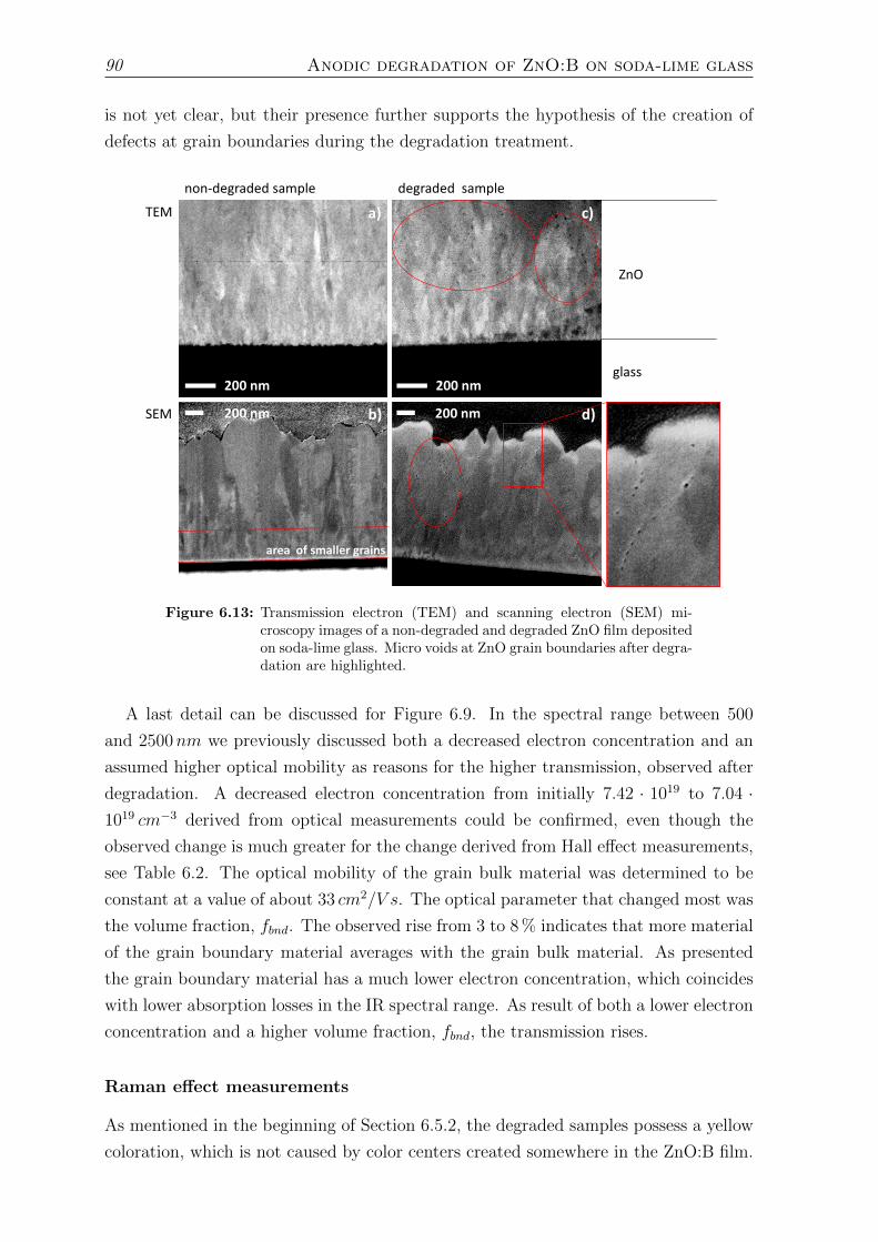
90 Anodic degradation of ZnO:B on soda-lime glass
is not yet clear, but their presence further supports the hypothesis of the creation of
defects at grain boundaries during the degradation treatment.
TEM
200 nm 200 nm
200 nm 200 nmSEM
non-degraded sample degraded sample
a)
b) d)
c)
area of smaller grains
glass
ZnO
Figure 6.13: Transmission electron (TEM) and scanning electron (SEM) mi-croscopy images of a non-degraded and degraded ZnO film depositedon soda-lime glass. Micro voids at ZnO grain boundaries after degra-dation are highlighted.
A last detail can be discussed for Figure 6.9. In the spectral range between 500
and 2500nm we previously discussed both a decreased electron concentration and an
assumed higher optical mobility as reasons for the higher transmission, observed after
degradation. A decreased electron concentration from initially 7.42 · 1019 to 7.04 ·1019 cm−3 derived from optical measurements could be confirmed, even though the
observed change is much greater for the change derived from Hall effect measurements,
see Table 6.2. The optical mobility of the grain bulk material was determined to be
constant at a value of about 33 cm2/V s. The optical parameter that changed most was
the volume fraction, fbnd. The observed rise from 3 to 8 % indicates that more material
of the grain boundary material averages with the grain bulk material. As presented
the grain boundary material has a much lower electron concentration, which coincides
with lower absorption losses in the IR spectral range. As result of both a lower electron
concentration and a higher volume fraction, fbnd, the transmission rises.
Raman effect measurements
As mentioned in the beginning of Section 6.5.2, the degraded samples possess a yellow
coloration, which is not caused by color centers created somewhere in the ZnO:B film.
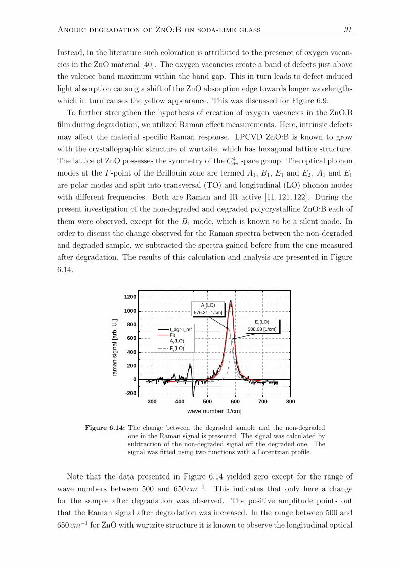
Anodic degradation of ZnO:B on soda-lime glass 91
Instead, in the literature such coloration is attributed to the presence of oxygen vacan-
cies in the ZnO material [40]. The oxygen vacancies create a band of defects just above
the valence band maximum within the band gap. This in turn leads to defect induced
light absorption causing a shift of the ZnO absorption edge towards longer wavelengths
which in turn causes the yellow appearance. This was discussed for Figure 6.9.
To further strengthen the hypothesis of creation of oxygen vacancies in the ZnO:B
film during degradation, we utilized Raman effect measurements. Here, intrinsic defects
may affect the material specific Raman response. LPCVD ZnO:B is known to grow
with the crystallographic structure of wurtzite, which has hexagonal lattice structure.
The lattice of ZnO possesses the symmetry of the C46v space group. The optical phonon
modes at the Γ -point of the Brillouin zone are termed A1, B1, E1 and E2. A1 and E1
are polar modes and split into transversal (TO) and longitudinal (LO) phonon modes
with different frequencies. Both are Raman and IR active [11, 121, 122]. During the
present investigation of the non-degraded and degraded polycrystalline ZnO:B each of
them were observed, except for the B1 mode, which is known to be a silent mode. In
order to discuss the change observed for the Raman spectra between the non-degraded
and degraded sample, we subtracted the spectra gained before from the one measured
after degradation. The results of this calculation and analysis are presented in Figure
6.14.
3 0 0 4 0 0 5 0 0 6 0 0 7 0 0 8 0 0- 2 0 0
0
2 0 04 0 0
6 0 0
8 0 01 0 0 0
1 2 0 0
E 1 ( L O )5 8 8 . 0 8 [ 1 / c m ]
raman
signa
l [arb.
U.]
w a v e n u m b e r [ 1 / c m ]
A 1 ( L O )5 7 6 . 3 1 [ 1 / c m ]
I _ d g r - I _ r e f F i t A 1 ( L O ) E 1 ( L O )
Figure 6.14: The change between the degraded sample and the non-degradedone in the Raman signal is presented. The signal was calculated bysubtraction of the non-degraded signal off the degraded one. Thesignal was fitted using two functions with a Lorentzian profile.
Note that the data presented in Figure 6.14 yielded zero except for the range of
wave numbers between 500 and 650 cm−1. This indicates that only here a change
for the sample after degradation was observed. The positive amplitude points out
that the Raman signal after degradation was increased. In the range between 500 and
650 cm−1 for ZnO with wurtzite structure it is known to observe the longitudinal optical
92 Anodic degradation of ZnO:B on soda-lime glass
vibration modes of A1 and E1. To determine the position of the respective resonant
wave numbers, two Lorentzian peak functions in order to simulate the measured Raman
signal in Figure 6.14, were utilized. For A1(LO) and E1(LO) values of 576.31 and
588.01 cm−1 were found, respectively. This is in good agreement to values reported in
the literature and identifies both modes accurately, see Ref. [11] p. 93. In the literature
the change of the intensity of these modes is reported to be sensitive to intrinsic defects
such as oxygen vacancies or zinc interstitials [123–125]. Scepanovic et al. observed a
beige/yellow coloration of the ZnO powder they investigated and attributed this change
to the presence of oxygen vacancies as dominant intrinsic defect [125]. Following these
interpretations confirms the argumentation of Figure 6.9, where the shift of absorption
edge was related to the creation of oxygen vacancies.
6.6 The glass substrate as a source of oxygen during
degradation treatment
As will be discussed later in more detail, oxygen is suspected to be responsible for some
of our observations. Since it is difficult to measure a small change in oxygen concen-
tration in an oxygen-rich environment (in ZnO:B), the following experiment was con-
ducted. On a standard soda-lime glass substrate we deposited a µc-Si:H layer followed
by an a-Si:H cap layer by plasma-enhanced chemical vapour deposition (PECVD). Fi-
nally, a ZnO:B layer was deposited to form an electrical contact to the silicon layer
stack (and not necessarily to study its degradation). The µc-Si:H was deposited in a
regime of high Raman crystallinity, thus yielding porous µc-Si:H material. This layer
was intended to act as a gettering material, incorporating the species escaping the glass
during degradation. The a-Si:H layer was intended to protect the porous µc-Si:H film
from initial oxidation, since the samples were handled in a normal environment before
ZnO:B deposition. This sample was treated according to the hot plate degradation
treatment, introduced in Section 6.2. Note, that the reference sample was heated on
the hot plate, but without applied voltage. The treated sample and reference sam-
ple were analysed by secondary ion mass spectroscopy (SIMS) to study the species
incorporated from the glass. The results of SIMS analysis are shown in Figure 6.15.
In Figure 6.15, we see a depth profile for the mass number to charge ratio of 60,
measured from the ZnO:B side to the glass substrate for the treated and the untreated
reference sample. The detector was set to sense negatively charged ions. Cesium was
used as primary ion source. Due to the obvious presence of considerable amounts of
silicon and oxygen, we observe a certain amount of singly negatively charged silicon
dioxide molecules (SiO−2 ) on this channel. We assume that this signal is representative
of the amount of oxygen available not only in the glass, but also in the µc-Si:H getter
material deposited directly on the glass substrate. Here, a chemical reaction of Si and O
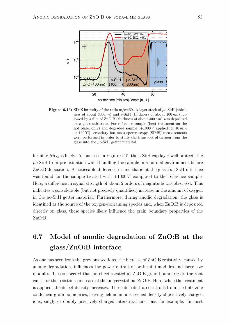
Anodic degradation of ZnO:B on soda-lime glass 93
+
20 40 60
104
105
106
a.U.
sputter time [minutes] / depth [a. U.]
m/e=60, SiO2, Ref m/e=60, SiO2, +1kV
glassµc-Si:H(300nm)
a-Si:H(100nm)ZnO (400nm)
Figure 6.15: SIMS intensity of the ratio m/e=60. A layer stack of µc-Si:H (thick-ness of about 300nm) and a-Si:H (thickness of about 100nm) fol-lowed by a film of ZnO:B (thickness of about 400nm) was depositedon a glass substrate. For reference sample (heat treatment on thehot plate, only) and degraded sample (+1000V applied for 10minat 160 ) secondary ion mass spectroscopy (SIMS) measurementswere performed in order to study the transport of oxygen from theglass into the µc-Si:H getter material.
forming SiOx is likely. As one sees in Figure 6.15, the a-Si:H cap layer well protects the
µc-Si:H from pre-oxidation while handling the sample in a normal environment before
ZnO:B deposition. A noticeable difference in line shape at the glass/µc-Si:H interface
was found for the sample treated with +1000V compared to the reference sample.
Here, a difference in signal strength of about 2 orders of magnitude was observed. This
indicates a considerable (but not precisely quantified) increase in the amount of oxygen
in the µc-Si:H getter material. Furthermore, during anodic degradation, the glass is
identified as the source of the oxygen-containing species and, when ZnO:B is deposited
directly on glass, these species likely influence the grain boundary properties of the
ZnO:B.
6.7 Model of anodic degradation of ZnO:B at the
glass/ZnO:B interface
As one has seen from the previous sections, the increase of ZnO:B resistivity, caused by
anodic degradation, influences the power output of both mini modules and large size
modules. It is suspected that an effect located at ZnO:B grain boundaries is the root
cause for the resistance increase of the polycrystalline ZnO:B. Here, when the treatment
is applied, the defect density increases. These defects trap electrons from the bulk zinc
oxide near grain boundaries, leaving behind an unscreened density of positively charged
ions, singly or doubly positively charged interstitial zinc ions, for example. In most
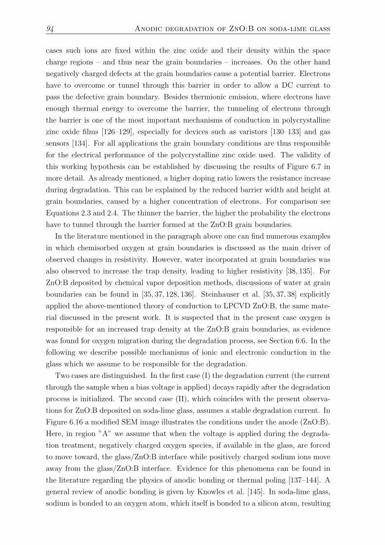
94 Anodic degradation of ZnO:B on soda-lime glass
cases such ions are fixed within the zinc oxide and their density within the space
charge regions – and thus near the grain boundaries – increases. On the other hand
negatively charged defects at the grain boundaries cause a potential barrier. Electrons
have to overcome or tunnel through this barrier in order to allow a DC current to
pass the defective grain boundary. Besides thermionic emission, where electrons have
enough thermal energy to overcome the barrier, the tunneling of electrons through
the barrier is one of the most important mechanisms of conduction in polycrystalline
zinc oxide films [126–129], especially for devices such as varistors [130–133] and gas
sensors [134]. For all applications the grain boundary conditions are thus responsible
for the electrical performance of the polycrystalline zinc oxide used. The validity of
this working hypothesis can be established by discussing the results of Figure 6.7 in
more detail. As already mentioned, a higher doping ratio lowers the resistance increase
during degradation. This can be explained by the reduced barrier width and height at
grain boundaries, caused by a higher concentration of electrons. For comparison see
Equations 2.3 and 2.4. The thinner the barrier, the higher the probability the electrons
have to tunnel through the barrier formed at the ZnO:B grain boundaries.
In the literature mentioned in the paragraph above one can find numerous examples
in which chemisorbed oxygen at grain boundaries is discussed as the main driver of
observed changes in resistivity. However, water incorporated at grain boundaries was
also observed to increase the trap density, leading to higher resistivity [38, 135]. For
ZnO:B deposited by chemical vapor deposition methods, discussions of water at grain
boundaries can be found in [35, 37, 128, 136]. Steinhauser et al. [35, 37, 38] explicitly
applied the above-mentioned theory of conduction to LPCVD ZnO:B, the same mate-
rial discussed in the present work. It is suspected that in the present case oxygen is
responsible for an increased trap density at the ZnO:B grain boundaries, as evidence
was found for oxygen migration during the degradation process, see Section 6.6. In the
following we describe possible mechanisms of ionic and electronic conduction in the
glass which we assume to be responsible for the degradation.
Two cases are distinguished. In the first case (I) the degradation current (the current
through the sample when a bias voltage is applied) decays rapidly after the degradation
process is initialized. The second case (II), which coincides with the present observa-
tions for ZnO:B deposited on soda-lime glass, assumes a stable degradation current. In
Figure 6.16 a modified SEM image illustrates the conditions under the anode (ZnO:B).
Here, in region ”A” we assume that when the voltage is applied during the degrada-
tion treatment, negatively charged oxygen species, if available in the glass, are forced
to move toward, the glass/ZnO:B interface while positively charged sodium ions move
away from the glass/ZnO:B interface. Evidence for this phenomena can be found in
the literature regarding the physics of anodic bonding or thermal poling [137–144]. A
general review of anodic bonding is given by Knowles et al. [145]. In soda-lime glass,
sodium is bonded to an oxygen atom, which itself is bonded to a silicon atom, resulting
Anodic degradation of ZnO:B on soda-lime glass 95
in a Si-O-Na group. This oxygen, which is bonded only to one silicon atom within the
glass matrix, is termed non-bridged oxygen (NBO). The sodium is weakly bonded to
the Si-O group, so that sodium can easily be displaced by an electric field, leaving
behind negatively charged oxygen that is still bonded to silicon. The sodium, which is
forced by the electric field, moves towards the cathode.
V[V]+
-
elec
tric
Fiel
d E
…
1µm
+
+
+
-
-
-
-
+
ZnO:B
Na+ + e- Na
2HO- + Zni+ ZnO+H2O
-
+-
Na+, H+
O-, OH-e-
- - - - - -+ + + + +
+
Zni+, Zni
2++
H2O O2(g) + 4H+
2H2O OH- + H3O+
----
A
B
C
4OH- O2(g) + H2O + 4e-H3O+ H+ + H2O
Figure 6.16: A SEM cross section illustrates the conditions under the anode(ZnO:B). Positively charged sodium ions are forced to move to-wards the cathode, whereas negatively charged oxygen species movetowards the anode. Region A marks the ion-depleted glass layer.Region B and C mark the ZnO:B film, where cracks and delamina-tion in the form of bubbles and circular spallings can be observed.Furthermore a lowering of electron concentration and a massive dropin mobility was found. Region B marks the ZnO:B layer next to theglass/ZnO:B interface where presumably an accumulation of zinctakes place. The red lines indicate grain boundaries.
As a result, a sub-anodic sodium-depleted negatively charged glass layer, full of
NBOs and with changed physical properties (refractive index, material density), evolves
(region ”A”) [138]. If no charge-transfer compensation mechanism is active (a current
of electrons or negatively charged ions in the reverse direction of the positively charged
sodium ions), the degradation current would decay and the depletion layer would fully
develop, causing the external voltage to drop completely over the established depletion
layer. Such a situation corresponds to case I. The thickness of the depletion layer
can be assumed to be on the order of one micrometer and depends on treatment
parameters such as temperature, duration, applied voltage and the glass composition.
For a depletion layer thickness of 1µm and a voltage drop of 1000V , a 107 V/cm electric
field is established. Again, while the voltage is applied in case II, anionic conduction is
of importance. In the literature it is hypothesized that, due to such high electric field,
NBOs are activated and contribute to anionic conduction [139,144]. Other publications
dismiss this contribution [117,145]. Krieger et al. [117] state that it is more likely that
electronic conduction occurs. In their explanation, none of the negatively charged
96 Anodic degradation of ZnO:B on soda-lime glass
NBOs migrate, but electrons jump from NBO to NBO, forced by the high electric
field to move towards the anode. However, such an electronic conduction mechanism
alone is in contradiction to the observed evolution of oxygen at the anode, since the
migration of an oxygen species towards the anode is missing.
Knowles et al. [145] argued that anionic conduction in the sodium-depleted layer
under the anode is linked to the presence of a sub-surface glass layer containing wa-
ter. Here, water is available in the form of protons (H+), hydroxide ions (OH−) and
molecular H2O [146–149]. Due to the electric field and electrolysis of water, negatively
charged hydroxide ions move towards the anode and might be responsible for the ob-
served oxygen evolution. Possible chemical reactions are indicated in Figure 6.16. This
argument is also in agreement with the results and conclusions of Krieger et al. who
reject the motion of NBOs [117]. Following their argument it is important to note that
proton injection into the glass is important to keep up the current of ions through the
sodium-depleted glass layer under the anode [149]. In the case of proton injection, the
protons follow the sodium ions jumping from NBO to NBO. The hydroxide ions (OH−)
move towards the anode and presumably become oxidized to release gaseous oxygen.
To validate this argument, the degradation treatment to a LPCVD ZnO:B layer
deposited on borosilicate glass was also applied. Here, no considerable increase of the
ZnO:B resistance was observed. Furthermore, it was found that, whereas an almost
constant current was observed during the degradation treatment using soda-lime glass
as the substrate (case II), a rapid decrease of the degradation current was observed
using borosilicate glass (case I). The borosilicate glass seems to block ionic as well as
electronic conduction. It prevents the migration of oxygen species towards the anode
and in turn the degradation of the deposited ZnO:B. The borosilicate glass possesses
only a small amount of sodium, and thus fewer NBOs. Furthermore, the boron-oxygen
group in borosilicate glass is known to reduce the number of NBOs further, as alkali
ions stabilize boron in a tetrahedral configuration without NBOs [114]. This highlights
the importance of the presence of NBOs for ionic conduction in silicate glasses, but
of course is not proof of NBO motion. Due to the absence of jump-sites (NBOs) for
sodium and protons, the degradation current at the beginning of the treatment rapidly
decreases. The electrolysis of water, which is mainly driven by the current, stops. This
in turn stops the evolution of oxygen at the anode and so does not produce a drastic
increase of the ZnO:B resistance.
For soda-lime glass, it is assumed that while the degradation treatment continues
the oxygen pressure at the glass/ZnO:B interface increases. Channelling of oxygen
along grain boundaries could explain the strong resistance increase observed for the
ZnO:B samples, since chemisorption of oxygen is likely (see region ”B” and ”C” red
lines in Figure 6.16). Here, the chemisorbed oxygen results in a higher potential barrier
and leads in turn to a drop of electron mobility. The increasing oxygen pressure could
also explain the occurrence of bubbles at the beginning of the treatment, which turn
Anodic degradation of ZnO:B on soda-lime glass 97
into circular spallings as shown in Figure 6.8. Carlson et al. [137, 138] reported the
presence of bubbles for anodic bonding of metal foils.
Due to the external electrode potential, negatively charged species from the glass
will accumulate (instead of becoming neutralized) at the glass/ZnO:B interface. As
indicated in region ”B” of Figure 6.16, this might attract positively charged zinc inter-
stitials. These are forced to move toward the interface and may partially create ZnO
together with the available oxygen species. Furthermore, an excess of zinc here could
also explain the generation of oxygen vacancies, which would cause the yellow appear-
ance and the red shift of optical absorption edge. Presumably, a zinc-rich ZnO:B layer
is created only in the vicinity of the glass/ZnO interface. Investigations by means of
energy dispersive x-ray analysis (EDX) on the samples presented in Figure 6.13 have
revealed no changes. Presumably the changes induced are below the detection limits
of the measurement. Nevertheless, evidence for the presence of an interface layer next
to the glass/ZnO:B interface and an increased amount of oxygen vacancies somewhere
in the ZnO:B material was found.
6.8 Improvements
In order to reduce the sensitivity of LPCVD-ZnO:B to the effect described above,
we have seen that increasing the level of doping is one way to achieve that goal. The
disadvantages of increasing the doping level are losses in optical transmission and losses
in haze. The haze value is determined by the ratio of diffuse and total transmission.
Sufficient haze, which is correlated to the light scattering properties of the ZnO:B front
contact, is of great importance and responsible for efficient light trapping within the
absorber layers of the micromorph tandem solar cell. Together with Oerlikon Solar
great efforts have been made to develop other approaches in order to retain optical and
electrical ZnO:B properties.
Furthermore, Bosch Solar Thin Film has independently developed a SiOx barrier
layer made by PECVD (patent pending) to further reinforce the LPCVD-ZnO. The dif-
ferent approaches investigated in the regard of their degradation behavior are presented
in Figure 6.17. Beside the standard TCO (Std-TCO), which is homogeneously doped,
the ATCO approach, developed in in the framework of the project PEPPER [1], the
Lasagne-TCO and the Lasagne-TCO enhanced by an underlying SiOx barrier layer is
shown. The Lasagne-TCO is derived from the ATCO, which combines a highly doped
seed layer with a lower doped bulk layer in a multilayer approach. Typical electrical
and optical parameters are compared in Figure 6.18.
One can see for the differently doped Std-TCOs in Figure 6.18 the reduction of
optical parameters by increasing the doping only. The haze parameter, for example, is
reduced from 30 % down to 10 %. Only 10 % in haze is not enough to provide sufficient
light trapping. While ATCO provides good electrical and optical properties compared
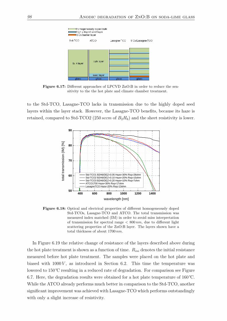
98 Anodic degradation of ZnO:B on soda-lime glass
Figure 6.17: Different approaches of LPCVD ZnO:B in order to reduce the sen-sitivity to the the hot plate and climate chamber treatment.
to the Std-TCO, Lasagne-TCO lacks in transmission due to the highly doped seed
layers within the layer stack. However, the Lasagne-TCO benefits, because its haze is
retained, compared to Std-TCO2 (250 sccm of B2H6) and the sheet resistivity is lower.
4 0 0 6 0 0 8 0 0 1 0 0 0 1 2 0 0 1 4 0 05 0
6 0
7 0
8 0
9 0
total
trans
missi
on (IM
) [%]
w a v e l e n g t h [ n m ]
S t d - T C O 1 B 2 H 6 / D E Z = 0 . 0 5 H a z e = 3 0 % R s q = 2 8 o h m S t d - T C O 2 B 2 H 6 / D E Z = 0 . 1 0 H a z e = 2 0 % R s q = 1 5 o h m S t d - T C O 3 B 2 H 6 / D E Z = 0 . 2 0 H a z e = 1 0 % R s q = 7 o h m A T C O 1 7 0 0 H a z e = 3 0 % R s q = 1 7 o h m L a s a g n e T C O H a z e = 2 0 % R s q = 1 3 o h m
Figure 6.18: Optical and electrical properties of different homogeneously dopedStd-TCOs, Lasagne-TCO and ATCO. The total transmission wasmeasured index matched (IM) in order to avoid miss interpretationof transmission for spectral range < 800nm, due to different lightscattering properties of the ZnO:B layer. The layers shown have atotal thickness of about 1700nm.
In Figure 6.19 the relative change of resistance of the layers described above during
the hot plate treatment is shown as a function of time. Rini denotes the initial resistance
measured before hot plate treatment. The samples were placed on the hot plate and
biased with 1000V , as introduced in Section 6.2. This time the temperature was
lowered to 150 resulting in a reduced rate of degradation. For comparison see Figure
6.7. Here, the degradation results were obtained for a hot plate temperature of 160 .
While the ATCO already performs much better in comparison to the Std-TCO, another
significant improvement was achieved with Lasagne-TCO which performs outstandingly
with only a slight increase of resistivity.
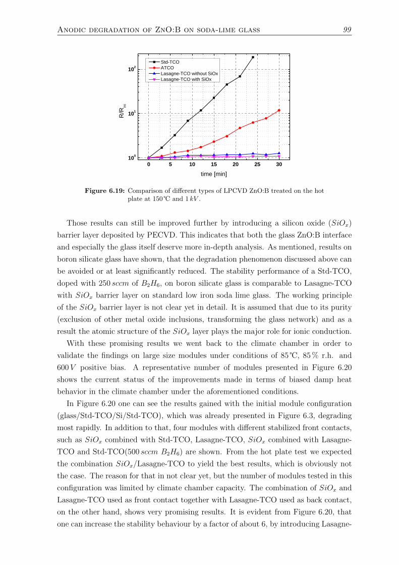
Anodic degradation of ZnO:B on soda-lime glass 99
0 5 1 0 1 5 2 0 2 5 3 01 0 0
1 0 1
1 0 2
R/Rini
t i m e [ m i n ]
S t d - T C O A T C O L a s a g n e - T C O w i t h o u t S i O x L a s a g n e - T C O w i t h S i O x
Figure 6.19: Comparison of different types of LPCVD ZnO:B treated on the hotplate at 150 and 1 kV .
Those results can still be improved further by introducing a silicon oxide (SiOx)
barrier layer deposited by PECVD. This indicates that both the glass ZnO:B interface
and especially the glass itself deserve more in-depth analysis. As mentioned, results on
boron silicate glass have shown, that the degradation phenomenon discussed above can
be avoided or at least significantly reduced. The stability performance of a Std-TCO,
doped with 250 sccm of B2H6, on boron silicate glass is comparable to Lasagne-TCO
with SiOx barrier layer on standard low iron soda lime glass. The working principle
of the SiOx barrier layer is not clear yet in detail. It is assumed that due to its purity
(exclusion of other metal oxide inclusions, transforming the glass network) and as a
result the atomic structure of the SiOx layer plays the major role for ionic conduction.
With these promising results we went back to the climate chamber in order to
validate the findings on large size modules under conditions of 85 , 85 % r.h. and
600V positive bias. A representative number of modules presented in Figure 6.20
shows the current status of the improvements made in terms of biased damp heat
behavior in the climate chamber under the aforementioned conditions.
In Figure 6.20 one can see the results gained with the initial module configuration
(glass/Std-TCO/Si/Std-TCO), which was already presented in Figure 6.3, degrading
most rapidly. In addition to that, four modules with different stabilized front contacts,
such as SiOx combined with Std-TCO, Lasagne-TCO, SiOx combined with Lasagne-
TCO and Std-TCO(500 sccm B2H6) are shown. From the hot plate test we expected
the combination SiOx/Lasagne-TCO to yield the best results, which is obviously not
the case. The reason for that in not clear yet, but the number of modules tested in this
configuration was limited by climate chamber capacity. The combination of SiOx and
Lasagne-TCO used as front contact together with Lasagne-TCO used as back contact,
on the other hand, shows very promising results. It is evident from Figure 6.20, that
one can increase the stability behaviour by a factor of about 6, by introducing Lasagne-
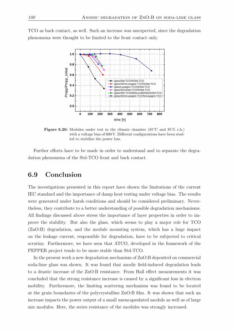
100 Anodic degradation of ZnO:B on soda-lime glass
TCO as back contact, as well. Such an increase was unexpected, since the degradation
phenomena were thought to be limited to the front contact only.
0 1 0 0 2 0 0 3 0 0 4 0 0 5 0 0 6 0 0 7 0 0 8 0 00 . 0
0 . 2
0 . 4
0 . 6
0 . 8
1 . 0
Pmpp
/Pmpp
_initia
l
t i m e [ h ]
g l a s s / S t d - T C O / S i / S t d - T C O g l a s s / S i O x / L a s a g n e - T C O / S i / S t d - T C O g l a s s / L a s a g n e - T C O / S i / S t d - T C O g l a s s / S i O x / S t d - T C O / S i / S t d - T C O g l a s s / S t d - T C O ( 5 0 0 s c c m B 2 H 6 ) / S i / S t d - T C O g l a s s / S i O x / L a s a g n e - T C O / S i / L a s a g n e - T C O
Figure 6.20: Modules under test in the climate chamber (85 and 85 % r.h.)with a voltage bias of 600 V. Different configurations have been stud-ied to stabilize the power loss.
Further efforts have to be made in order to understand and to separate the degra-
dation phenomena of the Std-TCO front and back contact.
6.9 Conclusion
The investigations presented in this report have shown the limitations of the current
IEC standard and the importance of damp heat testing under voltage bias. The results
were generated under harsh conditions and should be considered preliminary. Never-
theless, they contribute to a better understanding of possible degradation mechanisms.
All findings discussed above stress the importance of layer properties in order to im-
prove the stability. But also the glass, which seems to play a major role for TCO
(ZnO:B) degradation, and the module mounting system, which has a huge impact
on the leakage current, responsible for degradation, have to be subjected to critical
scrutiny. Furthermore, we have seen that ATCO, developed in the framework of the
PEPPER project tends to be more stable than Std-TCO.
In the present work a new degradation mechanism of ZnO:B deposited on commercial
soda-lime glass was shown. It was found that anodic field-induced degradation leads
to a drastic increase of the ZnO:B resistance. From Hall effect measurements it was
concluded that the strong resistance increase is caused by a significant loss in electron
mobility. Furthermore, the limiting scattering mechanism was found to be located
at the grain boundaries of the polycrystalline ZnO:B film. It was shown that such an
increase impacts the power output of a small unencapsulated module as well as of large
size modules. Here, the series resistance of the modules was strongly increased.
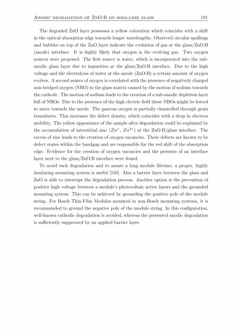
Anodic degradation of ZnO:B on soda-lime glass 101
The degraded ZnO layer possesses a yellow coloration which coincides with a shift
in the optical absorption edge towards longer wavelengths. Observed circular spallings
and bubbles on top of the ZnO layer indicate the evolution of gas at the glass/ZnO:B
(anode) interface. It is highly likely that oxygen is the evolving gas. Two oxygen
sources were proposed. The first source is water, which is incorporated into the sub-
anodic glass layer due to impurities at the glass/ZnO:B interface. Due to the high
voltage and the electrolysis of water at the anode (ZnO:B) a certain amount of oxygen
evolves. A second source of oxygen is correlated with the presence of negatively charged
non-bridged oxygen (NBO) in the glass matrix caused by the motion of sodium towards
the cathode. The motion of sodium leads to the creation of a sub-anodic depletion layer
full of NBOs. Due to the presence of the high electric field these NBOs might be forced
to move towards the anode. The gaseous oxygen is partially channelled through grain
boundaries. This increases the defect density, which coincides with a drop in electron
mobility. The yellow appearance of the sample after degradation could be explained by
the accumulation of interstitial zinc (Zn+, Zn2+) at the ZnO:B/glass interface. The
excess of zinc leads to the creation of oxygen vacancies. These defects are known to be
defect states within the bandgap and are responsible for the red shift of the absorption
edge. Evidence for the creation of oxygen vacancies and the presents of an interface
layer next to the glass/ZnO:B interface were found.
To avoid such degradation and to assure a long module lifetime, a proper, highly
insulating mounting system is useful [150]. Also a barrier layer between the glass and
ZnO is able to interrupt the degradation process. Another option is the prevention of
positive high voltage between a module’s photovoltaic active layers and the grounded
mounting system. This can be achieved by grounding the positive pole of the module
string. For Bosch Thin-Film Modules mounted in non-Bosch mounting systems, it is
recommended to ground the negative pole of the module string. In this configuration,
well-known cathodic degradation is avoided, whereas the presented anodic degradation
is sufficiently suppressed by an applied barrier layer.

102 Anodic degradation of ZnO:B on soda-lime glass
Chapter 7
Summary
The present work discussed advanced LPCVD ZnO and its challenges in application
for thin-film solar cells and modules. Here, advanced LPCVD ZnO refers to ZnO layers
that try to overcome to current limitations of standard boron-doped LPCVD ZnO:B,
typically used as front and back electrodes. These limitations are related to optical
and electrical properties and to the surface morphology influencing the quality and
therefore the efficiency of the subsequently deposited solar cell structure.
In Chapter 4 the suitability of adding ethanol as an additional precursor during
ZnO:B deposition to create a surface morphology that is more favorable for µc-Si:H
growth was evaluated. It was found that ethanol has a strong impact on the electrical
and optical properties of 2-µm-thick ZnO layers. The growth model proposed is based
on the assumption of a surface reaction and that oxygen, delivered by the ethanol, is
incorporated at the ZnO surface at oxygen vacancy sites. Although ethanol-enriched
ZnO single layers might be suitable for good µc-Si:H growth, their high resistivity of
up to 200Ωcm rules out their usage as electrodes for photovoltaic applications. In a
two-step deposition process, a 200-nm-thick ethanol-enriched ZnO cap layer on top
of a 1900-nm-thick as-grown rough ZnO film was deposited. A change in surface
morphology was observed for these bilayers as well. The sheet resistance of bilayer
films was maintained at reasonable values, independent of the thickness of the ethanol-
enriched cap layer. It was found that the used four point probe measurement was not
sensitive to the resistive cap layer. To solve resistivity issues, which might become a
problem for the potential application of bilayers, additional doping of the underlying
and cap layers still has to be studied. Future work will have to be done to investigate
the effects of deposition parameters like pressure and temperature on morphology.
Also, other types of precursors should be considered to induce morphological changes.
Finally, a complete solar cell, incorporating an optimized bilayer as the front electrode,
will have to be tested. Meanwhile work has been carried out by Ding et al. (to be
published) incorporating the above-presented approach into a micromorph solar cell.
Cell efficiencies above 12.2 % were achieved. Despite these results, the introduction of
103
104 Summary
ethanol-enriched bilayers into mass production of thin-film silicon solar modules still
is far away from realization. The process still has to be upscaled to substrate sizes
of 1.1× 1.3m2, and a production tool that enables the deposition of ethanol-enriched
bilayers has to be developed.
Another approach to an advanced LPCVD ZnO:B was followed by Ding et al. [1,2].
For an advanced TCO (ATCO), they combined a highly doped ZnO:B seed layer with
a low-doped ZnO:B bulk layer. Compared to a standard ZnO:B (Std-TCO), which is
homogeneously doped across the total layer thickness, their ATCO possesses enhanced
optical and electrical properties. For the first time, in Chapter 5 the introduction of
this ATCO into the production line at Bosch Solar Thin Film in Erfurt, Germany, on
substrate sizes of 1.1× 1.3m2 was discussed. Therefore, the deposition tool TCO1200
needed to be retrofitted. Comparing the ATCO with the Std-TCO, equal in layer
thickness (1800 nm) and sheet resistance (16 to 17Ω), ATCO possesses slightly better in
transmittance. Furthermore, ATCO showed 37 % haze, which is 3 to 5 % absolute more
haze compared to the Std-TCO. After ATCO optimization, a complete micromorph
solar module was fabricated, incorporating this new advanced LPCVD ZnO:B layer as
the front electrode. An initial module power of 153.7Wp was achieved.
After the introduction of new processes and materials, module manufactures are
usually committed to detailed tests, confirming product quality. One of these tests is
an accelerated damp heat lifetime test according to IEC61646, in which the modules
have to be exposed to 85 and 85 % relative humidity for 1000h. In Chapter 6 the
limitation of the current IEC standard was discussed. Furthermore, the importance of
test conditions with regard to considering a voltage bias, which is not yet included in
the current IEC standard, was shown. Note that the results in the present work were
generated under harsh conditions and should be considered preliminary. Nevertheless,
they contribute a better understanding of possible degradation mechanisms. In the
present work, for the first time, a novel degradation mechanism of ZnO:B on soda-lime
glass was introduced. A degradation model was proposed and solutions for minimizing
the degradation effect were presented. It was found that the resistance of the ZnO:B
front electrode strongly increases, when the ZnO:B electrode is biased with a positive
potential against a grounded module frame or mounting system. As a result the mod-
ule power was found to decrease. The investigations have shown that ZnO:B grain
boundaries are strongly affected by adsorbed or chemisorbed oxygen species coming
from glass. At the ZnO:B grain boundaries the increased number of oxygen species
leads to an increased defect concentration. These defects are known to build a po-
tential barrier, which electrons have to overcome by thermionic emission or quantum
mechanical tunneling. The increased defect concentration leads to an observable drop
in electron mobility and as a result to a major rise of ZnO:B resistivity.
To avoid such degradation and to assure a long module lifetime, a proper, highly
insulating mounting system is useful [150]. The introduction of a SiOx barrier layer

Summary 105
between the glass and the ZnO:B layer (patent pending) prevents front electrode degra-
dation and enhances module lifetime. Another option is the prevention of positive high
voltage between a module’s photovoltaic active layers and the grounded mounting sys-
tem. This can be achieved by grounding the positive pole of the module string. A
further prevention can be achieved by a higher doping level of the ZnO:B layer. Due to
the higher doping level, the increase of the barrier height and width during degradation
at ZnO:B grain boundaries is reduced.

106 Summary
References
[1] Ding, L., M. Boccard, G. Bugnon, M. Benkhaira, M. Despeisse, F. Sculati-Meillaud, S. Nicolay, P.A. Losio, O. Kluth, P. Carroy, et al.: New generationtransparent LPCVD ZnO electrodes for enhanced photocurrent in micromorphsolar cells and modules. IEEE Journal of Photovoltaics, 2(2):88–93, 2012.
[2] Ding, L., M. Boccard, G. Bugnon, M. Benkhaira, S. Nicolay, M. Despeisse, F.Meillaud, and C. Ballif: Highly transparent ZnO bilayers by LP-MOCVD as frontelectrodes for thin-film micromorph silicon solar cells. Solar Energy Materialsand Solar Cells, 98:331–336, 2012.
[3] British Petroleum (BP): 60 years BP statistical reviewof world energy, 2011. http://www.bp.com/en/global/corporate/about-bp/statistical-review-of-world-energy-2013/statistical-review-1951-2011.html, visited on 2013-08-29.
[4] British Petroleum (BP): BP statistical review of world en-ergy june 2013, 2013. http://www.bp.com/en/global/corporate/about-bp/statistical-review-of-world-energy-2013/statistical-review-downloads.html, visited on 2013-08-29.
[5] Roedel, W.: Physik unserer Umwelt: Die Atmosphare. Springer, 2000.
[6] TEL Solar AG (formerly Oerlikon Solar AG), Ecole Polytechnique Federalede Lausanne, University of Northumbria at Newcastle, Bosch Solar Thin FilmGmbH, Linde AG, Heliosphera, and University of Patras: Demonstration of highperformance processes and equipmments for thin film silicon photovoltaic mod-ules produced with lower enviromental impact and reduced cost and material use.http://cordis.europa.eu/projects/rcn/100464_en.html, visited on 2013-08-29.
[7] Messerschmidt, D., S. Nicolay, L. Ding, G. Bugnon, F. Meillaud, J. Eberhardt,and C. Ballif: Ethanol-enriched low-pressure chemical vapor deposition ZnO bilay-ers: Properties and growth - a potential electrode for thin film solar cells. Journalof Applied Physics, 113(2):024908–024908, 2013.
[8] Messerschmidt, D., A. Hochmuth, E. Radlein, H. Romanus, W.M. Gnehr, J.Eberhardt, and C. Ballif: Anodic degradation of zno on soda-lime glass. SolarEnergy Materials and Solar Cells, 117:569–576, 2013.
[9] Messerschmidt, D., K. Bratz, W.M. Gnehr, H. Romanus, J. Eberhardt, S. Nico-lay, and C. Ballif: Optical properties of anodically degraded zno. Journal of Ap-plied Physics, 115(9):094902, 2014.
[10] Shah, A.V., H. Schade, M. Vanecek, J. Meier, E. Vallat-Sauvain, N. Wyrsch, U.Kroll, C. Droz, and J. Bailat: Thin-film silicon solar cell technology. Progress inPhotovoltaics: Research and Applications, 12(2-3):113–142, 2004.
[11] Ellmer, K., A. Klein, and B. Rech: Transparent conductive zinc oxide, volume104. Springer, 2008.
107
108 REFERENCES
[12] Herold, R.J., S.L. Aggarwal, and V. Neff: Mechanisms of the reactions of diethyl-zinc with isopropanol and water. Canadian Journal of Chemistry, 41(5):1368–1380, 1963.
[13] Smith, S.M. and H.B. Schlegel: Molecular orbital studies of zinc oxide chemicalvapor deposition: gas-phase hydrolysis of diethyl zinc, elimination reactions, andformation of dimers and tetramers. Chemistry of Materials, 15(1):162–166, 2003.
[14] Kim, Y.S., Y.S. Won, H. Hagelin-Weaver, N. Omenetto, and T. Anderson:Homogeneous decomposition mechanisms of diethylzinc by raman spectroscopyand quantum chemical calculations. The Journal of Physical Chemistry A,112(18):4246–4253, 2008.
[15] Fay, S.: L’oxyde de zinc par depot chimique en phase vapeur comme contactelectrique transparent et diffuseur de lumiere pour les cellules solaires. Phd.thesis, University of Neuchatel, 2003.
[16] Nicolay, S., S. Fay, and C. Ballif: Growth model of MOCVD polycrystalline ZnO.Crystal Growth & Design, 9(11):4957–4962, 2009.
[17] Kashiwaba, Y., F. Katahira, K. Haga, T. Sekiguchi, and H. Watanabe: Hetero-epitaxial growth of ZnO thin films by atmospheric pressure CVD method. Journalof Crystal Growth, 221(1):431–434, 2000.
[18] Oda, S., H. Tokunaga, N. Kitajima, J. Hanna, I. Shimizu, and H. Kokado: Highlyoriented ZnO films prepared by MOCVD from diethylzinc and alcohols. JapaneseJournal of Applied Physics, 24(12):1607–1610, 1985.
[19] Hu, J. and R.G. Gordon: Textured fluorine-doped ZnO films by atmospheric pres-sure chemical vapor deposition and their use in amorphous silicon solar cells.Solar Cells, 30(1):437–450, 1991.
[20] Gruber, Th., C. Kirchner, and A. Waag: MOCVD growth of ZnO on differentsubstrate materials. physica status solidi (b), 229(2):841–844, 2002.
[21] Oleynik, N., A. Dadgar, J. Christen, J. Blasing andM. Adam, T. Riemann, A.Diez, A. Greiling, and M. Seip andA. Krost: Growth of ZnO layers by metalorganic chemical vapor phase epitaxy. physica status solidi (a), 192(1):189–194,2002.
[22] Kaufmann, Th., E. Fuchs, and M. Webert: Metalorganic chemical vapour depo-sition of oriented ZnO films. Crystal Research and Technology, 23(5):635–639,1988.
[23] Hahn, B., G. Heindel, E. Pschorr-Schoberer, and W. Gebhardt: MOCVD layergrowth of ZnO using DMZn and tertiary butanol. Semiconductor Science andTechnology, 13(7):788, 1998.
[24] Sallet, V., J.F. Rommeluere, A. Lusson, A. Riviere, S. Fusil, O. Gorochov, andR. Triboulet: MOCVD growth of ZnO on sapphire using tert-butanol. physicastatus solidi (b), 229(2):903–906, 2002.
[25] Ogata, K., T. Kawanishi, K. Maejima, K. Sakurai, Sz. Fujita, and Sg. Fujita:ZnO growth using homoepitaxial technique on sapphire and Si substrates by met-alorganic vapor phase epitaxy. Journal of Crystal Growth, 237:553–557, 2002.
[26] Dadgar, A., N. Oleynik, D. Forster, S. Deiter, H. Witek, J. Blasing, F. Bertram,A. Krtschil, A. Diez, J. Christen, et al.: A two-step metal organic vapor phaseepitaxy growth method for high-quality ZnO on GaN/Al2O3 (0001). Journal ofCrystal Growth, 267(1):140–144, 2004.
REFERENCES 109
[27] Fay, S., U. Kroll, C. Bucher, and E. Vallat Sauvain andA. Shah: Lowpressure chemical vapour deposition of ZnO layers for thin-film solar cells:temperature-induced morphological changes. Solar Energy Materials and SolarCells, 86(3):385–397, 2005.
[28] Fay, S., L. Feitknecht, R. Schluchter, U. Kroll, E. Vallat-Sauvain, and A. Shah:Rough ZnO layers by LP-CVD process and their effect in improving performancesof amorphous and microcrystalline silicon solar cells. Solar Energy Materials andSolar Cells, 90(18):2960–2967, 2006.
[29] Fay, S., J. Steinhauser, N. Oliveira, E. Vallat-Sauvain, and C. Ballif: Opto-electronic properties of rough LP-CVD ZnO:B for use as TCO in thin-film siliconsolar cells. Thin Solid Films, 515(24):8558–8561, 2007.
[30] Fay, S., J. Steinhauser, S. Nicolay, and C. Ballif: Polycrystalline ZnO:B grown byLPCVD as TCO for thin film silicon solar cells. Thin Solid Films, 518(11):2961–2966, 2010.
[31] Ozgur, U., Y.I. Alivov, C. Liu, A. Teke, MA Reshchikov, S. Dogan, V. Avrutin,S.J. Cho, and H. Morkoc: A comprehensive review of ZnO materials and devices.Journal of Applied Physics, 98(4):041301, 2005.
[32] McCluskey, M.D. and S.J. Jokela: Defects in ZnO. Journal of Applied Physics,106(7):071101–071101, 2009.
[33] Janotti, A. and C.G. Van de Walle: Hydrogen multicentre bonds. Nature Materi-als, 6(1):44–47, 2006.
[34] Seto, John Y.W: The electrical properties of polycrystalline silicon films. Journalof Applied Physics, 46(12):5247–5254, 1975.
[35] Steinhauser, J.: Low pressure chemical vapor deposited zinc oxide for siliconthin film solar cells optical and electrical properties. Phd. thesis, University ofNeuchatel, 2008.
[36] Steinhauser, J., S. Fay, N. Oliveira, E. Vallat-Sauvain, D. Zimin, U. Kroll, andC. Ballif: Electrical transport in boron-doped polycrystalline zinc oxide thin films.physica status solidi (a), 205(8):1983–1987, 2008.
[37] Steinhauser, J., S. Fay, N. Oliveira, E. Vallat-Sauvain, and C. Ballif: Transitionbetween grain boundary and intragrain scattering transport mechanisms in boron-doped zinc oxide thin films. Applied Physics Letters, 90(14):142107–142107, 2007.
[38] Steinhauser, J., S. Meyer, M. Schwab, S. Fay, C. Ballif, U. Kroll, and D. Borrello:Humid environment stability of low pressure chemical vapor deposited boron dopedzinc oxide used as transparent electrodes in thin film silicon solar cells. Thin SolidFilms, 520(1):558–562, 2011.
[39] Burstein, E.: Anomalous optical absorption limit in InSb. Physical Review,93(3):632, 1954.
[40] Wang, J., Z. Wang, B. Huang, Y. Ma, Y. Lui, X. Qin, X. Zhang, and Y. Dai: Oxy-gen vacancy induced band-gap narrowing and enhanced visible light photocatalyticactivity of ZnO. Applied Materials and Interfaces, 4:4024–4030, 2012.
[41] Srikant, V. and D.R. Clarke: Optical absorption edge of ZnO thin films: Theeffect of substrate. Journal of Applied Physics, 81(9):6357–6364, 1997.
[42] Fox, A.M.: Optical properties of solids, volume 3. Oxford university press, 2001.
110 REFERENCES
[43] Kim, I., K.S. Lee, T.S. Lee, J. Jeong, B. Cheong, Y.J. Baik, and W.M. Kim:Effect of fluorine addition on transparent and conducting Al doped ZnO films.Journal of Applied Physics, 100(6):063701–063701, 2006.
[44] Wolden, C.A., T.M. Barnes, J.B. Baxter, and E.S. Aydil: Infrared detection ofhydrogen-generated free carriers in polycrystalline ZnO thin films. Journal ofApplied Physics, 97(4):043522–043522, 2005.
[45] Ruske, F., A. Pflug, V. Sittinger, B. Szyszka, D. Greiner, and B. Rech: Opticalmodeling of free electron behavior in highly doped ZnO films. Thin Solid Films,518(4):1289–1293, 2009.
[46] Prunici, P., F.U. Hamelmann, W. Beyer, H. Kurz, and H. Stiebig: Modelling ofinfrared optical constants for polycrystalline low pressure chemical vapour depo-sition ZnO:B films. Journal of Applied Physics, 113(12):123104–123104, 2013.
[47] Born, M. and E. Wolf: Principles of optics: electromagnetic theory of propagation,interference and diffraction of light. CUP Archive, 1999.
[48] Hecht, E. and A. Zajac: Optics. Addison Wesley, New York, 2002.
[49] Aspnes, D.E.: Optical properties of thin films. Thin Solid Films, 89:249–262,1982.
[50] Maxwell-Garnett, J.C.: Colours in metal glasses and in metal films. Philos. Trans.R. Soc. London, 203:385–420, 1904.
[51] Donker, M.N.: Plasma Deposition of Microcrystalline Silicon Solar Cells: LookingBeyond the Glass. Phd. thesis, Forschungszentrum Julich, 2006.
[52] Lejeune, M., W. Beyer, R. Carius, J. Muller, and B. Rech: Silicontetrachloridebased microcrystalline silicon for application in thin film silicon solar cells. ThinSolid Films, 451-452:280, 2004.
[53] Platz, R. and S. Wagner: Intrinsic microcrystalline silicon by plasma-enhancedchemical vapor deposition from dichlorsilanne. Applied Physics Letters, 73:1236,1998.
[54] Cicala, G., P. Capezzuto, and G. Bruno: From amorphous to microcrystallinesilicon deposition in SiF4 − H2-He plasmas: in situ control by optical emissionspectroscopy. Thin Solid Films, 383:203, 2001.
[55] Rech, B.: Solarzellen aus amorphem Silizium mit hohem stabilem Wirkungsgrad.Phd. thesis, RWTH Achen, 1997.
[56] Meier, J., S. Dubail, R. Fluckiger, D. Fischer, H. Keppner, and A. Shah: In-trinsic microcrystalline silicon (µc-Si: H)-a promising new thin film solar cellmaterial. In Photovoltaic Energy Conversion, 1994., Conference Record of theTwenty Fourth. IEEE, volume 1, pages 409–412. IEEE, 1994.
[57] Meier, J., U. Kroll, S. Dubail, S. Golay, S. Fay, J. Dubail, and A. Shah: Efficiencyenhancement of amorphous silicon pin solar cells by LP-CVD ZnO. In Photo-voltaic Specialists Conference, 2000. Conference Record of the Twenty-EighthIEEE, pages 746–749. IEEE, 2000.
[58] Chittick, R., J. Alexande, and H. Sterling: The preparation and properties ofamorphous silicon. Journal of the Electrochemical Society, 116:77, 1969.
[59] Spear, W. and P. LeComber: Electronic properties of substitutionnally dopedamorphous Si and Ge. Philisophical Magazine, 33:935, 1976.
[60] Wagemann, Hans G. and H. Eschrich: Photovoltaik – Solarstrahlung und Hal-bleitereigenschaften. B. G. Teubner, 2007.
REFERENCES 111
[61] Senoussaoui, N.: Einfluss der Oberflachenstrukturierung auf die optischen Eigen-schaften der Dunnschichtsolarzellen auf Basis von a-Si:H und µc-Si:H. Phd.thesis, Heinrich-Heine-Universitat Dusseldorf, 2003.
[62] Vetterl, O.: On the Physics of Microcrystalline Silicon Thin Film Solar Cells;From the Material to Devices with High Conversion Efficiencies. Phd. thesis,Forschungszentrum Julich, 2001.
[63] Shah, A.V., J. Meier, E. Vallat-Sauvain, N. Wyrsch, U. Kroll, C. Dorz, and U.Graf: Material and solar cell research in microcrystalline silicon. Solar EnergyMaterials and Solar Cells, 78:469, 2003.
[64] Houben, L.: Plasmaabscheidung von mikrokristallinem Silizium: Merkmal derMikrostruktur und deren Deutung im Sinne von Wachstumsvorgangen. Phd. the-sis, Heinrich-Heine-Universitat Dusseldorf, 1998.
[65] Shah, A., C. Ballif, W. Beyer, J.E. Bouree, C. Dorz, F. Finger, M. Python, J.Randall, and H. Schade andN. Wyrsch: Thin-film silicon solar cells. EPFL Press,2010.
[66] Wurfel, P.: Physik der Solarzellen. Spektrum, Akad. Verlag, 2000.
[67] Green, M.A., K. Emery, Y. Hishikawa, W. Warta, and E.D. Dunlop: Solar cellefficiency tables (version 41). Progress in Photovoltaics: Research and Applica-tions, 21(1):1–11, 2013.
[68] Holovsky, J., M. Bonnet-Eymard, M. Boccard, M. Despeisse, and C. Ballif: Vari-able light biasing method to measure component I–V characteristics of multi-junction solar cells. Solar Energy Materials and Solar Cells, 103:128–133, 2012.
[69] Sze, S.M. and K.K. Ng: Physics of semiconductor devices. Wiley, 2006.
[70] Goetzberger, A., B. Voß, and J. Knobloch: Sonnenenergie: Photovoltaik: Physikund Technologie der Solarzellebildungen. Teubner, 1997.
[71] Bamford, C.R.: Optical properties of flat glass. Journal of Non-Crystalline Solids,47:1–20, 1982.
[72] Rubin, M.: Optical properties of soda lime silica glasses. Solar Energy Materials,12(4):275–288, 1985.
[73] Wartewig, S.: IR and Raman Spectroscopy. John Wiley & Sons, 2006.
[74] Bennett, J.M. and E.J. Ashley: Infrared reflectance and emittance of silver andgold evaporated in ultrahigh vacuum. Applied Optics, 4:221–224, 1965.
[75] Long, D.A.: The Raman effect: A unified treatment of the theory of Ramanscattering by molecules. West Sussex, England: John Wiley & Sons Ltd, 2002.
[76] Schroder, D.K.: Semiconductor material and device characterization. John Wiley& Sons, 2006.
[77] Magonov, S.N. and M.H. Whangbo: Surface analysis with STM and AFM: ex-perimental and theoretical aspects of image analysis. Wiley, 2008.
[78] Binnig, G., C.F. Quate, and Ch. Gerber: Atomic force microscope. PhysicalReview Letters, 56:930, 1986.
[79] Spiess, L., G. Teichert, R. Schwarzer, H. Behnken, and C. Genzel: Moderne ront-genbeugung: rontgendiffraktometrie fur materialwissenschaftler, physiker undchemiker. Springer, 2009.
[80] Luth, H.: Solid surfaces, interfaces and thin films, volume 3. Springer, 2001.
112 REFERENCES
[81] Czanderna, A.W.: Methods of surface analysis. North Holland, 1984.
[82] M. Grasserbauer, H. Dudek, M.F. Ebel: Angewandte Oberflachenanalyse mitSIMS, AES, XPS. Springer–Verlag, 1986.
[83] Wacom Electric Co., LTD.: Super solar simulator (2 lamps type)–specifications.www.wacom-ele.co.jp/Solar/ENGsolar2.htm, visited on 2013-08-29.
[84] Kluth, O., A. Loffl, S. Wieder, C. Beneking, W. Appenzeller, L. Houben, B. Rech,H. Wagner, S. Hoffmann andR.Waser, et al.: Texture etched Al-doped ZnO: a newmaterial for enhanced light trapping in thin film solar cells. In Photovoltaic Spe-cialists Conference, 1997., Conference Record of the Twenty-Sixth IEEE, pages715–718. IEEE, 1997.
[85] Staebler, D.L. and C.R. Wronski: Reversible conductivity changes in discharge-produced amorphous Si. Applied Physics Letters, 31(4):292–294, 1977.
[86] Python, M., E. Vallat-Sauvain, J. Bailat, D. Domine, L. Fesquet, A. Shah, and C.Ballif: Relation between substrate surface morphology and microcrystalline siliconsolar cell performance. Journal of Non-Crystalline Solids, 354(19):2258–2262,2008.
[87] Johnson, E.V., M. Nath, P. Roca i Cabarrocas, A. Abramov, and P Chatterjee:Why does the open-circuit voltage in a micro-crystalline silicon pin solar celldecrease with increasing crystalline volume fraction? Journal of Non-CrystallineSolids, 354(19):2455–2459, 2008.
[88] Python, M.: Microcrystalline Silicon Solar Cells: Growth and Defects. Phd.thesis, University of Neuchatel, 2009.
[89] Despeisse, M., C. Battaglia, M. Boccard, G. Bugnon, M. Charriere, P. Cuony,S. Hanni, L. Lofgren, F. Meillaud, G. Parascandolo, et al.: Optimization of thinfilm silicon solar cells on highly textured substrates. physica status solidi (a),208(8):1863–1868, 2011.
[90] Bailat, J., D. Domine, R. Schluchter, J. Steinhauser, S. Fay, F. Freitas, C. Bucher,L. Feitknecht, X. Niquille, T. Tscharner, et al.: High-efficiency pin microcrys-talline and micromorph thin film silicon solar cells deposited on LPCVD ZnOcoated glass substrates. In Photovoltaic Energy Conversion, Conference Recordof the 2006 IEEE 4th World Conference on, volume 2, pages 1533–1536. IEEE,2006.
[91] Hupkes, J., B. Rech, O. Kluth, T. Repmann, B. Zwaygardt, J. Muller, R.Drese, and M. Wuttig: Surface textured MF-sputtered ZnO films for microcrys-talline silicon-based thin-film solar cells. Solar Energy Materials and Solar Cells,90(18):3054–3060, 2006.
[92] Wenas, W.W. and M. Konagai: Control of the surface morphology of ZnO thinfilms for solar cells by novel two-step MOCVD process. In Photovoltaic SpecialistsConference, 2002. Conference Record of the Twenty-Ninth IEEE, pages 1130–1133. IEEE, 2002.
[93] Hongsingthong, A., I. Afdi Yunaz, S. Miyajima, and M. Konagai: Preparationof ZnO thin films using MOCVD technique with D2O/H2O gas mixture for useas TCO in silicon-based thin film solar cells. Solar Energy Materials and SolarCells, 95(1):171–174, 2011.
[94] Kim, Y. and Y. Won: Investigations on reaction pathways for ZnO formationfrom diethylzinc and water during chemical vapor deposition. Bulletin of theKorean Chemical Society, 30(7):1573–1578, 2009.
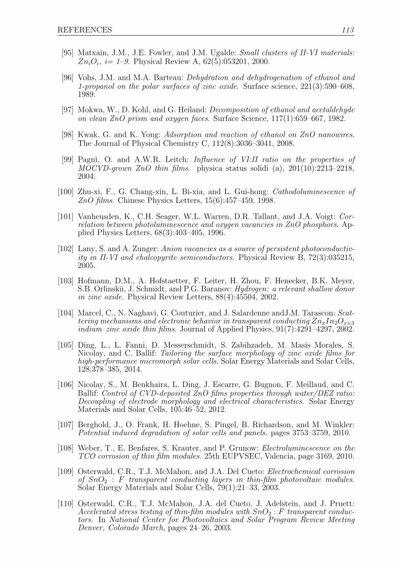
REFERENCES 113
[95] Matxain, J.M., J.E. Fowler, and J.M. Ugalde: Small clusters of II-VI materials:ZniOi, i= 1–9. Physical Review A, 62(5):053201, 2000.
[96] Vohs, J.M. and M.A. Barteau: Dehydration and dehydrogenation of ethanol and1-propanol on the polar surfaces of zinc oxide. Surface science, 221(3):590–608,1989.
[97] Mokwa, W., D. Kohl, and G. Heiland: Decomposition of ethanol and acetaldehydeon clean ZnO prism and oxygen faces. Surface Science, 117(1):659–667, 1982.
[98] Kwak, G. and K. Yong: Adsorption and reaction of ethanol on ZnO nanowires.The Journal of Physical Chemistry C, 112(8):3036–3041, 2008.
[99] Pagni, O. and A.W.R. Leitch: Influence of VI:II ratio on the properties ofMOCVD-grown ZnO thin films. physica status solidi (a), 201(10):2213–2218,2004.
[100] Zhu-xi, F., G. Chang-xin, L. Bi-xia, and L. Gui-hong: Cathodoluminescence ofZnO films. Chinese Physics Letters, 15(6):457–459, 1998.
[101] Vanheusden, K., C.H. Seager, W.L. Warren, D.R. Tallant, and J.A. Voigt: Cor-relation between photoluminescence and oxygen vacancies in ZnO phosphors. Ap-plied Physics Letters, 68(3):403–405, 1996.
[102] Lany, S. and A. Zunger: Anion vacancies as a source of persistent photoconductiv-ity in II-VI and chalcopyrite semiconductors. Physical Review B, 72(3):035215,2005.
[103] Hofmann, D.M., A. Hofstaetter, F. Leiter, H. Zhou, F. Henecker, B.K. Meyer,S.B. Orlinskii, J. Schmidt, and P.G. Baranov: Hydrogen: a relevant shallow donorin zinc oxide. Physical Review Letters, 88(4):45504, 2002.
[104] Marcel, C., N. Naghavi, G. Couturier, and J. Salardenne andJ.M. Tarascon: Scat-tering mechanisms and electronic behavior in transparent conducting ZnxIn2Ox+3
indium–zinc oxide thin films. Journal of Applied Physics, 91(7):4291–4297, 2002.
[105] Ding, L., L. Fanni, D. Messerschmidt, S. Zabihzadeh, M. Masis Morales, S.Nicolay, and C. Ballif: Tailoring the surface morphology of zinc oxide films forhigh-performance micromorph solar cells. Solar Energy Materials and Solar Cells,128:378–385, 2014.
[106] Nicolay, S., M. Benkhaira, L. Ding, J. Escarre, G. Bugnon, F. Meillaud, and C.Ballif: Control of CVD-deposited ZnO films properties through water/DEZ ratio:Decoupling of electrode morphology and electrical characteristics. Solar EnergyMaterials and Solar Cells, 105:46–52, 2012.
[107] Berghold, J., O. Frank, H. Hoehne, S. Pingel, B. Richardson, and M. Winkler:Potential induced degradation of solar cells and panels. pages 3753–3759, 2010.
[108] Weber, T., E. Benfares, S. Krauter, and P. Grunow: Electroluminescence on theTCO corrosion of thin film modules. 25th EUPVSEC, Valencia, page 3169, 2010.
[109] Osterwald, C.R., T.J. McMahon, and J.A. Del Cueto: Electrochemical corrosionof SnO2 : F transparent conducting layers in thin-film photovoltaic modules.Solar Energy Materials and Solar Cells, 79(1):21–33, 2003.
[110] Osterwald, C.R., T.J. McMahon, J.A. del Cueto, J. Adelstein, and J. Pruett:Accelerated stress testing of thin-film modules with SnO2 : F transparent conduc-tors. In National Center for Photovoltaics and Solar Program Review MeetingDenver, Colorado March, pages 24–26, 2003.
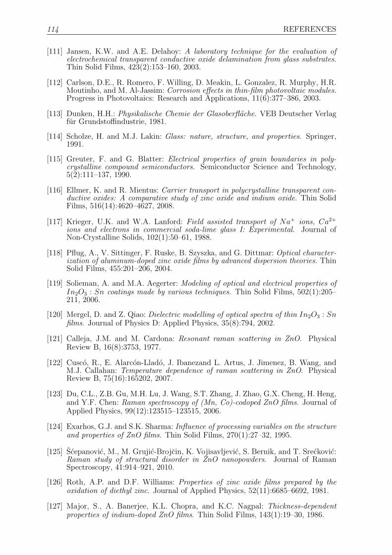
114 REFERENCES
[111] Jansen, K.W. and A.E. Delahoy: A laboratory technique for the evaluation ofelectrochemical transparent conductive oxide delamination from glass substrates.Thin Solid Films, 423(2):153–160, 2003.
[112] Carlson, D.E., R. Romero, F. Willing, D. Meakin, L. Gonzalez, R. Murphy, H.R.Moutinho, and M. Al-Jassim: Corrosion effects in thin-film photovoltaic modules.Progress in Photovoltaics: Research and Applications, 11(6):377–386, 2003.
[113] Dunken, H.H.: Physikalische Chemie der Glasoberflache. VEB Deutscher Verlagfur Grundstoffindustrie, 1981.
[114] Scholze, H. and M.J. Lakin: Glass: nature, structure, and properties. Springer,1991.
[115] Greuter, F. and G. Blatter: Electrical properties of grain boundaries in poly-crystalline compound semiconductors. Semiconductor Science and Technology,5(2):111–137, 1990.
[116] Ellmer, K. and R. Mientus: Carrier transport in polycrystalline transparent con-ductive oxides: A comparative study of zinc oxide and indium oxide. Thin SolidFilms, 516(14):4620–4627, 2008.
[117] Krieger, U.K. and W.A. Lanford: Field assisted transport of Na+ ions, Ca2+
ions and electrons in commercial soda-lime glass I: Experimental. Journal ofNon-Crystalline Solids, 102(1):50–61, 1988.
[118] Pflug, A., V. Sittinger, F. Ruske, B. Szyszka, and G. Dittmar: Optical character-ization of aluminum-doped zinc oxide films by advanced dispersion theories. ThinSolid Films, 455:201–206, 2004.
[119] Solieman, A. and M.A. Aegerter: Modeling of optical and electrical properties ofIn2O3 : Sn coatings made by various techniques. Thin Solid Films, 502(1):205–211, 2006.
[120] Mergel, D. and Z. Qiao: Dielectric modelling of optical spectra of thin In2O3 : Snfilms. Journal of Physics D: Applied Physics, 35(8):794, 2002.
[121] Calleja, J.M. and M. Cardona: Resonant raman scattering in ZnO. PhysicalReview B, 16(8):3753, 1977.
[122] Cusco, R., E. Alarcon-Llado, J. Ibanezand L. Artus, J. Jimenez, B. Wang, andM.J. Callahan: Temperature dependence of raman scattering in ZnO. PhysicalReview B, 75(16):165202, 2007.
[123] Du, C.L., Z.B. Gu, M.H. Lu, J. Wang, S.T. Zhang, J. Zhao, G.X. Cheng, H. Heng,and Y.F. Chen: Raman spectroscopy of (Mn, Co)-codoped ZnO films. Journal ofApplied Physics, 99(12):123515–123515, 2006.
[124] Exarhos, G.J. and S.K. Sharma: Influence of processing variables on the structureand properties of ZnO films. Thin Solid Films, 270(1):27–32, 1995.
[125] Scepanovic, M., M. Grujic-Brojcin, K. Vojisavljevic, S. Bernik, and T. Sreckovic:Raman study of structural disorder in ZnO nanopowders. Journal of RamanSpectroscopy, 41:914–921, 2010.
[126] Roth, A.P. and D.F. Williams: Properties of zinc oxide films prepared by theoxidation of diethyl zinc. Journal of Applied Physics, 52(11):6685–6692, 1981.
[127] Major, S., A. Banerjee, K.L. Chopra, and K.C. Nagpal: Thickness-dependentproperties of indium-doped ZnO films. Thin Solid Films, 143(1):19–30, 1986.
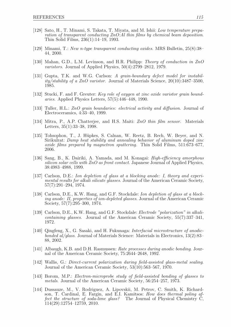
REFERENCES 115
[128] Sato, H., T. Minami, S. Takata, T. Miyata, and M. Ishii: Low temperature prepa-ration of transparent conducting ZnO:Al thin films by chemical beam deposition.Thin Solid Films, 236(1):14–19, 1993.
[129] Minami, T.: New n-type transparent conducting oxides. MRS Bulletin, 25(8):38–44, 2000.
[130] Mahan, G.D., L.M. Levinson, and H.R. Philipp: Theory of conduction in ZnOvaristors. Journal of Applied Physics, 50(4):2799–2812, 1979.
[131] Gupta, T.K. and W.G. Carlson: A grain-boundary defect model for instabil-ity/stability of a ZnO varistor. Journal of Materials Science, 20(10):3487–3500,1985.
[132] Stucki, F. and F. Greuter: Key role of oxygen at zinc oxide varistor grain bound-aries. Applied Physics Letters, 57(5):446–448, 1990.
[133] Tuller, H.L.: ZnO grain boundaries: electrical activity and diffusion. Journal ofElectroceramics, 4:33–40, 1999.
[134] Mitra, P., A.P. Chatterjee, and H.S. Maiti: ZnO thin film sensor. MaterialsLetters, 35(1):33–38, 1998.
[135] Tohsophon, T., J. Hupkes, S. Calnan, W. Reetz, B. Rech, W. Beyer, and N.Sirikulrat: Damp heat stability and annealing behavior of aluminum doped zincoxide films prepared by magnetron sputtering. Thin Solid Films, 511:673–677,2006.
[136] Sang, B., K. Dairiki, A. Yamada, and M. Konagai: High-efficiency amorphoussilicon solar cells with ZnO as front contact. Japanese Journal of Applied Physics,38:4983–4988, 1999.
[137] Carlson, D.E.: Ion depletion of glass at a blocking anode: I, theory and experi-mental results for alkali silicate glasses. Journal of the American Ceramic Society,57(7):291–294, 1974.
[138] Carlson, D.E., K.W. Hang, and G.F. Stockdale: Ion depletion of glass at a block-ing anode: II, properties of ion-depleted glasses. Journal of the American CeramicSociety, 57(7):295–300, 1974.
[139] Carlson, D.E., K.W. Hang, and G.F. Stockdale: Electrode ”polarization” in alkali-containing glasses. Journal of the American Ceramic Society, 55(7):337–341,1972.
[140] Qingfeng, X., G. Sasaki, and H. Fukunaga: Interfacial microstructure of anodic-bonded al/glass. Journal of Materials Science: Materials in Electronics, 13(2):83–88, 2002.
[141] Albaugh, K.B. and D.H. Rasmussen: Rate processes during anodic bonding. Jour-nal of the American Ceramic Society, 75:2644–2648, 1992.
[142] Wallis, G.: Direct-current polarization during field-assisted glass-metal sealing.Journal of the American Ceramic Society, 53(10):563–567, 1970.
[143] Borom, M.P.: Electron-microprobe study of field-assisted bonding of glasses tometals. Journal of the American Ceramic Society, 56:254–257, 1973.
[144] Dussauze, M., V. Rodriguez, A. Lipovskii, M. Petrov, C. Smith, K. Richard-son, T. Cardinal, E. Fargin, and E.I. Kamitsos: How does thermal poling af-fect the structure of soda-lime glass? The Journal of Physical Chemistry C,114(29):12754–12759, 2010.
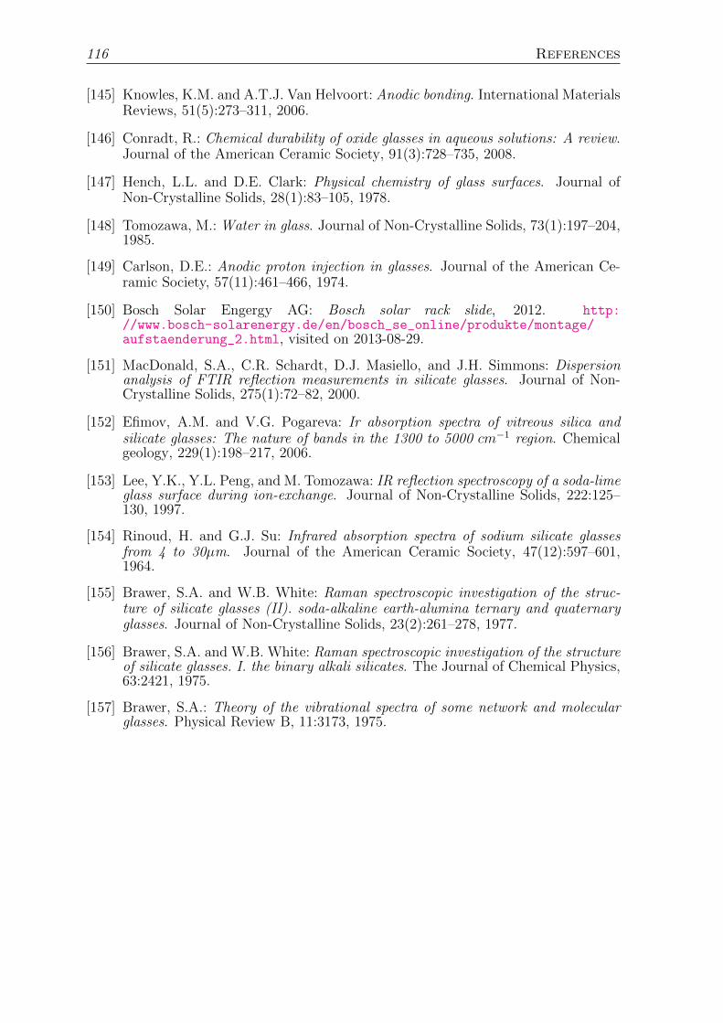
116 References
[145] Knowles, K.M. and A.T.J. Van Helvoort: Anodic bonding. International MaterialsReviews, 51(5):273–311, 2006.
[146] Conradt, R.: Chemical durability of oxide glasses in aqueous solutions: A review.Journal of the American Ceramic Society, 91(3):728–735, 2008.
[147] Hench, L.L. and D.E. Clark: Physical chemistry of glass surfaces. Journal ofNon-Crystalline Solids, 28(1):83–105, 1978.
[148] Tomozawa, M.: Water in glass. Journal of Non-Crystalline Solids, 73(1):197–204,1985.
[149] Carlson, D.E.: Anodic proton injection in glasses. Journal of the American Ce-ramic Society, 57(11):461–466, 1974.
[150] Bosch Solar Engergy AG: Bosch solar rack slide, 2012. http://www.bosch-solarenergy.de/en/bosch_se_online/produkte/montage/aufstaenderung_2.html, visited on 2013-08-29.
[151] MacDonald, S.A., C.R. Schardt, D.J. Masiello, and J.H. Simmons: Dispersionanalysis of FTIR reflection measurements in silicate glasses. Journal of Non-Crystalline Solids, 275(1):72–82, 2000.
[152] Efimov, A.M. and V.G. Pogareva: Ir absorption spectra of vitreous silica andsilicate glasses: The nature of bands in the 1300 to 5000 cm−1 region. Chemicalgeology, 229(1):198–217, 2006.
[153] Lee, Y.K., Y.L. Peng, and M. Tomozawa: IR reflection spectroscopy of a soda-limeglass surface during ion-exchange. Journal of Non-Crystalline Solids, 222:125–130, 1997.
[154] Rinoud, H. and G.J. Su: Infrared absorption spectra of sodium silicate glassesfrom 4 to 30µm. Journal of the American Ceramic Society, 47(12):597–601,1964.
[155] Brawer, S.A. and W.B. White: Raman spectroscopic investigation of the struc-ture of silicate glasses (II). soda-alkaline earth-alumina ternary and quaternaryglasses. Journal of Non-Crystalline Solids, 23(2):261–278, 1977.
[156] Brawer, S.A. and W.B. White: Raman spectroscopic investigation of the structureof silicate glasses. I. the binary alkali silicates. The Journal of Chemical Physics,63:2421, 1975.
[157] Brawer, S.A.: Theory of the vibrational spectra of some network and molecularglasses. Physical Review B, 11:3173, 1975.
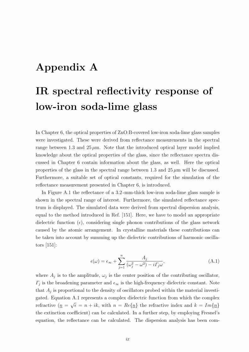
Appendix A
IR spectral reflectivity response of
low-iron soda-lime glass
In Chapter 6, the optical properties of ZnO:B-covered low-iron soda-lime glass samples
were investigated. These were derived from reflectance measurements in the spectral
range between 1.3 and 25µm. Note that the introduced optical layer model implied
knowledge about the optical properties of the glass, since the reflectance spectra dis-
cussed in Chapter 6 contain information about the glass, as well. Here the optical
properties of the glass in the spectral range between 1.3 and 25µm will be discussed.
Furthermore, a suitable set of optical constants, required for the simulation of the
reflectance measurement presented in Chapter 6, is introduced.
In Figure A.1 the reflectance of a 3.2 -mm-thick low-iron soda-lime glass sample is
shown in the spectral range of interest. Furthermore, the simulated reflectance spec-
trum is displayed. The simulated data were derived from spectral dispersion analysis,
equal to the method introduced in Ref. [151]. Here, we have to model an appropriate
dielectric function (ε), considering single phonon contributions of the glass network
caused by the atomic arrangement. In crystalline materials these contributions can
be taken into account by summing up the dielectric contributions of harmonic oscilla-
tors [151]:
ε(ω) = ε∞ +n∑j=1
Aj(ω2
j − ω2)− iΓjω, (A.1)
where Aj is to the amplitude, ωj is the center position of the contributing oscillator,
Γj is the broadening parameter and ε∞ is the high-frequency dielectric constant. Note
that Aj is proportional to the density of oscillators probed within the material investi-
gated. Equation A.1 represents a complex dielectric function from which the complex
refractive (n =√ε = n + ik, with n = Ren the refractive index and k = Imn
the extinction coefficient) can be calculated. In a further step, by employing Fresnel’s
equation, the reflectance can be calculated. The dispersion analysis has been com-
ix
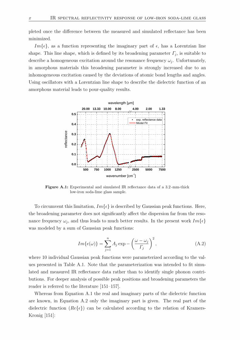
x IR spectral reflectivity response of low-iron soda-lime glass
pleted once the difference between the measured and simulated reflectance has been
minimized.
Imε, as a function representing the imaginary part of ε, has a Lorentzian line
shape. This line shape, which is defined by its broadening parameter Γj, is suitable to
describe a homogeneous excitation around the resonance frequency ωj. Unfortunately,
in amorphous materials this broadening parameter is strongly increased due to an
inhomogeneous excitation caused by the deviations of atomic bond lengths and angles.
Using oscillators with a Lorentzian line shape to describe the dielectric function of an
amorphous material leads to pour-quality results.
5 0 0 7 5 0 1 0 0 0 1 2 5 0 2 5 0 0 5 0 0 0 7 5 0 00 . 0
0 . 1
0 . 2
0 . 3
0 . 4
0 . 5
reflec
tance
2 0 . 0 0 1 3 . 3 3 1 0 . 0 0 8 . 0 0 4 . 0 0 2 . 0 0 1 . 3 3
Figure A.1: Experimental and simulated IR reflectance data of a 3.2 -mm-thicklow-iron soda-lime glass sample.
To circumvent this limitation, Imε is described by Gaussian peak functions. Here,
the broadening parameter does not significantly affect the dispersion far from the reso-
nance frequency ωj, and thus leads to much better results. In the present work Imεwas modeled by a sum of Gaussian peak functions:
Imε(ω) =n∑j=1
Aj exp−(ω − ωjΓj
)2
, (A.2)
where 10 individual Gaussian peak functions were parameterized according to the val-
ues presented in Table A.1. Note that the parameterization was intended to fit simu-
lated and measured IR reflectance data rather than to identify single phonon contri-
butions. For deeper analysis of possible peak positions and broadening parameters the
reader is referred to the literature [151–157].
Whereas from Equation A.1 the real and imaginary parts of the dielectric function
are known, in Equation A.2 only the imaginary part is given. The real part of the
dielectric function (Reε) can be calculated according to the relation of Kramers-
Kronig [151]:
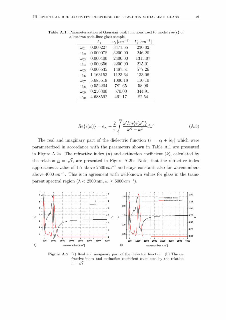
IR spectral reflectivity response of low-iron soda-lime glass xi
Table A.1: Parameterization of Gaussian peak functions used to model Imε ofa low-iron soda-lime glass sample.
Aj ωj [cm−1] Γj [cm−1]ω01 0.000227 3471.65 230.02ω02 0.000078 3200.00 246.20ω03 0.000400 2400.00 1313.07ω04 0.000356 2200.00 215.01ω05 0.006635 1487.51 577.26ω06 1.163153 1123.64 133.06ω07 5.685519 1006.18 110.10ω08 0.552204 781.65 58.96ω09 0.256300 570.00 344.91ω10 4.688592 461.17 82.54
Reε(ω) = ε∞ +2
π
∞∫0
ω′Imε(ω′)ω′2 − ω2
dω′ (A.3)
The real and imaginary part of the dielectric function (ε = ε1 + iε2) which were
parameterized in accordance with the parameters shown in Table A.1 are presented
in Figure A.2a. The refractive index (n) and extinction coefficient (k), calculated by
the relation n =√ε, are presented in Figure A.2b. Note, that the refractive index
approaches a value of 1.5 above 2500 cm−1 and stays constant, also for wavenumbers
above 4000 cm−1. This is in agreement with well-known values for glass in the trans-
parent spectral region (λ < 2500 nm, ω ≥ 5000 cm−1).
5 0 0 1 0 0 0 1 5 0 0 2 0 0 0 2 5 0 0 3 0 0 0 3 5 0 0 4 0 0 0
0
1
2
3
4
5
6
ε 1
w a v e n u m b e r [ c m - 1 ]
ε1
0
1
2
3
4
5
6
ε2
ε 2
a )5 0 0 1 0 0 0 1 5 0 0 2 0 0 0 2 5 0 0 3 0 0 0 3 5 0 0 4 0 0 0
0 . 5
1 . 0
1 . 5
2 . 0
2 . 5
n
w a v e n u m b e r [ c m - 1 ]
r e f r a c t i v e i n d e x
0 . 0 0
0 . 2 5
0 . 5 0
0 . 7 5
1 . 0 0
1 . 2 5
1 . 5 0 e x t i n c t i o n c o e f f i c i e n t
k
b )
Figure A.2: (a) Real and imaginary part of the dielectric function. (b) The re-fractive index and extinction coefficient calculated by the relationn =√ε.

xii IR spectral reflectivity response of low-iron soda-lime glass
Publications
• D. Messerschmidt, S. Nicolay, L. Ding, G. Bugnon, F. Meillaud, J. Eberhardt
and C. Ballif
”Ethanol-enriched low-pressure chemical vapor deposition ZnO bilayers: Proper-
ties and growth - A potential electrode for thin film solar cells“
Journal of Applied Physics 2(113), 024908–024908 (2013).
• D. Messerschmidt, A. Hochmuth, E. Radlein, H. Romanus, W.-H. Gnehr, J. Eber-
hardt and C. Ballif
”Anodic degradation of ZnO on soda-lime glass“
Solar Energy Materials and Solar Cells (117), 569–576 (2013).
• D. Messerschmidt, K. Bratz, W.-M. Gnehr, H. Romanus, J. Eberhardt, S. Nico-
lay and C. Ballif
”Optical properties of anodically degraded ZnO“
Journal of Applied Physics 9(115), 094902 (2014).
• L. Ding, L. Fanni, D. Messerschmidt, S. Zabihzadeh and M. Masis Morales,
S. Nicolay and C. Ballif
”Tailoring the surface morphology of zinc oxide films for high-performance mi-
cromorph solar cells“
Solar Energy Materials and Solar Cells (128), 378–385 (2014).
xiii

xiv Publications
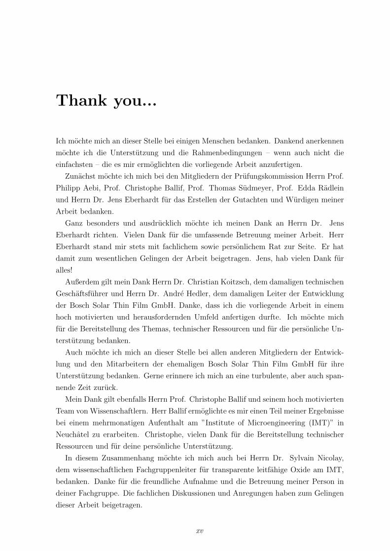
Thank you...
Ich mochte mich an dieser Stelle bei einigen Menschen bedanken. Dankend anerkennen
mochte ich die Unterstutzung und die Rahmenbedingungen – wenn auch nicht die
einfachsten – die es mir ermoglichten die vorliegende Arbeit anzufertigen.
Zunachst mochte ich mich bei den Mitgliedern der Prufungskommission Herrn Prof.
Philipp Aebi, Prof. Christophe Ballif, Prof. Thomas Sudmeyer, Prof. Edda Radlein
und Herrn Dr. Jens Eberhardt fur das Erstellen der Gutachten und Wurdigen meiner
Arbeit bedanken.
Ganz besonders und ausdrucklich mochte ich meinen Dank an Herrn Dr. Jens
Eberhardt richten. Vielen Dank fur die umfassende Betreuung meiner Arbeit. Herr
Eberhardt stand mir stets mit fachlichem sowie personlichem Rat zur Seite. Er hat
damit zum wesentlichen Gelingen der Arbeit beigetragen. Jens, hab vielen Dank fur
alles!
Außerdem gilt mein Dank Herrn Dr. Christian Koitzsch, dem damaligen technischen
Geschaftsfuhrer und Herrn Dr. Andre Hedler, dem damaligen Leiter der Entwicklung
der Bosch Solar Thin Film GmbH. Danke, dass ich die vorliegende Arbeit in einem
hoch motivierten und herausfordernden Umfeld anfertigen durfte. Ich mochte mich
fur die Bereitstellung des Themas, technischer Ressourcen und fur die personliche Un-
terstutzung bedanken.
Auch mochte ich mich an dieser Stelle bei allen anderen Mitgliedern der Entwick-
lung und den Mitarbeitern der ehemaligen Bosch Solar Thin Film GmbH fur ihre
Unterstutzung bedanken. Gerne erinnere ich mich an eine turbulente, aber auch span-
nende Zeit zuruck.
Mein Dank gilt ebenfalls Herrn Prof. Christophe Ballif und seinem hoch motivierten
Team von Wissenschaftlern. Herr Ballif ermoglichte es mir einen Teil meiner Ergebnisse
bei einem mehrmonatigen Aufenthalt am ”Institute of Microengineering (IMT)” in
Neuchatel zu erarbeiten. Christophe, vielen Dank fur die Bereitstellung technischer
Ressourcen und fur deine personliche Unterstutzung.
In diesem Zusammenhang mochte ich mich auch bei Herrn Dr. Sylvain Nicolay,
dem wissenschaftlichen Fachgruppenleiter fur transparente leitfahige Oxide am IMT,
bedanken. Danke fur die freundliche Aufnahme und die Betreuung meiner Person in
deiner Fachgruppe. Die fachlichen Diskussionen und Anregungen haben zum Gelingen
dieser Arbeit beigetragen.
xv
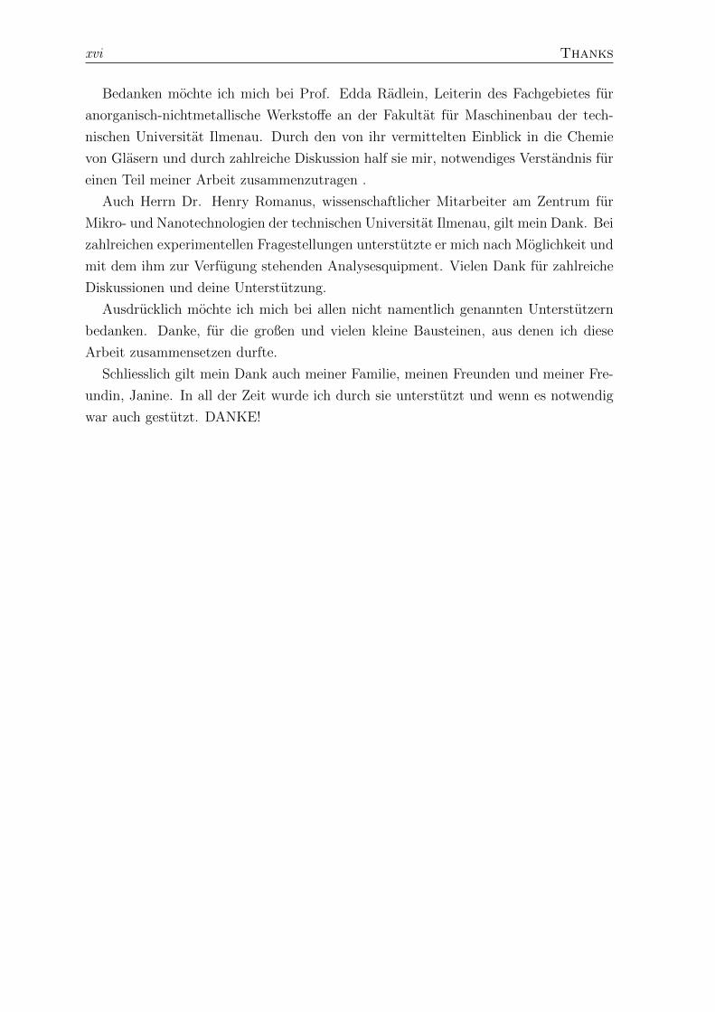
xvi Thanks
Bedanken mochte ich mich bei Prof. Edda Radlein, Leiterin des Fachgebietes fur
anorganisch-nichtmetallische Werkstoffe an der Fakultat fur Maschinenbau der tech-
nischen Universitat Ilmenau. Durch den von ihr vermittelten Einblick in die Chemie
von Glasern und durch zahlreiche Diskussion half sie mir, notwendiges Verstandnis fur
einen Teil meiner Arbeit zusammenzutragen .
Auch Herrn Dr. Henry Romanus, wissenschaftlicher Mitarbeiter am Zentrum fur
Mikro- und Nanotechnologien der technischen Universitat Ilmenau, gilt mein Dank. Bei
zahlreichen experimentellen Fragestellungen unterstutzte er mich nach Moglichkeit und
mit dem ihm zur Verfugung stehenden Analysesquipment. Vielen Dank fur zahlreiche
Diskussionen und deine Unterstutzung.
Ausdrucklich mochte ich mich bei allen nicht namentlich genannten Unterstutzern
bedanken. Danke, fur die großen und vielen kleine Bausteinen, aus denen ich diese
Arbeit zusammensetzen durfte.
Schliesslich gilt mein Dank auch meiner Familie, meinen Freunden und meiner Fre-
undin, Janine. In all der Zeit wurde ich durch sie unterstutzt und wenn es notwendig
war auch gestutzt. DANKE!
Curriculum Vitae
Personal informationLast name MesserschmidtFirst name DanielDate pof birth 7th February 1983Location of birth Meiningen, GermanyNationality GermanMarital Status Single
Education1989–1995 Elementary school:
”Rosa Luxemburg“,
Walldorf1995–2002 Secondary school
”Henfling Gymnasium“,
Meiningen
Military duty2002–2003
”General Olbricht Kaserne“,
Leipzig
Studies2003–2009 Studies of technical physics at the
technical University of Ilmenau2008–2009 Diploma thesis
”Untersuchungen zur Stabilitat mikromorpher
Siliziumdunnschicht-Solarzellen“since 2010 Doctorate at the
University of Neuchatel
Professional activity2009–2013 Development Engineer
Bosch Solar Thim Film GmbH, Erfurtsince 2014 Development Engineer
Robert Bosch GmbH, Reutlingen
Reutlingen, den August 31, 2014Daniel Messerschmidt
xvii
Copyright © 2022 FDOKUMEN